1
STARLINE® SG 2000 Telecommunications Optical Node Installation and Operation Manual 4 2 6 IN 7 Caution These servicing instructions are for use by qualified personnel only. To reduce the risk of electrical shock, do not perform any servicing other than that contained in the Installation and Troubleshooting Instructions unless you are qualified to do so. Refer all servicing to qualified service personnel. Special Symbols that Might Appear on the Equipment This is a class 1 product that contains a class IIIb laser and is intended for operation in a closed environment with fiber attached. Do not look into the optical connector of the transmitter with power applied. Laser output is invisible, and eye damage result. Do not defeat safety features that prevent looking into optical connector. This product contains a class IIIb laser and is intended for operation in a closed environment with fiber attached. Do not look into the optical connector of the transmitter with power applied. Laser output is invisible, and eye damage can result. Do not defeat safety features that prevent looking into optical connector. This symbol indicates that dangerous voltage levels are present within the equipment. These voltages are not insulated and may be of sufficient strength to cause serious bodily injury when touched. The symbol may also appear on schematics. The exclamation point, within an equilateral triangle, is intended to alert the user to the presence of important installation, servicing, and operating instructions in the documents accompanying the equipment. For continued protection against fire, replace all fuses only with fuses having the same electrical ratings marked at the location of the fuse. Copyright © 2001 by Motorola Inc. All rights reserved. No part of this publication may be reproduced in any form or by any means or used to make any derivative work (such as translation, transformation or adaptation) without written permission from Motorola, Inc. Motorola, Inc. reserves the right to revise this publication and to make changes in content from time to time without obligation on the part Motorola, Inc. to provide notification of such revision or change. Motorola Inc. provides this guide without warranty of any kind, either implied or expressed, including, but not limited, to the implied warranties of merchantability and fitness for a particular purpose. Motorola, Inc. may make improvements or changes in the product(s) described in this manual at any time. ________________________________________________________________________________________________________________________________ MOTOROLA, the stylized M logo, and STARLINE are registered trademarks, and LIFELINE is a trademark of Motorola, Inc. All other product or service names are the property of their respective owners. Contents Section 1 Introduction Using this Manual ..........................................................................................................................................1-3 Related Documentation ..................................................................................................................................1-3 Document Conventions ..................................................................................................................................1-4 If You Need Help ...........................................................................................................................................1-4 Calling for Repairs.........................................................................................................................................1-5 Section 2 Overview Housing ........................................................................................................................................................2-1 Mounting Holes ......................................................................................................................................2-1 Port Locations ........................................................................................................................................2-2 Gaskets .................................................................................................................................................2-3 Power Supply ................................................................................................................................................2-4 Network Monitoring ........................................................................................................................................2-5 Configuration ................................................................................................................................................2-5 Forward Path.................................................................................................................................................2-7 SG2-LR Receiver ...................................................................................................................................2-9 Analog Return Path .....................................................................................................................................2-10 Analog Return Transmitters .................................................................................................................. 2-10 Digital Return Path ......................................................................................................................................2-12 DS-SG2-DRT/A .................................................................................................................................... 2-12 DS-SG2-DRT-2X/A ............................................................................................................................... 2-13 Level Control...............................................................................................................................................2-14 Options and Accessories..............................................................................................................................2-14 Gain Selection...................................................................................................................................... 2-16 Tilt Selection ........................................................................................................................................ 2-18 Section 3 Bench Setup Powering the Node ........................................................................................................................................3-3 Power Supply Settings ...................................................................................................................................3-5 Single Power Supply or Commonly Powered Redundant Supplies .............................................................3-7 Individually Powered Supplies .................................................................................................................3-7 SG 2000 Installation and Operation Manual ii Contents Quick Checks - Functional Testing .................................................................................................................3-8 Forward Path ......................................................................................................................................... 3-8 Manual Gain Control .......................................................................................................................3-9 Thermal Control, Model TCU ...........................................................................................................3-9 Automatic Level Control, Model ADU................................................................................................3-9 Analog Return Path .............................................................................................................................. 3-10 Digital Return Path ............................................................................................................................... 3-10 Forward Path Padding ................................................................................................................................. 3-11 Launch Amplifier Output Stage Padding........................................................................................................ 3-14 Link Performance ........................................................................................................................................ 3-15 Installing the DS-SG2-DRRB Board Option ................................................................................................... 3-18 Installing the Status Monitor Option.............................................................................................................. 3-22 SG 2000 Activation Worksheet ..................................................................................................................... 3-23 Section 4 Installation Splicing Fiber ................................................................................................................................................4-1 Strand Wire Mounting ....................................................................................................................................4-3 Coaxial Cables ..............................................................................................................................................4-5 Fiber Cables .................................................................................................................................................4-5 Section 5 Operation Forward Path RF Configuration ......................................................................................................................5-1 Single Receiver Mode............................................................................................................................. 5-1 Redundant Receiver Mode ...................................................................................................................... 5-2 Broadband/Narrowcast Mode .................................................................................................................. 5-2 AB Override Functionality ....................................................................................................................... 5-3 B Override ......................................................................................................................................5-3 A Override ......................................................................................................................................5-4 Status Monitor/Manual Control Operation .........................................................................................5-4 Analog Return Path RF Configuration .............................................................................................................5-5 Digital Return Path RF Configuration ..............................................................................................................5-7 SG 2000 Optical Modules ..............................................................................................................................5-9 Installing SG 2000 Optical Modules ......................................................................................................... 5-9 Removing SG 2000 Optical Modules ....................................................................................................... 5-9 Cleaning the Optical Connector............................................................................................................. 5-10 SG2-LR Optical Receiver ............................................................................................................................. 5-10 Wavelength Selection Jumper ...................................................................................................................... 5-13 SG2-IFPT Optical Transmitter ...................................................................................................................... 5-14 SG2-FPT Optical Transmitter ....................................................................................................................... 5-15 SG2-DFBT Optical Transmitter ..................................................................................................................... 5-16 SG 2000 Installation and Operation Manual Contents iii SG2-DFBT/3 Optical Transmitter ..................................................................................................................5-18 SG2-EIFPT Optical Transmitter ....................................................................................................................5-19 DS-SG2-DRT/A Digital Return Transmitter ....................................................................................................5-20 DS-SG2-DRT-2X/A Digital Return Transmitter ...............................................................................................5-22 SG2-PS Power Supply .......................................................................................................................... 5-25 Status Monitoring ........................................................................................................................................5-26 Manual Control Board ..................................................................................................................................5-27 Ingress Control............................................................................................................................................5-29 Appendix A Specifications Appendix B Torque Specifications Abbreviations and Acronyms Figures Figure 1-1 SG 2000 — closed ............................................................................................ 1-1 Figure 1-2 SG 2000 — open .............................................................................................. 1-2 Figure 2-1 SG 2000 housing dimensions - front and side view ............................................. 2-1 Figure 2-2 Port locations ................................................................................................... 2-2 Figure 2-3 Housing gaskets ............................................................................................... 2-3 Figure 2-4 SG2-PS2 power supply ..................................................................................... 2-4 Figure 2-5 Configuration notation....................................................................................... 2-6 Figure 2-6 Signal flow diagram .......................................................................................... 2-7 Figure 2-7 SG2-LR receiver functional diagram .................................................................. 2-9 Figure 2-8 SG2 transmitter block diagram ........................................................................ 2-11 Figure 2-9 Optical input versus 750 MHz gain................................................................... 2-16 Figure 2-10 Optical input versus 870 MHz gain ................................................................. 2-17 Figure 2-11 Relative level dB versus 750 MHz slope 77 channels...................................... 2-18 Figure 2-12 Relative level dB versus 870 MHz slope 94 channels...................................... 2-19 Figure 2-13 Relative level dB versus 870 MHz slope 110 channels .................................... 2-20 Figure 3-1 SG 2000 lid showing major components............................................................. 3-1 Figure 3-2 SG 2000 RF chassis ......................................................................................... 3-2 Figure 3-3 Fuse configuration ............................................................................................ 3-3 Figure 3-4 Fuse locations .................................................................................................. 3-5 Figure 3-5 SG2-PS2 power supply ..................................................................................... 3-6 SG 2000 Installation and Operation Manual iv Contents Figure 3-6 JP1 common-powered single or redundant power configuration .......................... 3-7 Figure 3-7 JP1 split-powered redundant power supply configuration ................................... 3-7 Figure 3-8 SG2-75 low-gain output-stage pad-effects chart .............................................. 3-14 Figure 3-9 SG2-87 low-gain output-stage pad-effects chart .............................................. 3-15 Figure 3-10 SG2-* link c/n performance, 77 channels ....................................................... 3-16 Figure 3-11 SG2-* link c/n performance, 110 channels ..................................................... 3-17 Figure 3-12 DS-SG2-DRRB board ................................................................................... 3-18 Figure 3-13 DS-SG2-DRRB board installed ...................................................................... 3-19 Figure 3-14 Location of JXPs on E-pack .......................................................................... 3-20 Figure 3-15 SG2 lid configured with the DS-SG2-DRRB board .......................................... 3-21 Figure 4-1 Service cable connection and compression fitting .............................................. 4-1 Figure 4-2 Mounting bracket-front view .............................................................................. 4-3 Figure 4-3 Mounting bracket-rear and side views ............................................................... 4-4 Figure 4-4 Center conductor length ................................................................................... 4-5 Figure 4-5 Housing lid and fiber spool tray......................................................................... 4-6 Figure 4-6 Fiber spool tray ................................................................................................ 4-6 Figure 5-1 Single receiver ................................................................................................. 5-1 Figure 5-2 Redundant receiver .......................................................................................... 5-2 Figure 5-3 Broadband/narrowcast...................................................................................... 5-2 Figure 5-4 B override ........................................................................................................ 5-3 Figure 5-5 A override ........................................................................................................ 5-4 Figure 5-6 Status monitor/MCB operation .......................................................................... 5-4 Figure 5-7 Redundant return ............................................................................................. 5-5 Figure 5-8 Split return....................................................................................................... 5-5 Figure 5-9 RF chassis and location of the SG2-RPM/C or SG2-RPM/S board ...................... 5-6 Figure 5-10 DS-SG2-DRT/A redundant return .................................................................... 5-7 Figure 5-11 DS-SG2-DRT-2X/A split return ........................................................................ 5-8 Figure 5-12 DS-SG2-DRT-2X/A redundant return ............................................................... 5-8 Figure 5-13 SG2-LR ....................................................................................................... 5-10 Figure 5-14 Test-point voltage versus optical power ......................................................... 5-12 Figure 5-15 Wavelength selection jumper ........................................................................ 5-13 Figure 5-16 SG2-IFPT .................................................................................................... 5-14 Figure 5-17 SG2-FPT ..................................................................................................... 5-15 Figure 5-18 SG2-DFBT ................................................................................................... 5-16 Figure 5-19 SG2-DFBT/3 ................................................................................................ 5-18 Figure 5-20 SG2-EIFPT .................................................................................................. 5-19 Figure 5-21 DS-SG2-DRT/A ............................................................................................ 5-20 Figure 5-22 DS-SG2-DRT/A ............................................................................................ 5-20 SG 2000 Installation and Operation Manual Contents v Figure 5-23 DS-SG2-DRT-2X/A........................................................................................ 5-22 Figure 5-24 DS-SG2-DRT-2X/A........................................................................................ 5-22 Figure 5-25 DS-SG2-DRT-2X/A cable connector ............................................................... 5-24 Figure 5-26 DS-SG2-DRT-2X/A installed in SG 2000 ........................................................ 5-24 Figure 5-27 DS-SG2-DRT-2X/A second RF input cable connection .................................... 5-25 Figure 5-28 SG2-PS power supply ................................................................................... 5-25 Figure 5-29 MCB board ................................................................................................... 5-28 Tables Table 2-1 Analog return transmitters ................................................................................ 2-10 Table 2-2 Digital return transmitters ................................................................................. 2-12 Table 2-3 Options and accessories .................................................................................. 2-14 Table 3-1 AC fuses ........................................................................................................... 3-4 Table 3-2 SG 2000 pad chart-standard gain ..................................................................... 3-12 Table 3-3 SG 2000 pad chart-high gain ............................................................................ 3-13 Table 3-4 Common problems ........................................................................................... 3-22 Table 5-1 SG2-LR features .............................................................................................. 5-11 Table 5-2 SG2-LR minimum output levels......................................................................... 5-11 Table 5-3 SG2-IFPT features ........................................................................................... 5-14 Table 5-4 SG2-FPT features ............................................................................................ 5-15 Table 5-5 SG2-DFBT features.......................................................................................... 5-16 Table 5-6 SG2-DFBT/3 features ....................................................................................... 5-18 Table 5-7 SG2-EIFPT features ......................................................................................... 5-19 Table 5-8 DS-SG2-DRT/A features................................................................................... 5-21 Table 5-9 DS-SG2-DRT-2X/A features ............................................................................. 5-23 Table 5-10 Reporting and control provisions..................................................................... 5-26 Table 5-11 MCB user-interface settings............................................................................ 5-27 Table A-1 SG 2000 optical characteristics ......................................................................... A-1 Table A-2 Station RF characteristics ................................................................................. A-1 Table A-3 SG 2000 General characteristics ....................................................................... A-2 Table A-4 SG2-LR specifications ...................................................................................... A-2 Table A-5 SG2-IFPT RF specifications .............................................................................. A-3 Table A-6 SG2-FPT RF specifications ............................................................................... A-3 Table A-7 SG2-DFBT RF specifications............................................................................. A-4 Table A-8 SG2-DFBT/3 RF specifications .......................................................................... A-4 Table A-9 SG2-EIFPT RF specifications ............................................................................ A-5 Table A-10 SG2-DRT/A RF specifications ......................................................................... A-5 Table A-11 SG2-DRT-2X/A RF specifications .................................................................... A-6 Table A-12 Optical output power vs. wavelength for DS-SG2-DRT*/A transmitters .............. A-6 SG 2000 Installation and Operation Manual vi Contents Table A-13 Current requirements ...................................................................................... A-7 Table A-14 SG2-75 performance, with 77 channels ............................................................ A-8 Table A-15 SG2-87 performance, with 94 channels ............................................................ A-8 Table A-16 SG2-87 performance, with 110 channels .......................................................... A-8 SG 2000 Installation and Operation Manual Se ction 1 Introduction Motorola’s SG 2000 telecommunications optical node performs light wave-to-RF and RF-to-light wave signal conversions in an optical transmission link. This product is designed to support a wide variety of advanced hybrid-fiber/coaxial network topologies. As broadband communication systems continue to evolve, the demand increases for optical links that carry the signal further into the transport system. These systems require additional features and functionality such as digital compression and alternate access at significantly lower costs. Fully configured, the SG 2000 supports these next-generation telecommunication networks. It also supports a variety of single and two-way broadband network applications such as broadcast video, interactive video, telephony, and data. Figure 1-1 illustrates a closed SG 2000 telecommunications optical node: F i g u r e 1- 1 SG 2 0 00 — clo s ed 6 2 4 7 8 3 1 5 SG 2000 Installation and Operation Manual 1-2 Introduction Figure 1-2 illustrates an open SG 2000 telecommunications optical node: F i g u r e 1- 2 SG 2 0 00 — o p en -20dB -20dB JXP 1 FWD EQ H FWD EQ H PORT 1 PORT 2 L L ON JXP 2 TCU ADU -20dB +24 V DC MDR JX P A DU ON -20dB JXP 1 FTEC OFF VARILO SSER MAN SG2- IS IS JXP 2 IS REFER TO MANUAL FOR FUSE VALUES IS STATUS MONITOR JXP 3 JXP 4 ADU CAUTION: CONTAINS PARTS ANDASSEMBLIES SUSCEPTIBLE TO DAMAGE BY ELECTROSTATIC DISCHARGE ( ESD) FRB ADU RPM/* JXP 3 -20dB RCVR INPUT L PORT 3 H SG 2000 -20dB JXP 4 Optical Node L PORT 4 H FWD EQ FWD EQ -20dB -20dB ASSEMBLED IN MEXICO Base Lid Features include: ! 52 through 870 MHz forward passband, 5 through 40 MHz return standard (other splits are available, see Appendix A, “Specifications”) ! Optical receivers - up to three ! Optical transmitters - up to two ! Four independent RF outputs ! Ingress switching capability through manual or headend control ! Redundant powering capability ! 15 A power passing SG 2000 Installation and Operation Manual Introduction ! Optional LIFELINE™ status monitoring ! User-friendly fiber management ! 60/90 volt powering ! Digital return redundancy capability ! Modular plug-in diplex filters and equalizers ! Custom configuration for unique system requirements 1-3 Using this Manual The following sections provide information and instructions to install, configure, and operate the SG 2000: Section 1 Introduction provides a brief description of the product, identifies the information contained in this manual, and gives the help line telephone number and repair return information. Section 2 Overview describes the SG 2000 node and includes details regarding your options and their functions. Section 3 Bench Setup provides full configuration, set-up of options, and bench testing procedures that are recommended before installation. Section 4 Installation provides instructions for installing the SG 2000 in a distribution system. Section 5 Operation provides information governing the use of various options and applications required by your system. Appendix A Specifications provides technical specifications for the SG 2000 node and major options. Appendix B Torque Specifications provides the appropriate torque specifications for the screws, clamps, connectors, and bolts used in the SG 2000. Abbreviations The Abbreviations and Acronyms list contains the full spelling of the short forms and Acronyms used in this manual. Related Documentation Although these documents provide information that may be of interest to you, they are not required to install or operate the SG 2000. # LL-CU LIFELINE Control Unit Installation and Operation Manual # LIFELINE for Windows Site Preparation Guide # LIFELINE for Windows Software Operations Manual # Return Path Level Selection, Setup, and Alignment Procedure Reference Guide SG 2000 Installation and Operation Manual 1-4 Introduction Document Conventions Before you begin to use the SG 2000, familiarize yourself with the stylistic conventions used in this manual: Bold type Indicates text that you must type exactly as it appears or indicates a default value SMALL CAPS Denotes silk screening on the equipment, typically representing front and rearpanel controls, I/O connections and indicators (LEDs). * (Asterisk) Indicates that there are several versions of the same model number and the information applies to all models. When the information applies to a specific model, the complete model number is given. Italic type Denotes a displayed variable, a variable that you must type, or is used for emphasis If You Need Help If you need assistance while working with the SG 2000, contact the Motorola Technical Response Center (TRC): # Inside the U.S.: 1-888-944-HELP (1-888-944-4357) # Outside the U.S.: 215-323-0044 # Online: http://www.motorola.com/broadband, click HTML/Modem Version, click Customer Support, then click Web Support. The TRC is open from 8:00 a.m. to 7:00 p.m. Eastern Time, Monday through Friday and 10 AM to 6 PM Eastern Time, Saturday. When the TRC is closed, emergency service only is available on a call-back basis. Web Support offers a searchable solutions database, technical documentation, and low priority issue creation/tracking 24 hours per day, 7 days per week. SG 2000 Installation and Operation Manual Introduction 1-5 Calling for Repairs If repair is necessary, call the Motorola Repair Facility at 1-800-642-0442 for a Return for Service Authorization (RSA) number before sending the unit. The RSA number must be prominently displayed on all equipment cartons. The Repair Facility is open from 7 AM to 4 PM Pacific Time, Monday through Friday. When calling from outside the United States, use the appropriate international access code and then call 526-314-1000, extension 3194, to contact the Repair Facility. When shipping equipment for repair, follow these steps: 1 Pack the unit securely. 2 Enclose a note describing the exact problem. 3 Enclose a copy of the invoice that verifies the warranty status. 4 Ship the unit PREPAID to the following address: Motorola BCS c/o Exel Attn: RSA #___________ 6908 East Century Park Dr. Tucson, AZ 85706 SG 2000 Installation and Operation Manual Se ction 2 Overview Designed to be flexible, you can configure the SG 2000 with up to three optical receivers, four independent high-level RF outputs, and two return-path optical transmitters. Multiple receiver and transmitter combinations are available to satisfy split-band or redundancy requirements. The forward passband is extended to 870 MHz to increase channel capacity and support advanced interactive services and global applications. Housing The aluminum housing protects the electronics from weather damage and dissipates internally generated heat. Figure 2-1 illustrates the housing dimensions of the SG 2000 optical node: F i g u r e 2- 1 SG 2 0 00 ho us ing di m en sio ns - f ro n t an d s ide v i ew 2 4 OUT 6 12.25 8 3 4 7 3 1 21.60 5 10.99 For strand mounting, the optional bracket must be used. If the node is configured for strand mounting, the bracket is installed on the node at the factory. The bracket provides two clamps, located 16-7/8 inches apart, that secure the strand with 5/16 × 20 stainless steel bolts. Coaxial cable connections to the housing are made using conventional 5/8 inch × 24 threads per inch, stinger-type connectors. Mounting Holes Two threaded holes are located on the horizontal centerline on the back of the housing. These 5/16 × 18 × ¾ holes are separated by 11 inches center-to-center and can be used for pedestal or surface mounting. SG 2000 Installation and Operation Manual 2-2 Overview Port Locations The five housing ports, shown in Figure 2-2, provide connection for coaxial cables. Note that the housing ports are not labeled the same as the ports on the RF chassis. Side-by-side connector fittings are limited to .750 inches at ports 1 and 2 and/or ports 3 and 4. These ports are protected by factory inserted threaded plugs or plastic cap plugs which are discarded when the cable connectors are installed. Port 2 is used only for connection to an external 60 Vac or 90 Vac power supply. Port 4 is unused. Figure 2-2 illustrates a front and end view of the housing and port locations: F i g u r e 2- 2 Po rt lo c atio n s 6 2 4 7 8 SG 2000 Installation and Operation Manual OUT Lid 5 Port 2 4 1 Port 3 2 AC port IN Port 1 1 Unused 3 3 Port 4 Overview 2-3 Gaskets Each housing is equipped with a woven-wire gasket and a silicone-rubber weather gasket between the housing base and lid as shown in Figure 2-3: F i g u r e 2- 3 Hou sin g g a sk et s Weather gasket (silicone rubber) -20dB -20dB JXP 1 FWD EQ FWD EQ H H PORT 1 PORT 2 L L ON JXP 2 TCU ADU -20dB +24 V DC MDR JX P A DU ON -20dB JXP 1 FTEC OFF VARILO SSER MAN SG2- IS IS JXP 2 IS REFER TO MANUAL FOR FUSE VALUES IS STATUS MONITOR JXP 3 JXP 4 ADU CAUTION: CONTAINS PARTS ANDASSEMBLIES SUSCEPTIBLE TO DAMAGE BY ELECTROSTATIC DISCHARGE ( ESD) FRB ADU RPM/* JXP 3 -20dB RCVR INPUT L PORT 3 H SG 2000 -20dB JXP 4 Optical Node L PORT 4 H FWD EQ FWD EQ -20dB -20dB ASSEMBLED IN MEXICO RF gasket (woven wire) The gaskets provide efficient ground continuity, RF shielding and weather protection. Both gaskets must be in place and in good condition to ensure proper operation and protection of the node. The silicone rubber gasket should be lightly covered with silicone grease each time the node is opened. Replace the gasket if it is damaged or deformed. SG 2000 Installation and Operation Manual 2-4 Overview Power Supply The SG 2000 power supply (SG2-PS2) is located in the housing lid to optimize heat transfer and to balance the thermal load between the base and the lid. For high reliability or redundancy applications, two power supplies can be used. An umbilical cord connects the SG2-PS2 to the lid motherboard (LIDB). A flexible power-distribution design enables you to power the node from any of the four RF ports. Using fuses and shunts you can configure the node to distribute power to the remaining active ports. You can also power the node locally through the ac only port (port 2) while a second cable-plant power supply loops through the other two main RF ports. The power supply includes a heavy-duty, gas discharge tube surge protector located on the amplifier module. You can replace this surge protector with the optional FTEC surge protector. The FTEC triggers at approximately 230 V and presents a short circuit to the line during periods of over voltage. After the ac input voltage returns to normal, the FTEC returns to its open-circuit state. This provides the node with a level of protection against surge currents on the ac line. The same protector is used for both supplies unless the split ac-feed option is implemented; then, the secondary or redundant power supply is protected by a conventional heavy-duty gas discharge tube. The 20-ampere fuses are installed at the factory to provide power passing to additional amplifiers. Section 3, “Bench Setup,” discusses fusing options that are also diagrammed in Figure 3-1. Figure 3-2 illustrates the location of the fuses. The SG 2000 optical node can be powered from either 60 Vac or 90 Vac system power supplies. The unit is shipped from the factory set for 60 Vac powering. For systems equipped with 90 Vac powering, the suitcase jumper on the dc power supply can be repositioned to optimize the supply start-up voltage for the higher input range. Section 3, “Bench Setup” provides a description of this procedure. Figure 2-4 illustrates the SG2-PS2 power supply: F i g u r e 2- 4 SG 2- P S2 p o w e r su p p l y SG2-PS2 NO USER SERVICEABLE PARTS INSIDE ASSEMBLED IN MEXICO CAUTION 24V VOLTAGE S IN EXCESS OF 300 VOLTS A R E PR ESENT U ND ER COVE R A ND M AY B E PR ESENT A FTER POW ER IS R EMOVED SEE INSTALLATION MANUAL FOR SERVICE 5V ADJ LO HI TEST POINT TEST POINT The optional SG2-PS power supply is required to support DS-SG2-DRT-2X/A transmitters in a redundant configuration. The SG2-PS2 and SG2-PS power supplies are interchangeable. SG 2000 Installation and Operation Manual Overview 2-5 Network Monitoring The optional LIFELINE Status Monitoring System (LL-SG2) enables you to monitor the SG 2000 from a headend or a remote location. The transponder consists of a plug-in module mounted on the main RF board. If you do not employ status monitoring and use redundant receivers and/or transmitters, a manual control board (MCB) occupies the same position on the main RF board. The entire LIFELINE system includes: LL-CU control units Are connected to the system at the headend and interrogate each SG 2000 field transponder with FM outbound and inbound transmissions. A variety of outbound and inbound frequencies can be selected depending on the configuration of the system. The control unit reports this information to the status monitor computer. Status Monitor Computer and Software Includes an IBM-compatible computer that is connected to the control unit (CU) through an RS-232 link. LIFELINE software enables the operator to view measurements taken by the transponders. LL-SG2-* Field Installed Transponders Installed in individual field components, this unit interfaces with the CU at the headend. It reports such parameters as: forward amplifier dc current draw, ac and dc voltage, temperature, automatic drive unit (ADU-*) drive voltage, management and control of RF ingress switching, and tamper status. Configuration To accommodate unique system criteria, the SG 2000 is shipped as a configured product. Hundreds of variations are available with configurations designed to address numerous system requirements that include: ! Varying RF output configurations ! ! ! ! ! # Forward bandwidth to 750 MHz or 870 MHz Forward slope options L, M, H, and U Band splits S, J, A, K, E, and M Silicon or GaAs technology Forward and return path redundancy High and low gain options Network monitoring RF output level control - thermal or automatic # Multiple return options # # Optional hardware features include: ! Analog and digital return transmitter options ! Service cable # Surge protection Chromate or epoxy housing finish SC/APC or FC/APC optical connectors # Ingress switching # # SG 2000 Installation and Operation Manual 5-80 MHz/108-870 MHz K E M 26 27 28 29 30 31 32 33 DS-SG2-DRT-2x/A-1510c-DFB/SC w/split return DS-SG2-DRT-2x/A-1530c-DFB/SC w/split return DS-SG2-DRT-2x/A-1550c-DFB/SC w/split return DS-SG2-DRT-2x/A-1570c-DFB/SC w/split return DS-SG2-DRT/A-1310-FP/SC DS-SG2-DRT/A-1310-DFB/SC DS-SG2-DRT/A-1550-DFB/SC DS-SG2-DRT/A-1510c-DFB/SC 4 5 6 7 8 9 10 11 SG 2000 Installation and Operation Manual DS-SG2-DRT-2x/A-1530c-DFB/SC w/redundancy split return 19 Bandpass 750 MHz 870 MHz Key 75 87 1 Trunk; 2 Bridger 2 Trunk; 2 Bridger 2 Trunk; 1 Bridger E F G 4 Bridger D RF Configurations 2 Bridger 3 Bridger B C Key 87 40 41 DS-SG2-DRT-2x/A-1510c-DFB/SC w/redundancy split return 18 16 dB U SG2 39 DS-SG2-DRT-2x/A-1550-DFB/SC w/redundancy split return 17 14 dB H D T S R P High/34 dB GaAs Low/28 dB GaAs High/34 dB Silicon Low/28 dB Silicon ADU 403.25/S ADU 445.25/S ADU 325.25/S H I J Connectorization ** Surge Protection SC/APC FC/APC Dual SG2-LR One Narrowcast/One Broadcast Dual SG2-LR/Dual Receivers w/Redundancy Dual SG2-LR/Narrowcast w/Redundancy/One Broadcast None D N A 11 J Service Cable 6 FiberSer Cable None N Dual Redundant w/SIC D R* Power Supply H M L N N T N Single C N Vendor Freq N S Key S Key N DS-SG2-DRT/A-1610c-DFB/SC w/redundancy DS-SG2-DRT/A-1570c-DFB/SC w/redundancy DS-SG2-DRT/A-1490c-DFB/SC w/redundancy B Forward Receivers FTEC BTA Crowbar Surge Arrestor S F Key S 44 43 DS-SG2-DRT/A-1470c-DFB/SC w/redundancy DS-SG2-DRT-2x/A-1610c-DFB/SC w/redundancy split return DS-SG2-DRT-2x/A-1590c-DFB/SC w/redundancy split return C A SG2-LR Single ADU 549.00/S E Key N ADU 439.25/S D F Key Control TCU ADU 499.25/S N T A T Key P DS-SG2-DRT/A-1310-FP/SC w/redundancy DS-SG2-DRT-2x/A-1570c-DFB/SC w/redundancy split return Key Gain/Hybrid Technology 22 21 42 37 38 DS-SG2-DRT-2x/A-1310-FP/SC w/redundancy split return DS-SG2-DRT-2x/A-1310-DFB/SC w/redundancy split return 15 16 12.5 dB S DS-SG2-DRT-2x/A-1550c-DFB/SC w/redundancy split return 36 DS-SG2-DRT/A-1570c-DFB/SC 14 20 DS-SG2-DRT/A-1610c-DFB/SC 35 DS-SG2-DRT/A-1550c-DFB/SC 13 10 dB DS-SG2-DRT-2x/A-1470c-DFB/SC w/redundancy split return DS-SG2-DRT-2x/A-1490c-DFB/SC w/redundancy split return DS-SG2-DRT/A-1590c-DFB/SC 34 DS-SG2-DRT/A-1530c-DFB/SC 12 8 dB L DS-SG2-DRT/A-1470c-DFB/SC DS-SG2-DRT/A-1490c-DFB/SC DS-SG2-DRT-2x/A-1610c-DFB/SC w/split return DS-SG2-DRT-2x/A-1590c-DFB/SC w/split return DS-SG2-DRT-2x/A-1490c-DFB/SC w/split return DS-SG2-DRT-2x/A-1470c-DFB/SC w/split return DS-SG2-DRT/A-1570c-DFB/SC w/redundancy DS-SG2-DRT/A-1530c-DFB/SC w/redundancy DS-SG2-DRT/A-1550c-DFB/SC w/redundancy DS-SG2-DRT/A-1510c-DFB/SC w/redundancy B 3 Return Path Configurations (Digital Return) *** DS-SG2-DRT/A-1310-DFB/SC w/redundancy DS-SG2-DRT/A-1550-DFB/SC w/redundancy 6 dB S 25 Key DS-SG2-DRT-2x/A-1550-DFB/SC w/split return Return Path Configurations (Digital Return) *** 23 24 1 2 DS-SG2-DRT-2x/A-1310-FP/SC w/split return DS-SG2-DRT-2x/A-1310-DFB/SC w/split return Key A S 5-42 MHz/54-870 MHz 5-30 MHz/47-870 MHz A Tilt 5-65 MHz/85-870 MHz S J Key Bandpass Split 5-40 MHz/52-870 MHz 5-55 MHz/70-870 MHz Key N S Key N None Ingress switches Ingress switch MCB w/SIC TollG/Frequency agile AMC/Frequency agile None N Y X X Strand Pedestal Mounting Chromate C Key Finish None Key N Dual SG2-EIFPT/* w/redundancy Dual SG2-EIFPT/* w/split return SG2-EIFPT/* Dual SG2-FPT/* w/redundancy SG2-FPT/* Dual SG2-FPT/* w/split return Dual SG2-DFBT3/* w/redundancy Status Monitoring T R S P M O K Dual SG2-DFBT3/* w/split return SG2-DFBT3/* (2mw) J Dual SG2-DFBT/* w/redundancy I Dual SG2-DFBT/* w/split return No Transmitter SG2-DFBT/* F E N D Key Return Path Configurations (Analog Return) 2-6 Overview You can order the SG 2000 in a number of configurations to suit system requirements. The shipped configuration is noted in a label on the lower portion of the RF chassis cover. Figure 2-5 illustrates a sample model using the configuration notation: F i g u r e 2- 5 Conf igu r at io n n o t at io n Overview 2-7 Refer to the current Motorola catalog for option and feature availability. Forward Path The multiple receiver functionality of the platform accommodates split-band and/or redundancy applications. A typical split-band configuration has analog signals in the 52 MHz through 550 MHz band feeding one receiver (C location in Figure 2-6). Digital transmissions or narrowcast signals are carried between 450/550 MHz and 870 MHz on another fiber and processed by the second receiver (A location). You can use the optional third receiver (B location) as a back up in the event that the narrowcast receiver loses optical signal input. Automatic path switchover occurs through either the optional status monitoring or manual control-board modules. Figure 2-6 provides a diagram of the signal flow-path through the SG 2000: F i g u r e 2- 6 Si gn al flow d ia g ra m SG2 lid SG2 RF chassis SG2-ABJ/P forward A/B jumper JXP HP filter TP SG2-FBS forward band split ADU -1.5 Receiver C -2.0 JXP JXP Receiver B JXP TP Receiver A SG2-FRB Attenuator -2.0 @ Min atten -8.0 Splitter -1.0 Amplifier EQ +18.5 JXP MDR -0.5 + 18.5 Amplifier Ingress Splitter L JXP -2.0 JXP TP Diplex filter EQ Ingress Data lines TP H L JXP Ingress control Status monitor -0.5 -0.5 Amplifier +24 VDC +5 VDC ACV Power supply TP H -1.0 SG2-FJB/P forward jumper board Switch -1.0 Diplex filter JXP JXP Splitter -1.5 +15 Lo +21.5 Hi TP POT TP Power supply Diplex filter Amplifier JXP EQ Ingress -1.0 Optical transmitter JXP TP * -3.5 SG2-RPM/C -3.5 +8.5 TP -0.5 LP filter SG2-RPLPF Optical transmitter ** JXP SG2-RPM/S Diplex filter Amplifier JXP TP L JXP -3.5 -2.0 TP H TP EQ H -3.5 LP filter -2.0 Ingress LP filter L JXP TP SG2-RPLPF All forward and return path test points (TP) are -20dB * 5dB * * With second transmitter pad = 5dB; without second transmitter pad = 15dB SG 2000 Installation and Operation Manual 2-8 Overview To assess fiber link status, the optical-power monitor circuit is active at all times (even when the receiver is disabled). An integrated optical bulkhead connector and module link status indicators enhance fiber management and reduce troubleshooting time. The receiver module is fully compatible with the status monitor transponder for remote monitoring of key module and link performance parameters. Several plug-in boards are available to configure the SG 2000 lid board for single, redundant, or narrowcast receiver arrangements. A low-noise pre-amplifier hybrid amplifies the signal to a level suitable for connection to the RF chassis. An SG2-FRB flatness board, at the input to the RF chassis, compensates for hybrid and accessory response signatures. A variable attenuator circuit enables fine adjustment of the output level, and is driven either by the standard thermal control unit (TCU) or optional ADU pilot automatic gain control (AGC) module to compensate for temperature and input level variations. The MDR-*/* circuit board provides a fixed linear equalizer for either 750 MHz or 870 MHz. This equalizer comes in numerous values to support various levels of output tilt. The MDR board also compensates for the low frequency roll-off inherent in plug-in diplexers. A driver-hybrid amplifies the signal to a sufficiently high level to feed up to four power-doubling output stages. These output hybrids can be either conventional silicon or premium gallium arsenide types for even higher station output at low distortion. Plug-in facilities are available ahead of each output stage for individual equalizer boards. These can be installed to customize the tilt for the various ports. At one output, a minus 16 dB directional coupler provides signal to the optional ADU and status-monitor modules. This signal is used only when either or both of these options is installed. It is not necessary to terminate the coupler output when neither option is present. Minus 20 dB directional test points are available at various points in the signal paths of the node. Because these test points are 75-ohm source impedance, special test probes are not required. Model JXP-* attenuator pads are used for adjusting signal levels within the signal path. The unit is shipped with JXP-ZX versions installed. SG 2000 Installation and Operation Manual Overview 2-9 SG2-LR Receiver The receiver module (SG2-LR) is designed specifically for high performance in the SG 2000. The SG2-LR receiver uses an integrated optical-hybrid photo-detector for improved RF performance over the entire 40 MHz through 870 MHz passband. It is enabled and disabled in response to a signal from the status monitor transponder or manual control board (MCB). This provides excellent isolation, improved reliability, and reduced power consumption when the receiver is used in redundant applications. Figure 2-7 illustrates a functional block diagram of the SG2-LR receiver: F i g u r e 2- 7 SG 2- L R rec eiv e r fu nc tion al di ag ram Module enabled Threshold comparators Module fault +24V Module enable Module enable logic Hybrid current monitor Hybrid current sense signal (10V/A) Hybrid current test point (1.0 V/A) Optical receiver hybrid Optical input Matching network RF output Optical power test point (1 V/mW) Optical power monitor Optical power sense signal (1 V/mW) Threshold comparators Low Normal High SG 2000 Installation and Operation Manual 2-10 Overview Analog Return Path Similar to the multiple optical receivers, the dual return-path optical transmitters also have split-return or redundant functionality. In split-return applications two of the four RF return signals are fed to one optical transmitter while the remaining two return signals are fed to the second transmitter. Signal levels are adjusted in each return path using model JXP-* attenuator pads. Units are shipped with a JXP-5 (5 dB) attenuator pad at the input position of each installed transmitter. If only one transmitter is in the unit, there will be a 15 dB pad at the second transmitter input position to serve as a termination. Ingress switching is also an available option. If ingress switches are not used, JXP-2 pads are installed. When configured for redundancy, both return lasers are active and transmit the combined RF return signals simultaneously. Or, they can be activated independently using the status monitor transponder or the MCB. In the event of path failure, return path redundancy is accomplished at the headend or the receive site by switching to the alternate or active return fiber. Analog Return Transmitters Five optical analog return transmitters are available to meet the needs of most return applications. Table 2-1 identifies and describes the five analog return transmitters: T able 2- 1 An a log ret u r n t r an sm it t e r s Model Description SG2-IFPT/* Uses an isolated, uncooled, Fabry-Perot laser operating at 400 µW. It carries a full 35 MHz of digital data or up to two video channels. SG2-FPT/* Uses a non-isolated, uncooled, Fabry-Perot laser operating at 400 µW. It carries a full 35 MHz of digital data or up to two video channels. SG2-DFBT/* Uses an uncooled, isolated DFB laser operating at 1 mW for improved link performance. It carries a full 35 MHz of digital data or up to two video channels. SG2-DFBT/3 Uses an uncooled, isolated DFB laser operating at 2 mW for improved link performance. It carries a full 35 MHz of digital data or up to two video channels. SG2-EIFPT/* Uses an uncooled, enhanced, and isolated Fabry-Perot laser operating at 1 mW for improved link performance. It carries a full 35 MHz of digital data or up to two video channels. The transmitters include thermal compensation circuitry to minimize the change in received optical and RF signal level at the headend as the node temperature varies. To reduce power consumption and enhance reliability, the transmitters can be enabled and disabled in response to a signal from the status monitor transponder or the MCB. An integrated optical bulkhead connector and module status indicators enhance fiber management and reduce troubleshooting time. For remote monitoring of key module performance parameters, the return modules are fully compatible with the status-monitor transponder. SG 2000 Installation and Operation Manual Overview 2-11 Figure 2-8 illustrates a functional block diagram of the SG2 transmitter: F i g u r e 2- 8 SG 2 t r an sm it t e r b l o c k d i ag ra m Hybrid current test RF input JXP factory calibration only Thermal compensation Laser diode module Fiber output Optical power test Laser current test Laser bias control SG 2000 Installation and Operation Manual 2-12 Overview Digital Return Path The digital return transmitter series (DS-SG2-DRT*) converts a broadband analog RF return-path signal into digital optical signals with 10-bit resolution. The transmitters used for digital return applications are divided into two families: DS-SG2-DRT/A and DS-SG2-DRT-2X/A. Seven digital return transmitters per family are available to meet the needs of most digital return applications. Table 2-2 identifies the fourteen optical digital return transmitters: T able 2- 2 Dig it al retu rn t ra n s m itte rs DS-SG2- DRT/ A DS-SG2- DRT- 2X/ A DS-SG2-DRT/A-1310 FP DS-SG2-DRT-2X /A-1310 FP DS-SG2-DRT/A-1310 DFB DS-SG2-DRT-2X/A-1310 DFB DS-SG2-DRT/A-1470 DFB DS-SG2-DRT-2X/A-1470 DFB DS-SG2-DRT/A-1490 DFB DS-SG2-DRT-2X/A-1490 DFB DS-SG2-DRT/A-1550 DFB DS-SG2-DRT-2X/A-1550 DFB DS-SG2-DRT/A-1510c (2) (1) DFB DS-SG2-DRT-2X/A-1510c DFB DS-SG2-DRT/A-1530c DFB DS-SG2-DRT-2X/A-1530c DFB DS-SG2-DRT/A-1550c DFB DS-SG2-DRT-2X/A-1550c DFB DS-SG2-DRT/A-1570c DFB DS-SG2-DRT-2X/A-1570c DFB DS-SG2-DRT/A-1590 DFB DS-SG2-DRT-2X/A-1590 DFB DS-SG2-DRT/A-1610 DFB DS-SG2-DRT-2X/A-1610 DFB (1) 2X in the model number denotes time division multiplexing (TDM) (2) c in the model number denotes coarse wave division multiplexing (CWDM) To prepare for an anticipated increase in return traffic, provisioning for CWDM is built into the transmitters. The CWDM option consists of lasers at predefined wavelengths. This option is available to support multiplexing in the optical domain, using eight-wavelength wave division multiplexing (WDM) in the DS-SG2-DRT/A-15XX DFB and DS-SG2-DRT-2X/A-15XX DFB windows. DS-SG2-DRT/A The DS-SG2-DRT/A digitizes a single analog 5-42 MHz return path signal to produce a 1.6 Gbps data stream. This data stream is then routed to a digital laser for transmission to a corresponding digital return receiver. The node can be configured with one or two DS-SG2-DRT/A transmitters, with dual transmitters providing redundancy. In conjunction with these transmitters, the node must also be configured with the SG2 Return Path Module/Combined (SG2-RPM/C). The return signals from all four ports are combined and fed to the optical transmitters. SG 2000 Installation and Operation Manual Overview 2-13 When configured for redundancy, both return transmitters are normally active and transmit the combined RF return signal simultaneously. In the event of path failure, continuity of service is accomplished at the headend or the receiver site by switching to the alternate or active return fiber. Signal levels are adjusted in each return path using Model JXP-* attenuator pads. Units are shipped with a JXP-5 (5 dB) attenuator pad at the input position of each installed transmitter. If only one transmitter is installed, there will be a 15 dB pad at the second transmitter input position to serve as a termination. DS-SG2-DRT-2X/A The DS-SG2-DRT-2X/A has two separate RF inputs. The transmitter digitizes these two independent analog 5-42 MHz return-path signals to produce two 1.25 Gbps data streams. These two data streams are then multiplexed to create a single 2.5 Gbps data stream that is then routed to a digital laser for transmission to a corresponding digital return receiver. In conjunction with these transmitters, the node must also be configured with the SG2 Return Path Module/Split (SG2-RPM/S). Return signals from two of the four node ports are fed to one RF input of the transmitter while the remaining two return signals are fed to the second RF input. The signal paths for both inputs are explained in more detail in Section 5, “Operation”. Signal levels are adjusted in each return path using Model JXP-* attenuator pads. The transmitter gets one of its RF signals automatically when the unit is plugged into its appropriate slot. The second RF signal comes through a special adapter from the adjacent connector, which is normally available for installing a redundant transmitter. Therefore, the units are shipped with two JXP-5 attenuator pads at the input positions. Ingress control switching is an available option with any return transmitter configuration. If ingress switches are not used, JXP-2 pads are installed in each ingress switch position on the main RF board. The node can be configured with one or two DS-SG2-DRT-2X/A transmitters, with dual transmitters providing redundancy. The redundancy configuration is explained in more detail in Section 5, “Operation”. Section 5, “Operation,” also provides detailed information and block diagrams for each series of digital transmitters. SG 2000 Installation and Operation Manual 2-14 Overview Level Control The gain of hybrid IC amplifiers varies with temperature. In addition, changes in system channel loading and/or splices in the fiber link can change the level of the received signal. The standard TCU board compensates for anticipated hybrid gain changes by sensing housing temperature and signaling needed changes to the RF attenuator. The ADU board, an optional plug-in module, monitors the amplitude of a selected pilot frequency. The pilot frequency is an available analog television channel not scrambled by the sync suppression method. Any changes in amplitude are fed back to the RF attenuator that makes appropriate corrections. The input to the ADU contains a JXP-* pad. The factory-installed value of this pad is 6 dB (JXP-6) for bridger level outputs and 0 dB (JXP-ZX) for trunk level outputs. Under normal conditions, it should not be changed. Options and Accessories Table 2-3 provides a list of options and accessories for the SG 2000: T able 2- 3 O pt ion s a n d a cc e ss o ri e s Model Description Function ADU-* Automatic drive unit This option automatically adjusts gain by monitoring changes in the level of the selected pilot carrier. Either an ADU or TCU must be installed. TCU Thermal control unit The TCU controls amplifier gain for changes in hybrid gain at the sensed temperature. JXP-*A Fixed attenuator Attenuator pads are used to adjust amplifier levels and are available in 1 dB steps from 1 through 24 dB. The appropriate value must be installed. JXP-ZX 0 dB attenuator This attenuator is used in place of JXP-*A pads when no attenuation is needed. FTEC Crowbar overvoltage protection The FTEC is an electronic crowbar/surge protector that can be used to replace the existing 230-volt gas discharge surge protector. LL-SG2 LIFELINE module This module enables the system operator to monitor the SG2 from a remote location. See Section 5, “Operation” for parameters monitored. Several frequencies are available. See the product catalog for additional information. GFAL Test probe This probe is used to evaluate node performance. F/JXP Injection probe This probe is used to inject a signal for test purposes. SG 2000 Installation and Operation Manual Overview 2-15 Model Description Function SG2-MCB Manual control board This board locally controls the ingress switch and receiver/transmitter A/B redundant switching if the node is not equipped with status monitoring. SG2-SB/* Strand bracket Bracket for hanging a strand mounted node. SG2-PS Power supply Provides the +24 V and +5 V dc supply to the station. It has an extended voltage range and is power-factor corrected. SG2-PS2 Power supply Provides the +24 V and +5 V dc supply to the station. SG2SERCAB/* Service cable A 6-fiber service cable that is available with SC/APC or FC/APC connectors. SG2-FE*/750 Forward equalizers Used to increase output tilt at one or more ports in a 750 MHz system. They are available in 1 dB increments from 2 dB through 6 dB. SG2-FE*/870 Forward equalizers Used to increase output tilt at one or more ports in an 870 MHz system. They are available in 1 dB increments from 2 dB through 6 dB. SG2-IS Ingress switch This switch enables the operator to troubleshoot without shutting down the return path. It requires the use of either the LL-SG2/* or the SG2-MCB. SG2-LR Lightwave receiver This receiver converts the received optical signal to broadband RF. DS-SG2-DRRB Digital return redundancy board This board provides the redundant input to a DS-SG2-DRT/A-2X digital return transmitter. One DRRB is used for each -2X transmitter. SG2-* Table 2-1 identifies and describes the five optical analog return-path transmitters. Analog return transmitters DS-SG2-DRT* Digital return transmitters Table 2-2 identifies all models of the optical digital return-path transmitters. Section 5, “Operation,” provides detailed information and block diagrams for each series of digital transmitters. SG 2000 Installation and Operation Manual 2-16 Overview Gain Selection Figures 2-9 through 2-13 illustrate SG 2000 gain and tilt selection charts based on frequency and channel load options. To use the gain option selection charts, Figures 2-9 and 2-10, first find the point on the left hand axis that corresponds to the expected optical input power at the node. Move across this horizontal line to the right until it intersects a vertical line corresponding to the desired RF output level. If this intersection is above and to the left of the diagonal “lo gain limit” line for the channel loading under consideration, the low-gain option will give optimum performance with minimum padding. If the intersection lies between the “lo gain limit” and “hi gain limit” lines, then choose the high-gain option. Operation at a combination of input and output levels below and to the right of the “hi gain limit” line is not possible. Figure 2-9 illustrates the gain option selection chart for 750 MHz: F i g u r e 2- 9 O p t i ca l in p u t v e r su s 75 0 M Hz g a in 750 MHz Gain Selection 2 Optical input (dBm) 1 0 -1 -2 -3 -4 -5 38 40 42 44 46 48 50 52 Bridger output level (dBmV), 750 MHz equivalent (Trunk output level is 10 dB lower) Lo gain limit, 94 ch Hi gain limit, 94 ch Lo gain limit, 77 ch Hi gain limit, 77 ch Figure 2-9 gives the output level at 750 MHz. For a system loaded with analog channels to 550 MHz, the actual level at 550 MHz is 3.5 dB lower with the standard overall tilt of 12.5 dB. For the low tilt of 10 dB, the reduction at 550 MHz is 3.0 dB. For the high tilt of 14 dB, the 550 MHz level is 4.0 dB lower than at 750 MHz. SG 2000 Installation and Operation Manual Overview 2-17 Figure 2-10 illustrates the gain option selection chart for 870 MHz: F i g u r e 2- 10 O p t i ca l in p u t v e r su s 87 0 M Hz ga in 870 MHz Gain Selection 2 Optical input (dBm) 1 0 -1 -2 -3 -4 -5 38 40 42 44 46 48 50 52 Bridger output level (dBmV), 870 MHz equivalent (Trunk output level is 10 dB lower) Lo gain limit, 110 ch Hi gain limit, 110 ch Lo gain limit, 94 ch Hi gain limit, 94 ch Figure 2-10 gives the output level at 870 MHz. For a system loaded with analog channels to 750 MHz, the actual level at 750 MHz is 1.7 dB lower with the standard overall tilt of 11.5 dB. For the low tilt of 9.0 dB, the reduction at 750 MHz is 13 dB. For the high tilt of 14 dB, the 750 MHz level is 2.1 dB lower than at 870 MHz. For a system loaded with analog channels to 650 MHz, the actual level at 650 MHz is 3.1 dB lower than the given 870 MHz level with the standard overall tilt of 11.5 dB. For the low tilt of 9.0 dB, the reduction at 650 MHz is 2.4 dB. For the high tilt of 14 dB, the 650 MHz level is 3.8 dB lower than at 870 MHz. SG 2000 Installation and Operation Manual 2-18 Overview Tilt Selection To use the tilt selection charts, first determine the system operating bandwidth, either 750 MHz or 870 MHz. Next, determine the desired system channel load either 77, 94, or 110 channels. Use the corresponding bandwidth and channel loading chart to determine the preferred tilt, either low, standard, or high. Figure 2-11 illustrates the tilt selection chart for 750 MHz bandwidth and 77-channel load: F i g u r e 2- 11 Re lat iv e l ev e l d B v e r su s 75 0 M Hz s lop e 7 7 ch ann el s SG2 750 MHz Slope Chart 77 Analog Channels, 200 MHz Digital 14 13 12 11 Relative level, dB 10 9 8 7 6 5 4 3 2 1 0 -1 -2 -3 50 150 250 350 450 Frequency, MHz Low Standard High SG 2000 Installation and Operation Manual 550 650 750 Overview 2-19 Figure 2-12 illustrates the tilt selection chart for 870 MHz bandwidth and 94-channel load: F i g u r e 2- 12 Re lat iv e l ev e l d B v e r su s 87 0 M Hz s lop e 9 4 ch ann el s SG2 870 MHz Slope Chart 94 Analog Channels, 220 MHz Digital Relative level, dB 14 13 12 11 10 9 8 7 6 5 4 3 2 1 0 -1 -2 -3 -4 50 150 250 350 450 550 650 750 870 Frequency, MHz High Standard Low SG 2000 Installation and Operation Manual 2-20 Overview Figure 2-13 illustrates the tilt selection chart for 870 MHz bandwidth and 110-channel load: F i g u r e 2- 13 Re lat iv e l ev e l d B v e r su s 87 0 M Hz s lop e 1 10 cha nn el s SG2 870 MHz Slope Chart 110 Analog Channels, 120 MHz Digital 14 13 Relative level, dB 12 11 10 9 8 7 6 5 4 3 2 1 0 -1 -2 -3 50 150 250 350 450 Frequency, MHz High Standard Low SG 2000 Installation and Operation Manual 550 650 750 870 Se ct io n 3 Bench Setup Before you install the SG 2000 you must set it up to meet the power and configuration requirements for the node location. Bench set-up and quick check procedures are recommended to ensure proper functioning of all components and simplify field installation. The last two pages of this section provide an SG 2000 activation worksheet for you to record all pertinent setup information. To facilitate on-line replacement, “hot-plugging” — inserting and removing optical modules and power supplies — on SG 2000s equipped with redundant supplies, is possible with the node powered and operational. Figure 3-1 illustrates the upper-half housing or lid of the SG 2000 and identifies the location of all major components: Figu r e 3- 1 SG 2 0 00 l id sh ow ing ma jo r com pon ent s JP1 Pad - optical transmitter B Test point - optical transmitter B Pad - optical transmitter A Test point - optical transmitter A Optical transmitter B Optical transmitter A Power supply 2 Optical receiver C Optical receiver B Power supply 1 Optical receiver A JP2 Pad - optical receiver C Test point - optical receiver C Pad - optical receiver B Test point - optical receiver B Pad - optical receiver A Test point - optical receiver A SG 2000 Installation and Operation Manual 3-2 Bench Setup Figure 3-2 illustrates the RF chassis with the cover removed indicating the location of major components: Figu r e 3- 2 SG 2 0 00 R F ch as s is Drive unit selector (AUTO/MAN) Gain control (MAN ADJ) Driver hybrid MDR board Forward pad SG2-FE* Output hybrid port 1 Ingress switch or JXP2A Return pad Diplex filter Return pad Diplex filter Ingress switch or JXP2A Output hybrid port 3 Forward pad SG2-FE* Flatness board SG 2000 Installation and Operation Manual Status monitor or MCB ADU or TCU Forward pad SG2-FE* Output hybrid port 2 SM & ADU pad Ingress switches or JXP2A's Diplex filter Return pads Diplex filter Output hybrid port 4 ADU level control (ADU ADJ) SG2-FE* Forward pad Optics to RF cable interfaces Bench Setup 3-3 Powering the Node You can conveniently power the SG 2000 by applying 60 Vac or 90 Vac to housing port 2. This port is not used for RF purposes. All ports are rated at 15 amperes maximum and are fused with common, blade-type 20-ampere automotive fuses. The 10-ampere fuse protects the dc power supply wiring and can also be used to disconnect ac power from the power supply. In addition to providing overcurrent protection, fuse locations also determine the paths for ac bypassing through the housing. Figure 3-3 diagrams fuse configurations for ac and dc powering: Figu r e 3- 3 Fus e co nfig ur at ion Housing RF chassis IN Port 2 Port 1 F3 20 Amp F5 20 Amp F1 20 Amp AC port F7 Jumper Port 2 OUT Unused Port 4 Port 4 Port 3 F4 10 Amp Port 1 Port 3 F2 20 Amp F6 20 Amp SG2-PIC DC power supply 1 SG2-SIC JP1 Pos 2 DC power supply 2 Pos 1 SG2 lid assembly SG 2000 Installation and Operation Manual 3-4 Bench Setup Table 3-1 identifies and describes the ac fuse options: T able 3- 1 AC f u se s Fuse Function Rating Type F1 This fuse delivers ac power to all ports. It is always required except when power from the ac input (port 2) must be blocked at this location. 20 A, 32 Vdc Auto, plug-in, fast blow F2 This fuse passes ac power to/from port 1. 20 A, 32 Vdc Auto, plug-in, fast blow F3 This fuse passes ac to/from port IN. 20 A, 32 Vdc Auto, plug-in, fast blow F4 This fuse is always required for the dc power supply. 10 A, 32 Vdc Auto, plug-in, fast blow F5 This fuse passes ac to/from port OUT. 20 A, 32 Vdc Auto, plug-in, fast blow F6 This fuse passes ac to/from port 3. 20 A, 32 Vdc Auto, plug-in, fast blow F7 This jumper ties two sections of the ac power bus together thus delivering ac power to both sides of the node. It should be removed only when dual power supplies are fed from separate ac sources. Jumper Auto, plug-in, shunt F8 The 5V circuit includes Fuse F8 which protects the lid and RF board under short-circuit conditions in conjunction with redundant power supplies. 5 A, 32 Vdc Auto, plug-in, fast blow F9 The 24V circuit includes Fuse F9 that protects the lid and RF board under short-circuit conditions in conjunction with redundant power supplies. 10 A, 32 Vdc Auto, plug-in, fast blow CA UT ION! Voltages up to 90 Vac are accessible. To avoid shock hazard, confirm that no power is applied to the node before removing cover or replacing fuses. SG 2000 Installation and Operation Manual Bench Setup 3-5 Figure 3-4 illustrates the RF chassis cover and lid showing the location of the fuses: Figu r e 3- 4 Fus e lo ca t ion s F1 F4 -20dB -20dB JXP 1 FWD EQ H FWD EQ H PORT 1 PORT 2 L L ON JXP 2 F3 TCU ADU -20dB +24 V DC MDR JX P A DU ON OFF VARILO SSER MAN SG2IS IS F7 JXP 2 IS REFER TO MANUAL FOR FUSE VALUES IS STATUS MONITOR JXP 3 JXP 4 ADU F2 F5 -20dB JXP 1 FTEC CAUTION: CONTAINS PARTS ANDASSEMBLIES SUSCEPTIBLETO DAMAGEBY ELECTROSTATIC DISCHARGE( ESD) F6 FRB ADU RPM/* JXP 3 -20dB PORT 3 H SG 2000 RCVR INPUT L -20dB JXP 4 Optical Node L PORT 4 H FWD EQ FWD EQ -20dB -20dB ASSEMBLED IN MEXICO F8 F9 The dc power supply 24 V circuit includes fuse (F9) rated at 10 A; the 5 V circuit includes (F8) which is rated at 5 A. Power Supply Settings You can power the SG 2000 from either 60 Vac or 90 Vac system supplies. The unit is shipped from the factory set for 60 Vac (LO). If your system uses 90 Vac powering, reposition the suitcase jumper (Figure 3-5) on the dc power supply to the 90 Vac (HI) position to optimize the supply turn-on voltage for the higher input range. This applies to the SG2-PS2 or the optional SG2-PS. SG 2000 Installation and Operation Manual 3-6 Bench Setup Note that no damage results if the jumper is not changed. In a 90 Vac system, changing the jumper ensures that the dc supply does not turn on until the proper input voltage level is reached. This prevents excessive loading of the cable plant power supply during turn-on after a power-off situation. Figure 3-5 illustrates the location of the LO-HI jumper: Figu r e 3- 5 SG 2- P S2 p o w e r su p p l y SG2-PS2 NO USER SERVICEABLE PARTS INSIDE ASSEMBLED IN MEXICO CAUTION 24V VOLTAGE S IN EXCESS OF 300 VOLTS A R E PR ESENT U ND ER COVE R A ND M AY B E PR ESENT A FTER POW ER IS R EMOVED SEE INSTALLATION MANUAL FOR SERVICE 5V ADJ LO HI TEST POINT TEST POINT A second, optional dc power supply located in the lid of the SG 2000, offers full redundancy. Both power supplies are on-line continuously and share the current load. In the event one supply fails, the other assumes the entire load with no disruption of service. Each dc supply can deliver 4.3 A at +24 V and 0.69 A at +5 V. Test points are provided for 24 Vdc and 5 Vdc supplies. Green LEDs— two on each power supply and one on the RF chassis—indicate the overall health of the nodes dc power bus. The power supply is factory calibrated for 24 V and should not need output voltage adjustment. Power supply adjustment R51 is available but should be used only by qualified personnel. When dual supplies are used, the supply with the lower output voltage sets the output voltage of both supplies. Adjusting R51 on the other supply appears to have no visible effect. However, if the “leading” supply fails, the misadjusted supply undergoes a sudden, large voltage change. Figure 3-5 illustrates the location of R51 (ADJ). The ac input from the feederline to the power supply must be between 44 V and 90 Vrms with a line frequency of 50 Hz or 60 Hz. The wave shape of the input voltage must be quasi-squarewave. The power supply features a self-protection attribute that shuts it down for instantaneous line voltages between 112-142 Vrms. A precision output regulator protects against overcurrent and short circuits, thus providing a precise output voltage. By selectively positioning a jumper (JP1) on the SG 2000 lid motherboard (LIDB), the power supply can be configured to conform to different power requirements. Figure 3-1 illustrates the location of jumper JP1 and Figure 3-3 illustrates the schematic. The following subsections explain the powering options. SG 2000 Installation and Operation Manual Bench Setup 3-7 Single Power Supply or Commonly Powered Redundant Supplies To activate a single power supply or commonly powered redundant supplies, place jumper JP1 (illustrated in Figure 3-1) on the SG2-LIDB in the vertical position (strand-mount installation). Figure 3-6 illustrates this position. Power supplies #1 and #2 are both connected to the primary ac power feed. Figu r e 3- 6 J P1 c om mon- p ow er e d s ing l e o r r edu nd an t pow e r conf igu r at i o n Secondary AC JP1 Power supply #2 Power supply #1 Primary AC Individually Powered Supplies To activate split ac powering of the node, place jumper JP1 on the SG2-LIDB in the horizontal position (strand-mount installation). Figure 3-7 illustrates this position. Fuse jumper F7 must also be removed. The primary ac power feed now connects to power supply #l and an independent secondary ac source is connected to power supply #2. This configuration implies that the primary ac power source originates from port IN, port 1 or port 2. The secondary ac power source originates from port OUT or port 3. For this configuration the optional interconnect cable (SG2-SIC) must be installed between the lid board and the RF chassis. Figu r e 3- 7 J P1 s pl it-pow e r ed r e dund ant pow e r supp l y conf igu r at i on Secondary AC JP1 Power supply #2 Primary AC Power supply #1 Other power configurations are possible, but not recommended. CA UT ION! Take extreme care so that you do not directly connect primary and secondary power sources when implementing other configurations. SG 2000 Installation and Operation Manual 3-8 Bench Setup Quick Checks - Functional Testing It is recommended that you perform the procedures presented in the following subsections before you place the SG 2000 in service. Forward Path Figure 3-1 illustrates the location of the forward-path receiver modules. To set up the forward-path receivers: 1 Confirm the receiver configuration required. For a single receiver configuration use position C. For redundant receivers use optical receiver A and B positions. Redundancy options are discussed in Section 5, “Operation.” 2 Test the optical power input level using an optical power meter. Figure 5-10 illustrates the optical power test point on the top panel of the SG2-LR receiver module. The scaled voltage present at this test point is 1.0 V/mW. For 0 dBm (1.0 mW) input, the receiver output is approximately a flat 25 dBmV per channel for 77 channels. Other output levels are presented in Table 5-2. 3 Verify that the green LED (ON), located on the top panel of the receiver, is illuminated to confirm enable status. 4 Verify that the green LED (NORM), also located on the top panel of the receiver, is illuminated to confirm that the optical power is within the recommended operating range. See Section 5, “Operation” for other LED functions. 5 Select a JXP-* pad from Table 3-2 or Table 3-3. Insert it to the left of the receiver at the receiver pad facility. The test point and pad location for receiver C is located adjacent to the receiver as illustrated in Figure 3-1. 6 Check all four outputs at the amplifier test points located in the four corners of the RF chassis cover as illustrated in Figure 3-4. These test points have 20 dB loss. Therefore, for example, if the output is 44 dBmV, the test point should read 24 dBmV. If all ports are operated at the same level, use port 2 to set the output level. If all ports are not the same and port 2 is used as a “trunk” output and operated at a lower level, then use port 3 to set the output level. Port Output (dBmV) 1 _____ 2 _____ 3 _____ 4 _____ 7 Determine how much excess output is present at the reference port. Excess _____ dBmV. 8 Insert a pad of the value determined by the excess in Step 7 into the JXP location on the lid board immediately following the hybrid. SG 2000 Installation and Operation Manual Bench Setup 3-9 9 Remeasure the output level. It should be within 1 dB of the preferred level. If necessary, adjust the manual gain control. Check the remaining ports and add JXP pads to bring the outputs to the correct level. 10 Set the gain reserves using one of the following gain control options. Adjust the selected gain control option using the procedure presented in the appropriate subsection below. S Manual control only — there is no compensation for changes in amplifier gain due to input level or temperature fluctuations. T T Thermal control — the standard thermal control unit (TCU) is installed at the factory and compensates for gain changes due to temperature fluctuations only. Automatic level control — the optional ADU drive unit holds output levels constant despite fluctuations in temperature or input level. The ADU is available as a factory-installed option. You can also install an ADU in place of the standard TCU in the field. Manual Gain Control 1 Connect a signal level meter to the FORWARD TEST POINT and tune it to a channel near 750 MHz. 2 Position the drive selector horizontally. Figure 3-2 illustrates the location of the AUTO/MAN drive selector. 3 Turn the gain control (MAN ADJ) to maximum (fully clockwise) and then turn it counterclockwise to reduce the output by 4 dB. If the output level is greater than required, change the pad at the receiver output location to obtain the desired level. To calculate the correct pad value, subtract the desired level from the measured level and increase the pad by that amount. Note: Do not install a pad larger than 15 dB at the receiver output. If more attenuation is needed, put the remaining amount at the interstage pad location. Thermal Control, Model TCU 1 Perform steps 1 through 3 under Manual Gain Control. 2 Position the drive unit selector vertically. 3 Turn the level control potentiometer on the TCU to the preferred output level. Automatic Level Control, Model ADU The system must contain a non-scrambled analog channel at the ADU pilot frequency. 1 Perform steps 1 through 3 under Manual Gain Control. 2 Position the drive unit selector vertically. 3 Turn the ADU ADJ control on the main board to the preferred output level. SG 2000 Installation and Operation Manual 3-10 Bench Setup Analog Return Path Figure 3-1 illustrates the location of the return-path transmitter modules. To set up analog return-path transmitters: 1 Confirm the transmitter configuration required. For a single transmitter, use the optical transmitter A position. The redundant transmitter uses the optical transmitter B position. Redundancy options are discussed in Section 5, “Operation.” 2 For each return-path transmitter, measure the optical power level at the test point provided on the top panel of the transmitter as illustrated in Figure 5-12. The scaled voltage present at this test point is 1.0 V/mW. 3 Verify that the green LED (ON), located on the top panel of the transmitter, is illuminated to confirm enable status. Refer to Section 5, “Operation,” for FAULT LED functions. 4 Review return-path system levels. The unit is configured to drive the laser to the recommended level (+15 dBmV) when the total combined power at all ports is approximately +28 dBmV. Digital Return Path To set up digital return-path transmitters: 1 Confirm the transmitter configuration required. For a single transmitter, use the optical transmitter A position. The redundant transmitter uses the optical transmitter B position. Redundancy options are discussed in Section 5, “Operation.” 2 Verify that the green LED (ON), located on the top panel of the transmitter, is illuminated. Refer to Section 5, “Operation,” for FAULT LED functions. 3 Review return-path system levels. The unit is configured to drive the laser to the recommended level (+15 dBmV) when the total combined power at all ports is approximately +28 dBmV. Two models of return path modules are available with analog and digital transmitters: T T With the SG 2000 return path module/combined (SG2-RPM/C), the total combined power at all four ports totals approximately +28 dBmV. With the SG 2000 return path module/split (SG2-RPM/S), the total combined power at each pair of ports is approximately +28 dBmV. For more specific information regarding return path setup procedures, refer to the supplemental document Return Path Level Selection, Setup, and Alignment Procedure. SG 2000 Installation and Operation Manual Bench Setup 3-11 Forward Path Padding The pad values, presented in Table 3-2 or Table 3-3, serve as a starting-point reference for typical installations. While this chart is prepared specifically for 77 channel loading and the low-gain option, the difference for 110 channel loading is approximately 1 to 2 dB less. It may be necessary to select a JXP value 1 dB or 2 dB lower for the receiver output (amplifier input) pad than shown in Tables 3-2 or 3-3. This may be required to balance the four outputs for level, which can only be done with the output stage pads. If the optical levels are high, the transmitter’s optical modulation index (OMI) is higher than specified, or if the target output is low, the output pad may already be a non-zero value as indicated in Tables 3-2 or 3-3. To ensure that the target output level is reached on the lowest-level output branch, select input pads of at least 1 dB value for the output pad. Pads values shown are minimum values expected. If more padding is needed, increase the receiver pads to a maximum of 15 dB and place the rest of the required attenuation at the interstage pad facility. SG 2000 Installation and Operation Manual 3-12 Bench Setup T able 3- 2 SG 2 0 00 p ad ch a rt - st and a rd ga in Input dBm/mW 38 39 40 41 42 43 Output dBmV 44 45 46 47 48 49 50 51 52 2.0/1.6 Receiver JXPs Common JXP Output JXPs 3 12 6 3 12 5 3 12 4 3 12 3 3 12 2 3 12 1 3 12 0 3 11 0 3 10 0 3 9 0 3 8 0 3 7 0 3 6 0 3 5 0 3 4 0 1.5/1.4 Receiver JXPs Common JXP Output JXPs 3 11 6 3 11 5 3 11 4 3 11 3 3 11 2 3 11 1 3 11 0 3 10 0 3 9 0 3 8 0 3 7 0 3 6 0 3 5 0 3 4 0 3 3 0 1.0/1.3 Receiver JXPs Common JXP Output JXPs 3 10 6 3 10 5 3 10 4 3 10 3 3 10 2 3 10 1 3 10 0 3 9 0 3 8 0 3 7 0 3 6 0 3 5 0 3 4 0 3 3 0 3 2 0 0.5/1.1 Receiver JXPs Common JXP Output JXPs 3 9 6 3 9 5 3 9 4 3 9 3 3 9 2 3 9 1 3 9 0 3 8 0 3 7 0 3 6 0 3 5 0 3 4 0 3 3 0 3 2 0 3 1 0 0.0/1.0 Receiver JXPs Common JXP Output JXPs 3 8 6 3 8 5 3 8 4 3 8 3 3 8 2 3 8 1 3 8 0 3 7 0 3 6 0 3 5 0 3 4 0 3 3 0 3 2 0 3 1 0 3 0 0 –0.5/0.9 Receiver JXPs Common JXP Output JXPs 3 7 6 3 7 5 3 7 4 3 7 3 3 7 2 3 7 1 3 7 0 3 6 0 3 5 0 3 4 0 3 3 0 3 2 0 3 2 0 3 0 0 2 0 0 –1.0/0.8 Receiver JXPs Common JXP Output JXPs 3 6 6 3 6 5 3 6 4 3 6 3 3 6 2 3 6 1 3 6 0 3 5 0 3 4 0 3 3 0 3 2 0 3 1 0 3 0 0 2 0 0 1 0 0 –1.5/0.7 Receiver JXPs Common JXP Output JXPs 3 5 6 3 5 5 3 5 4 3 5 3 3 5 2 3 5 1 3 5 0 3 4 0 3 3 0 3 2 0 3 1 0 3 0 0 2 0 0 1 0 0 0 0 0 –2.0/0.6 Receiver JXPs Common JXP Output JXPs 3 4 6 3 4 5 3 4 4 3 4 4 3 4 2 3 4 1 3 4 0 3 3 0 3 2 0 3 1 0 3 0 0 2 0 0 1 0 0 0 0 0 –2.5/0.6 Receiver JXPs Common JXP Output JXPs 3 3 6 3 3 5 3 3 4 3 3 3 3 3 2 3 3 1 3 3 0 3 2 0 3 1 0 3 0 0 2 0 0 1 0 0 0 0 0 –3.0/0.5 Receiver JXPs Common JXP Output JXPs 3 2 6 3 2 5 3 2 4 3 3 3 3 2 2 3 2 1 3 2 0 3 1 0 3 0 0 2 0 0 1 0 0 0 0 0 –3.5/0.5 Receiver JXPs Common JXP Output JXPs 3 1 6 3 1 5 3 1 4 3 1 3 3 1 2 3 1 1 3 1 0 3 0 0 2 0 0 1 0 0 0 0 0 –4.0/0.4 Receiver JXPs Common JXP Output JXPs 3 0 6 3 0 5 3 0 4 3 0 3 3 0 2 3 0 1 3 0 0 2 0 0 1 0 0 0 0 0 Output is the equivalent at the highest frequency. Reserve gain set for 4 dB. Figure 3-1 illustrates the receiver and interstage pad facilities that are located on the lid motherboard. Output pad facilities are located on the main RF board. SG 2000 Installation and Operation Manual Bench Setup 3-13 T able 3- 3 SG 2 0 00 p ad ch a rt - h i gh g ai n Input dBm/mW Output dBmV 44 45 46 38 39 40 41 42 43 47 48 49 50 51 52 Receiver JXPs Common JXP Output JXPs NR NR NR NR NR NR NR NR NR NR NR NR NR NR NR Receiver JXPs Common JXP Output JXPs NR NR NR NR NR NR NR NR NR NR NR NR NR NR 3 9 0 Receiver JXPs Common JXP Output JXPs NR NR NR NR NR NR NR NR NR NR NR NR NR 3 9 0 3 8 0 Receiver JXPs Common JXP Output JXPs NR NR NR NR NR NR NR NR NR NR NR NR 3 9 0 3 8 0 3 7 0 Receiver JXPs Common JXP Output JXPs NR NR NR NR NR NR NR NR NR NR NR 3 9 0 3 8 0 3 7 0 3 6 0 Receiver JXPs Common JXP Output JXPs NR NR NR NR NR NR NR NR NR NR 3 9 0 3 8 0 3 7 0 3 6 0 3 5 0 Receiver JXPs Common JXP Output JXPs NR NR NR NR NR NR NR NR NR 3 9 0 3 8 0 3 7 0 3 6 0 3 5 0 3 4 0 Receiver JXPs Common JXP Output JXPs NR NR NR NR NR NR NR NR 3 9 0 3 8 0 3 7 0 3 6 0 3 5 0 3 4 0 3 3 0 Receiver JXPs Common JXP Output JXPs NR NR NR NR NR NR NR 3 9 0 3 8 0 3 7 0 3 6 0 3 5 0 3 4 0 3 3 0 3 2 0 –2.5/0.6 Receiver JXPs Common JXP Output JXPs 3 9 6 3 9 5 3 9 4 3 9 3 3 9 2 3 9 1 3 9 0 3 8 0 3 7 0 3 6 0 3 5 0 3 4 0 3 3 0 3 2 0 3 1 0 –3.0/0.5 Receiver JXPs Common JXP Output JXPs 3 8 6 3 8 5 3 8 4 3 8 3 3 8 2 3 8 1 3 8 0 3 7 0 3 6 0 3 5 0 3 4 0 3 3 0 3 2 0 3 1 0 3 0 0 –3.5/0.5 Receiver JXPs Common JXP Output JXPs 3 7 6 3 7 5 3 7 4 3 7 3 3 7 2 3 7 1 3 7 0 3 6 0 3 5 0 3 4 0 3 3 0 3 2 0 3 1 0 3 0 0 2 0 0 –4.0/0.4 Receiver JXPs Common JXP Output JXPs 3 6 6 3 6 5 3 6 4 3 6 3 3 6 2 3 6 1 3 6 0 3 5 0 3 4 0 3 3 0 3 2 0 3 1 0 3 0 0 2 0 0 1 0 0 2.0/1.6 1.5/1.4 1.0/1.3 0.5/1.1 0.0/1.0 –0.5/0.9 –1.0/0.8 –1.5/0.7 –2.0/0.6 NR = not recommended. Output is the equivalent at the highest frequency. Reserve gain set for 4 dB. Figure 3-1 illustrates the receiver and interstage pad facilities that are located on the lid motherboard. Output pad facilities are located on the main RF board. SG 2000 Installation and Operation Manual 3-14 Bench Setup Launch Amplifier Output Stage Padding By definition the launch amplifier is everything between the optical receiver RF output and the node output connector. The launch amplifier output-stage pad-effects charts show the tradeoff, over a range of output levels, between composite triple beat (CTB) and carrier-to-noise ratio (c/n) when pads are inserted ahead of the individual output hybrids. It is assumed that the output of the link is constant, so that the same amount of attenuation is removed from the pad facility at the receiver output. The four pairs of curves, illustrated in Figures 3-8 and 3-9, are for pad values of 0, 3, 6, and 10 dB. An overall tilt of 12.5 dB is assumed for the 750 MHz model and 11.5 dB for the 870 MHz model. CNR, dB Figu r e 3- 8 SG 2- 75 low - g ain out p ut - st ag e pad - ef f e ct s ch art 85.00 -85.00 80.00 -80.00 75.00 -75.00 70.00 -70.00 65.00 -65.00 60.00 -60.00 55.00 -55.00 50.00 -50.00 45.00 -45.00 38 39 40 41 42 43 44 45 46 Output Level (Highest Analog), dBmV - 12.5 dB Tilt SG 2000 Installation and Operation Manual 47 48 49 50 CNR-10 CNR-6 CNR-3 CNR-0 CTB-0 CTB-3 CTB-6 CTB-10 Bench Setup 3-15 80.00 -80.00 75.00 -75.00 70.00 -70.00 65.00 -65.00 60.00 -60.00 55.00 -55.00 50.00 -50.00 45.00 -45.00 40.00 CTB, dBc CNR, dB Figu r e 3- 9 SG 2- 87 low - g ain out p ut - st ag e pad - ef f e ct s ch art CNR-10 CNR-6 CNR-3 CNR-0 CTB-0 CTB-3 CTB-6 CTB-10 -40.00 38 39 40 41 42 43 44 45 46 47 48 49 50 Output Level (Highest Analog), dBmV - 11.5 dB Tilt Link Performance The SG 2000-* link performance charts are meant as a guide to assist you when working with varying link parameters. The link is defined as beginning at the transmitter RF input and ending at the RF output jack on the SG2-LR optical receiver. These charts show the effects of changes in fiber loss and receiver optical power input on c/n, CTB, and composite second order (CSO). The particular curve along which incident optical power should be equated to c/n is determined by the fiber loss budget in the system. This must only include fiber loss; no connector or splitting losses should be included in this number. Because these curves require knowing only the fiber loss and the received optical power, transmitter power is not a factor. The transmitter is assumed to have a relative intensity noise (RIN) of –158 dB/Hz. Figures 3-10 and 3-11 illustrate the distortion curves and show the changes in CTB and CSO that can be expected at higher optical inputs. These charts assume transmitter CTB of –66 dBc and CSO of –62 dBc for 77 channel loading. For 110-channel loading, the transmitter assumptions are –64 dBc CTB and –61 dBc CSO. SG 2000 Installation and Operation Manual 3-16 Bench Setup 57 -66 56 -65.5 55 -65 54 -64.5 53 -64 52 -63.5 51 -63 50 -62.5 49 -62 48 -61.5 -61 47 -6 -5 -4 -3 -2 -1 Received optical power, dBm Lf = fiber loss budget SG 2000 Installation and Operation Manual 0 1 2 Distortion, dBc C/n, dB Figu r e 3- 10 SG 2- * lin k c /n pe rf o r man c e, 7 7 ch an ne l s Lf=2dB Lf=3dB Lf=4dB Lf=5dB Lf=6dB Lf=7dB Lf=8dB Lf=9dB Lf=10dB Lf=11dB Lf=12dB Lf=13dB Lf=14dB CTB CSO Bench Setup 3-17 55 -65 54 -64.5 53 -64 52 -63.5 51 -63 50 -62.5 49 -62 48 -61.5 47 -61 46 -60.5 45 Distortion, dBc C/n, dB Figu r e 3- 11 SG 2- * lin k c /n pe rf o r man c e, 1 1 0 ch ann e ls Lf=2dB Lf=3dB Lf=4dB Lf=5dB Lf=6dB Lf=7dB Lf=8dB Lf=9dB Lf=10dB Lf=11dB Lf=12dB Lf=13dB Lf=14dB CTB CSO -60 -6 -5 -4 -3 -2 -1 0 1 2 Received optical power, dBm Lf = fiber loss budget SG 2000 Installation and Operation Manual 3-18 Bench Setup Installing the DS-SG2-DRRB Board Option The SG2 Digital Return Redundancy Board (DS-SG2-DRRB) is a fixed plug-in that only provides the capability for RF redundancy to the input of the (DS-SG2-DRT-2X/A). This boards offers full digital return path redundancy when installed in the SG2 fiber optic node. Figure 3-12 illustrates the DS-SG2-DRRB board: Figu r e 3- 12 DS -S G2- DR RB bo a rd The DS-SG2-DRRB board enables a reliable high-speed digital return path while utilizing a minimum number of components. It contains two independent RF splitters, each providing a single input and dual outputs for RF path A and RF path B in the SG2 lid board. The board can be installed as a factory enhancement or field upgrade. This optional kit does not have the capability of being controlled. To install the DS-SG2-DRRB board: 1 Open the housing. 2 Remove the JXP pads from P1 and P2 on the lid board. 3 Grasp the push-handles provided on the DS-SG2-DRRB board (shaded in Figure 3-13) and install it in the lid board at P1 and P2. SG 2000 Installation and Operation Manual Bench Setup 3-19 Figu r e 3- 13 DS -S G2- DR RB bo a rd ins t a ll ed SG2-DRT-2X/A (”B” location) SG2-DRT-2X/A (”A” location) Push handle DS-SG2-DRRB board Push handle 4 Insert the MCX connector terminating cable J1 into RF INPUT B on DS-SG2-DRT-2X/A in the transmitter A location. 5 Insert the MCX connector terminating cable J2 into RF INPUT B on DS-SG2-DRT-2X/A in the transmitter B location. 6 Remove the existing 0 dB jumpers and install 1 dB JXPs in the four return-path JXP locations on the E-pack as illustrated in Figure 3-14. SG 2000 Installation and Operation Manual 3-20 Bench Setup Figu r e 3- 14 L o c at i on of J X Ps on E- p a ck Replace 0 dB JXP with 1 dB JXP Replace 0 dB JXP with 1 dB JXP SG 2000 Installation and Operation Manual Bench Setup 3-21 Figure 3-15 illustrates a complete SG2 lid with the DS-SG2-DRRB board (shaded gray) installed: Figu r e 3- 15 SG 2 lid conf igu r ed w it h t he D S- SG 2- DR RB bo ar d RF INPUT B DANGER DS-SG2-DRRB board SG2000 INPUT A Digital Transmitter STAT US DS- SG2-DRT-2X/A 1310 DFB INPUT B J1 RF INPUT B DANGER J2 SG2000 INPUT A Digital Transmitter STAT US DS- SG2-DRT-2X/A 1310 DFB INPUT B When signals are applied to port in and port 1, they are routed directly to the transmitters through the D-type connectors on the lid board. When signals are fed from port out and port 3, they are routed to the transmitters from the cables on the DS-SG2-DRRB-SR board. SG 2000 Installation and Operation Manual 3-22 Bench Setup Installing the Status Monitor Option The model LL-SG2-*/* transponder is available as part of the LIFELINE status-monitoring system. The LL-SG2-*/* transponder continuously monitors node parameters, executes commands, and reports to the polling computer when interrogated. Section 2, “Overview,” provides additional information regarding status-monitoring functions. Detailed instructions for installing the LL-SG2-*/* transponder are provided in the Transponder for SG-2000 LL-SG2-*/* Installation Sheet, packaged with the transponder. Following physical installation, the transponder must be added to the software system and the alarm parameters must be configured. To complete these tasks, refer to the LIFELINE for Windows Software Operations Manual. If your nodes transponder was installed at the factory, it was tested and calibrated using special automatic test fixtures. It cannot be repaired, calibrated, or aligned in the field. If a problem is suspected, the LED visible on top of the transponder is useful in troubleshooting. During normal operations, it indicates the following: T The LED illuminates when the module is powered up T A flashing LED indicates two-way communication with the LL-CU control unit T A dark LED indicates loss of communication or power Table 3-4 lists some common problems and possible solutions: T able 3- 4 Com mon p rob le ms Fault/Indication Check/Suggested Action LED is off Check the input power to the receiver. Check the amplifier fuses and circuit breakers. LED is lit but not flashing This indicates that there is no communication with the control system. Check for proper installation of the control system. Verify that the RF levels are correct and that there are no interfering signals. Spurious tamper alarms are occurring Check for a malfunctioning photo-optic diode. If problems persist, call for help or return the unit for repair using the instructions provided in the documents associated with the LL-SG2-*/* transponder. SG 2000 Installation and Operation Manual Bench Setup 3-23 SG 2000 Activation Worksheet This worksheet is provided as a convenient reference to log pertinent information associated with setting up the SG 2000 node. Configurator number _ _ _/_ _ _ _ - _ _ _ _ - _ _ _ _ - _ _ _ _- _ Technician _______________ Node number _______________ Node location _______________ Date _______________ Temperature _______________ Channel load _______________ Power requirements Voltage Input/Output _____ _____ _____ _____ _____ _____ _____ _____ _____ _____ _____ _____ _____ _____ _____ _____ _____ _____ _____ _____ Low Frequency High Frequency Level _____ Level _____ Level _____ Level _____ Level _____ Level _____ Level _____ Level _____ Power source Port 1 Port 2 Port 3 Port 4 Output levels Port 1 Port 2 Port 3 Port 4 ADU frequency _____ Received optical power _____ Vdc SG2-LR output level _____ JXP values Receiver output pad Interstage pad Port 1 pad Port 2 pad Port 3 pad Port 4 pad Gain reserve _____ dB _____ dB _____ dB _____ dB _____ dB _____ dB _____ dB AC powering AC input power is provided to which port? _____ Is more than one power source used to power the station? _____ yes _____ no Does the node have an FTEC surge suppressor? _____yes _____ no Is a second gas-tube surge suppressor required? _____ yes _____ no Does the node contain one or two power packs? _____ Are fuses removed from output ports that do not require ac power? _____ yes _____no SG 2000 Installation and Operation Manual 3-24 Bench Setup DC powering Is the suitcase jumper on the power pack(s) in the correct position? _____60 V (lo) _____90 V (hi) Is the round, green LED on the main board illuminated? _____ yes _____ no Are the two rectangular green LEDs on each power pack illuminated? _____ 24 Vdc _____ 5 Vdc Voltage reading at 24 Vdc test point? _____ Vdc Voltage reading at 5 Vdc test point? _____ Vdc SG 2000 Installation and Operation Manual Se ction 4 Installation Installation consists of splicing the six-fiber service cable to the transportation fiber, installing the housing and electronics on the messenger strand, applying power, and placing the unit in service. To avoid excess weight and the possibility of damage during installation, the housing is normally mounted prior to inclusion of the electronic components. It is assumed that the node components have been removed, configured, and tested on the bench and only minimal alignment may be required following field installation. Splicing Fiber The six-fiber service cable can be spliced to the transportation cable at any time during the node installation. Splicing does not need to coincide with the installation of the housing. Fusion splicing is recommended because it has low insertion loss and is the most reliable method. A technician experienced in splicing fiber should do the splicing. To perform fusion splicing: 1 Obtain the 50-foot, six-fiber service cable with the compression fitting from the node package. Figure 4-1 illustrates this cable: F i g u r e 4- 1 Serv ic e c abl e c onn ec tion an d co mp re s sio n fitt ing 39.8” ± 1.5” Water Compression seal nut nut 2 Main body Service cable Heat shrink SC/APC connectors Splice each fiber according to procedures recommended by the manufacturer of the splicing equipment being used. A blue-coded fiber is suggested for the forward signal distribution and a brown-coded fiber is recommended for the return path. Cleanliness in the work area is essential. SG 2000 Installation and Operation Manual 4-2 3 Installation Assemble the splice enclosure following the instructions furnished with the enclosure. CA UT ION! It is important that the connections at the headend be duplicated. If they are different from the above recommendations, follow the scheme used for the headend connections. 4 Complete the splicing and installation of the splice enclosure. Suspend the extra cable from the messenger using locally accepted methods. Commonly used methods include suspending it from the messenger along its entire length, and/or fashioning a figure eight coil and suspending it from the messenger. If you intend to install the housing at a later time, protect the end of the service cable with the compression fitting and the fiber connectors from dirt and moisture. DA NG E R! To avoid possible injury to personnel or damage to the equipment, remove 60/90 volt ac power from the system before you install the node. SG 2000 Installation and Operation Manual Installation 4-3 Strand Wire Mounting Two strand clamps and bolt assemblies are located on a bracket attached to the top of the housing for normal horizontal mounting below the strand. Figures 4-2 and 4-3 illustrate the front, rear, and side views of an installed bracket: F i g u r e 4- 2 M ounting b r ac k et-f ro nt v i ew SG 2000 Installation and Operation Manual 4-4 Installation F i g u r e 4- 3 M ounting b r ac k et- re a r an d sid e v iew s 6 2 4 7 8 1 5 2 4 1 3 IN OUT 3 To mount the housing to the strand wire: 1 Attach the bracket to the housing using the two 5/16 × 18 bolts. 2 Loosen the 3/8 × 16 strand clamp bolt located on each mounting bracket. 3 Engage the strand in the housing strand clamps. Do not tighten the hex-head bolts at this time. This enables the clamps to slide along the strand wire until the housing is finally positioned with respect to the cables. 4 Re-install all modules and electronic components that were removed before the housing was installed. Connections to the housing are made using standard KS-type housing port entry connectors. Pin-type connectors with a nominal center conductor diameter of 0.067 inches are required. Measuring from the seating plane of the connector, the center conductor pin length must be 1.50 inches minimum and 1.65 inches maximum. SG 2000 Installation and Operation Manual Installation 4-5 Figure 4-4 illustrates the dimensions of the center conductor: F i g u r e 4- 4 Cen t e r co n d u ct o r l en g t h 1.65"Max. 1.50" Min. There are no surge protectors over the center seizure screws and none should be installed. Adding surge protectors degrades the return loss of the housing port. Coaxial Cables To install coaxial cables in the base: 1 Loosen, but do not remove, the three bolts on top of the housing and the bolt on each side of the housing. Rotate these bolts away from the cover. 2 Swing the housing lid away from the lower housing base. 3 Remove the protective port cap(s) in the base and verify that the seizure screw within either the trunk or feeder port is loosened to accept the center pin of the cable connector. 4 Secure the cable end in the cable connector as described in the instruction sheet for the connector. 5 Insert the center conductor fully until it enters the seizure mechanism. Tighten the terminal screw onto the cable connector and torque to 12 in-lbs (1 ft-lb). 6 Repeat steps 3 through 5 for all other cable connections required. 7 Protect all cable connections with heat-shrink tape or tubing. 8 Lash the cables to the strand where they approach it and secure the cable lashing wire to the strand with commercial clamps. 9 Verify that port plugs on any unused ports are firmly seated and torqued to 5 ft-lbs. Fiber Cables To install fiber cables in the lid: 1 Remove the protective port plug from the side of the housing lid and carefully pass the connector ends of the fiber service cable through this port. It is necessary to insert one connector at a time. Be careful not to bend the fiber any more than is necessary. 2 Thread the compression fitting into the port. The compression nut and rubber grommet must be sufficiently loose to enable the fitting to be turned without turning the fiber cable at the same time. Torque the main body of the fitting to 60 to 72 in-lbs (5 to 6 ft-lbs). SG 2000 Installation and Operation Manual 4-6 3 Installation Carefully dress the excess fiber into the ramp of the fiber spool tray. Wrap the fiber around the spooling cylinder one to two times depending on the length of the fiber. The diameter of the spool tray is matched to the bend radius of the fiber. Also ensure that the fiber is routed under the retaining flanges and through the pegs of the fiber tray for proper routing to the optics modules. Figures 4-5 and 4-6 illustrate the housing lid and fiber spool tray: F i g u r e 4- 5 Ho u sin g lid an d f ib e r sp o o l t ra y F i g u r e 4- 6 Fib er spoo l t r a y Fiber routed to optics modules through fiber tray pegs SG 2000 Installation and Operation Manual Installation 4-7 4 Connect each fiber by removing the protective boot from the fiber connector, cleaning the connector with pure isopropyl alcohol (99%) using a lint-free wipe, and drying it with filtered compressed air. After cleaning the fiber, insert it into the appropriate receiver or transmitter module. 5 Position the fiber service cable in the compression fitting to provide some slack in the fibers inside the housing. Tighten the compression nut until it bottoms out. Finally, tighten the water seal nut until there is no gap between it and the compression nut. 6 Close the housing and use a torque wrench to sequentially and progressively tighten the housing bolts to a final torque of 12 ft-lbs. in the sequence stamped on the housing lid as illustrated in Figure 1-1. SG 2000 Installation and Operation Manual Se ction 5 Operation This section provides information concerning the use of various options and applications required by your system. It may be helpful to refer to Figures 3-1 and 3-2 that illustrate the major components in the SG 2000 lid and RF chassis. Forward Path RF Configuration You can configure the SG2-lid motherboard (LIDB) using three different forward path RF options. Single Receiver Mode If you are using a single optical receiver module (SG2-LR) it must be installed in position C. An SG2-FJB/P jumper board must also be plugged into the LIDB. Figure 3-1 illustrates the location of this jumper board. The SG2-LIDB distributes an RF signal from the primary receiver (C) to the RF chassis as illustrated in Figure 5-1: F i g u r e 5- 1 Si ngl e r e ce iv e r SG2-FJB/P Optical receiver C JXP Optical receiver B JXP JXP A RF chassis Relay Optical receiver A JXP SG 2000 Installation and Operation Manual 5-2 Operation Redundant Receiver Mode Operation in the redundant mode requires the installation of two optical receivers, one in position A and the other in position B. An SG2-ABJ/P jumper board must be plugged into the lid motherboard. Figure 3-1 illustrates the location of this jumper board. The SG2-LIDB distributes an RF signal from receiver A or B to the RF chassis as illustrated in Figure 5-2: F i g u r e 5- 2 Red und an t r e ce iv e r SG2-ABJ/P Optical receiver C JXP Optical receiver B JXP RF chassis A JXP Relay Optical receiver A JXP Broadband/Narrowcast Mode For broadband/narrowcast operation, the broadcast optical receiver must be installed in position C and the narrowcast receiver in position A. If redundancy is required for the narrowcast channel, install the backup receiver in position B. An SG2-FBS split-band combiner board must also be plugged into the lid motherboard as illustrated in Figure 3-1. The SG2-LIDB distributes a broadband signal from receiver C to the RF chassis. It also distributes a narrowcast signal from receiver A or B to the RF chassis as illustrated in Figure 5-3: F i g u r e 5- 3 B r o ad ba n d / n a r ro w c a st SG2-FBS Optical receiver C A JXP HPF Secondary Optical receiver B JXP Relay Primary Optical receiver A JXP SG 2000 Installation and Operation Manual RF chassis Operation 5-3 AB Override Functionality The AB override switch (jumper JP2, illustrated in Figure 3-1) can be operated in three different positions. The positions are B override, A override, and status monitor/MCB: B Override The SG2-LIDB overrides the status monitor or manual control board signal and activates receiver B, as illustrated in Figure 5-4: F i g u r e 5- 4 B o v er r id e +5V JP2 Status monitor signal Receiver enable logic SG 2000 Installation and Operation Manual 5-4 Operation A Override The SG2-LIDB overrides the status monitor or manual control board signal and activates receiver A as illustrated in Figure 5-5: F i g u r e 5- 5 A o v er r id e +5V JP2 Status monitor signal Receiver enable logic Status Monitor/Manual Control Operation The SG2-LIDB enables the status monitor or manual control board to activate receiver A or receiver B as illustrated in Figure 5-6: F i g u r e 5- 6 St at u s mo n it o r/M CB op e r at io n +5V JP2 Status monitor signal SG 2000 Installation and Operation Manual Receiver enable logic Operation 5-5 Analog Return Path RF Configuration If you are using a single optical transmitter, it must be installed in the optical transmitter A position as illustrated in Figure 3-1. A JXP-15A (15 dB) pad must also be installed in the pad facility at the B transmitter location to terminate the signal from the return-path-module combiner board (SG2-RPM/C). For single return applications, the SG2-LIDB distributes an individual RF signal from the RF chassis to transmitter A. Installing an optional second transmitter (B) provides return redundancy as illustrated in Figure 5-7. Installing a redundant B transmitter also requires that you change the pad at that location to a JXP-5A. F i g u r e 5- 7 R ed u n d an t r et u rn LID BASE TP Optional transmitter A Status monitor SG2-RPM/C SG2-RPLPF JXP TP H LP filter Optional transmitter B Ingress JXP L JXP TP TP Bulkhead connector for dc power Alternatively, a second transmitter can be used to double the available return bandwidth by having each transmitter carry the return signals from only two ports. This is illustrated in Figure 5-8. It requires that the SG2-RPM/C (located on the bottom side of the RF chassis) be changed to a return-path-module split board (SG2-RPM/S) as illustrated in Figure 5-9: F i g u r e 5- 8 Sp lit r etu r n LID BASE Status monitor SG2-RPM/S TP Optional transmitter A SG2-RPLPF JXP LP filter TP H Optional transmitter B JXP TP LP filter Ingress L JXP TP SG 2000 Installation and Operation Manual 5-6 Operation For upgrading to split return operation, with DS-SG2-DRT-2X/A transmitters installed in positions A and B, the SG2-RPM/C board must be replaced with an SG2-RPM/S board. The main RF chassis must be removed to perform this exchange. Figure 5-9 illustrates the inside bottom view of the RF chassis, the location of the SG2-RPM/C board, and the removal sequence: F i g u r e 5- 9 RF ch a ss is an d lo c at io n o f t h e SG 2- R PM /C o r S G 2- R PM /S b o ar d Cover SG2-RPM/C Power connector RF chassis 1 Remove any fuses at F1, F2, F3, F5, or F6 to prevent arcing of the housing connectors. 2 Remove the six 5/16-inch hex-head screws that secure the RF chassis to the housing. Remove the housing. 3 Remove the six ¼-inch hex-head screws that secure the rear cover. Remove the cover. SG 2000 Installation and Operation Manual Operation 5-7 4 Remove the eight screws that secure the SG2-RPM/C board to the chassis. Remove the SG2-RPM/C board. To assist in removing the SG2-RPM/C board, the handle is cantilevered so that pulling up on the handle extracts the board from the chassis. 5 Remove the 5-pin power connector that provided dc power to the SG2-RPM/C board. 6 Install the SG2-RPM/S board by reversing the above procedure. Do not re-install the 5-pin power connector as the SG2-RPM/s does not require nor accept it. Digital Return Path RF Configuration If you are using a single DS-SG2-DRT/A transmitter, it must be installed in the optical transmitter A position as illustrated in Figure 3-1. A JXP-5A (5 dB) pad is installed in the pad facility at the A transmitter location. A JXP-15A (15 dB) pad must also be installed in the pad facility at the B transmitter location to terminate the signal from the return-path-module combiner board (SG2-RPM/C). For single return applications, the SG2-LIDB distributes an individual RF signal from the RF chassis to transmitter A. Installing an optional second transmitter (B) provides return redundancy as illustrated in Figure 5-10. Installing a redundant B transmitter also requires that you change the pad at that location to a JXP-5A. F i g u r e 5- 10 D S - S G 2- D R T / A r e d u n d an t ret ur n LID TP Optional transmitter A BASE Status monitor SG2-RPM/C JXP SG2-RPLPF TP H LP filter Transmitter B Ingress JXP L JXP TP TP Bulkhead connector for dc power SG 2000 Installation and Operation Manual 5-8 Operation If you are using a single DS-SG2-DRT-2X/A transmitter, it must be installed in the optical transmitter A position. A JXP-5A (5 dB) pad must be installed in the pad facility at the input of both the A and B transmitter locations. With this transmitter, the SG2 is configured with the return path module/split (SG2-RPM/S). Return signals from two of the four node ports are fed to one RF input of the transmitter while the remaining two return signals are fed to the second RF input as illustrated in Figure 5-11: F i g u r e 5- 11 D S - S G 2- D R T - 2 X / A s p l i t r et u rn LID BASE Status monitor SG2-RPM/S TP SG2-RPLPF JXP LP filter TP H Optional transmitter B JXP LP filter Ingress L JXP TP TP Using a DS-SG2-DRT-2X/A transmitter in conjunction with an optional second transmitter (B) provides return redundancy as illustrated in Figure 5-12. Installing a redundant B transmitter requires you to remove the JXPs that are installed before the input to the transmitter and replace it with a special adapter in order to route the signals properly. F i g u r e 5- 12 D S - S G 2- D R T - 2 X / A r e d u n d an t r et u rn LID BASE Status monitor SG2-RPM/S TP Optional transmitter A SG2-RPLPF LP filter TP H Transmitter B LP filter TP SG 2000 Installation and Operation Manual Ingress L JXP TP Operation 5-9 SG 2000 Optical Modules The optical modules available for the SG 2000 include: ! SG2-LR — forward path optical receiver ! SG2-EIFPT — isolated Fabry-Perot return transmitter ! SG2-IFPT — isolated Fabry-Perot return transmitter ! SG2-FPT — non-isolated Fabry-Perot return transmitter ! SG2-DFBT and SG2-DFBT/3 — isolated DFB return transmitters ! DS-SG2-DRT/A and DS-SG2-DRT-2X/A — digital return transmitters Designed specifically for use in the SG 2000 node platform, the modules combine high performance and easy maintenance. Installing SG 2000 Optical Modules The design of the SG 2000 optical modules enable you to install them while the node is in service. To install an optical module: 1 Determine the proper slot for the module by referring to the Forward Path RF Configuration or the Return Path RF Configuration information in the beginning of this section. Position the module in the appropriate slot and press gently on the casting until it is fully seated. Tighten the two mounting bolts to secure the module in the SG 2000 lid. 2 Remove the dust covers from the service cable connector and the module’s optical connector. 3 Carefully clean the optical connector using a suitable optical cleaning kit. 4 Connect the service cable to the module’s optical connector. 5 If necessary, check the optical power levels. Check and align the RF levels in accordance with system requirements and procedures. Removing SG 2000 Optical Modules The SG 2000 optical modules design enables you to remove them while the node is in service. CA UT ION! The module surfaces may be hot. Allocate sufficient time for the module to cool before handling. To remove an optical module: 1 Disconnect the service cable from the optical connector assembly on the module. Place dust covers on the service cable connector and the modules optical-connector assembly. 2 Loosen the two mounting bolts that secure the optical module in the SG 2000 lid. 3 Pull the module from the SG 2000 lid using the wire handle on top of the module. SG 2000 Installation and Operation Manual 5-10 Operation Cleaning the Optical Connector The design of the SG 2000 optical module connector enables you to clean it easily without removing the module from the node. To clean the connector: 1 If necessary, disconnect the service cable from the modules’ optical-connector assembly. Place a dust cover on the service cable connector. 2 Lift the metal tab to release the optical-connector assembly and pull it out of the module. CA UT ION! Do not pull the optical connector out more than two inches from the casting wall. If you pull the connector out too far, you must disassemble the module and respool the fiber. 3 Remove the bulkhead adapter from the internal optical connector. 4 Carefully clean the optical connector and bulkhead adapter using a suitable optical connector cleaning kit. If an optical connector cleaning kit is not available, clean the connector using pure isopropyl alcohol (99%) and a lint-free wipe. Dry it with filtered compressed air. You can also clean the bulkhead adapter using filtered compressed air. 5 Re-assemble the bulkhead adapter to the internal optical connector. Ensure that you install the internal optical connector in the end of the bulkhead adapter bearing the metal tangs. 6 Snap the optical connector assembly back into the module. 7 If necessary, clean and reconnect the service cable. SG2-LR Optical Receiver The SG2-LR is a line of forward-path optical receivers used in the SG 2000 node platform. It is designed to be used in conjunction with an AM-Blazer, AM-OMNI-LM*, MegaStar, or other similar optical transmitter. Figure 5-13 illustrates the SG2-LR: F i g u r e 5- 13 SG 2- L R SG2000 Optical Receiver SG2-LR ASSEM BLED IN MEXICO SG 2000 Installation and Operation Manual OPTICAL POWER (1 V/mW) HYBRID CURRENT (1 V/A) OPTICAL POWER O N F A U L T L O W N O R M H I G H Operation 5-11 Tables 5-1 and 5-2 provide additional information on the user-related features and output levels of the SG2-LR: T able 5- 1 SG 2- L R f e at u re s Feature Description Optical power test point This test point enables monitoring of the optical power level at the input to the module. The nominal scale factor is 1.0 V/mW. Hybrid current test point This test point enables monitoring the current drawn by the amplifier section of the integrated optical receiver hybrid. The nominal scale factor is 1.0 V/A. The hybrid current test-point voltage is between 0.150 V and 0.350 V (hybrid current of 150 mA through 350 mA) when the module is enabled under normal operating conditions. Receiver enable A green LED that provides visual indication of the receiver’s enable status. Fault indicator A red LED that illuminates when the module is enabled but the hybrid current is outside the normal operating range. Optical power status A green LED that is ON (NORM) when the optical power is within the recommended operating range (refer to Table A-4). Two red LEDs indicate that the optical power is above (HIGH) or below (LOW ) the recommended optical input power range. T able 5- 2 SG 2-L R min imu m out put lev el s Optical input l e ve l ( d B m / m W ) TP Volts (1 mW=1 V) Output (dBmV) 77 channels Output (dBmV) 110 channels Comments 3.2/2.1 2.1 32 30 Low level alarm 3.0/2.0 2.0 31 30 Low level alarm 2.8/1.9 1.9 31 29 Low level alarm 2.6/1.8 1.8 30 29 Low level alarm 2.3/1.7 1.7 30 28 Low level alarm 2.0/1.6 1.6 29 28 Normal 1.8/1.5 1.5 29 27 Normal 1.5/1.4 1.4 28 26 Normal 1.0/1.3 1.3 27 25 Normal 0.8/1.2 1.2 27 25 Normal 0.5/1.1 1.1 26 24 Normal 0.0/1.0 1.0 25 23 Optimum –0.5/0.9 0.9 24 22 Normal –1.0/0.8 0.8 23 21 Normal –1.5/0.7 0.7 22 20 Normal SG 2000 Installation and Operation Manual 5-12 Operation Optical input l e ve l ( d B m / m W ) TP Volts (1 mW=1 V) Output (dBmV) 77 channels Output (dBmV) 110 channels Comments –2.0/0.6 0.6 21 19 Normal –2.5/0.6 0.6 20 18 Normal –3.0/0.5 0.5 19 17 Normal –3.5/0.5 0.5 18 16 Normal –4.0/0.4 0.4 17 16 Normal –5.2/0.3 0.3 15 13 High level alarm Typical output levels are approximately 2 dB greater than the minimum levels. Optical modulation index (OMI) for 77 channels (per channel): 0.0403. OMI for 110 channels (per channel): 0.0337. Optical transmitter wavelength is 1310 nm. Bold type indicates default values. Figure 5-14 illustrates the relationship between test-point voltage (Vdc) and optical power (dBm): F i g u r e 5- 14 T est-po int v o lt ag e v e rs us opt i ca l pow er 5 4 Optical power (dBm) 3 2 1 0 -1 -2 -3 -4 -5 -6 0.25 0.50 0.75 1.00 1.25 1.50 1.75 2.00 2.25 Test point DC Voltage (Vdc) 1 Volt = 1 Mw optical power 10 Log10 x Voltage (DC) = optical power (dBm) SG 2000 Installation and Operation Manual 2.50 2.75 3.00 Operation 5-13 Wavelength Selection Jumper The SG2-LR can be used with either 1310 nm or 1550 nm transmitters. An internal wavelength selection jumper optimizes the optical power test point and optical power status indicator calibration for the system wavelength. Note that the jumper has no effect on the optical-to-RF performance (gain, flatness, slope) of the module. The wavelength selection jumper is factory-set and provides optimum calibration in a 1310 nm system. If you need to reset the jumper: 1 If necessary, remove the SG2-LR from the node. 2 Remove the five screws securing the sheet metal cover to the module casting and remove the cover. Note the position of the optical connector assembly so that you can replace it in the same position when you re-assemble the module. 3 Carefully lift the fiber coiling tray until the wavelength selection jumper is visible. To avoid damaging the fiber, do not lift the tray any more than is necessary to expose the wavelength selection jumper. 4 Position the jumper block on the appropriate pins for the desired wavelength. Figure 5-15 illustrates the circuit board which is labeled to facilitate this step: F i g u r e 5- 15 W av e len g t h s el e ct i o n ju mp er Wavelength selection jumper (shown in 1310 nm position) 1550 1310 5 Replace the fiber tray in the module taking care not to pinch the fiber between the coiling tray and the circuit board or casting. Position the optical connector assembly in its original position. 6 Replace the sheet metal cover, being careful not to pinch the fiber. Install the five screws to secure the cover. Torque the screws to 10-12 in-lbs. SG 2000 Installation and Operation Manual 5-14 7 Operation To verify the position of the optical connector assembly, lift the metal tab and attempt to remove the optical connector assembly from the module casting. The connector assembly should slide out easily. If not, remove the sheet metal cover and verify the position of the optical connector assembly. Release the metal tab and snap the optical connector assembly back into place. CA UT ION! Do not pull the optical connector out more than two inches from the casting wall. If you pull the connector out too far, you must disassemble the module and respool the fiber. 8 If necessary, re-install the SG2-LR in the node. SG2-IFPT Optical Transmitter The SG2-IFPT is an isolated Fabry-Perot return-path optical transmitter designed for use in the SG 2000 node platform. It has a nominal optical output power of 0.4 mW and can be used in conjunction with an AM-RPR, AM-OMNI-RPR/2, or other similar return path optical receiver. Figure 5-16 illustrates the SG2-IFPT: F i g u r e 5- 16 SG 2- I F PT SG2000 Optical Transmitter OPTICAL POWER (1 V/mW) LASER CURRENT (1 V/A) O N F A U L T SG2-IFPT ASSEM BLED IN MEXICO Table 5-3 provides information on the user-related features of the SG2-IFPT: T able 5- 3 SG 2- I F PT f e at u re s Feature Description Optical power test point This test point enables monitoring of the optical output level of the module. The nominal scale factor is 1.0 V/mW. The optical power test point voltage is between 0.375 V and 0.425 V (optical power of 0.375 mW through 0.425 mW) when the module is enabled under normal operating conditions. Note that the optical power test point does not track changes in optical power due to the laser tracking error. Laser current test point This test point enables monitoring of the current drawn by the laser diode. The nominal scale factor is 1.0 V/A. The laser current test point voltage is between 4 mV through 90 mV (laser current of 4 mA through 90 mA) when the module is enabled under normal operating conditions. The laser current is expected to vary widely with changes in temperature, but should always remain between the limits. SG 2000 Installation and Operation Manual Operation 5-15 Feature Description Transmitter enable A green LED that provides visual indication of the transmitter’s enable status. Fault indicator A single red LED that lights when the hybrid current is outside the normal operating range, the laser output power is below normal limits, or the laser current is above normal limits. Because the laser output requires a short period of time to stabilize, it is acceptable for the fault indicator to illuminate during the stabilization interval (approximately 2 seconds). Note that the module must be enabled for the fault indicator to function. SG2-FPT Optical Transmitter The SG2-FPT is a non-isolated Fabry-Perot return-path optical transmitter designed for use in the SG 2000 node platform. It has a nominal optical output power of 0.4 mW and can be used in conjunction with an AM-RPR, AM-OMNI-RPR/2, or other similar return path optical receiver. Figure 5-17 illustrates the SG2-FPT: F i g u r e 5- 17 SG 2- F PT SG2000 Optical Transmitter OPTICAL POWER (1 V/mW) LASER CURRENT (1 V/A) O N F A U L T SG2-FPT ASSEM BLED IN MEXICO Table 5-4 provides information on the user-related features of the SG2-FPT: T able 5- 4 SG 2- F PT f eat u r e s Feature Description Optical power test point This test point enables monitoring of the optical output level of the module. The nominal scale factor is 1.0 V/mW. The optical power test point voltage is between 0.375 V and 0.425 V (optical power of 0.375 mW through 0.425 mW) when the module is enabled under normal operating conditions. Note that the optical power test point does not track changes in optical power due to the laser tracking error. Laser current test point This test point enables monitoring of the current drawn by the laser diode. The nominal scale factor is 1.0 V/A. The laser current test point voltage is between 4 mV through 90 mV (laser current of 4 mA through 90 mA) when the module is enabled under normal operating conditions. The laser current is expected to vary widely with changes in temperature, but should always remain between the limits. SG 2000 Installation and Operation Manual 5-16 Operation Feature Description Transmitter enable A green LED that provides visual indication of the transmitter’s enable status. Fault indicator A single red LED that lights when the hybrid current is outside the normal operating range, the laser output power is below normal limits, or the laser current is above normal limits. Because the laser output requires a short period of time to stabilize, it is acceptable for the fault indicator to illuminate during the stabilization interval (approximately 2 seconds). Note that the module must be enabled for the fault indicator to function. SG2-DFBT Optical Transmitter The SG2-DFBT is an isolated distributed feedback (DFB) return path optical transmitter used in the SG 2000 node platform. It has a nominal optical output power of 1.0 mW and is used in conjunction with an AM-RPR, AM-OMNI-RPR/2, or other similar return-path optical receiver. Figure 5-18 illustrates the SG2-DFBT: F i g u r e 5- 18 SG 2- D F BT SG2000 Optical Transmitter OPTICAL POWER (1 V/mW) LASER CURRENT (1 V/A) O N F A U L T SG2-DFBT ASSEM BLED IN MEXICO Table 5-5 provides information on the user-related features of the SG2-DFBT: T able 5- 5 SG 2- D FBT f eat u r e s Feature Description Optical power test point This test point enables monitoring of the optical output level of the module. The nominal scale factor is 1.0 V/mW. The optical power test-point voltage is between 0.945 V through 1.055 V (optical power of 0.945 mW through 1.055 mW) when the module is enabled under normal operating conditions. Note that the optical power test point does not track changes in optical power due to the laser tracking error. Laser current test point This test point enables monitoring of the current drawn by the laser diode. The nominal scale factor is 1.0 V/A. The laser current test point voltage is between 5 mV through 110 mV (laser current of 5 mA through 110 mA) when the module is enabled under normal operating conditions. The laser current is expected to vary widely with changes in temperature, but should always remain between the limits. SG 2000 Installation and Operation Manual Operation 5-17 Feature Description Transmitter enable A green LED that provides visual indication of the transmitter’s enable status. Fault indicator A single red LED that lights if the hybrid current is outside the normal operating range, the laser output power is below normal limits, or the laser current is above normal limits. Because the laser output requires a short period of time to stabilize, it is acceptable for the fault indicator to illuminate during the stabilization interval (approximately 2 seconds). Note that the module must be enabled for the fault indicator to function. SG 2000 Installation and Operation Manual 5-18 Operation SG2-DFBT/3 Optical Transmitter The SG2-DFBT/3 is an isolated distributed feedback (DFB) return path optical transmitter used in the SG 2000 node platform. It has a nominal optical output power of 2.0 mW and is used in conjunction with an AM-RPR, AM-OMNI-RPR/2, or other similar return-path optical receiver. Figure 5-19 illustrates the SG2-DFBT/3: F i g u r e 5- 19 SG 2- D F BT / 3 SG2000 Optical Transmitter OPTICAL POWER (1 V/mW) LASER CURRENT (1 V/A) O N F A U L T SG2-DFBT/3 ASSEM BLED IN MEXICO Table 5-6 provides information on the user-related features of the SG2-DFBT/3: T able 5- 6 SG 2- D FBT / 3 f ea t u re s Feature Description Optical power test point This test point enables monitoring of the optical output level of the module. The nominal scale factor is 1.0 V/mW. The optical power test-point voltage is between 0.945 V through 1.055 V (optical power of 0.945 mW through 1.055 mW) when the module is enabled under normal operating conditions. Note that the optical power test point does not track changes in optical power due to the laser tracking error. Laser current test point This test point enables monitoring of the current drawn by the laser diode. The nominal scale factor is 1.0 V/A. The laser current test point voltage is between 5 mV through 110 mV (laser current of 5 mA through 110 mA) when the module is enabled under normal operating conditions. The laser current is expected to vary widely with changes in temperature, but should always remain between the limits. Transmitter enable A green LED that provides visual indication of the transmitter’s enable status. Fault indicator A single red LED that lights if the hybrid current is outside the normal operating range, the laser output power is below normal limits, or the laser current is above normal limits. Because the laser output requires a short period of time to stabilize, it is acceptable for the fault indicator to illuminate during the stabilization interval (approximately 2 seconds). Note that the module must be enabled for the fault indicator to function. SG 2000 Installation and Operation Manual Operation 5-19 SG2-EIFPT Optical Transmitter The SG2-EIFPT is an enhanced, isolated, Fabry-Perot return-path optical transmitter designed for use in the SG 2000 node platform. It has a nominal optical output power of 1 mW and can be used in conjunction with an AM-RPR, AM-OMNI-RPR/2, or other similar return path optical receiver. Figure 5-20 illustrates the SG2-EIFPT: F i g u r e 5- 20 SG 2- EI F PT SG2000 Optical Transmitter RF INPUT RF (-20 dB) OPTICAL POWER (1 V/mW) LASER CURRENT (1 V/A) O N F A U L T SG2-EIFPT ASSEM BLED IN MEXICO Table 5-7 provides information on the user-related features of the SG2-EIFPT: T able 5- 7 SG 2- EI F PT f e at u re s Feature Description Optical power test point This test point enables monitoring of the optical output level of the module. The nominal scale factor is 1.0 V/mW. The optical power test point voltage is between 0.945 V and 1.055 V (optical power of 0.945 mW through 1.055 mW) when the module is enabled under normal operating conditions. Note that the optical power test point does not track changes in optical power due to the laser tracking error. Laser current test point This test point enables monitoring of the current drawn by the laser diode. The nominal scale factor is 1.0 V/A. The laser current test point voltage is between 4 mV through 90 mV (laser current of 4 mA through 90 mA) when the module is enabled under normal operating conditions. The laser current is expected to vary widely with changes in temperature, but should always remain between the limits. Transmitter enable A green LED that provides visual indication of the transmitter’s enable status. Fault indicator A single red LED that lights when the hybrid current is outside the normal operating range, the laser output power is below normal limits, or the laser current is above normal limits. Because the laser output requires a short period of time to stabilize, it is acceptable for the fault indicator to illuminate during the stabilization interval (approximately 2 seconds). Note that the module must be enabled for the fault indicator to function. SG 2000 Installation and Operation Manual 5-20 Operation DS-SG2-DRT/A Digital Return Transmitter The DS-SG2-DRT/A is an SG2 return transmitter that digitizes a single analog 5 MHz-42 MHz return-path signal to produce a 1.6 Gbps data stream. This data stream is then routed to a digital laser for transmission to a corresponding digital return receiver. The transmitter can be configured with a digital laser wavelength that is applicable to the required link length. An automatic power control (APC) system regulates the optical output power from the laser. User-accessible input level-control adjustments enable you to adjust the transmitter +2 to −13 dB from an input level of 15 dBmV. All transmitter status-monitor information is available at the digital return receiver. To facilitate easy upgrades, the DS-SG2-DRT/A fits the same footprint and has the same set-up levels as the analog return transmitters. Figure 5-21 illustrates a block diagram of the DS-SG2-DRT/A: F i g u r e 5- 21 DS -S G2- DRT / A Optical TP RF TP Return band RF 5-42 MHz Serial bit stream @1.6 Gbps Antialiasing LPF RF XFMR A/D converter Transmit signal processing logic Digital lightwave to SG2 output Serializer CATV gain block Optical transmitter module XO XO Figure 5-22 illustrates the DS-SG2-DRT/A and attached cable: DANGER F i g u r e 5- 22 DS -S G2- DRT / A SG2000 INPUT A STATUS Digital Transmitter DS-SG2-DRT/A 1310 DFB Test Point A You can gain access to test point A through the transmitter test cable MCX-F (DS-SG2-DRT-TC, P/N 476803-001). SG 2000 Installation and Operation Manual Operation 5-21 Table 5-8 provides information on the user-related features of the DS-SG2-DRT/A transmitters: T able 5- 8 DS -S G2- DRT / A f e atu r es Feature Description Test point A This test point enables monitoring of the RF level at the input to the A/D. It measures −20 dB from the A/D input level. Input A The transmitter has a digitally controlled attenuator that adjusts for varying input levels. This push-button is an input level-control adjustment that provides +2 to −13 dB of adjustment from an input level of 15 dBmV. Increment attenuator setting Short press (0.1 to 1.5 seconds). The status LED indication is green with a short OFF blink (0.25 sec.) when the button is released. A short red blink occurs if the increment attempts to go past the maximum. Decrement attenuator setting Short press (0.1 to 1.5 seconds). The status LED indication is green with a short yellow blink (0.25 sec.) when the button is released. A short red blink occurs if the decrement attempts to go past the minimum. Change increment/ decrement direction Medium press (1.5 to 5.0 seconds). The status LED is OFF after 1.5 seconds when in the increment direction, and yellow when in the decrement direction. The LED is restored to its green or alarm state when the button is released. No increment or decrement occurs. Restore factory default setting Long press (5.0 seconds or longer). The status LED flashes green and yellow rapidly until the button is released. After five seconds of flashing, the factory defaults are restored. Status This tri-color LED is green if all parameters are within specification. A series of red flashes indicate an alarm condition. The number of red flashes indicate the parameter that is outside the specification. Alarms Status LED indication: No alarm Over temperature (> +85°C) Low +24 Vdc (< +18 Vdc) Low +5 Vdc (< +4.5 Vdc) Low +2.5 Vdc (< +2.2 Vdc) Laser bias/optical power out of spec. Steady green Long red, one red flash (repeating) Long red, two red flashes (repeating) Long red, three red flashes (repeating) Long red, five red flashes (repeating) Long red, six red flashes (repeating) It is recommended that you restore the factory default settings before you set up the node levels. This procedure places the transmitter input level 2 dB below maximum. SG 2000 Installation and Operation Manual 5-22 Operation DS-SG2-DRT-2X/A Digital Return Transmitter The DS-SG2-DRT-2X/A is an SG2 return transmitter that digitizes two independent analog 5 MHz-42 MHz return-path signals to produce two 1.25 Gbps data streams. These two data streams are then multiplexed to create a 2.5 Gbps data stream. This data stream is then routed to a digital laser for transmission to a corresponding digital return receiver. The transmitter can be configured with a digital laser wavelength that is applicable to the required link length. An APC system regulates the optical output power from the laser. Two user-accessible input level-control adjustments enable you to independently adjust the transmitter input levels +2 to −13 dB from an input level of 15 dBmV. All transmitter status-monitor information is available at the digital return receiver. To facilitate easy upgrades, the DS-SG2-DRT-2X/A fits the same footprint and has the same set-up levels as the analog return transmitters. Figure 5-23 illustrates a block diagram of the DS-SG2-DRT-2X/A: F i g u r e 5- 23 DS -S G2- DRT -2 X / A Return band RF 5-42 MHz Antialiasing LPF RF XFMR A/D converter Serial bit stream @2.5 Gbps CATV gain block Transmit signal processing logic XO Digital lightwave to SG2 output Serializer Return band RF 5-42 MHz Optical transmitter module Antialiasing LPF RF XFMR A/D converter XO CATV gain block Figure 5-24 illustrates the DS-SG2-DRT-2X/A and attached cable: DANGER F i g u r e 5- 24 DS -S G2- DRT -2 X / A RF INPUT B Test Point A SG2000 INPUT A Digital Transmitter STATUS DS-SG2-DRT-2X/A 1310 DFB INPUT B Test Point B You can gain access to test point A through the transmitter test cable MCX-F (DS-SG2-DRT-TC, P/N 476803-001). SG 2000 Installation and Operation Manual Operation 5-23 Table 5-9 provides information on the user-related features of the DS-SG2-DRT-2X/A: T able 5- 9 DS -S G2- DRT -2 X / A f e atu re s Feature Description Test point A and B These test points enable monitoring of the RF level at the input to the A/D. It measures −20 dB from the A/D input level. Input A and B The transmitter has a digitally controlled attenuator that adjusts for varying input levels. These push-buttons are input level-control adjustments that provide +2 to −13 dB of adjustment from an input level of 15 dBmV. No action is taken if both buttons are pressed. Increment attenuator setting Short press (0.1 to 1.5 seconds). The status LED indication is green with a short OFF blink (0.25 sec.) when the button is released. A short red blink occurs if the increment attempts to go past the maximum. Decrement attenuator setting Short press (0.1 to 1.5 seconds). The status LED indication is green with a short yellow blink (0.25 sec.) when the button is released. A short red blink occurs if the decrement attempts to go past the minimum. Change increment/ decrement direction Medium press (1.5 to 5.0 seconds). The status LED is OFF after 1.5 seconds when in the increment direction, and yellow when in the decrement direction. The LED is restored to its green or alarm state when the button is released. No increment or decrement occurs. Restore factory default setting Long press (5.0 seconds or longer). The status LED flashes green and yellow rapidly until the button is released. After five seconds of flashing, the factory defaults are restored. Status This tri-color LED is green if all parameters are within specification. A series of red flashes indicate an alarm condition. The number of red flashes indicate the parameter that is outside the specification. Alarms Status LED indication: No alarm Over temperature (> +85°C) Low +24 Vdc (< +18 Vdc) Low +5 Vdc (< +4.5 Vdc) Low +2.5 Vdc (< +2.2 Vdc) Laser bias/optical power out of spec. RF input B Steady green Long red, one red flash (repeating) Long red, two red flashes (repeating) Long red, three red flashes (repeating) Long red, five red flashes (repeating) Long red, six red flashes (repeating) This input is the second RF return signal that is obtained from the adjacent transmitter connector through a provided cable. The cable is illustrated in Figure 5-27. It is recommended that you restore the factory default settings before you set up the node levels. This procedure places the transmitter input level 2 dB below maximum. SG 2000 Installation and Operation Manual 5-24 Operation Figure 5-25 illustrates the DS-SG2-DRT-2X/A cable connector: F i g u r e 5- 25 D S - S G 2- D R T - 2 X / A c a bl e co n n e ct o r Figure 5-26 illustrates the DS-SG2-DRT-2X/A installed in the SG 2000 with completed fiber connections: RF INPUT B SG 2000 Installation and Operation Manual DANGER F i g u r e 5- 26 DS - S G 2- DRT - 2 X / A i n st a ll ed i n SG 2 0 00 SG2000 INPUT A Digital Transmit ter STATUS DS-SG2-DRT-2X/A 1310 DFB INPUT B Operation 5-25 Figure 5-27 provides greater detail of the DS-SG2-DRT-2X/A second RF input cable connection to the LIDB. This cable connects the other half of the split return to the DS-SG2-DRT-2X/A. F i g u r e 5- 27 D S - S G 2- D R T - 2 X / A s e co n d R F i n p u t ca b l e co n n e ct i o n Transmitter to node service cable Second RF input cable SG2-PS Power Supply The DS-SG2-DRT-2X/A requires the SG2-PS power supply rather than the SG2-PS2 power supply. The SG2-PS provides the power required to support dual DS-SG2-DRT-2X/A transmitters in a redundant configuration. Figure 5-28 illustrates the SG2-PS power supply: F i g u r e 5- 28 SG 2- P S p o w er s u p p l y SG2-PS NO USER SERVICEABLE PARTS INSIDE CAUTION ASSEMBLED IN MEXICO VOLTAGES IN EXCESS OF 250 VOLTS ARE PRESENT UNDER COVER AND MAY BE PRESENT AFTER POWER IS REMOVED S E E INS TA LL ATIO N M ANU AL FO R S E R V ICE ADJ HI LO 24V 5V TEST POINT TEST POINT SG 2000 Installation and Operation Manual 5-26 Operation Status Monitoring Table 5-10 identifies and describes the status monitor provisions built into the SG 2000 platform: T able 5- 1 0 Rep or t in g an d c o n t ro l p ro v i s io n s Parameter Description Power supply voltage Converts the +24 V and +5 V outputs from power supply #1 and #2 to a scaled dc voltage that is referenced to ground. Power supply presence A digital indication that is used to detect the presence of power supply #1 and #2. ac volts Measures the ac voltage provided to the dc power supplies. dc current at RF chassis Measures the dc current that the forward hybrid draws from the +24 Vdc supply. dc current at optical receiver Measures the dc current that optical receiver A, B, or C is drawing from the +24 Vdc supply. Laser current Measures the dc laser bias current for optical transmitter A or B. This is not implemented in the digital return transmitter. The status monitor signals are returned to the digital return receiver as part of the data stream. Receiver optical power Measures the optical power received by the A, B or C optical receiver. Transmitter optical power Measures the optical power emitted by the A or B optical transmitter. This is not implemented in the digital return transmitter. The status monitor signals are returned to the digital return receiver as part of the data stream. AGC drive level A scaled voltage that represents the dc level within the AGC drive loop. RF level Measures the RF power level that is coupled to provide an exit sample at the RF port. Ingress control switch Places a dc voltage on ingress control switches #1, #2, #3, and #4 to control their attenuation. Optical receiver A/B select A digital control that facilitates the status monitors ability to control the selection of optical receiver A or B. Optical transmitter enable A digital control that enables/disables optical transmitter A or B. This is not implemented in the digital return transmitter. The status monitor signals are returned to the digital return receiver as part of the data stream. SG 2000 Installation and Operation Manual Operation 5-27 Manual Control Board The SG 2000 manual control board (SG2-MCB) serves to locally control redundancy functions and ingress switch operation if a status monitor is not installed. Figure 3-2 illustrates the MCB board mounted on the main RF board in place of the status monitor. Inputs to the MCB are the received optical power signals from both the A and B receivers, scaled at 1 V/mW. The MCB board contains two 3-gang, dual-in-line-package (DIP) switches and five screwdriver adjustable potentiometers. Table 5-11 provides descriptions and functions of these user-interface settings: T able 5- 1 1 M CB us e r- in t e rf ac e s et t i n g s Description Switch S1-1 Function Determines whether the primary/redundant reset state occurs at 0.5 dB or more than the defined optical level threshold. This hysteresis or “gap” prevents the automatic switch-over function from “hunting” or switching back and forth if the received optical power remains close to the switching threshold. The factory setting is 1.0 dB. 1.0 dB Switch S1-2 Enables selection of either normal (NORM) or manual override (OVER) operation. In the NORM position, switchover between the primary and secondary optical paths is automatically controlled by the received optical power of the primary receiver. In the OVER position, the selection is performed manually using switch S1-3. The factory setting is NORM. Switch S1-3 Selects either receiver A (RXA) or receiver B (RXB) as the primary optical receiver when S1-2 is in the NORM position. With S1-2 in the OVER position, S1-3 manually enables either receiver. The factory setting is RXA. Switch S2-1 Selects standard slaving or cross slaving of the transmitters to the receivers. Set in the standard slaving (STD_SLV ) position, with switch S1-2 in the NORM position, transmitter A follows the enable/disable status of receiver A, and transmitter B that of receiver B. Setting S2-1 to cross slaving (CRS_SLV) causes transmitter B to be on when receiver A is enabled and transmitter A to be on when receiver B is enabled. The factory setting is STD_SLV. Switch S2-2 Controls the status of return transmitter A. If S1-2 is in the OVER position, S2-2 either enables transmitter A (TXA_EN) or disables transmitter A (TXA_DIS). If S1-2 is in the NORM position, then S2-2 enables slaving of the transmitter status to the corresponding receiver (TXA_DIS) or overrides the slaving function enabling the transmitter to be on continuously (TXA_EN). The factory setting is TXA_DIS. Switch S2-3 Performs the same function for transmitter B as S2-2 performs for transmitter A. The factory setting is TXB_DIS. Alarm potentiometer (ALRM) sets the received optical power threshold at which automatic switchover from the primary to the secondary path occurs. It can be set for any power level up to 2.5 mW (+4 dBm). The factory setting is 0.25 V (-3 dBm). SG 2000 Installation and Operation Manual 5-28 Operation Description Function Alarm test point (ALRM TP) provides access for measuring the cross-over optical level threshold. 3 dB test point (3 dB TP) is used to measure the optical power of the primary receiver. Measurements at this test point are 3 dB less than the actual value. Potentiometers ICS1 through ICS4 Control the attenuation of the ingress control switches (ICS) when they are installed in the return paths of the RF output ports. The factory setting is for minimum attenuation, however, they can be set for a maximum attenuation of approximately 40 dB. The following list indicates the potentiometer and its corresponding housing port: ICS1 housing port IN RF chassis port 1 ICS2 housing port OUT RF chassis port 2 ICS3 housing port 1 RF chassis port 3 ICS4 housing port 3 RF chassis port 4 Figure 5-29 illustrates the MCB board, switches, potentiometers, and test points: F i g u r e 5- 29 M CB boa rd ICS4 ICS2 ICS3 ALRM ICS1 S2 S1 SG 2000 Installation and Operation Manual 3 dB TP ALRM TP Operation 5-29 Ingress Control The SG 2000 platform incorporates electronic ingress control switching enabling operators to choose one of three options for troubleshooting noise sources. A maximum of four switches, (one ingress switch per RF port) can populate the RF amplifier. Figure 3-2 illustrates their location on the RF chassis. Ingress switches are controlled in one of two ways: (1) remotely — through the optional on-board LL-SG2 transponder in communication with the status monitoring system or; (2) locally — using the manual control board (MCB). The three states of the switch and their functions include: State Description Off Effectively isolates the contaminated leg by adding a minimum of 40 dB attenuation. –6 dB Typically initiated at the headend, it provides –6 dB additional attenuation to the return signal. This is useful in diagnosing noise presence without interfering with normal service. On Completes the return path without alteration to the return signal. SG 2000 Installation and Operation Manual Append ix A Specifications Specifications for the SG 2000 are valid over the given bandpass and operating temperature range listed in this section. The current catalog may contain additional information not provided below. Table A-1 lists the optical characteristics for the SG 2000 node: T able A- 1 SG 2 0 00 o p t i ca l ch a r act e ri st ic s Parameter Specification Optical wavelength 1310 ±20 nm through 1550 ±30 nm Received optical power minimum (low gain) minimum (high gain) maximum –2 dBm (47 dBmV) –4 dBm (47 dBmV) +2 dBm (continuous) Optical input return loss 40 dB minimum Equivalent input noise current 8 pa/Hz 1/2 Table A-2 lists the station RF characteristics for the SG 2000 node: T able A- 2 St at i on RF ch a r act e ri st i c s Parameter Specification Forward passband frequency 47 MHz through 870 MHz (dependent upon split) Return passband, each port 5 MHz through 65 MHz (dependent upon split); 200 MHz capable Upconverted return output 50 MHz through 400 MHz Splits S J A K E M 40/52 MHz 55/70 MHz 65/85 MHz 42/54 MHz 30/47 MHz 80/108 MHz Return loss 16 dB Minimum full gain RF amplifier (low gain) RF amplifier (high gain) Gain control range 32 dB 38 dB 8 dB Operational gain RF amplifier (low gain) RF amplifier (high gain) 28 dB 34 dB SG 2000 Installation and Operation Manual A-2 Specifications Parameter Specification Flatness over passband ±0.75 dB, all ports Operational tilt (standard) 750 MHz:10 dB ±1 dB (low),12.5 dB ±1 dB (standard), 14 dB ±1 dB (high) 870 MHz: 9 dB ±1 dB (low), 11.5 dB ±1 dB (standard), 14 dB ±1 dB (high) (plug-in equalizers available) Table A-3 lists the general characteristics for the SG 2000 node: T able A- 3 SG 2 0 00 G en er al ch a ra ct e ri st i c s Parameter Specifications AC input voltage 44 Vac through 110 Vac quasi-squarewave AC bypass current 15 A Hum modulation –70 dB @ 15 A bypass current Operating temperature –40° C through +60° C (–40° F through +140° F) Housing dimensions 21.6”(L) × 10.6”(W) × 11.0”(D), (without bracket) Weight Minimum 36 lbs./maximum 42 lbs. (without bracket) Table A-4 lists the general specifications for the SG2-LR optical receiver: T able A- 4 SG 2- L R sp ec if i c at i on s Parameter Specification Optical input power range-recommended –4.0 dBm to +2.0 dBm Optical input power-maximum 1 recommended 3 dBm Optical input return loss 40 dB minimum RF passband 40 MHz through 870 MHz Gain at 40 MHz 1 2 2 19.5 dB minimum Flatness 1.25 dB P-V maximum Tilt –0.5 dB to +2.0 dB maximum Equivalent noise input current 8 pA/Hz 1/2 maximum Absolute maximum optical input power that can be applied to the optical input connector. Relative to an ideal photodetector terminated in a 75-ohm impedance. SG 2000 Installation and Operation Manual Specifications A-3 Table A-5 lists the RF performance specifications for the SG2-IFPT laser transmitter: T able A- 5 SG 2- I F PT RF sp e cif i c at i o n s Parameter Specification Nominal RF input impedance 75-ohms RF passband 5 MHz to 65 MHz Flatness (peak to valley) 1.00 dB maximum RF input return loss 18 dB minimum Recommended total input power +15 dBmV Carrier to noise ratio 9 dB link, 35 MHz BW 40 dB minimum, +25±5°C and 36.5 dB minimum from –40°C to +60°C. Table A-6 lists the RF performance specifications for the SG2-FPT laser transmitter: T able A- 6 SG 2- F PT R F sp ec if i c at i o n s Parameter Specification Nominal RF input impedance 75-ohms RF passband 5 MHz through 65 MHz Flatness (peak to valley) 1.00 dB maximum RF input return loss 18 dB minimum Recommended total input power +15 dBmV Carrier to noise ratio 9 dB link, 35 MHz BW 35 dB minimum SG 2000 Installation and Operation Manual A-4 Specifications Table A-7 lists the RF performance specifications for the SG2-DFBT laser transmitter: T able A- 7 SG 2- D FBT R F sp ec if i cat io n s Parameter Specification Nominal RF input impedance 75-ohms RF passband 5 MHz through 200 MHz Flatness (peak to valley) 1.00 dB maximum RF input return loss 18 dB minimum Recommended total input power +15 dBmV Carrier to noise ratio 9 dB link, 35 MHz BW 41 dB minimum Table A-8 lists the RF performance specifications for the SG2-DFBT/3 laser transmitter: T able A- 8 SG 2- D FBT / 3 RF sp e ci f ic at io n s Parameter Specification Nominal RF input impedance 75-ohms RF passband 5 MHz through 200 MHz Flatness (peak to valley) 1.00 dB maximum RF input return loss 18 dB minimum Recommended total input power +15 dBmV Carrier to noise ratio 9 dB link, 35 MHz BW 46.5 dB minimum SG 2000 Installation and Operation Manual Specifications A-5 Table A-9 lists the RF performance specifications for the SG2-EIFPT laser transmitter: T able A- 9 SG 2- EI F PT RF sp e cif i cat io n s Parameter Specification Nominal RF input impedance 75-ohms RF input passband 5 MHz through 65 MHz Flatness (peak to valley) 1.00 dB maximum RF input return loss 18 dB minimum Recommended total input power +15 dBmV Optical output power 1 mW (1 dBm), nominal Carrier to noise ratio 9 dB link, 35 MHz BW 36.5 Table A-10 lists the RF performance specifications for the SG2-DRT/A digital return transmitter: T able A- 1 0 SG 2- D RT / A RF sp e c if ic at i o n s Parameter Specification Nominal RF input impedance 75-ohms RF passband 5 MHz through 42 MHz Flatness (peak to valley) ±0.5 dB maximum RF input return loss 18 dB minimum Recommended total input power +15 dBmV Noise power ratio (NPR) 40 dB with a minimum of 11 dB of input range from the RF input of the transmitter to the electrical output of the receiver SG 2000 Installation and Operation Manual A-6 Specifications Table A-11 lists the RF performance specifications for the SG2-DRT-2X/A digital return transmitter: T able A- 1 1 SG 2- D RT - 2 X/ A R F sp ec if i c at i o n s Parameter Specification Nominal RF input impedance 75-ohms RF passband 5 MHz through 42 MHz Flatness (peak to valley) ±0.5 dB maximum RF input return loss 18 dB minimum Recommended total input power +15 dBmV Noise power ratio 40 dB with a minimum of 11 dB of input range from the RF input of the transmitter to the electrical output of the receiver Table A-12 lists the minimum optical output power ratings for each available wavelength and transmitter model. These values are applicable for the DS-SG2-DRT/A and DS-SG2-DRT-2X/A: T able A- 1 2 Opti ca l output pow e r v s. w av e len gth fo r D S- SG 2-D RT */ A t r an s mitt e rs Minimum Optical Output Pow er (dBm) Model –7 -001, DS-SG2-DRT*/A-1310-FP-SC –2 -002, DS-SG2-DRT*/A-1310-DFB-SC –3 -008, DS-SG2-DRT*/A-1470-DFB-SC –3 -009, DS-SG2-DRT*/A-1490-DFB-SC –3 -003, DS-SG2-DRT*/A-1550-DFB-SC –3 -004, DS-SG2-DRT*/A-1510c-DFB-SC –3 -005, DS-SG2-DRT*/A-1530c-DFB-SC –3 -006, DS-SG2-DRT*/A-1550c-DFB-SC –3 -007, DS-SG2-DRT*/A-1570c-DFB-SC –3 -010, DS-SG2-DRT*/A-1590-DFB-SC –3 -011, DS-SG2-DRT*/A-1610-DFB-SC (avg. power w/randomized data pattern in all cases) SG 2000 Installation and Operation Manual Specifications A-7 Table A-13 lists the current requirements for various options and the two platforms available in the SG 2000: T able A- 1 3 Cu rr ent req u i r em en t s Option Watts ac pow er Amps @90V Amps @60V Amps @52V Amps @44V Silicon Module D, F Module C, E, G Module B 82.48 69.36 56.24 1.22 1.03 0.83 1.83 1.54 1.25 2.11 1.78 1.44 2.50 2.10 1.70 Gallium Arsenide (GaAs) Module D, F Module C, E, G Module B 92.72 77.04 61.36 1.37 1.14 0.91 2.06 1.71 1.36 2.38 1.98 1.57 2.81 2.33 1.86 Additional receiver-split band 8.96 0.13 0.20 0.23 0.27 Additional receiver, redundant 0.64 0.01 0.01 0.02 0.02 Analog return transmitters 9.84 0.15 0.22 0.25 0.30 Digital return transmitters DS-SG2-DRT/A DS-SG2-DRT-2X/A 4.17 8.33 0.08 0.17 0.12 0.23 0.12 0.25 0.14 0.27 Reduction for split return (3.52) (0.05) (0.08) (0.09) (0.11) Each ingress switch 1.96 0.03 0.04 0.05 0.06 ADU 2.24 0.03 0.05 0.06 0.07 MCB 1.81 0.03 0.04 0.05 0.05 Status monitor 3.41 0.05 0.08 0.09 0.10 Basic- platform (one-way, single receiver: Note 1) Add for: Note 1: Module letters denote the following: Module B - two bridger level outputs Module C - Three bridger level outputs Module D - Four bridger level outputs Module E - One trunk level, two bridger level outputs Module F - Two trunk level, two bridger level outputs Module G - Two trunk level, one bridger level output SG 2000 Installation and Operation Manual A-8 Specifications Table A-14 lists distortion and c/n performance for the SG2-75 with a load of 77 channels: T able A- 1 4 SG 2- 75 p erf o r m an ce , w it h 77 c h a n n el s 77 Channels Link Launch System C/N 52.3 64/65 52.0 CTB –67 –67 –61 CSO –62 –67 –61 Link: SG2-LR w/ALM9, 77ch, 20km Loss budget 9.0 dB Output level (550 MHz), 44.0 dBmV/ch Output level (50 MHz), 38.1 dBmV/ch Table A-15 lists distortion and c/n performance for the SG2-87 with a load of 94 channels: T able A- 1 5 SG 2- 87 p erf o r m an ce , w it h 94 c h a n n el s 94 Channels Link Launch System C/N 51.4 65/66 51.2 CTB –67 –62 –58 CSO –62 –62 –58 Link: SG2-LR w/ALM9, 94 ch, 20km Loss budget 9.0 dB Output level (650 MHz), 45.5 dBmV/ch Output level (50 MHz), 37.0 dBmV/ch Table A-16 lists distortion and c/n performance for the SG2-87 with a load of 110 channels: T able A- 1 6 SG 2- 87 p erf o r m an ce , w it h 11 0 ch an n e ls 110 Channels Link Launch System C/N 50.7 65/65 50.5 CTB –67 –59 –54 CSO –62 –58 –56 Link: SG2-LR w/ALM9, 110 ch, 20km Loss budget 9.0 dB Output level (750 MHz), 47.0 dBmV/ch Output level (50 MHz), 37.0 dBmV/ch SG 2000 Installation and Operation Manual Append ix B To r q u e S p e c i f i c a t i o n s Torque specifications are valid for all models of the SG 2000 node. Torque Fastener Screw Size Wrench Size In-lbs Ft-lbs N-m Strand clamp/pedestal mounting 5/16-18 1/2 inch 120-144 10-12 13.6-16.3 Housing/lid closure 5/16-18 1/2 inch 144 12 16.3 External/internal port plugs 5/8-24 1/2 inch 25-40 2.1-3.3 2.8-4.5 Seizure screw #8-32 3/16 inch 11-12 0.9-1.0 1.2-1.4 Hybrid #6-32 Phillips 15-17 1.2-1.4 1.7-1.9 Chassis (E-pack) #10-32 5/16 inch 18-22 1.5-1.8 2.0-2.4 Chassis cover #6-32 ¼ inch 15-17 1.2-1.4 1.7-1.9 Return path modules #6-32 ¼ inch 15-17 1.2-1.4 1.7-1.9 Return path module cover #6-32 ¼ inch 15-17 1.2-1.4 1.7-1.9 Power interconnect cable #4-40 slotted 4-6 0.3-0.5 0.5-0.7 Optical modules #10-32 5/16 inch 18-22 1.5-1.8 2.0-2.4 Power supplies #10-32 5/16 inch 10-12 0.8-1.0 1.1-8.1 Service cable fitting into housing 5/8-24 ¾ inch 60-72 5-6 6.8-8.1 SG 2000 Installation and Operation Manual Abbreviations and Acronyms The abbreviations and acronyms list contains the full spelling of the short forms used in this manual. A ampere ac alternating current A/D analog-to-digital ADU automatic drive unit AGC automatic gain control APC angled physical contact BW bandwidth CATV Community Antenna Television c/n carrier-to-noise ratio CSO composite second order CTB composite triple beat CU control unit dB decibel dBc decibels relative to the carrier dBm decibels relative to 1 milliwatt dBmV decibels relative to 1 millivolt dc direct current DFB distributed feedback DIP dual in-line package FC ferrule connector FM frequency modulation FTEC fast trigger electronic crowbar GBPS Gigabytes per second IC integrated circuit I/O input/output ICS ingress control switch km kilometer MCB manual control board MHz megahertz µW microwatt mA milliamp mW milliwatt SG 2000 Installation and Operation Manual Abbreviations and Acronyms-2 NTSC National Television Standards Committee OMI optical modulation index P-V Peak-to-valley pA picoampere RF radio frequency RIN relative intensity noise RSA return for service authorization SC snap connector TCU thermal control unit V volt VCXO Voltage controlled crystal oscillator XO Crystal oscillator SG 2000 Installation and Operation Manual 481740-001 12/01 MGBI

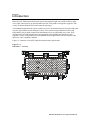
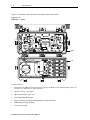
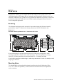
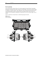
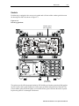
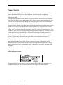
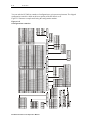
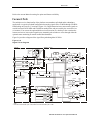
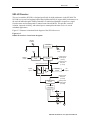
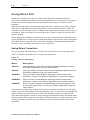
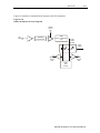
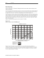
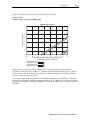
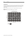
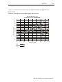
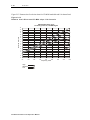
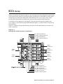
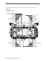
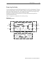
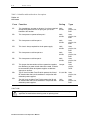
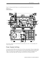
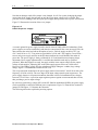
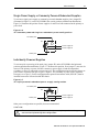
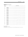
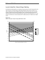
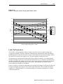
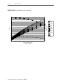
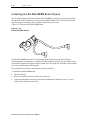
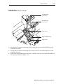
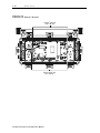
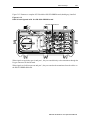

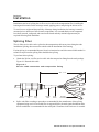
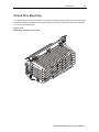
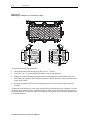
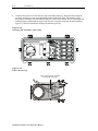
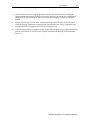
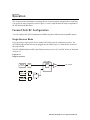
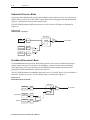
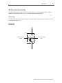
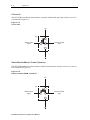
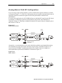
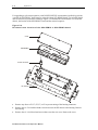
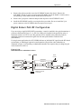
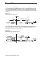
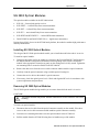
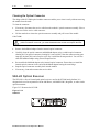
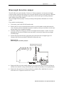
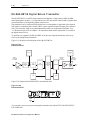
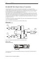
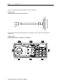
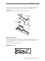
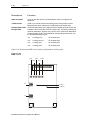


![TSE Series - User Manual [ES]](http://vs1.manualzilla.com/store/data/006232823_1-6e8b23ae158bff6df1360bba873002cc-150x150.png)