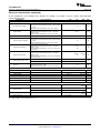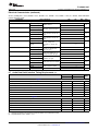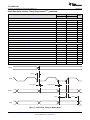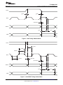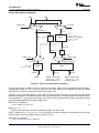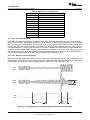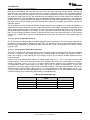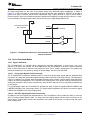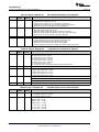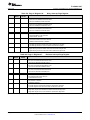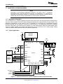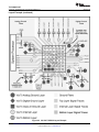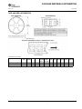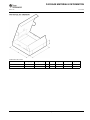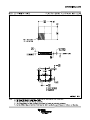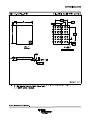
1
Product
Folder
Sample &
Buy
Support &
Community
Tools &
Software
Technical
Documents
TLV320AIC3107
SLOS545D – NOVEMBER 2008 – REVISED DECEMBER 2014
TLV320AIC3107 Low-Power Stereo Codec With Integrated Mono Class-D Speaker
Amplifier
1 Features
•
1
•
•
•
•
•
•
•
•
•
•
•
•
•
Stereo CODEC With Integrated Mono Class-D
Amplifier
High Performance Audio DAC
– 97-dBA Signal-to-Noise Ratio (Single Ended)
– 16/20/24/32-Bit Data
– Supports Sample Rates From 8 kHz to 96 kHz
– 3D/Bass/Treble/EQ/De-Emphasis Effects
– Flexible Power Saving Modes and
Performance are Available
High Performance Audio ADC
– 92-dBA Signal-to-Noise Ratio
– Supports Rates From 8 kHz to 96 kHz
– Digital Signal Processing and Noise Filtering
Available During Record
Seven Audio Input Pins
– Programmable as 6 Single-Ended or 3 Fully
Differential Inputs
– Capability for Floating Input Configurations
Multiple Audio Output Drivers
– Mono Fully Differential or Stereo Single-Ended
Headphone Drivers
– Single-Ended Stereo Line Outputs
Mono 1 W Class-D BTL 8Ω Speaker Driver
Low Power Consumption: 15-mW Stereo 48-kHz
Playback With 3.3-V Analog Supply
Ultra-Low Power Mode with Passive Analog
Bypass
Programmable Input/Output Analog Gains
Automatic Gain Control (AGC) for Record
Programmable Microphone Bias Level
Programmable PLL for Flexible Clock Generation
I2C™ Control Bus
Audio Serial Data Bus Supports I2S, Left/RightJustified, DSP, and TDM Modes
Extensive Modular Power Control
Power Supplies:
– Speaker Amp: 2.7 V – 5.5 V
– Analog: 2.7 V – 3.6 V.
– Digital Core: 1.525 V – 1.95 V
– Digital I/O: 1.1 V – 3.6 V
Packages: 5-mm × 5-mm 40-QFN, 0.4-mm Pitch
3.563-mm × 3.376-mm 42-DSBGA, 0.5 mm Pitch
(Product Preview)
•
•
•
2 Applications
•
•
•
•
Cellular Handsets
Digital Cameras
Portable Media Players
General Portable Audio Equipment
3 Description
The TLV320AIC3107 is a low power stereo audio
codec with stereo headphone amplifier, and mono
class-D speaker driver, as well as multiple inputs and
outputs programmable in single-ended or
fully differential configurations.
Device Information(1)
PART NUMBER
TLV320AIC3107
PACKAGE
BODY SIZE (MAX)
WQFN (40)
5.15 mm × 5.15 mm
DSBGA (42)
3.563 mm × 3.376 mm
(1) For all available packages, see the orderable addendum at
the end of the datasheet.
AVSS_DAC
DRVDD
DRVSS
AVDD_DAC
BCLK
WCLK
DVDD
IOVDD
DVSS
DIN
DOUT
AVDD_ADC
AVSS_ADC
4 Simplified Block Diagram
Audio Serial Bus Interface
H
E
A
D
P
H
O
N
E
HPLOUT
HPCOM
LINE 1LP
MICDET /LINE 1LM
MIC 3R/LINE 2RM
SWINP
SWINM
GPIO 1
PGA
0/
+59.5dB
0.5dB
Steps
HPROUT
DAC
Output
Amplifiers
MIX/MUX,
Switching,
and
Gain/Atten
Right
Channel
Right
Channel
ADC
DAC
Audio CLK
Gen
Bias/
Reference
LEFT _LOP
RIGHT _LOP
SPOP
SPOM
SWOUTP
SWOUTM
Feedthrough Line Paths to Class AB Line Amplifiers,
Passive Switches to Line Outputs,
and Class-D Speaker Amplifiers
MICBIAS
MCLK
AGC
Digital
Audio
Filtering,
Volume
Control,
Effects,
and
Processing
L
I
N
E
C
L
A
S
S
D
QFN
Only
I2C Serial
Control Bus
SPVDD
LINE 2LP
LINE 2RP /LINE 2LM
ADC
AGC
Left
Channel
SPVSS
MIC 3L/LINE 1RM
Analog
Signal
Input
MIX/MUX,
Switching,
and/or
Attenuation
Left
Channel
RESET
SCL
SDA
LINE 1RP
PGA
0/
+59.5dB
0.5dB
Steps
1
An IMPORTANT NOTICE at the end of this data sheet addresses availability, warranty, changes, use in safety-critical applications,
intellectual property matters and other important disclaimers. UNLESS OTHERWISE NOTED, this document contains PRODUCTION
DATA.
TLV320AIC3107
SLOS545D – NOVEMBER 2008 – REVISED DECEMBER 2014
www.ti.com
Table of Contents
1
2
3
4
5
6
7
8
Features ..................................................................
Applications ...........................................................
Description .............................................................
Simplified Block Diagram .....................................
Revision History.....................................................
Description (Continued) ........................................
Pin Configuration and Functions .........................
Specifications.........................................................
8.1
8.2
8.3
8.4
8.5
8.6
8.7
8.8
1
1
1
1
2
3
4
6
Absolute Maximum Ratings ...................................... 6
ESD Ratings ............................................................ 6
Recommended Operating Conditions....................... 6
Thermal Information .................................................. 7
Dissipation Ratings .................................................. 7
Electrical Characteristics........................................... 8
Audio Data Serial Interface Timing Requirements.. 11
Typical Characteristics ............................................ 15
9 Parameter Measurement Information ................ 17
10 Detailed Description ........................................... 17
10.1
10.2
10.3
10.4
10.5
10.6
Overview ...............................................................
Functional Block Diagram .....................................
Feature Description...............................................
Device Functional Modes......................................
Programming.........................................................
Register Maps .......................................................
17
17
18
39
41
44
11 Application and Implementation........................ 88
11.1 Application Information.......................................... 88
11.2 Typical Application ............................................... 88
12 Power Supply Recommendations ..................... 90
13 Layout................................................................... 90
13.1 Layout Guidelines ................................................. 90
13.2 Layout Example .................................................... 91
14 Device and Documentation Support ................. 93
14.1 Trademarks ........................................................... 93
14.2 Electrostatic Discharge Caution ............................ 93
14.3 Glossary ................................................................ 93
15 Mechanical, Packaging, and Orderable
Information ........................................................... 93
5 Revision History
Changes from Revision C (March 2009) to Revision D
•
2
Page
Added Pin Configuration and Functions section, ESD Ratings table, Feature Description section, Device Functional
Modes, Application and Implementation section, Power Supply Recommendations section, Layout section, Device
and Documentation Support section, and Mechanical, Packaging, and Orderable Information section .............................. 1
Submit Documentation Feedback
Copyright © 2008–2014, Texas Instruments Incorporated
Product Folder Links: TLV320AIC3107
TLV320AIC3107
www.ti.com
SLOS545D – NOVEMBER 2008 – REVISED DECEMBER 2014
6 Description (Continued)
Extensive register-based power control is included, enabling stereo 48-kHz DAC playback as low as 15 mW from
a 3.3-V analog supply, making it ideal for portable battery-powered audio and telephony applications.
The high-power output drivers are capable of driving a variety of load configurations, including up to three
channels of single-ended 16-Ω headphones using ac-coupling capacitors, or stereo 16-Ω headphones in a
capacitorless output configuration. The mono class-D output is capable of differentially driving an 8-Ω speaker.
The stereo audio DAC supports sampling rates from 8 kHz to 96 kHz and includes programmable digital filtering
in the DAC path for 3D, bass, treble, midrange effects, speaker equalization, and de-emphasis for 32-kHz, 44.1kHz, and 48-kHz rates. The stereo audio ADC supports sampling rates from 8 kHz to 96 kHz and is preceded by
programmable gain amplifiers or AGC that can provide up to 59.5 dB analog gain for low-level microphone
inputs. The TLV320AIC3107 provides an extremely high range of programmability for both attack (8-1,408 ms)
and for decay (0.05-22.4 seconds). This extended AGC range allows the AGC to be tuned for many types of
applications.
For battery saving applications where neither analog nor digital signal processing are required, the device can be
put in a special analog signal passthru mode. This mode significantly reduces power consumption, as most of the
device is powered down during this pass through operation.
The serial control bus supports I2C protocol, while the serial audio data bus is programmable for I2S, left/rightjustified, DSP, or TDM modes. A highly programmable PLL is included for flexible clock generation and support
for all standard audio rates from a wide range of available MCLKs, varying from 512 kHz to 50 MHz, with special
attention paid to the most popular cases of 12-MHz, 13-MHz, 16-MHz, 19.2-MHz, and 19.68-MHz system clocks.
The TLV320AIC3107 operates from an analog supply of 2.7 V–3.6 V, a digital core supply of 1.65 V–1.95 V, a
digital I/O supply of 1.1 V–3.6 V, and a speaker amplifier supply of 2.7V–5.5V. The device is available in the 5 ×
5-mm, 40-pin QFN package and in the future a 3.5 × 3-mm, 42-lead DSBGA package.
The record path of the TLV320AIC3107 contains integrated microphone bias, digitally controlled stereo
microphone preamplifier, and automatic gain control (AGC), with mix/mux capability among the multiple analog
inputs. Programmable filters are available during record which can remove audible noise that can occur during
optical zooming in digital cameras. The playback path includes mix/mux capability from the stereo DAC and
selected inputs, through programmable volume controls, to the various outputs.
The TLV320AIC3107 contains three high-power output drivers as well as two single-ended line output drivers,
and a differential class-D output driver.
Submit Documentation Feedback
Copyright © 2008–2014, Texas Instruments Incorporated
Product Folder Links: TLV320AIC3107
3
TLV320AIC3107
SLOS545D – NOVEMBER 2008 – REVISED DECEMBER 2014
www.ti.com
7 Pin Configuration and Functions
SCL
SDA
MICDET/LINE1LM
LINE1LP
LINE1RP
MIC3L/LINE1RM
LINE2LP
LINE2RP/LINE2LM
MIC3R/LINE2RM
MICBIAS
1
2
3
4
5
6
7
8
9
10
RSB Package
40-Pin WQFN With Exposed Thermal Pad
Bottom View
IOVDD
40
11
AVSS_ADC
DVSS
39
12
AVDD_ADC
DOUT
38
13
DRVDD
DIN
37
14
HPLOUT
WCLK
36
15
HPCOM
Thermal Pad
RIGHT_LOP
SWINM
21
20
AVDD_DAC
31
22
RESET
AVSS_DAC
LEFT_LOP
23
19
SPOM
32
24
GPIO1
SPVSS
DRVDD
25
18
SPVDD
33
26
DVDD
SPOP
HPROUT
27
17
28
34
SWOUTM
MCLK
29
DRVSS
SWOUTP
16
30
35
SWINP
BCLK
YZF Package
42-Pin DSBGA (6 × 7)
Bottom View
6
A
4
5
4
MIC3R/LINE2RM LINE2RP/LINE1LM MIC3L/LINE1RM
3
2
1
LINE1LP
MICDET/LINE1LM
SCL
A
B
AVSS_ADC
MICBIAS
LINE2LP
LINE1RP
IOVDD
SDA
B
C
HPLOUT
DRVDD
AVDD_ADC
DVSS
DIN
DOUT
C
D
HPROUT
HPCOM
DRVSS
DVDD
BCLK
WCLK
D
E
LEFT_LOP
DRVDD
SWINM
SWINP
GPIO1
MCLK
E
F
RIGHT_LOP
AVDD_DAC
SPOM
SPOP
SPVSS
RESET
F
G
AVSS_DAC
SPVSS
SPVDD
SPVSS
SPVSS
SPVSS
G
6
5
4
3
2
1
Submit Documentation Feedback
Copyright © 2008–2014, Texas Instruments Incorporated
Product Folder Links: TLV320AIC3107
TLV320AIC3107
www.ti.com
SLOS545D – NOVEMBER 2008 – REVISED DECEMBER 2014
Pin Functions
PIN
(1)
I/O
DESCRIPTION
QFN
WCSP (1)
1
A1
SCL
I
2
B1
SDA
I/O
3
A2
MICDET/LINE1LM
I
MIC1 or Line1 analog input (left – or multifunctional) or Microphone detect
4
A3
LINE1LP
I
MIC1 or Line1 analog input (left + or multifunctional)
5
B3
LINE1RP
I
MIC1 or Line1 analog input (R + or multifunctional)
6
A4
MIC3L/LINE1RM
I
MIC3 or Line1 analog input (R - or multifunctional)
7
B4
LINE2LP
I
MIC2 or Line2 analog input (left + or multifunctional)
8
A5
LINE2RP/LINE2LM
I
MIC2 or Line2 analog input (left + or right - or multifunctional)
9
A6
MIC3R/LINE2RM
I
MIC3 or Line2 analog input (right + or multifunctional)
10
B5
MICBIAS
O
Microphone bias voltage output
11
B6
AVSS_ADC
G
ADC analog ground supply, 0 V
12
C4
AVDD_ADC
P
ADC analog voltage supply, 2.7 V–3.6 V
13
C5
DRVDD
P
High-power output driver analog voltage supply, 2.7 V–3.6 V
14
C6
HPLOUT
O
High-power output driver (left +)
15
D5
HPCOM
O
High-power output driver (left – or multifunctional)
16
D4
DRVSS
G
High-power output driver analog ground supply, 0 V
17
D6
HPROUT
O
High-power output driver (right +)
18
E5
DRVDD
P
High-power output driver analog voltage supply, 2.7 V–3.6 V
19
E6
LEFT_LOP
O
Left line output
20
F6
RIGHT_LOP
O
Right line output
21
F5
AVDD_DAC
P
DAC analog voltage supply, 2.7 V–3.6 V
22
G6
AVSS_DAC
G
DAC analog ground supply, 0 V
23
F4
SPOM
O
Class-D (or Bypass SW, WCSP only) negative differential output
24
F2, G1, G2,
G3, G5
SPVSS
G
Class-D ground supply, 0 V
25
G4
SPVDD
P
Class-D voltage supply, 2.7 V–5.5 V
26
F3
SPOP
O
Class-D (or Bypass SW, WCSP only) positive differential output
27
E4
SWINM
I
Negative Bypass Switch Input
28
—
SWOUTM
O
Negative Bypass Switch Output, to be tied to SPOM externally
29
—
SWOUTP
O
Positive Bypass Switch Output, to be tied to SPOP externally
30
E3
SWINP
I
Positive Bypass Switch Input
31
F1
RESET
I
Reset
32
E2
GPIO1
I/O
33
D3
DVDD
P
Digital core voltage supply, 1.525 V–1.95 V
34
E1
MCLK
I
Master clock input
35
D2
BCLK
I/O
Audio serial data bus bit clock (input/output)
36
D1
WCLK
I/O
Audio serial data bus word clock (input/output)
37
C2
DIN
I
Audio serial data bus data input (input)
38
C1
DOUT
O
Audio serial data bus data output (output)
39
C3
DVSS
G
Digital core / I/O ground supply, 0 V
40
B2
IOVDD
P
I/O voltage supply, 1.1 V–3.6 V
NAME
I2C serial clock
I2C serial data input/output
General-purpose input/output
Product Preview
Submit Documentation Feedback
Copyright © 2008–2014, Texas Instruments Incorporated
Product Folder Links: TLV320AIC3107
5
TLV320AIC3107
SLOS545D – NOVEMBER 2008 – REVISED DECEMBER 2014
www.ti.com
8 Specifications
8.1 Absolute Maximum Ratings
over operating free-air temperature range (unless otherwise noted) (1)
TJ Max
(2)
MIN
MAX
UNIT
AVDD_DAC to AVSS_DAC, DRVDD to DRVSS, AVSS_ADC
–0.3
3.9
V
SPVDD to SPVSS
–0.3
6.0
V
AVDD to DRVSS
–0.3
3.9
V
IOVDD to DVSS
–0.3
3.9
V
DVDD to DVSS
–0.3
2.5
V
AVDD_DAC to DRVDD
–0.1
0.1
V
Digital input voltage to DVSS
–0.3
IOVDD + 0.3
V
Analog input voltage to AVSS_ADC
–0.3
AVDD + 0.3
V
Operating temperature range
–40
85
°C
105
°C
Junction temperature
Power dissipation
Tstg
(1)
(2)
(TJ Max – TA)/θJA
Storage temperature range
–65
105
°C
Stresses beyond those listed under Absolute Maximum Ratings may cause permanent damage to the device. These are stress ratings
only, and functional operation of the device at these or any other conditions beyond those indicated under Recommended Operating
Conditions is not implied. Exposure to absolute-maximum-rated conditions for extended periods may affect device reliability.
ESD compliance tested to EIA/JESD22-A114-B and passed.
8.2 ESD Ratings
VALUE
V(ESD)
(1)
(2)
Electrostatic discharge
Human-body model (HBM), per ANSI/ESDA/JEDEC JS-001 (1)
±2300
Charged-device model (CDM), per JEDEC specification JESD22C101 (2)
±1000
UNIT
V
JEDEC document JEP155 states that 500-V HBM allows safe manufacturing with a standard ESD control process.
JEDEC document JEP157 states that 250-V CDM allows safe manufacturing with a standard ESD control process.
8.3 Recommended Operating Conditions
over operating free-air temperature range (unless otherwise noted)
AVDD_DAC, DRVDD (1) Analog supply voltage
DVDD (1)
IOVDD
(1)
Digital core supply voltage
MIN
NOM
MAX
2.7
3.3
3.6
V
1.525
1.8
1.95
V
V
Digital I/O supply voltage
1.1
1.8
3.6
SPVDD
Speaker Amplifier supply voltage
2.7
3.6
5.5
VI
Analog full-scale 0 dB input voltage (DRVDD1 = 3.3 V) (Single Ended)
0.707
Stereo line output load resistance
10
Stereo headphone output load resistance
16
Digital output load capacitance
TA
(1)
6
Operating free-air temperature
V
VRMS
kΩ
Ω
10
–40
UNIT
pF
85
°C
Analog voltage values are with respect to AVSS_ADC, AVSS_DAC, DRVSS; digital voltage values are with respect to DVSS.
Submit Documentation Feedback
Copyright © 2008–2014, Texas Instruments Incorporated
Product Folder Links: TLV320AIC3107
TLV320AIC3107
www.ti.com
SLOS545D – NOVEMBER 2008 – REVISED DECEMBER 2014
8.4 Thermal Information
TLV320AIC3107
THERMAL METRIC (1)
RSB
YZF
40 PINS
42 PINS
30.7
49.5
RθJA
Junction-to-ambient thermal resistance
RθJC(top)
Junction-to-case (top) thermal resistance
16
0.1
RθJB
Junction-to-board thermal resistance
4.6
7.1
ψJT
Junction-to-top characterization parameter
0.2
0.8
ψJB
Junction-to-board characterization parameter
4.5
7
RθJC(bot)
Junction-to-case (bottom) thermal resistance
0.9
n/a
(1)
UNIT
°C/W
For more information about traditional and new thermal metrics, see the IC Package Thermal Metrics application report, SPRA953.
8.5 Dissipation Ratings (1)
(1)
(2)
PACKAGE TYPE
TA = 25°C
POWER RATING
DERATING
FACTOR
TA = 75°C
POWER RATING
TA = 85°C
POWER RATING
DSBGA (2)
QFN
1.60 W
20 mW/°C
600 mW
400 mW
2.35 W
29.4 mW/° C
882 mW
588 mW
This data was taken using 2 oz. trace and copper pad that is soldered directly to a JEDEC standard 4-layer 3 in × 3 in PCB.
Product Preview
Submit Documentation Feedback
Copyright © 2008–2014, Texas Instruments Incorporated
Product Folder Links: TLV320AIC3107
7
TLV320AIC3107
SLOS545D – NOVEMBER 2008 – REVISED DECEMBER 2014
www.ti.com
8.6 Electrical Characteristics
At 25°C, AVDD_DAC = 3.3 V, DRVDD = 3.3 V, SPVDD = 5 V, IOVDD = 3.3 V, DVDD = 1.8 V, Fs = 48-kHz, 16-bit audio data
(unless otherwise noted)
PARAMETER
TEST CONDITIONS
MIN
TYP
MAX
UNIT
AUDIO ADC
Input signal level (0 dB)
Single-ended input
Signal-to-noise ratio, Aweighted (1) (2)
Fs = 48 ksps, 0 dB PGA gain, Inputs ac-shorted to ground
Dynamic range
THD
(2)
Total harmonic distortion
Power supply rejection ratio
Gain error
Input channel separation
ADC programmable gain
amplifier maximum gain
Fs = 48 ksps, 0 dB PGA gain,
–60 dB full-scale input signal
THD
80
dB
91
dB
–88
217 Hz signal applied to DRVDD
49
1 kHz signal applied to DRVDD
46
Fs = 48 ksps, 0 dB PGA gain,
–2dB full-scale 1kHz input signal
0.84
1 kHz, -2dB full-scale signal, MIC3L to MIC3R
-86
1 kHz, -2dB full-scale signal, MIC2L to MIC2R
-98
1 kHz, -2dB full-scale signal, MIC1L to MIC1R
-75
1-kHz input tone
VRMS
92
Fs = 48 ksps, 0 dB PGA gain,
–2dB full-scale 1kHz input signal
ADC programmable gain
amplifier step size
Input resistance
0.707
–70
dB
dB
dB
dB
59.5
dB
0.5
dB
LINE1L inputs routed to single ADC
Input mix attenuation = 0 dB
20
LINE1L inputs routed to single ADC,
input mix attenuation = 12 dB
80
LINE2L inputs routed to single ADC
Input mix attenuation = 0 dB
20
LINE2L inputs routed to single ADC,
input mix attenuation = 12 dB
80
kΩ
Input level control minimum
attenuation setting
0
dB
Input level control maximum
attenuation setting
12
dB
Input signal level
Differential Input
Signal-to-noise ratio, Aweighted (1) (2)
Fs = 48 ksps, 0 dB PGA gain, Inputs ac-shorted to
ground, Differential Mode
Total harmonic distortion
1.414
VRMS
92
dB
Fs = 48 ksps, 0 dB PGA gain, –2dB Full-scale 1kHz input
signal, Differential Mode
–91
dB
LINE1L to LEFT_LOP
330
LINE1R to RIGHT_LOP
330
ANALOG PASS THROUGH MODE
Input to output switch
resistance, (rDS(on))
SWINP to SWOUTP
1
SWINM to SWOUTM
1
Ω
ADC DIGITAL DECIMATION FILTER, Fs = 48 kHz
Filter gain from 0 to 0.39 Fs
Filter gain at 0.4125 Fs
Filter gain at 0.45 Fs
Filter gain at 0.5 Fs
Filter gain from 0.55 Fs to 64 Fs
Filter group delay
(1)
(2)
8
±0.1
dB
–0.25
dB
–3
dB
–17.5
dB
–75
dB
17/Fs
s
Ratio of output level with 1-kHz full-scale sine-wave input, to the output level with the inputs short circuited, measured A-weighted over a
20-Hz to 20-kHz bandwidth using an audio analyzer.
All performance measurements done with 20-kHz low-pass filter and, where noted, A-weighted filter. Failure to use such a filter may
result in higher THD+N and lower SNR and dynamic range readings than shown in the Electrical Characteristics. The low-pass filter
removes out-of-band noise, which, although not audible, may affect dynamic specification values.
Submit Documentation Feedback
Copyright © 2008–2014, Texas Instruments Incorporated
Product Folder Links: TLV320AIC3107
TLV320AIC3107
www.ti.com
SLOS545D – NOVEMBER 2008 – REVISED DECEMBER 2014
Electrical Characteristics (continued)
At 25°C, AVDD_DAC = 3.3 V, DRVDD = 3.3 V, SPVDD = 5 V, IOVDD = 3.3 V, DVDD = 1.8 V, Fs = 48-kHz, 16-bit audio data
(unless otherwise noted)
PARAMETER
TEST CONDITIONS
MIN
TYP
2.3
2.5
MAX
UNIT
MICROPHONE BIAS
Programmable setting = 2.0
Bias voltage
Programmable setting = 2.5
Programmable setting = DRVDD
Current sourcing
Programmable setting = 2.5V
2
2.7
V
DRVDD
4
mA
AUDIO DAC - SINGLE ENDED LINE OUTPUT, LOAD = 10 kΩ
Full-scale output voltage
0 dB Input full-scale signal, output volume control = 0 dB,
Output common mode setting = 1.35 V
Signal-to-noise ratio, Aweighted
No input signal, output volume control = 0 dB,
Output common mode setting = 1.35 V, Fs = 48 kHz
97
Total harmonic distortion
0 dB 1 kHz input full-scale signal,
Output volume control = 0 dB,
Output common mode setting = 1.35 V, Fs = 48 kHz
-84
DAC Gain Error
0 dB 1 kHz input full-scale signal,
Output volume control = 0 dB,
Output common mode setting = 1.35 V, Fs = 48 kHz
-0.8
0.707
Vrms
dB
-70
dB
dB
AUDIO DAC - SINGLE ENDED HEADPHONE OUTPUT, LOAD = 16 Ω
Full-scale output voltage
0 dB Input full-scale signal,
Output volume control = 0 dB,
Output common mode setting = 1.35 V
0.707
Vrms
No input signal, output volume control = 0 dB,
Output common mode setting = 1.35 V, Fs = 48 kHz
95
dB
No input signal, output volume control = 0 dB,
Output common mode setting = 1.35 V,
Fs = 48 kHz, 50% DAC Current Boost Mode
96
dB
Dynamic range, A-weighted
–60 dB 1 kHz input full-scale signal,
Output volume control = 0 dB,
Output common mode setting = 1.35 V, Fs = 48 kHz
92
dB
Total harmonic distortion
0 dB 1 kHz input full-scale signal,
Output volume control = 0 dB,
Output common mode setting = 1.35 V, Fs = 48 kHz
-84
Signal-to-noise ratio, Aweighted
-65
dB
217 Hz Signal applied to DRVDD, AVDD_DAC
41
1 kHz Signal applied to DRVDD, AVDD_DAC
44
DAC channel separation
0 dB Full-scale input signal between left and right Lineout
84
dB
DAC Gain Error
0 dB 1 kHz input full-scale signal,
Output volume control = 0 dB,
Output common mode setting = 1.35 V, Fs = 48 kHz
-1
dB
Power supply rejection ratio
dB
AUDIO DAC - LINEOUT AND HEADPHONE OUT DRIVERS
First option
Output common mode
1.35
Second option
1.5
Third option
1.65
Fourth option
V
1.8
Output volume control max
setting
9
dB
Output volume control step size
1
dB
Submit Documentation Feedback
Copyright © 2008–2014, Texas Instruments Incorporated
Product Folder Links: TLV320AIC3107
9
TLV320AIC3107
SLOS545D – NOVEMBER 2008 – REVISED DECEMBER 2014
www.ti.com
Electrical Characteristics (continued)
At 25°C, AVDD_DAC = 3.3 V, DRVDD = 3.3 V, SPVDD = 5 V, IOVDD = 3.3 V, DVDD = 1.8 V, Fs = 48-kHz, 16-bit audio data
(unless otherwise noted)
PARAMETER
TEST CONDITIONS
MIN
TYP
MAX
UNIT
SPEAKER AMPLIFIER OUTPUT, LOAD = 8 Ω
Full-scale output voltage
1 kHz, 0dB full-scale input signal,
Output volume control for left line output = 0 dB, for classD = 0 dB
Output common mode setting = 1.35 V, Fs = 48 kHz
Output voltage
1 kHz, 0dB full-scale input signal,
Output volume control for left line output = -4.5 dB, for
class-D = 6 dB
Output common mode setting = 1.35 V, Fs = 48 kHz
Idle Channel Noise
No input signal, output gain control = 0 dB
-92
dB
Dynamic range, A-weighted
1 kHz,–60 dB full-scale input signal,
Output volume control for left line output = 0 dB, for classD = 0 dB
Output common mode setting = 1.35 V, Fs = 48 kHz
91
dB
Total harmonic distortion
1 kHz, 0 dB full-scale input signal,
Output volume control for left line output = –4.5 dB, for
class-D = 6 dB
Output common mode setting = 1.35 V, Fs = 48 kHz, 1 W
output power
1.77%
-35
dB
Total harmonic distortion
1 kHz, –6 dB full-scale input signal,
Output volume control for left line output = –4.5 dB, for
class-D = 6 dB
Output common mode setting = 1.35 V, Fs = 48 kHz, 250
mW output power
0.056%
-65
Power supply rejection ratio
Gain Error
2.5
Vrms
2.875
Vrms
217 Hz Signal applied to SPVDD
37
1 kHz Signal applied to SPVDD
33
1 kHz, 0 dB input full-scale signal,
Output volume control = 0 dB,
Output common mode setting = 1.35 V, Fs = 48 kHz
0.316%
-50
dB
dB
-1.6
dB
DAC DIGITAL INTERPOLATION – FILTER Fs = 48-ksps
Passband
0
Passband ripple
0.45 × Fs
±0.06
Hz
dB
Transition band
0.45 × Fs
0.55 × Fs
Hz
Stopband
0.55 × Fs
7.5 × Fs
Hz
Stopband attenuation
65
Group delay
dB
21/Fs
s
DIGITAL I/O
VIL
Input low level
VIH
Input high level (3)
VOL
Output low level
VOH
Output high level
(3)
10
–0.3
IOVDD > 1.6 V
0.7 × IOVDD
IOVDD < 1.6 V
1.1
0.3 ×
IOVDD
V
0.1 ×
IOVDD
0.8 × IOVDD
V
V
V
When IOVDD < 1.6V, minimum VIH is 1.1 V.
Submit Documentation Feedback
Copyright © 2008–2014, Texas Instruments Incorporated
Product Folder Links: TLV320AIC3107
TLV320AIC3107
www.ti.com
SLOS545D – NOVEMBER 2008 – REVISED DECEMBER 2014
Electrical Characteristics (continued)
At 25°C, AVDD_DAC = 3.3 V, DRVDD = 3.3 V, SPVDD = 5 V, IOVDD = 3.3 V, DVDD = 1.8 V, Fs = 48-kHz, 16-bit audio data
(unless otherwise noted)
PARAMETER
TEST CONDITIONS
MIN
TYP
MAX
UNIT
POWER CONSUMPTION, DRVDD, AVDD_DAC = 3.3 V, SPVDD = 5V, DVDD = 1.8 V, IOVDD = 3.3 V
IDRVDD+IAVDD_DAC
IDVDD
IDRVDD+IAVDD_DAC
IDVDD
IDRVDD+IAVDD_DAC
IDVDD
IDRVDD+IAVDD_DAC
IDVDD
IDRVDD+IAVDD_DAC
IDVDD
IDRVDD+IAVDD_DAC
IDVDD
IDRVDD+IAVDD_DAC
IDVDD
IDRVDD+IAVDD_DAC
IDVDD
IDRVDD+IAVDD_DAC
IDVDD
IDRVDD+IAVDD_DAC
0.1
RESET Held low
Mono ADC record, Fs = 8 ksps,
I2S Slave, AGC Off, No signal
2.1
Stereo ADC record, Fs = 8
ksps, I2S Slave, AGC Off, No
signal
4.1
Stereo ADC record, Fs = 48
ksps, I2S Slave, AGC Off, No
signal
4.3
Stereo DAC Playback to
Lineout , Analog mixer
bypassed Fs = 48 ksps, I2S
Slave
3.5
Stereo DAC Playback to
Lineout, Fs = 48 ksps, I2S
Slave, No signal
4.9
Stereo DAC Playback to stereo
single-ended headphone, Fs =
48 ksps, I2S Slave, No signal
6.7
Stereo LINEIN to stereo
LINEOUT, No signal
3.1
All blocks powered down,
Headset detection enabled
SPVDD
class-D disabled
mA
0.5
mA
0.6
mA
2.5
mA
2.3
mA
2.3
mA
2.3
mA
0
1.4
Extra power when PLL enabled
IDVDD
μA
0.2
mA
0.9
28
μA
2
200
nA
8.7 Audio Data Serial Interface Timing Requirements (1) (2)
IOVDD = 1.1 V
MIN
MAX
IOVDD = 3.3 V
MIN
MAX
UNIT
I2S/LJF/RJF TIMING IN MASTER MODE, SEE Figure 1
td(WS)
ADWS/WCLK delay time
50
15
ns
td(DO-WS)
ADWS/WCLK to DOUT delay time
50
20
ns
td(DO-BCLK)
BCLK to DOUT delay time
50
15
ns
ts(DI)
DIN setup time
10
th(DI)
DIN hold time
10
tr
Rise time
30
10
ns
tf
Fall time
30
10
ns
6
ns
6
ns
DSP TIMING IN MASTER MODE, SEE Figure 2
td(WS)
ADWS/WCLK delay time
50
15
ns
td(DO-BCLK)
BCLK to DOUT delay time
50
15
ns
ts(DI)
DIN setup time
10
th(DI)
DIN hold time
10
tr
Rise time
30
10
ns
tf
Fall time
30
10
ns
(1)
(2)
6
ns
6
ns
All timing specifications are measured at characterization but not tested at final test.
All specifications at 25°C, DVDD = 1.8 V
Submit Documentation Feedback
Copyright © 2008–2014, Texas Instruments Incorporated
Product Folder Links: TLV320AIC3107
11
TLV320AIC3107
SLOS545D – NOVEMBER 2008 – REVISED DECEMBER 2014
www.ti.com
Audio Data Serial Interface Timing Requirements(1)(2) (continued)
IOVDD = 1.1 V
MIN
IOVDD = 3.3 V
MAX
MIN
MAX
UNIT
I2S/LJF/RJF TIMING IN SLAVE MODE, SEE Figure 3
tP(BCLK)
BCLK clock period
tH(BCLK)
BCLK high period
70
35
ns
ns
tL(BCLK)
BCLK low period
70
35
ns
ts(WS)
ADWS/WCLK setup time
10
6
ns
th(WS)
ADWS/WCLK hold time
10
td(DO-WS)
ADWS/WCLK to DOUT delay time (for LJF Mode only)
25
35
ns
td(DO-BCLK)
BCLK to DOUT delay time
50
20
ns
ts(DI)
DIN setup time
10
6
th(DI)
DIN hold time
10
6
tr
Rise time
8
4
ns
tf
Fall time
8
4
ns
6
ns
ns
ns
DSP TIMING IN SLAVE MODE, SEE Figure 4
tP(BCLK)
BCLK clock period
tH(BCLK)
BCLK high period
70
35
ns
ns
tL(BCLK)
BCLK low period
70
35
ns
ts(WS)
ADWS/WCLK setup time
10
8
ns
th(WS)
ADWS/WCLK hold time
10
8
ns
td(DO-BCLK)
BCLK to DOUT delay time
ts(DI)
DIN setup time
10
6
ns
th(DI)
DIN hold time
10
6
ns
tr
Rise time
8
4
ns
tf
Fall time
8
4
ns
50
20
ns
WCLK
td(WS)
BCLK
td(DO-WS)
td(DO-BCLK)
SDOUT
tS(DI)
th(DI)
SDIN
T0145-01
2
Figure 1. I S/LJF/RJF Timing in Master Mode
12
Submit Documentation Feedback
Copyright © 2008–2014, Texas Instruments Incorporated
Product Folder Links: TLV320AIC3107
TLV320AIC3107
www.ti.com
SLOS545D – NOVEMBER 2008 – REVISED DECEMBER 2014
WCLK
td(WS)
td(WS)
BCLK
td(DO-BCLK)
SDOUT
tS(DI)
th(DI)
SDIN
T0146-01
Figure 2. DSP Timing in Master Mode
WCLK
tS(WS)
th(WS)
tH(BCLK)
BCLK
td(DO-WS)
tL(BCLK)
td(DO-BCLK)
SDOUT
tS(DI)
th(DI)
SDIN
T0145-02
2
Figure 3. I S/LJF/RJF Timing in Slave Mode
Submit Documentation Feedback
Copyright © 2008–2014, Texas Instruments Incorporated
Product Folder Links: TLV320AIC3107
13
TLV320AIC3107
SLOS545D – NOVEMBER 2008 – REVISED DECEMBER 2014
www.ti.com
WCLK
tS(WS)
tS(WS)
th(WS)
th(WS)
tL(BCLK)
BCLK
tH(BCLK)
td(DO-BCLK)
SDOUT
tS(DI)
th(DI)
SDIN
T0146-02
Figure 4. DSP Timing in Slave Mode
14
Submit Documentation Feedback
Copyright © 2008–2014, Texas Instruments Incorporated
Product Folder Links: TLV320AIC3107
TLV320AIC3107
www.ti.com
SLOS545D – NOVEMBER 2008 – REVISED DECEMBER 2014
8.8 Typical Characteristics
45
0
2.7 VDD_CM 1.35_LDAC
40
3.6 VDD_CM 1.8_LDAC
-20
SNR - Signal-To-Noise - dB
THD - Total Harmonic Distortion - dB
-10
3.3 VDD_CM1.65_LDAC
2.7 VDD_CM 1.35_RDAC
-30
-40
3.3 VDD_CM 1.65_RDAC
-50
-60
-70
35
30
25
20
15
10
-80
LINEIR Routed to RADC in Differential Mode,
48 KSPS, Normal Supply and Temperature,
Input Signal at -65 dB
5
3.6 VDD_CM 1.8_RDAC
0
-90
0
20
40
60
80
0
100
10
30
40
50
60
70
ADC, PGA - Setting - dB
Figure 5. Total Harmonic Distortion vs Headphone Out
Power
Figure 6. Signal-to-Noise Ratio vs ADC PGA Setting
4
4
AVDD = 3.3 V,
No Load
No Load
3.5
PGM = VDD
MICBIAS VOLTAGE - V
MICBIAS VOLTAGE - V
3.5
3
PGM = 2.5 V
2.5
PGM = VDD
3
PGM = 2.5 V
2.5
PGM = 2 V
PGM = 2 V
2
2
1.5
2.7
2.9
3.1
3.3
1.5
-60
3.5
-40
VDD - Supply Voltage - V
-20
0
20
40
60
TA - Free- Air Temperature - °C
80
100
Figure 8. MICBIAS Voltage vs Free-Air Temperature
Figure 7. MICBIAS Voltage vs Supply Voltage
0
0
-40
-60
-80
-100
-120
Load = 10 kW,
FS = 48 kHz, fs = 64 kHz,
AVDD = DRVDD = 3.3 V,
-20
-40
Amplitude - dB
Load = 10 kW,
FS = 48 kHz, fs = 64 kHz,
4096 Samples,
AVDD = DRVDD = 3.3 V,
-20
Amplitude - dB
20
Headphone Out Power - mW
-60
-80
-100
-120
-140
-140
-160
-160
0
1
2
3
4
5
6
7
8
9 10 11 12
f - Frequency - kHz
13
14
15 16
17 18
19 20
0
1
2
3
4
5
6
7
8
9
10
11
12
13 14
15 16
17 18
19
20
f - Frequency - kHz
Figure 10. Right DAC FFT
Figure 9. Left DAC FFT
Submit Documentation Feedback
Copyright © 2008–2014, Texas Instruments Incorporated
Product Folder Links: TLV320AIC3107
15
TLV320AIC3107
SLOS545D – NOVEMBER 2008 – REVISED DECEMBER 2014
www.ti.com
Typical Characteristics (continued)
0
0
Load = 10 kW,
FS = 48 kHz, fs = 64 kHz,
2048 Samples,
AVDD = DRVDD = 3.3 V,
-40
-60
Load = 10 kW,
FS = 48 kHz, fs = 64 kHz,
2048 Samples,
AVDD = DRVDD = 3.3 V,
-20
Amplitude - dB
Amplitude - dB
-20
-80
-100
-120
-40
-60
-80
-100
-120
-140
-140
-160
0
1
2
3
4
5
6
7
8
9
10
11
12 13
14 15
16
17 18 19
20
-160
0
1
2
3
4
f - Frequency - kHz
5
6
7
8
9 10 11 12 13
f - Frequency - kHz
14
15
16 17
18
19
20
Figure 12. Right ADC FFT
Figure 11. Left ADC FFT
3
THD - Total Harmonic Distortion - %
2
1
0.9
0.8
0.7
0.6
0.5
0.4
0.3
0.2
0.1
0.1
1
10
100
1000
Class-D Output Power - mW
Figure 13. Total Harmonic Distortion vs Class-D Output Power
16
Submit Documentation Feedback
Copyright © 2008–2014, Texas Instruments Incorporated
Product Folder Links: TLV320AIC3107
TLV320AIC3107
www.ti.com
SLOS545D – NOVEMBER 2008 – REVISED DECEMBER 2014
9 Parameter Measurement Information
All parameters are measured according to the conditions described in the Specifications section.
10 Detailed Description
10.1 Overview
The TLV320AIC3107 is a highly flexible, low power, stereo audio codec with extensive feature integration,
intended for applications in smartphones, PDAs, and portable computing, communication, and entertainment
applications. Available in a 5x5mm 40-lead QFN, the product integrates a host of features to reduce cost, board
space, and power consumption in space-constrained, battery-powered, portable applications.
The TLV320AIC3107 consists of the following blocks:
• Stereo audio multi-bit delta-sigma DAC (8 kHz–96 kHz)
• Stereo audio multi-bit delta-sigma ADC (8 kHz–96 kHz)
• Programmable digital audio effects processing (3-D, bass, treble, mid-range, EQ, notch filter, de-emphasis)
• Seven audio inputs
• Three high-power audio output drivers (headphone drive capability)
• Two single-ended line output drivers
• Fully programmable PLL
• Headphone/headset jack detection with interrupt
• Differential Class-D speaker driver
Communication to the TLV320AIC3107 for control is via I2C. The I2C interface supports both standard and fast
communication modes.
AVDD_DAC
AVSS_DAC
DRVDD
DRVSS
WCLK
BCLK
DVDD
IOVDD
DVSS
DOUT
DIN
AVDD_ADC
AVSS_ADC
10.2 Functional Block Diagram
Audio Serial Bus Interface
H
E
A
D
P
H
O
N
E
HPLOUT
HPCOM
LINE 1LP
MICDET /LINE 1LM
LINE 2LP
MIC 3R/LINE 2RM
SWINP
SWINM
Digital
Audio
Filtering,
Volume
Control,
Effects,
and
Processing
HPROUT
DAC
Output
Amplifiers
MIX/MUX,
Switching,
and
Gain/Atten
Right
Channel
Right
Channel
ADC
DAC
Audio CLK
Gen
Bias/
Reference
LEFT _LOP
RIGHT _LOP
SPOP
SPOM
SWOUTP
SWOUTM
Feedthrough Line Paths to Class AB Line Amplifiers,
Passive Switches to Line Outputs,
and Class-D Speaker Amplifiers
MICBIAS
MCLK
AGC
Left
Channel
L
I
N
E
C
L
A
S
S
D
QFN
Only
I2C Serial
Control Bus
SPVDD
GPIO 1
AGC
PGA
0/
+59.5dB
0.5dB
Steps
LINE 2RP /LINE 2LM
ADC
SPVSS
MIC 3L/LINE 1RM
Left
Channel
RESET
SCL
SDA
LINE 1RP
Analog
Signal
Input
MIX/MUX,
Switching,
and/or
Attenuation
PGA
0/
+59.5dB
0.5dB
Steps
Connect QFN thermal pad to DRVSS.
Submit Documentation Feedback
Copyright © 2008–2014, Texas Instruments Incorporated
Product Folder Links: TLV320AIC3107
17
TLV320AIC3107
SLOS545D – NOVEMBER 2008 – REVISED DECEMBER 2014
www.ti.com
10.3 Feature Description
10.3.1 Hardware Reset
The TLV320AIC3107 requires a hardware reset after power-up for proper operation. After all power supplies are
at their specified values, the RESET pin must be driven low for at least 10 ns. If this reset sequence is not
performed, the TLV320AIC3107 may not respond properly to register reads/writes.
10.3.2 Digital Audio Data Serial Interface
Audio data is transferred between the host processor and the TLV320AIC3107 via the digital audio data serial
interface, or audio bus. The audio bus on this device is flexible, including left or right justified data options,
support for I2S or PCM protocols, programmable data length options, a TDM mode for multichannel operation,
flexible master/slave configurability for each bus clock line, and the ability to communicate with multiple devices
within a system directly.
The audio bus of the TLV320AIC3107 can be configured for left or right justified, I2S, DSP, or TDM modes of
operation, where communication with standard telephony PCM interfaces is supported within the TDM mode.
These modes are all MSB-first, with data width programmable as 16, 20, 24, or 32 bits. In addition, the word
clock (WCLK or GPIO1) and bit clock (BCLK) can be independently configured in either Master or Slave mode,
for flexible connectivity to a wide variety of processors
The word clock (WCLK or GPIO1) is used to define the beginning of a frame, and may be programmed as either
a pulse or a square-wave signal. The frequency of this clock corresponds to the maximum of the selected ADC
and DAC sampling frequencies.
The bit clock (BCLK) is used to clock in and out the digital audio data across the serial bus. When in Master
mode, this signal can be programmed in two further modes: continuous transfer mode, and 256-clock mode. In
continuous transfer mode, only the minimal number of bit clocks needed to transfer the audio data are generated,
so in general the number of bit clocks per frame will be two times the data width. For example, if data width is
chosen as 16-bits, then 32 bit clocks will be generated per frame. If the bit clock signal in master mode will be
used by a PLL in another device, it is recommended that the 16-bit or 32-bit data width selections be used.
These cases result in a low jitter bit clock signal being generated, having frequencies of 32×Fs or 64×Fs. In the
cases of 20-bit and 24-bit data width in master mode, the bit clocks generated in each frame will not all be of
equal period, due to the device not having a clean 40×Fs or 48×Fs clock signal readily available. The average
frequency of the bit clock signal is still accurate in these cases (being 40×Fs or 48×Fs), but the resulting clock
signal has higher jitter than in the 16-bit and 32-bit cases.
In 256-clock mode, a constant 256 bit clocks per frame are generated, independent of the data width chosen.
The TLV320AIC3107 further includes programmability to 3-state the DOUT line during all bit clocks when valid
data is not being sent. By combining this capability with the ability to program at what bit clock in a frame the
audio data will begin, time-division multiplexing (TDM) can be accomplished, resulting in multiple codecs able to
use a single audio serial data bus.
When the audio serial data bus is powered down while configured in master mode, the pins associated with the
interface will be put into a 3-state output condition.
10.3.2.1 Right Justified Mode
In right-justified mode, the LSB of the left channel is valid on the rising edge of the bit clock preceding the falling
edge of word clock. Similarly, the LSB of the right channel is valid on the rising edge of the bit clock preceding
the rising edge of the word clock.
18
Submit Documentation Feedback
Copyright © 2008–2014, Texas Instruments Incorporated
Product Folder Links: TLV320AIC3107
TLV320AIC3107
www.ti.com
SLOS545D – NOVEMBER 2008 – REVISED DECEMBER 2014
Feature Description (continued)
1/fs
WCLK
BCLK
Left Channel
SDIN/
SDOUT
0
n−1 n−2 n−3
MSB
Right Channel
2
1
0
n−1 n−2 n−3
2
1
0
LSB
Figure 14. Right Justified Serial Bus Mode Operation
10.3.2.2 Left Justified Mode
In left-justified mode, the MSB of the right channel is valid on the rising edge of the bit clock following the falling
edge of the word clock. Similarly the MSB of the left channel is valid on the rising edge of the bit clock following
the rising edge of the word clock.
n-1 n-2 n-3
n-1 n-2 n-3
Figure 15. Left Justified Serial Data Bus Mode Operation
10.3.2.3 I2S Mode
In I2S mode, the MSB of the left channel is valid on the second rising edge of the bit clock after the falling edge
of the word clock. Similarly the MSB of the right channel is valid on the second rising edge of the bit clock after
the rising edge of the word clock.
n-1 n-2 n-3
n-1 n-2 n-3
Figure 16. I2S Serial Data Bus Mode Operation
Submit Documentation Feedback
Copyright © 2008–2014, Texas Instruments Incorporated
Product Folder Links: TLV320AIC3107
19
TLV320AIC3107
SLOS545D – NOVEMBER 2008 – REVISED DECEMBER 2014
www.ti.com
Feature Description (continued)
10.3.2.4 DSP Mode
In DSP mode, the rising edge of the word clock starts the data transfer with the left channel data first and
immediately followed by the right channel data. Each data bit is valid on the falling edge of the bit clock.
1/fs
WCLK
BCLK
Right Channel
Left Channel
SDIN/SDOUT
n–1 n–2 n–3 n–4
LSB MSB
2
1
0
n–1 n–2 n–3
LSB MSB
2
1
0
n–1
LSB
T0152-01
Figure 17. DSP Serial Bus Mode Operation
10.3.2.5 TDM Data Transfer
Time-division multiplexed data transfer can be realized in any of the above transfer modes if the 256-clock bit
clock mode is selected, although it is recommended to be used in either left-justified mode or DSP mode. By
changing the programmable offset, the bit clock in each frame where the data begins can be changed, and the
serial data output driver (DOUT) can also be programmed to 3-state during all bit clocks except when valid data
is being put onto the bus. This allows other codecs to be programmed with different offsets and to drive their
data onto the same DOUT line, just in a different slot. For incoming data, the codec simply ignores data on the
bus except where it is expected based on the programmed offset.
Note that the location of the data when an offset is programmed is different, depending on what transfer mode is
selected. In DSP mode, both left and right channels of data are transferred immediately adjacent to each other in
the frame. This differs from left-justified mode, where the left and right channel data will always be a half-frame
apart in each frame. In this case, as the offset is programmed from zero to some higher value, both the left and
right channel data move across the frame, but still stay a full half-frame apart from each other. This is depicted in
Figure 18 for the two cases.
20
Submit Documentation Feedback
Copyright © 2008–2014, Texas Instruments Incorporated
Product Folder Links: TLV320AIC3107
TLV320AIC3107
www.ti.com
SLOS545D – NOVEMBER 2008 – REVISED DECEMBER 2014
Feature Description (continued)
DSP Mode
word
clock
bit clock
data
in/out
N-1
N-2
1
Left Channel Data
offset
0
N-1
N-2
1
0
Right Channel Data
Left Justified Mode
word
clock
bit clock
data
in/out
N-1
offset
N-2
1
Left Channel Data
0
N-1
offset
N-2
1
0
Right Channel Data
Figure 18. DSP Mode and Left Justified Modes, Showing the
Effect of a Programmed Data Word Offset
10.3.3 Audio Data Converters
The TLV320AIC3107 supports the following standard audio sampling rates: 8 kHz, 11.025 kHz, 12 kHz, 16 kHz,
22.05 kHz, 24 kHz, 32 kHz, 44.1 kHz, 48 kHz, 88.2 kHz, and 96 kHz. The converters can also operate at
different sampling rates in various combinations, which are described further below.
The data converters are based on the concept of an Fsref rate that is used internal to the part, and it is related to
the actual sampling rates of the converters through a series of ratios. For typical sampling rates, Fsref will be
either 44.1 kHz or 48 kHz, although it can realistically be set over a wider range of rates up to 53 kHz, with
additional restrictions applying if the PLL is used. This concept is used to set the sampling rates of the ADC and
DAC, and also to enable high quality playback of low sampling rate data, without high frequency audible noise
being generated.
The sampling rate of the ADC and DAC can be set to Fsref/NDAC or 2×Fsref/NDAC, with NDAC being 1, 1.5, 2,
2.5, 3, 3.5, 4, 4.5, 5, 5.5, or 6.
While only one Fsref can be used at a time in the part, the ADC and DAC sampling rates can differ from each
other by using different NADC and NDAC divider ratios for each. For example, with Fsref=44.1-kHz, the DAC
sampling rate can be set to 44.1-kHz by using NDAC=1, while the ADC sampling rate can be set to 8.018-kHz by
using NADC=5.5.
When the ADCs and DACs are operating at different sampling rates, an additional word clock is required, to
provide information regarding where data begins for the ADC versus the DAC. In this case, the standard bit clock
signal is used to transfer both ADC and DAC data, the standard word clock signal is used to identify the start of
the DAC data, and a separate ADC word clock signal (denoted ADWK) is used. This clock can be supplied or
generated from GPIO1 at the same time the DAC word clock is supplied or generated from WCLK.
10.3.3.1 Audio Clock Generation
The audio converters in the TLV320AIC3107 need an internal audio master clock at a frequency of 256×Fsref,
which can be obtained in a variety of manners from an external clock signal applied to the device.
A more detailed diagram of the audio clock section of the TLV320AIC3107 is shown in Figure 19.
Submit Documentation Feedback
Copyright © 2008–2014, Texas Instruments Incorporated
Product Folder Links: TLV320AIC3107
21
TLV320AIC3107
SLOS545D – NOVEMBER 2008 – REVISED DECEMBER 2014
www.ti.com
Feature Description (continued)
MCLK
BCLK
CLKDIV_CLKIN
PLL_CLKIN
CLKDIV_IN
Q=2,3,…..,16,17
PLL_IN
K = J.D
J = 1,2,3,…..,62,63
D= 0000,0001,….,9998,9999
R= 1,2,3,4,….,15,16
P= 1,2,….,7,8
K*R/P
2/Q
PLL_OUT
CLKDIV_OUT
1/8
PLLDIV_OUT
CODEC_CLKIN
CLKMUX _OUT
CODEC_CLK=256*Fsref
CLKOUT_IN
M =1,2,4,8
N = 2,3,……,16,17
2/(N*M)
CLKOUT
CODEC
DAC_FS
GPIO1
ADC_FS
WCLK = Fsref/ Ndac
GPIO1 = Fsref/ Nadc
Ndac=1,1.5,2,…..,5.5,6
DAC DRA => Ndac = 0.5
Nadc=1,1.5,2,…..,5.5,6
ADC DRA => Nadc = 0.5
Figure 19. Audio Clock Generation Processing
The part can accept an MCLK input from 512 kHz to 50 MHz, which can then be passed through either a
programmable divider or a PLL, to get the proper internal audio master clock needed by the part. The BCLK
input can also be used to generate the internal audio master clock.
A primary concern is proper operation of the codec at various sample rates with the limited MCLK frequencies
available in the system. This device includes a highly programmable PLL to accommodate such situations easily.
The integrated PLL can generate audio clocks from a wide variety of possible MCLK inputs, with particular focus
paid to the standard MCLK rates already widely used.
When the PLL is disabled,
Fsref = CLKDIV_IN / (128 × Q)
(1)
Where Q = 2, 3, …, 17
CLKDIV_IN can be MCLK or BCLK, selected by register 102, bits D7-D6.
NOTE – when NDAC = 1.5, 2.5, 3.5, 4.5, or 5.5, odd values of Q are not allowed. In this mode, MCLK can be as
high as 50 MHz, and Fsref should fall within 39 kHz to 53 kHz.
When the PLL is enabled,
Fsref = (PLLCLK_IN × K × R) / (2048 × P)
22
Submit Documentation Feedback
Copyright © 2008–2014, Texas Instruments Incorporated
Product Folder Links: TLV320AIC3107
TLV320AIC3107
www.ti.com
SLOS545D – NOVEMBER 2008 – REVISED DECEMBER 2014
Feature Description (continued)
where
•
•
•
•
•
•
P = 1, 2, 3,…, 8
R = 1, 2, …, 16
K = J.D
J = 1, 2, 3, …, 63
D = 0000, 0001, 0002, 0003, …, 9998, 9999
PLLCLK_IN can be MCLK or BCLK, selected by Page 0, register 102, bits D5-D4
(2)
P, R, J, and D are register programmable. J is the integer portion of K (the numbers to the left of the decimal
point), while D is the fractional portion of K (the numbers to the right of the decimal point, assuming four digits of
precision).
Examples:
If K = 8.5, then J = 8, D = 5000
If K = 7.12, then J = 7, D = 1200
If K = 14.03, then J = 14, D = 0300
If K = 6.0004, then J = 6, D = 0004
When the PLL is enabled and D = 0000, the following conditions must be satisfied to meet specified
performance:
512 kHz ≤ ( PLLCLK_IN / P ) ≤ 20 MHz
80 MHz ≤ (PLLCLK _IN × K × R / P ) ≤ 110 MHz
4 ≤ J ≤ 55
When the PLL is enabled and D≠0000, the following conditions must be satisfied to meet specified performance:
10 MHz ≤ PLLCLK _IN / P ≤ 20 MHz
80 MHz ≤ PLLCLK _IN × K × R / P ≤ 110 MHz
4 ≤ J ≤ 11
R=1
Example:
MCLK = 12 MHz and Fsref = 44.1 kHz
Select P = 1, R = 1, K = 7.5264, which results in J = 7, D = 5264
Example:
MCLK = 12 MHz and Fsref = 48.0 kHz
Select P = 1, R = 1, K = 8.192, which results in J = 8, D = 1920
Table 1 lists several example cases of typical MCLK rates and how to program the PLL to achieve Fsref = 44.1
kHz or 48 kHz.
Table 1. Audio Clock Generation
Fsref = 44.1 kHz
MCLK (MHz)
P
R
J
D
ACHIEVED FSREF
% ERROR
2.8224
1
1
32
0
44100.00
0.0000
5.6448
1
1
16
0
44100.00
0.0000
12.0
1
1
7
5264
44100.00
0.0000
13.0
1
1
6
9474
44099.71
–0.0007
16.0
1
1
5
6448
44100.00
0.0000
19.2
1
1
4
7040
44100.00
0.0000
19.68
1
1
4
5893
44100.30
0.0007
48.0
4
1
7
5264
44100.00
0.0000
MCLK (MHz)
P
R
J
D
ACHIEVED FSREF
% ERROR
2.048
1
1
48
0
48000.00
0.0000
Fsref = 48 kHz
Submit Documentation Feedback
Copyright © 2008–2014, Texas Instruments Incorporated
Product Folder Links: TLV320AIC3107
23
TLV320AIC3107
SLOS545D – NOVEMBER 2008 – REVISED DECEMBER 2014
www.ti.com
Feature Description (continued)
Table 1. Audio Clock Generation (continued)
Fsref = 44.1 kHz
3.072
1
1
32
0
48000.00
0.0000
4.096
1
1
24
0
48000.00
0.0000
6.144
1
1
16
0
48000.00
0.0000
8.192
1
1
12
0
48000.00
0.0000
12.0
1
1
8
1920
48000.00
0.0000
13.0
1
1
7
5618
47999.71
–0.0006
16.0
1
1
6
1440
48000.00
0.0000
19.2
1
1
5
1200
48000.00
0.0000
19.68
1
1
4
9951
47999.79
–0.0004
48.0
4
1
8
1920
48000.00
0.0000
The TLV320AIC3107 can also output a separate clock on the GPIO1 pin. If the PLL is being used for the audio
data converter clock, the M and N settings can be used to provide a divided version of the PLL output. If the PLL
is not being used for the audio data converter clock, the PLL can still be enabled to provide a completely
independent clock output on GPIO1. The formula for the GPIO1 clock output when PLL is enabled and
CLKMUX_OUT is 0 is:
GPIO1 = (PLLCLK_IN× 2 × K × R) / (M × N × P)
(3)
When CLKMUX_OUT is 1, regardless of whether PLL is enabled or disabled, the input to the clock output divider
can be selected as MCLK or BCLK. Is this case, the formula for the GPIO1 clock is:
GPIO1 = (CLKDIV_IN × 2) / (M × N)
where
•
•
•
M = 1, 2, 4, 8
N = 2, 3, …, 17
CLKDIV_IN can be BCLK or MCLK, selected by page 0, register 102, bits D7-D6
(4)
10.3.3.2 Stereo Audio ADC
The TLV320AIC3107 includes a stereo audio ADC, which uses a delta-sigma modulator with 128-times
oversampling in single-rate mode, followed by a digital decimation filter. The ADC supports sampling rates from 8
kHz to 48 kHz in single-rate mode, and up to 96 kHz in dual-rate mode. Whenever the ADC or DAC is in
operation, the device requires an audio master clock be provided and appropriate audio clock generation be
setup within the part.
In order to provide optimal system power dissipation, the stereo ADC can be powered one channel at a time, to
support the case where only mono record capability is required. In addition, both channels can be fully powered
or entirely powered down.
The integrated digital decimation filter removes high-frequency content and downsamples the audio data from an
initial sampling rate of 128 Fs to the final output sampling rate of Fs. The decimation filter provides a linear phase
output response with a group delay of 17/Fs. The –3 dB bandwidth of the decimation filter extends to 0.45 Fs
and scales with the sample rate (Fs). The filter has minimum 75dB attenuation over the stopband from 0.55 Fs to
64 Fs. Independent digital highpass filters are also included with each ADC channel, with a corner frequency that
can be independently set to three different settings or can be disabled entirely.
Because of the oversampling nature of the audio ADC and the integrated digital decimation filtering,
requirements for analog anti-aliasing filtering are relaxed. The TLV320AIC3107 integrates a second order analog
anti-aliasing filter with 20 dB attenuation at 1 MHz. This filter, combined with the digital decimation filter, provides
sufficient anti-aliasing filtering without requiring additional external components.
The ADC is preceded by a programmable gain amplifier (PGA), which allows analog gain control from 0 dB to
59.5 dB in steps of 0.5 dB. The PGA gain changes are implemented with an internal soft-stepping algorithm that
only changes the actual volume level by one 0.5 dB step every one or two ADC output samples, depending on
the register programming (see registers Page-0/Reg-19 and 22). This soft-stepping ensures that volume control
changes occur smoothly with no audible artifacts. On reset, the PGA gain defaults to a mute condition, and upon
24
Submit Documentation Feedback
Copyright © 2008–2014, Texas Instruments Incorporated
Product Folder Links: TLV320AIC3107
TLV320AIC3107
www.ti.com
SLOS545D – NOVEMBER 2008 – REVISED DECEMBER 2014
power down, the PGA soft-steps the volume to mute before shutting down. A read-only flag is set whenever the
gain applied by PGA equals the desired value set by the register. The soft-stepping control can also be disabled
by programming a register bit. When soft stepping is enabled, the audio master clock must be applied to the part
after the ADC power down register is written to ensure the soft-stepping to mute has completed. When the ADC
powerdown flag is no longer set, the audio master clock can be shut down.
10.3.3.2.1 Stereo Audio ADC High Pass Filter
Often in audio applications it is desirable to remove the DC offset from the converted audio data stream. The
TLV320AIC3107 has a programmable first order high pass filter which can be used for this purpose. The Digital
filter coefficients are in 16-bit format and therefore use two 8-bit registers for each of the three coefficients of N0,
N1, and D1. The transfer function of the digital high pass filter is of the form:
*1
H(z) + N0 ) N1 z *1
32768 * D1 z
(5)
Programming the Left channel is done by writing to Page 1, Registers 65-70, and the right channel is
programmed by writing to Page 1, Registers 71-76. After the coefficients have been loaded, these ADC high
pass filter coefficients can be selected by writing to Page 0, Register 107, D7-D6, and the high pass filter can be
enabled by writing to Page 0, Register 12, bits D7-D4.
10.3.3.2.2 Automatic Gain Control (AGC)
An automatic gain control (AGC) circuit is included with the ADC and can be used to maintain nominally constant
output signal amplitude when recording speech signals (it can be fully disabled if not desired). This circuitry
automatically adjusts the PGA gain as the input signal becomes loud or weak, such as when a person speaking
into a microphone moves closer or farther from the microphone. The AGC algorithm has several programmable
settings, including target gain, attack and decay time constants, noise threshold, and maximum PGA gain
applicable that allow the algorithm to be fine tuned for any particular application. The algorithm uses the absolute
average of the signal (which is the average of the absolute value of the signal) as a measure of the nominal
amplitude of the output signal.
Note that completely independent AGC circuitry is included with each ADC channel with entirely independent
control over the algorithm from one channel to the next. This is attractive in cases where two microphones are
used in a system, but may have different placement in the end equipment and require different dynamic
performance for optimal system operation.
10.3.3.2.2.1 Target Level
Target Level represents the nominal output level at which the AGC attempts to hold the ADC output signal level.
The TLV320AIC3107 allows programming of eight different target levels, which can be programmed from –5.5
dB to –24 dB relative to a full-scale signal. Since the device reacts to the signal absolute average and not to
peak levels, it is recommended that the target level be set with enough margin to avoid clipping at the occurrence
of loud sounds.
10.3.3.2.2.2 Attack Time
Attack Time determines how quickly the AGC circuitry reduces the PGA gain when the input signal is too loud. It
can be varied from 7 ms to 1,408 ms. The extended Right Channel Attack time can be programmed by writing to
Page 0, Registers 103, and Left Channel is programmed by writing to Page 0, Register 105.
10.3.3.2.2.3 Decay Time
Decay Time determines how quickly the PGA gain is increased when the input signal is too low. It can be varied
in the range from 0.05 s to 22.4 s. The extended Right Channel Decay time can be programmed by writing to
Page 0, Registers 104, and Left Channel is programmed by writing to Page 0, Register 106.
The actual AGC decay time maximum is based on a counter length, so the maximum decay time will scale with
the clock set up that is used. The table below shows the relationship of the NADC ratio to the maximum time
available for the AGC decay. In practice, these maximum times are extremely long for audio applications and
should not limit any practical AGC decay time that is needed by the system.
Submit Documentation Feedback
Copyright © 2008–2014, Texas Instruments Incorporated
Product Folder Links: TLV320AIC3107
25
TLV320AIC3107
SLOS545D – NOVEMBER 2008 – REVISED DECEMBER 2014
www.ti.com
Table 2. AGC Decay Time Restriction
NADC RATIO
MAXIMUM DECAY TIME (seconds)
1.0
4.0
1.5
5.6
2.0
8.0
2.5
9.6
3.0
11.2
3.5
11.2
4.0
16.0
4.5
16.0
5.0
19.2
5.5
22.4
6.0
22.4
10.3.3.2.2.4 Noise Gate Threshold
Noise Gate Threshold determines the level below which if the input speech average value falls, AGC considers it
as a silence and hence brings down the gain to 0 dB in steps of 0.5 dB every FS and sets the noise threshold
flag. The gain stays at 0 dB unless the input speech signal average rises above the noise threshold setting. This
ensures that noise does not get gained up in the absence of speech. Noise threshold level in the AGC algorithm
is programmable from –30 dB to –90 dB relative to full scale. A disable noise gate feature is also available. This
operation includes programmable debounce and hysteresis functionality to avoid the AGC gain from cycling
between high gain and 0 dB when signals are near the noise threshold level. When the noise threshold flag is
set, the status of gain applied by the AGC and the saturation flag should be ignored.
10.3.3.2.2.5 Maximum PGA Gain Applicable
Maximum PGA Gain Applicable allows the user to restrict the maximum PGA gain that can be applied by the
AGC algorithm. This can be used for limiting PGA gain in situations where environmental noise is greater than
programmed noise threshold. It can be programmed from 0 dB to +59.5 dB in steps of 0.5 dB.
Input
Signal
Target
Level
Output
Signal
AGC
Gain
Decay Time
Attack
Time
Figure 20. Typical Operation of the AGC Algorithm During Speech Recording
26
Submit Documentation Feedback
Copyright © 2008–2014, Texas Instruments Incorporated
Product Folder Links: TLV320AIC3107
TLV320AIC3107
www.ti.com
SLOS545D – NOVEMBER 2008 – REVISED DECEMBER 2014
Note that the time constants here are correct when the ADC is not in double-rate audio mode. The time
constants are achieved using the Fsref value programmed in the control registers. However, if the Fsref is set in
the registers to, for example, 48 kHz, but the actual audio clock or PLL programming actually results in a different
Fsref in practice, then the time constants would not be correct.
The actual AGC decay time maximum is based on a counter length, so the maximum decay time scales with the
clock set up that is used. Table 2 shows the relationship of the NADC ratio to the maximum time available for the
AGC decay. In practice, these maximum times are extremely long for audio applications and should not limit any
practical AGC decay time that is needed by the system.
10.3.3.3 Stereo Audio DAC
The TLV320AIC3107 includes a stereo audio DAC supporting sampling rates from 8 kHz to 96 kHz. Each
channel of the stereo audio DAC consists of a digital audio processing block, a digital interpolation filter, multi-bit
digital delta-sigma modulator, and an analog reconstruction filter. The DAC is designed to provide enhanced
performance at low sampling rates through increased oversampling and image filtering, thereby keeping
quantization noise generated within the delta-sigma modulator and signal images strongly suppressed within the
audio band to beyond 20 kHz. This is realized by keeping the upsampled rate constant at 128 × Fsref and
changing the oversampling ratio as the input sample rate is changed. For an Fsref of 48 kHz, the digital deltasigma modulator always operates at a rate of 6.144 MHz. This ensures that quantization noise generated within
the delta-sigma modulator stays low within the frequency band below 20 kHz at all sample rates. Similarly, for an
Fsref rate of 44.1 kHz, the digital delta-sigma modulator always operates at a rate of 5.6448 MHz.
The following restrictions apply in the case when the PLL is powered down and double-rate audio mode is
enabled in the DAC.
Allowed Q values = 4, 8, 9, 12, 16
Q values where equivalent Fsref can be achieved by turning on PLL
Q = 5, 6, 7 (set P = 5 / 6 / 7 and K = 16 and PLL enabled)
Q = 10, 14 (set P = 5, 7 and K = 8 and PLL enabled)
10.3.3.3.1 Digital Audio Processing for Playback
The DAC channel consists of optional filters for de-emphasis and bass, treble, midrange level adjustment,
speaker equalization, and 3-D effects processing. The de-emphasis function is implemented by a programmable
digital filter block with fully programmable coefficients (see Page-1/Reg-21-26 for left channel, Page-1/Reg-47-52
for right channel). If de-emphasis is not required in a particular application, this programmable filter block can be
used for some other purpose. The de-emphasis filter transfer function is given by:
*1
H(z) + N0 ) N1 z *1
32768 * D1 z
(6)
where the N0, N1, and D1 coefficients are fully programmable individually for each channel. The coefficients that
should be loaded to implement standard de-emphasis filters are given in Table 3.
Table 3. De-Emphasis Coefficients for Common Audio Sampling Rates
SAMPLING FREQUENCY
N0
N1
D1
32-kHz
16950
–1220
17037
44.1-kHz
15091
–2877
20555
(1)
14677
–3283
21374
48-kHz
(1)
The 48-kHz coefficients listed in Table 3 are used as defaults.
In addition to the de-emphasis filter block, the DAC digital effects processing includes a fourth order digital IIR
filter with programmable coefficients (one set per channel). This filter is implemented as cascade of two biquad
sections with frequency response given by:
N0 ) 2
ǒ32768
*2
N1 z *1 ) N2 z *2
D1 z *1 * D2 z *2
N3 ) 2
Ǔǒ32768
*2
N4 z *1 ) N5 z*2
D4 z *1 * D5 z*2
Ǔ
Submit Documentation Feedback
Copyright © 2008–2014, Texas Instruments Incorporated
Product Folder Links: TLV320AIC3107
(7)
27
TLV320AIC3107
SLOS545D – NOVEMBER 2008 – REVISED DECEMBER 2014
www.ti.com
The N and D coefficients are fully programmable, and the entire filter can be enabled or bypassed. The structure
of the filtering when configured for independent channel processing is shown below in Figure 21, with LB1
corresponding to the first left-channel biquad filter using coefficients N0, N1, N2, D1, and D2. LB2 similarly
corresponds to the second left-channel biquad filter using coefficients N3, N4, N5, D4, and D5. The RB1 and
RB2 filters refer to the first and second right-channel biquad filters, respectively.
LB1
LB2
RB1
RB2
Figure 21. Structure of the Digital Effects Processing for Independent Channel Processing
The coefficients for this filter implement a variety of sound effects, with bass-boost or treble boost being the most
commonly used in portable audio applications. The default N and D coefficients in the part are given in Table 4
and implement a shelving filter with 0 dB gain from DC to approximately 150 Hz, at which point it rolls off to a 3
dB attenuation for higher frequency signals, thus giving a 3 dB boost to signals below 150 Hz. The N and D
coefficients are represented by 16-bit two’s complement numbers with values ranging from –32768 to 32767.
Table 4. Default Digital Effects Processing Filter Coefficients,
When in Independent Channel Processing Configuration
Coefficients
N0 = N3
D1 = D4
N1 = N4
D2 = D5
N2 = N5
27619
32131
–27034
–31506
26461
The digital processing also includes capability to implement 3-D processing algorithms by providing means to
process the mono mix of the stereo input, and then combine this with the individual channel signals for stereo
output playback. The architecture of this processing mode, and the programmable filters available for use in the
system, is shown in Figure 22. Note that the programmable attenuation block provides a method of adjusting the
level of 3-D effect introduced into the final stereo output. This combined with the fully programmable biquad filters
in the system enables the user to fully optimize the audio effects for a particular system and provide extensive
differentiation from other systems using the same device.
28
Submit Documentation Feedback
Copyright © 2008–2014, Texas Instruments Incorporated
Product Folder Links: TLV320AIC3107
TLV320AIC3107
www.ti.com
SLOS545D – NOVEMBER 2008 – REVISED DECEMBER 2014
+ +
+
L
+
+
–
LB2
To Left Channel
Atten
LB1
R
+
–
+
To Right Channel
RB2
B0155-01
Figure 22. Architecture of the Digital Audio Processing When 3-D Effects are Enabled
It is recommended that the digital effects filters should be disabled while the filter coefficients are being modified.
While new coefficients are being written to the device over the control port, it is possible that a filter using
partially updated coefficients may actually implement an unstable system and lead to oscillation or objectionable
audio output. By disabling the filters, changing the coefficients, and then re-enabling the filters, these types of
effects can be entirely avoided.
10.3.3.3.2 Digital Interpolation Filter
The digital interpolation filter upsamples the output of the digital audio processing block by the required
oversampling ratio before data is provided to the digital delta-sigma modulator and analog reconstruction filter
stages. The filter provides a linear phase output with a group delay of 21/Fs. In addition, programmable digital
interpolation filtering is included to provide enhanced image filtering and reduce signal images caused by the
upsampling process that are below 20 kHz. For example, upsampling an 8-kHz signal produces signal images at
multiples of 8-kHz (i.e., 8 kHz, 16 kHz, 24 kHz, etc.). The images at 8 kHz and 16 kHz are below 20 kHz and still
audible to the listener; therefore, they must be filtered heavily to maintain a good quality output. The interpolation
filter is designed to maintain at least 65 dB rejection of images that land below 7.455 Fs. In order to utilize the
programmable interpolation capability, the Fsref should be programmed to a higher rate (restricted to be in the
range of 39 kHz to 53 kHz when the PLL is in use), and the actual Fs is set using the NDAC divider. For
example, if Fs = 8 kHz is required, then Fsref can be set to 48 kHz, and the DAC Fs set to Fsref/6. This ensures
that all images of the 8-kHz data are sufficiently attenuated well beyond a 20-kHz audible frequency range.
10.3.3.3.3 Delta-Sigma Audio DAC
The stereo audio DAC incorporates a third order multi-bit delta-sigma modulator followed by an analog
reconstruction filter. The DAC provides high-resolution, low-noise performance, using oversampling and noise
shaping techniques. The analog reconstruction filter design consists of a 6-tap analog FIR filter followed by a
continuous time RC filter. The analog FIR operates at a rate of 128 × Fsref (6.144 MHz when Fsref = 48 kHz,
5.6448 MHz when Fsref = 44.1 kHz). Note that the DAC analog performance may be degraded by excessive
clock jitter on the MCLK input. Therefore, care must be taken to keep jitter on this clock to a minimum.
10.3.3.3.4 Audio DAC Digital Volume Control
The audio DAC includes a digital volume control block which implements a programmable digital gain. The
volume level can be varied from 0 dB to –63.5 dB in 0.5 dB steps, in addition to a mute bit, independently for
each channel. The volume level of both channels can also be changed simultaneously by the master volume
control. Gain changes are implemented with a soft-stepping algorithm, which only changes the actual volume by
one step per input sample, either up or down, until the desired volume is reached. The rate of soft-stepping can
be slowed to one step per two input samples through a register bit.
Submit Documentation Feedback
Copyright © 2008–2014, Texas Instruments Incorporated
Product Folder Links: TLV320AIC3107
29
TLV320AIC3107
SLOS545D – NOVEMBER 2008 – REVISED DECEMBER 2014
www.ti.com
Because of soft-stepping, the host does not know when the DAC has been actually muted. This may be
important if the host wishes to mute the DAC before making a significant change, such as changing sample
rates. In order to help with this situation, the device provides a flag back to the host via a read-only register bit
that alerts the host when the part has completed the soft-stepping and the actual volume has reached the
desired volume level. The soft-stepping feature can be disabled through register programming. If soft-stepping is
enabled, the MCLK signal should be kept applied to the device until the DAC power-down flag is set. When this
flag is set, the internal soft-stepping process and power down sequence is complete, and the MCLK can then be
stopped if desired.
The TLV320AIC3107 also includes functionality to detect when the user switches on or off the de-emphasis or
digital audio processing functions, to first (1) soft-mute the DAC volume control, (2) change the operation of the
digital effects processing, and (3) soft-unmute the part. This avoids any possible pop/clicks in the audio output
due to instantaneous changes in the filtering. A similar algorithm is used when first powering up or down the
DAC. The circuit begins operation at power up with the volume control muted, then soft-steps it up to the desired
volume level. At power down, the logic first soft-steps the volume down to a mute level, then powers down the
circuitry.
10.3.3.3.5 Increasing DAC Dynamic Range
The TLV320AIC3107 allows trading off dynamic range with power consumption. The DAC dynamic range can be
increased by writing to Page 0, Register 109 bits D7-D6. The lowest DAC current setting is the default, and the
dynamic range is displayed in the datasheet table. Increasing the current can increase the DAC dynamic range
by up to 1.5dB.
10.3.3.3.6 Analog Output Common-Mode Adjustment
The output common-mode voltage and output range of the analog output are determined by an internal bandgap
reference, in contrast to other codecs that may use a divided version of the supply. This scheme is used to
reduce the coupling of noise that may be on the supply (such as 217-Hz noise in a GSM cellphone) into the
audio signal path.
However, due to the possible wide variation in analog supply range (2.7 V – 3.6 V), an output common-mode
voltage setting of 1.35 V, which would be used for a 2.7 V supply case, will be overly conservative if the supply is
actually much larger, such as 3.3 V or 3.6 V. In order to optimize device operation, the TLV320AIC3107 includes
a programmable output common-mode level, which can be set by register programming to a level most
appropriate to the actual supply range used by a particular customer. The output common-mode level can be
varied among four different values, ranging from 1.35 V (most appropriate for low supply ranges, near 2.7 V) to
1.8 V (most appropriate for high supply ranges, near 3.6 V). Note that there is also some limitation on the range
of DVDD voltage as well in determining which setting is most appropriate.
Table 5. Appropriate Settings
30
CM SETTING
RECOMMENDED AVDD_DAC,
DRVDD
RECOMMENDED DVDD
1.35
2.7 V – 3.6 V
1.525 V – 1.95 V
1.50
3.0 V – 3.6 V
1.65 V – 1.95 V
1.65 V
3.3 V – 3.6 V
1.8 V – 1.95 V
1.8 V
3.6 V
1.95 V
Submit Documentation Feedback
Copyright © 2008–2014, Texas Instruments Incorporated
Product Folder Links: TLV320AIC3107
TLV320AIC3107
www.ti.com
SLOS545D – NOVEMBER 2008 – REVISED DECEMBER 2014
10.3.3.3.7 Audio DAC Power Control
The stereo DAC can be fully powered up or down, and in addition, the analog circuitry in each DAC channel can
be powered up or down independently. This provides power savings when only a mono playback stream is
needed.
10.3.4 Audio Analog Inputs
LINE1LP
0dB to -18dB in 0.5dB Steps
LINE2LP
0dB, -6dB, or -12dB
LINE1RP
0dB to -18dB in 0.5dB Steps
MIC3L/LINE 1RM
MIC3L
0dB to -18dB in 0.5dB Steps
MIC3R
MIC3R/LINE2RM
Left ADC
0dB to -18dB in 0.5dB Steps
LINE1LM
PDWN
MICDET/LINE1LM
0dB to -18dB in 0.5dB Steps
VCM
For LINE1L Single-Ended
0dB to -18dB in 0.5dB Steps
LINE2LM
LINE2RP/LINE2LM
0dB, -6dB, or -12dB
For LINE2L Single-Ended
VCM
0dB to -18dB in 0.5dB Steps
LINE1RM
0dB to -18dB in 0.5dB Steps
MICDET
For LINE1R Single-Ended
VCM
0dB to -18dB in 0.5dB Steps
For MIC3L
VCM
0dB to -18dB in 0.5dB Steps
For MIC3R
VCM
0dB to -18dB in 0.5dB Steps
Figure 23. Left Signal Path
Submit Documentation Feedback
Copyright © 2008–2014, Texas Instruments Incorporated
Product Folder Links: TLV320AIC3107
31
TLV320AIC3107
SLOS545D – NOVEMBER 2008 – REVISED DECEMBER 2014
www.ti.com
LINE1RP
0dB to -18dB in 0.5dB Steps
LINE2RP/LINE2LM
0dB, -6dB, or -12dB
LINE1LP
0dB to -18dB in 0.5dB Steps
MIC3L/LINE 1RM
MIC3L
0dB to -18dB in 0.5dB Steps
MIC3R/LINE2RM
MIC3R
Right ADC
0dB to -18dB in 0.5dB Steps
LINE1RM
PDWN
0dB to -18dB in 0.5dB Steps
VCM
For LINE1R Single-Ended
0dB to -18dB in 0.5dB Steps
LINE2RM
0dB, -6dB, or -12dB
VCM
For LINE2R Single-Ended
0dB to -18dB in 0.5dB Steps
MICDET/LINE1LM
LINE1LM
0dB to -18dB in 0.5dB Steps
VCM
For LINE1L Single-Ended
0dB to -18dB in 0.5dB Steps
For MIC3L
VCM
0dB to -18dB in 0.5dB Steps
For MIC3R
VCM
0dB to -18dB in 0.5dB Steps
Figure 24. Right Signal Path
10.3.5 Analog Line Output Drivers
The TLV320AIC3107 has two single-ended line output drivers, each capable of driving a 10-kΩ load. The output
stage design leading to the fully differential line output drivers is shown in Figure 25 and Figure 26. This design
includes extensive capability to adjust signal levels independently before any mixing occurs, beyond that already
provided by the PGA gain and the DAC digital volume control.
32
Submit Documentation Feedback
Copyright © 2008–2014, Texas Instruments Incorporated
Product Folder Links: TLV320AIC3107
TLV320AIC3107
www.ti.com
SLOS545D – NOVEMBER 2008 – REVISED DECEMBER 2014
The LINE2L/R signals refer to the signals that travel through the analog input bypass path to the output stage.
The PGA_L/R signals refer to the outputs of the ADC PGA stages that are similarly passed around the ADC to
the output stage. Note that since both left and right channel signals are routed to all output drivers, a mono mix
of any of the stereo signals can easily be obtained by setting the volume controls of both left and right channel
signals to –6 dB and mixing them. Undesired signals can also be disconnected from the mix as well through
register control.
DAC_L1
DAC_L
DAC_L2
DAC_L3
STEREO
AUDIO
DAC
DAC_R
DAC_R1
DAC_R2
DAC_R3
LINE2L
LINE2R
PGA_L
PGA_R
DAC_L1
DAC_R1
VOLUME
CONTROLS,
MIXING
LEFT_LOP
Gain = 0dB to +9dB,
Mute
DAC_L3
LINE2L
LINE2R
PGA_L
PGA_R
DAC_L1
DAC_R1
VOLUME
CONTROLS,
MIXING
DAC_R3
RIGHT_LOP
Gain = 0dB to +9dB,
Mute
Figure 25. Architecture of the Output Stage Leading to the Line Output Drivers
LINE2L
0dB to -78dB
LINE2R
0dB to -78dB
PGA_L
0dB to -78dB
+
PGA_R
0dB to -78dB
DAC_L1
0dB to -78dB
DAC_R1
0dB to -78dB
Figure 26. Detail of the Volume Control and Mixing Function Shown in Figure 21 and Figure 35
Submit Documentation Feedback
Copyright © 2008–2014, Texas Instruments Incorporated
Product Folder Links: TLV320AIC3107
33
TLV320AIC3107
SLOS545D – NOVEMBER 2008 – REVISED DECEMBER 2014
www.ti.com
The DAC_L/R signals are the outputs of the stereo audio DAC, which can be steered by register control based
on the requirements of the system. If mixing of the DAC audio with other signals is not required, and the DAC
output is only needed at the stereo line outputs, then it is recommended to use the routing through path
DAC_L3/R3 to the stereo line outputs. This results not only in higher quality output performance, but also in
lower power operation, since the analog volume controls and mixing blocks ahead of these drivers can be
powered down.
If instead the DAC analog output must be routed to multiple output drivers simultaneously (such as to LEFT_LOP
and RIGHT_LOP) or must be mixed with other analog signals, then the DAC outputs should be switched through
the DAC_L1/R1 path. This option provides the maximum flexibility for routing of the DAC analog signals to the
output drivers
The TLV320AIC3107 includes an output level control on each output driver with limited gain adjustment from 0
dB to 9 dB. The output driver circuitry in this device are designed to provide a low distortion output while playing
fullscale stereo DAC signals at a 0dB gain setting. However, a higher amplitude output can be obtained at the
cost of increased signal distortion at the output. This output level control allows the user to make this tradeoff
based on the requirements of the end equipment. Note that this output level control is not intended to be used as
a standard output volume control. It is expected to be used only sparingly for level setting, i.e., adjustment of the
fullscale output range of the device.
Each line output driver can be powered down independently of the others when it is not needed in the system.
When placed into powerdown through register programming, the driver output pins will be placed into a 3-stated,
high-impedance state.
10.3.6 Analog High Power Output Drivers
The TLV320AIC3107 includes three high power output drivers with extensive flexibility in their usage. These
output drivers are individually capable of driving 30 mW each into a 16-Ω load in single-ended configuration, and
two can be connected in bridge-terminated load (BTL) configuration between two driver outputs.
The high power output drivers can be configured in a variety of ways, including:
1. driving one fully differential output signals
2. driving up to three single-ended output signals
3. driving two single-ended output signals, with the remaining driver driving a fixed VCM level, for a pseudodifferential stereo output
The output stage architecture leading to the high power output drivers is shown in Figure 27, with the volume
control and mixing blocks being effectively identical to that shown in Figure 26. Note that each of these drivers
have a output level control block like those included with the line output drivers, allowing gain adjustment up to
+9dB on the output signal. As in the previous case, this output level adjustment is not intended to be used as a
standard volume control, but instead is included for additional fullscale output signal level control.
Two of the output drivers, HPROUT and HPLOUT, include a direct connection path for the stereo DAC outputs to
be passed directly to the output drivers and bypass the analog volume controls and mixing networks, using the
DAC_L2/R2 path. As in the line output case, this functionality provides the highest quality DAC playback
performance with reduced power dissipation, but can only be utilized if the DAC output does not need to route to
multiple output drivers simultaneously, and if mixing of the DAC output with other analog signals is not needed.
34
Submit Documentation Feedback
Copyright © 2008–2014, Texas Instruments Incorporated
Product Folder Links: TLV320AIC3107
TLV320AIC3107
www.ti.com
SLOS545D – NOVEMBER 2008 – REVISED DECEMBER 2014
LINE2L
LINE2R
PGA_L
PGA_R
DAC_L1
DAC_R1
VOLUME
CONTROLS,
MIXING
Volume 0dB to
+9dB, mute
HPLOUT
DAC_L2
LINE2L
LINE2R
PGA_L
PGA_R
DAC_L1
DAC_R1
VOLUME
CONTROLS,
MIXING
VCM
Volume 0dB to
+9dB, mute
HPCOM
DAC_R2
LINE2L
LINE2R
PGA_L
PGA_R
DAC_L1
DAC_R1
VOLUME
CONTROLS,
MIXING
Volume 0dB to
+9dB, mute
HPROUT
Figure 27. Architecture of the Output Stage Leading to the High Power Output Drivers
The high power output drivers include additional circuitry to avoid artifacts on the audio output during power-on
and power-off transient conditions. The user should first program the type of output configuration being used in
Page-0/Reg-14, to allow the device to select the optimal power-up scheme to avoid output artifacts. The powerup delay time for the high power output drivers is also programmable over a wide range of time delays, from
instantaneous up to 4-sec, using Page-0/Reg-42.
When these output drivers are powered down, they can be placed into a variety of output conditions based on
register programming. If lowest power operation is desired, then the outputs can be placed into a 3-state
condition, and all power to the output stage is removed. However, this generally results in the output nodes
drifting to rest near the upper or lower analog supply, due to small leakage currents at the pins. This then results
in a longer delay requirement to avoid output artifacts during driver power-on. In order to reduce this required
power-on delay, the TLV320AIC3107 includes an option for the output pins of the drivers to be weakly driven to
the VCM level they would normally rest at when powered with no signal applied. This output VCM level is
determined by an internal bandgap voltage reference, and thus results in extra power dissipation when the
drivers are in powerdown. However, this option provides the fastest method for transitioning the drivers from
powerdown to full power operation without any output artifact introduced.
The device includes a further option that falls between the other two – while it requires less power drawn while
the output drivers are in powerdown, it also takes a slightly longer delay to power-up without artifact than if the
bandgap reference is kept alive. In this alternate mode, the powered-down output driver pin is weakly driven to a
voltage of approximately half the DRVDD1/2 supply level using an internal voltage divider. This voltage will not
match the actual VCM of a fully powered driver, but due to the output voltage being close to its final value, a
much shorter power-up delay time setting can be used and still avoid any audible output artifacts. These output
voltage options are controlled in Page-0/Reg-42.
The high power output drivers can also be programmed to power up first with the output level control in a highly
attenuated state, then the output driver will automatically slowly reduce the output attenuation to reach the
desired output level setting programmed. This capability is enabled by default but can be enabled in Page-0/Reg40.
Submit Documentation Feedback
Copyright © 2008–2014, Texas Instruments Incorporated
Product Folder Links: TLV320AIC3107
35
TLV320AIC3107
SLOS545D – NOVEMBER 2008 – REVISED DECEMBER 2014
www.ti.com
10.3.7 Input Impedance and VCM Control
The TLV320AIC3107 includes several programmable settings to control analog input pins, particularly when they
are not selected for connection to an ADC PGA. The default option allows unselected inputs to be put into a 3state condition, such that the input impedance seen looking into the device is extremely high. Note, however, that
the pins on the device do include protection diode circuits connected to AVDD and AVSS. Thus, if any voltage is
driven onto a pin approximately one diode drop (~0.6 V) above AVDD or one diode drop below AVSS, these
protection diodes will begin conducting current, resulting in an effective impedance that no longer appears as a
3-state condition.
Another programmable option for unselected analog inputs is to weakly hold them at the common-mode input
voltage of the ADC PGA (which is determined by an internal bandgap voltage reference). This is useful to keep
the ac-coupling capacitors connected to analog inputs biased up at a normal DC level, thus avoiding the need for
them to charge up suddenly when the input is changed from being unselected to selected for connection to an
ADC PGA. This option is controlled in Page-0/Reg-20 and 23. The user should ensure this option is disabled
when an input is selected for connection to an ADC PGA or selected for the analog input bypass path, since it
can corrupt the recorded input signal if left operational when an input is selected.
In most cases, the analog input pins on the TLV320AIC3107 should be ac-coupled to analog input sources, the
only exception to this generally being if an ADC is being used for DC voltage measurement. The ac-coupling
capacitor will cause a highpass filter pole to be inserted into the analog signal path, so the size of the capacitor
must be chosen to move that filter pole sufficiently low in frequency to cause minimal effect on the processed
analog signal. The input impedance of the analog inputs when selected for connection to an ADC PGA varies
with the setting of the input level control, starting at approximately 20 kΩ with an input level control setting of 0
dB, and increasing to approximately 80-kΩ when the input level control is set at –12 dB. For example, using a
0.1 μF ac-coupling capacitor at an analog input will result in a highpass filter pole of 80 Hz when the 0 dB input
level control setting is selected.
10.3.8 General Purpose I/O
TLV320AIC3107 has a dedicated pin for General Purpose IO. This pin can be used to read status of external
signals through register read when configured as General Purpose Input. When configured as General Purpose
Output , this pin can also drive logic high or low. Besides these standard GPIO functions, this pin can also be
used in a variety of ways such as output for internal clocks and interrupt signals. TLV320AIC3107 generates a
variety of interrupts of use to the host processor such interrupts on jack detection, button press, short circuit
detection and AGC noise detection. All these interrupts can be routed individually to the GPIO pin or can be
combined by a logical OR. In the event of a combined interrupt, the user can read an internal status register to
find the actual cause of interrupt. When configured as interrupt, TLV320AIC3107 also offers the flexibility of
generating a single pulse or a train of pulses till the interrupt status register is read by the user.
10.3.9 MICBIAS Generation
The TLV320AIC3107 includes a programmable microphone bias output voltage (MICBIAS), capable of providing
output voltages of 2.0 V or 2.5 V (both derived from the on-chip bandgap voltage) with 4-mA output current drive.
In addition, the MICBIAS may be programmed to be switched to AVDD directly through an on-chip switch, or it
can be powered down completely when not needed, for power savings. This function is controlled by register
programming in Page-0/Reg-25.
10.3.10 Class-D Speaker Driver
Differential Class-D speaker outputs are available on the SPOP and SPOM pins as shown in Figure 28. The
integrated Class-D speaker amplifier can drive a one Watt audio signal into a differential 8-Ω load. The plus input
to the Class-D amplifier is the same signal available at the left lineout LEFT_LOP pin. The minus input to the
Class-D amplifier is an internal signal that is sourced as shown in Figure 32. A register (73) is used to enable the
Class-D amp and set its gain control (0 dB to +18 dB). Following the gain control and before the outputs is a
fixed +6 dB gain. Note that there are many other gains available in the signal path leading up to the Class-D amp
so for best results the user must map the gains correctly.
The following initialization sequence must be written to the AIC3107 registers prior to enabling the class-D
amplifier:
register data:
1. 0x00 0x0D
36
Submit Documentation Feedback
Copyright © 2008–2014, Texas Instruments Incorporated
Product Folder Links: TLV320AIC3107
TLV320AIC3107
www.ti.com
2.
3.
4.
5.
6.
SLOS545D – NOVEMBER 2008 – REVISED DECEMBER 2014
0x0D 0x0D
0x08 0x5C
0x08 0x5D
0x08 0x5C
0x00 0x00
Also available is an analog bypass switch to allow a signal (0.35V to 2.8V) to be input at SWINP and SWINM
and output at SWOUTP and SWOUTM. In a typical application, SWOUTP and SWOUTM are connected to
SPOP and SPOM respectively so as to provide an alternate method of driving the 8-Ω speaker. These bypass
switches have low on-resistance, so an external power amplifier can be used to drive a speaker directly through
these switches. When the Bypass Switch is enabled (Register 76, D1=1), enabling the Bypass Switch Bootstrap
Clock (Register 76, D0=1) is recommended.
Class-D
Speaker
Amplifier
LEFT_LOP
LEFT_LOM
+
-
Gain:
0 to +18 dB
6dB steps
26
SPOP
23
SPOM
+6db
Class-D Gain (R73-D7-D6)
Class-D Enable
(R73-D3)
Power Supplies
Bypass Switch
(R73-D1)
Bypass Switch
Bootstrap
Clock Enable
(R73-D0)
29
SWOUTP
28
SWOUTM
SWINM
27
SWINP
30
SPVSSL
SPVDDL
25 24
Figure 28. Differential Class-D Speaker Circuit
10.3.11 Short Circuit Output Protection
The TLV320AIC3107 includes programmable short-circuit protection for the high power output drivers, for
maximum flexibility in a given application. By default, if these output drivers are shorted, they will automatically
limit the maximum amount of current that can be sourced to or sunk from a load, thereby protecting the device
from an overcurrent condition. In this mode, the user can read Page-0/Reg-95 to determine whether the part is in
short-circuit protection or not, and then decide whether to program the device to power down the output drivers.
However, the device includes further capability to automatically power down an output driver whenever it does
into short-circuit protection, without requiring intervention from the user. In this case, the output driver will stay in
a power down condition until the user specifically programs it to power down and then power back up again, to
clear the short-circuit flag.
Submit Documentation Feedback
Copyright © 2008–2014, Texas Instruments Incorporated
Product Folder Links: TLV320AIC3107
37
TLV320AIC3107
SLOS545D – NOVEMBER 2008 – REVISED DECEMBER 2014
www.ti.com
10.3.12 Jack and Headset Detection
The TLV320AIC3107 includes extensive capability to monitor a headphone, microphone, or headset jack,
determine if a plug has been inserted into the jack, and then determine what type of headset/headphone is wired
to the plug. Figure 29 shows one configuration of the device that enables detection and determination of headset
type when a pseudo-differential (capless) stereo headphone output configuration is used. The registers used for
this function are Page-0/Reg 14, 37, 38, and 13. The type of headset detected can be read back from Page0/Reg-13. Note that for best results, it is recommended to select a MICBIAS value as high as possible, and to
program the output driver common-mode level at a 1.35V or 1.5V level.
Stereo
g
s
MICBIAS
MICDET
s
AVDD
To Detection block
MIC3(L/R)
Cellular
g
m
s
HPLOUT
Stereo +
g
Cellular
m
s
s
HPROUT
m = mic
s = earspeaker
To
detection
block
1.35
HPCOM
g = ground/midbias
Figure 29. Configuration of Device for Jack Detection Using a Pseudo-Differential (Capless) Headphone
Output Connection
A modified output configuration used when the output drivers are ac-coupled is shown in Figure 30. Note that in
this mode, the device cannot accurately determine the type of headset inserted if a mono or stereo headphone.
Stereo
g
s
MICBIAS
MICDET
s
AVDD
To Detection block
MIC3(L/R)
Cellular
g
m
s
HPLOUT
Stereo +
Cellular
g
m
s
s
HPROUT
m = mic
s = earspeaker
g = ground/midbias
Figure 30. Configuration of Device for Jack Detection Using an ac-Coupled Stereo Headphone Output
Connection
38
Submit Documentation Feedback
Copyright © 2008–2014, Texas Instruments Incorporated
Product Folder Links: TLV320AIC3107
TLV320AIC3107
www.ti.com
SLOS545D – NOVEMBER 2008 – REVISED DECEMBER 2014
An output configuration for the case of the outputs driving fully differential stereo headphones is shown in
Figure 31. In this mode there is a requirement on the jack side that either HPCOM or HPLOUT get shorted to
ground if the plug is removed, which can be implemented using a spring terminal in a jack. For this mode to
function properly, short-circuit detection should be enabled and configured to power-down the drivers if a shortcircuit is detected. The registers that control this functionality are in Page-0/Reg-38/Bit-D2-D1.
This switch closes when
MICDET
jack is removed
To Detection block
HPLOUT
HPCOM
Figure 31. Configuration of Device for Jack Detection Using a Fully Differential Stereo Headphone
Output Connection
10.4 Device Functional Modes
10.4.1 Bypass Path Mode
The TLV320AIC3107 is a versatile device designed for low-power applications. In some cases, only a few
features of the device are required. For these applications, the unused stages of the device must be powered
down to save power and an alternate route should be used. This is called a bypass path. The bypass path
modes let the device to save power by turning off unused stages, like ADC, DAC and PGA.
10.4.1.1 Analog Input Bypass Path Functionality
The TLV320AIC3107 includes the additional ability to route some analog input signals past the integrated data
converters, for mixing with other analog signals and then direct connection to the output drivers. This capability is
useful in a cellphone, for example, when a separate FM radio device provides a stereo analog output signal that
needs to be routed to headphones. The TLV320AIC3107 supports this in a low power mode by providing a direct
analog path through the device to the output drivers, while all ADCs and DACs can be completely powered down
to save power.
For fully-differential inputs, the TLV320AIC3107 provides the ability to pass the signals LINE2LP-LINE2LM and
LINE2RP-LINE2RM to the output stage directly. If in single-ended configuration, the device can pass the signal
LINE2LP and LINE2RP to the output stage directly.
10.4.1.2 ADC PGA Signal Bypass Path Functionality
In addition to the input bypass path described above, the TLV320AIC3107 also includes the ability to route the
ADC PGA output signals past the ADC, for mixing with other analog signals and then direct connection to the
output drivers. These bypass functions are described in more detail in the sections on output mixing and output
driver configurations.
Submit Documentation Feedback
Copyright © 2008–2014, Texas Instruments Incorporated
Product Folder Links: TLV320AIC3107
39
TLV320AIC3107
SLOS545D – NOVEMBER 2008 – REVISED DECEMBER 2014
www.ti.com
Device Functional Modes (continued)
10.4.1.3 Passive Analog Bypass During Powerdown
Programming the TLV320AIC3107 to Passive Analog bypass occurs by configuring the output stage switches for
pass through. This is done by opening switches SW-L0, SW-L3, SW-R0, and closing either SW-L1 or SW-L2 and
SW-R1 or SW-R2. See Figure 32 Passive Analog Bypass Mode Configuration. Programming this mode is done
by writing to Page 0, Register 108.
Connecting LINE1LP input signal to the LEFT_LOP pin is done by closing SW-L1 and opening SW-L0, this
action is done by writing a “1” to Page 0, Register 108, Bit D0. Connecting LINE2LP input signal to the
LEFT_LOP internal signal is done by closing SW-L2 and opening SW-L0, this action is done by writing a “1” to
Page 0, Register 108, Bit D2. Connecting MICDET/LINE1LM input signal to the LEFT_LOM internal signal is
done by closing SW-L4 and opening SW-L3, this action is done by writing a “1” to Page 0, Register 108, Bit D1.
Connecting LINE2RP/LINE2LM input signal to the LEFT_LOM internal signal is done by closing SW-L5 and
opening SW-L3, this action is done by writing a “1” to Page 0, Register 108, Bit D3.
Connecting MIC1RP/LINE1RP input signal to the RIGHT_LOP pin is done by closing SW-R1 and opening SWR0, this action is done by writing a “1” to Page 0, Register 108, Bit D4. Connecting LINE2RP/LINE2LM input
signal to the RIGHT_LOP pin is done by closing SW-R2 and opening SW-R0, this action is done by writing a “1”
to Page 0, Register 108, Bit D6. A diagram of the passive analog bypass mode configuration can be seen in
Figure 32.
In general, connecting two switches to the same output pin should be avoided, as this error will short two input
signals together, and can cause distortion of the signal as the two signal are in contention, and poor frequency
response can occur.
To Internal Class-D
Plus Input
LINE2LP
SW-L2
LINE2LP
LINE2LP
LINE2RP / LINE2LM
SW-L1
LINE1LP
SW-L0
LINE2LM
LEFT_LOP
SW-L3
LINE1LP
SW-L4
LINE1LM
LINE1LP
MICDET / LINE1LM
SW-L5
LINE2LM
LINE1LM
To Internal Class-D
Minus Input
(LEFT_LOM)
LINE1RP
SW-R2
LINE1RP
MIC3L / LINE1RM
LINE2RP
SW-R1
LINE1RP
LINE1RM
SW-R0
RIGHT_LOP
LINE2RP
LINE2RP / LINE2LM
MIC3R / LINE2RM
LINE2RM
Figure 32. Passive Analog Bypass Mode Configuration
40
Submit Documentation Feedback
Copyright © 2008–2014, Texas Instruments Incorporated
Product Folder Links: TLV320AIC3107
TLV320AIC3107
www.ti.com
SLOS545D – NOVEMBER 2008 – REVISED DECEMBER 2014
Device Functional Modes (continued)
10.4.2 Digital Audio Processing For Record Path
BCLK
WCLK
DIN
DOUT
In applications where record only is selected, and DAC is powered down, the playback path signal processing
blocks can be used in the ADC record path. These filtering blocks can support high pass, low pass, band pass or
notch filtering. In this mode, the record only path has switches SW-D1 through SW-D4 closed, and reroutes the
ADC output data through the digital signal processing blocks. Since the DAC's Digital Signal Processing blocks
are being re-used, naturally the addresses of these digital filter coefficients are the same as for the DAC digital
processing and are located on Page 1, Registers 1-52. This record only mode is enabled by powering down both
DACs by writing to Page 0, Register 37, bits D7-D6 (D7=D6=”0”). Next, enable the digital filter pathway for the
ADC by writing a “1” to Page 0, Register 107, bit D3. (Note, this pathway is only enabled if both DACs are
powered down.) This record only path can be seen in Figure 33.
DINL
DINR
AGC
DOUTR
DOUTL
Audio Serial Bus Interface
DAC
Powered
Down
Record Path
SW-D2
Left Channel
Analog Inputs
+
PGA
0/+59.5dB
0.5dB steps
ADC
Effects
SW-D1
Volume
Control
DAC
Powered
Down
AGC
Record Path
SW-D4
Right Channel
Analog Inputs
+
PGA
0/+59.5dB
0.5dB steps
ADC
Effects
SW-D3
DAC
L
Volume
Control
DACR
Figure 33. Record Only Mode With Digital Processing Path Enabled
10.5 Programming
10.5.1 I2C Control Mode
The TLV320AIC3107 supports the I2C control protocol using 7-bit addressing, and is capable of both standard
and fast modes. The TLV320AIC3107 responds to the I2C address of 001 1000. For I2C fast mode, note that the
minimum timing for each of tHD-STA, tSU-STA, and tSU-STO is 0.9 μs, as seen in Figure 34.
Submit Documentation Feedback
Copyright © 2008–2014, Texas Instruments Incorporated
Product Folder Links: TLV320AIC3107
41
TLV320AIC3107
SLOS545D – NOVEMBER 2008 – REVISED DECEMBER 2014
www.ti.com
Programming (continued)
SDA
tHD-STA ³ 0.9 ms
SCL
tSU-STA ³ 0.9 ms
tSU-STO ³ 0.9 ms
tHD-STA ³ 0.9 ms
S
Sr
P
S
Figure 34. I2C Fast-Mode Timing Requirements
I2C is a two-wire, open-drain interface supporting multiple devices and masters on a single bus. Devices on the
I2C bus only drive the bus lines LOW by connecting them to ground; they never drive the bus lines HIGH.
Instead, the bus wires are pulled HIGH by pull-up resistors, so the bus wires are HIGH when no device is driving
them LOW. This way, two devices cannot conflict; if two devices drive the bus simultaneously, there is no driver
contention.
Communication on the I2C bus always takes place between two devices, one acting as the master and the other
acting as the slave. Both masters and slaves can read and write, but slaves can only do so under the direction of
the master. Some I2C devices can act as masters or slaves, but the TLV320AIC3107 can only act as a slave
device.
An I2C bus consists of two lines, SDA and SCL. SDA carries data; SCL provides the clock. All data is transmitted
across the I2C bus in groups of eight bits. To send a bit on the I2C bus, the SDA line is driven to the appropriate
level while SCL is LOW (a LOW on SDA indicates the bit is zero; a HIGH indicates the bit is one). Once the SDA
line has settled, the SCL line is brought HIGH, then LOW. This pulse on SCL clocks the SDA bit into the
receivers shift register.
The I2C bus is bidirectional: the SDA line is used both for transmitting and receiving data. When a master reads
from a slave, the slave drives the data line; when a master sends to a slave, the master drives the data line.
Under normal circumstances the master drives the clock line.
Most of the time the bus is idle, no communication is taking place, and both lines are HIGH. When
communication is taking place, the bus is active. Only master devices can start a communication. They do this by
causing a START condition on the bus. Normally, the data line is only allowed to change state while the clock
line is LOW. If the data line changes state while the clock line is HIGH, it is either a START condition or its
counterpart, a STOP condition. A START condition is when the clock line is HIGH and the data line goes from
HIGH to LOW. A STOP condition is when the clock line is HIGH and the data line goes from LOW to HIGH.
After the master issues a START condition, it sends a byte that indicates which slave device it wants to
communicate with. This byte is called the address byte. Each device on an I2C bus has a unique 7-bit address to
which it responds. (Slaves can also have 10-bit addresses; see the I2C specification for details.) The master
sends an address in the address byte, together with a bit that indicates whether it wishes to read from or write to
the slave device.
Every byte transmitted on the I2C bus, whether it is address or data, is acknowledged with an acknowledge bit.
When a master has finished sending a byte (eight data bits) to a slave, it stops driving SDA and waits for the
slave to acknowledge the byte. The slave acknowledges the byte by pulling SDA LOW. The master then sends a
clock pulse to clock the acknowledge bit. Similarly, when a master has finished reading a byte, it pulls SDA LOW
to acknowledge this to the slave. It then sends a clock pulse to clock the bit.
42
Submit Documentation Feedback
Copyright © 2008–2014, Texas Instruments Incorporated
Product Folder Links: TLV320AIC3107
TLV320AIC3107
www.ti.com
SLOS545D – NOVEMBER 2008 – REVISED DECEMBER 2014
Programming (continued)
A not-acknowledge is performed by simply leaving SDA HIGH during an acknowledge cycle. If a device is not
present on the bus, and the master attempts to address it, it will receive a not−acknowledge because no device
is present at that address to pull the line LOW.
When a master has finished communicating with a slave, it may issue a STOP condition. When a STOP
condition is issued, the bus becomes idle again. A master may also issue another START condition. When a
START condition is issued while the bus is active, it is called a repeated START condition.
The TLV320AIC3107 also responds to and acknowledges a General Call, which consists of the master issuing a
command with a slave address byte of 00H.
SCL
DA(6)
SDA
Start
(M)
DA(0)
7-bit Device Address
(M)
RA(7)
Write
(M)
Slave
Ack
(S)
RA(0)
8-bit Register Address
(M)
D(7)
Slave
Ack
(S)
D(0)
8-bit Register Data
(M)
Slave
Ack
(S)
Stop
(M)
(M) => SDA Controlled by Master
(S) => SDA Controlled by Slave
Figure 35. I2C Write
SCL
DA(6)
SDA
Start
(M)
DA(0)
7-bit Device Address
(M)
RA(7)
Write
(M)
Slave
Ack
(S)
DA(6)
RA(0)
8-bit Register Address
(M)
Slave
Ack
(S)
Repeat
Start
(M)
DA(0)
7-bit Device Address
(M)
D(7)
Read
(M)
Slave
Ack
(S)
8-bit Register Data
(S)
D(0)
Master
No Ack
(M)
Stop
(M)
(M) => SDA Controlled by Master
(S) => SDA Controlled by Slave
Figure 36. I2C Read
In the case of an I2C register write, if the master does not issue a STOP condition, then the device enters autoincrement mode. So in the next eight clocks, the data on SDA is treated as data for the next incremental register.
Similarly, in the case of an I2C register read, after the device has sent out the 8-bit data from the addressed
register, if the master issues an ACKNOWLEDGE, the slave takes over control of SDA bus and transmit for the
next 8 clocks the data of the next incremental register.
10.5.1.1 I2C Bus Debug in a Glitched System
Occasionally, some systems may encounter noise or glitches on the I2C bus. In the unlikely event that this
affects bus performance, then it can be useful to use the I2C Debug register. This feature terminates the I2C bus
error allowing this I2C device and system to resume communications. The I2C bus error detector is enabled by
default. The TLV320AIC3107 I2C error detector status can be read from Page 0, Register 107, bit D0. If desired,
the detector can be disabled by writing to Page 0, Register 107, bit D2.
10.5.1.2 Register Map Structure
The register map of the TLV320AIC3107 actually consists of two pages of registers, with each page containing
128 registers. The register at address zero on each page is used as a page-control register, and writing to this
register determines the active page for the device. All subsequent read/write operations access the page that is
active at the time, unless a register write is performed to change the active page. The active page defaults to
page 0 on device reset.
Submit Documentation Feedback
Copyright © 2008–2014, Texas Instruments Incorporated
Product Folder Links: TLV320AIC3107
43
TLV320AIC3107
SLOS545D – NOVEMBER 2008 – REVISED DECEMBER 2014
www.ti.com
Programming (continued)
For example, at device reset, the active page defaults to page 0, and thus all register read/write operations for
addresses 1 to 127 access registers in page 0. If registers on page 1 must be accessed, the user must write the
8-bit sequence 0x01 to register 0, the page control register, to change the active page from page 0 to page 1.
After this write, it is recommended that the user also read back the page control register, to ensure the change in
page control has occurred properly. Future read/write operations to addresses 1 to 127 now access registers in
page 1. When page-0 registers must be accessed again, the user writes the 8-bit sequence 0x00 to register 0,
the page control register, to change the active page back to page 0. After a recommended read of the page
control register, all further read/write operations to addresses 1 to 127 access page-0 registers again.
10.6 Register Maps
10.6.1 Control Registers
The control registers for the TLV320AIC3107 are described in detail below. All registers are 8 bit in width, with
D7 referring to the most significant bit of each register, and D0 referring to the least significant bit.
Table 6. Page 0 / Register 0:
BIT
(1)
D7–D1
D0
(1)
READ/
WRITE
X
R/W
RESET
VALUE
0000000
0
DESCRIPTION
Reserved, write only zeros to these register bits
Page Select Bit
Writing zero to this bit sets Page-0 as the active page for following register accesses. Writing a
one to this bit sets Page-1 as the active page for following register accesses. It is recommended
that the user read this register bit back after each write, to ensure that the proper page is being
accessed for future register read/writes.
When resetting registers related to routing and volume controls of output drivers, it is recommended to reset them by writing directly to
the registers instead of using software reset.
Table 7. Page 0 / Register 1:
D7
READ/
WRITE
W
RESET
VALUE
0
D6–D0
W
0000000
BIT
44
Page Select Register
Software Reset Register
DESCRIPTION
Software Reset Bit
0 : Don’t Care
1 : Self clearing software reset
Reserved; don’t write
Submit Documentation Feedback
Copyright © 2008–2014, Texas Instruments Incorporated
Product Folder Links: TLV320AIC3107
TLV320AIC3107
www.ti.com
SLOS545D – NOVEMBER 2008 – REVISED DECEMBER 2014
Table 8. Page 0 / Register 2:
BIT
D7-D4
READ/
WRITE
R/W
RESET
VALUE
0000
D3-D0
R/W
0000
BIT
D7
READ/
WRITE
R/W
RESET
VALUE
0
D6–D3
R/W
0010
D2–D0
R/W
000
Codec Sample Rate Select Register
DESCRIPTION
ADC Sample Rate Select
0000: ADC Fs = Fsref/1
0001: ADC Fs = Fsref/1.5
0010: ADC Fs = Fsref/2
0011: ADC Fs = Fsref/2.5
0100: ADC Fs = Fsref/3
0101: ADC Fs = Fsref/3.5
0110: ADC Fs = Fsref/4
0111: ADC Fs = Fsref/4.5
1000: ADC Fs = Fsref/5
1001: ADC Fs = Fsref/5.5
1010: ADC Fs = Fsref / 6
1011–1111: Reserved, do not write these sequences.
DAC Sample Rate Select
0000 : DAC Fs = Fsref/1
0001 : DAC Fs = Fsref/1.5
0010 : DAC Fs = Fsref/2
0011 : DAC Fs = Fsref/2.5
0100 : DAC Fs = Fsref/3
0101 : DAC Fs = Fsref/3.5
0110 : DAC Fs = Fsref/4
0111 : DAC Fs = Fsref/4.5
1000 : DAC Fs = Fsref/5
1001: DAC Fs = Fsref/5.5
1010: DAC Fs = Fsref / 6
1011–1111 : Reserved, do not write these sequences.
Table 9. Page 0 / Register 3:
PLL Programming Register A
DESCRIPTION
PLL Control Bit
0: PLL is disabled
1: PLL is enabled
PLL Q Value
0000: Q = 16
0001 : Q = 17
0010 : Q = 2
0011 : Q = 3
0100 : Q = 4
…
1110: Q = 14
1111: Q = 15
PLL P Value
000: P = 8
001: P = 1
010: P = 2
011: P = 3
100: P = 4
101: P = 5
110: P = 6
111: P = 7
Submit Documentation Feedback
Copyright © 2008–2014, Texas Instruments Incorporated
Product Folder Links: TLV320AIC3107
45
TLV320AIC3107
SLOS545D – NOVEMBER 2008 – REVISED DECEMBER 2014
Table 10. Page 0 / Register 4:
BIT
D7–D2
READ/
WRITE
R/W
RESET
VALUE
000001
D1–D0
R/W
00
D7-D0
(1)
READ/
WRITE
R/W
RESET
VALUE
00000000
PLL J Value
000000: Reserved, do not write this sequence
000001: J = 1
000010: J = 2
000011: J = 3
…
111110: J = 62
111111: J = 63
Reserved, write only zeros to these bits
PLL Programming Register C (1)
DESCRIPTION
PLL D value – Eight most significant bits of a 14-bit unsigned integer valid values for D are from
zero to 9999, represented by a 14-bit integer located in Page-0/Reg-5-6. Values should not be
written into these registers that would result in a D value outside the valid range.
Note that whenever the D value is changed, register 5 should be written, immediately followed by register 6. Even if only the MSB or
LSB of the value changes, both registers should be written.
Table 12. Page 0 / Register 6:
BIT
D7–D2
READ/
WRITE
R/W
RESET
VALUE
00000000
D1-D0
R
00
BIT
D7
READ/
WRITE
R/W
RESET
VALUE
0
D6
R/W
0
D5
R/W
0
D4–D3
R/W
00
D2–D1
R/W
00
D0
R/W
0
PLL Programming Register D
DESCRIPTION
PLL D value – Six least significant bits of a 14-bit unsigned integer valid values for D are from
zero to 9999, represented by a 14-bit integer located in Page-0/Reg-5-6. Values should not be
written into these registers that would result in a D value outside the valid range.
Reserved, write only zeros to these bits.
Table 13. Page 0 / Register 7:
46
PLL Programming Register B
DESCRIPTION
Table 11. Page 0 / Register 5:
BIT
www.ti.com
Codec Datapath Setup Register
DESCRIPTION
Fsref setting
This register setting controls timers related to the AGC time constants.
0: Fsref = 48-kHz
1: Fsref = 44.1-kHz
ADC Dual rate control
0: ADC dual rate mode is disabled
1: ADC dual rate mode is enabled
Note: ADC Dual Rate Mode must match DAC Dual Rate Mode
DAC Dual Rate Control
0: DAC dual rate mode is disabled
1: DAC dual rate mode is enabled
Left DAC Datapath Control
00: Left DAC datapath is off (muted)
01: Left DAC datapath plays left channel input data
10: Left DAC datapath plays right channel input data
11: Left DAC datapath plays mono mix of left and right channel input data
Right DAC Datapath Control
00: Right DAC datapath is off (muted)
01: Right DAC datapath plays right channel input data
10: Right DAC datapath plays left channel input data
11: Right DAC datapath plays mono mix of left and right channel input data
Reserved. Only write zero to this register.
Submit Documentation Feedback
Copyright © 2008–2014, Texas Instruments Incorporated
Product Folder Links: TLV320AIC3107
TLV320AIC3107
www.ti.com
SLOS545D – NOVEMBER 2008 – REVISED DECEMBER 2014
Table 14. Page 0 / Register 8:
BIT
D7
READ/
WRITE
R/W
D6
R/W
D5
R/W
D4
R/W
D3
D2
R/W
R/W
D1-D0
R/W
Table 15. Page 0 / Register 9:
BIT
Audio Serial Data Interface Control Register A
RESET
DESCRIPTION
VALUE
0
Bit Clock Directional Control
0: BCLK is an input (slave mode)
1: BCLK is an output (master mode)
0
Word Clock Directional Control
0: WCLK (or GPIO1 if programmed as WCLK) is an input (slave mode)
1: WCLK (or GPIO1 if programmed as WCLK) is an output (master mode)
0
Serial Output Data Driver (DOUT) 3-State Control
0: Do not 3-state DOUT when valid data is not being sent
1: 3-State DOUT when valid data is not being sent
0
Bit/ Word Clock Drive Control
0:
BCLK / WCLK (or GPIO1 if programmed as WCLK) will not continue to be transmitted when running
in master mode if codec is powered down
1:
BCLK / WCLK (or GPIO1 if programmed as WCLK) will continue to be transmitted when running in
master mode - even if codec is powered down
0
Reserved. Don’t write to this register bit.
0
3-D Effect Control
0: Disable 3-D digital effect processing
1: Enable 3-D digital effect processing
00
Reserved. Write Only zeroes to these bits.
D7–D6
READ/
WRITE
R/W
RESET
VALUE
00
D5–D4
R/W
00
D3
R/W
0
D2
R/W
0
D1
R/W
0
D0
R/W
Audio Serial Data Interface Control Register B
DESCRIPTION
Audio Serial Data Interface Transfer Mode
00: Serial data bus uses I2S mode
01: Serial data bus uses DSP mode
10: Serial data bus uses right-justified mode
11: Serial data bus uses left-justified mode
Audio Serial Data Word Length Control
00: Audio data word length = 16-bits
01: Audio data word length = 20-bits
10: Audio data word length = 24-bits
11: Audio data word length = 32-bits
Bit Clock Rate Control
This register only has effect when bit clock is programmed as an output
0: Continuous-transfer mode used to determine master mode bit clock rate
1: 256-clock transfer mode used, resulting in 256 bit clocks per frame
DAC Re-Sync
0: Don’t Care
1: Re-Sync Stereo DAC with Codec Interface if the group delay changes by more than ±DACFS/4.
ADC Re-Sync
0: Don’t Care
1: Re-Sync Stereo ADC with Codec Interface if the group delay changes by more than ±ADCFS/4.
Re-Sync Mute Behavior
0: Re-Sync is done without soft-muting the channel. (ADC/DAC)
1: Re-Sync is done by internally soft-muting the channel. (ADC/DAC)
Submit Documentation Feedback
Copyright © 2008–2014, Texas Instruments Incorporated
Product Folder Links: TLV320AIC3107
47
TLV320AIC3107
SLOS545D – NOVEMBER 2008 – REVISED DECEMBER 2014
Table 16. Page 0 / Register 10:
BIT
D7–D0
READ/
WRITE
R/W
RESET
VALUE
00000000
D7
D6
D5
D4
D3–D0
48
READ/
WRITE
R
R
R
R
R/W
RESET
VALUE
0
0
0
0
0001
Audio Serial Data Interface Control Register C
DESCRIPTION
Audio Serial Data Word Offset Control
This register determines where valid data is placed or expected in each frame, by controlling
the offset from beginning of the frame where valid data begins. The offset is measured from
the rising edge of word clock when in DSP mode.
00000000: Data offset = 0 bit clocks
00000001: Data offset = 1 bit clock
00000010: Data offset = 2 bit clocks
…
Note: In continuous transfer mode the maximum offset is 17 for I2S/LJF/RJF modes and 16
for DSP mode. In 256-clock mode, the maximum offset is 242 for I2S/LJF/RJF and 241 for
DSP modes.
11111110: Data offset = 254 bit clocks
11111111: Data offset = 255 bit clocks
Table 17. Page 0 / Register 11:
BIT
www.ti.com
Audio Codec Overflow Flag Register
DESCRIPTION
Left ADC Overflow Flag
This is a sticky bit, so will stay set if an overflow occurs,
removed. The register bit reset to 0 after it is read.
0: No overflow has occurred
1: An overflow has occurred
Right ADC Overflow Flag
This is a sticky bit, so will stay set if an overflow occurs,
removed. The register bit reset to 0 after it is read.
0: No overflow has occurred
1: An overflow has occurred
Left DAC Overflow Flag
This is a sticky bit, so will stay set if an overflow occurs,
removed. The register bit reset to 0 after it is read.
0: No overflow has occurred
1: An overflow has occurred
Right DAC Overflow Flag
This is a sticky bit, so will stay set if an overflow occurs,
removed. The register bit reset to 0 after it is read.
0: No overflow has occurred
1: An overflow has occurred
PLL R Value
0000: R = 16
0001 : R = 1
0010 : R = 2
0011 : R = 3
0100 : R = 4
…
1110: R = 14
1111: R = 15
Submit Documentation Feedback
even if the overflow condition is
even if the overflow condition is
even if the overflow condition is
even if the overflow condition is
Copyright © 2008–2014, Texas Instruments Incorporated
Product Folder Links: TLV320AIC3107
TLV320AIC3107
www.ti.com
SLOS545D – NOVEMBER 2008 – REVISED DECEMBER 2014
Table 18. Page 0 / Register 12:
BIT
D7–D6
READ/
WRITE
R/W
RESET
VALUE
00
D5–D4
R/W
00
D3
R/W
0
D2
R/W
0
D1
R/W
0
D0
R/W
0
DESCRIPTION
Left ADC Highpass Filter Control
00: Left ADC highpass filter disabled
01: Left ADC highpass filter –3 dB frequency = 0.0045 × ADC Fs
10: Left ADC highpass filter –3 dB frequency = 0.0125 × ADC Fs
11: Left ADC highpass filter –3 dB frequency = 0.025 × ADC Fs
Right ADC Highpass Filter Control
00: Right ADC highpass filter disabled
01: Right ADC highpass filter –3 dB frequency = 0.0045 × ADC Fs
10: Right ADC highpass filter –3 dB frequency = 0.0125 × ADC Fs
11: Right ADC highpass filter –3 dB frequency = 0.025 × ADC Fs
Left DAC Digital Effects Filter Control
0: Left DAC digital effects filter disabled (bypassed)
1: Left DAC digital effects filter enabled
Left DAC De-emphasis Filter Control
0: Left DAC de-emphasis filter disabled (bypassed)
1: Left DAC de-emphasis filter enabled
Right DAC Digital Effects Filter Control
0: Right DAC digital effects filter disabled (bypassed)
1: Right DAC digital effects filter enabled
Right DAC De-emphasis Filter Control
0: Right DAC de-emphasis filter disabled (bypassed)
1: Right DAC de-emphasis filter enabled
Table 19. Page 0 / Register 13:
BIT
D7
READ/
WRITE
R/W
RESET
VALUE
0
D6-D5
R
00
D4-D2
R/W
000
D1-D0
R/W
00
Audio Codec Digital Filter Control Register
Headset / Button Press Detection Register A
DESCRIPTION
Headset Detection Control
0: Headset detection disabled
1: Headset detection enabled
Headset Type Detection Results
00: No headset detected
01: Stereo headset detected
10: Cellular headset detected
11: Stereo + cellular headset detected
Headset Glitch Suppression Debounce Control for Jack Detection
000: Debounce = 16msec( sampled with 2ms clock)
001: Debounce = 32msec( sampled with 4ms clock)
010: Debounce = 64msec( sampled with 8ms clock)
011: Debounce = 128msec( sampled with 16ms clock)
100: Debounce = 256msec( sampled with 32ms clock)
101: Debounce = 512msec( sampled with 64ms clock)
110: Reserved, do not write this bit sequence to these register bits.
111: Reserved, do not write this bit sequence to these register bits.
Headset Glitch Suppression Debounce Control for Button Press
00: Debounce = 0msec
01: Debounce = 8msec(sampled with 1ms clock)
10: Debounce = 16msec(sampled with 2ms clock)
11: Debounce = 32msec(sampled with 4ms clock)
Submit Documentation Feedback
Copyright © 2008–2014, Texas Instruments Incorporated
Product Folder Links: TLV320AIC3107
49
TLV320AIC3107
SLOS545D – NOVEMBER 2008 – REVISED DECEMBER 2014
Table 20. Page 0 / Register 14:
BIT
(1)
D7
READ/
WRITE
R/W
RESET
VALUE
0
D6 (1)
R/W
0
D5
R
0
D4
R
0
D3 (1)
R/W
0
D2–D0
R
000
Headset / Button Press Detection Register B
DESCRIPTION
Driver Capacitive Coupling
0: Programs high-power outputs for capless driver configuration
1: Programs high-power outputs for ac-coupled driver configuration
Stereo Output Driver Configuration A
Note: do not set bits D6 and D3 both high at the same time.
0: A stereo fully-differential output configuration is not being used
1: A stereo fully-differential output configuration is being used
Button Press Detection Flag
This register is a sticky bit, and will stay set to 1 after a button press has been detected, until the
register is read. Upon reading this register, the bit is reset to zero.
0: A button press has not been detected
1: A button press has been detected
Headset Detection Flag
0: A headset has not been detected
1: A headset has been detected
Stereo Output Driver Configuration B
Note: do not set bits D6 and D3 both high at the same time.
0: A stereo pseudo-differential output configuration is not being used
1: A stereo pseudo-differential output configuration is being used
Reserved. Write only zeros to these bits.
Do not set D6 and D3 to 1 simultaneously
Table 21. Page 0 / Register 15:
BIT
D7
READ/
WRITE
R/W
RESET
VALUE
1
D6-D0
R/W
0000000
BIT
D7
READ/
WRITE
R/W
RESET
VALUE
1
D6-D0
R/W
0000000
Left ADC PGA Gain Control Register
DESCRIPTION
Left ADC PGA Mute
0: The left ADC PGA is not muted
1: The left ADC PGA is muted
Left ADC PGA Gain Setting
0000000: Gain = 0.0 dB
0000001: Gain = 0.5 dB 0000010: Gain = 1.0 dB
…
1110110: Gain = 59.0 dB
1110111: Gain = 59.5 dB
1111000: Gain = 59.5 dB
…
1111111: Gain = 59.5 dB
Table 22. Page 0 / Register 16:
50
www.ti.com
Right ADC PGA Gain Control Register
DESCRIPTION
Right ADC PGA Mute
0: The right ADC PGA is not muted
1: The right ADC PGA is muted
Right ADC PGA Gain Setting
0000000: Gain = 0.0 dB
0000001: Gain = 0.5 dB
0000010: Gain = 1.0 dB
…
1110110: Gain = 59.0 dB
1110111: Gain = 59.5 dB
1111000: Gain = 59.5 dB
…
1111111: Gain = 59.5 dB
Submit Documentation Feedback
Copyright © 2008–2014, Texas Instruments Incorporated
Product Folder Links: TLV320AIC3107
TLV320AIC3107
www.ti.com
SLOS545D – NOVEMBER 2008 – REVISED DECEMBER 2014
Table 23. Page 0 / Register 17:
BIT
D7-D4
READ/
WRITE
R/W
RESET
VALUE
1111
D3-D0
R/W
1111
BIT
D7–D4
READ/
WRITE
R/W
RESET
VALUE
1111
D3–D0
R/W
1111
MIC3L/R to Left ADC Control Register
DESCRIPTION
MIC3L Input Level Control for Left ADC PGA Mix
Setting the input level control to a gain below automatically connects MIC3L to the left ADC PGA
mix
0000: Input level control gain = 0.0 dB
0001: Input level control gain = –1.5 dB
0010: Input level control gain = –3.0 dB
0011: Input level control gain = –4.5 dB
0100: Input level control gain = –6.0 dB
0101: Input level control gain = –7.5 dB
0110: Input level control gain = –9.0 dB
0111: Input level control gain = –10.5 dB
1000: Input level control gain = –12.0 dB
1001–1110: Reserved. Do not write these sequences to these register bits
1111: MIC3L is not connected to the left ADC PGA
MIC3R Input Level Control for Left ADC PGA Mix
Setting the input level control to a gain below automatically connects MIC3R to the left ADC PGA
mix
0000: Input level control gain = 0.0 dB
0001: Input level control gain = –1.5 dB
0010: Input level control gain = –3.0 dB
0011: Input level control gain = –4.5 dB
0100: Input level control gain = –6.0 dB
0101: Input level control gain = –7.5 dB
0110: Input level control gain = –9.0 dB
0111: Input level control gain = –10.5 dB
1000: Input level control gain = –12.0 dB
1001–1110: Reserved. Do not write these sequences to these register bits
1111: MIC3R is not connected to the left ADC PGA
Table 24. Page 0 / Register 18:
MIC3L/R to Right ADC Control Register
DESCRIPTION
MIC3L Input Level Control for Right ADC PGA Mix
Setting the input level control to a gain below automatically connects MIC3L to the right ADC
PGA mix
0000: Input level control gain = 0.0 dB
0001: Input level control gain = –1.5 dB
0010: Input level control gain = –3.0 dB
0011: Input level control gain = –4.5 dB
0100: Input level control gain = –6.0 dB
0101: Input level control gain = –7.5 dB
0110: Input level control gain = –9.0 dB
0111: Input level control gain = –10.5 dB
1000: Input level control gain = –12.0 dB
1001–1110: Reserved. Do not write these sequences to these register bits
1111: MIC3L is not connected to the right ADC PGA
MIC3R Input Level Control for Right ADC PGA Mix
Setting the input level control to a gain below automatically connects MIC3R to the right ADC
PGA mix
0000: Input level control gain = 0.0 dB
0001: Input level control gain = –1.5 dB
0010: Input level control gain = –3.0 dB
0011: Input level control gain = –4.5 dB
0100: Input level control gain = –6.0 dB
0101: Input level control gain = –7.5 dB
0110: Input level control gain = –9.0 dB
0111: Input level control gain = –10.5 dB
1000: Input level control gain = –12.0 dB
1001–1110: Reserved. Do not write these sequences to these register bits
1111: MIC3R is not connected to right ADC PGA
Submit Documentation Feedback
Copyright © 2008–2014, Texas Instruments Incorporated
Product Folder Links: TLV320AIC3107
51
TLV320AIC3107
SLOS545D – NOVEMBER 2008 – REVISED DECEMBER 2014
Table 25. Page 0 / Register 19:
BIT
D7
READ/
WRITE
R/W
RESET
VALUE
0
D6–D3
R/W
1111
D2
R/W
0
D1–D0
R/W
00
(1)
52
D7
READ/
WRITE
R/W
RESET
VALUE
0
D6–D3
R/W
1111
D2
R/W
0
D1-D0
R
00
LINE1L to Left ADC Control Register
DESCRIPTION
LINE1L Single-Ended vs Fully Differential Control
If LINE1L is selected to both left and right ADC channels, both connections must use the same
configuration (single-ended or fully differential mode).
0: LINE1L is configured in single-ended mode
1: LINE1L is configured in fully differential mode
LINE1L Input Level Control for Left ADC PGA Mix
Setting the input level control to a gain below automatically connects LINE1L to the left ADC
PGA mix
0000: Input level control gain = 0.0 dB
0001: Input level control gain = –1.5 dB
0010: Input level control gain = –3.0 dB
0011: Input level control gain = –4.5 dB
0100: Input level control gain = –6.0 dB
0101: Input level control gain = –7.5 dB
0110: Input level control gain = –9.0 dB
0111: Input level control gain = –10.5 dB
1000: Input level control gain = –12.0 dB
1001–1110: Reserved. Do not write these sequences to these register bits
1111: LINE1L is not connected to the left ADC PGA
Left ADC Channel Power Control
0: Left ADC channel is powered down
1: Left ADC channel is powered up
Left ADC PGA Soft-Stepping Control
00: Left ADC PGA soft-stepping at once per Fs
01: Left ADC PGA soft-stepping at once per two Fs
10–11: Left ADC PGA soft-stepping is disabled
Table 26. Page 0 / Register 20:
BIT
www.ti.com
LINE2L to Left ADC Control Register (1)
DESCRIPTION
LINE2L Single-Ended vs Fully Differential Control
If LINE2L is selected to both left and right ADC channels, both connections must use the same
configuration (single-ended or fully differential mode).
0: LINE2L is configured in single-ended mode
1: LINE2L is configured in fully differential mode
LINE2L Input Level Control for Left ADC PGA Mix
0000: Input level control gain = 0.0 dB
0001-0011: Reserved. Do not write these sequences to these register bits
0100: Input level control gain = –6.0 dB
0101-0111: Reserved. Do not write these sequences to these register bits
1000: Input level control gain = –12.0 dB
1001-1110: Reserved. Do not write these sequences to these register bits
1111: LINE2L is not connected to the left ADC PGA
Left ADC Channel Weak Common-Mode Bias Control
0: Left ADC channel unselected inputs are not biased weakly to the ADC common-mode voltage
1: Left ADC channel unselected inputs are biased weakly to the ADC common- mode voltage
Reserved. Write only zeros to these register bits
LINE1R SEvsFD control is available for both left and right channels. However this setting must be same for both the channels.
Submit Documentation Feedback
Copyright © 2008–2014, Texas Instruments Incorporated
Product Folder Links: TLV320AIC3107
TLV320AIC3107
www.ti.com
SLOS545D – NOVEMBER 2008 – REVISED DECEMBER 2014
Table 27. Page 0 / Register 21:
BIT
D7
READ/
WRITE
R/W
RESET
VALUE
0
D6–D3
R/W
1111
D2–D0
R
000
DESCRIPTION
LINE1R Single-Ended vs Fully Differential Control
If LINE1R is selected to both left and right ADC channels, both connections must use the same
configuration (single-ended or fully differential mode).
0: LINE1R is configured in single-ended mode
1: LINE1R is configured in fully differential mode
LINE1R Input Level Control for Left ADC PGA Mix
Setting the input level control to a gain below automatically connects LINE1R to the left ADC
PGA mix
0000: Input level control gain = 0.0 dB
0001: Input level control gain = –1.5 dB
0010: Input level control gain = –3.0 dB
0011: Input level control gain = –4.5 dB
0100: Input level control gain = –6.0 dB
0101: Input level control gain = –7.5 dB
0110: Input level control gain = –9.0 dB
0111: Input level control gain = –10.5 dB
1000: Input level control gain = –12.0 dB
1001–1110: Reserved. Do not write these sequences to these register bits
1111: LINE1R is not connected to the left ADC PGA
Reserved. Write only zeros to these register bits.
Table 28. Page 0 / Register 22:
BIT
D7
READ/
WRITE
R/W
RESET
VALUE
0
D6–D3
R/W
1111
D2
R/W
0
D1–D0
R/W
00
LINE1R to Left ADC Control Register
LINE1R to Right ADC Control Register
DESCRIPTION
LINE1R Single-Ended vs Fully Differential Control
If LINE1R is selected to both left and right ADC channels, both connections must use the same
configuration (single-ended or fully differential mode).
0: LINE1R is configured in single-ended mode
1: LINE1R is configured in fully differential mode
LINE1R Input Level Control for Right ADC PGA Mix
Setting the input level control to a gain below automatically connects LINE1R to the right ADC
PGA mix
0000: Input level control gain = 0.0 dB
0001: Input level control gain = –1.5 dB
0010: Input level control gain = –3.0 dB
0011: Input level control gain = –4.5 dB
0100: Input level control gain = –6.0 dB
0101: Input level control gain = –7.5 dB
0110: Input level control gain = –9.0 dB
0111: Input level control gain = –10.5 dB
1000: Input level control gain = –12.0 dB
1001–1110: Reserved. Do not write these sequences to these register bits
1111: LINE1R is not connected to the right ADC PGA
Right ADC Channel Power Control
0: Right ADC channel is powered down
1: Right ADC channel is powered up
Right ADC PGA Soft-Stepping Control
00: Right ADC PGA soft-stepping at once per Fs
01: Right ADC PGA soft-stepping at once per two Fs
10-11: Right ADC PGA soft-stepping is disabled
Submit Documentation Feedback
Copyright © 2008–2014, Texas Instruments Incorporated
Product Folder Links: TLV320AIC3107
53
TLV320AIC3107
SLOS545D – NOVEMBER 2008 – REVISED DECEMBER 2014
Table 29. Page 0 / Register 23:
BIT
D7
READ/
WRITE
R/W
D6–D3
R/W
D2
R/W
D1–D0
R
LINE2R to Right ADC Control Register
RESET
DESCRIPTION
VALUE
0
LINE2R Single-Ended vs Fully Differential Control
If LINE2R is selected to both left and right ADC channels, both connections must use the same
configuration (single-ended or fully differential mode).
0: LINE2R is configured in single-ended mode
1: LINE2R is configured in fully differential mode
1111 LINE2R Input Level Control for Right ADC PGA Mix
0000: Input level control gain = 0.0 dB
0001-0011: Reserved. Do not write these sequences to these register bits
0100: Input level control gain = –6.0 dB
0101-0111: Reserved. Do not write these sequences to these register bits
1000: Input level control gain = –12.0 dB
1001-1110: Reserved. Do not write these sequences to these register bits
1111: LINE2R is not connected to the right ADC PGA
0
Right ADC Channel Weak Common-Mode Bias Control
0: Right ADC channel unselected inputs are not biased weakly to the ADC common-mode voltage
1: Right ADC channel unselected inputs are biased weakly to the ADC common- mode voltage
00
Reserved. Write only zeros to these register bits
Table 30. Page 0 / Register 24:
BIT
www.ti.com
D7
READ/
WRITE
R/W
RESET
VALUE
0
D6–D3
R/W
1111
D2–D0
R
000
BIT
D7–D6
READ/
WRITE
R/W
RESET
VALUE
00
D5–D0
R/W
000000
LINE1L to Right ADC Control Register
DESCRIPTION
LINE1L Single-Ended vs Fully Differential Control
If LINE1L is selected to both left and right ADC channels, both connections must use the same
configuration (single-ended or fully differential mode).
0: LINE1L is configured in single-ended mode
1: LINE1L is configured in fully differential mode
LINE1L Input Level Control for Right ADC PGA Mix
Setting the input level control to a gain below automatically connects LINE1L to the right ADC
PGA mix
0000: Input level control gain = 0.0 dB
0001: Input level control gain = –1.5 dB
0010: Input level control gain = –3.0 dB
0011: Input level control gain = –4.5 dB
0100: Input level control gain = –6.0 dB
0101: Input level control gain = –7.5 dB
0110: Input level control gain = –9.0 dB
0111: Input level control gain = –10.5 dB
1000: Input level control gain = –12.0 dB
1001–1110: Reserved. Do not write these sequences to these register bits
1111: LINE1L is not connected to the right ADC PGA
Reserved. Write only zeros to these register bits.
Table 31. Page 0 / Register 25:
54
MICBIAS Control Register
DESCRIPTION
MICBIAS Level Control
00: MICBIAS output is powered down
01: MICBIAS output is powered to 2.0V
10: MICBIAS output is powered to 2.5V
11: MICBIAS output is connected to AVDD
Reserved. Write only zeros to these register bits.
Submit Documentation Feedback
Copyright © 2008–2014, Texas Instruments Incorporated
Product Folder Links: TLV320AIC3107
TLV320AIC3107
www.ti.com
SLOS545D – NOVEMBER 2008 – REVISED DECEMBER 2014
Table 32. Page 0 / Register 26:
BIT
(1)
D7
READ/
WRITE
R/W
RESET
VALUE
0
D6–D4
R/W
000
D3–D2
R/W
00
D1–D0
R/W
00
Left AGC Control Register A
DESCRIPTION
Left AGC Enable
0: Left AGC is disabled
1: Left AGC is enabled
Left AGC Target Level
000: Left AGC target level = –5.5 dB
001: Left AGC target level = –8 dB
010: Left AGC target level = –10 dB
011: Left AGC target level = –12 dB
100: Left AGC target level = –14 dB
101: Left AGC target level = –17 dB
110: Left AGC target level = –20 dB
111: Left AGC target level = –24 dB
Left AGC Attack Time
These time constants (1) will not be accurate when double rate audio mode is enabled.
00: Left AGC attack time = 8-msec
01: Left AGC attack time = 11-msec
10: Left AGC attack time = 16-msec
11: Left AGC attack time = 20-msec
Left AGC Decay Time
These time constants (1) will not be accurate when double rate audio mode is enabled.
00: Left AGC decay time = 100-msec
01: Left AGC decay time = 200-msec
10: Left AGC decay time = 400-msec
11: Left AGC decay time = 500-msec
Time constants are valid when DRA is not enabled. The values would change if DRA is enabled.
Table 33. Page 0 / Register 27:
BIT
D7-D1
READ/
WRITE
R/W
RESET
VALUE
1111111
D0
R/W
0
BIT
D7–D6
READ/
WRITE
R/W
RESET
VALUE
00
D5–D1
R/W
00000
D0
R/W
0
Left AGC Control Register B
DESCRIPTION
Left AGC Maximum Gain Allowed
0000000: Maximum gain = 0.0 dB
0000001: Maximum gain = 0.5 dB
0000010: Maximum gain = 1.0 dB
…
1110110: Maximum gain = 59.0 dB
1110111–111111: Maximum gain = 59.5 dB
Reserved. Write only zero to this register bit.
Table 34. Page 0 / Register 28:
Left AGC Control Register C
DESCRIPTION
Noise Gate Hysteresis Level Control
00: Hysteresis = 1 dB
01: Hysteresis = 2 dB
10: Hysteresis = 4 dB
11: Hysteresis is disabled
Left AGC Noise Threshold Control
00000: Left AGC Noise/Silence Detection disabled
00001: Left AGC noise threshold = –30 dB
00010: Left AGC noise threshold = –32 dB
00011: Left AGC noise threshold = –34 dB
…
11101: Left AGC noise threshold = –86 dB
11110: Left AGC noise threshold = –88 dB
11111: Left AGC noise threshold = –90 dB
Left AGC Clip Stepping Control
0: Left AGC clip stepping disabled
1: Left AGC clip stepping enabled
Submit Documentation Feedback
Copyright © 2008–2014, Texas Instruments Incorporated
Product Folder Links: TLV320AIC3107
55
TLV320AIC3107
SLOS545D – NOVEMBER 2008 – REVISED DECEMBER 2014
Table 35. Page 0 / Register 29:
BIT
D7
READ/
WRITE
R/W
RESET
VALUE
0
D6-D4
R/W
000
D3–D2
R/W
00
D1–D0
R/W
00
BIT
D7–D1
READ/
WRITE
R/W
RESET
VALUE
1111111
D0
R/W
0
Right AGC Enable
0: Right AGC is disabled
1: Right AGC is enabled
Right AGC Target Level
000: Right AGC target level = –5.5 dB
001: Right AGC target level = –8 dB
010: Right AGC target level = –10 dB
011: Right AGC target level = –12 dB
100: Right AGC target level = –14 dB
101: Right AGC target level = –17 dB
110: Right AGC target level = –20 dB
111: Right AGC target level = –24 dB
Right AGC Attack Time
These time constants will not be accurate when double rate audio mode is enabled.
00: Right AGC attack time = 8-msec
01: Right AGC attack time = 11-msec
10: Right AGC attack time = 16-msec
11: Right AGC attack time = 20-msec
Right AGC Decay Time
These time constants will not be accurate when double rate audio mode is enabled.
00: Right AGC decay time = 100-msec
01: Right AGC decay time = 200-msec
10: Right AGC decay time = 400-msec
11: Right AGC decay time = 500-msec
56
D7–D6
RESET
VALUE
00
D5–D1
R/W
00000
D0
R/W
0
Right AGC Control Register B
DESCRIPTION
Right AGC Maximum Gain Allowed
0000000: Maximum gain = 0.0 dB
0000001: Maximum gain = 0.5 dB
0000010: Maximum gain = 1.0 dB
…
1110110: Maximum gain = 59.0 dB
1110111–111111: Maximum gain = 59.5 dB
Reserved. Write only zero to this register bit.
Table 37. Page 0 / Register 31:
READ/
WRITE
R/W
Right AGC Control Register A
DESCRIPTION
Table 36. Page 0 / Register 30:
BIT
www.ti.com
Right AGC Control Register C
DESCRIPTION
Noise Gate Hysteresis Level Control
00: Hysteresis = 1 dB
01: Hysteresis = 2 dB
10: Hysteresis = 4 dB
11: Hysteresis is disabled
Right AGC Noise Threshold Control
00000: Right AGC Noise/Silence Detection disabled
00001: Right AGC noise threshold = –30 dB
00010: Right AGC noise threshold = –32 dB
00011: Right AGC noise threshold = –34 dB
…
11101: Right AGC noise threshold = –86 dB
11110: Right AGC noise threshold = –88 dB
11111: Right AGC noise threshold = –90 dB
Right AGC Clip Stepping Control
0: Right AGC clip stepping disabled
1: Right AGC clip stepping enabled
Submit Documentation Feedback
Copyright © 2008–2014, Texas Instruments Incorporated
Product Folder Links: TLV320AIC3107
TLV320AIC3107
www.ti.com
SLOS545D – NOVEMBER 2008 – REVISED DECEMBER 2014
Table 38. Page 0 / Register 32:
BIT
D7–D0
READ/
WRITE
R
RESET
VALUE
00000000
DESCRIPTION
Left Channel Gain Applied by AGC Algorithm
11101000: Gain = –12.0 dB
11101001: Gain = –11.5 dB
11101010: Gain = –11.0 dB
…
00000000: Gain = 0.0 dB
00000001: Gain = +0.5 dB
…
01110110: Gain = +59.0 dB
01110111: Gain = +59.5 dB
Table 39. Page 0 / Register 33:
BIT
D7-D0
READ/
WRITE
R
RESET
VALUE
00000000
(1)
D7–D3
READ/
WRITE
R/W
RESET
VALUE
00000
D2–D0
R/W
000
Right AGC Gain Register
DESCRIPTION
Right Channel Gain Applied by AGC Algorithm
11101000: Gain = –12.0 dB
11101001: Gain = –11.5 dB
11101010: Gain = –11.0 dB
…
00000000: Gain = 0.0 dB
00000001: Gain = +0.5 dB
…
01110110: Gain = +59.0 dB
01110111: Gain = +59.5 dB
Table 40. Page 0 / Register 34:
BIT
Left AGC Gain Register
Left AGC Noise Gate Debounce Register
DESCRIPTION
Left AGC Noise Detection Debounce Control
These times (1) will not be accurate when double rate audio mode is enabled.
00000: Debounce = 0-msec
00001: Debounce = 0.5-msec
00010: Debounce = 1-msec
00011: Debounce = 2-msec
00100: Debounce = 4-msec
00101: Debounce = 8-msec
00110: Debounce = 16-msec
00111: Debounce = 32-msec
01000: Debounce = 64×1 = 64ms
01001: Debounce = 64×2 = 128ms
01010: Debounce = 64×3 = 192ms
…
11110: Debounce = 64×23 = 1472ms
11111: Debounce = 64×24 = 1536ms
Left AGC Signal Detection Debounce Control
These times (1) will not be accurate when double rate audio mode is enabled.
000: Debounce = 0-msec
001: Debounce = 0.5-msec
010: Debounce = 1-msec
011: Debounce = 2-msec
100: Debounce = 4-msec
101: Debounce = 8-msec
110: Debounce = 16-msec
111: Debounce = 32-msec
Time constants are valid when DRA is not enabled. The values would change when DRA is enabled
Submit Documentation Feedback
Copyright © 2008–2014, Texas Instruments Incorporated
Product Folder Links: TLV320AIC3107
57
TLV320AIC3107
SLOS545D – NOVEMBER 2008 – REVISED DECEMBER 2014
Table 41. Page 0 / Register 35:
BIT
(1)
D7–D3
READ/
WRITE
R/W
RESET
VALUE
00000
D2–D0
R/W
000
www.ti.com
Right AGC Noise Gate Debounce Register
DESCRIPTION
Right AGC Noise Detection Debounce Control
These times (1) will not be accurate when double rate audio mode is enabled.
00000: Debounce = 0-msec
00001: Debounce = 0.5-msec
00010: Debounce = 1-msec
00011: Debounce = 2-msec
00100: Debounce = 4-msec
00101: Debounce = 8-msec
00110: Debounce = 16-msec
00111: Debounce = 32-msec
01000: Debounce = 64×1 = 64ms
01001: Debounce = 64×2 = 128ms
01010: Debounce = 64×3 = 192ms
…
11110: Debounce = 64×23 = 1472ms
11111: Debounce = 64×24 = 1536ms
Right AGC Signal Detection Debounce Control
These times (1) will not be accurate when double rate audio mode is enabled.
000: Debounce = 0-msec
001: Debounce = 0.5-msec
010: Debounce = 1-msec
011: Debounce = 2-msec
100: Debounce = 4-msec
101: Debounce = 8-msec
110: Debounce = 16-msec
111: Debounce = 32-msec
Time constants are valid when DRA is not enabled. The values would change when DRA is enabled.
Table 42. Page 0 / Register 36:
BIT
58
D7
READ/
WRITE
R
RESET
VALUE
0
D6
R
0
D5
R
0
D4
R
0
D3
R
0
D2
R
0
D1
R
0
D0
R
0
ADC Flag Register
DESCRIPTION
Left ADC PGA Status
0: Applied gain and programmed gain are not the same
1: Applied gain = programmed gain
Left ADC Power Status
0: Left ADC is in a power down state
1: Left ADC is in a power up state
Left AGC Signal Detection Status
0: Signal power is greater than noise threshold
1: Signal power is less than noise threshold
Left AGC Saturation Flag
0: Left AGC is not saturated
1: Left AGC gain applied = maximum allowed gain for left AGC
Right ADC PGA Status
0: Applied gain and programmed gain are not the same
1: Applied gain = programmed gain
Right ADC Power Status
0: Right ADC is in a power down state
1: Right ADC is in a power up state
Right AGC Signal Detection Status
0: Signal power is greater than noise threshold
1: Signal power is less than noise threshold
Right AGC Saturation Flag
0: Right AGC is not saturated
1: Right AGC gain applied = maximum allowed gain for right AGC
Submit Documentation Feedback
Copyright © 2008–2014, Texas Instruments Incorporated
Product Folder Links: TLV320AIC3107
TLV320AIC3107
www.ti.com
SLOS545D – NOVEMBER 2008 – REVISED DECEMBER 2014
Table 43. Page 0 / Register 37:
BIT
D7
READ/
WRITE
R/W
RESET
VALUE
0
D6
R/W
0
D5–D4
R/W
00
D3–D0
R
0000
DESCRIPTION
Left DAC Power Control
0: Left DAC not powered up
1: Left DAC is powered up
Right DAC Power Control
0: Right DAC not powered up
1: Right DAC is powered up
HPCOM Output Driver Configuration Control
00: HPCOM configured as differential of HPLOUT
01: HPCOM configured as constant VCM output
10: HPCOM configured as independent single-ended output
11: Reserved. Do not write this sequence to these register bits.
Reserved. Write only zeros to these register bits.
Table 44. Page 0 / Register 38:
BIT
D7-D3
D2
READ/
WRITE
R
R/W
RESET
VALUE
00
0
D1
R/W
0
D0
R
0
BIT
READ/
WRITE
R
RESET
VALUE
00000000
DAC Power and Output Driver Control Register
High Power Output Driver Control Register
DESCRIPTION
Reserved. Write only zeros to these register bits.
Short Circuit Protection Control
0: Short circuit protection on all high power output drivers is disabled
1: Short circuit protection on all high power output drivers is enabled
Short Circuit Protection Mode Control
0: If short circuit protection enabled, it will limit the maximum current to the load
1: If short circuit protection enabled, it will power down the output driver automatically when a short
is detected
Reserved. Write only zero to this register bit.
Table 45. Page 0 / Register 39:
D7–D0
DESCRIPTION
Reserved. Do not write to this register.
Table 46. Page 0 / Register 40:
BIT
D7–D6
READ/
WRITE
R/W
RESET
VALUE
00
D5–D4
R/W
00
D3–D2
R/W
00
D1–D0
R/W
00
Reserved Register
High Power Output Stage Control Register
DESCRIPTION
Output Common-Mode Voltage Control
00: Output common-mode voltage = 1.35V
01: Output common-mode voltage = 1.5V
10: Output common-mode voltage = 1.65V
11: Output common-mode voltage = 1.8V
LINE2L Bypass Path Control
00: LINE2L bypass is disabled
01: LINE2L bypass uses LINE2LP single-ended
10: LINE2L bypass uses LINE2LM single-ended
11: LINE2L bypass uses LINE2LP/M differentially
LINE2R Bypass Path Control
00: LINE2R bypass is disabled
01: LINE2R bypass uses LINE2RP single-ended
10: LINE2R bypass uses LINE2RM single-ended
11: LINE2R bypass uses LINE2RP/M differentially
Output Volume Control Soft-Stepping
00: Output soft-stepping = one step per Fs
01: Output soft-stepping = one step per 2Fs
10: Output soft-stepping disabled
11: Reserved. Do not write this sequence to these register bits.
Submit Documentation Feedback
Copyright © 2008–2014, Texas Instruments Incorporated
Product Folder Links: TLV320AIC3107
59
TLV320AIC3107
SLOS545D – NOVEMBER 2008 – REVISED DECEMBER 2014
Table 47. Page 0 / Register 41:
BIT
D7–D6
READ/
WRITE
R/W
RESET
VALUE
00
D5–D4
R/W
00
D3–D2
D1–D0
R/W
R/W
00
00
D7-D5
READ/
WRITE
R/W
RESET
VALUE
000
D4
D3-D2
R/W
R/W
0
00
D1
R/W
0
D0
R/W
0
BIT
D7
READ/
WRITE
R/W
D6–D0
R/W
Left DAC Output Switching Control
00: Left DAC output selects DAC_L1 path
01: Left DAC output selects DAC_L3 path to left line output driver
10: Left DAC output selects DAC_L2 path to left high power output drivers
11: Reserved. Do not write this sequence to these register bits.
Right DAC Output Switching Control
00: Right DAC output selects DAC_R1 path
01: Right DAC output selects DAC_R3 path to right line output driver
10: Right DAC output selects DAC_R2 path to right high power output drivers
11: Reserved. Do not write this sequence to these register bits.
Reserved. Write only zeros to these bits.
DAC Digital Volume Control Functionality
00: Left and right DAC channels have independent volume controls
01: Left DAC volume follows the right channel control register
10: Right DAC volume follows the left channel control register
11: Left and right DAC channels have independent volume controls (same as 00)
Output Driver Pop Reduction Register
DESCRIPTION
Output Driver Power-On Delay Control
000: Driver power-on time = 0-μsec
001: Driver power-on time = 100-μsec
010: Driver power-on time = 10-msec
011: Driver power-on time = 100-msec
100: Driver power-on time = 400-msec
101: Driver power-on time = 2-sec
110–111: Reserved. Do not write these sequences to these register bits.
Reserved. Write only zero to this register bit.
Driver Ramp-up Step Timing Control
00: Driver ramp-up step time = 0-msec
01: Driver ramp-up step time = 1-msec
10: Driver ramp-up step time = 2-msec
11: Driver ramp-up step time = 4-msec
Weak Output Common-mode Voltage Control
0: Weakly driven output common-mode voltage is generated from resistor divider off the AVDD supply
1: Weakly driven output common-mode voltage is generated from bandgap reference
Reserved. Write only zero to this register bit.
Table 49. Page 0 / Register 43:
60
DAC Output Switching Control Register
DESCRIPTION
Table 48. Page 0 / Register 42:
BIT
www.ti.com
RESET
VALUE
1
Left DAC Digital Volume Control Register
DESCRIPTION
Left DAC Digital Mute
0: The left DAC channel is not muted
1: The left DAC channel is muted
0000000 Left DAC Digital Volume Control Setting
0000000: Gain = 0.0 dB
0000001: Gain = –0.5 dB
0000010: Gain = –1.0 dB
…
1111101: Gain = –62.5 dB
1111110: Gain = –63.0 dB
1111111: Gain = –63.5 dB
Submit Documentation Feedback
Copyright © 2008–2014, Texas Instruments Incorporated
Product Folder Links: TLV320AIC3107
TLV320AIC3107
www.ti.com
SLOS545D – NOVEMBER 2008 – REVISED DECEMBER 2014
Table 50. Page 0 / Register 44:
BIT
D7
READ/
WRITE
R/W
RESET
VALUE
1
D6–D0
R/W
0000000
Right DAC Digital Volume Control Register
DESCRIPTION
Right DAC Digital Mute
0: The right DAC channel is not muted
1: The right DAC channel is muted
Right DAC Digital Volume Control Setting
0000000: Gain = 0.0 dB
0000001: Gain = –0.5 dB
0000010: Gain = –1.0 dB
…
1111101: Gain = –62.5 dB
1111110: Gain = –63.0 dB
1111111: Gain = –63.5 dB
10.6.2 Output Stage Volume Controls
A basic analog volume control with range from 0 dB to -78 dB and mute is replicated multiple times in the output
stage network, connected to each of the analog signals that route to the output stage. In addition, to enable
completely independent mixing operations to be performed for each output driver, each analog signal coming into
the output stage may have up to seven separate volume controls. These volume controls all have approximately
0.5 dB step programmability over most of the gain range, with steps increasing slightly at the lowest attenuations.
Table 51 lists the detailed gain versus programmed setting for this basic volume control.
Table 51. Output Stage Volume Control Settings and Gains
Gain Setting
Analog Gain
(dB)
0 0.0
Gain Setting
Analog Gain
(dB)
Gain Setting
Analog Gain
(dB)
Gain Setting
Analog Gain
(dB)
30
-15.0
60
-30.1
90
-45.2
1
-0.5
31
-15.5
61
-30.6
91
-45.8
2
-1.0
32
-16.0
62
-31.1
92
-46.2
3
-1.5
33
-16.5
63
-31.6
93
-46.7
4
-2.0
34
-17.0
64
-32.1
94
-47.4
5
-2.5
35
-17.5
65
-32.6
95
-47.9
6
-3.0
36
-18.0
66
-33.1
96
-48.2
7
-3.5
37
-18.6
67
-33.6
97
-48.7
8
-4.0
38
-19.1
68
-34.1
98
-49.3
9
-4.5
39
-19.6
69
-34.6
99
-50.0
10
-5.0
40
-20.1
70
-35.1
100
-50.3
11
-5.5
41
-20.6
71
-35.7
101
-51.0
12
-6.0
42
-21.1
72
-36.1
102
-51.4
13
-6.5
43
-21.6
73
-36.7
103
-51.8
14
-7.0
44
-22.1
74
-37.1
104
-52.2
15
-7.5
45
-22.6
75
-37.7
105
-52.7
16
-8.0
46
-23.1
76
-38.2
106
-53.7
17
-8.5
47
-23.6
77
-38.7
107
-54.2
18
-9.0
48
-24.1
78
-39.2
108
-55.3
19
-9.5
49
-24.6
79
-39.7
109
-56.7
20
-10.0
50
-25.1
80
-40.2
110
-58.3
21
-10.5
51
-25.6
81
-40.7
111
-60.2
22
-11.0
52
-26.1
82
-41.2
112
-62.7
23
-11.5
53
-26.6
83
-41.7
113
-64.3
24
-12.0
54
-27.1
84
-42.2
114
-66.2
25
-12.5
55
-27.6
85
-42.7
115
-68.7
26
-13.0
56
-28.1
86
-43.2
116
-72.2
Submit Documentation Feedback
Copyright © 2008–2014, Texas Instruments Incorporated
Product Folder Links: TLV320AIC3107
61
TLV320AIC3107
SLOS545D – NOVEMBER 2008 – REVISED DECEMBER 2014
www.ti.com
Table 51. Output Stage Volume Control Settings and Gains (continued)
Gain Setting
Analog Gain
(dB)
Gain Setting
Analog Gain
(dB)
Gain Setting
Analog Gain
(dB)
27
-13.5
57
-28.6
87
28
-14.0
58
-29.1
88
29
-14.5
59
-29.6
89
-44.8
Table 52. Page 0 / Register 45:
BIT
D7
READ/
WRITE
R/W
RESET
VALUE
0
D6-D0
R/W
0000000
BIT
D7
READ/
WRITE
R/W
RESET
VALUE
0
D6-D0
R/W
0000000
D7
RESET
VALUE
0
D6-D0
R/W
0000000
D7
READ/
WRITE
R/W
RESET
VALUE
0
D6-D0
R/W
0000000
BIT
D7
READ/
WRITE
R/W
RESET
VALUE
0
D6-D0
R/W
0000000
-78.3
118–127
Mute
LINE2L to HPLOUT Volume Control Register
PGA_L to HPLOUT Volume Control Register
PGA_L Output Routing Control
0: PGA_L is not routed to HPLOUT
1: PGA_L is routed to HPLOUT
PGA_L to HPLOUT Analog Volume Control
For 7-bit register setting versus analog gain values, see Table 51
DAC_L1 to HPLOUT Volume Control Register
DESCRIPTION
DAC_L1 Output Routing Control
0: DAC_L1 is not routed to HPLOUT
1: DAC_L1 is routed to HPLOUT
DAC_L1 to HPLOUT Analog Volume Control
For 7-bit register setting versus analog gain values, see Table 51
LINE2R to HPLOUT Volume Control Register
DESCRIPTION
LINE2R Output Routing Control
0: LINE2R is not routed to HPLOUT
1: LINE2R is routed to HPLOUT
LINE2R to HPLOUT Analog Volume Control
For 7-bit register setting versus analog gain values, see Table 51
Table 56. Page 0 / Register 49:
62
117
-44.3
DESCRIPTION
Table 55. Page 0 / Register 48:
BIT
-43.8
LINE2L Output Routing Control
0: LINE2L is not routed to HPLOUT
1: LINE2L is routed to HPLOUT
LINE2L to HPLOUT Analog Volume Control
For 7-bit register setting versus analog gain values, see Table 51
Table 54. Page 0 / Register 47:
READ/
WRITE
R/W
Analog Gain
(dB)
DESCRIPTION
Table 53. Page 0 / Register 46:
BIT
Gain Setting
PGA_R to HPLOUT Volume Control Register
DESCRIPTION
PGA_R Output Routing Control
0: PGA_R is not routed to HPLOUT
1: PGA_R is routed to HPLOUT
PGA_R to HPLOUT Analog Volume Control
For 7-bit register setting versus analog gain values, see Table 51
Submit Documentation Feedback
Copyright © 2008–2014, Texas Instruments Incorporated
Product Folder Links: TLV320AIC3107
TLV320AIC3107
www.ti.com
SLOS545D – NOVEMBER 2008 – REVISED DECEMBER 2014
Table 57. Page 0 / Register 50:
BIT
D7
READ/
WRITE
R/W
RESET
VALUE
0
D6-D0
R/W
0000000
BIT
D7-D4
READ/
WRITE
R/W
RESET
VALUE
0000
D3
R/W
0
D2
R/W
1
D1
R
1
D0
R/W
0
DESCRIPTION
DAC_R1 Output Routing Control
0: DAC_R1 is not routed to HPLOUT
1: DAC_R1 is routed to HPLOUT
DAC_R1 to HPLOUT Analog Volume Control
For 7-bit register setting versus analog gain values, see Table 51
Table 58. Page 0 / Register 51:
D7
READ/
WRITE
R/W
RESET
VALUE
0
D6-D0
R/W
0000000
HPLOUT Output Level Control
0000: Output level control = 0 dB
0001: Output level control = 1 dB
0010: Output level control = 2 dB
...
1000: Output level control = 8 dB
1001: Output level control = 9 dB
1010–1111: Reserved. Do not write these sequences to these register bits.
HPLOUT Mute
0: HPLOUT is muted
1: HPLOUT is not muted
HPLOUT Power Down Drive Control
0: HPLOUT is weakly driven to a common-mode when powered down
1: HPLOUT is 3-stated with powered down
HPLOUT Volume Control Status
0: All programmed gains to HPLOUT have been applied
1: Not all programmed gains to HPLOUT have been applied yet
HPLOUT Power Control
0: HPLOUT is not fully powered up
1: HPLOUT is fully powered up
D7
READ/
WRITE
R/W
RESET
VALUE
0
D6-D0
R/W
0000000
LINE2L Output Routing Control
0: LINE2L is not routed to HPCOM
1: LINE2L is routed to HPCOM
LINE2L to HPCOM Analog Volume Control
For 7-bit register setting versus analog gain values, see Table 51
D7
READ/
WRITE
R/W
RESET
VALUE
0
D6-D0
R/W
0000000
PGA_L to HPCOM Volume Control Register
DESCRIPTION
PGA_L Output Routing Control
0: PGA_L is not routed to HPCOM
1: PGA_L is routed to HPCOM
PGA_L to HPCOM Analog Volume Control
For 7-bit register setting versus analog gain values, see Table 51
Table 61. Page 0 / Register 54:
BIT
LINE2L to HPCOM Volume Control Register
DESCRIPTION
Table 60. Page 0 / Register 53:
BIT
HPLOUT Output Level Control Register
DESCRIPTION
Table 59. Page 0 / Register 52:
BIT
DAC_R1 to HPLOUT Volume Control Register
DAC_L1 to HPCOM Volume Control Register
DESCRIPTION
DAC_L1 Output Routing Control
0: DAC_L1 is not routed to HPCOM
1: DAC_L1 is routed to HPCOM
DAC_L1 to HPCOM Analog Volume Control
For 7-bit register setting versus analog gain values, see Table 51
Submit Documentation Feedback
Copyright © 2008–2014, Texas Instruments Incorporated
Product Folder Links: TLV320AIC3107
63
TLV320AIC3107
SLOS545D – NOVEMBER 2008 – REVISED DECEMBER 2014
Table 62. Page 0 / Register 55:
BIT
D7
READ/
WRITE
R/W
RESET
VALUE
0
D6-D0
R/W
0000000
BIT
D7
READ/
WRITE
R/W
RESET
VALUE
0
D6-D0
R/W
0000000
LINE2R Output Routing Control
0: LINE2R is not routed to HPCOM
1: LINE2R is routed to HPCOM
LINE2R to HPCOM Analog Volume Control
For 7-bit register setting versus analog gain values, see Table 51
D7
RESET
VALUE
0
D6-D0
R/W
0000000
PGA_R Output Routing Control
0: PGA_R is not routed to HPCOM
1: PGA_R is routed to HPCOM
PGA_R to HPCOM Analog Volume Control
For 7-bit register setting versus analog gain values, see Table 51
D7-D4
READ/
WRITE
R/W
RESET
VALUE
0000
D3
R/W
0
D2
R/W
1
D1
R
1
D0
R/W
0
BIT
D7
READ/
WRITE
R/W
RESET
VALUE
0
D6-D0
R/W
0000000
DAC_R1 Output Routing Control
0: DAC_R1 is not routed to HPCOM
1: DAC_R1 is routed to HPCOM
DAC_R1 to HPCOM Analog Volume Control
For 7-bit register setting versus analog gain values, see Table 51
HPCOM Output Level Control Register
DESCRIPTION
HPCOM Output Level Control
0000: Output level control = 0 dB
0001: Output level control = 1 dB
0010: Output level control = 2 dB
...
1000: Output level control = 8 dB
1001: Output level control = 9 dB
1010–1111: Reserved. Do not write these sequences to these register bits.
HPCOM Mute
0: HPCOM is muted
1: HPCOM is not muted
HPCOM Power Down Drive Control
0: HPCOM is weakly driven to a common-mode when powered down
1: HPCOM is 3-stated with powered down
HPCOM Volume Control Status
0: All programmed gains to HPCOM have been applied
1: Not all programmed gains to HPCOM have been applied yet
HPCOM Power Control
0: HPCOM is not fully powered up
1: HPCOM is fully powered up
Table 66. Page 0 / Register 59:
64
DAC_R1 to HPCOM Volume Control Register
DESCRIPTION
Table 65. Page 0 / Register 58:
BIT
PGA_R to HPCOM Volume Control Register
DESCRIPTION
Table 64. Page 0 / Register 57:
READ/
WRITE
R/W
LINE2R to HPCOM Volume Control Register
DESCRIPTION
Table 63. Page 0 / Register 56:
BIT
www.ti.com
LINE2L to HPROUT Volume Control Register
DESCRIPTION
LINE2L Output Routing Control
0: LINE2L is not routed to HPROUT
1: LINE2L is routed to HPROUT
LINE2L to HPROUT Analog Volume Control
For 7-bit register setting versus analog gain values, see Table 51
Submit Documentation Feedback
Copyright © 2008–2014, Texas Instruments Incorporated
Product Folder Links: TLV320AIC3107
TLV320AIC3107
www.ti.com
SLOS545D – NOVEMBER 2008 – REVISED DECEMBER 2014
Table 67. Page 0 / Register 60:
BIT
D7
READ/
WRITE
R/W
RESET
VALUE
0
D6-D0
R/W
0000000
BIT
D7
READ/
WRITE
R/W
RESET
VALUE
0
D6-D0
R/W
0000000
DESCRIPTION
PGA_L Output Routing Control
0: PGA_L is not routed to HPROUT
1: PGA_L is routed to HPROUT
PGA_L to HPROUT Analog Volume Control
For 7-bit register setting versus analog gain values, see Table 51
Table 68. Page 0 / Register 61:
D7
READ/
WRITE
R/W
RESET
VALUE
0
D6-D0
R/W
0000000
DAC_L1 Output Routing Control
0: DAC_L1 is not routed to HPROUT
1: DAC_L1 is routed to HPROUT
DAC_L1 to HPROUT Analog Volume Control
For 7-bit register setting versus analog gain values, see Table 51
D7
READ/
WRITE
R/W
RESET
VALUE
0
D6-D0
R/W
0000000
BIT
D7
READ/
WRITE
R/W
RESET
VALUE
0
D6-D0
R/W
0000000
LINE2R to HPROUT Volume Control Register
DESCRIPTION
LINE2R Output Routing Control
0: LINE2R is not routed to HPROUT
1: LINE2R is routed to HPROUT
LINE2R to HPROUT Analog Volume Control
For 7-bit register setting versus analog gain values, see Table 51
Table 70. Page 0 / Register 63:
BIT
DAC_L1 to HPROUT Volume Control Register
DESCRIPTION
Table 69. Page 0 / Register 62:
BIT
PGA_L to HPROUT Volume Control Register
PGA_R to HPROUT Volume Control Register
DESCRIPTION
PGA_R Output Routing Control
0: PGA_R is not routed to HPROUT
1: PGA_R is routed to HPROUT
PGA_R to HPROUT Analog Volume Control
For 7-bit register setting versus analog gain values, see Table 51
Table 71. Page 0 / Register 64:
DAC_R1 to HPROUT Volume Control Register
DESCRIPTION
DAC_R1 Output Routing Control
0: DAC_R1 is not routed to HPROUT
1: DAC_R1 is routed to HPROUT
DAC_R1 to HPROUT Analog Volume Control
For 7-bit register setting versus analog gain values, see Table 51
Submit Documentation Feedback
Copyright © 2008–2014, Texas Instruments Incorporated
Product Folder Links: TLV320AIC3107
65
TLV320AIC3107
SLOS545D – NOVEMBER 2008 – REVISED DECEMBER 2014
Table 72. Page 0 / Register 65:
BIT
D7-D4
READ/
WRITE
R/W
RESET
VALUE
0000
D3
R/W
0
D2
R/W
1
D1
R
1
D0
R/W
0
BIT
READ/
WRITE
R
RESET
VALUE
00000000
www.ti.com
HPROUT Output Level Control Register
DESCRIPTION
HPROUT Output Level Control
0000: Output level control = 0 dB
0001: Output level control = 1 dB
0010: Output level control = 2 dB
...
1000: Output level control = 8 dB
1001: Output level control = 9 dB
1010–1111: Reserved. Do not write these sequences to these register bits.
HPROUT Mute
0: HPROUT is muted
1: HPROUT is not muted
HPROUT Power Down Drive Control
0: HPROUT is weakly driven to a common-mode when powered down
1: HPROUT is 3-stated with powered down
HPROUT Volume Control Status
0: All programmed gains to HPROUT have been applied
1: Not all programmed gains to HPROUT have been applied yet
HPROUT Power Control
0: HPROUT is not fully powered up
1: HPROUT is fully powered up
Table 73. Page 0 / Register 66:
D7–D0
Reserved. Do not write to this register.
Table 74. Page 0 / Register 67:
BIT
READ/
WRITE
R
D7–D0
RESET
VALUE
00000000
D7–D0
READ/
WRITE
R
RESET
VALUE
00000000
Reserved. Do not write to this register.
READ/
WRITE
R
RESET
VALUE
00000000
D7–D0
READ/
WRITE
R
RESET
VALUE
00000000
Reserved. Do not write to this register.
D7–D0
Reserved. Do not write to this register.
D7–D
0
66
READ/
WRITE
R
RESET
VALUE
00000000
Reserved
DESCRIPTION
Reserved. Do not write to this register.
Table 78. Page 0 / Register 71:
BIT
Reserved
DESCRIPTION
Table 77. Page 0 / Register 70:
BIT
Reserved
DESCRIPTION
Table 76. Page 0 / Register 69:
BIT
Reserved
DESCRIPTION
Table 75. Page 0 / Register 68:
BIT
Reserved
DESCRIPTION
Reserved
DESCRIPTION
Reserved. Do not write to this register.
Submit Documentation Feedback
Copyright © 2008–2014, Texas Instruments Incorporated
Product Folder Links: TLV320AIC3107
TLV320AIC3107
www.ti.com
SLOS545D – NOVEMBER 2008 – REVISED DECEMBER 2014
Table 79. Page 0 / Register 72:
BIT
D7–D
0
READ/
WRITE
R
RESET
VALUE
00000000
Reserved. Do not write to this register.
Table 80. Page 0 / Register 73:
BIT
D7-D6
READ/
WRITE
R/W
RESET
VALUE
00
D5-D4
R/W
00
D3
W
0
D2
W
0
D1
W
0
D0
R/W
0
Class-D and Bypass Switch Control Register
DESCRIPTION
Left Class-D amplifier gain.
00: Left Class-D amplifier gain = 0.0 dB
01: Left Class-D amplifier gain = 6.0 dB
10: Left Class-D amplifier gain = 12.0 dB
11: Left Class-D amplifier gain = 18.0 dB
Right Class-D amplifier gain
00: Right Class-D amplifier gain = 0.0 dB
01: Right Class-D amplifier gain = 6.0 dB
10: Right Class-D amplifier gain = 12.0 dB
11: Right Class-D amplifier gain = 18.0 dB
Left Class-D Channel Shut-Down/Enable
0: shut down left class-D channel.
1: enable left class-D channel
Right Class-D Channel Shut-Down/Enable
0: shut down right class-D channel.
1: enable right class-D channel
Bypass Switch Enable
0: disable bypass switch
1: enable bypass switch
Bypass Switch Bootstrap Clock Enable
0: disable bypass switch bootstrap clock
1: enable bypass switch bootstrap clock
Table 81. Page 0 / Register 74:
BIT
D7–D0
READ/
WRITE
R
RESET
VALUE
00000000
D7–D0
READ/
WRITE
R
RESET
VALUE
00000000
Reserved
DESCRIPTION
Reserved. Do not write to this register.
Table 82. Page 0 / Register 75:
BIT
Reserved
DESCRIPTION
Reserved
DESCRIPTION
Reserved. Do not write to this register.
Submit Documentation Feedback
Copyright © 2008–2014, Texas Instruments Incorporated
Product Folder Links: TLV320AIC3107
67
TLV320AIC3107
SLOS545D – NOVEMBER 2008 – REVISED DECEMBER 2014
www.ti.com
Table 83. Page 0 / Register 76: ADC DC Dither Control Register
BIT
D7-D4
READ/
WRITE
R/W
RESET
VALUE
0000
D3-D0
R/W
0000
BIT
READ/
WRITE
R
RESET
VALUE
00000000
READ/
WRITE
R
RESET
VALUE
00000000
READ/
WRITE
R
RESET
VALUE
00000000
DESCRIPTION
Left ADC DC Dither Level
0000: DC dither disabled
0001: DC dither 15 mV (differential) (minimum magnitude)
0010: DC dither 30 mV (differential)
0011: DC dither 45 mV (differential)
0100: DC dither 60 mV (differential)
0101: DC dither 75 mV (differential)
0110: DC dither 90 mV (differential)
0111: DC dither 105 mV (differential) (maximum magnitude)
1000: DC dither disabled
1001: DC dither -15 mV (differential) (minimum magnitude)
1010: DC dither -30 mV (differential)
1011: DC dither -45 mV (differential)
1100: DC dither -60 mV (differential)
1101: DC dither -75 mV (differential)
1110: DC dither -90 mV (differential)
1111: DC dither -105 mV (differential) (maximum magnitude)
Right ADC DC Dither Level
0000: DC dither disabled
0001: DC dither 15 mV (differential) (minimum magnitude)
0010: DC dither 30 mV (differential)
0011: DC dither 45 mV (differential)
0100: DC dither 60 mV (differential)
0101: DC dither 75 mV (differential)
0110: DC dither 90 mV (differential)
0111: DC dither 105 mV (differential) (maximum magnitude)
1000: DC dither disabled
1001: DC dither -15 mV (differential) (minimum magnitude)
1010: DC dither -30 mV (differential)
1011: DC dither -45 mV (differential)
1100: DC dither -60 mV (differential)
1101: DC dither -75 mV (differential)
1110: DC dither -90 mV (differential)
1111: DC dither -105 mV (differential) (maximum magnitude)
Table 84. Page 0 / Register 77:
D7–D0
Reserved. Do not write to this register.
Table 85. Page 0 / Register 78:
BIT
D7–D0
D7–D0
Reserved. Do not write to this register.
D7
READ/
WRITE
R/W
RESET
VALUE
0
D6-D0
R/W
0000000
68
Reserved
DESCRIPTION
Reserved. Do not write to this register.
Table 87. Page 0 / Register 80:
BIT
Reserved
DESCRIPTION
Table 86. Page 0 / Register 79:
BIT
Reserved
DESCRIPTION
LINE2L to LEFT_LOP Volume Control Register
DESCRIPTION
LINE2L Output Routing Control
0: LINE2L is not routed to LEFT_LOP
1: LINE2L is routed to LEFT_LOP
LINE2L to LEFT_LOP Analog Volume Control
For 7-bit register setting versus analog gain values, see Table 51
Submit Documentation Feedback
Copyright © 2008–2014, Texas Instruments Incorporated
Product Folder Links: TLV320AIC3107
TLV320AIC3107
www.ti.com
SLOS545D – NOVEMBER 2008 – REVISED DECEMBER 2014
Table 88. Page 0 / Register 81:
BIT
D7
READ/
WRITE
R/W
RESET
VALUE
0
D6-D0
R/W
0000000
BIT
D7
READ/
WRITE
R/W
RESET
VALUE
0
D6-D0
R/W
0000000
DESCRIPTION
PGA_L Output Routing Control
0: PGA_L is not routed to LEFT_LOP
1: PGA_L is routed to LEFT_LOP
PGA_L to LEFT_LOP Analog Volume Control
For 7-bit register setting versus analog gain values, see Table 51
Table 89. Page 0 / Register 82:
D7
READ/
WRITE
R/W
RESET
VALUE
0
D6-D0
R/W
0000000
DAC_L1 Output Routing Control
0: DAC_L1 is not routed to LEFT_LOP
1: DAC_L1 is routed to LEFT_LOP
DAC_L1 to LEFT_LOP Analog Volume Control
For 7-bit register setting versus analog gain values, see Table 51
D7
READ/
WRITE
R/W
RESET
VALUE
0
D6-D0
R/W
0000000
BIT
D7
READ/
WRITE
R/W
RESET
VALUE
0
D6-D0
R/W
0000000
LINE2R to LEFT_LOP Volume Control Register
DESCRIPTION
LINE2R Output Routing Control
0: LINE2R is not routed to LEFT_LOP
1: LINE2R is routed to LEFT_LOP
LINE2R to LEFT_LOP Analog Volume Control
For 7-bit register setting versus analog gain values, see Table 51
Table 91. Page 0 / Register 84:
BIT
DAC_L1 to LEFT_LOP Volume Control Register
DESCRIPTION
Table 90. Page 0 / Register 83:
BIT
PGA_L to LEFT_LOP Volume Control Register
PGA_R to LEFT_LOP Volume Control Register
DESCRIPTION
PGA_R Output Routing Control
0: PGA_R is not routed to LEFT_LOP
1: PGA_R is routed to LEFT_LOP
PGA_R to LEFT_LOP Analog Volume Control
For 7-bit register setting versus analog gain values, see Table 51
Table 92. Page 0 / Register 85:
DAC_R1 to LEFT_LOP Volume Control Register
DESCRIPTION
DAC_R1 Output Routing Control
0: DAC_R1 is not routed to LEFT_LOP
1: DAC_R1 is routed to LEFT_LOP
DAC_R1 to LEFT_LOP Analog Volume Control
For 7-bit register setting versus analog gain values, see Table 51
Submit Documentation Feedback
Copyright © 2008–2014, Texas Instruments Incorporated
Product Folder Links: TLV320AIC3107
69
TLV320AIC3107
SLOS545D – NOVEMBER 2008 – REVISED DECEMBER 2014
Table 93. Page 0 / Register 86:
BIT
D7-D4
READ/
WRITE
R/W
RESET
VALUE
0000
D3
R/W
0
D2
D1
R
R
0
1
D0
R
0
D7
READ/
WRITE
R/W
RESET
VALUE
0
D6-D0
R/W
0000000
BIT
D7
READ/
WRITE
R/W
RESET
VALUE
0
D6-D0
R/W
0000000
BIT
D7
READ/
WRITE
R/W
RESET
VALUE
0
D6-D0
R/W
0000000
LEFT_LOP Output Level Control
0000: Output level control = 0 dB
0001: Output level control = 1 dB
0010: Output level control = 2 dB
...
1000: Output level control = 8 dB
1001: Output level control = 9 dB
1010–1111: Reserved. Do not write these sequences to these register bits.
LEFT_LOP Mute
0: LEFT_LOP is muted
1: LEFT_LOP is not muted
Reserved. Don’t write to this register bit.
LEFT_LOP Volume Control Status
0: All programmed gains to LEFT_LOP have been applied
1: Not all programmed gains to LEFT_LOP have been applied yet
LEFT_LOP Power Status
0: LEFT_LOP is not fully powered up
1: LEFT_LOP is fully powered up
LINE2L Output Routing Control
0: LINE2L is not routed to RIGHT_LOP
1: LINE2L is routed to RIGHT_LOP
LINE2L to RIGHT_LOP Analog Volume Control
For 7-bit register setting versus analog gain values, see Table 51
PGA_L Output Routing Control
0: PGA_L is not routed to RIGHT_LOP
1: PGA_L is routed to RIGHT_LOP
PGA_L to RIGHT_LOP Analog Volume Control
For 7-bit register setting versus analog gain values, see Table 51
D7
D6-D0
R/W
0000000
70
DAC_L1 to RIGHT_LOP Volume Control Register
DESCRIPTION
DAC_L1 Output Routing Control
0: DAC_L1 is not routed to RIGHT_LOP
1: DAC_L1 is routed to RIGHT_LOP
DAC_L1 to RIGHT_LOP Analog Volume Control
For 7-bit register setting versus analog gain values, see Table 51
Table 97. Page 0 / Register 90:
RESET
VALUE
0
PGA_L to RIGHT_LOP Volume Control Register
DESCRIPTION
Table 96. Page 0 / Register 89:
READ/
WRITE
R/W
LINE2L to RIGHT_LOP Volume Control Register
DESCRIPTION
Table 95. Page 0 / Register 88:
BIT
LEFT_LOP Output Level Control Register
DESCRIPTION
Table 94. Page 0 / Register 87:
BIT
www.ti.com
LINE2R to RIGHT_LOP Volume Control Register
DESCRIPTION
LINE2R Output Routing Control
0: LINE2R is not routed to RIGHT_LOP
1: LINE2R is routed to RIGHT_LOP
LINE2R to RIGHT_LOP Analog Volume Control
For 7-bit register setting versus analog gain values, see Table 51
Submit Documentation Feedback
Copyright © 2008–2014, Texas Instruments Incorporated
Product Folder Links: TLV320AIC3107
TLV320AIC3107
www.ti.com
SLOS545D – NOVEMBER 2008 – REVISED DECEMBER 2014
Table 98. Page 0 / Register 91:
BIT
D7
READ/
WRITE
R/W
RESET
VALUE
0
D6-D0
R/W
0000000
BIT
D7
READ/
WRITE
R/W
RESET
VALUE
0
D6-D0
R/W
0000000
DESCRIPTION
PGA_R Output Routing Control
0: PGA_R is not routed to RIGHT_LOP
1: PGA_R is routed to RIGHT_LOP
PGA_R to RIGHT_LOP Analog Volume Control
For 7-bit register setting versus analog gain values, see Table 51
Table 99. Page 0 / Register 92:
D7-D4
READ/
WRITE
R/W
RESET
VALUE
0000
D3
R/W
0
D2
D1
R
R
0
1
D0
R
0
DAC_R1 to RIGHT_LOP Volume Control Register
DESCRIPTION
DAC_R1 Output Routing Control
0: DAC_R1 is not routed to RIGHT_LOP
1: DAC_R1 is routed to RIGHT_LOP
DAC_R1 to RIGHT_LOP Analog Volume Control
For 7-bit register setting versus analog gain values, see Table 51
Table 100. Page 0 / Register 93:
BIT
PGA_R to RIGHT_LOP Volume Control Register
RIGHT_LOP Output Level Control Register
DESCRIPTION
RIGHT_LOP Output Level Control
0000: Output level control = 0 dB
0001: Output level control = 1 dB
0010: Output level control = 2 dB
...
1000: Output level control = 8 dB
1001: Output level control = 9 dB
1010–1111: Reserved. Do not write these sequences to these register bits.
RIGHT_LOP Mute
0: RIGHT_LOP is muted
1: RIGHT_LOP is not muted
Reserved. Don’t write to this register bit.
RIGHT_LOP Volume Control Status
0: All programmed gains to RIGHT_LOP have been applied
1: Not all programmed gains to RIGHT_LOP have been applied yet
RIGHT_LOP Power Status
0: RIGHT_LOP is not fully powered up
1: RIGHT_LOP is fully powered up
Submit Documentation Feedback
Copyright © 2008–2014, Texas Instruments Incorporated
Product Folder Links: TLV320AIC3107
71
TLV320AIC3107
SLOS545D – NOVEMBER 2008 – REVISED DECEMBER 2014
www.ti.com
Table 101. Page 0 / Register 94:
BIT
D7
READ/
WRITE
R
RESET
VALUE
0
D6
R
0
D5
D4
R
R
0
0
D3
R
0
D2
R
0
D1
R
0
D0
R
0
DESCRIPTION
Left DAC Power Status
0: Left DAC not fully powered up
1: Left DAC fully powered up
Right DAC Power Status
0: Right DAC not fully powered up
1: Right DAC fully powered up
Reserved. Do not write to this register bit.
LEFT_LOP Power Status
0: LEFT_LOP output driver powered down
1: LEFT_LOP output driver powered up
RIGHT_LOP Power Status
0: RIGHT_LOP is not fully powered up
1: RIGHT_LOP is fully powered up
HPLOUT Driver Power Status
0: HPLOUT Driver is not fully powered up
1: HPLOUT Driver is fully powered up
HPROUT Driver Power Status
0: HPROUT Driver is not fully powered up
1: HPROUT Driver is fully powered up
Reserved. Do not write to this register bit.
Table 102. Page 0 / Register 95:
BIT
D7
READ/
WRITE
R
RESET
VALUE
0
D6
R
0
D5
R
0
D4
D3
R
R
0
0
D2-D0
R
0
72
Module Power Status Register
Output Driver Short Circuit Detection Status Register
DESCRIPTION
HPLOUT Short Circuit Detection Status
0: No short circuit detected at HPLOUT
1: Short circuit detected at HPLOUT
HPROUT Short Circuit Detection Status
0: No short circuit detected at HPROUT
1: Short circuit detected at HPROUT
HPCOM Short Circuit Detection Status
0: No short circuit detected at HPCOM
1: Short circuit detected at HPCOM
Reserved. Do not write to this register bit.
HPCOM Power Status
0: HPCOM is not fully powered up
1: HPCOM is fully powered up
Reserved. Do not write to these register bits.
Submit Documentation Feedback
Copyright © 2008–2014, Texas Instruments Incorporated
Product Folder Links: TLV320AIC3107
TLV320AIC3107
www.ti.com
SLOS545D – NOVEMBER 2008 – REVISED DECEMBER 2014
Table 103. Page 0 / Register 96:
BIT
D7
READ/
WRITE
R
RESET
VALUE
0
D6
R
0
D5
R
0
D4
D3
R
R
0
0
D2
R
0
D1
R
0
D0
R
0
DESCRIPTION
HPLOUT Short Circuit Detection Status
0: No short circuit detected at HPLOUT driver
1: Short circuit detected at HPLOUT driver
HPROUT Short Circuit Detection Status
0: No short circuit detected at HPROUT driver
1: Short circuit detected at HPROUT driver
HPCOM Short Circuit Detection Status
0: No short circuit detected at HPCOM driver
1: Short circuit detected at HPCOM driver
Reserved. Do not write to this register bit.
Button Press Detection Status
0: No Headset Button Press detected
1: Headset Button Pressed
Headset Detection Status
0: No Headset insertion/removal is detected
1: Headset insertion/removal is detected
Left ADC AGC Noise Gate Status
0: Left ADC Signal Power Greater than Noise Threshold for Left AGC
1: Left ADC Signal Power Lower than Noise Threshold for Left AGC
Right ADC AGC Noise Gate Status
0: Right ADC Signal Power Greater than Noise Threshold for Right AGC
1: Right ADC Signal Power Lower than Noise Threshold for Right AGC
Table 104. Page 0 / Register 97:
BIT
(1)
D7
READ/
WRITE
R
RESET
VALUE
0
D6
R
0
D5
R
0
D4
D3
R
R
0
0
D2
R
0
D1
R
0
D0
R
0
Sticky Interrupt Flags Register
Real-time Interrupt Flags Register
DESCRIPTION
HPLOUT Short Circuit Detection Status
0: No short circuit detected at HPLOUT driver
1: Short circuit detected at HPLOUT driver
HPROUT Short Circuit Detection Status
0: No short circuit detected at HPROUT driver
1: Short circuit detected at HPROUT driver
HPCOM Short Circuit Detection Status
0: No short circuit detected at HPCOM driver
1: Short circuit detected at HPCOM driver
Reserved. Do not write to this register bit.
Button Press Detection Status (1)
0: No Headset Button Press detected
1: Headset Button Pressed
Headset Detection Status
0: No Headset is detected
1: Headset is detected
Left ADC AGC Noise Gate Status
0: Left ADC Signal Power Greater than Noise Threshold for Left AGC
1: Left ADC Signal Power Lower than Noise Threshold for Left AGC
Right ADC AGC Noise Gate Status
0: Right ADC Signal Power Greater than Noise Threshold for Right AGC
1: Right ADC Signal Power Lower than Noise Threshold for Right AGC
This bit is a sticky bit, cleared only when page 0, register 14 is read.
Submit Documentation Feedback
Copyright © 2008–2014, Texas Instruments Incorporated
Product Folder Links: TLV320AIC3107
73
TLV320AIC3107
SLOS545D – NOVEMBER 2008 – REVISED DECEMBER 2014
Table 105. Page 0 / Register 98:
BIT
D7-D4
READ/
WRITE
R/W
RESET
VALUE
0000
D3
R/W
0
D2
R/W
0
D1
R
0
D0
R/W
0
74
www.ti.com
GPIO1 Control Register
DESCRIPTION
GPIO1 Output Control
0000: GPIO1 is disabled
0001: GPIO1 used for audio serial data bus ADC word clock
0010: GPIO1 output = clock mux output divided by 1 (M=1)
0011: GPIO1 output = clock mux output divided by 2 (M=2)
0100: GPIO1 output = clock mux output divided by 4 (M=4)
0101: GPIO1 output = clock mux output divided by 8 (M=8)
0110: GPIO1 output = short circuit interrupt
0111: GPIO1 output = AGC noise interrupt
1000: GPIO1 = general purpose input
1001: GPIO1 = general purpose output
1010: Reserved. Do not write this sequence to these bits.
1011: GPIO1 = word clock for audio serial data bus (programmable as input or output)
1100: GPIO1 output = hook-switch/button press interrupt (interrupt polarity: active high, typical interrupt
duration: button pressed time + clock resolution. Clock resolution depends upon debounce
programmability. Typical interrupt delay from button: debounce duration + 0.5ms)
1101: GPIO1 output = jack/headset detection interrupt
1110: GPIO1 output = jack/headset detection interrupt OR button press interrupt
1111: GPIO1 output = jack/headset detection OR button press OR Short Circuit detection OR AGC
Noise detection interrupt
GPIO1 Clock Mux Output Control
0: GPIO1 clock mux output = PLL output
1: GPIO1 clock mux output = clock divider mux output
GPIO1 Interrupt Duration Control
0: GPIO1 Interrupt occurs as a single active-high pulse of typical duration 2ms.
1: GPIO1 Interrupt occurs as continuous pulses until the Interrupt Flags register (register 96) is read by
the host
GPIO1 General Purpose Input Value
0: A logic-low level is input to GPIO1
1: A logic-high level is input to GPIO1
GPIO1 General Purpose Output Value
0: GPIO1 outputs a logic-low level
1: GPIO1 outputs a logic-high level
Submit Documentation Feedback
Copyright © 2008–2014, Texas Instruments Incorporated
Product Folder Links: TLV320AIC3107
TLV320AIC3107
www.ti.com
SLOS545D – NOVEMBER 2008 – REVISED DECEMBER 2014
Table 106. Page 0 / Register 99:
BIT
D7–D0
READ/
WRITE
R
RESET
VALUE
00000000
READ/
WRITE
R
RESET
VALUE
00000000
Reserved. Do not write to this register.
Table 107. Page 0 / Register 100:
BIT
D7–D0
D7–D1
D0
READ/
WRITE
R
R/W
RESET
VALUE
0
0
Reserved. Do not write to this register.
CODEC CLKIN Source Selection Register
DESCRIPTION
Reserved. Do not write to these register bits.
CODEC_CLKIN Source Selection
0: CODEC_CLKIN uses PLLDIV_OUT
1: CODEC_CLKIN uses CLKDIV_OUT
Table 109. Page 0 / Register 102:
BIT
D7-D6
READ/
WRITE
R/W
RESET
VALUE
00
D5-D4
R/W
00
D3-D0
R/W
0010
D7
READ/
WRITE
R/W
RESET
VALUE
0
D6-D5
R/W
00
D4-D2
R/W
000
D1-D0
R/W
00
Clock Generation Control Register
DESCRIPTION
CLKDIV_IN Source Selection
00: CLKDIV_IN uses MCLK
01: Reserved. Do not use.
10: CLKDIV_IN uses BCLK
11: Reserved. Do not use.
PLLCLK_IN Source Selection
00: PLLCLK_IN uses MCLK
01: Reserved. Do not use.
10: PLLCLK _IN uses BCLK
11: Reserved. Do not use.
PLL Clock Divider N Value
0000: N=16
0001: N=17
0010: N=2
0011: N=3
…
1111: N=15
Table 110. Page 0 / Register 103:
BIT
Reserved
DESCRIPTION
Table 108. Page 0 / Register 101:
BIT
Reserved
DESCRIPTION
Left AGC New Programmable Attack Time Register
DESCRIPTION
Attack Time Register Selection
0: Attack time for the Left AGC is generated from Register 26.
1: Attack time for the Left AGC is generated from this Register.
Baseline AGC Attack time
00: Left AGC Attack time = 7-msec
01: Left AGC Attack time = 8-msec
10: Left AGC Attack time = 10-msec
11: Left AGC Attack time = 11-msec
Multiplication Factor for Baseline AGC
000: Multiplication factor for the baseline AGC Attack time = 1
001: Multiplication factor for the baseline AGC Attack time = 2
010: Multiplication factor for the baseline AGC Attack time = 4
011: Multiplication factor for the baseline AGC Attack time = 8
100: Multiplication factor for the baseline AGC Attack time = 16
101: Multiplication factor for the baseline AGC Attack time = 32
110: Multiplication factor for the baseline AGC Attack time = 64
111: Multiplication factor for the baseline AGC Attack time = 128
Reserved. Write only zero to these register bits.
Submit Documentation Feedback
Copyright © 2008–2014, Texas Instruments Incorporated
Product Folder Links: TLV320AIC3107
75
TLV320AIC3107
SLOS545D – NOVEMBER 2008 – REVISED DECEMBER 2014
Table 111. Page 0 / Register 104:
BIT
D7
READ/
WRITE
R/W
RESET
VALUE
0
D6-D5
R/W
00
D4-D2
R/W
000
D1-D0
R/W
00
(1)
Left AGC Programmable Decay Time Register (1)
DESCRIPTION
Decay Time Register Selection
0: Decay time for the Left AGC is generated from Register 26.
1: Decay time for the Left AGC is generated from this Register.
Baseline AGC Decay time
00: Left AGC Decay time = 50-msec
01: Left AGC Decay time = 150-msec
10: Left AGC Decay time = 250-msec
11: Left AGC Decay time = 350-msec
Multiplication Factor for Baseline AGC
000: Multiplication factor for the baseline AGC Decay time = 1
001: Multiplication factor for the baseline AGC Decay time = 2
010: Multiplication factor for the baseline AGC Decay time = 4
011: Multiplication factor for the baseline AGC Decay time = 8
100: Multiplication factor for the baseline AGC Decay time = 16
101: Multiplication factor for the baseline AGC Decay time = 32
110: Multiplication factor for the baseline AGC Decay time = 64
111: Multiplication factor for the baseline AGC Decay time = 128
Reserved. Write only zero to these register bits.
Decay time is limited based on NADC ratio that is selected. For
NADC = 1, Max Decay time = 4 seconds
NADC = 1.5, Max Decay time = 5.6 seconds
NADC = 2, Max Decay time = 8 seconds
NADC = 2.5, Max Decay time = 9.6 seconds
NADC = 3 or 3.5, Max Decay time = 11.2 seconds
NADC = 4 or 4.5, Max Decay time = 16 seconds
NADC = 5, Max Decay time = 19.2 seconds
NADC = 5.5 or 6, Max Decay time = 22.4 seconds
Table 112. Page 0 / Register 105:
BIT
D7
READ/
WRITE
R/W
RESET
VALUE
0
D6-D5
R/W
00
D4-D2
R/W
000
D1-D0
R/W
00
76
www.ti.com
Right AGC Programmable Attack Time Register
DESCRIPTION
Attack Time Register Selection
0: Attack time for the Right AGC is generated from Register 29.
1: Attack time for the Right AGC is generated from this Register.
Baseline AGC Attack time
00: Right AGC Attack time = 7-msec
01: Right AGC Attack time = 8-msec
10: Right AGC Attack time = 10-msec
11: Right AGC Attack time = 11-msec
Multiplication Factor for Baseline AGC
000: Multiplication factor for the baseline AGC Attack time = 1
001: Multiplication factor for the baseline AGC Attack time = 2
010: Multiplication factor for the baseline AGC Attack time = 4
011: Multiplication factor for the baseline AGC Attack time = 8
100: Multiplication factor for the baseline AGC Attack time = 16
101: Multiplication factor for the baseline AGC Attack time = 32
110: Multiplication factor for the baseline AGC Attack time = 64
111: Multiplication factor for the baseline AGC Attack time = 128
Reserved. Write only zero to these register bits.
Submit Documentation Feedback
Copyright © 2008–2014, Texas Instruments Incorporated
Product Folder Links: TLV320AIC3107
TLV320AIC3107
www.ti.com
SLOS545D – NOVEMBER 2008 – REVISED DECEMBER 2014
Table 113. Page 0 / Register 106:
BIT
D7
READ/
WRITE
R/W
RESET
VALUE
0
D6-D5
R/W
00
D4-D2
R/W
000
D1-D0
R/W
00
(1)
Right AGC New Programmable Decay Time Register (1)
DESCRIPTION
Decay Time Register Selection
0: Decay time for the Right AGC is generated from Register 29.
1: Decay time for the Right AGC is generated from this Register.
Baseline AGC Decay time
00: Right AGC Decay time = 50-msec
01: Right AGC Decay time = 150-msec
10: Right AGC Decay time = 250-msec
11: Right AGC Decay time = 350-msec
Multiplication Factor for Baseline AGC
000: Multiplication factor for the baseline AGC Decay time = 1
001: Multiplication factor for the baseline AGC Decay time = 2
010: Multiplication factor for the baseline AGC Decay time = 4
011: Multiplication factor for the baseline AGC Decay time = 8
100: Multiplication factor for the baseline AGC Decay time = 16
101: Multiplication factor for the baseline AGC Decay time = 32
110: Multiplication factor for the baseline AGC Decay time = 64
111: Multiplication factor for the baseline AGC Decay time = 128
Reserved. Write only zero to these register bits.
Decay time is limited based on NADC ratio that is selected. For
NADC = 1, Max Decay time = 4 seconds
NADC = 1.5, Max Decay time = 5.6 seconds
NADC = 2, Max Decay time = 8 seconds
NADC = 2.5, Max Decay time = 9.6 seconds
NADC = 3 or 3.5, Max Decay time = 11.2 seconds
NADC = 4 or 4.5, Max Decay time = 16 seconds
NADC = 5, Max Decay time = 19.2 seconds
NADC = 5.5 or 6, Max Decay time = 22.4 seconds
Table 114. Page 0 / Register 107:
BIT
D7
READ/
WRITE
R/W
RESET
VALUE
0
D6
R/W
0
D5-D4
D3
R/W
R/W
00
0
D2
R/W
0
D1
D0
R
R
0
0
New Programmable ADC Digital Path and I2C Bus Condition
Register
DESCRIPTION
Left Channel High Pass Filter Coefficient Selection
0: Default Coefficients are used when ADC High Pass is enabled.
1: Programmable Coefficients are used when ADC High Pass is enabled.
Right Channel High Pass Filter Coefficient Selection
0: Default Coefficients are used when ADC High Pass is enabled.
1: Programmable Coefficients are used when ADC High Pass is enabled.
Reserved. Write only zeroes to these bits.
ADC Digital output to Programmable Filter Path Selection
0: No additional Programmable Filters other than the HPF are used for the ADC.
1: The Programmable Filter is connected to ADC output, if both DACs are powered down.
I2C Bus Condition Detector
0: Internal logic is enabled to detect an I2C bus error, and clears the bus error condition.
1: Internal logic is disabled to detect an I2C bus error.
Reserved. Write only zero to these register bits.
I2C Bus error detection status
0: I2C bus error is not detected
1: I2C bus error is detected. This bit is cleared by reading this register.
Submit Documentation Feedback
Copyright © 2008–2014, Texas Instruments Incorporated
Product Folder Links: TLV320AIC3107
77
TLV320AIC3107
SLOS545D – NOVEMBER 2008 – REVISED DECEMBER 2014
Table 115. Page 0 / Register 108:
BIT
(1)
D7
D6
READ/
WRITE
R/W
R/W
RESET
VALUE
0
0
D5
D4
R/W
R/W
0
0
D3
R/W
0
D2
R/W
0
D1
R/W
0
D0
R/W
0
www.ti.com
Passive Analog Signal Bypass Selection During Powerdown
Register (1)
DESCRIPTION
Reserved. Write only zero to this register bit.
LINE2RP Path Selection
0: Normal Signal Path
1: Signal is routed by a switch to RIGHT_LOP
Reserved. Write only zero to this register bit.
LINE1RP Path Selection
0: Normal Signal Path
1: Signal is routed by a switch to RIGHT_LOP
LINE2LM Path Selection
0: Normal Signal Path
1: Signal is routed by a switch to LEFT_LOM (Internal Signal)
LINE2LP Path Selection
0: Normal Signal Path
1: Signal is routed by a switch to LEFT_LOP
LINE1LM Path Selection
0: Normal Signal Path
1: Signal is routed by a switch to LEFT_LOM (Internal Signal)
LINE1LP Path Selection
0: Normal Signal Path
1: Signal is routed by a switch to LEFT_LOP
Based on the setting above, if BOTH LINE1 and LINE2 inputs are routed to the output at the same time, then the two switches used for
the connection short the two input signals together on the output pins. The shorting resistance between the two input pins is two times
the bypass switch resistance (RDS(on)). In general this condition of shorting should be avoided, as higher drive currents are likely to
occur on the circuitry that feeds these two input pins of this device.
Table 116. Page 0 / Register 109:
BIT
D7-D6
READ/
WRITE
R/W
RESET
VALUE
00
D5-D0
R/W
000000
DAC Quiescent Current Adjustment Register
DESCRIPTION
DAC Current Adjustment
00: Default
01: 50% increase in DAC reference current
10: Reserved
11: 100% increase in DAC reference current
Reserved. Write only zero to these register bits.
Table 117. Page 0 / Register 110–127:
BIT
D7-D0
READ/
WRITE
R
RESET
VALUE
00000000
DESCRIPTION
Reserved. Do not write to these registers.
Table 118. Page 1 / Register 0:
BIT
D7-D1
D0
78
READ/
WRITE
X
R/W
RESET
VALUE
0000000
0
Reserved Registers
Page Select Register
DESCRIPTION
Reserved, write only zeros to these register bits
Page Select Bit
Writing zero to this bit sets Page-0 as the active page for following register accesses. Writing a one to
this bit sets Page-1 as the active page for following register accesses. It is recommended that the user
read this register bit back after each write, to ensure that the proper page is being accessed for future
register read/writes. This register has the same functionality on page-0 and page-1.
Submit Documentation Feedback
Copyright © 2008–2014, Texas Instruments Incorporated
Product Folder Links: TLV320AIC3107
TLV320AIC3107
www.ti.com
SLOS545D – NOVEMBER 2008 – REVISED DECEMBER 2014
Table 119. Page 1 / Register 1:
BIT
D7-D0
(1)
READ/
WRITE
R/W
RESET
VALUE
01101011
Left Channel Audio Effects Filter N0 Coefficient MSB Register (1)
DESCRIPTION
Left Channel Audio Effects Filter N0 Coefficient MSB
The 16-bit integer contained in the MSB and LSB registers for this coefficient are interpreted as a 2’s
complement integer, with possible values ranging from –32768 to +32767.
When programming any coefficient value in Page 1, the MSB register should always be written first, immediately followed by the LSB
register. Even if only the MSB or LSB of the coefficient changes, both registers should be written in this sequence.
Table 120. Page 1 / Register 2:
BIT
D7-D0
READ/
WRITE
R/W
RESET
VALUE
11100011
DESCRIPTION
Left Channel Audio Effects Filter N0 Coefficient LSB
The 16-bit integer contained in the MSB and LSB registers for this coefficient are interpreted as a 2’s
complement integer, with possible values ranging from –32768 to +32767.
Table 121. Page 1 / Register 3:
BIT
D7-D0
READ/
WRITE
R/W
RESET
VALUE
10010110
Left Channel Audio Effects Filter N0 Coefficient LSB Register
Left Channel Audio Effects Filter N1 Coefficient MSB Register
DESCRIPTION
Left Channel Audio Effects Filter N1 Coefficient MSB
The 16-bit integer contained in the MSB and LSB registers for this coefficient are interpreted as a 2’s
complement integer, with possible values ranging from –32768 to +32767.
Table 122. Page 1 / Register 4:
BIT
D7-D0
READ/
WRITE
R/W
RESET
VALUE
01100110
Left Channel Audio Effects Filter N1 Coefficient LSB Register
DESCRIPTION
Left Channel Audio Effects Filter N1 Coefficient LSB
The 16-bit integer contained in the MSB and LSB registers for this coefficient are interpreted as a 2’s
complement integer, with possible values ranging from –32768 to +32767.
Table 123. Page 1 / Register 5:
BIT
D7-D0
READ/
WRITE
R/W
RESET
VALUE
01100111
Left Channel Audio Effects Filter N2 Coefficient MSB Register
DESCRIPTION
Left Channel Audio Effects Filter N2 Coefficient MSB
The 16-bit integer contained in the MSB and LSB registers for this coefficient are interpreted as a 2’s
complement integer, with possible values ranging from –32768 to +32767.
Table 124. Page 1 / Register 6:
BIT
D7-D0
READ/
WRITE
R/W
RESET
VALUE
01011101
DESCRIPTION
Left Channel Audio Effects Filter N2 Coefficient LSB
The 16-bit integer contained in the MSB and LSB registers for this coefficient are interpreted as a 2’s
complement integer, with possible values ranging from –32768 to +32767.
Table 125. Page 1 / Register 7:
BIT
D7-D0
READ/
WRITE
R/W
RESET
VALUE
01101011
D7-D0
READ/
WRITE
R/W
Left Channel Audio Effects Filter N3 Coefficient MSB Register
DESCRIPTION
Left Channel Audio Effects Filter N3 Coefficient MSB
The 16-bit integer contained in the MSB and LSB registers for this coefficient are interpreted as a 2’s
complement integer, with possible values ranging from –32768 to +32767.
Table 126. Page 1 / Register 8:
BIT
Left Channel Audio Effects Filter N2 Coefficient LSB
Left Channel Audio Effects Filter N3 Coefficient LSB Register
RESET
DESCRIPTION
VALUE
11100011 Left Channel Audio Effects Filter N3 Coefficient LSB
The 16-bit integer contained in the MSB and LSB registers for this coefficient are interpreted as a 2’s
complement integer, with possible values ranging from –32768 to +32767.
Submit Documentation Feedback
Copyright © 2008–2014, Texas Instruments Incorporated
Product Folder Links: TLV320AIC3107
79
TLV320AIC3107
SLOS545D – NOVEMBER 2008 – REVISED DECEMBER 2014
Table 127. Page 1 / Register 9:
BIT
D7-D0
READ/
WRITE
R/W
RESET
VALUE
10010110
READ/
WRITE
D7-D0
R/W
Left Channel Audio Effects Filter N4 Coefficient MSB Register
DESCRIPTION
Left Channel Audio Effects Filter N4 Coefficient MSB
The 16-bit integer contained in the MSB and LSB registers for this coefficient are interpreted as a
2’s complement integer, with possible values ranging from –32768 to +32767.
Page 1 / Register 10:
BIT
Left Channel Audio Effects Filter N4 Coefficient LSB Register
RESET
VALUE
DESCRIPTION
01100110 Left Channel Audio Effects Filter N4 Coefficient LSB
The 16-bit integer contained in the MSB and LSB registers for this coefficient are interpreted as a 2’s
complement integer, with possible values ranging from –32768 to +32767.
Table 128. Page 1 / Register 11:
BIT
D7-D0
READ/
WRITE
R/W
RESET
VALUE
01100111
D7-D0
READ/
WRITE
R/W
RESET
VALUE
01011101
Left Channel Audio Effects Filter N5 Coefficient MSB
The 16-bit integer contained in the MSB and LSB registers for this coefficient are interpreted as a
2’s complement integer, with possible values ranging from –32768 to +32767.
D7-D0
READ/
WRITE
R/W
RESET
VALUE
01111101
D7-D0 R/W 00000000 Left Channel Audio Effects Filter N5 Coefficient LSB The 16-bit integer
contained in the MSB and LSB registers for this coefficient are interpreted as a 2’s complement
integer, with possible values ranging from -32768 to +32767.
D7-D0
READ/
WRITE
R/W
RESET
VALUE
10000011
Left Channel Audio Effects Filter D1 Coefficient MSB
The 16-bit integer contained in the MSB and LSB registers for this coefficient are interpreted as a
2’s complement integer, with possible values ranging from –32768 to +32767.
D7-D0
READ/
WRITE
R/W
RESET
VALUE
10000100
Left Channel Audio Effects Filter D1 Coefficient LSB
The 16-bit integer contained in the MSB and LSB registers for this coefficient are interpreted as a
2’s complement integer, with possible values ranging from –32768 to +32767.
D7-D0
80
READ/
WRITE
R/W
Left Channel Audio Effects Filter D2 Coefficient MSB Register
DESCRIPTION
Left Channel Audio Effects Filter D2 Coefficient MSB
The 16-bit integer contained in the MSB and LSB registers for this coefficient are interpreted as a
2’s complement integer, with possible values ranging from –32768 to +32767.
Table 133. Page 1 / Register 16:
BIT
Left Channel Audio Effects Filter D1 Coefficient LSB Register
DESCRIPTION
Table 132. Page 1 / Register 15:
BIT
Left Channel Audio Effects Filter D1 Coefficient MSB Register
DESCRIPTION
Table 131. Page 1 / Register 14:
BIT
Left Channel Audio Effects Filter N5 Coefficient LSB Register
DESCRIPTION
Table 130. Page 1 / Register 13:
BIT
Left Channel Audio Effects Filter N5 Coefficient MSB Register
DESCRIPTION
Table 129. Page 1 / Register 12:
BIT
www.ti.com
RESET
VALUE
11101110
Left Channel Audio Effects Filter D2 Coefficient LSB Register
DESCRIPTION
Left Channel Audio Effects Filter D2 Coefficient LSB
The 16-bit integer contained in the MSB and LSB registers for this coefficient are interpreted as a
2’s complement integer, with possible values ranging from –32768 to +32767.
Submit Documentation Feedback
Copyright © 2008–2014, Texas Instruments Incorporated
Product Folder Links: TLV320AIC3107
TLV320AIC3107
www.ti.com
SLOS545D – NOVEMBER 2008 – REVISED DECEMBER 2014
Table 134. Page 1 / Register 17:
BIT
D7-D0
READ/
WRITE
R/W
RESET
VALUE
01111101
DESCRIPTION
Left Channel Audio Effects Filter D4 Coefficient MSB
The 16-bit integer contained in the MSB and LSB registers for this coefficient are interpreted as a
2’s complement integer, with possible values ranging from –32768 to +32767.
Table 135. Page 1 / Register 18:
BIT
D7-D0
READ/
WRITE
R/W
RESET
VALUE
10000011
D7-D0
READ/
WRITE
R/W
RESET
VALUE
10000100
Left Channel Audio Effects Filter D4 Coefficient LSB
The 16-bit integer contained in the MSB and LSB registers for this coefficient are interpreted as a
2’s complement integer, with possible values ranging from –32768 to +32767.
D7-D0
READ/
WRITE
R/W
RESET
VALUE
11101110
Left Channel Audio Effects Filter D5 Coefficient MSB
The 16-bit integer contained in the MSB and LSB registers for this coefficient are interpreted as a
2’s complement integer, with possible values ranging from –32768 to +32767.
D7-D0
READ/
WRITE
R/W
RESET
VALUE
00111001
Left Channel Audio Effects Filter D5 Coefficient LSB The 16-bit integer contained in the MSB and
LSB registers for this coefficient are interpreted as a 2’s complement integer, with possible values
ranging from –32768 to +32767.
D7-D0
READ/
WRITE
R/W
RESET
VALUE
01010101
Left Channel De-emphasis Filter N0 Coefficient MSB The 16-bit integer contained in the MSB and
LSB registers for this coefficient are interpreted as a 2’s complement integer, with possible values
ranging from –32768 to +32767.
D7-D0
READ/
WRITE
R/W
RESET
VALUE
11110011
Left Channel De-emphasis Filter N0 Coefficient LSB The 16-bit integer contained in the MSB and
LSB registers for this coefficient are interpreted as a 2’s complement integer, with possible values
ranging from –32768 to +32767.
D7-D0
READ/
WRITE
R/W
RESET
VALUE
00101101
Left Channel De-emphasis Filter N1 Coefficient MSB Register
DESCRIPTION
Left Channel De-emphasis Filter N1 Coefficient MSB The 16-bit integer contained in the MSB and
LSB registers for this coefficient are interpreted as a 2’s complement integer, with possible values
ranging from –32768 to +32767.
Table 141. Page 1 / Register 24:
BIT
Left Channel De-emphasis Filter N0 Coefficient LSB Register
DESCRIPTION
Table 140. Page 1 / Register 23:
BIT
Left Channel De-emphasis Filter N0 Coefficient MSB Register
DESCRIPTION
Table 139. Page 1 / Register 22:
BIT
Left Channel Audio Effects Filter D5 Coefficient LSB Register
DESCRIPTION
Table 138. Page 1 / Register 21:
BIT
Left Channel Audio Effects Filter D5 Coefficient MSB Register
DESCRIPTION
Table 137. Page 1 / Register 20:
BIT
Left Channel Audio Effects Filter D4 Coefficient LSB Register
DESCRIPTION
Table 136. Page 1 / Register 19:
BIT
Left Channel Audio Effects Filter D4 Coefficient MSB Register
Left Channel De-emphasis Filter N1 Coefficient LSB Register
DESCRIPTION
Left Channel De-emphasis Filter N1 Coefficient LSB The 16-bit integer contained in the MSB and
LSB registers for this coefficient are interpreted as a 2’s complement integer, with possible values
ranging from –32768 to +32767.
Submit Documentation Feedback
Copyright © 2008–2014, Texas Instruments Incorporated
Product Folder Links: TLV320AIC3107
81
TLV320AIC3107
SLOS545D – NOVEMBER 2008 – REVISED DECEMBER 2014
Table 142. Page 1 / Register 25:
BIT
D7-D0
READ/
WRITE
R/W
RESET
VALUE
01010011
D7-D0
READ/
WRITE
R/W
RESET
VALUE
01111110
Left Channel De-emphasis Filter D1 Coefficient MSB The 16-bit integer contained in the MSB and
LSB registers for this coefficient are interpreted as a 2’s complement integer, with possible values
ranging from –32768 to +32767.
D7-D0
READ/
WRITE
R/W
RESET
VALUE
01101011
Left Channel De-emphasis Filter D1 Coefficient LSB The 16-bit integer contained in the MSB and
LSB registers for this coefficient are interpreted as a 2’s complement integer, with possible values
ranging from –32768 to +32767.
D7-D0
READ/
WRITE
R/W
Right Channel Audio Effects Filter N0 Coefficient MSB The 16-bit integer contained in the MSB and
LSB registers for this coefficient are interpreted as a 2’s complement integer, with possible values
ranging from –32768 to +32767.
RESET
VALUE
11100011
D7-D0
READ/
WRITE
R/W
RESET
VALUE
10010110
Right Channel Audio Effects Filter N0 Coefficient LSB The 16-bit integer contained in the MSB and
LSB registers for this coefficient are interpreted as a 2’s complement integer, with possible values
ranging from –32768 to +32767.
D7-D0
READ/
WRITE
R/W
RESET
VALUE
01100110
Right Channel Audio Effects Filter N1 Coefficient MSB The 16-bit integer contained in the MSB
and LSB registers for this coefficient are interpreted as a 2’s complement integer, with possible
values ranging from –32768 to +32767.
D7-D0
READ/
WRITE
R/W
RESET
VALUE
01100111
Right Channel Audio Effects Filter N1 Coefficient LSB The 16-bit integer contained in the MSB and
LSB registers for this coefficient are interpreted as a 2’s complement integer, with possible values
ranging from –32768 to +32767.
D7-D0
82
READ/
WRITE
R/W
Right Channel Audio Effects Filter N2 Coefficient MSB Register
DESCRIPTION
Right Channel Audio Effects Filter N2 Coefficient MSB The 16-bit integer contained in the MSB and
LSB registers for this coefficient are interpreted as a 2’s complement integer, with possible values
ranging from –32768 to +32767.
Table 149. Page 1 / Register 32:
BIT
Right Channel Audio Effects Filter N1 Coefficient LSB Register
DESCRIPTION
Table 148. Page 1 / Register 31:
BIT
Right Channel Audio Effects Filter N1 Coefficient MSB Register
DESCRIPTION
Table 147. Page 1 / Register 30:
BIT
Right Channel Audio Effects Filter N0 Coefficient LSB Register
DESCRIPTION
Table 146. Page 1 / Register 29:
BIT
Right Channel Audio Effects Filter N0 Coefficient MSB Register
DESCRIPTION
Table 145. Page 1 / Register 28:
BIT
Left Channel De-emphasis Filter D1 Coefficient LSB Register
DESCRIPTION
Table 144. Page 1 / Register 27:
BIT
Left Channel De-emphasis Filter D1 Coefficient MSB Register
DESCRIPTION
Table 143. Page 1 / Register 26:
BIT
www.ti.com
RESET
VALUE
01011101
Right Channel Audio Effects Filter N2 Coefficient LSB Register
DESCRIPTION
Right Channel Audio Effects Filter N2 Coefficient LSB The 16-bit integer contained in the MSB and
LSB registers for this coefficient are interpreted as a 2’s complement integer, with possible values
ranging from –32768 to +32767.
Submit Documentation Feedback
Copyright © 2008–2014, Texas Instruments Incorporated
Product Folder Links: TLV320AIC3107
TLV320AIC3107
www.ti.com
SLOS545D – NOVEMBER 2008 – REVISED DECEMBER 2014
Table 150. Page 1 / Register 33:
BIT
D7-D0
READ/
WRITE
R/W
RESET
VALUE
01101011
DESCRIPTION
Right Channel Audio Effects Filter N3 Coefficient MSB The 16-bit integer contained in the MSB
and LSB registers for this coefficient are interpreted as a 2’s complement integer, with possible
values ranging from –32768 to +32767.
Table 151. Page 1 / Register 34:
BIT
D7-D0
READ/
WRITE
R/W
RESET
VALUE
11100011
D7-D0
READ/
WRITE
R/W
RESET
VALUE
10010110
Right Channel Audio Effects Filter N3 Coefficient LSB The 16-bit integer contained in the MSB and
LSB registers for this coefficient are interpreted as a 2’s complement integer, with possible values
ranging from –32768 to +32767.
D7-D0
READ/
WRITE
R/W
RESET
VALUE
01100110
Right Channel Audio Effects Filter N4 Coefficient MSB The 16-bit integer contained in the MSB and
LSB registers for this coefficient are interpreted as a 2’s complement integer, with possible values
ranging from –32768 to +32767.
D7-D0
READ/
WRITE
R/W
RESET
VALUE
01100111
Right Channel Audio Effects Filter N4 Coefficient LSB The 16-bit integer contained in the MSB and
LSB registers for this coefficient are interpreted as a 2’s complement integer, with possible values
ranging from –32768 to +32767.
D7-D0
READ/
WRITE
R/W
RESET
VALUE
01011101
Right Channel Audio Effects Filter N5 Coefficient MSB The 16-bit integer contained in the MSB
and LSB registers for this coefficient are interpreted as a 2’s complement integer, with possible
values ranging from –32768 to +32767.
D7-D0
READ/
WRITE
R/W
RESET
VALUE
01111101
Right Channel Audio Effects Filter N5 Coefficient LSB The 16-bit integer contained in the MSB and
LSB registers for this coefficient are interpreted as a 2’s complement integer, with possible values
ranging from –32768 to +32767.
D7-D0
READ/
WRITE
R/W
RESET
VALUE
10000011
Right Channel Audio Effects Filter D1 Coefficient MSB Register
DESCRIPTION
Right Channel Audio Effects Filter D1 Coefficient MSB The 16-bit integer contained in the MSB
and LSB registers for this coefficient are interpreted as a 2’s complement integer, with possible
values ranging from –32768 to +32767.
Table 157. Page 1 / Register 40:
BIT
Right Channel Audio Effects Filter N5 Coefficient LSB Register
DESCRIPTION
Table 156. Page 1 / Register 39:
BIT
Right Channel Audio Effects Filter N5 Coefficient MSB Register
DESCRIPTION
Table 155. Page 1 / Register 38:
BIT
Right Channel Audio Effects Filter N4 Coefficient LSB Register
DESCRIPTION
Table 154. Page 1 / Register 37:
BIT
Right Channel Audio Effects Filter N4 Coefficient MSB Register
DESCRIPTION
Table 153. Page 1 / Register 36:
BIT
Right Channel Audio Effects Filter N3 Coefficient LSB Register
DESCRIPTION
Table 152. Page 1 / Register 35:
BIT
Right Channel Audio Effects Filter N3 Coefficient MSB Register
Right Channel Audio Effects Filter D1 Coefficient LSB Register
DESCRIPTION
Right Channel Audio Effects Filter D1 Coefficient LSB The 16-bit integer contained in the MSB and
LSB registers for this coefficient are interpreted as a 2’s complement integer, with possible values
ranging from –32768 to +32767.
Submit Documentation Feedback
Copyright © 2008–2014, Texas Instruments Incorporated
Product Folder Links: TLV320AIC3107
83
TLV320AIC3107
SLOS545D – NOVEMBER 2008 – REVISED DECEMBER 2014
Table 158. Page 1 / Register 41:
BIT
D7-D0
READ/
WRITE
R/W
RESET
VALUE
10000100
D7-D0
READ/
WRITE
R/W
RESET
VALUE
11101110
Right Channel Audio Effects Filter D2 Coefficient MSB The 16-bit integer contained in the MSB
and LSB registers for this coefficient are interpreted as a 2’s complement integer, with possible
values ranging from –32768 to +32767.
D7-D0
READ/
WRITE
R/W
RESET
VALUE
01111101
Right Channel Audio Effects Filter D2 Coefficient LSB The 16-bit integer contained in the MSB
and LSB registers for this coefficient are interpreted as a 2’s complement integer, with possible
values ranging from –32768 to +32767.
D7-D0
READ/
WRITE
R/W
RESET
VALUE
10000011
Right Channel Audio Effects Filter D4 Coefficient MSB The 16-bit integer contained in the MSB
and LSB registers for this coefficient are interpreted as a 2’s complement integer, with possible
values ranging from –32768 to +32767.
D7-D0
READ/
WRITE
R/W
RESET
VALUE
10000100
Right Channel Audio Effects Filter D4 Coefficient LSB The 16-bit integer contained in the MSB and
LSB registers for this coefficient are interpreted as a 2’s complement integer, with possible values
ranging from –32768 to +32767.
D7-D0
READ/
WRITE
R/W
RESET
VALUE
11101110
Right Channel Audio Effects Filter D5 Coefficient MSB The 16-bit integer contained in the MSB
and LSB registers for this coefficient are interpreted as a 2’s complement integer, with possible
values ranging from –32768 to +32767.
D7-D0
READ/
WRITE
R/W
RESET
VALUE
00111001
Right Channel Audio Effects Filter D5 Coefficient LSB The 16-bit integer contained in the MSB and
LSB registers for this coefficient are interpreted as a 2’s complement integer, with possible values
ranging from –32768 to +32767.
D7-D0
84
READ/
WRITE
R/W
RESET
VALUE
01010101
Right Channel De-emphasis Filter N0 Coefficient MSB Register
DESCRIPTION
Right Channel De-emphasis Filter N0 Coefficient MSB The 16-bit integer contained in the MSB
and LSB registers for this coefficient are interpreted as a 2’s complement integer, with possible
values ranging from –32768 to +32767.
Table 165. Page 1 / Register 48:
BIT
Right Channel Audio Effects Filter D5 Coefficient LSB Register
DESCRIPTION
Table 164. Page 1 / Register 47:
BIT
Right Channel Audio Effects Filter D5 Coefficient MSB Register
DESCRIPTION
Table 163. Page 1 / Register 46:
BIT
Right Channel Audio Effects Filter D4 Coefficient LSB Register
DESCRIPTION
Table 162. Page 1 / Register 45:
BIT
Right Channel Audio Effects Filter D4 Coefficient MSB Register
DESCRIPTION
Table 161. Page 1 / Register 44:
BIT
Right Channel Audio Effects Filter D2 Coefficient LSB Register
DESCRIPTION
Table 160. Page 1 / Register 43:
BIT
Right Channel Audio Effects Filter D2 Coefficient MSB Register
DESCRIPTION
Table 159. Page 1 / Register 42:
BIT
www.ti.com
Right Channel De-emphasis Filter N0 Coefficient LSB Register
DESCRIPTION
Right Channel De-emphasis Filter N0 Coefficient LSB The 16-bit integer contained in the MSB and
LSB registers for this coefficient are interpreted as a 2’s complement integer, with possible values
ranging from –32768 to +32767.
Submit Documentation Feedback
Copyright © 2008–2014, Texas Instruments Incorporated
Product Folder Links: TLV320AIC3107
TLV320AIC3107
www.ti.com
SLOS545D – NOVEMBER 2008 – REVISED DECEMBER 2014
Table 166. Page 1 / Register 49:
BIT
D7-D0
READ/
WRITE
R/W
RESET
VALUE
11110011
DESCRIPTION
Right Channel De-emphasis Filter N1 Coefficient MSB The 16-bit integer contained in the MSB
and LSB registers for this coefficient are interpreted as a 2’s complement integer, with possible
values ranging from –32768 to +32767.
Table 167. Page 1 / Register 50:
BIT
D7-D0
READ/
WRITE
R/W
RESET
VALUE
00101101
D7-D0
READ/
WRITE
R/W
RESET
VALUE
01010011
Right Channel De-emphasis Filter N1 Coefficient LSB The 16-bit integer contained in the MSB and
LSB registers for this coefficient are interpreted as a 2’s complement integer, with possible values
ranging from –32768 to +32767.
D7-D0
READ/
WRITE
R/W
RESET
VALUE
01111110
Right Channel De-emphasis Filter D1 Coefficient MSB Register
DESCRIPTION
Right Channel De-emphasis Filter D1 Coefficient MSB The 16-bit integer contained in the MSB
and LSB registers for this coefficient are interpreted as a 2’s complement integer, with possible
values ranging from –32768 to +32767.
Table 169. Page 1 / Register 52:
BIT
Right Channel De-emphasis Filter N1 Coefficient LSB Register
DESCRIPTION
Table 168. Page 1 / Register 51:
BIT
Right Channel De-emphasis Filter N1 Coefficient MSB Register
Right Channel De-emphasis Filter D1 Coefficient LSB Register
DESCRIPTION
Right Channel De-emphasis Filter D1 Coefficient LSB The 16-bit integer contained in the MSB and
LSB registers for this coefficient are interpreted as a 2’s complement integer, with possible values
ranging from –32768 to +32767.
Table 170. Page 1 / Register 53:
BIT
D7-D0
READ/
WRITE
R/W
RESET
VALUE
01111111
DESCRIPTION
3-D Attenuation Coefficient MSB The 16-bit integer contained in the MSB and LSB registers for
this coefficient are interpreted as a 2’s complement integer, with possible values ranging from
–32768 to +32767.
Table 171. Page 1 / Register 54:
BIT
D7-D0
READ/
WRITE
R/W
RESET
VALUE
11111111
READ/
WRITE
R
RESET
VALUE
00000000
3-D Attenuation Coefficient MSB Register
3-D Attenuation Coefficient LSB Register
DESCRIPTION
3-D Attenuation Coefficient LSB The 16-bit integer contained in the MSB and LSB registers for this
coefficient are interpreted as a 2’s complement integer, with possible values ranging from –32768
to +32767.
Table 172. Page 1 / Register 55–64:
BIT
D7-D0
Reserved. Do not write to these registers.
Table 173. Page 1 / Register 65:
BIT
D7-D0
READ/
WRITE
R/W
RESET
VALUE
00111001
Reserved Registers
DESCRIPTION
Left Channel ADC High Pass Filter N0 Coefficient MSB Register
DESCRIPTION
Left Channel ADC High Pass Filter N0 Coefficient MSB The 16-bit integer contained in the MSB
and LSB registers for this coefficient are interpreted as a 2’s complement integer, with possible
values ranging from -32768 to +32767.
Submit Documentation Feedback
Copyright © 2008–2014, Texas Instruments Incorporated
Product Folder Links: TLV320AIC3107
85
TLV320AIC3107
SLOS545D – NOVEMBER 2008 – REVISED DECEMBER 2014
Table 174. Page 1 / Register 66:
BIT
D7-D0
READ/
WRITE
R/W
RESET
VALUE
01010101
D7-D0
READ/
WRITE
R/W
RESET
VALUE
11110011
Left Channel ADC High Pass Filter N0 Coefficient LSB The 16-bit integer contained in the MSB
and LSB registers for this coefficient are interpreted as a 2’s complement integer, with possible
values ranging from -32768 to +32767.
D7-D0
READ/
WRITE
R/W
RESET
VALUE
00101101
Left Channel ADC High Pass Filter N1 Coefficient MSB The 16-bit integer contained in the MSB
and LSB registers for this coefficient are interpreted as a 2’s complement integer, with possible
values ranging from -32768 to +32767.
D7-D0
READ/
WRITE
R/W
RESET
VALUE
01010011
Left Channel ADC High Pass Filter N1 Coefficient LSB The 16-bit integer contained in the MSB
and LSB registers for this coefficient are interpreted as a 2’s complement integer, with possible
values ranging from -32768 to +32767.
D7-D0
READ/
WRITE
R/W
RESET
VALUE
01111110
Left Channel ADC High Pass Filter D1 Coefficient MSB The 16-bit integer contained in the MSB
and LSB registers for this coefficient are interpreted as a 2’s complement integer, with possible
values ranging from -32768 to +32767.
D7-D0
READ/
WRITE
R/W
RESET
VALUE
00111001
Left Channel ADC High Pass Filter D1 Coefficient LSB The 16-bit integer contained in the MSB
and LSB registers for this coefficient are interpreted as a 2’s complement integer, with possible
values ranging from -32768 to +32767.
D7-D0
READ/
WRITE
R/W
RESET
VALUE
01010101
Right Channel ADC High Pass Filter N0 Coefficient MSB The 16-bit integer contained in the MSB
and LSB registers for this coefficient are interpreted as a 2’s complement integer, with possible
values ranging from -32768 to +32767.
D7-D0
86
READ/
WRITE
R/W
RESET
VALUE
11110011
Right Channel ADC High Pass Filter N0 Coefficient LSB Register
DESCRIPTION
Right Channel ADC High Pass Filter N0 Coefficient LSB The 16-bit integer contained in the MSB
and LSB registers for this coefficient are interpreted as a 2’s complement integer, with possible
values ranging from -32768 to +32767.
Table 181. Page 1 / Register 73:
BIT
Right Channel ADC High Pass Filter N0 Coefficient MSB Register
DESCRIPTION
Table 180. Page 1 / Register 72:
BIT
Left Channel ADC High Pass Filter D1 Coefficient LSB Register
DESCRIPTION
Table 179. Page 1 / Register 71:
BIT
Left Channel ADC High Pass Filter D1 Coefficient MSB Register
DESCRIPTION
Table 178. Page 1 / Register 70:
BIT
Left Channel ADC High Pass Filter N1 Coefficient LSB Register
DESCRIPTION
Table 177. Page 1 / Register 69:
BIT
Left Channel ADC High Pass Filter N1 Coefficient MSB Register
DESCRIPTION
Table 176. Page 1 / Register 68:
BIT
Left Channel ADC High Pass Filter N0 Coefficient LSB Register
DESCRIPTION
Table 175. Page 1 / Register 67:
BIT
www.ti.com
Right Channel ADC High Pass Filter N1 Coefficient MSB Register
DESCRIPTION
Right Channel ADC High Pass Filter N1 Coefficient MSB The 16-bit integer contained in the MSB
and LSB registers for this coefficient are interpreted as a 2’s complement integer, with possible
values ranging from -32768 to +32767.
Submit Documentation Feedback
Copyright © 2008–2014, Texas Instruments Incorporated
Product Folder Links: TLV320AIC3107
TLV320AIC3107
www.ti.com
SLOS545D – NOVEMBER 2008 – REVISED DECEMBER 2014
Table 182. Page 1 / Register 74:
BIT
D7-D0
READ/
WRITE
R/W
RESET
VALUE
00101101
DESCRIPTION
Right Channel ADC High Pass Filter N1 Coefficient LSB The 16-bit integer contained in the MSB
and LSB registers for this coefficient are interpreted as a 2’s complement integer, with possible
values ranging from -32768 to +32767.
Table 183. Page 1 / Register 75:
BIT
D7-D0
READ/
WRITE
R/W
RESET
VALUE
01010011
D7-D0
READ/
WRITE
R/W
RESET
VALUE
01111110
Right Channel ADC High Pass Filter D1 Coefficient MSB Register
DESCRIPTION
Right Channel ADC High Pass Filter D1 Coefficient MSB The 16-bit integer contained in the MSB
and LSB registers for this coefficient are interpreted as a 2’s complement integer, with possible
values ranging from -32768 to +32767.
Table 184. Page 1 / Register 76:
BIT
Right Channel ADC High Pass Filter N1 Coefficient LSB Register
Right Channel ADC High Pass Filter D1 Coefficient LSB Register
DESCRIPTION
Right Channel ADC High Pass Filter D1 Coefficient LSB The 16-bit integer contained in the MSB
and LSB registers for this coefficient are interpreted as a 2’s complement integer, with possible
values ranging from -32768 to +32767.
Table 185. Page 1 / Register 77-127:
BIT
D7-D0
READ/
WRITE
R
RESET
VALUE
00000000
Reserved Registers
DESCRIPTION
Reserved. Do not write to these registers.
Submit Documentation Feedback
Copyright © 2008–2014, Texas Instruments Incorporated
Product Folder Links: TLV320AIC3107
87
TLV320AIC3107
SLOS545D – NOVEMBER 2008 – REVISED DECEMBER 2014
www.ti.com
11 Application and Implementation
NOTE
Information in the following applications sections is not part of the TI component
specification, and TI does not warrant its accuracy or completeness. TI’s customers are
responsible for determining suitability of components for their purposes. Customers should
validate and test their design implementation to confirm system functionality.
11.1 Application Information
The TLV320AIC3107 is a highly integrated low-power stereo audio codec with integrated stereo headphone/line,
and mono class D amplifier, as well as multiple inputs and outputs that are programmable in single-ended or fully
differential configurations. All the features of the TLV320AIC3107 are accessed by programmable registers.
External processor with I2C protocol is required to control the device. It is good practice to perform a hardware
reset after initial power up to ensure that all registers are in their default states. Extensive register-based power
control is included, enabling stereo 48-kHz DAC playback as low as 14-mW from a 3.3-V analog supply, making
it ideal for portable battery-powered audio and telephony applications.
11.2 Typical Application
IOVDD
Multimedia
Rp
Processor
Rp
AVDD
(2.7V-3.6V)
GPIO1
DOUT
DIN
BCLK
WCLK
MCLK
SDA
/RESET
SCL
AVDD_ADC
AVDD_DAC
DRVDD
DRVDD
MICBIAS
1k W
0.1 mF
IOVDD
1.525-1.95V
0.47mF
LINE1LP
Line In/
FM
IOVDD
(1.1-3.3V)
A
A
0.1 m F
DVDD
1 mF
1 mF
0.1 mF
0.47mF
1 mF
1 mF
MIC 3L/LINE1RM
Handset Mic
10 mF
1 mF
0.1 mF
0.47mF
1 mF
0.1 mF
0.1 mF
AIC3107
LINE1RP
DVSS
D
LINE2LP
LINE2RP/LINE2LM
Analog
Baseband/
Modem
VBAT
(2.7-5.5V)
SWINP
SWINM
SWOUTM
SPOM
SWOUTP
SPOP
HPLOUT
HPCOM
HPROUT
MIC3R/LINE2RM
1 mF
MICDET/LINE1LM
RIGHT_LOP
LEFT_LOP
SPVDD
AVSS_ADC
AVSS_DAC
DRVSS
A
SPVSS
A
2k W
Earjack mic HEADSET_MIC
and
HEADSET_GND
headset
speakers HEADSET_SPKR_R
(capless) HEADSET_SPKR_L
0.47mF
Figure 37. Typical Connections for Capless Headphone and External Speaker Amp
88
Submit Documentation Feedback
Copyright © 2008–2014, Texas Instruments Incorporated
Product Folder Links: TLV320AIC3107
TLV320AIC3107
www.ti.com
SLOS545D – NOVEMBER 2008 – REVISED DECEMBER 2014
Typical Application (continued)
11.2.1 Design Requirements
For this design example, use the parameters shown in Table 186.
Table 186. Design Parameters
PARAMETER
VALUE
Supply Voltage (AVDD, DRVDD)
3.3 V
Supply Voltage (DVDD, IOVDD)
1.8 V
Analog High-Power Output Driver
Load
16 Ω
Analog Fully Differential Line
Output Driver Load
10 kΩ
Class D Audio Amplifier Load
18 Ω
11.2.2 Detailed Design Procedure
• Use the Typical Application Schematic as a guide, integrate the hardware into the system.
• Following the recommended component placement, schematic layout and routing given in the Figure 41
below, integrate the device and its supporting components into the system PCB.
– For questions and support go to the E2E forums (e2e.ti.com). If it is necessary to deviate from the
recommended layout, please visit the E2E forum to request a layout review.
• Determining sample rate and Master clock frequency is required since powering up the device as all internal
timing is derived from the master clock. Refer to the Audio Clock Generation section in order to get more
information on how to configure correctly the required clocks for the device.
• As the TLV320AIC3107 is designed for low-power applications, when powered up, the device has several
features powered down. A correct routing of the TLV320AIC3107 signals is achieved by a correct setting of
the device registers, powering up the required stages of the device and configuring the internal switches to
follow a desired route.
• For more information of the device configuration and programming, refer to the TLV320AIC3107 technical
documents section in ti.com (http://www.ti.com/product/TLV320AIC3105/technicaldocuments).
11.2.3 Application Curves
0
4
2.7 VDD_CM 1.35_LDAC
No Load
3.6 VDD_CM 1.8_LDAC
-20
3.5
3.3 VDD_CM1.65_LDAC
MICBIAS VOLTAGE - V
THD - Total Harmonic Distortion - dB
-10
2.7 VDD_CM 1.35_RDAC
-30
-40
3.3 VDD_CM 1.65_RDAC
-50
-60
-70
PGM = VDD
3
PGM = 2.5 V
2.5
PGM = 2 V
2
-80
3.6 VDD_CM 1.8_RDAC
-90
0
20
40
60
80
100
1.5
2.7
Headphone Out Power - mW
2.9
3.1
3.3
3.5
VDD - Supply Voltage - V
Figure 38. Total Harmonic Distortion vs Headphone Out
Power
Figure 39. MICBIAS Voltage vs Supply Voltage
Submit Documentation Feedback
Copyright © 2008–2014, Texas Instruments Incorporated
Product Folder Links: TLV320AIC3107
89
TLV320AIC3107
SLOS545D – NOVEMBER 2008 – REVISED DECEMBER 2014
www.ti.com
12 Power Supply Recommendations
The TLV320AIC3107 has been designed to be extremely tolerant of power supply sequencing. However, in
some rare instances, unexpected conditions can be attributed to power supply sequencing. The following
sequence will provide the most robust operation.
IOVDD should be powered up first. The analog supplies, which include AVDD and DRVDD, should be powered
up second. The digital supply DVDD should be powered up last. Keep RESET low until all supplies are stable.
The analog supplies should be greater than or equal to DVDD at all times.
Figure 40. TLV320AIC3107 Power Supply Sequencing
SYMBOL
PARAMETER
MIN
t1
IOVDD to AVDD, DRVDD
0
t2
AVDD to DVDD
0
t3
IOVDD to DVDD
0
MAX
UNIT
4
ms
13 Layout
13.1 Layout Guidelines
PCB design is made considering the application, and the review is specific for each system requirements.
However, general considerations can optimize the system performance.
• The TLV320AIC3107IRSB thermal pad should be connected to analog output driver ground using multiple
VIAS to minimize impedance between the device and ground.
• SPVSS balls of TLV320AIC3107IYZF are recommended to be soldered directly to Class-D ground.
• SPVSS balls of TLV320AIC3107IYZF are recommended to be soldered directly to Class-D ground.
• The TLV320AIC3107 requires the decoupling capacitors to be placed as close as possible to the device
power supply terminals.
• If possible, route the differential audio signals differentially on the PCB. This is recommended to get better
noise immunity.
90
Submit Documentation Feedback
Copyright © 2008–2014, Texas Instruments Incorporated
Product Folder Links: TLV320AIC3107
TLV320AIC3107
www.ti.com
SLOS545D – NOVEMBER 2008 – REVISED DECEMBER 2014
13.2 Layout Example
Figure 41. AIC3107 WQFN Layout Example
Submit Documentation Feedback
Copyright © 2008–2014, Texas Instruments Incorporated
Product Folder Links: TLV320AIC3107
91
TLV320AIC3107
SLOS545D – NOVEMBER 2008 – REVISED DECEMBER 2014
www.ti.com
Layout Example (continued)
Figure 42. AIC3107 DSBGA Layout Example
92
Submit Documentation Feedback
Copyright © 2008–2014, Texas Instruments Incorporated
Product Folder Links: TLV320AIC3107
TLV320AIC3107
www.ti.com
SLOS545D – NOVEMBER 2008 – REVISED DECEMBER 2014
14 Device and Documentation Support
14.1 Trademarks
I2C is a trademark of Philips Electronics.
All other trademarks are the property of their respective owners.
14.2 Electrostatic Discharge Caution
These devices have limited built-in ESD protection. The leads should be shorted together or the device placed in conductive foam
during storage or handling to prevent electrostatic damage to the MOS gates.
14.3 Glossary
SLYZ022 — TI Glossary.
This glossary lists and explains terms, acronyms, and definitions.
15 Mechanical, Packaging, and Orderable Information
The following pages include mechanical, packaging, and orderable information. This information is the most
current data available for the designated devices. This data is subject to change without notice and revision of
this document. For browser-based versions of this data sheet, refer to the left-hand navigation.
Submit Documentation Feedback
Copyright © 2008–2014, Texas Instruments Incorporated
Product Folder Links: TLV320AIC3107
93
PACKAGE OPTION ADDENDUM
www.ti.com
27-Oct-2014
PACKAGING INFORMATION
Orderable Device
Status
(1)
Package Type Package Pins Package
Drawing
Qty
Eco Plan
Lead/Ball Finish
MSL Peak Temp
(2)
(6)
(3)
Op Temp (°C)
Device Marking
(4/5)
TLV320AIC3107IRSBR
ACTIVE
WQFN
RSB
40
3000
Green (RoHS
& no Sb/Br)
CU NIPDAU
Level-2-260C-1 YEAR
-40 to 85
AIC
3107I
TLV320AIC3107IRSBT
ACTIVE
WQFN
RSB
40
250
Green (RoHS
& no Sb/Br)
CU NIPDAU
Level-2-260C-1 YEAR
-40 to 85
AIC
3107I
TLV320AIC3107IYZFR
ACTIVE
DSBGA
YZF
42
3000
Green (RoHS
& no Sb/Br)
SNAGCU
Level-1-260C-UNLIM
-40 to 85
AIC3107I
TLV320AIC3107IYZFT
ACTIVE
DSBGA
YZF
42
250
Green (RoHS
& no Sb/Br)
SNAGCU
Level-1-260C-UNLIM
-40 to 85
AIC3107I
(1)
The marketing status values are defined as follows:
ACTIVE: Product device recommended for new designs.
LIFEBUY: TI has announced that the device will be discontinued, and a lifetime-buy period is in effect.
NRND: Not recommended for new designs. Device is in production to support existing customers, but TI does not recommend using this part in a new design.
PREVIEW: Device has been announced but is not in production. Samples may or may not be available.
OBSOLETE: TI has discontinued the production of the device.
(2)
Eco Plan - The planned eco-friendly classification: Pb-Free (RoHS), Pb-Free (RoHS Exempt), or Green (RoHS & no Sb/Br) - please check http://www.ti.com/productcontent for the latest availability
information and additional product content details.
TBD: The Pb-Free/Green conversion plan has not been defined.
Pb-Free (RoHS): TI's terms "Lead-Free" or "Pb-Free" mean semiconductor products that are compatible with the current RoHS requirements for all 6 substances, including the requirement that
lead not exceed 0.1% by weight in homogeneous materials. Where designed to be soldered at high temperatures, TI Pb-Free products are suitable for use in specified lead-free processes.
Pb-Free (RoHS Exempt): This component has a RoHS exemption for either 1) lead-based flip-chip solder bumps used between the die and package, or 2) lead-based die adhesive used between
the die and leadframe. The component is otherwise considered Pb-Free (RoHS compatible) as defined above.
Green (RoHS & no Sb/Br): TI defines "Green" to mean Pb-Free (RoHS compatible), and free of Bromine (Br) and Antimony (Sb) based flame retardants (Br or Sb do not exceed 0.1% by weight
in homogeneous material)
(3)
MSL, Peak Temp. - The Moisture Sensitivity Level rating according to the JEDEC industry standard classifications, and peak solder temperature.
(4)
There may be additional marking, which relates to the logo, the lot trace code information, or the environmental category on the device.
(5)
Multiple Device Markings will be inside parentheses. Only one Device Marking contained in parentheses and separated by a "~" will appear on a device. If a line is indented then it is a continuation
of the previous line and the two combined represent the entire Device Marking for that device.
(6)
Lead/Ball Finish - Orderable Devices may have multiple material finish options. Finish options are separated by a vertical ruled line. Lead/Ball Finish values may wrap to two lines if the finish
value exceeds the maximum column width.
Addendum-Page 1
Samples
PACKAGE OPTION ADDENDUM
www.ti.com
27-Oct-2014
Important Information and Disclaimer:The information provided on this page represents TI's knowledge and belief as of the date that it is provided. TI bases its knowledge and belief on information
provided by third parties, and makes no representation or warranty as to the accuracy of such information. Efforts are underway to better integrate information from third parties. TI has taken and
continues to take reasonable steps to provide representative and accurate information but may not have conducted destructive testing or chemical analysis on incoming materials and chemicals.
TI and TI suppliers consider certain information to be proprietary, and thus CAS numbers and other limited information may not be available for release.
In no event shall TI's liability arising out of such information exceed the total purchase price of the TI part(s) at issue in this document sold by TI to Customer on an annual basis.
Addendum-Page 2
PACKAGE MATERIALS INFORMATION
www.ti.com
27-Oct-2014
TAPE AND REEL INFORMATION
*All dimensions are nominal
Device
Package Package Pins
Type Drawing
SPQ
Reel
Reel
A0
Diameter Width (mm)
(mm) W1 (mm)
B0
(mm)
K0
(mm)
P1
(mm)
W
Pin1
(mm) Quadrant
TLV320AIC3107IRSBR
WQFN
RSB
40
3000
330.0
12.4
5.3
5.3
1.5
8.0
12.0
Q2
TLV320AIC3107IRSBT
WQFN
RSB
40
250
180.0
12.4
5.3
5.3
1.5
8.0
12.0
Q2
Pack Materials-Page 1
PACKAGE MATERIALS INFORMATION
www.ti.com
27-Oct-2014
*All dimensions are nominal
Device
Package Type
Package Drawing
Pins
SPQ
Length (mm)
Width (mm)
Height (mm)
TLV320AIC3107IRSBR
WQFN
RSB
40
3000
367.0
367.0
35.0
TLV320AIC3107IRSBT
WQFN
RSB
40
250
210.0
185.0
35.0
Pack Materials-Page 2
IMPORTANT NOTICE
Texas Instruments Incorporated and its subsidiaries (TI) reserve the right to make corrections, enhancements, improvements and other
changes to its semiconductor products and services per JESD46, latest issue, and to discontinue any product or service per JESD48, latest
issue. Buyers should obtain the latest relevant information before placing orders and should verify that such information is current and
complete. All semiconductor products (also referred to herein as “components”) are sold subject to TI’s terms and conditions of sale
supplied at the time of order acknowledgment.
TI warrants performance of its components to the specifications applicable at the time of sale, in accordance with the warranty in TI’s terms
and conditions of sale of semiconductor products. Testing and other quality control techniques are used to the extent TI deems necessary
to support this warranty. Except where mandated by applicable law, testing of all parameters of each component is not necessarily
performed.
TI assumes no liability for applications assistance or the design of Buyers’ products. Buyers are responsible for their products and
applications using TI components. To minimize the risks associated with Buyers’ products and applications, Buyers should provide
adequate design and operating safeguards.
TI does not warrant or represent that any license, either express or implied, is granted under any patent right, copyright, mask work right, or
other intellectual property right relating to any combination, machine, or process in which TI components or services are used. Information
published by TI regarding third-party products or services does not constitute a license to use such products or services or a warranty or
endorsement thereof. Use of such information may require a license from a third party under the patents or other intellectual property of the
third party, or a license from TI under the patents or other intellectual property of TI.
Reproduction of significant portions of TI information in TI data books or data sheets is permissible only if reproduction is without alteration
and is accompanied by all associated warranties, conditions, limitations, and notices. TI is not responsible or liable for such altered
documentation. Information of third parties may be subject to additional restrictions.
Resale of TI components or services with statements different from or beyond the parameters stated by TI for that component or service
voids all express and any implied warranties for the associated TI component or service and is an unfair and deceptive business practice.
TI is not responsible or liable for any such statements.
Buyer acknowledges and agrees that it is solely responsible for compliance with all legal, regulatory and safety-related requirements
concerning its products, and any use of TI components in its applications, notwithstanding any applications-related information or support
that may be provided by TI. Buyer represents and agrees that it has all the necessary expertise to create and implement safeguards which
anticipate dangerous consequences of failures, monitor failures and their consequences, lessen the likelihood of failures that might cause
harm and take appropriate remedial actions. Buyer will fully indemnify TI and its representatives against any damages arising out of the use
of any TI components in safety-critical applications.
In some cases, TI components may be promoted specifically to facilitate safety-related applications. With such components, TI’s goal is to
help enable customers to design and create their own end-product solutions that meet applicable functional safety standards and
requirements. Nonetheless, such components are subject to these terms.
No TI components are authorized for use in FDA Class III (or similar life-critical medical equipment) unless authorized officers of the parties
have executed a special agreement specifically governing such use.
Only those TI components which TI has specifically designated as military grade or “enhanced plastic” are designed and intended for use in
military/aerospace applications or environments. Buyer acknowledges and agrees that any military or aerospace use of TI components
which have not been so designated is solely at the Buyer's risk, and that Buyer is solely responsible for compliance with all legal and
regulatory requirements in connection with such use.
TI has specifically designated certain components as meeting ISO/TS16949 requirements, mainly for automotive use. In any case of use of
non-designated products, TI will not be responsible for any failure to meet ISO/TS16949.
Products
Applications
Audio
www.ti.com/audio
Automotive and Transportation
www.ti.com/automotive
Amplifiers
amplifier.ti.com
Communications and Telecom
www.ti.com/communications
Data Converters
dataconverter.ti.com
Computers and Peripherals
www.ti.com/computers
DLP® Products
www.dlp.com
Consumer Electronics
www.ti.com/consumer-apps
DSP
dsp.ti.com
Energy and Lighting
www.ti.com/energy
Clocks and Timers
www.ti.com/clocks
Industrial
www.ti.com/industrial
Interface
interface.ti.com
Medical
www.ti.com/medical
Logic
logic.ti.com
Security
www.ti.com/security
Power Mgmt
power.ti.com
Space, Avionics and Defense
www.ti.com/space-avionics-defense
Microcontrollers
microcontroller.ti.com
Video and Imaging
www.ti.com/video
RFID
www.ti-rfid.com
OMAP Applications Processors
www.ti.com/omap
TI E2E Community
e2e.ti.com
Wireless Connectivity
www.ti.com/wirelessconnectivity
Mailing Address: Texas Instruments, Post Office Box 655303, Dallas, Texas 75265
Copyright © 2014, Texas Instruments Incorporated