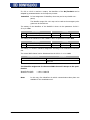
1
INDUSTRY PROCESS
AND AUTOMATION SOLUTIONS
Expansion
module EM-IO-02
Frequency Inverter 230 V / 400 V
0.55 kW ... 30.0 kW
ACTIVE
General points on the documentation
The present supplement of the documentation is valid for the frequency inverter series ACT 201 and ACT 401. The information necessary for the assembly and application of the EM-IO-02 expansion module is documented in this guidance.
For better clarity, the user documentation is structured according to the customerspecific demands made of the frequency inverter.
Brief instructions
The brief instructions describe the fundamental steps for mechanical and electrical
installation of the frequency inverter. The guided commissioning supports you in the
selection of necessary parameters and the software configuration of the frequency
inverter.
Operating instructions
The operating instructions document the complete functionality of the frequency inverter. The parameters necessary for specific applications for adaptation to the application and the extensive additional functions are described in detail.
Application manual
The application manual supplements the documentation for purposeful installation and
commissioning of the frequency inverter. Information on various subjects connected
with the use of the frequency inverter is described specific to the application.
Installation Instructions
Complementing the Brief Instructions and the Operating Instructions, the Installation
Instructions provide information on how to install and use the additional/optional
components.
The documentation and additional information can be requested via your local representation of the company of BONFIGLIOLI.
The following pictograms and signal words are used for the purposes of the present
documentation:
Danger!
means a directly threatening danger. Death, serious damage to persons and considerable damage to property will occur if the precautionary measure is not taken.
Warning!
marks a possible threat. Death, serious damage to persons and considerable damage
to property can be the consequence if attention is not paid to the text.
Caution!
refers to an indirect threat. Damage to people or property can be the result.
Attention!
refers to a possible operational behavior or an undesired condition, which can occur in
accordance with the reference text.
Note
marks information, which facilitates handling for you and supplements the corresponding part of the documentation.
Warning! In installation and commissioning, comply with the information in the
documentation. You as a qualified person must have read the documentation carefully and understood it. Comply with the safety instructions. For
the purposes of the instructions, "qualified person" designates a person
acquainted with the erection, assembly, commissioning and operation of
the frequency inverters and possessing the qualification corresponding to
the activity.
06/05
1
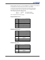
TABLE OF CONTENTS
General points on the documentation .................................................................................. 1
1
General safety and application information .................................................................. 5
1.1
General information................................................................................................. 5
1.2
Proper use................................................................................................................ 5
1.3
Transport and storage ............................................................................................. 6
1.4
Handling and positioning......................................................................................... 6
1.5
Electrical connection................................................................................................ 6
1.6
Operation information ............................................................................................. 6
1.7
Maintenance and service ......................................................................................... 6
2
Introduction ................................................................................................................... 7
3
Installation of the EM-IO-02 expansion module ........................................................... 8
3.1
General .................................................................................................................... 8
3.2
Mechanical installation ............................................................................................ 8
3.3 Electrical installation ............................................................................................. 10
3.3.1
Circuit diagram ...................................................................................................... 10
3.3.2
Control terminals ................................................................................................... 11
4
System bus interface.................................................................................................... 12
4.1
Bus termination ..................................................................................................... 12
4.2
Cables .................................................................................................................... 13
4.3
Socket X410B......................................................................................................... 13
4.4
Baud rate setting/line length ................................................................................ 14
4.5
Setting node address ............................................................................................. 14
4.6
Functional overview .............................................................................................. 15
4.7 Network management ........................................................................................... 15
4.7.1
SDO channels (parameter data) .............................................................................. 16
4.7.2
PDO channels (process data) .................................................................................. 16
4.8 Master functionality............................................................................................... 17
4.8.1
Control boot-up sequence, network management ..................................................... 17
4.8.2
SYNC telegram, generation..................................................................................... 19
4.8.3
Emergency message, reaction................................................................................. 20
4.8.4
Client SDO (system bus master).............................................................................. 21
4.9 Slave functionality ................................................................................................. 22
4.9.1
Implement boot-up sequence, network management................................................ 22
4.9.1.1
Boot-up message ............................................................................................ 22
4.9.1.2
Status control ................................................................................................. 22
4.9.2
Process SYNC telegram .......................................................................................... 23
4.9.3
Emergency message, fault switch-off....................................................................... 24
4.9.4
Server SDO1/SDO2 ................................................................................................ 25
2
06/05
TABLE OF CONTENTS
4.10
Communication channels, SDO1/SDO2.............................................................. 27
4.10.1 SDO telegrams (SDO1/SDO2) ................................................................................. 27
4.10.2 Communication via field bus connection (SDO1) ....................................................... 29
4.10.2.1 Profibus-DP .................................................................................................... 29
4.10.2.2 RS232/RS485 with VECTRON bus protocol ........................................................ 29
4.11
Process data channels, PDO ............................................................................... 31
4.11.1 Identifier assignment process data channel.............................................................. 31
4.11.2 Operation modes process data channel.................................................................... 32
4.11.3 Timeout monitoring process data channel ................................................................ 33
4.11.4 Communication relationships of the process data channel ......................................... 34
4.11.5 Virtual links ........................................................................................................... 35
4.11.5.1 Input parameters of the TxPDO’s for data to be transmitted ............................... 38
4.11.5.2 Source numbers of the RxPDO’s for received data.............................................. 40
4.11.5.3 Examples of virtual links .................................................................................. 41
4.12
Control parameters............................................................................................. 42
4.13
Handling of the parameters of the system bus .................................................. 43
4.14
Utilities ............................................................................................................... 45
4.14.1 Definition of the communication relationships........................................................... 46
4.14.2 Production of the virtual links.................................................................................. 47
4.14.3 Capacity planning of the system bus........................................................................ 48
5
Control inputs and outputs .......................................................................................... 50
5.1 Analog input EM-S1INA ......................................................................................... 50
5.1.1
General................................................................................................................. 50
5.1.2
Configuration voltage/current input ......................................................................... 50
5.1.3
Characteristic ........................................................................................................ 51
5.1.4
Operation modes ................................................................................................... 51
5.1.4.1
Examples........................................................................................................ 52
5.1.5
Scaling.................................................................................................................. 54
5.1.6
Tolerance band and hysteresis................................................................................ 55
5.1.7
Error and warning behavior .................................................................................... 56
5.1.8
Adjustment ........................................................................................................... 57
5.1.9
Filter time constant ................................................................................................ 57
5.2 Analog output EM- S1OUTA ................................................................................... 58
5.2.1
General................................................................................................................. 58
5.2.2
Operation modes ................................................................................................... 58
5.2.3
Adjustment ........................................................................................................... 58
5.2.4
Zero adjustment and amplification .......................................................................... 59
5.2.4.1
Examples........................................................................................................ 59
5.3 Digital output EM-S1OUTD .................................................................................... 60
5.3.1
General................................................................................................................. 60
5.3.2
Operation modes ................................................................................................... 60
5.4 Digital inputs EM-SxIND........................................................................................ 60
5.4.1
Fixed reference values and fixed value switch-over ................................................... 60
5.5 Digital inputs EM-SxIND for speed sensor EM-ENC............................................... 61
5.5.1
Division marks....................................................................................................... 61
5.5.2
Actual speed source ............................................................................................... 62
5.5.3
Actual value comparison......................................................................................... 62
06/05
3
TABLE OF CONTENTS
6
7
5.6
Frequency and percentage reference channel ...................................................... 63
5.7
Actual value display ............................................................................................... 63
5.8
Status of the digital signals ................................................................................... 64
5.9
Motor temperature ................................................................................................ 65
Parameter list............................................................................................................... 67
6.1
Actual value menu (VAL) ....................................................................................... 67
6.2
Parameter menu (PARA) ....................................................................................... 67
Annex ........................................................................................................................... 70
7.1
4
Error messages ...................................................................................................... 70
06/05
1
General safety and application information
This documentation has been created with greatest care and has been extensively and
repeatedly checked. For reasons of clarity, we have not been able to take all detailed
information on all the types of the products and also not every imaginable case of
positioning, operation or maintenance into account. If you require further information
or if particular problems not treated extensively enough in the operating instructions
occur, you can obtain the necessary information via the local representation of the
company BONFIGLIOLI.
In addition, we would point out that the contents of these operating instructions are
not part of an earlier or existing agreement, assurance or legal relationship, nor are
they intended to amend them. All the manufacturer's obligations result from the purchase contract in question, which also contains the completely and solely valid warranty regulation. These contractual warranty provisions are neither extended nor limited by the implementation of these operating instructions.
The manufacturer reserves the right to correct or amend the contents and product
information as well as omissions without specific announcement and assumes no kind
of liability for damage, injuries or expenditure to be put down to the aforementioned
reasons.
1.1
General information
Warning! VECTRON frequency inverters have high voltage levels during operating,
depending on their protection class, drive moving parts and have hot
surfaces.
In the event of inadmissible removal of the necessary covers, improper
use, wrong installation or operation, there is the risk of serious damage to
persons or property.
To avoid the damage, only qualified staff may carry out the transport,
installation, setup or maintenance work required. Comply with the standards EN 50178, IEC 60364 (Cenelec HD 384 or DIN VDE 0100), IEC
60664-1 (Cenelec HD 625 or VDE 0110-1), BGV A2 (VBG 4) and national
provisions. Qualified persons within the meaning of this principal safety
information are people acquainted with the erection, fitting, commissioning and operating of frequency inverters and the possible hazards and in
possession of qualifications matching their activities.
1.2
Proper use
Warning! The frequency inverters are electrical drive components intended for installation in industrial plant or machines. Commissioning and start of intended operation are not allowed until it has been established that the
machine corresponds to the provisions of the EC machine directive
98/37/EEC and EN 60204. According to the CE sign, the frequency inverters additionally fulfill the requirements of the low-voltage directive
73/23/EEC and the standards EN 50178 / DIN VDE 0160 and EN 61800-2.
Responsibility for compliance with the EMC directive 89/336/EEC is with
the user. Frequency inverters are available in a limited way and as components exclusively intended for professional use within the meaning of
the standard EN 61000-3-2.
With the issue of the UL certificate according to UL508c, the requirements
of the CSA Standard C22.2-No. 14-95 have also been fulfilled.
The technical data and the information on connection and ambient conditions stated on the rating plate and the documentation must be complied
with. The instructions must have been read and understood before starting work at the device.
06/05
5
1.3
Transport and storage
Transport and storage are to be done appropriate in the original packing. Store the
units only in dry rooms, which are protected against dust and moisture and are subjected to little temperature deviations only. Observe the climatic conditions according
to standard EN 50178 and to the information on the label of the original packing. The
duration of storage without connection to the admissible reference voltage may not
exceed one year.
1.4
Handling and positioning
Warning! Damaged or destroyed components may not be put into operation because they may be a health hazard.
The frequency inverters are to be used according to the documentation, the directives
and the standards. Handle carefully and avoid mechanical overload. Do not bend the
components or change the isolation distances. Do not touch electronic components or
contacts. The devices contain construction elements with a risk of electrostatic, which
can easily be damaged by improper handling. Any use of damaged or destroyed components shall be considered as a non-compliance with the applicable standards. Do
not remove any warning signs from the device.
1.5
Electrical connection
Warning! Before any assembly or connection work, de-energize the frequency inverter.
Do not touch the sockets, because the capacitors may still be charged.
Make sure that the frequency inverter is de-energized.
Comply with the information given in the operating instructions and on
the frequency inverter label.
While working on the frequency inverters, obey the applicable standards BGV A2 (VBG
4), VDE 0100 and other national directives. Comply with the information in the documentation on electrical installation and the relevant directives. Responsibility for compliance with and examination of the limit values of the EMC product standard EN
61800-3 for variable-speed electrical drive mechanisms is with the manufacturer of
the industrial plant or machine.
The documentation contains information on installation correct for EMC. The cables
connected to the frequency inverters may not be subjected to an isolation test with a
high test voltage without previous circuit measures.
1.6
Operation information
Warning! Before commissioning and the start of the intended operation, attach all
the covers and check the sockets. Check additional monitoring and protective devices pursuant to EN 60204 and the safety directives applicable
in each case (e.g. Working Machines Act, Accident Prevention Directives
etc.).
No connection work may be performed, while the system is in operation.
1.7
Maintenance and service
Warning! Unauthorized opening and improper interventions can lead to physical
injury or damage to property. Repairs on the frequency inverters may
only be done by the manufacturer or persons authorized by the latter.
6
06/05
2
Introduction
This document describes the possibilities and the properties of the EM-IO-02 expansion module for the frequency inverters of the ACT device series.
Note:
This document exclusively describes the EM-IO-02 expansion module. It
does not provide basic information on the operation of the ACT series
frequency inverters.
The EM-IO-02 expansion module is an optional hardware component to extend the
functionality of the frequency inverter. It enables the data exchange within the network between the components which have been directly connected, for example control and regulation elements.
The EM-IO-02 expansion module is supported as from software version 4.1.0 of device series ACT 201 and ACT 401.
The EM-IO-02 module extends the functionality of the frequency inverters of the ACT
device series by the following additional functions:
−
CAN system bus
(CAN interface ISO-DIS 11898; CAN High Speed; max. 1 MBaud)
−
Analog input
(second bipolar analog input)
−
Analog output
(second bipolar analog output)
−
Three digital inputs
(second speed sensor input)
−
Relay output
(make contacts)
−
PTC thermistor connection
Note:
The EM-IO-02 expansion module has been enclosed with the frequency
inverter as a separate component and must be fitted by the user. This is
described in detail in the chapter "Mechanical Installation".
To assemble the expansion module it can be simply plugged into the frequency inverters of the ACT device series.
Warning!
The assembly is done before the frequency inverter is put into operation,
and only in a voltage-free state.
The pluggable sockets of the expansion module enable economical overall fitting with
a safe function.
06/05
7
3
Installation of the EM-IO-02 expansion module
3.1
General
The mechanical and electrical installation of the EM-IO-02 expansion module is to be
carried out by qualified personnel according to the general and regional safety and
installation directives. Safe operation of the frequency inverter requires that the
documentation and the device specification be complied with during installation and
start of operation. For specific areas of application further provisions and guidelines
must be complied with where applicable.
The frequency inverters are designed according to the requirements and limit values
of product standard EN 61800-3 with an interference immunity factor (EMI) for operation in industrial applications. The electromagnetic interference is to be avoided by
expert installation and observation of the specific product information.
For further information, refer to the chapter "Electrical Installation" of the frequency
inverter operating instructions.
Warning!
3.2
Danger!
Mechanical installation
If the following instructions are not complied with, there is direct danger
with possible consequences of death or severe injury by electrical current.
To disregard the instructions can lead to destruction of the frequency
converter and/or of the expansion module.
•
Before assembly or disassembly of the EM-IO-02 expansion module, the frequency inverter must be de-energized. Take appropriate measures to make sure it
is not energized unintentionally.
•
Make sure that the frequency inverter is de-energized.
Danger!
8
All connection terminals where dangerous voltage levels may be present
(e.g. motor connection terminals, mains terminals, fuse connection terminals, etc.), must be protected against direct contact.
The mains, direct voltage and motor sockets can have dangerous voltages
even after disconnection of the frequency converter. Work may only be
done on the device after a waiting period of some minutes until the DC
link capacitors have been discharged.
06/05
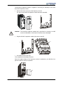
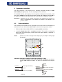
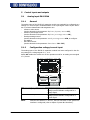
The EM-IO-02 expansion module is supplied in a housing for assembly on the lower
slot of the frequency inverter.
•
Remove the lower cover (1) of the frequency inverter.
The slot for the EM-IO-02 expansion module becomes accessible.
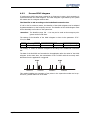
1
Caution!
•
The EM-IO-02 expansion module (2) is pre-fitted in a housing. Do NOT
touch the PCB visible on the back, as modules may be damaged.
Plug the EM-IO-02 expansion module (2) onto the slot (3).
2
3
• Re-install the lower cover (1).
This completes the assembly procedure.
When the supply voltage of the frequency inverter is switched on, the EM-IO-02 expansion module is ready for operation.
1
06/05
9
3.3
Danger!
Electrical installation
If the following instructions are not complied with, there is direct danger
with the possible consequences of death or severe injury by electrical
current. Further, failure to comply can lead to destruction of the frequency inverter and/or of the expansion module.
•
Before assembly or disassembly of the EM-IO-02 expansion module, the frequency inverter must be de-energized. Take appropriate measures to make sure it
is not energized unintentionally.
•
Make sure that the frequency inverter is de-energized.
Danger!
The mains, direct voltage and motor sockets can have dangerous voltages
even after disconnection of the frequency inverter. Work may only be
done on the device after a waiting period of some minutes until the DC
link capacitors have been discharged.
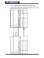
3.3.1
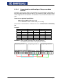
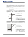
Circuit diagram
X410A
A
B
1 +20 V / 180mA
2 GND 20 V
EM-S1IND
3
EM-S2IND
4
EM-S3IND
5
EM-S1OUTD
6
7
X410B
EM-MPTC
1
C
2
EM-S1INA
D 3
A
D
E
4 EM-S1OUTA A
F
CAN-Low
5
CAN-High
6
7 GND
D
SYS
A Digital inputs EM-S1IND ... EM-S3IND
Digital signal, response time approx. 16 ms, Umax= 30 V, 10 mA at 24 V,
PLC compatible, frequency signal, 0 ... 30 V, 10 mA at 24 V, fmax = 150 kHz
B Relay connection EM-S1OUTD
Make contact, response time approx. 40 ms, 24 V AC / 1 A , 24 V DC / 1 A (ohmic)
C Motor PTC Resistor Connection EM-MPTC
Rated response resistance 2.85 kΩ (PTC) according to DIN 44081,
PTC or bimetal temperature sensor (break contact)
D Analog input EM-S1INA
Analog signal, resolution 12 Bit, Umax = ±10 V (Ri= 100 kΩ), Imax = ±20 mA (Ri= 250 Ω)
E Analog output EM- S1OUTA
Analog signal, Umax= ±10 V, Imax = 2 mA, overload and short-circuit proof
Communication interface system bus
CAN actuation of the system bus according to ISO-DIS 11898 (CAN High Speed)
F
10
06/05
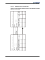
3.3.2
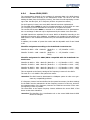
Control terminals
The control and software functionality can be freely configured for economical operation with a safe function.
Expansion module EM-IO-02
Wieland DST85 / RM3,5
0.14 … 1.5 mm2
AWG 30 … 16
0.14 … 1.5 mm2
AWG 30 … 16
0.25 … 1.0 mm2
AWG 22 … 18
0.25 … 0.75 mm2
AWG 22 … 20
0.2 … 0.3 Nm
1.8 … 2.7 lb-in
Caution!
•
•
The control inputs and outputs must be connected and disconnected free
of electrical power. Otherwise, components may be damaged.
The unit may only be connected with the power supply switched off.
Make sure that the frequency inverter is de-energized.
Socket X410A
Ter.
Description
1 Voltage output 20 V, Imax = 180 mA 1)
2 Earth / GND 20 V
3 Digital input EM-S1IND, Umax = 30 V, 10 mA at 24 V, PLC compatible,
response time approx. 16 ms
4 Digital input EM-S2IND, Umax = 30 V, 10 mA at 24 V, PLC compatible,
response time approx. 16 ms
5 Digital input EM-S3IND, Umax = 30 V, 10 mA at 24 V, PLC compatible,
response time approx. 16 ms
6-7 Digital output EM-S1OUTD, make contact, Umax = 24 V AC/DC, 1 A (ohmic)
Socket X410B
Ter.
Description
1-2 Motor PTC connection EM-MPTC,
rated response resistance > 2.85 kOhm (PTC) according DIN 44081
3 Analog input EM-S1INA, resolution 12 bit,
Umax= ±10 V (Ri = 100 kΩ),
Imax = ±20 mA (Ri = 250 Ω)
4 Analog output EM-S1OUTA,
Umax= ±10 V, Imax = 2 mA, overload and short circuit proof
5 System bus, CAN low
6 System bus, CAN high
7 Earth / GND
1)
06/05
The power supply at terminal X210A.1 may be loaded with a maximum current of
Imax = 180 mA. Relative to the application, the maximum current available will be
reduced by the further control outputs in the basic device and the expansion module.
11
4
System bus interface
The CAN connection of the system bus is physically designed according to ISODIS 11898 (CAN High Speed). The bus topology is the line structure.
In the default version, the frequency inverter supports a CAN protocol controller, which
may exist in either the CM-CAN communication module with CANopen interface OR in
an expansion module for the system bus, such as the EM-IO-02 expansion module.
Attention!
4.1
Installation of two optional components with CAN-Protocol controller results in a deactivation of the system bus interface in the EM-IO-02 expansion module.
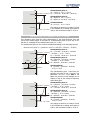
Bus termination
The necessary bus terminator at the physically first and last node can alternatively be
activated via the two DIP switches S1 and S2 on the EM-IO-02 expansion module.
•
Either set S1 to ON and S2 to OFF for a regular passive termination,
•
or switch S1 and S2 to ON for an active termination. This results in an improved
edge shape of the CAN signals, which improves the signal shapes, in particular in
extended systems.
Switch S3 is used to configure the analog input (see chapter "Analog input
EM-S1INA“).
ON
S3
X410A
S1
ON
ON
Note:
S2
X410B
Attention! The factory setting for the bus termination is OFF.
The active termination via the DIP switches S1 and S2 may only be activated in one expansion module. The other bus termination must be passive.
Data line
CAN high (X410B.6)
120 Ω
Data line
CAN low (X410B.5)
passive
12
332 Ω
Data line
CAN high (X410B.6)
Data line
CAN low (X410B.5)
332 Ω
active
06/05
4.2
Cables
For the bus line, use twisted cable with harness shield (no foil shield).
Attention! The control and communication lines are to be laid physically separate
from the power lines. The harness screen of the data lines is to be connected to ground (PE) on both sides on a large area and with good conductivity.
4.3
Socket X410B
The system bus is connected via the terminals 5, 6 and 7 of the socket X410B on the
EM-IO-02 expansion module.
X410A
X410B
5
Terminal
(5): X410B.5
(6): X410B.6
(7): X410B.7
06/05
X410B
6
Socket X410B
Input/Output
CAN-Low
CAN-High
GND
7
Description
CAN-Low (System bus)
CAN-High (System bus)
CAN-GND (System bus)
13
4.4
Baud rate setting/line length
The setting of the baud rate must be identical in all nodes on the system bus. The
maximum possible baud rate is based on the necessary overall line length of the system bus. The baud rate is set via the parameter Baud-Rate 903 and thus defines the
possible line length.
Operation mode
3 - 50 kBaud
4 - 100 kBaud
5 - 125 kBaud
6 - 250 kBaud
7 - 500 kBaud
8 - 1000 kBaud
Function
Transmission rate 50 kBaud
Transmission rate 100 kBaud
Transmission rate 125 kBaud
Transmission rate 250 kBaud
Transmission rate 500 kBaud
Transmission rate 1000 kBaud
max. line length
1000 meters
800 meters
500 meters
250 meters
100 meters
25 meters
A baud rate under 50 kBaud, as is defined according to CANopen, is not sensible for
the system bus as the data throughput is too low.
The maximum line lengths stated are guidelines. If they are made complete use of, a
calculation of the admissible length is to be done on the basis of the line parameters
and the bus driver (PCA82C250T).
4.5
Setting node address
A maximum of 63 slaves or frequency inverters with system bus can be operated on
the system bus. Each frequency inverter is given a node ID, which may only exist
once in the system, for its unambiguous identification. The setting of the system bus
node ID is done via the parameter Node-ID 900.
No.
900
Parameter
Description
Node-ID
min.
-1
max.
63
Setting
Factory setting
-1
Thus, the system bus possesses a maximum number of 63 nodes (Network nodes),
plus one frequency inverter as a master.
Note:
14
With the factory setting of parameter Node-ID 900 = -1, the system bus
is deactivated for this frequency inverter.
If the Node-ID 900 = 0 is set, the frequency inverter is defined as a master. Only one frequency inverter on the system bus may be defined as a
master.
06/05
4.6
Functional overview
To start with, the system bus produces the physical connection between the frequency
inverters. Logical communication channels are produced via this physical medium.
These channels are defined via the identifiers. As CAN does not possess a nodeoriented, but a message-oriented addressing via the identifiers, the logical channels
can be displayed via it.
In the basic state (factory setting) the identifiers are set according to the Predefined
Connection Set of CANopen. These settings are aimed at one master serving all the
channels. In order to be able to build up process data movement via the PDO channels
between individual or a number of inverters (transverse movement), the setting of the
identifiers in the nodes has to be adapted.
Note:
For understanding, it is important to observe that the data exchange is
done message-oriented. The frequency inverter can transmit and receive a
number of messages, identified via various identifiers.
As a special feature, the properties of the CAN bus mean that the messages transmitted by one node can be received by a number of nodes simultaneously. The error
monitoring methods of the CAN bus result in the message being rejected by all recipients and automatically transmitted again if there is a faulty reception in one receiver.
4.7
Network management
The network management controls the start of all the nodes on the system bus. Nodes
can be started or stopped individually or together. For node recognition in a CAL or
CANopen system, the slaves on the system bus generate a starting telegram (boot-up
report).
If a fault occurs, the slaves automatically transmit a fault report (emergency message).
For the functions of the network management, the methods and NMT telegrams (network management telegrams) defined according to CANopen (CiA DS 301) are used.
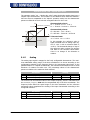
PLC
Field bus
System bus Master
Parameter
Function
Parameter
Function
SDO 2 SDO 1
PDO
SDO 2 SDO 1
PDO
System bus
Controller / PC
06/05
System bus Slave
System bus
System bus
15
4.7.1
SDO channels (parameter data)
Each frequency inverter possesses two SDO channels for the exchange of parameter
data. In a slave device, these are two server SDO's, in a device defined as a master a
client SDO and a server SDO. Attention must be paid to the fact that only one master
for each SDO channel may exist in a system.
Note:
Only one master can initiate by the system bus an exchange of data via
its client SDO.
The identifier assignment for the SDO channels (Rx/Tx) is done according to the Predefined Connection Set.
This assignment can be amended by parameterization, in order to solve identifier conflicts in a larger system in which further devices are on the CAN bus alongside the
frequency inverters.
Attention! In a system in which a frequency inverter works as a master, the identifier allocations for the SDO channel may not be altered.
In this way, an addressing of individual nodes via the field bus/system
bus path of the master frequency inverter is possible.
Parameters are read/written via the SDO channels. With the limitation to the SDO
Segment Protocol Expedited, which minimizes the handling needed for the parameter
exchange, the transmittable data are limited to the uint / int / long types. This permits
complete parameterization of the frequency inverters via the system bus, as all the
settings and practically all the actual values are displayed via these data types.
4.7.2
PDO channels (process data)
Each frequency inverter possesses three PDO channels (Rx/Tx) for the exchange of
process data.
The identifier assignment for the PDO channel (Rx/Tx) is done by default according to
the Predefined Connection Set. This assignment corresponds to an alignment to a
central master control.
In order to produce the logical channels between the devices (transverse movement)
on the system bus, the amendment of the PDO identifiers for Rx/Tx is necessary.
Each PDO channel can be operated with time or SYNC control. In this way, the operation behavior can be set for each PDO channel:
The setting of the operation mode is done via the following parameters:
TxPDO1 Function 930, TxPDO2 Function 932 und TxPDO3 Function 934
RxPDO1 Function 936, RxPDO2 Function 937 und RxPDO3 Function 938
Operation mode
0 -deactivated
1 -time-controlled
2 -SYNC controlled
Function
no exchange of data via the PDO channel (Rx and/or Tx)
Tx-PDO’s cyclically transmit according to the time specification
Rx-PDO‘s are read in with Ta = 1 ms and forward the data
received to the application
Tx-PDO’s transmit the data from the application that are
then current after the arrival of the SYNC telegram.
Rx-PDO’s forward the last data received to the application
after the arrival of the SYNC telegram.
For synchronous PDO’s, the master (PC, PLC or frequency inverter) generates the
SYNC telegram. The identifier assignment for the SYNC telegram is done by default
according to the Predefined Connection Set. This assignment can be altered by
parameterization.
16
06/05
4.8
Master functionality
An external control or a frequency inverter defined as a master (node ID = 0) can be
used as a master. The fundamental tasks of the master are controlling the start of the
network (boot-up sequence), generating the SYNC telegram and evaluating the emergency messages of the slaves.
Further, there can be access to the parameterization of all the frequency inverters on
the system bus by means of a field bus connection via the client SDO of the master
frequency inverter.
4.8.1
Control boot-up sequence, network management
The Minimum Capability Boot-Up method defined according to CANopen is used for
the state control of the nodes (nodes).
This method knows the pre-operational, operational and stopped states.
After the initialization phase, all the nodes are in the pre-operational state. The system
bus master transmits the NMT command Start-Remote-Node. With this command,
individual nodes or all the nodes can be started together. The frequency inverter defined as a master starts all the nodes with one command. After receipt of the Start
Remote Node command, the nodes change into the Operational state. From this time
on, process data exchange via the PDO channels is activated.
A master in the form of a PLC/PC can start the nodes on the system bus individually
and also stop them again.
As the slaves on the system bus need different lengths of time to conclude their initialization phases (especially if external components exist alongside the frequency
inverters), an adjustable delay for the change to Operational is necessary. The setting
is done in a frequency inverter defined as a system bus master via Boot-Up Delay
904.
No.
904
Parameter
Description
Boot-Up Delay
Min.
3500 ms
Setting
Max.
50000 ms
Factory setting
3500 ms
Properties of the states:
State
Pre-Operational
Operational
Stopped
Note:
06/05
Properties
Parameterization via SDO channel possible
Exchange of process data via PDO channel not possible
Parameterization via SDO channel possible
Exchange of process data via PDO channel possible
Parameterization via SDO channel not possible
Exchange of process data via PDO channel not possible
Start-Remote-Node is cyclically transmitted with the set delay time by an
frequency inverter defined as a system bus master, in order to put slaves
added with a delay or temporarily separated from the network back into
the Operational state.
17
Switch-on
(1)
Initialisation
from any
state
(2)
Pre-Operational
(4)
(7)
(5)
Stopped
(3)
(6)
(8)
Operational
After Power On and the initialization, the slaves are in the Pre-Operational state.
The transition (2) is automatic. The system bus master (frequency inverter or PLC/PC)
triggers the transition (3) to Operational state.
The transitions are controlled via NMT telegrams.
The identifier used for the NMT telegrams is "0" and may only be used by the system
bus master for NMT telegrams. The telegram contains two data bytes.
Byte 0
CS (Command Specifier)
Byte 1
Node-ID
Identifier = 0
With the statement of the node ID ≠ 0, the NMT command acts on the node selected
via the node ID. If node ID = 0, all the nodes are addressed.
Transition
(3) , (6)
(4) , (7)
(5) , (8)
Note:
18
Command
Start Remote Node
Enter Pre-Operational
Stop Remote Node
Reset Node
Reset Communication
Command Specifier
1
128
2
129
130
A frequency inverter defined as a system bus master only transmits the
command "Start Remote Node” with node ID = 0 (for all nodes). Transmission of the command is done after completion of the initialization
phase and the time delay Boot-Up Delay 904 following it.
06/05
4.8.2
SYNC telegram, generation
If synchronous PDO’s have been created on the system bus, the master must send the
SYNC telegram cyclically. If a frequency inverter has been defined as a system bus
master, the latter must generate the SYNC telegram. The interval for the SYNC telegram of a frequency inverter defined as the system bus master is adjustable. The
SYNC telegram is a telegram without data.
The default identifier = 128 according to the Predefined Connection Set.
If a PC or PLC is used as a master, the identifier of the SYNC telegrams can be
adapted by parameterization on the frequency inverter.
The identifier of the SYNC telegram must be set identically in all nodes on the system
bus.
The setting of the identifier of the SYNC telegram is done via the parameter SYNCIdentifier 918.
Parameter
No.
Description
918 SYNC-Identifier
Min.
0
Setting
Max.
2047
Fact. sett.
0
The setting "0” results in identifier assignment according to the Predefined Connection
Set.
Attention! The identifier range 129...191 may not be used as the emergency telegrams can be found there.
The temporal cycle for the SYNC is set on a frequency inverter defined as a system
bus master via the parameter SYNC-Time 919.
Note:
06/05
A setting of 0 ms for the parameter SYNC-Time 919 means "no SYNC
telegram”.
19
4.8.3
Emergency message, reaction
If a slave on the system bus suffers a fault, it transmits the emergency telegram. The
emergency telegram marks the node ID for the identification of the failed node via its
identifier and the existing fault message via its data contents (8 bytes).
After a fault has been acknowledged on the slave, the latter again transmits an emergency telegram with the data content zero.
The emergency telegram has the identifier 128 + node ID ( = 129 ... 191)
The system bus master evaluates the emergency telegrams of the slaves. Its reaction
to an emergency telegram can be set with Emergency Reaction 989.
Operation mode
0 -Error
1 -No Error
Function
The system bus master receives the emergency
telegram and switches-off
The Emergency Telegram is displayed as warning.
Operation mode - parameter 989 = 0 – Error
Behavior of the system bus master in Emergency Reaction 989 = 0 / Error:
As soon as the system bus master receives an emergency telegram, it also breaks
down and reports the failed node on the basis of its ID via the kind of error. Only the
node is reported, not the cause of the error.
The fault message on the system bus master via Current error 260 is 21nn with nn
= node ID (hexadecimal) of the slave in which a fault switch-off exists.
In addition, the system bus master reports the warning Sysbus (0x2000) via the parameter Warnings 270 Bit 13.
If a fault switch-off occurs on a number of slaves, the first slave to transmit its emergency telegram is displayed on the system bus master.
Operation mode - parameter 989 = 1 – No Error
Behavior of the system bus master in Emergency Reaction 989 = 1 / No Error:
As soon as the system bus master receives an emergency telegram, it reports the
warning Sysbus (0x2000) via the parameter Warnings 270 Bit 13.
Note:
20
In both cases, the Boolean variable SysbusEmergency with source number
730 is set to TRUE in the system bus master. It can be used in the system
bus master and (in transmission via a TxPDO) in the slaves for a defined
shutdown.
SysbusEmergency is also set if the system bus master breaks down.
Resetting of SysbusEmergency is done with the fault acknowledgment.
06/05
4.8.4
Client SDO (system bus master)
Each node on the system bus can be addressed via the SDO channels. In this way,
each node can be addressed and parameterized by one master via its client SDO1. All
the parameters of the data types uint/int/long are accessible. String parameters can
not be processed. If a frequency inverter has been defined as a system bus master,
each node on the system bus in this frequency inverter can be addressed by means of
a field bus connection (RS232, RS485, Profibus-DP) via its client SDO1.
Attention! The second SDO channel SDO2 of the frequency inverters is planned for
the parameterization of the frequency inverters via a visualization tool on
the system bus.
The service used is SDO Segment Protocol Expedited according to CANopen. The frequency inverter defined as a system bus master automatically generates the correct
telegrams. If the SDO channel is operated via a PLC/PC on the system bus, the telegrams must be generated according to the specification.
PLC
Field bus
Inv.1
Inverter 2
Inverter 2
Server-SDO 1
Server-SDO 1
Field bus
Client-SDO 1
System bus
Inverter 1
Inverter 2
Inverter 2
Server-SDO 2
Server-SDO 2
Server-SDO 2
System bus
Client-SDO 2
Visualizationtool
06/05
21
4.9
Slave functionality
4.9.1
Implement boot-up sequence, network management
4.9.1.1
Boot-up message
After the initialization, each slave on the system bus transmits its boot-up message
(heartbeat message).
Note:
The boot-up telegram has the identifier 1792 + node ID and a data byte
with contents = 0x00.
This telegram is of importance if a PLC/PC with CANopen functionality is used as a
master. The frequency inverter defined as a system bus master does not evaluate the
boot-up message.
4.9.1.2
Status control
The identifier used for the NMT telegrams is "0" and may only be used by the system
bus master for NMT telegrams. The telegram contains two data bytes.
Byte 0
CS (Command Specifier)
Byte 1
Node-ID
Identifier = 0
With the statement of the node ID ≠ 0, the NMT command acts on the node selected
via the node ID. If node ID = 0, all the nodes are addressed.
Transition
(3),(6)
(4),(7)
(5),(8)
-
Command
Start Remote Node
Enter Pre-Operational
Stop Remote Node
Reset Node
Reset Communication
Command Specifier
1
128
2
129
130
Attention! The reset node and reset communication command specified according
to DS 301 lead to a change to Pre-Operational via Initialization in the
frequency inverters. There is a new boot-up message.
After a slave has received the command "Start Remote Node”, it activates the PDO
channels and is ready for the exchange of process data.
22
06/05
4.9.2
Process SYNC telegram
If synchronous PDO’s have been created in an frequency inverter, their processing is
synchronized with the SYNC telegram. The SYNC telegram is generated by the system
bus master and is a telegram without data.
The identifier is 128 according to the Predefined Connection Set.
If a PC or PLC is used as a master, the identifier of the SYNC telegrams can be adapted
by parameterization on the frequency inverter. The identifier of the SYNC telegram must
be set identically in all nodes on the system bus.
Attention!
The identifier range 129 ... 191 may not be used as the emergency telegrams can be found there.
The setting of the identifier of the SYNC telegram is done via the parameter SYNCIdentifier 918.
Parameter
No.
Description
918 SYNC-Identifier
Setting
Max.
2047
Min.
0
Factory setting
0
The setting "0” results in identifier assignment according to the Predefined Connection
Set.
The data of the Rx-PDO’s are forwarded to the application after the arrival of the SYNC
telegram. At the same time, the transmission of the Tx-PDO’s with the currently available data from the application is triggered.
SYNC
RxPDO's
TxPDO's
SYNC
RxPDO's
TxPDO's
time
This method enables pre-occupancy of set points in the system bus nodes and a synchronous / parallel take-over of the data.
06/05
23
4.9.3
Emergency message, fault switch-off
As soon as a fault switch-off occurs in a slave frequency inverter, the emergency telegram is transmitted. The emergency telegram marks the node ID for the identification
of the failed node via its identifier and the existing fault message via its data contents
(8 bytes).
The emergency telegram has the identifier 128 + node ID.
After a fault acknowledgment, another emergency telegram is transmitted, with the
data content (Byte 0 ...7) being set to zero this time. This identifies the node's repeated readiness for operation. If a further fault occurs subsequently, it is transmitted
in a new emergency telegram.
The acknowledgment sequence is based on the definitions according to CANopen.
Data contents of the emergency telegram:
Byte
0
1
2
3
4
5
6
7
Value
0x00
0x10
0x80
0
0
0
0xnn
0xmm
Emergency telegram
Meaning
low-byte Error-Code
high-byte Error-Code
Error-Register
internal Error-Code, low-byte
internal Error-Code, high-byte
Bytes 0, 1 and 2 are firmly defined and compatible with CANopen.
Bytes 6/7 contain the product specific VECTRON error code.
Error-Code
= 0x1000
Error-Register = 0x80
= general error
= manufacturer-specific error
The explanation and description of the product-specific VECTRON error code can be
found in the annex "Error messages".
24
06/05
4.9.4
Server SDO1/SDO2
The communication channel for the exchange of parameter data is the SDO channel.
Communication works according to the client/server model. The server is the node
holding the data (here the frequency inverter), the client the node requesting or wanting to alter the data (PLC, PC or frequency inverter as system bus master).
For the frequency inverter, two server SDO channels have been implemented.
The first SDO channel SDO1 is used for the parameterization of the PLC/PC as a master or frequency inverter with field bus connection as a system bus master.
The second SDO channel SDO2 is reserved for a visualization tool for parameterization. An exchange of data can only be implemented by the master via a client SDO.
The SDO channels are stipulated for the server SDO’s via identifiers according to the
Predefined Connection Set to CANopen. As CANopen only provides for and defines one
SDO channel in the Predefined Connection Set, the second SDO channel can be deactivated.
In addition, the number of system bus nodes and the adjustable node ID are limited
to 63.
Identifier assignment according to the Predefined Connection Set:
Identifier Rx-SDO = 1536 + Node-ID
Identifier Tx-SDO = 1408 + Node-ID
(Node-ID = 1 ... 127, Identifier = 1537 ...
1663)
(Node-ID = 1 ... 127, Identifier = 1409 ...
1535)
Identifier assignment for SDO1/SDO2 compatible with the Predefined Connection Set:
Identifier Rx-SDO1 = 1536 + Node-ID (Node-ID = 1 ... 63, Identifier = 1537 ... 1599)
Identifier Tx-SDO1 = 1408 + Node-ID (Node-ID = 1 ... 63, Identifier = 1409 ... 1471)
Identifier Rx-SDO2 = 1600 + Node-ID (Node-ID = 0 ... 63, Identifier = 1600 ... 1663)
Identifier Tx-SDO2 = 1472 + Node-ID (Node-ID = 0 ... 63, Identifier = 1472 ... 1535)
This corresponds to the factory settings of the frequency inverters for the SDO‘s.
The node ID = 0 for SDO2 is the system bus master.
Attention! The SDO2 must be deactivated in a CANopen system in order not to generate any compatibility problems.
If a frequency inverter has been defined as the system bus master, the above settings
for the SDO1 must be maintained in all the frequency inverters. In this way, access to
the parameterization of the frequency inverters via a field bus connection on the master frequency inverter is possible.
The client SDO1 in the master frequency inverter addresses the server SDO1 of the
slaves via the above identifiers.
Attention! The identifiers for a visualization tool on the second SDO channel SDO2
cannot be changed.
06/05
25
If a PC or a PLC is used as a master, the identifiers of the Rx/Tx-SDO1 can be
adapted by parameterization on the frequency inverter.
Attention!
In free assignment of identifiers, there may not be any double occupancy!
The identifier range 129...191 may not be used as the emergency telegrams can be found there.
The setting of the identifiers of the RxSDO1 is done via the parameter RxSDO1Identifier 921.
Parameter
No.
Description
921 RxSDO1-Identifier
Min.
0
Setting
Max.
2047
Fact. sett.
0
The setting of the identifiers of the TxSDO1 is done via parameter number 922.
Parameter
No.
Description
922 TxSDO1-Identifier
Min.
0
Setting
Max.
2047
Fact. sett.
0
The setting "0” results in identifier assignment according to the Predefined Connection
Set.
The second SDO channel can be deactivated via the SDO2 Set Active 923.
Operation mode
0 -SDO2 deactivated
1 -SDO2 activated
Function
Communication channel deactivated
Communication channel activated for the visualization tool
The identifier assignment for the second SDO channel is always to the specification:
Identifier Rx-SDO2
Identifier Tx-SDO2
Note:
26
= 1600 + Node-ID
= 1472 + Node-ID
In this way, firm identifiers via which communication takes place are
available for the visualization tool.
06/05
4.10
Communication channels, SDO1/SDO2
4.10.1
SDO telegrams (SDO1/SDO2)
The service used for the exchange of parameter data is SDO Segment Protocol
Expedited. The data (type uint, int, long) are exchanged in a telegram.
Access to the parameters in the frequency inverters with a statement of parameter
number and data set is displayed via the addressing defined for object access pursuant to the specifications of CANopen via Index/Sub-Index.
Index = parameter number / Sub index = data set.
The data to be transmitted have a length of 2 bytes for uint/int and 4 bytes for long.
For standardization and simplification, 4 bytes are always transmitted.
The data are on bytes 4...7 of the SDO telegram.
uint/int variables are transmitted in bytes 4 and 5
with bytes 6 und 7 = 0.
long variables are transmitted in bytes 4...7.
Writing parameters:
Client Î Server
0
Ctrl. byte
0x22
uint/int
long
Server Î Client
0
Ctrl. byte
0x60
Server Î Client
0
Ctrl. byte
0x80
SDO Download (expedited)
1
2
Parameter number
LSB
MSB
3
Data set
0xnn
4
5
6
7
0x00
...
MSB
0x00
MSB
Data
LSB
LSB
LSB
MSB
...
Download Response Î Writing process free of errors
1
2
Parameter number
LSB
MSB
3
Data set
0xnn
4
5
6
7
6
7
0
0
Data
0
Abort SDO Transfer Î Writing process faulty
1
2
Parameter number
LSB
MSB
3
Data set
0xnn
4
5
Data
Code
0
The error code is stated in byte 4 in a faulty reading process.
(see Table, failure codes).
Attention! Control byte 0x22 for the identification "SDO Download expedited” does
not consider the bits "s” (data size indicated) and "n” (number of bytes
not containing data). If set, they are ignored. The user is responsible for
the number of bytes matching the type of data.
06/05
27
Reading parameters:
Client Î Server
0
Ctrl. byte
0x40
SDO Upload (expedited)
1
2
Parameter number
LSB
MSB
Server Î Client
0
Ctrl. byte
0x42
uint/int
long
4
5
6
7
6
7
0x00
...
MSB
0x00
MSB
6
7
0
0
Data
0
Upload Response Î Reading process free of errors
1
2
Parameter number
LSB
MSB
Server Î Client
0
Ctrl. byte
0x80
3
Data set
0xnn
3
Data set
0xnn
4
5
Data
LSB
LSB
LSB
MSB
...
Abort SDO Transfer Î Reading process faulty
1
2
Parameter number
LSB
MSB
3
Data set
0xnn
4
5
Code
0
Data
The error code is stated in byte 4 in a faulty reading process.
(see Table, failure codes).
Code
1
2
3
4
5
6
7
8
9
10
11
12
15
20
21
failure codes
Description
inadmissible parameter figure
inadmissible data set
parameter not readable
parameter not writable
reading error EEPROM
writing error EEPROM
checksum error EEPROM
parameter cannot be written during running drive
values of the data sets differ
parameter of wrong type
unknown parameter
BCC error in VECTRON bus protocol
unknown error
system bus node not available only in access via field bus
connection
string parameter not admissible only in access via VECTRON bus protocol
Errors marked in the table are generated by the field bus side, not in the Abort SDO
Transfer of the system bus.
28
06/05
4.10.2
Communication via field bus connection (SDO1)
If a frequency inverter has been defined as the system bus master and equipped with
a field bus interface, access to the parameterization of all the nodes in existence on
the system bus is possible by means of this field bus interface via the first SDO channel (SDO1). An extension has been created in the protocol frame of the field buses for
this purpose.
Attention! The prerequisite for this mechanism is that the identifier setting for the
first SDO channel (SDO1) corresponds to the Predefined Connection Set.
The parameter addressed must also exist in the system bus master.
4.10.2.1 Profibus-DP
If an object with communication channel (PKW) is used in Profibus-DP, access to all
the other nodes on the system bus can be done via it. The structure of the communication channel permits an additional addressing of a system bus node. This is done by
the use of an unused byte in the communication channel.
Communication channel PKW
0
AK/SPM
1
PKE
Parameter
number
2
Index
Data set
3
Node-ID
system bus
4
5
6
7
Data
Byte 3 is used to transmit the Node ID of the required node on the system bus. If byte
3 = 0, the master inverter of the system bus is addressed. The display is binary
(0...63).
4.10.2.2 RS232/RS485 with VECTRON bus protocol
In the VECTRON bus protocol, there is a byte in the telegram header that is always
transmitted with 0 as a standard feature.
ENQUIRY
0
Address
1
2
3
4
0
p
n
n
Node-ID
Data set Parameter number
system bus
5
n
6
ENQ
SELECT
0
Address
1
STX
2
3
4
0
p
n
n
Node-ID
Data set Parameter number
system bus
n
...
Byte 1 in the enquiry and byte 2 in the select telegram are not defined and are used to
transmit the Node ID of the required node on the system bus. If this byte = 0, the
master inverter of the system bus is addressed. The display is ASCII corresponding to
the conventions for the display of the address in the VECTRON bus protocol.
Note:
06/05
If there is an NAK fault message, the error is to be read out from the
system bus master with node ID = 0 via parameter 11!
29
Display of node ID system bus in the VECTRON bus protocol:
System bus Node-ID
System bus (ASCII-) HEX value System bus
address character
address
1
A
41
31
2
B
42
32
3
C
43
33
4
D
44
34
5
E
45
35
6
F
46
36
7
G
47
37
8
H
48
38
9
I
49
39
10
J
4A
40
11
K
4B
41
12
L
4C
42
13
M
4D
43
14
N
4E
44
15
O
4F
45
16
P
50
46
17
Q
51
47
18
R
52
48
19
S
53
49
20
T
54
50
21
U
55
51
22
V
56
52
23
W
57
53
24
X
58
54
25
Y
59
55
26
Z
5A
56
27
[
5B
57
28
\
5C
58
29
]
5D
59
30
^
5E
60
61
62
63
30
(ASCII-)
character
_
`
a
b
c
d
e
f
g
h
i
j
k
l
m
n
o
p
q
r
s
t
u
v
w
x
y
z
{
|
}
~
HEX value
5F
60
61
62
63
64
65
66
67
68
69
6A
6B
6C
6D
6E
6F
70
71
72
73
74
75
76
77
78
79
7A
7B
7C
7D
7E
7F
06/05
4.11
Process data channels, PDO
4.11.1
Identifier assignment process data channel
The process channel for the exchange of process data under CANopen is the PDO
channel. Up to three PDO channels with differing properties can be used in one device.
The PDO channels are defined via identifiers according to the Predefined Connection
Set to CANopen:
Identifier 1. Rx-PDO =
Identifier 1. Tx-PDO =
512 + Node-ID
384 + Node-ID
Identifier 2. Rx-PDO =
Identifier 2. Tx-PDO =
768 + Node-ID
640 + Node-ID
Identifier 3. Rx-PDO = 1024 + Node-ID
Identifier 3. Tx-PDO = 896 + Node-ID
This corresponds to the factory settings of the frequency inverters for the Rx/TxPDO‘s. This occupancy is aligned to an external master (PLC/PC) serving all the channels.
If the PDO channels are used for a connection of the frequency inverters amongst one
another, the identifiers are to be set accordingly by parameterization.
Attention! In free assignment of identifiers, there may not be any double occupancy!
The identifier range 129...191 may not be used as the emergency telegrams can be found there.
Setting of the identifiers of the Rx/TxPDO’s:
Parameter
No.
Description
924 RxPDO1 Identifier
925 TxPDO1 Identifier
926 RxPDO2 Identifier
927 TxPDO2 Identifier
928 RxPDO3 Identifier
929 TxPDO3 Identifier
Min.
0
0
0
0
0
0
Setting
Max.
2047
2047
2047
2047
2047
2047
Fact. sett.
0
0
0
0
0
0
The setting "0” results in identifier assignment according to the Predefined Connection
Set.
06/05
31
4.11.2
Operation modes process data channel
The transmit/receive behavior can be time controlled or controlled via a SYNC telegram. The behavior can be parameterized for each PDO channel.
Tx-PDO’s can work time controlled or SYNC controlled. A time controlled TxPDO
transmits its data at the interval of time set. A SYNC controlled TxPDO transmits its
data after the arrival of a SYNC telegram.
RxPDO’s in the time controlled setting forward the received data to the application
immediately. If an RxPDO has been defined as SYNC controlled, it forwards its received data to the application after the arrival of a SYNC telegram.
Settings TxPDO1/2/3
Parameter
No.
Description
931 TxPDO1 Time
933 TxPDO2 Time
935 TxPDO3 Time
Min.
1 ms
1 ms
1 ms
Setting
Max.
50000 ms
50000 ms
50000 ms
Fact. sett.
8 ms
8 ms
8 ms
The setting of the operation mode is done via the following parameters:
TxPDO1 Function 930, TxPDO2 Function 932 und TxPDO3 Function 934
Operation mode
0 -Not Active
1 -Controlled by time
2 -Controlled by SYNC
Function
No data are sent
In the cycle of the adjusted time interval the data
are sent
To arrival of a SYNC telegram the data are sent
Settings RxPDO1/2/3
The setting of the operation mode is done via the following parameters:
RxPDO1 Function 936, RxPDO2 Function 937 und RxPDO3 Function 938
Operation mode
0 -Controlled by time
1 -Controlled by SYNC
Note:
32
Function
The received data are passed on immediately
After arrival of a SYNC telegram the received data
are passed on
In the "controlled by time” operation mode, there is a polling of the received data with the trigger cycle of Ta = 1 ms.
06/05
4.11.3
Timeout monitoring process data channel
Each frequency inverter monitors its received data for whether they are updated within
a defined time window.
The monitoring is done onto the SYNC telegram and the RxPDO channels.
Monitoring SYNC / RxPDO‘s
No.
939
941
942
945
Parameter
Description
SYNC Timeout
RxPDO1 Timeout
RxPDO2 Timeout
RxPDO3 Timeout
Min.
0 ms
0 ms
0 ms
0 ms
Setting
Max.
60000 ms
60000 ms
60000 ms
60000 ms
Fact. sett.
0 ms
0 ms
0 ms
0 ms
Setting 0 means no timeout monitoring.
Attention! There is only monitoring for the SYNC telegram if at least one RxPDO or
one TxPDO channel is defined as SYNC controlled.
If a timeout period is exceeded, the frequency inverter breaks down and reports one
of the faults:
F2200
System bus Timeout SYNC
F2201
System bus Timeout
RxPDO1
System bus Timeout
RxPDO2
System bus Timeout
RxPDO3
F2202
F2203
06/05
33
4.11.4
Communication relationships of the process data
channel
Regardless of the process data to be transmitted, the communication relationships of
the process data channels must be defined. The connection of PDO channels is done
via the assignment of the identifiers. The identifiers of Rx-/Tx-PDO must match in each
case.
There are two principal possibilities:
-
one Rx-PDO to one Tx-PDO (one to one)
connect several Rx-PDO’s to one TxPDO (one to many)
This process is documented in a tabular form via a communication relationship
list.
Example:
Frequency inverter 1
PDO
Identifier
TxPDO1
385
RxPDO1
TxPDO2
641
RxPDO2
TxPDO3
RxPDO3
Frequency inverter 2 Frequency inverter 3
PDO
Identifier
PDO
Identifier
TxPDO1
TxPDO1
RxPDO1
385
RxPDO1
385
TxPDO2
TxPDO2
642
RxPDO2
641
RxPDO2
TxPDO3
TxPDO3
RxPDO3
642
RxPDO3
Attention! All the TxPDO’s used must have differing identifiers!
The Identifier must be clear in the system bus network.
Frequency inverter 1
PDO1 PDO2 PDO3
Rx Tx Rx Tx Rx Tx
385
641
34
Frequency inverter 2
PDO1 PDO2 PDO3
Rx Tx Rx Tx Rx Tx
385
641
642
Frequency inverter 3
PDO1
Rx Tx
385
PDO2 PDO3
Rx Tx Rx Tx
642
06/05
4.11.5
Virtual links
According to CANopen, a PDO telegram contains 0...8 data bytes. A mapping for any
kind of objects can be done in these data bytes.
For the system bus, the PDO telegrams are firmly defined with 8 data bytes. The mapping is not done via mapping parameters as with CANopen, but via the method of
sources and links.
Each function provides its output data via a source. These sources are defined via
source numbers. The input data of functions are defined via parameters. The link of a
data input to a data output is done via the assignment of parameters to source numbers.
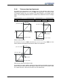
Example 1:
Function A
Source-No. 27
Function C
Parameter 125
Function B
Parameter 187
Source-No. 5
In example 1, the two inputs of function C are connected with the outputs of functions
A and B. Thus, the parameterization for this connection is:
Function C
Parameter 125 = Source-No. 27
Parameter 187 = Source-No. 5
Example of a virtual link in VPlus:
Parameter
(Softwarefunction)
Source-No.
(Operation mode)
e.g. Start-clockwise 068
e.g. 71-S2IND
Digital input
The assignment of the operation modes to the software functions available can be
adapted to the application in question.
06/05
35
For the system bus, the input data of the TxPDO’s are also displayed as input parameters and the output data of the RxPDO’s as sources.
Example 2:
Function A
Inverter 1
Source-No. 27
TxPDO
Inverter 1
Parameter 977
system bus
Function B
Inverter 1
Source-No. 5
RxPDO
Inverter 2
Parameter 972
Function C
Inverter 2
Source-No. 727
Parameter 125
Source-No. 724
Parameter 187
system bus
Example 2 displays the same situation as Example 1. But now, the functions A and B
are in frequency inverter 1 and function C in frequency inverter 2. The connection is
done via a TxPDO in frequency inverter 1 and a RxPDO in frequency inverter 2. Thus,
the parameterization for this connection is:
Frequency inverter 1
Parameter 977 = Source-No. 27
Parameter 972 = Source-No. 5
Frequency inverter 2
Parameter 125 = Source-No. 727
Parameter 187 = Source-No. 724
As the links with the system used exceed the device limits, they are termed "virtual
links".
36
06/05
The virtual links with the possible sources are related to the Rx/TxPDO channels. For
this purpose, the eight bytes of the Rx-/TxPDO’s are defined structured as inputs and
sources. This exists for each of the three PDO channels.
Each transmit PDO and receive PDO can be occupied as follows:
4 Boolean variables
or
4 uint/int variables 4 uint/int variables
or
2 long variables
or
a mixture paying attention to the eight bytes available
Assignment data type / number of bytes:
Assignment
Data type
Length
Boolean
2 Bytes
uint/int
2 Bytes
long
4 Bytes
06/05
37
4.11.5.1 Input parameters of the TxPDO’s for data to be
transmitted
The listed parameters can be used to stipulate the data that are to be transported
there for each position in the TxPDO telegrams. The setting is done in such a way that
a source number is entered for the required data in the parameters.
TxPDO1
Byte
0
1
2
3
4
5
6
7
TxPDO2
Byte
0
1
2
3
4
5
6
7
TxPDO3
Byte
0
1
2
3
4
5
6
7
Note:
38
P. No.
Boolean
input
946
Boolean1
947
Boolean2
948
Boolean3
949
Boolean4
P. No.
Boolean
input
956
Boolean1
957
Boolean2
958
Boolean3
959
Boolean4
P. No.
Boolean
input
966
Boolean1
967
Boolean2
968
Boolean3
969
Boolean4
TxPDO1
Byte
0
1
2
3
4
5
6
7
TxPDO2
Byte
0
1
2
3
4
5
6
7
TxPDO3
Byte
0
1
2
3
4
5
6
7
P. No.
uint/int
input
950
Word1
951
Word2
952
Word3
953
Word4
P. No.
uint/int
input
960
Word1
961
Word2
962
Word3
963
Word4
P. No.
uint/int
input
972
Word1
973
Word2
974
Word3
975
Word4
TxPDO1
Byte
0
1
2
3
4
5
6
7
TxPDO2
Byte
0
1
2
3
4
5
6
7
TxPDO3
Byte
0
1
2
3
4
5
6
7
P. No.
long input
954
Long1
955
Long2
P. No.
long input
964
Long1
965
Long2
P. No.
long input
976
Long1
977
Long2
Depending on the selected data information the percentages values are
displayed via the uint/int inputs!
06/05
With this method, there are up to three possibilities for a meaning of the contents of
the individual bytes. Each byte may only be used for one possibility.
To ensure this, the processing of the input links is derived from the setting.
If an input link has been set to the fixed value of zero, it is not processed.
The settings for the fixed value zero are:
Source =
Source =
7 (FALSE)
9 (0)
for boolean variables
for uint/int, long variables
This is simultaneously the factory setting.
Examples Boolean source
Source
6
7
70
71
72
161
163
164
Boolean source
Data
TRUE
FALSE
Contact input 1
Contact input 2
Contact input 3
Running message
Nominal figure reached
Set frequency reached (P. 510)
Examples uint/int source
uint/int source
Source
Data
9
0
63
Reference percentage 1
64
Reference percentage 2
52
Percentage MFI1
133
Output percentage ramp
137
Output reference percentage
channel
138 Output actual percentage channel
740
Control word
741
State word
Examples long source
long source
Source
Data
9
0
0
Output frequency ramp
1
Fixed frequency 1
5
Reference line value
62
Output frequency reference value
channel
50
Reference frequency MFI1
06/05
39
4.11.5.2 Source numbers of the RxPDO’s for received data
Equivalent to the input links of the TxPDO’s, the received data of the RxPDO’s are
displayed via sources or source numbers. The sources existing in this way can be used
in the frequency inverter via the local input links for the data targets.
RxPDO1
Byte
0
1
2
3
4
5
6
7
RxPDO2
Byte
0
1
2
3
4
5
6
7
RxPDO3
Byte
0
1
2
3
4
5
6
7
Source No.
Boolean
value
700
Boolean1
701
Boolean2
702
Boolean3
703
Boolean4
Source No.
Boolean
value
710
Boolean1
711
Boolean2
712
Boolean3
713
Boolean4
Source No.
Boolean
value
720
Boolean1
721
Boolean2
722
Boolean3
723
Boolean4
RxPDO1
Byte
0
1
2
3
4
5
6
7
RxPDO2
Byte
0
1
2
3
4
5
6
7
RxPDO3
Byte
0
1
2
3
4
5
6
7
Source No.
uint/int
value
704
Word1
705
Word2
706
Word3
707
Word4
Source No.
uint/int
value
714
Word1
715
Word2
716
Word3
717
Word4
Source No.
uint/int
value
724
Word1
725
Word2
726
Word3
727
Word4
RxPDO1
Byte
0
1
2
3
4
5
6
7
RxPDO2
Byte
0
1
2
3
4
5
6
7
RxPDO3
Byte
0
1
2
3
4
5
6
7
Source No.
longValue
708
Long1
709
Long2
Source No.
long
value
718
Long1
719
Long2
Source No.
long
value
728
Long1
729
Long2
With this method, there are up to three possibilities for a meaning of the contents of
the individual bytes. Each byte may only be used for one possibility.
Note:
40
Depending on the selected data information the percentages values are
displayed via the uint/int inputs!
06/05
4.11.5.3 Examples of virtual links
Example 1:
Frequency inverter 1
Source
Input link TxPDO1
No.
Byte
Control word
950
0
740
1
Output reference frequency
channel 62
Frequency inverter 2
RxPDO1 Source
Target
Byte
No.
0
704 Control input,
Control word
1
99
2
3
4
709
Ramp input,
Reference line
5
value 137
6
7
2
3
4
5
6
7
955
Parameter 950 = Source-No. 740
Parameter 955 = Source-No. 62
Parameter 99 = Source-No. 704
Parameter 137 = Source-No. 709
The control word of frequency inverter 1 is linked with the control word of frequency
inverter 2. In this way, both frequency inverters can be operated synchronously via
the remote control. The output of the reference value channel of frequency inverter 1
is laid onto the output of the ramp of frequency inverter 2. In this way, both frequency
inverters have a joint source of reference values and are given reference values in the
internal notation.
As an extension, a number of frequency inverters can also exist on the receive side
(Rx), these then being supplied with data parallel and simultaneously.
The input link not used in the TxPDO1 of frequency inverter 1 is on ZERO and is thus
not served.
Example 2:
Example of a virtual link with transmission via the system bus:
TxPDO1 Identifier 925
385
Parameter
Identifier
Inverter 1
system bus
06/05
TxPDO1 Boolean1 946
71-S2IND
Parameter
Source-No.
RxPDO1 Identifier 924
385
Parameter
Identifier
Inverter 2
Start-clockwise 068
700-RxPDO1 Boolean
Parameter
Source-No.
41
4.12
Control parameters
For the monitoring of the system bus and the display of the internal states, two control parameters are provided. There is a report of the system bus state and a report of
the CAN state via two actual value parameters.
The parameter Node-State 978 gives information about the Pre-Operational, Operational, Stopped state. A PDO transfer is only possible in the Operational state. The
state is controlled by the system bus master (PLC / PC / frequency inverter) via NMT
telegrams.
The parameter CAN-State 979 gives information about the state of the physical layer.
If there are transmission errors, the state changes from OKAY to WARNING until the
cancellation of the communication with BUS-OFF. After BUS-OFF, the CAN controller is
automatically re-initialized and the system bus started again.
Note:
If the BUS-OFF state occurs, the frequency inverter breaks down with
"F2210 BUS-OFF".
After Bus-OFF, the system bus in the frequency inverter is completely reinitialized.
There is a new boot-up message from the node and an emergency telegram with the
Bus-OFF message is transmitted. The change of state of the node to Operational is
done by the Start-Remote-Node telegram cyclically sent by the system bus master.
Actual values of the system bus
No.
Description
Function
978 Node-State
1 - Pre-Operational
2 - Operational
3 - Stopped
979 CAN-State
1 - OKAY
2 - WARNING
3 - BUS-OFF
42
06/05
4.13
Handling of the parameters of the system bus
As soon as the system bus expansion module EM-SYS exists in an frequency inverter,
the actual value parameters for system state and bus state are activated and can be
observed in the actual value menu VAL of the control unit KP500 or with the VPlus PC
program in the menu Actual values \ System bus.
Note:
The actual value parameters are on control level 3 and are thus available
for the user at any time.
All the setting parameters for the configuration of the system bus are not directly accessible for the user. For defined customer applications, pre-defined XPI files can be
generated by VECTRON for the VPlus PC program, with which the necessary parameters are visible for the user. The application-relevant variables are then available in
these XPI files.
Note:
XPI files can be read in addition to the loaded parameter information of
the frequency inverter into the VPlus PC program.
In the menu of the software under the point Edit you find the command
"Read in XPI file".
The method of working via an XPI file has its reasoning in the fact that deep interventions in the system are possible via the system bus and can lead to serious problems
in the application with an untrained user. Via the XPI files, a user is given a selection
list pre-defined by VECTRON.
Attention! The configuration of the necessary parameters for the system bus are
accessible by a XPI file with the help of the VPlus PC program.
The control unit KP500 does not support this functionality.
If the expansion module system bus EM-SYS is installed additionally to a
communication module for the field bus connection (CM-232, CM-485 or
CM-PDP) in the frequency inverter, the parameterization can be made
with the interface adapter KP232.
Experienced users have complete access to all the existing sources and possible input
links with the XPI file of the active functions. The selection depends on the selected
configuration and control procedure.
The display of the parameters when using the XPI file is according to the following
structure:
system bus
06/05
Basic Settings
900Node-ID
903Baud-Rate
Master Functions
904Boot-Up Delay
919SYNC-Time
SYNC-Identifier
918SYNC-Identifier
SDO1-Identifier
921RxSDO1-Identifier
922TxSDO1-Identifier
SDO2 Set Active
923SDO2 Set Active
PDO-Identifier
924RxPDO1-Identifier
925TxPDO1-Identifier
926RxPDO2-Identifier
927TxPDO2-Identifier
928RxPDO3-Identifier
929TxPDO3-Identifier
43
TxPDO-Function
930TxPDO1
931TxPDO1
932TxPDO2
933TxPDO2
934TxPDO3
935TxPDO3
RxPDO-Function
936RxPDO1 Function
937RxPDO2 Function
938RxPDO3 Function
Timeout
939SYNC Timeout
941RxPDO1 Timeout
942RxPDO2 Timeout
945RxPDO3 Timeout
TxPDO1 Objects
946TxPDO1
947TxPDO1
948TxPDO1
949TxPDO1
950TxPDO1
951TxPDO1
952TxPDO1
953TxPDO1
954TxPDO1
955TxPDO1
Boolean1
Boolean2
Boolean3
Boolean4
Word1
Word2
Word3
Word4
Long1
Long2
TxPDO2 Objects
956TxPDO2
957TxPDO2
958TxPDO2
959TxPDO2
960TxPDO2
961TxPDO2
962TxPDO2
963TxPDO2
964TxPDO2
965TxPDO2
Boolean1
Boolean2
Boolean3
Boolean4
Word1
Word2
Word3
Word4
Long1
Long2
TxPDO3 Objects
966TxPDO3
967TxPDO3
968TxPDO3
969TxPDO3
972TxPDO3
973TxPDO3
974TxPDO3
975TxPDO3
976TxPDO3
977TxPDO3
Boolean1
Boolean2
Boolean3
Boolean4
Word1
Word2
Word3
Word4
Long1
Long2
Actual values
system bus
44
Function
Time
Function
Tome
Function
Time
978Node-State
979CAN-State
06/05
4.14
Utilities
For the planning of the system bus according to the drive tasks in question, there are
utilities in the form of tables.
The planning of the system bus is done in three steps:
1.
2.
3.
Definition of the communication relationships
Production of the virtual links
Capacity check
The priority assignment of the identifiers is relevant for the definition of the communication relationships. Data that are to be transmitted with a higher priority must be
given low identifiers. This results in the message with the higher priority being transmitted first with a simultaneous access of two nodes to the bus.
Note:
The recommended identifier range for the communication relationships via
the PDO channels is 385 ... 1407.
The identifiers below 385 are used for the NMT telegrams (boot-up sequence, SYNC telegram) and emergency message.
The identifiers above 1407 are used for the SDO channel for parameterization.
06/05
45
46
Source- Input link/parameternumber
number:
Boolean
uint/int
TxPDO-Nr: ________
long
(Tx/RxPDO)
Input link/parameternumber
Boolean
uint/int
RxPDO-Nr: ________
________
long
Sourcenumber:
Node-ID:
Identifier: ___________
Node-ID:
________
Inverter: ___________________________
Inverter: ___________________________
4.14.1
Definition of the communication relationships
The communication relationships are planned and documented with the help of the
table. The table is available as a Microsoft Word document "kbl.doc" on the
BONFIGLIOLI VECTRON product CD or upon request.
06/05
06/05
Source- Input link/parameternumber
number:
Boolean
uint/int
TxPDO-Nr: ________
long
(Tx/RxPDO)
Input link/parameternumber
Boolean
uint/int
RxPDO-Nr: ________
________
long
Sourcenumber:
Node-ID:
Identifier: ___________
Node-ID:
________
Inverter: ___________________________
Inverter: ___________________________
4.14.2
Production of the virtual links
The virtual links are planned and documented with the help of the table. The table is
available as a Microsoft Word document "vvk.doc" on the BONFIGLIOLI VECTRON
product CD or upon request.
47
4.14.3
Capacity planning of the system bus
Each PDO telegram possesses a constant useful data content of 8 Bytes. According to
worst case, this results in a maximum telegram length of 140 bits. The maximum telegram run time of the PDO’s is thus stipulated via the set baud rate.
Capacity planning
Baud rate /
Telegram run time / μs
kBaud
1000
140
500
280
250
560
125
1120
100
1400
50
2800
As a function of the set baud rate and the transmission interval of the TxPDO’s selected, the following bus loads results:
Capacity of the system bus
Baud rate Bus load as a function of the transmission for one TxPDO in %
/ kBaud 1ms 2ms 3ms 4ms 5ms 6ms 7ms 8ms 9ms 10ms
1.000
14
7
4.7
3.5
2.8
2.3
2
1.8
1.6
1.4
500
28
14
9.3
7
5.6
4.7
4
3.5
3.1
2.8
250
56
28
18.7
14
11.2
9.3
8
7
6.2
5.6
125
112
56
37.3
28
22.4 18.7
16
14
12.4 11.2
100
140
70
46.7
35
28
23.3
20
17.5 15.6
14
50
280
140 93.3
70
56
46.7
40
35
31.1
28
Attention! A bus load >100% means that a telegram cannot be dispatched completely between two transmission times.
Such a setting is not admissible!
This observation must be done for each TxPDO. The sum of all the TxPDO’s decides on
the entire bus load. The bus load must be designed in such a way that any telegram
repetitions for transmission errors are possible without exceeding the bus capacity.
Note:
48
To facilitate capacity planning, an Microsoft Excel file with the name
"Load_Systembus.xls” is available.
06/05
The capacity planning are planned and documented with the help of the table. The
work sheet is available as a Microsoft Excel document "Load_Systembus.xls" on the
VECTRON product CD or by request.
Load system bus
Baud rate [kBaud]:
50, 100, 125, 250, 500, 1000
Frequency
inverter
1
2
3
4
5
6
7
8
9
10
TxPDO
Number
1
2
3
1
2
3
1
2
3
1
2
3
1
2
3
1
2
3
1
2
3
1
2
3
1
2
3
1
2
3
Total load [%]
Ta
[ms]
0
0
0
0
0
0
0
0
0
0
0
0
0
0
0
0
0
0
0
0
0
1
1
1
1
1
0
0
0
0
1000
Load
[%]
0
0
0
0
0
0
0
0
0
0
0
0
0
0
0
0
0
0
0
0
0
14
14
14
14
14
0
0
0
0
70
In the table, the set baud rate is entered from the parameter Baud-Rate 903 in
kBaud. For each frequency inverter, the set time for the transmission interval (e. g.
TxPDO1 Time 931) in ms is entered for the TxPDO being used at the time. In the
column Load the bus load caused by the individual TxPDO appears, under Total
Load the entire bus load.
For the bus load (Total load) the following limits have been defined:
Î OKAY
≤ 80 %
80 ... 90 % Î CRITICAL
Î NOT POSSIBLE
> 90 %
06/05
49
5
Control inputs and outputs
5.1
5.1.1
Analog input EM-S1INA
General
The analog input of the EM-IO-02 expansion module can optionally be configured as a
voltage or a current input. Parameterization of the input signal is done by the definition of a linear characteristic and assignment as a
− reference value source
(can be selected via the parameter Reference frequency source 475),
− reference percentage source
(can be selected via the parameter Reference percentage source 476),
− actual percentage source
(can be selected via the parameter Actual percentage source 478, in configuration x11) or
− limit value sources
(can be selected via the parameter Limit Source 734…737).
5.1.2
Configuration voltage/current input
ON
S3
X410A
Operation mode – switch S3
OFF Voltage input
ON -
Note:
50
Current input
S1
ON
ON
The analog input of the EM-IO-02 expansion module has been configured in the factory setting for a voltage signal of +/- 10 V.
Switch S3 enables the switch-over of the operation mode for an analog current signal
of +/-20 mA.
S2
X410B
Function
OFF (to the right) –
analog input EM-S1INA is configured for a
voltage signal.
ON (to the left) –
analog input EM-S1INA is configured for a
current signal.
With the two switches S1 and S2, the bus connection of the system bus
interface is configured (refer to chapter "System Bus Interface").
06/05
5.1.3
Characteristic
The mapping of the analog input signals onto a frequency or percentage reference
value is possible for various demands. The parameterization is to be done via two
points of the linear characteristic of the reference channel.
The characteristic point 1, with the coordinates X1 and Y1, and the characteristic point
2, with the coordinates X2 and Y2, are to be set in the four data sets.
The characteristic points X1 and X2 are stated as percentages, as the analog input can
be switched as a current or voltage input via switch S3.
No.
564
565
566
567
Parameter
Description
Characteristic point X1
Characteristic point Y1
Characteristic point X2
Characteristic point Y2
Min.
-100.00 %
-100.00 %
-100.00 %
-100.00 %
Setting
Max.
100.00 %
100.00 %
100.00 %
100.00 %
Fact. sett.
-98.00 %
-100.00 %
98.00 %
100.00 %
The coordinates of the characteristic points are related as a percentage to the analog
signal, with 10 V or 20 mA, and the parameter Maximum Frequency 419 or parameter Maximum reference percentage 519. The change of direction of rotation can be
done via the digital inputs and/or by selecting the characteristic points.
The definition of the analog input characteristic can be calculated via the two-point
form of the straight line equation. The speed Y of the drive mechanism is controlled
according to the analog control signal X.
Y=
Y2 - Y1
⋅ (X − X1) + Y1
X2 - X1
Attention! Monitoring of the analog input signal via the parameter Error/Warning
Behavior 563 demands a check of the characteristic parameters. Sensible
use is only possible if the Characteristic point X1 564 is in the positive
range.
5.1.4
Operation modes
The operation modes of the analog input characteristic enable application-related scaling as a supplement to the characteristic points stated. One of the four linear types of
characteristic is selected for adaptation of the signal for the analog input signal via the
parameter Operation mode 562.
If the characteristic points are not suited for the type of characteristic selected, the
characteristic points are corrected internally.
Operation mode
1 -bipolar
11 -unipolar
21 -unipolar
2…10 V / 4…20 mA
101 -bipolar abs. value
Function
The analog input signal is mapped onto the reference
figure according to the characteristic points (X1/Y1)
and (X2/Y2).
With a negative parameter value of the characteristic
points X1 or X2, they are mapped to the reference
value zero.
If the characteristic points X1 or X2 have been set with
a negative parameter figure or smaller than 0%, the
input characteristic is mapped to the reference value
20%.
Negative parameter values of the characteristic points
Y1 or Y2 are mapped as a positive reference value in
the characteristic.
Further information on the operation modes stated in the table can be found in the
following chapter "Examples“.
06/05
51
5.1.4.1
Examples
The analog input signal is mapped onto a reference value as a function of the characteristic. The following examples show the operation modes for an analog voltage signal. The parameter Minimum Frequency 418 is set to the value 0.00 Hz. The characteristic point 100% for the Y axis corresponds to the parameter Maximum Frequency
419 of 50.00 Hz in the examples.
Attention! The various operation modes change the input characteristic as a function
of the parameterized characteristic points. In the following examples, the
areas of the system of coordinates from which a characteristic point is
displaced are marked.
Operation mode "1 – bipolar"
In operation mode "1 – bipolar“, the characteristic of the analog input can be freely
set by stating two characteristic points.
Y
42.50Hz
Characteristic point 1:
X1 = -70.00% · 10 V = -7.00 V
(X2=80% / Y2=85%)
Y1 = -50.00% · 50.00 Hz = -25.00 Hz
X
-7V
Characteristic point 2:
X2 = 80.00% · 10 V = 8.00 V
Y2 = 85.00% · 50.00 Hz = 42.50 Hz
Tolerance band:
ΔX = 2.00% · 10 V = 0.20 V
8V
-25Hz
The change of direction of rotation is done
in the example at an analog input signal
of -1.44 V, with a tolerance band of ±0.20
V.
(X1=-70% / Y1=-50%)
Operation mode "11 – unipolar"
In operation mode "11 – unipolar“, the characteristic points are displaced to the origin
of the characteristics with a negative value for the X axis.
Y
42.50Hz
Characteristic point 1:
X1 = -70.00% · 10 V = -7.00 V
(X2=80% / Y2=85%)
Y1 = -50.00% · 50.00 Hz = -25.00 Hz
X
-7V
8V
-25Hz
(X1=-70% / Y1=-50%)
52
Characteristic point 2:
X2 = 80.00% · 10 V = 8.00 V
Y2 = 85.00% · 50.00 Hz = 42.50 Hz
Tolerance band:
ΔX = 2.00% · 10 V = 0.20 V
The characteristic point 1 has been displaced to the origin. The parameter Tolerance band 560 is not taken into account in this example, as no change of
sign of the reference frequency value
takes place.
06/05
Y
42.50Hz
Characteristic point 1:
X1 = 30.00 % · 10 V = 3.00 V
(X2=80% / Y2=85%)
Y1 = -50.00 % · 50.00 Hz = -25.00 Hz
Characteristic point 2:
X2 = 80,00 % · 10 V = 8.00 V
Y2 = 85.00 % · 50.00 Hz = 42.50 Hz
X
3.00V
8.00V
-25.00Hz
Tolerance band:
ΔX = 2.00 % · 10 V = 0.20 V
The change of direction of rotation is done
(X1=30% / Y1=-50%) in the example at an analog input signal of
4.85 V, with a tolerance band of ±0.20 V.
Operation mode "21 – unipolar 2…10 V / 4…20 mA"
This operation mode limits the input characteristic to the range between 20% and
100% of the analog signal. If the value for a characteristic point of the X axis is outside 0%, it is mapped to the characteristic point (2 V / 0 Hz).
The characteristic point on the X axis is calculated according to the following formula:
characteri stic point X = parameter value X ⋅ (100.00% - 20.00%) + 20.00%
Y
42.50Hz
Characteristic point 1:
X1 = [-70.00% · (100.00% - 20.00%)
(X2=80% / Y2=85%)
+ 20.00% ] · 10 V = -7.60 V
Y1 = -50.00% · 50.00 Hz = -25.00 Hz
-7.60V
8.40V
Characteristic point 2:
X2 = [80.00% · (100.00% - 20.00%)
X + 20.00% ] · 10 V = 8.40 V
Y2 = 85.00% · 50.00 Hz = 42.50 Hz
Tolerance band:
ΔX = [2.00% · (100.00% - 20.00%)
· 10 V] = 0.16 V
-25.00Hz
(X1=-70% / Y1=-50%)
The characteristic point 1 has been displaced to the point (2.00V / 0.00 Hz). The
parameter Tolerance band 560 is not
taken into account in this example, as no
change of sign of the reference frequency
value takes place.
Y
42.50Hz
Characteristic point 1:
X1 = [30,00% · (100.00% - 20.00%)
(X2=80% / Y2=85%)
+ 20.00% ] · 10 V = 4.40 V
Y1 = -50.00% · 50.00 Hz = -25.00 Hz
X
4.40V
8.40V
-25.00Hz
Characteristic point 2:
X2 = [80.00% · (100.00% - 20.00%)
+ 20.00% ] · 10 V = 8.40 V
Y2 = 85.00% · 50.00 Hz = 42.50 Hz
Tolerance band:
ΔX = [2.00% · (100.00% - 20.00%)
(X1=30% / Y1=-50%) · 10 V] = 0.16 V
The change of direction of rotation is done
in the example at an analog input signal of
5.88 V, with a tolerance band of ±0.16 V.
06/05
53
Operation mode "101 – bipolar abs. value"
The operation mode "101 – bipolar abs. value“ maps the bipolar analog signal onto a
unipolar input characteristic. The formation of the absolute value takes the characteristic into account comparable to the "bipolar" operation mode, but the characteristic
points are reflected on the X axis with a negative value for the Y axis.
Y
42.50Hz
Characteristic point 1:
X1 = -70.00% · 10 V = -7.00 V
(X2=80% / Y2=85%)
Y1 = -50.00% · 50.00 Hz = -25.00 Hz
25.00Hz
X
-7V
8V
-25.00Hz
(X1=-70% / Y1=-50%)
5.1.5
Characteristic point 2:
X2 = 80.00% · 10 V = 8.00 V
Y2 = 85.00% · 50.00 Hz = 42.50 Hz
Tolerance band:
ΔX = 2.00% · 10 V = 0.20 V
In this example, the reference value is
again increased from an analog input signal of -1.44 V with a tolerance band of
±0.20 V. The theoretical change of sign of
the reference value is taken into account
and leads to the tolerance band stated.
There is no change of the direction of
rotation.
Scaling
The analog input signal is mapped to the freely configurable characteristic. The maximum admissible setting range of the drive mechanism is to be set according to the
configuration selected via the frequency limits or the percentage value limits. In the
parameterization of a bipolar characteristic, the minimum and maximum limit for both
directions of rotation are taken over. The percentage values of the characteristic
points are relative to the maximum limits selected.
Parameter
No.
Description
418
Minimum Frequency
419
Maximum Frequency
Min.
0.00 Hz
0.00 Hz
Setting
Max.
999.99 Hz
999.99 Hz
Fact. sett.
3.50 Hz
50.00 Hz
The controls use the maximum value of the output frequency, which is calculated from
the maximum frequency 419 and the compensated slip of the drive mechanism. The
frequency limits define the speed range of the drive mechanism and the reference
percentage values supplement the scaling of the input characteristic according to the
configured functions.
Parameter
No.
Description
518
Minimum reference percentage
519
Maximum reference percentage
54
Min.
0.00 %
0.00 %
Setting
Max.
300.00 %
300.00 %
Fact. sett.
0.00 %
100.00 %
06/05
5.1.6
Tolerance band and hysteresis
The analog input characteristic with change of sign of the reference value can be
adapted by the parameter Tolerance band 560 of the application. The tolerance band
to be defined extends the zero crossing of the speed relative to the analog control
signal. The percentage parameter value is relative to the maximum current or voltage
signal.
Parameter
No.
Description
560 Tolerance band
Min.
0.00 %
Setting
Max.
25.00 %
(X2 / Y2)
Fact. sett.
2.00 %
(X2 / Y2)
pos. max. value
pos. max. value
+10V
(+20mA)
-10V
(-20mA)
+10V
-10V
(-20mA)
Tolerance band
(X1 / Y1)
neg. max. value
Without tolerance band
(X1 / Y1)
neg. max. value
With tolerance band
The Minimum Frequency 418 or the Minimum reference percentage 518 set in the
factory extends the parameterized tolerance band to the hysteresis.
(X2 / Y2)
pos. max. value
pos. min. value
neg. min. value
Tolerance band
(X1 / Y1)
neg. max. value
With tolerance band and minimum value
For example, the output variable resulting from the positive input signals is kept at the
positive minimum value until the input signal is below the value for the tolerance band
in a negative direction. After that proceed on the set characteristic.
06/05
55
5.1.7
Error and warning behavior
The monitoring of the analog input signal necessary according to the application is to
be configured via the parameter Error/Warning behavior 563.
Operation mode
0 -Off
1 -Warning < 1 V / 2 mA
2 -Shutdown < 1 V / 2 mA
Fault switch-off
3< 1 V / 2 mA
Function
The input signal is not monitored.
If the input signal is less than 1 V or 2 mA, there is
a warning message.
If the input signal is less than 1 V or 2 mA, there is
a warning message, the drive mechanism is decelerated according to stopping behavior 1.
If the input signal is less than 1 V or 2 mA, there is
a warning and fault message and the drive mechanism stops freely.
The monitoring of the analog input signal is active independent of the release of the
frequency inverter according to the operation mode selected.
In operation mode 2, the drive mechanism is decelerated independent of the stopping
behavior set (Parameter Operation mode 630) according to stopping behavior 1
(shutdown and switch-off). If the set holding time has expired, there is a fault message. A repeat start of the drive mechanism is possible by switching the start signal on
and off if the fault has been cleared beforehand.
Operation mode 3 defines the free stoppage of the drive mechanism, independent of
the stopping behavior selected, which is stipulated with the parameter Stop function
630.
Attention! Monitoring of the analog input signal via the parameter Error/Warning
Behavior 563 demands a check of the characteristic parameters.
56
06/05
5.1.8
Adjustment
As a result of component tolerances, it can be necessary to adjust the analog input.
Parameter Adjustment 568 is used for this purpose.
0-
Operation mode
no adjustment
1-
Adjustment 0 V / 0 mA
2-
Adjustment 10 V / 20 mA
Function
Normal operation
Adjustment of the measurement with an analog
signal of 0 V or 0 mA.
Adjustment of the measurement with an analog
signal of 10 V or 20 mA.
Example of the adjustment of the analog input with a voltage signal:
Note:
The measurements for the adjustment are to be done with a suitable
measuring instrument and the correct polarity.
If not, faulty measurements can result.
If an external voltage source is used for the adjustment, make sure to
set the voltage/current values exactly as these values are saved as 0 V/0
mA and 10 V/20 mA.
•
Apply 0 V to the analog input; e.g. with a wired link from the terminal of the analog input X410B.3 to terminal X210B.7 (earth/GND) of the frequency inverter.
•
Select operation mode "1 - Adjustment 0 V / 0 mA“.
•
Apply 10 V to the analog input, e.g. with a wired link from the terminal of the
analog input to terminal X210B.5 (reference output 10 V) of the frequency inverter.
•
Select operation mode "2 - Adjustment 10 V / 20 mA“.
This completes the adjustment of the analog input.
5.1.9
Filter time constant
The time constant of the filter for the reference analog value can be set via the parameter Filter time constant 561.
The time constant states the time for which the input signal is averaged by means of a
low pass filter, e.g. in order to eliminate fault effects.
The setting range is a range of values between 0 ms and 5000 ms in 15 steps.
Operation mode
0 -Time constant 0 ms
2
4
8
16
32
64
128
256
512
1000
2000
3000
4000
5000
06/05
-Time
-Time
-Time
-Time
-Time
-Time
-Time
-Time
-Time
-Time
-Time
-Time
-Time
-Time
constant
constant
constant
constant
constant
constant
constant
constant
constant
constant
constant
constant
constant
constant
2 ms
4 ms
8 ms
16 ms
32 ms
64 ms
128 ms
256 ms
512 ms
1000 ms
2000 ms
3000 ms
4000 ms
5000 ms
Function
Filter deactivated – analog reference value is forwarded unfiltered
Filter activated – averaging of the input signal via
the set value of the filter time constants
57
5.2
Analog output EM- S1OUTA
5.2.1
General
The analog output of the EM-IO-02 expansion module is a voltage output with a range
of +/-10 V. Parameterization of the output signals is done by the definition of the operation mode and a linear characteristic, stating the offset and the amplification.
5.2.2
Operation modes
The operation mode of the analog output is selected via the parameter Operation
mode 584.
Additional to the operation modes listed, those stated in the operating instructions of
the frequency inverter in the chapter "Analog output MFO1A“ also apply.
Operation mode
0 -Off
41 -Abs. value EM-S1INA
100 -10 V
101 to 141
201 to 254
5.2.3
Function
Analog output switched off,
0 V fixed voltage for the adjustment
Absolute value of Signal on the analog input EMS1INA, between 0.0 V…10.0 V
10 V fixed voltage for the adjustment
Operation modes 1 to 41
with sign, between -10.0 V...10.0 V
Operation modes 1…54;
Actual absolute value between 2.0 V...10.0 V
Adjustment
As a result of component tolerances, it can be necessary to adjust the analog output.
Parameter Adjustment 587 is used for this purpose.
Parameter
No.
Description
587 Adjustment
Min.
-15.00 V
Setting
Max.
15.00 V
Fact. sett.
0.00 V
Example of the adjustment of the analog output:
Note:
•
Select operation mode "0 – Off“ for the parameter Operation mode 584.
•
Enter the voltage measured on the output in the parameter Adjustment 587.
•
Select operation mode "100 - 10 V“ for parameter Operation mode 584.
•
Enter the voltage measured on the output in the parameter Adjustment 587.
•
Select operation mode "0 – Off“ on the parameter Operation mode 584. In case
the voltage measured at the output deviates from 0 V significantly, carry out the
adjustment procedure again.
Note:
•
58
The measurements for the adjustment are to be done with a suitable
measuring instrument and the correct polarity.
The order shown in the example is always to be complied with during
the adjustment.
If not, faulty measurements and settings can result.
The greatest precision to be achieved is approx. +/-40 mV.
Select the required operation mode of the analog output for parameter Operation
mode 584.
06/05
5.2.4
Zero adjustment and amplification
After the adjustment has been carried out, the voltage of the output signal at 0% and
100% of the reference signals can be set with the parameters Offset 585 (zero adjustment) and Amplification 586.
The zero adjustment with the parameter Offset 585 is done specific to the application
as a percentage of the final value of the analog output (10 V).
Via the parameter Amplification 586 the amplification can be set as a percentage of
the final value of the analog output (10 V).
In the factory setting, the zero point has been set at 0% Offset, i.e. minimum value of
the reference signal equal to 0 V output signal. The factory setting amplification equal
to 100% means that the output signal is 10 V when the reference value is reached.
Parameter
No.
Description
585 Offset
586 Amplification
5.2.4.1
Min.
-100.00 %
5.0 %
Setting
Max.
100.00 %
1000.0 %
Fact. sett.
0.00 %
100.0 %
Examples
The actual value parameter is mapped to the analog output signal as a function of the
selected parameters Offset 585 and Amplification 586. The following examples show
the application-specific adaptation for an analog voltage signal.
Example 1:
Parameter
No.
Description
585 Offset
586 Amplification
Setting
Example
0.00 %
1000.0 %
The setting of the parameter Offset 585 to
0.00% and the parameter Amplification
586 to 1000.0% means that the output
signal:
− is 0 V at 0% of the reference signal,
− is 10 V at 10% of the reference signal.
10 V
0V
0 % 10 %
100 %
Example 2:
Parameter
No.
Description
585 Offset
586 Amplification
9.5 V
-0.5 V
06/05
Setting
Example
-5.00 %
100.0 %
The setting of the parameter Offset 585
to -5,00% and the parameter Amplification 586 to 100,0% means that the output signal:
− is -0.5 V at 0% of the reference signal,
− is 9.5 V at 100% of the reference
signal.
59
5.3
Digital output EM-S1OUTD
5.3.1
General
The digital output of the EM-IO-02 expansion module is designed as a make contact
relay. Parameterization of this digital output permits a linking to a variety of functions.
The selection of functions depends on the parameterized configuration.
5.3.2
Operation modes
The operation mode of the digital output (Terminals X410A.6 and 7) is selected via the
parameter Operation Mode EM-S1OUTD 533.
The operation modes to be selected correspond to the table shown in the operating
instructions of the frequency inverter in the chapter "Digital outputs“.
5.4
Digital inputs EM-SxIND
The EM-IO-02 expansion module has three digital inputs. The assignment of the control
signals to the available software functions can be adapted to the application in question. As a function of the selected Configuration 30, the factory-set assignment and
the selection of the operation mode differ. In addition to the digital control inputs available, further internal logistic signals are also available as sources.
The individual software functions are assigned to the various signal sources via parameterization-capable inputs. This enables a flexible and varied use of the digital control
signals.
320
321
322
520
521
522
-
Operation mode
EM-S1IND
EM-S2IND
EM-S3IND
EM-S1IND inverted
EM-S2IND inverted
EM-S3IND inverted
Function
Signal on digital input 1 (X410A.3)
Signal on digital input 2 (X410A.4)
Signal on digital input 3 (X410A.5)
Inverted signal on digital input 4 (X410A.3)
Inverted signal on digital input 5 (X410A.4)
Inverted signal on digital input 6 (X410B.5)
Alongside the operation modes listed, those stated in the operating instructions of the
frequency inverter in the chapter "Digital inputs" also apply.
5.4.1
Fixed reference values and fixed value switch-over
Depending on the Reference Frequency Source 475 selected, fixed frequencies can be
used as reference values. The EM-IO-02 expansion module extends the functionality
described in the operating instructions of the frequency inverter (parameter Fixed frequency change-over 1 66 and Fixed frequency change-over 2 67) by the parameter
Fixed frequency change-over 3 131 and the matching parameters Fixed frequency 5
485, Fixed frequency 6 486, Fixed frequency 7 487, Fixed frequency 8 488.
Fixed frequency
change-over 1 66
Fixed frequency 1 480
Fixed frequency 2 481
Fixed frequency 3 482
Fixed frequency 4 483
Fixed frequency 5 485
Fixed frequency 6 486
Fixed frequency 7 487
Fixed frequency 8 488
60
0
1
1
0
0
1
1
0
Fixed frequency
change-over 2 67
0
0
1
1
1
1
0
0
Fixed frequency
change-over 3 131
0
0
0
0
1
1
1
1
06/05
5.5
Digital inputs EM-SxIND for speed sensor EM-ENC
The three digital inputs of the EM-IO-02 expansion module can be set via the parameter Operation mode Speed sensor 2 493 and selection of the corresponding operation
mode for the evaluation of a unipolar 24V two-channel speed sensor (incremental
speed sensor).
For parameter analog mode 553, the additional operation mode 4 – abs. value speed
sensor 2 can be selected, which can output the abs. value of the speed sensor signal 2
in the range from 0.00 Hz to maximum frequency 419 via the multifunctional output
MFO1.
Assignment of the inputs:
−
−
−
Digital input EM-S2IND: track A
Digital input EM-S3IND: track B
Digital input EM-S1IND: corresponding to the operation mode as a reference impulse
With the help of parameter Operation mode Speed sensor 2 493, the following operation modes are available:
Operation mode
0 -Off
4 -Quadruple evaluation
104 -
Quadruple evaluation
inverted
Quadruple evaluation
1004 -with reference impulse
Quadruple evaluation
1104 -inverted with reference impulse
5.5.1
Function
Speed measurement is not active; the digital inputs are
available for further functions.
Two-channel speed sensor with recognition of direction
of rotation via track signals A and B;
four signal edges are evaluated per division mark.
As operation mode 4; the actual speed value is inverted. (Alternative to exchanging the track signals).
Two-channel speed sensor with recognition of direction
of rotation via track signals A and B;
four signal edges are evaluated per division mark;
the reference impulse is used for sensor monitoring.
As operation mode 1004; the actual speed value is
inverted.
(Alternative to exchanging the track signals).
Division marks
The number of increments of the connected speed sensor can be adjusted via the
parameter Division marks speed sensor 2 494. The number of division marks of the
speed sensor is to be selected according to the speed range of the application.
The maximum number of division marks Smax is defined by the limit frequency of
fmax = 150 kHz of the digital inputs EM-S2IND (track A) and EM-S3IND (track B).
S max = 150000 Hz ⋅
60s/ min
nmax
nmax = Max. speed of the motor in RPM
To ensure a good true running of the drive mechanism, a sensor signal must be
evaluated at least every 2 ms (signal frequency f = 500 Hz). The minimum number of
division marks Smin of the incremental speed sensor for a required minimum speed
nmin can be calculated from this requirement. The evaluation of four signal edges per
mark is firmly defined in the function of speed sensor 2.
S min = 500 Hz ⋅
60s/ min
A ⋅ nmin
Parameter
No.
Description
494 Division marks speed sensor 2
06/05
nmin = Min. speed of the motor in RPM
A
= 4 (quadruple evaluation)
Min.
1
Setting
Max.
8192
Fact. sett.
1024
61
5.5.2
Actual speed source
If speed sensor 2 of the expansion module is configured to supply the actual value
signal for the speed controller, speed sensor 2 must be selected as the source. Switchover is affected via parameter Actual Speed Source 766. By default, speed sensor 1 is
used as the actual speed source.
Operation mode
1 -Speed sensor 1
2 -Speed sensor 2
5.5.3
Function
The actual speed source is speed sensor 1 of the
basic device (factory setting).
The actual speed source is speed sensor 2 of the
EM-IO-02 expansion module.
Actual value comparison
The expansion module provides additional operation modes for parameters Operation
Mode Comparator 1 540 and Operation Mode Comparator 2 543 which are described
in the operating instructions. These operation modes permit a comparison of the speed
sensor 2 signal with the maximum speed and a comparison of the analog input EMS1INA with the maximum analog input value.
Operation mode
actual speed 2,
8abs. value
Analog input
16 EM-S1INA, abs. value
108 and 116
62
Function
Speed Sensor 2 Speed 220 > maximum speed (calculated from Maximum Frequency 419 and No. of Pole
Pairs 373)
Analog input EM-S1INA 253 > analog input 100%
Operation modes with signs (+/-)
06/05
5.6
Frequency and percentage reference channel
The varied functions for the specification of the reference values are connected in the
various configurations by the frequency or percentage reference channel. The Reference frequency source 475, and the Reference percentage source 476 determine the
additive connection of the available reference sources as a function of the installed
hardware.
Operation mode
EM-S1INA,
2analog abs. value
MFI1A + EM-S1INA,
4abs. value
EM-S1INA
12 -+ FF (and/or FP),
abs. value
Function
Reference source is the analog input EM-S1INA
Reference sources are the multifunctional input
MFI1A and the analog input EM-S1INA
Reference sources are the analog input EM-S1INA
and fixed frequency FF (and/or the fixed percentage FP)
Reference sources are the multifunctional input
MFI1A + EM-S1INA + FF,
14 MFI1A, analog input EM-S1INA and fixed frequency
abs. value
FF
Reference sources are the analog input EM-S1INA
22 -EM-S1INA +MP, abs. value
and the motor potentiometer function MP.
Reference sources are the multifunctional input
MFI1A + EM-S1INA + MP,
24 MFI1A, analog input EM-S1INA and the motor poabs. value
tentiometer function MP
The frequency signals in Operation mode Speed
speed sensor 2 (F2),
34 abs. value
sensor 2 493 are evaluated as a reference value.
Reference sources are the multifunctional input
MFI1A and the frequency signals in Operation
35 -MFI1A + F2, abs. value
Mode Speed Sensor 2 493.
102 to 135
Operation modes with signs (+/-)
Alongside the operation modes listed, those stated in the operating instructions of the
frequency inverter in the chapter "Frequency reference channel“, and in the chapter
"Percentage reference channel“ also apply.
5.7
Actual value display
The actual value of speed sensor 2 can be read via the parameters Frequency speed
sensor 2 219 and Speed, speed sensor 2 220.
The analog input signal on analog input EM-S1INA can be a voltage or a current signal
depending on the setting of switch S3. Accordingly, the actual value parameter Analog
input EM-S1INA 253 is displayed as a percentage.
The analog output signal on analog output EM-S1OUTA can be read via the actual
value parameter Analog output EM-S1OUTA 266.
06/05
63
5.8
Status of the digital signals
The status of the digital signals can be read in decimal coding via the parameters Digital inputs 250 and Digital outputs 254. The display of the digital input signals enables
checking the various control signals and their connections with the software functions
in question, in particular in commissioning.
After conversion of the decimal figure into the binary system, bits 8, 9 and 10 display
the states of the inputs EM-S1IND, EM-S2IND and EM-S3IND.
Coding of the status of the digital signals
Bit
15 14 1312 1110 9 8
Bit
7 6 5 4 3 2 1 0
control signal 1
(decimal value 1)
control signal 2
(decimal value 2)
control signal 3
(decimal value 4)
control signal 4
(decimal value 8)
control signal 5
(decimal value 16)
control signal 6
(decimal value 32)
control signal 7
(decimal value 64)
control signal 8
(decimal value 128)
control signal 16
(decimal value 32768)
control signal 15
(decimal value 16384)
control signal 14
(decimal value 8192)
control signal 13
(decimal value 4096)
control signal 12
(decimal value 2048)
control signal 11
(decimal value 1024)
control signal 10
(decimal value 512)
control signal 9
(decimal value 256)
Example:
The actual value parameter Digital inputs 250 displays the decimal value 640. After
conversion into the binary system, the following combination results:
Binary system:
Bit
15 14 13 12 1110 9 8
Bit
7 6 5 4 3 2 1 0
0 0 0 0 0 0 1 0
1 0 0 0 0 0 0 0
control signal 10
(decimal value 512)
control signal 8
(decimal value 128)
The following status of the digital input signals of the EM-IO-02 expansion module has
been displayed
− Digital input EM-S1IND = 1 – control signal 8
− Digital input EM-S2IND = 0 – control signal 9
− Digital input EM-S3IND = 1 – control signal 10
Note:
64
The three digital inputs of the EM-IO-02 expansion module can be used
for the evaluation of a speed sensor via the parameter Operation mode
Speed sensor 2 493. The control signals are set to the logical value zero
as a function of the selected operation mode.
06/05
5.9
Motor temperature
Temperature monitoring forms part of the configurable error- and warning behavior.
The connected load can be monitored by connecting a measuring resistor (motor PTC)
with temperature characteristics according to DIN 44081 or by means of a bimetal
temperature sensor (break contact).
The operation mode of the motor ptc port can be selected via parameter Operation
Mode Motor Temp. 570 The operation modes described in chapter "Motor Temperature" of the frequency inverter operating instructions are complemented by the following operation modes with the EM-IO-02 expansion module:
Operation mode
EM-MPTC:
11 warning only
12 -
Function
The critical operating point is displayed by the control
unit and parameter Warnings 269.
Error-switch-off is displayed by message F0400. Errorswitch-off can be acknowledged via the control unit or
the digital input.
Error-switch-off according to operation mode 2, delayed
by one minute.
EM-MPTC:
Error-switch-off
EM-MPTC:
13 -Error-switch-off,
1 min. delay
EM-MPTC:
14 -Error-switch-off,
5 min. delay
EM-MPTC:
15 -Error-switch-off,
10 min. delay
Error-switch-off according to operation mode 2, delayed
by five minutes.
Error-switch-off according to operation mode 2, delayed
by ten minutes.
The function to be adjusted by parameter Operation Mode Motor Temp. 570 results in
signaling the overtemperature by the red LED of the frequency inverter, irrespective of
the selected operation modes of the control inputs and outputs.
The operation modes with error-switch-off result in the fault message "FAULT" with
fault number "F0400" being displayed on the control unit KP500.
The fault message can be acknowledged via parameter Program 34 or the logic signal
linked with parameter Error Acknowledgement 103.
Thermal switch
Error/Warning-Behaviour
Operation Mode Motor Temp. 570
0
S1IND
S2IND
S3IND
S4IND
S5IND
S6IND
MFI1D
Therm. Contact 204
PTC connection
EM-PTC
EM-PTC
The function selected according to the above table with parameter Operation Mode
Motor Temp. 570 can be linked, as required, to the digital control outputs and the
warning mask. (For detailed information, refer to the operating instructions of the frequency inverter).
06/05
65
Note:
The evaluation of the motor PTC port is independent of the signal at the
digital controller input S1IND (controller release).
The motor temperature for a temperature adjustment, as described in chapter "Temperature Adjustment", can be effected via analog input EM-S1INA. The selection is
effected via parameter Operation Mode 465.
Operation mode
2-
66
Temp. meas. at
EM-S1INA
Function
Temperature synchronization
(0 ... 200 °C => 0...10 V / 0...20 mA),
Actual temperature value at analog input of EM-IO-02
expansion module.
06/05
6 Parameter list
The parameter list is structured according to the menu branches of the control unit.
For better clarity, the parameters are marked with pictograms:
The parameter is available in the four data sets
The parameter value is set by the SETUP routine
This parameter cannot be written in the operation of the frequency inverter
6.1
No.
219
220
250
253
254
266
978
979
6.2
Actual value menu (VAL)
Actual values of the machine
Description
Unit
Display range
Frequency speed sensor 2
Hz
0,0 ... 999,99
Speed, speed sensor 2
rpm 0 ... 60000
Actual values of the frequency inverter
Digital inputs
00 ... 32767
Analog input EM-S1INA
%
-100 ... +100
Digital outputs
00 ... 32767
Analog output EM- S1OUTA
V
0.0 ... 10.0
Actual values of the system bus
Node-State
1 ... 3
CAN-State
1 ... 3
5.8
5.1
5.8
5.2
4.12
4.12
Parameter menu (PARA)
Digital input
No.
Description
Unit
131 Fixed Frequency change-over 3
Speed sensor 2
493 Operation mode speed sensor 2
494 Division marks speed sensor 2
Fixed frequencies
485 Fixed frequency 5
Hz
486 Fixed frequency 6
Hz
487 Fixed frequency 7
Hz
488 Fixed frequency 8
Hz
Digital output
533 Operation mode EM-S1OUTD
Analog input EM module
560 Tolerance band
%
561 Filter time constant
562 Operation mode
563 Error/warning behavior
564 Characteristic point X1
%
565 Characteristic point Y1
%
566 Characteristic point X2
%
567 Characteristic point Y2
%
568 Adjustment
-
06/05
Chapter
5.7
5.7
Setting range
Selection
Selection
1 ... 8192
-999.99
-999.99
-999.99
-999.99
...
...
...
...
Chapter
5.4.1
5.5
5.5.1
999.99
999.99
999.99
999.99
5.4.1
5.4.1
5.4.1
5.4.1
Selection
5.3.2
0.00 ... 25.00
Selection
Selection
Selection
-100.00 ... 100.00
-100.00 ... 100.00
-100.00 ... 100.00
-100.00 ... 100.00
Selection
5.1.6
5.1.9
5.1.4
5.1.7
5.1.3
5.1.3
5.1.3
5.1.3
5.1.8
67
Motor PTC Resistor Connection EM-module
No.
Description
Unit
Setting range
570 Operation mode motor temp.
Selection
Analog output EM-module
584 Operation mode
Selection
585 Offset
%
-100.00 ... 100.00
586 Amplification
%
5.0 ... 1000.0
587 Adjustment
V
-15.00 ... +15.00
Speed controller
766 Actual speed source
Selection
System bus
900 Node-ID
-1 ... 63
903 Baud-Rate
Selection
904 Boot-Up Delay
ms
3500 ... 50000
918 SYNC-Identifier
0 ... 2047
919 SYNC-Time
ms
0 ... 50000
921 RxSDO1-Identifier
0 ... 2047
922 TxSDO1-Identifier
0 ... 2047
923 SDO2 Set Active
Selection
924 RxPDO1-Identifier
0 ... 2047
925 TxPDO1-Identifier
0 ... 2047
926 RxPDO2-Identifier
0 ... 2047
927 TxPDO2-Identifier
0 ... 2047
928 RxPDO3-Identifier
0 ... 2047
929 TxPDO3-Identifier
0 ... 2047
930 TxPDO1 Function
Selection
931 TxPDO1 Time
ms
0 ... 50000
932 TxPDO2 Function
Selection
933 TxPDO2 Time
ms
0 ... 50000
934 TxPDO3 Function
Selection
935 TxPDO3 Time
ms
0 ... 50000
936 RxPDO1 Function
Selection
937 RxPDO2 Function
Selection
938 RxPDO3 Function
Selection
939 SYNC Timeout
ms
0 ... 60000
941 RxPDO1 Timeout
ms
0 ... 60000
942 RxPDO2 Timeout
ms
0 ... 60000
945 RxPDO3 Timeout
ms
0 ... 60000
946 TxPDO1 Boolean1
Selection
947 TxPDO1 Boolean2
Selection
948 TxPDO1 Boolean3
Selection
949 TxPDO1 Boolean4
Selection
950 TxPDO1 Word1
Selection
951 TxPDO1 Word2
Selection
952 TxPDO1 Word3
Selection
953 TxPDO1 Word4
Selection
954 TxPDO1 Long1
Selection
955 TxPDO1 Long2
Selection
956 TxPDO2 Boolean1
Selection
957 TxPDO2 Boolean2
Selection
958 TxPDO2 Boolean3
Selection
959 TxPDO2 Boolean4
Selection
960 TxPDO2 Word1
Selection
961 TxPDO2 Word2
Selection
962 TxPDO2 Word3
Selection
68
Chapter
5.9
5.2.2
5.2.4
5.2.4
5.2.3
5.5.2
4.5
4.4
4.8.4
4.8.2
4.9.2
4.9.4
4.9.4
4.9.4
4.11.1
4.11.1
4.11.1
4.11.1
4.11.1
4.11.1
4.11.2
4.11.2
4.11.2
4.11.2
4.11.2
4.11.2
4.11.2
4.11.2
4.11.2
4.11.3
4.11.3
4.11.3
4.11.3
4.11.5.1
4.11.5.1
4.11.5.1
4.11.5.1
4.11.5.1
4.11.5.1
4.11.5.1
4.11.5.1
4.11.5.1
4.11.5.1
4.11.5.1
4.11.5.1
4.11.5.1
4.11.5.1
4.11.5.1
4.11.5.1
4.11.5.1
06/05
System bus
No.
963
964
965
966
967
968
969
972
973
974
975
976
977
989
06/05
Description
TxPDO2 Word4
TxPDO2 Long1
TxPDO2 Long2
TxPDO3 Boolean1
TxPDO3 Boolean2
TxPDO3 Boolean3
TxPDO3 Boolean4
TxPDO3 Word1
TxPDO3 Word2
TxPDO3 Word3
TxPDO3 Word4
TxPDO3 Long1
TxPDO3 Long2
Emergency Reaction
Unit
-
Setting range
Selection
Selection
Selection
Selection
Selection
Selection
Selection
Selection
Selection
Selection
Selection
Selection
Selection
Selection
Chapter
4.11.5.1
4.11.5.1
4.11.5.1
4.11.5.1
4.11.5.1
4.11.5.1
4.11.5.1
4.11.5.1
4.11.5.1
4.11.5.1
4.11.5.1
4.11.5.1
4.11.5.1
4.8.3
69
7
Annex
7.1
Error messages
The various control functions and methods and the hardware of the frequency inverter
contain functions which continuously monitor the application. As a supplement to the
messages documented in these operating instructions, the following failure keys are
activated by the EM-IO-02 expansion module.
F14
F21
F22
02
30
31
32
33
34
35
Control connections
Reference value signal on analog input EM-S1INA faulty, check signal
Speed sensor signal 2 is faulty, check connections
One track of the speed sensor signal 2 is missing, check connections.
Direction of rotation of speed sensor 2 wrong, check connections.
Speed sensor 2, divisions marks wrong, check speed sensor
Division marks of speed sensor signal 2 too low, check speed sensor.
Division marks of speed sensor signal 2 too high, check speed sensor.
System bus
nn Fault report to system bus master in fault in system bus slave
nn = Node ID of slave (hex)
00
01
02
03
10
Communication
Communication
Communication
Communication
Communication
fault,
fault,
fault,
fault,
fault,
System bus
system bus, timeout SYNC telegram
system bus, timeout RxPDO1
system bus, timeout RxPDO2
system bus, timeout RxPDO3
system bus, bus OFF
Alongside the fault messages stated, there are further fault messages, however they
are only used for internal purposes and are not listed here. If you receive fault messages which are not listed here, please contact us by phone.
70
06/05
Bonfiglioli Worldwide & BEST Partners
AUSTRALIA
BONFIGLIOLI TRANSMISSION (Aust) Pty Ltd.
48-50 Adderley St. (East) Auburn (Sydney) N.S.W. 2144
Tel. (+61) 2 8748 4400 - Fax (+61) 2 9748 8740
P.o. Box 6705 Silverwater NSW 1811
www.bonfiglioli.com.au - [email protected]
HUNGARY
AGISYS AGITATORS & TRANSMISSIONS Ltd
2045 Törökbálint, Tö u.2. Hungary
Tel. +36 23 50 11 50 - Fax +36 23 50 11 59
www.agisys.hu - [email protected]
AUSTRIA
MOLL MOTOR GmbH
Industriestrasse 8 - 2000 Stockerau
Tel. (+43) 2266 63421+DW - Fax (+43) 6342 180
Tlx 61 32 22 348 Molla
www.mollmotor.at - [email protected]
INDIA
BONFIGLIOLI TRANSMISSIONS PVT Ltd.
PLOT AC7-AC11 Sidco Industrial Estate
Thirumudivakkam - Chennai 600 044
Tel. +91(0)44 24781035 / 24781036 / 24781037
Fax +91(0)44 24780091 / 24781904
www.bonfiglioli.co.in - [email protected]
BELGIUM
N.V. ESCO TRANSMISSION S.A.
Culliganlaan 3 - 1831 Machelem Diegem
Tel. 0032 2 7204880 - Fax 0032 2 7212827
Tlx 21930 Escopo B
www.escotrans.be - [email protected]
NEW ZEALAND
SAECO BEARINGS TRANSMISSION
36 Hastie Avenue, Mangere
Po Box 22256, Otahuhu - Auckland
Tel. +64 9 634 7540 - Fax +64 9 634 7552
[email protected]
BRASIL
ATI BRASIL
Rua Omlio Monteiro Soares, 260 - Vila Fanny - 81030-000
Tel. (+41) 334 2091 - Fax (+41) 332 8669
www.atibrasil.com.br - [email protected]
POLAND
POLPACK Sp. z o.o. - Ul. Chrobrego 135/137 - 87100 Torun
Tel. 0048.56.6559235 - 6559236 - Fax 0048.56.6559238
www.polpack.com.pl - [email protected]
CANADA
BONFIGLIOLI CANADA INC.
2-7941 Jane Street - Concord, ONTARIO L4K 4L6
Tel. (+1) 905 7384466 - Fax (+1) 905 7389833
www.bonfigliolicanada.com - [email protected]
CHINA
BONFIGLIOLI DRIVES (SHANGHAI) CO. LTD.
No. 8 Building, Area C1 - 318
SuHong Road, Qingpu, Shanghai 201700
Tel. +86 21 69225500 - Fax +86 21 69225511
www.bonfiglioli.cn - [email protected]
FRANCE
BONFIGLIOLI TRANSMISSIONS S.A.
14 Rue Eugène Pottier BP 19
Zone Industrielle de Moimont II - 95670 Marly la Ville
Tel. (+33) 1 34474510 - Fax (+33) 1 34688800
www.bonfiglioli.fr - [email protected]
GERMANY
BONFIGLIOLI DEUTSCHLAND GmbH
Hamburger Straße 18 - 41540 Dormagen
Tel. (+49) 2133 50260 - Fax (+49) 2133 502610
www.bonfiglioli.de - [email protected]
GREAT BRITAIN
BONFIGLIOLI UK Ltd
Unit 3 Colemeadow Road - North Moons Moat
Redditch. Worcestershire B98 9PB
Tel. (+44) 1527 65022 - Fax (+44) 1527 61995
www.bonfiglioli.co.uk - [email protected]
BONFIGLIOLI (UK) LIMITED
5 Grosvenor Grange - Woolston - Warrington, Cheshire WA1 4SF
Tel. (+44) 1925 852667 - Fax (+44) 1925 852668
www.bonfiglioliuk.co.uk - [email protected]
GREECE
BONFIGLIOLI HELLAS S.A.
O.T. 48A T.O. 230 - C.P. 570 22 Industrial Area - Thessaloniki
Tel. (+30) 2310 796456 - Fax (+30) 2310 795903
www.bonfiglioli.gr - [email protected]
HOLLAND
ELSTO AANDRIJFTECHNIEK
Loosterweg, 7 - 2215 TL Voorhout
Tel. (+31) 252 219 123 - Fax (+31) 252 231 660
www.elsto.nl - [email protected]
RUSSIA
FAM
57, Maly prospekt, V.O. - 199048, St. Petersburg
Tel. +7 812 3319333 - Fax +7 812 3271454
www.fam-drive.ru - [email protected]
SPAIN
TECNOTRANS SABRE S.A.
Pol. Ind. Zona Franca sector C, calle F, n°6 08040 Barcelona
Tel. (+34) 93 4478400 - Fax (+34) 93 3360402
www.tecnotrans.com - [email protected]
SOUTH AFRICA
BONFIGLIOLI POWER TRANSMISSION Pty Ltd.
55 Galaxy Avenue, Linbro Business Park - Sandton
Tel. (+27) 11 608 2030 OR - Fax (+27) 11 608 2631
www.bonfiglioli.co.za - [email protected]
SWEDEN
BONFIGLIOLI SKANDINAVIEN AB
Kontorsgatan - 234 34 Lomma
Tel. (+46) 40 412545 - Fax (+46) 40 414508
www.bonfiglioli.se - [email protected]
THAILAND
K.P.T MACHINERY (1993) CO.LTD.
259/83 Soi Phiboonves, Sukhumvit 71 Rd. Phrakanong-nur,
Wattana, Bangkok 10110
Tel. 0066.2.3913030/7111998
Fax 0066.2.7112852/3811308/3814905
www.kpt-group.com - [email protected]
USA
BONFIGLIOLI USA INC
1000 Worldwide Boulevard - Hebron, KY 41048
Tel.: (+1) 859 334 3333 - Fax: (+1) 859 334 8888
www.bonfiglioliusa.com
[email protected]
[email protected]
VENEZUELA
MAQUINARIA Y ACCESSORIOS IND.-C.A.
Calle 3B - Edif. Comindu - Planta Baja - Local B
La Urbina - Caracas 1070
Tel. 0058.212.2413570 / 2425268 / 2418263
Fax 0058.212.2424552
Tlx 24780 Maica V
www.maica-ve.com - [email protected]
HEADQUARTERS
BONFIGLIOLI RIDUTTORI S.p.A.
Via Giovanni XXIII, 7/A
40012 Lippo di Calderara di Reno
Bologna (ITALY)
Tel. (+39) 051 6473111
Fax (+39) 051 6473126
www.bonfiglioli.com
[email protected]
SPARE PARTS BONFIGLIOLI
B.R.T.
Via Castagnini, 2-4
Z.I. Bargellino - 40012
Calderara di Reno - Bologna (ITALY)
Tel. (+39) 051 727844
Fax (+39) 051 727066
www.brtbonfiglioliricambi.it
[email protected]
INDUSTRY PROCESS
AND AUTOMATION SOLUTIONS
ACTIVE
w w w. b o n f i g l i o l i . c o m
COD. VEC 218 R0