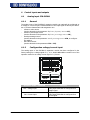
1
INDUSTRY PROCESS
AND AUTOMATION SOLUTIONS
Expansion Module EM-RES-02
Frequency Inverter 230 V / 400 V
ACTIVE and
ACTIVE Cube
GB
General points on the documentation
The present supplement of the documentation is valid for the frequency inverter series ACT and ACU. The information necessary for the assembly and application of
the EM-RES-02 expansion module is documented in this guidance.
For better clarity, the user documentation is structured according to the customerspecific demands made of the frequency inverter.
Brief instructions
The brief instructions describe the fundamental steps for mechanical and electrical
installation of the frequency inverter. The guided commissioning supports you in the
selection of necessary parameters and the software configuration of the frequency
inverter.
Operating instructions
The operating instructions document the complete functionality of the frequency inverter. The parameters necessary for specific applications for adaptation to the application and the extensive additional functions are described in detail.
Application manual
The application manual supplements the documentation for purposeful installation and
commissioning of the frequency inverter. Information on various subjects connected
with the use of the frequency inverter is described specific to the application.
Installation instructions
The installation instructions describe the mechanical installation and use of devices
which differ from those described in the brief instructions and the operating instructions.
The documentation and additional information can be requested via your local representation of the company BONFIGLIOLI.
The following pictograms and signal words are used in the documentation:
Danger!
means a directly threatening danger. Death, serious damage to persons and considerable damage to property will occur if the precautionary measure is not taken.
Warning!
marks a possible threat. Death, serious damage to persons and considerable damage
to property can be the consequence if attention is not paid to the text.
Caution!
refers to an indirect threat. Damage to people or property can be the result.
Attention!
refers to a possible operational behavior or an undesired condition, which can occur in
accordance with the reference text.
Note
marks information, which facilitates handling for you and supplements the corresponding part of the documentation.
Warning! In installation and commissioning, comply with the information in the
documentation. You as a qualified person must have read the documentation carefully and understood it. Comply with the safety instructions. For
the purposes of the instructions, "qualified person" designates a person
acquainted with the erection, assembly, commissioning and operation of
the frequency inverters and possessing the qualification corresponding to
the activity.
08/06
1
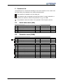
TABLE OF CONTENTS
1
General safety and application information .................................................................. 3
1.1
General information................................................................................................. 3
1.2
Proper use................................................................................................................ 3
1.3
Transport and storage ............................................................................................. 4
1.4
Handling and positioning......................................................................................... 4
1.5
Electrical connection................................................................................................ 4
1.6
Operation information ............................................................................................. 4
1.7
Maintenance and service ......................................................................................... 4
2
Introduction ................................................................................................................... 5
3
Installation of the EM-RES-02 expansion module ......................................................... 6
3.1
General .................................................................................................................... 6
3.2
Mechanical installation ............................................................................................ 6
3.3 Electrical installation ............................................................................................... 8
3.3.1
Circuit diagram ........................................................................................................ 8
3.3.2
Control Sockets ....................................................................................................... 9
4
Control inputs and outputs .......................................................................................... 10
4.1 Analog input EM-S1INA ........................................................................................ 10
4.1.1
General................................................................................................................. 10
4.1.2
Configuration voltage/current input ......................................................................... 10
4.1.3
Characteristic ........................................................................................................ 11
4.1.4
Operation modes ................................................................................................... 11
4.1.4.1
Examples........................................................................................................ 12
4.1.5
Scaling.................................................................................................................. 14
4.1.6
Tolerance band and hysteresis................................................................................ 15
4.1.7
Error and warning behavior .................................................................................... 16
4.1.8
Adjustment ........................................................................................................... 17
4.1.9
Filter time constant ................................................................................................ 17
4.2 Resolver input EM-RES .......................................................................................... 18
4.2.1
Offset ................................................................................................................... 18
4.2.2
Actual speed source ............................................................................................... 21
5
6
4.3
Frequency and percentage reference channel ...................................................... 21
4.4
Actual value display ............................................................................................... 22
4.5
Repetition frequency output EM-RFOUT ............................................................... 22
Parameter list............................................................................................................... 23
5.1
Actual value menu (VAL) ....................................................................................... 23
5.2
Parameter menu (PARA) ....................................................................................... 23
Annex ........................................................................................................................... 24
6.1
2
Error messages ...................................................................................................... 24
08/06
1
General safety and application information
This documentation has been created with greatest care and has been extensively and
repeatedly checked. For reasons of clarity, we have not been able to take all detailed
information on all the types of the products and also not every imaginable case of
positioning, operation or maintenance into account. If you require further information
or if particular problems not treated extensively enough in the operating instructions
occur, you can obtain the necessary information via the local representation of the
company BONFIGLIOLI.
In addition, we would point out that the contents of these operating instructions are
not part of an earlier or existing agreement, assurance or legal relationship, nor are
they intended to amend them. All the manufacturer's obligations result from the purchase contract in question, which also contains the completely and solely valid warranty regulation. These contractual warranty provisions are neither extended nor limited by the implementation of these operating instructions.
The manufacturer reserves the right to correct or amend the contents and product
information as well as omissions without specific announcement and assumes no kind
of liability for damage, injuries or expenditure to be put down to the aforementioned
reasons.
1.1
General information
Warning! BONFIGLIOLI VECTRON frequency inverters have high voltage levels during operating, depending on their protection class, drive moving parts and
have hot surfaces.
In the event of inadmissible removal of the necessary covers, improper
use, wrong installation or operation, there is the risk of serious damage to
persons or property.
To avoid the damage, only qualified staff may carry out the transport,
installation, setup or maintenance work required. Comply with the standards EN 50178, IEC 60364 (Cenelec HD 384 or DIN VDE 0100),
IEC 60664-1 (Cenelec HD 625 or VDE 0110-1), BGV A2 (VBG 4) and national provisions. Qualified persons within the meaning of this principal
safety information are people acquainted with the erection, fitting, commissioning and operating of frequency inverters and the possible hazards
and in possession of qualifications matching their activities.
1.2
Proper use
Warning! The frequency inverters are electrical drive components intended for installation in industrial plant or machines. Commissioning and start of intended operation are not allowed until it has been established that the
machine corresponds to the provisions of the EC machine directive
98/37/EEC and EN 60204. According to the CE sign, the frequency inverters additionally fulfill the requirements of the low-voltage directive
73/23/EEC and the standards EN 50178 / DIN VDE 0160 and EN 61800-2.
Responsibility for compliance with the EMC directive 89/336/EEC is with
the user. Frequency inverters are available in a limited way and as components exclusively intended for professional use within the meaning of
the standard EN 61000-3-2.
With the issue of the UL certificate according to UL508c, the requirements
of the CSA Standard C22.2-No. 14-95 have also been fulfilled.
The technical data and the information on connection and ambient conditions stated on the rating plate and the documentation must be complied
with. The instructions must have been read and understood before starting work at the device.
08/06
3
1.3
Transport and storage
Transport and storage are to be done appropriate in the original packing. Store the
units only in dry rooms, which are protected against dust and moisture and are subjected to little temperature deviations only. Observe the climatic conditions according
to standard EN 50178 and to the information on the label of the original packing. The
duration of storage without connection to the admissible reference voltage may not
exceed one year.
1.4
Handling and positioning
Warning! Damaged or destroyed components may not be put into operation because they may be a health hazard.
The frequency inverters are to be used according to the documentation, the directives
and the standards. Handle carefully and avoid mechanical overload. Do not bend the
components or change the isolation distances. Do not touch electronic components or
contacts. The devices contain construction elements with a risk of electrostatic, which
can easily be damaged by improper handling. Any use of damaged or destroyed components shall be considered as a non-compliance with the applicable standards. Do
not remove any warning signs from the device.
1.5
Electrical connection
Warning! Before any assembly or connection work, de-energize the frequency inverter. Make sure that the frequency inverter is de-energized.
Do not touch the sockets, because the capacitors may still be charged.
Comply with the information given in the operating instructions and on
the frequency inverter label.
While working on the frequency inverters, obey the applicable standards BGV A2 (VBG
4), VDE 0100 and other national directives. Comply with the information in the documentation on electrical installation and the relevant directives. Responsibility for compliance with and examination of the limit values of the EMC product standard EN
61800-3 for variable-speed electrical drive mechanisms is with the manufacturer of
the industrial plant or machine.
The documentation contains information on installation correct for EMC. The cables
connected to the frequency inverters may not be subjected to an isolation test with a
high test voltage without previous circuit measures.
1.6
Operation information
Warning! Before commissioning and the start of the intended operation, attach all
the covers and check the sockets. Check additional monitoring and protective devices pursuant to EN 60204 and the safety directives applicable
in each case (e.g. Working Machines Act, Accident Prevention Directives
etc.).
No connection work may be performed, while the system is in operation.
1.7
Maintenance and service
Warning! Unauthorized opening and improper interventions can lead to physical
injury or damage to property. Repairs on the frequency inverters may
only be done by the manufacturer or persons authorized by the latter.
4
08/06
2
Introduction
This document describes the possibilities and the properties of the EM-RES-02 expansion module for the frequency inverters of the ACT and ACU device series.
Note:
This document exclusively describes the EM-RES-02 expansion module. It
is not to be understood as fundamental information for the operation of
the frequency inverters of the ACT and ACU device series.
The EM-RES-02 expansion module is an optional hardware component to extend the
functionality of the frequency inverter. It enables the data exchange within the network between the components which have been directly connected, for example control and regulation elements.
The EM-RES-02 expansion module is supported from device series ACU and as
from software version 4.1.0 of device series ACT.
The EM-RES-02 module extends the functionality of the frequency inverters of the
ACT and ACU device series by the following additional functions:
−
Analog input
(second bipolar analog input)
−
Resolver input
−
Repetition frequency output
Note:
The EM-RES-02 expansion module has been enclosed with the frequency
inverter as a separate component and must be fitted by the user. This is
described in detail in the chapter "Mechanical Installation".
To assemble the expansion module it can be simply plugged into the frequency inverter of the ACT and ACU device series.
Warning! The assembly is done before the frequency inverter is put into operation,
and only in a voltage-free state.
The pluggable sockets of the expansion module enable economical overall fitting with
a safe function.
08/06
5
3
Installation of the EM-RES-02 expansion module
3.1
General
The mechanical and electrical installation of the EM-RES-02 expansion module is to be
carried out by qualified personnel according to the general and regional safety and
installation directives. Safe operation of the frequency inverter requires that the
documentation and the device specification be complied with during installation and
start of operation. For specific areas of application further provisions and guidelines
must be complied with where applicable.
The frequency inverters are designed according to the requirements and limit values
of product standard EN 61800-3 with an interference immunity factor (EMI) for operation in industrial applications. The electromagnetic interference is to be avoided by
expert installation and observation of the specific product information.
For further information, refer to the operating instructions of the frequency inverter.
Danger!
3.2
Danger!
Mechanical installation
If the following instructions are not complied with, there is direct danger
with possible consequences of death or severe injury by electrical current.
To disregard the instructions can lead to destruction of the frequency
inverter and/or of the expansion module.
•
Before assembly or disassembly of the EM-RES-02 expansion module, the frequency inverter must be de-energized. Take appropriate measures to make sure it
is not energized unintentionally.
•
Make sure that the frequency inverter is de-energized.
Danger!
6
All connection sockets where dangerous voltage levels may be present
(e.g. motor connection sockets, mains sockets, fuse connection sockets,
etc.) must be protected against direct contact.
The mains, direct voltage and motor sockets can be live with dangerous
voltage after disconnection of the frequency inverter. Work may only be
done on the device after a waiting period of some minutes until the DC
link capacitors have been discharged.
08/06
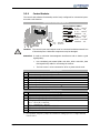
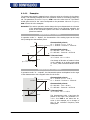
The EM-RES-02 expansion module is supplied in a housing for assembly on the lower
slot of the frequency inverter.
•
Remove the lower cover (1) of the frequency inverter.
The slot for the EM-RES-02 expansion module becomes accessible.
1
Caution!
•
The EM-RES-02 expansion module (2) is pre-fitted in a housing. Do NOT
touch the PCB visible on the back, as modules may be damaged.
Plug the EM-RES-02 expansion module (2) onto the slot (3).
2
3
•
Re-install the lower cover (1).
This completes the assembly procedure.
When the supply voltage of the frequency inverter is switched on, the EM-RES-02
expansion module is ready for operation.
1
08/06
7
3.3
Danger!
Electrical installation
If the following instructions are not complied with, there is direct danger
with the possible consequences of death or severe injury by electrical
current. Further, failure to comply can lead to destruction of the frequency inverter and/or of the expansion module.
•
Before electrical installation of the EM-RES-02 expansion module, the frequency
inverter must be de-energized. Take appropriate measures to make sure it is not
energized unintentionally.
•
Make sure that the frequency inverter is de-energized.
Danger!
The mains, direct voltage and motor sockets can have dangerous voltages
even after disconnection of the frequency inverter. Work may only be
done on the device after a waiting period of some minutes until the DC
link capacitors have been discharged.
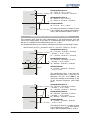
3.3.1
Circuit diagram
X410A
EM-RES REF+
1
1
EM-RES REF2
3 EM-RES SINEM-RES SIN+
4
2
EM-RES COS5
EM-RES COS+
6
EM-RFOUT A+
7
X410B
EM-RFOUT A1
B 1
EM-RFOUT B+
2
EM-RFOUT B3
EM-S1INA
C 4
EM-RFOUT R+
5
B 2
EM-RFOUT R6
7 GND
R
D
A
D
A Resolver interface EM-RES
A 1 Field voltage UREF eff = 4 V, Imax = 60 mA
A 2 Input voltage Umin eff = 2 V, voltage-proof until 30 V
The resolver interface is suitable for connecting commercial resolvers with the following specifications:
Input impedance > 95 Ω at 5 kHz, 10 kHz, 20 kHz, no. of pole pairs: up to 24,
30 000 rpm at no. of pole pairs = 1
phase displacement (at field frequency): 7 ° (5 kHz), 14 ° (10 kHz), 26 ° (20 kHz)
B Repetition frequency output EM-RFOUT
B 1 Frequency signal, fmax = 512 kHz, overload and short-circuit proof,
B 2
Imax = ±60 mA at min. permissible line termination 150 Ω,
TTL (push-pull) according to specification RS-422A / RS-485: Umax = 5 V
Reference signal
C Analog input EM-S1INA
Analog signal, resolution 12 Bit,
Umax= ±10 V (Ri = 100 kΩ), Imax = ±20 mA (Ri = 250 Ω)
8
08/06
3.3.2
Control Sockets
The control and software functionality can be freely configured for economical operation with a safe function.
Expansion module EM-RES-02
Wieland DST85 / RM3,5
0.14 … 1.5 mm2
AWG 30 … 16
0.14 … 1.5 mm2
AWG 30 … 16
0.25 … 1.0 mm2
AWG 22 … 18
2
0.25 … 0.75 mm
AWG 22 … 20
0.2 … 0.3 Nm
1.8 … 2.7 lb-in
Caution!
The control inputs and outputs must be connected and disconnected free
of electrical power. Otherwise components may be damaged.
Attention! In order to minimize electromagnetic interference and to obtain a good
signal quality:
Ter.
1
2
3
4
5
6
7
Ter.
1
2
3
4
5
6
7
1)
08/06
•
Use a shielded, pair-twisted (SIN+ with SIN-, COS+ with COS-, both
field signal lines) cable for connecting the resolver.
•
The line screen is to be connected to PE on a plane at both ends.
Socket X410A
Description
Resolver field signal EM-RES REF+
Resolver field signal EM-RES REFResolver input EM-RES SINResolver input EM-RES SIN+
Resolver input EM-RES COSResolver input EM-RES COS+
Repetition frequency output EM-RFOUT A+ 1)
Socket X410B
Description
Repetition frequency output EM-RFOUT A- -1)
Repetition frequency output EM-RFOUT B+ 1)
Repetition frequency output EM-RFOUT B- 1)
Analog input EM-S1INA, resolution 12 bit,
Umax= ±10 V (Ri = 100 kΩ),
Imax = ±20 mA (Ri = 250 Ω)
Repetition frequency output EM-RFOUT R+
Repetition frequency output EM-RFOUT REarth / GND
The repetition frequency output is interference voltage proof in a range between
-5 V to +10 V.
9
4
Control inputs and outputs
4.1
Analog input EM-S1INA
4.1.1
General
The analog input of the EM-RES-02 expansion module can optionally be configured as
a voltage or a current input. Parameterization of the input signal is done by the definition of a linear characteristic and assignment as a
− reference value source
(can be selected via the parameter Reference frequency source 475),
− reference percentage source
(can be selected via the parameter Reference percentage source 476),
− actual percentage source
(can be selected via the parameter Actual percentage source 478, in configuration x11) or
− limit value sources
(can be selected via the parameters 734…737).
4.1.2
Configuration voltage/current input
The analog input of the EM-RES-02 expansion module has been configured in the
factory setting for a voltage signal of +/- 10 V. Switch S3 enables a switch-over of the
operation mode for an analog current signal of +/-20 mA.
S3
X410A
Operation mode – switch S3
OFF - Voltage input
ON - Current input
10
X410B
Function
OFF (downward) –
analog input EM-S1INA is configured for a
voltage signal.
ON (upward) –
analog input EM-S1INA is configured for a
current signal.
08/06
4.1.3
Characteristic
The mapping of the analog input signals onto a frequency or percentage reference
value is possible for various demands. The parameterization is to be done via two
points of the linear characteristic of the reference channel.
The characteristic point 1, with the coordinates X1 and Y1, and the characteristic point
2, with the coordinates X2 and Y2, can be set in four parameters.
The characteristic points X1 and X2 are stated as percentages, as the analog input can
be switched as a current or voltage input via switch S3.
No.
564
565
566
567
Parameter
Description
Characteristic point X1
Characteristic point Y1
Characteristic point X2
Characteristic point Y2
Min.
-100.00 %
-100.00 %
-100.00 %
-100.00 %
Setting
Max.
100.00 %
100.00 %
100.00 %
100.00 %
Fact. sett.
-98.00 %
-100.00 %
98.00 %
100.00 %
The coordinates of the characteristic points are related as a percentage to the analog
signal, with 10 V or 20 mA, and the parameter Maximum Frequency 419 or parameter Maximum reference percentage 519. The change of direction of rotation can be
done via the digital inputs of the frequency inverter and/or by selecting the characteristic points.
The definition of the analog input characteristic can be calculated via the two-point
form of the straight-line equation. The speed Y of the drive mechanism is controlled
according to the analog control signal X.
Y=
Y2 - Y1
⋅ (X − X1) + Y1
X2 - X1
Attention! Monitoring of the analog input signal via the parameter Error/Warning
Behavior 563 demands a check of the characteristic parameters. Sensible
use is only possible if the Characteristic point X1 564 is in the positive
range.
4.1.4
Operation modes
The operation modes of the analog input characteristic enable application-related scaling as a supplement to the characteristic points stated. One of the four linear types of
characteristic is selected for adaptation of the signal for the analog input signal via the
parameter Operation mode 562.
If the characteristic points are not suited for the type of characteristic selected, the
characteristic points are corrected internally.
Operation mode
Function
1 - bipolar
The analog input signal is mapped onto the reference
figure according to the characteristic points (X1/Y1)
and (X2/Y2).
11 - unipolar
With a negative parameter value of the characteristic
points X1 or X2, they are mapped to the reference
value zero.
21 - unipolar
If the characteristic points X1 or X2 have been set
2…10 V / 4…20 mA
with a negative parameter figure or smaller than 0%,
the input characteristic is mapped to the reference
value 20%.
101 - bipolar absolute value Negative parameter values of the characteristic points
Y1 or Y2 are mapped as a positive reference value in
the characteristic.
Further information on the operation modes stated in the table can be found in the
following chapter "Examples“.
08/06
11
4.1.4.1
Examples
The analog input signal is mapped onto a reference value as a function of the characteristic. The following examples show the operation modes for an analog voltage signal. The parameter Minimum Frequency 418 is set to the value 0.00 Hz. The characteristic point 100% for the Y-axis corresponds to the parameter Maximum Frequency
419 of 50.00 Hz in the examples.
Attention! The various operation modes change the input characteristic as a function
of the parameterized characteristic points. In the following examples, the
areas of the coordinate system from which a characteristic point is displaced are marked.
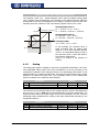
Operation mode "1 – bipolar"
In operation mode "1 – bipolar“, the characteristic of the analog input can be freely
set by stating two characteristic points.
Y
42.50Hz
Characteristic point 1:
X1 = -70.00% · 10 V = -7.00 V
(X2=80% / Y2=85%)
Y1 = -50.00% · 50.00 Hz = -25.00 Hz
X
-7V
Characteristic point 2:
X2 = 80.00% · 10 V = 8.00 V
Y2 = 85.00% · 50.00 Hz = 42.50 Hz
Tolerance band:
ΔX = 2.00% · 10 V = 0.20 V
8V
-25Hz
The change of direction of rotation is done
in the example at an analog input signal
of -1.44 V, with a tolerance band of ±0.20
V.
(X1=-70% / Y1=-50%)
Operation mode "11 – unipolar"
In operation mode "11 – unipolar“, the characteristic points are displaced to the origin
of the characteristics with a negative value for the X-axis.
Y
42.50Hz
Characteristic point 1:
X1 = -70.00% · 10 V = -7.00 V
(X2=80% / Y2=85%)
Y1 = -50.00% · 50.00 Hz = -25.00 Hz
X
-7V
8V
-25Hz
(X1=-70% / Y1=-50%)
12
Characteristic point 2:
X2 = 80.00% · 10 V = 8.00 V
Y2 = 85.00% · 50.00 Hz = 42.50 Hz
Tolerance band:
ΔX = 2.00% · 10 V = 0.20 V
The characteristic point 1 has been displaced to the origin. The parameter Tolerance band 560 is not taken into account in this example, as no change of
sign of the reference frequency value
takes place.
08/06
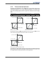
Y
42.50Hz
Characteristic point 1:
X1 = 30.00 % · 10 V = 3.00 V
(X2=80% / Y2=85%)
Y1 = -50.00 % · 50.00 Hz = -25.00 Hz
X
3.00V
Characteristic point 2:
X2 = 80.00 % · 10 V = 8.00 V
Y2 = 85.00 % · 50.00 Hz = 42.50 Hz
Tolerance band:
ΔX = 2.00 % · 10 V = 0.20 V
8.00V
-25.00Hz
(X1=30% / Y1=-50%)
The change of direction of rotation is done
in the example at an analog input signal of
4.85 V, with a tolerance band of ±0.20 V.
Operation mode "21 – unipolar 2…10 V / 4…20 mA"
This operation mode limits the input characteristic to the range between 20% and
100% of the analog signal. If the value for a characteristic point of the X-axis is outside 0%, it is mapped to the characteristic point (2 V / 0 Hz).
The characteristic point on the X-axis is calculated according to the following formula:
characteristic point X = parameter value X ⋅ (100.00% - 20.00%) + 20.00%
Y
42.50Hz
Characteristic point 1:
X1 = [-70.00% · (100.00% - 20.00%)
(X2=80% / Y2=85%)
+ 20.00% ] · 10 V = -7.60 V
Y1 = -50.00% · 50.00 Hz = -25.00 Hz
Characteristic point 2:
X2 = [80.00% · (100.00% - 20.00%)
X + 20.00% ] · 10 V = 8.40 V
Y2 = 85.00% · 50.00 Hz = 42.50 Hz
8.40V
-7.60V
Tolerance band:
ΔX = [2.00% · (100.00% - 20.00%)
· 10 V] = 0.16 V
-25.00Hz
(X1=-70% / Y1=-50%)
The characteristic point 1 has been displaced to the point (2.00 V / 0.00 Hz). The
parameter Tolerance band 560 is not
used in this example, as no change of sign
of the reference frequency value takes
place.
Y
42.50Hz
Characteristic point 1:
X1 = [30.00% · (100.00% - 20.00%)
(X2=80% / Y2=85%)
+ 20.00% ] · 10 V = 4.40 V
Y1 = -50.00% · 50.00 Hz = -25.00 Hz
X
4.40V
8.40V
-25.00Hz
Characteristic point 2:
X2 = [80.00% · (100.00% - 20.00%)
+ 20.00% ] · 10 V = 8.40 V
Y2 = 85.00% · 50.00 Hz = 42.50 Hz
Tolerance band:
ΔX = [2.00% · (100.00% - 20.00%)
(X1=30% / Y1=-50%) · 10 V] = 0.16 V
The change of direction of rotation is done
in the example at an analog input signal of
5.88 V, with a tolerance band of ±0.16 V.
08/06
13
Operation mode "101 – bipolar absolute value"
The operation mode "101 – bipolar absolute value“ maps the bipolar analog signal
onto a unipolar input characteristic. The formation of the absolute amount takes the
characteristic into account comparable to the "bipolar" operation mode, but the characteristic points are reflected on the X-axis with a negative value for the Y-axis.
Y
42.50Hz
Characteristic point 1:
X1 = -70.00% · 10 V = -7.00 V
(X2=80% / Y2=85%)
Y1 = -50.00% · 50.00 Hz = -25.00 Hz
25.00Hz
X
-7V
8V
-25.00Hz
(X1=-70% / Y1=-50%)
4.1.5
Characteristic point 2:
X2 = 80.00% · 10 V = 8.00 V
Y2 = 85.00% · 50.00 Hz = 42.50 Hz
Tolerance band:
ΔX = 2.00% · 10 V = 0.20 V
In this example, the reference value is
again increased from an analog input
signal of -1.44 V with a tolerance band of
±0.20 V. The theoretical change of sign of
the reference value is used and leads to
the tolerance band stated.
There is no change of the direction of
rotation.
Scaling
The analog input signal is mapped to the freely configurable characteristic. The maximum admissible setting range of the drive mechanism is to be set according to the
configuration selected via the frequency limits or the percentage value limits. In the
parameterization of a bipolar characteristic, the minimum and maximum limit for both
directions of rotation are taken over. The percentage values of the characteristic
points are relative to the maximum limits selected.
No.
418
419
Parameter
Description
Minimum Frequency
Maximum Frequency
Min.
0.00 Hz
0.00 Hz
Setting
Max.
999.99 Hz
999.99 Hz
Fact. sett.
3.50 Hz
50.00 Hz
The controls use the maximum value of the output frequency, which is calculated from
the maximum frequency 419 and the compensated slip of the drive mechanism. The
frequency limits define the speed range of the drive mechanism and the reference
percentage values supplement the scaling of the input characteristic according to the
configured functions.
No.
518
519
14
Parameter
Description
Minimum reference percentage
Maximum reference percentage
Min.
0.00 %
0.00 %
Setting
Max.
300.00 %
300.00 %
Fact. sett.
0.00 %
100.00 %
08/06
4.1.6
Tolerance band and hysteresis
The analog input characteristic with change of sign of the reference value can be
adapted by the parameter Tolerance band 560 of the application. The tolerance band
to be defined extends the zero crossing of the speed relative to the analog control
signal. The percentage parameter value is relative to the maximum current or voltage
signal.
Parameter
No.
Description
560 Tolerance band
Min.
0.00 %
Setting
Max.
25.00 %
(X2 / Y2)
Fact. sett.
2.00 %
(X2 / Y2)
pos. max. value
pos. max. value
+10V
(+20mA)
-10V
(-20mA)
+10V
-10V
(-20mA)
Tolerance band
(X1 / Y1)
neg. max. value
Without tolerance band
(X1 / Y1)
neg. max. value
With tolerance band
The Minimum Frequency 418 or the Minimum reference percentage 518 set in the
factory extends the parameterized tolerance band to the hysteresis.
(X2 / Y2)
pos. max. value
pos. min. value
neg. min. value
Tolerance band
(X1 / Y1)
neg. max. value
With tolerance band and minimum value
For example, the output variable resulting from the positive input signals is kept at the
positive minimum value until the input signal is below the value for the tolerance band
in a negative direction. After that proceed on the set characteristic.
08/06
15
4.1.7
Error and warning behavior
The monitoring of the analog input signal necessary according to the application is to
be configured via the parameter Error/Warning behavior 563.
Operation mode
0 - Off
1 - Warning < 1 V / 2 mA
2 - Shutdown < 1 V / 2 mA
3-
Fault switch-off
< 1 V / 2 mA
Function
The input signal is not monitored.
If the input signal is less than 1 V or 2 mA, there
is a warning message.
If the input signal is less than 1 V or 2 mA, there
is a warning message, the drive mechanism is
decelerated according to stopping behavior 1.
If the input signal is less than 1 V or 2 mA, there
is a warning and fault message and the drive
mechanism stops freely.
The monitoring of the analog input signal is active independent of the release of the
frequency inverter according to the operation mode selected.
In operation mode 2, the drive mechanism is decelerated independent of the stopping
behavior set (Parameter Operation mode 630) according to stopping behavior 1
(shutdown and switch-off). If the set holding time has expired, there is a fault message. A repeat start of the drive mechanism is possible by switching the start signal on
and off if the fault has been cleared.
Operation mode 3 defines the free stoppage of the drive mechanism, independent of
the stopping behavior selected, which is stipulated with the parameter Stop function
630.
Attention! Monitoring of the analog input signal via the parameter Error/Warning
Behavior 563 demands a check of the characteristic parameters.
16
08/06
4.1.8
Adjustment
As a result of component tolerances, it can be necessary to adjust the analog input.
Parameter Adjustment 568 is used for this purpose.
Operation mode
0 - no adjustment
1 - Adjustment 0 V / 0 mA
2 - Adjustment 10 V / 20 mA
Function
Normal operation
Adjustment of the measurement with an analog
signal of 0 V or 0 mA.
Adjustment of the measurement with an analog
signal of 10 V or 20 mA.
Example of the adjustment of the analog input with a voltage signal:
Note:
The measurements for the adjustment are to be done with a suitable
measuring instrument and the correct polarity.
If not, faulty measurements can result.
•
Apply 0 V to the analog input; e.g. with a wired link from the socket of the analog
input X410B.4 to socket X210B.7 (earth/GND) of the frequency inverter.
•
Select operation mode "1 - Adjustment 0 V / 0 mA“.
•
Apply 10 V to the analog input, e.g. with a wired link from the socket of the analog input to socket X210B.5 (reference output 10 V) of the frequency inverter.
•
Select operation mode "2 - Adjustment 10 V / 20 mA“.
4.1.9
Filter time constant
The time constant of the filter for the reference analog value can be set via the parameter Filter time constant 561.
The time constant states the time for which the input signal is averaged by means of a
low pass filter, e.g. in order to eliminate fault effects.
The setting range is a range of values between 0 ms and 5000 ms in 15 steps.
Operation mode
0 - Time constant 0 ms
2
4
8
16
32
64
128
256
512
1000
2000
3000
4000
5000
08/06
-
Time
Time
Time
Time
Time
Time
Time
Time
Time
Time
Time
Time
Time
Time
constant
constant
constant
constant
constant
constant
constant
constant
constant
constant
constant
constant
constant
constant
2 ms
4 ms
8 ms
16 ms
32 ms
64 ms
128 ms
256 ms
512 ms
1000 ms
2000 ms
3000 ms
4000 ms
5000 ms
Function
Filter deactivated – analog reference value is forwarded unfiltered
Filter activated – averaging of the input signal via
the set value of the filter time constants
17
4.2
Resolver input EM-RES
The resolver input is used for evaluating the position information from the resolver.
The frequency of the field signal for the resolver can be selected via parameter Operation Mode 380.
Operation mode
5- frequency 5 kHz
10- frequency 10 kHz
20- frequency 20 kHz
Function
Frequency of the reference signal for the resolver
If the no. of resolver pole pairs > 1, the measured electric angle runs through the
range of 0°...360° several times during one mechanical revolution.
For the detection of the position angle of the rotor at a synchronous motor, the ratio
of the no. of motor pole pairs to the no. of resolver pole pairs must be an integer.
The no. of pole pairs of the resolver can be adjusted via parameter No. of Pole Pairs
381.
No.
381
Parameter
Description
No. of pole pairs
Min.
1
Function
Max.
24
Fact. sett.
1
Assignment of the socket:
Resolver
Resolver
Resolver
Resolver
Resolver
Resolver
4.2.1
field signal EM-RES (X410A.1): REF+
field signal EM-RES (X410A.2): REFinput EM-RES (X410A.3): SINinput EM-RES (X410A.4): SIN+
input EM-RES (X410A.5): COSinput EM-RES (X410A.6): COS+
Offset
In order to enable the start of a synchronous machine, the absolute position of the
rotor must be known. This information is required in order to actuate the stator windings in the right order depending on the position of the rotor. The position of the rotary field in the synchronous machine must be controlled in order to obtain a continuous movement of the rotor. During first commissioning, the position of the rotor winding of the resolver is adjusted to the rotor displacement angle of the synchronous motor by adjusting the offset. For operating a synchronous machine with resolver, the
offset must be adjusted in order to obtain perfectly true running and a maximum
torque.
The correct Offset 382 is adjusted when the flux-forming voltage 235 reaches the
value 0 (approximately) while the motor is turning.
No.
382
Parameter
Description
Offset
Min.
-360.0°
Function
Max.
360.0°
Fact. sett.
0.0°
The offset can be determined and adjusted as follows:
18
•
During first commissioning "SEtUP" will be displayed in the control unit. Press ESC
to stop this operation. The guided commissioning („SETUP“) is performed after adjusting the offset.
•
Open the parameter menu "PARA" and enter the machine data indicated on the
type plate or the data sheet of the motor.
08/06
•
Set parameter Operation Mode 380 to the frequency value of the field signal for
the resolver.
•
Adjust parameter No. of Pole Pairs 381 to the number of pole pairs of the resolver.
Before adjusting the offset, take the following safety precautions:
•
Disable the frequency inverter via digital input S1IND (controller release).
•
If possible, uncouple the motor from the load so that the motor shaft turns freely.
If installed, release the mechanical brake.
If uncoupling is not possible, make sure that the motor is loaded as little as possible.
Warning!
In certain circumstances, the motor speed may reach high values. If the
motor is not uncoupled from the load, personal and material damage
may result. To avoid such damage, make the following settings in any
case.
•
Set the max. permissible output frequency of the frequency inverter to a low frequency value via parameter Switch-Off Limit 417. Select the frequency value such
that uncontrolled acceleration of the motor ("overspeeding") is detected at an early
stage. This limitation is necessary in order to avoid personal and material damage.
•
Set parameter Current Limit 728 of the speed controller to a low current value
(e.g. 10% of the rated motor current). In this way it is made sure that there are no
excessive currents of the offset is set incorrectly.
•
Turn motor shaft manually. Check the sense of rotation of the resolver via the actual value of parameter Frequency Speed Sensor 2 219. In the case of a clock-wise
rotation of the motor shaft, positive values are displayed for the actual frequency
value. If the displayed sense of rotation does not correspond to the actual sense of
rotation, change the connections SIN+ and SIN- at socket X410A of the frequency
inverter.
The Offset 382 must be between 0° and 360°, divided by the number of motor pole
pairs. If the number of resolver pole pairs is higher than 1, the possible range is between 0° and the max. offset.
Max. Offset =
360 °
number of motor pole pairs / number of resolver pole pairs
If the adjusted value is changed by the max. offset, this does not affect the fluxforming voltage 235.
08/06
•
Adjust a low reference speed value (approx. 10% lower than the Switch-off Limit
Frequency 417), and enable the frequency inverter via digital input S1IND (controller release) and S2IND (start clock-wise operation) in order to accelerate the
motor.
•
If an overcurrent is detected or a fault message is issued due to an overload, the
guided commissioning (setup) will start first. Confirm the machine and resolver
data. After completion of the guided commissioning, adjust the parameter Limit
Current 728 to a low value again because this value was overwritten during the
guided commissioning.
19
Depending on the behavior of the motor after start, carry out the following steps:
−
Motor does not turn, or the motor shaft only turns to a new position and
stops again:
•
Check if the parameters No. of Pole Pairs 373 for the motor and No. of Pole
Pairs 381 for the resolver are set correctly.
If these values are adjusted correctly, take the following measures complying with
the safety instructions.
Warning!
The mains, direct voltage and motor sockets can be live with dangerous
voltage after disconnection of the frequency inverter. Work only on the
device after a waiting period of some minutes until the DC link capacitors
have discharged.
•
Before electrical installation work, de-energize the frequency inverter and take
appropriate precautions to make sure it is not re-energized unintentionally.
Make sure that the frequency inverter is de-energized.
•
Exchange two motor phases (e.g. U and V) at the frequency inverter sockets
because the senses of rotation of the motor and the resolver do not correspond to each other.
•
Switch on the power supply again.
•
As described above, adjust a low speed reference value and start the motor.
If the motor does not start despite the phase exchange:
•
Increase the parameter value for Offset 382 by 90°, divided by the no. of motor pole pairs.
If the motor still does not turn, exchange the two motor phases (e.g. U and V)
again.
−
−
The motor turns and accelerates until it reaches the Frequency Switch-Off
Limit 417:
•
Check the resolver lines and check the resolver connection contacts.
•
In the case of fault message "Overfrequency" F1100: increase the parameter
value for Offset 382 by 180°, divided by the no. of motor pole pairs.
If the motor turns at the adjusted speed and in the right direction, carry
out the fine adjustment of the offset:
•
−
−
−
Adjust the parameter value for Offset 382 in small steps (e.g. 2.5°) until the
flux-forming voltage 235 is approximately 0.
In case the flux-forming voltage deviates from 0 significantly, adjust the offset
in bigger steps.
In the case of a positive flux-forming voltage, increase the offset.
In the case of a negative flux-forming voltage, reduce the offset.
•
Adjust parameters Frequency Switch-Off Limit 417 and Current Limit 728 to
the required values.
•
Repeat the fine adjustment of the offset at 50% of the rated frequency.
This completes the offset adjustment.
•
20
Start the guided commissioning. This is required for optimum current control.
08/06
4.2.2
Actual speed source
Switch-over is effected via Actual Speed Source 766. If the resolver delivers the actual
value signal for the speed controller, speed sensor 2 must be selected as the source In
the basic setting, speed sensor 1 is used as the actual value source.
Operation mode
1 - Speed sensor 1
2 - Speed sensor 2
4.3
Function
The actual speed source is speed sensor 1 of the
basic device (factory setting).
The actual speed source is speed sensor 2 of the EMRES-02 expansion module.
Frequency and percentage reference channel
The varied functions for the specification of the reference values are connected in the
various configurations by the frequency or percentage reference channel. The Reference frequency source 475, and the Reference percentage source 476 determine the
additive connection of the available reference sources as a function of the installed
hardware.
Operation mode
Function
2 - EM-S1INA, absolute value Reference source is the analog input EM-S1INA
MFI1A + EM-S1INA, abso- Reference sources are the multifunctional input
4lute value
MFI1A and the analog input EM-S1INA
Reference sources are the multifunctional input
MFI1A + EM-S1INA + FF,
14 MFI1A, analog input EM-S1INA and fixed frequency
absolute value
FF
Reference sources are the multifunctional input
MFI1A + EM-S1INA + MP,
24 MFI1A, analog input EM-S1INA and the motor poabsolute value
tentiometer function MP
The frequency signals of the resolver are evaluated
speed sensor 2 (F2), abso34 using a fixed number of division marks of 1024 as a
lute value
reference value.
102 to 124
Operation modes with signs (+/-)
Additional to the operation modes listed, those stated in the operating instructions of
the frequency inverter in the chapter "Frequency reference channel“, and in the chapter "Percentage reference channel“ also apply.
08/06
21
4.4
Actual value display
The actual value of speed sensor 2 can be read via the parameters Frequency speed
sensor 2 219 and Speed, speed sensor 2 220.
The analog input signal on analog input EM-S1INA can be a voltage or a current signal
depending on the setting of switch S3. Accordingly, the actual value parameter Analog
input EM-S1INA 253 is displayed as a percentage.
4.5
Repetition frequency output EM-RFOUT
The repetition frequency output EM-RFOUT emulates a speed sensor. The repetition
frequency output delivers the frequency signal of the resolver as a simulation of an
incremental speed sensor with reference signal. The number of division marks is set
permanently to 1024 division marks, thus no parameterization is required.
Assignment of the outputs:
Repetition frequency output EM-RFOUT
Repetition frequency output EM-RFOUT
Repetition frequency output EM-RFOUT
Repetition frequency output EM-RFOUT
Repetition frequency output EM-RFOUT
Repetition frequency output EM-RFOUT
22
(X410A.7): track A+
(X410B.1): track A(X410B.2): track B+
(X410B.3): track B(X410A.5): reference signal R+
(X410A.6): reference signal R-
08/06
5
Parameter list
The parameter list is structured according to the menu branches of the control unit.
For better clarity, the parameters are marked with pictograms:
The parameter is available in the four data sets
The parameter value is adjusted by the SETUP routine if a control method for a
synchronous machine is selected for parameter Configuration 30.
This parameter cannot be written in the operation of the frequency inverter
5.1
Actual value menu (VAL)
Actual values of the machine
No.
Description
Unit
Display range
219 Frequency speed sensor 2
Hz
0.0 ... 999.99
220 Speed, speed sensor 2
rpm
0 ... 60000
Actual values of the frequency inverter
253 Analog input EM-S1INA
%
-100 ... +100
5.2
4.4
Parameter menu (PARA)
Resolver
No.
Description
Unit
380 Operation mode
381 No. of pole pairs
382 Offset
°
Analog input
560 Tolerance band
%
561 Filter time constant
562 Operation mode
563 Error/warning behavior
564 Characteristic point X1
%
565 Characteristic point Y1
%
566 Characteristic point X2
%
567 Characteristic point Y2
%
568 Adjustment
Speed controller
766 Actual speed source
-
08/06
Chapter
4.4
4.4
Setting range
Selection
1 ... 24
-360.0 ... 360.0
Chapter
4.2
4.2
4.2.1
0.00 ... 25.00
Selection
Selection
Selection
-100.00 ... 100.00
-100.00 ... 100.00
-100.00 ... 100.00
-100.00 ... 100.00
Selection
4.1.6
4.1.9
4.1.4
4.1.7
4.1.3
4.1.3
4.1.3
4.1.3
4.1.8
Selection
4.2.2
23
6
Annex
6.1
Error messages
The various control functions and methods and the hardware of the frequency inverter
contain functions which continuously monitor the application. As a supplement to the
messages documented in these operating instructions, the following failure keys are
activated by the EM-RES-02 expansion module.
F14
21
22
23
24
Control connections
Resolver synchronization not successful. Check resolver signal for interferences.
Resolver counting error: Check resolver signal for interferences.
Resolver pole pair number is invalid. The ratio of the no. of pole pairs to
the no. of resolver pole pairs must be an integer number. Check parameters No. of Pole Pairs 373 for the motor and und No. of Pole
Pairs 381 for the resolver, correct if necessary.
Open circuit: check resolver connections and lines.
Additional to the listed fault messages, there are further fault messages for internal
purposes and not listed here. If you receive fault messages, which are not listed here,
please contact us by phone.
24
08/06
Bonfiglioli Worldwide & BEST Partners
AUSTRALIA
BONFIGLIOLI TRANSMISSION (Aust) Pty Ltd.
48-50 Adderley St. (East) Auburn (Sydney) N.S.W. 2144
Tel. (+61) 2 8748 4400 - Fax (+61) 2 9748 8740
P.o. Box 6705 Silverwater NSW 1811
www.bonfiglioli.com.au - [email protected]
HUNGARY
AGISYS AGITATORS & TRANSMISSIONS Ltd
2045 Törökbálint, Tö u.2. Hungary
Tel. +36 23 50 11 50 - Fax +36 23 50 11 59
www.agisys.hu - [email protected]
AUSTRIA
MOLL MOTOR GmbH
Industriestrasse 8 - 2000 Stockerau
Tel. (+43) 2266 63421+DW - Fax (+43) 6342 180
Tlx 61 32 22 348 Molla
www.mollmotor.at - [email protected]
INDIA
BONFIGLIOLI TRANSMISSIONS PVT Ltd.
PLOT AC7-AC11 Sidco Industrial Estate
Thirumudivakkam - Chennai 600 044
Tel. +91(0)44 24781035 / 24781036 / 24781037
Fax +91(0)44 24780091 / 24781904
www.bonfiglioli.co.in - [email protected]
BELGIUM
N.V. ESCO TRANSMISSION S.A.
Culliganlaan 3 - 1831 Machelem Diegem
Tel. 0032 2 7204880 - Fax 0032 2 7212827
Tlx 21930 Escopo B
www.escotrans.be - [email protected]
NEW ZEALAND
SAECO BEARINGS TRANSMISSION
36 Hastie Avenue, Mangere
Po Box 22256, Otahuhu - Auckland
Tel. +64 9 634 7540 - Fax +64 9 634 7552
[email protected]
BRASIL
ATI BRASIL
Rua Omlio Monteiro Soares, 260 - Vila Fanny - 81030-000
Tel. (+41) 334 2091 - Fax (+41) 332 8669
www.atibrasil.com.br - [email protected]
POLAND
POLPACK Sp. z o.o. - Ul. Chrobrego 135/137 - 87100 Torun
Tel. 0048.56.6559235 - 6559236 - Fax 0048.56.6559238
www.polpack.com.pl - [email protected]
CANADA
BONFIGLIOLI CANADA INC.
2-7941 Jane Street - Concord, ONTARIO L4K 4L6
Tel. (+1) 905 7384466 - Fax (+1) 905 7389833
www.bonfigliolicanada.com - [email protected]
CHINA
BONFIGLIOLI DRIVES (SHANGHAI) CO. LTD.
No. 8 Building, Area C1 - 318
SuHong Road, Qingpu, Shanghai 201700
Tel. +86 21 69225500 - Fax +86 21 69225511
www.bonfiglioli.cn - [email protected]
FRANCE
BONFIGLIOLI TRANSMISSIONS S.A.
Rue Eugène Pottier BP 19
Zone Industrielle de Moimont II - 95670 Marly la Ville
Tel. (+33) 1 34474510 - Fax (+33) 1 34688800
www.bonfiglioli.fr - [email protected]
GERMANY
BONFIGLIOLI DEUTSCHLAND GmbH
Hamburger Straße 18 - 41540 Dormagen
Tel. (+49) 2133 50260 - Fax (+49) 2133 502610
www.bonfiglioli.de - [email protected]
GREAT BRITAIN
BONFIGLIOLI UK Ltd
Unit 3 Colemeadow Road - North Moons Moat
Redditch. Worcestershire B98 9PB
Tel. (+44) 1527 65022 - Fax (+44) 1527 61995
www.bonfiglioli.co.uk - [email protected]
BONFIGLIOLI (UK) LIMITED
5 Grosvenor Grange - Woolston - Warrington, Cheshire WA1 4SF
Tel. (+44) 1925 852667 - Fax (+44) 1925 852668
www.bonfiglioliuk.co.uk - [email protected]
GREECE
BONFIGLIOLI HELLAS
O.T. 48A T.O. 230 - C.P. 570 22 Industrial Area - Thessaloniki
Tel. (+30) 2310 796456 - Fax (+30) 2310 795903
www.bonfiglioli.gr - [email protected]
HOLLAND
ELSTO AANDRIJFTECHNIEK
Loosterweg, 7 - 2215 TL Voorhout
Tel. (+31) 252 219 123 - Fax (+31) 252 231 660
www.elsto.nl - [email protected]
RUSSIA
FAM
57, Maly prospekt, V.O. - 199048, St. Petersburg
Tel. +7 812 3319333 - Fax +7 812 3271454
www.fam-drive.ru - [email protected]
SPAIN
TECNOTRANS SABRE S.A.
Pol. Ind. Zona Franca sector C, calle F, n°6 08040 Barcelona
Tel. (+34) 93 4478400 - Fax (+34) 93 3360402
www.tecnotrans.com - [email protected]
SOUTH AFRICA
BONFIGLIOLI POWER TRANSMISSION Pty Ltd.
55 Galaxy Avenue, Linbro Business Park - Sandton
Tel. (+27) 11 608 2030 OR - Fax (+27) 11 608 2631
www.bonfiglioli.co.za - [email protected]
SWEDEN
BONFIGLIOLI SKANDINAVIEN AB
Kontorsgatan - 234 34 Lomma
Tel. (+46) 40 412545 - Fax (+46) 40 414508
www.bonfiglioli.se - [email protected]
THAILAND
K.P.T MACHINERY (1993) CO.LTD.
259/83 Soi Phiboonves, Sukhumvit 71 Rd. Phrakanong-nur,
Wattana, Bangkok 10110
Tel. 0066.2.3913030/7111998
Fax 0066.2.7112852/3811308/3814905
www.kpt-group.com - [email protected]
USA
BONFIGLIOLI USA INC
1000 Worldwide Boulevard - Hebron, KY 41048
Tel.: (+1) 859 334 3333 - Fax: (+1) 859 334 8888
www.bonfiglioliusa.com
[email protected]
[email protected]
VENEZUELA
MAQUINARIA Y ACCESSORIOS IND.-C.A.
Calle 3B - Edif. Comindu - Planta Baja - Local B
La Urbina - Caracas 1070
Tel. 0058.212.2413570 / 2425268 / 2418263
Fax 0058.212.2424552
Tlx 24780 Maica V
www.maica-ve.com - [email protected]
HEADQUARTERS
BONFIGLIOLI RIDUTTORI S.p.A.
Via Giovanni XXIII, 7/A
40012 Lippo di Calderara di Reno
Tel. (+39) 051 6473111
Fax (+39) 051 6473126
www.bonfiglioli.com
[email protected]
SPARE PARTS BONFIGLIOLI
B.R.T
Via Castagnini, 2-4
Z.I. Bargellino - 40012
Calderara di Reno - Bologna (ITALY)
Tel. (+39) 051 727844
Fax (+39) 051 727066
www.brtbonfiglioliricambi.it
[email protected]
INDUSTRY PROCESS
AND AUTOMATION SOLUTIONS
ACTIVE and
ACTIVE Cube
w w w. b o n f i g l i o l i . c o m
COD. VEC 225 R2