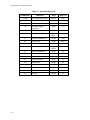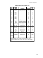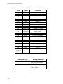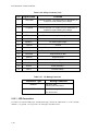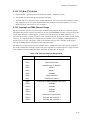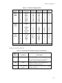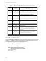
1
Little Board™/P5i Technical Manual P/N: 5001121 Revision: H Ampro Computers, Incorporated 4757 Hellyer Avenue San Jose, CA 95138 Tel (408) 360-0200 FAX (408) 360-0220 WEBSITE: www.ampro.com NOTICES DISCLAIMER Ampro Computers, Incorporated makes no representations or warranties with respect to the contents of this manual or of the associated Ampro products, and specifically disclaims any implied warranties of merchantability or fitness for any particular purpose. Ampro shall under no circumstances be liable for incidental or consequential damages or related expenses resulting from the use of this product, even if it has been notified of the possibility of such damages. Ampro reserves the right to revise this publication from time to time without obligation to notify any person of such revisions. If errors are found, please contact Ampro at the address listed on the title page of this document. TRADEMARKS The Ampro logo is a registered trademark, and Ampro, Little Board, StackPlane, MiniBackplane, MiniModule, and CoreModule are trademarks of Ampro Computers, Inc. All other marks are the property of their respective companies. TECHNICAL SUPPORT Technical support is available from 8:00 AM to 5:00 PM, Pacific time. • • Technical support telephone number: 800 966-5200. (Please have the product you wish to discuss at hand when you call) E-mail address: [email protected] Revision History Revision Reason for Change Date A Preliminary Release 10/96 B Beta Release 11/96 C Production Release 4/97 D Update Jumper Summary 6/97 E Update Housing 10/97 F Update Standoff 11/97 G Update Format 2/98 H PM Update 6/99 ©1997 AMPRO COMPUTERS, INCORPORATED No part of this document may be reproduced, transmitted, transcribed, stored in a retrieval system, or translated into any language or computer language, in any form or by any means, electronic, mechanical, magnetic, optical, chemical, manual, or otherwise, without the prior written permission of Ampro Computers, Incorporated. iii Little Board/P5i Technical Manual PREFACE This manual is for integrators and programmers of systems based on the Ampro Little Board™/P5i single board system. It contains information about hardware specifications, jumpering and installation, details about system setup, and how to configure peripheral drivers. There are three chapters, organized as follows: Chapter 1—Introduction. General information pertaining to the Little Board/P5i, its features, and specifications. Chapter 2—Hardware Configuration. A description of how to configure and connect the Little Board/P5i for use with a variety of onboard and external devices. Included are tables listing the pinouts of each of the board's connectors, details about jumper options, installation and mounting instructions, and descriptions and specifications regarding peripheral interfaces provided on the board. Chapter 3—Software Configuration. An overview of the system features, configuration options, SETUP guidelines, utilities, and peripheral drivers that are available under DOS, Windows, and other operating systems. iv TABLE OF CONTENTS CHAPTER 1—INTRODUCTION 1.1 General Description ............................................................................................................... 1–1 1.2 Features ................................................................................................................................. 1–1 1.2.1 Enhanced Reliability .............................................................................................. 1–4 1.3 Software ................................................................................................................................ 1–5 1.4 Designing Little Board Systems ............................................................................................. 1–5 1.4.1 Little Board Development Chassis ......................................................................... 1–6 1.5 Little Board/P5i Specifications .............................................................................................. 1–6 1.5.1 CPU/Motherboard.................................................................................................. 1–6 1.5.2 Embedded-PC System Enhancements..................................................................... 1–6 1.5.3 Onboard Peripherals .............................................................................................. 1–7 1.5.4 Support Software ................................................................................................... 1–9 1.5.5 Mechanical and Environmental Specifications ....................................................... 1–10 CHAPTER 2—HARDWARE CONFIGURATION 2.1 Introduction ........................................................................................................................... 2–1 2.1.1 Interface Connector Summary ................................................................................ 2–1 2.1.2 Connectors............................................................................................................. 2–4 2.1.3 Jumper Configuration Options ............................................................................... 2–4 2.2 DC Power ............................................................................................................................... 2–6 2.2.1 Power Requirements .............................................................................................. 2–6 2.2.2 Powerfail Options .................................................................................................. 2–7 2.2.3 Backup Battery ...................................................................................................... 2–7 2.2.4 Cooling Requirements............................................................................................ 2–8 2.3 DRAM ................................................................................................................................... 2–9 2.3.1 Shadowing ............................................................................................................. 2–9 2.3.2 Expanded Memory and Extended Memory ............................................................. 2–9 2.4 Math Coprocessor .................................................................................................................. 2–10 2.5 Serial Ports ............................................................................................................................ 2–10 2.5.1 I/O Addresses ........................................................................................................ 2–10 2.5.2 Interrupt Assignments ............................................................................................ 2–10 2.5.3 ROM-BIOS Installation of the Serial Ports ............................................................ 2–11 2.5.4 Serial Port Connectors (J11, J13) ........................................................................... 2–11 2.5.5 Serial Console........................................................................................................ 2–13 2.5.6 Serial Downloader ................................................................................................. 2–13 2.6 Multimode Parallel Port ......................................................................................................... 2–13 2.6.1 I/O Addresses ........................................................................................................ 2–13 2.6.2 ROM-BIOS Installation of Parallel Ports ............................................................... 2–14 2.6.3 Interrupts ............................................................................................................... 2–14 2.6.4 DMA Channels ...................................................................................................... 2–14 2.6.5 Parallel Port Connector (J15) ................................................................................. 2–14 2.7 Floppy Disk Interface ............................................................................................................ 2–17 2.7.1 Floppy Drive Considerations.................................................................................. 2–17 2.7.2 Floppy Interface Configuration .............................................................................. 2–17 2.7.3 Floppy Interface Connector (J14)........................................................................... 2–18 2.8 EIDE Hard Disk Interface ...................................................................................................... 2–19 v Little Board/P5i Technical Manual 2.8.1 IDE Connector Configuration (J12, J17) ................................................................ 2–22 2.8.2 IDE Interface Configuration................................................................................... 2–22 2.9 UltraSCSI Interface ............................................................................................................... 2–23 2.9.1 SCSI Interface Configuration ................................................................................. 2–25 2.10 Byte-Wide Sockets............................................................................................................... 2–25 2.10.1 Addressing the Byte-Wide Socket ........................................................................ 2–27 2.10.2 Byte-Wide S0’s Interaction with the OEM Flash Memory .................................... 2–28 2.10.3 Jumpering the Byte-Wide Socket ......................................................................... 2–28 2.10.4 Using EPROMs.................................................................................................... 2–28 2.10.5 Using Flash EPROMs .......................................................................................... 2–30 2.10.6 Using SRAMs ...................................................................................................... 2–31 2.10.7 Byte-Wide Socket Signals.................................................................................... 2–31 2.11 Flat Panel/CRT Video Controller ......................................................................................... 2–32 2.11.1 Connecting a CRT (J5)......................................................................................... 2–33 2.11.2 Connecting a Flat Panel (J3) ................................................................................ 2–34 2.11.3 The LCD Bias Supply Option............................................................................... 2–37 2.11.4 External Video Overlay Connector (J6)................................................................ 2–39 2.11.5 Disabling the Video Controller ............................................................................ 2–41 2.12 Ethernet Network Interface .................................................................................................. 2–41 2.12.1 Setting up a Boot PROM...................................................................................... 2–42 2.12.2 Connecting to the Ethernet Cable ......................................................................... 2–42 2.13 Battery-Backed Clock .......................................................................................................... 2–44 2.14 Watchdog Timer .................................................................................................................. 2–44 2.15 Utility Connector (J16) ........................................................................................................ 2–45 2.15.1 LED Connection .................................................................................................. 2–46 2.15.2 Speaker Connections............................................................................................ 2–47 2.15.3 Push-button Reset Connection.............................................................................. 2–47 2.15.4 Security Switch Connection ................................................................................. 2–47 2.15.5 Keyboard Connection........................................................................................... 2–47 2.15.6 External Battery Connections ............................................................................... 2–47 2.16 PC/104-Plus Expansion Bus................................................................................................. 2–47 2.16.1 On-board MiniModule Expansion ........................................................................ 2–48 2.16.2 Using Standard PC and AT Bus Cards ................................................................. 2–48 2.16.3 Expansion Bus Connector Pinouts........................................................................ 2–48 2.16.4 PCI Bus (P21) Notes ............................................................................................ 2–55 2.16.5 Interrupt and DMA Channel Usage ...................................................................... 2–55 CHAPTER 3—SOFTWARE CONFIGURATION 3.1 3.2 3.3 3.4 Introduction ........................................................................................................................... 3–1 SETUP Overview .................................................................................................................. 3–1 SETUP 1—Main Menu .......................................................................................................... 3–3 SETUP 2—Standard CMOS Setup ......................................................................................... 3–4 3.4.1 IDE Hard Disk Drives............................................................................................ 3–5 3.4.2 Floppy Drives ........................................................................................................ 3–6 3.4.3 Video ..................................................................................................................... 3–6 3.4.4 Error Halt .............................................................................................................. 3–6 3.4.5 DRAM Memory ..................................................................................................... 3–6 3.5 SETUP 3—BIOS Features SETUP......................................................................................... 3–7 3.6 SETUP 4—Chipset Features SETUP...................................................................................... 3–10 vi 3.7 SETUP 5—Power Management Setup.................................................................................... 3–13 3.8 SETUP 6—PCI Configuration Setup...................................................................................... 3–15 3.9 Operation with DOS .............................................................................................................. 3–16 3.10 Serial Ports .......................................................................................................................... 3–16 3.10.1 Using a Serial Modem.......................................................................................... 3–16 3.10.2 Serial Console Features........................................................................................ 3–17 3.10.3 Serial Booting and Serial Downloading................................................................ 3–18 3.10.4 Interrupt Sharing.................................................................................................. 3–19 3.11 Multimode Parallel Port ....................................................................................................... 3–20 3.11.1 Standard and Bi-Directional Operation................................................................. 3–21 3.11.2 EPP and ECP Operation ....................................................................................... 3–24 3.12 Ethernet LAN Interface........................................................................................................ 3–25 3.12.1 Network Terms .................................................................................................... 3–25 3.12.2 Twisted-Pair Installations..................................................................................... 3–25 3.12.3 AUI Installations.................................................................................................. 3–26 3.12.4 Using Network Operating Systems....................................................................... 3–26 3.12.5 Manufacturer’s Ethernet ID.................................................................................. 3–26 3.13 External Video Overlay (PC Video) ..................................................................................... 3–27 3.14 PC Speaker .......................................................................................................................... 3–27 3.15 Watchdog Timer .................................................................................................................. 3–27 3.16 Powerfail Monitor................................................................................................................ 3–28 3.17 System Memory Map ........................................................................................................... 3–29 3.18 System I/O Map ................................................................................................................... 3–30 vii Little Board/P5i Technical Manual FIGURES Figure 1–1 Mechanical Dimensions ............................................................................................. 1–16 Figure 1–2 Block Diagram........................................................................................................... 1–17 Figure 2–1 Connector and Jumper Locations ............................................................................... 2–3 Figure 2–2 Serial 3 Interrupt Configuration (W4, W6)................................................................. 2–11 Figure 2–3 Serial 4 Interrupt Configuration (W5, W7)................................................................. 2–11 Figure 2–4 Parallel Port DMA Selection (W18, W19).................................................................. 2–14 Figure 2–5 IDE Cabling............................................................................................................... 2–22 Figure 2–6 SCSI Enable/Disable Jumper...................................................................................... 2–25 Figure 2–7 Using 28-pin Devices in a 32-pin Socket.................................................................... 2–27 Figure 2–8 Flat Panel Shift Clock Polarity Jumper (W23)............................................................ 2–36 Figure 2–9 Vee Polarity Selection Jumper ................................................................................... 2–38 Figure 2–10 External Contrast Adjustment for LCD panels.......................................................... 2–38 Figure 2–11 Watchdog Timer Response Jumper (W24) ............................................................... 2–44 Figure 2–12 Stacking PC/104 Modules on the Little Board/P5i.................................................... 2–48 Figure 3–1 SETUP 1—Main Menu .............................................................................................. 3–3 Figure 3–2 SETUP 2—Standard CMOS SETUP .......................................................................... 3–4 Figure 3–3 SETUP 3—BIOS Features SETUP ............................................................................. 3–7 Figure 3–4 SETUP 4—Chipset Features SETUP.......................................................................... 3–10 Figure 3–5 SETUP 5—Power Management SETUP ..................................................................... 3–13 Figure 3–6 SETUP 6—PCI Configuration SETUP ....................................................................... 3–15 TABLES Table 1–1 Summary of Video Modes and DRAM Requirements .................................................. 1–11 Table 1–2 Flat Panel Controller Display Capabilities ................................................................... 1–12 Table 1–3 Supported CRT Video Modes—Standard VGA ........................................................... 1–12 Table 1–4 Supported CRT Video Modes—Standard VGA (Cont.) ............................................... 1–13 Table 1–5 Supported CRT Video Modes—Extended Resolution .................................................. 1–14 Table 1–6 Supported CRT Video Modes—High Refresh ............................................................. 1–15 Table 2–1 Connector Summary .................................................................................................... 2–2 Table 2–2 Configuration Jumper Summary .................................................................................. 2–5 Table 2–3 Power Connector (J10) ................................................................................................ 2–6 Table 2–4 J10 Mating Connector ................................................................................................. 2–6 Table 2–5 Airflow vs. Maximum Ambient Temperature............................................................... 2–8 Table 2–6 Serial Port I/O Addresses and Interrupts...................................................................... 2–10 Table 2–7 Serial Port Connectors (J11, J13) ................................................................................ 2–12 Table 2–8 J11 and J13 Mating Connector .................................................................................... 2–12 Table 2–9 Parallel Printer Port Address Configuration................................................................. 2–13 Table 2–10 Parallel Port Connector (J15)..................................................................................... 2–15 Table 2–11 J15 Mating Connector ............................................................................................... 2–16 Table 2–12 Supported Floppy Formats ........................................................................................ 2–17 Table 2–13 Floppy Disk Interface Connector (J14) ...................................................................... 2–18 Table 2–14 J14 Mating Connector ............................................................................................... 2–18 Table 2–15 IDE Interface Connector (J12)................................................................................... 2–20 Table 2–16 IDE Extension Connector (J17) ................................................................................. 2–21 Table 2–17 J12, J17 Mating Connectors ...................................................................................... 2–22 Table 2–18 SCSI Interface Connector (J9) ................................................................................... 2–24 viii Table 2–19 J9 Mating Connector ................................................................................................. 2–24 Table 2–20 Typical Byte-wide Devices........................................................................................ 2–26 Table 2–21 EPROM Jumpering for S0 ......................................................................................... 2–29 Table 2–22 Flash EPROM Jumpering for S0................................................................................ 2–30 Table 2–23 SRAM and NOVRAM Jumpering for S0 ................................................................... 2–31 Table 2–24 Byte-Wide Jumper Pin Signals (W15) ....................................................................... 2–32 Table 2–25 Video Connector Summary........................................................................................ 2–33 Table 2–26 CRT Interface Connector (J5).................................................................................... 2–34 Table 2–27 J5 Mating Connectors................................................................................................ 2–34 Table 2–28 Flat Panel Video Connector (J3) ................................................................................ 2–35 Table 2–29 J3 Mating Connectors................................................................................................ 2–36 Table 2–30 LCD Bias Supply Option Connector (J4) ................................................................... 2–37 Table 2–31 External Video Overlay Connector (J6) ..................................................................... 2–40 Table 2–32 J6 Mating Connector ................................................................................................. 2–41 Table 2–33 RJ45 Twisted Pair Connector (J7) ............................................................................. 2–42 Table 2–34 AUI Connector (J8) ................................................................................................... 2–43 Table 2–35 J8 Mating Connector ................................................................................................. 2–43 Table 2–36 Utility Connector (J16).............................................................................................. 2–46 Table 2–37 J16 Mating Connector ............................................................................................... 2–46 Table 2–38 Keyboard Connector (J16)......................................................................................... 2–47 Table 2–39 PC/104 Expansion Bus Connector, P1 (A1-A32) ....................................................... 2–50 Table 2–40 PC/104 Expansion Bus Connector, P1 (B1-B32) ....................................................... 2–51 Table 2–41 PC/104 Expansion Bus Connector, P2 (C0-C19) ....................................................... 2–52 Table 2–42 PC/104 Expansion Bus Connector, P2 (D0-D19) ....................................................... 2–53 Table 2–43 PC/104-Plus Expansion Bus Connector, P21 (A1-D30) ............................................. 2–54 Table 2–44 Interrupt Channel Assignments.................................................................................. 2–55 Table 2–45 DMA Channel Assignments ...................................................................................... 2–56 Table 3–1 Functions on Each SETUP Page .................................................................................. 3–2 Table 3–2 Serial Port Options ...................................................................................................... 3–11 Table 3–3 Parallel Port Options ................................................................................................... 3–12 Table 3–4 Parallel Port Modes ..................................................................................................... 3–12 Table 3–5 Required Commands ................................................................................................... 3–17 Table 3–6 Parallel Port Register Map........................................................................................... 3–21 Table 3–7 Parallel Port Register Bits ........................................................................................... 3–23 Table 3–8 Standard and PS/2 Mode Register Bit Definitions........................................................ 3–23 Table 3–9 Memory Map............................................................................................................... 3–30 Table 3–10 I/O Map...................................................................................................................... 3–31 ix CHAPTER 1 INTRODUCTION 1.1 GENERAL DESCRIPTION The Little Board/P5i is a high integration, high performance Pentium-based PC/AT compatible system in the footprint of a 5 1/4 inch disk drive. This rugged and high quality single-board system contains all the component subsystems of a PC/AT PCI motherboard plus the equivalent of six expansion boards. The Little Board/P5i is designed to meet the size, power consumption, temperature range, quality, and reliability demands of embedded applications. Key functions included on the Little Board/P5i are a high-speed Pentium CPU, 64-bit wide RAM, 256K synchronous cache, embedded-PC BIOS in Flash EPROM, keyboard and speaker interfaces, four buffered serial ports, a multimode IEEE-1284 enhanced parallel port, floppy controller, PCI bus quad EIDE drive controller, a flat panel/CRT display controller, an UltraSCSI controller (with built-in Adaptec SCSI BIOS), and an Ethernet 10BaseT LAN interface. In addition, the Little Board/P5i includes a comprehensive set of extensions and enhancements that are specifically designed for embedded systems. Among the many embedded-PC enhancements that ensure failsafe embedded system operation are a watchdog timer, a powerfail NMI generator, serial console and program download support, and an onboard bootable "solid state disk" (SSD) capability. System operation requires a single +5 Volt power source (and 3.3 Volts for PCI expansion cards if required) and offers "green PC" power-saving modes under support of Advanced Power Management (APM) BIOS functions. 1.2 FEATURES CPU/Motherboard The Little Board/P5i has a fully PC-compatible motherboard architecture, with a Pentium low-voltage CPU. Several CPU speeds are available: 100 MHz, 133 MHz, and 166 MHz. (As processor speeds increase, new versions may be offered. Contact your Ampro sales representative for current models.) The Pentium CPU has a 16K byte on-chip cache memory. In addition, a 256K byte synchronous secondary cache is provided for increased performance. The board uses standard 72-pin Single In-line Memory Modules (SIMM™), and supports memory from 8M bytes to 128M bytes in a 64-bit configuration. (Two SIMMs are required.) Both single- and double-sided SIMMs are supported. Either standard fast page-mode or EDO RAMs can be used. For parity support, use fast page-mode DRAMs. It has a full complement of standard PC/AT architectural features, including DMA channels, interrupt controllers, real-time clock, and timer counters. Enhanced Embedded-PC BIOS One of the most valuable features of the Little Board/P5i is its enhanced embedded-PC BIOS, which includes an extensive set of functions that meet the unique requirements of embedded system applications. These enhancements include: 1–1 Little Board/P5i Technical Manual Solid State Disk (SSD) support. Uses solid state memory in place of a rotating media drive (see below). Watchdog timer. Monitors boot process; provides function call for applications Fast boot operation. Normal or accelerated POST Fail-safe boot support. Intelligently retries boot devices until successful Battery-free boot support. Saves system SETUP information in non-volatile EEPROM Serial console option. Lets you use a serial device as console Serial loader option. Supports loading boot code from an external serial source EEPROM access function. 512 bits of EEPROM storage available to user; useful for serialization, copy protection, security, etc. OEM customization hooks. Can execute custom code prior to system boot via ROM extensions; allows sophisticated system customization without BIOS modification The ROM BIOS is stored in a Flash EPROM device for maintainability. 12V Flash programming power is generated on the board from the 5V supply. The standard ROM BIOS Flash device is 256K bytes, but a 1M byte device is available by special order. The additional Flash memory is available for OEM use. Modular PC/104-Plus Expansion Bus The Little Board/P5i provides a PC/104-Plus expansion bus for additional system functions. This bus offers compact, self-stacking, modular expandability. The PC/104-Plus expansion bus is an extension of the PC/104 bus. The PC/104 bus is defined in the IEEE P996.1 Standard for Compact Embedded PC Modules. It is an embedded system version of the signal set provided on a desktop PC's ISA bus. The PC/104-Plus bus adds a 120-pin PCI bus connector. To contact the PC/104 Consortium for a copy of the proposed PC/104-Plus specification: PC/104 Consortium 849 Independence Avenue, Suite B Mountain View, CA 94043 Telephone: 415 903-8304 FAX: 415 967-0995 The growing list of PC/104 modules available from Ampro and hundreds of other PC/104 vendors includes such functions as communications interfaces, video framegrabbers, field bus interfaces, digital signal processors (DSPs), data acquisition and control functions, and many specialized interfaces and controllers. In addition, custom application-specific logic boards can also be stacked directly on top of the Little Board/P5i using its PC/104 expansion bus interface as a rugged and reliable interconnect. On the Little Board/P5i module, the PCI bus is used for its onboard SCSI, EIDE, and video interfaces, and for add-on peripherals. You can attach PCI peripherals to the board’s stackable PCI bus expansion connector in much the same way PC/104 modules are stacked on the PC/104 connectors. The PCI expansion connector consists of 4 rows of 30 pins (120 pin header), and carries all of the appropriate PCI signals to accommodate up to 4 PCI add-on modules. The bus operates at clock speeds up to 33 MHz. Byte-Wide Socket, OEM Flash device, and Solid State Disk (SSD) Important features of the Little Board/P5i are its byte-wide memory socket and OEM Flash device. Both can provide memory in which you can install a bootable "solid state disk" (SSD). The SSD substitutes EPROMs, Flash EPROMs, or battery-backed SRAMs for conventional rotating-media drives. Using 1–2 Introduction Ampro's SSD Support Software, any DOS-based application, including the operating system, utilities, drivers, and application programs, can easily be run from SSD without modification. SSD operation is also supported by a growing number of real-time operating systems. The 32-pin byte-wide socket can be configured for nearly every available 28-pin and 32-pin standard JEDEC byte-wide memory device. The socket supports all varieties of devices, CMOS SRAM, SRAM non-volatile modules, EPROM, Flash EPROM, from 32K bytes to 1M byte and larger. You can order models of the Little Board/P5i with a 1M byte Flash EPROM onboard. Normally the board is equipped with a 256K byte Flash device, used for the ROM BIOS, SCSI driver, and video BIOSes. With the 1M byte Flash device, the remaining unused space can be used as an “OEM Flash device.” The OEM Flash device acts like a second byte-wide device, and can be used for SSD or general-purpose storage. Serial Ports The Little Board/P5i provides four PC-compatible RS232C serial ports, implemented using 16C550-type UARTs. These UARTs are equipped with 16-byte FIFO buffers to improve throughput. The serial ports incorporate a unique interrupt sharing scheme, allowing for increased flexibility when assigning interrupt channel resources. Parallel Port An enhanced bi-directional parallel port interface conforms to the IEEE-1284 standard. It provides new features attractive to embedded system designers, including increased speed, an internal FIFO buffer, and DMA transfer capability. Floppy Interface An onboard floppy disk interface provides access to standard floppy drives. The interface supports up to two floppy drives, 5.25 inch or 3.5 inch, in any combination. All standard floppy drive types, from 360K 5.25 inch to 1.44M 3.5 inch are supported. PCI-Bus EIDE Interface An onboard PCI EIDE provides high speed hard disk and CD-ROM drive access. The interface supports up to four IDE devices. The interface is fully compliant with AS/NSIS ATA Rev. 3.0 specification and the ATAPI Specification. The Ampro Extended BIOS supports hard drives greater than 528M bytes through Logical Block Addressing (LBA). PCI UltraSCSI Interface An onboard PCI UltraSCSI controller is implemented using the high speed Adaptec AIC 7860 SCSI controller. Data rates of up to 20 megabytes/second are achievable. An Adaptec SCSI BIOS is included onboard. The SCSI interface is compatible with current SCSI standards and is ASPI-compatible. PCI Flat Panel/CRT Display Controller A powerful and flexible PCI video display controller interfaces with both flat panels and CRTs, and offers full software compatibility with all popular PC video standards (VGA, Super VGA, and VESA). All standard resolutions up to 1280 x 1024 pixels and up to 16 million colors (True Color, in 640 x 480 VGA) are supported (refer to Tables 1–2 through 1–7 for video specifications). 1M byte of video memory is standard. A version with 512K bytes is available by special order. The display controller features: 1–3 Little Board/P5i Technical Manual High-speed PCI Architecture. The video controller provides an optimized 32-bit path between the CPU and video memory. Graphical User Interface (GUI) Accelerator. This feature can dramatically boost the performance of Windows®, Windows®95, and many graphics-intensive applications. Color Flat-Panel Support. Up to 16 million colors can be displayed on color TFT LCD flat panels and up to 226,981 colors on color STN LCD panels. Display Centering and Stretching. A variety of automatic display centering and stretching techniques can be employed when running lower resolution software on a higher resolution display. Color Simulation/Reduction. Color is automatically converted to gray-scale on monochrome LCD panels, using a 61-level Frame Rate Modulation (FRM) technique and dithering. Automatic Power Sequencing Controls. The video controller provides the signals to safely sequence the power and data signals to LCD flat panels. Advanced Power Management (APM) features are implemented in the power control logic. PC Video Support. The video controller allows up to 24 bits of external RGB video data to be input and merged with the internal VGA data stream. The controller supports two forms of video windowing, color key input and X-Y window keying. Standard Panel Support in the ROM BIOS. The ROM BIOS supports a number of standard flatpanel displays, selectable from SETUP. An optional adjustable LCD bias power supply can be plugged into the board to provide standard LCD flat panel bias voltages. Ethernet LAN Interface The Ethernet LAN interface uses Carrier Sense, Multiple Access/Collision Detect (CSMA/CD) for node access and operates at a 10M bytes/second data rate. The Ethernet interface contains the logic necessary to send and receive data packets and to control the CSMA/CD network access technology, and meets the IEEE 802.3 (ANSI 8802-3) Ethernet standard. The interface supports the Ethernet twisted-pair standard (10BaseT) and the AUI interface (Adapter Unit Interface), allowing for maximum versatility in connecting to different types of LAN media. Ethernet is preferred in many applications because of its high data rate and broad level of compatibility. Ampro supplies the Little Board/P5i with drivers and utilities to ensure compatibility with a wide range of popular operating systems and network operating systems. The Ethernet interface is based on the SMC9000-series single-chip Ethernet controller. DOS software drivers for ODI, NDIS, packet, and TCP/IP are supplied with the Little Board/P5i Development Kit. OS support includes QNX, UNIX, OS2, Windows®95, Windows NT™, and Windows/DOS. The Ethernet interface provides boot PROM capability. When the Ethernet boot code is programmed into the onboard Flash memory device, the embedded system boots directly from the network, eliminating the need for a local floppy, hard drive, or SSD. 1.2.1 Enhanced Reliability Reliability is especially important in embedded computer systems. Ampro, specializing in embedded system computers and peripherals, knows that embedded systems must be able to run reliably in rugged, hostile, and mission-critical environments without operator intervention. Over the years, Ampro has evolved system designs and a comprehensive testing program to ensure a reliable and stable system for harsh and demanding applications. These include: 1–4 Introduction ISO 9001 Manufacturing. Ampro is a certified ISO 9001 vendor. Regulatory testing. Knowing that many embedded systems must qualify under EMC emissions susceptibility testing, Ampro designs boards with careful attention to EMI issues. Boards are tested in standard enclosures to ensure that they can pass such emissions tests. Tests include European Union Directives EMC EN55022 and EN55011, ESD EN 61000-4-2, RF susceptibility ENV 50140, EFT EN610004-5, and conducted emissions at US voltages per FCC Part 15, Subpart J. Wide-range temperature testing. Ampro Engineering qualifies all of its designs by extensive thermal and voltage margin testing. 3.3V or 3.1V Voltage Reduction Technology (VRT) CPU for greater high temperature tolerance. The board uses the latest low-voltage CPU technology to extend its temperature range and reduce cooling requirements. Shock and Vibration Testing. Boards intended for use in harsh environments are tested for shock and vibration durability to MIL-STD 202F, Method 213-I, Condition A (three 50G shocks in each axis) and MILSTD 202F, Method 214A, Table 214-I, Condition D (11.95B random vibration, 100 Hz to 1000 Hz). (Contact your Ampro sales representative to obtain Shock and Random Vibration Test Report for the Little Board/P5i CPU for details.) 1.3 SOFTWARE The vast array of commercial and public-domain software for the IBM PC and PC/AT is usable in Little Board/P5i-based systems. You can use the most popular software development tools (editors, compilers, debuggers, etc.) for developing code for your application. With this software and the standard Amprosupplied utilities and drivers, you can quickly tailor a system to your needs. Use the board’s SETUP function for all system configuration. SETUP can be invoked using the DEL key at boot time or from the DOS command line using a utility program, SETUP.COM, available on the Common Utilities diskette. SETUP information is stored in both the battery-backed CMOS RAM-portion of the real-time clock, and in a configuration EEPROM. For a complete discussion of SETUP, see Chapter 3. 1.4 DESIGNING LITTLE BOARD SYSTEMS The Little Board/5Pi CPU affords a great deal of flexibility in system design. You can build a system using only the Little Board, serial or parallel devices for input/output, and a Solid State Disk drive in the byte-wide socket. Self-stacking Modules. The simplest way to expand a Little Board system is with self-stacking Ampro MiniModules. MiniModules are available for a wide variety of functions. You can stack the MiniModules on the Little Board and avoid the need for bus cables, card cages, and backplanes. MiniModules mount directly on the ISA portion of the PC/104-Plus bus connector. Modules can be stacked with an inter-board spacing of ~0.66 inches. Thus, a 3-module system fits within the outline of the Little Board and within a 2.4 inch vertical space. A complete description of self-stacking options with various Ampro MiniModules and other PC/104-compatible modules can be found in Ampro Application Note AAN9402, available from Ampro. 1–5 Little Board/P5i Technical Manual 1.4.1 Little Board Development Chassis Whatever your Little Board application, there will always be a need for an engineering development cycle. To help developers quickly assemble an embedded system, Ampro offers the Little Board Development Chassis. It includes a power supply, 3.5 inch 1.44M floppy disk drive, IDE hard drive, speaker, I/O connectors, a backplane for ISA and PCI expansion cards, and mounting studs for the Little Board. The Development chassis provides a “known good” environment for your development work. You can install the Little Board/P5i, MiniModules, or conventional expansion boards, keyboards, monitors, and I/O devices to quickly create a platform for your hardware and software engineering needs. Often, development chasses are used in repair and support facilities as well, and on the production floor for system test. Contact your Ampro sales representative for more information. 1.5 Little Board/P5i SPECIFICATIONS The following section provides technical specifications for the Little Board/P5i. 1.5.1 CPU/Motherboard CPU: 3.3 V or 3.1 V (VTR) Pentium processor, 100 MHz, 166 MHz, or 133 MHz (3.1 V) System RAM: − Sockets for two 72-pin SIMMs, standard fast-page mode or EDO − Supports from 8M bytes to 128M bytes total RAM − Requires 70 Ns fast page mode SIMMs with parity or EDO SIMMs without parity 256K level-two cache, synchronous-burst Shadow RAM support provides fast system BIOS and video BIOS execution 15 interrupt channels (8259-equivalent) 7 DMA channels (8237-equivalent) 3 programmable counter/timers (8254-equivalent) Standard PC/AT keyboard port Standard PC speaker port with .1 watt output drive Battery-backed real-time clock and CMOS RAM: − Up to 10 year battery life − Supports battery-free operation Ampro Extended BIOS 1.5.2 Embedded-PC System Enhancements 1–6 32-pin byte-wide memory socket: − Usable with 32K to 1M byte EPROM, 32K to 512K byte Flash EPROM, 32K to 512K byte SRAM, or 32K to 512K byte NOVRAM (Non-volatile RAM) − External 3.6 V lithium battery converts SRAM to NOVRAM Introduction − Onboard programming of 5 V and 12 V Flash EPROMs − Onboard +12 V power supply for Flash EPROM programming of the ROM BIOS or Flash device in the byte-wide socket. − Configurable as 64K byte window, addressed in the range of D0000h to DFFFFh − Supports PCMCIA memory card connection via Ampro Memory Card Adapter − Supported by Ampro SSD Support Software and many third-party operating systems OEM Flash Memory (available with 1M byte Flash BIOS option) − 768K OEM Flash memory is available for OEM use − Compatible with Ampro SSD software − Compatible with True Flash File System software and Ampro SSD Support Software, providing “disk-on-chip” functionality (Contact Ampro for details.) 4K-bit configuration EEPROM: − Stores system SETUP parameters − Supports battery-free boot capability − 512 bits available for OEM use Watchdog Timer − Utilizes the onboard real-time clock alarm function − Timeout triggers hardware reset or NMI Powerfail NMI triggers when +5 Volt power drops below +4.7 Volts. 1.5.3 Onboard Peripherals This section describes standard peripherals found on every Little Board/P5i. Four buffered serial ports with full handshaking − Implemented with 16550-equivalent controllers with built-in 16-byte FIFO buffers − Onboard generation of RS232C signal levels − Each channel supports either RS232C (direct connection) or RS485 (via Ampro RS485 Adapter) − Logged as COM1, COM2, COM3, and COM4 by DOS Multimode Parallel Port − Superset of standard LPT printer port − Bi-directional data lines − IEEE-1284 (EPP/ECP) compliant − Standard hardware supports all four IEEE-1284 protocol modes − Internal 16-byte FIFO buffer − DMA option for data transfers Floppy Disk Controller 1–7 Little Board/P5i Technical Manual − Supports one or two drives − Reliable digital phase-locked loop circuit − BIOS supports all standard PC/AT formats: 360K, 1.2M, 720K, and 1.44M PCI EIDE Disk Controller − A PCI bus implementation of an Extended IDE (EIDE) hard disk controller − Supports up to four hard disk drives. − Fast ATA-capable interface supports high-speed PIO modes − BIOS supports drives larger than 528 M bytes through Logical Block Addressing (LBA) PCI UltraSCSI Interface − ANSI X3.131-compliant − Uses the Adaptec AIC 7860 controller − Synchronous or asynchronous data transfer − Supports UltraSCSI data transfers at up to 20 MB/sec − Onboard active terminators for low current drain − Built-in Adaptec SCSI-BIOS − Compatible with standard SCSI driver products that are ASPI-compatible PCI Flat Panel/CRT Video Controller − Supports CRT, LCD, and EL displays − Uses C&T High Performance Flat Panel/CRT VGA Controller − Onboard display RAM 1M bytes standard (512K bytes on special order) − Video modes, resolutions, and memory requirements: See Table 1–1 through. − Supports interlaced or non-interlaced displays in up to 1280 x 1024 resolution modes − Supports 24-bit True Color at 640 x 480 VGA resolution − GUI accelerator for enhanced performance − Video BIOS supports VESA super VGA modes. See Table 1–1 through. − Software programmable flat panel interface. Flat panel video BIOS contained in an onboard Flash EPROM device for easy customization − Optional LCD Bias Supply. Circuit board plugs on to connector on the Little Board/P5i Supplies 15 V < Vee < 35 V DC, positive or negative polarity, at 30 mA (Max) − Voltage level (LCD contrast control) adjustable with an onboard or external potentiometer − Sequences LCD power supplies to protect display − Implements Advanced Power Management (APM) functions Ethernet LAN Interface − 1–8 − Complies with IEEE 802.3 (ANSI 8802-3) Introduction − Controller: SMC9000-series − Topology: Ethernet bus, using CSMA/CD − Media interface options: − 10BaseT (twisted pair), via an onboard RJ45 connector − AUI, via an onboard header connector, DB15F (transition cable available from Ampro) − 10Base2 (thin coax), via external MAU − Data rate: 10M bits per second − Data buffer: 4608 byte RAM, accessed via I/O ports − I/O base address options: 300h, 320h, 360h, or 380h − Interrupt options: IRQ3, IRQ9 (default), IRQ10, IRQ11 − Boot ROM image can be installed in system using a Flash programming utility (provided) 1.5.4 Support Software Ampro Embedded PC-BIOS Features: − Solid State Disk (SSD) support − Watchdog timer (WDT) support − Fast boot options − Fail-safe boot logic − Battery-free boot − Serial console option − Serial loader option − EEPROM access functions − Advanced Power Management (APM) support − Large hard disk Logical Block Addressing (LBA) support See the Ampro Embedded-PC BIOS data sheet for additional details about these features. Software Utilities included: − Watchdog timer support − Serial access and development support − SCSI support, including ASPI manager − Display controller support − Ethernet controller support 1–9 Little Board/P5i Technical Manual 1.5.5 Mechanical and Environmental Specifications 8.0 x 5.75 x 1.2* inches (146 x 203 x 30 mm). Refer to Figure 1–1 for mounting dimensions. * Note: this specification depends on the height of the DRAM SIMM module. Some versions of DRAM SIMM modules can exceed this specification. Power requirements (typical, with 8M byte DRAM) – 100 MHz: 2.6A @ 5V DC – 133 MHz 2.3A @ 5V DC – 166 MHz 2.9A @ 5V DC Operating environment: − Standard: 0° to 60° C (with adequate airflow); 0° to 70° C (with VRT processor); Extended temperature range can be tested by special order − 5 to 95% relative humidity (non-condensing) Storage temperature: -55° to +85° C Weight: 11.6 oz. (329 gm), no DRAM installed Shock and Vibration – Tested to MIL-STD 202F, Method 213B, Table 213-I, Condition A (three 50G shocks in each axis) and MIL-STD 202F, Method 214A, Table 214-I, Condition D (11.95B random vibration, 100 Hz to 1000 Hz for 5 minutes per axis). ISA portion of the PC/104-Plus expansion bus − Female, non-stackthrough, 16-bit bus connectors, for expansion via PC/104 modules − Four mounting holes PCI portion of the PC/104-Plus expansion bus: − 4 x 30 (120-pin) 2 mm. pitch non-stackthrough connector. − Electrical specifications equivalent to the PCI Local Bus Specification Rev. 2.1. Note Contact Ampro regarding custom configurations and special order options. 1–10 Introduction Table 1–1 Summary of Video Modes and DRAM Requirements Video Standard Maximum Resolution Maximum Colors Displayed Video RAM Requirement* (Bytes) CGA Graphics 320 x 200 640 x 200 4 2 512K 512K CGA Text 640 x 200 16 512K MDA 720 x 350 Mono 512K EGA 640 x 350 16 512K VGA 320 x 200 640 x 480 256 16 512K 512K VESA (Standard SuperVGA) 640 x 480 800 x 600 1024 x 768 640 x 480 640 x 480 640 x 480 1024 x 768 1280 x 1084 256 256 16 32K 64K 16 M 256 16 512K 512K 512K 1M 1M 1M 1M 1M * NOTE: All video RAM is factory-installed; 1M is standard, 512K is available by special order Flat Panel Displays The Little Board/P5i display controller supports all flat panel display technologies including plasma, electroluminescent (EL), and LCD. LCD panel types include single panel-single drive (SS), and dual panel-dual drive (DD) configurations. Note Panel technology is changing rapidly. Flat panel support in the Little Board/P5i ROM BIOS will change from time to time to maintain compatibility with current panel technology. 1–11 Little Board/P5i Technical Manual Table 1–2 Flat Panel Controller Display Capabilities Resolution CRT Colors Mono LCD Gray Scales DD STN LCD Colors 9-bit TFT LCD Color Video Memory Simultaneous Display? 320 x 200 256/256K 61/61 256/226,981 256/185,193 512K Yes 640 x 480 16/256K 16/61 16/226,981 16/185,193 512K Yes 640 x 480 256/256K 61/61 256/226,981 256/185,193 512K Yes 800 x 600 16/256K 16/61 16/226,981 16/185,193 512K Requires 1M 800 x 600 256/256K 61/61 256/226,981 256/185,193 512K Requires 1M 1024 x 768 16/256K 16/61 16/226,981 16/185,193 512K Requires 1M 1024 x 768 256/256K 61/61 256/226,981 256/185,193 1M Yes NOTE: Availability of colors and palette capacity depends on internal settings controlled by the video BIOS. A customized version of the BIOS is required for some displays. Table 1–3 Supported CRT Video Modes—Standard VGA Mode Display Mode Colors Text Font Pixels Clock (MHz) Horiz (KHz) Vert (Hz) 0+, 1+ Text 16 40x25 9x16 360x400 28.322 31.5 70 40x25 8x14 320x350 25.175 40x25 8x8 320x200 25.175 80x25 9x16 720x400 28.322 31.5 70 80x25 8x14 640x350 25.175 80x25 8x8 640x200 25.175 2+, 3+ 16 4 Graphics 4 40x25 8x8 320x200 25.175 31.5 70 5 Graphics 4 40x25 8x8 320x200 25.175 31.5 70 6 Graphics 2 80x25 8x8 640x200 25.175 31.5 70 7+ Text Mono 80x25 9x16 720x400 28.322 31.5 70 80x25 9x14 720x350 80x25 9x8 720x350 40x25 8x8 320x200 25.175 31.5 70 D 1–12 Text Planar 16 Introduction Table 1–4 Supported CRT Video Modes—Standard VGA (Cont.) Mode Display Mode Colors Text Font Pixels Clock (MHz) Horiz (KHz) Vert (Hz) E Planar 16 80x25 8x8 640x200 25.175 31.5 70 F Planar Mono 80x25 8x14 640x350 25.175 31.5 70 10 Planar 16 80x25 8x14 640x350 25.175 31.5 70 11 Planar 2 80x30 8x16 640x480 25.175 31.5 60 12 Planar 16 80x30 8x16 640x480 25.175 31.5 60 13 Packed Pixel 256 40x25 8x8 320x200 25.175 31.5 70 CRT Support for Standard Video Modes: PS/2 fixed frequency analog CRT monitor or equivalent. 31.5/35.5 KHz horizontal frequency. Multi-frequency CRT monitor. 37.5 KHz minimum horizontal frequency. Multi-frequency high-performance CRT monitor. 48.5 KHz minimum horizontal frequency. 1–13 Little Board/P5i Technical Manual Table 1–5 Supported CRT Video Modes—Extended Resolution Mode Display Mode Colors Text Font Pixels Clock (MHz) Horiz (KHz) Vert (Hz) Mem. CRT 20 4-bit Linear 16 80x30 8x16 640x480 25.175 31.5 60 512K a, b, c 22 4-bit Linear 16 100x37 8x16 800x600 40.000 37.5 60 512K b,c 24 4-bit Linear 16 128x48 8x16 1024x768 65.000 48.5 60 512K c 44.900 35.5 43 512K b,c 24I 30 8-bit Linear 256 80x30 8x16 640x480 25.175 31.5 60 512K a,b,c 32 8-bit Linear 256 100x37 8x16 800x600 40.000 37.5 60 512K b,c 34 8-bit Linear 256 128x48 8x16 1024x768 65.000 48.5 60 1M c 44.900 35.5 43 1M b,c 34I 40 15-bit Linear 32K 80x30 8x16 640x480 50.350 31.5 60 1M a,b,c 41 16-bit Linear 64K 80x30 8x16 640x480 50.350 31.5 60 1M a,b,c 50 24-bit Linear 16M 80x30 8x16 640x480 65.000 27.1 51.6 1M b,c 60 Text 16 132x25 8x16 1056x400 40.000 30.5 68 256K a,b,c 61 Text 16 132x50 8x16 1056x400 40.000 30.5 68 256K a,b,c 6A,70 Planar 16 100x37 8x16 800x600 40.000 38.0 60 256K b,c 72,75 Planar 16 128x48 8x16 1024x768 65.000 48.5 60 512K c 44.900 35.5 43 512K b,c 72I,75I 78 Packed Pixel 16 80x25 8x16 640x400 25.175 31.5 70 256K a,b,c 79 Packed Pixel 256 80x30 8x16 640x480 25.175 31.5 60 512K a,b,c 7C Packed Pixel 256 100x37 8x16 800x600 40.000 37.5 60 512K b,c 7E Packed Pixel 256 128x48 8x16 1024x768 65.000 48.5 60 1M c 44.900 35.5 43 1M b,c 7EI (The “I” in the Mode # column indicates “Interlaced.”) 1–14 Introduction Table 1–6 Supported CRT Video Modes—High Refresh Mode Display Mode Colors Text Font Pixels Clock (MHz) Horiz (KHz) Vert (Hz) Mem. CRT 12 Planar 16 80x30 8x16 640x480 31.500 37.5 75 256K b, c 30 8-bit Linear 256 80x30 8x16 640x480 31.500 37.5 75 256K c 79 Packed Pixel 256 80x30 8x16 640x480 31.500 37.5 75 512K c 6A,70 Planar 16 100x37 8x16 800x600 49.500 46.9 75 512K c 32 8-bit Linear 256 100x37 8x16 800x600 49.500 46.9 75 1M c 7C Packed Pixel 256 100x37 8x16 800x600 49.500 46.9 75 1M c CRT Support for Extended Resolution Modes: a PS/2 fixed frequency analog CRT monitor or equivalent. 31.5/35.5 KHz horizontal frequency.. b Multi-frequency CRT monitor. 37.5 KHz minimum horizontal frequency specification. c Multi-frequency high-performance CRT monitor. 48.5 KHz minimum horizontal. 1–15 Little Board/P5i Technical Manual .162 .062 0 0 .360 .435 .55 5.350 4.150 3.950 3.000 2.550 2.400 1.550 1.000 .400 0 .100 SIMM Height (Varies) .250 .900 .930 J16 J12 1 J17 J14 .125 HOLES, .250 PADS (8 Places) 1 J9 1 J15 1 1 1 1 1 J8 J11 J13 1 6.800 6.350 7.600 7.150 1 1 7.100 J10 1 7.600 7.500 7.400 J100 7.800 5.800 1 S0 J21 5.700 J7 J22 5.975 P2C P2D 3.500 1 3.100 2.800 2.700 P1B P1A 2.650 2.500 J18 1 1.900 1.050 .900 J19 1 U2 U1 .650 .350 1 0.300 0.080 0 Figure 1–1 Mechanical Dimensions 1–16 5.150 5.225 5.250 5.350 5.365 5.550 4.825 4.950 2.675 2.275 1.875 1.950 .900 0 .200 .200 .400 1 0 Introduction Figure 1–2 Block Diagram 1–17 Little Board/P5i Technical Manual 1–18 CHAPTER 2 HARDWARE CONFIGURATION 2.1 INTRODUCTION This chapter covers configuring the Little Board/P5i and using on-board and peripheral devices. The topics covered in this chapter are: Power and the power fail monitor 256K Level-two synchronous cache DRAM memory RS232C serial ports, including Ampro interrupt sharing Enhanced parallel port Floppy disk interface PCI EIDE hard-disk interface 32-pin byte-wide socket and OEM Flash memory UltraSCSI hard disk interface Flat-panel/CRT video interface Ethernet local area network interface Utility connector (Keyboard, PC speaker, reset button, external battery) Watchdog timer Battery-backed clock PC/104-Plus expansion bus This chapter includes data on the board’s connector signals and pinouts, external device requirements, interconnection cable wiring, and board configuration. 2.1.1 Interface Connector Summary Refer to Figure 2-1 for the locations of the connectors (P1, P2, J3-J21) and configuration jumpers (W1– W24). Table 2-1 summarizes the use of the I/O connectors and Table 2-2 summarizes use of the configuration jumpers. Each interface is described in its own section, showing connector pinouts, signal definitions, required mating connectors, and configuration jumper options. Many of the connectors have a key pin removed. This allows you to block the corresponding cable connector socket to help prevent improper assembly. Table 2-1 indicates which pins are key pins, and Figure 2-1 shows their locations. 2–1 Little Board/P5i Technical Manual Table 2–1 Connector Summary 2–2 Connector Function Size Key Pin P1 A/B PC/104 Expansion Bus 64-Pin B10 P2 C/D PC/104 Expansion Bus 40-pin C19 J3 Flat Panel Video 50-pin None J4 VEE Bias Supply Connector 12-pin 3, 10 J5 CRT Video 10-pin None J6 Video External Overlay 60-pin .050 in. None J7 Ethernet Twisted Pair RJ-45 None J8 Ethernet AUI 10-pin None J9 SCSI Interface 50-pin 25 J10 Power, +5V and +12V 7-pin Molex None J11 Serial 1 and Serial 2 20-pin 20 J12 IDE Interface 40-pin 20 J13 Serial 3 and Serial 4 20-pin 20 J14 Floppy Interface 34-pin 6 J15 Parallel Port 26-pin 26 J16 Utility/Keyboard 16-pin None J17 IDE Extension 20-pin None J20 CPU Fan Power 2-pin None J21 PCI Bus 120-pin A1 Hardware Configuration Figure 2–1 Connector and Jumper Locations 2–3 Little Board/P5i Technical Manual 2.1.2 Connectors The I/O connectors are shrouded dual-row male headers for use with flat ribbon (IDC) female connectors and ribbon cable. Ampro recommends that you use “center-bump polarized” connectors to prevent accidentally installing cables backwards. Use non-strain-relief connectors to stay within the vertical height envelope shown in Figure 1–1. Many of the connectors have “key pins”. Install a blocking key in the corresponding connector socket on the mating ribbon cable to prevent misalignment. If you use the recommended mating connectors, you can install retaining clips to secure a cable to its connector. (The connector heights of some brands do not allow the use of retaining clips.) Retaining clips are especially useful in high-vibration environments. You can also design a PC board assembly, made with female connectors in the same relative positions as the Little Board’s connectors, to eliminate cables, meet packaging requirements, add EMI filtering, or customize your installation in other ways. Precise dimensions for locating connectors are provided in Figure 1–1. The ISA portion of the PC/104-Plus expansion bus appears on two connectors (P1 and P2). You can expand the system with on-board MiniModule products or other PC/104-compliant expansion modules. These modules stack directly on the connectors, or use conventional or custom expansion hardware, including solutions available from Ampro. The PCI portion of the PC/104-Plus expansion bus appears on connector J21. It uses a 2 mm. 4-row connector called out in the PC/104-Plus draft specification. Like the P1/P2 connectors, J21 has both male and female connections, allowing for “stackthrough” assembly. If you plan to use the on-board video controller with a flat-panel LCD screen requiring a Vee bias voltage supply, you can install Ampro’s optional LCD Bias Supply board on connector J4, as shown in Figure 2-1. This board can be jumpered to supply positive or negative Vee from ±15V to ±35V (adjustable). (Only certain LCD panels require an external Vee supply.) 2.1.3 Jumper Configuration Options Ampro installs option jumpers in default positions so that in most cases the Little Board/P5i requires no special jumpering for standard AT operation. You can connect the power and peripherals and operate it immediately. The only jumpers of concern are those that configure the byte-wide socket for a device you install. Jumper-pin arrays are designated W1, W2, and so forth. Jumper pins are spaced 2 mm apart. A square solder pad identifies pin 1 of each jumper array. Table 2-2 is a summary of jumper use. In the Default column, two numbers separated by a slash (for example, 1/2) means that pins 1 and 2 are shorted with a 2 mm jumper block. 2–4 Hardware Configuration Table 2–2 Configuration Jumper Summary Jumper Function On Off 1/2 2/3 Enabled Disabled - - W1 Video Controller Enable W2 Byte-wide Backup Battery Connected Not Connected - - W3 SCSI Termination Power Connected Not Connected - - W4 Serial 3 IRQ Select - No IRQ IRQ4 IRQ12 W5 Serial 4 IRQ Select - No IRQ IRQ3 IRQ10 W6 Serial 1 and 3 IRQ4 Sharing No Share IRQ4 Sharing - - W7 Serial 2 and 4 IRQ3 Sharing No Share IRQ3 Sharing - - W8 +5V for External RS-485 (Serial 4) +5 on J13-11 Not Connected - - W9 BIOS/Byte-wide Chip Select Swap BIOS Chip Byte-wide - - W10 CPU Frequency Ratio Select 0 1/3 or 2/3 2/5 or 1/2 Do Not Change W11 CPU Frequency Ratio Select 1 1/2 or 2/3 2/5 or 1/3 Do Not Change W12 Factory Use Only Factory Only Normal Do Not Add Shunt W13 BIOS Programming Power (12V) Connected Not Connected - - W14 Main System Clock Select - 50MHz 60MHz 66MHz W15 Byte-Wide S0 Configuration W16 Factory Use Only W17 See 2.10 Byte-Wide Sockets For Jumper Configurations Factory Only Normal Do Not Add Shunt SCSI Enable - - Enabled Disabled W18 DRQ for ECP (Parallel Port) - No DRQ DRQ1 DRQ3 W19 DACK* for ECP (Parallel Port) - No DACK* DACK1* DACK3* W20 Backlight Enable Signal Select - - Optional Standard W21 Byte-wide Power Selection - - Non SRAM SRAM W22 Byte-wide Write Enable Enabled Disabled - - W23 Flat Panel Shift Clock Polarity - - Normal Inverted W24 Watchdog Timer Output Select - Disabled IOCHCK* Reset 2–5 Little Board/P5i Technical Manual 2.2 DC POWER The power connector J10 is a 7-pin polarized connector. Refer to Table 2–3 for power connections and Table 2–4 for mating connector information. Caution Be sure the power plug is wired correctly before applying power to the board! See Table 2–3. Table 2–3 Power Connector (J10) Pin Signal Name Function 1, 7 +5VDC +5VDC ±5% input 2, 3, 6 Ground Ground return 4 +12VDC +12VDC ±5% input 5 +3.3VDC +3.3V ±5% input (Only required for PCI expansion boards) Table 2–4 J10 Mating Connector Connector Type DISCRETE WIRE Mating Connector MOLEX HOUSING 09-50-8073 Pins 08-52-0071 2.2.1 Power Requirements The Little Board/P5i requires only +5VDC (±5%) for operation. The voltage required for the RS232 ports is generated on-board from the +5VDC supply. An onboard +5V to +12V converter supplies power for programming Flash EPROMs. An onboard 3.3V/3.1V dual voltage supply circuit provides power to the low-voltage CPU and other onboard components. The exact power requirement of the Little Board/P5i system depends on several factors, including the installed byte-wide memory devices, SCSI bus termination, CPU speed, the peripheral connections, and which, if any, MiniModule products or other expansion boards are attached. For example, AT keyboards draw their power from the board, and there can be some loading from the serial and parallel ports. Consult the specifications in Chapter 1 for the basic power requirements of your model. Other Voltages There may be a requirement for an external +12 volt supply, depending on what peripherals you connect to the Little Board system. For instance, +12V is required for most flat panel backlight power supplies and for an external Ethernet LAN MAU device connected to the Ethernet controller AUI interface. You 2–6 Hardware Configuration can connect a +12V supply to the Little Board module through the power connector, J10. This will supply +12V to the ISA and PCI portions of the PC/104 expansion busses. Similarly, you can connect -12V to J16, the Utility Connector, to supply those voltages to both expansion busses, and -5V to J16 to supply -5V. Pinouts for the Utility Connector are provided in Table 2–36. If a PCI expansion card requiring 3.3V is installed, that voltage can be connected to J10-5 to supply power to J21, the PCI bus interface connector. Switching Power Supplies If you use a switching power supply, be sure it regulates properly with the load your system draws. Some switching power supplies do not regulate properly unless they are loaded to some minimum value. If this is the case with your supply, consult the manufacturer about additional loading, or use another supply or another type of power source (such as a linear supply, batteries, etc.). The minimum power for the Little Board/P5i appears in the power specifications in Chapter 1. 2.2.2 Powerfail Options The Little Board/P5i includes a circuit that can sense a power failure. If the +5V power supply falls below 4.7 V, the powerfail logic produces a non-maskable interrupt (NMI). If it falls below 4.4V, it generates a hard reset. Non-maskable interrupt (NMI): When the supply voltage falls below (approximately) 4.7 volts, the powerfail logic sends an NMI to the CPU. If you want a response to the NMI, you can provide an NMI handler in your application, and patch the NMI interrupt vector address to point to your routine. See Chapter 3 for additional information about writing an NMI handler for the powerfail interrupt. If you have configured the byte-wide socket S0 for battery backup, it will be write protected while power is below 4.75 volts. (Its chip select is held to a logic 1.) This is to prevent writing bad data to an SRAM in S0 when the voltage is low. Hardware reset: If the supply voltage falls below (approximately) 4.4V, the powerfail logic initiates a hardware reset (like pressing the RESET button). A “clean” reset during a low voltage period prevents erratic operation or crashes. Reset is asserted for the duration of the low-voltage period plus ~200 mS after the voltage returns to above 4.4V. 2.2.3 Backup Batteries Real-Time Clock Battery The real-time clock backup battery on the Little Board/P5i should last 10 years under normal usage. Byte-wide Socket Backup Battery for SRAMs You can connect an external 3.6V lithium battery to convert an SRAM in byte-wide socket to a nonvolatile RAM (NOVRAM). When selecting a backup battery, calculate the battery life using the following formula. Battery life = (BAT mA-h ÷ SRAM backup current) × Duty Cycle To calculate battery life, divide the milliamp-hour battery rating by the SRAM backup current rating. Then, multiply that result by the duty cycle of the battery. That is, estimate the percentage of time the battery supplies power (while the system is off). Connect the positive terminal of the battery to the Utility Connector, J16, pin 15 and the negative terminal to J16-16. 2–7 Little Board/P5i Technical Manual To connect the external battery to byte-wide socket S0 to back up an SRAM, install jumpers on W2 and W21-2/3. If you use another type of memory device in S0, you must remove W2 and install a jumper on W21-1/2. 2.2.4 Cooling Requirements The Pentium CPU, DRAM SIMMs, video controller, and core logic chips draw most of the power and generate most of the heat. The board is designed to support various speed versions of the Pentium from 100 MHz to 166 MHz with 66 MHz clocks. The standard models use a 3.3V CPU, and optional models can be special-ordered with VRT (3.1V core) processors for use in power-sensitive applications. As CPU speeds offered by manufacturers are continuing to increase, contact your Ampro sales representative for the currently available speeds. A heat sink and (optional) fan assembly are provided for the CPU. The fan gets its +5V power from J20. Table 2-5 shows the maximum ambient temperature for a CPU case temperature of 70 °C at various airflow values for various models of the Little Board/P5i. (Values for the 133 MHz VRT CPU are given for an 85 °C CPU case temperature.) Table 2–5 Airflow vs. Maximum Ambient Temperature Processor Speed Still Air 200 LFM 400 LFM Fan/Heatsink 100 MHz Max -5.8 30.6 49.8 54.9 100 MHz Typical 40.8 54.8 62.2 64.2 100 MHz Stop Grant 58.4 64.0 66.9 67.7 166 MHz Max -24.5 20.9 44.8 51.1 166 MHz Typical 34.0 51.3 60.4 62.8 166 MHz Stop Grant 55.8 62.6 66.2 67.2 133 MHz* Max 25.8 54.2 69.2 73.2 133 MHz* Typical 55.0 69.4 77.0 79.0 133 MHz* Stop Grant 75.3 79.9 82.4 83.1 Thermal Resistance of a Typical .65” Heat Sink and Fan/Heatsink Combination 7.5 3.9 2.0 1.5 * VRT CPU 2.3 DRAM The board has positions for two 72-pin Single In-line Memory Modules (SIMMs), U1 and U2. The Pentium’s memory is organized as a 64-bit data bus, so you must use two modules, the size depending on your memory needs. (Both SIMMs must be the same size and type.) The ROM BIOS automatically detects the memory modules that are installed and configures the system accordingly. You can use standard fast page-mode DRAMs or EDO DRAMs with access times of 70 nS or less. Either 32-bit or 36-bit SIMMs may be used. 2–8 Hardware Configuration Note Some memory modules are “taller” than others. The tall SIMMs will increase the thickness dimension of the Little Board/P5. On-board memory is allocated as follows (standard for the PC architecture): The first 640K bytes of DRAM are assigned to the DOS region 00000h to 9FFFFh. DRAM in the top 384K bytes of the first 1M byte is not available for user programs. DRAM is mapped into this area to shadow the ROM BIOS, video BIOS, and PCI drivers. (Shadowing is described in the following section.) The remaining memory is mapped to extended memory starting at the 1M byte boundary. A more detailed memory map is provided in Chapter 3. When the system boots, the BIOS measures the amount of memory installed and configures the internal memory controller for that amount. (No jumpering or manual configuration is required.) The amount it measured can be displayed by running SETUP. 2.3.1 Shadowing To improve system performance, the ROM BIOS and video BIOS are shadowed. When the system operates directly from ROM code, it accesses an 8-bit memory device. When the ROM contents are shadowed, the contents are copied into system DRAM where they are accessed as 64-bit wide data. Shadowing a BIOS ROM substantially enhances system performance, especially when an application or operating system repeatedly accesses the ROM. Shadowing for both the ROM BIOS and the video BIOS is built into the Ampro Extended BIOS. There is no user setting. 2.3.2 Expanded Memory and Extended Memory Memory above the 1 megabyte boundary is called “extended” memory. It is a contiguous linear block of memory. Some programs require that memory be available as EMS memory. The EMS memory standard makes memory available as pages rather than as a contiguous block. The exact manner for accessing EMS memory is defined in the LIM 4.0 specification. You can convert the board’s extended memory into expanded memory using DOS EMS emulation utilities. Current versions of DOS provide EMS emulation utilities that conform to the LIM 4.0 specification. Refer to your DOS technical documentation for instructions for using their EMS emulation utility. 2.4 MATH COPROCESSOR The Pentium CPU contains a built-in floating point math coprocessor. There are no configuration jumpers or options for the math coprocessor. 2.5 SERIAL PORTS The Little Board/P5i provides four standard RS232C serial ports, Serial 1 and Serial 2 at J11, and Serial 3 and Serial 4 at J13. 2–9 Little Board/P5i Technical Manual All ports support software selectable standard baud rates up to 115.2.2K bits/second, 5-8 data bits, and 1, 1.5, or 2 stop bits. Note that the IEEE RS232C specification limits the serial port to 19.2K bits/second on cables up to 50 feet in length. RS-485 Adapter Power (W1) Install a jumper on W8 if you attach an Ampro RS485 Adapter to Serial 4 (J13). It supplies +5 volt power to the adapter through J13-11. 2.5.1 I/O Addresses The serial ports appear at the standard port addresses as shown in Table 2-6. These are fixed assignments and cannot be changed. Each serial port, however, can be independently disabled using the SETUP function, freeing its I/O addresses for use by other devices installed on the PC/104 and PCI expansion buses. For information about serial port configuration using SETUP, see Chapter 3. Table 2–6 Serial Port I/O Addresses and Interrupts Port I/O Address Interrupt Serial 1 3F8h - 3FFh 4 Serial 2 2F8h - 2FFh 3 Serial 3 3E8h - 3EFh 4 or 12 Serial 4 2E8h - 2EFh 3 or 10 2.5.2 Interrupt Assignments As shown in Table 2-6, Interrupt 4 (IRQ4) is assigned to Serial 1 and Interrupt 3 (IRQ3) to Serial 2. These assignments can be disabled, but they cannot be changed. Serial 3 and Serial 4 can share these same interrupts, using a “wired-or” configuration, they can use independent IRQs, or they can be disabled and use no interrupt at all. Jumper options are provided to independently select the wired-or configuration or independent interrupts for Serial 3 and Serial 4. Figure 2–2 Serial 3 Interrupt Configuration (W4, W6) 2–10 Hardware Configuration Figure 2–3 Serial 4 Interrupt Configuration (W5, W7) When a serial port is disabled, leave its jumpers off to make its IRQ available to other peripherals installed on the PC/104 expansion bus. For information about disabling the serial ports using SETUP, see Chapter 3. 2.5.3 ROM-BIOS Installation of the Serial Ports Normally, the ROM BIOS supports Serial 1 as the DOS COM1 device, Serial 2 as the DOS COM2 device, and so on. If you disable a serial port, and there is no substitute serial port in the system, then the ROM-BIOS assigns the COMn designations in sequence as it finds the serial ports, starting from the primary serial port and searching to the last one, Serial 4. Thus, for example, if Serial 1 and Serial 3 are disabled, the ROM-BIOS assigns COM1 to Serial 2 and COM2 to Serial 4. 2.5.4 Serial Port Connectors (J11, J13) Serial 1 and Serial 2 appear on connector J11; Serial 3 and Serial 4 appear on connector J13. Table 2-7 gives the connector pinout and signal definitions for J11 and J13. Both connectors are wired the same. In addition, the table indicates the pins to which each signal must be wired for compatibility with DB25 and DB9 connectors. The serial port pinout is arranged so that you can use a flat ribbon cable between the header and a standard DB9 connector. Split a 20-wire ribbon cable into two 10-wire sections, each one going to a DB9 connector. Normally PC serial ports use male DB connectors. Table 2-8 shows the manufacturer’s part number for mating connectors. 2–11 Little Board/P5i Technical Manual Table 2–7 Serial Port Connectors (J11, J13) Ports Serial 1 (J11) or Serial 3 (J13) Serial 2 (J11) or Serial 4 (J13) * Pin Signal Name Function In/Out DB25 Pin DB9 Pin 1 DCD Data Carrier Detect IN 8 1 2 DSR Data Set Ready IN 6 6 3 RXD Receive Data IN 3 2 4 RTS Request To Send OUT 4 7 5 TXD Transmit Data OUT 2 3 6 CTS Clear to Send IN 5 8 7 DTR Data Terminal Ready OUT 20 4 8 RI Ring Indicator IN 22 9 9 GND Signal Ground - 7 5 10 N/A No Connection - - - 11 DCD* Data Carrier Detect* IN 8 1 12 DSR Data Set Ready IN 6 6 13 RXD Receive Data IN 3 2 14 RTS Request To Send OUT 4 7 15 TXD Transmit Data OUT 2 3 16 CTS Clear to Send IN 5 8 17 DTR Data Terminal Ready OUT 20 4 18 RI Ring Indicator IN 22 9 19 GND Signal Ground - 7 5 20 N/A Key Pin - - - W8 jumper OFF = DCD; W8 jumper ON = +5V for powering an Ampro RS485 Adapter board (Serial 4 only). Table 2–8 J11 and J13 Mating Connector Connector Type RIBBON Mating Connector 3M 3421-7600 Latching Clip 3505-8020 DISCRETE WIRE MOLEX HOUSING 22-55-2202 PIN 16-02-0103 2–12 Hardware Configuration 2.5.5 Serial Console Unique to Ampro is ROM BIOS support for using a serial console (keyboard and display) in place of the conventional video controller, monitor, and keyboard. See Chapter 3 for an explanation of the serial console option. 2.5.6 Serial Downloader Also unique to Ampro is ROM BIOS support for downloading a program from a host computer via a serial port. The program is then run as if it had been loaded from disk. See Chapter 3 for an explanation of the serial download option. 2.6 MULTIMODE PARALLEL PORT The Little Board/P5i incorporates a multimode parallel port. This port supports four modes of operation: Standard PC/AT printer port (output only) PS/2-compatible bi-directional parallel port (SPP) Enhanced Parallel Port (EPP) Extended Capabilities Port (ECP) See “Multimode Parallel Port” in Chapter 3 for a description of the parallel ports modes. This section lists the pinout of the parallel port connector and describes how to configure it for its I/O port and interrupt assignments, and how to assign a DMA channel to the port when operating in ECP mode. Refer to Chapter 3 for programming information, including how to use the port for bi-directional I/O. 2.6.1 I/O Addresses The parallel port functions are controlled by eight I/O ports and their associated register and control functionality. By selecting the base I/O address, you can configure the parallel port as the primary port (typically LPT1) or the secondary port (typically LPT2), or you may disable the port to free the hardware resources for other peripherals. Table 2-9 lists the parallel port addresses you can select. Use the SETUP function described in Chapter 3 to select the parallel port I/O addresses. Table 2–9 Parallel Printer Port Address Configuration Selection I/O Address Primary 378h - 37Fh Secondary 278h - 27Fh Disable None For details about the parallel port I/O addresses and the data, status, control, EPP, and ECP port bit definitions, refer to the parallel port section in Chapter 3. 2–13 Little Board/P5i Technical Manual 2.6.2 ROM-BIOS Installation of Parallel Ports Normally, the BIOS assigns the name LPT1 to the primary parallel port, and LPT2 to the secondary parallel port (if present), and so on. However, the BIOS scans the standard addresses for parallel ports and if it only finds a secondary port, it assigns LPT1 to that one. Configure the parallel port for the primary assignment shown in Table 2–1, unless you have added another parallel port that occupies the primary parallel port’s I/O addresses. In that case, make the Little Board/P5i’s parallel port the secondary port. 2.6.3 Interrupts The parallel port can be configured to generate an interrupt request upon a variety of conditions, depending on the mode the port is in. (These are described in Chapter 3.) In most applications, the interrupt is not used. The standard parallel port interrupts are: Primary port IRQ7 Secondary port IRQ5 The parallel port interrupt is selected using SETUP. 2.6.4 DMA Channels In ECP enhancement mode, the parallel port can send and receive data under control of an on-board DMA controller. DMA channels operate with a request/acknowledge hardware handshake protocol between an internal DMA controller and the parallel port logic. On the Little Board/P5i, select the DMA request (DRQ) and DMA acknowledge (DACK) assignments using jumpers. You can configure the parallel port to use either DMA channel 1 or DMA channel 3. To select a DMA channel for the parallel port, set jumpers W18 and W19 as shown in Figure 2–4: Figure 2–4 Parallel Port DMA Selection (W18, W19) If you will not be using DMA with the parallel port, leave the jumpers off. This makes the DMA controls available to other peripherals installed on the expansion bus. 2.6.5 Parallel Port Connector (J15) Connection to the parallel port is through connector J15. Table 2–10 gives this connector’s pinout and signal definitions. You can use a flat ribbon cable between J15 and a female DB25 connector. The table also gives the connections from the header pins to the DB25 connector. Table 2–11 gives manufacturer’s part numbers for mating connectors. 2–14 Hardware Configuration Table 2–10 Parallel Port Connector (J15) J15 Pin Signal Name Function In/Out DB25 Pin 1 STROBE* Output data strobe OUT 1 3 Data 0 LSB of printer data I/O 2 5 Data 1 I/O 3 7 Data 2 I/O 4 9 Data 3 I/O 5 11 Data 4 I/O 6 13 Data 5 I/O 7 15 Data 6 I/O 8 17 Data 7 MSB of printer data I/O 9 19 ACK* Character accepted IN 10 21 BUSY Cannot receive data IN 11 23 PAPER OUT Out of paper IN 12 25 SEL OUT Printer selected IN 13 2 AUTOFD* Autofeed OUT 14 4 ERROR Printer error IN 15 6 INIT* Initialize printer OUT 16 8 SEL IN Selects printer OUT 17 26 N/A Key pin GROUND Signal ground N/A 18-25 10,12, 14,16 18,20 22,24 Data lines: 24 mA sink (.4 V max.), 12 mA source (2.4 V min.). Control lines: 24 mA sink (.4 V max.), open collector with 4.7K pullups. 2–15 Little Board/P5i Technical Manual Table 2–11 J15 Mating Connector Connector Type RIBBON Mating Connector 3M 3399-7600 Latching Clip 3505-8026 DISCRETE WIRE MOLEX HOUSING 22-55-2262 PIN 16-02-0103 Note For maximum reliability, keep the cable between the board and the device it drives to 10 feet or less in length. IEEE-1284-compliant Cables Using the parallel port for high-speed data transfer in ECP/EPP modes requires special cabling for maximum reliability. Some of the parameters for a compliant IEEE-1284 cable assembly include: • All signals are twisted pair with a signal and ground return • Each signal and ground return should have a characteristic unbalanced impedance of 62 +/- 6 ohms within a frequency band of 4 to 16 MHz • The wire-to-wire crosstalk should be no greater than 10% Please refer to the IEEE-1284 standard for the complete list of requirements for a compliant cable assembly, including recommended connectors Latch Up Protection The parallel port incorporates chip protection circuitry on some inputs, designed to minimize the possibility of CMOS “latch up” due to a printer or other peripheral being powered up while the Little Board/P5i is turned off. 2–16 Hardware Configuration 2.7 FLOPPY DISK INTERFACE The on-board floppy disk controller and ROM BIOS support one or two floppy disk drives in any of the standard DOS formats shown in Table 2–12. Table 2–12 Supported Floppy Formats Capacity Drive Size Tracks Data Rate 360K 5-1/4 inch 40 250 KHz 1.2M 5-1/4 inch 80 500 KHz 720K 3-1/2 inch 80 250 KHz 1.44M 3-1/2 inch 80 500 KHz 2.7.1 Floppy Drive Considerations Nearly any type of soft-sectored, single or double-sided, 40 or 80 track, 5-1/4 inch or 3-1/2 inch floppy disk drive is usable with this interface. Using higher quality drives improves system reliability. Here are some considerations about the selection, configuration, and connection of floppy drives to the Little Board/P5i. Drive Interface—The drives must be compatible with the board’s floppy disk connector signal interface, as described below. Ampro recommends any standard PC-or AT-compatible 5-1/4 inch or 3-1/2 inch floppy drive. Drive Quality—Use high quality, DC servo, direct drive motor floppy disk drives. Drive Select Jumpering—Both drives must be jumpered to the second drive select. Floppy Cable—For systems with two drives, use a floppy cable with conductors 10-16 twisted between the two drives. This is standard practice for PC-compatible systems. Drive Termination—Resistive terminations should be installed only on the drive connected to the last interface cable connector (farthest from the board). Near-end cable termination is provided on the Little Board/P5i. Head Load Jumpering—When using drives with a Head Load option, jumper the drive for head load with motor on rather than head load with drive select. This is the default for PC-compatible drives. Drive Mounting—If you mount a floppy drive very close to the Little Board or another source of EMI, you may need to place a thin metal shield between the disk drive and the device to reduce the possibility of electromagnetic interference. 2.7.2 Floppy Interface Configuration The floppy interface is configured using SETUP to set the number and type of floppy drives connected to the system. Refer to the SETUP section in Chapter 3 for details. If you don’t use the floppy interface, disable it in SETUP. This frees the floppy’s I/O addresses, IRQ6, and DMA channel 2 for use by other peripherals installed on the PC/104 bus. 2–17 Little Board/P5i Technical Manual 2.7.3 Floppy Interface Connector (J14) Table 2–13 shows the pinout and signal definitions of the floppy disk interface connector, J14. The pinout of J14 meets the AT standard for floppy drive cables. Table 2–14 shows the manufacturer’s part numbers for mating connectors. Table 2–13 Floppy Disk Interface Connector (J14) Pin Signal Name Function In/Out 2 RPM/RWC* Speed/Precomp OUT 4 N/A (Not used) N/A 6 N/A Key pin N/A 8 IDX* Index Pulse IN 10 MO1* Motor On 1 OUT 12 DS2* Drive Select 2 OUT 14 DS1* Drive Select 1 OUT 16 MO2* Motor On 2 OUT 18 DIRC* Direction Select OUT 20 STEP* Step OUT 22 WD* Write Data OUT 24 WE* Write Enable OUT 26 TRKO* Track 0 IN 28 WP* Write Protect IN 30 RDD* Read Data IN 32 HS* Head Select OUT 34 DCHG* Disk Change IN 1-33 (all odd) Signal grounds N/A Table 2–14 J14 Mating Connector Connector Type RIBBON DISCRETE WIRE 2–18 Mating Connector 3M 3414-7600 MOLEX HOUSING 22-55-2342 PIN 16-02-0103 Hardware Configuration 2.8 EIDE HARD DISK INTERFACE The Little Board/P5i provides an interface for up to four Integrated Device Electronics (IDE) peripheral devices, such as hard disk drives and CD-ROM drives. A standard IDE interface appears at connector J12, a 40-pin, dual-row connector. Additional signals needed for a third and fourth drive appear on J17. (If you only intend to connect one or two drives, you do not need to connect a cable to J17.) Table 2–15 shows the interface signals and pin outs for the IDE interface connector, J12. Table 2–16 shows the signals for the IDE extension connector, J17. Table 2–17 shows manufacturer’s part numbers for mating connectors for J12 and J17. Note For maximum reliability, keep IDE drive cables less than 18 inches long. 2–19 Little Board/P5i Technical Manual Table 2–15 IDE Interface Connector (J12) 2–20 Pin Signal Name Function In/Out 1 HOST RESET* Reset signal from host OUT 2 GND Ground OUT 3 HOST D7 Data bit 7 I/O 4 HOST D8 Data bit 8 I/O 5 HOST D6 Data bit 6 I/O 6 HOST D9 Data bit 9 I/O 7 HOST D5 Data bit 5 I/O 8 HOST D10 Data bit 10 I/O 9 HOST D4 Data bit 4 I/O 10 HOST D11 Data bit 11 I/O 11 HOST D3 Data bit 3 I/O 12 HOST D12 Data bit 12 I/O 13 HOST D2 Data bit 2 I/O 14 HOST D13 Data bit 13 I/O 15 HOST D1 Data bit 1 I/O 16 HOST D14 Data bit 14 I/O 17 HOST D0 Data bit 0 I/O 18 HOST D15 Data bit 15 I/O 19 GND Ground OUT 20 KEY Keyed pin N/C 21 DRQ0 DMA Request 0 OUT 22 GND Ground OUT 23 HOST IOW* Write strobe OUT 24 GND Ground OUT 25 HOST IOR* Read strobe OUT 26 GND Ground OUT 27 IDERDY I/O Channel Ready OUT 28 RSVD Reserved N/C 29 DACK0* DMA Acknowledge 0 IN Hardware Configuration Table 2–15 IDE Interface Connector (J12) (cont.) Pin Signal Name Function In/Out 30 GND Ground OUT 31 HOST IRQ14 Drive interrupt request IN 32 IDE16 IOCS16 OUT 33 HOST A1 Drive address 1 OUT 34 RSVD Reserved N/C 35 HOST A0 Drive address 0 OUT 36 HOST A2 Drive address 2 OUT 37 HOST CS0* Chip select OUT 38 HOST CS1* Chip select OUT 39 RSVD Reserved N/C 40 GND Ground OUT Table 2–16 IDE Extension Connector (J17) Pin Signal Name Function In/Out 1 DRQ1 DMA Request 1 OUT 2 GND Ground 3 HOST IOW* Write strobe 4 GND Ground 5 HOST IOR* Read strobe 6 GND Ground 7 IDERDY Drive I/O ready IN 8 N/C 9 DACK1* DMA Acknowledge 1 IN 10 GND Ground 11 SIRQ1 Drive Interrupt Request IN 12 IDE16* IOCS16 OUT 13 HOST A1 Drive A1 OUT 14 RSVD Reserved N/C 15 Host A0 Drive A0 OUT 16 HOST A2 Drive A2 OUT 17 HOST CS2* Chip Select 2 OUT 18 HOST CS3* Chip Select 3 OUT 19 N/C 20 GND OUT OUT Ground 2–21 Little Board/P5i Technical Manual Table 2–17 J12, J17 Mating Connectors Connector Type RIBBON, 40 wire RIBBON, 20 wire DISCRETE WIRE Mating Connector 3M 3417-7600 Latching Clip 3505-8040 3M 3421-7600 Latching Clip 3505-8020 MOLEX HOUSING 22-55-2402 PIN 16-02-0103 2.8.1 IDE Connector Configuration (J12, J17) The two IDE interface connectors are physically oriented to allow for constructing simple ribbon cables. The signal locations on the connectors are also arranged to support this. Figure 2–5 shows how ribbon cables can be arranged to support four IDE devices. The cable to drives 1 and 2 is a standard 40-pin IDE cable connected to J12. The cable to drives 3 and 4 is made up of the first twenty signals from J12 (extending from the drive 2 connector) plus the 20 signals from J17. Figure 2–5 IDE Cabling 2.8.2 IDE Interface Configuration Use SETUP to specify your IDE hard disk drive type. Refer to the SETUP section in Chapter 3 for details. If you do not find a drive type whose displayed parameters match the drive you are using, use drive type USER. It allows you to manually enter the drive’s parameters. The drive manufacturer provides the drive parameters—check the drive’s documentation for the proper values to enter. If you are using a newer IDE drive, use drive type AUTO. It automatically configures the drive type parameters from information provided by the drive itself. The Autoconfigure function is described in Chapter 3. 2–22 Hardware Configuration 2.9 ULTRASCSI INTERFACE The Little Board/P5i features a PCI Small Computer System Interface (UltraSCSI) controller. The SCSI port uses a 50-pin male header connector (J9) to interface with peripherals. This connector provides an 8bit path to the peripheral device, standard for most peripherals. The controller subsystem is internally connected to the PCI expansion bus. Table 2–18 SCSI Interface Connector (J9) shows the pinout and signal definitions of the SCSI interface. Refer to your SCSI device documentation, or the ANSI X3.131 SCSI specification for detailed information on the SCSI signal functions. Note For maximum reliability, keep the SCSI cable as short as possible for data transfer rates above 10 MB/s. Table 2–19 shows manufacturer’s part numbers for mating connectors. 2–23 Little Board/P5i Technical Manual Table 2–18 SCSI Interface Connector (J9) Pin Signal Function 2 DB0* Data Bit 0 (LSB) 4 DB1* Data Bit 1 6 DB2* Data Bit 2 8 DB3* Data Bit 3 10 DB4* Data Bit 4 12 DB5* Data Bit 5 14 DB6* Data Bit 6 16 DB7* Data Bit 7 18 DBP* Data Bit Parity 26 TERM PWR Termination +5V DC 32 ATN* Attention 34 GROUND Signal Ground 36 BSY* Busy 38 ACK* Transfer Acknowledge 40 RST* Reset 42 MSG* Message 44 SEL* Select 46 C/D* Control/Data 48 REQ* Transfer Request 50 I/O* Data Direction 25 N/A Key Pin GROUND Signal Grounds 1-49(odd) 20,22,24 28,30 Table 2–19 J9 Mating Connector Connector Type RIBBON DISCRETE WIRE 2–24 Mating Connector 3M 3425-7600 Latching Clip 3505-8050 MOLEX HOUSING 22-552502 PIN 16-02-0103 Hardware Configuration 2.9.1 SCSI Interface Configuration Configure the SCSI interface according to your system’s needs. This is covered in the following paragraphs. Interrupt Request Assignment The SCSI interface is a PCI peripheral and is assigned to the PCI INTA interrupt. No user setup is required Active Terminators The SCSI interface uses “active terminators” for the SCSI bus. Active terminators draw less current than 330/220 ohm terminators (standard for non-UltraSCSI interfaces), are less susceptible to noise, and are required for the high data transfer rates of UltraSCSI.. Only the SCSI devices on each end of the SCSI bus should be terminated. External Termination Power Option You can power external SCSI terminations from the Little Board/P5i. A jumper option, W3, connects power (+5V) to the SCSI bus TERMPWR signal (J9, pin 26). The board includes a Schottky protection diode to prevent damage to the board by current flowing from the SCSI bus. The default jumpering of W3 is open; that is, termination power is not normally supplied by the Little Board/P5i. SCSI ID Every SCSI device must be configured for a specific SCSI bus ID, between 0 and 7. Set disk drive and other SCSI target device IDs to 0 – 6. The SCSI BIOS automatically detects SCSI devices on the bus and logs them in at boot time. Enabling or Disabling the SCSI Disk Interface Disable or enable the SCSI interface using jumper W17. Set the jumper as shown in Figure 2–6. Figure 2–6 SCSI Enable/Disable Jumper Details about the SCSI interface, installing a SCSI hard disk, and using SETUP to configure the SCSI interface are provided in Chapter 3. 2.10 BYTE-WIDE SOCKETS The Little Board/P5i has a 32-pin onboard byte-wide memory socket, designated S0. This socket can accept a wide variety of EPROM, Flash EPROM, SRAM, and nonvolatile RAM (NOVRAM) devices. Battery backup power can be connected to S0 using a jumper option to make a standard SRAM “nonvolatile.” You can use a memory device installed in the byte-wide socket for a variety of purposes: Simple program storage BIOS extension 2–25 Little Board/P5i Technical Manual Solid State Disk (SSD) drive Table 2–20 shows representative byte-wide memory devices that can be installed in the byte-wide socket. The table gives examples of generic part numbers, the size of the device (K bytes), and the DIP package pin count. It also lists the SSD device type, used by the Ampro Solid State Disk (SSD) Support Software to identify memory devices. Table 2–20 Typical Byte-wide Devices SSD Device Type Package Pins Size Generic Part Number EPROMs EPROM32 32K byte 28 27C256 EPROM64 64K byte 28 27C512 EPROM128 128K byte 32 27C010 EPROM256 256K byte 32 27C020 EPROM512 512K byte 32 27C040 EPROM1024 1024K byte 32 27C080 Flash EPROMs EPROM128 128K bytes 32 28F010 EPROM256 256K bytes 32 28F020 EPROM512 512K bytes 32 29F040 SRAMs SRAM32 32K bytes 28 43256 SRAM128 128K bytes 32 62204 SRAM512 512K bytes 32 434000 The pinout of the 32-pin socket can be configured to comply with both the 28-pin and 32-pin JEDEC standards. You can install a 28-pin device in the 32-pin socket. Install the 28-pin device with pin 1 oriented to the socket’s pin 3, as indicated in Figure 2–7. 2–26 Hardware Configuration Figure 2–7 Using 28-pin Devices in a 32-pin Socket 2.10.1 Addressing the Byte-Wide Socket Use SETUP (described in Chapter 3) to enable or disable the socket, and specify whether the byte-wide socket or the OEM Flash device is enabled by the BIOS upon system initialization. Byte-Wide Socket Address When enabled, the byte-wide socket resides in a 64K contiguous block starting a D0000h. Note When a byte-wide socket is enabled, the memory address space it uses is unavailable for other devices, even if no memory device is installed in the socket. You must disable the byte-wide socket in SETUP before you can use the memory space for other purposes. The size of the device installed in the byte-wide socket is not limited to 64K bytes. Using a page addressing scheme, devices (or modules) up to 1M bytes can be used. The upper address lines (A16-A19) are synthesized and can be set by software. A description and examples of byte-wide page control are provided in Chapter 3. If a device larger than 64K bytes is installed, you must select which page is visible in the address window. A page is 64K bytes. The Ampro Extended BIOS provides convenient software calls to manage enabling/disabling the socket and selecting pages. Refer to Chapter 3 for details about the byte-wide extended ROM-BIOS calls. If you install a device that is smaller than the selected window size, the contents of the device are duplicated in the byte-wide socket’s memory space. For example, the software will see two copies of a 32K device in a 64K window. ROM-BIOS Extensions The system can be configured to run its application from the byte-wide socket instead of loading it into DRAM from a disk drive. This technique, known as a ROM BIOS extension, directly executes the application during the Power On Self Test (POST) instead of booting from floppy or hard disk. The ROM-BIOS extension concept, and its practical implementation, is discussed in Ampro Application Notes AAN-8702 and AAN-9003. Performance Issues Note that executing programs directly from the byte-wide socket can adversely affect system performance. There are a number of factors that can contribute to the performance impact: 2–27 Little Board/P5i Technical Manual The byte-wide device is accessed as an 8-bit device, compared to DRAM which is accessed as 64 bits. The device is accessed from the PC expansion bus which is much slower than the high-speed processor memory bus. You can improve performance substantially by copying the contents of the byte-wide device into DRAM and executing the DRAM copy. 2.10.2 Byte-Wide S0’s Interaction with the OEM Flash Memory Access to the byte-wide socket is integrated with access to the (optional) Flash memory device, designated the OEM Flash memory in SETUP. The OEM Flash memory device, 768K of Flash memory, is available if your board is equipped with a 1M byte Flash device. The standard Flash device is 256K bytes. The OEM Flash memory acts as a second byte-wide device (S1), in that you access it through the same code mechanisms as the byte-wide socket. (These mechanisms are described in Chapter 3.) The first 256K bytes of the Flash memory device hold the ROM BIOS and other system software. The remaining portion of the 1M byte device can be used by OEMs or end-users in a manner similar to the byte-wide socket. Models with a 1M byte Flash device can be special-ordered from Ampro. (Contact your Ampro Sales Representative for details.) 2.10.3 Jumpering the Byte-Wide Socket You must jumper the byte-wide sockets for the device you install. Jumper array W15 configures S0 for a particular device type. Table 2–21 to Table 2–23 show how to install jumpers for supported memory devices. Table 2–24 describes the byte-wide socket signals that correspond to each jumper pin. 2.10.4 Using EPROMs If you install an EPROM in socket S0, and you have an external backup battery connected to J16, make sure the jumper on W2 is removed and the jumper on W21 is on 1/2 to prevent premature discharge of the battery. Some EPROMs draw current through their chip select lines (or other pins) when powered down. 2–28 Hardware Configuration Table 2–21 EPROM Jumpering for S0 EPROM (Typical Devices) Pins 8K EPROM 27C64 16K EPROM 27C128 8K EEPROM 28C64 28 32K EPROM 27C256 28 64K EPROM 27C512 28 128K EPROM 27C010 32 256K EPROM 27C020 32 512K EPROM 27C040 32 1M EPROM 32 27C080 Jumper Diagram 2–29 Little Board/P5i Technical Manual 2.10.5 Using Flash EPROMs Flash programming power for +12V Flash devices is provided by an on-board power supply. You do not need to connect an external +12V power supply to program Flash devices. Programming power is switched under software control so that it is applied only during the actual programming process (to prevent accidental corruption of the data). A utility for programming supported Flash devices is included on the utility disk that is provided with the Little Board/P5i Development Kit. Some Flash EPROMs draw current through their chip select lines (or other pins) when powered down. If you install a Flash EPROM in socket S0, and you have a backup battery connected to J16, make sure the jumper on W2 is removed and the jumper on W21 is on 1/2 to prevent premature discharge of the battery. Table 2–22 Flash EPROM Jumpering for S0 Flash EPROM Typical Devices 32K 5V Flash EPROM 2–30 29C256 Pins 28 32K 5V Flash EPROM 28C256 28 64K 5V Flash EPROM 128K 5V Flash EPROM 256K 5V Flash EPROM 512K 5V Flash EPROM 29F512 29F010 29F020 29F040 32 32K 12V Flash EPROM 64K 12V Flash EPROM 128K 12V Flash EPROM 256K 12V Flash EPROM 28F256 28F512 28F010 28F020 32 Jumper Diagram Hardware Configuration 2.10.6 Using SRAMs If you install an SRAM in socket S0, you can provide backup power from an external battery connected to J16 when power is off by shorting W2 and W21-2/3. The external battery power is connected to the SRAM through a low forward voltage drop Schottky diode and a solid state switch that senses the state of Vcc (+5V). Note Some byte-wide devices draw battery backup current through their chip select lines when power is off. When using memory devices that do not require battery backup, remove the jumper on W2 and set W21 to 1/2. This prevents the backup battery from being drained prematurely. Table 2–23 SRAM and NOVRAM Jumpering for S0 SRAM Typical Devices 32K SRAM 128K SRAM 43256 628128 32K NOVRAM Dallas DS1235Y Benchmarq BQ4013Y 512K SRAM 628512 Pins Jumper Diagram 28 32 32 512K NOVRAM Dallas DS1650Y Benchmarq BQ4015Y NOTE: W2 and W21 are shown configured to provide backup power to the SRAM to make it into a non-volatile RAM (NOVRAM). To configure W2 and W21 for a NOVRAM (a device that already has an internal battery), remove the jumper from W2 and move the jumper on W21 to 1/2. 2.10.7 Byte-Wide Socket Signals Jumper arrays W15, W2, and W21 configure the byte-wide socket for specific memory devices. The figures in the previous sections show how to set the jumpers for familiar devices. The following table lists the signals that appear on the pins of W15. Use this table if you need to configure the socket for a device not shown in the configuration figures. 2–31 Little Board/P5i Technical Manual Table 2–24 Byte-Wide Jumper Pin Signals (W15) W15 Pin Signal Name 1 -- 2 Vpp 3 -- 4 A18 Address A18 (static) 5 Pin 3 Connection to pin 3 of the byte-wide socket 6 A19 Address A19 (static) 7 Pin 33 8 SMEMW* 9 Pin 31 Connection to pin 31 of the byte-wide socket 10 SA15 Address SA15 from the expansion bus 11 Pin 5 Connection to pin 5 of the byte-wide socket 12 SA14 Address SA14 from the expansion bus 13 A17 14 Pin 32 Connection to pin 32 of the byte-wide socket 15 Vcc or backup battery Connected to the center pin of W21. W21-1 connects to +5V; W21-3 connects to the backup battery through an electronic switch. Description No connection Programming power for Flash devices No connection Connection to pin 33 of the byte-wide socket Write strobe Address A17 (static) 2.11 FLAT PANEL/CRT VIDEO CONTROLLER The Little Board/P5i provides an integrated high-performance super VGA video controller. The video controller supports both CRT and flat panel displays. It uses four connectors to interface with external devices. These connectors are summarized in Table 2–25. Complete hardware details about each connector and the features they support are provided in sections that follow. 2–32 Hardware Configuration Table 2–25 Video Connector Summary Name Connector Pins/Type Flat Panel J3 LCD Bias Supply Option J4 CRT J5 External Video Overlay J6 50-pin Shrouded .100 Header Description Provides connections for a broad array of standard flat panel displays. Intended for standard 50-wire ribbon cable. 12-pin .100 Header Ampro provides a small add-on board that will supply the Vee voltage for most common LCD flat panel displays. It mounts to this connector. For details about the Vee Supply Option, refer to its section, below. 10-pin Shrouded .100 Header Provides connections for a CRT display. To connect to a standard CRT cable, use a short “transition cable” to a DB-15 connector. 60-pin .050 Header Provides connections for external video overlay signals (See Chapter 3). 2.11.1 Connecting a CRT (J5) Analog video signals from the video controller appear on a 10-pin dual-row header, J5. These signals are compatible with the standard video monitors commonly used with desktop PCs. Specifications for compatible monitors are provided in Chapter 1. Normally, signals from J5 are connected to a standard DB-15 video connector by a “transition cable” made from a ribbon cable connector and a short length of 10-wire ribbon cable. A transition cable can connect the video signals to a bulkhead-mounted DB-15 connector, allowing any standard CRT to be easily connected using a standard monitor video cable. Table 2–26 gives the signal pinout of J5 and pin connections for a DB-15 connector. 2–33 Little Board/P5i Technical Manual Table 2–26 CRT Interface Connector (J5) Pin Signal Name DB-15 1 Red 1 2 Ground 6 3 Green 2 4 Ground 7 5 Blue 3 6 Ground 8 7 Horizontal Sync. 13 8 Ground 10 9 Vertical Sync. 14 10 Ground 4, 5, 9, 11, 12, 15 Table 2–27 J5 Mating Connectors Connector Type RIBBON DISCRETE WIRE Mating Connector 3M 3473-7600 Latching Clip 3505-8010 MOLEX HOUSING 22-55-2102 PIN 16-02-0103 2.11.2 Connecting a Flat Panel (J3) Signals for a wide range of flat panel displays, both color and gray scale, appear on connector J3. Although flat panels of a similar type use similar sets of signals from the video controller, they do not share a standardized interface connector pin configuration. Note, also, that the names of panel control signals vary from manufacturer to manufacturer. Read the description of each signal carefully to determine how each signal is to be used for the display you choose. Refer to the panel manufacturer’s technical literature to determine how to wire a cable for the panel you choose for your application. 2–34 Hardware Configuration Table 2–28 lists the signals available on connector J3. Table 2–28 Flat Panel Video Connector (J3) Pin Signal Name 2, 34, 37 +5V +5 Volt supply from Little Board/P5i 3 +12V +12 Volt supply (from J10) 5 ShfClk Shift Clock. Pixel clock for flat panel data. Sometimes called Video Clock. Jumper selectable polarity (W23). 7 M M signal for panel AC drive control. Sometimes called ACDCLK or AC Drive. May also be configured to be -BLANK or as Display Enable (DE) for TFT panels. 9 LP Latch Pulse. Sometimes called Load Clock, Line Load, or Input Data Latch. It’s the flat panel equivalent of HSYNC. 10 FLM First Line Marker. Also called Frame Sync or Scan Start-up. Flat panel equivalent to VSYNC. 12–31 VD0-VD19 Panel video data 0 through 19 (in order). For 8-, 9-, 12-, or 16-bit flat panels. 36 ENABKL Enable backlight. Power control for panel backlight. Active low, open collector. 38 ENAVEE Enable Vee. Power sequencing control for panel bias voltage. Active high. 39 ENAVDD Enable Vdd. Power sequencing control for panel driver electronics Vdd. Active high. 41 VD20 Video data 20 42 VD21 Video data 21 43 VD22 Video data 22 44 VDDSAFE 45 VD23 Video data 23 46 VEE Switched Vee supply to panel (from LCD Bias Supply) 47 EXTCONT External contrast adjustment (to LCD Bias Supply) 50 +12VSAFE Switched +12V supply to panel 1, 4, 6, 8, 40, 48, 49 Ground 11, 32, 33, 35 N/C Description Switched +5V supply to panel Ground No connection 2–35 Little Board/P5i Technical Manual Table 2–29 J3 Mating Connectors Connector Type RIBBON DISCRETE WIRE Mating Connector 3M 4325-7600 MOLEX HOUSING 55-22-2502 PIN 16-02-0103 Flat Panel Shift Clock Polarity Some flat panels require an inverted shift clock. A jumper, W23 is provided for this purpose. Set the jumper block on W23 as shown in Figure 2–8. Figure 2–8 Flat Panel Shift Clock Polarity Jumper (W23) Power Sequencing Some LCD flat panel displays can be damaged when the VEE bias supply is applied to the LCD substrate without first enabling the control and data lines. This can result in damage to the panel or reduction of its operational life. The video controller provides signals for sequencing the power in the proper order to protect the panel from these effects. The Little Board/P5i supports automatic sequencing of Vdd (+5V) and +12V (for an external backlight power inverter). The Ampro LCD Bias Supply board supports automatic power sequencing of VEE. If you use your own supply, you must enable the power using the special enable signals provided on connector J3, ENAVEE, ENAVDD, and ENABKL. The Ampro LCD Bias Supply board and circuits on the Little Board/P5i implement the power sequencing feature using these signals. For more information, see “The LCD Bias Supply Option” on page 2–37. Advanced Power Management Note that the same signals that support power sequencing are also used to provide the power management feature. In “panel off mode” both the CRT and flat-panel interface are turned off, but the VGA subsystem (registers and display memory) remain powered. In “standby mode”, the CRT and flat-panel interfaces are turned off, and in addition, the VGA subsystem is turned off. The screen DRAM is placed in a low-power mode in which only the DRAM is refreshed. To take advantage of the power savings modes, you must implement the power switches using the special enable signals on connector J40. The Ampro LCD Bias Supply option fully implements the advanced power management features. BIOS Support of Non-Standard Panels Ampro supplies flat panel BIOS images for several popular LCD panels. You select the panel BIOS using SETUP (see Chapter 3). If you select an unsupported panel, you must modify the standard BIOS to support the panel. Ampro can provide a BIOS modification kit to do this. Contact your Ampro sales representative or Ampro Technical Support for information about the Little Board/P5i Flat Panel BIOS Modification Kit. 2–36 Hardware Configuration 2.11.3 The LCD Bias Supply Option The LCD Bias Supply Option is a small circuit board that supplies Vee power to an LCD display. The board converts the +5V from the Little Board/P5i to the Vee voltage (between 15V and 35V) required by most LCD panels, and makes this voltage available on the flat panel connector J3. LCD displays are sensitive to the sequence (order) and timing that power supply and control signals are applied to the display during power up and removed during power down cycles. LCD manufacturers warn OEMs that violating the sequence and timing specifications of these signals can damage the display or reduce its service life. The Little Board/P5i video controller automatically sequences the appropriate signals to meet the requirements of virtually any LCD display. The Ampro LCD Bias Supply option mounts parallel to the Little Board/P5i, connected to the board via a 12-pin connector, J4. You secure the board to the Little Board/P5i using a 7/16 inch nylon standoff. Table 2–30 shows the connector pinout for J4, with a description of each signal. Note that some signals also appear on the flat panel connector, J3. Table 2–30 LCD Bias Supply Option Connector (J4) J4 Pin J3 Pin Description 1 Ground 2 +5V to the Vee Supply Option board 4 Ground 6 38 8 Enable Vee TTL control signal, driven by the VGA controller chip Ground 11 46 Vee Output, to panel 12 47 Contrast adjustment Analog control signal Selecting Vee Polarity Most LCD displays require a Vee supply of between 15V and 35V. Some panels need a negative supply, and some a positive supply. The LCD Bias Supply Option provides a jumper for selecting the Vee output polarity. To select the polarity for the panel you will be using, set the jumper on W1 (on the LCD Bias Supply board, not on the Little Board/P5i) as shown in Figure 2–9. Figure 2–9 Vee Polarity Selection Jumper 2–37 Little Board/P5i Technical Manual Note Incorrect Vee polarity or voltage can damage an LCD panel. Set the polarity and voltage on the Vee supply before connecting the LCD panel. Attaching an External Contrast Control Vee controls the contrast of the LCD display. (Do not confuse this with a backlight, which illuminates the screen using one or more fluorescent tubes. Backlights generally require a high voltage AC supply.) An onboard control (R1) allows you to set the precise Vee voltage for the contrast you require. However, you may want to provide a more accessible Vee control so that a user can set the display contrast to accommodate various ambient lighting conditions. The board provides a jumper and control signal to allow the attachment of a remote potentiometer. To use the contrast potentiometer on the LCD Bias Supply board, install a jumper on W2 (on the LCD Bias Supply board). To use an external potentiometer, remove the jumper from W2, and connect a circuit as shown in Figure 2–10 between J3-47 and ground. Figure 2–10 External Contrast Adjustment for LCD panels Select Ra and Rb to provide the appropriate voltage range adjustment for the LCD panel you are using. Consult your panel’s technical literature for the range of voltages you need to supply for the contrast adjustment. Use the following formulae to calculate the resistor values (in K Ohms). 270 Ra = - 12 (Vee max/1.5) - 1 270 Rb = - 12 - Ra (Vee min/1.5) - 1 2–38 Hardware Configuration Example: Suppose the following values are shown in the panel’s data sheet: Vee Max = 24 V Vee min = 20 V Calculate the required resistor values as follows: Ra = (270 / ((24 / 1.5) - 1)) -12 Ra = 6K Ω Rb = (270 / ((20 / 1.5) - 1)) -12 - 6 Rb = 3.9K Ω 2.11.4 External Video Overlay Connector (J6) This section describes the External Video Overlay Connector (J6). The interface at this connector is used to overlay externally-generated RGB video over the internal VGA data stream. It uses either color keying or X-Y window keying. For further information about the external video overlay function, see the explanation in Chapter 3. J6 is a high density latching connector with .1 in. x .05 in pins. Table 2–31 lists the signals and pin numbers for J6 and Table 2–32 lists a compatible mating connector. 2–39 Little Board/P5i Technical Manual Table 2–31 External Video Overlay Connector (J6) J6 Pin Name Function 13 PCV R0 Red Video Data 0 (Input) 15 PCV R1 Red Video Data 1 (Input) 17 PCV G0 Grn Video Data 0 (Input) 19 VSYNC Vertical Sync (output) 21 HSYNC Horizontal Sync (output) 23 PCV G1 Grn Video Data 1 (Input) 25 PCV B0 Blue Video Data 0 (Input) 27 PCV B1 Blue Video Data 1 (Input) 29 PCLK Pixel Clock (output) 31 CLRKEY Color Key (Input) 33 PCV R2 Red Video Data 2 (Input) 34 PCV R3 Red Video Data 3 (Input) 36 PCV R4 Red Video Data 4 (Input) 37 PCV R5 Red Video Data 5 (Input) 39 PCV G2 Grn Video Data 2 (Input) 40 PCV G3 Grn Video Data 3 (Input) 42 PCV G4 Grn Video Data 4 (Input) 43 PCV G5 Grn Video Data 5 (Input) 45 PCV G6 Grn Video Data 6 (Input) 46 PCV G7 Grn Video Data 7 (Input) 48 PCV B2 Blue Video Data 2 (Input) 49 PCV B3 Blue Video Data 3 (Input) 51 PCV B4 Blue Video Data 4 (Input) 52 PCV B5 Blue Video Data 5 (Input) 54 PCV B6 Blue Video Data 6 (Input) 55 PCV B7 Blue Video Data 7 (Input) 57 PCV R7 Red Video Data 7 (Input) 58 PCV R6 Red Video Data 6 (Input) 2, 4, 6, 8, 10, 12, 14, 16, 18, 20, 22, 24, 26, 28, 30, 32, 35, 38, 41, 44, 47, 50, 53, 56 Ground Ground 1, 3, 5, 7, 9, 11, 59, 60 2–40 No Connection Hardware Configuration Table 2–32 J6 Mating Connector Mating Connector AMP 1-111196-1 (latching connector) 2.11.5 Disabling the Video Controller The video controller can be disabled by removing the jumper on W1. The default state is enabled, with the jumper installed. 2.12 ETHERNET NETWORK INTERFACE This section describes how to configure and connect the Ethernet LAN interface. There are no jumpers to set on the Ethernet interface, and no hardware configuration, other than connecting the network cable to an appropriate connector. Software configuration of the Ethernet interface includes the following steps (mentioned briefly here, and covered in detail in Chapter 3): In SETUP, enable the Ethernet interface. In SETUP, select the I/O address block. The interface uses a 16-byte block of I/O addresses starting at 300h, 320h (the default), 360h, or 380h. In SETUP, select the Ethernet media you will be using. Select the twisted pair interface if you want to connect a twisted pair cable to the RJ45 connector. Select the AUI interface if you want to attach an external transceiver or Media Attachment Unit (MAU) and run on a different medium, such as thick coax or thin coax. In SETUP, select an IRQ. The interface can use either IRQ3, IRQ9 (the default), IRQ10, or IRQ11. Choose an unused interrupt, as interrupt sharing is not implemented for this interface. Note IRQ11 is the default interrupt selection for the SCSI interface. Only select IRQ11 if you do not have it enabled for the SCSI interface. Note IRQ3 is the default interrupt for serial 2 and an option for serial 4. Only select IRQ3 if these serial ports are not using it. If you plan to boot from the network (that is, if you plan to use the Little Board/P5i as a diskless peripheral or workstation), set up the boot PROM. See the section, “Setting up a Boot PROM”, below, for details. Install the proper driver for the network operating system you will be running. Normally this is done by adding a DEVICE= entry in the CONFIG.SYS file. This is covered in detail in Chapter 3. 2–41 Little Board/P5i Technical Manual 2.12.1 Setting up a Boot PROM If you plan to boot from the network, you must provide a boot ROM program compatible with your network operating system. You install this program in the Expansion BIOS ROM, a Flash EPROM device provided on the board. Complete details are provided in Chapter 3. Briefly, these are the steps you take: In SETUP, enable S1, the Expansion BIOS ROM. Remove jumper W9 and install jumper W13 to write-enable the Flash device. Program your boot PROM code using a utility called PGMP5I.COM, supplied by Ampro on the utility disk that comes with the Little Board/P5i Development Kit. 2.12.2 Connecting to the Ethernet Cable The Ethernet interface supports two Ethernet media, 10BaseT (twisted pair) and the AUI interface. The interface connectors are described in this section. Ampro supplies an optional transition cable assembly that plugs into the AUI connector. The AUI interface cable provides a female DB-15 connector. Contact Ampro for information on ordering this cable. Twisted Pair Interface (J7) The twisted pair interface (10BaseT) appears on connector J7. It is a standard RJ45 telephone-type modular connector, which is the normal connector used with standard twisted-pair cables. If you are using the twisted-pair interface, you must select it using SETUP. Details are provided in Chapter 3. The following table lists the signals and pin numbers of J7: Table 2–33 RJ45 Twisted Pair Connector (J7) 2–42 J7 Pin Function 1 + Transmit Data 2 - Transmit Data 3 + Receive Data 4 N/C 5 N/C 6 - Receive Data Hardware Configuration AUI Interface (J8) You can connect the Ethernet interface to a LAN through the standard Adapter Unit Interface (AUI) connection. The AUI connects to an external transceiver or MAU which, in turn, connects to the LAN cable. The AUI enables you to connect your node to fiber optic, thick net cable, or other Ethernet media, with the appropriate MAU. Connect the AUI adapter cable to J8. Ampro offers an optional AUI adapter cable to connect between J8 and a standard MAU adapter cable. Length of the MAU cable should be less than 24 inches. If you use the AUI interface, you must supply +12V, via the PC Expansion Bus connector, J1A/B, or power connector, J10. Note This is the only Little Board/P5i interface that requires an external +12V supply. If you use the AUI interface, you must select it in SETUP. You cannot use the RJ45 interface and the AUI interfaces simultaneously. The following table lists the signals and pin numbers of J8 and a MAU-compatible DB-15: Table 2–34 AUI Connector (J8) J8 Pin AUI DB-15 Pin Function 1 9 - Collision Detect 2 2 + Collision Detect 3 10 - Transmit Data 4 3 + Transmit Data 7 12 - Receive Data 8 5 + Receive Data 9 13 +12V Power* 5, 6, 10 4, 11, 6 Ground 1, 7, 8, 14, 15 N/C Twisted pairs: 1/2, 3/4, 7/8 2–43 Little Board/P5i Technical Manual Table 2–35 J8 Mating Connector Connector Type RIBBON DISCRETE WIRE Mating Connector 3M 3473-7600 MOLEX HOUSING 22-55-2102 Pin 16-02-0103 2.13 BATTERY-BACKED CLOCK An AT-compatible battery-backed real-time clock (with CMOS RAM) is standard on the Little Board/P5i. The clock is powered by a 3.0 volt Lithium battery soldered to the board. Battery drain for the clock is less than 0.4 uA. This battery will support the clock for about 10 years. The factory initializes the real-time clock and various parameters in the configuration memory for a standard configuration. The factory sets the date and time, but it may not be set for your time zone. Use SETUP to change these values as needed. The contents of the configuration memory are also stored in an onboard EEPROM. The ROM BIOS reads the EEPROM to get configuration information if the CMOS RAM data is lost. This means that the board will function if the battery fails. Note that without a battery, the real-time clock date and time will not be correct. 2.14 WATCHDOG TIMER A unique feature of the on-board clock circuitry is a watchdog timer. You can program this timer to generate an interrupt or reset signal if the programmed time interval expires before the timer is reinitialized. Use SETUP to select the time interval. The options are: Disable, 30 seconds, 60 seconds, and 90 seconds. The watchdog timer uses the standard alarm feature of the real-time clock. In a standard AT, the alarm output is connected to IRQ8. On the Little Board/P5i you can also jumper W24 to connect the alarm output to I/O Channel Check (-IOCHCK) or Reset. I/O Channel Check is the bus signal that triggers a non-maskable interrupt (NMI). Reset is a hard reset signal, the same as pressing the Reset button. Jumper W24 as shown in Figure 2–11. To disable the watchdog timer, leave W24 open, and select Watchdog Timer Disable in SETUP. If you enable the watchdog timer in SETUP, but do not install a jumper on W24, IRQ8 will turn off the interrupt and the system will continue, unaffected. If you select I/O Channel Check, the watchdog timer will generate a message on the screen. Install your own interrupt handler to cause the watchdog timer to trigger a different response. If you select Reset, no interrupt handler is required. Figure 2–11 Watchdog Timer Response Jumper (W24) 2–44 Hardware Configuration Note Some operating systems, including some versions of DOS, turn off the real-time clock alarm at boot time. If your OS does this, make sure that your application program enables the alarm function using this BIOS call. 2.15 UTILITY CONNECTOR (J16) Seven functions appear on the 16-pin connector at J16. These are: Auxiliary power connections Power indicator LED PC speaker Push-button reset switch Security key switch Keyboard interface External back-up battery Table 2–36 shows the pinout and signal definitions of the Utility Connector. Since there are connections for diverse features on this single connector, you would usually choose a discrete-wire connector rather than a ribbon cable connector, though this is not a requirement. Table 2-33 shows manufacturer’s part numbers for both types of mating connectors. 2–45 Little Board/P5i Technical Manual Table 2–36 Utility Connector (J16) Pin Signal Name Function 1 -12V power Connect external -12V supply here for distribution to expansion cards needing this voltage. 2 Ground Ground return 3 -5V power Connect external -5V supply here for distribution to expansion cards needing this voltage. 4 Ground Ground return 5 LED Anode LED current source (+5V through 330 ohms) 6 RSVD No connection 7 Speaker + PC audio signal output 8 Ground Ground 9 Reset To one side of manual reset button. 10 Kbd SW To one side of the keyboard security switch. 11 Kbd Data Keyboard serial data 12 Kbd Clk Keyboard clock 13 Ground Keyboard ground 14 Kbd Power Keyboard +5V power 15 BATV+ External battery + 16 BATV- External battery - Table 2–37 J16 Mating Connector Connector Type RIBBON DISCRETE WIRE Mating Connector 3M 3452-7600 Latching Clip 3505-8016 MOLEX Housing 22-55-2162 Pin 16-02-0103 2.15.1 LED Connection To connect an external LED power-on indication lamp, connect the LED anode (-) to J16-5 and the cathode (+) to ground. J16-5 provides +5V through a 300 ohm resistor. 2–46 Hardware Configuration 2.15.2 Speaker Connections The board supplies about 100 mW for a speaker on J16-7. Connect the other side of the speaker to ground (J16-8). A transistor amplifier buffers the speaker signal. Use a small general purpose 2 or 3 inch permanent magnet speaker with an 8 ohm voice coil. Refer to Chapter 3, Section 3.14 for an explanation of the PC speaker circuit architecture. 2.15.3 Push-button Reset Connection J16-9 provides a connection for an external normally-open momentary switch to manually reset the system. Connect the other side of the switch to ground. The reset signal is “de-bounced” on the board. 2.15.4 Security Switch Connection Connect a security switch between J16-10 and ground. The security switch can be a key switch (as provided on desktop PCs) or other mechanical switch, or a digital signal that you provide. The security switch locks out keyboard entry. 2.15.5 Keyboard Connection You can connect an AT (not PC) keyboard to the keyboard port. J16-11 through J16-14 provide this function. Normally, AT keyboards include a cable that terminates in a male 5-pin DIN plug for connection to an AT (or a 6-pin miniature DIN plug for PS-2). Table 2–38 gives the keyboard connector pinout and signal definitions, and includes corresponding pin numbers for DIN keyboard connectors. Table 2–38 Keyboard Connector (J16) J16 Pin Signal Name DIN-5 Pins DIN-6 Pins 12 Keyboard Clock 1 5 11 Keyboard Data 2 1 13 Ground 4 3 14 Keyboard power 5 4 2.15.6 External Battery Connections To connect an external battery to back up an SRAM in the byte-wide socket, connect its positive terminal to J16-15 and its negative terminal to J16-16. Use a 3.6 volt lithium cell. 2.16 PC/104-PLUS EXPANSION BUS The PC/104-Plus expansion bus appears on three header connectors, P1, P2, and J21. P1 is a 64-pin female dual-row header. P2 is a 40-pin female dual-row header, and J21 is a 120-pin 2mm female quadrow header (4 x 30). The PC-bus subset of the PC/104-Plus expansion bus connects to P1. The AT expansion bus signals connect to P2. The layout of signals on P1 and P2 is compliant with the PC/104 bus specification, and make up the ISA bus portion of the PC/104-Plus bus. An implementation of the PCI bus appears on J21. 2–47 Little Board/P5i Technical Manual PC/104-compatible expansion modules can be installed on the Little Board/P5i expansion bus. The buffered output signals to the expansion bus are standard TTL level signals. All inputs to the Little Board/P5i operate at TTL levels and present a typical CMOS load to the expansion bus. The current ratings for most output signals driving the ISA portion of the expansion bus are shown in Tables 2-35 through 2-38, and indicate how the signals are terminated on the Little Board/P5i. The PCI portion of the expansion bus is shown in Table 2-39. 2.16.1 On-board MiniModule Expansion You can install one or more Ampro MiniModule products or other PC/104 modules on the Little Board/P5i expansion connectors. When installed on P1 and P2, the expansion modules fit within the Little Board/P5i’s outline dimensions. Most Ampro MiniModule products have stackthrough connectors compatible with the PC/104 specification. You can stack several modules on the Little Board/P5i headers. Each additional module increases the thickness of the package by 0.66 inches (15 mm). See Figure 2–12. Figure 2–12 Stacking PC/104 Modules on the Little Board/P5i 2.16.2 Using Standard PC and AT Bus Cards Ampro offers several options that allow you to add conventional 8-bit and 16-bit ISA expansion cards to the Little Board/P5i system. Contact Ampro for further information about optional bus expansion products. 2.16.3 Expansion Bus Connector Pinouts Table 2–39 through Table 2–43 show the pinout and signal functions on the PC/104-Plus-compatible expansion bus connectors. These include P1, P2, and J21. The Little Board/P5i does not generate ±12VDC or -5VDC for the expansion bus. If devices on the bus require these voltages, -12V and -5V can be supplied to the bus connector from the utility connector (J16). +12V can be supplied through J10-4. If a PCI peripheral board requires 3.3V, you can attach this voltage to J10-5. 2–48 Hardware Configuration You do not need to add a +12V supply to program Flash EPROMs installed in the byte-wide socket, or for the onboard Flash device that stores the ROM BIOS, video BIOS, and optional Ethernet boot PROM code. An onboard supply provides the programming voltage. This supply does not provide power to the expansion bus. Most Ampro expansion products provide onboard DC-to-DC converters to convert the +5V supply to other voltages they require. The expansion bus pin numbers for P1 and P2, shown in the following tables, correspond to the scheme normally used on ISA expansion bus card sockets. Rather than numerical designations (1, 2, 3) they have alpha-numeric designations (A1, A2…, B1, B2…, etc.). Similarly, the rows of J21 are designated A, B, C, and D. Figure 2–1 shows the location of each connector. 2–49 Little Board/P5i Technical Manual Table 2–39 PC/104 Expansion Bus Connector, P1 (A1-A32) 2–50 Pin Signal Name Function In/Out A1 IOCHCK* bus NMI input IN A2 SD7 Data bit 7 I/O A3 SD6 Data bit 6 I/O A4 SD5 Data bit 5 I/O A5 SD4 Data bit 4 I/O A6 SD3 Data bit 3 I/O A7 SD2 Data bit 2 I/O A8 SD1 Data bit 1 I/O A9 SD0 Data bit 0 I/O A10 IOCHRDY Processor Ready Ctrl IN A11 AEN Address Enable I/O A12 SA19 Address bit 19 I/O A13 SA18 Address bit 18 I/O A14 SA17 Address bit 17 I/O A15 SA16 Address bit 16 I/O A16 SA15 Address bit 15 I/O A17 SA14 Address bit 14 I/O A18 SA13 Address bit 13 I/O A19 SA12 Address bit 12 I/O A20 SA11 Address bit 11 I/O A21 SA10 Address bit 10 I/O A22 SA9 Address bit 9 I/O A23 SA8 Address bit 8 I/O A24 SA7 Address bit 7 I/O A25 SA6 Address bit 6 I/O A26 SA5 Address bit 5 I/O A27 SA4 Address bit 4 I/O A28 SA3 Address bit 3 I/O A29 SA2 Address bit 2 I/O A30 SA1 Address bit 1 I/O A31 SA0 Address bit 0 I/O A32 GND Ground N/A Hardware Configuration Table 2–40 PC/104 Expansion Bus Connector, P1 (B1-B32) Pin Signal Name Function In/Out B1 GND Ground N/A B2 RESETDRV System reset signal OUT B3 +5V +5 Volt power N/A B4 IRQ9 Interrupt request 9 IN B5 -5V To J16-3 N/A B6 DRQ2 DMA request 2 IN B7 -12V To J16-1 N/A B8 ENDXFR* Zero wait state IN B9 +12V To J10-1 N/A B10 N/A Keyed pin N/A B11 SMEMW* Mem Write(lwr 1MB) I/O B12 SMEMR* Mem Read(lwr 1MB) I/O B13 IOW I/O Write I/O B14 IOR I/O Read I/O B15 DACK3* DMA Acknowledge 3 OUT B16 DRQ3 DMA Request 3 IN B17 DACK1* DMA Acknowledge 1 OUT B18 DRQ1 DMA Request 1 IN B19 REFRESH* Memory Refresh I/O B20 SYSCLK Sys Clock OUT B21 IRQ7 Interrupt Request 7 IN B22 IRQ6 Interrupt Request 6 IN B23 IRQ5 Interrupt Request 5 IN B24 IRQ4 Interrupt Request 4 IN B25 IRQ3 Interrupt Request 3 IN B26 DACK2* DMA Acknowledge 2 OUT B27 TC DMA Terminal Count OUT B28 BALE Address latch enable OUT B29 +5V +5V power N/A B30 OSC 14.3 MHz clock OUT B31 GND Ground N/A B32 GND Ground N/A 2–51 Little Board/P5i Technical Manual Table 2–41 PC/104 Expansion Bus Connector, P2 (C0-C19) 2–52 Pin Signal Name Function In/Out C0 GND Ground N/A C1 SBHE Bus High Enable I/O C2 LA23 Address bit 23 I/O C3 LA22 Address bit 22 I/O C4 LA21 Address bit 21 I/O C5 LA20 Address bit 20 I/O C6 LA19 Address bit 19 I/O C7 LA18 Address bit 18 I/O C8 LA17 Address bit 17 I/O C9 MEMR* Memory Read I/O C10 MEMW* Memory Write I/O C11 SD8 Data Bit 8 I/O C12 SD9 Data Bit 9 I/O C13 SD10 Data Bit 10 I/O C14 SD11 Data Bit 11 I/O C15 SD12 Data Bit 12 I/O C16 SD13 Data Bit 13 I/O C17 SD14 Data Bit 14 I/O C18 SD15 Data Bit 15 I/O C19 Key Key Pin N/A Hardware Configuration Table 2–42 PC/104 Expansion Bus Connector, P2 (D0-D19) Pin Signal Name Function In/Out D0 GND Ground N/A D1 MEMCS16* 16-bit Mem Access IN D2 IOCS16* 16-bit I/O Access IN D3 IRQ10 Interrupt Request 10 IN D4 IRQ11 Interrupt Request 11 IN D5 IRQ12 Interrupt Request 12 IN D6 IRQ15 Interrupt Request 15 IN D7 IRQ14 Interrupt Request 14 IN D8 DACK0* DMA Acknowledge 0 OUT D9 DRQ0 DMA Request 0 IN D10 DACK5* DMA Acknowledge 5 OUT D11 DRQ5 DMA Request 5 IN D12 DACK6* DMA Acknowledge 6 OUT D13 DRQ6 DMA Request 6 IN D14 DACK7* DMA Acknowledge 7 OUT D15 DRQ7 DMA Request 7 IN D16 +5V +5 Volt Power N/A D17 MASTER* Bus Master Assert IN D18 GND Ground N/A D19 GND Ground N/A 2–53 Little Board/P5i Technical Manual Table 2–43 PC/104-Plus Expansion Bus Connector, P21 (A1-D30) 2–54 Pin A B C D 1 GND/5.0V KEY4 Reserved +5 AD00 2 VI/O (+5V) AD02 AD01 +5V 3 AD05 GND AD04 AD03 4 C/BE0* AD07 GND AD06 5 GND AD09 AD08 GND 6 AD11 VI/O (+5V) AD10 M66EN1 7 AD14 AD13 GND AD12 8 +3.3V C/BE1* AD15 +3.3V 9 SERR* GND SB0* PAR 10 GND PERR* +3.3V SDONE 11 STOP* +3.3V LOCK* GND 12 +3.3V TRDY* GND DEVSEL* 13 FRAME* GND IRDY* +3.3V 14 GND AD16 +3.3V C/BE2* 15 AD18 +3.3V AD17 GND 16 AD21 AD20 GND AD19 17 +3.3V AD23 AD22 +3.3V 18 IDSEL0 GND IDSEL1 IDSEL2 19 AD24 C/BE3* VI/O (+5V) IDSEL3 20 GND AD26 AD25 GND 21 AD29 +5V AD28 AD27 22 +5V AD30 GND AD31 23 REQ0* GND REQ1* VI/O 24 GND REQ2* +5V GNT0* 25 GNT1* VI/O (+5V) GNT2* GND 26 +5V CLK0 GND CLK1F 27 CLK2 +5V CLK3 GND 28 GND INTD* +5V RST* 29 +12V INTA* INTB* INTC* 30 -12V Reserved Reserved GND/3.3V KEY4 Hardware Configuration 2.16.4 PCI Bus (P21) Notes 1. Signal M66EN is grounded on the motherboard (Ground = 33MHz bus speed). 2. The shaded cells in the table denote unsupported signals. 3. The KEY pins are to guarantee proper module installation. Pin-A1 will be removed and the female side plugged for 5.0V I/O signals and Pin-D30 will be modified in the same manner for 3.3V I/O. Both pins will be removed for 3.3/5.0 operation. 2.16.5 Interrupt and DMA Channel Usage The PC architecture provides several interrupt and DMA control signals. When you expand the system through the ISA portion of the PC/104-Plus bus (P1, P2) with MiniModule products or plug-in cards that require either interrupt or DMA support, you must select which interrupt or DMA channel to use. Typically this involves switches or jumpers on the expansion module. In most cases, these are not shared resources. It is important that you configure the new module to use an interrupt or DMA channel not already in use. For your convenience, Table 2–44 and Table 2–45 provide a summary of the normal interrupt and DMA channel assignments on the Little Board/P5i. The PCI bus uses four interrupts (INTA*, INTB*, INTC*, and INTD*). These interrupts are mapped to any of the available ISA interrupts. The PCI bus needs only INTA* if each PCI device is single function. If an expansion card has multiple functions, then more interrupts may be required. Table 2–44 Interrupt Channel Assignments Interrupt Function IRQ0 ROM BIOS clock tick function, from Timer 0* IRQ1 Keyboard interrupt* IRQ2 Cascade input for IRQ8-15* IRQ3 Serial 2 IRQ4 Serial 1 IRQ5 Available IRQ6 Floppy controller IRQ7 Parallel port (option) IRQ8 Reserved for battery-backed clock alarm* IRQ9 Available IRQ10 Available IRQ11 Available IRQ12 Available IRQ13 Reserved for coprocessor* IRQ14 IDE hard disk controller 1 IRQ15 IDE hard disk controller 2 2–55 Little Board/P5i Technical Manual Table 2–45 DMA Channel Assignments 2–56 Channel Function 0 Available for 8-bit transfers 1 Available for 8-bit transfers (Multimode Parallel port) 2 Floppy controller 3 Available for 8-bit transfers 4 Cascade for channels 0-3 5 Available for 16-bit transfers 6 Available for 16-bit transfers 7 Available for 16-bit transfers CHAPTER 3 SOFTWARE CONFIGURATION 3.1 INTRODUCTION This chapter provides the information you will need to software-configure your Little Board/P5. It describes how to configure onboard options using the SETUP function. It also provides technical details about each functional block of the board, from a software point-of-view. This chapter presumes you have some familiarity with DOS (PC-DOS, MS-DOS, or DR DOS). It does not attempt to describe the standard DOS and ROM BIOS functions. Refer to the appropriate DOS and PC reference manuals for information about DOS, its drivers, and utilities. Where Ampro has added to or modified standard functions, these will be described. The Ampro Common Utilities manual contains detailed descriptions of the Ampro utility programs. 3.2 SETUP OVERVIEW Many options provided on the Little Board/P5i are controlled by the SETUP function. The parameters are displayed on separate screens, selected from a main menu screen. To configure the board, you modify the fields in these screens and save the results in the onboard configuration memory. The configuration memory consists of portions of the CMOS RAM in the battery-backed real-time clock chip and an Ampro-unique configuration EEPROM. To enhance embedded-system reliability, the contents of the EEPROM mirror the contents of the CMOS memory. The EEPROM retains your configuration information even if the clock’s backup battery should fail. The SETUP information is retrieved from configuration memory when the board is powered up or when it is rebooted with a CTL-ALT-DEL key combination. Changes made to the SETUP parameters (with the exception of the real-time clock time and date settings) do not take effect until the board is rebooted. The SETUP function is located in the ROM BIOS. It can be accessed by pressing DEL while the computer is in the Power On Self Test (POST), just prior to booting up. This is called hot key access. The screen will display a message indicating when you can enter DEL. Table 3–1 summarizes the choices found on each SETUP page. 3–1 Little Board/P5i Technical Manual Table 3–1 Functions on Each SETUP Page Page Menu Name 1 Main Menu 2 Standard CMOS SETUP 3 BIOS Features SETUP 4 Chipset Features SETUP 5 Power Management SETUP 6 PCI Configuration SETUP 3–2 Functions Select various SETUP screens Load or Save BIOS defaults Configure IDE auto detection Set date and time Enter IDE hard disk parameters Set type and number of floppy disks Set default video state Configure BIOS error handling Displays amount of installed DRAM memory Enable/disable virus warning message Enable/disable internal and external CPU caches Enable/disable quick POST Additional floppy parameters Set NumLock default state Enable/disable system NMI Configure keyboard typematic rates Enable/disable PCI/VGA palette snoop Enable/disable watchdog timer Enable/disable system status messages Configure byte-wide and OEM Flash devices Enable/disable shadowing of memory areas Enable/disable UltraSCSI interface Set onboard VGA controller display mode Set VGA flat panel type Enable/disable serial console Enable/disable boot loader Configure internal controls (not recommended) Enable/disable/configure IDE interfaces Enable/disable floppy disk controller Enable/disable/configure serial ports Enable/disable/configure parallel port Enable/disable/configure Ethernet LAN controller Set power management level Set power management options Set power management timers Select power management events Set up interrupt mapping Enable/disable PCI to memory read and write buffers Enable/disable VGA frame buffer Enable/disable byte merge for frame buffer Enable/disable fast back-to-back cycle Enable/disable PCI write burst Enable/disable primary frame buffer Software Configuration 3.3 SETUP 1—MAIN MENU The first SETUP page contains a menu for accessing several SETUP screens, plus several additional parameters. Figure 3–1 shows SETUP page 1. Sections following the figure describe each option. CMOS SETUP UTILITY Ampro Computers, Inc. STANDARD CMOS SETUP LOAD BIOS DEFAULTS BIOS FEATURES SETUP LOAD SETUP DEFAULTS CHIPSET FEATURES SETUP IDE HDD AUTO DETECTION POWER MANAGEMENT SETUP SAVE & EXIT SETUP PCI CONFIGURATION SETUP EXIT WITHOUT SAVING ESC : Quit ↑ ↓ → ← : Select Item F1 (Shift)F2 : Change Color : Help Help messages for each feature line appear here Figure 3–1 SETUP 1—Main Menu The main menu screen allows the selection of other optional setup screens. • STANDARD CMOS SETUP—allows the setup of time, date, hard and floppy disk, video and POST halt conditions. • BIOS FEATURES SETUP—selects BIOS features including Virus Warning, caching, POST speed, boot sequence, floppy features, A20 options, memory parity, keyboard typematic selection, security, PCI/VGA palette snoop, shadowing, and onboard SCSI. • CHIPSET FEATURES SETUP—allows the modification of chipset function including configuration, AT bus clock, DRAM timing, SRAM timing, refresh, ISA bus timing, memory allocation at 15M, IDE controller, IDE buffering, secondary IDE, IDE modes, and onboard FDC, serial, and parallel port. • POWER MANAGEMENT SETUP—selects Advanced Power Management features. • PCI CONFIGURATION SETUP—configures the PCI interrupt and other PCI-unique features. • LOAD BIOS DEFAULTS—sets all BIOS features to their default state. • LOAD SETUP DEFAULTS—initializes all chipset features to the default state. • IDE HDD AUTO DETECTION—polls the IDE interfaces for hard disks and displays the various ways the device can be configured. • SAVE & EXIT SETUP—prompts to save CMOS information and exits. • EXIT WITHOUT SAVING—exits without writing SETUP information. 3–3 Little Board/P5i Technical Manual 3.4 SETUP 2—STANDARD CMOS SETUP Use SETUP 2 to set the date and time, configure your hard and floppy disks, and report system memory. Figure 3–2 shows what can be configured on SETUP 2, and the sections that follow describe each parameter. STANDARD CMOS SETUP Ampro Computers, Inc. Date (mm:dd:yyyy) : Wed, Feb 23, 1997 Time (hh:mm:ss) : 8 : 17 : 25 HARD DISK Primary Master Primary Slave Secondary Master Secondary Slave : : : : TYPE SIZE Auto Auto Auto Auto 0 0 0 0 Drive A : 1.44M, 3.5 in. Drive B : None Video : EGA/VGA Halt On : All Errors ESC : Quit: F1 : Help CYLS HEAD PRECOMP LANDZ SECTOR MODE 0 0 0 0 0 0 0 0 0 0 0 0 0 0 0 0 0 0 0 0 Base Memory: Extended Memory: Other Memory: 640K 7168K 384K Total Memory: 8192K ↑ ↓ → ← : Select Item (Shift)F2 : Change Color AUTO AUTO AUTO AUTO PU/PD/+/- : Modify Figure 3–2 SETUP 2—Standard CMOS SETUP This SETUP screen allows you to configure the following parameters: • DATE and TIME—requires the numeric entry of mm:dd:yyyy. (Note full 4 digit year.) Day of the week and calendar month are displayed. Time and date entries take effect as soon as they are entered. • HARD DISK—set the parameters for the drives connected to the IDE interface. See “IDE Hard Disk Drives” below for more information. • FLOPPY DISK—select the type of floppy drive(s) connected to the floppy drive interface. See “Floppy Drives” below for more information. • VIDEO—select the initial video mode. See “Video” below for more information. • HALT ON—select the Power On Self Test (POST) response to errors. See “Error Halt” below for more information. 3–4 Software Configuration 3.4.1 IDE Hard Disk Drives The ROM BIOS supports up to four hard disk drives connected to the IDE interface. IDE CD-ROM drives and other IDE-interfaced peripherals are configured by software or drivers supplied separately. Only hard disk drives are directly supported in the system’s ROM BIOS. Physical drives can have one or more logical partitions. You can install up to eight logical drives using drive partitions. (Older versions of DOS may limit the number of logical drives you can install.) To configure the system for the IDE hard drives in your system, set the drive parameters with SETUP, as outlined here: Drive Types—The configuration memory contains a default list of parameters that specify the physical format of each drive. Each type specifies the total number of cylinders, number of heads, cylinder to begin precompensation, landing zone cylinder number, and the number of sectors per cylinder. The drive manufacturer supplies these parameters. The list contains “legacy values”, standard for PCs—a number of older (smaller) drives are defined. Drive type USER lets you enter drive parameters manually. If no built-in drive type matches your drive, select drive type USER and enter the drive parameters in the fields provided. Drive type AUTO selects Autoconfigure. Autoconfigure queries the drive for its parameters. Most modern drives will respond to the query, allowing the BIOS to set the drive parameter values automatically. This option also provides Logical Block Addressing (LBA) capability, which is used to support drives larger than 512M bytes. Note LBA uses a translation scheme to convert physical heads, sectors and cylinders to logical block numbers. Due to differences in the translation schemes used by different system BIOSes, LBAcompatible drives that have been formatted on Ampro systems may not function properly in other systems that support LBA mode. However, due to the intelligent translation algorithm in the Ampro BIOS, drives formatted in other systems are likely to be usable on the Little Board/P5i CPU. Note that this only applies to IDE drives that support LBA mode. Consult the technical literature for the drive you select to find out if it supports LBA mode. Drive Selection—Besides specifying the physical characteristics of each IDE drive, you must also specify how they are to be used by the ROM BIOS. Two factors control how they are used: cabling and drive number jumper(s). 1. Two connectors are provided for connecting IDE drives to the Little Board. The first, J12, provides the standard signals necessary for the first two IDE drives. If you wish to connect additional IDE peripherals, make a cable using signals from both J12 and J17 as described in Chapter 2. 2. An IDE drive can be jumpered as a master or slave. Each manufacturer’s drive can be different, so you must refer to the drive’s technical literature to find out how to jumper the drives you install. Drives default to master from the factory, so if you only have one IDE drive in a system it 3–5 Little Board/P5i Technical Manual is generally already set up properly. When connecting four drives, jumper a master and a slave for each cable. Once you have set the system’s configuration memory, the IDE drive(s) can be formatted and otherwise prepared normally. Refer to your operating system and disk drive documentation for specific procedures and requirements. 3.4.2 Floppy Drives The ROM BIOS supports all of the popular DOS-compatible floppy disk formats. This includes all the 5-1/4 inch and 3-1/2 inch floppy formats—360K, 720K, 1.2M, and 1.44M. (Note that some formats are not supported by early versions of DOS.) In addition, the ROM BIOS supports dual capacity use of high density floppy drives. That is, you can read and boot from 360K floppies in a 1.2M 5-1/4 inch drive, and from 720K floppies in a 1.44M 3-1/2 inch drive. Drive Parameter Setup Enter the number and type of floppy drives in the system. If the drives connected to the system do not match the parameters in the configuration memory, POST displays an error message. To eliminate the error message, set the drive parameters to match your floppy drives. 3.4.3 Video Specify the initial video mode. Select Mono, CGA40, CGA80, or EGA/VGA. If your video display card is VGA, super VGA, or any other high resolution standard, specify EGA/VGA no matter how it is configured to come up. 3.4.4 Error Halt Select which kinds of errors will halt the Power-On Self Test (POST). If you plan to use the module without a keyboard, be sure to set this option to not halt on keyboard error. 3.4.5 DRAM Memory The ROM BIOS automatically detects the amount of memory during POST and stores the result when you save the configuration values when exiting SETUP. This SETUP page displays the amount of memory found in the system. 3–6 Software Configuration 3.5 SETUP 3—BIOS FEATURES SETUP Use SETUP 3 to set a variety of BIOS feature options. Figure 3–3 shows what can be configured on SETUP 3, and the sections that follow describe each parameter. BIOS FEATURES SETUP Ampro Computers, Inc. Virus Warning CPU Internal Cache External Cache Quick Power On Self Test Boot Sequence Swap Floppy Drive Boot Up Floppy Seek Boot Up NumLock Status : : : : : : : : Disabled Enabled Disabled Disabled A,C Disabled Enabled Off PC/104-Plus NMI Typematic Rate Setting Typematic Rate (chars/Sec Typematic Delay (Msec) PCI/VGA Pallette Snoop Watchdog Timer Show System Status at Boot Socket S0 (32-pin DIP) : : : : : : : : Enabled Enabled 30 250 Disabled Disabled Enabled Disabled Socket S1 (OEM Flash) : Disabled OS Select For DRAM > 64MB : Non-OS2 Video BIOS Shadow : Enabled C8000-CBFFF Shadow : Enabled CC000-CFFFF Shadow : Disabled D0000-D3FFF Shadow : Disabled D4000-D7FFF Shadow : Disabled D8000-DBFFF Shadow : Disabled DC000-DFFFF Shadow : Disabled Onboard UltraSCSI : Disabled Onboard VGA DIsplay : CRT VGA Flat Panel Type : 1 Flat Panel Video : Normal Serial Console : Disabled Serial Boot Loader : Disabled Ethernet Controller : AUI I/O Adr: 320h IRQ: 9 Node Address: 00405302xxxx ESC:Quit ↑ ↓ → ← : Select Item F1 :Help PU/PD/+/- : Modify F5 :Old Values (Shift)F2:Color F6 :Load BIOS Defaults F7 :Load Setup Defaults Figure 3–3 SETUP 3—BIOS Features SETUP This SETUP screen allows you to configure the following parameters: Virus Warning—monitors for writes to the hard disk boot sector. If a write is detected, the BIOS will display the following warning message, beep the speaker and wait for user confirmation. !!! WARNING !!! Disk Boot sector is to be modified type "Y" to accept, any key to abort Award Software, Inc. CPU Internal Cache—enable or disable the 16K Pentium internal cache. External Cache—enable or disable the 256K secondary cache. Quick Power On Self Test—when enabled, the POST will skip some tests in order to shorten the POST time. Boot Sequence—determines which drive to search first for the disk operating system. 3–7 Little Board/P5i Technical Manual Swap Floppy Drive— If two floppy drives are connected to the system, drive A becomes drive B and vice-versa. Boot Up Floppy Seek—during POST, the BIOS performs a seek test to determine if the drive is 40 or 80 tracks (360K drives have 40 tracks, other drives have 80 tracks). Boot Up NumLock Status—sets the default state of the keyboard’s numeric keypad. On sets the keypad to numbers, Off sets the keypad to arrows. PC/104-Plus NMI—enables or disables the system NMI. The possible sources for NMIs are ISA IOCHCHK, PCI Parity Check signals, Watchdog timer, or Power Fail. Typematic Rate Setting—enable or disable the typematic function (automatic keyboard key repeat). Typematic Rate (chars/Sec)—set the typematic rate. This is the rate at which a held-down key is repeated. Typematic Delay (mSec)—set the time a key must be pressed before typematic repeating begins. Watchdog Timer—sets the time period for the watchdog timer. Can be set to 30, 60, or 90 seconds, or Disabled. Show System Status at Boot—When enabled (the default), messages are displayed on the console during the Power-On Self Test. Socket S0 (32-pin DIP)—sets the address of the byte-wide socket S0. Can be Disabled or D0000h. Socket S1 (OEM Flash)—sets the address of the portion of the onboard BIOS flash device that is available for OEM use. S1 operates like the byte-wide socket, S0. Can be Disabled or D0000h. OS Select for DRAM > 64MB—if you are running OS/2, set to OS/2. Otherwise set to Non-OS/2. Shadow Options—determines whether option ROMs in the specified address range are shadowed in DRAM. Onboard UltraSCSI1—enables or disables the onboard UltraSCSI controller. This determines whether the Adaptec SCSI BIOS is installed at boot time. Note that the SCSI hardware is not enabled or disabled with this feature. Use W17 to enable or disable the SCSI controller hardware. Onboard VGA Display—choices are CRT, FP (Flat Panel), or CRT/FP (CRT and Flat Panel). Note that when you select CRT/FP (the default), the CRT may not display correctly if it is not compatible with the selected flat-panel display. VGA Flat Panel Type—there are eight (8) VGA Flat Panel types. Contact Ampro Technical Support for the current list of supported panels. Flat Panel Video—can be set to Normal or Reverse. 1 When the UltraSCSI BIOS is installed, Sockets S0 and S1 cannot be enabled due to a memory conflict. The UltraSCSI may be installed by using the SCSI driver if the Sockets need to be enabled. This will however, prohibit booting from the SCSI drive. 3–8 Software Configuration Serial Console—enables or disables use of a serial console connected to a serial port. When used as a serial console, the serial port does not appear in the BIOS COM port table. This means that it will not be COM1, COM2, etc. Select the serial port and its BAUD rate, such as Serial 1@2400, Serial 2@9600, and so forth. Other communication parameters are fixed at 8-bit words, 1 start bit, 1 stop bit, and no parity. Default setup of the serial console port is Disabled. See “Serial Ports” on page 3–16 for more information. Serial Boot Loader—enables or disables the serial boot loader function. When you enable the boot loader, select either COM1, COM2, COM3, or COM4. Other communication parameters are fixed at 9600 BAUD, 8-bit words, 1 start bit, 1 stop bit, and no parity. Ethernet Controller—Use this parameter to enable or disable the Ethernet interface. When disabled, the interface is set to E0E0h, an unused I/O port address. To enable the interface, select which connector (interface) you will use for your Ethernet media connection. The choices are AUI or TP (twisted pair) I/O Address—Set the Ethernet controller I/O port base address. The default is 320h. You can set it to 300h, 320h, 360h, or 380h. IRQ—Select the Ethernet controller IRQ. The default is IRQ9. The choices are IRQ3, IRQ9, IRQ10, or IRQ11. (Note that the default IRQ for Serial 2 and Serial 4 is IRQ3, and the default IRQ for the SCSI interface is IRQ11.) Ethernet Node Address—The SETUP screen displays the node address of the Ethernet controller. This is the DLC address, which is sometimes needed when configuring software, routers, or network management tools. This is just a display of the address. You cannot change it. 3–9 Little Board/P5i Technical Manual 3.6 SETUP 4—CHIPSET FEATURES SETUP SETUP 4—Chipset Features SETUP controls internal chipset features and certain peripheral SETUP functions. Many of these items should never be changed by the OEM or end user, as they specify internal parameters that have been chosen to support the existing motherboard design. Change them only if directed to by Ampro technical support. Figure 3–4 shows what can be configured on SETUP 4. The items that can be changed by the OEM are listed below. CHIPSET FEATURES SETUP Ampro Computers, Inc. Auto Configuration AT Bus Clock DRAM Access Timing DRAM Posted Buffer Timing SRAM Read Timing SRAM Write Timing DRAM Parity Hidden Refresh Slow Refresh 16 Bit ISA I/O Command WS 16 Bit ISA Mem Command WS Local Memory 15-16M CPU Pipelined Function On-Chip IDE Controller : : : : : : : : : : : : : : Enabled CLK2/8 Normal Normal 1-Wait 1-Wait Disabled Disabled 15 us 2 Wait 2 Wait Enabled Disabled Enabled IDE Buffer for DOS & Win The 2nd Channel IDE IDE HDD Block Mode : Enabled : Disabled : Enabled IDE IDE IDE IDE Primary Master PIO Primary Slave PIO Secondary Master PIO Secondary Slave PIO Onboard FDC Controller Onboard Serial Port 1 Onboard Serial Port 2 Onboard Serial Port 3 Onboard Serial Port 4 Onboard Parallel Port Parallel Port Mode : : : : Auto Auto Auto Auto :Enabled :COM1/3F8 :COM2/2F8 :COM3/3E8 :COM4/2E8 :378/IRQ7 :Normal ESC:Quit: ↑ ↓ → ← : Select Item F1 :Help PU/PD/+/- : Modify F5 :Old Values (Shift)F2:Color F6 :Load BIOS Defaults F7 :Load Setup Defaults Figure 3–4 SETUP 4—Chipset Features SETUP This SETUP screen allows you to configure the following parameters: • Auto Configuration—controls the configuration of AT Bus Clock, DRAM, and SRAM timing. Always leave this option enabled. If parameters have been changed, setting this option to Enabled returns the values of parameters on this page to their default states. • DRAM Parity—the default state for DRAM Parity is Disabled. To enable DRAM parity checking, enable this option and enable System NMI on the BIOS Features SETUP screen, SETUP 3. • On-Chip IDE Controller—enables or disables the onboard primary IDE controller. Default is Enabled. Disable if you will not be using IDE devices or if you add an external IDE controller. • The 2nd Channel IDE—enables or disables the secondary IDE controller. Default is Disabled. Enable if you attach IDE devices to the secondary IDE controller. • IDE HDD Block Mode—when enabled, this allows your hard drive system to use a mode where the interface transfers large blocks of data instead of the normal small blocks. Enabled is the default state. 3–10 Software Configuration • IDE PIO—these four selections let you set the PIO mode for devices attached to the IDE interface. Auto (default) lets the BIOS automatically determine what mode is appropriate for each device. Mode 1 through Mode 4 forces the BIOS to use the specified mode, and overrides the MODE setting on the Standard CMOS SETUP Screen, SETUP 2. • Onboard FDC Controller—enables or disables the onboard floppy disk controller. • Onboard Serial Port n —you can configure each serial port’s address and interrupt. Available choices are listed in Table 3–2. Table 3–2 Serial Port Options Port Options Resources Serial 1 COM1 COM2 COM3 COM4 Disabled 3F8, IRQ4 2F8, IRQ3 2E8, IRQ3 3E8, IRQ4 None Serial 2 COM1 COM2 COM3 COM4 Disabled 3F8, IRQ4 2F8, IRQ3 2E8, IRQ3 3E8, IRQ4 None Serial 3 COM3 Disabled 2E8, IRQ3 None Serial 4 COM4 Disabled 3E8, IRQ4 None Note that the DOS COMn (COM1, COM2, etc.) is a logical designation, not a physical value. When the system boots, the ROM BIOS scans the standard serial port addresses (in the order shown in Table 3–2) and installs the first port it finds as COM1. If it finds a second port, it installs that one as COM2, and so on. If you disable a serial port, the COMn designations change. (If a serial port is being used as a serial console (enabled from SETUP screen 3), it will not be assigned a COM designation.) The Little Board/P5i provides for “interrupt sharing.” For further information about interrupt sharing as well as other information, see “Serial Ports” on page 3–16. • Onboard Parallel Port—set the parallel port address or disable it. Available choices are listed in Table 3–3. Table 3–3 Parallel Port Options Option Selection 378h Standard LPT1 address (default) 278h Standard LPT2 address 3BCh Alternate LPT address NONE Parallel port disabled 3–11 Little Board/P5i Technical Manual The ROM BIOS assigns a logical designation (LPT1 or 2) to the parallel port, based on a scan at boot time. Changing the port’s designation with SETUP does not necessarily change it from LPT1 to LPT2. There must be an LPT1 elsewhere in the system for the onboard parallel port to become LPT2. For further information about using the parallel port, see “Multimode Parallel Port” on page 3–20. • Parallel Port Mode—set the parallel port mode, either Normal, EPP, ECP, or EPP/ECP. Table 3–4 Parallel Port Modes Option Normal 3–12 Selected Mode Standard parallel port (default) EPP Bi-directional mode ECP Fast, buffered, IEEE-1284 EPP/ECP Bi-directional and buffered Software Configuration 3.7 SETUP 5—POWER MANAGEMENT SETUP The Little Board/P5i CPU BIOS incorporates an Advanced Power Management BIOS (APM) compliant with Advanced Power Management (APM) BIOS Interface Specification Revision 1.1, created by Intel and Microsoft. SETUP 5—Power Management SETUP allows you to configure your system to most effectively save energy while operating at the speed and response level you want. Figure 3–5 shows what can be configured on SETUP 5. A description of each option is listed below. Note When features of the APM BIOS are enabled, some reduced power states are entered automatically. Reduced power states alter the performance of the system, usually slowing or halting the CPU. Use the power management functions with care when using the Little Board in applications which require guaranteed maximum response times. POWER MANAGEMENT SETUP Ampro Computers, Inc. Power Management : Min Saving PM Control by APM : Yes Video Off Option : All Modes ->Off CPU Thermal Mgmt. : Disable ** PM Timers HDD Power Down Doze Mode Standby Mode Suspend Mode ** : Disable : 1 Hour : 1 Hour : 1 Hour VGA DRQ ** PM Events ** : ON : ON IRQ3 IRQ4 IRQ5 IRQ6 IRQ7 (COM 2) : (COM 1) : (LPT 2) : (Floppy Disk) : (LPT 1) : ON ON ON ON OFF IRQ8 IRQ9 IRQ10 IRQ11 IRQ12 IRQ13 IRQ14 IRQ15 (RTC Alarm (IRQ2 Redir) (Reserved) (Reserved) (PS/2 Mouse) (Coprocessor) (Hard Disk) (Reserved) : : : : : : : : ON ON ON ON ON ON ON ON ESC:Quit ↑ ↓ → ← :Select Item F1 :Help PU/PD/+/- : Modify F5 :Old Values (Shift)F2:Color F6 :Load BIOS Defaults F7 :Load Setup Defaults Figure 3–5 SETUP 5—Power Management SETUP This SETUP screen allows you to configure the following parameters: Power Management—sets the type or degree of power savings and is directly related to the power management modes defined by the APM specification. Settings are Disable (default), Min. Power Saving, Max. Power Saving, and User Defined. 3–13 Little Board/P5i Technical Manual PM Control by APM—when enabled, an Advanced Power Management (APM) device will be activated to enhance the Max. Power Saving mode and stop the CPU internal clock. If Max. Power Saving mode is not enabled, this parameter defaults to No. Video Off Option—sets the conditions under which the BIOS powers down the video. Selections include Always On (option disabled), Suspend = Off, Stby = Off. CPU Thermal Mgmt.—options are Disable, 70°C, and 85°C . NOTE Selection of the 85°C should only be used with the 133 MHz CPU. Other CPU speeds use the 70°C setting. When the CPU temperature exceeds the selected temperature, performance will be reduced to 33% during system idle time. System performance resumes to 100% during any power managed event. The system is again throttled to 33% after 2 seconds of idle time. Power management control must be enabled to engage CPU thermal management. HDD Power Down—when enabled and after a set time of system inactivity, hard disk drives are powered down. Other devices remain active. Doze Mode—when enabled and after a set time of system inactivity, the CPU clock speed is reduced. Other devices remain active. Standby Mode—when enabled and after a set time of system inactivity, the disk drives and video monitor are shut down. Other devices remain active. Suspend Mode—when enabled and after a set time of system inactivity, all activities except DRAM refresh are shut down. VGA—enables or disables VGA video events as power management events. Default is Off. DRQ—when On, the power management system monitors system requests for DMA. IRQn—exempts IRQs from triggering power management events. When On, activity will neither prevent the system from going into a power management mode nor awaken it from an existing power management mode. 3–14 Software Configuration 3.8 SETUP 6—PCI CONFIGURATION SETUP The Little Board/P5i CPU BIOS incorporates automatic PCI IRQ configuration for peripherals. You can, however, override the automatic features and specify PCI IRQ settings with SETUP 6. Figure 3–6 shows what can be configured on SETUP 6. A description of each option is listed below. PCI CONFIGURATION SETUP Ampro Computers, Inc. PCI BIOS Auto-Config : Enabled 1st 2nd 3rd 4th PCI PCI IDE Available IRQ Available IRQ Available IRQ Available IRQ IDE 2nd Channel IRQ Activiated By IRQ Map To : : : : : : : 10 11 9 12 Enabled Edge ISA PCI to Mem. Write Buffer :Enabled PCI to Mem. Read Buffer :Enabled VGA Frame Buffer :Enabled Byte Merge For Frame Buf. :Disabled Fast-Back-TO-Back Cycle :Enabled PCI Write Burst :Enabled Primary Frame Buffer :Disabled ESC:Quit ↑ ↓ → ← : Select Item F1 :Help PU/PD/+/- : Modify F5 :Old Values (Shift)F2:Color F6 :Load BIOS Defaults F7 :Load Setup Defaults Figure 3–6 SETUP 6—PCI Configuration SETUP This SETUP screen allows you to configure the following parameters: • PCI BIOS Auto-Config—when enabled, allows the BIOS to auto-configure the PCI bus. Enabled is the default state. • Nth Available IRQ— set these as shown in Figure 3–6. • PCI IDE 2nd Channel— set to Enabled if you are using the second IDE channel (that is, if you have 3 or 4 IDE drives in your system). • PCI IRQ Activated By— Edge or Level. Always specify Edge. • IDE IRQ Map To— always set this to ISA. • Advanced Bus Settings—the remaining settings are system settings that should not be changed by the OEM or end-user. Contact Ampro Technical Support for details if you think you may need to change any of these parameters. 3–15 Little Board/P5i Technical Manual 3.9 OPERATION WITH DOS The Little Board/P5i supports IBM’s PC-DOS or Microsoft’s MS-DOS, Version 3.3 or later, or any version of Digital Research’s DR DOS as the disk operating system. Any differences between these similar operating systems are noted in the text where applicable. EMS Option—The Little Board/P5i can emulate the Lotus-Intel-Microsoft Expanded Memory Specification Version 4.0 (LIM EMS 4.0), with the memory management capability of the Pentium CPU, under control of a device driver. Such drivers are available with the newer versions of DOS. With Microsoft MS-DOS, the driver is called EMM386.EXE. Serial Ports—DOS normally supports the board’s four serial ports as COM1, COM2, COM3, and COM4. At boot time, DOS initializes the serial ports, assigning them their COM port designations and their communication parameter settings. Although this might vary with different types and versions of DOS, typical communication parameter settings are 2400 baud, even parity, 7 bits, and 1 stop bit. Usually an application program that uses a serial port will access the port’s hardware and reinitialize the communication parameters to other values, based on settings that the user has entered when configuring the application program. Parallel Port—The Parallel Printer port is normally the DOS LPT1 device. Most application software uses LPT1 as the default printer port. If you enable the port, printing to it is automatic. The following DOS commands can be used to test printing with the parallel printer: A>COPY CONFIG.SYS LPT1 Prints contents of CONFIG.SYS A>DIR >LPT1 Prints the directory In addition, the <PrtSc> (Print Screen) key will print the contents of the video screen to the LPT1 device. Also, you can use the Printer Echo function to print all characters typed on the keyboard. The command <Ctrl-P> enables the Printer Echo function. Entering <Ctrl-P> again disables Printer Echo. Disk Drives—Older versions of DOS require you to divide disk drives larger than 32M bytes into more than one partition. More recent versions permit drives to be up to 2G bytes. Larger IDE drives require Logical Block Addressing (LBA). Logical Block Addressing is supported by the ROM BIOS. 3.10 SERIAL PORTS The four serial ports on the Little Board/P5i are standard PC-compatible ports based on the 16550-class UART controller. This device provides increased performance by utilizing a 16-byte FIFO memory. 3.10.1 Using a Serial Modem You can use any of the RS232C ports as a modem interface. You will not need to concern yourself with serial port initialization since most PC communications programs control the serial port hardware directly. If your program does not do this, use the DOS MODE command to initialize the port. When installing a modem, be sure to connect appropriate input and output handshake signals, depending on what your communications software requires. Standard PC-compatible serial modem cables that correctly connect all of the proper signals are commonly available. The signal arrangement on the serial port connectors is described in Chapter 2. Many powerful communications programs are available to control modem communications. Some of these programs offer powerful “script” languages that allow you to generate complex automatically functioning applications with little effort. 3–16 Software Configuration 3.10.2 Serial Console Features To use the serial console features, connect a serial console device to Serial 1 or Serial 2. Use SETUP 3 to enable the serial console feature. When enabled, the serial console is set up for: • 9600 baud • No parity • 8 bits • One stop bit To use an ASCII terminal as the console device for your system, set the serial baud rate, parity, data length, and stop bits of the terminal to match the serial console settings. For proper display of SETUP and POST messages from the BIOS, you must use an IEEE-compatible terminal that implements the standard ASCII cursor commands. The required commands and their hexadecimal codes are listed in Table 3–5. Table 3–5 Required Commands Hex Command 08 Backspace 0A Line Feed 0B Vertical Tab 0C Non-destructive Space 0D Carriage Return Note Some programs that emulate an ASCII terminal do not properly support the basic ASCII command functions shown in Table 3–5. Ampro provides a suitable PC terminal emulator program, TVTERM, on the Common Utilities diskette. After booting this system, the keyboard and screen of the terminal become the system console. The programs you use this way must use ROM BIOS video functions (rather than direct screen addressing) for their display I/O. You can enter keyboard data from both the external serial device and the standard AT keyboard. Arrow Keys During Setup During SETUP, the serial console arrow keys and function keys must be simulated. The arrow keys are simulated with the following: Up ^ or Ctrl-e Down v or Ctrl-x 3–17 Little Board/P5i Technical Manual Right > or Ctrl-d Left < or Ctrl-s PgUp Ctrl-r PgDn Ctrl-c The function keys are simulated by entering two keystrokes, an “F” followed by the function key number. Thus, function key F3 is simulated with the literal “F3” typed on the keyboard. (Don’t type the quotes). F10 is simulated with “F0”. Note that these keystroke simulations are only valid during SETUP, not during normal operation. Note DOS programs that write directly to video RAM will not display properly on a serial console device. COM Port Table When the system boots, DOS initializes the serial ports to 9600 baud (typical). To preserve the selected console port parameters stored in SETUP, the Ampro ROM BIOS deletes the selected console port from the internal COM port table, normally used by DOS to locate the serial ports. With the port deleted from the COM port table, DOS cannot change its parameters. Because it is not listed in the BIOS COM port table, it is not assigned a COMn designation (COM1, COM2, etc.). 3.10.3 Serial Booting and Serial Downloading Serial console functionality has been expanded to incorporate two additional features useful in embedded applications. The serial boot facility enables the Little Board/P5i to boot from code downloaded through a serial port in a manner similar to booting from a local hard disk or from a network. The serial downloading facility permits updating Flash memory devices installed in the byte-wide socket over the serial port. Refer to Ampro Application Note AAN-9403 for a complete description of these features. Refer to the Ampro Common Utilities manual for descriptions of SERLOAD and SERPROG, utility programs used to support serial booting and serial downloading. 3–18 Software Configuration 3.10.4 Interrupt Sharing Having four serial ports reveals a weakness in the standard PC architecture. Namely, if you require all four ports to use interrupts, you must determine how to deal with the interrupts for the third and fourth serial ports. Normally, Serial 3 attaches to IRQ4 and Serial 4 attaches to IRQ3, but, since interrupts are not normally a sharable resource, you could do this only if you enabled and disabled the conflicting interrupt lines, a less than ideal solution. Ampro provides two solutions to this problem, selectable with jumper options. If you want to assign different interrupts to Serial 3 and Serial 4, you can use jumpers to assign IRQ12 to Serial 3 and IRQ10 to Serial 4. As an alternative, you can jumper the ports to participate in true interrupt sharing. That is, Serial 1 and Serial 3 share IRQ4 and Serial 2 and Serial 4 share IRQ3. This is accomplished by circuitry that connects the interrupt lines from each port in a wired-OR arrangement. Interrupt ORing allows true interrupt sharing, because it assures that an interrupt is detected as soon as any device requests it. It is then necessary only to determine which of the devices sharing the common interrupt assignment produced the interrupt request. This can be accomplished by simple device status read operations. Sample Code for Interrupt Sharing The following assembly language code is an example of software that supports the wired-OR approach to interrupt sharing. In the code sample shown, Serial 1 and Serial 3, located at hardware addresses 03F8h and 03E8h, respectively, have both been assigned to interrupt IRQ4. The interrupt line will be activated whenever either of the serial ports contain a new byte of received data. When an interrupt is detected on IRQ4, the interrupt service routine reads the status register of each serial port to determine whether that port caused the interrupt (is holding a byte of received data). If data is present, it is read from that port and written to the other port. After both ports have been serviced in this manner, the interrupt is cleared. Then both ports are interrogated again. This second set of status reads covers the case in which a new byte of data arrives while the first set of status reads are taking place, before the interrupt is cleared. This assures that all the received bytes will be read. INTR EQU 20H ; 8259 interrupt controller is 20h,21h INTR1 EQU INTR+1 ; ; ************ INTERRUPT SERVICE ROUTINE ************ ; SerInt: PUSH AX PUSH DX MOV DX,CS:IFl1 IN AL,DX AND AL,1 ; see if data received JNZ NIn1 In1: SUB DX,2 ; point to data register IN AL,DX ; read data in MOV DX,CS:Ser1 OUT DX,AL ; write data to other port NIn1: MOV DX,CS:IFl3 IN AL,DX AND AL,1 ; see if data received JNZ NIn2 In2: SUB DX,2 ;point to data register 3–19 Little Board/P5i Technical Manual IN AL,DX ;read data in MOV DX,CS:Ser3 OUT DX,AL ;write data to other port Nin2: MOV AL,64H ;clear IRQ4 to enable new interrupt OUT INTR,AL MOV DX,CS:IFl1 IN AL,DX AND AL,1 ;see if data received JZIn1 Ninb1: MOV DX,CS:IFl3 IN AL,DX; AND AL,1 ;see if data received JZ In2 POP DX POP AX IRET ; ; *********INTERRUPT INITIALIZATION ROUTINE********* ; MOV DX,OFFSET SerInt MOV AL,0Ch ;set the vector for IRQ4 PUSH DS PUSH CS POP DS ; set the vector for INT13 using a DOS function call MOV AH,25h ;set the interrupt vector in AL INT 21h ;the vector is in DS:DX ; POP DS ;restore DS IN AL,INTR1 AND AL,0EFh ;unmask IRQ4 OUT INTR1,AL MOV AL,64h ;clear interrupt 4 flag OUT INTR,AL ; ; ****************PORT ADDRESS TABLE**************** ; Ser3 DW 3E8h ;base address of Serial 3 Ser1 DW 3F8h ;base address of Serial 1 ; Ifl3 DW 3eah ;status register of Serial 3 Ifl1 DW 3fah ;status register of Serial 1 ; 3.11 MULTIMODE PARALLEL PORT The enhanced parallel printer port is a superset of the standard PC-compatible printer port. It supports four modes of operation: Standard PC/AT printer port—Centronics-type output only printer port, compatible with the original IBM PC printer port. Bi-directional parallel port—Sometimes called a PS/2-compatible parallel port. It behaves the same as the standard PC/AT port on outputs, and provides an input mode as well. Enhanced Parallel Port (EPP)—Bi-directional parallel port, compatible with the Standard and PS/2 ports, and adding automatic read- and write-cycle modes. Automatically generates input and output 3–20 Software Configuration handshaking signals for increased throughput. Data flow is monitored by a watchdog timer (separate from the board’s watchdog timer) to ensure reliable transfers. Extended Capabilities Parallel Port (ECP)—Compliant with the IEEE-1284 Extended Capabilities Port Protocol and ISA Standard (Rev 1.09, January 7, 1993), developed by Microsoft. The ECP mode provides the highest level throughput for the parallel port. It provides interlocking handshaking, a 16-byte FIFO buffer, DMA transfers (optional), hardware RLE data compression (optional), and well-defined software protocols. The low-level software interface to the parallel port consists of eight addressable registers. The address map of these registers is shown in Table 3–6. Table 3–6 Parallel Port Register Map Register Name Address Data Port Base address Status Port Base address + 1 Control Port Base address + 2 EPP Address Port Base address + 3 EPP Data Port 0 Base address + 4 EPP Data Port 1 Base address + 5 EPP Data Port 2 Base address + 6 EPP Data Port 3 Base address + 7 Note: EPP registers are only accessible when in EPP mode 3.11.1 Standard and Bi-Directional Operation You can use the parallel port as a standard output-only printer port or as a bi-directional data port with up to 12 output lines and 17 input lines. The bi-directional mode can be very valuable in custom applications. For example, you might use it to control an LCD display, scan keyboards, sense switches, or interface with optically isolated I/O modules. All data and interface control signals are TTL-compatible. The default mode of the port is output only. To use the port as a bi-directional data port you must put it in bi-directional mode with a BIOS call. For example: ;---------------------------------------------------------; Code to set the parallel port mode ;---------------------------------------------------------MOV MOV MOV INT AH,0CDh AL,0Ch BX,01h 13h ; AMPRO command ; AMPRO function ; Extended mode (00 for output-only mode) This code leaves the port in input mode. Once the port is in bi-directional mode, you can directly access the control register without using the BIOS. The port address is 37Ah for LPT1 and 27Ah for LPT2. You 3–21 Little Board/P5i Technical Manual can dynamically change the port between input and output modes by changing bit 5. A 1 in bit five sets the port to input only; a 0 sets it to output only. Here is a sample of code for dynamically changing the port direction after it is in Extended Mode. ;---------------------------------------------------------; Code to change the parallel port direction to input ;---------------------------------------------------------MOV IN OR OUT ; DX,37Ah AL,DX AL,20h DX,AL ;(27Ah for LPT2) ;set bit 5 ;---------------------------------------------------------; Code to change the parallel port direction to output ;---------------------------------------------------------MOV IN AND OUT DX,37Ah AL,DX AL,0DFh DX,AL ;(27Ah for LPT2) ;clear bit 5 Besides the eight data lines, you can use the four control lines (-STROBE, -AUTOFD, -INIT, and -SEL IN) as general purpose output lines. Similarly, you can use the five status lines (-ERROR, SEL OUT, PAPER EMPTY, -ACK, and BUSY) as general purpose input lines. You can read the four control lines and use them as input lines. These lines have open collector drivers with 4.7K ohm pull-ups. To use a control line as an input line, you must first write to its corresponding bit in the control register. Refer to Table 3–7. If the line is inverting, write a 0, otherwise write a 1. This will cause the line to float (pulled up by the 4.7K ohm resistors). When they float, you can use them as inputs. Bit 4 in the Control Register (Table 3–7) enables the parallel port interrupt. If this bit is high 1, then a rising edge on the -ACK (IRQ) line will produce an interrupt on the parallel port interrupt (IRQ7 or IRQ5). 3–22 Software Configuration Table 3–7 Parallel Port Register Bits Register Bit DATA (378h) (278h) 0 1 2 3 4 5 6 7 STATUS (379h) (279h) 0 1 2 3 4 5 6 7 CONTROL (37Ah) (27Ah) 0 1 2 3 4 5 6 7 Signal Name or Function In/Out Active High/Low J15 Pin DB25F Pin I/O I/O I/O I/O I/O I/O I/O I/O High High High High High High High High 3 5 7 9 11 13 15 17 2 3 4 5 6 7 8 9 TMOUT 0 0 -ERROR SLCT PE -ACK (IRQ) BUSY In ----In In In In In ------Low High High Low High ------4 25 23 19 21 ------15 13 12 10 11 -STROBE -AUTOFD -INIT SLC IRQE PCD 1 1 Out* Out* Out* Out* --------- Low Low High High High High ----- 1 2 6 8 --------- 1 14 16 17 --------- Data Data Data Data Data Data Data Data 0 1 2 3 4 5 6 7 * Can also be used as input (see text). Parallel port register bit definitions: Table 3–8 Standard and PS/2 Mode Register Bit Definitions Signal Name Full Name Description TMOUT Time-out Valid only in EPP mode , this signal goes true after a 10 μS time-out has occurred on the EPP bus. This bit is cleared by reset. -ERR Error SLCT Printer selected status Reflects the status of the -ERROR input. 0 means an error has occurred. Reflects the status of the SLCT input. 1 means a printer is on-line. 3–23 Little Board/P5i Technical Manual Table 3–8 Standard and PS/2 Mode Register Bit Definitions (Cont.) Signal Name Full Name Description PE Paper end Reflects the status of the PE input. 1 indicates paper end. -ACK Acknowledge -BUSY Busy Reflects the complement of the BUSY input. 0 indicates a printer is busy. STROBE Strobe This bit is inverted and output to the -STROBE pin. AUTOFD Auto feed This bit is inverted and output to the -AUTOFD pin. -INIT Initiate output This bit is output to the -INIT pin. SLC Printer select input This bit is inverted and output to the pin. It selects a printer. IRQE Interrupt request enable PCD Parallel control direction PD0-PD7 Parallel Data Bits Reflects the status of the ACK input. 0 indicates a printer received a character.. When set to 1, interrupts are enabled. An interrupt is generated by the positive-going ACK input. When set to 1, port is in input mode. In printer mode, the printer is always in output mode regardless of the state of this bit. 3.11.2 EPP and ECP Operation The board’s parallel port is compliant with the IEEE-1284 Extended Capabilities Port Protocol and ISA Standard (Rev 1.09, January 7, 1993), developed by Microsoft. Contact IEEE Customer Service and request IEEE Std 1284 for information about EPP and ECP operation. IEEE Customer Service 445 Hoes Lane PO Box 1331 Piscataway, NJ 08855-1331 USA Phone: (800) 678-IEEE (in the US and Canada) (908) 981-0060 (outside the US and Canada) FAX: (908) 981-9667 Telex: 833233 3–24 Software Configuration 3.12 ETHERNET LAN INTERFACE This section discusses the hardware and software considerations when setting up a network using the Ethernet LAN interface. 3.12.1 Network Terms The following are some of the terms used in this section: Trunk or network segment—The cable over which network stations communicate. A segment is usually made up of several cable lengths connected together. A segment is limited in its total length and the number of network stations it can support. However, a network is not limited to one segment. Network trunk —The sum of all the segment cables. Several segments can be interconnected with repeaters, routers, or bridges to form the network trunk cable. Repeater, router, or bridge—Devices that extend the size of a network beyond the limitations of one segment. These devices not only form a pathway for network signals traveling from one trunk segment to another; they also regenerate and strengthen network signals. Station—Any device that is connected to a network by means of a network interface card. A Little Board/P5i has the equivalent of an Ethernet network interface card. The Little Board will be a station on a network when connected via its Ethernet interface. Node—Another term for a network station. Each node has its own network interface card (or equivalent). Attachment Unit Interface—(AUI) One of the standard interfaces used to connect a node to the net, often used between a network interface card and a hub or concentrator. 3.12.2 Twisted-Pair Installations This section discusses the guidelines for twisted-pair installations. Cables and Connectors Connector jack—You can plug a standard RJ-45-terminated cable directly to the female RJ-45 connector on the Little Board/P5i. Connector plug—The RJ-45 connector plugs, attached to both ends of twisted-pair Ethernet cable lengths, are used to connect the Little Board/P5i to a hub or concentrator. Terminators—There are no external termination devices required. Termination is handled automatically by the hub devices. Twisted-pair Ethernet cable is 22 or 24 gauge copper wire twisted together in pairs. Ethernet twisted-pair uses two pairs (four wires), one for transmit, one for receive. It is available from many industry suppliers. Standard RJ-45 connectors are used for all connections in a twisted-pair cable network. Twisted-pair Ethernet cables must be 100 meters or less between any node and hub or repeater. 3–25 Little Board/P5i Technical Manual 3.12.3 AUI Installations This section discusses the guidelines for installations that use the AUI port for connection to an external transceiver device. You can connect the Little Board/P5i to a LAN through the standard Adapter Unit Interface (AUI) connection. The AUI connects to an external device such as a hub, concentrator, or MAU. The AUI enables you to connect your node to fiber optic, thick net cable, or other Ethernet media via an external transceiver. Cables and Connectors The AUI interface appears on a 10-pin ribbon cable connector. You can attach an optional transition cable (available from Ampro) consisting of a female 10-pin ribbon cable connector on one end and a female DB-15 on the other. 3.12.4 Using Network Operating Systems The most common method of using the Little Board/P5i Ethernet LAN interface is by means of a “network operating system.” In some cases the network operating system is part of the computer’s operating system. In other cases (as with DOS and Windows 3.1) the network operating system is provided separately. One example of a network operating system for DOS is Novell’s Netware, which supports client-server communications. That is to say, a central computer that runs Netware as its network operating system provides file server and network services to systems (clients) connected to the LAN. Each client must also have a compatible network operating system installed . Modern network architectures are based on the OSI model which defines layers of software between the network hardware, the network operating system, and the applications that use the network services. At the “bottom” level is the actual Ethernet cable and the hardware interface, in this case, the Little Board/P5i LAN interface. A driver is used to talk directly with the hardware, masking differences in the hardware from the layers above it, including the network operating systems. Several network operating system drivers compatible with the Little Board/P5i’s LAN hardware are provided on the Utilities diskette that is included with Little Board/P5i Development Kit. New drivers or new versions of existing drivers are made available on Ampro’s Technical Support bulletin board. The driver is the only unique software needed to use the LAN interface. The supported network operating systems provide the other layers in the OSI model. 3.12.5 Manufacturer’s Ethernet ID Each manufacturer of Ethernet network adapters and interfaces is assigned a unique manufacturer’s ID by the IEEE Standards Office. A network address consists of 48 bits. The upper 24 bits are the manufacturer’s ID and the lower 24 bits are the board’s unique ID. Each Little Board’s Ethernet controller ID is displayed on SETUP screen 3. 3–26 Software Configuration 3.13 EXTERNAL VIDEO OVERLAY (PC VIDEO) The video controller supports external RGB video data to be input and merged with the internal VGA data stream through the External Video Overlay port (J6). This interface allows you to display “live” video. The controller supports two forms of video windowing: 1. Color key input 2. X-Y window keying Color key input is the familiar video overlay technique in which a particular color is designated as a “key” for switching between two video sources. The PC video interface provides for an externallygenerated color key signal input, which switches between the external video source and internallygenerated video. X-Y window key input can be used to position the live video window coordinates. A complete description of the PC Video interface is beyond the scope of this manual. To find out more about the PC Video interface, contact Ampro Computers technical support. 3.14 PC SPEAKER One of the core control logic devices includes a standard AT-compatible speaker port. The speaker logic signal is buffered by a transistor amplifier, and provides about 100 milliwatts to an external 8 ohm speaker. The audio output is based on two signals: the output of Timer 2; and the programming of two bits, 0 and 1, at I/O port 61h. Bit 1 of I/O port 61h is one term of a 2-input AND gate. The other term is the output from Timer 2. Thus, setting bit 1 to a logic 1 enables the output of Timer 2 to the speaker, and a logic 0 disables it. If you disable Timer 2 by setting bit 0 of port 61h to a 0, then you can use bit 1 of port 61h to control the speaker directly. 3.15 WATCHDOG TIMER The purpose of a watchdog timer function is to restart the system should some mishap occur. Possible problems include: a failure to boot properly; the application software losing control; temporary power supply problems including spikes, surges, or interference; the failure of an interface device; unexpected conditions on the bus; or other hardware or software malfunctions. The watchdog timer helps assure proper start-up after an interruption. The Little Board/P5i ROM-BIOS supports the board’s watchdog timer function in two ways: There is an initial watchdog timer setting, specified using SETUP, which determines whether the watchdog timer will be used to monitor the system boot, and if so, how long the time-out is (30, 60, or 90 seconds). There is a special ROM-BIOS function which may be used by application software to start, stop, and retrigger the watchdog timer function. The initial time-out should be set (using SETUP) to be long enough to guarantee that the system can boot and pass control to the application. Then, the application must periodically retrigger the timer so that the time-out does not occur. If the time-out does occur, the system will respond in a manner determined by how the watchdog timer jumper, W24, is set (see Chapter 2). 3–27 Little Board/P5i Technical Manual The following simple assembly language routine illustrates how to control the watchdog timer using the Ampro ROM-BIOS function that has been provided for this purpose: ;---------------------------------------------------------; Watchdog timer control program ;---------------------------------------------------------MOV AH,0C3h ; Watchdog Timer BIOS function MOV AL,nn ; Use “00” to disable, “01” to enable ; timer. MOV BX,mm ; Selects time, in seconds ;(00-FFh; 1-255 seconds) INT 15h Ampro provides a simple DOS program that can be used from the command line or in a batch program to manage the watchdog timer. It is called WATCHDOG, and is described in the Ampro Common Utilities manual. Note Some operating systems, including some versions of DOS, turn off the real-time clock alarm at boot time. If your OS does this, make sure that your application program enables the alarm function using this BIOS call. 3.16 POWERFAIL MONITOR A hard reset is generated by a powerfail circuit if power falls below 4.4V. If you have jumpered W20, the power management circuitry generates a power-fail Non-Maskable Interrupt (NMI) if the power falls below 4.7V. When an NMI occurs, the BIOS detects the NMI and displays the message “Power Fail NMI” on the console. At this point you have two options via the keyboard. You can mask the NMI and continue (the PC architecture provides a mask bit for the non-maskable interrupt), or reboot the system. If you want to do something else with the NMI, you must provide your own power fail NMI handler and patch the NMI interrupt vector address to install it. 3–28 Software Configuration 3.17 SYSTEM MEMORY MAP The Little Board/P5i architecture allows it to address up to 128M bytes of memory. Table 3–9 shows how this memory is used. The DRAM, the byte-wide sockets, and ROM BIOS occupy the first megabyte (starting at 00000h). You can install up to 128M bytes of DRAM onboard with 4M, 8M, 16M, 32M, and 64M byte 72-pin SIMMs. The BIOS automatically determines how much memory is in the system during POST. If the amount of memory is different from the amount in the system the last time the SETUP information was saved, you must enter SETUP and save the SETUP contents again to prevent an error message from being displayed during POST. Table 3–9 Memory Map Memory Address 0 - FFFFFFFFh 0 - 9FFFFh 0100000h - 7FFFFFFh 0A0000h - 0BFFFFh Function Total System Address Range Lower System DRAM Extended Memory DRAM Video RAM, as follows: CGA Video: B8000-BFFFFh Monochrome: B0000-B7FFFh EGA,VGA, and SuperVGA video: A0000-AFFFFh 0C0000h - 0C9FFFh Video BIOS for Onboard Video Controller. CA000h - CBFFFh Ampro BIOS Extensions CC000h - Dxxxxh Adaptec SCSI BIOS D0000h - DFFFFh Byte-Wide Memory Socket (S0) if Enabled D0000h - DFFFFh Onboard User Flash Memory (S1) if Enabled E0000h - EFFFFh System ROM BIOS (during system initialization) F0000h - FFFFFh System ROM BIOS (always resident) 3–29 Little Board/P5i Technical Manual 3.18 SYSTEM I/O MAP Table 3–10 lists the I/O port assignments used on the Little Board/P5i. Table 3–10 I/O Map I/O Address Function 03F8h - 03FFh Primary serial port 03F2h - 03F7h Floppy disk controller ports 3F2: FDC Digital output register 3F4: FDC Main status register 3F5: FDC Data register 3F7: FDC Control register 03F0h - 03F1h Ampro reserved 03E8h - 03EFh Third serial port 03D0h - 3DFh Video controller 03C0h - 03CFh Flat Panel/CRT VGA display adapter 03B0h - 03BFh Monochrome display adapter 0378h - 037Fh Primary parallel printer port 0320h - 033Fh Ethernet interface (default) 02F8h - 02FFh Secondary serial port 2F0h - 2F3h Ampro reserved 02E8h - 02EFh Fourth serial port 0278h - 027Fh Secondary parallel printer port 1F8h - 1FFh 01F0h - 01F7h IDE hard disk interface 00F0h - 00FFh Reserved 00C0h - 00DFh DMA controller 2 (8237 equivalent) 00A0h - 00A1h Interrupt controller 2 (8359 equivalent) 0092h 3–30 Ampro reserved Fast A20 gate and CPU reset 0080h - 009Fh DMA page registers (74LS612 equivalent) 0070h - 0071h Real-time clock and NMI mask 0060h - 0064h Keyboard controller (8042 equivalent) 0040h - 0043h Programmable timer (8254 equivalent) 0020h - 0021h Interrupt controller 1 (8359 equivalent) 0000h - 000Fh DMA controller 1 (8237 equivalent) Software Configuration The I/O port functions and addresses (except for a few “Ampro reserved” addresses) shown in the table are all standard for PC compatibles from both a hardware and software perspective. Typically, the ROM BIOS provides all the services needed to use the onboard devices and devices connected to I/O ports. If you need to directly program the standard functions, refer to a programming reference for the PC/AT. Note Other I/O ports below 100h are reserved for internal system functions and should not be accessed. 3–31 INDEX 10BaseT, 2–42 28-pin devices, in 32-pin sockets, 2–26 AAN-8702, 2–27 AAN-9003, 2–27 AAN-9403, Serial boot, 3–18 Active terminators, SCSI, 2–25 Analog video, 2–33 ANSI X3.131, 2–23 APM, video, 2–36 AUI, 2–41, 3–26 AUI connector (J8), 2–43 Battery, 2–7 Calculating life, 2–7 Battery, external, 2–47 Battery-backed clock, 2–44 Block Diagram, 1–17 Boot PROM, Ethernet, 2–42 Bridge, 3–25 Byte-wide, 1–2 Addressing, 2–27 Configuration, 2–28 Socket signals, 2–31 Sockets, 2–25 Byte-wide Devices, 2–26 Cables AUI, 2–43 Floppy, 2–18 IDE, 2–19 Modem, 3–16 Parallel port, 2–14 SCSI, 2–23 Twisted-pair, Ethernet, 2–42 Utility, 2–45 Cache, 3–7 CGA40, 3–6 CGA80, 3–6 Clock, 2–44 COM port table, 3–18 Configuration Summary, 2–4 Configuration, Byte-wide, 2–28 Connector AUI Ethernet (J8), 2–43 CRT (J5), 2–34 Ethernet RJ45 (J7), 2–42 Floppy (J14), 2–18 IDE (J12), 2–20 Keyboard (J16), 2–47 LCD bias supply (J4), 2–37 Parallel port (J15), 2–15 PC/104 expansion bus (P1, P2), 2–50 Power (J10), 2–6 SCSI (J9), 2–24 Serial ports (J11, J13), 2–12 Utility (J16), 2–46 Connector locations, 2–3 Connector usage summary, 2–2 Contrast, flat panel, 2–38 Cooling, CPU, 2–8 Coprocessor, math, 2–9 CPU, 1–1 CPU, cooling, 2–8 CRT connector (J5), 2–34 CRT video modes, 1–12 CTL-ALT-DEL, 3–1 Cursor commands, 3–17 DC Power, 2–6 DIN plug, keyboard, 2–47 Direction, parallel port, 3–20 Disk, EIDE, 2–18, 3–5 Disk, floppy, 2–17, 3–6 Disk, SCSI, 2–23 DMA, 2–55 DMA, parallel port, 2–14 DOS, 3–16 MODE command, 3–16 DRAM, 2–8, 3–6 DRAM, video requirements, 1–11 Index–1 Little Board/P5i Technical Manual EGA/VGA, 3–6 EIDE interface, 1–3, 2–18 Embedded-PC System Enhancements, 1–6 EMS, 3–16 Environmental specifications, 1–10 Error Halt, 3–6 Ethernet ID, 3–26 Ethernet interface, 1–4, 1–9, 2–41, 3–9, 3–25 Expanded memory, 2–9 Expansion bus, 1–2, 2–47 Extended memory, 2–9 External battery, 2–47 External Video Overlay, 3–27 External Video Overlay Connector (J6), 2–40 Flash EPROMs, 2–30 Flat panel contrast, 2–38 Flat panel displays, 1–11 Flat panel shift clock jumper (W23), 2–36 Flat panel video, 2–32 Flat Panel Video Connector (J3), 2–35 Floppy connector (J14), 2–18 Floppy drives, 2–17, 3–6 Floppy interface, 1–3, 2–17 Halt On ..., 3–4 Hard drives, partitioning, 3–16 I/O map, 3–30 IDE connector (J12), 2–20 IDE hard drives, 3–5 IEEE-1284, 2–16, 3–21, 3–24 Installation, MiniModules, 2–48 Interface, EIDE, 2–18 Interface, floppy disk, 2–17 Interrupt sharing, 3–19 Interrupts, 2–55 Jumper locations, 2–3 Jumper summary, 2–5 Jumpering, byte-wide, 2–28 Jumpering, general information, 2–4 Keyboard connector (J16), 2–47 Index–2 LCD bias supply connector (J4), 2–37 LED, power, 2–46 LIM 4.0, 2–9, 3–16 Lithium battery, external, 2–47 LPT, 3–12 Manufacturer ID, 3–26 Math coprocessor, 2–9 Mating connector (J1), 2–6 Mating connector (J11, J13), 2–12 Mating connector (J12, J17), 2–22 Mating connector (J14), 2–18 Mating connector (J15), 2–16 Mating connector (J16), 2–46 Mating connector (J3), 2–36 Mating connector (J5), 2–34 Mating Connector (J6), 2–41 Mating connector (J8), 2–43 Mating connector (J9), 2–24 MAU, 2–41 Mechanical dimensions, 1–16 Mechanical specifications, 1–10 Memory map, 3–29 Memory, expanded, 2–9 Memory, extended, 2–9 MiniModule installation, 2–48 Modem, 3–16 Motherboard, 1–1 Multimode Parallel Port, 3–20 Network operating systems, 3–26 Network terms, 3–25 Network trunk, 3–25 NMI, 2–7 NMI, powerfail, 3–28 OEM Flash memory, 2–28 OSI model, 3–26 Parallel port, 1–3, 2–13, 3–16, 3–20 Parallel port connector (J15), 2–15 Parallel port, extended mode, 3–20 Partioning hard drives, 3–16 PC Video, 3–27 Index PC/104 bus, 1–2 PC/104 bus connectors (P1, P2), 2–50 PC/104-Plus bus, 2–47 Performance, system, 2–28 Polarity, Vee supply, 2–37 Port, Serial, 2–10 Power Connector (J10), 2–6 Power fail write protect, 2–7 Power LED, 2–46 Power requirements, 2–6 Power supplies, switching, 2–7 Power, DC, 2–6 Powerfail NMI, 3–28 Powerfail options, 2–7 POWERGOOD signal, 2–45 Printer port, 2–13 Pushbutton reset, 2–47 Real-time clock, 2–7, 2–44 Regulatory testing, 1–5 Repeater, 3–25 Reset, 2–7 Reset, pushbutton, 2–47 RJ45 connector (J7), 2–42 ROM-BIOS, extension, 2–27 Router, 3–25 SCSI connector (J9), 2–24 SCSI Interface, 1–3, 2–23 Security switch, 2–47 Segment, 3–25 Serial boot, 3–18 Serial console, 3–9, 3–17, 3–18 Serial downloading, 3–9, 3–18 Serial port, 1–3, 2–10, 3–16 Serial port connectors (J11, J13), 2–12 SETUP, 2–9, 3–1 SETUP Page 1, 3–3 SETUP Summary, 3–2 SETUP, APM, Page 5, 3–13 SETUP, BIOS Features, Page 3, 3–7 SETUP, Chipset Features, Page 4, 3–10 SETUP, PCI Config., Page 6, 3–15 SETUP, Standard CMOS, Page 2, 3–4 Shadowing, 2–9, 2–28 Shock and Vibration Testing, 1–5 Solid state disk (SSD), 1–2 Speaker, 2–47, 3–27 Specifications, 1–6 SRAMs, 2–31 SSD, 1–2 Stacking PC/104 modules, 2–48 Switch, security, 2–47 Switching power supplies, 2–7 System date and time, 3–4 Temperature, 2–8 Temperature testing, 1–5 Termination, AT bus, 2–48 Termination, floppy drives, 2–17 Termination, SCSI bus, 2–23 Terminators, Ethernet, 3–25 TERMPWR, 2–25 Timer, watchdog, 2–44 Twisted-pair, 3–25 Twisted-pair interface (J7), 2–42 UltraSCSI Interface, 1–3 Utility connector (J16), 2–46 Vee polarity, 2–37 Video Connector Summary, 2–33 Video DRAM requirements, 1–11 Video mode summary, 1–11 Video option, 1–3, 1–8 Virus Warning, 3–7 Watchdog timer, 2–44, 3–27 Watchdog timer jumper (W24), 2–44 Index–3