1
Application Report
SLAA154 – October 2002
Interfacing the TLV320AIC12/13/14/15 Codec to the
TMS320C5402™ DSP
Bolanle Onodipe
High Performance Analog Products
ABSTRACT
This application report presents the process of interfacing of the TLV320AIC12/13/14/15
voice-band codec with the TMS320C5402™ DSP. It presents the hardware configuration
and the software driver for a two-device cascade (single master and single slave)
configuration mode. The design can be considered as an application example, a test tool,
or a startup platform for developing and using the codec/DSP system.
1
2
3
4
5
6
Contents
Introduction...................................................................................................................................2
Hardware System..........................................................................................................................3
2.1 Basic Stand-Alone Master Codec/DSP Interface.....................................................................3
2.2 Basic Two-AIC12 Cascade Codec/DSP Interface ...................................................................4
2.3 Codec/C5402™ DSP Starter Kit System.................................................................................4
Software Interface.........................................................................................................................4
3.1 Codec Control Register Initialization .......................................................................................4
3.2 Analog Interface......................................................................................................................6
3.2.1 Analog Inputs ..............................................................................................................6
3.2.2 Analog Outputs............................................................................................................6
3.3 Digital Interface .......................................................................................................................6
3.4 Interface Data Format .............................................................................................................7
3.5 Control Frame Data Format ....................................................................................................9
Design Issues..............................................................................................................................10
Test Procedure for AIC12. ..........................................................................................................11
5.1 TLV320AIC Development Platform Board Setup...................................................................11
5.2 SYNC RESET Synchronization Test .......................................................................................11
5.3 AIC12 EVM Board.................................................................................................................12
5.4 AC Test.................................................................................................................................13
References ..................................................................................................................................13
Figure 1.
Figure 2.
Figure 3.
Figure 4.
Figure 5.
Figure 6.
Figures
Typical AIC12/C54xx™ DSP Digital Interface, Stand-Alone Master Operation ...................3
Typical AIC12/C54xx™ DSP Digital Interface, Two-AIC12 Cascade Mode ........................5
Master / Slave Communication in Programming Mode .......................................................7
Master / Slave Communication in Continuous Mode ..........................................................8
Data Frame Format............................................................................................................8
Control Frame Data Format................................................................................................9
TMS320C5402, TMS320C54xx, TMS320C28xx, and TMS320C6xxx are trademarks of Texas Instruments. All trademarks are
the property of their respective owners.
1
SLAA154
Table 1.
Table 2.
Table 3.
Table 4.
Table 5.
Table 6.
1
Tables
Control Register Address Chart........................................................................................10
Test Point Voltage Levels.................................................................................................11
Development Platform Jumpers .......................................................................................11
AIC12 EVM Board Jumpers .............................................................................................12
EVM Test Point Signals ...................................................................................................12
EVM Output Signals.........................................................................................................13
Introduction
The TLV320AIC12/13/14/15 low-cost low-power high-performance voice-band codec devices
are the new members of the TLV320AICxx family, featuring16-bit resolution and up to 26 kilosamples per second (KSPS) speed. The four types of codec chips have the exact same core
and compatible pinouts—differences are only at the voltage range of the digital input/output
power supply and the number of the analog output ports. Refer to [1] through [4] for the
corresponding data manuals, and refer to the Table 1 in [5] for the summary of these
differences. For simplification, the annotation AIC12 is used throughout this report for one of the
TLV320AIC12/13/14/15 devices, if not otherwise indicated.
Digital voice sampling is implemented by converting analog signals to the digital domain
(coding), and digital signals to the analog domain (decoding), using the codec’s internal ADC
and DAC modules respectively. Codecs are typically used in systems with one (or more) host
processor(s), such as a DSP or MCU. Interface between the codec and the host processor is
required for any application using the codec device. This application report focuses on the
interface and related issues, in which the TMS320C5402 DSP is chosen as the host processor.
The AIC12 device is designed with various flexible features. Many of these features are
software/firmware programmable. Hence, in addition to ferrying digitized voice signals between
the DSP and the codec, there is also the need to transfer command, control, and status
information through the codec/DSP interface. In this report, this category of data information is
referred to as the control data. This distinguishes the data from the ADC/DAC digital signals,
which are usually referred to as the voice data.
There are two digital serial ports on an AIC12 codec—one called the SMARTDM serial port and
another called the host port. The SMARTDM port can transfer both voice data and control data;
while the host port is devoted to receiving/transmitting (Rx/Tx) only the control data. This report
dwells exclusively with the SMARTDM port interface.
The SMARTDM port primarily consists of a four-wire interface, denoted by FS, SCLK, DIN, and
DOUT. The names of the associated terminals on the multichannel buffered serial port (McBSP)
found in many of TI’s DSPs, such as TMS320C28xx™ DSP generation, TMS320C5xxx™ DSP
generation, or TMS320C6xxx™ DSP generation, are FSX/R, CLKX/R, DX, and DR respectively.
These terminals carry the frame synchronization, shift clock, data transmitted and data receive
respectively. The host port consists of only two signal pins, the SCL and the SDA. It supports the
I2C or S2C (start-stop communication) interface and allows additional on-the-fly reconfiguration
to change the modes and working conditions of the AIC12.
2
Interfacing the TLV320AIC12/13/14/15 Codec to the TMS320C5402™ DSP
SLAA154
An AIC12 device is defined a master or a slave on the basis of the origin of the FS and SCLK.
The AIC12 is a master if the FS and SCLK are generated by the AIC12 and both signals are the
outputs from the codec to the host processor or other codec devices. Otherwise, if the two
signals are inputs to the codec, the AIC12 is called a slave. Moreover, if only one AIC12
interfaces with a serial port of the host processor, it is said to be operating in the stand-alone
mode. Conversely, if two or more AIC12s are daisy-linked and communicating with a single host
serial port, the AIC12 codecs are said to operate in the cascade mode. Up to 16 AIC12 codecs
can be cascaded. They can all be slave devices, but only one of them can be a master device.
This report mainly discusses the AIC12/DSP interface for codecs in the two-codec cascade
mode. The stand-alone slave operation is addressed in reference [5].
Whereas this report focuses on the two-device AIC12 cascade configuration, single-master and
single-slave, it touches lightly on the operation and configuration of the stand-alone master
configuration. The hardware configuration and software needed for this mode is quite straight
forward, once the user understands the operation of the master-slave cascade mode.
2
Hardware System
The hardware and basic digital interface issues of the AIC/DSP system are addressed for the
AIC12 stand-alone master and two-device cascade mode.
2.1
Basic Stand-Alone Master Codec/DSP Interface
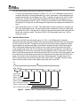
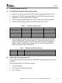
Figure 1 illustrates the typical digital interface when the AIC12 codec/C54xx™ DSP system
works in the codec’s stand-alone master mode.
IOVDD
'C54xxDSP
'AIC12 CODEC
BDX
BDR
DIN
DOUT
FS
BFSX
BFSR
BCLKX
BCLKR
SCLK
IOVDD
I2C master
or S2C
{
10K
M/S
SDA
SCL
CLKOUT
10K
FSD
Reset Command
RESET
Power Down Command
0.01uF
MCLK
0.1uF
1uF
1.8VDC
DVDD
DVSS
Digital Ground
0.01uF
Other Clock Source
10K
PWRDN
10K
Host Port
10K
SMARTDM Port
McBSP
0.1uF
1uF
IOVDD
3.3VDC
IOVSS
Digital Ground
Digital
Analog
Figure 1. Typical AIC12/C54xx™ DSP Digital Interface, Stand-Alone Master Operation
Interfacing the TLV320AIC12/13/14/15 Codec to the TMS320C5402™ DSP
3
SLAA154
In the Figure 1, note that the reset and power-down signals must be synchronized to the main
clock (MCLK) of the codec. For more information see reference [5]. Also note that the maximum
frequency of MCLK is 100MHz
2.2
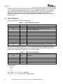
Basic Two-AIC12 Cascade Codec/DSP Interface
The typical circuit for the two AIC12 devices in cascade operation mode is given in Figure 2. As
in the case of the stand-alone operation, the reset and power-down signals must be
synchronized to the main clock (MCLK). Also, the signal edge time difference from one codec to
another should be within 2ns.
2.3
Codec/C5402™ DSP Starter Kit System
To develop this application report, a codec/DSP system was built using a TMSC5402™ DSP
starter kit board, a TLV320AIC development platform board, and an AIC12 EVM board. The AIC
development platform is the bridge between the AIC12 EVM board and the C5402™ DSP starter
kit. Refer to Figure 3 in reference [5] for the system layers and board-to-board connections. The
system connections are based on the interface concept illustrated in Figure 1 or Figure 2.
More information is available for the C5402™ DSP EVM board at TI’s website:
http://focus.ti.com/docs/tool/toolfolder.jhtml?PartNumber=TMDS320005402.
Also refer to [6] for additional information on the codec development and AIC12 EVM boards.
Before powering up the system, board jumpers and switches need to be properly set up. This
process is called the hardware configuration. The C5402™ DSP starter kit board is configured
according to Tables 3 and 4 in reference [5]. Also, see the Test Procedures for AIC12 section in
this report. The codec’s hardware configuration consists primarily in setting the logic state of
pins M/S and FSD. Under the stand-alone master mode, the M/S should be logic high and the
FSD should be pulled high—see Figure 1. When using the two-AIC12 cascade mode, the first
AIC12 (whose FS is connected to the DSP), is always the master. The second AIC12, and the
DSP are slaves. The hardware configuration under the cascade mode is shown in Figure 2.
3
Software Interface
The AIC12/C54x™ DSP is configured for a master and one slave cascade setup, in which the
codec provides all serial shift clock and frame synchronization. The complete software code
required for configuring the DSP for this mode of operation can be downloaded from the product
folder at TI’s website (www.ti.com). More detailed information on the AIC12 codec can be
obtained in reference [1]. Detailed explanations of the software programs can be found in
reference [5]. This includes the DSP memory map register (MMR) configuration, the DSP
system clock control setup, the McBSP initialization routine, and the control loop timing routine.
3.1
Codec Control Register Initialization
There are six control registers (CR) in an AIC12 device. These give users the option to select
and control the codec’s functions. For definitions of these registers, refer to the data manual [1].
The following sections address the basic AIC12 initialization guideline, issues, and other
important points.
4
Interfacing the TLV320AIC12/13/14/15 Codec to the TMS320C5402™ DSP
Figure 2.
'AIC12#0
BDX
BDR
DIN
DOUT
FS
BFSX
BFSR
SCLK
BCLKX
BCLKR
'AIC12#1
M/S
FSD
DIN
DOUT
FS
RESET
SCLK
SMARTDM Port
McBSP
SMARTDM Port
CLKOUT
MCLK
Digital
Analog
Other Clock Source
DVDD
DVSS
IOVDD
IOVSS
SDA
SCL
Host Port
SDA
SCL
M/S
MCLK
Digital
Analog
10K
10K
10K
FSD
RESET
PWRDN
PWRDN
Host Port
Typical AIC12/C54xx™ DSP Digital Interface, Two-AIC12 Cascade Mode
Interfacing the TLV320AIC12/13/14/15 Codec to the TMS320C5402™ DSP
IOVDD
IOVDD
'C54xxDSP
Reset Command
Power Down Command
DVDD
DVSS
IOVDD
IOVSS
IOVDD
10K
I2C master or S2C
10K
{
SLAA154
5
SLAA154
3.2
Analog Interface
The AIC12 device has a full complement of analog input and output terminals that facilitate
modern digital telephony and voice communication. The AIC12 codec has three software
selectable analog inputs and three programmable outputs. The selection of these analog inputs
and outputs is determined by the programmed statuses of the D1 and D2 bits, and the D7, D3,
and D4 bits of the configuration register CR6 respectively.
3.2.1 Analog Inputs
The analog input sources are:
•
The MICIN accommodates a single-ended microphone interface, and a higher quality
pseudo differential microphone interface. In the case of the pseudo differential
configuration, a single-ended input signal is internally converted to a differential signal
before being digitally processed. An on-chip front-end programmable pre-amplification
circuit is provided to allow the use of a wide range of microphones. Amplification selection
of 0, 6, 12, and 24 dB can be made by properly programming the bits D0 and D1 of
configuration register 5C.
•
There are also two pairs of differential analog inputs, INP1/INM1 and INP2/INM2. This
differential configuration provides good common-mode rejection of undesirable analog
signals. These inputs could also be configured for single-ended operation.
Note that all the analog inputs are self-biased at 1.35 volts.
3.2.2 Analog Outputs
The analog outputs of this codec are the differential outputs of the DAC channel. They have
different drive specifications.
3.3
•
The OUTP1/OUTM1 can directly drive a load of 600 Ω in either a single-ended mode or a
differential mode.
•
The OUTP2 and OUTP3 are outputs from two programmable gain amplifiers. They can
drive output loads of 16 Ω directly, and are configurable for either single-ended or
differential operation mode.
Digital Interface
The interaction between the DSP system is conducted through the smart time division
multiplexed (SMARTDM) serial port. The McBSP1 port of the C5402™ DSP provides this
interface. In master mode, the codec generates the serial clock (SCLK) from the system
supplied master clock (MCLK). Its frequency depends on the following parameters and settings:
6
•
MCLK frequency
•
The number of codecs cascaded—two in this case (master and one slave)
•
The data transfer mode selected—programming mode or continuous mode, and
•
The programmed selection of the M, N, and P timing parameters
Interfacing the TLV320AIC12/13/14/15 Codec to the TMS320C5402™ DSP
SLAA154
The following equations determine the respective frequencies:
3.4
•
FS (frame synchronization frequency) = MCLK / (16 * M * N * P). Reference [1] provides a
complete description of the programmable M, N, and P parameters. These parameters are
programmed through control register four (CR4). To specify the value for M, bit D7 of CR4
must be set, and the value specified in bit locations D0 through D6 are assigned to it. To
specify the parameters N and P, bit D7 of CR4 must be cleared, and the values specified in
bit locations D3 through D6; and D0 through D2 respectively are assigned to parameters N
and P.
•
SCLK (serial shift clock) = FS * MD * PM. Where MD is number of devices in cascade, and
PM is the data transfer mode. The data transfer mode is selected by setting or clearing the
bit location D6 of CR1. Clearing this bit selects the programming mode, while setting this bit
selects the continuous mode. The value of PM is 2 for the program mode, and 1 for the
continuous mode.
Interface Data Format
Upon reset, the DAC input data length option of 15 bit + one LSB bit option is selected.
Numerical information is communicated to the codec through the DIN terminal of the codec and
the DX terminal of the DSP. Through this channel, both the codec’s control registers and DAC
input registers are programmed. Data communication between the ADC of the codec and the
DSP is conducted through the DOUT terminal of the codec and the DR terminal of the DSP.
In the programming mode, (D6 of CR1 cleared), each data frame contains two 16 bit blocks of
data information for each device in cascade. See the illustration below. In this mode, the data
frame of the DIN terminal carries 16-bit data from the DSP to the codec’s DAC data register, and
the control frame of the DIN terminal carries the configuration instructions from the DSP to the
codec. The format for this configuration instruction is discussed later. The data frame of the
DOUT terminal carries the numerical results of the codec’s ADC to the DSP, while the control
frame carries the data content of the register being read, back to the DSP.
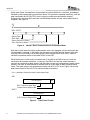
FS
DIN / DOUT
Master Data
Slave Data
Master Control
Slave Control
Master Data (next frame)
Slave Data (next frame)
Master Control (next frame)
Slave Control (next frame)
Figure 3.
Master / Slave Communication in Programming Mode
Interfacing the TLV320AIC12/13/14/15 Codec to the TMS320C5402™ DSP
7
SLAA154
Within each frame, the data frame for each device is transmitted first in one block, immediately
followed by the corresponding control frame block. This process is repeated indefinitely, until the
data frame select bit, bit D6 of CR1 is set, implying a continuous data transfer request.
Subsequently, the serial shift clock rate is automatically halved, and the control frame block is
dropped—see Figure 4.
FS
DIN / DOUT
Master Data
Slave Data
Master Data (next frame)
Slave Data (next frame)
Figure 4.
Master / Slave Communication in Continuous Mode
Note that in both cases the frame synchronization rate is not changed; only the shift clock rate
(not depicted) is changed. In this mode, the data frame of the DIN terminal carries 16-bit data
from the DSP to the codec’s DCA data register, while the data frame of the DOUT terminal
carries the numerical results of the codec’s ADC to the DSP.
While the device is in the continuous data mode, if the LSB of the DIN bit string is clear the
continuous data transfer continues. If, however, the LSB is set, then the codec assumes a
control frame request has been issued, and the codec reverts to the programming mode of data
transfer, one block of data followed by another block of control data for each synchronization
frame. The codec stays in this programming mode until bit 6 of CR1 is set. Figure 5 shows the
data frame format for the AIC12 in its various modes of operation.
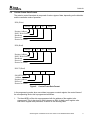
(15 + 1) Bit Mode (Continuous Data Transfer Mode Only)
DIN
D15 through D1
D0
DAC Converter Input Data
Control Frame Request Bit
DOUT
D15 through D0
A/D Converter Output Data
Figure 5.
8
Data Frame Format
Interfacing the TLV320AIC12/13/14/15 Codec to the TMS320C5402™ DSP
SLAA154
3.5
Control Frame Data Format
The codec’s control frame data is composed of various types of data, depending on the direction
and the read/write mode of operation.
DIN (Write)
D15-D13
0
D11
111
D7-D0
1
0
111
D7-D0
Register Address
Read / Write Select
Broadcast
Reserved
Data to be written
DIN (Read)
D15-D13
Register Address
Read / Write Select
Broadcast
Reserved
Data to be written
DOUT (Read)
D15-D12
D11-D9
0
D7-D0
SMART Device
Address
Register Address
Reserved
Data to be written
Figure 6.
Control Frame Data Format
In the programming mode, when one wishes to program a control register, the control frame of
the corresponding device slot is programmed as follows:
1.
The three MSB’s of the slot are programmed with the address of the register to be
programmed. This is also true for the bit streams on DIN, for both control register write
and control register read processes, as shown in the following table.
Interfacing the TLV320AIC12/13/14/15 Codec to the TMS320C5402™ DSP
9
SLAA154
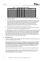
Table 1.
Control Register Address Chart
Register Address
D15
D14
D13
Register Name
0
0
0
0
No Operation
1
0
0
1
Control Register 1 (CR1)
2
0
1
0
Control Register 2 (CR2)
3
0
1
1
Control Register 3 (CR3)
4
1
0
0
Control Register 4 (CR4)
5
1
0
1
Control Register 5 (CR5)
6
1
1
0
Control Register 6 (CR6)
2.
In the read mode, bit D12 of the DIN control data stream is set, while in the write mode,
the D12 bit is cleared.
3.
In the write mode, if the user wishes to program a particular register with a common value
for all the codecs within the cascade, set the broadcast bit, D11. This forces the contents
of the lower 8-bits of the DIN bit stream to be programmed into that specified control
register for all the codec devices in the cascade. If D11 is cleared, then only the
corresponding AIC device is programmed. This bit must be set to 0 in the read mode.
4.
Bits D8 through D10 must always be set in the read or write mode.
5.
The data to be written to the codec should be programmed in the lower 8-bits of the DIN
data stream. For a read instruction, this lower byte is don’t care.
If a read instruction was issued, i.e. bit D12 of DIN bit stream is set in the same cycle, and within
the same device slot, the content of the register of the corresponding codec device is pumped
out of the DOUT terminal of the codec. The first 4 bits of the stream indicate the SMARTDM
device address of the respective codec, the next three bits carry the register address for the
register being read. Bit 8 is reserved and always 0. The lower 8-bits of the output data stream,
DOUT (read), contain the content of the codec’s register.
4
Design Issues
The jumper settings for the AIC12 EVM board used for this application note are provided in the
section on test procedures for the AIC12.
The first task to be performed during the AIC12 initialization is to read the CR1 of all codecs in
the cascade at least once. This is necessary in order to clear the overflow flags of any of the
codec’s ADC and DAC, ADOVF (D7) and DAOVF (D4) in CR1 that might have been set as a
result of any previous conversions. This is because once either of these flags has been set in
any of the codecs; the flag remains set until the user reads the CR1. Reading this control
register automatically resets the overflow flags.
It is most important to remember that there can only be one master in the cascaded system.
The reset and power-down signals must be synchronized to the main clock (MCLK), and the
signal edge timing difference from one codec to another should be within 2ns. And most
importantly, MCLK must not exceed 100 MHz.
10
Interfacing the TLV320AIC12/13/14/15 Codec to the TMS320C5402™ DSP
SLAA154
5
Test Procedure for AIC12.
5.1
TLV320AIC Development Platform Board Setup
1.
Select the 3.3 V source from the DSP (DSP_3.3VDC), by setting the jumper W1 for 1-2.
2.
Plugging the TLV320AIC development platform to the DSP DSK through the common
connector turns on the two yellow LEDs, D1 and D2.
3.
Confirm that the digital and analog power sources, and grounds are properly isolated.
4.
Confirm the following voltage levels on the listed test points, and J3 pins.
Table 2.
Voltage Level
Test Points
Reference Point
3.3 VDC (Digital)
TP2
TP3
25 & 27
3.3 VDC (Analog)
TP5
TP4
37 &39
3.3 VDC (A/Drive)
TP6
TP4
33 & 35
1.8 VDC
TP1
TP3
29 & 31
Ground (Digital)
TP3
TP3
2, 4, 6, 28, 30 & 32
Ground (Analog)
TP4
TP4
34, 36, 38 & 40
5.
J3 Pin Number
Set the development platform such that the system clock is derived from the DSP DSK,
50 MHz, by selecting the 1-2 setting on jumper W2. Confirm that the clock frequency is
actually 50 MHz. Note that there is a 100 MHz clock option onboard the development
platform. However, for the particular selection for M, N, and P in the associated test
software, this option should not be selected.
Table 3.
5.2
Test Point Voltage Levels
Development Platform Jumpers
Jumper
Setting
W1
1–2
Analog 3.3 V is driven from the DSP DSK.
Condition
W2
1–2
W3
Open
Select 50 MHz clock source for driving MCLK
CNTLa does not drive the power-down (SYNC PWDN) circuit.
SYNC RESET Synchronization Test
Test and make sure that the rising edge of the SYNC RESET signal is properly synchronized to
the MCLK.
Place the scope probes on the following test points:
1.
TP12 (SYNC RESET)
2.
TP7 (Reset Switch & DSP Reset Signal)
3.
J3 Pin 1 (MCLK)
Interfacing the TLV320AIC12/13/14/15 Codec to the TMS320C5402™ DSP
11
SLAA154
With the scope in the single trigger mode, and set the scope sync to trigger on the rising edge of
the TP12 signal, press the reset push button on the development platform. Confirm that the
rising edge of SYNC RESET occurs on the rising edge of MCLK. Then set the scope sync to
trigger on the falling edge of the TP12 signal; again press the reset push button on the
development platform. Confirm that the falling edge of SYNC RESET also occurs on the rising
edge of MCLK.
5.3
AIC12 EVM Board
Set the jumpers on the EVM board as follows:
Table 4.
AIC12 EVM Board Jumpers
Jumper
Setting
Condition
W1
1–2
U2 is master
W2
1–2
Make the selection options for FSD_1 a logic 1 or FS_2
W3
2–3
Pass FSD_1 through to FS_2
W4
2–3
Select J3 pin #1 as signal source for INM1_b (negative input)
W5
2–3
Select J5 pin #2 as signal source for INM1_a (negative input)
W6
1–2
OUTP1_b is routed directly to J6 Pin #2
W7
1–2
OUTP1_a is routed directly to J7 Pin #2
W8
Closed
Connect AGND to DGND
W9
Closed
Connect AGND to DRV_AGND
W10
Closed
Do not isolate the secondary AIC unit from the primary AIC unit
P1
9 – 10
Top EVM Card: FSD_x (Last) is pulled High
P1
11 – 12
Top EVM Card: GBL_SCL is pulled high (I C communication)
P1
13 – 14
Top EVM Card: GBL_SDA is pulled high (I C communication)
2
2
With the above settings, if the C5402™ DSP development platform (DSK) and the EVM board
are properly connected—applying power to the system and pressing the RESET push button
produces the EVM test point signals listed in the following table:
Table 5.
Test Point
EVM Test Point Signals
Signal
Default Frequency (Two AIC12 Devices)
TP8
SCLK
260.416 kHz
TP9
FS_1
4.069 kHz
TP10
DXa / DIN
N/A
TP11
N/A
TP12
DRA / DOUT
SYNC RESET
Logic 1
TP13
SYNC PWDN
Logic 1
Default settings:
M = 16
N=6
P=8
FS = MCLK / (16 * M * N * P) = 4.069 kHz.
SCLK = FS * 4 * 16 = 260.416 kHz. (Program Mode)
12
Interfacing the TLV320AIC12/13/14/15 Codec to the TMS320C5402™ DSP
SLAA154
5.4
AC Test
With the jumper settings as described above, apply a periodic signal from a function generator to
J3 and J5 input terminals of the AIC12 EVM board. The frequency of the applied signal must be
less than 7 kHz, since the sampling frequency of the codec is 15.625 kHz.
Compile and load the AIC12SW_C.pjt project program onto the DSK. This software programs
the codec to operate in the continuous mode—set M = 20, N = 5 and P = 2. Since MCLK
frequency is 50 MHz, then FS = MCLK / (16 * M * N * P) = 15.625 kHz. Because there are two
AIC12 devices on the board, and the AICs are programmed for continuous mode operation, the
SCLK = FS * 2 * 16 = 500 kHz.
Confirm that both the sampling rate (FS) and the sample clock frequency (SCLK) are 15.625
kHz and 0.5 MHz, respectively.
Using a two-wire speaker probe, verify that the signal outputs on the respective terminals tally
with the signals in the following table.
Table 6.
Terminal
J6
6
EVM Output Signals
Pin Selection
1 & 2, (OutP1_b & OutM1_b)
Output Signal
DSP generated DFTM tone
J7
1 & 2, (OutP1_a & OutM1_a)
Reproduction of function generator tone
J10
1 & 2, (OutP2_b & OutMV_b)
DSP generated DFTM tone
J10
3 & 2, (OutP3_b & OutMV_b)
DSP generated DFTM tone
J11
1 & 2, (OutP2_a & OutMV_a)
Reproduction of function generator tone
J11
3 & 2, (OutP3_a & OutMV_a)
Reproduction of function generator tone
References
[1]
TLV320AIC12, Low Power CMOS, 16-bit, 26-KSPS Codec with Smart Time Division
Multiplexed (SMARTDMTM) Serial Port, data manual (SLWS115)
[2]
TLV320AIC13, SMARTDMTM Low Power, Low Voltage, 1.1 V to 3.6 V I/O, 16-bit, 26KSPS Codec, data manual (SLWS139)
[3]
TLV320AIC14, Low Power CMOS, 16-bit, 26-KSPS Codec with Smart Time Division
Multiplexed (SMARTDMTM) Serial Port, data manual (SLWS140)
[4]
TLV320AIC15, SMARTDMTM Low Power, Low Voltage, 1.1 V to 3.6 V I/O, 16-bit, 26KSPS Codec data manual (SLWS141)
[5].
TLV320AIC12/13/14/15 Codec Operating under Stand-Alone Slave Mode, application
report, (SLAA142)
[6]
TLV320AIC Family EVM System (Bolanle Onodipe and Joe Purvis, SLAA141)
[7]
TMS320VC5402 Fixed-Point Digital Signal Processor (SPRS079D)
[8]
TMS320C54x DSP CPU and Peripherals, Reference Set Volume 1 (SPRU131F)
[9]
TMS320C54x DSP Enhanced Peripherals, Reference Set Volume 5 (SPRU302)
[10]
Code Composer, user’s guide (SPRU296)
Interfacing the TLV320AIC12/13/14/15 Codec to the TMS320C5402™ DSP
13
SLAA154
14
[11]
TMS320C54x DSP Mnemonic Instruction Set, Reference Set Volume 2 (SPRU172B)
[12]
TMS320C54x Assembly Language Tools, user’s guide (SPRU102D)
[13]
TMS320C54x Optimizing C Compiler, user’s guide (SPRU103D)
[14]
TMS320C54x DSP Applications Guide, Reference Set Volume 4 (SPRU173)
Interfacing the TLV320AIC12/13/14/15 Codec to the TMS320C5402™ DSP
IMPORTANT NOTICE
Texas Instruments Incorporated and its subsidiaries (TI) reserve the right to make corrections, modifications,
enhancements, improvements, and other changes to its products and services at any time and to discontinue
any product or service without notice. Customers should obtain the latest relevant information before placing
orders and should verify that such information is current and complete. All products are sold subject to TI’s terms
and conditions of sale supplied at the time of order acknowledgment.
TI warrants performance of its hardware products to the specifications applicable at the time of sale in
accordance with TI’s standard warranty. Testing and other quality control techniques are used to the extent TI
deems necessary to support this warranty. Except where mandated by government requirements, testing of all
parameters of each product is not necessarily performed.
TI assumes no liability for applications assistance or customer product design. Customers are responsible for
their products and applications using TI components. To minimize the risks associated with customer products
and applications, customers should provide adequate design and operating safeguards.
TI does not warrant or represent that any license, either express or implied, is granted under any TI patent right,
copyright, mask work right, or other TI intellectual property right relating to any combination, machine, or process
in which TI products or services are used. Information published by TI regarding third–party products or services
does not constitute a license from TI to use such products or services or a warranty or endorsement thereof.
Use of such information may require a license from a third party under the patents or other intellectual property
of the third party, or a license from TI under the patents or other intellectual property of TI.
Reproduction of information in TI data books or data sheets is permissible only if reproduction is without
alteration and is accompanied by all associated warranties, conditions, limitations, and notices. Reproduction
of this information with alteration is an unfair and deceptive business practice. TI is not responsible or liable for
such altered documentation.
Resale of TI products or services with statements different from or beyond the parameters stated by TI for that
product or service voids all express and any implied warranties for the associated TI product or service and
is an unfair and deceptive business practice. TI is not responsible or liable for any such statements.
Mailing Address:
Texas Instruments
Post Office Box 655303
Dallas, Texas 75265
Copyright 2002, Texas Instruments Incorporated