1
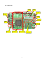
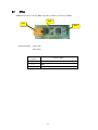
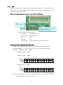
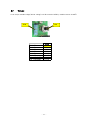
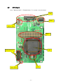
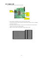
FL-850/FL4H
FL-850/FL4H-S
Hardware Manual
Date published: September 2011 (2nd Edition)
Tessera Technology Inc.
- 1 -
CAUTION:
・
The information in this document is subject to change without notice.
・
No part of this document may be copied or reproduced in any form or by any means without
prior written consent of Tessera Technology Inc.
・
Tessera Technology Inc. assumes no responsibility for inaccuracies or misprints of this
document.
・
Tessera Technology Inc. does not assume any liability for infringement of patents,
copyrights or other intellectual property rights of third parties by or arising from the use of
Tessera Technology Inc. products listed in this document or any other liability arising from
the use of such products. No license, express, implied or otherwise, is granted under any
patents, copyrights or other intellectual property rights of Tessera Technology Inc. or
others.
・
Descriptions of circuits, software and other related information in this document are
provided for illustrative purposes in semiconductor product operation and application
examples. The incorporation of these circuits, software and information in the design of a
customer's equipment shall be done under the full responsibility of the customer. Tessera
Technology Inc. assumes no responsibility for any losses incurred by customers or third
parties arising from the use of these circuits, software and information.
- 2 -
TABLE OF CONTENTS
1
INTRODUCTION ................................................................................................................... 4
2
FEATURES ............................................................................................................................ 5
3
2.1
CAN ..................................................................................................................................... 6
2.2
FLEXRAY ............................................................................................................................... 8
2.3
IEBUS ................................................................................................................................. 11
2.4
ETHERNET ............................................................................................................................ 12
2.5
SERIAL SELECT ..................................................................................................................... 14
2.5.1
LCD........................................................................................................................... 15
2.5.2
RS-232C.................................................................................................................... 18
2.5.3
USB Serial Conversion............................................................................................ 19
2.6
PUSH SWITCH ....................................................................................................................... 20
2.7
VOLUME ............................................................................................................................... 21
2.8
POWER ................................................................................................................................ 22
2.9
CPU BOARD ........................................................................................................................ 23
2.9.1
Power ........................................................................................................................ 24
2.9.2
CPU........................................................................................................................... 24
2.9.3
Clock ......................................................................................................................... 25
2.9.4
Reset ......................................................................................................................... 25
2.9.5
Switch & LED......................................................................................................... 26
2.9.6
Debug Connector...................................................................................................... 27
2.9.7
Filter socket.............................................................................................................. 28
2.9.8
CAN .......................................................................................................................... 29
CPU TERMINAL CONNECTION LIST.............................................................................. 30
- 3 -
1 Introduction
In this document, features and hardware specifications of FL-850/FL4H, which the 32-bit single-chip
microcomputer V850E2/FL4-H from Renesas Electronics Corporation is mounted, are described.
- 4 -
2 Features
CAN
LCD
RS-232C
FlexRay
USB
Volume
IEBus
Power
Ethernet
CPU Board
Push Switch
- 5 -
Serial select
2.1
CAN
The CAN controller of the microcomputer is connected to the CAN transceiver (TJA1040). It
supports CAN physical layer. Also, CAN bus signal is connected to DSUB 9pin female
connector.
CAN 3
CAN 2
CAN 1
CAN 0
CAN 4
JP8
One terminal can be selected by using jumpers from maximum of three multipurpose terminals, and
can be connected to CAN transceiver.
Only one line must be shorted in each jumper.
CAN 4 is in CPU board. JP8 is a power supply jumper of the CAN transceiver. Be short-circuited
usually.
- 6 -
Following table shows the connection of V850E2/FL4-H.
Jumper
P0_7/URTE11RX/FCN1TX/K R0I2/CSIH2CSS2/INTP4
Connecter
1-2
P1_2/TAUA0I2/TAUA0O2/TAUC4O2/ENCA0BIN/TAPA0UP/CSIH2SI/FCN1TX
TxD
JP22
P0_12/TAUJ0I0/TAUJ0O0/KR0I0/INTP8/CSCXFOUT
3-4
5-6
P0_6/ FCN1RX/ URTE11TX/KR0I1/CSIH2CSS1/NMI
1-2
P1_1/TAUA0I1/TAUA0O1/TAUC4O1/ENCA0AIN/FCN1RX /FCN0TX
RxD
JP23
3-4
MODE0
JP20
Short
TxD
JP26
P0_15/TAUJ0I3/TAUJ0O3/KR0I7/CSIH2CSS7/ FCN4RX/TAUB1O14/CSIG0SC
P1_5/ TAUA0I5/TAUA0O5/TAUC4O9/ENCA0TIN1/TAPA0VN
5-6
P0_9/URTE10RX/ FCN2TX/K R0I4/CSIH2CSS4/INTP6/TAUA0O6/IICB0SCL
P1_9/TAUA0I9/TAUA0O9/INTP3/FLX0TXENA/CSIH1SC/URTE4RX /FCN2TX
1-2
P2_2/URTE7RX/ FCN4TX/INTP1/CSIH1CSS7/TAUJ1I2/TAUJ1O2
3-4
5-6
P0_8/ FCN2RX/ URTE10TX/KR0I3/CSIH2CSS3/INTP5/TAUA0O5/IICB0SDA
P1_8/TAUA0I8/TAUA0O8/TAUC4O14/CSIH1SO/ FCN2RX/URTE4TX
CAN 0
1-2
RxD
JP27
3-4
MODE1
JP24
Short
TxD
JP30
P2 _0/ FCN4RX/URTE6TX/CSIH1CSS5/INTP10
CAN 1
5-6
P1_14/TAUA0I14/TAUA0O14/FLX0STPWT/URTE5TX/CSIH1CSS3/INTP8
P0_11/URTE11RX/ FCN3TX/INTP10
1-2
P4_1/TAUB1I2/TAUB1O2/TAUA0I14/TAUA0O14/CSIH0SO/URTE2RX /FCN3TX
3-4
P24_5/INTP10/URTE0RX/ FCN4TX/TAUC8O10
5-6
P0 _10/ FCN3RX/URTE11TX/INTP9
1-2
P4_2/TAUB1I3/TAUB1O3/TAUA0I15/TAUA0O15/CSIH0SC/ FCN3RX/ URTE2TX
RxD
JP31
3-4
MODE2
JP28
Short
TxD
JP34
P24_4/ FCN4RX/URTE0TX/TAUC8O9
CAN 2
5-6
P3_2/ TAUB2I2/TAUB2O2/TAUA0I2/TAUA0O2/KR0I7
P0_13/TAUJ0I1/TAUJ0O1/KR0I5/CSIH2CSS5/INTP7 /FCN5TX/CSIG0SI
P24_3/INTP9/URTE9RX/ FCN5TX/TAUC8O6
1-2
P3_9/TAUB2I11/TAUB2O11/TAUA0I9/TAUA0O9/URTE5RX/ FCN5TX /INTP12/URTE3TX
P0_14/TAUJ0I2/TAUJ0O2/KR0I6/CSIH2CSS6/ FCN5RX/TAUB1O13/CSIG0SO
P24_2/ FCN5RX/URTE9TX/TAUC8O5
1-2
RxD
JP35
3-4
MODE3
JP32
Short
TxD
JP3
P3_10/TAUB2I13/TAUB2O13/TAUA0I10/TAUA0O10/ FCN5RX /URTE5TX
P3_3/ TAUB2I3/TAUB2O3/TAUA0I3/TAUA0O3/KR0I6
P0_4/ FCN0TX/I NTP11
P1_1/TAUA0I1/TAUA0O1/TAUC4O1/ENCA0AIN/FCN1RX /FCN0TX
P0 _5/ FCN0RX/I NTP12
P1_7/TAUA0I7/TAUA0O7/TAUC4O13/CSIH1SI/TAPA0WN/ FCN0RX /CSIH2CSS1
P1_3/ TAUA0I3/TAUA0O3/TAUC4O5/ENCA0ZIN/TAPA0UN/CSIH2SO
3-4
5-6
CAN 3
5-6
RxD
JP4
MODE4
JP1
1-2
2-3
1-2
CAN 4
2-3
Short
Default
JP21, JP25, JP29, JP33, and JP2 are termination resistor connect. Open or short these as
needed.
termination resistor
JP21:CAN 0
JP25:CAN 1
JP29:CAN 2
JP33:CAN 3
JP2 : CAN 4
1-2 Short
3-4 Short
1-2
3-4
1-2
3-4
Short
Open
Open
Open
60Ω
120Ω
Non
- 7 -
CAN 0,1,2,3
DSUB Connector
Pin Number
1
2
3
4
5
6
7
8
9
Signal Name
N.C.
CANL
GND
N.C.
0.1uF
N.C.
CANH
N.C.
N.C.
2.2
FlexRay
The FlexRay controller of the microcomputer is externally connected to the FlexRay
transceiver (TJA1080). It supports FlexRay physical layer. Also, FlexRay bus signal is connected
to DSUB 9pin female connector.
FlexRay A
FlexRay B
Following table shows the connections for V850E2/FL4-H.
Signal
JP4
TJA1080
FLX0TXDA
1-2
TXD
P1_9/TAUA0I9/TAUA0O9/INTP3 /FLX0TXENA/CSIH1SC/URTE4RX/FCN2TX
FLX0TXENA
3-4
TXEN
P3_7/TAUB2I9/TAUB2O9/TAUA0I7/TAUA0O7/URTE7RX/CSIG0SI/URTE3TX
STBN1
5-6
STBN
P3_4/TAUB2I5/TAUB2O5/TAUA0I4/TAUA0O4/KR0I5
EN1
7-8
----
P1_11/TAUA0I11/TAUA0O11/URTE3RX/FLX0TXDA/CSIH1CSS0/INTP5
P1_10/TAUA0I10/TAUA0O10/ FLX0RXDA/ URTE3TX/INTP4
FLX0RXDA
9-10
RXD
P3_5/TAUB2I6/TAUB2O6/TAUA0I5/TAUA0O5/KR0I4/CSIG0SC
ERRN1
11-12
ERRN
P3_6/TAUB2I7/TAUB2O7/TAUA0I6/TAUA0O6/CSIG0SO
RXEN1
13-14
RXEN
P1_6/TAUA0I6/TAUA0O6/TAUC4O10/TAPA0WP/CSIH2CSS0
WAKE1
15-16
WAKE
Signal
JP16
TJA1080
P1_13/TAUA0I13/TAUA0O13/URTE4RX /FLX0TXDB/CSIH1CSS2/INTP7
FLX0TXDB
1-2
TXD
TXEN
P1_15/TAUA0I15/TAUA0O15/URTE5RX /FLX0TXENB/CSIH1CSS4/INTP9
FLX0TXENB
3-4
P4_8/TAUB1I11/TAUB1O11/CSIG4SC/KR0I0/CSIH0CSS4/ENCA0ZIN
STBN2
5-6
STBN
P4_5/TAUB1I7/TAUB1O7/CSIG0SC/KR0I3/CSIH0CSS1/ENCA0TIN1
EN2
7-8
----
P1_12/TAUA0I12/TAUA0O12/ FLX0RXDB/URTE4TX/CSIH1CSS1/INTP6
FLX0RXDB
9-10
RXD
P4_6/TAUB1I9/TAUB1O9/CSIG4SI/URTE11TX/KR0I2/CSIH0CSS2/ENCA0AIN
ERRN2
11-12
ERRN
P4_7/INTP4/TAUB1O10/URTE11RX/CSIG4SO/KR0I1/CSIH0CSS3/ENCA0BIN
RXEN2
13-14
RXEN
P1_7/TAUA0I7/TAUA0O7/TAUC4O13/CSIH1SI/TAPA0WN/FCN0RX/CSIH2CSS1
WAKE2
15-16
WAKE
JP11 and JP19 are jumpers for TJA1082 (not mounted). Do not short them.
JP41
P1_2/TAUA0I2/TAUA0O2/TAUC4O2/ENCA0BIN/TAPA0UP/CSIH2 SI/FCN1TX
SDO
3-4
P1_4/TAUA0I4/TAUA0O4/TAUC4O6/ENCA0TIN0/TAPA0VP/CSIH2S C
SCLK
1-2
- 8 -
EN and ERRN terminals of TJA1080 are connected as shown below logic circuit diagram.
Set EN1 terminal to Low when you need to access upper one (FlexRay A) with CSI. Set to High when
you do not need to access it.
In the same way, set EN2 terminal to Low when you need to access upper one (FlexRay B) with CSI.
Set to High when you do not need to access it.
JP5, JP7, JP17, and JP18 are the selection of FlexRay transceiver IC (TJA1080 or TJA1082).
Normally, use these with the default settings since it does not mount TJA1082.
FlexRay A
FlexRay B
JP5 : 1-2
JP7 : 1-2
JP5 : 2-3
JP7 : 2-3
JP17 : 1-2
JP18 : 1-2
JP17 : 2-3
JP18 : 2-3
TJA1080
TJA1082
TJA1080
TJA1082
JP9, JP10, JP14, and JP15 are the connection for termination resistor (50Ω). Open or short
these as needed.
FlexRay A
FlexRay B
JP9
BP
JP10
BM
JP14
BP
JP15
BM
Default: Short
- 9 -
JP6, JP8, JP12, and JP13 are the jumpers to change wire connection of DSUB 9pin female connector,
which outputs FlexRay bus signal.
Type-1
JP6
JP8
JP12
JP13
1-2
1-2
5-6
5-6
FlexRay A
1-2
1-2
3-4
3-4
FlexRay A
1-2
5-6
1-2
5-6
All Open
All Open
FlexRay A
DSUB connector
Pin No.
1
2
3
4
5
6
7
8
9
Signal
N.C.
BM A
N.C.
N.C.
N.C.
N.C.
BP A
N.C.
N.C.
FlexRay B
Pin No.
1
2
3
4
5
6
7
8
9
DSUB connector
Signal
N.C.
BM B
N.C.
N.C.
N.C.
N.C.
BP B
N.C.
N.C.
Type-2
JP6
JP8
JP12
JP13
DSUB connector
Pin No.
1
2
3
4
5
6
7
8
9
Signal
N.C.
BM A
BM B
N.C.
N.C.
N.C.
BP A
BP B
N.C.
FlexRay B
Pin No.
1
2
3
4
5
6
7
8
9
DSUB connector
Signal
N.C.
N.C.
N.C.
N.C.
N.C.
N.C.
N.C.
N.C.
N.C.
Type-3
JP6
JP8
JP12
JP13
DSUB connector
Pin No.
1
2
3
4
5
6
7
8
9
Signal
N.C.
BM A
N.C.
N.C.
N.C.
N.C.
BP A
N.C.
N.C.
- 10 -
FlexRay B
Pin No.
1
2
3
4
5
6
7
8
9
DSUB connector
Signal
N.C.
BM A
N.C.
N.C.
N.C.
N.C.
BP A
N.C.
N.C.
2.3
IEBus
V850E2/FL4-H does not have IEBus controller, therefore it cannot use IEBus.
JP42
CN4
JP43
Default Settings
JP43: Open
JP42: Short
CN4 Pin
Number
1
Function Name
(+) Bus Output, (+) Receiver Input
2
GND
3
(-) Bus Output, (-) Receiver Input
- 11 -
2.4
Ethernet
Ethernet can be used by connecting PHY Chip (KSZ8041NL) from MICREL to the built-in
Ethernet controller.
SW16
SW18
SW17
VDD3V
VDD3VE
VDD3VE
LED4
SW16
LED1
V850E2/FL4-H
PHY
Ethernet
Jack
SW17
KSZ8041NL
LED0
SW18
LED5
Set following DIP switches to ON when you use Ethernet.
・SW16 (default setting: ON)
・SW17 (default setting: ON)
・SW18 (default setting: ON)
z Ethernet circuit can only be used when the microcomputer's IO voltage is 3.3V.
Please note damage when it sets it to 5V.
- 12 -
P25_0/MEMC0AD0/INTP6/ ETH0TXD3/ URTE6RX/CSIG2SO/TAUC6O1
P25_1/MEMC0AD1/ ETH0TXD2/CSIG2SI/URTE6TX/TAUC6O2
P25_2/MEMC0AD2/ ETH0TXD1/CSIG2SC/TAUC6O5
P25_3/MEMC0AD3/ ETH0TXD0/CSIG4SI/URTE7TX/TAUC6O6
P25_4/MEMC0AD4/INTP7/ ETH0TXEN/ URTE7RX/CSIG4SO/TAUC6O9
P25_5/MEMC0AD5/ETH0REFCLK/ ETH0TXER/CSIG4SC/TAUC6O10
P25_6/MEMC0AD6/ ETH0CRSDV/TAUC6O13
P25_7/MEMC0AD7/ ETH0RXER/TAUC6O14
P25_8/MEMC0AD8/ ETH0RXD0/TAUC5O1
P25_9/MEMC0AD9/ ETH0RXD1/TAUC5O2
P25_10/MEMC0AD10/ ETH0RXD2 /CSIH2CSS6/TAUC5O5
P25_11/MEMC0AD11/ ETH0RXD3 /CSIH2CSS7/TAUC5O6
P25_12/MEMC0AD12/ ETH0RXDV/IICB0SDA/TAUC5O9
P25_13/MEMC0AD13/ ETH0RXCLK/IICB0SCL/TAUC5O10
P25_14/MEMC0AD14/INTP5/ ETH0MDC/URTE5RX/FCN3TX/TAUC5O13
P25_15/MEMC0AD15/ ETH0MDI/ ETH0MDO/FCN3RX/URTE5TX/TAUC5O14
P27_1/INTP1/MEMC0A17/ ETH0COL/ADCA1TRG1/PMCA0/MSEL1
P27_2/INTP2/MEMC0A18/ ETH0TXCLK/ADCA1TRG0/PMCA0/MSEL2
Strapping Options
PHY Address 00001
MII Mode
ISOLATE mode: Disable
SPEED mode: 100Mbps
DUPLEX mode: Half Duplex
Nway Auto-Negotiation Enable
- 13 -
KSZ8041NL
ETH0TXD3
ETH0TXD2
ETH0TXD1
ETH0TXD0
ETH0TXEN
ETH0TXER
ETH0CRSDV
ETH0RXER
ETH0RXD0
ETH0RXD1
ETH0RXD2
ETH0RXD3
ETH0RXDV
ETH0RXCLK
ETH0MDC
ETH0MDO
ETH0COL
ETH0TXCLK
2.5
Serial select
It can be connected by selecting the microcomputer's UART terminal to "LCD",
"RS-232C", and "USB Serial Conversion".
The terminals for using UART can be selected by DIP switch (SW1, SW4, and SW6).
※ Do not set multiple ON within a group.
P21_7/MEMC0WAIT/CSIH2CSS1/URTE0TX/TAUC3O6
P4_2/TAUB1I3/TAUB1O3/TAUA0I15/TAUA0O15/CSIH0SC/FCN3RX/URTE2TX
P3_12/TAUB2I15/TAUB2O15/TAUA0I12/TAUA0O12/URTE7RX/URTE6TX/INTP14
TXD
N.C.
P21_8/INTP15/CSIH2CSS2/ URTE0RX/PMCA0MSEL0/TAUC3O9
P4_1/TAUB1I2/TAUB1O2/TAUA0I14/TAUA0O14/CSIH0SO/URTE2RX/FCN3TX
P3_11/TAUB2I14/TAUB2O14/TAUA0I11/TAUA0O11/ URTE6RX/INTP13
RXD
N.C.
P3_7/TAUB2I9/TAUB2O9/TAUA0I7/TAUA0O7/URTE7RX/CSIG0SI/ URTE3TX
P4_9/TAUB1I13/TAUB1O13/CSIH0CSS5/ URTE8TX
P24_0/ URTE8TX/TAUC8O1
TXD
N.C.
P3_8/TAUB2I10/TAUB2O10/TAUA0I8/TAUA0O8/INTP11/URTE6TX/ URTE3RX
P4_10/TAUB1I14/TAUB1O14/INTP15/CSIH0CSS6/ URTE8RX
P24_1/INTP8/ URTE8RX/TAUC8O2
RXD
N.C.
P3_10/TAUB2I13/TAUB2O13/TAUA0I10/TAUA0O10/FCN5RX/URTE5TX
P21_5/INTP13/MEMC0RD/CSIH2RY/ URTE9TX/TAUC3O2
P4_3/TAUB1I5/TAUB1O5/CSIG0SI/ URTE10TX/INTP10
TXD
N.C.
P3_9/TAUB2I11/TAUB2O11/TAUA0I9/TAUA0O9/ URTE5RX/FCN5TX/INTP12/URTE3TX
P21_6/INTP14/MEMC0CLK/CSIH2CSS0/ URTE9RX/TAUC3O5
P4_4/INTP2/TAUB1O6/ URTE10RX/ CSIG0SO/CSIH0CSS0/ENCA0TIN0
RXD
N.C.
The destination for UART can be selected by the slide switch (SW2, SW3, and SW5).
SW2
LCD
SW5
RS-232C
SW3
USB Serial Conversion
Slide Switch
0
1
2
0
1
2
0
1
2
- 14 -
UART0
UART1
UART2
UART0
UART1
UART2
UART0
UART1
UART2
SW1
1 ON
2 OFF
3 OFF
4 OFF
UART0
5 ON
6 OFF
7 OFF
8 OFF
SW4
1 OFF
2 ON
3 OFF
4 OFF
UART1
5 OFF
6 ON
7 OFF
8 OFF
SW6
1 ON
2 OFF
3 OFF
4 OFF
UART2
5 ON
6 OFF
7 OFF
8 OFF
2.5.1 LCD
Words can be displayed on LCD panel by sending data to UART that is connected to LCD.
"Binary mode" to display hexadecimal and "ASCII mode" to display ASCII characters can be
selected by the DIP switch (SW7).
Initial screen displays when you press the reset switch on CPU board.
VR1
Adjust LCD Contrast
FP1
SW7
Connector for debugging the microcomputer
(78K0/KF2) for LCD control.
Normally, do not connect anything.
UART Communication Specifications
・ Baud Rate
115.2Kbps (Fixed)
・ Data Length
8bit (LSB First)
・ Parity
None
・ Stop Bit
1bit
・ Flow Control
None (continuous transmission enabled)
Binary Mode 1 (SW7-1:ON, SW7-2:ON, SW7-3:Any)
It displays the hexadecimal data as sent with entering space between 1Byte data.
It can display 10Byte in 1 screen. It scrolls 1 line when it received 11Byte of data.
(example)
URTH?TX = 0x01; TXWait();
URTH?TX = 0x02; TXWait();
・・・・・・・・・・
URTH?TX = 0x0A; TXWait();
0
1
0
2
0
3
0
4
0
5
0
6
0
7
0
8
0
9
0
A
7
0
8
0
9
0
A
URTH?TX = 0x10; TXWait();
0
6
1
0
0
(use case) By developing a program to send 10Byte once in 1 second, it will display the
first 1Byte at the top-left of the screen.
- 15 -
Binary Mode 2 (SW7-1:ON, SW7-2:OFF, SW7-3:ON)
It displays the hexadecimal data as sent without entering space between 1Byte data.
It can display 16Byte in 1 screen. It scrolls 1 line when it received 17Byte of data.
(example)
URTH?TX = 0x01; TXWait();
URTH?TX = 0x02; TXWait();
・・・・・・・・・・
URTH?TX = 0x10; TXWait();
0
1
0
2
0
3
0
4
0
5
0
6
0
7
0
8
0
9
0
A
0
B
0
C
0
D
0
E
0
F
1
0
0
B
0
C
0
D
0
E
0
F
1
0
URTH?TX = 0x11; TXWait();
0
9
1
1
0
A
(use case) By developing a program to send 16Byte once in 1 second, it will display the
first 1Byte at the top-left of the screen.
- 16 -
ASCII Mode Ver.2 (SW7-1:OFF, SW7-2:Any, SW7-3:Any)
It displays the characters as sent.
It can display 16 characters in 1 line. It scrolls 1 line when it received 17th character or
linefeed code (0x0D: \r ).
(example)
URTH?TX = ‘F’; TXWait();
URTH?TX = ‘l’; TXWait();
・・・・・・・・・・
URTH?TX = ‘T’; TXWait();
F
l
e
x
T
E
S
T
R
a
y
URTH?TX = ‘\r’; TXWait();
URTH?TX = ‘1’; TXWait();
T
E
S
T
1
The position of the cursor can be specified by sending xy-coordinate right after
ESC code (0x1B).
ESC(0x1B) + xy
x: 0(0x30)~9(0x39),a(0x61), b, c, d, e, f(0x66)
y: 0(0x30),1(0x31)
(example) printf(buf, “¥x1b00TEST¥x1ba1LCD”);
y
↓
0
T
E
S
T
1
X →
0
1
2
3
4
- 17 -
5
6
7
8
9
L
C
D
a
b
c
d
e
f
2.5.2 RS-232C
UART that is connected to "RS-232C" can send and receive signals with the RS-232C level of
D-SUB9 pin connector.
Use a cross cable when you connect to PC.
RS-232C
RS-232C
D-SUB Connector
Pin Number
1
2
3
4
5
6
7
8
9
Signal
N.C.
RxD
TxD
N.C.
GND
N.C.
RTS(N.C.)
CTS(N.C.)
N.C.
- 18 -
2.5.3 USB Serial Conversion
UART that is connected to "USB serial conversion" can communicate with the COM port of PC
through USB microcomputer (uPD78F0730).
USB driver is stored in the same media as this manual. When you encountered a warning
"Windows Logo Test" while installing the USB driver, please select "Continue".
USB1
Recommended UART communication specification
・ Baud rate
115.2Kbps
・ Data length
8bit (LSB First)
・ Parity
None
・ Stop Bit
1bit
・ Flow Control
None
- 19 -
2.6
Push Switch
4 interrupt signals can be connected to microcomputer's interrupt terminals. The signal can
be set to High by pressing H button, and to Low by pressing L button. It becomes High by reset
signal of the CPU.
Also, it has chattering prevention circuit.
JP36
SW_NMI
JP37
SW_INTA
JP39
SW_INTB
JP40
SW_INTC
The interrupt signals are disconnected by taking each jumper pin out.
P0_6/FCN1RX/URTE11TX/KR0I1/CSIH2CSS1 /NMI
P27_0/ INTP0 /MEMC0A16/ADCA1TRG2/PMCA0MSEL0
P21_2/ INTP10 /MEMC0BEN1/CSIH2SI/IICB0SDA/TAUC2I13/TAUC2O13
P21_3/ INTP11 /MEMC0BEN0/CSIH2SO/IICB0SCL/TAUB2I14/TAUB2O14
- 20 -
Jumper
JP36:Open
JP37: Short
JP39: Short
JP40: Short
Switch
SW8/9
SW10/11
SW12/13
SW14/15
Signal
SW_NMI
SW_INTA
SW_INTB
SW_INTC
2.7
Volume
It can output variable voltage (0V-IO voltage) to A/D terminal of CPU by variable resistor of 10KΩ.
JP38
VR2
ADCA0I0
ADCA0I1
ADCA0I2
ADCA0I3
ADCA0I4
ADCA0I5
P10_6/ADCA0I6
P10_7/ADCA0I7
JP38
1-2
3-4
5-6
7-8
9-10
11-12
13-14
15-16
- 21 -
2.8
Power
Connect bundled AC adapter (+5V) to AC Jack. You do not need to connect to the AC Jack
on the CPU board.
It generates the power of +12V for FlexRay driver and +3.3V for Ethernet PHY chip power
from this power supply with using regulator.
JP2 : 5V
AC Jack
JP3 : 3.3V
Terminal: VDD
Terminal: GND
Power supply source can be changed by JP2 and JP3.
JP2
5V
JP3
3.3V
1-2
AC adapter
2-3
Terminal
1-2
Regulator
2-3
Terminal
JP1 is the jumper to fix the IO voltage when it does not connect CPU board. Normally, do
not short this.
Powe LED(12V)
JP1
Powe LED(5V)
Powe LED(3.3V)
- 22 -
2.9
CPU Board
One of "EB-850/FL4H" or "EB-850/FL4H-S" is mounted on the CPU board
CAN
Power
Switch & LED
Filter
CPU
Debug Connector
Clock
Reset Switch
- 23 -
2.9.1 Power
There is a jumper pin for measuring the current when you use only CPU board itself.
JP5
JP6
CN4 : AC Jack
JP7
No.
Select
JP7
Short
JP5
Short
1-2
JP6
2-3
Note
I/O Power (3.3V or 5V)
Connect ammeter to check the current
Internal Power (1.25V)
Connect ammeter to check the current
Operation voltage is 5V.
Operation voltage is 3.3V.
(Only when FL-BASE board is connected)
2.9.2 CPU
CPU is direct-mounted for "EB-850/FL4H".
For "EB-850/FL4H-S", only socket is mounted. Make sure the position of 1pin when you mount
CPU.
1pin
- 24 -
2.9.3 Clock
For the X1 and X2 of the CPU, 4MHz crystal oscillator (Y1) is mounted on the socket.
For the XT1 and XT2 of the CPU, 32.768KHz crystal oscillator (Y2) is connected.
Y1
Y2
2.9.4 Reset
CPU can be reset by pressing the Reset switch (SW2).
JP9
SW2
The method of outputting reset on the FL-BASE board can be set with the jumper.
No.
JP9
Select
Note
1-2
CPU Port(P0_0)
2-3
Reset Switch(SW2)
- 25 -
2.9.5 Switch & LED
They are connected to port terminals of the CPU.
SW1
LED1
LED2
LED3
LED4
Power LED
・ P24_12, P24_13, and P24_14 can be used for the switch inputs.
It connects the pull-up resistor with built-in CPU. Set the switch to OFF to read High
and to ON to read Low.
・ P24_8, P24_9, P24_10, and P24_11 can be connected to LED. Set the switch ON and
output Low from the port to light the LED.
・ SW1-8 is power indicator. Power LED is off when power is OFF.
P24_12/TAUC7O9
P24_13/TAUC7O10
P24_14/ETH0COL/TAUC7O13
P24_8/TAUC7O1
P24_9/TAUC7O2
P24_10/TAUC7O5
P24_11/TAUC7O6
5V Power Supply
- 26 -
SW1 Connect to
1
GND
2
GND
3
GND
4
LED1
5
LED2
6
LED3
7
LED4
8
Power LED
2.9.6 Debug Connector
Debugger or Flash writer can be connected to CN4.
It supports "QB-V850MINIL" and “E1” emulator.
Please use the 16pin conversion adaptor of the "QB-V850MINIL" attachment when you
connect "QB-V850MINIL".
Please use the 14pin conversion adaptor "E1-16C" of this product attachment when you
connect "E1".
For the Flash writer, it supports "PG-FP5" writer.
CN4
E1-16C
Pin
Number
Pin
Signal
Debugger
Writer
Number
Signal
1
GND
←
←
1
DCUTCK
2
RESET
←
←
2
GND
3
DCUTDO
SO
3
DCUTRST
4
VDD
←
←
4
FLMD0
5
DCUTDI
SI
RxD/TxD
5
DCUTDO
6
N.C.
6
T_RESET
7
DCUTCK
7
DCUTDI
8
DCUTRDY
8
VDD
9
DCUTRST
9
DCUTMS
10
N.C.
10
RESET
11
N.C.
11
DCUTRDY
12
DCUTMS
12
GND
13
N.C.
13
RESET
14
FLMD0
14
GND
15
T_RESET
16
N.C.
SCK
←
←
- 27 -
2.9.7 Filter socket
Filters can be implemented to A/D input terminals.
Connects (CN1, CN2) are connected through the sockets as illustrated below. Therefore, please
make sure you connect resistor between the socket 4pin and 5pin when you use A/D terminal.
5
4
3
2
1
J1
Socket
Connector
ADCA0I0
ADCA0I1
ADCA0I2
ADCA0I3
ADCA0I4
ADCA0I5
P10_6/ADCA0I6
P10_7/ADCA0I7
P10_8/ADCA0I8
P10_9/ADCA0I9/ADCA0TRG0
P10_10/ADCA0I10/ADCA0TRG1
P10_11/ADCA0I11/ADCA0TRG2
CPU
Soc ket
J1
J2
J3
J4
J5
J6
J7
J8
J9
J10
J11
J12
- 28 -
P10_12/ADCA0I12
P10_13/ADCA0I13
P10_14/ADCA0I14
P10_15//ADCA0I15
P12_0/ADCA1I0
P12_1/ADCA1I1
P12_2/ADCA1I2
P12_3/ADCA1I3
P12_4/ADCA1I4
P12_5/ADCA1I5
P12_6/ADCA1I6
P12_7/ADCA1I7
Socke t
J13
J14
J15
J16
J17
J18
J19
J20
J21
J22
J23
J24
2.9.8 CAN
Please refer to 2.1 CAN.
- 29 -
3 CPU Terminal Connection List
Please refer to the Excel file which separately distributed.
- 30 -