1
APDS-9900 and APDS-9901
Digital Proximity and Ambient Light Sensor
Data Sheet
Description
Features
The APDS-9900/9901 provides digital ambient light
sensing (ALS), IR LED and a complete proximity detection
system in a single 8 pin package. The proximity function
offers plug and play detection to 100 mm (without front
glass) thus eliminating the need for factory calibration
of the end equipment or sub-assembly. The proximity
detection feature operates well from bright sunlight
to dark rooms. The wide dynamic range also allows for
operation in short distance detection behind dark glass
such as a cell phone. In addition, an internal state machine
provides the ability to put the device into a low power
mode in between ALS and proximity measurements
providing very low average power consumption. The ALS
provides a photopic response to light intensity in very low
light condition or behind a dark faceplate.
ALS, IR LED and Proximity Detector in an Optical Module
The APDS-9900/9901 is particularly useful for display
management with the purpose of extending battery life
and providing optimum viewing in diverse lighting conditions. Display panel and keyboard backlighting can
account for up to 30 to 40 percent of total platform power.
The ALS features are ideal for use in notebook PCs, LCD
monitors, flat-panel televisions, and cell phones.
The proximity function is targeted specifically towards
near field proximity applications. In cell phones, the
proximity detection can detect when the user positions
the phone close to their ear. The device is fast enough
to provide proximity information at a high repetition
rate needed when answering a phone call. This provides
both improved “green” power saving capability and the
added security to lock the computer when the user is not
present. The addition of the micro-optics lenses within
the module, provide highly efficient transmission and
reception of infrared energy which lowers overall power
dissipation.
Ordering Information
Part Number
Packaging
Quantity
APDS-9900
Tape & Reel
2500 per reel
APDS-9901
Tape & Reel
2500 per reel
• Ambient Light Sensing (ALS)
– Approximates Human Eye Response
– Programmable Interrupt Function with Upper and
Lower Threshold
– Up to 16-Bit Resolution
– High Sensitivity Operates Behind Darkened Glass
– Up to 1,000,000:1 Dynamic Range
• Proximity Detection
– Fully Calibrated to 100 mm Detection
– Integrated IR LED and Synchronous LED Driver
– Eliminates “Factory Calibration” of Prox
– Covers a 2000:1 Dynamic Range
• Programmable Wait Timer
– Wait State Power – 70 µA Typical
– Programmable from 2.72 ms to > 6 Sec
• I2C Interface Compatible
– Up to 400 kHz (I2C Fast-Mode)
– Dedicated Interrupt Pin
• Sleep Mode Power - 2.5 µA Typical
• Small Package L3.94 x W2.36 x H1.35 mm
Applications
•
•
•
•
•
•
Cell Phone Backlight Dimming
Cell Phone Touch-screen Disable
Notebook/Monitor Security
Automatic Speakerphone Enable
Automatic Menu Pop-up
Digital Camera Eye Sensor
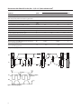
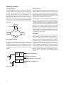
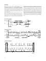
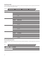
8 - VDD
1 - SDA
7 - SCL
2 - INT
6 - GND
3 - LDR
5 - LED A
4 - LED K
Functional Block Diagram
VDD
Interrupt
INT
Upper Threshold
ALS
ADC
Data
SCL
Lower Threshold
I2C Interface
Ch0
Ch1
Upper Threshold
Prox
Detect
ADC
LED A
SDA
Data
Lower Threshold
Prox IR
LED
LED K
LED Regulated
Constant Current
Sink
Control
Logic
LDR
GND
Detailed Description
The APDS-9900/9901 light-to-digital device provides
on-chip Ch0 and Ch1 diodes, integrating amplifiers,
ADCs, accumulators, clocks, buffers, comparators, a state
machine and an I2C interface. Each device combines one
Ch0 photodiode (visible plus infrared) and one Ch1 infrared-responding (IR) photodiode. Two integrating ADCs simultaneously convert the amplified photodiode currents
to a digital value providing up to 16-bits of resolution.
Upon completion of the conversion cycle, the conversion
result is transferred to the Ch0 and CH1 data registers. This
digital output can be read by a microprocessor where the
illuminance (ambient light level) in Lux is derived using an
empirical formula to approximate the human eye response.
Communication to the device is accomplished through a
fast (up to 400 kHz), two-wire I2C serial bus for easy connection to a microcontroller or embedded controller. The
digital output of the APDS-9900/9901 device is inherently more immune to noise when compared to an analog
interface.
The APDS-9900/9901 provides a separate pin for level-style
interrupts. When interrupts are enabled and a pre-set
value is exceeded, the interrupt pin is asserted and
remains asserted until cleared by the controlling firmware.
2
The interrupt feature simplifies and improves system
efficiency by eliminating the need to poll a sensor for a
light intensity or proximity value. An interrupt is generated
when the value of an ALS or proximity conversion exceeds
either an upper or lower threshold. Additionally, a programmable interrupt persistence feature allows the user
to determine how many consecutive exceeded thresholds
are necessary to trigger an interrupt. Interrupt thresholds
and persistence settings are configured independently for
both ALS and proximity.
Proximity detection is fully provided with an 850 nm IR
LED. An internal LED driver (LDR) pin, is jumper connected
to the LED cathode (LED K) to provide a factory calibrated
proximity of 100 +/- 20 mm. This is accomplished with a
proprietary current calibration technique that accounts
for all variances in silicon, optics, package and most importantly IR LED output power. This will eliminate or greatly
reduce the need for factory calibration that is required for
most discrete proximity sensor solutions. While the APDS9900/9901 is factory calibrated at a given pulse count,
the number of proximity LED pulses can be programmed
from 1 to 255 pulses, which will allow greater proximity
distances to be achieved. Each pulse has a 16 µs period.
I/O Pins Configuration
PIN
NAME
TYPE
DESCRIPTION
1
SDA
I/O
I2C serial data I/O terminal – serial data I/O for I2C.
2
INT
O
Interrupt – open drain.
3
LDR
I
LED driver for proximity emitter – up to 100 mA, open drain.
4
LEDK
O
LED Cathode, connect to LDR pin in most systems to use internal LED driver circuit
5
LEDA
I
LED Anode, connect to VBATT on PCB
6
GND
7
SCL
8
VDD
Power supply ground. All voltages are referenced to GND.
I
I2C serial clock input terminal – clock signal for I2C serial data.
Power Supply voltage.
Absolute Maximum Ratings over operating free-air temperature range (unless otherwise noted)†
Parameter
Symbol
Power Supply voltage
VDD
Digital voltage range
Min
Max
Units
Test Conditions
3.8
V
[1]
-0.5
3.8
V
Digital output current
IO
-1
20
mA
Storage temperature range
Tstg
-40
85
°C
†
Stresses beyond those listed under “absolute maximum ratings” may cause permanent damage to the device. These are stress ratings only and
functional operation of the device at these or any other conditions beyond those indicated under “recommended operating conditions” is not
implied. Exposure to absolute-maximum-rated conditions for extended periods may affect device reliability.
Note:
1. All voltages are with respect to GND.
Recommended Operating Conditions
Parameter
Symbol
Min
Operating Ambient Temperature
TA
-30
Supply voltage
VDD
2.5
Supply Voltage Accuracy, VDD
total error including transients
LED Supply Voltage
VBATT
Available Options
Part Number
Interface Description
APDS-9901
I2C VBUS = VDD Interface
APDS-9900
I2C 1.8V VBUS Interface
3
Typ
3.0
Max
Units
85
°C
3.6
V
-3
+3
%
2.5
4.5
V
Operating Characteristics, VDD = 3 V, TA = 25° C (unless otherwise noted)
Parameter
Symbol
Supply current [1]
IDD
Min
Typ
Max
Units
Test Conditions
175
250
µA
Active (ATIME=0xdb, 100ms)
70
Wait Mode
2.5
INT SDA output low voltage
VOL
Leakage current, SDA, SCL, INT pins
ILEAK
Leakage current, LDR pin
ILEAK
SCL, SDA input high voltage
VIH
SCL, SDA input low voltage,
VIL
Oscillator frequency
fosc
4.0
Sleep Mode
0
0.4
0
0.6
-5
5
µA
10
µA
0.7 VBUS
1.25
0.3 VBUS
0.54
705
750
795
V
3 mA sink current
6 mA sink current
V
APDS-9901
APDS-9900
V
APDS-9901
APDS-9900
kHz
PON = 1
Note:
1. The power consumption is raised by the programmed amount of Proximity LED Drive during the 8 us the LED pulse is on. The nominal and
maximum values are shown under Proximity Characteristics. There the IDD supply current is IDD Active + Proximity LED Drive programmed value.
ALS Characteristics, VDD = 3 V, TA = 25° C, Gain = 16, AEN = 1 (unless otherwise noted)
Parameter
Channel
Min
Typ
Max
Units
Test Conditions
Dark ALS ADC count value
Ch0
0
1
5
counts
Ee = 0, AGAIN = 120x,
ATIME = 0xDB(100ms)
Ch1
0
1
5
2.58
2.72
2.90
ms
ATIME = 0xff
256
steps
Full Scale ADC Counts per Step
1023
counts
Full scale ADC count value
65535
counts
ATIME = 0xC0
6000
counts
λp = 640 nm, Ee = 56 µW/cm2,
ATIME = 0xF6 (27 ms), GAIN = 16x
ALS ADC Integration Time
Step Size
ALS ADC Number of
Integration Steps
ALS ADC count value
1
Ch0
4000
5000
4000
5000
Ch1
Ch0
790
Ch1
ALS ADC count value ratio:
Ch1/Ch0
Irradiance Responsivity:
Re
Gain scaling, relative to
1x gain setting
λp = 850 nm, Ee = 79 µW/cm2,
ATIME = 0xF6 (27 ms), GAIN = 16x
6000
2800
10.8
15.8
20.8
41
56
68
Ch0
29.1
Ch1
4.6
Ch0
22.8
Ch1
12.7
%
λp = 640 nm, ATIME = 0xF6 (27 ms)
λp = 850 nm, ATIME = 0xF6 (27 ms)
Counts per
(µW/ cm2)
λp = 640 nm, ATIME = 0xF6 (27 ms)
λp = 850 nm, ATIME = 0xF6 (27 ms)
-5
5
%
8x
-5
5
16x
-5
5
120x
Notes:
1. Optical measurements are made using small-angle incident radiation from light-emitting diode optical sources. Visible 640 nm LEDs and infrared
850 nm LEDs are used for final product testing for compatibility with high-volume production.
2. The 640 nm irradiance Ee is supplied by an AlInGaP light-emitting diode with the following characteristics: peak wavelength = 640 nm and spectral
halfwidth ½ = 17 nm.
3. The 850 nm irradiance Ee is supplied by a GaAs light-emitting diode with the following characteristics: peak wavelength = 850 nm and spectral
halfwidth ½ = 40 nm.
4. The specified light intensity is 100% modulated by the pulse output of the device so that during the pulse output low time, the light intensity is at
the specified level, and zero otherwise.
4
Proximity Characteristics, VDD = 3 V, TA = 25° C, PGAIN = 1, PEN = 1 (unless otherwise noted)
Parameter
Min
Typ
Max
Units
Test Conditions
IDD Supply current – LDR Pulse On
3
mA
ADC Conversion Time Step Size
2.72
ms
PTIME = 0xff
steps
PTIME = 0xff
1023
counts
PTIME = 0xff
255
pulses
ADC Number of Integration Steps
1
Full Scale ADC Counts
Proximity IR LED Pulse Count
0
16.3
µs
Proximity Pulse – LED On Time
7.2
µs
Proximity LED Drive
100
mA
Proximity Pulse Period
Proximity ADC count value, no object
Proximity ADC count value,
100 mm distance object
PDRIVE = 0
50
PDRIVE = 1
25
PDRIVE = 2
12.5
PDRIVE = 3
100
LED driving 8 pulses, PDRIVE = 0, open view
(no glass) and no reflective object above the
module.
416
520
624
counts
Reflecting object – 73 mm x 83 mm Kodak
90% grey card, 100mm distance, LED driving
8 pulses, PDRIVE = 0, open view (no glass)
above the module.
Min
Typ
Max
Units
Test Conditions
1.4
1.5
IR LED Characteristics, VDD = 3 V, TA = 25C
Parameter
Forward Voltage, VF
V
IF = 20 mA
Reverse Voltage, VR
5.0
V
IR = 10 µA
Radiant Power, PO
4.5
mW
IF = 20 mA
Peak Wavelength, λP
850
nm
IF = 20 mA
Spectrum Width, Half Power, Δλ
40
nm
IF = 20 mA
Optical Rise Time, TR
20
ns
IFP = 100 mA
Optical Fall Time, TF
20
ns
IFP = 100 mA
Wait Characteristics, VDD = 3 V, TA = 25° C, Gain = 16, WEN = 1 (unless otherwise noted)
Parameter
Min
Wait Step Size
Wait Number of Step
5
ISINK Sink current @ 600 mV,
LDR Pin
Typ
Max
2.72
1
256
Units
Test Conditions
ms
WTIME = 0xff
steps
Characteristics of the SDA and SCL bus lines, VDD = 3 V, TA = 25° C (unless otherwise noted)†
STANDARD-MODE
Parameter
Symbol
SCL clock frequency
fSCL
Hold time (repeated) START condition.
After this period, the first clock pulse is generated
FAST-MODE
Min.
Max.
Min.
Max.
Units
0
100
0
400
kHz
tHD;STA
4.0
–
0.6
–
µs
LOW period of the SCL clock
tLOW
4.7
–
1.3
–
µs
HIGH period of the SCL clock
tHIGH
4.0
–
0.6
–
µs
Set-up time for a repeated START condition
tSU;STA
4.7
–
0.6
–
µs
Data hold time
tHD;DAT
0
–
0
–
ns
Data set-up time
tSU;DAT
250
–
100
–
ns
Rise time of both SDA and SCL signals
tr
20
1000
20
300
ns
Fall time of both SDA and SCL signals
tf
20
300
20
300
ns
Set-up time for STOP condition
tSU;STO
4.0
–
0.6
–
µs
Bus free time between a STOP and START condition
tBUF
4.7
–
1.3
–
µs
Capacitive load for each bus line
Cb
–
400
–
400
pF
Noise margin at the LOW level for each connected
device (including hysteresis)
VnL
0.1VBUS
–
0.1VBUS
–
V
Noise margin at the HIGH level for each connected
device (including hysteresis)
VnH
0.2VBUS
–
0.2VBUS
–
V
†
Specified by design and characterization; not production tested.
SDA
tLOW
tf
tf
tSU;DAT
tr
tHD;STA
tSP
tr
tBUF
SCL
S
tHD;STA
SCL
SDA
Figure 1. I2C Bus Timing Diagram
6
tHD;DAT
tHIGH
tSU;STA
Sr
tSU;STO
P
S
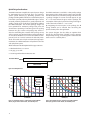
MSC610
9000
8000
1.0
7000
Ch 0
0.8
Avg Sensor LUX
NORMALIZED RESPONSITIVITY
1.2
0.6
0.4
Ch 1
5000
4000
3000
2000
0.2
1000
0.0
300
400
500
600
700
800
WAVELENGTH (nm)
900
1000
0
1100
1000
2000
3000
4000 5000
Meter LUX
6000
7000
8000
0.1
1600
1400
0.08
Avg Sensor LUX
1200
1000
800
600
400
0.06
0.04
0.02
200
0
0
Figure 3a. ALS Sensor LUX vs. Meter LUX using Fluorescent Light
Figure 2. Spectral Response
Avg Sensor LUX
6000
0
300
600
900
Meter LUX
1200
0
1500
Figure 3b. ALS Sensor LUX vs. Meter LUX using Incandescent Light
0
0.01 0.02 0.03 0.04 0.05 0.06 0.07 0.08 0.09
Meter LUX
0.1
Figure 3c. ALS Sensor LUX vs. Meter LUX using Low Lux Fluorescent Light
1.2
NORMALIZED IDD @ 3V
NORMALIZED IDD @ 3V 25°C
1.1
1.0
0.9
0.8
2.4
2.6
2.8
3
VDD (V)
3.2
3.4
3.6
3.8
NORMALIZED RESPONSITIVITY
Figure 4a. Normalized IDD vs. VDD
1.1
1.0
0.9
0.8
0.7
0.6
0.5
0.4
0.3
0.2
0.1
0.0
-100
-80
-60
-40
-20
0
20
ANGLE (DEG)
1.0
0.9
0.8
-60
-40
-20
0
20
40
TEMPERATURE (°C)
Figure 4b. Normalized IDD vs. Temperature
40
60
Figure 5. Normalized ALS Response vs. Angular Displacement
7
1.1
80
100
60
80
100
PRINCIPLES OF OPERATION
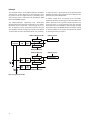
System State Machine
Ch0 and Ch1 Diodes
The APDS-9900/9901 provides control of ALS, proximity
detection and power management functionality through
an internal state machine. After a power-on-reset, the
device is in the sleep mode. As soon as the PON bit is set,
the device will move to the start state. It will then continue
through the Prox, Wait and ALS states. If these states are
enabled, the device will execute each function. If the PON
bit is set to a 0, the state machine will continue until all
conversions are completed and then go into a low power
sleep mode.
Conventional silicon detectors respond strongly to infrared
light, which the human eye does not see. This can lead to
significant error when the infrared content of the ambient
light is high (such as with incandescent lighting) due to
the difference between the silicon detector response and
the brightness perceived by the human eye.
Sleep
PON = 1 (rO:b0)
PON = 0 (rO:b0)
Start
Prox
ALS
ALS Operation
Wait
Figure 6. Simplified State Diagram
NOTE: In this document, the nomenclature uses the bit
field name in italics followed by the register number and
bit number to allow the user to easily identify the register
and bit that controls the function. For example, the power
on (PON) is in register 0, bit 0. This is represented as PON
(r0:b0).
Ch0
ADC
Ch0
ALS Control
Ch1
ADC
Ch1
Figure 7. ALS Operation
8
Ch0
Data
Ch1
Data
This problem is overcome in the APDS-9900/9901 through
the use of two photodiodes. One of the photodiodes,
referred to as the Ch0 channel, is sensitive to both visible
and infrared light while the second photodiode is sensitive
primarily to infrared light. Two integrating ADCs convert
the photodiode currents to digital outputs. The CH1DATA
digital value is used to compensate for the effect of the
infrared component of light on the CH0DATA digital value.
The ADC digital outputs from the two channels are used in
a formula to obtain a value that approximates the human
eye response in units of Lux.
The ALS engine contains ALS gain control (AGAIN) and
two integrating analog-to-digital converters (ADC) for
the Ch0 and Ch1 photodiodes. The ALS integration time
(ALSIT) impacts both the resolution and the sensitivity
of the ALS reading. Integration of both channels occurs
simultaneously and upon completion of the conversion
cycle, the results are transferred to the Ch0 and CH1 data
registers (CDATAx and IRDATAx). This data is also referred
to as channel “count”. The transfers are double-buffered
to ensure that invalid data is not read during the transfer.
After the transfer, the device automatically moves to
the next state in accordance with the configured state
machine.
CDATAH (r0 x 15), CDATAL (r0 x 14)
ATIME (r0 x 01), 0 x ff to 0 x 00
AGAIN (r0 x OF, b1:0), 1x, 8x, 16x, 120 x Gain
IRDATAH (r0 x 17), IRDATAL (r0 x 16)
The ALS Timing register value (ATIME) for programming the integration time (ALSIT) is a 2’s complement values. The ALS
Timing register value can be calculated as follows:
ATIME = 256 – ALSIT / 2.72 ms
Inversely, the integration time can be calculated from the register value as follows:
ALSIT = 2.72 ms * (256 – ATIME)
For example, if a 100 ms integration time is needed, the device needs to be programmed to:
ATIME = 256 – (100 / 2.72) = 256 – 37 = 219 = 0xDB
Conversely, the programmed value of 0xC0 would correspond to:
ALSIT = (256 – 0xC0) * 2.72 =64 * 2.72 = 172 ms.
Note: 2.72 ms can be estimated as 87 / 32. Multiply by 87 the shift by 5 bits.
Calculating ALS Lux
Definition:
CH0DATA = 256 * CDATAH (r0x15) + CDATAL (r0x14)
CH1DATA = 256 * IRDATAH (r0x17) + IRDATAL (r0x16)
IAC = IR Adjusted Count
LPC= Lux per Count
ALSIT = ALS Integration Time (ms)
AGAIN= ALS Gain
DF = Device Factor, DF = 52 for APDS-9900/9901
GA = Glass (or Lens) Attenuation Factor
B, C, D – Coefficients
Lux Equation:
IAC1= CH0DATA – B x CH1DATA
IAC2= C x CH0DATA – D x CH1DATA
IAC = Max (IAC1, IAC2, 0)
LPC = GA x DF / (ALSIT × AGAIN)
Lux = IAC x LPC
Coefficients in open air:
GA= 0.48
B = 2.23
C = 0.7
D = 1.42
Sample Lux Calculation in Open Air
Assume the following constants:
ALSIT = 400
AGAIN= 1
LPC= GA x DF / (ALSIT × AGAIN)
LPC= 0.48 x 52 / (400 x 1)
LPC= 0.06
Assume the following measurements:
CH0DATA = 5000
CH1DATA = 525
Then:
IAC1= 5000 – 2.23 x 525 = 3829
IAC2= 0.7 x 5000 – 1.42 x 525 = 2755
IAC = Max(3829, 2755, 0) = 3829
Lux:
Lux= IAC X LPC
Lux= 3829 X 0.06
Lux= 230
Note: please refer to application note for coefficient GA, B, C and D calculation with window.
9
Recommend ALS Operations
Proximity Detection
Proximity sensing uses an internal IR LED light source to
emit light which is then viewed by the integrated light
detector to measure the amount of reflected light when
an object is in the light path. The amount of light detected
from a reflected surface can then be used to determine an
object’s proximity to the sensor. The APDS-9900/9901 is
factory calibrated to meet the requirement of proximity
sensing of 100+/- 20 mm, thus eliminating the need for
factory calibration of the end equipment. When the APDS9900/9901 is placed behind a typical glass surface, the
proximity detection achieved is around 25 to 40 mm, thus
providing an ideal touch-screen disable.
10000
1000
50
LUX
100
, 1x
ms
x
10
1
s,
50 m
0.1
s
0m
0.01
40
1
10
100
6x
s, 1
s, 8
m
50
x
m
50
120
0x
, 12
1000
Counts
Figure 8. Gain and Integration Time to Lux without IR
10000
100000
With the programming versatility of the integration time
and gain, it can be difficult to understand when to use the
different modes. Figure 8 shows a log-log plot of the Lux
vs. integration time and gain with a spectral factor of unity
and no IR present.
The maximum illuminance which can be measured is
~10k Lux with no IR present. The intercept with a count
of 1 shows the resolution of each setting. The Lux values
in the table increase as the SF increases (spectral attenuation increases). For example, if a 10% transmissive glass
is used, the Lux values would all be multiplied by 10. The
Lux values in the table decrease as the IR Factor decreases.
For example, with a 10% IR Factor, which corresponds to
a strong incandescent light, the Lux value would need to
be divided by 10.
There are many factors that will impact the decision on
which value to use for integration time and gain. One of
the first factors is 50/60 Hz ripple rejection for fluorescent
lighting. The programmed value needs to be multiples
of 10/8.3 ms or the half cycle time. Both frequencies can
be rejected with a programmed value of 50 ms (ATIME =
0xED). With this value, the resolution will be 1.3 Lux per
count. If higher resolution is needed, a longer integration
time may be needed. In this case, the integration time
should be programmed in multiples of 50.
The light level is the next determining factor for configuring device settings. Under bright conditions, the count
will be fairly high. If a low light measurement is needed, a
higher gain and/or longer integration time will be needed.
As a general rule, it is recommended to have a Ch0 channel
count of at least 10 to accurately apply the Lux equation.
The digital accumulation is limited to 16 bits, which occurs
at an integration time of 173 ms. This is the maximum
recommended programmed integration time before
increasing the gain. (150 ms is the maximum to reduce the
fluorescent ripple.)
10
The APDS-9900/9901 has controls for the number of IR
pulses (PPCOUNT), the integration time (PTIME), the LED
drive current (PDRIVE) and the photodiode configuration
(PDIODE). At the end of the integration cycle, the results
are latched into the proximity data (PDATA) register.
The LED drive current is controlled by a regulated current
sink on the LDR pin. This feature eliminates the need to use
a current limiting resistor to control LED current. The LED
drive current can be configured for 12.5 mA, 25 mA, 50 mA,
or 100 mA. For higher LED drive requirements, an external
P type transistor can be used to control the LED current.
The number of LED pulses can be programmed to a value
of 1 to 255 pulses as needed. Increasing the number of
LED pulses at a given current will increase the sensor sensitivity. Sensitivity grows by the square root of the number
of pulses. Each pulse has a 16 mS period.
The proximity integration time (PTIME) is the period of
time that the internal ADC converts the analog signal
to a digital count. It is recommend that this be set to a
minimum of PTIME = 0xFF or 2.72 ms.
Add IR +
Background
LED On
Subtract
Background
LED Off
16 µs
IRLED Pulses
Figure 9. Proximity IR LED Waveform
Optical Design Considerations
The APDS-9900/9901 simplifies the optical system design
by eliminating the need for light pipes and improves
system optical efficiency by providing apertures and
package shielding which will reduce crosstalk when placed
in the final system. By reducing the IR LED to glass surface
crosstalk, proximity performance is greatly improved and
enables a wide range of cell phone applications utilizing
the APDS-9900/9901. The module package design has
been optimized for minimum package foot print and
short distance proximity of 100 mm typical. The spacing
between the glass surface and package top surface is
critical to controlling the crosstalk. If the package to top
surface spacing gap, window thickness and transmittance
are met, there should be no need to add additional components (such as a barrier) between the LED and photodiode. Thus with some simple mechanical design implementations, the APDS-9900/9901 will perform well in the
end equipment system.
The APDS-9900/9901 is available in a low profile package
that contains optics which provides optical gain on botht
the LED and the sensor side of the package. The device has
a package Z height of 1.35 mm and will support air gap
of < = 0.5 mm between the glass and the package. The
assumption of the optical system level design is that glass
surface above the module is < = to 1.0 mm.
By integrating the micro-optics in the package, the IR
energy emitted can be reduced thus conserving the
precious battery life in the application.
The system designer has the ability to optimize their
designs for slim form factor Z height as well as improve
the proximity sensing, save battery power and disable the
touch screen in a cellular phone.
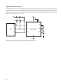
APDS-9900/9901 Module Optimized design parameters
• Window thickness, t ≤ 1.0 mm
• Air gap, g ≤ 0.5 mm
• Assuming window IR transmittance 90%
Plastic/Glass Window
Windows Thickness, t
Air Gap, g
APDS-9900/9901
Figure 10. Proximity Detection
1200
1200
6P (100mA)
1000
4P (100mA)
800
16P (100mA)
8P (50mA)
600
PS COUNT
PS COUNT
1000
8P (100mA)
800
400
200
0
600
400
200
0
2
4
6
8
10
DISTANCE (cm)
12
14
Figure 11a. PS Output vs. Distance, at Various Pulse number (LED drive
Current). No glass in front of the module, 18% Kodak Grey Card.
11
4P (100mA)
6P (100mA)
8P (100mA)
16P (100mA)
8P (50mA)
16
0
0
2
4
6
8
10
12
DISTANCE (cm)
14
16
18
Figure 11b. PS Output vs. Distance, at Various Pulse number (LED drive
Current). No glass in front of the module, 90% Kodak Grey Card.
20
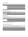
Interrupts
The interrupt feature of the APDS-9900/9901 simplifies
and improves system efficiency by eliminating the need
to poll the sensor for a light intensity or proximity value.
The interrupt mode is determined by the PIEN or AIEN
field in the ENABLE register.
The APDS-9900/9901 implements four 16-bit-wide
interrupt threshold registers that allow the user to define
thresholds above and below a desired light level. For
ALS, an interrupt can be generated when the ALS Ch0
data (CDATA) exceeds the upper threshold value (AIHTx)
or falls below the lower threshold (AILTx). For proximity,
Prox
Integration
Prox
ADC
an interrupt can be generated when the proximity data
(PDATA) exceeds the upper threshold value (PIHTx) or falls
below the lower threshold (PILTx).
To further control when an interrupt occurs, the APDS9900/9901 provides an interrupt persistence feature. This
feature allows the user to specify a number of conversion
cycles for which an event exceeding the ALS interrupt
threshold must persist (APERS) or the proximity interrupt
threshold must persist (PPERS) before actually generating
an interrupt. Refer to the register descriptions for details
on the length of the persistence.
PIHTH (r0 x OB), PIHTL (r0 x OA)
PPERS (r0 x OC, b7:4)
Upper Limit
Prox Persistence
Prox
Data
Lower Limit
PILTH (r09), PIHTL (r08)
Ch0
ADC
Ch0
AIHTH (r07), AIHTL (r06)
APERS (r0 x OC, b3:0)
Upper Limit
ALS Persistence
Ch0
Data
Lower Limit
Ch1
Ch1
ADC
Ch1
Data
AILTH (r05), AILTL (r04)
Figure 12. Programmable Interrupt
12
State Diagram
The following shows a more detailed flow for the state
machine. The device starts in the sleep mode. The PON
bit is written to enable the device. If the PEN bit is set,
the state machine will step through the proximity states
of proximity accumulate and then proximity ADC conversion. As soon as the conversion is complete, the state
machine will move to the following state.
When AEN bit is set, the state machine will step through
the ALS states of ALS accumulate and then ALS ADC conversion. In this case, a minimum of 1 integration time
step should be programmed. The ALS state machine will
continue until it reaches the terminal count at which
point the data will be latched in the ALS register and the
interrupt set, if enabled.
If the WEN bit is set, the state machine will then cycle
through the wait state. If the WLONG bit is set, the wait
cycles are extended by 12x over normal operation. When
the wait counter terminates, the state machine will step to
the ALS state.
Power Management
Up to 255 LED Pulses
Pulse Frequency: 60 kHz
Time: 16.3 µs – 4.2 ms
Maximum 4.2 ms
Power consumption can be controlled through the use
of the wait state timing since the wait state consumes
only 70 µA of power. The following shows an example
of using the power management feature to achieve an
average power consumption of 158 µA of current with
4 – 100 mA pulses of proximity detection and 50 ms of ALS
detection.
Up to 255 steps
Step: 2.72 ms
Time: 2.72 ms – 696 ms
120 Hz Minimum – 8 ms
100 Hz Minimum – 10 ms
Sleep
PON = 1
PON = 0
Start
Prox
Accum
ALS
PEN = 1
Prox
Check
ALS
Check
Prox
ADC
AEN = 1
Wait
Check
Up to 255 steps
Step: 2.72 ms
Time: 2.72 ms – 696 ms
Recommened – 2.72 ms 1023 Counts
ALS
Delay
WEN = 1
WLONG = 0
Counts up to 256 steps
Step: 2.72 ms
Time: 2.72 ms – 696 ms
Minimum – 2.72 ms
Wait
WLONG = 1
Counts up to 256 steps
Step: 32.64 ms
Time: 32.64 ms – 8.35 s
Minimum – 32.64 ms
Figure 13. Extended State Diagram
4 IRLED Pulses
Prox Accum
Prox ADC
WAIT
ALS
64 µs (32 µs LED On Time)
2.72 ms
47 ms
50 ms
Example: 100 ms Cycle Time
State
Duration (ms)
Prox Accum (LED On)
0.064 (0.032)
Prox ADC
2.72
WAIT
47
ALS
50
Current (mA)
100
0.175
0.070
0.175
Avg = ((0.032 x 100) + (2.72 x 0.175) + (47 x 0.070) + (50 x 0.175)) ÷ 100 = 158 µA
Figure 14. Power Consumption Calculations
13
Basic Software Operation
The following pseudo-code shows how to do basic initialization of the APDS-9900/9901.
uint8 ATIME, PIME, WTIME, PPCOUNT;
ATIME = 0xff; // 2.7 ms – minimum ALS integration time
WTIME = 0xff; // 2.7 ms – minimum Wait time
PTIME = 0xff; // 2.7 ms – minimum Prox integration time
PPCOUNT = 1; // Minimum prox pulse count
WriteRegData(0, 0); //Disable and Powerdown
WriteRegData (1, ATIME);
WriteRegData (2, PTIME);
WriteRegData (3, WTIME);
WriteRegData (0xe, PPCOUNT);
uint8 PDRIVE, PDIODE, PGAIN, AGAIN;
PDRIVE = 0; //100mA of LED Power
PDIODE = 0x20; // CH1 Diode
PGAIN = 0; //1x Prox gain
AGAIN = 0; //1x ALS gain
WriteRegData (0xf, PDRIVE | PDIODE | PGAIN | AGAIN);
uint8 WEN, PEN, AEN, PON;
WEN = 8; // Enable Wait
PEN = 4; // Enable Prox
AEN = 2; // Enable ALS
PON = 1; // Enable Power On
WriteRegData (0, WEN | PEN | AEN | PON); // WriteRegData(0,0x0f );
Wait(12); //Wait for 12 ms
int CH0_data, CH1_data, Prox_data;
CH0_data = Read_Word(0x14);
CH1_data = Read_Word(0x16);
Prox_data = Read_Word(0x18);
WriteRegData(uint8 reg, uint8 data)
{
m_I2CBus.WriteI2C(0x39, 0x80 | reg, 1, &data);
}
uint16 Read_Word(uint8 reg);
{
uint8 barr[2];
m_I2CBus.ReadI2C(0x39, 0xA0 | reg, 2, ref barr);
return (uint16)(barr[0] + 256 * barr[1]);
}
14
I2C Protocol
written is the command byte followed by reading a series
of bytes. If a read command is issued, the register address
from the previous command will be used for data access.
Likewise, if the MSB of the command is not set, the device
will write a series of bytes at the address stored in the last
valid command with a register address. The command
byte contains either control information or a 5 bit register
address. The control commands can also be used to clear
interrupts. For a complete description of I2C protocols,
please review the I2C Specification at: http://www.NXP.
com
Interface and control of the APDS-9900/9901 is accomplished through an I2C serial compatible interface
(standard or fast mode) to a set of registers that provide
access to device control functions and output data. The
device supports a single slave address of 0x39 hex using
7 bit addressing protocol. (Contact factory for other addressing options.)
The I2C standard provides for three types of bus transaction: read, write and a combined protocol. During a
write operation, the first byte written is a command byte
followed by data. In a combined protocol, the first byte
Start and Stop conditions
SDA
SCL
S
P
START condition
STOP condition
Data transfer on I2C-bus
P
SDA
MSB
SCL
S or Sr
1
acknowledgement
signal from slave
2
7
START or
repeated START
condition
8
MSB
MSB
1
9
ACK
byte complete,
interrupt within slave
2
3 to 8
9
ACK
acknowledgement
signal from receiver
1
2
3 to 8
clock line held LOW while
interrupts are serviced
A complete data transfer
SDA
SCL
1–7
8
9
1–7
8
9
1–7
8
9
P
S
START
condition
15
ADDRESS
R/W
ACK
DATA
ACK
DATA
ACK
STOP
condition
MBC604
9
ACK
Sr
Sr or P
STOP or
repeated START
condition
A
Acknowledge (0)
N
Not Acknowledged (1)
P
Stop Condition
R
Read (1)
S
Start Condition
Sr
Repeated Start Condition
W
Write (0)
…
Continuation of protocol
Master-to-Slave
Slave-to-Master
1
7
1
1
8
1
8
1
1
S
Slave Address
W
A
Command Code
A
Data
A
P
1
8
1
8
1
1
A
Data Low
A
Data High
A
P
I2C Write Protocol
1
7
S
Slave Address
1
1
8
1
1
W
A
Command Code
A
P
I2C Write Protocol (Clear Interrupt)
1
7
1
1
8
S
Slave Address
W
A
Command Code
I2C Write Word Protocol
1
7
1
1
8
1
1
7
1
1
8
1
1
S
Slave Address
W
A
Command Code
A
Sr
Slave Address
R
A
Data
N
P
I2C Read Protocol – Combined Format
1
7
1
1
8
1
1
7
1
1
8
1
S
Slave Address
W
A
Command Code
A
Sr
Slave Address
R
A
Data Low
A
I2C Read Word Protocol
16
8
1
1
Data High
N
P
Register Set
The APDS-9900/9901 is controlled and monitored by data registers and a command register accessed through the serial
interface. These registers provide for a variety of control functions and can be read to determine results of the ADC
conversions.
ADDRESS
RESISTER NAME
R/W
REGISTER FUNCTION
Reset Value
−
COMMAND
W
Specifies register address
0x00
0x00
ENABLE
R/W
Enable of states and interrupts
0x00
0x01
ATIME
R/W
ALS ADC time
0x00
0x02
PTIME
R/W
Proximity ADC time
0xFF
0x03
WTIME
R/W
Wait time
0xFF
0x04
AILTL
R/W
ALS interrupt low threshold low byte
0x00
0x05
AILTH
R/W
ALS interrupt low threshold hi byte
0x00
0x06
AIHTL
R/W
ALS interrupt hi threshold low byte
0x00
0x07
AIHTL
R/W
ALS interrupt hi threshold hi byte
0x00
0x08
PILTL
R/W
Proximity interrupt low threshold low byte
0x00
0x09
PILTH
R/W
Proximity interrupt low threshold hi byte
0x00
0x0A
PIHTL
R/W
Proximity interrupt hi threshold low byte
0x00
0x0B
PIHTH
R/W
Proximity interrupt hi threshold hi byte
0x00
0x0C
PERS
R/W
Interrupt persistence filters
0x00
0x0D
CONFIG
R/W
Configuration
0x00
0x0E
PPCOUNT
R/W
Proximity pulse count
0x00
0x0F
CONTROL
R/W
Gain control register
0x00
0x11
REV
R
Revision Number
Rev
0x12
ID
R
Device ID
ID
0x13
STATUS
R
Device status
0x00
0x14
CDATAL
R
Ch0 ADC low data register
0x00
0x15
CDATAH
R
Ch0 ADC high data register
0x00
0x16
IRDATAL
R
Ch1 ADC low data register
0x00
0x17
IRDATAH
R
Ch1 ADC high data register
0x00
0x18
PDATAL
R
Proximity ADC low data register
0x00
0x19
PDATAH
R
Proximity ADC high data register
0x00
The mechanics of accessing a specific register depends on the specific protocol used. See the section on I2C protocols
on the previous pages. In general, the COMMAND register is written first to specify the specific control/status register
for following read/write operations.
17
Command Register
The command registers specifies the address of the target register for future write and read operations.
7
COMMAND
6
CMD
5
4
3
TYPE
2
1
0
ADD
–
FIELD
BITS
DESCRIPTION
COMMAND
7
Select Command Register. Must write as 1 when addressing COMMAND register.
TYPE
6:5
Selects type of transaction to follow in subsequent data transfers:
FIELD VALUE
INTEGRATION TIME
00
Repeated Byte protocol transaction
01
Auto-Increment protocol transaction
10
Reserved – Do not use
11
Special function – See description below
Byte protocol will repeatedly read the same register with each data access.
Block protocol will provide auto-increment function to read successive bytes.
ADD
4:0
Address register/special function register. Depending on the transaction type, see above, this field
either specifies a special function command or selects the specific control-status-register for
following write or read transactions:
FIELD VALUE
READ VALUE
00000
Normal – no action
00101
Proximity interrupt clear
00110
ALS interrupt clear
00111
Proximity and ALS interrupt clear
other
Reserved – Do not write
ALS/Proximity Interrupt Clear. Clears any pending ALS/Proximity interrupt. This special function is
self clearing.
Enable Register (0x00)
The ENABLE register is used primarily to power the APDS-9900/9901 device up and down as shown in Table 4.
ENABLE
7
6
5
4
3
2
1
0
Address
Reserved
Reserved
PIEN
AIEN
WEN
PEN
AEN
PON
0x00
FIELD
BITS
DESCRIPTION
Reserved
7:6
Reserved. Write as 0.
PIEN
5
Proximity Interrupt Enable. When asserted, permits proximity interrupts to be generated.
AIEN
4
ALS Interrupt Enable. When asserted, permits ALS interrupt to be generated.
WEN
3
Wait Enable. This bit activates the wait feature. Writing a 1 activates the wait timer.
Writing a 0 disables the wait timer.
PEN
2
Proximity Enable. This bit activates the proximity function. Writing a 1 enables proximity.
Writing a 0 disables proximity.
AEN
1
ALS Enable. This bit actives the two channel ADC. Writing a 1 activates the ADC.
Writing a 0 disables the ADC.
PON
0
Power ON. This bit activates the internal oscillator to permit the timers and ADC channels to operate.
Writing a 1 activates the oscillator. Writing a 0 disables the oscillator.
Notes:
1. A 2.72 ms delay is automatically inserted prior to entering the ADC cycle, independent of the WEN bit.
2. Both AEN and PON must be asserted before the ADC channels will operate correctly.
3. During writes and reads over the I2C interface, this bit is overridden and the oscillator is enabled, independent of the state of PON.
4. A minimum interval of 2.72 ms must pass after PON is asserted before either proximity or an ALS can be initiated. This required time is enforced by
the hardware in cases where the firmware does not provide it.
18
ALS Timing Register (0x01)
The ALS timing register controls the integration time of the ALS Ch0 and Ch1 channel ADCs in 2.72 ms increments.
FIELD
BITS
DESCRIPTION
ATIME
7:0
VALUE
CYCLES
TIME (ALSIT)
Max Count
0xff
1
2.72 ms
1023
0xf6
10
27.2 ms
10239
0xdb
37
100.64 ms
37887
0xc0
64
174.08 ms
65535
0x00
256
696.32 ms
65535
Proximity Time Control Register (0x02)
The proximity timing register controls the integration time of the proximity ADC in 2.72 ms increments. It is recommended
that this register be programmed to a value of 0xff (1 cycle, 1023 bits).
FIELD
BITS
DESCRIPTION
PTIME
7:0
VALUE
CYCLES
TIME
Max Count
0xff
1
2.72 ms
1023
Wait Time Register (0x03)
Wait time is set 2.72 ms increments unless the WLONG bit is asserted in which case the wait times are 12x longer. WTIME
is programmed as a 2’s complement number.
FIELD
BITS
DESCRIPTION
WTIME
7:0
REGISTER VALUE
WALL TIME
TIME (WLONG = 0)
TIME (WLONG = 1)
0xff
1
2.72 ms
0.032 sec
0xb6
74
201.29 ms
2.37 sec
0x00
256
696.32 ms
8.19 sec
Notes:
1. The Write Byte protocol cannot be used when WTIME is greater than 127.
2. The Proximity Wait Time Register should be configured before PEN and/or AEN is/are asserted.
ALS Interrupt Threshold Register (0x04 − 0x07)
The ALS interrupt threshold registers provides the values to be used as the high and low trigger points for the comparison function for interrupt generation. If the value generated by the ALS channel crosses below the low threshold
specified, or above the higher threshold, an interrupt is asserted on the interrupt pin.
REGISTER
ADDRESS
BITS
DESCRIPTION
AILTL
0x04
7:0
ALS Ch0 channel low threshold lower byte
AILTH
0x05
7:0
ALS Ch0 channel low threshold upper byte
AIHTL
0x06
7:0
ALS Ch0 channel high threshold lower byte
AIHTH
0x07
7:0
ALS Ch0 channel high threshold upper byte
Note: The Write Word protocol should be used to write byte-paired registers.
19
Proximity Interrupt Threshold Register (0x08 − 0x0B)
The proximity interrupt threshold registers provide the values to be used as the high and low trigger points for the comparison function for interrupt generation. If the value generated by proximity channel crosses below the lower threshold
specified, or above the higher threshold, an interrupt is signaled to the host processor.
REGISTER
ADDRESS
BITS
DESCRIPTION
PILTL
0x08
7:0
Proximity ADC channel low threshold lower byte
PILTH
0x09
7:0
Proximity ADC channel low threshold upper byte
PIHTL
0x0A
7:0
Proximity ADC channel high threshold lower byte
PIHTH
0x0B
7:0
Proximity ADC channel high threshold upper byte
Persistence Register (0x0C)
The persistence register controls the filtering interrupt capabilities of the device. Configurable filtering is provided to
allow interrupts to be generated after each ADC integration cycle or if the ADC integration has produced a result that
is outside of the values specified by threshold register for some specified amount of time. Separate filtering is provided
for proximity and ALS functions.
ALS interrupts are generated by looking only at the ADC integration results of channel 0.
7
6
PERS
5
4
3
PPERS
2
1
0
APERS
0x0c
FIELD
BITS
DESCRIPTION
PPERS
7:4
Proximity interrupt persistence. Controls rate of proximity interrupt to the host processor.
APERS
20
3:0
FIELD VALUE
MEANING
INTERRUPT PERSISTENCE FUNCTION
0000
Every
Every proximity cycle generates an interrupt
0001
1
1 consecutive proximity values out of range
…
…
…
1111
15
15 consecutive proximity values out of range
Interrupt persistence. Controls rate of interrupt to the host processor.
FIELD VALUE
MEANING
INTERRUPT PERSISTENCE FUNCTION
0000
Every
Every ALS cycle generates an interrupt
0001
1
1 consecutive Ch0 channel values out of range
0010
2
2 consecutive Ch0 channel values out of range
0011
3
3 consecutive Ch0 channel values out of range
0100
5
5 consecutive Ch0 channel values out of range
0101
10
10 consecutive Ch0 channel values out of range
0110
15
15 consecutive Ch0 channel values out of range
0111
20
20 consecutive Ch0 channel values out of range
1000
25
25 consecutive Ch0 channel values out of range
1001
30
30 consecutive Ch0 channel values out of range
1010
35
35 consecutive Ch0 channel values out of range
1011
40
40 consecutive Ch0 channel values out of range
1100
45
45 consecutive Ch0 channel values out of range
1101
50
50 consecutive Ch0 channel values out of range
1110
55
55 consecutive Ch0 channel values out of range
1111
60
60 consecutive Ch0 channel values out of range
Configuration Register (0x0D)
The configuration register sets the wait long time.
7
6
5
CONFIG
4
3
2
Reserved
1
0
WLONG
Reserved
0x0D
FIELD
BITS
DESCRIPTION
Reserved
7:2
Reserved. Write as 0.
WLONG
1
Wait Long. When asserted, the wait cycles are increased by a factor 12x from that programmed in
the WTIME register.
Reserved
0
Reserved. Write as 0.
Proximity Pulse Count Register (0x0E)
The proximity pulse count register sets the number of proximity pulses that will be transmitted. When proximity
detection is enabled, a proximity detect cycle occurs after each ALS cycle. PPCOUNT defines the number of pulses to be
transmitted at a 62.5 kHz rate.
7
6
PPCOUNT
5
4
3
2
1
0
PPCOUNT
FIELD
BITS
DESCRIPTION
PPCOUNT
7:0
Proximity Pulse Count. Specifies the number of proximity pulses to be generated.
21
0x0E
Control Register (0x0F)
The Gain register provides eight bits of miscellaneous control to the analog block. These bits typically control functions
such as gain settings and/or diode selection.
7
CONTROL
6
5
PDRIVE
4
PDIODE
FIELD
BITS
DESCRIPTION
PDRIVE
7:6
LED Drive Strength.
PDIODE
PGAIN
AGAIN
5:4
3:2
1:0
3
2
1
PGAIN
FIELD VALUE
LED STRENGTH
00
100 mA
01
50 mA
10
25 mA
11
12.5 mA
0
AGAIN
0x0F
Proximity Diode Select.
FIELD VALUE
DIODE SELECTION
00
Reserved
01
Reserved
10
Proximity uses the Ch1 diode
11
Reserved
Proximity Gain Control.
FIELD VALUE
Proximity GAIN VALUE
00
1X Gain
01
Reserved
10
Reserved
11
Reserved
ALS Gain Control.
FIELD VALUE
ALS GAIN VALUE
00
1X Gain
01
8X Gain
10
16X Gain
11
120X Gain
Revision number Register (0x11)
The Revision number register provides the silicon revision number. The Rev ID is a read-only register whose value never
changes.
7
6
5
4
REV
ID
FIELD
BITS
DESCRIPTION
REV
7:0
Revision number identification
0x01
22
3
2
1
0
0x11
Device ID Register (0x12)
The ID register provides the value for the part number. The ID register is a read-only register.
7
6
5
4
ID
3
2
1
0
Device ID
FIELD
BITS
DESCRIPTION
ID
7:0
Part number identification
0x12
0x29 = APDS-9900
0x20 = APDS-9901
Status Register (0x13)
The Status Register provides the internal status of the device. This register is read only.
STATUS
7
6
5
4
3
2
1
0
Reserved
Reserved
PINT
AINT
Reserved
Reserved
PVALID
AVALID
0x13
FIELD
BITS
DESCRIPTION
Reserved
7:6
Reserved. Write as 0.
PINT
5
Proximity Interrupt. Indicates that the device is asserting a proximity interrupt.
AINT
4
ALS Interrupt. Indicates that the device is asserting an ALS interrupt.
Reserved
3:2
Reserved. Write as 0.
PVALID
1
PS Valid. Indicates that the PS has completed an integration cycle.
AVALID
0
ALS Valid. Indicates that the ALS Ch0/Ch1 channels have completed an integration cycle.
ALS Data Registers (0x14 − 0x17)
ALS Ch0 and CH1 data are stored as two 16-bit values. To ensure the data is read correctly, a two byte read I2C transaction
should be utilized with a read word protocol bit set in the command register. With this operation, when the lower byte
register is read, the upper eight bits are stored into a shadow register, which is read by a subsequent read to the upper
byte. The upper register will read the correct value even if additional ADC integration cycles end between the reading
of the lower and upper registers.
REGISTER
ADDRESS
BITS
DESCRIPTION
CDATA
0x14
7:0
ALS Ch0 channel data low byte
CDATAH
0x15
7:0
ALS Ch0 channel data high byte
IRDATA
0x16
7:0
ALS Ch1 channel data low byte
IRDATAH
0x17
7:0
ALS Ch1 channel data high byte
Proximity DATA Register (0x18 − 0x19)
Proximity data is stored as a 16-bit value. To ensure the data is read correctly, a two byte read I2C transaction should be
utilized with a read word protocol bit set in the command register. With this operation, when the lower byte register is
read, the upper eight bits are stored into a shadow register, which is read by a subsequent read to the upper byte. The
upper register will read the correct value even if additional ADC integration cycles end between the reading of the lower
and upper registers.
REGISTER
ADDRESS
BITS
DESCRIPTION
PDATA
0x18
7:0
Proximity data low byte
PDATAH
0x19
7:0
Proximity data high byte
23
Application Information: Hardware
The application hardware circuit for using implementing an ALS and Proximity system solution is quite simple with the
APDS-9900/9901 and is shown in following figure. The 1 µF decoupling capacitors should be low ESR to reduce noise.
It further recommended to maximize system performance the use of power and ground planes is recommended in the
PCB. If mounted on a flexible circuit, the power and ground traces back to the PCB should be sufficiently wide enough
to have a low resistance, such as < 1 ohm.
VBUS
VDD
1 µF
10 kΩ
10 kΩ
10 kΩ
VDD
MCU
GPIO
INT
SCL
SCL
LDR
APDS-9900/9901
LED K
VBATT
SDA
LED A
SDA
GND
Figure 15. Circuit implementation for ALS plus Proximity solution using the APDS-9900/9901
24
1 µF
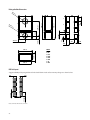
Package Outline Dimensions
1
8
7
2
2
7
6
3
3
6
5
4
4
5
±0
.05
0.25 (x6)
1.35 ±0.20
2.36 ±0.2
2.10 ±0.1
0.05
0.58 ±0.05
1.18 ±0.05
0.80
0.60
PINOUT
1 - SDA
2 - INT
3 - LDR
4 - LEDK
5 - LEDA
6 - GND
7 - SCL
8 - VDD
PCB Pad Layout
Suggested PCB pad layout guidelines for the Dual Flat No-Lead surface mount package are shown below.
0.60
0.80
0.72 (x8)
0.25 (x6)
0.60
Notes: all linear dimensions are in mm.
25
0.72 (x8)
1
3.73 ±0.1
8
1.34
.90
.05
3.94 ±0.2
Ø0
±0
2.40 ±0.05
Ø1
0.05
±0
.10
4 ±0.10
0.29 ±0.02
B0
Ø1
Unit Orientation
.05
A
8 ±0.10
2.70 ±0.10
8° Max
A0
All dimensions unit: mm
Reel Dimensions
26
1.70 ±0.10
±0
A
5.50 ±0.05
12 +0.30
-0.10
4.30 ±0.10
Ø1
. 50
2 ±0.05
1.75 ±0.10
Tape Dimensions
K0
6° Max
Moisture Proof Packaging
All APDS-9900/9901 options are shipped in moisture proof package. Once opened, moisture absorption begins. This
part is compliant to JEDEC MSL 3.
Units in A Sealed
Mositure-Proof
Package
Package Is
Opened (Unsealed)
Environment
less than 30 deg C, and
less than 60% RH?
Yes
Yes
No Baking
Is Necessary
Package Is
Opened less
than 168 hours?
No
Perform Recommended
Baking Conditions
Baking Conditions:
No
Recommended Storage Conditions:
Package
Temperature
Time
Storage Temperature
10° C to 30° C
In Reel
60° C
48 hours
Relative Humidity
below 60% RH
In Bulk
100° C
4 hours
Time from unsealing to soldering:
If the parts are not stored in dry conditions, they must be
baked before reflow to prevent damage to the parts.
Baking should only be done once.
27
After removal from the bag, the parts should be soldered
within 168 hours if stored at the recommended storage
conditions. If times longer than 168 hours are needed, the
parts must be stored in a dry box
Recommended Reflow Profile
MAX 260° C
R3
R4
TEMPERATURE (°C)
255
230
217
200
180
150
120
R2
60 sec to 120 sec
Above 217° C
R1
R5
80
25
0
P1
HEAT UP
Process Zone
Heat Up
Solder Paste Dry
50
100
150
P2
SOLDER PASTE DRY
Symbol
P1, R1
P2, R2
P3, R3
Solder Reflow
P3, R4
Cool Down
P4, R5
Time maintained above liquidus point , 217° C
Peak Temperature
Time within 5° C of actual Peak Temperature
Time 25° C to Peak Temperature
200
P3
SOLDER
REFLOW
250
P4
COOL
DOWN
300
t-TIME
(SECONDS)
∆T
Maximum ∆T/∆time
or Duration
25° C to 150° C
150° C to 200° C
200° C to 260° C
260° C to 200° C
200° C to 25° C
> 217° C
260° C
> 255° C
25° C to 260° C
3° C/s
100 s to 180s
3° C/s
-6° C/s
-6° C/s
60 s to 120 s
–
20 s to 40 s
8 mins
The reflow profile is a straight-line representation of
a nominal temperature profile for a convective reflow
solder process. The temperature profile is divided into
four process zones, each with different ∆T/∆time temperature change rates or duration. The ∆T/∆time rates or
duration are detailed in the above table. The temperatures
are measured at the component to printed circuit board
connections.
In process zone P1, the PC board and component pins
are heated to a temperature of 150° C to activate the flux
in the solder paste. The temperature ramp up rate, R1, is
limited to 3° C per second to allow for even heating of
both the PC board and component pins.
Process zone P2 should be of sufficient time duration (100
to 180 seconds) to dry the solder paste. The temperature
is raised to a level just below the liquidus point of the
solder.
Process zone P3 is the solder reflow zone. In zone P3, the
temperature is quickly raised above the liquidus point of
solder to 260° C (500° F) for optimum results. The dwell
time above the liquidus point of solder should be between
60 and 120 seconds. This is to assure proper coalescing
of the solder paste into liquid solder and the formation
of good solder connections. Beyond the recommended
dwell time the intermetallic growth within the solder connections becomes excessive, resulting in the formation of
weak and unreliable connections. The temperature is then
rapidly reduced to a point below the solidus temperature
of the solder to allow the solder within the connections to
freeze solid.
Process zone P4 is the cool down after solder freeze. The
cool down rate, R5, from the liquidus point of the solder to
25° C (77° F) should not exceed 6° C per second maximum.
This limitation is necessary to allow the PC board and
component pins to change dimensions evenly, putting
minimal stresses on the component.
It is recommended to perform reflow soldering no more
than twice.
For product information and a complete list of distributors, please go to our web site: www.avagotech.com
Avago, Avago Technologies, and the A logo are trademarks of Avago Technologies in the United States and other countries.
Data subject to change. Copyright © 2005-2013 Avago Technologies. All rights reserved.
AV02-2867EN - June 4, 2013