1
EECS 452 – Lecture 5
Today:
FPGA / Cyclone II overview.
The Altera DE2-70 board.
Aspects of the Verilog/SystemVerilog HDLs
Information relevant to lab exercise three.
Yet more information.
References:
DE2-70 User Manual.
DE2-70 demonstrations, V10.
Altera Quartus II introductory course.
Verilog in One Day Tutorial.
Last one out should close the lab door!!!!
Please keep the lab clean and organized.
Design is where science and art break even. — Robin Mathew
EECS 452 – Fall 2014
Lecture 5 – Page 1/143
Tuesday – September 16, 2014
Lecture overview
▶ FPGA overview.
▶ Altera Cyclone II overview.
▶ The Terasic/Altera DE2-70 board.
▶ Altera’s Quartus II design software.
▶ Various aspects of Verilog/SystemVerilog.
▶ Code examples.
A significant part of learning is asking good questions. Or, in today’s world,
using well chosen search terms. For example, verilog tutorial or
verilog always block.
The links included in today’s lecture note are some of the ones that I came across
that I’ve found informative and useful. The ones shown in red are hot, click and
go. (However, not everything red is a link.)
My main goal today is to make you aware.
The links work today, but will they work tomorrow? — anon
EECS 452 – Fall 2014
Lecture 5 – Page 2/143
Tuesday – September 16, 2014
Free eBook
EECS 452 – Fall 2014
Lecture 5 – Page 3/143
Tuesday – September 16, 2014
Full Custom, ASIC, FPGA
Full Custom: design at the transistor level.
Application Specific Integrated Circuit: design using proved gate
libraries. Starting chip likely already has transistors on it.
Field Programmable Gate Arrary: interconnected configurable
logic blocks.
Ordered going down: decreasing cost, increasing ease to produce.
EECS 452 – Fall 2014
Lecture 5 – Page 4/143
Tuesday – September 16, 2014
What is a Field Programmable Gate Array (FPGA)?
From our viewpoint, (almost) unstructured logic that we can
sculpt (configure) to meet our needs.
In reality, a collection of small well defined logic blocks, a highly configurable
interconnection network and a carefully designed clock distribution network. Plus whatever other features that
a manufacturer might add to differentiate product.
http://en.wikipedia.org/wiki/Field-programmable_gate_array
EECS 452 – Fall 2014
Lecture 5 – Page 5/143
Tuesday – September 16, 2014
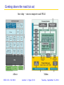
FPGA organization
Field Programmable Gate Array
(reconfigurable logic)
Not shown are off-fabric block RAM, multipliers, DSP blocks, PLL, etc.
From rfneulink.com.
EECS 452 – Fall 2014
Lecture 5 – Page 6/143
Tuesday – September 16, 2014
Routing makes all things possible
▶
First layers above
gates/transistors form
logic blocks or logic
elements.
▶
The next layers support
configuration of the
blocks.
▶
The higher layers are
programmable
interconnects.
▶
Equal delays from to
“the” clock to the gates
are all important,in the
chip design and in
design with the chip.
Intel. Not a FPGA but it illustrates the importance of routing.
EECS 452 – Fall 2014
Lecture 5 – Page 7/143
Tuesday – September 16, 2014
Coming down the road (at us)
One chip — microcomputer and FPGA!
Altera
EECS 452 – Fall 2014
Xilinx
Lecture 5 – Page 8/143
Tuesday – September 16, 2014
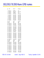
Cyclone II EP2C70 is used on the DE2-70
Table 1–1. Cyclone II FPGA Family Features (Part 1 of 2)
Feature
EP2C5 (2)
EP2C8 (2)
EP2C15 (1)
EP2C20 (2)
EP2C35
EP2C50
EP2C70
4,608
8,256
14,448
18,752
33,216
50,528
68,416
26
36
52
52
105
129
250
119,808
165,888
239,616
239,616
483,840
594,432
1,152,00
0
Embedded
multipliers (3)
13
18
26
26
35
86
150
PLLs
2
2
4
4
4
4
4
LEs
M4K RAM blocks (4
Kbits plus
512 parity bits
Total RAM bits
The DE2-70 uses the Cyclone II EP2C70 part in a 896 ball ball grid
array (BGA) package, speed grade 6 (fastest).
Documentation for the Cyclone II can be found at:
http://www.altera.com/literature/lit-cyc2.jsp
EECS 452 – Fall 2014
Lecture 5 – Page 9/143
Tuesday – September 16, 2014
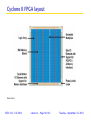
Cyclone II FPGA layout
From Altera.
EECS 452 – Fall 2014
Lecture 5 – Page 10/143
Tuesday – September 16, 2014
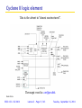
Cyclone II logic element
This is the almost in “almost unstructured”.
The magic word is: configurable.
From Altera.
EECS 452 – Fall 2014
Lecture 5 – Page 11/143
Tuesday – September 16, 2014
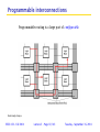
Programmable interconnections
Programmable routing is a large part of configurable.
From Google Images.
EECS 452 – Fall 2014
Lecture 5 – Page 12/143
Tuesday – September 16, 2014
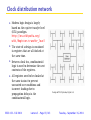
Clock distribution network
▶ Modern logic design is largely
based on the register transfer level
(RTL) paradigm.
http://en.wikipedia.org/
wiki/Register-transfer_level
▶ The state of a design is contained
in registers that are all clocked at
the same time.
▶ Between clock tics, combinatorial
logic is used to determine the next
contents of the registers.
▶ All registers need to be clocked at
the same instant to prevent
unwanted race conditions and
incorrect loading due to
propagation delays in the
combinatorial logic.
EECS 452 – Fall 2014
Lecture 5 – Page 13/143
Design of VLSI Systems, Figure 5.5.
Tuesday – September 16, 2014
DE2-70 RAM
The EP2C70 M4K blocks contain a total of 1,152,000 bits (144,000
bytes). Can’t necessarily use as one large block . . . routing
limitations.
Each LE contains a D-register that can be used as a one-bit
memory.
The Cyclone II does not support use of a LE’s LUT as memory.
Xilinx’s (but not Altera’s) LUTs support use as a 16 bit shift
register. A design making heavy use of bit-serial arithmetic likely
would choose a Xilinx FPGA over an Altera FPGA.
EECS 452 – Fall 2014
Lecture 5 – Page 14/143
Tuesday – September 16, 2014
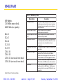
M4K RAM
Table 2–7. M4K Memory Modes
Memory Mode
Off-fabric.
250 MHz max clock.
4608 bits (inc. parity).
4K×1
2K×2
1K×4
512×8
512×9
256×16
256×18
128×32 (not avail. true dual)
128×36 (not avail. true dual)
Description
Single-port memory
M4K blocks support single-port mode, used when
simultaneous reads and writes are not required.
Single-port memory supports non-simultaneous
reads and writes.
Simple dual-port memory
Simple dual-port memory supports a
simultaneous read and write.
Simple dual-port with mixed
width
Simple dual-port memory mode with different
read and write port widths.
True dual-port memory
True dual-port mode supports any combination of
two-port operations: two reads, two writes, or one
read and one write at two different clock
frequencies.
True dual-port with mixed
width
True dual-port mode with different read and write
port widths.
Embedded shift register
M4K memory blocks are used to implement shift
registers. Data is written into each address
location at the falling edge of the clock and read
from the address at the rising edge of the clock.
ROM
The M4K memory blocks support ROM mode. A
MIF initializes the ROM contents of these blocks.
FIFO buffers
A single clock or dual clock FIFO may be
implemented in the M4K blocks. Simultaneous
read and write from an empty FIFO buffer is not
supported.
From Cyclone II documentation.
EECS 452 – Fall 2014
Lecture 5 – Page 15/143
Tuesday – September 16, 2014
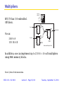
Multipliers
signa (1)
signb (1)
aclr
clock
ena
EP2C70 has 150 embedded.
Off-fabric.
Data A
D
Q
ENA
D
Q
ENA
CLRN
Use as:
Data Out
CLRN
300 9×9
150 18×18
Data B
D
Q
ENA
CLRN
Input
Register
Output
Register
Embedded Multiplier Block
In addition, one can implement up to 250 16 × 16 soft multipliers
using M4K memory blocks.
From Cyclone II documentation.
EECS 452 – Fall 2014
Lecture 5 – Page 16/143
Tuesday – September 16, 2014
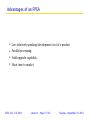
Advantages of an FPGA
▶
Low (relatively speaking) development cost of a product.
▶
Parallel processing.
▶
Field upgrade capability.
▶
Short time to market.
EECS 452 – Fall 2014
Lecture 5 – Page 17/143
Tuesday – September 16, 2014
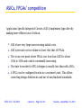
ASICs, FPGAs’ competition
Application Specific Integrated Circuits (ASICs) implement logic directly
making more efficient use of silicon.
▶
ASICs have very large non-recurring initial costs.
▶
ASICs per unit cost in volume is lower that that of FPGAs.
▶
The cross over point where FPGAs cost less than ASICS is about
100k to 200k units and is continually increasing.
▶
The time-to-market for FPGA designs is usually less than with ASICs.
▶
A FPGA can be configured in-situ in a customer’s unit. This allows
correcting design deficiencies and use of non-finalized standards.
EECS 452 – Fall 2014
Lecture 5 – Page 18/143
Tuesday – September 16, 2014
Who makes FPGAs?
▶
Xilinx, has approximately a 47% market share.
▶
Altera, has approximately a 41% market share.
▶
Both provide free Web editions of their basic design software for
use with their low end devices (where we live).
▶
Xilinx’s tool set is named ISE.
▶
Altera’s tool set is named Quartus II.
▶
Both are based on Eclipse and are very similar in use.
▶
Both support the Verilog, SystemVerilog and VHDL design
languages.
EECS 452 – Fall 2014
Lecture 5 – Page 19/143
Tuesday – September 16, 2014
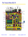
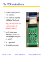
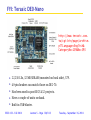
The Terasic/Altera DE2-70
Ethernet 10/100M Port
USB Device Port
USB Blaster Port
Mic in
USB Host Port
Line In Line Out
VGA Out
RS-232 Port
Video In 1 Video In 2
TV Decoder (NTSC/PAL) X2
12V DC Power Supply
Connector
PS2 Port
VGA 10-bit DAC
Power ON/OFF Switch
Ethernet 10/100M Controller
USB Host/Slave
Controller
Audio CODEC
50Mhz Oscillator
Altera USB Blaster
Controller chipset
Expansion Header 2
Altera EPCS16
Configuration Device
Expansion Header 1
RUN/PROG Switch for
JTAG/AS Modes
SD Card Slot
Lock
(SD Card Not Included)
16x2 LCD Module
IrDA Transceiver
7-Segment Displays
8Mbyte Flash Memory
18 Red LEDs
8 Green LEDs
SMA Extemal Clock
18 Toggle Switches
32Mbyte SDRAMx2
EECS 452 – Fall 2014
28Mhz Oscillator
Lecture 5 – Page 20/143
2Mbyte SSRAM
4 Push-button Switches
Tuesday – September 16, 2014
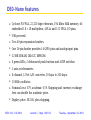
DE2-70 features
USB Blaster interface
2 Mbyte SSRAM
Two 32-Mbyte SDRAM
8-Mbyte Flash memory
SD Card socket
SMA connector
16×2 LCD display
8 seven-segment LED digits
4 push button switches
18 toggle switches
18 red user LEDs
9 green user LEDs
50 MHz clock oscillator
28 MHz clock oscillator
24-bit audio CODEC
line-in, line-out, mike-in jacks
VGA DAC (10-bit high speed)
2 TV Decoders
10/100 Ethernet Contoller
RJ45 Ethernet connector
USB Hose/Slave
USB type A and B connectors
PS/2 mouse/keyboard connector
IrDA transceiver
2 40-pin expansion connectors
recently phased out
http://www.terasic.com.tw/cgi-bin/page/archive.pl?Language=English&CategoryNo=53&No=226
EECS 452 – Fall 2014
Lecture 5 – Page 21/143
Tuesday – September 16, 2014
The DE2-70 power on default
▶
Used to built confidence that the board works.
▶
▶
▶
▶
▶
The default is contained in an EEPROM on the DE2-70 and is
automatically loaded into the DE2-70’s FPGA on power on.
Generates VGA logo display.
Blinks LEDs
Initializes the audio CODEC.
and much more.
▶
Contained in EEPROM. Source code is available on the Terasic
DE2-70 support web pages.
▶
EEPROM can be reprogrammed.
▶
Boot initializes peripherals. They might not be initialized as your
application needs them.
If you use it , initialize it!
An example is the CODEC: has a bypass added to the CODEC output.
EECS 452 – Fall 2014
Lecture 5 – Page 22/143
Tuesday – September 16, 2014
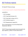
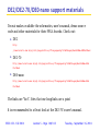
DE2-70 reference materials
The Terasic DE2-70 Resources web page
http://www.terasic.com.tw/cgi-bin/page/archive.pl?Language=English&CategoryNo=53&No=226&PartNo=4
contains files for:
▶
DE2-70 User Manual,
▶
DE2_70 Control Panel (for Quartus 10.0),
▶
DE2_70 Video Utility (For Quartus 10.0/10.1),
▶
DE2-70 CD-ROM (for Quartus 9.1),
▶
DE2-70 Demonstrations for QuartusII 10.0 .
The two of most importance to us are the User Manual and the
Demonstrations. Must haves!
The DE2-70 Demonstrations also includes data sheets (manuals) for the
major components, e.g. SDRAM, TV Decoder, Ethernet interface.
EECS 452 – Fall 2014
Lecture 5 – Page 23/143
Tuesday – September 16, 2014
Definitive resources
The DE2-70 schematics. Describes what actually connects to who and
how.
The Quartus .csv pin name list. Establishes a convention for sinal
names.
The pin names used on the schematics do not necessarily match those
used when designing using Quartus. They, on occasion, differ between
related boards such as the DE2, the DE2-70 and the DE0-nano.
We make do with what we are provided. Try to avoid marching to your
own drummer.
Treat the DE-70 as NOT tolerant to signal levels other than 3.3 Volts!!!
This also applies to the C5515 USBstick, actually, more so!.
EECS 452 – Fall 2014
Lecture 5 – Page 24/143
Tuesday – September 16, 2014
Pleas
Please do not solder to any of the connector pins on the DE2-70,
the C5515 or the connector/adapter boards.
If the jumpers that we have in lab are not adequate see Jon or me
about buying or building what is needed.
When doing your projects give early thought to how things will
connect and order the needed parts early. It takes about a week to
order and get delivery. This can be sped up by paying more for
shipping, but this can get very expensive. Of course, at least one
order per semester goes awry.
If you break something or burn something out. Please tell Jon,
Professor Hero or me. Things happen. Not knowing that a piece of
equipment has been damaged is generally much worse than not
knowing.
EECS 452 – Fall 2014
Lecture 5 – Page 25/143
Tuesday – September 16, 2014
Hardware Description Languages
▶
Describes digital hardware, the logic elements it is made of, how
they are connected and how they are clocked.
▶
Used for design,design verification and synthesis (implementation).
▶
Maps a hardware description into bit streams used to configure a
FPGA.
▶
Two main HDL languages, (System)Verilog and VHDL.
▶
SystemVerilog is modeled after C. Makes assumptions, can be
criticized as helping (in effect) when making mistakes.
▶
VHDL is (sort of) Ada like. Makes you be very precise. Often
criticized as to leading to verbose code.
▶
The world is about half (System)Verilog and half VHDL.
Verilog/SystemVerilog is used in EECS 452.
EECS 452 – Fall 2014
Lecture 5 – Page 26/143
Tuesday – September 16, 2014
The (System)Verilog hardware description language
Looks like a programming language. IT IS NOT!
▶
Does not program hardware!
▶
Describes hardware modules and how they are
interconnected.
▶
The syntax is very closely modeled on that of C.
It is a hardware description language.
EECS 452 – Fall 2014
Lecture 5 – Page 27/143
Tuesday – September 16, 2014
Brief history of the Verilog HDL
▶
Seeds planted about 1985. Originally intended as a simulation
language.
▶
Sold to Cadence in 1990. Capability for synthesis was gradually
added.
▶
Verilog-1995 standard.
▶
Verilog-2002 standard
▶
Verilog IEEE standard 1364-2005 issued.
▶
Initial SystemVerilog standard, 1800-2005.
▶
SystemVerilog Standard merged with Verilog Standard, 1800-2009.
▶
Current IEEE SystemVerilog standard version, 1800-2012.
▶
EECS has recently switched from Verilog to SystemVerilog.
▶
SystemVerilog is upward compatible with Verilog.
EECS 452 – Fall 2014
Lecture 5 – Page 28/143
Tuesday – September 16, 2014
Learning SystemVerilog
Common quotes:
▶
You learn by doing.
▶
You learn from your mistakes.
▶
Start simple, slowly add complexity.
My background is VHDL (an alternative HDL). I’ve done a moderately
small amount design using SystemVerilog. For both languages I’ve done
a lot of learning.
One thing that I’ve learned is that when something goes wrong it is
important understand what and why. Otherwise nothing has been
learned.
EECS 452 – Fall 2014
Lecture 5 – Page 29/143
Tuesday – September 16, 2014
Some Verilog and SystemVerilog references
http://en.wikipedia.org/wiki/Verilog
http://en.wikipedia.org/wiki/SystemVerilog
http://www.asic-world.com/systemverilog/tutorial.html
Digital System Design with SystemVerilog, Mark
Zwolinski, Prentice Hall, 2010.
Download the SystemVerilog standard . . . it’s free!
http://standards.ieee.org/events/edasymposium/stds.html
Complements of Accellera.
EECS 452 – Fall 2014
Lecture 5 – Page 30/143
Tuesday – September 16, 2014
Comments on (System) Verilog references
▶
I’ve seen the claim (on the web) that the SystemVerilog standard
makes a good tutorial. With a bit of caution, I have found the
standard to be very useful. Having a previous bit of Verilog
background helps deciding what to pay attention to and what to
skip over.
▶
There don’t seem to be many texts focused on design and synthesis
using SystemVerilog. There are several that focus on the use of
SystemVerilog for design verification and benchmarking.
▶
I used Mark Zwolinski’s Digital System Design with SystemVerilog as
as a reference for my learning. This is well written and reasonably
current, copyright 2010.
EECS 452 – Fall 2014
Lecture 5 – Page 31/143
Tuesday – September 16, 2014
Comments about standards
▶
If you are earning your living doing programming and or
hardware design, you should have a copy of the associated
standards. Typically we depend upon secondary sources such
as textbooks and web articles. Where did they get their
information?
▶
It is often useful to read the standards.
▶
Standards are notoriously hard to read. I strongly feel that it’s
worth the effort to at least look at them.
The Verilog and SystemVerilog standards are readily available on
the web.
EECS 452 – Fall 2014
Lecture 5 – Page 32/143
Tuesday – September 16, 2014
Verilog DIY learning links
http://www.asic-world.com, in particular:
http://www.asic-world.com/verilog/verilog_one_day.html
Altera’s HDL design examples:
http://www.altera.com/support/examples/exm-index.html
How does SystemVerilog extend Verilog?
http://en.wikipedia.org/wiki/SystemVerilog
There are also two EECS 270 tutorials linked to on the lab exercise 3
write-up.
Consider using SystemVerilog.
EECS 452 – Fall 2014
Lecture 5 – Page 33/143
Tuesday – September 16, 2014
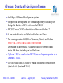
Altera’s Quartus II design software
▶
An Eclipse GUI based development system.
▶
Supports the development flow from design entry to loading the
design bit file into a FPGA and/or loader EPROM.
▶
EECS 452 uses CAEN’s subscription edition on Windows 7.
▶
A free web edition is available for Windows and Linux.
▶
I’m running version 13.0 SP1 on Windows, Ubuntu and Debian.
http://dl.altera.com/13.0sp1/?edition=web
Depending on the version, a small edit might be needed on the
install file if not installing on Red Hat Linux.
▶
Cyclone II FPGAs (used on the DE2-70) are no longer supported as of
Quartus II V13.1.
▶
The DE0-Nano uses a Cyclone IV which continues to be supported
(started with Quartus II V10.0).
EECS 452 – Fall 2014
Lecture 5 – Page 34/143
Tuesday – September 16, 2014
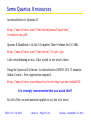
Some Quartus II resources
An introduction to Quartus II.
http://www.altera.com/literature/manual/quartus2_
introduction.pdf
Quartus II Handbook v14.0a10 (Complete Three-Volume Set) (23 MB).
http://www.altera.com/literature/lit-qts.jsp
A bit overwhelming in size. Take a peek to see what’s there.
Using the Quartus II Software: An Introduction (ODSW1100) 72 minutes
Online Course . Free, registration required.
http://www.altera.com/education/training/courses/odsw1100
It is strongly recommended that you watch this!!!
Not all of the covered material applies to us, but a lot does!
EECS 452 – Fall 2014
Lecture 5 – Page 35/143
Tuesday – September 16, 2014
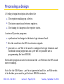
Processing a design
A Verilog design description describes the
▶
The registers making up a device.
▶
The interconnections between registers.
▶
The timing of changes in the register states.
A series of Quartus programs
▶
synthesizes the design to the basic logic element level.
▶
fits the result into the FPGA and routes signals.
▶
generates a .sof file to be used to configure the logic elements and
establish routing segments and .pof file for possible use in
programming the boot EPROM.
The loader program is used to download the .sof file into the FPGA and
start it running.
Note: For the DE0-Nano a .pof is not generated and the .sof file needs
to be further processed to get the boot EPROM contents.
EECS 452 – Fall 2014
Lecture 5 – Page 36/143
Tuesday – September 16, 2014
Quartus II file extensions
Quartus II uses and/or generates file using a various file extensions. The
extensions most important to us are:
.v
Verilog text file.
.sv
SystemVerilog text file.
.qpf
Project description file.
.csv
Comma separated values. Normally used to generate
the working pin name description file.
.qsv
Pin description list. Often there is a default version
that can be used to generate the working version.
.sdc
clock definitions.
.sof
Bit output file used to program the FPGA.
.pof
Bit output file used to program boot flash EPROM.
There are more, but these are the ones you will normally work with.
EECS 452 – Fall 2014
Lecture 5 – Page 37/143
Tuesday – September 16, 2014
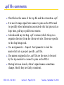
.qsf file comments
▶
This file has the name of the top file and the extenstion .qsf.
▶
It is used to map signal/wire names to pins on the FPGA and
to specifify other information associated with that pin such as
logic time, pull-up or pull-down resistor.
▶
I downloaded my starting .qsf versions (which I keep in a
separate directory from the Altera web site. These are specific
to the chip being used.
▶
Use assignments — Import Assignments to load the
master list into a project specific .qsf file.
▶
The names assigned in the .qsf file are the ones to be used
by the top module to connect to pins on the FPGA.
▶
Moving between boards, Altera’s signal names sometimes
change. Mostly they are fairly consistent.
EECS 452 – Fall 2014
Lecture 5 – Page 38/143
Tuesday – September 16, 2014
DE2-70 .qsf file snippet
set_location_assignment
set_location_assignment
set_location_assignment
set_location_assignment
set_location_assignment
set_location_assignment
set_location_assignment
set_location_assignment
set_location_assignment
set_location_assignment
set_location_assignment
set_location_assignment
set_location_assignment
set_location_assignment
set_location_assignment
set_location_assignment
set_location_assignment
set_location_assignment
set_location_assignment
set_location_assignment
EECS 452 – Fall 2014
PIN_E14 -to TD1_VS
PIN_D14 -to TD1_RST_N
PIN_H15 -to TD2_CLK27
PIN_C10 -to TD2_DATA[0]
PIN_A9 -to TD2_DATA[1]
PIN_B9 -to TD2_DATA[2]
PIN_C9 -to TD2_DATA[3]
PIN_A8 -to TD2_DATA[4]
PIN_B8 -to TD2_DATA[5]
PIN_A7 -to TD2_DATA[6]
PIN_B7 -to TD2_DATA[7]
PIN_E15 -to TD2_HS
PIN_D15 -to TD2_VS
PIN_B10 -to TD2_RST_N
PIN_R29 -to EXT_CLOCK
PIN_E16 -to CLOCK_28
PIN_AD15 -to CLOCK_50
PIN_D16 -to CLOCK_50_2
PIN_R28 -to CLOCK_50_3
PIN_R3 -to CLOCK_50_4
Lecture 5 – Page 39/143
Tuesday – September 16, 2014
DE0-Nano .qsf file snippet
#============================================================
# Accelerometer and EEPROM
#============================================================
set_location_assignment PIN_F2 -to I2C_SCLK
set_location_assignment PIN_F1 -to I2C_SDAT
set_instance_assignment -name IO_STANDARD "3.3-V LVTTL" -to I2C_SCLK
set_instance_assignment -name IO_STANDARD "3.3-V LVTTL" -to I2C_SDAT
set_location_assignment
set_location_assignment
set_instance_assignment
set_instance_assignment
PIN_G5 -to G_SENSOR_CS_N
PIN_M2 -to G_SENSOR_INT
-name IO_STANDARD "3.3-V LVTTL" -to G_SENSOR_CS_N
-name IO_STANDARD "3.3-V LVTTL" -to G_SENSOR_INT
#============================================================
# ADC
#============================================================
set_location_assignment PIN_A10 -to ADC_CS_N
set_location_assignment PIN_B10 -to ADC_SADDR
set_location_assignment PIN_B14 -to ADC_SCLK
set_location_assignment PIN_A9 -to ADC_SDAT
set_instance_assignment -name IO_STANDARD "3.3-V LVTTL" -to ADC_CS_N
set_instance_assignment -name IO_STANDARD "3.3-V LVTTL" -to ADC_SADDR
set_instance_assignment -name IO_STANDARD "3.3-V LVTTL" -to ADC_SCLK
set_instance_assignment -name IO_STANDARD "3.3-V LVTTL" -to ADC_SDAT
EECS 452 – Fall 2014
Lecture 5 – Page 40/143
Tuesday – September 16, 2014
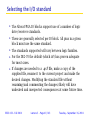
Selecting the I/O standard
▶
The Altera FPGA IO blocks support use of a number of logic
drive/receiver standards.
▶
These are generally selected per IO block. All pins in a given
block must use the same standard.
▶
The standards supported will vary between logic families.
▶
For the DE2-70 the default (which is?) has proven adequate
for most cases.
▶
If changes are needed to a .qsf file, make a copy of the
supplied file, rename it to the current project and make the
desired changes. Modifying the standard file without
renaming (and commenting the changes) likely will have
undesired and unexpected consequences at some future time.
EECS 452 – Fall 2014
Lecture 5 – Page 41/143
Tuesday – September 16, 2014
.sdc file comments
▶
Not strictly needed, but . . . .
▶
Used to describes the clocks used by a design. Typically our
designs will primarily use a 50 MHz clock. But not necessarily
exclusively.
▶
Timing information is used when routing and optimizing a a
design.
▶
Information along with chip information to calculate expected
set up and hold times and the maximum allowable clock
frequency. Most small, lab exercises just work. However with
larger projects and/or those with multiple clocks the timing
results should be checked.
▶
I copy and rename a version from project to project adding or
commenting out as needed.
EECS 452 – Fall 2014
Lecture 5 – Page 42/143
Tuesday – September 16, 2014
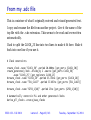
From my .sdc file
This is a mixture of what I originally entered and wizard generated text.
I copy and rename the file from another project. Give it the name of the
top file with the .sdc extension. This seems to be read and overwritten
automatically.
I had to split the CLOCK_25 line into two lines to make it fit here. Make it
back into one line if you use it.
# Clock constraints
create_clock -name "CLOCK_50" -period 20.000ns [get_ports {CLOCK_50}]
create_generated_clock -divide_by 2 -source [get_ports CLOCK_50]
-name "CLOCK_25" [get_registers CLOCK_25]
#create_clock -name "CLOCK_28" -period 35.714ns [get_ports {CLOCK_28}]
#create_clock -name "TD1_CLK27" -period 37.037ns [get_ports {TD1_CLK27}]
#create_clock -name "GPIO_1[10]" -period 25ns [get_ports {GPIO_1[10]}]
# Automatically constrain PLL and other generated clocks
derive_pll_clocks -create_base_clocks
EECS 452 – Fall 2014
Lecture 5 – Page 43/143
Tuesday – September 16, 2014
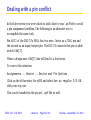
Dealing with a pin conflict
In the lab exercise you were asked to add a line to your .qsf file to avoid
a pin assignment problem. The following is an alternate way to
accomplish the same task.
Pin AD25 of the DE2-70’s FPGA has two uses. One is as a JTAG pin and
the second as an input/output pin. The DE2-70 connects this pin to slide
switch iSW[7].
When a design uses iSW[7] this will lead to a fatal error.
To correct the situation:
Assignments -- Device -- Device and Pin Options
Click on the Value entry for nCEO and select Use as regular I/O. OK
click your way out.
This can be handled in the project .qsf file as well.
EECS 452 – Fall 2014
Lecture 5 – Page 44/143
Tuesday – September 16, 2014
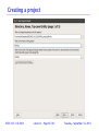
Creating a project
EECS 452 – Fall 2014
Lecture 5 – Page 45/143
Tuesday – September 16, 2014
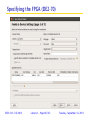
Specifying the FPGA (DE2-70)
EECS 452 – Fall 2014
Lecture 5 – Page 46/143
Tuesday – September 16, 2014
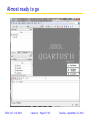
Almost ready to go
EECS 452 – Fall 2014
Lecture 5 – Page 47/143
Tuesday – September 16, 2014
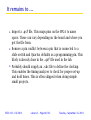
It remains to . . .
▶
Import a .qsf file. This maps pins on the FPGA to name
space. These can vary depending on the board and where you
got the file from.
▶
Remove a pin conflict between a pin that is connected to a
slide switch and Quartus defaults as a programming pin. This
likely is already done in the .qsf file used in the lab.
▶
Probably should supply an .sdc file to define the clocking.
This enables the timing analyzer to check for proper set-up
and hold times. This is often skipped when doing simple
small projects.
EECS 452 – Fall 2014
Lecture 5 – Page 48/143
Tuesday – September 16, 2014
Quartus II screen shot
EECS 452 – Fall 2014
Lecture 5 – Page 49/143
Tuesday – September 16, 2014
The warning windows
The warning and the critical warning windows are your friends.
If the SV/V compiler encounters a inconsistency (e.g., declared array size
does not match the size used in an expression) rather than throw an
error it will make a decision about how to resolve it and continue on.
When writing code it is a good philosophy to say what you mean and
mean what you say. (I.e., don’t get clever!)
Usually the warnings alert you to when the compiler has had to make a
decision. One can accept the decision or fix their code to eliminate the
the warnings.
Critical warnings are the most severe. The compiler did something but
didn’t like what it had to do. Fix these for sure.
EECS 452 – Fall 2014
Lecture 5 – Page 50/143
Tuesday – September 16, 2014
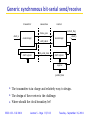
Structure of a (Verilog/SystemVerilog design
Off-FPGA Hardware
pins/pads
FGPA Fabric
top module
module a
module a
EECS 452 – Fall 2014
module b
module etc.
module a
Lecture 5 – Page 51/143
Tuesday – September 16, 2014
Comments on module structure
▶
(System)Verilog is very C like.
▶
Multiple modules can be present in a source file.
▶
Consider naming the top module with the project name
followed by _top. For example my VGA_nano project top file
is named VGA_nano_top.sv.
▶
The top level module port signal names need to match the
names in the assigned .qsf file. The .qsf file assigns signal
names to actual pins on the FPGA.
▶
Occasionally one wants to combine two existing projects each
having its own top file. Consider using a top_top file.
EECS 452 – Fall 2014
Lecture 5 – Page 52/143
Tuesday – September 16, 2014
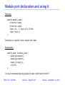
Module port declaration and using it
Definition:
module module_name (
direction name1,
direction name2,
input clk, // typically 50 MHz
input reset_n
);
Directions are typically input, output and inout.
Instantiation:
module_name instance_name (
.name2(parameter2),
.name1(parameter1),
.reset_n(reset_n),
.clk(clk)
);
I strongly recommend passing signals by name rather than by order!!!
EECS 452 – Fall 2014
Lecture 5 – Page 53/143
Tuesday – September 16, 2014
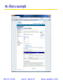
An Altera example
EECS 452 – Fall 2014
Lecture 5 – Page 54/143
Tuesday – September 16, 2014
Altera’s addsub.v example
module addsub
(
input [7:0] dataa,
input [7:0] datab,
input add_sub,
// if this is 1, add; else subtract
input clk,
output reg [8:0] result
);
always @ (posedge clk)
begin
if (add_sub)
result <= dataa + datab;
else
result <= dataa - datab;
end
endmodule
This is a behavioral description of what is to be accomplished. Note the
automatic promotion of the number of bits.
EECS 452 – Fall 2014
Lecture 5 – Page 55/143
Tuesday – September 16, 2014
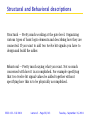
Structural and Behavioral descriptions
Structural — Pretty much working at the gate level. Organizing
various types of basic logic elements and describing how they are
connected. If you want to add two twelve bit signals you have to
design and build the adder.
Behavioral — Pretty much saying what you want. Not so much
concerned with how it is accomplished. For example specifying
that two twelve bit signal values be added together without
specifying how this is to be physically accomplished.
EECS 452 – Fall 2014
Lecture 5 – Page 56/143
Tuesday – September 16, 2014
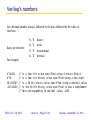
Verilog’s numbers
Size (decimal number, always), followed by the base, followed by the value, in
that base.
Bases are denoted:
’b, ’B
binary
’o, ’O
octal
’h, ’H
hexadecimal
’d, ’D
decimal
For example:
4’b0101
4’H5
16’d32767
-16’d1234
//
//
//
//
//
EECS 452 – Fall 2014
is a four bit value specified using 4 binary digits
is a four bit binary value specified using a hex digit
is a 16 bit binary value specified using a decimal value
is the 16 bit binary value specified in two’s complement
form corresponding to decimal value -1234
Lecture 5 – Page 57/143
Tuesday – September 16, 2014
Verilog’s base logic elements
and
nand
nor
or
xor
xnor
These six logic gates can have only one output and multiple inputs. The
output is specified first in the instantiation.
Example and gate declaration:
and a1 (out, in1, in2, in3);
buf
not
These can have multiple outputs but only one input.
Example declaration:
EECS 452 – Fall 2014
buf b1 (out1, out2, in);
Lecture 5 – Page 58/143
Tuesday – September 16, 2014
Full Adder
outputs
inputs
cn
sn
bn
an
cn−1
0
0
0
0
0
0
1
0
0
1
0
1
0
1
0
1
0
0
1
1
0
1
1
0
0
1
0
1
0
1
1
0
1
1
0
1
1
1
1
1
EECS 452 – Fall 2014
Åçìí
Å~êêó
Åáå
~
Ä
Lecture 5 – Page 59/143
ë
ëìã
Tuesday – September 16, 2014
Full Adder — Structural
module full_adder(a,b,cin,sum,cout);
input a,b,cin;
output sum, cout;
xor (sum,a,b,cin);
and (a0,a,b),(a2,a,cin),(a3,b,cin);
or (cout,a0,a1,a2);
endmodule
This is somewhat on the “obsessed with detail” side of life. We rarely, if
ever, want to work at this low of level of abstraction.
At least it is a level of abstraction above specifying how to arrange
individual transistors.
EECS 452 – Fall 2014
Lecture 5 – Page 60/143
Tuesday – September 16, 2014
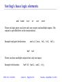
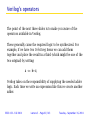
Verilog’s operators
The point of the next three slides is to make you aware of the
operators available in Verilog.
These generally cause the required logic to be synthesized. For
example, if we have two 16-bit reg items we can add them
together and place the result in a third (which might be one of the
two original) by writing:
a <= b+c;
Verilog takes on the responsibility of supplying the needed adder
logic. Each time we write an expression like this we create another
adder.
EECS 452 – Fall 2014
Lecture 5 – Page 61/143
Tuesday – September 16, 2014
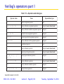
Verilog’s operators part 1
Table 11-1—Operators and data types
Operator token
Name
=
+=
binary assignment operator
-=
/=
*=
%=
&=
|=
^=
Operand data types
any
binary arithmetic assignment operators
integral, real, shortreal
binary arithmetic modulus assignment operator
integral
binary bit-wise assignment operators
integral
>>= <<=
binary logical shift assignment operators
integral
>>>= <<<=
binary arithmetic shift assignment operators
integral
?:
conditional operator
any
+
-
!
~ & ~&
~^ ^~
+
-
*
|
/
~|
^
**
%
&
|
^
^~
~^
>> <<
unary arithmetic operators
integral, real, shortreal
unary logical negation operator
integral, real, shortreal
unary logical reduction operators
integral
binary arithmetic operators
integral, real, shortreal
binary arithmetic modulus operator
integral
binary bit-wise operators
integral
binary logical shift operators
integral
From IEEE Standard 1800-2009.
EECS 452 – Fall 2014
Lecture 5 – Page 62/143
Tuesday – September 16, 2014
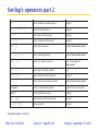
Verilog’s operators part 2
%
&
|
^
^~
~^
binary arithmetic operators
integral,
binary arithmetic modulus operator
integral
,
binary bit-wise operators
integral
binary logical shift operators
integral
>>> <<<
binary arithmetic shift operators
integral
&& ||
-> <->
binary logical operators
integral, real, shortreal
binary relational operators
integral, real, shortreal
binary case equality operators
any except real and
shortreal
>> <<
<
<=
===
==
>=
!=
==?
++
>
!==
!=?
--
binary logical equality operators
any
binary wildcard equality operators
integral
unary increment, decrement operators
integral, real, shortreal
inside
binary set membership operator
singular for the left operand
dista
binary distribution operator
integral
{}
concatenation, replication operators
integral
stream operators
integral
{{}}
{<<{}} {>>{}}
aThe
operator is described in 16.15.2 (Assume statement) and 18.5.4 (Distribution).
From IEEE Standard 1800-2009.
EECS 452 – Fall 2014
Lecture 5 – Page 63/143
Tuesday – September 16, 2014
Verilog’s operator precedences
Table 11-2—Operator precedence and associativity
Operator
()
+
[]
::
.
~
&
~&
|
~|
^
~^
^~
++
Associativity
Precedence
left
highest
-
!
-- (unary)
*
/
%
left
+
- (binary)
left
**
<<
<
==
left
>>
<=
<<<
>
!=
>>>
>=
===
left
inside
!==
==?
dist
!=?
& (binary)
^
~^
left
left
left
^~ (binary)
left
| (binary)
left
&&
left
||
left
?: (conditional operator)
right
–> <->
right
= += -= *= /= %= &= ^= |=
<<= >>= <<<= >>>= := :/ <=
none
{}
{{}}
concatenation
lowest
From IEEE Standard 1800-2009.
EECS 452 – Fall 2014
Lecture 5 – Page 64/143
Tuesday – September 16, 2014
SystemVerilog’s data types
In Verilog there are two primary data types, wires (wire) and
registers(reg).
Wires represent connections. Registers correspond to variables to
hold values.
The default data type is a one bit wide wire.
Note: registers are not necessarily actual registers.
SystemVerilog introduced logic type to replace the use of wire
and reg.
SystemVerilog is a weakly typed language.
EECS 452 – Fall 2014
Lecture 5 – Page 65/143
Tuesday – September 16, 2014
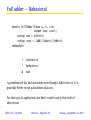
Full adder — Behavioral
module FullAdder(input a, b, cin,
output sum, cout);
assign sum = a^b^cin;
assign cout = (a&b)|(a&cin)|(b&cin);
endmodule
^
exclusive-or
|
inclusive-or
&
and
I parenthesized the and operations even though I didn’t have to. It is
generally better to use parentheses than not.
For this type of application, one likely would work at this level of
abstraction.
EECS 452 – Fall 2014
Lecture 5 – Page 66/143
Tuesday – September 16, 2014
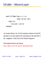
Full adder — Behavioral, again
module FullAdder(input a, b, cin,
output reg sum, cout);
always @(*)
{cout,sum} = a+b+cin;
endmodule
An even more abstract view. Note the automatic extension of one-bit bit
operations to two bits caused by the concatenation on the result side of
the = assignment. At least this is what I think has happened.
This example is based on one found at
http://www.asic-world.com/verilog/syntax2.html.
EECS 452 – Fall 2014
Lecture 5 – Page 67/143
Tuesday – September 16, 2014
Full adder test
Each full adder implementation should
give the same result.
module FullAdder_top
( output [17:0] oLEDR,
input [17:0] iSW
);
FullAdder_S fa0 (iSW[1], iSW[2], iSW[0],
oLEDR[0], oLEDR[1]
);
Testing using switches:
FullAdder_B0 fa1 (iSW[1], iSW[2], iSW[0],
oLEDR[4], oLEDR[5]
);
▶ iSW[0] carry in
▶ iSW[1] a value
▶ iSW[2] b value
Displaying using red leds:
▶ 0,4,8 the sum out
▶ 1,5,9 the carry out
This was a good learning exercise.
EECS 452 – Fall 2014
FullAdder_B1 (.cout(oLEDR[9]), .sum(oLEDR[8]),
.cin(iSW[0]), .b(iSW[2]), .a(iSW[1])
);
endmodule
//---------------------------------------module FullAdder_S (a,b,cin,sum,cout);
input a,b,cin;
output sum, cout;
xor (sum,a,b,cin);
and (a0,a,b),(a2,a,cin),(a3,b,cin);
or (cout,a0,a1,a2);
endmodule
//---------------------------------------module FullAdder_B0 (input a, b, cin,
output sum, cout);
assign sum = a^b^cin;
assign cout = (a&b)|(a&cin)|(b&cin);
endmodule
//---------------------------------------module FullAdder_B1 (input a, b, cin,
output reg sum, cout);
always @(*)
{cout,sum} = a+b+cin;
endmodule
Lecture 5 – Page 68/143
Tuesday – September 16, 2014
Unrestricting the signal order
The order of the signals in the instantiation of a module normally MUST
match the order in the associated module definition.
For modules having a large of number of signals to connect this can be a
recipe for disaster.
Today’s common wisdom is that having to match order is not a good
thing. That is, one should not require it.
Using the construct shown in the FullAdder_B1 instantiation removes
the matching order requirement. The signal order used in this
instantiation is the reverse of that of the module definition, yet, the logic
works.
FullAdder_B1 (.cout(oLEDR[9]), .sum(oLEDR[8]),
.cin(iSW[0]), .b(iSW[2]), .a(iSW[1])
);
Quartus II makes the external signal connections to the top module by
name.
EECS 452 – Fall 2014
Lecture 5 – Page 69/143
Tuesday – September 16, 2014
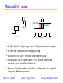
Blocking versus non-blocking assignments
How does
c = a;
d = c;
differ from
c <= a;
d <= c;
?
In an FPGA everything CAN happen all at once. — anon
EECS 452 – Fall 2014
Lecture 5 – Page 70/143
Tuesday – September 16, 2014
SystemVerilog procedural statements
Selection statements
—
if–else, case, casez, casex, unique, unique0, priority
Loop statements
—
for, repeat, foreach, while, do...while, forever
Jump statements
—
break, continue, return
From IEEE Standard 1800-2009. I’m mixing my standards between this slide and
the next, sorry.
EECS 452 – Fall 2014
Lecture 5 – Page 71/143
Tuesday – September 16, 2014
Syntax for looping statements
Expanding on the looping statements:
function_loop_statement ::= (From Annex A - A.6.8)
forever function_statement
| repeat ( expression ) function_statement
| while ( expression ) function_statement
| for ( variable_assignment ; expression ; variable_assignment )
function_statement
loop_statement ::=
forever statement
| repeat ( expression ) statement
| while ( expression ) statement
| for ( variable_assignment ; expression ; variable_assignment )
statement
Syntax 9-7—Syntax for the looping statements
From IEEE Standard 1364-2001.
EECS 452 – Fall 2014
Lecture 5 – Page 72/143
Tuesday – September 16, 2014
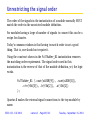
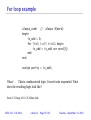
For loop example
always_comb
// always @(word)
begin
is_odd = 0;
for (i=0; i<=7; i=i+1) begin
is_odd = is_odd xor word[i];
end
end
assign parity = is_odd;
Whoa!
This is combinatorial logic. It sure looks sequential. What
does the resulting logic look like?
From Y.T.Chang 2001 CIC/Xilinx slide.
EECS 452 – Fall 2014
Lecture 5 – Page 73/143
Tuesday – September 16, 2014
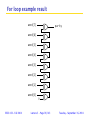
For loop example result
word[7]
parity
word[6]
word[5]
word[4]
word[3]
word[2]
word[1]
word[0]
0
EECS 452 – Fall 2014
Lecture 5 – Page 74/143
Tuesday – September 16, 2014
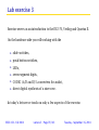
Lab exercise 3
Exercise serves as an introduction to the DE2-70, Verilog and Quartus II.
On the hardware side you will working with the
▶
slide switches,
▶
push button switches,
▶
LEDs,
▶
seven-segment digits,
▶
CODEC (A/D and D/A converters for audio),
▶
direct digital synthesis of a sine wave.
In today’s lecture we touch on only a few aspects of the exercise.
EECS 452 – Fall 2014
Lecture 5 – Page 75/143
Tuesday – September 16, 2014
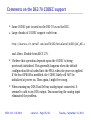
Comments on the DE2-70 CODEC support
▶
Same CODEC part is used on the DE2-70 as on the DE2.
▶
Large chunks of CODEC support code from
http://courses.cit.cornell.edu/ece576/DE2/NoiseCancel/AUDIO_DAC_ADC.v
and Altera. Module from EECS 270.
▶
I believe that operation depends upon the CODEC to being
previously initialized. This generally happens when the default
configuration file is loaded into the FPGA when the power is applied.
If the boot EPROM is modified, the CODEC likely will NOT be
initialized at power on. Then again, I might be wrong.
▶
When running my DDS I had left my analog input connected. It
seemed to add to my DDS output. Disconnecting the analog input
eliminated the problem.
EECS 452 – Fall 2014
Lecture 5 – Page 76/143
Tuesday – September 16, 2014
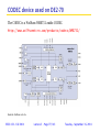
CODEC device used on DE2-70
The CODEC is a Wolfson WM8731 audio CODEC.
http://www.wolfsonmicro.com/products/codecs/WM8731/
From the Wolfson web site.
EECS 452 – Fall 2014
Lecture 5 – Page 77/143
Tuesday – September 16, 2014
The WM8731, what and how
“Stereo 24-bit multi-bit sigma delta ADCs and DACs are used with
oversampling digital interpolation and decimation filters. Digital audio
input word lengths from 16-32 bits and sampling rates from 8kHz to
96kHz are supported.” (From the WM8731 web site.)
The lab exercise using the WM8731 is reasonably self-contained.
However, if you need more information (perhaps for use in a project):
▶
Read the data sheet. (Also present on the DE2-70 System CD-ROM.)
▶
Read section 6.11 of the D2-70 User manual.
▶
Look at the DE_70_i2sound demonstration located in the
DE2-70_demonstrations_V10 collection.
See WAN_0117 for information on setting supported sampling rates.
EECS 452 – Fall 2014
Lecture 5 – Page 78/143
Tuesday – September 16, 2014
DE2-70 schematic, CODEC
C39
VCC33
1u
R99
4.7K
R100
4.7K
LINE IN
5
2
4
1
3
1u
NCL
R
NCR
L
GND
J11
C38
PHONE JACK B
VCC33
R108
R109
2K
2K
R101
R102
4.7K
4.7K
AGND
AGND
J10
WM8731
MBIAS
VMID
AGND
AVDD
ROUT
LOUT
HPGND
21
20
19
18
17
16
15
R104
C41
680
10u
AGND
A_VCC33
C42
R105
1n
47K
AGND
J12 LINE OUT
AGND
AGND
AGND
PHONE JACK G
29
8
9
10
11
12
13
14
EXPOSED
DACDAT
DACLRCK
ADCD AT
ADCLRCK
HPVDD
LHPOUT
RHPOUT
XTI/MCLK
XTO
DCVDD
DGND
DBVDD
CLKOUT
BCLK
PHONE JACK P
NCL
R
NCR
L
GND
1
2
3
4
5
6
7
AGND
5
2
4
1
3
A_VCC33
AUD_XCK
AUD_BCLK
AUD_DACDAT
AUD_DACLRCK
AUD_ADCD AT
AUD_ADCLRCK
C40
1u
SCLK
SDIN
CSB
MODE
LLINEIN
RLINEIN
MICIN
U13
28
27
26
25
24
23
22
I2C ADDRESS READ IS 0x34
I2C ADDRESS WRITE IS 0x35
MIC IN
330
NCL
R
NCR
L
GND
R103
5
2
4
1
3
I2C_SDAT
I2C_SCLK
AGND
AGND
C43
100u
C44
100u
A_VCC33
R106
R107
47K
47K
AGND
AGND
AGND
From DE2-70 User Manual.
EECS 452 – Fall 2014
Lecture 5 – Page 79/143
Tuesday – September 16, 2014
DE2-70 CODEC pin assignments
Signal Name
FPGA Pin No.
Description
AUD_ADCLRCK
PIN_F19
Audio CODEC ADC LR Clock
AUD_ADCDAT
PIN_E19
Audio CODEC ADC Data
AUD_DACLRCK
PIN_G18
Audio CODEC DAC LR Clock
AUD_DACDAT
PIN_F18
Audio CODEC DAC Data
AUD_XCK
PIN_D17
Audio CODEC Chip Clock
AUD_BCLK
PIN_E17
Audio CODEC Bit-Stream Clock
I2C_SCLK
PIN_J18
I2C Data
PIN_H18
I2C Clock
I2C_SDAT
Table 5.12. Audio CODEC pin assignments.
From DE2-70 User manual.
EECS 452 – Fall 2014
Lecture 5 – Page 80/143
Tuesday – September 16, 2014
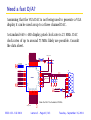
Need a fast D/A?
Assuming that the VGA DAC is not being used to generate a VGA
display it can be used as up to a three channel DAC.
A standard 640 × 480 display pixel clock rate is 25 MHz. DAC
clock rates of up to around 75 MHz likely are possible. Consult
the data sheet.
R9
R8
R7
R6
R5
R4
R3
R2
R1
R0
PSAVE
RSET
G0
G1
G2
G3
G4
G5
G6
G7
G8
G9
BLANK
SYNC
ADV7123
VAA
B0
B1
B2
B3
B4
B5
B6
B7
B8
B9
CLOCK
1
2
3
4
5
6
7
8
9
10
11
12
VREF
COMP
IOR
IOR
IOG
IOG
VAA
VAA
IOB
IOB
GND
GND
36
35
34
33
32
31
30
29
28
27
26
25
BC47
BC48
0.1u
0.1u
J7
VGA_R
VGA_G
VGA_B
VGA_VCC33
R82
R83
R84
75
75
75
VGA_HS
VGA_VS
R85
R86
47
47
VGA_VCC33
EECS 452 – Fall 2014
1
2
3
4
5
6
7
8
9
10
11
12
13
14
15
6
1
11
10
5
16
VGA_B0
VGA_B1
VGA_B2
VGA_B3
VGA_B4
VGA_B5
VGA_B6
VGA_B7
VGA_B8
VGA_B9
VGA_CLOCK
13
14
15
16
17
18
19
20
21
22
23
24
VGA_G0
VGA_G1
VGA_G2
VGA_G3
VGA_G4
VGA_G5
VGA_G6
VGA_G7
VGA_G8
VGA_G9
VGA_BLANK_n
VGA_SYNC_n
U10
48
47
46
45
44
43
42
41
40
39
38
37
RSET
VGA_R[0..9]
VGA_G[0..9]
VGA_B[0..9]
4.7K
560
15
VGA
17
VGA_R9
VGA_R8
VGA_R7
VGA_R6
VGA_R5
VGA_R4
VGA_R3
VGA_R2
VGA_R1
VGA_R0
VGA_VCC33
R80
R81
BC49 0.1u
From the DE2-70 schematics PDF file.
VCC33
VGA_VCC33
Lecture 5 – Page 81/143
VGA_VCC33
Tuesday – September 16, 2014
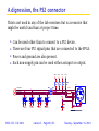
A digression, the PS2 connector
This is not used in any of the lab exercises but is a resource that
might be useful (and has) at project time.
5
4
3
RXD
R44
330
R45
330
2
1
LEDR
UART_RXD
J2
VCC33
D
▶
TXD
LEDG
UART_TXD
5
9
4
8
3
7
2
6
1
D
Can be used other than to connect to a PS2 device.
U7
UART_RXD
UART_RTS
UART_TXD
UART_CTS
12
9
11
10
R1IN
R2IN
T1OUT
T2OUT
13
8
14
7
C+ ADM3202
C1C2+
VCC
C2GND
V+
V-
16
15
R1OUT
R2OUT
T1IN
T2IN
RXD
RTS
TXD
CTS
There are four PS2 signal pins that are connected to the FPGA.
▶
Power and ground are also present.
▶
Each non-supply pin can be used either as input or output.
C9
C
1u
C10
VCC33
1
3
4
5
2
6
1u
BC33
C11
C12
0.1u
1u
1u
10
11
▶
VCC33
RS232
BC32 0.1u
C
VCC5
VCC5
VCC5
VCC5
R46
R47
R172
R173
2K
2K
2K
2K
J3
TOP
KBDAT
KBCLK
MSCLK
VCC33
VCC33
6
5
3
2
B
1
9
10
11
BC34
BC35
VCC33
8
PS2
2
1
1
2
3
5
6
8
MSDAT
3
3
BAT54S
2
D96
BAT54S
1
D95
BAT54S
2
D10
BAT54S
1
120
120
120
120
VCC5
D9
2
1
3
R48
R49
R174
R175
3
B
PS2_KBDAT
PS2_KBCLK
PS2_MSDAT
PS2_MSCLK
VCC33
0.1u
0.1u
Copyright (c) 2007 by Terasic Technologies Inc. Taiwan.
All rights reserved.
No part of this schematic design may be reproduced, duplicated, or used
without the prior written permission of Terasic.
A
EECS 452 – Fall 2014
Lecture 5 – Page 82/143
A
Title
Tuesday – September 16, 2014
ALTERA DE2-70
Size
Document Number
Rev
Implementing a DDS sine table
▶
Use a case statement with assignments. Simple and easy. This is one
of ways described in the lab exercise. A large table requires use of a
lot of logic elements. A 256 × 16 table uses 4096 LE D-registers.
▶
Indexed arrays are supported by Verilog 2001. These can be
initialized by reading an external initialization file (constructs exist
to do this) or by using an initial block.
▶
SystemVerilog allows array initialization values to be listed pretty
much as in the same manner as for C.
▶
Use a M4K memory block to hold the table. Off fabric. Simply a RAM
block initialized using a .mif file. If you never write to it, initialized
RAM serves as a ROM. A single M4K memory block can hold a
256 × 16 sine table with 512 (nominally parity) bits left over.
EECS 452 – Fall 2014
Lecture 5 – Page 83/143
Tuesday – September 16, 2014
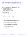
Sine generation using a case statement
always@(negedge clock)
counter <= counter + FTV;
always@*
begin
case(counter[9:6])
0 : dataOut
1 : dataOut
2 : dataOut
3 : dataOut
4 : dataOut
5 : dataOut
6 : dataOut
7 : dataOut
8 : dataOut
9 : dataOut
10 : dataOut
11 : dataOut
12 : dataOut
13 : dataOut
14 : dataOut
15 : dataOut
default :
dataOut
<=
endcase
end
EECS 452 – Fall 2014
<=
<=
<=
<=
<=
<=
<=
<=
<=
<=
<=
<=
<=
<=
<=
<=
0;
12539;
23170;
30273;
32767;
30273;
23170;
12539;
0;
-12539;
-23170;
-30273;
-32767;
-30273;
-23170;
-12539;
0
;
Lecture 5 – Page 84/143
Tuesday – September 16, 2014
Sine generation using an array
reg [15:0] sine_table [15:0];
initial begin
sine_table[0] = 0;
sine_table[1] = 12539;
sine_table[2] = 23170;
sine_table[3] = 30273;
sine_table[4] = 32767;
sine_table[5] = 30273;
sine_table[6] = 23170;
sine_table[7] = 12539;
sine_table[8] = 0;
sine_table[9] = -12539;
sine_table[10] = -23170;
sine_table[11] = -30273;
sine_table[12] = -32767;
sine_table[13] = -30273;
sine_table[14] = -23170;
sine_table[15] = -12539;
end
always@(negedge clock)
counter <= counter + FTV;
always @(*)
dataOut = sine_table[counter[9:6]];
EECS 452 – Fall 2014
Lecture 5 – Page 85/143
Tuesday – September 16, 2014
Sine generation using SystemVerilog
reg [15:0] sine_table[0:15] = ’{0, 12539, 23170, 30273,
32767, 30273, 23170, 12539,
0, -12539, -23170, -30273,
-32767, -30273, -23170, -12539};
always@(negedge clock)
counter <= counter + FTV;
always @(*)
dataOut = sine_table[counter[9:6]];
▶
Made the needed changes to my previous .v file.
▶
Note the use of ’{ as the opening brace.
▶
Note the top line sine_table index order.
▶
Changed the file extension to .sv.
▶
Recompiled and ran.
EECS 452 – Fall 2014
Lecture 5 – Page 86/143
Tuesday – September 16, 2014
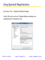
Using QuartusII Megafunctions
In Quartus, Tools — MegaWizard Plug-In Manager
Usually will create a new one. Though editing an existing one is
something that I’ve frequently done.
EECS 452 – Fall 2014
Lecture 5 – Page 87/143
Tuesday – September 16, 2014
Megafunctions continued
Some are free, some are not. I think that the
non-free ones are in the MegaStore.
Non-free can usually be used tethered and are
likely time-duration limited.
My most common use has been RAM, ROM and
FIFO.
There is documentation. You have to hunt it up.
EECS 452 – Fall 2014
Lecture 5 – Page 88/143
Tuesday – September 16, 2014
Specifying a ROM
EECS 452 – Fall 2014
Lecture 5 – Page 89/143
Tuesday – September 16, 2014
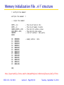
Memory Initialization File .mif structure
%
multiple-line comment
multiple-line comment
%
-- single-line comment
DEPTH = 32;
WIDTH = 8;
ADDRESS_RADIX = HEX;
DATA_RADIX = BIN;
CONTENT
BEGIN
------
00
01
02
03
04
05
06
07
08
09
0A
0B
0C
-- memory address : data
:
:
:
:
:
:
:
:
:
:
:
:
:
00000000;
00000001;
00000010;
00000011;
00000100;
00000101;
00000110;
00000111;
00001000;
00001001;
00001010;
00001011;
00001100;
The size of data in bits
The size of memory in words
The radix for address values
The radix for data values
start of (address : data pairs)
END;
http://quartushelp.altera.com/9.1/mergedProjects/reference/glossary/def_mif.htm
EECS 452 – Fall 2014
Lecture 5 – Page 90/143
Tuesday – September 16, 2014
More .mif information
.mif files are not part of the Verilog standards.
▶
Binary radix is BIN.
▶
Octal radix is OCT.
▶
Hexadecimal radix is HEX.
▶
Unsigned decimal is UNS.
▶
Signed decimal is DEC.
There are also some address/value pair syntax rules.
It is usually relatively easy to write a C program or MATLAB script to
automatically generate a .mif file. Or, at least, its contents for copy and
paste.
EECS 452 – Fall 2014
Lecture 5 – Page 91/143
Tuesday – September 16, 2014
Example .mif sine table generator
/*
* main.c
*
* slapdash quick and dirty sine table .. not
* checked for symmetry, etc.
*
* initial version .. 02 Oct 2011 .. K.Metzger
*
*/
#include <stdlib.h>
#include <stdio.h>
#include <math.h>
#define N 256
#define pi 3.14159265
void main(void) {
unsigned ctr;
int v;
FILE *out;
out = fopen("sine_rom.mif", "wa");
if (out == NULL) {
printf("cannot open output file\n");
exit(1);
}
printf("starting\n");
for(ctr=0; ctr<N; ctr++) {
v = 32767*sin(2*pi*ctr/(float)N);
fprintf(out, "%d : %04X;\n", ctr, v);
}
fclose(out);
printf("done\n");
}
EECS 452 – Fall 2014
Lecture 5 – Page 92/143
Tuesday – September 16, 2014
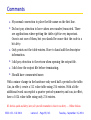
Comments
▶
My normal convention to place the file name on the first line.
▶
Did not pay attention to how values are rounder/truncated. There
are applications where getting the table right is very important.
Ours is not one of them, but you should be aware that the code is a
bit dirty.
▶
Only prints out the table entries. Have to hand add the descriptor
information.
▶
I did pay attention to the return when opening the output file.
▶
I did close the output file before terminating.
▶
Should have commented more.
With a minor change in the hardware only need half a period in the table.
Can, in effect, create a 512 value table using 256 entries. With a little
additional work can exploit a quarter period symmetry and can, in effect,
have a 1024 value table using only 256 entries.
If I do this quick and dirty, later, all you will remember is that it was dirty. — Wilbur Nelson
EECS 452 – Fall 2014
Lecture 5 – Page 93/143
Tuesday – September 16, 2014
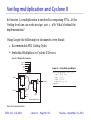
Verilog multiplication and Cyclone II
In Exercise 3 a multiplication is involved in computing FTVs. At the
Verilog level one can write assign out = a*b. What’s behind the
implementation?
Using Google the following two documents were found:
▶
Recommended HDL Coding Styles.
▶
Embedded Multipliers in Cyclone II Devices.
Figure 12–2. Multiplier Block Architecture
signa (1)
signb (1)
aclr
clock
ena
Data A
D
Example 11–1. Verilog HDL Unsigned Multiplier
Q
ENA
D
Q
ENA
CLRN
Data Out
module unsigned_mult (out, a, b);
output [15:0] out;
input [7:0] a;
input [7:0] b;
assign out = a * b;
endmodule
CLRN
Data B
D
Q
ENA
CLRN
Input
Register
Output
Register
Embedded Multiplier Block
From Altera documentation.
EECS 452 – Fall 2014
Lecture 5 – Page 94/143
Tuesday – September 16, 2014
Overflow lecture material
Variations on Blinky for the DE2-70.
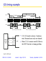
Crossing time boundaries
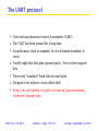
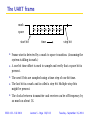
Bit serial interfacing.
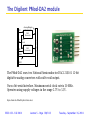
PMod D/A and A/D.
DE0-Nano.
Some comments.
Last one out should close the lab door!!!!
Please keep the lab clean and organized.
Always code as if the guy who ends up maintaining your code will be a violent
psychopath who knows where you live. — John Woods
EECS 452 – Fall 2014
Lecture 5 – Page 95/143
Tuesday – September 16, 2014
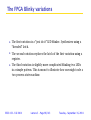
The FPGA Blinky variations
▶
The first variation is a “just do it” LED blinker. Synthesizes using a
“dreaded” latch.
▶
The second variation replaces the latch of the first variation using a
register.
▶
The third variation is slightly more complicated blinking two LEDs
in a simple pattern. This is meant to illustrate how one might code a
two process state machine.
EECS 452 – Fall 2014
Lecture 5 – Page 96/143
Tuesday – September 16, 2014
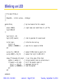
Blinking an LED
// File name: Blinky.sv
//
// 10Sep2013 .. initial version .. K.Metzger
//
module Blinky
(
output LEDR[0],
input CLOCK_50
);
logic led_bit, clk;
logic [24:0] counter;
// top level module for this example
// signal names must match those in .qsf file
// sized to generate 0.5 second event
initial begin
led_bit = 0;
counter = 25000000-1;
end
// initialize the start-up
assign clk = CLOCK_50;
assign LEDR[0] = led_bit;
// connect 50 MHz clock to generic clk
// connect the led_bit to RED LED 0
// count for 1/2 second at 50 MHz
always_ff @(posedge clk) begin
counter <= counter-1;
//
if (counter == 0) begin
//
led_bit <= ~led_bit;
//
counter <= 25000000-1; //
end
end
// use rising edge of the clock
set next counter value to current minus 1
but if the counter equals 0
complement the led bit
reset the counter
endmodule
EECS 452 – Fall 2014
Lecture 5 – Page 97/143
Tuesday – September 16, 2014
Blinky comments
▶ A common problem is mismatching the top level signal names with the
ones used in the .qsf file. This is NOT flagged as an error!
▶ What happens to led_bit when counter is not 0? A latch is synthesized.
▶ The values of led_bit and counter change only on the positive edge
transition of clk.
▶ 25 bits allows counts of up to 33,554,432.
▶ One of my SystemVerilog fantasies is that counting down to 0 simplifies the
end test logic.
▶ SystemVerilog is a weakly typed language. It allows to do things like take an
integer and put it into a register. The value 25000000-1 is evaluated as a 32
bit value, truncated to 25 bits and then converted into a logic vector that
can be loaded into a 25 bit register.
▶ This is all well and good if I wrote code to do what I intended. If not, then
the compiler does it’s best to figure out what I meant and doesn’t tell me
what it did.
▶ It is very important to say you mean and mean what you say.
EECS 452 – Fall 2014
Lecture 5 – Page 98/143
Tuesday – September 16, 2014
Blinky using registers
// File name: Blinky_D.sv
//
// 10Sep2013 .. initial version .. K.Metzger
//
module Blinky_D
(
output LEDR[0],
input CLOCK_50
);
logic led_bit, next_led_bit, clk;
logic [24:0] counter, next_counter;
initial begin
led_bit = 0;
counter = 25000000-1;
end
assign clk = CLOCK_50;
assign LEDR[0] = led_bit;
always_ff @(posedge clk) begin
led_bit <= next_led_bit;
counter <= next_counter;
end
always_comb begin
next_counter = counter-1;
next_led_bit = led_bit;
if (counter == 0) begin
next_counter = 25000000-1;
next_led_bit = ~led_bit;
end
end
endmodule
EECS 452 – Fall 2014
Lecture 5 – Page 99/143
Tuesday – September 16, 2014
Blinky_D comments
▶
I got sort of canonical. The counter was already a register because
of the way it was being used. At least I think it was.
▶
The led_bit is aways updated in the always_ff block. The
next_led_bit = led_bit determines what the updated value is if
there isn’t a change to be made.
EECS 452 – Fall 2014
Lecture 5 – Page 100/143
Tuesday – September 16, 2014
Blinky_state part 1
// File name: Blinky_state.sv
//
// 10Sep2013 .. initial version .. K.Metzger
// 17Sep2013 .. made Blinky more complicated and added states .. KM
module Blinky_state
(
output LEDR[0],
output LEDG[0],
input CLOCK_50
);
logic
logic
logic
logic
logic
red_led_bit, next_red_led_bit;
green_led_bit, next_green_led_bit;
clk;
[7:0] time_counter, next_time_counter;
[24:0] counter, next_counter;
enum
{starting, turn_on_red, turn_on_green} state, next_state;
initial begin
red_led_bit = 0;
green_led_bit = 0;
counter = 25000000-1;
time_counter = 0;
state = starting;
end
assign clk = CLOCK_50;
assign LEDR[0] = red_led_bit;
assign LEDG[0] = green_led_bit;
always_ff @(posedge clk) begin
red_led_bit <= next_red_led_bit;
green_led_bit <= next_green_led_bit;
time_counter <= next_time_counter;
counter <= next_counter;
state <= next_state;
end
EECS 452 – Fall 2014
Lecture 5 – Page 101/143
Tuesday – September 16, 2014
Blinky_state part 2
always_comb begin
next_counter = counter-1;
next_time_counter = time_counter;
next_red_led_bit = red_led_bit;
next_green_led_bit = green_led_bit;
next_state = state;
if (counter == 0) begin
next_counter <= 25000000-1;
next_time_counter <= time_counter + 1;
end
case (state)
starting: begin
if (time_counter == 2) begin
next_time_counter <= 0;
next_red_led_bit <= 1;
next_state <= turn_on_red;
end
end
turn_on_red: begin
if (time_counter == 4) begin
next_time_counter <= 0;
next_green_led_bit <= 1’b1;
next_time_counter <= 0;
next_state <= turn_on_green;
end
end
turn_on_green: begin
if (time_counter == 6) begin
next_time_counter <= 0;
next_red_led_bit <= 0;
next_green_led_bit <= 0;
next_state <= starting;
end
end
endcase
end
endmodule
EECS 452 – Fall 2014
Lecture 5 – Page 102/143
Tuesday – September 16, 2014
Blinky_state comments
▶
Idles for one second with both LEDs off. Turns the red LED on. After
two seconds turns on the green LED. After 3 more seconds turns
both off. Repeats.
▶
Uses an enum statement to define the states and a case statement to
select between states.
▶
The “present” and “next” paradigm is reasonably common. At least
one FPGA test uses “present” as a prefix as is done with “next”.
▶
The always_ff always loads the next value into the current. The
always_comb starts by setting the next values to their current
values. This is what makes the compiler synthesize registers.
▶
Perturbations abound. For example, the counter could be
incremented in the always_ff eliminating the need for a next
version and making the code slightly less verbose.
▶
Notice the lack of comments. This is often justified by stating that
the code is self documenting. Generally it’s considered good practice
to have some comments. You might be the one that has to maintain
the code.
EECS 452 – Fall 2014
Lecture 5 – Page 103/143
Tuesday – September 16, 2014
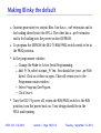
Loading Blinky into the FPGA
▶
There are two ways to get access to the USB Blaster programmer.
1. On the tool bar at the top of the Quartus II window go to
Tools---Programmer.
2. In the Task window where you clicked Compile Design double
click Program Device (Open Programmer).
▶
Make sure that the DE2-70 RUN/PROG switch (left middle side) is in
the RUN position.
▶
The programmer support is normally configured properly and all
one needs is to click the Start button. Progress is indicated in the
Progress window.
▶
Sometimes the USB-Blaster isn’t connected to the programmer
suport. Sometimes this means the USB cable is not present or the
DE2-70 is powered off. Sometimes, for some reason, the driver isn’t
present in the PC.
▶
The file to be loaded into the FPGA has a .sof extension.
EECS 452 – Fall 2014
Lecture 5 – Page 104/143
Tuesday – September 16, 2014
Making Blinky the default
▶
Quartus generates two output files. One has a .sof extension and is
for loading directly into the FPGA. The other has a .pof extension
and is for loading into the power-on boot EEPROM.
▶
To program the EEPROM the DE2-70 RUN/PROG switch needs to be in
the PROG position.
▶
In the programmer window:
▶
▶
▶
▶
▶
Change the Mode to Active Serial Programming.
Add File, select output_files. You should see your .pof file
listed. Click on it then on open. This will return you to the
Programmer main window.
Select Program/Configure.
Click Start.
Turn the DE2-70 power off, return the RUN/PROG switch to the RUN
position, turn the power back on. Your design should be in the
FPGA and running.
EECS 452 – Fall 2014
Lecture 5 – Page 105/143
Tuesday – September 16, 2014
Restoring the default default
▶
The Terasic supplied default start-up code can be found in the
DE2-70_v.1.4.0_CDROM file.
▶
Mouse down through DE2_70_demonstrations, DE2_70_Default
to find the DE2_70_Default.qpf file.
▶
The included .sof and .pof were generated using a earlier version
of Quartus and might not be programmable using the current
version’s USB Blaster. I generally recompile.
▶
Program the EEPROM using the newly generated .pof as described
in the preceding slide.
EECS 452 – Fall 2014
Lecture 5 – Page 106/143
Tuesday – September 16, 2014
The FPGA breakout board
▶
Connects 40-pin IO port to 8
6-pin connectors.
▶
6-pin connectors compatible
with Digilent PMod boards.
http://www.digilentinc.com/
Products/Catalog.cfm?
NavPath=2,401&Cat=9.
▶
Supply voltage jumper
selectable, +3.3V and +5.0V.
Remove jumpers when power
not needed!
▶
Pin 1 light colored.
▶
Also useful as test points.
EECS 452 – Fall 2014
Lecture 5 – Page 107/143
Tuesday – September 16, 2014
DE2-70 FPGA breakout board connections
08/05/12 7:08:14 PM f=1.50 C:\Users\Kurt\Documents\eagle\Fall_2011_DE2-70_breakout\DE270Break.sch (Sheet: 1/1)
EECS 452 – Fall 2014
Lecture 5 – Page 108/143
Tuesday – September 16, 2014
DE2/DE2-70/DE0-Nano GPIO names
pin
1
2
3
4
5
6
7
8
9
10
11
12
13
14
15
16
17
18
19
20
21
22
23
24
25
26
27
28
29
30
31
32
33
34
35
36
37
38
39
40
DE2
GPIO_x[0]
GPIO_x[1]
GPIO_x[2]
GPIO_x[3]
GPIO_x[4]
GPIO_x[5]
GPIO_x[6]
GPIO_x[7]
GPIO_x[8]
GPIO_x[9]
VCC5
GND
GPIO_x[10]
GPIO_x[11]
GPIO_x[12]
GPIO_x[13]
GPIO_x[14]
GPIO_x[15]
GPIO_x[16]
GPIO_x[17]
GPIO_x[18]
GPIO_x[19]
GPIO_x[20]
GPIO_x[21]
GPIO_x[22]
GPIO_x[23]
GPIO_x[24]
GPIO_x[25]
VCC33
GND
GPIO_x[26]
GPIO_x[27]
GPIO_x[28]
GPIO_x[29]
GPIO_x[30]
GPIO_x[31]
GPIO_x[32]
GPIO_x[33]
GPIO_x[34]
GPIO_x[35]
EECS 452 – Fall 2014
DE2-70
DE0-Nano
CLKINnx
GPIO_x[0]
CLKINpx
GPIO_x[1]
GPIO_x[2]
GPIO_x[3]
GPIO_x[4]
GPIO_x[5]
GPIO_x[6]
GPIO_x[7]
VCC5
GND
GPIO_x[8]
GPIO_x[9]
GPIO_x[10]
GPIO_x[11]
GPIO_x[12]
GPIO_x[13]
CLKOUTnx
GPIO_x[14]
CLKOUTnx
GPIO_x[15]
GPIO_x[16]
GPIO_x[17]
GPIO_x[18]
GPIO_x[19]
GPIO_x[20]
GPIO_x[21]
VCC33
GND
GPIO_x[22]
GPIO_x[23]
GPIO_x[24]
GPIO_x[25]
GPIO_x[26]
GPIO_x[27]
GPIO_x[28]
GPIO_x[29]
GPIO_x[30]
GPIO_x[31]
IN0
GPIO_x[0]
IN1
GPIO_x[1]
GPIO_x[2]
GPIO_x[3]
GPIO_x[4]
GPIO_x[5]
GPIO_x[6]
GPIO_x[7]
VCC_SYS
GND
GPIO_x[8]
GPIO_x[9]
GPIO_x[10]
GPIO_x[11]
GPIO_x[12]
GPIO_x[13]
GPIO_x[14]
GPIO_x[15]
GPIO_x[16]
GPIO_x[17]
GPIO_x[18]
GPIO_x[19]
GPIO_x[20]
GPIO_x[21]
GPIO_x[22]
GPIO_x[23]
VCC3P3
GND
GPIO_x[24]
GPIO_x[25]
GPIO_x[26]
GPIO_x[27]
GPIO_x[28]
GPIO_x[29]
GPIO_x[30]
GPIO_x[31]
GPIO_x[32]
GPIO_x[33]
Lecture 5 – Page 109/143
Tuesday – September 16, 2014
Bit-serial data transfers
▶
Moore’s law has been running for some time now. Space on a chip
become very inexpensive, pins and interconnections have not.
▶
Many devices have relatively low data rates. Maybe 1M 8 or 16-bit
words per second.
▶
Modern run-of-the-mill digital drivers often can drive PCB-traces
and actual wires at rates of 50 Mbs and often higher.
▶
For many of the synchronous bit-serial protocols everything is edge
driven. The inter/intra clock rates do not have to be constant!
EECS 452 – Fall 2014
Lecture 5 – Page 110/143
Tuesday – September 16, 2014
Clock domain crossings
“A clock domain crossing occurs whenever data is transferred
from a flop driven by one clock to a flop driven by another
clock.”
Saurabh Verna
EECS 452 – Fall 2014
Lecture 5 – Page 111/143
Tuesday – September 16, 2014
CDC references
▶
Understanding clock domain crossing issues, Saurabh Verna, EE
Times–India, December 2007.
▶
Clock Domain Crossing (CDC) Design & Verification Techniques
Using System Verilog, Clifford E. Cummings.
▶
http://www.fpga4fun.com/CrossClockDomain.html.
EECS 452 – Fall 2014
Lecture 5 – Page 112/143
Tuesday – September 16, 2014
g clock
domain and mitigation
Metastability
s
names shown
ectly used. For
C2 imply the
tion clocks rey A and B are
nd destination
ectively. Also,
stination flops
positive edge
1.
2.
In theory, a flip-flop can take a very
long time to decide.
▶
It is not possible to guarantee that a
metastable state will not occur.
▶
Fast logic and slow clock rates help,
but . . . .
▶
It is possible to reduce the probability
of a metastable state to a very small
number.
▶
A two state synchronizer is often
adequate. However, for reliability
applications (e.g., aircraft control
systems) use three or more.
Clock domain crossing
Crossing Issues
bes three main
possibly occur
s a clock doe solutions for
so described.
nsition on sigy close to the
ck C2, it could
old violation at
p “FB”. As a regnal B may osnite amount of
put is unstable
ot settle down
ue before the
C2 arrives. This
nown as metap “FB” is said to
tastable state.
turn can have
consequences
pective:
▶
Metastability has consequences.
data is fed to
Multi-flop synchronization.
places in the 3.
ead to a high
nd even chipEECS
For452
example,
see Figure
2. in the destination
domain. A 5
– Fall
2014
Lecture
worst case.
If the input signal A transitions commonly used synchronizer
ut cones may very close to the posedge of is a multi-flop synchronizer as
From: Understanding clock domain crossing issues, Saurabh.
– Page 113/143
Tuesday – September 16, 2014
Metastability cause
ts
Q
X
Q
th
setup time
clock b
hold time
X
clock a
clock b
▶
It takes time for things to get ready to happen and then to happen.
▶
If there isn’t adequate time, things go wrong.
▶
In theory, it can take a very long time to settle down.
▶
Metastability can be a problem in a FPGA’s clock distribution
network even in a single clock domain.
▶
Quartus II’s timing analyzer checks to whether or not the required
setup and hold times are met.
EECS 452 – Fall 2014
Lecture 5 – Page 114/143
Tuesday – September 16, 2014
Generic synchronous bit-serial send/receive
transmitter
connection
receiver
received_flag
frame_sync
clock_a
control logic
shift register
shift_clock
bit_serial_data
control logic
?
clock_b
shift register
register
parallel_data
▶
The transmitter is in charge and relatively easy to design.
▶
The design of the receiver is the challenge.
▶
Where should the clock boundary be?
EECS 452 – Fall 2014
Lecture 5 – Page 115/143
Tuesday – September 16, 2014
An answer is ?
▶
As late as possible.
▶
When using a well designed protocol, it should be possible to clock
the receiver and generate the received_flag using the supplied
clock and frame synchronization signals.
▶
The only signal that needs metastabilty protection should be the
received_flag.
▶
If this is not the case, the protocol is not properly designed or the
receiver designer needs to think more.
▶
The receiver is double buffered allowing a full frame time in which
to retrieve the received value.
▶
I use an asynchronous clear from the b time domain on the flag bit.
This avoids metastability problems.
EECS 452 – Fall 2014
Lecture 5 – Page 116/143
Tuesday – September 16, 2014
Commonly encountered protocols
▶
SPI (serial peripheral interface)
▶
▶
▶
I2S (Inter-IC, Integrated Interchip Sound)
▶
▶
Used to interconnect audio devices together.
I2C (Inter-Integrated Circuit)
▶
▶
Not standardized.
Supported by many devices such as A/D and D/A chips.
Multi-master, low speed with addressability.
UART (Univeral asynchronous receive/transmit)
▶
▶
Dates from the 1920s. Has been somewhat updated.
Uses pre-agreed upon clock rate.
There are many, many more. Some are even “one-wire” and self clocking.
EECS 452 – Fall 2014
Lecture 5 – Page 117/143
Tuesday – September 16, 2014
The SPI protocol
▶
A synchronous bit-serial protocol.
▶
Originated by Motorola but not standardized.
▶
Many devices use a SPI-like protocol. For example, the PMod A/D
and D/A converter modules.
▶
The Wikipedia has a nice discussion:
http://en.wikipedia.org/wiki/Serial_Peripheral_Interface_Bus
▶
Meant to be easy to implement and work with.
▶
Typical transfer size are 8 and 16 bits.
▶
Bi-directional. Send a word, receive a word, with latency.
▶
A relevant learning document is the C5515 SPI User’s Guilde,
SPRUFO3.
EECS 452 – Fall 2014
Lecture 5 – Page 118/143
Tuesday – September 16, 2014
SPICCR
SPIDCR1
SPICDR
SPIDCR2
SPI_RX/MISO
B6
B7
B5
B4
B3
B2
B1
B0
SPI timing example
SPICMD1
Clock
Generator
SPICMD2
SPI_CSn/SS
SPISTAT1
SPISTAT2
SPI_CLK
Sequencer
SPI
Interrupt to
CPU
SPI_CS
Figure 6. SPI
Mode 2 Transfer (CKPn = 1, CKPHn = 0)
SPIDAT2
SPI_RX
SPIDAT1
SPI_CLK/SCK
SPI_TX
SPI_TX/MOSI
B6
B7
Use Case Statement
B5
ntended for communication between the DSP and up to four SPI-complaint slave devices.
cations include an interface to external I/O or peripheral expansion via devices such as shift
B6
B5
B7
play drivers, SPISPI_RX/MISO
EEPROMs, and analog-to-digital converters.
The programmable
n capability of the SPI allows it to interface to a variety of SPI format devices without the need
.
B4
B3
B2
B1
B0
B4
B3
B2
B1
B0
SPI_CSn/SS
interface with a single
slave device is shown in Figure 2. The DSP controls the flow of
on by providing shift-clock (SPI_CLK) and slave-select signals (SPI_CSn).
Figure 2. Typical SPI Interface
SPRUFO3 – September
2009
SPI-Compliant
DSP
Slave
Submit Documentation Feedback
Serial Peripheral Interface (SPI)
Copyright © 2009, Texas Instruments Incorporated
SPI_CLK
SCK
SPI_TX
MOSI
SPI_RX
MISO
SPI_CSn
▶
C5515 SPI mode 2 is shown.
▶
The TI C5515 SPI can only be a master!
▶
We can design either master or slave
interfaces in the FPGA.
SS
tandard(s) Compliance Statement
s not conform to a specific industry standard.
From TI’s SPRUFO3.pdf.
EECS 452 – Fall 2014
Lecture 5 – Page 119/143
Tuesday – September 16, 2014
13
My DIY SPI timing example
FPGA changes
output on rising
edges
FPGA samples
on falling edges
TI RX
TI DX
Start of
transfer
Transmitter
shift register
loaded
Transmit register
empty flag set
EECS 452 – Fall 2014
Lecture 5 – Page 120/143
End of Receive
transfer flag set
Receive
register
loaded
Tuesday – September 16, 2014
The I2S protocol
▶
Used by CODEC chips in the C5515 and the DE2-70 for data transfer.
▶
Several modes of operation, stereo, mono, etc.
▶
When C5515 is a master the word rate is fixed and constant. When
C5515 is slave the edge timings from the FPGA rule!
▶
A reasonable use is an reverse channel from FPGA to C5515.
▶
A useful reference is the C5515 I2S User’s guide, SPRUFX4.
EECS 452 – Fall 2014
Lecture 5 – Page 121/143
Tuesday – September 16, 2014
N N N
- - 1 2 3
DATA
3
2
1
N N N
- - 1 2 3
0
I2S timing example
LD(n)
3
2
1
N N N
- - 1 2 3
0
RD(n)
LD(n) = n'th sample of left channel data
LD(n+1)
RD(n) = n'th sample of right channel data
Figure 1-8. Timing Diagram for I2S Mode
I2S FS
LEFT CHANNEL
RIGHT CHANNEL
I2S_CLK
ti.com
Architecture
Table 1-1. I2S Signal Descriptions
Name
Signal
I2Sn_CLK
N N N
-INPUT
- /OUTPUT
3
1INPUT
2 /OUTPUT
3
DATA
I2Sn_FS
I2Sn_DX
OUTPUT
I2Sn_RX
INPUT
Description
2
1
0
I2S Clock
I2S Frame Sync Clock
N N N
- - 1 2 3
I2S Data Transmit
LD(n)
3
2
1
0
N N N
- - 1 2 3
RD(n)
I2S Data Receive
LD(n) = n'th sample of left channel data
The diagram below is a typical connection between I2S interface to an audio or voice-band Codec.
3
LD(n+1)
RD(n) = n'th sample of right channel data
Figure 1-3. Block Diagram of I2S Interface to Audio/Voice Band Codec
Figure 1-9. Timing Diagram for I2S Mode with Inverse Bit-Clock Polarity
I2S_FS
AIC32 or
I2S_CLK
any
I2S
Codec
I2Sn_CLK
WCLK
I2Sn_FS
DIN
I2Sn_DX
DOUT
DATA
LEFT CHANNEL
CLK
I2Sn_RX
N N N
- - 3 2
1 2 3
DSP
1
▶
C5515 I2S
RIGHTmode
CHANNEL is shown. Variations
exist. Monaural uses only one channel.
▶
When C5515 is master need RC filter in
theN DOUT
line due to timingN problem.
N N
N N
0
LD(n)
.1
Pin Multiplexing
LD(n) = n'th sample of left channel data
Depending on the I2S bus being used, the DSP should be configured to route those I2S signals to the
multiplexed Serial
Port TI’s
0, Serial
Port 1, or Parallel Port pins by writing to the External Bus Selection
From
SPRUFX4.pdf.
Register (EBSR). For more information on pin multiplexing, see the device-specific DSP system guide.
1.2.5.2
1
2
3
3
2
1
0
RD(n)
1
2
3
3
LD(n+1)
RD(n) = n'th sample of right channel data
DSP Format
EECS 452
Fallformat,
2014 the trailing edge
Lecture
– Page 122/143 pulse, I2Sn_FS,
Tuesday
– September
16,with
2014
In –DSP
of the5frame-synchronization
starts
the data transfer
NOTE: Configuring the EBSR to route I2S0 or I2S1 signals to Serial Port0 or Serial Port1
respectively also routes those I2S interrupts to the CPU (see Section 1.2.10).
the left channel data first and immediately followed by the right channel data. Each data bit is valid on the
The I2C protocol
▶
Eight data bits and eight bits address plus two handshake bits.
▶
Ack bit is driven by addressed device, if present and ready.
▶
Used by the CODEC in the DE2-70 for configuration.
▶
The FPGA CODEC and NTSC video decoder devices are configured
using I2C.
▶
We have a couple of CMOS digital cameras that are I2C configured.
EECS 452 – Fall 2014
Lecture 5 – Page 123/143
Tuesday – September 16, 2014
clock signals to permit that transfer. Any device that is addressed by this master is
considered a slave during this transfer.
The I2C connection and timing
An example of multiple I2C modules that are connected for a two-way transfer from one device to other
devices is shown in Figure 2.
www.ti.com
Figure 2. Multiple I2C Modules Connected
2.6
VDD
Serial Data Formats
Peripheral Architecture
Figure 7 shows an example of a data transfer on the I2C-bus. The I2C peripheral supports 2-bit to 8-bit
data values. Figure 7 shows
transfer using (BC =I2C000 in ICMDR). Each bit put on the
Pull-up a typical I2C data
TI device
resistors
I2C line. The data is controller
SDA line is equivalent to
one pulse on the SCL
always transferred with the
most-significant bit (MSB) first. The number of data values that can be transmitted or received is
unrestricted; however, in most systems, the transmitter and receiver have agreed upon the number of data
Serial data (SDA)
values to transfer
transfer begins.
Serial before
clock (SCL)
The I2C peripheral supports the following data formats:
• 7-bit addressing mode.
I2C
EPROM
• 10-bit addressing mode.
• Free data format mode.
SPRUFO1A – September 2009
Submit Documentation Feedback
TI device
I2C
Figure 7. I2C Peripheral Data Transfer
Inter-Integrated Circuit (I2C) Peripheral
Acknowledgement
Copyright ©
Texas
Instruments Incorporated
bit2009,
from
slave
11
(No-)Acknowledgement
bit from receiver
SDA
MSB
SCL
START
condition (S)
1
2
Slave address
2.6.1
7
8
R/W
9
ACK
1
2
8
9
ACK
STOP
condition (P)
Data
7-Bit Addressing Format
From TI’s SPRUFO1A.
In the 7-bit addressing format (Figure 8), the first byte after a START condition (S) consists of a 7-bit slave
EECS 452
– Fall followed
2014 by a R/W bit.
Lecture
5 –bit
Page
124/143
Tuesday
address
The R/W
determines
the direction of the
data. – September 16, 2014
• R/W = 0: The master writes (transmits) data to the addressed slave.
The UART protocol
▶
Universal asynchronous receiver/transmitter (UART).
▶
The UART has been around for a long time.
▶
Asynchronous, clock is assumed. No clock domain boundary to
cross!
▶
Usually eight data bits plus optional parity. Two or three support
bits.
▶
There exist “standard” baud (bits/second) rates.
▶
Designed to be robust to clock offset/drift.
▶
http://en.wikipedia.org/wiki/Universal_asynchronous_
receiver/transmitter.
EECS 452 – Fall 2014
Lecture 5 – Page 125/143
Tuesday – September 16, 2014
The UART frame
mark
space
start bit
b0 b1 b2 b3 b4 b5 b6 b7
time
stop bit
▶
Frame start is detected by a mark to space transition. (Assuming the
system is idling in mark.)
▶
A one bit time offset is used to sample and verify that a space bit is
present.
▶
The next 8 bits are sampled using a time step of one bit time.
▶
The last bit is a mark and is called a stop bit. Multiple stop bits
might be present.
▶
The clocks between transmitter and receiver can be off frequency by
as much as about 5%.
EECS 452 – Fall 2014
Lecture 5 – Page 126/143
Tuesday – September 16, 2014
The FT232R UART/USB breakout
▶
Used to communicate UART data (8-bit) over
USB.
▶
Powered by the USB connector’s 5 Volts.
Regulates this down to 3.3 Volts.
▶
Supports RTS/CTS handshake.
▶
Max baud clock is counted down from 3 Mbs.
Integer divide factor.
▶
I’ve successfully used these at 1.5 Mbs and 3.0
Mbs.
▶
I’m using FTDI’s D2XX direct drivers on the
RPi (the USB end). I located a special build for
RPi’s hard float. FTDI’s V1.1.12 only supports
soft float. The HF and SF calling sequences are
not compatible.
EECS 452 – Fall 2014
Lecture 5 – Page 127/143
Tuesday – September 16, 2014
Bit-serial comments
▶
The PMod boards are pretty much intended for use on FPGA boards
made by Digilent. The DE2-70/DE0-Nano breakout board allows
their use on these Terasic boards as well.
▶
Using an adapter card or cable one can plug a PMod A/D and/or
PMod D/A directly to a C5515 breakout board 6-pin connector. I’ve
tested using SPI and I2S.
▶
Once can implement your own serial protocol. A few semesters a
project (Seymour) bit-banged a four bit protocol between an FPGA
and the Raspberry Pi.
EECS 452 – Fall 2014
Lecture 5 – Page 128/143
Tuesday – September 16, 2014
Synchronizer module
// File name: synchronizer.sv
//
// 09Aug2012 .. version started .. K.Metzger
//
module synchronizer
(
input signal_in,
input clear_in,
output signal_out,
input clk);
logic [1:0] delay;
assign signal_out = delay[1];
always_ff@(posedge(clk), posedge(clear_in)) begin
if (clear_in) delay <= 0;
else delay <= {delay[0], signal_in};
end
endmodule
EECS 452 – Fall 2014
Lecture 5 – Page 129/143
Tuesday – September 16, 2014
The Digilent PMod-DA2 module
Analog Outputs
2
DAC121S101
D/A
Converter
Sync,
Clock
D2
DAC121S101
D/A
Converter
J2 Connector
J1 Connector
D1
GND
VCC
The PMod-DA2 uses two National Semiconductor DAC121S101 12-bit
digital-to-analog converters with rail-to-rail output.
Uses a bit-serial interface. Maximum serial clock rate is 30 MHz.
Operates using supply voltages in the range 2.7V to 5.5V.
Figure from the PMod Digilent data sheet.
EECS 452 – Fall 2014
Lecture 5 – Page 130/143
Tuesday – September 16, 2014
The DAC121S101 D/A
Max serial clock : 30 MHz
Data uses offset binary.
Analog output updates on
16th shift clock falling edge.
From the National Semiconductor data sheet.
20114906
EECS 452 – Fall 2014
Lecture 5 – Page 131/143
Tuesday – September 16, 2014
How to make the D/A work
Here are some observations/guesses about control of the D/A. These
are based on the timing timing diagram and written signal
descriptions contained in the data sheet. Use of a state machine in the
D/A control logic is assumed.
▶
sync_n can remain high between updates going low when a serial
transfer is to start.
▶
The start of a serial transfer is detected by sampling sync_n
using the rising edges of sclk.
▶
Data bits are sampled on the falling edges of sclk.
▶
There is a counter in the D/A that loads D/A holding register
from the input shift register. Possibly on the 16th falling edge of
sclk.
▶
After loading the DAC register the state machine waits for the
next high to low transition on sync_n
EECS 452 – Fall 2014
Lecture 5 – Page 132/143
Tuesday – September 16, 2014
Starting simple with the D/A
A simple test is to run a counter and send the count values to the D/A
and observe the waveform. About as basic test you can do.
Check the schematic and data sheet to
▶
determine the part number.
▶
see how the part is designed into the board.
▶
find the PMod pin signal assignments.
Check the D/A data manual to determine
▶
how it works. Actually, to learn how to make it work.
▶
the signal timings.
▶
the mapping from digital input values to output voltages.
EECS 452 – Fall 2014
Lecture 5 – Page 133/143
Tuesday – September 16, 2014
The Digilent PMod-AD1 module
P1: CS
ADC
1
Filter
P1
P2
P3: Data 2
ADC
2
Filter
P4: Clk
P3
P4
P5: GND
P5
P6: Vcc
P6
J2 Connector
J1 Connector
P2: Data1
AD1 Circuit Diagram
The PMod-AD1 uses two National Semiconductor ADCS7476 12-bit
analog-to-digital converters supporting rail-to-rail input.
Uses a bit-serial interface. Maximum serial clock rate is 20 MHz. Operates
using supply voltages in the range 2.7V to 5.25V.
Figure from the PMod Digilent data sheet.
EECS 452 – Fall 2014
Lecture 5 – Page 134/143
Tuesday – September 16, 2014
The ADCS7476 A/D
Max serial clock : 20 MHz
Max sample rate: 1 MHz
Data uses offset binary.
Input switches from track to hold on
falling edge of the sync signal.
From the National Semiconductor data sheet.
EECS 452 – Fall 2014
Lecture 5 – Page 135/143
Tuesday – September 16, 2014
Comments
▶
Timing diagrams typically show what one can get away with not
necessarily best practice.
▶
Notice the runt SDATA digit. This is what can get away with. I
really wouldn’t design to cause this.
▶
Relative to the clock shown I started CSbar half a clock earlier.
This gives a more full data bit.
▶
The SDATA bits are sampled at the instant at which the sclk
falling edges are started.
▶
I can do this because I sample the bit at the same time as I start
the edge to fall. It takes time to fall and be recognized by the A/D
and then shift the next data bit. Generally the registers in the
FPGA have 0 ns hold time.
EECS 452 – Fall 2014
Lecture 5 – Page 136/143
Tuesday – September 16, 2014
DIY directed study DSP with FPGAs
▶
On Amazon, about $122.
▶
Uses Verilog, now includes some
VHDL.
▶
930 pages.
▶
Published May 2014.
▶
Uses Quartus II web edition.
▶
Includes source code in appendices.
▶
Focuses on communications
applications.
▶
Signed fixed point and floating point
IEEE library examples.
▶
Overview on parallel all-pass IIR filter
design.
From the Amazon web site.
EECS 452 – Fall 2014
Lecture 5 – Page 137/143
Tuesday – September 16, 2014
FYI: Terasic DE0-Nano
http://www.terasic.com.
tw/cgi-bin/page/archive.
pl?Language=English&
CategoryNo=139&No=593
▶
22,230 LEs, 32 MB SDRAM (mounted on back side), $79.
▶
40-pin headers can match those on DE2-70.
▶
Has been used in past EECS 452 projects.
▶
Have a couple of units on-hand.
▶
Built in USB-blaster.
EECS 452 – Fall 2014
Lecture 5 – Page 138/143
Tuesday – September 16, 2014
DE0–Nano features
▶
Cyclone IV FPGA, 22,320 logic elements, 594 Kbits M4K memory, 66
embedded 18 × 18 multipliers, 4 PLLs and 152 FPGA I/O pins.
▶
USB powered.
▶
Two 40-pin expansion headers.
▶
One 26-pin header provides 16 GPIO pins and analog input pins.
▶
32 MB SDRAM, 2Kb I2C EEPROM.
▶
8 green LEDs, 2 debounced push buttons and 4 DIP switches.
▶
3 axis accelerometer.
▶
8-channel, 12-bit A/D converter, 50 ksps to 200 ksps.
▶
50 MHz oscillator.
▶
Nominal cost: $79, academic: $59. Shipping and currency exchange
fees can double the academic price.
▶
Digikey price: $82.80, plus shipping.
EECS 452 – Fall 2014
Lecture 5 – Page 139/143
Tuesday – September 16, 2014
DE2/DE2-70/DE0-nano support materials
Terasic makes available the schematics, user’s manual, demo source
code and other materials for their FPGA boards. Check out:
▶
DE2
http:
//www.terasic.com.tw/cgi-bin/page/archive.pl?Language=English&CategoryNo=165&No=30&PartNo=4
▶
DE2-70
http://www.terasic.com.tw/cgi-bin/page/archive.pl?Language=English&CategoryNo=183&No=226&
PartNo=4
▶
DE0-nano
http://www.terasic.com.tw/cgi-bin/page/archive.pl?Language=English&CategoryNo=139&No=593&
PartNo=4
The links are “hot”. Sites that use long links are a pain!
It is recommended to at least look at the DE2-70’s user’s manual.
EECS 452 – Fall 2014
Lecture 5 – Page 140/143
Tuesday – September 16, 2014
A low cost competitor
There is actually quite a lot of competition.
Boards similar to Terasic’s but using Xilinx parts can be found at
http://Digilentinc.com.
Xilinx is the dominant FPGA manufacturer.
For example, the very low cost ($69 academic) BASYS2:
From the Digilent web site.
EECS 452 – Fall 2014
Lecture 5 – Page 141/143
Tuesday – September 16, 2014
Thoughts on DIY career development
Once you graduate, career development likely will be mostly DIY.
▶ Buy an evaluation board. The Terasic DE2/DE2-70/DE0-Nano are great
value. The Digilent Xilinx boards are also. I own two or more of each
manufacturer’s. Do something with them!
▶ Find useful information. There’s a lot of useful material available on the
web, and a lot that isn’t. Sorting can be a problem.
The next slide lists some potential starter books.
▶ I’ve made numerous web searches to find relevant articles, purchased old
texts and even read some. Collect!
▶ Join the IEEE. At least look at their technical group publications.
▶ Join or create a club. Find someone you can talk technical with.
▶ Volunteer teach.
In addition:
EECS 452 – Fall 2014
Practice, practice, practice, . . .
Lecture 5 – Page 142/143
Tuesday – September 16, 2014
Starting a personal library
▶
The SystemVerilog standard. Available from the library in e-form.
▶
FPGA prototyping by xxxxx examples: Xilinx Spartan-3 version / Pong
P. Chu. Two versions, one where xxxxx is replaced by VHDL and the
other by Verilog. I own the VHDL version.
▶
Digital System Design with SystemVerilog, Mark Zwolinski, Prentice
Hall, 2010
▶
SystemVerilog for design : a guide to using SystemVerilog for
hardware design and modeling by Stuart Sutherland, Simon
Davidmann, Peter Flake ; foreword by Phil Moorby. Library copy is
missing but is available in e-form.
▶
B. Parhami, Computer Arithmetic: Algorithms and Hardware
Designs, 2nd edition, Oxford University Press, New York, 2010.
http://www.ece.ucsb.edu/~parhami/text_comp_arit.htm
▶
Digital Signal Processing with Field Programmable Gate Arrays
(Signals and Communication Technology), 3rd, Uwe Meyer-Baese.
EECS 452 – Fall 2014
Lecture 5 – Page 143/143
Tuesday – September 16, 2014