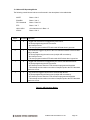
1
GF
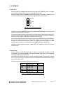
ATHENA™
High Integration CPU
with Ethernet and Data Acquisition
Model ATH400-128, ATH400-128N, ATH660-128, ATH660-128N
User Manual Revision 1.40
Document # 765820
Copyright 2004
Diamond Systems Corporation
8430-D Central Ave.
Newark, CA 94560
Tel (510) 456-7800
www.diamondsystems.com
ATHENA
High-Performance Rugged Embedded CPU with Data Acquisition
TABLE OF CONTENTS
1.
2.
3.
4.
DESCRIPTION ..................................................................................................................................5
FEATURES .......................................................................................................................................6
ATHENA BOARD DRAWING .............................................................................................................8
I/O HEADERS...................................................................................................................................9
4.1
PC/104 Bus Connectors ..............................................................................................................9
4.2
Main I/O Connector – J3 ..........................................................................................................10
4.3
Input Power – J11 .....................................................................................................................12
4.4
Output Power – J12 ..................................................................................................................13
4.5
Ethernet – J4 .............................................................................................................................13
4.6
USB – J5 (USB 0/1), J21 (USB 2/3)..........................................................................................13
4.7
Watchdog Features – J6............................................................................................................14
4.8
IDE Drive – J8 ..........................................................................................................................14
4.9
Data Acquisition I/O Connector – J14 (Models with Data Acquisition only)...........................15
4.10 LCD Panel (LVDS Interface) Connector – J24.........................................................................16
4.11 LCD Backlight Connector – J28 ...............................................................................................17
4.12 CPU Fan Connector – J27........................................................................................................17
4.13 VGA Connector – J25 ...............................................................................................................18
4.14 Audio I/O Connector – J15 .......................................................................................................19
4.15 CD Input Connector – J30 ........................................................................................................20
5.
JUMPER SETTINGS ........................................................................................................................21
5.1
J10: System Configuration ........................................................................................................21
5.2
J13: Data Acquisition Circuit Configuration............................................................................23
5.3
J6: Watchdog Timer & System Recovery ..................................................................................24
6.
SYSTEM FEATURES .......................................................................................................................25
6.1
System Resources ......................................................................................................................25
6.2
COM Port / FPGA / Watchdog Control Registers ....................................................................26
6.3
Console Redirection to a Serial Port ........................................................................................27
6.4
Flash Memory ...........................................................................................................................28
6.5
Backup Battery..........................................................................................................................28
6.6
System Reset ..............................................................................................................................28
6.7
On-Board Video ........................................................................................................................28
7.
BIOS .............................................................................................................................................29
7.1
BIOS Settings ............................................................................................................................29
7.2
BIOS Console Redirection Settings...........................................................................................31
8.
SYSTEM I/O ...................................................................................................................................32
8.1
Ethernet.....................................................................................................................................32
8.2
Serial Ports ...............................................................................................................................32
8.3
PS/2 Ports .................................................................................................................................33
8.4
USB Ports..................................................................................................................................33
9.
NOTES ON OPERATING SYSTEMS AND BOOTING PROCEDURES ..................................................34
9.1
Windows Operating Systems Installation Issues .......................................................................34
9.1.1 Driver installation .....................................................................................................................................34
9.1.2 BIOS Settings for Windows......................................................................................................................34
9.2
DOS Operating Systems Installation Issues ..............................................................................35
10.
DATA ACQUISITION CIRCUIT – I/O MAP AND REGISTER DESCRIPTIONS ..........................................36
10.1 Base Address .............................................................................................................................37
10.2
Data Acquisition Circuit Register Map .............................................................................38
10.3 Register Bit Definitions .............................................................................................................39
11.
ANALOG-TO-DIGITAL INPUT RANGES AND RESOLUTION ................................................................51
11.1.1 Overview.................................................................................................................................................51
11.2
Input Range Selection........................................................................................................51
11.3
Input Range Table ..............................................................................................................51
12.
PERFORMING AN A/D CONVERSION .............................................................................................52
ATHENA CPU User Manual V1.40
Page 2
12.1 Select the input channel ............................................................................................................52
12.2 Select the input range................................................................................................................52
12.3 Wait for analog input circuit to settle .......................................................................................52
12.4 Perform an A/D conversion on the current channel .................................................................53
12.5 Wait for the conversion to finish ...............................................................................................53
12.6 Read the data from the board....................................................................................................53
12.7 Convert the numerical data to a meaningful value ...................................................................54
13.
A/D SCAN, INTERRUPT, AND FIFO OPERATION ..............................................................................55
13.1 Athena A/D Operating Modes ...................................................................................................56
14.
ANALOG OUTPUT RANGES AND RESOLUTION .................................................................................57
14.1 Description................................................................................................................................57
14.2 Resolution..................................................................................................................................57
14.3 Output Range Selection.............................................................................................................57
14.4 D/A Conversion Formulas and Tables......................................................................................58
15.
GENERATING AN ANALOG OUTPUT ...............................................................................................60
15.1 Compute the D/A code for the desired output voltage ..............................................................60
15.2 Write the value to the selected output channel..........................................................................60
15.3 Wait for the D/A to update ........................................................................................................60
16.
ANALOG CIRCUIT CALIBRATION ....................................................................................................61
16.1 A/D bipolar offset......................................................................................................................61
16.2 A/D unipolar offset....................................................................................................................61
16.3 A/D full-scale ............................................................................................................................61
16.4 D/A full scale.............................................................................................................................61
17.
DIGITAL I/O OPERATION................................................................................................................62
18.
COUNTER/TIMER OPERATION .......................................................................................................63
18.1 Counter 0 – A/D Sample Control ..............................................................................................63
18.2 Counter 1 – Counting/Totalizing Functions..............................................................................63
18.3 Command Sequences.................................................................................................................64
19.
W ATCHDOG TIMER PROGRAMMING ..............................................................................................66
19.1 Watchdog Timer ........................................................................................................................66
19.2 Watchdog Timer Register Details .............................................................................................67
19.3 Example : Watchdog Timer With Software Trigger ..................................................................69
19.4 Example : Watchdog Timer With Hardware Trigger ................................................................69
20.
DATA ACQUISITION SPECIFICATIONS ............................................................................................70
21.
FLASHDISK MODULE .....................................................................................................................71
21.1 Installing the Flashdisk Module................................................................................................71
21.2
Configuration .......................................................................................................................71
21.3
Using the Flashdisk with Another IDE Drive ...................................................................71
21.4
Power Supply ......................................................................................................................71
22.
FLASH DISK PROGRAMMER BOARD ..............................................................................................72
23.
I/O CABLES ...................................................................................................................................73
24.
QUICK START GUIDE ......................................................................................................................74
24.1 General Setup............................................................................................................................74
24.2 IDE Configuration ....................................................................................................................74
24.3 Booting into MS-DOS, FreeDOS or ROM-DOS .......................................................................75
24.4 Booting into Linux or Microsoft Windows ................................................................................75
ATHENA CPU User Manual V1.40
Page 3
TABLES
Table 1: J1,J2 – PC/104 Connector Pinouts ....................................................................................9
Table 2: J3 – Main I/O Connector ..................................................................................................10
Table 3: J11 – Input Power Connector Pinout................................................................................12
Table 4: J12 – Output Power Connector Pinout .............................................................................13
Table 5: J4 – Ethernet Connector Pinout .......................................................................................13
Table 6: J5, J21 – USB Connector Pinout......................................................................................13
Table 7: J6 – Watchdog Connector Pinout ....................................................................................14
Table 8: J8 – IDE Drive Connector Pinout......................................................................................14
Table 9: J14 – Data Acqisition Connector Pinout ...........................................................................15
Table 10: J24 – LCD Connector Pinout..........................................................................................16
Table 11: J28 – LCD Backlight Connector Pinout ..........................................................................17
Table 12: J27 – CPU Fan Connector Pinout ..................................................................................17
Table 13: J25 – VGA Header Pinout ..............................................................................................18
Table 14: J15 – Audio I/O Connector Pinout ..................................................................................19
Table 15: J30 – CD Input Connector Pinout...................................................................................20
Table 16: System Resources .........................................................................................................25
Table 17: I/O COM3/4 Control Register Definition .........................................................................26
Table 18: J11 – Ethernet Connector ..............................................................................................32
Table 19: COM PORT Default Resource Listing............................................................................32
Table 20: Data Acquisition : Analog Input Range...........................................................................51
Table 21: A/D Operating Modes .....................................................................................................56
Table 22: I/O COM3/4 Control Register Definition .........................................................................66
Table 23: Cable Kit C-ATH-KIT Contents.......................................................................................73
FIGURES
Figure 1 : ACC-IDEEXT FlashDisk Programmer Board .................................................................72
Figure 2 : Cable Kit C-ATH-KIT ......................................................................................................73
ATHENA CPU User Manual V1.40
Page 4
ATHENA
High-Performance Rugged Embedded CPU with Data Acquisition
1. DESCRIPTION
Athena is an embedded CPU board in a modified PC/104 form factor that integrates a complete
embedded PC, consisting of the following subsystems onto a single compact board:
♦
CPU
♦
Core PC Chipset (including memory controller, PCI interface, and ISA interface)
♦
Video
♦
Sound
♦
Ethernet
♦
Analog I/O
A detailed list of features is shown on the next page.
The single board Athena computer is a Pentium III class device with onboard central processing,
memory and memory management devices and I/O management for specific functions. It is
larger than the PC-104 PCB format on two sides, but uses the PC-104 mounting method and
interface specification. The computer communicates externally via an ISA bus as well as the
specified I/O ports. It generates onboard RGB video for CRT display systems and contains LVDS
formatting to drive a flat panel. The single board computer is powered from an externally
regulated +5VDC supply. The frequencies of processor operation and onboard RAM memory are:
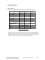
Model
Processor Speed
RAM Size
Data Acquisition
ATH 400-128
400 Mhz
128MB
Yes
ATH 400-128N
400 Mhz
128MB
No
ATH 660-128
660 Mhz
128MB
Yes
ATH 660-128N
660 Mhz
128MB
No
The 400 Mhz Athena models are convection cooled (heat sink only). An integrated heat sink + fan
is provided for the 660 Mhz models.
The Athena CPU uses the ISA bus internally to connect serial ports 1 through 4, as well as the
data acquisition circuit, to the processor. The ISA bus is brought out to an expansion connector to
mate with add-on boards. Diamond Systems manufactures a wide variety of compatible PC/104
add-on boards for analog I/O, digital I/O, counter/timer functions, serial ports, and power supplies.
ATHENA CPU User Manual V1.40
Page 5
2. FEATURES
System Features
Processor Section
♦
Via Eden Processor running at 400MHz or 660MHz with integrated math co-processor
♦
Pentium-class platform including SDRAM, IDE controller and USB
Core System
♦
128MB SDRAM system memory (standard)
♦
100MHz memory bus
♦
2MB 16-bit wide integrated flash memory for BIOS and user programs
♦
2D VGA Video graphics engine (VESA-style VGA output with DDC Monitor support)
I/O
♦
♦
4 RS-232 serial ports, 115.2kbaud max
♦
2 ports 16550-compatible
♦
2 ports 16850-compatible with 128-byte FIFOs
4 USB 1.1 ports
♦
IDE drive connectors; 44 pin notebook drive connection
♦
Accepts solid-state flash disk module directly on board
♦
10/100 BaseT full-duplex PCI bus mastering Ethernet (100Mbps or 10Mbps)
♦
IrDA port (requires external transceiver, not included)
♦
PS/2 keyboard and mouse ports
♦
LEDs
♦
Interface for speaker and additional external LEDs
System Features
♦
Plug and play BIOS with IDE auto detection, 32-bit IDE access, and LBA support
♦
User-selectable console redirection terminal mode on either COM1 or COM2
♦
On-board lithium backup battery for real-time-clock and CMOS RAM
♦
ATX power switching capability
♦
Programmable watchdog timer
♦
Extended temperature range operation (-40 to +85 C)
o
ATHENA CPU User Manual V1.40
Page 6
Data Acquisition Subsystem
Analog Input
♦
16 single-ended / 8 differential inputs, 16-bit resolution
♦
100KHz maximum aggregate A/D sampling rate
♦
Programmable input ranges/gains with maximum range of ±10V / 0-10V
♦
Both bipolar and unipolar input ranges
♦
10 ppm/ C drift accuracy
♦
Internal and external A/D triggering
♦
48-sample FIFO for reliable high-speed sampling and scan operation
o
Analog Output
♦
4 analog outputs, 12-bit resolution
♦
±10V and 0-10V output ranges
♦
±5V and 0-5V output range (optional)
Digital I/O
♦
24 programmable digital I/O, 3.3V and 5V logic compatible
♦
Enhanced output current capability: –8/+12mA max
Counter/Timers
♦
1 24-bit counter/timer for A/D sampling rate control
♦
1 16-bit counter/timer for user counting and timing functions
♦
Programmable gate and count enable
♦
Internal and external clocking capability
ATHENA CPU User Manual V1.40
Page 7
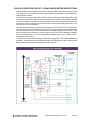
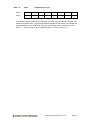
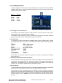
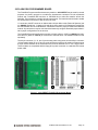
3. ATHENA BOARD DRAWING
I/O Connectors
J1
J2
J3
J4
J5
J6
J7
J8
J9
J11
PC/104 8-bit bus connector
PC/104 16-bit bus connector
Main I/O connector
Ethernet connector
USB 0/1 header
Watchdog/Failsafe Features header
Mini USB-B connector
Primary IDE (44-pin, laptop)
External Battery connector
Input Power
J12
J14
J15
J16
J21
J24
J25
J27
J28
J30
External Auxiliary Power connector
Data Acquisition I/O
Audio I/O
Manufacturing header (not installed)
USB 2/3 header
LCD Panel connector
VGA connector
CPU Fan header
LCD Backlight header
CD Input connector
Configuration Jumper Blocks
J10
J13
System configuration jumper block
Data acquisition circuit configuration jumper block
ATHENA CPU User Manual V1.40
Page 8
4. I/O HEADERS
All cables mentioned in this chapter are included in Diamond Systems’ cable kit C-ATH-KIT.
These cables are further described in chapter 23. Some cables are also available individually.
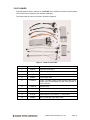
4.1 PC/104 Bus Connectors
The PC/104 bus is essentially identical to the ISA Bus except for the physical design. It specifies
two pin and socket connectors for the bus signals. A 64-pin header J1 incorporates the 62-pin 8bit bus connector signals, and a 40-pin header J2 incorporates the 36-pin 16-bit bus connector
signals. The additional pins on the PC/104 connectors are used as ground or key pins. The
female sockets on the top of the board and the extended mating pins on the bottom of the board
enable PC/104 board stacking
In the pinout figures below, the tops correspond to the left edge of the connector when the board
is viewed from the primary side (side with the CPU chip and the female end of the PC/104
connector) and the board is oriented so that the PC/104 connectors are along the bottom edge of
the board.
View from Top of Board
J2: PC/104 16-bit bus connector
Ground
MEMCS16IOCS16IRQ10
IRQ11
IRQ12
IRQ15
IRQ14
DACK0DRQ0
DACK5DRQ5
DACK6DRQ6
DACK7DRQ7
+5V
MASTERGround
Ground
D0
D1
D2
D3
D4
D5
D6
D7
D8
D9
D10
D11
D12
D13
D14
D15
D16
D17
D18
D19
C0
C1
C2
C3
C4
C5
C6
C7
C8
C9
C10
C11
C12
C13
C14
C15
C16
C17
C18
C19
Ground
SBHELA23
LA22
LA21
LA20
LA19
LA18
LA17
MEMRMEMWSD8
SD9
SD10
SD11
SD12
SD13
SD14
SD15
Key (pin cut)
J1: PC/104 8-bit bus connector
IOCHCHKSD7
SD6
SD5
SD4
SD3
SD2
SD1
SD0
IOCHRDY
AEN
SA19
SA18
SA17
SA16
SA15
SA14
SA13
SA12
SA11
SA10
SA9
SA8
SA7
SA6
SA5
SA4
SA3
SA2
SA1
SA0
Ground
A1
A2
A3
A4
A5
A6
A7
A8
A9
A10
A11
A12
A13
A14
A15
A16
A17
A18
A19
A20
A21
A22
A23
A24
A25
A26
A27
A28
A29
A30
A31
A32
B1
B2
B3
B4
B5
B6
B7
B8
B9
B10
B11
B12
B13
B14
B15
B16
B17
B18
B19
B20
B21
B22
B23
B24
B25
B26
B27
B28
B29
B30
B31
B32
Ground
RESET
+5V
IRQ9
-5V
DRQ2
-12V
0WS+12V
Key (pin cut)
SMEMWSMEMRIOWIORDACK3DRQ3
DACK1DRQ1
RefreshSYSCLK
IRQ7
IRQ6
IRQ5
IRQ4
IRQ3
DACK2TC
BALE
+5V
OSC
Ground
Ground
Table 1: J1,J2 – PC/104 Connector Pinouts
ATHENA CPU User Manual V1.40
Page 9
4.2 Main I/O Connector – J3
An 80-pin high-density connector is provided for access to the user I/O. The following functions
are supported by this connector:
♦
2 serial ports
♦
PS/2 keyboard
♦
ATX Power switch
♦
Parallel port
♦
PS/2 mouse
♦
Reset switch
♦
Watchdog timer I/O
♦
IrDA port
♦
Power and HDD LEDs
The connector mates with Diamond Systems’ cable no. C-PRZ-01, which consists of a dualribbon-cable assembly with industry-standard connectors at the user end. The CPU mating
connector includes integral latches for enhanced reliability. Each ribbon cable has 40 wires.
Cable “A”
COM 1
COM 2
COM 3
COM 4
Utilities A
1
2
3
4
5
6
7
8
9
10
11
12
13
14
15
16
17
18
19
20
21
22
23
24
25
26
27
28
29
30
31
32
33
34
35
36
37
38
39
40
DCD1
DSR 1
RXD 1
RTS 1
TXD 1
CTS 1
DTR 1
RI 1
Ground
DCD 2
DSR 2
RXD 2
RTS 2
TXD 2
CTS 2
DTR 2
RI 2
Ground
DCD 3
DSR 3
RXD 3
RTS 3
TXD 3
CTS 3
DTR 3
RI 3
Ground
DCD 4
DSR 4
RXD 4
RTS 4
TXD 4
CTS 4
DTR 4
RI 4
Ground
+5V Out
Speaker Out
IDE Drive LED
Power LED
Cable “B”
LPT 1
Keyboard
Mouse
Utilities B
1
2
3
4
5
6
7
8
9
10
11
12
13
14
15
16
17
18
19
20
21
22
23
24
25
26
27
28
29
30
31
32
33
34
35
36
37
38
39
40
STBAFDPD0
ERRPD1
INITPD2
SLINPD3
Ground
PD4
Ground
PD5
Ground
PD6
Ground
PD7
Ground
ACKGround
BUSY
Ground
PE
Ground
SLCT
KB Clk
KB/MS VKB Data
KB/MS V+
MS Clk
KB/MS VMS Data
KB/MS V+
Ground
ResetATX Power
KB Lock
IR RX
IR TX
+3VSB
Table 2: J3 – Main I/O Connector
ATHENA CPU User Manual V1.40
Page 10
Notes on J3 Signals
COM1 – COM4
The signals on these pins are RS-232 level signals and may be
connected directly to RS-232 devices. The pinout of these signals is
designed to allow a 9-pin male IDC connector to be crimped onto the
corresponding ribbon cable wires to provide the correct pinout for a PC
serial port connector (DTE).
LPT1
The signals on these pins comprise a standard PC parallel port. The
pinout of these signals is designed to allow a 25-pin female IDC
connector to be crimped onto the corresponding ribbon cable wires to
provide the correct pinout for a PC parallel port connector.
Keyboard, Mouse
These are PS/2 signals for keyboard and mouse.
Clk
VData
V+
Clock pin; connects to pin 5 of the PS/2 connector.
Power pin; connects to pin 3 of the PS/2 connector.
Data pin; connects to pin 1 of the PS/2 connector.
Power pin; connects to pin 4 of the PS/2 connector.
Pins 2 and 6 on the Mini-Din-6 PS/2 connectors are unused.
Utilities A
+5V Out
Speaker Out
IDE Drive LED
Power LED
This pin is a switched power pin that is turned on and off with the ATX
power switch or with the +5V input.
The signal on this pin is referenced to +5V Out. Connect a speaker
between this pin and +5V Out.
Referenced to +5V Out. Does not require a series resistor. Connect
LED directly between this pin and +5V Out.
Referenced to +5V Out. Does not require a series resistor. Connect
LED directly between this pin and +5V Out.
Utilities B
ResetATX Power
KB Lock
IR RX, IR TX
+5V In
Connection between this pin and Ground will generate a Reset
condition.
When ATX is enabled, a momentary contact between this pin and
ground causes the CPU to turn on, and a contact of 4 seconds or longer
will generate a power shutdown. ATX power control is enabled with a
jumper on jumper block J10 (see page 21).
When this pin is connected to Ground, the keyboard and mouse inputs
are ignored.
IrDA pins. Can be connected directly to an IrDA transceiver.
Connected to +5V input power on J11 (see page 12). This pin is not
switched by ATX control. This pin is provided for auxiliary use such as
front panel lighting or other circuitry at the user’s discretion.
Connector Part Numbers
J3 plug on CPU board:
3M / Robinson Nugent no. P50E-080P1-S1-TG
Both cable-mount and board-mount connectors are available to mate with J3:
Cable-mount socket:
3M / Robinson Nugent no. P50E-080S-TG
Board-mount socket: 3M / Robinson Nugent no. P50-080S-R1-TG
ATHENA CPU User Manual V1.40
Page 11
4.3 Input Power – J11
1
2
3
4
5
6
7
8
9
+5V In
Ground
Ground
+12V In
Ground
+5V In
-12V In
-5V In
ATX Control
Table 3: J11 – Input Power Connector Pinout
Input power for Athena may be supplied either through J11 from an external supply or directly
through the PC/104 bus power pins if a PC/104 power supply is used with the CPU.
Athena requires only +5VDC input power to operate. All other required voltages are generated on
board with miniature switching regulators. However since the PC/104 bus includes pins for ±5V
and ±12V, these voltages may be supplied through J11 if needed. The +5V and +12V voltages
are controlled by the ATX power manager switches, while -5V and -12V are routed directly to the
corresponding pins on PC/104 bus and are not controlled by the ATX function.
Make sure that the power supply used has enough current capacity to drive your system. The
Athena CPU requires up to 2A on the +5V line for the 400Mhz configuration (2.7A for the 660Mhz
configuration.) If you have a disk drive or other modules connected, you need additional power. In
particular, many disk drives need extra current during startup. If your system fails to boot properly,
or if disk accesses do not work properly, the first thing to check is the power supply voltage level.
Many boot-up problems are caused simply by insufficient voltage due to excess current draw on
the +5V supply.
Multiple +5V and Ground pins are provided for extra current carrying capacity if needed. Each pin
is rated at 3A max (15W). For the Athena CPU and panel I/O board 3A is sufficient, so +5 and
Ground require only a single wire each. In this case the first 4 pins may be connected to a
standard 4-pin miniature PC power connector if desired. Be advised that some voltage will be
dropped in the wire depending on the wire guage (AWG).
For a larger PC/104 stack the total power requirements should be calculated to determine
whether additional wires are necessary.
ATX control enables the +5V and +12V power to be switched on and off with an external
momentary switch. A short press on the switch will turn on power, and holding the switch on for 4
seconds or longer will turn off power.
Diamond Systems’ cable no. 698009 mates with J11. It provides 9 color-coded wires with stripped
and tinned leads for connection to user-supplied power sources. This cable may also be used
with Diamond Systems’ Jupiter-MM series power supplies in vehicle-based applications. In this
configuration, the input power is supplied to the Jupiter-MM board, and the Jupiter-MM output
power is connected to J11 on the CPU using cable 698009. When used in this way, make sure
the two red +5V wires are both connected to the +5V output screw terminal on Jupiter-MM and
the Jupiter-MM is not plugged onto the PC/104 stack.
ATHENA CPU User Manual V1.40
Page 12
4.4 Output Power – J12
1
2
3
4
+5V Out
Ground
Ground
+12V Out
Table 4: J12 – Output Power Connector Pinout
J12 provides switched power for use with external drives. If ATX is enabled, the power is
switched on and off with the ATX input switch. If ATX is not enabled, the power is switched on
and off in conjunction with the external power.
Diamond Systems’ cable no. 698006 mates with J12. It provides a standard full-size power
connector for a hard drive or CD-ROM drive and a standard miniature power connector for a
floppy drive.
Connector Part Numbers
J12 Connector on CPU board:
Digi-Key Corp. 640456-4
J12 Mating Cable Connector:
Molex 22-01-3047
4.5 Ethernet – J4
1
2
3
4
5
6
Common
RXCommon
RX+
TXTX+
Table 5: J4 – Ethernet Connector Pinout
J4 is a 1x6 pin header. It mates with Diamond Systems’ cable no. 698002, which provides a
panel-mount RJ-45 jack for connection to standard CAT5 network cables.
Connector Part Numbers
J11 Connector on CPU board:
Digi-Key Corp. 640456-6
J11 Cable Connector:
Molex 16-02-0096
4.6 USB – J5 (USB 0/1), J21 (USB 2/3)
Key (pin cut)
USB2 PwrUSB2 Data+
USB2 DataUSB2 Pwr+
1
3
5
7
9
2
4
6
8
10
Shield
USB1 PwrUSB1 Data+
USB1 DataUSB1 Pwr+
Table 6: J5, J21 – USB Connector Pinout
J5 and J21 are 2x5 pin headers. They mate with Diamond Systems’ cable no. 698012, each
providing 2 standard USB type A jacks in a panel-mount housing.
Connector Part Numbers
J5, J21 Connector on CPU board:
J5, J21 Mating Cable Connector:
Standard 2x5, 0.1” header (with pin 1 removed)
Oupiin 4072-2X5H (Standard PC USB Header Interface)
ATHENA CPU User Manual V1.40
Page 13
4.7 Watchdog Features – J6
1
2
3
Ground
WDI
WDO
Table 7: J6 – Watchdog Connector Pinout
J6 is used for watchdog timer access.
The watchdog timer circuit is described on page 66 of this manual. It may be programmed
directly, as described in this user manual, or with Diamond Systems’ Universal Driver software.
4.8 IDE Drive – J8
RESETD7
D6
D5
D4
D3
D2
D1
D0
Ground
DRQ
IDEIOWIDEIORIORDY
DACKIRQ14
A1
A0
CS0LED+5V
Ground
1
3
5
7
9
11
13
15
17
19
21
23
25
27
29
31
33
35
37
39
41
43
2
4
6
8
10
12
14
16
18
20
22
24
26
28
30
32
34
36
38
40
42
44
Ground
D8
D9
D10
D11
D12
D13
D14
D15
Key (Not Used)
Ground
Ground
Ground
Ground
Ground
Pulled low for 16-bit operation
Not Used
A2
CS1Ground
+5V
Not Used
Table 8: J8 – IDE Drive Connector Pinout
J8 is a 2x22 (44-pin) 2mm-pitch pin header. It mates with Diamond Systems’ cable no. 698004,
and may be used to connect up to 2 IDE drives (hard disks, CD-ROMs, or flashdisk modules).
The 44-pin connector includes power and mates directly with notebook drives and flashdisk
modules. To use a standard format hard disk or CD-ROM drive with a 40-pin connector, an
adapter PCB such as Diamond Systems’ ACC-IDEEXT is required.
ATHENA CPU User Manual V1.40
Page 14
4.9 Data Acquisition I/O Connector – J14 (Models with Data Acquisition only)
Athena includes a 50-pin header labeled J14 for all data acquisition I/O. This header is located on
the left side of the board. Pin 1 is the lower right pin and is marked on the board. Diamond
Systems’ cable no. C-50-18 provides a standard 50-pin connector at each end and mates with
this header.
DIO A0
DIO A2
DIO A4
DIO A6
DIO B0
DIO B2
DIO B4
DIO B6
DIO C0
DIO C2
DIO C4 / Gate 0
DIO C6 / Clk 1
Ext Trig
+5V Out
Vout 0
Vout 2
Aground (Vout)
Vin 0
Vin 1
Vin 2
Vin 3
Vin 4
Vin 5
Vin 6
Vin 7
1
3
5
7
9
11
13
15
17
19
21
23
25
27
29
31
33
35
37
39
41
43
45
47
49
2
4
6
8
10
12
14
16
18
20
22
24
26
28
30
32
34
36
38
40
42
44
46
48
50
DIO A1
DIO A3
DIO A5
DIO A7
DIO B1
DIO B3
DIO B5
DIO B7
DIO C1
DIO C3
DIO C5 / Gate 1
DIO C7 / Out 0
Tout 1
Dground
Vout 1
Vout 3
Aground (Vin)
Vin 8
Vin 9
Vin 10
Vin 11
Vin 12
Vin 13
Vin 14
Vin 15
Table 9: J14 – Data Acqisition Connector Pinout
Signal Name
DIO A7-A0
DIO B7-B0
DIO C7-C0
Ext Trig
Tout 1
Vin 7/7+ ~ Vin 0/0+
Vin 15/7- ~ Vin 8/0Vout0-3
+5V Out
Aground (Vout), (Vin)
Dground
Definition
Digital I/O port A; programmable direction
Digital I/O port B; programmable direction
Digital I/O port C; programmable direction
C7-C4 may be configured for counter/timer signals; see page 47
External A/D trigger input
Counter/Timer 1 output
Analog input channels 7 – 0 in single-ended mode;
High side of input channels 7 – 0 in differential mode
Analog input channels 15 – 8 in both single-ended mode;
Low side of input channels 7 – 0 in differential mode
Analog output channels 0 – 3
Connected to switched +5V supply
Analog ground; used for analog circuitry only
Vout pin is for the analog outputs; Vin pin is for the analog inputs
Digital ground; used for digital circuitry only
ATHENA CPU User Manual V1.40
Page 15
4.10 LCD Panel (LVDS Interface) Connector – J24
Ground
Y CLOCK Y CLOCK +
Ground
Y Data 0 Y Data 0 +
Ground
Y Data 2 Y Data 2 +
Ground
Y Data 1 Y Data 1 +
Ground
VDD (LCD Display)
VDD (LCD Display)
1
3
5
7
9
11
13
15
17
19
21
23
25
27
29
2
4
6
8
10
12
14
16
18
20
22
24
26
28
30
Ground
Z CLOCK Z CLOCK +
Ground
Z Data 0 Z Data 0 +
Ground
Z Data 1 Z Data 1 +
Ground
Z Data 2 Z Data 2 +
Ground
VDD (LCD Display)
VDD (LCD Display)
Table 10: J24 – LCD Connector Pinout
J24 provides access to the internal LVDS LCD display drivers. Note that the LCD also requires
the backlight to be connected (J28 below) in order to function correctly.
Signal Name
Y Data 2-0 +/Y Clock +/Z Data 2-0 +/Z Clock +/VDD
Ground
Definition
Primary Data Channel, bits 2-0 (LVDS Differential signaling)
Primary Data Channel, Clock (LVDS Differential signaling)
Secondary Data Channel, bits 2-0 (LVDS Differential signaling)
Secondary Data Channel, Clock (LVDS Differential signaling)
+3.3V Switched Power Supply for LCD display (only powered up when
LCD display is active)
Power Ground, 0V
Connector Part Numbers
J24 plug on CPU board:
Cable-mount socket:
JST Part Number: BM30B-SRDS-G-TF
JST Part Number: JST SHDR-30V-S-B
ATHENA CPU User Manual V1.40
Page 16
4.11 LCD Backlight Connector – J28
1
2
3
+12V
Control
Ground
Table 11: J28 – LCD Backlight Connector Pinout
Signal Name
Control
+12V, Ground
Definition
Output signal (from Athena) to allow power-down of backlight
Power Supply for LCD Backlight assembly
J28 provides the Backlight power and control for the optional LCD panel. See J24 (above) for
details on the LCD data interface. Note that the +12V supply will be removed when the system is
powered down; the control signal is to allow the system to power-down the backlight when the
system enables monitor-power-down during its power management control.
Note: 12V must be provided either on the J11 input power connector or on the 12V pin on the
PC/104 connector in order for the LCD backlight to operated. This voltage is not generated
internally.
Connector Part Numbers
J28 Connector on CPU board:
J28 Mating Cable Connector:
Digi-Key Corp. A19470
Molex
22-01-3037
4.12 CPU Fan Connector – J27
1
2
3
Fan RPM
Ground
+5V
Table 12: J27 – CPU Fan Connector Pinout
Signal Name
Fan-RPM
+5V, Ground
Definition
TTL signal input that pulses with each revolution of the fan
Power Supply for optional CPU Fan (if necessary)
Connector Part Numbers
J27 Connector on CPU board:
J27 Mating Cable Connector:
Heilind Electronics
JST
89400-0320
PHR-3
ATHENA CPU User Manual V1.40
Page 17
4.13 VGA Connector – J25
GREEN
BLUE
HSYNCH
VSYNCH
1
3
5
7
2
4
6
8
RED
Ground
DDC-Data
DDC-Clock
Table 13: J25 – VGA Header Pinout
Signal Name
RED
GREEN
BLUE
Ground
DDC-CLOCK/DATA
Definition
RED signal (positive, 0.7Vpp into 75 Ohm load)
GREEN signal (positive, 0.7Vpp into 75 Ohm load)
BLUE signal (positive, 0.7Vpp into 75 Ohm load)
Ground return
Digital serial I/O signals used for monitor detection (DDC1 specification)
J25 provides a connection for VGA monitors. Note that while the DDC serial detection pins are
present, there is no 5V supply provided (nor are the old “Monitor ID” pins used). Diamond Cable
Assembly #698024 provides a female DB15 connection to interface with a standard RGB monitor.
Connector Part Numbers
J25 Connector on CPU board:
J25 Mating Cable Connector:
Standard 2x5, 0.1” Box header
Standard 2x5, 0.1” female ribbon cable connector
ATHENA CPU User Manual V1.40
Page 18
4.14 Audio I/O Connector – J15
1
2
3
4
5
6
7
8
9
10
LEFT Line Out
RIGHT Line Out
Audio Ground
LEFT Line Input
RIGHT Line Input
Audio Ground
Microphone Input
Power Reference for Microphone
NC (Key)
Audio Ground
Table 14: J15 – Audio I/O Connector Pinout
Signal Name
Line Out
Line Input
Microphone Input
Definition
Line Level output. These outputs are not capable of driving
headphones. They must only be connected to high-impedance
devices such as amplified speakers.
Line-Level input; referred to as “Line In” in most sound documentation
Microphone-level mono input; phantom power provided via pin 8
The sound chip used is AC97-compatible.
Connector Part Numbers
J15 Connector on CPU board:
Standard 2x5, 0.1” Box header
ATHENA CPU User Manual V1.40
Page 19
4.15 CD Input Connector – J30
J30 provides a connector for a PC-standard CD input cable.
1
2
3
4
LEFT CD Input
Left Ground
Right Ground
RIGHT CD Input
Table 15: J30 – CD Input Connector Pinout
J30 provides the CD Audio Input to the AC97 Sound circuitry. The connector is an industrystandard CD-IN connector, as is common in most desktop Personal Computers. Note that the
left and right grounds are decoupled, but are also tied together on-board. This input is intended
for CD-input only (i.e., no amplified or microphone inputs).
Connector Part Numbers
J30 Connector on CPU board:
J30 Mating Cable Connector:
Molex 70543-0003
Standard (PC) CD Audio cable
ATHENA CPU User Manual V1.40
Page 20
5. JUMPER SETTINGS
Refer to the Athena board drawing on page 8 for locations of the configuration items mentioned
here. See page 23 for information on configuration J13 for the data acquisition circuit.
5.1 J10: System Configuration
Jumper block J10 is used for configuration of IRQ levels, wait states, ATX power control, and
CMOS RAM.
Serial Port and A/D IRQ Settings
COM3 may be set to IRQ4 or IRQ9. COM4 may be set to IRQ3 or IRQ15. The A/D circuit may be
set to IRQ5 or IRQ4 if COM3 does not use it. In addition, it is possible to set up all 3 circuits to
share IRQ4 or IRQ5. Note that only 1 device can use the ‘shared’ IRQ at one time. True IRQ
sharing where all 3 devices can run simultaneously is not supported here.
ATX Power Control
Athena must have ATX enabled to function properly. This jumper must be installed for the board
to boot when power is applied.
Erasing CMOS RAM
The CMOS RAM may be cleared with a jumper as shown on the next page. This will cause the
CPU to power up with the default BIOS settings. To clear the CMOS RAM, power down the CPU,
install the jumper as shown, return it to its default position, and then power up again.
Before erasing CMOS RAM, write down any custom BIOS settings you have made!
Default Settings
ATHENA CPU User Manual V1.40
Page 21
The different configurations for J10 are shown below. Each illustration shows only the jumper of
interest. An asterisk (*) indicates the default setting.
ATHENA CPU User Manual V1.40
Page 22
5.2 J13: Data Acquisition Circuit Configuration
Jumper block J13 is used to configure the A/D and D/A circuits of the Athena. It is located on the
left side of the board next to the data acquisition I/O pin header and is oriented vertically. The
functions are shown below and are described in detail on the following page.
The default settings are as shown:
The various configurations are illustrated and described below. For correct configuration, pick one
option from the first two configurations (single-ended or differential A/D), one option from the
second two configurations (unipolar or bipolar A/D), and one option from the third two
configurations (unipolar or bipolar D/A).
ATHENA CPU User Manual V1.40
Page 23
Single-ended / Differential Inputs
Athena can accept both single-ended and differential inputs. A single-ended input uses 2 wires,
input and ground. The measured input voltage is the difference between these two wires. A
differential input uses 3 wires: input +, input -, and ground. The measured input voltage is the
difference between the + and - inputs.
Differential inputs are frequently used when the grounds of the input device and the measurement
device (Athena) are at different voltages, or when a low-level signal is being measured that has
its own ground wire. A differential input also has higher noise immunity than a single-ended input,
since most noise affects both + and – input wires equally, so the noise will be canceled out in the
measurement. The disadvantage of differential inputs is that only half as many are available,
since two input pins are required to produce a single differential input. Athena can be configured
for either 16 single-ended inputs or 8 differential inputs.
If you have a combination of single-ended and differential input signals, select differential mode.
Then to measure the single-ended signals, connect the signal to the + input and connect analog
ground to the - input.
WARNING: The maximum range of voltages that can be applied to an analog input on Athena
without damage is ±35V. If you connect the analog inputs on Athena to a circuit whose ground
potential plus maximum signal voltage exceeds ±35V, the analog input circuit may be damaged.
Check the ground difference between the input source and Athena before connecting analog
input signals.
Unipolar / Bipolar Inputs
The analog inputs can be configured for can be configured for unipolar (positive input voltages
only) or bipolar (both negative and positive input voltages). For unipolar inputs, install a jumper
as shown. For bipolar inputs, leave the jumper out.
Analog Output Configuration
The 4 analog outputs can also be configured for unipolar (positive voltages only) or bipolar (both
negative and positive output voltages). In unipolar mode, the outputs range between 0-10V. In
bipolar mode, the outputs range between ±10V.
When the board powers up or is reset, the analog outputs are also reset. The D/A reset method
is selected with a jumper on J13. If the jumper is in, the outputs will reset to the bottom of their
range (called zero-scale). If the jumper is out, the outputs will reset to the middle of their range
(mid-scale). Normally the D/A is configured to power up to 0V, so that when the power is turned
on the device connected to the analog output doesn’t see a step change in voltage. Therefore, for
unipolar mode normally the outputs should be configured for zero-scale reset, and for bipolar
mode the outputs should be configured for mid-scale reset, since 0V is halfway between -10V
and +10V for the ±10V range.
5.3 J6: Watchdog Timer & System Recovery
J6 is used in conjunction with the watchdog timer. This jumper has different dimensions than J10
and J13, and the jumpers are not interchangeable.
Watchdog timer operation is described in detail on page 66.
ATHENA CPU User Manual V1.40
Page 24
6. SYSTEM FEATURES
6.1 System Resources
The table below lists the default system resources utilized by the circuits on Athena.
Device
Address (Hex)
ISA IRQ
ISA DMA
Serial Port COM1
I/O 3F8 – 3FF
4
-
Serial Port COM2
I/O 2F8 – 2FF
3
-
Serial Port COM3
I/O 3E8 – 3EF
9
-
Serial Port COM4
I/O 2E8 – 2EF
15
-
LPT Printer Port
I/O 378 – 37F
7
3
IDE Controller A
I/O 1F0 – 1F7
14
-
A/D Circuit (when applicable)
I/O 280 – 28F
5
-
Watchdog Timer / Serial Port /
FPGA Enable/ Disable
I/O 25C – 25F
-
-
Ethernet
OS-dependant
OS-dependant
-
USB
OS-dependant
OS-dependant
-
Sound
OS-dependant
OS-dependant
-
Video
OS-dependant
OS-dependant
-
Table 16: System Resources
Note that most of these resources are configurable and, in many cases, the Operating System
will alter these settings. The main devices that are subject to this dynamic configuration are onboard Ethernet, sound, video, USB, and any PC/104 cards that are in the system. These settings
may also vary depending on what other devices are present in the system.
ATHENA CPU User Manual V1.40
Page 25
6.2 COM Port / FPGA / Watchdog Control Registers
A registers located at address 0x25F is used for the purposes of controlling the serial port, FPGA
and watchdog features:
Register Map Bit Assignments
A blank bit in the write registers is unused. A blank bit in the read registers reads back as 0 or 1,
unknown state.
WRITE
Address
0x25F
7
COM4EN
6
COM3EN
5
FPGAEN
4
WDEN
3
2
1
0
7
COM4EN
6
COM3EN
5
FPGAEN
4
WDEN
3
2
1
0
READ
Address
0x25F
Table 17: I/O COM3/4 Control Register Definition
0x25F
Write
Bit No.
Name
7
Chip select enable/disable
6
5
4
3
2
1
0
COM4EN COM3EN FPGAEN WDEN
COM4EN
COM4 chip select enable. 1 = enable COM4-CS#. 0 = disable COM4-CS#.
COM3EN
COM3 chip select enable. 1 = enable COM3-CS#. 0 = disable COM3-CS#.
FPGEN
FPGA chip select enable. 1 = enable FPGA-CS#. 0 = disable FPGA-CS#.
WDEN
Watchdog enable. 1 = WDT counter enable. 0 = WDT counter disable, WDO
disable, WDI disable, CPURST# disable, EXTSMI# disable.
The CPLD initializes all values to zero on power up. The BIOS then enables each
resource based on BIOS settings.
0x25F
Read
Bit No.
Name
7
Chip select enable/disable
6
5
4
3
2
1
0
COM4EN COM3EN FPGAEN WDEN
Reads back written values
ATHENA CPU User Manual V1.40
Page 26
6.3 Console Redirection to a Serial Port
In many applications without a video card it may be necessary to obtain keyboard and monitor
access to the CPU for configuration, file transfer, or other operations. Athena supports this
operation by enabling keyboard input and character output onto a serial port (console redirection).
A serial port on another PC can be connected to the serial port on Athena with a null modem
cable, and a terminal emulation program (such as HyperTerminal) can be used to establish the
connection. The terminal program must be capable of transmitting special characters including F2
(some programs or configurations trap special characters).
The default Athena BIOS setting disables console redirection.
There are three possible configurations for console redirection:
♦
POST only (default)
♦
Always On
♦
Disabled
To modify the console redirection settings, enter the BIOS, select the Advanced menu, and then
select Console Redirection. In Com Port Address, select Disabled to disable the function, “Onboard COM A” for COM1, or “On-board COM B” for COM2.
If you select Disabled, you will not be able to enter BIOS again during power-up through the serial
port. To reenter BIOS when console redirection is disabled, you must use a monitor connected to
the onboard VGA and a keyboard connected to J3 or remove the CMOS battery jumper to reset
the BIOS to the default ‘POST only’ condition.
More detail on BIOS settings for console redirection can be found on page 31.
ATHENA CPU User Manual V1.40
Page 27
6.4 Flash Memory
Athena contains a 2Mbyte 16-bit wide flash memory chip for storage of BIOS and other system
configuration data.
6.5 Backup Battery
Athena contains an integrated RTC / CMOS RAM backup battery. The battery is located adjacent
to the PC/104 bus connector J1 (within the PC/104 outline). This battery has a capacity of
120mAH and will last over 3 years in power-off state. The on-board battery is activated for the
first time during initial factory configuration and test. Note that storage temperature of the board
can affect the total battery life. Storage at 23ºC is recommended.
6.6 System Reset
Athena contains a chip to control system reset operation. Reset will occur under the following
conditions:
♦
User causes reset with a ground contact on the Reset input
♦
Input voltage drops below 4.75V
♦
Over current condition on output power line
The ISA Reset signal is an active high pulse with a duration of 200ms. The internal PCI Reset is
active low, with a pulse width duration of 200 msec typical.
6.7 On-Board Video
The on-board video for the Athena board is based on an S3-TwisterT (VIA 8606 “PN133T”
Northbridge) video system. As such, the board memory is shared between the Video and main
system memory. A block of memory is configured (via BIOS Settings, accessible in the BIOS
configuration menus) for video which is then removed from use for main system memory. This
implies that the more memory used for the Video, the less memory is available for system
resources.
Note that the video memory can be set at 8Mbytes for almost all applications – increasing the
memory size will not increase video performance. Additional memory will only benefit the limited
3D support provided by the chipset. Also note that 3D hardware acceleration is not supported
across extended temperature range. In general, this 3D hardware is typically only used for 3D
games – most likely, these limitations will not affect most embedded applications.
Note that the low-level BIOS can support LCD output in conjunction with standard RGB output
(i.e., dual-displays).
ATHENA CPU User Manual V1.40
Page 28
7. BIOS
7.1 BIOS Settings
Athena uses a BIOS from Phoenix Technologies modified to support the custom features of the
Athena board. Some of these features are described here.
To enter the BIOS during system startup (POST – power on self-test), press F2.
Serial Ports
-The address and interrupt settings for serial ports COM1 and COM2 may be modified. COM1
and COM2 address and interrupt settings are done in the BIOS, Advanced menu, I/O Device
Configuration. See page 32 for details.
-The addresses of COM3 and COM4 are fixed. The IRQ selections for COM3 and COM4 are
configured on J10.
Select Advanced menu, Advanced Chipset Control, I/O Chip Device Configuration.
Parallel Port
The parallel port is configured in the Advanced -> I/O Chip Device Configuration menu. It is set
by default to ECP mode and located at address 0x378, IRQ 7 and DMA 3.
You can move the base address to 0x278 or 0x3BC. The IRQ can be set to 5 or 7. The DMA
can be set to 1 or 3.
LCD Video Settings
Athena provides direct digital support for LVDS-based LCD interfaces only. As such, there are
two settings that affect this support during BIOS boot:
•
Boot Video Device – By default, this is set to “AUTO”. With the AUTO setting, the system will
attempt to identify an RGB monitor (via DDC) and, if no RGB monitor is detected then the
system enables LCD support. If you wish to use the LCD display regardless of standard
monitor connection (i.e., with both connected at once), then set “Boot Video Device” to
“Both”.
•
Panel Type – This setting defaults to “7”. Do not alter this setting unless specifically
instructed to do so. This setting affects the LCD display modes supported; mode “7” is the
only setting currently supported. Not all LCD displays are supported.
Miscellaneous
-Memory Cache Settings:
Unless there is a specific reason to change these settings, it is best to keep these settings as-is.
Certain system functions (such as USB keyboard support under BIOS menus) may be adversely
affected by changes to these settings, due mainly to a heavy reduction in performance. These
cache settings can make a huge difference for low-level BIOS calls and, as such, can severely
limit performance if they are disabled.
-On the Advanced Chipset Control screen, the following settings should be retained:
Frame Buffer Size: 8MB
AGP Rate: 4X
Expansion Bus Performance: Normal
ATHENA CPU User Manual V1.40
Page 29
The Frame Buffer size can be increased for specific applications; just be aware that an increase
in this memory size will result in a decrease in overall system memory available. The AGP rate
affects internal video accesses and does not affect any external bus speeds.
“Expansion Bus Performance” is an adjustment to allow an increase in ISA I/O Access speeds.
For applications where ISA I/O accesses seem to be a limiting factor, this performance may be
increased to “Accelerated”. Be aware that increasing these timings may adversely affect system
stability with external add-on PC/104 cards. This setting has no direct affect on PCI or memory
speeds; it only affects ISA PC/104 devices. It is best to leave this setting at “Normal” if there are
no ISA I/O Performance issues.
- On the Advanced screen, the following settings should be retained:
Installed O/S
Win98
Large Disk Access Mode
DOS
- On the On-Chip Multifunction Device screen, the following settings should be retained:
USB Device
Legacy Audio
Enabled
Disabled
“Legacy Audio” will only affect DOS-based applications when used with the VIA-supported
DOS Drivers. Enabling this setting will require system I/O, IRQ, and DMA resources. It is
strongly recommended that this setting be left “Disabled.”
- On the PCI and ISA Configuration pages (from the Advanced screen), the following setting
should be retained:
PCI IRQ Level 1-4
Autoselect for all
PCI/PNP ISA UMB Region Exclusion Available for all
-The Power Management Screen will only be in effect when under DOS. Otherwise, the OS
power management settings will pre-empt these settings. The only power management mode
supported by the system is “Power-On Suspend” – other suspend modes are not supported and
should not be used under any OS (Examples of unsupported suspend modes: “Hibernate” under
Windows and “Suspend-to-Disk” or “Suspend-to-RAM”.)
- The Memory Shadow page of BIOS options should not be modified unless you are certain what
you are doing. These settings can adversely affect system performance and, potentially, system
reliability.
ATHENA CPU User Manual V1.40
Page 30
7.2 BIOS Console Redirection Settings
For applications where the Video interfaces will not be used, the textual feedback typically sent to the
monitor can be redirected to a COM PORT. In this manner, a system can be managed and booted
without the need for any video connection.
The BIOS allows the following configuration options for Console Redirection to a COM PORT:
•
COM PORT Address : Disabled (default), COM PORT A, or COM PORT B
o
•
NOTE: IF Console Redirection is enabled here, note that the Associated COM
PORT (“A” here referring to COM 1 and “B” referring to COM 2) will be
enabled, regardless of the COM PORT settings elsewhere.
“Continue CR After POST” : Off (default) or On
o
Determines whether the system is to Wait for CR over COM PORT before continuing
(after POST is completed, before OS starts loading)
•
Baud Rate : 19.2K (default), 300, 1200, 2400, 9600, 38.4K, 57.6K, 115.2K
•
Console Connection : Direct (default) or Modem
•
Console Type : PC ANSI (default, VT100, VT100 (8-bit), PC-ANSI (7-bit), VT100+, or VTUTF8
•
Flow Control : CTS/RTS (default), XON-XOFF, None
•
# of video Pages to support 1(default) to 8
Note that Console Redirection only works for text-based interaction. If the OS enables video and
starts using direct video functions (as would be the case with a Linux X-terminal or Windows, for
instance), then Console Redirection will have no effect and video would be required.
ATHENA CPU User Manual V1.40
Page 31
8. SYSTEM I/O
8.1 Ethernet
Athena includes a 10/100Mbps Ethernet connection using Cat-5 (100BaseT) wiring. The signals
are provided on a 6-pin header (J4) on the right edge of the board.
Diamond Systems’ cable no. 698002 mates with the header and provides a standard RJ-45
connector in panel-mount form for connecting to standard Cat5 network cables.
1
2
3
4
5
6
Common
RXCommon
RX+
TXTX+
Table 18: J11 – Ethernet Connector
The Ethernet chip is the National Semiconductor DP83815 MacPhyter chip. It is connected to the
system via the board’s internal PCI bus.
The Athena Software CD includes Ethernet drivers for Windows 95, Windows 98, Windows NT,
and Linux. The latest drivers can also be downloaded from National Semiconductor’s website at
www.national.com. Search for DP83815 to reach the product folder.
A DOS utility program is provided for testing the chip and accessing the configuration EEPROM.
Each board is factory-configured for a unique MAC address using this program. To run the
program, you must boot the computer to DOS. The program will not run properly in a DOS
window inside of Windows. In normal operation this program should not be required.
Additional software support includes a packet driver with software to allow a full TCP/IP
implementation.
8.2 Serial Ports
Athena contains 4 serial ports. Each port is capable of transmitting at speeds of up to
115.2Kbaud. Ports COM1 and COM2 are built into the standard chipset. They consist of standard
16550 type UARTs with 16-byte FIFOs.
Ports COM3 and COM4 are derived from an Exar 16C2850 dual UART chip and include 128-byte
FIFOs. Ports 3 and 4 may be operated at speeds up to 460Kbaud with installation of high-speed
drivers as a custom option.
The serial ports use the following default system resources:
Port
Address range
IRQ
COM1
I/O 3F8 – 3FF
4
COM2
I/O 2F8 – 2FF
3
COM3
I/O 3E8 – 3EF
9
COM4
I/O 2E8 – 2EF
15
Table 19: COM PORT Default Resource Listing
ATHENA CPU User Manual V1.40
Page 32
The settings of COM1 and COM2 may be changed in the system BIOS. Select the Advanced
menu, then I/O Device Configuration. The base address and interrupt level may be modified on
this page.
The addresses of COM3 and COM4 are fixed. The interrupt (IRQ) settings for COM3 and COM4
are selected with J10. COM3 may use IRQ4 or IRQ9. COM4 may use IRQ3 or IRQ15. See page
20 for serial port IRQ jumper settings. Note that once these jumper selections are made, the user
must update the Serial Port IRQ settings to match these selections – the IRQ settings are NOT
autodetected in the same manner that the address settings are.
8.3 PS/2 Ports
Athena supports 2 PS/2 ports: one dedicated for keyboard and the other dedicated for mouse
function. The two PS/2 ports are accessible via a cable assembly (DSC#C-PRZ-01) attached to
J3. Support for these ports is independent of, and in addition to, mouse and keyboard support via
the USB ports.
8.4 USB Ports
Athena contains 4 USB Ports (referenced as “USB0” through “USB3”). All four USB ports are
accessible via cable assemblies attached to J5 (“USB0” and “USB1”) and J21 (“USB2” and
“USB3”).
USB support is intended primarily for the following devices (although any USB1.1-standard device
should function without issue):
•
Keyboards
•
Mice
•
USB Floppy Drive (NOTE : this is required for “Crisis Recovery” of boot ROM)
•
USB flash disks
The BIOS fully supports the USB keyboard during BIOS initialization screens, as well as legacy
emulation for DOS-based applications.
The USB ports can be used for keyboards and mice at the same time that the PS/2 keyboard and
mouse are plugged in – multiple devices of the same type are supported, although this can get
rather confusing.
ATHENA CPU User Manual V1.40
Page 33
9. NOTES ON OPERATING SYSTEMS AND BOOTING PROCEDURES
9.1 Windows Operating Systems Installation Issues
Installation of Windows operating systems ( Win98/2000/XP ) should follow the sequence below.
If the sequence is not followed certain drivers might not work and may prevent the device from
functioning properly under Windows.
1) Enable CD-ROM support in the BIOS. Change boot sequence in BIOS so system boots from
CD-ROM first.
2) Insert Windows installation CD into CD-ROM and restart computer
3) Follow the instructions for installing Windows.
9.1.1 DRIVER INSTALLATION
4) Install the Via “4-in-1” driver first. Install driver v4.35 for Windows 98, v4.40 or later for
Windows 2000/XP. During installation select the following options:
a.
Normal Install
b.
Select the following four options
i.
VIA ATAPI Vendor Support Driver
ii.
AGP VxD Driver
iii.
IRQ Routing Miniport Driver
iv.
VIA INF Driver v1.40a
c.
Install VIA ATAPI Vendor Support Driver
d.
Enable DMA Mode
e.
Install VIA AGP VXD in Turbo Mode
f.
Install VIA IRQ Routing Miniport Driver
5) Now install the Via/S3 Video driver. Follow installation instructions.
6) Install the Via Sound driver. Make sure the sound driver is ComboAudio v3.90 or later
7) Install the National Semiconductors Network driver.
8) The USB driver for the floppy drive needs to be loaded before the USB floppy drive will be
functional under Windows (legacy support will provide floppy access for DOS boot).
9.1.2 BIOS SETTINGS FOR WINDOWS
•
“OS” Setting : When using any version of Windows, the “Operating System” selection in the
BIOS setup menus should be set to “Win98”.
•
“Audio” Setting : “Legacy Audio” must be disabled for Windows to boot properly.
ATHENA CPU User Manual V1.40
Page 34
9.2 DOS Operating Systems Installation Issues
Installation of DOS operating systems ( MS-DOS, FreeDOS, ROM-DOS ) should follow the
sequence below.
1) Enable the following in BIOS:
a.
Floppy Drive detection.
b.
Legacy USB support.
2) Change BIOS boot sequence so system boots through USB floppy drive.
3) Insert DOS installation floppy disk into USB floppy drive and start/restart system.
4) Install various drivers needed.
Note : For DOS Ethernet to work, in BIOS set “Operating System” to “other”. DOS Sound
emulation currently is not functional.
ATHENA CPU User Manual V1.40
Page 35
10. DATA ACQUISITION CIRCUIT – I/O MAP AND REGISTER DESCRIPTIONS
Models ATH400-128 and ATH660-128 contain a data acquisition subsystem consisting of A/D,
D/A, digital I/O, and counter/timer features. This subsystem is equivalent to a complete add-on
data acquisition module.
The A/D section includes a 16-bit A/D converter, 16 input channels, and a 48-sample FIFO. Input
ranges are programmable, and the maximum sampling rate is 100KHz. The D/A section includes
4 12-bit D/A channels. The digital I/O section includes 24 lines with programmable direction. The
counter/timer section includes a 24-bit counter/timer to control A/D sampling rates and a 16-bit
counter/timer for user applications.
High-speed A/D sampling is supported with interrupts and a FIFO. The FIFO is used to store a
user-selected number of samples, and the interrupt occurs when the FIFO reaches this threshold.
Once the interrupt occurs, an interrupt routine runs and reads the data out of the FIFO. In this
way the interrupt rate is reduced by a factor equal to the size of the FIFO threshold, enabling a
faster A/D sampling rate. The circuit can operate at sampling rates of up to 100KHz, with an
interrupt rate of 6.6-10KHz.
The A/D circuit uses the default settings of I/O address range 280h – 28Fh (base address 280)
and IRQ 5. These settings can be changed if needed. The I/O address range is changed in the
BIOS, and the interrupt level is changed with jumper block J10.
ATHENA CPU User Manual V1.40
Page 36
10.1 Base Address
The data acquisition circuitry on Athena occupies a block of 16 bytes in I/O memory space. The
default address range for this block is 280h – 28Fh (base address 280).
The data acquisition FPGA can be enabled/disabled in the BIOS under the Advanced menu.
Scroll down to the “FPGA Mode:” option and select “Enabled” or “Disabled” accordingly. If the
FPGA is disabled you will not be able to interact with the data acquisition circuit.
The FPGA can be enabled or disabled programmatically through the CPLD. More information is
on page 26.
A functional list of registers is provided below, and detailed bit definitions are provided on the next
page and in the following chapter.
Base +
0
1
2
3
4
5
6
7
8
9
10
11
12
13
14
15
Write Function
Command register
Not used
A/D channel register
A/D gain and scan settings
Interrupt / DMA / counter control
FIFO threshold
D/A LSB
D/A MSB + channel no.
Digital I/O port A output
Digital I/O port B output
Digital I/O port C output
Digital I/O direction control
Counter/timer D7-0
Counter/timer D15-8
Counter/timer D23-16
Counter/timer control register
Read Function
A/D LSB
A/D MSB
A/D channel register
A/D gain and status readback
Interrupt / DMA / counter control readback
FIFO threshold readback
FIFO current depth
Interrupt and A/D channel readback
Digital I/O port A
Digital I/O port B
Digital I/O port C
Digital I/O direction control readback
Counter/timer D7-0
Counter/timer D15-8
Counter/timer D23-16
FPGA revision code
ATHENA CPU User Manual V1.40
Page 37
10.2 Data Acquisition Circuit Register Map
WRITE
Address
0
(Blank bits are unused and have no effect)
7
6
STRTAD RSTBRD
5
RSTDA
4
3
RSTFIFO CLRDMA
2
1
0
CLRT
CLRD
CLRA
L2
L1
L0
SCANEN
G1
G0
1
2
H3
H2
H1
H0
L3
3
4
CKSEL1 CKFRQ1 CKFRQ0
5
ADCLK
DMAEN
TINTE
DINTE
AINTE
FT5
FT4
FT3
FT2
FT1
FT0
DA5
DA4
DA3
DA2
DA1
DA0
DA11
DA10
DA9
DA8
6
DA7
DA6
7
DACH1
DACH0
8
PA7
PA6
PA5
PA4
PA3
PA2
PA1
PA0
9
PB7
PB6
PB5
PB4
PB3
PB2
PB1
PB0
10
PC7
PC6
PC5
PC4
PC3
PC2
PC1
PC0
11
DIOCTR
DIRA
DIRCH
DIRB
DIRCL
12
CTRD7
CTRD5
CTRD4
CTRD3
CTRD2
CTRD1
CTRD0
13
CTRD15 CTRD14 CTRD13
CTRD12
CTRD11 CTRD10
CTRD9
CTRD8
14
CTRD23 CTRD22 CTRD21
CTRD20
CTRD19 CTRD18 CTRD17 CTRD16
15
CTRNO
READ
CTRD6
LATCH
GTDIS
GTEN
CTDIS
CTEN
LOAD
CLR
(Blank bits are unused and read back as 0)
Address
7
6
5
4
3
2
1
0
0
AD7
AD6
AD5
AD4
AD3
AD2
AD1
AD0
1
AD15
AD14
AD13
AD12
AD11
AD10
AD9
AD8
2
H3
H2
H1
H0
L3
L2
L1
L0
3
STS
SD
WAIT
DACBSY
OVF
SCANEN
G1
G0
ADCLK
DMAEN
TINTE
DINTE
AINTE
4
CKSEL1 CKFRQ1 CKFRQ0
5
FT5
FT4
FT3
FT2
FT1
FT0
6
FD5
FD4
FD3
FD2
FD1
FD0
7
DMAINT
TINT
DINT
AINT
ADCH3
ADCH2
ADCH1
ADCH0
8
PA7
PA6
PA5
PA4
PA3
PA2
PA1
PA0
9
PB7
PB6
PB5
PB4
PB3
PB2
PB1
PB0
10
PC7
PC6
PC5
PC4
PC3
PC2
PC1
PC0
11
DIOCTR
DIRA
DIRCH
DIRB
DIRCL
12
CTRD7
CTRD4
CTRD3
CTRD2
CTRD1
CTRD0
13
CTRD15 CTRD14 CTRD13 CTRD12 CTRD11 CTRD10
CTRD9
CTRD8
14
CTRD23 CTRD22 CTRD21 CTRD20 CTRD19 CTRD18 CTRD17 CTRD16
15
REV7
CTRD6
REV6
CTRD5
REV5
REV4
REV3
REV2
REV1
ATHENA CPU User Manual V1.40
REV0
Page 38
10.3 Register Bit Definitions
In these register definitions, a bit marked ‘X’ is an unused bit.
All unused bits in readable registers read back as 0.
Base + 0
Bit No.
Name
Write
7
Command Register
6
5
4
3
STRTAD RSTBRD RSTDA RSTFIFO CLRDMA
2
1
0
CLRT
CLRD
CLRA
This register is used to perform various functions. The register bits are not data bits but instead
command triggers. Each function is initiated by writing a 1 to a particular bit. Writing a 1 to any
bit in this register does not affect any other bit in this register. For example, to reset the
FIFO, write the value 0x10 (16) to this register to write a 1 to bit 4. No other function of the
register will be performed. Multiple actions can be carried out simultaneously by writing a 1 to
multiple bits simultaneously.
STRTAD
Start an A/D conversion (trigger the A/D) when in software-trigger mode (AINTE = 0).
Once the program writes to this bit, the A/D conversion will start and the STS bit
(base + 3 bit 7) will go high. The program should then monitor STS and wait for it to
go low (check if value in base + 3 is less than 128 or 0x80). When it goes low the
A/D data at Base + 0 and Base + 1 may be read.
When AINTE = 1 (base + 4 bit 0), the A/D cannot be triggered by writing to this bit.
Instead the A/D will be triggered by a signal selected by ADCLK in base + 4 bit 5.
RSTBRD
Reset the entire board excluding the D/A. Writing a 1 to this bit causes all registers
on the board to be reset to 0. The effect on the digital I/O is that all ports are reset to
input mode, and the logic state of their pins will be determined by the pull-up/pulldown configuration setting selected by the user. All A/D, counter/timer, interrupt, and
DMA functions will cease. However the D/A values will remain constant.
RSTDA
Reset the 4 analog outputs. The analog outputs will be reset to either mid-scale or
zero-scale, depending on the jumper configuration selected by the user. A separate
reset is provided for the D/A so that the user may reset the board if needed without
affecting the circuitry connected to the analog outputs.
RSTFIFO
Reset the FIFO depth to 0. This clears the FIFO so that further A/D conversions will
be stored in the FIFO starting at address 0.
CLRDMA
Writing a 1 to this bit causes the DMA interrupt request flip flop to be reset.
CLRT
Writing a 1 to this bit causes the timer interrupt request flip flop to be reset.
CLRD
Writing a 1 to this bit causes the digital I/O interrupt request flip flop to be reset.
CLRA
Writing a 1 to this bit causes the analog interrupt request flip flop to be reset.
The user’s interrupt routine must write to the appropriate bit prior to exiting in order to
enable future interrupts. Otherwise the interrupt line will stay high indefinitely and no
additional interrupt requests will be generated by the board.
ATHENA CPU User Manual V1.40
Page 39
Base + 0
Read
A/D LSB
Bit No.
7
6
5
4
3
2
1
0
Name
AD7
AD6
AD5
AD4
AD3
AD2
AD1
AD0
AD7 - 0
A/D data bits 7 - 0; AD0 is the LSB; A/D data is an unsigned 16-bit value.
The A/D value is derived by reading two bytes from Base + 0 and Base + 1 and applying the
following formula:
A/D value = (Base + 0 value) + (Base + 1 value) * 256
The value is interpreted as a twos complement 16-bit number ranging from –32768 to +32767.
This raw A/D value must then be converted to the corresponding input voltage and/or the
engineering units represented by that voltage by applying additional application-specific formulas.
Both conversions (conversion to volts and then conversion to engineering units) may be
combined into a single formula for efficiency.
Base + 1
Write
Not Used
Base + 1
Read
A/D MSB
Bit No.
7
6
5
4
3
2
1
0
Name
AD15
AD14
AD13
AD12
AD11
AD10
AD9
AD8
AD15 - 8
A/D data bits 15 – 8; AD15 is the MSB; A/D data is an unsigned 16-bit value.
See Base + 0 Read on the previous page for information on A/D values and
formulas.
ATHENA CPU User Manual V1.40
Page 40
Base + 2
Read/Write
A/D Channel Register
Bit No.
7
6
5
4
3
2
1
0
Name
H3
H2
H1
H0
L3
L2
L1
L0
H3 – H0
High channel of channel scan range
Ranges from 0 to 15 in single-ended mode, 0 - 7 in differential mode.
L3 - L0
Low channel of channel scan range
Ranges from 0 to 15 in single-ended mode, 0 - 7 in differential mode.
The high channel must be greater than or equal to the low channel.
When this register is written, the current A/D channel is set to the low channel, so that the next
time an A/D conversion is triggered the low channel will be sampled.
When this register is written to, the WAIT bit (Read Base + 3 bit 5) will go high for 10
microseconds to indicate that the analog input circuit is settling. During this time an A/D
conversion should not be performed because the data will be inaccurate.
After writing a new gain setting (Base + 3), the WAIT bit is also set, and the program must
monitor it prior to starting an A/D conversion.
The channel and gain registers can be written to in succession without waiting for the intervening
WAIT signal. Only one WAIT period must be observed between the last triggering condition (write
to Base + 2 or Base + 3) and the start of an A/D conversion.
The A/D circuit is designed to automatically increment the A/D channel each time a conversion is
generated. This enables the user to avoid having to write the A/D channel each time. The A/D
channel will rotate through the values between LOW and HIGH. For example, if LOW = 0 and
HIGH = 3, the A/D channels will progress through the following sequence: 0, 1, 2, 3, 0, 1, 2, 3, 0,
1, ….
Reading from this register returns the value previously written to it.
ATHENA CPU User Manual V1.40
Page 41
Base + 3
Write
Analog Input Gain
Bit No.
7
6
5
4
3
2
1
0
Name
X
X
X
X
X
SCANEN
G1
G0
SCANEN
1
Scan mode enable:
Each A/D trigger will cause the board to generate an A/D conversion on each
channel in the range LOW – HIGH (the range is set with the channel register in Base
+ 2).
The STS bit (read Base + 3 bit 7) stays high during the entire scan.
0
Each A/D trigger will cause the board to generate a single A/D conversion on the
current channel. The internal channel pointer will increment to the next channel in
the range LOW – HIGH or reset to LOW if the current channel is HIGH.
The STS bit stays high during the A/D conversion.
G1-G0
Analog input gain. The gain is the ratio of the voltage seen by the A/D converter and
the voltage applied to the input pin. The gain setting is the same for all input
channels.
When this register is written to, the WAIT bit (Read Base + 3 bit 6) will go high for 10
microseconds to indicate that the analog input circuit is settling. During this time an A/D
conversion should not be performed because the data will be inaccurate. After writing a new gain
setting, the program should monitor the WAIT bit prior to starting an A/D conversion.
After writing a new channel selection (Base + 2), the WAIT bit is also set, and the program must
monitor it prior to starting an A/D conversion.
The channel and gain registers can be written to in succession without waiting for the intervening
WAIT signal. Only one WAIT period must be observed between the last triggering condition (write
to Base + 2 or Base + 3) and the start of an A/D conversion.
The following table lists the possible analog input ranges:
G1
0
0
1
1
G0
0
1
0
1
Gain
1
2
4
8
Unipolar Range
Invalid
0-8.3V
0-5V
0-2.5V
Bipolar Range
±10V
±5V
±2.5V
±1.25V
ATHENA CPU User Manual V1.40
Page 42
Base + 3
Read
Analog Input Status
Bit No.
7
6
5
4
3
2
1
0
Name
STS
SD
WAIT
DACBSY
OVF
SCANEN
G1
G0
STS
A/D status. 1 = A/D conversion or scan in progress, 0 = A/D is idle.
If SCANEN = 0 (single conversion mode), STS goes high when an A/D conversion is
started and stays high until the conversion is finished. If SCANEN = 1 (scan mode
enabled), STS stays high during the entire scan. After starting a conversion in
software, the program must monitor STS and wait for it to become 0 prior to reading
A/D values from Base + 0 and Base + 1.
SD
Single-ended / Differential mode indicator. 1 = SE, 0 = DI.
WAIT
A/D input circuit status. 1 = A/D circuit is settling on a new value, 0 = ok to start
conversion.
WAIT goes high after the channel register (Base + 2) or the gain register (Base + 3)
is changed. It stays high for 9 microseconds. The program should monitor this bit
after writing to either register and wait for it to become 0 prior to starting an A/D
conversion.
DACBSY
Indicates the DAC is busy updating (approx. 30 µS). 1 = Busy, 0 = Idle. Do not
attempt to write to the DAC (registers 6 and 7) while DACBSY = 1.
OVF
FIFO Overflow bit. This bit indicates that the FIFO has overflowed, meaning that the
A/D circuit has attempted to write data to it when it is full. This condition occurs when
data is written into the FIFO faster than it is read out.
When overflow occurs, the FIFO will not accept any more data until it is reset. The
OVF condition is sticky, meaning that it remains true until the FIFO is reset, so the
application program will be able to determine if overflow occurs. If overflow occurs,
then you must either reduce the sample rate or increase the efficiency of your
interrupt routine and/or operating system.
SCANEN
Scan mode readback (see Base + 3 Write above).
G1-G0
A/D gain setting readback (see Base + 3 Write above).
ATHENA CPU User Manual V1.40
Page 43
Base + 4
Bit No.
Name
CKSEL1
Read/Write
7
Interrupt / DMA / Counter Control
6
5
4
CKSEL1 CKFRQ1 CKFRQ0 ADCLK
3
2
1
0
DMAEN
TINTE
DINTE
AINTE
Clock source selection for counter/timer 1:
0 = internal oscillator, frequency selected by CLKFRQ1
1 = external clock input CLK1 (DIO C pins must be set for ctr/timer signals)
CKFRQ1
Input frequency selection for counter/timer 1 when CKSEL1 = 1:
0 = 10MHz, 1 = 100KHz
CKFRQ0
Input frequency selection for counter/timer 0.
0 = 10MHz, 1 = 1MHz
ADCLK
A/D trigger select when AINTE = 1:
0 = internal clock output from counter/timer 0
1 = external clock input EXTTRIG
DMAEN
Enable DMA operation. 1 = enable, 0 = disable.
TINTE
Enable timer interrupts. 1 = enable, 0 = disable.
DINTE
Enable digital I/O interrupts. 1 = enable, 0 = disable.
AINTE
Enable analog input interrupts. 1 = enable, 0 = disable.
NOTE: When AINTE = 1, the A/D cannot be triggered by writing to Base + 0.
Analog output interrupts are not supported on this board.
Multiple interrupt operations may be performed simultaneously. All interrupts will be on the same
interrupt level. The user’s interrupt routine must monitor the status bits to know which circuit has
requested service. After processing the data but before exiting, the interrupt routine must then
clear the appropriate interrupt request bit using the register at Base + 0.
Base + 5
Read/Write
FIFO Threshold
Bit No.
7
6
5
4
3
2
1
0
Name
X
X
FT5
FT4
FT3
FT2
FT1
FT0
FT5–0
FIFO threshold. When the number of A/D samples in the FIFO reaches this number,
the board will generate an interrupt and set AINT high (Base + 7 bit 4). The interrupt
routine is responsible for reading the correct number of samples out of the FIFO.
The valid range is 1-48. If the value written is greater than 48, then 48 will be used. If
the value written is 0, then 1 will be used. The interrupt rate is equal to the total
sample rate divided by the FIFO threshold. Generally, for higher sampling rates a
higher threshold should be used to reduce the interrupt rate. However remember that
the higher the FIFO threshold, the smaller the amount of FIFO space remaining to
store data while waiting for the interrupt routine to respond. If you get a FIFO
overflow condition, you must lower the FIFO threshold and/or lower the A/D sampling
rate.
ATHENA CPU User Manual V1.40
Page 44
Base + 6
Write
DAC LSB
Bit No.
7
6
5
4
3
2
1
0
Name
DA7
DA6
DA5
DA4
DA3
DA2
DA1
DA0
DA7–0
Base + 6
D/A data bits 7 - 0; DA0 is the LSB. D/A data is an unsigned 12-bit value. This
register must be written to before Base + 7, since writing to Base + 7 updates the
DAC immediately.
Read
A/D Channel and FIFO Status
Bit No.
7
6
5
4
3
2
1
0
Name
0
0
FD5
FD4
FD3
FD2
FD1
FD0
FD5–0
Current FIFO depth. This value indicates the number of A/D values currently stored
in the FIFO.
ATHENA CPU User Manual V1.40
Page 45
Base + 7
Write
DAC MSB + Channel No.
Bit No.
7
6
5
4
3
2
1
0
Name
DACH1
DACH0
X
X
DA11
DA10
DA9
DA8
DACH1–0 D/A channel. The value written to Base + 6 and Base + 7 are written to the selected
channel, and that channel is updated immediately. The update takes approximately
20 microseconds due to the DAC serial interface.
DA11–8
Base + 7
D/A bits 11 - 8; DA11 is the MSB. D/A data is an unsigned 12-bit value.
Read
Analog Operation Status
Bit No.
7
6
5
4
3
2
1
0
Name
DMAINT
TINT
DINT
AINT
ADCH3
ADCH2
ADCH1
ADCH0
DMAINT
DMA interrupt status. 1 = interrupt pending, 0 = interrupt not pending.
TINT
Timer interrupt status, same values as above.
DINT
Digital I/O interrupt status, same values as above.
AINT
Analog input interrupt status, same values as above.
ADCH3-0
Current A/D channel. This is the channel that will be sampled on the next
conversion.
When any of bits 7–4 are 1, the corresponding circuit is requesting service. The interrupt routine
must poll these bits to determine which circuit needs service and then act accordingly.
ATHENA CPU User Manual V1.40
Page 46
Base + 8
Read / Write
Digital I/O Port A
Bit No.
7
6
5
4
3
2
1
0
Name
A7
A6
A5
A4
A3
A2
A1
A0
Base + 9
Read / Write
Digital I/O Port B
Bit No.
7
6
5
4
3
2
1
0
Name
B7
B6
B5
B4
B3
B2
B1
B0
Base + 10
Read / Write
Digital I/O Port C
Bit No.
7
6
5
4
3
2
1
0
Name
C7
C6
C5
C4
C3
C2
C1
C0
These 3 registers are used for digital I/O. The direction of each register is controlled by bits in the
register below.
Base + 11
Read / Write
Digital I/O Control Register
Bit No.
7
6
5
4
3
2
1
0
Name
DIOCTR
X
X
DIRA
DIRCH
X
DIRB
DIRCL
The bit assignments of this register are designed to be compatible with the 82C55 chip’s control
register.
DIOCTR
Selects counter I/O signals or digital I/O lines C4-C7 on pins 21-24 of J14:
Pin No.
21
22
23
24
NOTE:
DIOCTR = 1
C4
C5
C6
C7
DIOCTR = 0
Gate 0
Gate 1
Clk 1
Out 0
Pin direction for DIOCTR = 0
Input
Input
Input
Output
If DIOCTR = 0, then the pin direction is as shown above. If DIOCTR = 1 then the pin
direction is controlled by DIRCH.
This bit resets to 1.
DIRA
DIRB
DIRCH
DIRCL
Port A direction. 0 = output, 1 = input
Port B direction: 0 = output, 1 = input
Port C bits 7-4 direction: 0 = output, 1 = input
Port C bits 3-0 direction: 0 = output, 1 = input
ATHENA CPU User Manual V1.40
Page 47
Base + 12
Read/Write
Counter/Timer D7 - 0
Bit No.
7
6
5
4
3
2
1
0
Name
D7
D6
D5
D4
D3
D2
D1
D0
This register is used for both Counter 0 and Counter 1. It is the LSB for both counters.
When writing to this register, an internal load register is loaded. Upon issuing a Load command
through Base + 15, the selected counter’s LSB register will be loaded with this value.
When reading from this register, the LSB value of the most recent Latch command will be
returned. The value returned is NOT the value written to this register.
Base + 13
Read/Write
Counter/Timer D15 - 8
Bit No.
7
6
5
4
3
2
1
0
Name
D15
D14
D13
D12
D11
D10
D9
D8
This register is used for both Counter 0 and Counter 1. It is the MSB for counter 1 and the middle
byte for counter 0.
When writing to this register, an internal load register is loaded. Upon issuing a Load command
through Base + 15, the selected counter’s associated register will be loaded with this value. For
counter 0, it is the middle byte. For counter 1, it is the MSB.
When reading from this register, the associated byte of the most recent Latch command will be
returned. The value returned is NOT the value written to this register.
Base + 14
Read/Write
Counter/Timer D23 - 16
Bit No.
7
6
5
4
3
2
1
0
Name
D23
D22
D21
D20
D19
D18
D17
D16
This register is used for Counter 0 only. Counter 0 is 24 bits wide, while Counter 1 is only 16 bits
wide.
When writing to this register, an internal load register is loaded. Upon issuing a Load command
through Base + 15 for Counter 0, the counter’s MSB register will be loaded with this value. When
issuing a Load command for counter 1, this register is ignored.
When reading from this register, the MSB value of the most recent Latch command for counter 0
will be returned. The value returned is NOT the value written to this register.
ATHENA CPU User Manual V1.40
Page 48
Base + 15
Write
Counter/Timer Control Register
Bit No.
7
6
5
4
3
2
1
0
Name
CTRNO
LATCH
GTDIS
GTEN
CTDIS
CTEN
LOAD
CLR
This register is used to control the counter/timers. A counter is selected with bit 7, and then a 1 is
written to any ONE of bits 6 – 0 to select the desired operation for that counter. The other bits and
associated functions are not affected. Thus only one operation can be performed at a time.
CTRNO
Counter no., 0 or 1
LATCH
Latch the selected counter so that its value may be read. The counter must be
latched before it is read. Reading from registers 12-14 returns the most recently
latched value. If you are reading Counter 1 data, read only Base + 12 and Base + 13.
Any data in Base + 14 will be from the previous Counter 0 access.
GTDIS
Disable external gating for the selected counter.
GTEN
Enable external gating for the selected counter. If enabled, the associated gate
signal GATE0 or GATE1 controls counting on the counter. If the GATEn signal is
high, counting is enabled. If the GATEn signal is low, counting is disabled.
CTDIS
Disable counting on the selected counter. The counter will ignore input pulses.
CTEN
Enable counting on the selected counter. The counter will decrement on each input
pulse.
LOAD
Load the selected counter with the data written to Base + 12 through Base + 14 or
Base + 12 and Base + 13 (depending on which counter is being loaded).
CLR
Clear the current counter (set its value to 0).
To load a counter: First write the load value to Base + 12 and Base + 13 (for Counter 1) or Base
+ 12 through Base + 14 (for Counter 0). Then write a Load command to Base + 15. For example,
to load Counter 0 with the hex value 123456:
♦
Write 0x12 to Base + 14 (these three bytes can be written to in any order)
♦
Write 0x34 to Base + 13
♦
Write 0x56 to Base + 12
♦
Write 0x02 to Base + 15 to load counter 0
To enable counting: Write 0x04 (ctr 0) or 0x84 (ctr 1) to Base + 15.
To stop counting: Write 0x08 (ctr 0) or 0x88 (ctr 1) to Base + 15.
To read a counter: First latch it, then read the value:
♦
Write 0x40 to Base + 15 to latch counter 0 or 0xC0 to latch counter 1
♦
Read LSB from Base +12
♦
Read Middle Byte from Base + 13
♦
Read MSB from Base + 14
♦
Assemble 3 bytes into the current counter value
More complete counter programming operations are provided in chapter 18 on page 63.
ATHENA CPU User Manual V1.40
Page 49
Base + 15
Read
FPGA Revision Code
Bit No.
7
6
5
4
3
2
1
0
Name
REV7
REV6
REV5
REV4
REV3
REV2
REV1
REV0
This register is used to control the counter/timers. A counter is selected with bit 7, and then a 1 is
written to any ONE of bits 6 – 0 to select the desired operation for that counter. The other bits and
associated functions are not affected. Thus only one operation can be performed at a time.
REV7-0
Revision code, read as a 2-digit hex value, i.e. 0x20 = revision 2.0
ATHENA CPU User Manual V1.40
Page 50
11. ANALOG-TO-DIGITAL INPUT RANGES AND RESOLUTION
11.1.1 OVERVIEW
Athena uses a 16-bit A/D converter. The full range of numerical values for a 16-bit number is 0 65535. However the A/D converter uses twos complement notation, so the A/D value is
interpreted as a signed integer ranging from –32768 to +32767.
16
The smallest change in input voltage that can be detected is 1/(2 ), or 1/65536, of the full-scale
input range. This smallest change results in an increase or decrease of 1 in the A/D code, and so
this change is referred to as 1 LSB, or 1 Least Significant Bit.
The analog inputs on Athena have three configuration options:
♦
Single-ended or differential mode
♦
Unipolar or bipolar mode
♦
Input range (gain)
The single-ended / differential and unipolar / bipolar configuration is done with a jumper on
jumper block J13 (see page 23), and the input range selection is done in software.
11.2 Input Range Selection
Athena can be configured to measure both unipolar (positive only) and bipolar (positive and
negative) analog voltages. This configuration is done with a jumper and applies to all inputs. In
addition you can select a gain setting for the inputs, which causes them to be amplified before
they reach the A/D converter. The gain setting is controlled in software, so it can be changed on a
channel-by-channel basis. In general you should select the highest gain (smallest input range)
that will allow the A/D converter to read the full range of voltages over which your input signals will
vary. However, if you pick too high a gain, then the A/D converter will clip at either the high end or
low end, and you will not be able to read the full range of voltages on your input signals.
11.3 Input Range Table
The table below indicates the analog input range for each possible configuration. The polarity is
set with a jumper on jumper block J13, and the gain is set with the G1 and G0 bits in the register
at Base + 3. The Gain value in the table is provided for clarity. Note that the single-ended vs.
differential setting has no impact on the input range or the resolution.
Polarity
Bipolar
Bipolar
Bipolar
Bipolar
Unipolar
Unipolar
Unipolar
Unipolar
G1
0
0
1
1
0
0
1
1
G0
0
1
0
1
0
1
0
1
Input Range Resolution (1 LSB)
±10V
305µV
±5V
153µV
±2.5V
76µV
±1.25V
38µV
--- Invalid --0 – 8.3V
153µV
0 – 5V
76µV
0 – 2.5V
38µV
Table 20: Data Acquisition : Analog Input Range
ATHENA CPU User Manual V1.40
Page 51
12. PERFORMING AN A/D CONVERSION
This chapter describes the steps involved in performing an A/D conversion on a selected input
channel using direct programming (not with the driver software).
There are seven steps involved in performing an A/D conversion:
1. Select the input channel
2. Select the input range
3. Wait for analog input circuit to settle
4. Initiate an A/D conversion
5. Wait for the conversion to finish
6. Read the data from the board
7. Convert the numerical data to a meaningful value
12.1 Select the input channel
To select the input channel to read, write a low-channel/high-channel pair to the channel register
at base + 2 (see page 41). The low 4 bits select the low channel, and the high 4 bits select the
high channel. When you write any value to this register, the current A/D channel is set to the low
channel.
For example:
To set the board to channel 4 only, write 0x44 to Base + 2.
To set the board to read channels 0 through 15, write 0xF0 to Base + 2.
⇒ Note: When you perform an A/D conversion, the current channel is automatically incremented
to the next channel in the selected range. Therefore, to perform A/D conversions on a group of
consecutively-numbered channels, you do not need to write the input channel prior to each
conversion. For example, to read from channels 0 - 2, write Hex 20 to base + 2. The first
conversion is on channel 0, the second will be on channel 1, and the third will be on channel 2.
Then the channel counter wraps around to the beginning again, so the fourth conversion will be
on channel 0 again and so on.
If you are sampling the same channel repeatedly, then you set both high and low to the same
value as in the first example above. Then on subsequent conversions you do not need to set the
channel again.
12.2 Select the input range
Select the input range from among the available ranges shown on page 51. If the range is the
same as for the previous A/D conversion then it does not need to be set again. Write this value to
the input range register at Base + 3 (see page 42).
For example:
For ±5V range (gain of 2), write 0x01 to Base + 3.
12.3 Wait for analog input circuit to settle
After writing to either the channel register (Base + 2) or the input range register (Base + 3), you
must allow time for the analog input circuit to settle before starting an A/D conversion. The board
has a built-in 10µS timer to assist with the wait period. Monitor the WAIT bit at Base + 3 bit 5.
When it is 1 the circuit is actively settling on the input signal. When it is 0 the board is ready to
perform A/D conversions.
ATHENA CPU User Manual V1.40
Page 52
12.4 Perform an A/D conversion on the current channel
After the above steps are completed, start the A/D conversion by writing to Base + 0. This write
operation only triggers the A/D if AINTE = 0 (interrupts are disabled). When AINTE = 1, the A/D
can only be triggered by the on-board counter/timer or an external signal. This protects against
accidental triggering by software during a long-running interrupt-based acquisition process.
outp(base,0x80);
12.5 Wait for the conversion to finish
The A/D converter chip takes up to 5 microseconds to complete one A/D conversion. Most
processors and software can operate fast enough so that if you try to read the A/D converter
immediately after starting the conversion, you will beat the A/D converter and get invalid data.
Therefore the A/D converter provides a status signal to indicate whether it is busy or idle. This bit
can be read back as bit 7 in the status register at Base + 3. When the A/D converter is busy
(performing an A/D conversion), this bit is 1 and the program must wait. When the A/D converter
is idle (conversion is done and data is available), this bit is 0 and the program may read the data.
Here are examples:
while (inp(base+3) & 0x80);
// Wait for conversion to finish before proceeding
This method could hang your program if there is a hardware fault and the bit is stuck at 1. Better
is to use a loop with a timeout:
int checkstatus()
// returns 0 if ok, -1 if error
int i;
for (i = 0; i < 10000; i++)
{
if !(inp(base+3) & 0x80) then return(0);
}
return(-1);
// conversion didn’t complete
// conversion completed
12.6 Read the data from the board
Once the conversion is complete, you can read the data back from the A/D converter. The data is
a 16-bit value and is read back in two 8-bit bytes. The LSB must be read from the board before
the MSB, because the data is inserted into the board’s FIFO in that order. Unlike other registers
on the board, the A/D data may only be read one time, since each time a byte is read from the
FIFO, the FIFO’s internal pointer advances, and that byte is no longer available. Note that
reading data from an empty FIFO returns unpredictable results.
The following pseudo-code illustrates how to read and construct the 16-bit A/D value:
LSB = inp(base);
MSB = inp(base+1);
Data = MSB * 256 + LSB; // combine the 2 bytes into a 16-bit value
The final data is interpreted as a 16-bit signed integer ranging from –32768 to +32767.
⇒ Note: The data range always includes both positive and negative values, even if the board is
set to a unipolar input range. The data must now be converted to volts or other engineering units
by using a conversion formula as shown on the next page.
In scan mode, the behavior is the same except that when the program initiates a conversion, all
channels in the programmed channel range will be sampled once, and the data will be stored in
the FIFO. The FIFO depth register will increment by the scan size. When STS goes low, the
program should read out the data for all channels.
ATHENA CPU User Manual V1.40
Page 53
12.7 Convert the numerical data to a meaningful value
Once you have the A/D value, you need to convert it to a meaningful value. The first step is to
convert it back to the actual measured voltage. Afterwards you may need to convert the voltage to
some other engineering units (for example, the voltage may come from a temperature sensor,
and then you would need to convert the voltage to the corresponding temperature according to
the temperature sensor’s characteristics).
Since there are a large number of possible input devices, this secondary step is not included
here; only conversion to input voltage is described. However you can combine both
transformations into a single formula if desired.
To convert the A/D value to the corresponding input voltage, use the following formulas:
Conversion Formula for Bipolar Input Ranges
Input voltage = A/D value / 32768 * Full-scale input range
Example: Input range is ±5V and A/D value is 17761:
Input voltage = 17761 / 32768 * 5V = 2.710V
For a bipolar input range, 1 LSB = 1/32768 * Full-scale voltage.
Here is an illustration of the relationship between A/D code and input voltage for a bipolar input
range (VFS = Full scale input voltage):
A/D Code
-32768
-32767
…
-1
0
1
…
32767
Input voltage symbolic formula
-VFS
-VFS + 1 LSB
…
-1 LSB
0
+1 LSB
…
VFS - 1 LSB
Input voltage for ±5V range
-5.0000V
-4.9998V
…
-0.00015V
0.0000V
0.00015V
…
4.9998V
Conversion Formula for Unipolar Input Ranges
Input voltage = (A/D value + 32768) / 65536 * Full-scale input range
Example: Input range is 0-5V and A/D value is 17761:
Input voltage = (17761 + 32768) / 65536 * 5V = 3.855V
For a unipolar input range, 1 LSB = 1/65536 * Full-scale voltage.
Here is an illustration of the relationship between A/D code and input voltage for a unipolar input
range (VFS = Full scale input voltage):
A/D Code
-32768
-32767
…
-1
0
1
…
32767
Input voltage symbolic formula
0V
1 LSB (VFS / 65536)
…
VFS / 2 - 1 LSB
VFS / 2
VFS / 2 + 1 LSB
…
VFS - 1 LSB
Input voltage for 0-5V range
0.0000V
0.000076V
…
2.4999V
2.5000V
2.5001V
…
4.9999V
ATHENA CPU User Manual V1.40
Page 54
13. A/D SCAN, INTERRUPT, AND FIFO OPERATION
The control bits SCANEN (scan enable) and AINTE (A/D interrupt enable) in conjunction with the
FIFO determine the behavior of the board during A/D conversions and interrupts.
At the end of an AD conversion, the 16-bit A/D data is latched into the 8-bit FIFO in an interleaved
fashion, first LSB, then MSB. A/D Data is read out of the FIFO with 2 read operations, first Base +
0 (LSB) and then Base + 1 (MSB).
When SCANEN = 1, each time an A/D trigger occurs, the board will perform an A/D conversion
on all channels in the channel range programmed in Base + 2. When SCANEN = 0, each time an
A/D trigger occurs, the board will perform a single A/D conversion and then advance to the next
channel and wait for the next trigger.
During interrupt operation (AINTE = 1), the FIFO will fill up with data until it reaches the threshold
programmed in the FIFO threshold register, and then the interrupt request will occur. If AINTE =
0, the FIFO threshold is ignored and the FIFO continues to fill up.
If the FIFO reaches its limit of 48 samples, then the next time an A/D conversion occurs the
Overflow flag OVF will be set. In this case the FIFO will not accept any more data, and its
contents will be preserved and may be read out. In order to clear the overflow condition, the
program must reset the FIFO by writing to the FIFORST bit in Base + 1, or a hardware reset must
occur.
In Scan mode (SCANEN = 1), the FIFO threshold should be set to a number at least equal to the
scan size and in all cases equal to an integral number of scans. For example if the scan size is 8
channels, the FIFO threshold should be set to 8, 16, 24, 32, 40, or 48, but not less than 8. This
way the interrupt will occur at the end of the scan, and the interrupt routine can read in a complete
scan or set of scans each time it runs.
In non-scan mode (SCANEN = 0), the FIFO threshold should be set to a level that minimizes the
interrupt rate but leaves enough time for the interrupt routine to respond before the next A/D
conversion occurs. Remember that no data is available until the interrupt occurs, so if the rate is
slow the delay to receive A/D data may be long. Therefore for slow sample rates the FIFO
threshold should be small. If the sample rate is high, the FIFO threshold should be high to reduce
the interrupt rate. However remember that the remaining space in the FIFO determines the time
the interrupt routine has to respond to the interrupt request. If the FIFO threshold is too high, the
FIFO may overflow before the interrupt routine responds. A good rule of thumb is to limit the
interrupt rate to no more than 1,000-2,000 per second in Windows and Linux or 10,000 per
second in DOS. Experimentation may be necessary to determine the optimum FIFO threshold for
each application.
The table on the next page describes the board’s behavior for each of the 4 possible cases of
AINTE and SCANEN. The given interrupt software behavior describes the operation of the
Diamond Systems Universal Driver software. If you write your own software or interrupt routine
you should conform to the described behavior for optimum results.
ATHENA CPU User Manual V1.40
Page 55
13.1 Athena A/D Operating Modes
The following control bits and values are referenced in the descriptions in the table below.
AINTE
Base + 4 bit 0
SCANEN
Base + 3 bit 2
FIFO threshold
Base + 5 bits 5-0
STS
Base + 3 bit 7
LOW, HIGH
4-bit channel nos. in Base + 2
ADCLK
Base + 4 bit 4
AINTE
SCANEN
Operation
0
0
- Single A/D conversions are triggered by write to B+0.
- STS stays high during the A/D conversion.
- No interrupt occurs.
- The user program monitors STS and reads A/D data when it goes low.
0
1
- A/D scans are triggered by write to B+0. All channels between LOW and HIGH
will be sampled.
- STS stays high during the entire scan (multiple A/D conversions).
- No interrupt occurs.
- The user program monitors STS and reads all A/D values when it goes low.
1
0
- Single A/D conversions are triggered by the source selected with ADCLK.
- STS stays high during the A/D conversion.
- A/D interrupt occurs when the FIFO reaches its programmed threshold.
- The interrupt routine reads out a number of samples equal to the FIFO threshold
each time it runs.
1
1
- A/D scans are triggered by the source selected with ADCLK.
- STS stays high during the entire scan (multiple A/D conversions).
- A/D interrupt occurs when the FIFO reaches its programmed threshold.
- The interrupt routine reads out a number of samples equal to the FIFO threshold
each time it runs.
Table 21: A/D Operating Modes
ATHENA CPU User Manual V1.40
Page 56
14. ANALOG OUTPUT RANGES AND RESOLUTION
14.1 Description
Athena uses a 4-channel 12-bit D/A converter (DAC) to provide 4 analog outputs. A 12-bit DAC
can generate output voltages with the precision of a 12-bit binary number. The maximum value of
12
a 12-bit binary number is 2 - 1, or 4095, so the full range of numerical values that the DACs
support is 0 - 4095. The value 0 always corresponds to the lowest voltage in the output range,
and the value 4095 always corresponds to the highest voltage minus 1 LSB (the theoretical top
end of the range corresponds to an output code of 4096 which is impossible to achieve).
⇒ Note: In this manual, the terms analog output, D/A, and DAC are all used interchangeably to
mean the same thing.
14.2 Resolution
The resolution is the smallest possible change in output voltage. For a 12-bit DAC the resolution
12
is 1/(2 ), or 1/4096, of the full-scale output range. This smallest change results from an increase
or decrease of 1 in the D/A code, and so this change is referred to as 1 LSB, or 1 least significant
bit. The value of this LSB is calculated as follows:
1 LSB = Output voltage range / 4096
Example:
Output range = 0-10V;
Output voltage range = 10V – 0V = 10V
1 LSB = 10V / 4096 = 2.44mV
Example:
Output range = ±10V;
Output voltage range = 10V – (-10V) = 20V
1 LSB = 20V / 4096 = 4.88mV
14.3 Output Range Selection
Jumper block J13 is used to select the DAC output range. See page 23 for configuration data.
The DACs can be configured for 0-10V or ±10V.
Two parameters are configured: unipolar/bipolar mode and power-up/reset clear mode. In most
case, for unipolar mode set the board to reset to zero scale, and for bipolar mode configure the
board for reset to mid-scale. In each case the DACs will reset to 0V.
ATHENA CPU User Manual V1.40
Page 57
14.4 D/A Conversion Formulas and Tables
The formulas below explain how to convert between D/A codes and output voltages.
D/A Conversion Formulas for Unipolar Output Ranges
Output voltage = (D/A code / 4096) * Reference voltage
D/A code = (Output voltage / Reference voltage) * 4096
Example:
Output range in unipolar mode = 0 – 10V
Full-scale range = 10V – 0V = 10V
Desired output voltage = 2.000V
D/A code = 2.000V / 10V * 4096 = 819.2 => 819
Note the output code is always an integer.
For the unipolar output range 0-10V, 1 LSB = 1/4096 * 10V = 2.44mV.
Here is an illustration of the relationship between D/A code and output voltage for a unipolar
output range (VREF = Reference voltage):
D/A Code
0
1
…
2047
2048
2049
…
4095
Output voltage symbolic formula
0V
1 LSB (VREF / 4096)
…
VREF / 2 - 1 LSB
VREF / 2
VREF / 2 + 1 LSB
…
VREF - 1 LSB
Output voltage for 0 – 10V range
0.0000V
0.0024V
…
4.9976V
5.0000V
5.0024V
…
9.9976V
ATHENA CPU User Manual V1.40
Page 58
D/A Conversion Formulas for Bipolar Output Ranges
Output voltage = ((D/A code – 2048) / 2048) * Output reference
D/A code = (Output voltage / Output reference) * 2048 + 2048
Example:
Output range in bipolar mode = ±10V
Full-scale range = 10V – (-10V) = 20V
Desired output voltage = 2.000V
D/A code = 2V / 10V * 2048 + 2048 = 2457.6 => 2458
For the bipolar output range ±10V, 1 LSB = 1/4096 * 20V, or 4.88mV.
Here is an illustration of the relationship between D/A code and output voltage for a bipolar output
range (VREF = Reference voltage):
D/A Code
0
1
…
2047
2048
2049
…
4095
Output voltage symbolic formula
-VREF
-VREF + 1 LSB
…
-1 LSB
0
+1 LSB
…
VREF - 1 LSB
Output voltage for ±10V range
-10.0000V
-9.9951V
…
-0.0049V
0.0000V
0.0049V
…
9.9951V
ATHENA CPU User Manual V1.40
Page 59
15. GENERATING AN ANALOG OUTPUT
This chapter describes the steps involved in generating an analog output (also called performing
a D/A conversion) on a selected output channel using direct programming (not with the driver
software).
There are three steps involved in performing a D/A conversion:
1. Compute the D/A code for the desired output voltage
2. Write the value to the selected output channel
3. Wait for the D/A to update
15.1 Compute the D/A code for the desired output voltage
Use the formulas on the preceding page to compute the D/A code required to generate the
desired voltage.
⇒ Note: The DAC cannot generate the actual full-scale reference voltage; to do so would require
an output code of 4096, which is not possible with a 12-bit number. The maximum output value is
4095. Therefore the maximum possible output voltage is always 1 LSB less than the full-scale
reference voltage.
15.2 Write the value to the selected output channel
First use the following formulas to compute the LSB and MSB values:
LSB = D/A Code & 255 ;keep only the low 8 bits
MSB = int(D/A code / 256) ;strip off low 8 bits, keep 4 high bits
Example:
Output code = 1776
LSB = 1776 & 255 = 240 (F0 Hex); MSB = int(1776 / 256) = int(6.9375) = 6
The LSB is an 8-bit number in the range 0-255. The MSB is a 4-bit number in the range 0-15.
The MSB is always rounded DOWN. The truncated portion is accounted for by the LSB.
Now write these values to the selected channel. The LSB is written to Base + 6. The MSB and
channel number are written to Base + 7. The 2-bit channel no. (0-3) is written to bits 7 and 6, and
the MSB is written to bits 3-0.
outp(Base + 6, LSB);
outp(Base + 7, MSB + channel << 6);
15.3 Wait for the D/A to update
Writing the MSB and channel number to Base + 7 starts the D/A update process for the selected
channel. The update process requires approximately 30 microseconds to transmit the data
serially to the D/A chip and then update the D/A circuit in the chip. During this period, no attempt
should be made to write to any other channel in the D/A through addresses Base + 6 or Base + 7.
The status bit DACBUSY (Base + 3 bit 4) indicates whether the D/A is busy updating (1) or idle
(0). After writing too the D/A, monitor this bit until it is zero before proceeding to the next D/A
operation.
ATHENA CPU User Manual V1.40
Page 60
16. ANALOG CIRCUIT CALIBRATION
Calibration applies only to boards with the analog I/O circuit.
The analog I/O circuit is calibrated during production test prior to shipment. Over time the circuit
may drift slightly. If calibration is desired follow the procedure below. For analog I/O circuit
configuration see page 23.
Four adjustments are possible:
♦
A/D bipolar offset
♦
A/D unipolar offset
♦
A/D full-scale
♦
D/A full-scale
No adjustment for D/A offset is possible.
16.1 A/D bipolar offset
Potentiometer R66, BPOF is used for adjustment. Configure the circuit for Bipolar A/D mode.
Input 0V to any input channel and perform A/D conversions on that channel. The gain setting and
single-ended vs. differential mode do not matter. Adjust R66 until the A/D value is 0. To eliminate
the effects of noise, it is best to take a number of readings and average the values.
16.2 A/D unipolar offset
Potentiometer R67, UNOF is used for adjustment. Configure the circuit for Unipolar A/D mode.
The gain setting and single-ended vs. differential mode do not matter. Input 0V to any input
channel and perform A/D conversions on that channel. Adjust R67 until the A/D value is 0~1. To
eliminate the effects of noise, it is best to take a number of readings and average the values.
16.3 A/D full-scale
Potentiometer R74, ADFS is used for adjustment. Configure the circuit for Bipolar A/D mode
±10V. Input 9.9945V to any input channel and perform A/D conversions on that channel using a
gain setting of 1. Single-ended vs. differential mode does not matter. Adjust R74 until the average
A/D value is 32750. To eliminate the effects of noise, it is best to take a number of readings and
average the values.
Any input voltage and A/D reading near the top of the range (10V) can be used for the calibration
target voltage/reading. The above value is provided as an example.
16.4 D/A full scale
Potentiometer R89, DAFS is used for adjustment. Configure the D/A for 0-10V output range.
Write the output code of 4095 to all four D/A channels. Measure each one and adjust R89 until
the average reading is as close to 9.9976 as possible.
ATHENA CPU User Manual V1.40
Page 61
17. DIGITAL I/O OPERATION
Athena contains 24 digital I/O lines organized as three 8-bit I/O ports, A, B, and C. The direction
for each port is programmable, and port C is further divided into two 4-bit halves, each with
independent direction. The ports are accessed at registers Base + 8 through Base + 10
respectively, and the direction register is at Base + 11.
Base +
7
6
5
4
3
2
1
0
8
PA7
PA6
PA5
PA4
PA3
PA2
PA1
PA0
9
PB7
PB6
PB5
PB4
PB3
PB2
PB1
PB0
10
PC7
PC6
PC5
PC4
PC3
PC2
PC1
PC0
11
DIOCTR
DIRA
DIRCH
DIRB
DIRCL
The digital I/O lines are located at pins 1 through 24 on the I/O header J14 (see page 15). They
are 3.3V and 5V logic compatible. Each output is capable of supplying –8mA in logic 1 state and
+12mA in logic 0 state. See the specifications on page 70 for more detail.
DIRA, DIRB, DIRCH, and DIRCL control the direction of ports A, B, C4-7, and C0-3. A 0 means
output and a 1 means input. All ports power up to input mode and the output registers are cleared
to zero. When a port direction is changed to output, its output register is cleared to zero. When a
port is in output mode, its value can be read back.
DIOCTR is used to control the function of lines C7-C4 on the I/O connector. When DIOCTR=1,
the lines are C7-C4. When DIOCTR=0, these lines are counter/timer lines:
Pin No.
21
22
23
24
DIOCTR = 1
C4
C5
C6
C7
DIOCTR = 0
Gate 0
Gate 1
Clk 1
Out 0
Pin direction for DIOCTR = 0
Input
Input
Input
Output
ATHENA CPU User Manual V1.40
Page 62
18. COUNTER/TIMER OPERATION
Athena contains two counter/timers that provide various timing functions on the board for A/D
timing and user functions. These counters are controlled with registers in the on-board data
acquisition controller FPGA. See pages 44 and 49 for information on the counter/timer control
register bits and how to perform various functions using these counters.
18.1 Counter 0 – A/D Sample Control
The first counter, Counter 0, is a 24-bit “divide-by-n” counter used for controlling A/D sampling.
The counter has a clock input, a gate input, and an output. The input is a 10MHz or 1MHz clock
provided on the board and selected with bit CKFRQ0 in Base + 4 bit 5. The gate is an optional
signal that can be input on pin 21 of the I/O header J14 when DIOCTR (Base + 11 bit 7) is 1. If
this signal is not used then the counter runs freely. The output is a positive pulse whose
frequency is equal to the input clock divided by the 24-bit divisor programmed into the counter.
The output appears on pin 24 of the I/O header when DIOCTR=1.
The counter operates by counting down from the programmed divisor value. When it reaches
zero, it outputs a positive-going pulse equal to one input clock period (100ns or 1µs, depending
on the input clock selected by CKFRQ0). It then reloads to the initial load value and repeats the
process indefinitely.
The output frequency can range from 5MHz (10MHz clock, divisor = 2) down to 0.06Hz (1MHz
24
clock divided by 16,777,215, or 2 -1). The output is fed into the A/D timing circuit and can be
selected to trigger A/D conversions when AINTE is 1 and ADCLK is 0 in Base + 4. Using the
control register at Base + 15 the counter can be loaded, cleared, enabled, and disabled, the
optional gate can be enabled and disabled, and the counter value can be latched for reading.
18.2 Counter 1 – Counting/Totalizing Functions
The second counter, Counter 1, is similar to Counter 0 except it is a 16-bit counter. It also has an
input, a gate, and an output. These signals may be user-provided on the I/O header when
DIOCTR=0 or the input may come from the on-board clock generator. When the on-board clock
generator is used, the clock frequency is either 10MHz or 100KHz as determined by control bit
CKFRQ1 in Base + 4.
The output is a positive-going pulse that appears on pin 26 of the I/O header. The output pulse
occurs when the counter reaches zero. When the counter reaches zero it will reload and start
over on the next clock pulse. The output stays high the entire time the counter is at zero, i.e. from
the input pulse that causes the counter to reach zero until the input pulse that causes the counter
to reload.
When DIOCTR=0, Counter 1 operates as follows: It counts positive edges of the signal on pin 23
on the I/O header. The gate is provided on pin 22. If it is high then the counter will count, and if it
is low the counter will hold its value and ignore input pulses. This pin has a pull-up so the counter
can operate without any external gate signal.
NOTE: When counting external pulses, Counter 1 will only update its read register every 4th
pulse. This behavior is due to the synchronous design of the counter having to contend with the
asynchronous input pulses. The count register contents are correct on the 4th pulse but will
remain static until 4 more pulses occur on the input.
When DIOCTR=1, Counter 1 operates as follows: It takes its input from the on-board clock
generator based on the value of the CKFRQ1 bit in Base + 4. There is no gating and the counter
runs continuously.
Counter 1 may be used as either a pulse generator or a totalizer/counter. In pulse generator
mode the output signal on pin 26 is of interest. In totalizer/counter mode the counter value is of
interest and may be read by first latching the value and then reading it. The width of the pulse is
equal to the time period of the selected counters clock source.
ATHENA CPU User Manual V1.40
Page 63
18.3 Command Sequences
Diamond Systems provides driver software to control the counter/timers on Athena. The
information here is intended as a guide for programmers writing their own code in place of the
driver and also to give a better understanding of the counter/timer operation.
The counter control register is shown below.
Base + 15
Write
Counter/Timer Control Register
Bit No.
7
6
5
4
3
2
1
0
Name
CTRNO
LATCH
GTDIS
GTEN
CTDIS
CTEN
LOAD
CLR
To make a counter run (load and enable a counter)
1. Load the desired initial value into the counter.
2. If you want to use the gate function, enable the gate.
3. Enable the counter.
To read a counter
1. Latch the counter. The counter continues to operate.
2. Read the value from the data registers.
A counter may be enabled or disabled at any time. If disabled, the counter will ignore incoming
clock edges.
The gating may be enabled or disabled at any time. When gating is disabled, the counter will
count all incoming edges. When gating is enabled, if the gate is high the counter will count all
incoming edges, and if the gate is low the counter will ignore incoming clock edges.
Loading and enabling a counter
For counter 0, three bytes are required to load a 24-bit value. For counter 1, two bytes are needed
for a 16-bit value. The value is an unsigned integer.
a. Write the data to the counter:
Break the load value into 3 bytes, low, middle, and high (two bytes for counter 1). Then
write the bytes to the data registers in any sequence.
Counter 0
outp(base+12,low);
outp(base+13,middle);
outp(base+14,high);
Counter 1
outp(base+12,low);
outp(base+13,high);
b. Load the counter:
Counter 0
outp(base+15,0x02);
c.
Counter 1
outp(base+15,0x82);
Enable the gate if desired:
Counter 0
outp(base+15,0x10);
Counter 1
outp(base+15,0x90);
d. Enable the counter:
Counter 0
outp(base+15,0x04);
Counter 1
outp(base+15,0x84);
ATHENA CPU User Manual V1.40
Page 64
Reading a counter
a. Latch the counter:
Counter 0
outp(base+15,0x40);
Counter 1
outp(base+15,0xC0);
b. Read the data:
The value is returned in 3 bytes, low, middle, and high (2 bytes for counter 1)
Counter 0
low=inp(base+12);
middle=inp(base+13);
high=inp(base+14);
c.
Counter 1
low=inp(base+12);
high=inp(base+13);
Assemble the bytes into the complete counter value:
Counter 0
val = high * 2^16 + middle * 2^8 + low;
Counter 1
val = high * 2^8 + low;
Enabling the counter gate
Counter 0
outp(base+15,0x10);
Counter 1
outp(base+15,0x90);
The counter will run only when the gate input is high.
Disabling the counter gate
Counter 0
outp(base+15,0x20);
Counter 1
outp(base+15,0xA0);
The counter will run continuously.
Clearing a counter
Clearing a counter is done when you want to restart an operation. Normally you only clear a
counter after you have stopped (disabled) and read the counter. If you clear a counter while it is
still enabled, it will continue to count incoming pulses, so its value may not stay at zero.
a. Stop (disable) the counter:
Counter 0
outp(base+15,0x08);
Counter 1
outp(base+15,0x88);
b. Read the data (optional). See “Reading a counter” above.
c.
Clear the counter:
Counter 0
outp(base+15,0x01);
Counter 1
outp(base+15,0x81);
ATHENA CPU User Manual V1.40
Page 65
19. WATCHDOG TIMER PROGRAMMING
19.1 Watchdog Timer
Athena contains a watchdog timer circuit consisting of one programmable timer, WDT. The input
to the circuit is WDI, and the output is WDO. Both signals appear on the watchdog connector J6.
WDI may be triggered in hardware or in software. A special “early” version of WDO may be output
on the WDO pin. When this signal is connected to WDI, the watchdog circuit will be retriggered
automatically.
The duration of the timer is user-programmable. When WDT is triggered, it begins to count down.
When it reaches zero, it will generate a user-selectable combination of these events:
♦
System Management interrupt (SMI)
♦
Hardware reset
The watchdog timer circuit is programmed via I/O registers located at address 0x25C. Detailed
programming info can be found below. The Athena watchdog timer is supported in the DSC
Universal Driver software version 5.7 and later.
Address
0x25C
0x25D
0x25E
0x25F
Write Function
WDT trigger register
WDT, counter register
Watchdog control register
Chip select enable/disable
Read Function
None, write only
None, write only
Readback, see details
Readbacks the same written bits
Register Map Bit Assignments
A blank bit in the write registers is unused. A blank bit in the read registers reads back as 0 or 1,
unknown state.
WRITE
Address
0x25C
7
6
5
4
WDTRIG
0x25D
WDT3
WDT2
WDT1
WDT0
0x25E
WDIEN
WDOEN
WDSMI
WDEDGE
0x25F
COM4EN
COM3EN
FPGAEN
WDEN
7
6
5
4
0x25E
WDIEN
WDOEN
WDSMI
WDEDGE
0x25F
COM4EN
COM3EN
FPGAEN
WDEN
3
2
1
0
3
2
1
0
READ
Address
0x25C
0x25D
Table 22: I/O COM3/4 Control Register Definition
ATHENA CPU User Manual V1.40
Page 66
19.2 Watchdog Timer Register Details
0x25C
Write
Bit No.
7
WDT Trigger Register
6
5
0x25C
3
2
1
0
WDTRIG
Name
WDTRIG
4
Writing a 1 to this bit triggers an immediate software reload of the WDT watchdog
timer.
Read
WDT Trigger Register
This register does not read back.
0x25D
Write
Bit No.
7
6
5
4
Name
WDT3
WDT2
WDT1
WDT0
WDT0-3
0x25D
WDT Counter Register
3
2
1
0
Writing to bits WDT0-3 loads WDT with the 4-bit counter value. Use this register to
set the WDT countdown period. Each tick takes 145ms, so you can set the period
between 145ms (1) and 2.175ms (15).
Read
WDT Counter Register
This register does not read back.
ATHENA CPU User Manual V1.40
Page 67
0x25E
Write
Bit No.
Name
WDIEN
7
WDT Control Register
6
5
4
3
2
1
0
WDIEN WDOEN WDSMI WDEDGE
0 = Disable edges on the WDI pin retriggering WDT.
1 = Enable egdes on the WDI pin retriggering WDT.
WDOEN
0 = Disable edge on WDO pin when WDT reaches 1.
1 = Enable edge on WDO pin when WDT reaches 1.
WDSMI
0 = Disable SMI signal when WDT reaches 0.
1 = Enable SMI signal when WDT reaches 0.
WDEDGE 0 = Falling edge on WDI retriggers WDT when WDIEN = 1.
1 = Rising edge on WDI retriggers WDT when WDIEN = 1.
0x25E
Read
WDT Control Register
Reads back current state of the WDT Control Register.
0x25F
Write
Bit No.
Name
7
Chip select enable/disable
6
5
4
3
2
1
0
COM4EN COM3EN FPGAEN WDEN
COM4EN
COM4 chip select enable. 1 = enable COM4-CS#. 0 = disable COM4-CS#.
COM3EN
COM3 chip select enable. 1 = enable COM3-CS#. 0 = disable COM3-CS#.
FPGEN
FPGA chip select enable. 1 = enable FPGA-CS#. 0 = disable FPGA-CS#.
WDEN
Watchdog enable. 1 = WDT counter enable. 0 = WDT counter disable, WDO
disable, WDI disable, CPURST# disable, EXTSMI# disable.
The CPLD initializes all values to zero on power up. The BIOS then enables each
resource based on BIOS settings.
0x25F
Read
Bit No.
Name
7
Chip select enable/disable
6
5
4
3
2
1
0
COM4EN COM3EN FPGAEN WDEN
Reads back current state of the chip select values
ATHENA CPU User Manual V1.40
Page 68
19.3 Example : Watchdog Timer With Software Trigger
Software trigger relies on a thread of execution to constantly trigger WDT. If the thread is ever
halted, WDT will reach zero and initiate the reset sequence.
In this example we will set the watchdog timer to a countdown period of 2.175 seconds. Note that
longer timeout periods should typically be used when relying on software-based triggers for the
Watchdog Timer in order to accommodate varying software latencies (interrupt latencies, other
tasks with priority at certain times, etc)
Setting up the watchdog timer:
outp(0x25D, 0xF0);
//set WDT to 15 (2.175 sec)
outp(0x25F, inp(0x25F) | 0x10);
//set WDEN chip select high to enable WDT.
The timer is now setup and active. A separate thread should be constantly running this code:
while (1)
{
outp(0x25C, 0x10);
//reset WDT
sleep(1000);
//sleep one second
}
If this thread is interrupted or if the parent process crashes, then the board will reset 2 seconds
after the last trigger is received.
19.4 Example : Watchdog Timer With Hardware Trigger
Hardware trigger relies on an external pulse to constantly retrigger WDT. If the external stream
of pulses is ever halted, WDT will reach zero and initiate the reset sequence.
In this example, we will make use of the “WDOEN” feature to automatically reset WDT unless a
physical connection is broken. The physical connection must be made between WDO and WDI
on the watchdog header J6.
Since software is not involved in maintaining the timer, we can set the reset period to a much
smaller value. In this example, the reset pulse will travel across the physical connection every 435
milliseconds.
outp(0x25D, 0x30);
//set WDT to 3 (435 ms)
outp(0x25E, 0xD0);
//set WDIEN=1, WDOEN=1, WDEDGE=1
outp(0x25F, inp(0x25F) | 0x10);
//set WDEN chip select
Now when WDT reaches 1, a rising edge will flow from WDO to WDI, resetting the timer back to
3 and lowering the signal on WDO. When the connection from WDO to WDI is severed, the
rising edge will never reach WDI and the system will reset.
ATHENA CPU User Manual V1.40
Page 69
20. DATA ACQUISITION SPECIFICATIONS
These specifications apply to units with Data Acquisition Only
Analog Inputs
No. of inputs
A/D resolution
Input ranges
8 differential or 16 single-ended (user selectable)
16 bits (1/65,536 of full scale)
Input bias current
Bipolar:
±10V, ±5V, ±2.5V, ±1.25V
Unipolar: 0-8.3V, 0-5V, 0-2.5V
50nA max
Maximum input voltage
±10V for linear operation
Overvoltage protection
±35V on any analog input without damage
Nonlinearity
Drift
Conversion rate
Conversion trigger
FIFO
±3LSB, no missing codes
o
10PPM/ C typical
100,000 samples per second max
software trigger, internal pacer clock, or external TTL signal
48 samples; programmable interrupt threshold
Analog Outputs
No. of outputs
D/A resolution
Output ranges
4
12 bits (1/4096 of full scale)
Unipolar: 0-10V or user-programmable
Bipolar: ±10V or user-programmable
Output current
±5mA max per channel
Settling time
4µS max to ±1/2 LSB
Relative accuracy
±1 LSB
Nonlinearity
±1 LSB, monotonic
Digital I/O
No. of lines
Compatibility
Input voltage
Input current
Output voltage
Output current
I/O capacitance
Counter/Timers
A/D pacer clock
Pacer clock source
General purpose
GP clock source
24
3.3V and 5V logic compatible
Logic 0: -0.5V min, 0.8V max; Logic 1: 2.0V min, 5.5V max
±1µA max
Logic 0: 0.0V min, 0.4V max; Logic 1: 2.4V min, 3.3V max
Logic 0: 12mA max; Logic 1: -8mA max
10pF max
24-bit down counter
10MHz, 1MHz, or external signal
16-bit down counter
10MHz, 100KHz, or external signal
ATHENA CPU User Manual V1.40
Page 70
21. FLASHDISK MODULE
Athena is designed to accommodate an optional flashdisk module. This module contains 32MB to
128MB of solid state non-volatile memory that operates like an IDE drive without requiring any
additional driver software support.
Model
FD-32
FD-64
FD-96
FD-128
Capacity
32MB
64MB
96MB
128MB
21.1 Installing the Flashdisk Module
The flashdisk module installs directly on the IDE connector J16 and is held down with a spacer
and two screws onto a mounting hole on the board.
The flashdisk module contains a jumper for master/slave configuration. For master, install the
jumper over pins 3&4, and for slave install the jumper over pins 1&2.
21.2 Configuration
To configure the CPU to work with the Flashdisk module, enter the BIOS (press F2 during
startup). Select the Main menu, and then select IDE Primary Master. Enter the following settings:
Type:
Cylinders:
Heads:
Sectors:
Multi Sector Transfer:
LBA Mode Control:
32 Bit I/O:
Transfer Mode:
Ultra DMA Mode:
User
489 for 32MB flashdisk
4 for 32MB flashdisk
32 for 32MB flashdisk
Disable
Enable
Disable
Fast PIO 1
Disable
Exit the BIOS and save your change. The system will now boot and recognize the FlashDisk
module as drive C:.
21.3 Using the Flashdisk with Another IDE Drive
Since the flashdisk occupies the board’s IDE connector, mounting it on the board prevents the
simultaneous use of another IDE drive with the same IDE port. To utilize both the flashdisk and
another drive, an adapter board, such as Diamond Systems’ ACC-IDEEXT, and cables are
required. The ACC-IDEEXT adapter board is described on page 72.
21.4 Power Supply
The 44-pin cable carries power from the CPU to the adapter board and will power the flashdisk
module and any drive using a 44-pin connector, such as a notebook hard drive.
A drive utilizing a 40-pin connector, such as a CD-ROM or full-size hard drive, requires an
external power source through an additional cable. The power may be provided from the CPU’s
power out connector (J12) or from one of the two 4-pin headers on the ACC-IDEEXT board.
Diamond Systems’ cable no. 698006 may be used with either power connector to bring power to
the drive.
ATHENA CPU User Manual V1.40
Page 71
22. FLASH DISK PROGRAMMER BOARD
The Flash Disk Programmer Board accessory model no. ACC-IDEEXT may be used for several
purposes. Its primary purpose is to enable the simultaneous connection of both a flashdisk
module and a standard IDE hard drive or CD-ROM drive to allow file transfers to/from the
flashdisk. This operation is normally done at system setup. The board can also be used to enable
the simultaneous connection of two drives to the CPU.
J1 connects to the IDE connector on Athena with a 44-pin ribbon cable (Diamond Systems’ part
no. 698004). Both 40-pin .1” spacing (J4) and 44-pin 2mm spacing (J3) headers are provided for
the external hard drive or CD-ROM drive. A dedicated connector (J2) is provided for the flashdisk
module. Any two devices may be connected simultaneously using this board with proper master /
slave jumper configurations on the devices.
The Flash Disk Programmer Board comes with a 44-wire cable no. (DSC no. 698004) and a 40wire cable no. (DSC no. C-40-18) for connection to external drives. The flashdisk module is sold
separately.
The 44-pin connector (J1, J2, and J3) and mating cable carry power, but the 40-pin connector
(J4) and mating cable do not. J5 and J6 on the accessory board may be used to provide power to
a 44-pin device attached to the board when the board is attached to a PC via a 40-pin cable.
These headers are compatible with the floppy drive power connector on a standard PC internal
power cable.
Figure 1 : ACC-IDEEXT FlashDisk Programmer Board
ATHENA CPU User Manual V1.40
Page 72
23. I/O CABLES
Diamond Systems offers a cable kit no. C-ATH-KIT with 10 cables to connect to all I/O headers
on the board. Some cables are also available separately.
The mating cable for each I/O connector is listed in Chapter 4.
Figure 2 : Cable Kit C-ATH-KIT
Photo No.
Cable No.
1
698032
USB cable, ports 2 & 3
Description
2
698012
USB cable, ports 0 & 1
3
698009
Power input cable
4
698006
Power output cable
5
C-PRZ-01
80-wire / 2-cable breakout cable assembly with serial,
parallel, PS/2 mouse/keyboard, power, reset, speaker, &
LED connectors
6
C-PRZ-02
Ethernet cable
7
698030
VGA cable
8
698031
Audio cable
9
C-50-18
Data acquisition, 50 conductor .1" ribbon cable
10
698004
IDE, 44 conductor 2mm ribbon cable
Table 23: Cable Kit C-ATH-KIT Contents
ATHENA CPU User Manual V1.40
Page 73
24. QUICK START GUIDE
This section will describe the steps necessary to get your Athena up and running. It is assumed
that you have also purchased the Athena Development Kit. This kit includes all cables described
on on page 73, a power supply, USB floppy drive, mounting hardware, IDE flashdisk and the
flashdisk programmer board. More details about the development kit can be found here:
http://www.diamondsystems.com/products/athena#dk
24.1 General Setup
This section describes the initial setup that will be identical no matter which operating system or
IDE configuration you choose to use.
1) Remove the Athena board from its packaging.
2) Install the mounting kit standoffs into the PC/104 mounting holes located at each corner of
the board. This ensures that the board will not touch the surface beneath it, and will help
redistribute the force when you push connectors onto the board.
3) Attach the high density ribbon cable C-PRZ-01 to locking connector J3. Make sure the cable
is inserted snugly and the connector has locked. If you have a PS/2 mouse and keyboard,
attach them to the corresponding connectors on C-PRZ-01.
4) Attach the VGA cable 698030 to J25. Connect your monitor’s VGA cable to the DB9 socket.
5) Take the power supply out of its packaging. Do not plug it into the wall yet. Plug the 9-pin
connector into J11 of the Athena board, right below the PC/104 bus. Take care that the red
wire (+5 VDC) goes to pin 1.
6) Optional for Ethernet: Plug cable C-PRZ-02 into J4. You can use the RJ-45 socket on the CPRZ-02 cable to patch Athena into your network.
7) Optional for USB Devices: You will need to connect the USB cables if you are going to use a
USB floppy, keyboard or mouse. Plug USB cable 698012 into J5. If you need 3 or 4 USB
sockets, connect cable 698032 into J21.
24.2 IDE Configuration
Athena has a single IDE channel that can support up to two devices simultaneously (Master and
Slave.) IDE devices connect through J8, which is a 44-pin, laptop IDE pinout. Here are a few
example setups:
1) One IDE flashdisk connected directly to J8.
2) One laptop IDE harddrive connected directly to J8 through a 44-pin ribbon cable. This cable
comes in the cable kit (cable 698004.)
3) Use cable 698004 to connect an IDE flashdisk programmer board to J8. You can then
connect other 40-pin or 44-pin IDE compatible devices to the programmer board. Use cable
698006 attached to J12 to provide power from the Athena board to 40-pin devices.
Remember that the Athena cannot generate 12VDC itself. You will have to supply your own
12VDC line to the IDE device, or through the Athena power input connector.
ATHENA CPU User Manual V1.40
Page 74
24.3 Booting into MS-DOS, FreeDOS or ROM-DOS
This section describes how to boot into a DOS-based operating system via a bootable floppy
disk.
1) Plug the USB floppy drive into one of the USB terminals of cable 698012 (see step 7.)
2) Insert your DOS-based boot disk into the USB floppy drive.
3) Connect the power supply to the wall (to provide power to Athena)
4) At this point the Athena will boot and you should see the BIOS power-on self test (POST.)
Press F2 at this screen to enter BIOS configuration.
5) Under the “Advanced” menu, scroll to “Legacy USB Support” and enable it. Without enabling
this option, the BIOS will not boot from a disk in the USB floppy drive.
6) Reboot the system. It will now boot of your floppy.
24.4 Booting into Linux or Microsoft Windows
This section describes how to setup the Athena board in preparation for a Linux or Windows
install from an installation CD-ROM onto a laptop IDE harddrive.
1) Connect the IDE flashdisk programmer board to J8 (see section 24.2.)
2) Connect a CD-ROM drive jumpered for the slave position to the IDE flashdisk programmer
board through the 40-pin cable.
3) Connect power to the CD-ROM drive using cable 698006 attached to J12. Be sure that an
external 12VDC source is being suppled to J11.
4) Connect a laptop harddrive jumpered for master position to the second slot of the 44-pin
cable.
5) Boot the Athena buy plugging the power supply into the wall.
6) Go to the BIOS configuration screen by pressing F2 at the power-on self test.
7) Go to the “Boot” menu and ensure that the CD-ROM drive is first boot device.
8) Insert the boot CD for your operating system into the CD-ROM drive.
9) Save BIOS settings and reboot.
10) You should now be able to install your OS.
ATHENA CPU User Manual V1.40
Page 75