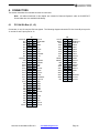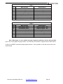
1
Hercules III User Manual
High Integration EBX SBC with Data Acquisition & DC Power Supply
Rev A.0: July 2013
Revision
Date
Comment
A.0
7/5/13
Initial version
FOR TECHNICAL SUPPORT
PLEASE CONTACT:
[email protected]
Copyright 2013
Diamond Systems Corporation
555 Ellis Street
Mountain View, CA 94043 USA
Tel 1-650-810-2500
Fax 1-650-810-2525
www.diamondsystems.com
TABLE OF CONTENTS
1.
IMPORTANT SAFE HANDLING INFORMATION .............................................................................................................. 5
2.
INTRODUCTION............................................................................................................................................................ 7
2.1
2.2
2.3
2.4
2.5
3.
FUNCTIONS...................................................................................................................................................................... 7
DATA ACQUISITION ........................................................................................................................................................... 8
EXPANSION OPTIONS ......................................................................................................................................................... 8
OPERATING SYSTEM SUPPORT ............................................................................................................................................. 8
MECHANICAL, ELECTRICAL, ENVIRONMENTAL ......................................................................................................................... 8
GETTING STARTED ....................................................................................................................................................... 9
3.1
INTRODUCING THE HERCULES III DEVELOPMENT KIT ................................................................................................................ 9
3.1.1
Hercules III Cable Kit........................................................................................................................................... 10
3.2
SYSTEM SETUP ............................................................................................................................................................... 11
3.2.1
Unpacking .......................................................................................................................................................... 11
3.2.2
Mounting Kit ...................................................................................................................................................... 11
3.2.3
Keyboard and Mouse ......................................................................................................................................... 11
3.2.4
mSATA Flashdisk Socket ..................................................................................................................................... 11
3.2.5
Mass Storage Devices ........................................................................................................................................ 11
3.2.6
Connecting Power .............................................................................................................................................. 11
3.2.7
Display ................................................................................................................................................................ 11
3.3
BOOTING THE SYSTEM ..................................................................................................................................................... 12
3.3.1
BIOS Setup .......................................................................................................................................................... 12
3.3.2
Operating System Drivers .................................................................................................................................. 12
4.
FUNCTIONAL OVERVIEW ............................................................................................................................................ 13
4.1
FUNCTIONAL BLOCK DIAGRAM .......................................................................................................................................... 13
4.2
FUNCTIONAL OVERVIEW................................................................................................................................................... 14
4.2.1
CPU Core ............................................................................................................................................................ 14
4.2.2
Video .................................................................................................................................................................. 14
4.2.3
Ethernet ............................................................................................................................................................. 14
4.2.4
USB ..................................................................................................................................................................... 14
4.2.5
mSATA Solid State Storage................................................................................................................................. 14
4.2.6
Audio .................................................................................................................................................................. 14
4.2.7
Serial Ports ......................................................................................................................................................... 14
4.2.8
GPS Module ........................................................................................................................................................ 14
4.2.9
CAN Interface ..................................................................................................................................................... 15
4.2.10 Data Acquisition ................................................................................................................................................. 15
4.2.11 PC/104-Plus Expansion Bus ................................................................................................................................ 15
4.2.12 Power Supply...................................................................................................................................................... 15
4.2.13 Battery Backup ................................................................................................................................................... 15
4.2.14 Watchdog Timer ................................................................................................................................................ 15
4.2.15 BIOS .................................................................................................................................................................... 16
5.
BOARD LAYOUT ......................................................................................................................................................... 16
5.1
5.2
6.
CONNECTOR SUMMARY ................................................................................................................................................... 17
JUMPER SUMMARY ......................................................................................................................................................... 17
CONNECTORS ............................................................................................................................................................. 18
6.1
6.2
6.3
6.4
PC/104 ISA BUS (J1, J2) ................................................................................................................................................ 18
PCI-104 BUS (J3) .......................................................................................................................................................... 19
SATA (J4) .................................................................................................................................................................... 19
UTILITY (J7) ................................................................................................................................................................... 20
Hercules III User Manual Rev A.0
www.diamondsystems.com
Page 2
6.5
6.6
6.7
6.8
6.9
6.10
6.11
6.12
6.13
6.14
6.15
6.16
6.17
6.18
6.19
6.20
6.21
7.
DIGITAL I/O (J8) ............................................................................................................................................................ 20
ANALOG I/O (J9) ........................................................................................................................................................... 22
GIGABIT ETHERNET (J10, J11) .......................................................................................................................................... 22
AUDIO (J12) .................................................................................................................................................................. 23
AUDIO AMP (J13) ......................................................................................................................................................... 23
EXTERNAL AUXILIARY POWER (J15) ................................................................................................................................... 23
SERIAL PORTS 1, 2, 3, 4 (J18) .......................................................................................................................................... 24
EXTERNAL BATTERY (J20)................................................................................................................................................. 24
USB (J21, J22) ............................................................................................................................................................. 25
LCD PANEL, LVDS INTERFACE (J24) .................................................................................................................................. 25
VGA (J25) .................................................................................................................................................................... 26
SERIAL PORTS 5, 6 (J27) .................................................................................................................................................. 27
LCD BACKLIGHT (J28) ..................................................................................................................................................... 27
CAN (J32) .................................................................................................................................................................... 28
POWER INPUT (J33)........................................................................................................................................................ 28
MSATA (J35) ................................................................................................................................................................ 29
PCIE MINICARD (J36) ..................................................................................................................................................... 30
JUMPER CONFIGURATION.......................................................................................................................................... 31
7.1
7.2
7.3
7.4
7.5
7.6
8.
COM3 & COM4 RS-422/285 TERMINATION (JP2) ........................................................................................................... 31
DIGITAL I/O CONFIGURATION (JP3) ................................................................................................................................... 31
LCD PANEL CONFIGURATION (JP4, JP5, JP6) ...................................................................................................................... 32
IRQ & FPGA ADDRESS SELECTION (JP7) ............................................................................................................................ 32
PCI-104 CONNECTOR VIO (JP9) ...................................................................................................................................... 33
COM3 & COM4 CONFIGURATION (JP10, JP11) ................................................................................................................ 33
SYSTEM OPERATION .................................................................................................................................................. 34
8.1
8.2
8.3
8.4
8.5
9.
SYSTEM RESOURCES ........................................................................................................................................................ 34
CONSOLE REDIRECTION TO A SERIAL PORT ........................................................................................................................... 34
WATCHDOG TIMER ......................................................................................................................................................... 35
BACKUP BATTERY............................................................................................................................................................ 35
SYSTEM RESET................................................................................................................................................................ 36
BIOS ........................................................................................................................................................................... 36
9.1
BIOS SETTINGS .............................................................................................................................................................. 36
9.1.1
Serial Ports ......................................................................................................................................................... 36
9.1.2
LCD Video Settings ............................................................................................................................................. 36
9.1.3
Miscellaneous Settings ....................................................................................................................................... 37
9.2
BIOS CONSOLE REDIRECTION SETTINGS .............................................................................................................................. 38
10.
SYSTEM I/O ............................................................................................................................................................ 38
10.1
10.2
10.3
11.
ETHERNET ..................................................................................................................................................................... 38
SERIAL PORTS................................................................................................................................................................. 38
USB PORTS ................................................................................................................................................................... 40
OPERATING SYSTEMS AND BOOTING PROCEDURES ............................................................................................... 40
11.1 WINDOWS OPERATING SYSTEM INSTALLATION ISSUES ........................................................................................................... 40
11.1.1 Driver Installation............................................................................................................................................... 40
11.1.2 BIOS Setting for Windows .................................................................................................................................. 40
11.2 DOS OPERATING SYSTEMS INSTALLATION ISSUES .................................................................................................................. 40
12.
DATA ACQUISITION CIRCUIT................................................................................................................................... 41
13.
ANALOG-TO-DIGITAL INPUT RANGES AND RESOLUTION ........................................................................................ 66
13.1 OVERVIEW..................................................................................................................................................................... 66
13.1.1 Input Range Selection ........................................................................................................................................ 66
13.1.2 Input Range Table .............................................................................................................................................. 66
Hercules III User Manual Rev A.0
www.diamondsystems.com
Page 3
14.
PERFORMING AN A/D CONVERSION ...................................................................................................................... 67
14.1 INTRODUCTION............................................................................................................................................................... 67
14.2 SELECT THE INPUT CHANNEL ............................................................................................................................................. 67
14.3 SELECT THE INPUT RANGE................................................................................................................................................. 67
14.4 WAIT FOR ANALOG INPUT CIRCUIT TO SETTLE ...................................................................................................................... 67
14.5 PERFORM AN A/D CONVERSION ON THE CURRENT CHANNEL .................................................................................................. 67
14.6 WAIT FOR THE CONVERSION TO FINISH ............................................................................................................................... 68
14.7 READ THE DATA FROM THE BOARD..................................................................................................................................... 68
14.8 CONVERT THE NUMERICAL DATA TO A MEANINGFUL VALUE ..................................................................................................... 68
14.8.1 Conversion Formula for Bipolar Input Ranges ................................................................................................... 69
14.8.2 Conversion Formula for Unipolar Input Ranges ................................................................................................. 69
15.
A/D SCAN, INTERRUPT AND FIFO OPERATION ........................................................................................................ 70
16.
DIGITAL-TO-ANALOG OUTPUT RANGES AND RESOLUTION .................................................................................... 71
16.1 DESCRIPTION ................................................................................................................................................................. 71
16.2 RESOLUTION .................................................................................................................................................................. 72
16.3 OUTPUT RANGE SELECTION .............................................................................................................................................. 72
16.4 D/A CONVERSION FORMULAS AND TABLES .......................................................................................................................... 73
16.4.1 D/A Conversion Formulas for Unipolar Output Ranges ..................................................................................... 73
16.4.2 D/A Conversion Formulas for Bipolar Output Ranges ........................................................................................ 74
17.
GENERATING AN ANALOG OUTPUT........................................................................................................................ 75
17.1
17.2
17.3
COMPUTE THE D/A CODE FOR THE DESIRED OUTPUT VOLTAGE ............................................................................................... 75
WRITE THE VALUE TO THE SELECTED OUTPUT CHANNEL REGISTERS .......................................................................................... 75
WAIT FOR THE D/A TO UPDATE......................................................................................................................................... 75
18.
ANALOG CIRCUIT CALIBRATION ............................................................................................................................. 76
19.
DIGITAL I/O OPERATION ........................................................................................................................................ 77
20.
COUNTER/TIMER OPERATION ................................................................................................................................ 78
20.1 COUNTER 0 – A/D SAMPLE CONTROL ................................................................................................................................ 78
20.2 COUNTER 1 – COUNTING/TOTALIZING FUNCTIONS................................................................................................................ 78
20.3 COMMAND SEQUENCES ................................................................................................................................................... 79
20.3.1 Load and Enable (Run) a Counter Sequence ...................................................................................................... 79
20.3.2 Read a Counter Sequence .................................................................................................................................. 79
20.3.3 Disabling the Counter Gate Command............................................................................................................... 80
20.3.4 Clearing a Counter Sequence ............................................................................................................................. 80
21.
WATCHDOG TIMER PROGRAMMING ..................................................................................................................... 81
21.1
22.
WATCHDOG TIMER REGISTER DETAILS ................................................................................................................................ 81
DATA ACQUISITION SPECIFICATIONS...................................................................................................................... 83
22.1
22.2
22.3
22.4
ANALOG INPUTS (DATA ACQUISITION UNITS ONLY)................................................................................................................. 83
ANALOG OUTPUTS (DATA ACQUISITION UNITS ONLY) ............................................................................................................. 83
DIGITAL I/O................................................................................................................................................................... 83
COUNTER/TIMERS (DATA ACQUISITION UNITS ONLY) .............................................................................................................. 83
23.
MSATA FLASHDISK MODULE .................................................................................................................................. 84
24.
SPECIFICATIONS ..................................................................................................................................................... 85
24.1
24.2
24.3
24.4
CPU............................................................................................................................................................................. 85
DATA ACQUISITION CIRCUITRY .......................................................................................................................................... 85
POWER SUPPLY .............................................................................................................................................................. 86
GENERAL ....................................................................................................................................................................... 86
Hercules III User Manual Rev A.0
www.diamondsystems.com
Page 4
1. IMPORTANT SAFE HANDLING INFORMATION
WARNING!
ESD-Sensitive Electronic Equipment
Observe ESD-safe handling procedures when working with this product.
Always use this product in a properly grounded work area and wear appropriate
ESD-preventive clothing and/or accessories.
Always store this product in ESD-protective packaging when not in use.
Safe Handling Precautions
The Helios board contains a high number of I/O connectors with connection to sensitive electronic components.
This creates many opportunities for accidental damage during handling, installation and connection to other
equipment. The list here describes common causes of failure found on boards returned to Diamond Systems for
repair. This information is provided as a source of advice to help you prevent damaging your Diamond (or any
vendor’s) embedded computer boards.
ESD damage – This type of damage is usually almost impossible to detect, because there is no visual sign of
failure or damage. The symptom is that the board eventually simply stops working, because some component
becomes defective. Usually the failure can be identified and the chip can be replaced.
To prevent ESD damage, always follow proper ESD-prevention practices when handling computer boards.
Damage during handling or storage – On some boards we have noticed physical damage from mishandling. A
common observation is that a screwdriver slipped while installing the board, causing a gouge in the PCB surface
and cutting signal traces or damaging components.
Another common observation is damaged board corners, indicating the board was dropped. This may or may not
cause damage to the circuitry, depending on what is near the corner. Most of our boards are designed with at
least 25 mils clearance between the board edge and any component pad, and ground / power planes are at least
20 mils from the edge to avoid possible shorting from this type of damage. However these design rules are not
sufficient to prevent damage in all situations.
A third cause of failure is when a metal screwdriver tip slips, or a screw drops onto the board while it is powered
on, causing a short between a power pin and a signal pin on a component. This can cause overvoltage / power
supply problems described below. To avoid this type of failure, only perform assembly operations when the
system is powered off.
Sometimes boards are stored in racks with slots that grip the edge of the board. This is a common practice for
board manufacturers. However our boards are generally very dense, and if the board has components very close
to the board edge, they can be damaged or even knocked off the board when the board tilts back in the rack.
Diamond recommends that all our boards be stored only in individual ESD-safe packaging. If multiple boards are
stored together, they should be contained in bins with dividers between boards. Do not pile boards on top of each
other or cram too many boards into a small location. This can cause damage to connector pins or fragile
components.
Power supply wired backwards – Our power supplies and boards are not designed to withstand a reverse power
supply connection. This will destroy each IC that is connected to the power supply (i.e. almost all ICs). In this
case, the board will most likely cannot be repaired and must be replaced. A chip destroyed by reverse power or
by excessive power will often have a visible hole on the top or show some deformation on the top surface due to
vaporization inside the package. Check twice before applying power!
Board not installed properly in PC/104 stack – A common error is to install a PC/104 board accidentally shifted by
1 row or 1 column. If the board is installed incorrectly, it is possible for power and ground signals on the bus to
make contact with the wrong pins on the board, which can damage the board. For example, this can damage
components attached to the data bus, because it puts the 12V power supply lines directly on data bus lines.
Hercules III User Manual Rev A.0
www.diamondsystems.com
Page 5
Overvoltage on analog input – If a voltage applied to an analog input exceeds the design specification of the
board, the input multiplexor and/or parts behind it can be damaged. Most of our boards will withstand an
erroneous connection of up to 35V on the analog inputs, even when the board is powered off, but not all boards,
and not in all conditions.
Overvoltage on analog output – If an analog output is accidentally connected to another output signal or a power
supply voltage, the output can be damaged. On most of our boards, a short circuit to ground on an analog output
will not cause trouble.
Overvoltage on digital I/O line – If a digital I/O signal is connected to a voltage above the maximum specified
voltage, the digital circuitry can be damaged. On most of our boards the acceptable range of voltages connected
to digital I/O signals is 0-5V, and they can withstand about 0.5V beyond that (-0.5 to 5.5V) before being damaged.
However logic signals at 12V and even 24V are common, and if one of these is connected to a 5V logic chip, the
chip will be damaged, and the damage could even extend past that chip to others in the circuit.
Bent connector pins – This type of problem is often only a cosmetic issue and is easily fixed by bending the pins
back to their proper shape one at a time with needle-nose pliers. The most common cause of bent connector pins
is when a PC/104 board is pulled off the stack by rocking it back and forth left to right, from one end of the
connector to the other. As the board is rocked back and forth it pulls out suddenly, and the pins at the end get
bent significantly. The same situation can occur when pulling a ribbon cable off of a pin header. If the pins are
bent too severely, bending them back can cause them to weaken unacceptably or even break, and the connector
must be replaced.
Hercules III User Manual Rev A.0
www.diamondsystems.com
Page 6
2. INTRODUCTION
Hercules III is an embedded single-board computer (SBC) in the EBX small form factor that integrates a complete
embedded PC, data acquisition circuitry, and DC power supply into a single board.
The Hercules III SBC is based on an Intel E680T CPU with onboard central processing, memory and memory
management devices and I/O management for specific functions. The Hercules III SBC includes the following
additional features.
Communicates externally over the ISA bus, PCI bus, and I/O ports
Generates on-board RGB video for CRT display systems
Contains LVDS formatting to drive a flat panel
Is powered from an external +7-40VDC wide voltage input
One standard model of Hercules III with data acquisition is available as shown in the following table. Three other
models are available with a minimum order of 50 units.
Model
Processor Speed
RAM Size
Data Acquisition
Availability
HRCE1600A-1G
1.6GHz
1GB
Yes
Standard model
HRCE1600D-1G
1.6GHz
1GB
DIO only
MOQ of 50
HRCE1600A-2G
1.6GHz
2GB
Yes
MOQ of 50
HRCE1600D-2G
1.6GHz
2GB
DIO only
MOQ of 50
The Hercules III SBC brings the ISA and PCI buses out to an expansion connector to mate with add-on boards.
Diamond Systems manufactures a wide variety of compatible PC/104-Plus add-on boards for analog I/O, digital
I/O, counter/timer functions, serial ports and power supplies.
2.1
Functions
The Hercules III board includes the following key system and data acquisition features. The functions listed below
are applicable for all models.
1.6GHz Intel Atom E680T “Tunnel Creek” processor (Queensbay platform)
1GB or 2GB SDRAM soldered on-board
2 Gigabit Ethernet ports on pin header, with on-board magnetics
5 USB 2.0 ports
1 USB 2.0 device port
2 RS-232/422/485 serial ports
4 fixed RS-232 serial ports
LVDS flat panel interface
VGA or LVDS interface up to 1600 x 1200 maximum
1 SATA port
1 mSATA disk module interface
1 CANbus 2.0 port
40 digital I/O lines with programmable direction
HD Audio CODEC
+7V to +40V DC/DC wide range power supply with 35W available for add-on accessories or modules
Hercules III User Manual Rev A.0
www.diamondsystems.com
Page 7
2.2
Data Acquisition
The functions listed below are applicable to the data acquisition versions only.
32 channel 16-bit A/D, 250KHz maximum sample rate
Single-ended or differential mode
Programmable input ranges +/-10V, +/-5V, +/-2.5V, +/-1.25V, 0-10V, 0-5V, 0-2.5V
Interrupt-based sampling with 2048-sample programmable FIFO
4 12-bit D/A channels
Output ranges: +/-10V, +/-5V, 0-10V, 0-5V
4 pulse width modulation circuits
Watchdog timer
1 24-bit and 1 16-bit counter/timer for A/D sample rate control, event counting, and programmable
interrupts
Auto-calibration with Universal Driver software support
2.3
Expansion Options
mSATA flashdisk mounting capability
PC/104-Plus expansion connector
PCIe MiniCard and GPS receiver sockets
2.4
Operating System Support
Windows Embedded Standard 7
Linux 2.6
Windows CE 6.0 R3
2.5
Mechanical, Electrical, Environmental
EBX form factor, 5.75”W x 8.0”H, identical to Hercules II
Fanless heat sink on top side
-40°C to +85°C ambient operating temperature without a fan
MIL-STD-202G shock and vibration compliant
Power input requirements: +7-40VDC +/- 5%
Hercules III User Manual Rev A.0
www.diamondsystems.com
Page 8
3.
GETTING STARTED
First-time Hercules III SBC users normally receive the product as part of Diamond’s Hercules III Development Kit,
which provides everything needed to ensure rapid application development. This section of the Hercules III User
Manual covers basic hardware setup, power connection, system boot-up, and initial software configuration. After
Hercules III is up and running, refer to the later sections of this manual for the detailed hardware and software
reference information needed to adapt the product to specific applications.
Important Safe-Handling Information
WARNING: ESD-Sensitive Electronic Equipment!
Observe ESD-safe handling procedures when working
with this product.
Always use this product in a properly grounded work area
and wear appropriate ESD-preventive clothing and/or
accessories.
Always store this product in ESD-protective packaging
when not in use.
Please refer to page 5 of this manual (“Important Safe-Handling Information”) for further
details.
3.1
Introducing the Hercules III Development Kit
The Hercules III Development Kit (DK-HRCE-A-xxx) provides everything required for Hercules III based rapid
application development. Development Kits are available with bootable images of Linux, Windows Embedded 7
and Windows CE. The various Development Kits are as follows:
DK-HRCE-A-LNX
Development Kit with bootable Linux operating system
DK-HRCE-A-WE7
Development Kit with bootable Windows Embedded 7 operating system
DK-HRCE-A-WCE
Development Kit with bootable Windows CE 6 operating system
The table on the next page lists the boards, cables, and other items included.
Hercules III User Manual Rev A.0
www.diamondsystems.com
Page 9
Item
3.1.1
Diamond P/N
Description
1
HRCE1600A-1G
Hercules III SBC, 1.6GHz Atom E680T CPU, 1GB SDRAM, Data
Acquisition
2
889210x
16GB mSATA MLC flashdisk with bootable OS pre-loaded
(based on the Kit ordered)
3
C-HRCE-KIT
Hercules III Cable Kit
4
PS-12V-01
12V AC Power Adapter
5
7460001
Hercules III Quick Start Guide
6
6710010
Diamond Systems Software and Documentation CD
7
DOC-PKG
Diamond Systems Document Package
8
MTG104
PC/104 Mounting Hardware Kit
9
7492100/7492103
BSP Quickstart guide (based on the Kit ordered)
10
7482100/7482103
BSP User Manual (based on the Kit ordered)
Hercules III Cable Kit
The Hercules III Cable Kit (number C-HRCE-KIT) provides convenient access to most of Hercules III’s I/O
features. The kit’s cable assemblies are identified in the following table.
Number
Quantity
Cable No.
Description
1
2
3
4
5
6
7
8
9
10
11
12
13
14
15
16
1
1
1
1
1
1
1
1
2
1
1
1
1
1
1
1
6981006
6981011
6981012
6981015
6981018
6981022
6981024
6981025
6981080
6981314
8180020
C-20-18
C-40-18
C-50-18
C-DB9M-2
C-DB9M-4
Power out cable
External battery cable
Dual USB cable
Power input cable
Speaker output cable
PS/2 keyboard & mouse cable
VGA cable
Audio I/O cable
Ethernet cable
CANbus cable
Utility board
Utility signals cable
Analog I/O cable
Digital I/O cable
Serial port 5 & 6 cable
Serial ports 1 -- 4 cable
Connects to …
J15
J20
J21, J22
J33
J13
J6
J25
J12
J10, J11
J32
J7
J9
J8
J18
J27
Note: On each interface cable, the end of the cable connector that has a red wire going to it
should be oriented toward the end of the board connector that is labeled “pin 1” (typically the pin
with a square pad on the PCB).
Hercules III User Manual Rev A.0
www.diamondsystems.com
Page 10
3.2
System Setup
This section outlines a simple process for preparing Hercules III for first-time operation using the Hercules III
Development Kit. Additional details regarding Hercules III’s interface functions and connections may be found in
Section 6 of this document (Connectors).
3.2.1
Unpacking
Unpack and remove the Hercules III single board computer from its packaging.
3.2.2
Mounting Kit
Install the four standoffs found in the mounting kit (MTG104) into the four PC/104 mounting holes located on the
board. This ensures that the board will not touch the surface beneath it, and helps redistribute the force when you
push connectors onto the board.
3.2.3
Keyboard and Mouse
Hercules III supports operation using a PS/2-based keyboard and mouse devices. Plug the keyboard and mouse
connectors into the appropriate connectors on the Main I/O cable in the Hercules III Cable Kit (cable number
6981022). Connect the end of the cable into connector J16 on Hercules III.
3.2.4
mSATA Flashdisk Socket
Hercules III provides a location for on-board installation of an optional mSATA flashdisk on connector J35. Plug
the mSATA flashdisk module in the Development Kit into connector J35 on Hercules III. Remove the screw from
the mounting stand-off before installing the flashdisk. Secure the flashdisk to Hercules III with the screw once the
flashdisk is installed.
3.2.5
Mass Storage Devices
If desired, connect SATA hard drives to Hercules III by connecting a SATA cable to SATA connector J4 and then
to the SATA drive. Hercules III can operate with a combination of SATA and CD-ROM drives, and can boot from
either of them.
Caution! Be sure the PS-12V-01 AC power adapter is disconnected
from its AC power source prior to performing the following step.
3.2.6
Connecting Power
Connect cable 6981015 to the PS-12V-01 AC power adapter or an ATX power supply. Connect the other end of
the 6981015 cable to connector J33 on the Hercules III SBC.
3.2.7
Display
Hercules III provides interfaces for both LVDS flat panel displays and VGA output. Connect the VGA cable,
6981024, between the VGA connector, J25, and a VGA-compatible display.
Hercules III User Manual Rev A.0
www.diamondsystems.com
Page 11
3.3
Booting the System
Power-up the VGA video monitor. Then plug the PS-12V-01 AC power adapter to an AC outlet. Hercules III
should begin its boot-up sequence immediately, as evidenced by BIOS messages on the connected VGA display.
You can run the BIOS Setup utility and proceed to install an operating system on the boot drive just as you would
on a normal desktop PC.
3.3.1
BIOS Setup
Hercules III’s BIOS provides a wide range of configuration options. When you power up Hercules III for the first
time, you should immediately enter the BIOS “Setup” utility in order to adjust BIOS settings to match your
system’s peripheral devices and other requirements, and to configure various other hardware and software
parameters.
Options configurable via Setup typically include:
Number and type of mass storage devices
Boot device priority (default is mSATA)
Video display type and resolution
USB, SATA, serial, and parallel interface modes and protocols
PCI and PnP configuration
Power management setup
Automatic power-up after LAN connection, RTC alarm, power resumption, etc.
System monitoring and security functions
3.3.2
Operating System Drivers
Hercules III will boot and run the operating system from the mSATA flashdisk as defined by which Development
Kit was ordered. Hercules III should now be fully operational.
If you desire to run a different operating system, depending on the operating system to be installed, it may be
necessary to install software drivers for on-board interface controllers. Drivers for Windows XP, Windows
Embedded Standard 7, Windows Embedded CE, and Linux 2.6, if required, are included on the Software and
Documentation CD that is included in the Hercules III Development Kit.
Hercules III User Manual Rev A.0
www.diamondsystems.com
Page 12
4. FUNCTIONAL OVERVIEW
4.1
Functional Block Diagram
Hercules III User Manual Rev A.0
www.diamondsystems.com
Page 13
4.2
Functional Overview
This section describes the major Hercules III subsystems.
4.2.1
CPU Core
Hercules III’s core embedded computer circuit features the ultra low power Intel Atom “Queensbay” extended
temperature platform, consisting of an Atom processor (“Tunnel Creek”) with I/O Hub (“Topcliff”). The rest of the
circuit consists of 1GB or 2GB of on-board SDRAM memory, display controller with LVDS and onboard VGA/ DVI
converter, plus SATA, USB, serial port and LAN interfaces. Off-board system buses include PCI Express and ISA.
4.2.2
Video
The video circuit consists of Intel’s integrated GMA500 controller with dual independent display support. A 24-bit,
single-channel LVDS hardware interface is provided as an interface to LCD displays. The LVDS transmitter
operates at 112MHz, with resolutions up to 1366x768 pixels.
CRT resolution of up to 1280x1024 pixels is supported by conversion from the Tunnel Creek through a single
SDVO interface to analog VGA with a Chrontel chip.
Simultaneous CRT and LCD support is provided.
In addition, the chipset integrated video controller provides hardware acceleration for H.264, MPEG2, VC1 and
WMV9 video decoding standards.
4.2.3
Ethernet
Hercules III provides dual Gigabit Ethernet ports, one supported from the Top Cliff’s internal MAC and the other
from the Intel 82574IT Gigabit MAC/PHY. Both ports provide a vertical RJ-45 connector with integrated agnetic.
The Wake-On-LAN feature requires integration with the board’s power supply and Hercules III BIOS.
4.2.4
USB
Hercules III offers 5 user accessible USB 2.0 ports. All ports have minimum 500mA per port drive capability with
short circuit / over current and ESD protection on each port. All of the ports are brought out to I/O connectors for
user access.
4.2.5
mSATA Solid State Storage
A mSATA connector provides mounting for a solid state bootable USB flashdisk module with capacity up to 64GB.
Both MLC and SLC mSATA devices are supported and available.
4.2.6
Audio
Hercules III provides HD audio support from the Tunnel Creek CPU via a Realtek ALC262 high definition CODEC.
Audio I/O includes stereo line in, stereo line out, amplified out and mono mic in. The board includes audio power
amplifier circuitry for stereo speaker output. The amplifier circuit is powered by +5VDC from the board. User DC
control of volume is provided which overrides the software settings.
4.2.7
Serial Ports
Hercules III provides six serial ports with varying protocols and signal availability. The SCH3116 provides all of
the serial ports. Two of the serial ports (COM3 & COM4) support RS-232/422/485 protocols. The other four ports
(COM1, COM2, COM5, & COM6) support RS-232 only.
The BIOS supports serial console redirection on COM1. This feature enables keyboard input and character video
output to be routed to COM1.
4.2.8
GPS Module
Hercules III supports a plug-in Condor C2626 GPS module. The Condor C2626 provides an L1 Frequency
(1575.42MHz) GPS receiver with NMEA protocol from a serial port. UART1 from Top Cliff is interfaced with the
GPS module.
Hercules III User Manual Rev A.0
www.diamondsystems.com
Page 14
4.2.9
CAN Interface
Hercules III provides one channel of CAN 2.0 with transceiver.
4.2.10 Data Acquisition
The board provides the following data acquisition capabilities.
Type of I/O
PWM
Characteristics
32 single-ended/16 differential inputs, 16-bit resolution.
250KHz maximum aggregate A/D sampling rate.
Programmable input ranges/gains:
+/-10V, +/-5V, +/-2.5V, +/-1.25V, 0-10V, 0-5V, 0-2.5V.
A/D 2048 FIFO for reliable high-speed sampling and scan operation.
Four analog outputs, 12-bit resolution.
±10V and 0-10V output ranges.
Indefinite short circuit protection on outputs.
4 pulse width modulator circuits
Digital I/O
40 programmable digital I/O, 3.3V and 5V logic compatible.
Counter/Timers
One 24-bit counter/timer for A/D sampling rate control.
One 16-bit counter/timer for user counting and timing functions.
Analog Input
Analog Output
On board I2C flash EEROM is provided for auto-calibration value storage.
4.2.11 PC/104-Plus Expansion Bus
The PC/104-Plus expansion bus offers both the ISA bus and PCI bus, and enables installation of additional I/O
boards. It consists of two stack-through connectors press-fit onto the board, enabling expansion both above and
below the board.
4.2.12 Power Supply
Hercules III contains an on-board DC/DC power supply with 55 watts of output power. With approximately 13.8W
required to power the SBC, this leaves 35W available to power peripherals and add-on boards. The +7-40VDC
input range means that Hercules III is compatible with vehicle, battery or industrial power sources. The on-board
supply features ACPI compatibility for intelligent power management.
4.2.13 Battery Backup
Hercules III includes a backup battery for CMOS RAM and real-time clock backup. The battery is mounted on the
o
top side of the board. The battery provides a minimum of 5 years backup capability at 25 C with the system
powered off.
A connector and jumper are provided to disable the on-board battery and enable use of an external battery
instead. External battery voltage requirement is 3.3V +/- 10%. The jumper also clears the CMOS RAM when it is
removed and no external battery is connected.
4.2.14 Watchdog Timer
A programmable watchdog timer (WDT) is included to provide an automatic reset in case of system hang. The
WDT may be retriggered either by a software command or a digital input. The system will reset when the WDT is
enabled and expires. The WDT circuitry is integrated in the FPGA chip.
Hercules III User Manual Rev A.0
www.diamondsystems.com
Page 15
4.2.15 BIOS
The AMI BIOS includes the following key features:
Boot from LAN (PXE) and USB as well as C: and D:
User selectable Master boot device selection
Free boot sequence configuration
Support for various LCD configurations supported by the video chipset
Console (display and keyboard) redirection to serial port
DSC-configurable default settings in battery-less configurations
Initialize USB keyboard & mouse
Customizable splash screen
5. BOARD LAYOUT
The figure below shows the Hercules III board layout, including connectors, jumper blocks and mounting holes.
JP2
JP9
J25
J23
J27
J36 J18
JP10
JP11 J34
J15
J12
J3
J13
J37
SKT2
J19
J11
J28
JP4
JP5
J24
J10
J14
JP6
J9
J21
J8
J22
JP7
J20
JP3
J7
J32
J4
J29
Hercules III User Manual Rev A.0
J35
J2
J1
www.diamondsystems.com
J5
J6
Page 16
5.1
Connector Summary
The following table lists the connectors on the Hercules III SBC.
Connector
J1
J2
J3
J4
J6
J7
J8
J9
J10, J11
J12
J13
J14
J15
J18
J20
J21
J22
J23
J24
J25
J27
J28
J32
J29
J34
J35
J36
SKT2
5.2
Description
PC/104, ISA bus A,B
PC/104, ISA bus C,D
PCI-104, PCI bus
SATA
PS/2 Keyboard & Mouse
Utility
Digital I/O
Analog I/O
Gigabit Ethernet
Audio I/O
Audio Amp
ADC Calibration
External Auxiliary Power
Serial Ports 1, 2, 3, & 4
External Battery
USB 0/1
USB 2/3
USB 4 , USB Device
LVDS LCD
VGA
Serial Ports 5 & 6
LCD backlight power
CANbus
Power Input
GPS PPS
mSATA Socket
PCIe MiniCard Socket
GPS Socket
Jumper Summary
The following table lists the jumper blocks on the Hercules III SBC.
Jumper
Description
JP2
COM3 & COM4 RS-485/422 termination
JP3
Digital I/O configuration
JP4
LCD VDD select
JP5
LCD backlight VDD select
JP6
LCD scan direction and frame rate setting
JP7
IRQ & FPGA address selection
JP9
PC/104-Plus VIO selection
JP10
COM3 configuration
JP11
COM4 configuration
Hercules III User Manual Rev A.0
www.diamondsystems.com
Page 17
6. CONNECTORS
This section describes the on-board Hercules III connectors.
Note: All cables mentioned in this chapter are included in Diamond Systems’ cable kit C-HRCE-KIT.
Some cables are also available individually.
6.1
PC/104 ISA Bus (J1, J2)
Connectors J1 and J2 carry the ISA bus signals. The following diagram shows the PC/104 A and B pin layout for
J1 and the C and D pin layout for J2.
J1
IOCHCHKSD7
SD6
SD5
SD4
SD3
SD2
SD1
SD0
IOCHRDY
AEN
SA19
SA18
SA17
SA16
SA15
SA14
SA13
SA12
SA11
SA10
SA9
SA8
SA7
SA6
SA5
SA4
SA3
SA2
SA1
SA0
Ground
A1
A2
A3
A4
A5
A6
A7
A8
A9
A10
A11
A12
A13
A14
A15
A16
A17
A18
A19
A20
A21
A22
A23
A24
A25
A26
A27
A28
A29
A30
A31
A32
J2
B1
B2
B3
B4
B5
B6
B7
B8
B9
B10
B11
B12
B13
B14
B15
B16
B17
B18
B19
B20
B21
B22
B23
B24
B25
B26
B27
B28
B29
B30
B31
B32
Hercules III User Manual Rev A.0
Ground
RESETDRV
+5V
IRQ9
-5V
DRQ2
-12V
ENDXFR+12V
Key
SMEMWSMEMRIOWIORDACK3DRQ3
DACK1DRQ1
REFRESHSYSCLK
IRQ7
IRQ6
IRQ5
IRQ4
IRQ3
DACK2TC
BALE
+5V
OSC
Ground
Ground
Ground
SBHELA23
LA22
LA21
LA20
LA19
LA18
LA17
MEMRMEMWSD8
SD9
SD10
SD11
SD12
SD13
SD14
SD15
Key
www.diamondsystems.com
C0
C1
C2
C3
C4
C5
C6
C7
C8
C9
C10
C11
C12
C13
C14
C15
C16
C17
C18
C19
D0
D1
D2
D3
D4
D5
D6
D7
D8
D9
D10
D11
D12
D13
D14
D15
D16
D17
D18
D19
Ground
MEMCS16-IOCS16IRQ10
IRQ11
IRQ12
IRQ15
IRQ14
DACK0DRQ0
DACK5DRQ5
DACK6DRQ6
DACK7DRQ7
+5
MASTERGround
Ground
Page 18
6.2
PCI-104 Bus (J3)
The PCI-104 bus connector is a non-stackthrough connector with short PCB pins. The bus stacks upward only.
No pin shroud is required on the bottom side.
J3
6.3
Pin
A
1
2
3
4
5
6
7
8
9
10
11
12
13
14
15
16
17
18
19
20
21
22
23
24
25
26
27
28
29
30
GND/5.0V KEY
VI/O
AD05
C/BE0*
GND
AD11
AD14
+3.3V
SERR*
GND
STOP*
+3.3V
FRAME*
GND
AD18
AD21
+3.3V
IDSEL0
AD24
GND
AD29
+5V
REQ0*
GND
GNT1*
+5V
CLK2
GND
+12V
-12V
2
B
C
D
Reserved
AD02
GND
AD07
AD09
VI/O
AD13
C/BE1*
GND
PERR*
+3.3V
TRDY*
GND
AD16
+3.3V
AD20
AD23
GND
C/BE3*
AD26
+5V
AD30
GND
REQ2*
VI/O
CLK0
+5V
INTD*
INTA*
Reserved
+5
AD01
AD04
GND
AD08
AD10
GND
AD15
SB0*
+3.3V
LOCK*
GND
IRDY*
+3.3V
AD17
GND
AD22
IDSEL1
VI/O
AD25
AD28
GND
REQ1*
+5V
GNT2*
GND
CLK3
+5V
INTB*
Reserved
AD00
+5V
AD03
AD06
GND
M66EN
AD12
+3.3V
PAR
SDONE
GND
DEVSEL*
+3.3V
C/BE2*
GND
AD19
+3.3V
IDSEL2
IDSEL3
GND
AD27
AD31
VI/O
GNT0*
GND
CLK1
GND
RST*
INTC*
2
GND/3.3V KEY
SATA (J4)
Industry standard vertical SATA connector.
Hercules III User Manual Rev A.0
www.diamondsystems.com
Page 19
6.4
Utility (J7)
A 20-pin connector provides access to the standard button/LED connections. Cable C-20-18 is used to connect
to J7.
Ground
Ground
Network : Activity LED
Network : Link LED
+5V In
Power LED
Watch Dog Timer - Input
SPEAKER
+5V In
N/C
1
3
5
7
9
11
13
15
17
19
2
4
6
8
10
12
14
16
18
20
Reset Key
Power Button
+3.3V Standby
+3.3V Standby
SATA LED
External Battery
Ground
Watch Dog Timer - Output
N/C
Ground
Connector type: Shrouded .1” dual row straight pin header with gold flash plating
6.5
Digital I/O (J8)
Hercules III includes a 50-pin header, J8, for all digital I/O.
J8 Digital I/O Connector
DIO A0
1
2
DIO A1
DIO A2
3
4
DIO A3
DIO A4
5
6
DIO A5
DIO A6
7
8
DIO A7
DIO B0
9
10
DIO B1
DIO B2
11
12
DIO B3
DIO B4
13
14
DIO B5
DIO B6
15
16
DIO B7
DIO C0
17
18
DIO C1
DIO C2
19
20
DIO C3
DIO C4
21
22
DIO C5
DIO C6
23
24
DIO C7
DIO D0
25
26
DIO D1
DIO D2
27
28
DIO D3
DIO D4
29
30
DIO D5
DIO D6
31
32
DIO D7
DIO E0 / PWM0
33
34
DIO E1 / PWM1
DIO E2 / PWM2
35
36
DIO E3 / PWM3
DIO E4 / GATE1
37
38
DIO E5 / TOUT1
Hercules III User Manual Rev A.0
www.diamondsystems.com
Page 20
DIO E6 / DIOLATCH
39
40
DIO E7 / GATE0
EXTTRIG
41
42
TOUT0
ACK
43
44
WDI
WDO
45
46
FXA
FXB
47
48
FXB
+5V
49
50
Digital Ground
Signal
Definition
DIO A7-A0
DIO B7-B0
DIO C7-C0
DIO D7-D0
DIO E7-E0
Digital I/O port A; programmable direction
Digital I/O port B; programmable direction
Digital I/O port C; programmable direction
Digital I/O port D; programmable direction
Digital I/O port E; programmable direction
E3-E0 may be configured for PWM signals
External A/D trigger input
Counter/Timer 0/1 output
Pulse width modulator signals
Watchdog timer input/output
Connected to switched +5V supply
(Output only! Do not connect to external supply)
Digital ground (0V - reference); used for digital circuitry only
EXTTRIG
TOUT0/1
PWM0-3
WDI/O
+5V out
DGND
Diamond Systems cable number C-50-18 provides a standard 50-pin connector at each end and mates with this
header.
Connector type: Hirose DF50 1mm, RA, pos. lock, 50 pins
Hercules III User Manual Rev A.0
www.diamondsystems.com
Page 21
6.6
Analog I/O (J9)
Hercules III models with analog data acquisition include a 40-pin header, J9, for the analog I/O features. The
pinout definition depends on the analog input jumper configuration. This is available only on models with data
acquisition.
Vout 0
Vout 2
Output Ground
Vin 0
Vin 1
Vin 2
Vin 3
Vin 4
Vin 5
Vin 6
Vin 7
Vin 8
Vin 9
Vin 10
Vin 11
Vin 12
Vin 13
Vin 14
Vin 15
Input Ground
Single-Ended
1
2
3
4
5
6
7
8
9
10
11
12
13
14
15
16
17
18
19
20
21
22
23
24
25
26
27
28
29
30
31
32
33
34
35
36
37
38
39
40
Vout 1
Vout 3
Output Ground
Vin 16
Vin 17
Vin 18
Vin 19
Vin 20
Vin 21
Vin 22
Vin 23
Vin 24
Vin 25
Vin 26
Vin 27
Vin 28
Vin 29
Vin 30
Vin 31
Input Ground
Vout 0
Vout 2
Output Ground
Vin 0 +
Vin 1 +
Vin 2 +
Vin 3 +
Vin 4 +
Vin 5 +
Vin 6 +
Vin 7 +
Vin 8 +
Vin 9 +
Vin 10 +
Vin 11 +
Vin 12 +
Vin 13 +
Vin 14 +
Vin 15 +
Input Ground
Differential
1
2
3
4
5
6
7
8
9
10
11 12
13 14
15 16
17 18
19 20
21 22
23 24
25 26
27 28
29 30
31 32
33 34
35 36
37 38
39 40
Vout 1
Vout 3
Output Ground
Vin 0 Vin 1 Vin 2 Vin 3 Vin 4 Vin 5 Vin 6 Vin 7 Vin 8 Vin 9 Vin 10 Vin 11 Vin 12 Vin 13 Vin 14 Vin 15 Input Ground
Connector type: Hirose DF50 1mm, RA, pos. lock, 40 pins
Diamond Systems cable number C-40-18 provides a standard 40-pin connector at each end and mates with this
header.
6.7
Gigabit Ethernet (J10, J11)
Hercules III provides 2 Gigabit Ethernet ports, each with the following pinout.
NC
DA+
DB+
DC+
DD+
1
3
5
7
9
2
4
6
8
10
Key / Cut
DADBDC-
DD-
Connector type: Standard 2mm pitch vertical header with external magnetics
Diamond Systems cable number 6981080 mates with these headers.
Hercules III User Manual Rev A.0
www.diamondsystems.com
Page 22
6.8
Audio (J12)
1
2
3
4
5
6
7
8
9
10
LEFT Headphone / Line Out
RIGHT Headphone / Line Out
Audio Ground
LEFT Line Input
RIGHT Line Input
LEFT AUX Input
RIGHT AUX Input
Audio Ground
Power Reference for Microphone
Microphone Input
Connector type: Vertical .1” pitch friction lock connector; Tyco 1-640456-0 or equivalent
Diamond Systems cable number 6981025 mates with this header.
6.9
Audio AMP (J13)
Speaker Left +
Speaker Left Line level Mono output
Speaker Right Speaker Right +
1
3
5
7
9
2
4
6
8
10
Volume Low
Volume Mid (Wipe)
Audio Ground
Volume High
NC
Connector type: Shrouded .1” dual row straight pin header with gold flash plating
6.10
External Auxiliary Power (J15)
Connector type:
1
+5V switched
2
Ground
3
Ground
4
+12V switched
Vertical .1” pitch friction lock connector
Connector on board: Tyco 640456-4 pin header or equivalent
Hercules III User Manual Rev A.0
www.diamondsystems.com
Page 23
6.11
Serial Ports 1, 2, 3, 4 (J18)
J18 is a 40-pin header that provides access to serial ports 1, 2, 3 and 4. The pinout depends on the protocol
selection. The pinouts below show all ports with the same protocol; however each port may have its own protocol
selection.
RS-232 Configuration
RS-485 Configuration
RS-422 Configuration
Port 1
Port 2
Port 3
Port 4
DCD 1
RXD 1
TXD 1
DTR 1
GND
DCD 2
RXD 2
TXD 2
DTR 2
GND
DCD 3
RXD 3
TXD 3
DTR 3
GND
DCD 4
RXD 4
TXD 4
DTR 4
GND
1
3
5
7
9
11
13
15
17
19
21
23
25
27
29
31
33
35
37
39
2
4
6
8
10
12
14
16
18
20
22
24
26
28
30
32
34
36
38
40
DSR 1
RTS 1
CTS 1
RI 1
NC
DSR 2
RTS 2
CTS 2
RI 2
NC
DSR 3
RTS 3
CTS 3
RI 3
NC
DSR 4
RTS 4
CTS 4
RI 4
NC
NC
TXD/RXD+ 3
GND
NC
GND
NC
TXD/RXD+ 4
GND
NC
GND
1
3
5
7
9
11
13
15
17
19
21
23
25
27
29
31
33
35
37
39
2
4
6
8
10
12
14
16
18
20
22
24
26
28
30
32
34
36
38
40
NC
TXD/RXD- 3
NC
NC
NC
NC
TXD/RXD- 4
NC
NC
NC
NC
TXD+ 3
GND
RXD+ 3
GND
NC
TXD+ 4
GND
RXD+ 4
GND
1
3
5
7
9
11
13
15
17
19
21
23
25
27
29
31
33
35
37
39
2
4
6
8
10
12
14
16
18
20
22
24
26
28
30
32
34
36
38
40
NC
TXD- 3
RXD- 3
NC
NC
NC
TXD- 4
RXD- 4
NC
NC
Connector type: Standard 2.54mm dual row straight pin header with 4mm posts and gold flash plating
Diamond Systems cable number C-DB9M-4 provides a standard DB9 connector at each end and mates with this
header.
6.12
External Battery (J20)
Connector J20 is used to connect an external battery for maintaining the real-time clock and CMOS settings
(BIOS settings for various system configurations). The battery voltage for this input should be 3-3.6VDC. The
current draw averages under 4µA at 3V. Use cable 6981011 with J20.
J20 External Battery Connector (end view)
Connector type:
1
Battery input (+)
2
Ground
Vertical .1” pitch friction lock connector
Connector on board: Tyco 640456-2 pin header or equivalent
Hercules III User Manual Rev A.0
www.diamondsystems.com
Page 24
6.13
USB (J21, J22)
Connectors J21 (USB 0/1) and J22 (USB 2/3) provide four USB 2.0 ports. The connectors have identical pinouts
as described below.
J21/J22 USB Connectors
Key (pin cut)
1
2
Shield
USB 1/3 Power -
3
4
USB 0/2 Power -
USB1/3 D+
5
6
USB0/2 D+
USB1/3 D-
7
8
USB0/2 D-
USB1/3 VCC
9
10 USB0/2 VCC
Connectors J21 and J22 mate with Diamond Systems cable number 6981012, which provides two standard USB
type A jacks in a panel-mount housing.
Connector type: Standard 2.54mm dual row straight pin header with 4mm posts and gold flash plating
6.14
LCD Panel, LVDS Interface (J24)
Connector J24 provides access to the internal LVDS LCD display drivers. Note that the LCD also requires the
backlight to be connected (see J28 below) to function correctly. The LCD panel power is jumper-selectable for
3.3V (default) or 5V. The Intel Atom E-Series CPU has maximum allowable LCD support of 1280 x 768.
J24 LCD Panel Connector
Ground
1
2
LVDS clock-
3
4
LVDS clock+
5
6
Ground
7
8
Ground
LVDS data 0-
9
10
LVDS data 3+
LVDS data 0+
11
12
LVDS data 3-
Ground
13
14
Ground
LVDS data 2-
15
16
LVDS data 2+
17
18
Ground
19
20
Hercules III User Manual Rev A.0
Ground
Ground
www.diamondsystems.com
Page 25
LVDS data 1-
21
22
Scan Direction
LVDS data 1+
23
24
LVDS Map
Ground
25
26
Ground
VDD (LCD display)
27
28
VDD (LCD display)
VDD (LCD display)
29
30
VDD (LCD display)
Signal
Definition
LVDS Data 0-2 +/LVDS Clock +/LVDS Data 0-2 +/LVDS Clock +/VDD
Primary Data Channel, bits 0-2 (LVDS Differential signaling)
Primary Data Channel, Clock (LVDS Differential signaling)
Secondary Data Channel, bits 0-2 (LVDS Differential signaling)
Secondary Data Channel, Clock (LVDS Differential signaling)
+3.3V Switched Power Supply for LCD display
(only powered up when LCD display is active)
Power Ground, 0V
Ground
Connector on board: JST model number BM30B-SRDS-G-TF or equivalent
Mating cable connector: JST model number SHDR-30V-S-B or equivalent
Terminals: JST model number SSH-003GA-P0.2 or equivalent
6.15
VGA (J25)
Connector J25 is a 2x5-pin header for connecting a VGA monitor.
J25 VGA Connector
Red
1
2
R-Ground
Green
3
4
G-Ground
Blue
5
6
B-Ground
HSynch
7
8
DDC-Data
VSynch
9
10
DDC-Clock
Signal
Definition
Ground
Red
Green
Blue
DDC clock/data
HSYNC
VSYNC
Ground return
RED signal (positive, 0.7Vpp into 75 Ohm load)
GREEN signal (positive, 0.7Vpp into 75 Ohm load)
BLUE signal (positive, 0.7Vpp into 75 Ohm load)
Digital serial I/O signals used for monitor detection (DDC1 specification)
Horizontal sync
Vertical sync
Hercules III User Manual Rev A.0
www.diamondsystems.com
Page 26
Note: While the DDC serial detection pins are present, a 5V power supply is not provided (the old
“Monitor ID” pins are also not used).
Diamond Systems cable number 6981024 provides a female DB15 connection to interface with a standard RGB
monitor.
Connector type:
6.16
Standard 2.54mm dual row straight pin header with 4mm posts and gold flash plating
Serial Ports 5, 6 (J27)
NC
RXD 5
TXD 5
NC
GND
NC
RXD 6
TXD 6
NC
GND
Port 5
Port 6
1
3
5
7
9
11
13
15
17
19
2
4
6
8
10
12
14
16
18
20
NC
RTS 5
CTS 5
NC
NC
NC
RTS 6
CTS 6
NC
NC
Diamond Systems cable number C-DB9M-2 provides a standard DB9 connector at each end and mates with this
header.
6.17
LCD Backlight (J28)
Connector J28 provides the backlight power and control for the optional LCD panel. See the description for
connector J24, above, for details on the LCD data interface.
J28 LCD Backlight Connector (end view)
1
VDD
2
VDD
3
Ground
4
Ground
5
BKLTEN
6
BKLTCTL
The brightness control for the LCD backlight has a weak pull-down resistor to ensure maximum brightness when it
is not connected externally.
Connector on board: Vertical 1.25mm pitch connector; Molex 53398-0671 or equivalent
Hercules III User Manual Rev A.0
www.diamondsystems.com
Page 27
6.18
CAN (J32)
NC
CAN Data Ground
NC
NC
1
3
5
7
9
2
4
6
8
10
CAN Ground
CAN Data +
NC
Vcc
NC
Connector type: 1.25mm single row straight connector from Molex or equivalent
Diamond Systems cable number 6981314 mates with this header.
6.19
Power Input (J29)
Input power for Hercules III is supplied from a +7-40V external supply through connector J29 on pins +Vin.
1
+Vin
2
+Vin
3
Ground
4
Ground
5
+12V
6
Ground
7
+Vin
8
-12V
9
-5V
10
NC
Diamond Systems cable number 6981015 mates with this header.
Hercules III User Manual Rev A.0
www.diamondsystems.com
Page 28
6.20
mSATA (J35)
The mSATA connector is for cable-free connection to a SATA SSD module. The 52-pin mSATA connector
supports mSATA modules.
Signal
Name
NC
NC
NC
NC
GND
NC
NC
GND
NC
NC
GND
TX+
TXGND
GND
RXRX+
GND
GND
+3.3V
+3.3V
GND
NC
NC
DA/DSS
PRSNT#
Hercules III User Manual Rev A.0
Pin#
1
3
5
7
9
11
13
15
Key
17
19
21
23
25
27
29
31
33
35
37
39
41
43
45
47
49
51
Pin
#
Signal
Name
2
4
6
8
10
12
14
16
+3.3V
GND
NC
NC
NC
NC
NC
NC
18
20
22
24
26
28
30
32
34
36
38
40
42
44
46
48
50
52
GND
NC
NC
+3.3V
GND
NC
NC
NC
GND
NC
NC
GND
NC
NC
NC
NC
GND
+3.3V
www.diamondsystems.com
Page 29
6.21
PCIe MiniCard (J36)
The 52 pin min PCI Express connector supports add-on PCIe MiniCards.
Pin#
1
3
5
7
9
11
13
15
17
19
21
23
25
27
29
31
33
35
37
39
41
43
45
47
49
51
Hercules III User Manual Rev A.0
Name
Pin#
WAKE#
2
COEX1
4
COEX2
6
CLKREQ#
8
GND
10
REFCLK12
REFCLK+
14
GND
16
Mechanical Key
Reserved*
18
(UIM_C8)
Reserved*
20
(UIM_C4)
GND
22
PERn0
24
PERp0
26
GND
28
GND
30
PETn0
32
PETp0
34
GND
36
GND
38
+3.3Vaux
40
+3.3Vaux
42
GND
44
Reserved
46
Reserved
48
Reserved
50
Reserved
52
www.diamondsystems.com
Name
3.3Vaux
GND
1.5V
UIM_PWR
UIM_DATA
UIM_CLK
UIM_RESET
UIM_VPP
GND
W_DISABLE#
PERST#
+3.3Vaux
GND
+1.5V
SMB_CLK
SMB_DATA
GND
USB_DUSB_D+
GND
LED_WWAN#
LED_WLAN#
LED_WPAN#
+1.5V
GND
+3.3Vaux
Page 30
7. JUMPER CONFIGURATION
The Hercules III board has the following jumper-selectable configuration options.
Jumper Block
JP2
JP3
JP4
JP5
JP6
JP7
JP9
JP10
JP11
7.1
Configuration Functions
COM3 & COM4 RS-422/485 termination
Digital I/O configuration
LCD VDD select
LCD backlight VDD select
LCD scan direction and frame rate setting
IRQ & FPGA address Selection
PC/104-Plus VIO selection
COM3 RS-485/422 pull-up
COM4 RS-485-422 pull-up
COM3 & COM4 RS-422/285 Termination (JP2)
JP2 provides 120ohm termination on the D+/D- and RxD_/RxD- lines for COM3 and COM4 RS-422/485
configurations per the following table. The default is no jumpers installed
Pins
1-2
Provides 120Ω termination between the D+/D- lines in RS-485 mode for COM3
Default
No jumper
3-4
Provides 120Ω termination between the RxD+/RxD- lines in RS-422 mode for COM3
No jumper
5-6
Provides 120Ω termination between the D+/D- lines in RS-485 mode for COM4
No jumper
7-8
Provides 120Ω termination between the RxD+/RxD- lines in RS-422 mode for COM4
No jumper
7.2
Jumper installed
Digital I/O Configuration (JP3)
The 40 digital I/O lines have 47Kohm pull resistors that may be configured for pull-up or pull-down with a jumper
per the following table. The default is 47Kohm pull-up.
Pins
Jumper installed
1-3
Provides 47K pull up on DIO lines
Default
Jumper
2-4
Provides 47K pull up on DIO lines
Jumper
3-5
Provides 47K pull down on DIO lines
No jumper
4-6
Provides 47K pull down on DIO lines
No jumper
Hercules III User Manual Rev A.0
www.diamondsystems.com
Page 31
7.3
LCD Panel Configuration (JP4, JP5, JP6)
Hercules III has three jumpers that set the LCD configuration.
JP4: LCD panel supply voltage +3.3V or +5V
Pins
Jumper installed
1-2
+5V LCD VDD
Default
No jumper
2-3
+3.3V LCD VDD
Jumper
JP5: LCD backlight power +5V or +12V (+12V provided through the input power connector)
Pins
Jumper installed
1-2
+5V LCD backlight power
Default
Jumper
2-3
+12V LCD backlight power
No jumper
JP6: LCD panel scan direction and frame rate control
Pins
Jumper installed
Jumper not installed
1-2
Scan direction: Normal scan
Scan direction: Reverse scan
Default
Jumper
3-4
Frame Rate Control: Off
Frame Rate Control: On
Jumper
7.4
IRQ & FPGA Address Selection (JP7)
JP7 sets the A/D IRQ and the address of the FPGA as follows.
Pins
Jumper installed
1-3
A/D IRQ 5
3-4
A/D IRQ 7
5-6
FPGA address: x260
Hercules III User Manual Rev A.0
Jumper not installed
Default
Jumper
No jumper
FPGA address: x240
www.diamondsystems.com
No jumper
Page 32
7.5
PCI-104 Connector VIO (JP9)
Jumper JP9 enables selection of +3.3V or +5V for VIO on the PCI-104 connector as follows.
Pins
1-2
+5V PCI VIO power
Default
No jumper
2-3
+3.3V PCI VIO power
Jumper
7.6
Jumper installed
COM3 & COM4 Configuration (JP10, JP11)
COM3 and COM4 can be configured as follows using jumpers JP10 and JP11 respectively. The jumper settings
work the same on both JP10 and JP11.
Pins
Jumper installed
Default
1-3
Provides 47K pull up on RXD
No jumper
3-4
Provides 47K pull down on RTS
No jumper
5-6
Provides 47K pull up on DTR
No jumper
7-8
Provides 47K pull down on CTS
No jumper
Hercules III User Manual Rev A.0
www.diamondsystems.com
Page 33
8. SYSTEM OPERATION
8.1
System Resources
The table below lists the system resources utilized by the circuits on Hercules III.
Device
Default Address
ISA IRQ
ISA
DMA
Selectable
Addresses
Serial Port COM1
Serial Port COM2
Serial Port COM3
Serial Port COM4
Serial Port COM5
Serial Port COM6
FPGA
A/D Circuit (when applicable)
Watchdog
Timer/Serial Port/FPGA
Ethernet
USB
Sound
Video
I/O 0x3F8
I/O 0x2F8
I/O 0x3E8
I/O 0x2E8
I/O 0x100
I/O 0x108
I/O 0x240
I/O 0x280 – 0x28F
I/O 0x25C-0x25F
4
3
4
3
4
3
5
4,5,6
–
–
–
–
–
–
–
3
–
–
2F8, 3E8, 2E8
3F8, 3E8, 2E8
–
–
–
–
278, 3BC
–
–
OS-dependent
OS-dependent
OS-dependent
OS-dependent
OS-dependent
OS-dependent
OS-dependent
OS-dependent
–
–
–
–
–
–
–
–
Note: In the preceding table, the selectable addresses are declared in CMOS BIOS.
Most of these resources are configurable and, in many cases, the operating system alters these settings. The
main devices that are subject to this dynamic configuration are on-board Ethernet, sound, video, USB, and any
PC/104-Plus cards that are in the system. These settings may also vary depending on what other devices are
present in the system. For example, adding a PC/104-Plus card may change the on-board Ethernet resources.
8.2
Console Redirection to a Serial Port
In many applications without a local display and keyboard, it may be necessary to obtain keyboard and monitor
access to the CPU for configuration, file transfer, or other operations. Hercules III supports this operation by
enabling keyboard input and character output onto a serial port, referred to as console redirection. A serial port
on another PC can be connected to the serial port on Hercules III with a null modem cable, and a terminal
emulation program, such as HyperTerminal, can be used to establish the connection. The terminal program must
be capable of transmitting special characters including F2 (some programs or configurations trap special
characters).
The default Hercules III BIOS setting disables console redirection.
There are three possible configurations for console redirection:
POST-only (default)
Always On
Disabled
Hercules III User Manual Rev A.0
www.diamondsystems.com
Page 34
To modify the console redirection settings:
1. Enter the BIOS.
2. Select the Advanced menu.
3. Select Console Redirection.
4. In Com Port Address, select Disabled to disable the function, On-board COM A for COM1, or On-board
COM B for COM2 (default).
If you select Disabled, you will not be able to enter BIOS again during power-up through the serial port.
If you selected COMA or COMB, continue with the configuration, as follows.
5. For Console Type, select PC ANSI.
6. You can modify the baud rate and flow control here if desired.
7. At the bottom, for Continue C.R. after POST, select Off (default) to turn off after POST or select On to
remain on always.
8. Exit the BIOS and save your settings.
8.3
Watchdog Timer
Hercules III contains a watchdog timer circuit provided by the Super I/O controller SCH3116. The watchdog timer
can be configured using the BIOS and also using direct register command access mechanism to the SCH3116
controller.
Watchdog Timer Block Diagram
8.4
Backup Battery
Hercules III contains an integrated RTC/CMOS RAM backup battery. This battery has a capacity of 120mAH and
will last over five years in power-off state.
Hercules III User Manual Rev A.0
www.diamondsystems.com
Page 35
The on-board battery is activated for the first time during initial factory configuration and test.
temperature of the board can affect the total battery life. Storage at 23ºC is recommended.
8.5
Storage
System Reset
Hercules III contains a chip to control system reset operation. Reset occurs under the following conditions.
User causes reset with a ground contact on the Reset input
Input voltage drops below 4.75V
Over-current condition on output power line
The ISA Reset signal is an active high pulse with a 200ms duration. The PCI Reset is active low, with a typical
pulse width duration of 200 msec.
9. BIOS
Hercules III uses a BIOS from American Megatrends modified to support the custom features of the SBC.
9.1
BIOS Settings
To change the following BIOS settings, press Del during system startup power on self-test (POST).
9.1.1
Serial Ports
The address and interrupt settings for serial ports COM1 and COM2 may be modified. COM1 and COM2 address
and interrupt settings are configured using the Advanced, Advanced Chipset Control, I/O Chip Device
Configuration menu.
The addresses of COM3 and COM4 are fixed. The IRQ selections for COM3 and COM4 are configured using
jumper block JP6.
9.1.2
LCD Video Settings
Hercules provides direct digital support for LVDS-based LCD interfaces only. As such, there are two settings that
affect this support during BIOS boot.
Boot Video Device – By default, this is set to “AUTO”. With the AUTO setting, the system attempts to identify an
RGB monitor (via DDC). If no RGB monitor is detected, the system enables LCD support. If you choose to use
the LCD display regardless of standard monitor connection (i.e., with both connected at once), set “Boot Video
Device” to “Both”.
Panel Type – This setting defaults to “7”. Do not alter this setting unless specifically instructed to do so. This
setting affects the LCD display modes supported; mode “7” is the only setting currently supported. Not all LCD
displays are supported.
Hercules III User Manual Rev A.0
www.diamondsystems.com
Page 36
9.1.3
Miscellaneous Settings
Memory Cache
Unless there is a specific reason to change these settings, it is best to keep these settings as-is. Certain
system functions, such as USB keyboard support under BIOS menus, may be adversely affected by
changes to these settings. These cache settings can make a noticeable difference for low-level BIOS
calls and, as such, can severely limit performance if they are disabled.
Advanced Chipset Control
The following settings should be retained:
Frame Buffer Size: 8MB
AGP Rate: 4X
Expansion Bus Performance: Normal
The Frame Buffer size can be increased for specific applications. Be aware, however, that an increase in this
memory size will result in a decrease in overall system memory available. The AGP rate affects internal video
accesses and does not affect any external bus speeds.
“Expansion Bus Performance” is an adjustment to allow an increase in ISA I/O Access speeds. For applications
where ISA I/O accesses seem to be a limiting factor, this performance may be increased to “Accelerated”. Be
aware that increasing these timings may adversely affect system stability with external add-on PC/104 cards.
This setting has no direct affect on PCI or memory speeds; it only affects ISA PC/104 devices. It is best to leave
this setting at “Normal,” if there are no ISA I/O performance issues.
Advanced
Installed O/S:
(See Section 23) Select the operating system.
Large Disk Access Mode: (See Section 23) Select the disk access mode.
On-Chip Multifunction Device
USB Device: Enabled/disable USB ports.
Legacy Audio:
“Legacy Audio” only affects DOS-based applications when used with the VIA-supported DOS Drivers.
Enabling this setting will require system I/O, IRQ, and DMA resources. It is strongly recommended that
this setting be left “Disabled.”
PCI and ISA Configuration (from the Advanced menu)
The following settings should be retained:
PCI IRQ Level 1-4:
Auto-select for all
PCI/PNP ISA UMB Region Exclusion: Available for all
Power Management
This setting is only effective under DOS. Otherwise, the OS power management settings pre-empt these
settings. The only power management mode supported by the system is “Power-On Suspend.” Other
suspend modes are not supported and should not be used under any OS. Examples of unsupported
suspend modes include, “Hibernate,” under Windows, and “Suspend-to-Disk” or “Suspend-to-RAM”.
Memory Shadow
Hercules III User Manual Rev A.0
www.diamondsystems.com
Page 37
These parameters should only be modified by advanced users. These settings can adversely affect
system performance and reliability.
9.2
BIOS Console Redirection Settings
For applications where the Video interfaces are not used, the textual feedback typically sent to the monitor can be
redirected to a COM port. In this manner, a system can be managed and booted without using a video
connection.
The BIOS allows the following configuration options for Console Redirection to a COM port.
COM port address: Disabled (default), COM port A, or COM port B.
If Console Redirection is enabled here, the associated COM port (with “A” here referring to COM 1 and
“B” referring to COM 2) is enabled regardless of the COM port settings elsewhere.
“Continue CR after POST”: Off (default), or On.
Determines whether or not the system is to wait for a carriage return over the COM port before continuing
(after POST is completed and before OS starts loading).
Baud Rate: 19.2K (default), 300, 1200, 2400, 9600, 38.4K, 57.6K, 115.2K.
Console Connection: Direct (default) or Modem.
Console Type: PC ANSI (default), VT100, VT100 (8-bit), PC-ANSI (7-bit), VT100+, or VT-UTF8.
Flow Control: CTS/RTS (default), XON-XOFF, None.
Number of video Pages to support: 1(default) to 8.
Note: Console Redirection only works for text-based interaction. If the OS enables video and starts
using direct video functions (which would be the case with a Linux X-terminal or Windows, for example),
Console Redirection has no effect and video is then required.
10. SYSTEM I/O
10.1
Ethernet
The Ethernet chip is the Intel 82574 and Topcliff integrated MAC.
The Hercules III Software CD includes Ethernet drivers for Windows XP, Windows CE, and Linux. The latest
drivers can also be downloaded from National Semiconductor’s website, listed in the Additional Information
section of this document. (Search for “DP83815” to locate the product folder on the website).
A DOS utility program is provided for testing the chip and accessing the configuration EEPROM. Each board is
factory-configured for a unique MAC address using this program. To run the program, boot the computer to DOS
because the program will not run properly in a DOS window. In normal operation this program is not required.
Additional software support includes a packet driver with software to allow a full TCP/IP implementation.
10.2
Serial Ports
Hercules III contains six serial ports. Each port is capable of transmitting at speeds up to 115.2Kbaud. All ports
are from the SCH3116 Super I/O chip.
The serial ports use the following default system resources.
Hercules III User Manual Rev A.0
www.diamondsystems.com
Page 38
Port
I/O Address Range
IRQ
COM1
COM2
COM3
COM4
COM4
COM4
0x3F8
0x2F8
0x3E8
0x2E8
0x100
0x108
4
3
4
3
4
3
The COM1 and COM2 settings may be changed in the system BIOS. Select the Advanced menu, followed by I/O
Device Configuration, to modify the base address and interrupt level.
The addresses of COM3 and COM4 are fixed. The IRQ settings for COM3 and COM4 are selected using jumper
block J10. COM3 can use IRQ3, IRQ4, IRQ5, IRQ6 or IRQ9, and COM4 can use IRQ3 or IRQ15.
Note: Once these jumper selections are made, the user must update the Serial Port IRQ settings to
match these selections. The IRQ settings are NOT auto detected in the same way as the address
settings.
Hercules III User Manual Rev A.0
www.diamondsystems.com
Page 39
10.3
USB Ports
Four USB 2.0 ports, USB0 through USB3, are accessible using cable assemblies attached to connectors J21 and
J22. USB5 is available on J23.
USB support is intended primarily for the following devices (although any USB-standard device should function).
Keyboard
Mouse
USB Floppy Drive (This is required for Crisis Recovery of boot ROM)
USB flash disk
The BIOS supports the USB keyboard during BIOS initialization screens and legacy emulation for DOS-based
applications.
The USB ports can be used for keyboard and mouse at the same time that the PS/2 keyboard and mouse are
connected.
11. OPERATING SYSTEMS AND BOOTING PROCEDURES
11.1
Windows Operating System Installation Issues
Windows operating systems installation should follow these steps, or some device drivers may not function
correctly under Windows.
1. Enable CD-ROM support in the BIOS. Change the boot sequence in the BIOS so the system boots from
CD-ROM first.
2. Insert the Windows installation CD into the CD-ROM and restart the computer.
3. Follow the manufacturer’s instructions for installing Windows.
11.1.1 Driver Installation
Drivers are provided on a CD. Please, follow the instructions included on the CD to install drivers for the different
operating systems.
11.1.2 BIOS Setting for Windows
When using any version of Windows, the Operating System selection in the BIOS setup menus should be set to
Win98. Also, Legacy Audio must be disabled for Windows to boot properly.
11.2
DOS Operating Systems Installation Issues
User the following sequence to install DOS operating systems: MS-DOS, FreeDOS and ROM-DOS.
1. Enable the following in BIOS:
o Floppy Drive detection
o Legacy USB support
2. Change the BIOS boot sequence so the system boots through the USB floppy drive.
3. Insert the DOS installation floppy disk into the USB floppy drive and start/restart the system.
4. Install any drivers needed.
Note: For DOS Ethernet, set Operating System to other in the BIOS.
Note: DOS Sound emulation is currently not functional.
Hercules III User Manual Rev A.0
www.diamondsystems.com
Page 40
12. DATA ACQUISITION CIRCUIT
Hercules III contains a data acquisition subsystem consisting of digital I/O (DIO), watchdog timer (WDC),
counter/timer, pulse width modulation (PWM), and optional analog I/O features. The features of a board that
includes data acquisition are equivalent to a complete PC/104 add-on data acquisition module.
The A/D section includes a 16-bit A/D converter, 32 input channels and a 2048-sample (4kByte) FIFO. Input
ranges are programmable, and the maximum sampling rate is 250 KHz. The D/A section includes four 12-bit D/A
channels. The digital I/O section includes 40 lines with programmable direction. The counter/timer section
includes a 24-bit counter/timer to control A/D sampling rates and a 16-bit counter/timer for user applications. A 4channel PWM controller provides a way to automatically generate PWM-based waveforms.
High-speed A/D sampling is supported with interrupts and a FIFO. The FIFO is used to store a user-selected
number of samples, and an interrupt is generated when the FIFO reaches this threshold. Once the interrupt
occurs, an interrupt service routine reads the data from the FIFO. In this way, the interrupt rate is reduced by a
factor equal to the size of the FIFO threshold, enabling a faster A/D sampling rate. In DOS, or similar lowoverhead OSs, the circuit can operate at sampling rates of up to 250 KHz.
The interrupt rate, when using high sample-rates, is kept low because of the large FIFO buffer. With a 250 kHz
sampling rate and a FIFO threshold of 1024 samples (half-full), the interrupt rate is kept to a reasonable range of
approximately 250Hz. Reducing the FIFO interrupt threshold increases the interrupt rate for a given sampling
frequency, while increasing the threshold (especially the FIFO full threshold) increases the risk that samples may
be lost because of interrupt latency. The interrupt rate is an issue under multitasking OSs, such as Windows,
since interrupt handler latency can significant. For example, operating a serial port at maximum speed
(115kbaud) can tax the resources of a system's latency periods, especially when such activity is talking place over
the ISA bus, which is the case with both the serial ports and with the A/D FIFO. An interrupt rate of greater than
10 KHz can be difficult to sustain in Windows without losing samples.
The A/D circuit uses the default settings of I/O address range 0x240 – 0x25F (base address 0x240) and IRQ 5.
The IRQ setting can be changed if needed using jumper J4.
The figure on the following page shows a block diagram of the data acquisition circuit.
Hercules III User Manual Rev A.0
www.diamondsystems.com
Page 41
Figure 1: Data Acquisition Block Diagram
Hercules III User Manual Rev A.0
www.diamondsystems.com
Page 42
Data Acquisition Circuitry I/O Map
I/O Memory Space
The data acquisition circuitry on Hercules III occupies a block of 32 bytes in I/O memory space. The default
address range for this block is 0x240 – 0x24F (base address 0x240).
The address range is a 32-byte block in ISA I/O Space. Within these 32-bytes, the registers are paged to provide
full access to additional registers for additional functions; four pages (0-3) are available. Page is configured using
the first register of the address space, located at the base address. Byte zero is always present and is mirrored
across all four pages so the page register is always available.
The following tables list the register functions and base address offset, for each of the four pages.
Page 0
Base +
Write Function
0
Reset + page register
1
Analog configuration register
2
A/D low channel
3
A/D high channel
4
A/D range register
5
D/A channel
6
D/A LSB
7
D/A MSB
8
FIFO threshold LSB
9
FIFO threshold MSB
10
11
12
Configuration register
13
Operation control register
14
15
Command register
16
DIO port A
17
DIO port B
18
DIO port C
19
DIO port D
20
DIO port E
21
22
DIO config / bit set
23
24
Ctr/timer LSB
25
Ctr/timer CSB
26
Ctr/timer MSB
27
Ctr command/configuration register
28
Watchdog timer A LSB
29
Watchdog timer A MSB
30
Watchdog timer B data
31
Watchdog configuration register
Hercules III User Manual Rev A.0
Read Function
A/D LSB
A/D MSB
A/D low channel readback
A/D high channel readback
A/D range + status readback
FIFO threshold LSB readback
FIFO threshold MSB readback
FIFO depth LSB
FIFO depth MSB
Configuration register readback
Operation control register readback
Operation status register
Hardware config + A/D channel
readback
DIO
port A
DIO port B
DIO port C
DIO port D
DIO port E
DIO config readback
Ctr/timer LSB
Ctr/timer CSB
Ctr/timer MSB
Watchdog timer A LSB
Watchdog timer A MSB
Watchdog timer B data
Watchdog config. register readback
www.diamondsystems.com
Page 43
Page 1
Base +
Write Function
Read Function
24
PWM data register LSB
PWM data register LSB
25
PWM data register CSB
PWM data register CSB
26
PWM data register MSB
PWM data register MSB
27
PWM configuration register
28
(Autocal) EEPROM/TrimDAC Data
(Autocal) EEPROM/TrimDAC Data
29
(Autocal) EEPROM/TrimDAC
(Autocal) EEPROM/TrimDAC Address
Address)
30
(Autocal) Calibration Control register (Autocal) Calibration Status register
31
(Autocal) EEPROM Access Key
FPGA Revision Code
Register
Page 2
Base +
24
25
26
27
28
29
30
31
Write Function
D/A waveform (future)
D/A waveform (future)
D/A waveform (future)
D/A waveform (future)
D/A waveform (future)
D/A waveform (future)
-
Read Function
Feature ID register – A/D
Feature ID register – D/A
Feature ID register – DIO
Feature ID register – Ctr/timers
Device ID register
Device ID register
-
Note: When pages 1 or 2 are enabled, the page 0 registers at addresses 0-23 are still accessible.
Page 3 is a 27-byte page occupying locations 1-27 of the chip, and contains a copyright notice in ASCII format.
In page 3, the RESET command and page register at base + 0 are accessible, so the chip may be reset or the
page changed.
Hercules III User Manual Rev A.0
www.diamondsystems.com
Page 44
I/O Register Map Bit Assignments
Note: In the tables below, blank bits are not used. Writes to a blank bit have no effect. Reads of a
blank bit return the value zero.
Page 0 Write
Base +
0
1
2
3
4
5
6
7
8
9
10
11
12
13
14
15
16
17
18
19
20
21
22
23
24
25
26
27
28
29
30
31
7
6
5
4
3
2
1
0
HOLDOFF
RESET
-
-
-
-
PAGE1
PAGE0
-
-
-
-
-
DABU
SEDIFF
ADBU
-
-
-
L4
L3
L2
L1
L0
-
-
-
H4
H3
H2
H1
H0
LDAD
-
-
-
-
-
G1
G0
SU
-
-
-
-
-
DACH1
DACH0
DA7
DA6
DA5
DA4
DA3
DA2
DA1
DA0
-
-
-
-
DA11
DA10
DA9
DA8
FT7
FT6
FT5
FT4
FT3
FT2
FT1
FT0
-
-
-
-
FT11
FT10
FT9
FT8
-
-
-
-
-
-
-
-
-
-
-
-
-
-
-
LED
SINGLE
-
TINTE
DINTE
AINTE
FIFOEN
SCANEN
CLKSEL
CLKEN
-
-
-
-
-
-
-
-
DIOCTR1 DIOCTR0
SCINT
CLKSRC1 CLKFRQ1 CLQFRQ0
-
-
FIFORST
DARST
CLRT
CLRD
CLRA
ADSTART
DIOA7
DIOA6
DIOA5
DIOA4
DIOA3
DIOA2
DIOA1
DIOA0
DIOB7
DIOB6
DIOB5
DIOB4
DIOB3
DIOB2
DIOB1
DIOB0
DIOC7
DIOC6
DIOC5
DIOC4
DIOC3
DIOC2
DIOC1
DIOC0
DIOD7
DIOD6
DIOD5
DIOD4
DIOD3
DIOD2
DIOD1
DIOD0
DIOE7
DIOE6
DIOE5
DIOE4
DIOE3
DIOE2
DIOE1
DIOE0
-
-
-
-
-
-
-
-
MODE
P2
P1
PO/DIRE
B2/DIRD
B1/DIRC
B0/DIRB
D/DIRA
-
-
-
-
-
-
-
CTRD0
CTRD7
CTRD6
CTRD5
CTRD4
CTRD3
CTRD2
CTRD1
CTRD15
CTRD14
CTRD13
CTRD12
CTRD11
CTRD10
CTRD9
CTRD8
CTRD23
CTRD22
CTRD21
CTRD20
CTRD19
CTRD18
CTRD17
CTRD16
CTR
LATCH
CTDIS
GTEN
CTDIS
CTEN
LOAD
CLR
WDA7
WDA6
WDA5
WDA4
WDA3
WDA2
WDA1
WDA0
WDA15
WDA14
WDA13
WDA12
WDA11
WDA10
WDA9
WDA8
WDB7
WDB6
WDB5
WDB4
WDB3
WDB2
WDB1
WDB0
WDTRIG
-
WDEN
WDSMI
WDRST
WDT-1
WDEDGE
WDIEN
Hercules III User Manual Rev A.0
www.diamondsystems.com
Page 45
Page 0 Read
Base +
0
1
2
3
4
5
6
7
8
9
10
11
12
13
14
15
16
17
18
19
20
21
22
23
24
25
26
27
28
29
30
31
7
6
5
4
3
2
1
0
AD7
AD6
AD5
AD4
AD3
AD2
AD1
AD0
AD15
AD14
AD13
AD12
AD11
AD10
AD9
AD8
-
-
-
L4
L3
L2
L1
L0
-
-
-
H4
H3
H2
H1
H0
ADBUSY
WAIT
DABUSY
DABU
SEDIFF
ADBU
G1
G0
-
-
-
-
-
-
-
-
-
-
-
-
-
-
-
-
-
-
-
-
-
-
-
-
FT7
FT6
FT5
FT4
FT3
FT2
FT1
FT0
-
-
-
-
FT11
FT10
FT9
FT8
FD7
FD6
FD5
FD4
FD3
FD2
FD1
FD0
-
FD12
FD10
FD9
FD8
-
-
LED
SINGLE
-
TINTE
DINTE
AINTE
-
TINT
DINT
AINT
OVF
FF
TF
EF
CFG1
CFG0
-
ADCH4
ADCH3
ADCH2
ADCH1
ADCH0
DIOA7
DIOA6
DIOA5
DIOA4
DIOA3
DIOA2
DIOA1
DIOA0
DIOCTR1 DIOCTR0
FD11
SCINT
FIFOEN
CLKSRC1 CLKFRQ1 CLQFRQ
0
SCANEN CLKSEL
CLKEN
DIOB7
DIOB6
DIOB5
DIOB4
DIOB3
DIOB2
DIOB1
DIOB0
DIOC7
DIOC6
DIOC5
DIOC4
DIOC3
DIOC2
DIOC1
DIOC0
DIOD7
DIOD6
DIOD5
DIOD4
DIOD3
DIOD2
DIOD1
DIOD0
DIOE7
DIOE6
DIOE5
DIOE4
DIOE3
DIOE2
DIOE1
DIOE0
-
-
-
-
-
-
-
-
-
-
-
DIRE
DIRD
DIRC
DIRB
DIRA
-
-
-
-
-
-
-
-
CTRD7
CTRD6
CTRD5
CTRD4
CTRD3
CTRD2
CTRD1
CTRD0
CTRD15
CTRD14
CTRD13
CTRD12
CTRD11
CTRD10
CTRD9
CTRD8
CTRD23
CTRD22
CTRD21
CTRD20
CTRD19
CTRD18
CTRD17
CTRD16
-
-
-
-
-
-
-
-
WDA7
WDA6
WDA5
WDA4
WDA3
WDA2
WDA1
WDA0
WDA15
WDA14
WDA13
WDA12
WDA11
WDA10
WDA9
WDA8
WDB7
WDB6
WDB5
WDB4
WDB3
WDB2
WDB1
WDB0
-
-
-
-
-
-
-
-
Page 1 Write
Offsets base+28, +29 and +31 refer to EEPROM Data, address, and unlock command registers for autocalibration.
Base +
7
HOLDOFF
0
24
25
26
27
D7
28
29
EE_EN
30
31
6
5
4
3
2
1
0
RESET
-
-
-
-
PAGE1
PAGE0
-
-
-
-
-
-
-
-
-
-
-
-
-
-
-
-
-
-
-
-
-
-
-
-
-
-
-
-
D6
D5
D4
D3
D2
D1
D0
A6
A5
A4
A3
A2
A1
A0
EE_RW
RUNCAL
CMUXEN
TDACEN
-
-
-
-
-
-
-
-
-
-
Hercules III User Manual Rev A.0
www.diamondsystems.com
Page 46
Page 1 Read
Offset base+31 is the FPGA revision code (0x40).
Base +
7
0
PWMD7
24
PWMD15
25
PWMD23
26
27
D7
28
29
0
30
31
6
5
4
3
2
1
0
-
-
-
-
-
-
-
PWMD6
PWMD5
PWMD4
PWMD3
PWMD2
PWMD1
PWMD0
PWMD14
PWMD13
PWMD12
PWMD11
PWMD10
PWMD9
PWMD8
PWMD22
PWMD21
PWMD20
PWMD19
PWMD18
PWMD17 PWMD16
-
-
-
-
-
-
-
D6
D5
D4
D3
D2
D1
D0
A6
A5
A4
A3
A2
A1
A0
TDBUSE
EEBUSY
CMUXEN
0
0
0
0
-
-
-
-
-
-
-
Page 2 Write
Offsets base+24 through base+31 are reserved for a future D/A waveform generator circuit.
Base +
7
HOLDOFF
0
24
25
26
27
28
29
30
31
6
5
4
3
2
1
0
RESET
-
-
-
-
PAGE1
PAGE0
-
-
-
-
-
-
-
-
-
-
-
-
-
-
-
-
-
-
-
-
-
-
-
-
-
-
-
-
-
-
-
-
-
-
-
-
-
-
-
-
-
-
-
-
-
-
-
-
-
-
-
-
-
-
-
-
6
5
4
3
2
1
0
-
-
-
-
-
-
-
ADQ6
ADQ5
ADQ4
ADQ3
ADQ2
ADQ1
ADQ0
Page 2 Read
Base +
7
0
ADQ7
24
FDID2
25
DIOQ7
26
PWMQ3
27
ID7
28
ID15
29
30
31
FDID1
FDID0
DAQ4
DAQ3
DAQ2
DAQ1
DAQ0
DIOQ6
DIOQ5
DIOQ4
DIOQ3
DIOQ2
DIOQ1
DIOQ0
PWMQ2
PWMQ1
PWMQ0
CTRQ3
CTRQ2
CTRQ1
CTRQ0
ID6
ID5
ID4
ID3
ID2
ID1
ID0
ID14
ID13
ID12
ID11
ID10
ID9
ID8
-
-
-
-
-
-
-
-
-
-
-
-
-
-
Hercules III User Manual Rev A.0
www.diamondsystems.com
Page 47
I/O Register Definitions
Page 0 Register Definitions
Page Select and Reset Command: Base+0 (Write)
Bit:
7
6
5
4
3
2
Name:
HOLDOFF
RESET
-
-
-
-
1
0
PAGE
HOLDOFF
When this bit is set, the chip ignores any data written to this register. This bit enables
shadowing this register with another device at the same address.
RESET
Reset the entire data acquisition circuit. After a reset, the following conditions are true:
Digital I/O ports are set to input mode and all output registers are cleared to 0.
A/D channel registers and range settings are cleared to zero, except for the Analog
Configuration Register (Base+1) which is set to 0x04.
D/A channels are cleared to mid-scale or zero-scale, depending on the board jumper
setting.
Counter/timers are disabled and counter registers are cleared to zero.
Watchdog timer is disabled and timer registers are cleared to zero.
FIFO is reset, causing all contents to be lost, and threshold is set to 1024 samples.
The internal channel / gain table is reset to all zeros.
1.
2.
3.
4.
5.
6.
7.
PAGE
Select page.
0 = Main features page
1 = Extended features page
2 = ID page
3 = Copyright notice page
A/D LSB: Base+0 (Read)
Bit:
7
6
5
4
3
2
1
0
Name:
AD7
AD6
AD5
AD4
AD3
AD2
AD1
AD0
AD7-AD0 A/D LSB data. The A/D data must be read LSB first, followed by MSB.
Analog Configuration: Base+1 (Write)
Bit:
7
6
5
4
3
2
1
0
Name:
-
-
-
-
-
DABU
SEDIFF
ADBU
DABU
D/A output range: 0 = bipolar, 1 = unipolar. (Default on reset is unipolar mode).
SEDIFF A/D mode: 0 = single-ended, 1 = differential.
ADBU
A/D input range: 0 = bipolar, 1 = unipolar.
Hercules III User Manual Rev A.0
www.diamondsystems.com
Page 48
A/D MSB: Base+1 (Read)
Bit:
7
6
5
4
3
2
1
0
Name:
AD15
AD14
AD13
AD12
AD11
AD10
AD9
AD8
AD15-AD8 A/D MSB data. The A/D data must be read LSB first, followed by MSB.
A/D Low Channel: Base+2 (Read/Write)
Bit:
7
6
5
4
3
2
1
0
Name:
-
-
-
L4
L3
L2
L1
L0
L4-L0
A/D low channel number.
A/D High Channel: Base+3 (Read/Write)
Bit:
7
6
5
4
3
2
1
0
Name:
-
-
-
H4
H3
H2
H1
H0
1
0
H4-H0
A/D high channel number.
A/D Input Range Control: Base+4 (Write)
Bit:
7
6
5
4
3
2
Name:
LDAD
-
-
-
-
-
G(1/0)
LDAD
The FPGA contains a global input range setting as well as a 32x4 table for all 32 input
channels that can be used for individual input ranges, for each channel. The chip uses either
the global input range setting or the individual range table, based on the setting of the
SINGLE bit in register Base+12.
If this bit is set (1), the remaining bits are stored as the individual input range for the A/D
channel currently set by L4-L0 in register Base+2. If this bit is reset (0), the remaining bits
are the global setting for all input channels.
G(1/0)
Gain: The gain is the ratio between the input voltage and the voltage seen by the A/D
converter. The A/D always works with a maximum input voltage of 10V. A gain of 2 means
the maximum input voltage at the connector pin is 5V.
0 = gain of 1
1 = gain of 2
2 = gain of 4
3 = gain of 8
Hercules III User Manual Rev A.0
www.diamondsystems.com
Page 49
A/D Range/Status Readback: Base+4 (Read)
Bit:
7
6
5
4
3
2
Name:
ADBUSY
WAIT
DABUSY
DABU
SEDIFF
ADBU
1
0
G(1/0)
ADBUSY 0 = A/D is idle and data may be read out.
1 = A/D is performing an A/D conversion.
WAIT
0 = A/D circuit is ready to perform an A/D conversion.
1 = A/D circuit is settling on a new channel or gain setting. The program must not initiate an
A/D conversion while WAIT = 1.
DABUSY 0 = D/A circuit is idle / D/A output is stable.
1 = D/A circuit is transferring data to the D/A chip after writing data to the board.
DABU
0 = bipolar.
1 = unipolar D/A output range.
SEDIFF 0 = single-ended.
1 = differential A/D mode.
ADBU
0 = bipolar.
1 = unipolar A/D input range.
G(1/0)
Readback of global A/D gain setting. The individual A/D gain settings may not be read back.
D/A Channel: Base+5 (Write)
Bit:
7
6
5
4
3
2
Name:
SU
-
-
-
-
-
SU
1
0
DACH(1/0)
Simultaneous Update:
0 = Transparent (written directly to the DAC’s)/Simultaneous write.
1 = Latch and hold data (DAC output not updated until “0” is written later).
DACH(1/0) D/A channel number.
Note: Writing to this register updates the selected D/A channel with the data currently stored in
registers Base+6 and Base+7. The high-order bit determines if the data is transferred directly out
to the DAC’s (transparent mode) or is latched and held for a later simultaneous update.
D/A LSB: Base+6 (Write)
Bit:
7
6
Name:
5
4
3
2
1
0
DA7-DA0
DA7-DA0 D/A LSB data.
Hercules III User Manual Rev A.0
www.diamondsystems.com
Page 50
D/A MSB: Base+7 (Write)
Bit:
7
6
5
4
Name:
3
2
1
0
3
2
1
0
2
1
0
DA15-DA8
DA15-DA8 D/A MSB data.
FIFO Threshold LSB: Base+8 (Read/Write)
Bit:
7
6
5
4
Name:
FT7-FT0
FT7-FT0 FIFO threshold value LSB.
FIFO Threshold MSB: Base+9 (Read/Write)
Bit:
7
6
5
4
3
Name:
-
-
-
-
-
FT10-FT8
FT10-FT8 FIFO threshold value MSB.
When the FIFO depth is greater than or equal to the FIFO threshold, TF (threshold flag) = 1 and an A/D
interrupt request will be generated, if FIFOEN = 1 and ADINTE = 1.
The FIFO size is 2048 samples. The threshold value may be anywhere from 1 to 2047 samples. In
most cases, the threshold does not need to be larger than one-half the FIFO size, or 1024 samples.
On power-up or system reset, the FIFO threshold is set to 1024 samples.
FIFO Depth LSB: Base+10 (Read)
Bit:
7
6
Name:
5
4
3
2
1
0
FD7-FD0
FD7-FD0 Current FIFO depth LSB.
Hercules III User Manual Rev A.0
www.diamondsystems.com
Page 51
FIFO Depth MSB: Base+11 (Read)
Bit:
7
6
5
Name:
-
-
-
4
3
2
1
0
FD12-FD8
FD12-FD8 Current FIFO depth MSB.
The FIFO depth registers indicates the current depth, or number of bytes, in the FIFO. The depth is
reset to 0 when a FIFORST command occurs. It increments by one each time a byte from the A/D
converter is inserted into the FIFO and decrements by one each time a byte is read from the FIFO. FD,
therefore, increments/decrements by two for a full A/D sample write or read operation. If a 16-bit read
operation occurs, FD decrements by 2 after the operation.
Configuration: Base+12 (Read/Write)
Bit:
7
6
Name:
LED
SINGLE
LED
5
4
DIOCTR1 DIOCTR0
3
SCINT
2
1
0
CLKSRC1 CLKFRQ1 CLKFRQ0
Active high, a simple status bit used to drive external LED. Default is high upon power-up.
SINGLE Indicates whether to use the global A/D input range or the individual input range table for A/D
conversions.
0 = use global setting for all channels.
1 = use the programmed settings for each channel.
DIOCTR1 I/O connector DIOE7-4 pins signal selection:
0 = digital I/O lines DIOE7-4 appear on DIOE7-4 pins of I/O connectors.
1 = counter signals appear on DIOE7-4 pins of I/O connectors.
DIOCTR0 I/O connector DIOE3-0 pins signal selection:
0 = digital I/O lines DIOE3-0 appear on DIOE3-0 pins of I/O connectors.
1 = PWM signals appear on DIOE3-0 pins of I/O connectors.
SCINT
A/D scan interval selection:
0 = 4µS
1 = 9µS
CLKSRC1 Clock source for counter 1:
0 = internal (see CLKFRQ1 below).
1 = external (J8, pin 41, EXTTRIG).
CLKFRQ1 Internal clock frequency for counter 1:
0 = 10MHz
1 = 100 KHz
CLKFRQ0 Internal clock frequency for counter 0:
0 = 10MHz
1 = 100 KHz
Hercules III User Manual Rev A.0
www.diamondsystems.com
Page 52
Operation Control: Base+13 (Read/Write)
Bit:
Name:
7
6
5
4
3
2
1
0
TINTE
DINTE
AINTE
FIFOEN
SCANEN
CLKSEL
CLKEN
TINTE
Timer interrupt enable (Only one of the TINTE/DINTE/AINTE interrupts may be enabled at a
time):
0 = disabled
1 = enabled
DINTE
Digital I/O interrupt enable (Only one of the TINTE/DINTE/AINTE interrupts may be enabled
at a time):
0 = disabled
1 = enabled
AINTE
A/D interrupt enable (Only one of the TINTE/DINTE/AINTE interrupts may be enabled at a
time):
0 = disabled
1 = enabled
FIFOEN FIFO enable. When the FIFOEN = 1 and AINTE = 1, A/D interrupts occur when the FIFO
reaches its programmed threshold set with FT11-0. When FIFOEN = 0 and AINTE = 1, A/D
interrupts occur according to the following conditions: a) if SCANEN = 1, the interrupt occurs
at the end of the scan, and the FIFO contains all the samples of the scan; b) if SCANEN = 0,
the interrupt occurs after each single A/D conversion.
0 = disabled
1 = enabled
SCANEN A/D Scan enable. When SCANEN = 1, the A/D circuit performs a complete scan of all
channels between the low and high channels, inclusive, with each trigger.
0 = disabled
1 = enabled
CLKSEL A/D hardware clock select (only applies when CLKEN = 1):
0 = rising edge of counter/timer 0.
1 = falling edge on external trigger from I/O connector.
CLKEN
A/D hardware clock enable. When CLKEN = 1, the A/D circuit is triggered by the hardware
clock selected with CLKSEL above, and the software A/D trigger is disabled.
0 = disabled
1 = enabled
Hercules III User Manual Rev A.0
www.diamondsystems.com
Page 53
Operation Status: Base+14 (Read)
Bit:
7
6
5
4
3
2
1
0
Name:
-
TINT
DINT
AINT
OVF
FF
TF
EF
TINT
Timer interrupt status:
1 = interrupt pending
0 = no interrupt pending
DINT
Digital I/O interrupt status:
1 = interrupt pending
0 = no interrupt pending
AINT
A/D interrupt status:
1 = interrupt pending
0 = no interrupt pending
OVF
FIFO overflow flag. Overflow occurs when the FIFO is full and an A/D conversion occurs. If
OVF is set, it will stay set until the FIFO is reset with a FIFORST command.
0 = no overflow
1 = overflow
FF
FIFO full flag:
0 = FIFO is not full
1 = FIFO is full
TF
FIFO threshold flag:
0 = FIFO depth is below the programmed threshold
1 = FIFO depth is at or above the programmed threshold
EF
FIFO empty flag:
0 = not empty
1 = empty
Command: Base+15 (Write)
Bit:
7
6
5
4
3
2
1
0
Name:
-
-
FIFORST
DARST
CLRT
CLRD
CLRA
ADSTART
FIFORST Reset the FIFO. After this command, OVF, FF, and TF = 0, and EF = 1.
DARST
Reset the D/A. All D/A channels are reset to zero-scale.
CLRT
Clear timer interrupt request.
CLRD
Clear digital I/O interrupt request.
CLRA
Clear A/D interrupt request.
ADSTART Start an A/D conversion. After this command, ADBUSY = 1, until the A/D conversion is
finished.
Each bit in this register represents a command. Writing a 1 to any bit executes the command specified
by that bit. Only one bit may be written at a time.
Hercules III User Manual Rev A.0
www.diamondsystems.com
Page 54
Hardware Configuration and A/D Channel Readback: Base+15 (Read)
Bit:
7
Name:
6
5
CFG(1/0)
4
3
-
2
1
0
ADCH4-0
CFG(1/0) These bits report the logic level of two input pins on the logic chip that can be used to
indicate the board’s hardware configuration. The current, default value is “11”.
ADCH4-0 Current A/D channel. This is the channel sampled on the next A/D conversion.
Digital I/O Port A: Base+16 (Read/Write)
Bit:
7
6
5
4
Name:
3
2
1
0
3
2
1
0
3
2
1
0
3
2
1
0
DIOA7-0
DIOA7-0 Port A DIO data.
Digital I/O Port B: Base+17 (Read/Write)
Bit:
7
6
5
4
Name:
DIOB7-0
DIOB7-0 Port B DIO data.
Digital I/O Port C: Base+18 (Read/Write)
Bit:
7
6
5
4
Name:
DIOC7-0
DIOC7-0 Port C DIO data.
Digital I/O Port D: Base+19 (Read/Write)
Bit:
7
6
Name:
5
4
DIOD7-0
DIOD7-0 Port D DIO data.
Hercules III User Manual Rev A.0
www.diamondsystems.com
Page 55
Digital I/O Port E: Base+20 (Read/Write)
Bit:
7
6
5
4
Name:
3
2
1
0
DIOE7-0
DIOE7-0 Port E DIO data. Port E shares device pins with 4 counter/timer signals and 4 PWM outputs.
The function of these two groups of four pins is controlled with register bits DIOCTR1 and
DIOCTR0.
DIOCTR1:
0 = digital I/O lines DIOE7-4 appear on DIOE7-4 pins of I/O connectors.
1 = counter signals appear on DIOE7-4 pins of I/O connectors.
DIOCTR0:
0 = digital I/O lines DIOE3-0 appear on DIOE3-0 pins of I/O connectors.
1 = PWM signals appear on DIOE3-0 pins of I/O connectors.
(See register Base+12, Configuration Register, for details).
Digital I/O Configuration / Bit Programming: Base+22 (Write)
Bit:
7
Name:
MODE
6
-
5
4
3
2
P2-P0
B2-B0
-
DIRE-A
1
0
D
MODE
Indicates port direction or bit programming mode:
0 = port direction; used to configure the direction of the digital I/O ports.
1 = bit programming; provides a quick way to program individual digital I/O bits.
P2-P0
(MODE = 0)
Port number:
0=A
1=B
2=C
3=D
B2-B0
(MODE = 0)
Bit number, 0-7.
D
(MODE = 0)
Bit value, 0 or 1.
DIRE-A
(MODE = 1)
Direction for ports A – E. On power-up or system reset, all ports are set to input mode and
the contents of the output registers are set to 0.
0 = input
1 = output
Hercules III User Manual Rev A.0
www.diamondsystems.com
Page 56
Note: Counter/timer 0 is 24 bits wide and uses all three of the following registers. Counter/timer 1 is 16
bits wide and uses only registers 24 and 25. The bytes may be written and read in any order.
Counter/Timer Data Byte 1: Base+24 (Read/Write)
Bit:
7
6
5
4
Name:
3
2
1
0
3
2
1
0
2
1
0
CTRD7-0
CTRD7-0 LSB for counter/timers 0 and 1.
Counter/Timer Data Byte 2: Base+25 (Read/Write)
Bit:
7
6
5
4
Name:
CTRD15-8
CTRD15-8 CSB (middle byte) for counter/timer 0, MSB for counter/timer 1.
Counter/Timer Data Byte 3: Base+26 (Read/Write)
Bit:
7
6
5
4
Name:
3
CTRD23-16
CTRD23-16 MSB for counter/timer 0.
Counter/Timer Control: Base+27 (Write)
Bit:
7
6
5
4
3
2
1
0
Name:
CTR
LATCH
GTDIS
GTEN
CTDIS
CTEN
LOAD
CLEAR
CTR
Counter number, 0 or 1.
LATCDH Latch selected counter’s current data into bytes 1-3 or 1-2, as appropriate.
GTDIS
Disable gating on selected counter.
GTEN
Enable gating on selected counter.
CTDIS
Disable counting on selected counter.
CTEN
Enable counting on selected counter.
LOAD
Load selected counter with data in bytes 1-3 or 1-2, as appropriate.
CLEAR
Clear selected counter to zero.
Hercules III User Manual Rev A.0
www.diamondsystems.com
Page 57
Watchdog Timer A LSB Data: Base+28 (Read/Write)
Bit:
7
6
5
4
Name:
3
2
1
0
WDA7-0
WDA7-0 LSB of timer A divisor. Loading occurs for both bytes when the MSB is written.
Watchdog Timer A MSB Data: Base+29 (Read/Write)
Bit:
7
6
5
4
Name:
3
2
1
0
WDA15-8
WDA15-8 MSB of timer A divisor. Loading occurs for both bytes when the MSB is written.
Watchdog Timer B Data: Base+30 (Read/Write)
Bit:
7
6
5
4
Name:
3
2
1
0
WDB7-0
WDB7-0 Watchdog timer B data register. Loading occurs immediately upon writing to this register.
Watchdog Timer Configuration: Base+31 (Read/Write)
Bit:
7
6
5
4
3
2
1
0
Name:
WDTRIG
-
WDEN
WDSMI
WDRST
WDT-1
WDEDGE
WDIEN
WDTRIG If this bit is set (1), the remaining bits of this register are ignored and, instead, watchdog timer
A is retriggered; i.e. reloaded with its initial value. If this bit is reset (0), the remaining bits in
this register are used to configure the watchdog timer circuit.
WDEN
Enable watchdog timer circuit:
0 = disabled
1 = enabled
WDSMI
Enable SMI interrupt upon watchdog timer timeout.
WDRST Enable system reset upon watchdog timer timeout (setting this clears WDSMI).
WDT-1
Enable output pulse from timer A 1 clock early on WDO pin of I/O connectors. This allows
WDO to be connected to WDI to prevent watchdog timer timeout as long as the timer is
running.
WDEDGE Select active edge for hardware (external) retrigger:
0 = rising edge.
1 = falling edge.
WDIEN
Enable external input hardware watchdog trigger instead of on-board software trigger.
0 = internal trigger only.
1 = external trigger plus internal trigger are enabled.
Hercules III User Manual Rev A.0
www.diamondsystems.com
Page 58
Page 1 Register Definitions
Page Select and Reset Command: Base+0 (Write)
Bit:
7
6
5
4
3
2
Name:
HOLDOFF
RESET
-
-
-
-
1
0
PAGE
HOLDOFF
When this bit is set, the chip ignores any data written to this register. This bit enables
shadowing this register with another device at the same address.
RESET
Reset the entire data acquisition circuit. After a reset, the following conditions are true:
Digital I/O ports are set to input mode and all output registers are cleared to 0.
A/D channel registers and range settings are cleared to zero, except for the Analog
Configuration Register (Base+1) which is set to 0x04.
D/A channels are cleared to mid-scale or zero-scale, depending on the board jumper
setting.
Counter/timers are disabled and counter registers are cleared to zero.
Watchdog timer is disabled and timer registers are cleared to zero.
FIFO is reset, causing all contents to be lost, and threshold is set to 1024 samples.
The internal channel / gain table is reset to all zeros.
1.
2.
3.
4.
5.
6.
7.
PAGE
Select page.
0 = Main features page
1 = Extended features page
2 = ID page
3 = Copyright notice page
PWM Data LSB: Base+24 (Write)
Bit:
7
6
5
4
Name:
3
2
1
0
3
2
1
0
PWMD7-0
PWMD7-0 PWM data bits 7-0.
PWM Data CSB: Base+25 (Write)
Bit:
7
6
Name:
5
4
PWMD15-8
PWMD15-8 PWM data bits 15-8.
Hercules III User Manual Rev A.0
www.diamondsystems.com
Page 59
PWM Data MSB: Base+26 (Write)
Bit:
7
6
5
4
Name:
3
2
1
0
3
2
1
0
0/CLK
0/POL
PWMD23-16
PWMD23-16 PWM data bits 23-16.
PWM Command: Base+27 (Write)
Bit:
7
6
Name:
FLAG
RSVD
5
FLAG
Command/configuration flag:
0 = command
1 = configuration
RSVD
(reserved for future use)
4
PWM(1/0)
0/OUTEN CTR/ENA
PWM(1/0) Indicates which of the four PWM circuits to access.
CLK
If FLAG = 0, value of bits 1-3 are zero, which is the load counter command.
If FLAG = 1, selects internal clock source for both PWM counters:
0 = 10MHz
1 = 100 KHz
POL
If FLAG = 0, value of bits 1-3 are zero, which is the load counter command.
If FLAG = 1, selects polarity of output pulse (active level):
0 = active low level
1 = active high level
OUTEN If FLAG = 0, value of bits 1-3 are zero, which is the load counter command.
If FLAG = 1, output enable:
0 = disabled (output held at inactive level based on setting of POL bit)
1 = enabled
CTR/ENA If FLAG = 0, indicates which counter to act on:
0 = rate counter.
1 = duty cycle counter.
If FLAG = 1,
0 = disabled
1 = running
Hercules III User Manual Rev A.0
www.diamondsystems.com
Page 60
EEPROM/TrimDAC Data: Base+28 (Read/Write)
Bit:
7
6
5
4
Name:
D7-0
3
2
1
0
D7-0
Calibration data to be read or written to the EEPROM and/or TrimDAC. During EEPROM or
TrimDAC write operations, the data written to this register is written to the selected device.
During EEPROM read operations this register contains the data read from the EEPROM,
which is valid only after EEBUSY = 0.
The EEPROM data can be read and written. The TrimDAC data can only be written.
EEPROM / TrimDAC Address: Base+29 (Read/Write)
Bit:
7
6
5
4
3
2
1
0
Name:
A7-0
A7-0
EEPROM / TrimDAC address. The EEPROM recognizes address 0 – 255 using address bits
A7 – A0. The TrimDAC recognizes addresses 0 – 7 using bits A2 – A0. In each case, unused
address bits are ignored.
Current implementations of FPGA/Data Acquisition storage only use the lower 128 bytes of
EEPROM data (addresses 0-127). The remaining 128 bytes (addresses 128-255) are
available for general use.
Calibration Control: Base+30 (Write)
Bit:
7
6
Name:
EE_EN
EE_RW
5
4
3
RUNCAL CMUXEN TDACEN
2
1
0
-
-
-
EE_EN
EEPROM Enable. Setting this bit initiates a transfer to/from the EEPROM; the direction is
indicated by the EE_RW bit. However if TDACEN is set simultaneously, EE_EN is ignored.
EE_RW
Selects read or write operation for the EEPROM:
0 = Write
1 = Read
RUNCAL Setting this bit causes the board to reload the calibration settings from EEPROM registers 07 into the eight TrimDACs. which is equivalent to a “reload” operation. During reload
operation, TDBUSY = 1.
CMUXEN Calibration multiplexer enable. The CMUXEN bit is used to enable calibration mode. After
calibration is complete, CMUXEN is reset and the desired configuration is restored. The
calibration multiplexer is used to read precision on-board reference voltages that are used in
the auto-calibration process. It also can be used to read the value of analog output 0.
0 = disable calibration multiplexer, enable user inputs.
1 = enable calibration multiplexer and disable user analog input channels/muxes.
TDACEN TrimDAC Enable. Setting this bit will initiates a transfer to the TrimDAC. This bit overrides
the EE_EN setting; if both bits are set simultaneously, EE_EN is ignored.
Hercules III User Manual Rev A.0
www.diamondsystems.com
Page 61
Calibration Status: Base+30 (Read)
Bit:
7
6
Name:
0
TDBUSY
5
4
EEBUSY CMUXEN
3
2
1
0
0
0
0
0
TDBUSY TrimDAC busy indicator:
0 = User may access TrimDAC.
1 = TrimDAC is being accessed or reload operation is in progress.
EEBUSY EEPROM busy indicator:
0 = User may access EEPROM.
1 = EEPROM is being accessed.
CMUXEN Calibration multiplexer enable status.
0 = disabled
1 = enabled
Note: When either TDBUSY or EEBUSY is set, do not access the data and address registers at
Base+12 and Base+13.
EEPROM Access Key: Base+31 (Write)
Bit:
7
6
5
Name:
4
3
2
1
0
EEPROM Access Key
EEPROM
To access the EEPROM, write the value 0xA5 (10100101) to this register each time, after
Access setting the PAGE bit in order. This helps prevent accidental corruption of EEPROM contents.
Key
FPGA Revision Code: Base+31 (Read)
Bit:
7
6
5
4
3
2
1
0
Name:
FPGA Revision Code
FPGA
Revision
Code
This register indicates the revision number of the FPGA design. The current revision code is
0x40.
Hercules III User Manual Rev A.0
www.diamondsystems.com
Page 62
Page 2 Register Definitions
Page Select and Reset Command: Base+0 (Write)
Bit:
7
6
5
4
3
2
Name:
HOLDOFF
RESET
-
-
-
-
HOLDOFF
0
PAGE
When this bit is set, the chip ignores any data written to this register. This bit enables
shadowing this register with another device at the same address.
RESET
1.
2.
3.
4.
5.
6.
7.
PAGE
1
Reset the entire data acquisition circuit. After a reset, the following conditions are true:
Digital I/O ports are set to input mode and all output registers are cleared to 0.
A/D channel registers and range settings are cleared to zero, except for the Analog
Configuration Register (Base+1) which is set to 0x04.
D/A channels are cleared to mid-scale or zero-scale, depending on the board jumper
setting.
Counter/timers are disabled and counter registers are cleared to zero.
Watchdog timer is disabled and timer registers are cleared to zero.
FIFO is reset, causing all contents to be lost, and threshold is set to 1024 samples.
The internal channel / gain table is reset to all zeros.
Select page.
0 = Main features page
1 = Extended features page
2 = ID page
3 = Copyright notice page
A/D Feature ID: Base+24 (Read)
Bit:
7
6
5
4
Name:
3
2
1
0
2
1
0
ADQ7-0
ADQ7-0 Indicates the number of A/D channels available on the board.
D/A Feature ID & FIFO Depth ID: Base+25 (Read)
Bit:
Name:
7
6
5
4
3
FDID2-0
DAQ4-0
FDID2-0 Indicates the maximum sample depth supported by the FPGA FIFO. Currently, a value of
“001” is defined, which describes a FIFO depth of 2048 samples.
DAQ4-0 Indicates the number of D/A channels available on the board.
Hercules III User Manual Rev A.0
www.diamondsystems.com
Page 63
Digital I/O Feature ID: Base+26 (Read)
Bit:
7
6
5
4
Name:
3
2
1
0
2
1
0
DIOQ7-0
DIOQ7-0 Indicates the number of DIO pins available on the board.
PWM and Ctr/Timer Feature ID: Base+27 (Read)
Bit:
7
Name:
6
5
4
3
PWMQ3-0
CTRQ3-0
PWMQ3-0 Indicates the number of PWM channels available on he board.
CTRQ3-0 Indicates the number of counter/timers available on the board.
Chip ID LSB: Base+28 (Read)
Bit:
7
6
5
4
Name:
ID7-0
3
2
1
0
3
2
1
0
ID7-0
(See Chip ID MSB: Base+29, below)
Chip ID MSB: Base+29 (Read)
Bit:
7
Name:
ID15
ID15
ID14-8
6
5
4
ID14-8
Prototype/released board indicator:
0 = Prototype/unreleased version.
1 = Released design.
Together with Chip ID LSB: Base+28, indicates the unique chip ID according to a (TBD)
format. Each revision of the chip contains a unique 16-bit ID to enable software to
distinguish between different board versions. The current chip ID should be 0x8000 or
higher.
Hercules III User Manual Rev A.0
www.diamondsystems.com
Page 64
Page 3 Register Definitions
Page Select and Reset Command: Base+0 (Write)
Bit:
7
6
5
4
3
2
Name:
HOLDOFF
RESET
-
-
-
-
1
0
PAGE
HOLDOFF When this bit is set, the chip ignores any data written to this register. This bit enables
shadowing this register with another device at the same address.
RESET
PAGE
Reset the entire data acquisition circuit. After a reset, the following conditions are true:
1. Digital I/O ports are set to input mode and all output registers are cleared to 0.
2. A/D channel registers and range settings are cleared to zero, except for the Analog
Configuration Register (Base+1) which is set to 0x04.
3. D/A channels are cleared to mid-scale or zero-scale, depending on the board jumper
setting.
4. Counter/timers are disabled and counter registers are cleared to zero.
5. Watchdog timer is disabled and timer registers are cleared to zero.
6. FIFO is reset, causing all contents to be lost, and threshold is set to 1024 samples.
7. The internal channel / gain table is reset to all zeros.
Select page.
0 = Main features page
1 = Extended features page
2 = ID page
3 = Copyright notice page
Copyright Notice: Base+1 to Base+31 (Read)
Bit:
7
6
Name:
5
4
3
2
1
0
Copyright Notice Text
Copyright 31 bytes of 8-bit ASCII-formatted copyright notice text.
Notice
Text
Hercules III User Manual Rev A.0
www.diamondsystems.com
Page 65
13. ANALOG-TO-DIGITAL INPUT RANGES AND RESOLUTION
13.1
Overview
Hercules III uses a 16-bit A/D converter. The full range of numerical values for a 16-bit number is 0 - 65535.
However, the A/D converter uses two’s complement notation, so the A/D value is interpreted as a signed integer,
ranging from –32768 to +32767.
The smallest change in input voltage that can be detected is 1/(216), or 1/65536, of the full-scale input range.
This smallest change results in an increase or decrease of 1 in the A/D code, and is referred to as 1 LSB (1 Least
Significant Bit).
The analog inputs on Hercules III have three configuration options.
Single-ended or differential mode
Unipolar or bipolar mode
Input range (gain)
The single-ended/differential and unipolar/bipolar modes are configured using software.
13.1.1 Input Range Selection
You can select a gain setting for the inputs, which causes them to be amplified before they reach the A/D
converter. The gain setting is controlled in software, which allows it to be changed on a channel-by-channel
basis. In general, you should select the highest gain (smallest input range) that allows the A/D converter to read
the full range of voltages over which the input signals will vary. However, a gain that is too high causes the A/D
converter to clip at either the high end or low end, and you will not be able to read the full range of voltages on
your input signals.
13.1.2 Input Range Table
The table below indicates the analog input range for each possible configuration. The gain is set with the G1 and
G0 bits in the register at Base+3. The Gain value in the table is provided for clarity. Note that the single-ended
vs. differential setting has no impact on the input range or the resolution.
Polarity
G1
G0
Input Range
Resolution 1LSB
Bipolar
Bipolar
Bipolar
Bipolar
Unipolar
Unipolar
Unipolar
Unipolar
0
0
1
1
0
0
1
1
0
1
0
1
0
1
0
1
±10V
±5V
±2.5V
±1.25V
Invalid
0 - 10V
0 - 5V
0 - 2.5V
305µV
153µV
76µV
38µV
Invalid
153µV
76µV
38µV
Hercules III User Manual Rev A.0
www.diamondsystems.com
Page 66
14. PERFORMING AN A/D CONVERSION
14.1
Introduction
This chapter describes the steps involved in performing an A/D conversion on a selected input channel using
direct programming (without the driver software). Perform an A/D conversion according to the following steps,
each step is discussed in detail below.
5. Select the input channel.
6. Select the input range.
7. Wait for analog input circuit to settle.
8. Initiate an A/D conversion.
9. Wait for the conversion to finish.
10. Read the data from the board.
11. Convert the numerical data to a meaningful value.
14.2
Select the Input Channel
To select the input channel to read, write a low-channel/high-channel pair to the channel register at Base+2. The
low four bits select the low channel, and the high four bits select the high channel. When you write any value to
this register, the current A/D channel is set to the low channel.
For example, to set the board to channel 4 only, write 0x44 to Base+2). To set the board to read channels 0
through 15, write 0xF0 to Base+2.
When you perform an A/D conversion, the current channel automatically increments to the next channel in the
selected range. Therefore, to perform A/D conversions on a group of consecutively-numbered channels, you do
not need to write the input channel prior to each conversion. For example, to read from channels 0 - 2, write 0x20
to base+2. The first conversion is on channel 0, the second will be on channel 1 and the third will be on channel
2. The channel counter wraps around to the beginning so the fourth conversion will be on channel 0, again.
If you are sampling the same channel repeatedly, set both high and low to the same value as in the first example,
above. On subsequent conversions, you do not need to set the channel again.
14.3
Select the Input Range
Select the input range from among the available ranges. If the range is the same as for the previous A/D
conversion it does not need to be set again. Write this value to the input range register at Base+3.
For example, for ±5V range (gain of 2), write 0x01 to Base+3.
14.4
Wait for Analog Input Circuit to Settle
After writing to either the channel register, Base+2, or the input range register, Base+3, allow time for the analog
input circuit to settle before starting an A/D conversion. The board has a built-in 10µS timer to assist with the wait
period. Monitor the WAIT bit at Base+3, bit 5. When the bit value is 1, the circuit is actively settling on the input
signal. When the value is 0, the board is ready to perform A/D conversions.
14.5
Perform an A/D Conversion on the Current Channel
After the above steps are completed, start the A/D conversion by writing to Base+0. This write operation only
triggers the A/D if AINTE = 0 (interrupts are disabled). When AINTE = 1, the A/D can only be triggered by the onboard counter/timer or an external signal. This protects against accidental triggering by software during a longrunning interrupt-based acquisition process.
outp(base,0x80);
Hercules III User Manual Rev A.0
www.diamondsystems.com
Page 67
14.6
Wait for the Conversion to Finish
The A/D converter chip takes up to five microseconds to complete one A/D conversion. Most processors and
software can operate fast enough so that if you try to read the A/D converter immediately after starting the
conversion, the read will occur faster than the A/D conversion and return invalid data. Therefore, the A/D
converter provides a status signal to indicate whether it is busy or idle. This bit can be read back from the status
register at Base+3, bit 7. When the A/D converter is busy (performing an A/D conversion), the bit value is 1 and
the program must wait. When the A/D converter is idle (conversion is done and data is available), this bit value is
0 and the program may read the data.
The following statement is a simple example of this operation.
while (inp(base+3) & 0x80);
// Wait for conversion to finish before proceeding
The above example could hang your program if there is a hardware fault and the bit is stuck at 1. A better
solution is to use a loop with a timeout, as shown below.
int checkstatus()
// returns 0 if ok, -1 if error
int i;
for (i = 0; i < 10000; i++)
{
if !(inp(base+3) & 0x80) then return(0);
// conversion completed
}
return(-1);
// conversion did not complete
14.7
Read the Data from the Board
Once the conversion is complete, you can read the data back from the A/D converter. The data is a 16-bit value
and is read back in two 8-bit bytes. The LSB must be read from the board before the MSB because the data is
inserted into the board’s FIFO in that order. Unlike other registers on the board, the A/D data may only be read
one time, because each time a byte is read from the FIFO the internal FIFO pointer advances and that byte is no
longer available. Reading data from an empty FIFO returns unpredictable results.
The following pseudo-code illustrates how to read and construct the 16-bit A/D value.
LSB = inp(base);
MSB = inp(base+1);
Data = MSB * 256 + LSB;
// combine the 2 bytes into a 16-bit value
The final data are interpreted as a 16-bit signed integer in the range -32768 to +32767.
Note: The data range always includes both positive and negative values, even if the board is set to a
unipolar input range. The data must now be converted to volts or other engineering units by using a
conversion formula, as discussed below.
In scan mode, the behavior is the same except when the program initiates a conversion, all channels in the
programmed channel range will be sampled once and the data will be stored in the FIFO. The FIFO depth
register increments by the scan size. When STS goes low, the program should read out the data for all channels.
14.8
Convert the numerical data to a meaningful value
Once the A/D value is read, it needs to be converted to a meaningful value. The first step is to convert it back to
the actual measured voltage. Afterwards, you may need to convert the voltage to some other engineering units.
For example, the voltage may come from a temperature sensor and the voltage would then need to be converted
to the corresponding temperature, according to the temperature sensor’s characteristics.
Since there are a large number of possible input devices, this secondary step is not included here. Only
conversion to input voltage is described. However, you can combine both transformations into a single formula if
desired.
Hercules III User Manual Rev A.0
www.diamondsystems.com
Page 68
To convert the A/D value to the corresponding input voltage, use the following formulas.
14.8.1 Conversion Formula for Bipolar Input Ranges
Input voltage = A/D value / 32768 * Full-scale input range
Example:
Given, Input range is 5V and A/D value is 17761.
Therefore,
Input voltage = 17761 / 32768 * 5V = 2.710V.
For a bipolar input range,
1 LSB = 1/32768 * Full-scale voltage.
The table, below, shows the relationship between A/D code and input voltage for a bipolar input range (VFS = Full
scale input voltage).
A/D Code
Input Voltage Symbolic Formula
-32768
-32767
...
-1
0
1
...
32767
Input Voltage for 5V Range
-VFS
-VFS + 1 LSB
...
-1 LSB
0
+1 LSB
...
VFS - 1 LSB
-5.0000V
-4.9998V
...
-0.00015V
0.0000V
0.00015V
...
4.9998V
14.8.2 Conversion Formula for Unipolar Input Ranges
Input voltage = (A/D value + 32768) / 65536 * Full-scale input range
Example:
Given, Input range is 0-5V and A/D value is 17761.
Therefore,
Input voltage = (17761 + 32768) / 65536 * 5V = 3.855V.
For a unipolar input range, 1 LSB = 1/65536 * Full-scale voltage.
The following table illustrates the relationship between A/D code and input voltage for a unipolar input range (VFS
= Full scale input voltage).
A/D Code
-32768
-32767
...
-1
0
1
...
32767
Input Voltage Symbolic Formula
Input Voltage for
0V
1 LSB (VFS / 65536)
...
VFS / 2 - 1 LSB
VFS / 2
VFS / 2 + 1 LSB
...
VFS - 1 LSB
Hercules III User Manual Rev A.0
www.diamondsystems.com
5V Range
0.0000V
0.000076V
...
2.4999V
2.5000V
2.5001V
...
4.9999V
Page 69
15. A/D SCAN, INTERRUPT AND FIFO OPERATION
The control bits SCANEN (scan enable) and AINTE (A/D interrupt enable) in conjunction with the FIFO determine
the behavior of the board during A/D conversions and interrupts.
At the end of an AD conversion, the 16-bit A/D data is latched into the 8-bit FIFO in an interleaved fashion: first
LSB, then MSB. A/D Data is read out of the FIFO with 2 read operations, first Base + 0 (LSB) and then Base + 1
(MSB).
When SCANEN = 1, each time an A/D trigger occurs, the board will perform an A/D conversion on all channels in
the channel range programmed in Base + 2. When SCANEN = 0, each time an A/D trigger occurs, the board will
perform a single A/D conversion and then advance to the next channel and wait for the next trigger.
During interrupt operation (AINTE = 1), the FIFO will fill up with data until it reaches the threshold programmed in
the FIFO threshold register, and then the interrupt request will occur. If AINTE = 0, the FIFO threshold is ignored
and the FIFO continues to fill up.
If the FIFO reaches its limit of 48 samples, then the next time an A/D conversion occurs the Overflow flag OVF
will be set. In this case the FIFO will not accept any more data, and its contents will be preserved and may be
read out. In order to clear the overflow condition, the program must reset the FIFO by writing to the FIFORST bit
in Base + 1, or a hardware reset must occur.
In Scan mode (SCANEN = 1), the FIFO threshold should be set to a number at least equal to the scan size and in
all cases equal to an integral number of scans. For example if the scan size is 8 channels, the FIFO threshold
should be set to 8, 16, 24, 32, 40, or 48, but not less than 8. This way the interrupt will occur at the end of the
scan, and the interrupt routine can read in a complete scan or set of scans each time it runs.
In non-scan mode (SCANEN = 0), the FIFO threshold should be set to a level that minimizes the interrupt rate but
leaves enough time for the interrupt routine to respond before the next A/D conversion occurs. Remember that no
data is available until the interrupt occurs, so if the rate is slow the delay to receive A/D data may be long.
Therefore for slow sample rates the FIFO threshold should be small. If the sample rate is high, the FIFO threshold
should be high to reduce the interrupt rate. However remember that the remaining space in the FIFO determines
the time the interrupt routine has to respond to the interrupt request. If the FIFO threshold is too high, the FIFO
may overflow before the interrupt routine responds. A good rule of thumb is to limit the interrupt rate to no more
than 1,000-2,000 per second in Windows and Linux or 10,000 per second in DOS. Experimentation may be
necessary to determine the optimum FIFO threshold for each application.
The table on the next page describes the board’s behavior for each of the 4 possible cases of AINTE and
SCANEN. The given interrupt software behavior describes the operation of the Diamond Systems Universal
Driver software. If you write your own software or interrupt routine you should conform to the described behavior
for optimum results.
The following table describes the register settings for the A/D operating modes. (LOW and HIGH channels
referenced in the table are the 4-bit channel numbers in Base+2.)
Hercules III User Manual Rev A.0
www.diamondsystems.com
Page 70
AINTE
Base+4,
bit 0
SCANE
Base+2,
bit 1
0
0
0
1
1
0
1
1
Operation
Single A/D conversions are triggered by write to B+0.
STS stays high during the A/D conversion.
No interrupt occurs.
The user program monitors STS (Base+3, bit 7) and reads A/D data when STS
goes low.
A/D scans are triggered by write to B+0. All channels between LOW and HIGH
are sampled.
STS stays high during the entire scan (multiple A/D conversions).
No interrupt occurs.
The user program monitors STS (Base+3, bit 7) and reads A/D data when STS
goes low.
Single A/D conversions are triggered by the source selected with ADCLK
(Base+4, bit 4).
STS stays high during the A/D conversion.
A/D interrupt occurs when the FIFO reaches its programmed threshold.
The interrupt routine reads the number of samples equal to the FIFO threshold
(Base+5, bits 0-5).
A/D scans are triggered by the source selected with ADCLK (Base+4, bit 4).
STS stays high during the entire scan (multiple A/D conversions).
A/D interrupt occurs when the FIFO reaches its programmed threshold.
The interrupt routine reads the number of samples equal to the FIFO threshold
(Base+5, bits 0-5).
16. DIGITAL-TO-ANALOG OUTPUT RANGES AND RESOLUTION
16.1
Description
Hercules III uses a 4-channel 12-bit D/A converter (DAC) to provide four analog outputs. A 12-bit DAC can
generate output voltages with the precision of a 12-bit binary number. The maximum value of a 12-bit binary
12
number is 2 - 1, or 4095, so the full range of numerical values that the DACs support is 0 - 4095. The value 0
always corresponds to the lowest voltage in the output range, and the value 4095 always corresponds to the
highest voltage minus 1 LSB. The theoretical top end of the range corresponds to an output code of 4096 which
is impossible to achieve.
Note: In this manual, the terms analog output, D/A, and DAC are all used interchangeably to mean the
conversion of digital data originating from the Hercules III computer hardware to an analog signal terminating at
an external source.
Hercules III User Manual Rev A.0
www.diamondsystems.com
Page 71
16.2
Resolution
12
The resolution is the smallest possible change in output voltage. For a 12-bit DAC the resolution is 1/(2 ), or
1/4096, of the full-scale output range. This smallest change results from an increase or decrease of 1 in the D/A
code, so this change is referred to as 1 least significant bit (1 LSB ). The value of this LSB is calculated as
follows.
1 LSB = Output voltage range / 4096
Example:
For, Output range = 0-10V,
Output voltage range = 10V – 0V = 10V
Therefore,
1 LSB = 10V / 4096 = 2.44mV
Example:
For, Output range = 10V;
Output voltage range = 10V – (-10V) = 20V
Therefore,
1 LSB = 20V / 4096 = 4.88mV
16.3
Output Range Selection
The DACs can be configured for 0-10V or 10V.Two parameters are configured:
unipolar/bipolar mode
power-up/reset clear mode.
In most cases, for unipolar mode configure the board to reset to zero scale, and for bipolar mode configure the
board for reset to mid-scale. In each case, the DACs reset to 0V.
Hercules III User Manual Rev A.0
www.diamondsystems.com
Page 72
16.4
D/A Conversion Formulas and Tables
The formulas below explain how to convert between D/A codes and output voltages.
16.4.1 D/A Conversion Formulas for Unipolar Output Ranges
Output voltage = (D/A code / 4096) * Reference voltage
D/A code = (Output voltage / Reference voltage) * 4096
Example:
For,
Output range in unipolar mode = 0 – 10V,
and,
Full-scale range = 10V – 0V = 10V,
if,
Desired output voltage = 2.000V,
D/A code = 2.000V / 10V * 4096 = 819.2 => 819
Note: the output code is always an integer.
For the unipolar output range 0-10V, 1 LSB = 1/4096 * 10V = 2.44mV.
The following table illustrates the relationship between D/A code and output voltage for a unipolar output range
(VREF = Reference voltage).
D/A Code
Output Voltage Symbolic Formula
Output Voltage for 0-10V Range
0
1
...
2047
2048
2049
...
4095
0V
1 LSB (VREF / 4096)
...
VREF / 2 - 1 LSB
VREF / 2
VREF / 2 + 1 LSB
...
VREF - 1 LSB
0.0000V
0.0024V
...
4.9976V
5.0000V
5.0024V
...
9.9976V
Hercules III User Manual Rev A.0
www.diamondsystems.com
Page 73
16.4.2 D/A Conversion Formulas for Bipolar Output Ranges
Output voltage = ((D/A code – 2048) / 2048) * Output reference
D/A code = (Output voltage / Output reference) * 2048 + 2048
Example:
For,
Output range in bipolar mode = ±10V
and,
Full-scale range = 10V – (-10V) = 20V
if,
Desired output voltage = 2.000V
D/A code = 2V / 10V * 2048 + 2048 = 2457.6 => 2458
For the bipolar output range 10V, 1 LSB = 1/4096 * 20V, or 4.88mV.
The following table illustrates the relationship between D/A code and output voltage for a bipolar output range
(VREF = Reference voltage).
D/A Code
Output Voltage Symbolic Formula
Output Voltage for 10V Range
0
1
...
2047
2048
2049
...
4095
-VREF
VREF + 1 LSB
...
-1 LSB
0
+1 LSB
...
VREF - 1 LSB
-10.0000V
-9.9951V
...
-0.0049V
0.0000V
0.0049V
...
9.9951V
Hercules III User Manual Rev A.0
www.diamondsystems.com
Page 74
17. GENERATING AN ANALOG OUTPUT
There are three steps involved in performing a D/A conversion, or generating an analog output. Each step is
described in more detail, below. The descriptions use direct programming instead of driver software.
Compute the D/A code for the desired output voltage.
12. Write the value to the selected output channel.
13. Wait for the D/A to update.
17.1
Compute the D/A Code for the Desired Output Voltage
Use the formulas in the preceding section to compute the D/A code required to generate the desired voltage.
Note: The DAC cannot generate the actual full-scale reference voltage; to do so would require an output
code of 4096, which is not possible with a 12-bit number. The maximum output value is 4095. Therefore,
the maximum possible output voltage is always 1 LSB less than the full-scale reference voltage.
17.2
Write the Value to the Selected Output Channel Registers
Use the following formulas to compute the LSB and MSB values.
LSB = D/A Code & 255 ;keep only the low 8 bits
MSB = int(D/A code / 256) ;strip off low 8 bits, keep 4 high bits
Example:
For,
Output code = 1776
Compute,
LSB = 1776 & 255 = 240 (0xF0)
and
MSB = int(1776 / 256) = int(6.9375) = 6
The LSB is an 8-bit number in the range 0-255. The MSB is a 4-bit number in the range 0-15.
The MSB is always rounded down. The truncated portion is accounted for by the LSB.
Write these values to the selected channel. The LSB is written to Base+6. The MSB and channel number are
written to Base+7 (MSB = bits 0-3, channel number,0-3 = bits 6-7).
outp(Base+6, LSB);
outp(Base+7, MSB + channel << 6);
17.3
Wait for the D/A to Update
Writing the MSB and channel number to Base+7 starts the D/A update process for the selected channel. The
update process requires approximately 30 microseconds to transmit the data serially to the D/A chip and update
the D/A circuit in the chip. During this period, no attempt should be made to write to any other channel in the D/A
through addresses Base+6 or Base+7.
The status bit DACBUSY (Base+3, bit 4) indicates if the D/A is busy updating (1) or idle (0). After writing to the
D/A, monitor DACBUSY until it is zero before continuing with the next D/A operation.
Hercules III User Manual Rev A.0
www.diamondsystems.com
Page 75
18. ANALOG CIRCUIT CALIBRATION
The Hercules III data acquisition circuit contains an advanced autocalibration circuit that can maintain the
accuracy of both A/D and D/A circuits to within the specified tolerances regardless of time and temperature.
Autocalibration is supported in the Diamond Systems Universal Driver software included with the board.
The autocalibration circuit uses an ultra-stable +5V reference voltage IC as the source for its calibration. Both A/D
and D/A circuits are calibrated in the analog domain by using a series of 8-bit “TrimDACs” to adjust the offset and
gain settings of the circuits. The data values driving the DACs are stored in an EEPROM and are loaded
automatically each time the board powers up.
During the autocalibration process, the board will measure the on-board reference and calibrate the A/D circuit by
adjusting the TrimDACs to achieve the best accuracy. Once the A/D circuit is calibrated, the D/A circuit is
calibrated by routing the D/A outputs into the A/D converter and adjusting them as well. The new calibration
values for the TrimDACs are stored back into the EEPROM so they can be automatically recalled thereafter.
A unique feature of Diamond’s autocalibration process is that each analog input range is individually calibrated for
optimum performance. Analog amplifier circuits with 16-bit accuracy exhibit gain and offset errors that vary
depending on the gain setting. The settings that work best for one range may not be sufficient to calibrate
another. If a circuit is calibrated for maximum accuracy in a particular input range, such as +/-5V, changing the
input range to +/-10V or 0-2.5V may introduce errors that exceed the resolution of a 16-bit measurement and will
require calibration again.
To counteract this phenomenon, Diamond’s autocalibration circuit provides for a separate complete set of
calibration settings for each analog input range. During the autocalibration process, each range is calibrated one
at a time, and its set of calibration settings is stored in a separate area of the EEPROM’s memory. One of these
ranges is identified as the “boot range”, and this range’s calibration values are the ones that are automatically
recalled during power-up. You have the option of specifying the boot range, which should be chosen as the range
most commonly used in your application. When you change the input range, you have the option of loading the
calibration values for the new input range to maintain optimum accuracy of your measurements.
The autocalibration process is triggered with a single function call in the Diamond Universal Driver software. The
process takes about 10-20 seconds to calibrate the complete set of analog input ranges and about the same time
for the D/A circuit. Autocalibration can easily be incorporated into your application program, so that you can
calibrate the data acquisition circuit as often as necessary while your system is running.
Hercules III User Manual Rev A.0
www.diamondsystems.com
Page 76
19. DIGITAL I/O OPERATION
Hercules III contains 40 digital I/O lines organized as five 8-bit I/O ports: Port A-E. The direction of each port is
programmable. Port E is also used for the PWM outputs. The port data are accessed at registers Base+8
through Base+10, and the port direction register is located at Base+11.
Base +
8
7
PA7
6
PA6
5
PA5
4
PA4
3
PA3
2
PA2
1
PA1
0
PA0
9
PB7
PB6
PB5
PB4
PB3
PB2
PB1
PB0
10
PC7
PC6
PC5
PC4
PC3
PC2
PC1
PC0
11
DIOCTR
-
-
DIRA
DIRCH
-
DIRB
DIRCL
The digital I/O lines are located on I/O header J8. The lines are 3.3V and 5V logic compatible. Each output is
capable of supplying –8mA in logic 1 state and +12mA in logic 0 state.
DIRA, DIRB, DIRCH, and DIRCL control the direction of ports A, B, C4-7 and C0-3. A direction value of 0 means
output and 1 means input. All ports power up to input mode and the output registers are cleared to zero. When a
port direction is changed to output, its output register is cleared to zero. When a port is in output mode, its value
can be read back.
DIOCTR is used to control the function of lines C7-C4 on the I/O connector.
port C7-C4. When DIOCTR = 0, the lines are used for the counter/timer.
Pin Number
40
DIOCTR = 1
C4
37
C5
Hercules III User Manual Rev A.0
When DIOCTR = 1, the lines are
DIOCTR = 0 Pin direction for DIOCTR = 0
Gate0
Input
Gate1
Input
C6
Clk1
Input
C7
Out0
Output
www.diamondsystems.com
Page 77
20. COUNTER/TIMER OPERATION
Hercules III contains two counter/timers that provide various timing functions on the board for A/D timing and user
functions. These counters are controlled with registers in the on-board data acquisition controller FPGA.
20.1
Counter 0 – A/D Sample Control
Counter 0 is a 24-bit, “divide-by-n” counter used for controlling A/D sampling. The counter has a clock input, a
gate input, and an output. The input is a 10MHz or 1MHz clock provided on the board and selected with bit
CKFRQ0 in register Base+4, bit 5. The gate is an optional signal that can be input on pin 21 of I/O header J14
when DIOCTR (Base+11, bit 7) is 1. If this signal is not used, the counter runs freely. The output is a positive
pulse whose frequency is equal to the input clock divided by the 24-bit divisor programmed into the counter. The
output appears on pin 24 of the I/O header when DIOCTR is 1.
The counter operates by counting down from the programmed divisor value. When the counter reaches zero, it
outputs a positive-going pulse equal to one input clock period (100ns or 1µs, depending on the input clock
selected by CKFRQ0). The counter then reloads to the initial load value and repeats the process, indefinitely.
The output frequency can range from 5MHz (10MHz clock, divisor = 2) to 0.06Hz (1MHz clock divided by
16,777,215, or 224-1). The output is fed into the A/D timing circuit and can be selected to trigger A/D conversions
when Base+4 register bits AINTE is 1 and ADCLK is 0. Using the control register at Base+15, the counter can be
loaded, cleared, enabled and disabled. The optional gate can be enabled and disabled, and the counter value
can be latched for reading.
20.2
Counter 1 – Counting/Totalizing Functions
Counter 1 is similar to Counter 0 except that it is a 16-bit counter. Counter 1 also has an input, a gate and an
output. These signals may be user-provided on the I/O header when DIOCTR is 0, or the input may come from
the on-board clock generator. When the on-board clock generator is used, the clock frequency is either 10MHz or
100KHz, as determined by control Base+4 register bit CKFRQ1.
The output is a positive-going pulse that appears on pin 26 of the I/O header. The output pulse occurs when the
counter reaches zero. When the counter reaches zero, it reloads and restarts on the next clock pulse. The
output stays high for the entire time the counter is at zero; i.e., from the input pulse that causes the counter to
reach zero until the input pulse that causes the counter to reload.
When DIOCTR is 0, Counter 1 operates as follows.
It counts positive edges of the signal on pin 23 on the I/O header.
The gate is provided on pin 22. If the signal is high, the counter counts. If the signal is low, the counter
holds its value and ignore input pulses. This pin has a pull-up so the counter can operate without any
external gate signal.
NOTE: When counting external pulses, Counter 1 only updates its read register every fourth pulse. This
behavior is due to the synchronous design of the counter having to contend with the asynchronous input
pulses. The count register contents are correct on the fourth pulse but remain static until four additional
pulses occur on the input.
When DIOCTR is 1, Counter 1 operates as follows.
The counter takes its input from the on-board clock generator based on the value of the Base+4 register
CKFRQ1 bit. There is no gating and the counter runs continuously.
Counter 1 may be used as either a pulse generator or a totalizer/counter. In pulse generator mode, the output
signal on pin 26 is of interest. In totalizer/counter mode, the counter value is of interest and may be read by first
latching the value and then reading it. The width of the pulse is equal to the time period of the selected counters
clock source.
Hercules III User Manual Rev A.0
www.diamondsystems.com
Page 78
20.3
Command Sequences
Diamond Systems provides driver software to control the counter/timers on Hercules III. The information in this
section is intended as a guide for programmers writing their own code, instead of using the driver, and to give a
better understanding of the counter/timer operation.
The counter control register is located at I/O address base+15.
20.3.1 Load and Enable (Run) a Counter Sequence
14. Write the data to the counter. For counter 0, three bytes are required to load a 24-bit value. For counter
1, two bytes are needed for a 16-bit value. The value is an unsigned integer.
Break the load value into 3 bytes: low, middle, and high, (Two bytes for Counter 1) and write the bytes to
the data registers in any sequence.
Counter 0:
Counter 1:
outp(base+12,low);
outp(base+13,middle);
outp(base+14,high);
outp(base+12,low);
outp(base+13,high);
15. Load the counter.
Counter 0:
Counter 1:
outp(base+15,0x02);
outp(base+15,0x82);
16. Enable the gate if desired. The gating may be enabled or disabled at any time. When gating is disabled,
the counter counts all incoming edges. When gating is enabled, if the gate is high the counter counts all
incoming edges and, if the gate is low, the counter ignores incoming clock edges.
Counter 0:
Counter 1:
outp(base+15,0x10);
outp(base+15,0x90);
17. Enable the counter. A counter may be enabled or disabled at any time. If disabled, the counter ignores
incoming clock edges.
Counter 0:
Counter 1:
outp(base+15,0x04);
outp(base+15,0x84);
20.3.2 Read a Counter Sequence
18. Latch the counter.
Counter 0:
Counter 1:
outp(base+15,0x40);
outp(base+15,0xC0);
19. Read the data.
The value is returned in 3 bytes, low, middle, and high (2 bytes for counter 1).
Counter 0:
Counter 1:
low=inp(base+12);
middle=inp(base+13);
high=inp(base+14);
low=inp(base+12);
high=inp(base+13);
20. Assemble the bytes into the complete counter value.
Counter 0:
Counter 1:
val = high * 216 + middle * 28 + low;
Hercules III User Manual Rev A.0
val = high * 28 + low;
www.diamondsystems.com
Page 79
20.3.3 Disabling the Counter Gate Command
Disabling the counter gate, as shown below, causes the counter to run continuously.
Counter 0:
Counter 1:
outp(base+15,0x20);
outp(base+15,0xA0);
20.3.4 Clearing a Counter Sequence
Clear a counter to restart an operation. Normally, a counter is only cleared after stopping (disabling) and reading
the counter. If you clear a counter while it is enabled, it continues to count incoming pulses so the counter value
may not remain at zero.
21. Stop (disable) the counter.
Counter 0:
Counter 1:
outp(base+15,0x08);
outp(base+15,0x88);
22. Read the data (optional).
The value is returned in 3 bytes, low, middle, and high (2 bytes for counter 1).
Counter 0:
Counter 1:
low=inp(base+12);
middle=inp(base+13);
high=inp(base+14);
low=inp(base+12);
high=inp(base+13);
23. Clear the counter.
Counter 0:
Counter 1:
outp(base+15,0x01);
Hercules III User Manual Rev A.0
outp(base+15,0x81);
www.diamondsystems.com
Page 80
21. WATCHDOG TIMER PROGRAMMING
Hercules III contains a watchdog timer circuit consisting of one programmable timer. The input to the circuit is
WDI and the output is WDO, which appear on connector J8. WDI may be triggered in hardware or in software. A
special “early” version of WDO may be output on the WDO pin. When this signal is connected to WDI, the
watchdog circuit is retriggered automatically.
The watchdog timer duration is user-programmable. When WDT is triggered, it begins to count down. Upon
reaching zero, it generates a user-selectable combination of the following events.
System management interrupt
Hardware reset
The watchdog timer circuit is programmed using I/O registers located at address 0x25C. Detailed programming
information is described, below. The Hercules III watchdog timer is supported in the DSC Universal Driver
software version 5.7 and later.
21.1
Watchdog Timer Register Details
The registers in the following table are used to program the watchdog timer.
I/O Address
0x25C
0x25D
0x25E
0x25F
Write Function
Read Function
WDT trigger
WDT, counter
Watchdog control
Chip select enable/disable
None, write-only
None, write-only
Readback
Readback the last bits written
In the tables, below, a blank bit (-) indicates the bit is unused. A blank bit in the read registers reads back as 0 or
1, unknown state.
I/O Address: 0x25C (Write)
Bit:
7
Name:
WDTRIG
6
5
4
-
3
2
WDTRIG
1
0
1
0
-
Writing a 1 triggers an immediate software reload of the watchdog timer.
I/O Address: 0x25D (Write)
Bit:
7
6
5
4
Name:
WDT3
WDT2
WDT1
WDT0
WDT4-7
3
2
-
Writing to bits WDT4-7 loads the watchdog timer with the 4-bit counter value. Use this
register to set the countdown period. Each tick is 145ms, so the period range is 145ms to
2.175 seconds (1 to 15).
I/O Address: 0x25E (Read/Write)
Bit:
7
6
5
4
Name:
WDIEN
WDOEN
WDSMI
WDEDGE
Hercules III User Manual Rev A.0
3
www.diamondsystems.com
2
1
0
-
Page 81
WDIEN
0 = Disable edges on the WDI pin, retriggering watchdog timer.
1 = Enable edges on the WDI pin retriggering watchdog timer.
WDOEN
0 = Disable edge on WDO pin when watchdog timer reaches 1.
1 = Enable edge on WDO pin when watchdog timer reaches 1.
WDSMI
0 = Disable system management interrupt signal when watchdog timer reaches 0.
1 = Enable system management interrupt signal when watchdog timer reaches 0.
WDEDGE 0 = Falling edge on WDI retriggers watchdog timer, when WDIEN = 1.
1 = Rising edge on WDI retriggers watchdog timer, when WDIEN = 1.
I/O Address: 0x25F (Read/Write)
Bit:
Name:
7
6
COM4EN COM3EN
5
4
FPGAEN
WDEN
3
2
1
0
-
COM4EN COM4 chip select enable.
1 = Enable COM4-CS#.
0 = Disable COM4-CS#.
COM3EN COM3 chip select enable.
1 = Enable COM3-CS#.
0 = Disable COM3-CS#.
FPGAEN
FPGA chip select enable.
1 = Enable FPGA-CS#.
0 = Disable FPGA-CS#.
WDEN
Watchdog enable.
1 = Watchdog timer counter enable.
0 = Watchdog timer counter disable, WDO disable, WDI disable, CPURST# disable,
EXTSMI# disable.
The CPLD initializes all values to zero on power up, and the BIOS enables each resource based on
BIOS settings.
Hercules III User Manual Rev A.0
www.diamondsystems.com
Page 82
22. DATA ACQUISITION SPECIFICATIONS
22.1
Analog Inputs (data acquisition units only)
Number of inputs: 16 differential or 32 single-ended (user selectable)
A/D resolution: 16 bits (1/65,536 of full scale)
Input ranges,
Bipolar: ±10V, ±5V, ±2.5V, ±1.25V
Unipolar: 0-10V, 0-5V, 0-2.5V
Input bias current: 50nA max
Maximum input voltage: ±10V for linear operation
Over-voltage protection: ±35V on any analog input without damage
Nonlinearity: ±2LSB, no missing codes
Drift: 10PPM/oC typical
Conversion rate: 100,000 samples per second max
Conversion trigger: software trigger, internal pacer clock, or external TTL signal
FIFO: 2048 samples, programmable interrupt threshold
22.2
Analog Outputs (data acquisition units only)
No. of outputs: 4
D/A resolution: 12 bits (1/4096 of full scale)
Output ranges,
Unipolar: 0-10V or user-programmable
Bipolar: ±10V or user-programmable
Output current: ±5mA max per channel
Settling time: 4µS max to ±1/2 LSB
Relative accuracy: ±1 LSB
Nonlinearity: ±1 LSB, monotonic
22.3
Digital I/O
No. of lines: 40
Compatibility: 3.3V and 5V logic compatible
Input voltage: Logic 0: -0.5V min, 0.8V max; Logic 1: 2.0V min, 5.5V max
Input current: ±1µA max
Output voltage: Logic 0: 0.0V min, 0.4V max; Logic 1: 2.4V min, 3.3V max
Output current: Logic 0: 12mA max; Logic 1: -8mA max
I/O capacitance: 10pF max
22.4
Counter/Timers (data acquisition units only)
A/D pacer clock: 24-bit down counter
Clock source: 10MHz, 1MHz or external signal
General purpose: 16-bit down counter
Clock source: 10MHz, 100KHz or external signal
Hercules III User Manual Rev A.0
www.diamondsystems.com
Page 83
23. MSATA FLASHDISK MODULE
Hercules III is designed to accommodate an optional solid-state mSATA flashdisk module using either MLC
(FDMM-xxG-XT models) or SLC (FDMS-xxG-XT models) technology. The modules contain from 8GB to 64GB of
solid-state non-volatile memory that operates like a disk drive without requiring additional driver software support.
The flashdisk module installs directly on the mSATA flashdisk connector, J35, and is held down with two spacers
and two screws onto two mounting hole on the board.
Model
Capacity
FDMM-64G-XT
FDMM-32G-XT
FDMM-16G-XT
FDMS-64G-XT
FDMS-32G-XT
FDMS-16G-XT
FDMS-8G-XT
64GB
32GB
16GB
64GB
32GB
16GB
8GB
mSATA Flashdisk Module
Hercules III User Manual Rev A.0
www.diamondsystems.com
Page 84
24. SPECIFICATIONS
24.1
CPU
Processor:
Intel Atom E680T CPU
Speed:
1.6GHz
Power consumption:
13.8W nominal; 20W maximum
Cooling:
Heat sink
Operating Temperature: -40ºC to +85ºC
Chipset: Intel Topcliff
On-board DRAM memory: 1GB or 2GB
Bus interface: PC/104-Plus (ISA + PCI)
Display type: CRT and/or 18-bit dual channel LVDS flat panel
CRT resolution: 1600 x 1200
Flat Panel Resolution : UXGA 1600 x 1200
USB ports: 5 USB 2.0; 1 USB 2.0 device port
1 mSATA flashdisk socket supports up to 64GB
Serial ports: 2 RS-232/422/485; 4 RS-232
Networking: dual Gigabit Ethernet
Mass storage interfaces: 1 SATA port; 1 mSATA interface
1 CANbus 2.0 port
Keyboard/mouse: PS/2
Audio: HD audio with Realtek ALC262 CODEC
Expansion sockets: PCIe MiniCard full sized socket; GPS receiver socket
24.2
Data Acquisition Circuitry
Analog inputs: 32 single-ended, 16 differential; user selectable
A/D resolution: 16 bits
Bipolar ranges: ±10V, ±5V, ±2.5V, ±1.25V
Sample rate: 250KHz maximum total
Unipolar ranges: 0-10V, 0-5V, 0-2.5V, 0-1.25V
Input bias current: 100pA max
Protection: ±35V on any analog input without damage
Input Impedance: 10^13 ohms
Relative accuracy: ±2 LSB after autocalibration
Nonlinearity: ±3LSB, no missing codes
Conversion rate: 100,000 samples/sec. max
On-board FIFO: 2048 samples, programmable threshold
A/D and D/A Calibration: Automatic using on-board microcontroller and temperature sensor
Analog Outputs: 4, 12-bit resolution
Output ranges: ±5V, ±10V, 0-5V, 0-10V
Output current: ±5mA max per channel
Settling time: 7µS max to 0.01%
Relative accuracy: ±1 LSB
Nonlinearity: ±1 LSB, monotonic
Hercules III User Manual Rev A.0
www.diamondsystems.com
Page 85
Reset: Reset to zero-scale or mid-scale (jumper selectable)
Waveform buffer: 1,024 samples
Digital I/O lines: 40 programmable direction in 8-bit ports
Input voltage: Logic 0: 0.0V min, 0.8V; max Logic 1: 2.0V min, 5.0V max
Input current: ±1µA max
Output voltage: Logic 0: 0.0V min, 0.33V; max Logic 1: 2.4V min, 5.0V max
Output current: Logic 0: 64mA max per line Logic 1: -15mA max per line
A/D Pacer clock: 24-bit down counter (source: 10MHz, 1MHz or external signal)
General purpose: 16-bit down counter (source: 10MHz, 100KHz or external signal)
4 pulse width modulators
24.3
Power Supply
Input Voltage: +7-40V DC/DC power supply
Output Power: 55W
Available Power: 35W (up to 20W consumed by SBC)
24.4
General
Shock: MIL-STD-202G, Method 213B compliant
Vibration: MIL-STD-202G, Method 214A compliant
Dimensions: 5.75 x 8.0 in. (106 x 114mm)
Weight: 10.1oz.(286g) without heatsink
Hercules III User Manual Rev A.0
www.diamondsystems.com
Page 86