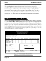
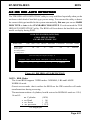
1
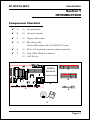
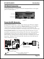
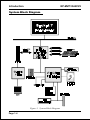
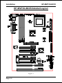
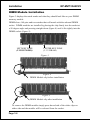
EP-MVP3G-M
EP-MVP3G2
EP-MVP3G5
ISA/PCI/A
GP Mainboar
d with
ISA/PCI/AGP
Mainboard
Onboar
d PCI IDE and Super
Onboard
Multi-I/O
TRADEMARK
All products and company names are trademarks or registered
trademarks of their respective holders.
These specifications are subject to change without notice.
Manual Revision 10.2
September 30, 1999
EP-MVP3G-M/2/5
User Notice
No part of this product, including the product and software may be reproduced,
transmitted, transcribed, stored in a retrieval system, or translated into any
language in any form without the express written permission of EPoX Computer
Company (hereinafter referred to as EPoX) except for documentation kept by the
purchaser for backup purposes.
We provide this manual “as is” without warranty of any kind, either expressed or
implied, including but not limited to the implied warranties or conditions of
merchantability or fitness for a particular purpose. In no event shall EPoX be
liable for any loss of profits, loss of business, loss of use or data, interruption of
business or for indirect, special incidental, or consequential damages of any kind,
even if EPoX has been advised of the possibility of such damages arising from any
defect or error in the manual or product. EPoX may revise this manual from time
to time without notice. For updated BIOS, drivers, or product release information
you may visit our websites at http://www.epox.com or http://www.epox.com.tw.
Products mentioned in this manual are mentioned for identification purposes only.
Product names appearing in this manual may or may not be registered trademarks
or copyrights of their respective companies. The product name and revision
number are both printed on the mainboard itself.
Handling Procedures
Static electricity can severely damage your equipment. Handle the EP-MVP3GM/2/5 and any other device in your system with extreme care and avoid unnecessary contact with system components on the mainboard. Always work on an
antistatic surface to avoid possible damage to the mainboard from static discharge.
Always have the power supply unplugged and powered off when inserting and
removing devices within the computer chassis. EPoX assumes no responsibility
for any damage to the EP-MVP3G-M/2/5 mainboard that results from failure to
follow instruction or failure to observe safety precautions.
CAUTION
* The EP-MVP3G-M/2/5 mainboard is subject to damage by static electricity.
Always observe the handling procedures.
* We strongly recommend power source “OFF” while installation, or plug-in
power cable or plug power supply into onboard power connector at last step.
EP-MVP3G-M/2/5
Technical Support Services
If you need additional information, help during installation or normal use of this
product, please contact your retailer. Your retailer will have the most current
information about your configuration. If your retailer cannot help, you may visit
our online technical support website and/or contact our support technicians at the
locations listed below.
Record your serial number before installing your EP-MVP3G-M/2/5 mainboard.
(The serial number is located near the PCI slots at the edge of the board.)
EP-MVP3G-M/2/5 serial number:
______________________________
Contacting Technical Support
EPoX technical support is working hard to answer all of your questions online.
From our website you can find answers to many common questions, drivers, BIOS
updates, tech notes, and important technical bulletins. If you are still unable to
locate the solution you are seeking, you always have the option to contact our
support technicians directly.
North American website (English language)
http://www.epox.com
[email protected]
[email protected]
European website (Multi-language)
http://www.epox.nl
[email protected]
[email protected]
Taiwan website (Chinese language)
http://www.epox.com.tw
[email protected]
[email protected]
Thank you for using EPoX mainboards!
Copyright 1999 EPoX Computer Company. All rights reserved.
EP-MVP3G-M/2/5
Table of Contents
Page
Section 1
Introduction
Components Checklist ..............................................1-1
Overview
EP-MVP3G-M/2/5 Form-Factor .............................. 1-2
I/O Shield Connector ................................................1-3
Power-On/Off (Remote) .......................................... 1-3
System Block Diagram .............................................1-4
Section 2
Features
EP-MVP3G-M/2/5 Features ....................................2-1
Section 3
Installation
EP-MVP3G-M/2/5 Detailed Layout ........................3-2
Easy Installation Procedure
Configure Jumpers ...................................................3-3
System Memory Configuration ................................ 3-5
Device Connectors ...................................................3-7
External Modem Ring-in Power ON and
Keyboard Power ON Function (KBPO) .................. 3-9
Section 4
Award BIOS Setup
BIOS Instructions .....................................................4-1
Standard CMOS Setup .............................................4-2
BIOS Features Setup ................................................4-3
Chipset Features Setup .............................................4-7
Power Management Setup ....................................... 4-10
PNP/PCI Configuration ........................................... 4-13
Integrated Peripherals ...............................................4-15
Load Setup Defaults ................................................. 4-19
Change Supervisor or User Password ...................... 4-20
IDE HDD Auto Detection ........................................4-21
EP-MVP3G-M/2/5
Save & Exit Setup .................................................... 4-23
Exit Without Saving ..................................................4-23
Appendix
Appendix A
Memory Map ...........................................................A-1
I/O Map ....................................................................A-1
Timer & DMA Channels Map ..................................A-2
Interrupt Map ...........................................................A-2
RTC & CMOS RAM Map .......................................A-3
Appendix B
POST Codes ............................................................A-5
Unexpected Errors....................................................A-8
EP-MVP3G-M/2/5
Page Left Blank
EP-MVP3G-M/2/5
Introduction
Section 1
INTRODUCTION
Components Checklist
ü
A.
(1)
One mainboard
ü
B.
(1)
One user’s manual
ü
C.
(1)
Floppy ribbon cable
ü
D.
(1)
IDE ribbon cable
ATA-66 IDE ribbon cable (EP-MVP3G2/5 only)
ü
E.
(1)
PS/2 to AT keyboard connector adapter (optional)
ü
F.
(1)
(1)
Ultra_DMA IDE driver diskette
AGP Drivers
USER’S
MANUAL
C
EP-MVP3G-M/2/5
D
B
A
E
or
F
Page 1-1
Introduction
EP-MVP3G-M/2/5
EP-MVP3G-M/2/5 Form Factor
The EP-MVP3G-M/2/5 is designed with ATX form factor - the new industry
standard of chassis. The ATX form factor is essentially a Baby-AT baseboard
rotated 90 degrees within the chassis enclosure and a new mounting configuration
for the power supply. With these changes the processor is relocated away from the
expansion slots, allowing them all to hold full length add-in cards. ATX defines a
double height aperture to the rear of the chassis which can be used to host a wide
range of onboard I/O. Only the size and position of this aperture is defined,
allowing PC manufacturers to add new I/O features (e.g.; TV input, TV output,
joystick, modem, LAN, etc.) to systems. This will help systems integrators
differentiate their products in the marketplace, and better meet your needs.
•
Smaller size promotes a smaller system size.
•
I/O shield does not need to be retooled in an ATX 2.01 or later. Mainboard
could be used in an ATX 2.01-compliant.
•
A smaller power supply cam be used. High integration on mainboard reduces
the system costs.
Expandable I/O
ATX
Power
Supply
Single chassis
fan for
system
CPU located near
Power Supply
Full length
slots
ATX power
connector
Floppy / IDE
connectors
close to
peripheral
bays
Page 1-2
3 1/2"
Bay
5 1/4"
Bay
Figure 2: Summary of ATX chassis features
EP-MVP3G-M/2/5
Introduction
I/O Shield Connector
The EP-MVP3G-M/2/5 is equipped with an I/O back panel.Please use the appropriate I/O shield (figure 3).
Parallel Port
PS/2 Mouse
PS/2 Keyboard
USB
COM1
COM2
Figure 3
Power-On/Off (Remote)
The EP-MVP3G-M/2/5 has a single 20-pin connector for ATX power supplies.
For ATX power supplies that support the Remote On/Off feature, this should be
connected to the systems front panel for system Power On/Off button. The
systems power On/Off button should be a momentary button that is normally open.
The EP-MVP3G-M/2/5 has been designed with “Soft Off" functions. You can
turn Off the system from one of two sources: The first is the front panel Power
On/Off button, and the other is the "Soft Off" function (coming from the EPMVP3G-M/2/5’s onboard circuit controller) that can be controlled by the operating system. Windows 95/98 will control this when the user clicks that they are
ready to Shutdown the system.
ATX
POWER SUPPLY
J3
Case (chassis) Power
ON/OFF button
Figure 4: Simple ATX Power
ON/OFF Controller
Page 1-3
Introduction
EP-MVP3G-M/2/5
System Block Diagram
Figure 5: System Block Diagram
Page 1-4
EP-MVP3G-M/2/5
Features
Section 2
FEATURES
EP-MVP3G-M/2/5 Features:
•
Intel Pentium® Processor, Pentium Processor with MMX technology,
AMD K6/K6-2/K6 III, Cyrix 6x86MX/MII & idt C6/Winchip operating at
133 ~ 500 MHz with 321 ZIF socket 7 provides scalability to accept
faster Processors in the future.
•
Supports ESDJ (Easy Setting Dual Jumper) function for CPU selection.
•
Designed with VIA MVP3 AGPset.
•
Supports up to 384 MB of DRAM (minimum of 16 MB) on board,
You can use 168-pin DIMM x 3. (please see Section 3-2).
•
The EP-MVP3G-M/EP-MVP3G2 Supports 1MB L2 cache.
The EP-MVP3G5 supports 2MB L2 cache.
•
Supports (2) 16 bit ISA slots, (5) 32 bit PCI slots, (1) AGP Slot and provides
(2) independent high performance PCI IDE interfaces capable of supporting
PIO Mode 3/4 and Ultra DMA 33/66 devices. The EP-MVP3G-M/2/5 supports (5) PCI Bus Master slots and a jumperless PCI INT# control scheme
which reduces configuration confusion when plugging in PCI card(s).
•
Supports ATAPI (e.g. CD-ROM) devices on both Primary and Secondary
IDE interfaces.
•
Designed with Integrated Multi I/O: (1) floppy port, (1) parallel port
(EPP, ECP), and (2) serial ports (16550 Fast UART).
Note: Japanese “Floppy 3 mode” is also supported
•
Features Award Plug & Play BIOS. With Flash Memory you can always
upgrade to the current BIOS as they are released. (http://www.epox.com
please visit our Technical Support section for the latest updates)
•
Includes a PS/2 mouse connector.
Page 2-1
Features
EP-MVP3G-M/2/5
•
allows use of a PS/2 keyboard.
•
EP-MVP3G-M/2/5 utilizes a Lithium battery which provides environmental
protection and longer battery life.
•
Built-in ATX 20-pin power supply connector.
•
Software power-down when using Windows® 95/98.
•
Supports ring-in feature (remote power-on through external modem,
allows system to be turned on remotely).
•
Resume by Alarm - Allows your system to turn on at a preselected time.
•
Supports CPU Hardware sleep and SMM (System Management Mode).
•
Supports USDM software to offer motherboard various status.
•
Supports the CPU, PWR and Chassis fan Auto stop in sleep mode.
•
Supports the system Power LED (PANEL) blanks in the sleep mode.
•
Supports Keyboard Power ON function (KBPO).
•
Built-in WOL (Wake On Lan) Connector.
•
Built-in SB-LINK Header for Creative Labs Sound Blaster compatabile
AWE64D PCI Sound Card.
Page 2-2
EP-MVP3G-M/2/5
Installation
Section 3
INSTALLATION
Page 3-1
Installation
EP-MVP3G-M/2/5
EP-MVP3G-M/2/5 Detailed Layout
Figure 1
Page 3-2
EP-MVP3G-M/2/5
Installation
Easy Installation Procedure
The following must be completed before powering on your new system:
3-1. Configure Jumpers
3-2. System Memory Configuration
3-3. Device Connectors
3-4. External Modem Ring-in Power On and Keyboard Power On
Function (KBPO)
Section 3-1
Configure Jumpers
We design this motherboard with the fewest jumpers to make your install fast and
easy.
Note: The jumpers as shown below are in their correct physical orientation.
(Figure 1)
JP1
CMOS Clear
1-2: Normal (Default)
2-3: Clear CMOS
JP4
Keyboard Power-ON Function
1-2: Disabled (Default)
2-3: Enabled
JP5
SDRAM Clock Selection
1-2: SDRAM = AGP (2/3 CPU Clock)
2-3: SDRAM = CPU (Default)
Page 3-3
Installation
EP-MVP3G-M/2/5
CPU Selection
SW1
SW1
1
2
4
ON
ON
1.8V
ON
ON
ON
2.0V
ON
ON
5
ON
2.1V
ON
ON
2.2V
ON
2.3V
ON
ON
ON
JP3
28 27
112MHz
100MHz
95MHz
83MHz
75MHz
66MHz
5.5X
5X
4.5X
4X
3.5X
3X
2.5X
2X
Pentium/MMX
AMD K6/K6-2/K6 III
IDT-C6/Winchip
2.4V
ON
2.8V
ON
2.9V
ON
3.2V
JP3
Multiplier
166MHz
2.5X
Cyrix/IBM
6x86MX/MII
Bus Clock
66MHz
PR200
75MHz
PR233
83MHz
PR266
95MHz
PR300
250MHz
100MHz
PR366
200MHZ
66MHz
PR266
75MHz
PR300
250MHz
83MHz
PR333
95MHz
*PR400
300MHz
100MHz
*PR433
233MHz
66MHz
3X
PR300
75MHz
PR333
83MHz
*PR400
333MHz
95MHz
*PR466
350MHz
100MHz
*PR500
266MHz
66MHz
PR333
3.5X
2 1
ESDJ
CPU
Vcore
3
333MHz
4X
75MHz
PR400
83MHz
*PR466
380MHz
95MHz
*PR533
400MHz
100MHz
*PR550
300MHz
66MHz
450MHz
4.5X
333MHz
475MHz
66MHz
5X
500MHz
366MHz
100MHz
95MHz
100MHz
5.5X
66MHz
* Reserved
Page 3-4
EP-MVP3G-M/2/5
Installation
Section 3-2
System Memory Configuration
Memory Layout
The EP-MVP3G-M/2/5 supports (3) 168-pin DIMMs (Dual In-line Memory
Module). The DIMMs can be either EDO (Extended Data Out) or SDRAM
(Synchronized DRAM). The DIMMs may be installed using just one chip.
•
DIMM SDRAM may be 83MHz (12ns), 100MHz (10ns) or 125MHz
(8ns) bus speed.
•
If you use both 50ns and 60ns memory you must configure your BIOS
to read 60ns.
•
When using Synchronous DRAM we recommend using the 4 clock
variety over the 2 clock.
Figure 2 and Table 1 show several possible memory configurations using both
SIMM and DIMM.
DIMM 1
B a nk 0/1
DIMM 2
B a nk 2/3
B a nk 4/5
DIMM 3
-S y nc hro n ou s
-E D O
Figure 2
Total Me mory
DIMM 1
(Bank 0/1)
DIMM 2
(Bank 2/3)
DIMM 3
(Bank 4/5)
= 128MB
Maximum
EDO/SDRAM*
8MB, 16MB, 32MB, None
64MB, 128MB X 1
None
= 256MB
Maximum
EDO/SDRAM*
EDO/SDRAM*
8MB, 16MB, 32MB,
8MB, 16MB, 32MB,
64MB,
64MB, 128MB X 1
128MB X 1
None
= 384MB
Maximum
EDO/SDRAM*
EDO/SDRAM*
8MB, 16MB, 32MB, 8MB, 16MB, 32MB,
64MB, 128MB X 1 64MB, 128MB X 1
EDO/SDRAM*
8MB, 16MB, 32MB,
64MB, 128MB X 1
Table 1
* SDRAM only supports 8, 16, 32, 64, 128MB DIMM modules.
* We recommend to use PC100 Memory Module for bus speed between
66MHz and 100MHz.
* Using non-compliant memory with higher bus speed (over clocking) may
severely compromise the integrity of the system.
Page 3-5
Installation
EP-MVP3G-M/2/5
DIMM Module Installation
Figure 3 displays the notch marks and what they should look like on your DIMM
memory module.
DIMMs have 168-pins and two notches that will match with the onboard DIMM
socket. DIMM modules are installed by placing the chip firmly into the socket at
a 90 degree angle and pressing straight down (figure 4) until it fits tightly into the
DIMM socket (figure 5).
LEFT KEY ZONE
(UNBUFFERED)
CENTER KEY ZONE
(3.3 V DRAM)
Figure 3
Figure 4
DIMM Module clip before installation
Figure 5
DIMM Module clip after installation
To remove the DIMM module simply press down both of the white clips on
either side and the module will be released from the socket.
Page 3-6
EP-MVP3G-M/2/5
Installation
Section 3-3
Device Connectors
Please install the motherboard into the chassis.
Now that your motherboard is installed you are ready to connect all your connections (figure 6).
Parallel Port
PS/2 Mouse
PS/2 Keyboard
USB
COM1
COM2
Figure 6
J2,J3: Chassis Panel Connector
• Power_LED, Speaker, Reset, Power_ON/OFF, Turbo LED and
HDD LED, IR Connector
J4:
CPU Fan Power
• A plug-in for the CPU Fan Power
J4:
Power Fan Power
• A plug-in for the Power supply Fan
J6:
Chassis Fan Power
• A plug-in for the chassis Fan Power
J7:
WOL (Wake On Lan) Connector
J8:
SB_LIBK Connector
IDE1:
Primary IDE Connector
IDE2:
Secondary IDE Connector
FDD1: Floppy Controller Connector
PW1:
ATX Power Connector
• 20-pin power connector
Page 3-7
Installation
EP-MVP3G-M/2/5
Device Connectors (continued)
(This is connected to the power button on the case. Using the SoftOff by Pwr-BTTN feature, you can choose either Instant Off (turns
system off immediatly), or 4 sec delay (you need to hold the button
down for 4 seconds before the system turns off). When the system is
in 4 sec delay mode, there is a special feature to make the system to
go into suspend mode when the button is pressed momentarily.)
Power On/Off
J3
1
Turbo LED indicator - LED ON when higher speed is selected
+
IDE LED indicator - LED ON when Onboard PCI IDE Hard disks
is activate
+
IR Connector
1. VCC
2. NC
3. IRRX
4. GND
5. IRTX
1
J2
Power LED - Power LED connector
1. Power LED(+)
2. N/C
3. GND
4. NC
5. GND
1
Speaker - Connect to the system's speaker for beeping
1. Speaker
2. N/C
3. GND
4. GND
1
Reset - Closed to restart system.
1
Page 3-8
EP-MVP3G-M/2/5
Installation
Section 3-4
External Modem Ring-in Power
ON and Keyboard Power ON
Functions (KBPO)
On the basis of bounded functions in I/O chipset, the two serial ports are able to
support the External Modem Ring-in Power ON function. Once users connect the
external modem to COM1 or COM2, the EP-MVP3G-M/2/5 mainboard allows
users to turn on their system through the remote and host's dial-up control.
Exclusive Keyboard Power ON Function
To innovate a unique feature to benefit users, we devoted the easiest and most
convenient way to turn on your system based on the the ATX power supply.
How to work with it
Step 1: Please check JP4 at the position 1-2 after you finished the system
installation.
JP4
Keyboard Power-ON Function
1-2: Disabled (Default)
2-3: Enabled
Step 2: You can enjoy the Keyboard Power ON function (KBPO) by pressing any
2 key and BUTTON only to turn on your system. Your system will be
turned on automatically, after releasing the keys. To power off you
system, you can use the Soft-OFF function under Windows 95.
Notes: Intel ATX version 2.0 specification has recommended you use the
power supply with 0.72A(720mA) in 5.0VSB. With our this
mainboard, the 5.0VSB standby power only has to be > = 0.2A
(200mA) then you can enjoy this unique benefit. However, the ATX
power supply which is < 0.2 (200mA) is still applicable to your
system by placed JP4 at the position 2-3 to disable this feature.
Page 3-9
Installation
EP-MVP3G-M/2/5
Page Left Blank
Page 3-10
EP-MVP3G-M/2/5
BIOS
Section 4
AWARD BIOS SETUP
BIOS Instructions
Award’s ROM BIOS provides a built-in Setup program which allows user to
modify the basic system configuration and hardware parameters. The modified
data will be stored in a battery-backed CMOS, so that data will be retained even
when the power is turned off. In general, the information saved in the CMOS RAM
will stay unchanged unless there is a configuration change in the system, such as
hard drive replacement or a device is added.
It is possible for the CMOS battery to fail, this will cause data loss in the CMOS
only. If this does happen you will need to reconfigure your BIOS settings.
To enter the Setup Program :
Power on the computer and press the <Del> key immediately, this will bring you
into the BIOS CMOS SETUP UTILITY.
ROM PCI/ISA BIOS(2A5LEPAE)
CMOS SETUP UTILITY
AWARD SOFTWARE, INC.
STANDARD CMOS SETUP
SUPERVISOR PASSWORD
BIOS FEATURES SETUP
USER PASSWORD
CHIPSET FEATURES SETUP
IDE HDD AUTO DETECTION
POWER MANAGEMENT SETUP
SAVE & EXIT SETUP
PNP/PCI CONFIGURATION
EXIT WITHOUT SAVING
INTEGRATED PERIPHERALS
LOAD SETUP DEFAULTS
ESC : QUIT
: SELECT ITEM
F10 : Save & Exit Setup
(Shift)F2 : Change Color
Time, Date, Hard Disk Type...
Figure 4-1 CMOS SETUP UTILITY
Page 4-1
BIOS
EP-MVP3G-M/2/5
The menu displays all major selection items. Select the item you need to
reconfigure. The selection is made by moving cursor (press any direction key ) to
the item and press the 'Enter' key. An on-line help message is displayed at the
bottom of the screen as the cursor is moving to various items which provides a
better understanding of each function. When a selection is made, the menu of
selected item will appear so the user can modify the associated configuration
parameters.
4-1 STANDARD CMOS SETUP
Choose "STANDARD CMOS SETUP" in the CMOS SETUP UTILITY Menu (Fig.
4-1). The STANDARD CMOS SETUP allows user to configure system setting such
as the current date and time, type of hard disk installed, floppy type, and display type.
Memory size is auto-detected by the BIOS and displayed for your reference. When a
field is highlighted (use direction keys to move cursor and <Enter> key to select), the
entries in the field will be changed by pressing <PgDn> or <PgUp> keys or user can
enter new data directly from the keyboard.
ROM PCI/ISA BIOS (2A5LEPAE)
STANDARD CMOS SETUP
AWARD SOFTWARE, INC.
Date (mm:dd:yy) : Wed, Jan 15 1998
Time (hh:mm:ss) : 14 : 30 : 50
HARD DISKS
Primary Master
Primary Slave
Secondary Master
Secondary Slave
TYPE
: Auto
: Auto
: Auto
: Auto
SIZE
0
0
0
0
CYLS
0
0
0
0
Drive A : 1.44M,3.5 in.
Drive B : None
Floppy 3 mode Support : Disable
Video : EGA/VGA
Halt On : All, But keyboard
ESC : Quit
F1 : Help
(Shift) F2
HEAD
0
0
0
0
PRECOMP
0
0
0
0
LANDZONE SECTORS MODE
0
0
Auto
0
0
Auto
0
0
Auto
0
0
Auto
Base Memory
:
640K
Extended Memory : 31744K
Other Memory
:
384K
Total Memory : 32768K
: Select Item
: Change Color
PU/PD/+/- : Modify
Figure 4-2 STANDARD CMOS SETUP
Page 4-2
EP-MVP3G-M/2/5
BIOS
Note: If the Primary Master/Slave and the Secondary Master/Slave are
set as "Auto", the hard disk size and model will be auto-detected.
Note: The "Halt On :" field is to determine when to halt the system by the
BIOS if an error occurrs.
4-2 BIOS FEATURES SETUP
By selecting the "BIOS FEATURES SETUP" option in the CMOS SETUP UTILITY
menu, user can change system related parameters in the displayed menu. This menu
shows all of the manufacturer's default values of this mainboard. Again, user can move
the cursor by pressing direction keys and <PgDn> or <PgUp> keys to modify the
parameters. Pressing [F1] key to display help message of the selected item.
ROM PCI/ISA BIOS (2A5LEPAE)
BIOS FEATURES SETUP
AWARD SOFTWARE, INC.
Virus Warning
CPU Internal Cache
External Cache
Quick Power On Self Test
Boot Sequence
Swap Floppy Drive
Boot Up Floppy Seek
Boot Up NumLock Status
Gate A20 Option
Memory Parity/ECC Check
Typematic Rate Setting
Typematic Rate (Chars/Sec)
Type matic Delay (Msec)
Security Option
PCI/VGA Palette Snoop
OS Select For DRAM > 64MB
HDD S.M.A.R.T. capability
Report No FDD For WIN 95
:
:
:
:
:
:
:
:
:
:
:
:
:
:
:
:
:
:
Disabled
Enabled
Enabled
Enabled
A, C, SCSI
Disabled
Enabled
On
Fast
Disabled
Disabled
6
250
Setup
Disabled
Non-OS2
Disabled
Yes
Video BIOS
C8000-CBFFF
CC000-CFFFF
D0000-D3FFF
D4000-D7FFF
D8000-DBFFF
DC000-DFFFF
Shadow
Shadow
Shadow
Shadow
Shadow
Shadow
Shadow
Esc : Quit
F1 : Help
F5 : Old Values
F7 : Load Setup Defaults
:
:
:
:
:
:
:
Enabled
Disabled
Disabled
Disabled
Disabled
Disabled
Disabled
: Select Item
PU/PD/+/- : Modify
(Shift)F2 : Color
Figure 4-3 BIOS FEATURES SETUP
Virus Warning: This category flashes on the screen. During and after the system
boots up, any attempt to write to the boot sector or partition table of the hard disk
drive will halt the system and an error message will appear. You should then run an
anti-virus program to locate the virus. Keep in mind that this feature protects only
the boot sector, not the entire hard drive. Default value is Disabled.
Page 4-3
BIOS
EP-MVP3G-M/2/5
Enabled : Activates automatically when the system boots up causing a warning
message to appear when any attempt to access the boot sector or
hard disk partition table.
Disabled :No warning message to appear when any attempt to access the boot
sector or hard disk partition table.
CPU Internal Cache / External Cache: These two categories speed up memory
access. However, it depends on CPU/chipset design. The default value is Enabled.
If your CPU is without Internal Cache then this item "CPU Internal Cache" will not
be shown.
Enabled
: Enable cache.
Disabled
: Disable cache.
Quick Power On Self Test:This category speeds up Power On Self Test (POST)
after you power on the computer. If it is set to Enable, BIOS will shorten or skip
some checking items during POST.
Enabled : Enable quick POST.
Disabled: Normal POST.
Boot Sequence:This category determines which drive is searched first for
the O/S(Operating System).The default value is A,C.
A,C : The system will search for floppy disk drive first then hard disk drive.
C,A : The system will search for hard disk drive first then floppy disk drive.
Swap Floppy Drive: This will swap your physical drive letters A&B if you are
using two floppy disks. The default value is Disabled.
Enabled : Floppy A & B will be swapped under the O/S.
Disabled : Floppy A & B will be not swapped.
Boot Up Floppy Seek: During Power-On-Self-Test (POST), BIOS will determine
if the installed floppy drive is 40 or 80 tracks. Only 360K type is 40 tracks while
760K, 1.2M and 1.44M are all 80 tracks. The default value is Enabled.
Enabled : BIOS searches for floppy disk drive to determine if it is 40 or 80 tracks.
Note that BIOS cannot tell from 720K, 1.2M or 1.44M drive type as
they are all 80 tracks.
Disabled: BIOS will not search for the type of floppy disk drive by track number.
Page 4-4
EP-MVP3G-M/2/5
BIOS
Note that there will not be any warning message if the drive installed is
360K.
Boot Up NumLock Status: The default value is On.
On : Keypad is number keys.
Off : Keypad is arrow keys.
Gate A20 Option: This refers to the way the system addresses memory above
1MB (extended memory). The default value is Fast.
Normal: The A20 signal is controlled by keyboard controller or chipset hardware.
Fast
: The A20 signal is controlled by Port 92 or chipset specific method.
Typematic Rate Setting: This determines the typematic rate.
Enabled : Enable typematic rate and typematic delay programming.
Disabled: Disable typematic rate and typematic delay programming. The system
BIOS will use default value of 2 items and the default is controlled by
the keyboard.
Typematic Rate(Chars/Sec): This is the number of characters that will be repeated by a keyboard press. The default is 6.
6 : 6 characters per second.
8 : 8 characters per second.
10: 10 characters per second.
12: 12 characters per second.
15: 15 characters per second.
20: 20 characters per second.
24: 24 characters per second.
30: 30 characters per second.
Typematic Delay(Msec): This determines the time between the first and second
character displayed, when holding a key. The default is 250.
250 : 250msec.
500 : 500 msec.
750 : 750 msec.
1000: 1000 msec.
Security Option: This category allows you to limit access to the system and
Setup, or just to Setup. The default value is Setup.
System: The system will not boot and the access to Setup will be denied if the
correct password is not entered at the prompt.
Setup : The system will boot, but the access to Setup will be denied if the correct
password is not entered at the prompt.
Page 4-5
BIOS
EP-MVP3G-M/2/5
PCI/VGA Palette Snoop: This filed controls the ability of a primary PCI VGA
controller to share a common palette (when a snoop write cycles) with an ISA
video card. The default value is Disabled.
Enabled: If an ISA card connects to a PCI VGA card via the VESA connector
and the ISA card connects to VGA monitor and uses the RAMDAC of
PCI card, the PCI/VGA Palette Snoop is enabled.
Disabled: Disable the VGA card Palette snoop function.
OS Select For DRAM > 64MB: Some operating systems require special
handling. Use this option only if your system has greater than 64MB of memory.
The default is Non-OS2.
OS2:
Select this if you are running the OS/2 operating system with greater
than 64MB of RAM.
Non-OS2:Select this for all other operating systems and configurations.
HDD S.M.A.R.T capability: Enabled SMART hard drive functions for compatible
hardware. The default is Disabled.
Enabled: S.M.A.R.T features are available.
Disabled: S.M.A.R.T features will no be available.
Report No FDD For WIN95: This option allows BIOS to indicate whether
WIN95 is with FDD or not. The Default value is Yes.
NO: Report No FDD for WIN95.
YES: Report FDD for WIN95
Video BIOS Shadow: It determines whether video BIOS will be copied to RAM.
However, it is optional from chipset design. Video Shadow will increase the video
speed.
Enabled : Video shadow is enabled.
Disabled: Video shadow is disabled.
C8000 CC000 D0000 D4000 D8000 DC000 Page 4-6
CBFFF
CFFFF
D3FFF
D7FFF
DBFFF
DFFFF
Shadow :
Shadow:
Shadow:
Shadow:
Shadow:
Shadow:
EP-MVP3G-M/2/5
BIOS
These categories determine whether optional ROM will be copied to RAM by 16K
byte or 32K byte per unit and the size depends on the chipset.
Enabled : Optional shadow is enabled.
Disabled: Optional shadow is disabled.
4-3 CHIPSET FEATURES SETUP
Choose the "CHIPSET FEATURES SETUP" in the CMOS SETUP UTILITY menu
to display the following menu.
ROM PCI/ISA BIOS (2A5LEPAE)
CHIPSET FEATURES SETUP
AWARD SOFTWARE, INC.
Bank 0/1 DRAM Timing
Bank 2/3 DRAM Timing
Bank 4/5 DRAM Timing
SDRAM Cycle Length
SDRAM Bank Interleave
DRAM Page-Mode
DRAM Read Pipeline
DRAM Fast Decoding
Sustained 3T Write
Cache Rd+CPU Wt Pipeline
Cache Timing
Linear Burst
Video BIOS Cacheable
System BIOS Cacheable
Memory Hole AT 15Mb Addr.
AGP Aperture Size
Cyrix M2 ADS# delay
Fan In Suspend
: FP/EDO Fast
: FP/EDO Fast
: FP/EDO Fast
:3
: Disabled
: Enabled
: Enabled
: Auto
: Enabled
: Enabled
: Fast
: Disabled
: Enabled
: Disabled
: Disabled
: 64M
: Disabled
: Off
Auto Detect DIMM/PCI Clk
: Enabled
Spread Spectrum
: Disabled
CPU Host Clock (CPU/PCI)
: Default
CPU Warning Temperature
: 60OC/140OC
Shutdown Temperature
: 70OC/158OC
Current CPU Temperature
: 37OC/98 OC
Current System Temperature.
: 25OC/77 OC
Current CPU FAN Speed
: 0 RPM
Current CHASSIS FAN Speed
: 0 RPM
Current POWER FAN Speed
: 0 RPM
CPUcore : 2.20V
CPUI/O : 3.52V
+5V
: 4.99V
+12V : 12.09V
-12V
: -12.04V
-5V
: -5.12V
Esc : Quit
F1 : Help
F5 : Old Values
F7 : Load Setup Defaults
: Select Item
PU/PD/+/- : Modify
(Shift)F2 : Color
Figure 4-4 CHIPSET FEATURES SETUP
Page 4-7
BIOS
EP-MVP3G-M/2/5
Bank 0/1, 2/3, 4/5 DRAM Timing: This value in this field is set by the system
board manufacturer, depending on whether the board has paged DRAMs or EDO
(extended data output) DRAMs.
The Choice: Bank 0/1, 2/3, 4/5.
SDRAM Cycle length: This setting defines the CAS timing parameter of the
SDRAM in terms of clocks. The default is 3.
2: Provides faster memory performance.
3: Provides better memory compatibility.
SDRAM Bank Interleave: The default value is Disabled.
Disabled : Normal Setting.
2 Bank/4 Bank: SDRAM 2 or 4 Bank Interleave.
DRAM Page-Mode: The item will active or inactive chipset page registers.
Enabled: Page-Mode Enabled.
Disabled: No page registers update and non Page-Mode operation.
DRAM Fast Decoding: The item will effective DRAM operation sequential.
Video BIOS Cacheable: This option copies the video ROM BIOS to fast RAM
(C0000h to C7FFFh). The default is Enabled.
Enabled: Enables the Video BIOS Cacheable to speed up the VGA Performance.
Disabled: Will not use the Video BIOS Cacheable function.
System BIOS Cacheable: This allows you to copy your BIOS code from slow
ROM to fast RAM. The default is Disabled.
Enabled: The option will improve system performance. However, if any program writes to this memory area, a system error may result.
Disabled: System BIOS non-cacheable.
Memory Hole at 15M-16M Addr.: The default value is Disabled.
Disabled: Normal Setting.
Enabled : This field enableds the main memory (15~16MB) remap to ISA BUS.
AGP Aperture Size: The amount of the system memory that the AGP card is
allowed to share. The options available are 4M, 8M, 16M, 32M, 64M, 128M,
256M. The default value is 64M.
Page 4-8
EP-MVP3G-M/2/5
BIOS
Auto Detect DIMM/PCI Clk: Allows you to stop DIMM/PCI Clock drive when
the DIMM site or PCI Slot are not plug. This item may help reduce EMI.
The default is Enabled.
Enabled: Provides unused DIMM/PCI to stop.
Disabled: Provides the clock generator always driving.
Spread Spectrum : Allows you to active the Spread Spectrum Modulation
function for reduce EMI. (Note: When Enabled the item that performance will be
impacted). The default is Disabled.
Enabled: Provides the Spread Spectrum function from clock generator.
Disabled: NO Spread Spectrum function.
CPU Host Clock (CPU/PCI): Allows the external clock to be modified depending upon what FSB has been selected. Should not be used to clock processor faster
than it was designed for. The default is Default.
66MHz FSB options: Default, 66.6, 75, and 83.3MHz.
100MHz FSB options: Default, 95, 100, 112, 124, and 133MHz.
CPU Warning Temperature: The default value is Disabled
Disabled : Normal Setting.
Enabled: The options available is 50C/122F~70C/158F.
Current System Temperature: This is the current temperature of the system.
Current CPU Temperature: This is the current temperature of the CPU.
Current CPU Fan Speed: The current CPU fan speed in RPMs.
Current CHASSIS FAN Speed: The current chassis fan speed in RPMs .
Current POWER FAN Speed: The current power fan speed in RPMs .
CPU(V) : The voltage level of the CPU(Vio/Vcore).
+5V, +12V: The voltage level of the power supply.
Page 4-9
BIOS
EP-MVP3G-M/2/5
4-4 POWER MANAGEMENT SETUP
Choose the "POWER MANAGEMENT SETUP" in the CMOS SETUP
UTILITY to display the following screen. This menu allows the user to modify
the power management parameters and IRQ signals. In general, these parameters
should not be changed unless it is absolutely necessary.
ROM PCI/ISA BIOS (2A5LEPAE)
POWER MANAGEMENT SETUP
AWARD SOFTWARE, INC.
ACPI function
Power Management
PM Control by APM
Video off Option
Video off Method
MODEM Use IRQ
Soft-off by PWRBTN
**PM Timers **
HDD Power Down
Doze Mode
Suspend Mode
** PM Events **
VGA
LPT & COM
HDD & FDD
DMA /master
Modem Ring Resume
RTC Alarm Resume
:
:
:
:
:
:
:
Enabled
User Define
Yes
Suspend -> Off
V/H SYNC+Blank
3
Delay 4 Sec
: Disable
: Disable
: Disable
:
:
:
:
:
:
OFF
LPT /COM
ON
OFF
Disabled
Disabled
Primary INTR
IRQ3
IRQ4
IRQ5
IRQ6
IRQ7
IRQ8
IRQ9
IRQ10
IRQ11
IRQ12
IRQ13
IRQ14
IRQ15
(COM 2)
(COM 1)
(LPT 2)
(Floppy Disk)
(LPT 1)
(RTC Alarm)
(IRQ2 Redir)
(Reserved)
(Reserved)
(PS/2 Mouse)
(Coprocessor)
(Hard Disk)
(Reserved)
: ON
: Primary
: Primary
: Primary
: Disabled
: Primary
: Disabled
: Secondary
: Secondary
: Secondary
: Primary
: Primary
: Primary
: Disabled
Esc : Quit
: Select Item
F1 : Help
PU/PD/+/- : Modify
F5 : Old Values
(Shift)F2 : Color
F7 : Load Setup Defaults
Figure 4-5 POWER MANAGEMENT SETUP
ACPI function: Use this to enable or disable ACPI power management functions.
The default is enabled.
Enabled: Enabled ACPI power management functions.
Disabled: Disabled ACPI power management functions.
You can only change the content of Doze Mode, Standby Mode, and Suspend
Mode when the Power Management is set to 'User Define'.
Power Management: Use this to select your Power Management selection.
The default is User define.
Disabled:
The system operates in NORMAL conditions (Non-GREEN),
and the Power Management function is disabled.
Max. saving: Maximum power savings. Inactivity period is 1 minute in
each mode.
Page 4-10
EP-MVP3G-M/2/5
BIOS
Min. saving: Minimum power savings. Inactivity period is 1 hour in each
mode.
User define: Allows user to define PM Timers parameters to control power
saving mode.
PM controlled APM: This option shows weather or not you want the Power
Management to be controlled the Advanced Power Management (APM).
The default is Yes.
Yes: APM controls your PM
No: APM does not control your PM
Video Off option: Tells you what time frame that the video will be disabled under
current power management settings. The default is Suspend -> Off.
Standby: Video powers off after time shown in standby mode setting.
Doze:
Video powers off after time shown in doze mode setting.
Suspend: Video powers off after time shown in suspend mode setting.
N/A:
Video power off not controlled by power management.
Video Off Method: This option allows you to select how the video will be
disabled by the power management. The default is V/H Sync + Blank
V/H Sync + Blank: System turns off vertical and horizontal synchronization ports and writes blanks to the video buffer.
DPMS:
Select this option if your monitor supports the Display
Power Management Signaling (DPMS) standard of the
Video Electronics Standards Association (VESA). Use
the software supplied for your video subsystem to
select video power management values.
Blank Screen:
System only writes blanks to the video buffer.
MODEM Use IRQ: Name the interrupt request (IRQ) line assigned to the
modem (if any) on your system. Activity of the selected IRQ always awakens the
system. Default is IRQ 3.
N/A: No IRQ is used. 3: IRQ 3
4: IRQ 4
5: IRQ 5
7: IRQ 7
9: IRQ 9
10: IRQ 10
11: IRQ 11
Page 4-11
BIOS
EP-MVP3G-M/2/5
Soft-Off by PWR-BTTN: Use this to select your soft-off function.
The default is Delay 4 sec.
Instant Off:
Turns off instantly.
Delay 4 Second : Turns off after a 4 second delay. If momentary press of
button, the system will go into Suspend Mode. Press
again to take system out of Suspend Mode.
This mainboard supports HDD Power Down, Doze and Standby power saving
functions when using the Intel Pentium II Processor. The default is Disabled
HDD Power Down: HDD Standby timer can be set from 1 to 15 minute(s).
Doze Mode: The “Doze” mode timer starts to count when no “PM events” have
occurred.
Suspend Mode: This function works only when the Pentium II Processor is
installed. The timer starts to count when “System Standby” mode timer is timed
out and no “PM Events” are occurring. Valid range is from 1 minute up to 1 hour.
VGA: When set to On (default), any event occurring at a VGA port will awaken a
system which has been powered down.
LPT & COM: When set to On (default), any event occurring at a COM(serial)/
LPT (printer) port will awaken a system which has been powered down.
HDD & FDD: When set to On (default), any event occurring at a hard or floppy
drive port will awaken a system which has been powered down.
DMA/master: When set to On (default), any event occurring to the DMA
controller will awaken a system which has been powered down.
Modem Ring Resume: When set to Enabled, any event occurring to the Modem
Ring will awaken a system which has been powered down.
RTC Alarm Resume: When set to Enable rta alarm resume, you could set the
date (of month) and timer (hh:mm:ss), any event occurring at will awaken a system
which has been powered down.
Page 4-12
EP-MVP3G-M/2/5
BIOS
4-5 PNP/PCI CONFIGURATION
The PNP/PCI configuration program is for the user to modify the PCI/ISA IRQ signals
when various PCI/ISA cards are inserted in the PCI or ISA slots.
WARNING : Any misplacing IRQ could cause system can't pick out the rescouces.
ROM PCI/ISA BIOS (2A5LEPAE)
PNP/PCICONFIGURATION
AWARD SOFTWARE, INC.
PNP OS Installed
Resources Controlled By
Reset Configuration Data
: No
: Auto
: Disabled
CPU ot PCI Write Buffer
PCI Dynamic Bursting
PCI Master 0 WS Write
PCI Delay Transaction
PCI#2 Access #1 Retry
AGP Master 1 WS Write
AGP Master 1 WS Read
: Enabled
: Enabled
: Enabled
: Disabled
: Disabled
: Enabled
: Disabled
PCI IRQ Actived By
Assign IRQ For USB
Assign IRQ For VGA
: Level
: Enabled
: Enabled
ESC : Quit
: Select Item
F1 : Help
PU/PD/+/: Modify
F5 1: No Change (Shift) F2 : Color
F7 : Load Setup Defaults
Figure 4-6 PCI CONFIGURATION SETUP
PNP OS Installed: Do you have a PNP OS installed on your system.
The default is No.
Yes: Select if you are using a PNP OS
No: Select if your OS does not support PNP.
Resources Controlled By:The default value is Auto.
Manual: The field defines that the PNP Card's resource is controlled by
manual. You can setup whether IRQ-X or DMA-X is assigned to PCI/
ISA PNP or Legacy ISA Cards.
Auto:
If your ISA card and PCI card are all PNP cards. Set this field to
"Auto". The BIOS will assign the interrupt resource automatically.
Page 4-13
BIOS
EP-MVP3G-M/2/5
Reset Configuration Data: The default value is Disabled.
Disabled: Normal Setting
Enabled: If you plug some Legacuy cards in the system and record into
ESCD (Extended System Configuration Data). You can set this
field to be Enabled and to clear ESCD at one time, when some
Legacy cards are removed.
CPU to PCI Write Buffer: When enabled, up to four D words of data can be
written to the PCI bus without interruting the CPU. When disabled, a write buffer
is not used and the CPU read cycle will not be completed until the PCI bus signals
that it is ready to receive the data.
The Choice: Enabled, Disabled.
PCI Dynamic Bursting: When Enabled, data transfers on the PCI bus, where
possible, make use of the high-performance PCI bust protocol, in which graeater
amounts of data are transferred at a single command.
The Choice: Enabled, Disabled.
PCI Master 0 WS Write: When Enabled, writes to the PCI bus are command
with zero wait states.
The Choice: Enabled, Disabled.
PCI Delay Transaction: The chipset has an embedded 32-bit posted write buffer
to support delay transactions cycles. Select Enabled to support compliance with
PCI specification version 2.1.
The Choice: Enabled, Disabled.
PCI #2 Access #1 Retry: This item allows you enabled/disable the PCI #2
Access #1 Retry.
The Choice: Enabled, Disabled.
Assign IRQ for USB: This item allows the BIOS to assign an IRQ to the USB
controller. If no USB devices are used in the system this can be set to "disabled" to
free an IRQ for other device uses. The default is Enabled.
Disabled: Release IRQ for other device.
Enabled: Release IRQ for other device.
Page 4-14
EP-MVP3G-M/2/5
BIOS
4-6 INTEGRATED PERIPHERALS
ROM PCI/ISA BIOS (2A5LEPAE)
INTEGRATER PERIPHERALS
WARD SOFTWARE, INC.
OnChip IDE First Channel
OnChip IDE Second Channel
IDE Prefetch Mode
IDE HDD Block Mode
IDE primary Master PIO
IDE Primary Slave PIO
IDE Secondary Master PIO
IDE Secondary Slave PIO
IDE Primary Master UDMA
IDE Primary Slave UDMA
IDE Secondary Master UDMA
IDE Secondary Slave UDMA
IDEInit Display First
: Enabled
: Enabled
: Enabled
: Enabled
: Auto
: Auto
: Auto
: Auto
: Auto
: Auto
: Auto
: Auto
: PCI Slot
Onboard FDD Controller
Onboard Serial Port 1
Onboard Serial Port 2
UART 2 Mode
IR Function Duplex
RxD, TxD Active
: Enabled
: 3F8/IRQ4
: 2F8/IRQ3
: Standard
: Half
: Hi, Hi
Onboard Parallel Port
Onboard Parallel Mode
ECP Mode Use DMA
Parallel Port EPP Type
OnChip USB
USB Keyboard Support
ESC : Quit
F1 : Help
PU/PD/+/F5 : No Change (Shift) F2
F7 : Load Setup Defaults
: 378/IRQ7
: ECP / EPP
:3
: EPP1.9
: Enabled
: Disabled
: Select Item
: Modify
: Color
Note: If you do not use the Onboard IDE connector, then you will need to
set Onboard Primary PCI IDE: Disabled and Onboard Secondary
PCI IDE: Disabled
Note: The Onboard PCI IDE cable should be equal to or less than 18 inches
(45 cm.).
Onchip IDE First Channel: The default value is Enabled.
Enabled: Enables Onboard IDE primary port.
Disabled: Disables Onboard IDE primary port.
Onchip IDE Second Channel: The default is Enabled.
Enabled: Enables Onboard IDE secondary port.
Disabled: Disables Onboard IDE secondary port.
IDE Prefetch Mode: Enable prefetching for IDE drive interfaces that support its
faster drive accesses. If uou are getting disk drive errors, change the setting to
omit the drive interface where the errors occur. Depending on the configuration of
your IDE subsystem, this field may not appear, and it does not appear when the
Internal PCI/IDE field, above, is Disabled.
Page 4-15
BIOS
EP-MVP3G-M/2/5
The Choice: Enabled, Disabled.
IDE HDD Block Mode: The default value is Enabled.
Enabled : Enabled IDE HDD Block Mode. The HDD transfer rate is better than
Disable.
Disabled: Disable IDE HDD Block Mode.
IDE Primary Master PIO: The default value is Auto.
Auto
: BIOS will automatically detect the Onboard Primary Master PCI
IDE HDD Accessing mode.
Mode0~4
: Manually set the IDE Accessing mode.
IDE Primary Slave PIO: The default value is Auto.
Auto
: BIOS will automatically detect the Onboard Primary Slave PCI IDE
HDD Accessing mode.
Mode0~4
: Manually set the IDE Accessing mode.
IDE Secondary Master PIO: The default value is Auto.
Auto
: BIOS will automatically detect the Onboard Secondary Master PCI
IDE HDD Accessing mode.
Mode0~4
: Manually set the IDE Accessing mode.
IDE Secondary Slave PIO: The default value is Auto.
Auto
: BIOS will automatically detect the Onboard Secondary Slave PCI
IDE HDD Accessing mode.
Mode0~4
: Manually set the IDE Accessing mode.
IDE Primary Master UDMA: This allows you to select the mode of operation
for the hard drive. The default is Auto.
Auto: The computer will select the optimal setting.
Disabled: The hard drive will run in normal mode.
IDE Primary Slave UDMA: This allows you to select the mode of operation for
the hard drive. The default is Auto.
Auto: The computer will select the optimal setting.
Disabled: The hard drive will run in normal mode.
Page 4-16
EP-MVP3G-M/2/5
BIOS
IDE Secondary Master UDMA: This allows you to select the mode of operation
for the hard drive. The default is Auto.
Auto
: The computer will select the optimal setting.
Disabled
: The hard drive will run in normal mode.
IDE Secondary Slave UDMA: This allows you to select the mode of operation
for the hard drive. The default is Auto.
Auto
: The computer will select the optimal setting.
Disabled
: The hard drive will run in normal mode.
Init Display First: If two video cards are used (1 AGP and 1 PCI) this specifies
which one will be the primary display adapter. The default is PCI Slot.
PCI Slots
: PCI video card will be primary adapter.
AGP
: AGP video card will be primary adapter.
Onboard FDC Controller: The default value is Enabled.
Enabled
: Enable the Onboard floppy drive interface controller.
Disabled
: Disable the Onboard floppy drive interface controller, When using
On-card ISA FDC's controller.
Onboard Serial Port 1: This field allows the user to sellect the serial port. The
default value is 3F8H/IRQ4.
COM1: Enable Onboard Serial port 1 and address is 3F8H/IRQ4.
COM2: Enable Onboard Serial port 1 and address is 2F8H/IRQ3.
COM3: Enable Onboard Serial port 1 and address is 3E8H/IRQ4.
COM4: Enable Onboard Serial port 1 and address is 2E8H/IRQ3.
Disabled: Disable Onboard Serial port 1.
Onboard Serial Port 2: This field allows the user to sellect the serial port. The
default value is 2F8H/IRQ3.
COM1: Enable Onboard Serial port 2 and address is 3F8H/IRQ4.
COM2: Enable Onboard Serial port 2 and address is 2F8H/IRQ3.
COM3: Enable Onboard Serial port 2 and address is 3E8H/IRQ4.
COM4: Enable Onboard Serial port 2 and address is 2E8H/IRQ3.
Disabled: Disable Onboard Serial port 2.
Page 4-17
BIOS
EP-MVP3G-M/2/5
UART 2 Mode:The default value is standard. This field allows the User to select
the COM2 port that can support a serial Infrared Interface.
Standard: Support a Serial Infrared Interface IrDA.
HPSIR: Support a HP Serial Infrared Interface format.
ASKIR: Support a Sharp Serial Infrared Interface format.
IR Function Duplex: This item allows you to select the IR function when you
select the UART2 Mode is ASKIR.
The Choice: Half, Full.
RxD, TxD Active: This item configures the receive and transmit signals generated
form the IR port. The default is Hi Hi.
The Choice: Hi Hi, Hi Lo, Lo Hi, and Lo Lo.
Onboard Parallel port: This field allows the user to sellect the LPT port. The
default value is 378H/IRQ7.
378H
: Enable Onboard LPT port and address is 378H and IRQ7
278H
: Enable Onboard LPT port and address is 278H and IRQ5.
3BCH
: Enable Onboard LPT port and address is 3BCH and IRQ7.
Disabled
: Disable Onboard LPT port.
Note: Parallel Port address is 378H/3BCH that selects the rounting of IRQ7
for LPT1.
Parallel Port address is 278H that selects the rounting of IRQ5 for LPT1.
Onboard Parallel Mode: This field allows the user to sellect the parallel port
mode. The default value is ECP+EPP.
Normal
: Standard mode. IBM PC/AT Compatible bidirectional parallel port.
EPP
: Enhanced Parallel Port mode.
ECP
: Extended Capability Port mode.
EPP+ECP : ECP Mode & EPP Mode.
ECP Mode USE DMA: This field allows the user to sellect DMA1 or DMA3 for
the ECP mode. The default value is DMA3.
DMA1
: The filed selects the rounting of DMA1 for the ECP mode.
DMA3
: The filed selects the rounting of DMA3 for the ECP mode.
Page 4-18
EP-MVP3G-M/2/5
BIOS
Parallel Port EPP Type: This item allows you to determine the IR transfer mode
of onboard I/O chip.
The Choice: EPP1.9, EPP1.7.
USB Keyboard Support: The controls the activation status of an optional USB
Keyboard that may ne attached. The default is disabled.
Enabled:
Enable USB keyboard support.
Disabled: Disabled USB keyboard support.
4-7 LOAD SETUP DEFAULTS
The "LOAD SETUP DEFAULTS" function loads the system default data directly
from ROM and initializes the associated hardware properly. This function will be
necessary only when the system CMOS data is corrupted.
ROM PCI/ISA BIOS (2A5LEPAE)
CMOS SETUP UTILITY
AWARD SOFTWARE, INC.
STANDARD CMOS SETUP
SUPERVISOR PASSWORD
BIOS FEATURES SETUP
USER PASSWORD
CHIPSET FEATURES SETUP
IDE HDD AUTO DETECTION
POWER MANAGEMENT SETUP
HDD LOW LEVEL FORMAT
PNP/PCI CONFIGURA
Load SETUP Default (Y/N)? Y
INTEGRATED PERIPH
ETUP
SAVING
LOAD SETUP DEFAULTS
ESC: QUIT
F10:Save & Exit Setup
:SELECT ITEM
(Shift)F2 :Change Color
Load Setup Defaults Except Standard COMS SETUP
Figure 4-8 LOAD SETUP DEFAULT
Page 4-19
BIOS
EP-MVP3G-M/2/5
4-8 CHANGE SUPERVISOR or USER PASSWORD
To change the password, choose the "SUPERVISOR PASSWORD or USER PASSWORD " option from the CMOS SETUP UTILITY menu and press [Enter].
NOTE : Either "Setup" or "System" must be selected in the "Security Option" of the
BIOS FEATURES SETUP menu (Refer to Figure 3-3 for the details).
1. If CMOS is corrupted or the option is not used, a default password stored in the
ROM will be used. The screen will display the following message:
Enter Password:
Press the [Enter] key to continue after proper password is given.
2. If CMOS is corrupted or the option was used earlier and the user wish to change
default password, the SETUP UTILITY will display a message and ask for a
confirmation.
Confirm Password:
3. After pressing the [Enter] key (ROM password if the option was not used) or
current password (user-defined password), the user can change the password and
store new one in CMOS RAM. A maximum of 8 characters can be entered.
Page 4-20
EP-MVP3G-M/2/5
BIOS
4-9 IDE HDD AUTO DETECTION
The "IDE HDD AUTO DETECTION" utility is a very useful tool especially when you do
not know which kind of hard disk type you are using. You can use this utility to detect
the correct disk type installed in the system automatically. But now you can set HARD
DISK TYPE to Auto in the STANDARD CMOS SETUP. You do not need the "IDE
HDD AUTO DETECTION" utility. The BIOS will Auto-detect the hard disk size and
model on display during POST.
ROM PCI/ISA BIOS(2A5LEPAE)
CMOS SETUP UTILITY
AWARD SOFTWARE, INC.
HARD DISKS
TYPE
Primary Master :
Primary Slave
:
Secondary Master :
Secondary Slave :
SIZE CYLS
343
665
HEADS
PRECOMP
LANDZONE
65535
664
16
SECTORS
63
MODE
NORMAL
Select Secondary Slave Option (N=Skip) : N
OPTIONS
1 (Y)
SIZE CYLS HEAD PRECOMP LANDZ SECTOR MODE
0
0
0
0
0
0 NORMAL
ESC : Skip
Figure 4-9 IDE HDD AUTO DETECTION
NOTE: HDD Modes
The Award BIOS supports 3 HDD modes : NORMAL, LBA and LARGE
NORMAL mode.
Generic access mode that is neither the BIOS nor the IDE controller will make
transformations during accessing.
The maximum nunbers of cylinders, head & sectors for NORMAL mode are 1024,
16 and 63.
no. Cyclinder
(1024)
x no. Head
( 16)
x no. Sector
( 63)
x no. per sector
( 512)
528 Megabytes
Page 4-21
BIOS
EP-MVP3G-M/2/5
If an user sets the HDD to NORMAL mode, the maximum accessible HDD size
will be 528 Megabytes even though its physical size may be greater than that!
LBA (Logical Block Addressing) mode: This is a new HDD accessing method to
overcome the 528 Megabyte bottleneck.
The number of cylinders, heads and sectors shown in the setup may not be the number
physically contained in the HDD.
During the HDD accessing, the IDE controller will transform the logical address
described by sector, head and cylinder into its own physical address inside the HDD.
The maximum HDD size supported by LBA mode is 8.4 Gigabytes which is
obtained by the following formula:
no. Cyclinder
x no. Head
x no. Sector
x bytes per secttor
8.4 Gigabytes
(1024)
( 255)
( 63)
( 512)
LARGE mode: This is an extended HDD access mode supported by Award Software.
Some IDE HDDs contain more than 1024 cylinders without LBA support (in some
cases, user does not want LBA). The Award BIOS provides another alternative to
support these kinds of LARGE mode:
CYLS.
1120
560
HEADS
16
32
SECTOR
59
59
MODE
NORMAL
LARGE
BIOS tricks DOS (or other OS) that the number of cylinders is less than 1024 by
dividing it by 2. At the same time, the number of heads is multiplied by 2. A reverse
transformation process will be made inside INT 12h in order to access the right
HDD address
Maximum HDD size:
no. Cyclinder
x no. Head
x no. Sector
x bytes per sector
1 Gigabytes
Page 4-22
(1024)
( 32)
( 63)
( 512)
EP-MVP3G-M/2/5
BIOS
Note:
To support LBA or LARGE mode of HDDs, there must be some softwares involved. All
softwares are located in the Award HDD Service Routine (1NT 13h). It may fail to
access a HDD with LBA (LARGE) mode selected if you are running under on Operating
System which replaces the whole 1NT 13h. UNIX operating systems do not support
either LBA or LARGE and must utilize the Standard mode. UNIX can support drives
larger than 528MB.
4-10 SAVE & EXIT SETUP
The "SAVE & EXIT SETUP" option will bring you back to boot up procedure
with all the changes you just recorded in the CMOS RAM.
4-11 EXIT WITHOUT SAVING
The "EXIT WITHOUT SAVING" option will bring you back to normal boot
up procedure without saving any data into CMOS RAM. All old data in the
CMOS will not be destroyed.
Page 4-23
BIOS
EP-MVP3G-M/2/5
Page Left Blank
Page 4-24
EP-MVP3G-M/2/5
Appendix
Appendix A
A-1 MEMORY MAP
Address Range
[00000-7FFFF]
[80000-9FBFF]
[9FC00-9FFFF]
Size
512K
127K
1K
[A0000-C7FFF]
[C8000-DFFFF]
160K
96K
[E0000-EEFFF]
[EF000-EFFFF]
60K
4K
[F0000-F7FFF]
[F8000-FCFFF]
[FD000-FDFFF]
[FE000-FFFFF]
32K
20K
4K
8K
Description
Conventional memory
Extended Conventional memory
Extended BIOS data area if PS/2 mouse is
installed
Available for Hi DOS memory
Available for Hi DOS memory and adapter
ROMs
Available for UMB
Video service routine for Monochrome &
CGA adaptor
BIOS CMOS setup utility
BIOS runtime service routine (2)
Plug and Play ESCD data area
BIOS runtime service routine (1)
A-2 I/O MAP
[000-01F]
[020-021]
[022-023]
[040-05F]
[060-06F]
[070-07F]
[080-09F]
[0A0-0BF]
[0C0-0DF]
[0F0-0FF]
[1F0-1F8 ]
[278-27F]
[2B0-2DF]
DMA controller.(Master)
INTERRUPT CONTROLLER.(Master)
CHIPSET control registers. I/O ports.
TIMER control registers.
KEYBOARD interface controller.(8042)
RTC ports & CMOS I/O ports.
DMA register.
INTERRUPT controller.(Slave)
DMA controller.(Slave)
MATH COPROCESSOR.
HARD DISK controller.
PARALLEL port 2.
GRAPHICS adapter controller.
A-1
Appendix
[2F8-2FF]
[360-36F]
[378-37F]
[3B0-3BF]
[3C0-3CF]
[3D0-3DF]
[3F0-3F7]
[3F8-3FF]
EP-MVP3G-M/2/5
SERIAL port 2.
NETWORK ports.
PARALLEL port 1.
MONOCHROME & PARALLEL port adapter.
EGA adapter.
CGA adapter.
FLOPPY DISK controller.
SERIAL port 1.
A-3 TIMER & DMA CHANNELS MAP
TIMER MAP:
TIMER Channel 0
TIMER Channel 1
TIMER Channel 2
DMA CHANNELS:
DMA Channel 0
DMA Channel 1
DMA Channel 2
DMA Channel 3
DMA Channel 4
DMA Channel 5
DMA Channel 6
DMA Channel 7
System timer interrupt.
DRAM REFRESH request.
SPEAKER tone generator.
Available.
Onboard ECP (Option).
FLOPPY DISK (SMC CHIP).
Onboard ECP (default).
Cascade for DMA controller 1.
Available.
Available.
Available
A-4 INTERRUPT MAP
NMI :
Parity check error.
IRQ (H/W):
0
System TIMER interrupt from TIMER 0.
1
KEYBOARD output buffer full.
2
Cascade for IRQ 8-15.
3
SERIAL port 2.
4
SERIAL port 1.
5
PARALLEL port 2.
A-2
EP-MVP3G-M/2/5
6
7
8
9
10
11
12
13
14
15
Appendix
FLOPPY DISK (SMC CHIP).
PARALLEL port 1.
RTC clock.
Available.
Available.
Available.
PS/2 Mouse.
MATH coprocessor.
Onboard HARD DISK (IDE1) channel.
Onboard HARD DISK (IDE1) channel.
A-5 RTC & CMOS RAM MAP
RTC & CMOS:
00
Seconds.
01
Second alarm.
02
Minutes.
03
Minutes alarm.
04
Hours.
05
Hours alarm.
06
Day of week.
07
Day of month.
08
Month.
09
Year.
0A
Status register A.
0B
Status register B.
0C
Status register C.
0D
Status register D.
0E
Diagnostic status byte.
0F
Shutdown byte.
10
FLOPPY DISK drive type byte.
11
Reserve.
12
HARD DISK type byte.
13
Reserve.
14
Equipment type.
15
Base memory low byte.
A-3
Appendix
16
17
18
19-2d
2E-2F
30
31
32
33
34-3F
40-7F
A-4
EP-MVP3G-M/2/5
Base memory high byte.
Extension memory low byte.
Extension memory high byte.
Reserved for extension memory low byte.
Reserved for extension memory high byte.
DATE CENTURY byte.
INFORMATION FLAG.
Reserve.
Reserved for CHIPSET SETTING DATA.
EP-MVP3G-M/2/5
Appendix
Appendix B
B-1 POST CODES
ISA POST codes are typically output to I/O port address 80h.
POST (hex)
DESCRIPTION
01-02
Reserved.
C0
Turn off OEM specific cache, shadow.
03
1. Initialize EISA registers (EISA BIOS only).
2. Initialize all the standard devices with default values
Standard devices includes.
- DMA controller (8237).
- Programmable Interrupt Controller (8259).
- Programmable Interval Timer (8254).
- RTC chip.
04
Reserved
05
1. Keyboard Controller Self-Test.
06
2. Enable Keyboard Interface.
07
Reserved.
08
Verifies CMOS's basic R/W functionality.
C1
Auto-detection of onboard DRAM & Cache.
C5
Copy the BIOS from ROM into E0000-FFFFF shadow RAM
so that POST will go faster.
08
Test the first 256K DRAM.
09
OEM specific cache initialization. (if needed)
0A
1. Initialize the first 32 interrupt vectors with correspond
ing Interrupt handlers. Initialize INT numbers from 33-120
with Dummy (Spurious) Interrupt Handler.
2. Issue CPUID instruction to identify CPU type.
3. Early Power Management initialization. (OEM specific)
0B
1. Verify the RTC time is valid or not.
2. Detect bad battery.
3. Read CMOS data into BIOS stack area.
4. PnP initializations including. (PnP BIOS only)
- Assign CSN to PnP ISA card.
A-5
Appendix
0C
0D
0E
0F
10
11
12-13
14
15
16
17
19
1A-1D
1E
1F-29
30
31
32
A-6
EP-MVP3G-M/2/5
- Create resource map from ESCD.
5. Assign IO & Memory for PCI devices. (PCI BIOS only)
Initialization of the BIOS Data Area. (40:ON - 40:FF)
1. Program some of the Chipset's value according to Setup.
(Early Setup Value Program)
2. Measure CPU speed for display & decide the system
clock speed.
3. Video initialization including Monochrome, CGA, EGA/
VGA. If no display device found, the speaker will beep.
1. Test video RAM. (If Monochrome display device found)
2. Show messages including.
- Award Logo, Copyright string, BIOS Data code & Part
No.
- OEM specific sign on messages.
- Energy Star Logo. (Green BIOS ONLY)
- CPU brand, type & speed.
- Test system BIOS checksum. (Non-Compress Version
only)
DMA channel 0 test.
DMA channel 1 test.
DMA page registers test.
Reserved.
Test 8254 Timer 0 Counter 2.
Test 8259 interrupt mask bits for channel 1.
Test 8259 interrupt mask bits for channel 2.
Reserved.
Test 8259 functionality.
Reserved.
If EISA NVM checksum is good, execute EISA initialization.
(EISA BIOS only)
Reserved.
Detect Base Memory & Extended Memory Size.
1. Test Base Memory from 256K to 640K.
2. Test Extended Memory from 1M to the top of memory.
1. Display the Award Plug & Play BIOS Extension message.
(PnP BIOS only)
EP-MVP3G-M/2/5
33-3B
3C
3D
3E
3F-40
BF
41
42
43
45
44
45
46-4D
4E
4F
50
51
52
Appendix
2. Program all onboard super I/O chips (if any) including
COM ports, LPT ports, FDD port ... according to setup value.
Reserved.
Set flag to allow users to enter CMOS Setup Utility.
1. Initialize Keyboard.
2. Install PS2 mouse.
Try to turn on Level 2 cache.
Note: Some chipset may need to turn on the L2 cache in
this stage.
But usually, the cache is turn on later in POST 61h.
Reserved.
1. Program the rest of the Chipset's value according to Setup.
(Later Setup Value Program)
2. If auto-configuration is enabled, program the chipset with
pre-defined Values.
Initialize floppy disk drive controller.
Initialize Hard drive controller.
If it is a PnP BIOS, initialize serial & parallel ports.
Reserved.
Initialize math coprocessor.
Reserved.
If there is any error detected (such as video, kb...), show all
error messages on the screen & wait for user to press <F1>
key.
1. If password is needed, ask for password.
2. Clear the Energy Star Logo. (Green BIOS only)
Write all CMOS values currently in the BIOS stack area
back into the CMOS.
Reserved.
1. Initialize all ISA ROMs.
2. Later PCI initializations. (PCI BIOS only)
- assign IRQ to PCI devices.
- initialize all PCI ROMs.
3. PnP Initialzations. (PnP BIOS only)
- assign IO, Memory, IRQ & DMA to PnP ISA devices.
- initialize all PnP ISA ROMs.
4. Program shadows RAM according to Setup settings.
A-7
Appendix
53
60
61
62
63
FF
EP-MVP3G-M/2/5
5. Program parity according to Setup setting.
6. Power Management Initialization.
- Enable/Disable global PM.
- APM interface initialization.
1. If it is NOT a PnP BIOS, initialize serial & parallel ports.
2. Initialize time value in BIOS data area by translate the
RTC time value into a timer tick value.
Setup Virus Protection. (Boot Sector Protection) function
ality
according to Setup setting.
1. Try to turn on Level 2 cache.
Note: If L2 cache is already turned on in POST 3D, this
part will be skipped.
2. Set the boot up speed according to Setup setting.
3. Last chance for Chipset initialization.
4. Last chance for Power Management initialization.
(Green BIOS only)
5. Show the system configuration table.
1. Setup daylight saving according to Setup value.
2. Program the NUM Lock, typematic rate & typematic
sp eed according to Setup setting.
1. If there is any changes in the hardware configuration,
update the ESCD information. (PnP BIOS only)
2. Clear memory that have been used.
3. Boot system via INT 19H.
System Booting. This means that the BIOS already pass the
control right to the operating system.
B-2 Unexpected Errors:
POST (hex)
B0
B1
A-8
DESCRIPTION
If interrupt occurs in protected mode.
Unclaimed NMI occurs.0