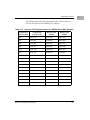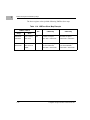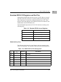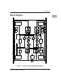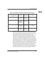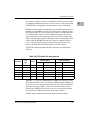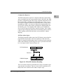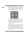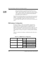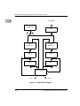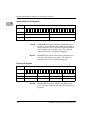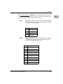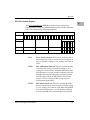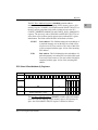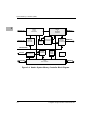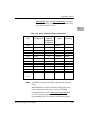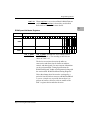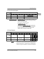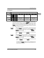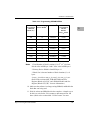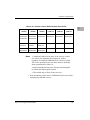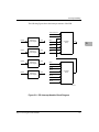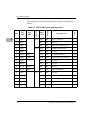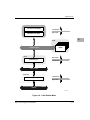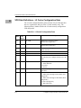
1
MVME2400-Series
VME Processor Module
Programmer’s
Reference Guide
V2400A/PG1
Notice
While reasonable efforts have been made to assure the accuracy of this document,
Motorola, Inc. assumes no liability resulting from any omissions in this document, or from
the use of the information obtained therein. Motorola reserves the right to revise this
document and to make changes from time to time in the content hereof without obligation
of Motorola to notify any person of such revision or changes.
No part of this material may be reproduced or copied in any tangible medium, or stored in
a retrieval system, or transmitted in any form, or by any means, radio, electronic,
mechanical, photocopying, recording or facsimile, or otherwise, without the prior written
permission of Motorola, Inc.
It is possible that this publication may contain reference to, or information about Motorola
products (machines and programs), programming, or services that are not announced in
your country. Such references or information must not be construed to mean that Motorola
intends to announce such Motorola products, programming, or services in your country.
Restricted Rights Legend
If the documentation contained herein is supplied, directly or indirectly, to the U.S.
Government, the following notice shall apply unless otherwise agreed to in writing by
Motorola, Inc.
Use, duplication, or disclosure by the Government is subject to restrictions as set forth in
subparagraph (c)(1)(ii) of the Rights in Technical Data and Computer Software clause at
DFARS 252.227-7013.
Motorola, Inc.
Computer Group
2900 South Diablo Way
Tempe, Arizona 85282
Preface
The MVME2400-Series VME Processor Module Programmer’s Reference Guide provides
brief board level information, complete memory maps, and detailed ASIC chip information
including register bit descriptions for the MVME2400 series VME Processor Modules
(also called MVME240x in this manual). The information contained in this manual applies
to the single board computers built from some of the plug-together components listed in the
following table.
Model
MVME2401-1
MVME2401-3
MPC
MPC750
@ 233 MHz
Memory
Handles
32MB ECC SDRAM
Scanbe Handles
32MB ECC SDRAM
1101 Handles
MVME2402-1
64MB ECC SDRAM
Scanbe Handles
MVME2402-3
64MB ECC SDRAM
1101 Handles
32MB ECC SDRAM
Scanbe Handles
32MB ECC SDRAM
1101 Handles
MVME2432-1
64MB ECC SDRAM
Scanbe Handles
MVME2432-3
64MB ECC SDRAM
1101-1 Handles
MVME2433-1
128MB ECC SDRAM
Scanbe Handles
MVME2433-3
128MB ECC SDRAM
1101-1 Handles
MVME2434-1
256MB ECC SDRAM
Scanbe Handles
MVME2434-3
256MB ECC SDRAM
1101-1 Handles
MVME2431-1
MVME2431-3
MPC750
@ 350 MHz
This manual is intended for anyone who wants to program these boards in order to design
OEM systems, supply additional capability to an existing compatible system, or work in a
lab environment for experimental purposes.
A basic knowledge of computers and digital logic is assumed.
To use this manual, you should be familiar with the publications listed in Appendix A,
Related Documentation.
The following conventions are used in this document:
bold
is used for user input that you type just as it appears. Bold is also used for
commands, options and arguments to commands, and names of programs,
directories, and files.
italic
is used for names of variables to which you assign values. Italic is also used for
comments in screen displays and examples.
courier
is used for system output (e.g., screen displays, reports), examples, and system
prompts.
<RETURN> or <CR>
represents the carriage return or enter key.
CTRL
represents the Control key. Execute control characters by pressing the CTRL key
and the letter simultaneously, e.g., CTRL-d.
The computer programs stored in the Read Only Memory of this device contain material
copyrighted by Motorola Inc., first published 1990, and may be used only under a license
such as the License for Computer Programs (Article 14) contained in Motorola’s Terms and
Conditions of Sale, Rev. 1/79.
All Motorola PWBs (printed wiring boards) are manufactured by UL-recognized
manufacturers, with a flammability rating of 94V-0.
!
WARNING
This equipment generates, uses, and can radiate electromagnetic energy. It may cause or be susceptible to electromagnetic interference (EMI) if not installed and used in a
cabinet with adequate EMI protection.
Motorola® and the Motorola symbol are registered trademarks of Motorola, Inc.
PowerStackTM, VMEmoduleTM, and VMEsystemTM are trademarks of Motorola, Inc.
PowerPCTM, PowerPC 603TM, and PowerPC 604TMare trademarks of IBM Corp, and are
used by Motorola, Inc. under license from IBM Corp.
AIXTM is a trademark of IBM Corp.
TimekeeperTM and ZeropowerTM are trademarks of Thompson Components.
All other products mentioned in this document are trademarks or registered trademarks of
their respective holders.
©Copyright Motorola 1999
All Rights Reserved
Printed in the United States of America
March 1999
Safety Summary
Safety Depends On You
The following general safety precautions must be observed during all phases of operation, service, and repair of this
equipment. Failure to comply with these precautions or with specific warnings elsewhere in this manual violates safety
standards of design, manufacture, and intended use of the equipment. Motorola, Inc. assumes no liability for the
customer’s failure to comply with these requirements.
The safety precautions listed below represent warnings of certain dangers of which Motorola is aware. You, as the
user of the product, should follow these warnings and all other safety precautions necessary for the safe operation of
the equipment in your operating environment.
Ground the Instrument.
To minimize shock hazard, the equipment chassis and enclosure must be connected to an electrical ground. The
equipment is supplied with a three-conductor ac power cable. The power cable must be plugged into an approved
three-contact electrical outlet. The power jack and mating plug of the power cable meet International Electrotechnical
Commission (IEC) safety standards.
Do Not Operate in an Explosive Atmosphere.
Do not operate the equipment in the presence of flammable gases or fumes. Operation of any electrical equipment in
such an environment constitutes a definite safety hazard.
Keep Away From Live Circuits.
Operating personnel must not remove equipment covers. Only Factory Authorized Service Personnel or other
qualified maintenance personnel may remove equipment covers for internal subassembly or component replacement
or any internal adjustment. Do not replace components with power cable connected. Under certain conditions,
dangerous voltages may exist even with the power cable removed. To avoid injuries, always disconnect power and
discharge circuits before touching them.
Do Not Service or Adjust Alone.
Do not attempt internal service or adjustment unless another person capable of rendering first aid and resuscitation is
present.
Use Caution When Exposing or Handling the CRT.
Breakage of the Cathode-Ray Tube (CRT) causes a high-velocity scattering of glass fragments (implosion). To
prevent CRT implosion, avoid rough handling or jarring of the equipment. Handling of the CRT should be done only
by qualified maintenance personnel using approved safety mask and gloves.
Do Not Substitute Parts or Modify Equipment.
Because of the danger of introducing additional hazards, do not install substitute parts or perform any unauthorized
modification of the equipment. Contact your local Motorola representative for service and repair to ensure that safety
features are maintained.
Dangerous Procedure Warnings.
Warnings, such as the example below, precede potentially dangerous procedures throughout this manual. Instructions
contained in the warnings must be followed. You should also employ all other safety precautions which you deem
necessary for the operation of the equipment in your operating environment.
!
WARNING
Dangerous voltages, capable of causing death, are present in
this equipment. Use extreme caution when handling, testing,
and adjusting.
Contents
CHAPTER 1
Board Description and Memory Maps
Introduction................................................................................................................1-1
Manual Terminology..................................................................................................1-1
Overview....................................................................................................................1-3
Feature Summary .......................................................................................................1-3
System Block Diagram ..............................................................................................1-4
Functional Description...............................................................................................1-7
Overview.............................................................................................................1-7
Programming Model ..................................................................................................1-8
Memory Maps.....................................................................................................1-8
Processor Memory Maps .............................................................................1-8
PCI Memory Maps ....................................................................................1-14
VMEbus Mapping .....................................................................................1-21
System Configuration Information ...................................................................1-27
ISA Local Resource Bus ..........................................................................................1-29
W83C553 PIB Registers...................................................................................1-29
UART................................................................................................................1-29
General-Purpose Software-Readable Header (SRH) Switch (S3) ....................1-30
NVRAM/RTC & Watchdog Timer Registers ...................................................1-31
VME Registers..................................................................................................1-31
LM/SIG Control Register ..........................................................................1-32
LM/SIG Status Register.............................................................................1-33
Location Monitor Upper Base Address Register.......................................1-34
Location Monitor Lower Base Address Register ......................................1-35
Semaphore Register 1 ................................................................................1-35
Semaphore Register 2 ................................................................................1-36
VME Geographical Address Register (VGAR) ........................................1-36
Emulated Z8536 CIO Registers and Port Pins..................................................1-37
Z8536 CIO Port Pins .................................................................................1-37
ISA DMA Channels..........................................................................................1-38
CHAPTER 2
Hawk PCI Host Bridge & Multi-Processor Interrupt Controller
Introduction................................................................................................................2-1
Overview.............................................................................................................2-1
Features...............................................................................................................2-1
vii
Block Diagram........................................................................................................... 2-3
Functional Description .............................................................................................. 2-4
Architectural Overview ...................................................................................... 2-4
PPC Bus Interface .............................................................................................. 2-5
PPC Address Mapping ................................................................................ 2-5
PPC Slave.................................................................................................... 2-7
PPC FIFO .................................................................................................... 2-9
PPC Master................................................................................................ 2-10
PPC Arbiter ............................................................................................... 2-14
PPC Parity ................................................................................................. 2-16
PPC Bus Timer.......................................................................................... 2-17
PCI Bus Interface ............................................................................................. 2-18
PCI Address Mapping ............................................................................... 2-18
PCI Slave................................................................................................... 2-21
PCI FIFO ................................................................................................... 2-25
PCI Master ................................................................................................ 2-25
Generating PCI Cycles .............................................................................. 2-29
PCI Arbiter ................................................................................................ 2-33
Endian Conversion ........................................................................................... 2-37
When PPC Devices are Big-Endian .......................................................... 2-37
When PPC Devices are Little Endian ....................................................... 2-38
PHB Registers ........................................................................................... 2-39
Error Handling.................................................................................................. 2-40
Watchdog Timers.............................................................................................. 2-41
PCI/PPC Contention Handling ......................................................................... 2-44
Transaction Ordering........................................................................................ 2-46
PHB Hardware Configuration .......................................................................... 2-48
Multi-Processor Interrupt Controller (MPIC) Functional Description.................... 2-49
MPIC Features:................................................................................................. 2-49
Architecture ...................................................................................................... 2-50
External Interrupt Interface .............................................................................. 2-50
CSR’s Readability ............................................................................................ 2-51
Interrupt Source Priority................................................................................... 2-51
Processor’s Current Task Priority..................................................................... 2-52
Nesting of Interrupt Events .............................................................................. 2-52
Spurious Vector Generation.............................................................................. 2-52
Interprocessor Interrupts (IPI) .......................................................................... 2-53
8259 Compatibility........................................................................................... 2-53
PHB Detected Errors ........................................................................................ 2-53
Timers............................................................................................................... 2-54
Interrupt Delivery Modes ................................................................................. 2-54
viii
Block Diagram Description ..............................................................................2-55
Program Visible Registers .........................................................................2-57
Interrupt Pending Register (IPR) ...............................................................2-57
Interrupt Selector (IS) ................................................................................2-57
Interrupt Request Register (IRR)...............................................................2-58
In-Service Register (ISR) ..........................................................................2-58
Interrupt Router .........................................................................................2-58
Programming Notes ..........................................................................................2-60
External Interrupt Service..........................................................................2-60
Reset State .................................................................................................2-61
Operation ..........................................................................................................2-62
Interprocessor Interrupts............................................................................2-62
Dynamically Changing I/O Interrupt Configuration .................................2-62
EOI Register ..............................................................................................2-63
Interrupt Acknowledge Register................................................................2-63
8259 Mode.................................................................................................2-63
Current Task Priority Level.......................................................................2-63
Architectural Notes ...........................................................................................2-63
Effects of Interrupt Serialization.......................................................................2-64
Registers...................................................................................................................2-65
PPC Registers ...................................................................................................2-65
Vendor ID/Device ID Registers ................................................................2-68
Revision ID Register .................................................................................2-68
General Control-Status/Feature Registers .................................................2-69
PPC Arbiter/PCI Arbiter Control Registers...............................................2-71
Hardware Control-Status/Prescaler Adjust Register .................................2-75
PPC Error Test/Error Enable Register.......................................................2-78
PPC Error Status Register..........................................................................2-81
PPC Error Address Register ......................................................................2-83
PPC Error Attribute Register .....................................................................2-84
PCI Interrupt Acknowledge Register ........................................................2-86
PPC Slave Address (0,1 and 2) Registers..................................................2-86
PPC Slave Offset/Attribute (0, 1 and 2) Registers ....................................2-87
PPC Slave Address (3) Register ................................................................2-88
PPC Slave Offset/Attribute (3) Registers ..................................................2-89
WDTxCNTL Registers..............................................................................2-91
WDTxSTAT Registers ..............................................................................2-93
General Purpose Registers.........................................................................2-93
PCI Registers ....................................................................................................2-95
Vendor ID/ Device ID Registers ...............................................................2-96
PCI Command/ Status Registers................................................................2-97
Revision ID/ Class Code Registers............................................................2-99
ix
Header Type Register................................................................................ 2-99
MPIC I/O Base Address Register ........................................................... 2-100
MPIC Memory Base Register ................................................................. 2-100
PCI Slave Address (0,1,2 and 3) Registers ............................................. 2-101
PCI Slave Attribute/ Offset (0,1,2 and 3) Registers................................ 2-102
CONFIG_ADDRESS Register ............................................................... 2-104
CONFIG_DATA Register ...................................................................... 2-106
MPIC Registers .............................................................................................. 2-108
MPIC Registers ....................................................................................... 2-108
Feature Reporting Register ..................................................................... 2-112
Global Configuration Register ................................................................ 2-113
Vendor Identification Register ................................................................ 2-114
Processor Init Register ............................................................................ 2-115
IPI Vector/Priority Registers................................................................... 2-116
Spurious Vector Register ........................................................................ 2-117
Timer Frequency Register....................................................................... 2-117
Timer Current Count Registers ............................................................... 2-118
Timer Basecount Registers ..................................................................... 2-119
Timer Vector/Priority Registers .............................................................. 2-120
Timer Destination Registers.................................................................... 2-121
External Source Vector/Priority Registers .............................................. 2-121
External Source Destination Registers.................................................... 2-123
PHB-Detected Errors Vector/Priority Register ....................................... 2-123
PHB-Detected Errors Destination Register............................................. 2-124
Interprocessor Interrupt Dispatch Registers............................................ 2-125
Interrupt Task Priority Registers ............................................................. 2-126
Interrupt Acknowledge Registers............................................................ 2-127
End-of-Interrupt Registers ...................................................................... 2-127
CHAPTER 3
System Memory Controller (SMC)
Introduction ............................................................................................................... 3-1
Overview ............................................................................................................ 3-1
Bit Ordering Convention .................................................................................... 3-1
Features .............................................................................................................. 3-1
Block Diagrams ......................................................................................................... 3-2
Functional Description .............................................................................................. 3-7
Performance........................................................................................................ 3-7
Four-beat Reads/Writes............................................................................... 3-7
Single-beat Reads/Writes ............................................................................ 3-7
Address Pipelining ...................................................................................... 3-7
x
Page Holding ...............................................................................................3-8
SDRAM Speeds...........................................................................................3-8
SDRAM Organization ...............................................................................3-10
ROM/Flash Speeds ....................................................................................3-11
PowerPC 60x Bus Interface..............................................................................3-13
Responding to Address Transfers..............................................................3-13
Completing Data Transfers........................................................................3-14
PPC60x Data Parity ...................................................................................3-14
PPC60x Address Parity .............................................................................3-15
Cache Coherency .......................................................................................3-15
Cache Coherency Restrictions...................................................................3-15
L2 Cache Support ......................................................................................3-15
ECC...................................................................................................................3-16
Cycle Types ...............................................................................................3-16
Error Reporting..........................................................................................3-16
Error Logging ............................................................................................3-17
ROM/Flash Interface ........................................................................................3-18
I2C Interface .....................................................................................................3-23
I2C Byte Write...........................................................................................3-24
I2C Random Read .....................................................................................3-26
I2C Current Address Read.........................................................................3-28
I2C Page Write ..........................................................................................3-30
I2C Sequential Read ..................................................................................3-32
Refresh/Scrub....................................................................................................3-35
CSR Accesses ...................................................................................................3-35
External Register Set ........................................................................................3-35
Chip Configuration ...........................................................................................3-35
Programming Model ................................................................................................3-36
CSR Architecture..............................................................................................3-36
Register Summary.............................................................................................3-36
Detailed Register Bit Descriptions ...................................................................3-39
Vendor/Device Register ............................................................................3-40
Revision ID/ General Control Register .....................................................3-40
SDRAM Enable and Size Register (Blocks A, B, C, D) ...........................3-42
SDRAM Base Address Register (Blocks A/B/C/D)..................................3-44
CLK Frequency Register ...........................................................................3-45
ECC Control Register ................................................................................3-46
Error Logger Register ................................................................................3-50
Error_Address Register .............................................................................3-52
Scrub/Refresh Register ..............................................................................3-52
Scrub Address Register .............................................................................3-53
ROM A Base/Size Register .......................................................................3-54
xi
ROM B Base/Size Register ....................................................................... 3-57
ROM Speed Attributes Registers .............................................................. 3-59
Data Parity Error Log Register ................................................................. 3-60
Data Parity Error Address Register........................................................... 3-61
Data Parity Error Upper Data Register ..................................................... 3-62
Data Parity Error Lower Data Register ..................................................... 3-62
I2C Clock Prescaler Register .................................................................... 3-63
I2C Control Register ................................................................................. 3-63
I2C Status Register.................................................................................... 3-64
I2C Transmitter Data Register .................................................................. 3-65
I2C Receiver Data Register....................................................................... 3-66
SDRAM Enable and Size Register (Blocks E,F,G,H) .............................. 3-66
SDRAM Base Address Register (Blocks E/F/G/H).................................. 3-67
SDRAM Speed Attributes Register .......................................................... 3-69
Address Parity Error Log Register ............................................................ 3-71
Address Parity Error Address Register ..................................................... 3-72
32-Bit Counter........................................................................................... 3-73
External Register Set................................................................................. 3-73
tben Register.............................................................................................. 3-75
Software Considerations.......................................................................................... 3-76
Programming ROM/Flash Devices .................................................................. 3-76
Writing to the Control Registers....................................................................... 3-76
Initializing SDRAM Related Control Registers ............................................... 3-77
SDRAM Speed Attributes......................................................................... 3-77
SDRAM Size............................................................................................. 3-77
I2C EEPROMs .......................................................................................... 3-77
SDRAM Base Address and Enable........................................................... 3-78
SDRAM Control Registers Initialization Example................................... 3-78
Optional Method for Sizing SDRAM ....................................................... 3-84
ECC Codes .............................................................................................................. 3-88
CHAPTER 4
Universe II (VMEbus to PCI) Chip
General Information .................................................................................................. 4-1
Introduction ........................................................................................................ 4-1
Product Overview - Features .............................................................................. 4-1
Functional Description .............................................................................................. 4-2
Architectural Overview ...................................................................................... 4-2
VMEbus Interface ....................................................................................... 4-4
PCI Bus Interface ........................................................................................ 4-5
Interrupter and Interrupt Handler ................................................................ 4-6
xii
DMA Controller ..........................................................................................4-7
Registers - Universe II Control and Status Registers (UCSR) ..................................4-7
Universe II Register Map....................................................................................4-8
CHAPTER 5
Programming Details
Introduction................................................................................................................5-1
PCI Arbitration...........................................................................................................5-1
Interrupt Handling......................................................................................................5-2
Hawk MPIC ........................................................................................................5-3
8259 Interrupts....................................................................................................5-4
ISA DMA Channels ...................................................................................................5-7
Exceptions..................................................................................................................5-8
Sources of Reset..................................................................................................5-8
Soft Reset............................................................................................................5-9
Universe II Chip Problems after a PCI Reset .....................................................5-9
Error Notification and Handling .......................................................................5-10
Endian Issues ...........................................................................................................5-11
Processor/Memory Domain ..............................................................................5-14
MPIC’s Involvement.........................................................................................5-14
PCI Domain ......................................................................................................5-14
PCI-SCSI ...................................................................................................5-14
PCI-Ethernet ..............................................................................................5-14
PCI-Graphics .............................................................................................5-15
Universe II’s Involvement ................................................................................5-15
VMEbus Domain ..............................................................................................5-15
ROM/Flash Initialization .........................................................................................5-16
APPENDIX A
Ordering Related Documentation
Motorola Computer Group Documents ....................................................................A-1
Manufacturers’ Documents.......................................................................................A-2
Related Specifications...............................................................................................A-5
APPENDIX B
MVME2400 VPD Reference Information
Vital Product Data (VPD) Introduction .................................................................... B-1
VPD Data Definitions........................................................................................ B-1
VPD Data Definitions - Product Configuration Options Data .......................... B-3
VPD Data Definitions - FLASH Memory Configuration Data ......................... B-5
VPD Data Definitions - L2 Cache Configuration Data ..................................... B-6
xiii
Example VPD SROM ....................................................................................... B-8
Glossary
Abbreviations, Acronyms, and Terms to Know .....................................................GL-1
Index
xiv
List of Figures
Figure 1-1. MVME2400 Series System Block Diagram ...........................................1-6
Figure 1-2. VMEbus Master Mapping.....................................................................1-22
Figure 1-3. VMEbus Slave Mapping .......................................................................1-24
Figure 1-4. General-Purpose Software-Readable Header........................................1-30
Figure 2-1. Hawk’s PCI Host Bridge Block Diagram ...............................................2-3
Figure 2-2. PPC to PCI Address Decoding................................................................2-6
Figure 2-3. PPC to PCI Address Translation .............................................................2-7
Figure 2-4. PCI to PPC Address Decoding..............................................................2-19
Figure 2-5. PCI to PPC Address Translation ...........................................................2-20
Figure 2-6. PCI Spread I/O Address Translation .....................................................2-30
Figure 2-7. Big to Little Endian Data Swap ............................................................2-38
Figure 2-8. Serial Mode Interrupt Scan ...................................................................2-51
Figure 2-9. MPIC Block Diagram ...........................................................................2-56
Figure 3-1. Hawk Used with Synchronous DRAM in a System ..............................3-3
Figure 3-2. Hawk’s System Memory Controller Internal Data Paths ........................3-4
Figure 3-3. Falcon Internal Data Paths (Simplified)..................................................3-4
Figure 3-3. Overall SDRAM Connections (4 Blocks using Register Buffers) ..........3-5
Figure 3-4. Hawk’s System Memory Controller Block Diagram ..............................3-6
Figure 3-5. Programming Sequence for I2C Byte Write .........................................3-25
Figure 3-6. Programming Sequence for I2C Random Read ....................................3-27
Figure 3-7. Programming Sequence for I2C Current Address Read .......................3-29
Figure 3-8. Programming Sequence for I2C Page Write .........................................3-31
Figure 3-9. Programming Sequence for I2C Sequential Read.................................3-34
Figure 3-10. Read/Write Check-bit Data Paths........................................................3-47
Figure 4-1. Architectural Diagram for the Universe II ..............................................4-3
Figure 4-2. UCSR Access Mechanisms.....................................................................4-8
Figure 5-1. MVME2400 Series Interrupt Architecture..............................................5-2
Figure 5-2. PIB Interrupt Handler Block Diagram ....................................................5-5
Figure 5-3. Big-Endian Mode ..................................................................................5-12
Figure 5-4. Little-Endian Mode ...............................................................................5-13
xv
xvi
List of Tables
Table 1-1. MVME240x Features ..............................................................................1-3
Table 1-2. Default Processor Memory Map ..............................................................1-9
Table 1-3. CHRP Memory Map Example................................................................1-10
Table 1-4. PHB Register Values for CHRP Memory Map ......................................1-11
Table 1-5. PREP Memory Map Example.................................................................1-12
Table 1-6. PHB Register Values for PREP Memory Map .......................................1-13
Table 1-7. PCI CHRP Memory Map .......................................................................1-14
Table 1-8. PHB PCI Register Values for CHRP Memory Map ...............................1-16
Table 1-9. Universe II PCI Register Values for CHRP Memory Map ....................1-16
Table 1-10. PCI PREP Memory Map.......................................................................1-18
Table 1-11. PHB PCI Register Values for PREP Memory Map ..............................1-19
Table 1-12. Universe II PCI Register Values for PREP Memory Map ....................1-20
Table 1-13. Universe II PCI Register Values for VMEbus Slave Map Example.....1-25
Table 1-14. VMEbus Slave Map Example...............................................................1-26
Table 1-15. 16550 Access Registers ........................................................................1-29
Table 1-16. MK48T59/559 Access Registers ..........................................................1-31
Table 1-17. VME Registers......................................................................................1-32
Table 1-18. Emulated Z8536 Access Registers........................................................1-37
Table 1-19. Z8536 CIO Port Pins Assignment ........................................................1-37
Table 2-1. PPC Slave Response Command Types ....................................................2-8
Table 2-2. PPC Master Transaction Profiles and Starting Offsets ...........................2-11
Table 2-3. PPC Master Write Posting Options.........................................................2-12
Table 2-4. PPC Master Read Ahead Options ..........................................................2-12
Table 2-5. PPC Master Transfer Types ....................................................................2-14
Table 2-6. PPC Arbiter Pin Assignments.................................................................2-15
Table 2-7. PCI Slave Response Command Types....................................................2-22
Table 2-8. PCI Master Command Codes ................................................................2-26
Table 2-9. PCI Arbiter Pin Description....................................................................2-33
Table 2-10. Fixed Mode Priority Level Setting .......................................................2-34
Table 2-11. Mixed Mode Priority Level Setting .....................................................2-35
Table 2-12. Arbitration Setting ................................................................................2-36
Table 2-13. Address Modification for Little Endian Transfers................................2-39
Table 2-14. WDTxCNTL Programming ..................................................................2-43
Table 2-15. PHB Hardware Configuration ..............................................................2-48
xvii
Table 2-16. PPC Register Map for PHB ................................................................. 2-66
Table 2-17. PCI Configuration Register Map.......................................................... 2-95
Table 2-18. PCI I/O Register Map........................................................................... 2-96
Table 2-19. MPIC Register Map............................................................................ 2-108
Table 2-20. Cascade Mode Encoding .................................................................... 2-114
Table 2-21. Tie Mode Encoding ............................................................................ 2-114
Table 3-1. 60x Bus to SDRAM Estimated Access Timing at 100MHz with PC100
SDRAMs (CAS_latency of 2) .................................................................................. 3-8
Table 3-2. PowerPC 60x Bus to ROM/Flash Access Timing (120ns @ 100MHz). 3-11
Table 3-3. PowerPC 60x Bus to ROM/Flash Access Timing (80ns @ 100MHz)... 3-12
Table 3-4. PowerPC 60x Bus to ROM/Flash Access Timing (50ns @ 100MHz)... 3-12
Table 3-5. PowerPC 60x Bus to ROM/Flash Access Timing (30ns @ 100MHz)... 3-13
Table 3-6. Error Reporting....................................................................................... 3-16
Table 3-7. PowerPC 60x to ROM/Flash (16 Bit Width) Address Mapping ............ 3-20
Table 3-8. PowerPC 60x to ROM/Flash (64 Bit Width) Address Mapping ........... 3-21
Table 3-9. Register Summary ................................................................................. 3-37
Table 3-10. Block_A/B/C/D/E/F/G/H Configurations ............................................ 3-43
Table 3-11. ROM Block A Size Encoding .............................................................. 3-55
Table 3-12. rom_a_rv and rom_b_rv encoding ....................................................... 3-55
Table 3-13. Read/Write to ROM/Flash.................................................................... 3-56
Table 3-14. ROM Block B Size Encoding .............................................................. 3-58
Table 3-15. ROM Speed Bit Encodings .................................................................. 3-60
Table 3-16. Trc Encoding ........................................................................................ 3-70
Table 3-17. tras Encoding ........................................................................................ 3-70
Table 3-18. Deriving tras, trp, trcd and trc Control Bit Values from SPD Information380
Table 3-19. Programming SDRAM SIZ Bits .......................................................... 3-83
Table 3-20. Address Lists for Different Block Size Checks.................................... 3-87
Table 3-21. Syndrome Codes Ordered by Bit in Error ............................................ 3-88
Table 3-22. Single Bit Errors Ordered by Syndrome Code ..................................... 3-89
Table 4-1. Universe II Register Map ........................................................................ 4-9
Table 5-1. Hawk Arbitration Assignments ................................................................ 5-1
Table 5-2. MPIC Interrupt Assignments ................................................................... 5-3
Table 5-3. PIB PCI/ISA Interrupt Assignments ........................................................ 5-6
Table 5-4. Reset Sources and Devices Affected ....................................................... 5-9
Table 5-5. Error Notification and Handling ............................................................ 5-10
Table 5-6. ROM/FLASH Bank Default.................................................................. 5-16
Table A-1. Motorola Computer Group Documents................................................. A-1
Table A-2. Manufacturers’ Documents .................................................................. A-2
xviii
Table A-3. Related Specifications ..........................................................................A-5
Table B-1. VPD Packet Types .................................................................................. B-1
Table B-2. MVME2400 Product Configuration Options Data ................................ B-3
Table B-3. FLASH Memory Configuration Data ..................................................... B-5
Table B-4. L2 Cache Configuration Data ................................................................ B-6
Table B-5. VPD SROM Configuration Specification for 01-W3394F01* .............. B-8
xix
xx
1Board Description and
Memory Maps
1
Introduction
This manual provides programming information for the MVME240x
VME Processor Modules. Extensive programming information is
provided for the primary Application-Specific Integrated Circuit (ASIC)
devices used on the boards: the Hawk and Universe II chips. Reference
information is included in Appendix A for the Large Scale Integration
(LSI) devices used on the boards and sources for additional information
are listed.
This chapter briefly describes the board level hardware features of the
MVME2400-series VME Processor Modules. The chapter begins with a
board level overview and features list. Memory maps are next, and are the
major feature of this chapter.
Programmable registers in the MVME2400-series that reside in ASICs are
covered in the chapters on those ASICs. Chapter 2 and Chapter 3 covers
the Hawk ASIC, Chapter 4 covers the Universe II chip, and Chapter 5
covers certain programming features, such as interrupts and exceptions.
Appendix A lists all related documentation.
Manual Terminology
Throughout this manual, a convention is used which precedes data and
address parameters by a character identifying the numeric format as
follows:
$
%
&
dollar
percent
ampersand
specifies a hexadecimal character
specifies a binary number
specifies a decimal number
For example, “12” is the decimal number twelve, and “$12” is the decimal
number eighteen.
Unless otherwise specified, all address references are in hexadecimal.
1-1
1
Board Description and Memory Maps
An asterisk (*) following the signal name for signals which are level
significant denotes that the signal is true or valid when the signal is low.
An asterisk (*) following the signal name for signals which are edge
significant denotes that the actions initiated by that signal occur on high to
low transition.
Note
In some places in this document, an underscore (_) following
the signal name is used to indicate an active low signal.
In this manual, assertion and negation are used to specify forcing a signal
to a particular state. In particular, assertion and assert refer to a signal that
is active or true; negation and negate indicate a signal that is inactive or
false. These terms are used independently of the voltage level (high or low)
that they represent.
Data and address sizes for MPC60x chips are defined as follows:
❏
A byte is eight bits, numbered 0 through 7, with bit 0 being the least
significant.
❏
A half-word is 16 bits, numbered 0 through 15, with bit 0 being the
least significant.
❏
A word or single word is 32 bits, numbered 0 through 31, with bit 0
being the least significant.
❏
A double word is 64 bits, numbered 0 through 63, with bit 0 being
the least significant.
Refer to Chapter 5 for Endian Issues, which covers which parts of the
MVME2400 series use big-endian byte ordering, and which use smallendian byte ordering.
The terms control bit and status bit are used extensively in this document.
The term control bit is used to describe a bit in a register that can be set and
cleared under software control. The term true is used to indicate that a bit
is in the state that enables the function it controls. The term false is used to
indicate that the bit is in the state that disables the function it controls. In
all tables, the terms 0 and 1 are used to describe the actual value that should
be written to the bit, or the value that it yields when read. The term status
1-2
Computer Group Literature Center Web Site
Overview
bit is used to describe a bit in a register that reflects a specific condition.
The status bit can be read by software to determine operational or
exception conditions.
Overview
The MVME2400-series VME Processor Module family, hereafter
sometimes referred to simply as the MVME240x or the V2400 series,
provides many standard features required by a computer system: Ethernet
interface, async serial port, boot Flash, and up to 256MB of ECC DRAM.
Feature Summary
There are many models based on the MVME2400 series architecture. The
following table summarizes the major features of the MVME2400 series:
Table 1-1. MVME240x Features
Feature
Description
TM
Microprocessor
233 MHZ MPC750 PowerPC
(MVME2401 - 2402 models)
processor
350 MHZ MPC750 PowerPCTM processor
(MVME2431 - 2434 models)
Form factor
6U VMEbus
SDRAM
Double-Bit-Error detect, Single-Bit-Error correct across 72 bits 32MB,
64MB, 128MB, or 256MB SDRAM
L2 Cache
1MB back side L2 Cache using late write or burst-mode SRAMS
Flash memory
Sockets for 1 MB
8 MB Soldered on-board
Memory Controller
Hawk’s SMC (System Memory Controller)
PCI Host Bridge
Hawk’s PHB (PCI Host Bridge)
Interrupt Controller
Hawk’s MPIC (Multi-Processor Interrupt Controller)
PCI Interface
32/64-bit Data, 33MHz operation
http://www.mcg.mot.com/literature
1-3
1
1
Board Description and Memory Maps
Table 1-1. MVME240x Features (Continued)
Feature
Description
Real-time clock
8KB NVRAM with RTC and battery backup (SGS-Thomson M48T559)
Peripheral Support
One 16C550-compatible async serial port routed to front panel RJ45
10BaseT/100BaseTX Ethernet interface routed to front panel RJ45
Switches
Reset (RST) and Abort (ABT)
Status LEDs
Four: Board fail (BFL), CPU, PMC (one for PMC slot 2, one for slot 1)
Timers
One 16-bit timer in W83C553 ISA bridge; four 32-bit timers in MPIC
device
Watchdog timer provided in SGS-Thomson M48T59
VME I/O
VMEbus P2 connector
Serial I/O
One asynchronous debug port via RJ45 connector on front panel
Ethernet I/O
10Base-T/100Base-TX connections via RJ45 connector on front panel
Two IEEE P1386.1 PCI Mezzanine Card (PMC) slots for one doublewidth or two single-width PMCs
PCI interface
Front panel and/or VMEbus P2 I/O on both PMC slots
One 114-pin Mictor connector for optional PMCspan expansion module
VMEbus system controller functions
VMEbus interface
64-bit PCI (Universe II)
VMEbus-to-local-bus interface (A32/A24/A16, D64 (MBLT)
D32//D16/D08 Master and Slave
System Block Diagram
The MVME2400 is a VMEbus-based single-slot Single Board Computer
based on the PowerPC MPC750 processor. The MVME2400 features two
PCI Mezzanine Card slots, an Ethernet Interface, serial port, up to 9MB of
boot FLASH, and up to 256MB of ECC protected system RAM. The Hawk
ASIC controls all of the functions previously controlled by the
Raven/Falcon chipsets, in addition to new functionality. The Hawk
provides the interface to the PowerPC 60x Bus, the interface to all onboard SDRAMs, error notification for SDRAMs, the interface to
ROM/Flash, and the I2C master, the external status/control register
support, synchronous PPC60x/PCI clock ratio support, the interface to the
PCI, and an interrupt controller. PCI devices include: VME, Ethernet, and
1-4
Computer Group Literature Center Web Site
System Block Diagram
two PMC slots. Standard I/O functions are provided by the UART device
which resides on the ISA bus. The NVRAM/RTC also resides on the ISA
bus. The general system block diagram for MVME2400 series is shown
below:
http://www.mcg.mot.com/literature
1-5
1
Board Description and Memory Maps
Debug Connector
Processor
MPC750
Clock
Generator
FLASH
1MB to 9MB
System
Registers
Hawk Asic
System Memory Controller (SMC)
and PCI Host Bridge (PHB)
PCI Expansion
1M
SDRAM
32/64/128/256MB
100 MHz MPC604 Processor Bus
L2 Cache
2,64-bit PMC Slot
33MHz 32/64-bit PCI Local Bus
PIB
W83c553
VME Bridge
Universe II
serial port
RJ45
ISA Bus
10/100TX
RJ45
Ethernet
ISA
Registers
Buffers
RTC/NVRAM/WD
MK48T559
TL16C550
UART
Front Panel
PMC FrontIO
Slot2
PMC Front IO
SLot1
1
VME P2
VME P12067 9708
2067 9708
Figure 1-1. MVME2400 Series System Block Diagram
1-6
Computer Group Literature Center Web Site
Functional Description
Functional Description
Overview
The MVME2400 series is a family of single-slot VME processor modules.
It consists of the MPC750 processor and L2 cache that directly connects to
the MPC750, the Hawk ASIC, which is made up of the PCI Bridge (PHB),
the Multi-Processor Interrupt Controller (MPIC), and the System Memory
Controller (SMC). The MVME2400 series also includes 9MB of Flash
memory, 32MB to 256MB of ECC-protected SDRAM, and a rich set of
features of I/O peripherals.
The I/O peripheral devices on the PCI bus include: the Universe II
VMEbus interface ASIC, and two PMC slots. Functions provided from the
ISA bus are: one asynchronous serial port, a real-time clock,
counters/timers, and a software-readable header.
The MVME2400 series board interfaces to the VMEbus via the P1 and P2
connectors, which use the 5-row 160-pin connectors as specified in the
proposed VME64 Extension Standard. It also draws +5V, +12V, and -12V
power from the VMEbus backplane through these two connectors.
Additional power of 2.0V and 3.3V is regulated onboard from the +5V
power.
Front panel connectors on the MVME2400 series board include: an RJ45
connector for the Ethernet 10Base-T/100Base-TX interface, and an RJ45
connector for the async serial debug port. The front panel also includes
reset and abort switches and status LEDs.
The MVME2400 series contains two IEEE1386.1 PCI Mezzanine Card
(PMC) slots. These PMC slots are 64-bit capable and support both front
and rear I/O. Pins 1 through 64 of PMC slot 1 connector J14 are routed to
row C and row A of the 5-row DIN P2 connector. Pins 1 through 46 of
PMC slot 2 connector J24 are routed to row D and row Z of P2.
Additional PCI expansion is supported with a 114-pin Mictor connector.
This connection allows stacking of one or two PMCspan dual-PMC carrier
boards, to increase the I/O capability. Each PMCspan board requires an
additional VME slot.
http://www.mcg.mot.com/literature
1-7
1
1
Board Description and Memory Maps
Programming Model
Memory Maps
The following sections describe the memory maps for the MVME2400
series.
Processor Memory Maps
The Processor memory map is controlled by the Hawk ASIC. The Hawk
ASIC has flexible programming Map Decoder registers to customize the
system to fit many different applications.
1-8
Computer Group Literature Center Web Site
Programming Model
Default Processor Memory Map
After a reset, the Hawk ASIC provides the default processor memory map
as shown in the following table.
Table 1-2. Default Processor Memory Map
Size
Start
Notes
Processor Address
Definition
End
0000 0000
7FFF FFFF
2G
Not mapped
8000 0000
8001 FFFF
128K
PCI/ISA I/O Space
8002 0000
FEF7 FFFF
2G - 16M 640K
Not mapped
FEF8 0000
FEF8 FFFF
64K
SMC Registers
FEF9 0000
FEFE FFFF
384K
Not mapped
FEFF 0000
FEFF FFFF
64K
PHB Registers
FF00 0000
FFEF FFFF
15M
Not mapped
FFF0 0000
FFFF FFFF
1M
ROM/FLASH Bank A or Bank B
1
2
Notes:
1. This default map for PCI/ISA I/O space allows software to
determine if the system is MPC105-based or Hawk-based by
examining either the PHB Device ID or the CPU Type Register.
2. The first one Mbyte of ROM/FLASH Bank A appears at this range
after a reset if the rom_b_rv control bit is cleared. If the rom_b_rv
control bit is set then this address range maps to ROM/FLASH Bank
B.
http://www.mcg.mot.com/literature
1-9
1
1
Board Description and Memory Maps
Processor CHRP Memory Map
The following table shows a recommended CHRP memory map from the
point of view of the processor.
Table 1-3. CHRP Memory Map Example
Size
Notes
Processor Address
Definition
Start
End
0000 0000
top_dram
dram_size
System Memory (onboard SDRAM)
1, 2
4000 0000
FCFF FFFF
3G - 48M
PCI Memory Space:
4000 0000 to FCFF FFFF
3,4,8
FD00 0000
FDFF FFFF
16M
Zero-Based PCI/ISA Memory Space
(mapped to 00000000 to 00FFFFFF)
3,8
FE00 0000
FE7F FFFF
8M
Zero-Based PCI/ISA I/O Space
(mapped to 00000000 to 007FFFFF)
3,5,8
FE80 0000
FEF7 FFFF
7.5M
Reserved
FEF8 0000
FEF8 FFFF
64K
SMC Registers
FEF9 0000
FEFE FFFF
384K
Reserved
FEFF 0000
FEFF FFFF
64K
PHB Registers
9
FF00 0000
FF7F FFFF
8M
ROM/FLASH Bank A
1,6
FF80 0000
FF8F FFFF
1M
ROM/FLASH Bank B
1,6
FF90 0000
FFEF FFFF
6M
Reserved
FFF0 0000
FFFF FFFF
1M
ROM/FLASH Bank A or Bank B
7
Notes:
1. Programmable via the Hawk ASIC. For the MVME2400 series,
RAM size is limited to 256MB and ROM/FLASH to 9MB.
2. To enable the “Processor-hole” area, program the SMC to ignore
0x000A0000 - 0x000BFFFF address range and program the PHB to
map this address range to PCI memory space.
1-10
Computer Group Literature Center Web Site
Programming Model
3. Programmable via PHB.
4. CHRP requires the starting address for the PCI memory space to be
256MB-aligned.
5. Programmable via PHB for either contiguous or spread-I/O mode.
6. The actual size of each ROM/FLASH bank may vary.
7. The first one Mbyte of ROM/FLASH Bank A appears at this range
after a reset if the rom_b_rv control bit is cleared. If the rom_b_rv
control bit is set then this address range maps to ROM/FLASH Bank
B.
8. This range can be mapped to the VMEbus by programming the
Universe II ASIC accordingly. The map shown is the recommended
setting which uses the Special PCI Slave Image and two of the four
programmable PCI Slave Images.
9. The only method to generate a PCI Interrupt Acknowledge cycle
(8259 IACK) is to perform a read access to the PHB’s PIACK
register at 0xFEFF0030.
The following table shows the programmed values for the associated PHB
registers for the processor CHRP memory map.
Table 1-4. PHB Register Values for CHRP Memory Map
Address
Register Name
Register Value
FEFF 0040
MSADD0
4000 FCFF
FEFF 0044
MSOFF0 & MSATT0
0000 00C2
FEFF 0048
MSADD1
FD00 FDFF
FEFF 004C
MSOFF1 & MSATT1
0300 00C2
FEFF 0050
MSADD2
0000 0000
FEFF 0054
MSOFF2 & MSATT2
0000 0002
FEFF 0058
MSADD3
FE00 FE7F
FEFF 005C
MSOFF3 & MSATT3
0200 00C0
http://www.mcg.mot.com/literature
1-11
1
1
Board Description and Memory Maps
Processor PREP Memory Map
The Hawk ASIC can be programmed for PREP-compatible memory map.
The following table shows the PREP memory map of the MVME2400
series from the point of view of the processor
.
Table 1-5. PREP Memory Map Example
Processor Address
Size
Definition
Notes
Start
End
0000 0000
top_dram
dram_size
System Memory (onboard DRAM)
1
8000 0000
BFFF FFFF
1G
Zero-Based PCI I/O Space:
0000 0000 - 3FFFF FFFF
2
C000 0000
FCFF FFFF
1G - 48M
Zero-Based PCI/ISA Memory Space:
0000 0000 - 3CFFFFFF
2, 5
FD00 0000
FEF7 FFFF
40.5M
Reserved
FEF8 0000
FEF8 FFFF
64K
SMC Registers
FEF9 0000
FEFE FFFF
384K
Reserved
FEFF 0000
FEFF FFFF
64K
PHB Registers
6
FF00 0000
FF7F FFFF
8M
ROM/FLASH Bank A
1, 3
FF80 0000
FF8F FFFF
1M
ROM/FLASH Bank B
1, 3
FF90 0000
FFEF FFFF
6M
Reserved
FFF0 0000
FFFF FFFF
1M
ROM/FLASH Bank A or Bank B
4
Notes:
1. Programmable via the SMC. For the MVME2400 series, RAM size
is limited to 256MB and ROM/FLASH to 9MB.
2. Programmable via the Hawk’s PHB.
3. The actual size of each ROM/FLASH bank may vary.
1-12
Computer Group Literature Center Web Site
Programming Model
4. The first 1 Mbyte of ROM/FLASH Bank A appears at this range
after a reset if the rom_b_rv control bit is cleared. If the rom_b_rv
control bit is set then this address range maps to ROM/FLASH Bank
B.
5. This range can be mapped to the VMEbus by programming the
Universe II ASIC accordingly.
6. The only method to generate a PCI Interrupt Acknowledge cycle
(8259 IACK) is to perform a read access to the PHB’s PIACK
register at 0xFEFF0030.
The following table shows the programmed values for the associated PHB
registers for the processor PREP memory map.
Table 1-6. PHB Register Values for PREP Memory Map
Address
Register Name
Register Value
FEFF 0040
MSADD0
C000 FCFF
FEFF 0044
MSOFF0 & MSATT0
4000 00C2
FEFF 0048
MSADD1
0000 0000
FEFF 004C
MSOFF1 & MSATT1
0000 0002
FEFF 0050
MSADD2
0000 0000
FEFF 0054
MSOFF2 & MSATT2
0000 0002
FEFF 0058
MSADD3
8000 BFFF
FEFF 005C
MSOFF3 & MSATT3
8000 00C0
PCI Configuration Access
PCI Configuration accesses are accomplished via the CONFIG_ADD and
CONFIG_DAT registers. These two registers are implemented by the PHB
portion of the Hawk ASIC. In the CHRP memory map example, the
CONFIG_ADD and CONFIG_DAT registers are located at 0xFE000CF8
and 0xFE000CFC, respectively. With the PREP memory map, the
CONFIG_ADD register and the CONFIG_DAT register are located at
0x80000CF8 and 0x80000CFC, respectively.
http://www.mcg.mot.com/literature
1-13
1
1
Board Description and Memory Maps
PCI Memory Maps
The PCI memory map is controlled by the PHB portion of the Hawk ASIC
and the Universe II ASIC. The PHB and the Universe II ASIC have
flexible programming Map Decoder registers to customize the system to
fit many different applications.
Default PCI Memory Map
After a reset, the PHB and the Universe II ASIC turn all the PCI slave map
decoders off. Software must program the appropriate map decoders for a
specific environment.
PCI CHRP Memory Map
The following table shows a PCI memory map of the MVME2400 series
that is CHRP-compatible from the point of view of the PCI local bus.
Table 1-7. PCI CHRP Memory Map
PCI Address
Start
Size
Definition
Notes
End
0000 0000
top_dram
dram_size
Onboard ECC DRAM
1
4000 0000
EFFF FFFF
3G - 256M
VMEbus A32/D32 (Super/Program)
3
F000 0000
F7FF FFFF
128M
VMEbus A32/D16 (Super/Program)
3
F800 0000
F8FE FFFF
16M - 64K
VMEbus A24/D16 (Super/Program)
4
F8FF 0000
F8FF FFFF
64K
VMEbus A16/D16 (Super/Program)
4
F900 0000
F9FE FFFF
16M - 64K
VMEbus A24/D32 (Super/Data)
4
F9FF 0000
F9FF FFFF
64K
VMEbus A16/D32 (Super/Data)
4
FA00 0000
FAFE FFFF
16M - 64K
VMEbus A24/D16 (User/Program)
4
FAFF 0000
FAFF FFFF
64K
VMEbus A16/D16 (User/Program)
4
FB00 0000
FBFE FFFF
16M - 64K
VMEbus A24/D32 (User/Data)
4
FBFF 0000
FBFF FFFF
64K
VMEbus A16/D32 (User/Data)
4
FC00 0000
FC03 FFFF
256K
MPIC
1
1-14
Computer Group Literature Center Web Site
Programming Model
Table 1-7. PCI CHRP Memory Map (Continued)
PCI Address
Start
Size
Definition
Notes
End
FC04 0000
FCFF FFFF
16M - 256K
PCI Memory Space
FD00 0000
FDFF FFFF
16M
PCI Memory Space or
System Memory Alias Space (mapped
to 00000000 to 00FFFFFF)
FE00 0000
FFFF FFFF
48M
Reserved
1
Notes:
1. Programmable via the PHB’s PCI Configuration registers. For the
MVME2400 series, RAM size is limited to 256MB.
2. To enabled the CHRP “io-hole”, program the PHB to ignore the
0x000A0000 - 0x000FFFFF address range.
3. Programmable mapping via the four PCI Slave Images in the
Universe II ASIC.
4. Programmable mapping via the Special Slave Image (SLSI) in the
Universe II ASIC.
http://www.mcg.mot.com/literature
1-15
1
1
Board Description and Memory Maps
The following table shows the programmed values for the associated PHB
PCI registers for the PCI CHRP memory map.
Table 1-8. PHB PCI Register Values for CHRP Memory Map
Configuration
Address Offset
Configuration
Register Name
Register Value
(Aliasing OFF)
Register Value
(Aliasing ON)
$14
MPIC MBASE
FC00 0000
FC00 0000
$80
PSADD0
0000 3FFF
0100 3FFF
$84
PSOFF0 & PSATT0
0000 00FX
0000 00FX
$88
PSADD1
0000 0000
FD00 FDFF
$8C
PSOFF1 & PSATT1
0000 0000
0000 00FX
$90
PSADD2
0000 0000
0000 0000
$94
PSOFF2 & PSATT2
0000 0000
0000 0000
$98
PSADD3
0000 0000
0000 0000
$9C
PSOFF3 & PSATT3
0000 0000
0000 0000
The next table shows the programmed values for the associated
Universe II PCI registers for the PCI CHRP memory map.
Table 1-9. Universe II PCI Register Values for CHRP Memory Map
Configuration
Address Offset
1-16
Configuration
Register Name
Register Value
$100
LSI0_CTL
C082 5100
$104
LSI0_BS
4000 0000
$108
LSI0_BD
F000 0000
$10C
LSI0_TO
XXXX 0000
$114
LSI1_CTL
C042 5100
$118
LSI1_BS
F000 0000
$11C
LSI1_BD
F800 0000
Computer Group Literature Center Web Site
Programming Model
Table 1-9. Universe II PCI Register Values for CHRP Memory Map
Configuration
Address Offset
Configuration
Register Name
Register Value
$120
LSI1_TO
XXXX 0000
$128
LSI2_CTL
0000 0000
$12C
LSI2_BS
XXXX XXXX
$130
LSI2_BD
XXXX XXXX
$134
LSI2_TO
XXXX XXXX
$13C
LSI3_CTL
0000 0000
$140
LSI3_BS
XXXX XXXX
$144
LSI3_BD
XXXX XXXX
$148
LSI3_TO
XXXX XXXX
$188
SLSI
C0A053F8
http://www.mcg.mot.com/literature
1-17
1
1
Board Description and Memory Maps
PCI PREP Memory Map
The following table shows a PCI memory map of the MVME2400 series
that is PREP-compatible from the point of view of the PCI local bus.
Table 1-10. PCI PREP Memory Map
PCI Address
Size
Start
Definition
Notes
End
0000 0000
00FF FFFF
16M
PCI/ISA Memory Space
0100 0000
2FFF FFFF
752M
VMEbus A32/D32 (Super/Program)
3
3000 0000
37FF FFFF
128M
VMEbus A32/D16 (Super/Program)
3
3800 0000
38FE FFFF
16M - 64K
VMEbus A24/D16 (Super/Program)
4
38FF 0000
38FF FFFF
64K
VMEbus A16/D16 (Super/Program)
4
3900 0000
39FE FFFF
16M - 64K
VMEbus A24/D32 (Super/Data)
4
39FF 0000
39FF FFFF
64K
VMEbus A16/D32 (Super/Data)
4
3A00 0000
3AFE FFFF
16M - 64K
VMEbus A24/D16 (User/Program)
4
3AFF 0000
3AFF FFFF
64K
VMEbus A16/D26 (User/Program)
4
3B00 0000
3BFE FFFF
16M - 64K
VMEbus A24/D32 (User/Data)
4
3BFF 0000
3BFF FFFF
64K
VMEbus A16/D32 (User/Data)
4
3C00 0000
7FFF FFFF
1G + 64M
PCI Memory Space
8000 0000
FBFF FFFF
2G - 64M
Onboard ECC DRAM
1
FC00 0000
FC03 FFFF
256K
MPIC
1
FC04 0000
FFFF FFFF
64M - 256K
PCI Memory Space
Notes:
1. Programmable via the PHB’s PCI Configuration registers. For the
MVME2400 series, RAM size is limited to 256MB.
2. To enabled the CHRP “io-hole”, program the PHB to ignore the
0x000A0000 - 0x000FFFFF address range.
1-18
Computer Group Literature Center Web Site
Programming Model
3. Programmable mapping via the four PCI Slave Images in the
Universe II ASIC.
4. Programmable mapping via the Special Slave Image (SLSI) in the
Universe II ASIC.
The following table shows the programmed values for the associated PHB
PCI registers for the PREP-compatible memory map.
Table 1-11. PHB PCI Register Values for PREP Memory Map
Configuration
Address Offset
Configuration
Register Name
Register Value
$14
MPIC MBASE
FC00 0000
$80
PSADD0
8000 FBFF
$84
PSOFF0 & PSATT0
8000 00FX
$88
PSADD1
0000 0000
$8C
PSOFF1 & PSATT1
0000 0000
$90
PSADD2
0000 0000
$94
PSOFF2 & PSATT2
0000 0000
$98
PSADD3
0000 0000
$9C
PSOFF3 & PSATT3
0000 0000
http://www.mcg.mot.com/literature
1-19
1
1
Board Description and Memory Maps
The next table shows the programmed values for the associated
Universe II PCI registers for the PCI PREP memory map.
Table 1-12. Universe II PCI Register Values for PREP Memory Map
Configuration
Address Offset
1-20
Configuration
Register Name
Register Value
$100
LSI0_CTL
C082 5100
$104
LSI0_BS
0100 0000
$108
LSI0_BD
3000 0000
$10C
LSI0_TO
XXXX 0000
$114
LSI1_CTL
C042 5100
$118
LSI1_BS
3000 0000
$11C
LSI1_BD
3800 0000
$120
LSI1_TO
XXXX 0000
$128
LSI2_CTL
0000 0000
$12C
LSI2_BS
XXXX XXXX
$130
LSI2_BD
XXXX XXXX
$134
LSI2_TO
XXXX XXXX
$13C
LSI3_CTL
0000 0000
$140
LSI3_BS
XXXX XXXX
$144
LSI3_BD
XXXX XXXX
$148
LSI3_TO
XXXX XXXX
$188
SLSI
C0A05338
Computer Group Literature Center Web Site
Programming Model
VMEbus Mapping
Note
For the MVME2400 series, RAM size is limited to 256MB.
VMEbus Master Map
The processor can access any address range in the VMEbus with the help
from the address translation capabilities of the Universe II ASIC. The
recommended mapping is shown in the Processor Memory Map section.
The following figure illustrates how the VMEbus master mapping is
accomplished.
http://www.mcg.mot.com/literature
1-21
1
1
Board Description and Memory Maps
PROCESSOR
VMEBUS
PCI MEMORY
ONBOARD
MEMORY
PROGRAMMABLE
SPACE
NOTE 2
PCI MEMORY
SPACE
NOTE 1
VME A24
VME A16
NOTE 3
VME A24
VME A16
NOTE 1
PCI/ISA
MEMORY SPACE
VME A24
VME A16
PCI
I/O SPACE
VME A24
VME A16
MPC
RESOURCES
11553.00 9609
Figure 1-2. VMEbus Master Mapping
Notes:
1. Programmable mapping done by the Hawk ASIC.
1-22
Computer Group Literature Center Web Site
Programming Model
2. Programmable mapping via the four PCI Slave Images in the
Universe II ASIC.
3. Programmable mapping via the Special Slave Image (SLSI) in the
Universe II ASIC.
VMEbus Slave Map
The eight programmable VME Slave Images in the Universe II ASIC
allow other VMEbus masters to get to any devices on the MVME2400
series. The combination of the four Universe II VME Slave Images and the
four PHB PCI Slave Decoders offers a lot of flexibility for mapping the
system resources as seen from the VMEbus. In most applications, the
VMEbus only needs to see the system memory and, perhaps, the software
interrupt registers (SIR1 and SIR2 registers). An example of the VMEbus
slave map is shown below:
http://www.mcg.mot.com/literature
1-23
1
1
Board Description and Memory Maps
PCI Memory
Processor
VMEbus
NOTE 2
Onboard
Memory
NOTE 1
NOTE 1
PCI I/O Space
ISA Space
NOTE3
Software INT
Registers
1896 9609
Figure 1-3. VMEbus Slave Mapping
Notes:
1. Programmable mapping via the four VME Slave Images in the
Universe II ASIC.
2. Programmable mapping via PCI Slave Images in the Hawk ASIC.
3. Fixed mapping via the PIB device.
1-24
Computer Group Literature Center Web Site
Programming Model
The following table shows the programmed values for the associated
Universe II registers for the VMEbus slave function.
Table 1-13. Universe II PCI Register Values for VMEbus Slave Map Example
Configuration
Address Offset
Configuration
Register Name
Register Value
(CHRP)
Register Value
(PREP)
$F00
VSI0_CTL
C0F2 0001
C0F2 0001
$F04
VSI0_BS
4000 0000
4000 0000
$F08
VSI0_BD
4000 1000
4000 1000
$F0C
VSI0_TO
C000 1000
C000 1000
$F14
VSI1_CTL
E0F2 00C0
E0F2 00C0
$F18
VSI1_BS
1000 0000
1000 0000
$F1C
VSI1_BD
2000 0000
2000 0000
$F20
VSI1_TO
F000 0000
7000 0000
$F28
VSI2_CTL
0000 0000
0000 0000
$F2C
VSI2_BS
XXXX XXXX
XXXX XXXX
$F30
VSI2_BD
XXXX XXXX
XXXX XXXX
$F34
VSI2_TO
XXXX XXXX
XXXX XXXX
$F3C
VSI3_CTL
0000 0000
0000 0000
$F40
VSI3_BS
XXXX XXXX
XXXX XXXX
$F44
VSI3_BD
XXXX XXXX
XXXX XXXX
$F48
VSI3_TO
XXXX XXXX
XXXX XXXX
http://www.mcg.mot.com/literature
1-25
1
1
Board Description and Memory Maps
The above register values yield the following VMEbus slave map:
Table 1-14. VMEbus Slave Map Example
VMEbus Address
Size
Range
CHRP Map
PREP Map
Mode
4000 0000 4000 0FFF
A32 U/S/P/D
D08/16/32
4K
PCI/ISA I/O Space:
0000 1000 - 0000 1FFF
PCI/ISA I/O Space:
0000 1000 - 0000 1FFF
1000 0000 1FFF FFFF
A32 U/S/P/D
D08/16/32/64
RMW
256M
PCI/ISA Memory Space
(On-board DRAM)
0000 0000 - 0FFF FFFF
PCI/ISA Memory Space
(On-board DRAM)
8000 0000 - 8FFF FFFF
1-26
Computer Group Literature Center Web Site
Programming Model
System Configuration Information
The MVME2400 uses a 512 byte serial EEPROM to store Vital Product
Data (VPD). The VPD is a variable format data structure that contains
static board configuration feature information based on your particular
board build options. This is a new approach to housing specific baseboard,
mezzanine and I/O transition module local hardware configuration
information, and will be used as a standard information storage mechanism
for future MCG products.
The serial EEPROM can be viewed as two separate and distinct 256 byte
SROMs. The first 256 byte portion of such a device contains the product’s
vital product data (VPD). The second 256 byte portion contains the local
memory configuration serial presence detect (SPD) data. The MVME2400
VPD SROM is located at I2C address 0xA0 and the MVME2400 SPD
SROM is located at I2C address 0xA8.
Vital product data contains static board build information that is typcially
used for board initialization, configuration, and verification. Each board
has its own unique VPD SROM containing local hardware configuration
information.
The VPD consists of a header section, followed by contiguous formatted
data packets. The header section consists of eye-catcher and size fields,
and the data packets consist of identifier, data length, and data content
fields.
The header section begins with an eye-catcher field that can be used to
verify the existence of an initialized VPD SROM (an optional EEPROM
CRC packet may also be used to verify the integrity of the VPD content).
The “size” field contains the total number of bytes assigned to the VPD
portion of the SROM.
Each packet begins with a unique identifier field that defines the content
and data structure of the packet’s data section. The data length field
contains the size of the data section in bytes. This is also added to the data
section base address to locate the starting address of the following VPD
packet. Different data section lengths are sometimes used to denote
different revision levels or array sizes for packets of a particular identifier.
Packets must be contiguous but may be placed in any order. The
http://www.mcg.mot.com/literature
1-27
1
1
Board Description and Memory Maps
termination packet identifier marks the end of the VPD and must
immediately follow the last valid packet. Common VPD packets include
assigned ethernet address, board serial number, processor internal/external
clock frequency, processor identifier, connector population, and other
packets.
Customers may add additional data packets which are assigned to the user
range of packet identifiers and adhere to this specification. Although the
addition of user packets is discouraged, one potential user packet
application is the specification of customer installed hardware modules.
Additional information on VPD Data Definitions, Product Configuration
Options, FLASH Memory Configuration Data, L2 Cache Configuration
Data, and an Example of VPD SROM data can be found in Appendix B of
this manual.
1-28
Computer Group Literature Center Web Site
ISA Local Resource Bus
ISA Local Resource Bus
W83C553 PIB Registers
The PIB contains ISA Bridge I/O registers for various functions. These
registers are actually accessible from the PCI bus. Refer to the W83C553
Data Book for details.
UART
A 16550-compatible UART provides the MVME2400 series with an
asynchronous serial port. Refer to the TL16C550 Data Sheet for additional
details and programming information.
The following table shows the mapping of the 16550 registers within the
MVME2400 series’s ISA I/O space beginning at address 0x2f8:
Table 1-15. 16550 Access Registers
ISA I/O Address
Function
0000 02f8
Receiver Buffer (Read);
Transmitter Holding (Write)
0000 -03f9
Interrupt Enable
0000 03fa
Interrupt Identification (Read);
FIFO Control (Write)
0000 03fb
Line Control
0000 03fc
MODEM control
0000 03fd
Line Status
0000 03fe
MODEM Status
0000 03ff
Scratch
http://www.mcg.mot.com/literature
1-29
1
1
Board Description and Memory Maps
General-Purpose Software-Readable Header (SRH) Switch
(S3)
Switch S3 is an eight pole single-throw switch with software readable
switch settings. These settings can be read as a register at ISA I/O address
$801 (hexadecimal). Each switch pole can be set to either logic 0 or logic
1. A logic 0 means the switch is in the “ON” position for that particular bit.
A logic 1 means the switch is in the “OFF” position for that particular bit.
SRH Register Bit 0 is associated with Pin 1 and Pin 16 of the SRH, and
SRH Register Bit 7 is associated with Pin 8 and Pin 9 of the SRH. The SRH
is a read-only register.
If Motorola’s PowerPC firmware, PPCBug, is being used, it reserves all
bits, SRH0 to SRH7. If it is not being used, the switch can be used for other
applications.
.
1
16
8
SRH7 = 0
SRH4 = 1
SRH5 = 1
SRH6 = 1
8
7
SRH6 = 0
SRH3 = 1
7
6
SRH5 = 0
SRH2 = 1
6
5
SRH4 = 0
SRH1 = 1
5
4
SRH3 = 0
SRH0 = 1
4
3
SRH2 = 0
16
3
2
SRH1 = 0
ON
2
SRH0 = 0
1
1
1
ON
SRH7 = 1
Figure 1-4. General-Purpose Software-Readable Header
1-30
Computer Group Literature Center Web Site
ISA Local Resource Bus
NVRAM/RTC & Watchdog Timer Registers
The MK48T59/559 provides the MVME2400 series with 8K of nonvolatile SRAM, a time-of-day clock, and a watchdog timer. Accesses to
the MK48T59559 are accomplished via three registers: The
NVRAM/RTC Address Strobe 0 Register, the NVRAM/RTC Address
Strobe 1 Register, and the NVRAM/RTC Data Port Register. The
NVRAM/RTC Address Strobe 0 Register latches the lower 8 bits of the
address and the NVRAM/RTC Address Strobe 1 Register latches the upper
5 bits of the address.
Table 1-16. MK48T59/559 Access Registers
PCI I/O Address
Function
0000 0074
NVRAM/RTC Address Strobe 0 (A7 - A0)
0000 0075
NVRAM/RTC Address Strobe 1 (A15 - A8)
0000 0077
NVRAM/RTC Data Register
The NVRAM and RTC is accessed through the above three registers.
When accessing a NVRAM/RTC location, follow the following
procedure:
1. Write the low address (A7-A0) of the NVRAM to the
NVRAM/RTC STB0 register,
2. Write the high address (A15-A8) of the NVRAM to the
NVRAM/RTC STB1 register, and
3. Then read or write the NVRAM/RTC Data Port.
Refer to the MK48T59 Data Sheet for additional details and programming
information.
VME Registers
The following registers provide the following functions for the VMEbus
interface: a software interrupt capability, a location monitor function, and
a geographical address status. For these registers to be accessible from the
VMEbus, the Universe II ASIC must be programmed to map the VMEbus
http://www.mcg.mot.com/literature
1-31
1
1
Board Description and Memory Maps
Slave Image 0 into the appropriate PCI I/O address range. Refer to the
VMEbus Slave Map section for additional details. The following table
shows the registers provided for various VME functions:
Table 1-17. VME Registers
PCI I/O Address
Function
0000 1000
LM/SIG Control Register
0000 1001
LM/SIG Status Register
0000 1002
VMEbus Location Monitor Upper Base Address
0000 1003
VMEbus Location Monitor Lower Base Address
0000 1004
VMEbus Semaphore Register 1
0000 1005
VMEbus Semaphore Register 2
0000 1006
VMEbus Geographical Address Status
These registers are described in the following sub-sections.
LM/SIG Control Register
The LM/SIG Control Register is an 8-bit register located at ISA I/O
address x1000. This register provides a method to generate software
interrupts. The Universe II ASIC is programmed so that this register can
be accessed from the VMEbus to generate software interrupts to the
processor(s).
REG
LM/SIG Control Register - Offset $1000
BIT
SD7
SD6
SD5
SD4
SD3
SD2
SD1
SD0
FIELD
SET
SIG1
SET
SIG0
SET
LM1
SET
LM0
CLR
SIG1
CLR
SIG0
CLR
LM1
CLR
LM0
OPER
WRITE-ONLY
RESET
0
0
0
0
0
0
0
0
SET_SIG1 Writing a 1 to this bit will set the SIG1 status bit.
1-32
Computer Group Literature Center Web Site
ISA Local Resource Bus
SET_SIG0 Writing a 1 to this bit will set the SIG0 status bit.
SET_LM1 Writing a 1 to this bit will set the LM1 status bit.
SET_LM0 Writing a 1 to this bit will set the LM0 status bit.
CLR_SIG1Writing a 1 to this bit will clear the SIG1 status bit.
CLR_SIG0Writing a 1 to this bit will clear the SIG0 status bit.
CLR_LM1 Writing a 1 to this bit will clear the LM1 status bit.
CLR_LM0 Writing a 1 to this bit will clear the LM0 status bit.
LM/SIG Status Register
The LM/SIG Status Register is an 8-bit register located at ISA I/O address
x1001. This register, in conjunction with the LM/SIG Control Register,
provides a method to generate interrupts. The Universe II ASIC is
programmed so that this register can be accessed from the VMEbus to
provide a capability to generate software interrupts to the onboard
processor(s) from the VMEbus.
REG
LM/SIG Status Register - Offset $1001
BIT
SD7
SD6
SD5
SD4
SD3
SD2
SD1
SD0
FIELD
EN
SIG1
EN
SIG0
EN
LM1
EN
LM0
SIG1
SIG0
LM1
LM0
OPER
RESET
R/W
0
0
READ-ONLY
0
0
0
0
0
0
EN_SIG1 When the EN_SIG1 bit is set, a LM/SIG Interrupt 1 is
generated if the SIG1 bit is asserted.
EN_SIG0 When the EN_SIG0 bit is set, a LM/SIG Interrupt 0 is
generated if the SIG0 bit is asserted.
EN_LM1 When the EN_LM1 bit is set, a LM/SIG Interrupt 1 is
generated and the LM1 bit is asserted.
http://www.mcg.mot.com/literature
1-33
1
1
Board Description and Memory Maps
EN_LM0 When the EN_LM0 bit is set, a LM/SIG Interrupt 0 is
generated and the LM0 bit is asserted.
SIG1
SIG1 status bit. This bit can only be set by the SET_LM1
control bit. It can only be cleared by a reset or by writing
a 1 to the CLR_LM1 control bit.
SIG0
SIG0 status bit. This bit can only be set by the SET_LM0
control bit. It can only be cleared by a reset or by writing
a 1 to the CLR_LM0 control bit.
LM1
LM1 status bit. This bit can be set by either the location
monitor function or the SET_LM1 control bit. LM1
correspond to offset 3 from the location monitor base
address. This bit can only be cleared by a reset or by
writing a 1 to the CLR_LM1 control bit.
LM0
LM0 status bit. This bit can be set by either the location
monitor function or the SET_LM0 control bit. LM0
correspond to offset 1 from the location monitor base
address. This bit can only be cleared by a reset or by
writing a 1 to the CLR_LM0 control bit.
Location Monitor Upper Base Address Register
The Location Monitor Upper Base Address Register is an 8-bit register
located at ISA I/O address x1002. The Universe II ASIC is programmed
so that this register can be accessed from the VMEbus to provide VMEbus
location monitor function.
REG
Location Monitor Upper Base Address Register - Offset $1002
BIT
SD7
SD6
SD5
SD4
SD3
SD2
SD1
SD0
FIELD
VA15
VA14
VA13
VA12
VA11
VA10
VA9
VA8
0
0
0
0
OPER
RESET
R/W
0
0
VA[15:8]
1-34
0
0
Upper Base Address for the location monitor function.
Computer Group Literature Center Web Site
ISA Local Resource Bus
Location Monitor Lower Base Address Register
The Location Monitor Lower Base Address Register is an 8-bit register
located at ISA I/O address x1003. The Universe II ASIC is programmed
so that this register can be accessed from the VMEbus to provide VMEbus
location monitor function.
REG
Location Monitor Lower Base Address Register - Offset $1003
BIT
SD7
SD6
SD5
SD4
SD3
FIELD
VA7
VA6
VA5
VA4
LMEN
OPER
RESET
R/W
0
0
0
0
0
SD2
SD1
SD0
R
R
R
0
0
0
VA[7:4]
Lower Base Address for the location monitor function.
LMEN
This bit must be set to enable the location monitor
function.
Semaphore Register 1
The Semaphore Register 1 is an 8-bit register located at ISA I/O address
x1004. The Universe II ASIC is programmed so that this register can be
accessible from the VMEbus. This register can only be updated if bit 7 is
low or if the new value has the most significant bit cleared. When bit 7 is
high, this register will not latch in the new value if the new value has the
most significant bit set.
REG
BIT
Semaphore Register 1 - Offset $1004
SD7
SD6
SD5
SD4
FIELD
SEM1
OPER
R/W
RESET
0
0
http://www.mcg.mot.com/literature
0
0
SD3
SD2
SD1
SD0
0
0
0
0
1-35
1
1
Board Description and Memory Maps
Semaphore Register 2
The Semaphore Register 2 is an 8-bit register located at ISA I/O address
x1005. The Universe II ASIC is programmed so that this register can be
accessible from the VMEbus. This register can only be updated if bit 7 is
low or if the new value has the most significant bit cleared. When bit 7 is
high, this register will not latch in the new value if the new value has the
most significant bit set.
REG
BIT
Semaphore Register 2 - Offset $1005
SD7
SD6
SD5
SD4
FIELD
SEM2
OPER
R/W
RESET
0
0
0
0
SD3
SD2
SD1
SD0
0
0
0
0
VME Geographical Address Register (VGAR)
The VME Geographical Address Register is an 8-bit read-only register
located at ISA I/O address x1006. This register reflects the states of the
geographical address pins at the 5-row, 160-pin P1 connector.
REG
BIT
VME Geographical Address Register - Offset $1006
SD7
SD6
FIELD
SD5
SD4
SD3
SD2
SD1
SD0
GAP#
GA4#
GA3#
GA2#
GA1#
GA0#
X
X
X
OPER
RESET
1-36
READ ONLY
X
X
X
X
X
Computer Group Literature Center Web Site
ISA Local Resource Bus
Emulated Z8536 CIO Registers and Port Pins
Although the MVME2400 series does not use a Z8536, there are several
functions within this part that are emulated within an ISA Register PLD.
These functions are accessed by reading/writing the Port A, B, C Data
Registers and Control Register. Note that the Pseudo IACK function is not
implemented in the MVME2400 series.
The MVME2400 implements the Z8536 CIO functions according to the
following table.
Table 1-18. Emulated Z8536 Access Registers
PCI I/O Address
Function
0000 0844
Port C’s Data Register
0000 0845
Port B’s Data Register
0000 0846
Port A’s Data Register
0000 0847
Control Register
Z8536 CIO Port Pins
The following table shows the signal function and port mapping for the
Z8536 CIO emulation. The direction of these ports are fixed in hardware.
Table 1-19. Z8536 CIO Port Pins Assignment
Port
Pin
Signal
Name
Direction
Descriptions
PA0
I/O
Not used
PA1
I/O
Not used
PA2
I/O
Not used
PA3
I/O
Not used
PA4
I/O
Not used
PA5
I/O
Not used
http://www.mcg.mot.com/literature
1-37
1
1
Board Description and Memory Maps
Table 1-19. Z8536 CIO Port Pins Assignment (Continued)
Port
Pin
Signal
Name
PA6
BRDFAIL
Direction
Output
Descriptions
Board Fail: When set will cause BFL LED to be lit.
PA7
I/O
Not used
PB0
I/O
Not used
PB1
I/O
Not used
PB2
I/O
Not used
PB3
I/O
Not used
PB4
I/O
Not used
PB5
I/O
Not used
PB6
I/O
Not used
PB7
ABORT_
Input
Status of ABORT# signal
PC0
I/O
Not used
PC1
I/O
Not used
PC2
BASETYP0
Input
PC3
BASETYP1
Input
Genesis Base Module Type:
00b = Genesis II (see Base Module Status Register)
01b = MVME1600-011
10b = Reserved
11b = MVME1600-001
ISA DMA Channels
The MVME2400 series does not implement any ISA DMA channels.
1-38
Computer Group Literature Center Web Site
2Hawk PCI Host Bridge & MultiProcessor Interrupt Controller
2
Introduction
Overview
This chapter describes the architecture and usage of the PowerPC to PCI
Local Bus Bridge (PHB) and the Multi-Processor Interrupt Controller
(MPIC) portion of the Hawk ASIC. The Hawk is intended to provide
PowerPC 60x (PPC60x) compliant devices access to devices residing on
the PCI Local Bus. In the remainder of this chapter, the PPC60x bus will
be referred to as the PPC bus and the PCI Local Bus as PCI. PCI is a high
performance 32-bit or 64-bit, burst mode, synchronous bus capable of
transfer rates of 132 MByte/sec in 32-bit mode or 264 MByte/sec in 64-bit
mode using a 33 MHz clock.
Features
❏
PPC Bus Interface
– Direct interface to MPC750 processor.
– 64-bit data bus, 32-bit address bus.
– Four independent software programmable slave map decoders.
– Multi-level write post FIFO for writes to PCI.
– Support for PPC bus clock speeds up to 100 MHz.
– Selectable big or little endian operation.
– 3.3 V signal levels
❏
PCI Interface
– Fully PCI Rev. 2.1 compliant.
– 32-bit addressing, 32 or 64-bit data bus.
– Support for accesses to all three PCI address spaces.
– Multiple-level write posting buffers for writes to the PPC bus.
2-1
Hawk PCI Host Bridge & Multi-Processor Interrupt Controller
– Read-ahead buffer for reads from the PPC bus.
2
– Four independent software programmable slave map decoders.
❏
Interrupt Controller
– MPIC compliant.
– MPIC programming model.
– Support for 16 external interrupt sources and two processors.
– Supports 15 programmable Interrupt and Processor Task priority
levels.
– Supports the connection of an external 8259 for ISA/AT
compatibility.
– Distributed interrupt delivery for external I/O interrupts.
– Multiprocessor interrupt control allowing any interrupt source to
be directed to either processor.
– Multilevel cross processor interrupt control for multiprocessor
synchronization.
– Four Interprocessor Interrupt sources
– Four 32-bit tick timers.
– Processor initialization control
❏
2-2
Two 64-bit general purpose registers for cross-processor
messaging.
Computer Group Literature Center Web Site
http://www.mcg.mot.com/literature
Reset
Clocks
PPC Decode
Reg
PPC Input
Clock Phasing
Reg
PCI Input
PPC60x Bus
PPC Slave
PPC/PCI
Clock
PCI Slave
PCI Decode
Mux
PPC FIFO
Mux
PCI FIFO
PCI Host Bridge (PHB)
PCI Bus
Data
FIFO
Command
FIFO
Data
FIFO
Command
FIFO
PPC Registers
Endian
Endian
PCI Registers
MPIC Interface
PPC
Arbiter
PPC
Timer
Reg
Reg
PCI
Parity
PPC
Lock
PPC Output
Mux
PCI Output
Mux
PCI
Arbiter
PPC Master
PCI Master
Block Diagram
Block Diagram
2
Figure 2-1. Hawk’s PCI Host Bridge Block Diagram
2-3
Hawk PCI Host Bridge & Multi-Processor Interrupt Controller
2
Functional Description
Architectural Overview
A functional block diagram of the Hawk’s PHB is shown in Figure 2-1.
The PHB control logic is subdivided into the following functions: PCI
slave, PCI master, PPC slave and PPC master. The PHB data path logic is
subdivided into the following functions: PCI FIFO, PPC FIFO, PCI Input,
PPC Input, PCI Output, and PPC Output. Address decoding is handled in
the PCI Decode and PPC Decode blocks. The control register logic is
contained in the PCI Registers and PPC Registers blocks. The clock
phasing and reset control logic is contained within the PPC/PCI Clock
block.
The FIFO structure implemented within PHB has been selected to allow
independent data transfer operations to occur between PCI bound
transactions and PPC bound transactions. The PCI FIFO is used to support
PPC bound transactions, while the PPC FIFO is used to support PCI bound
transactions. Each FIFO supports a command path and a data path. The
data path portion of each FIFO incorporates a multiplexer to allow
selection between write data and read data, as well as logic to handle the
PPC/PCI endian function.
All PPC originated PCI bound transactions utilize the PPC Slave and PCI
Master functions for maintaining bus tracking and control. During both
write and read transactions, the PPC Slave will place command
information into the PPC FIFO. The PCI Master will draw this command
information from the PPC FIFO when it is ready to process the transaction.
During write transactions, write data is captured from the PPC60x bus
within the PPC Input block. This data is fed into the PPC FIFO.The PCI
Output block removes the data from the FIFO and presents it to the PCI
bus. During read transactions, read data is captured from the PCI bus
within the PCI Input block. From there, the data is fed into the PPC FIFO.
The PPC Output block removes the data from the FIFO and presents it to
the PPC60x bus.
All PCI originated PPC bound transactions utilize the PCI Slave and PPC
Master functions for maintaining bus tracking and control. During both
write and read transactions, the PCI Slave will place command information
2-4
Computer Group Literature Center Web Site
Functional Description
into the PCI FIFO. The PPC Master will draw this command information
from the PCI FIFO when it is ready to process the transaction. During write
transactions, write data is captured from the PCI bus within the PCI Input
block. This data is fed into the PCI FIFO. The PPC Output block removes
the data from the FIFO and presents it to the PPC60x bus. During read
transactions, read data is captured from the PPC60x bus within the PPC
Input block. From there, the data is fed into the PCI FIFO. The PCI Output
block removes the data from the FIFO and presents it to the PCI bus.
The MPIC is hosted by the PHB. A custom MPIC Interface is provided to
allow write data and control to be passed to the MPIC and to allow read
data to be passed back to the PHB. The MPIC Interface is controlled
exclusively by the PCI Slave.
The data path function imposes some restrictions on access to the MPIC,
the PCI Registers, and the PPC Registers. The MPIC and the PCI Registers
are only accessible to PCI originated transactions. The PPC Registers are
only accessible to PPC originated transactions.
PHB has several small blocks that support various PPC functions.
Arbitration is provide by the PPC Arbiter block. Cache line locking (via
PCI Lock) is handled by the PPC Lock block. Finally, a timer function is
implemented in the PPC Timer block.
PHB also provides miscellaneous support for various PCI functions.
Arbitration on the PCI bus is handled by the PCI Arbiter block. Parity
checking and generation is handled within the PCI Parity block.
PPC Bus Interface
The PPC Bus Interface is designed to be coupled directly to up to two
PPC601, PPC 603, or PPC604 microprocessors and one peripheral
PPC60x master device. It uses a subset of the capabilities of the PPC bus
protocol.
PPC Address Mapping
The PHB will map either PCI memory space or PCI I/O space into PPC
address space using four programmable map decoders. These decoders
provide windows into the PCI bus from the PPC bus. The most significant
http://www.mcg.mot.com/literature
2-5
2
Hawk PCI Host Bridge & Multi-Processor Interrupt Controller
16 bits of the PPC address are compared with the address range of each
map decoder, and if the address falls within the specified range, the access
is passed on to the PCI. An example of this is shown in Figure 2-2.
2
PPC Bus Address
8 0 8 0 1 2 3 4
0
1516
Decode is
XSADDx Register
>=
and
31
<=
7 0 8 0 9 0 0 0
0
1516
31
Figure 2-2. PPC to PCI Address Decoding
There are no limits imposed by the PHB on how large of an address space
a map decoder can represent. There is a lower limit of a minimum of 64
KBytes due to the resolution of the address compare logic.
For each map, there is an associated set of attributes. These attributes are
used to enable read accesses, enable write accesses, enable write posting,
and define the PCI transfer characteristics.
2-6
Computer Group Literature Center Web Site
Functional Description
Each map decoder also includes a programmable 16-bit address offset. The
offset is added to the 16 most significant bits of the PPC address, and the
result is used as the PCI address. This offset allows PCI devices to reside
at any PCI address, independent of the PPC address map. An example of
this is shown in Figure 2-3.
PPC Bus Address
8 0 8 0 1 2 3 4
0
1516
31
+
XSOFFx Register
9 0 0 0
0
15
=
PCI Bus Address
1 0 8 0 1 2 3 4
31
1615
0
Figure 2-3. PPC to PCI Address Translation
Care should be taken to assure that all programmable decoders decode
unique address ranges since overlapping address ranges will lead to
undefined operation.
PPC Slave
The PPC slave provides the interface between the PPC bus and the PPC
FIFO. The PPC slave is responsible for tracking and maintaining
coherency to the PPC60x processor bus protocol. The actions taken by the
PPC Slave to service a transaction are dependent upon whether the
transaction is posted or compelled. During compelled transactions, such as
a read or a non-posted single beat write, the PPC Slave will hold off
asserting AACK_ and TA_ until after the transaction has completed on the
PCI bus. This has the effect of removing all levels of pipelining during
compelled PHB accesses. The interdependency between the assertion of
http://www.mcg.mot.com/literature
2-7
2
Hawk PCI Host Bridge & Multi-Processor Interrupt Controller
AACK_ and TA_ allows the PPC Slave to assert a retry to the processor in
the event that the transaction is unable to complete on the PCI side. It
should be noted that any transaction that crosses a PCI word boundary
could be disrupted after only having a portion of the data transferred.
2
The PPC Slave cannot perform compelled burst write transactions. The
PPC bus protocol mandates that the qualified retry window must occur no
later than the assertion of the first TA_ of a burst transaction. If the PHB
were to attempt a compelled linkage for all beats within a burst write, there
is a possibility that the transaction could be interrupted. The interruption
would occur at a time past the latest qualified retry window and the PPC
Slave would be unable to retry the transaction. Therefore, all burst write
transactions will be posted regardless of the write posting attribute within
the associated map decoder register.
If the PPC Slave is servicing a posted write transaction and the PPC FIFO
can accept the transaction, the assertion of AACK_ and TA_ will occur as
soon as the PPC Slave decode logic settles out and the PPC bus protocol
allows for the assertion. If the PPC FIFO is full, the PPC Slave will hold
the processor with wait states (AACK_ will not be asserted) until there is
room within the PPC FIFO to store the pending transaction.
The PPC slave divides PPC command types into three categories: address
only, write, and read. If a command type is an address only and the address
presented at the time of the command is a valid PHB address, the PPC
slave will respond immediately by asserting AACK_. The PHB will not
respond to address only cycles where the address presented is not a PHB
address. The response of the PPC slave to command types is listed in Table
2-1.
Table 2-1. PPC Slave Response Command Types
PPC Transfer Type
2-8
Transfer
Encoding
Transaction
Clean Block
00000
Addr Only
Flush Block
00100
Addr Only
SYNC
01000
Addr Only
Kill Block
01100
Addr Only
EIEIO
10000
Addr Only
Computer Group Literature Center Web Site
Functional Description
Table 2-1. PPC Slave Response Command Types (Continued)
PPC Transfer Type
Transfer
Encoding
2
Transaction
ECOWX
10100
No Response
TLB Invalidate
11000
Addr Only
ECIWX
11100
No Response
LWARX
00001
Addr Only
STWCX
00101
Addr Only
TLBSYNC
01001
Addr Only
ICBI
01101
Addr Only
Reserved
1XX01
No Response
Write-with-flush
00010
Write
Write-with-kill
00110
Write
Read
01010
Read
Read-with-intent-to-modify
01110
Read
Write-with-flush-atomic
10010
Write
Reserved
10110
No Response
Read-atomic
11010
Read
Read-with-intent-to-modify-atomic
11110
Read
Reserved
00011
No Response
Reserved
00111
No Response
Read-with-no-intent-to-cache
01011
Read
Reserved
01111
No Response
Reserved
1xx11
No Response
PPC FIFO
A 64-bit by 8 entry FIFO (2 cache lines total) is used to hold data between
the PPC Slave and the PCI Master to ensure that optimum data throughput
is maintained. The same FIFO is used for both read and write transactions.
A 46-bit by 4 entry FIFO is used to hold command information being
passed between the PPC Slave and the PCI Master. If write posting has
been enabled, then maximum number of transactions that may be posted is
limited by the abilities of either the data FIFO or the command FIFO. For
http://www.mcg.mot.com/literature
2-9
Hawk PCI Host Bridge & Multi-Processor Interrupt Controller
example, two burst transactions would make the data FIFO the limiting
factor for write posting. Four single beat transactions would make the
command FIFO be the limiting factor. If either limit is exceeded then any
pending PPC transactions will be delayed (AACK_ and TA_ will not be
asserted) until the PCI Master has completed a portion of the previously
posted transactions and created some room within the command and/or
data FIFOs.
2
The PHB does not support byte merging or byte collapsing. Each and
every single beat transaction presented to the PPC Slave will be presented
to the PCI bus as a unique single beat transfer.
PPC Master
The PPC Master can transfer data either in 1-to-8 byte single beat
transactions or 32 byte four beat burst transactions. This limitation is
strictly imposed by the PPC60x bus protocol. The PPC Master will attempt
to move data using burst transfers whenever possible. If a transaction starts
on a non-cache line address, the PPC Master will perform as many single
beat transactions as needed until the next highest cache line boundary is
reached. If a write transaction ends on a non-cache line boundary, then the
PPC Master will finish the transaction with as many single beat
transactions as needed to complete the transaction. Table 2-2 shows the
relationship between starting addresses and PPC60x bus transaction types
when write posting and read ahead are enabled.
2-10
Computer Group Literature Center Web Site
Functional Description
2
Table 2-2. PPC Master Transaction Profiles and Starting Offsets
Start Offset
(i.e. from 0x00,0x20,0x40,
etc.)
Write Profile
Read Profile
Notes
0x...00 -> 0x....07
Burst @ 0x00
Burst @ 0x20
....
Burst @ 0x00
Burst @ 0x20
....
Most efficient
0x....08 -> 0x....0f
Single @ 0x08
Single @ 0x10
Single @ 0x18
Burst @ 0x20
....
Burst @ 0x00
Burst @ 0x20
....
Discard read beat 0x00
0x....10 -> 0x....17
Single @ 0x10
Single @ 0x18
Burst @ 0x20
....
Burst @ 0x00
Burst @ 0x20
....
Discard read beat 0x00
and 0x08
0x....18 -> 0x....1f
Single @ 0x18
Burst @ 0x20
....
Single @ 0x18
Burst @ 0x20
....
While the PCI Slave is filling the PCI FIFO with write data, the PPC
Master can be moving previously posted write data onto the PPC60x bus.
In general, the PPC60x bus is running at a higher clock rate than the PCI
bus, which means the PCI bus can transfer data at a continuous
uninterrupted burst while the PPC60x bus transfers data in distributed
multiple bursts. The PHB write posting mechanism has been tuned to
create the most efficient possible data transfer between the two busses
during typical operation. It is conceivable that some non-typical conditions
could exist that would upset the default write post tuning of the PHB. For
example, if a PPC60x master is excessively using PPC60x bus bandwidth,
then the additional latency associated with obtaining ownership of the
PPC60x bus might cause the PCI Slave to stall if the PCI FIFO gets full. If
the PCI Slave is continuously stalling during write posted transactions,
then further tuning might be needed. This can be accomplished by
changing the WXFT (Write Any Fifo Threshold) field within the PSATTx
registers to recharacterize PHB write posting mechanism. The FIFO
http://www.mcg.mot.com/literature
2-11
Hawk PCI Host Bridge & Multi-Processor Interrupt Controller
threshold should be lowered to anticipate any additional latencies incurred
by the PPC Master on the PPC60x bus. Table 2-3 summarizes the PHB
available write posting options.
2
Table 2-3. PPC Master Write Posting Options
WXFT
WPEN
PPC60x Start
PPC60x Continuation
xx
0
FIFO = 1 dword
FIFO = 1 dword
00
1
FIFO >= 4 cache lines
FIFO >= 1 cache line
01
1
FIFO >= 3 cache lines
FIFO >= 1 cache line
10
1
FIFO >= 2 cache lines
FIFO >= 1 cache line
11
1
FIFO >= 1 cache lines
FIFO >= 1 cache line
The PPC Master has an optional read ahead mode controlled by the RAEN
bit in the PSATTx registers that allows the PPC Master to prefetch data in
bursts and store it in the PCI FIFO. The contents of the PCI FIFO will then
be used to satisfy the data requirements for the remainder of the PCI read
transaction. The PHB read ahead mechanism has been tuned for maximum
efficiency during typical operation conditions. If excessive latencies are
encountered on the PPC60x bus, it may be necessary to tune the read ahead
mechanism to compensate for this. Additional tuning of the read-ahead
function is controlled by the RXFT/RMFT (Read Any Fifo
Threshold/Read Multiple Fifo Threshold) fields in the PSATTx registers.
These fields can be used to characterize when the PPC Master will
continue reading ahead with respect to the PCI FIFO threshold. The FIFO
threshold should be raised to anticipate any additional latencies incurred
by the PPC Master on the PPC60x bus. Table 2-4 summarizes the PHB
available read ahead options.
Table 2-4. PPC Master Read Ahead Options
RXFT
RMFT
RAEN
xx
xx
0
PCI Command
Initial
Read Size
Read
1 cache line
Read Line
2-12
Continuation
PCI received
data and
FRAME_
asserted
Subsequent
Read Size
1 cache line
Computer Group Literature Center Web Site
Functional Description
Table 2-4. PPC Master Read Ahead Options (Continued)
RXFT
RMFT
RAEN
PCI Command
Initial
Read Size
00
xx
1
Read
xx
00
x
Read Multiple
01
xx
1
Read
Continuation
Subsequent
Read Size
4 cache lines
FIFO <= 0
cache lines
FIFO >= 4
cache lines
4 cache lines
FIFO <= 1
cache line
FIFO >= 4
cache lines
4 cache lines
FIFO <= 2
cache lines
FIFO >= 4
cache lines
4 cache lines
FIFO <= 3
cache lines
FIFO >= 4
cache lines
Read Line
Read Line
xx
01
x
Read Multiple
10
xx
1
Read
xx
10
x
Read Multiple
11
xx
1
Read
Read Line
Read Line
xx
11
x
2
Read Multiple
Upon completion of a prefetched read transaction, any residual read data
left within the PCI FIFO will be invalidated (discarded). The PHB does not
have a mechanism for snooping the PPC60x bus for transactions
associated with the prefetched read data within the PCI FIFO, therefore
caution should be exercised when using the prefetch option within
coherent memory space.
The PPC Master will never perform prefetch reads beyond the address
range mapped within the PCI Slave map decoders. As an example, assume
PHB has been programmed to respond to PCI address range $10000000
through $1001FFFF with an offset of $2000. The PPC Master will perform
its last read on the PPC60x bus at cache line address $3001FFFC or word
address $3001FFF8.
The PPC60x bus transfer types generated by the PPC Master depend on the
PCI command code and the INV/GBL bits in the PSATTx registers. The
GBL bit determines whether or not the GBL_ signal is asserted for all
portions of a transaction and is fully independent of the PCI command
code and INV bit. A following table shows the relationship between the
PCI command codes and the INV bit.
http://www.mcg.mot.com/literature
2-13
Hawk PCI Host Bridge & Multi-Processor Interrupt Controller
2
Table 2-5. PPC Master Transfer Types
PCI Command Code
INV
PPC Transfer Type
PPC Transfer Size
TT0-TT4
Memory Read
Memory Read Multiple
Memory Read Line
0
Read
Burst/Single Beat
01010
Memory Read
Memory Read Multiple
Memory Read Line
1
Read With Intent to
Modify
Burst/Single Beat
01110
Memory Write
Memory Write and
Invalidate
x
Write with Kill
Burst
00110
Memory Write
Memory Write and
Invalidate
x
Write with Flush
Single Beat
00010
The PPC master incorporates an optional operating mode called Bus Hog.
When Bus Hog is enabled, the PPC master will continually request the
PPC bus for the entire duration of each PCI transfer. When Bus Hog is not
enabled, the PPC master will structure its bus request actions according to
the requirements of the FIFO. The Bug Hog mode was primarily designed
to assist with system level debugging and is not intended for normal modes
of operation. It is a brute force method of guaranteeing that all PCI to
PPC60x transactions will be performed without any intervention by host
CPU transactions. Caution should be exercised when using this mode since
the over-generosity of bus ownership to the PPC master can be detrimental
to the host CPU’s performance. The Bus Hog mode can be controlled by
the XMBH bit within the GCSR. The default state for XMBH is disabled.
PPC Arbiter
PHB has an internal PPC60x bus arbiter. The use of this arbiter is optional.
If the internal arbiter is disabled, then the PHB must be allowed to
participate in an externally implemented PPC60x arbitration mechanism.
2-14
Computer Group Literature Center Web Site
Functional Description
The selection of either internal or external PPC arbitration mode is made
by sampling an RD line at the release of reset. Please see the section titled
“PHB Hardware Configuration” in this chapter for more information.
PHB has been designed to accommodate up to four PPC60x bus masters,
including itself (HAWK), two processors (CPU0/CPU1) and an external
PPC60x master (EXTL). EXTL can be an L2 cache, a second bridge chip,
etc. When the PPC Arbiter is disabled, PHB will generate an external
request and listen for an external grant for itself. It will also listen to the
other external grants to determine the PPC60x master identification field
(XID) within the GCSR. When the PPC Arbiter is enabled, PHB will
receive requests and issue grants for itself and for the other three bus
masters. The XID field will be determined by the PPC Arbiter.
The PPC60x arbitration signals and their functions are summarized in
Table 2-6.
Table 2-6.PPC Arbiter Pin Assignments
Internal Arbiter
Pin
Type
Reset
XARB0
BiDir
XARB1
Pin Name
External Arbiter
Direction
Function
Direction
Function
Tristate
Output
CPU0 Grant_
Input
CPU0 Grant_
BiDir
Tristate
Output
CPU1 Grant_
Input
CPU1 Grant_
XARB2
BiDir
Tristate
Output
EXTL Grant_
Input
EXTL Grant_
XARB3
BiDir
Tristate
Input
CPU0 Request_
Output
HAWK Request_
XARB4
Input
--
Input
CPU1 Request_
Input
HAWK Grant_
XARB5
Input
--
Input
EXTL Request_
Input
--
While RST_ is asserted, XARB0 through XARB4 will be held in tri-state.
If the internal arbiter mode is selected, then XARB0 through XARB3 will
be driven to an active state no more than ten clock periods after PHB has
detected a rising edge on RST_. If the external arbiter mode has been
selected, then XARB4 will be driven to an active state no more than ten
clock periods after PHB has detected a rising edge on RST_.
The PPC Arbiter implements the following prioritization scheme:
http://www.mcg.mot.com/literature
2-15
2
Hawk PCI Host Bridge & Multi-Processor Interrupt Controller
2
❏
HAWK (Highest Priority)
❏
EXTL
❏
CPUx
❏
CPUy (Lowest Priority)
The PPC Arbiter is controlled by the XARB register within the PHB
PPC60x register group.
The PPC Arbiter supports two prioritization schemes. Both schemes affect
the priority of the CPU’s with respect to each other. The CPU fixed option
always places the priority of CPU0 over that of CPU1. The CPU rotating
option gives priority on a rotational basis between CPU0 and CPU1. In all
cases the priority of the CPUs remains fixed with respect to the priority of
HAWK and EXTL, with HAWK always having the highest priority of all.
The PPC Arbiter supports four parking modes. Parking is implemented
only on the CPUs and is not implemented on either HAWK or EXTL. The
parking options include parking on CPU0, parking on CPU1, parking on
the last CPU, or parking disabled.
There are various system level debug functions provided by the PPC
Arbiter. The PPC Arbiter has the optional ability to flatten the PPC60x bus
pipeline. Flattening can be imposed uniquely on single beat reads, single
beat writes, burst reads, and burst writes. It is possible to further qualify the
ability to flatten based on whether there is a switch in masters or whether
to flatten unconditionally for each transfer type. This is a debug function
only and is not intended for normal operation.
PPC Parity
PHB will generate data parity whenever it is sourcing PPC data. This
happens during PPC Master write cycles and PPC Slave read cycles. Valid
data parity will be presented when DBB_ is asserted for PPC Master write
cycles. Valid data parity will be presented when TA_ is asserted for PPC
Slave read cycles.
PHB will check data parity whenever it is sinking PPC data. This happens
during PPC Master read cycles and PPC Slave write cycles. Data parity
will be considered valid anytime TA_ has been asserted. If a data parity
2-16
Computer Group Literature Center Web Site
Functional Description
error is detected, then the PHB will latch address and attribute information
within the ESTAT, EADDR, and EATTR registers, and an interrupt or
machine check will be generated depending on the programming of the
ESTAT register.
PHB has a mechanism to purposely induce data parity errors for testability.
The DPE field within the ETEST register can be used to purposely inject
data parity errors on specific data parity lines. Data parity errors can only
be injected during cycles where PHB is sourcing PPC data.
PHB will generate address parity whenever it is sourcing a PPC
address.This will happen for all PPC Master transactions. Valid address
parity will be presented when ABB_ is being asserted.
PHB has a mechanism to purposely inject address parity errors for
testability. The APE field within the ETEST register can be used to
purposely inject address parity errors on specific address parity lines.
Address parity errors can only be injected during cycles where PHB is
sourcing a PPC address.
PHB does not have the ability to check for address parity errors.
PPC Bus Timer
The PPC Timer allows the current bus master to recover from a potential
lock-up condition caused when there is no response to a transfer request.
The time-out length of the bus timer is determined by the XBT field within
the GCSR.
The PPC Timer is designed to handle the case where an address tenure is
not closed out by the assertion of AACK_. The PPC Timer will not handle
the case where a data tenure is not closed out by the appropriate number of
TA_ assertions. The PPC Timer will start timing at the exact moment when
the PPC60x bus pipeline has gone flat. In other words, the current address
tenure is pending closure, all previous data tenures have completed, and
the current pending data tenure awaiting closer is logically associated with
the current address tenure.
The time-out function will be aborted if AACK_ is asserted anytime before
the time-out period has passed. If the time-out period reaches expiration,
then the PPC Timer will assert AACK_ to close the faulty address tenure.
http://www.mcg.mot.com/literature
2-17
2
Hawk PCI Host Bridge & Multi-Processor Interrupt Controller
If the transaction was an address only cycle, then no further action will be
taken. If the faulty transaction was a data transfer cycle, then the PPC
Timer will assert the appropriate number of TA_’s to close the pending
data tenure. Error information related to the faulty transaction will be
latched within the ESTAT, EADDR, and EATTR registers, and an
interrupt or machine check will be generated depending on the
programming of the ESTAT register.
2
There are two exceptions that will dynamically disable the PPC Timer. If
the transaction is PCI bound, then the burden of closing out a transaction
is left to the PCI bus. Note that a transaction to the PPC60x registers is
considered to be PCI bound since the completion of these types of accesses
depends on the ability of the PCI bus to empty PCI bound write posted
data.
A second exception is the assertion of the XBTCLM_ signal. This is an open
collector (wired OR) bi-directional signal that is used by a bridge to indicate the
burden of timing a transaction has been passed on to another bus domain. The
PHB will assert this signal whenever it has determined that a transaction is being
timed by its own PCI bus. Any other bridge devices listening to this signal will
understand that the current pending cycle should not be subject to a time-out
period. During non-PCI bound cycles, PPC Timer will abort the timing of the
transaction any time it detects XBTCLM_ has been assertedPCI Interface.
PCI Bus Interface
The PCI Interface of the PHB is designed to connect directly to a PCI
Local Bus and supports Master and Target transactions within Memory
Space, I/O Space, and Configuration Space.
PCI Address Mapping
The PHB provides three resources to the PCI:
2-18
❏
Configuration registers mapped into PCI Configuration space
❏
PPC bus address space mapped into PCI Memory space
❏
MPIC control registers mapped into either PCI I/O space or PCI
Memory space
Computer Group Literature Center Web Site
Functional Description
Configuration Registers:
2
The PHB Configuration registers are mapped within PCI Configuration
space according to how the system connects Hawk’s DEVSEL_ pin. PHB
provides a configuration space that is fully compliant with the PCI Local
Bus Specification 2.1 definition for configuration space. There are two
base registers within the standard 64 byte header that are used to control
the mapping of MPIC. One register is dedicated to mapping MPIC into
PCI I/O space, and the other register is dedicated to mapping MPIC into
PCI Memory space. The mapping of PPC address space is handled by
device specific registers located above the 64 byte header. These control
registers support a mapping scheme that is functionally similar to the PCIto-PPC mapping scheme described in the section titled PPC Address
Mapping.
PPC Bus Address Space:
The PHB will map PPC address space into PCI Memory space using four
programmable map decoders. The most significant 16 bits of the PCI
address is compared with the address range of each map decoder, and if the
address falls within the specified range, the access is passed on to the PPC
bus. An example of this is shown in Figure 2-4.
PCI Bus Address
8 0 8 0 1 2 3 4
31
Decode is
PSADDx Register
1615
>=
and
0
<=
7 0 8 0 9 0 0 0
31
1615
0
Figure 2-4. PCI to PPC Address Decoding
There are no limits imposed by the PHB on how large of an address space
a map decoder can represent. There is a lower limit of a minimum of 64
KBytes due to the resolution of the address compare logic.
http://www.mcg.mot.com/literature
2-19
Hawk PCI Host Bridge & Multi-Processor Interrupt Controller
For each map, there is an independent set of attributes. These attributes are
used to enable read accesses, enable write accesses, enable write posting,
and define the PPC bus transfer characteristics.
2
Each map decoder also includes a programmable 16-bit address offset. The
offset is added to the 16 most significant bits of the PCI address, and the
result is used as the PPC address. This offset allows devices to reside at any
PPC address, independent of the PCI address map. An example of this is
shown in Figure 2-5.
PCI Bus Address
8 0 8 0 1 2 3 4
31
1615
0
+
PSOFFx Register
9 0 0 0
31
16
=
PPC Bus Address
1 0 8 0 1 2 3 4
0
1516
31
Figure 2-5. PCI to PPC Address Translation
All PHB address decoders are prioritized so that programming multiple
decoders to respond to the same address is not a problem. When the PCI
address falls into the range of more than one decoder, only the highest
priority one will respond. The decoders are prioritized as shown below.
Decoder
PCI Slave 0
Priority
highest
PCI Slave 1
PCI Slave 2
PCI Slave 3
2-20
lowest
Computer Group Literature Center Web Site
Functional Description
MPIC Control Registers:
2
The MPIC control registers are located within either PCI Memory or PCI
I/O space using traditional PCI defined base registers within the predefined
64-byte header. Please see the section on MPIC Interrupt Controller
Implementation for more information.
PCI Slave
The PCI Slave provides the control logic needed to interface the PCI bus
to the PCI FIFO. The PCI Slave can accept either 32-bit or 64-bit
transactions, however it can only accept 32-bit addressing. There is no
limit to the length of the transfer that the PCI Slave can handle. During
posted write cycles, the PCI Slave will continue to accept write data until
the PCI FIFO is full. If the PCI FIFO is full, the PCI Slave will hold off the
master with wait states until there is more room in the FIFO. The PCI Slave
will not initiate a disconnect. If the write transaction is compelled, the PCI
Slave will hold off the master with wait states while each beat of data is
being transferred. The PCI Slave will issue TRDY_ only after the data
transfer has successfully completed on the PPC bus. If a read transaction
is being performed within an address space marked for prefetching, the
PCI Slave (in conjunction with the PPC Master) will attempt to read ahead
far enough on the PPC bus to allow for an uninterrupted burst transaction
on the PCI bus. Read transactions within address spaces marked for no
prefetching will receive a TRDY_ indication on the PCI bus only after one
burst read has successfully completed on the PPC bus. Each read on the
PPC bus will only be started after the previous read has been
acknowledged on the PCI bus and there is an indication that the PCI Master
wishes for more data to be transferred.
The following paragraphs identify some associations between the
operation of the PCI slave and the PCI 2.1 Local Bus Specification
requirements.
http://www.mcg.mot.com/literature
2-21
Hawk PCI Host Bridge & Multi-Processor Interrupt Controller
Command Types:
2
Table 2-7 shows which types of PCI cycles the slave has been designed to
accept.
Table 2-7. PCI Slave Response Command Types
Command Type
Slave Response?
Interrupt Acknowledge
No
Special Cycle
No
I/O Read
Yes
I/O Write
Yes
Reserved
No
Reserved
No
Memory Read
Yes
Memory Write
Yes
Reserved
No
Reserved
No
Configuration Read
Yes
Configuration Write
Yes
Memory Read Multiple
Yes
Dual Address Cycle
No
Memory Read Line
Yes
Memory Write and
Invalidate
Yes
Addressing:
The PCI Slave will accept any combination of byte enables during read or
write cycles. During write cycles, a discontinuity (i.e., a ‘hole’) in the byte
enables forces the PCI Slave to issue a disconnect. During all read cycles,
the PCI Slave returns an entire word of data regardless of the byte enables.
During I/O read cycles, the PCI Slave performs integrity checking of the
byte enables against the address being presented and assert SERR* in the
event there is an error.
2-22
Computer Group Literature Center Web Site
Functional Description
The PCI Slave only honors the Linear Incrementing addressing mode. The
PCI Slave performs a disconnect with data if any other mode of addressing
is attempted.
Device Selection:
The PCI slave will always respond valid decoded cycles as a medium
responder.
Target Initiated Termination:
The PCI Slave normally strives to complete transactions without issuing
disconnects or retries. There are four exceptions where the PCI Slace
performs a disconnect:
❏
All burst configuration cycles are terminated with a disconnect after
one data beat has been transferred.
❏
All transactions that have a byte enable hole are disconnected.
❏
All transactions attempting to perform non-linear addressing mode
are terminated with a disconnect after one data beat is transferred.
❏
A transaction that crosses from a valid PHB deode space to an
invalid PHB decode space is disconnected. Note that this does not
include crossing contiguous multiple map decoder space, in which
case PHB does not issue a disconnect.
There are two exceptions where the PCI Slave performs a retry (disconnect
with no data transfer):
❏
While within a lock sequence, the PCI Slave retries all non-locking
masters.
❏
At the completion of a lock sequence between the times the two
locks are released on the PCI bus and the PPC bus. All accesses to
the PCI Slave regardless of who is the master will be retried.
Delayed Transactions:
The PCI Slave does not participate in the delayed transaction protocol.
http://www.mcg.mot.com/literature
2-23
2
Hawk PCI Host Bridge & Multi-Processor Interrupt Controller
Fast Back-to-Back Transactions:
2
The PCI Slave supports both of the fundamental target requirements for
fast back-to-back transactions. The PCI slave meets the first criteria of
being able to successfully track the state of the PCI bus without the
existence of an IDLE state between transactions. The second criteria
associate with signal turn-around timing is met by default since the PCI
Slave functions as a medium responder.
Latency:
The PCI slave does not have any hardware mechanisms in place to
guarantee that the initial and subsequent target latency requirements are
met. Typically this is not a problem since the bandwidth of the PPC bus far
exceeds the bandwidth of the PCI bus.
Exclusive Access:
The PCI Slave fully supports the PCI lock function. From the perspective
of the PPC bus, the PHB enables a lock to a single 32 byte cache line.
When a cache line has been locked, the PHB snoops all transactions on the
PPC bus. If a snoop hit happens, the PHB retries the transaction. Note that
the retry is ‘benign’ since there is no follow-on transaction after the retry
is asserted. The PHB contiues to snoop and retry all accesses to the locked
cache line until a valid ‘unlock’ is presented to the PHB and the last locked
cache line transaction is successfully executed.
Note that the PHB locks the cache line that encompasses the actual address
of the locked transaction. For example, a locked access to offset 0x28
creates a lock on the cache line starting at offset 0x20.
From the perspective of the PCI bus, the PCI Slave locks the entire
resource. Any attempt by a non-locking master to access any PCI resource
represented by the PHB results in the PCI Slave issuing a retry.
Parity:
The PCI Slave supports address parity error detection, data parity
generation and data parity error detection.
2-24
Computer Group Literature Center Web Site
Functional Description
Cache Support:
2
The PCI Slave does not participate in the PCI caching protocol.
PCI FIFO
A 64-bit by 16 entry FIFO (4 cache lines total) is used to hold data between
the PCI Slave and the PPC Master to ensure that optimum data throughput
is maintained. The same FIFO is used for both read and write transactions.
A 52-bit by 4 entry FIFO is used to hold command information being
passed between the PCI Slave and the PPC Master. If write posting is
enabled, then the maximum number of transactions that may be posted is
limited by the abilities of either the data FIFO or the command FIFO. For
example, one burst transaction, 16 dwords long, would make the data FIFO
the limiting factor for write posting. Four single beat transactions would
make the command FIFO be the limiting factor. If either limit is exceeded
then any pending PCI transactions are delayed (TRDY_ is not asserted)
until the PPC Master has completed a portion of the previously posted
transactions and created some room within the command and/or data
FIFOs.
PCI Master
The PCI Master, in conjunction with the capabilities of the PPC Slave,
attempt to move data in either single beat or four-beat (burst) transactions.
The PCI Master supports 32-bit and 64-bit transactions in the following
manner:
❏
All PPC60x single beat transactions, regardless of the byte count,
are subdivided into one or two 32-bit transfers, depending on the
alignment and the size of the transaction. This includes single beat
8-byte transactions.
❏
All PPC60x burst transactions are transferred in 64-bit mode if the
PCI bus has 64-bit mode enabled. If at any time during the
transaction the PCI target indicates it can not support 64-bit mode,
the PCI Master continues to transfer the remaining data within that
transaction in 32-bit mode.
http://www.mcg.mot.com/literature
2-25
Hawk PCI Host Bridge & Multi-Processor Interrupt Controller
The PCI Master can support Critical Word First (CWF) burst transfers.
The PCI Master divides this transaction into two parts. The first part starts
on the address presented with the CWF transfer request and continues up
to the end of the current cache line. The second transfer starts at the
beginning of the associated cache line and works its way up to (but not
including) the word addressed by the CWF request.
2
It should be noted that even though the PCI Master can support burst
transactions, a majority of the transaction types handled are single-beat
transfers. Typically PCI space is not configured as cache-able, therefore
burst transactions to PCI space would not naturally occur. It must be
supported since it is conceivable that bursting could happen. For example,
nothing prevents the processor from loading up a cache line with PCI write
data and manually flushing the cache line.
The following paragraphs identify some associations between the
operation of the PCI Master and the PCI 2.1 Local Bus Specification
requirements.
Command Types:
The PCI Command Codes generated by the PCI Master depend on the type
of transaction being performed on the PPC bus. Please refer to the section
on the PPC Slave earlier in this chapter for a further description of PPC bus
read and PPC bus write. Table 2-8 summarizes the command types
supported and how they are generated.
Table 2-8. PCI Master Command Codes
Entity Addressed
PPC
Transfer Type
TBST*
MEM
C/BE
PCI Command
PIACK
Read
x
x
0000
Interrupt Acknowledge
CONADD/CONDAT
Write
x
x
0001
Special Cycle
PPC Mapped PCI Space
Read
x
0
0010
I/O Read
Write
x
0
0011
I/O Write
-- Unsupported --
0100
Reserved
-- Unsupported --
0101
Reserved
PPC Mapped PCI Space
2-26
Read
1
1
0110
Memory Read
Write
x
1
0111
Memory Write
Computer Group Literature Center Web Site
Functional Description
Table 2-8. PCI Master Command Codes (Continued)
Entity Addressed
PPC
Transfer Type
TBST*
MEM
C/BE
PCI Command
-- Unsupported --
1000
Reserved
-- Unsupported --
1001
Reserved
2
CONADD/CONDAT
Read
x
x
1010
Configuration Read
CONADD/CONDAT
Write
x
x
1011
Configuration Write
-- Unsupported --
1100
Memory Read Multiple
-- Unsupported --
1101
Dual Address Cycle
1110
Memory Read Line
1111
Memory Write and
Invalidate
PPC Mapped PCI Space
Read
0
1
-- Unsupported --
Addressing:
The PCI Master generates all memory transactions using the Linear
Incrementing addressing mode.
Combining, Merging, and Collapsing:
The PCI Master does not participate in any of these protocols.
Master Initiated Termination:
The PCI Master can handle any defined method of target retry, target
disconnect, or target abort. If the target responds with a retry, the PCI
Master waits for the required two clock periods and attempts the
transaction again. This process continues indefinitely until the transaction
is completed, the transaction is aborted by the target, or if the transaction
is aborted due to a PHB detected bridge lock. The same happens if the
target responds with a disconnect and there is still data to be transferred.
If the PCI Master detects a target abort during a read, any untransferred
read data is filled with ones. If the PCI Master detects a target abort during
a write, any untransferred portions of data will be dropped. The same rule
applies if the PCI Master generates a Master Abort cycle.
http://www.mcg.mot.com/literature
2-27
Hawk PCI Host Bridge & Multi-Processor Interrupt Controller
Arbitration:
2
The PCI Master can support parking on the PCI bus. There are two cases
where the PCI Master continuously asserts its request.
❏
If the PCI Master starts a transaction that is going to take more than
one assertion of FRAME_, the PCI Master continuously asserts its
request until the transaction has completed. For example, the PCI
Master continuously asserts requests during the first part of a two
part critical word first transaction.
❏
If at least one command is pending within the PPC FIFO.
The PCI Master always removes its request when it receives a disconnect
or a retry.
There is a case where the PCI Master could assert a request but not actually
perform a bus cycle. This may happen if the PCI Master is placed in the
speculative request mode. Refer to the section titled PCI/PPC Contention
Handling for more information. In no case will the PCI Master assert its
request for more than 16 clocks without starting a transaction.
Fast Back-to-Back Transactions:
The PCI Master does not generate fast back-to-back transactions.
Arbitration Latency:
Because a bulk of the transactions are limited to single-beat transfers on
PCI, the PCI Master does not implement a Master Latency Timer.
Exclusive Access:
The PCI Master is not able to initiate exclusive access transactions.
Address/Data Stepping:
The PCI Master does not participate in the Address/Data Stepping
protocol.
2-28
Computer Group Literature Center Web Site
Functional Description
Parity:
2
The PCI Master supports address parity generation, data parity generation,
and data parity error detection.
Cache Support:
The PCI Master does not participate in the PCI caching protocol.
Generating PCI Cycles
There are four basic types of bus cycles that can be generated on the PCI
bus:
❏
Memory and I/O
❏
Configuration
❏
Special Cycle
❏
Interrupt Acknowledge
Generating PCI Memory and I/O Cycles
Each programmable slave may be configured to generate PCI I/O or
memory accesses through the MEM and IOM fields in its XSATTx
register as shown below.
:
MEM
IOM
PCI Cycle Type
1
x
Memory
0
0
Contiguous I/O
0
1
Spread I/O
If the MEM bit is set, the PHB performs Memory addressing on the PCI
bus. The PHB takes the PPC bus address, applies the offset specified in the
XSOFFx register, and maps the result directly to the PCI bus.
The IBM CHRP specification describes two approaches for handling PCI
I/O addressing: contiguous or spread address modes. When the MEM bit
is cleared, the IOM bit is used to select between these two modes whenever
a PCI I/O cycle is to be performed.
http://www.mcg.mot.com/literature
2-29
Hawk PCI Host Bridge & Multi-Processor Interrupt Controller
The PHB performs contiguous I/O addressing when the MEM bit is clear
and the IOM bit is clear. The PHB takes the PPC address, apply the offset
specified in the XSOFFx register, and map the result directly to PCI.
2
The PHB performs spread I/O addressing when the MEM bit is clear and
the IOM bit is set. The PHB takes the PPC address, applies the offset
specified in the MSOFFx register, and maps the result to PCI as shown in
Figure 2-6.
.
PPC Address + Offset
31
31
12 11
25 24
5 4
0
5 4
0
0 0
00 00 00 00 00 0
PCI Address
1915 9702
Figure 2-6. PCI Spread I/O Address Translation
Spread I/O addressing allows each PCI device’s I/O registers to reside on
a different PPC memory page, so device drivers can be protected from
each other using memory page protection.
All I/O accesses must be performed within natural word boundaries. Any
I/O access that is not contained within a natural word boundary results in
unpredictable operation. For example, an I/O transfer of four bytes starting
at address $80000010 is considered a valid transfer. An I/O transfer of four
bytes starting at address $80000011 is considered an invalid transfer since
it crosses the natural word boundary at address $80000013/$80000014.
2-30
Computer Group Literature Center Web Site
Functional Description
Generating PCI Configuration Cycles
2
The PHB uses configuration Mechanism #1 as defined in the PCI Local
Bus Specification 2.1 to generate configuration cycles. Please refer to this
specification for a complete description of this function.
Configuration Mechanism #1 uses an address register/data register format.
Performing a configuration access is a two step process. The first step is to
place the address of the configuration cycle within the
CONFIG_ADDRESS register. Note that this action does not generate any
cycles on the PCI bus. The second step is to either read or write
configuration data into the CONFIG_DATA register. If the
CONFIG_ADDRESS register is set up correctly, the PHB will pass this
access on to the PCI bus as a configuration cycle.
The addresses of the CONFIG_ADDRESS and CONFIG_DATA registers
are actually embedded within PCI I/O space. If the CONFIG_ADDRESS
register has been set incorrectly or the access to either the
CONFIG_ADDRESS or CONFIG_DATA register is not 1,2, or 4 bytes
wide, the PHB will pass the access on to PCI as a normal I/O Space
transfer.
The CONFIG_ADDRESS register is located at offset $CF8 from the
bottom of PCI I/O space. The CONFIG_DATA register is located at offset
$CFC from the bottom of PCI I/O space. The PHB address decode logic
has been designed such that XSADD3 and XSOFF3 must be used for
mapping to PCI Configuration (consequently I/O) space. The
XSADD3/XSOFF3 register group is initialized at reset to allow PCI I/O
access starting at address $80000000. The powerup location (i.e., Little
Endian disabled) of the CONFIG_ADDRESS register is $80000CF8, and
the CONFIG_DATA register is located at $80000CFC.
The CONFIG_ADDRESS register must be prefilled with four fields: the
Register Number, the Function Number, the Device Number, and the Bus
Number.
The Register Number and the Function Number get passed along to the
PCI bus as portion of the lower address bits.
http://www.mcg.mot.com/literature
2-31
Hawk PCI Host Bridge & Multi-Processor Interrupt Controller
When performing a configuration cycle, the PHB uses the upper 20
address bits as IDSEL lines. During the address phase of a configuration
cycle, only one of the upper address bits will be set. The device that has its
IDSEL connected to the address bit being asserted is selected for a
configuration cycle. The PHB decodes the Device Number to determine
which of the upper address lines to assert. The decoding of the five-bit
Device Number is show as follows:.
2
Device Number
Address Bit
00000
AD31
00001 - 01010
All Zeros
01011
AD11
01100
AD12
(etc.)
(etc.)
11101
AD29
11110
AD30
11111
All Zeros
The Bus Number determines which bus is the target for the configuration
read cycle. The PHB will always host PCI bus #0. Accesses that are to be
performed on the PCI bus connected to the PHB must have zero
programmed into the Bus Number. If the configuration access is targeted
for another PCI bus, then that bus number should be programmed into the
Bus Number field. The PHB will detect a non-zero field and convert the
transaction to a Type 1 Configuration cycle.
Generating PCI Special Cycles
The PHB supports the method stated in PCI Local Bus Specification 2.1
using Configuration Mechanism #1 to generate special cycles. To prime
the PHB for a special cycle, the host processor must write a 32 bit value to
the CONFIG_ADDRESS register. The contents of the write are defined
later in this chapter under the CONFIG_ADDRESS register definition.
After the write to CONFIG_ADDRESS has been accomplished, the next
write to the CONFIG_DATA register causes the PHB to generate a special
cycle on the PCI bus. The write data is driven onto AD[31:0] during the
special cycle’s data phase.
2-32
Computer Group Literature Center Web Site
Functional Description
Generating PCI Interrupt Acknowledge Cycles
2
Performing a read from the PIACK register will initiate a single PCI
Interrupt Acknowledge cycle. Any single byte or combination of bytes
may be read from, and the actual byte enable pattern used during the read
will be passed on to the PCI bus. Upon completion of the PCI interrupt
acknowledge cycle, the PHB will present the resulting vector information
obtained from the PCI bus as read data.
PCI Arbiter
The Hawk’s internal PCI arbiter supports up to 8 PCI masters. This
includes Hawk and 7 other external PCI masters. The arbiter can be
configured to be enabled or disabled at reset time by strapping the rd[9] bit
either high for enabled or low for disabled. Table 2-9 describes the pins
and its function for both modes.
Table 2-9. PCI Arbiter Pin Description
Pin Name
Pin
Type
Reset
Internal Arbiter
Direction
Function
External Arbiter
Direction
Function
PARBI0
Input
--
Input
ext req0_
input
HAWK gnt_
PARBI1
Input
--
Input
ext req1_
Input
NA
PARBI2
Input
--
Input
ext req2_
Input
NA
PARBI3
Input
--
Input
ext_req3_
Input
NA
PARBI4
Input
--
Input
ext_req4_
Input
NA
PARBI5
Input
--
Input
ext req5_
Input
NA
PARBI6
Input
--
Input
ext req6_
Input
NA
PARBO0
Output
Tristate
Output
ext gnt0_
Output
HAWK req_
PARBO1
Output
Tristate
Output
ext gnt1_
Output
NA
PARBO2
Output
Tristate
Output
ext gnt2_
Output
NA
PARBO3
Output
Tristate
Output
ext gnt3_
Output
NA
PARBO4
Output
Tristate
Output
ext gnt4_
Output
NA
PARBO5
Output
Tristate
Output
ext gnt5_
Output
NA
PARBO6
Output
Tristate
Output
ext gnt6_
Output
NA
http://www.mcg.mot.com/literature
2-33
Hawk PCI Host Bridge & Multi-Processor Interrupt Controller
The Hawk’s PCI arbiter has various programming options. It supports 3
different priority schemes: fixed, round robin and mixed mode. It also
allows various levels of reprioritization programming options within fixed
and mixed modes. Parking can be programmed to any of the requestors, the
last requestor or none. A special bit is added to hold grant asserted for an
agent that initiates a lock cycle. Once a lock cycle is detected, the grant is
held asserted until the PCI LOCK_ pin is released. This feature works only
when the “POL” bit is enabled.
2
The priority scheme can be programmed by writing the “PRI” field in the
PCI Arbiter control register. The default setting for priority scheme is fixed
mode. The Fixed mode holds each requestor at a fixed level in its
hierarchy. The levels of priority for each requestor is programmable by
writing the “HEIR” field in the PCI Arbiter control register. Table 2describes all available settings for the “HEIR” field in fixed mode.
Table 2-10. Fixed Mode Priority Level Setting
HEIR
Setting
2-34
Priority Levels
Highest
Lowest
000
PARB6
PARB5
PARB4
PARB3
PARB2
PARB1
PARB0
HAWK
001
HAWK
PARB6
PARB5
PARB4
PARB3
PARB2
PARB1
PARB0
010
PARB0
HAWK
PARB6
PARB5
PARB4
PARB3
PARB2
PARB1
011
PARB1
PARB0
HAWK
PARB6
PARB5
PARB4
PARB3
PARB2
100
PARB2
PARB1
PARB0
HAWK
PARB6
PARB5
PARB4
PARB3
101
PARB3
PARB2
PARB1
PARB0
HAWK
PARB6
PARB5
PARB4
110
PARB4
PARB3
PARB2
PARB1
PARB0
HAWK
PARB6
PARB5
111
PARB5
PARB4
PARB3
PARB2
PARB1
PARB0
HAWK
PARB6
Computer Group Literature Center Web Site
Functional Description
Notes “000” is the default setting in fixed mode.
2
The HEIR setting only covers a smaLL subset of all possible
combinations. It is the responsibility of the system designer
to connect the request/grant pair in a manner most beneficial
to their design goals.
When the arbiter is programmed for round robin priority mode, the arbiter
maintains fairness and provides equal opportunity to the requestors by
rotating its grants. The contents in “HEIR” field are “don’t cares” when
operated in this mode.
When the arbiter is programmed for mixed mode, the 8 requestors are
divided up into 4 groups and each groups is occupied by 2 requestors.
PARB6 and PARB5 are defined in group1; PARB4 and PARB3 are
defined in group 2; PARB2 and PARB1 are defined in group 3; PARB0
and HAWK are defined in group 4. Arbitration is set for round robin mode
between the 2 requestors within each group and set for fixed mode between
the 4 groups. The levels of priority for each group is programmable by
writing the “HEIR” field in the PCI Arbiter control register. Table 2-11
describes all available setting for the “HEIR” field in mixed mode.
Table 2-11. Mixed Mode Priority Level Setting
HEIR
Setting
000
001
010
PRIORITY Levels
Highest
Lowest
group 1
group 2
group 3
group 4
PARB 6 & 5
PARB 4 & 3
PARB 2 & 1
PARB 0 &
HAWK
group 4
group 1
group 2
group 3
PARB 0 &
HAWK
PARB 6 & 5
PARB 4 & 3
PARB 2 & 1
group 3
group 4
group 1
group 2
PARB 2 & 1
PARB 0 &
HAWK
PARB 6 & 5
PARB 4 & 3
http://www.mcg.mot.com/literature
2-35
Hawk PCI Host Bridge & Multi-Processor Interrupt Controller
Table 2-11. Mixed Mode Priority Level Setting (Continued)
2
HEIR
Setting
011
PRIORITY Levels
Highest
Lowest
group 2
group 3
group 4
group 1
PARB 4 & 3
PARB 2 & 1
PARB 0 &
HAWK
PARB 6 & 5
Notes “000” is the default setting in mixed mode.
The HEIR setting only covers a small subset of all possible
combinations and the requestors within each group is fixed
and cannot be interchanged with other groups. It is the
responsibility of the system designer to connect the
request/grant pair in a manner most beneficial to their design
goals.
All other combinations in the HEIR setting not specified in
the table are invalid and should not be used.
Arbitration parking is programmable by writing to the “PRK” field of the
PCI arbiter control register. Parking can be programmed for any of the
requestors, last requestor or none. Table 2-12 describes all available
settings for the “PRK” field.
Table 2-12. Arbitration Setting
2-36
PRK setting
Function
0000
Park on last requestor
0001
Park on PARB6
0010
Park on PARB5
0011
Park on PARB4
0100
Park on PARB3
0101
Park on PARB2
0110
Park on PARB1
0111
Park on PARB0
Computer Group Literature Center Web Site
Functional Description
Table 2-12. Arbitration Setting
PRK setting
2
Function
1000
Park on HAWK
1111
Parking disabled
Notes 1. “1000” is the default setting.
2. Parking disabled is a test mode only and should not be
used, since no one will drive the PCI bus when in idle state.
3. All other combinations in the PRK setting not specified in
the table are invalid and should not be used.
A special function is added to the PCI arbiter to hold the grant asserted
through a lock cycle. When the “POL” bit in the PCI arbiter control
register is set, the grant associated with the agent initiating the lock cycle
will be held asserted until the lock cycle is complete. If this bit is clear, the
arbiter does not distinguish between lock and non-lock cycle.
Endian Conversion
The PHB supports both Big- and Little-Endian data formats. Since the PCI
bus is inherently Little-Endian, conversion is necessary if all PPC devices
are configured for Big-Endian operation. The PHB may be programmed to
perform the Endian conversion described below.
When PPC Devices are Big-Endian
When all PPC devices are operating in Big-Endian mode, all data to/from
the PCI bus must be swapped such that the PCI bus looks big endian from
the PPC bus’s perspective. This association is true regardless of whether
the transaction originates on the PCI bus or the PPC bus. This is shown in
Figure 2-7.
http://www.mcg.mot.com/literature
2-37
Hawk PCI Host Bridge & Multi-Processor Interrupt Controller
DL23-16
DL31-24
D6
D7
PPC Bus
D7
D6
D5
D4
D3
D2
D1
D0
64-bit PCI
DL15-08
DL23-16
DL31-24
D3
D4
D5
D6
D7
D7
D6
D5
D4
32-bit PCI
D3
D2
D1
D0
AD07-00
DL07-00
D2
AD15-08
DH31-24
AD39-32
DH23-16
D1
AD23-16
DH15-08
D0
AD31-24
DH07-00
AD07-00
DL15-08
D5
AD15-08
DL07-00
D4
AD23-16
DH31-24
D3
AD31-24
DH23-16
D2
AD47-40
DH15-08
D1
AD55-48
D0
AD63-56
DH07-00
.
2
PPC Bus
1916 9610
Figure 2-7. Big to Little Endian Data Swap
When PPC Devices are Little Endian
When all PPC devices are operating in little endian mode, the originating
address is modified to remove the exclusive-ORing applied by PPC60x
processors. Note that no data swapping is performed. Address
modification happens to the originating address regardless of whether the
2-38
Computer Group Literature Center Web Site
Functional Description
transaction originates from the PCI bus or the PPC bus. The three low
order address bits are exclusive-ORed with a three-bit value that depends
on the length of the operand, as shown in Table 2-13.
Table 2-13. Address Modification for Little Endian Transfers
Data Length
(bytes)
Note
Address Modification
1
XOR with 111
2
XOR with 110
4
XOR with 100
8
no change
The only legal data lengths supported in little endian mode
are 1, 2, 4, or 8-byte aligned transfers.
Since this method has some difficulties dealing with unaligned PCIoriginated transfers, the PPC master of the PHB will break up all unaligned
PCI transfers into multiple aligned transfers into multiple aligned transfers
on the PPC bus.
PHB Registers
The PHB registers are not sensitive to changes in Big-Endian and LittleEndian mode. With respect to the PPC bus (but not always the address
internal to the processor), the PPC registers are always represented in BigEndian mode. This means that the processor’s internal view of the PPC
registers will appear different depending on which mode the processor is
operating in.
With respect with the PCI bus, the configuration registers are always
represented in Little-Endian mode.
The CONFIG_ADDRESS and CONFIG_DATA registers are actually
represented in PCI space to the processor and are subject to the Endian
functions. For example, the powerup location of the CONFIG_ADDRESS
http://www.mcg.mot.com/literature
2-39
2
Hawk PCI Host Bridge & Multi-Processor Interrupt Controller
register with respect to the PPC bus is $80000cf8 when the PHB is in BigEndian mode. When the PHB is switched to Little-Endian mode, the
CONFIG_ADDRESS register with respect to the PPC bus is $80000cfc.
Note that in both cases the address generated internal to the processor will
be $80000cf8.
2
The contents of the CONFIG_ADDRESS register are not subject to the
Endian function.
The data associated with PIACK accesses is subject to the Endian
swapping function. The address of a PIACK cycle is undefined, therefore
address modification during Little-Endian mode is not an issue.
Error Handling
The PHB is capable of detecting and reporting the following errors to one
or more PPC masters:
❏
XBTO - PPC address bus time-out
❏
XDPE - PPC data parity error
❏
PSMA - PCI master signalled master abort
❏
PRTA - PCI master received target abort
❏
PPER - PCI parity error
❏
PSER - PCI system error
Each of these error conditions will cause an error status bit to be set in the
PPC Error Status Register (ESTAT). If a second error is detected while any
of the error bits is set, the OVFL bit is asserted, but none of the error bits
are changed. Each bit in the ESTAT may be cleared by writing a 1 to it;
writing a 0 to it has no effect. New error bits may be set only when all
previous error bits have been cleared.
When any bit in the ESTAT is set, the PHB will attempt to latch as much
information as possible about the error in the PPC Error Address
(EADDR) and Attribute Registers (EATTR). Information is saved as
follows:
2-40
Computer Group Literature Center Web Site
Functional Description
2
Error Status
Error Address and Attributes
XBTO
From PPC bus
XDPE
From PPC bus
PRTA
From PCI bus
PSMA
From PCI bus
PPER
Invalid
PSER
Invalid
Each ESTAT error bit may be programmed to generate a machine check
and/or a standard interrupt. The error response is programmed through the
PPC Error Enable Register (EENAB) on a source by source basis. When a
machine check is enabled, either the XID field in the EATTR Register or
the DFLT bit in the EENAB Register determine the master to which the
machine check is directed. For errors in which the master who originated
the transaction can be determined, the XID field is used. For errors not
associated with a particular PPC master, or associated with masters other
than processor 0,1 or 2, the DFLT bit is used. One example of an error
condition which cannot be associated with a particular PPC master would
be a PCI system error.
Watchdog Timers
PHB features two watchdog timers called Watchdog Timer 1 (WDT1) and
Watchdog Timer 2 (WDT2). Although both timers are functionally
equivalent, each timer operates completely independent of each other.
WDT1 and WDT2 are initialized at reset to a count value of 8 seconds and
16 seconds respectively. The timers are designed to be reloaded by
software at any time. When not being loaded, the timer will continuously
decrement itself until either reloaded by software or a count of zero is
reached. If a timer reaches a count of zero, an output signal will be asserted
and the count will remain at zero until reloaded by software or PHB reset
is asserted. External logic can use the output signals of the timers to
generate interrupts, machine checks, etc.
http://www.mcg.mot.com/literature
2-41
Hawk PCI Host Bridge & Multi-Processor Interrupt Controller
Each timer is composed of a prescaler and a counter. The prescaler
determines the resolution of the timer, and is programmable to any binary
value between 1 us and 32,768 us. The counter counts in the units provided
by the prescaler. For example, the watchdog timer would reach a count of
zero within 24 us if the prescaler was programmed to 2 us and the counter
was programmed to 12.
2
The watchdog timers are controlled by registers mapped within the PPC
control register space. Each timer has a WDTxCNTL register and a
WDTxSTAT register. The WDTxCNTL register can be used to start or
stop the timer, write a new reload value into the timer, or cause the timer
to initialize itself to a previously written reload value. The WDTxSTAT
register is used to read the instantaneous count value of the watchdog
timer.
Programming of the Watchdog Timers is performed through the
WDTxCNTL register and is a two step process.
2-42
❏
Step 1 is to ‘arm’ the WDTxCNTL register by writing
PATTERN_1 into the KEY field. Only the KEY byte lane may be
selected during this process. The WDTxCNTL register will not arm
itself if any of the other byte lanes are selected or the KEY field is
written with any other value than PATTERN_1. The operation of
the timer itself remains unaffected by this write.
❏
Step 2 is to write the new programming information to the
WDTxCNTL register. The KEY field byte lane must be selected
and must be written with PATTERN_2 for the write to take affect.
The effects on the WDTxCNTL register depend on the byte lanes
that are written to during step 2 and are shown in
Computer Group Literature Center Web Site
Functional Description
2
Table 2-14. WDTxCNTL Programming
Byte Lane Selection
Results
KEY
ENAB
/RES
RELOAD
WDT
WDTxCNTL Register
0:7
8:15
16:23
24:31
Prescaler/
Enable
Counter
RES/ENAB
RELOAD
No
x
x
x
No Change
No Change
No Change
No Change
Yes
No
No
x
Update
from
RES/ENAB
Update
from
RELOAD
No Change
No Change
Yes
No
x
No
Update
from
RES/ENAB
Update
from
RELOAD
No Change
No Change
Yes
No
Yes
Yes
Update
from
RES/ENAB
Update
from data
bus
No Change
Update
from
data bus
Yes
Yes
No
x
Update
from data
bus
Update
from
RELOAD
Update
from data
bus
No Change
Yes
Yes
x
No
Update
from data
bus
Update
from
RELOAD
Update
from data
bus
No Change
Yes
Yes
Yes
Yes
Update
from data
bus
Update
from data
bus
Update
from data
bus
Update
from
data bus
The WDTxCNTL register will always become unarmed after the second
write regardless of byte lane selection. Reads may be performed at any
time from the WDTxCNTL register and will not affect the write arming
sequence.
http://www.mcg.mot.com/literature
2-43
Hawk PCI Host Bridge & Multi-Processor Interrupt Controller
2
PCI/PPC Contention Handling
The PHB has a mechanism that detects when there is a possible resource
contention problem (i.e. deadlock) as a result of overlapping PPC and PCI
initiated transactions. The PPC Slave, PCI Slave and PCI Master functions
contain the logic needed to implement this feature.
The PCI Slave and the PPC Slave contribute to this mechanism in the
following manner. Each slave function will issue a stall signal to the PCI
Master anytime it is currently processing a transaction that must have
control of the opposing bus before the transaction can be completed. The
events that activate this signal are:
❏
Read cycle with no read data in the FIFO
❏
Non-posted write cycle
❏
Posted write cycle and FIFO full
A simultaneous indication of a stall from both slaves means that a bridge
lock has happened. To resolve this, one of the slaves must back out of its
currently pending transaction. This will allow the other stalled slave to
proceed with its transaction. When the PCI Master detects bridge lock, it
will always signal the PPC Slave to take actions to resolve the bridge lock.
If the PPC bus is currently supporting a read cycle of any type, the PPC
Slave will terminate the pending cycle with a retry. Note that if the read
cycle is across a mod-4 address boundary (i.e. from address 0x...02, 3
bytes), it is possible that a portion of the read could have been completed
before the stall condition was detected. The previously read data will be
discarded and the current transaction will be retried.
If the PPC bus is currently supporting a posted write transaction, the
transaction will be allowed to complete since this type of transaction is
guaranteed completion. If the PPC bus is currently supporting a nonposted write transaction, the transaction will be terminated with a retry.
Note that a mod-4 non-posted write transaction could be interrupted
between write cycles, and thereby result in a partially completed write
cycle. It is recommended that write cycles to write-sensitive non-posted
locations be performed on mod-4 address boundaries.
2-44
Computer Group Literature Center Web Site
Functional Description
The PCI Master must make the determination to perform the resolution
function since it must make some decisions on possibly removing a
currently pending command from the PPC FIFO.
There are some performance issues related to bridge lock resolution. PHB
offers two mechanism that allow fine tuning of the bridge lock resolution
function.
Programmable Lock Resolution
Consider the scenario where the PPC Slave is hosting a read cycle and the
PCI Slave is hosting a posted write transaction. If both transactions happen
at roughly the same time, then the PPC Slave will hold off its transaction
until the PCI Slave can fill the PCI FIFO with write posted data. Once this
happens, both slaves will be stalled and a bridge lock resolution cycle will
happen. The effect of this was to make the PPC Slave waste PPC bus
bandwidth. In addition, a full PCI FIFO will cause the PCI Slave to start
issuing wait states to the PCI bus.
From the perspective of the PCI bus, a better solution would be to select a
PCI FIFO threshold that will allow the bridge lock resolution cycle to
happen early enough to keep the PCI FIFO from getting filled. A similar
case exists with regards to PCI read cycles. Having the bridge lock
resolution associated with a particular PCI FIFO threshold would allow the
PPC Master to get an early enough start at prefetching read data to keep the
PCI Slave from starving for read data.
From the perspective of the PPC bus, a selective FIFO threshold will make
the PPC Slave release the PPC bus at an earlier time thereby reducing
wasted PPC bus bandwidth. PHB offers an option to have the PPC Slave
remove a stalled transaction immediately upon detecting any PCI Slave
activity. This option would help in the case where distributing PPC60x bus
bandwidth between multiple masters is of utmost importance.
The PHB is tuned to provide the most efficient solution for bridge lock
resolution under normal operating conditions. If further fine tuning is
desired, the WLRT/RLRT (Write Lock Resolution Threshold/Read Lock
Resolution Threshold) fields within the HCSR can be adjusted
accordingly. Note that the FIFO full option exists mainly to remain
architecturally backwards compatible with previous bridge designs.
http://www.mcg.mot.com/literature
2-45
2
Hawk PCI Host Bridge & Multi-Processor Interrupt Controller
Speculative PCI Request
2
There is a case where the processor could get starved for PCI read data
while the PCI Slave is hosting multiple PPC60xc bound write cycles.
While attempting to perform a read from PCI space, the processor would
continually get retried as a result of bridge lock resolution. Between PCI
writes, the PPC Master will be taking PPC60x bus bandwidth trying to
empty write posted data, which will further hamper the ability of the
processor to complete its read transaction.
PHB offers an optional speculative PCI request mode that helps the
processor complete read cycles from PCI space. If a bridge lock resolution
cycle happens when the PPC Slave is hosting a compelled cycle, the PCI
Master will speculatively assert a request on the PCI bus. Sometime later
when the processor comes back a retries the compelled cycle, the results of
the PCI Master holding the request will increase the chance of the
processor successfully completing its cycle.
PCI speculative requesting will only be effective if the PCI arbiter will at
least some times consider the PHB to be a higher priority master than the
master performing the PPC60x bound write cycles. The PCI Master obeys
the PCI specification for benign requests and will unconditionally remove
a speculative request after 16 clocks.
The PHB considers the speculative PCI request mode to be the default
mode of operation. If this is not desired, then the speculative PCI request
mode can be disable by changing the SPRQ bit in the HCSR.
Transaction Ordering
All transactions will be completed on the destination bus in the same order
that they are completed on the originating bus. A read or a compelled write
transaction will force all previously issued write posted transactions to be
flushed from the FIFO. All write posted transfers will be completed before
a read or compelled write is begun to assure that all transfers are completed
in the order issued.
2-46
Computer Group Literature Center Web Site
Functional Description
All PCI Configuration cycles intended for internal PHB registers will also
be delayed if PHB is busy so that control bits which may affect write
posting do not change until all write posted transactions have completed.
For the same reason all PPC60x write posted transfers will also be
completed before any access to the PHB PPC registers is begun.
The PCI Local Bus Specification 2.1 states that posted write buffers in
both directions must be flushed before completing a read in either
direction. PHB supports this by providing two optional FIFO flushing
options. The XFBR (PPC60x Flush Before Read) bit within the GCSR
register controls the flushing of PCI write posted data when performing
PPC-originated read transactions. The PFBR (PCI Flush Before Read) bit
within the GCSR register controls the flushing of PPC write posted data
when performing PCI-originated read transactions. The PFBR and XFBR
functions are completely independent of each other, however both
functions must be enabled to guarantee full compliance with PCI Local
Bus Specification 2.1.
When the XFBR bit is set, the PHB will handle read transactions
originating from the PPC bus in the following manner:
❏
Write posted transactions originating from the processor bus are
flushed by the nature of the FIFO architecture. The PHB will hold
the processor with wait states until the PCI bound FIFO is empty.
❏
Write posted transactions originated from the PCI bus are flushed
whenever the PCI slave has accepted a write-posted transaction and
the transaction has not completed on the PPC bus.
The PPC Slave address decode logic settles out several clocks after the
assertion of TS_, at which time the PPC Slave can determine the
transaction type. If it is a read and XFBR is enabled, the PPC Slave will
look at the ‘ps_fbrabt’ signal. If this signal is active, the PPC Slave will
retry the processor.
When the PFBR bit is set, PHB will handle read transactions originating
from the PCI bus in the following manner:
❏
Write posted transactions originating from the PCI bus are flushed
by the nature of the FIFO architecture. The PHB will hold the PCI
Master with wait states until the PPC bound FIFO is empty.
http://www.mcg.mot.com/literature
2-47
2
Hawk PCI Host Bridge & Multi-Processor Interrupt Controller
❏
2
Write posted transactions originated from the PPC60x bus are
flushed in the following manner. The PPC Slave will set a signal
called ‘xs_fbrabt’ anytime it has committed to performing a posted
write transaction. This signal will remain asserted until the PCI
bound FIFO count has reached zero.
The PCI Slave decode logic settles out several clocks after the assertion of
FRAME_, at which time the PCI Slave can determine the transaction type.
If it is a read and PFBR is enabled, the PCI Slave will look at the
‘xs_fbrabt’ signal. If this signal is active, the PCI Slave will retry the PCI
Master.
PHB Hardware Configuration
Hawk has the ability to perform custom hardware configuration to
accommodate different system requirements. The PHB has several
functions that may be optionally enabled or disabled using passive
hardware external to Hawk. The selection process occurs at the first rising
edge of CLK after RST_ has been released. All of the sampled pins are
cascaded with several layers of registers to eliminate problems with hold
time.
Table 2-15 summarizes the hardware configuration options that relate to
the PHB.
Table 2-15. PHB Hardware Configuration
Function
PCI 64-bit Enable
PPC Register Base
MPIC Interrupt Type
2-48
Sample Pin(s)
Sampled
State
REQ64_
0
64-bit PCI Bus
1
32-bit PCI Bus
0
Register Base = $FEFF0000
1
Register Base = $FEFE0000
0
Parallel Interrupts
1
Serial Interrupts
RD[5]
RD[7]
Meaning
Computer Group Literature Center Web Site
Multi-Processor Interrupt Controller (MPIC) Functional Description
Table 2-15. PHB Hardware Configuration
Function
PPC Arbiter Mode
Sample Pin(s)
Sampled
State
RD[8]
0
RD[9]
PPC:PCI Clock Ratio
RD[10:12]
Meaning
Disabled
1
PCI Arbiter Mode
2
Enabled
0
Disabled
1
Enabled
000
Reserved
100
1:1
010
2:1
110
3:1
001
3:2
101
Reserved
011
5:2
111
Reserved
Multi-Processor Interrupt Controller (MPIC)
Functional Description
The MPIC is a multi-processor structured intelligent interrupt controller.
MPIC Features:
❏
MPIC programming model
❏
Supports two processors
❏
Supports 16 external interrupts
❏
Supports 15 programmable Interrupt & Processor Task priority
levels
❏
Supports the connection of an external 8259 for ISA/AT
compatibility
❏
Distributed interrupt delivery for external I/O interrupts
http://www.mcg.mot.com/literature
2-49
Hawk PCI Host Bridge & Multi-Processor Interrupt Controller
2
❏
Direct/Multicast interrupt delivery for Interprocessor and timer
interrupts
❏
Four Interprocessor Interrupt sources
❏
Four timers
❏
Processor initialization control
Architecture
The PCI Slave of the PHB implements two address decoders for placing
the MPIC registers in PCI IO or PCI Memory space. Access to these
registers require PPC and PCI bus mastership. These accesses include
interrupt and timer initialization and interrupt vector reads.
The MPIC receives interrupt inputs from 16 external sources, four
interprocessor sources, four timer sources, and one PHB internal error
detection source. The externally sourced interrupts 1 through 15 have two
modes of activation; low level or active high positive edge. External
interrupt 0 can be either level or edge activated with either polarity. The
PHB interrupt request is an active low level sensitive interrupt. The
Interprocessor and timers interrupts are event activated.
If the OPIC is enabled, the PHB detected errors will be passed on to MPIC.
If the OPIC is disabled PHB detected errors are passed directly to the
processor 0 interrupt pin.
External Interrupt Interface
The external interrupt interface functions as either a parallel or a serial
interface depending on the EINTT bit in the MPIC Global Configuration
Register. If this bit is set MPIC is in the serial mode. Otherwise MPIC
operates in the parallel mode.
In the serial mode, all 16 external interrupts are serially scanned into MPIC
using the SI_STA and SI_DAT pins as shown in Figure 2-8
In the parallel mode, 16 external signal pins are used as interrupt inputs
(interrupts 0 through 15).
2-50
Computer Group Literature Center Web Site
Multi-Processor Interrupt Controller (MPIC) Functional Description
2
PCLK
SI_STA
SI_DAT
EXT0 EXT1 EXT2
EXT13EXT14 EXT15
Earliest possible assertion of SI_STA
Figure 2-8. Serial Mode Interrupt Scan
Using PCLK as a reference, external logic will pulse SI_STA one clock
period indicating the beginning of an interrupt scan period. On the same
clock period that SI_STA is asserted, external logic will feed the state of
EXT0 on the SI_DAT pin. External logic will continue to sequentially
place EXT1 through EXT15 on SI_DAT during the next 15 clock periods.
This process may be repeated at any rate, with the fastest possible next
assertion of SI_STA on the clock following the sampling of EXT15. Each
scan process must always scan exactly 16 external interrupts.
CSR’s Readability
Unless explicitly specified, all registers are readable and return the last
value written. The exceptions are the IPI dispatch registers and the EOI
registers which return zero’s on reads, the interrupt source ACT bit which
returns current interrupt source status, the interrupt acknowledge register
which returns the vector of the highest priority interrupt which is currently
pending, and reserved bits which returns zero’s. The interrupt
acknowledge register is also the only register which exhibits any read sideeffects.
Interrupt Source Priority
Each interrupt source is assigned a priority value in the range from 0 to 15
where 15 is the highest. In order for delivery of an interrupt to take place
the priority of the source must be greater than that of the destination
processor. Therefore setting a source priority to zero inhibits that interrupt.
http://www.mcg.mot.com/literature
2-51
Hawk PCI Host Bridge & Multi-Processor Interrupt Controller
2
Processor’s Current Task Priority
Each processor has a task priority register which is set by system software
to indicate the relative importance of the task running on that processor.
The processor will not receive interrupts with a priority level equal to or
lower than its current task priority. Therefore setting the current task
priority to 15 prohibits the delivery of all interrupts to the associated
processor.
Nesting of Interrupt Events
A processor is guaranteed never to have an in service interrupt preempted
by an equal or lower priority source. An interrupt is considered to be in
service from the time its vector is returned during an interrupt
acknowledge cycle until an EOI (End of Interrupt) is received for that
interrupt. The EOI cycle indicates the end of processing for the highest
priority in service interrupt.
Spurious Vector Generation
Under certain circumstances the MPIC will not have a valid vector to
return to the processor during an interrupt acknowledge cycle. In these
cases the spurious vector from the spurious vector register will be returned.
The following cases would cause a spurious vector fetch.
2-52
❏
INT is asserted in response to an externally sourced interrupt which
is activated with level sensitive logic and the asserted level is
negated before the interrupt is acknowledged.
❏
INT is asserted for an interrupt source which is masked using the
mask bit in the Vector-Priority register before the interrupt is
acknowledged.
Computer Group Literature Center Web Site
Multi-Processor Interrupt Controller (MPIC) Functional Description
Interprocessor Interrupts (IPI)
2
Processor 0 and 1 can generate interrupts which are targeted for the other
processor or both processors. There are four Interprocessor Interrupts (IPI)
channels. The interrupts are initiated by writing a bit in the IPI dispatch
registers. If subsequent IPI’s are initiated before the first is acknowledged,
only one IPI will be generated. The IPI channels deliver interrupts in the
Direct Mode and can be directed to more than one processor.
8259 Compatibility
The MPIC provides a mechanism to support PC-AT compatible chip sets
using the 8259 interrupt controller architecture. After power on reset, the
MPIC defaults to 8259 pass-through mode. In this mode, if the OPIC is
enabled interrupts from external source number 0 (the interrupt signal from
the 8259 is connected to this external interrupt source on the MPIC) are
passed directly to processor 0. If the pass-through mode is disabled and the
OPIC is enabled, the 8259 interrupts are delivered using the priority and
distribution mechanisms of the MPIC.
MPIC does not interact with the vector fetch from the 8259 interrupt
controller.
PHB Detected Errors
PHB detected errors are grouped together and sent to the interrupt logic as
a singular interrupt source. The interrupt delivery mode for this interrupt is
distributed. When the OPIC is disabled the PHB interrupt will be directly
passed on to processor 0 INT pin.
For system implementations where the MPIC controller is not used, the
PHB Detected Error condition will be made available by a signal which is
external to the Hawk ASIC. Presumably this signal would be connected to
an externally sourced interrupt input of a MPIC controller in a different
device. Since the MPIC specification defines external I/O interrupts to
operate in the distributed mode, the delivery mode of this error interrupt
should be consistent.
http://www.mcg.mot.com/literature
2-53
Hawk PCI Host Bridge & Multi-Processor Interrupt Controller
2
Timers
There is a divide by eight pre-scaler which is synchronized to the PHB
clock (PPC60x processor clock). The output of the prescaler enables the
decrement of the four timers. The timers may be used for system timing or
to generate periodic interrupts. Each timer has four registers which are
used for configuration and control. They are:
❏
Current Count Register
❏
Base Count Register
❏
Vector-Priority Register
❏
Destination Register
Interrupt Delivery Modes
The direct and distributed interrupt delivery modes are supported. Note
that the direct delivery mode has sub modes of multicast or non-multicast.
The IPI’s and Timer interrupts operate in the direct delivery mode. The
externally sourced or I/O interrupts operate in the distributed mode.
In the direct delivery mode, the interrupt is directed to one or both
processors. If it is directed to two processors (i.e. multicast), it will be
delivered to two processors. The interrupt is delivered to the processor
when the priority of the interrupt is greater than the priority contained in
the task register for that processor, and when the priority of the interrupt is
greater than any interrupt which is in-service for that processor. An
interrupt is considered to be in service from the time its vector is returned
during an interrupt acknowledge cycle until an EOI is received for that
interrupt. The EOI cycle indicates the end of processing for the highest
priority in service interrupt.
2-54
Computer Group Literature Center Web Site
Multi-Processor Interrupt Controller (MPIC) Functional Description
In the distributed delivery mode, the interrupt is pointed to one or more
processors but it will be delivered to only one processor. Therefore, for
externally sourced or I/O interrupts, multicast delivery is not
supported.The interrupt is delivered to a processor when the priority of the
interrupt is greater than the priority contained in the task register for that
processor, and when the priority of the interrupt is greater than any
interrupt which is in-service for that processor, and when the priority of
that interrupt is the highest of all interrupts pending for that processor, and
when that interrupt is not in-service for the other processor. If both
destination bits are set for each processor, the interrupt will be delivered to
the processor that has a lower task register priority. Note, due to a deadlock
condition that can occur when the task register priorities for each processor
are the same and both processors are targeted for interrupt delivery, the
interrupt will be delivered to processor 0 or processor 1 as determined by
the TIE mode. Additionally, If priorities are set the same for competing
interrupts, external int. 0 is given the highest priority in hardware followed
by external int.1 through 15 and then followed by timer 0 through timer 3
and followed by IPI 0 and 1. For example, if both ext0 and ext1 interrupts
are pending with the same assigned priority; during the following interrupt
acknowledge cycles, the first vector returned shall be that of ext0 and then
ext1. This is an arbitrary choice.
Block Diagram Description
The description of the block diagram shown in Figure 2-9 focuses on the
theory of operation for the interrupt delivery logic. If the preceding section
is a satisfactory description of the interrupt delivery modes and the reader
is not interested in the logic implementation, this section can be skipped.
http://www.mcg.mot.com/literature
2-55
2
Hawk PCI Host Bridge & Multi-Processor Interrupt Controller
2
Int. signals
Program Visible
Registers
IPR
Interrupt
Selector_1
Interrupt
Selector_0
IRR_1
IRR_0
ISR_1
ISR_0
Interrupt Router
INT 1
INT 0
Figure 2-9. MPIC Block Diagram
2-56
Computer Group Literature Center Web Site
Multi-Processor Interrupt Controller (MPIC) Functional Description
Program Visible Registers
2
These are the registers that software can access. They are described in
detail in the MPIC Register section.
Interrupt Pending Register (IPR)
The interrupt signals to MPIC are qualified and synchronized to the clock
by the IPR. If the interrupt source is internal to the Hawk ASIC or external
with their Sense bit = 0 (edge sensitive), a bit is set in the IPR. That bit is
cleared when the interrupt associated with that bit is acknowledged. If the
interrupt source is external and level activated, the output from the IPR is
not negated until the level into the IPR is negated.
Externally sourced interrupts are qualified based upon their Sense and/or
Pol bits in the Vector-Priority register. IPI and Timer Interrupts are
generated internally to the Hawk ASIC and are qualified by their
Destination bit. Since the internally generated interrupts use direct delivery
mode with multicast capability, there are two bits in the IPR, one for each
processor, associated with each IPI and Timer interrupt source.
The MASK bits from the Vector-Priority registers is used to qualify the
output of the IPR. Therefore, if an interrupt condition is detected when the
MASK bit is set, that interrupt will be requested when the MASK bit is
lowered.
Interrupt Selector (IS)
There is a Interrupt Selector (IS) for each processor. The IS receives
interrupt requests from the IPR. If the interrupt request are from an
external source, they are qualified by the destination bit for that interrupt
and processor. If they are from an internal source, they have been qualified.
The output of the IS will be the highest priority interrupt that has been
qualified. This output is the priority of the selected interrupt and its source
identification. The IS will resolve an interrupt request in two PHB clock
ticks.
The IS also receives a second set of inputs from the ISR. During the End
Of Interrupt cycle, these inputs are used to select which bits are to be
cleared in the ISR.
http://www.mcg.mot.com/literature
2-57
Hawk PCI Host Bridge & Multi-Processor Interrupt Controller
2
Interrupt Request Register (IRR)
There is a Interrupt Request Register (IRR) for each processor. The IRR
always passes the output of the IS except during Interrupt Acknowledge
cycles. This guarantees that the vector which is read from the Interrupt
Acknowledge Register is not changing due to the arrival of a higher
priority interrupt. The IRR also serves as a pipeline register for the two tick
propagation time through the IS.
In-Service Register (ISR)
There is a In-Service Register (ISR) for each processor. The contents of the
ISR is the priority and source of all interrupts which are in-service. The
ISR receives a bit-set command during Interrupt Acknowledge cycles and
a bit-clear command during End Of Interrupt cycles.
The ISR is implemented as a 40 bit register with individual bit set and clear
functions. Fifteen bits are used to store the priority level of each interrupt
which is in-service. Twenty-five bits are used to store the source
identification of each interrupt which is in service. Therefore there is one
bit for each possible interrupt priority and one bit for each possible
interrupt source.
Interrupt Router
The Interrupt Router monitors the outputs from the ISR’s, Current Task
Priority Registers, Destination Registers, and the IRR’s to determine when
to assert a processor’s INT pin.
When considering the following rule sets, it is important to remember that
there are two types of inputs to the Interrupt Selectors. If the interrupt is a
distributed class interrupt, there is a single bit in the IPR associated with
this interrupt and it is delivered to both Interrupt Selectors. This IPR bit is
qualified by the destination register contents for that interrupt before the
Interrupt Selector compares its priority to the priority of all other
requesting interrupts for that processor. If the interrupt is programmed to
be edge sensitive, the IPR bit is cleared when the vector for that interrupt
is returned when the Interrupt Acknowledge register is examined. On the
other hand, if the interrupt is a direct/multicast class interrupt, there are two
bits in the IPR associated with this interrupt. One bit for each processor.
2-58
Computer Group Literature Center Web Site
Multi-Processor Interrupt Controller (MPIC) Functional Description
Then one of these bits are delivered to each Interrupt Selector. Since this
interrupt source can be multicast, each of these IPR bits must be cleared
separately when the vector is returned for that interrupt to a particular
processor.
If one of the following sets of conditions are true, the interrupt pin for
processor 0 is driven active.
❏
Set1
– The source ID in IRR_0 is from an external source.
– The destinaition bit for processor 1 is 0 for this interrupt.
– The priority from IRR_0 is greater than the highest priority in
ISR_0
– The priority from IRR_0 is greater than the contents of task
register_0
❏
Set2
– The source ID in IRR_0 is from an external source
– The destination bit for processor 1 is a 1 for this interrupt
– The source ID in IRR_0 is not present is ISR_1.
– The priority from IRR_0 is greater than the highest priority in
ISR_0.
– The priority from IRR_0 is greater than the Task Register_0
contents.
– The contents of Task Register_0 is less than the contents of Task
Register_1.
❏
Set3
– The source ID in IRR_0 is from an internal source.
– The priority from IRR_0 is greater than the highest priority in
ISR_0.
– The priority from IRR_0 is greater than the Task Register_0
contents.
http://www.mcg.mot.com/literature
2-59
2
Hawk PCI Host Bridge & Multi-Processor Interrupt Controller
There is a possibility for a priority tie between the two processors when
resolving external interrupts. In that case, the interrupt will be delivered to
processor 0 or processor 1 as determined by the TIE mode bit. This case is
not defined in the above rule set.
2
Programming Notes
External Interrupt Service
The following summarizes how an external interrupt is serviced:
2-60
❏
An external interrupt occurs.
❏
The processor state is saved in the machine status save/restore
registers. A new value is loaded into the Machine State
Register(MSR). The External Interrupt Enable bit in the new MSR
(MSRee) is set to zero. Control is transferred to the O/S external
interrupt handler.
❏
The external interrupt handler calculates the address of the Interrupt
Acknowledge register for this processor (MPIC Base Address +
0x200A00 + (processor ID shifted left 12 bits).
❏
The external interrupt handler issues an Interrupt Acknowledge
request to read the interrupt vector from the Hawk’ MPIC. If the
interrupt vector indicates the interrupt source is the 8259, the
interrupt handler issues a second Interrupt Acknowledge request to
read the interrupt vector from the 8259. The Hawk’ MPIC does not
interact with the vector fetch from the 8259.
❏
The interrupt handler saves the processor state and other interruptspecific information in system memory and re-enables for external
interrupts (the MSRee bit is set to 1). MPIC blocks interrupts from
sources with equal or lower priority until an End-of-Interrupt is
received for that interrupt source. Interrupts from higher priority
interrupt sources continue to be enabled. If the interrupt source was
the 8259, the interrupt handler issues an EOI request to the MPIC.
This resets the In-Service bit for the 8259 within the MPIC and
allows it to recognize higher priority interrupt requests, if any, from
Computer Group Literature Center Web Site
Multi-Processor Interrupt Controller (MPIC) Functional Description
the 8259. If none of the nested interrupt modes of the 8259 are
enabled, the interrupt handler issues an EOI request to the 8259.
– The device driver interrupt service routine associated with this
interrupt vector is invoked.
– If the interrupt source was not the 8259, the interrupt handler
issues an EOI request for this interrupt vector to the MPIC. If the
interrupt source was the 8259 and any of the nested interrupt
modes of the 8259 are enabled, the interrupt handler issues an
EOI request to the 8259.
Normally, interrupts from ISA devices are connected to the 8259 interrupt
controller. ISA devices typically rely on the 8259 Interrupt Acknowledge
to flush buffers between the ISA device and system memory. If interrupts
from ISA devices are directly connected to the MPIC (bypassing the
8259), the device driver interrupt service routine must read status from the
ISA device to ensure buffers between the device and system memory are
flushed.
Reset State
After power on reset, the MPIC state is:
❏
Current task priority for all CPUs set to 15.
❏
All interrupt source priorities set to zero.
❏
All interrupt source mask bits set to a one.
❏
All interrupt source activity bits cleared.
❏
Processor Init Register is cleared.
❏
All counters stopped and interrupts disabled.
❏
Controller mode set to 8259 pass-through.
http://www.mcg.mot.com/literature
2-61
2
Hawk PCI Host Bridge & Multi-Processor Interrupt Controller
2
Operation
Interprocessor Interrupts
Four interprocessor interrupt (IPI) channels are provided for use by all
processors. During system initialization the IPI vector/priority registers for
each channel should be programmed to set the priority and vector returned
for each IPI event. During system operation a processor may generate an
IPI by writing a destination mask to one of the IPI dispatch registers. Note
that each IPI dispatch register is shared by both processors. Each IPI
dispatch register has two addresses but they are shared by both processors.
That is there is a total of four IPI dispatch registers in the MPIC.
The IPI mechanism may be used for self interrupts by programming the
dispatch register with the bit mask for the originating processor.
Dynamically Changing I/O Interrupt Configuration
The interrupt controller provides a mechanism for safely changing the
vector, priority, or destination of I/O interrupt sources. This is provided to
support systems which allow dynamic configuration of I/O devices. In
order to change the vector, priority, or destination of an active interrupt
source, the following sequence should be performed:
❏
Mask the source using the MASK bit in the vector/priority register.
❏
Wait for the activity bit (ACT) for that source to be cleared.
❏
Make the desired changes.
❏
Unmask the source.
This sequence ensures that the vector, priority, destination, and mask
information remain valid until all processing of pending interrupts is
complete.
2-62
Computer Group Literature Center Web Site
Multi-Processor Interrupt Controller (MPIC) Functional Description
EOI Register
2
Each processor has a private EOI register which is used to signal the end
of processing for a particular interrupt event. If multiple nested interrupts
are in service, the EOI command terminates the interrupt service of the
highest priority source. Once an interrupt is acknowledged, only sources
of higher priority will be allowed to interrupt the processor until the EOI
command is received. This register should always be written with a value
of zero which is the nonspecific EOI command.
Interrupt Acknowledge Register
Upon receipt of an interrupt signal, the processor may read this register to
retrieve the vector of the interrupt source which caused the interrupt.
8259 Mode
The 8259 mode bits control the use of an external 8259 pair for PC--AT
compatibility. Following reset this mode is set for pass through which
essentially disables the advanced controller and passes an 8259 input on
external interrupt source 0 directly through to processor zero. During
interrupt controller initialization this channel should be programmed for
mixed mode in order to take advantage of the interrupt delivery modes.
Current Task Priority Level
Each processor has a separate Current Task Priority Level register. The
system software uses this register to indicate the relative priority of the task
running on the corresponding processor. The interrupt controller will not
deliver an interrupt to a processor unless it has a priority level which is
greater than the current task priority level of that processor. This value is
also used in determining the destination for interrupts which are delivered
using the distributed deliver mode.
Architectural Notes
The hardware and software overhead required to update the task priority
register synchronously with instruction execution may far outweigh the
anticipated benefits of the task priority register. To minimize this
http://www.mcg.mot.com/literature
2-63
Hawk PCI Host Bridge & Multi-Processor Interrupt Controller
overhead, the interrupt controller architecture should allow the task
priority register to be updated asynchronously with respect to instruction
execution. Lower priority interrupts may continue to occur for an
indeterminate number of cycles after the processor has updated the task
priority register. If this is not acceptable, the interrupt controller
architecture should recommend that, if the task priority register is not
implemented with the processor, the task priority register should only be
updated when the processor enters or exits an idle state.
2
Only when the task priority register is integrated within the processor, such
that it can be accessed as quickly as the MSRee bit, for example, should
the architecture require the task priority register be updated synchronously
with instruction execution.
Effects of Interrupt Serialization
All external interrupt source’s that are level sensitive must be negated at
least N PCI clocks prior to doing an EOI cycle for that interrupt source,
where N is equal to the number of PCI clocks necessary to scan in the
external interrupts. In the example shown, 16 external interrupts are
scanned in, N = 16. Serializing the external interrupts cause’s a delay
between the time that the external interrupt source changes level and when
MPIC logic actually see’s the change. Spurious interrupts can result if an
EOI cycle occurs before the interrupt source is seen to be negated by MPIC
logic.
2-64
Computer Group Literature Center Web Site
Registers
Registers
2
This section provides a detailed description of all PHB registers. The
section is divided into two parts: the first covers the PPC Registers and the
second part covers the PCI Configuration Registers. The PPC Registers are
accessible only from the PPC bus using any single beat valid transfer size.
The PCI Configuration Registers reside in PCI configuration space. These
are primarily accessible from the PPC bus by using the
CONFIG_ADDRESS and CONFIG_DATA registers. The PPC Registers
are described first; the PCI Configuration Registers are described next. A
complete discussion of the MPIC registers can be found later in this
chapter.
It is possible to place the base address of the PPC registers at either
$FEFF0000 or $FEFE0000. Having two choices for where the base
registers reside allows the system designer to use two of the Hawk’s PCI
Host Bridges connected to one PPC60x bus. Please refer to the section
titled “PHB Hardware Configuration” for more information. All
references to the PPC registers of PHB within this document are made with
respect to the base address $FEFF0000.
The following conventions are used in the Hawk register charts:
❏
R
Read Only field.
❏
R/W
Read/Write field.
❏
S
Writing a ONE to this field sets this field.
❏
C
Writing a ONE to this field clears this field.
PPC Registers
The PPC register map of the PHB is shown in Table 2-6.
http://www.mcg.mot.com/literature
2-65
Hawk PCI Host Bridge & Multi-Processor Interrupt Controller
2
Table 2-16. PPC Register Map for PHB
Bit --->
$FEFF0000
1 1 1 1 1 1 1 1 1 1 2 2 2 2 2 2 2 2 2 2 3 3
0 1 2 3 4 5 6 7 8 9 0 1 2 3 4 5 6 7 8 9 0 1 2 3 4 5 6 7 8 9 0 1
VENID
$FEFF0004
DEVID
REVID
$FEFF0008
GCSR
$FEFF000C
XARB
PARB
$FEFF0010
XPAD
$FEFF0014
$FEFF0018
$FEFF001C
$FEFF0020
ETEST
EENAB
$FEFF0024
ESTAT
$FEFF0028
EADDR
$FEFF002C
EATTR
$FEFF0030
PIACK
$FEFF0034
$FEFF0038
$FEFF003C
$FEFF0040
$FEFF0044
XSADD0
XSOFF0
$FEFF0048
$FEFF004C
XSADD1
XSOFF1
$FEFF0050
$FEFF0054
$FEFF0060
2-66
XSATT1
XSADD2
XSOFF2
$FEFF0058
$FEFF005C
XSATT0
XSATT2
XSADD3
XSOFF3
XSATT3
WDT1CNTL
Computer Group Literature Center Web Site
Registers
Table 2-16. PPC Register Map for PHB (Continued)
Bit --->
2
1 1 1 1 1 1 1 1 1 1 2 2 2 2 2 2 2 2 2 2 3 3
0 1 2 3 4 5 6 7 8 9 0 1 2 3 4 5 6 7 8 9 0 1 2 3 4 5 6 7 8 9 0 1
$FEFF0064
$FFEF0068
WDT1STAT
WDT2CNTL
$FEFF006C
WDT2STAT
$FEFF0070
GPREG0(Upper)
$FEFF0074
GPREG0(Lower)
$FEFF078
GPREG1(Upper)
$FEFF07C
GPREG1(Lower)
http://www.mcg.mot.com/literature
2-67
Hawk PCI Host Bridge & Multi-Processor Interrupt Controller
2
Vendor ID/Device ID Registers
Address
Bit
$FEFF0000
1 1 1 1 1 1 1 1 1 1 2 2 2 2 2 2 2 2 2 2 3 3
0 1 2 3 4 5 6 7 8 9 0 1 2 3 4 5 6 7 8 9 0 1 2 3 4 5 6 7 8 9 0 1
Name
VENID
DEVID
R
R
$1057
$4803
Operation
Reset
VENID
Vendor ID. This register identifies the manufacturer of
the device. This identifier is allocated by the PCI SIG to
ensure uniqueness. $1057 has been assigned to Motorola
and is hardwired as a read-only value. This register is
duplicated in the PCI Configuration Registers.
DEVID
Device ID. This register identifies this particular device.
The Hawk will always return $4803. This register is
duplicated in the PCI Configuration Registers.
Revision ID Register
Address
Bit
$FEFF0004
1 1 1 1 1 1 1 1 1 1 2 2 2 2 2 2 2 2 2 2 3 3
0 1 2 3 4 5 6 7 8 9 0 1 2 3 4 5 6 7 8 9 0 1 2 3 4 5 6 7 8 9 0 1
Name
Operation
Reset
REVID
R
R
R
R
$00
$01
$00
$00
REVID
2-68
Revision ID. This register identifies the PHB revision
level. This register is duplicated in the PCI Configuration
Registers.
Computer Group Literature Center Web Site
Registers
General Control-Status/Feature Registers
2
The General Control-Status Register (GCSR) provides miscellaneous
control and status information for the PHB. The bits within the GCSR are
defined as follows:
Address
Bit
$FEFF0008
1 1 1 1 1 1 1 1 1 1 2 2 2 2 2 2 2 2 2 2 3 3
0 1 2 3 4 5 6 7 8 9 0 1 2 3 4 5 6 7 8 9 0 1 2 3 4 5 6 7 8 9 0 1
Name
GCSR
00
00
00
00
00
00
00
00
00
00
00
00
00
00
00
00
0
0
0
0
0
0
0
0
0
0
0
0
0
0
0
0
Reset
R
R
R
R
R
R
R
R
R
R
R
R
R
R
R
R
XID0
R
XID1
R
R
R
R
OPIC R
R
P64
R
XBT0 R/W
XBT1 R/W
XFBR R/W
HMBH R/W
PFBR R
R
R
R/W
LEND
Operation
LEND
Endian Select. If set, the PPC bus is operating in little
endian mode. The PPC address will be modified as
described in the section titled “When PPC Devices are
Little Endian”. When LEND is clear, the PPC bus is
operating in big endian mode, and all data to/from PCI is
swapped as described in the section titled “When PPC
Devices are Big-Endian.”
PFBR
PCI Flush Before Read. If set, the PHB will guarantee
that all PPC initiated posted write transactions will be
completed before any PCI initiated read transactions will
be allowed to complete. When PFBR is clear, there will be
no correlation between these transaction types and their
order of completion. Please refer to the section on
Transaction Ordering for more information.
XMBH
PPC Master Bus Hog. If set, the PPC master of the PHB
will operate in the Bus Hog mode. Bus Hog mode means
the PPC master will continually request the PPC bus for
the entire duration of each transfer. If Bus Hog is not
http://www.mcg.mot.com/literature
2-69
Hawk PCI Host Bridge & Multi-Processor Interrupt Controller
enabled, the PPC master will request the bus in a normal
manner. Please refer to the section on PPC Master for
more information.
2
2-70
XFBR
PPC Flush Before Read. If set, the PHB will guarantee
that all PCI initiated posted write transactions will be
completed before any PPC-initiated read transactions will
be allowed to complete. When XFBR is clear, there will
be no correlation between these transaction types and
their order of completion. Please refer to the section titled
Transaction Ordering for more information.
XBTx
PPC Bus Time-out. This field specifies the enabling and
PPC bus time-out length to be used by the PPC timer. The
time-out length is encoded as follows:
MBT
Time Out Length
00
256 µsec
01
64 µsec
10
8 µsec
11
disabled
P64M
64-bit PCI Mode. If set, the PHB is connected to a 64-bit
PCI bus. Refer to the section titled PHB Hardware
Configuration for more information on how this bit gets
set.
OPIC
OpenPIC Interrupt Controller Enable. If set, the PHB
detected errors will be passed on to the MPIC. If cleared,
PHB detected errors will be passed on to the processor 0
INT pin.
XIDx
PPC ID. This field is encoded as shown below to indicate
who is currently the PPC bus master. This information is
obtained by sampling the XARB0 thru XARB3 pins when
in external PPC arbitration mode. When in internal PPC
arbitration mode, this information is generated by the PPC
Arbiter. In a multi- processor environment, these bits
allow software to determine on which processor it is currently
running.
Computer Group Literature Center Web Site
Registers
.
MID
Current PPC Data Bus Master
00
device on ABG0*
01
device on ABG1*
10
device on ABG2
11
Hawk
2
PPC Arbiter/PCI Arbiter Control Registers
The PPC Arbiter Register (XARB) provides control and status for the PPC
Arbiter. Please refer to the section titled PPC Arbiter for more
information. The bits within the XARB register are defined as follows:
Address
Bit
$FEFF000C
1 1 1 1 1 1 1 1 1 1 2 2 2 2 2 2 2 2 2 2 3 3
0 1 2 3 4 5 6 7 8 9 0 1 2 3 4 5 6 7 8 9 0 1 2 3 4 5 6 7 8 9 0 1
Name
XARB
0
0
0
0
0
0
0
0
0
0
0
0
0
1
0
0
1
0
0
0
0
0
0
0
0
R/W
ENA
R/W
R
R
R/W
R/W
R/W
POL
HIER0 R/W
HIER1 R/W
HIER2 R/W
PRK0 R/W
PRK1 R
PRK2 R
PRK3 R
R
PRI0
R
PRI1
R
ENA
R
R
R
RW
RW
RW
R
Reset
RW
PRK0
PRK1
PRI
FSW0
FSW1
FSW0
FBW1
FSR0
FSR1
FBR0
FBR1
Operation
PARB
FBRx
Flatten Burst Read. This field is used by the PPC Arbiter
to control how bus pipelining will be affected after all
burst read cycles. The encoding of this field is shown in
the table below.
FSRx
Flatten Single Read. This field is used by the PPC
Arbiter to control how bus pipelining will be affected after
all single beat read cycles. The encoding of this field is
shown in the table below.
FBWx
Flastten Burst Write. This field is used by the PPC
Arbiter to control how bus pipelining will be affected after
all burst write cycles. The encoding of this field is shown
in the table below.
http://www.mcg.mot.com/literature
2-71
Hawk PCI Host Bridge & Multi-Processor Interrupt Controller
FSWx
2
Flatten Single Write. This field is used by the PPC
Arbiter to control how bus pipelining will be affected after
all single beat write cycles. The encoding of this field is
shown in the table below.
FBR/FSR/FBW/FSW
00
None
01
None
10
Flatten always
11
Flatten if switching masters
PRI
Priority. If set, the PPC Arbiter will impose a rotating
between CPU0 grants. If cleared, a fixed priority will be
established between CPU0 and CPU1 grants, with CPU0
having a higher priority than CPU1.
PRKx
Parking. This field determines how the PPC Arbiter will
implement CPU parking. The encoding of this field is
shown in the table below.
PRK
ENA
2-72
Effects on Bus Pipelining
CPU Parking
00
None
01
Park on last CPU
10
Park always on CPU0
11
Park always on CPU1
Enable. This read only bit indicates the enabled state of
the PPC Arbiter. If set, the PPC Arbiter is enabled and is
acting as the system arbiter. If cleared, the PPC Arbiter is
disabled and external logic is implementing the system
arbiter. Refer to the section titled PHB Hardware
Configuration for more information on how this bit gets
set.
Computer Group Literature Center Web Site
Registers
The PCI Arbiter Register (PARB) provides control and status for the PCI
Arbiter. Refer to the section titled PCI Arbiter for more informatiion. The
bits within the PARB register are defined as follows:
PRIx
Priority. This field is used by the PCI Arbiter to establish
a particular bus priority scheme. The encoding of this field
is shown in the following table.
PRKx
PRI
Priority Scheme
00
Fixed
01
Round Robin
10
Mixed
11
Reserved
Parking. This field is used by the PCI Arbiter to establish
a particular bus parking scheme. The encoding of this
field is shown in the following table.
PRK
Parking Scheme
0000
Park on last master
0001
Park always on PARB6
0010
Park always on PARB5
0011
Park always on PARB4
0100
Park always on PARB3
0101
Park always on PARB2
0110
Park always on PARB1
0111
Park always on PARB0
1000
Park always on HAWK
1111
None
http://www.mcg.mot.com/literature
2-73
2
Hawk PCI Host Bridge & Multi-Processor Interrupt Controller
HIERx
2
HIER
Hierarchy. This field is used by the PCI Arbiter to
establish a particular priority ordering when using a fixed
or mixed mode priority scheme. When using the fixed
priority scheme, the encoding of this field is shown in the
table below.
Priority ordering, highest to lowest
000
PARB6 -> PARB5 -> PARB4 -> PARB3 -> PARB2 -> PARB1 -> PARB0 -> HAWK
001
HAWK -> PARB6 -> PARB5 -> PARB4 -> PARB3 -> PARB2 -> PARB1 -> PARB0
010
PARB0 -> HAWK -> PARB6 -> PARB5 -> PARB4 -> PARB3 -> PARB2 -> PARB1
011
PARB1 -> PARB0 -> HAWK -> PARB6 -> PARB5 -> PARB4 -> PARB3 -> PARB2
100
PARB2 -> PARB1 -> PARB0 -> HAWK -> PARB6 -> PARB5 -> PARB4 -> PARB3
101
PARB3 -> PARB2 -> PARB1 -> PARB0 -> HAWK -> PARB6 -> PARB5 -> PARB4
110
PARB4 -> PARB3 -> PARB2 -> PARB1 -> PARB0 -> HAWK -> PARB6 -> PARB5
111
PARB5 -> PARB4 -> PARB3 -> PARB2 -> PARB1 -> PARB0 -> HAWK -> PARB6
When using the mixed priority scheme, the encoding of this field is shown
in the following table.
HIER
2-74
Priority ordering, highest to lowest
000
Group 1 -> Group 2 -> Group 3 -> Group 4
001
Group 4 -> Group 1 -> Group 2 -» Group 3
010
Group 3 -> Group 4 -> Group 1 -> Group 2
011
Group 2 -> Group 3 -> Group 4 -> Group 1
100
Reserved
101
Reserved
110
Reserved
111
Reserved
Computer Group Literature Center Web Site
Registers
POL
Park on lock. If set, the PCI Arbiter will park the bus on
the master that successfully obtains a PCI bus lock. The
PCI Arbiter keeps the locking master parked and does not
allow any non-locked masters to obtain access of the PCI
bus until the locking master releases the lock. If this bit is
cleared, the PCI Arbiter does not distinguish between
locked and non-locked cycles.
ENA
Enable. This read only bit indicates the enabled state of
the PCI Arbiter. If set, the PCI Arbiter is enabled and is
acting as the system arbiter. If cleared, the PCI Arbiter is
disabled and external logic is implementing the system
arbiter. Please refer to the section titled PHB Hardware
Configuration for more information on how this bit gets
set.
Hardware Control-Status/Prescaler Adjust Register
The Hardware Control-Status Register (HCSR) provides hardware
specific control and status information for the PHB. The bits within the
HCSR are defined as follows:
$FEFF0010
HCSR
Reset
R
R
R
R
R
R
R
R
R
R
R
R/W
R/W
R/W
R/W
R/W
Operation
XPAD
R
R/W
0
0
0
0
0
X
X
X
0
0
0
1
0
0
0
0
XPR2
XPR1
XPR0
Name
SPRQ
WLRT1
WLRT0
RLRT1
RLRT0
Bit
0
1
2
3
4
5
6
7
8
9
10
11
12
13
14
15
16
17
18
19
20
21
22
23
24
25
26
27
28
29
30
31
Address
$00
$9C
XPRx
http://www.mcg.mot.com/literature
PPC/PCI Clock Ratio. This is a read only field that is
used to indicate the clock ratio that has been established
by the PHB at the release of reset. The encoding of this
field is shown in the following table.
2-75
2
Hawk PCI Host Bridge & Multi-Processor Interrupt Controller
2
XPR
2-76
PPC60x/PCI clock ratio
000
Undefined
001
1:1
010
2:1
011
3:1
100
3:2
101
Undefined
110
5:2
111
Undefined
SPRQ
Speculative PCI Request. If set, the PHB PCI Master
will perform speculative PCI requesting when a PCI
bound transaction has been retried due to bridge lock
resolution. If cleared, the PCI Master will only request the
PCI bus when a transaction is pending within the PHB
FIFOs.
WLRTx
Write Lock Resolution Threshold. This field is used by
the PHB to determine a PPC bound write FIFO threshold
at which a bridge lock resolution will create a retry on a
pending PCI bound transaction. The encoding of this field
is shown in the following table.
WLRT
Write lock resolution threshold
00
Match write threshold mode (i.e. PSATTx WXFT)
01
Immediate
10
FIFO full
11
FIFO full
Computer Group Literature Center Web Site
Registers
RLRTx
Read Lock Resolution Threshold. This field is used by
the PHB to determine a PPC bound read FIFO threshold
at which a bridge lock resolution will create a retry on a
pending PCI bound transaction. The encoding of this field
is shown in the following table.
RLRT
Read lock resolution threshold
00
Match read threshold mode (i.e. PSATTx RXFT or RMFT)
01
Immediate
10
FIFO less than 1 cache line
11
FIFO less than 1 cache line
The PPC Prescaler Adjust Register (XPAD) is used to specify a scale
factor for the prescaler to ensure that the time base for the bus timer is
1MHz. The scale factor is calculated as follows:
XPAD = 256 - Clk,
where Clk is the frequency of the CLK input in MHz. The following table
shows the scale factors for some common CLK frequencies.
http://www.mcg.mot.com/literature
Frequency
XPAD
100
$9C
83
$AD
66
$BE
50
$CE
2-77
2
Hawk PCI Host Bridge & Multi-Processor Interrupt Controller
PPC Error Test/Error Enable Register
The Error Test Register (ETEST) provides a way to inject certain types of
errors to test the PHB error capture and status circuitry. The bits within the
ETEST are defined as follows:
$FEFF0020
Operation
R/W
R/W
R/W
R/W
R/W
R/W
R/W
R/W
R
R
R
R
R/W
R/W
R/W
R/W
R
R/W
R/W
R/W
R/W
R/W
R/W
R/W
R
R
R/W
R/W
R/W
R/W
R/W
R/W
XBTOII
XDPEI
PPERI
PSERI
PSMAI
PRTAI
EENAB
DFLT
XBTOM
XDPEM
PPERM
PSERM
PSMAM
PRTAM
ETEST
DPE0
DPE1
DPE2
DPE3
DPE4
DPE5
DPE6
DPE7
Name
APE0
APE1
APE2
APE3
Bit
0
1
2
3
4
5
6
7
8
9
10
11
12
13
14
15
16
17
18
19
20
21
22
23
24
25
26
27
28
29
30
31
Address
Reset
0
0
0
0
0
0
0
0
0
0
0
0
0
0
0
0
0
0
0
0
0
0
0
0
0
0
0
0
0
0
0
0
2
DPEx
Data Parity Error Enable. These bits are used for test
reasons to purposely inject data parity errors whenever the
PHB is sourcing PPC data. A data parity error will be
created on the correcponding PPC data parity bus if a bit
is set. For example, setting DPE0 will cause DP0 to be
generated incorrectly. If the bit is cleared, the PHB will
generate correct data parity.
APEx
Address Parity Error Enable. These bits are used for
test reasons to purposely inject address parity errors
whenever the PHB is acting as a PPC bus master. An
address parity error will be created on the corresponding
PPC address parity bus if a bit is set. For example, setting
APE0 will cause AP0 to be generated incorrectly. If the
bit is cleared, the PHB will generate correct address
parity.
The Error Enable Register (EENAB) controls how the PHB is to respond
to the detection of various errors. In particular, each error type can
uniquely be programmed to generate a machine check, generate an
interrupt, generate both, or generate neither. The bits within the ETEST are
defined as follows:
2-78
Computer Group Literature Center Web Site
Registers
DFLT
Default PPC Master ID. This bit determines which
MCHK_ pin will be asserted for error conditions in which
the PPC master ID cannot be determined or the PHB was
the PPC master. For example, in the event of a PCI parity
error for a transaction in which the PHB’s PCI master was
not involved, the PPC master ID cannot be determined.
When DFLT is set, MCHK1_ is used. When DFLT is
clear, MCHK0_ will be used.
XBTOM
PPC Address Bus Time-out Machine Check Enable.
When this bit is set, the XBTO bit in the ESTAT register
will be used to assert the MCHK output to the current
address bus master. When this bit is clear, MCHK will not
be asserted.
XDPEM
PPC Data Parity Error Machine Check Enable. When
this bit is set, the XDPE bit in the ESTAT register will be
used to assert the MCHK output to the current address bus
master. When this bit is clear, MCHK will not be asserted.
PPERM
PCI Parity Error Machine Check Enable. When this
bit is set, the PPER bit in the ESTAT register will be used
to assert the MCHK output to bus master 0. When this bit
is clear, MCHK will not be asserted.
PSERM
PCI System Error Machine Check Enable. When this
bit is set, the PSER bit in the ESTAT register will be used
to assert the MCHK output to bus master 0. When this bit
is clear, MCHK will not be asserted.
PSMAM
PCI Signalled Master Abort Machine Check Enable.
When this bit is set, the PSMA bit in the ESTAT register
will be used to assert the MCHK output to the bus master
which initiated the transaction. When this bit is clear,
MCHK will not be asserted.
PRTAM
PCI Master Received Target Abort Machine Check
Enable.When this bit is set, the PRTA bit in the ESTAT
register will be used to assert the MCHK output to the bus
master which initiated the transaction. When this bit is
clear, MCHK will not be asserted.
http://www.mcg.mot.com/literature
2-79
2
Hawk PCI Host Bridge & Multi-Processor Interrupt Controller
2
2-80
XBTOI
PPC Address Bus Time-out Interrupt Enable.When
this bit is set, the XBTO bit in the MERST register will be
used to assert an interrupt through the MPIC interrupt
controller. When this bit is clear, no interrupt will be
asserted.
XDPEI
PPC Data Parity Error Interrupt Enable. When this bit
is set, the XDPE bit in the ESTAT register will be used to
assert an interrupt through the MPIC. When this bit is
clear, no interrupt will be asserted.
PPERI
PCI Parity Error Interrupt Enable.When this bit is set,
the PPER bit in the ESTAT register will be used to assert
an interrupt through the MPIC interrupt controller. When
this bit is clear, no interrupt will be asserted.
PSERI
PCI System Error Interrupt Enable.When this bit is
set, the PSER bit in the ESTAT register will be used to
assert an interrupt through the MPIC interrupt controller.
When this bit is clear, no interrupt will be asserted.
PSMAI
PCI Master Signalled Master Abort Interrupt
Enable.When this bit is set, the PSMA bit in the ESTAT
register will be used to assert an interrupt through the
MPIC interrupt controller. When this bit is clear, no
interrupt will be asserted.
PRTAI
PCI Master Received Target Abort Interrupt
Enable.When this bit is set, the PRTA bit in the ESTAT
register will be used to assert an interrupt through the
MPIC interrupt controller. When this bit is clear, no
interrupt will be asserted.
Computer Group Literature Center Web Site
Registers
PPC Error Status Register
2
The Error Status Register (ESTAT) provides an array of status bits
pertaining to the various errors that the PHB can detect. The bits within the
ESTAT are defined in the following paragraphs.
Address
Bit
$FEFF0024
1 1 1 1 1 1 1 1 1 1 2 2 2 2 2 2 2 2 2 2 3 3
0 1 2 3 4 5 6 7 8 9 0 1 2 3 4 5 6 7 8 9 0 1 2 3 4 5 6 7 8 9 0 1
Name
ESTAT
R
R
$00
$00
$00
0
0
0
0
0
0
0
0
Reset
R
PRTA R/C
PSMA R/C
PSER R/C
PPER R/C
XDPE R
XBTO R/C
R
R/C
OVF
Operation
OVF
Error Status Overflow. This bit is set when any error is
detected and any of the error status bits are already set. It
may be cleared by writing a 1 to it; writing a 0 to it has no
effect.
XBTO
PPC Address Bus Time-out. This bit is set when the PPC
timer times out. It may be cleared by writing a 1 to it;
writing a 0 to it has no effect. When the XBTOM bit in the
EENAB register is set, the assertion of this bit will assert
MCHK to the master designated by the XID field in the
EATTR register. When the XBTOI bit in the EENAB
register is set, the assertion of this bit will assert an
interrupt through the MPIC.
XDPE
PPC Data Parity Error. This bit is set when the PHB
detects a data bus parity error. It may be cleared by writing
a 1 to it; writing a 0 to it has no effect. When the XDPEM
bit in the EENAB register is set, the assertion of this bit
will assert MCHK to the master designated by the XID
http://www.mcg.mot.com/literature
2-81
Hawk PCI Host Bridge & Multi-Processor Interrupt Controller
field in the EATTR register. When the XDPEI bit in the
EENAB register is set, the assertion of this bit will assert
an interrupt through the MPIC.
2
2-82
PPER
PCI Parity Error. This bit is set when the PCI PERR_
pin is asserted. It may be cleared by writing it to a 1;
writing it to a 0 has no effect. When the PPERM bit in the
EENAB register is set, the assertion of this bit will assert
MCHK to the master designated by the DFLT bit in the
EATTR register. When the PPERI bit in the EENAB
register is set, the assertion of this bit will assert an
interrupt through the MPIC.
PSER
PCI System Error. This bit is set when the PCI SERR_
pin is asserted. It may be cleared by writing it to a 1;
writing it to a 0 has no effect. When the PSERM bit in the
EENAB register is set, the assertion of this bit will assert
MCHK to the master designated by the DFLT bit in the
EATTR register. When the PSERI bit in the EENAB
register is set, the assertion of this bit will assert an
interrupt through the MPIC.
PSMA
PCI Master Signalled Master Abort. This bit is set
when the PCI master signals master abort to terminate a
PCI transaction. It may be cleared by writing it to a 1;
writing it to a 0 has no effect. When the PSMAM bit in the
EENAB register is set, the assertion of this bit will assert
MCHK to the master designated by the XID field in the
EATTR register. When the PSMAI bit in the EENAB
register is set, the assertion of this bit will assert an
interrupt through the MPIC.
PRTA
PCI Master Received Target Abort. This bit is set when
the PCI master receives target abort to terminate a PCI
transaction. It may be cleared by writing it to a 1; writing
it to a 0 has no effect. When the PRTAM bit in the
EENAB register is set, the assertion of this bit will assert
MCHK to the master designated by the XID field in the
Computer Group Literature Center Web Site
Registers
EATTR register. When the PRTAI bit in the EENAB
register is set, the assertion of this bit will assert an
interrupt through the MPIC.
2
PPC Error Address Register
The Error Address Register (EADDR) captures addressing information on
the various errors that the PHB can detect. The register captures the PPC
address when the XBTO bit is set in the ESTAT register. The register
captures the PCI address when the PSMA or PRTA bits are set in the
ESTAT register. The register’s contents are not defined when the XDPE,
PPER or PSER bits are set in the ESTAT register.
Address
Bit
$FEFF0028
1 1 1 1 1 1 1 1 1 1 2 2 2 2 2 2 2 2 2 2 3 3
0 1 2 3 4 5 6 7 8 9 0 1 2 3 4 5 6 7 8 9 0 1 2 3 4 5 6 7 8 9 0 1
Name
Operation
Reset
http://www.mcg.mot.com/literature
EAADR
R
$00000000
2-83
Hawk PCI Host Bridge & Multi-Processor Interrupt Controller
2
PPC Error Attribute Register
The Error Attribute Register (EATTR) captures attribute information on
the various errors that the PHB can detect. If the XDPE, PPER or PSER
bits are set in the ESTAT register, the contents of the EATTR register are
zero. If the XBTO bit is set the register is defined by the following figure:
Address
Bit
$FEFF002C
1 1 1 1 1 1 1 1 1 1 2 2 2 2 2 2 2 2 2 2 3 3
0 1 2 3 4 5 6 7 8 9 0 1 2 3 4 5 6 7 8 9 0 1 2 3 4 5 6 7 8 9 0 1
Name
2-84
R
$00
$00
0
0
0
0
0
0
0
0
0
0
0
0
0
0
0
0
Reset
R
TT4
R
TT3
R
TT2
R
TT1
R
TT0
R
TSIZ2 R
TSIZ1 R
TSIZ0 R
TBST R
R
R
R
XID0 R
XID1 R
R
R
Operation
EATTR
XIDx
PPC Master ID. This field contains the ID of the PPC
master which originated the transfer in which the error
occurred. The encoding scheme is identical to that used in
the GCSR register.
TBST
Transfer Burst. This bit is set when the transfer in which
the error occurred was a burst transfer.
TSIZx
Transfer Size. This field contains the transfer size of the
PPC transfer in which the error occurred.
TTx
Transfer Type. This field contains the transfer type of the
PPC transfer in which the error occurred.
Computer Group Literature Center Web Site
Registers
If the PSMA or PRTA bit are set the register is defined by the following
figure:
Address
Bit
$FEFF002C
1 1 1 1 1 1 1 1 1 1 2 2 2 2 2 2 2 2 2 2 3 3
0 1 2 3 4 5 6 7 8 9 0 1 2 3 4 5 6 7 8 9 0 1 2 3 4 5 6 7 8 9 0 1
Name
EATTR
R
R
R
R
R
R
R
R
R
R
R
R
R
R
R
R
R
R
$00
$00
0
0
0
0
0
0
0
0
0
0
0
0
0
0
0
0
Reset
BYTE0
BYTE1
BYTE2
BYTE3
BYTE4
BYTE5
BYTE6
BYTE7
COMM0
COMM1
COMM2
COMM3
MID0
MID1
WP
Operation
WP
Write Post Completion. This bit is set when the PCI
master detects an error while completing a write post
transfer.
XIDx
PPC Master ID. This field contains the ID of the PPC
master which originated the transfer in which the error
occurred. The encoding scheme is identical to that used in
the GCSR register
COMMx
PCI Command. This field contains the PCI command of
the PCI transfer in which the error occurred.
BYTEx
PCI Byte Enable. This field contains the PCI byte
enables of the PCI transfer in which the error occurred. A
set bit designates a selected byte.
http://www.mcg.mot.com/literature
2-85
2
Hawk PCI Host Bridge & Multi-Processor Interrupt Controller
PCI Interrupt Acknowledge Register
The PCI Interrupt Acknowledge Register (PIACK) is a read only register
that is used to initiate a single PCI Interrupt Acknowledge cycle. Any
single byte or combination of bytes may be read from, and the actual byte
enable pattern used during the read will be passed on to the PCI bus. Upon
completion of the PCI interrupt acknowledge cycle, the PHB will present
the resulting vector information obtained from the PCI bus as read data.
Address
Bit
$FEFF0030
1 1 1 1 1 1 1 1 1 1 2 2 2 2 2 2 2 2 2 2 3 3
0 1 2 3 4 5 6 7 8 9 0 1 2 3 4 5 6 7 8 9 0 1 2 3 4 5 6 7 8 9 0 1
Name
PIACK
Operation
R
Reset
$00000000
PPC Slave Address (0,1 and 2) Registers
The PPC Slave Address Registers (XSADD0, XSADD1, and XSADD2)
contains address information associated with the mapping of PPC memory
space to PCI memory/io space. The fields within the XSADDx registers
are defined as follows:
Address
Bit
XSADD0 - $FEFF0040
XSADD1 - $FEFF0048
XSADD2 - $FEFF0050
0
1
2
3
4
5
6
7
8
9
10
11
12
13
14
15
16
17
18
19
20
21
22
23
24
25
26
27
28
29
30
31
2
Name
Operation
Reset
2-86
XSADDx
START
END
R/W
R/W
$0000
$0000
Computer Group Literature Center Web Site
Registers
START
Start Address. This field determines the start address of
a particular memory area on the PPC bus which will be
used to access PCI bus resources. The value of this field
will be compared with the upper 16 bits of the incoming
PPC address.
END
End Address. This field determines the end address of a
particular memory area on the PPC bus which will be used
to access PCI bus resources. The value of this field will be
compared with the upper 16 bits of the incoming PPC
address.
PPC Slave Offset/Attribute (0, 1 and 2) Registers
XSATTx
R
R/W
R/W
R
R/W
R
R
R/W
R/W
Reset
R/W
$0000
$00
0
0
0
0
0
0
0
0
Operation
MEM
IOM
XSOFFx
REN
WEN
Name
WPEN
Bit
XSOFF0/XSATT0 - $FEFF0044
XSOFF1/XSATT1 - $FEFF004C
XSOFF2/XSATT2 - $FEFF0054
0
1
2
3
4
5
6
7
8
9
10
11
12
13
14
15
16
17
18
19
20
21
22
23
24
25
26
27
28
29
30
31
Address
The PPC Slave Offset Registers (XSOFF0, XSOFF1, and XSOFF2)
contains offset information associated with the mapping of PPC memory
space to PCI memory/io space. The field within the XSOFFx registers is
defined as follows:
XSOFFx
http://www.mcg.mot.com/literature
PPC Slave Offset. This register contains a 16-bit offset
that is added to the upper 16 bits of the PPC address to
determine the PCI address used for transfers from the PPC
bus to PCI. This offset allows PCI resources to reside at
addresses that would not normally be visible from the
PPC bus.
2-87
2
Hawk PCI Host Bridge & Multi-Processor Interrupt Controller
The PPC Slave Attributes Registers (XSATT0, XSATT1, and XSATT2)
contain attribute information associated with the mapping of PPC memory
space to PCI memory/io space. The bits within the XSATTx registers are
defined as follows:
2
REN
Read Enable. If set, the corresponding PPC Slave is
enabled for read transactions.
WEN
Write Enable. If set, the corresponding PPC Slave is
enabled for write transactions.
WPEN
Write Post Enable. If set, write posting is enable for the
corresponding PPC Slave.
MEM
PCI Memory Cycle. If set, the corresponding PPC Slave
will generate transfers to or from PCI memory space.
When clear, the corresponding PPC Slave will generate
transfers to or from PCI I/O space using the addressing
mode defined by the IOM field.
IOM
PCI I/O Mode. If set, the corresponding PPC Slave will
generate PCI I/O cycles using spread addressing as
defined in the section titled Generating PCI Cycles. When
clear, the corresponding PPC Slave will generate PCI I/O
cycles using contiguous addressing. This field only has
meaning when the MEM bit is clear.
PPC Slave Address (3) Register
Address
Bit
MSADD3 - $FEFF0058
1 1 1 1 1 1 1 1 1 1 2 2 2 2 2 2 2 2 2 2 3 3
0 1 2 3 4 5 6 7 8 9 0 1 2 3 4 5 6 7 8 9 0 1 2 3 4 5 6 7 8 9 0 1
Name
Operation
Reset
2-88
XSADD3
START
END
R/W
R/W
Regbase 0xfeff0000 => $8000
Regbase 0xfefe0000 => $9000
Regbase 0xfeff0000 => $8080
Regbase 0xfefe0000 => $9080
Computer Group Literature Center Web Site
Registers
The PPC Slave Address Register3 (XSADD3) contains address
information associated with the mapping of PPC memory space to PCI
memory/io space. XSADD3 (in conjunctiion with XSOFF3/XSATT3) is
the only register group that can be used to initiate access to the PCI
CONFIG_ADDRESS ($80000CF8) and CONFIG_DATA ($80000CFC)
registers. The power up value of XSADD3 (and XSOFF3/XSATT3) are
set to allow access to these special register spaces without PPC register
initialization. The fields within XSADD3 are defined as follows:
START
Start Address. This field determines the start address of
a particular memory area on the PPC bus which will be
used to access PCI bus resources. The value of this field
will be compared with the upper 16 bits of the incoming
PPC address.
END
End Address. This field determines the end address of a
particular memory area on the PPC bus which will be used
to access PCI bus resources. The value of this field will be
compared with the upper 16 bits of the incoming PPC
address.
PPC Slave Offset/Attribute (3) Registers
XSATT3
Reset
R
Regbase 0xfeff0000 => $8000
Regbase 0xfefe0000 => $7000
$00
R/W
R/W
R
R/W
R
R
R
R/W
R/W
1
1
0
0
0
0
0
0
Operation
IOM
XSOFF3
REN
WEN
Name
XSOFF3/XSATT3 - $FEFF005C
WPEN
Bit
0
1
2
3
4
5
6
7
8
9
10
11
12
13
14
15
16
17
18
19
20
21
22
23
24
25
26
27
28
29
30
31
Address
The PPC Slave Offset Register 3 (XSOFF3) contains offset information
associated with the mapping of PPC memory space to PCI memory/IO
space. the field within the XSOFF3 register is defined as follows:
http://www.mcg.mot.com/literature
2-89
2
Hawk PCI Host Bridge & Multi-Processor Interrupt Controller
XSOFFx
2
PPC Slave Offset. This register contains a 16-bit offset
that is added to the upper 16 bits of the PPC address to
determine the PCI address used for transfers from the PPC
bus to PCI. This offset allows PCI resources to reside at
addresses that would not normally be visible from the
PPC bus. It is initialized to $8000 to facilitate a zero based
access to PCI space.
The PPC Slave Attributes Register3 (XSATT3) contains attribute
information associated with the mapping of PPC memory space to PCI
memory/IO space. The bits within the XSATT3 register are defined as
follows:
2-90
REN
Read Enable. If set, the corresponding PPC slave is
enabled for read transactions.
WEN
Write Enable. If set, the corresponding PPC slave is
enabled for write transactions.
WPEN
Write Post Enable. If set, write posting is enabled for the
corresponding PPC slave.
IOM
PCI I/O Mode. If set, the corresponding PPC slave will
generate PCI I/O cycles using spread addressing as
defined in the section on Generating PCI Cycles. When
clear, the corresponding PPC slave will generate PCI I/O
cycles using contiguous addressing.
Computer Group Literature Center Web Site
Registers
WDTxCNTL Registers
2
Bit
WDT1CNTL - $FEFF0060
WDT2CNTL - $FEFF0068
0
1
2
3
4
5
6
7
8
9
10
11
12
13
14
15
16
17
18
19
20
21
22
23
24
25
26
27
28
29
30
31
Address
Reset
W
$00
RELOAD
R/W
R
Operation
RES
R
R/W
R/W
1
0
KEY
ENAB
ARM
WDTxCNTL
Name
00
$7 or $8
$FF
The Watchdog Timer Control Registers (WDT1CNTL and
WDT2CNTL) are used to provide control information to the watchdog
timer functions within the PHB. The fields within WDTxCNTL registers
are defined as follows:
KEY
Key. This field is used during the two step arming process
of the Control register. This field is sensitive to the
following data patterns:
PATTERN_1 = $55
PATTERN_2 = $AA
The Control register will be in the armed state if
PATTERN_1 is written to the KEY field. The Control
register will be changed if in the armed state and
PATTERN_2 is written to the KEY field. An incorrect
sequence of patterns will cause the Control register to be
in the unarmed state.
A value of all zeros will always be returned within the
KEY field during read cycles.
http://www.mcg.mot.com/literature
2-91
Hawk PCI Host Bridge & Multi-Processor Interrupt Controller
2
2-92
ENAB
ENAB. This field determines whether or not the WDT is
enabled. If a one is written to this bit, the timer will be
enabled. A zero written to this bit will disable the timer.
The ENAB bit may only be modified on the second step
of a successful two step arming process.
ARM
ARMED. This read-only bit indicates the armed state of
the register. If this bit is a zero, the register is unarmed. If
this bit is a one, the register is armed for a write.
RES
RESOLUTION. This field determines the resolution of
the timer. The RES field may only be modified on the
second step of a successful two step arming process. The
following table shows the different options associated
with this bit.
RES
Timer Resolution
Approximate Max
Time
0000
1 us
64 msec
0001
2 us
128 msec
0010
4 us
256 msec
0011
8 us
512 msec
0100
16 us
1 sec
0101
32 us
2 sec
0110
64 us
4 sec
0111
128 us
8 sec
1000
256 us
16 sec
1001
512 us
32 sec
1010
1024 us
1 min
1011
2048 us
2 min
1100
4096 us
4 min
1101
8192 us
8 min
1110
16,384 us
16 min
1111
32,768 us
32 min
Computer Group Literature Center Web Site
Registers
RELOAD Reload. This field is written with a value that will be used
to reload the timer. The RELOAD field may only be
modified on the second step of a successful two step
arming process.
WDTxSTAT Registers
Bit
WDT1STAT - $FEFF0064
WDT2STAT - $FEFF006C
0
1
2
3
4
5
6
7
8
9
10
11
12
13
14
15
16
17
18
19
20
21
22
23
24
25
26
27
28
29
30
31
Address
WDTxSTAT
Name
Operation
Reset
COUNT
R
R
R
$00
$00
$FF
The Watchdog Timer Status Registers (WDT1STAT and WDT2STAT)
are used to provide status information from the watchdog timer functions
within the PHB. The field within WDTxSTAT registers is defined as
follows:
COUNT
Count. This read-only field reflects the instantaneous
counter value of the WDT.
General Purpose Registers
Address
Bit
GPREG0 (Upper) - $FEFF0070
GPREG0 (Lower) - $FEFF0074
GPREG1 (Upper) - $FEFF0078
GPREG1 (Lower) - $FEFF007C
1 1 1 1 1 1 1 1 1 1 2 2 2 2 2 2 2 2 2 2 3 3
0 1 2 3 4 5 6 7 8 9 0 1 2 3 4 5 6 7 8 9 0 1 2 3 4 5 6 7 8 9 0 1
Name
Operation
Reset
http://www.mcg.mot.com/literature
GPREGx
R/W
$00000000
2-93
2
Hawk PCI Host Bridge & Multi-Processor Interrupt Controller
The General Purpose Registers (GPREG0, GPREG1, GPREG2, and
GPREG3) are provided for inter-process message passing or general
purpose storage. They do not control any hardware.
2
2-94
Computer Group Literature Center Web Site
Registers
PCI Registers
2
The PCI Configuration Registers are compliant with the configuration
register set described in the PCI Local Bus Specification, Revision 2.1.
The CONFIG_ADDRESS and CONFIG_DATA registers described in
this section are accessed from the PPC bus within PCI I/O space.
All write operations to reserved registers will be treated as no-ops. That is,
the access will be completed normally on the bus and the data will be
discarded. Read accesses to reserved or unimplemented registers will be
completed normally and a data value of 0 returned.
The PCI Configuration Register map of the PHB is shown in Table 2-7.
The PCI I/O Register map of the PHB is shown in Table 2-8.
Table 2-17. PCI Configuration Register Map
3 3 2 2 2 2 2 2 2 2 2 2 1 1 1 1 1 1 1 1 1 1
1 0 9 8 7 6 5 4 3 2 1 0 9 8 7 6 5 4 3 2 1 0 9 8 7 6 5 4 3 2 1 0
<--- Bit
DEVID
VENID
$00
STATUS
COMMAND
$04
CLASS
REVID
HEADER
$08
$0C
MIBAR
$10
MMBAR
$14
$18 - $7C
PSADD0
PSOFF0
$80
PSATT0
PSADD1
PSOFF1
$88
PSATT1
PSADD2
PSOFF2
http://www.mcg.mot.com/literature
$8C
$90
PSATT2
PSADD3
PSOFF3
$84
$94
$98
PSATT3
$9C
2-95
Hawk PCI Host Bridge & Multi-Processor Interrupt Controller
Table 2-18. PCI I/O Register Map
2
3 3 2 2 2 2 2 2 2 2 2 2 1 1 1 1 1 1 1 1 1 1
1 0 9 8 7 6 5 4 3 2 1 0 9 8 7 6 5 4 3 2 1 0 9 8 7 6 5 4 3 2 1 0
<--- Bit
CONFIG_ADDRESS
$CF8
CONFIG_DATA
$CFC
Vendor ID/ Device ID Registers
Offset
Bit
Name
$00
3 3 2 2 2 2 2 2 2 2 2 2 1 1 1 1 1 1 1 1 1 1
1 0 9 8 7 6 5 4 3 2 1 0 9 8 7 6 5 4 3 2 1 0 9 8 7 6 5 4 3 2 1 0
DEVID
VENID
R
R
$4803
$1057
Operation
Reset
2-96
VENID
Vendor ID. This register identifies the manufacturer of
the device. This identifier is allocated by the PCI SIG to
ensure uniqueness. $1057 has been assigned to Motorola.
This register is duplicated in the PPC Registers.
DEVID
Device ID. This register identifies the particular device.
The Hawk will always return $4803. This register is
duplicated in the PPC Registers.
Computer Group Literature Center Web Site
Registers
PCI Command/ Status Registers
2
The Command Register (COMMAND) provides course control over the
PHB ability to generate and respond to PCI cycles. The bits within the
COMMAND register are defined as follows:
R/C
R/C
R/C
R/C
R/C
R
R
R/C
R
R
R
R
R
R
R
R
R
R
R
R
R
R
R
R/W
R
R/W
R
R
R
R/W
R/W
R/W
MSTR
MEMSP
IOSP
Operation
Reset
0
0
0
0
0
0
1
0
1
0
1
0
0
0
0
0
0
0
0
0
0
0
0
0
0
0
0
0
0
1
0
0
PERR
COMMAND
SERR
STATUS
RCVPE
SIGSE
RCVMA
RCVTA
SIGTA
SELTIM1
SELTIM0
DPAR
FAST
Name
P66M
Bit
$04
31
30
29
28
27
26
25
24
23
22
21
20
19
18
17
16
15
14
13
12
11
10
9
8
7
6
5
4
3
2
1
0
Offset
IOSP
IO Space Enable. If set, the PHB will respond to PCI I/O
accesses when appropriate. If cleared, the PHB will not
respond to PCI I/O space accesses.
MEMSP
Memory Space Enable. If set, the PHB will respond to
PCI memory space accesses when appropriate. If cleared,
the PHB will not respond to PCI memory space accesses.
MSTR
Bus Master Enable. If set, the PHB may act as a master
on PCI. If cleared, the PHB may not act as a PCI master.
PERR
Parity Error Response. If set, the PHB will check parity
on all PCI transfers. If cleared, the PHB will ignore any
parity errors that it detects and continue normal operation.
SERR
System Error Enable. This bit enables the SERR_ output
pin. If clear, the PHB will never drive SERR_. If set, the
PHB will drive SERR_ active when a system error is
detected.
The Status Register (STATUS) is used to record information for PCI bus
related events. The bits within the STATUS register are defined as follows:
http://www.mcg.mot.com/literature
2-97
Hawk PCI Host Bridge & Multi-Processor Interrupt Controller
2
2-98
P66M
PCI66 MHz. This bit indicates the PHB is capable of
supporting a 66.67 MHz PCI bus.
FAST
Fast Back-to-Back Capable. This bit indicates that the
PHB is capable of accepting fast back-to-back
transactions with different targets.
DPAR
Data Parity Detected. This bit is set when three
conditions are met: 1) the PHB asserted PERR_ itself or
observed PERR_ asserted; 2) the PHB was the PCI master
for the transfer in which the error occurred; 3) the PERR
bit in the PCI Command Register is set. This bit is cleared
by writing it to 1; writing a 0 has no effect.
SELTIM
DEVSEL Timing. This field indicates that the PHB will
always assert DEVSEL_ as a ‘medium’ responder.
SIGTA
Signalled Target Abort. This bit is set by the PCI slave
whenever it terminates a transaction with a target-abort. It
is cleared by writing it to 1; writing a 0 has no effect.
RCVTA
Received Target Abort. This bit is set by the PCI master
whenever its transaction is terminated by a target-abort. It
is cleared by writing it to 1; writing a 0 has no effect.
RCVMA
Received Master Abort. This bit is set by the PCI master
whenever its transaction (except for Special Cycles) is
terminated by a master-abort. It is cleared by writing it to
1; writing a 0 has no effect.
SIGSE
Signaled System Error. This bit is set whenever the PHB
asserts SERR_. It is cleared by writing it to 1; writing a 0
has no effect.
RCVPE
Detected Parity Error. This bit is set whenever the PHB
detects a parity error, even if parity error checking is
disabled (see bit PERR in the PCI Command Register). It
is cleared by writing it to 1; writing a 0 has no effect.
Computer Group Literature Center Web Site
Registers
Revision ID/ Class Code Registers
2
Offset
Bit
$08
3 3 2 2 2 2 2 2 2 2 2 2 1 1 1 1 1 1 1 1 1 1
1 0 9 8 7 6 5 4 3 2 1 0 9 8 7 6 5 4 3 2 1 0 9 8 7 6 5 4 3 2 1 0
Name
Operation
Reset
CLASS
REVID
R
R
$060000
$01
REVID
Revision ID. This register identifies the PHB revision
level. This register is duplicated in the PPC Registers.
CLASS
Class Code. This register identifies PHB as the following:
Base Class Code
$06
PCI Bridge Device
Subclass Code
$00
PCI Host Bridge
Program Class Code
$00
Not Used
Header Type Register
Bit
$0C
31
30
29
28
27
26
25
24
23
22
21
20
19
18
17
16
15
14
13
12
11
10
9
8
7
6
5
4
3
2
1
0
Offset
Name
Operation
Reset
HEADER
R
R
R
R
$00
$00
$00
$00
The Header Type Register (Header) identifies the PHB as the following:
Header Type
http://www.mcg.mot.com/literature
$00
Single Function Configuration Header
2-99
Hawk PCI Host Bridge & Multi-Processor Interrupt Controller
2
MPIC I/O Base Address Register
Offset
Bit
$10
3 3 2 2 2 2 2 2 2 2 2 2 1 1 1 1 1 1 1 1 1 1
1 0 9 8 7 6 5 4 3 2 1 0 9 8 7 6 5 4 3 2 1 0 9 8 7 6 5 4 3 2 1 0
Name
MIBAR
Operation
R
$0000
$0000
1
0
Reset
R/W
IO/MEM R
RES
R
BASE
The MPIC I/O Base Address Register (MIBAR) controls the mapping of
the MPIC control registers in PCI I/O space.
IO/MEM IO Space Indicator. This bit is hard-wired to a logic one
to indicate PCI I/O space.
RES
Reserved. This bit is hard-wired to zero.
BASE
Base Address. These bits define the I/O space base
address of the MPIC control registers. The MIBAR
decoder is disabled when the BASE value is zero.
MPIC Memory Base Register
Offset
Bit
$14
3 3 2 2 2 2 2 2 2 2 2 2 1 1 1 1 1 1 1 1 1 1
1 0 9 8 7 6 5 4 3 2 1 0 9 8 7 6 5 4 3 2 1 0 9 8 7 6 5 4 3 2 1 0
Name
MMBAR
2-100
R
$0000
$0000
0
0
0
0
Reset
R/W
R
R
R
R
Operation
IO/MEM
MTYP0
MTYP1
PRE
BASE
Computer Group Literature Center Web Site
Registers
The MPIC Memory Base Address Register (MMBAR) controls the
mapping of the MPIC control registers in PCI memory space.
2
IO/MEM IO Space Indicator. This bit is hard-wired to a logic zero
to indicate PCI memory space.
MTYPx
Memory Type. These bits are hard-wired to zero to
indicate that the MPIC registers can be located anywhere
in the 32-bit address space
PRE
Prefetch. This bit is hard-wired to zero to indicate that the
MPIC registers are not prefetchable.
BASE
Base Address. These bits define the memory space base
address of the MPIC control registers. The MBASE
decoder is disabled when the BASE value is zero.
PCI Slave Address (0,1,2 and 3) Registers
Offset
Bit
PSADD0 - $80
PSADD1 - $88
PSADD2 - $90
PSADD3 - $98
3 3 2 2 2 2 2 2 2 2 2 2 1 1 1 1 1 1 1 1 1 1
1 0 9 8 7 6 5 4 3 2 1 0 9 8 7 6 5 4 3 2 1 0 9 8 7 6 5 4 3 2 1 0
Name
Operation
Reset
PSADDx
START
END
R/W
R/W
$0000
$0000
The PCI Slave Address Registers (PSADDx) contain address information
associated with the mapping of PCI memory space to PPC memory space.
The fields within the PSADDx registers are defined as follows:
http://www.mcg.mot.com/literature
2-101
Hawk PCI Host Bridge & Multi-Processor Interrupt Controller
2
START
Start Address. This field determines the start address of
a particular memory area on the PCI bus which will be
used to access PPC bus resources. The value of this field
will be compared with the upper 16 bits of the incoming
PCI address.
END
End Address. This field determines the end address of a
particular memory area on the PCI bus which will be used
to access PPC bus resources. The value of this field will
be compared with the upper 16 bits of the incoming PCI
address.
PCI Slave Attribute/ Offset (0,1,2 and 3) Registers
The PCI Slave Attribute Registers (PSATTx) contain attribute
PSATTx
Reset
R/W
R/W
R
R
R/W
R/W
R/W
R/W
R/w
R/W
R/W
R/W
R
R
R/W
R/W
R/W
$0000
1
0
0
0
1
0
1
0
0
0
0
0
0
0
0
0
Operation
GBL
INV
PSOFFx
WXFT1
WXFT0
Name
RXFT1
RXFT0
RMFT1
RMFT0
REN
WEN
WPEN
RAEN
Bit
PSOFF0/PSATT0 - $84
PSOFF1/PSATT1 - $8C
PSOFF2/PSATT2 - $94
PSOFF3/PSATT3 - $9C
31
30
29
28
27
26
25
24
23
22
21
20
19
18
17
16
15
14
13
12
11
10
9
8
7
6
5
4
3
2
1
0
Offset
information associated with the mapping of PCI memory space to PPC
memory space. The fields within the PSATTx registers are defined as
follows:
INV
2-102
Invalidate Enable. If set, the PPC master will issue a
transfer type code which specifies the current transaction
should cause an invalidate for each PPC transaction
originated by the corresponding PCI slave. The transfer
type codes generated are shown in Table 2-3.
Computer Group Literature Center Web Site
Registers
GBL
Global Enable. If set, the PPC master will assert the
GBL_ pin for each PPC transaction originated by the
corresponding PCI slave.
RAEN
Read Ahead Enable. If set, read ahead is enabled for the
corresponding PCI slave.
WPEN
Write Post Enable. If set, write posting is enabled for the
corresponding PCI slave.
WEN
Write Enable. If set, the corresponding PCI slave is
enabled for write transactions.
REN
Read Enable. If set, the corresponding PCI slave is
enabled for read transactions.
RMFTx
Read Multiple FIFO Threshold. This field is used by
the PHB to determine a FIFO threshold at which to
continue prefetching data from local memory during PCI
read multiple transactions. This threshold applies to
subsequent prefetch reads since all initial prefetch reads
will be four cache lines. This field is only applicable if
read-ahead has been enabled. The encoding of this field is
shown in the table below.
RMFT/RXFT
Subsequent Prefetch FIFO Threshold
00
0 Cache lines
01
1 Cache line
10
2 Cache lines
11
3 Cache lines
The PCI Slave Offset Registers (PSOFFx) contain offset information
associated with the mapping of PCI memory space to PPC memory space.
The field within the PSOFFx registers is defined as follows:
PSOFFx
http://www.mcg.mot.com/literature
PCI Slave Offset. This register contains a 16-bit offset
that is added to the upper 16 bits of the PCI address to
determine the PPC address used for transfers from PCI to
the PPC bus. This offset allows PPC resources to reside at
addresses that would not normally be visible from PCI.
2-103
2
Hawk PCI Host Bridge & Multi-Processor Interrupt Controller
2
CONFIG_ADDRESS Register
The description of the CONFIG_ADDRESS register is presented in three
perspectives: from the PCI bus, from the PPC Bus in Big Endian mode,
and from the PPC bus in Little Endian mode. Note that the view from the
PCI bus is purely conceptual, since there is no way to access the
CONFIG_ADDRESS register from the PCI bus.
Conceptual perspective from the PCI bus:
Offset
Bit
Name
$CFB
$CFA
$CF9
$CF8
3 3 2 2 2 2 2 2 2 2 2 2 1 1 1 1 1 1 1 1 1 1
1 0 9 8 7 6 5 4 3 2 1 0 9 8 7 6 5 4 3 2 1 0 9 8 7 6 5 4 3 2 1 0
CONFIG_ADDRESS
DEV
FUN
REG
R/W
R
R/W
R/W
R/W
R/W
1
$00
$00
$00
$0
$00
EN
BUS
Operation
R
R
0
0
Reset
Perspective from the PPC bus in Big Endian mode:
Offset
Bit (DH)
$CF8
$CF9
$CFA
$CFB
1 1 1 1 1 1 1 1 1 1 2 2 2 2 2 2 2 2 2 2 3 3
0 1 2 3 4 5 6 7 8 9 0 1 2 3 4 5 6 7 8 9 0 1 2 3 4 5 6 7 8 9 0 1
Name
R/W
R/W
Reset
$00
$00
$0
$00
0
0
2-104
R
1
R/W
R/W
R/W
EN
Operation
R
R
REG
CONFIG_ADDRESS
DEV
FUN
BUS
$00
Computer Group Literature Center Web Site
Registers
Perspective from the PPC bus in Little Endian mode:
Offset
Bit (DL)
Name
$CFC
$CFD
$CFE
$CFF
1 1 1 1 1 1 1 1 1 1 2 2 2 2 2 2 2 2 2 2 3 3
0 1 2 3 4 5 6 7 8 9 0 1 2 3 4 5 6 7 8 9 0 1 2 3 4 5 6 7 8 9 0 1
CONFIG_ADDRESS
DEV
FUN
REG
R/W
R
R/W
R/W
R/W
R/W
1
$00
$00
$00
$0
$00
EN
BUS
Operation
R
R
0
0
Reset
The register fields are defined as follows:
REG
Register Number. Configuration Cycles: Identifies a
target double word within a target’s configuration space.
This field is copied to the PCI AD bus during the address
phase of a Configuration cycle.
Special Cycles: This field must be written with all zeros.
FUN
Function Number. Configuration Cycles: Identifies a
function number within a target’s configuration space.
This field is copied to the PCI AD bus during the address
phase of a Configuration cycle.
Special Cycles: This field must be written with all ones.
DEV
Device Number. Configuration Cycles: Identifies a
target’s physical PCI device number. Refer to the section
on Generating PCI Cycles for a description of how this
field is encoded.
Special Cycles: This field must be written with all ones.
BUS
Bus Number. Configuration Cycles: Identifies a targeted
bus number. If written with all zeros, a Type 0
Configuration Cycle will be generated. If written with any
value other than all zeros, then a Type 1 Configuration
Cycle will be generated.
Special Cycles: Identifies a targeted bus number. If
written with all zeros, a Special Cycle will be generated.
If written with any value other than all zeros, then a
Special Cycle translated into a Type 1 Configuration
Cycle will be generated.
http://www.mcg.mot.com/literature
2-105
2
Hawk PCI Host Bridge & Multi-Processor Interrupt Controller
EN
2
Enable. Configuration Cycles: Writing a one to this bit
enables CONFIG_DATA to Configuration Cycle
translation. If this bit is a zero, subsequent accesses to
CONFIG_DATA will be passed though as I/O Cycles.
Special Cycles: Writing a one to this bit enables
CONFIG_DATA to Special Cycle translation. If this bit is
a zero, subsequent accesses to CONFIG_DATA will be
passed though as I/O Cycles.
CONFIG_DATA Register
The description of the CONFIG_DATA register is also presented in three
perspectives; from the PCI bus, from the PPC Bus in Big Endian mode,
and from the PPC bus in Little Endian mode. Note that the view from the
PCI bus is purely conceptual, since there is no way to access the
CONFIG_DATA register from the PCI bus.
2-106
Computer Group Literature Center Web Site
Registers
Conceptual perspective from the PCI bus:
Offset
Bit
$CFF
$CFE
$CFD
2
$CFC
3 3 2 2 2 2 2 2 2 2 2 2 1 1 1 1 1 1 1 1 1 1
1 0 9 8 7 6 5 4 3 2 1 0 9 8 7 6 5 4 3 2 1 0 9 8 7 6 5 4 3 2 1 0
Name
CONFIG_DATA
Data ‘D’
Data ‘C’
Data ‘B’
Data ‘A’
Operation
R/W
R/W
R/W
R/W
Reset
n/a
n/a
n/a
n/a
Perspective from the PPC bus in Big Endian mode:
Offset
Bit (DL)
$CFC
$CFD
$CFE
$CFF
1 1 1 1 1 1 1 1 1 1 2 2 2 2 2 2 2 2 2 2 3 3
0 1 2 3 4 5 6 7 8 9 0 1 2 3 4 5 6 7 8 9 0 1 2 3 4 5 6 7 8 9 0 1
Name
CONFIG_DATA
Data ‘A’
Data ‘B’
Data ‘C’
Data ‘D’
Operation
R/W
R/W
R/W
R/W
Reset
n/a
n/a
n/a
n/a
Perspective from the PPC bus in Little Endian mode:
Offset
Bit (DH)
$CF8
$CF9
$CFA
$CFB
1 1 1 1 1 1 1 1 1 1 2 2 2 2 2 2 2 2 2 2 3 3
0 1 2 3 4 5 6 7 8 9 0 1 2 3 4 5 6 7 8 9 0 1 2 3 4 5 6 7 8 9 0 1
Name
CONFIG_DATA
Data ‘D’
Data ‘C’
Data ‘B’
Data ‘A’
Operation
R/W
R/W
R/W
R/W
Reset
n/a
n/a
n/a
n/a
http://www.mcg.mot.com/literature
2-107
Hawk PCI Host Bridge & Multi-Processor Interrupt Controller
2
MPIC Registers
The following conventions are used in the Hawk register charts:
❏
R
Read Only field.
❏
R/W
Read/Write field.
❏
S
Writing a ONE to this field sets this field.
❏
C
Writing a ONE to this field clears this field.
MPIC Registers
The MPIC register map is shown in the following table. The Off field is
the address offset from the base address of the MPIC registers in the PPCIO or PPC-MEMORY space. Note that this map does not depict linear
addressing. The PCI-SLAVE of the PHB has two decoders for generating
the MPIC select. These decoders will generate a select and acknowledge
all accesses which are in a reserved 256K byte range. If the index into that
256K block does not decode a valid MPIC register address, the logic will
return $00000000.
The registers are 8, 16, or 32 bits accessible.
Table 2-19. MPIC Register Map
3 3 2 2 2 2 2 2 2 2 2 2 1 1 1 1 1 1 1 1 1 1
1 0 9 8 7 6 5 4 3 2 1 0 9 8 7 6 5 4 3 2 1 0 9 8 7 6 5 4 3 2 1 0
Off
FEATURE REPORTING REGISTER 0
$01000
GLOBAL CONFIGURATION REGISTER 0
$01020
MPIC VENDOR IDENTIFICATION REGISTER
$01080
PROCESSOR INIT REGISTER
$01090
IPI0 VECTOR-PRIORITY REGISTER
$010a0
IPI1 VECTOR-PRIORITY REGISTER
$010b0
IPI2 VECTOR-PRIORITY REGISTER
$010c0
IPI3 VECTOR-PRIORITY REGISTER
$010d0
2-108
Computer Group Literature Center Web Site
Registers
3 3 2 2 2 2 2 2 2 2 2 2 1 1 1 1 1 1 1 1 1 1
1 0 9 8 7 6 5 4 3 2 1 0 9 8 7 6 5 4 3 2 1 0 9 8 7 6 5 4 3 2 1 0
SP REGISTER
Off
$010e0
TIMER FREQUENCY REPORTING REGISTER
$010f0
TIMER 0 CURRENT COUNT REGISTER
$01100
TIMER 0 BASE COUNT REGISTER
$01110
TIMER 0 VECTOR-PRIORITY REGISTER
$01120
TIMER 0 DESTINATION REGISTER
$01130
TIMER 1 CURRENT COUNT REGISTER
$01140
TIMER 1 BASE COUNT REGISTER
$01150
TIMER 1VECTOR-PRIORITY REGISTER
$01160
TIMER 1DESTINATION REGISTER
$01170
TIMER 2 CURRENT COUNT REGISTER
$01180
TIMER 2 BASE COUNT REGISTER
$01190
TIMER 2 VECTOR-PRIORITY REGISTER
$011a0
TIMER 2 DESTINATION REGISTER
$011b0
TIMER 3 CURRENT COUNT REGISTER
$011c0
TIMER 3 BASE COUNT REGISTER
$011d0
TIMER 3 VECTOR-PRIORITY REGISTER
$011e0
TIMER 3 DESTINATION REGISTER
$011f0
INT. SRC. 0 VECTOR-PRIORITY REGISTER
$10000
INT. SRC. 0 DESTINATION REGISTER
$10010
INT. SRC. 1 VECTOR-PRIORITY REGISTER
$10020
INT. SRC. 1 DESTINATION REGISTER
$10030
INT. SRC. 2 VECTOR-PRIORITY REGISTER
$10040
INT. SRC. 2 DESTINATION REGISTER
$10050
INT. SRC. 3 VECTOR-PRIORITY REGISTER
$10060
INT. SRC. 3 DESTINATION REGISTER
$10070
INT. SRC. 4 VECTOR-PRIORITY REGISTER
$10080
http://www.mcg.mot.com/literature
2-109
2
Hawk PCI Host Bridge & Multi-Processor Interrupt Controller
2
3 3 2 2 2 2 2 2 2 2 2 2 1 1 1 1 1 1 1 1 1 1
1 0 9 8 7 6 5 4 3 2 1 0 9 8 7 6 5 4 3 2 1 0 9 8 7 6 5 4 3 2 1 0
Off
INT. SRC. 4 DESTINATION REGISTER
$10090
INT. SRC. 5 VECTOR-PRIORITY REGISTER
$100a0
INT. SRC. 5 DESTINATION REGISTER
$100b0
INT. SRC. 6 VECTOR-PRIORITY REGISTER
$100c0
INT. SRC. 6 DESTINATION REGISTER
$100d0
INT. SRC. 7 VECTOR-PRIORITY REGISTER
$100e0
INT. SRC. 7 DESTINATION REGISTER
$100f0
INT. SRC. 8 VECTOR-PRIORITY REGISTER
$10100
INT. SRC. 8 DESTINATION REGISTER
$10110
INT. SRC. 9 VECTOR-PRIORITY REGISTER
$10120
INT. SRC. 9 DESTINATION REGISTER
$10130
INT. SRC. 10 VECTOR-PRIORITY REGISTER
$10140
INT. SRC. 10 DESTINATION REGISTER
$10150
INT. SRC. 11 VECTOR-PRIORITY REGISTER
$10160
INT. SRC. 11 DESTINATION REGISTER
$10170
INT. SRC. 12 VECTOR-PRIORITY REGISTER
$10180
INT. SRC. 12 DESTINATION REGISTER
$10190
INT. SRC. 13 VECTOR-PRIORITY REGISTER
$101a0
INT. SRC. 13 DESTINATION REGISTER
$101b0
INT. SRC. 14 VECTOR-PRIORITY REGISTER
$101c0
INT. SRC. 14 DESTINATION REGISTER
$101d0
INT. SRC. 15 VECTOR-PRIORITY REGISTER
$101e0
INT. SRC. 15 DESTINATION REGISTER
$101f0
PHB DETECTED ERRORS VECTOR-PRIORITY REGISTER
$10200
PHB DETECTED ERRORS DESTINATION REGISTER
$10210
IPI 0 DISPATCH REGISTER PROC. 0
$20040
2-110
Computer Group Literature Center Web Site
Registers
3 3 2 2 2 2 2 2 2 2 2 2 1 1 1 1 1 1 1 1 1 1
1 0 9 8 7 6 5 4 3 2 1 0 9 8 7 6 5 4 3 2 1 0 9 8 7 6 5 4 3 2 1 0
Off
IPI 1 DISPATCH REGISTER PROC. 0
$20050
IPI 2 DISPATCH REGISTER PROC. 0
$20060
IPI 3 DISPATCH REGISTER PROC. 0
$20070
CURRENT TASK PRIORITY REGISTER PROC. 0
$20080
IACK REGISTER
P0
$200a0
EOI REGISTER P0
$200b0
IPI 0 DISPATCH REGISTER PROC. 1
$21040
IPI 1 DISPATCH REGISTER PROC. 1
$21050
IPI 2 DISPATCH REGISTER PROC. 1
$21060
IPI 3 DISPATCH REGISTER PROC. 1
$21070
CURRENT TASK PRIORITY REGISTER PROC. 1
$21080
http://www.mcg.mot.com/literature
IACK REGISTER
P1
$210a0
EOI REGISTER P1
$210b0
2-111
2
Hawk PCI Host Bridge & Multi-Processor Interrupt Controller
2
Feature Reporting Register
Offset
Bit
$01000
3 3 2 2 2 2 2 2 2 2 2 2 1 1 1 1 1 1 1 1 1 1
1 0 9 8 7 6 5 4 3 2 1 0 9 8 7 6 5 4 3 2 1 0 9 8 7 6 5 4 3 2 1 0
Name
FEATURE REPORTING
NIRQ
NCPU
VID
Operation
R
R
R
R
R
Reset
$0
$00F
$0
$01
$02
2-112
NIRQ
NUMBER OF IRQs. The number of the highest external
IRQ source supported. The IPI, Timer, and PHB Detected
Error interrupts are excluded from this count.
NCPU
NUMBER OF CPUs. The number of the highest physical
CPU supported. There are two CPUs supported by this
design. CPU #0 and CPU #1.
VID
VERSION ID. Version ID for this interrupt controller.
This value reports what level of the specification is
supported by this implementation. Version level of 02 is
used for the initial release of the MPIC specification.
Computer Group Literature Center Web Site
Registers
Global Configuration Register
2
Offset
Bit
$01020
3 3 2 2 2 2 2 2 2 2 2 2 1 1 1 1 1 1 1 1 1 1
1 0 9 8 7 6 5 4 3 2 1 0 9 8 7 6 5 4 3 2 1 0 9 8 7 6 5 4 3 2 1 0
Name
GLOBAL CONFIGURATION
TIE
M
EINTT
RESET
Reset
R/W 0
R/W 0
R
0
C
0
Operation
R
R
R
R
$00
$00
$00
$00
R
RESET CONTROLLER. Writing a one to this bit forces
the controller logic to be reset. This bit is cleared
automatically when the reset sequence is complete. While
this bit is set, the values of all other register are undefined.
EINTT
External Interrupt Type. This read only bit indicates the
external interrupt type: serial or parallel mode. When this
bit is set MPIC is in serial mode for external interrupts 0
through 15. When this bit is cleared MPIC is in parallel
mode for external interrupts.
M
CASCADE MODE. Allows cascading of an external
8259 pair connected to the first interrupt source input pin
(0). In the pass through mode, interrupt source 0 is passed
directly through to the processor 0 INT pin. MPIC is
essentially disabled. In the mixed mode, 8259 interrupts
are delivered using the priority and distribution
mechanism of the MPIC. The Vector/Priority and
Destination registers for interrupt source 0 are used to
control the delivery mode for all 8259 generated interrupt
sources.
http://www.mcg.mot.com/literature
2-113
Hawk PCI Host Bridge & Multi-Processor Interrupt Controller
Table 2-20. Cascade Mode Encoding
2
M
TIE
Mode
0
Pass Through
1
Mixed
Tie Mode. Writing a one to this register bit will cause a
tie in external interrupt processing to, swap back and forth
between processor 0 and 1. The first tie in external
interrupt processing always goes to Processor 0 after a
reset. When this register bit is set to 0, a tie in external
interrupt processing will always go to processor 0 (Mode
used on Version $02 of MPIC).
Table 2-21. Tie Mode Encoding
T
Mode
0
Processor 0 always selected
1
Swap between Processor’s
Vendor Identification Register
Offset
Bit
$01080
3 3 2 2 2 2 2 2 2 2 2 2 1 1 1 1 1 1 1 1 1 1
1 0 9 8 7 6 5 4 3 2 1 0 9 8 7 6 5 4 3 2 1 0 9 8 7 6 5 4 3 2 1 0
Name
VENDOR IDENTIFICATION
STP
Operation
Reset
R
R
R
R
$00
$02
$00
$00
There are two fields in the Vendor Identification Register which are not
defined for the MPIC implementation but are defined in the MPIC
specification. They are the vendor identification and device ID fields.
2-114
Computer Group Literature Center Web Site
Registers
STP
STEPPING.The stepping or silicon revision number is
initially 0.
Processor Init Register
Offset
Bit
$01090
3 3 2 2 2 2 2 2 2 2 2 2 1 1 1 1 1 1 1 1 1 1
1 0 9 8 7 6 5 4 3 2 1 0 9 8 7 6 5 4 3 2 1 0 9 8 7 6 5 4 3 2 1 0
Name
Reset
R
R
R
R
$00
$00
$00
$00
P0 R/W 0
P1 R/W 0
Operation
PROCESSOR INIT
P1
PROCESSOR 1. Writing a 1 to P1 will assert the Soft
Reset input of processor 1. Writing a 0 to it will negate the
SRESET signal.
P0
PROCESSOR 0. Writing a 1 to P0 will assert the Soft
Reset input of processor 0. Writing a 0 to it will negate the
SRESET signal.
The Soft Reset input to the 604 is negative edge-sensitive.
http://www.mcg.mot.com/literature
2-115
2
Hawk PCI Host Bridge & Multi-Processor Interrupt Controller
2
IPI Vector/Priority Registers
Offset
Bit
IPI 0 - $010A0
IPI 1 - $010B0
IPI 2 - $010C0
IPI 3 - $010D0
3 3 2 2 2 2 2 2 2 2 2 2 1 1 1 1 1 1 1 1 1 1
1 0 9 8 7 6 5 4 3 2 1 0 9 8 7 6 5 4 3 2 1 0 9 8 7 6 5 4 3 2 1 0
Name
Reset
PRIOR
ACT
R
0
MASK R/W 1
Operation
IPI VECTOR/PRIORITY
VECTOR
R
R/W
R
R/W
$000
$0
$00
$00
MASK
MASK. Setting this bit disables any further interrupts
from this source. If the mask bit is cleared while the bit
associated with this interrupt is set in the IPR, the interrupt
request will be generated.
ACT
ACTIVITY. The activity bit indicates that an interrupt
has been requested or that it is in-service. The ACT bit is
set to a one when its associated bit in the Interrupt Pending
Register or In-Service Register is set.
PRIOR
Interrupt priority 0 is the lowest and 15 is the highest.
Note that a priority level of 0 will not enable interrupts.
VECTOR This vector is returned when the Interrupt Acknowledge
register is examined during a request for the interrupt
associated with this vector.
2-116
Computer Group Literature Center Web Site
Registers
Spurious Vector Register
2
Offset
Bit
$010E0
3 3 2 2 2 2 2 2 2 2 2 2 1 1 1 1 1 1 1 1 1 1
1 0 9 8 7 6 5 4 3 2 1 0 9 8 7 6 5 4 3 2 1 0 9 8 7 6 5 4 3 2 1 0
Name
Operation
Reset
VECTOR
R
R
R
R/W
$00
$00
$00
$FF
VECTOR This vector is returned when the Interrupt Acknowledge
register is read during a spurious vector fetch.
Timer Frequency Register
Offset
Bit
$010F0
3 3 2 2 2 2 2 2 2 2 2 2 1 1 1 1 1 1 1 1 1 1
1 0 9 8 7 6 5 4 3 2 1 0 9 8 7 6 5 4 3 2 1 0 9 8 7 6 5 4 3 2 1 0
Name
TIMER FREQUENCY
Operation
R/W
Reset
$00000000
This register is used to report the frequency (in Hz) of the clock source for
the global timers. Following reset, this register contains zero. The system
initialization code must initialize this register to one-eighth the MPIC
clock frequency. For the PHB implementation of the MPIC, a typical value
would be $7de290 (which is 66/8 MHz or 8.25 MHz).
http://www.mcg.mot.com/literature
2-117
Hawk PCI Host Bridge & Multi-Processor Interrupt Controller
2
Timer Current Count Registers
Offset
Bit
Timer 0 - $01100
Timer 1 - $01140
Timer 2 - $01180
Timer 3 - $011C0
3 3 2 2 2 2 2 2 2 2 2 2 1 1 1 1 1 1 1 1 1 1
1 0 9 8 7 6 5 4 3 2 1 0 9 8 7 6 5 4 3 2 1 0 9 8 7 6 5 4 3 2 1 0
Name
R
0
2-118
CC
R
Reset
T
Operation
TIMER CURRENT COUNT
$00000000
T
TOGGLE. This bit toggles whenever the current count
decrements to zero. The bit is cleared when a value is
written into the corresponding base register and the CI bit
of the corresponding base register transitions from a 1 to
a 0.
CC
CURRENT COUNT. The current count field decrements
while the Count Inhibit bit is the Base Count Register is
zero. When the timer counts down to zero, the Current
Count register is reloaded from the Base Count register
and the timer’s interrupt becomes pending in MPIC
processing.
Computer Group Literature Center Web Site
Registers
Timer Basecount Registers
Offset
Bit
3 3 2 2 2 2 2 2 2 2 2 2 1 1 1 1 1 1 1 1 1 1
1 0 9 8 7 6 5 4 3 2 1 0 9 8 7 6 5 4 3 2 1 0 9 8 7 6 5 4 3 2 1 0
Name
Reset
TIMER BASECOUNT
BC
CI R/W 1
Operation
2
Timer 0 - $01110
Timer 1 - $01150
Timer 2 - $01190
Timer 3 - $011D0
R/W
$00000000
CI
COUNT INHIBIT. Setting this bit to one inhibits
counting for this timer. Setting this bit to zero allows
counting to proceed.
BC
BASE COUNT. This field contains the 31 bit count for
this timer. When a value is written into this register and
the CI bit transitions from a 1 to a 0, it is copied into the
corresponding Current Count register and the toggle bit in
the Current Count register is cleared. When the timer
counts down to zero, the Current Count register is
reloaded from the Base Count register and the timer’s
interrupt becomes pending in MPIC processing.
http://www.mcg.mot.com/literature
2-119
Hawk PCI Host Bridge & Multi-Processor Interrupt Controller
2
Timer Vector/Priority Registers
Offset
Bit
Timer 0 - $01120
Timer 1 - $01160
Timer 2 - $011A0
Timer 3 - $011E0
3 3 2 2 2 2 2 2 2 2 2 2 1 1 1 1 1 1 1 1 1 1
1 0 9 8 7 6 5 4 3 2 1 0 9 8 7 6 5 4 3 2 1 0 9 8 7 6 5 4 3 2 1 0
Name
Reset
PRIOR
ACT
R
0
MASK R/W 1
Operation
TIMER VECTOR/PRIORITY
VECTOR
R
R/W
R
R/W
$000
$0
$00
$00
MASK
MASK. Setting this bit disables any further interrupts
from this source. If the mask bit is cleared while the bit
associated with this interrupt is set in the IPR, the interrupt
request will be generated.
ACT
ACTIVITY. The activity bit indicates that an interrupt
has been requested or that it is in-service. The ACT bit is
set to a one when its associated bit in the Interrupt Pending
Register or In-Service Register is set.
PRIOR
Interrupt priority 0 is the lowest and 15 is the highest.
Note that a priority level of 0 will not enable interrupts.
VECTOR This vector is returned when the Interrupt Acknowledge
register is examined upon acknowledgment of the
interrupt associated with this vector.
2-120
Computer Group Literature Center Web Site
Registers
Timer Destination Registers
2
Offset
Bit
Timer 0 - $01130
Timer 1 - $01170
Timer 2 - $011B0
Timer 3 - $011F0
3 3 2 2 2 2 2 2 2 2 2 2 1 1 1 1 1 1 1 1 1 1
1 0 9 8 7 6 5 4 3 2 1 0 9 8 7 6 5 4 3 2 1 0 9 8 7 6 5 4 3 2 1 0
Name
TIMER DESTINATION
Reset
R
R
R
R
$00
$00
$00
$00
P0 R/W 0
P1 R/W 0
Operation
This register indicates the destinations for this timer’s interrupts. Timer
interrupts operate in the Directed delivery interrupt mode. This register
may specify multiple destinations (multicast delivery).
P1
PROCESSOR 1. The interrupt is directed to processor 1.
P0
PROCESSOR 0. The interrupt is directed to processor 0.
External Source Vector/Priority Registers
Offset
Bit
Int Src 0 - $10000
Int Src 2 -> Int Src15 - $10020 -> $101E0
3 3 2 2 2 2 2 2 2 2 2 2 1 1 1 1 1 1 1 1 1 1
1 0 9 8 7 6 5 4 3 2 1 0 9 8 7 6 5 4 3 2 1 0 9 8 7 6 5 4 3 2 1 0
Name
EXTERNAL SOURCE VECTOR/PRIORITY
R
0
R/W 1
Reset
R
$000
R
0
R
0
SENSE R/W 0
R/W 0
POL
ACT
MASK
Operation
http://www.mcg.mot.com/literature
PRIOR
VECTOR
R/W
R
R/W
$0
$00
$00
2-121
Hawk PCI Host Bridge & Multi-Processor Interrupt Controller
2
MASK
MASK. Setting this bit disables any further interrupts
from this source. If the mask bit is cleared while the bit
associated with this interrupt is set in the IPR, the interrupt
request will be generated.
ACT
ACTIVITY. The activity bit indicates that an interrupt
has been requested or that it is in-service. The ACT bit is
set to a one when its associated bit in the Interrupt Pending
Register or In-Service Register is set.
POL
POLARITY. This bit sets the polarity for external
interrupts. Setting this bit to a zero enables active low or
negative edge. Setting this bit to a one enables active high
or positive edge. Only External Interrupt Source 0 uses
this bit in this register.
SENSE
SENSE. This bit sets the sense for external interrupts.
Setting this bit to a zero enables edge sensitive interrupts.
Setting this bit to a one enables level sensitive interrupts.
For external interrupt sources 1 through 15, setting this bit
to a zero enables positive edge triggered interrupts.
Setting this bit to a one enables active low level triggered
interrupts.
PRIOR
PRIORITY. Interrupt priority 0 is the lowest and 15 is
the highest. Note that a priority level of 0 will not enable
interrupts.
VECTOR VECTOR. This vector is returned when the Interrupt
Acknowledge register is examined upon acknowledgment
of the interrupt associated with this vector.
2-122
Computer Group Literature Center Web Site
Registers
External Source Destination Registers
Offset
Bit
2
Int Src 0 - $10010
Int Src 2 -> Int Src 15 - $10030 -> $101F0
3 3 2 2 2 2 2 2 2 2 2 2 1 1 1 1 1 1 1 1 1 1
1 0 9 8 7 6 5 4 3 2 1 0 9 8 7 6 5 4 3 2 1 0 9 8 7 6 5 4 3 2 1 0
Name
EXTERNAL SOURCE DESTINATION
Reset
R
R
R
R
$00
$00
$00
$00
P0 R/W 0
P1 R/W 0
Operation
This register indicates the possible destinations for the external interrupt
sources. These interrupts operate in the Distributed interrupt delivery
mode.
P1
PROCESSOR 1. The interrupt is pointed to processor 1.
P0
PROCESSOR 0. The interrupt is pointed to processor 0.
PHB-Detected Errors Vector/Priority Register
Offset
Bit
$10200
3 3 2 2 2 2 2 2 2 2 2 2 1 1 1 1 1 1 1 1 1 1
1 0 9 8 7 6 5 4 3 2 1 0 9 8 7 6 5 4 3 2 1 0 9 8 7 6 5 4 3 2 1 0
Name
PHB DETECTED ERRORS VECTOR/PRIORITY
$000
R/W
R
R/W
0
0
1
0
R
0
R/W 1
Reset
R
R
R
SENSE R/W
R
ACT
MASK
Operation
PRIOR
$0
$00
$00
MASK
http://www.mcg.mot.com/literature
VECTOR
MASK. Setting this bit disables any further interrupts
from this source. If the mask bit is cleared while the bit
associated with this interrupt is set in the IPR, the interrupt
request will be generated.
2-123
Hawk PCI Host Bridge & Multi-Processor Interrupt Controller
2
ACT
ACTIVITY. The activity bit indicates that an interrupt
has been requested or that it is in-service. The ACT bit is
set to a one when its associated bit in the Interrupt Pending
Register or In-Service Register is set.
SENSE
SENSE. This bit sets the sense for the internal PHB
detected error interrupts. It is hardwired to 1 to enable
active low level sensitive interrupts.
PRIOR
PRIORITY. Interrupt priority 0 is the lowest and 15 is
the highest. Note that a priority level of 0 will not enable
interrupts.
VECTOR VECTOR. This vector is returned when the Interrupt
Acknowledge register is examined upon acknowledgment
of the interrupt associated with this vector.
PHB-Detected Errors Destination Register
Offset
Bit
$10210
3 3 2 2 2 2 2 2 2 2 2 2 1 1 1 1 1 1 1 1 1 1
1 0 9 8 7 6 5 4 3 2 1 0 9 8 7 6 5 4 3 2 1 0 9 8 7 6 5 4 3 2 1 0
Name
Reset
R
R
R
R
$00
$00
$00
$00
P0 R/W 0
P1 R/W 0
Operation
PHB DETECTED ERROR DESTINATION
This register indicates the possible destinations for the PHB detected error
interrupt source. These interrupts operate in the Distributed interrupt
delivery mode.
2-124
P1
PROCESSOR 1. The interrupt is pointed to processor 1.
P0
PROCESSOR 0. The interrupt is pointed to processor 0.
Computer Group Literature Center Web Site
Registers
Interprocessor Interrupt Dispatch Registers
Offset
Bit
Processor 0 $20040, $20050, $20060, $20070
Processor 1 $21040, $21050,$21060, $21070
3 3 2 2 2 2 2 2 2 2 2 2 1 1 1 1 1 1 1 1 1 1
1 0 9 8 7 6 5 4 3 2 1 0 9 8 7 6 5 4 3 2 1 0 9 8 7 6 5 4 3 2 1 0
Name
Reset
IPI DISPATCH
R
R
R
R
$00
$00
$00
$00
P0 R/W 0
P1 R/W 0
Operation
2
There are four Interprocessor Interrupt Dispatch Registers. Writing to an
IPI Dispatch Register with the P0 and/or P1 bit set causes an interprocessor
interrupt request to be sent to one or more processors. Note that each IPI
Dispatch Register has two addresses. These registers are considered to be
per processor registers and there is one address per processor. Reading
these registers returns zeros.
P1
PROCESSOR 1. The interrupt is directed to processor 1.
P0
PROCESSOR 0. The interrupt is directed to processor 0.
http://www.mcg.mot.com/literature
2-125
Hawk PCI Host Bridge & Multi-Processor Interrupt Controller
2
Interrupt Task Priority Registers
Offset
Bit
Processor 0 $20080
Processor 1 $21080
3 3 2 2 2 2 2 2 2 2 2 2 1 1 1 1 1 1 1 1 1 1
1 0 9 8 7 6 5 4 3 2 1 0 9 8 7 6 5 4 3 2 1 0 9 8 7 6 5 4 3 2 1 0
Name
INTERRUPT TASK PRIORITY
TP
Operation
Reset
R
R
R
R
R/W
$00
$00
$00
$0
$F
There is one Task Priority Register per processor. Priority levels from 0
(lowest) to 15 (highest) are supported. Setting the Task Priority Register to
15 masks all interrupts to this processor. Hardware will set the task register
to $F when it is reset or when the Init bit associated with this processor is
written to a one.
2-126
Computer Group Literature Center Web Site
Registers
Interrupt Acknowledge Registers
Offset
Bit
2
Processor 0 $200A0
Processor 1 $210A0
3 3 2 2 2 2 2 2 2 2 2 2 1 1 1 1 1 1 1 1 1 1
1 0 9 8 7 6 5 4 3 2 1 0 9 8 7 6 5 4 3 2 1 0 9 8 7 6 5 4 3 2 1 0
Name
Operation
Reset
VECTOR
R
R
R
R
$00
$00
$00
$FF
On PowerPC-based systems, Interrupt Acknowledge is implemented as a
read request to a memory-mapped Interrupt Acknowledge register.
Reading the Interrupt Acknowledge register returns the interrupt vector
corresponding to the highest priority pending interrupt. Reading this
register also has the following side effects.Reading this register without a
pending interrupt will return a value of $FF hex.
❏
The associated bit in the Interrupt Pending Register is cleared.
❏
Reading this register will update the In-Service register.
VECTOR Vector. This vector is returned when the Interrupt
Acknowledge register is read.
End-of-Interrupt Registers
Offset
Bit
Processor 0 $200B0
Processor 1 $210B0
3 3 2 2 2 2 2 2 2 2 2 2 1 1 1 1 1 1 1 1 1 1
1 0 9 8 7 6 5 4 3 2 1 0 9 8 7 6 5 4 3 2 1 0 9 8 7 6 5 4 3 2 1 0
Name
Operation
Reset
EOI
R
R
R
R
W
$00
$00
$00
$0
$0
EOI
http://www.mcg.mot.com/literature
END OF INTERRUPT. There is one EOI register per
processor. EOI Code values other than 0 are currently
undefined. Data values written to this register are ignored;
zero is assumed. Writing to this register signals the end of
processing for the highest priority interrupt currently in
2-127
Hawk PCI Host Bridge & Multi-Processor Interrupt Controller
service by the associated processor. The write operation
will update the In-Service register by retiring the highest
priority interrupt. Reading this register returns zeros.
2
2-128
Computer Group Literature Center Web Site
3System Memory Controller
(SMC)
3
Introduction
The SMC in the Hawk ASIC is equivalent to the former Falcon Pair
portion of a Falcon/Raven chipset. As were its predecessors, it is designed
for the MVME family of boards. The SMC has interfaces between the
PowerPC 60x bus (also called PPC60x bus or PPC bus) and SDRAM,
ROM/Flash, and its control and status register sets (CSR). Note that the
term SDRAM refers to Synchronous Dynamic Random Access Memory
and is used throughout this document.
Overview
This chapter provides a functional description and programming model for
the SMC portion of the Hawk. Most of the information for using the device
in a system, programming it in a system, and testing it is contained here.
Bit Ordering Convention
All SMC bused signals are named using big-endian bit ordering (bit 0 is
the most significant bit), except for the RA signals, which use little-endian
bit ordering (bit 0 is the least significant bit).
Features
❏
SDRAM Interface
– Double-bit error detect/Single-bit error correct on 72-bit basis.
– Two blocks with up to 256Mbytes each at 100MHz.
– Eight blocks with up to 256Mbytes each at 66.67MHz
– Uses -8, -10, or PC100 SDRAMs
– Programmable base address for each block.
– Built-in Refresh/Scrub.
3-1
System Memory Controller (SMC)
❏
Error Notification for SDRAM
– Software programmable Interrupt on Single/Double-Bit Error.
– Error address and Syndrome Log Registers for Error Logging.
3
– Does not provide TEA_ on Double-Bit Error. (Chip has no
TEA_ pin.)
❏
ROM/Flash Interface
– Two blocks with each block being 16 or 64 bits wide.
– Programmable access time on a per-block basis.
❏
I2C master interface.
❏
External status/control register support
Block Diagrams
Figure 3-1 depicts a Hawk as it would be connected with SDRAMs in a
system. Figure 3-2 shows the SMC’s internal data paths. Figure 3-3 shows
the overall SDRAM connections. Figure 3-4 shows a block diagram of the
SMC portion of the Hawk ASIC.
3-2
Computer Group Literature Center Web Site
Block Diagrams
Synch
DRAM
3
PowerPC 60x Bus
SDRAM
Data (64 Bits)
PowerPC
Data (64 Bits)
PowerPC
Data Parity (8 Bits)
Data
HAWK
SDRAM
Address & Control
PowerPC
Address &Control
PowerPC
Address Parity (4 bits)
SDRAM
Check Bits (8 Bits)
Check
Figure 3-1. Hawk Used with Synchronous DRAM in a System
http://www.mcg.mot.com/literature
3-3
System Memory Controller (SMC)
(8 Bits)
Latched D
(64 Bits)
MUX
DFF’s
3
SDRAM
Side
HAMGEN
PowerPC
Side
D[0:63]
(64 Bits)
(8 Bits)
+
Uncorrected Data
(64 Bits)
CKD[0:7]
PARGEN
DP[0:7]
LATCHES
+
RD[0:63]
(8 Bits)
HAMGEN
SYNDEC
(8 Bits)
LATCHES
Corrected Data
(64 Bits)
PARCHK
(64 Bits)
Figure 3-2. Hawk’s System Memory Controller Internal Data Paths
3-4
Computer Group Literature Center Web Site
Block Diagrams
3
D0/D1_CS_
C0/C1_CS_
B0/B1_CS_
A0/A1_CS_
BA,RA,RAS_,
HAWK
CAS_,WE_,DQM
RD0-63
CKD0-7
SDRAM
BLOCK A
SDRAM
BLOCK B
SDRAM
BLOCK C
SDRAM
BLOCK D
Figure 3-3. Overall SDRAM Connections (4 Blocks using Register Buffers)
http://www.mcg.mot.com/literature
3-5
System Memory Controller (SMC)
3
PPC60x Ctrl
SDRAM
&
ROM/Flash
CONTROL
PPC60x
SLAVE
INTERFACE
PPC60x Attr
PPC60x
ADDRESS
DECODER
REFRESHER
/SCRUBBER
ARBITER
MEM Ctrl
SDRAM
ADDRESS
MULTIPLEXOR
MEM Addr
PPC60x Addr
I2C Bus
PPC60x Data
I2C
INTERFACE
STATUS
/CONTROL
REGISTERS
DATA
MULTIPLEXOR
SDRAM
ERROR
LOGGER
JTAG
MEM Data
Figure 3-4. Hawk’s System Memory Controller Block Diagram
3-6
Computer Group Literature Center Web Site
Functional Description
Functional Description
The following sections describe the logical function of the SMC. The SMC
has interfaces between the PowerPC bus and SDRAM, ROM/Flash, and its
control and status register sets (CSR).
Performance
Four-beat Reads/Writes
The SMC performs best when doing bursting (4-beat accesses). This is
made possible by the burst nature of synchronous DRAMs. When the
PPC60x master begins a burst read to SDRAM, the SMC starts the access
and when the access time is reached, the SDRAM provides all four beats
of data, one on each clock. Hence, the SMC can provide the four beats of
data with zero idle clocks between each beat.
Single-beat Reads/Writes
Because of start-up, addressing, and completion overhead, single-beat
accesses to and from the PowerPC60x bus do not achieve data rates as high
as do four-beat accesses. Single-beat writes are the slowest because they
require that the SMC perform a read cycle then a write cycle to the
SDRAM in order to complete. Fortunately, in most PPC60x systems,
single-beat accesses can be held to a minimum, especially with data cache
and copyback modes in place.
Address Pipelining
The SMC takes advantage of the fact that PowerPC 60x processors can do
address pipelining. Many times while a data cycle is finishing, the
PowerPC 60x processor begins a new address cycle. The SMC can begin
the next SDRAM access earlier when this happens, thus increasing
throughput.
http://www.mcg.mot.com/literature
3-7
3
System Memory Controller (SMC)
Page Holding
Further savings comes when the new address is close enough to a previous
one that it falls within an open page in the SDRAM array. When this
happens, the SMC can transfer the data for the next cycle without having
to wait to activate a new page in SDRAM. In the SMC this feature is
referred to as page holding.
3
SDRAM Speeds
The SDRAM that the Hawk ASIC controls uses the 60x clock. The SMC
can be configured to operate at several different 60x clock frequencies
using SDRAMs that have various speed characteristics. The bits that
control this configuration are located in the SDRAM Speed Attributes
Register, which is described in the Register portion of this section. Refer
to the table below for some specific timing numbers.
Table 3-1. 60x Bus to SDRAM Estimated Access Timing at 100MHz with PC100
SDRAMs (CAS_latency of 2)
ACCESS TYPE
Access Time
(tB1-tB2-tB3-tB4)
4-Beat Read after idle,
SDRAM Bank Inactive
10-1-1-1
4-Beat Read after idle,
SDRAM Bank Active - Page Miss
12-1-1-1
4-Beat Read after idle,
SDRAM Bank Active - Page Hit
7-1-1-1
4-Beat Read after 4-Beat Read,
SDRAM Bank Active - Page Miss
5-1-1-1
4-Beat Read after 4-Beat Read,
SDRAM Bank Active - Page Hit
2.5-1-1-1
4-Beat Write after idle,
SDRAM Bank Active or Inactive
4-1-1-1
3-8
Comments
2.5-1-1-1 is an average of 21-1-1 half of the time and 31-1-1 the other half.
Computer Group Literature Center Web Site
Functional Description
Table 3-1. 60x Bus to SDRAM Estimated Access Timing at 100MHz with PC100
SDRAMs (CAS_latency of 2) (Continued)
ACCESS TYPE
Access Time
(tB1-tB2-tB3-tB4)
4-Beat Write after 4-Beat Write,
SDRAM Bank Active - Page Miss
6-1-1-1
4-Beat Write after 4-Beat Write,
SDRAM Bank Active - Page Hit
3-1-1-1
1-Beat Read after idle,
SDRAM Bank Inactive
10
1-Beat Read after idle,
SDRAM Bank Active - Page Miss
12
1-Beat Read after idle,
SDRAM Bank Active - Page Hit
7
1-Beat Read after 1-Beat Read,
SDRAM Bank Active - Page Miss
8
1-Beat Read after 1-Beat Read,
SDRAM Bank Active - Page Hit
5
1-Beat Write after idle,
SDRAM Bank Active or Inactive
5
1-Beat Write after 1-Beat Write,
SDRAM Bank Active - Page Miss
13
1-Beat Write after 1-Beat Write,
SDRAM Bank Active - Page Hit
8
http://www.mcg.mot.com/literature
Comments
3
3-1-1-1 for the second burst
write after idle.
2-1-1-1 for subsequent burst
writes.
3-9
System Memory Controller (SMC)
Notes SDRAM speed attributes are programmed for the following:
CAS_latency = 2, tRCD = 2 CLK Periods, tRP = 2CLK
Periods, tRAS = 5 CLK Periods, tRC = 7 CLK Periods, tDP
= 2 CLK Periods, and the swr dpl bit is set in the SDRAM
Speed Attributes Register.
3
The Hawk is configured for “no external registers” on the
SDRAM control signals.
SDRAM Organization
The SDRAM is organized as 1, 2, 3, 4, 5, 6, 7, or 8 blocks, 72 bits wide
with 64 of the bits being normal data and the other 8 being checkbits. The
72 bits of SDRAM for each block can be made up of x4, x8, or x16
components or of 72-bit DIMMs that are made up of x4 or x8 components.
The 72-bit, unbuffered DIMMs can be used as long as AC timing is met
and they use the components listed. All components must be organized
with 4 internal banks.
3-10
Computer Group Literature Center Web Site
Functional Description
ROM/Flash Speeds
The SMC provides the interface for two blocks of ROM/Flash. Access
times to ROM/Flash are programmable for each block. Access times are
also affected by block width. Refer to the following tables for some
specific timing numbers.)
Table 3-2. PowerPC 60x Bus to ROM/Flash Access Timing (120ns @
100MHz)
CLOCK PERIODS REQUIRED FOR:
ACCESS TYPE
4-Beat Read
1st Beat
2nd Beat
3rd Beat
4th Beat
Total
Clocks
16
Bits
64
Bits
16
Bits
64
Bits
16
Bits
64
Bits
16
Bits
64
Bits
16
Bits
64
Bits
70
22
64
16
64
16
64
16
262
70
4-Beat Write
N/A
N/A
1-Beat Read (1 byte)
22
22
-
-
-
-
-
-
22
22
1-Beat Read (2 to 8
bytes)
70
22
-
-
-
-
-
-
70
22
1-Beat Write
21
21
-
-
-
-
-
-
21
21
Note
The information in Table 3-2 applies to access timing when
configured for devices with an access time equal to 12 clock
periods.
http://www.mcg.mot.com/literature
3-11
3
System Memory Controller (SMC)
Table 3-3. PowerPC 60x Bus to ROM/Flash Access Timing (80ns @ 100MHz)
3
CLOCK PERIODS REQUIRED FOR:
ACCESS TYPE
4-Beat Read
1st Beat
2nd Beat
3rd Beat
4th Beat
Total
Clocks
16
Bits
64
Bits
16
Bits
64
Bits
16
Bits
64
Bits
16
Bits
64
Bits
16
Bits
64
Bits
54
18
48
12
48
12
48
12
198
54
4-Beat Write
N/A
N/A
1-Beat Read (1 byte)
18
18
-
-
-
-
-
-
18
18
1-Beat Read (2 to 8
bytes)
54
18
-
-
-
-
-
-
54
18
1-Beat Write
21
21
-
-
-
-
-
-
21
21
Notes The information in Table 3-3 applies to access timing when
configured for devices with an access time equal to 8 clock
periods.
Table 3-4. PowerPC 60x Bus to ROM/Flash Access Timing (50ns @ 100MHz)
CLOCK PERIODS REQUIRED FOR:
ACCESS TYPE
1st Beat
2nd Beat
3rd Beat
4th Beat
Total
Clocks
16
Bits
64
Bits
16
Bits
64
Bits
16
Bits
64
Bits
16
Bits
64
Bits
16
Bits
64
Bits
4-Beat Read
42
15
36
9
36
9
36
9
150
42
4-Beat Write
N/A
1-Beat Read (1 byte)
15
15
-
-
-
-
-
-
15
15
1-Beat Read (2 to 8
bytes)
42
15
-
-
-
-
-
-
42
15
1-Beat Write
21
21
-
-
-
-
-
-
21
21
3-12
N/A
Computer Group Literature Center Web Site
Functional Description
Note
The information in Table 3-4 applies to access timing when
configured for devices with an access time equal to 5 clock
periods.
3
Table 3-5. PowerPC 60x Bus to ROM/Flash Access Timing (30ns @ 100MHz)
CLOCK PERIODS REQUIRED FOR:
ACCESS TYPE
1st Beat
2nd Beat
3rd Beat
4th Beat
Total
Clocks
16
Bits
64
Bits
16
Bits
64
Bits
16
Bits
64
Bits
16
Bits
64
Bits
16
Bits
64
Bits
4-Beat Read
34
13
28
7
28
7
28
7
118
34
4-Beat Write
N/A
1-Beat Read (1 byte)
13
13
-
-
-
-
-
-
13
13
1-Beat Read (2 to 8
bytes)
34
13
-
-
-
-
-
-
34
13
1-Beat Write
21
21
-
-
-
-
-
-
21
21
Note
N/A
The information in Table 3-5 applies to access timing when
configured for devices with an access time equal to 3 clock
periods.
PowerPC 60x Bus Interface
The SMC has a PowerPC slave interface only. It has no PowerPC master
interface. The slave interface is the mechanism for all accesses to
SDRAM, ROM/Flash, and the internal and external register sets.
Responding to Address Transfers
When the SMC detects an address transfer that it is to respond to, it asserts
AACK_ immediately if there is no uncompleted PowerPC 60x bus data
transfer in process. If there is one in process, then the SMC waits and
http://www.mcg.mot.com/literature
3-13
System Memory Controller (SMC)
asserts AACK_ coincident with the uncompleted data transfer’s last data
beat if the SMC is the slave for the previous data. If it is not, it holds off
AACK_ until the CLK after the previous data transfer’s last data beat.
3
Completing Data Transfers
If an address transfer to the SMC will have an associated data transfer, the
SMC begins a read or write cycle to the accessed entity
(SDRAM/ROM/Flash/Internal or External Register) as soon as the entity
is free. If the data transfer will be a read, the SMC begins providing data
to the PowerPC 60x bus as soon as the entity has data ready and the
PowerPC 60x data bus is granted. If the data transfer will be a write, the
SMC begins latching data from the PowerPC data bus as soon as any
previously latched data is no longer needed and the PowerPC 60x data bus
is available.
PPC60x Data Parity
The Hawk has 8 DP pins for generating and checking PPC60x data bus
parity.
During read cycles that access the SMC, the Hawk generates the correct
value on DP0-DP7 so that each data byte lane along with its corresponding
DP signal has odd parity. This can be changed on a lane basis to even parity
by software bits that can force the generation of wrong (even) parity.
During write cycles to the SMC, the SMC checks each of the eight PPC60x
data byte lanes and its corresponding DP signal for odd parity. If any of the
eight lanes has even parity, the SMC logs the error in the CSR and can
generate a machine check if so enabled.
While normal (default) operation is for the SMC to check data parity only
on writes to it, it can be programmed to check data parity on all reads or
writes to any device on the PPC bus.
Refer to the “Data Parity Error Log Register” section further on in this
document for additional control register details.
3-14
Computer Group Literature Center Web Site
Functional Description
PPC60x Address Parity
The Hawk has 4 AP pins for generating and checking PPC60x address bus
parity.
During any address transfer cycle on the PPC60x, the SMC checks each of
the 4 8-bit PPC60x address lanes and its corresponding AP signal for odd
parity. If any of the 4 lanes has even parity, the SMC logs the error in the
CSR and can generate a machine check if so enabled.
Note that the SMC does not generate address parity because it is not a
PPC60x address master.
Refer to the “Address Parity Error Log Register” section further on in this
document for additional control register details.
Cache Coherency
The SMC supports cache coherency to SDRAM only. It does this by
monitoring the ARTRY_ control signal on the PowerPC 60x bus and
behaving appropriately when it is asserted. When ARTRY_ is asserted, if
the access is a SDRAM read, the SMC does not source the data for that
access. If the access is a SDRAM write, the SMC does not write the data
for that access. Depending upon when the retry occurs, the SMC may cycle
the SDRAM even though the data transfer does not happen.
Cache Coherency Restrictions
The PowerPC 60x GBL_ signal must not be asserted in the CSR areas.
L2 Cache Support
The SMC provides support for a look-aside L2 cache (only at 66.67MHz)
by implementing a hold-off input, L2CLM_. On cycles that select the
SMC, the SMC samples L2CLM_ on the second rising edge of the CLK
input after the assertion of TS_. If L2CLM_ is high, the SMC responds
normally to the cycle. If it is low, the SMC ignores the cycle.
http://www.mcg.mot.com/literature
3-15
3
System Memory Controller (SMC)
ECC
The SMC performs single-bit error correction and double-bit error
detection for SDRAM across 64 bits of data using 8 check bits. No
checking is provided for ROM/Flash.
3
Cycle Types
To support ECC, the SMC always deals with SDRAM using full width
(72-bit) accesses. When the PowerPC 60x bus master requests any size
read of SDRAM, the SMC reads the full width at least once. When the
PowerPC 60x bus master requests a four-beat write to SDRAM, the SMC
writes all 72 bits four times. When the PowerPC 60x bus master requests
a single-beat write to SDRAM, the SMC performs a full width read cycle
to SDRAM, merges in the appropriate PowerPC 60x bus write data, and
writes full width back to SDRAM.
Error Reporting
The SMC checks data from the SDRAM during single- and four-beat reads,
during single-beat writes, and during scrubs. Table 3-6 shows the actions it
takes for different errors during these accesses.
Note that the SMC does not assert TEA_ on double-bit errors. In fact, the
SMC does not have a TEA_ signal pin and it assumes that the system does
not implement TEA_. The SMC can, however, assert machine check
(MCHK0_) on double-bit error.
Table 3-6. Error Reporting
Error Type
Single-Beat/FourBeat Read
Terminate the
PowerPC 60x bus cycle
normally.
Single-Bit
Error
Four-Beat Write
Terminate the
PowerPC 60x bus cycle
normally.
Provide corrected data to Correct the data read
the PowerPC 60x bus
from SDRAM, merge
master.
with the write data, and
write the corrected,
merged data to SDRAM.
Assert SMC_INT if so
enabled. 2
3-16
Single-Beat Write
Assert SMC_INT if so
enabled. 2
Scrub
This cycle is not seen on
the PowerPC 60x bus.
Write corrected data
back to SDRAM if so
enabled.
N/A 1
Assert SMC_INT if so
enabled. 2
Computer Group Literature Center Web Site
Functional Description
Table 3-6. Error Reporting
Error Type
Single-Beat/FourBeat Read
Terminate the
PowerPC 60x bus cycle
normally.
Double-Bit
Error
Triple- (or
greater)
Bit Error
Single-Beat Write
Terminate the
PowerPC 60x bus cycle
normally.
Four-Beat Write
Scrub
This cycle is not seen on
the PowerPC 60x bus.
Do not perform the
write portion of the
Provide miss-corrected, Do not perform the write
N/A 1
read-modify-write cycle
SDRAM data to the Pow- portion of the read-modify-write cycle to
to SDRAM.
erPC 60x bus master.
SDRAM.
Assert SMC_INT if so
Assert SMC_INT if so
Assert SMC_INT if so
enabled. 2
enabled. 2
Assert MCHK0_ if so
enabled. 2
Assert MCHK0_ if so
enabled.
enabled.
Some of these errors are detected correctly and are treated the same as double-bit errors. The rest could
show up as “no error” or “single-bit error”, both of which are incorrect.
Notes:
1. No opportunity for error since no read of SDRAM occurs during a
four-beat write.
2. The SMC asserts its interrupt output (SMC_INT) upon detecting an
interrupt-qualified error condition. The potential sources of
SMC_INT assertion are single-bit error, multiple-bit error, and
single-bit error counter overflow. The SMC_INT signal is internally
connected to the MPIC.
Error Logging
ECC error logging is facilitated by the SMC because of its internal latches.
When an error (single- or double-bit) occurs, the SMC records the address
and syndrome bits associated with the data in error. Once the error logger
has logged an error, it does not log any more until the elog control /status
bit has been cleared by software, unless the currently logged error is
single-bit and a new, double-bit error is encountered. The logging of errors
that occur during scrub can be enabled/disabled in software. Refer to the
Error Logger Register in this chapter.
http://www.mcg.mot.com/literature
3-17
3
System Memory Controller (SMC)
ROM/Flash Interface
The SMC provides the interface for two blocks of ROM/Flash. Each block
provides addressing and control for up to 64Mbytes. Note that no ECC
error checking is provided for the ROM/Flash.
3
The ROM/Flash interface allows each block to be individually configured
by jumpers and/or by software as follows:
1. Access for each block is controlled by three software programmable
control register bits: an overall enable, a write enable, and a reset
vector enable. The overall enable controls normal read accesses.
The write enable is used to program Flash devices. The reset vector
enable controls whether the block is also enabled at $FFF00000 $FFFFFFFF. The overall enable and write enable bits are always
cleared at reset. The reset vector enable bit is cleared or set at reset
depending on external jumper configuration. This allows the board
designer to use external jumpers to enable/disable Block A/B
ROM/Flash as the source of reset vectors.
2. The base address for each block is software programmable. At reset,
Block A’s base address is $FF000000 and Block B’s base address is
$FF400000.
As noted above, in addition to appearing at the programmed base
address, the first 1Mbyte of Block A/B also appears at $FFF00000$FFFFFFFF if the reset vector enable bit is set.
3. The assumed size for each block is software programmable. It is
initialized to its smallest setting at reset.
4. The access time for each block is software programmable.
5. The assumed width for Block A/B is determined by an external
jumper at reset time. It also is available as a status bit and cannot be
changed by software.
When the width status bit is cleared, the block’s ROM /Flash is
considered to be 16 bits wide, where each half of the SMC interfaces
to 8 bits. In this mode, the following rules are enforced:
a. only single-byte writes are allowed (all other sizes are ignored),
and
3-18
Computer Group Literature Center Web Site
Functional Description
b. all reads are allowed (multiple accesses are performed to the
ROM/Flash devices when the read is for greater than one byte).
When the width status bit is set, the block’s ROM/Flash is
considered to be 64 bits wide, where each half of the SMC interfaces
with 32 bits. In this mode, the following rules are enforced:
a. only aligned, 4-byte writes should be attempted (all other sizes
are ignored), and
b. all reads are allowed (multiple accesses to the ROM/Flash
device are performed for burst reads).
More information about ROM/Flash is found in the section on SMC
Registers in this chapter.
In order to place code correctly in the ROM/Flash devices, address
mapping information is required. Table 3-7 shows how PowerPC 60x
addresses map to the ROM/Flash addresses when ROM/Flash is 16 bits
wide. Table 3-8 shows how they map when Flash is 64 bits wide.
http://www.mcg.mot.com/literature
3-19
3
System Memory Controller (SMC)
Table 3-7. PowerPC 60x to ROM/Flash (16 Bit Width) Address Mapping
3
PowerPC 60x A0-A31
ROM/Flash A22-A0
ROM/Flash Device Selected
$XX000000
$000000
Upper
$XX000001
$000001
Upper
$XX000002
$000002
Upper
$XX000003
$000003
Upper
$XX000004
$000000
Lower
$XX000005
$000001
Lower
$XX000006
$000002
Lower
$XX000007
$000003
Lower
$XX000008
$000004
Upper
$XX000009
$000005
Upper
$XX00000A
$000006
Upper
$XX00000B
$000007
Upper
$XX00000C
$000004
Lower
$XX00000D
$000005
Lower
$XX00000E
$000006
Lower
$XX00000F
$000007
Lower
.
.
.
.
.
.
.
.
.
$XXFFFFF8
$7FFFFC
Upper
$XXFFFFF9
$7FFFFD
Upper
$XXFFFFFA
$7FFFFE
Upper
$XXFFFFFB
$7FFFFF
Upper
$XXFFFFFC
$7FFFFC
Lower
$XXFFFFFD
$7FFFFD
Lower
$XXFFFFFE
$7FFFFE
Lower
$XXFFFFFF
$7FFFFF
Lower
3-20
Computer Group Literature Center Web Site
Functional Description
Table 3-8. PowerPC 60x to ROM/Flash (64 Bit Width) Address Mapping
PowerPC 60x A0-A31
ROM/Flash A22-A0
ROM/Flash Device Selected
$X0000000
$000000
Upper
$X0000001
$000000
Upper
$X0000002
$000000
Upper
$X0000003
$000000
Upper
$X0000004
$000000
Lower
$X0000005
$000000
Lower
$X0000006
$000000
Lower
$X0000007
$000000
Lower
$X0000008
$000001
Upper
$X0000009
$000001
Upper
$X000000A
$000001
Upper
$X000000B
$000001
Upper
$X000000C
$000001
Lower
$X000000D
$000001
Lower
$X000000E
$000001
Lower
$X000000F
$000001
Lower
.
.
.
.
.
.
.
.
.
$X3FFFFF0
$7FFFFE
Upper
$X3FFFFF1
$7FFFFE
Upper
$X3FFFFF2
$7FFFFE
Upper
$X3FFFFF3
$7FFFFE
Upper
$X3FFFFF4
$7FFFFE
Lower
$X3FFFFF5
$7FFFFE
Lower
$X3FFFFF6
$7FFFFE
Lower
$X3FFFFF7
$7FFFFE
Lower
$X3FFFFF8
$7FFFFF
Upper
$X3FFFFF9
$7FFFFF
Upper
http://www.mcg.mot.com/literature
3-21
3
System Memory Controller (SMC)
Table 3-8. PowerPC 60x to ROM/Flash (64 Bit Width) Address Mapping
PowerPC 60x A0-A31
ROM/Flash A22-A0
ROM/Flash Device Selected
$X3FFFFFA
$7FFFFF
Upper
$X3FFFFFB
$7FFFFF
Upper
$X3FFFFFC
$7FFFFF
Lower
$X3FFFFFD
$7FFFFF
Lower
$X3FFFFFE
$7FFFFF
Lower
$X3FFFFFF
$7FFFFF
Lower
3
3-22
Computer Group Literature Center Web Site
Functional Description
I2C Interface
The ASIC has an I2C (Inter-Integrated Circuit) two-wire serial interface
bus: serial clock line (SCL) and serial data line (SDA). This interface has
master-only capability and may be used to communicate the configuration
information to a slave I2C device such as serial EEPROM. The I2C
interface is compatible with these devices, and the inclusion of a serial
EEPROM in the memory subsystem may be desirable. The EEPROM
could maintain the configuration information related to the memory
subsystem even when the power is removed from the system. Each slave
device connected to the I2C bus is software addressable by a unique
address. The number of interfaces connected to the I2C bus is solely
dependent on the bus capacitance limit of 400pF.
For I2C bus programming, the ASIC is the only master on the bus and the
serial EEPROM devices are all slaves. The I2C bus supports 7-bit
addressing mode and transmits data one byte at a time in a serial fashion
with the most significant bit (MSB) being sent out first. Five registers are
required to perform the I2C bus data transfer operations. These are the I2C
Clock Prescaler Register, I2C Control Register, I2C Status Register, I2C
Transmitter Data Register, and I2C Receiver Data Register.
The I2C serial data (SDA) is an open-drain bidirectional line on which data
can be transferred at a rate up to 100 Kbits/s in the standard mode, or up to
400 kbits/s in the fast mode. The I2C serial clock (SCL) is programmable
via I2_PRESCALE_VAL bits in the I2C Clock Prescaler Register. The
I2C clock frequency is determined by the following formula:
I2C CLOCK = SYSTEM CLOCK / (I2_PRESCALE_VAL+1) / 2
The I2C bus has the ability to perform byte write, page write, current
address read, random read, and sequential read operations.
http://www.mcg.mot.com/literature
3-23
3
System Memory Controller (SMC)
I2C Byte Write
The I2C Status Register contains the i2_cmplt bit which is used to indicate
if the I2C master controller is ready to perform an operation. Therefore, the
first step in the programming sequence should be to test the i2_cmplt bit
for the operation-complete status. The next step is to initiate a start
sequence by first setting the i2_start and i2_enbl bits in the I2C Control
Register and then writing the device address (bits 7-1) and write bit (bit
0=0) to the I2C Transmitter Data Register. The i2_cmplt bit will be
automatically clear with the write cycle to the I2C Transmitter Data
Register. The I2C Status Register must now be polled to test the i2_cmplt
and i2_ackin bits. The i2_cmplt bit becomes set when the device address
and write bit have been transmitted, and the i2_ackin bit provides status as
to whether or not a slave device acknowledged the device address. With
the successful transmission of the device address, the word address will be
loaded into the I2C Transmitter Data Register to be transmitted to the slave
device. Again, i2_cmplt and i2_ackin bits must be tested for proper
response. After the word address is successfully transmitted, the next data
loaded into the I2C Transmitter Data Register will be transferred to the
address location selected previously within the slave device. After
i2_cmplt and i2_ackin bits have been tested for proper response, a stop
sequence must be transmitted to the slave device by first setting the i2_stop
and i2_enbl bits in the I2C Control Register and then writing a dummy data
(data=don’t care) to the I2C Transmitter Data Register. The I2C Status
Register must now be polled to test i2_cmplt bit for the operation-complete
status. The stop sequence will initiate a programming cycle for the serial
EEPROM and also relinquish the ASIC master’s possession of the I2C
bus.
3
3-24
Computer Group Literature Center Web Site
Functional Description
DEVICE ADDR
SDA
M
START S
B
WORD ADDR
DATA
A
C
K
A
W
C
R
K
A
C STOP
K
3
ACK from Slave Device
BEGIN
READ I2C STATUS REG
CMPLT=1?
N
Y
LOAD “$09” (START CONDITION) TO
I2C CONTROL REG
LOAD “DEVICE ADDR+WR BIT” TO
I2C TRANSMITTER DATA REG
READ I2C STATUS REG
CMPLT=ACKIN=1?
N
*
Y
LOAD “WORD ADDR” TO
I2C TRANSMITTER DATA REG
READ I2C STATUS REG
CMPLT=ACKIN=1?
N
*
Y
LOAD “DATA” TO
I2C TRANSMITTER DATA REG
READ I2C STATUS REG
CMPLT=ACKIN=1?
N
*
Y
LOAD “$05” (STOP CONDITION) TO
I2C CONTROL REG
LOAD “DUMMY DATA” TO
I2C TRANSMITTER DATA REG
READ I2C STATUS REG
CMPLT=1?
N
Y
END
(*): Stop condition should be generated to abort the transfer after a software wait loop (~1ms) has been expired
Figure 3-5. Programming Sequence for I2C Byte Write
http://www.mcg.mot.com/literature
3-25
System Memory Controller (SMC)
I2C Random Read
The I2C random read begins in the same manner as the I2C byte write. The
first step in the programming sequence should be to test the i2_cmplt bit
for the operation-complete status. The next step is to initiate a start
sequence by first setting the i2_start and i2_enbl bits in the I2C Control
Register and then writing the device address (bits 7-1) and write bit (bit
0=0) to the I2C Transmitter Data Register. The i2_cmplt bit will be
automatically clear with the write cycle to the I2C Transmitter Data
Register. The I2C Status Register must now be polled to test the i2_cmplt
and i2_ackin bits. The i2_cmplt bit becomes set when the device address
and write bit have been transmitted, and the i2_ackin bit provides status as
to whether or not a slave device acknowledged the device address. With
the successful transmission of the device address, the word address will be
loaded into the I2C Transmitter Data Register to be transmitted to the slave
device. Again, i2_cmplt and i2_ackin bits must be tested for proper
response. At this point, the slave device is still in a write mode. Therefore,
another start sequence must be sent to the slave to change the mode to read
by first setting the i2_start and i2_enbl bits in the I2C Control Register and
then writing the device address (bits 7-1) and read bit (bit 0=1) to the I2C
Transmitter Data Register. After i2_cmplt and i2_ackin bits have been
tested for proper response, the I2C master controller writes a dummy value
(data=don’t care) to the I2C Transmitter Data Register.This causes the I2C
master controller to initiate a read transmission from the slave device.
Again, i2_cmplt bit must be tested for proper response. After the I2C
master controller has received a byte of data (indicated by i2_datin=1 in
the I2C Status Register), the system software may then read the data by
polling the I2C Receiver Data Register. The I2C master controller does not
acknowledge the read data for a single byte transmission on the I2C bus,
but must complete the transmission by sending a stop sequence to the slave
device. This can be accomplished by first setting the i2_stop and i2_enbl
bits in the I2C Control Register and then writing a dummy data (data=don’t
care) to the I2C Transmitter Data Register. The I2C Status Register must
now be polled to test i2_cmplt bit for the operation-complete status. The
stop sequence will relinquish the ASIC master’s possession of the I2C bus.
3
3-26
Computer Group Literature Center Web Site
Functional Description
DEVICE ADDR
SDA
DEVICE ADDR
WORD ADDR x
A
W
C
R
K
M
START S
B
A
M
C START S
K
B
R
D
3
DATA x
A
C
K
N
O STOP
A
C
K
ACK and DATA from Slave Device
BEGIN
READ I2C STATUS REG
CMPLT=1?
N
Y
LOAD “$09” (START CONDITION) TO
I2C CONTROL REG
LOAD “DEVICE ADDR+WR BIT” TO
I2C TRANSMITTER DATA REG
READ I2C STATUS REG
READ I2C STATUS REG
CMPLT=ACKIN=1?
N
*
CMPLT=ACKIN=1?
N
*
Y
Y
LOAD “DUMMY DATA” TO
I2C TRANSMITTER DATA REG
LOAD “WORD ADDR x” TO
I2C TRANSMITTER DATA REG
READ I2C STATUS REG
READ I2C STATUS REG
CMPLT=ACKIN=1?
N
*
CMPLT=DATIN=1?
N
*
Y
Y
LOAD “$09” (REPEATED START
CONDITION) TO I2C CONTROL REG
LOAD “DEVICE ADDR+RD BIT” TO
I2C TRANSMITTER DATA REG
READ I2C RECEIVER DATA REG
LOAD “$05” (STOP CONDITION) TO
I2C CONTROL REG
LOAD “DUMMY DATA” TO
I2C TRANSMITTER DATA REG
READ I2C STATUS REG
CMPLT=1?
N
Y
END
(*): Stop condition should be generated to abort the transfer after a software wait loop (~1ms) has been expired
Figure 3-6. Programming Sequence for I2C Random Read
http://www.mcg.mot.com/literature
3-27
System Memory Controller (SMC)
I2C Current Address Read
The I2C slave device should maintain the last address accessed during the
last I2C read or write operation, incremented by one. The first step in the
programming sequence should be to test the i2_cmplt bit for the operationcomplete status. The next step is to initiate a start sequence by first setting
the i2_start and i2_enbl bits in the I2C Control Register and then writing
the device address (bits 7-1) and read bit (bit 0=1) to the I2C Transmitter
Data Register. The i2_cmplt bit will be automatically clear with the write
cycle to the I2C Transmitter Data Register. The I2C Status Register must
now be polled to test the i2_cmplt and i2_ackin bits. The i2_cmplt bit
becomes set when the device address and read bit have been transmitted,
and the i2_ackin bit provides status as to whether or not a slave device
acknowledged the device address. With the successful transmission of the
device address, the I2C master controller writes a dummy value
(data=don’t care) to the I2C Transmitter Data Register.This causes the I2C
master controller to initiate a read transmission from the slave device.
Again, i2_cmplt bit must be tested for proper response. After the I2C
master controller has received a byte of data (indicated by i2_datin=1 in
the I2C Status Register), the system software may then read the data by
polling the I2C Receiver Data Register. The I2C master controller does not
acknowledge the read data for a single byte transmission on the I2C bus,
but must complete the transmission by sending a stop sequence to the slave
device. This can be accomplished by first setting the i2_stop and i2_enbl
bits in the I2C Control Register and then writing a dummy data (data=don’t
care) to the I2C Transmitter Data Register. The I2C Status Register must
now be polled to test i2_cmplt bit for the operation-complete status. The
stop sequence will relinquish the ASIC master’s possession of the I2C bus.
3
3-28
Computer Group Literature Center Web Site
Functional Description
DATA of (last ADDR+1)
DEVICE ADDR
SDA
M
START S
B
N
O
A
C
K
A
R
C
D
K
STOP
3
ACK and DATA from Slave Device
BEGIN
READ I2C STATUS REG
CMPLT=1?
N
Y
LOAD “$09” (START CONDITION) TO
I2C CONTROL REG
LOAD “DEVICE ADDR+RD BIT” TO
I2C TRANSMITTER DATA REG
READ I2C STATUS REG
CMPLT=ACKIN=1?
N
*
Y
LOAD “DUMMY DATA” TO
I2C TRANSMITTER DATA REG
READ I2C STATUS REG
CMPLT=DATIN=1?
N
*
Y
READ I2C RECEIVER DATA REG
LOAD “$05” (STOP CONDITION) TO
I2C CONTROL REG
LOAD “DUMMY DATA” TO
I2C TRANSMITTER DATA REG
READ I2C STATUS REG
CMPLT=1?
N
Y
END
(*): Stop condition should be generated to abort the transfer after a software wait loop (~1ms) has been expired
Figure 3-7. Programming Sequence for I2C Current Address Read
http://www.mcg.mot.com/literature
3-29
System Memory Controller (SMC)
I2C Page Write
The I2C page write is initiated the same as the I2C byte write, but instead
of sending a stop sequence after the first data word, the I2C master
controller will transmit more data words before a stop sequence is
generated. The first step in the programming sequence should be to test the
i2_cmplt bit for the operation-complete status. The next step is to initiate a
start sequence by first setting the i2_start and i2_enbl bits in the I2C
Control Register and then writing the device address (bits 7-1) and write
bit (bit 0=0) to the I2C Transmitter Data Register. The i2_cmplt bit will be
automatically clear with the write cycle to the I2C Transmitter Data
Register. The I2C Status Register must now be polled to test the i2_cmplt
and i2_ackin bits. The i2_cmplt bit becomes set when the device address
and write bit have been transmitted, and the i2_ackin bit provides status as
to whether or not a slave device acknowledged the device address. With
the successful transmission of the device address, the initial word address
will be loaded into the I2C Transmitter Data Register to be transmitted to
the slave device. Again, i2_cmplt and i2_ackin bits must be tested for
proper response. After the initial word address is successfully transmitted,
the first data word loaded into the I2C Transmitter Data Register will be
transferred to the initial address location of the slave device. After
i2_cmplt and i2_ackin bits have been tested for proper response, the next
data word loaded into the I2C Transmitter Data Register will be transferred
to the next address location of the slave device, and so on, until the block
transfer is complete. A stop sequence then must be transmitted to the slave
device by first setting the i2_stop and i2_enbl bits in the I2C Control
Register and then writing a dummy data (data=don’t care) to the I2C
Transmitter Data Register. The I2C Status Register must now be polled to
test i2_cmplt bit for the operation-complete status. The stop sequence will
initiate a programming cycle for the serial EEPROM and also relinquish
the ASIC master’s possession of the I2C bus.
3
3-30
Computer Group Literature Center Web Site
Functional Description
SDA
A
C
K
A
W
C
R
K
DATA n
DATA 1
WORD ADDR 1
DEVICE ADDR
M
START S
B
A
C STOP
K
A
C
K
ACK from Slave Device
BEGIN
READ I2C STATUS REG
CMPLT=1?
N
Y
LOAD “$09” (START CONDITION) TO
I2C CONTROL REG
LOAD “DEVICE ADDR+WR BIT” TO
I2C TRANSMITTER DATA REG
READ I2C STATUS REG
CMPLT=ACKIN=1?
N
*
LOAD “DATA1 ... DATA n” TO
I2C TRANSMITTER DATA REG
Y
LOAD “WORD ADDR 1” TO
I2C TRANSMITTER DATA REG
READ I2C STATUS REG
READ I2C STATUS REG
CMPLT=ACKIN=1?
CMPLT=ACKIN=1?
N
*
N
*
Y
Y
LAST BYTE ?
N
Y
LOAD “$05” (STOP CONDITION) TO
I2C CONTROL REG
LOAD “DUMMY DATA” TO
I2C TRANSMITTER DATA REG
READ I2C STATUS REG
CMPLT=1?
N
Y
END
(*): Stop condition should be generated to abort the transfer after a software wait loop (~1ms) has been expired
Figure 3-8. Programming Sequence for I2C Page Write
http://www.mcg.mot.com/literature
3-31
3
System Memory Controller (SMC)
I2C Sequential Read
The I2C sequential read can be initiated by either an I2C random read
(described here) or an I2C current address read.
3
The first step in the programming sequence of an I2C random read
initiation is to test the i2_cmplt bit for the operation-complete status. The
next step is to initiate a start sequence by first setting the i2_start and
i2_enbl bits in the I2C Control Register and then writing the device address
(bits 7-1) and write bit (bit 0=0) to the I2C Transmitter Data Register. The
i2_cmplt bit is automatically cleared with the write cycle to the I2C
Transmitter Data Register.
The I2C Status Register must now be polled to test the i2_cmplt and
i2_ackin bits. The i2_cmplt bit becomes set when the device address and
write bit are transmitted, and the i2_ackin bit provides status as to whether
or not a slave device acknowledged the device address. With the successful
transmission of the device address, the initial word address is loaded into
the I2C Transmitter Data Register to be transmitted to the slave device.
Again, i2_cmplt and i2_ackin bits must be tested for proper response.
At this point, the slave device is still in a write mode. Therefore, another
start sequence must be sent to the slave to change the mode to read by first
setting the i2_start, i2_ackout, and i2_enbl bits in the I2C Control Register
and then writing the device address (bits 7-1) and read bit (bit 0=1) to the
I2C Transmitter Data Register. After i2_cmplt and i2_ackin bits are tested
for proper response, the I2C master controller writes a dummy value
(data=don’t care) to the I2C Transmitter Data Register.This causes the I2C
master controller to initiate a read transmission from the slave device.
After the I2C master controller has received a byte of data (indicated by
i2_datin=1 in the I2C Status Register) and the i2_cmplt bit has also been
tested for proper status, the I2C master controller responds with an
acknowledge and the system software may then read the data by polling
the I2C Receiver Data Register.
As long as the slave device receives an acknowledge, it will continue to
increment the word address and serially clock out sequential data words.
The I2C sequential read operation is terminated when the I2C master
controller does not respond with an acknowledge. This can be
accomplished by setting only the i2_enbl bit in the I2C Control Register
3-32
Computer Group Literature Center Web Site
Functional Description
before receiving the last data word. A stop sequence then must be
transmitted to the slave device by first setting the i2_stop and i2_enbl bits
in the I2C Control Register and then writing a dummy data (data=don’t
care) to the I2C Transmitter Data Register. The I2C Status Register must
now be polled to test i2_cmplt bit for the operation-complete status. The
stop sequence will relinquish the ASIC master’s possession of the I2C bus.
http://www.mcg.mot.com/literature
3-33
3
System Memory Controller (SMC)
DEVICE ADDR
SDA
WORD ADDR 1
A
W
C
R
K
M
START S
B
DEVICE ADDR
A
M
C START S
K
B
DATA 1
A
R
C
D
K
A
C
K
3
DATA n
N
O
A
C
K
STOP
ACK and DATA from Slave Device
BEGIN
READ I2C STATUS REG
CMPLT=1?
N
LOAD “DUMMY DATA” TO
I2C TRANSMITTER DATA REG
Y
LOAD “$09” (START CONDITION) TO
I2C CONTROL REG
READ I2C STATUS REG
LOAD “DEVICE ADDR+WR BIT” TO
I2C TRANSMITTER DATA REG
CMPLT=DATIN=1?
N
*
Y
READ I2C STATUS REG
CMPLT=ACKIN=1?
READ I2C RECEIVER DATA REG
N
*
LOAD “$01” TO I2C CONTROL REG
Y
LOAD “WORD ADDR 1” TO
I2C TRANSMITTER DATA REG
LAST BYTE - 1 ?
Y
READ I2C STATUS REG
N
CMPLT=ACKIN=1?
N
*
LAST BYTE ?
Y
Y
LOAD “$0B” (REPEATED START
CONDITION) TO I2C CONTROL REG
LOAD “DEVICE ADDR+RD BIT” TO
I2C TRANSMITTER DATA REG
READ I2C STATUS REG
CMPLT=ACKIN=1?
N
LOAD “$05” (STOP CONDITION) TO
I2C CONTROL REG
LOAD “DUMMY DATA” TO
I2C TRANSMITTER DATA REG
READ I2C STATUS REG
N
*
CMPLT=1?
Y
N
Y
END
(*): Stop condition should be generated to abort the transfer after a software wait loop (~1ms) has been expired
Figure 3-9. Programming Sequence for I2C Sequential Read
3-34
Computer Group Literature Center Web Site
Functional Description
Refresh/Scrub
The SMC performs refresh by doing a burst of 4 CAS-Before-RAS (CBR)
refresh cycles to each block of SDRAM once every 60us. It performs
scrubs by replacing every 128th refresh burst with a read cycle to 8 bytes
in each block of SDRAM. If during the read cycle, the SMC detects a
single-bit error, it performs a write cycle back to SDRAM using corrected
data providing the SWEN control bit is set. It does not perform the write if
the SWEN bit is cleared. If the SMC detects a double-bit error, it does not
perform a write.
If so enabled, single- and double-bit scrub errors are logged and the
PowerPC 60x bus master is notified via interrupt.
CSR Accesses
The SMC has a set of control and status registers (CSR) that allow software
to control certain functions and to monitor some status.
External Register Set
The SMC has an external register chip select pin which enables it to talk to
an external set of registers. This interface is like the ROM/Flash interface
but with less flexibility. It is intended for the system designer to be able to
implement general-purpose status/control signals with this external set.
Refer to the section on SMC Registers, further on in this chapter, for a
description of this register set.
The SMC has a mode in which two of its pins become control register
outputs. When the SMC is to operate in this mode, the External Register
Set cannot be implemented. The two control bits appear in the range where
the External Register Set would have been had it been implemented.
Chip Configuration
Some configuration options in the Hawk must be configured at power-up
reset time before software performs any accesses to it. The Hawk obtains
this information by latching the value on some of the upper RD signals just
http://www.mcg.mot.com/literature
3-35
3
System Memory Controller (SMC)
after the rising edge of the PURST_ signal pin. A recommended way to
control the RD signals during reset is to place pull-up or pull-down
resistors on the RD bus. If there is a set of buffers between the RD bus and
the ROM/Flash devices, it is best to put the pull-up/pull-down resistors on
the far side of the buffers so that loading will be kept to a minimum. The
Hawk’s SDRAM buffer control signals cause the buffers to drive toward
the Hawk during power-up reset.
3
Other configuration information is needed by software to properly
configure the Hawk’s control registers. This information can be obtained
from devices connected to the I2C bus.
Programming Model
CSR Architecture
The CSR (control and status register set) consists of the chip’s internal
register set and its external register set. The base address of the CSR is hard
coded to the address $FEF80000 (or $FEF90000 if the RD[5] pin is low at
reset).
Accesses to the CSR are performed on the upper 32 bits of the PPC60x
data bus. Unlike the internal register set, data for the external register set
can be writen and read on both the upper and lower halves of the PPC60x
data bus.
CSR read accesses can have a size of 1, 2, 4, or 8 bytes with any alignment.
CSR write accesses are restricted to a size of 1 or 4 bytes and they must be
aligned.
Register Summary
Table 3-9 on the following page shows a summary of the internal and
external register set.
3-36
Computer Group Literature Center Web Site
Programming Model
31
30
29
28
27
26
25
24
23
22
21
20
19
18
17
16
15
14
isa_hole
PU STAT
ram d en
aonly_en
ram c en
RAM D
SIZ
RAM D BASE
mbe_me
esblk0
int
mien
sien
por
RAM C BASE
ERR_SYNDROME
FEF80038
SBE COUNT
swen
SCRUB FREQUENCY
http://www.mcg.mot.com/literature
rom a we
rom b we
rom_b_spd1
rom a en
rom b en
rom_a_rv
rom_b_rv
ROMB
SIZ
rom_b_spd0
FEF80060
ROM
A SIZ
rom_a_spd1
ROM B BASE
rom_a_64
ROM A BASE
rom_b_64
SCRUB ADDRESS
rom_a_spd0
scb1
scb0
ERROR_ADDRESS
FEF80048
FEF80058
dpien
scien
apien
derc
esbt
rwcb
embt
esen
elog
escb
refdis
FEF80028
RAM B BASE
scof
CLK FREQUENCY
RAM C
SIZ
esblk2
FEF80020
RAM B
SIZ
esblk1
RAM A BASE
FEF80050
13
12
11
REVID
ram b en
RAM A
SIZ
FEF80018
FEF80040
10
9
DEVID
tben_en
ram a en
FEF80008
FEF80030
8
VENDID
FEF80000
FEF80010
7
6
5
4
3
2
1
BIT # ---->
0
Table 3-9. Register Summary
3-37
3
System Memory Controller (SMC)
DPE_DP
DPE_A
FEF80078
DPE_DH
FEF80080
DPE_DL
FEF80090
GWDP
dpe_me
dpelog
DPE_TT
FEF80070
i2_start
i2_stop
i2_ackout
i2_enbl
i2_ackin
i2_cmplt
FEF800A0
i2_err
FEF80098
i2_datin
I2_PRESCALE_VAL
FEF800E
8
3-38
RAM H
SIZ
RAM H BASE
trcd
trp
tdp
RAM G BASE
swr_dpl
tras1
trc2
cl3
trc1
APE_TT
RAM G
SIZ
ape_me
FEF800E0
RAM F BASE
RAM E BASE
FEF800D0
RAM F
SIZ
tras0
FEF800C8
RAM E
SIZ
trc0
FEF800C0
ram h en
I2_DATARD
ram g en
FEF800B0
ram f en
I2_DATAWR
ram e en
FEF800A8
apelog
3
FEF80068
dpe_ckall
Table 3-9. Register Summary (Continued)
APE_AP
APE_A
Computer Group Literature Center Web Site
Programming Model
Table 3-9. Register Summary (Continued)
FEF80100
FEF88300
3
p0_tben
p1_tben
CTR32
FEF88000
FEF8FFF8
31
30
29
28
27
26
25
24
23
22
21
20
19
18
17
16
15
14
13
12
11
10
9
8
7
6
5
4
3
2
1
0
BIT # ---->
EXTERNAL REGISTER SET
Notes 1. All empty bit fields are reserved and read as zeros.
2. All status bits are shown in italics.
3. All control bits are shown with underline.
4. All control-and-status bits are shown with italics and
underline.
Detailed Register Bit Descriptions
The following sections describe the registers and their bits in detail. The
possible operations for each bit in the register set are as follows:
R
The bit is a read only status bit.
R/W
The bit is readable and writable.
R/C
The bit is cleared by writing a one to itself.
The possible states of the bits after local and power-up reset are as defined
below.
P
The bit is affected by power-up reset (PURST_).
L
The bit is affected by local reset (RST_).
X
The bit is not affected by reset.
V
The effect of reset on the bit is variable.
http://www.mcg.mot.com/literature
3-39
System Memory Controller (SMC)
Vendor/Device Register
ADDRESS
NAME
OPERATION
VENDID
DEVID
READ ONLY
READ ONLY
$1057
$4803
RESET
VENDID
This read-only register contains the value $1057. It is the
vendor number assigned to Motorola Inc.
DEVID
This read-only register contains the value $4803. It is the
device number for the Hawk.
31
30
29
28
27
26
25
24
23
22
21
20
19
18
17
16
15
14
13
12
11
10
9
8
7
6
5
4
3
2
1
0
BIT
$FEF80000
Revision ID/ General Control Register
ADDRESS
$01
31
30
29
28
27
26
25
24
23
22
21
20
19
18
17
16
0
0
0
0
0
0
X
R
aonly_en
VP R
0 PL R/W isa_hole
0
X
R
X
R
0
X
R
0
0
X
R
pu_stat0
VP R
VP R
pu_stat1
VP R
pu_stat2
VP R
pu_stat3
15
R
R
R
R
R
READ ONLY
14
13
12
11
10
9
8
7
6
5
4
3
2
1
0
tben en
3-40
REVID
X
X
X
X
X
RESET
X
X
0P
OPERATION
0
0
0
0
0
0
R
0
R
R/W tben_en
NAME
$FEF80008
R
R
R
R
R
BIT
X
X
X
X
X
3
tben_en controls the enable for the p1_tben and p0_tben
output signals. When tben_en is set, the I2Clm_ input pin
becomes the p1_tben output pin and the ercs_output pin
becomes the p0_tben output pin. Also, the SMC does not
respond to accesses that fall within the external register
set address range except for the address $FEF88300.
When tben_en is cleared, the I2clm_ and ercs_ pins retain
their normal function and the SMC does respoond to
external register set accesses.
Computer Group Literature Center Web Site
Programming Model
Software should only set the tben_en bit when there is no
external L2 cache connected to the I2clm_ pin and when
there is no external register set.
REVID
The REVID bits are hard-wired to indicate the revision
level of the SMC. The value for the first revision is $01.
aonly_en
Normally, the SMC responds to address-only cycles only
if they fall within the address range of one of its enabled
map decoders. When the aonly_en bit is set, the SMC also
responds to address-only cycles that fall outside of the
range of its enabled map decoders provided they are not
acknowledged by some other slave within 8 clock periods.
aonly_en is read-only and reflects the level that was on
the RD4 pin at power-up reset time.
isa_hole
When it is set, isa_hole disables any of the SDRAM or
ROM/Flash blocks from responding to PowerPC accesses
in the range from $000A0000 to $000BFFFF. This has the
effect of creating a hole in the SDRAM memory map for
accesses to ISA. When isa_hole is cleared, there is no hole
created in the memory map.
pu_stat0-pu_stat3
http://www.mcg.mot.com/literature
pu_stat0, pu_stat1, pu_stat2, and pu_stat3 are read-only
status bits that indicate the levels that were on the RD13,
RD14, RD15, and RD16 signal pins respectively at
power-up reset. They provide a means to pass information
to software using pull-up/pull-down resistors on the RD
bus or on a buffered RD bus.
3-41
3
System Memory Controller (SMC)
SDRAM Enable and Size Register (Blocks A, B, C, D)
ADDRESS
31
30
29
28
27
26
25
24
23
22
21
20
19
18
17
16
15
14
13
12
11
10
9
8
7
6
5
4
3
2
1
0
OPERATION
R/W
R
R
R
R/W
R/W
R/W
R/W
R/W
R
R
R
R/W
R/W
R/W
R/W
R/W
R
R
R
R/W
R/W
R/W
R/W
R/W
R
R
R
R/W
R/W
R/W
R/W
RESET
0 PL
X
X
X
0P
0P
0P
0P
0 PL
X
X
X
0P
0P
0P
0P
0 PL
X
X
X
0P
0P
0P
0P
0 PL
X
X
X
0P
0P
0P
0P
NAME
$FEF80010
ram a en
0
0
0
ram a siz0
ram a siz1
ram a siz2
ram a siz3
ram b en
0
0
0
ram b siz0
ram b siz1
ram b siz2
ram b siz3
ram c en
0
0
0
ram c siz0
ram c siz1
ram c siz2
ram c siz3
ram d en
0
0
0
ram d siz0
ram d siz1
ram d siz2
ram d siz3
3
BIT
Writes to this register must be enveloped by a period of time in which no
accesses to SDRAM occur. The requirements of the envelope are that all
SDRAM accesses must have completed before the write starts and none
should begin until after the write is done. A simple way to do this is to
perform at least two read accesses to this or another register before and
after the write.
Additionally, sometime during the envelope, before or after the write, all
of the SDRAMs’ open pages must be closed and the Hawk’s open page
tracker reset. The way to do this is to allow enough time for at least one
SDRAM refresh to occur by waiting for the 32-bit counter (see register
description further on in this chapter) to increment at least 100 times. The
wait period needs to happen during the envelope.
ram a/b/c/d en
ram a/b/c/d en enables 60x accesses to the corresponding
block of SDRAM when set, and disables them when
cleared.
Note that ram e/f/g/h en are located at $FEF800C0 (refer
to the section on SDRAM Enable and Size Register
(Blocks E, F, G, H) further on in this chapter for more
information.) They operate the same for blocks E-H as
these bits do for blocks A-D.
ram a/b/c/d siz0-3 These control bits define the size of their corresponding
block of SDRAM. Table 3-10 shows the block
configuration assumed by the SMC for each value of ram
3-42
Computer Group Literature Center Web Site
Programming Model
siz0-ram siz3. Note that ram e/f/g/h size0-3 are located
at $FEF800C0. They operate identically for blocks E-H as
these bits do for blocks A-D.
3
Table 3-10. Block_A/B/C/D/E/F/G/H Configurations
ram a-h
siz0-3
Component
Configuration
Number of
SDRAM
Components
In the Block
Block
SIZE
SDRAM
Technology
%0000
-
-
0MBytes
-
%0001
4Mx16
5
32MBytes
64Mbit
%0010
8Mx8
9
64MBytes
64Mbit
%0011
8Mx16
5
64MBytes
128Mbit
%0100
16Mx4
18
128MBytes
64Mbit
%0101
16Mx8
9
128MBytes
128Mbit
%0110
16Mx16
5
128MBytes
256Mbit
%0111
32Mx4
18
256MBytes
128Mbit
%1000
32Mx8
9
256MBytes
256Mbit
%1001
64Mx4
18
512MBytes
256Mbit
%1010
%1111
Reserved
-
-
-
Notes All SDRAM components should be organized with 4 internal
banks.
When DIMMs are used, the Component Configuration refers
to the configuration of the devices used on the DIMMs.
It is important that all of the ram a/b/c/d/e/f/g/h siz0-3 bits
be set to accurately match the actual size of their
corresponding blocks. This includes clearing them to binary
http://www.mcg.mot.com/literature
3-43
System Memory Controller (SMC)
00000 if their corresponding blocks are not present. Failure
to do so will cause problems with addressing and with scrub
logging.
3
SDRAM Base Address Register (Blocks A/B/C/D)
ADDRESS
NAME
RAM A BASE
RAM B BASE
RAM C BASE
RAM D BASE
OPERATIO
N
READ/WRITE
READ/WRITE
READ/WRITE
READ/WRITE
0 PL
0 PL
0 PL
0 PL
RESET
Writes to this register must be enveloped by a period of
time in which no accesses to SDRAM occur. The
requirements of the envelope are that all SDRAM
accesses must have completed before the write starts and
none should begin until after the write is done. A simple
way to do this is to perform at least two read accesses to
this or another register before and after the write.
Additionally, sometime during the envelope, before or
after the write, all of the SDRAMs’ open pages must be
closed and the Hawk’s open page tracker reset. The way
to do this is to allow enough time for at least one SDRAM
refresh to occur by waiting for the “32-Bit Counter”,
described further on in this chapter, to increment at least
100 times. The wait period needs to happen during the
envelope.
RAM A/B/C/D BASE
3-44
These control bits define the base address for their block’s
SDRAM. RAM A/B/C/D BASE bits 0-7/8-15/16-23/2431 correspond to PowerPC 60x address bits 0 - 7. For
larger SDRAM sizes, the lower significant bits of
A/B/C/D BASE are ignored. This means that the block’s
base address will always appear at an even multiple of its
size. Remember that bit 0 is MSB.
Computer Group Literature Center Web Site
31
30
29
28
27
26
25
24
23
22
21
20
19
18
17
16
15
14
13
12
11
10
9
8
7
6
5
4
3
2
1
0
BIT
$FEF80018
Programming Model
Note that RAM_E/F/G/H_BASE are located at
$FEF800C8 (refer to the section on SDRAM Base
Address Register (Blocks E/F/G/H). They operate the
same for blocks E-H as these bits do for blocks A-D.
3
Also note that the combination of RAM_X_BASE and
ram_x_siz should never be programmed such that
SDRAM responds at the same address as the CSR,
ROM/Flash, External Register Set, or any other slave on
the PowerPC bus.
CLK Frequency Register
ADDRESS
31
30
29
28
27
26
25
24
23
22
21
20
19
18
17
16
15
14
13
12
11
10
9
8
7
6
5
4
3
por
0
0
0
0
0
0
0
CLK FREQUENCY
READ/WRITE
READ ZERO
READ ZERO
R
R/C
R
R
R
R
R
R
64 P
X
X
X
1P
X
X
X
X
X
X
RESET
2
OPERATIO
N
1
NAME
0
BIT
$FEF80020
CLK FREQUENCY
These bits should be programmed with the hexadecimal
value of the operating CLOCK frequency in MHz (i.e.
$42 for 66MHz). When these bits are programmed this
way, the chip’s prescale counter produces a 1MHz
(approximate) output. The output of the chip prescale
counter is used by the refresher/scrubber and the 32-bit
counter. After power-up, this register is initialized to $64
(for 100MHz). The formula is:
Counter_Output_Frequency = (Clock
Frequency)/CLK_FREQUENCY
For example, if the Clock Frequency is 100MHz and
CLK_FREQUENCY is $64, then the counter output
frequency is 100MHz/100 = 1MHz.
When the CLK pin is operating slower than 100MHz,
software should program CLK_FREQUENCY to be at
least as slow as the CLK pin’s frequency as soon as
http://www.mcg.mot.com/literature
3-45
System Memory Controller (SMC)
possible after power-up reset so that SDRAM refresh
does not get behind. It is okay for the software then to take
some time to “up” CLK_FREQUENCY to the correct
value. Refresh will get behind only when the actual CLK
pin’s frequency is lower than the value programmed into
CLK_FREQUENCY.
3
por
por is set by the occurrence of power up reset. It is cleared
by writing a one to it. Writing a 0 to it has no effect.
ECC Control Register
ADDRESS
R
R
R
R
R
R
X
X
X
X
X
X
X
rwcb
rwcb, when set, causes reads and writes to SDRAM from
the PowerPC 60x bus to access check-bit data rather than
normal data. The data path used for reading and writing
check bits is D0-D7. Each 8-bit check-bit location
services 64 bits of normal data. The figure below shows
the relationship between normal data and check-bit data.
Computer Group Literature Center Web Site
0 PL
R
When set, refdis causes the refresher and all of its
associated counters and state machines to be cleared and
maintained that way until refdis is removed (cleared). If a
refresh cycle is in process when refdis is updated by a
write to this register, the update does not take effect until
the refresh cycle has completed. This prevents the
generation of illegal cycles to the SDRAM when refdis is
updated.
mbe_me R/W
0
0
0
0
0
0
0PL
0PL
0 PL
0 PL
0 PL
0PL
X
X
0
R/C
R/W
R/W
R/W
R/W
R/W
R
R
X
1 PL
0 PL
0 PL
X
X
X
X
refdis
31
30
29
28
27
26
25
24
int
mien
sien
dpien
scien
opien
0
0
R
R/W
R/W
R/W
R
R
R
R
READ ZERO
23
22
21
20
19
18
17
16
15
14
13
12
11
10
9
8
7
6
5
4
3
2
1
3-46
X
RESET
R
OPERATIO
N
0
derc
rwcb
refdis
0
0
0
0
0
NAME
0
BIT
$FEF80028
Programming Model
0
3
Normal
View of
Data
(rwcb=0)
64 bits
0
1
2
3
4
5
6
7
Check-bit
View
(rwcb=1)
Figure 3-10. Read/Write Check-bit Data Paths
Note that if test software wishes to force a single-bit error to a location
using the rwcb function, the scrubber may correct the location before the
test software gets a chance to check for the single-bit error. This can be
avoided by disabling scrub writes. Also note that writing bad check-bits
can set the elog bit in the Error Logger Register. The writing of check-bits
causes the SMC to perform a read-modify-write to SDRAM. If the location
to which check-bits are being written has a single- or double-bit error, data
in the location may be altered by the write check-bits operation. To avoid
this, it is recommended that the derc bit also be set while the rwcb bit is
set. A possible sequence for performing read-write check-bits is as
follows:
1. Disable scrub writes by clearing the swen bit if it is set.
2. Make sure software is not using DRAM at this point, because while
rwcb is set, DRAM will not function as normal memory.
3. Set the derc and rwcb bits in the Data Control register.
4. Perform the desired read and/or write check-bit operations.
http://www.mcg.mot.com/literature
3-47
System Memory Controller (SMC)
5. Clear the derc and rwcb bits in the Data Control register.
6. Perform the desired testing related to the location/locations that
have had their check-bits altered.
3
7. Enable scrub writes by setting the swen bit if it was set before.
derc
Setting derc to one alters SMC operation as follows:
1. During reads, data is presented to the PowerPC 60x data bus
uncorrected from the SDRAM array.
2. During single-beat writes, data is written without correcting singlebit errors that may occur on the read portion of the read-modifywrite. Check-bits are generated for the data being written.
3. During single-beat writes, the write portion of the read-modifywrite happens regardless of whether there is a multiple-bit error
during the read portion. No correction of data is attempted. Checkbits are generated for the data being written.
4. During scrub cycles, if swen is set, a read-writes to SDRAM
happens with no attempt to correct data bits. Check-bits are
generated for the data being written.
derc is useful for initializing SDRAM after power-up and
for testing SDRAM, but it should be cleared during
normal system operation.
3-48
apien
When apien is set, the logging of a PPC60x address parity
error causes the int bit to be set if it is not already. When
the int bit is set, the Hawk’s internal SMC_INT signal to
the MPIC is asserted.
scien
When scien is set, the rolling over of the
SBE COUNT register causes the int bit to be set if it is not
already. When the int bit is set, the Hawk’s internal
SMC_INT signal to the MPIC is asserted.
dpien
When dpien is set, the logging of a PPC60x data parity
error causes the int bit to be set if it is not already. When
the int bit is set, the Hawk’s internal SMC_INT signal to
the MPIC is asserted.
Computer Group Literature Center Web Site
Programming Model
sien
When sien is set, the logging of a single-bit error causes
the int bit to be set if it is not already. When the int bit is
set, the Hawk’s internal SMC_INT signal to the MPIC is
asserted.
mien
When mien is set, the logging of a non-correctable error
causes the int bit to be set if it is not already. When the int
bit is set, the Hawk’s internal SMC_INT signal to the
MPIC is asserted.
int
int is set when one of the SMC’s interrupt conditions
occurs. It is cleared by reset or by software writing a one
to it. The Hawk’s internal SMC_INT signal tracks int.
When int is set, SMC_INT is asserted. When int is
cleared, SMC_INT is negated.
mbe_me
When mbe_me is set, the detection of a multiple-bit error
during a PowerPC read or write to SDRAM causes the
SMC to pulse its machine check interrupt request pin
(MCHK0_) true. When mbe_me is cleared, the SMC
does not assert its MCHK0_ pin on multiple-bit errors.
The SMC never asserts its MCHK0_ pin in response to a
multiple-bit error detected during a scrub cycle.
!
Caution
Note that the SMC_INT (internal signal) and the MCHK0_
pin are the only non-polled notification that a multiple-bit
error has occurred. The SMC does not assert TEA as a result
of a multiple bit error. In fact, the SMC does not have a TEA_
signal pin and it assumes that the system does not implement
TEA.
http://www.mcg.mot.com/literature
3-49
3
System Memory Controller (SMC)
Error Logger Register
ADDRESS
SBE_COUNT
R/C
R
R
R
R
R
R
R
0P
X
X
X
0P
0P
0P
X
0P
0P
0 PL
0P
X
X
X
READ/WRITE
0P
elog
When set, elog indicates that a single- or a multiple-bit
error has been logged by the SMC. If elog is set by a
multiple-bit error, then no more errors will be logged until
software clears it. If elog is set by a single-bit error, then
no more single-bit errors will be logged until software
clears it, however if elog is set by a single-bit error and a
multiple-bit error occurs, the multiple-bit error will be
logged and the single-bit error information overwritten.
elog can only be set by the logging of an error and cleared
by the writing of a one to itself or by power-up reset.
escb
escb indicates the entity that was accessing SDRAM at the
last logging of a single- or multiple-bit error by the SMC.
If escb is 1, it indicates that the scrubber was accessing
SDRAM. If escb is 0, it indicates that the PowerPC 60x
bus master was accessing SDRAM.
esen
When set, esen allows errors that occur during scrubs to
be logged. When cleared, esen does not allow errors that
occur during scrubs to be logged.
embt
embt is set by the logging of a multiple-bit error. It is
cleared by the logging of a single-bit error. It is undefined
after power-up reset. The syndrome code is meaningless
if its embt bit is set.
Computer Group Literature Center Web Site
31
30
29
28
27
26
25
24
23
22
21
20
19
18
scof
0
0
0
esblk2
esblk1
esblk0
0
0P
0P
17
R
R
R/W
R
R
R
R
RESET
16
R/C
READ ONLY
15
ERR_SYNDROME
OPERATION
3-50
14
13
12
11
10
9
8
7
6
5
4
3
2
1
esbt
embt
esen
escb
0
0
0
elog
NAME
$FEF80030
0
3
BIT
Programming Model
esbt
esbt is set by the logging of a single-bit error. It is cleared
by the logging of a multiple-bit error. When the SMC logs
a single-bit error, the syndrome code indicates which bit
was in error. (Refer to the section on SDRAM ECC
Codes.)
ERR_SYNDROME ERR_SYNDROME reflects the syndrome value at the
last logging of an error. This eight-bit code indicates the
position of the data error. When all the bits are zero, there
was no error. Note that if the logged error was multiplebit then these bits are meaningless. Refer to the section on
SDRAM ECC Codes for a decoding of the syndromes.
esblk0,esblk1, esbik2
scof
Together these three bits indicate which block of SDRAM
was being accessed when the SMC logged a scrub error.
esblk0,esblk1, esbik2 are 0,0,0 for Block A; 0,0,1 for
Block B; 0,1,0 for Block C; and 0,1,1 for Block D, etc.
scof is set by the SBE COUNT register rolling over from
$FF to $00. It is cleared by software writing a 1 to it.
SBE COUNT SBE_COUNT keeps track of the number of single-bit
errors that have occurred since it was last cleared. It
counts up by one each time it detects a single-bit error
(independent of the state of the elog bit). The
SBE_COUNT is cleared by power-up reset and by
software writing all zeros to itself. When
SBE COUNT rolls over from $FF to $00, the SMC sets
the scof bit. The rolling over of SBE_COUNT pulses the
internal interrupt signal, SMC_INT, low if the scien bit is
set.
http://www.mcg.mot.com/literature
3-51
3
System Memory Controller (SMC)
Error_Address Register
ADDRESS
NAME
R
R
R
READ ONLY
RESET
X
X
X
0P
ERROR_ADDRESS
31
0
0
0
ERROR_ADDRESS
OPERATION
30
29
28
27
26
25
24
23
22
21
20
19
18
17
16
15
14
13
12
11
10
9
8
7
6
5
4
3
2
1
BIT
0
3
$FEF80038
These bits reflect the value that corresponds to bits 0-28
of the PowerPC 60x address bus when the SMC last
logged an error during a PowerPC access to SDRAM.
They reflect the value of the SCRUB ADDRESS counter
if the error was logged during a scrub cycle.
Scrub/Refresh Register
ADDRESS
OPERATION
RESET
31
30
29
28
27
26
25
24
23
22
21
20
19
18
17
16
15
14
13
12
11
10
9
8
7
6
5
4
3
2
1
0
scb0
scb1
0
0
0
0
0
swen
READ ZERO
READ ZERO
READ/WRITE
X
X
$00 P
scb0,scb1
These bits increment every time the scrubber completes a
scrub of the entire SDRAM. When they reach binary 11,
they roll over to binary 00 and continue. These bits are
cleared by power-up reset.
swen
When set, swen allows the scrubber to perform write
cycles. When cleared, swen prevents scrubber writes.
SCRUB_FREQUENCY
3-52
SCRUB FREQUENCY
R
R
R
R
R
R
R
R/W
NAME
0P
0P
X
X
X
X
X
0P
BIT
$FEF80040
Determines the rate of scrubbing by setting the roll-over
count for the scrub prescale counter. Each time the SMC
performs a refresh burst, the scrub prescale counter
increments by one. When the scrub prescale counter
reaches the value stored in this register, it clears and
resumes counting starting at 0.
Computer Group Literature Center Web Site
Programming Model
Note that when this register is all 0’s, the scrub prescale
counter does not increment, disabling any scrubs from
occurring. Since SCRUB_FREQUENCY is cleared to
0’s at power-up reset, scrubbing is disabled until software
programs a non-zero value into it.
3
Scrub Address Register
ADDRESS
0P
SCRUB ADDRESS These bits form the address counter used by the scrubber
for all blocks of SDRAM. The scrub address counter
increments by one each time a scrub to one location
completes to all of the blocks of SDRAM. When it
reaches all 1s, it rolls back over to all 0’s and continues
counting. The SCRUB_ADDRESS counter is readable
and writable for test purposes.
Note that for each block, the most significant bits of
SCRUB ADDRESS COUNTER are meaningful only
when their SDRAM devices are large enough to require
them.
http://www.mcg.mot.com/literature
31
30
29
0
0
0
R
R
R
28
27
26
25
24
23
22
21
20
19
18
17
16
15
14
13
12
11
10
9
8
7
6
5
4
3
2
1
0
READ/WRITE
X
X
X
RESET
0
0
0
OPERATION
SCRUB ADDRESS
R
R
R
NAME
X
X
X
BIT
$FEF80048
3-53
System Memory Controller (SMC)
ROM A Base/Size Register
ADDRESS
$FEF80050
rom a we
rom a en
rom_a_rv
R
R/W
R/W
R/W
R
R
R
R
X
0 PL
0 PL
VP
X
X
X
X
Writes to this register must be enveloped by a period of time in which no
accesses to ROM/Flash Block A, occur. A simple way to provide the
envelope is to perform at least two accesses to this or another of the SMC’s
registers before and after the write.
ROM A BASE
These control bits define the base address for ROM/Flash
Block A. ROM A BASE bits 0-11 correspond to
PowerPC 60x address bits 0 - 11 respectively. For larger
ROM/Flash sizes, the lower significant bits of ROM A
BASE are ignored. This means that the block’s base
address will always appear at an even multiple of its size.
ROM A BASE is initialized to $FF0 at power-up or local
bus reset.
Note that in addition to the programmed address, the first
1Mbyte of Block A also appears at $FFF00000 $FFFFFFFF if the rom_a_rv bit is set and the rom_b_rv
bit is cleared.
Also note that the combination of ROM_A_BASE and
rom_a_siz should never be programmed such that
ROM/Flash Block A responds at the same address as the
CSR, SDRAM, External Register Set, or any other slave
on the PowerPC bus.
rom_a_64
3-54
31
30
0
0
0
0
0
0 PL
0 PL
0 PL
VP
READ ZERO
X
29
28
27
26
25
24
R/W
R/W
R/W
R
$FF0 PL
23
rom a siz2
rom a siz1
rom a siz0
rom_a_64
READ/WRITE
22
21
20
19
18
17
16
15
14
13
12
RESET
11
OPERATIO
N
10
ROM A BASE
NAME
9
8
7
6
5
4
3
2
1
0
3
BIT
rom_a_64 indicates the width of ROM/Flash being used
for Block A. When rom_a_64 is cleared, Block A is 16
bits wide, where each half of SMC interfaces to 8 bits.
Computer Group Literature Center Web Site
Programming Model
When rom_a_64 is set, Block A is 64 bits wide, where
each half of the SMC interfaces to 32 bits. rom_a_64
matches the value that was on the RD2 pin at power-up
reset. It cannot be changed by software.
The rom a siz control bits are the size of ROM/Flash for
Block A. They are encoded as shown in Table 3-11.
rom a siz
Table 3-11. ROM Block A Size Encoding
rom a siz
BLOCK
SIZE
%000
1MB
%001
2MB
%010
4MB
%011
8MB
%100
16MB
%101
32MB
%110
64MB
%111
Reserved
rom_a_rv rom_a_rv and rom_b_rv determine which if either of
Blocks A and B is the source of reset vectors or any other
access in the range $FFF00000 - $FFFFFFFF as shown in
the table below.
Table 3-12. rom_a_rv and rom_b_rv encoding
rom_a_rv
rom_b_rv
0
0
Neither Block is the source of
reset vectors.
0
1
Block B is the source of reset
vectors.
1
0
Block A is the source of reset
vectors.
1
1
Block B is the source of reset
vectors.
http://www.mcg.mot.com/literature
Result
3-55
3
System Memory Controller (SMC)
rom_a_rv is initialized at power-up reset to match the
value on the RD0 pin.
rom a en
3
When rom a en is set, accesses to Block A ROM/Flash in
the address range selected by ROM A BASE are enabled.
When rom a en is cleared, they are disabled.
rom a we When rom a we is set, writes to Block A ROM/Flash are
enabled. When rom a we is cleared, they are disabled.
Note that if rom_a_64 is cleared, only 1-byte writes are
allowed. If rom_a_64 is set, only 4-byte writes are
allowed. The SMC ignores other writes. If a valid write is
attempted and rom a we is cleared, the write does not
happen but the cycle is terminated normally.
See Table 3-13 for details of ROM/Flash accesses.
Table 3-13. Read/Write to ROM/Flash
Cycle
Transfer
Size
Alignment
rom_x_64
rom_x_we
Hawk Response
write
1-byte
X
0
0
Normal termination, but no
write to ROM/Flash
write
1-byte
X
0
1
Normal termination, write
occurs to ROM/Flash
write
1-byte
X
1
X
No Response
write
4-byte
Misaligned
X
X
No Response
write
4-byte
Aligned
0
X
No Response
write
4-byte
Aligned
1
0
Normal termination, but no
write to ROM/Flash
write
4-byte
Aligned
1
1
Normal termination, write
occurs to ROM/Flash
write
2,3,5,6,7,
8,32-byte
X
X
X
No Response
read
X
X
X
X
Normal Termination
3-56
Computer Group Literature Center Web Site
Programming Model
ROM B Base/Size Register
ADDRESS
$FEF80058
rom b we
rom b en
rom_b_rv
R
R/W
R/W
R/W
R
R
R
R
X
0 PL
0 PL
VP
X
X
X
X
Writes to this register must be enveloped by a period of time in which no
accesses to ROM/Flash Block B, occur. A simple way to provide the
envelope is to perform at least two accesses to this or another of the SMC’s
registers before and after the write.
ROM B BASE
These control bits define the base address for ROM/Flash
Block B. ROM B BASE bits 0-11 correspond to
PowerPC 60x address bits 0 - 11 respectively. For larger
ROM/Flash sizes, the lower significant bits of ROM B
BASE are ignored. This means that the block’s base
address will always appear at an even multiple of its size.
ROM B BASE is initialized to $FF4 at power-up or local
bus reset.
Note that in addition to the programmed address, the first
1Mbyte of Block B also appears at $FFF00000 $FFFFFFFF if the rom_b_rv bit is set.
Also note that the combination of ROM_B_BASE and
rom_b_siz should never be programmed such that
ROM/Flash Block B responds at the same address as the
CSR, SDRAM, External Register Set, or any other slave
on the PowerPC bus.
http://www.mcg.mot.com/literature
31
30
0
0
0
0
0
0 PL
0 PL
0 PL
VP
READ ZERO
X
29
28
27
26
25
24
R/W
R/W
R/W
R
$FF4 PL
23
rom b siz2
rom b siz1
rom b siz0
rom_b_64
READ/WRITE
22
21
20
19
18
17
16
15
14
13
12
RESET
11
OPERATIO
N
10
ROM B BASE
NAME
9
8
7
6
5
4
3
2
1
0
BIT
3-57
3
System Memory Controller (SMC)
rom_b_64 rom_b_64 indicates the width of ROM/Flash
device/devices being used for Block B. When rom_b_64
is cleared, Block B is 16 bits wide, where each half of the
SMC interfaces to 8 bits. When rom_b_64 is set, Block B
is 64 bits wide, where each half of the SMC interfaces to
32 bits. rom_b_64 matches the value that was on the RD3
pin at power-up reset. It cannot be changed by software.
3
rom b siz The rom b siz control bits are the size of ROM/Flash for
Block B. They are encoded as shown in Table
3-14.
Table 3-14. ROM Block B Size Encoding
rom b siz
BLOCK
SIZE
%000
1Mbytes
%001
2Mbytes
%010
4Mbytes
%011
8Mbytes
%100
16Mbytes
%101
32Mbytes
%110
64Mbytes
%111
Reserved
rom_b_rv rom_b_rv and rom_a_rv determine which if either of
Blocks A and B is the source of reset vectors or any other
access in the range $FFF00000 - $FFFFFFFF as shown in
Table 3-12.
rom_b_rv is initialized at power-up reset to match the
value on the RD1 pin.
rom b en
3-58
When rom b en is set, accesses to Block B ROM/Flash in
the address range selected by ROM B BASE are enabled.
When rom b en is cleared they are disabled.
Computer Group Literature Center Web Site
Programming Model
rom b we When rom b we is set, writes to Block B ROM/Flash are
enabled. When rom b we is cleared they are disabled.
Refer back to Table 3-13 for more details.
3
ROM Speed Attributes Registers
ADDRESS
OPERATION
RESET
READ ZERO
READ ZERO
READ ZERO
X
X
X
rom_a_spd0,1
rom_a_spd0,1 determine the access timing used for
ROM/Flash Block A. The encoding of these bits are
shown in Table 3-15.
The device access times shown in the table are
conservative and allow time for buffers on address,
control, and data signals. For more accurate information
see the section entitled “Timing Specifications for
ROM/Flash Signals” further on in this manual, along with
the section titled “ROM/Flash Read Timing Diagram”.
Writes that change these bits must be enveloped by a
period of time in which no accesses to ROM/Flash Block
A, occur. A simple way to provide the envelope is to
perform at least two accesses to this or another of the
SMC’s registers before and after the write.
http://www.mcg.mot.com/literature
31
30
29
28
27
26
25
23
24
0
X
R
X
R
0
0 PL R/W rom a spd0
0 PL R/W rom a spd1
X
R
0
X
R
0
0 PL R/W rom b spd0
0 PL R/W rom b spd1
NAME
22
21
20
19
18
17
16
15
14
13
12
11
10
9
8
7
6
5
4
3
2
1
0
BIT
$FEF80060
3-59
System Memory Controller (SMC)
Table 3-15. ROM Speed Bit Encodings
rom_a/b_spd0,1
3
Approximate ROM Block A/B Device Access Time
%00
12 Clock Periods (120ns @ 100MHz, 180ns @ 66.67MHz)
%01
8 Clock Periods (80ns @ 100MHz, 120ns @ 66.67MHz)
%10
5 Clock Periods (50ns @ 100MHz, 75ns @ 66.67MHz)
%11
3 Clock Periods (30ns @100MHz, 45ns @ 66.67MHz)
rom_b_spd0,1
rom_b_spd0,1 determine the access timing used for
ROM/Flash Block B. Refer to the table above.
Writes that change these bits must be enveloped by a
period of time in which no accesses to ROM/Flash, Bank
B, occur. A simple way to provide the envelope is to
perform at least two accesses to this or another of the
SMC’s registers before and after the write.
Data Parity Error Log Register
ADDRESS
3-60
READ/WRITE
0 PL
dpelog
dpelog is set when a parity error occurs on the PPC60x
data bus during a PPC60x data cycle whose parity the
SMC is qualified to check. It is cleared by writing a one to
it or by power-up reset.
dpe_tt0-4
dpe_tt is the value that was on the TT0-TT4 signals when
the dpelog bit was set.
Computer Group Literature Center Web Site
31
30
29
28
27
26
25
24
23
22
21
20
19
18
17
16
15
0
0
0
0
0
0
dpe_ckall
0 PL R/W dpe_me
0P
GWDP
R
R
R
R
R
R
R/W
READ ONLY
14
13
12
11
10
9
8
7
6
5
4
3
2
1
0
dpelog
0
0
dpe_tt0
dpe_tt1
dpe_tt2
dpe_tt3
dpe_tt4
DPE_DP
X
X
X
X
X
X
0 PL
RESET
X
0P
0P
0P
0P
0P
OPERATION
R/C
R
R
R
R
R
R
R
NAME
0P
BIT
$FEF80068
Programming Model
DPE_DP
DPE_DP is the value that was on the DP0-DP7 signals
when the dpelog bit was set.
dpe_ckall
When dpe_ckall is set, the Hawk checks data parity on all
cycles in which TA_ is asserted. When dpe_ckall is
cleared, the Hawk checks data parity on cycles when TA_
is asserted only during writes to the Hawk.
3
Note that the Hawk does not check parity during cycles in
which there is a qualified ARTRY_ at the same time as the
TA_
dpe_me
When dpe_me is set, the transition of the dpelog bit from
false to true causes the Hawk to pulse its machine check
interrupt request pin (MCHK0_) true. When dpe_me is
cleared, the Hawk does not assert its MCHK0_ pin based
on the dpelog bit.
GWDP
The GWDP0-GWDP7 bits are used to invert the value
that is driven onto DP0-DP7 respectively during reads to
the Hawk. This allows test software to generate wrong
(even) parity on selected byte lanes. For example, to
create a parity error on DH24-DH31 and DP3 during
Hawk reads, software should set GWDP3.
Data Parity Error Address Register
ADDRESS
NAME
DPE_A
OPERATION
READ ONLY
RESET
0 PL
DPE_A
http://www.mcg.mot.com/literature
DPE_A is the address of the last PPC60x data bus parity
error that was logged by the Hawk. It is updated only
when dpelog goes from 0 to 1.
3-61
31
30
29
28
27
26
25
24
23
22
21
20
19
18
17
16
15
14
13
12
11
10
9
8
7
6
5
4
3
2
1
0
BIT
$FEF80070
System Memory Controller (SMC)
Data Parity Error Upper Data Register
ADDRESS
NAME
31
30
29
28
27
26
25
24
23
22
21
20
19
18
17
16
15
14
13
12
11
10
9
8
7
6
5
4
3
2
1
0
BIT
$FEF80078
DPE_DH
OPERATION
READ ONLY
RESET
0 PL
DPE_DH
DPE_DH is the value on the upper half of the PPC60x
data bus at the time of the last logging of a PPC60x data
bus parity error by the Hawk. It is updated only when
dpelog goes from 0 to 1.
Data Parity Error Lower Data Register
ADDRESS
NAME
READ ONLY
RESET
0 PL
DPE_DL
DPE_DL is the value on the lower half of the PPC60x
data bus at the time of the last logging of a PPC60x data
bus parity error by the Hawk. It is updated only when
dpelog goes from 0 to 1.
Computer Group Literature Center Web Site
31
30
29
28
27
26
25
24
23
22
21
20
19
18
17
16
15
14
13
12
11
10
9
8
7
DPE_DL
OPERATION
3-62
6
5
4
3
2
1
BIT
$FEF80080
0
3
Programming Model
I2C Clock Prescaler Register
ADDRESS
NAME
31
30
29
28
27
26
25
24
23
22
21
20
19
18
17
16
15
14
13
12
11
10
9
8
7
6
5
4
3
2
1
$FEF80090
0
BIT
I2_PRESCALE_VAL
OPERATION
READ ZERO
READ ZERO
READ/WRITE
X
X
$01F3 P
RESET
I2_PRESCALE_VAL is a 16-bit register value that will
be used in the following formula for calculating frequency
of the I2C gated clock signal:
I2_PRESCALE_VAL
I2C CLOCK = SYSTEM CLOCK/
(I2_PRESCALE_VAL +1)/2
After power-up, I2_PRESCALE_VAL is initialized to
$1F3 which produces a 100KHz I2C gated clock signal
based on a 100.0MHz system clock. Writes to this
register will be restricted to 4-bytes only.
I2C Control Register
ADDRESS
31
30
29
28
27
26
25
24
READ ZERO
READ ZERO
READ ZERO
R
R
R
R
R/W
R/W
R/W
R/W
X
X
X
X
X
X
X
0 PL
0 PL
0 PL
0 PL
RESET
23
0
0
0
0
i2_start
i2_stop
i2_ackout
i2_enbl
NAME
OPERATION
22
21
20
19
18
17
16
15
14
13
12
11
10
9
8
7
6
5
4
3
2
1
$FEF80098
0
BIT
i2_start
When set, the I2C master controller generates a start sequence
on the I2C bus on the next write to the I2C Transmitter Data
Register and clears the i2_cmplt bit in the I2C Status Register.
After the start sequence and the I2C Transmitter Data Register
http://www.mcg.mot.com/literature
3-63
3
System Memory Controller (SMC)
contents have been transmitted, the I2C master controller will
automatically clear the i2_start bit and then set the i2_cmplt
bit in the I2C Status Register.
3
i2_stop
When set, the I2C master controller generates a stop sequence
on the I2C bus on the next dummy write (data=don’t care) to
the I2C Transmitter Data Register and clears the i2_cmplt bit
in the I2C Status Register. After the stop sequence has been
transmitted, the I2C master controller will automatically clear
the i2_stop bit and then set the i2_cmplt bit in the I2C Status
Register.
i2_ackout
When set, the I2C master controller generates an acknowledge
on the I2C bus during read cycles. This bit should be used only
in the I2C sequential read operation and must remain cleared
for all other I2C operations. For I2C sequential read operation,
this bit should be set for every single byte received except on
the last byte in which case it should be cleared.
i2_enbl
When set, the I2C master interface will be enabled for I2C
operations. If clear, reads and writes to all I2C registers are
still allowed but no I2C bus operations will be performed.
I2C Status Register
ADDRESS
31
30
29
28
27
26
25
24
READ ZERO
READ ZERO
R
R
R
R
R
R
R
R
X
X
X
RESET
i2_datin
3-64
23
0
0
0
0
i2_datin
i2_err
i2_ackin
i2_cmplt
READ ZERO
X
X
X
X
0 PL
0 PL
0 PL
1 PL
NAME
OPERATION
22
21
20
19
18
17
16
15
14
13
12
11
10
9
8
7
6
5
4
3
2
1
0
BIT
$FEF800A0
This bit is set whenever the I2C master controller has
successfully received a byte of read data from an I2C bus slave
device. This bit is cleared after the I2C Receiver Data Register
is read.
Computer Group Literature Center Web Site
Programming Model
i2_err
This bit is set when both i2_start and i2_stop bits in the I2C
Control Register are set at the same time. The I2C master
controller will then clear the contents of the I2C Control
Register, and further writes to the I2C Control Register will not
be allowed until after the I2C Status Register is read. A read
from the I2C Status Register will clear this bit.
i2_ackin
This bit is set if the addressed slave device is acknowledged to
either a start sequence or data writes from the I2C master
controller and cleared otherwise. The I2C master controller will
automatically clear this bit at the beginning of the next valid I2C
operation.
i2_cmplt
This bit is set after the I2C master controller has successfully
completed the requested I2C operation and cleared at the
beginning of every valid I2C operation. This bit is also set after
power-up.
3
I2C Transmitter Data Register
ADDRESS
NAME
OPERATION
RESET
I2_DATAWR
READ ZERO
READ ZERO
READ ZERO
READ/WRITE
X
X
X
0 PL
I2_DATAWR The I2_DATAWR contains the transmit byte for I2C data
transfers. If a value is written to I2_DATAWR when the
i2_start and i2_enbl bits in the I2C Control Register are set, a
start sequence is generated immediately followed by the
transmission of the contents of the I2_DATAWR to the
responding slave device. The I2_DATAWR[24:30] is the
device address, and the I2_DATAWR[31] is the WR/RD bit
(0=WRite, 1=ReaD). After a start sequence with
I2_DATAWR[31]=0, subsequent writes to the I2C Transmitter
Data Register will cause the contents of I2_DATAWR to be
transmitted to the responding slave device. After a start
sequence with I2_DATAWR[31]=1, subsequent writes to the
I2C Transmitter Data Register (data=don’t care) will cause the
http://www.mcg.mot.com/literature
3-65
31
30
29
28
27
26
25
24
23
22
21
20
19
18
17
16
15
14
13
12
11
10
9
8
7
6
5
4
3
2
1
0
BIT
$FEF800A8
System Memory Controller (SMC)
responding slave device to transmit data to the I2C Receiver
Data Register. If a value is written to I2_DATAWR (data=don’t
care) when the i2_stop and i2_enbl bits in the I2C Control
Register are set, a stop sequence is generated.
3
I2C Receiver Data Register
ADDRESS
NAME
31
30
29
28
27
26
25
24
23
22
21
20
19
18
17
16
15
14
13
12
11
10
9
8
7
6
5
4
3
2
1
$FEF800B0
0
BIT
I2_DATARD
OPERATION
READ ZERO
READ ZERO
READ ZERO
READ
X
X
X
0 PL
RESET
I2_DATARD
The I2_DATARD contains the receive byte for I2C data
transfers. During I2C sequential read operation, the current
receive byte must be read before any new one can be brough in.
A read of this register will automatically clear the i2_datin bit in
the I2C Status Register.
SDRAM Enable and Size Register (Blocks E,F,G,H)
ADDRESS
31
30
29
28
27
26
25
24
23
22
21
20
19
18
17
16
15
14
13
12
11
10
9
8
7
6
5
4
3
2
1
0
OPERATION
R/W
R
R
R
R/W
R/W
R/W
R/W
R/W
R
R
R
R/W
R/W
R/W
R/W
R/W
R
R
R
R/W
R/W
R/W
R/W
R/W
R
R
R
R/W
R/W
R/W
R/W
RESET
0 PL
X
X
X
0P
0P
0P
0P
0 PL
X
X
X
0P
0P
0P
0P
0 PL
X
X
X
0P
0P
0P
0P
0 PL
X
X
X
0P
0P
0P
0P
NAME
$FEF800C0
ram e en
0
0
0
ram e siz0
ram e siz1
ram e siz2
ram e siz3
ram f en
0
0
0
ram f siz0
ram f siz1
ram f siz2
ram f siz3
ram g en
0
0
0
ram g siz0
ram g siz1
ram g siz2
ram g siz3
ram h en
0
0
0
ram h siz0
ram h siz1
ram h siz2
ram h siz3
BIT
Writes to this register must be enveloped by a period of time in which no
accesses to SDRAM occur. The requirements of the envelope are that all
SDRAM accesses must have completed before the write starts and none
3-66
Computer Group Literature Center Web Site
Programming Model
should begin until after the write is done. A simple way to do this is to
perform at least two read accesses to this or another register before and
after the write.
3
Additionally, sometime during the envelope, before or after the write, all
of the SDRAMs’ open pages must be closed and the Hawk’s open page
tracker reset. The way to do this is to allow enough time for at least one
SDRAM refresh to occur by waiting for the 32-bit Counter (see section
further on) to increment at least 100 times. The wait period needs to
happen during the envelope.
ram e/f/g/h en ram e/f/g/h en enables accesses to the corresponding block of
SDRAM when set, and disables them when cleared.
Note that ram a/b/c/d en are located at $FEF80010 (refer to the
section on SDRAM Enable and Size Register (Blocks A,B,C,D)
in a previous section). They operate the same for blocks A-D as
these bits do for blocks E-H.
ram e/f/g/h siz0-3 These control bits define the size of their corresponding block of
SDRAM. Note that ram a/b/c/d siz0-3 are located at
$FEF80010. They operate identically for blocks A-D as these
bits do for blocks E-H. The table associated with the previous
section on blocks A,B,C,D shows how these bits relate to the
block configuration.
SDRAM Base Address Register (Blocks E/F/G/H)
ADDRESS
NAME
OPERATION
RESET
RAM E BASE
RAM F BASE
RAM G BASE
RAM H BASE
READ/WRITE
READ/WRITE
READ/WRITE
READ/WRITE
0 PL
0 PL
0 PL
0 PL
Writes to this register must be enveloped by a period of time in which no
accesses to SDRAM occur. The requirements of the envelope are that all
SDRAM accesses must have completed before the write starts and none
http://www.mcg.mot.com/literature
3-67
31
30
29
28
27
26
25
24
23
22
21
20
19
18
17
16
15
14
13
12
11
10
9
8
7
6
5
4
3
2
1
0
BIT
$FEF800C8
System Memory Controller (SMC)
should begin until after the write is done. A simple way to do this is to
perform at least two read accesses to this or another register before and
after the write.
3
Additionally, sometime during the envelope, before or after the write, all
of the SDRAMs’ open pages must be closed and the Hawk’s open page
tracker reset. The way to do this is to allow enough time for at least one
SDRAM refresh to occur by waiting for the 32-Bit Counter to increment
at least 100 times. The wait period needs to happen during the envelope.
RAM E/F/G/H BASE These control bits define the base address for their block’s
SDRAM. RAM E/F/G/H BASE bits 0-7/8-15/16-23/24-31
correspond to PowerPC60x address bits 0 - 7. For larger
SDRAM sizes, the lower significant bits of RAM E/F/G/H
BASE are ignored. This means that the block’s base address
will always appear at an even multiple of its size. Remember
that bit 0 is MSB.
Note that RAM A/B/C/D BASE are located at $FEF80018
(refer to the section titled “SDRAM Base Address Register
(Blocks A/B/C/D)” for more information). They operate the
same for blocks A-D as these bits do for blocks E-H.
Also note that the combination of RAM_X_BASE and
ram_x_siz should never be programmed such that SDRAM
responds at the same address as the CSR, ROM/Flash,
External Register Set, or any other slave on the PowerPC bus.
3-68
Computer Group Literature Center Web Site
Programming Model
SDRAM Speed Attributes Register
ADDRESS
The SDRAM Speed Attributes Register should be programmed based on
the SDRAM device characteristics and the Hawk’s operating frequency to
ensure reliable operation.
In order for writes to this register to work properly they should be
separated from any SDRAM accesses by a refresh before the write and by
another refresh after the write. The refreshes serve two purposes: 1) they
make sure that all of the SDRAMs are idle ensuring that mode-register-set
operations for cl3 updates work properly, and 2) they make sure that no
SDRAM accesses happen during the write. A simple way to meet theses
requirments is to use the following sequence:
1. Make sure all accesses to SDRAM are done.
2. Wait for the “32-Bit Counter” (refer to section further on) to
increment at least 100 times.
3. Perform the write/writes to this register (and other SMC registers if
desired)
4. Wait again for the “32-Bit Counter” to increment at least 100 times
before resuming accesses to SDRAM.
cl3
When cl3 is cleared, the SMC assumes that the SDRAM runs
with a CAS_ latency of 2. When cl3 is set, the SMC assumes that
it runs with a CAS_ latency of 3. Note that writing so as to
change cl3 from 1 to 0 or vice-versa causes the SMC to perform
a mode-register-set operation to the SDRAM array. The moderegister-set operation updates the SDRAM’s CAS latency to
match cl3.
http://www.mcg.mot.com/literature
31
30
29
28
27
26
25
23
24
X
X
X
X
X
X
X
X
R
R
R
R
R
R
R
R
0
0
0
0
0
0
0
0
22
21
20
19
18
17
15
16
0
X
R
X
R
0
X
R
0
1 P R/W trp
X
R
0
X
R
0
X
R
0
1 P R/W trcd
14
13
12
11
10
9
8
7
R
R
R
R/W
R
R/W
R/W
R/W
RESET
0
X
R
X
R
0
1 P R/W tras0
1 P R/W tras1
X
R
0
X
R
0
1 P R/W swr_dpl
1 P R/W tdp
6
5
4
3
OPERATION
X
X
X
1P
X
0P
1P
1P
0
0
0
cl3
NAME
0
trc0
trc1
trc2
2
1
$FEF800D0
0
BIT
3-69
3
System Memory Controller (SMC)
trc0,1,2
Together trc0,1,2 determine the minimum number of clock
cycles that the SMC assumes the SDRAM requires to satisfy its
Trc parameter. These bits are encoded as follows:
3
Table 3-16. Trc Encoding
tras0,1
trc0,1,2
Minimum Clocks for Trc
%000
8
%001
9
%010
10
%011
11
%100
reserved
%101
reserved
%110
6
%111
7
Together tras0,1 determine the minimum number of clock
cycles that the SMC assumes the SDRAM requires to satisfy its
tRAS parameter. These bits are encoded as follows:
Table 3-17. tras Encoding
swr_dpl
3-70
tras0,1
Minimum Clocks for tras
%00
4
%01
5
%10
6
%11
7
swr_dpl causes the SMC to always wait until four clocks after
the write command portion of a single write before allowing a
precharge to occur. This function may not be required. If such is
the case, swr_dpl can be cleared by software.
Computer Group Literature Center Web Site
Programming Model
tdp
tdp determines the minimum number of clock cycles that the
SMC assumes the SDRAM requires to satisfy its Tdp parameter.
When tdp is 0, the minimum time provided for Tdp is 1 clock.
When tdp is 1, the minimum is 2 clocks.
trp
trp determines the minimum number of clock cycles that the
SMC assumes the SDRAM requires to satisfy its Trp parameter.
When trp is 0, the minimum time provided for Trp is 2 clocks.
When trp is 1 the minimum is 3 clocks.
trcd
trcd determines the minimum number of clock cycles that the
SMC assumes the SDRAM requires to satisfy its Trcd
parameter. When trcd is 0, the minimum time provided for Trcd
is 2 clocks. When trcd is 1 the minimum is 3 clocks.
3
Address Parity Error Log Register
ADDRESS
RESET
READ ZERO
X
apelog
apelog is set when a parity error occurs on the PPC60x address
bus during any PPC60x address cycle (TS_ asserted to AACK_
asserted). It is cleared by writing a one to it or by power-up reset.
ape_tt0-4
ape_tt is the value that was on the TT0-TT4 signals when the
apelog bit was set.
ape_ap0-3
APE_AP is the value that was on the AP0-AP7 signals when the
apelog bit was set.
ape_me
When ape_me is set, the transition of the apelog bit from false
to true causes the Hawk to pulse its machine check interrupt
request pin (MCHK0_) true. When ape_me is cleared, apelog
does not affect the MCHK0_ pin.
http://www.mcg.mot.com/literature
3-71
31
30
29
28
27
26
25
24
23
22
21
20
19
18
17
16
15
14
13
12
11
10
9
8
7
6
5
4
3
2
1
0
apelog
0
0
ape_tt0
ape_tt1
ape_tt2
ape_tt3
ape_tt4
0
0
0
0
ape_ap0
ape_ap1
ape_ap2
ape_ap3
0P R
X
R
0
X
R
0
X
R
0
X
R
0
X
R
0
X
R
0
X
R
0
0 PL R/W ape_me
OPERATION
R/C
R
R
R
R
R
R
R
R
R
R
R
R
R
R
NAME
0P
X
X
0P
0P
0P
0P
0P
X
X
X
X
0P
0P
0P
BIT
$FEF800E0
System Memory Controller (SMC)
Address Parity Error Address Register
ADDRESS
NAME
READ ONLY
RESET
0 PL
APE_A
APE_A is the address of the last PPC60x address bus parity
error that was logged by the Hawk. It is updated only when
apelog goes from 0 to 1.
Computer Group Literature Center Web Site
31
30
29
28
27
26
25
24
23
22
21
20
19
18
17
16
15
14
13
12
11
10
9
8
7
6
5
4
APE_A
OPERATION
3-72
3
2
1
$FEF800E8
0
3
BIT
Programming Model
32-Bit Counter
ADDRESS
$FEF80100
31
30
29
28
27
26
25
24
23
22
21
20
19
18
17
16
15
NAME
14
13
12
11
10
9
8
7
6
5
4
3
2
1
0
BIT
CTR32
OPERATIO
N
READ/WRITE
RESET
0 PL
CTR32 is a 32-bit, free-running counter that increments
once per microsecond if the CLK_FREQUENCY register
has been programmed properly. Notice that CTR32 is
cleared by power-up and local reset.
CTR32
Note
When the system clock is a fractional frequency, such as
66.67MHz, CTR32 will count at a fractional amount faster or
slower than 1MHz, depending on the programming of the
CLK_FREQUENCY Register.
External Register Set
ADDRESS
$FEF88000 - $FEF8FFF8
EXTERNAL REGISTER SET
READ/WRITE
X PL
EXTERNAL REGISTER SET The EXTERNAL REGISTER SET is user provided and
is external to the Hawk. It is enabled only when the
tben_en bit is cleared. When the tben_en bit is set, the
EXTERNAL REGISTER SET is disabled and the Hawk
does not respond in its range except for the tben register at
$FEF88300.
http://www.mcg.mot.com/literature
3-73
31
30
29
28
27
26
25
24
23
22
21
20
19
18
17
16
15
14
13
12
RESET
11
OPERATIO
N
10
NAME
9
8
7
6
5
4
3
2
1
0
BIT
3
System Memory Controller (SMC)
The tben register (which is internal to Hawk) responds
only when tben_en is set.
The Hawk’s EXTERNAL REGISTER SET interface is
similar to that for ROM/Flash Block A and B. In fact,
another name for the External Register Set is ROM/Flash
Block C. The differences between Blocks A/B and C are
that the following parameters are fixed rather than
programmable for Block C.
3
1. The device speed for Block C is fixed at 11 Clocks.
2. The width for Block C is fixed at 64 bits.
3. The address range for Block C is fixed at $FEF88000$FEF8FFF8 ($FEF98000-$FEF9FFF8 when Hawk is
configured for the alternate CSR base address).
4. Block C is never used for reset vectors.
5. Block C is always enabled unless the tben_en bit is set.
6. Writes to Block C cannot be disabled.
Note
3-74
The fact that the assumed width is 64 bits does not require
that all 64 bits have to be used. The system designer can
connect the needed width device to the bits desired for the
application. Devices less than 64 bits will cause holes for
addresses corresponding to non-connected bits.
Computer Group Literature Center Web Site
Programming Model
tben Register
ADDRESS
RESET
READ ZERO
READ ZERO
READ ZERO
X
X
X
The tben Register is only enabled when the tben_en bit in the Revision
ID/General Control Register is set. When tben_en is cleared, the External
Register Set interface is enabled and appears in its designated range. When
tben_en is set, the External Register Set interface is disabled and the SMC
does not respond to accesses in its designated range except that it responds
to the address of this, tben register.
p1_tben
When the tben_en bit is set, the L2CLM_ input pin becomes the
P1_TBEN output pin and it tracks the value on p1_tben. When
p1_tben is 0, the P1_TBEN pin is low and when p1_tben is 1,
the P1_TBEN pin is high.
When the tben_en bit is cleared, p1_tben has no effect on any
pin.
p0_tben
When the tben_en bit is set, the ERCS_ output pin becomes the
P1_TBEN output pin and it tracks the value on p0_tben. When
p0_tben is 0, the P0_TBEN pin is low and when p1_tben is 1,
the P0_TBEN pin is high.
When the tben_en bit is cleared, p0_tben has no effect on any
pin.
Note that when tben_en is high, L2CLM_ cannot be driven by
an external L2 cache controller and no External Register Set
devices can be controlled.
http://www.mcg.mot.com/literature
3-75
31
30
29
28
27
26
25
24
23
22
21
20
19
18
17
16
15
14
13
12
11
10
9
R
R
R/W
R/W
R
R
R
R
OPERATION
X
X
1 PL
1 PL
X
X
X
X
NAME
8
7
6
5
4
3
2
1
0
$FEF88300
0
0
p1_tben
p0_tben
0
0
0
0
BIT
3
System Memory Controller (SMC)
Software Considerations
This section contains information that will be useful in programming a
system that uses the Hawk.
3
Programming ROM/Flash Devices
Those who program devices to be controlled by the Hawk should make
note of the address mapping that is shown in Table 3-7 and in Table 3-8.
For example, when using 8-bit devices, the code will be split so that every
other 4-byte segment goes in each device.
Writing to the Control Registers
Software should not change control register bits that affect SDRAM
operation while SDRAM is being accessed. Because of pipelining,
software should always make sure that the two accesses before and after
the updating of critical bits are not SDRAM accesses. A possible scenario
for trouble would be to execute code out of SDRAM while updating the
critical SDRAM control register bits. The preferred method is to be
executing code out of ROM/Flash and avoiding SDRAM accesses while
updating these bits.
Some registers have additional requirements for writing. For more
information refer to the register sections in this chapter titled “SDRAM
Enable and Size Register (Blocks A,B,C,D)”, “SDRAM Base Address
Register (Blocks A/B/C/D)”, “SDRAM Enable and Size Register (Blocks
E,F,G,H)”, “SDRAM Base Address Register (Blocks E/F/G/H)”, and
“SDRAM Speed Attributes Register.”
Since software has no way of controlling refresh/scrub accesses to
SDRAM, the hardware is designed so that updating control bits
coincidentally with refreshes is not a problem.
As with SDRAM control bits, software should not change control bits that
affect ROM/Flash while the affected Block is being accessed. This
generally means that the ROM/Flash size, base address, enable, write
enable, etc. are changed only while executing initially in the reset vector
area ($FFF00000 - $FFFFFFFF).
3-76
Computer Group Literature Center Web Site
Software Considerations
Initializing SDRAM Related Control Registers
In order to establish proper SDRAM operation, software must configure
control register bits in Hawk that affect each SDRAM block’s speed, size,
base address, and enable. The SDRAM speed attributes are the same for all
blocks and are controlled by one 32-bit register. The size, base address and
enable can be different for each block and are controlled in individual 8bit registers.
SDRAM Speed Attributes
The SDRAM speed attributes come up from power-up reset initialized to
the slowest settings that Hawk is capable of. This allows SDRAM accesses
to be performed before the SDRAM speed attributes are known. An
example of a need for this is when software requires some working
memory that it can use while gathering and evaluating SDRAM device
data from serial EEPROM’s. Once software knows the SDRAM speed
parameters for all blocks, it should discontinue accessing SDRAM for at
least one refresh period before and after it programs the SDRAM speed
attribute bits.
SDRAM Size
The SDRAM size control bits come up from power-up reset cleared to
zero. Once software has determined the correct size for an SDRAM block,
it should set the block’s size bits to match. The value programmed into the
size bits tells the Hawk how big the block is (for map decoding), and how
to translate that block’s 60x addresses to SDRAM addresses.
Programming a block’s size to non-zero also allows it to participate in
scrubbing if scrubbing is enabled.
After software programs the size bits, it should wait for a refresh to happen
before beginning to access SDRAM.
I2C EEPROMs
Most of the information needed to program the SDRAM speed attributes
and size is provided by EEPROM devices that are connected to Hawk’s
I2C bus. The EEPROM devices contain data in a specific format called
Serial Presence Detect (SPD).
http://www.mcg.mot.com/literature
3-77
3
System Memory Controller (SMC)
Board designers can implement one EEPROM for each of Hawk’s
SDRAM blocks or they can implement one EEPROM for several such
blocks. When using DIMMs, the board designer can use the EEPROM that
is provided on the DIMM.
3
I2C EEPROMs that are used for SPD can be wired to appear at one of 8
different device locations. Board designers should establish an I2C
EEPROM addressing scheme that will allow software to know which I2C
address to use to find information for each SDRAM block. For example,
hardware could always place the I2C EEPROM for SDRAM block A at the
first address, block B at the second, etc. Whatever addressing scheme is
used should also deal with cases where multiple blocks are described by
one I2C EEPROM.
SDRAM Base Address and Enable
Each block needs to be programmed for a unique base address that is an
even multiple of its size. Once a block’s speed attributes, size, and base
address have been programmed and time for at least one refresh has
passed, it can be enabled.
SDRAM Control Registers Initialization Example
The following is a possible sequence for initializing SDRAM control
registers:
1. Get a small piece of SDRAM for software to use for this routine
(optional).
This routine assumes that SDRAM related control bits are still at the
power-up-reset default settings. We will use a small enough piece of
SDRAM that the address signals that are affected by SDRAM size
will not matter.
For each SDRAM block:
a. Set the block’s base address to some even multiple of 32Mbytes
(refer to the section titled SDRAM Base Address Register
(Blocks A/B/C/D) for more information.)
b. Set the block’s size to 4Mx16 and enable it (refer to the section
titled SDRAM Enable and Size Register (Blocks A,B,C,D) for
more information.)
3-78
Computer Group Literature Center Web Site
Software Considerations
c. Test the first 1Mbyte of the block.
d. If the test fails, disable the block, clear its size to 0Mbyutes,
disable it and then repeat steps 1 through 5 with the next block.
If the test passes, go ahead and use the first 1M of the block.
2. Using the I2C bus, determine which memory blocks are present.
Using the addressing scheme established by the board designer,
probe for SPD’s to determine which blocks of SDRAM are present.
SPD byte 0 could be used to determine SPD presence. SPD Byte 5
indicates the number of SDRAM blocks that belong to an SPD.
3. Obtain the CAS latency information for all blocks that are present
to determine whether to set or to clear the cl3 bit.
For each SDRAM block that is present:
a. Check SPD byte 18 to determine which CAS latencies are
supported.
b. If a CAS latency of 2 is supported, then go to step 3. Otherwise,
a CAS latency of 3 is all that is supported for this block.
c. If a CAS latency of 2 is supported, check SPD byte 23 to
determine the CAS_latency _2 cycle time. If the CAS_latency_2
cycle time is less than or equal to the period of the system clock
then this block can operate with a CAS latency of 2. Otherwise
a CAS latency of 3 is all that is supported for this block.
If any block does not support a CAS latency of 2, then cl3 is to
be set. If all of the blocks support a CAS latency of 2, then the
cl3 bit is to be cleared.
Do not update the cl3 bit at this point. You will use the
information from this step later.
4. Determine the values to use for tras, trp, trcd, and trc
The values to use for tras, trp, trcd and trc can be obtained from
the SPD. The tras bits determine the minimum tRAS time produced
by the Hawk. The trp bit determines the minimum tRP time
produced by the Hawk, etc. Each set of bits should accommodate
the slowest block of SDRAM. The SPD parameters are specified in
nanoseconds and have to be converted to 60x clock periods for the
Hawk.
http://www.mcg.mot.com/literature
3-79
3
System Memory Controller (SMC)
Use the following table to convert SPD bytes 27, 29 and 30 to the
correct values for tras, trp, trcd and trc.
Do not actually update these bits in the Hawk at this time. You will
use the information from this step later.
3
Table 3-18. Deriving tras, trp, trcd and trc Control Bit Values from SPD
Information
Control Bits
Parameter
$FEF800D1
bits 2,3
(tras)
tRAS
(SPD Byte 30)
$FEF800D2
bit 3
(trp)
tRP
(SPD Byte 27)
$FEF800D2
bit 7
(trcd)
tRCD
(SPD Byte 29)
3-80
Parameter Expressed
in CLK Periods
tRAS_CLK = tRAS/T
(T = CLK Period
in nanoseconds)
See Notes 1, 2 and 9
tRP_CLK = tRP/T
(T = CLK Period
in nanoseconds)
See Notes 3, 4 and 9
tRCD_CLK = tRCD/T
(T = CLK Period
in nanoseconds)
See Notes 5, 6 and 9
Possible Control Bit Values
0.0 < tRAS_CLK <= 4.0
tras =%00
4.0 < tRAS_CLK <=5.0
tras =%01
5.0 < tRAS_CLK <= 6.0
tras =%10
6.0 < tRAS_CLK <= 7.0
tras =%11
7.0 < tRAS_CLK
Illegal
0.0 < tRP_CLK <= 2
trp =%0
2.0 < tRP_CLK <= 3
trp =%1
3 < tRP_CLK
Illegal
0.0 < tRCD_CLK <= 2
trcd =%0
2.0 < tRCD_CLK <= 3
trcd =%1
3 < tRCD_CLK
Illegal
Computer Group Literature Center Web Site
Software Considerations
Table 3-18. Deriving tras, trp, trcd and trc Control Bit Values from SPD
Information
Control Bits
$FEF800D0
bits 5,6,7
(trc)
Parameter
tRC
(SPD Bytes 30
and 27)
Parameter Expressed
in CLK Periods
tRC_CLK = (tRAS +
tRP)/T
(T = CLK Period
in nanoseconds)
See Notes 7, 8 and 9
Possible Control Bit Values
3
0.0 < tRC_CLK <=
6.0
trc =%110
6.0 < tRC_CLK <=
7.0
trc =%111
7.0 < tRC_CLK <=
8.0
trc =%000
8.0 < tRC_CLK <=
9.0
trc =%001
9.0 < tRC_CLK <=
10.0
trc =%010
10.0 < tRC_CLK <=
11.0
trc =%011
11.0 < tRC_CLK
illegal
Note
1. Use tRAS from the SDRAM block that has the slowest tRAS.
2. tRAS_CLK is tRAS expressed in CLK periods.
3. Use tRP from the SDRAM block that has the slowest tRP.
4. tRP_CLK is tRP expressed in CLK periods.
5. Use tRCD from the SDRAM block that has the slowest tRCD.
6. tRCD_CLK is tRCD expressed in CLK periods.
7. Use tRC from the SDRAM block that has the slowest tRC.
8. tRC_CLK is tRC expressed in CLK periods.
http://www.mcg.mot.com/literature
3-81
System Memory Controller (SMC)
a. Remember that CLK is the Hawk’s 60x clock input pin.
9. Determine the size for each block that is present.
(Do not actually program the Hawk’s size bits at this point. You use
this information to program them later.)
Each block’s size can be determined using the following algorithm:
3
a. Calculate the number of rows in each device using SPD byte 3.
If the number of rows is ROWS and the value in SPD byte 3 is R,
then ROWS=2R.
b. Calculate the number of columns in each device using SPD byte
4. If the number of columns is COLUMNS and the value in SPD
byte 4 is C, then
COLUMNS=2C.
c. Calculate the total number of addresses within each device. If the
total number of addresses in a device is A, then
A=ROWS X COLUMNS
d. Calculate the total number of locations in the block using the
results of step 3 and SPD byte 17. If the total number of locations
in the block is L, and the value in byte 17 is 4, then
L=Ax4
or
L = 2R X 2C X 4
(Note that the Hawk only works if byte 17 is 4).
e. Obtain the primary device width from SPD byte 13.
f. Determine the size bits based on the results of steps d and e using
the following table:
3-82
Computer Group Literature Center Web Site
Software Considerations
Table 3-19. Programming SDRAM SIZ Bits
Total Number
of Locations
within the
Block (L) 1
Primary
Device Width 2
Block Size 3
Value to be
programmed
into the
Block’s
ram_x_siz bits
3
4
4M
16
32Mbytes
%0001
8M
8
64Mbytes
%0010
8M
16
64Mbytes
%0011
16M
4
128Mbytes
%0100
16M
8
128Mbytes
%0101
16M
16
128Mbytes
%0110
32M
4
256Mbytes
%0111
32M
8
256Mbytes
%1000
64M
4
512Mbytes
%1001
Notes 1. Total Number of block Locations (L) is 2R x 2C x 4 where
R is the value in SPD byte 3 and C is the value in SPD byte 4.
2. Primary Device Width is from SPD byte 13.
3. Block Size is the total number of block locations (L) x 8
bytes.
4. ram_x_siz refers to ram_a_siz, ram_b_siz, ram_c_siz, etc.
(Refer to the sections titled “SDRAM Enable and Size
Register (Blocks A,B,C,D)” and “SDRAM Enable and Size
Register (Blocks E,F,G,H)” for more information.)
10. Make sure the software is no longer using SDRAM, and disable the
block that was being used.
11. Wait for at least one SDRAM refresh to complete. A simple way to
do this is to wait for the 32-bit counter to increment at least 100
times. (Refer to the section titled “32-Bit Counter” for more
http://www.mcg.mot.com/literature
3-83
System Memory Controller (SMC)
information). Note that the refdis control bit must not be set in the
ECC Control Register.
12. Now that at least one refresh has occurred since SDRAM was last
accessed, it is okay to write to the SDRAM control registers.
3
a. Program the SDRAM Speed Attributes Register using the
information obtained in steps 3 and 4 and the fact that the
swr_dp and tdp bits should be set to 1’s.
b. Program the SDRAM Base Address Register (Blocks A/B/C/D)
and the SDRAM Base Address Register (Blocks E/F/G/H). Each
block’s base address should be programmed so that it is an even
multiple of its size. (The size information was obtained in step
5). If the isa_hole bit is to be set this may be a good time to do
that also. Refer to the “Revision ID/General Control Register”
section for more information.
c. Program the SDRAM Enable and Size Register (Blocks
A,B,C,D) and the SDRAM Enable and Size Register (Blocks
E,F,G,H). Use the information from step 5 for this. Only those
blocks that exist should be enabled. Also, only those that exist
should be programmed with a non-zero size.
13. Wait for at least one SDRAM refresh to complete. A simple way to
do this is to wait for the 32-bit counter to increment at least 100
times (refer to the section on the 32-Bit Counter for more
information). Note that the refdis control bit must not be set in the
ECC Control Register.
14. SDRAM is now ready to use.
Optional Method for Sizing SDRAM
Generally SDRAM block sizes can be determined by using SPD
information (refer to the previous section on SDRAM Control Registers
Initialization Example). Another method for accomplishing this is as
follows:
1. Initialize the SMC’s control register bits to a known state.
3-84
Computer Group Literature Center Web Site
Software Considerations
a. Clear the isa_hole bit (refer to the section titled “Vendor/Device
Register” for more information.)
b. Make sure the “CLK Frequency Register” matches the operating
frequency.
c. Wait for at least one SDRAM refresh to complete. A simple way
to do this is to wait for the 32-bit counter to increment at least
100 times (refer to the section on “32-Bit Counter” for more
information). Note that the refdis control bit must not be set in
the ECC Control Register.
d. Make sure that the SDRAM Speed Attributes Register contains
its power-up reset values. If not, make sure that the values match
the actual characteristics of the SDRAM being used.
e. Make sure the following bits are initialized as follows:
refdis = 0
rwcb = 0
derc = 1
scien = 0
dpien = 0
sien = 0
mien = 0
mbe_me = 0
SCRUB_FREQUENCY = $00
(Refer to the ECC Control Register section and the
Scrub/Refresh Register section for more information).
f. Make sure that ROM/Flash banks A and B are not enabled to
respond in the range $00000000 - $20000000. (Refer to the
section on ROM A Base/Size Register and ROM B Base/Size
Register for more information.)
g. Make sure that no other devices are set up to respond in the range
$00000000 - $20000000.
2. For each of the Blocks A through H:
http://www.mcg.mot.com/literature
3-85
3
System Memory Controller (SMC)
a. Set the block’s base address to $00000000. Refer to the sections
titled “SDRAM Base Address Register (Blocks A/B/C/D)” and
“SDRAM Enable and Size Register (Blocks E,F,G,H).”
3
b. Enable the block and make sure that the other seven blocks are
disabled. Refer to the same sections as referenced in the previous
step.
c. Set the block’s size control bits. Start with the largest possible
(512Mbytes). Refer to the same sections as referenced in the
previous step.
d. Wait for at least one SDRAM refresh to complete.
e. Write a unique 64-bit data pattern to each one of a specified list
of addresses. The list of addresses to be written varies depending
on the size that is currently being checked. The address lists are
shown in the table below.
f. Read back all of the addresses that have been written.
If all of the addresses still contain exactly what was written, then
the block’s size has been found. It is the size for which it is
currently programmed.
If any of the addresses do not contain exactly what was written,
then the block’s memory size is less than that for which it is
programmed. Sizing needs to continue for this block by
programming its control bits to the next smaller size, waiting for
at least one refresh to complete, and repeating steps e and f.
g. If no match is found for any size then the block is unpopulated
and has a size of 0MB. Its size should be programmed to 0.
3-86
Computer Group Literature Center Web Site
Software Considerations
Table 3-20. Address Lists for Different Block Size Checks
512MB
(64Mx4)
256MB
(32Mx8)
256MB
(32Mx4)
128MB
(16Mx16)
128MB
(16Mx8)1
128MB
(16Mx4)1
$00000000
$00008000
$10000000
$00000000
$00004000
$08000000
$00000000
$00008000
$00000000
$04000000
$00000000
$00004000
$00000000
$00004000
64MB
(8Mx16)2
64MB
(8Mx8)2
32MB
(4Mx16)3
$00000000
$00002000
$00000000
$00002000
$00000000
$00001000
Notes 1. 16Mx8 and 16Mx4 are the same. If the real size is either
one of these, this algorithm will program for 16Mx8
regardless of whether the SDRAM size is 16Mx8 or 16Mx4.
This is not a problem because the Hawk behaves identically
when programmed for either size.
2. 8Mx16 and 8Mx8 are the same. The same idea that applies
to 16Mx8 and 16Mx4 applies to them.
3. This needed only to check for non-zero size.
3. Wait enough time to allow at least 1 SDRAM refresh to occur before
beginning any SDRAM accesses.
http://www.mcg.mot.com/literature
3-87
3
System Memory Controller (SMC)
ECC Codes
When the Hawk reports a single-bit error, software can use the syndrome
that was logged by the Hawk to determine which bit was in error. Table 320 shows the syndrome for each possible single bit error. Table 3-21 shows
the same information ordered by syndrome.
3
Table 3-21. Syndrome Codes Ordered by Bit in Error
Bit Syndrome Bit Syndrome Bit Syndrome Bit Syndrome Bit Syndrome
rd0
$4A
rd16
$92
rd32
$A4
rd48
$29
ckd0
$01
rd1
$4C
rd17
$13
rd33
$C4
rd49
$31
ckd1
$02
rd2
$2C
rd18
$0B
rd34
$C2
rd50
$B0
ckd2
$04
rd3
$2A
rd19
$8A
rd35
$A2
rd51
$A8
ckd3
$08
rd4
$E9
rd20
$7A
rd36
$9E
rd52
$A7
ckd4
$10
rd5
$1C
rd21
$07
rd37
$C1
rd53
$70
ckd5
$20
rd6
$1A
rd22
$86
rd38
$A1
rd54
$68
ckd6
$40
rd7
$19
rd23
$46
rd39
$91
rd55
$64
ckd7
$80
rd8
$25
rd24
$49
rd40
$52
rd56
$94
rd9
$26
rd25
$89
rd41
$62
rd57
$98
rd10
$16
rd26
$85
rd42
$61
rd58
$58
rd11
$15
rd27
$45
rd43
$51
rd59
$54
rd12
$F4
rd28
$3D
rd44
$4F
rd60
$D3
rd13
$0E
rd29
$83
rd45
$E0
rd61
$38
rd14
$0D
rd30
$43
rd46
$D0
rd62
$34
rd15
$8C
rd31
$23
rd47
$C8
rd63
$32
3-88
Computer Group Literature Center Web Site
ECC Codes
Table 3-22. Single Bit Errors Ordered by Syndrome Code
Syn- Bit Syn- Bit Syn- Bit Syn- Bit Syn- Bit Syn- Bit Syn- Bit Syn- Bit
drome
drome
drome
drome
drome
drome
drome
drome
$00
-
$20
ckd5
$40
ckd6
$60
-
$80
ckd7
$A0
-
$C0
-
$E0
rd45
$01
ckd0
$21
-
$41
-
$61
rd42
$81
-
$A1
rd38
$C1
rd37
$E1
-
$02
ckd1
$22
-
$42
-
$62
rd41
$82
-
$A2
rd35
$C2
rd34
$E2
-
$03
-
$23
rd31
$43
rd30
$63
-
$83
rd29
$A3
-
$C3
-
$E3
-
$04
ckd2
$24
-
$44
-
$64
rd55
$84
-
$A4
rd32
$C4
rd33
$E4
-
$05
-
$25
rd8
$45
rd27
$65
-
$85
rd26
$A5
-
$C5
-
$E5
-
$06
-
$26
rd9
$46
rd23
$66
-
$86
rd22
$A6
-
$C6
-
$E6
-
$07
rd21
$27
-
$47
-
$67
-
$87
-
$A7
rd52
$C7
-
$E7
-
$08
ckd3
$28
-
$48
-
$68
rd54
$88
-
$A8
rd51
$C8
rd47
$E8
-
$09
-
$29
rd48
$49
rd24
$69
-
$89
rd25
$A9
-
$C9
-
$E9
rd4
$0A
-
$2A
rd3
$4A
rd0
$6A
-
$8A
rd19
$AA
-
$CA
-
$EA
-
$0B
rd18
$2B
-
$4B
-
$6B
-
$8B
-
$AB
-
$CB
-
$EB
-
$0C
-
$2C
rd2
$4C
rd1
$6C
-
$8C
rd15
$AC
-
$CC
-
$EC
-
$0D
rd14
$2D
-
$4D
-
$6D
-
$8D
-
$AD
-
$CD
-
$ED
-
$0E
rd13
$2E
-
$4E
-
$6E
-
$8E
-
$AE
-
$CE
-
$EE
-
$0F
-
$2F
-
$4F
rd44
$6F
-
$8F
-
$AF
-
$CF
-
$EF
-
$10
ckd4
$30
-
$50
-
$70
rd53
$90
-
$B0
rd50
$D0
rd46
$F0
-
$11
-
$31
rd49
$51
rd43
$71
-
$91
rd39
$B1
-
$D1
-
$F1
-
$12
-
$32
rd63
$52
rd40
$72
-
$92
rd16
$B2
-
$D2
-
$F2
-
$13
rd17
$33
-
$53
-
$73
-
$93
-
$B3
-
$D3
rd60
$F3
-
$14
-
$34
rd62
$54
rd59
$74
-
$94
rd56
$B4
-
$D4
-
$F4
rd12
$15
rd11
$35
-
$55
-
$75
-
$95
-
$B5
-
$D5
-
$F5
-
$16
rd10
$36
-
$56
-
$76
-
$96
-
$B6
-
$D6
-
$F6
-
$17
-
$37
-
$57
-
$77
-
$97
-
$B7
-
$D7
-
$F7
-
$18
-
$38
rd61
$58
rd58
$78
-
$98
rd57
$B8
-
$D8
-
$F8
-
$19
rd7
$39
-
$59
-
$79
-
$99
-
$B9
-
$D9
-
$F9
-
$1A
rd6
$3A
-
$5A
-
$7A
rd20
$9A
-
$BA
-
$DA
-
$FA
-
$1B
-
$3B
-
$5B
-
$7B
-
$9B
-
$BB
-
$DB
-
$FB
-
$1C
rd5
$3C
-
$5C
-
$7C
-
$9C
-
$BC
-
$DC
-
$FC
-
$1D
-
$3D
rd28
$5D
-
$7D
-
$9D
-
$BD
-
$DD
-
$FD
-
$1E
-
$3E
-
$5E
-
$7E
-
$9E
rd36
$BE
-
$DE
-
$FE
-
$1F
-
$3F
-
$5F
-
$7F
-
$9F
-
$BF
-
$DF
-
$FF
-
http://www.mcg.mot.com/literature
3-89
3
System Memory Controller (SMC)
3
3-90
Computer Group Literature Center Web Site
4Universe II (VMEbus to PCI)
Chip
Note
4
All of the information in this chapter (except the section
Universe II Chip Problems after a PCI Reset) is taken from
the Universe II User Manual, which is listed in
Manufacturers’ Documents in Appendix A. Refer to that
manual for complete information.
General Information
Introduction
The Universe II VMEbus interface chip (CA91C142) provides a reliable
high performance 64-bit VMEbus to PCI interface in one device.
Designed by Tundra Semiconductor Corporation in consultation with
Motorola, the Universe II is compliant with the VME64 specification and
is tuned to the new generation of high speed processors.
The Universe II is ideally suited for CPU boards acting as both master and
slave in the VMEbus system, and is particularly fitted for PCI local
systems. The Universe II is manufactured in a CMOS process.
Product Overview - Features
❏
Fully compliant, 64-bit, 33 MHz PCI local bus interface
❏
Fully compliant, high performance 64-bit VMEbus interface
❏
Integral FIFOs for write posting to maximize bandwidth utilization
❏
Programmable DMA controller with linked list support
❏
VMEbus transfer rates of 60-70 MBytes/sec
❏
Complete suite of VMEbus address and data transfer modes
4-1
Universe II (VMEbus to PCI) Chip
– A32/A24/A16 master and slave
– D64 (MBLT)/D32/D16/D08 master and slave
– BLT, ADOH, RMW, LOCK
4
❏
Automatic initialization for slave-only applications
❏
Flexible register set, programmable from both the PCI bus and
VMEbus ports
❏
Full VMEbus system controller functionality
❏
IEEE 1149.1 JTAG testability support, and
❏
Available in 313-pin Plastic BGA and 324-pin contact Ceramic
BGA
Functional Description
Architectural Overview
This section introduces the general architecture of the Universe II. This
description makes reference to the functional block diagram provided in
Figure 4-1 that follows. Notice that for each of the interfaces, VMEbus and
PCI bus, there are three functionally distinct modules: master module,
slave module, and interrupt module. These modules are connected to the
different functional channels operating in the Universe II. These channels
are:
❏
VME Slave Channel
❏
PCI Bus Slave Channel
❏
DMA Channel
❏
Interrupt Channel
❏
Register Channel
The Architectural Overview is organized into the following sections:
❏
4-2
VMEbus Interface
Computer Group Literature Center Web Site
Functional Description
❏
PCI Bus Interface
❏
Interrupter and Interrupt Handler
❏
DMA Controller
These sections describe the operation of the Universe II in terms of the
different modules and channels illustrated in Figure 4-1.
DMA Channel
DMA bidirectional FIFO
PCI Bus
Interface
VMEbus
Interface
VMEbus Slave Channel
PCI
Master
posted writes FIFO
prefetch read FIFO
coupled read
VME
Slave
PCI Bus Slave Channel
PCI
BUS
PCI
Slave
posted writes FIFO
coupled read logic
VME
Master
VMEbus
Interrupt Channel
PCI
Interrupts
Interrupt Handler
Interrupter
VME
Interrupts
Register Channel
1894 9609
Figure 4-1. Architectural Diagram for the Universe II
http://www.mcg.mot.com/literature
4-3
4
Universe II (VMEbus to PCI) Chip
VMEbus Interface
Universe II as VMEbus Slave
The Universe II VME Slave Channel accepts all of the addressing and data
transfer modes documented in the VME64 specification (except A64 and
those intended to support 3U applications, i.e. A40 and MD32). Incoming
write transactions from the VMEbus may be treated as either coupled or
posted, depending upon the programming of the VMEbus slave image.
(Refer to VME Slave Images in the Universe II User Manual.) With posted
write transactions, data is written to a Posted Write Receive FIFO
(RXFIFO), and the VMEbus master receives data acknowledgment from
the Universe II. Write data is transferred to the PCI resource from the
RXFIFO without the involvement of the initiating VMEbus master (Refer
to Posted Writes in the Universe II User Manual for a full explanation of
this operation.). With a coupled cycle, the VMEbus master only receives
data acknowledgment when the transaction is complete on the PCI bus.
This means that the VMEbus is unavailable to other masters while the PCI
bus transaction is executed.
4
Read transactions may be prefetched or coupled. If enabled by the user, a
prefetched read is initiated when a VMEbus master requests a block read
transaction (BLT or MBLT) and this mode is enabled. When the Universe
II receives the block read request, it begins to fill its Read Data FIFO
(RDFIFO) using burst transactions from the PCI resource. The initiating
VMEbus master then acquires its block read data from the RDFIFO rather
than from the PCI resources directly.
Universe II as VMEbus Master
The Universe II becomes VMEbus master when the VME Master Interface
is internally requested by the PCI Bus Slave Channel, the DMA Channel,
or the Interrupt Channel. The Interrupt Channel always has priority over
the other two channels. Several mechanisms are available to configure the
relative priority that the PCI Bus Slave Channel and DMA Channel have
over ownership of the VMEbus Master Interface.
The Universe II’s VME Master Interface generates all of the addressing
and data transfer modes documented in the VME64 specification (except
A64 and those intended to support 3U applications, i.e. A40 and MD32).
4-4
Computer Group Literature Center Web Site
Functional Description
The Universe II is also compatible with all VMEbus modules conforming
to pre-VME64 specifications. As VMEbus master, the Universe II
supports Read-Modify-Write (RMW), and Address-Only-withHandshake (ADOH) but does not accept RETRY* as a termination from
the VMEbus slave. The ADOH cycle is used to implement the VMEbus
Lock command allowing a PCI master to lock VMEbus resources.
4
PCI Bus Interface
Universe II as PCI Slave
Read transactions from the PCI bus are always processed as coupled. Write
transactions may be either coupled or posted, depending upon the setting
of the PCI bus slave image. (Refer to PCI Bus Slave Images in the Universe
II User Manual.) With a posted write transaction, write data is written to a
Posted Write Transmit FIFO (TXFIFO) and the PCI bus master receives
data acknowledgment from the Universe II with zero wait states.
Meanwhile, the Universe II obtains the VMEbus and writes the data to the
VMEbus resource independent of the initiating PCI master. (Refer to
Posted Writes in the Universe II User Manual for a full description of this
operation.)
To allow PCI masters to perform RMW and ADOH cycles, the Universe II
provides a Special Cycle Generator. The Special Cycle Generator can be
used in combination with a VMEbus ownership function to guarantee PCI
masters exclusive access to VMEbus resources over several VMEbus
transactions, and. (Refer to Exclusive Accesses and RMW and ADOH
Cycles in the Universe II User Manual for a full description of this
functionality.)
Universe II as PCI Master
The Universe II becomes PCI master when the PCI Master Interface is
internally requested by the VME Slave Channel or the DMA Channel.
There are mechanisms provided which allow the user to configure the
relative priority of the VME Slave Channel and the DMA Channel.
http://www.mcg.mot.com/literature
4-5
Universe II (VMEbus to PCI) Chip
Interrupter and Interrupt Handler
Interrupter
The Universe II interrupt channel provides a flexible scheme to map
interrupts to either the PCI bus or VMEbus interface. Interrupts are
generated from either hardware or software sources (Refer to Interrupter
in the Universe II User Manual for a full description of hardware and
software sources.). Interrupt sources can be mapped to any of the PCI bus
or VMEbus interrupt output pins. Interrupt sources mapped to VMEbus
interrupts are generated on the VMEbus interrupt output pins VIRQ#[7:1].
When a software and hardware source are assigned the same VIRQn# pin,
the software source always has higher priority.
4
Interrupt sources mapped to PCI bus interrupts are generated on one of the
INT#[7:0] pins. To be fully PCI compliant, all interrupt sources must be
routed to a single INT# pin.
For VMEbus interrupt outputs, the Universe II interrupter supplies an 8-bit
STATUS/ID to a VMEbus interrupt handler during the IACK cycle, and
optionally generates an internal interrupt to signal that the interrupt vector
has been provided. (Refer to VMEbus Interrupt Generation in the
Universe II User Manual.)
Interrupts mapped to PCI bus outputs are serviced by the PCI interrupt
controller. The CPU determines which interrupt sources are active by
reading an interrupt status register in the Universe II. The source negates
its interrupt when it has been serviced by the CPU. (Refer to PCI Interrupt
Generation in the Universe II User Manual.)
VMEbus Interrupt Handling
A VMEbus interrupt triggers the Universe II io generate a normal VMEbus
IACK cycle and generate the specified interrupt output. When the IACK
cycle is complete, the Universe II releases the VMEbus and the interrupt
vector is read by the PCI resource servicing the interrupt output. Software
interrupts are ROAK, while hardware, and internal interrupts are RORA.
4-6
Computer Group Literature Center Web Site
Registers - Universe II Control and Status Registers (UCSR)
DMA Controller
The Universe II provides an internal DMA controller for high performance
data transfer between the PCI and VMEbus. DMA operations between the
source and destination bus are decoupled through the use of a single
bidirectional FIFO (DMAFIFO). Parameters for the DMA transfer are
software configurable in the Universe II registers. (Refer to DMA
Controller in the Universe II User Manual.)
The principal mechanism for DMA transfers is the same for operations in
either direction (PCI to VME, or VME to PCI), only the relative identity
of the source and destination bus changes. In a DMA transfer, the
Universe II gains control of the source bus and reads data into its
DMAFIFO. Following specific rules of DMAFIFO operation (refer to
FIFO Operation and Bus Ownership in the Universe II User Manual), it
then acquires the destination bus and writes data from its DMAFIFO.
The DMA controller can be programmed to perform multiple blocks of
transfers using entries in a linked list. The DMA will work through the
transfers in the linked-list following pointers at the end of each linked-list
entry. Linked-list operation is initiated through a pointer in an internal
Universe II register, but the linked list itself resides in PCI bus memory.
Registers - Universe II Control and Status
Registers (UCSR)
The Universe II Control and Status Registers (UCSR) facilitate host
system configuration and allow the user to control Universe II operational
characteristics. The UCSRs are divided into three groups:
❏
PCI Configuration Space (PCICS)
❏
VMEbus Control and Status Registers (VCSR), and
❏
Universe II Device Specific Status Registers (UDSR)
The Universe II registers are little-endian.
http://www.mcg.mot.com/literature
4-7
4
Universe II (VMEbus to PCI) Chip
Figure 4-2 below summarizes the supported register access mechanisms.
VMEbus Configuration
and Status Registers
(VCSR)
4
Universe II DEVICE
SPECIFIC REGISTERS
(UDSR)
4 Kbytes
PCI CONFIGURATION
SPACE
(PCICS)
1895 9609
Figure 4-2. UCSR Access Mechanisms
Universe II Register Map
Table 4-1 below lists the Universe II registers by address offset. Tables in
the Universe II User Manual provide detailed descriptions of each register.
Address offsets in Table 4-1 below apply to accesses from the PCI bus and
to accesses from the VMEbus side using the VMEbus Register Access
Image (Refer to Registers in the Universe II User Manual.). For register
accesses in CR/CSR space, be sure to add 508 KBytes (0x7F00) to the
address offsets provided in the table.
!
Caution
4-8
Register space marked as “Reserved” should not be
overwritten. Unimplemented registers return a value of 0 on
reads; writes complete normally.
Computer Group Literature Center Web Site
Registers - Universe II Control and Status Registers (UCSR)
Table 4-1. Universe II Register Map
Offset
Register
Name
000
PCI Configuration Space ID Register
PCI_ID
004
PCI Configuration Space Control and Status Register
PCI_CSR
008
PCI Configuration Class Register
PCI_CLASS
00C
PCI Configuration Miscellaneous 0 Register
PCI_MISC0
010
PCI Configuration Base Address Register
PCI_BS
014
PCI Unimplemented
018
PCI Unimplemented
01C
PCI Unimplemented
020
PCI Unimplemented
024
PCI Unimplemented
028
PCI Reserved
02C
PCI Reserved
030
PCI Unimplemented
034
PCI Reserved
038
PCI Reserved
03C
PCI Configuration Miscellaneous 1 Register
040 - 0FF
4
PCI_MISC1
PCI Unimplemented
100
PCI Slave Image 0 Control
LSI0_CTL
104
PCI Slave Image 0 Base Address Register
LSI0_BS
108
PCI Slave Image 0 Bound Address Register
LSI0_BD
10C
PCI Slave Image 0 Translation Offset
LSI0_TO
110
Universe II Reserved
114
PCI Slave Image 1 Control
LSI1_CTL
118
PCI Slave Image 1 Base Address Register
LSI1_BS
11C
PCI Slave Image 1 Bound Address Register
LSI1_BD
http://www.mcg.mot.com/literature
4-9
Universe II (VMEbus to PCI) Chip
Table 4-1. Universe II Register Map (Continued)
Offset
120
Register
PCI Slave Image 1 Translation Offset
124
4
LSI1_TO
Universe II Reserved
128
PCI Slave Image 2 Control
LSI2_CTL
12C
PCI Slave Image 2 Base Address Register
LSI2_BS
130
PCI Slave Image 2 Bound Address Register
LSI2_BD
134
PCI Slave Image 2 Translation Offset
LSI2_TO
138
Universe II Reserved
13C
PCI Slave Image 3 Control
LSI3_CTL
140
PCI Slave Image 3 Base Address Register
LSI3_BS
144
PCI Slave Image 3 Bound Address Register
LSI3_BD
148
PCI Slave Image 3 Translation Offset
LSI3_TO
14C - 16C
Universe II Reserved
170
Special Cycle Control Register
SCYC_CTL
174
Special Cycle PCI bus Address Register
SCYC_ADDR
178
Special Cycle Swap/Compare Enable Register
SCYC_EN
17C
Special Cycle Compare Data Register
SCYC_CMP
180
Special Cycle Swap Data Register
SCYC_SWP
184
PCI Miscellaneous Register
LMISC
188
Special PCI Slave Image
SLSI
18C
PCI Command Error Log Register
L_CMDERR
190
PCI Address Error Log
LAERR
194 - 1FC
4-10
Name
Universe II Reserved
200
DMA Transfer Control Register
DCTL
204
DMA Transfer Byte Count Register
DTBC
208
DMA PCI bus Address Register
DLA
Computer Group Literature Center Web Site
Registers - Universe II Control and Status Registers (UCSR)
Table 4-1. Universe II Register Map (Continued)
Offset
Register
20C
210
Universe II Reserved
DMA VMEbus Address Register
214
218
Name
DVA
4
Universe II Reserved
DMA Command Packet Pointer
21C
DCPP
Universe II Reserved
220
DMA General Control and Status Register
DGCS
224
DMA Linked List Update Enable Register
D_LLUE
228 - 2FC
Universe II Reserved
300
PCI Interrupt Enable
LINT_EN
304
PCI Interrupt Status
LINT_STAT
308
PCI Interrupt Map 0
LINT_MAP0
30C
PCI Interrupt Map 1
LINT_MAP1
310
VMEbus Interrupt Enable
VINT_EN
314
VMEbus Interrupt Status
VINT_STAT
318
VMEbus Interrupt Map 0
VINT_MAP0
31C
VMEbus Interrupt Map 1
VINT_MAP1
320
Interrupt Status/ID Out
STATID
324
VIRQ1 STATUS/ID
V1_STATID
328
VIRQ2 STATUS/ID
V2_STATID
32C
VIRQ3 STATUS/ID
V3_STATID
330
VIRQ4 STATUS/ID
V4_STATID
334
VIRQ5 STATUS/ID
V5_STATID
338
VIRQ6 STATUS/ID
V6_STATID
33C
VIRQ7 STATUS/ID
V7_STATID
340 - 3FC
http://www.mcg.mot.com/literature
Universe II Reserved
4-11
Universe II (VMEbus to PCI) Chip
Table 4-1. Universe II Register Map (Continued)
Offset
4
Name
400
Master Control
MAST_CTL
404
Miscellaneous Control
MISC_CTL
408
Miscellaneous Status
MISC_STAT
40C
User AM Codes Register
USER_AM
410 - EFC
Universe II Reserved
F00
VMEbus Slave Image 0 Control
VSI0_CTL
F04
VMEbus Slave Image 0 Base Address Register
VSI0_BS
F08
VMEbus Slave Image 0 Bound Address Register
VSI0_BD
F0C
VMEbus Slave Image 0 Translation Offset
VSI0_TO
F10
Universe II Reserved
F14
VMEbus Slave Image 1 Control
VSI1_CTL
F18
VMEbus Slave Image 1 Base Address Register
VSI1_BS
F1C
VMEbus Slave Image 1 Bound Address Register
VSI1_BD
F20
VMEbus Slave Image 1 Translation Offset
VSI1_TO
F24
Universe II Reserved
F28
VMEbus Slave Image 2 Control
VSI2_CTL
F2C
VMEbus Slave Image 2 Base Address Register
VSI2_BS
F30
VMEbus Slave Image 2 Bound Address Register
VSI2_BD
F34
VMEbus Slave Image 2 Translation Offset
VSI2_TO
F38
Universe II Reserved
F3C
VMEbus Slave Image 3 Control
VSI3_CTL
F40
VMEbus Slave Image 3 Base Address Register
VSI3_BS
F44
VMEbus Slave Image 3 Bound Address Register
VSI3_BD
F48
VMEbus Slave Image 3 Translation Offset
VSI3_TO
F4C - F6C
4-12
Register
Universe II Reserved
Computer Group Literature Center Web Site
Registers - Universe II Control and Status Registers (UCSR)
Table 4-1. Universe II Register Map (Continued)
Offset
Register
Name
F70
VMEbus Register Access Image Control Register
VRAI_CTL
F74
VMEbus Register Access Image Base Address
VRAI_BS
F78
Universe II Reserved
F7C
Universe II Reserved
4
F80
VMEbus CSR Control Register
VCSR_CTL
F84
VMEbus CSR Translation Offset
VCSR_TO
F88
VMEbus AM Code Error Log
V_AMERR
F8C
VMEbus Address Error Log
VAERR
F90 - FEC
Universe II Reserved
FF0
VME CR/CSR Reserved
FF4
VMEbus CSR Bit Clear Register
VCSR_CLR
FF8
VMEbus CSR Bit Set Register
VCSR_SET
FFC
VMEbus CSR Base Address Register
VCSR_BS
http://www.mcg.mot.com/literature
4-13
Universe II (VMEbus to PCI) Chip
4
4-14
Computer Group Literature Center Web Site
5Programming Details
5
Introduction
This chapter contains details of several programming functions that are not
tied to any specific ASIC chip.
PCI Arbitration
PCI arbitration can be performed by either the Hawk ASIC (default), or the
PIB. The Hawk ASIC supports eight external PCI masters. This includes
Hawk and 7 external PCI masters. The arbitration assignments on the
MVME2400 series when the Hawk is the PCI arbiter are as follows:
Table 5-1. Hawk Arbitration Assignments
PCI BUS
REQUEST
PCI Master(s)
Request 0
Hawk ASIC
Request 1
PIB
Request 2
Universe II ASIC (VMEbus)
Request 3
PMC Slot 1
Request 4
PMC Slot 2
Request 5
PCIX Slot
Request 6
Ethernet
5-1
Programming Details
Interrupt Handling
The interrupt architecture of the MVME2400 series SBC is shown in the
following figure:
INT
5
INT_
PIB
(8529 Pair)
Processor
MCP_
Hawk MPIC
INT_
Processor
SERR_& PERR_
PCI Interrupts
ISA Interrupts
MCP_
11559.00 9609
Figure 5-1. MVME2400 Series Interrupt Architecture
5-2
Computer Group Literature Center Web Site
Interrupt Handling
Hawk MPIC
The Hawk ASIC has a built-in interrupt controller that meets the MultiProcessor Interrupt Controller (MPIC) Specification. This MPIC supports
up to two processors and 16 external interrupt sources. There are also six
other interrupt sources inside the MPIC: Two cross-processor interrupts
and four timer interrupts. All ISA interrupts go through the 8259 pair in the
PIB. The output of the PIB then goes through the MPIC in the Hawk. Refer
to Chapter 2 for details on the MPIC. The following table shows the
interrupt assignments for the MPIC on the MVME2400 series:
Table 5-2. MPIC Interrupt Assignments
MPIC
IRQ
Edge/
Level
Polarity
IRQ0
Level
High
PIB (8259)
IRQ1
N/A
N/A
Not used
IRQ2
Level
Low
PCI-Ethernet
IRQ3
Level
Low
Hawk WDT1O_L (resistor population option)
IRQ4
Level
Low
Hawk WDT20_L (resistor population option)
IRQ5
Level
Low
PCI-VME INT 0 (Universe II LINT0#)
2,3
IRQ6
Level
Low
PCI-VME INT 1 (Universe II LINT1#)
2
IRQ7
Level
Low
PCI-VME INT 2 (Universe II LINT2#)
2
IRQ8
Level
Low
PCI-VME INT 3 (Universe II LINT3#)
2
IRQ9
Level
Low
PCI-PMC1 INTA#, PMC2 INTB#, PCIX INTA#
3
IRQ10
Level
Low
PCI-PMC1 INTB#, PMC2 INTC#, PCIX INTB#
IRQ11
Level
Low
PCI-PMC1 INTC#, PMC2 INTD#, PCIX INTC#
IRQ12
Level
Low
PCI-PMC1 INTD#, PMC2 INTA#, PCIX INTD#
IRQ13
Level
Low
LM/SIG Interrupt 0
3
IRQ14
Level
Low
LM/SIG Interrupt 1
3
Interrupt Source
http://www.mcg.mot.com/literature
Notes
1
3
5-3
5
Programming Details
Table 5-2. MPIC Interrupt Assignments (Continued)
MPIC
IRQ
Edge/
Level
Polarity
IRQ15
N/A
N/A
Interrupt Source
Notes
Not used
Notes:
1. Interrupt from the PCI/ISA Bridge.
5
2. The mapping of interrupt sources from the VMEbus and Universe
II internal interrupt sources is programmable via the Local Interrupt
Map 0 Register and the Local Interrupt Map 1 Register in the
Universe II ASIC.
3. These interrupts also appear at the PIB for backward compatibility
with older MVME1600 and PM603/4 modules.
8259 Interrupts
There are 15 interrupt requests supported by the PIB. These 15 interrupts
are ISA-type interrupts that are functionally equivalent to two 82C59
interrupt controllers. Except for IRQ0, IRQ1, IRQ2, IRQ8_, and IRQ13,
each of the interrupt lines can be configured for either edge-sensitive mode
or level-sensitive mode by programming the appropriate ELCR registers
in the PIB.
There is also support for four PCI interrupts, PIRQ3_-PIRQ0_. The PIB
has four PIRQ Route Control Registers to allow each of the PCI interrupt
lines to be routed to any of eleven ISA interrupt lines (IRQ0, IRQ1, IRQ2,
IRQ8_, and IRQ13 are reserved for ISA system interrupts). Since PCI
interrupts are defined as level-sensitive, software must program the
selected IRQ(s) for level-sensitive mode. Note that more than one PCI
interrupt can be routed to the same ISA IRQ line. The PIB can be
programmed to handle the PCI interrupts if the MPIC is either not present
or not used.
5-4
Computer Group Literature Center Web Site
Interrupt Handling
The following figure shows the interrupt structure of the PIB.
Timer1/Counter0
IRQ1
0
1
2
PIRQ0_
PIRQ Route
Control Register
IRQx
IRQ3
IRQ4
3
4
Controller 1
(INT1)
INTR
5
IRQ5
5
IRQ6
PIRQ1_
PIRQ2_
PIRQ Route
Control Register
IRQx
PIRQ Route
Control Register
IRQx
IRQ7
IRQ8
IRQ9
IRQ10
IRQ11
PIRQ3_
PIRQ Route
Control Register
IRQx
IRQ12
6
7
0
1
2
3
4
Controller 2
(INT2)
IRQ13
5
IRQ14
IRQ15
6
7
1897 9609
Figure 5-2. PIB Interrupt Handler Block Diagram
http://www.mcg.mot.com/literature
5-5
Programming Details
The assignments of the PCI and ISA interrupts supported by the PIB are as
follows:
Table 5-3. PIB PCI/ISA Interrupt Assignments
IRQ0
2
Interrupt Source
Edge
High
Timer 1 / Counter 0
IRQ1
N/A
N/A
Not used
3-10
IRQ2
Edge
High
Cascade Interrupt from INT2
3
IRQ8_
Edge
Low
ABORT Switch Interrupt
4
IRQ9
N/A
N/A
Not used
5
IRQ10
PIRQ0_
Level
Low
PCI-Ethernet Interrupt
2,3,4
6
IRQ11
PIRQ1_
Level
Low
Universe II Interrupt (LINT0#)
2,3,4
7
IRQ12
N/A
N/A
Not used
8
IRQ13
N/A
N/A
Not used
9
IRQ14
PIRQ2_
N/A
N/A
Not used
10
IRQ15
PIRQ3_
Level
Low
PMC/PCIX Interrupt
11
IRQ3
N/A
N/A
Not used
12
IRQ4
Edge
High
COM1 (16550)
13
IRQ5
Level
High
LM/SIG Interrupt 0/1
14
IRQ6
N/A
N/A
Not used
15
IRQ7
N/A
N/A
Not used
5-6
INT1
Edge/
Level
Notes
1
PCI
IRQ
Polarity
5
ISA
IRQ
Controller
PRI
INT2
INT1
1
2,3,4
4
Computer Group Literature Center Web Site
ISA DMA Channels
Notes:
1. Internally generated by the PIB.
2. After a reset, all ISA IRQ interrupt lines default to edge-sensitive
mode.
3. These PCI interrupts are routed to the ISA interrupts by
programming the PRIQ Route Control Registers in the PIB. The
PCI to ISA interrupt assignments in this table are suggested. Each
ISA IRQ to which a PCI interrupt is routed to MUST be
programmed for level-sensitive mode. Use this routing for PCI
interrupts only when the MPIC is either not present or not used.
4. The MPIC, when present, should be used for these interrupts.
ISA DMA Channels
The MVME2400 series does not implement any ISA DMA channels.
http://www.mcg.mot.com/literature
5-7
5
Programming Details
Exceptions
Sources of Reset
There are nine potential sources of reset on the MVME2400 series. They
are:
1. Power-On Reset
5
2. RESET Switch
3. Watchdog Timer Reset via the MK48T59 Timekeeper device
4. Port 92 Register via the PIB
5. I/O Reset via the Clock Divisor Register in the PIB
6. VMEbus SYSRESET# signal
7. Local software reset via the Universe II ASIC (MISC_CTL
Register)
8. VME System Reset Via the Universe II ASIC (MISC_CTL
Register)
9. VME CSR reset via the Universe II ASIC (VCSR_SET Register)
5-8
Computer Group Literature Center Web Site
Exceptions
The following table shows which devices are affected by various reset
sources:
Table 5-4. Reset Sources and Devices Affected
VMEbus (System
Controller)
PCI Devices
x
x
x
x
x
x
Reset Switch
x
x
x
x
x
x
Watchdog (MK48T59)
x
x
x
x
x
x
VME System Reset (SYSRESET# Signal)
x
x
x
x
x
x
VME System Software Reset (MISC_CTL
Register)
x
x
x
x
x
x
VME Local Software Reset (MISC_CTL
Register)
x
x
x
x
x
VME CSR Reset (VCSR_SET Register)
x
x
x
x
x
Hot Reset (Port 92 Register)
x
x
x
x
x
x
x
PCI/ISA Reset (Clock Divisor Register)
ISA Devices
Falcon Chipset
Hawk ASIC
Processor (s)
Power-On
Device Affected
Soft Reset
Software can assert the SRESET# pin of any processor by programming
the Processor Init Register of the MPIC appropriately.
Universe II Chip Problems after a PCI Reset
Under certain conditions, there can be problems with the Universe II chip
after a PCI reset. Refer to Chapter 4 for the details.
http://www.mcg.mot.com/literature
5-9
5
Programming Details
Error Notification and Handling
The Hawk ASIC can detect certain hardware errors and can be
programmed to report these errors via the MPIC interrupts or Machine
Check Interrupt. Note that the TEA* signal is not used at all by the
MVME2400 series. The following table summarizes how the hardware
errors are handled by the MVME2400 series:
Table 5-5. Error Notification and Handling
5
Cause
Action
Single-bit ECC
Store: Write corrected data to memory
Load: Present corrected data to the MPC master
Generate interrupt via MPIC if so enabled
Double-bit ECC
Store: Terminate the bus cycle normally without writing toSDRAM
Load: Present un-corrected data to the MPC master
Generate interrupt via MPIC if so enabled
Generate Machine Check Interrupt to the Processor(s) if so enabled
MPC Bus Time Out
Store: Discard write data and terminate bus cycle normally
Load: Present undefined data to the MPC master
Generate interrupt via MPIC if so enabled
Generate Machine Check Interrupt to the Processor(s) if so enabled
PCI Target Abort
Store: Discard write data and terminate bus cycle normally
Load: Return all 1’s and terminate bus cycle normally
Generate interrupt via MPIC if so enabled
Generate Machine Check Interrupt to the Processor(s) if so enabled
PCI Master Abort
Store: Discard write data and terminate bus cycle normally
Load: Return all 1’s and terminate bus cycle normally
Generate interrupt via MPIC if so enabled
Generate Machine Check Interrupt to the Processor(s) if so enabled
PERR# Detected
Generate interrupt via MPIC if so enabled
Generate Machine Check Interrupt to the Processor(s) if so enabled
SERR# Detected
Generate interrupt via MPIC if so enabled
Generate Machine Check Interrupt to the Processor(s) if so enabled
5-10
Computer Group Literature Center Web Site
Endian Issues
Endian Issues
The MVME2400 series supports both little endian software and big-endian
software. Because the PowerPC processor is inherently big endian, PCI is
inherently little-endian, and the VMEbus is big endian, things do get rather
confusing. The following figures shows how the MVME2400 series
handles the endian issue in big-endian and little-endian modes:
5
http://www.mcg.mot.com/literature
5-11
Programming Details
Big-Endian PROGRAM
Hawk
5
DRAM
60X System Bus
Hawk
N-way Byte Swap
Big Endian
Little Endian
PCI Local Bus
Universe II
Little Endian
N-way Byte Swap
Big Endian
VMEbus
1898 9609
Figure 5-3. Big-Endian Mode
5-12
Computer Group Literature Center Web Site
Endian Issues
Little-Endian PROGRAM
Little Endian
Big Endian
EA Modification (XOR)
5
Hawk
DRAM
60X System Bus
Hawk
Big Endian
EA Modification
Little Endian
PCI Local Bus
Universe II
Little Endian
N-way Byte Swap
Big Endian
VMEbus
1899 9609
Figure 5-4. Little-Endian Mode
http://www.mcg.mot.com/literature
5-13
Programming Details
Processor/Memory Domain
The MPC604 processor can operate in both big-endian and little-endian
mode. However, it always treats the external processor/memory bus as bigendian by performing address rearrangement and reordering when
running in little-endian mode.
The MPIC registers inside the Hawk, the registers inside the SMC, the
SDRAM, the ROM/FLASH and the system registers always appear as bigendian.
5
MPIC’s Involvement
Since PCI is little-endian, the MPIC performs byte swapping in both
directions (from PCI to memory and from the processor to PCI) to
maintain address invariance when it is programmed to operate in bigendian mode with the processor and the memory sub-system.
In little-endian mode, it reverse-rearranges the address for PCI-bound
accesses and rearranges the address for memory-bound accesses (from
PCI). In this case, no byte swapping is done.
PCI Domain
The PCI bus is inherently little-endian and all devices connected directly
to PCI will operate in little-endian mode, regardless of the mode of
operation in the processor’s domain.
PCI-SCSI
The MVME2400 series does not implement SCSI.
PCI-Ethernet
Ethernet is byte stream oriented with the byte having the lowest address in
memory being the first one to be transferred regardless of the endian mode.
Since address invariance is maintained by the Hawk in both little-endian
5-14
Computer Group Literature Center Web Site
Endian Issues
and big-endian mode, there should be no endian issues for the Ethernet
data. Big-endian software must still however be aware of the byteswapping effect when accessing the registers of the PCI-Ethernet device.
PCI-Graphics
The effects of byte swapping on big-endian software must be considered
by big-endian software.
Note
5
There are no graphics on the MVME2400 series boards.
Universe II’s Involvement
Since PCI is little-endian and the VMEbus is big-endian, the Universe II
performs byte swapping in both directions (from PCI to VMEbus and from
VMEbus to PCI) to maintain address invariance, regardless of the mode of
operation in the processor’s domain.
VMEbus Domain
The VMEbus is inherently big-endian and all devices connected directly to
VMEbus are expected to operate in big-endian mode, regardless of the
mode of operation in the processor’s domain.
In big-endian mode, byte-swapping is performed by the Universe II and
then by the MPIC. The result has the desirable effect by being transparent
to the big-endian software.
In little-endian mode, however, software must be aware of the byteswapping effect from the Universe II and the address reverse-rearranging
effect of the MPIC.
http://www.mcg.mot.com/literature
5-15
Programming Details
ROM/Flash Initialization
There are two methods used to inject code into the Flash in Bank A: (1) Incircuit programming and (2) Loading it from the ROM/Flash Bank B. For
the second method, the hardware must direct the SMC to map the
FFF00000-FFFFFFFF address range to Bank B following a hard reset.
Bank A then can be programmed by code from Bank B.
Software can determine the mapping of the FFF00000-FFFFFFFF address
range by examining the rom_b_rv bit in the SMC’s Rom B Base/Size
Register.
5
Table 5-6. ROM/FLASH Bank Default
rom_b_rv
5-16
Default Mapping for FFF00000-FFFFFFFF
0
ROM/FLASH Bank A
1
ROM/FLASH Bank B
Computer Group Literature Center Web Site
AOrdering Related
Documentation
A
Motorola Computer Group Documents
The publications listed below are on related products, and some may be
referenced in this document. If not shipped with this product, manuals may
be purchased by contacting your local Motorola sales office.
Table A-1. Motorola Computer Group Documents
Document Title
Publication
Number
MVME2400-Series VME Processor Module
Installation and Use
V2400A/IH
MVME2400-Series VME Processor Module
Programmer’s Reference Guide (this manual)
V2400A/PG
PPCBug Firmware Package User’s Manual (Parts 1 and 2)
PPCBUGA1/UM
PPCBUGA2/UM
PPCBug Diagnostics Manual
PPCDIAA/UM
PMCspan PMC Adapter Carrier Module Installation and Use
PMCSPANA/IH
Note
Although not shown in the above list, each Motorola
Computer Group manual publication number is suffixed with
characters that represent the revision level of the document,
such as “/xx2” (the second revision of a manual); a
supplement bears the same number as the manual but has a
suffix such as “/xx2A1” (the first supplement to the second
revision of the manual).
A-1
A
Manufacturers’ Documents
Manufacturers’ Documents
For additional information, refer to the following table for manufacturers’
data sheets or user’s manuals. As an additional help, a source for the listed
document is also provided. Please note that in many cases, the information
is preliminary and the revision levels of the documents are subject to
change without notice.
Table A-2. Manufacturers’ Documents
Publication
Number
Document Title and Source
PowerPC 750TM RISC Microprocessor Technical Summary
Literature Distribution Center for Motorola
Telephone: 1-800- 441-2447
FAX: (602) 994-6430 or (303) 675-2150
E-mail: [email protected]
MPC750/D
PowerPC 750TM RISC Microprocessor User’s Manual
Literature Distribution Center for Motorola
Telephone: 1-800- 441-2447
FAX: (602) 994-6430 or (303) 675-2150
E-mail: [email protected]
OR
IBM Microelectronics
Mail Stop A25/862-1
PowerPC Marketing
1000 River Street
Essex Junction, Vermont 05452-4299
Telephone: 1-800-PowerPC
Telephone: 1-800-769-3772
FAX: 1-800-POWERfax
FAX: 1-800-769-3732
MPC750UM/AD
A-2
MPR750UMU-01
Computer Group Literature Center Web Site
Ordering Related Documentation
Table A-2. Manufacturers’ Documents (Continued)
Document Title and Source
Publication
Number
PowerPCTM Microprocessor Family: The Programming Environments
Literature Distribution Center for Motorola
Telephone: 1-800- 441-2447
FAX: (602) 994-6430 or (303) 675-2150
E-mail: [email protected]
OR
IBM Microelectronics
Mail Stop A25/862-1
PowerPC Marketing
1000 River Street
Essex Junction, Vermont 05452-4299
Telephone: 1-800-PowerPC
Telephone: 1-800-769-3772
FAX: 1-800-POWERfax
FAX: 1-800-769-3732
MPCFPE/AD
TL16C550C UART
Texas Instruments
P.O. Box 655303
Dallas, Texas 75265
web: www.ti.com
SLLS177E
DECchip 21143 PCI Fast Ethernet LAN Controller
Hardware Reference Manual
Digital Equipment Corporation
Maynard, Massachusetts
DECchip Information Line
Telephone (United States and Canada): 1-800-332-2717
TTY (United States only): 1-800-332-2515
Telephone (outside North America): +1-508-568-6868
EC-QWC3B-TE
W83C553 Enhanced System I/O Controller with PCI Arbiter (PIB)
Winbond Electronics Corporation
Winbond Systems Laboratory
2730 Orchard Parkway
San Jose, CA 95134
Telephone: (408) 943-6666
FAX:(408) 943-6668
W83C553
http://www.mcg.mot.com/literature
MPRPPCFPE-01
A-3
A
A
Manufacturers’ Documents
Table A-2. Manufacturers’ Documents (Continued)
Publication
Number
Document Title and Source
M48T559 CMOS 8K x 8 TIMEKEEPERTM SRAM Data Sheet
SGS-Thomson Microelectronics Group
Marketing Headquarters (or nearest Sales Office)
1000 East Bell Road
Phoenix, Arizona 85022
Telephone: (602) 867-6100
M48T59
Universe II User Manual
Tundra Semiconductor Corporation
603 March Road
Kanata, ON K2K 2M5, Canada
Telephone: 1-800-267-7231
OR
695 High Glen Drive
San Jose, California 95133, USA
Telephone: (408) 258-3600
FAX: (408) 258-3659
Universe
(Part Number
9000000.MD303.01
A-4
Computer Group Literature Center Web Site
Ordering Related Documentation
Related Specifications
For additional information, refer to the following table for related
specifications. As an additional help, a source for the listed document is
also provided. Please note that in many cases, the information is
preliminary and the revision levels of the documents are subject to change
without notice.
Table A-3. Related Specifications
Document Title and Source
VME64 Specification
VITA (VMEbus International Trade Association)
7825 E. Gelding Drive, Suite 104
Scottsdale, Arizona 85260-3415
Telephone: (602) 951-8866
FAX: (602) 951-0720
Publication
Number
ANSI/VITA 1-1994
NOTE: An earlier version of this specification is available as:
Versatile Backplane Bus: VMEbus
Institute of Electrical and Electronics Engineers, Inc.
Publication and Sales Department
345 East 47th Street
New York, New York 10017-21633
Telephone: 1-800-678-4333
OR
Microprocessor system bus for 1 to 4 byte data
Bureau Central de la Commission Electrotechnique Internationale
3, rue de Varembé
Geneva, Switzerland
IEEE - Common Mezzanine Card Specification (CMC)
Institute of Electrical and Electronics Engineers, Inc.
Publication and Sales Department
345 East 47th Street
New York, New York 10017-21633
Telephone: 1-800-678-4333
http://www.mcg.mot.com/literature
ANSI/IEEE
Standard 1014-1987
IEC 821 BUS
P1386 Draft 2.0
A-5
A
A
Related Specifications
Table A-3. Related Specifications (Continued)
Publication
Number
Document Title and Source
IEEE - PCI Mezzanine Card Specification (PMC)
Institute of Electrical and Electronics Engineers, Inc.
Publication and Sales Department
345 East 47th Street
New York, New York 10017-21633
Telephone: 1-800-678-4333
P1386.1 Draft 2.0
Peripheral Component Interconnect (PCI) Local Bus Specification,
Revision 2.0
PCI Special Interest Group
P.O. Box 14070
Portland, Oregon 97214-4070
Marketing/Help Line
Telephone: (503) 696-6111
Document/Specification Ordering
Telephone: 1-800-433-5177or (503) 797-4207
FAX: (503) 234-6762
PCI Local Bus
Specification
PowerPC Reference Platform (PRP) Specification,
Third Edition, Version 1.0, Volumes I and II
International Business Machines Corporation
Power Personal Systems Architecture
11400 Burnet Rd.
Austin, TX 78758-3493
Document/Specification Ordering
Telephone: 1-800-PowerPC
Telephone: 1-800-769-3772
Telephone: 708-296-9332
MPR-PPC-RPU-02
A-6
Computer Group Literature Center Web Site
Ordering Related Documentation
Table A-3. Related Specifications (Continued)
Document Title and Source
Publication
Number
PowerPC Microprocessor Common Hardware Reference Platform
A System Architecture (CHRP), Version 1.0
Literature Distribution Center for Motorola
Telephone: 1-800- 441-2447
FAX: (602) 994-6430 or (303) 675-2150
E-mail: [email protected]
OR
AFDA, Apple Computer, Inc.
P. O. Box 319
Buffalo, NY 14207
Telephone: 1-800-282-2732
FAX: (716) 871-6511
OR
IBM 1580 Route 52, Bldg. 504
Hopewell Junction, NY 12533-7531
Telephone: 1-800-PowerPC
OR
Morgan Kaufmann PUblishers, Inc.
340 Pine street, Sixth Floor
San Francisco, CA 94104-3205, USA
Telephone: (413) 392-2665
FAX: (415) 982-2665I
Interface Between Data Terminal Equipment and Data Circuit-Terminating
Equipment Employing Serial Binary Data Interchange (EIA-232-D)
Electronic Industries Association
Engineering Department
2001 Eye Street, N.W.
Washington, D.C. 20006
http://www.mcg.mot.com/literature
ANSI/EIA-232-D
Standard
A-7
A
A
Related Specifications
A-8
Computer Group Literature Center Web Site
BMVME2400 VPD Reference
Information
B
Vital Product Data (VPD) Introduction
The data listed in the following tables are for general reference
information. The VPD identifies board information that may be useful
during board initialization, configuration and verification.
VPD Data Definitions
The following table describes and lists the currently assigned packet
identifiers. Note: Additional packet identifiers may be added to this list
as future versions of the VPD are released.
Table B-1. VPD Packet Types
ID#
Size
Description
Data
Type
Notes
00
N/A
Guaranteed Illegal
N/A
01
Variable
Product Identifier (e.g., “MBX”, “MTX”,
“MVME2600”, “MCP750”, “MVME2400”, etc.)
ASCII
1
02
Variable
Factory Assembly Number (e.g., “01-W3394F01C”,
etc.)
ASCII
1
03
Variable
Serial Number (e.g., “3383185”, etc.)
ASCII
1
04
10
Product Configuration Options Data
Binary
The data in this packet further describes the board
configuration (e.g., header population, I/O routing, etc.).
Its exact contents is dependent upon the product
configuration/type.
A following table describes this packet.
05
04
MPU Internal Clock Frequency in Hertz (e.g.,
350,000,000 decimal, etc.)
Integer (4byte)
2
06
04
MPU External Clock Frequency in Hertz (e.g.,
100,000,000 decimal, etc.).
This is also called the local processor bus frequency.
Integer (4byte)
2
B-1
Vital Product Data (VPD) Introduction
Table B-1. VPD Packet Types (Continued)
B
ID#
Size
Description
Data
Type
Notes
07
04
Reference Clock Frequency in Hertz (e.g., 32,768
Integer (4decimal, etc.). This value is the frequency of the crystal byte)
driving the OSCM.
2
08
06
Ethernet Address (e.g., 08003E26A475, etc.)
3, 4
09
Variable
MPU Type (e.g., 601, 602, 603, 604, 750, 801, 821, 823, ASCII
860, 860DC, 860DE, 860DH, 860EN, 860MH, etc.)
1
0A
4
EEPROM CRC
Integer (4This packet is optional. This packet would be utilized in byte)
environments where CRC protection is required. When
computing the CRC this field (i.e., 4 bytes) is set to zero.
This CRC only covers the range as specified the size
field.
2
0B
9
FLASH Memory Configuration
A table found later in this document further describes
this packet.
Binary
Binary
0C
TBD
VLSI Device Revisions/Versions
Binary
0D
04
Host PCI-Bus Clock Frequency in Hertz (e.g.,
33,333,333 decimal, etc.)
Integer (4byte)
0E
Variable
L2 Cache Configuration
A table found later in this document further describes
this packet.
Binary
0FBF
Reserved
C0FE
User Defined
An example of a user defined packet could be the type of
LCD panel connected in an MPC821 based application.
FF
N/A
Termination Packet (follows the last initialized data
packet)
2
N/A
Notes:
1. The data size is variable. Its actual size is dependent upon the
product configuration/type.
B-2
Computer Group Literature Center Web Site
MVME2400 VPD Reference Information
2. Integer values are formatted/stored in big-endian byte ordering.
B
3. This packet may be omitted if the ethernet interface is non-existent,
or the ethernet interface has an associative SROM (e.g.,
DEC21x4x).
4. This packet may contain an additional byte following the address
data. This additional byte indicates the ethernet interface number.
This additional byte would be specified in applications where the
host product supports multiple ethernet interfaces. For each ethernet
interface present, the instance number would be incremented by one
starting with zero.
VPD Data Definitions - Product Configuration Options Data
The product configuration options data packet consists of a binary bit field.
The first bit of the first byte is bit 0 (i.e., PowerPC bit numbering). An
option is present when the assigned bit is a one. the following table further
describes the product configuration options VPD data packet:
Table B-2. MVME2400 Product Configuration Options Data
Bit Number
Bit Mnemonic
Bit Description
0
PCO_PCI0_CONN1
PCI/PMC bus 0 connector 1 present
1
PCO_PCI0_CONN2
PCI/PMC bus 0 connector 2 present
2
PCO_PCI0_CONN3
PCI/PMC bus 0 connector 3 present
3
PCO_PCI0_CONN4
PCI/PMC bus 0 connector 4 present
4
PCO_PCI1_CONN1
PCI/PMC bus 1 connector 1 present
5
PCO_PCI1_CONN2
PCI/PMC bus 1 connector 2 present
6
PCO_PCI1_CONN3
PCI/PMC bus 1 connector 3 present
7
PCO_PCI1_CONN4
PCI/PMC bus 1 connector 4 present
8
PCO_ISA_CONN1
ISA bus connector 1 present
9
PCO_ISA_CONN2
ISA bus connector 2 present
10
PCO_ISA_CONN3
ISA bus connector 3 present
11
PCO_ISA_CONN4
ISA bus connector 4 present
12
PCO_EIDE1_CONN1
IDE/EIDE device 1 connector 1 present
13
PCO_EIDE1_CONN2
IDE/EIDE device 1 connector 2 present
http://www.mcg.mot.com/literature
B-3
Vital Product Data (VPD) Introduction
Table B-2. MVME2400 Product Configuration Options Data (Continued)
B
Bit Number
B-4
Bit Mnemonic
Bit Description
14
PCO_EIDE2_CONN1
IDE/EIDE device 2 connector 1 present
15
PCO_EIDE2_CONN2
IDE/EIDE device 2 connector 2 present
16
PCO_ENET1_CONN
Ethernet device 1 connector present
17
PCO_ENET2_CONN
Ethernet device 2 connector present
18
PCO_ENET3_CONN
Ethernet device 3 connector present
19
PCO_ENET4_CONN
Ethernet device 4 connector present
20
PCO_SCSI1_CONN
SCSI device 1 connector present
21
PCO_SCSI2_CONN
SCSI device 2 connector present
22
PCO_SCSI3_CONN
SCSI device 3 connector present
23
PCO_SCSI4_CONN
SCSI device 4 connector present
24
PCO_SERIAL1_CONN
Serial device 1 connector present
25
PCO_SERIAL2_CONN
Serial device 2 connector present
26
PCO_SERIAL3_CONN
Serial device 3 connector present
27
PCO_SERIAL4_CONN
Serial device 4 connector present
28
PCO_FLOPPY_CONN1
Floppy device connector 1 present
29
PCO_FLOPPY_CONN2
Floppy device connector 2 present
30
PCO_PARALLEL1_CONN
Parallel device 1 connector present
31
PCO_PARALLEL2_CONN
Parallel device 2 connector present
32
PCO_PMC1_IO_CONN
PMC slot 1 I/O connector present
33
PCO_PMC2_IO_CONN
PMC slot 2 I/O connector present
34
PCO_USB0_CONN
USB channel 0 connector present
35
PCO_USB1_CONN
USB channel 1 connector present
36
PCO_KEYBOARD_CONN
Keyboard connector present
37
PCO_MOUSE_CONN
Mouse connector present
38
PCO_VGA1_CONN
VGA device 1 connector present
39
PCO_SPEAKER_CONN
Speaker connector present
40
PCO_VME_CONN
VME backplane connector present
41
PCO_CPCI_CONN
Compact PCI backplane connector present
42
PCO_ABORT_SWITCH
Abort switch present
43
PCO_BDFAIL_LIGHT
Board fail light present
44
PCO_SWREAD_HEADER
Software readable header present
Computer Group Literature Center Web Site
MVME2400 VPD Reference Information
Table B-2. MVME2400 Product Configuration Options Data (Continued)
Bit Number
Bit Mnemonic
Bit Description
45
Reserved for future configuration options
46
Reserved for future configuration options
47
Reserved for future configuration options
48-127
Reserved for future configuration options
VPD Data Definitions - FLASH Memory Configuration Data
The FLASH memory configuration data packet consists of byte fields
which indicate the size/organization/type of the FLASH memory array.
The following table(s) further describe the FLASH memory configuration
VPD data packet.
Table B-3. FLASH Memory Configuration Data
Byte Field Size
Offset
(Bytes)
Field
Mnemonic
Field Description
00
2
FMC_MID
Manufacturer’s Identifier (FFFF = Undefined/NotApplicable)
02
2
FMC_DID
Manufacturer’s Device Identifier (FFFF = Undefined/NotApplicable)
04
1
FMC_DDW
Device Data Width (e.g., 8-bits, 16-bits)
05
1
FMC_NOD
Number of Devices/Sockets Present
06
1
FMC_NOC
Number of Columns (Interleaves)
07
1
FMC_CW
Column Width in Bits
This will always be a multiple of the device’s data width.
08
1
FMC_WED
W
Write/Erase Data Width
The FLASH memory devices must be programmed in
parallel when the write/erase data width exceeds the
device’s data width.
09
1
FMC_BANK Bank Number of FLASH Memory Array: 0 = A, 1 = B
http://www.mcg.mot.com/literature
B-5
B
Vital Product Data (VPD) Introduction
B
VPD Data Definitions - L2 Cache Configuration Data
The L2 cache configuration data packet consists of byte fields that show
the size, organization, and type of the L2 cache memory array. The
following table(s) further describe the L2 cache memory configuration
VPD data packet.
Table B-4. L2 Cache Configuration Data
Byte
Offset
Field
Size
(Bytes)
Field Mnemonic
Field Description
00
2
L2C_MID
Manufacturer’s Identifier (FFFF =
Undefined/Not-Applicable)
02
2
L2C_DID
Manufacturer’s Device Identifier (FFFF =
Undefined/Not-Applicable)
04
1
L2C_DDW
Device Data Width (e.g., 8-bits, 16-bits, 32-bits,
64-bits, 128-bits)
05
1
L2C_NOD
Number of Devices Present
06
1
L2C_NOC
Number of Columns (Interleaves)
07
1
L2C_CW
Column Width in Bits
This will always be a multiple of the device’s data
width.
08
1
L2C_TYPE
L2 Cache Type:
00 - Arthur Backside
01 - External
02 - In-Line
09
1
L2C_ASSOCIATE
Associative Microprocessor Number (If
Applicable)
0A
1
L2C_OPERATIONMODE Operation Mode:
00 - Either Write-Through or Write-Back (S/W
Configurable)
01 - Either Write-Through or Write-Back (H/W
Configurable)
02 - Write-Through Only
03 - Write-Back Only
B-6
Computer Group Literature Center Web Site
MVME2400 VPD Reference Information
Table B-4. L2 Cache Configuration Data (Continued)
Byte
Offset
Field
Size
(Bytes)
Field Mnemonic
0B
1
L2C_ERROR_DETECT
Error Detection Type:
00 - None
01 - Parity
02 - ECC
0C
1
L2C_SIZE
L2 Cache Size (Should agree with the physical
organization above):
00 - 256K
01 - 512K
02 - 1M
03 - 2M
04 - 4M
0D
1
L2C_TYPE_BACKSIDE
L2 Cache Type (Backside Configurations):
00 - Late Write Sync, 1nS Hold, Differential
Clock, Parity
01 - Pipelined Sync Burst, 0.5nS Hold, No
Differentia Clock, Parity
02 - Late Write Sync, 1nS Hold, Differential
Clock, No Parity
03 - Pipelined Sync Burst, 0.5nS Hold, No
Differential Clock, No Parity
0E
1
L2C_RATIO_BACKSIDE L2 Cache Core to Cache Ration (Backside
Configurations):
00 - Disabled
01 - 1:1 (1)
02 - 3:2 (1.5)
03 - 2:1 (2)
04 - 5:2 (2.5)
05 - 3:1 (3)
B
Field Description
It is possible for a product to contain multiple L2 cache configuration
packets.
http://www.mcg.mot.com/literature
B-7
Vital Product Data (VPD) Introduction
B
Example VPD SROM
One MVME2400 board build configuration example is provided below.
Table B-5. VPD SROM Configuration Specification for 01-W3394F01*
OFFSET
VALUE
00 (0x00)
4D
01 (0x01)
02 (0x02)
03 (0x03)
04 (0x04)
05 (0x05)
06 (0x06)
07 (0x07)
08 (0x08)
09 (0x09)
10 (0x0a)
4F
54
4F
52
4F
4C
41
01
00
01
11 (0x0b)
12 (0x0c)
13 (0x0d)
14 (0x0e)
15 (0x0f)
16 (0x10)
17 (0x11)
18 (0x12)
19 (0x13)
20 (0x14)
21 (0x15)
22 (0x16)
0A
4D
56
4D
45
32
34
33
31
2D
31
02
B-8
FIELD TYPE
DESCRIPTION
ASCII
Eye-Catcher (“MOTOROLA”)
Note: Lowest CRC byte for the calculation of
CRC.
BINARY
Size of VPD in bytes
PACKET
ASCII
Product Identifier [MVME2431-1]
PACKET
ASCII
Factory Assembly Number [01-W3394F01C]
Computer Group Literature Center Web Site
MVME2400 VPD Reference Information
Table B-5. VPD SROM Configuration Specification for 01-W3394F01*
OFFSET
VALUE
23 (0x17)
24 (0x18)
25 (0x19)
26 (0x1a)
27 (0x1b)
28 (0x1c)
29 (0x1d)
30 (0x1e)
31 (0x1f)
32 (0x20)
33 (0x21)
34 (0x22)
35 (0x23)
36 (0x24)
0C
30
31
2D
57
33
33
39
34
46
30
31
43
03
37 (0x25)
38 (0x26)
39 (0x27)
40 (0x28)
41 (0x29)
42 (0x2a)
43 (0x2b)
44 (0x2c)
45 (0x2d)
07
xx
xx
xx
xx
xx
xx
xx
04
46 (0x2e)
47 (0x2f)
48 (0x30)
49 (0x31)
10
CO
00
80
FIELD TYPE
PACKET
ASCII
B
DESCRIPTION
Serial Number
**Serial number to be filled in at ATE
PACKET
BINARY
http://www.mcg.mot.com/literature
Product Configuration Options Data
B-9
Vital Product Data (VPD) Introduction
B
Table B-5. VPD SROM Configuration Specification for 01-W3394F01*
OFFSET
VALUE
50 (0x32)
51 (0x33)
52 (0x34)
53 (0x35)
54 (0x36)
55 (0x37)
56 (0x38)
57 (0x39)
58 (0x3A)
59 (0x3B)
60 (0x3C)
61 (0x3D)
62 (0x3E)
63 (0x3F)
80
00
B8
00
00
00
00
00
00
00
00
00
00
05
64 (0x40)
65 (0x41)
66 (0x42)
67 (0x43)
68 (0x44)
69 (0x45)
04
14
DC
93
80
06
70 (0x46)
71 (0x47)
72 (0x48)
73 (0x49)
74 (0x4A)
75 (0x4B)
76 (0x4C)
04
05
F5
E1
00
09
03
B-10
FIELD TYPE
DESCRIPTION
PACKET
INTEGER
MPU Internal Clock Frequency in Hertz [350 Mhz]
PACKET
ASCII
MPU External Clock Frequency in Hertz [100 Mhz]
MPU Type [750]
Computer Group Literature Center Web Site
MVME2400 VPD Reference Information
Table B-5. VPD SROM Configuration Specification for 01-W3394F01*
OFFSET
VALUE
77 (0x4D)
78 (0x4E)
79 (0x4F)
80 (0x50)
37
35
30
0A
81 (0x51)
82 (0x52)
83 (0x53)
84 (0x54)
85 (0x55)
86 (0x56)
04
xx
xx
xx
xx
OB
87 (0x57)
88 (0x58)
89 (0x59)
90 (0x5A)
91 (0x5B)
92 (0x5C)
93 (0x5D)
94 (0x5E)
95 (0x5F)
96 (0x60)
97 (0x61)
98 (0x62)
0A
00
01
22
C4
10
04
02
20
20
00
OB
99 (0x63)
0A
FIELD TYPE
PACKET
INTEGER
DESCRIPTION
EPROM CRC
When computing the CRC this field (i.e 4 bytes) is
set to zero.This CRC only covers the range as Integer (4-byte). Note:
Lower CRC byte for the calculation of CRC = 00
Upper CRC byte for the calculation of CRC =
255
** CRC to be filled in at ATE
PACKET
BINARY
FLASH Memory Configuration #1
PACKET
BINARY
FLASH Memory Configuration #2
http://www.mcg.mot.com/literature
B-11
B
Vital Product Data (VPD) Introduction
B
Table B-5. VPD SROM Configuration Specification for 01-W3394F01*
OFFSET
VALUE
100
(0x64)
101
(0x65)
102
(0x66)
103
(0x67)
104
(0x68)
105
(0x69)
106
(0x6A)
107
(0x6B)
108
(0x6C)
109
(0x6D)
110
(0x6E)
111
(0x6F)
112
(0x70)
113
(0x71)
114
(0x72)
115
(0x73)
FF
B-12
FIELD TYPE
DESCRIPTION
FF
FF
FF
08
02
02
08
08
01
OE
PACKET
BINARY
L2 Cache Configuration
OF
FF
FF
FF
FF
Computer Group Literature Center Web Site
MVME2400 VPD Reference Information
Table B-5. VPD SROM Configuration Specification for 01-W3394F01*
OFFSET
VALUE
116
(0x74)
117
(0x75)
118
(0x76)
119
(0x77)
120
(0x78)
121
(0x79)
122
(0x7A)
123
(0x7B)
124
(0x7C)
125
(0x7D)
126
(0x7E)
127
(0x7F)
128
(0x80)
129
(0x81)
130
(0x82)
131
(0x83)
20
FIELD TYPE
DESCRIPTION
02
02
20
00
00
00
01
02
01
04
OD
PACKET
INTEGER
Host PCI-Bus Clock Frequency in Hertz [33 MHz]
04
01
FC
AO
http://www.mcg.mot.com/literature
B-13
B
Vital Product Data (VPD) Introduction
B
Table B-5. VPD SROM Configuration Specification for 01-W3394F01*
OFFSET
VALUE
132
(0x84)
133
(0x85)
:
255
(0xFF)
55
FF
BINARY
DESCRIPTION
Reserved for future expansion
:
FF
Note
B-14
FIELD TYPE
BINARY
Reserved for future expansion
Note: Upper CRC byte for the calculation of
CRC
*This data will change to reflect the specific configuration of
the corresponding board assembly number to which it
applies.
Computer Group Literature Center Web Site
Glossary
Abbreviations, Acronyms, and Terms to Know
This glossary defines some of the abbreviations, acronyms, and key terms used in this
document.
10Base-5
An Ethernet implementation in which the physical medium is a
doubly shielded, 50-ohm coaxial cable capable of carrying data at 10
Mbps for a length of 500 meters (also referred to as thicknet). Also
known as thick Ethernet.
10Base-2
An Ethernet implementation in which the physical medium is a
single-shielded, 50-ohm RG58A/U coaxial cable capable of
carrying data at 10 Mbps for a length of 185 meters (also referred to
as AUI or thinnet). Also known as thin Ethernet.
10Base-T
An Ethernet implementation in which the physical medium is an
unshielded twisted pair (UTP) of wires capable of carrying data at
10 Mbps for a maximum distance of 185 meters. Also known as
twisted-pair Ethernet.
100Base-TX
An Ethernet implementation in which the physical medium is an
unshielded twisted pair (UTP) of wires capable of carrying data at
100 Mbps for a maximum distance of 100 meters. Also known as
fast Ethernet.
ACIA
Asynchronous Communications Interface Adapter
AIX
Advanced Interactive eXecutive (IBM version of UNIX)
architecture
The main overall design in which each individual hardware
component of the computer system is interrelated. The most
common uses of this term are 8-bit, 16-bit, or 32-bit architectural
design systems.
ASCII
American Standard Code for Information Interchange. This is a 7bit code used to encode alphanumeric information. In the IBMcompatible world, this is expanded to 8-bits to encode a total of 256
alphanumeric and control characters.
ASIC
Application-Specific Integrated Circuit
GL-1
Glossary
G
L
O
S
S
A
R
Y
AUI
Attachment Unit Interface
BBRAM
Battery Backed-up Random Access Memory
bi-endian
Having big-endian and little-endian byte ordering capability.
big-endian
A byte-ordering method in memory where the address n of a word
corresponds to the most significant byte. In an addressed memory
word, the bytes are ordered (left to right) 0, 1, 2, 3, with 0 being the
most significant byte.
BIOS
Basic Input/Output System. This is the built-in program that
controls the basic functions of communications between the
processor and the I/O (peripherals) devices. Also referred to as ROM
BIOS.
BitBLT
Bit Boundary BLock Transfer. A type of graphics drawing routine
that moves a rectangle of data from one area of display memory to
another. The data specifically need not have any particular
alignment.
BLT
BLock Transfer
board
The term more commonly used to refer to a PCB (printed circuit
board). Basically, a flat board made of nonconducting material, such
as plastic or fiberglass, on which chips and other electronic
components are mounted. Also referred to as a circuit board or card.
bpi
bits per inch
bps
bits per second
bus
The pathway used to communicate between the CPU, memory, and
various input/output devices, including floppy and hard disk drives.
Available in various widths (8-, 16-, and 32-bit), with accompanying
increases in speed.
cache
A high-speed memory that resides logically between a central
processing unit (CPU) and the main memory. This temporary
memory holds the data and/or instructions that the CPU is most
likely to use over and over again and avoids accessing the slower
hard or floppy disk drive.
CAS
Column Address Strobe. The clock signal used in dynamic RAMs to
control the input of column addresses.
CD
Compact Disc. A hard, round, flat portable storage unit that stores
information digitally.
GL-2
Computer Group Literature Center Web Site
CD-ROM
Compact Disk Read-Only Memory
CFM
Cubic Feet per Minute
CHRP
See Common Hardware Reference Platform (CHRP).
CHRP-compliant
See Common Hardware Reference Platform (CHRP).
CHRP Spec
See Common Hardware Reference Platform (CHRP).
CISC
Complex-Instruction-Set Computer. A computer whose processor
is designed to sequentially run variable-length instructions, many of
which require several clock cycles, that perform complex tasks and
thereby simplify programming.
CODEC
COder/DECoder
Color Difference (CD)
The signals of (R-Y) and (B-Y) without the luminance (-Y) signal.
The Green signals (G-Y) can be extracted by these two signals.
Common Hardware Reference Platform (CHRP)
A specification published by the Apple, IBM, and Motorola which
defines the devices, interfaces, and data formats that make up a
CHRP-compliant system using a PowerPC processor.
Composite Video Signal (CVS/CVBS)
Signal that carries video picture information for color, brightness
and synchronizing signals for both horizontal and vertical scans.
Sometimes referred to as “Baseband Video”.
cpi
characters per inch
cpl
characters per line
CPU
Central Processing Unit. The master computer unit in a system.
DCE
Data Circuit-terminating Equipment.
DLL
Dynamic Link Library. A set of functions that are linked to the
referencing program at the time it is loaded into memory.
DMA
Direct Memory Access. A method by which a device may read or
write to memory directly without processor intervention. DMA is
typically used by block I/O devices.
DOS
Disk Operating System
dpi
dots per inch
http://www.mcg.mot.com/literature
GL-3
G
L
O
S
S
A
R
Y
Glossary
G
L
O
S
S
A
R
Y
DRAM
Dynamic Random Access Memory. A memory technology that is
characterized by extreme high density, low power, and low cost. It
must be more or less continuously refreshed to avoid loss of data.
DTE
Data Terminal Equipment.
ECC
Error Correction Code
ECP
Extended Capability Port
EEPROM
Electrically Erasable Programmable Read-Only Memory. A
memory storage device that can be written repeatedly with no
special erasure fixture. EEPROMs do not lose their contents when
they are powered down.
EISA (bus)
Extended Industry Standard Architecture (bus) (IBM). An
architectural system using a 32-bit bus that allows data to be
transferred between peripherals in 32-bit chunks instead of 16-bit or
8-bit that most systems use. With the transfer of larger bits of
information, the machine is able to perform much faster than the
standard ISA bus system.
EPP
Enhanced Parallel Port
EPROM
Erasable Programmable Read-Only Memory. A memory storage
device that can be written once (per erasure cycle) and read many
times.
ESCC
Enhanced Serial Communication Controller
ESD
Electro-Static Discharge/Damage
Ethernet
A local area network standard that uses radio frequency signals
carried by coaxial cables.
fast Ethernet
See 100Base-TX.
FDC
Floppy Disk Controller
FDDI
Fiber Distributed Data Interface. A network based on the use of
optical-fiber cable to transmit data in non-return-to-zero, invert-on1s (NRZI) format at speeds up to 100 Mbps.
FIFO
First-In, First-Out. A memory that can temporarily hold data so that
the sending device can send data faster than the receiving device can
accept it. The sending and receiving devices typically operate
asynchronously.
GL-4
Computer Group Literature Center Web Site
firmware
The program or specific software instructions that have been more
or less permanently burned into an electronic component, such as a
ROM (read-only memory) or an EPROM (erasable programmable
read-only memory).
frame
One complete television picture frame consists of 525 horizontal
lines with the NTSC system. One frame consists of two Fields.
graphics controller
On EGA and VGA, a section of circuitry that can provide hardware
assist for graphics drawing algorithms by performing logical
functions on data written to display memory.
HAL
Hardware Abstraction Layer. The lower level hardware interface
module of the Windows NT operating system. It contains platform
specific functionality.
hardware
A computing system is normally spoken of as having two major
components: hardware and software. Hardware is the term used to
describe any of the physical embodiments of a computer system,
with emphasis on the electronic circuits (the computer) and
electromechanical devices (peripherals) that make up the system.
HCT
Hardware Conformance Test. A test used to ensure that both
hardware and software conform to the Windows NT interface.
HAWK
The next generation ASIC which combines the functionality of the
previous Falcon and Raven ASICs.
I/O
Input/Output
IBC
PCI/ISA Bridge Controller
IDC
Insulation Displacement Connector
IDE
Intelligent Device Expansion
IEEE
Institute of Electrical and Electronics Engineers
interlaced
A graphics system in which the even scanlines are refreshed in one
vertical cycle (field), and the odd scanlines are refreshed in another
vertical cycle. The advantage is that the video bandwidth is roughly
half that required for a non-interlaced system of the same resolution.
This results in less costly hardware. It also may make it possible to
display a resolution that would otherwise be impossible on given
hardware. The disadvantage of an interlaced system is flicker,
especially when displaying objects that are only a few scanlines
high.
http://www.mcg.mot.com/literature
GL-5
G
L
O
S
S
A
R
Y
Glossary
G
L
O
S
S
A
R
Y
IQ Signals
Similar to the color difference signals (R-Y), (B-Y) but using
different vector axis for encoding or decoding. Used by some USA
TV and IC manufacturers for color decoding.
ISA (bus)
Industry Standard Architecture (bus). The de facto standard system
bus for IBM-compatible computers until the introduction of VESA
and PCI. Used in the reference platform specification. (IBM)
ISASIO
ISA Super Input/Output device
ISDN
Integrated Services Digital Network. A standard for digitally
transmitting video, audio, and electronic data over public phone
networks.
LAN
Local Area Network
LED
Light-Emitting Diode
LFM
Linear Feet per Minute
little-endian
A byte-ordering method in memory where the address n of a word
corresponds to the least significant byte. In an addressed memory
word, the bytes are ordered (left to right) 3, 2, 1, 0, with 3 being the
most significant byte.
MBLT
Multiplexed BLock Transfer
MCA (bus)
Micro Channel Architecture
MCG
Motorola Computer Group
MFM
Modified Frequency Modulation
MIDI
Musical Instrument Digital Interface. The standard format for
recording, storing, and playing digital music.
MPC
Multimedia Personal Computer
MPC105
The PowerPC-to-PCI bus bridge chip developed by Motorola for the
Ultra 603/Ultra 604 system board. It provides the necessary
interface between the MPC603/MPC604 processor and the Boot
ROM (secondary cache), the DRAM (system memory array), and
the PCI bus.
MPC601
Motorola’s component designation for the PowerPC 601
microprocessor.
MPC603
Motorola’s component designation for the PowerPC 603
microprocessor.
GL-6
Computer Group Literature Center Web Site
MPC604
Motorola’s component designation for the PowerPC 604
microprocessor.
MPIC
Multi-Processor Interrupt Controller
MPU
MicroProcessing Unit
MTBF
Mean Time Between Failures. A statistical term relating to
reliability as expressed in power on hours (poh). It was originally
developed for the military and can be calculated several different
ways, yielding substantially different results. The specification is
based on a large number of samplings in one place, running
continuously, and the rate at which failure occurs. MTBF is not
representative of how long a device, or any individual device is
likely to last, nor is it a warranty, but rather, of the relative reliability
of a family of products.
multisession
The ability to record additional information, such as digitized
photographs, on a CD-ROM after a prior recording session has
ended.
non-interlaced
A video system in which every pixel is refreshed during every
vertical scan. A non-interlaced system is normally more expensive
than an interlaced system of the same resolution, and is usually said
to have a more pleasing appearance.
nonvolatile memory
A memory in which the data content is maintained whether the
power supply is connected or not.
NTSC
National Television Standards Committee (USA)
NVRAM
Non-Volatile Random Access Memory
OEM
Original Equipment Manufacturer
OMPAC
Over - Molded Pad Array Carrier
OS
Operating System. The software that manages the computer
resources, accesses files, and dispatches programs.
OTP
One-Time Programmable
palette
The range of colors available on the screen, not necessarily
simultaneously. For VGA, this is either 16 or 256 simultaneous
colors out of 262,144.
parallel port
A connector that can exchange data with an I/O device eight bits at
a time. This port is more commonly used for the connection of a
printer to a system.
http://www.mcg.mot.com/literature
GL-7
G
L
O
S
S
A
R
Y
Glossary
G
L
O
S
S
A
R
Y
PCI (local bus)
Peripheral Component Interconnect (local bus) (Intel). A highperformance, 32-bit internal interconnect bus used for data transfer
to peripheral controller components, such as those for audio, video,
and graphics.
PCMCIA (bus)
Personal Computer Memory Card International Association (bus).
A standard external interconnect bus which allows peripherals
adhering to the standard to be plugged in and used without further
system modification.
PCR
PCI Configuration Register
PHB
PCI Host Bridge
PDS
Processor Direct Slot
physical address
A binary address that refers to the actual location of information
stored in secondary storage.
PIB
PCI-to-ISA Bridge
pixel
An acronym for picture element, and is also called a pel. A pixel is
the smallest addressable graphic on a display screen. In RGB
systems, the color of a pixel is defined by some Red intensity, some
Green intensity, and some Blue intensity.
PLL
Phase-Locked Loop
PMC
PCI Mezzanine Card
POWER
Performance Optimized With Enhanced RISC architecture (IBM)
PowerPC™
The trademark used to describe the Performance Optimized With
Enhanced RISC microprocessor architecture for Personal
Computers developed by the IBM Corporation. PowerPC is
superscalar, which means it can handle more than one instruction per
clock cycle. Instructions can be sent simultaneously to three types of
independent execution units (branch units, fixed-point units, and
floating-point units), where they can execute concurrently, but finish
out of order. PowerPC is used by Motorola, Inc. under license from
IBM.
PowerPC 601™
The first implementation of the PowerPC family of
microprocessors. This CPU incorporates a memory management
unit with a 256-entry buffer and a 32KB unified (instruction and
data) cache. It provides a 64-bit data bus and a separate 32-bit
address bus. PowerPC 601 is used by Motorola, Inc. under license
from IBM.
GL-8
Computer Group Literature Center Web Site
PowerPC 603™
The second implementation of the PowerPC family of
microprocessors. This CPU incorporates a memory management
unit with a 64-entry buffer and an 8KB (instruction and data) cache.
It provides a selectable 32-bit or 64-bit data bus and a separate 32bit address bus. PowerPC 603 is used by Motorola, Inc. under
license from IBM.
PowerPC 604™
The third implementation of the PowerPC family of
microprocessors. PowerPC 604 is used by Motorola, Inc. under
license from IBM.
PowerPC Reference Platform (PRP)
A specification published by the IBM Power Personal Systems
Division which defines the devices, interfaces, and data formats that
make up a PRP-compliant system using a PowerPC processor.
PowerStack™ RISC PC (System Board)
A PowerPC-based computer board platform developed by the
Motorola Computer Group. It supports Microsoft’s Windows NT
and IBM’s AIX operating systems.
PRP
See PowerPC Reference Platform (PRP).
PRP-compliant
See PowerPC Reference Platform (PRP).
PRP Spec
See PowerPC Reference Platform (PRP).
PROM
Programmable Read-Only Memory
PS/2
Personal System/2 (IBM)
QFP
Quad Flat Package
RAM
Random-Access Memory. The temporary memory that a computer
uses to hold the instructions and data currently being worked with.
All data in RAM is lost when the computer is turned off.
RAS
Row Address Strobe. A clock signal used in dynamic RAMs to
control the input of the row addresses.
Reduced-Instruction-Set Computer (RISC)
A computer in which the processor’s instruction set is limited to
constant-length instructions that can usually be executed in a single
clock cycle.
RFI
Radio Frequency Interference
http://www.mcg.mot.com/literature
GL-9
G
L
O
S
S
A
R
Y
Glossary
G
L
O
S
S
A
R
Y
RGB
The three separate color signals: Red, Green, and Blue. Used with
color displays, an interface that uses these three color signals as
opposed to an interface used with a monochrome display that
requires only a single signal. Both digital and analog RGB interfaces
exist.
RISC
See Reduced Instruction Set Computer (RISC).
ROM
Read-Only Memory
RTC
Real-Time Clock
SBC
Single Board Computer
SCSI
Small Computer Systems Interface. An industry-standard highspeed interface primarily used for secondary storage. SCSI-1
provides up to 5 Mbps data transfer.
SCSI-2 (Fast/Wide)
An improvement over plain SCSI; and includes command queuing.
Fast SCSI provides 10 Mbps data transfer on an 8-bit bus. Wide
SCSI provides up to 40 Mbps data transfer on a 16- or 32-bit bus.
serial port
A connector that can exchange data with an I/O device one bit at a
time. It may operate synchronously or asynchronously, and may
include start bits, stop bits, and/or parity.
SIM
Serial Interface Module
SIMM
Single Inline Memory Module. A small circuit board with RAM
chips (normally surface mounted) on it designed to fit into a standard
slot.
SIO
Super I/O controller
SMP
Symmetric MultiProcessing. A computer architecture in which
tasks are distributed among two or more local processors.
SMT
Surface Mount Technology. A method of mounting devices (such as
integrated circuits, resistors, capacitors, and others) on a printed
circuit board, characterized by not requiring mounting holes. Rather,
the devices are soldered to pads on the printed circuit board.
Surface-mount devices are typically smaller than the equivalent
through-hole devices.
GL-10
Computer Group Literature Center Web Site
software
A computing system is normally spoken of as having two major
components: hardware and software. Software is the term used to
describe any single program or group of programs, languages,
operating procedures, and documentation of a computer system.
Software is the real interface between the user and the computer.
SRAM
Static Random Access Memory
SSBLT
Source Synchronous BLock Transfer
standard(s)
A set of detailed technical guidelines used as a means of establishing
uniformity in an area of hardware or software development.
SVGA
Super Video Graphics Array (IBM). An improved VGA monitor
standard that provides at least 256 simultaneous colors and a screen
resolution of 800 x 600 pixels.
Teletext
One way broadcast of digital information. The digital information is
injected in the broadcast TV signal, VBI, or full field, The
transmission medium could be satellite, microwave, cable, etc. The
display medium is a regular TV receiver.
thick Ethernet
See 10Base-5.
thin Ethernet
See 10Base-2.
twisted-pair Ethernet
See 10Base-T.
UART
Universal Asynchronous Receiver/Transmitter
Universe
ASIC developed by Tundra in consultation with Motorola, that
provides the complete interface between the PCI bus and the 64-bit
VMEbus.
UV
UltraViolet
UVGA
Ultra Video Graphics Array. An improved VGA monitor standard
that provides at least 256 simultaneous colors and a screen
resolution of 1024 x 768 pixels.
Vertical Blanking Interval (VBI)
The time it takes the beam to fly back to the top of the screen in order
to retrace the opposite field (odd or even). VBI is in the order of 20
TV lines. Teletext information is transmitted over 4 of these lines
(lines 14-17).
VESA (bus)
Video Electronics Standards Association (or VL bus). An internal
interconnect standard for transferring video information to a
computer display system.
http://www.mcg.mot.com/literature
GL-11
G
L
O
S
S
A
R
Y
Glossary
G
L
O
S
S
A
R
Y
VGA
Video Graphics Array (IBM). The third and most common monitor
standard used today. It provides up to 256 simultaneous colors and
a screen resolution of 640 x 480 pixels.
virtual address
A binary address issued by a CPU that indirectly refers to the
location of information in primary memory, such as main memory.
When data is copied from disk to main memory, the physical address
is changed to the virtual address.
VL bus
See VESA Local bus (VL bus).
VMEchip2
MCG second generation VMEbus interface ASIC (Motorola)
VME2PCI
MCG ASIC that interfaces between the PCI bus and the VMEchip2
device.
volatile memory
A memory in which the data content is lost when the power supply
is disconnected.
VRAM
Video (Dynamic) Random Access Memory. Memory chips with
two ports, one used for random accesses and the other capable of
serial accesses. Once the serial port has been initialized (with a
transfer cycle), it can operate independently of the random port. This
frees the random port for CPU accesses. The result of adding the
serial port is a significantly reduced amount of interference from
screen refresh. VRAMs cost more per bit than DRAMs.
Windows NT™
The trademark representing Windows New Technology, a
computer operating system developed by the Microsoft Corporation.
XGA
EXtended Graphics Array. An improved IBM VGA monitor
standard that provides at least 256 simultaneous colors and a screen
resolution of 1024 x 768 pixels.
Y Signal
Luminance. This determines the brightness of each spot (pixel) on a
CRT screen either color or B/W systems, but not the color.
GL-12
Computer Group Literature Center Web Site
Index
Numerics
16550 access registers 1-29
16550 UART 1-29
32-Bit Counter 3-73
SMC 3-73
8259 interrupts
PIB 5-4
A
A0-A31 3-5
AACK
as used with PPC Slave 2-7
abbreviations, acronyms, and terms to know
GL-1
access timing (ROM) 3-11, 3-12
address
decoders PPC to PCI 2-7
limits on PHB map decoding 2-6
address decoders
PCI to PPC 2-5
address mapping
PPC 2-5
address modification for little endian transfers 2-39
address offsets
as part of map decoders 2-20
address parity
PPC60x 3-15
Address Parity Error Address Register
SMC 3-72
Address Parity Error Log Register
SMC 3-71
address pipelining 3-7
address transfers 3-13
address/data stepping 2-28
addressing
to PCI Slave 2-22
addressing mode
for PCI Master 2-27
PCI Slave limits 2-23
Application-Specific Integrated Circuit
(ASIC) 1-1
arbiter
as controlled by the XARB register 2-16
Hawk’s internal 2-33
PPC 2-14, 2-16
arbitration
from PCI Master 2-28
arbitration latency 2-28
arbitration parking 2-36
architectural diagram for the Universe 4-3
architectural overview 2-4
Universe II 4-2
ARTRY_ 3-15
assertion, definition 1-2
asterisk (*)
as denotes signal level 1-2
B
big to little endian data swap 2-38
big-endian 1-2
big-endian mode 5-12
binary number 1-1
bit descriptions 3-39
bit ordering convention
SMC 3-1
IN-1
Index
block diagram 2-3
SMC poriton of Hawk 3-2
block diagrams
Hawk with SDRAMs 3-2
board configuration information 1-27
bridge
PHB 2-1
PowerPC to PCI Local Bus Bridge 2-1
bus cycle types
on the PCI bus 2-29
Bus Hog
PPC master device 2-14
bus interface (60x)
to SMC 3-13
byte ordering 1-2
byte, definition 1-2
C
I
N
D
E
X
cache coherency
SMC 3-15
cache coherency restrictions 3-15
cache support 2-25, 2-29
CHRP memory map
PHB PCI Register Values 1-16
register values 1-11
Universe II PCI Register Values 1-16
CHRP memory map example 1-10
CLK FREQUENCY 3-45
CLK Frequency Register
SMC 3-45
clock frequency 3-45
combining, merging, and collapsing 2-27
command types 2-22
from PCI Master 2-26
PPC slave 2-8
CONFIG_ADDRESS Register 2-104
CONFIG_DATA Register 2-106
configuration options
Hawk 3-35
configuration registers 2-19
configuration requirements
Hawk 3-35
IN-2
configuration type
as used by PHB 2-31
contention
between PCI and PPC 2-44
contention handling
explained (PHB) 2-44
control bit descriptions 3-39
control bit, definition 1-2
conventions, manual 1-1
Critical Word First (CWF)
as supported by PCI Master 2-26
CSR accesses
SMC 3-35
CSR architecture
SMC 3-36
CSR base address 3-36
CSR reads and writes 3-36
CWF burst transfers
explained 2-26
cycle types
SMC 3-16
D
data
discarded from prefetched reads 2-13
data parity
PPC 2-16
Data Parity Error Address Register
SMC 3-61
Data Parity Error Log Register
SMC 3-60
Data Parity Error Lower Data Register
SMC 3-62
Data Parity Error Upper Data Register
SMC 3-62
data throughput
PPC Slave to PCI Master 2-9
data transfer
PPC Master rates 2-10
relationship between PCI Slave and
PPC60x bus 2-11
data transfers
Computer Group Literature Center Web Site
SMC 3-14
decimal number 1-1
decoder
priorities 2-20
decoders
address PCI to PPC 2-5
for PCI to PPC addressing 2-19
PPC to PCI 2-7
default PCI memory map 1-14
default processor memory map 1-9
delayed transactions
PCI Slave 2-23
derc 3-48
device selection 2-23
Disable Error Correction control bit 3-48
DMA controller 4-7
documentation, related A-1, B-1
double word, definition 1-2
DRAM connection diagram 3-5
DRAM enable bits 3-42
DRAM size control bits 3-42
E
ECC
SMC 3-16
ECC Codes
Hawk 3-88
ECC codes 3-88
ECC Control Register
SMC 3-46
EEPROM access 3-77
elog 3-50
embt 3-50
emulated Z8536 access registers 1-37
emulated Z8536 CIO registers and port pins
1-37
Endian Conversion 2-37
endian conversion 2-37
endian issues
MVME2400 5-11
End-of-Interrupt Registers 2-127
Error Address Register
http://www.mcg.mot.com/literature
SMC 3-52
error correction 3-16
Error Correction Codes 3-88
error detection 3-16
error handling 2-40
Error Logger Register 3-50
SMC 3-50
error logging 3-17
SMC 3-17
error notification and handling 5-10
Hawk 5-10
error reporting 3-16
ERROR_ADDRESS 3-52
ERROR_SYNDROME 3-51
esbt 3-51
escb 3-50
esen 3-50
exceptions
MVME2400 5-8
exclusive access 2-28
PCI Slave 2-24
External Register Set
SMC 3-35, 3-73
external register set reads and writes 3-36
External Source Destination Registers 2-123
External Source Vector/Priority Registers
2-121
F
Falcon ECC Memory Controller chip set 3-1
Falcon internal data paths (simplified) 3-4
Falcon pair used with DRAM in a system 3-3
false, definition 1-2
fast back-to-back transactions 2-28
PCI Slave 2-24
Feature Reporting Register 2-112
features 2-1
SMC 3-1
FIFO
from PPC Slave to PCI Master 2-9
with PCI Slave 2-25
FIFO structure
IN-3
I
N
D
E
X
Index
explained 2-4
Flash (see ROM/Flash) 3-18
four-beat reads/writes 3-7
functional description 1-7
Hawk PHB 2-4
SMC 3-7
Universe II 4-2
G
General Control Register
SMC 3-40
General Control-Status/Feature Registers
2-69
general information
Universe II 4-1
General Purpose Registers 2-93
general-purpose software-readable header
1-30
general-purpose software-readable header
(J17) 1-30
generating PCI configuration cycles 2-31
generating PCI cycles 2-29
generating PCI interrupt acknowledge cycles
2-33
generating PCI memory and I/O cycles 2-29
generating PCI special cycles 2-32
Global Configuration Register 2-113
H
I
N
D
E
X
half-word, definition 1-2
Hawk
address parity 3-15
configuration options 3-35
data parity 3-14
ECC Codes 3-88
error notification and handling 5-10
I2C Byte Write 3-24
I2C Current Address Read 3-28
I2C Interface 3-23
I2C Page Write 3-30
I2C Random Read 3-26
I2C Sequential Read 3-32
IN-4
programming details 5-1
programming ROM/Flash devices 3-76
software considerations 3-76
writing to the control registers 3-76
Hawk block diagram 2-3
Hawk MPIC
interrupts 5-3
Hawk MPIC control registers
2-21
Hawk’s DEVSEL_ pin
as criteria for PHB config. mapping 2-19
Hawk’s I2C bus 3-77
Hawk’s PCI arbiter
priority schemes 2-34
Hawk’s SMC
overview 3-1
Header/Type Register 2-99
hexadecimal character 1-1
I
I/O Base Register
MPIC 2-100
I2C Byte Write
Hawk 3-24
I2C Clock Prescaler Register
SMC 3-63
I2C Control Register
SMC 3-63
I2C Current Address Read
Hawk 3-28
I2C EEPROMs 3-77
I2C Interface
Hawk 3-23
I2C Page Write
Hawk 3-30
I2C Random Read
Hawk 3-26
I2C Receiver Data Register
SMC 3-66
I2C Sequential Read
Hawk 3-32
I2C Status Register
Computer Group Literature Center Web Site
SMC 3-64
I2C Transmitter Data Register
SMC 3-65
initializing
SDRAM-related control registers 3-77
Interprocessor Interrupt Dispatch Registers
2-125
Interrupt Acknowledge Registers 2-127
Interrupt Controller
features 2-2
Interrupt Enable control bits 3-48
interrupt handling
on MVME2400 5-2
Interrupt Task Priority Registers 2-126
interrupter 4-6
interrupter and interrupt handler 4-6
interrupts
Hawk MPIC 5-3
introduction
Hawk PHB/MPIC 2-1
PHB/MPIC 2-1
programming details for Hawk 5-1
SMC 3-1
Universe II 4-1
IPI Vector/Priority Registers 2-116
ISA Bus
resources available 1-29
ISA DMA channels 1-38, 5-7
ISA local resource bus 1-29
L
L2 cache support
SMC 3-15
L2CLM_ 3-15
Large Scale Integration (LSI) 1-1
latency
PCI Slave 2-24
Little Endian
mode of PPC devices 2-38
little-endian mode 5-13
LM/SIG Control Register 1-32
LM/SIG Status Register 1-33
http://www.mcg.mot.com/literature
Location Monitor Lower Base Address Register 1-35
Location Monitor Upper Base Address Register 1-34
Lock Resolution
programmable 2-45
M
manual terminology 1-2
manufacturers’ documents A-2
map decoders
PPC to PCI 2-7
mapping
PPC address 2-5
master initiated termination 2-27
mcken 3-49
Memory Base Register 2-100
memory map
processor CHRP 1-10
memory maps 1-8
mien 3-49
MK48T59/559 access registers 1-31
Motorola Computer Group documents A-1
MPC address mapping 2-5
MPC arbiter 2-14
MPC bus address space
2-19
MPC bus interface 2-5
MPC slave 2-7
MPC Slave Address (0,1 and 2) Registers
2-86
MPC slave response command types 2-8
MPC to PCI address decoding 2-6
MPC to PCI address translation 2-7
MPC write posting 2-9
MPC604
processor/memory domain 5-14
MPIC 2-1
interface with PHB 2-5
MPIC Registers 2-108
MPIC registers 2-108
MPIC’s involvement 5-14
IN-5
I
N
D
E
X
Index
Multi-Processor Interrupt Controller 2-1
MVME2300 series system block diagram 1-6
MVME2400
endian issues 5-11
interrupt handling 5-2
sources of reset 5-8
MVME2400 description 1-4
MVME2400 series
programmable registers 1-1
MVME240x features 1-3
MVME2600 series interrupt architecture 5-2
N
negation, definition 1-2
NVRAM/RTC & Watchdog Timer Registers
1-31
O
overall DRAM connections 3-5
overview 1-3, 2-1
SMC 3-1
P
I
N
D
E
X
parity 2-29
PCI Slave 2-24
PCI
contention with PPC 2-44
PCI address mapping 2-18
PCI arbiter
Hawk internal version 2-33
PCI arbitration
Hawk 5-1
PCI arbitration assignments 5-1
PCI bus interface 4-5
PCI CHRP memory map 1-14
PCI Command/ Status Registers 2-97
PCI configuration access 1-13
PCI configuration register map 2-95
PCI domain 5-14
PCI expansion
described 1-7
PCI FIFO 2-25
IN-6
used with PCI Slave 2-21
PCI Interface 2-1
purpose 2-18
PCI interface 2-18
PCI Interface features 2-1
PCI Interrupt Acknowledge Register 2-86
PCI Master
explained 2-4
PCI master 2-25
PCI master command codes 2-26
PCI memory maps 1-14
PCI PREP memory map 1-18
PCI registers 2-95
PCI request
speculative 2-46
PCI Slave
disconnect scenarios 2-23
with PCI Master 2-25
PCI slave 2-21
PCI Slave Address (0,1,2 and 3) Registers
2-101
PCI Slave Attribute/ Offset (0,1,2 and 3)
Registers 2-102
PCI slave response command types 2-22
PCI spread I/O address translation 2-30
PCI to MPC address decoding 2-19
PCI to MPC address translation 2-20
PCI write posting 2-25
PCI-Ethernet 5-14
PCI-graphics 5-15
PCI-SCSI 5-14
performance
SMC 3-7
PHB 2-1
address mapping 2-5
configuration type 2-31
contention handling explained 2-44
endian conversion 2-37
retuning write thresholds 2-11
spread I/O addressing 2-30
watchdog timers 2-41
PHB Configuration registers
Computer Group Literature Center Web Site
as mapped within PCI Configuration
space 2-19
PHB errors
types described 2-40
PHB PCI Register Values
CHRP memory map 1-16
PREP Memory Map 1-19
PHB Register Values
CHRP Memory Map 1-11
PHB Register values
PREP Memory Map 1-13
PHB registers 2-39
PHB-Detected Errors Destination Register
2-124
PHB-Detected Errors Vector/Priority Register 2-123
PIB
8259 interrupts 5-4
PIB interrupt handler block diagram 5-5
PIB PCI/ISA interrupt assignments 5-6
pipelining
removing 2-7
PMC slots
described 1-7
PowerPC 60x address to ROM/Flash address
mapping with 2, 32-bit or 1, 64-bit
3-21
PowerPC 60x bus to ROM/Flash access timing using 32/64-bit devices 3-11
PowerPC 60x bus to ROM/Flash access timing using 8-bit devices 3-12
PowerPC 60x to ROM/Flash address mapping when ROM/Flash is 16 bits
wide (8 bits per Falcon) 3-20
PowerPC 60x to ROM/Flash address mapping with 2, 8-bit devices 3-20
Power-Up Reset status bit 3-46
PPC
address mapping 2-5
contention with PCI 2-44
PPC Arbiter
debug functions 2-16
http://www.mcg.mot.com/literature
parking modes 2-16
prioritization schemes 2-16
PPC Arbiter Control Register 2-71
PPC Bus
interface limits 2-5
PPC Bus Address Space 2-19
PPC bus arbiter 2-14
PPC Bus features 2-1
PPC Bus Interface 2-1
PPC bus timer 2-17
PPC devices
as little endian 2-38
when Big-Endian 2-37
PPC Error Address Register 2-83
PPC Error Attribute Register - EATTR 2-84
PPC Error Enable Register 2-78
PPC Error Status Register 2-81
PPC Master
Bug Hog 2-14
doing prefetched reads 2-13
read ahead mode 2-12
PPC master 2-10
PPC Parity 2-16
PPC registers 2-65
PPC slave
role 2-7
PPC Slave Address (3) Register 2-87
PPC Slave Address Register 2-88
PPC Slave Offset/Attribute (0,1 and 2) Registers 2-89
PPC60x Data Parity 3-14
PREP Memory Map
Universe II PCI Register Values 1-20
PREP memory map
PHB PCI Register Values 1-19
PHB Register values 1-13
PREP memory map example 1-12
Prescaler Adjust Register 2-75
priority schemes
described (PCI arbiter) 2-34
PRK
as used in arbitration parking 2-36
IN-7
I
N
D
E
X
Index
RAM A BASE 3-44, 3-67
RAM B BASE 3-44, 3-67
RAM C BASE 3-44, 3-67
RAM D BASE 3-44, 3-65, 3-66, 3-67
Raven MPC register map 2-66
Raven PCI Host Bridge & Multi-Processor
Interrupt Controller chip 2-1
Raven PCI I/O register map 2-96
RavenMPIC interrupt assignments 5-3
RavenMPIC register map 2-108
read ahead mode
in PPC Master 2-12
Read/Write Checkbits control bit 3-46
Read/Write to ROM/Flash 3-56
readable switch settings 1-30
refresh/scrub 3-35
SMC 3-35
Refresh/Scrub Address Register
SMC 3-53
register bit descriptions
SMC 3-39
register map 2-65
PCI 2-95
register summary 3-36
Registers
programmable in ASICs 1-1
registers
CLK Frequency 3-45
CONFIG_ADDRESS 2-104
CONFIG_DATA 2-106
End-of-Interrupt 2-127
External Source Destination 2-123
External Source Vector/Priority 2-121
Feature Reporting 2-112
General Purpose 2-93
Global Configuration 2-113
Hardware Control-Status Register 2-75
Header Type 2-99
Interprocessor Interrupt Dispatch 2-125
Interrupt Acknowledge 2-127
Interrupt Task Priority 2-126
IPI Vector/Priority (MPIC) 2-116
MPIC 2-108
MPIC I/O Base Address 2-100
MPIC Memory Base 2-100
PCI 2-95
PCI Interrupt Acknowledge 2-86
PCI Slave Address 2-101
PCI Slave Attribute 2-102
PHB-Detected Errors Destination 2-124
PHB-Detected Errors Vector/Priority
2-123
PPC Error Address 2-83
PPC Error Attribute 2-84
PPC Error Enable 2-78
PPC Error Status 2-81
PPC Slave Address 2-88
PPC Slave Offset/Attribute 2-87, 2-89
Processor Init (MPIC) 2-115
SMC 32-Bit Counter 3-73
SMC Address Parity Error Address 3-72
SMC Address Parity Error Log 3-71
SMC Base Address 3-67
SMC Data Parity Error Address 3-61
SMC Data Parity Error Log 3-60
SMC Data Parity Error Lower Data 3-62
SMC Data Parity Error Upper Data 3-62
SMC ECC Control 3-46
SMC Error Address 3-52
IN-8
Computer Group Literature Center Web Site
processor CHRP memory map 1-10
Processor Init Register 2-115
processor memory map 1-8
processor memory maps 1-8
processor PREP memory map 1-12
processor/memory domain
MPC604 5-14
product overview - features
Universe II 4-1
Programmable Lock Resolution 2-45
programming details 5-1
programming model 1-8
programming ROM/Flash devices 3-76
R
I
N
D
E
X
SMC Error Logger 3-50
SMC External Register set 3-73
SMC General Control Register 3-40
SMC I2C Clock Prescaler 3-63
SMC I2C Control 3-63
SMC I2C Receiver Data 3-66
SMC I2C Status 3-64
SMC I2C Transmitter Data 3-65
SMC ROM A Base/Size 3-54
SMC ROM B Base/Size 3-57
SMC ROM Speed Attributes 3-59
SMC Scrub Address 3-53
SMC Scrub/Refresh 3-52
SMC SDRAM Base Address 3-44
SMC SDRAM Enable and Size 3-42,
3-66
SMC SDRAM Speed Attributes 3-69
SMC tben 3-75
SMC Vendor/Device Register 3-40
Spurious Vector (MPIC) 2-117
Timer Basecount (MPIC) 2-119
Timer Current Count (MPIC) 2-118
Timer Destination 2-121
Timer Frequency (MPIC) 2-117
Timer Vector/Priority 2-120
Vendor Identification (MPIC) 2-114
WDTxCNTL 2-91
WDTxSTAT 2-93
writing to the control registers 3-76
registers - Universe II Control and Status
Registers (UCSR) 4-7
related documentation, ordering A-1, B-1
related specifications A-5
reset sources and devices affected 5-9
Resources
via ISA Local Resource Bus 1-29
Revision ID 3-41
Revision ID Register 2-68
Revision ID/ Class Code Registers 2-99
Revision ID/General Control Register 3-40
ROM 5-16
ROM Block A Size Encodings 3-55
http://www.mcg.mot.com/literature
ROM Block B Size Encoding 3-58
ROM Speed Attributes Register
SMC 3-59
ROM/Flash 3-18
ROM/Flash A Base Address control bits 3-54
ROM/Flash A Base/Size Register
SMC 3-54
ROM/Flash A size encoding 3-55
ROM/Flash A Width control bit 3-54
ROM/Flash B Base Address control bits 3-57
ROM/Flash B Base/Size Register
SMC 3-57
ROM/Flash B Width control bit 3-58
ROM/FLASH bank default 5-16
ROM/Flash initialization
SMC 5-16
ROM/Flash Interface 3-18
ROM/Flash interface 3-18
ROM/Flash speeds
of SMC 3-11
rom_a_64 3-54
ROM_A_BASE 3-54
rom_a_en 3-56
rom_a_rv 3-55
rom_a_rv and rom_b_rv encoding 3-55
rom_a_siz 3-55
rom_a_we 3-56
rom_b_64 3-58
ROM_B_BASE 3-57
rom_b_en 3-58
rom_b_rv 3-58
rom_b_siz 3-58
rom_b_we 3-59
Row Address 3-53
rwcb 3-46
S
SBE_COUNT 3-51
scb0,scb1 3-52
scien 3-46, 3-48
scof 3-51
scrub counter 3-52
IN-9
I
N
D
E
X
Index
I
N
D
E
X
Scrub Write Enable control bit 3-52
Scrub/Refresh Register
SMC 3-52
SDRAM
Operational Method for Sizing 3-84
sizing 3-77
speed attributes 3-77
SDRAM Attributes Register
SMC 3-42
SDRAM Base Address Register
SMC 3-67
SDRAM Base Address/Enable 3-78
SDRAM Base Register
SMC 3-44
SDRAM block organization 3-10
SDRAM Control Registers
Initialization Example 3-78
SDRAM Enable and Size Register
SMC 3-66
SDRAM registers
initializing 3-77
SDRAM Speed Attributes Register
SMC 3-69
SDRAM speeds 3-8
Semaphore Register 1 1-35
Semaphore Register 2 1-36
Serial Presence Detect (SPD) 3-77
Seven-Segment Display Register 1-31
sien 3-49
Single Bit Error Counter 3-51
single word, definition 1-2
single-beat reads/writes 3-7
single-bit error 3-16
single-bit errors ordered by syndrome code
3-89
sizing SDRAM 3-77
small-endian 1-2
SMC
32-Bit Counter 3-73
address parity 3-15
Address Parity Error Address Register
3-72
IN-10
Address Parity Error Log Register 3-71
block diagram 3-2
cache coherency 3-15
CLK Frequency Register 3-45
CSR Accesses 3-35
cycle types 3-16
data parity 3-14
Data Parity Error Upper Data Register
3-62
data transfers 3-14
ECC Control Register 3-46
Error Address Register 3-52
error correction 3-16
Error Logger Register 3-50
error logging 3-17
External Register Set 3-35
General Control Register 3-40
I2C Transmitter Data Register 3-65
L2 cache support 3-15
refresh/scrub 3-35
ROM A Base/Size Register 3-54
ROM B Base/Size Register 3-57
ROM Speed Attributes Register 3-59
ROM/Flash initialization 5-16
ROM/Flash Interface 3-18
Scrub/Refresh Register 3-52
SDRAM Base Address Register 3-44,
3-67
SDRAM Enable and Size Register 3-42,
3-66
SDRAM Speed Attributes Register 3-69
Vendor/Device Register 3-40
SMC Data Parity Error Address Register
3-61
SMC Data Parity Error Log Register 3-60
SMC Data Parity Error Lower Data Register
3-62
SMC External Register Set 3-73
SMC I2C Clock Prescaler Register 3-63
SMC I2C Control Register 3-63
SMC I2C Receiver Data Register 3-66
SMC I2C Status Register 3-64
Computer Group Literature Center Web Site
SMC Scrub Address Register 3-53
SMC tben Register 3-75
soft reset
MPIC 5-9
software considerations 3-76
Hawk 3-76
software readable switch settings 1-30
sources of reset
MVME2400 5-8
SPD 3-77
specifications
related A-5
Speculative PCI Request 2-46
spread I/O addressing
as function of PHB 2-30
Spurious Vector Register 2-117
SRAM base address 3-36
status bit descriptions 3-39
status bit, definition 1-2
swen 3-52
switch
S3 1-30
switches
software readable 1-30
syndrome codes ordered by bit in error 3-88
System Configuration Information 1-27
T
TA
as used with PPC Slave 2-7
Table 2-10
Table 2-2. 2-10
target initiated termination
2-23
tben Register
SMC 3-75
Timer Basecount Registers 2-119
Timer Current Count Registers 2-118
Timer Destination Registers 2-121
Timer Frequency Register 2-117
Timer Vector/Priority Registers 2-120
timing (ROM/Flash access) 3-11
http://www.mcg.mot.com/literature
transaction
burst 2-8
instance of interrupt 2-8
transaction ordering 2-46
transactions
compelled 2-7
PCI originated/PPC bound described 2-4
posted 2-7
PPC originated/PCI bound described 2-4
PPC Slave limits 2-8
unable to retry 2-8
transfer types
generated by PPC Master 2-13
PCI command code dependent 2-13
PPC60x bus 2-13
triple- (or greater) bit error 3-17
true, definition 1-2
U
UART 1-29
UCSR access mechanisms 4-8
Universe (VMEbus to PCI) chip 4-1
Universe as PCI master 4-5
Universe as PCI slave 4-5
Universe as VMEbus master 4-4
Universe as VMEbus slave 4-4
Universe chip problems after a PCI reset 5-9
Universe II
function described 4-1
Universe II ASIC
programming for VME Register info.
1-31
Universe II PCI Register Values
CHRP Memory Map 1-16
PREP Memory Map 1-20
Universe II register map 4-8
Universe’s involvement
with endian issues 5-15
V
Vendor ID/ Device ID Registers 2-96
Vendor ID/Device ID Registers 2-68
IN-11
I
N
D
E
X
Index
Vendor Identification Register 2-114
Vendor/Device Register
SMC 3-40
Vital Product Data (VPD) 1-27, B-1
VME Geographical Address Register
(VGAR) 1-36
VME Registers 1-31
VME registers 1-31, 1-32
VMEbus
master mapping diagram 1-22
slave mapping diagram 1-24
VMEbus domain
in endian issues 5-15
VMEbus interface
to Universe II 4-4
VMEbus interrupt handling 4-6
VMEbus mapping 1-21
VMEbus master map 1-21
VMEbus slave map 1-23
VMEbus slave map example 1-26
Universe II PCI Register Values 1-25
VPD B-1
example of SROM data B-8
use of 1-27
VPD - FLASH Memory Configuration Data
B-5
VPD - L2 Cache Configuration Data B-6
VPD - Product Configuration Options B-3
VPD definitions B-1
as part of PHB tuning 2-11
writing to the control registers 3-76
Z
Z8536 CIO port pins 1-37
Z8536 CIO port pins assignment 1-37
W
I
N
D
E
X
W83C553 PIB registers 1-29
Watchdog Timer
registers 2-42
watchdog timers
as part of PHB 2-41
WDTxCNTL register 2-42
WDTxCNTL Registers 2-91
WDTxSTAT Registers 2-93
when MPC devices are big-endian 2-37
word, definition 1-2
write posting
IN-12
Computer Group Literature Center Web Site
MVME2400-Series
VME Processor Module
Programmer’s
Reference Guide
34 pages
1/8” spine
36 - 84 pages
3/16” & 1/4” spine
86 - 100 pages
5/16” spine
102 - 180 pages
3/8” - 1/2” spine
182 - 308 pages
5/8” - 1 1/8” spine
2 lines allowed
®
™
®
™
®
®
™
™
MVME2400-Series VME Processor Module
Programmer’s Reference Guide