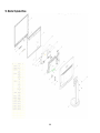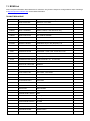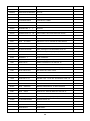
1
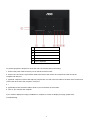
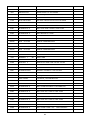
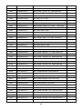
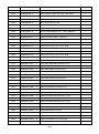
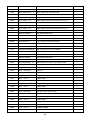
19.5" LCD Monitor
AOC E2060Swda
Service
Service
Service
Horizontal Frequency
30-83 KHz
Table of Contents
Description
Page
Description
Page
Table of Contents.......……..............................……........1
5.2.Power Board……………..……………...….......21
Revision List.…........................................…………........2
6.Schematic……………........................................22
Important Safety Notice.……............................……......3
6.1.Main Board………...........................................22
1.Monitor Specification..............................………..........4
2.LCD Monitor Description……………………………......5
3.Operation Instruction…………...............……..............6
3.1.General Instructions...........................…...................6
3.2.Control Button…………….…..............……...............6
3.3.OSD Setting…........................................................8
4.Input/Output Specification............……………...........16
4.1.Input Signal Connector............………….................16
4.2.Factory Preset Display Modes……........................17
6.2.Power Board...…….........................................27
6.3.Key Board...…….............................................30
7.PCB Layout..………….......................................31
7.1.Main Board………...........................................31
7.2.Power Board…...............................................34
7.3.Key Board……………....................................36
8.Maintainability………........................................37
8.1.Equipments and Tools Requirement...............37
8.2.Trouble Shooting…………..............................38
9.White-Balance, Luminance Adjustment.............42
4.3.Panel Specification.....………...…………...............18
10.Monitor Exploded View………..…….…............44
5.Block Diagram…….....................………….................20
11.BOM List…………………………………............45
5.1.Main Board…….…………...………………....…......20
SAFETY NOTICE
ANY PERSON ATTEMPTING TO SERVICE THIS CHASSIS MUST FAMILIARIZE HIMSELF WITH THE CHASSIS
AND BE AWARE OF THE NECESSARY SAFETY PRECAUTIONS TO BE USED WHEN SERVICING
ELECTRONIC EQUIPMENT CONTAINING HIGH VOLTAGES.
CAUTION: USE A SEPARATE ISOLATION TRANSFOMER FOR THIS UNIT WHEN SERVICING
R FOR TH
UNIT WHEN S
Revision List
Version
Release Date
Revision History
TPV Model Name
A00
Nov.-30-2012
Initial release
T9CMUF7BBGACDNE
2
Important Safety Notice
Proper service and repair is important to the safe, reliable operation of all AOC Company Equipment. The service
procedures recommended by AOC and described in this service manual are effective methods of performing service
operations. Some of these service operations require the use of tools specially designed for the purpose. The
special tools should be used when and as recommended.
It is important to note that this manual contains various CAUTIONS and NOTICES which should be carefully read in
order to minimize the risk of personal injury to service personnel. The possibility exists that improper service
methods may damage the equipment. It is also important to understand that these CAUTIONS and NOTICES ARE
NOT EXHAUSTIVE. AOC could not possibly know, evaluate and advise the service trade of all conceivable ways in
which service might be done or of the possible hazardous consequences of each way. Consequently, AOC has not
undertaken any such broad evaluation. Accordingly, a servicer who uses a service procedure or tool which is not
recommended by AOC must first satisfy himself thoroughly that neither his safety nor the safe operation of the
equipment will be jeopardized by the service method selected.
Hereafter throughout this manual, AOC Company will be referred to as AOC.
WARNING
Use of substitute replacement parts, which do not have the same, specified safety characteristics may create shock,
fire, or other hazards.
Under no circumstances should the original design be modified or altered without written permission from AOC.
AOC assumes no liability, express or implied, arising out of any unauthorized modification of design.
Servicer assumes all liability.
FOR PRODUCTS CONTAINING LASER:
DANGER-Invisible laser radiation when open AVOID DIRECT EXPOSURE TO BEAM.
CAUTION-Use of controls or adjustments or performance of procedures other than those specified herein may
result in hazardous radiation exposure.
CAUTION -The use of optical instruments with this product will increase eye hazard.
TO ENSURE THE CONTINUED RELIABILITY OF THIS PRODUCT, USE ONLY ORIGINAL MANUFACTURER'S
REPLACEMENT PARTS, WHICH ARE LISTED WITH THEIR PART NUMBERS IN THE PARTS LIST SECTION OF
THIS SERVICE MANUAL.
Take care during handling the LCD module with backlight unit
-Must mount the module using mounting holes arranged in four corners.
-Do not press on the panel, edge of the frame strongly or electric shock as this will result in damage to the screen.
-Do not scratch or press on the panel with any sharp objects, such as pencil or pen as this may result in damage to
the panel.
-Protect the module from the ESD as it may damage the electronic circuit (C-MOS).
-Make certain that treatment person’s body is grounded through wristband.
-Do not leave the module in high temperature and in areas of high humidity for a long time.
-Avoid contact with water as it may a short circuit within the module.
-If the surface of panel becomes dirty, please wipe it off with a soft material. (Cleaning with a dirty or rough cloth may
damage the panel.)
3
1. Monitor Specifications
4
2. LCD Monitor Description
The LCD monitor will contain a main board, a power board, a key board which house the flat panel control logic,
brightness control logic and DDC.
The power part will provide AC to DC Inverter voltage to drive the backlight of panel and the main board chips each
voltage.
Monitor Block Diagram
LED Drive.
Flat Panel and backlight
RS232 Connector
Power Board
For white balance
Main Board
adjustment in factory
mode
Video signal, DDC
Key Board
AC-IN
100V-240V
Host Computer
5
3. Operating Instructions
3.1 General Instructions
This monitor only has one external control function button; press the Power/Auto Configuration button to turn the
monitor on or off.
If you need to adjust other functions, please visit the official AOC website (www.aoc.com)to download and install
AOC’s exclusive i-Menu application software, and then perform related function adjustments to get the screen you
require.
• Connect the power cord properly.
• Connect the signal cable onto the PC’s graphics card.
• Push the button to start the monitor, and the power indicator will light up..
3.2 Control Buttons
E960SRDA/ E960PRDA /E2060SWDA/E2060PWDA / E2260SDA/ E2260PDA:
1
Source/Auto/Exit
2
ECO(DCR)/<
3
Volume / >
4
Menu/Enter
5
Power
Power
Press the Power button to turn on/off the monitor.
Eco (DCR)/ <
Press the Eco key continuously to select the Eco mode of brightness and DCR on when there is no OSD. ( Eco
mode hot key may not be available in all models).
Volume / >
When there is no OSD,Press Volume button to active volume adjustment bar,Press <or + to adjust volume(Only for
the models with speakers)
Auto / Exit
When there is no OSD, press Auto/Source button continuously about 3 second to do auto configure .
Source hot key
When the OSD is closed, press Source button will be Source hot key function. Press Source button continuously to
select the input source showed in the message bar , press Menu/Enter button to change to the source selected
6
1
USB (Optional)
2
Power
3
/
4
DVI (Optional)
5
Analog (DB-15 VGA cable)
6
Line in (Optional)
To protect equipment, always turn off the PC and LCD monitor before connecting.
1. Connect the power cable to the AC port on the back of the monitor.
2. Connect one end of the 15-pin D-Sub cable to the back of the monitor and connect the other end to the
computer's D-Sub port.
3. (Optional –Requires a video card with DVI port)Connect one end of the DVI cable to the back of the monitor and
connect the other end to the computer‟s DVI port.
4. /
5. (Optional)Connect the audio cable to audio in port on the back of the monitor
6. Turn on your monitor and computer.
If your monitor displays an image, installation is complete. If it does not display an image, please refer
Troubleshooting.
7
3.3 OSD Setting
Basic and simple instruction on the control keys.
1) Press the
MENU-button to activate the OSD window.
2) Press < or > to navigate through the functions. Once the desired function is highlighted, press the
MENU-button to activate it . press< or >to navigate through the sub-menu functions. Once the desired
function is highlighted, press
MENU-button to activate it.
3) Press< or >to change the settings of the selected function. Press AUTO to exit. If you want to adjust
any other function, repeat steps 2-3.
4) OSD Lock Function: To lock the OSD, press and hold the
press
MENU button while the monitor is off and then
power button to turn the monitor on. To un-lock the OSD - press and hold the
while the monitor is off and then press
MENU button
power button to turn the monitor on.
Notes:
1) If the product has only one signal input, the item of "Input Select" is disable to adjust.
2) If the product screen size is 4:3 or input signal resolution is wide format, the item of "Image Ratio" is disable to
adjust.
3) One of DCR, Color Boost, and Picture Boost functions is active, the other two function is turned off accordingly.
8
Luminance
1 Press
(Menu) to display menu.
2 Press < or > to select
(Luminance), and press
3 Press < or > to select submenu, and press
to enter.
to enter.
4 Press < or > to adjust.
5 Press
to exit.
9
Image Setup
1 Press
(Menu) to display menu.
2 Press < or > to select
(Image Setup), and press
3 Press < or > to select submenu, and press
to enter.
to enter.
4 Press < or > to adjust.
5 Press
to exit.
10
Color Setup
1 Press
(Menu) to display menu.
2 Press < or > to select
(Color Setup), and press
3 Press < or > to select submenu, and press
to enter.
to enter.
4 Press < or > to adjust.
5 Press
to exit.
11
Picture Boost
1 Press
(Menu) to display menu.
2 Press < or > to select
(Picture Boost), and press
3 Press < or > to select submenu, and press
to enter.
to enter.
4 Press < or > to adjust.
5 Press
to exit.
12
OSD Setup
1 Press
(Menu) to display menu.
2 Press < or > to select
(OSD Setup), and press
3 Press < or > to select submenu, and press
to enter.
to enter.
4 Press < or > to adjust.
5 Press
to exit.
13
Extra
1 Press
(Menu) to display menu.
2 Press < or > to select
(Extra), and press
3 Press < or > to select submenu, and press
to enter.
to enter.
4 Press < or > to adjust.
5 Press
to exit.
14
Exit
1 Press
(Menu) to display menu.
2 Press < or > to select
(Exit), and press
3 Press < or > to select submenu, and press
to enter.
to enter.
4 Press < or > to adjust.
5 Press
to exit.
LED Indicator
Status
LED Color
Full Power Mode
Green or Blue
Active-off Mode
Orange or red
15
4. Input/Output Specification
4.1 Input Signal Connector
Pin Assignments
16
4.2 Factory Preset Display Modes
17
4.3 Panel Specification
4.3.1 General Features
M195FGE-L20 is a 19.5” TFT Liquid Crystal Display module with WLED Backlight unit and 30 pins 2ch-LVDS
interface. This module supports 1600 x 900 HD+ mode and can display up to 16.7M colors. The converter module
for Backlight is not built in.
4.3.2 Display Characteristics
4.3.3 Electrical Characteristics
TFT LCD MODULE
Vcc = 5.0 V, Ta = 25 ± 2 ºC, Fr = 75Hz
18
Back Light Unit
Ta = 25 ± 2.ºC
4.3.4 Optical Characteristics
19
5. Block Diagram
5.1 Main Board
715G5270M01000004I
04.SCALER
02.INPUT
+5V
EDID_WP
+5V
EDID_WP
R0+
R0SOG_DET
G0+
G0B0+
B0AHS0
AVS0
DDCSDA1
DDCSCL1
VGA_CABLE_DET
R0+
R0SOG_DET
G0+
G0-
B0+
B0AHS0
AVS0
DDCSDA1
DDCSCL1
VGA_CABLE_DET
R0+
R0SOG_DET
G0+
G0B0+
B0AHS0
AVS0
VCC3.3
DDCSDA1
DDCSCL1
PA[0..9]
VCC1.2
+5V
VCC1.2
+5V
05.PANEL INTERFACE
PA[0..9]
PA[0..9]
VGA_CABLE_DET
02.D-SUB INPUT
PB[0..9]
EDID_WP
VCC3.3
EDID_WP
PB[0..9]
PB[0..9]
JV_SCL
JV_SCL
JV_SDA
JV_SDA
VLCD
VLCD
05.PANEL INTERFACE
03.DVI INPUT
+5V
EDID_WP
+5V
EDID_WP
RX0+
RX0RX1+
RX1RX2+
RX2RXC+
RXCDDCSCL2
DDCSDA2
DVI_CABLE_DET
DVI_HPD
RX0+
RX0RX1+
RX1RX2+
RX2RXC+
RXCDDCSCL2
DDCSDA2
DVI_CABLE_DET
DVI_HPD
RX0+
RX0RX1+
RX1RX2+
RX2RXC+
RXCDDCSCL2
DDCSDA2
DVI_CABLE_DET
06.POWER
Adj_BACKLIGHT
on_BACKLIGHT
Volume
Mute
PS_EN
DVI_HPD
Panel_ON
03.DVI INPUT
Adj_BACKLIGHT
on_BACKLIGHT
Volume
Mute
PS_EN
Panel_ON
Adj_BACKLIGHT
on_BACKLIGHT
Volume
Mute
PS_EN
Panel_ON
+5V
VCC3.3
VCC1.2
VLCD
04.SCALER
+5V
VCC3.3
VCC1.2
VLCD
06.POWER
OEM MODEL AOC E960SWDA/SDA
Size
絬隔瓜絪腹
G5270-M01-000-0040-7-120710
TPV MODEL
DUAL
Rev
Key Component
T P V ( Top
COVER & REVISE HISTORY
PCB NAME
715G5270M010000040
Date
20
Victory
Electronics
Co . ,
Wednesday , July 11, 2012
Ltd. )
Sheet
2
of
7
称爹
B
1
<称爹>
5.2 Power Board
715G4497P05000001C
AC input
Bridge
Rectifier
and Filter
EMI filter
15V
Rectifier
diodes
Transformer
5V
Start Resistor
(R908,R935)
Feedback
PWM Control
(U901)
Circuit
Power Switch
(Q901)
Photo coupler
Regulator
(U902)
L801
14.5V
(U903)
D801
MOSFET
(Q801)
LED
(CN804)
ON/OFF
PWM Control
PF7024
DIM
(U801)
Audio
Audio Power Amplifier
+5V
APA2603JI
CN601(Phone Jack)
CN602
(U601)
21
6. Schematic
6.1 Main Board
715G5270M01000004I
R151
100R 1/16W 5%
VGA_CABLE_DET
5
16
CN101
R103
0R05 1/10W
C190
GIN0
VGA_5V
4,5,7 +5V
RIN0
R117
EDID_WP
DDCSCL1
DDCSDA1
4,5 EDID_WP
R116
R115
C109
U102
8
7
6
5
VCC E0
WC
E1
SCL E2
SDA VSS
220nF 16V
ZD103
RLZ5.6B
1
2
3
4
RIN0-
HSIN0R123
VSIN0
R121
1
2
3
I/O1 I/O4
GND NC
I/O2 I/O3
6
5
4
AZC398-04S
DDCSCL_A
DET_VGA
C116
0.1UF 16V
1
2
3
I/O1 I/O4
GND NC
I/O2 I/O3
6
5
4
AZC398-04S
GIN0
C117
0.1UF 16V
T P V ( Top
22
G0-
C108
47N 16V
R0+
C111
47N 16V
R0-
Electronics
G0- 5
R0+ 5
100R 1/16W 5%
100R 1/16W 5%
R0- 5
AHS0 5
AVS0 5
Co . ,
C113
C114
C115
NC/22pF 50V
NC/22pF 50V
22P 50V 22P 50V
OEM MODEL AOC E960SWDA/SDA
Size
絬 隔 瓜 絪 腹
G5270-M01-000-0040-7-120710
TPV MODEL
DUAL
Rev
Key Component
D-SUB I/O
PCB NAME
715G5270M010000040
Date
Victory
C107
47N 16V
G0+ 5
R127
C112
RIN0
G0+
R122
47R 1/16W 5%
R124
R125
2K2 1/16W 5%
HSIN0
BIN0
SOG_DET 5
C105 47N 16V
R114
47R 1/16W 5%
0R05 1/10W
ESD_VGA
U101
ESD_VGA
DDCSDA_A
B0- 5
C110
2K2 1/16W 5%
U103
B0-
R120
10R 1/16W 5%
R126
VSIN0
C103 47N 16V
B0+ 5
C106
R118
0R05 1/10W
C192
M24C02-RMN6TP
5PF 50V
R113
75 OHM +-5% 1/16W
1K 1/16W 5%
B0+
C104
1000pF 50V
R112
10R 1/16W 5%
75 OHM +-5% 1/16W
2
1
GIN0R150
3
22K 1/16W 5%
4K7 1/16W 5%
4K7 1/16W 5%
ESD_VGA
D101
BAV70
R108
47R 1/16W 5%
R109
470R 1/16W 5%
R110
0R05 1/10W
C191
C102 47N 16V
C101
5PF 50V
BIN0-
R107
75 OHM +-5% 1/16W
RLZ5.6B
R105
10R 1/16W 5%
5PF 50V
+5V
ZD101
C125
BIN0
17
11
FB101
300OHM
NC/5PF 50V
12
C124
NC/5PF 50V
DDCSDA1 R106
DDCSDA_A
47R 1/16W 5%
BIN0BIN0
GIN0GIN0
RIN0RIN0
NC/5PF 50V
13
VGA_5V
NC/0.1UF 16V
14
HSIN0
5 DDCSDA1
DB15
10
5
9
4
8
3
7
2
6
1
15
NC/0.1UF 16V
DDCSCL1 R102
DDCSCL_A
47R 1/16W 5%
VSIN0
5 DDCSCL1
Wednesday , July 11, 2012
Ltd. )
Sheet
3
of
7
称爹
B
1
<称爹>
+5V
DVI5V
1
2
3
NC/0.1UF 16V
DAT0+
DAT0DAT1+
DAT1DAT2+
DAT2-
1
FB190
U104
I/O1 I/O4
GND NC
I/O2 I/O3
2
1
4K7 1/16W 5%
R133
3
R135
22K 1/16W 85%
7
6
5
2
300OHM
C119
U105
1
2
3
4
VCC E0
WC
E1
SCL E2
SDA VSS
220nF 16V
C120
ZD102
C118
DDC_WP
NC/0.1UF 16V
RLZ5.6B
EDID_WP 3,5
NC/0.1UF 16V
AZC398-04S
R137
R138
R139
R140
R141
R142
10R
10R
10R
10R
10R
10R
1/16W
1/16W
1/16W
1/16W
1/16W
1/16W
5%
5%
5%
5%
5%
5%
RX0+
RX0RX1+
RX1RX2+
RX2-
5
5
5
5
5
5
RLZ5.6B
DDCSCL2 5
DDCSDA2 5
ZD104
FB102
ESD_DVI
1
DCLK+
R143
R144
DCLKU106
1
2
3
I/O1 I/O4
GND NC
I/O2 I/O3
R153
1K 1/16W 5%
M24C02-RMN6TP
6
5
4
6
5
4
C122
AZC398-04S
NC/0.1UF 16V
1
2
3
I/O1 I/O4
GND NC
I/O2 I/O3
2
R131
RXC+ 5
RXC- 5
NC/300OHM
1K 1/16W 5%
ESD_DVI
U107
ESD_DVI
10R 1/16W 5%
10R 1/16W 5%
6
5
4
AZC398-04S
C123
NC/0.1UF 16V
+5V
Q101
NC/AO3401A
1
18
17
10
9
2
1
13
12
5
4
21
20
23
24
DVI_CABLE_DET 5
DVI5V
C126
11
3
19
22
47R 1/16W 5%
47R 1/16W 5%
2
26
25
GND
GND
DAT0+
DAT0DAT1+
DAT1DAT2+
DAT2DAT3+
DAT3DAT4+
DAT4DAT5+
DAT5clk+
clk-
DET_DVI
SCL_DVI
SDA_DVI
+5V_DVI
HPD
R129
R130
NC/10K 1/16W 5%
R136
D104
NC/BAV70
Q102 NC/22K 1/16W 5%
R154
3
1/3shield
2/4shield
0/5shield
clk shield
8
15
6
7
14
16
100R 1/16W 5%
0R05 1/10W
R132
VSY NC
SY NC GND
DDC SCL
DDC SDA
+5V
HPD
R152
D103
BAV70
R134
CN102
JACK
4K7 1/16W 5%
3,5,7 +5V
DVI_HPD 5
NC/LMBT3904LT1G
OEM MODEL AOC E960SWDA/SDA
Size
絬隔瓜絪腹
T P V ( Top
G5270-M01-000-0040-7-120710
TPV MODEL
DUAL
Rev
Key Component
DVI
PCB NAME
715G5270M010000040
Date
23
Victory
Electronics
Co . ,
Wednesday , July 11, 2012
Ltd. )
Sheet
4
of
7
称爹
B
1
<称爹>
ADC33
VDDP
VDDC
VCC3.3
VDDP
FB401
3
4
5
6
7
8
10
11
1
2
39
61
VDDP
VDDP
41
63
VDDC
VDDC
VCTRL
LVA3P
LVA3M
LVA2P
LVA2M
LVA1P
LVA1M
LVA0P
LVA0M
RX2P
RX2N
RX1P
RX1N
RX0P
RX0N
RXCKP
RXCKN
DDCD_DA/RS232_TX1
DDCD_CK/RS232_RX1
R416
0R 1/16W 5%
R401
65
U402
1
2
3
4
C410
WP
10K 1/16W 5%
0.22UF 16V
8
7
6
5
S
Vcc
DO HOLD
W
C
Vss
DIO
R403
R404
R405
R406
WP
22R 1/16W
22R 1/16W
22R 1/10W
22R 1/16W
26
27
5%28
5%29
5%30
5%31
LVB3P
LVB3M
LVBCKP
LVBCKM
LVB2P
LVB2M
LVB1P
LVB1M
LVB0P
LVB0M
PMGPIO16
78
C412 56P 50V
R407
77
2
PWM3/GPIO20
PWM1/GPIO22
SAR0/GPIO_SAR0
SAR1/GPIO_SAR1
SAR2/GPIO_SAR2
SAR3/GPIO_SAR3
PWM4/PMGPIO00
PWM5/PMGPIO01
PWM0/PMGPIO02
PWM6/PMGPIO03
PWM0/PMGPIO04
PMGPIO11
XIN
0R05 1/16W
R408
XOUT
X401
NC/1MOHM 1/16W +/-5%
1
14.31818MHZ/32PF
R409
0R05 1/16W
C413 56P 50V
42
C404
45
46
47
48
49
50
PA0
PA1
PA2
PA3
PA4
PA5
PA6
PA7
PA8
PA9
51
52
53
54
55
56
57
58
59
60
PB0
PB1
PB2
PB3
PB4
PB5
PB6
PB7
PB8
PB9
43
44
PB2
PB3
C402
0.1UF 16V
C403
0.1UF 16V
VCC1.2
10uF 10V
PA[0..9]
VCC1.2
NC/120 OHM
C406
5
PB[0..9]
PB[0..9]
C407
C408
0.1UF 16V
0.1UF 16V
5
VCC3.3
20
R410
100R 1/16W 5%
EDID_WP
3
R418
R419
R420
NC/100R 1/16W 5%
NC/100R 1/16W 5%
JV_SCL
JV_SDA
3
3
KEY 1
KEY 2
CABLE_DET
R412
R413
LED_2
10K 1/16W 5%
LED_1
10K 1/16W 5%
INTB
R411
+5V
BUZZER
NC/100R 1/16W 5%
Volume
DVI_HPD
POWER
3
3
+5V
GND
32
33
34
35
36
37
38
EE_WP
MSDA
MSCL
R414
Mute
NC/100R 1/16W 5%
3
PS_EN
3
on_BACKLIGHT 2
adj_BACKLIGHT 2
Panel_ON 2
2,3,4,6,8
9
23
40
64
79
GND
GND
GND
GND
GND
GPIO01
IIC_SDA/GPIO02
IIC_SCL/GPIO03
GPIO04
GPIO05
PWM2/GPIO11
PWM1/GPIO12
0.1UF 16V
FB403
2
PA[0..9]
66
67
68
69
70
71
72
73
74
75
76
80
C405
VDDC
R417
HOLDZ/PMGPIO06
WPZ/PMGPIO07
SDO
CSZ
SCK
SDI
NC/5pf F 16V
10K 1/16W 5%
62
TSUMU59AHN-1
RESET
FLASH MX25L2026DM1I-12G 2Mb
C411
SOP-8
R402
120 OHM
4.7UF 10V
10uF 10V
RESET
ADC33
FB402
NC/4K7 1/16W 5%
VCC3.3
RX2+
RX2RX1+
RX1RX0+
RX0RXC+
RXCDDCSDA2
DDCSCL2
RIN0P
RIN0M
GIN0P
GIN0M
SOGIN0
BIN0P
BIN0M
HSY NC0
VSY NC0
DDCA_DA/RS232_TX0
DDCA_CK/RS232_RX0
VCC3.3
C401
10uF 10V
NC/4K7 1/16W 5%
C409
3
3
3
3
3
3
3
3
5
5
19
18
16
15
17
14
13
21
22
24
25
120 OHM
R447
NC/100K 1/16W 5%
+5V
R0+
R0G0+
G0SOG_DET
B0+
B0AHS0
AVS0
DDCSDA1
DDCSCL1
VCC3.3
NC/200K R448
+5V
3
3
3
3
3
3
3
3
3
5
5
AVDD_33
12
2,5
CN401
R438
330 OHM +-5% 1/10W
VGA_CABLE_DET 3
R444
470OHM 1/10W
DVI_CABLE_DET 4
CN408
R476
7
6
5
4
3
2
1
LED_G
NC
1
2
3
4
5
6
7
VCC3.3
TOUCH_POWER
1
NC/10K 1/16W 5%
NC/1UF 10V
R490
INTB NC/4K7 1/16W 5%
EE_WP
NC/100R 1/16W 5%
R471
C415
NC/CONN
BUZZER
+5V 3,4,7
CN409
+5V
MSCL
MSDA
1
2
3
4
5
6
2
NC/120OHM
R429
3K9 +/-5% 1/16W
Tack sw
1K ohm
LED_A
Touch Key
C429
NC/0.1uF 50V
3
2
1
R484
D404
NC/RLZ5.6B
+5V
CN406
NC/7PIN
KEY 1
ADC5
KEY 2
ADC6
POWER PA3
LED_G
LED_A
R410, R411, R420
FB404
NC/120 OHM
FB405
VCC3.3
NC/CONN
1K 1/16W 5%
1K 1/16W 5%
1K 1/16W 5%
2
NC/0R05 1/16W
Q403
LMBT3906LT1G
1
R492
220K 1/16W 5%
LED_1
C427
MLVS0402M04
R443
R491
100K 1/16W 5%
CABLE_DET
R421
R422
R423
D403
NC/RLZ5.6B
CN407
R439
390K
C426
MLVS0402M04
NC/6PIN
D402
NC/RLZ5.6B
CONN
VCC3.3
C425
MLVS0402M04
+5V
0R05 1/16W
D401
NC/RLZ5.6B
R441
R442
2K2 1/16W 5%
C424
MLVS0402M04
VCC3.3
1
2
3
4
5
6
2
NC
C423
MLVS0402M04
6
5
4
3
2
1
LED_A
R475
NC/M24C16
CN405
1
CN404
R428
3K9 +/-5% 1/16W
Q401
LMBT3906LT1G
2
LED_2
1
NC/0R05 1/16W
NC/0R05 1/16W
R427
3K9 +/-5% 1/16W
R430
R431
NC/220N16V
1
2
3
4
2
VCC NC
WC NC
SCL NC
SDA VSS
2
8
7
6
5
NC/0R05 1/16W
NC/8PIN
U403
EE_WP
VCC3.3
R434
VCC3.3
2
NC/10K 1/16W 5%
C414
NC/2K2 1/16W 5%
NC/2K2 1/16W 5%
1
R437
R433
2K2 1/16W 5%
R473
R472
1
R436
NC/10K 1/16W 5%
MSCL
MSDA
R435
NC/10K 1/16W 5%
VCC3.3
1
2
3
4
5
6
7
8
+5V
1
R432
0R05 1/16W
100 ohm
C425, C426,C427
Tack sw
0.1uF/16V
Touch Key
NC
NC/CONN
OEM MODEL AOC E960SWDA/SDA
Size
絬隔瓜絪腹
G5270-M01-000-0040-7-120710
TPV MODEL
Rev
Key Component
T P V ( Top
5.0.SCALER
PCB NAME
Date
24
Victory
Electronics
Tuesday , August 28, 2012
Co . ,
Ltd. )
Sheet
DUAL
715G5270M010000040
5
of
7
称爹
C
1
<称爹>
PA[0..9]
PB[0..9]
5 PB[0..9]
PA0
PA1
PA2
PA3
PA4
PA5
PA6
PA7
PA8
PA9
PB0
PB1
PB2
PB3
PB4
PB5
PB6
PB7
PB8
PB9
LVA3P
LVA3M
LVACKP
LVACKM
LVA2P
LVA2M
LVA1P
LVA1M
LVA0P
LVA0M
VLCD 7
RXO0+
RXO1+
RXO2+
RXOC+
RXO3+
RXE0+
RXE1+
RXE2+
RXEC+
RXE3+
2
FB406
120 OHM
RXOCRXOC+
RXO3RXO3+
RXE0RXE0+
LVA1M
LVA1P
RXE1RXE1+
LVA2M
LVA2P
LVACKM
LVACKP
LVA3M
LVA3P
RXE2RXE2+
RXECRXEC+
RXE3RXE3+
30
29
28
27
26
25
24
23
22
21
20
19
18
17
16
15
14
13
12
11
10
9
8
7
6
5
4
3
2
1
NC/300 OHM 1/4W
NC/CONN
RXOC-
R446
JV_SCL
+
RXEC+
LVBCKM
LVBCKP
LVB3M
LVB3P
LVA0M
LVA0P
JV_SCL
JV_SDA
5 JV_SCL
5 JV_SDA
C430
100uF16V
C432
NC
RXO0RXO0+
RXO1RXO1+
RXO2RXO2+
C431
0.1UF 16V
300 OHM 1/4W
1
3
5
7
9
11
13
15
17
19
21
23
25
27
29
LVB0M
LVB0P
LVB1M
LVB1P
LVB2M
LVB2P
1
2
4
6
8
10
12
14
16
18
20
22
24
26
28
30
RXEC-
CN410
CONN
VLCD
CN411
RXO0RXO1RXO2RXOCRXO3RXE0RXE1RXE2RXECRXE3JV_SDA
LVB3P
LVB3M
LVBCKP
LVBCKM
LVB2P
LVB2M
LVB1P
LVB1M
LVB0P
LVB0M
R445
5 PA[0..9]
C433
NC
RXOC+
T P V ( Top
Victory
Electronics
Co . ,
Ltd. )
OEM MODEL AOC E960SWDA/SDA
Size
Rev
絬隔瓜絪腹
G5270-M01-000-0040-7-120710
TPV MODEL
DUAL
Key Component
LVDS PANEL I/O
PCB NAME
715G5270M010000040
Date
Wednesday , July 11, 2012
Sheet
25
6
of
7
称爹
A
1
<称爹>
+5V
VCC3.3
U701
+5V
VCC3.3 5
4
+
1
R701
4K7 1/16W 5%
ADJ(GND)
VIN
C702
100uF16V
4
3
3,4,5 +5V
VCC3.3
LSP1117E33AG
2
VOUT
C704
0.1UF 16V
+5V 3,4,5
CN701
R702
9
8
7
6
5
4
3
2
1
100R 1/16W 5%
Adj_BACKLIGHT 5
+
C706
VCC3.3
C705
100uF16V
3
VIN
ADJ(GND)
0.1UF 16V
DIM
ON/OFF
U702
R703
R704
10K 1/16W 5%
1
10K 1/16W 5%
2
VOUT
CONN
Q701
C707
LMBT3904LT1G
TO-252
R705
22K 1/16W 5%
on_BACKLIGHT 5
NC/0.1UF 16V
R708
NC/5.6 OHM +-5% 2WS
U703
100OHM
Volume
3
5
VI
GND
R713
+ C711
470OHM1/16W
Mute
C713
NC/0.1UF 16V
NC/100uF16V
5
2
4
VCC1.2 5
+
C710
NC/100uF16V
1
+5V
C712
NC/0.1UF 16V
U704
TO252
1
3
R718
NC
ADJ/GND
2
INPUT OUTPUT
NC/AZ1117D-1.2TRE1
VLCD
PS_EN 5
+5V
VLCD 6
5
6
7
8
C717
NC
D
D
D
D
R716
10K 1/16W 5%
Q704
AO4411
Q705
NC/AO3401A
G
S
S
S
R722
NC
R717
4
3
2
1
R714
VCC1.2
VO
4
R721 22K 1/16W 5%
100K 1/16W 5%
+5V
Q706
5 Panel_ON
R723
4K7 1/16W 5%
C715
220nF 16V
R720
NC
LMBT3904LT1G
C718
0.1UF 16V
C720
0.1UF 16V
C721
0.1UF 16V
<Variant Name>
OEM MODEL AOC E960SWDA/SDA
Size
絬隔瓜絪腹
T P V ( Top
G5270-M01-000-0040-7-120710
TPV MODEL
DUAL
Rev
Key Component
POWER
PCB NAME
715G5270M010000040
Date
26
Victory
Electronics
Co . ,
Wednesday , July 11, 2012
Ltd. )
Sheet
7
of
7
称爹
B
1
<称爹>
6.2 Power Board
715G4497P05000001C
!
1
R929 100 OHM 1/4W
BD901
FB803
2
3
R903 100 OHM 1/4W
C928
-
R904
250OHM2W
C937
NC
R932
NC
+
R906
100K
!
!
R931
NC
!
C907
82UF 450V
C911
1500PF2KV
R933
NC
D908
NC/IN4148
47N 50V
!
6
5
1
R914
NC
R926
10K OHM +-5% 1/8W
C914
1nF 50V
C930
NC
U902
PC123X2Y FZOF
FB901
BEAD
C906
R923
1NF 50V 220 OHM 1/4W
2
!
D906
MBRF1560CT
3
R919
150 OHM 1/8W
R918
NC
R920
4.7K 1/8W
1
NR901
NTCR
C922
470UF M 16V
P0765ATF
R915
22 OHM 1/4W +-5%
C912
100N 50V
t
+
2
C908
0.47UF
1
!Q901
R917
10 OHM 1/4W
1
R934
NC
2
8
LD7576AGR
C920
680uF/10V
D905 NC/31DQ06FC3
D907
1N4148
1
R902
620K 1/4W
C902
1000PF/250VAC
+
POWER X'FMR
2
R921
NC/100K 1/10WU901
1%
1
HV
2 CT
3 COMP
CS
VCC
C927
4
GND OUT
+
NC
C925
D909 NC/31DQ06FC3
4
30mH
F902
T4AL 250V
+5V
R912 100 OHM 1/4W
R913
1 OHM 1/4W
R907
1K OHM +-5% 1/8W
L906
9
10
C913
47uF/50V
R908
10K 1/4W
C923
1nF 50V
C929 2.2N 630V
C917 2.2N 630V
R910 100 OHM 1/4W
1
+
R905
470OHM +-5% 1/8W
Q904
2SD1207T
R909 100 OHM 1/4W
7
8
4
2
!
R900
11
12
D904
FR107
1
620K 1/4W
5
D903
FR107
R911
10K 1/4W
!
3 L901 4
!
JUMP
ZD901
MTZJ T-72 22B
C918
330UF/25V
SR515
3
4
!
R901
620K 1/4W
+
D902
!
6 T901
F801
0R05 1/4W
2
2.2N 630V
D901
NC/SR5150
1
2
2KBP08M-70
2
1
2
+
C916 2.2N 630V
R930 100 OHM 1/4W
C924
0.1uF 50V
C903
1000PF/250VAC
R924
0.47OHM2W
R916
20K 1/8W +/-1%
R928
1K 1/8W
C900
3300pF 250V
C915
U903
KIA431A-AT/P
F901
R925
9.31KOHM +-1% 1/8W
T4AL 250V
!
FB902
!
1
C938
NC
R935
20K 1/8W +/-1%
2
BEAD
2
3
TH2
TH1
CN901
SOCKET
L907
MUTE
VOL
N
L
E
1
CN902
Wire Harness
HS1
HEAT SINK(Q901)
7
6
1
2
HS2
NC/HEAT SINK(D906_5V/4A)
+5V
1
2
ON/OFF
C926
100N 50V
HS3
HEAT SINK(D906_5V/2.5A)
1
2
DIM
9
8
7
6
5
4
3
2
1
F903
FUSE
+5V1
+
+ C931
NC/470uF/16V
C921
NC/1000uF25V
GND1
GND
1
2
T P V ( Top
絬隔瓜絪腹
Key Component
Date
27
Victory
Electronics
Co . ,
G4497-P03-000-0010-15-120409
01.POWER
Tuesday , May 29, 2012
Ltd. )
OEM MODEL
226V4LAB
TPV MODEL
PLPCCB341MHC2
PCB NAME
Sheet
Size
Rev
Custom
1
715G4497-P03-000-0010
1
of
3
称爹
ODM MODEL
+14.5V
D801A
1
2
SR3100-MK18
D801
FB802
L801
NC
1
2
1
2
CN803
+14.5V
10 OHM 1/8W
47UH
BEAD
8
7
6
5
R804
C801
330uF 25V
Q801
C814
100N 50V
NC
C810
0.47UF 50V
S1
G1
S2
G2
APM8005KCTRG
1
2
3
4
R801
ON/OFF
2
R805
10N 50V
R802
300K 1/8W
R807
FB801
BEAD
1
DIM
R806
C806
C803
1N 50V
9
10
11
12
13
14
15
16
VIN
VREF
STATUS
LDR
SSTCMP
ISW
PWM
ENA
ISEN1
RT
ISEN2
OVP
GND
ISET
ISEN3
ISEN4
C809
160K 1/8W
4.7uF100V
C811
0.47UF 50V
R819
NC
R820
R822
NC
NC
R821
C808
NC
8
7
6
5
4
3
2
1
R808
CN804
CONN
6
5
4
3
2
1
10R 1/8W 5%
C812
100PF 50V
R816
7.5KOHM +-1%
C816
1/8W
1000PF500V
R817
680 OHM 1/4W
C813
100P 50V
100 OHM +-1% 1/8W
220N/50V
NC
R815
10R 1/8W 5%
U801
100K 1/8W
R818 10K 1/8W
R803
300K 1/8W
+
R814
NC
10K 1/8W
C802
1
2
D1
D1
D2
D2
+
R813
R812
0.3R 5%
0.3R 5%
OZ9998BGN
C804
0.47UF
CN801
C815
1N 50V
5
4
3
2
1
R809
C805
2.2UF
R810
11K 1/8W 1%
330K 1% 1/8W
C807
470NF 50V
R811
7.5KOHM +-1% 1/8W
NC
R827
R824
CN802
1R 1%
1
2
1R 1%
R825
R826
NC/CONN
1R 1%
1R 1%
T P V ( Top
Electronics
Co . ,
Ltd. )
OEM MODEL
G4497-P03-000-0010-15-120409
TPV MODEL
Key Component
02.CONVERTER
PCB NAME
Date
28
Victory
絬 隔 瓜 絪 腹
Tuesday , May 29, 2012
Sheet
226V4LAB
PLPCCB341MHC2
715G4497-P03-000-0010
2
of
3
Custom
Size
Rev
称爹
1
ODM MODEL
+5V1
+
C604
470UF M 16V
VOL
R603
10K 1/10W 5%
C609
1U 25V
0.47uF 16V
0.47uF 16V
R602
10K 1/10W 5%
C603
C602
+5V1
FB602
1
2
120 OHM
10K 1/10W 5%
U601
R609
8
7
6
5
4
3
2
1
CN601
4
5
3
2
1
Lin
R604
10K 1/10W 5%
C601 0.47uF 16V
Rin
C606 0.47uF 16V
R605
10K 1/10W 5%
PHONEJACK
SE/BTL
LOUTP
VOLUME
VDD
LINN
LOUTN
GND
GND
GND
GND
RINN
ROUTN
BY PASS
VDD
SHUTDOWN ROUTP
C618
470pF 50V
FB601
9
10
11
12
13
14
15
16
1
120 OHM
2
CN602
C617
470pF 50V 4
3
2
1
FB603
1
2
120 OHM
C619
CONN
RJ604 470pF 50V
0 OHM1/4W
FB604
C611100P 50V
R608
0R05OHM1/8W
C610100P 50V
APA2603JI-TUG 3W
C612
100N 50V
R606
R607
5.6K 1/10W 5% 5.6K 1/10W 5%
+5V1
C608
1U 25V
1
2
120 OHM
R601
C620
470pF 50V
NC
R612
10K 1/10W
CN603
HS5
NC
R610
0R05 1/10W
RJ602
RJ603
0 OHM1/4W
0 OHM1/4W
C613
100N 50V
1
2
3
4
1
2
+5V1
NC/CONN
Q608
NC
MUTE
T P V ( Top
Victory
Electronics
Co . ,
Ltd. )
絬隔瓜絪腹
G4497-P03-000-0010-15-120409
TPV MODEL
Key Component
03.AUDIO
PCB NAME
Date
Monday , April 09, 2012
Sheet
29
226V4LAB
OEM MODEL
PLPCCB341MHC2
715G4497-P03-000-0010
2
of
3
A
Size
Rev
称爹
1
ODM MODEL
6.3 Key Board
SGND
1
2
3
4
5
6
LBADC1
LBADC2
DC_POWERON
LED_1#
LED_2#
2ZD007
SUB
NC/MLVS0603M04 1
NC/MLVS0603M04 1
CN001
269-3UYSUBC/S530-A3-X6/T3
2
UY
BLUE
1
3
2ZD006
LED001
715G5357K03000001M
SGND
R005
2KOHM 1/10W
R003
100R 1/10W 5%
R001
100R 1/10W 5%
R002
1K 1/10W 5%
R004
2KOHM 1/10W
POWER
0.083V
AUTO
DOWN
UP
MENU
SW005
2ZD005
0.673V
POWER( 100 ohm )
SW
NC/MLVS0603M04 1
MENU(1K)
SW004
2ZD004
1.118V
SW
NC/MLVS0603M04 1
0.083V
DOWN(2K)
SW003
2ZD003
UP( 100 ohm )
SW
NC/MLVS0603M04 1
1.118V
SW002
2ZD002
LBADC2
AUTO(2.0K)
SW
NC/MLVS0603M04 1
LBADC1
SW001
2ZD001
SGND
SW
NC/MLVS0603M04 1
POWER
CONN
SGND
LED
(Power)
(MENU)
(UP+)
(DOWN-)
(AUTO)
CONNECTOR
OEM MODEL AOC
Size
絬隔瓜絪腹
T P V ( Top
G5357-K0D-000-0010
TPV MODEL
e2460Swg
Rev
Key Component
2.0.key
PCB NAME
715G5357-K0D-000-0010
Date
30
Victory
Electronics
Co . ,
Tuesday , January 17, 2012
Ltd. )
Sheet
1
of
2
称爹
B
D
<称爹>
7. PCB Layout
7.1 Main Board
715G5270M01000004I
31
32
33
7.2 Power Board
715G4497P05000001C
34
35
7.3 Key Board
715G5357K03000001M
36
8. Maintainability
8.1 Equipments and Tools Requirement
1.
Voltmeter.
2.
Oscilloscope.
3.
Pattern Generator.
4.
DDC Tool with an IBM Compatible Computer.
5.
Alignment Tool.
6.
LCD Color Analyzer.
7.
Service Manual.
8.
User Manual.
37
8.2 Trouble Shooting
1.
No Power
No power
NG
Check power cable is
tightened?
Re-plug the power cable
OK
NG
Check Power “On/Off”
is “On”?
Turn on the Power “On/Off” switch
OK
NG
Check the LED
indicate is OK?
Check the AC power
OK
Replace the converter board
NG
Replace main board and check connections
NG
Replace key board and check connections
38
2. No Video (Power LED Blue)
No Video (Power LED Blue)
NG
Press the power
button is OK?
Replace the main board
OK
OK
Replace the converter
board
The end
NG
OK
Replace the main
board and connection
The end
NG
OK
Check the LVDS/FFC
cable or panel
NG
Replace the key board
39
Replace the LVDS/FFC
cable or panel
3. DIM
DIM (image overlap, focus or flicker)
OK
Reset in factory mode
The end
NG
OK
Set to the optimal
frequency, select the
recommended frequency
The end
NG
OK
Readjust the phase and pixel
clock in the user mode
The end
NG
OK
Pull out signal cable and
check “Self Test Feature
Check” is ok?
Check the signal cable
and the PC
NG
NG
OK
Replace the main board
The end
NG
Replace the panel
OK
40
4. Color is not optimal
Color is not optimal
Color shift
Miss color
Reset the factory mode
Replace the signal cable
NG
OK
In the user mode, set the” color
NG
The end
settings” until customer satisfy
Pull out the signal cable
and check the screen
color display is normal?
NG
OK
NG
Replace the signal cable or PC
Replace the main board
41
9. White- Balance, Luminance Adjustment
Approximately 30 minutes should be allowed for warm up before proceeding white balance adjustment.
How to setting MEM channel you can reference to chroma 7120 user guide or simpl use “SC” key and “NEXT” Key
to modify xyY value and use “ID” key to modify the TEXT description Following is the procedure to do white-balance
adjust .
2. Setting the color temp. you want
A. MEM.CHANNEL 3 Warm (6500K):
Warm color temp. parameter is x = 313 ±20, y = 329 ±20
B. MEM.CHANNEL 4 Normal (7300K):
Normal color temp. parameter is x = 301 ±20, y = 317 ±20
C. MEM.CHANNEL 9 Cool (9300K):
Cool color temp. parameter is x = 283 ±20, y = 297 ±20
D. MEM.CHANNEL 10 (sRGB color):
sRGB color temp. parameter is x = 313 ±20, y = 329 ±20
3. Enter into the factory mode
A. USE the tool
,,double-click the icon
and
choose”Enter Factory” You will enter into the factory mode
B. Press the MENU button,Pull out the power cord, then plug the power cord. Then the factory OSD will be at
the left top of the panel.
4. Gain adjustment:
Move cursor to “-F-” and press MENU key
42
A. Adjust Warm (6500K) color-temperature
1. Switch the chroma-7120 to RGB-Mode (with press “MODE” button)
2. Switch the MEM.channel to Channel 3 (with up or down arrow on chroma 7120)
3. The LCD-indicator on chroma 7120 will show x = 313 ±20, y = 329 ±20
4. Adjust the RED on factory window until chroma 7120 indicator reached the value R=100
5. Adjust the GREEN on factory window until chroma 7120 indicator reachedthe value G=100
6. Adjust the BLUE on factory window until chroma 7120 indicator reached the value B=100
7. Repeat above procedure (item 4, 5, 6) until chroma 7120 RGB value meet the tolerance =100±2
B. Adjust Normal (7300K) color-temperature
1. Switch the chroma-7120 to RGB-Mode (with press “MODE” button)
2. Switch the MEM.channel to Channel 4 (with up or down arrow on chroma 7120)
3. The LCD-indicator on chroma 7120 will show x = 301 ±20, y = 317 ±20
4. Adjust the RED on factory window until chroma 7120 indicator reached the value R=100
5. Adjust the GREEN on factory window until chroma 7120 indicator reachedthe value G=100
6. Adjust the BLUE on factory window until chroma 7120 indicator reached the value B=100
7. Repeat above procedure (item 4, 5, 6) until chroma 7120 RGB value meet the tolerance =100±2
C. Adjust Cool (9300K) color-temperature
1. Switch the Chroma-7120 to RGB-Mode (with press “MODE” button)
2. Switch the MEM. Channel to Channel 9 (with up or down arrow on chroma 7120)
3. The LCD-indicator on chroma 7120 will show x = 283 ±20, y = 297 ±20
4. Adjust the RED on factory window until chroma 7120 indicator reached the value R=100
5. Adjust the GREEN on factory window until chroma 7120 indicator reached the value G=100
6. Adjust the BLUE on factory window until chroma 7120 indicator reached the value B=100
7. Repeat above procedure (item 4, 5, 6) until chroma 7120 RGB value meet the tolerance =100±2
D. Adjust sRGB color-temperature
1. Switch the chroma-7120 to RGB-Mode (with press “MODE” button)
2. Switch the MEM.channel to Channel 10 (with up or down arrow on chroma 7120)
3. The LCD-indicator on chroma 7120 will show x = 313 ±20, y = 329 ±20
4. Adjust the RED on factory window until chroma 7120 indicator reached the value R=100
5. Adjust the GREEN on factory window until chroma 7120 indicator reachedthe value G=100
6. Adjust the BLUE on factory window until chroma 7120 indicator reached the value B=100
7. Repeat above procedure (item 4, 5, 6) until chroma 7120 RGB value meet the tolerance =100±2
E. Turn the Power-button off to quit from factory mode.
43
10. Monitor Exploded View
44
11. BOM List
Note: The parts information listed below are for reference only, and are subject to change without notice. Please go
to http://cs.tpv.com.cn/hello1.asp for the latest information.
T9CMUF7BBGACDNE
Location
HDCP-SMT
Part No.
Description
040G 58162435A
MANUAL P/N LABEL
052G
PAPER TAPE
2191
A
070GHDCP500HDC
HDCP CODE
E08904
089G 17356G580
AUDIO CABLE 1.8M without PE bag
E08902
089G 728HAA DB
D-SUB CABLE 1800mm
E08903
089G1748HAA AC
DVI CABLE 1800MM
ECN403
089G179J30N 22
FFC CABLE 30P 150mm 1.0MM
E08901
089G404A18N HL
AC POWER CORD 1800 for Europe
ECN804
095G8014 6DE45
HARNESS 6P(CI1406)-6P(2008) 140
0D1G1030
6120
screw
0M1G1140
6120
screw
SP01
378G0025518YAB
SPEAKER 4 OHM 2.5W 40X20 50mm NO
ECNSP01
395G801404W633
HARNESS 4P(2008)-2P+2P 60+160
708GA03301SH01
40(1890)-SLIP SHEET
750GBM195FGK13N000
LCD M195FGE-L20
AM1G1740 10125
SCREW
AM1G1740 10225 CR3
SCREW
H15G00746030GH
MAINFRAME
H40G 001624 1A
CARTON LABEL BARCODE 1
H40G 45762413B
P/N LABEL FOR BASE
H40G020N61554A
RATING LABEL E2060SwD EU
H44GA0331010DJ
CUSHION
H44GA0332010DJ
CUSHION
H44GA03361501A00BC
ARTWORK CARTON E2060SW WW
H70G22C161503D
CD MANUAL 60th
KEPCCHA6
KEY BOARD
PLPCC9311MHD1
ADAPTER BOARD
Q33G0519ABJ 1S0130
KEY
Q33G0520
1 1C0100
LENS_POWER
Q34G7495ABJ 4S0130
REAR_COVER
Q34G7498ABJ 2S0100
STAND
Q34G7512ABJ 1S0130
BASE
Q34G7631AEDA1S0101
BEZEL
Q37G02490150ML
HINGE ASS'Y
Q45G8801M08A0100BX
MANUAL PE BAG
E750
45
C1 NH CMI
Remark
Q45G990161940500BX
PROTECT BAG
M05203
Q52G100204500A00HB
AL FOIL
M05202
Q52G100204500A00HB
AL FOIL
M05201
Q52G100204500A00HB
AL FOIL
Q52G1801MNT170AFJY
INSULATING SHEET
H40G000261553A
TCO'05 EPA LABEL
756GHCCB0BV0030001
MAIN BOARD-CBPCCUFA1H1
100GAMMA006W11
MCU ASSY-056G2233501
SMTCC-U402
CN404
033G3802 6B
Y
L
WAFER
CN701
033G3802 9B
Y
L
CONN 2.0 9P
CN410
033G801930F CH
JS
FFC CONN 1.0mm 30P R/A 34mm 6.3mm
CN101
088G 35315F XH
D-SUB 15PIN VERTICAL CONN WITH SCREW
CN102
088G 35424FXNH
DVI CONN WITH SCREW 24P
093G
CRYSTAL S-F-14.31818M-32-3030-2085-30
X401
22 53CEC
R/A
709G52700HM001
COMSUMPTIVE ASSY
H40G 45762429A
LABEL
LED001
381G00122YG0GP
LED yellow/green GP32032M/P310-ZY-30
CN001
395G820H06D539
HARNESS 6P(SANW)-6P(2008) 280mm
709G53570HM001
COMSUMPTIVE ASSY
GND1
009G6005
1
GND TERMINAL
U902
056G 139
9
IC EL817M(X) photocoupler DIP-4
U601
056G 616 85
AUDIO APA2603JI-TUG 3W DIP-16
061G
RST NTCR 8OHM +/20%/NMM01 4A XIANZHENG
NR901
58809MEN
C908
063G107K334 6S
CAP X2 330NF 10% 275V BULK ( B )
C907
067G 40Z10115H
EC 100UF 20% 450V 18*35
L901
073G 174 65 H2
LINE FILTER 30mH MIN
L907
073G 253 91 V1
CHOKE COIL 1.1UH 30% 3LFDR0810-1R0K, HF
L906
073G 253 91 V1
CHOKE COIL 1.1UH 30% 3LFDR0810-1R0K, HF
CN901
087G 501 32 HC
AC SOCKET 3P DB-14-05 R/A
CN601
088G 30214K DC
PHONE JACK 5P GREEN -
BD901
093G
50460519
BRIDGE KBP206G X0 2A 800V KBP 80A
D902
093G
60322
SCHOTTKY SR5150-MK23 5A 150V D0-27
D901
093G
60322
SCHOTTKY SR5150-MK23 5A 150V D0-27
D801A
093G
60924
DIODE SR510-22 DO-201AD
CN902
095G 825 9D549
HARNESS 9P(SCN)-9P(2008) 100MM
CN602
311GW200A04ABX
WAFER 2.0mm 4P
CN804
311GW200A06ABX
WAFER 2.0mm 6P
L801
373G0253214DN2
BOOST CHOKE 47UH 10% 2A --
705GH93043
D906 ASS'Y
705GHC57029
-46
709G4497 HM001
CONSUMPTIVE ASS'Y
H40G 45762429A
LABEL
S80GL22T3V6
X'FMR 490UH 7% 4UH EER28 --
Q55G 100625
TIN STICK_LOW ARGENTUM
C430
067G 3051013PB
EC 105C 100uF M 16V 5*11mm JH CD263
C705
067G 3051013PB
EC 105C 100uF M 16V 5*11mm JH CD263
C702
067G 3051013PB
EC 105C 100uF M 16V 5*11mm JH CD263
R003
061G0603101 JT
RST CHIP 100R 1/10W 5% TZAI YUAN
R001
061G0603101 JT
RST CHIP 100R 1/10W 5% TZAI YUAN
R002
061G0603102 JT
RST CHIP 1K 1/10W 5% TZAI YUAN
R004
061G0603202 JT
RST 0603 2K 5% 1/10W
R005
061G0603202 JT
RST 0603 2K 5% 1/10W
ZD007
093G
64 59 SU
ESD MLVS0603M04 0603
ZD006
093G
64 59 SU
ESD MLVS0603M04 0603
ZD004
093G
64 59 SU
ESD MLVS0603M04 0603
ZD005
093G
64 59 SU
ESD MLVS0603M04 0603
ZD002
093G
64 59 SU
ESD MLVS0603M04 0603
ZD001
093G
64 59 SU
ESD MLVS0603M04 0603
ZD003
093G
64 59 SU
ESD MLVS0603M04 0603
T901
HS3
090G6084
1
0M1G 930
8120
SCREW 3x8
D906
093G1506
2
SCHOTTKY FMW-2156 15A 60V TO-220
HS1
090G6064
1
HEAT SINK
0M1G 930
8120
SCREW 3x8
Q901
GP
HEAT SINK
357G0667941A01
MOSFET P0765GTF 7 650 TO-220F
055G
WELDING FLUX WITHOUT PB
Q51G
23524
6
4509
GLUE_RTV
Q55G 100625
TIN STICK_LOW ARGENTUM
U901
056G 379529
AC/DC CONVERTER IC LD7576AGR SOP-7
Q801
057G 763 92
FET P8008HV 4A/80V SOP-8
R610
061G0603000 JF
RST CHIPR MAX 0R05 1/10W FENGHUA
R612
061G0603103 JF
RST CHIPR 10K OHM +-5% 1/10W FENGHUA
R604
061G0603103 JT
RST CHIP 10K 1/10W 5% TZAI YUAN
R605
061G0603103 JT
RST CHIP 10K 1/10W 5% TZAI YUAN
R609
061G0603103 JT
RST CHIP 10K 1/10W 5% TZAI YUAN
R603
061G0603103 JT
RST CHIP 10K 1/10W 5% TZAI YUAN
R607
061G0603562 JF
RST 0603 5.6K 5% 1/10W
R606
061G0603562 JF
RST 0603 5.6K 5% 1/10W
R828
061G0805000 JF
RST CHIPR 0 OHM +-5%
1/8W FENGHUA
RJ801
061G0805000 JF
RST CHIPR 0 OHM +-5%
1/8W FENGHUA
47
R608
061G0805000 JF
RST CHIPR 0 OHM +-5%
1/8W FENGHUA
R818
061G0805000 JF
RST CHIPR 0 OHM +-5%
1/8W FENGHUA
R804
061G0805100 JF
RST CHIPR 10 OHM +-5% 1/8W FENGHUA
R928
061G08051001FF
RST CHIPR 1KOHM +-1% 1/8W FENGHUA
R827
061G08051008FT
RST 0805 1R 1% 1/8W
R824
061G08051008FT
RST 0805 1R 1% 1/8W
R825
061G08051008FT
RST 0805 1R 1% 1/8W
R826
061G08051008FT
RST 0805 1R 1% 1/8W
R907
061G0805102 JT
RST CHIPR 1K OHM +- 5% 1/8W
R801
061G0805103 JF
RST CHIPR 10K OHM +-5% 1/8W FENGHUA
R926
061G0805103 JT
RST 0805 10K 5% 1/8W
R805
061G0805104 JY
RST CHIPR
R808
061G0805109 JF
RST CHIPR 1 OHM +- 5% 1/8W
FENGHUA
R807
061G0805109 JF
RST CHIPR 1 OHM +- 5% 1/8W
FENGHUA
R810
061G08051202FT
RST CHIP 12K 1/8W 1%
R919
061G08051500FT
RST CHIPR 150OHM +-1% 1/8W
R815
061G0805164 JF
RST 0805 160K 5% 1/8W
R935
061G08052002FT
RST CHIP 20K 1/8W 1%
R916
061G08052002FT
RST CHIP 20K 1/8W 1%
R809
061G08052203FF
RST CHIPR 220KOHM +-1% 1/8W FENGHUA
R802
061G0805304 JF
RST CHIPR 300KOHM +-5% 1/8W FENGHUA
R920
061G08054701FF
RST CHIPR 4.7KOHM +-1% 1/8W FENGHUA
R905
061G0805471 JT
RST CHIPR 470OHM +-5% 1/8W TZAI YUAN
R811
061G08055101FT
RST CHIP 5K1 1/8W 1%
R806
061G0805512 JF
RST CHIPR 5.1KOHM +-5% 1/8W FENGHUA
R816
061G08056801FF
RST CHIPR 6.8KOHM +-1% 1/8W FENGHUA
R925
061G08059311FF
RST CHIPR 9.31KOHM +-1% 1/8W FENGHUA
RJ602
061G1206000 JF
RST CHIPR MAX0R05 1/4W FENGHUA
RJ603
061G1206000 JF
RST CHIPR MAX0R05 1/4W FENGHUA
F801
061G1206000 JT
RST CHIPR MAX0R05 1/4W TZAI YUAN
RJ601
061G1206000 JT
RST CHIPR MAX0R05 1/4W TZAI YUAN
R917
061G1206100 JT
RST CHIPR 10 OHM +-5% 1/4W TZAI YUAN
R817
061G12061001FT
RST CHIP R 1Kohm +-1% 1/4W
R909
061G1206101 JT
RST CHIPR 100 OHM +-5% 1/4W TZAI YUAN
R929
061G1206101 JT
RST CHIPR 100 OHM +-5% 1/4W TZAI YUAN
R910
061G1206101 JT
RST CHIPR 100 OHM +-5% 1/4W TZAI YUAN
R903
061G1206101 JT
RST CHIPR 100 OHM +-5% 1/4W TZAI YUAN
R930
061G1206101 JT
RST CHIPR 100 OHM +-5% 1/4W TZAI YUAN
R912
061G1206101 JT
RST CHIPR 100 OHM +-5% 1/4W TZAI YUAN
R911
061G1206103 JF
RST CHIPR 10KOHM +-5% 1/4W FENGHUA
48
TZAI YUAN
100KOHM 1/8W YAGEO
TZAIYUAN
R908
061G1206103 JT
RST CHIPR 10KOHM +-5% 1/4W TZAI YUAN
R602
061G1206103 JT
RST CHIPR 10KOHM +-5% 1/4W TZAI YUAN
R913
061G1206109 JT
RST CHIPR 1 OHM +-5% 1/4W TZAI YUAN
R923
061G1206221 JT
RST CHIPR 220 OHM +-5% 1/4W TZAI YUAN
R812
061G1206308 JT
RST 1206 0.3R 5% 1/4W
R813
061G1206308 JT
RST 1206 0.3R 5% 1/4W
R900
061G1206624 JF
RST CHIPR 620KOHM +-5% 1/4W FENGHUA
R901
061G1206624 JF
RST CHIPR 620KOHM +-5% 1/4W FENGHUA
R902
061G1206624 JF
RST CHIPR 620KOHM +-5% 1/4W FENGHUA
C619
065G060322131J
F
CAP CHIP 0603 220PF J 50V NPO
C617
065G060322131J
F
CAP CHIP 0603 220PF J 50V NPO
C620
065G060322131J
F
CAP CHIP 0603 220PF J 50V NPO
C618
065G060322131J
F
CAP CHIP 0603 220PF J 50V NPO
C606
065G060347412K
Y
CAP CHIP 0.47uF 16V +/-10%
X7R
C603
065G060347412K
Y
CAP CHIP 0.47uF 16V +/-10%
X7R
C601
065G060347412K
Y
CAP CHIP 0.47uF 16V +/-10%
X7R
C602
065G060347412K
Y
CAP CHIP 0.47uF 16V +/-10%
X7R
C813
065G080510131J
Y
CAP CHIP 0805 100P 50V NP0 +/-5%
C610
065G080510131J
Y
CAP CHIP 0805 100P 50V NP0 +/-5%
C611
065G080510131J
Y
CAP CHIP 0805 100P 50V NP0 +/-5%
C812
065G080510131J
Y
CAP CHIP 0805 100P 50V NP0 +/-5%
C923
065G080510232K
F
CAP 0805 1000PF 10% 50V X7R
C906
065G080510232K
F
CAP 0805 1000PF 10% 50V X7R
C815
065G080510232K
F
CAP 0805 1000PF 10% 50V X7R
C914
065G080510232K
F
CAP 0805 1000PF 10% 50V X7R
C802
065G080510332K
F
CAP 0805 10NF K 50V X7R
C915
065G080510332K
F
CAP 0805 10NF K 50V X7R
C814
065G080510432K
A
CAP CHIP 0805 0.1UF K 50V X7R
C926
065G080510432K
Y
CAP CHIP 0805 100N 50V X7R +/-10%
C924
065G080510432K
Y
CAP CHIP 0805 100N 50V X7R +/-10%
C613
065G080510432K
Y
CAP CHIP 0805 100N 50V X7R +/-10%
C612
065G080510432K
Y
CAP CHIP 0805 100N 50V X7R +/-10%
C912
065G080510432K
Y
CAP CHIP 0805 100N 50V X7R +/-10%
C608
065G080510522K
T
CAP 0805 1UF 10% 25V X7R
C609
065G080510522K
T
CAP 0805 1UF 10% 25V X7R
C807
065G080533332K
F
CAP 0805 33NF K 50V X7R
C927
065G080547332K
F
CAP CHIP 0805 47NF K 50V X7R
C811
065G080547432K
A
CAP CHIP 0805 0.47UF K 50V X7R
C810
065G080547432K
A
CAP CHIP 0805 0.47UF K 50V X7R
C805
065G080547432K
F
0805 0.47UF K 50V X7R
49
C804
065G080547432K
T
CAP CHIP 0805 0.47UF K 50V X7R
C917
065G120622272K
A
CAP 1206 2.2NF 10% 500V X7R
C928
065G120622272K
A
CAP 1206 2.2NF 10% 500V X7R
C916
065G120622272K
A
CAP 1206 2.2NF 10% 500V X7R
C929
065G120622272K
A
CAP 1206 2.2NF 10% 500V X7R
FB604
071G 56K121
M
CHIP BEAD 120OHM 6A MGLB2012-120T-LF
FB601
071G 56K121
M
CHIP BEAD 120OHM 6A MGLB2012-120T-LF
FB602
071G 56K121
M
CHIP BEAD 120OHM 6A MGLB2012-120T-LF
FB603
071G 56K121
M
CHIP BEAD 120OHM 6A MGLB2012-120T-LF
U801
356G0700045
LED DRIVER PF7024 S SOP-16
709G4497 HS001
CONSUMPTIVE ASS'Y
SW003
077G603S AI HJ
TACT SWITCH AI 2PIN SEALED
SW004
077G603S AI HJ
TACT SWITCH AI 2PIN SEALED
SW002
077G603S AI HJ
TACT SWITCH AI 2PIN SEALED
SW005
077G603S AI HJ
TACT SWITCH AI 2PIN SEALED
SW001
077G603S AI HJ
TACT SWITCH AI 2PIN SEALED
E715
715G5357K03000001M
KEY PCB FR1 SS 117*10*1.6MM
C900
065G306M33233R
CAP Y1 3.3NF 20% 250V Y5U
FB901
071G
FERRITE BEAD
55 29
709G4497 HA001
CONSUMPTIVE ASS'Y
E715
715G4497P05000001C
PWR PCB FR1 CTI>600 SS 184*122*1.6
R924
061G152M47852T
RST MOFR 0.47 OHM +-5% 2WS FUTABA
J805
095G
90 23
JUMP WIRE - -
J810
095G
90 23
JUMP WIRE - -
D907
093G
6451652T
1N4148
J909
095G
90 23
JUMP WIRE - -
F902
084G
56
J813
095G
90 23
JUMP WIRE - -
J601
095G
90 23
JUMP WIRE - -
J804
095G
90 23
JUMP WIRE - -
J806
095G
90 23
JUMP WIRE - -
C902
065G306M10233R
CAP Y1 1NF 20% 250V Y5U
C809
067G 4153309KT
EC 33UF 20% 100V 8*12 ED
Q904
057G 530503
2SD1207T
C911
065G
2K152 2T6921
CAP CER 1500pF K 2KV Y5P
J605
095G
90 23
JUMP WIRE - -
D904
093G
6026T52T
CTIFIER DIODE FR107
J815
095G
90 23
JUMP WIRE - -
FB802
071G
55 29
FERRITE BEAD
R922
061G152M47152T
4
SY
C
FUSE 4A 250V MST 4A 250V
T
SY
RST MOF 470R 5% 2W FUTABA
50
U903
056G 563355
Shunt Regu TL431G-A-TA TO-92 42V 150mA
J812
095G
JUMP WIRE - -
R904
061G152M47152T
D903
093G
6026T52T
CTIFIER DIODE FR107
FB801
071G
55 29
FERRITE BEAD
J903
095G
90 23
JUMP WIRE - -
J905
095G
90 23
JUMP WIRE - -
CN901
006G
31500
EYELET
J809
095G
90 23
JUMP WIRE - -
J811
095G
90 23
JUMP WIRE - -
FB902
071G
55 29
FERRITE BEAD
J603
095G
90 23
JUMP WIRE - -
C920
067G 2046812KT
CAP CS 680UF 20% 10V 8*11 3900mA GP1A6
J802
095G
90 23
JUMP WIRE - -
FB803
071G
55 29
FERRITE BEAD
C918
367G215X3314AT
EC 330UF 20% 25V 10*12 RF
C903
065G306M10233R
CAP Y1 1NF 20% 250V Y5U
J901
095G
90 23
JUMP WIRE - -
F901
084G
56
J602
095G
90 23
JUMP WIRE - -
ZD901
093G
3960252T
ZENER MTZJ20B 18.63-19.59V 0.5W DO-35
F903
084G
56
FUSE 4A 250V MST 4A 250V
J908
095G
90 23
JUMP WIRE - -
J803
095G
90 23
JUMP WIRE - -
C801
367G215X3314AT
EC 330UF 20% 25V 10*12 RF
J921
095G
90 23
JUMP WIRE - -
J906
095G
90 23
JUMP WIRE - -
R906
061G152M10452T
J910
095G
C913
367G215X4707AT
EC 47uF 20% 50V - 6.3*11mm RG
C816
065G
2K102 2T6921
CAP CER 1000pF 2KV K Y5P
J801
095G
90 23
JUMP WIRE - -
J606
095G
90 23
JUMP WIRE - -
C922
367G415X4713AT
EC 470uf 20% 16V
J904
095G
90 23
JUMP WIRE - -
J907
095G
90 23
JUMP WIRE - -
C604
367G415X4713AT
EC 470uf 20% 16V
J808
095G
90 23
JUMP WIRE - -
J807
095G
90 23
JUMP WIRE - -
R915
061G 17222052T
90 23
4
4
SY
C
RST MOF 470R 5% 2W FUTABA
FUSE 4A 250V MST 4A 250V
C
SY
90 23
RST MOFR 100KOHM +-5% 2WS FUTABA
JUMP WIRE - -
TZ
10X13 RS
10X13 RS
RST CFR 22R 5% 1/4W
51
U701
056G 563527BHF
LDO BL1117-33CX 1A 3.3V SOT-223
U103
056G 662 52
ESD PROTECT AZC398-04S.R7G SOT23-6
U104
056G 662 52
ESD PROTECT AZC398-04S.R7G SOT23-6
U106
056G 662 52
ESD PROTECT AZC398-04S.R7G SOT23-6
U101
056G 662 52
ESD PROTECT AZC398-04S.R7G SOT23-6
U107
056G 662 52
ESD PROTECT AZC398-04S.R7G SOT23-6
U102
056G1133 34
1
EEPROM M24C02-RMN6TP 2Kb SO-8
U105
056G1133 34
1
EEPROM M24C02-RMN6TP 2Kb SO-8
U402
056G2233501
FLASH MX25L2026DM1I-12G 2Mb SOP-8
Q403
057G 417517
Tra LMBT3906LT1G -200mA/-40V SOT-23 LRC
Q401
057G 417517
Tra LMBT3906LT1G -200mA/-40V SOT-23 LRC
Q706
057G 417518
TRA LMBT3904LT1G 200mA/40V SOT-23 LRC
Q701
057G 417518
TRA LMBT3904LT1G 200mA/40V SOT-23 LRC
Q704
057G 763
AO4411 SO-8 BY AOS
R432
061G0402000 JY
RST CHIPR MAX 0R05 OHM 1/16W YAGEO
R409
061G0402000 JY
RST CHIPR MAX 0R05 OHM 1/16W YAGEO
R416
061G0402000 JY
RST CHIPR MAX 0R05 OHM 1/16W YAGEO
R441
061G0402000 JY
RST CHIPR MAX 0R05 OHM 1/16W YAGEO
R407
061G0402000 JY
RST CHIPR MAX 0R05 OHM 1/16W YAGEO
R105
061G0402100 JF
RST CHIPR 10 OHM +-5% 1/16W FENGHUA
R120
061G0402100 JF
RST CHIPR 10 OHM +-5% 1/16W FENGHUA
R138
061G0402100 JF
RST CHIPR 10 OHM +-5% 1/16W FENGHUA
R143
061G0402100 JF
RST CHIPR 10 OHM +-5% 1/16W FENGHUA
R140
061G0402100 JF
RST CHIPR 10 OHM +-5% 1/16W FENGHUA
R144
061G0402100 JF
RST CHIPR 10 OHM +-5% 1/16W FENGHUA
R139
061G0402100 JF
RST CHIPR 10 OHM +-5% 1/16W FENGHUA
R142
061G0402100 JF
RST CHIPR 10 OHM +-5% 1/16W FENGHUA
R141
061G0402100 JF
RST CHIPR 10 OHM +-5% 1/16W FENGHUA
R137
061G0402100 JF
RST CHIPR 10 OHM +-5% 1/16W FENGHUA
R112
061G0402100 JF
RST CHIPR 10 OHM +-5% 1/16W FENGHUA
R124
061G0402101 JY
RST CHIPR 100 OHM +-5% 1/16W YAGEO
R125
061G0402101 JY
RST CHIPR 100 OHM +-5% 1/16W YAGEO
R702
061G0402101 JY
RST CHIPR 100 OHM +-5% 1/16W YAGEO
R152
061G0402101 JY
RST CHIPR 100 OHM +-5% 1/16W YAGEO
R410
061G0402101 JY
RST CHIPR 100 OHM +-5% 1/16W YAGEO
R151
061G0402101 JY
RST CHIPR 100 OHM +-5% 1/16W YAGEO
R713
061G0402101 JY
RST CHIPR 100 OHM +-5% 1/16W YAGEO
R150
061G0402102 JY
RST CHIPR 1KOHM +-5% 1/16W YAGEO
R153
061G0402102 JY
RST CHIPR 1KOHM +-5% 1/16W YAGEO
R422
061G0402102 JY
RST CHIPR 1KOHM +-5% 1/16W YAGEO
3
52
R423
061G0402102 JY
RST CHIPR 1KOHM +-5% 1/16W YAGEO
R421
061G0402102 JY
RST CHIPR 1KOHM +-5% 1/16W YAGEO
R131
061G0402102 JY
RST CHIPR 1KOHM +-5% 1/16W YAGEO
R716
061G0402103 JF
RST CHIPR 10KOHM +-5% 1/16W FENGHUA
R703
061G0402103 JF
RST CHIPR 10KOHM +-5% 1/16W FENGHUA
R401
061G0402103 JF
RST CHIPR 10KOHM +-5% 1/16W FENGHUA
R412
061G0402103 JF
RST CHIPR 10KOHM +-5% 1/16W FENGHUA
R413
061G0402103 JF
RST CHIPR 10KOHM +-5% 1/16W FENGHUA
R704
061G0402103 JF
RST CHIPR 10KOHM +-5% 1/16W FENGHUA
R402
061G0402103 JF
RST CHIPR 10KOHM +-5% 1/16W FENGHUA
R491
061G0402104 JY
RST CHIPR 100KOHM +-5% 1/16W YAGEO
R717
061G0402104 JY
RST CHIPR 100KOHM +-5% 1/16W YAGEO
R403
061G0402220 JY
RST CHIPR
22 OHM +-5% 1/16W YAGEO
R406
061G0402220 JY
RST CHIPR
22 OHM +-5% 1/16W YAGEO
R404
061G0402220 JY
RST CHIPR
22 OHM +-5% 1/16W YAGEO
R126
061G0402222 JY
RST CHIPR 2.2KOHM +-5% 1/16W YAGEO
R442
061G0402222 JY
RST CHIPR 2.2KOHM +-5% 1/16W YAGEO
R127
061G0402222 JY
RST CHIPR 2.2KOHM +-5% 1/16W YAGEO
R433
061G0402222 JY
RST CHIPR 2.2KOHM +-5% 1/16W YAGEO
R135
061G0402223 JY
RST CHIPR 22KOHM +-5% 1/16W YAGEO
R705
061G0402223 JY
RST CHIPR 22KOHM +-5% 1/16W YAGEO
R721
061G0402223 JY
RST CHIPR 22KOHM +-5% 1/16W YAGEO
R117
061G0402223 JY
RST CHIPR 22KOHM +-5% 1/16W YAGEO
R492
061G0402224 JY
RST CHIPR 220KOHM +-5% 1/16W YAGEO
R429
061G0402392 JY
RST CHIPR 3.9KOHM 5% 1/16W YAGEO
R428
061G0402392 JY
RST CHIPR 3.9KOHM 5% 1/16W YAGEO
R427
061G0402392 JY
RST CHIPR 3.9KOHM 5% 1/16W YAGEO
R439
061G0402394 JY
RST CHIP R 390K +/-5% 1/16W YAGEO
R114
061G0402470 JY
RST CHIPR 47 OHM 5% 1/16W YAGEO
R108
061G0402470 JY
RST CHIPR 47 OHM 5% 1/16W YAGEO
R122
061G0402470 JY
RST CHIPR 47 OHM 5% 1/16W YAGEO
R106
061G0402470 JY
RST CHIPR 47 OHM 5% 1/16W YAGEO
R130
061G0402470 JY
RST CHIPR 47 OHM 5% 1/16W YAGEO
R129
061G0402470 JY
RST CHIPR 47 OHM 5% 1/16W YAGEO
R102
061G0402470 JY
RST CHIPR 47 OHM 5% 1/16W YAGEO
R109
061G0402471 JY
RST CHIPR 470OHM +-5% 1/16W YAGEO
R714
061G0402471 JY
RST CHIPR 470OHM +-5% 1/16W YAGEO
R116
061G0402472 JY
RST CHIPR 4.7KOHM +-5% 1/16W YAGEO
R115
061G0402472 JY
RST CHIPR 4.7KOHM +-5% 1/16W YAGEO
R134
061G0402472 JY
RST CHIPR 4.7KOHM +-5% 1/16W YAGEO
53
R723
061G0402472 JY
RST CHIPR 4.7KOHM +-5% 1/16W YAGEO
R133
061G0402472 JY
RST CHIPR 4.7KOHM +-5% 1/16W YAGEO
R701
061G0402472 JY
RST CHIPR 4.7KOHM +-5% 1/16W YAGEO
R121
061G0402750 JY
RST CHIPR 75OHM +-5% 1/16W YAGEO
R113
061G0402750 JY
RST CHIPR 75OHM +-5% 1/16W YAGEO
R107
061G0402750 JY
RST CHIPR 75OHM +-5% 1/16W YAGEO
R123
061G0603000 JY
RST CHIPR MAX0R05 1/10W YAGEO
R118
061G0603000 JY
RST CHIPR MAX0R05 1/10W YAGEO
R132
061G0603000 JY
RST CHIPR MAX0R05 1/10W YAGEO
R110
061G0603000 JY
RST CHIPR MAX0R05 1/10W YAGEO
R103
061G0603000 JY
RST CHIPR MAX0R05 1/10W YAGEO
R405
061G0603220 JY
RST CHIPR
R438
061G0603331 JY
RST CHIPR 330 OHM +-5% 1/10W YAGEO
R444
061G0603471 JY
RST CHIPR 470 OHM 5% 1/10W YAGEO
R446
061G1206301 JF
RST CHIPR 300 OHM +-5% 1/4W fenghua
C104
065G040210232K
A
CAP 0402 1NF 10% 50V X7R
C720
065G040210412K
F
CAP 0402 100NF 10% 16V X7R
C718
065G040210412K
F
CAP 0402 100NF 10% 16V X7R
C117
065G040210412K
F
CAP 0402 100NF 10% 16V X7R
C405
065G040210412K
F
CAP 0402 100NF 10% 16V X7R
C721
065G040210412K
F
CAP 0402 100NF 10% 16V X7R
C116
065G040210412K
F
CAP 0402 100NF 10% 16V X7R
C407
065G040210412K
F
CAP 0402 100NF 10% 16V X7R
C408
065G040210412K
F
CAP 0402 100NF 10% 16V X7R
C704
065G040210412K
F
CAP 0402 100NF 10% 16V X7R
C402
065G040210412K
F
CAP 0402 100NF 10% 16V X7R
C403
065G040210412K
F
CAP 0402 100NF 10% 16V X7R
C431
065G040210412K
F
CAP 0402 100NF 10% 16V X7R
C706
065G040210412K
F
CAP 0402 100NF 10% 16V X7R
C112
065G040222031J
A
CAP 0402 22PF J 50V NPO
C113
065G040222031J
A
CAP 0402 22PF J 50V NPO
C119
065G040222415K
Y
CAP CHIP 0402 220nF 16V X5R
C109
065G040222415K
Y
CAP CHIP 0402 220nF 16V X5R
C715
065G040222415K
Y
CAP CHIP 0402 220nF 16V X5R
C410
065G040222415K
Y
CAP CHIP 0402 220nF 16V X5R
C103
065G040247312K
T
CAP 0402 47NF 10% 16V X7R
C105
065G040247312K
T
CAP 0402 47NF 10% 16V X7R
C108
065G040247312K
T
CAP 0402 47NF 10% 16V X7R
C107
065G040247312K
T
CAP 0402 47NF 10% 16V X7R
C111
065G040247312K
T
CAP 0402 47NF 10% 16V X7R
54
22 OHM £«-5£¥ 1/10W YAGEO
C102
065G040247312K
T
CAP 0402 47NF 10% 16V X7R
C101
065G040250931C
Y
CAP 0402 5PF 0.25pF 50V NP0
C106
065G040250931C
Y
CAP 0402 5PF 0.25pF 50V NP0
C110
065G040250931C
Y
CAP 0402 5PF 0.25pF 50V NP0
C412
065G040256031J
Y
CAP CHIP 0402 56pF 50V NP0 +/-5%
C413
065G040256031J
Y
CAP CHIP 0402 56pF 50V NP0 +/-5%
C406
065G0603475A5K
T
CAP CHIP 0603 4.7UF K 10V
C409
065G0805106A5K
A
CAP 0805 10UF 10% 10V X5R
C401
065G0805106A5K
A
CAP 0805 10UF 10% 10V X5R
C404
065G0805106A5K
A
CAP 0805 10UF 10% 10V X5R
FB401
071G 56K121
M
CHIP BEAD 120OHM 6A MGLB2012-120T-LF
FB402
071G 56K121
M
CHIP BEAD 120OHM 6A MGLB2012-120T-LF
FB406
071G 56K121
M
CHIP BEAD 120OHM 6A MGLB2012-120T-LF
FB101
071G 59G301
M
CHIP BEAD 0603 300R 25% 200mA
FB190
071G 59G301
M
CHIP BEAD 0603 300R 25% 200mA
D101
093G
64 42 PP
BAV70 SOT-23
D103
093G
64 42 PP
BAV70 SOT-23
X5R
ZD104
093G 39S940
T
ZENER GLZ5.6B 5.6 0.5 MINI-MELF LL-34
ZD103
093G 39S940
T
ZENER GLZ5.6B 5.6 0.5 MINI-MELF LL-34
ZD101
093G 39S940
T
ZENER GLZ5.6B 5.6 0.5 MINI-MELF LL-34
ZD102
093G 39S940
T
ZENER GLZ5.6B 5.6 0.5 MINI-MELF LL-34
C425
093G 64S501 SU
ESD MLVS0402M04 4V 402
C423
093G 64S501 SU
ESD MLVS0402M04 4V 402
C426
093G 64S501 SU
ESD MLVS0402M04 4V 402
C424
093G 64S501 SU
ESD MLVS0402M04 4V 402
C427
093G 64S501 SU
ESD MLVS0402M04 4V 402
U401
356G0562080B17
SCALER TSUMU59AHN-1 LQFP-80
709G52700HS001
COMSUMPTIVE ASSY
715G5270M01000004I
MAIN PCB FR4 DS 80*72*1.6mm
H52G
美纹胶带
E715
2191
H52G1701
1
1
MESH PRINTTING_PAPER
55