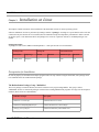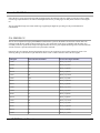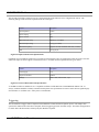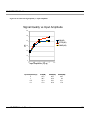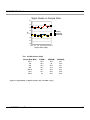
1
X5-GSPS User's Manual
X5-GSPS User's Manual
The X5-GSPS User's Manual was prepared by the technical staff of
Innovative Integration on February 5, 2009.
For further assistance contact:
Innovative Integration
2390-A Ward Ave
Simi Valley, California 93065
PH:
FAX:
(805) 578-4260
(805) 578-4225
email: [email protected]
Website: www.innovative-dsp.com
This document is copyright 2009 by Innovative Integration. All rights
are reserved.
VSS \ Distributions \ X5-GSPS \ Documentation \ Manual \ X5GSPSMaster.odm
#XXXXXX
Rev 1.1
Table of Contents
X5-GSPS User's Manual...........................................................................................................................2
List of Tables.............................................................................................................................7
List of Figures...........................................................................................................................8
Chapter 1:Introduction.............................................................................................................................9
Real Time Solutions!..................................................................................................................................9
Vocabulary..................................................................................................................................................9
What is X5-GSPS? ..........................................................................................................................10
What is Malibu? ..............................................................................................................................10
What is C++ Builder?.......................................................................................................................10
What is DialogBlocks?.....................................................................................................................10
What is wxWidgets?.........................................................................................................................11
What is Microsoft MSVC?...............................................................................................................11
What kinds of applications are possible with Innovative Integration hardware?.............................11
Why do I need to use Malibu with my Baseboard?..........................................................................11
Finding detailed information on Malibu...........................................................................................12
Online Help..........................................................................................................................................12
Innovative Integration Technical Support........................................................................................12
Innovative Integration Web Site........................................................................................................12
Typographic Conventions.......................................................................................................................12
Chapter 2:Windows Installation.............................................................................................................14
Host Hardware Requirements................................................................................................................14
Software Installation................................................................................................................................14
Tools Registration....................................................................................................................................16
Bus Master Memory Reservation Applet.........................................................................................17
Hardware Installation.............................................................................................................................18
After Power-up.........................................................................................................................................18
Chapter 3:Installation on Linux.............................................................................................................19
Package File Names.........................................................................................................................19
Prerequisites for Installation...................................................................................................................19
The Redistribution Package Group - MalibuRed............................................................................19
Malibu..................................................................................................................................................20
Other Software....................................................................................................................................20
Baseboard Package Installation Procedure...........................................................................................20
Board Packages...................................................................................................................................21
Unpacking the Package.......................................................................................................................21
Creating Symbolic Links..................................................................................................................21
Completing the Board Install.............................................................................................................22
Linux Directory Structure.......................................................................................................................22
Applets..............................................................................................................................................22
Documentation.................................................................................................................................22
Examples..........................................................................................................................................22
Hardware..........................................................................................................................................22
Chapter 4:Hardware Installation...........................................................................................................23
Compatible Host Cards...........................................................................................................................23
System Requirements..............................................................................................................................26
Power Considerations..............................................................................................................................26
Mechanical Considerations.....................................................................................................................27
Chapter 5:About the X5 XMC Modules................................................................................................28
X5 XMC Architecture..............................................................................................................................28
X5 Computing Core.................................................................................................................................29
X5 PCI Express Interface........................................................................................................................30
Data Buffering and Memory Use............................................................................................................31
Computational SRAM......................................................................................................................31
Data Buffer DRAM..........................................................................................................................32
Serial EEPROM Interface......................................................................................................................32
EEPROM..........................................................................................................................................32
Digital I/O.................................................................................................................................................33
Software Support.................................................................................................................................33
Digital IO Electrical Characteristics.................................................................................................35
Notes on Digital IO Use.......................................................................................................................35
P16 SERDES I/O......................................................................................................................................36
Thermal Protection and Monitoring......................................................................................................37
Thermal Failures......................................................................................................................................38
Led Indicators..........................................................................................................................................39
JTAG Scan Path.......................................................................................................................................39
FrameWork Logic....................................................................................................................................40
Integrating with Host Cards and Systems.............................................................................................40
Updating the XMC logic Configuration EEPROM..............................................................................41
Chapter 6:Writing Custom Applications...............................................................................................43
The Snap Example...................................................................................................................................43
Tools Required.....................................................................................................................................43
Program Design...................................................................................................................................44
The Host Application ..............................................................................................................................44
User Interface......................................................................................................................................44
Configure Tab...................................................................................................................................44
Setup Tab..........................................................................................................................................45
Stream Tab........................................................................................................................................45
Host Side Program Organization......................................................................................................46
ApplicationIo.......................................................................................................................................46
Initialization......................................................................................................................................46
Starting Data flow.............................................................................................................................49
Handle Data Available......................................................................................................................53
EEProm Access................................................................................................................................55
The Linux Snap Example........................................................................................................................56
The ApplicationIo Class...................................................................................................................56
User Interface......................................................................................................................................57
Configure Tab...................................................................................................................................58
Setup Tab..........................................................................................................................................59
Stream Tab........................................................................................................................................60
The Wave Example..................................................................................................................................60
Stream Initialization.........................................................................................................................60
Data Required Event Handler...........................................................................................................62
The Wave Example for Linux.................................................................................................................64
The ApplicationIo Class...................................................................................................................64
User Interface......................................................................................................................................64
Chapter 7:Developing Host Applications...............................................................................................65
Borland Turbo C++..................................................................................................................................65
Other considerations:..........................................................................................................................66
Microsoft Visual Studio 2005..................................................................................................................67
DialogBlocks.............................................................................................................................................69
Summary...................................................................................................................................................69
Chapter 8:Applets....................................................................................................................................70
Common Applets......................................................................................................................................70
Registration Utility (NewUser.exe)....................................................................................................70
Reserve Memory Applet (ReserveMemDsp.exe).............................................................................71
Data Analysis Applets..............................................................................................................................71
Binary File Viewer Utility (BinView.exe)..........................................................................................71
Applets for the X5-210M Baseboard......................................................................................................71
Logic Update Utility (VsProm.exe)....................................................................................................72
Finder...................................................................................................................................................73
Chapter 9:X5-GSPS XMC Module........................................................................................................74
Introduction..............................................................................................................................................74
Hardware Features..................................................................................................................................76
A/D Converters....................................................................................................................................76
A/D Front End.....................................................................................................................................77
Input Range and Conversion Codes..................................................................................................78
Driving the A/D Inputs........................................................................................................................79
Overrange Detection...........................................................................................................................79
Sample Rate Generation and Clocking Controls .................................................................................79
Triggering ................................................................................................................................................80
Trigger Source.....................................................................................................................................82
Framed Trigger Mode.........................................................................................................................82
Decimation...........................................................................................................................................83
FrameWork Logic Functionality............................................................................................................83
Power Controls and Thermal Design.....................................................................................................84
System Thermal Design......................................................................................................................84
Temperature Sensor and Over Temperature Protection................................................................84
Alert Log...................................................................................................................................................85
Overview..............................................................................................................................................85
Types of Alerts.....................................................................................................................................85
Alert Packet Format...........................................................................................................................86
Software Support for Alerts...............................................................................................................86
Tagging the Data Stream....................................................................................................................87
Calibration................................................................................................................................................87
Updating the Calibration Coefficients..............................................................................................87
Using the X5-GSPS..................................................................................................................................87
Where to start?....................................................................................................................................87
Getting Good Analog Performance...................................................................................................88
Performance Data....................................................................................................................................88
Power Consumption............................................................................................................................88
Environmental.....................................................................................................................................89
Analog Input........................................................................................................................................90
Connectors................................................................................................................................................97
RF Connectors J1-J4...........................................................................................................................97
XMC P15 Connector...........................................................................................................................98
XMC P16 Connector.........................................................................................................................101
Xilinx JTAG Connector....................................................................................................................104
Mechanicals............................................................................................................................................106
List of Tables
Table 1. X5 XMC Bus Requirements....................................................................................................23
Table 2. Required PCIe Resource Allocations......................................................................................26
Table 3. XMC Mounting Hardware......................................................................................................27
Table 4. X5 XMC Family......................................................................................................................28
Table 5. X5 XMC Family Peripherals...................................................................................................29
Table 6. X5 Computing Core Devices..................................................................................................30
Table 7. PCI Express Standards Compliance........................................................................................31
Table 8. Interfaces from PCI Express to Application Logic.................................................................31
Table 9. IUsesDioPort Class Operations...............................................................................................33
Table 10. Digital IO Bits Electrical Characteristics..............................................................................35
Table 11. X5 JTAG Scan Path...............................................................................................................39
Table 12. Development Tools for the Windows Snap Example............................................................43
Table 13. X5-GSPS A/D Features.........................................................................................................77
Table 14. A/D Conversion Coding........................................................................................................78
Table 15. Alert Types.............................................................................................................................85
Table 16. Alert Packet Format...............................................................................................................86
Table 17. X5-GSPS Power Consumption.............................................................................................89
Table 18. X5-GSPS Environmental Limits...........................................................................................89
Table 19. X5-GSPS Analog Performance Summary.............................................................................90
Table 20. X5-GSPS XMC Connector P15 Pinout...............................................................................100
Table 21. P15 Signal Descriptions......................................................................................................101
Table 22. X5-GSPS XMC Secondary Connector P16 Pinout.............................................................103
Table 23. P16 Signal Descriptions......................................................................................................104
Table 24. X5-GSPS JP3 Xilinx JTAG Connector Pinout....................................................................106
List of Figures
Figure 1. Innovative Install Program...................................................................................................15
Figure 2. Progress is shown for each section........................................................................................16
Figure 3. ToolSet registration form.......................................................................................................17
Figure 4. BusMaster configuration.......................................................................................................17
Figure 5. Installation complete..............................................................................................................17
Figure 6. Innovative Single lane PCIe – XMC.3 adapter card (P/N 80172).........................................24
Figure 7. Innovative PCI 64/66 – XMC.3 (4x lanes) adapter card (P/N 80167-0).............................25
Figure 8. Innovative x8 Lane PCI Express – XMC.3 (8x lanes) adapter card (P/N 80173-0)...........25
Figure 9. eInstrument Node – cabled PCI Express adapter (x1 lane) for XMC Modules (II P/N 90181)
...............................................................................................................................................................25
Figure 10. eInstrument PC – embedded PC (Windows/Linux) hosts two XMC modules (II P/N
90199)...................................................................................................................................................26
Figure 11. X5 XMC Family Block Diagram.........................................................................................28
Figure 12. DIO Control Register (BAR1+0x14)...................................................................................34
Figure 13. Digital IO Port Addresses....................................................................................................34
Figure 14. Virtex-5 Rocket I/O assignments for P16 signals................................................................37
Figure 15. XMC EEProm Programmer.................................................................................................41
Figure 16. X5-GSPS Module (analog cover and heat sink removed)...................................................75
Figure 17. X5-GSPS Block Diagram....................................................................................................76
Figure 18. X5-GSPS A/D Channel 0 Front End...................................................................................78
Figure 19. X5-GSPS A/D Channel 1 Front End...................................................................................78
Figure 20. Sample Clock Generation and Distribution Block Diagram...............................................79
Figure 21. Input Clock Electrical Specifications..................................................................................80
Figure 22. Clock Oscillator Electrical Specifications...........................................................................80
Figure 23. Analog Triggering Timing...................................................................................................82
Figure 24. X5-GSPS FrameWork Logic Data Flow.............................................................................83
Figure 25. Frequency Response for 10 MHz to 1 GHz span, 500 mVp-p input...................................91
Figure 26. Frequency Response for 600 MHz to 900 MHz span, 500 mVp-p input............................91
Figure 27. X5-GSPS Ground Noise, Fs = 125 MSPS, input grounded................................................92
Figure 28. X5-GSPS Noise Floor, Fs = 125 MSPS, input grounded....................................................92
Figure 29. X5-GSPS A/D Signal Quality vs. Input Amplitude.............................................................93
Figure 30. Signal Quality vs Input Frequency, Fin = 101 MHz, 2 Vp-p...............................................94
Figure 1. Signal Quality, Fin = 101 MHz, 2Vp-p, Fs = 1497.5 MSPS, DC Coupled...........................95
Figure 2. Signal Quality, Fin = 101 MHz, 2Vp-p, Fs = 1497.5 MSPS, DC Coupled...........................96
Figure 3. Signal Quality, Fin = 101 MHz, 2Vp-p, Fs = 637.5 MSPS, DC Coupled.............................97
Figure 4. Connectors J1-J4 Functions...................................................................................................98
Figure 5. P15 XMC Connector Orientation..........................................................................................99
Figure 6. P16 XMC Connector Orientation........................................................................................102
Figure 7. X5-GSPS JP1 Orientation, board face view........................................................................105
Figure 8. X5-GSPS JP1 Orientation, board top edge view.................................................................105
Figure 9. X5-GSPS Mechanicals (Top View) Rev A..........................................................................107
Figure 10. X5-GSPS Mechanicals (Bottom View) Rev A..................................................................108
Chapter 1:
Introduction
Real Time Solutions!
Thank you for choosing Innovative Integration, we appreciate your business! Since 1988, Innovative Integration has grown
to become one of the world's leading suppliers of DSP and data acquisition solutions. Innovative offers a product portfolio
unrivaled in its depth and its range of performance and I/O capabilities .
Whether you are seeking a simple DSP development platform or a complex, multiprocessor, multichannel data acquisition
system, Innovative Integration has the solution. To enhance your productivity, our hardware products are supported by
comprehensive software libraries and device drivers providing optimal performance and maximum portability.
Innovative Integration's products employ the latest digital signal processor technology thereby providing you the competitive
edge so critical in today's global markets. Using our powerful data acquisition and DSP products allows you to incorporate
leading-edge technology into your system without the risk normally associated with advanced product development. Your
efforts are channeled into the area you know best ... your application.
Vocabulary
Introduction
What is X5-GSPS?
The X5- GSPS is a PCI Express XMC IO module featuring a National ADC08D1500, 1.6 GSPS, 8-bit A/D dual-channel A/
D converter.
A Xilinx Virtex5 SX95T with 512 MByte DDR2 DRAM and 4MB QDR-II memory provide a very high performance DSP
core for demanding applications such as emerging wireless standards. The close integration of the analog IO, memory and
host interface with the FPGA enables real-time signal processing at extremely high rates exceeding 300 GMACs per second.
The X5 XMC modules couple Innovative's powerful Velocia architecture with a high performance, 8-lane PCI Express
interface that provides over 1 GB/s sustained transfer rates to the host. Private links to host cards with > 1.6 GB/s capacity
using J16 are provided for system integration. The X5 family can be fully customized using VHDL and MATLAB using the
FrameWork Logic toolset. The MATLAB BSP supports real-time hardware-in-the-loop development using the graphical,
block diagram Simulink environment with Xilinx System Generator.
Software tools for host development include C++ libraries and drivers for Windows and Linux. Application examples
demonstrating the module features and use are provided.
What is Malibu?
Malibu is the Innovative Integration-authored component suite, which combines with the Borland, Microsoft or GNU C++
compilers and IDEs to support programming of Innovative hardware products under Windows and Linux. Malibu supports
both high-speed data streaming plus asynchronous mailbox communications between the DSP and the Host PC, plus a wealth
of Host functions to visualize and post-process data received from or to be sent to the target DSP.
What is C++ Builder?
C++ Builder is a general-purpose code-authoring environment suitable for development of Windows applications of any type.
Armada extends the Builder IDE through the addition of functional blocks (VCL components) specifically tailored to perform
real-time data streaming functions.
What is DialogBlocks?
DialogBlocks is an easy-to-use dialog editor for your wxWidgets applications, generating C++ code and XRC resource files.
Using sizer-based layout, DialogBlocks helps you build dialogs and panels that look great on Windows, Linux or any
supported wxWidgets platform. Add context-sensitive help text, tooltips, images, splitter windows and more.
X5-GSPS User's Manual
10
Introduction
What is wxWidgets?
wxWidgets was started in 1992 by Julian Smart at the University of Edinburgh. Initially started as a project for creating
applications portable across Unix and Windows, it has grown to support the Mac platform, WinCE, and many other toolkits
and platforms. The number of developers contributing to the project is now in the dozens and the toolkit has a strong userbase
that includes everyone from open source developers to corporations such as AOL. So what is special about wxWidgets
compared with other cross-platform GUI toolkits?
wxWidgets gives you a single, easy-to-use API for writing GUI applications on multiple platforms that still utilize the native
platform's controls and utilities. Link with the appropriate library for your platform (Windows/Unix/Mac, others coming
shortly) and compiler (almost any popular C++ compiler), and your application will adopt the look and feel appropriate to
that platform. On top of great GUI functionality, wxWidgets gives you: online help, network programming, streams,
clipboard and drag and drop, multithreading, image loading and saving in a variety of popular formats, database support,
HTML viewing and printing, and much more.
What is Microsoft MSVC?
MSVC is a general-purpose code-authoring environment suitable for development of Windows applications of any type.
Armada extends the MSVC IDE through the addition of dynamically created MSVC-compatible C++ classes specifically
tailored to perform real-time data streaming functions.
What kinds of applications are possible with Innovative Integration hardware?
Data acquisition, data logging, stimulus-response and signal processing jobs are easily solved with Innovative Integration
baseboards using the Malibu software. There are a wide selection of peripheral devices available in the Matador DSP product
family, for all types of signals from DC to RF frequency applications, video or audio processing. Additionally, multiple
Innovative Integration baseboards can be used for a large channel or mixed requirement systems and data acquisition cards
from Innovative can be integrated with Innovative's other DSP or data acquisition baseboards for high-performance signal
processing.
Why do I need to use Malibu with my Baseboard?
One of the biggest issues in using the personal computer for data collection, control, and communications applications is the
relatively poor real-time performance associated with the system. Despite the high computational power of the PC, it cannot
reliably respond to real-time events at rates much faster than a few hundred hertz. The PC is really best at processing data,
not collecting it. In fact, most modern operating systems like Windows are simply not focused on real-time performance, but
rather on ease of use and convenience. Word processing and spreadsheets are simply not high-performance real-time tasks.
The solution to this problem is to provide specialized hardware assistance responsible solely for real- time tasks. Much the
same as a dedicated video subsystem is required for adequate display performance, dedicated hardware for real-time data
collection and signal processing is needed. This is precisely the focus of our baseboards – a high performance, state-of-theart, dedicated digital signal processor coupled with real-time data I/O capable of flowing data via a 64-bit PCI bus interface.
The hardware is really only half the story. The other half is the Malibu software tool set which uses state of the art software
techniques to bring our baseboards to life in the Windows environment. These software tools allow you to create applications
for your baseboard that encompass the whole job - from high speed data acquisition, to the user interface.
X5-GSPS User's Manual
11
Introduction
Finding detailed information on Malibu
Information on Malibu is available in a variety of forms:
•
Data Sheet (http://www.innovative-dsp.com/products/malibu.htm)
•
On-line Help
•
Innovative Integration Technical Support
•
Innovative Integration Web Site (www.innovative-dsp.com)
Online Help
Help for Malibu is provided in a single file, Malibu.chm which is installed in the Innovative\Documentation folder during the
default installation. It provides detailed information about the components contained in Malibu - their Properties, Methods,
Events, and usage examples. An equivalent version of this help file in HTML help format is also available online at
http://www.innovative-dsp.com/support/onlinehelp/Malibu.
Innovative Integration Technical Support
Innovative includes a variety of technical support facilities as part of the Malibu toolset. Telephone hotline supported is
available via
Hotline (805) 578-4260 8:00AM-5:00 PM PST.
Alternately, you may e-mail your technical questions at any time to:
[email protected].
Also, feel free to register and browse our product forums at http://forum.iidsp.com/, which are an excellent source of FAQs
and information submitted by Innovative employees and customers.
Innovative Integration Web Site
Additional information on Innovative Integration hardware and the Malibu Toolset is available via the Innovative Integration
website at www.innovative-dsp.com
Typographic Conventions
This manual uses the typefaces described below to indicate special text.
X5-GSPS User's Manual
12
Introduction
Typeface
Source Listing
Boldface
Emphasis
Cpp Variable
Cpp Symbol
KEYCAPS
Menu Command
X5-GSPS User's Manual
Meaning
Text in this style represents text as it appears onscreen or in code. It
also represents anything you must type.
Text in this style is used to strongly emphasize certain words.
Text in this style is used to emphasize certain words, such as new
terms.
Text in this style represents C++ variables
Text in this style represents C++ identifiers, such as class, function,
or type names.
Text in this style indicates a key on your keyboard. For example,
“Press ESC to exit a menu”.
Text in this style represents menu commands. For example “Click
View | Tools | Customize”
13
Windows Installation
Chapter 2:
Windows Installation
This chapter describes the software and hardware installation procedure for the Windows platform (WindowsXP and Vista).
Do NOT install the hardware card into your system at this time. This will follow the software
installation.
Host Hardware Requirements
The software development tools require an IBM or 100% compatible Pentium IV - class or higher machine for proper
operation. An Intel-brand processor CPU is strongly recommended, since AMD and other “clone” processors are not
guaranteed to be compatible with the Intel MMX and SIMD instruction-set extensions which the Armada and Malibu Host
libraries utilize extensively to improve processing performance within a number of its components. The host system must
have at least 128 Mbytes of memory (256MB recommended), 100 Mbytes available hard disk space, and a DVD-ROM
drive. Windows2000 or WindowsXP (referred to herein simply as Windows) is required to run the developer’s package
software, and are the target operating systems for which host software development is supported.
Software Installation
The development package installation program will guide you through the installation process.
Note: Before installing the host development libraries (VCL components or MFC classes), you must
have Microsoft MSVC Studio (version 9 or later) and/or Codegear RAD Studio C++ (version 11)
installed on your system, depending on which of these IDEs you plan to use for Host development. If
you are planning on using these environments, it is imperative that they are tested and knownoperational before proceeding with the library installation. If these items are not installed prior to
running the Innovative Integration install, the installation program will not permit installation of the
associated development libraries. However, drivers and DLLs may be installed to facilitate field
deployment.
You must have Administrator Privileges to install and run the software/hardware onto your system, refer to the Windows
documentation for details on how to get these privileges.
X5-GSPS User's Manual
14
Windows Installation
Starting the Installation
To begin the installation, start Windows. Shut down all running programs and disable anti-virus software. Insert the
installation DVD. If Autostart is enabled on your system, the install program will launch. If the DVD does not Autostart,
click on Start | Run... Enter the path to the Setup.bat program located at the root of your DVD-ROM drive (i.e.
E:\Setup.bat) and click “OK” to launch the setup program.
SETUP.BAT detects if the OS is 64-bit or 32-bit and runs the appropriate installation for each
environment. It is important that this script be run to launch an install.
When installing on a Vista OS, the dialog below may pop up. In each case, select “Install this driver software anyway” to
continue.
Figure 1. Vista Verificaton Dialog
The Installer Program
After launching Setup, you will be presented with the following screen.
X5-GSPS User's Manual
15
Windows Installation
Figure 2. Innovative Install Program
Using this interface, specify which product to install, and where on your system to install it.
1) Select the appropriate product from the Product Menu.
2) Specify the path where the development package files are to be installed. You may type a path or click “Change” to
browse for, or create, a directory. If left unchanged, the install will use the default location of “C:\Innovative”.
3) Typically, most users will perform a “Full Install” by leaving all items in the “Components to Install” box
checked. If you do not wish to install a particular item, simply uncheck it. The Installer will alert you and
automatically uncheck any item that requires a development environment that is not detected on your system.
4) Click the Install button to begin the installation.
Note: The default “Product Filter” setting for the installer interface is “Current Only” as indicated by
the combo box located at the top right of the screen. If the install that you require does not appear in the
“Product Selection Box” (1), Change the “Product Filter” to “Current plus Legacy”.
Each item of the checklist in the screen shown above, has a sub-install associated with it and will open a sub-install screen if
checked. For example, the first sub-install for “Quadia - Applets, Examples, Docs, and Pismo libraries” is shown below.
The installation will display a progress window, similar to the one shown below, for each item checked.
X5-GSPS User's Manual
16
Windows Installation
Figure 3. Progress is shown for each section.
Tools Registration
At the end of the installation process you will be prompted to register. If you decide that you would like to register at a later
time, click “Register Later”.
X5-GSPS User's Manual
17
Windows Installation
When you are ready to register, click Start | All Programs | Innovative |
<Board Name> | Applets. Open the New User folder and launch
NewUser.exe to start the registration application. The registration form
to the left will be displayed.
Before beginning DSP and Host software development, you must
register your installation with Innovative Integration. Technical
support will not be provided until registration is successfully
completed. Additionally, some development applets will not operate
until unlocked with a passcode provided during the registration
process.
It is recommend that you completely fill out this form and return it to
Innovative Integration, via email or fax. Upon receipt, Innovative
Integration will provide access codes to enable technical support and
unrestricted access to applets.
Figure 4. ToolSet registration form
Bus Master Memory Reservation Applet.
At the conclusion of the installation process, ReserveMem.exe will run
(except for SBC products). This will allow you to set the memory size
needed for the busmastering to occur properly. This applet may be run from
the start menu later if you need to change the parameters.
For optimum performance each Matador Family Baseboard requires 2 MB
of memory to be reserved for its use. To reserve this memory, the registry
must be updated using the ReserveMem applet. Simply select the Number
of Baseboards you have on your system, click Update and the applet will
update the registry for you. If at any time you change the number of boards
in your system, then you must invoke this applet found in Start | All
Programs | Innovative | <target board> | Applets | Reserve Memory.
After updating the system exit the applet by clicking the exit button to
resume the installation process.
Figure 5. BusMaster configuration
At the end of the install process, the following screen will appear.
X5-GSPS User's Manual
18
Windows Installation
Figure 6. Installation complete
Click the “Shutdown Now” button to shut down your computer. Once the shutdown process is complete unplug the system
power cord from the power outlet and proceed to the next section, “Hardware Installation.”
Hardware Installation
Now that the software components of the Development Package have been installed the next step is to configure and install
your hardware. Detailed instructions on board installation are given in the Hardware Installation chapter, following this
chapter.
IMPORTANT: Many of our high speed cards, especially the PMC and XMC Families, require forced
air from a fan on the board for cooling. Operating the board without proper airflow may lead to
improper functioning, poor results, and even permanent physical damage to the board. These boards
also have temperature monitoring features to check the operating temperature. The board may also be
designed to intentionally fail on over-temperature to avoid permanent damage. See the specific
hardware information for airflow requirements.
After Power-up
After completing the installation, boot your system into Windows.
Innovative Integration boards are plug and play compliant, allowing Windows to detect them and auto-configure at start-up.
Under rare circumstances, Windows will fail to auto-install the device-drivers for the JTAG and baseboards. If this happens,
please refer to the “TroubleShooting” section.
X5-GSPS User's Manual
19
Windows Installation
X5-GSPS User's Manual
20
Installation on Linux
Chapter 3:
Installation on Linux
This chapter contains instruction on the installation of the baseboard software for Linux operating systems.
Software installation on Linux is performed by loading a number of packages. A Package is a special kind of archive file that
contains not only the files that are to be installed, but also installation scripts and dependency information to allow a smooth
fit into the system. This information allows the package to be removed, or patched. Innovative uses RPM packages in its
installs.
Package File Names
A package file name such as Malibu-LinuxPeriphLib-1.1-3.i586.rpm encodes a lot of information.
Package Name
Distribution
Malibu-Linux
Package ID
Subpackage
PeriphLib
Version
1.1
Information Fields
Revision
Hardware Type
Extension
3
i586
.rpm
Prerequisites for Installation
In order to properly use the baseboard example programs and to develop software using the baseboard, some packages need
to be installed before the actual baseboard package.
The Redistribution Package Group - MalibuRed
This set of packages contain the libraries and drivers needed to run a program using Malibu. This group is called
“MalibuRed” because it contains the packages needed to allow running Malibu based programs on a target, non-development
machine. (Red is short for 'redistributable').
MalibuRed Packages
Description
WinDriver-9.2-1.i586.rpm
Installs WinDriver 9.2 release.
MalibuLinux-Red-[ver]-[rel].i586.rpm
Installs Baseboard Driver Kernel Plugin.
intel-ipp_rti-5.3p.x32.rpm
Installs Intel IPP library redistributable files.
X5-GSPS User's Manual
21
Installation on Linux
The installation CD, or the web site contains a file called LinuxNotes.pdf giving instructions on how to load these packages
and how to install the drivers onto your Linux machine. This file is also loaded onto the target machine by the the MalibuLinuxRed RPM. These procedures need to be completed for every target machine.
Malibu
To develop software for a baseboard the Malibu packages also must be installed.
Malibu Packages
Description
Malibu-LinuxPeriphLib-[ver]-[rel].i586.rpm
Installs Malibu Source, Libraries and Examples.
Other Software
Our examples use the DialogBlocks designer software and wxWidgets GUI library package for user interface code. If you
wish to rebuild the example programs you will have to install this software as well.
Package
wxWidgets
DialogBlocks
Company
URL
wxWidgets
http://www.wxwidgets.org
Anthemion
http://www.anthemion.co.uk.org/dialogblocks
Baseboard Package Installation Procedure
Each baseboard installation for Linux consists of one or more package files containing self-extracting packages of
compressed files, as listed in the table below. Note that package version codes may vary from those listed in the table.
Each of these packages automatically extract files into the /usr/Innovative folder, herein referred to as the Innovative
root folder in the text that follows. For example, the X5-400 RPM extracts into /usr/Innovative/X5-400-[ver]. A
symbolic link named X5-400 is then created pointing to the version directory to allow a single name to apply to any version
that is in use.
X5-GSPS User's Manual
22
Installation on Linux
Board Packages
Baseboard
Packages
Description
X5-400M
Malibu-LinuxPeriphLib-[ver]-[rel].i586.rpm
Board files and examples.
X5-210M
X5-210M-LinuxPeriphLib-[ver]-[rel].i586.rpm
Board files and examples.
X3-10M
X3-10M-LinuxPeriphLib-[ver]-[rel].i586.rpm
Board files and examples.
X3-25M
X3-25M-LinuxPeriphLib-[ver]-[rel].i586.rpm
Board files and examples.
X3-A4D4
X3-A4D4-LinuxPeriphLib-[ver]-[rel].i586.rpm
Board files and examples.
X3-SD
X3-SD-LinuxPeriphLib-[ver]-[rel].i586.rpm
Board files and examples.
X3-SDF
X3-SDF-LinuxPeriphLib-[ver]-[rel].i586.rpm
Board files and examples.
X3-Servo
X3-Servo-LinuxPeriphLib-[ver]-[rel].i586.rpm
Board files and examples.
SBC-ComEx
Sbc-ComEx-LinuxPeriphLib-[ver]-[rel].i586.rpm
Board files and examples.
Unpacking the Package
As root, type:
rpm -i -h X5-400-LinuxPeriphLib-1.1-4.i586.rpm
This extracts the X5-400 board files into the Innovative root directory. Use the package for the particular board you are
installing.
Creating Symbolic Links
The example programs assume that the user has created symbolic links for the installed board packages. A script file is
provided to simplify this operation by the Malibu Red package. In the MalibuRed/KerPlug directory, there is a script called
quicklink.
quicklink X5-400 1.1
These commands will create a symbolic link X5-400 pointing to X5-400-1.1.
This script can be moved to the user's bin directory to allow it to be run from any directory.
X5-GSPS User's Manual
23
Installation on Linux
Completing the Board Install
The normal board install is complete with the installation of the files. The board driver install is already complete with the
loading of the Malibu Red package. If there are any board-specific steps they will be listed at the end of this chapter.
Linux Directory Structure
When a board package is installed, its files are placed under the /usr/Innovative folder. The base directory is named
after the board with a version number attached -- for example, the version 2.0 X5-400 RPM extracts into
/usr/Innovative/X5-400-2.0.
This allows multiple version of installs to coexist by using a symbolic link to point to a particular version. Changing the
symbolic link changes with version will be used.
Under the main directory there are a number of subdirectories.
Applets
The applets subdirectory contains small application programs that aid in the use of the board. For example, there is a Finder
program that allows the user to flash an LED on the board to determine which board is associated with a target number. See
the Applets chapter for a fuller description of the applets for a board.
Documentation
This directory contains any documentation files for the project. Open the index.html file in the directory with a web browser
to see the available files and a description of the contents.
Examples
This directory and its subdirectories contain the projects, source and example programs for the board.
Hardware
This directory contains files associated with programming the board Logic and any logic images provided.
X5-GSPS User's Manual
24
Hardware Installation
Chapter 4:
Hardware Installation
The X5 XMC cards may be used on a variety of host cards supporting an XMC.3 PCI Express (VITA standard 42.3
compatible) site. XMC P16 is also used for system integration including use as a dedicated data channel.
Compatible Host Cards
X5 XMC cards are compatible with the VITA 42.3 PCI Express mezzanine module sites. The card form factor is IEEE 1386
with XMC connectors P15 and P16. P15 is used for PCI Express, while P16 is used as digital IO unique to the X5 modules.
The X5 modules mount 10mm from the host card and may use standoffs for mechanically securing the module to the host.
Table 1. X5 XMC Bus Requirements
PCI Express Bus
Requirement
Type
Standard
PCI Express 1.0a
Lanes
8
Bus Speed
2.5 Gbps per lane per direction
Power Supplies
3.3V and VPWR (+5V or +12V) is required on all XMCs.
Adapter cards for XMC modules, shown below, allow X5 XMC modules to be used in a desktop PCs with PCI Express or
PC slots.
To get out of the PC chassis, consider using either the eInstrument Node. The eInstrument node can host one XMC using
cabled PCI Express using a cable as long as 5 meters.
For an intelligent computing node, the eInstrument PC provides an embedded PC running Windows or Linux, disk drives,
and other PC peripherals with two XMC module sites.
X5-GSPS User's Manual
25
Hardware Installation
Figure 7. Innovative Single lane PCIe – XMC.3 adapter card (P/N 80172)
Figure 8. Innovative PCI 64/66 – XMC.3 (4x lanes) adapter card (P/N 80167-0)
Figure 9. Innovative x8 Lane PCI Express – XMC.3 (8x lanes) adapter card (P/N 80173-0)
X5-GSPS User's Manual
26
Hardware Installation
Figure 10. eInstrument Node – cabled PCI Express adapter (x1 lane) for XMC Modules (II P/N 90181)
Figure 11. eInstrument PC – embedded PC (Windows/Linux) hosts two XMC modules (II P/N 90199)
XMC systems should be be compatible with VITA 42.3 specification for P15.
The P16 interface can only be used when the PCI Express interface is present and active. The XMC P16 interface to the host
may be customized in the Application Logic. Host card support for P16 interfaces varies so this must be verified on a caseby-case basis to determine compatibility. In the specific description of each module, the P16 connection pinout is provided in
this manual. Innovative's adapter cards provide access to P16 IO for system integration. Contact technical support if you
need any assistance in checking compatibility with the X5 XMC P16 interface.
System Requirements
The PCI Express slot must be PCI Express 1.0a compatible and be able to map the following resources.
X5-GSPS User's Manual
27
Hardware Installation
Table 2. Required PCIe Resource Allocations
Required PCIe Resources
BAR0 : 1MB Memory
BAR1 : 64K B Memory
1 Interrupt
When you first plug in the module, it will then be found and the driver should be installed for the module. The standard driver
resides in the \Innovative\drivers directory after software installation.
The XMC module may be used an any PCI Express slot supporting 1 or more lanes. Innovative offers a line of adapters for
use with the X5 series which allow the module to be used in PCI and cPCI environments. These adapters may limit the
number of lanes available to the X5 for host communication, depending on their design.
Power Considerations
Each XMC should be reviewed for its specific power, cooling and any special mechanical considerations. For each module
the power consumption and required power supplies are shown in the specific discussion for that module.
For desktop applications, you MUST provide forced air cooling with 5-10 CFM capability. The air must blow directly
on the Virtex5 device.
The X5 XMCs are designed to operate over the typical commercial temperature range of 0 to 70 C, but this relies on
sufficient forced air cooling for most installations and modules. At the lower temperatures, it is also required that the
environment be non-condensing for the standard commercial modules. Extended temperature versions of many modules are
available with conformal coating if the environment is more demanding.
During operation, the module temperature should be monitored to prevent unexpected shutdown. If the module temperature
exceeds 85C, the module will deactivate on-board power supplies to avoid overheating. Please refer to the section on thermal
properties for more details.
PCI Express slots are rated for their power capability. Each installation should be reviewed to verify that the host card plus
the module do not exceed the rated power of the slot. The power consumption for each module is provided in the specific
discussion of that module. Most slots support 15W in desktop systems and provide 3.3V and 12V. Some XMC modules
require -12V, which must be provided by the host card.
X5-GSPS User's Manual
28
Hardware Installation
Mechanical Considerations
The X5 modules conform to IEEE1386 CMC specification and ANSI/VITA 42.0 specifications. These specifications define
the size of the module and mounting requirements. In short the modules are 75 x 150 mm and mount 10 mm from the host
card. This allows the XMC modules to fit in one slot in desktop PC or compact PCI systems.
For ruggedness, the modules should be mounted to a host card using the mounting screws and standoffs. The host bracket
should securely hold the XMC front bracket so that the module is snug in the bracket opening. This reduces mechanical strain
on the XMC connectors from the front panel cable attachments.
The card may be secured to the host card with two standoffs and four screws as shown. The Digikey number is provided
(www.digikey.com) for convenience; many suppliers have these standard screw and standoff sizes.
For high vibration applications, screws should be mounted with locking compound such as Loctite.
Table 3. XMC Mounting Hardware
Description
Quantity
Digikey Part Number
Metric pan head screw, M3x5, 3mm x 5mm
5
H742-ND
Threaded Standoff, 10mm with 3mm thread
3
4391K
During the logic and firmware design process, some modules require access to JTAG connectors for use with the
development tools. This may require greater access space than the final installation. A variety of engineering tools are
available to assist the designer during the development process such as PCIe to XMC adapters. A cabled version allows the
module to operate outside the chassis. An open chassis may also be required to get access to the XMC during the
development process so that the cables are easily accessible.
X5-GSPS User's Manual
29
About the X5 XMC Modules
Chapter 5:
About the X5 XMC Modules
In this chapter, we will discuss the common features of the X5 module family. Specifics on each module are covered in later
chapters.
X5 XMC Architecture
The X5 XMC modules share a common architecture and many features such as the PCI Express interface, data buffering
features, the Application Logic, and other system integration features. This allows the X5 XMC modules to utilize common
software and logic firmware, while providing unique analog and digital features.
QDR-II
SRAM
4MB
XMC
42.3
PCI
Express
8 lanes
Ext Clk
Analog
I/O
I/O
connect
PCI
Express
Intf
App FPGA
Analog
Xilinx Virtex5
interface
LX110T/SX95T
XMC
P16
DIO/
RIO
Clocks
SRAM
Controller
RapidIO
Intf
DRAM
Controller
Config ROM
DDR2
DRAM
512MB
Trigger
Trigger
PWR
Figure 12. X5 XMC Family Block Diagram
The X5 XMCs have a variety of analog and digital IO front ends suited to many applications.
Table 4. X5 XMC Family
X5 XMC
X5-400M
Features
2 A/D channels, 14 bit, 400MHz; 2 D/A channels, up to
X5-GSPS User's Manual
Applications
Software radio, RADAR, medical imaging
30
About the X5 XMC Modules
X5 XMC
Features
Applications
500M updates/sec
X5-210M
4 A/D channels, 14 bit, 250 MHz
Software radio, RADAR
X5-GSPS
2 A/D channels at 1.5GSPS
IF/RF simulation and test, RADAR
X5-COM
4 SFP ports at 3.125 Gbps
Remote IO, system expansion
The X5 XMCs feature a Xilinx Virtex-5 SX95T core for signal processing and control. In addition to the features in the
Virtex-5 logic such as embedded multipliers and memory blocks, the FPGA computing core has one bank of DDR2 DRAM
and two banks of QDR2 SRAM for data buffering and computing memory.
There are also a number of support peripherals for IO control and system integration. Each XMC may have additional
application-specific support peripherals.
Table 5. X5 XMC Family Peripherals
Peripheral
Features
XMC.3 PCI Express
interface
The XMC.3 host interface integrates with PCI Express systems using eight lanes operating at 2.5 Gbps
that provides up to 4 GBytes/sec data rate on the bus (full duplex). This interface complies with VITA
standard 42.3 which specifies PCI Express interface for the XMC module format.
The Velocia packet system provides fast and flexible communications with the host using a credit-based
flow control supporting packet transfers with the host. A secondary command channel provides
independent interface for control and status outside of the data channel that is extensible to custom
applications.
XMC P16
Provides a bank of digital IO lines which may be used for general purpose bit I/O or to implement a
private link to cards featuring a parallel data bus. Additionally, eight independent rocket I/O links
(VITA 42.0) are available, each capable of 500 MB/s, full-duplex operation
Timing and triggering
Flexible clocking and synchronization features for I/O
Data buffering and
Computational Memory
Two 1Mx16 SRAM devices are used provide data buffering, processor memory and computation
memory for the Application FPGA
Alert Log
Monitors system events and error conditions to help manage the data acqusiton process
X5 Computing Core
The X5 XMC module family has an FPGA-based computing core that controls the data acquisition process, provides data
buffing and host communications. The computing core consists of a Xilinx Virtex-5 FPGA, one bank of DDR2 DRAM
(4Gbits in a x64 configuration), and two banks of QDR2 SRAM (32Mbits total in two x32 dual-ported banks). The FPGA
uses the memories for data buffering and computational workspace.
X5-GSPS User's Manual
31
About the X5 XMC Modules
Table 6. X5 Computing Core Devices
Feature
Device
Part Number
Application Logic FPGA
Xilinx Virtex-5 SX95T
XC5VSX95T-1FFG1136C
Computation memory
QDR2 SRAM
2x Cypress CY7C1314BV18-167
Buffer memory
DDR2 DRAM
4x Micron MT47H64M16HR-37E
As the focus of the module, the X5 computing core connects the IO, peripherals, host communications and support features.
Each IO device directly connects to the application FPGA on the X5 modules providing tight coupling for high performance,
real-time IO. The FPGA logic implements an interface to each device that connects them to the controls and data
communications features on the module. Support features, such as sample triggering and data analysis, are implemented in
the logic to provide precise real-time control over the data acquisition process.
The X5 module architecture is really defined by the features in the logic that connect the IO devices to Velocia packet system.
For data from IO devices such as A/Ds, the data flows from the IO interface and is then enqueued in the multi-queue buffer.
The packetizer then creates data packets from the data stream that are moved across the data link to the PCIe interface.
Packets to output devices travel in the opposite direction – from the link to the de-framer and into the multi-queue data buffer.
The output IO, such as a DAC, then consumes the data from the queue as required. The Alert Log monitors error conditions
and important events for management of the data acquisition process.
The host interacts with the X5 computing core using the packet system for high speed data and over the command channel.
The packet system is the main data channel to the card and delivers the high performance, real-time data capability of moving
data to and from the module. Since it uses an efficient DMA system, it is very efficient at moving data which leaves the host
system unburdened by the data flow. The command channel provides the PCIe host direct access to the computing core logic
for status, control and initialization. Since it is outside the packet system, it is less complex to use and provides unimpeded
access to the logic.
The application FPGA image is loaded at power up from onboard flash EEPROM storage.
Adding New Features to the FPGA
The functionality of the computing core can be modified using the FrameWork Logic tools for the X5 module family. The
tools support development in either VHDL or MATLAB. Signal processing, data analysis and unique functions can be added
to the X5 modules to suit application-specific requirements. See the X5 FrameWork Logic User Guide for further
information.
X5 PCI Express Interface
The X5 module family has a PCI Express interface that provides a lane, 2.5 Gbps full duplex link to the host computer. The
interface is compatible with industry standard PCI Express systems and may be used in a variety of host computers. The
following standards govern the PCI Express interface on the X5 XMC modules.
X5-GSPS User's Manual
32
About the X5 XMC Modules
Table 7. PCI Express Standards Compliance
Standard
Describes
Standards Group
PCI Express 1.0a
PCI Express electrical and protocol standards.
2.5 Gbps data rate per lane per direction.
PCI SIG ( http://www.picmg.com )
ANSI/VITA 42
XMC module mechanicals and connectors
VITA ( www.vita.org )
ANSI VITA 42.3
XMC module with PCI Express Interface.
VITA ( www.vita.org )
The major interfaces to the application logic are the data link, command channel and SelectMAP interface. The data link
provides a high performance channel for the application logic to communicate with the host computer while the Command
Channel is a command and control interface from the host computer to the application logic. The SelectMAP interface is the
application FPGA configuration port for loading the logic image.
The data link is the primary data path for the data communications between the application FPGA and host computer. When
data packets are created by the application logic, such as A/D samples, or required by the application logic for output devices,
such as DAC channels, the data flows over the data link as packets. The maximum transfer rate over the data link is 2000
MB/s with a 1200 MB/s sustained rate (half-duplex). The data packets contain a Peripheral Device Number (PDN) that
identifies the peripheral associated with the this data packet. In this way, the packet system is extensible to other devices that
may be added to the logic. For example, an FFT analysis can be added to the logic and its result sent to the host as a new
PDN for display and further analysis while maintaining other data streams from A/D channels.
Table 8. Interfaces from PCI Express to Application Logic
Application Logic
Interface
Max Data Rate
Typical Use
Data Link
2000 MB/s burst, 1200 MB/s sustained
(half-duplex)
Velocia packet system interface main path for data communications
Command Channel
5 MB/s sustained
Command, control and status
Data Buffering and Memory Use
There are two sets of memory devices attached to the application FPGA that provide data buffering and computational RAM
for FPGA applications.
Computational SRAM
The SRAM on the X5 series is a 4Mbyte memory dedicated as FPGA local memory. Applications in the FPGA may use the
SRAM as a local buffer memory if the data buffer is too large to fit in FPGA block RAMs, or as memory for an embedded
processor in the FPGA.
X5-GSPS User's Manual
33
About the X5 XMC Modules
The SRAM devices connected to the FPGA are 4 Mbytes total size, organized as two banks of 16Mbitx32 dual ported
memory. This device is an Cypress CY7C1314 (or equivalent) which is a synchronous QDR2 SRAM and supports clock rates
up to 167 MHz. All SRAM control and data lines pins are directly connected to the FPGA, allowing the SRAM memory
control to be customized to the application.
The Framework Logic provides a simple SRAM interface that can be readily modified for many types of applications.
Detailed explanation of the interface control logic is described in the FrameWork Logic User Guide. The Framework Logic
provides a simple register interface to the SBSRAM control logic that is used for test and demonstration. FPGA logic
developers can easily replace the simple register interface logic to build on top of the high performance logic core when
integrating the SRAM into their logic design.
MATLAB developers frequently use the SRAM as the real-time data buffer during development. Since the MATLAB
Simulink tools operate over the FPGA JTAG during development at a low rate, it is necessary to use the SRAM for real-time,
high speed data buffering. The MATLAB Simulink library for each X5 module demonstrates the use of the SRAM as a data
capture buffer. The SRAM captures real-time, high-speed data that can then be read out into MATLAB for analysis or display
as a snapshot. This allows high-speed, real-time to be captured and brought into MATLAB Simulink over the slow
(10Mb/sec) JTAG link. See the X5 FrameWork Logic User Guide for more details and examples.
Data Buffer DRAM
The second set of memory provides a 512MByte DDR2 memory pool local to the FPGA. The Framework Logic implements
a data buffer with one or more queues for the A/D and D/A streams as appropriate for the particular X5 module.
In the Framework logic, the SRAM use is demonstrated as a multiple queue FIFO memory that divides the 2 MB memory
buffer into separate queues (virtual FIFOs) for input and output. The logic component, referred to as Multi-Queue DRAM,
controls the DRAM to create the FIFO queue functionality. Custom logic applications can use the Multi Queue DRAM
buffer component to add additional queues for new devices.
Serial EEPROM Interface
EEPROM
A serial EEPROM on the X5 series is used to store configuration and calibration information. The interface to the serial
EEPROM is an I2C bus that is controlled by the PCI logic device. The device is an Atmel AT24C16-10SI, a 16K bit device.
The I2C bus is slow and the calibration is read out of the EEPROM at initialization time by the application software and
written into registers in the application logic for real-time error correction.
The EEPROM also has a write cycle limit of 100K cycles, so it should only be written to when calibration is performed or
configuration information changes. Once the write cycle duration limit is exceeded, the device will not reliably store data any
more.
As delivered from the factory, this EEPROM contains the calibration coefficients used for the A/D and D/A error correction.
Caution: the serial EEPROM contains the calibration coefficients for the analog and is preprogrammed at factory test. Do
not erase these coefficients or calibration will be lost.
X5-GSPS User's Manual
34
About the X5 XMC Modules
Use the baseboard IdRom() method to obtain a reference to the internally-managed IUsesPmcEeprom object, as shown
below:
// Open the module
Innovative::X5_400M Module;
Module.Target(0);
Module.Open();
// Create a 50-32-bit-word section at offset zero in ROM user space
PmcIdromSection Section1(Module.IdRom().Rom(), PmcIdrom::waUser, 0, 50);
// Create a 50-32-bit-word section at offset 50 in ROM user space
PmcIdromSection Section2(Module.IdRom().Rom(), PmcIdrom::waUser, 50, 50);
// Write to ROM
for (int i = 0; i < 50; ++i)
Section1.AsInt(i, i*2);
Section1.StoreToRom();
for (int i = 50; i < 100; ++i)
Section2.AsFloat(i, static_cast<float>(i*2));
Section2.StoreToRom();
// Read from ROM
Section1.LoadFromRom();
for (int i = 0; i < 50; ++i)
int x = Section1.AsInt(i);
Section2.LoadFromRom();
for (int i = 50; i < 100; ++i)
float x = Section2.AsFloat(i);
Digital I/O
The X5 series has a digital I/O port accessible over the P16 connector that provides basic bit I/O. The port provides 16 bits of I/
O that may be used as inputs or outputs. The port is configured and accesses directly from the PCI Express host. For more
advanced applications, the digital I/O port may be reconfigured in custom logic applications for a variety purposes since it is
provides direct connections to the applicant FPGA. The port pins use 3.3V LVTTL signaling.
The DIO port is presented on P16. See the connectors section of this chapter the connector pin out and information about the
connector.
Software Support
The digital I/O hardware is controlled by the IUsesDioPort class. Its properties:
Table 9. IUsesDioPort Class Operations
Function
DioPortConfig()
X5-GSPS User's Manual
Type
Property
Description
Configures banks of bits for input or output
35
About the X5 XMC Modules
Function
Type
DioPortData()
Description
Property
Broadside Read/Write to low-order 32-bits of
DIO.
Typical use of the digital IO port involves first configuring the port using the Config() operator. This sets the byte direction and
the clock mode. The port is then ready for read/write configurations to each port. For instance:
// Open the module
Innovative::X5_400M Module;
Module.Target(0);
Module.Open();
// All bits input
Module.Config(0x0);
// Read the state of the port
volatile short x = Module.DioPortData();
// All bits output
Module.Config(0x3);
// Toggle the state of all output bits
while (1)
Module.DioPortData(~Module.DioPortData());
Hardware Implementation
Digital I/O port activity is controlled by the digital I/O configuration control and data register. Port direction is controlled by
the configuration control register.
Bit
Function
0
DIO bits 7..0 direction control, 0=input, default
1
DIO bits 15..8 direction control, 0=input, default
31..6
-
Figure 13. DIO Control Register (BAR1+0x14)
Port
Address
DIO_L
BAR1+0x13
DIO_H
BAR1+0x16
Figure 14. Digital IO Port Addresses
X5-GSPS User's Manual
36
About the X5 XMC Modules
Data may be written to/read from the digital I/O port using the digital I/O port data registers. Data written to ports bits which
are set for output mode will be latched and driven to the corresponding port pins, while data written to input bits will be
ignored. The input DIO may be clocked externally by enabling the external digital clock bit in the appropriate configuration
register. If the internal clock is used, the data is latched at the beginning of any read from the port. Data read from output bits
is equal to the last latched bit values (i.e. the last data written to the port by the host ).
Digital I/O port pins are set to all inputs after logic configuration.
External signals connected to the digital I/O port bits or timer input pins should be limited to a voltage range between 0 and
3.3V referenced to ground on the digital I/O port connector. Exceeding these limits will cause damage to the X5 hardware.
Digital IO Electrical Characteristics
The digital IO pins are LVTTL compatible pins driven by 3.3V logic. The DIO port pins connect to the application FPGA via
100 ohm series resistors.
Warning: the DIO pins are NOT 5V compatible. Input voltage must not exceed 4.05V during normal operation. Undershoot
and overshoot must be limited: see the Xilinx Virtex-5 User Guide for details.
Parameter
Value
Notes
Input Voltage
Max = 4.05V
Min = -0.75V
Exceeding these will damage
the FPGA
Output Voltage
''1' > 2.4V
'0' < 0.4V
For load < +/-12mA
Output Current
+/-12mA
FPGA can be reconfigured for
custom designs for other drive
currents.
Input Logic
Thresholds
'1' >= 2VDC
'0' < 0.8VDC
Input Impedance
>1M ohm || 15 pF
Excludes cabling
Table 10. Digital IO Bits Electrical Characteristics
Notes on Digital IO Use
The digital I/O on X5 modules, as supported using the standard FrameWork Logic, is intended for low speed bit I/O controls
and status. The interface is capable of data rates exceeding 75 MHz and custom logic developers can implement much higher
speed and sophisticated interfaces by modifying the logic.
X5-GSPS User's Manual
37
About the X5 XMC Modules
Since the bit I/O is not connected to the high speed data stream, this limits the effective update or read rate to about 1 MHz.
Custom logic implementations can achieve much higher data rates by creating logic for data packets transfers to the Digital
IO.
The X5 FrameWork Logic user Guide details logic supporting the digital IO port and gives the pin information for
customization.
P16 SERDES I/O
The X5 series implements a high speed SERDES communication system on the XMC P16 connector to allow data to be
exchanged with the host outside of the PCI Express bus. P16 connections on the X5 are compatible with the VITA 42.0
secondary connector specification, and provide eight transmit and receive pairs implemented using Virtex-5 Rocket I/O links.
A clock reference is provided on board for use by the Rocket I/O links.
Pinouts for the P16 connector showing the transmit and receive pair locations are given in the Connectors section. The
following table gives the Rocket I/O pin allocations on the Virtex-5 which connect to each of the P16 signals.
P16 Signal
Virtex-5 FG1136 Pin Number
Virtex-5 MGT Signal Identifier
TXP0
B6
MGT_124_ TXN1
TXN0
B5
MGT_124_TXP1
RXP0
A7
MGT_124_RXN1
RXN0
A6
MGT_124_RXP1
TXP1
B9
MGT_124_ TXN0
TXN1
B10
MGT_124_TXP0
RXP1
A8
MGT_124_RXN0
RXN1
A9
MGT_124_RXP0
TXP2
D2
MGT_120_ TXN1
TXN2
E2
MGT_120_TXP1
RXP2
C1
MGT_120_RXN1
RXN2
D1
MGT_124_RXP1
TXP3
B3
MGT_120_ TXN0
TXN3
B4
MGT_120_TXP0
RXP3
A2
MGT_120_RXN0
RXN3
A3
MGT_124_RXP0
TXP4
K2
MGT_116_ TXN1
X5-GSPS User's Manual
38
About the X5 XMC Modules
P16 Signal
Virtex-5 FG1136 Pin Number
Virtex-5 MGT Signal Identifier
TXN4
L2
MGT_116_TXP1
RXP4
J1
MGT_116_RXN1
RXN4
K1
MGT_116_RXP1
TXP5
G2
MGT_116_ TXN0
TXN5
F2
MGT_116_TXP0
RXP5
H1
MGT_116_RXN0
RXN5
G1
MGT_116_RXP0
TXP6
AN9
MGT_126_ TXN1
TXN6
AN10
MGT_126_TXP1
RXP6
AP8
MGT_126_RXN1
RXN6
AP9
MGT_126_RXP1
TXP7
AN6
MGT_126_ TXN0
TXN7
AN5
MGT_126_TXP0
RXP7
AP7
MGT_126_RXN0
RXN7
AP6
MGT_126_RXP0
Figure 15. Virtex-5 Rocket I/O assignments for P16 signals
Note that the positive and negative polarities of the individual lanes are reversed between the polarity notation on the P16
connector versus the polarity notation on the Rocket I/O pin pairs. This was done to avoid vias on the PC board and thus
optimize the layout for signal integrity purposes. If needed by the application , strict signal polarity can be reversed in the
Virtex-5 logic design by using the Rocket I/O polarity controls within each MGT tile.
Reference clocks running at 125 MHz are connected to the reference clock input pins of MGT_126 and MGT_120 (pins AL7,
AM7, E4, and D4 respectively). This clock is supplied by an LVPECL oscillator at location Y3. If a different frequency is
required by the user's application, this oscillator can be replaced by any 6 pin 2.5V LVPECL output device compatible with
Pletronics LV7745DEW footprint.
Thermal Protection and Monitoring
The Virtex-5 logic device includes a temperature and voltage monitoring subsystem called System Monitor. The X5 design
uses the System Monitor to check Virtex-5 device die temperature and control the enable/disable feature on key board power
supplies. This allows logic to disable power on the card in the event of an over-temperature condition within the Virtex-5
device. In the event of an over-temperature condition, the logic, memory interface, and analog power supplies are disabled,
X5-GSPS User's Manual
39
About the X5 XMC Modules
shutting down power to most of the X5 module. The host system power must be toggled in order to reset the module from
this condition.
The Framework Logic implements this feature as standard. Although it is possible for custom user logic to remove this
feature, it is not recommended as it would expose the hardware to potential damage from over-temperature conditions, should
they occur.
The power enable signal is on Virtex-5 pin AF13. This pin must be held high to enable power.
Software support tools provide convenient access to the temperature and thermal controls. These should be used in
application programming configure and monitor the temperature, as illustrated below:
// Open the module
Innovative::X5_400M Module;
Module.Target(0);
Module.Open();
// Create reference to thermal management object on module
const LogicTemperatureIntf & Temp(Module.Thermal());
// Read current temperature
float t = Module.LogicTemperature();
// Read/write current warning temperature
float t = Module.LogicWarningTemperature();
Module.LogicWarningTemperature(70.0);
// Read current failure temperature
float t = Module.LogicFailureTemperature();
// See if the module is in thermal shutdown
bool state = Module.Failed();
Thermal Failures
The X5 modules will shut down if the Virtex-5 die temperature exceeds 85 degrees Celsius. This means that something is
wrong either with the module or with the system design. Damage may occur if the module temperature exceeds this limit. If
your software was monitoring the alert packets, you will receive a temperature warning alert prior to failure. Otherwise, the
temperature reading in the application may provide information pointing to overheating.
The most important thing to do is to determine the root cause of the failure. The module could have failed, the system power
is bad, or the environment is too harsh.
The first thing to do is inspect the module. Is anything discolored or do any ICs show evidence of damage? This may be due
to device failure, system power problems, or from overheating. If damage is noticed, the module is suspect and should be
sent for repair. If not, test the module outside the system in a benign environment such as on an adapter card in a desktop PC
with a small fan. It should not overheat. If it does, this module is is now bad.
Now consider what may have caused the failure. A bad module could be the cause, but it could have went bad due to system
failure or overheating. The system power supply could cause a failure by not providing proper power to the module. This
X5-GSPS User's Manual
40
About the X5 XMC Modules
could be too little power resulting in the module failing or power glitches causing the temp sensor to drop out. Did other
cards in the system fail? If so, this may indicate that a system problem must be solved.
If the module did overheat, you should review the thermal design of the system. What was the ambient tmeprature when
failure occurred? Is the air flow adequate? Is air flow blocked to the card? Did a fan fail? If conduction cooling is being
used, what is the temperature of the surrounding components? The heat must be dissipated either through conduction or
convection for the module to keep from overheating.
You should also review application and be sure that you have taken advantage of any power saving features on the module.
Many of the X5 modules have power saving features that allow you to turn off unused channels, reduce clock rates or stop
data when the module is not in use.
Led Indicators
The X5-SDF has two LEDs available for use by application logic. By default, the Framework Logic image lights both LEDs
light when the Virtex-5 finishes configuration.
Custom logic designs can use it for any purpose. When using the stock firmware, the state of user logic LEDs can be
controlled using the Innovative::X5_400M::Led() property.
JTAG Scan Path
X5 modules have a JTAG scan path for the Xilinx devices on the module. This is used for logic development tools such as
Xilinx ChipScope and System Generator, and for initial programming of the PCI FPGA configuration FLASH ROM.
Nominally, there are two devices in the scan chain: the Virtex-5 device and the Coolrunner CPLD used to implement the
configuration support. Optionally, the SRAM devices may be included in the scan chain if JTAG access is needed for
debugging purposes.
Table 11. X5 JTAG Scan Path
JTAG Device
Number
Device
Function
0
Virtex-5
Application logic
1
Coolrunner-II
Configuration control
X5-GSPS User's Manual
41
About the X5 XMC Modules
FrameWork Logic
Many of the standard X5 XMC features are implemented in the application logic. This feature set includes a data flow,
triggering features, and application-specific features. In many cases, this logic provides the features needed for a standard
data acquisition function and is supported by software tools for data analysis and logging. In this manual, the FrameWork
Logic features for each card are described in in general to explain the standard hardware functionality.
The X5 FrameWork Logic User Guide provides developers with the tools and know-how for developing custom logic
applications. See this manual and the supporting source code for more information. The X5 XMC modules are supported by
the FrameWork Logic Development tools that allow designs to be developed in HDL or MATLAB Simulink. Standard
features are provided as components that may be included in custom applications, or further modified to meet specific design
requirements.
Integrating with Host Cards and Systems
The X5 XMCs may be directly integrated PCI Express systems that support VITA 42.3 XMC modules. The host card must
be both mechanically and electrically compatible or an adapter card must be used.
The XMC modules conform to IEEE 1386 specification for single width mezzanine cards . This specification is common to
both PMC and XMC modules and specifies the size, mounting, mating card requirements for spacing and clearances.
There are several adapter cards that are used to integrate the XMC modules into other form-factor PCI Express systems, such
as desktop systems.
There are also adapter cards to electrically adapter the PCI Express XMC modules in older PCI systems that use a bridge
device between the two buses. PCI is not electrical
Host Type
Bus
Mechanical Form-factor Adapter
Required
XMC.3 module PCI Express 1.0a XMC, single width
slot
None
Example card
Kontron CP6012
www.kontron.com
Diversified Technology CPB4712
http://www.diversifiedtechnology.com/p
roducts/cpci/cpb4712.html
Desktop PC
PCI Express 1.0a PCI Express Plug-in card, PCIe-XMC.3
x8 lane
adapter
Innovative 80173
Desktop PC
PCI 2.2
Innovative 80167
X5-GSPS User's Manual
PCI Plug-in card
PCI-XMC.3
42
About the X5 XMC Modules
Host Type
Bus
Mechanical Form-factor Adapter
Required
Example card
adapter
Compact PCI
PCI Express 1.0a 3U
CPCIe-XMC.3
adapter
Innovative 80207
Cabled PCI
Express
PCI Express 1.0a Cabled PCI Express to
remote IO
Cable PCIe
Adapter and
XMC.3 carrier
Innovative 90181
Embedded PC
Host
PCI Express to
local PC core
None
90199
~10x7x3 inches
Updating the XMC logic Configuration EEPROM
Virtex-5 configuration data is stored in an onboard flash EEPROM which may be updated using software provided by
Innovative. Logic images may come as updates from Innovative, or be generated by a user developing custom functionality.
The applet provided by Innovative, VsProm.exe, programs the FLASH using a .bit or .exo image file generated by the Xilinx
toolset.
Figure 16. XMC EEProm Programmer
X5-GSPS User's Manual
43
About the X5 XMC Modules
The EEPROM application is straightforward to use: a Target board is selected, then an .EXO file is selected for
reprogramming. The Target number tells the software which XMC module to program. If you have multiple XMC modules
in the system, each has a unique Target number assigned by the software. If you don't know which card is which target, you
can use the Finder program to blink the LED on each Target.
Once you have selected the .EXO file, press the load button to begin programming. The progress bar shows that the
programming is underway and when it is completed. Programming a few minutes due to the size of the configuration
bitstreams used by the Virtex-5 device. DO NOT TURN OFF THE HOST COMPUTER OR RESTART IT UNTIL
PROGRAMMING IS SUCCESSFULLY COMPLETED.
Once the EEPROM is reprogrammed, the X5 module must be power-cycled for reconfiguration to take place and the new
bitstream loaded into the Virtex-5 device.
If an invalid image is programmed into the EEPROM, or the process is interrupted before completion for any reason, the
Virtex-5 may no longer configure properly or may not communicate properly on the PCIE bus. If this occurs, the utility
cannot be used to reprogram the EEPROM again. Instead, a Xilinx JTAG cable must be used to configure the Virtex-5
device from a known good image, followed by a warm-boot of the host system to allow the host OS to recognize the X5
module on the PCIE bus. Once this is accomplished, a known-good image may be reprogrammed into the EEPROM using
the VsProm.exe tool.
X5-GSPS User's Manual
44
Writing Custom Applications
Chapter 6:
Writing Custom Applications
Most scientific and engineering applications require the acquisition and storage of data for analysis after the fact. Even in
cases where most data analysis is done in place, there is usually a requirement that some data be saved to monitor the system.
In many cases a pure data that does no immediate processing is the most common application.
The X3 and X5 XMC card families are high bandwidth analog capture modules with an advanced architecture that provides
ultimate flexibility and speed for the most advanced hardware-assisted signal processing and ultrasonic signal capture. The
maximum data rate from these module are often above 250 Msamples/s. This means that a simple logger that saves all of the
data to the host disk is not feasible using standard operating system disk I/O calls, as the slower disk writes eventually cause
overflow and data loss in the streaming system.
Some modules support decimation so that long duration samples can be taken without data. Also quick snapshots of analog
data can be taken without loss as long as the amount of data is less than the net capacity of system memory and what the
baseboard holds. The example program provided for nearly all cards is this limited capacity data logger, called the Snap
example
The Snap Example
The Snap example in each software distribution demonstrates this logging functionality. It consists of a host program in
Windows, which works with the logic provided on the board's flash to stream data to the host. It uses the Innovative Malibu
software libraries to accomplish the tasks.
Tools Required
In general, writing applications for the X5 family requires the development of host program. This requires a development
environment, a debugger, and a set of support libraries from Innovative.
Table 12. Development Tools for the Windows Snap Example
Processor
Host PC
Development Environment
Codegear Developers Studio C++
Innovativ
e Toolset
Malibu
Project Directory
Examples\Snap\Bcb11
Microsoft Visual Studio 2008
Examples\Snap\VC9
Common Host Code
Examples\Snap\Common
On the host side, the Malibu library is provided in source form, plus pre-compiled Microsoft, Borland or GCC libraries. The
application code that implements the entirety of the board-specific functionality of example is factored into the
ApplicationIo.cpp/h unit. All User Interface aspects of the program are completely independent from the code in
ApplicationIo, which contains code portable to either compilation environment (i.e., it is common code). While each
X5-GSPS User's Manual
45
Writing Custom Applications
compiler implements the GUI differently, each version of the example project uses the same file to interact with the hardware
and acquire data.
Program Design
The Snap example is designed to allow repeated data reception operations on command from the host. As mentioned earlier,
received data can be saved as Host disk files. When using modest sample rates, data can be logged to standard disk files.
However, full bandwidth storage of multiple A/D channels can require up more capacity, so a dedicated RAID0 drive array
partitioned as NTFS for data storage may be required, or data may have to be cached online and stored after stopping data
flow. The example application software is written to perform minimal processing of received data and is a suitable template
for high-bandwidth applications.
The example uses various configuration commands to prepare the module for data flow. Parametric information is obtained
from a Host GUI application, but the code is written to be GUI-agnostic. All board-specific I/O is performed within the
ApplicationIo.cpp/.h unit. Data is transferred from the module to the Host as packets of Buffer class objects.
The Host Application
The picture to the right shows the main window of an X5 example (for the X5-400M). This form is from the designer of the
MSVC 9.0 version of the example, but the Borland version is similar. It shows the layout of the controls of the User
Interface.
User Interface
This application has five tabs. Each tab has its
own significance and usage, though few are
interrelated. All these tabs share a common
area, which displays messages and feedback
throughout the operation of the program.
Configure Tab
As soon as the application is launched, the
Configure tab is displayed. In this tab, a combo
box is available to allow the selection of the
device from those present in the system. All X5
family devices of whatever type share a
sequence of target number identifiers. The first
board found is Target 0, the second Target 1,
and so on.
Click the Open button to open the driver. To
change targets, click the Close button to close the driver, select the number of the desired target using the Target # combo
box, then click Open to open communications with the specified target module. The order of the targets is determined by the
X5-GSPS User's Manual
46
Writing Custom Applications
location in the PCI bus, so it will remain unchanged from run to run unless the board is moved to a different slot or another
target is installed.
Setup Tab
This tab has a set of controls that hold
the parameters for transmission. These
settings are delivered to the target and
configure the target accordingly. This
tab has several sections.
Clock section offers configurations and
routing of the clock. The clock for the
FPGA can come from an external clock
or from an internal crystal. The selection
can be made at upper right corner of this
section.
The clock rate of the clock source is
specified in the Output field in MHz.
The Communications section controls
the Alert features and the input data
packets size. Checking the box next to
an alert will allow the logic to generate
an alert if the condition occurs. This
alert can then be left in the data stream,
or extracted to notify the application.
In the Channels section, we can specify number of channels to activate. Selecting a channel will flow data from that data
source.
The Trigger selection box controls the way that data streaming is started. It can be started by an external signal or by the
software. Data can also be collected into frames. In this mode a trigger will collect multiple samples before checking the
trigger again. By default trigger source is set to software triggering, though external trigger can be provided once selected.
The Digital I/O field configures the onboard digital I/O. The Data Logging option determines if data streaming stops after
collecting points (a Snapshot of data) or streams forever until manually stopped.
The module supports a test mode for module debugging and system test. The Test Counter Enable is used to turn on test
mode and substitutes a ramp signal with channel number in the upper byte of the data. The Decimation section sets up the
decimation logic to discard data, reducing the incoming data rate.
Stream Tab
The two buttons in the button bar start and stop data streaming. Press the running man button to start streaming data. Press
the stop button to stop streaming, unless the stream has stopped itself. When streaming, the status bar data is collected and
X5-GSPS User's Manual
47
Writing Custom Applications
displayed. This includes a count of the data blocks received, the data rate, the measured temperature of the board logic, and
the digital I/O value.
Host Side Program Organization
The Malibu library is designed to be rebuildable in each of three different host environments: Codegear Developer's Studio
C++ , Microsoft Visual Studio 2008, and on Linux. Because the library has a common interface in all environments, the code
that interacts with Malibu is separated out into a class, ApplicationIo in the files ApplicationIo.cpp and .h. This class acts
identically in all the platforms.
The Main form of the application creates an ApplicationIo to perform the work of the example. The UI can call the methods
of the ApplicationIo to perform the work when, for example, a button is pressed or a control changed.
Sometimes, however, the ApplicationIo object needs to 'call back into' the UI. But since the code here is common, it can't use
a pointer to the main window or form, as this would make ApplicationIo have to know details of Borland or the VC
environment in use.
The standard solution to decouple the ApplicationIo from the form is to use an Interface class to hide the implementation. An
interface class is an abstract class that defines a set of methods that can be called by a client class (here, ApplicationIo). The
other class produces an implementation of the Interface by either multiple inheriting from the interface, or by creating a
separate helper class object that derives from the interface. In either case the implementing class forwards the call to the UI
form class to perform the action. ApplicationIo only has to know how to deal with a pointer to a class that implements the
interface, and all UI dependencies are hidden.
The predefined IUserInterface interface class is defined in ApplicationIo.h. The constructor of ApplicationIo requires a
pointer to the interface, which is saved and used to perform the actual updates to the UI inside of ApplicationIo's methods.
ApplicationIo
Initialization
The main form creates an ApplicationIo object in its constructor. The object creates a number of Malibu objects at once as
can be seen from this detail from the header ApplicationIo.h.
X5-GSPS User's Manual
48
Writing Custom Applications
//
// Member Data
Innovative::X5_400M
IUserInterface *
Innovative::PacketStream
IntArray
unsigned int
ii64
bool
bool
bool
Innovative::StopWatch
Innovative::DataLogger
IntArray
Innovative::BinView
Innovative::Scripter
float
std::string
Innovative::AveragedRate
double
std::string
Innovative::SoftwareTimer
...
Module;
UI;
Stream;
_Rx;
Cursor;
BlocksToLog;
Opened;
Stopped;
StreamConnected;
Clock;
Logger;
DataRead;
Graph;
Script;
ActualSampleRate;
Root;
Time;
FBlockRate;
FVersion;
Timer;
In Malibu, objects are defined to represent units of hardware as well as software units. The X5_400M object represents the
board. The PacketStream object encapsulates supported, board-specific operations related to I/O Streaming. A Scripter object
can be used to add a simple scripting language to the application, for the purposes of performing hardware initialization
during FPGA firmware development. The Buffer class object is used to access buffer contents.
When the Open button is pressed, the application io object begins the process of setting up the board for a run. The first thing
done is to link Malibu software events to callback functions in the applications by setting the handler functions:
// Hook script event handlers.
Script.OnCommand.SetEvent(this, &ApplicationIo::HandleScriptCommand);
Script.OnMessage.SetEvent(this, &ApplicationIo::HandleScriptMessage);
This code attaches script event handlers to their corresponding events. Malibu has a method where functions can be 'plugged
into' the library to be called at certain times or in response to certain events detected. Events allow a tight integration between
an application and the library. These events are informational messages issued by the scripting and logic loader feature of the
module. They display feedback during the loading of the user logic and when script is used.
//
// Configure Module Event Handlers
Module.OnBeforeStreamStart.SetEvent(this, &ApplicationIo::HandleBeforeStreamStart);
Module.OnBeforeStreamStart.Synchronize();
Module.OnAfterStreamStart.SetEvent(this, &ApplicationIo::HandleAfterStreamStart);
Module.OnAfterStreamStart.Synchronize();
Module.OnAfterStreamStop.SetEvent(this, &ApplicationIo::HandleAfterStreamStop);
Module.OnAfterStreamStop.Synchronize();
Similarly, HandleBeforeStreamStart, HandleAfterStreamStart and HandleAfterStreamStop handle events issued on before
stream start, after stream start and after stream stop respectively. These handlers could be designed to perform multiple tasks
as event occurs including displaying messages for user. These events are tagged as Synchronized, so Malibu will marshal the
execution of the handlers for these events into the main thread context, allowing the handlers to perform user-interface
operations.
//
X5-GSPS User's Manual
49
Writing Custom Applications
// Alerts
Module.Alerts().OnTimeStampRolloverAlert.SetEvent(
this, &ApplicationIo::HandleTimestampRolloverAlert);
Module.Alerts().OnSoftwareAlert.SetEvent(this, &ApplicationIo::HandleSoftwareAlert);
Module.Alerts().OnWarningTemperature.SetEvent(this, &ApplicationIo::HandleWarningTempAlert);
Module.Alerts().OnInputFifoOverrun.SetEvent(this, &ApplicationIo::HandleInputFifoOverrunAlert);
Module.Alerts().OnInputTrigger.SetEvent(this, &ApplicationIo::HandleInputTriggerAlert);
Module.Alerts().OnInputOverrange.SetEvent(this, &ApplicationIo::HandleInputFifoOverrangeAlert);
This code attaches alert processing event handlers to their corresponding events. Alerts are packets that the module generates
and sends to the Host as packets containing out-of-band information concerning the state of the module. For instance, if the
analog inputs were subjected to an input over-range, an alert packet would be sent to the Host, interspersed into the data
stream, indicating the condition. This information can be acted upon immediately, or simply logged along with analog data
for subsequent post-analysis.
//
// Configure Stream Event Handlers
Stream.OnDataAvailable.SetEvent(this, &ApplicationIo::HandleDataAvailable);
The Stream object manages communication between the application and a piece of hardware. Separating the I/O into a
separate class clarifies the distinction between an I/O protocol and the implementing hardware.
In Malibu, high rate data flow is controlled by one of a number of streaming classes. In this example we use the events of the
PacketStream class to alert us when a packet arrives from the target. When a data packet is delivered by the data streaming
system, OnDataAvailable event will be issued to process the incoming data. This event is set to be handled by
HandleDataAvailable. After processing, the data will be discarded unless saved in the handler. Similarly,
“OnDataRequired” event is handled by HandleDataRequired. In such a handler, packets would be filled with data for output
to the baseboard. The Snap application does not generate output, so the event is left unhandled.
Timer.OnElapsed.SetEvent(this, &ApplicationIo::HandleTimer);
Timer.OnElapsed.Thunk();
In this example, a Malibu SoftwareTimer object has been added to the ApplicationIo class to provide periodic status updates
to the user interface. The handler above serves this purpose.
An event is not necessarily called in the same thread as the UI. If it is not, and if you want to call a UI function in the handler
you have to have the event synchronized with the UI thread. A call to Synchronize() directs the event to call the event
handler in the main UI thread context. This results in a slight performance penalty, but allows us to call UI methods in the
event handler freely. The Timer uses a similar synchronization method, Thunk(). Here the event is called in the main thread
context, but the issuing thread does not wait for the event to be handled before proceeding. This method is useful for
notification events.
Creating a hardware object does not attach it to the hardware. The object has to be explicitly opened. The Open() method of
the baseboard activates the board for use. It opens the device driver for the baseboard and allocates internal resources for
use. The next step is to call Reset() method which performs a board reset to put the board into a known good state. Note that
reset will stop all data streaming through the busmaster interface and it should be called when data taking has been halted.
The size of the busmaster region is changeable by using the BusMasterSize() property before opening the board. Larger
values allow more overlap between the board and application, at the cost of slower allocation at startup time.
//
// Open Devices
FBusmasterSize = 1 << (Settings.BusmasterSize + 22);
Module.BusMasterSize(FBusmasterSize);
X5-GSPS User's Manual
50
Writing Custom Applications
Module.Target(Settings.Target);
Module.Open();
Module.Reset();
UI->Status("Module Device Opened...");
Opened = true;
This code shows how to open the device for streaming. Each baseboard has a unique code given in a PC. For instance, if
there are three boards in a system, they will be targets 0,1 and 2. The order of the targets is determined by the location in the
PCIe bus, so it will remain unchanged from run to run. Moving the board to a different PCIe slot may change the target
identification. The Led() property can be use to associate a target number with a physical board in a configuration.
//
// Connect Stream
Stream.ConnectTo(&Module);
StreamConnected = true;
UI->Status("Stream Connected...");
Once the object is attached to actual physical device, the streaming controller associates with a baseboard by the
ConnectTo() method. Once connected, the object is able to call into the baseboard for board-specific operations during data
streaming. If an objects supports a stream type, this call will be implemented. Unsupported stream types will not compile.
Lastly we capture and display some information to the screen. This includes the logic version, bus informaiton, and the
number of input channels.
FHwPciClk = Module.Debug()->PciClockRate();
FHwBusWidth = Module.Debug()->PciBusWidth();
DisplayLogicVersion();
FChannels = Module.Input().Info().Channels().Channels();
}
Similarly, the Close() method closes the hardware. Inside this method, first we logically detach the streaming subsystem from
its associated baseboard using Disconnect() method. Malibu method Close() is then used to detach the module from the
hardware and release its resources.
//--------------------------------------------------------------------------// ApplicationIo::Close() -- Close Hardware & set up callbacks
//--------------------------------------------------------------------------void
{
ApplicationIo::Close()
Stream.Disconnect();
StreamConnected = false;
Opened = false;
}
UI->Status("Stream Disconnected...");
Starting Data flow
After downloading interface logic user can setup clocking and triggering options. The stream button then can be used to start
streaming and thus data flow.
//--------------------------------------------------------------------------// ApplicationIo::StartStreaming() -- Initiate data flow
//--------------------------------------------------------------------------void
ApplicationIo::StartStreaming()
X5-GSPS User's Manual
51
Writing Custom Applications
{
if (!StreamConnected)
{
UI->Log("Stream not connected! -- Open the boards");
return;
}
//
// Make sure packets fit nicely in BM region.
if (FBusmasterSize/16 < (unsigned int)Settings.PacketSize)
{
Log("Error: Packet size is larger than recommended size");
return;
}
//
// Set up Parameters for Data Streaming
// ...First have UI get settings into our settings store
UI->GetSettings();
Before we start streaming, all necessary parameters must be checked and loaded into option object. UI-> GetSettings() loads
the settings information from the UI controls into the Settings structure in the ApplicationIo class.
if (SampleRate() > Module.Input().Info().MaxRate())
{
UI->Log("Sample rate too high.");
StopStreaming();
UI->AfterStreamAutoStop();
return;
}
We insure that the sample rate specified by the GUI is within the capabilities of the module.
if (Settings.Framed)
{
if (Settings.FrameCount < Settings.PacketSize)
{
UI->Log("Error: Frame count must exceed packet size");
UI->AfterStreamAutoStop();
return;
}
}
The module supports both framed and continuous triggering. In framed mode, each trigger event, whether external or
software initiated, results in the acquisition of a fixed number of samples. In continuous mode, data flow continues whenever
the trigger is active, and pauses while the trigger is inactive. The code above issues a warning if the trigger mode is framed
and ill-formed.
FBlockCount = 0;
FBlockRate = 0;
FTriggered = -1;
The class variables above are used to maintain counts of blocks received, reception rate and whether the module is currently
triggered. These values are initialized prior to each streaming run.
//
// Channel Enables
Module.Output().Info().Channels().DisableAll();
X5-GSPS User's Manual
52
Writing Custom Applications
Module.Input().Info().Channels().DisableAll();
for (int i = 0; i < Channels(); ++i)
{
bool active = Settings.ActiveChannels[i] ? true : false;
if (active==true)
Module.Input().Info().Channels().Enabled(i, true);
}
X5_400M::IIClockSource src[] = { X5_400M::csExternal, X5_400M::csInternal };
Module.ClockSource(src[Settings.SampleClockSource]);
int ActiveChannels = Module.Input().Info().Channels().ActiveChannels();
if (!ActiveChannels)
{
UI->Log("Error: Must enable at least one channel");
UI->AfterStreamAutoStop();
return;
}
The module supports up to 2 channels of simultaneous data. The previous call to GetSettings populated the Settings object
with the number of channels to be enabled on this run. That information is used to enable the required channels via the
Channels object within the Module.Input().Info() object. The clock source is also programmed using its property.
// Packets scaled in units of events (samples per each enabled channel)
int SamplesPerWord = 1;
Module.ReturnPacketSize(Settings.PacketSize*ActiveChannels/SamplesPerWord + 2);
The size of the data packets sent from the module to the Host during streaming is programmable. This is helpful during
framed acquisition, since the packet size can be tailored to match a multiple of the frame size, providing application
notification on each acquired frame. In other applications, such as when an FFT is embedded within the FPGA, the packet
size can be programmed to match the processing block size from the algorithm within the FPGA.
//
// Start Loggers on active channels
if (Settings.PlotEnable)
Graph.Quit();
if (Settings.LoggerEnable || Settings.PlotEnable)
Logger.Start();
BlocksToLog = Settings.SamplesToLog/Settings.PacketSize
+ ((Settings.SamplesToLog%Settings.PacketSize) ? 1 : 0);
Stopped = false;
The example illustrates logging data to a disk file, with post-viewing of the acquired data using BinView. The code fragment
above closes any pending instance of BinView and logger data files.
Module.Dio().DioPortConfig(Settings.DioConfig);
The module supports programmable bit I/O, available on connector JP16. The code fragment above programs the direction
of these DIO bits in accordance with the settings from the GUI.
X5-GSPS User's Manual
53
Writing Custom Applications
// Set test mode
Module.Input().TestEnable(Settings.TestCounterEnable);
// Set Decimation Factor
int factor = Settings.DecimationEnable ? Settings.DecimationFactor : 0;
Module.Input().Decimation(factor);
For test purposes, the FPGA firmware supports replacement of analog input samples with ascending ramp data. If the test
counter is enabled in the GUI, it is applied to the hardware using the preceding code fragment.
The logic has a decimation feature, where samples are discarded to reduce the sample rate. If used, all but one of every N
samples are discarded. If no decimation is desired, the default value of 1 should be used.
// All channels trigger together
Module.Input().ExternalTrigger((Settings.ExternalTrigger == 1));
Samples will not be acquired until the channels are triggered. Triggering may be initiated by a software command or via an
external input signal to the Trigger SMA connector. The code fragment above selects the trigger mode.
// Frame count in units of packet elements
if (Settings.Framed)
Module.Input().Framed(Settings.FrameCount);
else
Module.Input().Unframed();
The module supports framed triggering, where a single trigger enables many data samples to be taken before rechecking the
trigger. This code enables framed mode, or disables it depending on the settings.
enum IUsesX5Alerts::AlertType Alert[] = {
IUsesX5Alerts::alertTimeStampRollover, IUsesX5Alerts::alertSoftware,
IUsesX5Alerts::alertWarningTemperature,
IUsesX5Alerts::alertInputFifoOverrun,
IUsesX5Alerts::alertInputTrigger, IUsesX5Alerts::alertInputOverrange };
for (unsigned int i = 0; i < Settings.AlertEnable.size(); ++i)
Module.Alerts().AlertEnable(Alert[i], Settings.AlertEnable[i] ? true : false);
The fragment above enables alert generation by the module. The GUI control includes check boxes for each of the types of
alerts of which the module is capable. The enabled state of the check boxes is copied into the Settings.AlertEnable array.
This code fragment applies the state of each bit in that array to the Alerts() sub-object within the module. During streaming,
an alert message will be sent to the Host tagged with a special alert packet ID (PID), to signify the alert condition.
//
// Start Streaming
Stream.Start();
UI->Log("Stream Mode started");
UI->Status("Stream Mode started");
The Stream Start command applies all of the above configuration settings to the module, then enables PCI data flow. The
software timer is then started as well.
FTicks = 0;
Timer.Enabled(true);
}
X5-GSPS User's Manual
54
Writing Custom Applications
Handle Data Available
Once streaming is enabled and the module is triggered, data flow will commence. Samples will be accumulated into the
onboard FIFO, then they are bus-mastered to the Host PC into page-locked, driver-allocated memory following a two -word
header (data packets). Upon receipt of a data packet, Malibu signals the Stream.OnDataAvailable event. By hooking this
event, your application can perform processing on each acquired packet. Note, however, that this event is signaled from
within a background thread. So, you must not perform non-reentrant OS system calls (such as GUI updates) from within
your handler unless you marshal said processing into the foreground thread context.
//--------------------------------------------------------------------------// ApplicationIo::HandleDataAvailable() -- Handle received packet
//--------------------------------------------------------------------------void
{
ApplicationIo::HandleDataAvailable(PacketStreamDataEvent & Event)
if (Stopped)
return;
static Buffer Packet;
//
// Extract the packet from the Incoming Queue...
Event.Sender->Recv(Packet);
IntegerDG Packet_DG(Packet);
PacketBufferHeader PktBufferHdr(Packet);
When the event is signaled, the data buffer must be copied from the system bus-master pool into an application buffer. The
preceding code copies the packet into the local Buffer called Packet. Since data sent from the hardware can be of arbitrary
type (integers, floats, or even a mix, depending on the board and the source), Buffer objects have no assumed data type and
have no functions to access the data in them. Instead, a second class called a datagram wraps the buffer, providing typed or
specialized access to the data in the buffer.
The above code associates 2 datagram classes with the packet. IntegerDG provides access to the data in the packet as if it
were an array of 32-bit integers. The PacketBufferHeader datagram class provides access to the header of the packet, and
defines access methods to the fields in the header of a Packet Stream buffer.
//
// Process the data packet
int Channel = PktBufferHdr.PeripheralId();
// Discard packets from sources other than analog devices
if (Channel >= Channels())
return;
Each Packet Stream Buffer consists of a header and a body of data. The header contains a field that specifies the source of
the data packet. This can be interrogated to provide different processing for packets from each source. In the fragment above,
packets containing peripheral IDs greater than the number of enabled channels are discarded. Consequently, alert packets are
not retained or processed.
// Calculate transfer rate in KB/s
double Period = Time.Differential();
if (Period)
FBlockRate = Packet_DG.SizeInBytes() / (Period*1.0e6);
X5-GSPS User's Manual
55
Writing Custom Applications
The code fragment above calculates the nominal block processing rate. The AveragedRate object, Time, maintains a moving
averaged filtered rate. This rate is stored in FBlockRate for use by display method of the GUI.
if (Settings.LoggerEnable && !Logger.Logged())
{
// Start counter
Clock.Start();
std::stringstream msg;
msg << "Packet size: " << Packet.Size() << " samples";
UI->Log(msg.str());
}
// If enabled, log the data stream
if (Settings.LoggerEnable || Settings.PlotEnable)
if (FBlockCount < BlocksToLog)
Logger.LogWithHeader(Packet);
//
// Count the blocks gone by on each Channel...
++FBlockCount;
In this example, each received packet is logged to a disk file. The packet header and the body are written into the file, which
implies that a post-analysis tool (such as BinView) will be used to parse channelized data from the file. Alternately, custom
applications may use the Innovative::PacketDeviceMap object to conveniently extract channelized data from a packet data
source.
//
// Stop streaming when both Channels have passed their limit
if (Settings.AutoStop && IsDataLoggingCompleted() && !Stopped)
{
// Stop counter and display it
double elapsed = Clock.Stop();
StopStreaming();
UI->AfterStreamAutoStop();
UI->Log("Stream Mode Stopped automatically");
UI->Log(std::string("Elasped (S): ") + FloatToString(elapsed));
}
// Auto-analyze and retrigger in framed mode
if (!Settings.Framed)
return;
Packets are processed until a specified amount of data is logged or the GUI Stop button is pressed.
if ((Settings.ExternalTrigger == 0) && Settings.AutoTrigger)
{
__int64 samples = FBlockCount * Settings.PacketSize;
int triggers = static_cast<int>(samples/Settings.FrameCount);
if (triggers != FTriggered)
SoftwareTrigger();
}
}
In the event that were operating in framed trigger mode, the example code re-asserts a software trigger each time a framesworth of data packets have been received. If we're in continuous mode, no action need be performed to sustain data flow.
X5-GSPS User's Manual
56
Writing Custom Applications
EEProm Access
Each PMC module contains an IDROM region that can be used to read or write information associated with the module. In
the next line of code we make a call to Malibu method IdRom(), which returns an object that acts as interface to that region.
We further can query the ROM for its contents. Additional methods can be used to get more specific information.
//--------------------------------------------------------------// System::Void LoadFromRomButton_Click()
//--------------------------------------------------------------private: System::Void LoadFromRomButton_Click(System::Object^
{
Io->ReadRom();
// Then test the information.
...
}
sender, System::EventArgs^
e)
//--------------------------------------------------------------------------// ApplicationIo::ReadRom() -- Read rom using relevant settings
//--------------------------------------------------------------------------void ApplicationIo::ReadRom()
{
Module.IdRom().LoadFromRom();
Settings.ModuleName = Module.IdRom().Name();
Settings.ModuleRevision = Module.IdRom().Revision();
for (int ch = 0; ch < Channels(); ++ch)
{
Settings.AdcGain[ch] = Module.Input().Gain(ch);
Settings.AdcOffset[ch] = Module.Input().Offset(ch);
}
Settings.Calibrated = Module.Input().Calibrated();
}
There is also a mechanism to write to the on-board EEPROM.
//--------------------------------------------------------------------------// ApplicationIo::WriteRom() -- Write rom using relevant settings
//--------------------------------------------------------------------------void ApplicationIo::WriteRom()
{
Module.IdRom().Name(Settings.ModuleName);
Module.IdRom().Revision(Settings.ModuleRevision);
for (int ch = 0; ch < Channels(); ++ch)
{
Module.Input().Gain(ch, Settings.AdcGain[ch]);
Module.Input().Offset(ch, Settings.AdcOffset[ch]);
}
X5-GSPS User's Manual
57
Writing Custom Applications
Module.Input().Calibrated(Settings.Calibrated);
Module.IdRom().StoreToRom();
}
The application code should test for NAN and in general for the validity of the received data. Please see Form1.h for
MSVC .NET 2005 projects or Main.cpp for Borland 10 projects.
//--------------------------------------------------------------// System::Void LoadFromRomButton_Click()
//--------------------------------------------------------------private: System::Void LoadFromRomButton_Click(System::Object^
{
Io->ReadRom();
sender, System::EventArgs^
e)
for (int i = 0; i < Io->Channels(); ++i)
{
if (!_isnan(Io->Settings.AdcGain[i]) && _finite(Io->Settings.AdcGain[i]))
{
AdcCoefGrid[0, i]->Value = gcnew String(
Innovative::FloatToString(Io->Settings.AdcGain[i], 4).c_str());
}
else
{
AdcCoefGrid[0, i]->Value = gcnew String("NAN");
}
if (!_isnan(Io->Settings.AdcOffset[i]) && _finite(Io->Settings.AdcOffset[i]))
{
AdcCoefGrid[1, i]->Value = gcnew String(
Innovative::FloatToString(Io->Settings.AdcOffset[i], 4).c_str());
}
else
{
AdcCoefGrid[1, i]->Value = gcnew String("NAN");
}
}
PllCorrectionEdit->Text = gcnew String(
Innovative::FloatToString(Io->Settings.PllCorrection, 4).c_str());
CalibratedCheckBox->Checked = Io->Settings.Calibrated;
ModuleNameEdit->Text = gcnew String(Io->Settings.ModuleName.c_str());
ModuleRevisionEdit->Text = gcnew String(Io->Settings.ModuleRevision.c_str());
}
The Linux Snap Example
With the release of Linux support for Malibu and for Innovative products, there are versions of the example programs for
this platform. This section discusses the Linux Snap example.
The ApplicationIo Class
Because we designed the original examples to separate Malibu and Baseboard functionality into a portable class, this code
can move to the Linux example unchanged. So the above discussion of the features of the ApplicationIo class is directly
applicable to the Linux example. In fact, the code itself is shared between the platforms.
X5-GSPS User's Manual
58
Writing Custom Applications
User Interface
The Linux OS supports a number of different windowing systems. We have chosen WxWidgets and DialogBlocks as an
inexpensive, easy to use library and environment. Again, since the ApplicationIo object holds all the “program logic” for an
application porting to a new environment is relatively straightforward.
This application has five tabs. Each tab has its own significance and usage, though few are interrelated. All these tabs share a
common area, which displays messages and feedback throughout the operation of the program.
Configure Tab
As soon as the application is launched,
the Configure tab is displayed. In this
tab, a combo box is available to allow
the selection of the device from those
present in the system. All X5 family
devices of whatever type share a
sequence of target number identifiers.
The first board found is Target 0, the
second Target 1, and so on.
Click the Open button to open the driver.
To change targets, click the Close
button to close the driver, select the
number of the desired target using the
Target # combo box, then click Open
to open communications with the
specified target module. The order of
the targets is determined by the location
in the PCI bus, so it will remain
unchanged from run to run unless the
board is moved to a different slot or
another target is installed.
X5-GSPS User's Manual
59
Writing Custom Applications
Setup Tab
This tab has a set of controls that hold
the parameters for transmission. These
settings are delivered to the target and
configure the target accordingly. This
tab has several sections.
The Clock section offers configurations
and routing of the clock. The clock for
the FPGA can come from an external
clock or from an internal crystal. The
selection can be made at upper right
corner of this section.
The clock rate of the clock source is
specified in the Output field in MHz.
The Communications section controls
the Alert features and the input data
packets size. Checking the box next to
an alert will allow the logic to generate
an alert if the condition occurs. This
alert can then be left in the data stream,
or extracted to notify the application.
In the Channels section, we can specify
number of channels to activate.
Selecting a channel will flow data from
that data source.
The Trigger selection box controls the way that data streaming is started. It can be started by an external signal or by the
software. Data can also be collected into frames. In this mode a trigger will collect multiple samples before checking the trigger
again. By default trigger source is set to software triggering, though external trigger can be provided once selected.
The Digital I/O field configures the onboard digital I/O. The Data Logging option determines if data streaming stops after
collecting points (a Snapshot of data) or streams forever until manually stopped.
The module supports a test mode for module debugging and system test. The Test Counter Enable is used to turn on test mode
and substitutes a ramp signal with channel number in the upper byte of the data. The Decimation section sets up the decimation
logic to discard data, reducing the incoming data rate.
X5-GSPS User's Manual
60
Writing Custom Applications
Stream Tab
The two buttons in the button bar start
and stop data streaming. Press the
running man button to start streaming
data. Press the stop button to stop
streaming, unless the stream has
stopped itself. When streaming, the
status bar data is collected and
displayed. This includes a count of the
data blocks received, the data rate, the
measured temperature of the board
logic, and the digital I/O value.
The Wave Example
The Wave example in the software distribution demonstrates output streaming. It will only be included if the board supports
streaming out to a DAC or similar device or devices.
In many ways the Wave example is similar to the Snap example. Differences are highlighted in this section.
Stream Initialization
Setup of the stream is much like the Snap example. We have similar error checking code and rate guarding.
//--------------------------------------------------------------------------// ApplicationIo::StartStreaming()
//---------------------------------------------------------------------------
X5-GSPS User's Manual
61
Writing Custom Applications
void ApplicationIo::StartStreaming()
{
if (!FStreamConnected)
{
UI->Log("Stream not connected! -- Open the boards");
return;
}
//
// Make sure packets fit nicely in BM region.
if (FBmSizeWords/8 < (unsigned int)Settings.StreamPacketSize)
{
UI->Log("Error: Packet size is larger than recommended size");
return;
}
//
// Set up Parameters for Data Streaming
// ...First have UI get settings into our settings store
UI->GetSettings();
if (Settings.TestEnable)
{
Module.Output().TestEnable(Settings.TestEnable);
Module.Output().TestMode(Settings.TestMode);
Module.Output().TestFrequency(Settings.TestFrequency);
}
if (SampleRate() > Module->Output().Info().MaxRate())
{
UI->Log("Sample rate too high.");
StopStreaming();
UI->AfterStreamAutoStop();
return;
}
FBlockCount = 0;
FBlockRate = 0;
FTriggered = -1;
The first difference is that we configure the Output() sub-object instead of Input(). The X5 Family divides the interface
functions for Input and Output devices into separate configuration sub-objects. This allows Input and Output to be
independently configured.
//
// Channel Enables
Module.Output().Info().Channels().DisableAll();
for (int i = 0; i < Channels(); ++i)
if (Settings.ActiveChannels[i]==true)
Module.Output().Info().Channels().Enabled(i, true);
int ActiveChannels = Module->Output().Info().Channels().ActiveChannels();
if (!ActiveChannels)
{
UI->Log("Error: Must enable at least one channel");
UI->AfterStreamAutoStop();
return;
}
FStreaming = true;
// Set Decimation Factor
int factor = Settings.DecimationEnable ? Settings.DecimationFactor : 0;
X5-GSPS User's Manual
62
Writing Custom Applications
Module.Output().Decimation(factor);
// All channels trigger together
Module->Output().ExternalTrigger((Settings.ExternalTrigger == 1));
// Frame count in units of packet elements
if (Settings.Framed)
Module->Output().Framed(Settings.FrameCount);
else
Module->Output().Unframed();
Alerts and starting the Stream are the same as in Input only mode.
enum IUsesX5Alerts::AlertType Alert[] =
{
IUsesX5Alerts::alertTimeStampRollover,
IUsesX5Alerts::alertSoftware,
IUsesX5Alerts::alertWarningTemperature,
IUsesX5Alerts::alertOutputFifoUnderrun,
IUsesX5Alerts::alertOutputTrigger
};
for (unsigned int i = 0; i < Settings.AlertEnable.size(); ++i)
Module->Alerts().AlertEnable(Alert[i], Settings.AlertEnable[i] ? true : false);
// Start Streaming
Stream->Start();
UI->Log("Stream Mode started");
UI->Status("Stream Mode started");
FTicks = 0;
Timer.Enabled(true);
}
//--------------------------------------------------------------------------// ApplicationIo::StopStreaming()
//--------------------------------------------------------------------------void ApplicationIo::StopStreaming()
{
if (!FStreaming)
return;
if (!FStreamConnected)
{
UI->Log("Stream not connected! -- Open the boards");
return;
}
}
//
// Stop Streaming
Stream->Stop();
FStreaming = false;
Timer.Enabled(false);
Data Required Event Handler
When the output stream needs additional data, the Data Required event is signalled. The Wave application uses this call to
generate new blocks for each channel and send them to the output via the SendOneBlock() method.
X5-GSPS User's Manual
63
Writing Custom Applications
//--------------------------------------------------------------------------// ApplicationIo::HandleDataRequired()
//--------------------------------------------------------------------------void ApplicationIo::HandleDataRequired(PacketStreamDataEvent & Event)
{
SendOneBlock(Event.Sender);
}
//-----------------------------------------------------------------------------// ApplicationIo::SendOneBlock()
//-----------------------------------------------------------------------------const int HeaderTagValuePostPacketizer = 0x00000000;
const int HeaderTagValueOriginal = HeaderTagValuePostPacketizer;
void ApplicationIo::SendOneBlock(PacketStream * PS)
{
static Buffer Packet;
ShortDG Packet_DG(Packet);
if (!FBlockCount)
{
Packet_DG.Resize(Settings.StreamPacketSize);
PacketBufferHeader PktBufferHdr(Packet);
PktBufferHdr.PacketSize(Settings.StreamPacketSize);
PktBufferHdr.PeripheralId(Module.Output().PacketId());
PktBufferHdr[1] = HeaderTagValueOriginal;
//
// Builds a one or 2 channel buffer
BuildWave(Packet, Settings.WaveType);
}
For speed, the packet is created on the first call only. After that, the same data wave is sent to all channels. Note that it is
allowed to send more than one output packet per notification. If no packets are sent, however, it is possible that further
notifications may stop until the application starts sending data again. This decoupling of notification from sending allows
different models of data generation to exist in Malibu. An application may send packets asynchronously and not handle
notifications at all.
// Calculate transfer rate in kB/s
double Period = Time.Differential();
if (Period)
FBlockRate = Packet_DG.SizeInBytes() / (Period*1.0e6);
//
// No matter what channels are enabled, we have one packet type
//
to send here
PS->Send(Packet);
}
++FBlockCount;
X5-GSPS User's Manual
64
Writing Custom Applications
The Wave Example for Linux
With the release of Linux support for Malibu and for Innovative products, there are versions of the example programs for
this platform. This section discusses the Linux Wave example.
The ApplicationIo Class
Because we designed the original examples to separate Malibu and Baseboard functionality into a portable class, this code
can move to the Linux example unchanged. So the above discussion of the features of the ApplicationIo class is directly
applicable to the Linux example. In fact, the code itself is shared between the platforms.
User Interface
Again, much of the Wave example's
interface is the same as that of the Snap
example described above. An exception
is the “Waveform Data Source” section
that configures the output waveform.
There are two potential sources for a
waveform. The first is the FPGA can
generate a test waveform internally that
is either a ramp or the sum of two sine
waves. The FPGA group allows this to
be configured. If the Enable box is
checked the logic generator will be used.
Alternatively the software can generate a
waveform to be played. This is
configured by the “Software” section.
The frequency and amplitude of the
wave can be controlled, or the data can
be read from a file.
A single block is pre-calculated with this
waveform and sent when data is needed.
This avoids issues with the speed of
calculation of a buffer when data is
required, at the cost of some flexibility.
X5-GSPS User's Manual
65
Developing Host Applications
Chapter 7:
Developing Host Applications
Developing an application will more than likely involve using an integrated development environment (IDE) , also known as
an integrated design environment or an integrated debugging environment. This is a type of computer software that assists
computer programmers in developing software.
The following sections will aid in the initial set-up of these applications in describing what needs to be set in Project Options
or Project Properties.
Borland Turbo C++
BCB10 (Borland Turbo C++) Project Settings
When creating a new application with File, New, VCL Forms Application - C++ Builder
Change the Project Options for the Compiler:
Project Options
++ Compiler (bcc32)
C++ Compatibility
Check ‘zero-length empty base class (-Ve)’
Check ‘zero-length empty class member functions (-Vx)’
In our example Host Applications, if not checked an access violation will occur when attempting to enter any event function.
i.e.
Access Violation OnLoadMsg.Execute – Load Message Event
Because of statement
Board->OnLoadMsg.SetEvent( this, &ApplicationIo::DoLoadMsg );
Change the Project Options for the Linker:
Project Options
Linker (ilink32)
Linking – uncheck ‘Use Dynamic RTL’
In our example Host Applications, if not unchecked, this will cause the execution to fail before the Form is constructed.
Error: First chance exception at $xxxxxxxx. Exception class EAccessViolation with message “Access Violation!”
Process ???.exe (nnnn)
X5-GSPS User's Manual
66
Developing Host Applications
Other considerations:
Project Options
++ Compiler (bcc32)
Output Settings
check – Specify output directory for object files(-n)
(release build) Release
(debug build) Debug
Paths and Defines
add Malibu
Pre-compiled headers
uncheck everything
Linker (ilink32)
Output Settings
check – Final output directory
(release build) Release
(debug build) Debug
Paths and Defines
(ensure that Build Configuration is set to All Configurations)
add Lib/Bcb10
(change Build Configuration to Release Build)
add lib\bcb10\release
(change Build Configuration to Debug Build)
add lib\bcb10\debug
(change Build Configuration back to All Configurations)
Packages
uncheck - Build with runtime packages
X5-GSPS User's Manual
67
Developing Host Applications
Microsoft Visual Studio 2005
Microsoft Visual C++ 2005 (version 8) Project Properties
When creating a new application with File, New, Project with Widows Forms Application:
X5-GSPS User's Manual
68
Developing Host Applications
Project Properties (Alt+F7)
Configuration Properties
C++
General
Additional Include Directories
Malibu
PlotLab/Include – for graph/scope display
Code Generation
Run Time Library
Multi-threaded Debug DLL (/Mdd)
Precompiled Headers
Create/Use Precompile Headers
Not Using Precompiled Headers
Linker
Additional Library Directories
Innovative\Lib\Vc8
If anything appears to be missing, view any of the example sample code Vc8 projects.
X5-GSPS User's Manual
69
Developing Host Applications
DialogBlocks
DialogBLocks Project Settings (under Linux)
Project Options
[Configurations]
Compiler name = GCC
Build mode = Debug
Unicode mode = ANSI
Shared mode = Static
Modularity = Modular
GUI mode = GUI
Toolkit = <your choice wxX11, wxGTK+2, etc>
Runtime linking = Static or Dynamic, we use Static to facilitate execution of programs out of the box.
Use exceptions = Yes
Use ODBC = No
Use OpenGL = No
Use wx-config = Yes
Use insalled wxWidgets = Yes
Enable universal binaries = No
...
Debug flags = -ggdb -DLINUX
Library path = %INNOVATIVE%/Lib/Gcc/Debug, %WINDRIVER%/lib
Linker flags = %AUTO% -Wl, @%PROJECTDIR%/Example.lcf
IncludePath= -I%INNOVATIVE%/Malibu -I%INNOVATIVE%/Malibu/LinuxSupport %AUTO%
[Paths]
INNOVATIVE= /usr/Innovative
WINDRIVER= /usr/Innovative/WinDriver
WXWIN= /usr/wxWidgets-2.8-7
provided that this is the location where you have installed wxWidgets.
Summary
Developing Host and target applications utilizing Innovative DSP products is straightforward when armed with the appropriate
development tools and information.
X5-GSPS User's Manual
70
Applets
Chapter 8:
Applets
The software release for a baseboard contains programs in addition to the example projects. These are collectively called
“applets”. They provide a variety of services ranging from post analysis of acquired data to loading programs and logic to a
full replacement host user interface. The applets provided with this release are described in this chapter.
Shortcuts to these utilities are installed in Windows by the installation. To invoke any of these utilities, go to the Start Menu |
Programs | <<Baseboard Name>> and double-click the shortcut for the program you are interested in running.
Common Applets
Registration Utility (NewUser.exe)
Some of the Host applets provided in the Developers Package are keyed to
allow Innovative to obtain end-user contact information. These utilities allow
unrestricted use during a 20 day trial period, after which you are required to
register your package with Innovative. After, the trial period operation will be
disallowed until the unlock code provided as part of the registration is entered
into the applet. After using the NewUser.exe applet to provide Innovative
Integration with your registration information, you will receive:
The unlock code necessary for unrestricted use of the Host applets
A WSC (tech-support service code) enabling free software maintenance
downloads of development kit software and telephone technical hot line
support for a one year period.
X5-GSPS User's Manual
71
Applets
Reserve Memory Applet (ReserveMemDsp.exe)
Each Innovative PCI-based DSP baseboard requires 2 to 8 MB of memory to be reserved for
its use, depending on the rates of bus-master transfer traffic which each baseboard will
generate. Applications operating at transfer rates in excess of 20 MB/sec should reserve
additional, contiguous busmaster memory to ensure gap-free data acquisition.
To reserve this memory, the registry must be updated using the ReserveMemDsp applet. If at
any time you change the number of or rearrange the baseboards in your system, then you
must invoke this applet to reserve the proper space for the busmaster region. See the Help
file ReserveMemDsp.hlp, for operational details.
Data Analysis Applets
Binary File Viewer Utility (BinView.exe)
BinView is a data display tool specifically designed to
allow simplified viewing of binary data stored in data
files or a resident in shared DSP memory. Please see the
on-line BinView help file in your Binview installation
directory.
Applets for the X5-210M Baseboard
X5-GSPS User's Manual
72
Applets
Logic Update Utility (VsProm.exe)
The Logic Update Utility applet is designed to allow fieldupgrades of the logic firmware on the 210M module. The
utility permits an embedded firmware logic update file to
reprogrammed into the baseboard Flash ROM, which stores
the "personality" of the board.
Note that this utility should only be used after firmware
development and debugging has been completed. During the
development cycle, it is much more efficient to download
and debug firmware using the Xilinx Bit-Blaster JTAG cable.
To use the applet, select the instance of the 400M module to
be updated. This will be target zero in single-target
installations.
Then, click the browse button (...) to select the logic bit file
image containing the updated firmware image. Typically,
this is located in the Innovative\X5210M\Hardware\Images folder on your default drive.
Finally, click the Write button to program the firmware into
the on-board FLASH rom. Programming typically takes
about five minutes. After rebooting the PC, the new
firmware will take effect.
X5-GSPS User's Manual
73
Applets
Finder
The Finder is designed to help correlate board target numbers
against PCI slot numbers in systems employing multiple
boards.
Target Number
Select the Target number of the board you wish to identify
using the Target Number combo box.
Blink
Click the Blink button to blink the LED on the board for the
specified target. It will continue blinking until you click
Stop.
On/OFF
Use the On and Off buttons to activate or deactivate
(respectively) the LED on the baseboard for the specified
target. When you exit the application, the board’s LED will
remain in the state programmed by this applet.
X5-GSPS User's Manual
74
X5-GSPS XMC Module
Chapter 9:
X5-GSPS XMC Module
Introduction
The X5-GSPS is a member of the X5 XMC family that has two channels of 8-bit 1.5 GSPS A/D conversion with DC coupled
inputs. The two channels can be used as one 8-bit 3 GSPS A/D in a special double-rate mode.
The X5-GSPSP has a high performance computing core for signal processing, data buffering and system IO is built around a
Virtex-5 FPGA. Supporting peripherals include 512MBytes of DDR2 DRAM, 4MBytes of QDR2 SRAM, conversion
timebase and triggering circuitry, 16 bits of digital IO, and a PCI Express interface. The module format is a single slot XMC
and is compatible with XMC.3 host sites.
X5-GSPS User's Manual
75
X5-GSPS XMC Module
Figure 17. X5-GSPS Module (analog cover and heat sink removed)
Custom application logic development for the X5-GSPS is supported by the FrameWork Logic system from Innovative using
VHDL and/or MATLAB Simulink. Signal processing, data analysis, and application-specific algorithms may be developed
for use in the X5-GSPS logic and integrated with the hardware using the FrameWork Logic.
Software support for the module includes host integration support including device drivers, XMC control and data flow and
support applets.
X5-GSPS User's Manual
76
X5-GSPS XMC Module
Figure 18. X5-GSPS Block Diagram
Hardware Features
A/D Converters
The X5-GSPS has two channels of 8-bit A/D sampling at up to 1.5 GSPS. The A/D has an interleaved sample mode that
allows one channel to sample at up to 3 GSPS. Minimum sample rate is 200 MHz, below which severely degraded
performance occurs. . The X5-GSPS implements a DC-coupled or AC-coupled, 50 ohm terminated SMA connector-based
front end.
X5-GSPS User's Manual
77
X5-GSPS XMC Module
Feature
Description
Inputs
2
Input Range
+1V to -1V single-ended
Input Coupling
DC
Input Impedance
50 ohm
A/D Devices
National Semiconductor ADC08D1500 (Rev A)
National Semiconductor ADC08D1520 (Rev B)
Output Format
2's complement, 8-bit
Number of A/D Devices
2 simultaneously sampling
Sample Rate
200-1500 MSPS
Calibration
Factory calibrated. Gain and offset errors are
digitally corrected in logic. Non-volatile EEPROM
coefficient memory.
Table 13. X5-GSPS A/D Features
Conversion clocking is provided by either a low jitter programmable clock source or an external clock input. The clock
buffering is designed to minimize jitter and maximum acquired signal quality. See the clock discussion for more details.
A/D Front End
Front end circuitry for the A/D converters includes a 50 ohm terminated SMA input connector followed by a differential
amplifier which implements the single-ended to differential conversion and A/D drive functions. The following two figures
show the schematics for each channel.
X5-GSPS User's Manual
78
X5-GSPS XMC Module
Figure 19. X5-GSPS A/D Channel 0 Front End
Figure 20. X5-GSPS A/D Channel 1 Front End
Input bandwidth measurement is shown in the data section of this chapter.
Input Range and Conversion Codes
Each A/D input has a +1V to -1V single-ended input with 50 ohm input impedance. Other input ranges may be custom
ordered.
Data output codes from the A/D system is 2's complement. The following table gives the transfer function.
Input voltage (V+-V-)
Conversion Code (hex)
+1
0x7F
+0.5
0x3F
0V
0x0
-0.5
0xC0
-1
0x80
Table 14. A/D Conversion Coding
X5-GSPS User's Manual
79
X5-GSPS XMC Module
Driving the A/D Inputs
The X5-GSPS has single-ended, DC coupled inputs that are 50 ohm terminated. The 50 ohm termination is used to match the
input cable and connector characteristic impedance. The source signal must be able to drive this input impedance to achieve
the best signal quality over the input voltage range. The signal source must be able to drive +/- 20mA for a full scale input.
Overrange Detection
The logic detects when an overrange occurs on the input by inspecting each data point. Data values of 0x80 or 0x7F are full
scale and are considered to be overrange inputs. The overrange detection can be used to trigger an alert in the logic to notify
the application when this error condition has occurred. The alert message shows when the overrange occurred in system time
and which channels overranged.
Custom logic has access to the overrange bits in the A/D interface component. Each data sample indicates when an overrange
occurs as part of its status byte appended to the data. This allows implementation of automatic gain controls for auto-ranging
external front end signal conditioning.
Sample Rate Generation and Clocking Controls
Conversion clock sources on the X5-GSPS include an external clock input and provision for an on-board oscillator. Clocks
used to drive the X5-GSPS must be extremely low jitter in order to yield good signal to noise ratio, noise floor, and spur
performance.
The following block diagram shows the organization of the clock distribution system.
J4 External
Clock Input
CLKIN
50
ohms
OUT
To A/D CLK
pins
(Diff Pair)
AD9516
PLL/Clock
Mux/Buffer
100 MHz
Osc
REFIN
PLL SPI port
Y5
Virtex-5
Figure 21. Sample Clock Generation and Distribution Block Diagram
X5-GSPS User's Manual
80
X5-GSPS XMC Module
The external clock input at connector J4 is AC coupled and can accept either sine wave or digital clock sources. The
following table gives the electrical requirements for the clock input.
Feature
Description
Input Impedance
50 ohm
Input Coupling
AC
Input Connector
SMA
Minimum Input Swing
200mVp-p (-20.8 dBm)
Maximum Input Swing
2.0Vp-p (-0.8 dBm)
Maximum Frequency
Supports converter maximum clock rates (1.5 GHz)
Jitter
<0.5 ps, pk-pk
Figure 22. Input Clock Electrical Specifications
Oscillators may be installed at location Y5 to provide an on-board clock source for applications which can run at a fixed rate
and do not require or cannot support external clock sources. Oscillator electrical specifications are given below.
Feature
Description
Power Supply
3.3V
Output I/O Standard
LVPECL
Package
5mm x 7mm, surface mount, 6 pin
Figure 23. Clock Oscillator Electrical Specifications
A 100 MHz oscillator is standard for Y5. Compatible oscillators include Pletronics LV9945DEVand Raltron C9P. As
always, oscillators should be carefully evaluated for their phase noise performance in order to ensure the best signal integrity
from A/D data. A oscillator with < 500 fs jitter is recommended.
Triggering
The X5-GSPS has a trigger control component in the FPGA that controls the data acquisition process. The sample clock
specifies the instant in time when data is sampled, whereas triggering specifies when data is kept. This allows the application
to collect data at the desired rate, and keep only the data that is required.
X5-GSPS User's Manual
81
X5-GSPS XMC Module
On the X5-GSPS module, both A/D channels operate synchronously using the same clock and trigger. The trigger controls
allows data to be acquired continuously, or during a specified time, as triggered by either a software or external trigger. Data
can also be decimated to reduce data rates.
Trigger Mode
Data Collected/Played Back
Start Trigger
Stop Trigger
Continuous
All enabled channel pairs
Software or rising edge of
external trigger
Software or falling edge of
external trigger
Framed
N sample points for each of
the enabled channel pairs
Software or rising edge of
external trigger
Stops when N samples are
collected back
Decimation
M points are discarded for
every point kept. May be
used with either trigger
mode.
-
-
Table 1: Trigger Modes
Fs
Trigger
Analog
Input
Samples are acquired when trigger is true on
rising edges of Fs when trigger is true.
Figure 24. Analog Triggering Timing
As shown in the diagram, samples are captured when the sample clock and the trigger are true. The trigger is true in
continuous mode after a rising edge on the trigger input, software or external, until a falling edge is found. The trigger is timed
against the sample clock and may have a 0 to +1 A/D conversion clock uncertainty for an asynchronous trigger input.
Trigger Source
A software trigger or external trigger can be used by the trigger controls. Software trigger can always be used, but external
triggering must be selected. The trigger source is level-sensitive for the continuous mode or edge-triggered for the framed
mode triggering.
The Malibu software tools provide trigger source configuration and methods for software triggering, retriggering in framed
mode and trigger mode controls.
X5-GSPS User's Manual
82
X5-GSPS XMC Module
Framed Trigger Mode
Framed trigger mode is useful for collecting data sets of a fixed size each time the input trigger is fired. In framed mode, the
trigger goes false once the programmed number of points N have been collected. Start triggers that occur during a frame
trigger are ignored.
The maximum number of points per frame is 16,777,216 (2^24) points, while the minimum number of points is 8. Frame size
must be a multiple of 8 on the X5-GSPS.
Data flow to the host is independent of the framed triggering mode. In most cases, packet sizes to the host are selected to be
integer submultiples of the frame size to allow the entire data set to flow to the host. That way, the entire data frame can be
moved immediately to the host without waiting for the next trigger frame.
Decimation
The data may be decimated by a programmed ratio to reduce the data rate. This mode is usually used when the data rate is less
than the minimum master clock rate of the A/D. A/D performance is not specified and will degrade (sometimes with
unpredictable results) if the converter is operated below its minimum sample rate.
The decimation simply discards M points for every point kept – no averaging or filtering is used. When decimation is true, the
number of points captured in the framed mode is the number of decimated points, in other words the discarded points do not
count. Maximum decimation rate is 1/4095.
When decimation is used in the framed trigger mode, the number of points captured is after decimation. The frame count is
always the actual number of points inserted into the FIFO.
FrameWork Logic Functionality
The FrameWork Logic implements a data flow for the X5-GSPS that supports standard data acquisition functionality. This
data flow, when used with the supporting software, allows the X5-GSPS to act as a data acquisition card with 512MB of data
buffering and high speed data streaming to the host PCI Express. The example software for the X5-GSPS demonstrates data
flow control, logic loading and data logging.
X5-GSPS User's Manual
83
X5-GSPS XMC Module
2 channels
Figure 25. X5-GSPS FrameWork Logic Data Flow
The data flow is driven by the data acquisition process . Data flows from the A/D devices into the A/D interface component
in the FPGA as controlled by the triggering. The data is then error corrected and the enabled channels flow to the data buffer.
The data buffer implements a data queue in the DRAM. The packetizer pulls data from the queue, creates data packets of the
programmed size and sends those to the PCIe interface logic or out the host link. From here, the Velocia packet system
controls the flow of data to the host. Data packets flow into host memory for consumption by the host program.
The Board Basics and Host Communications chapters of this manual discuss the use of the packet data system used on the
X5 module family. The X5-GSPS module FrameWork Logic connects the data from A/D interface to the packet system by
forming the data into 32-bit words of consecutive enabled channels. Status indicators for the A/Ds are integrated with the
alert log to provide host notifications of important events for monitoring the data acquisition process, some of which are
unique to the X5-GSPS.
The complete description of the FrameWork Logic is provided in the X5-GSPS FrameWork Logic User Guide including the
memory mapping, register definitions and functional behavior. This logic is about 30% of the available logic in the
application FPGA (Virtex5 SX95T device). In many custom applications, unused logic functions can be deleted to free up
gates for the new application.
Power Controls and Thermal Design
The X5-GSPS module has temperature monitoring and power controls to aid in system integration. Also, the module has
been designed to include conduction cooling to improve heat dissipation from the module. These features can make the
module more reliable in operation and also reduce power consumption.
System Thermal Design
The X5-GSPS can dissipate upwards of 25 watts depending on the features in use and details of the logic design, such as
amount and rate of data processing. Forced air cooling may be required depending on the power dissipation and the ambient
X5-GSPS User's Manual
84
X5-GSPS XMC Module
operating temperatures. This requirement is highly application dependent and must be evaluated for each application and
installation.
If forced air cooling is not used, conduction cooling is another method of dissipating the module heat. A thermal plane in the
card is attached to thermal conduction surfaces on each side of the module. The card can then be cooled by mounting the
card on host card that supports conduction cooling per VITA specification 20. The conduction cooling method allows the
module heat to be flowed out to the chassis. The thermal plane has NO electrical connection in the module and cannot be
used as a ground.
Temperature Sensor and Over Temperature Protection
The Virtex-5 System Monitor temperature sensor is described in detail in the Board Basics chapter of this manual. The
temperature sensor is used to monitor the Virtex-5 junction temperature and deactivate board power supplies to protect the
logic device from overheating.
Alert Log
Overview
X5 modules have an Alert Log that can be used to monitor the data acquisition process and other significant events. Using
alerts, the application can create a time history of the data acquisition process that shows when important events occurred
and mark the data stream to correlate system events to the data.. This provides a precision timed log of all of the important
events that occurred during the acquisition and playback for interpretation and correlation to other system-level events. Alerts
for critical system events such as triggering, data overruns, analog overrange, and thermal warnings provide the host system
with information to manage the module.
The Alert Log creates an alert packet whenever an enabled alert is active. The packet includes information on the alert, when
it occurred in system time, and other status information. The system time is kept in the logic using a 32-bit counter running
at the sample clock rate. Each alert packet is transmitted in the packet stream to the host , marked with a Peripheral Device
Number corresponding to the Alert Log.
The Alter Log allows X5 modules to provide the host system with time-critical information about the data acquisition to allow
better system performance. System events, such as over-ranges, can be acted on in real-time to improve the data acquisition
quality. Monitoring functions can be created in custom logic that triggers only when the digitized data shows that something
interesting happened. Alerts make this type of application easier for the host to implement since they don't require host activity
until the event occurs.
Types of Alerts
Alerts can be broadly categorized into system, IO and software alerts.
System alerts include monitoring functions such as temperature, time stamp rollover and PLL lost. These alerts just monitor
that the system is working properly. The temperature warning should be used increase temperature monitor and to prepare to
X5-GSPS User's Manual
85
X5-GSPS XMC Module
shut down if necessary because thermal overload may be coming. Better to shut down than crash in most cases. The
temperature failure alert tells the system that the module actually shut itself down. This usually requires that the module be
restarted when conditions permit.
The data acquisition alerts, including over ranges, overflows and triggering, tell the system that important events occurred in
the data acquisition process. Overflow is particularly bad – data was lost and the system should try to alleviate the system by
unclogging the data pipe, or just start over. If you get an overrange alert, then the data may just be bad for a while but
acquisition can continue. Modules with programmable input ranges can use this to trigger software range changes.
Software alerts are used to tag the data. Any message can be made into an alert packet so that the data stream logged includes
system information that is time-correlated to the data.
Table 15. Alert Types
Alert
Timestamp rollover
Software Alert
ADC Queue Overflow
ADC Trigger
ADC Overrange
Purpose
The 32-bit timestamp counter rolled over. This can be used to extend the
timestamp counter in software.
The host software can create alerts to tag the data stream.
The ADC data queue overflowed indicating the the host did not consume
the data quickly enough.
The ADC trigger went active.
An ADC channel was overranged
Alert Packet Format
Alert data packets have a fixed format in the system The Peripheral Device Number (PDN) is programmable in the software
and is included in the packet header, thus identifying the alert data packets in the data stream. The packet shows the
timestamp in system time, what alerts were signaled and a status word for each alert.
Dword #
0
1
2
3
4
5
10..6
12
35..13
Description
Header 1: PDN & Total #, N, of Dwords in packet ( e.g. Headers + data payload )
Header 2: 0x00000000
Alerts Signaled
Timestamp
0
Software Word
0
X"1303000" & "000" & mq_overflow(0);
unused
Table 16. Alert Packet Format
X5-GSPS User's Manual
86
X5-GSPS XMC Module
Since alert packets contain status words such as temperature for each packet, a software alert can essentially be used to read
temperature of the module and so that it can be recorded.
Software Support for Alerts
Applications have different needs for alert processing. Aside from the bulk movement of data, most applications require some
means of handling special conditions such as post-processing upon receipt of a stop trigger or closing a driver when an
acquisition is completed.
When the alert system is enabled, the module logic continuously monitors the status of the peripheral (usually analog)
hardware present on the baseboard and generates an alert whenever an alert condition is detected. It's also possible for
application software to generate custom alert messages to tag the data stream with system information.
The Malibu software provides support for alert configuration and alert packet processing. See the software manual for usage.
Tagging the Data Stream
The Alert Log can be used to tag the data stream with system information by using software alerts. This helps to provide systemlevel correlation of events by creating alert packets in the data stream created by the host software. Alert packets are then created by
the X5 module and are in the stream of data packets from the module. For example it is often interesting when something happens
to the unit under test, such as a change in engine speed or completion of test stimulus.
Calibration
Each X5-GSPS is calibrated as part of the production tests performed. The calibration results are provided on the production
test report with each module. The results of the calibration are stored in the on-board EEPROM memory. These calibration
values are used by the logic to correct the analog errors and are loaded into the A/D as part of the initialization by the
software.
The calibration technique used determines the A/D errors by first measuring the output with ground connected, then a 0.9V
source, and a -0.9V source. The measurements are the average of 64K samples at each test voltage. From these three points
across the input range, the gain and offset errors are calculated.
All test voltages are measured as part of the procedure with NIST traceable equipment. Production calibration is performed at
room temperature (~24C) with the module operating temperature at about 65C.
Under normal circumstances, calibration is accurate for one year. For recalibration, the module can be sent to Innovative or
re-calibrated using a similar test procedure.
Updating the Calibration Coefficients
A software applet for writing the calibration coefficients to the EEPROM is provided (EEPROM.exe). New coefficients are
simply typed into the offset and gain field for each channel.
X5-GSPS User's Manual
87
X5-GSPS XMC Module
Calibration coefficients for gain should not be outside the range of 0.95 to 1.05, and offset should not be outside the range of +/-400
counts for the A/Ds . If the calculated coefficients are larger than this, they are either wrong or the channel is damaged.
Using the X5-GSPS
Where to start?
The best place to start with the X5-GSPS module is to install the module and use the SNAP example to acquire some data.
This program lets you log data from the module and use all the features like triggering, clocks, alerts and calibration ROM.
You can use this program to acquire some data and log it to disk. This should let you verify that the module can acquire the
data you want and give you a quick start on deciding what sample rates to use, how to trigger the data acquisition best for
your application, and just get familiar with using the module.
The program also shows how to use BinView, a data analysis and viewing program by Innovative, that will let you see what
you acquired in detail. Both time domain and frequency domain data can be viewed and analyzed. Data can also be exported
to programs like Excel and MATLAB for further analysis.
Before you begin to write software, taking a look at SNAP will allow you see everything working. You can then look at the
code for SNAP and modify it for your application or grab code from it that is useful.
Getting Good Analog Performance
The X5-GSPS is capable of digitizing very high frequency signals. To maximize signal to noise ratio and spur performance,
it is important to use do the following
●
Use only low jitter clock sources. The higher the input/output frequency, the more sensitive the system will be
to clock jitter.
●
Band limit input signals if possible. This avoids noise contributions and aliasing caused by out-of band energy
in the input signal
●
Scale your input signals to take advantage of the full scale input ad output ranges of the converters. This will
maximize signal to noise in most cases. Custom input and output ranges can be ordered if necessary.
●
Use high coax cables at all times, and terminate all signals to 50 ohms. Cables should be RG-179 or better.
●
Reference input signals to the module ground. Be sure not to introduce ground loops.
●
Provide sufficient signal strength to drive the input. The X5-GSPS terminates its inputs to 50 ohms, so signals
sources must be able to drive the DC termination effectively.
If you decide to test the X5-GSPS to verify its performance, be aware that most signal sources are not good enough without
additional filtering and careful use. Most single-ended lab instruments are limited by their distortion, especially at higher
frequencies, to about 70 dB. Post-filter is necessary to clean them up if you want to test the X5-GSPS.
X5-GSPS User's Manual
88
X5-GSPS XMC Module
Performance Data
Power Consumption
The X5-GSPS requires the following power for typical operation with when using the FrameWork Logic. This typical
number assumes a 250 MHz system clock rate and 125 MSPS A/D and D/A data rates for the application logic.
Table 17. X5-GSPS Power Consumption
Voltage
Maximum Allowed
Current (A)
Typical Current
Required (A)
Typical
Derived from
Power (W)
Supplies these Devices
3.3V
15
5.1A
16.8
Direct connect to the
PCIe host
FPGA, clock controls, and
analog power supplies
12V
4
0.83
9.96
Direct connect to the
PCIe host (VPWR
pins)
FPGA
Total
Power
26.8
Surge currents occur initially at power-on and after application logic initialization. The power-on surge current lasts for
about 10 ms at several amperes on both 3.3V and 12V. This surge is due primarily to charging the on-card capacitors and the
startup current of the FPGAs. After initial power-up, the logic configuration will also result in a step change to the current
consumption because the logic will begin to operate. In our testing and measurements, this has not been a surge current as
much as a just a step change in the power consumption.
Power consumption varies and is primarily as a function of the logic design. Logic designs with high utilization and fast
clock rates require higher power. Since calculating power consumption in the logic requires many details to be considered,
Xilinx tools such as XPower are used to get the best estimates.
It is important that any custom logic design have a substantial safety margin for the power consumption. Allowance for
decreased power supply efficiency due to heating can account for 10% derating. Also, dynamic loads should be considered so
that peak power is adequate. In many cases a factor of 2 for derating is recommended.
X5-GSPS User's Manual
89
X5-GSPS XMC Module
Environmental
Table 18. X5-GSPS Environmental Limits
Condition
Limits
Operating Ambient Temperature
0 to 55 C
Humidity
5 to 95 %, non condensing
Storage Temperature
-30 to 85 C
Forced Air Cooling
Dependent on application
Vibration, operating
ETS 300 019- 1.3 [R3], class 3.3
Vibration, storage
ETS 300 019- 1.1 [R1], class 1.2
Vibration, transportation
ETS 300 019- 1.2 [R2], class 2.3
except for free-fall: class 2.2
Analog Input
A summary of the analog performance follows for the X5-GSPS module.
All tests performed at room temperature, with no forced air cooling unless noted. Test environment was PCIe adapter card in
PC running testbed software using FrameWork Logic.
Table 19. X5-GSPS Analog Performance Summary
Test Group
Analog Input
Accuracy
Analog Input
Analog Input
Parameter
Measured
Units
Test Conditions
Impedance
50
Ohms
nominal
Input Range
2
Vp-p
Standard on X5-GSPS, calibration results may limit input
range to 0.99 of full scale nominal.
Offset
<10
mV
Factory calibration, average of 64K samples
Gain
0.02
%
Factory calibration, average of 64K samples
Ground Noise
31
mVp-p
Input Grounded, Fs = 1497 MSPS, 128K samples
Ground Noise
Floor
-82
dB
Input Grounded, Fs = 1497 MSPS, 64K sample FFT, nonaveraged
Crosstalk
-71
dB
Worst case, Fin = 101 MHz, 2V p-p input
X5-GSPS User's Manual
90
X5-GSPS XMC Module
Test Group
Parameter
Measured
Units
Test Conditions
Analog
Response
Bandwidth
820
MHz
-3 dB, 500 mVp-p sine
Amplitude
Variation
1
dB
10 to 650 MHz, 500 mVp-p sine
Analog Input Response
Analog Input Response
2
0
1
-0.5
0
-1
-1
-1.5
-2
dB
-3
dB
dB
dB
-2
-2.5
-3
-4
-3.5
-5
-4
-6
-4.5
-7
10
100
1000
550
600
650
700
750
800
850
900
950
Frequenc y (MH z )
Frequency (MHz)
Figure 26. Frequency Response for 10 MHz to 1 GHz
span, 500 mVp-p input
X5-GSPS User's Manual
Figure 27. Frequency Response for 600 MHz to 900
MHz span, 500 mVp-p input
91
X5-GSPS XMC Module
Figure 28. X5-GSPS Ground Noise, Fs = 125 MSPS, input grounded
Figure 29. X5-GSPS Noise Floor, Fs = 125 MSPS, input grounded
X5-GSPS User's Manual
92
X5-GSPS XMC Module
Figure 30. X5-GSPS A/D Signal Quality vs. Input Amplitude
Signal Quality vs Input Amplitude
60
50
S/N(dB)
SFDR(dB)
SINAD(dB)
dB
40
30
20
10
0
0
0.5
1
1.5
Input Amplitude (Vp-p)
Input Amplitude(V)
2
1
0.5
0.1
X5-GSPS User's Manual
S/N(dB)
41.2
38.7
31.3
17.6
2
2.5
SFDR(dB)
48.1
43.3
34.1
20.6
SINAD(dB)
40.1
38
31.1
17.4
93
X5-GSPS XMC Module
Signal Quality vs Sample Rate
52
50
48
dB
46
S/N(dB)
SFDR(dB)
SINAD(dB)
44
42
40
38
637.5 700
850
900 998.3313001497.5
Sample Rate (MHz)
Fin = 101 MHz, filtered, 2Vp-p
Sample Rate (MHz)
637.5
700
850
900
998.33
1300
1497.5
S/N(dB)
43.8
43.4
43.2
43.7
43.7
43.1
44
SFDR(dB)
48.6
48
48.3
47.9
49.9
48.8
49.2
SINAD(dB)
43.7
43.2
43.1
42.8
43.5
42.9
43.6
Figure 31. Signal Quality vs Input Frequency, Fin = 101 MHz, 2 Vp-p
X5-GSPS User's Manual
94
X5-GSPS XMC Module
Figure 1. Signal Quality, Fin = 101 MHz, 2Vp-p, Fs = 1497.5 MSPS, DC Coupled
SFDR =49.2 dB
ENOB= 7.0 bits
Fin = 101Hz, 2Vp-p
Fs = 1497.5MSPS
X5-GSPS User's Manual
95
X5-GSPS XMC Module
Figure 2. Signal Quality, Fin = 101 MHz, 2Vp-p, Fs = 1497.5 MSPS, DC Coupled
X5-GSPS User's Manual
96
X5-GSPS XMC Module
S/N = 43.8 dB
SINAD = 43.7 dB
SFDR = 48.6 dB
ENOB = 7.0 bits
THD = -78.1 dB
Fin = 101MHz, 2Vp-p
Fs = 637.5 MSPS
Figure 3. Signal Quality, Fin = 101 MHz, 2Vp-p, Fs = 637.5 MSPS, DC Coupled
Connectors
RF Connectors J1-J4
J1-J2connectors are positioned on the front panel for analog input, clock and trigger signals to be connected to the module.
X5-GSPS User's Manual
97
X5-GSPS XMC Module
Connector Type:
SMA 50 ohm
Number of Connections:
1 per signal
Connector Part Number
Amphenol 901-143
Mating Connector:
Amphenol 901-9511-3 or equivalent
Cable
Innovative part number 67048
SMA to BNC cable
Connector
Function
J1
A/D channel 0
J2
A/D channel 1
J3
Trigger input
J4
Clock input
Figure 4. Connectors J1-J4 Functions
XMC P15 Connector
P15 is the XMC PCI Express connector to the host.
X5-GSPS User's Manual
98
X5-GSPS XMC Module
Connector Types:
XMC pin header, 0.05 in pin spacing, vertical mount
Number of Connections:
114, arranged as 6 rows of 19 pins each
Connector Part Number
Samtec ASP-105885-01
Mating Connector:
Samtec ASP-105884-01
Figure 5. P15 XMC Connector Orientation
X5-GSPS User's Manual
99
X5-GSPS XMC Module
Column
Row
A
B
C
D
E
F
1
PET0p0
PET0n0
3.3V
PET0p1
PET0n1
VPWR
2
GND
GND
GND
GND
MRSTI#
3
PET0p2
PET0n2
PET0p3
PET0n3
VPWR
4
GND
GND
GND
GND
MRSTO#
5
PET0p4
PET0n4
PET0p5
PET0n5
VPWR
6
GND
GND
GND
GND
+12V
7
PET0p6
PET0n6
PET0p7
PET0n7
VPWR
8
GND
GND
GND
GND
-12V
3.3V
3.3V
3.3V
9
VPWR
10
GND
GND
GND
GND
GA0
11
PER0p0
PER0n0
MBIST#
PER0p1
PER0n1
VPWR
12
GND
GND
GA1
GND
GND
MPRESENT#
13
PER0p2
PER0n2
3.3VAUX
PER0p3
PER0n3
VPWR
14
GND
GND
GA2
GND
GND
MSDA
15
PER0p4
PER0n4
PER0p5
PER0n5
VPWR
16
GND
GND
GND
GND
MSCL
17
PER0p6
PER0n6
PER0p7
PER0n7
18
GND
GND
GND
GND
3.3V
19
PEX REFCLK+
PEX REFCLK-
WAKE#
ROOT#
FAN**
MVMRO
LED_N**
Table 20. X5-GSPS XMC Connector P15 Pinout
Note: All unlabeled pins are not used by X5 modules but may defined in VITA42 and VITA42.3 specifications.
**Note:LED_N and FAN are special purpose pins that support Innovative adapter card functions. These are reserved pins on
the VITA42.3 specification.
X5-GSPS User's Manual
100
X5-GSPS XMC Module
Table 21. P15 Signal Descriptions
Signal
Description
PET0px/PET0nx
PCI Express Tx +/-
PER0px/PER0nx
PCI Express Rx +/-
PEX REFCLK+/-
PCI Express reference clock, 100 MHz +/-
MRSTI#
Master Reset Input, active low
MRSTO#
Master Reset Output, active low
GA0
Geographic Address 0
GA1
Geographic Address 1
GA2
Geographic Address 2
MBIST#
Built-in Self Test, active low
MPRESENT#
Present, active low
MSDA
PCI Express Serial ROM data
MSCL
PCI Express Serial ROM clock
MVMRO
PCI Express Serial ROM write enable
WAKE#
Wake indicator to upstream device, active low
ROOT#
Root device, active low
XMC P16 Connector
P16 is the XMC secondary connector to the host and is used for digital IO, data link and triggering functions.
Connector Types:
XMC pin header, 0.05 in pin spacing, vertical mount
Number of Connections:
114, arranged as 6 rows of 19 pins each
Connector Part Number
Samtec ASP-105885-01
Mating Connector:
Samtec ASP-105884-01
X5-GSPS User's Manual
101
X5-GSPS XMC Module
Figure 6. P16 XMC Connector Orientation
X5-GSPS User's Manual
102
X5-GSPS XMC Module
Table 22. X5-GSPS XMC Secondary Connector P16 Pinout
Column
Row
A
B
1
TXP0
TXN0
2
DGND
DGND
3
TXP2
TXN2
4
DGND
DGND
5
TXP4
TXN4
6
DGND
DGND
7
TCP6
TXN6
8
DGND
DGND
10
DGND
DGND
11
RXP0
RXN0
12
DGND
DGND
13
RXP2
RXN2
14
DGND
DGND
15
RXP4
RXN4
16
DGND
DGND
17
RXP6
18
DGND
C
D
E
TXP1
TXN1
DGND
DGND
TXP3
TXN3
DGND
DGND
TXP5
TXN5
DGND
DGND
TXP7
TXN7
DIO6
DGND
DGND
DIO7
DIO8
DGND
DGND
DIO9
RXP1
RXN1
DGND
DGND
RXP3
RXN3
DGND
DGND
RXP5
RXN5
DGND
DGND
RXN6
RXP7
RXN7
DGND
DGND
DGND
DIO0
DIO2
DIO4
F
DIO1
DIO3
DIO5
9
DIO10
DIO12
DIO14
DIO11
DIO13
DIO15
19
Note: All unlabeled pins are not used by X5 modules but may defined in VITA42 and VITA42.3 specifications.
X5-GSPS User's Manual
103
X5-GSPS XMC Module
Table 23. P16 Signal Descriptions
Signal
Description
DIO0-15
Digital IO 0-15
TXP0-7
SERDES transmit positive
TXN0-7
SERDES transmit negative
RXP0-7
SERDES receive positive
RXN0-7
SERDES receive negative
Xilinx JTAG Connector
JP1 is used for the Xilinx JTAG chain. It connects directly with Xilinx JTAG cables such as Parallel Cable IV or Platform
USB.
Connector Types:
14-pin dual row male header, 2mm pin spacing, right angle
Number of Connections:
14, arranged as 2 rows of 7 pins each
Connector Part Number
Samtec TMM-107-01-L-D-RA or equivalent
Mating Connector:
AMP 111623-3 or equivalent
Board edge
Board
Pin 13
Pin 14
JP1
Pin 2
Pin 1 end
Figure 7. X5-GSPS JP1 Orientation, board face view
X5-GSPS User's Manual
Pin 1
Figure 8. X5-GSPS JP1 Orientation, board top edge
view
104
X5-GSPS XMC Module
Table 24. X5-GSPS JP3 Xilinx JTAG Connector Pinout
Pin
Signal
Direction
1,3,5,7,9,11,13
Digital Ground
Power
2
1.8V
Power
4
TMS
I
6
TCK
I
8
TDO
O
10
TDI
I
12,14
No Connect
-
Mechanicals
The following diagrams show the X5-GSPS connectors and physical locations. The XMC conforms to IEEE 1386 form
factor, 75mm x 150mm. The spacing to the host card is 10 mm and consumes a single slot in desktop and Compact PCI/PXI
chassis. An EMI shield over the analog section is normally installed.
Detailed drawings for mechanical design work are available through technical support.
X5-GSPS User's Manual
105
X5-GSPS XMC Module
M2.5 TH (3 PL)
J1- A/D 0
J2- A/D 1
J3- T RIGGER
J4- EXT CLK
M2 TH (6 PL)
X5-GSPS User's Manual
Jp1 - JTAG
106
X5-GSPS XMC Module
Figure 9. X5-GSPS Mechanicals (Top View) Rev A
Figure 10. X5-GSPS Mechanicals (Bottom View) Rev A
X5-GSPS User's Manual
107