1
L5A TFT- LCD TV
SERVICE MANUAL
CONTENTS
PAGES
Safety instructions
1
Technical specifications
2
Panel Specification
3
Chassis block diagram
4
Scaler block diagram
5
Block diagram of power supply
6
Chassis overwiev
7
Service mode items and explanations
12
Data sheet of important IC’s
17
Recommended Part List
29
Frequency list of channels
30
SAFETY PRECAUTIONS
GENERAL GUIDELINES
1. Always use the manufacturer’s replacement safety
components. The critical safety components marked
with
on the schematics diagrams should not be
by other substitutes. Other substitute may create the
electrical shock , fire or other hazards. Take
attention to replace the spacers with the originals.
Furthermore where a short circuit has occurred ,
replace those components that indicate evidence of
overheating.
2. After servicing , see that all the protective devices
such as insulation barriers, insulation papers, shields
and isolation R-C combinations are correctly
installed.
5
High temperature & high humidity
reduce the life-time.
LCD is not proper to be used at high temperature
and high humidity. Please keep specified
temperature and humidity condition.
6-
Keep out of Corrosive Gas.
Corrosive gas effect the polarizer and the circuit
chemically and cause defects accordingly.
7 -
Electrostatic discharge can make
Damage
3. When the receiver is not being used for a long time
of period of time , unplug the power cord of the
Adaptor from the AC outlet.
Color TFT LCD Module is very sensitive
both electrically and physically.Users,
therefore, are requested to follow the
“Guidance of handling color TFT LCD
Module”on the followings.
Be careful not to make scratch on the
polarizer.
Surface of polarizer is soft and can be physically
damaged easily.
Please do not touch, push or rub polarizer surface
with materials over HB hardness.
1-
2Keep clean the surface.
Please wear rubber glove when touch the surface of
LCD screen. Please use soft and anti-static material
as cleaner.
3Keep out of water.
Water on/in the LCD may cause electrical short or
corrosion. Please wipe out dry or water carefully.
4-
Prevent swift Temperature &
Humidity change.
Instantaneous temperature and/or humidity change
can make dew or ice which cause nonconformance
such as malfunction.
There are electro-static sensitive components such
as CMOS in LCD Module. Please earth human
body when handle the LCD.In addition, please do
not touch the interface connector pin with bare.
8-
Do not operate for a long time under
the same pattern
Operating LCD for a long time under the same
pattern can cause image persistence and can
damage it. Please follow following guidance.
1. Turn the power off when do not use.
2. Change the pattern periodically.
L5A TECHNICAL SPECIFICATION
PAL B/G+I+D/K SECAM L/L'
Receiving System
Comb Filter
Adaptive 4H\2H
Scaling
Upto SXGA at 75Hz
Gamma Correction
8 to 10-bit LUT
Histogram Equalization
Stereo Decoding
(German A2, Nicam, BTSC)
Stereo L, R In
YES
German A2, Nicam
3
Stereo L, R Out
3
Audio Output Power RMS in Max at 10% THD)
Teletext
2x3W, 2x5W for 22"W
Level (1.5, 2.5, Teleweb)
Teletext 1.5
Type (Fast\Top\Simple)
Simple, Fast, Top
Page Memory
WSS
+
VPS\PDC
Picture Formats
(4:3, 16:9, 14:9, Panorama, LetterBox, Subtitle)
250p or 10p
+
4:3
+
16:9
+
Panorama
+
Letterbox
+
Subtitle
+
WSS (Wide Screen Signalling)
+
ATS (Automatic Tuning System)
Frequency Search
Manual Search
Channel Table Search
Number of Program Storage
100
No Ident Timer
+
Picture Freeze
+
Equalizer
+
Zapping
+
AVL (Automatic Volume Level)
+
Sound Status Memory
+
Picture Status Memory
+
Swap
+
Child Lock
+
Program Lock
+
Picture Format Switching Thru Pin 8
+
Auto RGB Detect Thru Pin 16
+
PC Plug & Play (DDC\CI)
Timer
+
Off Timer (Sleep Timer)
+
On Timer
+
Picture Smart (User, Soft, Natural, Rich)
Sound Smart (User, Music, Sports,
Cinema, Speech)
Scart
+
S-video (DIN)
1
AV In (3 RCA)
AV Out (3 RCA)
+
2
1
1 (ONLY L, R)
D-Sub 15
1
Headphone
1
CVBS In
3
Y\C In
1
RGB+FB -Video
1
RGB+HS, VS In -Graphics
1
CVBS Out
2
PANEL SPECIFICATION
14"
15"
Manufacturer
17W"
20"
22W"
AUO
Samsung
Hannstar
Samsung
CMO
AUO
Sanyo
Samsung
CMO
AUO
Samsung
Interface
Single LVDS
Double TTL\Single
LVDS
Dual LVDS
Single LVDS
Single TTL\Single
LVDS
Single LVDS
Single LVDS
Resolution
VGA (640x480)
XGA (1024x768)
SXGA (1280x1024)
WXGA (1280x768)
SVGA (800x600)
VGA (640x480)
WXGA (1280x720)
WXGA (1280x768)
Brightness (cd/m2)>
450
250
300
400
500
450
450
Contrast>
500
300
400
400
500
500
400
Response Time
(Tr+Tf) msec <
25
35
25
25
16
25
25
Viewing Angle R\L\H\L >
85/85/85/85
60/60/40/50
70\70\60\60
70/70 50/60
80\80\60\60
85/85 85/85
85/85 85/85
12V
12V
12V
12V
15V
15V
24V
48W
48W
60W
60W
75W
100W
St-By Power Consumption
<3W
<3W
<3W
<3W
<3W
<3W
<3W
Input Range
100-240V/50, 60Hz
100-240V/50, 60Hz
100-240V/50, 60Hz
100-240V/50, 60Hz
100-240V/50, 60Hz
100-240V/50, 60Hz
100-240V/50, 60Hz
Adaptor Input
Power consumptions
17"
23W"
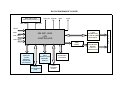
BLOCK DIAGRAM OF MAIN CHASSIS (L5A)
SVHS-Y/C
Tuner IF
SC1-RGB
YUV
YUV
CVBS-IF
Video Decoder
VPC 3230D
Scaler
Stage
HS/VS
PANEL
HS/VS
HS/VS
RGB
FB
RGB
CVBS
HS/VS
VGA-IN
EEPROM
24LC16
Teletext Decoder
SDA 5550
K6T1008V2E
SRAM
(Optional)
M29W040
Flash
Memory
L
R
MSP3410G
AUDIO
L DECODER
R
R
L
R
SIF/AM-mono
Scart 1
Scart 2
SVHS/FAV
TDA1571
Stereo
Amplifier
TDA1308
Headphone
Amplifier
EEPROM
24LC02
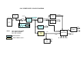
BLOCK DIAGRAM OF SCALER
BAC LIGHT UNIT
S508 (LVDS) S500(TTL)
BR1_ADJ
Panel_En Standby
Mute
Reset
BLK_EN
HS/VS
RGB
LVDS
CONNECTOR
(20 OR 30 PINS)
(S503,S502)
GM 5221 U500
LCD
CONTROLLER
VGA_RGB
VGA HS/VS
S506
CONN.
U501
PARALEL
FLASH
MEMORY
M29W040B
(OPTIONAL)
U503
SERIAL FLASH
MEMORY
M25P40
S505
PROGRAMING
CON
KEYBOARD
CON. S509
U502
EEPROM
24C16
DAUGHTER
BOARD
FOR TTL
INTERFACES
P
A
N
E
L
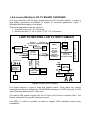
L5A POWER SUPPLY BLOCK DIAGRAM
S600
DC Jack
F600
+15V-STBY
15V,12V
LM2576
U600
S602
LM1117
3.3V
V-INV
LM2576
U607
+5V-STBY
LM1117
1.8V
U605
Fuse
5A
F601
V-INV
V-INV
78L08
U606
3.3V-STBY
1.8V-STBY
+8V
2.5V
+5V
INPUT:
12V FOR 14,15,17 INCH
15V FOR 20, 22 INCH
24V FOR 23 INCH
5V-STBY
78L12
U608
+ 12V
U602
SDI9933ADY
+12V
ONLY FOR 23 "
ONLY FOR 20, 22, 23 "
PNL-EN Power STBY
78L08
U606
+8V
LM117-3.3V
U604
Panel
Power
3.3V
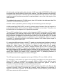
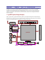
L5-A Low-to-Mid End LCD-TV BOARD OVERVIEW
L5-A Low-to-Mid End LCD TV board incorporates the LCD Controller gm2221, to create a
high quality, stand-alone LCD-based TV system for consumer applications. Figure 1
illustrates the Block diagram of the board.
This board supposed to have two versions:
1. Low-End (to drive 14''-15’’ 4:3 panels)
2. Mid-End (to drive 17’’-20’’ 4:3 and 17’’-22’’-23'' 16:9 panels)
LOW TO MID END LCD TV WITH GM2221
Multimedia
Tuner
RGB, HS, VS
Graphics
Upto SXGA at 75Hz
UXGA at 60Hz
QSS
SDA,SCL
EDID
VGA
CVBS
EXT. CVBS, S-video
Chroma
Decoder
VPC 3230D
ITU 656
8-bit
Scart RGB, FB
8V
Step Down
& Lineer
Regulators
12V
Selected
Video
3.3V 2.5V 1.8V
Teletext
RGB, FB
5V
Teletext
Decoder +MCU
SDA5550
FLASH
GM2221
15",
17",
20''
4:3
NVRAM
ADC+PLL
ITU 656
De-interlace
Scaling
MCU X86
OSD(4bit\pixel)
2 LVDS Tx
1p, 2p\clk
LVDS
24-bit TTL
HS, VS, DE
Upto SXGA at 75Hz
17''
22''
16:9
TFT
LCD
QSS
Ext L/R
FLASH
SDRAM
Audio
Decoder
MSP 3410G
HP
L/R
HP
TDA1308T
Main
L/R
AudioAmp
TDA1517P
L
R
Figure 1 System Block Diagram
L5-A board supports 5 types of video and graphics inputs. These inputs are: Analog
terrestrial tuner input for multisystem PAL/SECAM transmission, SCART input (x2), S-VHS
input, RCA input and analog PC video input.
The analog RGB signals coming from the PC input (via D-Sub15 connector P401) are
directly connected to the gm2221 analog input port.
One EDID IC (U400) is provided on board to support VESA standard plug-and play
compatibility.
On the board, one high quality video decoder (U100) is provided (VPC3230D of Micronas)
to process video inputs coming from the video sources. The video processor can process 3
composite video inputs and 1 S-Cideo input from the NTSC/PAL video sources. The CVBS
output recovered from the tuner module is made available to one of the video inputs of the
video decoder.
The digitized video output (in ITU-656 format) from U100 is fed to the dedicated video Port
of gm2221 for decoding and processing.
Gm2221 makes it possible to perform scaling and de-interlacing for the video input.
A 4Mbit serial flash ROM (U503) is used for storing system firmware. Also the footprint for
a parallel flash ROM, which can be upto 2Mbits, is available on the board. This option can
be used either for development or for production purposes.
The gm2221 provides direct connect via the integrated LVDS transmitters to LCD panels
with integrated LVDS receivers. Both single LVDS (via S503) and double LVDS(via S502)
panels can be supported directly from the L5-A main-board. For single LVDS panels, only
S503 connector is soldered on the main-board, which is a 20 pin connector. For Double
LVDS panels, only S502 connector is soldered on the main-board, which is a 30 pin
connector. For supporting different LVDS panels, different LVDS cables (either single or
double LVDS) can be made used.
For supporting different single or double TTL panels, a daughter board interface is used via
40 pin S506 connector. On this connector, the signals are 3x8bit RGB with TTL control
signals (i.e. HSync, VSync, CLK, O/E etc.) to support a wide variety of LCD panels.
Depending on the panel used, different daughter boards will be used to support that
particular panel. For single TTL panels, the daughter board will just be a routing the RGB
and control signals to the particular connector interface for that particular panel. For double
TTL panels, there will be two LVDS receiver IC’s on the daughter board (double TTL is not
directly from GM2221 but double LVDS is supporter due to IC packaging problems) to
demodulate double LVDS signal into double TTL signal.
The LCD panel resolution supported can be up to SXGA at 75 Hz or UXGA at 60 Hz.
It is important to note that at any point in time gm2221 could drive only one type of Panel.
When LVDS Panel is connected (to connector S503 or S502) ensure that the panel
backlight is connected to S508. The integrated PWM output from gm2221 is used to
control the LCD panel backlight intensity for dimming functions.
The on screen display is implemented using OSD capability of gm2221. Infra Remote (IR)
controller connector (S507) is provided as a primary control interface for connecting IR
detector to the GPIO of gm2221. An IR remote controller unit and detector provide remote
OSD menu access at user convenience.
A keypad connector (S507) is provided which utilizes the integrated low bandwidth ADC in
gm2221 for scanning 5-6 keys (menu,V+,V-,P+,P- keys standard- source key optional) on
the keypad. The keypad allows access to the OSD without using the remote IR controller.
The L5-A board also has In System Programming (ISP) capability for the external flash
ROM using DDC2Bi. This can be done using the D-Sub 15 (PC) connector on the board.
ISP can also be performed using G-probe through the RS232 interface.
One channel of the dual channel FET power switch (U602) is used to control the power
sequencing to the LCD panel. Depending on the type of the panel, the input voltage to this
FET device can be chosen as shown below:
For +3.3V panels
For +5V panels
For +12V panels
J601 is soldered on the main-board
J600 is soldered on the main-board
J603 is soldered on the main-board
An LM2576, a step-down regulator IC (U600), is used to generate the main +5V_STBY
voltage on the board. This IC can deliver up-to 3 Ampers of 5Volts. There is no stand-by
control for this regulator, which means this IC is always on, as soon as power is supplied
to the board.
U603(+3.3V_STBY) and U605 (+1.8V_STBY) linear regulators are used to supply the
voltage necessary for the GM2221 IC and some peripherals. These voltages are also
available in stand-by mode to power the microprocessor inside gm2221, LED, IR receiver
IC and EEPROM. These devices are necessary to wake up the board from stand-by state.
Second channel of the dual channel FET power switch (U602) is used to control cut some
voltages in stand-by mode. These voltages are +5V, +3.3V and +2.5V. These voltages are
used by the video processor (VPC 3230D), audio processor (MSP 34x0G), teletext
processor (SDA5550), tuner and some peripheral IC’s and circuitry. In order to limit the
stand-by power consumption, these voltages are not available in stand-by mode. Also the
audio amplifier (TDA1517) is also in its stand-by mode using its dedicated stand-by pin.
The board employs MSP3410G, a multi-system audio processor solution from Micronas.
The system supports 4 audio input ports, one of which is not used on the L5-A board.
Audio output is provided with speaker and headphone jacks (S409, S401) provided on the
board. The sound IF signal from the tuner is connected to the audio processor directly.
4. GM2221 LCD TV CONTROLLER
The gm2221 IC is a highly integrated single channel scaler that can be used for both LCD
monitors up to SXGA/UXGA resolutions and rear projection systems with DLP and HTPS
LCD engines up to 1280x720 (720P). Some of the key features include:
• Single processing channel.
• RGB and YUV signal processing with RGB to YUV and YUV to RGB color space
converters.
• Video signal processing/de-interlacing using spatial, VT (vertical-temporal) diagonal
interpolation.
• The on-chip turbo x86 micro-controller is used as the system CPU.
• The on-chip OSD controller is available for creating bitmapped OSD menus
• The keypad buttons utilize the input of the on-chip low bandwidth ADC.
• Software IR decoders is used with an external remote controller.
• One of the on-chip PWM outputs is used for controlling back-light intensity
• Integrated LVDS transmitters to LCD panels with integrated LVDS receivers.
The LCD panel resolution supported can be up to SXGA resolutions.
6. LCD PANEL INTERFACE
The L5-A board can drive panels both with LVDS and TTL interfaces. The footprints for
single LVDS and double LVDS connectors are available on the board (S503 and S502,
respectively). Either of these connectors can be used without any changes on the board.
The TTL interface is supported by a daughter board (S506 is the connector for the
daughter board). For the TTL case, connecting the daughter board to the connector will be
sufficient.
A Hirose 30-pin connector (S502) is used for double LVDS link from the board to various
LVDS panels. This connector can also be used for single LVDS, but another connector
footprint (S503) is available for single LVDS purposes. Using only S503 for single LVDS
panels decreases the cost. The LVDS traces are routed differentially from the gm2221 IC
to the connector. These are 100-Ohm differential traces.
L5A SERVICE MENU
Service Menu is entered by pressing 9, 3, 0, 1 keys on the remote controller when the Picture icon is
highlighted in the Main Menu.
Service Menu has 3 sub-menus. These are:
•
Options
•
Adjustments
•
Selections.
Navigation through these menus can be done by pressing OK button. Every adjustment made in this
menu is saved automatically.
OPTIONS
Options are adjustments that the user can select On or Off.
•
BG
•
DK
•
I
•
LL’
•
SCART 2
•
FAV
•
SVHS
•
HOTEL MODE
•
STAND BY
•
MSP CARRIER MUTE
•
WSS SCART
•
FIRST ATS
BG / DK / I / L
Enabling or disabling these options will remove / add these standards to Manual Install menu, SYSTEM
item.
SCART 2 / FAV / SVHS
If a source is disabled in the Service Menu, it will be skipped during source switches. If SCART2 is
enabled, SW assumes that the FAV source share the same path as the SVHS source on the HW. If it is
disabled, it is assumed that FAV and SVHS share separate paths. TUNER and SCART1 are enabled by
default.
HOTEL MODE
Enabling Hotel Mode has two effects. First, SETUP menu is no longer accessible by the user. Second,
maximum adjustable volume value is limited to HOTEL VOLUME value. This value can be adjusted in the
ADJUSTMENTS sub-menu of the Service Menu.
STAND BY
If this Option is OFF, the TV will stay in Stand By mode after a Power On. If this Option is ON, the TV will
recall its last stand by status before the Power Off, and switch on from Stand By automatically, if the last
state was ‘Stand by On’.
MSP CARRIER MUTE
If this option is ON, sound processor’s carrier mute functionality will be enabled. The MSP will mute the
sound automatically if the signal quality is bad. Setting this option Off will disable this functionality.
WSS RF / WSS SCART
Automatic picture format switching for WSS and Pin8 can be enabled or disabled through this option.
If WSS SCART is set to OFF, AUTO picture format mode will be disabled for SCART1 and SCART2
modes. Pin8 source switching will still be operational, but no picture format changes from Pin8 voltage
level will be ignored.
ATS
If this option is set to ON, TV will display Country Selection menu in the next start. After some country is
selected, the user will be prompted for the start of AutoProgramming process.
ADJUSTMENTS
This sub-menu contains numeric adjustments. These items are:
•
WHITE R
•
WHITE G
•
WHITE B
•
PRESCALE FM
•
PRESCALE NICAM
•
PRESCALE SCART
•
HOTEL VOLUME
WHITE R / WHITE G / WHITE B
These are used for color bias adjustment. Unlike other items in the service menu, changes will take effect
immediately.
PRESCALE FM / PRESCALE NICAM / PRESCALE SCART
These are prescale values that will be used for the initialization of the sound processor (MSP), at the next
switch on.
HOTEL VOLUME
This value is used as the volume limit, when the Hotel Mode is on.
SELECTIONS
This sub-menu contains selections.
•
TUNER TYPE
SAMSUNG / PHILIPS
•
TELETEXT
NO TEXT / FAST / FAST&TOP
•
MSP CLIP
REDUCE VOL / REDUCE TONE / COMPROMISE / DYNAMIC
TUNER TYPE
One of two supported tuner can be selected from this item. System must be restarted for this change to
take effect.
TELETEXT
NO TEXT: Teletext is totally disabled. TXT/MIX button will not be functional. AUTO picture format mode
will be disabled in RF, F-AV and SHVS modes. Naming and sorting functionality during Autoprogramming
will be disabled.
FAST: TOPtext functionality will be disabled.
FAST&TOP: TOPtext functionality is enabled.
TIMER MODE
If OFF TIMER is selected, the user will be able to enter time of the day info for the TV to switch off. If
SLEEP TIMER is selected, the user can specify some time period, after which the TV will go to stand by
automatically.
MSP CLIP
This selection identifies which method will be used by the sound processor to prevent clipping effects on
volume. Details can be found in data sheet msp34x0g_4pd.pdf, page 30.
AUTOPROGRAMMING
When the user selects the Autoprogram item in Setup menu, Country Selection menu is opened. The user
must select a country before the Autoprogramming starts. Broadcast system will be selected according to
the country selected.
Broadcast systems according to countries:
BELGIUM
BG + L
CROATIA
BG
CZECH REP.
DK
DENMARK
BG
FINLAND
BG
FRANCE
L + BG
GERMANY
BG
GREECE
BG
HUNGARY
DK
IRELAND
I
ITALY
BG
NETHERLANDS
BG
NORWAY
BG
POLAND
DK
PORTUGAL
BG
SPAIN
BG
SWEDEN
BG
SWITZERLAND
BG + L
TURKEY
BG
UNITED KINGDOM
I
For countries France, Belgium and Switzerland, autoprogramming is done twice. For Belgium and
Switzerland, first BG channels will be searched, after the search in BG is done, searching will restart for L
standard. If the selected country is France, the sequence of standards is reversed, thus, first L then BG.
TELETEXT LANGUAGES
L5A SW decides which teletext language group will be used for teletext decoding, according to the
country selected for autoprogramming.Teletext languages according to countries:
EAST EUROPE:CROATIA ,CZECH_REP, POLAND
WEST EUROPE: BELGIUM ,DENMARK, FINLAND, UK, FRANCE, GERMANY,
IRELAND ,ITALY ,NETHERLANDS, NORWAY, PORTUGAL,SPAIN, SWEDEN, SWITZERLAND,
HUNGARY
TURKISH-GREEK:GREECE TURKEY
PC MODE
PC mode can be entered by pressing PC button on the remote controller. User can return back to TV
mode by pressing the PC or TV buttons.
After the switching to PC mode, VGA input will be displayed on screen, as soon as the mode (input
resolution and frequency) is determined.
If there is no input from the VGA input, NO SIGNAL dialog will be displayed for 15 seconds. At the end of
this period if there is no signal from VGA input, the TV will go to Sleep State. While in the sleep state, the
TV will keep monitoring the VGA input. If VGA signal is detected, the TV will wake from Sleep State, to PC
mode. Alternatively, the user may select to switch the TV on from Sleep State, just like switching on from
Stand-by. In this case, the set will switch on from TV mode.
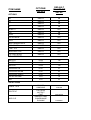
OPTIONS/
VALUES
DEFAULT
VALUES OR
SETUP
BG
ON/OFF
ON
DK
ON/OFF
ON
I
ON/OFF
ON
LL'
ON/OFF
ON
SCART 2
ON/OFF
OFF
FAV
ON/OFF
ON
SVHS
ON/OFF
ON
HOTEL MODE
ON/OFF
OFF
STBY
ON/OFF
OFF
MSP CARRİER MUTE
ON/OFF
OFF
WSS SCART
ON/OFF
ON
FIRST ATS
ON/OFF
OFF
BACKLIGHT POL
ON/OFF
OFF
FACTORY MODE
ON/OFF
OFF
WHITE R
0-255
128
WHITE G
0-255
128
WHITE B
0-255
128
PRESCALE FM
0-127
37
PRESCALE NICAM
0-127
63
PRESCALE SCART
0-127
27
HOTEL VOLUME
0-63
16
AGC
0-31
23
PHILIPS
SAMSUNG
PHILIPS
ITEM NAME
OPTIONS
ADJUSTMENTS
SELECTIONS
TUNER TYPE
TELETEXT
MSP CLIP
FAST&TOP
NO TEXT
FAST
REDUCE TONE
COMPROMISE
DYNAMIC
FAST&TOP
DYNAMIC
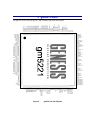
GENESIS
GM5221
LCD TV CONTROLLER
The gm5221 is an LCD TV controller supporting resolutions up to SXGA (1280x1024). The gm5221
leverages Genesis patented advanced image-processing technology as well as a proven integrated
ADC/PLL and an Ultra-Reliable DVI™ compliant digital receiver to provide excellent image quality.
gm5221 also integrates a microcontroller, an OSD controller, advanced color management and dual
LVDS transmitters.
1.1 gm5221 System Design Example
Figure 1 below shows a typical dual interface LCD TV system based on the gm5221. Designs based on
the gm5221 have reduced system cost, simplified hardware and firmware design and increased reliability
because only a minimal number of components are required in the system.
IR
KEY BOARD
TUNER
PACK
C
V
B
S
S
V
I
D
E
O
VIDEO
DECODER
L
C
D
V CHIP
gm5221
Y
Pb
Pr
V
G
A
M
U
X
D
V
I
EEPROM
AUDIO
PROCESSOR
Figure 1.
AUDIO
AMPL
gm5221 System Design Example
D
I
S
P
L
A
Y
1.2 gm5221 Family Features
•
Intelligent Image Processing™
•
•
•
•
•
•
•
•
Ultra-Reliable DVI-Compliant Input Port
•
•
•
•
•
•
•
Supporting NTSC / PAL interlaced and progressive
Direct connect to commercially available video decoders
Spatial de-interlacing
Advanced Color Management
•
•
•
Programmable gamma correction (CLUT)
TV color controls including hue and saturation controls
Full color matrix allows end-users to experience the same
colors as viewed on CRTs and other displays (e.g. sRGB
compliance)
Advanced Active Color Management ™ (ACM-II) provide
flesh-tone compensation and image enhancement for video
preset modes like sport, nature .
Adaptive Contrast and Color™ (ACC) ensures full dynamic
range is used in video content
On-chip Versatile OSD Controller
•
•
•
•
•
•
•
•
On-chip RAM for high-quality programmable menus
1, 2 and 4-bit per pixel character cells
Horizontal and vertical stretch of OSD menus
Blinking, transparency and blending
Supports two independent OSD menu rectangles
Proportional fonts
Digital clock spectrum management
Eliminates EMI suppression components and shielding
Built-in LVDS Transmitters
•
•
•
•
•
Simplifies manufacturing / test
Energy Spectrum Management (ESM™)
•
•
•
High-performance X86 MCU with on-chip RAM and ROM
External parallel ROM or serial SPI ROM interface
Unified memory architecture simplifies chip programming
23 general-purpose inputs/outputs (GPIOs) available
2-wire serial bus master to control NVRAM, video decoder
Two DDC2Bi ports with DMA buffer to internal RAM
Four PWM outputs for analog backlight control, audio, etc.
General-purpose ADC’s for keypad and temperature sensing
Integrated reset circuit
Slow clock mode for 50mW sleep mode power consumption
JTAG debug / ICE support for firmware debugging
Built-in Test Pattern Generator
•
Operating up to 165 MHz (up to UXGA 60Hz)
Direct connect to all DVI 1.0-compliant transmitters
High-bandwidth Digital Content Protection (HDCP)
Note: HDCP function is available H version only.
CCIR-656 8-bit Video Input Port
•
•
•
•
Supports SDTV RGB inputs in interlaced mode
Supports EDTV (480p) up to 1080i HDTV inputs
Supports mid level clamp for YPbPr inputs
Macro vision decoding
Supports up to 162 MHz (SXGA 75Hz / UXGA 60Hz)
On-chip high-performance PLLs (single reference crystal
required)
Composite-sync, Sync-on-Green (SOG) and Sync-on-Y
(SoY) support
Input format detection
Phase and image positioning
Embedded X86 On-chip Microcontroller
•
•
•
•
•
•
•
•
•
•
•
Analog RGB Input Port
•
•
•
•
•
•
•
•
Fully programmable zoom ratios
High-quality shrink capability from UXGA resolution
Programmable coefficients for variable sharpness control
RealRecovery™ provides full color recovery image for
refresh rates higher than those supported by the LCD panel
Four channel 6/8-bit LVDS transmitter
Support for 8 or 6-bit panels with high-quality dithering
Single / double wide up to SXGA 75Hz output
Pin swap, odd / even swap and red / blue group swap of RGB
outputs for flexibility in board layout
Highly integrated System-on-a-Chip
•
•
•
•
•
•
All system clocks synthesized from a single external crystal
50mW power saving mode
5-Volt tolerant inputs
Two Layer PCB support
On-chip reset feature to eliminate external reset component
Integrated Schmitt trigger for HSYNC and VSYNC
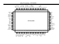
PACKAGE
•
•
208-pin PQFP
3.3V IO and 1.8V core power supplies
2 gm5221 Pinout
53
54
55
56
57
58
59
60
61
62
63
64
65
66
67
68
69
70
71
72
73
74
75
76
77
78
79
80
81
82
83
84
85
86
87
88
89
90
91
92
93
94
95
96
97
98
99
100
101
102
103
104
1
2
3
4
5
6
7
8
9
10
11
12
13
14
15
16
17
18
19
20
21
22
23
24
25
26
27
28
29
30
31
32
33
34
35
36
37
38
39
40
41
42
43
44
45
46
47
48
49
50
51
52
N/C
N/C
DCLK
JTAG_RESET
RESERVED
RESERVED
RESERVED
RESERVED
RESERVED
RESERVED
RESERVED
JTAG_TDO
RESERVED
JTAG_TDI
PPWR
PBIAS
GPIO15
RESERVED
HOST_SCL/UART_DI
HOST_SDA/UART_DO
RVDD_3.3
CRVSS
CVDD_1.8
CRVSS
DDC_SCL_VGA
DDC_SDA_VGA
DDC_SCL_DVI
DDC_SDA_DVI
GPIO0
GPIO1
GPIO2
GPIO3
GPIO4
CVDD_1.8
CRVSS
GPIO5
GPIO6
GPIO7/IRQin
GPIO8/IRQout
GPIO9/SCL
GPIO10/SDA
CRVSS
RVDD_3.3
CVDD_1.8
CRVSS
GPIO11/PWM0
GPIO12/PWM1
GPIO13/PWM2
GPIO14/PWM3
GPIO16/VDATA7
GPIO17/VDATA6
N/C
ROM_DATA3
ROM_DATA2
ROM_DATA1
ROM_DATA0
ROM_OEn
ROM_WEn
ROM_CSn
CRVSS
CVDD_1.8
RESERVED
AVDD_LV_E_3.3
AVSS_LV_E
CH3P_LV_E/ER0
CH3N_LV_E/ER1
CLKP_LV_E/ER2
CLKN_LV_E/ER3
CH2P_LV_E/ER4
CH2N_LV_E/ER5
CH1P_LV_E/ER6
CH1N_LV_E/ER7
CH0P_LV_E/EG0
CH0N_LV_E/EG1
AVSS_LV_E
AVDD_LV_E_3..3
AVSS_LV
AVDD_LV_3.3
AVDD_LV_O_3.3
AVSS_LV_O
CH3P_LV_O/EG2
CH3N_LV_O/EG3
CLKP_LV_O/EG4
CLKN_LV_O/EG5
CH2P_LV_O/EG6
CH2N_LV_O/EG7
CH1P_LV_O/EB0
CH1N_LV_O/EB1
CH0P_LV_O/EB2
CH0N_LV_O/EB3
AVSS_LV_O
AVDD_LV_O_3..3
CVDD_1..8
CVSS
EB4
EB5
EB6
EB7
DEN
DHS
DVS
RVDD_3.3
CRVSS
N/C
208
207
206
205
204
203
202
201
200
199
198
197
196
195
194
193
192
191
190
189
188
187
186
185
184
183
182
181
180
179
178
177
176
175
174
173
172
171
170
169
168
167
166
165
164
163
162
161
160
159
158
157
ROM_DATA4
ROM_DATA5
CRVSS
RVDD_3.3
ROM_DATA6
ROM_DATA7
ROM_ADDR0
ROM_ADDR1
ROM_ADDR2
ROM_ADDR3
ROM_ADDR4
ROM_ADDR5
ROM_ADDR6
ROM_ADDR7
ROM_ADDR8
ROM_ADDR9
ROM_ADDR10
CRVSS
RVDD_3.3
ROM_ADDR11
ROM_ADDR12
ROM_ADDR13
ROM_ADDR14
ROM_ADDR15
ROM_ADDR16
ROM_ADDR17
VSYNC
HSYNC/CSYNC
CRVSS
CVDD_1.8
RESETn
LBADC_GND
LBADC_RETURN
LBADC_IN3
LBADC_IN2
LBADC_IN1
LBADC_VDD_3.3
AVDD_RPLL_3.3
TCLK
XTAL
AGND_RPLL
RESERVED
VDD_RPLL_1.8
GND_RPLL
VDD_ADC_1.8
GND_ADC
N/C
N/C
N/C
N/C
N/C
N/C
The gm5221 devices are packaged in a 208-pin Plastic Quad Flat Pack (PQFP).
Figure 2.
gm5221 Pin Out Diagram
156
155
154
153
152
151
150
149
148
147
146
145
144
143
142
141
140
139
138
137
136
135
134
133
132
131
130
129
128
127
126
125
124
123
122
121
120
119
118
117
116
115
114
113
112
111
110
109
108
107
106
105
AGND_ADC
RESERVED
AVDD_ADC_3.3
AGND_RED
REDRED+
AVDD_RED_3.3
AGND_GREEN
GREENGREEN+
SOG_MCSS
AVDD_GREEN_3.3
AGND_BLUE
BLUEBLUE+
AVDD_BLUE_3.3
CRVSS
CVDD_1.8
RESERVED
VDD_RXPLL_1.8
GND_RXPLL
RESERVED
AVDD_RXC_3.3
RXCRXC+
AGND_RXC
AVDD_RX0_3.3
RX0RX0+
AGND_RX0
VDD_RX0_1.8
AVDD_RX1_3.3
RX1RX1+
AGND_RX1
VDD_RX1_1.8
AVDD_RX2_3.3
RX2RX2+
AGND_RX2
VDD_RX2_1.8
AGND_IMB
REXT
AVDD_IMB_3.3
VCLK
GPIO23/VDATA0
GPIO22/VDATA1
GPIO21/VDATA2
GPIO20/VDATA3
GPIO19/VDATA4
GPIO18/VDATA5
N/C
C7
C6
C5
C4
VSUPC
GNDC
C3
C2
C1
C0
GNDSY
VSUPSY
INTLC
AVO
FSY/HC
MSY/HS
VS
FPDAT
VSTBY
CLK5
NC
XTAL1
XTAL2
ASGF
Video Processing - VPC3230D
64 63 62 61 60 59 58 57 56 55 54 53 52 51 50 49 48 47 46 45 44 43 42 41
GNDF
VRT
I2CSEL
ISGND
VSUPF
VOUT
CIN
VIN1
VIN2
VIN3
65
66
40
39
67
68
38
37
69
36
70
71
35
34
72
73
33
32
VPC3230D
76
77
29
28
FB1IN
78
79
27
26
AISGND
80
25
FFOE
CLK20
FFRE
FFWE
FFRSTW
9 10 11 12 13 14 15 16 17 18 19 20 21 22 23 24
YCOEQ
FFIE
7 8
VGAV
6
TEST
5
SDA
RESQ
4
GNDCAP
SCL
3
GNDD
2
VSUPD
1
G2/Y2IN
R2/CR2IN
GNDAI
VREF
R1/CR1IN
B2/CB2IN
VSUPAI
B1/CB1IN
G1/Y1IN
VIN4
VSUPCAP
31
30
ASGF
NC
74
75
Y0
Y1
Y2
Y3
VSUPY
GNDY
Y4
Y5
Y6
Y7
GNDLLC
VSUPLLC
LLC1
LLC2
VSUPPA
GNDPA
Video Processing - VPC3230D
1. Features
Video Decoding
- 4 Composite inputs, 1 S-VHS input
- Composite video & sync output
- integrated high-quality A/D converters
- Adaptive 2H comb filter Y/C separator
- 1H NTSC comb filter
- Multi-standard color decoder(1 Crystal)
- Multi-standard sync decoder
- Black line detector
Video Decoding
- Horizontal scaling(0.25 to 4)
- Panorama vision
- Black level expander
- Dynamic peaking
- Soft limiter(gamma correction)
- Color transient improvement
RGB Processing
- Programmable RGB matrix
- Digital color bus interface
- Additional analog RGB/Fast blank input
- Half contrast switch
- Picture frame generator
Deflection
- Scan velocity modulation output
- High performance H/V deflection
- Separate ADC for tube measurements
- EHT compensation
Miscellaneous
- One 20.25MHz crystal, few external components
- Embedded RISC controller(80 MIPS)
- I2C Bus interface
- Single 5V power supply
- Submicrom COMS technology
- 64 pin PSDIP package
Block Diagram
CIN1
VIN1
Adaptive
Comb
Filter
Analog
Front End
Color
Decoder
VIN2
NTSC,
PAL,
SECAL
VIN3
VIN4
AGC,
2*ADC
FB
RGB/
YCbCr
Y/G
ANALOG
Component
Front-End
Saturation
Tint
MIXER
2D Scaler
PIP
Panorama
Mode
Contrast
Brightness
Peaking
Output
Formatter
U/B
ITU-R 656
ITU-R 601
YCOE
Memory
Control
FIFO
CNTL
Y
LL Clock
FB
Cr
Matrix
Contrast
Saturation
Brightness
Tint
SYNC
+
Clock
Generation
Cb
FB
Y OUT
CrCb OUT
I2C BUS
V/R
4 x ADC
Processing
Cr
Cb
NTSC
PAL
VOUT
RGB/
YCbCr
Y
H Sync
Vsync
CNTL
AVI0
Clock
Gen.
20.25MHz
Video Processing - VPC3230D
Pin
Pin Name
No.
Type
Short Description
Pin
No.
Pin Name
Type
Short Description
1
B1/CB1IN
IN
Blue1/Cb1 Analog Component Input
25
GND PA SUPPLYD
Ground, Pad Decoupling Circuitry
2
G1/Y1IN
IN
Green1/Y1 Analog Component Input
26
V SUPPA SUPPLYD
Supply Voltage, Pad Decoupling Circuitry
3
R1/CR1IN
IN
Red1/Cr1 Analog Component Input
27
LLC2
OUT
Double Clock Output
4
B2/CB2IN
IN
Blue2/Cb2 Analog Component Input
28
LLC1
IN/OUT
5
G2/Y2IN
IN
Green2/Y2 Analog Component Input
29
V SUPLLCSUPPLYD
Supply Voltage, LLC Circuitry
6
R2/CR2IN
IN
Red2/Cr2 Analog Component Input
30
GND LLC SUPPLYD
Ground, LLC Circuitry
7
ASGF
Analog Shield GND F
31
Y7
OUT
Picture Bus Luma (MSB)
8
NC
No connected
32
Y6
OUT
Picture Bus Luma
9
V SUPCAPSUPPLYD
Supply Voltage, Digital Decoupling
Circuitry
33
Y5
OUT
Picture Bus Luma
10
V SUPD SUPPLYD
Supply Voltage, Digital Circuitry
34
Y4
OUT
Picture Bus Luma
11
GND D
Ground, Digital Circuitry
35
GND Y
SUPPLYD
Ground, Luma Output Circuitry
12
GND CAP SUPPLYD
Ground, Digital Decoupling Circuitry
36
V SUPY
SUPPLYD
Supply Voltage, Luma Output Circuitry
13
SCL
IN/OUT
I 2 C Bus Clock
37
Y3
OUT
Y Picture Bus Luma
14
SDA
IN/OUT
I 2 C Bus Data
38
Y2
OUT
Y Picture Bus Luma
15
RESQ
IN
Reset Input, Active Low
39
Y1
OUT
Y Picture Bus Luma
16
TEST
IN
Test Pin, connect to GND D
40
Y0
OUT
Y Picture Bus Luma(LSB)
17
VGAV
IN
VGAV Input
41
C7
OUT
Picture Bus Chroma (MSB)
18
YCOEQ
IN
Y/C Output Enable Input, Active Low
42
C6
OUT
Picture Bus Chroma
19
FFIE
OUT
FIFO Input Enable
43
C5
OUT
Picture Bus Chroma
20
FFWE
OUT
FIFO Write Enable
44
C4
OUT
Picture Bus Chroma
21
FFRSTW
OUT
FIFO Reset Write/Read
45
V SUPC SUPPLYD
Supply Voltage, Chroma Output Circuitry
22
FFRE
OUT
FIFO Read Enable
46
GND C
Ground, Chroma Output Circuitry
23
FFOE
OUT
FIFO Output Enable
47
C3
OUT
Picture Bus Chroma
24
CLK20
IN/OUT
48
C2
OUT
Picture Bus Chroma
-
SUPPLYD
Main Clock Output 20.25 MHz
SUPPLYD
Clock Output
Video Processing - VPC3230D
Pin
Pin Name
No.
Type
49
C1
OUT
Picture Bus Chroma
71
CIN
IN
Chroma / Analog Video 5 Input
50
C0
OUT
Picture Bus Chroma(LSB)
72
VIN1
IN
Video 1 Analog Input
51
GND SY SUPPLYD
Ground, Sync Pad Circuitry
73
VIN2
IN
Video 2 Analog Input
52
V SUPSY SUPPLYD
Supply Voltage, Sync Pad Circuitry
74
VIN3
IN
Video 3 Analog Input
53
INTLC
OUT
Interlace Output
75
VIN4
IN
Video 4 Analog Input
54
AVO
OUT
Active Video Output
76
55
FSY/HC
OUT
Front Sync/ Horizontal Clamp Pulse
56
MSY/HS
IN/OUT
57
VS
58
FPDAT
IN/OUT
V SUPAI SUPPLYA Supply Voltage, Analog Component
Inputs Front-End
GND AI SUPPLYA Ground, Analog Component Inputs
Front-End
Reference Voltage Top, Analog
VREF
OUT
Component Inputs Front-End
FB1IN
IN
Fast Blank Input
59
V STBY
SUPPLYA
60
CLK5
61
NC
62
XTAL1
IN
63
XTAL2
OUT
64
ASGF
65
GND F
66
VRT
67
I2CSEL
IN
68
ISGND
SUPPLYA
Signal Ground for Analog Input,
connect to GND F
69
V SUPF
SUPPLYA
Supply Voltage, Analog Front-End
70
VOUT
OUT
OUT
-
Short Description
OUT
OUT
77
Main Sync/Horizontal Sync Pulse
Vertical Sync Pulse
78
Front-End/ Back-End Data
79
Standby Supply Voltage
80
CCU 5 MHz Clock Output
No connected
Analog Crystal Input
Analog Crystal Output
Analog Shield GND F
SUPPLYA
Pin
Pin Name
No.
Ground, Analog Front-End
Reference Voltage Top, Analog
I 2 C Bus Address Select
Analog Video Output
Type
Short Description
AISGND SUPPLYA Signal Ground for Analog Component
Inputs, connect to GND AI
NC
NC
AHVSS
AHVSS
AGNDC
NC
SC4_IN_L
SC4_IN_R
ASG4
SC3_IN_L
SC3_IN_R
ASG2
SC2_IN_L
SC2_IN_R
ASG1
SC1_IN_L
SC1_IN_R
VREFTOP
NC
MONO_IN
AVSS
AVSS
NC
NC
Audio Processing - MSP3440G
64 63 62 61 60 59 58 57 56 55 54 53 52 51 50 49 48 47 46 45 44 43 42 41
AVSUP
AVSUP
65
66
40
39
CAPL_M
AHVSUP
ANA_IN1+
67
68
38
37
CAPL_A
SC1_OUT_L
69
70
36
35
SC1_OUT_R
71
72
34
33
SC2_OUT_L
ANA_INANA_IN2+
TESTEN
XTAL_IN
XTAL_OUT
TP
MSP3410D
AUD_CL_OUT
NC
74
32
31
75
30
NC
D_CTR_I/O_1
76
77
29
D_CTR_I/O_0
78
79
28
27
ADR_WS
DACA_R
ADR_DA
NC
I2S_DA_IN1
NC
I2S_DA_OUT
RESETQ
I2S_WS
NC
I2S_CL
NC
I2C_DA
NC
9 10 11 12 13 14 15 16 17 18 19 20 21 22 23 24
I2S_DA_IN2
8
DVSS
7
DVSS
6
DVSS
5
DVSUP
4
DVSUP
3
DVSUP
2
ADR_CL
1
I2C_CL
80
NC
ADR_SEL
STANDBYQ
73
VREF1
SC2_OUT_R
ASG3
NC
DACM_SUB
NC
DACM_L
26
DACM_R
VREF2
25
DACA_L
Audio Processing - MSP3410D
Pin
Pin Name
No.
1
NC
2
I2C_CL
3
Type
Short Description
Pin
Pin Name
No.
Type
Short Description
Not connected
26
V SUPPA SUPPLYD
Supply Voltage
IN/OUT
I2Cclock
27
LLC2
OUT
Double Clock Output
I2C_DA
IN/OUT
I2C data
28
LLC1
IN/OUT
4
I2S_CL
IN/OUT
I2S clock
29
V SUPLLCSUPPLYD
Supply Voltage, LLC Circuitry
5
I2S_WS
IN/OUT
I2S word strobe
30
GND LLC SUPPLYD
Ground, LLC Circuitry
6
I2S_DA_OUTOUT
I2S data output
31
Y7
OUT
Picture Bus Luma (MSB)
7
I2S_DA_IN1 IN
I2S1 data input
32
Y6
OUT
Picture Bus Luma
8
ADR_DA
OUT
ADR data output
33
Y5
OUT
Picture Bus Luma
9
ADR_WS
OUT
ADR word strobe
34
Y4
OUT
Picture Bus Luma
10
ADR_CL SUPPLYD
Supply Voltage, Digital Circuitry
35
GND Y
SUPPLYD
Ground, Luma Output Circuitry
11
DVSUP
SUPPLYD
Ground, Digital Circuitry
36
V SUPY
SUPPLYD
Supply Voltage, Luma Output Circuitry
12
DVSUP
SUPPLYD
Ground
37
Y3
OUT
Y Picture Bus Luma
13
DVSUP
IN/OUT
I 2 C Bus Clock
38
Y2
OUT
Y Picture Bus Luma
14
DVSS
IN/OUT
I 2 C Bus Data
39
Y1
OUT
Y Picture Bus Luma
15
DVSS
IN
Reset Input, Active Low
40
Y0
OUT
Y Picture Bus Luma(LSB)
16
DVSS
IN
Test Pin, connect to GND D
41
C7
OUT
Picture Bus Chroma (MSB)
17
I2S_DA_IN2 IN
VGAV Input
42
C6
OUT
Picture Bus Chroma
18
NC
IN
Y/C Output Enable Input, Active Low
43
C5
OUT
Picture Bus Chroma
19
NC
OUT
FIFO Input Enable
44
C4
OUT
Picture Bus Chroma
20
NC
OUT
FIFO Write Enable
45
V SUPC SUPPLYD
Supply Voltage, Chroma Output Circuitry
21
RESET_Q
OUT
FIFO Reset Write/Read
46
GND C
Ground, Chroma Output Circuitry
22
NC
OUT
FIFO Read Enable
47
C3
OUT
Picture Bus Chroma
23
NC
OUT
FIFO Output Enable
48
C2
OUT
Picture Bus Chroma
24
DACA_R
49
C1
OUT
Picture Bus Chroma
25
DACA_R SUPPLYD
50
C0
OUT
Picture Bus Chroma(LSB)
IN/OUT
Main Clock Output 20.25 MHz
Ground
SUPPLYD
Clock Output
Audio Processing - MSP3440G
Pin
Pin Name
No.
Type
Short Description
Pin
Pin Name
No.
Short Description
Type
51
GND SY SUPPLYD
Ground, Sync Pad Circuitry
72
XTAL_OUT OUT
Crystal oscillator
52
V SUPSY SUPPLYD
Supply Voltage, Sync Pad Circuitry
73
TP
Test pin
53
INTLC
OUT
Interlace Output
74
AUD_CL_OUT
OUT
Audio clock output(18.432MHz)
54
AVO
OUT
Active Video Output
75
NC
Not connected
55
FSY/HC
OUT
Front Sync/ Horizontal Clamp Pulse
MSY/HS
IN/OUT
76
NC
Not connected
56
57
SC1_in_R
SCART 1input,right
77
D_CTR_I/O_1
IN/OUT
D_CTR_I/O_1
58
VREFTOP
Reference voltage IF A/D converter
78
D_CTR_I/O_0
IN/OUT
D_CTR_I/O_0
59
NC
Not connected
79
ADR_SEL
IN
I2C Bus address select
60
MONO_IN
AVSS
80
STANDBYQ
IN
Stand-by(low active)
61
Analog ground
62
AVSS
Analog ground
63
NC
Not connected
64
NC
Not connected
65
AVSUP
Analog power supply 5V
66
AVSUP
Analog power supply 5V
67
ANA_IN+
IN
IF input 1
68
ANA_IN-
IN
IF common{can be left vacant,only
if IF input1 is also not in use}
69
ANA_IN2+
IN
IF input{can be left vacant,only if
IF input1 is also not in use}
70
TESTEN
IN
Test pin
71
XTAL_IN
IN
Crystal oscillator
IN
IN
Main Sync/Horizontal Sync Pulse
Mono input
SDA5550 MICROCONTROLLER
BLOCK DIAGRAM
L5A SPARE PART LIST
POSITION
F600
IR1
MENU
S602
TU201
U100
U301
U304
U400
U401
U402
U403
U500
U502
U600
U602
U603
U604
U605
Y100
Y300
Y400
Y500
BEKO CODE
056T14-AU1
056T20-AU1
8R9107-AS
8R9850-00A
8R9953
Y48120
Y48121
Y48913
Y92913
ZC5850-00A
ZF9110
ZF9187F
ZG4110
ZG4255-01
ZH1183-CH1
ZH6183-AU3
054290
452521-01
010844
ZC5502-AS
Y56502-AS
ZC5513-AS
8R9100-AS
031274
8R8138-PH1
452937
453013
452662-02
453010
453026
453021
452706-01
453296
452662-02
453294
401372
453124
453124
453295
056161
056953
056952
056119
PART DESCRIPTION
LCD AU OPTRONICS T140VN01 14" LCD TV
LCD AU A201SN01 V.3 (20" LCD TV)
SPEAKER 4R 5W LCD TV
ACCESSORIE BOX 17" LCD TV BEKO
POWER SWITCH LCD TV
L5 CHASIS 20" DAUGHTER BOARD L5A VER
L5A CHASIS 20" DAUGHTER BOARD CH CHI
ADAPTOR AC 15V 4.6A 20" CLASS II
ADAPTOR AC12V/5A CLASS II
ACCESSORIE BOX 20" LCD TV BEKO
L5A CHASIS 14"TOS P/NX/1/K/S/VGA/NT A-OS
RC L5A TOSHIBA GRI/SHINE SI.P.ED CT-873
L5A CHASIS 20"TOS AU P/NX/2/K/S/VGA/NT
BACK COVER TOSH.BRI.SIL.P.20" LCDTV VGA
INVERTOR 20" V201V1-T01 (PLCD0318604H)
INVERTOR 14" AUO TAILON TLI-04-0411-A2
FUSE 5.0A 250V ROUND
IR RECEIVER TSOP34838 SS1A
TACT SWITCH 2 LEG (MTSB)
CABLE PANEL INTERFACE LCD20" CHIMEI
KAB.PANEL INTERFACE LCD TV 15" MOLEX L5A
CABLE PANEL INVERTOR LCDTV FERRIT 20 CHI
CABLE LCD POWER SWITCH L=350MM
JACK POWER HORIZONTAL
TUNER FRONTEND PHILIPS FQ1216MEPT/I H-3
IC-CHIP VPC3230D-C5 QFP80 T&R
IC SDA5550 PLCC-84 TRAY
IC-CHIP AT24C16AN 10SI2.7 TAPE&REEL
IC -CHIP M24C02 - MN6T (4.5 - 5.5V) SO8
IC-CHIP MSP3410G PQFP80 T&R
IC TDA1517P
IC TDA1308T/N2 SO-G8 (T&R)
IC-CHIP GM2221 208PIN PQFP TRAY
IC-CHIP AT24C16AN 10SI2.7 TAPE&REEL
IC-CHIP LM2576D2TR4-005V 3A TO263 STPT&R
TRN FDS9933A
IC-CHIP NCP1117DT33RK TO-252 PACKAGE
IC-CHIP NCP1117DT33RK TO-252 PACKAGE
IC-CHIP NCP1117DT18RK TO252 (T&R)
CRYSTAL 20.25MHZ HC49-U
CRYSTAL 6MHZ CL 20PF
CRYSTAL 18.432MHZ +-30PPM
CRYSTAL 14.31818MHz CL=18PF30/30PPMHC49U
FREQUENCY TABLE (MHz)
Channel
Number
BG
CH
CH
CH
CH
CH
CH
CH
CH
CH
CH
CH
CH
CH
CH
CH
CH
CH
CH
CH
CH
CH
CH
CH
CH
CH
CH
CH
CH
CH
CH
CH
CH
CH
CH
CH
CH
CH
CH
CH
CH
CH
CH
CH
CH
1
2
3
4
5
6
7
8
9
10
11
12
13
14
15
16
17
18
19
20
21
22
23
24
25
26
27
28
29
30
31
32
33
34
35
36
37
38
39
40
41
42
43
44
48.25
55.25
62.25
175.25
182.25
189.25
196.25
203.25
210.25
217.25
224.25
53.75
62.25
82.25
175.25
183.25
192.25
201.25
210.25
471.25
479.25
487.25
495.25
503.25
511.25
519.25
527.25
535.25
543.25
551.25
559.25
567.25
575.25
583.25
591.25
599.25
607.25
615.25
623.25
631.25
639.25
647.25
655.25
I
DK
L/L'
49.75
59.25
77.25
85.25
93.25
175.25
183.25
191.25
199.25
207.25
215.25
223.25
45.75
53.75
61.75
69.75
95.25
49.75
59.25
77.25
85.25
93.25
175.25
183.25
191.25
199.25
207.25
215.25
223.25
47.75
55.75
60.50
63.75
176.00
184.00
192.00
200.00
208.00
216.00
189.25
182.25
196.25
210.25
471.25
479.25
487.25
495.25
503.25
511.25
519.25
527.25
535.25
543.25
551.25
559.25
567.25
575.25
583.25
591.25
599.25
607.25
615.25
623.25
631.25
639.25
647.25
655.25
471.25
479.25
487.25
495.25
503.25
511.25
519.25
527.25
535.25
543.25
551.25
559.25
567.25
575.25
583.25
591.25
599.25
607.25
615.25
623.25
631.25
639.25
647.25
655.25
471.25
479.25
487.25
495.25
503.25
511.25
519.25
527.25
535.25
543.25
551.25
559.25
567.25
575.25
583.25
591.25
599.25
607.25
615.25
623.25
631.25
639.25
647.25
655.25
Channel
Number
BG
I
DK
L/L'
CH
CH
CH
CH
CH
CH
CH
CH
CH
CH
CH
CH
CH
CH
CH
CH
CH
CH
CH
CH
CH
CH
CH
CH
CH
CH
CH
CH
CH
CH
CH
CH
CH
CH
CH
CH
S
S
S
S
S
S
S
S
S
S
S
S
S
S
45
46
47
48
49
50
51
52
53
54
55
56
57
58
59
60
61
62
63
64
65
66
67
68
69
70
71
72
73
74
75
76
77
78
79
80
1
2
3
4
5
6
7
8
9
10
11
12
13
14
663.25
671.25
679.25
687.25
695.25
703.25
711.25
719.25
727.25
735.25
743.25
751.25
759.25
767.25
775.25
783.25
791.25
799.25
807.25
815.25
823.25
831.25
839.25
847.25
855.25
663.25
671.25
679.25
687.25
695.25
703.25
711.25
719.25
727.25
735.25
743.25
751.25
759.25
767.25
775.25
783.25
791.25
799.25
807.25
815.25
823.25
831.25
839.25
847.25
855.25
863,25
871,25
879,25
887,25
663.25
671.25
679.25
687.25
695.25
703.25
711.25
719.25
727.25
735.25
743.25
751.25
759.25
767.25
775.25
783.25
791.25
799.25
807.25
815.25
823.25
831.25
839.25
847.25
855.25
663.25
671.25
679.25
687.25
695.25
703.25
711.25
719.25
727.25
735.25
743.25
751.25
759.25
767.25
775.25
783.25
791.25
799.25
807.25
815.25
823.25
831.25
839.25
847.25
855.25
863.25
103.25
111.25
119.25
127.25
135.25
143.25
151.25
159.25
167.25
231.25
239.25
247.25
255.25
263.25
103.25
111.25
119.25
127.25
135.25
143.25
151.25
159.25
167.25
231.25
239.25
247.25
255.25
263.25
69.25
76.25
83.25
90.25
97.25
59.25
93.25
105.25
112.25
119.25
126.25
133.25
140.25
147.25
154.25
161.25
168.25
231.25
238.25
245.25
252.25
160.00
172.00
220.00
232.00
244.00
256.00
268.00
280.00
116.75
128.75
140.75
152.75
164.75
176.75
188.75
200.75
212.75
224.75
236.75
248.75
260.75
272.75
Channel
Number
BG
I
DK
L/L'
S
S
S
S
S
S
S
S
S
S
S
S
S
S
S
S
S
S
S
S
S
S
S
S
S
S
S
15
16
17
18
19
20
21
22
23
24
25
26
27
28
29
30
31
32
33
34
35
36
37
38
39
40
41
259.25
266.25
273.25
280.25
287.25
294.25
303.25
311.25
319.25
327.25
335.25
343.25
351.25
359.25
367.25
375.25
383.25
391.25
399.25
407.25
415.25
423.25
431.25
439.25
447.25
455.25
463.25
271.25
279.25
287.25
295.25
303.25
271.25
279.25
287.25
295.25
303.25
284.75
296.75
55.75
60.50
63.75
311.25
319.25
327.25
335.25
343.25
351.25
359.25
367.25
375.25
383.25
391.25
399.25
407.25
415.25
423.25
431.25
439.25
447.25
455.25
463.25
311.25
319.25
327.25
335.25
343.25
351.25
359.25
367.25
375.25
383.25
391.25
399.25
407.25
415.25
423.25
431.25
439.25
447.25
455.25
463.25
303.25
311.25
319.25
327.25
335.25
343.25
351.25
359.25
367.25
375.25
383.25
391.25
399.25
407.25
415.25
423.25
431.25
439.25
447.25
455.25
463.25