1
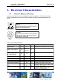
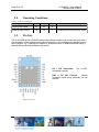
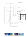
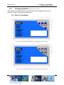
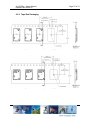
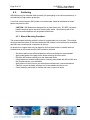
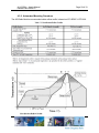
Anaren Integrated Radio A1101R09x User’s Manual Release Date 05/08/12 THIS PAGE INTENTIONALLY LEFT BLANK iii USER’S MANUAL Models A1101R09A and A1101R09C Contents 1. Overview .......................................................................................................................................................... 5 1.1. A1101R09A .................................................................................................................................................5 1.2. A1101R09C .................................................................................................................................................5 1.3. Features....................................................................................................................................................... 6 1.4. Theory of Operation..................................................................................................................................6 1.4.1. Typical Flow ........................................................................................................................................9 1.5. Applications ............................................................................................................................................. 11 1.6. Configuration ........................................................................................................................................... 11 2. Approvals and Usage ................................................................................................................................... 13 2.1. Product Approvals .................................................................................................................................. 13 2.1.1. USA (Federal Communications Commission, FCC) ......................................................................... 13 2.1.1.1. FCC Labeling Requirements ................................................................................................ 13 2.1.1.2. End User Manual ................................................................................................................... 14 2.1.1.3. RF Exposure ............................................................................................................................ 14 2.1.2. Canada (Industry Canada, IC) .......................................................................................................... 15 2.1.2.1. IC Labeling Requirements .................................................................................................... 15 2.1.2.2. RF Exposure ............................................................................................................................ 16 2.2. Potential Interference Sources ............................................................................................................... 17 2.2.1. Time critical data ............................................................................................................................... 17 2.3. Approved Usage ..................................................................................................................................... 17 2.3.1. USA & Canada ................................................................................................................................. 18 3. Electrical Characteristics .............................................................................................................................. 19 3.1. Absolute Maximum Ratings .................................................................................................................. 19 3.2. Operating Conditions ............................................................................................................................. 20 3.3. Pin Out ...................................................................................................................................................... 20 3.4. Recommended Layout (dimensions in mm) ...................................................................................... 22 3.5. Power Supply Considerations ............................................................................................................... 24 4. Mechanical and Process ................................................................................................................................ 25 4.1. Radio Module Details (dimensions in mm) ........................................................................................ 25 4.1.1. A1101R09A ...................................................................................................................................... 25 4.1.2. A1101R09C ....................................................................................................................................... 25 4.2. Packaging Details (dimensions in mm) ............................................................................................... 26 4.2.1. Matrix Tray Packaging ..................................................................................................................... 26 4.2.2. Tape-Reel Packaging ......................................................................................................................... 27 4.3. Soldering................................................................................................................................................... 28 4.3.1. Manual Mounting Procedure ........................................................................................................... 28 4.3.2. Automated Mounting Procedure ...................................................................................................... 29 THIS PAGE INTENTIONALLY LEFT BLANK A1101R09x – User’s Manual Release Date 05/08/12 Page 5 of 33 1. Overview The A1101R09A and A1101R09C are surface mount modules – each with an integrated crystal, internal voltage regulator, matching circuitry and filtering. The A1101R09A has an integral antenna, whereas the A1101R09C utilizes an external antenna through a U.FL connector (see Table 2). The modules operate in the US 902 – 928MHz ISM band and are ideal for achieving low power wireless connectivity without having to deal with extensive RF, antenna design and regulatory compliance, allowing quick time to market. The modules are 100% tested to provide consistent performance. The A1101R09A and A1101R09C have received regulatory approvals for modular devices in the United States (FCC) and Canada under Industry Canada (IC) Radio Standards Specification (RSS) RSS-210 and RSS-Gen. The modular approval allows the OEM or end user to place either an A1101R09A or an A1101R09C with an approved antenna inside a finished product without having to perform costly regulatory testing for an intentional radiator. Section 2.3 has information on the requirements for the end user/integrator must fulfill to use the modules without intentional radiator regulatory testing. The A1101R09A and A1101R09C are based on the CC1101 transceiver IC from Texas Instruments. All control lines for the transceiver are provided at module level for full control of its operation. Please see the CC1101 data sheet (www.ti.com) for how to control the modules. The A1101R09A measure 9x16x2.5mm and A1101R09C measures 9x12x2.5mm. The modules are footprint compatible with each other. 1.1. A1101R09A The A1101R09A has an integral antenna, providing high efficiency and near omni-directional radiation pattern. This approach offers the lowest system cost when the application allows collocation of radio and antenna. 1.2. A1101R09C The A1101R09C has a compact antenna connector that allows for locating the antenna away from the module due to form/function or in order to exit a metal enclosure, see Figure 7 – Figure 10 for more information on antenna location and enclosure considerations. Page 6 of 33 1.3. A1101R09x – User’s Manual Release Date 05/08/12 Features Features: Benefits Summary: Frequency range: 902-928 MHz Ultra small package size A1101R09C : 9mm x 12mm x 2.5mm A1101R09A : 9mm x 16mm x 2.5mm Impedance controlled multi-layer PCB Shielded Package 1.8 to 3.6 V operation SPI Interface RoHS Compliant LGA Footprint Low Power Consumption Regulatory approvals for FCC Digital RSSI output Programmable channel filter bandwidth Programmable output power up to +10 dBm High sensitivity (–104 dBm at 1.2 kBaud, 1% packet error rate) Low current consumption (14.4 mA in RX, 1.2kBaud, input well above sensitivity limit) Fast startup time: 240us from SLEEP to Rx or Tx mode Separate 64 byte Rx and Tx FIFOs Data Rate: 1.2 – 500 Kbit/Sec Programmable data rate from 1.2 to 500 kBaud Sleep state: 0.2µA Idle State: 1.7mA 1.4. Operating temperature -40 to +85C 100% RF Tested in production Common footprint for all family members No RF engineering experience necessary Only requires a 2 layer PCB implementation Excellent receiver selectivity and blocking Performance Suited for systems compliant with FCC CFR47 Part 15.247a2 and 15.249 (US) and Canada under Industry Canada (IC) Radio Standards Specification (RSS) RSS-210 and RSS-Gen. No regulatory “Intentional radiator” testing required to integrate module into end product. Simple certification labeling replaces testing. Theory of Operation The A1101R09A and A1101R09C are for low power wireless applications in the US 902 – 928MHz ISM band. The devices can be used to implement a variety of networks, including; point to point, point to multipoint, peer to peer and mesh networks. The A1101R09A and A1101R09C both interface to an application microcontroller via an SPI bus. Physical and MAC layer functionality are accessed via the SPI bus through addressable registers as well as execution commands. Data received, or to be transmitted, are also accessed through the SPI bus and are implemented as a FIFO register (64 bytes each for Tx and Rx). A1101R09x – User’s Manual Release Date 05/08/12 Page 7 of 33 To transmit, a frame of data is placed in the FIFO; this may include a destination address. A transmit command is given, which will transmit the data according to the initial setup of the registers. To receive data, a receive command is given, which enables the unit to “listen” for a transmission; when such a transmission occurs, it places the received frame in the FIFO. When neither transmit nor receive is required, the device can enter either an Idle mode, from which it can quickly re-enter receive, a transmit mode, or a low power sleep mode from which a crystal startup is required prior to transmit or receive operation. Below is a block diagram for each of the A1101R09A and A1101R09C modules. Antenna o The antenna couples energy between the air and the AIR module. For applications where installations are done by an end user (non-professional), an omni-directional antenna pattern is desired such that the application will work equally well in any direction. Similarly for peer to peer or point to multipoint applications an omni-directional pattern is desired such that all nodes have a fair chance of communicating. The A1101R09A module has an integral antenna that is near omni-directional, whereas the A1101R09C has approved antenna options ranging from near omni-directional to shaped front/back patterns (useful for inline, professional installations). Note that the end radiation pattern depends not only on the antenna, but also on the ground plane, enclosure and installation environment. Filtering o Filtering removes spurious signals to comply with regulatory intentional radiator requirements. Matching o Matching provides the correct loading of the transmit amplifier to achieve the highest output power, as well as the correct loading for the receive LNA to achieve the best sensitivity. Physical o The physical layer provides conversions between data, symbol and RF signal. MAC o The MAC layer is part of the Logical Link Layer and provides frame handling, addressing and medium access services. Microcontroller Interface o The microcontroller interface exposes registers and commands for the physical and MAC layers to a microcontroller. Power Management o Power management ensures a stable supply for the internal functions, as well as providing means for a low power sleep mode (in which case, most of the transceiver is power off). Page 8 of 33 A1101R09x – User’s Manual Release Date 05/08/12 Figure 1 The functionality of the A1101R09A, using an integral antenna Figure 2 The functionality of the A1101R09C, using an external antenna. A1101R09x – User’s Manual Release Date 05/08/12 Page 9 of 33 Figure 3 Transceiver IC block diagram. 1.4.1. Typical Flow After initial setup of registers for desired behavior, the normal operation flow diagram is shown in Figure 4. In applications of infrequent data transmissions, the transceiver would be in “sleep” mode to save power. From there it would awaken and then enter “idle” mode. As part of the wake up process the crystal oscillator is started (~240μs) and the digital microcontroller interface is powered up. Before transmit or receive, the frequency synthesizer needs to be started (“FS_Wakeup”) and, having been powered off (or idle for a while), the control loop of the VCO/PLL needs to be calibrated (“calibrate”). A data frame is loaded into the transmit FIFO and the “TX” mode is entered. The transceiver will transmit the data and enter “idle” mode after completion. When transmit is complete “RX” mode is entered to wait for the acknowledge frame. Once a frame is received, the transceiver will again enter “idle” mode. If no acknowledge frame is received within a given timeout, the data frame would be re-transmitted. If the acknowledge frame indicates that the data was received, the next data frame will be transmitted. After the last data frame has been transmitted successfully, the transceiver will again be put in “sleep” mode. Page 10 of 33 A1101R09x – User’s Manual Release Date 05/08/12 Medium access Figure 4 Transceiver state diagram A1101R09x – User’s Manual Release Date 05/08/12 1.5. Page 11 of 33 Applications Ultra low-power wireless applications, operating in the 902-928 MHz ISM band. Wireless alarm and security systems Industrial monitoring and control Wireless sensor networks AMR – Automatic Meter Reading Home and building automation Existing applications where simple upgrade to wireless is desired 1.6. Configuration Table 1 lists the radio module configuration parameters, and the level of configurability by the user. Legend: Certification is valid for any value choosen Use the provided certified settings as other may degrade performance Any modification of this value is a violation of the certification and the customer is responsible for optaining their own certification Unused/undocumented function. The provided default value must be written. No assumption should be made on the value read from this field Read only register (burst mode read only, command strobes otherwise). Page 12 of 33 A1101R09x – User’s Manual Release Date 05/08/12 Table 1 Configuration Parameters Register Name IOCFG2 IOCFG1 IOCFG0 FIFOTHR SYNC1 SYNC0 PKTLEN PKTCTRL1 PKTCTRL0 ADDR CHANNR FSCTRL1 FSCTRL0 FREQ2 FREQ1 FREQ0 MDMCFG4 MDMCFG3 MDMCFG2 MDMCFG1 MDMCFG0 DEVIATN MCSM2 MCSM1 MCSM0 FOCCFG BSCFG AGCCTRL2 AGCCTRL1 AGCCTRL0 WOREVT1 WOREVT0 WORCTRL FREND1 FREND0 FSCAL3 FSCAL2 FSCAL1 FSCAL0 RCCTRL1 RCCTRL0 FSTEST PTEST AGCTEST TEST2 TEST1 TEST0 PARTNUM VERSION FREQOFF_EST LQI RSSI MARC_STATE WORTIME1 WORTIME0 PKTSTATUS VCO_VC_DAC TXBYTES RXBYTES RCCTRL1_STATUS RCCTRL0_STATUS PATABLE FIFO Bit Fields Within Register Register Retained Address during (Hex) sleep 7 6 5 4 3 2 1 0 00 1 0 GDO2_INV GDO2_CFG 01 1 GDO_DS GDO1_INV GDO1_CFG 02 1 GDO0_TEMP_SENSOR_ENABLE GDO0_INV GDO0_CFG 03 1 Reserved ADC_RETENTION CLOSE_IN_RX FIFO_THR 04 1 SYNC_MSB 05 1 SYNC_LSB 06 1 PACKET_LENGTH 07 1 PQT 0 CRC_AUTOFLUSH APPEND_STATUS ADR_CHK 08 1 0 WHITE_DATA PKT_FORMAT 0 CRC_EN LENGTH_CONFIG 09 1 DEVICE_ADDR 0A 1 CHAN 0B 1 0 0 FREQ_IF 0C 1 FREQOFF 0D 1 FREQ[23:22]=0 FREQ[21:16] 0E 1 FREQ[15:8] 0F 1 FREQ[7:0] 10 1 CHANBW_E CHANBW_M DRATE_E 11 1 DRATE_M 12 1 DEM_DCFILT_OFF MOD_FORMAT MANCHESTER_EN SYNC_MODE 13 1 FEC_EN NUM_PREAMBLE 0 CHANSPC_E 14 1 CHANSPC_M 15 1 0 DEVIATION_E 0 DEVIATION_M 16 1 0 RX_TIME_RSSI RX_TIME_QUAL RX_TIME 17 1 0 CCA_MODE RXOFF_MODE TXOFF_MODE 18 1 0 FS_AUTOCAL PO_TIMEOUT PIN_CTRL_EN XOSC_FORCE_ON 19 1 0 FOC_BS_CS_GATE FOC_PRE_K FOC_POST_K FOC_LIMIT 1A 1 BS_PRE_K BS_PRE_KP BS_POST_K BS_POST_KP BS_LIMIT 1B 1 MAX_DVGA_GAIN MAX_LNA_GAIN MAGN_TARGET 1C 1 0 AGC_LNA_PRIORITY CARRIER_SENSE_REL_THR CARRIER_SENSE_ABS_THR 1D 1 HYST_LEVEL WAIT_TIME AGC_FREEZE FILTER_LENGTH 1E 1 EVENT0[15:8] 1F 1 EVENT0[7:0] 20 1 RC_PD EVENT1 RC_CAL 0 WOR_RES 21 1 LNA_CURRENT LNA2MIX_CURRENT LODIV_BUF_CURRENT MIX_CURRENT 22 1 0 LODIV_BUF_CURRENT_TX 0 PA_POWER 23 1 FSCAL3[7:6] CHP_CURR_CAL_EN FSCAL3[3:0] 24 1 0 VCO_CORE_H_EN FSCAL2 25 1 0 FSCAL1 26 1 0 FSCAL0 27 1 0 RCCTRL1 28 1 0 RCCTRL0 29 0 FSTEST 2A 0 PTEST 2B 0 AGCTEST 2C 0 TEST2 2D 0 TEST1 2E 0 TEST0[7:2] VCO_SEL_CAL_EN TEST0[0] 2F 30 1 PARTNUM 31 1 VERSION 32 0 FREQOFF_EST 33 0 CRC_OK LQI_EST 34 0 RSSI 35 0 MARC_STATE 36 0 TIME[15:8] 37 0 TIME[7:0] 38 0 CRC_OK CS PQT_REACHED CCA SFD GDO2 GDO0 39 0 VCO_VC_DAC 3A 0 TXFIFO_UNDERFLOW NUM_TXBYTES 3B 0 RXFIFO_OVERFLOW NUM_RXBYTES 3C 0 RCCTRL1_STATUS 3D 0 RCCTRL0_STATUS 3E 1 PATABLE 3F 0 TXFIFO/RXFIFO A1101R09x – User’s Manual Release Date 05/08/12 Page 13 of 33 2. Approvals and Usage The A1101R09A and A1101R09C have been designed to meet most national regulations for worldwide ISM-band use. In particular, the radio modules have been certified to the following standards. 2.1. Product Approvals 2.1.1. USA (Federal Communications Commission, FCC) The A1101R09A, with integrated antenna, as well as the A1101R09C, used with the antennas listed in Table 2 below, have been tested to comply with FCC Part 15 - 15.247(a2) and 15.247(b) and 15.249 “Intentional Radiators.” The devices meet the requirements for modular transmitter approval as detailed in FCC public notice DA 00-1407 Released: June 26, 2000. The A1101R09A and A1101R09C module can be integrated into a finished product without obtaining subsequent FCC approvals. (15.19a3) The modules comply with part 15 of the FCC rules. Operation is subject to the following two conditions: (1) this device may not cause harmful interference, and (2) this device must accept any interference received, including interference that may cause undesired operation. Table 2 Approved Antennas Item 1 2 3 Part Number Integral part of A1101R09A 66089-0906 66089-0930 2.1.1.1. Manufacturer Anaren Anaren Anaren Type Integral Antenna Monopole whip, 6mm lead Monopole whip, 30mm lead Gain 2 3 3 FCC Labeling Requirements The A1101R09A and A1101R09C modules have been labeled with their own FCC ID number and if the FCC ID is not visible when the module is installed inside another device, then the outside of the finished product into which the module is installed must also display a label referring to the enclosed module. This exterior label can use wording such as the following: Contains Transmitter Module FCC ID: X7J-A10040601 -orContains FCC ID: X7J-A10040601 This device complies with Part 15 - 15.247(a2) and 15.247(b) and 15.249 of the FCC Rules. Operation is subject to the following two conditions: (1) this device may not cause harmful interference, and (2) this device must accept any interference received, including interference that may cause undesired operation. Page 14 of 33 2.1.1.2. A1101R09x – User’s Manual Release Date 05/08/12 End User Manual The end user manual should include the following statement: This equipment has been tested and found to comply with the limits for a Class B digital device, pursuant to part 15 of the FCC Rules. These limits are designed to provide reasonable protection against harmful interference in a residential installation. This equipment generates, uses, and radiates radio frequency energy, and, if not installed and used in accordance with the instructions, may cause harmful interference to radio communications. However, there is no guarantee that interference will not occur in a particular installation. If this equipment does cause harmful interference to radio or television reception, which can be determined by turning the equipment off and on, the user is encouraged to try to correct the interference by one or more of the following measures: Reorient or relocate the receiving antenna. Increase the separation between the equipment and receiver. Connect the equipment into an outlet on a circuit different from that to which the receiver is connected. Consult the dealer or an experienced radio/TV technician for help. 2.1.1.3. RF Exposure All transmitters regulated by the FCC must comply with RF exposure requirements. OET Bulletin 65 “Evaluating Compliance with FCC Guidelines for Human Exposure to Radio Frequency Electromagnetic Fields” provides assistance in determining whether proposed or existing transmitting facilities, operations or devices comply with limits for human exposure to Radio Frequency (RF) fields adopted by the Federal Communications Commission (FCC). The bulletin offers guidelines and suggestions for evaluating compliance. If appropriate, compliance with exposure guidelines for mobile and unlicensed devices can be accomplished by the use of warning labels and by providing end users with information concerning minimum separation distances from transmitting structures and proper installation of antennas. The following statement must be included as a CAUTION statement in manuals and OEM products to alert end users of FCC RF Exposure compliance: To satisfy FCC RF Exposure requirements for mobile and base station transmission devices, a separation distance of 20 cm or more should be maintained between the antenna of this device and persons during operation. To ensure compliance, operation at closer than this distance is not recommended. The antenna(s) used for this transmitter must not be co-located or operating in conjunction with any other antenna or transmitter. If the A1101R09A and A1101R09C module is used in a portable application (antenna is less than 20 cm from persons during operation), the end user is responsible for performing Specific Absorption Rate (SAR) testing in accordance with FCC rules 2.1091. A1101R09x – User’s Manual Release Date 05/08/12 Page 15 of 33 2.1.2. Canada (Industry Canada, IC) The A1101R09A and A1101R09C modules have been certified for use in Canada under Industry Canada (IC) Radio Standards Specification (RSS) RSS-210 and RSS-Gen. From section 3.2 RSS-Gen, Issue 3, December 2010, Modular Approval for Category I Equipment or Category II Equipment: “Modular approval permits the installation of the same module in a host device or multiple host devices without the need to recertify the device. Equipment certification for a modular device may be sought for either Category I equipment or Category II equipment. Transmitters designed as modules for the installation in a host device may obtain equipment certification as a modular device provided that the applicable RSS is met and the following conditions in this section are met.” In section 7.1.2 Transmitter Antenna, it has been mentioned that the user manuals for transmitters shall display the following notice in a conspicuous location: Notice: Under Industry Canada regulations, this radio transmitter may only operate using an antenna of a type and maximum (or lesser) gain approved for the transmitter by Industry Canada. To reduce potential radio interference to other users, the antenna type and its gain should be so chosen that the equivalent isotropically radiated power (e.i.r.p.) is not more than that necessary for successful communication. Avis: Sous la réglementation d'Industrie Canada, ce transmetteur radio ne peut fonctionner qu’en utilisant seulement une antenne d'un type et d’un maximum (ou moins) de gain approuvé pour l'émetteur par Industrie Canada. Pour réduire des potentielles interférences radio pour les autres utilisateurs, le type d'antenne et son gain doivent être choisis de sorte que la puissance isotrope rayonnée équivalente (PIRE) ne dépasse pas ce qui est nécessaire pour une communication réussie. 2.1.2.1. IC Labeling Requirements From section 3.2.1 RSS-Gen, Issue 3, December 2010, Labeling Requirements for the Host Device: The host device shall be properly labeled to identify the modules within the host device. The Industry Canada certification label of a module shall be clearly visible at all times when installed in the host device, otherwise the host device must be labeled to display the Industry Canada certification number of the module, preceded by the words “Contains transmitter module”, or the word “Contains”, or similar wording expressing the same meaning. From section 5.2, RSS-Gen, Issue 3, December 2010, Equipment Certification Numbers and Labels: Every unit of Category I radio apparatus certified for marketing and use in Canada shall bear a permanent label on which is indelibly displayed the model number and Industry Canada certification number of the equipment model (transmitter, receiver, or inseparable combination Page 16 of 33 A1101R09x – User’s Manual Release Date 05/08/12 thereof). Each model shall be identified by a unique combination of a model number and a certification number, which are assigned as described below in this section. The label shall be securely affixed to a permanently attached part of the device, in a location where it is visible or easily accessible to the user, and shall not be readily detachable. The label shall be sufficiently durable to remain fully legible and intact on the device in all normal conditions of use throughout the device’s expected lifetime. These requirements may be met either by a separate label or nameplate permanently attached to the device or by permanently imprinting or impressing the label directly onto the device. The label text shall be legible without the aid of magnification, but is not required to be larger than 8-point font size. If the device is too small to meet this condition, the label information may be included in the user manual upon agreement with Industry Canada. Label: Contains IC: 8975A-A10040601 Notice: This device complies with Industry Canada licence-exempt RSS standard(s). Operation is subject to the following two conditions: (1) this device may not cause interference, and (2) this device must accept any interference, including interference that may cause undesired operation of the device. Avis: Cet appareil est conforme avec Industrie Canada RSS standard exempts de licence (s). Son fonctionnement est soumis aux deux conditions suivantes: (1) cet appareil ne peut pas provoquer d'interférences et (2) cet appareil doit accepter toute interférence, y compris les interférences qui peuvent causer un mauvais fonctionnement du dispositif. For more information, see: Industry Canada http://www.ic.gc.ca/. 2.1.2.2. RF Exposure All transmitters regulated by IC must comply with RF exposure limits as set forth in RSS-102, Issue 4, section 4, “Exposure Limits”. Furthermore RSS-102, Issue 4, Section 2 “Certification Requirements”, provides assistance in determining the specific requirements for compliance. If appropriate, compliance with exposure guidelines for mobile and unlicensed devices can be accomplished by the use of warning labels and by providing users with information concerning minimum separation distances from transmitting structures and proper installation of antennas. The following statement must be included as a CAUTION statement in manuals and OEM products to alert users of IC RF Exposure compliance: Notice: To satisfy IC RF Exposure requirements for mobile and base station transmission devices, a separation distance of 20 cm or more should be maintained between the antenna of this device and persons during operation. To ensure compliance, operation at closer than this distance is not recommended. The antenna(s) used for this transmitter must not be co-located or operating in conjunction with any other antenna or transmitter. A1101R09x – User’s Manual Release Date 05/08/12 Page 17 of 33 Avis: Pour répondre à la IC d'exposition pour les besoins de base et mobiles dispositifs de transmission de la station, sur une distance de séparation de 20 cm ou plus doit être maintenue entre l'antenne de cet appareil et les personnes en cours de fonctionnement. Pour assurer le respect, l'exploitation de plus près à cette distance n'est pas recommandée. L'antenne (s) utilisé pour cet émetteur ne doit pas être co-localisés ou fonctionner conjointement avec une autre antenne ou transmetteur. 2.2. Potential Interference Sources Alarm systems o These typically use low duty cycles and are therefore easy to avoid using acknowledge/retransmit methods Car alarms (internal motion sensors) Video surveillance o These are typically operated on a fixed channel determined at installation time and can be avoided by using clear channel assessment. It may be useful to change the channel used by the video surveillance equipment also, if possible. 2.2.1. Time critical data If the user requires specific time critical data throughput that cannot tolerate the delays of potentially many re-transmissions, the user is encouraged to implement an environment-aware algorithm that periodically monitors/scans the frequency band and maintain a list of “best available” channels. 2.3. Approved Usage These radio modules can be used in a variety of physical layer configurations; the following restricts the use to maintain compliance with the above referenced certification bodies. The user is encouraged to use minimum power required to establish a link, thus minimizing interference. Changes or modifications to the module and/or operation outside the limits set forth below are prohibited and could void the user’s authority to operate the modules. Uses of these radio modules are limited to the following frequency ranges and modulation settings. Using the radio modules outside of these limitations are prohibited and could void the user’s authority to operate the modules. The user should use one of the register configurations listed below. Anaren provides register setting files for optimal performance and compliance for each of the data rates given in the following at www.anaren.com. Page 18 of 33 A1101R09x – User’s Manual Release Date 05/08/12 2.3.1. USA & Canada Within the USA and Canada, the modules have been approved for use as digitally modulated transmitters, for which they must have a minimum occupied bandwidth (6dB bandwidth) of 500kHz. In addition, the spectral density may not exceed 8dBm/3kHz and the total output power including antenna gain may not exceed 1W. Table 3 shows configurations that are compliant with this use and the expected performance. Table 3 FCC Approved configurations with max. allowed output power Modulation Datarate (kB) 6-dB BW (kHz) PSD (dBm) Power Table (Hex) Fomin (MHz) Fomax (MHz) 2-FSK 2-FSK 2-FSK MSK MSK 1.2 38 250 425 500 530 535 540 515 585 6.84 6.88 3.68 1.26 1.35 0xCB 0xCA 0xC0 0xC0 0xC0 902.49985 902.49985 902.49985 902.8093 902.8093 927.58578 927.58578 927.58578 927.28586 927.28586 In order to meet the band edge requirements, the center frequency of the operating channel has to be chosen between Fomin and Fomax. Also, the power levels provided in Table 3 are the max allowed power levels for each configuration, however, the user is encouraged to use minimum power required to establish a link in order to minimize interference. For available power levels from the module, please refer to Table 4. It is encouraged to use a medium access technique which should include addressing of individual transceiver nodes; and should include a combination of a clear channel assessment, transmit and detect, or a frequency hopping method. This ensures that the un-licensed band can be shared with other systems/applications. Table 4 Output Power vs. PA Table Value Power (dBm) PA_TABLE (Hex) Power (dBm) PA_TABLE (Hex) 12.5 0xC0 7 0xCE 12 0xC1 5 0x80 11.5 0XC3 4.5 0x81 11 0xC4 4 0x85 10.5 0xC5 3.5 0x87 10 0xC7 3 0x88 9.5 0xC8 2 0x8B 9 0xC9 1 0x8C 8.5 0xCB 0 0x70 8 0xCC -1 0x61 7.5 0xCD -2 0x5B Power (dBm) PA_TABLE (Hex) -3 0x64 -4 0x56 -5 0x67 -6 0x8F -7 0x38 -8 0x2A -9 0x29 -10 0x35 -15 0x24 -20 0x19 A1101R09x – User’s Manual Release Date 05/08/12 Page 19 of 33 3. Electrical Characteristics 3.1. Absolute Maximum Ratings Under no circumstances must the absolute maximum ratings given in Table 2 be violated. Stress exceeding one or more of the limiting values may cause permanent damage to the device. Caution! ESD sensitive device. Precaution should be used when handling the device in order to prevent permanent damage. Caution! This assembly contains moisture sensitive devices and requires proper handling per IPC/JEDEC J-STD-033 Table 5 Absolute Maximum Ratings Parameter Min Max Units Supply voltage -0.3 3.9 V Voltage on any digital pin -0.3 VDD + 0.3 max 3.9 V Voltage on the pins RF_P, RF_N and DCOUPL -0.3 2.0 V Voltage ramp-up rate 120 kV/µs Input RF level +10 dBm 150 o C Solder reflow temperature 260 o C ESD 750 V ESD 400 V Storage temperature range -50 Condition All supply pins must have the same voltage According to IPC/JEDEC J-STD-020C According to JEDEC STD22, method A114, Human Body Model (HBM) According to JEDEC STD22, C101C, Charged Device Model (HBM) Page 20 of 33 3.2. A1101R09x – User’s Manual Release Date 05/08/12 Operating Conditions Table 6 Operating Conditions Parameter Min Max Operating temperature -40 85 Operating supply voltage 1.8 3.6 3.3. Units o Condition C V All supply pins must have the same voltage Pin Out The A1101R09A and A1101R09C radio modules share a common pin-out and foot print, that is also shared by Anaren modules using other frequencies -- thus enabling easy changeover from one to another, e.g. if changing the frequency, antenna scheme, or adaptive antenna tuning is desired. Below the common footprint are shown. NC = NO Connection. connected internally. Pin is NOT DNC = Do Not Connect. Internal connection used during assembly, do not connect. Figure 5 Pin Out. A1101R09x – User’s Manual Release Date 05/08/12 Page 21 of 33 Table 7 Pin Descriptions Pin # 1 Pin Name DNC Pin Type NC 2 DNC NC 3 DNC NC 4 NC NC 5 NC NC 6 NC NC 7 Vdcoup1 Analog 8 9 10 GND SCLK MISO/GDO1 11 12 13 MOSI _CSN GDO0 14 15 GDO2 Vdcoup2 Ground Digital Input Digital Output Digital Input Digital Input Digital I/O (Analog output) Digital I/O Analog 16 NC NC 17 18 GND Vdd 19 NC Ground Power Supply NC 20 NC NC 21 NC NC 22 DNC NC 23 DNC NC 24 DNC NC Description Internal GND connection used during testing, not recommended to connect to main GND. Internal RF output connection used during test. Connecting this pin to anything will require recertification for intentional radiators. Internal GND connection used during testing, not recommended to connect to main GND. Pin is not connected internally, but is reserved for future expansion. It is recommended not to connect this pin to anything. Pin is not connected internally, but is reserved for future expansion. It is recommended not to connect this pin to anything. Pin is not connected internally, but is reserved for future expansion. It is recommended not to connect this pin to anything. Optional decoupling of the modules internal Vdd supply. It is recommended to not connect anything to this pin. In particular noisy environment this pin can be used to further reduce the noise on the modules internal Vdd, please see section 3.5 for further information. One of two primary ground pins SPI bus clock signal SPI bus data out from radio when CSN is low, and general purpose I/O pin when CSN is high SPI bus data into radio SPI bus select (active low) General purpose port General purpose port Optional decoupling of the modules internal Vdd supply. It is recommended to not connect anything to this pin. In particular noisy environment this pin can be used to further reduce the noise on the modules internal Vdd, please see section 3.5 for further information. No Connect, the pin is not connected internally, but is reserved for future expansion. It is recommended not to connect this pin to anything. One of two primary ground pins Power supply pin Pin is not connected internally, but is reserved for future expansion. It is recommended not to connect this pin to anything. Pin is not connected internally, but is reserved for future expansion. It is recommended not to connect this pin to anything. Pin is not connected internally, but is reserved for future expansion. It is recommended not to connect this pin to anything. Internal GND connection used during testing, not recommended to connect to main GND. Pin is not connected internally, but is reserved for future expansion. It is recommended not to connect this pin to anything. Internal GND connection used during testing, not recommended to connect to main GND. Page 22 of 33 3.4. A1101R09x – User’s Manual Release Date 05/08/12 Recommended Layout (dimensions in mm) Figure 6 Recommended PCB layout. A1101R09x – User’s Manual Release Date 05/08/12 Figure 7 Mounting the module in a corner Figure 9 Mounting the module along an edge with overhang. This option is not generally recommended, but is a method to save PCB in an environmentally benign environment Page 23 of 33 Figure 8 Mounting the module along an edge Figure 10 Mounting the module along an edge, with a ground plane cut-out. This option degrades range slightly. Page 24 of 33 3.5. A1101R09x – User’s Manual Release Date 05/08/12 Power Supply Considerations Noise on the power supply line reduces the sensitivity of a receiver and modulates onto a transmitter’s signal, both of which causes a degradation of link quality and hence a reduction in range. The A1101R09A and A1101R09C radio modules each have an integral ferrite bead in the supply line from pin 18 (Vdd) and decoupling capacitance to reduce any noise on the incoming power supply line. This arrangement will eliminate most supply voltage noise. In particularly noisy environments (switching regulators, motor controls, etc.), it may be necessary to add additional noise reduction means. Pin 7 (Vdcoup1) is connected to the modules internal supply line after the ferrite bead and decoupling capacitors and can be used to probe the noise at module level. The noise level measured on pin 7 should not exceed 120mVpp when in transmit or receive mode; it may however exceed this value when setting up or accessing data to/from the FIFOs, while not actively transmitting or receiving. If the level measured is exceeding the above limit, steps should be taken to ensure maximum range, including: Adding decoupling capacitance to pin 7 (Vdcoup1). Adding additional filtering in the supply line. Adding an LDO in the supply line (the TPS731xx low Dropout Regulator from TI is recommended). A1101R09x – User’s Manual Release Date 05/08/12 Page 25 of 33 4. Mechanical and Process 4.1. Radio Module Details (dimensions in mm) 4.1.1. A1101R09A Figure 11 A1101R09A dimensions 4.1.2. A1101R09C Figure 12 A1101R09C dimensions Page 26 of 33 4.2. A1101R09x – User’s Manual Release Date 05/08/12 Packaging Details (dimensions in mm) AIR modules are available in Matrix Tray and Tape & Reel packaging for high-volume assembly. Details of packaging provided below: 4.2.1. Matrix Tray Packaging Figure 13 A1101R09A00GM Matrix Tray Packaging Detail (30/Tray) Figure 14 A1101R09C00GM Matrix Tray Packaging Detail (40/Tray) A1101R09x – User’s Manual Release Date 05/08/12 4.2.2. Tape-Reel Packaging Figure 15 A1101R09A00GR Tape-Reel Packaging Detail (500/Reel) Figure 16 A1101R09C00GR Tape-Reel Packaging Detail (500/Reel) Page 27 of 33 Page 28 of 33 4.3. A1101R09x – User’s Manual Release Date 05/08/12 Soldering AIR Modules may be mounted either manually (for prototyping or low volume production), or automatically for high-volume production. A no-clean tin/silver/copper (SAC) solder is recommended, however lead based no-clean pastes may also be used. CAUTION: AIR Modules are designed for no-clean fluxes only. DO NOT use waterbased fluxes that require aqueous cleaning after solder. Spot cleaning with a flux remover and toothbrush may be performed with care. 4.3.1. Manual Mounting Procedure The recommended soldering method is reflow of a paste solder on a hot plate. This method works provided the bottom of the board where the AIR module is to be mounted is accessible, and there are no bottom-side components in the way. An aluminum or copper block may be placed on the hot plate surface to transfer heat to a localized area on the board where the AIR module is mounted - Set the hot plate to the reflow temperature solder manufacturer’s recommended Apply solder paste to the pads on the board receiving the AIR module Place the AIR module carefully onto the dispensed solder Using tweezers or another holding device, carefully place board with AIR module onto the hot plate surface (or metal block) Apply heat until reflow occurs, per solder paste manufacturer’s recommendations Carefully remove the board and place on a heat-resistant surface to cool Check assembly electrically to confirm there are no opens or shorts. A1101R09x – User’s Manual Release Date 05/08/12 Page 29 of 33 4.3.2. Automated Mounting Procedure The AIR Radio Module recommended solder reflow profile is based on IPC/JEDEC J-STD-020. Page 30 of 33 A1101R09x – User’s Manual Release Date 05/08/12 A1101R09x – User’s Manual Release Date 05/08/12 Page 31 of 33 DOCUMENT HISTORY Date 07/17/10 08/23/10 11/19/10 02/10/11 07/06/11 Author Richardson Richardson Richardson Richardson Richardson 03/28/12 04/29/12 05/08/12 Sula Richardson Richardson Change Note No./Notes Initial Draft Initial Release Formatting applied – no content change Corrected typographic error Corrected typographic errors / added process section Updated approved usage for FCC Formatting applied – no content change Corrected typographic error THIS PAGE INTENTIONALLY LEFT BLANK Attach distributor contact information here If you have additional questions, need samples, or would like a quote – please email the AIR team at [email protected] . For a full list of our franchised distributors, please visit our website: http://www.anaren.com/air/ Anaren Microwave, Inc. 6635 Kirkville Road East Syracuse, NY 13057 Tel: +1 315 432 8909 +1 800 411 6596 Fax: +1 315 432 8970 Anaren Microwave (Europe), Inc. 12 Somerset House, Suite 16 & 17 Hussar Court, Waterlooville Hampshire, England P07-7SG Tel: +44 2392 232392 Fax: +44 2392 251369 Anaren Communication Suzhou Co. Ltd. No. 5 Chun Hui Road Wei Ting, Suzhou Industrial Park Suzhou 215122, PR China Tel: +86 512 6287 6400 Fax: +86 512 6274 9283


![Hacking Medical Devices - [media.blackhat.com]](http://vs1.manualzilla.com/store/data/005931227_1-f7547ce2b3ff0825b843d9b1dbb48800-150x150.png)