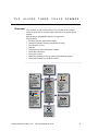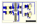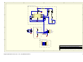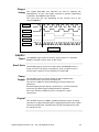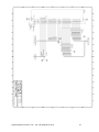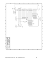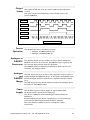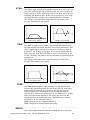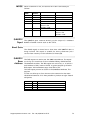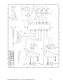
1
AL4000
DMX512
Processors
Revision 5.0 September 2010
www.ArtisticLicence.com
[email protected] Fax +44 (0)20 84 26 05 51
2
C
O
N
T
E
N
T
S
DMX512 Processor Range Overview............ 8
AL4002 Three Phase Dimmer ................... 11
AL4005 Demux Controller....................... 22
AL4006/9 Analogue & Relay Controller ....... 34
AL4007 Demux Controller....................... 41
AL4008 Relay Controller ........................ 48
AL4016 Single Phase Dimmer ................... 54
AL4020 Multiplex Controller .................... 63
AL4100 Servo Motion Controller ............... 70
AL4400 PWM Dimmer Processor................ 80
AL4800 Moving Lamp Processor ................ 85
AL2001/AL3001 Three Phase Dimmer ......... 98
[email protected] Fax +44 (0)20 84 26 05 51
3
[email protected] Fax +44 (0)20 84 26 05 51
4
I
N
Overview
T
R
O
D
U
C
T
I
O
N
Artistic Licence offers a range of products tailored to the specific
requirements of product manufacturers in the Lighting Industry.
The AL4000 DMX512 Processor (aka Dimmer Chips) range include
microprocessor solutions for a wide selection of lighting control
products. The range is usually supplied at chip level for integration at
the design phase. We can, however, supply board level solutions or
indeed entire turnkey product design.
Originally aimed at small companies without the R&D facilities to
develop microprocessor equipment, we now supply major lighting
manufacturers around the world.
We guarantee that a Dimmer Chip will simplify your next design.
Check out our web site for the latest releases.
www.ArtisticLicence.com
AL4002
AL4005
AL4006/9
Three Phase Dimmer
The AL4002 is a 68 pin PLCC device. It provides all the control
features required for a medium specification three phase digital
dimmer.
Both analogue and DMX512 inputs are supported. Features include
four dimmer curves, preheat, consecutive or alternate phase outputs,
good data indication and fan speed control.
DMX base address is set by external thumbwheel inputs.
Demux Controller
The AL4005 is a 40 pin DIL device. It provides all the control
features required to develop a 96 channel DMX512 to analogue
converter.
DMX base address is set by external thumbwheel inputs.
Analogue & Relay Controller
The AL4006 and AL4009 are 40 pin DIL devices. They both provide
two analogue and sixteen switched outputs. Excellent for automating
smoke machines etc.
DMX base address is set by external thumbwheel inputs.
[email protected] Fax +44 (0)20 84 26 05 51
5
AL4007
AL4008
AL4016
AL4020
AL4100
AL4200
Demux Controller
The AL4007 is a 40 pin DIL device. It provides all the control
features required to develop a 72 channel DMX512 to analogue
converter.
DMX base address is set by external thumbwheel inputs.
Relay Controller
The AL4008 is a 40 pin DIL device. It provides all the control
features required to develop a 24 channel DMX512 to switched relay
converter. Individual DMX channels are used to set the state of each
relay.
DMX base address is set by external thumbwheel inputs.
Single Phase Dimmer
The AL4016 is a 40 pin DIL device. It provides all the control
features required for a medium specification, sixteen channel, single
phase digital dimmer.
DMX512 input only is supported.
DMX base address is set by external thumbwheel inputs.
Multiplex Controller
The AL4020 is a 40 pin DIL device. It provides a DMX output that
represents the htp merge of received DMX512 and up to 72 analogue
inputs. The device can also be used as a simple analogue to DMX512
converter.
DMX base address is set by external thumbwheel inputs.
Dual Servo Controller
The AL4100 is a 40 pin dip device. It receives DMX512 and uses the
information to position control two DC servo motors. Perfect for
colour scrollers, colour wheels, moving yokes, moving lamps and
animatronics.
Up Down Relay Controller
The AL4200 provides all the control features required for a four
channel, forward - reverse relay driver.
Applications include drape release and general purpose animatronic
effects.
The AL4200 is the core technology used in the DMX-Kabuki.
[email protected] Fax +44 (0)20 84 26 05 51
6
AL4400
AL4800
AL2001
/ AL3001
PWM Dimmer Controller
The AL4400 provides all the control features required for a high
specification DC - PWM dimmer.
Applications include low voltage lamp dimming, LED, LEP, EL and cold
cathode colour mixing.
The AL4400 is the core technology used in the Power-Pipe and
Colour-Fill.
PWM Moving Lamp Controller
The AL4800 provides all the control features required for a medium
specification moving lamp or moving yoke.
The basic configuration provides micro-stepping (high resolution)
outputs for pan and tilt. Pin inputs allow 2 settings for pan motor
type and 4 settings for tilt motor type.
The colour wheel and gobo wheel motors are also micro-stepping
motors and assumed to be continuously rotating with inputs for a
home sensor.
The iris motor is also a wave drive stepper motor channel with end
stop sensor.
Applications include moving lamps, moving yokes, colour wheels and
general purpose animatronics.
Custom variations of this part can be produced subject to order
quantity.
Three Phase Dimmer
This two chip solution provides the engine for a powerful three phase
DMX and analogue digital dimmer. Features include LCD drive, keypad
input, analogue and DMX512 input, dimmer curves, channel preheat
and all data stored in flash ram.
It provides all the control features required for a high specification
three phase digital dimmer.
[email protected] Fax +44 (0)20 84 26 05 51
7
THE
AL4002
Overview
THREE
PHASE
DIMMER
The AL4002 is a 68 pin PLCC device. It provides all the control
features required for a medium specification three phase digital
dimmer.
Both analogue and DMX512 inputs are supported.
Key features:
• 12 Phase position modulated outputs
• Automatic mains frequency and phase tracking
• Four dimmer curves
• Preheat
• Consecutive or alternate phase outputs
• Good data indication
• Fan speed control
• DMX base address is set by external thumbwheel inputs
• Individual channel test at 50% & 100%
[email protected] Fax +44 (0)20 84 26 05 51
8
Pin
Functions
Pin
Function
In / Out
1
NC
-
2
VCC
I
3
Output 1 (PH1-1)
O
4
BCD input (HUN1)
I
5
BCD input (HUN2)
I
6
BCD input (HUN4)
I
7
BCD input (HUN8)
I
8
Output 12 (PH3-4)
O
9
Output 11 (PH3-3)
O
10
Output 10 (PH3-2)
O
11
Output 9 (PH3-1)
O
12
BCD input (TEN8)
I
13
BCD input (TEN4)
I
14
BCD input (TEN2)
I
15
BCD input (TEN1)
I
16
RESET (Active low)
I
17
TEST (Connect to 0V)
I
18
NC
-
19
GND
I
20
VCC
I
21
NC
-
22
NC
-
23
Analogue Bus D (AN-D)
I
24
Analogue Bus C (AN-C)
I
25
NC
-
26
NC
-
27
NC
-
28
NC
-
29
VCC (Analogue)
I
30
GND (Analogue)
I
31
Analogue Bus A (AN-A)
I
32
Analogue Bus B (AN-B)
I
33
Analogue Address (ANAD1)
O
34
Analogue Address (ANAD0)
O
35
NC
-
36
GND
I
37
VCC
I
38
Zero Cross Input. Active Low (ZC3)
I
39
NC
-
40
Curve select (CURVE1)
I
[email protected] Fax +44 (0)20 84 26 05 51
9
Pin
Functions
Pin
Function
In / Out
41
Curve select (CURVE0)
I
42
NC
-
43
TTL DMX512 Input (RX)
I
44
Phase Output Sequence (ORDER)
I
45
NC
-
46
NC
-
47
BCD input (UNIT2)
I
48
BCD input (UNIT1)
I
49
VCC
I
50
Crystal Connection (OSC1)
I
51
Crystal Connection (OSC2)
O
52
NC
-
53
GND
I
54
Good Data, Lo=Good (GOOD)
O
55
BCD input (UNIT4)
I
56
BCD input (UNIT8)
I
57
Fan drive, Hi=Fast (HIFAN)
O
58
Zero Cross Input. Active Low (ZC2)
I
59
Zero Cross Input. Active Low (ZC1)
I
60
AUX
I
61
Output 8 (PH2-4)
O
62
Output 7 (PH2-3)
O
63
Output 6 (PH2-2)
O
64
Output 5 (PH2-1)
O
65
Output 4 (PH1-4)
O
66
Output 3 (PH1-3)
O
67
Output 2 (PH1-2)
O
68
GND
I
[email protected] Fax +44 (0)20 84 26 05 51
10
Phase
Outputs
Phase
Sequence
The AL4002 phase outputs are synchronised to the three zero cross
input signals over a frequency range of 45 to 65Hz. The output phase
trigger position is defined by the highest value of the DMX512 input,
the analogue input and the preheat level. The output is additionally
modified by the output curve selected.
The AL4002 is designed such that it can be used for both standard
configurations of three phase dimmer. The two conventions differ in
the sequence of the phase outputs and is selected by tying the
ORDER pin either Hi or Low:
DMX, Analogue or
Test Input Channel
1
2
3
4
5
6
7
8
9
10
11
12
Dimmer
Curves
Alternate
(ORDER=1)
Controlled Output
PH1-1
PH2-1
PH3-1
PH1-2
PH2-2
PH3-2
PH1-3
PH2-3
PH3-3
PH1-4
PH2-4
PH3-4
The phase output relationship to the control input can be globally
modified to one of four response curves. The options are:
1. Linear - The output phase varies linearly with the input.
2. Square - The output power varies linearly with the input.
3. S curve - A modified form of Square with greater control in the
centre of the range.
4. Relay - The output switches to full when the input exceeds 25%.
The curves are selected as follows:
CURVE1
0
0
1
1
Zero Cross
Inputs
Consecutive
(ORDER=0)
Controlled Output
PH1-1
PH1-2
PH1-3
PH1-4
PH2-1
PH2-2
PH2-3
PH2-4
PH3-1
PH3-2
PH3-3
PH3-4
CURVE0
0
1
0
1
Output
Linear
Square
S Curve
Relay
The three zero cross inputs (ZC1-3) are used to provide the mains
synchronisation. The inputs are active low, that is the signal should
pulls low at the zero crossing point of each respective phase.
For single phase operation the three inputs should be commoned.
[email protected] Fax +44 (0)20 84 26 05 51
11
It is imperative that the rise time of the signal is greater that 1uS.
Failure to adhere to this specification may cause output inaccuracy.
The minimum low period of the zero cross signal is 10uS.
The allowed frequency range is 90Hz to 125Hz. Frequencies outside
this range will cause non linear output.
Output
timing
The following examples show the relationship between Output, Zero
cross for three input values.
Zero Cross
10% Output
50% Output
90% Output
DMX512
Base
Address
Test Mode
Analogue
Inputs
The BCD inputs are used to set the DMX base address. The inputs
are set up for connection of three standard Binary Coded Decimal
Thumbwheel switches. The BCD inputs are active low, i.e. to select a
base address of 001, connect UNIT1 to ground and pull up all other
BCD inputs. Valid addresses range from 001 to 512.
The BCD inputs are also used to enter test mode.
When Test mode is active, the DMX512 input is disabled, but the
Analogue inputs remain active.
When the Hundred inputs are set to either ‘6’ or ‘7’ Test mode is
active. The Hundred input sets the intensity, while the Ten and Units
inputs select the channel.
The following examples show the operation:
Hundreds
Tens
Units
Output
0
0
5
7
6
7
6
0
0
1
0
0
0
1
0
1
2
1
1
9
2
All Off
Controlled by inputs
Controlled by inputs
Output 1 @ 100%
Output 1 @ 50%
Output 9 @ 100%
Output 12 @ 50%
DMX
Input
Off
On
On
Off
Off
Off
Off
Analogue
Input
Off
On
On
On
On
On
On
The Analogue inputs are decoded by the external multiplexers.
Designs which do not require analogue inputs or preheat may ground
the AN-X inputs. The Preheat input value is applied to all channels.
No analogue input voltage may exceed 5V. The following table shows
the decoding.
ANAD1
ANAD
AN-A
AN-B
[email protected] Fax +44 (0)20 84 26 05 51
AN-C
AN-D
12
0
0
1
1
DMX512
Input
Good Data
Fan Speed
Power
Supply
Crystal
EMC
DMX512
Isolation
0
0
1
0
1
Input
Input
Input
Input
1
2
3
4
Input
Input
Input
Input
5
6
7
8
Input
Input
Input
Input
9
10
11
12
Spare 1
Spare 2
Spare 3
Preheat
The DMX512 input connects directly to the output of a standard
RS485 or RS422 receiver such as the 75176.
The GOOD signal is driven low to show that valid DMX512 data is
being received. The output is suitable for direct connection (via a
current limit resistor) to the cathode of a 20mA LED.
The HIFAN signal is driven Hi when any six outputs exceed 50%
power. The signal can be used to increase the fan speed when the
Dimmer is handling greater than 50% power.
The AL4002 requires a 5V DC supply at approximately 6mA
All Ground and Vcc pins must be connected.
The device is CMOS so normal handling precautions should be
adhered to.
Good decoupling and pcb layout conventions (i.e. fill all unused pcb
areas with grounded copper planes) should be followed.
Particular attention should be paid to routing the Zero Cross and
Crystal connections.
The AL4002 requires a 16MHz, fundamental mode crystal. A tuning
capacitance of approximately 12pF is suggested between each crystal
connection and Ground. The inherent pcb and lead capacitance must
be included in this.
There are two major considerations in reducing the electromagnetic
radiation generated by the AL4002.
The device tends to generate noise at the third harmonic of the
crystal (48MHz). Adding the crystal capacitors detailed above
reduces this to acceptable limits.
Broad band noise can be reduced by good decoupling. A range of
22uF aluminium capacitors and 0u1 ceramic capacitors should be used
on the circuit board. A 560pF ceramic capacitor should also be
connected across the AL4002 power pins as close as possible to the
device.
The use of 150uH inductors in series with all three DMX512 signals
is also an effective way to reduce conducted emissions.
In order to ensure that DMX512 works reliably (this relates to all
[email protected] Fax +44 (0)20 84 26 05 51
13
systems) it is very important to ensure that the cable screen is
connected to pin 1 and that pin 1 is not connected to mains earth.
This simple precaution solves most DMX512 problems.
It is also a good idea to isolate the DMX512 input circuitry.
Application
The following circuit shows the AL4002 application drawing. This is
also the circuit diagram for the evaluation PCB.
[email protected] Fax +44 (0)20 84 26 05 51
14
1
2
4
3
VCC
J7
SW3
C2
560pF
C8
560pF
C4
560pF
C1
560pF
C1
C2
C3
560pF
COM
COM
2
20
37
49
29
D
DGND
60
45
46
21
22
25
26
27
28
39
HUN8
HUN4
HUN2
HUN1
TEN8
TEN4
TEN2
TEN1
UNIT8
UNIT4
UNIT2
UNIT1
C
ORDER
CURVE0
CURVE1
INVERT
Fan Hi
57
AN-A
AN-B
AN-C
AN-D
ANAD1
ANAD0
31
32
24
23
33
34
ZC1
ZC2
ZC3
HI FAN
AN-A
AN-B
AN-C
AN-D
ANAD1
ANAD0
RX
GOOD
MCLR
TEST
PH1-1
PH1-2
PH1-3
PH1-4
PH2-1
PH2-2
PH2-3
PH2-4
PH3-1
PH3-2
PH3-3
PH3-4
7
6
5
4
12
13
14
15
56
55
47
48
HUN8
HUN4
HUN2
HUN1
TEN8
TEN4
TEN2
TEN1
UNIT8
UNIT4
UNIT2
UNIT1
44
41
40
42
Order
Curve0
Curve1
Invert
59
58
38
ZC1
ZC2
ZC3
43
54
DMX OK
J5
SW2
C1
C2
COM
COM
W1
W2
W4
W8
1
2
4
8
5
4
3
2
1
COM
COM
10K
J4
SW1
C1
C2
D
RP3
W1
W2
W4
W8
1
2
4
8
RP1
5
4
3
2
1
DGND
SW4
1
2
3
4
DGND
8
7
6
5
Order
Curve0
Curve1
Invert
10K
9
8
7
6
5
4
3
2
1
UNIT1
UNIT2
UNIT4
UNIT8
TEN1
TEN2
TEN4
TEN8
9
8
7
6
5
4
3
2
1
HUN1
HUN2
HUN4
HUN8
C
VCC
SW-DIP4
R2
10K
R3
10K
R4
10K
J2
1
2
3
4
ZC1
ZC2
ZC3
SIP 4 PIN
DGND
B
VCC
16
17
VCC
DC1
CAP 100NF
U1
DGND
XTAL1
16MHz Crystal
2
N1
TNET
6
1
7
C7
DGND
DGND
N2
TNET
R1
J1
120R
1
2
3
4
3
N3
TNET
GND
A
SIP 3 PIN
5
75176
AL4002 APPLICATION CIRCUIT
'DMX In'
50
51
AL4002
VCC
OSC1/CLKIN
OSC2/CLKOUT
19
36
53
68
30
GND
GND
GND
GND
AGND
8
B
3
67
66
65
64
63
62
61
11
10
9
8
VCC
5
4
3
2
1
U4
PH1-1
PH1-2
PH1-3
PH1-4
PH2-1
PH2-2
PH2-3
PH2-4
PH3-1
PH3-2
PH3-3
PH3-4
AUX1
AUX2
AUX3
AUX4
AUX5
AUX6
AUX7
AUX8
AUX9
AUX10
1
2
4
8
'Zero Cross
Inputs'
VCC
VCC
VCC
VCC
AVCC
DGND
W1
W2
W4
W8
1.00
Rev.
Title:
17/5/00
Date
A
AL4002-12000 Three Phase Dimmer Evaluation Board
Drawing No:
DGND
Original release
Notes
Rev:1.00 Sheet:1 of 3
Drawn: AILP
© Copyright Artistic Licence (UK) Ltd 2000
Print Date: 2-Jun-2000
ARTISTIC LICENCE (UK) LTD
DGND
Livingstone Court, Peel Road, Harrow, Middlesex HA3 7QT, England Tel: +44 (0)20 8863 4515
1
2
3
4
1
2
3
4
U9
20
1
19
2
VCC
DC3
D
16
VCC
3
VCC
J17
C
IN 1
IN 2
IN 3
IN 4
IN 5
IN 6
IN 7
IN 8
DIODE CLAMP
GND
OUT 1
OUT 2
OUT 3
OUT 4
OUT 5
OUT 6
OUT 7
OUT 8
1
2
3
4
5
6
7
8
9
10
18
17
16
15
14
13
12
11
16
5
15
6
14
RP6
1
2
3
4
5
6
7
8
16
15
14
13
12
11
10
9
7
1M
4
2
5
1
11
15
14
12
6
9
10
DGND
ANAD1
ANAD0
DGND
DGND
330R
U3
Y3B
Y2B
Y1B
Y0B
Y3A
Y2A
Y1A
Y0A
E
A1
A0
ZB
ZA
3
AN-B
13
AN-A
4052
SIP 10 Pin
ULN2803
4
1
2
3
4
5
6
7
8
9
13
8
12
9
11
10
C
8
7
U7
1
2
3
4
5
6
7
8
10
9
PH1-1
PH1-2
PH1-3
PH1-4
PH2-1
PH2-2
PH2-3
PH2-4
17
'Analog Inputs'
VCC
VCC
IP8
IP7
IP6
IP5
IP4
IP3
IP2
IP1
RP4
10
9
8
7
6
5
4
3
2
1
Vdd
J8
18
100NF
Vss
Vee
D
DGND
DGND
DGND
VCC
VCC
J10
ULN2803
OUT 1
OUT 2
OUT 3
OUT 4
OUT 5
OUT 6
OUT 7
OUT 8
1
2
3
4
5
6
7
8
9
10
18
17
16
15
14
13
12
11
1
2
3
4
5
6
7
8
HDSP4820 LED Pack
U8
20
1
330R
Sip 10 Pin
19
2
18
3
17
4
DGND
DGND
B
16
15
14
13
12
11
10
9
VCC
DC2
VCC
J6
Preheat
Spare3
Spare2
Spare1
IP12
IP11
IP10
IP9
ANAD1
ANAD0
16
16
IN 1
IN 2
IN 3
IN 4
IN 5
IN 6
IN 7
IN 8
DIODE CLAMP
GND
RP2
10
9
8
7
6
5
4
3
2
1
1M
DGND
5
1
2
3
4
5
6
7
8
9
100NF
DGND
DGND
4
2
5
1
11
15
14
12
6
9
10
U2
Y3B
Y2B
Y1B
Y0B
Y3A
Y2A
Y1A
Y0A
E
A1
A0
Vdd
1
2
3
4
5
6
7
8
10
9
ZB
ZA
3
AN-D
13
AN-C
B
Vss
Vee
PH3-1
PH3-2
PH3-3
PH3-4
Fan Hi
RP5
'Analog Inputs'
U6
8
7
4052
A
DMX OK
15
6
14
7
13
8
12
9
DGND
'DMX OK'
Title:
11
DGND
10 'Power'
A
AL4002-12000 Three Phase Dimmer Evaluation Board
Drawing No:
Rev:1.00 Sheet:2 of 3
Drawn: AILP
© Copyright Artistic Licence (UK) Ltd 2000
Print Date: 2-Jun-2000
ARTISTIC LICENCE (UK) LTD
HDSP4820 LED Pack
Livingstone Court, Peel Road, Harrow, Middlesex HA3 7QT, England Tel: +44 (0)20 8863 4515
1
2
3
4
1
2
3
Evaluation Board Frequency Source
4
VCC
R6
D
D
1K
DC4
D2
1N4148
Control V
6
Threshold
NE555
1
C6
10nF
C
R5
91K
7
Discharge
GND
Trigger
5
R7
3K3
3
Output
MAX
2
VCC
Reset
RV2
47K
C5
100nF
MIN
DGND
VCC
C
VCC
22UF
22UF
DGND
MAX
DE1
VCC
J3
1
2
3
4
RV1
+5V IP
Gnd IP
85-120Hz OP
0-5V OP
B
4 Pin Screw Term
10K
TP3 TP2 TP1
MIN
DE2
Evaluation Board Analog Voltage Source
B
Frequencey
Adjust
8
CAP 100NF
DGND
U5
4
D1
1N4148
DGND
DGND
Evaluation Board Prototype Area
J9
J11
J12
J13
J14
J15
J16
A
1
2
3
4
5
6
6 PIN Screw Term
Title:
A
AL4002-12000 Three Phase Dimmer Evaluation Board
Drawing No:
Rev:1.00 Sheet:3 of 3
Drawn:
© Copyright Artistic Licence (UK) Ltd 2000
Print Date: 2-Jun-2000
ARTISTIC LICENCE (UK) LTD
Livingstone Court, Peel Road, Harrow, Middlesex HA3 7QT, England Tel: +44 (0)20 8863 4515
1
[email protected] Fax +44 (0)20 84 26 05 51
2
3
4
17
Bill Of
Materials
The following components are required for the evaluation PCB. Please
note that some component values may require modification subject to
the intended application.
Designator
C1
C2
C3
C4
C5
C6
C7
C8
D1
D2
DC1
DC2
DC3
DC4
DE1
DE2
J1
J10
J11
J12
J13
J14
J15
J16
J17
J2
J3
J4
J5
J6
J7
J8
J9
N1
N2
N3
R1
R2
R3
R4
R5
R6
R7
RP1
RP2
RP3
RP4
RP5
RP6
Part Type
560pF
560pF
560pF
560pF
100nF
10nF
560pF
1N4148
1N4148
CAP 100NF
100NF
100NF
CAP 100NF
22UF
22UF
SIP 3 PIN
Sip 10 Pin
TESTPOINT
TESTPOINT
TESTPOINT
TESTPOINT
TESTPOINT
TESTPOINT
SIP 10 Pin
SIP 4 PIN
4 Pin Screw Term
CONN SIP 5PIN
CONN SIP 5PIN
CONN SIP 10PIN
CONN SIP 5PIN
CONN SIP 10PIN
6 PIN Screw Term
TNET
TNET
TNET
120R
10K
10K
10K
91K
1K
3K3
10K
1M
10K
1M
330R
330R
Designator
RV1
RV2
SW1
SW2
SW3
SW4
TP1
TP2
TP3
U1
U2
U3
U4
U5
U6
U7
U8
U9
XTAL1
Part Type
10K
47K
BCD-HOZ
BCD-HOZ
BCD-HOZ
SW-DIP4
TESTPOINT
TESTPOINT
TESTPOINT
75176
4052
4052
AL4002
NE555
ULN2803
ULN2803
HDSP4820 LED Pack
HDSP4820 LED Pack
16MHz Crystal
[email protected] Fax +44 (0)20 84 26 05 51
19
T H E
Overview
A L 4 0 0 5
DEMUX
PROCESSOR
The AL4005 is designed to receive the DMX512 protocol and provide
all the control signals necessary to generate 96 channels of analogue
control signals.
The AL4005 is suitable for the development of DMX512 to Analogue
Decoders and also provides an elegant solution to the DMX512
upgrade of existing analogue dimmers.
The AL4005 is supplied as a 40 pin DIL device.
Key features:
•
•
•
•
•
DMX512 input
Good data received indicator
Parallel output for external Digital to Analogue conversion
Individual channel test at 50% and 100%
DMX base address is set by external thumbwheel inputs
[email protected] Fax +44 (0)20 84 26 05 51
20
Pin
Functions
Circuit
Operation
Pin
1
2
3
4
5
6
7
8
9
10
11
12
13
14
15
16
17
18
19
20
21
22
23
24
25
26
27
28
29
30
31
32
33
34
35
36
37
38
39
40
Function
VCC 5V
Chip Select 0
Chip Select 1
Chip Select 2
Chip Select 3
Chip Select 4
Chip Select 5
DAC Select
TRIG - Scope Trigger
GND
BCD Unit 1
BCD Unit 2
BCD Unit 4
BCD Unit 8 (msb)
BCD Ten 1
BCD Ten 2
BCD Ten 4
BCD Ten 8 (msb)
Osc1 (16mhz crystal)
Osc2 (16mhz crystal)
NC
DMX512 TTL Receive
NC
Good Rx (Open Collector, Lo=Good)
NC
NC
Test (Connect to GND)
BCD Hundred 4
BCD Hundred 2
BCD Hundred 1
GND
MCLR (Connect to VCC)
D7 (msb dac data)
D6
D5
D4
AD3 (msb channel address)
AD2
AD1
AD0
In/Out
O
O
O
O
O
O
O
O
I
I
I
I
I
I
I
I
O
I
I
I
I
I
O
O
O
O
O
O
O
O
The AL4005 chip selects and address outputs are used to
address a single demultiplex channel from the 96 available.
The Analogue multiplex output is then routed through that
channel to the sample and hold circuit.
The application drawings that follow show this process using
4067 16 channel de-multiplexors and TL084 op-amps. The
[email protected] Fax +44 (0)20 84 26 05 51
21
TL084 has been chosen in order to provide a very high input
impedance for the sample and hold circuit.
It should be noted that the address and chip select signals
are all converted to CMOS voltages, in order to drive the
demultiplex circuitry at a 15V supply.
The analogue output of the DAC is amplified to produce the
analogue level required by the demultiplexors.
DMX512
Base
Address
Test Mode
The BCD inputs are used to set the DMX base address. The
inputs are set up for connection of three standard Binary
Coded Decimal Thumbwheel switches. The BCD inputs are
active low, i.e. to select a base address of 001, connect UNIT1
to ground and pull up all other BCD inputs. Valid addresses
range from 001 to 512.
The BCD inputs are also used to enter test mode.
When Test mode is active, the DMX512 input is disabled.
When the Hundred inputs are set to either ‘6’ or ‘7’ Test mode
is active. The Hundred input sets the intensity, while the Ten
and Units inputs select the channel.
The following examples show the operation:
Hundreds
Tens
Units
Output
0
0
5
7
6
7
6
0
0
1
0
0
6
1
0
1
2
1
1
9
2
All Off
Controlled by inputs
Controlled by inputs
Output 1 @ 100%
Output 1 @ 50%
Output 69 @ 100%
Output 12 @ 50%
[email protected] Fax +44 (0)20 84 26 05 51
DMX
Input
Off
On
On
Off
Off
Off
Off
22
Output
timing
The signals AD0-AD3 and CS0-CS5 are used to address the
demultiplexor circuits. The signals continue to operate independent
of whether the DMX512 input exists.
The cycle time will vary depending on the refresh rate of the
received DMX512.
AD0
AD1
AD2
AD3
CS0
Channel 3
DMX512
Input
Good Data
Power
Supply
Crystal
The DMX512 input connects directly to the output of a standard
RS485 or RS422 receiver such as the 75176.
The GOOD signal is driven low to show that valid DMX512 data is
being received. The output is suitable for direct connection (via a
current limit resistor) to the cathode of a 20mA LED.
The AL4005 requires a 5V DC supply at approximately 6mA
All Ground and Vcc pins must be connected.
The device is CMOS so normal handling precautions should be
adhered to.
Good decoupling and pcb layout conventions (i.e. fill all unused pcb
areas with grounded copper planes) should be followed.
Particular attention should be paid to routing the crystal
connections.
The AL4005 requires a 16MHz, fundamental mode crystal. A tuning
capacitance of approximately 12pF is suggested between each crystal
connection and Ground. The inherent pcb and lead capacitance must
be included in this.
[email protected] Fax +44 (0)20 84 26 05 51
23
EMC
Application
There are two major considerations in reducing the electromagnetic
radiation generated by the AL4005.
The device tends to generate noise at the third harmonic of the
crystal (48MHz). Adding the crystal capacitors detailed above
reduces this to acceptable limits.
Broad band noise can be reduced by good decoupling. A range of
22uF aluminium capacitors and 0u1 ceramic capacitors should be used
on the circuit board. A 560pF ceramic capacitor should also be
connected across the AL4005 power pins as close as possible to the
device.
The use of 150uH inductors in series with all three DMX512 signals
is also an effective way to reduce conducted emissions.
The following circuit shows the AL4005 application drawing. This is
also the circuit diagram for the evaluation PCB.
The evaluation card is designed to output 16 channels, however
further PCB’s can be added to extend the number of outputs.
[email protected] Fax +44 (0)20 84 26 05 51
24
1
2
VCC
DC4
14
560pF
U2
Vcc
HUN1
HUN2
HUN4
C
8
2
N1
TNET
6
1
7
R1
N2
TNET
J4
120R
1
2
3
4
VCC
3
DC2
N3
TNET
SIP 3 PIN
75176
+AN
11
100NF
DC6
DGND
B
DGND
DGND
DGND
VCC
LED1
2
R4
100R
7
6
12
13
22UF
22UF
22UF
22UF
22UF
DE1
DE6
DE5
DE2
DE4
4
MIN
RV1
4K7
MAX
DC5
1.00
Rev.
Title:
12/5/00
Date
DGND
DGND
-AN
DGND
100NF
DGND
-AN
Original release
Notes
A
AL4005 -12000 Demux Processor Evaluation Board
Drawing No:
AL4005 APPLICATION CIRCUIT
330R
1
2
3
4
CA3240
R5
680R
DGND
VCC
DE3
22UF
330R
A
+AN
ANALOG
5
R2
R3
VCC
J5
1
AD557
LED2
+AN
V+
3
16
15
14
O/P
SNA
SNB
-AN
U6
V-
10
31
DGND
D7
D6
D5
D4
D3
D2
D1
D0
CS
CE
Vcc
8
7
6
5
4
3
2
1
10
9
XTAL1
16MHz Crystal
100NF
DGND
8
U4
C1
'Power'
9
8
7
6
5
4
3
2
1
D
CAP 100NF
U1
DGND
DGND
DMX RX
UNIT1
UNIT2
UNIT4
UNIT8
TEN1
TEN2
TEN4
TEN8
DC1
10K
VCC
AL4005
'DMX OK'
10K
9
8
7
6
5
4
3
2
1
VCC
A0
A1
A2
A3
7407B
TP2
19
20
OSC1/CLKIN
OSC2/CLKOUT
COM
COM
RP1
5
4
3
2
1
DGND
1
2
3
4
5
6
7
8
9
DMX RX
TP5
TP1
2
4
6
8
10
12
1
2
4
8
W1
W2
W4
W8
GND
UNIT1
UNIT2
UNIT4
UNIT8
TEN1
TEN2
TEN4
TEN8
1
3
5
9
11
13
10K
J6
5
11
12
13
14
15
16
17
18
Vcc
U3
5
4
3
2
1
DGND
+AN
RP3
1
2
4
8
W1
W2
W4
W8
COM
COM
C1
C2
RP2
J7
SW1
1
2
3
4
100NF
HUN1
HUN2
HUN4
C1
C2
1
2
3
4
A0
A1
A2
A3
DGND
COM
COM
VCC
5
4
3
2
1
SW2
J3
VCC
DGND
32
27
MCLR
TEST
CS4
CS5
ANALOG
DGND
10K
7407B
1
2
3
4
1
2
4
8
W1
W2
W4
W8
J1
CS0
CS1
CS2
CS3
CS4
CS5
Gnd
Gnd
DAC
TRIG
GOOD RX
AUX1
DMX512
AUX2
2
4
6
8
10
12
DC3
30
29
28
8
9
24
23
22
21
1
2
3
4
5
6
7
8
9
Gnd
UNIT1
UNIT2
UNIT4
UNIT8
TEN1
TEN2
TEN4
TEN8
CS0
CS1
CS2
CS3
C1
C2
7
HUN1
HUN2
HUN4
VSS
VSS
TP3
TP4
40
39
38
37
36
35
34
33
A0
A1
A2
A3
AD4
AD5
AD6
AD7
B
1
3
5
9
11
13
Gnd
2
3
4
5
6
7
26
25
CS0
CS1
CS2
CS3
CS4
CS5
AUX3
AUX4
C
U5
+AN
RP4
7
VCC
D
DGND
14
1
DGND
J8
SW3
J2
100NF
'DMX In'
C2
VCC
VCC
4
3
Rev:1.00 Sheet:1 of 3
Drawn: AILP
© Copyright Artistic Licence (UK) Ltd 2000
Print Date: 2-Jun-2000
ARTISTIC LICENCE (UK) LTD
Livingstone Court, Peel Road, Harrow, Middlesex HA3 7QT, England Tel: +44 (0)20 8863 4515
1
2
3
4
2
4
3
D
DC15
+AN
100NF
4
1
DGND
D
U11A
3
C18
470pF
1
2
11
TL084
DC14
-AN
100NF DGND
U11B
5
7
C17
470pF
6
U11C
TL084
10
C15
470pF
8
J9
9
DP1
1
2
3
4
5
+AN
C
TL084
DC8
U11D
24
12
C13
470pF
100NF
DGND
14
DC11
+AN
13
TL084
13
14
11
10
15
A3
A2
A1
A0
E
VSS
B
Y0
Y1
Y2
Y3
Y4
Y5
Y6
Y7
Y8
Y9
Y10
Y11
Y12
Y13
Y14
Y15
DGND
1
2
3
4
5
U8A
3
C11
470pF
1
2
Output 5
Output 6
Output 7
Output 8
TL084
DC10
-AN
100NF DGND
DGND
U8B
5
7
C9
470pF
B
6
U8C
TL084
10
C7
470pF
12
4067
8
9
TL084
U8D
12
DGND
Output 16 Sig
Output 15 Sig
Output 14 Sig
Output 13 Sig
Output 12 Sig
Output 11 Sig
Output 10 Sig
Output 9 Sig
J10
4
100NF
9
8
7
6
5
4
3
2
23
22
21
20
19
18
17
16
11
A3
A2
A1
A0
CS0
Z
VDD
U9
1
ANALOG
C
Output 1
Output 2
Output 3
Output 4
C5
470pF
14
13
TL084
DGND
A
Title:
A
AL4005 -12000 Demux Processor Evaluation Board
Drawing No:
Rev:1.00 Sheet:2 of 3
Drawn: AILP
© Copyright Artistic Licence (UK) Ltd 2000
Print Date: 2-Jun-2000
ARTISTIC LICENCE (UK) LTD
Livingstone Court, Peel Road, Harrow, Middlesex HA3 7QT, England Tel: +44 (0)20 8863 4515
1
[email protected] Fax +44 (0)20 84 26 05 51
2
3
4
27
2
D
DC7
+AN
100NF
4
1
DGND
3
4
D
U7A
3
C3
470pF
1
2
11
TL084
DC9
-AN
100NF DGND
U7B
5
7
C4
470pF
6
U7C
TL084
10
C6
470pF
8
J11
9
DP2
TL084
C
1
2
3
4
5
U7D
12
14
DC12
+AN
100NF
4
C8
470pF
13
TL084
Output 9 Sig
Output 10 Sig
Output 11 Sig
Output 12 Sig
Output 13 Sig
Output 14 Sig
Output 15 Sig
Output 16 Sig
DGND
C
J12
1
2
3
4
5
U10A
3
C10
470pF
Output 9
Output 10
Output 11
Output 12
1
2
Output 13
Output 14
Output 15
Output 16
11
TL084
DC13
-AN
100NF DGND
U10B
DGND
5
7
C12
470pF
B
6
B
U10C
TL084
10
C14
470pF
8
9
TL084
U10D
12
C16
470pF
14
13
TL084
DGND
A
Title:
A
AL4005 -12000 Demux Processor Evaluation Board
Drawing No:
Rev:1.00 Sheet:3 of 3
Drawn: AILP
© Copyright Artistic Licence (UK) Ltd 2000
Print Date: 2-Jun-2000
ARTISTIC LICENCE (UK) LTD
Livingstone Court, Peel Road, Harrow, Middlesex HA3 7QT, England Tel: +44 (0)20 8863 4515
1
[email protected] Fax +44 (0)20 84 26 05 51
2
3
4
28
Bill Of
Materials
The following components are required for the evaluation PCB. Please
note that some component values may require modification subject to
the intended application.
Designator
C1
C10
C11
C12
C13
C14
C15
C16
C17
C18
C2
C3
C4
C5
C6
C7
C8
C9
DC1
DC10
DC11
DC12
DC13
DC14
DC15
DC2
DC3
DC4
DC5
DC6
DC7
DC8
DC9
DE1
DE2
DE3
DE4
DE5
DE6
DP1
DP2
Part Type
470pF
470pF
470pF
470pF
470pF
470pF
470pF
470pF
470pF
560pF
470pF
470pF
470pF
470pF
470pF
470pF
470pF
CAP 100NF
100NF
100NF
100NF
100NF
100NF
100NF
100NF
100NF
100NF
100NF
100NF
100NF
100NF
100NF
22UF
22UF
22UF
22UF
22UF
22UF
Diode Pack
Diode Pack
Designator
J1
J10
J11
J12
J2
J3
J4
J5
J6
J7
J8
J9
LED1
LED2
N1
N2
N3
R1
R2
R3
R4
R5
RP1
RP2
RP3
RP4
RV1
SW1
SW2
SW3
TP1
TP2
TP3
TP4
TP5
U1
U10
U11
U2
U3
U4
U5
U6
U7
U8
U9
XTAL1
Part Type
CONN SIP 4PIN
CONN SIP 5PIN
CONN SIP 5PIN
CONN SIP 5PIN
CONN SIP 4PIN
CONN SIP 4PIN
CONN SIP 3PIN
CONN SCREW 4PIN
CONN SIP 5PIN
CONN SIP 5PIN
CONN SIP 5PIN
CONN SIP 5PIN
LED 3MM
LED 3MM
Tnet 150uHNET
Tnet 150uHNET
Tnet 150uHNET
120R
330R
330R
100R
680R
10K
10K
10K
10K
4K7
BCD-HOZ
BCD-HOZ
BCD-HOZ
TESTPOINT
TESTPOINT
TESTPOINT
TESTPOINT
TESTPOINT
75176
TL084
TL084
AL4005
7407B
AD557
7407B
CA3240
TL084
TL084
4067
16MHz Crystal
[email protected] Fax +44 (0)20 84 26 05 51
31
THE AL4006/9 ANALOGUE AND RELAY PROCESSOR
Overview
The AL4006 is designed to receive the DMX512 protocol and provide
two analogue outputs and sixteen switch outputs.
Applications include:
•
•
•
•
•
Single and dual channel dimmer control
Smoke machine remote control
Colour scroller control
Motor speed control
Robotics
The AL4006 - AL4009 are supplied as 40 pin DIL devices.
Key features:
•
•
•
•
•
DMX512 input
Good data received indicator
16 relay drive outputs
Individual channel test at 50% and 100%
DMX base address is set by external thumbwheel inputs
[email protected] Fax +44 (0)20 84 26 05 51
32
Pin
Functions
Pin
1
2
3
4
5
6
7
8
9
10
11
12
13
14
15
16
17
18
19
20
21
22
23
24
25
26
27
28
29
30
31
32
33
34
35
36
37
38
39
40
Function
VCC 5V
SW 1
SW 2
SW 3
SW 4
SW 5
SW6
SW 7
SW 8
GND
BCD Unit 1
BCD Unit 2
Analogue 1
Analogue 2
BCD Ten 1
BCD Ten 2
BCD Ten 4
BCD Ten 8 (msb)
Osc1 (16mhz crystal)
Osc2 (16mhz crystal)
NC
DMX512 TTL Receive
NC
Good Rx (Open Collector, Lo=Good)
BCD Unit 8
BCD Unit 4
Test (Connect to GND)
BCD Hundred 4
BCD Hundred 2
BCD Hundred 1
GND
MCLR (Connect to VCC)
SW 16
SW 15
SW14
SW 13
SW 12
SW11
SW 10
SW 9
[email protected] Fax +44 (0)20 84 26 05 51
In/Out
O
O
O
O
O
O
O
O
I
I
O
O
I
I
I
I
I
O
I
I
I
I
I
I
I
O
O
O
O
O
O
O
O
33
Circuit
Operation
The AL4006 provides sixteen outputs (SW1-SW16) for driving
relays or other binary devices. The relay outputs are controlled by
the levels of sixteen consecutive DMX512 channels, starting at the
base address.
The SW0 output will switch low when the base address channel
exceeds
50%.
(The AL4009 will switch high when the base address channel exceeds
50%. )
The maximum sink current of the relay outputs is 35mA. For most
relays
an external darlington driver package will be required (See
Application
drawing). An output level of 0V represents relay on. (The AL4009 has
reversed polarity relay outputs, so an output level of 5V represents
relay on).
The AL4006 provides two analogue outputs which represent the
DMX512 levels of two consecutive DMX512 channels, starting at the
base address.
The outputs are TTL Pulse width modulated at a frequency of
15.625khz. These outputs can be used directly for motor speed
control, or integrated and amplified for an analogue 0-10V output.
The maximum sink current of the analogue outputs is 35mA.
[email protected] Fax +44 (0)20 84 26 05 51
34
DMX512
Base
Address
The BCD inputs are used to set the DMX base address. The inputs
are set up for connection of three standard Binary Coded Decimal
Thumbwheel switches. The BCD inputs are active low, i.e. to select a
base address of 001, connect UNIT1 to ground and pull up all other
BCD inputs. Valid addresses range from 001 to 512.
The relationship between DMX512 channels and outputs is shown
below:
DMX512 Channel
DMX Base + 0
DMX Base + 1
DMX Base + 2
DMX Base + 3
DMX Base + 4
DMX Base + 5
DMX Base + 6
DMX Base + 7
DMX Base + 8
DMX Base + 9
DMX Base + 10
DMX Base + 11
DMX Base + 12
DMX Base + 13
DMX Base + 14
DMX Base + 15
Test Mode
Relay controlled
SW 1
SW 2
SW 3
SW 4
SW 5
SW 6
SW 7
SW 8
SW 9
SW 10
SW 11
SW 12
SW 13
SW 14
SW 15
SW 16
Analogue Output controlled
Analogue 1
Analogue 2
N/A
N/A
N/A
N/A
N/A
N/A
N/A
N/A
N/A
N/A
N/A
N/A
N/A
N/A
The BCD inputs are also used to enter test mode.
When Test mode is active, the DMX512 input is disabled.
When the Hundred inputs are set to either ‘6’ or ‘7’ Test mode is
active. The Hundred input sets the intensity, while the Ten and Units
inputs select the channel.
The following examples show the operation:
Hundreds
Tens
Units
Output
0
0
5
7
6
7
0
0
1
0
0
0
0
1
2
1
1
9
All Off
Controlled by inputs
Controlled by inputs
SW 1 On, Analogue 1 @ 100%
Analogue 1 @ 50%
SW On
[email protected] Fax +44 (0)20 84 26 05 51
DMX
Input
Off
On
On
Off
Off
Off
35
DMX512
Input
Good Data
Power
Supply
Crystal
EMC
Application
The DMX512 input connects directly to the output of a standard
RS485 or RS422 receiver such as the 75176.
The GOOD signal is driven low to show that valid DMX512 data is
being received. The output is suitable for direct connection (via a
current limit resistor) to the cathode of a 20mA LED.
The AL4006/9 requires a 5V DC supply at approximately 6mA
All Ground and Vcc pins must be connected.
The device is CMOS so normal handling precautions should be
adhered to.
Good decoupling and pcb layout conventions (i.e. fill all unused pcb
areas with grounded copper planes) should be followed.
Particular attention should be paid to routing the crystal
connections.
The AL4006/9 requires a 16MHz, fundamental mode crystal. A
tuning capacitance of approximately 12pF is suggested between each
crystal connection and Ground. The inherent pcb and lead
capacitance must be included in this.
There are two major considerations in reducing the electromagnetic
radiation generated by the AL4006/9.
The device tends to generate noise at the third harmonic of the
crystal (48MHz). Adding the crystal capacitors detailed above
reduces this to acceptable limits.
Broad band noise can be reduced by good decoupling. A range of
22uF aluminium capacitors and 0u1 ceramic capacitors should be used
on the circuit board. A 560pF ceramic capacitor should also be
connected across the AL4005 power pins as close as possible to the
device.
The use of 150uH inductors in series with all three DMX512 signals
is also an effective way to reduce conducted emissions.
The following circuit shows the AL4006/9 application drawing. This
is also the circuit diagram for the evaluation PCB.
The evaluation card provides 8 relays on board, plus an 8 channel
darlington drive output for an additional 8 relays.
[email protected] Fax +44 (0)20 84 26 05 51
36
1
2
4
3
VCC
C1
VCC
COM
COM
SW5 NO
SW6 COM
DGND
1
2
4
8
5
4
3
2
1
10K
J3
W1
W2
W4
W8
1
2
4
8
RP1
5
4
3
2
1
DGND
DGND
RLY4
1
2
3
4
9
8
7
6
5
4
3
2
1
UNIT1
UNIT2
UNIT4
UNIT8
TEN1
TEN2
TEN4
TEN8
9
8
7
6
5
4
3
2
1
HUN1
HUN2
HUN4
1
2
3
4
C
PWM1
PWM2
Screw Term 4 Pin
DGND
+
J15
VCC
SW7 NO
SW8 COM
1
2
3
4
R3
330R
LED2
Screw Term 4 Pin
-
VCC
LED1
DE1
22UF
DE2
22UF
DGND
8
XTAL1
16MHz Crystal
100NF
U1
VCC
10
31
DGND
N1
TNET
2
6
1
N2
TNET
B
Evaluation Board Prototype Area
J7
DC1
DGND
DE3
22UF
SW8 NO
R2
330R
VCC
1
2
3
RLY2
+
J4
J5
DGND
J6
J9
J10
J11
J12
J13
1
2
3
4
5
6
6 PIN Screw Term
7
4
N3
TNET
SIP 3 PIN
R1
120R
1.00
Rev.
Title:
3
75176
DGND
18/5/00
Date
Original release
Notes
A
AL4002-12000 Analog & Relay Processor Evaluation Board
Drawing No:
AL4006/9 APPLICATION CIRCUIT
DGND
Rev:1.00 Sheet:1 of 1
Drawn: AILP
© Copyright Artistic Licence (UK) Ltd 2000
Print Date: 2-Jun-2000
ARTISTIC LICENCE (UK) LTD
Livingstone Court, Peel Road, Harrow, Middlesex HA3 7QT, England Tel: +44 (0)20 8863 4515
1
D
J2
Screw Term 4 Pin
RLY1
10K
VCC
SW6 NO
SW7 COM
GND
VCC
RP2
J8
W1
W2
W4
W8
SW1
C1
C2
VCC
5
4
3
2
1
J17
-
PWM1
PWM2
C2
'DMX In'
RLY3
+
ULN2803A
COM
COM
Screw Term 4 Pin
SW4 NO
SW5 COM
SIP 10 PIN
VCC
J1
1
2
3
4
5
6
7
8
9
10
DGND
AL4006
A
18
17
16
15
14
13
12
11
OUT 1
OUT 2
OUT 3
OUT 4
OUT 5
OUT 6
OUT 7
OUT 8
1
2
4
8
-
UNIT1
UNIT2
UNIT4
UNIT8
TEN1
TEN2
TEN4
TEN8
IN 1
IN 2
IN 3
IN 4
IN 5
IN 6
IN 7
IN 8
DIODE CLAMP
GND
+
11
12
26
25
15
16
17
18
19
20
OSC1/CLKIN
OSC2/CLKOUT
RLY6
1
2
3
4
-
VSS
VSS
U4
HUN1
HUN2
HUN4
32
27
MCLR
TEST
J19
SW3 NO
SW4 COM
+
B
RLY5
J18
30
29
28
13
14
24
23
22
21
ANALOGUE1
ANALOGUE2
GOOD RX
AUX9
DMX512
AUXA
DGND
W1
W2
W4
W8
SW2
SW2 NO
SW3 COM
VCC
1
2
3
4
5
6
7
8
10
9
COM
COM
C1
C2
-
UNIT1
UNIT2
UNIT4
UNIT8
TEN1
TEN2
TEN4
TEN8
C1
C2
Screw Term 4 Pin
+
HUN1
HUN2
HUN4
RLY8
1
2
3
4
-
C
J20
SIP 10 PIN
ULN2803A
40
39
38
37
36
35
34
33
SW9
SW10
SW11
SW12
SW13
SW14
SW15
SW16
RLY7
SW1 NO
SW2 COM
+
SW1
SW2
SW3
SW4
SW5
SW6
SW7
SW8
18
17
16
15
14
13
12
11
OUT 1
OUT 2
OUT 3
OUT 4
OUT 5
OUT 6
OUT 7
OUT 8
-
2
3
4
5
6
7
8
9
IN 1
IN 2
IN 3
IN 4
IN 5
IN 6
IN 7
IN 8
DIODE CLAMP
GND
J14
SW3
SW1 COM
1
2
3
4
5
6
7
8
9
10
+
1
2
3
4
5
6
7
8
10
9
U3
D
All relays are Omron G6B SPNO 5A/8A
5
1
U2
DGND
VCC
J16
VCC
560pF
2
3
4
Bill Of
Materials
The following components are required for the evaluation PCB.
Designator
C1
C2
DC1
DE1
DE2
DE3
J1
J10
J11
J12
J13
J14
J15
J16
J17
J18
J19
J2
J20
J3
J4
J5
J6
J7
J8
J9
LED1
LED2
N1
N2
N3
R1
R2
R3
RLY1
RLY2
RLY3
RLY4
RLY5
RLY6
RLY7
RLY8
RP1
RP2
SW1
SW2
SW3
U1
U2
U3
U4
XTAL1
Part Type
560pF
100NF
22UF
22UF
22UF
SIP 3 PIN
TESTPOINT
TESTPOINT
TESTPOINT
TESTPOINT
CONN SIP 5PIN
Screw Term 4 Pin
SIP 10 PIN
Screw Term 4 Pin
SIP 10 PIN
Screw Term 4 Pin
Screw Term 4 Pin
Screw Term 4 Pin
CONN SIP 5PIN
TESTPOINT
TESTPOINT
TESTPOINT
CONN SCREW 6PIN
CONN SIP 5PIN
TESTPOINT
LED 3MM
LED 3MM
TNET
TNET
TNET
120R
330R
330R
RLY OMRON G6B SPNO
RLY OMRON G6B SPNO
RLY OMRON G6B SPNO
RLY OMRON G6B SPNO
RLY OMRON G6B SPNO
RLY OMRON G6B SPNO
RLY OMRON G6B SPNO
RLY OMRON G6B SPNO
10K
10K
BCD-HOZ
BCD-HOZ
BCD-HOZ
75176
ULN2803A
AL4006
ULN2803A
16MHz Crystal
T H E
Overview
A L 4 0 0 7
DEMUX
PROCESSOR
The AL4007 is designed to receive the DMX512 protocol and provide
all the control signals necessary to generate 72 channels of analogue
control signals.
The AL4007 is suitable for the development of DMX512 to Analogue
Decoders and also provides an elegant solution to the DMX512
upgrade of existing analogue dimmers.
The AL4007 is supplied as a 40 pin DIL device.
Key features:
•
•
•
•
•
DMX512 input
Good data received indicator
Parallel output for external Digital to Analogue conversion
Individual channel test at 50% and 100%
DMX base address is set by external thumbwheel inputs
[email protected] Fax +44 (0)20 84 26 05 51
39
Pin
Functions
Pin
1
2
3
4
5
6
7
8
9
10
11
12
13
14
15
16
17
18
19
20
21
22
23
24
25
26
27
28
29
30
31
32
33
34
35
36
37
38
39
40
Function
VCC 5V
CS Address 0
CS Address 1
CS Address 2
CS Enable
CS 8
NC
DAC Select
TRIG - Scope Trigger
GND
BCD Unit 1
BCD Unit 2
BCD Unit 4
BCD Unit 8 (msb)
BCD Ten 1
BCD Ten 2
BCD Ten 4
BCD Ten 8 (msb)
Osc1 (16mhz crystal)
Osc2 (16mhz crystal)
NC
DMX512 TTL Receive
NC
Good Rx (Open Collecter, Lo=Good)
NC
NC
Test (Connect to GND)
BCD Hundred 4
BCD Hundred 2
BCD Hundred 1
GND
MCLR (Connect to VCC)
D7 (msb dac data)
D6
D5
D4
AD3 (msb channel address)
AD2
AD1
AD0
[email protected] Fax +44 (0)20 84 26 05 51
In/Out
O
O
O
O
O
O
O
I
I
I
I
I
I
I
I
O
I
I
I
I
I
O
O
O
O
O
O
O
O
40
Circuit
Operation
The AL4007 and 74LS138 provide chip selects and address outputs,
used to address a single demultiplex channel from the 72 available.
The analogue multiplex output is then routed through that channel to
the sample and hold circuit.
The application drawings which follow show this process using 4051, 8
channel de-multiplexors and TL084 op-amps. The TL084 has been
chosen in order to provide a very high input impedance for the
sample and hold circuit.
It should be noted that the analogue multiplex bus and the 4051's
are all run at 5V supply in order to avoid converting the address and
chip select signals to CMOS voltages.
The final conversion to a 10V output is produced by using a gain stage
in the output amplifier.
DMX512
Base
Address
Test Mode
The BCD inputs are used to set the DMX base address. The inputs
are set up for connection of three standard Binary Coded Decimal
Thumbwheel switches. The BCD inputs are active low, i.e. to select a
base address of 001, connect UNIT1 to ground and pull up all other
BCD inputs. Valid addresses range from 001 to 512.
The BCD inputs are also used to enter test mode.
When Test mode is active, the DMX512 input is disabled.
When the Hundred inputs are set to either ‘6’ or ‘7’ Test mode is
active. The Hundred input sets the intensity, while the Ten and Units
inputs select the channel.
The following examples show the operation:
Hundreds
Tens
Units
Output
0
0
5
7
6
7
6
0
0
1
0
0
6
1
0
1
2
1
1
9
2
All Off
Controlled by inputs
Controlled by inputs
Output 1 @ 100%
Output 1 @ 50%
Output 69 @ 100%
Output 12 @ 50%
[email protected] Fax +44 (0)20 84 26 05 51
DMX
Input
Off
On
On
Off
Off
Off
Off
41
Output
timing
The signals AD0-AD3 and CS are used to address the demultiplexor
circuits. The signals continue to operate independent of whether the
DMX512 input exists.
The cycle time will vary depending on the refresh rate of the
received DMX512.
AD0
AD1
AD2
AD3
CS0
Channel 3
DMX512
Input
Good Data
Power
Supply
Crystal
The DMX512 input connects directly to the output of a standard
RS485 or RS422 receiver such as the 75176.
The GOOD signal is driven low to show that valid DMX512 data is
being received. The output is suitable for direct connection (via a
current limit resistor) to the cathode of a 20mA LED.
The AL4007 requires a 5V DC supply at approximately 6mA
All Ground and Vcc pins must be connected.
The device is CMOS so normal handling precautions should be
adhered to.
Good decoupling and pcb layout conventions (i.e. fill all unused pcb
areas with grounded copper planes) should be followed.
Particular attention should be paid to routing the crystal
connections.
The AL4007 requires a 16MHz, fundamental mode crystal. A tuning
capacitance of approximately 12pF is suggested between each crystal
connection and Ground. The inherent pcb and lead capacitance must
be included in this.
[email protected] Fax +44 (0)20 84 26 05 51
42
EMC
Application
There are two major considerations in reducing the electromagnetic
radiation generated by the AL4007.
The device tends to generate noise at the third harmonic of the
crystal (48MHz). Adding the crystal capacitors detailed above
reduces this to acceptable limits.
Broad band noise can be reduced by good decoupling. A range of
22uF aluminium capacitors and 0u1 ceramic capacitors should be used
on the circuit board. A 560pF ceramic capacitor should also be
connected across the AL4005 power pins as close as possible to the
device.
The use of 150uH inductors in series with all three DMX512 signals
is also an effective way to reduce conducted emissions.
The following circuit shows the AL4007 application drawing.
[email protected] Fax +44 (0)20 84 26 05 51
43
[email protected] Fax +44 (0)20 84 26 05 51
44
[email protected] Fax +44 (0)20 84 26 05 51
45
T H E
Overview
A L 4 0 0 8
RELAY
PROCESSOR
The AL4008 is designed to receive the DMX512 protocol and provide
the control signals necessary to drive 24 relays or other switched
devices.
The AL4008 is suitable for the development of DMX512 Switch
Packs.
The AL4008 is supplied as a 40 pin DIL device.
Key features:
•
•
•
•
•
DMX512 input
Good data received indicator
Multiplexed relay drive
Individual channel test
DMX base address is set by external thumbwheel inputs
[email protected] Fax +44 (0)20 84 26 05 51
46
Pin
Functions
Pin
1
2
3
4
5
6
7
8
9
10
11
12
13
14
15
16
17
18
19
20
21
22
23
24
25
26
27
28
29
30
31
32
33
34
35
36
37
38
39
40
Function
VCC 5V
CS Address 0
CS Address 1
CS Address 2
NC
NC
NC
NC
TRIG - Scope Trigger
GND
BCD Unit 1
BCD Unit 2
BCD Unit 4
BCD Unit 8 (msb)
BCD Ten 1
BCD Ten 2
BCD Ten 4
BCD Ten 8 (msb)
Osc1 (16mhz crystal)
Osc2 (16mhz crystal)
NC
DMX512 TTL Receive
NC
Good Rx (Open Collecter, Lo=Good)
NC
NC
Test (Connect to GND)
BCD Hundred 4
BCD Hundred 2
BCD Hundred 1
GND
MCLR (Connect to VCC)
D7
D6
D5
D4
D3
D2
D1
D0
[email protected] Fax +44 (0)20 84 26 05 51
In/Out
O
O
O
O
I
I
I
I
I
I
I
I
I
O
I
I
I
I
I
O
O
O
O
O
O
O
O
47
Circuit
Operation
DMX512
Base
Address
Test Mode
DMX512
Input
Good Data
Power
Supply
Crystal
The AL4008 provides chip selects and a data bus which is used to
address a single switched output from the 24 available.
The output devices used are 74HCT374 octal latches.
Please not the 470R pull down network attached to the data bus.
This device ensures that the relays do not momentarily energise
during the power on sequence.
The BCD inputs are used to set the DMX base address. The inputs
are set up for connection of three standard Binary Coded Decimal
Thumbwheel switches. The BCD inputs are active low, i.e. to select a
base address of 001, connect UNIT1 to ground and pull up all other
BCD inputs. Valid addresses range from 001 to 512.
The BCD inputs are also used to enter test mode.
When Test mode is active, the DMX512 input is disabled.
When the Hundred inputs are set to ‘7’ Test mode is active. The Ten
and Units inputs select the channel.
The following examples show the operation:
Hundreds
Tens
Units
Output
0
0
5
7
6
0
0
1
0
1
0
1
2
1
9
All Off
Controlled by inputs
Controlled by inputs
Output 1 On
Output 19 On
DMX
Input
Off
On
On
Off
Off
The DMX512 input connects directly to the output of a standard
RS485 or RS422 receiver such as the 75176.
The GOOD signal is driven low to show that valid DMX512 data is
being received. The output is suitable for direct connection (via a
current limit resistor) to the cathode of a 20mA LED.
The AL4008 requires a 5V DC supply at approximately 6mA
All Ground and Vcc pins must be connected.
The device is CMOS so normal handling precautions should be
adhered to.
Good decoupling and pcb layout conventions (i.e. fill all unused pcb
areas with grounded copper planes) should be followed.
Particular attention should be paid to routing the crystal
connections.
The AL4008 requires a 16MHz, fundamental mode crystal. A tuning
capacitance of approximately 12pF is suggested between each crystal
[email protected] Fax +44 (0)20 84 26 05 51
48
connection and Ground. The inherent pcb and lead capacitance must
be included in this.
EMC
Application
There are two major considerations in reducing the electromagnetic
radiation generated by the AL4008.
The device tends to generate noise at the third harmonic of the
crystal (48MHz). Adding the crystal capacitors detailed above
reduces this to acceptable limits.
Broad band noise can be reduced by good decoupling. A range of
22uF aluminium capacitors and 0u1 ceramic capacitors should be used
on the circuit board. A 560pF ceramic capacitor should also be
connected across the AL4005 power pins as close as possible to the
device.
The use of 150uH inductors in series with all three DMX512 signals
is also an effective way to reduce conducted emissions.
The following circuit shows the AL4008 application drawing.
[email protected] Fax +44 (0)20 84 26 05 51
49
[email protected] Fax +44 (0)20 84 26 05 51
50
[email protected] Fax +44 (0)20 84 26 05 51
51
THE
AL4016
Overview
SINGLE
PHASE
DIMMER
The AL4016 is designed to receive the DMX512 protocol and provide
16 phase position modulated outputs in order to switch thyristor or
triac loads.
The AL4016 provides all the control processes required by modern
digital lighting dimmers
Key Features include:
•
•
•
•
•
•
•
•
DMX512 input
Good data received indicator
16 phase position modulated outputs
Automatic mains frequency and phase tracking
Anti-Thump turn on circuitry
Power Linear dimmer curve
Pre-heat selection
Individual channel test at 50% and 100%
The AL4016 is a 40 pin DIL device.
[email protected] Fax +44 (0)20 84 26 05 51
52
Pin
Functions
Phase
Outputs
Pin
1
2
3
4
5
6
7
8
9
10
11
12
13
14
15
16
17
18
19
20
21
22
23
24
25
26
27
28
29
30
31
32
33
34
35
36
37
38
39
40
Function
VCC 5V
Phase Output 1
Phase Output 2
Phase Output 3
Phase Output 4
Phase Output 5
Phase Output 6
Phase Output 7
Phase Output 8
GND
BCD Unit 1
BCD Unit 2
BCD Unit 4
BCD Unit 8 (msb)
BCD Ten 1
BCD Ten 2
BCD Ten 4
BCD Ten 8 (msb)
Osc1 (16MHz crystal)
Osc2 (16MHz crystal)
Preheat (On=Hi)
DMX512 TTL Receive
Select 1
Good Rx (Open Collector, Lo=Good)
Select 0
Zero Cross (Active Lo)
Test (Connect to GND)
BCD Hundred 4
BCD Hundred 2
BCD Hundred 1
GND
MCLR (Connect to VCC)
Phase Output 16
Phase Output 15
Phase Output 14
Phase Output 13
Phase Output 12
Phase Output 11
Phase Output 10
Phase Output 9
In/Out
O
O
O
O
O
O
O
O
I
I
I
I
I
I
I
I
I
I
O
I
I
I
I
I
I
I
O
O
O
O
O
O
O
O
The AL4016 phase outputs are synchronised to the zero cross
input signal over a frequency range of 45Hz to 65Hz. The
output phase trigger position is defined by the DMX512 input
level and modified by a square law curve. When driving a
thyristor load, this arrangement provides a linear variation in
the load power for a linear variation of the DMX512 input
level.
[email protected] Fax +44 (0)20 84 26 05 51
53
The Zero Cross input provides synchronisation to the mains
frequency.
An active low pulse at the mains zero cross point (i.e. twice
the mains frequency) is required. The pulse width should be in
the order of 100uS. It is imperative that this input be a
'clean', fast rise time pulse. Any jitter at the Zero Cross input
will produce flickering on the outputs.
The application circuit shows a suitable circuit for use with a
low voltage AC output from a transformer.
Dimmer
Patch
Select
Two inputs Select 0 and Select 1 are used to define the
relationship between the DMX512 input and the Phase outputs.
In normal single phase operation these two inputs should be
connected to 0V. The following table details the other options.
It can be seen that options 1,2 & 3 are used when three
AL4016 processors are used for three phase control, but use a
common DMX512 Base Address.
Phase Output
Select 0
Select 1
1
2
3
4
5
6
7
8
9
10
11
12
13
14
15
16
Controlled by DMX Channel
0
1
0
1
0
0
1
1
3
2
1
1
6
5
4
2
9
8
7
3
12
11
10
4
15
14
13
5
18
17
16
6
21
20
19
7
24
23
22
8
27
26
25
9
30
29
28
10
33
32
31
11
36
35
34
12
39
38
37
13
42
41
40
14
45
44
43
15
48
47
46
16
[email protected] Fax +44 (0)20 84 26 05 51
54
Output
timing
The following examples show the relationship between Output, Zero
cross for three input values.
Zero Cross
10% Output
50% Output
90% Output
DMX512
Base
Address
Test Mode
DMX512
Input
Good Data
The BCD inputs are used to set the DMX base address. The inputs
are set up for connection of three standard Binary Coded Decimal
Thumbwheel switches. The BCD inputs are active low, i.e. to select a
base address of 001, connect UNIT1 to ground and pull up all other
BCD inputs. Valid addresses range from 001 to 512.
The BCD inputs are also used to enter test mode.
When Test mode is active, the DMX512 input is disabled.
When the Hundred inputs are set to either ‘6’ or ‘7’ Test mode is
active. The Hundred input sets the intensity, while the Ten and Units
inputs select the channel.
The following examples show the operation:
Hundreds
Tens
Units
Output
0
0
5
7
6
7
6
0
0
1
0
0
0
1
0
1
2
1
1
9
2
All Off
Controlled by inputs
Controlled by inputs
Output 1 @ 100%
Output 1 @ 50%
Output 9 @ 100%
Output 12 @ 50%
DMX
Input
Off
On
On
Off
Off
Off
Off
The DMX512 input connects directly to the output of a standard
RS485 or RS422 receiver such as the 75176.
The GOOD signal is driven low to show that valid DMX512 data is
being received. The output is suitable for direct connection (via a
current limit resistor) to the cathode of a 20mA LED.
[email protected] Fax +44 (0)20 84 26 05 51
55
Power
Supply
Crystal
EMC
Application
The AL4016 requires a 5V DC supply at approximately 6mA
All Ground and Vcc pins must be connected.
The device is CMOS so normal handling precautions should be
adhered to.
Good decoupling and pcb layout conventions (i.e. fill all unused pcb
areas with grounded copper planes) should be followed.
Particular attention should be paid to routing the Zero Cross and
Crystal connections.
The AL4016 requires a 16MHz, fundamental mode crystal. A tuning
capacitance of approximately 12pF is suggested between each crystal
connection and Ground. The inherent pcb and lead capacitance must
be included in this.
There are two major considerations in reducing the electromagnetic
radiation generated by the AL4016.
The device tends to generate noise at the third harmonic of the
crystal (48MHz). Adding the crystal capacitors detailed above
reduces this to acceptable limits.
Broad band noise can be reduced by good decoupling. A range of
22uF aluminium capacitors and 0u1 ceramic capacitors should be used
on the circuit board. A 560pF ceramic capacitor should also be
connected across the AL4002 power pins as close as possible to the
device.
The use of 150uH inductors in series with all three DMX512 signals
is also an effective way to reduce conducted emissions.
The following circuit shows the AL4016 application drawing.
[email protected] Fax +44 (0)20 84 26 05 51
56
[email protected] Fax +44 (0)20 84 26 05 51
57
[email protected] Fax +44 (0)20 84 26 05 51
58
[email protected] Fax +44 (0)20 84 26 05 51
59
[email protected] Fax +44 (0)20 84 26 05 51
60
THE
AL4020
Overview
MULTIPLEX - MERGE PROCESSOR
The AL4020 is designed to receive both a DMX512 input and up to
72 analogue inputs. The two input types are htp merged to form a
DMX512 output.
The start channel of the analogue data on the DMX512 output can be
selected with the BCD switch inputs.
Setting the BCD inputs to "000" disable the DMX512 input and
allows the device to operate as a simple analogue to DMX512
converter without any user controls.
Multiple devices can be cascaded using the DMX512 inputs and
outputs to produce products with up to 512 channel capability.
The insertion delay of the AL4020 is less than 60uS which ensures
that cascaded device designs do not introduce a DMX512 response
delay.
[email protected] Fax +44 (0)20 84 26 05 51
61
Pin
Functions
Circuit
Operation
Pin
1
2
3
4
5
6
7
8
9
10
11
12
13
14
15
16
17
18
19
20
21
22
23
24
25
26
27
28
29
30
31
32
33
34
35
36
37
38
39
40
Function
VCC +5V
ANIN (analogue multiplex input)
Not Used (connect to GND)
Not Used (connect to GND)
Not Used (connect to GND)
Not Used (connect to GND)
Not Used (connect to GND)
BCD Hundred 1
BCD Hundred 2
BCD Hundred 4
VCC 5V
GND
Osc1 (16MHz crystal)
Osc2 (16MHz crystal)
Good Rx (Open Collector, Lo=Good)
NC
Scope Trigger
NC
A0
A1
A2
CS Address 0
NC
NC
DMX512 TTL Transmit
DMX512 TTL Receive
CS Address 1
CS Address 2
CS Enable
Chip Select 8
GND
VCC (5V)
BCD Unit 1
BCD Unit 2
BCD Unit 4
BCD Unit 8 (msb)
BCD Ten 1
BCD Ten 2
BCD Ten 4
BCD Ten 8 (msb)
In/Out
I
I
I
I
I
I
I
I
I
O
O
O
O
O
O
O
O
I
O
O
O
O
I
I
I
I
I
I
I
I
The AL4020 and 74LS138 provide chip selects and address
outputs which are used to address a single analogue input from
the 72 available.
The level is converted to an 8 bit digital value and buffered
internally.
The level buffer is passed through a digital filter to reduce
analogue noise and bit jitter prior to forming the final output.
[email protected] Fax +44 (0)20 84 26 05 51
62
The application drawings which follow show this process using
4051 8 channel multiplexers. It should be noted that the
analogue multiplex bus and the 4051's are all run at a 5V supply
in order to avoid converting the address and chip select signals
to CMOS voltages. This necessitates the potential divider at
the input for each channel, such that the 10V input can be
reduced in level. Components D1, D2 and R3 provide protection
against over voltage or reverse polarity inputs.
DMX512
Input
Good Data
DMX512
Base
Address
Test Mode
The DMX512 input connects directly to the output of a
standard RS485 or RS422 receiver such as the 75176.
The GOOD signal is driven low to show that valid DMX512 data
is being received. The output is suitable for direct connection
(via a current limit resistor) to the cathode of a 20mA LED.
The BCD inputs are used to set the DMX base address. The
inputs are set up for connection of three standard Binary Coded
Decimal Thumbwheel switches. The BCD inputs are active low,
i.e. to select a base address of 001, connect UNIT1 to ground
and pull up all other BCD inputs. Valid addresses range from 001
to 512.
The BCD inputs are also used to enter test mode.
When Test mode is active, the DMX512 input is disabled.
When the Hundred inputs are set to either ‘6’ or ‘7’ Test mode
is active. The Hundred input sets the intensity, while the Ten
and Units inputs select the channel.
The following examples show the operation:
Hundreds
Tens
Units
Output
0
0
5
7
6
7
6
0
0
1
0
0
6
1
0
1
2
1
1
9
2
Analogue only
Analogue & DMX Merge
Analogue & DMX Merge
Output 1 @ 100%
Output 1 @ 50%
Output 69 @ 100%
Output 12 @ 50%
[email protected] Fax +44 (0)20 84 26 05 51
DMX
Input
Off
On
On
Off
Off
Off
Off
Analogue
Inputs
On
On
On
Off
Off
Off
Off
63
Output
timing
The signals A0-A3 and CSxx are used to address the multiplexor
circuits.
The cycle time will vary depending on the refresh rate of the
received DMX512.
A0
A1
A2
A3
CS0
Channel 3 - Analogue Input
Device
Operation
Analogue to
DMX512
Conversion
Analogue
and
DMX512
Merge
Power
Supply
The AL4020 operates in two distinct modes:
• Analogue to DMX512 Conversion.
• Analogue and DMX512 Merge.
The address wheels are set to 000 in order to enable Analogue to
DMX512 conversion. In this mode, the DMX512 input is ignored and
the received data indicator does not illuminate.
The DMX512 output transmits 512 channels of which the first 72
represent the analogue inputs.
The BCD inputs are set to a value in the range 001 to 512 in order to
enable Analogue and DMX512 merge. In this mode, the DMX512 input
and the analogue inputs are combined in a highest takes precedence
form.
The BCD inputs set the channel address at which the analogue inputs
are added to the DMX512 input.
The AL4020 requires a 5V DC supply at approximately 6mA
All Ground and Vcc pins must be connected.
The device is CMOS so normal handling precautions should be
adhered to.
Good decoupling and pcb layout conventions (i.e. fill all unused pcb
areas with grounded copper planes) should be followed.
Particular attention should be paid to routing the crystal
connections.
[email protected] Fax +44 (0)20 84 26 05 51
64
Crystal
EMC
Application
The AL4020 requires a 16MHz, fundamental mode crystal. A tuning
capacitance of approximately 12pF is suggested between each crystal
connection and Ground. The inherent pcb and lead capacitance must
be included in this.
There are two major considerations in reducing the electromagnetic
radiation generated by the AL4020.
The device tends to generate noise at the third harmonic of the
crystal (48MHz). Adding the crystal capacitors detailed above
reduces this to acceptable limits.
Broad band noise can be reduced by good decoupling. A range of
22uF aluminium capacitors and 0u1 ceramic capacitors should be used
on the circuit board. A 560pF ceramic capacitor should also be
connected across the AL4005 power pins as close as possible to the
device.
The use of 150uH inductors in series with all three DMX512 signals
is also an effective way to reduce conducted emissions.
The following circuit shows the AL4020 application drawing.
[email protected] Fax +44 (0)20 84 26 05 51
65
[email protected] Fax +44 (0)20 84 26 05 51
66
[email protected] Fax +44 (0)20 84 26 05 51
67
THE
Overview
AL4100
SERVO-CONTROL PROCESSOR
The AL4100 is designed to receive the DMX512 protocol and control
two DC Motor servo circuits.
Applications include:
•
•
•
•
•
Colour Changers
Pan & Tilt Yokes
Automated Luminaries
Moving Faders
Special Effects
[email protected] Fax +44 (0)20 84 26 05 51
68
Pin
Functions
Circuit
Operation
Pin
1
2
3
4
5
6
7
8
9
10
11
12
13
14
15
16
17
18
19
20
21
22
23
24
25
26
27
28
29
30
31
32
33
34
35
36
37
38
39
40
Function
VCC (5V)
SERVO A (Shaft posn channel A)
SERVO B (Shaft posn channel B)
TRIM A (Max posn set - channel A)
TRIM B (Max posn set - channel B)
Not Used (connect to ground)
MAX SPEED (Max speed set - A & B)
FERR (Following error set - A & B)
STALL SPEED (Stall speed set - A & B)
TRAP (Trapezium point set - A & B)
VCC (5V)
GND
Osc1 (16MHz crystal)
Osc2 (16MHz crystal)
DIR A (Direction / Brake - channel A)
PWM A (Speed - channel A)
PWM B (Speed - channel B)
DIR B (Direction / Brake - channel B)
SERVO (set as, Servo=Lo, Speed=Hi)
Good Rx (Lo= good DMX512 data)
BAS0 (DMX base offset)
BAS1 (DMX base offset)
!DIR A (Direction / Brake - channel A)
!DIR B (Direction / Brake - channel B)
Not Used (connect to ground)
DMX (TTL DMX receive)
BCD Hundred 1
BCD Hundred 2
BCD Hundred 4
BCD Hundred 8
GND
VCC (5V)
BCD Unit 1
BCD Unit 2
BCD Unit 4
BCD Unit 8 (msb)
BCD Ten 1
BCD Ten 2
BCD Ten 4
BCD Ten 8 (msb)
In/Out
I Analogue
I Analogue
I Analogue
I Analogue
I Analogue
I Analogue
I Analogue
I Analogue
I Analogue
I
I
O
O
O
O
I
O
I
I
O
O
I Analogue
I
I
I
I
I
I
I
I
I
I
I
I
I
The AL4100 uses two consecutive channels of DMX data to position
two DC servo motors.
The DMX512 base address is set by the BCD thumbwheel switches.
Additional offset inputs BAS0, BAS1 allow up to four AL4100
processors to connect to the same thumbwheels with contiguous
[email protected] Fax +44 (0)20 84 26 05 51
69
addresses.
Each motor is position controlled using a programmable trapezoid
speed profile. Motor speed is controlled with a pulse width
modulated output, whilst two binary outputs control direction, declutching and motor breaking.
Motor position is sensed by an analogue potentiometer input. The
AL4100 provides inputs for control of the maximum allowed position,
maximum desired speed, motor stall speed, required positional
accuracy and acceleration.
Additionally the AL4100 may be switched to speed control mode, in
which case the DMX512 input controls motor speed not position.
Pin
Functions
PWM
DIR !DIR
The motion control pins function as detailed below:
The PWM output is a TTL pulse width modulation of the required
motor speed. Output frequency is 64KHz. Output high represents
maximum speed.
The DIR & !DIR outputs control the motor operation. Their primary
function is to set the motor direction.
Coding is as follows:
DIR
0
0
1
1
!DIR
0
1
0
1
Motion
Dynamic Breaking
Rotate CW
Rotate CCW
Dynamic Breaking
[email protected] Fax +44 (0)20 84 26 05 51
70
TRIM
SERVO
The TRIM input sets the maximum allowed position of the motor.
The AL4100 will scale the incoming DMX data to fit the range set by
TRIM as shown by the following table:
TRIM
Voltage
DMX
Level
0
127
255
Position as
percentage of
TRIM
0%
50%
100%
5V
5V
5V
4V
4V
4V
SERVO
Voltage
0V
2.5V
5.0V
0
127
255
0%
50%
100%
0V
2.0V
4.0V
The TRIM input is most important in applications such as colour
changers where it is used to calibrate the number of gels fitted.
MAX
The MAX input is used to set the maximum speed allowed during a
position search. The voltage at this input will normally be set by a
divider
chain. It is not intended as a user control
V
V
LOW MAX SPEED
T
[email protected] Fax +44 (0)20 84 26 05 51
HIGH MAX SPEED
T
71
STALL
The STALL input sets the minimum speed below which the motor will
stall. This value is significant in ensuring that the motor reaches its
required position. If the STALL speed is set too high, the motor will
overshoot and then hunt back to the correct position. If set too low,
the motor will stall out before the required position is reached.
The voltage at this input will normally be set by a divider chain.
It is not intended as a user control.
V
V
T
LOW STALL SPEED
TRAP
T
HIGH STALL SPEED
The TRAP (Trapezium Point) input is used to set the distance from
the search position at which the motor will start to decelerate. This
value is significant in ensuring that the motor reaches its required
position. If the TRAP is set too high, the motor will decelerate too
slowly, overshoot and then hunt back to the correct position. If set
too low, the motor and gearbox will be unnecessarily stained by harsh
deceleration.
The voltage at this input will normally be set by a divider chain.
It is not intended as a user control.
V
V
T
LOW TRAP POINT
FERR
SERVO
T
HIGH TRAP POINT
The FERR (Following Error) input is used to set the allowed error
between the requested position and the motor position. Clearly the
lowest value is preferred as it equates to the highest accuracy.
However issues such as noise pick-up and variable load make it
impractical to attain a zero following error. If FERR is set to a value
lower than a particular application can attain, the servo loop will
become unstable and hunting will occur. The FERR input is linearly
calibrated to 16 bit resolution. That is:
FERR=0V equates to 0 bit allowed inaccuracy.
FERR=5V equates to 16 bits allowed inaccuracy.
This control input should be connected to GND for servo operation.
[email protected] Fax +44 (0)20 84 26 05 51
72
MODE
DMX512
Input
Good Data
DMX512
Base
Address
When connected to VCC, the motors will rotate continuously as
follows:
SERVO
MODE
Lo
Lo
DMX
Address
1
2
Hi
Hi
1
2
Hi
Hi
3
4
MOTOR A
MOTOR B
Position Request
N/A
N/A
Position Request
Speed
0-127 = Off
128-191 = CW
192-255 = CCW
N/A
N/A
N/A
NA
Speed
0-127 = Off
128-191 = CW
192-255 = CCW
The DMX512 input connects directly to the output of a standard
RS485 or RS422 receiver such as the 75176.
The GOOD signal is driven low to show that valid DMX512 data is
being received. The output is suitable for direct connection (via a
current limit resistor) to the cathode of a 20mA LED.
The BCD inputs are used to set the DMX base address. The inputs
are set up for connection of three standard Binary Coded Decimal
Thumbwheel switches. The BCD inputs are active low, i.e. to select a
base address of 001, connect UNIT1 to ground and pull up all other
BCD inputs. Valid addresses range from 001 to 512.
The BAS inputs provide an offset to the DMX Base Address. The
purpose
of this is to allow up to four devices to be connected to the same
thumbwheel switches. It is then possible to produce an eight channel
subsystem.
BAS1
0
0
1
1
BAS0
0
1
0
1
Add to DMX Base Address
0
2
4
6
[email protected] Fax +44 (0)20 84 26 05 51
73
Test Mode
Power
Supply
Crystal
The BCD inputs are also used to enter test mode.
When Test mode is active, the DMX512 input is disabled.
When the Hundred inputs are set to either ‘6’ or ‘7’ Test mode is
active. The Hundred input sets the motor channel, while the Ten and
Units inputs select the position.
The following examples show the operation:
Hundreds
0
0
5
Tens
0
0
1
Units
0
1
2
Output
No Function
Normal Operation
Normal Operation
DMX Input
Off
On
On
6
6
6
0
5
9
0
0
9
Motor A Min Position
Motor A Centre Position
Motor A Max Position
Off
Off
Off
7
7
7
0
5
9
0
0
9
Motor B Min Position
Motor B Centre Position
Motor B Max Position
Off
Off
Off
The AL4100 requires a 5V DC supply at approximately 6mA
All Ground and Vcc pins must be connected.
The device is CMOS so normal handling precautions should be
adhered to.
Good decoupling and pcb layout conventions (i.e. fill all unused pcb
areas with grounded copper planes) should be followed.
Particular attention should be paid to routing the crystal
connections.
The AL4100 requires a 16MHz, fundamental mode crystal. A tuning
capacitance of approximately 12pF is suggested between each crystal
connection and Ground. The inherent pcb and lead capacitance must
be included in this.
[email protected] Fax +44 (0)20 84 26 05 51
74
EMC
Application
There are two major considerations in reducing the electromagnetic
radiation generated by the AL4100.
The device tends to generate noise at the third harmonic of the
crystal (48MHz). Adding the crystal capacitors detailed above
reduces this to acceptable limits.
Broad band noise can be reduced by good decoupling. A range of
22uF aluminium capacitors and 0u1 ceramic capacitors should be used
on the circuit board. A 560pF ceramic capacitor should also be
connected across the AL4005 power pins as close as possible to the
device.
The use of 150uH inductors in series with all three DMX512 signals
is also an effective way to reduce conducted emissions.
The following circuit shows the AL4100 application drawing.
[email protected] Fax +44 (0)20 84 26 05 51
75
[email protected] Fax +44 (0)20 84 26 05 51
76
[email protected] Fax +44 (0)20 84 26 05 51
77
T H E
A L 4 4 0 0
Overview
P W M
P R O C E S S O R
The AL4400 provides all the control features required for a high
specification pulse width modulated dimmer.
The AL4400 is suitable for a wide range of low voltage dimming
applications. The device is optimised for control of RGB or CMY
colour mixing devices such as LED (Light Emitting Diode), LEP (Light
Emitting Polymer) or dichroic filtered lamps.
The AL4400 forms the core of the Artistic Licence Power-Pipe.
Indeed, this document should be read in conjunction with the PowerPipe User Guide.
The AL4400 provides four pulse width modulated outputs that are
generally connected to MOSFET devices for high power switching.
Control can be either internal or external. In External mode, the
DMX512 protocol is used to control each drive signal. Internal mode
provides a range of pre-programmed effects.
Four rotary wheels provide the user interface. Please refer to the
Power-Pipe User Guide for details of the user interface.
The AL4400 is supplied as a 40 pin DIL device.
[email protected] Fax +44 (0)20 84 26 05 51
78
Pin
Functions
Pin
1
2
3
4
Name
VCC 5V
AUX1
AUX2
TCL
5
TADR
6
7
AUX3
TDA
8
SCL
9
SDA
10
TXENAB
11
12
13
14
15
16
17
18
19
20
21
22
23
24
VCC 5V
GND
CLKIN
CLKOUT
RED
GREEN
BLUE
AMBER
MODE1
MODE2
MODE4
MODE8
POW
RXENAB
25
26
27
28
29
30
31
32
33
34
35
36
37
38
39
40
DMXTX
DMXRX
HUN1
HUN2
HUN4
HUN8
GND
VCC 5V
TEN1
TEN2
TEN4
TEN8
UNIT1
UNIT2
UNIT4
UNIT8
Function
Power supply
Not used – no connection
Not used – no connection
Reserved for future version supporting
the LM74 temperature sensor.
Reserved for future version supporting
the LM74 temperature sensor.
Not used – no connection
Reserved for future version supporting
the LM74 temperature sensor. Pull to
5V via 3K3 resistor.
Reserved for future version supporting
the 24LC256 flash drive.
Reserved for future version supporting
the 24LC256 flash drive. Pull to 5V via
3K3 resistor.
Active high signal enables 75176
DMX512 transmit.
Power supply
Power supply
16 MHz Crystal
16 MHz Crystal
PWM Output
PWM Output
PWM Output
PWM Output
Active low system good LED drive.
Active low signal enables 75176
DMX512 receive.
DMX512 transmit
DMX512 receive
Power supply
Power supply
[email protected] Fax +44 (0)20 84 26 05 51
In/Out
O
O
O
O
O
I/O
O
I/O
O
I
O
O
O
O
O
I
I
I
I
O
O
O
I
I
I
I
I
I
I
I
I
I
I
I
I
79
DMX512
Input
POW LED
Power
Supply
Crystal
EMC
Application
The DMX512 input connects directly to the output of a standard
RS485 or RS422 receiver such as the 75176.
The GOOD signal is driven low to show that the system is operating
normally. The output is suitable for direct connection (via a current
limit resistor) to the cathode of a 20mA LED.
The AL4800 requires a 5V DC supply at approximately 6mA
All Ground and Vcc pins must be connected.
The device is CMOS so normal handling precautions should be
adhered to.
Good decoupling and pcb layout conventions (i.e. fill all unused pcb
areas with grounded copper planes) should be followed.
Particular attention should be paid to routing the crystal
connections.
The AL4400 requires a 16MHz, fundamental mode crystal. A tuning
capacitance of approximately 12pF is suggested between each crystal
connection and Ground. The inherent pcb and lead capacitance must
be included in this.
There are two major considerations in reducing the electromagnetic
radiation generated by the AL4400.
The device tends to generate noise at the third harmonic of the
crystal (48MHz). Adding the crystal capacitors detailed above
reduces this to acceptable limits.
Broad band noise can be reduced by good decoupling. A range of
22uF aluminium capacitors and 0u1 ceramic capacitors should be used
on the circuit board. A 560pF ceramic capacitor should also be
connected across the AL4800 power pins as close as possible to the
device.
The use of 150uH inductors in series with all three DMX512 signals
is also an effective way to reduce conducted emissions.
The following circuit shows the AL4400 application drawing.
[email protected] Fax +44 (0)20 84 26 05 51
80
1
2
4
3
8
VCC
1
2
3
N1
TNET
R1
N2
TNET
U1
VCC
J1
D
120R
GND
VCC
Rx
4
Tx
5
U2
VCC
N3
TNET
N4
TNET
3
75176
8
C
1
D
7
DGND
1
2
3
RxEnable
6
DMX512 I/P (XLR5M)
J3
2
DGND
2
6
1
C
7
DMX512 O/P (XLR5F)
DGND
GND
4
3
TxEnable
5
75176
DGND
B
B
A
Title:
A
AL4400 Eval Circuit
Drawing No:
Rev:1.0 Sheet:1 of 2
Drawn:
© Copyright Artistic Licence (UK) Ltd 1998
Print Date: 19-Feb-2002
ARTISTIC LICENCE (UK) LTD
Livingstone Court, Peel Road, Harrow, Middlesex HA3 7QT, England Tel/Fax: +44 (0) 181 863 4515
1
2
3
4
1
2
3
4
D
DGND
32
+AN
2
3
4
5
6
7
Aux1
Aux2
Tclk
Tadr
Aux3
Tda
C
1
2
4
8
W1
W2
W4
W8
COM
COM
R5
C5
470pF
1K0
Red
3
C1
C2
MOSFET N CHAN BUK100-50GL
SW2 Fit 0-9 Switch
1
2
3
4
5
RP2
Red
1K0
Blue
Green
Yellow
RxEnable
Tx
Rx
1
2
4
8
W1
W2
W4
W8
COM
COM
T2
LED3
VCC
SW BCD-HEX (UNIT/BLUE)
R3
330R 0.25W 5%
L3
2
C1
C2
LED1
RP1
C
C6
470pF
Red
SW3 Fit 0-F
1
2
3
4
5
6
7
8
9
1
2
4
8
W1
W2
W4
W8
MOSFET N CHAN BUK100-50GL
Power / status
COM
COM
C1
C2
T3
L4
2
SW BCD-HEX (MODE)
LED4
SW4 Fit 0-9 Switch
1
2
4
8
10K
W1
W2
W4
W8
Blue
COM
COM
Green
1K0
Green
3
VCC
1
Polyswitch 5.0A
R6
1
Green
J5
F3
Ferrite
J6
F4
Ferrite
1
Polyswitch 5.0A
Blue
R7
1
C1
C2
Blue
1K0
C7
470pF
3
SW BCD-HEX (HUN/RED)
TxEnable
MOSFET N CHAN BUK100-50GL
DGND
1
B
XTAL1
13
14
ClkIn
ClkOut
16MHz
31
AL4400
D
SW BCD-HEX (TEN/GREEN)
8
9
10
Mclr
Gnd
LED2
1
Red
19
20
21
22
27
28
29
30
Scl
Sda
TxEnab
Gnd
Ferrite
15
16
17
18
23
24
25
26
Mode 1
Mode 2
Mode 4
Mode 8
Hun 1
Hun 2
Hun 4
Hun 8
B
L2
2
33
34
35
36
37
38
39
40
Red
Green
Blue
Yellow
Pow
RxEnab
DmxTx
DmxRx
NB Form fuse legs before fitting
J4
F2
1
Polyswitch 5.0A
Red
T1
SW1 Fit 0-9 Switch
Ten 1
Ten 2
Ten 4
Ten 8
Unit 1
Unit 2
Unit 4
Unit 8
12
R1
3K3
U1
VCC
C10
560pF
VCC
11
VCC VCC
R4
1k0
DGND
C9
DNF
DGNDDGND
VCC
3K3 0.25W 5%
8
R2
SDA
SCL
WP
VSS
A
VCC
U5
5
6
7
A0
A1
A2
1
2
3
Title:
GND
EEPROM I2C 24LC256
Drawing No:
Do Not Fit
4
A
AL4400 Eval Circuit
Rev:1.0 Sheet:2 of 2
Drawn:
© Copyright Artistic Licence (UK) Ltd 1998
Print Date: 19-Feb-2002
ARTISTIC LICENCE (UK) LTD
DGND
Livingstone Court, Peel Road, Harrow, Middlesex HA3 7QT, England Tel/Fax: +44 (0) 181 863 4515
1
[email protected] Fax +44 (0)20 84 26 05 51
2
3
4
82
THE AL4800 MOVING
Overview
LAMP PROCESSOR
The AL4800 provides all the control features required for a medium
specification moving lamp or moving yoke.
The basic configuration provides micro-stepping (high resolution)
outputs for pan and tilt. Pin inputs allow 2 settings for pan motor
type and 4 settings for tilt motor type.
The colour wheel and gobo wheel motors are also high resolution
micro-stepping motors and assumed to be continuously rotating with
inputs for a home sensor.
The dowser motor is also a wave drive stepper motor channel with
end stop sensor.
The AL4800 is supplied as a 40 pin DIL device.
Pin
Functions
Circuit
Operation
Pin
1
2
3
4
5
6
7
8
9
10
11
12
13
14
15
16
17
18
19
20
21
22
23
24
25
26
27
28
29
30
31
32
33
34
35
36
37
38
39
40
Function
VCC 5V
Pan Select 1
Pan Select 2
Tilt Select 1
Tilt Select 2
Good DMX
DMX Direction
BCD Hun 1
BCD Hun 2
BCD Hun 4
VCC 5V
GND
Clk In
Clk Out
DAC Wr
DAC A0
DAC A1
DAC LDAC
D0
D1
D2
D3
O/P1 Clk
O/P2 Clk
DMX Transmit
DMX Receive
D4
D5
D6
D7
GND
VCC 5V
Audio Trigger
Colour Index
Gobo Index
Mode
Pan Invert
Tilt Invert
Pan / Tilt Swap
IP Clk
In/Out
I
I
I
I
O
O
I
I
I
I
O
O
O
O
O
I/O
I/O
I/O
I/O
O
O
O
I
I/O
I/O
I/O
I/O
I
I
I
I
I
I
I
O
The AL4800 uses two additional 8 bit latches (U8 & U9) and
an 8 bit receiver (U6) in order to extend the effective pin
count of the circuit.
Pin functions are described below.
Motors
[email protected] Fax +44 (0)20 84 26 05 51
84
The AL4800 is designed to use 1.8º per step motors. The
reference motor is a 12V stepper motor: Japan Servo Co Ltd
KH42HM2B013. (Farnell 586-389)
The motor control channels are defined as follows:
Sensors
DMX512
Control
Motor
Function
Type
Drive
Mode
1
Pan
Bi-Polar
Micro-Step
Constrained
2
Tilt
Bi-Polar
Micro-Step
Constrained
3
Colour
Uni-Polar
Micro-Step
Continuous
4
Gobo
Uni-Polar
Micro-Step
Continuous
5
Dowser
Uni-Polar
Half-Step
Constrained
The motor channels use the following sensing methods to detect end
stops or zero positions:
Motor
Function
Sensor
1
Pan
Overdrive motor into end stop
2
Tilt
Overdrive motor into end stop
3
Colour
4
Gobo
5
Dowser
Hall Effect or Mechanical
Switch
Hall Effect or Mechanical
Switch
Overdrive motor into end stop
The five motors are position controlled based on the DMX512 input
levels. Two operating modes are available and programmed via the
Mode input. Mode 1 is selected with the Mode pin hi or floating.
Mode 2 when the pin is connected to ground.
DMX
Channel
1
Name
Level
Mode 1
Pan
0-255
2
Tilt
0-255
Full range of motor as set by
PanSel1/2. Full range is calibrated on
power up by driving the motor from
end to end.
Full range of motor as set by
TiltSel1/2. Full range of motor. Full
range is calibrated on power up by
driving the motor from end to end.
[email protected] Fax +44 (0)20 84 26 05 51
Mode 2
85
DMX
Channel
3
Name
Level
Mode 1
Mode 2
Colour
0-12
Colour 1 (Open
White)
Colour 1 (Open
White)
Forward spin
fastest
Forward spin
fast
Forward spin
slow
Forward spin
slowest
Reverse spin
slowest
Reverse spin slow
13-24
25-37
Colour 2
38-49
50-62
Colour 3
63-74
75-89
Colour 4
Reverse spin fast
80-99
100-112
113-119
Reverse spin
faster
Colour 1
120-124
Colour 1 – 2
125-129
Colour 5
Colour 6
Colour 2
130-137
Colour 2 – 3
138-143
Colour 3
144-149
Colour 3 – 4
150-156
Colour 7
Colour 4
157-163
Colour 4 - 5
164-169
Colour 5
170-174
Colour 5 – 6
175-180
Colour 8
Colour 6
181-187
Colour 6 – 7
188-194
Colour 7
195-199
Colour 7 – 8
200-206
Colour 9
Colour 8
207-212
Colour 8 – 9
213-219
Colour 9
220-224
Colour 9 – 10
225-230
Colour 10
231-249
250-255
Colour 10
Colour 10 - 1
Colour 1 (Open
White)
[email protected] Fax +44 (0)20 84 26 05 51
Colour 1 (Open
White)
86
DMX
4
Name
Gobo
Level
0-12
Mode 1
Gobo 1 (Open)
13-24
25-37
Gobo 2
38-49
50-62
Gobo 3
63-74
75-89
Gobo 4
80-99
100-112
Reverse spin fast
113-119
120-124
Gobo 1 – 2
Gobo 5
Gobo 6
Gobo 2 – 3
138-143
Gobo 3
144-149
Gobo 3 – 4
Gobo 7
Gobo 4 - 5
164-169
Gobo 5
170-174
Gobo 5 – 6
Gobo 8
Gobo 6
181-187
Gobo 6 – 7
188-194
Gobo 7
195-199
Gobo 7 – 8
200-206
Gobo 9
Gobo 8
207-212
Gobo 8 – 9
213-219
Gobo 9
220-224
Gobo 9 – 10
225-230
Gobo 10
231-249
250-255
Dimmer
Gobo 4
157-163
175-180
6
Gobo 2
130-137
150-156
Effects
Forward spin
fastest
Forward spin
fast
Forward spin
slow
Forward spin
slowest
Reverse spin
slowest
Reverse spin slow
Reverse spin
faster
Gobo 1
125-129
5
Mode 2
Gobo 1 (Open)
Gobo 10
Gobo 10 - 1
Gobo 1 (Open)
Gobo 1 (Open)
Dimmer channel 6 must be above zero.
0-25
No Action
26-225
Slow to Fast Strobe
226-255
No Action
0-255
Dimmer closed to open
[email protected] Fax +44 (0)20 84 26 05 51
87
Redirect
Control
A further three input pins alter the operation of the Pan and Tilt
motors:
Pin
State
Function
Pan Invert
Off (+5V)
Pan operates normally.
On (GND)
Pan movement relative to DMX
channel level is inverted
Tilt operates normally.
Tilt
Invert
Off (+5V)
Pan / Tilt
Swap
Off (+5V)
On (GND)
On (GND)
Pan Axis
Tilt Axis
Tilt movement relative to DMX
channel level is inverted
Pan and Tilt operate as
described above.
Pan and Tilt motors are
swapped.
The Pan motor is driven in high resolution micro-stepping mode. In
order to cater for variations in final product design, four different
ranges of total travel are available.
The travel settings are selected by PanSel1 & PanSel2. These pins
are intended to be set at design time. They are not user controls.
The pan axis calibrates by driving the motor into a mechanical limit.
It is important to ensure that the mechanical stop is set to coincide
with one of the natural steps of the motor. This will ensure that the
calibration phase provides maximum accuracy.
PanSel2
PanSel1
Travel
0
0
360 degrees
0
1
240 degrees
1
0
180 degrees
1
1
120 degrees
The Tilt motor is driven in high resolution micro-stepping mode. In
order to cater for variations in final product design, four different
ranges of total travel are available.
The travel settings are selected by TiltSel1 & Tilt2. These pins are
intended to be set at design time. They are not user controls.
The tilt axis calibrates by driving the motor into a mechanical limit.
It is important to ensure that the mechanical stop is set to coincide
with one of the natural steps of the motor. This will ensure that the
calibration phase provides maximum accuracy.
TiltSel2
TiltSel1
Travel
0
0
360 degrees
0
1
240 degrees
1
0
180 degrees
1
1
120 degrees
[email protected] Fax +44 (0)20 84 26 05 51
88
DAC
Selection
Colour
& Gobo
The pan and tilt channels use a DAC to provide high resolution microstepping. The pin LDAC is driven to ground potential by the AL4800
allowing a number of compatible parts to be used. The AD7305 is the
design reference part. The Maxim MAX506 can also be used.
The colour and gobo channels use a sensor pin to provide a position
reference to calibrate the wheel. The Colour (Gobo) Index pin should
be pulsed low to indicate the reference position.
The reference position should preferably be generated by an opto
slot sensor. A low resistance pull-up of approximately 1K0 is advised
tin order to reduce the possibility of spurious triggering.
The following table shows the position of each wheel stop in both
stepper counts and degrees.
Position
Index
Position 1
Position 1-2
Position 2
Position 2-3
Position 3
Position 3-4
Position 4
Position 4-5
Position 5
Position 5-6
Position 6
Position 6-7
Position 7
Position 7-8
Position 8
Position 8-9
Position 9
Position 9-10
Position 10
Position 10-1
Dowser
Power On
Calibration
Count (0-200) Angle (0-360)
1
-7.2
5
0
15
18
25
36
35
54
45
72
55
90
65
108
75
126
85
144
95
162
105
180
115
198
125
216
135
234
145
252
155
270
165
288
175
306
185
324
195
342
The dowser channel moves a total angle of 22.5º. A resolution of 50
steps is provided within this range.
At power on, the following events occur:
• Colour Wheel rotates until index position is found.
• Gobo Wheel rotates until index position is found.
• Dowser drives into closed position.
• Pan & Tilt drive into end stops.
[email protected] Fax +44 (0)20 84 26 05 51
89
•
DMX512
Base
Address
DMX512
Input
Good Data
Power
Supply
Crystal
EMC
DMX Data accepted.
The BCD inputs are used to set the DMX base address. The inputs
are set up for connection of three standard Binary Coded Decimal
Thumbwheel switches. The BCD inputs are active low, i.e. to select a
base address of 001, connect UNIT1 to ground and pull up all other
BCD inputs. Valid addresses range from 001 to 512.
The DMX512 input connects directly to the output of a standard
RS485 or RS422 receiver such as the 75176.
The GOOD signal is driven low to show that valid DMX512 data is
being received. The output is suitable for direct connection (via a
current limit resistor) to the cathode of a 20mA LED.
The AL4800 requires a 5V DC supply at approximately 6mA
All Ground and Vcc pins must be connected.
The device is CMOS so normal handling precautions should be
adhered to.
Good decoupling and pcb layout conventions (i.e. fill all unused pcb
areas with grounded copper planes) should be followed.
Particular attention should be paid to routing the crystal
connections.
The AL4800 requires a 16MHz, fundamental mode crystal. A tuning
capacitance of approximately 12pF is suggested between each crystal
connection and Ground. The inherent pcb and lead capacitance must
be included in this.
There are two major considerations in reducing the electromagnetic
radiation generated by the AL4800.
The device tends to generate noise at the third harmonic of the
crystal (48MHz). Adding the crystal capacitors detailed above
reduces this to acceptable limits.
Broad band noise can be reduced by good decoupling. A range of
22uF aluminium capacitors and 0u1 ceramic capacitors should be used
on the circuit board. A 560pF ceramic capacitor should also be
connected across the AL4800 power pins as close as possible to the
device.
The use of 150uH inductors in series with all three DMX512 signals
is also an effective way to reduce conducted emissions.
[email protected] Fax +44 (0)20 84 26 05 51
90
Application
The following circuit shows the AL4800 application drawing. This is
also the circuit diagram for the evaluation PCB.
[email protected] Fax +44 (0)20 84 26 05 51
91
2
3
VCC
RP1
10K SIL
DGND
VSS
VSS
MCLR
OSC1/CLKIN
OSC2/CLKOUT
GND
10
VCC
DGND
VCC
U2
7805
3
DMX TX
DMX RX
DMX Dir
9
8
7
6
5
4
3
2
1
2
5
6
9
12
15
16
19
1Q
2Q
3Q
4Q
5Q
6Q
7Q
8Q
Dowser A
Dowser B
Dowser C
Dowser D
Pan A
Pan B
Tilt A
Tilt B
1
2
3
4
5
6
7
8
10
OP2 Clk
13
14
XTAL1
16MHz Crystal
C7
12
9
14
7
16
5
18
3
1Y1
2Y1
1Y2
2Y2
1Y3
2Y3
1Y4
2Y4
DGND
1A1
2A1
1A2
2A2
1A3
2A3
1A4
2A4
VCC
LED1
DE1
22UF
DE4
22UF
N1
TNET
330R
DGND
7
N2
TNET
DGND
8
11
6
13
4
15
2
17
DMX Unit 1
DMX Unit 2
DMX Unit 4
DMX Unit 8
DMX Ten 1
DMX Ten 2
DMX Ten 4
DMX Ten 8
DMX TX
R1
J1
120R
1
2
3
4
N3
TNET
3
SIP 3 PIN
75176
DGND
DGND
1.00
Rev.
Title:
11/5/00
Date
A
AL4800-12000 Stepper Motor Controller Evaluation Board
Drawing No:
DGND
Original release
Notes
Rev: 1.00 Sheet: 1 of 2
Drawn:
© Copyright Artistic Licence (UK) Ltd 2000
AILP
Print Date: 25-Jun-2000
ARTISTIC LICENCE (UK) LTD
Livingstone Court, Peel Road, Harrow, Middlesex HA3 7QT, England Tel: +44 (0)20 8863 4515
1
2
B
R27
1
10
1
19
AL4800 APPLICATION CIRCUIT
+7-12V
Uni-Polar Motors +V
Bi-Polar Motors +V
Gnd
DGND
DGND
VCC
2
74244
IP Clk
DIODE 1N4001
J3
1
2
3
4
CAP 100NF
U1
DGND
CAP 100NF
U6
D0
D1
D2
D3
D4
D5
D6
D7
16
15
14
13
12
11
10
9
6
DMX RX
1
D1
DC2
DC7
VCC
C
+AN
SW-DIP8
VCC
DMX Hun 1
DMX Hun 2
DMX Hun 4
C1
220UF 35V
DC1
100NF
+AN-PWM
VCC
DGND
DMX Dir
VCC-IN1
1
SW4
Pan Sel 1
Pan Sel 2
Tilt Sel 1
Tilt Sel 2
Mode
Pan Invert
Tilt Invert
Pan and Tilt Swap
N
o
t
e
:
T
h
74374
R6
330R
DC3
100NF
SW BCD-DEC
DGND
GND
VCC
OE
LED2
1D
2D
3D
4D
5D
6D
7D
8D
C1
C2
COM
COM
Vin
VCC-IN
25
26
7
6
VCC
3
4
7
8
13
14
17
18
W1
W2
W4
W8
DIODE 1N4001
Vout
SW1
1
2
4
8
CAP 100NF
U8
D0
D1
D2
D3
D4
D5
D6
D7
DGND
D2
2
Colour Index
Gobo Index
Pan Invert
Tilt Invert
Pan and Tilt Swap
Mode
Pan Sel 1
Pan Sel 2
Tilt Sel 1
Tilt Sel 2
Audio Trig
31
12
C1
C2
8
34
35
37
38
39
36
2
3
4
5
33
20
DAC WR
DAC A0
DAC A1
DAC LDAC
AL4800
DGND
1
11
15
16
17
18
1
2
3
4
5
6
Colour Index
Gobo Index
Audio Trig
COM
COM
GND
Hun1
Hun2
Hun4
J2
SW BCD-DEC
DMX Hun 1
DMX Hun 2
DMX Hun 4
DC10
8
9
10
W1
W2
W4
W8
5
DMX TX
DMX RX
DMX Dir
DMX OK
1
2
4
8
RP2
10K SIL
VCC
D
VCC
C1
C2
COM
COM
SW2
DMX Ten 1
DMX Ten 2
DMX Ten 4
DMX Ten 8
GND
B
W1
W2
W4
W8
SW BCD-DEC
DGND
1
Colour Index
Gobo Index
Pan Invert
Tilt Invert
Pan & Tilt Swap
Mode
Pan Sel1
Pan Sel2
Tilt Sel1
Tilt Sel2
Audio Trig
IP Clk
OP1 Clk
OP2 Clk
Colour A
Colour B
Colour C
Colour D
Gobo A
Gobo B
Gobo C
Gobo D
OP1 Clk
20
DAC WR
DAC A0
DAC A1
DAC LDAC
40
23
24
2
5
6
9
12
15
16
19
1Q
2Q
3Q
4Q
5Q
6Q
7Q
8Q
SW3
1
2
4
8
DMX Unit 1
DMX Unit 2
DMX Unit 4
DMX Unit 8
74374
VCC
C
D0
D1
D2
D3
D4
D5
D6
D7
CLK
IP Clk
OP1 Clk
OP2 Clk
19
20
21
22
27
28
29
30
11
D0
D1
D2
D3
D4
D5
D6
D7
'DMX OK'
VDD
VDD
U4
VCC
DGND
1D
2D
3D
4D
5D
6D
7D
8D
OE
C5
560pF
3
4
7
8
13
14
17
18
1G
2G
32
11
D0
D1
D2
D3
D4
D5
D6
D7
CLK
U9
C3
560pF
A
CAP 100NF
'DMX In'
VCC
N
o
t
e
:
T
VCC
9
8
7
6
5
4
3
2
1
20
DC11
D
4
GND
1
3
4
2
+AN-PWM
RC1
RC2
SEN2
COMP2
GND
GND
C8
100pF NPO
SEN1
COMP1
C
DGND
23
22
Pan Sense1
3
4
Pan Sense2
R8
1K 1%
L6219DS
18
19
6
7
R14
DGND
300K 1%
11
10
8
9
R9
R2
20R 1%
R10
20R 1%
R3
R7
1K
20R 1%
R11
20R 1%
R4
20R 1%
R12
20R 1%
R5
20R 1%
20R 1%
C4
C2
14
12
R21
C11
100pF NPO
REF1
PH1
I0 1
I1 1
OUT 1A
OUT 1B
OUT 2A
OUT 2B
REF2
PH2
I0 2
I1 2
SEN1
COMP1
RC1
RC2
SEN2
COMP2
1
21
2
5
6
5
4
3
2
1
Tilt Mot 1A
Tilt Mot 1B
Tilt Mot 2A
Tilt Mot 2B
23
22
Tilt Sense1
3
4
Tilt Sense2
DGND
C12
100pF NPO
R20
1K 1%
L6219DS
DGND
300K 1%
3300pF
DGND
R23
R15
20R 1%
R24
300K 1%
R22
3300pF
J5
VS
VSS
Tilt A
Tilt B
300K 1%
C6
100pF NPO
15
16
20
17
GND
GND
14
12
R13
REF2
PH2
I0 2
I1 2
GND
GND
11
10
8
9
Pan B
OUT 1A
OUT 1B
OUT 2A
OUT 2B
6
5
4
3
2
1
18
19
REF1
PH1
I0 1
I1 1
J4
Pan Mot 1A
Pan Mot 1B
Pan Mot 2A
Pan Mot 2B
D
DGND
U5
VS
VSS
Pan A
13
DGND
1
21
2
5
22UF
24
DGND
U3
15
16
20
17
22UF
DE3
DC6
100NF
GND
GND
DGND
+AN-PWM
DC9
100NF
6
7
13
D
DE2
DC4
100NF
24
DC5
100NF
VCC
'Pan Motor'
'Bi-Polar Drive'
VCC
4
3
'Tilt Motor'
'Bi-Polar Drive'
1
20R 1%
R16
R19
1K 1%
20R 1%
R25
20R 1%
R17
20R 1%
R26
20R 1%
R18
20R 1%
20R 1%
C10
C9
3300pF
DGND
C
3300pF
DGND
DGND
VCC
DC8
+AN
+AN
+AN
J6
6
5
4
3
2
1
+AN
Vdd
15
17
16
6
DB0
DB1
DB2
DB3
DB4
DB5
DB6
DB7
Vout A
Vout B
Vout C
Vout D
Dowser A
1
2
3
4
5
6
7
8
10
9
Dowser B
Dowser C
Dowser D
WR
A0/SHDN
A1
LDAC
J7
U10
2
1
20
19
IN 1
IN 2
IN 3
IN 4
IN 5
IN 6
IN 7
IN 8
DIODE CLAMP
GND
OUT 1
OUT 2
OUT 3
OUT 4
OUT 5
OUT 6
OUT 7
OUT 8
18
17
16
15
14
13
12
11
Dowser Mot A
Dowser Mot B
Dowser Mot C
Dowser Mot D
6
5
4
3
2
1
U11
Colour A
Colour B
Colour C
Colour D
Gobo A
Gobo B
Gobo C
Gobo D
1
2
3
4
5
6
7
8
10
9
ULN2803A
GND
DAC WR
DAC A0
DAC A1
DAC LDAC
Vref
14
13
12
11
10
9
8
7
Vss
D0
D1
D2
D3
D4
D5
D6
D7
IN 1
IN 2
IN 3
IN 4
IN 5
IN 6
IN 7
IN 8
DIODE CLAMP
GND
OUT 1
OUT 2
OUT 3
OUT 4
OUT 5
OUT 6
OUT 7
OUT 8
18
17
16
15
14
13
12
11
Colour Mot A
Colour Mot B
Colour Mot C
Colour Mot D
Gobo Mot A
Gobo Mot B
Gobo Mot C
Gobo Mot D
J8
6
5
4
3
2
1
ULN2803A
DGND
B
DGND
'Gobo Motor'
'Uni-Polar Drive'
DGND
U7
'Dowser Motor'
'Uni-Polar Drive'
18
4
CAP 100NF
'Colour Motor'
'Uni-Polar Drive'
B
AD7305
Title:
5
3
A
A
AL4800-12000 Stepper Motor Controller Evaluation Board
Drawing No:
DGND
Rev: 1.00 Sheet: 2 of 2
Drawn:
© Copyright Artistic Licence (UK) Ltd 2000
AILP
Print Date: 25-Jun-2000
ARTISTIC LICENCE (UK) LTD
[email protected] Fax +44 (0)20 84 26 05 51
1
Livingstone Court, Peel Road, Harrow, Middlesex HA3 7QT, England Tel: +44 (0)20 8863 4515
2
3
4
93
Bill Of
Materials
The following components are required for the evaluation PCB. Please
note that some component values may require modification subject to
the intended application.
Designator
C1
C10
C11
C12
C2
C3
C4
C5
C6
C8
C9
D1
D2
DC1
DC10
DC11
DC2
DC3
DC4
DC5
DC6
DC7
DC8
DC9
DE1
DE2
DE3
DE4
J1
J2
J3
J4
J5
J6
J7
J8
LED1
LED2
N1
N2
N3
Part Type
220UF 35V
3300pF
100pF NPO
100pF NPO
3300pF
560pF
3300pF
560pF
100pF NPO
100pF NPO
3300pF
DIODE 1N4001
DIODE 1N4001
100NF
CAP 100NF
CAP 100NF
CAP 100NF
100NF
100NF
100NF
100NF
CAP 100NF
CAP 100NF
100NF
22UF
22UF
22UF
22UF
3 PIN
SCREW 6PIN
SCREW 4PIN
SCREW 6PIN
SCREW 6PIN
SCREW 6PIN
SCREW 6PIN
SCREW 6PIN
LED 3MM
LED 3MM
TNET 270PF
TNET 270PF
TNET 270PF
Designator
R1
R10
R11
R12
R13
R14
R15
R16
R17
R18
R19
R2
R20
R21
R22
R23
R24
R25
R26
R27
R3
R4
R5
R6
R7
R8
R9
RP1
RP2
SW1
SW2
SW3
SW4
U1
U10
U11
U2
U3
U4
U5
U6
U7
U8
U9
XTAL1
Part Type
120R 1%
20R 1%
20R 1%
20R 1%
300K 1%
300K 1%
20R 1%
20R 1%
20R 1%
20R 1%
1K 1%
20R 1%
1K 1%
300K 1%
300K 1%
20R 1%
20R 1%
20R 1%
20R 1%
330R
20R 1%
20R 1%
20R 1%
330R 1%
1K 1%
1K 1%
20R 1%
10K SIL
10K SIL
BCD-DEC
BCD-DEC
BCD-DEC
DIP8
75176
ULN2803A
ULN2803A
7805
L6219DS
AL4800
L6219DS
74LS244
AD7305
74LS374
74LS374
16MHz Crystal
[email protected] Fax +44 (0)20 84 26 05 51
95
THE AL2001/AL3001 DIGITAL
Overview
DIMMER
The AL2001/AL3001 combination provide all the core functionality
required to produce a sophisticated three phase digital dimming
system.
Key Features include:
• LCD display and keypad
• DMX512 input
• Analogue input
• Three phase operation
• Good data received indicator
• 12 phase position modulated outputs
• Automatic mains frequency and phase tracking
• Anti-Thump turn on circuitry
• Four user selectable dimmer curves
• User programmable Pre-heat per channel
[email protected] Fax +44 (0)20 84 26 05 51
96
AL3001 Pin
Functions
The AL3001 is supplied as a 40 pin plastic DIL package. All signal
levels are TTL. The pin functions are as follows:
Pin
1
2
3
4
5
6
7
8
9
10
11
12
13
14
15
16
17
18
19
20
21
22
23
24
25
26
27
28
29
30
31
32
33
34
35
36
37
38
39
40
Function
VCC
SDA (eeprom data)
SCLK (eeprom clock)
NC
NC
LCD D4 (lcd data)
LCD D5 (lcd data)
LCD D6 (lcd data)
LCD D7 (lcd data)
GND
SW5 (Enter)
SW4 (Down)
SW3 (Up)
SW2 (Right)
SW1 (Left)
LCDE (lcd E clock)
LCDWR (lcd write)
LCDRS (lcd register select)
Crystal Connection (OSC1)
Crystal Connection (OSC2)
NC
TTL DMX512 Input (RX)
Good Data, Lo=Good (GOOD)
FAN (drives low on hi-temp)
ACK (handshake to AL2001)
NC
TEST (connect to GND)
SYN (handshake to AL2001)
FRM (handshake to AL2001)
NC
GND
MCLR (connect to VCC)
T7 (data bus to AL2001)
T6 (data bus to AL2001)
T5 (data bus to AL2001)
T4 (data bus to AL2001)
T3 (data bus to AL2001)
T2 (data bus to AL2001)
T1 (data bus to AL2001)
T0 (data bus to AL2001)
[email protected] Fax +44 (0)20 84 26 05 51
In/Out
I/O
O
I
I
I/O
I/I
I/O
I/O
I
I
I
I
I
O
O
O
I
I
I
O
O
I/O
I
I/O
I/O
I
I/O
I/O
I/O
I/O
I/O
I/O
I/O
I/O
97
AL2001 Pin
Functions
The AL2001 is supplied as a 84 pin PLCC package. All signal
levels are TTL. The pin functions are as follows:
Pin
1
2
3
4
5
6
7
8
9
10
11
12
13
14
15
16
17
18
19
20
21
22
23
24
25
26
27
28
29
30
31
32
33
34
35
36
37
38
39
40
Function
NC
GND
NC
NC
ANAD0 (analogue mult address)
ANAD1 (analogue mult address)
ANAD2 (analogue mult address)
SIX (connect to VCC)
NC
NC
P86 (Phase fail detect)
RESET (active lo)
XTAL
EXTAL
MD1 (connect to VCC)
MD0 (connect to VCC)
REDZC2 (red zero cross)
STBY (connect to VCC)
VCC +5V
NC
NC
NC
GND
GND
T7 (transfer to AL3001)
NC
T5 (transfer to AL3001)
T4 (transfer to AL3001)
T3 (transfer to AL3001)
T2 (transfer to AL3001)
T1 (transfer to AL3001)
T0 (transfer to AL3001)
ACK (byte ack to AL3001)
NC
CYCLEI (PLL connect to CYCLEO)
REDZC1 (red zero cross input)
BLUZC (blue zero cross input)
YELZC (yellow zero cross input)
FRM (frame sync from AL3001)
SYN (byte sync from AL3001)
[email protected] Fax +44 (0)20 84 26 05 51
In/Out
O
O
O
I
I
I
I
O
I
I
I
I
I/O
I/O
I/O
I/O
I/O
I/O
I/O
O
I
I
I
I
I
I
98
Pin
41
42
43
44
45
46
47
48
49
50
51
52
53
54
55
56
57
58
59
60
61
62
63
64
65
66
67
68
69
70
71
72
73
74
75
76
77
78
79
80
81
82
83
84
Function
GND
AVCC (analogue +5V supply)
AN3 (connect to GND)
AN-BLU (analogue multiplex i/p)
AN-YEL (analogue multiplex i/p)
AN-RED (analogue multiplex i/p)
AN-TEMP (temperature sensor i/p)
AN5 (connect to GND
AN6 (connect to GND
AN7 (connect to GND
AVSS (analogue GND)
PHSEL1 (master zero cross select)
TRACKO (PLL connect to TRACKI)
PHSEL0 (master zero cross select)
TRACKI (PLL connect to TRACKO)
CYCLEO (PLL connect to CYCLEI)
REDZC0 (red zero cross input)
NC
NC
VCC +5V
NC
NC
NC
NC
NC
BLU3 (phase output)
BLU2 (phase output)
BLU1 (phase output)
BLU0 (phase output)
GND
NC
NC
NC
NC
RED3 (phase output)
RED2 (phase output)
RED1 (phase output)
RED0 (phase output)
YEL0 (phase output)
YEL1 (phase output)
YEL2 (phase output)
YEL3 (phase output)
NC
NC
[email protected] Fax +44 (0)20 84 26 05 51
In/Out
I
I
I
I
I
I
I
I
I
O
O
O
I
O
I
O
O
O
O
O
O
O
O
O
O
O
O
-
99
System
Operation
User
Interface
The AL2001 and AL3001 communicate via a bi-directional eleven bit
parallel bus. The AL2001 contains all phase control timing circuits
including the phase locked loops used to synchronise to mains
frequency.
The AL2001 is also responsible for reading the analogue control
voltage
inputs and the temperature sensor.
The AL3001 is the user interface processor, controlling the display,
keyboard, DMX512 input and non-volatile data storage.
The AL3001 controls the 2 by 20 character LCD and keypad to
provide
the following menu structure:
EDIT
PREHEAT?
CH 1 2 3 4 5 6
LV 10 20 30 40 50 60
ENABLE
PREHEAT?
DISABLE
PREHEAT?
CHANGE
DMX BASE?
DMX BASE =
0 0 1
EDIT
CURVES?
CH 1 2 3 4 5 6
DL LN LN SQ RL OF OF
001 DMX512
PREHEAT GOOD DMX
Preheat
Curves
The Pre-heat levels are programmed by the user to define the
minimum
allowed level for each channel. Preheat may be globally enabled or
disabled. This data is stored in the eeprom.
The dimmer curves represent the rate of change of the dimmer
output
with respect to both the DMX512 and analogue inputs. Four user
programmable options are available, these are linear (LN), square
(SQ), relay (RL) and off (OF). This data is stored in the eeprom.
[email protected] Fax +44 (0)20 84 26 05 51
100
DMX512
Input
Analogue
Input
Zero Cross
The DMX512 input connects directly to the output of a standard
RS485
or RS422 receiver such as the 75176. The base address of the
received
block of twelve channels is set via the keypad and stored in eeprom.
The DMX512 data is merged with the analogue inputs on a highest
takes
precedence basis.
The Good Rx indicator is an open collector output, suitable for
connection
to a 20 mA LED. The output sinks current when DMX512 errors are
detected.
The Analogue inputs are routed through the AL2001 as shown in the
application drawings. The DMX512 data is merged with the analogue
inputs on a highest takes precedence basis. The circuitry must be
calibrated such that the maximum voltage is 5V at the AN_xxx
inputs.
The AL2001 requires a zero cross for each phase. The circuit will
operate on single phase in which case all zero cross inputs must be
commoned. The Zero Cross input provides synchronisation to the
mains
frequency. An active low pulse at the mains zero cross point (i.e.
twice the mains frequency) is required. The pulse width should be in
the order of 100uS. It is imperative that this input be a 'clean', fast
rise time pulse. Any jitter at the Zero Cross input will produce
flickering on the outputs.
The external 4539 multiplexor is used to ensure that the REDZC
input
is always connected to a source of zero cross pulses. Should the red
zero cross fail, the AL2001 will select one of the other phases to
ensure continued operation.
Temperature
Sensor
The temperature sensor is calibrated over a range of 5V. The
following
bands are defined:
• 0V - 1.37V High temperature fault, causes output switch off and
fan drive
• 1.56 - 2.15V High temperature warning, causes fan drive
• 2.2V - 5V Within normal tolerance.
The temperature input is disabled by connection to AVCC. The above
voltages assume that AVCC=5V.
[email protected] Fax +44 (0)20 84 26 05 51
101
Errors
The AL3001 shows error conditions on the LCD screen and the
GOOD Led.
The following conditions are displayed:
"GOOD DMX"
"DMX ERRORS"
"NO DMX"
"HI TEMP"
"TEMP > 70"
Power
Supply
Output
timing
LED off
LED on
LED off
LED on
LED on
FAN on
FAN on
Outputs disabled
The AL2001/AL3001 requires a 5V power supply at a current of
approximately
40mA. Good power supply decoupling is essential, and normal pcb
layout
conventions should be followed (i.e. ground plane any and all empty
areas of pcb).
All GND and VCC inputs must be connected.
The following examples show the relationship between Output, Zero
cross for three input values.
Zero Cross
10% Output
50% Output
90% Output
Application
The following circuit shows the AL4002 application drawing.
[email protected] Fax +44 (0)20 84 26 05 51
102
[email protected] Fax +44 (0)20 84 26 05 51
103
[email protected] Fax +44 (0)20 84 26 05 51
104
[email protected] Fax +44 (0)20 84 26 05 51
105
[email protected] Fax +44 (0)20 84 26 05 51
106
Terms & Conditions of Sale
1. DEFINITIONS AND INTERPRETATION In these Conditions: a) ‘‘the Seller’’ means
Artistic Licence (UK) Ltd.; b) ‘‘Order Acknowledgement’’ means the Seller’s Order
Acknowledgement; c) ‘‘the Buyer ‘‘means the person firm or company named as the Buyer in
the Order Acknowledgement; d) ‘‘the Goods’’ means the Goods which are the subject of the
Order Acknowledgement including, where the order so admits, a part of those Goods; e) the
terms set out in the Order Acknowledgement and in these Conditions are together referred
to in these Conditions as ‘‘the Contract’’.
2. Contract Terms a) These Conditions shall be deemed to be incorporated in all agreements
from time to time entered into between the Seller and the Buyer which provide for the sale
of any Goods by the Seller to the Buyer. b) These Conditions shall apply in place of and
prevail over any terms or Conditions contained in or referred to in the Buyer’s order or in
correspondence or elsewhere or implied by trade custom, practice or course of dealing
unless specifically agreed to in writing by the Seller and any purported provisions to the
contrary are hereby excluded or extinguished. c) The Seller has drawn up the Seller’s
Conditions of Sale in the light of Unfair Contract Terms Act 1977 as amended and
considers them to be fair and reasonable and its prices and insurance arrangements are
based upon Contracts made on these Conditions. If the Buyer considers these terms
unreasonable, it must inform the Seller in writing before any Contract is made - otherwise
it will be deemed to have accepted that the Seller’s Conditions are fair and reasonable. d)
All orders placed by the Buyer by telephone shall be deemed to incorporate these Terms
and Conditions. f) No alteration to the Contract or any of these Conditions shall be binding
on the Seller unless agreed in writing.
3. SPECIFICATIONS AND INFORMATION Where the Seller is not the manufacturer the
Seller relies on the specifications supplied by the manufacturer.
4. PRICES a) The Seller’s catalogues, price lists and quotations do not constitute offers
made by the Seller unless they are expressed to be fixed quotations remaining open for a
specific period and the Seller reserves the right to withdraw or revise the same at any time
prior to the Order Acknowledgement. b) Unless otherwise specified all prices are exclusive
of: I) Value added Tax and any other United Kingdom tax or duty payable: ii) Custom and
Excise duties, import or export duties and all other taxes, tariffs and surcharges of any
nature at an time levied or imposed in any country or territory: iii) carriage, packing and
insurance; and iv) any release certificates or certificates of conformity; c) The Seller
reserves the right, by giving notice to the Buyer at any time before delivery, to increase
the price of the Goods to reflect any increases in the cost to the Seller which is due to any
factor beyond the control of the Seller, any change in delivery dates, quantities or
specifications for the Goods which is requested by the Buyer, or any delay caused by any
instructions of the Buyer or failure of the Buyer to give the Seller adequate information or
instructions.
5. PAYMENT TERMS a) Except as otherwise specified in writing payment for the Goods
shall be due in full, without deduction or set-off, within 14 days of the date of the Seller’s
invoice. b) In the event of any payment becoming overdue (and without prejudice to any
other right the Seller may have) the Seller shall be entitled to charge interest at the rate
of 3% per month over the base rate of the National Westminster Bank Plc on a daily basis
to run from the due date for payment thereof until receipt by the Seller of the full
amount, whether before or after judgement. c) If any matter referred to in Condition 12a
has occurred, all monies unpaid by the Buyer to the Seller shall become immediately due and
payable. d) The Seller reserves the right to suspend deliveries, to cancel any allowance of
further credit or to require full or partial payment of the price of the Goods prior to
delivery in the event of any payment not being made when due or if the Seller at its sole
discretion at any time considers that the financial circumstances of the Buyer have ceased
to justify the terms allowed. e) The Buyer shall not be entitled to any cash or other
discount unless expressly agreed in writing. f) If the Seller is unable to deliver all the
Goods ordered by the Buyer for reasons beyond the Seller’s control (including, but not
limited to those specified in Condition 15), the Buyer shall pay for such of the Goods as are
delivered.
6. DELIVERY a) Any period or date for delivery stated in the Contract is intended as an
estimate only and is not a contractual commitment and the Seller shall not be liable for any
damage or losses arising out of the delay. b) Delivery of the Goods to the Buyer’s address
or any other place stipulated by the Buyer in writing shall constitute delivery. c) Where the
Goods are to be delivered in instalments, each delivery shall constitute a separate Contract
and failure by the Seller to deliver any one or more of the instalments shall not entitle the
Buyer to treat the Contract as a whole as repudiated. d) Where orders are accepted by the
Seller with delivery date(s) to be advised by the Buyer and the Buyer fails to confirm
delivery requirements within 3 months or defers delivery the Seller reserves the right to
treat the order as cancelled and make a cancellation charge in accordance with 9b below. e)
If the Goods are lost or damaged in transit and before delivery the Seller will, at its sole
discretion, refund the cost of, or repair or replace free of charge, the lost or damaged
Goods.
7. PASSING OF PROPERTY AND RISK a) Property of the Goods sold shall remain in the
Company until such time as ALL monies due from the Buyer to the Seller (upon whatever
grounds and howsoever such liability shall have been incurred) have been paid in full. b)
Notwithstanding the provisions in this of this Condition, the Seller shall be entitled to bring
an action against the Buyer for the price of the Goods in the event of non-payment by the
Buyer by the due date as if the property in the Goods had already passed to the Buyer. c)
Until such time as the Property of the Goods passes to the Buyer (and provided the Goods
are still in existence and have not been resold) the Seller shall be entitled at any time to
require the Buyer to deliver up the Goods to the Seller and, if the Buyer fails to do so
forthwith, to enter upon any premises of the Buyer where the Goods are stored with
vehicles if necessary and repossess the Goods. e) The Buyer shall not be entitled to pledge
or in any way charge by way of security for any indebtedness any of the Goods which remain
the property of the Seller, but if the Buyer does so all monies owing by the Buyer to the
Seller shall (without prejudice to any of the right or remedy of the Seller) become
immediately due and payable. f) The Seller shall at its own risk take all necessary steps to
protect the Seller’s title to the Goods against claims by third parties. g) The risk in the
Goods shall pass to the Buyer on delivery notwithstanding that the property may not have
passed to it and the Buyer shall be responsible for insuring and seeing that the Goods are
adequately packaged if returning them to the Seller for any reason. 8. Warranty And
Acknowledgement a) A good title is warranted to the Goods sold by the Seller. b) i) the
Seller guarantees at its’ discretion either to refund the cost of, or replace free of charge
any of the Goods found to its satisfaction to be defective owing to faulty design, materials
or workmanship within six months of the date of delivery, provided that in the case of
Goods or components not of the Seller’s manufacture, its liability under this clause shall in
no circumstances extend beyond any corresponding liability of the manufacture to the
Seller of such Goods and components. ii) the Seller shall be under no liability under the
above warranty (or any other warranty, Condition or guarantee) if the total price for the
Goods has not been paid by the due date for payment. c) the Buyer relies on its own
skill and judgement as to the sufficiency,
capacity and performance of the Goods and as to their suitability for any purposes for
which the Buyer may require them. d) The warranty in these Conditions are given in lieu
of and replaces, exclude and extinguish all and every Condition, warranty, innominate
term or representation whatsoever whether express or implied by statute, common law,
trade usage, custom or otherwise in respect of the quality, fitness for purpose,
merchantability, description of the Goods or otherwise.
9. Return Of Goods. a) The Buyer shall not return any of the Goods to the Seller or
cancel any order without the Seller’s written consent and the Seller shall be under no
liability whatsoever for any Goods returned by the Buyer without such consent. b) The
Seller reserves the right to make a cancellation charge for the cancellation of any order
and/or the return of any Goods, which may include the cost of all loss (including loss of
profit and losses incurred as the result of placing orders with third parties for supply of
all or part of the Goods), costs (including the cost of all labour and materials used
whether by the Seller or by a third party), damages, charges and expenses incurred by
the Seller as a result of cancellation.
10.Limitation Of Damages a) Except as provided in these Conditions, the Seller shall be
under no liability to the Buyer for any damages or losses, direct or indirect, resulting
form defects in design, materials or workmanship or from any act or default of the
Seller, whether negligent or otherwise. b) The Seller shall have no liability for any
indirect or consequential losses or expenses suffered by the Buyer, however caused,
including but not limited to loss of anticipated profits, goodwill, reputation, business
receipts or Contracts, or losses or expenses resulting from third party claims. c) The
Seller shall not be liable for the loss of, or damage to, any software programs occurring
during or as the consequence of, the repair or upgrade of any of the Goods, whether
under warranty or not. d) Subject to Condition 10e the Seller’s aggregate liability to the
Buyer whether for negligence, breach of Contract, misrepresentation or otherwise shall
in no circumstances exceed the cost of the Goods which give rise to such liability in
respect of any occurrence or series of occurrences. e) Nothing in these Conditions shall
be interpreted as excluding or restricting any legal liability of the Seller for death or
personal injury resulting from the negligence of the Seller, its employee, agents or subContractors or restricting any other Seller’s legal obligations arising under section 12 of
the Supply of Goods and Services Act 1982 or the Consumer Protection Act 1987.
11. Termination a) This term applies if: i) The Buyer makes any voluntary arrangement
with its creditors or becomes a subject to an administration order or (being an individual
or firm) becomes bankrupt or (being a company) goes into liquidation (otherwise than for
the purposes of amalgamation or reconstruction); or ii) an encumbrancer takes
possession, or a receiver or an administrative receiver is appointed, of any of the
property or assets of the Buyer; or iii) the Buyer ceases, or threatens to cease, to carry
on business: or iv) the Buyer in breach of any term, Condition or provision of the
Contract as required by law; or v) the Seller reasonably apprehends that any of the
events mentioned above is about to occur in relation to the Buyer and notifies the Buyer
accordingly. b) If this Condition applies then, without prejudice to any other right or
remedy available to the Seller, the Seller shall be entitled to cancel the Contract or
suspend any further deliveries under the Contract without any liability to the Buyer, and
if the Goods have been delivered but not paid for price shall become immediately due
and payable notwithstanding any previous agreement or agreement to the contrary.
12. Intellectual Property a) the Buyer acknowledges that all rights in respect of patents,
copyrights, design rights, trade marks or other industrial or intellectual property rights
connected with the Goods shall not pass to the Buyer. b) The Buyer shall indemnify the
Seller against any and all liabilities, claims and costs incurred by or made against the
Seller as a direct or indirect result of carrying out of any of the work required to be
done or to the Goods in accordance with the requirements or specifications of the Buyer
involving any infringement of any rights of any third party.
13. Software a) Where the Goods include software and the Buyer has been furnished
with the developers licence, the Buyer shall sign and return it to the Seller within 7 days
or as otherwise specified in the licence, and if the Buyer fails to sign and return the
licence: i) the Seller reserves the right to withhold release of the software; and ii) the
Seller shall nevertheless be entitled to payment in full for the software. b) In the
absence of the developer’s software licence being furnished, the Buyer shall accept a
non-exclusive, non-transferable licence to use the software as provided in these
Conditions and subject to the further provisions of Condition 13c and 13d. c) The Buyer
shall not copy (other than for normal equipment operation), reproduce, translate, adapt,
vary or modify the software or communicate any part of it to a third party without the
prior written consent of the Seller. d) The licence granted by Condition 13b shall
continue until or unless: i) either party gives to the other one month’s prior written
notice of termination, on or before the expiry of which the Buyer shall return or
destroy the software as the Seller shall direct, which notice may only be given to the
Seller if the continued use of or possession of the Software by the Buyer infringes the
developer’s third party rights or if the Seller is required to give notice by law; or ii) the
Seller terminates the licence immediately if the Buyer fails, or has failed, to comply with
any term or Condition of the Contract including (without limitation) breach of copyright,
patent or confidentiality.
14. Force Majeure The Seller shall have no liability on respect of any failure or delay in
fulfilling any of the Seller’s obligations to the extent that fulfilment thereof if
prevented, frustrated, impeded and/or delayed or rendered uneconomic as a
consequence of any circumstance or event beyond the Seller’s reasonable control.
15. Notices Any notice hereunder shall be deemed to have been given if delivered by
hand or sent by prepaid first class post, telex or facsimile (confirmed by telephone and
followed by notice by post) to the party concerned at its last known address, and
deemed to have been received on the date of dispatch, if delivered by hand or sent by
telex or facsimile, and on the third day after posting, if sent by post.
16. General a) The rights of the Seller shall not be prejudiced restricted by any
indulgence or forbearance extended to the Buyer and no waiver of any breach shall
operate as a waiver of any subsequent breach. b) If any of these Conditions or any part
is held to be invalid for any purpose it shall for that purpose be deemed to have been
omitted but shall not prejudice the effectiveness of the rest of these Conditions.
18. Proper Law The formation, construction and performance of the Contract shall be
governed in all aspects by the Law of England and Wales and the parties hereto submit
to the exclusive jurisdiction of the English courts.
[email protected] Fax +44 (0)20 84 26 05 51
107
© Artistic Licence Engineering Ltd.
1996-2010
24 Forward Drive,
Christchurch Avenue,
Harrow,
Middlesex,
England,
HA3 8NT
Fax: +44 (0)20 84 26 05 51
Email: [email protected]
The information contained in this document is subject to change without notice. Artistic
Licence Engineering Ltd. make no warranty of any kind with regard to this material,
including, but not limited to, the implied warranties of fitness for a particular purpose.
Artistic Licence Engineering Ltd. shall not be liable for errors contained herein or for
incidental or consequential damages in connection with the furnishing, performance or
use of this material.
Due to our policy of continuous improvement, specifications are subject to change
without notice.
Artistic Licence products are fully compliant with European EMC and LVD directives.
Patent Applications Pending.
[email protected] Fax +44 (0)20 84 26 05 51
108