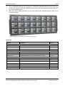
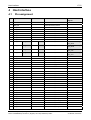
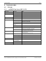
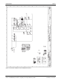
1
Design Guide netRAPID Chip Carrier Hilscher Gesellschaft für Systemautomation mbH www.hilscher.com DOC111004DG04EN | Revision 4 | English | 2014-09 | Released | Public Introduction 2/72 Table of Contents 1 Introduction.............................................................................................................................................4 1.1 About this document ......................................................................................................................4 1.1.1 List of revisions.................................................................................................................................. 4 1.1.2 References to documents.................................................................................................................. 4 1.2 Legal notes.....................................................................................................................................5 1.2.1 1.2.2 1.2.3 1.2.4 1.2.5 2 Copyright ........................................................................................................................................... 5 Important notes ................................................................................................................................. 5 Exclusion of liability ........................................................................................................................... 6 Warranty............................................................................................................................................ 6 Export regulations.............................................................................................................................. 6 Product overview ...................................................................................................................................7 2.1 Block diagrams.............................................................................................................................10 2.1.1 NRP 10-CCS ................................................................................................................................... 10 2.1.2 NRP 10-DPS ................................................................................................................................... 10 2.1.3 NRP 52-RE...................................................................................................................................... 11 3 Mechanics .............................................................................................................................................12 3.1 Dimension ....................................................................................................................................12 3.2 Design guidelines for the host system .........................................................................................12 3.2.1 Footprint .......................................................................................................................................... 12 3.2.2 Thermal behavior and thermal pad.................................................................................................. 13 3.2.3 Keep-out area.................................................................................................................................. 14 3.3 3.4 4 Tempering, storage and soldering ...............................................................................................14 Matrix label ...................................................................................................................................16 Host interface .......................................................................................................................................17 4.1 Pin assignment.............................................................................................................................17 4.2 General signals ............................................................................................................................20 4.2.1 4.2.2 4.2.3 4.2.4 4.3 Parallel dual-port memory............................................................................................................22 4.3.1 4.3.2 4.3.3 4.3.4 4.3.5 4.4 Supply voltage ................................................................................................................................. 20 Reset signal..................................................................................................................................... 20 Boot signal and boot options ........................................................................................................... 21 Host interface mode ........................................................................................................................ 21 Address bus and data bus............................................................................................................... 22 Dual-port memory control lines........................................................................................................ 23 Interrupt line to the host system....................................................................................................... 23 Busy line to the host system ............................................................................................................ 23 Timing diagram dual-port memory interface .................................................................................... 24 Serial dual-port memory mode.....................................................................................................26 5 Diagnostic interface .............................................................................................................................27 5.1 USB interface ...............................................................................................................................27 5.2 Serial interface – UART ...............................................................................................................28 6 Device type specific interfaces ...........................................................................................................29 6.1 NRP 10-CCS................................................................................................................................29 6.1.1 6.1.2 6.1.3 6.1.4 6.1.5 6.2 NRP 10-DPS ................................................................................................................................32 6.2.1 6.2.2 6.2.3 6.2.4 6.2.5 6.3 Connections overview ..................................................................................................................... 29 CC-Link interface............................................................................................................................. 30 LEDs................................................................................................................................................ 30 Address and baud rate switches...................................................................................................... 31 SYNC .............................................................................................................................................. 31 Connections overview ..................................................................................................................... 32 PROFIBUS DP interface ................................................................................................................. 33 LEDs................................................................................................................................................ 33 Switches .......................................................................................................................................... 34 SYNC .............................................................................................................................................. 34 NRP 52-RE ..................................................................................................................................35 6.3.1 6.3.2 6.3.3 6.3.4 6.3.5 Connections overview ..................................................................................................................... 35 Ethernet interface ............................................................................................................................ 36 LEDs................................................................................................................................................ 36 Switches .......................................................................................................................................... 37 SYNC .............................................................................................................................................. 38 netRAPID Chip Carrier | Design Guide DOC111004DG04EN | Revision 4 | English | 2014-09 | Released | Public © Hilscher, 2013-2014 Introduction 7 3/72 Evaluation Boards................................................................................................................................39 7.1 Evaluation Board NRPEB-CCS and NRPEB-DPS ......................................................................39 7.1.1 7.1.2 7.1.3 7.1.4 7.1.5 7.2 Fieldbus measuring points (X3) ....................................................................................................... 40 PROFIBUS DP (X30) ...................................................................................................................... 40 CC-Link (X50).................................................................................................................................. 41 Address switches (S1, S2) and baud rate switch (S0) for CC-Link .................................................. 41 Address switches (S1, S2) for PROFIBUS DP ................................................................................ 42 Evaluation Board NRPEB-RE2 ....................................................................................................43 7.2.1 Ethernet interface (X50) .................................................................................................................. 44 7.2.2 Address switches for Ethernet (S1, S2)........................................................................................... 44 7.3 Operating elements of Evaluation Boards ...................................................................................45 7.3.1 Reset button (T1) ............................................................................................................................ 45 7.3.2 S-Boot button (T2) ........................................................................................................................... 45 7.4 Interfaces .....................................................................................................................................46 7.4.1 7.4.2 7.4.3 7.4.4 7.4.5 7.4.6 7.4.7 8 Host interface (X1)........................................................................................................................... 46 Host interface measuring pins (X2) ................................................................................................. 48 SYNC, serial (UART) and GPIO measuring pins (X4) ..................................................................... 49 Host interface mode (X5)................................................................................................................. 50 USB interface (X6)........................................................................................................................... 51 JTAG connector (X11)..................................................................................................................... 52 Power supply (X100) ....................................................................................................................... 53 Technical data ......................................................................................................................................54 8.1 CC-Link ........................................................................................................................................54 8.1.1 netRAPID Chip Carrier NRP 10-CCS .............................................................................................. 54 8.1.2 Evaluation Board NRPEB-CCS ....................................................................................................... 55 8.2 PROFIBUS DP Slave...................................................................................................................56 8.2.1 netRAPID Chip Carrier NRP 10-DPS .............................................................................................. 56 8.2.2 Evaluation Board NRPEB-DPS ....................................................................................................... 57 8.3 Real-Time Ethernet ......................................................................................................................58 8.3.1 netRAPID Chip Carrier NRP 52-RE................................................................................................. 58 8.3.2 Evaluation Board NRPEB-RE2........................................................................................................ 59 8.4 Signals..........................................................................................................................................60 9 Schematics............................................................................................................................................61 9.1 Overview ......................................................................................................................................61 9.2 NRPEB-CCS and NRPEB-DPS...................................................................................................62 9.3 NRPEB-RE2.................................................................................................................................64 10 Bill of material.......................................................................................................................................66 10.1 Overview ......................................................................................................................................66 10.2 NRPEB-CCS and NRPEB-DPS...................................................................................................66 10.3 NRPEB-RE2.................................................................................................................................68 11 Appendix ...............................................................................................................................................70 11.1 List of tables .................................................................................................................................70 11.2 List of figures................................................................................................................................71 11.3 Contacts .......................................................................................................................................72 netRAPID Chip Carrier | Design Guide DOC111004DG04EN | Revision 4 | English | 2014-09 | Released | Public © Hilscher, 2013-2014 Introduction 1 4/72 Introduction 1.1 About this document This design guide describes the mechanical and electrical interfaces of netRAPID products. This document includes the description of the netRAPID Evaluation Boards. 1.1.1 List of revisions Rev Date Name Chapter Revision 2 2013-12-16 HH All Description of NRP 10-DPS, NRP 10-CCS and NRP 52-RE. 3 2014-07-30 HH 2 Section Product overview expanded. 4 2014-09-16 HH 3.3 Section Tempering, storage and soldering: Tempering and storage added. 4.1 Section Pin assignment updated. 4.2.2 Section Reset signal expanded. 4.2.3 Section Boot signal and boot options: information about mandatory push botton (or an equivalent device) added. 4.4 Section Serial dual-port memory mode expanded. 5.1 Section USB interface expanded. 2.1 Figure 3, Figure 4 and Figure 5: Colors of SYS-LED corrected. Table 1: List of revisions 1.1.2 References to documents This document refers to the following other documents: [1] Hilscher Gesellschaft für Systemautomation mbH: Getting Started Guide, Serial Dual-Port Memory Interface with netX, Revision 3, english, 2014-07. [2] Hilscher Gesellschaft für Systemautomation mbH: Technical Data Reference Guide, netX 10, Revision 0.9, English, 2011-12. [3] Hilscher Gesellschaft für Systemautomation mbH: Technical Data Reference Guide, netX 51/52, Revision 2, English, 2013-05. [4] Hilscher Gesellschaft für Systemautomation mbH: Dual-Port Memory Interface Manual, netX based products, Revision 12, English, 2012. netRAPID Chip Carrier | Design Guide DOC111004DG04EN | Revision 4 | English | 2014-09 | Released | Public © Hilscher, 2013-2014 Introduction 1.2 1.2.1 5/72 Legal notes Copyright © Hilscher, 2013-2014, Hilscher Gesellschaft für Systemautomation mbH All rights reserved. The images, photographs and texts in the accompanying material (user manual, accompanying texts, documentation, etc.) are protected by German and international copyright law as well as international trade and protection provisions. You are not authorized to duplicate these in whole or in part using technical or mechanical methods (printing, photocopying or other methods), to manipulate or transfer using electronic systems without prior written consent. You are not permitted to make changes to copyright notices, markings, trademarks or ownership declarations. The included diagrams do not take the patent situation into account. The company names and product descriptions included in this document may be trademarks or brands of the respective owners and may be trademarked or patented. Any form of further use requires the explicit consent of the respective rights owner. 1.2.2 Important notes The user manual, accompanying texts and the documentation were created for the use of the products by qualified experts, however, errors cannot be ruled out. For this reason, no guarantee can be made and neither juristic responsibility for erroneous information nor any liability can be assumed. Descriptions, accompanying texts and documentation included in the user manual do not present a guarantee nor any information about proper use as stipulated in the contract or a warranted feature. It cannot be ruled out that the user manual, the accompanying texts and the documentation do not correspond exactly to the described features, standards or other data of the delivered product. No warranty or guarantee regarding the correctness or accuracy of the information is assumed. We reserve the right to change our products and their specification as well as related user manuals, accompanying texts and documentation at all times and without advance notice, without obligation to report the change. Changes will be included in future manuals and do not constitute any obligations. There is no entitlement to revisions of delivered documents. The manual delivered with the product applies. Hilscher Gesellschaft für Systemautomation mbH is not liable under any circumstances for direct, indirect, incidental or follow-on damage or loss of earnings resulting from the use of the information contained in this publication. netRAPID Chip Carrier | Design Guide DOC111004DG04EN | Revision 4 | English | 2014-09 | Released | Public © Hilscher, 2013-2014 Introduction 1.2.3 6/72 Exclusion of liability The software was produced and tested with utmost care by Hilscher Gesellschaft für Systemautomation mbH and is made available as is. No warranty can be assumed for the performance and flawlessness of the software for all usage conditions and cases and for the results produced when utilized by the user. Liability for any damages that may result from the use of the hardware or software or related documents, is limited to cases of intent or grossly negligent violation of significant contractual obligations. Indemnity claims for the violation of significant contractual obligations are limited to damages that are foreseeable and typical for this type of contract. It is strictly prohibited to use the software in the following areas: for military purposes or in weapon systems; for the design, construction, maintenance or operation of nuclear facilities; in air traffic control systems, air traffic or air traffic communication systems; in life support systems; in systems in which failures in the software could lead to personal injury or injuries leading to death. We inform you that the software was not developed for use in dangerous environments requiring fail-proof control mechanisms. Use of the software in such an environment occurs at your own risk. No liability is assumed for damages or losses due to unauthorized use. 1.2.4 Warranty Although the hardware and software was developed with utmost care and tested intensively, Hilscher Gesellschaft für Systemautomation mbH does not guarantee its suitability for any purpose not confirmed in writing. It cannot be guaranteed that the hardware and software will meet your requirements, that the use of the software operates without interruption and that the software is free of errors. No guarantee is made regarding infringements, violations of patents, rights of ownership or the freedom from interference by third parties. No additional guarantees or assurances are made regarding marketability, freedom of defect of title, integration or usability for certain purposes unless they are required in accordance with the law and cannot be limited. Warranty claims are limited to the right to claim rectification. 1.2.5 Export regulations The delivered product (including the technical data) is subject to export or import laws as well as the associated regulations of different counters, in particular those of Germany and the USA. The software may not be exported to countries where this is prohibited by the United States Export Administration Act and its additional provisions. You are obligated to comply with the regulations at your personal responsibility. We wish to inform you that you may require permission from state authorities to export, re-export or import the product. netRAPID Chip Carrier | Design Guide DOC111004DG04EN | Revision 4 | English | 2014-09 | Released | Public © Hilscher, 2013-2014 Product overview 2 7/72 Product overview netRAPID chip carriers are for easy and fast integration into a host system: Fully functional 32 x 32 mm chip carrier that can be soldered directly on a PCB of the host system, for a direct network connection, only a connector on PCB is needed, parallel dual-port memory or serial dual-port memory (fast SPI slave interface), LEDs, address switches. Hardware development is confined to connect the network connector, the LEDs and possibly an address switch. The interface from the host system to the netRAPID device is either a parallel dual-port memory interface or a serial dual-port memory interface by means of a fast SPI connection. The netRAPID can be soldered manually onto the host system and simplifies prototype production. For series production netRAPID can be soldered onto a host system PCB using SMD. Steps 1. Start with the Evaluation Board. Each Evaluation Board is equipped with a soldered-on netRAPID to start evaluation immediately. Figure 1: Evaluation Board, 3 pcs. netRAPID and Evaluation DVD with software tools The netRAPID Evaluation DVD contains limited versions of Loadable Firmware (LFW) for testing and evaluation purposes, software tools for configuring the netRAPID, for downloading firmware and for testing I/O communication, C-Toolkit (source code for developers of non-Windows target platforms and embedded systems), USB drivers for Windows (needed for accessing the USB diagnostic interface of the netRAPID from a Windows configuration PC), cifX Device Driver (needed for accessing the host interface of the netRAPID from a Windows PC via PCI), PDF documentation for users and developers. netRAPID Chip Carrier | Design Guide DOC111004DG04EN | Revision 4 | English | 2014-09 | Released | Public © Hilscher, 2013-2014 Product overview 8/72 2. Three netRAPID devices are included the netRAPID Evaluation Board. Create your host system and simply solder the netRAPID device onto your host system manually and have your first prototype done. 3. Start your series SMD production of your host system with netRAPID devices from a tray containing 24 pcs. Figure 2: netRAPID tray containing 24 pcs. for series production Overview Products Description Part no Evaluation board including NRP 10-CCS 7600.740 CC-Link Slave NRPEB-CCS NRP 10-CCS TRAY 24 pieces of NRP 10-CCS Chip Carriers 7652.740 NRPLFW-CCS Loadable CC-Link Slave Firmware for NRP 10-CCS 7601.740 NRPEB-DPS Evaluation board including NRP 10-DPS 7600.420 NRP 10-DPS TRAY 24 pieces of NRP 10-DPS Chip Carriers 7652.420 NRPLFW-DPS Loadable PROFIBUS DP Slave Firmware for NRP 10-DPS 7601.420 NRPEB-RE2 Evaluation board including NRP 52-RE 7600.200 NRP 52-RE TRAY 24 pieces of NRP 52-RE Chip Carriers 7672.100 NRPLFW-ECS Loadable EtherCAT Slave Firmware for NRP 52-RE 7601.120 NRPLFW-OMB Loadable Open Modbus/TCP Firmware for NRP 52-RE 7601.860 NRPLFW-PNS Loadable PROFINET IO-Device Firmware for NRP 52-RE 7601.850 NRPLFW-EIS Loadable EtherNet/IP Adapter Firmware for NRP 52-RE 7601.830 NRPLFW-S3S Loadable Sercos Slave Firmware for NRP 52-RE 7601.160 PROFIBUS DP Slave Real-Time Ethernet (Slave) Table 2: Product overview netRAPID Chip Carrier | Design Guide DOC111004DG04EN | Revision 4 | English | 2014-09 | Released | Public © Hilscher, 2013-2014 Product overview 9/72 Interface overview The subsequent table lists interfaces and functions of the netRAPID Chip Carriers which are currently supported by the licensed netRAPID Standard Loadable Firmware (NRPLFW). Note that customized netRAPID firmware with extra functionalities will be available from Hilscher on request. Diagnostic interface NRP 52-RE Communication interface NRP 10-CCS Host interface NRP 10-DPS Standard functions 8 bit parallel dual-port memory ✓ ✓ ✓ - 16 bit parallel dual-port memory ✓ ✓ ✓ - Serial dual-port memory (SPI) ✓ ✓ ✓ - PROFIBUS DP (Slave) ✓ - - - CC-Link (Slave) - ✓ - - Real-Time Ethernet (Slave) - - ✓ - ✓ ✓ ✓ Default: USB is activated. USB Remark Default: UART is deactivated. The pins of the UART interface are shared with the pins for the SYNC interface. UART - - - Production interface JTAG - - - For Hilscher development and production only. Input 2x 4 bit (address switch) ✓ ✓ - - 1x 4 bit (baud rate switch) - ✓ - - 1 bit GPIO - - - Standard firmware does not use the GPIO. Output Default: SYNC is activated - - ✓ The pins of the SYNC interface are shared with the pins for the UART interface. SYS-LED ✓ ✓ ✓ - COM0, COM1 ✓ ✓ ✓ - - - ✓ - SYNC interface SYNC0, SYNC1 LED Link and Act Table 3: Interface and standard functions overview netRAPID Chip Carrier | Design Guide DOC111004DG04EN | Revision 4 | English | 2014-09 | Released | Public © Hilscher, 2013-2014 Product overview 2.1 2.1.1 10/72 Block diagrams NRP 10-CCS Figure 3: NRP 10-CCS block diagram 2.1.2 NRP 10-DPS Figure 4: NRP 10-DPS block diagram netRAPID Chip Carrier | Design Guide DOC111004DG04EN | Revision 4 | English | 2014-09 | Released | Public © Hilscher, 2013-2014 Product overview 2.1.3 11/72 NRP 52-RE Figure 5: NRP 52-RE block diagram netRAPID Chip Carrier | Design Guide DOC111004DG04EN | Revision 4 | English | 2014-09 | Released | Public © Hilscher, 2013-2014 Mechanics 3 12/72 Mechanics 3.1 Dimension A netRAPID has the following dimensions: L= 32 mm, W = 32 mm and H = 4 mm. 3.2 3.2.1 Design guidelines for the host system Footprint The layout for the netRAPID footprint on the host system requires the following dimensions. There is one footprint for NRP 10 chip carriers and one for NRP 52 chip carriers. Figure 6: Footprint NRP 10 netRAPID Chip Carrier | Design Guide DOC111004DG04EN | Revision 4 | English | 2014-09 | Released | Public © Hilscher, 2013-2014 Mechanics 13/72 Figure 7: Footprint NRP 52 3.2.2 Thermal behavior and thermal pad NRP 10 devices have a power consumption of 1 - 1.2 W and NRP 52 devices of 1.8 W, which generates heat. The generated heat must be dissipated to prevent overheating of the chip. While there is a hard limit for the chip’s junction temperature at 125 °C above, which malfunction and permanent damage may occur, it is always desired to keep the junction temperature as low as possible, as a semiconductor’s statistical life time generally decreases with rising temperature. Make sure that the case temperature of the netX is always below 100 °C, which is the recommended maximum value for a netX design. This value was chosen because the FIT-rate for the silicon process, which netX are based on, shows a significant rise in the temperature range between 100°C and the absolute maximum junction temperature. However, since the absolute max. junction temperature is 125 °C, it is at the device manufacturer’s discretion if he wants to follow this recommendation or rather decides to accept a higher junction temperature and trade a decrease of the MTBF of his devices for a higher temperature range specification. netRAPID devices have a thermal pad at the bottom for heat dissipation to the PCB of the host system. Important note: You must use a thermal pad on the PCB for the host system. This is absolutely necessary in order to reach the temperature range for netRAPID devices. netRAPID Chip Carrier | Design Guide DOC111004DG04EN | Revision 4 | English | 2014-09 | Released | Public © Hilscher, 2013-2014 Mechanics 14/72 This results in requirements for the PCB of the host system: Use at least 9 vias, which are to be connected to ground plane. Use a large copper surface on the PCB of the host system to reach a good heat dissipation for the netRAPID. Don’t place components on the PCB of the host system below the netRAPID to avoid heat dissipation of other component than netRAPID. The thermal pad of the netRAPID device has GND potential. Figure 6 on page 12 shows position and size of the thermal pad for NRP 10 and Figure 7 on page 13 shows it for NRP 52. 3.2.3 Keep-out area Make sure that no vias and no wires are on the PCB of the host system underneath the netRAPID device. Important note: Make sure to use the thermal pad. Figure 6 on page 12 shows position and size of the thermal pad for NRP 10 and Figure 7 on page 13 shows it for NRP 52. 3.3 Tempering, storage and soldering Tempering netRAPID have to be tempered to reduce unwanted moisture before they are soldered onto the host system. If the moisture is not reduced then the heating during the soldering process to more than 200 °C can lead possible destruction of electronic parts of the netRAPID. To avoid this, netRAPID have to be tempered 24 h at 80 °C. Hilscher tempers netRAPID devices before they are shipped. After tempered, netRAPID devices are shipped welded in a tray. Moisture sensitivity level The Moisture Sensitivity Level (MSL) is MSL 3, 168 h, 30 °C / 60%RH. Storage The netRAPID in a welded (sealed) tray can be stored up to 1 year. After 1 year the netRAPID devices have to be tempered again, before soldered onto a host system. netRAPID Chip Carrier | Design Guide DOC111004DG04EN | Revision 4 | English | 2014-09 | Released | Public © Hilscher, 2013-2014 Mechanics 15/72 Soldering netRAPID devices can be placed on the PCB of the host system for SMD production. netRAPID can be picked and placed (from the tray to the PCB of the host system) using asymmetric suck in. Place netRAPID on the top side of the PCB of the host system. Important note: The thermal profile for reflow soldering depends on the used soldering paste and the used reflow system. Read the data sheet of the manufacturer of the used soldering paste for requirements to the thermal profile. When using the Heraeus soldering paste Sn/Ag/Cu-95.5/4/0.5 (F620CU0.5-88M3 lead free) then the following thermal profile is recommended: Figure 8: Thermal profile for reflow soldering Adhesion keeps the components on the netRAPID in place during the reflow soldering. netRAPID Chip Carrier | Design Guide DOC111004DG04EN | Revision 4 | English | 2014-09 | Released | Public © Hilscher, 2013-2014 Mechanics 3.4 16/72 Matrix label A matrix label is on the device for identification. It contains 3 items: 1. Part number 2. Hardware revision 3. Serial number The figure shows part number 7600.100, hardware revision 2 and serial number 20000. Part number Hardware Revision Serial number Figure 9: Matrix label netRAPID Chip Carrier | Design Guide DOC111004DG04EN | Revision 4 | English | 2014-09 | Released | Public © Hilscher, 2013-2014 Host interface 4 4.1 17/72 Host interface Pin assignment Pin Signal Specification Function Other shared 1 PE 2 DPM_D0 I Dual-Port Memory Data 0 3 DPM_D1 I Dual-Port Memory Data 1 4 DPM_D2 I Dual-Port Memory Data 2 5 DPM_D3 I Dual-Port Memory Data 3 6 DPM_D4 I Dual-Port Memory Data 4 7 DPM_D5 I Dual-Port Memory Data 5 8 DPM_D6 I Dual-Port Memory Data 6 9 DPM_D7 I Dual-Port Memory Data 7 10 DPM_D8 SPM_MISO I O6 Dual-Port Memory Data 8 Serial-Host-Memory SPI_MISO 11 DPM_D9 SPM_MOSI I I Dual-Port Memory Data 9 Serial-Host-Memory SPI_MOSI 12 DPM_D10 SPM_CSn I I Dual-Port Memory Data 10 Serial-Host-Memory SPI_CSn 13 DPM_D11 SPM_CLK I I Dual-Port Memory Data 11 Serial-Host-Memory SPI_CLK 14 DPM_D12 I Dual-Port Memory Data 12 15 DPM_D13 I Dual-Port Memory Data 13 16 DPM_D14 I Dual-Port Memory Data 14 17 DPM_D15 I Dual-Port Memory Data 15 18 +3V3 19 GND I Ground 20 DPM_A0 I Dual-Port Memory Address 0 21 DPM_A1 I Dual-Port Memory Address 1 22 DPM_A2 I Dual-Port Memory Address 2 23 DPM_A3 I Dual-Port Memory Address 3 24 DPM_A4 I Dual-Port Memory Address 4 25 DPM_A5 I Dual-Port Memory Address 5 26 DPM_A6 I Dual-Port Memory Address 6 27 DPM_A7 I Dual-Port Memory Address 7 28 DPM_A8 I Dual-Port Memory Address 8 29 DPM_A9 I Dual-Port Memory Address 9 30 DPM_A10 I Dual-Port Memory Address 10 31 DPM_A11 I Dual-Port Memory Address 11 32 DPM_A12 I Dual-Port Memory Address 12 33 DPM_A13 I Dual-Port Memory Address 13 34 DPM_CSn I50KU Dual-Port Memory Chip Select 35 DPM_BHEn I50KU Dual-Port Memory Bus High Enable 36 DPM_RDn I50KU Dual-Port Memory Read 37 DPM_WRn I50KU Dual-Port Memory Write 38 DPM_BUSYn I50KU Dual-Port Memory Busy Signals Protected Earth Ground +3.3V Power Supply netRAPID Chip Carrier | Design Guide DOC111004DG04EN | Revision 4 | English | 2014-09 | Released | Public © Hilscher, 2013-2014 Host interface Pin Signal 39 DPM_DIRQ 18/72 Specification Function I50KU During start up: Setting of Host Interface Mode (see section Host interface mode on page 21). Other shared Signals HIFM0 I50KU Host Interface Mode 0 During runtime: Dual-Port Memory Data Interrupt. 40 DPM_SIRQ HIFM1 I50KU I50KU During start up: Setting of Host Interface Mode (see section Host interface mode on page 21). Host Interface Mode 1 During runtime: Dual-Port Memory Synchronization Interrupt. 41 DPM_RESETn 42 UART_RX SYNC0 I5KU I5KU / O6 UART Receive Date Synchronization Signal 0 43 UART_TX SYNC1 O6 I5KU / O6 UART Transmit Data Synchronization Signal 1 44 USB- USB USB Signal D- 45 USB+ USB USB Signal D+ 46 S2_1n I50KU Switch 2 - D1 47 S2_2n I50KU Switch 2 - D2 48 S2_4n I50KU Switch 2 - D4 49 S2_8n I50KU Switch 2 - D8 50 S1_1n I50KU Switch 1 - D1 51 S1_2n I50KU Switch 1 - D2 52 S1_4n I50KU Switch 1 - D4 53 S1_8n I50KU Switch 1 - D8 54 S0_1 I50KD Switch 0 - D1 LINK0 O6 Link-LED of Ethernet channel 0 S0_2 I50KD Switch 0 - D2 ACT0 O6 Activity-LED of Ethernet channel 0 55 56 57 I1.5KU Dual-Port Memory Reset S0_4 I50KD Switch 0 - D4 LINK1 O6 Link-LED of Ethernet channel 1 S0_8 I50KD Switch 0 - D8 ACT1 O6 Activity-LED of Ethernet channel 1 58 GND 59 +3V3 60 RDYn Ground VCC BOOT O6 +3.3V Power Supply I1.5KU System LED yellow / Ready 61 RUNn O6 System LED green / Run 62 COM0_Gn O6 Communication Status LED 0 green 63 COM0_Rn O6 Communication Status LED 0 red 64 COM1_Gn O6 Communication Status LED 1 green 65 COM1_Rn O6 Communication Status LED 1 red 66 GPIO I50KD / O6 General Purpose In Output 67 68 69 70 System Boot Isolation Gap FB1 Field bus specific Field bus connector pin 1 RXN0 Ethernet specific Ethernet channel 0 receive negative FB2 Field bus specific Field bus connector pin 2 RXP0 Ethernet specific Ethernet channel 0 receive positive FB3 Field bus specific Field bus connector pin 3 netRAPID Chip Carrier | Design Guide DOC111004DG04EN | Revision 4 | English | 2014-09 | Released | Public © Hilscher, 2013-2014 Host interface Pin 19/72 Signal Specification Function TXN0 Ethernet specific Ethernet channel 0 transmit negative FB4 Field bus specific Field bus connector pin 4 TXP0 Ethernet specific Ethernet channel 0 transmit positive Other shared Signals 71 72 73 74 75 76 FB5 Field bus specific Field bus connector pin 5 - Ethernet specific - FB6 Field bus specific Field bus connector pin 6 RXN1 Ethernet specific Ethernet channel 1 receive positive FB7 Field bus specific Field bus connector pin 7 RXP1 Ethernet specific Ethernet channel 1 receive positive FB8 Field bus specific Field bus connector pin 8 TXN1 Ethernet specific Ethernet channel 1 transmit negative FB9 Field bus specific Field bus connector pin 9 TXP1 Ethernet specific Ethernet channel 1 transmit positive Table 4: Pin assignment Gray fields in columns Signal and Specification indicate that column Other shared Signals contains the description of the signal. The following table lists the meaning of the abbreviations used in the specification column: Symbol Meaning I Input I1.5KU Input with 1.5 kΩ resistor to +3V3 I50KD Input with 50 kΩ resistor to GND I50KU Input with 50 kΩ resistor to +3V3 O6 Output: load of max. 6 mA Field bus specific According to the respective field bus specification Ethernet specific According to the respective Ethernet specification Table 5: Symbols of pin assignment netRAPID Chip Carrier | Design Guide DOC111004DG04EN | Revision 4 | English | 2014-09 | Released | Public © Hilscher, 2013-2014 Host interface 4.2 4.2.1 20/72 General signals Supply voltage Only a single 3.3 V operation voltage is needed to operate the netRAPID. The voltage must be regulated and can have a tolerance of ±5% (3.15 - 3.45 V) and must be connected twice to the netRAPID chip carrier. The power has to be supplied between pins +3V3 and GND. To avoid EMI problems use bypass capacitors in the power supply path. All other special voltages required on the netRAPID are generated by onboard DC/DC converters. A voltage supervisor circuit on all netRAPID devices supervises the voltage and the microprocessor. If the voltage decreases below the voltage reset level of typically 2.93 V (2.85 3.00 V) the netRAPID is held in reset state. If the voltage exceeds the reset voltage threshold, the netRAPID will begin with the power up sequence. To avoid problems with the power supply we recommend using a voltage of 3.3 V. The operation will thus be in the safe range of the voltage operation area, ensuring that short voltage drops, spikes and noise will not cause any reset conditions. The maximum power consumption depends on the netRAPID type. For power consumption values see section Technical data on page 54. 4.2.2 Reset signal It is possible to reset the netRAPID by the global power-on reset signal DPM_RESETn. As long as the signal DPM_RESETn has high level, the netRAPID stays in operating mode. The netRAPID is in reset mode when the signal DPM_RESETn has a static low level. To reset the netRAPID the DPM_RESETn signal must be low for more than 10 µs. Afterwards, the netRAPID starts the initialization and program execution. This power up time is different for each netRAPID and loaded firmware. Important: During reset all signals of the dual-port memory are configured as inputs! The output level could be floating. If the host system needs a stable level, a pull-up or pull-down resistor is required on the host system. For details about the circuit for the host system see Figure 21: Schematic NRPEB-CCS and NRPEB-DPS (Part 1) on page 62 or see Figure 23: Schematic NRPEB-RE2 (Part 1) on page 64. Recommendation: Always add a push button to your host system connected to the netRAPID device to reset the netRAPID device. This reset button together with the mandatory push button (or switch or an equivalent device) to activate the serial boot mode is important for your production, because the serial boot mode is needed to load the Second Stage Boot Loader into the netRAPID device. netRAPID Chip Carrier | Design Guide DOC111004DG04EN | Revision 4 | English | 2014-09 | Released | Public © Hilscher, 2013-2014 Host interface 4.2.3 21/72 Boot signal and boot options Mandatory: Always add a push button or switch (or an equivalent device) to your host system connected to the netRAPID device to activate the serial boot mode of the ROM loader. The serial boot mode is necessary for your production to load the Second Stage Boot Loader into the netRAPID device or later for support to be able to update the Second Stage Boot Loader. If you do not implement a push button or switch (or an equivalent device) to your host system, you will not be able to load or update the Second Stage Boot Loader! With NRP 52 devices without a Second Stage Boot Loader activate the Ethernet boot mode by default which is not supported. For details about the circuit for the host system see Figure 21: Schematic NRPEB-CCS and NRPEB-DPS (Part 1) on page 62 or see Figure 23: Schematic NRPEB-RE2 (Part 1) on page 64. Note: If you want to make use of the other boot options that the netRAPID offers, you need to implement two DIP switches or an equivalent device for switching two signals (RUN and RDY). Note: To serial boot mode requires an USB interface or a serial (UART) interface. Activating the boot mode The boot signal is located at pin 60 (RDY). After a reset it is an input signal and active low. To activate the boot mode, pin 60 has to be connected via 390 Ω to GND (low signal) after a reset. Note: The signal level during the reset and shortly afterwards must be low in order to force the netRAPID into the boot mode. 4.2.4 Host interface mode netRAPIDs support two host interface modes parallel dual-port memory and serial dual-port memory (SPI). The host interface mode is evaluated by the Second Stage Boot Loader during boot. The Second Stage Boot Loader uses this setting to initialize the selected dual-port memory mode in the host interface. Activating the parallel dual-port memory mode A high signal at DPM_DIRQn (pin 39) activates the dual-port memory mode (via a 2.2 kΩ pullup resistor or the input is open). The data width of the dual-port memory can be set to 8 or 16 bit. The data width is set at DPM_SIRQn (pin 40) during the start-up phase. A high signal at DPM_SIRQn (via a 2.2 kΩ pull-up resistor or the input is open) sets the data width of 8 bit. A low signal at DPM_SIRQn (via a 2.2 kΩ pull-down resistor) sets the data width of 16 bit. netRAPID Chip Carrier | Design Guide DOC111004DG04EN | Revision 4 | English | 2014-09 | Released | Public © Hilscher, 2013-2014 Host interface 22/72 Activating the serial dual-port memory mode (SPI) A low signal at DPM_DIRQn activates the SPI mode (via a 2.2 kΩ pull-down resistor). netRAPID internal pull-up and pull-down resistors Pin Signal netX 10 on NRP 10 netX 52 on NRP 52 39 DPM_DIRQn 50 kΩ pull-up 50 kΩ pull-up 40 DPM_SIRQn 50 kΩ pull-up 50 kΩ pull-down Important: Never drive the host interface mode signal (DPM_DIRQn pin 39). Instead, operation with pull-down and pull-up resistors is recommended. 4.3 Parallel dual-port memory The communication for all input and output data and control commands between the netRAPID and the host system are exchanged over the dual port memory. From host system side, the dual-port memory looks like static RAM. The netRAPID always provides addressing capabilities for 16 KByte dual port memory. Only a few signals are used to control the access to the dual port memory. These data lines can drive 6 mA at maximum. To avoid data loss by simultaneous access at the same memory cell, it is necessary to use the BUSYn signal. Please refer to the special documents for the basic description of the data model and communication methods with devices based on the netX. 4.3.1 Address bus and data bus These signal lines contain the address bus lines A0 up to A13 and data bus lines D0 up to D15 of the dual-port memory. The address and data lines are non-multiplexed. The dual-port memory of the netRAPID has a size of 16 KB. NRP 10 devices only use the lowest 8 KB of the dual-port memory. Unused address lines may be equipped with a pull-down resistor of 560 Ω. The following table explains the available possibilities: netRAPID Host address space Connect Pull-down to address line NRP 10 8 KB A0 ... A12 A13 NRP 52 16 KB A0 ... A13 none Table 6: Possibilities for usage of dual-port memory The netRAPID supports additional data bus lines to drive a 16 bit data interface. If your host interface can support a width of 16-bit, connect the DPM_SIRQn signal to Vcc. If not, let the DPM_SIRQn signal unconnected causing 16-bit devices to work in 8-bit mode. netRAPID Chip Carrier | Design Guide DOC111004DG04EN | Revision 4 | English | 2014-09 | Released | Public © Hilscher, 2013-2014 Host interface 23/72 In case of a 16-bit system you have to generate the DPM_BHEn (pin 35) and DPM_A0 (pin 20) signal according to the following table. DPM_BHEn DPM_A0 Function 0 0 word access 0 1 access high byte 1 0 access low byte 1 1 no access Table 7: Function table of the 16-bit decode logic 4.3.2 Dual-port memory control lines Integration of the netRAPID is done by mapping the memory space of the dual port memory into the address range of the host system. The access to the dual-port memory is handled over the control lines DPM_WRn (pin 37, write), DPM_RDn (pin 36, read) and DPM_CSn (pin 34, Chip select) and could be like standard static RAM. All signals are low active. 4.3.3 Interrupt line to the host system The signal DPM_DIRQn (located at pin 39, also used as mode discrimination signal) can be used to generate an interrupt to the host system when the netX processor of the netRAPID writes into the specific handshake cells of the dual-port memory. These cells are used for synchronization of the netRAPID and the host system and have handshake bits. The interrupt will be cleared if the host reads the handshake cell that was written from the netX of the netRAPID. Important: In interrupt mode, when an 8-bit host performs a read access to any of the 16-bit wide handshake registers, the netX releases the interrupt as soon as the high byte or the low byte was read. The read order (high byte first or low byte first) is irrelevant. An 8-bit host shall use polling mode instead of interrupt mode! Important: Never drive the signal DPM_DIRQn (pin 39). Instead, operation with pull-down and pull-up resistors is recommended. 4.3.4 Busy line to the host system The signal DPM_BUSYn is used to insert wait states into a current access from host system to a netRAPID. When the signal is active the host must wait for the current transfer. Also see the timing diagram in section Timing diagram dual-port memory interface on page 24. netRAPID Chip Carrier | Design Guide DOC111004DG04EN | Revision 4 | English | 2014-09 | Released | Public © Hilscher, 2013-2014 Host interface 4.3.5 24/72 Timing diagram dual-port memory interface The following diagram shows the timing for dual-port memory read access. Figure 10: Timing diagram for read access The following diagram shows the timing for dual-port memory write access. Figure 11: Timing diagram for write access Description and values are on the next page. netRAPID Chip Carrier | Design Guide DOC111004DG04EN | Revision 4 | English | 2014-09 | Released | Public © Hilscher, 2013-2014 Host interface 25/72 The following table gives the values for the timing parameters for netRAPID devices. For exchangeability of netRAPID NRP 52 with netRAPID NRP 10 devices and visa versa use the values of column Common of Table 8. Symbol Description netRAPID 10 netRAPID 52 Common netX 10 netX 52 t1 tAS min. Minimum address setup time 0 ns 0 ns 2 ns t2 tBV max. Maximum time from cycle start until BUSYn signal is valid 5.7 ns 5.7 ns 40 ns t3 tBAR typ. Typical BUSY active time (read access) - - - tBAR max. See important note 1 68 ns 68 ns - tBAW min. Minimum BUSY active time (write access) 0 ns 0 ns 0 ns tBAW max. See important note 1 68 ns 68 ns - t5 tDVR min. Minimum time between valid data bus signals and rising edge of BUSYn signal 7.8 ns 7.8 ns 5 ns t6 tDSW min. Minimum setup time for write data 10.8 ns 12.8 ns 25 ns t7 tDHR min. Minimum read data hold time 2.1 ns 2.1 ns 0 ns t8 tDHW min. Minimum hold time for write data 0.8 ns 2.8 ns 2.8 ns t9 tAHR min. Minimum address hold time 0 ns 0 ns 0 ns t10 tAHW min. Minimum address hold time 0.9 ns 2.9 ns 2.9 ns t11 tRWI Minimum inactive time for RDn or WRn 10.5 ns 12.5 ns 12.5 ns t4 Table 8: Symbols for netRAPID timing diagram for read and write access Important note 1: Avoid dual-port memory access errors It is mandatory that the host CPU always uses the BUSYn signal, otherwise this results in wrong data read from the dual-port memory or dual-port memory write accesses are ignored. For maximum performance, the BUSYn signal must always be evaluated by the host CPU. Note 2: The value for tBAR typ. (t3 typ.) depends on the used firmware/application on the netX. Note 3: DPM_BHEn (pin 35) only used for 16 bit interface. netRAPID Chip Carrier | Design Guide DOC111004DG04EN | Revision 4 | English | 2014-09 | Released | Public © Hilscher, 2013-2014 Host interface 4.4 26/72 Serial dual-port memory mode The netRAPIDs offer a serial dual-port memory interface, which is a SPI Slave interface. The supported mode is clock idle state high with sampling on the trailing clock edge (SPI mode 3). The Serial Peripheral Interface (SPI) is a bus system for the synchronous serial communication of digital electronic circuits allowing versatile applications. It is based on the master-slave-principle. The general connection of the serial dual-port memory to any SPI capable host CPU is shown in the following figure. Figure 12: Serial dual-port memory interface For the pinning of netRAPID, see Table 4 on page 19. Activating the serial dual-port memory mode The serial dual-port memory mode is activated by a pull-down resistor as described in section Host interface mode on page 21. Timing diagram serial dual-port memory interface To access the serial dual-port memory, see timing diagram in section Serial IO Mode Timing in the document Technical Data Reference Guide, netX 10 (reference [2]), see timing diagram in section Serial IO Mode Timing in the document Technical Data Reference Guide, netX 51/52 (reference [3]). Software implementation and protocol A protocol contains an address, a function identifier (read/write), a length information and data to access to the dual-port memory. For information about the software implementation and the protocol see section Host Software Implementation and section Serial DPM Protocol Description in the document Serial Dual-Port Memory Interface, see reference [1]. Important: The host application has to do two read commands to initialize the serial dual-port memory communication (SPI). Any address can be used. netRAPID Chip Carrier | Design Guide DOC111004DG04EN | Revision 4 | English | 2014-09 | Released | Public © Hilscher, 2013-2014 Diagnostic interface 5 27/72 Diagnostic interface The diagnostic interface can be used for configuration download, diagnostic purposes and firmware update (firmware update at netRAPID NRP 10 only) It is mandatory to add a diagnostic interface to the host system. This interface is needed during the production process to load the Second Stage Boot Loader and firmware into the netRAPID device. 5.1 USB interface The USB interface is needed during production to load the Second Stage Boot Loader and the firmware into the netRAPID device. The USB interface is handled by the ROM loader in this case. Once the Second Stage Boot Loader is running, the Second Stage Boot Loader handles the USB interface. Once the firmware is running, the firmware handles the USB interface. The standard firmware activates the USB interface by default. Note: The following pins of the netRAPID relate to the Universal Serial Bus (USB) interface. Pin Name 44 USB- 45 USB+ Table 9: Pin assignment of USB interface The USB signals have LVTTL level (3.3 V). Note: USB is used for diagnostic and for production purposes. Note: The external USB power supply line is not used by the netRAPID. The USB signals have to be protected with 22 Ώ and transient diode. The circuit for the host system is shown in chapter Schematics which is on page 62 (NRPEB-CCS and NRPEB-DPS) or page 64 (NRPEB-RE2). netRAPID Chip Carrier | Design Guide DOC111004DG04EN | Revision 4 | English | 2014-09 | Released | Public © Hilscher, 2013-2014 Diagnostic interface 5.2 28/72 Serial interface – UART The pins of the UART interface are shared with the pins for the SYNC interface. The standard firmware activates the SYNC interface and deactivates the UART by default. Note: The following pins of the netRAPID relate to the serial interface (UART). The table provides the signal names: Pin Name Shared with 42 UART_RX SYNC0 43 UART_TX SYNC1 Table 10: Pin assignment to serial interface (UART) The signals UART_RX and UART_TX have LVTTL level. They allow setting up an interface for diagnostic purposes. netRAPID Chip Carrier | Design Guide DOC111004DG04EN | Revision 4 | English | 2014-09 | Released | Public © Hilscher, 2013-2014 Device type specific interfaces 6 29/72 Device type specific interfaces 6.1 6.1.1 NRP 10-CCS Connections overview Figure 13: NRP 10-CCS connections overview netRAPID Chip Carrier | Design Guide DOC111004DG04EN | Revision 4 | English | 2014-09 | Released | Public © Hilscher, 2013-2014 Device type specific interfaces 6.1.2 30/72 CC-Link interface The pin assignment for CC-Link: Pin Signal CC-Link Signal 68 FB1 DA 69 FB2 DB 70 FB3 DG 71 FB4 SLD 72 FB5 FG 73 FB6 not connected 74 FB7 not connected 75 FB8 not connected 76 FB9 not connected Table 11: Pin assignment CC-Link interface of NRP 10-CCS It is also strongly recommended to keep the length for the signal lines below 30 mm and to take EMC aspects into account. For details about the circuit for the host system see Figure 21: Schematic NRPEB-CCS and NRPEB-DPS (Part 1) on page 62. 6.1.3 LEDs Pin Signal No. Function 60 RDYn V11 System status LED (SYS) yellow 61 RUNn V11 System status LED (SYS) green 62 COM0_Gn V12 Communication status LED (COM0) green CC-Link: L RUN 63 COM0_Rn V12 Communication status LED (COM0) red CC-Link: L ERR 64 COM1_Gn V13 Communication status LED (COM1) green 65 COM1_Rn V13 Communication status LED (COM1) red CC-Link: not used CC-Link: not used 66 GPIO V1 yellow (560 Ω to +3.3 V) 66 GPIO V1 green (560 Ω to GND) Table 12: Pin assignment LEDs (NRP 10-CCS) For details about the circuit for the host system see Figure 21: Schematic NRPEB-CCS and NRPEB-DPS (Part 1) on page 62. netRAPID Chip Carrier | Design Guide DOC111004DG04EN | Revision 4 | English | 2014-09 | Released | Public © Hilscher, 2013-2014 Device type specific interfaces 6.1.4 31/72 Address and baud rate switches The CC-Link Slave firmware reads the position of three switches to configure the CC-Link station address and the baud rate. Pin Signal Function 46 S2_1n Switch 2 – D1 47 S2_2n Switch 2 – D2 48 S2_4n Switch 2 – D4 49 S2_8n Switch 2 – D8 50 S1_1n Switch 1 – D1 51 S1_2n Switch 1 – D2 52 S1_4n Switch 1 – D4 53 S1_8n Switch 1 – D8 54 S0_1 Switch 0 – D1 55 S0_2 Switch 0 – D2 56 S0_4 Switch 0 – D4 57 S0_8 Switch 0 – D8 Address *10 Address *1 Baud rate Table 13: Pin assignment address switch and baud rate switch (NRP 10-CCS) The switches are BCD coded with 10 positions. Example fof a switch: COPAL Typ: SA-7111TA, see http://www.copal-electronics.com/ For details about the circuit for the host system see Figure 21: Schematic NRPEB-CCS and NRPEB-DPS (Part 1) on page 62. The meaning of the switches is explained in section Address switches (S1, S2) and baud rate switch (S0) on page 41. 6.1.5 SYNC There are no signals on SYNC0 and SYNC1 because the CC-Link Slave firmware does not generate SYNC signals. netRAPID Chip Carrier | Design Guide DOC111004DG04EN | Revision 4 | English | 2014-09 | Released | Public © Hilscher, 2013-2014 Device type specific interfaces 6.2 6.2.1 32/72 NRP 10-DPS Connections overview Figure 14: NRP 10-DPS connections overview netRAPID Chip Carrier | Design Guide DOC111004DG04EN | Revision 4 | English | 2014-09 | Released | Public © Hilscher, 2013-2014 Device type specific interfaces 6.2.2 33/72 PROFIBUS DP interface The pin assignment for PROFIBUS DP: Pin Signal PROFIBUS DP Signal 68 FB1 ISO GND 69 FB2 CNTR-P 70 FB3 Rx/Tx+ 71 FB4 not connected 72 FB5 not connected 73 FB6 not connected 74 FB7 Rx/Tx- 75 FB8 not connected 76 FB9 VP Table 14: Pin assignment PROFIBUS DP interface of NRP 10-DPS It is also strongly recommended to keep the length for the signal lines below 30 mm and to take EMC aspects into account. For details about the circuit for the host system see Figure 21: Schematic NRPEB-CCS and NRPEB-DPS (Part 1) on page 62. 6.2.3 LEDs Pin Signal No. Function 60 RDYn V11 System status LED (SYS) yellow 61 RUNn V11 System status LED (SYS) green 62 COM0_Gn V12 Communication Status LED (COM0) green PROFIBUS DP COM 63 COM0_Rn V12 Communication Status LED (COM0) red 64 COM1_Gn V13 Communication Status LED (COM1) green PROFIBUS DP COM PROFIBUS DP not used 65 COM1_Rn V13 Communication Status LED (COM1) red PROFIBUS DP not used 66 GPIO V1 yellow (560 Ω to +3.3 V) 66 GPIO V1 green (560 Ω to GND) Table 15: Pin assignment LEDs (NRP 10-CCS) For details about the circuit for the host system see Figure 21: Schematic NRPEB-CCS and NRPEB-DPS (Part 1) on page 62. netRAPID Chip Carrier | Design Guide DOC111004DG04EN | Revision 4 | English | 2014-09 | Released | Public © Hilscher, 2013-2014 Device type specific interfaces 6.2.4 34/72 Switches The PROFIBUS DP Slave firmware reads the position of two address switches to configure the PROFIBUS station address. Pin Signal Function 46 S2_1n Switch 2 – D1 47 S2_2n Switch 2 – D2 48 S2_4n Switch 2 – D4 49 S2_8n Switch 2 – D8 50 S1_1n Switch 1 – D1 51 S1_2n Switch 1 – D2 52 S1_4n Switch 1 – D4 53 S1_8n Switch 1 – D8 54 S0_1 Switch 0 – D1 55 S0_2 Switch 0 – D2 56 S0_4 Switch 0 – D4 57 S0_8 Switch 0 – D8 Address *10 Address *1 not used Table 16: Pin assignment address switch (NRP 10-DPS) The switches are BCD coded with 10 positions. Example of a switch: COPAL Type: SA-7111TA, see http://www.copal-electronics.com/ For details about the circuit for the host system see Figure 21: Schematic NRPEB-CCS and NRPEB-DPS (Part 1) on page 62. The meaning of the switches is explained in section Address switches (S1, S2) for PROFIBUS DP on page 42. 6.2.5 SYNC There are no signals on SYNC0 and SYNC1 because the PROFIBUS DP Slave firmware does not generate SYNC signals. netRAPID Chip Carrier | Design Guide DOC111004DG04EN | Revision 4 | English | 2014-09 | Released | Public © Hilscher, 2013-2014 Device type specific interfaces 6.3 6.3.1 35/72 NRP 52-RE Connections overview Figure 15: NRP 52-RE connections overview netRAPID Chip Carrier | Design Guide DOC111004DG04EN | Revision 4 | English | 2014-09 | Released | Public © Hilscher, 2013-2014 Device type specific interfaces 6.3.2 36/72 Ethernet interface The pin assignment for Ethernet: Pin Signal Ethernet Signal 68 FB1 RXN0 69 FB2 RXP0 70 FB3 TXN0 71 FB4 TXP0 72 FB5 not connected 73 FB6 RXN1 74 FB7 RXP1 75 FB8 TXN1 76 FB9 TXP1 Table 17: Pin assignment Ethernet interface of NRP 52-RE It is also strongly recommended to keep the length for the signal lines below 30 mm and to take EMC aspects into account. For details about the circuit for the host system see Figure 23: Schematic NRPEB-RE2 (Part 1) on page 64. 6.3.3 LEDs Pin Signal 54 LINK0 No. Function Link-LED of Ethernet channel 0 55 ACT0 Activity-LED of Ethernet channel 0 56 LINK1 Link-LED of Ethernet channel 1 57 ACT1 Activity-LED of Ethernet channel 1 60 RDYn V11 System status LED (SYS) yellow 61 RUNn V11 System status LED (SYS) green 62 COM0_Gn V12 Communication Status LED (COM0) green 63 COM0_Rn V12 Communication Status LED (COM0) red 64 COM1_Gn V13 Communication Status LED (COM1) green 65 COM1_Rn V13 Communication Status LED (COM1) red 66 GPIO V1 yellow (560 Ω to +3.3 V) 66 GPIO V1 green (560 Ω to GND) Table 18: Pin assignment LEDs (NRP 52-RE) Use two red/green LEDs, which cover all Real-Time Ethernet protocols. For details about the circuit for the host system see Figure 23: Schematic NRPEB-RE2 (Part 1) on page 64. netRAPID Chip Carrier | Design Guide DOC111004DG04EN | Revision 4 | English | 2014-09 | Released | Public © Hilscher, 2013-2014 Device type specific interfaces 37/72 6.3.4 Switches Note: Address switches are for future use, as the Ethernet firmware does not read the positions of the switches. Pin Signal Function 46 S2_1n Switch 2 – D1 47 S2_2n Switch 2 – D2 48 S2_4n Switch 2 – D4 49 S2_8n Switch 2 – D8 50 S1_1n Switch 1 – D1 51 S1_2n Switch 1 – D2 52 S1_4n Switch 1 – D4 53 S1_8n Switch 1 – D8 54 S0_1 Switch 0 – D1 55 S0_2 Switch 0 – D2 56 S0_4 Switch 0 – D4 57 S0_8 Switch 0 – D8 Address *10 Address *1 not used Table 19: Pin assignment address switch (NRP 52-RE) The switches are BCD coded with 10 positions. Example for a switch: COPAL Typ: SA-7111TA, see http://www.copal-electronics.com/ For details about the circuit for the host system see schematics of the Evaluation Board in section NRPEB-RE2 on page 64. netRAPID Chip Carrier | Design Guide DOC111004DG04EN | Revision 4 | English | 2014-09 | Released | Public © Hilscher, 2013-2014 Device type specific interfaces 6.3.5 38/72 SYNC The pins of the SYNC interface are shared with the pins for the UART interface. By default the SYNC interface is activated and UART is deactivated in the standard firmware. Note: Pin Name Shared with 42 SYNC0 UART_RX 43 SYNC1 UART_TX Table 20: Pin assignment to SYNC interface The SYNC Signal has LVTTL level. A maximum load of 6 mA may not be exceeded. Possible Destruction of the Device due to high current! Make sure that outputs never drive against each other. Two outputs that drive against each other cause a too high current and result in device damage. This situation can happen for example if the host system has an output signal connected to SYNC0 and a firmware is loaded that uses SYNC0 as output too. It is also strongly recommended to keep the cable length for the SYNC signals below 50 mm and to take EMC aspects into account. In general, both SYNC signal lines can be used as input or output. The following table shows the meaning of the SYNC signals for the real-time Ethernet protocols currently offering SYNC signal support. Protocol Signal SYNC0 Signal SYNC1 Since Input/Output Input/Output Firmware SYNC 0 SYNC 1 Output Output PROFINET IODevice - Sercos Slave Remarks Version EtherCAT Slave - Configurable - - - CON_CLK DIV_CLK 3.0.10.0 Configurable Output Output Table 21: Meaning of the SYNC signals netRAPID Chip Carrier | Design Guide DOC111004DG04EN | Revision 4 | English | 2014-09 | Released | Public © Hilscher, 2013-2014 Evaluation Boards 7 39/72 Evaluation Boards 7.1 Evaluation Board NRPEB-CCS and NRPEB-DPS Figure 16: Evaluation Board NRPEB-CCS and NRPEB-DPS No. in Name Description Page V1 LED GPIO - V13 LED COM1 - V12 LED COM0 - V11 LED SYS - T1 Reset button 39 T2 Button for serial boot mode 45 X6 USB interface (Mini-USB) 51 X4 SYNC and GPIO measuring points 39 X5 Host interface mode setting 39 X100 Connector for power supply 53 X1 Host interface 46 - Matrix label (part number, hardware revision and serial number) 16 - Label with production number - X2 Host interface measuring points 48 figure netRAPID Chip Carrier | Design Guide DOC111004DG04EN | Revision 4 | English | 2014-09 | Released | Public © Hilscher, 2013-2014 Evaluation Boards No. in 40/72 Name Description Page X11 JTAG interface, foil connector (for Hilscher development and production only) 52 X3 Field bus interface measuring points 40 X30 PROFIBUS DP connector (NRPEB-DPS) 40 X50 CC-Link connector (NRPEB-CCS) 41 S0 Baud rate switch CC-Link baud rate (implemented on NRPEB-CCS only) 41 S1 Address switch Station address * 1 41 (CC-Link) S2 Address switch Station address * 10 figure 42 (PROFIBUS) Table 22: Positions of NRPEB-CCS and NRPEB-DPS 7.1.1 X3 Fieldbus measuring points (X3) Pin Signal Pin Pin assignment 1 FB1 68 2 FB2 69 Pin assignment for CC-Link see section CC-Link interface on page 30. 3 FB3 70 4 FB4 71 5 FB5 72 6 FB6 73 7 FB7 74 8 FB8 75 9 FB9 76 10 GND Pin assignment for PROFIBUS see section PROFIBUS DP interface on page 33. Table 23: Pin assignment fieldbus interface X3 7.1.2 PROFIBUS DP (X30) PROFIBUS DP pin assignment PROFIBUS 9-pole sub-D socket, female Pin Signal Description 3 FB3 / Rx/Tx + Receive- / Transmit data positive 4 FB2 / CNTR-P Control signal for repeater (direction control) 5 FB1 / ISO GND Data ground 6 FB9 / VP Power supply positive 5V for terminating resistor only. 8 FB7 / Rx/Tx - Receive- / Transmit data negative Shield PE Metal shell on PE Table 24: PROFIBUS RS-485 pin assignment Position in Figure 16 on page 39. netRAPID Chip Carrier | Design Guide DOC111004DG04EN | Revision 4 | English | 2014-09 | Released | Public © Hilscher, 2013-2014 Evaluation Boards 7.1.3 41/72 CC-Link (X50) CC-Link pin assignment CC-Link Pin Signal Description 1 FB1 / DA Data positive 2 FB2 / DB Data negative 3 FB3 / DG Data ground, to ISO_GND, 3.3 nF against PE 4 FB4 / SLD Shield, Pin 4 and Pin 5 are connected internally 5 FB5 / FG Fieldground, Pin 4 and Pin 5 are connected internally and are on PE COMBICON male connector Table 25: CC-Link pin assignment Position in Figure 16 on page 39. 7.1.4 Address switches (S1, S2) and baud rate switch (S0) for CCLink The following table shows the meaning of the switches. CC-Link Slave Station address S2, position on page 39. Baud rate in Figure 16 S1, position on page 39. Station address = Value * 10 Value range for Station address: 0 … 6 = valid address + 1 … 64 7, 8, 9 = invalid address, error in Figure 16 S0, position on page 39. in Figure 16 Value * 1 0, 1, …, 8, 9 = valid address 0 = 156 kBaud 1 = 625 kBaud 2 = 2,5 MBaud 3 = 5 MBaud 4 = 10 MBaud 5 ... 9 = Invalid, error Table 26: Description of the address and baud rate switch Example: For station address 12 set S2 to 1 and S1 to 2. For baud rate 156 kBaud set S0 to 0. Depending on the configuration parameter ‘Number of stations’ (firmware parameter), the value range for station address is: Number of stations Value range for station address 1 1 … 64 2 1 … 63 3 1 … 62 4 1 … 61 Table 27: Value range for station address depending on number of stations netRAPID Chip Carrier | Design Guide DOC111004DG04EN | Revision 4 | English | 2014-09 | Released | Public © Hilscher, 2013-2014 Evaluation Boards 7.1.5 42/72 Address switches (S1, S2) for PROFIBUS DP The following table shows the meaning of the switches. PROFIBUS DP Station address Slave S2, position on page 39. in Figure 16 S1, position on page 39. Station address = Value * 10 Value range for Station address: 0, 1, …, 8, 9 = valid address + in Figure 16 Value * 1 0, 1, …, 8, 9 = valid address 0 … 99 Table 28: Meaning of the address switch (PROFIBUS DP) Example: For station address 12 set S2 to 1 and S1 to 2. netRAPID Chip Carrier | Design Guide DOC111004DG04EN | Revision 4 | English | 2014-09 | Released | Public © Hilscher, 2013-2014 Evaluation Boards 7.2 43/72 Evaluation Board NRPEB-RE2 Figure 17: Evaluation Board NRPEB-RE2 Positions 16 and 18 are left out to keep identical numbering with the NRPEB-CCS and NRPEB-DPS. Note: No. in Name Description Page V1 LED GPIO - V13 LED COM1 - V12 LED COM0 - V11 LED SYS - T1 Reset button 43 T2 Button for serial boot mode 45 X6 USB interface (Mini-USB) 51 X4 SYNC and GPIO measuring points 43 X5 Host interface mode setting 43 X100 Connector for power supply 53 X1 Host interface 46 - Matrix label (part number, hardware revision and serial number) 16 - Label with production number - figure netRAPID Chip Carrier | Design Guide DOC111004DG04EN | Revision 4 | English | 2014-09 | Released | Public © Hilscher, 2013-2014 Evaluation Boards No. in 44/72 Name Description Page X2 Host interface measuring points 48 X11 JTAG interface, foil connector (for Hilscher development and production only) 52 - - - X50 Ethernet interface (RJ45 socket) 40 - - - S1 Address switch Station address * 1 44 S2 Address switch Station address * 10 figure - - Table 29: Positions on NRPEB-RE2 7.2.1 Ethernet interface (X50) Ethernet on RJ45 Pin Assignment Ethernet RJ45 socket, female Pin Signal Description 1 TX+ Transmit data positive 2 TX– Transmit data negative 3 RX+ Receive data positive 4 Term 1 Connected and terminated to PE via RC combination (Bob Smith 5 Term 1 Termination) 6 RX– Receive data negative 7 Term 2 Connected and terminated to PE via RC combination (Bob Smith 8 Term 2 Termination) Table 30: Ethernet RJ45 pin assignment 7.2.2 Address switches for Ethernet (S1, S2) Note: Address switches are for future use, as the Ethernet firmware does not read the positions of the switches. netRAPID Chip Carrier | Design Guide DOC111004DG04EN | Revision 4 | English | 2014-09 | Released | Public © Hilscher, 2013-2014 Evaluation Boards 7.3 7.3.1 T1 45/72 Operating elements of Evaluation Boards Reset button (T1) Function Resets the chip carrier. When pressed, pin 41 is connected to GND. Table 31: Reset button T1 Position in Figure 16 on page 39. 7.3.2 S-Boot button (T2) T2 Function Activating the serial boot mode via UART or USB. This signal is evaluated after a reset of the chip during start-up phase. In serial boot mode, communication from the boot wizard application to the chip is possible. When pressed, pin 60 is connected to GND. Table 32: S-Boot button T2 Position in Figure 16 on page 39. netRAPID Chip Carrier | Design Guide DOC111004DG04EN | Revision 4 | English | 2014-09 | Released | Public © Hilscher, 2013-2014 Evaluation Boards 7.4 7.4.1 46/72 Interfaces Host interface (X1) Connector X1 has the signals of the host interface. X1 is a 64-pin connector. X1 Pin Signal Pin Description (chip carrier) 1 +3V3 - +3.3V Power Supply 2 GND - Ground 3 - 4 - Ground 41 Dual-Port Memory Reset 39 Dual-Port Memory Data Interrupt 5 GND 6 - 7 RESETn 8 - 9 - 10 - 11 DPM_DIRQn 12 DPM_BUSYn 38 Dual-Port Memory Busy 13 GND Ground 14 DPM_RDn 36 Dual-Port Memory Read 15 DPM_WRn 37 Dual-Port Memory Write 16 - 17 - 18 - 19 DPM_BHEn 35 Dual-Port Memory Bus High Enable 20 GND - Ground 21 - 22 - 23 - 24 DMP_CSn 34 Dual-Port Memory Chip Select 25 GND 26 - 27 - 28 - 29 - 30 - 31 - 32 - 33 - 34 - 35 - 36 DPM_A13 33 Dual-Port Memory Address 13 37 DPM_A12 32 Dual-Port Memory Address 12 38 DPM_A11 31 Dual-Port Memory Address 11 39 DPM_A10 30 Dual-Port Memory Address 10 40 DPM_A9 29 Dual-Port Memory Address 9 Ground netRAPID Chip Carrier | Design Guide DOC111004DG04EN | Revision 4 | English | 2014-09 | Released | Public © Hilscher, 2013-2014 Evaluation Boards X1 Pin 47/72 Signal Pin Description (chip carrier) 41 DPM_A8 28 Dual-Port Memory Address 8 42 DPM_A7 27 Dual-Port Memory Address 7 43 DPM_A6 26 Dual-Port Memory Address 6 44 DPM_A5 25 Dual-Port Memory Address 5 45 DPM_A4 24 Dual-Port Memory Address 4 46 DPM_A3 23 Dual-Port Memory Address 3 47 DPM_A2 22 Dual-Port Memory Address 2 48 DPM_A1 21 Dual-Port Memory Address 1 49 DPM_A0 20 Dual-Port Memory Address 0 50 GND - Ground 51 DPM_D15 17 Dual-Port Memory Data 15 52 DPM_D14 16 Dual-Port Memory Data 14 53 DPM_D13 15 Dual-Port Memory Data 13 54 DPM_D12 14 Dual-Port Memory Data 12 55 DPM_D11 13 Dual-Port Memory Data 11 12 Dual-Port Memory Data 10 11 Dual-Port Memory Data 9 10 Dual-Port Memory Data 8 SPM_CLK 56 DPM_D10 SPM_CSn 57 DPM_D9 SPM_MOSI 58 DPM_D8 SPM_MISO 59 DPM_D7 9 Dual-Port Memory Data 7 60 DPM_D6 8 Dual-Port Memory Data 6 61 DPM_D5 7 Dual-Port Memory Data 5 62 DPM_D4 6 Dual-Port Memory Data 4 63 DPM_D3 5 Dual-Port Memory Data 3 64 DPM_D2 4 Dual-Port Memory Data 2 65 DPM_D1 3 Dual-Port Memory Data 1 66 DPM_D0 2 Dual-Port Memory Data 0 67 +3V3 - +3.3V Power Supply 68 GND - Ground Table 33: Pin assignment X1 Position in Figure 16 on page 39 or Figure 17 on page 43. netRAPID Chip Carrier | Design Guide DOC111004DG04EN | Revision 4 | English | 2014-09 | Released | Public © Hilscher, 2013-2014 Evaluation Boards 7.4.2 48/72 Host interface measuring pins (X2) Connector X2 has the signals of the host interface. X2 is a 40-pin connector. X2 Pin Signal Pin (chip Description carrier) 1 RESETn 41 DPM_DIRQn 39 2 3 HIFM0 Host Interface Mode 0 4 DPM_BUSYn 38 5 DPM_WRn 37 6 DPM_RDn 36 7 DPM_BHEn 35 8 DMP_CSn 34 9 DPM_A13 33 Dual-Port Memory Address 13 10 DPM_A12 32 Dual-Port Memory Address 12 11 DPM_A11 31 Dual-Port Memory Address 11 12 DPM_A10 30 Dual-Port Memory Address 10 13 DPM_A9 29 Dual-Port Memory Address 9 14 DPM_A8 28 Dual-Port Memory Address 8 15 DPM_A7 27 Dual-Port Memory Address 7 16 DPM_A6 26 Dual-Port Memory Address 6 17 DPM_A5 25 Dual-Port Memory Address 5 18 DPM_A4 24 Dual-Port Memory Address 4 19 DPM_A3 23 Dual-Port Memory Address 3 20 DPM_A2 22 Dual-Port Memory Address 2 21 DPM_A1 21 Dual-Port Memory Address 1 22 DPM_A0 20 Dual-Port Memory Address 0 23 DPM_D15 17 Dual-Port Memory Data 15 24 DPM_D14 16 Dual-Port Memory Data 14 25 DPM_D13 15 Dual-Port Memory Data 13 26 DPM_D12 14 Dual-Port Memory Data 12 DPM_D11 13 27 SPM_CLK 28 DPM_D10 12 SPM_CSn 29 DPM_D9 DPM_D8 Dual-Port Memory Data 10 Serial-Host Memory SPI_CSn 11 SPM_MOSI 30 Dual-Port Memory Data 11 Serial-Host-Memory SPI_CLK Dual-Port-Memory Data 0 Serial-Host Memory SPI_MOSI 10 SPM_MISO Dual-Port Memory Data 8 Serial-Host Memory SPI_MISO 31 DPM_D7 9 Dual-Port Memory Data 7 32 DPM_D6 8 Dual-Port Memory Data 6 33 DPM_D5 7 Dual-Port Memory Data 5 34 DPM_D4 6 Dual-Port Memory Data 4 35 DPM_D3 5 Dual-Port Memory Data 3 36 DPM_D2 4 Dual-Port Memory Data 2 37 DPM_D1 3 Dual-Port Memory Data 1 netRAPID Chip Carrier | Design Guide DOC111004DG04EN | Revision 4 | English | 2014-09 | Released | Public © Hilscher, 2013-2014 Evaluation Boards X2 49/72 Pin Signal Pin (chip Description 38 DPM_D0 39 +3V3 +3.3V Power Supply 40 GND Ground carrier) 2 Dual-Port Memory Data 0 Table 34: Pin assignment X2 Position in Figure 16 on page 39 or Figure 17 on page 43. 7.4.3 SYNC, serial (UART) and GPIO measuring pins (X4) X4 Pin Signal Pin Description (chip carrier) 1 UART_RxD SYNC0 42 UART Receive Date Synchronization Signal 0 2 UART_TxD SYNC1 43 UART Transmit Data Synchronization Signal 1 3 GPIO 66 General Purpose In- / Output 4 GND - Ground Table 35: Pin Assignment X4 Position in Figure 16 on page 39 respectively Figure 17 on page 43. netRAPID Chip Carrier | Design Guide DOC111004DG04EN | Revision 4 | English | 2014-09 | Released | Public © Hilscher, 2013-2014 Evaluation Boards 7.4.4 X5 50/72 Host interface mode (X5) Pin Signal Pin Description (chip carrier) 1 Low via 2.2 kΩ to GND 2 Low via 2.2 kΩ to GND 3 DPM_STRQ 40 4 DPM_DIRQ 39 5 open 6 open Table 36: Pin Assignment X5 Position in Figure 16 on page 39 or Figure 17 on page 43. Set host interface Use a jumper to set the host interface mode. The mode is read during the start-up phase. If parallel dual-port memory mode is set, then the data width of 8 or 16 bit has to be selected. X5 Host Interface Mode Jumper Position Serial dual-port memory mode Jumper from pin 2 to 4. Parallel dual-port memory mode Jumper from pin 4 to 6 and jumper from pin 1 to 3. 16 bit Parallel dual-port memory mode Jumper from pin 4 to 6 and jumper from pin 3 to 5. 8 bit Table 37: Jumper position to set host interface mode netRAPID Chip Carrier | Design Guide DOC111004DG04EN | Revision 4 | English | 2014-09 | Released | Public © Hilscher, 2013-2014 Evaluation Boards 7.4.5 51/72 USB interface (X6) mini USB jack Pin Signal USB Pin Description Device 1 2 D- 44 Data –; has to be protected with a 22 Ω resistor. 3 D+ 45 Data +; has to be protected with a 22 Ω resistor. 4 5 Position GND Ground in Figure 16 on page 39 repectively Figure 17 on page 43. netRAPID Chip Carrier | Design Guide DOC111004DG04EN | Revision 4 | English | 2014-09 | Released | Public © Hilscher, 2013-2014 Evaluation Boards 7.4.6 X5 52/72 JTAG connector (X11) Pin Signal 1 +3.3 V 2 BSCAN_TRST# 3 JT_TCK 4 JT_TDO 5 JT_TD1 6 JT_TMS 7 JT_TRSTN 8 GND Table 38: Pin assignment JTAG connector NXAC-JTAG Interface: Connector: SEK-18 SV MA LP STR29 20P PL3 to film Dimensions: 43.2 x 43.2 mm Interface not isolated Order Number: 2400.000 Figure 18: NXAC-JTAG foil adapter Figure 19: NXAC-JTAG schematics netRAPID Chip Carrier | Design Guide DOC111004DG04EN | Revision 4 | English | 2014-09 | Released | Public © Hilscher, 2013-2014 Evaluation Boards 7.4.7 53/72 Power supply (X100) The Evaluation board has to be supplied by DC. VIN is from 18 V to 30 V. The typical supply voltage is 24 V. Pin Description 1 GND Ground 2 VIN 18 - 30 V DC The evaluation board supplies the netRAPID device with 3.3 V operating voltage. Position in Figure 16 on page 39 respectively Figure 17 on page 43. The connection for the power supply is suitable for the power supply NXAC-Power. The power supply NXAC-POWER has the following technical data: NXAC-POWER Value Part number 7930.000 Input 100-240 V ~0,4 A (47-63 Hz) Output 24 V / 0,625 A, short-circuit-proof Cable length 1,8 m Connector With barrel connector, sizes in mm Figure 20: Sizes of barrel connector NXAC-POWER Table 39: Technical data power supply NXAC-POWER netRAPID Chip Carrier | Design Guide DOC111004DG04EN | Revision 4 | English | 2014-09 | Released | Public © Hilscher, 2013-2014 Technical data 8 54/72 Technical data 8.1 CC-Link 8.1.1 netRAPID Chip Carrier NRP 10-CCS NRP 10-CCS Parameter Value Device identification Part number 7650.740 Communication interface Field bus CC-Link Slave CC-Link Interface Transmission rate 156 kBit/s, 625 kBit/s, 2500 kBit/s, 5 MBit/s, 10 MBit/s Interface Type RS-485 Galvanic Isolation optically isolated Communication controller Type netX 10 Memory FLASH 4 MB serial Flash EPROM Host interface Type Parallel Dual-port memory or serial Dual-port memory (SPI) Dual-port memory size 16 KB (14 address lines), where 8 KB used by firmware (13 address lines, lowest 8 KB) Data width (parallel) 8 or 16 bit Serial dual-port memory interface SPI Slave, mode 3 (CPOL = 1, CPHA = 1) Serial transmission rate Max. 50 MHz Connector Type 76-pin solder contacts 1 mm with 1.5 mm grid USB Signals at chip carrier (supported by standard firmware) Available only if integrated in host system UART RXD, TXD signals at chip carrier (not supported by standard firmware) Display LED Display Signals at chip carrier SYS System Status L RUN/L ERR Communication status Power supply Voltage +3.3 V ± 5 % DC Current at 3.3 V (typ.) 360 mA Current at 3.3 V (max.) 710 mA Power Consumption (typ.) 1.2 W Diagnostic Interface Signal lines Voltage of IO signal lines +3.3 V ± 5 % Environmental conditions Ambient temperature range for operation 0 … +70 °C Air flow 0.5 m/s Dimensions LxWxH 32 x 32 x 4 mm Weight Weight approx. 4 g Table 40: Technical data NRP 10-CCS netRAPID Chip Carrier | Design Guide DOC111004DG04EN | Revision 4 | English | 2014-09 | Released | Public © Hilscher, 2013-2014 Technical data 8.1.2 55/72 Evaluation Board NRPEB-CCS NRPEB-CCS Parameter Value Device identification Part number 7600.740 Field bus Interface CC-Link Slave Connector Combicon 5-pin , male connector Type Parallel dual-port memory or serial dual-port memory (SPI) Connector Type 68-pin (X1) or 40-pin (X2) Host interface Diagnostic Interface Display USB Mini-B USB UART Pin header LED SYS System Status COM0, COM1 Communication status GPIO Status Operating elements Buttons Reset push button Switch Baud rate switch Serial boot mode push button Address switch (*1) Address switch (*10) Power supply Voltage 24 V ± 6 V DC Current at 24 V (typ.) 55 mA Power Consumption 1.3 W (at 24 V) Signal lines Voltage of IO signal lines +3.3 V ± 5 % Environmental conditions Ambient temperature range for operation 0 … +70 °C Air flow 0.5 m/s Dimensions (L x W x H) 100 x 65 x 12 mm Weight Weight approx. 45 g Table 41: Technical data Evaluation Board NRPEB-CCS netRAPID Chip Carrier | Design Guide DOC111004DG04EN | Revision 4 | English | 2014-09 | Released | Public © Hilscher, 2013-2014 Technical data 8.2 56/72 PROFIBUS DP Slave 8.2.1 netRAPID Chip Carrier NRP 10-DPS NRP 10-DPS Parameter Value Device identification Part number 7650.420 Communication controller Type netX 10 Memory FLASH 4 MB serial Flash EPROM Communication interface Field bus PROFIBUS DP Slave PROFIBUS Interface Transmission rate 9,6 kBit/s, 19,2 kBit/s, 31,25 kBit/s, 45,45 kBit/s, 93,75 kBit/s, 187,5 kBit/s, 500 kBit/s, 1,5 MBit/s, 3 MBit/s, 6 MBit/s, 12 MBit/s Interface Type RS-485 Galvanic Isolation Isolated Type Parallel Dual-port memory or serial Dual-port memory (SPI) Dual-port memory size 16 KB (14 address lines), where 8 KB used by firmware (13 address lines, lowest 8 KB) Data width (parallel) 8 or 16 bit Serial dual-port memory interface SPI Slave, mode 3 (CPOL = 1, CPHA = 1) Serial transmission rate Max. 50 MHz Connector Type 76-pin solder contacts 1 mm with 1.5 mm grid USB Signals at chip carrier (supported by standard firmware) Available only if integrated in host system UART RXD, TXD signals at chip carrier (not supported by standard firmware) Display LED Display Signals at chip carrier SYS system status COM communication status Power supply Voltage +3.3 V ± 5 % DC Current at 3.3 V (typ.) 290 mA Host interface Diagnostic Interface Current at 3.3 V (max.) 790 mA Power Consumption 1W Signal lines Voltage of IO signal lines +3.3 V ± 5 % Environmental conditions Ambient temperature range for operation -20 … +70 °C Air flow 0.5 m/s Dimensions LxWxH 32 x 32 x 4 mm Weight Weight approx. 3 g Table 42: Technical data NRP 10-DPS netRAPID Chip Carrier | Design Guide DOC111004DG04EN | Revision 4 | English | 2014-09 | Released | Public © Hilscher, 2013-2014 Technical data 8.2.2 57/72 Evaluation Board NRPEB-DPS NRPEB-DPS Parameter Value Device identification Part number 7600.420 Field bus Interface PROFIBUS DP Slave Connector D-Sub 9-pin, female Type Parallel dual-port memory or serial dual-port memory (SPI) Connector Type 68-pin (X1) or 40-pin (X2) Host interface Diagnostic Interface Display USB Mini-B USB UART Pin header LED SYS system status COM0, COM1 communication status GPIO status Operating elements Buttons Reset push button Switch Address switch (*1) Serial boot mode push button Address switch (*10) Power supply Voltage 24 V ± 6 V DC Current at 24 V (typ.) 45 mA Power Consumption 1.1 W (at 24 V) Signal lines Voltage of IO signal lines +3.3 V ± 5 % Environmental conditions Ambient temperature range for operation -20 … +70 °C Air flow 0.5 m/s Dimensions LxWxH 100 x 65 x 12 mm Weight Weight approx. 45 g Table 43: Technical data NRPEB-DPS netRAPID Chip Carrier | Design Guide DOC111004DG04EN | Revision 4 | English | 2014-09 | Released | Public © Hilscher, 2013-2014 Technical data 8.3 58/72 Real-Time Ethernet 8.3.1 netRAPID Chip Carrier NRP 52-RE NRP 52-RE Parameter Value Device identification Part number 7670.100 Communication controller Type netX 52 Integrated memory FLASH 4 MB serial Flash EPROM Ethernet interface Transmission rate 100 MBit/s 10 MBit/s (depending on loaded firmware) Host interface Diagnostic Interface Display Half duplex/Full duplex supported (at 100 MBit/s) Auto-Negotiation depending on loaded firmware Auto-Crossover depending on loaded firmware Galvanic Isolation Isolated Type Parallel Dual-port memory or serial Dual-port memory (SPI) Dual-port memory size 16 KB (14 address lines) Data width (parallel) 8 or 16 bit Serial dual-port memory interface SPI Slave, mode 3 (CPOL = 1, CPHA = 1) Serial transmission rate Max. 50 MHz Connector Type 76-pin solder contacts 1 mm with 1.5 mm grid UART RXD, TXD (depending on loaded firmware) USB Yes LED Display Signals at chip carrier SYS system status COM0, COM1 communication status Link0, Link1 Activity0, Activity1 Power supply Voltage +3.3 V ± 5 % DC Current at 3.3 V (typ.) 520 mA Current at 3.3 V (max.) 600 mA Power Consumption (typ.) 1.8 W Signal lines Voltage of IO signal lines +3.3 V ± 5 % Environmental conditions Ambient temperature range for operation -20 … +70 °C Air flow 0.5 m/s Dimensions (L x W x H) Weight 32 x 32 x 4 mm Weight approx. 4 g Table 44: Technical data NRP 52-RE netRAPID Chip Carrier | Design Guide DOC111004DG04EN | Revision 4 | English | 2014-09 | Released | Public © Hilscher, 2013-2014 Technical data 8.3.2 59/72 Evaluation Board NRPEB-RE2 NRPEB-RE2 Parameter Value Device identification Part number 7600.200 Ethernet interface Connector 2x RJ45 Host interface Type Parallel dual-port memory or serial dual-port memory (SPI) Connector Type 68-pin (X1) or 40-pin (X2) Diagnostic Interface USB Mini-B USB UART Pin header Display LED Display SYS System Status COM0, COM1 Communication status GPIO Status (not supported by standard firmware) Operating elements Buttons Reset push button S-Boot push button Switch Address switch (*1) Address switch (*10) (not supported by standard firmware) Power supply Voltage 24 V ± 6 V DC Current at 24 V (typ.) 100 mA Power Consumption (typ.) 2.4 W Signal lines Voltage of IO signal lines +3.3 V ± 5 % Environmental conditions Ambient temperature range for operation -20 … +70 °C Air flow 0.5 m/s Dimensions LxWxH 100 x 65 x 18 mm Weight Weight approx. 45 g Table 45: Technical data NRPEB-RE2 netRAPID Chip Carrier | Design Guide DOC111004DG04EN | Revision 4 | English | 2014-09 | Released | Public © Hilscher, 2013-2014 Technical data 8.4 60/72 Signals Input / Output Min. Typ. Max. Unit VIH 2.0 3.3 3.6 V VIL 0 0.8 V 10 µA Binary input DI Ili Binary output DO VOH Notice: Outputs are not overload protected! 2.4 IOH VCC-0.1 V V 6 mA Table 46: Technical data signals netRAPID Chip Carrier | Design Guide DOC111004DG04EN | Revision 4 | English | 2014-09 | Released | Public © Hilscher, 2013-2014 Schematics 9 61/72 Schematics 9.1 Overview This chapter contains the schematics of the Evaluation Boards. The schematics are an example for the host system. The host CPU, which is a standard PC, is connected via a PC adapter card to the host interface connector (X1). Function NRPEB-CCS NRPEB-RE2 NRPEB-DPS Host interface Page 62 Page 64 Page 63 Page 65 Host mode setting Communication interface USB diagnostic interface SYNC interface and UART diagnostic interface Input 2x 4 bit (address switch) Input 1x 4 bit (baud rate switch) Output 1 bit GPIO LED Reset S-Boot Power supply Table 47: Function overview schematics netRAPID Chip Carrier | Design Guide DOC111004DG04EN | Revision 4 | English | 2014-09 | Released | Public © Hilscher, 2013-2014 Schematics 9.2 62/72 NRPEB-CCS and NRPEB-DPS Figure 21: Schematic NRPEB-CCS and NRPEB-DPS (Part 1) netRAPID Chip Carrier | Design Guide DOC111004DG04EN | Revision 4 | English | 2014-09 | Released | Public © Hilscher, 2013-2014 Schematics 63/72 Figure 22: Schematic NRPEB-CCS and NRPEB-DPS (Part 2) netRAPID Chip Carrier | Design Guide DOC111004DG04EN | Revision 4 | English | 2014-09 | Released | Public © Hilscher, 2013-2014 Schematics 9.3 64/72 NRPEB-RE2 Figure 23: Schematic NRPEB-RE2 (Part 1) netRAPID Chip Carrier | Design Guide DOC111004DG04EN | Revision 4 | English | 2014-09 | Released | Public © Hilscher, 2013-2014 Schematics 65/72 Figure 24: Schematic NRPEB-RE2 (Part 2) netRAPID Chip Carrier | Design Guide DOC111004DG04EN | Revision 4 | English | 2014-09 | Released | Public © Hilscher, 2013-2014 Bill of material 66/72 10 Bill of material 10.1 Overview The following tables contain the parts which are used on the Evaluation Boards. These tables contain the description, type and a manufacturer of the part. 10.2 NRPEB-CCS and NRPEB-DPS Both Evaluation Boards only differ in the field bus connector and the baud rate switch: Evaluation Board NRPEB-CCS has X50 (CC-Link connector) and S0 (baud rate switch), while NRPEB-DPS has X30 (PROFIBUS connector) but no S0 (baud rate switch). Reference Description # Type (manufacturer) Manufacturer C5 C6 C107 Ceramic capacitor SMD0805 3 35.70.05 10uF 10V SMD0805 X5R 15% Samsung C100 C101 C102 Ceramic capacitor SMD1210 3 UMK325C7106KM-L 10uF 50V X7S SMD 1210 Taiyo Yuden C103 C105 Ceramic capacitor SMD0805 2 31.65.76 100nF 50V SMD 0805 X7R 10% Samsung C104 Ceramic capacitor SMD0603 1 31.17.21 C0603 2200pF, 50V, X7R 10% Samsung C106 Ceramic capacitor SMD0603 1 32.91.65 100nF 50V SMD 0603 X7R 10% Samsung C108 Ceramic capacitor SMD0805 1 0805W226M6R3NT 22uF 6.3V X5R SMD0805 Novacap L100 Storage throttle SMD 1 274489169843 CDRH8D43NP100NC Sumida LP1 LED light pipe 4x angled 1 1296.1004 Mentor N100 Switching regulators step down 1 MIC2198YML-TR MIC2198YMLTR Micrel R1 R2 R8 R9 Resistor SMD 0603 1% 4 6900422 RC0603 FR-07 560R 1% Yageo R3 Resistor SMD 0603 1 31.30.66 390R, 1%, 63mW, SMD0603, TK100 Samsung R4 R5 Resistor SMD 0603 2 31.30.41 22R, 1%, 63mW, SMD0603 Samsung R10 R11 R12 R102 Resistor SMD 0603 4 31.30.29 1K5, 1%, 63mW, SMD0603, TK100 Samsung R13 R15 Resistor SMD 0603 2 31.30.45 270R, 1%, 63mW, SMD0603, TK100 Samsung R14 R16 Resistor SMD 0603 2 31.30.80 470R 63mW 1% SMD 0603, TK100 Samsung R17 R18 R100 Resistor SMD 0603 3 34.07.40 2.2K 63mW 1% SMD 0603 TK50 Firstohm R101 Resistor SMD 0603 1 6950011 RC0603 FR-07 4,7K 1% Royalohm R103 Resistor SMD 1206 1% 1 YAGRL1206FR070R018L RL 1206 FR-07 0R018L Yageo S1 S2 (NRPEB-DPS) Rotary code switch BCD angled, SMD 2 COPAL Typ SA-7111TA Copal netRAPID Chip Carrier | Design Guide DOC111004DG04EN | Revision 4 | English | 2014-09 | Released | Public © Hilscher, 2013-2014 Bill of material Reference 67/72 Description # Type (manufacturer) Manufacturer S0 S1 S2 Rotary code switch BCD angled, (NRPEB-CCS) SMD 3 COPAL Typ SA-7111TA Copal T1 T2 Push button Tyco 2 FSMSMTR, 1437566-4 Tyco/AMP V1 V11 LED yellow/green SMD 2 629885 HSMF-C166 Avago V12 V13 LED red/green SMD 2 HSMF-C165 Avago V3 Transient Suppressor USB port 1 229011 SN65220DBVT Texas Instruments V104 V105 Schottky Diode SMD 2 PMEG4005AEV,115 PMEG4005AEV,115 NXP (Philips) V106 V107 Transistor MOSFET N channel 2 FDC5612 Fairchild X1 Plug connector 68-pin 1 12C09-068SB SL-RM1,2768pol.(2x34) Haxel X2 Multi-pin connector 2*20-pin 1 102.126.040.26 Haxel X3 Multi-pin connector 1*10-pin 1 101.126.010.016 12.6mm Haxel X4 Jumper pin connector 1*4-pin 1 101.113.004.26 11.3mm Haxel X5 Jumper pin connector 2*3-pin 1 102.113.006.26 11.3mm Haxel X6 Mini-USB female 5-pin, angled SMD 1 USB MINI-B SMT MOLEX 675031020 Molex X11 Foil connector 1 08FLZ-RSM2-TB(LF)(SN) JST X30 (NRPEB-DPS) D-Sub socket 9-pin 1 618 009 231 321 Würth COMBICON 5-pin socket X50 (NRPEB-CCS) 1 1748222 MSTBA2,5/5-G-5,08-AU Phoenix Contact COMBICON 5-pin plug X50 (NRPEB-CCS) 1 COMBICON 5-pin plug Phoenix Contact X100 1 Lumberg Typ 1613 13 Lumberg Power supply chassis socket Table 48: Bill of material for NRPEB-CCS or NRPEB-DPS netRAPID Chip Carrier | Design Guide DOC111004DG04EN | Revision 4 | English | 2014-09 | Released | Public © Hilscher, 2013-2014 Bill of material 68/72 10.3 NRPEB-RE2 Reference Description # Type (manufacturer) Manufacturer C1 Ceramic capacitor SMD1808 1 1808J2K00222KXT 2.2nF 2KV 10% SMD 1808 X7R Syfer C5 C6 C107 Ceramic capacitor SMD0805 3 35.70.05 10uF 10V SMD0805 X5R 15% Samsung C100 C101 C102 Ceramic capacitor SMD1210 3 UMK325C7106KM-L 10uF 50V X7S SMD 1210 Taiyo Yuden C103 C105 Ceramic capacitor SMD0805 2 31.65.76 100nF 50V SMD 0805 X7R 10% Samsung C104 Ceramic capacitor SMD0603 1 31.17.21 C0603 2200pF, 50V, X7R 10% Samsung C106 Ceramic capacitor SMD0603 1 32.91.65 100nF 50V SMD 0603 X7R 10% Samsung C108 Ceramic capacitor SMD0805 1 0805W226M6R3NT 22uF 6.3V X5R SMD0805 Novacap C109 Tantal capacitor SMD_D Low ESR 1 T495D107K010ATE100 100uF 10V SMD_D Low ESR Kemet L100 Storage throttle SMD 1 274489169843 CDRH8D43NP-100NC Sumida LP1 LED light pipe 4x angled 1 1296.1004 Mentor N100 Switching regulators step down 1 MIC2199YML TR Micrel R1 R2 R8 R9 Resistor SMD 0603 1% 4 6900422 RC0603 FR-07 560R 1% Yageo R3 Resistor SMD 0603 1 31.30.66 390R, 1%, 63mW, SMD0603, TK100 Samsung R4 R5 Resistor SMD 0603 2 31.30.41 22R, 1%, 63mW, SMD0603 Samsung R6 Resistors network SMD 1 CAY16-750 J4 LF 75R 5% SMD1206 Bourns R11 R12 R102 Resistor SMD 0603 3 31.30.29 1K5, 1%, 63mW, SMD0603, TK100 Samsung R13 R15 Resistor SMD 0603 2 31.30.45 270R, 1%, 63mW, SMD0603, TK100 Samsung R14 R16 Resistor SMD 0603 2 31.30.80 470R 63mW 1% SMD 0603, TK100 Samsung R17 R18 R100 Resistor SMD 0603 3 34.07.40 2.2K 63mW 1% SMD 0603 TK50 Firstohm R101 Resistor SMD 0603 1 6950011 RC0603 FR-07 4,7K 1% Royalohm R103 Resistor SMD 1206 1% 1 YAGRL1206FR070R018L RL 1206 FR-07 0R018L Yageo S1 S2 Rotary code switch BCD angled, SMD 2 COPAL Typ SA-7111TA Copal T1 T2 Push button Tyco 2 FSMSMTR, 1437566-4 Tyco/AMP V1 V11 LED yellow/green SMD 2 629885 HSMF-C166 Avago V12 V13 LED red/green SMD 2 HSMF-C165 Avago V3 Transient suppressor USB port 1 229011 SN65220DBVT Texas Instruments V104 V105 Schottky Diode SMD 2 PMEG4005AEV,115 PMEG4005AEV,115 NXP (Philips) V106 V107 Transistor MOSFET N channel 2 FDC5612 Fairchild X1 Plug connector 68-pin 1 12C09-068SB SL-RM1,2768pol.(2x34) Haxel X2 Multi-pin connector 2*20-pin 1 102.126.040.26 Haxel X4 Jumper pin connector 1*4-pin 1 101.113.004.26 11.3mm Haxel X5 Jumper pin connector 2*3-pin 1 102.113.006.26 11.3mm Haxel X6 Mini-USB female 5-pin, angled SMD 1 USB MINI-B SMT MOLEX 675031020 Molex netRAPID Chip Carrier | Design Guide DOC111004DG04EN | Revision 4 | English | 2014-09 | Released | Public © Hilscher, 2013-2014 Bill of material 69/72 Reference Description # Type (manufacturer) Manufacturer X11 Foil connector 1 08FLZ-RSM2-TB(LF)(SN) JST X50 RJ45 socket 8-pin 2-ports shielded 2xLED 1 278406 RJHSE-5381-02 Amphenol X100 Power supply chassis socket 1 Lumberg Typ 1613 13 Lumberg Table 49: Bill of material for NRPEB-RE2 netRAPID Chip Carrier | Design Guide DOC111004DG04EN | Revision 4 | English | 2014-09 | Released | Public © Hilscher, 2013-2014 Appendix 70/72 11 Appendix 11.1 List of tables Table 1: List of revisions...................................................................................................................................................... 4 Table 2: Product overview................................................................................................................................................... 8 Table 3: Interface and standard functions overview ............................................................................................................ 9 Table 4: Pin assignment.................................................................................................................................................... 19 Table 5: Symbols of pin assignment.................................................................................................................................. 19 Table 6: Possibilities for usage of dual-port memory......................................................................................................... 22 Table 7: Function table of the 16-bit decode logic ............................................................................................................. 23 Table 8: Symbols for netRAPID timing diagram for read and write access ....................................................................... 25 Table 9: Pin assignment of USB interface......................................................................................................................... 27 Table 10: Pin assignment to serial interface (UART)......................................................................................................... 28 Table 11: Pin assignment CC-Link interface of NRP 10-CCS ........................................................................................... 30 Table 12: Pin assignment LEDs (NRP 10-CCS) ............................................................................................................... 30 Table 13: Pin assignment address switch and baud rate switch (NRP 10-CCS) ............................................................... 31 Table 14: Pin assignment PROFIBUS DP interface of NRP 10-DPS ................................................................................ 33 Table 15: Pin assignment LEDs (NRP 10-CCS) ............................................................................................................... 33 Table 16: Pin assignment address switch (NRP 10-DPS) ................................................................................................. 34 Table 17: Pin assignment Ethernet interface of NRP 52-RE ............................................................................................. 36 Table 18: Pin assignment LEDs (NRP 52-RE) .................................................................................................................. 36 Table 19: Pin assignment address switch (NRP 52-RE) ................................................................................................... 37 Table 20: Pin assignment to SYNC interface .................................................................................................................... 38 Table 21: Meaning of the SYNC signals............................................................................................................................ 38 Table 22: Positions of NRPEB-CCS and NRPEB-DPS ..................................................................................................... 40 Table 23: Pin assignment fieldbus interface X3................................................................................................................. 40 Table 24: PROFIBUS RS-485 pin assignment.................................................................................................................. 40 Table 25: CC-Link pin assignment .................................................................................................................................... 41 Table 26: Description of the address and baud rate switch ............................................................................................... 41 Table 27: Value range for station address depending on number of stations.................................................................... 41 Table 28: Meaning of the address switch (PROFIBUS DP) .............................................................................................. 42 Table 29: Positions on NRPEB-RE2 ................................................................................................................................. 44 Table 30: Ethernet RJ45 pin assignment .......................................................................................................................... 44 Table 31: Reset button T1................................................................................................................................................. 45 Table 32: S-Boot button T2 ............................................................................................................................................... 45 Table 33: Pin assignment X1 ............................................................................................................................................ 47 Table 34: Pin assignment X2 ............................................................................................................................................ 49 Table 35: Pin Assignment X4 ............................................................................................................................................ 49 Table 36: Pin Assignment X5 ............................................................................................................................................ 50 Table 37: Jumper position to set host interface mode ....................................................................................................... 50 Table 38: Pin assignment JTAG connector ....................................................................................................................... 52 Table 39: Technical data power supply NXAC-POWER.................................................................................................... 53 Table 40: Technical data NRP 10-CCS............................................................................................................................. 54 Table 41: Technical data Evaluation Board NRPEB-CCS................................................................................................. 55 Table 42: Technical data NRP 10-DPS ............................................................................................................................. 56 Table 43: Technical data NRPEB-DPS ............................................................................................................................. 57 Table 44: Technical data NRP 52-RE ............................................................................................................................... 58 Table 45: Technical data NRPEB-RE2.............................................................................................................................. 59 Table 46: Technical data signals ....................................................................................................................................... 60 Table 47: Function overview schematics........................................................................................................................... 61 Table 48: Bill of material for NRPEB-CCS or NRPEB-DPS............................................................................................... 67 Table 49: Bill of material for NRPEB-RE2 ......................................................................................................................... 69 netRAPID Chip Carrier | Design Guide DOC111004DG04EN | Revision 4 | English | 2014-09 | Released | Public © Hilscher, 2013-2014 Appendix 71/72 11.2 List of figures Figure 1: Evaluation Board, 3 pcs. netRAPID and Evaluation DVD with software tools ...................................................... 7 Figure 2: netRAPID tray containing 24 pcs. for series production ....................................................................................... 8 Figure 3: NRP 10-CCS block diagram............................................................................................................................... 10 Figure 4: NRP 10-DPS block diagram............................................................................................................................... 10 Figure 5: NRP 52-RE block diagram ................................................................................................................................. 11 Figure 6: Footprint NRP 10 ............................................................................................................................................... 12 Figure 7: Footprint NRP 52 ............................................................................................................................................... 13 Figure 8: Thermal profile for reflow soldering .................................................................................................................... 15 Figure 9: Matrix label......................................................................................................................................................... 16 Figure 10: Timing diagram for read access ....................................................................................................................... 24 Figure 11: Timing diagram for write access....................................................................................................................... 24 Figure 12: Serial dual-port memory interface .................................................................................................................... 26 Figure 13: NRP 10-CCS connections overview................................................................................................................. 29 Figure 14: NRP 10-DPS connections overview ................................................................................................................. 32 Figure 15: NRP 52-RE connections overview ................................................................................................................... 35 Figure 16: Evaluation Board NRPEB-CCS and NRPEB-DPS ........................................................................................... 39 Figure 17: Evaluation Board NRPEB-RE2 ........................................................................................................................ 43 Figure 18: NXAC-JTAG foil adapter .................................................................................................................................. 52 Figure 19: NXAC-JTAG schematics .................................................................................................................................. 52 Figure 20: Sizes of barrel connector NXAC-POWER ........................................................................................................ 53 Figure 21: Schematic NRPEB-CCS and NRPEB-DPS (Part 1)......................................................................................... 62 Figure 22: Schematic NRPEB-CCS and NRPEB-DPS (Part 2)......................................................................................... 63 Figure 23: Schematic NRPEB-RE2 (Part 1) ...................................................................................................................... 64 Figure 24: Schematic NRPEB-RE2 (Part 2) ...................................................................................................................... 65 netRAPID Chip Carrier | Design Guide DOC111004DG04EN | Revision 4 | English | 2014-09 | Released | Public © Hilscher, 2013-2014 Appendix 72/72 11.3 Contacts Headquarters Germany Hilscher Gesellschaft für Systemautomation mbH Rheinstrasse 15 65795 Hattersheim Phone: +49 (0) 6190 9907-0 Fax: +49 (0) 6190 9907-50 E-Mail: [email protected] Support Phone: +49 (0) 6190 9907-99 E-Mail: [email protected] Subsidiaries China Japan Hilscher Systemautomation (Shanghai) Co. Ltd. 200010 Shanghai Phone: +86 (0) 21-6355-5161 E-Mail: [email protected] Hilscher Japan KK Tokyo, 160-0022 Phone: +81 (0) 3-5362-0521 E-Mail: [email protected] Support Support Phone: +86 (0) 21-6355-5161 E-Mail: [email protected] Phone: +81 (0) 3-5362-0521 E-Mail: [email protected] France Korea Hilscher France S.a.r.l. 69500 Bron Phone: +33 (0) 4 72 37 98 40 E-Mail: [email protected] Hilscher Korea Inc. Seongnam, Gyeonggi, 463-400 Phone: +82 (0) 31-789-3715 E-Mail: [email protected] Support Phone: +33 (0) 4 72 37 98 40 E-Mail: [email protected] India Hilscher India Pvt. Ltd. Pune, Delhi, Mumbai Phone: +91 8888 750 777 E-Mail: [email protected] Switzerland Hilscher Swiss GmbH 4500 Solothurn Phone: +41 (0) 32 623 6633 E-Mail: [email protected] Support Phone: +49 (0) 6190 9907-99 E-Mail: [email protected] Italy USA Hilscher Italia S.r.l. 20090 Vimodrone (MI) Phone: +39 02 25007068 E-Mail: [email protected] Hilscher North America, Inc. Lisle, IL 60532 Phone: +1 630-505-5301 E-Mail: [email protected] Support Support Phone: +39 02 25007068 E-Mail: [email protected] Phone: +1 630-505-5301 E-Mail: [email protected] netRAPID Chip Carrier | Design Guide DOC111004DG04EN | Revision 4 | English | 2014-09 | Released | Public © Hilscher, 2013-2014