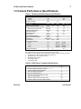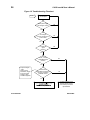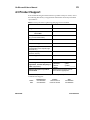
1
MotionVision® CA-D6-xxxxW High-Speed Area Scan Cameras Camera User’s Manual 03-32-00225 rev 06 Printed 03/18/99 10:00 AM 2 CA-D6-xxxxW User’s Manual CA-D6-xxxxW Camera User’s Manual Document Number 03-32-00225 Revision Level 06 © 1998 DALSA Inc. All information provided in this manual is believed to be accurate and reliable. No responsibility is assumed by DALSA for its use. DALSA reserves the right to make changes to this information without notice. Reproduction of this manual in whole or in part, by any means, is prohibited without prior permission having been obtained from DALSA INC. About DALSA DALSA specializes in the manufacture, design, research and development of high performance solid state CCD image sensors and modular cameras. DALSA cameras provide the highest spatial resolution at the highest data transfer speed of any known products in the industry. DALSA’s CCD image sensors and cameras are used worldwide in document scanning, image capture, surveillance, process monitoring and manufacturing inspection. DALSA also develops customized products for specific customers and applications. All DALSA products are manufactured using the latest state-of-the-art equipment to ensure product reliability. All electronic modules and cameras are subjected to a 24 hour burn-in test. For further information not included in this manual, or for information on DALSA’s extensive line of image sensing products, please call: North America DALSA INC. 605 McMurray Road Waterloo, ON, CANADA N2V 2E9 Phone: 519 886 6000 FAX: 519 886 8023 website: www.dalsa.com Europe DALSA GmbH. Breslauer Str. 34 D-82194, Gröbenzell (Munich) GERMANY Phone: FAX: +49-8142-46770 +49-8142-467746 TURBOSENSOR™, QUIETSENSOR™, DDBS™, DOBS™ and DUBS™ are registered trademarks of DALSA INC. Schneider Optics and CORION are trademarks of their respective holders. TM 03-32-00225-06 Our symbol represents a cross-section of the control circuitry basic to all DALSA image sensors. DALSA INC. CA-D6-xxxxW User’s Manual 3 CA-D6-XXXXW USER’S MANUAL Contents 1.0 Introduction to the CA-D6 5 1.1 Camera Highlights........................................................................................... 5 1.2 Image Sensor .................................................................................................. 5 1.3 Camera Performance Specifications............................................................... 7 1.4 CCD Camera Primer ....................................................................................... 8 2.0 Camera Hardware Interface 9 2.1 Installation Overview ....................................................................................... 9 2.2 Input/Output..................................................................................................... 9 2.3 Connectors, Pinouts, and Cables.................................................................. 10 2.4 Power Supplies ............................................................................................. 11 2.5 User Bus (Inputs) .......................................................................................... 12 2.6 Data Bus........................................................................................................ 15 2.7 Timing............................................................................................................ 16 2.8 Multi-Camera Operation ................................................................................ 18 3.0 Optical and Mechanical Considerations 19 3.1 Mechanical Interface ..................................................................................... 19 3.2 Optical Interface ............................................................................................ 20 3.3 EMC Operation.............................................................................................. 23 4.0 Troubleshooting 25 4.1 Common Solutions ........................................................................................ 25 4.2 Specific Solutions.......................................................................................... 27 4.3 Product Support ............................................................................................ 29 Appendix A: EIA-644 Reference 31 Appendix B: EMC Declaration of Conformity 35 Index 37 DALSA INC. 03-32-00225-06 4 03-32-00225-06 CA-D6-xxxxW User’s Manual DALSA INC. 5 CA-D6-xxxxW User’s Manual CHAPTER 1 1.0 Introduction to the CA-D6 1.1 Camera Highlights • 260x260 or 532Hx516V pixels, 10 µm square with 100% fill factor • Frame transfer architecture and pixel resetno shutter required • 4 outputs at 25 MHz: frame rates to 955 or 262 frames/sec • 8 bit digital data in EIA-644 (LVDS differential) format • Separate connectors for power, control and data • “Snapshot” operation • Vertical antiblooming • Operation verified to limits set in EMC standards IEC 1000-4-2; 1995, 1000-4-3; 1995, 1000-4-4; 1995, and CISPR-22. The CA-D6-xxxxW cameras use DALSA’s patented modular architecture. This system of connecting circuit modules through standardized busses allows DALSA to build a high performance modular camera using the reliability, flexibility, and cost-effectiveness of high-volume interchangeable parts. Within the camera, a timing board (PB-D6-X205) generates all internal timing and a driver board (PB-D6-A198) provides bias voltages and clocks to the CCD image sensor. Two A/D boards (PB-xxD344) process the video and an output board (PB-xx-X733) filters the power lines. 1.2 Image Sensor The CA-D6-xxxxW use the IA-D6 family of image sensors. Available in 260x260 and 532x516 arrays, the sensors have 10 µm square pixels with 100% fill factor. The IA-D6 image sensors use a frame transfer architecture, providing on-chip storage. DALSA INC. 03-32-00225-06 6 CA-D6-xxxxW User’s Manual Figure 1. IA-D6-0256 Image Sensor VPS VPS 269 Rows or 525 Rows 260 Columns or 532 Columns 6I 6I 6I 6I 4 CCD Readout Shift Registers OS2 OS1 OS3 OS4 CRLAST VPS 6I 6 isolation CCD cells Note: All readout shift registers have the same clocks and output structure as OS1. 2 R esp o n siv ity [D N /(n J/c m )] Figure 2. CA-D6 Camera Spectral Response 1 .4 1 .2 1 .0 0 .8 0 .6 0 .4 0 .2 0 4 00 5 00 6 00 7 00 8 00 9 00 1 00 0 W ave le n gth (n m ) R e sp o n sivit y 03-32-00225-06 DALSA INC. 7 CA-D6-xxxxW User’s Manual 1.3 Camera Performance Specifications Table 1. CA-D6-xxxxW Performance Specifications Calibration Conditions Frame Rate (FVAL) 256x256 512x512 Data Rate (STROBE) Halogen light source Specification Saturation Output Amplitude Photoresponse Non-Uniformity (PRNU) PRNU with exposure control Fixed Pattern Noise (FPN) Output Gain Mismatch Mean Output Offset Random Noise Noise Equivalent Exposure Saturation Equivalent Exposure Responsivity Dynamic Range Supply Current (256/512) +15.0 V +5.0 V +5.0 V -5.0 V Operating Temperature Units Min. Hz Hz Hz MHz Typ. Max. Notes 955 262 25 1 Min. Typ. Max. Notes DN 243 DN (rms) DN (rms) DN (rms) DN DN 4 DN (rms) pJ/cm2 nJ/cm2 DN/(nJ/cm2) ratio 325:1 248 1.2 1.6 0.5 1.5 5 0.45 336 181.4 1.34 540:1 254 1.8 2.4 0.75 3.0 8 0.75 Units mA mA mA mA °C 0 2 2 3 1 300/350 350/400 900/1200 950/1300 1000/1300 1050/1400 200/230 250/280 50 4 5 Notes DN = digital numbers, also known as “levels” (0-255 for 8-bit systems). All cameras use sensor grade 01. Other grades also available. Contact DALSA for information. 1. DC light source, bulb color temp 3150K, 750nm cutoff filter. 2. Measured at 20%, 50% and 80% of VSAT. 3. Measured at 50% of VSAT. 4. Unterminated outputs. 5. Terminated outputs. Table 2. IA-D6 Sensor Cosmetic Specifications Specification DALSA INC. a b c d e f g Number of first & last columns excluded Number of first & last rows excluded Max. # of single pixel blemishes Max. # of cluster blemishes Max. size of clusters (# of adjacent pixels) Max. # of column defects Blemish variation from mean at 50% VSAT h Blemish variation from average dark level (DN) IA-D6 Grade 01 1 1 10 0 NA 0 ±10% 5 03-32-00225-06 8 CA-D6-xxxxW User’s Manual 1.4 CCD Camera Primer How CCD Image Sensors Work In a CCD camera such as the CA-D6-xxxxW, a CCD image sensor converts photons (light) into electrons (electricity). When photons hit an image sensor, an electron is released, and the sensor adds this electric charge to the charge it has already collected. This is called charge integration. The brighter your light source, the more photons available for the sensor to integrate, and the smaller the amount of time required to collect a given amount of charge. The way photosensitive elements (pixels) on CCD image sensors collect charge has often been compared to buckets filling with water. From this analogy comes the term “full-well capacity,” meaning the maximum charge (number of electrons) a pixel can hold without “spilling” charge onto adjacent pixels. As light energy hits an array of pixels, the pixels collect charge. At certain intervals, a frame transfer sensor such as the IA-D6 transfers its collected charge from the active, photosensitive region to a light-shielded storage region. Then it transfers the charge, line by line, to one or more readout registers, which feed each pixel’s charge from the image sensor into an output node that converts the charges into voltages. After this transfer and conversion, the voltages are amplified to become the camera’s analog output. In digital output cameras, the camera’s analog-todigital (A/D) board converts voltages to digital numbers (0-255 for 8-bit cameras). These digital numbers are what the camera outputs as data to a framegrabber. For more information on terms and concepts from the digital imaging industry, see DALSA’s current Databook Glossary, CCD Technology Primer, and Application Notes. 03-32-00225-06 DALSA INC. 9 CA-D6-xxxxW User’s Manual CHAPTER 2 2.0 Camera Hardware Interface 2.1 Installation Overview In order to set up your camera, you should take these steps: 1. Decide on modes of operation—will you use USR_EN? 2. Test and connect power supplies. 3. Test and connect User Bus control signals from framegrabber. 4. Test and connect data signals output from camera. You must also set up the other components of your system, including light sources, framegrabbers, camera mounts, heat sinks, host computers, optics, and so on. 2.2 Input/Output DALSA INC. 03-32-00225-06 10 CA-D6-xxxxW User’s Manual 2.3 Connectors, Pinouts, and Cables DB50F—Data BusOS1/OS2 and OS3/OS4 Camera connector uses crimp labeling convention for pin numbers 2(34) Crimp label Solder label 2(34) 50(50) 3(18) 48(33) 1(1) 49(17) Mating Part: Amphenol 17D-D50P (solder pin) with shell 17-1657-50 Cable: 26 AWG 100Ω shielded twisted pair Note on DB50 connectors: There are several standard ways to number the pins of DB50 connectors. The connectors on the back of the camera use the “crimp” convention, but many shielded connectors used to control EMI/EMC (including the Amphenol part listed here) use the “solder” convention. To help you translate between numbering conventions, this pinout table lists both. The signals are located on the same physical pins in both cases, but the STROBE pin is numbered 37 under the “crimp” convention and 13 under the “solder” convention. Crimp Label 1 4 7 10 13 16 19 22 25 28 31 34 37 40 43 46 49 Solder Label 1 2 3 4 5 6 7 8 9 10 11 12 13 14 15 16 17 03-32-00225-06 Signal OSBD7 OS2D6B OS2D4 OS2D3B OS2D1 OS2D0B USR_EN OS1D7B OS1D5 OS1D4B OS1D2 OS1D1B STROBE LVALB not used not used not used Crimp Label 3 6 9 12 15 18 21 24 27 30 33 36 39 42 45 48 Solder Label 18 19 20 21 22 23 24 25 26 27 28 29 30 31 32 33 Signal OS2D6 OS2D5B OS2D3 OS2D2B OS2D0 FVALB OS1D7 OS1D6B OS1D4 OS1D3B OS1D1 OS1D0B LVAL not used not used not used Crimp Label 2 5 8 11 14 17 20 23 26 29 32 35 38 41 44 47 50 Solder Label 34 35 36 37 38 39 40 41 42 43 44 45 46 47 48 49 50 Signal OS2D7B OS2D5 OS2D4B OS2D2 OS2D1B FVAL USR_ENB OS1D6 OSID5B OS1D3 OS1D2B OS1D0 STROBEB not used not used not used not used DALSA INC. 11 CA-D6-xxxxW User’s Manual DB15M—Power Mating Part: Amphenol 17D-A15S with shell 17-1657-15 Cable: 22 AWG min. shielded Pin 1 2 3 4 5 6 7 8 Signal DGND +5V Digital not used -5V Digital Not used +15V +15V AGND Pin 9 10 11 12 13 14 15 Signal +5V Digital DGND not used not used -5V Analog AGND +5V Analog DB15F—Control Mating Part: Amphenol 17D-A15P with shell 17-1657-15 Cable: 22 AWG min. shielded Pin Signal Pin Signal 1 not used 9 not used 2 not used 10 not used 3 not used 11 not used 4 EXSYNCB 12 EXSYNC 5 PRIN 13 PRINB 6 future use 14 future use 7 not used 15 not used 8 not used 2.4 Power Supplies See section 1.3 for power requirements. When setting up the camera’s power supplies, follow these guidelines: • Do not use the shield on a multi-conductor cable for ground. • Connect separate supplies at the source and at the camera. • Use separate leads for better noise immunity. The companies listed below make power supplies that meet the camera’s requirements, but they should not be considered the only choices. Many high quality supplies are available from other vendors. DALSA assumes no responsibility for the use of these supplies. • Uniforce, 408-946-3864 (CA, USA) • Power-One, 805-987-8741 (CA, USA) • Vision 1, 406-585-7225 (MT, USA) • Tectrol Inc., 416-630-4026 (ON, CAN) • Xantrex, 206-671-2966 (WA, USA) DALSA INC. 03-32-00225-06 12 CA-D6-xxxxW User’s Manual 2.5 User Bus (Inputs) The User Bus uses a DB25 connector and includes the mandatory control signal EXSYNC and optional signal PRIN. These signals must be supplied from your framegrabber to the camera using EIA-644 (differential) format, which requires the use of twisted pair cable. DALSA recommends shielded cables. Maximum cable lengths depends on environmental factors and EIA-644 limitations. See Appendix A. EXSYNC—Triggers Frame Readout EXSYNC is an optional signal used to control the camera’s frame rate. When EXSYNC is left unconnected or connected to logic LOW, the camera outputs data at its maximum frame rate (free-run mode). When EXSYNC is toggled, its falling edge triggers frame readout; in this mode its frequency determines the camera’s frame rate (FVAL frequency). The delay between the falling edge of EXSYNC and the first valid pixel varies with model and is shown on the timing diagram (section 2.9). Minimum EXSYNC high or low time: 100 ns. • DB15 Pins—EXSYNC: 12; EXSYNCB: 4. Note: Restricting EXSYNC to logic HIGH prevents frame readout. PRIN—Controls Electronic Shuttering PRIN is an optional signal that can shorten the effective exposure time by resetting the pixels (draining accumulated charge) on the image sensor between EXSYNC-triggered frame readouts. PRIN is active when connected to logic LOW; exposure effectively begins on the rising edge of PRIN. If PRIN is unconnected or connected to logic HIGH, the integration time is maximized; if it is connected to logic LOW the sensor collects no image information. The PRIN pulse width must be 6.5±1µs. During the frame transfer period, the camera ignores PRIN inputs. • DB15 pins: PRIN 5; PRINB 13. 03-32-00225-06 DALSA INC. 13 CA-D6-xxxxW User’s Manual Application Tip: Combining Input Signals for Exposure Control and “Snapshot” Operation When used together, EXSYNC and PRIN can give very precise control over exposure and image capture. The examples below illustrate some camera operating options. Figure 3 depicts the operation of the camera when EXSYNC is kept low and PRIN high at all times. The camera operates at its maximum frame rate with the maximum exposure time, which is defined as the time from the end of one frame transport to the beginning of the next frame transport. Figure 3. Free-Run Mode exposure time EXSYNC frame transport MODE frame readout frame transport frame readout PRIN Figure 4 depicts the operation of the camera when the EXSYNC signal frequency is user controlled. The frame rate is variable and depends solely on the EXSYNC rate. Keeping PRIN high maximizes the time the sensor is exposed to light. The exposure time is defined from the end of one frame transport to the beginning of the next frame transport. Figure 4. User-Controlled EXSYNC exposure time EXSYNC MODE frame transport frame readout frame transport frame readout PRIN DALSA INC. 03-32-00225-06 14 CA-D6-xxxxW User’s Manual Figure 5 shows the operation of the camera when EXSYNC and PRIN are both user controlled. The start of the exposure time depends on the rising edge of PRIN in combination with the falling edge of EXSYNC. The exposure time is defined from the rising edge of PRIN to the falling edge of EXSYNC. PRIN must be kept low for 6.5±1µs to drain all charge that was previously collected. Note also that the camera will ignore PRIN inputs during frame readout. Figure 5. User-Controlled EXSYNC and PRIN exposure time EXSYNC MODE frame transport frame readout frame transport frame readout PRIN For “snapshot” operation (see Figure 6), you can use a combination of EXSYNC and PRIN to trigger image capture from external event. The CA-D6 can remain in a wait state until it receives a combination of EXSYNC and PRIN. During the wait state, the EXSYNC and PRIN signals must be high (meaning the camera is continually integrating incident light). To begin the effective exposure period, PRIN must be toggle low for 6.5±1µs and then high. After the desired exposure (e.g. 20 ms) EXSYNC must go low, and the exposed frame is transferred and output. cont’d... 03-32-00225-06 DALSA INC. 15 CA-D6-xxxxW User’s Manual Figure 6. Event-Triggered Image Capture Trigger event exposure time EXSYNC MODE wait state exposure frame transport frame readout PRIN Note that to have the camera react to an external event, your imaging system must detect the event and then send the appropriate EXSYNC and PRIN signals to the camera to cause it to capture images. 2.6 Data Bus Digital Data See section 2.3 for pinouts. The CA-D6-xxxxW provides 4 channels of 8 bits of data in EIA-644 differential format at 25 MHz. To help clock digital data into framegrabbers, the camera outputs clocking signals STROBE, LVAL, and FVAL. IMPORTANT: This camera’s data is valid on the rising edge of STROBE, unlike previous DALSA cameras, which used the falling edge. STROBE STROBE is a pixel clock signal for digital data. It is continuous, toggling even when data is not valid. Digital data is valid on its rising edge with LVAL and FVAL high. LVAL LVAL high with FVAL high indicates the camera is outputting a valid line of pixels. Between valid lines within a frame, LVAL goes low for 29 inactive pixels (0256 model) or 47 inactive pixels (0512 model). FVAL FVAL high indicates the camera is outputting a valid frame of data. DALSA INC. 03-32-00225-06 16 CA-D6-xxxxW User’s Manual USR_EN—Input for Multiplexing USR_EN is an input used during camera multiplexing. When multiple cameras share the same data bus, their digital data outputs can be placed into tri-state by connecting USR_EN to logic LOW. Connecting USR_EN to logic HIGH activates a camera’s outputs. USR_EN is an optional signal; if not using USR_EN, connect it to logic HIGH and USR_ENB to logic LOW. 2.7 Timing When exposed to light, the sensor collects charge. The EXSYNC control signal (input from framegrabber) triggers the transfer and readout of the charge. The FVAL output goes high to indicate a valid frame; the LVAL output goes high for each of the lines that make up the frame. LVAL goes low between the lines of a frame. The STROBE signal is a pixel clock; digital data is valid on its rising edge. After a frame is read out, the FVAL signal goes low and the sensor collects charge for the next frame. Figure 7. CA-D6-xxxxW Overall Timing 1 8 E X SY N C 2 F VA L 3 5 LVA L 7 6 LIN E 1 LAST LIN E 4 ST R O B E O S1 1 N /4 O S2 N /4 + 1 N /2 N /2 + 1 3 N /4 3 N /4 + 1 N O S3 O S4 N OT ES: Po sitio n o f th e first v alid p ixe l (v a lid o n th e risin g ed ge o f S T RO B E ) 02 56 051 2 D im en sio n s o f sin gle fra m e 4 x (26 0 lin e s o f 6 5 pixels) 4x (51 6 line s o f 1 3 3 pixe ls) 11 E X S Y N C m inim u m pu lse w id th 22 E X S Y N C to ↑F VA L 33 F VA L to ↑LVA L 1 0 0n s 10 0 ns 1 5 42 S T RO B E s 71 3 6 ST R O B Es 2 2 ST RO B E s 22 S T RO B E s 44 E X S Y N C to first v a lid p ixe l 55 LVA L H IG H 66 B e tw e e n line s: LVA L L O W 1 5 64 S T RO B E s 71 5 8 ST RO B E s 6 5 ST R O B Es 13 3 ST RO B Es 2 9 ST R O B Es 37 S T RO B E s 77 ↓LVA L to ↓F VA L 1 5 ST R O B Es 1 5 ST RO B E s 88 M in im um tim e be tw e e n fra m e s 1 7 15 S T RO B E s 74 6 1 ST RO B E s 03-32-00225-06 IMPORTANT: This camera’s data is valid on the rising edge of STROBE, unlike previous DALSA cameras, which used the falling edge. DALSA INC. 17 CA-D6-xxxxW User’s Manual Figure 8. CA-D6-xxxxW Detailed Timing Symbol Description DALSA INC. Min. Typ. -2 0 Max. Unit TLSW ↑LVAL to ↓STROBE TLSZW ↓LVAL to ↓STROBE -2 0 2 ns TSETUP Data setup 18 23 28 ns THOLD Data hold 12 17 22 ns TPL PRIN pulse 5.5 6.5 7.5 µs TEL EXSYNC pulse 100 2 ns ns 03-32-00225-06 18 CA-D6-xxxxW User’s Manual 2.8 Multi-Camera Operation Camera Multiplexing Camera multiplexing puts multiple cameras on the same data bus. All the multiplexed cameras are spliced into the same data cable; this is possible because the camera’s output line drivers can be tri-stated. The usual control signals can be spliced on a single cable, but they can also be kept separate for each camera. The cameras do not require synchronized control signals because only one camera can be active at any one time—a camera becomes active when you supply it with a differential USR_EN signal. Each multiplexed camera must receive its own USR_EN signal from a separate differential pair from a EIA-644 line driver. USR_EN in logic HIGH activates camera max.39 ns output. USR_EN in logic LOW puts USR_EN outputs in tri-state. Note that toggling Data the camera outputs from tri-state to active requires a small but important amount of setup and hold time. Be sure to take this time into account when configuring your system. 03-32-00225-06 max. 50 ns DALSA INC. 19 CA-D6-xxxxW User’s Manual CHAPTER 3 3.0 Optical and Mechanical Considerations 3.1 Mechanical Interface The camera’s electronics are housed in a rugged anodized aluminum case. Mounting For maximum stability and best heat sinking, DALSA recommends mounting the camera by its front plate. There are four M4 holes and seven 4-40 UNC holes tapped into the front plate for mounting the camera or attaching heat sinking. Other mounting options include M4 holes on the sides of the camera (stability increases with number of sides used) and the tripod mount (least stable). Environment The camera and cables should be shielded from environmental noise sources for best operation. The camera should also be kept as cool as possible. Mounting holes (see above) allow you to attach heat sinking. DALSA INC. 03-32-00225-06 20 CA-D6-xxxxW User’s Manual 3.2 Optical Interface Front plate C-mount Z-axis aligner Imager clamp Die 17.5 mm The CA-D6-xxxxW camera comes with a mount adapter for C-mount lenses, which have a back focal distance of 17.5 mm. Ensure that the image circle diameter of the lens to be used is as great as the diagonal of the imaging region of the image sensor. IMPORTANT: The camera’s Z-axis alignment is optimized for the adapter provided. Do not remove the mount adapter without contacting DALSA first, or you may misalign your lens. Illumination The amount and wavelengths of light required to capture useful images depend on the particular application. Factors include the nature, speed, and spectral characteristics of objects being imaged, exposure times, light source characteristics, environmental and acquisition system specifics, and more. DALSA’s current Databook provides an introduction to this potentially complicated issue. See “4.Radiometry and Photo Responsivity” and “Camera Sensitivities in Photometric Units”. It is often more important to consider exposure than illumination. The total amount of energy (which is related to the total number of photons reaching the 2 sensor) is more important than the rate at which it arrives. For example, 5 µJ/cm 2 can be achieved by exposing 5 mW/cm for 1 mS just the same as exposing an 2 intensity of 5 W/cm for 1 µS. 03-32-00225-06 DALSA INC. 21 CA-D6-xxxxW User’s Manual Light Sources Keep these guidelines in mind when setting up your light source. • Halogen light sources generally provide very little blue relative to IR. • Fiber-optic light distribution systems generally transmit very little blue relative to IR. • Some light sources age; over their lifespan they produce less light. This aging may not be uniform—a light source may produce progressively less light in some areas of the spectrum but not others. Filters CCD cameras are often very responsive to infrared (IR) wavelengths of light. If you wish to exclude IR, use a “hot mirror” or IR cutoff filter that transmits visible wavelengths but does not transmit wavelengths over 700 µm. Examples are the Schneider Optics™ B+W 489, which includes a mounting ring, the CORION™ LS-750, which does not include a mounting ring, and the CORION™ HR-750 series hot mirror. Lens Modeling Any lens surrounded by air can be modeled for camera purposes using three primary points: the first and second principal points and the second focal point. The primary points for a lens should be available from the lens data sheet or from the lens manufacturer. Primed quantities denote characteristics of the image side of the lens. That is, h is the object height and h′ is the image height. The focal point is the point at which the image of an infinitely distant object is brought to focus. The effective focal length (f′) is the distance from the second principal point to the second focal point. The back focal length (BFL) is the distance from the image side of the lens surface to the second focal point. The object distance (OD) is the distance from the first principal point to the object. Figure 9. Primary Points in a Lens System Magnification and Resolution The magnification of a lens is the ratio of the image size to the object size: DALSA INC. 03-32-00225-06 22 CA-D6-xxxxW User’s Manual m= h′ h where m is the magnification, h’ is the image height (pixel size) and h is the object height (desired object resolution size). By similar triangles, the magnification is alternatively given by: m= f′ OD These equations can be combined to give their most useful form: h′ f′ = h OD This is the governing equation for many object and image plane parameters. Example: An acquisition system has a 512 x 512 element, 10 µm pixel pitch area scan camera, a lens with an effective focal length of 45 mm, and requires that 100µm in the object space correspond to each pixel in the image sensor. Using the preceding equation, the object distance must be 450 mm (0.450 m). 10µm 45mm = 100µm OD 03-32-00225-06 OD = 450mm (0.450m) DALSA INC. 23 CA-D6-xxxxW User’s Manual 3.3 EMC Operation The CA-D6 has been designed for EMC compliance. The test setup shown below has been verified to the limits set in EMC standards IEC 1000-4-2; 1995, 1000-4-3; 1995, 1000-4-4; 1995, and CISPR-22. Data Bus: 3M #3750-50, 6’ (1.8m), shielded jacketed twisted pair Data Bus: 3M #3750-50, 6’ (1.8m), shielded jacketed twisted pair Data Bus: 3M #3750-50, 6’ (1.8m), shielded jacketed twisted pair User Bus: 3M #3750-9, 6’ (1.8m), shielded jacketed twisted pair Power: 18 AWG Follow these specific guidelines to maximize compliance in your application: DALSA INC. • Keep control and data cables as short as possible. • Control and data cables must have 95% coverage shields that include braided wire. Metallic foil shields are insufficient without braided wire. • Ensure that all cable shields have 360° electrical connection to the connector. 03-32-00225-06 24 03-32-00225-06 CA-D6-xxxxW User’s Manual DALSA INC. 25 CA-D6-xxxxW User’s Manual CHAPTER 4 4.0 Troubleshooting The information in this chapter can help you solve problems that may occur during the setup of your camera. Remember that the camera is part of the entire acquisition system. You may have to troubleshoot any or all of the following: • power supplies • cabling • framegrabber hardware & software • host computer • light sources • optics • operating environment • encoder Your steps in dealing with a technical problem should be: 1. Follow the troubleshooting flowchart (Figure 10 in this chapter). 2. Try the general and specific solutions listed in sections 4.1 and 4.2. 3. If these solutions do not resolve your problem, see section 4.3 on getting product support. 4.1 Common Solutions Connections The first step in troubleshooting is to verify that your camera has all the correct connections. Follow the troubleshooting flowchart shown in Figure 10. Power Supply Voltages Check for the presence of all analog and digital voltages at the camera DB25 connector. Verify that all grounds are connected. EXSYNC The EXSYNC signal from your framegrabber or camera controller must either toggle or be connected to logic LOW. With EXSYNC restricted to logic HIGH, the camera will not output any data. Using an oscilloscope, check the camera end of the control signal cable and verify that EXSYNC and EXSYNCB toggle. DALSA INC. 03-32-00225-06 26 CA-D6-xxxxW User’s Manual Figure 10. Troubleshooting Flowchart START Check setup see Chapter 2 Check power supply. Are voltages correct? No Yes Are voltages correct at camera end of power cable? No Yes Is ± EXSYNC signal present? No Yes Are ± LVAL, ± FVAL, ± STROBE signals present? No Yes • Scope the digital video • Under varying illumination, trigger from LVAL while looking at each individual digital bit. Does each digital data bit toggle and are there continuous STROBE clocks? No Yes Complete the table in the Product Support section and contact your DALSA representative 03-32-00225-06 DALSA INC. 27 CA-D6-xxxxW User’s Manual Data Clocking/Output Signals Verify the presence of all data clocking and output signals. Trigger the oscilloscope from the rising edge of FVAL (ch1; DC coupled). Adjust the oscilloscope time base to allow for a complete cycle of each signal: • STROBE—Verify the presence of the STROBE and STROBEB signals. There should be a continuous clock signal present at the same frequency as your data rate. • LVAL—Verify the presence of the LVAL and LVALB signals. • FVAL—Verify the presence of the FVAL and FVALB signals. • Digital Output—Use FVAL to trigger the scope sweep. Illuminate the camera target and check each individual digital output signal on ch2 of the oscilloscope (±D0 - D7 on the digital output connector). The digital output data signal should change value when light is blocked from the camera lens. If any of the above signals are missing, contact DALSA product support. 4.2 Specific Solutions No Output or Erratic Behavior If your camera provides no output or behaves erratically, it may be picking up random noise from long cables acting as antennae. Do not attach wires to unused pins. Verify that the camera is not receiving spurious MCLK, or USR_EN inputs. Noisy Output Check your power supply voltage outputs for noise. Noise present on these lines can result in poor video quality. Low quality or non-twisted pair cable can also add noise to the video output. Dark Patches If dark patches appear in your output the optics path may have become contaminated. Clean your lenses and sensor windows with extreme care. 1. Take standard ESD precautions. 2. Wear latex gloves or finger cots 3. Blow off dust using a filtered blow bottle or dry, filtered compressed air. 4. Fold a piece of optical lens cleaning tissue (approx. 3" x 5") to make a square pad that is approximately one finger-width DALSA INC. 03-32-00225-06 28 CA-D6-xxxxW User’s Manual 5. Moisten the pad on one edge with 2-3 drops of clean solvent—either alcohol or acetone. Do not saturate the entire pad with solvent. 6. Wipe across the length of the window in one direction with the moistened end first, followed by the rest of the pad. The dry part of the pad should follow the moistened end. The goal is to prevent solvent from evaporating from the window surface, as this will end up leaving residue and streaking behind. 7. Repeat steps 2-4 using a clean tissue until the entire window has been cleaned. 8. Blow off any adhering fibers or particles using dry, filtered compressed air. Stuck Bits If data bits seem to be stuck or do not change, check that the camera is not saturated by preventing light from entering. Next, disconnect the digital cable from the camera. Check the digital signals at the output of the camera, ensuring that the correct values are present. Check all cable connections, especially right at the connector; poor connections or broken wires will cause randomly changing bits or stuck bits. Horizontal Lines or Patterns in Image Patterns may be caused by low frequency illumination variations. Use a DC or high frequency light source. 03-32-00225-06 DALSA INC. 29 CA-D6-xxxxW User’s Manual 4.3 Product Support If the troubleshooting flowchart indicates a problem with your camera, collect the following data about your application and situation and call your DALSA representative. Note: You may also want to photocopy this page to fax to DALSA. Customer name Organization name Customer phone number fax number Complete Product Model Number (e.g. CL-C3-1024A-STDJ) Complete Serial Number Your DALSA Agent or Dealer Acquisition System hardware (framegrabber, host computer, light sources, etc.) Acquisition System software (version, OS, etc.) Power supplies and current draw Data rate used Control signals used in your application, and their frequency or state (if applicable) Detailed description of problem encountered. ❑ EXSYNC ❑ BIN ❑ MCLK ❑ Other _______ ❑ PRIN please attach description with as much detail as appropriate In addition to your local DALSA representative, you may need to call DALSA Technical Sales Support: Voice: Fax: DALSA INC. North America 519-886-6000 519-886-8023 Europe +49-8142-46770 +49-8142-467746 Asia 519-886-6000 519-886-8023 03-32-00225-06 30 03-32-00225-06 CA-D6-xxxxW User’s Manual DALSA INC. 31 CA-D6-xxxxW User’s Manual CA-D6-XXXXW USER’S MANUAL Appendix A: EIA-644 Reference EIA-644 is an electrical specification for the transmission of digital data. The standard is available from the EIA (Electronic Industries Association). It defines voltage levels, expected transmission speeds over various cable lengths, common mode voltage operating requirements for transmitters and receivers, and input impedances and sensitivities for receivers. The table below gives a quick comparison between EIA-644 and RS422 (another differential standard). Table 3. RS422 vs. EIA-644 Parameter RS422 EIA-644 Differential Driver Output Voltage ±2-5V ±250-450mV Receiver Input Threshold ±200mV ±100mV Data Rate <30Mbps >400Mbps Supply Current, Quad Driver (no load, static)* 60mA 3.0mA Prop. Delay of Driver, max.* 11ns 3ns Prop. Delay of Receiver, max.* 30ns 5ns Supply Current, Quad Receiver (no load, static)* 23mA 10mA * based on National Semiconductor DS90C031/2 The standard requires that two wires (e.g. twisted pair) be used to transmit one signal in a differential mode. This means that one wire will be logic HIGH while the other wire is logic LOW. Voltage swing between HIGH and LOW is approximately 350mV, with a typical offset of approximately 1.25V. The use of differential signal transmission allows the receiver to reject common mode voltages. This noise rejection improves data integrity and allows cameras to be installed in an industrial environment. EIA-644-compatible line receivers and drivers are available from many different IC manufacturers in a variety of fabrication technologies such as CMOS and GaAs. The EIA-644 standard does not define specific voltages, so it can migrate from 5V power supplies to 3.3V and sub-3V. DALSA recommends the use of 5V CMOS line drivers and receivers such as National Semiconductor parts DS90C0C31 quad line driver and DS90C032 quad line receiver. To achieve full benefit of the common mode rejection, twisted pair cable should be used for all EIA-644 signals. The cable impedance should be 100 Ohms and the cable terminated at the receiving end with a 100 Ohm resistor. All EIA-644 inputs DALSA INC. 03-32-00225-06 32 CA-D6-xxxxW User’s Manual in a DALSA camera are terminated with 100 Ohms between the (+) and (-) of a signal. Figure A-1 (a) shows an example of an EIA-644 transmission. DALSA indicates the (+) signal by the name of the signal; i.e. MCLK, while the (-) signal is indicated by either an overscore over the name or appending the letter B to the end of the name; i.e. MCLK or MCLKB. The (+) signal has the same sense as the TTL signal which is sent or received; i.e. when MCLK in the TTL domain is HIGH then MCLK in the EIA-644 domain is HIGH. The (-) signal has the opposite sense of the TTL domain signal and so if MCLK TTL is HIGH then MCLKB EIA-644 is LOW. Figure 11 shows the relationship. Figure 11. EIA-644 Example Unused EIA-644 Inputs and Outputs Unused outputs should be left unconnected. This will reduce power dissipation within the camera and reduce radiated emissions. Unused inputs should also be left unconnected; EIA-644 chips have fail-safe features that guarantee a known logic state (HIGH) in fault conditions 03-32-00225-06 DALSA INC. 33 CA-D6-xxxxW User’s Manual (unconnected, shorted, or unterminated). Do not connect cables to unused inputs. Cables can act as antennae and cause erratic camera behavior. Cable Lengths Figure 12 shows a graph of ideal communication data rate vs. cable length for the EIA-644 standard. Figure 12. EIA-644 Data Rate vs. Cable Length 1000 Data Rate (Mbps) 20% Jitter Measured at 0V Differential 20% Jitter Measured at ±0100mV Differential 100 CAT3 Cable Typical Data Rate vs. Cable Length (National DS90C031) 10 1 1 2 3 5 10 Cable Length (m) DALSA INC. 03-32-00225-06 34 03-32-00225-06 CA-D6-xxxxW User’s Manual DALSA INC. 35 CA-D6-xxxxW User’s Manual CA-D6-XXXXW USER’S MANUAL Appendix B: EMC Declaration of Conformity We, DALSA INC. 605 McMurray Rd., Waterloo, ON CANADA N2V 2E9 declare under sole responsibility, that the product(s): CA-D6-0256W-ECEW CA-D6-0512W-ECEW meets the test (limits) for: Electrostatic Discharge, IEC 1000-4-2; 1995 Radiated Immunity, IEC 1000-4-3; 1995 Burst ELF, Class III, IEC 1000-4-4; 1995 Radiated Emissions, CISPR 22 and therefore correspond(s) to the regulations of the EU-Directive 89/336/EEC. Place of Issue Waterloo, ON, CANADA Date of Issue 18 November 1997 Name and Signature of authorized person Brian Doody Vice-President, Operations This Declaration corresponds to EN 45 014. DALSA INC. 03-32-00225-06 36 03-32-00225-06 CA-D6-xxxxW User’s Manual DALSA INC. 37 CA-D6-xxxxW User’s Manual CA-D6-XXXXW USER’S MANUAL Index 1 E 100% fill factor • 5 A/D boards • 5 About DALSA • 2 asynchronous reset (PRIN) • 12 EMC compliance • 5, 23 EMC Declaration of Conformity • 35 EMC Operation • 23 environmental considerations • 19 Event-Triggered Image Capture • 15 EXSYNC • 12 troubleshooting • 25 B F bucket analogy • 8 fiber-optic light sources • 21 fill factor • 5 Filters • 21 free-run mode • 13 full-well capacity • 8 FVAL • 15 A C cable lengths • 12 cables • 11 length • 33 CCD image sensors • 8 combining input signals • 13 connectors • 10 cooling • 19 cosmetic specifications • 7 DALSA INC. H halogen light sources • 21 hot mirror • 21 how CCD image sensors work • 8 D I DALSA User Bus Standard • 5 dark patches • 27 Data Bus • 15 Digital Data • 15 DN (digital numbers) • 7 driver board • 5 IA-D1 image sensor • 5 Illumination • 20 Input/Output • 9 inputs (user bus) • 12 Installation Overview • 9 integration • 8 interface mechanical • 19 optical • 20 03-32-00225-06 38 CA-D6-xxxxW User’s Manual Introduction to the CA-D1 • 5 L Lens Modeling • 21 light sources • 21 Logic HIGH and LOW • 31 LVAL • 15 troubleshooting • 27 M magnification • 21 mechanical interface • 19 mounting • 19 multi-camera operation • 18 multiplexing, camera • 18 R RS422 reference • 31 S shuttering, electronic (PRIN) • 12 snapshot operation • 15 state diagrams • 16 STROBE • 15 troubleshooting • 27 stuck bits • 28 T noisy output • 27 Technical Sales Support • 29 temperature • 19 Timing • 16 timing board • 5 troubleshooting • 25 O U optical interface • 20 user bus • 12 USR_EN • 16, 18 N P performance specifications • 7 photosensitive elements (pixels) • 8 pinout DB25 User Bus • 10 OS1 data • 10 pixels and resolution • 5 power supplies • 11 PRIN • 12 03-32-00225-06 DALSA INC.