1
United States Patent [191
[ll]
4,317,181
Teza et a1.
[45]
Feb. 23, 1982
[54] FOUR MODE MICROCOMPUTER POWER
[57]
SAVE OPERATION
[75] Inventors: Jeffrey R. Teza, Houston; Kenneth A.
Power microcomputer with on'chlp memory capability,
Lies, Lubbock, both of Te,(_
and multiple partition power control of circuit groups.
Texas Instruments Incorporated’
Dallas’ Tex-
voltage and a non-switched negative voltage enables
the power hungry clocked logic and the display inter
,
Incorporation of a ?rst and second switched negative
[73] Asslgnee:
[21] Appl' No‘: 106,809
[ 1
22
ABSTRACT
A calculator having constant memory utilizing a low
F]
i ed:
D
face and keystroke detect circuitry, to be turned off
26
e¢~
979
while power is maintained on the internal static RAM,
and on the RAM write logic, digit latches. and R-lines
9 1
[51] Int. Cl.3 .............................................. .. G06F 1/04
Whilch connect t9 both 3.16 “item?! Rf‘ixM' or to selec‘
[52] us. or. .................. ..
[58] Field of Search .............. ..
SW1“: ‘? "° ‘ages . n a“ ‘‘ ‘Ffnam em 0 .‘mem’ ‘’ m“ "'
364/707; 364/900
364/707, 200 MS File,
“"9 Yb 3”?“ 1" 1cm“ ‘Tatlon ‘ eb 1:15.‘ “d “CO1”?
364/900 MS File
ple oscillator, multlple partition system IS controlled to
provide an off-mode, display only mode (low frequency
[56]
References Cited
oscillator), a process only mode, and a display and pro
Us. PATENT DOCUMENTS
cess mode, ‘thereby optimizing. power dissipation to
system requlrernents. Thus, semi-non-volatlle memory
3/
51°35" 121?]- ---- "l---------- " 36223030);
x
(constant memory) capability, power down standby,
4'2l8*876 841980 ?jshilxglgltegla' "
and display only, capabilities may be achieved. Power
consumption less than conventional CMOS is obtain
able.
Primary Examiner-Jerry Smith
Attorney, Agent, or Firm-Leo Heiting; Robert D.
Marshall, Jr.; Melvin Sharp
6 Claims, 19 Drawing Figures
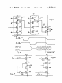
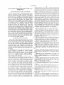
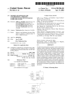
404
r
l
7
DISPLAY
OSCILLATOR
400
/
1
EN-‘—-—,
40?
on
406
/
no
e__\
EN
40/
PROCESSOR
ANDI/O
OSCILLATOR
CONTROLLER
4,4
i
MEANS
/
‘r409
CLOCK
GENERATOR EN‘ ‘
E"
5N2‘
'
/4/5
CLOCK
GENERATOR
{4/0
0
DlSPLAY
I
INTERFACE
[
‘
1
1’ / 4/2
KEYBOARD
MEANS
PROCESSOR
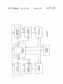
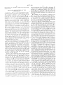
US. Patent
Feb. 23, 1982
Sheet 1 of8
4,317,181
.0. 0w?
\
wla?loww
\0/
__\ \<@,\.
O
US. Patent
Feb. 23, 1982
9 AT T E R Y
Sheet 2 of 8
~50
[5/
POWER
4,317,181
F19, .3 0
'
CONSUMPTION
CONTROLLER
~55- — — — —
53
CIRCUIT
7/
CIRCUIT
GROUP
GROUP
BATTERY f,”
[5 5
5/
*
11
POWER
6LocK
CONSUMPTION
CON TROLLER
60\
Fl‘g I ah
— — — — — —-—
POWER
POWER
"_ SWITCH
SWITCH ""'
I
52
clRcum/
.
l6 /
GROUP
53
|
\mRcurr ___1
GROUP
F/g I 3d
50
—\\
8 AT T E RY
a
—\\
5/
a/
-—\\
——\1
FIRST
POWER
SWITCH
SECOND
POWER
SWITCH
L
52
\
POWER /
CONSUMPTION
CONTROLLER '
\
FIRST
CIRCUIT
ROu
|
7/
53
\
X
SECOND
CIRCUIT
GROUP
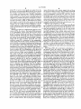
U.S. Patent
Feb. 23, 1982
OPERABLE
STATE
4,317,181
FIRST POWER
swncnms
MEANS
SECOND POWER
SWITCHING
MEAN 5
OFF
OFF
OFF
DISPLAY AND
KEY DETECT
OFF
0 N
pnoccss
KEYSTROKE
0"
0"
PROCESS
TIMER
oN
0“
CALCULATOR
MODES
OFF- STATE
Sheet 4 of 8
-______
___-__—_
TABLEQE OPERATIVE STATE MAPPING Fig, 4
US. Patent
Feb. 23, 1982
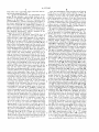
ANYKEY
PUc
Sheet 7 of 8
4,317,181
SOFTWARE
ANYKEY
REQUEST
TlMEKEEP/PUC
OFF
INST.
F19. //
TIMEKEEP
OVERLOAD/
PUC
TIMEKEEP
O-VERLOAD/
PUG
REQUEST
TIMEKEEP/
PUC
OSCILLATOR
APPEARS!
PUC
oscmmoas
DISAPPEARS
Fig!
ANYKEY/PLLC
U.S. Patent
Feb. 23, 1982
Sheet 8 of 8
4,317,181
1
4,317,181
2
display interface, the processor, and the keyboard. The
FOUR MODE MICROCOMPUTER POWER SAVE
OPERATION
BACKGROUND OF THE INVENTION
This invention relates to calculators and more partic
ularly to calculators having a multiple mode power
controller. Multimode power control is a significant
advancement over turning off the processor circuitry
between keystrokes as described in co-pending applica
tion, Ser. No. 106,430, filed Dec. 26, I979 for “Turn Off
controller provides four state clock mode control so as
to conserve system power by selectively enabling the
display oscillator, the processor main oscillator. the
display clock generator, and the main clock generator,
in response to receiving prede?ned combinations of
instruction codes from the processor and operative key
codes from the keyboard, so as to effect a display only
mode wherein the display oscillator and display clock
generator are enabled, and the main oscillator and main
clock generator are disabled; a display and process
Processor Between Key Strokes", by Graham Tubbs,
mode wherein the main oscillator, display clock genera
assigned to the same assignee as the present invention.
That invention, as does the present invention, addresses
play oscillator disabled; a processor only mode wherein
tor, and main clock generator are enabled and the dis
the problem of how to minimize power dissipation
the main oscillator and main clock generator are en
while maintaining full operational capability. Some
abled and the display oscillator and display clock gener
calculators, such as that disclosed in the “Turn Off
ator are disabled; and an off mode wherein the display
Processor Between Key Strokes" patent application
cited above, have essentially three (3) mode systems: off
mode, display and processing mode, or display mode.
oscillator, the display clock generator, the main oscilla—
tor and the main clock generator are all disabled.
BRIEF DESCRIPTION OF THE DRAWINGS
present invention in that a single main clock oscillator
The novel features believed characteristic of the in
was utilized which was kept on in the display mode,
vention are set forth in the appended claims. The inven
such as described in the above cited co-pending applica
tion itself, however, as well as other features and advan
tion on “Turn Off Processor Between Key Strokes". 25 tages thereof, will be best understood by reference to
Other calculators are essentially two-mode machines,
the following detailed description of illustrative em
having an off mode and a process and display mode.
bodiments, when read in conjunction with the accom~
The main oscillator is always on so long as the calcula
panying drawings, wherein:
Furthermore, prior calculators system differ from the
tor is on in the two<mode machine.
SUMMARY OF INVENTION
The present invention goes beyond the two or three
mode machines and provides a four mode system which
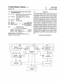
FIG. 1 is a pictorial view ofa handheld calculator in
which multi-partition switched power designs embody
ing the invention may be utilized advantageously;
FIG. 2 is an elevational view in section of the calcula'
tor of FIG. 1 taken along the line 2——2 of FIG. 1;
FIG. 3a—d are electrical block diagrams of alternate
off the display oscillator and saves power, a display 35
embodiments of a multi-partition power conservation
only state which turns off the main oscillator and saves
design of one type of MOS/LS1 calculator chip utiliz—
considerable power, and a display and process state
ing the invention, in particular the chip 20 of FIG. 1;
which turns off the display oscillator to save power and
FIG. 4 is an operative state mapping table of one
which allows full access to inputs and output and gives
embodiment of the present invention as shown in FIG.
complete processing capability while providing a visi
may be in an off state, a process only state which turns
ble display.
3:
FIG. 5 is a detailed schematic diagram detailing criti»
cal off-state DC current pathway nodes in a ratioless
present invention is applicable to clocked CMOS,
CMOS structure embodiment of the chip 20 of FIGS.
NMOS, VMOS, bipolar systems, and to ratioless
CMOS structures such as described in co-pending appli 45 3a-d;
FIGS. 6(a)~(d) are representations of voltages as a
cation Ser. No. 46,388, filed June 8, I979, by Jeff Sout
The multimode power conservation controller of the
hard et al, for “Ratioless Logic", assigned to the as
signee of the present invention.
function of time which illustrate circuit operation in a
ratioless CMOS embodiment of the invention in the
calculator;
The calculator of the present invention utilizes a
FIGS. 7 and 8 are detailed schematic diagrams detail‘
multipartitioned power distribution system and a four SO
ing critical off-state DC current pathway nodes in a
state power controller to selectively provide clocked
clocked CMOS structure embodiment of the chip 20 of
signals to selected circuit groups, and thereby control
power, by gating system clocks to selected circuit
groups in response to externally provided input stimuli,
such as user inputs, for example keyboard key depres
FIGS. 3a-c utilizing the invention;
FIG. 9 is a block diagram of a preferred embodiment
of a multimode multipartitioned power conservation
system;
sions or digital interface signals from within or from
FIG. 10 is a state transition diagram for a four state
another integrated circuit. In a preferred embodiment,
mode control system of the preferred embodiment;
the multi-partitioned four state control system com
FIG. 11 is a state transition diagram for the four mode
prises: a main oscillator; 21 display oscillator; a display
clock generator coupled to the display oscillator; a 60 multipartitioned power controller system with time
display interface coupled to the display clock generator,
keeping function;
FIG. 12 is a state transition diagram of a slave con
the display interface for coupling to an external display;
troller system comprising a two mode multipartitioned
a main clock generator coupled to the main oscillator;
system; and
and a processor coupled to the main clock generator,
FIG. 13 is a detailed schematic of an alternate em
the processor coupled to other circuit groups within the 65
calculator system; a keyboard; and a controller means
coupled to the display oscillator, the main oscillator, the
display clock generator, the main clock generator, the
bodiment of the circuit group 50 of FIG. 3a and more
specifically of a clocked CMOS circuit group such as
described with reference to FIGS. 7 and 8 with the
3
4,317,181
4
improvement of controller output logic level in the
standby mode.
desired connections from the chip 20 to the display 12.
A pair of silver oxide or equivalent batteries 28. are
DETAILED DESCRIPTION ()1: THE
INVENTION
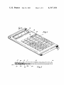
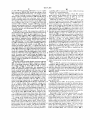
Referring to FIG. 1. a typical handheld electronic
calculator which incorporates the invention is shown.
The calculator comprises a case or housing 10 of
molded plastic or the like. with a keyboard 11 and a
display 12. The keyboard includes number keys 0'9. a
housing 10. and is connected to the PC board 21 by
mounted in a compartment behind a door 29 in the
wires 25 which are soldered to the PC board at one end
and engage terminals of the battery by connectors at the
other end.
The simplicity of the calculator is apparent from
FIG. 2. It consists of a housing, a keyboard device. a
chip. a display device. two small PC boards. and a bat»
tery. No components are needed on the board 21 except
decimal point key, and several standard operation keys
the chip 20. i.e.. no resistors capacitors, transistors.
drivers or any other devices, although such components
such as it’. —-. :, ‘x1. '41-. etc. In some embodiments, the
calculator system could perform a variety of additional
functions, so keys such as
Y‘. SIN. COS.
TAN. LOG.
LN. STO. RCL. etc. may be included.
in the keyboard 11. Additional watch functions and
5
corresponding keys may be added. The display 12 has a
number of digits of seven segment type. with decimal
battery in the preferred embodiment is connected to
power consumption controller 51. The power consump
points. Alternatively. alphanumeric display digits of
nine. eleven or thirteen segments, or a 5 >4 7 dot matrix
may be used. Displays of 8. 10 or l2 digits are com~
tion controller 51 is connected to a plurality of circuit
groups including a first circuit group 52 and a second
monly used and these may also include exponents for
scienti?c notation. and minus sign for both mantissa and
circuit group 53. In a preferred embodiment. the first
circuit group 52 comprises a processor. and the second
exponent. The display usually comprises liquid crystal
devices (LCD). although visible light emitting diodes.
vacuum florcscent displays. or a gas discharge panel,
may he used to add features to the chip 20.
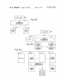
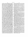
Referring to FIG. 3a. a block diagram of the system
within the chip 20 of FIG. 2 is shown. This system may
be a digit processor chip, such as that described in US.
Pat. Nos. 3.991.305 or 4,014,013. A power source 50. a
25
circuit group 53 comprises the display interface cir
cuitry. The power consumption controller 51 selec»
teries within the housing 10. although an AC adapter
tively activates either one or both of the first circuit
group 52 and the second circuit group 53 to an active on
state, or selectively deactivates the circuit groups to an
off state of low power dissipation stand-by mode re~
may be attached. as well as a battery charger if re
sponsive to the calculator operative state as explained
for example. may also be used with appropriate inter
face circuitry. The calculator is a self-contained unit
having a power supply in the form of a battery or bat
with reference to FIGv 4, infra. Alternately. the battery
chargeable batteries are used.
50 may selectively be connected to the circuit groups.
In place of the usual ON'OFF slide switch which has
including the first circuit group 52 and the second cir»
been used in prior calculators. the calculator of FIG. 1
includes a push~button. momentary~contact~on switch 35 euit group 53. Referring to FIG. 3b. a preferred detailed
embodiment of the power conservation system of FIG.
14 and a like push-button OFF switch 15. The switches
3a is shown. The battery 50 is connected to the power
14 and 15 are exactly like the remainder of the keyswit
consumption controller 51, to the clock oscillator
ches in the keyboard 11 in that they are single-pole
means 55, to a first power switching means 60. to a
single-throw normally open “Form A" switches which
remain closed only as long as pressure is manually ap» 40 second power switching means 61. to the first circuit
group 52, and to the second circuit group 53. The first
plied. In contrast. the usual slide switch would remain
power switching means 60 is interposed between the
closed when moved to the ON position, supplying volt
power consumption controller 51 and the first circuit
age from the battery to the electronic circuitry of the
group 52 and connected therebetween. In a similar
calculator continuously until the switch is manually
45 manner. the second power switching means 61 is inter
moved to the OFF position.
posed between the power consumption controller 51
In FIG. 2. the general form of the internal structure
of the calculator is seen. The keyboard 11 includes an
X—-Y matrix keyboard device 16 suitably of the type
shown in US. Pat. No‘. 4,005,293 issued Jan. 25. I977.
assigned to Texas Instruments Incorporated. About ten
to thirteen wires 19 extend from the end of keyboard
device 16 for connection to the electronic circuitry of
and the second circuit group 53 and connected therebe
tween. The power consumption controller 51 outputs a
first control signal to the first power switching means 60
and a second control signal to the second power switch
ing means 61 so as to selectively activate the first and
second power switching means 60 and 61. respectively.
the calculator. An integrated circuit calculator chip 20
with an excitation source signal from the clock oscilla
contains all of the memory. arithmetic and control cir
cuitry. as will be described. The chip 20 is encased in a
each of the first and second power switching means 60
standard twenty-eight pin dual~in-linc plastic package
tor means 55. or to provide an inactive control signal to
and 61, respectively. thereby disabling the power
for example. which is commonly used in the semicon
ductor industry. Depending upon the complexity of the
switching means 60 and 61, responsive to the operative
also other chip packaging and mounting techniques
signal output from the pover consumption controller
51, selectively provides clock signals to the first circuit
group 52, thereby activating the dynamic circuitry con
state of the calculator system as described with refer
ence to FIG. 4, below. First power switching means 60.
calculator. and the multiplexing scheme used. the num—
her of pins in the package could he more or less. and 60 in response to receiving the active state first control
may be used. The chip Z0 is connected to a printed or
etched circuit board 21 by soldering the pins to conduc
tors on the board 21. as are the wires 19. The display 12
is mounted on a small PC board 22. beneath a plastic
tained therein and affecting a power dissipating active
lens 23 which enhances the visibility ofthe display. The
PC board 22 is mounted on the board 21 by pins
switching means 60. Alternatively. when the first
power switching means 60 is disabled by an inactive
soldered to conductors on the board which make the
first control signal output from the power conservation
state responsive to an activated state of the first power
5
4,317,181
means 51. no active clock signals are output from the
?rst power switching means 60 to the ?rst circuit group
6
means 61 provides clock output signals derived from
the received output from the clock oscillator means 55
in response to receipt of the enabled output from the
power consumption controller 51. The ?rst circuit
group 52 and the second circuit group 53 are comprised
52, thereby forcing the ?rst circuit group 52 to an inac
tive standby non-clocked state, virtually eliminating
power dissipation within the ?rst circuit group 52. In a
similar manner, the second power switching means 61
of clocked logic which only dissipates power when the
responsive to whether the power consumption control
ler 51 second control signal output is active or inactive
provides activated cycling or inactivated non-cycling
clock signals, respectively. to the second circuit group
received clocks are in an active cycling state. Thus, by
selectively controlling the clocks to the ?rst and second
circuit groups 52 and 53, respectively, the power con—
sumption controller 51 effectively controls power con
53, to effect an on state of power dissipation or an off
sumption in the integrated circuit 20.
standby state of virtually no power dissipation, respec
The ?rst and second power switching means 60 and
tively, responsive to the operative state of the calculator
61 in response to receiving control output signals from
system as determined by the power consumption con
the power consumption controller 51, effectively con
troller 51.
nect and disconnect the power to the ?rst and second
Referring to FIG. 3c, a detailed block diagram of the
circuit groups 52 and 53, respectively, by means of a
system of FIG. 3b is shown. The battery 50 is connected
two-fold technique. First, critical node power down
to an independent circuit group 70, the ?rst circuit
DC pathways must be ferretted out of the design prior
group 52, which includes a processor means, the ?rst
to manufacture so as to prevent loss of power through
power switching means 60, the power consumption 20 leakage when clocking is halted and the circuit groups
controller 51, the second power switching means 61,
are in a standby off mode. The critical node DC path
the second circuit group 53, which includes a display
ways are compensated for by circuit design techniques.
means and the clock oscillator means 55. The clock
Secondly, system clocks of the ?rst and second circuit
oscillator means 55 is connected to the independent
groups 52 and 53 are cycled so as to activate and pro
circuit group 70, the ?rst power switching means 60,
vide power to the respective circuit group to effect an
which includes a processor clock generator means, and
on-mode, or the system clocks are disabled so as to
the second power switching means 61, which includes
an input/output (1/0) clock generating means. The
force the respective circuit group to a stand-by non
independent circuit group 70 comprises logic which is
power consuming off mode, effectively disconnecting
power.
Referring to FIG. 3d, an alternative embodiment of
the system of FIG. 3b is shown. The battery 50 is con
nected to a ?rst power switching means 80, the power
consumption controller 51 and a second power switch
ing means 81. The power conservation means 51 is
connected to the ?rst power switching means 80, and
the second power switching means 81. Alternatively,
the ?rst power switching means 80 and the second
power switching means 81 may form an integral part of
the power conservation means. The ?rst power switch
ing means 80 is connected to the ?rst circuit group 52.
Alternatively, the ?rst power switching means 80 may
form an integral part of the ?rst circuit group 52. The
?rst power switching means 80 is interposed between
the battery means 50 and the ?rst circuit group 52, for
45 selectively coupling the battery means 50 to the circuit
an active ready state so long as power is provided to it 30
from the battery 50. The independent circuit group 70
has an input for connection to a keyboard 71 having an
on-key, and an off-key, and a plurality of operation
keys, each of the keys of the keyboard means being
individually operable to provide respective keystroke
signals for as long as the key is depressed. The indepen
dent circuit group 70 may be part of the power con
sumption controller 51, or may be a separate circuit
group within the integrated circuit. The independent
circuit group 70 provides an operation keystroke signal
output to the power consumption controller 51, respon
sive to detecting key operation from the keyboard
means 71, and provides an output to the power con
sumption controller 51 indicative of the respective key
stroke detected. The power consumption controller 51
includes an enabling means which provides a ?rst con
group 52 in response to receiving an active ?rst control
trol signal output to the ?rst power switching means 60
and a second control signal output to the second power
signal output from the power consumption controller
switching means 61, responsive to the received opera
tion keystroke output from the independent circuit
51. Similarly, the second power switching means 81 is
interposed between the battery means 50 and the second
circuit group 53, for coupling the battery means 50 to
the second circuit group 53 in response to receiving an
group 70. The power consumption controller 51 as
sumes an active state upon receiving an on-key stroke
signal and assumes a standby state upon receiving an
active second control signal output from the power
consumption controller 51. Alternatively, the second
off-key stroke signal. Power consumption controller 51
power switching means 81 may form an integral part of
provides an output to the input/output (I/O) clock 55 the second circuitry group 53. The power consumption
generator means of the second power switching means
controller 51 is operable to provide the respective con»
61, when in the active state, enabling the I/O clock
trol signals to the ?rst and second power switching
generator means, and provides an output to the proces
sor clock generating means of the ?rst power switching
means 60, when the power consumption controller 51 is
in the active state and has received a particular opera
tion keystroke signal from the independent circuit
means 80 and 81 in response to the operative state of the
calculator system. As described above with reference to
FIG. 30 an independent circuit group 70, either within
the power consumption controller 51 or a separate cir~
cuit group connected to the battery 50, has an input for
connection to the keyboard means 71, and is responsive
receiving the enabled output from the power consump
to the received keystroke signals therefrom for deter
tion controller 51 responds to the received output from 65 mining operative state selection in the power consump
the clock oscillator means 55 so as to generate clocks
tion controller 51. The power switching means 80 and
output to the processor means of the ?rst circuit group
81, may be comprised of integrated power switches or
52. In a similar manner, the second power switching
other power coupling means when used in conjunction
group 70. The ?rst power switching means 60 when
7
4,317,181
with either static or dynamic logic in the ?rst and sec
ond circuit groups 52 and 53.
In a preferred embodiment, the independent circuit
group 70 also includes a non-volatile memory as de~
8
Thus, the embodiment ofthe invention as set forth in
FIGS. 3a-d, as explained with reference to FIG, 4,
maintains an active and valid display throughout the
calculator on-state while the power hungry clocked
scribed in co-pending application Ser. No. 047,431, by
logic and processor circuitry of the ?rst circuit group
Harper et a], ?led June 11, 1979, for “Calculator with
Constant Memory", which is assigned to the assignee of
52 of FIGS. 3a—d are selectively connected so as to
the present application and now abandoned. The sec
ond circuit group 53 may additionally comprise cir
cuitry as described in co-pending application Ser. No.
046,887, by Leach et al, ?led June 8, 1979, and now US.
Pat. No. 4,264,963 for “Static Latches for Storing Dis
play Segment Information“ which is assigned to the
assignee of the present application.
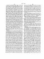
The interaction of the blocks from FIGS, 3a—d is
better understood by reference to the table of FIG. 4,
which provides a state table mapping of the operative
modes of the power consumption controller 51 of
FIGS. 3a-d. As seen in FIG. 4, when the calculator is in
the off-state, the power consumption controller 51 dis
ables a ?rst clock gating means and the second clock
gating means connected to the ?rst and second power
switching means 60 and 61 (80, 81 in FIG. 30’), respec
tively, resulting in an off-mode. When the calculator is 25
in the on<state. one of three power consumption con
troller modes may result. Initially upon power up, as
well as between keystroke processing (as will be de
scribed), the power consumption controller 51 outputs
the enabled second clock gating signal to the second
consume system power only when needed to process
keystroke or timer inputs. The resulting system greatly
reduces power consumption. The system may be de
signed with static, ratioless CMOS, clocked CMOS, or
other clocked logic design structures.
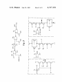
In FIG. 5, a preferred embodiment of the system in
FIGS. Zia-c is shown utilizing a ratioless CMOS struc
ture as described in co-pending application Ser. No.
46,888, ?led June 8, 1979, by Tubbs et al, “Ratioless
Logic." An inverter within one of the circuit groups is
analyzed with reference to FIG. 5 to describe the afore
mentioned two-fold technique of (1) critical node DC
pathway design analysis and compensation, and (2)
clocked power switching techniques. A ?rst inverter
stage 108, is comprised of four MOS transistors in series
connection: a P-channel transistor 110 and N-channe]
transistors 112,114 and 116. The gates of the transistors
110 and 116 are connected to a ?rst control clock 0.
The gate of isolation transistor 112 is connected to a
?rst stage isolation control clock (114, and the gate of the
input responsive transistor 114 is connected to an exter
nal input from the previous stage or from an external
source outside the circuit. The source'drain path of the
?rst transistor 110 is connected between a positive sup
power switching means 61 so as to provide system
ply voltage +V and a circuit output node 100 which
clocks to the second circuit group 53 thereby maintain
connects to the gate of an input transistor 124 ofa sec
ing a display corresponding to the most recent display
register output from the processor of the ?rst circuit
group 52. This mode of the power controller, the dis»
tured equivalent to the ?rst stage 108 with clocks d); and
play and key detect mode, concurrently disables the
ond inverter stage 109. The second stage 109 is struc~
(in; replacing clocks (in and rim, and with a precharge
transistor 120 connected between the +V supply and
?rst power switching means 60 to conserve power con
an output connection node 101 ofthe second stage 109.
For purposes of discussion, assume that the circuit of
cessor of the independent logic group 70 outputs an
FIG. 5 is within the ?rst circuit group 52 of FIG. 315.
enabled keystroke process control signal to the power 40 When the ?rst power switching means 52 is enabled, the
controller 51 which outputs the enabled ?rst clock gat
system clocks (1)], (s2, 4),; and d1]; begin cycling. The
sumption. When a key is depressed. the keystroke pro
ing signal to the ?rst power switching means 60, and
outputs the enabled second clock gating signal to the
second power switching means 61, In this keystroke
processing and display output mode, all areas of the
integrated circuit calculator chip are active in a power
consuming state. Upon completion of the keystroke
processing, the ?rst control signal output to the power
consumption controller 51 is disabled, causing the
clocks (b1 and d); periodically precharge the output
connection nodes 100 and 101. The clocks (111, (1)4, and
(1);, tin; connect the nodes 100 and 101 so as to be selec
tively discharged in response to the input at each stage
via isolation transistors 112, and 122, input stage transis
tors 114. and 124, and discharge transistors 116 and 126,
of the ?rst and second circuit stages, respectively. The
output nodes 100 and 101 are isolated front discharge by
power consumption controller 51 to disable the control
transistors 112, 122, respectively. When the ?rst power
signal to the ?rst power switching means 60 and to
return to the display and key detect mode as shown in
the table FIG, 4. Additionally, in an alternate embodi
switching means 60 of FIG. 3b is disabled, the associ
ment, timing circuitry may be contained in the indepen
dent circuit group 70 so as to respond to a timer inter»
rupt output (such as in a watch or stopwatch), and
provide an output to the power consumption controller
51 so
to activate it to output the enabled ?rst clock
gating signal to the ?rst power switching means 60,
which thereby enables the ?rst circuit group 52, so as to
ated clock sources (1)1, (1)3, (114 and as become inactive
non-cycling and, without preventive design, potential
DC current pathways may result which consume
power. Due to the structure of the ratioless CMOS
circuit stage, it does not form a direct DC current path
way within the con?nes ofits own structure in a power
down mode, However. where the output node connec
tion 101 of the second circuit stage 100 is connected to
the inputs of a conventional CMOS inverter stage com
process the timer interrupt. Additionally, in this mode,
prised of transistors 130 and 132 as shown in FIG. 5,
the power consumption controller 51 outputs the en
abled second clock gating signal to the second power
problem pathways may exist. During normal circuit
operation in the active (ON) mode, the voltage at either
switching means 61 so as to enable the second circuit
node 101 is approximately at the —l-\/ or —V voltage
level, enabling either transistor 132 or 130, respectively,
group 53. In either the keystroke detect and display
mode or the keystroke processing and display mode, the
detection of an off-key operative signal causes the sys~
so as to cause the node 103 to be connected to the +\/
tern to go to the off-mode.
ated clock circuitry is powered down, the voltage levels
or ——V voltage supply rail, However, when the associ
4,317,181
at node 101 may degrade sufficiently so as to enable
both transistors 130 and 132, thereby providing a direct
DC current pathway between the +V supply and the
—V supply resulting in power dissipation. By proper
design of the precharge transistors 110 and 120 and by
proper off-state clock level selection, when the ?rst
power switching means is in the power down off mode,
the voltages at the output connection nodes 100 and 101
are in essence tied to the +V supply rail, and only
transistor 132 is enabled, transistor 130 being disabled,
thereby preventing a direct DC current pathway from
resulting. The above discussion is equally applicable to
the second power switching means 61 and the second
circuit group 53.
Referring now to FIG. 6 in conjunction with FIG. 5,
the operation of the power down control system may be
better understood. When (b1 goes negative, to the —V
supply voltage, transistor 110 is enabled which charges
the output node 100 to the +V voltage level. When 4)]
goes positive, transistor 110 is disabled and transistor
116 is simultaneously enabled, which will isolate the
node 100 from the +V rail. When the isolation transis
tor 112 is enabled by (b4 and input transistor 114 is en
abled by an input X, the output at node 100 may dis
charge via transistor 116 to the —V voltage rail respon
sive to the input X. The operation of the second circuit
10
a standby (off) or active (on) state, while preventing
off-state DC current pathways.
There are numerous off-state critical DC current
paths which can be hidden with in a design, including
the ratioless CMOS structure of FIG. 5, and the
clocked CMOS structures of FIGS. 7 and 8.
Referring to FIG. 7 a clocked CMOS inverter gate
structure is shown. The inverter logic is performed by
transistors 312 and 314 which form a CMOS static in
verter transistor pair. The input X is connected to the
gates of the transistors 312 and 314, the output appear
ing at the node 330. When a power rail transistor clock
signal applied to the node 300 goes to the negative level,
the transistors 310 and 316 are enabled so as to connect
the static inverter, transistors 312 and 314. to the power
supply voltages +V and —V. When the clock appear
ing at node 300 is maintained at a positive voltage level,
+V, the transistors 310 and 316 are disabled, thereby
isolating the static inverter pair transistors 312 and 314
from the +V and —V power supply voltages. The
clock signal appearing at node 300 is connected directly
to the gate oftransistor 310, and is connected to an input
of an inverter circuit 320 which provides a signal corre‘
sponding to a voltage polarity reversal of the input
clock to be connected to the gate of the transistor 316.
Thus, the transistors 310 and 316 are enabled and dis
stage 109 is identical to that as described with reference
abled in unison.
to the ?rst circuit stage 108 except that the precharge
The clocked CMOS structure, as shown in FIG. 8, is
clock d); is separate from the subsequent to the control
identical to the clocked CMOS inverter gate structure
clock (in of the first circuit stage 108 during each clock 30 of FIG. 7 except that the inverter 320 of FIG. 7 is re
cycle. At power down, both clocks go negative to
moved from between the clock signal at node 300 and
gether and stay at the —V level enabling transistors 110
the gate of transistor 316 and is instead connected be
and 120, and connecting nodes 100 and 101 to the +V
tween the clock at the node 300 and the gate of the
supply voltage as required for connection to the subse
transistor 310. The relocation of the inverter 320 pro
quent CMOS stage.
35 vides clock polarity reversal from the system shown in
When the clocks (in and (b2 disable transistors 110 and
FIG. 7.
120, and when either the isolation transistors 112 and
122, or discharge transistors 116 and 126, are disabled,
the output voltages at nodes 100 and 101 of circuit
stages 108 and 109, respectively, are maintained by
means of capacitive storage, in isolation. These voltage
levels would normally degrade with time due to stored
charge leakage, and where the voltage at output 101
Thus, in FIG. 8, a positive clock signal level enables
transistors 310 and 316, thereby enabling the inverter
transistor pair 312 and 314 to function properly. Alter
49 natively, when the clock signal appearing at node 300 is
at a negative signal level, the transistors 310 and 316 are
disabled, thereby isolating the transistor pair 312 and
314 from power.
degrades to a point where the voltage level is between
An alternate clocked CMOS structure may be con
the thresholds ofthe transistors 130 and 132 so as to turn 45 structed with clocked transistors 310 and 316 connected
both transistors on, a DC current path would be created
in the center of the series structure and inverter transis
that would draw substantial current through it. How
tors 312 and 314 being connected to the power rails and
ever, by enabling transistors 110 and 120 (by driving
to the center clocked transistors, as shown with refer
clock (in and 4);, respectively, to a negative level) the
ence to FIG. 13.
output nodes 100 and 101 will be directly connected to
Referring back to FIG. 3, the power consumption
controller 51 selectively provides for effective power
consumption connection and disconnection of the first
the +V supply voltage. Since a negative voltage level
on the ¢~| and (b3 clocks will disable transistors 116 and
126, respectively, the voltage output at nodes 100 and
101 will be prevented from discharging irrespective of
the input to the stage and irrespective of the level of the
clock applied to the isolation transistors. Thus, the volt
age levels at nodes 100 and 101 will be constant at the
+ V voltage level in the power down mode. The critical
node output 101, which is connected to the input of the
static inverter transistor pair 130 and 132, is held at the
+V voltage level during power down, thereby pre
venting a direct DC current path through the transistor
pair 130 and 132 during power down. When all the
clocks in the system of FIG. 5 are inactive non-cycling
(steady state), there are no state changes in the system,
and negligible current is drawn. The power controller
selectively turns clocks on and off to force circuit stages
associated with the selected power switching means to
and second circuit groups 52 and 53, respectively. The
concept can be expanded such that the power consump
55 tion controller 51 may control a plurality of power
switching means which in turn provide for connection
of clock signals to a plurality of circuit groups.
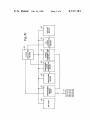
Referring to FIG. 9. a further improvement over the
invention of FIGS. 30-11 is shown. The controller
means 400 provides for four different operating modes
as described further with reference to FIGS. 10-13 and
Tables I and 2, infra. In a preferred embodiment, two
latches within the controller means 400 determine one
of four possible operational modes in response to soft
ware and hardware control inputs. The two latches
which may be independently set and reset are com
prised ofa main oscillator latch 401 (MO) and a display
mode latch 402 (DM). The controller means 400 is
11
4,317,181
12
the display oscillator 404 may be used for scanning the
keyboard means 412 and for generating keyboard inter
rupts when the calculator system is in the processor
only mode (MO: I, DMzO, as described with refer
connected to a main oscillator 406 which provides a
main oscillator clock output in response to receiving an
enable input from the controller 400 for activating the
processor and I/O circuitry. A main clock generator
408 is connected to the main oscillator 406 and to the
ence to FIG. 10), to allow for off-key detection.
Referring to FIG. 10 and Table I, it is seen that the
system of FIG. 9 is a four state (mode) control system.
controller means 400 for providing multiphase clock
outputs in response to receiving the main oscillator
clock output from the main oscillator 406 and an enable
In a preferred embodiment. the IIlOdt‘ latches are re
input from the controller means 400. Processor means
410 is connected to the main clock generator 408 and to
sponsive to independent direct control signals for the
main oscillator latch 401 and for the display mode latch
402. Additionally, there is a control signal for the dis
the controller means 400 for processing data received
from the controller means 400 in response to receiving
play speed control, which selectively multiplexes the
the multiphase clock outputs from the main clock gen
display interface between the oscillator 406 (when the
main oscillator latch 40] is set and the display mode
latch 402 is reset) and the display oscillator 404 (when
the main oscillator latch 401 is reset and the display
erator 408. A keyboard means 412 is connected to the
controller means 400. The keyboard means is comprised
of an on key, an off key, and a plurality of operation
keys, each of the keys being individually operable to
mode latch 402 is set). In an alternate embodiment the
display oscillator is always on except in the OFF mode
provide respective key operation signals for the dura
tion of key depression. A display oscillator 404 is con
state, and the display mode latch 402 acts only as a
nected to the controller 400 for providing a display 20 display speed control.
oscillator clock output in response to receiving an en
In the off mode, state 0 O, the calculator system is not
able input from the controller 400, for activating display
interface circuitry. A display clock generator 414 is
in use. All clocks are at an non-cycling inactive level
(V55) and the display is blank. Only a KA (on key oper
connected to the display oscillator 404 and to the con
troller means 400 for selectively providing multiphase 25 ative key code) can alter the state of the machine from
the off state. An on key operative key code will set the
clock outputs in response to receiving the clock output
main
oscillator latch 401 (MO), generating a power up
from the display oscillator 404 and an enable input from
clear
signal
(PUC) and bringing the system to a process
the controller means 400. A display interface 416 is
only mode state l 0 of FIG. 10 and Table 1. The proces
connected to the display clock generator 414 and to the
sor 410 of FIG. 9 may then load the display interface
controller means 400 for selectively providing outputs
416 for the desired power up display, and then go to a
representative of the information to be displayed corre
display only mode, state 0 l in FIG. 10 and Table l,
sponding to the data received from the processor means
awaiting a keystroke operative key code.
410 in response to receiving the multiphase clock out
In the display only mode, the state 0 1 of FIG. 10 and
puts from the display clock generator 414. The control
ler means 400 selectively provides enable outputs, to the 35 Table l, the calculator is in a waiting state. The proces
sor 410 is off and the display exhibits whatever was
display oscillator 404, and the display clock generator
loaded into the display interface prior to entering this
414, and the main oscillator 406 and the main clock
state. Periodically, the select/R lines which connect to
generator 408, so as to enable the selected oscillator and
the external keyboard display will be hardware inter
clock generator to provide a clock output, said enable
output being selectively provided in response to receiv
ing a combination of prede?ned key operation codes
from the keyboard means 412 and in response to receiv
ing prede?ned instruction codes from the processor
40
rupted and pulled to the active supply level (VDD) for a
?rst time interval, approximately 125 microseconds in a
preferred embodiment. This will enable any keyboard
entry sharing the select/R lines to provide for an opera»
tive key code to power up clear the machine to a pro
410. In an alternate embodiment, the controller means
400 includes the main oscillator latch 401 which is set in 45 cess only mode (state I 0 of FIG. 10 and Table l) by
setting the main oscillator latch 401 and resetting the
response to certain prede?ned combinations of instruc
display mode latch 402 (thereby generating a power up
tion codes and key operation codes so as to enable the
clear). The processor 410 is thereby placed in a fully
main oscillator 406 and main clock generator 408 and is
active mode, so that in conjunction with the controller
further comprised of the display mode latch 402 which
is selectively enabled in response to receiving prede 50 means 400, it can scan a keyboard 412 for the specific
key pressed, debounce, and process the depressed key
?ned combinations of key operation codes from the
to determine the operative key code.
keyboard means 412 and instruction codes from the
The process only mode, state I 0 of FIG. 10 and
Table l, is the normal processing mode ofthe system in
embodiment, the display clock generator 414 is enabled 55 the preferred embodiment. This state always follows a
power up clear. Display information is generally up
in response to receiving an output from the display
dated in this mode. Since the display interface section is
mode latch 402 (DM) at input EN| and in response to
running at processor speeds in the process only mode,
receiving an output from the main oscillator latch 401
that is, display clock generator 414 is responsive to main
(M0) at input ENZ. An advantage ofdesign simplicity is
gained in this way in exchange for a slight increase in 60 oscillator 406, the display will be blanked while in this
mode. In an LCD preferred embodiment. the select/R
active state on power for the calculator system. Addi
processor 410 so as to enable the display oscillator 404
and the display clock generator 414. In a preferred
tionally, in the preferred embodiment, the display clock
buffers will be at binary logic levels (Vpp-V55) causing
them to act as R lines for keyboard interface rather than
as a display interface. Periodically, the select/R buffers
latch 401. Furthermore, in the preferred embodiment, 65 will be hardware interrupted and pulled to V53, en
generator 414 is enabled in response to receiving either
the DM output from latch 402 or the MO output from
the display interface 416 may be controlled directly by
the DM output from latch 402. Finally, the preferred
embodiment yields a functional design benefit in that
abling the off key (KD) to reset the main oscillator latch
40] and thereby place the calculator in the off mode,
state 0 0 of FIG. 10 and Table l.
13
4,317,181
In the process and display mode, state 1 l of FIG. 10
and Table l, the display oscillator 404 and processor
oscillator 406 may be enabled simultaneously or alterna
tively the processor oscillator 406 only may be enabled.
This is particularly useful in the event that a long num
ber crunching routine is going to occur and a blank
display is undesirable for this length of time. The dis
play interface 416 can be updated in the process only
mode, and the system can then go to the process and
14
from the controller 400 of FIG. 9 forces the system to
change states to the display only mode, state 0 l of FIG.
11, as ‘described with reference to FIG. 10. Any opera
tive keycode (any key) forces a power up clear and a
state transition from state 0 1 display only mode to state
1 0 process only mode, as described with reference to
FIG. 10. In addition, in the system with timekeeping, a
request timekeep output from the timekeep counter
latch causes a power up clear to occur forcing a state
display mode so that the display will exhibit previously
transition from the display only mode 0 l to the process
updated data while the system is processing the number
only mode I 0.
crunching routine. While it is possible for the processor
Referring to FIGS. 9 to 11, in a preferred mode, the
410 to communicate with the display interface 416 in
display oscillator 404 when enabled is operative at a
this mode, this will generally not be done except for
frequency of 50 Hz, and the main processor oscillator
quick input/output and K line communication since
406 when enabled is operative at a frequency of 1.6
enabling the main oscillator 406 only, will cause the
MHz or alternatively at a frequency of 500 KHz, de
display to blank. If a key is being held down after the
pending on the desired processor throughput.
system is ?nished processing it, the system will wait in
The system of FIG. 10 may be described as a master
the process and display mode (for calculators without
system controller which provides both processing and
the key rollover feature) for the key to be released 20 display control functions. In addition, the system inte
before returning to the display only mode. This is ac
grated circuit chip of FIG. 9 may exist without a display
complished by means of a software actuable any key
interface and therefore without a display oscillator. In
latch within the controller means 400, which when set
in response to instruction code set and reset signals will
this case, the system may be referred to as a slave con
troller system, as will be described with reference to the
pull all the select/R lines to VDD. The processor 410 25 state transition diagram of FIG. 12.
may then quickly scan the K lines to determine if a key
When the slave system is in an off state, state 0 0, the
is being held down. This sequence can generally be
appearance of an oscillator input causes a power up
done so quickly as to not affect the display. The se
clear to occur forcing the system to a process mode,
lect/R lines are interrupted and pulled to V55 in this
state I 0 FIG. 12. When the oscillator input is removed
mode also (every third common time for 125 microsec 30 (disappears) the system is forced to an off state, state 0
onds in a preferred embodiment) so that an off key
0 of FIG. 12.
(KD) can place the calculator in the off mode.
Referring to FIG. 13, a detailed schematic of an alter
Referring to Table 2, instruction codes for the set
nate embodiment of the circuit group 50 of FIG. 3a and
display mode latch (DM), reset display mode latch
more specifically of a clocked CMOS circuit group
(DM), and off instructions are shown for the preferred 35 such as described with reference to FIGS. 7 and 8, is
embodiment.
shown. When the power consumption controller 51 of
Referring to FIG. 11, a state transition diagram for
FIG. 3a forces the circuit group 52 to a standby low
the multimode power controller for a calculator system
power state, and clocks $4, (1);; and rbcof FIG. 13 are set
with timekeeping is shown. The state transitions in a
to the active logic level non-cycling state, all clocked
timekeeping application contain the same four modes as 40 gates are transformed to static gates, and all sequential
in the nontimekeeping application, as shown in FIG. 10,
logic to combinational logic, thereby allowing imposi
each mode serving the same function. A timekeeping
tion of a prede?ned output level. This requires that
overload register output will generate a power up clear
various critical input control nodes in the logic must be
and place the calculator system into the process only
forced to a fixed state so as to force the combinational
mode. In addition, as explained with reference to FIG. 45 logic to output a prede?ned voltage level. For example,
10, the on key operative key code (KA) generates a
if it is desired that node 500 be at a logical high level
power up clear so as to place the system in a process
during the standby state, node 502 must be set to a
only mode. In the timekeeping system, an additional
logical low level in the standby state. A preset output
means for going from the off mode, state 0 0 in FIG. 11,
504 from the power consumption controller 51 is cou
to the process only mode, State l 0 in FIG. 11, is accom
pled to one input of NOR gate 503. The output of NOR
plished in response to a request timekeep output from a
gate 503 is coupled to node 502, thereby effectively
counter latch in the timekeeping circuitry to provide for
controlling the forced state output at node 500. When
a periodic update of the timekeeping latches, every one
the preset output 504 is output at a high logic level
second in a preferred embodiment. As described above
during the standby state, the output of NOR gate 502
with reference to FIG. 10, a set display mode oscillator 55 will be forced to a logic low level irrespective of the
latch instruction code from the controller 400 of FIG. 9
logic level of signal e at input 505 of NOR gate 503.
causes the system of FIG. I] to go from the process
Thus, node 502 is forced to a logic low level in direct
only mode to the process and display mode, and a reset
response to a preset output 504 from the power con
display mode latch instruction code from the controller
sumption controller 51 and thereby forces a logical high
400 of FIG. 9 causes the system to go from a process 60 level output at node 500, as desired, irrespective of the
and display mode to a process only mode. In addition, a
other input signal levels. Thus, in response to the preset
timekeep overload output from a timekeeping overload
output from the power consumption controller 51. a
latch causes a power up clear to occur and forces a state
predefined output level is obtainable independent of the
transition to the process only mode. The timekeep over
active mode inputs 505, 506, or 507 to the logic circuitry
load output forces a power up clear, but when the sys 65 of FIG. 13. A significant advancement is achieved be
tem is already in the process only mode, no state transi
yond the standby power dissipation modes of ratiolcss
tion occurs. When the system is in the process and dis
precharge discharge logic shown in FIG. 5, or the
play mode, state I l of FIG. 11, an offinstruction code
clocked CMOS logic is shown in FIG. 7 and 8, by the
4,317,181
15
16
mode to supply ?rst clock pulses to control oper
ation of said ?rst set of data processing opera
tional circuits; and
rationless clocked controlled state output logic as
shown in FIG. 13. The system of FIG. 5 provides an
output at a ?xed voltage level (at the precharge voltage
(ii) second clock pulse generator means controlled
by said second oscillator means, responsive to
level) when the clocks are brought to an active state and
the clocked CMOS of FIGS. 7 and 8 provides an output
isolated from the applied voltages which may be ran
dom, while the output level of the clocked CMOS logic
with controlled output level is at a prede?ned desired
output level which may be different from the precharge
level.
In the preferred embodiment, as shown in FIG. 13,
predetermined signals from said operator input
means and to second predetermined mode sig
nals from other portions ofsaid electronic circuit
means selectively to operate in a standby, low
power consumption mode or to operate in an
active mode to supply second clock pulses to
control operation of said second set of data pro
when the clocks are inactive (in a non-cycling mode), a
minimum power dissipation is achieved. When the
cessing operational circuits.
clocks are held at the active level in the non-cycling
2. The data processing system as recited in claim 1,
wherein said second clock pulse generator means is
further controlled by Said ?rst oscillator means respon
mode and a preset output is applied to the sequential
logic, the clocked CMOS logic becomes truly combina
tional (static) logic, providing a prede?ned output state
sive to prede?ned signals from said operator input
in a minimum power dissipation mode.
When the clocks are cycling in the active mode, the
means and to alternate predetermined mode signals
from said electronic circuit means for operating in a
preset output 504 from the power consumption control 20 standby, low power consumption mode or in an active
ler 51 is at an inactive level (a low level in FIG. 13) so
mode to supply second clock pulses to control opera
as to allow the logic to operate as sequentially clocked
tion
of said second set of data processing operational
logic in the desired manner.
circuits.
Although the invention has been described with ref
3. The data processing system as recited in claim 1,
erence to speci?c embodiments, this description is not 25
further comprising:
meant to be construed in a limiting sense. Various modi
?cations of the disclosed embodiment, as well as other
embodiments of the invention, will become apparent to
persons skilled in the art upon reference to the descrip
tion of the invention. It is, therefore, contemplated that 30
the appended claims will cover any such modi?cations
or embodiments as fall within the true scope of the
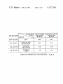
TABLE 1
Tt-sois
OSCILLATOR CONTROL IN VARIOUS MODES
DM COMMENT
DISPLAY
PROCESSOR
1
l
I
0
0
1
0
0
PROCESS &
DISPLAY
PROCESS
ONLY
DISPLAY
ONLY
OFF
means, said second oscillator means, said ?rst clock
pulse generator means, said second clock pulse
generator means, and said operator input means,
said controller means comprising:
(i) means for selectively operating each of said ?rst
invention.
MO
(a) an output means for generating an operator per
ceivable output; and
(b) controller means connected to said ?rst oscillator
50H:
1.6M/500K
1.6M/500K
L6M/500K
50Hz
OFF
OFF
OFF
35
response to receiving an OFF Signal;
tor means and said ?rst clock pulse generator
means in said standby low power consumption
mode and for selectively operating said second
45
SET DM : OABS
RESET DM = OAB4
OFF INST. = 0035
50
1. An electronic data processing system comprising:
(a) operator input means having means for generating
an ON signal, an OFF signal and a plurality of
operation signals; and
?rst and second clock pulse generator means in
said standby low power consumption mode in
(ii) means for selectively operating said ?rst oscilla
TABLE 2
We claim:
and second oscillator means, and each of said
oscillator means and said second clock pulse
generator means in said active mode in response
to receiving an ON signal;
(iii) means for selectively operating said ?rst oscil
lator means, said ?rst clock pulse generator
means and said second clock pulse generator
means in said active mode and for selectively
operating said second oscillator means in said
standby, low power consumption mode in re
sponse to receiving one of said plurality of oper~
ation signals; and
(iv) means for selectively operating said ?rst oscil
lator means, said ?rst clock pulse generator
oscillator means and ?rst and second sets of data
means, said second clock pulse generator means,
and said second oscillator means in said active
processing operational circuits for performing data
mode in response to mode inputs indicative that
(b) electronic circuit means having ?rst and second
processing operations in accordance with said op
eration signals and for generating mode signals
including:
(i) ?rst clock pulse generator means controlled by
said ?rst oscillator means, responsive to prede
termined signals from said operator input means
and to ?rst predetermined mode signals from
other portions of said electronic circuit means
selectively to operate in a standby, low power
consumption mode, or to operate in an active
said ?rst set of data processing operational cir
cuits is performing a data processing operation.
4. The data processing system as recited in claim 3,
wherein:
said ?rst set of data processing operational circuits
includes arithmetic logic means; and
Said second set of data processing operational circuits
is coupled to said output means and includes an
output interface means.
5. An electronic data processing system comprising:
17
4,317,181
18
(a) operator input means having means for generating
fl 10W pOyvcr standby mode in response to receiv
an ON signal, an OFF signal and a plurality of
mg 531d macnve Secmld enabk Output;
(3) ?rst clock generator means, connected to said
operation signals; and
controller means and said ?rst oscillator means,
(b) electronic circuit means having an OFF mode, a
process only mode, a display only mode and a 5
process and display mode, comprising:
(1) controller means, connected to said operator
input means’ including means for Sel?ctlvdy
generating inactive ?rst enable, ?rst control, 10
second enable and second control output when
said electronic circuit is in the OFF mode, means
for generating active ?rst enable, ?rst control
and second control outputs and inactive second
enable output when said electronic circuit is in 15
the process only mode, means for generating
active second enable and second control outputs
and inactive ?rst enable and ?rst control outputs
for selectively generating ?rst clock outputs in a
cycling state at said ?rst frequency in response to
receiving said active ?rst control output and said
?rst frequency signal and generating a prede
?ned steady state output in response to receiving
Said inactive ?rst Comm] Output; and
(4) second clock generator means, connected to
said controller means, said ?rst oscillator means
and said second oscillator means for selectively
g??erallng Second Clock ompuis 1'" a Cycling
state at said ?rst frequency in response to receiv
ing said active ?rst control output, said inactive
second control output and said ?rst frequency
signal, generating second clock outputs in a cy
cling state at said second frequency in response
when said electronic circuit is in the display only 20
to receiving said active second control output,
mode, and means for generating active ?rst enand generating a prede?ned steady output in
able’ ?rst Control, Second enable and Second
response to receiving said inactive ?rst control
control outputs when said electronic circuit is in
output and said inactive Second Comm] Output
the processor and display mode;
6. The data processing system ofclaim 5 wherein said
(2) oscillator means, connected to said controller 25 ElECU'OIIiC Circuit further Comprises:
means, including ?rst oscillator means for 55189.
processor means, connected to said ?rst clock genera
tively generating a ?rst frequency signal in re
sponse to receiving said active ?rst enable output
and operating in a low power standby mode in
response to receiving said inactive ?rst enable 30
tor means, for selectively executing data process
ing functions corresponding to the received opera
tion signals in response to receiving the ?rst clock
outputs in a cycling state; and
display interface means connected to said second
output, and second oscillator means for selec
clock generator means, for selectively generating
?ve-l)’ generaiing a Second frequency signal
operator perceivable outputs representative of the
Whlch has relatively low f‘requemly as Compared
w1th said ?rst frequency in response to receiving 35
information to be output in response to receiving
the second clock outputs in a cycling state.
said active second enable output and operating in
"‘
45
55
65
"‘
*
*
*