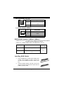
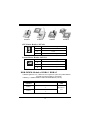
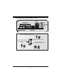
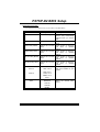
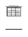
1
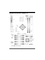
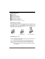
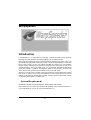
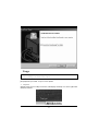
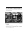
P44TTS SP--D D22 FCC Information and Copyright This equipment has been tested and found to c omply with the limits of a C lass B digital device, pursuant to Part 15 of the FCC Rules . T hese limits are designed to provide reasonable protection agains t harmful interference in a residential installation. This equipment generates , uses and can radiate radio frequency energy and, if not ins talled and used in accordance with the instructions, may c ause harmful interference to radio communications . There is no guarantee that interference will not occur in a partic ular installation. The vendor makes no representations or warranties with respec t to the contents here of and specially disclaims any implied warranties of merchantability or fitness for any purpose. F urther the vendor reserves the right to revise this publication and to make changes to the c ontents here of without obligation to notify any party beforehand. Duplication of this publication, in part or in whole, is not allowed without firs t obtaining the vendor’s approval in writing. The c ontent of this user’s manual is subject to be changed without notice and we will not be responsible for any mistakes found in this us er’s manual. A ll the brand and product names are trademarks of their respective c ompanies . i C Coonntteennttss LAYOUT OF P4TS P-D2 VERS ION 1.X................................................. 1 COMPONENT INDEX FOR P4TSP-D2 V.1.X ...................................... 2 LAYOUT OF P4TS P-D2 VERS ION 7.X................................................. 3 ENGLIS H................................................................................................... 4 P4TSP-D2 Features ....................................................................................4 Package contents.......................................................................................5 How to set up a Jumper?............................................................................6 CPU Installation.........................................................................................6 DDR DIMM Modules: DDRA1/ DDRA2 ...........................................................7 Installing DDR Module................................................................................7 Jumpers, Headers, Connectors & Slots.........................................................8 DEUTSCH................................................................................................ 15 Die Spezifikationen von P4TSP-D2 ............................................................. 15 Verpackungsinhalt ................................................................................... 17 Einstellung der Jumper............................................................................. 17 Installation der CPU.................................................................................. 17 DDR-DIMM-Modules: DDRA1/ DDRA2 ......................................................... 18 Installation von DDR-Modul....................................................................... 19 Jumpers, Headers, Anschlüsse & Slots....................................................... 19 FRANÇAIS .............................................................................................. 27 Caractéristiques de P4TSP-D2................................................................... 27 Contenu de l'Emballage............................................................................ 28 WARPSPEEDERTM ................................................................................ 29 Introduction............................................................................................. 29 System Requirement................................................................................ 29 Installation .............................................................................................. 30 Usage..................................................................................................... 31 TROUBLE S HOOTING......................................................................... 39 PROBLEMLÖS UNG.............................................................................. 40 ii Layout of P4TSP-D2 Version 1.x NOTE: ●represents the f irst pin. 1 Component Index for P4TSP-D2 Version 1.x A. Power Source Sel ection for Keyboard and N. Communication Net work Ri ser Slot (CNR1) Mouse (JKBV1) B. Power Source Selection for USB (JUSBV1) C. Back Panel Connector O. S ystem FAN H eader (JSFAN1) P. Front USB Header (JUSB2) Q. Front USB Header (JUSB3) R. Power Source Selection for USB D. Power Source Selection for USB (JUSBV2) (JUSBV3_4) S. Game Port Header (JG AME 1): Optional E. ATX 12V Po wer Connector (JATX PW R2) T. Front Panel Connector (JP ANEL1) F. ATX 12V Po wer Connector (JATX PW R1) U. Seri al ATA Connector (S ATA1-2) G. Front Audio Head er (JAUDIO1) V. Case Open Connector (JCL1) H. Accel erated Graphi cs Port Slot (AGP1) W. Clear CMOS Function (JCMOS1) I. Digital Audio Connector (JS PDIF_OUT1) X. IDE Connectors (IDE 1-2) J. CD-ROM Audio-In Header (JCDIN2) Y. DDR DIMM Modules (DDRA1/ DDRA2) K. CD-ROM Audio-In Header (JCDIN1) Z. Floppy Di sk Connector (FDD1) L. PCI BUS Slots (PCI 1-5) A1. CPU Fan Connector (JCFAN 1) M. W ake On LAN Header (WOL1): Optional B1. Audio DJ Connector (JDJ1): Optional 2 Layout of P4TSP-D2 Version 7.x NOTE: ●represents the f irst pin. 3 English P4TSP-D2 Features A. Hardware CPU Prov ides Socket 478. ® ® Supports the Intel Pentium 4 processor to 3.2GHz. ® ® Supports the Intel Pentium 4 Northwood CPU. (Willamette not supported) ® ® Supports the Intel Pentium 4 478-pin Prescott CPU. Front Side Bus at 400/533/800MHz. Supports Hy per-Threading Technology. Chipset North Bridge: Intel 848P. South Bridge: Intel ICH5. Main Memory Supports 64-bit wide DDR data channels with 2 DIMMs. Available bandwidth up to 3.2GB/s (DDR400) f or single-channel mode. Supports 128-Mb, 256-Mb, 512-Mb DDR technologies. Supports only x8, x16, DDR devices. Supports four bank devices. Maximum memory size is 2GB. Super I/O Chip: ITE IT8712. Low Pin Count Interface. Prov ides the most commonly used legacy Super I/O functionality. Env ironment Control initiatives, - H/W Monitor - Fan Speed Controller - ITE's "Smart Guardian" f unction Slots Five 32-bit PCI bus master slots. One CNR slot. (only optional on v ersion 1.x) One AGP 4X/8X compatible slot. On Board IDE Supports four IDE disk drives. Supports PIO Mode 4, Ultra DMA 33/66/100 Bus Master Mode. LAN (optional) Chip: RTL8100C/RTL8110S(B) Supports 10Mb/s, 100Mb/s, and 1000Mb/s auto-negotiation operation. 4 Half/Full duplex capability. Supports ACPI, PCI power management. On Board AC’97 Sound Codec Chip: CMI9739A (for v.1.0-v.1.2)/ CMI9761A (for v.1.3 &v.7.x). Compliant with AC’97 specification. AC97 2.2 interface (CMI9739A)/ AC97 2.3 interf ace (CMI9761A). Supports 6 channels . Supports stereo microphone. (only f or CMI9761A.) On Board Peripherals a.Rearside 2 serial ports. (version 7.x only supports one serial port.) 1 parallel port. (SPP/EPP/ECP mode) Audio ports in vertical position. 1 RJ-45 LAN jack. (optional) PS/2 mouse and PS/2 keyboard. 4 USB2.0 ports. (optional) b.F ront Side 1 floppy port supports 2 FDDs with 360K, 720K, 1.2M, 1.44M and 2.88Mbytes. 4 USB2.0 ports. 1 front audio header. 1 S/PDIF_Out header. Dimensions ATX Form Factor: 20.3 X 30.5cm (W x L) (f or version 1.x) ATX Form Factor: 20.3 X 29.3 cm (W x L) (for version 7.x) B. BIOS & Software BIOS Award legal BIOS. APM1.2. ACPI. USB Function. Software TM TM Supports Warpspeeder™, 9th Touch™, BootBlocker , WinFlasher , FLASHER™. Off ers the highest performance for Windows 98 SE, Windows 2000, Windows Me, Windows XP, UNIX series, etc. Pack age contents HDD Cable X 1 FDD Cable X 1 User’s Manual X 1 5 Fully Setup Driv er CD X 1 USB 2.0 Cable X1 (optional) S/PDIF Cable X 1 (optional) Rear I/O Panel f or ATX Case X 1 Serial ATA Cable X 1 (optional) Serial ATA Power Switch Cable X 1 (optional) How to set up a Jumper? The illustration shows how to set up jumpers. When a Jumper cap is placed on pins, the jumper is “close”. If no jumper cap is placed on the pins, the jumper is ”open”. The illustration shows a 3-pin jumper whose pin1 and 2 are “close” when a jumper cap is placed on these 2 pins. Jumper open Jumper close Pin 1-2 close CPU Installation Step1: Pull the lever sideway s away from the socket and then raise the lev er up to a 90-degree angle. Step2: Look f or the white dot/cut edge. The white dot/cut edge should point wards the lev er piv ot. The CPU will f it only in the correct orientation. Step3: Hold the CPU down f irmly, and then close the lever to complete the installation. Step4: Put the CPU Fan on the CPU and buckle it. Connect the CPU fan power cable to the JCFAN1. This completes the installation. Step1 Step2 Step3 6 Step4 CPU Fan Header: JCFAN1 3 1 JCFAN1 Pin Assignment 1 Ground 2 +12V 3 FAN RPM rate Sense S ystem Fan Header: JSFAN1 1 3 JSFAN1 Pin Assignment 1 Ground 2 +12V 3 FAN RPM rate Sense DDR DIMM Modules: DDRA1/ DDRA2 DRAM Access Time: 2.5V Unbuffered/ no registered (without ECC) DDR SDRAM PC2100/ PC2700/ PC3200 Ty pe required. DRAM Ty pe: 128MB/ 256MB/ 512MB/ 1GB DIMM Module. (184 pin) DIMM Socket Location DDR Module DDRA1 64MB/128MB/256MB/512MB/1GB DDRA2 Total Memory Size (MB) *1 Max is 64MB/128MB/256MB/512MB/1GB *1 ***Only for reference*** 2GB Installing DDR Module 1. Unlock a DIMM slot by pressing the retaining clips outward. Align a DIMM to the slot in the way that the notch of the DIMM matches the break of the slot. 2. Insert the DIMM v ertically and firmly into the slot until the retaining chip snap back in place and the DIMM is properly seated. 7 Jumpers, Headers, Connectors & Slots Floppy Disk Connector: FDD1 The motherboard provides a standard f loppy disk connector that supports 360K, 720K, 1.2M, 1.44M and 2.88M floppy disk types. This connector supports the prov ided f loppy drive ribbon cables. Hard Disk Connectors: IDE1/ IDE2 The motherboard has a 32-bit Enhanced PCI IDE Controller that provides PIO Mode 0~4, Bus Master, and Ultra DMA 33/ 66/ 100 f unctionality. It has two HDD connectors IDE1 (primary) and IDE2 (secondary). The IDE connectors can connect a master and a slave driv e, so you can connect up to f our hard disk driv es. The f irst hard drive should alway s be connected to IDE1. Peripheral Component Interconnect Slots: PCI 1-5 This motherboard is equipped with 5 standard PCI slots. PCI stands f or Peripheral Component Interconnect, and it is a bus standard for expansion cards. This PCI slot is designated as 32 bits. Accelerated Graphics Port S lot: AGP1 Y our monitor will attach directly to that v ideo card. This motherboard supports video cards for PCI slots, but it is also equipped with an Accelerated Graphics Port (AGP). An AGP card will take advantage of AGP technology f or improved video efficiency and performance, especially with 3D graphics. Communication Network Riser S lot: CNR1 (not support version 7.x) The CNR specification is an open Industry Standard Architecture, and it defines a hardware scalable riser card interf ace, which supports modem only. Serial ATA Connector: S ATA1/ S ATA2 The motherboard has a PCI to SATA Controller with 2 channels SATA interface, it satisfies the SATA 1.0 spec and with transfer rate of 1.5Gb/s. 65 3 2 7 4 1 S ATA1/ SATA2 Pin Assignment Pin Assignment 1 Ground 2 TX+ 3 TX- 4 Ground 5 RX- 6 RX+ 7 Ground 8 Front Panel Connector: JPANEL1 P WR_LED S LP (+) (+) (-) ON/ OF F IR 24 2 JPANEL1 1 23 (+) (-) S PK HLED R ST IR Pin 1 Assignment +5V Function Speaker Pin 2 Assignment Sleep Control Function Sleep 3 NA Connector 4 Ground Button 5 7 NA Speaker 6 8 NA Power LED (+) NA POWER 9 HDD LED (+) Hard Drive 10 Power LED (+) LED 11 HDD LED (-) LED 12 Power LED (-) 13 Ground Reset 14 Power Button Power-on 15 Reset Control Button 16 Ground Button 17 NA 18 KEY 19 NA IrDA 20 KEY IrDA 21 +5V Connector 22 Ground Connector 23 IRTX 24 IRRX Power Connectors: JATXPWR1/ J ATXPWR2 10 1 20 11 J ATXPWR1 PIN 1 Assignment +3.3V PIN 11 Assignment +3.3V 2 3 +3.3V Ground 12 13 -12V Ground 4 +5V 14 PS_ON 5 6 Ground +5V 15 16 Ground Ground 7 Ground 17 Ground 8 9 PW_OK Standby Voltage +5V +12V 18 19 -5V +5V 20 +5V 10 9 1 3 2 J ATXPWR2 PIN Assignment PIN Assignment 1 +12V 3 Ground 2 +12V 4 Ground Power S ource Selection for Keyboard/ Mouse: JKBV1 (only optional on version 1.x) JKBV1 Assignment Description +5V for key board and mouse 3 +5V 1 Pin 1-2 close 3 +5V Standby Voltage 1 PS/2 Mouse and PS/2 Keyboard are powered with +5V standby v oltage Pin 2-3 close Note: In order to support this function “Pow er-on system via keyboard and mouse”, “JKBV1” jumper cap should be placed on pin 2-3. Power S ource Selection for USB: JUSBV1/ JUS BV2/ JUS BV3_4 (only optional on version 1.x) JUSBV1/JUSBV2/ JUSBV3_4 Assignment Description JUSBV1: 5V for USB at the JUSB1 connector port 1 3 +5V Pin 1-2 close JUSBV2: 5V f or USB at the JRJ45USB1 coonector port JUSBV3_4: 5V for USB at the JUSB2/3 connector ports 1 3 Pin 2-3 close +5V Standby Voltage JUSBV1: JUSB1 port powered with standby v oltage of 5V JUSBV2: JRJ45USB1 port powered with standby voltage of 5V JUSBV3_4: JUSB2/3 ports powered with standby voltage of 5V 10 Note: In order to support this function “Power-on system via USB device”, “JUSBV1/JUSBV2/ JUSBV3_4” jumper cap should be placed on pin 2-3 individually. Clear CMOS Jumper: JCMOS1 JCMOS1 Assignment 3 Normal Operation (default) 1 Pin 1-2 Close 3 Clear CMOS Data 1 Pin 2-3 Close ※ Clear CM OS Procedures: 1. Remov e AC power line. 2. Set the jumper to “Pin 2-3 Close”. 3. Wait for fiv e seconds. 4. Set the jumper to “Pin 1-2 Close”. 5. Power on the AC. 6. Reset y our desired password or clear the CMOS data. Case Open Connector: JCL1 Pin Assignment 1 1 Case Open Signal JCL1 2 Ground AUD IO DJ Connector: JDJ1 (only optional on version 1.x) 1 5 JDJ1 Pin Assignment Pin Assignment 1 SMBDATA 2 SMBCLK 3 INT_B 4 KEY 5 ATX_PWROK 11 Game Header: JGAME1 (only optional on version 1.x) 15 1 16 2 JGAME1 Pin 1 Assignment +5V Pin 2 Assignment +5V 3 Joy stick B Button 1 4 Joy stick A Button 1 5 Joy stick B Coordinate X 6 Joy stick A Coordinate X 7 MIDI Output 8 Ground 9 Joy stick B Coordinate Y 10 Ground 11 Joy stick B Button 2 12 Joy stick A Coordinate Y 13 MIDI Input 14 Joy stick A Button 2 15 NA 16 +5V CD-ROM Audio-In Header: JCDIN1/ (JCDIN2: only optional on version 1.x) Pin 1 Assignment Left Channel Input 1 2 Ground JCDIN1/ JCDIN2 3 Ground 4 Right Channel Input Front Panel Audio Header: JAUDIO1 2 1 14 13 J AUDIO1 Pin Assignment Mic In/ Center Pin 3 Mic Power/ Bass 4 Audio Power 5 Right Line Out/ Speaker Out Right 6 Right Line Out/ Speaker Out Right 7 Reserv ed 8 Key 9 Left Line Out/ Speaker Out Left 10 Left Line Out/ Speaker Out Left 1 11 13 2 Right Line In/ Rear Speaker Right 12 Left Line In/ Rear Speaker Left 14 12 Assignment Ground Right Line In/ Rear Speaker Right Left Line In/ Rear Speaker Left Digital Audio Connector: JS PDIF_OUT1 (optional) Pin 1 JSPDIF_OUT1 1 Assignment +5V 2 SPDIF_OUT 3 Ground Wake On LAN Header: WO L1 (only optional on version 1.x) 1 WOL1 Pin 1 Assignment +5V_Standby 2 3 Ground Wake up Front USB Header: JUSB2/JUS B3 9 10 Pin 1 3 5 7 9 1 2 JUSB2/3 Assignment +5V USBUSB+ Ground KEY Pin 2 4 6 8 10 Assignment +5V USBUSB+ Ground NA Auxiliary Audio-In Connector: JAUX1 (only optional on version 7.x) 1 J AUX1 Pin 1 Assignment Left channel AUX_IN 2 CD_Ground 3 CD_Ground 4 Righ channel AUX_IN S M Bus Consumer Infrared Header: JS MB_CIR (only optional on version 7.x) 8 7 2 1 JSMB_CIR Pin 1 3 5 7 Assignment Ground CIRRX NA SMBDATA 13 Pin 2 4 6 8 Assignment +5V Standby CIRTX Power-on Button SMBCLK Back Panel Connectors (for version 1.x) J RJ45USB1 JKBMS1 PS/2 Mouse JUSB1 USB LAN (op tional) JPRNT1 Line In Parallel Port Speaker Out MIC In PS/2 Keyb oard COM1 COM2 JCOM1 J COM2 USB J AUDIO Back Panel Connectors (for version 7.x) LAN Printer Port Line In Speaker Out Mic In PS/2 PS/2 Keyboard Mouse COM1 USB (Optional) USB 6 Channel Speakers Speaker Out/ Right & Left Line In/ Rear Speaker (Left & Right) Mic In/ Center & Bass 14 Deutsch Die Spezifik ationen von P4TSP-D2 A. Hardware CPU Uterstützung für Sockel 478. Unterstützung für Intel CPU Northwood. (Willamette wird nicht untergestützt) ® Unterstützung für den Intel Pentium 4 Prozessor bis zu 3.2GHz. ® Unterstützung für den Intel Pentium 4 Prescott CPU. FSB mit 400/533/800MHz. Uterstützung für die Hyper-Threading Technologie. Chipsatz Die Northbridge: Intel 848P. Die Southbridge: Intel ICH5. Hauptspeicher Unterstützung für 64-bit Breite DDR-Datenkanal mit ein oder zwei DIMMs pro Kanal. Verf ügbare Bandbreite bis zu 3.2GB/s (DDR400) f ür Einzeln-Kanal-Modus. Unterstützung für 128-MB, 256-Mb und 512-Mb DDR Technologie. Unterstützung für x8, x16 DDR Geräte. Vier DDR Speicherbänke. Die maximale Speichergröße ist 2GB. Super I/O Chip: ITE IT8712. Low Pin Count Interface. Die meisten gemeinsamen vergebrauchten Super I/O Funktionen werden geliefert. Umweltkontroll-Initiative: - H/W Monitor - Vetilator-Geschwindigkeit-Controller - ITE's "Smart Guardian" Funktion Steckplätze Fünf 32-bit PCI-Bus-Slots. Ein CNR-Slot. (optional) Ein 4X/8X AGP-Slot. Onboard-IDE Unterstützung für vier IDE Diskettenlauf werke. Unterstützung für PIO Modus 4, Ultra DMA 33/66/100 Bus Master Modus. LAN (optional) 15 Chip: RTL8100C/ RTL8110S(B). Unterstützung für 10 Mb/s, 100 Mb/s und 1000Mb/s Auto-Negotiation. Halb/Voll-Duplex Fähigkeit. Unterstützung für ACPI, PCI Power Management. Onboard AC’97 Sound Codec Chip: CMI9739A (für version 1.0-12)/CMI9761A (f ür v ersion 1.3 &v ersion 7.x). Entspricht der Spezif ikation von AC’97. AC97 2.2 Interf ace (CMI9739A)/ AC97 2.3 Interf ace (CMI9761A). Unterstützung für 6-Kanal. Unterstützung für Stereo-Mikrof on (f ür CMI9761A). Onboard-Peripheriegeräte a.Rückwand 2 serielle Schnittstellen. (1 serielle Schnittstelle für version 7.x) 1 parallele Schnittstelle. (SPP/EPP/ECP-Modus) Audio-Schnittstellen auf der vertikalen Position. 1 RJ-45 LAN Buchse.(optional) PS/2-Maus und PS/2-Tastatur. 4 USB2.0-Ports. b.Vorderseite 1 Floppy-Port mit Unterstützung für 2 Diskettenlauf werke.(360KB, 720KB, 1.2MB, 1.44MB und 2.88MB) 4 USB2.0-Ports. 1 Front- Audio-Header. 1 S/PDIF-Header. (optional) Abmessung ATX Form-Factor: 20.3 X 30.5cm (W X L) ATX Form-Factor: 20.3 X 30.5cm (W X L) (f ür version 7.x) B. BIOS & Software BIOS Award legal BIOS. Unterstützung für APM1.2. Unterstützung ACPI. Unterstützung USB Funkion. Software Unterstützung für Warpspeeder™, 9th Touch™, BootBlockerTM, WinFlasherTM, FLASHER™ Unterstützung f ür die am meisten verbreiteten Betriebsysteme wie Windows 98SE., Windows 2000, Windows ME, Windows XP and SCO UNIX usw.. 16 Verpack ungsinhalt HDD Kable X 1 FDD Kable X 1 Benutzer Handbuch X1 Treiber CD für Installation X1 USB 2.0 Kable X1 (optional) S/PDIF Kable X 1 (optional) I/O-Rückwand f ür ATX Gehäuse X 1 Serial ATA Kable X 1 (optional) Serial ATA Netzschalter Kable X 1 (optional) Einstellung der Jumper Die Abbildung verdeutlicht, wie Jumper eingestellt werden. Pins werden durch die Jumper-Kappe v erdeckt, ist der Jumper ”geschlossen”. Keine Pins werden durch die Jumper-Kappe verdeckt, ist der Jumper “geöffnet”. Die Abbiildung zeigt einen 3-Pin Jumper dessen Pin1 und Pin2 ”geschlossen“ sind, bzw. es bef indet sich eine Jumper-Kappe auf diesen beiden Pins. Jumper geschlossen Jumper geöffnet Pin1-2 geschlossen Installation der CPU Schritt 1: Ziehen Sie den Hebel seitlich vom Sockel weg. Heben Sie den Hebel dann in 90-Grad-Winkel nach oben. Schritt 2: Suchen Sie nach der scharf en Kante, die auf Drehpunkt des Hebels weisen muss. Die CPU passt nur, wenn sie richtig ausgerichtet ist. Schritt 3: Drücken Sie die CPU fest in den Sockel und schließen Sie den Hebel. Schritt 4: St ecke n S ie I hr en CPU- Lüfter auf di e CPU. Sch li eße n S ie di e Stromversorgungsstecker für CPU-Lüfter an JCFAN1 an. Dann beenden Sie die Installation. 17 Schritt 1 Schritt 2 Schritt 3 Schritt 4 CPU-Lüfter Header: JCFAN1 3 1 JCFAN1 Pin Beschreibung 1 Masse 2 +12V 3 Lüfter RPM Geschwindigkeit Sensor S ystem-Lüfter Header: JS FAN1 1 3 JSFAN1 Pin Beschreibung 1 Masse 2 +12V 3 Lüfter RPM Geschwindigkeit Sensor DDR-DIMM- Modules: DDRA1/ DDRA2 DRAM-Zugriffszeit: 2.5V unbuffered/ nicht registrierter (ohne ECC) DDR SDRAM PC2100/ PC2700/ PC3200 Ty p erforderlich. DRAM-Ty p: 128MB/ 256MB/ 512MB/ 1GB DIMM-Module (184-Pin) DIMM-Sockel Standort DDRA1 DDRA2 DDR-Module 64MB/128MB/256MB/512MB/1GB *1 64MB/128MB/256MB/512MB/1GB *1 ***Nur als Referenz*** 18 Speichergröße (MB) Maximal ist 2GB Installation von DDR-Modul 1. 2. Öff nen Sie einen DIMM-Slots, indem Sie die seitlich Chips nach außen drücken. Richten Sie das DIMM-Modul so über dem Slot aus, dass das Modul mit der Kerbe in den Slot passt. Drücken Sie das DIMM-Modul in den Slot, bis die seitlichen Clips zuschnappen und das Modul f est sitzt. Jumpers, Headers, Anschlüsse & Slots Diskettenanschluss: FDD1 Das Motherboard enthält einen standardmäßigen Diskettenanschluss, der 360K-, 720K-, 1.2M-, 1.44M- und 2.88M-Disketten unterstützt. Dieser Anschluss unterstützt die mitgelief erte Bandkabel des Diskettenlaufwerks. Festplattenanschlüsse: IDE1 und ID E2 Das Mainboard hat einen 32-Bit Enhanced PCI IDE-Controller, der die Modi PIO0~4, Bus Master sowie die Ultra DMA/33/66/100/133- Funktion zur Verf ügung stellt. Dieser ist mit zweii HDD-Anschlüssen versehen IDE1 (primär) und IDE2 (sekundär). Die IDE-Anschlüsse können eine Master- und eine Slave-Festplatte v erbinden, so dass bis zu 4 Festplatten angeschlossen werden können. Die erste Festplatte sollte immer an IDE1 angeschlossen werden. Peripheral Component Interconnect Slots: PCI 1-5 Dieses Motherboard ist mit 5 standardmäßigen PCI-Slots ausgestattet. PCI steht f ür Peripheral Component Interconnect und bezieht sich auf einem Busstandard für Erweiterungskarten, der den älteren ISA-Busstandard in den meisten Schnittstellen ersetzt hat. Dieser PCI-Slot ist f ür 32 bits vorgesehen. Accelerated Graphics Port S lot: AGP1 Ihr Monitor wird direkt an die Graf ikkarte angeschlossen. Dieses Motherboard unterstützt Grafikkarten f ür PCI-Slots, aber es ist auch mit einem Accelerated Graphics Port ausgestattet. AGP-Karten v erwenden die AGP-Technologie, um die Wirksamkeit und Leistung von Videosignalen zu v erbessern, besonders wenn es sich um 3D-Graf iken handelt. Communication Network Riser S lot: CNR1 (optional) Die CNR-Angaben entsprechen einer offenen Industry Standard Architecture, und sie def inieren eine Hardware-skalierbare Riser-Card-Schnittstelle, welche nur Audio, Netzwerk und Modem unterstützt. Serial ATA Connector: JS ATA1/JS ATA2 Auf diesen Motherboard gibt es ein PCI-to-SATA Controller mit 2-Kanal Interf ace, die der Spezif ikation von SATA 1.0 entspricht ( Dtenübertragung mit 1.5Gb/S) 19 Anschlüsse für die Vorderseite: JPANEL1 PWR_LED ON/O FF SLP IR (+) (+) (-) 2 JPANEL1 24 1 23 ( +) (-) SPK HLED RST IR Pin 1 Belegung +5V Funktion Pin 2 Belegung Schlaf - Kontroll Funktion Schlaf - 3 Kein 4 Erde Knopf 5 Kein LautsprecherAnschluss 6 Kein Kein 7 Lautsprecher 8 Power LED (+) POWER 9 HDD LED (+) Festplatte 10 Power LED (+) LED 11 HDD LED (-) LED 12 Power LED (-) 13 15 Masse Reset-Kontroll Rückstellknopf 14 16 Power-Knopf 17 Kein Kein 18 IrDA- Schlüsse Schlüsse IrDA 21 +5V Anschluss 22 Erde Anschluss 23 IRTX 24 IRRX 19 20 Erde Power-On Knopf Power Connectors: JATXPWR1/ J ATXPWR2 10 1 20 11 J ATXPWR1 PIN 1 2 3 Belegung +3.3V +3.3V Erde PIN 11 12 13 Belegung +3.3V -12V Masse 4 +5V 14 PS_ON 5 Erde 15 Erde 6 +5V 16 7 Erde 17 Erde Erde 8 9 PW_OK +5V reserv ierte Spannung 18 19 -5V +5V 10 +12V 20 +5V 20 1 3 2 JATXPWR2 PIN Belegung PIN Belegung 1 +12V 3 Erde 2 +12V 4 Erde Auswahl von S tromsmodi fü r Tastatur/ Maus: JKBV1 (optional) JKBV1 Pin-Belegung Beschreibung +5V +5V f ür Tastatur und Maus +5V reserv ierte Spannung Durch +5V reservierte Spannung für PS/2-Maus und PS/2-Tastatur zum Erwecken v om System 3 1 Pin 1-2 geschlossen 3 1 Pin 2-3 geschlossen Anmerkung: Um die Funktion ― “Erwecken durch Tastatur/Maus“ ― zu aktivieren, müssen Pins 2-3 von JKBV1 durch die Jumperkappe verdeckt w erden. Auswahl von S tromsmodi fü r US B: JUS BV1/ JUS BV2/ JUS BV3_4 (optional) JUSBV1/JUSBV2/ JUSBV3_4 Pin-Belegung Beschreibung JUSBV1: 5V für USB-Port v on JUSB1 1 3 JUSBV2: 5V für USB-Port v on JRJ45USB1 +5V JUSBV3_4: 5V für USB-Port v on JUSB2/3 Pin 1-2 geschlossen 1 3 Pin 2-3 geschlossen +5V reserv ierte Spannung 21 JUSBV1: 5V reserv ierte Spannung f ür JUSB1 zum Erwecken JUSBV2: 5V reserv ierte Spannung f ür JRJ45USB1 zum Erwecken JUSBV3_4: 5V reservierte Spannung f ür JUSB2/3 zum Erwecken Anmerkung: Um die Funktion ―“Erw ecken durch USB-Geräte“―zu aktivieren, müssen Pins 2-3 von “JUSBV1/JUSBV2/ JUSBV3_4”durch die Jumperkappe verdeckt w erden. Jumper zum Löschen des CMOS: JCMOS1 JCMOS1 Beschreibung 3 Normale Operation (Def ault) 1 Pin 1-2 geschlossen 3 CMOS-Daten zum Löschen 1 Pin 2-3 geschlossen ※ Prozeduren zum Löschen des CMOS: 1. Ausschalten Sie das System. 2. Lassen Sie Pin 2-3 v on JCOMS1 geshclossen sein. 3. Bitte warten Sie 15 Sekunden. 4. Lassen Sie Pin 1-2 v on JCOMS1 geshclossen sein. 5. Einschalten Sie das System wieder. 6. Zurücksetzen Sie ihr gewunschtes Kennwort oder löschen Sie die CMOS-Daten. Serial ATA Anschlüsse: S ATA1/ S ATA2 Pin Belegung Pin 1 Erde 2 TX+ 3 TX- 4 Erde 7 4 1 5 RX- 6 RX+ S ATA1/ SATA2 7 Erde 65 3 2 Belegung Warnmeldung für Chassis-Öffnen Anschluss: JCL1 Pin Belegung 1 1 Warnmeldung für Chassis-Öffnen JCL1 2 Erde 22 AUD IO DJ Anschluss: JDJ1 (optional) 1 5 Pin Belegung Pin Belegung 1 SMBDATA 2 SMBCLK 3 INT_B 4 Schlüsse 5 ATX_PWROK JDJ1 Game Header: JGAME1 (o ptional) 15 1 16 2 JGAME1 Pin Belegung Pin Belegung 1 +5V 2 +5V 3 Joy stick B Knopf 1 4 Joystick A Knopf 1 5 Joy stick B Koordierung X 6 Joy stick A Koordierung X 7 MIDI Ausgabe 8 Erde 9 Joy stick B Koordierung Y 10 Erde 11 Joy stick B Knopf 2 12 Joy stick A Koordierung Y 13 MIDI Eingabe 14 Joystick A Knopf 2 15 Kein 16 +5V CD-ROM Audio-In Header: JCDIN1/ (JCDIN2: optional) Pin 1 Belegung Linkkanal Eingabe 1 2 Erde JCDIN1/ JCDIN2 3 Erde 4 Rechtkanal Eingabe Digital Audio Anschluss: JS PDIF_OUT1 (optional) Pin 1 JSPDIF_OUT1 1 Belegung +5V 2 SPDIF_Ausgabe 3 Erde 23 Front Panel Audio Header: JAUDIO1 2 1 14 13 J AUDIO1 Pin Belegung Mikrof on-Eingang/ Pin Belegung 2 Erde 4 Audio-Betriebsspannung Audio-Signal des rechten Kanals zur Vorderseite / Lautsprecher-Signal des rechten Kanals zur Vorderseite 6 Audio-Signal des rechten Kanals zur Vorderseite / Lautsprecher-Signal des rechten Kanals zur Vorderseite Reserv ieret für spät. Verwendung durch Kopf hörer-Verstärker 8 Schlüsse Audio-Signal des linken Kanals zur Vorderseite / Lautsprecher-Signal des linken Kanals zur Vorderseite 10 Audio-Signal des linken Kanals zur Vorderseite / Lautsprecher-Signal des linken Kanals zur Vorderseite 1 Zentrum Mikrofon-Betriebsspannung 3 /Bass 5 7 9 11 Audio-Signal des rechten Kanals v on der Vorderseite / 12 Lautsprecher-Signal des rechten Kanals v on der Vorderseite 13 Audio-Signal des linken Kanals v on der Vorderseite/ Lautsprecher-Signal des linken Kanals v on der Vorderseite 14 Audio-Signal des rechten Kanals v on der Vorderseite/ Lautsprecher-Signal des rechten Kanals v on der Vorderseite Audio-Signal des linken Kanals von der Vorderseite/ Lautsprecher-Signal des linken Kanals v on der Vorderseite Wake On LAN Header: WO L1 (optional) 1 WOL1 Pin Beschreibung 1 +5V_SB 2 Erde 3 Wake-up 24 Front USB Header: JUSB2/JUS B3 9 10 1 2 JUSB2/3 Pin 1 3 5 Belegung +5V(geschmelzt) USBUSB+ Pin 2 4 6 Belegung +5V(geschmelzt) USBUSB+ 7 9 Erde Schlüsse 8 10 Erde Kein Auxiliary Audio-In Connector: JAUX1 (o ptional) Pin 1 J AUX1 1 Assignment Left channel AUX_IN 2 CD_Erde 3 CD_Erde 4 Righ channel AUX_IN S M Bus Consumer Infrared Header: JS MB_CIR (optional) 8 7 2 1 JSMB_CIR Pin 1 3 5 7 Assignment Erde CIRRX Kein SMBDATA Anschlüsse für die Rückwand 25 Pin 2 Assignment +5V geschmelzt 4 6 8 CIRTX Power-on Button SMBCLK Anschlüsse für die Rückwand (für version 7.x) L AN Printer Port Line In Speaker Out Mic In PS/2 PS/2 Keyboard Mouse COM1 USB (Optional) USB 6 Kanal Lauts pre c he r Line-In/ R ücklautsprecher Lautsprecher Ausgang/ Fornt-Lautsprecher (L/R) (L /R ) Mikrofon Eingang/ Zentr allautsprecher & Bass 26 Français Caractéristiques de P4TSP-D2 CPU Offre les Socket-478. Supporte le processeur Intel Pentium 4 jusqu’à 3.2GHz. Supporte Intel Pentium 4 Northwood CPU. (Willamette not supported) Supporte Intel Pentium 4 478 Prescott CPU. Fonctionnant en Bus Frontal de 400/ 533/800MHz. Supporte Hy per-Threading. (seulment pour onboard VGA) Chipset North Bridge: Intel 848P South Bridge: Intel ICH5 Mémoire Principale Prend en charge un ou deux canaux de données DDR de 64 bits de large av ec 1 DIMM par canal. Bande passant disponible jusqu’à 3.2Go/s (DDR400) pour le mode canal simple et 6.4Go/s (DDR 400) pour mode canal double. Prend en charge les technologies DDR 128 Mo, 256 Mo, 512 Mo. Prend en charge seulement les périphériques DDR x8, x16. (Ne prend pas en charge les DIMM et ECC en registres) Prend en charge quatre banques de mémoire. La taille maxim um de la mémoire est de 2Go. Super E/S Puce: ITE IT8712. Interf ace de Comptage de Broche Faible. Offre la f onctionnalité Super E/S héritée la plus couramment utilisée. Initiatives de Contrôle d’Env ironnement, - Moniteur H/W - Fonction "Smart Guardian" de ITE Slots 5 slots de maîtrise de bus PCI 32 bits. Un slot CNR. (optionnel) Un slot AGP 4X/8X. IDE Interne Supporte quatre disques durs IDE. Supporte PIO Mode 4, le Mode Maître et le Mode de Maîtrise de Bus Ultra DMA 33/66/100/133. LAN (optionnel) RealTek RTL8100C/RTL8110S(B). Supporte Négociation automatique :10/100/1000 Mb/s. Full/Half Duplex. Supporte ACPI, PCI Power management. Codec Son AC’97 Interne CMI9739A (pour version 1.0-1.2)/CMI9761A (pour v ersion 1.3 & 7.x) 27 Conforme aux spécif ications du codec AC’97. Supporte 6 canaux. Prend en charge le microphone stéréo. (pour CMI9761A) Périphériques Internes a. Côté arrière 2 ports série (1 port pour v ersion 7.x) 1 port parallèle (mode SPP/EPP/ECP) Ports audio en positionv erticale. 1 port RJ-45 LAN. (Optionnel) Souris PS/2 et clavier PS/2. 4 ports USB2.0. b. Côté frontal : 1 port disquette prenant en charge 2 FDD av ec 360K, 720K, 1.2M, 1.44M et 2,88Mo. 4 ports USB2.0. 1 Embase S/PDIF. (Optionnel) 1 Embase Audio. BIOS AWARD legal Bios. Supporte APM1.2. Supporte ACPI Supporte la Fonction USB. Système d’Exploitation Offre les meilleures perf ormances pour MS-DOS, Windows 2000, Windows Me, Windows XP, SCO UNIX etc. TM TM TM TM Supporte Warspeeder , 9th Touch , BootBlocker , WinFlasher , TM FLASHER Dimensions Facteur de Forme ATX: 20.3cm X 30.5cm (l X L) Facteur de Forme ATX: 20.3cm X 29.3cm (l X L) (pour v ersion 7.x) Contenu de l'Emballage Câble de Disque Dur X1 Câble de Lecteur de Disquette X1 Manuel d’utilisation X1 Câble USB X1 (Optionnel) Panneau d’E/S Arrière pour Boîtier Flex X 1 CD de Pilote Complet X 1 Câble S/PDIF X 1 (optionnel) Câble ATA Série X 1 (optionnel) Câble de Commutateur d’Alimentation ATA Série X 1 (optionnel) 28 WarpSpeederTM Introduction [ WarpSpeeder™ ], a new powerf ul control utility, f eatures three user-f riendly functions including Ov erclock Manager, Ov ervoltage Manager, and Hardware Monitor. With the Ov erclock Manager, users can easily adjust the frequency they prefer orthey can get the best CPU perf ormance with just one click. The Ov ervoltage Manager, on the other hand, helps to power up CPU core v oltage and Memory voltage. The cool Hardware Monitor smartly indicates the temperatures, voltage and CPU fan speed as well as the chipset inf ormation. Also, in the About panel, you can get detail descriptions about BIOS model and chipsets. In addition, the frequency status of CPU, memory, AGP and PCI along with the CPU speed are synchronically shown on our main panel. Moreov er, to protect users' computer systems if the setting is not appropriate when testing and results in system f ail or hang, [ WarpSpeeder™ ] technology assures the system stability by automatically rebooting the computer and then restart to a speed that is either the original system speed or a suitable one. System Requirement OS Support: Windows 98 SE, Windows Me, Windows 2000, Windows XP DirectX: DirectX 8.1 or above. (The Windows XP operating system includes DirectX 8.1. If y ou use Windows XP, y ou do not need to install DirectX 8.1.) 29 Installation 1. Execute the setup execution f ile, and then the following dialog will pop up. Please click “Next” button and f ollow the default procedure to install. 2. When y ou see the f ollowing dialog in setup procedure, it means setup is completed. If the “Launch the WarpSpeeder Tray Utility” checkbox is checked, the Tray Icon utility and [WarpSpeeder™] utility will be automatically and immediately launched after y ou click “Finish” button. 30 Usage The following figures are just only for reference, the screen printed in this user manual will change according to your motherboard on hand. [WarpSpeeder™] includes 1 tray icon and 5 panels: 1. Tray Icon: Whenev er the Tray Icon utility is launched, it will display a little tray icon on the right side of Windows Taskbar. 31 This utility is responsible f or conveniently invoking [WarpSpeeder™] Utility. Y ou can use the mouse by clicking the left button in order to inv oke [WarpSpeeder™] directly from the little tray icon or you can right-click the little tray icon to pop up a popup menu as following f igure. The “Launch Utility” item in the popup menu has the same function as mouse left-click on tray icon and “Exit” item will close Tray Icon utility if selected. 2. Main Panel If you click the tray icon, [ WarpSpeeder™ ] utility will be inv oked. Please ref er do the following f igure; the utility’s f irst window y ou will see is Main Panel. Main Panel contains features as follow s: a. Display the CPU Speed, CPU external clock, Memory clock, AGP clock, and PCI clock inf ormation. b. Contains About, Voltage, Overclock, and Hardware Monitor Buttons f or invoking respective panels. c. With a user-friendly Status Animation, it can represent 3 ov erclock percentage stages: Duck walking => overclock percentage from 100% ~ 110 % Duck running => overclock percentage from 110% ~ 120% Duck Burning => overclock percentage from 120% ~ abov e 32 3. Voltage Panel Click the Voltage button in Main Panel, the button will be highlighted and the Voltage Panel will slide out to up as the f ollowing figure. In this panel, you can decide to increase CPU core voltage and Memory voltage or not. The def ault setting is “No”. If y ou want to get the best performance of ov erclocking, we recommend y ou click the option “Y es”. 33 4. Overclock Panel Click the Ov erclock button in Main Panel, the button will be highlighted and the Overclock Panel will slide out to left as the f ollowing figure. 34 Overclock Panel contains the these features: a. “–3MHz button”, “-1MHz button”, “+1MHz button”, and “+3MHz button”: prov ide user the ability to do real-time overclock adjustment. Warning: Manually overclock is potentially dangerous, especially w hen the overclocking percentage is over 110 %. We strongly recommend you verify every speed you overclock by click the Verify button. Or, you can just click Auto overclock button and let [ WarpSpeeder™ ] automatically gets the best result for you. b. “Recovery Dialog button”: Pop up the following dialog. Let user select a restoring way if system need to do a f ail-safe reboot. 35 c. “Auto-ov erclock button”: User can click this button and [ WarpSpeeder™ ] will set the best and stable performance and frequency automatically. [ WarpSpeeder™ ] utility will execute a series of testing until system f ail. Then system will do f ail-saf e reboot by using Watchdog f unction. After reboot, the [ WarpSpeeder™ ] utility will restore to the hardware def ault setting or load the verif ied best and stable frequency according to the Recovery Dialog’s setting. d. “Verify button”: User can click this button and [ WarpSpeeder™ ] will proceed a testing f or current frequency. If the testing is ok, then the current f requency will be sav ed into system registry. If the testing f ail, system will do a fail-safe rebooting. After reboot, the [ WarpSpeeder™ ] utility will restore to the hardware default setting or load the verif ied best and stable frequency according to the Recovery Dialog’s setting. Note: Because the testing programs, invoked in Auto-overclock and Verify, include DirectDraw , Direct3D and DirectShow tests, the DirectX 8.1 or newer runtime library is required. And please make sure your display card’s color depth is High color (16 bit) or True color( 24/32 bit ) that is required for Direct3D rendering. 36 5. Hardware Monitor Panel Click the Hardware Monitor button in Main Panel, the button will be highlighted and the Hardware Monitor panel will slide out to left as the f ollowing figure. In this panel, you can get the real-time status information of y our system. The inf ormation will be ref reshed ev ery 1 second. 6. About Panel Click the About button in Main Panel, the button will be highlighted and the About Panel will slide out to up as the following f igure. In this panel, you can get model name and detail inf ormation in hints of all the chipset that are related to overclocking. Y ou can also get the mainboard’s BIOS model and the Version number of [ WarpSpeeder™ ] utility. 37 Note: Because the overclock, overvoltage, and hardware monitor features are controlled by several separate chipset, [ WarpSpeeder™ ] divide these features to separate panels. If one chipset is not on board, the correlative button in Main panel will be disabled, but will not interfere other panels’ 38 functions. This property can make [ WarpSpeeder™ ] utility more robust. Trouble Shooting PROBABLE SOLUTION No power to the system at all Power light don’t * Make sure power cable is securely plugged in illuminate, fan inside power supply does not turn * Replace cable on. Indicator light on keyboard does not turn on * Contact technical support PROBABLE SOLUTION System inoperative. Keyboard lights are on, * Using even pressure on both ends of the power indicator il ghts are lit, hard drive is DIMM, press down firmly until the module snaps into place. spinning. PROBABLE SOLUTION System does not boot from hard disk drive, can * Check cable running from disk to diskcontroller be booted from CD-ROM drive. board. Make sure both ends are securely plugged in; check the drive type in the standard CMOS setup. * Backing up the hard drive is extremely important. All hard dis ks are capable o breaking down at any time. PROBABLE SOLUTION System only boots from CD-ROM. Hard disk can * Back up data and applications files. Reforma be read and applications can be used but the hard drive. Re-install applications and data booting from hard disk is impossible. using backup disks. PROBABLE SOLUTION Screen message says “Invalid Configuration” or * Review system’s equipment . Make sure “CMOS Failure.” correct information is in setup. PROBABLE SOLUTION Cannot boot system after installing second hard * Set master/slave jumpers correctly. drive. * Run SET UP program and select correct drive types. Call drive manufacturers for compatibility with other drives. 39 Problemlösung MÖGLICHE URSACHE LÖSUNG Das System hat keine Spannungsversorgung. * Versichern Sie sich, dass das Stromkabel richtig Die Stromanzeige leuchtet nic ht, der Lüfter im angebracht ist Inneren der Stromversorgung wird nicht * Ersetzen Sie das Stromkabel eingeschaltet. T astaturleuchten sind nicht an. * Wenden Sie sich an Ihre Kundendienststelle MÖGLICHE URSACHE LÖSUNG Das System funktioniert nicht. Die * Drücken Sie das D I MM-Modul bei gleichem T astaturleuchten sind an, die Stromanzeige Druck an beide Seiten, bis es einrastet. leuchtet, die Festplatte dreht sich. MÖGLICHE URSACHE LÖSUNG Das System wird von der Festplatte nicht * Überprüfen Sie das Kabel zwischen Festplatte hochgefahren, vom CD-ROM-Treiber aber ja. und Festplatten-Controller. Versichern Sie sich, dass beide Enden richtig angebrach sind; überprüfen Sie den Laufwerktyp in der standardmäßigen CMOS-Einrichtung. * Ein Backup der Festplatte ist sehr wichtig. Alle Festplatten können irgendwann beschädig werden. MÖGLICHE URSACHE LÖSUNG Das System wird nur von der CD-RO M * Machen Sie eine Sicherungskopie von allen hochgefahren. Die Festplatte wird gelesen und Daten und Anwendungsdateien. Formatieren die Anwendungen sind funktionsfähig, aber es Sie die Festplatte und reinstallieren Sie die ist nicht möglich, das System von der Festplatte Anwendungen und Daten mit Hilfe von Backup-Disks. zu starten. MÖGLICHE URSACHE LÖSUNG Auf dem Bildschirm erscheint die Meldung * Überprüfen Sie die Systemkomponenten und “Ungültige Konfiguration” oder “CMOS Fehler.” versichern Sie sich, das diese richtig eingerichtet sind. MÖGLICHE URSACHE LÖSUNG Das System kann nach der Installation einer * Setzen Sie die Master/Slave-Jumper richtig ein. zweiten Festplatte nicht hochgefahren werden. * Führen Sie das SET UP-Programm aus und wählen Sie die richtigen Laufwerktypen. Wenden Sie sich an den Laufwerkhersteller, um die Kompatibilität mit anderen Laufwerken zu überprüfen. 40 03/22/2004 41 P4TSP-D2 BIOS Setup BIOS Setup........................................................................................1 1 Main Menu..................................................................................................... 3 2 Standard CMOS Features .............................................................................. 6 3 Advanced BIOS Features............................................................................... 9 4 Advanced Chipset Features.......................................................................... 13 5 Integrated Peripherals .................................................................................. 16 6 Power Management Setup ........................................................................... 20 7 PnP/PCI Configurations ............................................................................... 24 8 PC Health Status .......................................................................................... 26 9 Frequency Control ....................................................................................... 28 i P4TSP-D2 BIOS Setup BIOS Setup Introduction This manual discussed Award™ Setup program built into the ROM BIOS. The Setup program allows users to modify the basic system configuration. This special information is then stored in battery-backed RAM so that it retains the Setup information when the power is turned off. The Award BIOS™ installed in your computer system’s ROM (Read Only Memory) is a custom version of an industry standard BIOS. This means that it supports Intel Pentium ® 4 processor input/output system. The BIOS provides critical low-level support for standard devices such as disk drives and serial and parallel ports. Adding important has customized the Award BIOS™, but nonstandard, features such as virus and password protection as well as special support for detailed fine-tuning of the chipset controlling the entire system. The rest of this manual is intended to guide you through the process of configuring your system using Setup. Plug and Play Support These AWARD BIOS supports the Plug and Play Version 1.0A specification. ESCD (Extended System Configuration Data) write is supported. EPA Green PC Support This AWARD BIOS supports Version 1.03 of the EPA Green PC specification. APM Support These AWARD BIOS supports Version 1.1&1.2 of the Advanced Power Management (APM) specification. Power management features are implemented via the System Management Interrupt (SMI). Sleep and Suspend power management modes are supported. This AWARD BIOS can manage power to the hard disk drives and video monitors . ACPI Support Award ACPI BIOS support Version 1.0 of Advanced Configuration and Power interface specification (ACPI). It provides ASL code for power management and device configuration capabilities as defined in the ACPI specification, developed by Microsoft, Intel and Toshiba. 1 P4TSP-D2 BIOS Setup PCI Bus Support This AWARD BIOS also supports Version 2.1 of the Intel PCI (Peripheral Component Interconnect) local bus specification. DRAM Support DDR DRAM (Double Data Rate Synchronous DRAM) are supported. Supported CPUs This AWARD BIOS supports the Intel Pentium ® 4 CPU. Using Setup In general, you use the arrow keys to highlight items, press <Enter> to select, use the <PgUp> and <PgDn> keys to change entries, press <F1> for help and press <Esc> to quit. The following table provides more detail about how to navigate in the Setup program by using the keyboard. Keystroke Up arrow Down arrow Left arrow Right arrow Move Enter PgUp key PgDn key + Key - Key Esc key F1 key F5 key F7 key F10 key Function Move to previous item Move to next item Move to the item on the left (menu bar) Move to the item on the right (menu bar) Move to the item you desired Increase the numeric value or make changes Decrease the numeric value or make changes Increase the numeric value or make changes Decrease the numeric value or make changes Main Menu – Quit and not save changes into CMOS Status Page Setup Menu and Option Page Setup Menu – E xit Current page and return to Main Menu General help on Setup navigation keys Load previous values from CMOS Load the optimized defaults Save all the CMOS changes and exit 2 P4TSP-D2 BIOS Setup 1 Main Menu Once you enter Award BIOS™ CMOS Setup Utility, the Main Menu will appear on the screen. The Main Menu allows you to select from several setup functions. Use the arrow keys to select among the items and press <Enter> to accept and enter the sub-menu. 0 WARNING The information about BIOS defaults on manual (Figure 1,2,3,4,5,6,7,8,9) is just for reference, please refer to the BIOS installed on board, for update information. Figure 1. Main Menu Standard CMOS Features This submenu contains industry standard configurable options. Advanced BIOS Features This submenu allows you to configure enhanced features of the BIOS. Advanced Chipset Features This submenu allows you to configure special chipset features. 3 P4TSP-D2 BIOS Setup Integrated Peripherals This submenu allows you to configure certain IDE hard drive options and Programmed Input/ Output features. Power Management Setup This submenu allows you to configure the power management features. PnP/PCI Configurations This submenu allows you to configure certain “Plug and Play” and PCI options. PC Health Status This submenu allows you to monitor the hardware of your system. Frequency Control This submenu allows you to change CPU Vcore Voltage and CPU/PCI clock. (However, this function is strongly recommended not to use. Not properly change the voltage and clock may cause CPU or M/B damage!) Load Optimized Defaults This selection allows you to reload the BIOS when the system is having problems particularly with the boot sequence. These configurations are factory settings optimized for this system. A confirmation message will be displayed before defaults are set. Set Supervisor Password Setting the supervisor password will prohibit everyone except the supervisor from making changes using the CMOS Setup Utility. You will be prompted with to enter a password. Set User Password If the Supervisor Password is not set, then the User Password will function in the same way as the Supervisor Password. If the Supervisor Password is set and the User Password is set, the “User” will only be able to view configurations but will not be able to change them. 4 P4TSP-D2 BIOS Setup Save & Exit Setup Save all configuration changes to CMOS(memory) and exit setup. Confirmation message will be displayed before proceeding. Exit Without Saving Abandon all changes made during the current session and exit setup. Confirmation message will be displayed before proceeding. Upgrade BIOS This submenu allows you to upgrade bios. 5 P4TSP-D2 BIOS Setup 2 Standard CMOS Features The items in Standard CMOS Setup Menu are divided into 10 categories. Each category includes no, one or more than one setup items. Use the arrow keys to highlight the item and then use the<PgUp> or <PgDn> keys to select the value you want in each item. Figure 2. Standard CMOS Setup 6 P4TSP-D2 BIOS Setup Main Menu Selections This table shows the selections that you can make on the Main Menu. Item Options Date mm : dd : yy Set the system date. Note that the ‘Day’ automatically changes when you set the date. Time hh : mm : ss Set the clock. IDE Primary Master Options are in its sub menu. Press <Enter> to enter the sub menu of detailed options IDE Primary Slave Options are in its sub menu. Press <Enter> to enter the sub menu of detailed options. IDE Secondary Master Options are in its sub menu. Press <Enter> to enter the sub menu of detailed options. IDE Secondary Slave Options are in its sub menu. Press <Enter> to enter the sub menu of detailed options. 360K, 5.25 in Select the type of floppy disk drive installed in your system. Drive A 1.2M, 5.25 in 720K, 3.5 in Drive B Description system internal 1.44M, 3.5 in 2.88M, 3.5 in None Video EGA/VGA CGA 40 CGA 80 MONO 7 Select the default device. video P4TSP-D2 BIOS Setup Item Halt On Options Description All Errors Select the situation in which No Errors you want the BIOS to stop All, but Keyboard All, but Diskette the POST process and notify you. All, but Disk/ Key Base Memory N/A Displays the amount of conventional memory detected during boot up. Extended Memory N/A Displays the amount of extended memory detected during boot up. Total Memory N/A Displays the total memory available in the system. 8 P4TSP-D2 BIOS Setup 3 Advanced BIOS Features Figure 3. Advanced BIOS Setup Boot Seq & Floppy Setup First/ Second/ Third/ Boot Other Device These BIOS attempt to load the operating system from the device in the sequence selected in these items. The Choices: Floppy, LS120, HDD-0, SCSI, CDROM, HDD-1, HDD-2, HDD-3, ZIP100, LAN, HPT370, Disabled, Enabled. Swap Floppy Drive For systems with two floppy drives, this option allows you to swap logical drive assignments. The Choices: Disabled (default), Enabled. Boot Up Floppy Seek Enabling this option will test the floppy drives to determine if they have 40 or 80 tracks. Disabling this option reduces the time it takes to boot-up. The Choices: Disabled, Enabled (default). Report NO FDD for Win95 The Choices: NO (default). 9 P4TSP-D2 BIOS Setup Cache Setup CPU L1 & L2 Cache/CPU L3 Cache Depending on the CPU/ chipset in use, you may be able to increase memory access time with this option. Enabled (default) Enable cache. Disabled Disable cache. CPU Feature Thermal Management This option allows you to select the way to control the “Thermal Management.” The Choices: Thermal Monitor 1 (Default), Thermal Monitor 2. TM2 Bus Ratio This option represents the frequency (bus ratio of the throttled performance state that will be initiated when the on-diesensor goes from not hot to hot.) Min= 0 Max= 255 Key in a DEC number= The Choices: 0 X (Default) TM2 Bus VID This option represents the voltage of the throttled performance state that will be initiated when the on-diesensor goes from not hot to hot. The Choices: 0.8375V (Default), 0.8375-1.6000. Limit CPUID MaxVal Set Limit CPUID MaxVal to 3, it should be “Disabled” for WinXP. The Choices: Disabled (Default), Enabled. Virus Warning This option allows you to choose the Virus Warning feature that is used to protect the IDE Hard Disk boot sector. If this function is enabled and an attempt is made to write to the boot sector, BIOS will display a warning message on the screen and sound an alarm beep. Enabled Virus protection is activated. Disabled (default) Virus protection is disabled. Hyper-Threading Technology This option allows you to enable or disabled Hyper-Threading Technology. “Enabled” for Windows XP and Linux 2.4.x (OS optimized for Hyper-Threading Technology). “Disable” for other OS (OS not optimized for Hyper-Threading Technology). The Choices: Enabled (Default), Disabled. Quick Power On Self Test Enabling this option will cause an abridged version of the Power On Self-Test (POST) to 10 P4TSP-D2 BIOS Setup execute after you power up the computer. Disabled Normal POST. Enabled (default) Enable quick POST. Boot Up NumLock Status Selects the NumLock. State after power on. On (default) Numpad is number keys. Off Numpad is arrow keys. Gate A20 Option Select if chipset or keyboard controller should control Gate A20. Normal A pin in the keyboard controller controls Gate A20. Fast (default) Lets chipset control Gate A20. Typematic Rate Setting When a key is held down, the keystroke will repeat at a rate determined by the keyboard controller. When enabled, the typematic rate and typematic delay can be configured. The Choices: Disabled (default), Enabled. Typematic Rate (Chars/Sec) Sets the rate at which a keystroke is repeated when you hold the key down. The Choices: 6 (default), 8,10,12,15,20,24,30. Typematic Delay (Msec) Sets the delay time after the key is held down before it begins to repeat the keystroke. The Choices: 250 (default), 500,750,1000. Security Option This option will enable only individuals with passwords to bring the system online and/or to use the CMOS Setup Utility. System A password is required for the system to boot and is also required to access the Setup Utility. Setup (default) A password is required to access the Setup Utility only. This will only apply if passwords are set from the Setup main menu. APIC Mode Selecting Enabled enables ACPI device mode reporting from the BIOS to the operating system. The Choices: Enabled (default), Disabled. 11 P4TSP-D2 BIOS Setup MPS Version Control For OS The BIOS supports version 1.1 and 1.4 of the Intel multiprocessor specification. Select version supported by the operation system running on this computer. The Choices: 1.4 (default), 1.1. OS Select For DRAM > 64MB A choice other than Non-OS2 is only used for OS2 systems with memory exceeding 64MB. The Choices: Non-OS2 (default), OS2. Summary Screen Show This item allows you to enable/disable the summary screen. system configuration and PCI device listing. The choices: Enabled, Disabled (default). 12 Summary screen means P4TSP-D2 BIOS Setup 4 Advanced Chipset Features This submenu allows you to configure the specific features of the chipset installed on your system. This chipset manage bus speeds and access to system memory resources, such as DRAM. It also coordinates communications with the PCI bus. The default settings that came with your system have been optimized and therefore should not be changed unless you are suspicious that the settings have been changed incorrectly. Figure 4. Advanced Chipset Setup DRAM Timing Selectable When synchronous DRAM is installed, the number of clock cycles of CAS latency depends on the DRAM timing. The Choices: By SPD (default), Manual. CAS Latency Time When synchronous DRAM is installed, the number of clock cycles of CAS latency depends on the DRAM timing. The Choices: 1.5, 2 (default), 2.5, 3. Active to Precharge Delay This item controls the number of DRAM clocks to activate the precharge delay. The Choices: 8 (default),7, 6, 5 13 P4TSP-D2 BIOS Setup DRAM RAS# to CAS# Delay This field let you insert a timing delay between the CAS and RAS strobe signals, used when DRAM is written to, read from, or refreshed. Fast gives faster performance; and slow gives more stable performance. This field applies only when synchronous DRAM is installed in the system. The Choices: 4 (default), 3, 2. DRAM RAS# Precharge If an insufficient number of cycle is allowed for RAS to accumulate its charge before DRAM refresh, the refresh may be incomplete, and the DRAM may fail to retain data. Fast gives faster performance; and Slow gives more stable performance. This field applies only when synchronous DRAM is installed in the system. The Choices: 4 (default), 3, 2. Memory Frequency For This item allows you to select the Memory Frequency. The Choices: Auto (default), DDR266, DDR300, DDR400. System BIOS Cacheable Selecting Enabled allows you caching of the system BIOS ROM at F0000h~FFFFFh, resulting a better system performance. However, if any program writes to this memory area, a system error may result. The Choices: Enabled (default), Disabled. Video BIOS Cacheable Select Enabled allows caching of the video BIOS, resulting a better system performance. However, if any program writes to this memory area, a system error may result. The Choices: Disabled, Enabled (default). Video RAM Cacheable This option allows you to enable or disable VGA RAM cache capability. The Choices: Disabled (default), Enabled Memory Hole At 15M-16M You can reserve this area of system memory for ISA adapter ROM. When this area is reserved it cannot be cached. The user information of peripherals that need to use this area of system memory usually2 discussed their memory requirements. The Choices: Disabled (default), Enabled. Delay Prior to Thermal Set this item to enable the CPU Thermal function to engage after the specified time. The Choices: 4 Min, 8 Min, 16 Min (default), 32 Min. 14 P4TSP-D2 BIOS Setup AGP Aperture Size (MB) Select the size of the Accelerated Graphics Port (AGP) aperture. The apertures is a portion of the PCI memory address range dedicated for graphics memory address space. Host cycles that hit the aperture range are forwarded to the AGP without any translation. The Choices: 64 , 4, 8, 16, 32, 128 (default), 256. Init Display First This item allows you to decide to active whether PCI Slot or on-chip VGA first. The Choices: AGP (default), PCI Slot. 15 P4TSP-D2 BIOS Setup 5 Integrated Peripherals Figure 5. Integrated Peripherals Onboard IDE Device Press Enter to configure the onboard IDE Controllers. IDE HDD Block Mode Block mode is also called block transfer, multiple commands, or multiple sector read / write. If your IDE hard drive supports block mode (most new drives do), select Enabled for automatic detection of the optimal number of block mode (most new drives do), select Enabled for automatic detection of the optimal number of block read / write per sector where the drive can support. The Choices: Enabled (default), Disabled. IDE DMA transfer access The Choices: Enabled (default), Disabled. On-Chip Primary/ Secondary PCI IDE This item allows you to enable or disable the primary/ secondary IDE Channel. The Choices: Enabled (Default), Disabled. Primary / Secondary /Master / Slave PIO The IDE PIO (Programmed Input / Output) fields let you set a PIO mode (0-4) for each of the IDE devices that the onboard IDE interface supports. Modes 0 to 4 will increased performance progressively. In Auto mode, the system 16 P4TSP-D2 BIOS Setup automatically determines the best mode for each device. The Choices: Auto (default), Mode0, Mode1, Mode2, Mode3, Mode4. Primary / Secondary /Master / Slave UDMA Ultra DMA/100 functionality can be implemented if it is supported by the IDE hard drives in your system. As well, your operating environment requires a DMA driver (Windows 95 OSR2 or a third party IDE bus master driver). If your hard drive and your system software both support Ultra DMA/100, select Auto to enable BIOS support. The Choices: Auto (default), Disabled. On-Chip Serial ATA This item allows you to choose “Disabled” to disabled SATA Controller, “Auto” auto arrange by bios, “Combined Mode” PATA and SATA are combined with a maximun of 2 IDE drives in each channels, “Enhanced Mode” enabled SATA and PATA with a maximun of 6 IDE drives, “SATA Only” SATA is operating in legacy mode. The Choices: Auto (default), Disabled, Combined Mode, Enhanced Mode, SATA Only. Serial ATA Port0/1 Mode The Choices: Primary Master(default), Primary Slave, Secondary Master, Secondary Slave, SATA0 Master, SATA1 Master. Onboard Device Press Enter to configure the onboard Device. USB Controller Select Enabled if your system contains a Universal Serial Bus (USB) controller and you have USB peripherals. The Choices: Enabled (default), Disabled USB 2.0 Controller The Choices: enabled (default), disabled. USB Keyboard/Mouse Support This item allows you to enable or disable the USB Keyboard/ Mouse Legacy Support. Enabled Enable USB Keyboard/Mouse Support. Disabled (default) Disable USB Keyboard/Mouse Support. AC97 Audio/ Modem This item allows you to decide to enable/ disable to support AC97 Audio/Modem. The Choices: Auto (default), Disabled. 17 P4TSP-D2 BIOS Setup Onboard PCI LAN This item allows you to enable or disable the onboard PCI LAN. The Choices: Enabled (default), disabled. Onboard LAN Boot ROM Decide whether to invoke the boot ROM of the onboard LAN chip. The Choices: Disabled, Enable (default). Super IO Device Press Enter to configure the Super I/O Device. Power On Function This item allows you to choose the powen on function. The Choices: Button Only (default), Password, Hot Key, Mouse Left, Mouse Right, Any Key, Keyboard 98. KB Power on Possword Input password and press Enter to set the Keyboard power on password . HOT Key power ON Input password and press Enter to set the Keyboard power on password . The Choices: Ctrl-F1(default) , Ctrl-F2 , Ctrl-F3 , Ctrl-F4 , Ctrl-F5, Ctrl-F6 , Ctrl-F7 , Ctrl-F8 , Ctrl-F9, Ctrl-F10 , Ctrl-F11 , Ctrl-F12 . Onboard FDC Controller Select Enabled if your system has a floppy disk controller (FDC) installed on the system board and you wish to use it. If install and FDC or the system has no floppy drive, select Disabled in this field. The Choices: Enabled (default), Disabled. Onboard Serial Port 1 Select an address and corresponding interrupt for the first and second serial ports. The Choices: 3F8/IRQ4 (default), Disabled, Auto, 2F8/IRQ3, 3E8/IRQ4, 2E8/IRQ3. Onboard Serial Port 2 Select an address and corresponding interrupt for the first and second serial ports The Choices: 2F8/IRQ3 (default), Disabled, Auto, 3F8/IRQ4 , 3E8/IRQ4, 2E8/IRQ3. UART Mode Select This item allows you to determine which Infrared (IR) function of onboard I/O chip. The Choices: Normal (default), ASKIR, IrDA, SCR . 18 P4TSP-D2 BIOS Setup UR2 Duplex Mode Select the value required by the IR device connected to the IR port. Full-duplex mode permits simultaneous two-direction transmission. Half-duplex mode permits transmission in one direction only at a time. The Choices: Half (default), Full. Onboard Parallel Port This item allows you to determine access onboard parallel port controller with which I/O Address. The Choices: 378/IRQ7 (default), 278/IRQ5, 3BC/IRQ7, Disabled. Parallel Port Mode The default value is SPP. SPP(default) EPP ECP ECP+EPP Using Parallel port as Standard Printer Port. Using Parallel Port as Enhanced Parallel Port. Using Parallel port as Extended Capabilities Port. Using Parallel port as ECP & EPP mode. ECP Mode Use DMA Select a DMA Channel for the port. The Choices: 3 (default), 1. Power After Power Fail This setting specifies whether your system will reboot after a power fail or interrupts occurs. off Leaves the computer in the power off state. on Reboots the computer. Former-Sts Restores the system to the status before power failure or interrupt occurs. The Choices: off (default), on, Former-Sts. Game Port Address Game Port I/O Address. The Choices: 201 (default), 209, Disabled. Midi Port Address Midi Port Base I/O Address. The Choices: 330 (default), 300, Disabled. Midi Port IRQ This determines the IRQ in which the Midi Port can use. The Choices: 10 (default), 5. 19 P4TSP-D2 BIOS Setup 6 Power Management Setup The Power Management Setup Menu allows you to configure your system to utilize energy conservation and power up/power down features. Figure 6. Power Management Setup ACPI Function This item displays the status of the Advanced Configuration and Power Management (ACPI). The Choices: Enabled (default), Disabled. ACPI Suspend Type The item allows you to select the suspend type under the ACPI operating system. The Choices: S1 (POS) (default) Power on Suspend S3 (STR) (optional) Suspend to RAM S1 & S3 POS+STR Run VGABIOS if S3 Resume Choosing Enabled will make BIOS run VGA BIOS to initialize the VGA card when system wakes up from S3 state . The system time is shortened if you disable the function , but system will need AGP driver to initialize the card . So , if the AGP driver of the VGA card does not support the initialization feature , the display may work abnormally or not function after S3 . The Choices:Auto (default), Yes, No. 20 P4TSP-D2 BIOS Setup Power Management This category allows you to select the type (or degree) of power saving and is directly related to the following modes: 1.HDD Power Down. 2.Doze Mode. 3.Suspend Mode. There are four options of Power Management, three of which have fixed mode settings Min. Saving Minimum power management. Doze Mode = 1 hr. Standby Mode = 1 hr Suspend Mode = 1 hr. HDD Power Down = 15 min Max Saving Maximum power management only available for sl CPU’s. Doze Mode = 1 min Standby Mode = 1 min. Suspend Mode = 1 min. HDD Power Down = 1 min. User Defined (default) Allows you to set each mode individually. When not disabled, each of the ranges are from 1 min. to 1 hr. except for HDD Power Down which ranges from 1 min. to 15 min. and disable. Video Off Method This option determines the manner in which the monitor is goes blank. V/H SYNC+Blank This selection will cause the system to turn off the vertical and horizontal synchronization ports and write blanks to the video buffer. Blank Screen This option only writes blanks to the video buffer. DPMS (default) Initial display power management signaling. 21 P4TSP-D2 BIOS Setup Video Off In Suspend This determines the manner in which the monitor is blanked. The Choices: Yes (default), No. Suspend Type Select the Suspend Type. The Choices: Stop Grant (default, PwrOn Suspend). MODEM Use IRQ This determines the IRQ, which can be applied in MODEM use. The Choices:3 (default)/ 4 / 5 / 7 / 9 / 10 / 11 / NA. Suspend Mode When enabled and after the set time of system inactivity, all devices except the CPU will be shut off. The Choices: Disabled (default), 1Min, 2Min, 4Min, 8Min, 12Min, 20Min, 30Min, 40Min, 1Hour. HDD Power Down When enabled and after the set time of system inactivity , the hard disk drive will be powered down while all other devices remain active. The Choices: Disabled (default), 1Min, 2Min, 3Min, 4Min, 5Min, 6Min, 7Min, 8Min, 9Min, 10Min, 11Min, 12Min, 13Min, 14Min, 15Min. . Soft-Off by PWR-BTTN Pressing the power button for more than 4 seconds forces the system to enter the Soft-Off state when the system has “hung.” The Choices: Delay 4 Sec, Instant-Off (default). Intruder# Detection This item allows you to enabled or disable intruder# detection The Choices: Disabled (default), Enabled. Wake-Up by PCI card When you select Enable, a PME signal from PCI card returns the system to Full On state. The Choices: Enabled, Disabled (default). Power On by Ring An input signal on the serial Ring Indicator (RI) line (in other words, an 22 P4TSP-D2 BIOS Setup incoming call on the modem) awakens the system from a soft off state. The Choices: Enabled, Disabled (default). USB Keyboard/ Mouse Wake-Up from S3 This item allows you to enable or disabled wake up from S3 from USB keyboard/ Mouse. The Choices: Disabled (Default), Enabled. Resume by Alarm This function is for setting date and time for your computer to boot up. During Disabled, you cannot use this function. During Enabled, Choose the Date and Time. Alarm: Date (of Month) Alarm You can choose which month the system will boot up. Time (hh:mm:ss) Alarm You can choose shat hour, minute and second the system will boot up. Note: If you have change the setting, you must let the system boot up until it goes to the operating system, before this functin will work. Reload Global Timer Event Reload Global Timer Events are I/O events whose occurrence can prevent the system from entering a power saving mode or can awaken the system from such a mode. In effect, the system remains alert for anything, which occurs to a device, which is configured as Enabled, even when the system is in a power down mode. Primary IDE 0/1 Secondary IDE 0/1 FDD, COM, LPT Port PCI PIRQ [A-D]# 23 P4TSP-D2 BIOS Setup 7 PnP/PCI Configurations This section describes configuring the PCI bus system. PCI, or Personal Computer Interconnect, is a system which allows I/O devices to operate at speeds nearing the speed of the CPU itself uses when communicating with its own special components. This section covers some very technical items and it is strongly recommended that only experienced users should make any changes to the default settings. Figure 7. PnP/PCI Configurations Reset Configuration Data The system BIOS supports the PnP feature which requires the system to record which resources are assigned and protects resources from conflict. Every peripheral device has a node, which is called ESCD. This node records which resources are assigned to it. The system needs to record and update ESCD to the memory locations. These locations (4K) are reserved in the system BIOS. If the Disabled (default) option is chosen, the system‘s ESCD will update only when the new configuration varies from the last one. If the Enabled option is chosen, the system is forced to update ESCDs and then is automatically set to the “Disabled” mode. The above settings will be shown on the screen only if “Manual” is chosen for the resources controlled by function. Legacy is the term, which signifies that a resource is assigned to the ISA Bus and provides non-PnP ISA add-on cards. PCI / ISA PnP signifies that a resource is assigned to the PCI Bus or provides for ISA PnP add-on cards and peripherals. The Choices: Disabled (default), Enabled. 24 P4TSP-D2 BIOS Setup Resources Controlled By By Choosing “Auto(ESCD)” (default), the system BIOS will detect the system resources and automatically assign the relative IRQ and DMA channel for each peripheral.By Choosing “Manual”, the user will need to assign IRQ & DMA for add-on cards. Be sure that there are no IRQ/DMA and I/O port conflicts. IRQ Resources This submenu will allow you to assign each system interrupt a type, depending on the type of device using the interrupt. When you press the “Press Enter” tag, you will be directed to a submenu that will allow you to configure the system interrupts. This is only configurable when “Resources Controlled By” is set to “Manual”. IRQ-3 IRQ-4 IRQ-5 IRQ-7 IRQ-9 IRQ-10 IRQ-11 IRQ-12 IRQ-14 IRQ-15 assigned to assigned to assigned to assigned to assigned to assigned to assigned to assigned to assigned to assigned to PCI Device PCI Device PCI Device PCI Device PCI Device PCI Device PCI Device PCI Device PCI Device PCI Device PCI / VGA Palette Snoop Choose Disabled or Enabled. Some graphic controllers which are not VGA compatible take the output from a VGA controller and map it to their display as a way to provide boot information and VGA compatibility. However, the color information coming from the VGA controller is drawn from the palette table inside the VGA controller to generate the proper colors, and the graphic controller needs to know what is in the palette of the VGA controller. To do this, the non-VGA graphic controller watches for the Write access to the VGA palette and registers the snoop data. In PCI based systems, where the VGA controller is on the PCI bus and a non-VGA graphic controller is on an ISA bus, the Write Access to the palette will not show up on the ISA bus if the PCI VGA controller responds to the Write. In this case, the PCI VGA controller should not respond to the Write, it should only snoop the data and permit the access to be forwarded to the ISA bus. The non-VGA ISA graphic controller can then snoop the data on the ISA bus. Unless you have the above situation, you should disable this option. Disabled(default) Disables the function. Enabled Enables the function. 25 P4TSP-D2 BIOS Setup 8 PC Health Status Figure 8. PC Health Status Shutdown Temperature This item allows you to set up the CPU shutdown Temperature. This item only effective under Windows 98 ACPI mode. The Choices: 60°C/140°C, 65°C/149°F, Disabled (default). CPU FAN Control by The Choice “smart” can make your CPU FAN to reduce noice. The Choices: Always On(default), smart. SYS FANControl by The Choice “smart” can make your System FAN to reduce noice. The Choices: Always On (default), smart. CPU Vcore/ AGP Voltage/ +3.3V/ +5.0V/ +12V/ 5V (SB)/ Voltage Battery Detect the system’s voltage status automatically. 26 P4TSP-D2 BIOS Setup Current CPU Temp Show you the current CPU temperature. Current SYS FAN Speed This field displays the current speed SYSTEM fan. Current CPU FAN Speed This field displays the current CPUFAN speed. Show H/W Monitor in POST If you computer contain a monitoring system, it will show PC health status during POST stage. The item offers several delay time to select you want. The Choices: Enabled (default), Disabled . 27 P4TSP-D2 BIOS Setup 9 Frequency Control Figure 9. Frequency Control CPU Clock Ratio The Choices: 8 X(default), 9X, 10X, 11X, 12X, 13X, 14 X, 15X, 16X, 17X, 18X, 19X, 20 X, 21 X, 22 X, 23 X. CPU Voltage This item allows you to select CPU Voltage Regulator. The Choices: Default (default), +2.5%, +5.5%, +8.1%. DIMM Voltage This item allows you to select DDR Voltage Regulator. The Choices: 2.5V (Default), 2.6V, 2.7V, 2.8V. Auto Detect PCI Clk This item allows you to enable / disable auto Detect PCI Clock. The Choices: Enabled (default), Disabled. Spread Spectrum This item allows you to enable/disable the Spread Spectrum function. The Choices: Enabled (default), Disabled. 28 P4TSP-D2 BIOS Setup CPU Clock This item allows you to select CPU Clock, and CPU over clocking. If unfortunately, the system’s frequency that you are selected is not functioning, there are two methods of booting-up the system. Method 1: Clear the COMS data by setting the JCOMS1 ((2-3) closed)) as “ON” status. All the CMOS data will be loaded as defaults setting. Method 2: Press the <Insert> key and Power button simultaneously, after that keep-on pressing the <Insert> key until the power-on screen showed. This action will boot-up the system according to FSB of the processor. ※ It’s strongly recommended to set CPU Vcore and clock in default setting. If the CPU Vcore and clock are not in default setting, it may cause CPU or M/B damage. 29