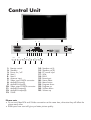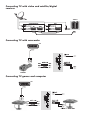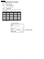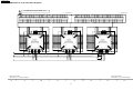
1
P7 PDP TV
SERVICE MANUAL
CONTENTS
PAGES
Safety Instuctions
2-5
Technical Specification
6-7
User Instruction
8-29
Back Appearance of TV
30
Interconnection Diagram
31
Block Diagram
32
Block Diagram of Power Supply
33
Service Mode
34-35
Data Sheet of important IC’s and parts
36-46
Frequency list of channel
50-52
ATTACHMENT 1:
ATTACHMENT 2:
ATTACHMENT 3:
Panel Service Manual
LG-PDP42V6
Panel Service Manual
Samsung 42” S3
Circuit Diagrams
SAFETY PRECAUTIONS
GENERAL GUIDELINES
1. It is advised to insert an isolation transformer in the
AC supply before servicing a hot chassis.
2. Always use the manufacturer’s replacement safety
components. The critical safety components marked
with
on the schematics diagrams should not be
by other substitutes. Other substitute may create the
electrical shock , fire or other hazards. Take
attention to replace the spacers with the originals.
Furthermore where a short circuit has occurred ,
replace those components that indicate evidence of
overheating.
3. After servicing , see that all the protective devices
such as insulation barriers, insulation papers, shields
and isolation R-C combinations are correctly
installed.
4. When the receiver is not being used for a long time
of period of time , unplug the power cord of the
Adaptor from the AC outlet.
PDP Module is very sensitive
both electrically and physically.Users,
therefore, are requested to follow the
“Guidance of handling color PDP
Module”on the followings.
1 -Be careful not to make scratch on the
polarizer.
Surface of polarizer is soft and can be physically
damaged easily.Please do not touch, push or rub
polarizer surface with materials over HB hardness.
2 - Keep clean the surface.
Please wear rubber glove when touch the surface of
PDP screen. Please use soft and anti-static material
as cleaner.
3 -Keep out of water.Water on/in the PDP may
cause electrical short or corrosion. Please wipe out
dry or water carefully.
4 -Prevent swift Temperature & Humidity
change.Instantaneous temperature and/or humidity
change can make dew or ice which cause
nonconformance such as malfunction.
5 - High temperature & high humidity
reduce the life-time.
PDP is not proper to be used at high temperature
and high humidity. Please keep specified
temperature and humidity condition.
6 - Keep out of Corrosive Gas.Corrosive gas
effect the polarizer and the circuit chemically and
cause defects accordingly.
7 - Electrostatic discharge can make
Damage
There are electro-static sensitive components
in PDP Module. Please earth human
body when handle the PDP.In addition, please do
not touch the interface connector pin with bare.
8 - Do not operate for a long time under
the same pattern
Operating PDP for a long time under the same
pattern can cause image persistence and can
damage it. Please follow following guidance.
1. Turn the power off when do not use.
2. Change the pattern periodically.
LEAKAGE CURRENT COLD CHECK
1. Unplug the AC cord and connect a jumper
between the two prongs of the plug.
2. Turn the receiver’s power switch.
3. Measure the resistance value with an ohmmeter,
between the jumpered AC plug and each exposed
metallic cabinet part on the receiver. When the exposed
metallic part a return path to the chassis the reading
should be between 4Mohm and the 20Mohm. When the
exposed metal does not have a return path to the chassis,
the reading must be infinite.
LEAKAGE CURRENT HOT CHECK
1. Plug the AC cord directly in to the AC outlet. Do
not use an isolation transformer for this check.
2. Connect a 2Kohm 10W resistor in series with an
3.
4.
5.
6.
exposed metallic part on the receiver and an earth,
such as a water pipe.
Use an AC voltmeter with high impedance to
measure the potential across the resistor.
Check each exposed metallic part and check the
voltage at the each point.
Reverse the AC plug at the outlet and repeat each of
the above measurements.
The potential at the any point should not exceed 1.4
Vrms. In case a measurement is outside the limits
specified , there is the possibility of a shock hazard ,
and the receiver should be repaired and rechecked
before it is returned to the customer.
HOT CHECK CIRCUIT
AC-Voltmeter
TO INSTRUMENTS
EXPOSED
Water pipe
(earth)
METALLIC PARTS
2 K Ohm
Important information
Read and heed the notes on safety so that no hazard to your health arises during contractual use. Errors during
installation and connection can damage the device or subsequently related devices.
Always keep the operating instructions within reach. Heed the warnings on the device and in the operating
instructions.
• General reference
Before you connect the plasma display, please carefully
read throught the general notes on safety and the
operating instructions. Only in this manner can you
utilise all functions safely and reliably.
As far as possible, keep the operating instructions
together with the device so that you can use it to look
up information.
Heed the warnings on the device and in the operating
instructions.
Never allow children to utilise electrical devices without
supervision.
• Operation
The plasma TV acquired by you, meets the highest
quality codes and standards to be found in this
business segment. A plasma display consists of a
multitude of so called pixels. One pixel consists
of 3 elements (red, green and blue). Even using
the highest quality control practices during the
manufacture of the displays, it can not be 100 %
excluded that some pixels or pixel elements will
be defective. These defects may appear as
permanent illuminated pixels, non illuminating
pixels or unstable pixels (flickering) respectively.
We therefore ask for your understanding when
we declare that these defects are not covered
under the warranty liability. This is valid insofar
that the sum of all defective pixels or pixel elements
does not exceed 0,01 % of the total amount.
The brightness and contrast of plasma displays
decreases with time.
Plasma displays are phosphor based and under
certain operating conditions, so-called “BurnIn” effect may occur. This is in fact a degrigation
of the phosphor and is a natural process in plasma
technology.
Such operating conditions are:
- static images being displayed for long periods
- continues display of the same background
- use of a non full screen format (e.g. 4:3) for a long
periods.
Once Burn-In has occurred it is normally irreversible.
To avoid or to reduce the Burn-In effect, please
follow the listed recommendations:
- Please use moving images or continuous moving
static images in full screen format (slide show)
during the first 100 hours of operation
- Please use your plasma TV in a full screen format
(16:9)
- In case the plasma display is used as a PC monitor,
please use moving images
- Always switch the screen off, if it is not in use
-
Decrease contrast and brightness as much as
possible
If possible display images with maximum colour
depth and scale
Certain conditions may cause a humming noise in the
displays electonics. This is usually caused by the mains
power supply having different ground wires. One
remedy for solving this problem is to insert a filter
between antenna cable and antenna input. These filters
are available at all specialised trade outlets.
If the plasma display is connected to an external
antenna, it has to be grounded to protect against
electrical hazards and static discharges. The grounding
must conform and be in accordance with the actual
regulations in force.
• Environmental conditions
Never operate the plasma display under
environmental conditions which differ from those
of the technical data. Divergent conditions can lead
to endangerment, fire or breakdown of the device.
Protect the plasma display against moisture. This
pertains to permanent high humidity, the proximity
ta water, water drops and water splashes as well
as rain. Do not place any water-filled containers
(e.g. vases) on the device.
Protect the device against heat. Avoid the proximity,
to fire, heating devices, ovens or permanent exposure
to direct sunlight.
Protect the display against heat accumulation. Do
not cover the ventilation slots. Maintain a distance
of at least 10 cm above and below the ventilation
from sides 4 cm from rear 4 cm slots as well as
laterally to furniture and to the ceiling. Do not furnish
the device with curtains.
The display is designed for mounting in landscape
format on walls or installations.
• Mains connection
The mains input and the mains switch are located
on the rear side. The mains input is located on the
upper right and the mains switch is placed in the
upper middle. For safe disconnection of the display
from the mains voltage, the mains switch is to be
turned off and the mains cable is to be removed
from the mains input module.
Connect the plasma display only to a socket with
earthing contacts installed according to regulations,
and whose main voltage conforms with the device’s
technical data. See to it that the mains plug and
the socket are accessible at all times. Install the
mains cable in such a fashion that nobody can get
caught in it. Use only the supplied mains cable.
Protect it against damages, and do not make any
alterations to it. Never use a damaged mains cable.
• Signal inputs
Always turn the plasma display and the signal
source off before you establish a connection between
both devices.
• Disturbances
In the event of damages to the mains cable or the
device, immediately pull the mains plug from the
socket.
Under no circumstances should you attempt to open
and/or to repair the device yourself. Instead,
contact our Service Hotline or another suitable
professional workshop.
• Batteries
Batteries can be life-threatening when swallowed.
That’s why you should safeguard batteries from
the reach of small children. Immediate medical
assistance should be utilised if a battery has been
swallowed.
Always take the exhausted batteries out of the
remote control immediately, since these leak and
can cause damage as a result.
The enclosed batteries may not be charged or
reactivated by other means, not taken apart, thrown
in fire or short-circuited.
TO FULLY DISCONNECT THE TV, SWITCH OFF
THE MAINS SOCKET AND REMOVE THE
POWER PLUG.
Exhausted batteries do not belong in household
waste. The batteries must be disposed of at the
collection points provided for this purpose.
• Cleaning and maintenance
Before cleaning, turn the device off, and pull the
mains plug from the socket. Wait a few minutes
so that the capacitors in the device can be
completely discharged.
Use only a slightly dampened, soft cloth for cleaning.
You should avoid chemical solvents and cleaning
agents, because these can damage the surfaces.
• The plasma display generates high voltage internally
for the gas discharge. Turn the device off and pull
the mains plug from the socket during installation,
maintenance and repairs. Wait a few minutes so
that the capacitors in the device can be completely
discharged.
• In case foreign elements such as water, liquids,
metal parts, etc. get into the plasma display, pull
the mains plug out immediately. Never attempt to
touch anything inside the device with any kind of
objects. The danger of an electric shock or accident
exists.
• Pull out the mains plug immediately if smoke,
unpleasant odour or unusual noises are emitted
from the device. Also proceed in the same manner
if the display is no longer able to present an image
after being turned on or during operation. Never
attempt to continue operating the display in this
condition.
• In the event of lengthy absence or during
thunderstorms, pull the mains plug from the socket,
and pull the house antenna socket from the antenna
jack.
• Never plug-in or pull-out the mains plug with wet
hands. Never operate the mains switch with wet
hands.
• Utilise only the supplied mains cable. Protect it
against damages, and do not make any alterations
to it. Never use a damaged mains cable.
• The plasma display has a glass surface. Should
the device be subjected to excessive loading (e.g.
through shock, vibration, bending and heat shock),
the glass surface can break. Do not subject the
glass surface to any pressure or shock. Should the
glass be broken, immediately pull the mains plug
and do not touch the broken glass with bare hands.
• When the plasma display has been switched to
the stand-by mode it is still connected to the mains.
You must switch the mains switch into the 0 position
or pull the mains plug from the socket for complete
disconnection.
• For ergonomic reasons it is recommended to avoid
using red and blue fonts or symbols on dark
backgrounds. Such a display causes poor
readability due to the lower contrast, and
prematurely fatigues the eyes. Therefore, please
use high-contrast displays as much as possible,
e.g. black font on a white background.
• During the connection of external laudspeakers,
pay attention to the loudspeaker output technical
data. In the event of insufficient dimensioning of
the loudspeaker, the loudspeaker and/ or the builtin amplifier can be damaged.
• Packaging and packing resources which are no
longer needed are able to be recycled, and should
always be turned in for recycling.
• Place the carton upright with the underside on firm
ground. You will recognise the top side by the
direction of the arrowheads on the longitudinal
side
• The plasma display may only be mounted on
vertical (plumb) walls by means of the wail
mounting unit. Before beginning the mounting,
make sure that the display is turned off and the
mains cable and signal cable are unplugged.
The backgraund has to be firm and structurally
able to carry a load. Appropriate materials are
to be utilised for varying wall superstructures,
such as wooden walls or hollow-space walls. If
there’s any doubt, contact your responsible sales
or service department.
Important notes on safety!
Your safety and the safety of others is important. Please, therefore, ensure you read the Safety
instructions before you operate this television.
Safety instructions
!
Read all the safety instructions before first use of your TV.
• Position the television so that direct light does not fall on the screen. Excessive light
will cause a washed out effect.
• Position the power supply lead and other leads so that they are not likely to be walked
on or pinched by things placed on or against them.
• Do not place objects filled with liquid such as vase or flower pot near the television.
• Do not expose the TV to dripping or splashing of liquids.
• Do not place naked flame sources such as lighted candles on the TV set.
• Make sure that no naked flame sources, such as lighted candles, are placed on top
of the appliance.
• Do not place the television near heat sources such as radiators, ovens, stoves, etc.
• Do not push, hit or screw the screen of your product.
• The heat built up in the set escapes through ventilation holes, so do not cover the set
by drapes, clothes etc. that may block air circulation. Do not place the television on
carpet or soft furnishings.
• Never let children push anything into the holes or slots on the case.
• Clean the TV Screen using a slightly damp cloth or chamois leather. Never use abrasive
cleaning agents like liquid or aerosol cleaners.
• Remove the mains plug from the socket outlet while cleaning.
• Never apply pressure on the screen when cleaning.
• Never put your screen on hard objects. Your PDP screen may be damaged.
you wish to place the television on a shelf or in a wall unit always ensure there is a
10 • Ifminimum
air gap of 10 cm around the top, sides and rear of the television, to assist
cm
ventilation.
230
• Your TV set is designed to operate with mains voltages 230V AC; 50Hz. Do not connect
your TV set to power sources other than the mains supply.
• If you don't use the television for a long period, please remove the mains plug from wall
socket outlet.
• Your TV set is designed as a CLASS I apparatus, the TV set has to be connected to a
mains socket outlet with a protective earthing connection.
•To fully disconnect the TV, the mains plug is used as a disconnecting device and therefore
shall be readily operable.
PC FORMATS
DOS Modes 640 x 400 and 720 x 400
VGA (640 x 480) @ 50Hz - 90Hz repetition rate
SVGA (800 x 600) @ 50Hz - 90Hz repetition rate
WVGA (848 x 600) @ 50Hz - 90Hz repetition rate
XGA (1024 x 768) @ 50Hz - 90Hz repetition rate
IMAGE FORMATS
4:3, 16:9, auto, zoom, letterbox, subtitle
INPUTS/VIDEO
Mini DIN................Y/C / Hi 8 (PAL, SECAM, NTSC)
Cinch.....................CVBS Video In (PAL, SECAM, NTSC)
SCART 1 ................CVBS, RGB (PAL, SECAM, NTSC)
CVBS output
SCART 2 ................CVBS, RGB (PAL, SECAM, NTSC)
CVBS output
RF Tuner.................VHF/UHF/HYPERBAND for terrestrial
antennas or cable networks (47MHz to 861 MHz)
(PAL, SECAM)
PC
DVI (D)...................VGA/SVGA/WVGA/XGA
Digital (DVI)
AUDIO INPUTS
Y/C (S-Video) - CVBS
SCART 1
SCART 2
PC
OUTPUTS
Cinch.....................L/R Audio Output
loudspeaker............2 x 7W sine @ 4 Ω
Cinch.....................CVBS Output
CONTROL
On-Screen Display Menu .......24 languages
IR remote control
VIDEOTEXT
TOP FLOF...............800 pages of memory
control with special keys on the remote control
OPERATING VOLTAGE RANGE
170V - 240V AC alternating voltage
50Hz
POWER CONSUMPTION
275 W
Special Features
•
•
•
•
•
•
•
•
•
•
•
•
•
•
•
•
•
•
•
•
•
•
•
•
•
•
•
42’’ PDP VGA Panel
852x480 pixels
16,722,216 color (8 byte)
Available for Cable Channels (A decoder may be required)
3000:1 contrast ratio
2x7 W Stereo sound (With detachable speakers)
800-Page Teletext Feature
PIP (Picture in Picture) Feature
Wide angle perspective
SCART socket, AV Socket and external sound system connection
S-VHS and Cinch inputs for S-Video connection
DVI connection
PC connection
AVL – Automatic Volume Limiting
ATS – Automatic Tuning System
Programmed power off
Graphic equalizer
Color Transfer sharpness feature (CTI)
Black-White Transfer sharpness feature (LTI) and picture sharpness
Compound Filter (Digital Comb Filter) Feature for clear images
On screen viewing of all control commands, program numbers and additional features
Manual Fine Tuning
100 Program memory
Infrared Remote Control
Child lock (this feature works like a Panel Lock)
Ability to watch NTSC broadcasts through SCART input
East handling through an advanced menu system. Abiltiy to choose from 24 languages.
Connection of Mains Cable
Always utilise the enclosed mains cable in order to
guarantee optimal image quality.
First of all, insert the main cable into the input panel,
and only thereafter into the socket.
• Never utilise a damaged mains cable!
• Use only sockets with a protective eathing conductor
system to ensure safe operation.
A line filter and switches for sabilisation of the supply
voltages ensure safe operaion within normal mains
voltage variations. In case the mains voltage lies
beyond the stated limits, please contact your responsible
sales office. In the event the mains cable cannot be
utilised on account of differing standards in your
country, please see to it that you utilise a mains cable
commensurate with the country-specific standards
which are listed in the following:
•
•
•
•
•
•
USA
Germany
Canada
Switzerland
Great Britain
Japan
UL
VDE
CSA
SEV
BASE/BS
MITI
This list is not complete. For reasons of safety it may
be necessary to select a different safety standard.
At any rate, the mains cable has to consist of three
wire conductors of at least 10A/0.75 mm2 in order
to avoid an accident as a result of electric shock. One
of the three wires is impemented on both ends of the
cable as an earthing contact connection.
Turning On the Plasma Display
You can only control your plasma display with the
remote control when the device is in stand-by mode.
Switch the mains switch in the input panel into Position I.
The operational display on the front side of the display
screen lights up red.
• Press a numeric button or the Program
Up / Program Down button on the
remote handset or PR+ / PR- or MENU
button on the front panel of the TV to
switch the TV on. The standby indicator
turns into green. The picture will appear
after a few seconds.
Press the Standby button to switch the
TV to standby. The standby indicator turns
into red.
• The plasma display is always connected to the
power supply network in stand-by mode. You must
switch the mains switch into position 0 and pull the
mains plug from the socket for complete disconnection.
• Display has a mains adapter, and can be operated
with a supply voltage of 230V AC and 50HZ.
Note 1: Your TV will go to stand-by mode in five
minutes if there is no broadcast signal.
Note 2: Your TV is equiped to operate with front
panel buttons, “MENU”, “SOURCE”, “ PROG ”,
“ VOL ” in case your R/C is broken or the
batteries are exhausted.
The batteries
Remove the back cover to reveal the battery
compartment and make sure you insert the batteries
the right way round.
Suitable battery types for this remote are UM-4, IEC
R03 or AAA 1.5V.
Do not combine a used, old battery with a new one
or mix battery types.
The performance of the remote control will deteriorate
beyond a distance of 8 metres or outside an angel
of 30 degrees from the centre of the TV.
Operating Modes
Operating mode at the beginning of utilisation
Due to the functionality of the Plasma-TV please pay
attention, that particularly during the first 100 to 150
operation hours the display has to operate with a full
screen format adjustment (see submenu Display, Picture
Format). This prevents the formation of brightness
differences in the display areas. As an alternative to
the picture format 4:3 the adjustment Video NLS should
be selected.
Further on, in order to prevent the formation of permanent
shadows in the displayed image, please avoid to show
fixed-images of any kind (PC mode, teletext pages,
Photo CD image etc.) during the first operation hours.
If the Plasma-TV will be used as a PC monitor, the
utilisation of a screensaver is recommended.
PC mode
For optimal image reproduction, we recommend the
848 x 480, 640 x 480 or 720 x 400 pixel resolutions.
The 848 x 480 pixel resolution corresponds to the
display matrix, and offers the best image reproduction.
You can obtain the driver for this resolution on the
Internet pages of mont of the well-know manufacturers
of graphics cards.
In contrast to applications with CRT monitors, with flat
displays it is not necessary to select a high image
refresh for a flicker-free presentation. A refresh of
60Hz is recommended.
Video recorder mode
The utilisation of Y/C (S-Video) inputs is recommended
for enhancement of image quality - if your recorder
offers playback in Y/C (S-Video) format.
DVD player mode
The application of the RGB operating mode, which
can be connected to the SCART 1 input, is
recommended for optimal utilisation. In case your
player does not offer this operating mode, please use
the Y/C (S Video) signal mode.
Image sticking
The manufacturer would like to point out to you that
during lengthy viewing of freeze pictures (e.g. PC
playback), the image is still slightly visible in the full
mask for a few minutes during the subsequent playback
of a different source. This is known as “image sticking”
This “vanishing” residual image is caused by the
system, and does not represent a flaw. Therefore it
can not be considered as a case for warranty claim.
Video cable
A high-quality 75Ω coaxial cable should be utilised
for the connection of the video signal. Poor quality
signal cable can result in strong disturbances and
formation of shadows in the displayed image, as well
as exceeding the permissible EMC level. The
mechanical interlocks of the individual plug-and-socket
connectors are necessary for perfect and safe operation
of the device.
Control Unit
14
5
SCART - 2
AV IN
4
1.
2.
3.
4.
5.
6.
7.
8.
9.
10.
11.
12.
13.
MENU
20
21
12
SPEAKER OUT
SCART - 1
SOURCE
15
ANT
VIDEO
L
R
6
7
8
9
VIDEO
22
R
13
PC
AUDIO IN
VGA
PC DVI - D
16
17
18
19
VOL
23
24
Remote control
Stand-by
Power on / off
Scart 1
Scart 2
Antenna input
Video input CINCH connector
Audio RCA input (L)
Audio RCA input (R)
Video output CINCH connector
Audio RCA output (L)
Audio RCA output (R)
L
10 11 12
PROG
3
SVHS
AV OUT
25
14.
15.
16.
17.
18.
19.
20.
21.
22.
23.
24.
25.
Speaker out (L)
Speaker out (R)
PC sound input
VGA
DVI-D
Power Input
Source Select
Menu button
Program down
Program up
Volume down
Volume up
S-VHS
Please note
• Do not use Video RCA and S-Video connections at the same time, otherwise they will effect the
picture each other.
• RGB inputs from scart will give you better picture quality.
Remote control
1
2
23
24
3
4
25
5
26
27
6
28
7
16
18
8
29
9
30
10
11
31
12
32
13
14
15
33
17
34
19
35
20
21
22
36
1. Picture Format choice button ( )
2. Temporary sound mute button ( )
3. Equalizer selection button ( )
4. PIP Position choice button
5. PIP/PAP On-Off button
6. AV modes select button
7. Numeric buttons
8. ZOOM mode choice button
9. Program down button (
)
10. Upward movement ( ) (Menu)
11. Volume down button ( )
12. Left movement ( ) (Menu)
13. Confirmation and Temporary
picture freezing button (Freeze) ( )
14. Info / Txt index page button ( )
15. Down button ( ) (Menu)
16. Txt Question/Answer button (Reveal) ( )
17. Red Fastext Button ( )
18. Teletext enlarge button (Double) ( )
19. Blue Teletext Button ( )
20. Teletext / Mix choice buttons ( )
21. UPDATE Button ( )
22. Yellow teletext Button ( )
23. Stand-by On/Off button ( )
24. Picture mode choice button ( )
25. PAT (Picture and Teletext) Mode
On-Off button
26. PIP size button
27. PC mode input button
28. TV mode input button
29. Return to Selected Program Button (SWAP) (
30. Program Up button (
)
31. Volume Up button ( )
32. Right button ( ) (Menu)
33. MENU button
34. Txt Stop Button (Hold) ( )
35. Green teletext button ( )
36. SUB PAGE Button ( )
)
Using the TV
Turning on for the first time and Tuning
TV controls
Temporary On-Off (STAND-BY)
Programme selection
Press the (
)/(
) buttons on your
remote control, or by selecting a numeric
button in order to get the desired channel
on your television. In order to select a
program whose number is greater than
9, you can use the numeric buttons,
punching in the desired numbers as
required. For example, to select program
12, press the numeric buttons 1 and 2
one after another.
When you press the red ( ) stand-by
button (temporary on-off function) located
on the upper right hand side of your
remote control of your television when
it is switched on;
indicator of your television will light red.
To switch your television back on, either
press the same button, any of the number
)/(
) buttons.
buttons or one of the (
Caution!
If you are not going to use your television
for a long period of time, make sure to
switch it off from the main power button.
There are certain settings which you must make
when setting up the television.
When you first switch it on, the Language menu
appears.
1. Select the menu language by pressing ( ) or
( ).
2. Select Country with ( ) or ( ) and then select
the country where you are located with ( ) or
( ).
3. Select Station search with ( ) or ( ) and press
( ) to start the search.
• The automatic station search starts. This may last
a minute or longer, depending on the number
of television stations received.
• After the search, the station list appears.
You can delete any stations which have been
saved more than once. You can also move stations
to a different preset position, and change or
enter the station names.
Mute
To temporarily mute the sound of your
television, press the ( ) button, where
the ( ) on screen display will appear
on screen as an indication of the
application.
When you press the same button again, the
sound will return. During mute, when you press
the ( ) button the volume will decrease and
automatically get out of the mute function, if you
press the ( ) button the volume will increase
and automatically get out of the mute function.
Return to Selected Button
Program (SWAP)
If you wish to return to the previous
program that you were watching then
you have the ability to return with a
single function, by pressing the ( )
button. Regardless of whether you are
in AV, or any other program, by using
the SWAP function allows you to swap
between the program you were
watching and the last selected program. If you
hit the same button again, you will return to the
program or AV you were watching before.
PR 01
PR 11
PR 01
Control Menu
Press the ( ) button. You will see the
MENU with all the headings of the
different controls on screen. The Right/left
buttons ( )/( ) enable you to move
between the different control menu title where
you can indicate your choice by pressing the
( ) or Up/down ( )/( ) button.
In the event that you wish to exit the application
at any given stage, simply press the MENU or
TV button.
Tuning the television
You can either tune the programs automatically
or manually storing them in your television.
Please Note
In the case that your television does not receive
any broadcast signals for 5 minutes it will
automatically go on stand-by. The 5 minute
countdown OSD will be on screen.
Automatic tuning and storing of
the television program channels
with ATS
The ATS (Automatic Tuning System) on your
television enables the automatic finding and
sequencing of channels.
Sequencing is done according to the selected
country channels, which broadcast Teletext and
channel names; followed by all channels with
Teletexts without channel names and then by
channels without Teletext, to be concluded by
foreign channels broadcasting Teletext with
channel names.
Press the ( ) button Press the right move
button ( ) to select the Adjustment menu.
You can reach this menu directly by
pressing the Blue ( ) button. Using the
Up/down ( )/( ) buttons select the
ATS line and press the ( ) button, the
screen will show the ATS menu. At the
Country line select the country you want
to watch by using the Right-left ( )/( )
buttons.
Afterwards press the down ( ) button
to select the autoprogram heading and
press the ( ) or the Right/left ( )/( )
buttons. The screen will show a warning
before the Automatic Tuning.
To start Autoprogram press the ( )
button; the channels will be searched
automatically and those with broadcasting will
be saved from the first program into memory.At
this point, the autoprogram warning menu
appears showing an indicator that displays the
present situation of the Automatic Tuning process.
To stop the process at any given time, press the
( ) button.
After the automatic search the screen will show
the Program Table. The program numbers that
have been stored are reflected in the Program
Table, giving you the ability to assign any
program number to the channel of your choice.
To quit the station list, press the ( ) button.
Manual tuning and storing of the
television channels
If you already know the Channel
number
Press the ( ) button. Press the right move
button to select the Adjustment menu.
You can reach this menu directly by
pressing the ( ) button.
Using the Up/down ( )/( ) buttons
select the Set-Up line and press the ( )
button, the screen will show the Set-Up
menu. Select the program you want to
Set-Up by using the Right-left ( )/( )
buttons or the numeric keys. Choose
the system in which do a search among
the system lines.
Enter the System line using the down
button( ).Here your TV can be set to
one system, you can also select from
( )/( ) more than one systems. Move
to the Band line using the down button
( ). Using the right-left ( )/( ) buttons
on your remote control select “C” for
the cable channels received through the
“S” antena.
Using the Up ( ) button select the Channel line
and enter the channel number by using the
numeric keypad or right-left buttons. If the channel
on screen is in the quality you desire and you
want to store it into memory, select the Saving
line with the down ( ) button.
Afterwards press the ( ) button, after a moment
you will see a Stored sign. The channel will be
stored according to the program number of your
choice. In order to store other channels, simply
repeat the above process. In the event that you
wish to exit the Channel Settings, simply press
the ( ) button
If you do not know the Channel
number
Press the ( ) button. Press the right move
( ) button to select the Adjustment
menu.
You can reach this menu directly by
pressing the ( ) button.Using the
Up/down ( )/( ) buttons select the
Set-Up line and press the ( ) button, the
screen will show the Set-Up menu.
Select the program you want to Set-Up
by using the Right-left ( )/( ) buttons or
the numeric keys. Choose the system in
which to do a search among the system
lines. Enter the System line using the
down button( ).Here your TV can be
set to one system, you can also select
from ( )/( ) more than one systems.
(option) Move to the Band line using the down
button ( ).
Fine tuning
If the current channel requires fine tuning,
select the Manual Fine Tuning bar by
using the down ( ) button in the
Manual Tuning menu. Using the rightleft movement ( )/( ) buttons on your
remote control you will have the ability
to get the exact quality of tuning
required. Under normal conditions you
will not need Fine Tuning. Your television
will automatically lock channels, which
need AFC values. However, in the event
that the TV transmitters do not work,
then you may need to use this process. For
storing the settings to the memory press ( )
button.
Using the right-left ( )/( ) buttons on your remote
control select “C” for the cable channels received
through the “S” antena. Use the down ( ) button
to select the Search line, and scan the channels
using the right ( ) button to increase and the
left ( ) button to decrease. Select the Saving
line if you found the channel in the quality you
desire.
Afterwards press the ( ) button to store into
memory. For the other channels using the Program
No line, select the program numbers you want
and repeat the same process.
If you want to Fine Tune or name the channel
you found, please refer to the concerning sections.
ENGLISH -18-
Program Table
Press the ( ) button. Press the right move
button to select the Adjustment menu.
You can reach this menu direclty by
pressing the ( ) button. The screen will
show the program table when you select
the program table line with Up/down
( )/( ) and press the ( ) button.
Switching the locations of the
program channels that have
already been stored
Select the program you want to switch
by using the Up-down ( )/( ) or Rightleft ( )/( ) button. Press the Green ( )
colored button.
number and name will appear green.
Using the Up-down ( )/( ) or Rightleft ( )/( ) buttons carry it to other
program location you want to switch.
To finish the switching press the Green
( ) button. The first channel program
number indicated can be moved to the
second channel program number, which
in turn moves the initial channel program
number that has been indicated.
Deleting a program that has been
stored
Select the program you want to delete
by using the Up-down ( )/( ) button
or Right-left ( )/( ) button. Press the
Blue ( ) colored button. The screen will
show the confirmation menu. You can
press the Green ( ) button to delete or
the Red ( ) button to exit the menu.
When you press the Green ( ) button,
the selected channel will be deleted and
all following channels will move up in
their position accordingly.
Skipping a program that has been
stored
In the event that you do not wish to come
across certain programs while going up
and down between channels using the
)/(
) buttons, then you can use
(
the following function. Select the program
to be stored by using the Up-down
( )/( ) button or Right-left ( )/( )
button. Press the Red ( ) colored button.
To the right of the name of the program
to be skipped will appear the letter “S”
in red. You have the option of applying
this method on more than one program
channel.
In order to see the program numbers
that are to be skipped, write down the
number of the concealed program
directly. To cancel the program skipping
function press the Red ( ) button again.
The red “S” to the right of the program name
will disappear, an the skipping will be cancelled.
To name the programs
The programs in the table might show the channel
names automatically with ATS, but could also
show the channel number instead of the name.
You can name any or all of the programs
with names that have a maximum of
five characters.
Select the program you want to name
using the Up-down ( )/( ) or Rightleft ( )/( ) buttons.Press the Yellow ( )
button. The screen will show the number,
volume type and name information for
the channel you want to name. Using
the Up-down ( )/( ) buttons to select
the desired letter, number or sign.
the second letter use the Right-left ( )/( )
button and again use the Up-down
( )/( ) buttons to select the desired
letter, number or sign. After entering all
the letters press the ( ) button to store
the name.
To write names for any of the other programs,
simply repeat the above procedure. In the event
that you wish to exit the application, simply press
the ( ) button.
If no name is enter for any program, the program
number will be automatically displayed.
The setup of your television:
Setting up the Sound Menu
You can set the volume with the “ VOL+” and
“VOL -“ buttons on the television or the ( ) , ( )
buttons on the remote control.
You can control the other sound settings by
entering the Sound menu For this application all
you need to do is press the ( ) button of your
remote control. Select the Sound menu with the
direction ( ) button. You can reach this menu
directly by pressing the Red ( ) button. Select
the functions from the headings in this menu.
Effect: If you want to add depth to the sound of
the program you watch, select Spatial with the
( ) button.
Television transmitters have different sound levels.
This can be noticed from the different volume
levels that can be heard while switching from one
program to another. Using the right/left movement
( )/( ) buttons switch to Open. The AVL
(Automatic Volume Limiting) function maintains
the same sound level as you switch from program
to program. To cancel choose Closed.
Balance: To adjust the volume balance between
the left and right speakers to the desired level,
select the Balance bar using the down ( ) button.
Using the right/left movement ( )/( ) buttons
adjust the balance.
Sound Type: The program you watch might be
stereo or in two different languages. Using the
right/left keys ( )/( ) in this menu you can select
Mono/Stereo or Dual-I/Dual-II language.
Equalizer: Selecting the Equalizer mark press
( ) or ( ) button. The equalizer setting function
will be displayed. You can selected with the
right/left ( / ) buttons, pre-programed,
unchangeable sound enhancing Music, Sport,
Cinema and Speech, User settings for the
programs you are watching. These can be adjusted
by you in the User selection. To adjust the User
selection; select the User selection and press the
( ) button.You can adjust the frequency levels
with the ( ) and ( ) buttons. You can select
120Hz, 500Hz, 1.5KHz, 5KHz and 10KHz
frequency bands with ( ) and ( ) buttons. Storing
the adjustment levels in memory press the menu
button to exit the user option.
You can exit the equalizer function pressing
the( )button again.
Please note: You can choose the equalizer
position directly from the ( ) button of your
remote control.
You can exit the equalizer function pressing the
( ) button at any time.
Picture Setup (Green button)
By pressing the ( ) button on your
remote control please enter the Picture
menu. You can enter this menu directly
by pressing the ( ). Select the setting
function you want using the Up and
down buttons ( )/( ) and adjust their
levels with the right and left
( )/( ).
The picture brightness, contrast, color
and sharpness levels can all be adjusted
according to your desire. The changes
you make in the picture settings will be
automatically stored without any further
transactions necessary being your
Personal settings.
Static Reduction: Using this feature you can
reduce static by selecting Normal, Soft, Softest,
Sharpest and Sharp function.
Smart Picture: This is one of the pre-installed
and unchangeable features, to select
this feature use your ( )/( ) buttons.
Soft, Natural and Rich are constant
values. User are the values you stored
into memory. Furthermore, you can select
one of the non-adjustable default settings in the
memory (Picture Mode) by pressing the “ “
button on your remote control.
Picture Format: This feature enables you to
watch any broadcast image in the format
you desire. These are; Auto, 16:9
Subtitle, Letterbox, 4:3 and Zoom. You
can do the selection without entering
the picture menu by using the ” “
format selection button.
Color Tint: When NTSC video is used in SCART,
Color Tint settings can be made. If you do not
use such a video type the Color Tint choice is
not seen in the menu. If NTSC video is used in
SCART this choice becomes active and can be
seen in the menu.
Depending on the type of broadcast being
transmitted, programmes can be viewed in a
number of formats. Press the ” “ button
repeatedly to select between Zoom, Letterbox,
Subtitle, Auto, 16:9, and 4:3.
Please note: Whenever the MENU button is
pressed the picture size setting will change while
the menus are ON the screen. This is to ensure
that the menus do not overlap the edges of the
viewable area.
Zoom
This setting will entarge the image
to fit the screen by streching the
image horizontally, holding the
correct proportions at the centre
of the image. Some distrotion may
occur.
Letterbox
Use this setting when watching a
widescreen DVD, widescreen video
tape or a 16:9 broadcast (when
available). Due to the range of
widescreen formats (16:9, 14:9,
20:9 etc.) black bars may be
visible on the top and bottom of
the screen. Letterbox format
removes blck bars or makes it much
less visible.
Subtitle
When subtitles are included on a
letterbox format broadcast, this
setting will raise the picture to
ensure that all the text is displayed.
Auto
Some channels may send
automatic screen formatting. If you
wish to swich automatically to this
format select Auto.
The TV will outomatically switch
to detected format from the scart
inputs.
16:9
Use this setting when wathching
a widescreen DVD, widescreen
video tape or a 16:9 broadcast
(when available). Due to tre range
of widescreen formats (16:9,
14:9, 20:9 etc.) black bars may
be visible on the top and bottom
of the screen.
4:3
Use this setting to view a trie 4:3
broadcast.
Using the special functions to change the size of the
displayed image (i.e. changing the height/width ratio) for
the purposes of public display or commercial gain may
infringe on copyright laws.
Features Menu (Yellow Button)
Press the ( ) button on your remote
control. Select the Function menu line
with the ( ) button.
You can reach this menu directly by
pressing the Yellow ( ) button. You
can select the headings you want to
adjust in this menu by using the
Up/down ( )/( ) buttons.
Stand-by Control: Your television features an
automatic stand-by feature which can be enabled
between 15 and 120 minutes. If you
want your television to autmatically go
into stand-by, please select the Standby Control line. Select the desired
duration with the Right ( ) and left ( )
button.
At the end of the choosen duration the
screen will show a 30 second countdown
before switching off the screen and
entering into stand-by. To cancel the
automatic stand-by select “0” at the Stand-by
Control.
VCR mode: Using this feature you can avoid
image distortions from the device or the magnetic
tape while watching. For this you have to swtich
the VCR mode to ON.
Child Lock: If you switch this feature On, the
buttons on the TV will not work when the TV is
in Stand-by mode or on and screen will show
a Child Lock warning.
Language: Select the menu language line and
press ( ) or the right ( ) button. The
screen will show the menu languages.
Select the desired language using the
Up-down ( )/( ) and Right-left ( )/( )
buttons. Press the ( ) button again. Your
television will now feature the language
you have choosen for all the adjustment
indicators.
Menu Background: Using this feature you
can adjust the background of the viewable menus
and other OSDs as Transparent or Opaque.
Please note: This feature is only active for the
AV inputs. This feature will not be seen in Function
menu while watching programs or in PC mode.
This feature becomes automatically active in the
”0” numbered program.When you store the “0”
numbered channel as video device antena output,
you will be able to avoid image distortions from
the device or the magnetic tape while watching.
ZOOM: To activate this feature you have to
press the ( ) button on your remote
control while watching a program.
When you enter this menu you will see
in the lower right corner of the screen
the Zoom sub-menu. Using the Up/down
( )/( ) buttons you can enlarge or
shrink the image in 16 steps. During the
Zoom process the image will be enlarge
focused on the center.
want to move the image up/down or
right/left ( )/( ) press the ( ) button
on your remote.
buttons to move around.
In the event that you wish to exit the
Zoom menu, simply press the ( ) button.
Please Note: The Zoom function is not
available during PIP.
FREEZE: This feature enables you to freeze the
image of a program you are watching.
For this use the ( ) button on your remote
control, make sure you don’t have any
menus on screen. The image will be
frozen until you press the button the
second time.
Please Note: The Freeze function is not
available during PIP.
PIP Size
This feature enables you to resize your
PIP window. For this press the ( ) button,
while having PIP on screen, to bring the
PIP Size menu on screen.
Press the right/left ( )/( ) buttons to
make the PIP Size selection. After resizing your
PIP window you can exit the menu by pressing
the ( ) button on the remote control.
PAT Mode
While watching TV you can enter the
PAT (Picture and Teletext) mode by
pressing the ( ) button on your remote
control. This feature enables you to read
the program’s teletext, if available, while
watching the very same program.
To exit this mode press the ( ) button on your
remote control again.
In this menu select either Picture in Picture (PIP)
or Divided Screen (PAP) and press the ( ) button.
According to the selection a picture will open in
main picture and will position itself in the lower
screen.
If you choose Full Screen mode PIP will go out.
In the event that you wish to exit PIP mode, simply
press the “ ” button.
Note:
1) From the program you are watching or from
AV mode, you can open the PIP window, and
change the other programs through the main
image.
2) You can use PIP in PC or DVI mode.
3) The same AV input cannot be watched with
PIP and the main image.
PIP Position
This feature enables you to position your
PIP window. For this press the ( ) button,
while having PIP on screen, to bring the
PIP Position menu on screen.
Press the right/left ( )/( ) buttons to
make the PIP Position selection. After you
positioned your PIP window you can exit the
menu by pressing the ( ) button on the remote
control.
Teletext
Mode
Using Teletext
TV/Text mix
To view a TV programme whilst in text
mode, press the ( ) button. The text
will be superimposed over the TV
programme.
Teletext is an information system that displays
text on your TV screen. Using the teletext control
buttons you can view pages of information that
are listed in the teletext index.
Press the ( ) button again to return to
the channel you are watching.
Please Note
No on screen display is available in text mode.
The contrast, brightness and colour cannot be
changed but the volume control is still available.
Page search whilst watching TV
In Text mode press the ( ) button. The
TV will return to TV mode with the text
page number in the top left hand corner
of the screen.
To enter Text mode
Please Note
Make sure the TV channel you are watching
transmits teletext.
Press the ( ) button. The text page will
appear, normally the index page.
To exit Text mode
Press the ( ) button. The screen will
return to the channel you were watching.
To select a page of text
0
9
0
9
Enter the page number you want using
the Numeric buttons.
The top line of the text page will appear
whilst the text searches for your page.
When the page is found the number will
remain in the top left hand corner of the
screen.
Press the ( ) button to view your selected
page of text.
Double height text
Find the number of the page in the index
and enter it using the Numeric buttons.
The number of the page will appear in
the top left hand corner of the screen.
If you have difficulty reading the
text on the TV you can double the height
of the text.
The page counter will search for your
page. When it finds it, the page will be
displayed.
Press the ( ) button. The top half of the
page will be displayed in double height
text.
To move to the next page of text press
)/( ) button.
the (
Press the ( ) button again. The bottom
half of the page will be displayed in
double height text.
To move to the previous page press the
)/( ) button.
(
To return to the index page press the
( ) button.
Press the ( ) button again to return to
the full page.
Page Stop
To reveal information
Press the ( ) button to reveal concealed
information (quiz answers etc.).
If the page of text you have selected
contains sub pages, these sub pages
will automatically be displayed in order
with a delay to allow you to read the
page.
To stop the move to the next sub page
press the ( ) button.
To continue moving through the sub
pages press the ( ) button again.
Press the ( ) button again to cancel
the information again.
Clock
Press the ( ) button, whilst watching a
TV program , to display the time.
To select a sub page
If the page of text you are viewing
contains sub pages, the number of the
sub page you are on and the total
number of sub pages is displayed on
the right of the screen i.e. 1/7.
To select a sub page press the ( )
button. Press the green button to select
next sub-page or press the red button
to select the previous sub-page.
5
Enter the number of the sub page, using
the Numeric buttons in the format S0001
for sub page 1.
The teletext will search for the sub
page. This may take some time. To
return to the TV whilst the teletext is
searching press the ( ) button.
When the page number is found it will
appear in the top left hand corner of
the screen.
Press the ( ) button again to view the
text page.
Fastext
At the bottom of the teletext screen is a row of
subject headings in red, green yellow and blue.
The remote control has a row of coloured buttons
corresponding to the row of coloured subjects
on the screen.
Pressing one of the coloured buttons will take
you directly to the page corresponding to the
subject heading.
Connecting external equipment
AV Inputs:
Press the ( ) button on your remote control. You
will enter the Source menu from where you can
elect the screen input mode. Here select the input
you desire.
TV: To move to TV mode while in AV modes,
move on to the selection and press the ( )
button.
Scart1: To be able to view the broadcasting
images form the device connected to Scart1,
move on to the selection and press the ( )
button. (If the connected device has an RGB
output, you will be able to watch it over Scart.)
Scart2: To be able to view the broadcasting
images form the device connected to Scart2,
move on to the selection and press the ( )
button. (If the connected device has an RGB
output, you will be able to watch it over Scart.)
SVHS: To be able to view the images form the
device connected to the S-Video input, move on
to the selection and press the ( ) button.
AV: To be able to view the images form the
device connected to the RCA (Chinch) input,
move on to the selection and press the ( ) button.
PC: To be able to view monitor images in PC
mode, move on to the selection and press the
( ) button.
DVI: To be able to view images in DVI mode,
move on to the selection and press the ( ) button.
Connecting a video recorder
Via SCART
Make sure the TV and video recorder are both
switched off.
Plug one end of the SCART lead (not supplied)
into the back of the video recorder and the other
end into one of the SCART sockets on the back
of the TV.
Switch on the video recorder and the TV.
Press the ( ) button on the remote
control to select SCART1 or SCART2 to
correspond with the SCART socket you
are using on the back of the TV.
Please note: You can connect RGB external
equipment via Scart. It is necessary to you use
a full Scart cable for this purpose.
Select the video output of the external device
by using its menu, and set to RGB.
Via RCA lead (optional)
Make sure the TV and video recorder are both
switched off.
Plug one end of the RCA lead into the video and
audio out sockets on the back of the video
recorder and plug the other end into the video
and audio in sockets of the TV.
If the sound is mono, use the Audio Input L. and
in the SOUND menu select the MONO feature.
Via aerial socket
Make sure the TV and video recorder are both
switched off.
Unplug the aerial lead form the TV and plug
it into the aerial socket on the video
recorder.
Via RCA lead and S-Video socket
You can also connect it through the
S-Video socket of the TV.
Plug the S-Video plug into the S-Video socket
and the audio leads into the audio sockets.
Plug a coaxial plug into the RF out socket on
the rear of the video recorder and plug the
other end into the aerial socket on the TV.
Switch on the video recorder and the TV. If
your video recorder has a test signal, switch
it on. (Refer to the video recorder user guide).
L
R
Audio In (R)
VIDEO
L
Audio In (L)
AV IN
SPEAKER OUT
VIDEO
AV OUT
R
SVHS
See ‘Tuning the TV’ and carry out the tuning
procedure for the video recorder test signal.
Select a programme number 0.
Video In
SCART - 2
SPEAKER OUT
AV IN
SVHS
AV OUT
ANT
SCART - 1
SCART - 1
SVHS
SCART - 2
ANT
L
R
L
ANT
SCART - 1
SCART - 2
Audio In (R)
Audio In (L)
VIDEO
AV IN
SPEAKER OUT
VIDEO
AV OUT
R
S-Video In
VIDEO
L
R
VIDEO
L
R
Connecting a DVD player
Via RCA lead
Make sure the TV and DVD player are both
switched off.
Via SCART
Make sure the TV and DVD player are both
switched off.
Plug one end of the SCART lead (not supplied)
into the back of the DVD player and the other
end into the SCART socket on the back of the
TV.
Switch on the DVD and the TV.
Plug one end of the RCA lead into the video and
audio out sockets on the back of the DVD player
and plug the other end into the video and audio
in sockets of the TV.
Via RCA lead and S-Video socket
You can also connect it through the S-Video
socket of the TV.
L
R
Audio In (R)
VIDEO
L
Audio In (L)
AV IN
SPEAKER OUT
VIDEO
AV OUT
R
SVHS
Plug the S-Video plug into the S-Video socket
and the audio leads into the audio sockets.
Video In
SCART - 2
SPEAKER OUT
AV IN
SVHS
AV OUT
ANT
SCART - 1
SCART - 1
SVHS
SCART - 2
ANT
AV IN
SCART - 1
L
Audio In (R)
R
SPEAKER OUT
SCART - 2
VIDEO
AV OUT
R
S-Video In
ANT
VIDEO
L
Audio In (L)
VIDEO
L
R
VIDEO
L
R
Connecting a decoder
Via SCART
Make sure the TV and decoder are both switched
off.
Plug one end of the SCART lead (not supplied)
into the back of the decoder and the other end
into the SCART on the back of the TV.
Switch on the decoder and the TV.
Press the ( ) button on the remote control
to select SCART1.
Via RCA lead
Make sure the TV and decoder are both switched
off.
Connecting DVI-D
Your TV has DVI-D input socket. You can connect
any device such as PC etc. which has DVI digital
out using the proper cable. At the same time you
can listen to the sound from the connected device.
PC or DVI use a special cable to PC-DVI/AUDIO
IN input at the back of your TV.
AV Outputs
You can connect any device which is proper to
Phono inputs via Phono Video and Audio Outs
at the back of your TV set using proper AV cable
(not available with the set).
Any programme or AV input which is seen on
the main screen other than S-VHS, PC or DVI
(which is option) is available as picture and sound
signals at Phono Video/Audio outs.
Scart sockets at the back of your TV set are always
give the signals of selected programme from the
set Tuner.
L
R
Audio In (R)
Video In
SCART - 2
SPEAKER OUT
SCART - 1
AV IN
SVHS
AV OUT
ANT
VIDEO
L
Audio In (L)
AV IN
SPEAKER OUT
VIDEO
AV OUT
R
SVHS
Note: For Decoder connection Via RCA lead
your Decoder device must have the tuner built
in.
Plug one end of the RCA lead into the video and
audio out sockets on the back of the decoder
and plug the other end into the video and audio
in sockets on the TV.
SCART - 1
SCART - 2
ANT
VIDEO
L
R
VIDEO
L
R
INTRODUCTION
Because your 42” 16:9 PDP-TV equipment is provided with VGA inputs, it may be used as a PC
monitor as well. (Pug&Play)
Connecting PC:
Connect your PC through the D-Sub connector
and an appropiate cable (not inlcuded with your
TV) to PC-IN input the back of the TV.
Again using an appriopiate cable you can
connect your PC sound output to the PC-DVI /
AUDIO IN input on the back of the TV and listen
to sound.
Transition to the PC mode
In order for the PDP to switch to the monitor (PC)
mode, you can press the ( ) button on your
remote control. In order to switch from the PC
mode back to the TV mode, use the ( ) button
on your remote control.
PC Input Settings
You can enter the picture setting menu by pressing
the ( ) or the ( ) while in PC mode. In order to
make the necessary adjustments in this menu,
you can use the right-left, up-down direction
( )/( ) ( )/( ) buttons on your remote control.
Here you can make adjustments to Brilliance
and Contrast as well as other adjustments for
the monitor listed below.
H.Position: Horizontal position setting
V.Position: Vertical position setting
PHASE: Using the Right/left ( )/(
you can adjust color and shape.
) buttons
Picture Format: You can select your PC viewing
image from auto, 4:3 or one-to-one.
You can make your choices without entering the
picture menu by using the format button on your
remote control.
Automatic Configuration: The most suitable
geometric settings in accordance to the entry
mode is configured by this function. For this
application, choice the AUTOMATIC
CONFIGURATION option and press the ( )
button.
In PC mode you are able to use ZOOM and PIP
as mentioned in the sections above.
You can adjust the volume of the device you
connect to the Audio-In input at the back of the
TV by using the ( )/( ) or /( ) buttons.
Transition to the DVI mode
Connect your PC or digital video device using
its connector and an appropriate cable (not
included with your TV) to the DVI input at the
back of your TV.Again using an appriopiate
cable you can connect your PC or sound device
output to the PC-DVI / AUDIO IN input on the
back of the TV and listen to sound.
Please Note: To be able to view images in
DVI mode your computer must have a graphics
card with DVI output.
Adjustments in DVI mode are the same as in PC
mode. However automatic configuration will not
function in this mode.
Connecting TV with video and satellite/digital
receiver
Connecting TV with camcorder
L
R
L
ANT
VIDEO
AV IN
SPEAKER OUT
VIDEO
AV OUT
R
SVHS
AV1
Connecting TV games and computer
L
R
L
VIDEO
ANT
AV IN
SPEAKER OUT
VIDEO
AV OUT
R
SVHS
AV1
Technical specifications table
42” 16:9
Plazma TV
2X7 W
275 W
6W
General technical specifications
Power Supply
AC: ..............................................................................230 V 50 Hz
Number of preset programmes: ..............................100
RF Aerial input:..........................................................75 ohm (unbalanced)
Speaker empedance: ................................................4 ohm
Sound Systems: .........................................................Mono/Stereo/NICAM
Batteries: ....................................................................2xUM-4, IEC R03 or AAA 1.5 V
Receiving channels:...................................................VHF (Band I Channels 2-4)
....................................................................................VHF (Band II Channels 5-12)
....................................................................................UHF (Channels 21-69)
....................................................................................Cable TV (S1-S20/S21-S41)
Receiving Broad system: ..........................................Pal BG
Pal SECAM BG
Pal SECAM BG DK/DK’
Pal SECAM BG LL'
Pal I
L6B Chassis
Power Supply
Panel Power
Supply
Scart
Adaptor
L6B
Chassis
Note: You can find more detailed informations regarding panel and panel modules in the panel
sections of the service manual.
TO PANEL PSU
MAIN CHASSIS
JP452
JP451
CN1
JP453
POWER
SUPPLY
MODULE
S150
SPEAKER
S2
TO
PANEL LOCIG BORD
S550
CN3
CN2
S350
S50
JP450
MAIN POWER
SWITCH
MODULE
TO HEADPHONE JACK
IR RECEIVER/LED
MODULE
KEY BOARD
MODULE
220V AC
INPUT
Video-Main
AV4 Video-In
Video In/Out
SCART 1 2 3
SC1-SC2 RGB
AV Out Audio
AV4
Audio-In
Audio-Switch
TDA6420
Audio
In-Out
Flash Memory
AM29VL160
Video-PIP
Scart RGB
Audio-In/Out
I2C Communication
De-Interlacer
Scaler
OSD
Micro-Cont.
Gamma Corr.
48 Bit RGB VS/HS
Dual İnterface for
FPD
AD9887
RGB HS/VS-In
SVHS Socket
Speaker
TO THE
PANEL
Stand by
LED’s
Reset
Mute
B/L Enable
Digital Dim
EEPROM
24LC21
Headphone
Amp.
TDA1308
PC DVI Audio -In
Progressive
or Intrelaced
24 Bit Dual
RGB ,HS,VS
DE,PCLK
IR In
Audio Amplifier
TA2024
Headphone Jack
PW181
IMAGE
PROCESSOR
16 Bit
YUV
RGB Switch
PI5V30
AUDIO PROCESSOR
MSP3410D
EEPROM
24C64
24 Bit RGB
Video Switch
TDA6415C
Pin 8 Switch
PCF8591
PW1231
De-Interlacer
LVDS Transmitter
DS090C385
PIP-Video
AV-Out Video
QSS-PIP
IF IC TDA9886T
16 Bit
YUV
Multi Standard
Video Decoder
SAA7118MP
Tuner-PIP
SDRAM
MT48LC16M
SVHS Y/C
Tuner-Main
QSS-Main
IF IC TDA9886T
Main-Video
RF In
Multi Standard
Video Decoder
SAA7118MP
L6B BLOCK DIAGRAM
D-SUB 15 socket
EEPROM
24LC21
DVI Input
DVI Socket
L6B POWER SUPPLY BLOCK DIAGRAM (MAIN CHASSIS)
J450
U451
FDS9933A
12V
(5V)
F450
U454
LM2576
+5V_STBY
+2,5V_STBY
U458
NCP1117
DC_IN
GND
F451
VOLTAGE
DOUBLER
S450
12V
'33V
U452
FDS9933N
GND
12V_AMP
PNL_EN
U450
NCP117
+1,5V_STBY
+5V
U457
NCP1117
STAND_BY
U453
FDS9933N
+3,3V_STBY
+12V
+3,3V
U455
LM2576
+12V_INVERTER
U456
LM317
+8V
PANEL_POWER
L6B SERVICE MENU
1. Activating the Service Menu
When the menu is on the screen press ‘9’, ‘3’, ’0’, ’1’ on the remote controller. This will
activate the service menu.
2. Service Menu Structure
The service menu has three items: display, calibre and version
2.1 Display
Display item has seven options:
a- Panel
Panel option gives information about the current panel resolution. It is a read only
option and can not be set.
b- Factory mode
Used during production, keep "off".
c- Scart prescale
Scart prescale option sets the prescale values for the input sounds entering the scart
input of the MSP(Micronas Sound Processor). Changing this value you can adjust
the level of the output sound going to loudspeakers for all the sources except the
Tuners. The range is between 0 and 100.
d- nicam prescale
Nicam prescale option sets the prescale values for the Nicam standard sounds for
tuner inputs. Changing this value you can adjust the level of the output sound
going to loudspeakers for Nicam sounds entering the analog sound input of MSP.
The range is between 0 and 100.
e- fm/am prescale
fm/am prescale option sets the prescale values for the FM/AM standard sounds for
tuner inputs. Changing this value you can adjust the level of the output sound
going to loudspeakers for FM/AM sounds entering the analog sound input of MSP.
The range is between 0 and 100.
f- Agc(Automatic Gain Control) adjust
Agc adjust option sets the input voltage going to IF decoder AGC pin. Changing
this value you can adjust this voltage for optimum Tuner performance. The range
is between 0 and 31.
g- R/G/B Brightness/Contrast: These are used for color bias adjustment. The range is
Between 0 and 255
2.2 Calibre
Calibre item has nine options:
a- video format
Video format option force the video format to the desired format. Selectable
formats are Auto, Pal, NTSC and SECAM.
b- colorspace
Colorspace option gives the information about the video input colorspace input to
PW181 IC. Do not change this value unless an error occurred in the colors
displayed.
c- test pattern
This option activates the internal pattern of PW181 IC. There are 3 choices: none,
vert bars, solid color. None will deactivate the internal pattern. Vert bars choice
activates the bar pattern for the selected color component. Solid color activates the
solid pattern with one color selected in color component and also you can change
the level of the color by solid field level.
d- Color components:
This option selects the color for the internal pattern of PW181 IC. There are 4
choices: all, red, green and blue. If you choose all, you can see the white pattern
and if you choose one of the other choices you can see the test pattern with the
selected color.
e- solid field level
This option will adjust the level of the colors for the test pattern. The range is
betwwen 1 and 64.
f- Initial ATS
This option will enable or disable the Initial setup for the TV. Setting this option to
On, the TV will open from the Quick setup menu. Setting this option to Off will
disable this option.
g- factory reset
Factory reset option executes a reset operation for the NVRAM. Pressing OK
when this option is selected will erase the NVRAM and load default values to
NVRAM.
h- dpms
This option selects the Power option for the TV. Setting this option to On the TV
will switch to the last state for power on transition. Setting this to Off will disable
this option and the TV will always switch to Stand-by state while power on
transition.
i- osd timeout
This option sets the OSD timeout for the main menu structure. Selections are 5, 15
and 60 secs. The default is 60 sec.
(backlight:Not used in this product.
2.3 Version
This item gives the information about the version of the software. Also you can see the
last modified time for the GUI(graphical user interface).
TEA6415C
BUS-CONTROLLED VIDEO MATRIX SWITCH
■
■
■
■
■
■
■
■
■
20MHz BANDWIDTH
CASCADABLE WITH ANOTHER TEA6415C
(INTERNAL ADDRESS CAN BE CHANGED BY
PIN 7 VOLTAGE)
8 INPUTS (CVBS, RGB, MAC, CHROMA, ...)
6 OUTPUTS
POSSIBILITY OF MAC OR CHROMA SIGNAL
FOR EACH INPUT BY SWITCHING-OFF THE
CLAMP WITH AN EXTERNAL RESISTOR
BRIDGE
BUS CONTROLLED
6.5dB GAIN BETWEEN ANY INPUT AND OUTPUT
-55dB CROSSTALK AT 5MHz
FULLY ESD PROTECTED
DIP20
(Plastic Package)
ORDER CODE : TEA6415C
DESCRIPTION
The main function of the TEA6415C is to switch 8
video input sources on the 6 outputs.
Each output can be switched to only one of the
inputs whereas but any same input may be connected to several outputs.
All the switching possibilities are controlled through
the I2C bus.
SO20
(Plastic Micropackage)
ORDER CODE : TEA6415CD
INPUT
1
20
INPUT
DATA
2
19
GROUND
INPUT
3
18
OUTPUT
CLOCK
4
17
OUTPUT
INPUT
5
16
OUTPUT
INPUT
6
15
OUTPUT
PROG
7
14
OUTPUT
INPUT
8
13
OUTPUT
VCC
9
12
GROUND
10
11
INPUT
INPUT
6415C-01.EPS
PIN CONNECTIONS
TEA6415C
BLOCK DIAGRAM
P ERI
TV1
P ERI
TV2
TTX
18
17
16
LUMA PIP
CHROMA
POWER
MAC
DEC.
GND
1
CVBS
(P ERI P LUG1)
3
CVBS
(AM TUNER)
5
MAC S IGNAL
(AMTUNER)
6
CVBS
(P ERI P LUG2)
8
CVBS
(FM TUNER)
10
MAC S IGNAL
(FM TUNER)
11
SYNCHRO
(TTX/BTX)
20
14
13
12
T
E
A
6
4
1
5
C
BUS
DECODER
2
7
4
9
19
DATA
P ROG
CLOCK
VCC
GND
GENERAL DESCRIPTION
The main functionof the IC is to switch 8 video input
sources on 6 outputs.
Each output can be switched on only one of each
input. On each input an alignment of the lowest
level of the signal is made (bottom of synch. top for
CVBS or black level for RGB signals).
Each nominal gain between any input and output
is 6.5dB. For D2MAC or Chroma signal the alignment is switched off by forcing, with an external
resistor bridge, 5 VDC on the input. Each input can
be used as a normal input or as a MAC or Chroma
input (with external resistor bridge). All the switching possibilities are changed through the BUS.
Driving 75Ω load needs an external transistor.
It is possible to have the same input connected to
several outputs.
The starting configuration upon power on (power
supply : 0 to 10V) is undetermined.
In this case, 6 words of 16 bits are necessary to
determine one configuration. In other case, 1 word
of 16 bits is necessary to determine one configuration.
6415C-02.EPS
CVBS
(MAC/DEC)
15
I2C-bus controlled single and multistandard
alignment-free IF-PLL demodulators
1
TDA9885; TDA9886
FEATURES
• 5 V supply voltage
• Gain controlled wide-band Vision Intermediate
Frequency (VIF) amplifier, AC-coupled
• Multistandard true synchronous demodulation with
active carrier regeneration: very linear demodulation,
good intermodulation figures, reduced harmonics, and
excellent pulse response
• Gated phase detector for L and L-accent standard
• SIF-AGC for gain controlled SIF amplifier, single
reference QSS mixer able to operate in high
performance single reference QSS mode and in
intercarrier mode, switchable via I2C-bus
• Fully integrated VIF Voltage Controlled Oscillator
(VCO), alignment-free, frequencies switchable for all
negative and positive modulated standards via I2C-bus
• AM demodulator without extra reference circuit
• Digital acquisition help, VIF frequencies of 33.4, 33.9,
38.0, 38.9, 45.75, and 58.75 MHz
• I2C-bus control for all functions
• 4 MHz reference frequency input: signal from
Phase-Locked Loop (PLL) tuning system or operating
as crystal oscillator
• VIF Automatic Gain Control (AGC) detector for gain
control, operating as peak sync detector for negative
modulated signals and as a peak white detector for
positive modulated signals
• External AGC setting via pin OP1
• Precise fully digital Automatic Frequency Control (AFC)
detector with 4-bit digital-to-analog converter, AFC bits
readable via I2C-bus
• Alignment-free selective FM-PLL demodulator with high
linearity and low noise
• I2C-bus transceiver with pin programmable Module
Address (MAD)
• Four I2C-bus addresses via MAD.
2
GENERAL DESCRIPTION
The TDA9885 is an alignment-free multistandard
(PAL and NTSC) vision and sound IF signal PLL
demodulator for negative modulation only and
FM processing.
• TakeOver Point (TOP) adjustable via I2C-bus or
alternatively with potentiometer
The TDA9886 is an alignment-free multistandard
(PAL, SECAM and NTSC) vision and sound IF signal PLL
demodulator for positive and negative modulation,
including sound AM and FM processing.
• Fully integrated sound carrier trap for 4.5, 5.5, 6.0,
and 6.5 MHz, controlled by FM-PLL oscillator
3
• Sound IF (SIF) input for single reference Quasi Split
Sound (QSS) mode, PLL controlled
4
APPLICATIONS
• TV, VTR, PC and STB applications.
ORDERING INFORMATION
PACKAGE
TYPE NUMBER
NAME
TDA9885T/V3
SO24
TDA9885TS/V3
SSOP24
TDA9885HN/V3
HVQFN32
TDA9886T/V3
TDA9886TS/V3
SO24
SSOP24
DESCRIPTION
plastic small outline package; 24 leads; body width 7.5 mm
VERSION
SOT137-1
plastic shrink small outline package; 24 leads; body width 5.3 mm
SOT340-1
plastic, heatsink very thin quad flat package; no leads; 32 terminals;
body 5 × 5 × 0.85 mm
SOT617-1
plastic small outline package; 24 leads; body width 7.5 mm
SOT137-1
plastic shrink small outline package; 24 leads; body width 5.3 mm
SOT340-1
This text is here in white to force landscape pages to be rotated correctly when browsing through the pdf in the Acrobat reader.This text is here in
_white to force landscape pages to be rotated correctly when browsing through the pdf in the Acrobat reader.This text is here inThis text is here in
white to force landscape pages to be rotated correctly when browsing through the pdf in the Acrobat reader. white to force landscape pages to be ...
TOP
TAGC
VAGC (1)
VPLL
REF
AFC
14 (15)
16
19 (21)
15 (16)
21 (23)
CBL
VIF-AGC
AFC DETECTOR
DIGITAL VCO CONTROL
RC VCO
(18) 17
SOUND TRAPS
4.5 to 6.5 MHz
VIF-PLL
video output: 2 V (p-p)
[1.1 V (p-p) without trap]
TDA9885
TDA9886
SIF2
24 (27)
SIF1
23 (26)
SINGLE REFERENCE QSS MIXER
INTERCARRIER MIXER
AND AM DEMODULATOR
CVBS
AUDIO PROCESSING
AND SWITCHES
(7) 8
AUD
(3) 5
DEEM
de-emphasis
network
MAD
(4) 6
SIF AGC
SUPPLY
OUTPUT
PORTS
audio output
NARROW-BAND
FM-PLL DEMODULATOR
I 2C-BUS TRANSCEIVER
I2C-bus controlled single and multistandard
alignment-free IF-PLL demodulators
1 (30)
BLOCK DIAGRAM
VIF1
external reference signal
or 4 MHz crystal
9 (8)
TUNER AGC
2 (31)
6
VIF-PLL
filter
CAGC(neg)
VIF2
handbook, full pagewidth
CVAGC(pos)
AFD
CAF
CAGC
18 (20)
VP
AGND
n.c.
3 (1)
22 (24) 11 (10)
10 (9)
7 (5)
12 (11)
4 (2)
OP1
OP2
SDA
DGND
SIOMAD
FMPLL
SCL
sound intercarrier output
and MAD select
(1) Not connected for TDA9885.
Pin numbers for TDA9885HN in parenthesis.
Fig.1 Block diagram.
MHC108
FM-PLL
filter
TDA9885; TDA9886
20 (22)
(6, 12, 13, 14, 17,
19, 25, 28, 29, 32)
13
TEA6420
BUS-CONTROLLED AUDIO MATRIX
..
.
..
..
5 STEREO INPUTS
4 STEREO OUPUTS
GAIN CONTROL 0/2/4/6dB/MUTE FOR EACH
OUTPUT
CASCADABLE (2 different addresses)
SERIAL BUS CONTROLLED
VERY LOW NOISE
VERY LOW DISTORSION
SHRINK24
(Plastic Package)
ORDER CODE : TEA6420
DESCRIPTION
The TEA6420 switches 5 stereo audio inputs on
4 stereo outputs.
All the switching possibilities are changed through
the I2C bus.
SO28
(Plastic Micropackage)
ORDER CODE : TEA6420D
PIN CONNECTIONS
SO28
GND
1
24
SDA
GND
1
28
SDA
CAPACITANCE
2
23
SCL
CAPACITANCE
2
27
SCL
26
ADDR
VS
3
22
ADDR
VS
3
L1
4
21
R1
L1
4
25
R1
L2
5
20
R2
L2
5
24
R2
6
23
R3
L3
6
19
R3
L3
L4
7
18
R4
NC
7
22
NC
L5
8
17
R5
NC
8
21
NC
L4
9
20
R4
LOUT1
9
16
ROUT4
ROUT1
10
15
LOUT4
L5
10
19
R5
11
18
ROUT4
LOUT2
11
14
ROUT3
LOUT1
ROUT2
12
13
LOUT3
ROUT1
12
17
LOUT4
LOUT2
13
16
ROUT3
ROUT2
14
15
LOUT3
6420-01.EPS / 6420-02.EPS
SHRINK24
TEA6420
BLOCK DIAGRAM
RIGHT INPUTS
T
E
A
6
4
2
0
GAIN = 0/2/4/6dB
RIGHT
OUTP UTS
SDA
VS
C
BUS DECODER
SUPPLY
S CL
ADDR
GND
LEF T
OUTP UTS
6420-03.EPS
GAIN = 0/2/4/6dB
LEF T INPUTS
ABSOLUTE MAXIMUM RATINGS
Parameter
VCC
Supply Voltage
Toper
Operating Ambient Temperature
Tstg
Storage Temperature
Value
Unit
10.2
V
0, + 70
o
- 20, + 150
o
C
C
6420-01.TBL
Symbol
Symbol
R th(j-a)
Parameter
Value
Junction Ambient Thermal Resistance
SHRINK24
SO28
Unit
o
75
75
C/W
6420-02.TBL
THERMAL DATA
ELECTRICAL CHARACTERISTICS
TA = 25oC, VS = 10V, RL = 10kΩ, RG = 600Ω, f = 1kHz (unless otherwise specified)
Symbol
Parameter
Test Conditions
Min.
Typ.
Max.
Unit
8
9
10.2
V
5
8
mA
SUPPLY
VS
Supply Voltage
IS
Supply Current
SVR
Ripple Rejection
VIN = 500mVRMS, BW = 20 - 20kHz
70
80
dB
VIN
Input DC Level
4.5
5
5.5
V
RI
Input Resistance
30
50
100
kΩ
CS
Channel Separation
80
70
90
82
VIN = 2VRMS
f = 1kHz
Gain = 0dB
Gain = 6dB
dB
dB
6420-03.TBL
MATRIX
PW1231
Product Specification
General
Crystal
The PW1231 is a high-quality, digital video signal
processor that incorporates Pixelworks’ patented
deinterlacing, scaling, and video enhancement
algorithms. The PW1231 accepts industry-standard video
formats and resolutions, and converts the input into any
desired output format.The video algorithms are highly
efficient, providing excellent quality video.
The PW1231 Video SignalProcessor combines many
functions into a single device, including memory
controller, auto-configuration, and others. This high level
of integration enables simple, flexible, cost-effective
solutions featuring fewer required components.
Video
Video
Decoder
PW1231
System Block Diagram
PW1231
Digital
Output
SDRAM
Features
•
•
•
•
•
•
•
•
Built-In Memory Controller
Motion-Adaptive Deinterlace Processor
Intelligent Edge Deinterlacing
Digital Color/Luminance Transient Improvement (DCTI/DLTI)
Interlaced Video Input Options, including NTSC and PAL
Independent horizontal and vertical scaling
Copy Protection
Two-Wire Serial Interface
Applications:
For use with Digital Displays
•
•
•
•
•
Flat-Panel (LCD, DLP) TVs
Rear Projection TVs
Plasma Displays
LCD Multimedia Monitors
Multimedia Projectors
Device
Application
Package
PW1231
PW1231-L
Up to XGA
160-pin PQF
NOTE: “L” denotes lead (Pb) free
Tw o-Wire
Interface
ITU-R BT
656
Secondary
Video Port
ITU-R BT
601
Primary
Video Port
I-Channel
Previous
Video
Prim ary
Picture
Film-Mode
Detection
(3:2 & 2:2)
Memory Unit
Up
Scaler
VSync /
HSync
Timing
Color Space
Converter (CSC)
Video
Enhancem ents
Blue
Screen
RGB
Deinterlacer
Display Unit
Figure 1-1 Internal Block Diagram
Program m ing Unit
PW1231
Internal Block Diagram
Video
Input
Motion
Detect and
Noise
Reduction
Input Unit
YUV
Display
Tim ing
Digital
Output
Data
Digital
Output
Timing
Pin Diagram
120
119
118
117
116
115
114
113
112
111
110
109
108
107
106
105
104
103
102
101
100
99
98
97
96
95
94
93
92
91
90
89
88
87
86
85
84
83
82
81
2W_A2
2W_A1
XTALO
XTALI
VR7
VR6
VR5
VR4
VR3
VR2
VR1
VR0
PVHS
PVVS
CREF
PVCLK
VSS
VDD
VG7
VG6
VG5
VG4
VG3
VG2
VG1
VG0
SVCLK
SVVS
SVHS
PVSS
PVDD
VB7
VB6
VB5
VB4
VB3
VB2
VB1
VB0
NC
Pinout Information
PW1231
(Top View)
80
79
78
77
76
75
74
73
72
71
70
69
68
67
66
65
64
63
62
61
60
59
58
57
56
55
54
53
52
51
50
49
48
47
46
45
44
43
42
41
1
2
3
4
5
6
7
8
9
10
11
12
13
14
15
16
17
18
19
20
21
22
23
24
25
26
27
28
29
30
31
32
33
34
35
36
37
38
39
40
121
122
123
124
125
126
127
128
129
130
131
132
133
134
135
136
137
138
139
140
141
142
143
144
145
146
147
148
149
150
151
152
153
154
155
156
157
158
159
160
PVSS
DR3
DR4
DR5
DR6
DR7
VDD
VSS
PVSS
NC
NC
NC
NC
NC
NC
NC
NC
NC
NC
NC
NC
NC
NC
NC
NC
NC
NC
NC
NC
PVDD
NC
NC
MA4
MA3
MA5
MA2
MA6
MA1
MA7
MA0
PVDD
PVSS
MPDVSS
MPAVDD
SCL
SDA
TDO
TCK
TDI
TMS
TRSTN
RESETn
VDD
VSS
TEST
DCLK
DVS
DHS
DB0
DB1
DB2
DB3
DB4
DB5
DB6
PVDD
PVSS
DB7
DG0
DG1
DG2
DG3
DG4
DG5
DG6
DG7
DR0
DR1
DR2
PVDD
Figure 2-1 PW1231 Pin Layout
PVDD
PVSS
DPAVSS
DPAVDD
DPDVSS
DPDVDD
CGMS
DEN
TESTCLK
VSS
VDD
MD0
MD15
MD1
MD14
MD2
MD13
MD3
MD12
MD4
MD11
MD5
MD10
MD6
MD9
MD7
MD8
PVSS
PVDD
MCLK
MWE
MCAS
MRAS
MCLKFB
MA12
MA11
MA13
MA9
MA10
MA8
PW181
Product Specification
General Description
The PW181 ImageProcessor is a highly integrated
“system-on-a-chip” that interfaces computer graphics and
video inputs in virtually any format to a fixed-frequency flat
panel display.
Crystal
Video
Input
Computer and video images from NTSC/PAL to WUXGA
at virtually any refresh rate can be resized to fit on a fixedfrequency target display device with any resolution up to
WUXGA. Video data from 4:3 aspect ratio NTSC or PAL
and 16:9 aspect ratio HDTV or SDTV is supported. Multiregion, nonlinear scaling allows these inputs to be resized
optimally for the native resolution of the display.
Advanced scaling techniques are supported, such as
format conversion using multiple programmable regions.
Three independent image scalers coupled with frame
locking circuitry and dual programmable color lookup
tables create sharp images in multiple windows, without
user intervention.
Embedded SDRAM frame buffers and memory controllers
perform frame rate conversion and enhanced video
processing completely on-chip. A separate memory is
dedicated to storage of on-screen display images and
CPU general purpose use.
Advanced video processing techniques are supported
using the internal frame buffer, including motion adaptive,
temporal deinterlacing with film mode detection. When
used in combination with the new third-generation scaler,
this advanced video processing technology delivers the
highest quality video for advanced displays.
Both input ports support integrated DVI 1.0 content
protection using standard DVI receivers.
A new advanced OSD Generator with more colors and
larger sizes supports more demanding OSD applications,
such as on-screen programming guides. When coupled
with the new, faster, integrated microprocessor, this OSD
Generator supports advanced OSD animation techniques.
Programmable features include the user interface, custom
start-up screen, all automatic imaging features, and
special screen effects.
Com puter
Video
Decoder
PW181
Display
ADC/
TMDS
PW181
System Block Diagram
ROM
Features
•
•
•
•
•
•
•
•
•
•
•
Third-generation, two-dimensional filtering techniques
Third-generation, advanced scaling techniques
Second-generation Automatic Image Optimization
Frame rate conversion
Video processing
On-Screen Display (OSD)
On-chip microprocessor
JTAG debugger and boundary scan
Picture-in-picture (PIP)
Multi-region, non-linear scaling
Hardware 2-wire serial bus support
Applications
• Multimedia Displays
• Plasma Displays
• Digital Television
Device
Application
PW181-10V
Up to XGA Displays
PW181-20V
Up to UXGA Displays
PW181-30V
Up to WUXGA Display
Package
352 PBGA
RAMWE,
RAMOE,
ROMWE,
ROMOE
PortC PortB PortA
(7:0) (7:0) (7:0)
PortD(7:0)
PortE(7:0)
PortF(7:0)
GPIO
PWM
2-Wire
Serial
A(19:0),
D(15:0),
BHEN,
CS(1:0),
RD, WR
CPUTDO
Processor ROM/
RAM Interface
CPUTMS,
CPUTCK,
CPUTDI
16-bit
Turbo µP
NMI
Watchdog and
Timers
EXTINT
RxD, TxD
IRRCVR (1:0)
UART
IR
Decoders
Interrupt
Controller
Microprocessor Bus
VCLK, VPEN,
VVS, VHS,
Video Port
Sync Decoder
Auto Image
Optimizer
Color Space
Converter HDCP
Horizontal
Image
Scaler
Processor
Memory
Interface
CRISP
Image
Scaler
SDRAM
Frame
Buffer
GRGB
(47:0)
GCOAST,
GREF,
GBLKSPL,
GHSFOUT
Graphics Port
Sync Decoder
Auto Image
Optimizer
Color Space
Converter HDCP
Spatial
Noise
Reduction
Memory In
Bus
GCLK, GFBK,
GPEN, GVS,
GHS, GSOG
OSD/CPU
Memory
Controller
OSD
Memory
Bus
Display Port
Image
Scaler
Field
Video
Deinterlace
OSD and CPU
SDRAM
Memory Out Bus
VRGB
(23:0)
Frame
Buffer
Memory
Controller
OSD
Control &
Blend
Color Matrix,
Gamma Correction
CLTs, Color Space
Expander
Display
Timing
Generator
MCLK DCLK UCLK
Master Reset
Dual PLL
Clock
Generator
Reset
MCLKEXT, DCLKEXT,
XI*
XO*
Figure 1-1 Internal Block Diagram
PW181 Internal Block
Diagram
*For internal clock generator
RGBE
(23:0)
RGBO
(23:0)
DVS,
DHS,
DEN,
DCLK
FREQUENCY TABLE (MHz)
Channel
Number
BG
CH
CH
CH
CH
CH
CH
CH
CH
CH
CH
CH
CH
CH
CH
CH
CH
CH
CH
CH
CH
CH
CH
CH
CH
CH
CH
CH
CH
CH
CH
CH
CH
CH
CH
CH
CH
CH
CH
CH
CH
CH
CH
CH
CH
1
2
3
4
5
6
7
8
9
10
11
12
13
14
15
16
17
18
19
20
21
22
23
24
25
26
27
28
29
30
31
32
33
34
35
36
37
38
39
40
41
42
43
44
48.25
55.25
62.25
175.25
182.25
189.25
196.25
203.25
210.25
217.25
224.25
53.75
62.25
82.25
175.25
183.25
192.25
201.25
210.25
471.25
479.25
487.25
495.25
503.25
511.25
519.25
527.25
535.25
543.25
551.25
559.25
567.25
575.25
583.25
591.25
599.25
607.25
615.25
623.25
631.25
639.25
647.25
655.25
I
DK
L/L'
49.75
59.25
77.25
85.25
93.25
175.25
183.25
191.25
199.25
207.25
215.25
223.25
45.75
53.75
61.75
69.75
95.25
49.75
59.25
77.25
85.25
93.25
175.25
183.25
191.25
199.25
207.25
215.25
223.25
47.75
55.75
60.50
63.75
176.00
184.00
192.00
200.00
208.00
216.00
189.25
182.25
196.25
210.25
471.25
479.25
487.25
495.25
503.25
511.25
519.25
527.25
535.25
543.25
551.25
559.25
567.25
575.25
583.25
591.25
599.25
607.25
615.25
623.25
631.25
639.25
647.25
655.25
471.25
479.25
487.25
495.25
503.25
511.25
519.25
527.25
535.25
543.25
551.25
559.25
567.25
575.25
583.25
591.25
599.25
607.25
615.25
623.25
631.25
639.25
647.25
655.25
471.25
479.25
487.25
495.25
503.25
511.25
519.25
527.25
535.25
543.25
551.25
559.25
567.25
575.25
583.25
591.25
599.25
607.25
615.25
623.25
631.25
639.25
647.25
655.25
Channel
Number
BG
I
DK
L/L'
CH
CH
CH
CH
CH
CH
CH
CH
CH
CH
CH
CH
CH
CH
CH
CH
CH
CH
CH
CH
CH
CH
CH
CH
CH
CH
CH
CH
CH
CH
CH
CH
CH
CH
CH
CH
S
S
S
S
S
S
S
S
S
S
S
S
S
S
45
46
47
48
49
50
51
52
53
54
55
56
57
58
59
60
61
62
63
64
65
66
67
68
69
70
71
72
73
74
75
76
77
78
79
80
1
2
3
4
5
6
7
8
9
10
11
12
13
14
663.25
671.25
679.25
687.25
695.25
703.25
711.25
719.25
727.25
735.25
743.25
751.25
759.25
767.25
775.25
783.25
791.25
799.25
807.25
815.25
823.25
831.25
839.25
847.25
855.25
663.25
671.25
679.25
687.25
695.25
703.25
711.25
719.25
727.25
735.25
743.25
751.25
759.25
767.25
775.25
783.25
791.25
799.25
807.25
815.25
823.25
831.25
839.25
847.25
855.25
863,25
871,25
879,25
887,25
663.25
671.25
679.25
687.25
695.25
703.25
711.25
719.25
727.25
735.25
743.25
751.25
759.25
767.25
775.25
783.25
791.25
799.25
807.25
815.25
823.25
831.25
839.25
847.25
855.25
663.25
671.25
679.25
687.25
695.25
703.25
711.25
719.25
727.25
735.25
743.25
751.25
759.25
767.25
775.25
783.25
791.25
799.25
807.25
815.25
823.25
831.25
839.25
847.25
855.25
863.25
103.25
111.25
119.25
127.25
135.25
143.25
151.25
159.25
167.25
231.25
239.25
247.25
255.25
263.25
103.25
111.25
119.25
127.25
135.25
143.25
151.25
159.25
167.25
231.25
239.25
247.25
255.25
263.25
69.25
76.25
83.25
90.25
97.25
59.25
93.25
105.25
112.25
119.25
126.25
133.25
140.25
147.25
154.25
161.25
168.25
231.25
238.25
245.25
252.25
160.00
172.00
220.00
232.00
244.00
256.00
268.00
280.00
116.75
128.75
140.75
152.75
164.75
176.75
188.75
200.75
212.75
224.75
236.75
248.75
260.75
272.75
Channel
Number
BG
I
DK
L/L'
S
S
S
S
S
S
S
S
S
S
S
S
S
S
S
S
S
S
S
S
S
S
S
S
S
S
S
15
16
17
18
19
20
21
22
23
24
25
26
27
28
29
30
31
32
33
34
35
36
37
38
39
40
41
259.25
266.25
273.25
280.25
287.25
294.25
303.25
311.25
319.25
327.25
335.25
343.25
351.25
359.25
367.25
375.25
383.25
391.25
399.25
407.25
415.25
423.25
431.25
439.25
447.25
455.25
463.25
271.25
279.25
287.25
295.25
303.25
271.25
279.25
287.25
295.25
303.25
284.75
296.75
55.75
60.50
63.75
311.25
319.25
327.25
335.25
343.25
351.25
359.25
367.25
375.25
383.25
391.25
399.25
407.25
415.25
423.25
431.25
439.25
447.25
455.25
463.25
311.25
319.25
327.25
335.25
343.25
351.25
359.25
367.25
375.25
383.25
391.25
399.25
407.25
415.25
423.25
431.25
439.25
447.25
455.25
463.25
303.25
311.25
319.25
327.25
335.25
343.25
351.25
359.25
367.25
375.25
383.25
391.25
399.25
407.25
415.25
423.25
431.25
439.25
447.25
455.25
463.25
ORDER NO. PDP0505022C0
High Definition Plasma Display Module
MD-42HM8 SERIES
Specifications
Power Source
AC 100 - 240 V, 50/60 Hz
Plasma Display panel
Drive method : AC type 42-inch, 16 : 9 aspect ratio
Screen Size
Approx. 36 7/32 " (921mm) (W) × 20 25/64 “ (518 mm) (H) × 41 37/64 “ (1056 mm) (diagonal)
No. of Pixels
786,432 (1,024 (W) × 768 (H)) [3,072 × 768 dots]
Mass (Weight)
18.5 kg
Operating Condition
Temperature
32˚F - 104˚F (0˚C - 40˚C)
Humidity
20% - 80%
Note:
Design and Specifications are subject to change without notice.
© 2005 Matsushita Electric Industrial Co., Ltd. All
rights reserved. Unauthorized copying and
distribution is a violation of law.
MD-42HM8 SERIES
CONTENTS
Page
1 Safety Precautions
1.1. General Guidelines
Page
3
10.4. P-Board (1 of 2) Schematic Diagram
36
3
10.5. P-Board (2 of 2) Schematic Diagram
37
2 Prevention of Electro Static Discharge (ESD) to
10.6. D-Board Block Diagram
38
4
10.7. D-Board (1 of 6) Schematic Diagram
39
3 About lead free solder (PbF)
5
10.8. D-Board (2 of 6) Schematic Diagram
40
4 How to read Model Number
6
10.9. D-Board (3 of 6) Schematic Diagram
41
5 PCB Structure & List
7
10.10. D-Board (4 of 6) Schematic Diagram
42
6 Set Serial Label Information
8
10.11. D-Board (5 of 6) Schematic Diagram
43
7 Trouble shooting guide
9
10.12. D-Board (6 of 6) Schematic Diagram
44
7.1. How to identify SOS Blinking Signal
9
10.13. C1, C2, C3 and C4-Board Block Diagram
45
7.2. Timing Chart of LED Blinking
9
10.14. C1-Board (1 of 2) Schematic Diagram
46
7.3. How to Display Internal Test pattern
10
10.15. C1-Board (2 of 2) Schematic Diagram
47
7.4. Local screen failure
Electrostatically Sensitive (ES) Devices
11
10.16. C2-Board (1 of 2) Schematic Diagram
48
8 Adjustment Procedure
12
10.17. C2-Board (2 of 2) Schematic Diagram
49
8.1. Driver Set-up
12
10.18. C3-Board (1 of 2) Schematic Diagram
50
8.2. Initialization Pulse Adjust
13
10.19. C3-Board (2 of 2) Schematic Diagram
51
8.3. P.C.B. (Printed Circuit Board) exchange
14
10.20. C4-Board (1 of 2) Schematic Diagram
52
8.4. Adjustment Volume Location
14
10.21. C4-Board (2 of 2) Schematic Diagram
53
8.5. Test Point Location
14
10.22. SC-Board Block Diagram
54
15
10.23. SC-Board (1 of 2) Schematic Diagram
55
9.1. P-Board
15
10.24. SC-Board (2 of 2) Schematic Diagram
56
9.2. D-Board
18
10.25. SU-Board Block Diagram
57
9.3. C1-Board
21
10.26. SU-Board (1 of 2) Schematic Diagram
58
9.4. C2-Board
22
10.27. SU-Board (2 of 2) Schematic Diagram
59
9.5. C3-Board
23
10.28. SD-Board Block Diagram
60
9.6. C4-Board
24
10.29. SD-Board (1 of 2) Schematic Diagram
61
9.7. SC-Board
25
10.30. SD-Board (2 of 2) Schematic Diagram
62
9.8. SU-Board
28
10.31. SS, SS2 and SS3-Board Block Diagram
63
9.9. SD-Board
29
10.32. SS, SS2 and SS3-Board Schematic Diagram
64
9.10. SS-Board
30
9 Conductor View
11 Replacement Parts List
65
33
11.1. Replacement Parts List Notes
65
10.1. Schematic Diagram Notes
33
11.2. Mechanical Replacement Parts List
66
10.2. Main Block Diagram
34
11.3. Electrical Replacement Parts List
67
10.3. P-Board Block Diagram
35
10 Block and Schematic Diagram
2
MD-42HM8 SERIES
1 Safety Precautions
1.1.
General Guidelines
1. When servicing, observe the original lead dress. If a short circuit is found, replace all parts which have been overheated or
damaged by the short circuit.
2. After servicing, see to it that all the protective devices such as insulation barriers, insulation papers shields are properly
installed.
3. After servicing, make the following leakage current checks to prevent the customer from being exposed to shock hazards.
1.1.1.
Leakage Current Cold Check
1. Unplug the AC cord and connect a jumper between the two
prongs on the plug.
2. Measure the resistance value, with an ohmmeter, between
the jumpered AC plug and each exposed metallic cabinet
part on the equipment such as screwheads, connectors,
control shafts, etc. When the exposed metallic part has a
return path to the chassis, the reading should be between
1MW and 5.2MW.
When the exposed metal does not have a return path to
the chassis, the reading must be
.
Figure 1
1.1.2.
Leakage Current Hot Check (See
Figure 1.)
1. Plug the AC cord directly into the AC outlet. Do not use an
isolation transformer for this check.
2. Connect a 1.5kW, 10 watts resistor, in parallel with a 0.15µF
capacitors, between each exposed metallic part on the set
and a good earth ground such as a water pipe, as shown in
Figure 1.
3. Use an AC voltmeter, with 1000 ohms/volt or more
sensitivity, to measure the potential across the resistor.
4. Check each exposed metallic part, and measure the
voltage at each point.
5. Reverse the AC plug in the AC outlet and repeat each of the
above measurements.
6. The potential at any point should not exceed 0.75 volts
RMS. A leakage current tester (Simpson Model 229 or
equivalent) may be used to make the hot checks, leakage
current must not exceed 1/2 milliamp. In case a
measurement is outside of the limits specified, there is a
possibility of a shock hazard, and the equipment should be
repaired and rechecked before it is returned to the
customer.
3
MD-42HM8 SERIES
2 Prevention of Electro Static Discharge (ESD) to
Electrostatically Sensitive (ES) Devices
Some semiconductor (solid state) devices can be damaged easily by static electricity. Such components commonly are called
Electrostatically Sensitive (ES) Devices. Examples of typical ES devices are integrated circuits and some field-effect transistors and
semiconductor "chip" components. The following techniques should be used to help reduce the incidence of component damage
caused by electro static discharge (ESD).
1. Immediately before handling any semiconductor component or semiconductor-equipped assembly, drain off any ESD on your
body by touching a known earth ground. Alternatively, obtain and wear a commercially available discharging ESD wrist strap,
which should be removed for potential shock reasons prior to applying power to the unit under test.
2. After removing an electrical assembly equipped with ES devices, place the assembly on a conductive surface such as alminum
foil, to prevent electrostatic charge buildup or exposure of the assembly.
3. Use only a grounded-tip soldering iron to solder or unsolder ES devices.
4. Use only an anti-static solder removal device. Some solder removal devices not classified as "anti-static (ESD protected)" can
generate electrical charge sufficient to damage ES devices.
5. Do not use freon-propelled chemicals. These can generate electrical charges sufficient to damage ES devices.
6. Do not remove a replacement ES device from its protective package until immediately before you are ready to install it. (Most
replacement ES devices are packaged with leads electrically shorted together by conductive foam, alminum foil or comparable
conductive material).
7. Immediately before removing the protective material from the leads of a replacement ES device, touch the protective material
to the chassis or circuit assembly into which the device will be installed.
Caution
Be sure no power is applied to the chassis or circuit, and observe all other safety precautions.
8. Minimize bodily motions when handling unpackaged replacement ES devices. (Otherwise hamless motion such as the brushing
together of your clothes fabric or the lifting of your foot from a carpeted floor can generate static electricity (ESD) sufficient to
damage an ES device).
4
MD-42HM8 SERIES
3 About lead free solder (PbF)
Note: Lead is listed as (Pb) in the periodic table of elements.
In the information below, Pb will refer to Lead solder, and PbF will refer to Lead Free Solder.
The Lead Free Solder used in our manufacturing process and discussed below is (Sn+Ag+Cu).
That is Tin (Sn), Silver (Ag) and Copper (Cu) although other types are available.
This model uses Pb Free solder in it’s manufacture due to environmental conservation issues. For service and repair work, we’d
suggest the use of Pb free solder as well, although Pb solder may be used.
PCBs manufactured using lead free solder will have the PbF within a leaf Symbol
stamped on the back of PCB.
Caution
· Pb free solder has a higher melting point than standard solder. Typically the melting point is 50 ~ 70 °F (30~40 °C) higher.
Please use a high temperature soldering iron and set it to 700 ± 20 °F (370 ± 10 °C).
· Pb free solder will tend to splash when heated too high (about 1100 °F or 600 °C).
If you must use Pb solder, please completely remove all of the Pb free solder on the pins or solder area before applying Pb
solder. If this is not practical, be sure to heat the Pb free solder until it melts, before applying Pb solder.
· After applying PbF solder to double layered boards, please check the component side for excess solder which may flow onto
the opposite side. (see figure below)
Suggested Pb free solder
There are several kinds of Pb free solder available for purchase. This product uses Sn+Ag+Cu (tin, silver, copper) solder.
However, Sn+Cu (tin, copper), Sn+Zn+Bi (tin, zinc, bismuth) solder can also be used.
5
MD-42HM8 SERIES
4 How to read Model Number
(Example) MD-42HM8ASSJ
Note
1. This Service Manual has made based on Model No. (MD-42HM8ASSJ).
So, the information of Power Supply Circuit is included in Circuit Board Diagram, Schematic Diagram and Parts List.
2. The packing materials for only Single Packing Type are supplied as spare parts. (The packing materials for One way and
Returnable type are not supplied as spare parts.)
6
MD-42HM8 SERIES
5 PCB Structure & List
Board Name
1
2
3
4
5
6
7
8
9
10
11
12
D
SS
SC
SU
SD
C1
C2
C3
C4
SS2
SS3
P
Parts Number
TZTNP01YJSR
TNPA3558
TNPA3557
TNPA3189AB
TNPA3190AB
TNPA3553AB
TNPA3554AB
TNPA3555
TNPA3556
TNPA3675
TNPA3676
ETXMM563MDK
Function
Applicable Model Number
MD-42HM8ASSJ MD-42HM8BSSJ
MD-42HM8ASRJ MD-42HM8BSRJ
MD-42HM8ASNJ MD-42HM8BSNJ
Interface & Digital Process
Sustain Drive
Scan Drive
Scan Drive Output (Upper)
Scan Drive Output (Lower)
Data Drive (Upper Left)
Data Drive (Upper Right)
Data Drive (Lower Right)
Data Drive (Lower Left)
Sustain Connector (Upper)
Sustain Connector (Lower)
Power Supply
Recommend
1
1
1
1
1
NONE
7
1
Remakrs
MD-42HM8 SERIES
6 Set Serial Label Information
8
MD-42HM8 SERIES
7 Trouble shooting guide
7.1.
How to identify SOS Blinking Signal
[Function]
When an abnormality has occurred in the PDP module, the protection circuit operates and reset to the stand-by mode. At the
same time, the defective P.C.Board can be indicated by the number of the pulse at Pin 3(LED_R) of D8 connector on D8 Board.
By using this tool (V1 board), the indication of pulse is shown to the blinking of red LED.
(Pluse High = LED light, Pulse Low = LED light off)
Tool name
V1 board
Lead Wire (D8-V34)
Part number
TNPA3199
TXJV340MMS
Supply period
until end of DEC ./2005
until end of DEC ./2005
Supply route
Normal spare part route (chargeable)
Normal spare part route (chargeable)
[How to check]
Connect the V1 board to D8 connector on D board, and turn on the power (SS34) of PDP module.
If power is shut down by protection circuit, the red LED of V1 board will be shown as blinking.
(Refer to Fig. A)
(If the unit keeps power on, the green LED of V1 board will be lighting.)
7.2.
Timing Chart of LED Blinking
1. Subject
Information of LED Blinking timing chart.
9
MD-42HM8 SERIES
7.3.
How to Display Internal Test pattern
[Function]
To display some Internal test pattern on screen without signal input in order to check defect symptom.
Tool name
Remote Controller
Part number
EUR646529
Supply period
until end of DEC ./2005
Supply route
Normal spare part route (chargeable)
V1 board TNPA3199 is necessary to receive command from remote controller.
[Check condition]
1. Disconnect the cable(D3 connector) from D baord.
(*This function doesn’t work when D3 connector connected.)
2. Connect the V1 board to D8 connector on D board.
[How to use]
1. Press the Position button (UP), then press Status button
for 3 times with-in 2 seconds.
White pattern is displayed on the screen.
2. After that, press Action button to change the test pattern
as follows.
3. Press the R button to exit internal test pattern mode.
10
MD-42HM8 SERIES
7.4.
Local screen failure
Plasma display may have local area failure on the screen. Fig - 1 is the possible defect P.C.B. for each local area.
11
MD-42HM8 SERIES
8 Adjustment Procedure
8.1.
8.1.1.
Driver Set-up
Item / Preparation
1. Input an APL 100 % white signal.
8.1.2.
Adjustments
Adjust driver section voltages referring the panel data on the
panel data label.
Name
Vsus
Ve
Vset
Vad
Vscn
Vda
Test Point
TPVSUS
(SS)
TPVE (SS)
TPVSET
(SC)
TPVAD (SC)
Voltage
Vsus ± 2V
Volume
VR351 (P)
Ve ± 1V
240V ± 7V
VR6145 (SS)
Fixed
Remarks
*
*
-105V ± 1V
VR6477
(SC)
TPVSCN
Vad + 130V ± Fixed
(SC)
4V
TPVDA (SS) 70V ± 1V
Fixed
*See the Panel label.
12
MD-42HM8 SERIES
8.2.
Initialization Pulse Adjust
1. Input a Cross hatch signal.
Adjust the indicated test point for the specified wave form.
T1
T2
Test point
TPSC1 (SC)
TPSC1 (SC)
Volume
--VR6557 (SC)
13
Level
10 ± 10 / - 5 Sec
210 ± 10µ Sec
MD-42HM8 SERIES
8.3.
8.3.1.
P.C.B. (Printed Circuit Board) exchange
Caution
1. To remove P.C.B. , wait 1 minute after power was off for discharge from electrolysis capacitors.
8.3.2.
Quick adjustment after P.C.B. exchange
P.C.B.
P Board
SC Board
SS Board
Name
Vsus
Vad
Ve
Test Point
TPVSUS (SS)
TPVAD (SC)
TPVE (SS)
Voltage
Vsus ± 2V
-105V ± 1V
Ve ± 1V
*See the Panel label.
8.4.
Adjustment Volume Location
8.5.
Test Point Location
14
Volume
VR351 (P)
VR6477(SC)
VR6145 (SS)
Remarks
*
*
MD-42HM8 SERIES
9 Conductor View
9.1.
P-Board
P-BOARD (FOIL SIDE)
ETXMM563MDK
6
5
4
3
2
1
MD-42HM8 SERIES
P-BOARD ETXMM563MDK
A
MD-42HM8 SERIES
P-BOARD ETXMM563MDK
B
C
D
E
15
F
G
H
I
MD-42HM8 SERIES
P
Parts Location
Parts Location
P-BOARD (FOIL SIDE)
IC
IC301
IC401
IC501
MC301
MC303
MC401
MC501
MC601
MC602
MC603
MC604
MC701
P-BOARD (COMPONENT SIDE)
TRANSISTOR
E-3
G-3
B-3
D-4
E-4
F-4
B-2
G-2
H-3
C-4
E-1
H-5
Q332
Q333
Q402
Q451
Q453
Q551
Q554
Q555
Q555
Q602
Q603
Q605
Q606
IC
E-3
E-3
G-4
F-5
E-5
G-5
G-6
F-6
G-6
H-3
H-2
G-1
G-1
IC301
IC401
IC501
MC301
MC303
MC401
MC501
MC601
MC602
MC603
MC604
MC701
MD-42HM8 SERIES
P-BOARD PARTS LOCATION
TRANSISTOR
C-3
B-3
G-3
E-4
D-4
C-4
G-2
B-2
A-3
G-4
D-1
A-5
Q601
G-3
MD-42HM8 SERIES
P-BOARD PARTS LOCATION
16
MD-42HM8 SERIES
P-BOARD (COMPONENT SIDE)
ETXMM563MDK
6
5
4
3
2
1
MD-42HM8 SERIES
P-BOARD ETXMM563MDK
A
MD-42HM8 SERIES
P-BOARD ETXMM563MDK
B
C
D
E
17
F
G
H
I
MD-42HM8 SERIES
9.2.
D-Board
DBOARD (FOIL SIDE)
TZTNP01YJSR
6
R018
Q700
R811
R810
R724
C801
R815
R813
D801
R725
R814
R017
C806
R023
Q003
C740
D015
Q002
R121
Q9000
R721
R720
C738
R120
R154
D016
Q001 R015 Q004
R020
R016
R019
R014
C805
15
IC702
28
C808
R832
R022
R105
C804
R831
R731
C807
R130
C803
C809
R099
R733
R137
Q800
C800
R812
5
D800
R021
Q801
R544
R543
C511
C512
C508
R533
R532
R531
R530
R516
R153
R152
C507
R554
C509
R555
R104
D014
R509
R510
R508
R505
R005
R004
C347
R103
R553
D002
R043
D012
R007
R053
R303
C355
C352
C351
C353
R302
R547
C349
R301
C320
D9000
R307
C034
3
R093
C029
R108
R008
R330
R332
R304
C340 C325
C338 C318
C317
C336
C335
C315
C314
C332
C330
C312
C310
C309
C308
NO.
R923
C516
R517
R536
D013
R306
ORDER
C306
C307
C329
R106
R134
R136
R135
C504
R524
R300
C319
R336
C505
R309
R344
R347
R345
R346
R320
R315
R323
R328
R213
R335
3
C519
C503
C517
R538 R537
R322
C313
C322
C323
C324
R325
C303
FOR
1 D
1
IC301
4
R316
R317
CR NO.9
R310
REVERSE
5
C321
R319
C337
R727
R728 R729
C311
C304
C305
C326
C327 C331
C328
C506
C514 L500
L501
R723
C316
C334
C333
C719
C716
C727
C725
C718
C720
R726
SEE
3
14
R722
PbF
TNPA3654
4
C737
R719
R718
1
C739
C028
D001
1
2
4
R032
R116
R112
R111
Q008
C009
R031
Q005
R148
R115
R114
R117
R119
R133
R512
C012
R054
Q009
R901
D900
Q900
R101
R904
R903
R905
C901
R900
C900
R902
R013
R144
D011
R055
C008
R113
R156
R157
R118
5
C024
IC004
R824
R124
R126
R123
R122
Q010
D010
D009 D007 D006 D005
D004
C032
R131
R038
R037
R077
D008
1
D003
MD-42HM8 SERIES
D-BOARD TZTNP01YJSR
A
MD-42HM8 SERIES
D-BOARD TZTNP01YJSR
B
C
D
E
18
F
G
H
I
MD-42HM8 SERIES
D
Parts Location
Parts Location
D-BOARD (FOIL SIDE)
IC
IC9004
IC9301
IC9702
D-BOARD (COMPONENT SIDE)
TRANSISTOR
F-2
B-3
D-5
Q9000
Q9001
Q9002
Q9003
Q9004
Q9005
Q9008
Q9009
Q9010
Q9700
Q9800
Q9801
Q9900
IC
H-5
H-5
H-5
H-5
H-5
H-1
H-2
H-1
H-1
C-6
C-5
D-6
D-1
IC9001
IC9003
IC9005
IC9006
IC9007
IC9008
IC9200
IC9300
IC9302
IC9303
IC9500
IC9502
IC9503
IC9504
IC9700
IC9810
IC9811
IC9812
IC9813
IC9814
IC9815
IC9816
IC9817
MD-42HM8 SERIES
D-BOARD PARTS LOCATION
TRANSISTOR
B-1
C-2
B-3
A-2
A-1
B-5
H-4
G-2
E-2
G-2
B-4
C-2
C-2
B-5
E-4
D-4
E-5
G-5
G-4
H-4
H-4
H-4
H-4
Q9011
Q9012
Q9013
Q9020
Q9021
Q9022
Q9023
Q9500
Q9701
Q9702
Q9703
Q9704
Q9901
TP
B-2
D-2
D-2
B-2
D-2
B-3
D-2
C-4
E-5
G-5
F-5
F-5
G-1
TP013
TP300
TP301
TP700
B-1
F-4
G-4
F-5
MD-42HM8 SERIES
D-BOARD PARTS LOCATION
19
MD-42HM8 SERIES
D-BOARD (COMPONENT SIDE)
TZTNP01YJSR
6
11
ZA006
10
1
10
X200
1
R208
R206
R207
R205
R840 IC817
1
10
10
1
R204
R202
C202
R094
R922
R826
D34
FL001
CR NO.9
TNPA3654
25
48
R830
55
D901
Q901
D4
14
R914
FL900
FL901
1
1
R918
1
55
1
FL9000
R906
R917
ZA004
ZA001
5
4
D33
R907
R912
ORDER NO.
C362
11
21 20
R342
R908
C360
IC300
R916
R909
22
R915
C030
R048
R146
R141
R047
R919
23
R827
R069
R039
R109
R341
C356
R331
R333
R913
C357
50
R911
R910
R149
C9000
Q021 Q023 Q012 Q013
20
R091
R092
R513
R161
30
31
IC302
IC003
1 D
20 IC200
10
ZA005
17
19
R088
R087
R086
R085
R084
R083
R082
R089
C014
R090
1
C500 C501
IC502
R155
IC503
20
8
1
MD-42HM8 SERIES
D-BOARD TZTNP01YJSR
A
11
R800
R808
R809
R817
15
16
C359
51
R058
R059
26
25
C021
C015
11
1
1
R081
C013
R080
IC001
R138
R132
11
1
TP013
C031
R125
5
8
IC007
8
R046
R159
R012
R158
10 R162
Q020
R511
10
Q011
1
1
20
R010
R045
100
1
20
C027
C010
4
1
1
14
L200
18
19
R075
IC006
19
20
2
R200
C206
R203
R340
20
D6 D8
1
10
12 11
13
IC303
R338
FL200
8
C342
R339
C354
2
FL300
9
C204
R211
R212
C203
C205
C200
24
1
2
3
4
5
6
7
R337
11 IC005
10
C300
+
J HG F E DC BA
C348
10
11
11
20
1
10
C715
K
80
75
IC816
R838 R839
+
R740
FL302
C722
C712
C724
R717
TP301
TP300
M
L
C345
C344
C343
81
R305
R327
TR N
P
IC815
IC814
R837
R214
C207
C346
C700
C341
R329
R324
R326
R318
R343
AC AB AA WV U
Y
IC813
R836
R201
C201
R210
R209
+
20
20
1
L701
R743
R348
R707
R705
51 50
76
1
55
FL801
1
R313
R312
R314
C302 C301
C358
R321
C339
R311
C361
R308
R742
R738
R716
R741
C704
C703
C705
C723
FL301
R700
R056
R129
R070
R068
R504
C020
C001
C035
R139
ZA002
D701
R739
D700
IC700
C706
5
C350
R140
R142
R702 R823
R822
10
R820
R821
11
11
20
1
10
L700
1
C033 R151
R041
R042
Q022
C729
C721
R803
20 11
D702
+
C713
R802 R804
20
11
20
D32
C742
R701
D703
R842
1
R163
R100
R006
R057
R003
C515
R548
R540
R507
R145
R147 R150
R506
R060
R500
R525
R549
R550
C714
IC811
C741
Q703
Q701
Q702
C743
R703 R709
R704
Q704
C744
C728
R706
C702
C016
C017
R526
IC810
R807
R841
C036
R107
R044
6
8
10
11
12
13
14
15
16
9
7
4
5
R551
1
X500
C011
R026
R040
R049
R050
R052
R051
R009
R011
C025
C018
C002
X9000
C003
R806
R708
R527
R518
R519
R522
R520
R523
R521
C707
R160
R528
R503
R502
R501
R529
C513
Q500
R819
R143
R071
R072
R033 R078
R034 R079
R030 R029
C019 R110
R095 R096
R097 R028
R027 R098
R127
R128
R9000
R001
20
R002
C006
2
3
M K H F D B A
T RP N L J G E C
1
FL701
FL702
C736
R843
IC812
TP700
R816
PbF
C026
10
IC504
IC500
C022
R073
D25
R556
2
1
R061
IC008
R062
R063
R064
R065
R066
R067
R024
R036
1
D5
1
31
D20
R102
R076
R074
C802
11
C518
2
C023
3
C732
C521
5
4
ZA003
100
20
C734
FL704
D31
C701
1
R515
R714
C502
C510 R035
29
20
1
C005
FL002
FL003
FL004
2
R534
R546
C520
D3
C004
R025
30
C733
55
C730
FL703
5
FL800
1
C731
C007
C735
19
MD-42HM8 SERIES
D-BOARD TZTNP01YJSR
B
C
D
E
20
F
G
H
I
MD-42HM8 SERIES
9.3.
C1-Board
C1
Parts Location
6
C1-BOARD
IC
IC7101
IC7102
IC7103
IC7104
IC7105
F-2
E-2
F-2
G-2
F-2
5
C1-BOARD (FOIL SIDE)
TNPA3553AB
4
1 C1
TNPA3553
123
SEE REVERSEFOR ORDERNO.
3
R7165
R7155
R7154
R7153
R7152
C7181
C7180
C7152
C7131
C7167
C7135
C7130
R7135
10
C7176
R7171
11
R7170
20
C7153
R7119
R7118
1
1
C7129
C7166
C7188
FL7101
68
C7128
A
R7123
C7189
IC7104
R7144
R7109
C11
R7124
R7172
R7173
C7177
R7162
R7161
5
1
1
20
CA4
D7107
R7168
R7112
R7113
C7194
C7192
C7193
R7176
R7177
R7163
R7157
R7156
D7108
1
IC7101
10
IC7105
1
IC7103
4
C12
C7118
C7146
C7117
C7182
C7183
20
A C1MM1
11
C7191
C7187
C7186
R7158
R7166
R7167
1
55
R7143
C7184
IC7102
10
C7190
1
C7174
C7116
C7175
R7142
C7141
R7117
11
R7116
PbF
20
C7185
11
R7139
R7136
R7160
R7137
C7147
C7119
R7149
R7145
R7146
R7147
C7142
C7143
R7114
ORDER NO.
R7141
R7151
R7150
ZA7103
C7114
C7115
R7133
C7127
C7126
C7113
R7131
R7174
10
C7134
C7163
1
R7134
R7175
R7115
CA3
68
D7106
D7105
C7172
1 C1
R7122
C7173
C7150
C7123
1
R7169
R7130
TNPA3553
68
D7104
C7151
C7149
C7148
C7110
C7103
C7107
R7132
C7170
R7110
C7106
R7111
C7109
R7102
R7101
C7171
R7103
ZA7102
C7111
D7103
D7101
C7112
R7125
R7148
R7121
C7133
1
R7127
R7128
R7126
CA2
R7100
R7129
R7105
R7106
R7104
R7140
R7108
D7102
R7120
68
C7132
2
C7108
CA1
R7107
C1-BOARD (COMPONENT SIDE)
TNPA3553AB
R7179
R7178
ZA7101
1
MD-42HM8 SERIES
C1-BOARD TNPA3553AB
A
MD-42HM8 SERIES
C1-BOARD TNPA3553AB
B
C
D
E
21
F
G
H
I
MD-42HM8 SERIES
9.4.
C2-Board
C2
Parts Location
6
C2-BOARD
IC
IC7201
IC7202
IC7203
IC7204
IC7205
C-2
D-2
D-2
C-2
B-1
5
C2-BOARD (FOIL SIDE)
TNPA3554AB
4
1 C2
TNPA3554
SEE REVERSE FOR ORDER NO.
12 3
3
R7223
R7275
5
R7276
R7265
R7266
R7267
R7269
R7245
R7246
R7249
ORDER
R7257
1
R7274
C7229
NO.
C24 4
R7270
C7266
C7279
C7276
C7267
R7271
R7262
R7261
C7260
C7247
C7231
C7228
C7254
1 C2
C7255
TNPA3554
C7246
R7251
C7277
D7208
C7219
C7218
C7217
D7207
R7256
R7242
R7241
C7240
C7216
ZA7202
C7274
C7252
C7253
C7250
C7251
C7227
C7215
C7214
C7213
C7226
D7205
D7206
1
CA8
R7260
C7278
11
10
C7275
R7268
1
C7263
C7243
D7204
D7203
68
R7250
11
10
C7232
20
R7231
R7230
1
R7222
C7206
R7254
R7203
R7212
R7213
R7214
R7215
R7216
R7217
R7218
R7219
IC7202
R7255
C7233
20
R7221
C7220
1
20
11
R7247
R7225
R7226
R7229
C7212
IC7203
1
CA7
R7240
R7220
C7223
C7282
R7234
C7271
C7270
C7284
R7235
C7286
C7249
R7200
C7234
R7204
10 IC7204
IC7205
C7248
D7201
R7236
C7211
C7207
C7272
68
1
C7203
R7237
11
C7210
C7209
R7232
10
C7288
R7258
20
R7211
C7281
1
R7210
C7290
C7291
C7280
IC7201
R7233
55
R7224
R7244
C21
C7289
1
R7272
R7273
R7252
FL7201
1
R7243
R7239
C22
R7253
R7263
C2MM1
R7248
R7228
CA6
1
C7208
C7273
R7202
R7201
C7200
4
ZA7201
68
R7208
D7202
CA5
R7238
R7227
68
R7206
C7292
R7205
R7209
1
2
R7207
C2-BOARD (COMPONENT SIDE)
TNPA3554AB
C7230
ZA7203
R7277
R7279
R7280
R7278
PbF
1
MD-42HM8 SERIES
C2-BOARD TNPA3554AB
A
MD-42HM8 SERIES
C2-BOARD TNPA3554AB
B
C
D
E
22
F
G
H
I
MD-42HM8 SERIES
9.5.
C3-Board
Parts Location
C3-BOARD
IC
6
IC7301
IC7302
IC7303
IC7304
IC7305
B-2
C-2
C-2
D-2
D-1
5
C3
C3-BOARD (FOIL SIDE)
TNPA3555
4
TNPA3555
1 C3 1 2 3
SEE REVERSE FOR ORDER NO.
3
C3-BOARD (COMPONENT SIDE)
TNPA3555
C7384
R7361
R7336
R7310
C7331
C7367
C7397
R7372
C7377
C7330
C7360
C7328
CB8
1
R7367
68
R7365
R7368
R7369
C7319
D7308
D7307
C7364
R7317
C7361
C7396
C7335
C7334
C7376
CB7
C7395
R7339
12
1
R7363
C7329
C32
R7360
R7343
C7317
R7353
R7352
C7375
C7318
R7344
C7340
R7358
R7366
R7347
R7348
FL7302
C3MM4
68
R7349
C7344
1
R7346
R7340
R7320
R7328
C7324
R7316
C7341
C7316
C7337
C7336
C7315
CB6
C7374
PbF
C7347
C7314
R7315
C7321
R7324
R7323
C7372
C7320
C7313
D7306
R7327
R7335
C7333
C7332
D7305
R7329
IC7305
ORDER NO.
R7325
R7326
R7359
R7334
ZA7301
D7303
D7304
68
1
5
C7304
C7312
R7331
R7337
1
C7390
R7300
R7308
C7327
R7333
R7332
C7373
R7322
C7393
C7392
1 C3
TNPA3555
R7345
R7330
C3MM1
C3MM2
C7371
C7310
C7307
C7338
C7339
C7311
CB5
C33
D7301
D7302
11
C7391
R7306
4
68
20
10
R7376
C7309
1
ZA7303
11
C7386
R7307
R7342
R7341
ZA7302
C7385
1
R7313
R7377
C7370
R7305
R7314
C7301
R7304
R7303
R7302
10
IC7304
C7300
1
11
10
20
11
R7301
R7311
C7387
IC7301
IC7303
R7312
R7321
1
C31
C7308
R7371
R7370
1
C7382
C7383
IC7302
R7378
10
1
R7318
R7319
FL7301
55
20
1
R7309
C7381
C7380
C7389
R7379
R7357
R7356
R7355
R7354
R7351
R7350
C7388
R7374
C3MM3
20
R7375
2
1
MD-42HM8 SERIES
C3-BOARD TNPA3555
A
MD-42HM8 SERIES
C3-BOARD TNPA3555
B
C
D
E
23
F
G
H
I
MD-42HM8 SERIES
9.6.
C4-Board
Parts Location
C4-BOARD
IC
6
IC7401
IC7402
IC7403
IC7404
IC7405
G-2
E-2
F-2
G-2
F-1
5
C4
C4-BOARD (FOIL SIDE)
TNPA3556
4
12 3
1 C4
TNPA3556
SEE REVERSE FOR ORDER NO.
3
FL7401
20
C7486
C7436
C7460
C7429
C7477
R7473
C7467
C7428
C7430
C7431
R7472
68
1
R7469
R7465
R7468
D7408
D7407
C7461
R7463
11
C7437
R7467
R7401
R7422
R7421
C7493
C7492
10
R7466
R7430
IC7405
C7464
IC7404
R7495
R7496
4
5
1
C7490
R7438
C7481
C7480
C7491
R7464
R7416
C7476
R7439
1
R7442
C7447
R7453
R7452
C7418
1
R7470
R7481
R7411
1
C7419
68
R7471
R7482
20
R7460
R7448
CB2
C7485
C7484
IC7401
R7441
R7402
C7444
1
CB3
R7449
R7440
68
C7416
C7440
C7438
C7439
C7414
C7415
R7414
C7420
C7432
C7412
ZA7401
R7447
R7428
C7482
20
C7478
R7417
R7491
1
20
C7427
R7433
R7432
C7413
C7479
R7437
R7419
C7487
C41
ZA7403
1
R7418
55
10
11
C7494
R7492
11
C7424
1
D7406
D7405
R7446
R7408
R7420
R7427
R7409
R7406
R7407
R7405
R7400
R7435
R7445
C7404
68
R7423
C7421
R7424
C4MM1
C7433
C7434
C7435
D7404
D7403
R7429
1
PbF
D7401
D7402
R7425
CB1
C7473
C7471
C7470
C7483
C7411
C4MM3
C7475
ORDER NO.
R7415
C7407
R7413
R7412
C7410
R7403
C7409
C7408
C7401
R7404
C7474
R7410
C7400
1 C4
TNPA3556
ZA7402
10
1
IC7402
C7472
R7426
2
R7483
R7484
R7485
R7486
R7487
R7488
R7489
R7490
R7494
R7493
IC7403
11
R7436
C7441
R7444
R7443
C7417
R7434
10
C4MM2
C4-BOARD (COMPONENT SIDE)
TNPA3556
CB4
C43
1
MD-42HM8 SERIES
C4-BOARD TNPA3556
A
MD-42HM8 SERIES
C4-BOARD TNPA3556
B
C
D
E
24
F
G
H
I
MD-42HM8 SERIES
9.7.
SC-Board
6
TP46
TP47
TP48
TP49
TP61
TP62
TP63
TP83
TP84
TP81
TP56
TP57
TP43
TP58
TP42
TP41
TP40
SC-BOARD (FOIL SIDE)
TNPA3557
A40
A2
A39
A1
B40
B2
B40
B1
B39
A40
A39
C513
R512
A2
A1
B2
B1
VR523
C551
L472
R677
TP60
TP80
TP54
TP55
TP44
TP45
TP51
SC42
SC41
TP50
B39
TP59
5
C598
R511
C550
VR557
C522
C461
4
K
G
C
E
G
Q611
C
E
G
Q612
C
E
G
Q613
K
K
TP76
L473
Q492
VR491
TP77
R465
E
B
A
T431
C494
1 0
A
C601
B
C602
Q491
C603
C
C604
L648
C607
C492
CR No.6
C605
L647
PbF
3
R594
R602
R499
R434
D624
6
SC90
3
R498
2
1
E
SC
1
SEE REVERSE FOR ORDER NO.
C
TNPA3557
C459
C526
C684
1
C
A
A
S
D614
A
E
G
Q601
E
C
G
Q602
C
E
G
Q603
D
Q552
D604
A
TP70
K
K
A
A
L636
L651
A
D
G
C476
Q451
C
P2
S1
L631
B
L650
S
G
L637
D
S
D
A
G
D
S
L618
L620
L621
L622
L623
L624
L625
L645
L644
A
A
R474
VR477
C456
A
G
A
L619
R687
R688
2
A
A
S
A
C435
D627
D620
Q648
Q649
A
K
K
D619
Q634
L634
Q635
L635
D608
L632
D609
L633
D623
L630
K
K
1
5
6
C436
S2
B1
TP8
3
TP11
TP26
TP24
TP28
TP20
D583
TP27
C701
R450
L603
R451
S3
C
TP25
TP22
TP29
L604
TP23
C703
TP7
1 SC23
TP10
E
Q471
C610
1
SC2
L617
TP31
TP14
6
L609
TP16
TP21
TP6
TP4
TP2
TP3
TP30
TP12
L613
TP13
L612
C683
L611
L616
B2
L615
A
A
P1
ST
D650
C702
TP1
T471
C704
E
B
K
R459
C454
C475
TP15
TP9
1
MD-42HM8 SERIES
SC-BOARD TNPA3557
A
MD-42HM8 SERIES
SC-BOARD TNPA3557
B
C
D
E
25
F
G
H
I
MD-42HM8 SERIES
SC
Parts Location
Parts Location
SC-BOARD (FOIL SIDE)
TRANSISTOR
Q6451
Q6471
Q6491
Q6492
Q6552
Q6601
Q6602
Q6603
Q6611
Q6612
Q6613
Q6634
Q6635
Q6648
Q6649
TP
F-2
G-2
E-3
E-3
E-4
C-4
B-4
B-4
E-4
D-4
D-4
D-2
C-2
E-2
D-2
TP1
TP2
TP3
TP4
TP6
TP7
TP8
TP9
TP10
TP11
TP12
TP13
TP14
TP15
TP16
TP20
TP21
TP22
TP23
TP24
TP25
TP26
TP27
TP28
TP29
TP30
TP31
A-2
A-1
B-1
B-1
B-1
B-1
B-1
B-1
E-2
D-1
D-2
D-1
E-1
D-1
D-2
D-1
D-1
D-2
E-1
E-1
D-2
D-1
E-1
E-1
E-2
D-2
E-2
SC-BOARD (COMPONENT SIDE)
TP41
TP42
TP43
TP44
TP45
TP46
TP47
TP48
TP49
TP50
TP51
TP54
TP55
TP56
TP57
TP58
TP59
TP60
TP61
TP62
TP63
TP70
TP76
TP77
TP80
TP81
TP83
TP84
IC
B-5
B-5
B-5
B-5
B-5
G-5
G-5
G-5
G-5
G-5
G-5
C-5
B-5
C-5
B-5
B-5
G-5
F-5
G-5
F-5
F-5
G-3
G-3
E-3
C-5
C-5
F-5
F-5
IC6431
IC6451
IC6453
IC6454
IC6455
IC6462
IC6471
IC6472
IC6491
IC6500
IC6509
IC6511
IC6512
IC6521
IC6541
IC6542
IC6543
IC6544
IC6581
IC6601
IC6602
IC6603
IC6604
IC6605
IC6606
MD-42HM8 SERIES
SC-BOARD PARTS LOCATION
TRANSISTOR
B-3
B-3
B-4
B-4
B-5
B-2
B-2
B-3
C-3
A-5
A-4
C-5
B-3
D-4
C-4
C-4
B-4
C-5
E-1
E-3
E-2
D-2
C-1
D-1
C-1
Q6431
Q6432
Q6435
Q6451
Q6455
Q6471
Q6472
Q6474
Q6475
Q6476
Q6477
Q6491
Q6492
Q6502
Q6503
Q6504
Q6506
Q6511
Q6512
Q6520
Q6521
Q6523
Q6524
Q6525
Q6526
Q6530
Q6531
Q6532
A-3
A-3
A-3
B-2
B-2
A-2
A-2
B-2
A-2
B-4
A-4
D-3
C-3
C-3
C-4
C-4
C-3
D-5
D-5
D-4
D-5
D-4
C-4
C-5
D-5
D-4
E-4
E-4
Q6533
Q6534
Q6535
Q6536
Q6537
Q6538
Q6539
Q6540
Q6541
Q6551
Q6552
Q6554
Q6560
Q6561
Q6562
Q6563
Q6564
Q6565
Q6566
Q6567
Q6568
Q6569
Q6581
Q6582
Q6583
Q6588
Q6601
Q6601
Q6602
E-4
F-4
F-4
F-4
F-4
G-4
G-4
G-4
G-4
C-4
C-4
A-3
E-5
E-5
F-5
F-5
F-5
F-5
G-5
G-5
G-5
G-5
E-2
C-5
C-5
C-4
C-5
F-4
G-4
Q6603
Q6608
Q6609
Q6611
Q6612
Q6613
Q6619
Q6620
Q6627
Q6628
Q6629
Q6630
Q6634
Q6635
Q6639
Q6640
Q6648
Q6649
G-4
E-3
E-3
D-4
D-4
E-4
D-3
D-3
E-2
E-2
D-2
D-2
E-2
F-2
C-1
C-1
D-2
E-2
TP
TP15V
TPSC1
TPSOS1
TPSOS2
TPVAD
TPVSCN
TPVSET
TPVSET2
TPVSUS
G-1
E-5
C-2
D-2
B-4
B-3
B-3
A-3
H-2
MD-42HM8 SERIES
SC-BOARD PARTS LOCATION
26
MD-42HM8 SERIES
6
SC-BOARD (COMPONENT SIDE)
TNPA3557
R514
D512
DIP
D
R511
A2
A1
R512
B2
B1
R563
S Q564
G
R564
S Q565
G
R565
R566
S Q566
G
9
R567
S Q567
G
1
R568
S
S
G
G
C524
D523
D462
5
D
C510
C540
D
D
D
D
D
D
D
D
D
D
D
D
D
D
D
D
D
D
D
D
D
G
Q536
S
G
R537
Q537
G
C526
R593
3
C514
2
R484
1
4
C519
R572
IC451
TPVSET2
D556
R442
IC472
R443
C684
R500
PC502
R592
R466
D495
D587
D506
R640
K
D624
R594
R646
A
R655
9
16
Q491
C
C631
D602
R499
C490
C489
C632
C634
C638
C602
C603
C604
D600
C491
C488
R465
R602
C601
R638
R633
8
1
R670
R436
R438
B
SC90
C432
1
E
TPVSCN
4
Q619
L648
L647
D491
C492
D492
R672
R492
R600
Q608
R639
B
E
R671
D501
TPVSET
R498
2 10
1
3
R434
R494
IC601
B
A
R644
E
R493
R496
R491
D500
VR491
Q609
R645
C633 R647
C
Q620
C494
Q492
R497
IC491
R495
C493
R650
R523
R502
C502
D458
C437
R437
R439
C458
R440
R435
Q435
Q432
IC431
L431
C620
L607
1
C436
VR477
Q474
R478
IC471
R453
C465
Q472
C669
A
A
R687
TPVSUS
C676
L644
4
5
L611
Discharge
L609
C609
SC2
TP15V
6
1
C610
3
D583
1
19
L625
8
R586
1
L612
C652
C584
16
1 IC581
R584
R691
IC605
C683
L645
L613
C629
IC602
9
R641
R585
20
D623
L624
D625
L623
L622
C704
L621
L620
L618
R688
D609
A
L619
C651
C653
Q581
A
A
A
R702
Q635
R830
R831
R654
C702
K
K
C670
R703
S
D
G
JS535
C585
Q634
D
S
R604
R636
D582
10
R693
R701
K
D608
1
D650
SC20
2
R695
A C650
R610
11
C681
10
R697
A
R588
R587
D584
C679
L604
R696
20
R698
IC606
C600
1
Q640
R815
1
R659
7
D476
C474
R459
C475
11
IC604
Q455
T471
L471
L603
L535
Q628
R603
C648
R637
8
R642
R692
20
C682
14
R460
8
R657
Q639
C454
R658
C640
R694
Q627
R583
R582
R589
D585
L662
16
9
C680
R456
D456
R458
S2
B1
R450
R461
K
1
G
R635
IC603
C642
C645
R608
R651
C646
8
TPSOS2
TPSOS1
R452
R828
JS648
IC452
S3
L451
B2
R451
R455
S
L661
D661
L548
C630
D651
C
L534
D662
R850
D455
D
C641
R457
R464
G
L549
R634
L615
JS534
R829
S Q629
R609
L631
L616
B
Q451
ST
P1
C476
L630
L633
L632
L635
L617
E
L634
L637
L636
R445
R446
S1
R444
L650
4
R479
L651
R480
2 1
3
D
Q630
G
D619
R851
D484
R476
JS649
Q649
A
R853
D620
D627
E
K
A
A
R852
A
A
Q648
C673
K
A
C672
C456
PC474
P2
Q471
C
K
C675
C480
C472
B
D471
D472
R448
C434
R473
R475
D473
C473
R474
SC
T431
C435
R472
6
Q431
D436
5
C
PbF
1
D475
TNPA3557
E
ORDER NO.
G
S
CR No.6
C
E
Q541
Q502
D470
L473
C495
R432 R431
C433
R433
D435
C605
G
R616
R615
G
S
G Q540
Q603
C613
C
E
K
C612
S
G Q539
R614
C
S
Q538
Q602
K
A
G
R613
A
S
R611
G
C614
D604
C624
A
R612
D614
Q601
R630
C611
C607
S
Q535
R541
G
R540
S
R538
Q534
R539
G
R536
S
Q533
R535
G
A
E
G
S
Q532
R629
C515
E
G
G
Q613
R628
Q612
R627
R626
R625
Q611
R546
C
C
E
S
Q531
C623
R534
G
R533
S
Q530
C622
R532
R531
R529
D520
R530
D527
G
Q523
C
Q505
Q475
2
Q569
R569
Q563
G
8 R553
C522
D454
4
R580
D
S
IC521
R664
C621
G
R520
D510
R591
R599
R590
C459
R489
D468
R571
C571
R578
C576
D557
R543
R575
D459
PC467
D478
R576
C575
IC512
R581
R649
C516
C517
3
4
Q503
G R562
S Q562
4
1
R510
D516
Q552
G R561
S Q561
2
D
D522
R521
D515
C521
D521
C555
C541 5
8
8
D461
D460
PC505
IC543
Q504
D503
C503
R503
R504
R526
D524
Q520
D452
C542
D553
R527
R524
R522
R668
IC541
IC542
C546
D541
R550
1
D545
D544
D526
R665
D453
C554
R544
D451
R549
5
R551
R648
R469
R483
D481
C460
1
R552
G
S Q560
Q521
S
Q568
10
G
D525
R525
R607
SC45
R528
R669
R556
Q551
R555
R558
VR523
Q525
D457
4
R554
D549
C544
C543
VR557
Q524
D
D474
R595
D546
R481
D572
D483
C477
R667
R545
D540
S
PC469
D432 R441
D433
PC434
6
D550
Q526
R573
Q554
R542
R666
4
IC544
R557
R570
R574
4
R468
D555
D482
1
D552
R577
5
Q582
R596
TPSC1
Q512
R660
D542
1
S
R547
R548
1
3
S
R482
PC503
2
G
G
D547
R485
R467
1
D514 R663
8
Q586
D548
C550
C461
R486
PC458
PC501
PC507
2
2
4
C649
D466
R517
R516
C553
R454
3
R470
C501
C551
PC480
D479
D465
A40 R643
B40 A39 Q501
B39 D
Q583
D
R675
IC453
Q476
D487
7
1
D463
R509 R501
D509
TPVAD
D518
R488
8
14
C581
D490 D488
R508
R506
R507
R505
C507
C505
C462
D477
R487
C547
Q477
C466
D517
R559
R676
R677
L472
C463
D494
7
D489
1
D493
D486
D485
C580
IC509
R598
R597
3
D551
IC455
D528
R801
R802
8
C509
D543
C467
1
IC500
14
4
SC42
D499
IC454
9
R560
2
S
10
ZA401
A2
A1
B2
B1
D570
5
G
SC46
4
A40
A39
B40
B39
ZA403
1
5
R606
R605
SC41
ZA402
C513
S
8
C512
IC511
G
Q511
D513
R515
C598
R579
R519
R518
R513
C511
D511
D586
C701
C703
SC23
1
SCMM1
1
MD-42HM8 SERIES
SC-BOARD TNPA3557
A
MD-42HM8 SERIES
SC-BOARD TNPA3557
B
C
D
E
27
F
G
H
I
MD-42HM8 SERIES
9.8.
SU-Board
Parts Location
SU
SU-BOARD
IC
6
TP
IC6901
IC6902
IC6903
IC6904
IC6905
IC6906
5
B-1
C-2
D-2
F-2
G-2
H-2
TPSU1
TPSU2
D-2
F-2
SU-BOARD(FOIL SIDE)
TNPA3189AB
TNPA3189
1
PbF
SEE REVERSE FOR ORDER NO.
4
SU
1 2 3
SUMM1
A40
A1
3
SU-BOARD(COMPONENT SIDE)
TNPA3189AB
A1
A1
A48
A1
A48
A1
A48
A48
R6915
SU4
26
50
25
100
76
C6906
1
75
1 IC6905
IC6906
25
51
26
76
C6905
R6906
C6916
A80
A41
1
D6903
R6916
50
TPSU2
1 IC6904
25
R6905
C6904
R6904
100
76
75
IC6903
C6908
C6917
51
26
50
25
100
1
R6914
B48
C6915
51
26
50
51
76
R6913
C6903
C6902
1
R6903
SU45
B1
C6918
C6914
C6913
TPSU1
IC6902
R6912
R6902
100
1
75
10
76
C6907
R6911
D6902
R6901
IC6901
75
51
76
50
C6901
SU
SU3
PbF
75
25
26
50
ORDER NO.
51
100
1
25
26
C6911
1
TNPA3189
D6901
D6904
C6912
2
B1
B48
SU2
75
C6920
SU1
B1
B48
100
C6919
B1
B48
MD-42HM8 SERIES
SU-BOARD TNPA3189AB
A
MD-42HM8 SERIES
SU-BOARD TNPA3189AB
B
C
D
E
28
F
G
H
I
MD-42HM8 SERIES
9.9.
SD-Board
Parts Location
SD-BOARD
IC
6
TP
IC6957
IC6958
IC6959
IC6960
IC6961
IC6962
TPSD1
TPSD2
A-2
C-2
D-2
E-2
F-2
G-1
D-1
F-1
SD
SD-BOARD(FOIL SIDE)
TNPA3190AB
SDMM1
5
1
TNPA3190
PbF
SEE REVERSE FOR ORDER NO.
SD
4
1 2 3
C1
C40
3
SD-BOARD(COMPONENT SIDE)
TNPA3190AB
A1
A48
A1
A48
A48
A48
A1
A1
R6985
C6990
SD4
B1
C6978
R6976
50
C6976
1
100
100
76
R6975
51
75
76
C6986
26
5
IC6961
1
R6974
100
76
R6983
R6984
TPSD2
IC6960
R6982
C6974
R6973
51
SD
2
50
2
26
5
25
1
100
C6973
76
75
TPSD1
51
50
26
50
IC6959
25
1
C6972
R6981
1
100
75
100
76
C6971
D6962
C6977
R6971
C6985
B48
C6984
51
26
1
IC6958
25
51
50
26
50
51
IC6957
75
C6981
PbF
ORDER NO.
C6983
76
1
TNPA3190
C6982
R6972
B1
SD3
75
R6986
2
B48
D6964
B1
SD2
C6989
C6988
B48
D6963
SD1
75
C6987
B1
B48
26
1 IC6962
25
SD46
C6975
D6961
10
1
C80
C41
MD-42HM8 SERIES
SD-BOARD TNPA3190AB
A
MD-42HM8 SERIES
SD-BOARD TNPA3190AB
B
C
D
E
29
F
G
H
I
MD-42HM8 SERIES
9.10. SS-Board
SS2-BOARD (FOIL SIDE)
TNPA3675
SS22
SS23
1
6
SS55
13
1
TNPA3675
1 SS2
SEE REVERSE FOR ORDER NO.
5
IC6101
IC6102
IC6103
IC6104
IC6105
IC6106
IC6107
IC6109
1 SS3
TNPA3676
2
1
7
SS-BOARD (FOIL SIDE)
SEE REVERSE FOR ORDER NO.
SS56
13
1
SS12
D-3
F-4
D-4
B-4
C-4
B-3
C-4
B-2
TRANSISTOR
Q6000
Q6001
Q6005
Q6006
Q6010
Q6011
Q6012
Q6101
Q6102
Q6115
Q6116
PbF
SS-BOARD (FOIL SIDE)
TNPA3558
1
10
Q6117
Q6125
Q6127
Q6128
Q6129
Q6130
Q6132
Q6133
Q6134
Q6135
Q6138
Q6141
Q6144
Q6145
Q6731
IC
PbF
6
7
2
6
Parts Location
SS3-BOARD (FOIL SIDE)
TNPA3676
F-4
F-4
E-4
D-4
G-2
F-2
F-2
F-4
F-4
D-2
D-2
C-2
C-4
B-3
B-3
B-4
B-4
E-3
E-3
D-3
D-3
B-2
C-4
D-4
D-4
B-2
SS2
SS
SS3
TP
TP15V
TPSOS3
TPVDA
TPVe
TPVSUS
F-5
B-5
H-4
B-2
H-4
TP8
D160
L113
TP7
TP9
L116
L103
JS100
A
L102
L101
SS11
L114
C119
C101
C102
C104
D101
K
L115
C124
7
TP5
C126
TP6
G
A
A
A
A
G
S
D
D
G
S
G
S
D
D
1
D111
K
Q000
A
A
A
A
TP14
Q006
D115
Q001
D129
D116
K
K
K
K
SS32
R176
D112
K
C121
A
A
Q005
D128
S
A
A
TP2
R177
L106
L121
L120
L118
L119
L125
L124
L123
L153
L122
L152
TP11
L105
L104
A
TP3
4
C060
TP10
C103
TP1
1
3
12
L155
L134
L154
L135
L136
L137
L130
L131
L132
L133
TP23
C122
TP13
TP4
TP15
C120
C112
C111
C110
A
A
SS34
TP18
C187
3
TP19
SS24
C113
TP17
L156
C114
TP32
L157
C106
4
1
TP16
D121
TP20
K
TP21
TP12
TP22
R191
1
1
TNPA3558
TP33
1 2 3
SS
VR145
R189
SEE REVERSE FOR ORDER NO.
L117
R187
Q010
Q011
Q012
K
Q115
K
Q116
R136
SS21
A
7
A
D013
A
E
G
E
C
G
E
C
G
E
C
E
G
C
E
G
C
C
E
2
G
B
1
D018
R181
C
13
13
SS53
7
2
1
Q731
R134
1
6
R135
A
6
SS54
C
B
Q117
13
1
SS52
SS20
2
E
Q138
PbF
CR No.6
SS51
13
1
1
1
MD-42HM8 SERIES
SS-BOARD TNPA3558
SS2-BOARD TNPA3675
SS3-BOARD TNPA3676
MD-42HM8 SERIES
SS-BOARD TNPA3558
SS2-BOARD TNPA3675
SS3-BOARD TNPA3676
A
B
C
D
E
30
F
G
H
I
MD-42HM8 SERIES
Parts Location
SS2-BOARD (COMPONENT SIDE)
TNPA3675
SS3-BOARD (COMPONENT SIDE)
TNPA3676
6
PbF
2
1 SS2
TNPA3675
6
7
Q6000
Q6001
Q6005
Q6006
Q6010
Q6011
Q6012
Q6115
Q6116
Q6117
Q6138
Q6731
SS22
SS23
1
SS-BOARD (COMPONENT SIDE)
TRANSISTOR
TNPA3676
6
1 SS3
2
7
1
ORDER NO.
ORDER NO.
SS55 1
1
PbF
3
SS56
1
13
TP6
TP7
TP8
TP9
TP10
TP11
TP12
TP13
TP14
TP15
TP16
TP17
TP18
TP19
TP20
TP21
TP22
TP23
TP32
TP33
C-4
D-4
E-4
E-4
C-2
C-2
D-2
E-2
F-2
F-2
H-2
G-2
TP
5
TP1
TP2
TP3
TP4
TP5
SS-BOARD (COMPONENT SIDE)
TNPA3558
R156
R158
R157
D161
L114
C081
TPVDA
K
R214
L152
L122
L153
L123
L124
L119
L125
L118
L120
R193
L121
SS11
L115
A
D122
Q000
A
A
A
Discharge
C182
D112
D111
G
TPVSUS
C165
L000
C166
R000
JS000
D
S
R002
S
G
D128
A
A
A
R177
R176
K
K
C149
16
K
R113
9
IC101
R115
R114
L133
L132
L131
L130
L137
L136
L135
L134
L107
L154
C120
L155
D149
R126
D150
L108
Q133
R102
L157
A
A
Q135
1
8
D141
R123
D121
R116
G
R112
S
L156
C185
C186
D152
3
G
D
K
1
S
L001
R081
Q001
A
R082
R003
G
R083
G
7
R001
R127
R171
R172
R163
12
D
JS001
L005
D
S
R145
Q102
1
D173
R100
C159
R148
L159
R162
R101
D151
3
A
A
K
CR No.6
C175
R149
C164
IC106
R160
20
K
PbF
R167
C158
1
11
D172
C168
R195
Q101
Q005
R161
10
A
A
S
8
1
C153
JS002
L006
D115
Q006
R129
C169
IC104
A
1
R005
JS003
R007
D116
D129
1
10
SS12
D101
R118
R117
9
C170
16
R183
L162
C121
R006
R008
C183
SS32
C154
C144
C150
D119
L161
D110
L104
L105
8
C151
L106
Q144
C157
C126
C172
L101
R199
R198
C145
R119
C082
R175
R188
D
L102
ORDER NO.
1
R120
Q129
1 SS
L103
A
C174
C060
C124
R124
Q145
8
C160
4
L113
9
1
R151
D158
R153
D159
D156
IC102
D195
C156
R128
Q125
C104
16
R152
R170
G
SS3
C119
4
C103
C152
1
9
16
C102
C101
R197
1
C161
SS
ORDER NO.
C155
R132
R133
C163
8
G
S
4
5
R154
R130
D171
R168
D
JS100
IC105
8
C118
IC103
Q141
5
R125
SS2
TNPA3558
TP15V
D162
IC107
R155
TPSOS3
R131
S
Q130
L116
D160
R169
A-4
A-4
A-4
H-3
A-4
A-4
B-5
D-5
B-5
C-4
B-4
A-2
H-4
H-4
H-4
H-4
H-3
H-3
H-3
H-3
H-3
H-3
H-3
A-3
H-3
C122
R166
4
SS34
K
R191
D153
C148
Q134
C146
Q132
C143
R121
D140
D Q128
D Q127
TPVe
R189
R164
C147
ZA103
L158
R165
R122
C113
C112
C111
C110
C187
1
C114
R159
C106
SS24
ZA101
VR145
R144
IC109
L117
R187
B
Q138
R140
R147
R150
D165
R142
E
C
R136
R141
2
D166
R135
C
Q117
R108
C
R106
Q116
C
C
C116
C117
1
2
SS51
1
A
A
A
1
SS52
G
E
Q012
R024
C013
C018
1
SS53
Q011
G
C
C011
13
E
R021
C
C012
R022
13
E
R023
C
C115
R109
R111
13
R107
R134
Q731
A
Q115
G
R025
SS21
SS20
R110
K
7
K
6
E
G
1
E
G
2
E
R181
D013
G
D018
6
7
B
E
Q010
C010
R020
SS54
1
13
ZA102
1
MD-42HM8 SERIES
SS-BOARD TNPA3558
SS2-BOARD TNPA3675
SS3-BOARD TNPA3676
MD-42HM8 SERIES
SS-BOARD TNPA3558
SS2-BOARD TNPA3675
SS3-BOARD TNPA3676
A
B
C
D
E
31
F
G
H
I
MD-42HM8 SERIES
32
MD-42HM8 SERIES
10 Block and Schematic Diagram
10.1. Schematic Diagram Notes
33
MD-42HM8 SERIES
10.2. Main Block Diagram
S.R.
S.R.
S.R.
S.R.
S.R.
C12
C1
Vda-75V
S.R.
S.R.
S.R.
C24
C22
C2 DATA DRIVER(RIGHT)
DATA DRIVER(LEFT)
C11
C21
SU SCAN OUT
S.R
64
SC SCAN DRIVE
S.R
64
D31
SS2
D32
SS34
S.R
64
D FORMAT CONVERTER,
PLASMA AI PROCESSOR
CONTROL
PULSE
SDRAM
SS24
SS23
SIGNAL
D5
INPUT
S.R
64
LVDS
PICTURE
RECEIVER
OUTPUT
FORMAT
CONVERTER
RGB
PROCESSOR
PLASMA AI
SUB-FIELD
PROCESSOR
SS20
SS
SUSTAIN DRIVE
VIDEO
SUSTAIN
PULSE
DATA
FLASH
S.R
64
OSD
D3
MEMORY
ADDRESS
VOLTAGE
(VE)
SUSTAIN CONTROL
FPGA
CONTROL
S.R
64
DATA DRIVE
SUSTAIN
PULSE
DISCHARGE
CONTROL
SCAN
PULSE
D8
ERASE
PULSE
MICOM
SOS
SC20
SD SCAN OUT
IIC
VOLTAGE
GENERATOR
S.R
64
SCAN CONTROL
D20
P5V
STB5V_M
P POWER SUPPLY
P12V
SOS1
EEPROM
D25
P25
DC/DC CONVERTER
IIC
SOS2
SC2
S.R
64
P2
P5V
STB5V_M
SP12V
SS21
SS22
STB-12V
VSUS
+15V
SC23
P23
D34
15V
VDA
D33
VSUS
SS32
SS12
SS11
SS3
S.R
64
PROTECTION(SOS)
STANDBY
VOLTAGE
CONTROL
RECTIFIER
F_STBY-14V
STANDBY
VOLTAGE
RECTIFIER
P10
STB14V
STB5V
S.R
64
+12VS(W)
VDA
PROCESS
VOLTAGE
RECTIFIER
PROCESS
VOLTAGE
CONTROL
S.R
64
15V
15V
12V
FAN CONT
P30
FAN SOS
5V
15V
Vda
STB_12V
AC CORD
S.R
64
P5
P9
LINE
FILTER
POWER
FACTOR
CONTROL
RECTIFIER
RELAY
SUSTAIN
VOLTAGE
RECTIFIER
SUSTAIN
VOLTAGE
CONTROL
VSUS
P12
P11
C31
C41
C4 DATA DRIVER(LEFT)
Vda-75V
C43
S.R.
S.R.
S.R.
S.R.
C3 DATA DRIVER(RIGHT)
VDA
C33
C32
S.R.
S.R.
S.R.
S.R.
MD-42HM8 SERIES
Main Block Diagram
MD-42HM8 SERIES
Main Block Diagram
34
MD-42HM8 SERIES
10.3. P-Board Block Diagram
CNPFC
1
AC IN
120V
RF601 3A
P
50/60Hz
P9
MC604
POWER SUPPLY
F601
LIVE
1
K602
L601
L602
2
4
AC-
HOT
COLD
P2
MC601
RECTIFIER
K601
3
L604
Vsus 180V
PFC
DC(+)
2
8
5
11
15
14
17
16
VSUS
2
VSUS
VR351
VSUS
10
12
TO SC2
1
18
7
POWER MODULE
Exchanged board only
F602
9
3
1
P11
1
3
6
4
9
10
7
4
18
8
4
MAIN ON/OFF
RUSH ON/OFF
10
3
7
MC301
1
Q606
Q605
1
5
4
MC602
6
GATE
7
VS_LVP2
11
Q602
Q603
11
6
VSUS
DRIVE VOLTAGE
OSCILLATOR
TH351
OVP
3
MC303
3
+5
VSUS
21 VSUS
VS_LVP1
VIN
IIn
BIAS
2
20
Vsus
POWER SUPPLY
2
PFC CONTROL
8
TO SS11
DC(-)
AC-
VS-OUT
NEUTRAL
22
5V
17
VS_STOP
16
HV_ON
(COLD)
19
P23
13
TO SC23
1
15VD
2
15VD
ON/OFF
RLY-
BIAS
RLY-
RUSH
-PFC
ON
MC501
STB POWER CONTROL
3
POWER MODULE
Exchanged board only
6
HOT
Q333
COLD
P5
4
BIAS
-GND
4
+5
1
RFCO_ON
2
POWER MODULE
Exchanged board only
Q332
GND(BIAS)
ON/OFF
PFC
9
HV_ON
TO PB5
15VD
6
12VS(S)
7
12VS(W)
8
12VS(W)
1
12VC
2
12VC
IC501
IPD
P30
D501
L606
1
4
5
D602
AC+
TO PB30
15V(FAN)
3
FAN SOS
4
5VC
5
FAN CONT
ZD601
Q601
AC-
P12
1
4
1
3
2
PC503
AC_N
15
24
AC_DET
FB_STB
8
1
7
PG
2
VDA
4
15VD
PFC_ON
8
T501
5V_ON
HV_ON
MC303
STB ON/OFF
MAIN SW
ON/OFF
Q554
Q553
5
3
DRIVE VOLTAGE
OSCILLATOR
(HOT)
ISUS
2
OUT
4
FB
6
SW_MAIN
R352
P25
3
14
STB_OFF
Q555
T301
VDA
POWER MODULE
Exchanged board only
D305
ZD309
ZD310 D307
IC301
4
D
VCC
POWER MODULE
Exchanged board only
D308
25 STB_IN
ZC
5
OSC
2
7
+5VC
D451
T401
22
1
PG
FB-
HOT
COLD
12VC
2
12VC
18
ALL_OFF
16
PS_SOS
17
PANEL_ON
13
F_STB_ON
26 AC DET
ERROR DET
(COLD)
P10
D454
FB_MULTI
TO PA10
F_STB_14V
2
F_STB_14V
3
F_STB_14V
Q451
D455
P2
19
V3
8
1
23 21 18 14
PS_SOS
25
PANEL_ON
2
F_STB_ON
3
ALL_OFF
11
VS_OUT
6
5V_OUT
10 F14V_ON
7
VS_STOP
VR451
16 20 19
VS_LVP1
18
24
VS_LVP2
+15V
D452
11
5
5V_ON
V1
14
4
SW_MAIN
15V_OUT
STB_OUT
9
F14V_ON/OFF
PC_HV_ON
Q452
STB_OFF
S5B
S6
16
PC_PFC_ON
V4
20
PC_PFC_DET
PFC
VD_OUT
IC401
ZD408
15V
ON/OFF
S5A
STB_ON
ZD404
ZD409
MC701
D453
S1
13 15V_IN
Q453
S2A
POWER OUTPUT CONTROL
POWER MODULE
Exchanged board only
12 12V/15V_ON
12V_ON/OFF
S2B
V2
S3
PG
BIAS
1
2
3
4
6
9
MC401
5
8
POWER CONTROL
18
17
19
POWER MODULE
Exchanged board only
MD-42HM8 SERIES
P-Board Block Diagram
MD-42HM8 SERIES
P-Board Block Diagram
35
H=SOS
L=OK
MC603
24
S4
23
7
STB5V
1
1
P1
FAN_SOS
+5VC
D351
23 STB_IN
9
TO D5
FAN_CONT
9
10
D306
PFC
L401
SW_MAIN
Q551
STB_OUT
5
AC_L
ERROR DET
(HOT)
POWER MODULE
Exchanged board only
MC603
8
DISCHG
3
TO SS12
VDA
MD-42HM8 SERIES
10.4. P-Board (1 of 2) Schematic Diagram
COLD
IXMM564M-D-9
HOT
A
TO
D-BOARD
(D25)
D607
S3V60
D612
EP01C
R618
82
L601
P2570205Z
F601
LIVE
K601
DG12D1-0
2
1
DC(+)
PFC
X3
PG
K10
3
4
MC601
MP00P3
2
1
4
1
L.F
2
A11
D3
C606
0.22u
G1 S2
3
1
G2 S3
6
4
G3
9
255K
R635
18k
255K
R654
18k
R655
18k
C603
220p
C610
450V
1u
D603
MA111
R677
0
R623
10K
C611
450V
1u
R636
255K
7
R637
255K
R640
549K
C622
630V
0.047u
R641
R613
549K
150K
R649
549K
R614
150K
C623
450V
160u
C624
450V
160u
+
DC(-)
4
R634
R653
+
S1
3 AC
F602
NEWTRAL 1
C627
630V
0.047u
+
B
C626
450V
160u
R628
10K
R617
0.27
A601
3.6kV
R615
0.27
R620
R678
R626
R638
68
0
68
249K
C628
330u
R609
R616
0.27
121k
X9
X10
A602
3.6kV
X1
8
D2
2 AC
L602
P2570205Z
Z603
470V
3
+
C601
1.0u
D601
MA111
5
D1
L.F
3
C604
220p
R683
1.8k
CNPFC
1
R608
82
MP00P5
K602
DJ12D2-0
4
Z601
750V
C621
1KV
0.001u
C620
1KV
0.001u
L614
EXCELDR35
MC604
P9
L608
EXCELDR35
R603
15
L613
0
R602
150
L611
0
RF601
HUF5K100J14
L612
EXCELDR35
TO
AC CORD
L607
EXCELDR35
L604
S3783106Z
RLY_ON
RLY_RUSH
R631
0
121k
R679
0
R621
150
R610
R642
249K
R627
150
D606
0
D609
D608
RB550VA
RB550VA
R611
121k
R612
121k
C
R632
150K
R633
150K
X8
PGBIAS_PFC
X3
BIAS_GND
X7
ON/OFF_PFC
X2
STB
R625
Q605
10K
2SB709A
Q602
R624
18K
2SD2098
R629
47K
4
+5
1
0vp
Iin
10
+
Vin
7
BIAS
3
MC602
IXMM564M-G-9
R644
100K
9
GATE
Q606
D605
MIF60
Q603
2SD601A
2SB1386
C633
50V
0.011u
6
D602
S1WBA80
F603
C629
25V
47u
11
C625
25V
0.47u
GND
D
ON/OFF
R630
10K
R646
150K
R656
820
R657
820
R681
820
R658
820
R659
820
R682
820
X25
DISCHG
X21
AC_L
X22
AC_N
AC+
R619
0
1
2
L.F
E
R604
470K
L606
ELF15N004A
C630
0.047u
R622
0
4
3
R605
470K
D614
ERA22-10
D613
ERA22-10
R606
1K
Q601
2SK3302
C634
25V
220u
AC-
R607
330k
ZD608
MA4220N
X4
PG_STB
HOT
P-BOARD ETXMM563MDK (1/2)
F
COLD
MD-42HM8 SERIES
P-Board (1 of 2) Schematic Diagram
MD-42HM8 SERIES
P-Board (1 of 2) Schematic Diagram
1
2
3
4
5
36
6
7
8
9
MD-42HM8 SERIES
10.5. P-Board (2 of 2) Schematic Diagram
P-BOARD ETXMM563MDK (2/2)
A
IXMM564M-B-9
F922L
IXMM564M-C-9
B
MIP3E30MP
2SB1386
2SD2098
MR4020F2
2SB766A
C
HOT
HOT
HOT
HOT
COLD
COLD
COLD
COLD
MP4451
IXMM564M-F-9
IXMM564M-E-9
D
2SB709A
HAT1130R
HAT1130R
HAT1130R
HAT1130R
HAT1130R
E
TO
PB-BOARD
(PB30)
HAT1130R
F
TO
SC-BOARD
(SC2)
TO
D-BOARD
(D25)
TO
PB-BOARD
(PB5)
TO
SS-BOARD
(SS11)
TO
SS-BOARD
(SS12)
TO
SC-BOARD
(SC23)
TO
PA-BOARD
(PA10)
MD-42HM8 SERIES
P-Board (2 of 2) Schematic Diagram
MD-42HM8 SERIES P-Board (2 of 2) Schematic Diagram
10
11
12
13
14
37
15
16
17
18
MD-42HM8 SERIES
10.6. D-Board Block Diagram
D32
D DIGITAL SIGNAL PROCESSOR
D5
E+LVDS0
1
E-LVDS0
2
E+LVDS1
4
E-LVDS1
5
E+LVDS2
6
E-LVDS2
7
E+LVDS3
9
E-LVDS3
10
E+LVDS4
11
FORMAT CONVERTER,
PlASMA AI
SUB-FIELD PROCESSOR
P+1.5V
E-LVDS4
12
14
E-LVDSCLK
15
LVDS_DET
16
0+LVDSCLK
17
0-LVDSCLK
18
O+LVDS0
20
O-LVDS0
21
O+LVDS1
23
PICTURE OUT
Q9800
RECEIVER
I/P
HD
DCK
DCK
Video DATA
DRIVER
PROCESSOR
XRST
OCK
5V DET
55
40
DRV-RST
D31
TO C11
48bit(DA,DB,DC0-15)
8
SCL
P3V_SCL2
SDA
P3V_SDA2
24bit
(UA,UB,
UC8-15)
27
DATA L
36
L-UP
41
11
CLK8
14
CLK5
25
FREE_RUN
7
CLK1
10
CLK4
O+LVDS3
28
CLKU2
X9200
X1
26
1
IC9200
CLKU3
CLOCK GENE.
X2 20
IC9303
FPCLK
FPDATA1
FPDATA0
4
VOUT
(DATA L TIMING)
CLK2
CLK3
DATA DRIVE
Q9801
P5V
DPCLK2
RESET
30
34
RESET
3.3V
DPCLK5
29
31
(PCU2)
IC9301
32M FLASH MEMORY
29
30
48bit(UA,UB,UCO-15)
DATA
DRVCLKD0-D3
O-LVDS2
31
SUB-FIELD
NEW PLASMA AI
WB-ADJ
st-r
O+LVDS2
O-LVDS3
41
P5V
P5V
Video DATA
RGB 10bit
CONTRAST
CONVERTER
CLKM_IN
O-LVDS4
CTI/TINT
COLOR
FORMAT
CONVERTER
B 10bit
VD
CLK0
52
G 10bit
VD
(DATA R TIMING)
CLK1
10
DRVCLKU0-U3
R 10bit
HD
5
DATA R
R-UP
DATA DRIVE
R0-R9
B0-B9
6
TO C21
7
PLASMA AI/SUB FIELD PROCESSOR
RGB PROCESSOR
LVDS
CLKU0
(PCU1)
FORMAT CONVERTER/RGB PROCESSOR
24
O+LVDS4
38
CLKU1
IC9300
PCK
O-LVDS1
(UA,UB,UC0-7)
IC9302
P+3.3V
P+2.5V
DDR SDRAM(128M)
G0-G9
E+LVDSCLK
12
24bit
5
5V DET
1
VCC 5
P5V
DISCHARGE
4
CONTROL
P+1.5V
6
DRV-RST
D34
TO C41
P+1.5V
P+2.5V
P+2.5V
IC9504
IC9500
P+3.3V
LEVEL CONVERTER
P+3.3V
Control DATA
FPGA/SYNC/OSD/DISCHARGE CONTROL
3.3V
DATA DRIVER
FPGA CONTROL
LEVEL CONVERTER
ODED,ODEU
NCS
DATA0
STB 5V
CONF_DONE
D3
(DA,DB,DC8-15)
Sustain Control DATA 6bit
5V
CLKD3
SC PULSE
CONF_DONE
12
6
ASDI0
DRVMUTE
NCE
READY
READY
7
ALARM
8
20
DATA L TIMING
19
P3V_SCL1
20
P3V_SDA1
11
FAN_CONT(FAN_MAX)
1
3.3V
5V
DATA DRIVE
Scan Control DATA 13bit
19
CL,CLK,SIU,SID,SCSU,CEL2,CPH,CEL,CBK,CSL,CSH,CML,CMH
Q9900
45
P5V
52
P5V
55
P3V_SCL2
FAN_CONT
FAN_SOS
P3V_SDA2
ECO_ON
IC9008
F_STBY_ON
STB5V_M
AVR STB3.3V
STB3.3V
49
XRST
50
NRST
44
Q9003
ON/OFF
FOR
FACTORY D4
USE
TXD
10
11
IIC/INT
12
Q9004
2
AVR
1
4
OSD
TXD_PC
IC9001
RXD_PC
RXD_PC
EEPROM
IIC_INT
IIC_CONT
SCL
IIC_INT
7
SCL2
6
SDA1
5
SCL1
4
IIC_CONT
2
Q9012
P3V_SCL1
6
SCL1
SDA2
Q9013
P3V_SDA1
SCL2
SDA1
SDA1
SCL2
IIC_CONT
21 TXD1
MICOM
65 IIC_CONT
DATA R TIMING
41
XIN
28
XOUT 26
36
(PCD1)
X9000
DATA DRIVE
9.216MHz
39
78 IIC_INT
51
85 STB_SCL1
SUSTAIN
STB3.3V
46
IC9004
84 STB_SDA1
Q9700
RESET
RESET
67 STB_SCL2
Q9901
5
DATA
5V_DET
P5V
4
Q9009
P3V_SDA2
R-DOWN
40
CLKD0
IC9003
22 RXD1
RESET 30
SCL1
34
CLKD1
Q9008
P3V_SCL2
DATA R
(DA,DB,DC0-7)
19
TXD_PC
8
24bit
14
Q9001
SDA 5
SDA2
DRVRST
D33 TO C31
SW
RXD
5V_DET
5V(P)
LEVEL CONVERTER
Q9000
3
4
16
NRST
DRVMUTE
SDA
IC9005,06
IIC_CLK1
14
SCL
L-DOWN
21
(PCD2)
DRV_RST
R,G,B,HD,VD,CK
CONTROL
DCLK
IIC_DATA1
ECO_ON
NCE
DCLK
ALARM
PANEL_STB_ON
TUNER_SUB_ON
OSD
ASDI0
DATA L
CLKD2
UMH,UML,USH,USL,UEH,NUEL,ODED,ODEU
NCONFIG
14
23
42
NCONFIG
DISPEN
FAN_SOS
3.3V
SCAN OUT
DATA0
STB 5V
TO DG3
24bit
CLRU,LEU,PCU1,PCU2
CLRD,LED,PCD1,PCD2
IC9502
SS PULSE
NCS
9
5V
SDA2
P5V
R9028
66 STB_SDA2
1
P12V
TO P25
D25
44
+12V
1
+12V
2
+5V
+5V
9
10
FAN_CONT
3
FAN_SOS
14
F_STBY_ON
13
ECO_ON
15
PS_SOS
FOR
FACTORY
USE
ALARM
STB5V_M
READY
7
STBY5V
PANEL_MAIN_ON
P5V
6
71
72
ALARM
READY
DRV_SOS9 97
CONF_DONE
nCONFIG
5
nCE
6
7
nCS
8
ASDIO
9
PSTB
11
PBUSY
13
PDB0
15
PSLCT
17
PDB1
19
DCDC_ON
16
XRST
18
3.3V
4
3.3V
14
TO SC20
2
F_STBY_ON
ECO_ON
3.3V
P12V
PANEL_MAIN_ON
PANEL_MAIN_ON
PS_SOS
1.5V
PS_SOS
48 PANEL_MAIN_ON
9
SCAN
13
DATA
P5V
20
98 PS_SOS
1
LED_G 70
Q9702
CONF_DONE
DATA0
D20
Q9011
57
FAN_SOS
D6
3
DRVRST
SOS9
SOS7
16
1
DRV_SOS9
SOS2
DRV_SOS7 92
DRVRST_DATA
FAN_CONT
17
DCLK
DRV_SOS2 99
G2
DCLK
D2
D1
S2
G1
S1
G2
D2
D1
S2
G1
LED_R 69
S1
Q9701
REM_IN
11
DRV_SOS7
LED_R
12
DRV_SOS2
Q9010
10
REMOCON
NCONFIG
NCE
D8
DATA0
2
DATA
DCLK 6
1
NCS
ADSI
IC9007
LED_G
P5V
LED_R
PROM(FPGA)
5
STB5V_M
26
SW1
23
BG2
27
TG2
24
VIN
17
19
SW2
BG2
NCS
ASDI0
RUN/SS1
RUN/SS2
1
15
REM
16
TG2
Q9023
IC9702
P5V_DET
DC_DC CONV.
1.5V/3.3V
Q9703
Q9704
41
93
3.3V_DET
94
P12V_DET
95
Q9022
3.3V
FOR
FACTORY
USE
2
LED_G
3
LED_R
6
REMOCON
1
STB5V
P12V
IC9700
Q9021
Q9020
AVR 2.5V
P_ON/OFF
3.3V
3.3V
P5V
LED_G
VCC
CTL
OUT
2
1
4
2.5V
MD-42HM8 SERIES
D-Board Block Diagram
MD-42HM8 SERIES
D-Board Block Diagram
38
MD-42HM8 SERIES
10.7. D-Board (1 of 6) Schematic Diagram
FL9701
P12V
J0HABH000012
G
3
D25
5
0
6
0
7
5.0
8
0
9
5.0
1
2G
1
3.2
18
0
19
0
20
0
16V
0.1u
STBY5V
GND
C
TUNER_SUB_ON
GND
C_SEL
GND
ALL_OFF
IIC_CLK1
IIC_DATA1
GND
STBY3.3V
3.3V
D5
GND
GND
P12V
E+ LVDS0
E- LVDS0
GND
D
E+ LVDS1
1
1.2
R9062
RE_E+
P12V
2
1.2
100
RE_E-
GND
3
0
4
1.2
GND
P5V
RD_E+
6
7
8
9
10
11
12
13
15
16
17
18
19
20
21
22
23
25
26
27
28
29
30
5
1.2
E+ LVDS2
6
1.2
7
1.2
C
OUT
5
1%
C9702
0.1u
C9706
C9703
C9705
6.3V
10u
6.3V
10u
6.3V
0
0
2.8
R9134 100
DRVMUTE
3.2
R9135 100
READY
3.2
R9136 100
0
1.2
10
1.2
R9120 100
R9121
100
0.7
5.0
E+ LVDS4
11
1.2
E- LVDS4
12
1.2
20k
11
2.6
TUNER_SUB_ON
SC_SIU
Y5
14
0
SC_SID
3.2
Y4
15
C_SEL
SC_SCSU
Y3
16
0
SC_CEL2
0
Y2
17
ALL_OFF
SC_CPH
3.0
GND
13
0
14
1.2
RCLK_E+
GND
100
E+ LVDSCLK
P5V
E- LVDSCLK
LVDS_DET
O+ LVDSCLK
O- LVDSCLK
GND
O+ LVDS0
15
SIU
1.2
100
SID
RCLK_E-
SCSU
LVDS_DET
16
0
17
0
R9152
4.7k
CEL2
18
0
R9153
4.7k
CPH
19
0
20
0
21
0
E
GND
RE_0+
DRV_SOS7
RE_0-
DRV_SOS2
100
GND
22
23
0
O- LVDS1
24
0
O+ LVDS2
25
0
O- LVDS2
CEL
0
O+ LVDS1
26
0
GND
27
0
O+ LVDS3
28
0
O- LVDS3
29
0
O+ LVDS4
30
0
31
0
10
R9722
S1
0
17
Q9701
SW2
C9714
4V
68u
0
C9721
0.1u
16V
B1MBCDA00002
16
TG2
1.5V
15
RUN/SS2
FL9002
J0HABH000013
0
3.3V
2
3
3.3
0
8
A6
7
A5
6
R9743
0
A4
5
Q9703
DC-DC ON/OFF
3.3V
FP_SID
FP_SCSU
4
FP_CEL2
A2
3
A1
2
G1
1
D9015
MA3X152K0L
FP_CPH
G2
Vcc
16V
1u
P12V
R9704
10k
R9709
100
R9702
10k
DCDC_ON
Q9704
B1ABCF000138
1
FL9003
G
B1ABCF000138
FP_SIU
C9026
G
G
G
0
9
A7
A3
20
STB3.3V
3
3.3
A8
R9703
10k
P ON/OFF
1
J0HABH000013
R9159
0
P12V_MOTO
12.0
Y8
12.0
11
GND 10
Y7
0
12
SC_CEL
0
Y6
P5V_MOTO
13
SC_CBK
5.0
Y5
14
Y4
Y3
Y2
SC_CMH
C9022
16V
5.0
0.1u
2.9
3
0.8
4
5.3
5
0
0
7
2.2
8
2.8
9
0.1
8
A6
7
A5
6
A4
5
A3
4
FP_CEL
FP_CBK
FP_CSL
FP_CSH
FP_CML
A2
3
A1
2
G1
1
FP_CMH
G2
19
C9023
16V
47u
Vcc
20
16V
1u
6
9
A7
Y1
C9027
2
A8
SC_CL
SC_CLK
2
K_DONE
R9158
SC_SID
0
3
SC_SCSU
10
0
11
0
12
0
13
4.3
14
0
15
0
16
0
17
0.9
18
0.7
SC_CPH
R9073
EXB2HV470JV
DRV_SOS7
DRV_SOS2
RD_0+
CBK
100
RD_0-
GND
R9074
RC_0+
GND
R9076
100
CSL
RC_0-
SC_CEL
SC_CBK
SC_CSL
SC_CSH
SC_CML
SC_CMH
CSH
R9061
O- LVDS4
G1
1.5V
R9741
SC_CEL2
R9102
O- LVDS0
S2
C9713
6.3V
10u
1%
FP_CLK
19
P3V_SDA1
SC_SIU
R9067
G2
R9716
0.03
50V
0.1u
R9739
FP_CL
18
P3V_SCL1
3.0
D20
CLK
SENSE2+
D1
C9740
16V
0.1u
Y1
18
CL
RA_E+
14
D1
18
GND 10
Y6
13
P5V
RA_E-
SENSE2-
D2
C9723
19
BG2
BOOST2
Y7
12
SC_CLK
17
100
VOSENSE2
13
PGND
D2
Y8
STB5V_M
SC_CL
0
FL9004
16
R9066
12
C9719
G1C4R3M00003
D9700
MA2J72800L
C9729
16V
4.7u
R9718
ALARM
SC_CML
1
ITH2
L9700
20
INEXCH
P5V
P5V
3.3VOUT
11
INT_5V
21
INTVCC
1%
SC_CSH
RB_E-
10
22
EXTVCC
PANEL_STBY_ON
G
G
RC_E-
RB_E+
SGND
17.4k
RC_E+
R9065
ITH1
9
0.1u
D9701
MA2J72800L
23
BG1
P_ON/OFF
9
E- LVDS3
FCB
8
0
24
VIN
0
+
E+ LVDS3
7
25
BOOST1
R9719
15
TO
SC-BOARD
(SC20)
PLLIN
50V
0
SC_CSL
100
0
3.3V
C9724
R9738
1000p
50V
R9064
8
R9729
20k
ECO_ON
100
GND
C9716
50V
22p
10u
FAN_SOS
RD_E-
E- LVDS2
0
C9727
50V
1000p
1%
R9063
E- LVDS1
PLLFLTR
6
20k
FAN_CONT
2
24
R9728
R9742
0
J0HABH000013
14
VOSENSE1
5
D9016
PANEL_STBY_ON
5
C9725
50V
1000p
1%
C9715
4V
68u
S1
26
MA3X152K0L
GND
2.5V
G1
27
4
EXB2HV272JV
ALARM
INEXCH
4
SENSE1-
S2
3.3V
EXB2HV272JV
READY
16V
47u
C9718
50V
22p
R9010
GND
DISPEN
0
C9707
R9707
1% 1k
R9012
ECO_ON
1%
16V
3
R9721
20k
3.3V->5V
FAN_SOS
3.3V->2.5V
0
+
C9701
2
SENSE1+
3
R9700
0
1
2
SW1
3.3V
D3
FAN_CONT
GND
ALL_OFF
G2
R9740
0
C9722
16V
0.1u
TG1
1%
C0DBEJG00001
PANEL_MAIN_ON
0.03
10
17
R9720
63.4k
IC9700
28
PGOOD
C9712
6.3V
10u
R9717
D1
Q9702
RUN/SS1
IC9702
PS_SOS
R9708
PANASONIC_MODE
D1
B1MBCDA00002
1
1000p
DC-DC CONV
C0DBAZH00020
1.5V/3.3V
ECO_ON
0
1k
KILL_SOS
0
16
R9706
RUSH_ON/OFF
B
0
15
4
ALL_OFF
FAN_SOS
14
Vcc
PS_SOS
PANEL_MAIN_ON
50V
C9739
16V
0.1u
CTL
ECO_ON
D2
C9720
TUNER_SUB_ON
2
FAN_SOS
D2
+
2.6
L9701
G1C6R8M00009
C9741
25V
4.7u
C9744
25V
4.7u
+
0
13
C9736
16V
0.1u
10
12
C9734 C9735
16V
16V
47u
47u
C9742
25V
0.1u
C9743
25V
4.7u
C9728
25V
4.7u
G
1
GND
F_STBY_ON
P12V
C9733
16V
0.1u
R9727
0
C9731
16V
47u
R9723
5.0
11
G
GND
+
10
+
STBY5V
STB5V_M
FL9704
J0HABH000013
3
+5V
P5V_MOTO
R9726
P5V
G
G
GND
10
FL9703
J0HABH000013
P5V_MOTO
+
+5V
0
3.3V->5V
GND
4
G
3
FAN_CONT
IC9005
D-BOARD TZTNP01YJSR (1/6)
6.7
C0JBAZ000856
GND
12.0
3
IC9006
A
GND
2
C0JBAZ000856
+12V
FAN_CONT
47u
FL9702
J0HABH000012
P12V_MOTO
1
C9732
50V
0.01u
C9730
25V
P12V_MOTO
12.0
+12V
1
2G
+
TO
P-BOARD
(P25)
RB_0+
CML
RB_0-
CMH
100
RA_0+
19
3.9
20
0.5
R9075
EXB2HV470JV
K_DONE
R9093
47k
RA_0R9060
100
F
TO
D-BOARD
(4/6)
MD-42HM8 SERIES
D-Board (1 of 6) Schematic Diagram
1
AA
2
3
4
5
39
6
7
AB
MD-42HM8 SERIES
D-Board (1 of 6) Schematic Diagram
AC
8
9
MD-42HM8 SERIES
10.8. D-Board (2 of 6) Schematic Diagram
R9160
0
P5V
P5V
R9162
0
1
D-BOARD TZTNP01YJSR (2/6)
C9502
C9500
16V
1
G1
20
1
G1
2
A1
16V
1u
20
Vcc
1u
DD_PCU1
Vcc
19
G2
3
A2
4
A3
19
DD_PCU2
G2
DD_ODED
18
FP_USL
FP_UEH
6
A5
7
A6
8
A7
9
16
DD_CLRU
DD_PCD1
12
DD_LED
DD_CLRD
A6
8
A7
9
A8
D-PCU1
17
D-PCU2
D-LEU
16
Y3
D-CLRU
15
Y4
D-PCD1
14
Y5
D-PCD2
13
Y6
D-LED
12
USL
10
11
18
Y2
Y7
GND
UEH
Y8
D-CLRD
11
Y8
R9515
EXB2HV272JV
R9511
EXB2HV272JV
GND
7
UML
Y7
10
A5
USH
Y6
A8
6
DD_PCD2
Y5
13
A4
UMH
Y4
14
A3
5
NUEL
Y3
15
A2
4
Y1
DD_LEU
D-ODED
Y2
3.3V->5V
FP_USH
A4
IC9502
FP_UML
5
C0JBAZ000856
FP_UMH
17
3
D-ODEU
Y1
FP_NUEL
C0JBAZ000856
A1
3.3V->5V
2
IC9504
DD_ODEU
11
12
3.3V
L8DO_UC20
1
A15
2
A14
3
A13
L8DO_UB20
48
A16
L8DO_UA19
AA_BYTE
47
BYTE
L8DO_UB19
46
VSS
L8DO_UC19
4
A12
5
A11
6
A10
L8DO_UA14
45
DQ15/A-1
L8DO_UA18
L8DO_UC12
44
DQ7
L8DO_UC18
7
L8DO_UA17
L8DO_UB21
DATA POWER SAVE
PICTURE_OUTPUT
L8DO_UA21
AA_XWE
R9518
VCCI
H10
GND
IC9500
K10
GND
IC9500
T5
GND
IC9500
G11
GND
IC9500
F6
GND
IC9500
L11
GND
R9036
IC9500
M9
IO
CMH
16V
47u
C9511
C9503
0.1u
IC9500
N9
LVDS60n
CML
IC9500
P10
LVDS58n
SIU
IC9500
FP_CML
K6
GND
IC9500
A12
GND
C9504
0.1u
IC9500
C1
VCCIO1
IC9500
P1
VCCIO1
IC9500
A3
VCCIO2
IC9500
T3
VCCIO4
IC9500
G6
VCCIO1
IC9500
F7
VCCIO2
IC9500
L7
VCCIO4
IC9500
F10
VCCIO2
IC9500
L10
VCCIO4
VCCINT
H6
VCCA_PLL1
IC9500
L6
GND
IC9500
T12
GND
IC9500
G7
GND
IC9500
A16
GND
C9505
0.1u
IC9500
N11
LVDS56p
DMHL
IC9500
T11
LVDS59n
DSLL
IC9500
H7
VCCINT
IC9500
K7
VCCINT
L8_R6
IC9500
R11
LVDS57p
DSHL
IC9500
N12
LVDS56n
DMLR
16V
M_ROUT1
LVDS35p
M_ROUT2
LVDS36p
M_ROUT3
IC9500
D13
LVDS35p
M_ROUT4
IC9500
D14
LVDS37p
M_ROUT5
IC9500
D15
LVDS38n
M_ROUT6
IC9500
FP_DMHR
0.1u
IC9500
T7
VCCINT
IC9500
M11
VREF0B4
D16
M_ROUT7
LVDS39p
DMHR
FP_DSLR
IC9500
G8
VCCINT
IC9500
J8
VCCINT
IC9500
R12
LVDS55n
DSLR
IC9500
P12
LVDS55p
DSHR
IC9500
IC9500
P9
LVDS60p
CSH
IC9500
N10
LVDS58p
CL
IC9500
R10
LVDS59p
SID
IC9500
R9
LVDS61p
CSL
IC9500
M10
VREF1B4
CLK
IC9500
FP_CL
J7
F8
GND
GND
IC9500
IC9500
T16
J5
GND
GNDA_PLL1
C9506
0.1u
IC9500
E13
LVDS37n
M_ROUT8
IC9500
E14
LVDS38p
M_ROUT9
IC9500
H8
GND
IC9500
J6
GNDA_PLL1
IC9500
K8
GND
IC9500
J11
GNDA_PLL2
C9507
C9516
IC9500
L8
GND
IC9500
J12
GNDG_PLL2
IC9500
F9
GND
IC9500
F11
VCCIO2
C9508
IC9500
IC9500
0.1u
16V
0.1u
H9
VCCINT
L9501
J10
T10
IC9500
K11
VCCIO3
IC9500
A14
VCCIO2
IC9500
T14
VCCIO4
C9517
VCCINT
Vout
Vcc
R9336
4.7k
RESET
13
NC
14
WP/ACC
15
RY/BY
37
GND
L8DO_UC21
16
A18
L8DO_UA20
17
A17
IC9500
A10
VCCINT
G10
VCCINT
0.1u
35
L8DO_UA10
34
L8DO_UC13
33
L8DO_UB10
L8DO_UA12
32
DQ9
NC
L8DO_UB17
18
A7
L8DO_UC17
19
A6
20
A5
21
A4
L8DO_UB16
L8DO_UC16
22
A3
L8DO_UA15
23
A2
L8DO_UB15
24
A1
31
L8DO_UC10
30
L8DO_UB12
29
L8DO_UA9
DQ1
DQ8
DQ0
AA_XOE
28
OE
27
VSS
26
AA_XCE
25
L8DO_UC15
CE
VCCINT
R9522
EXB2HV470JV
J0JHC0000078
IC9500
C9360
16V
L8DO_UB13
36
DQ2
C0EBE0000066
H11
VCCA_PLL2
L8_G0
0.1u
12
DQ3
IC9301
R9519
EXB38V470JV
IC9500
16V
FP_CSL
FP_CLK
IC9500
0.1u
L8DO_UC11
38
DQ10
L8DO_UA16
16V
16V
FP_SID
C9515
L8DO_UA13
39
L8_R9
FP_DSHR
16V
16V
FP_CSH
DQ5
DQ11
L8_R8
0.1u
L8DO_UB11
VCC
R9335
4.7k
3.3V
SUB
16V
C9514
LVDS36n
C14
C15
L8_R7
FP_DMLR
C9512
B16
IC9500
IC9500
L8_R5
FP_DSHL
0.1u
16V
FP_SIU
L8_R3
L8_R4
A7
WE
L8DO_UC14
40
L8_R2
FP_DSLL
+
C9518
IC9500
IC9500
16V
FP_CMH
DMLL
LVDS57n
FP_DMHL
16V
0
SC_PULSE
P11
A20
11
C3FBND000172
IC9500
GND
IC9500
J0JHC0000078
0.1u
C9303
16V
0.1u
GND
A5
IC9500
L8_R1
FP_DMLL
L9500
C9510
10
L8DO_UA11
41
DQ13
DQ4
5
T1
IC9500
16V
47u
A19
1
IC9500
L8_R0
0
C9513
GND
M_ROUT0
4
L9
LVDS34n
2
IC9500
B15
3
GND
+
A1
IC9500
EXB2HV470JV
R9035
3.3V
IC9500
A8
9
42
DQ6
DQ12
1.5V
GND
8
DQ14
*IC9303
VCCINT
A9
L8DO_UB14
43
32M FLASH
L8DO_UB18
IC9500
E15
LVDS39n
M_GOUT0
IC9500
E16
LVDS40p
M_GOUT1
IC9500
F13
LVDS41p
IC9500
F14
LVDS41n
M_GOUT3
IC9500
F15
LVDS40n
M_GOUT4
IC9500
F16
LVDS42p
M_GOUT5
IC9500
G12
VREF0B3
M_GOUT6
IC9500
G13
LVDS43p
IC9500
G14
LVDS43n
M_GOUT8
IC9500
G15
LVDS42n
M_GOUT9
IC9500
H12
VREF1B3
M_BOUT0
C9205
6.3V
IC9500
H13
IO
M_BOUT1
10u
IC9500
K12
VREF2B3
M_BOUT2
RESET
A0
L8_G1
16V
M_GOUT2
L8_G2
0.1u
DATA_DRIVER
L8_G3
16V
FP_CEL
IC9500
IC9500
N8
LVDS62p
G9
IC9500
GND
CEL
IC9500
FP_CBK
IC9500
P8
LVDS62n
CBK
IC9500
R8
LVDS63p
SCSU
J9
K9
VCCINT
L8_G4
DD_ODEU
C9509
GND
0.1u
IC9500
C16
VCCIO3
IC9500
P16
VCCIO3
L8_G5
IC9500
E3
LVDS11p
ODEU
IC9500
D3
LVDS12p
CLRU
IC9500
B4
LVDS17p
PCU
IC9500
A4
LVDS17n
L8_G6
16V
DD_CLRU
FP_SCSU
L8_G7
DD_PCU1
M8
IO
CPH
IC9500
T9
LVDS61n
CEL2
DD_LEU
FP_CEL2
DD_PCU2
M_GOUT7
EXB38V470JV
L8_G8
LEU
13
L8_G9
IC9500
C4
PCU2
LVDS16n
L8_OCK
IC9500
R9520
L8_PCK
FP_CPH
2
3.3V
L9200
G1C150KA0038
IC9500
R13
LVDS54n
CLRD
IC9500
P13
LVDS53n
PCD2
L8_B0
L8_B1
DD_PCD2
LVDS_INPUT
L8_B2
IC9500
N13
LVDS51n
PCD
IC9500
T13
LVDS54p
LED
IO
M_BOUT3
PLL2_OUTn
M_BOUT4
IC9500
K16
LVDS44p
M_BOUT5
IC9500
L13
LVDS47p
M_BOUT6
LVDS8n
LVDS7p
IC9500
F1
LVDS7n
IC9500
G1
LVDSCLK1p
IC9500
H1
LVDSCLK1n
IC9500
K1
LVDS6p
IC9500
N7
LVDS64n
UML
L8_VIN
IC9500
M7
IO
UMH
L8_HIN
IC9500
R7
LVDS65n
USL
IC9500
M6
VREF2B4
NUEL
FP_UMH
TEST
RA_E+
FP_USL
IC9500
RA_E-
F5
DPCLK1
FP_NUEL
R9524
R9525
47
47
R9526
IC9500
M14
LVDS47n
M_VDO
IC9500
M15
LVDS46n
IC9500
T8
LVDS63n
UEL
IC9500
P7
LVDS64p
USH
FP_USH
IC9500
L1
M_HDO
IC9500
M16
LVDS46p
M_DCKO
IC9500
M13
LVDS48p
MASK
11
12
CLK8
CLK7
13
14
GND
CLK6
CLK5
16
17
18
PDTS
S2
19
R9202
47
ENHMASK
C9206
16V
0.1u
C9202
16V
0.1u
MODEL SEL
LVDS6n
RE_0+
IC9500
CLOCK GEN
47
FP_UEH
RCLK_E+
RCLK_E-
C1ZBZ0002769
CLK4
LVDS8p
E1
IC9200
C9203
50V
10p
CLK3
F2
RB_E-
G2
M_BOUT9
9
IC9500
LVDS44n
C9204
50V
10p
FP_UML
IC9500
L16
SS_PULSE
RC_ERB_E+
IC9500
IC9500
nSTATUS
10
LVDS10n
J13
H0J200500038
CLK2
D1
M_BOUT8
CLK1
IC9500
M_BOUT7
8
LVDS10p
LVDS45n
LVDS45p
7
E2
L14
L15
GND
IC9500
IC9500
IC9500
6
IC9500
RC_E+
R9521
EXB38V470JV
L8_B9
47
L8_B8
R9204
R9517
10k
VDD
3.3V
5
FPGA/SYNC/OSD
DISCHARGE CONTROL
CLK9
LVDS13n
S1
LVDS13p(CLKUSR)
B1
4
C2
IC9500
RD_E-
3
IC9500
RD_E+
0
X9200
*R9206
10k
LVDS14n
*R9207
C3
X2
L8_B7
RE_EIC9500
20
R9212
C1ZBZ0002599
S0
LVDS14p(INIT_DONE)
K14
K15
X1/ICLK
D4
L8_B5
L8_B6
2
IC9500
IC9500
IC9500
L8_B4
DD_LED
IC9500
47
L8_B3
VREF1B1 LVDS_DET
1
H5
10k
IC9500
RE_E+
VDD
LVDS_DET
C9207
16V
0.1u
C9201
16V
0.1u
DD_PCD1
15
10k
VDD
R9516
R9201
EXB2HV470JV
DD_CLRD
3
R9200
R9523
ODED
LVDS48n
10k
N14
R9210
IC9500
47
DD_ODED
3.3V
M4
LVDS2p
N3
LVDS2n
IC9500
L2
LVDS5p
IC9500
M1
LVDS5n
VREF0B1 MODEL[0]
IC9500
G5
IC9500
F4
IO
IC9500
E4
LVDS12n MODEL[2]
3.3V
FREE RUN CLK
MODEL[1]
CLK_INPUT
RE_0IC9500
IC9500
G16
LVDSCLK2p
PRCKI
IC9500
J16
PLL2_OUTp
PRCK_OUT
IC9500
M12
DPCLK6
CLKM_OUT
IC9500
L12
DPCLK5
CLKM_IN
IC9500
N1
LVDS4p
IC9500
M2
LVDS4n
RC_0-
10k
0
R9551
RC_0+
*R9543
R9533
10k
RD_0-
*R9531
10k
RD_0+
RB_0+
IC9500
R1
TO
IC9500
E5
DPCLK2
IC9500
J1
PLL1_OUTp
D-BOARD
(5/6)
LVDS1p
RB_0IC9500
P2
LVDS1n
IC9500
P3
LVDS0p
IC9500
N4
LVDS0n
RA_0+
RA_0-
14
MD-42HM8 SERIES
D-Board (2 of 6) Schematic Diagram
BA
MD-42HM8 SERIES D-Board (2 of 6) Schematic Diagram
10
11
12
13
14
40
15
16
17
18
MD-42HM8 SERIES
GND
GND
GND
2
1
SIDE
GND
3
CLK[0](+)
CLK[1](-)
LEU
PCU1
CLRU
ODEU
GND
DOUTUA[0]
DOUTUB[0]
DOUTUC[0]
DOUTUA[1]
DOUTUB[1]
DOUTUC[1]
GND
DOUTUA[2]
DOUTUB[2]
4
5
6
7
8
9
10
11
12
13
14
15
16
17
18
DOUTUA[3]
DOUTUB[3]
DOUTUC[3]
GND
DOUTUA[4]
DOUTUB[4]
DOUTUC[2]
19
20
21
22
23
24
25
DOUTUC[4]
26
DOUTUB[5]
DOUTUC[5]
GND
DOUTUA[6]
DOUTUB[6]
DOUTUC[6]
DOUTUA[7]
DOUTUB[7]
DOUTUA[5]
27
28
29
30
31
32
33
34
35
DOUTUC[7]
36
DRV_RST
5V_DET
DOUTUA[16]
DOUTUB[16]
DOUTUC[16]
GND
DOUTUA[17]
OUTUUB[17]
DOUTUC[17]
DOUTUA[18]
DOUTUB[18]
DOUTUC[18]
P5V
P5V
P5V
GND
37
38
39
40
41
42
43
44
45
46
47
48
49
50
51
52
P5V
55
TP9841
P5V
TP9884
TP9811
TP9812
TP9813
TP9814
TP9815
TP9816
TP9817
TP9818
TP9819
TP9820
TP9821
TP9822
TP9823
TP9824
TP9825
TP9827
TP9826
TP9828
TP9829
TP9830
TP9831
TP9833
TP9832
TP9834
TP9836
TP9835
TP9838
TP9837
TP9808
TP9807
TP9806
TP9805
TP9804
TP9803
*FL9801
J0HABH000013
TP9802
2
TP9801
3
G
TO
C2-BOARD
(C21)
P5V
G
1
*D32
TERM
TP9800
TP9843
TP9844
TP9845
TP9846
TP9847
TP9883
TP9881
TP9882
TP9880
TP9879
TP9878
TP9877
TP9876
TP9875
TP9874
TP9873
TP9872
TP9871
TP9870
TP9869
TP9868
TP9867
TP9866
TP9865
TP9864
TP9863
TP9862
TP9861
TP9860
TP9859
TP9858
TP9857
TP9856
TP9855
TP9854
TP9853
TP9852
TP9851
TP9850
TP9849
TP9848
*FL9800
J0HABH000013
53
P5V
P5V
P5V
P5V
TERM
54
5V_DET
TO
C1-BOARD
(C11)
SIDE
1
2
3
DRV_RST
GND
DOUTUA[8]
DOUTUB[8]
DOUTUC[8]
DOUTUA[9]
DOUTUB[9]
DOUTUC[9]
GND
DOUTUA[10]
DOUTUB[10]
DOUTUC[10]
DOUTUA[11]
DOUTUB[11]
DOUTUC[11]
GND
DOUTUA[12]
DOUTUB[12]
DOUTUC[12]
DOUTUA[13]
DOUTUB[13]
DOUTUC[13]
GND
CLK[2](+)
CLK[3](-)
LEU
PCU2
CLRU
ODEU
GND
DOUTUA[14]
DOUTUB[14]
DOUTUC[14]
*D31
4
5
6
7
8
9
10
11
12
13
14
15
16
17
18
19
20
21
22
23
24
25
26
27
28
29
30
31
32
33
34
35
36
37
DOUTUB[15]
DOUTUC[15]
GND
DOUTUA[19]
DOUTUB[19]
DOUTUC[19]
GND
DOUTUA[20]
DOUTUB[20]
DOUTUC[20]
DOUTUA[21]
DOUTUB[21]
DOUTUC[21]
GND
GND
DOUTUA[15]
38
39
40
41
42
43
44
45
46
47
48
49
50
51
52
53
54
55
GND
10.9. D-Board (3 of 6) Schematic Diagram
G
CLKU0
CLKU1
LEU_R
PCU1_R
CLRU_R
ODEU_R
DOUTUA0
DOUTUB0
DOUTUC0
DOUTUA1
DOUTUB1
DOUTUC1
DOUTUA2
DOUTUB2
DOUTUA3
DOUTUC2
DOUTUC3
DOUTUB3
DOUTUA4
DOUTUB4
DOUTUA5
DOUTUC4
DOUTUC5
DOUTUB5
DOUTUA6
DOUTUB6
DOUTUC6
TP9840
DOUTUA7
TP9839
DOUTUC7
5V_DET2
5V_DET1
2
DOUTUB7
3
G
DRVRST_5V2
1
DRVRST_5V1
DOUTUA8
DOUTUB8
DOUTUC8
DOUTUA9
DOUTUB9
DOUTUC9
DOUTUA10
DOUTUB10
DOUTUC10
DOUTUA11
DOUTUB11
DOUTUC11
DOUTUA12
DOUTUB12
DOUTUC12
DOUTUA13
DOUTUB13
DOUTUC13
CLKU2
CLKU3
LEU
PCU2
CLRU
ODEU
DOUTUA14
DOUTUB14
DOUTUC14
DOUTUA15
DOUTUB15
DOUTUC15
TP9842
*R9811
10k
5V_DET2
CLKU0
CLKU1
LEU_R
PCU1_R
CLRU_R
ODEU_R
*D9800
MA3X152K0L
22
*Q9800
*R9812
100k
B1ABCF000138
5V SENSE
*C9800
50V
0.01u
5V_SENSE
DRVCLKU0_B
DRVCLKU1_B
D-LEU_BR
D-PCU1_BR
D-CLRU_BR
D-ODEU_BR
*R9808
22
*R9809
*R9810
4.7k
EXB38V470JV
L8DO_UA0_B
L8DO_UC0_B
L8DO_UB0_B
L8DO_UA1_B
*R9800
DOUTUA0
DOUTUB0
DOUTUC0
DOUTUA1
DOUTUC1
DOUTUB1
L8DO_UB1_B
L8DO_UC1_B
DOUTUB2
DOUTUA2
L8DO_UA2_B
*R9803
EXB2HV470JV
L8DO_UB2_B
DOUTUC2
DOUTUA3
L8DO_UA3_B
L8DO_UC2_B
DOUTUB3
L8DO_UB3_B
DOUTUC3
L8DO_UC3_B
DOUTUB4
DOUTUA4
L8DO_UA4_B
L8DO_UB4_B
DOUTUC4
L8DO_UC4_B
EXB2HV470JV
L8DO_UA5_B
L8DO_UB5_B
L8DO_UC5_B
L8DO_UB6_B
L8DO_UA6_B
L8DO_UA7_B
L8DO_UC6_B
*R9804
DOUTUA5
DOUTUB5
DOUTUC5
DOUTUA6
DOUTUB6
DOUTUC6
DOUTUA7
DOUTUB7
DOUTUC7
DRVRST_5V
5V_SENSE
DRDLY0
5V SENSE
L8DO_UB7_B
*Q9801
B1ABCF000138
*R9815 *C9801
0.01u
100k
50V
EXB2HV470JV
L8DO_UC7_B
*R9817
R9824
10k
*R9813
4.7k
*R9802
DRVRST_5V2
*D9801
MA3X152K0L
22
*R9814
10k
5V_DET1
DOUTUA8
DOUTUB8
3.3V
*R9823
EXB2HV470JV
L8DO_UB8_B
L8DO_UA8_B
DOUTUC8
L8DO_UC8_B
DOUTUB9
DOUTUA9
L8DO_UA9_B
L8DO_UB9_B
DOUTUA10
DOUTUC9
L8DO_UC9_B
L8DO_UA10_B
L8DO_UB10_B
*R9822
EXB2HV470JV
DOUTUB10
DOUTUC10
L8DO_UC10_B
DOUTUA11
L8DO_UA11_B
DOUTUC11
DOUTUB11
L8DO_UB11_B
L8DO_UC11_B
DOUTUB12
DOUTUA12
L8DO_UA12_B
L8DO_UB12_B
DOUTUA13
DOUTUC12
L8DO_UC12_B
L8DO_UA13_B
DOUTUB13
DOUTUC13
L8DO_UC13_B
L8DO_UB13_B
EXB38V470JV
*R9807
DRVRST_5V1
22
DRVRST_5V
*R9816
*R9821
22
DRVCLKU2_B
DRVCLKU3_B
D-LEU_B
D-PCU2_B
D-CLRU_B
D-ODEU_B
*R9820
22
CLKU2
CLKU3
LEU
CLRU
PCU2
ODEU
*R9806
L8DO_UA14_B
L8DO_UC14_B
L8DO_UB14_B
L8DO_UA15_B
EXB38V470JV
DOUTUA14
DOUTUB14
DOUTUC14
DOUTUA15
DOUTUB15
L8DO_UB15_B
L8DO_UC15_B
*R9819
EXB2HV470JV
DOUTUC15
3.3V
3.3V
11
12
L8DO_UA0
FL9300
J0HABH000013
3.3V_L8
2.5V
FL9301
J0HABH000013
G
G
1.5V
FL9302
J0HABH000013
3
1
2
G
1.5V_L8
3
2
1
G
DRVCLKU0
3
L8_PCK
2
IC9300
A1
VSS
IC9300
M8
VSS
A2
VSS
IC9300
M9
VSS
IC9300
A23
VSS
IC9300
M10
VSS
IC9300
AA3
VSS
IC9300
M11
VSS
C9304
0.1u
C9305
16V
0.1u
C9306
AA8
IC9300
VSS
M12
AA15
VSS
IC9300
M13
VSS
IC9300
AA17
VSS
IC9300
M14
VSS
IC9300
AA21
VSS
IC9300
M15
VSS
IC9300
AB2
VSS
IC9300
M16
VSS
16V
0.1u
C9308
16V
0.1u
C9309
16V
0.1u
C9310
IC9300
AB8
VSS
IC9300
AB18
VSS
IC9300
N9
VSS
IC9300
AB22
VSS
IC9300
N10
VSS
N8
AC1
IC9300
IC9300
AC8
AC14
IC9300
VSS
IC9300
VSS
VSS
IC9300
3.3V_L8
C9311
16V
0.1u
16V
0.1u
C9313
16V
0.1u
VSS
C9314
16V
0.1u
C9315
16V
0.1u
N11
N12
N13
VSS
16V
0.1u
C9318
16V
0.1u
VSS
VSS
E7
VDD33
IC9300
E8
VDD33
IC9300
E14
VDD33
IC9300
E15
VDD33
R9324
0
R9325
0
R9326
VSS
IC9300
N14
W1
DOUTUB00
A19
DOUTUB01
IC9300
A20
DOUTUC00
IC9300
B19
DOUTUC01
L8DO_UC15_B
L8DO_UC1
L8DO_UB2
IC9300
A22
DRVCLKU0
IC9300
B21
DRVCLKU1
IC9300
D17
DOUTUA02
IC9300
B17
DOUTUA03
L8DO_UA4
DRVCLKU2
W3
TCPOUT
IC9300
C20
DRVCLKU2
Y2
PLLON
IC9300
A21
DRVCLKU3
IC9300
W4
WDLLON
IC9300
D19
DRVCLKU4
IC9300
E17
DOUTUB02
IC9300
C17
DOUTUB03
IC9300
B18
DOUTUC02
IC9300
A18
DOUTUC03
IC9300
B20
DRVCLKU5
C16
DOUTUA04
IC9300
A16
DOUTUA05
IC9300
D14
DOUTUA06
IC9300
B14
DOUTUA07
IC9300
D13
DOUTUA08
A17
DOUTUB04
IC9300
D15
DOUTUB05
IC9300
B15
DOUTUB06
IC9300
E18
IC9300
C14
DOUTUB07
IC9300
E13
DOUTUB08
IC9300
D16
IC9300
G19
VDD33
IC9300
H5
VDD33
IC9300
H19
VDD33
L8DO_UA14
B16
DOUTUC05
C15
DOUTUC06
IC9300
A15
DOUTUC07
IC9300
A14
DOUTUC08
*R9842
EXB2HVR000V
L8DO_UC7
L8DO_UB7
R9300
EXB2HV330JV
L8DO_UC8
L8DO_UB8
OCK
L8DO_UA9
L8DO_UC9
L8DO_UB9
IC9300
A13
DOUTUA09
F_DATA0
IC9300
B13
DOUTUB09
IC9300
C13
L8_DQ7
L8DR_DQ7
L8_DQ6
L8DR_DQ6
IC9300
C12
DOUTUA10
F_DATA3
IC9300
D11
DOUTUA11
F_DATA6
IC9300
D12
DOUTUB10
F_DATA2
IC9300
A12
DOUTUB11
F_DATA5
IC9300
B11
DOUTUB12
F_DATA8
IC9300
C10
DOUTUB13
F_DATA11
IC9300
D9
DOUTUB14
F_DATA14
IC9300
A9
DOUTUB15
F_ADRS1
IC9300
B8
DOUTUB16
F_ADRS4
IC9300
C7
DOUTUB17
F_ADRS7
D-ODEU_B
D-ODEU
D-CLRU_B
D-CLRU
D-PCU2
D-PCU2_B
D-LEU
D-LEU_B
DOUTUC09
L8DR_DQ16
L8DO_UC10
L8DO_UB10
L8DO_UA10
VDD33
L8DO_UB14
L8DO_UA14_B
DOUTUC04
IC9300
IC9300
L8_DQ16
F19
L8DO_UB14_B
L8DO_UC5
EXTDLLON
VDD33
IC9300
L8DO_UC14
L8DO_UC6
L8DO_UB6
L8DO_UA8
D2
L8DO_UA15
L8DO_UC14_B
L8DO_UC4
IC9300
L8DO_UB5
L8DO_UA6
0
L8DO_UC3
L8DO_UB4
IC9300
L8DO_UA5
DRVCLKU3
IC9300
L8DO_UB15
L8DO_UA15_B
L8DO_UC2
L8DO_UB3
L8DO_UA3
IC9300
AB1
L8DO_UC15
L8DO_UB15_B
PCK
IC9300
IC9300
DRVCLKU3
DRVCLKU3_B
IC9300
E12
DOUTUC10
F_DATA1
IC9300
B12
DOUTUC11
F_DATA4
IC9300
C11
DOUTUC12
F_DATA7
IC9300
D10
DOUTUC13
F_DATA10
IC9300
A10
L8_DQ5
L8DR_DQ5
L8_DQ4
L8DR_DQ4
DRVCLKU2_B
L8DO_UA11
DRDLY0
IC9300
C22
L8DO_UC11
L8DO_UB11
DRDLY0
L8DO_UB12
L8DO_UA12
IC9300
A11
DOUTUA12
F_DATA9
IC9300
B10
DOUTUA13
F_DATA12
L8DO_UA13
L8_DQ18
L8DR_DQ18
L8_DQ17
L8DR_DQ17
L8DO_UC12
L8DO_UB13
L8_DQ3
L8DO_UC13
DRVCLKU2
L8DO_UC13_B
L8DO_UC13
L8DO_UB13_B
L8DO_UB13
L8DR_DQ3
AA_XCE
IC9300
IC9300
J5
B1
ROMCE
L8DO_UA14
VDD33
M19
VDD33
N19
VDD33
IC9300
R5
VDD33
L8DO_UC14
L8DO_UB14
IC9300
C9
DOUTUA14
F_DATA15
IC9300
D8
DOUTUA15
F_ADRS2
IC9300
A8
DOUTUA16
F_ADRS5
IC9300
B7
DOUTUA17
F_ADRS8
L8DO_UB16
L8DO_UA16
L8DO_UA17
DOUTUC14
F_DATA13
IC9300
B9
DOUTUC15
F_ADRS0
IC9300
C8
DOUTUC16
F_ADRS3
IC9300
D7
DOUTUC17
F_ADRS6
R9306
EXB2HV330JV
L8DO_UC17
L8_DQ20
L8_DQ2
L8_DQ19
IC9300
U19
L8DO_UB18
IC9300
VDD33
D6
DOUTUA18
L8DO_UA13
L8DO_UC12_B
L8DO_UC12
L8DO_UB12_B
L8DO_UB12
L8DR_DQ2
L8DO_UA12_B
L8DO_UA12
L8DR_DQ19
L8DO_UC11_B
L8DO_UC11
L8DR_DQ20
L8DO_UC18
IC9300
F_ADRS11
L8DO_UA13_B
L8DO_UC16
L8DO_UB17
L8DO_UA18
*R9843
EXB2HVR000V
L8DO_UC15
L8DO_UB15
L8DO_UA15
IC9300
IC9300
E6
DOUTUB18
IC9300
F_ADRS10
A7
DOUTUC18
F_ADRS9
L8_DQ1
L8DR_DQ1
L8DO_UB11_B
L8DO_UB11
L8DR_DQ21
L8DO_UA11_B
L8DO_UA11
L8DR_DQ0
L8DO_UC10_B
L8DO_UC10
L8_R0
IC9300
IC9300
V19
G3
L8DO_UB19
L8DO_UA19
RI0
VDD33
IC9300
A6
DOUTUA19
F_ADRS14
L8_DQ21
L8DO_UC19
IC9300
B6
DOUTUB19
F_ADRS13
IC9300
C6
DOUTUC19
F_ADRS12
L8_R1
L8_DQ0
IC9300
AC19
C19
IC9300
L8_OCK
16V
0.1u
C9317
IC9300
16V
IC9300
IC9300
L8DO_UB1
L8DO_UA7
16V
0.1u
C9312
C9316
IC9300
16V
0.1u
C9307
VSS
IC9300
IC9300
DOUTUA00
DOUTUA01
L8DO_UA2
DRVCLKU1
3.3V_L8
IC9300
IC9300
IC9300
D18
C18
*R9841
EXB2HVR000V
L8DO_UC0
L8DO_UB0
IC9300
IC9300
L8DO_UA1
G
+
1
2.5V_L8
G
C9358
4V
220u
3.3V
G2
L8DO_UB20
L8DO_UA20
RI1
IC9300
VSS
A5
DOUTUA20
F_ADRS17
L8DO_UC20
IC9300
B5
DOUTUB20
F_ADRS16
IC9300
C5
DOUTUC20
F_ADRS15
IC9300
D5
DOUTUC21
F_ADRS18
L8_R2
IC9300
IC9300
N15
VSS
IC9300
N16
VSS
VSS
IC9300
P8
VSS
IC9300
AC23
VSS
IC9300
B22
IC9300
C21
G1
RI2
VSS
L8DO_UC21
L8DO_UB21
L8DO_UA21
IC9300
B4
DOUTUA21
F_ADRS20
IC9300
A4
DOUTUB21
F_ADRS19
R9301
L8_R3
*R9836
EXB2HVR000V
EXB2HV330JV
IC9300
H4
RI3
IC9300
H3
RI4
L8_R4
L8_DQ23
L8DR_DQ23
L8_DQS0
L8DR_DQS0
L8_DQ30
L8DR_DQ30
L8_R5
IC9300
IC9300
IC9300
D20
E19
H8
VSS
IC9300
IC9300
VSS
IC9300
VSS
P9
P10
P11
0.1u
C9320
16V
0.1u
VSS
VSS
IC9300
IC9300
H9
H10
H11
VSS
IC9300
IC9300
VSS
IC9300
VSS
P12
P13
P14
VSS
16V
0.1u
C9323
16V
0.1u
C9324
16V
0.1u
C9325
16V
0.1u
VSS
IC9300
H12
VSS
IC9300
P15
VSS
IC9300
H13
VSS
IC9300
P16
VSS
IC9300
AC9
L8_DQ15
IC9300
IC9300
AC13
VSS
IC9300
R8
J4
L8_R8
IC9300
IC9300
IC9300
W6
J3
W10
IC9300
J2
RI9
IC9300
J1
GI0
W11
VDD25
W12
VDD25
IC9300
W17
VDD25
IC9300
K4
GI1
IC9300
K3
GI2
VSS
IC9300
H15
IC9300
VSS
R9
K1
IC9300
C2
VSS
IC9300
R10
IC9300
MN84512-A(LSI58)
GI4
D3
L5
J8
VSS
IC9300
R11
VSS
J9
VSS
IC9300
R12
VSS
GI5
IC9300
J10
VSS
IC9300
R13
VSS
IC9300
IC9300
J11
J12
VSS
IC9300
VSS
R14
VSS
IC9300
R15
IC9300
J13
VSS
IC9300
R16
VSS
IC9300
J14
VSS
IC9300
T8
VSS
IC9300
J15
IC9300
VSS
T9
VSS
VSS
IC9300
J16
VSS
IC9300
T10
VSS
IC9300
K8
VSS
IC9300
T11
VSS
IC9300
K9
VSS
IC9300
T12
VSS
IC9300
K10
VSS
IC9300
T13
VSS
IC9300
IC9300
IC9300
K11
K12
K13
VSS
IC9300
IC9300
VSS
IC9300
VSS
T14
T15
T16
VSS
VSS
C9326
0.1u
C9327
16V
0.1u
C9328
16V
0.1u
C9329
16V
0.1u
C9330
16V
0.1u
C9331
16V
0.1u
C9332
16V
0.1u
C9333
16V
0.1u
C9334
16V
0.1u
C9335
16V
0.1u
C9336
16V
0.1u
C9337
16V
0.1u
C9338
16V
0.1u
IC9300
L4
GI6
IC9300
L3
GI7
L8_G7
1.5V_L8
L8_G8
IC9300
E9
VDD15
IC9300
E10
VDD15
IC9300
E11
VDD15
TIOCTL1
IC9300
Y10
DQ28
IC9300
AA11
DQ27
C1
TCKSEL0
FORMAT CONVERTER
RGB PROCESSOR
PLASMA AI
SUB FIELD PROCESSOR
K14
VSS
IC9300
W5
VSS
K15
VSS
IC9300
W8
VSS
E4
TCKSEL1
IC9300
F5
TCKSEL2
IC9300
L9
VSS
IC9300
IC9300
L10
VSS
IC9300
L11
VSS
W19
L2
GI8
IC9300
D1
MINTEST
L1
GI9
IC9300
E3
SCANEN
IC9300
M5
BI0
IC9300
C4
SCANMODE
VDD15
VDD15
IC9300
M4
BI1
IC9300
M3
BI2
IC9300
Y8
VSS
IC9300
Y15
VSS
IC9300
M2
VSS
IC9300
Y16
VSS
L13
VSS
IC9300
Y20
VSS
F4
TEST0
E2
TEST1
VSS
IC9300
K19
VDD15
IC9300
N5
VDD15
IC9300
P5
VDD15
IC9300
L15
VSS
L16
VSS
IC9300
AA14
IC9300
Y1
IC9300
Y13
AVSS
G5
AVSSP
L8DO_UC7
L8DO_UB7_B
L8DO_UB7
L8DR_DQ10
L8DO_UA7_B
L8DO_UA7
L8DR_DQ27
L8DO_UC6_B
L8DO_UC6
L8_DQ11
L8DR_DQ11
L8DO_UB6_B
AB19
AD5
L8DO_UB6
L8_DQ26
L8DR_DQ26
L8DO_UA6_B
L8DO_UA6
L8DR_DQ8
L8DO_UC5_B
L8DO_UC5
L8_DQ8
IC9300
AA7
IC9300
DQ23
AB7
DQ22
AA19
AD4
AC20
IC9300
P19
VDD15
IC9300
M1
BI4
IC9300
N4
BI5
IC9300
N3
BI6
0
R9313
0
R9314
IC9300
N2
BI7
0
R9318
0
R9319
L8_B7
IC9300
T3
ID0
IC9300
T2
ID1
AD3
AB20
L8DR_DQ25
*R9838
EXB2HVR000V
AD2
L8DR_DQ9
L8DO_UA5_B
IC9300
Y7
DQ21
IC9300
Y6
DQ20
IC9300
AA20
AD1
IC9300
AC21
AD0
AA6
DQ19
IC9300
Y5
DQ18
IC9300
AA5
DQ17
IC9300
AB21
BA1
IC9300
AC22
BA0
L8DO_UC4_B
L8DO_UC4
L8DO_UB4_B
L8DO_UB4
L8DO_UA4_B
L8DO_UA4
L8DO_UC3_B
L8DO_UC3
L8DO_UB3_B
L8DO_UB3
L8DO_UA3_B
L8DO_UA3
L8DR_NWE
L8_NCAS
L8DR_NCAS
L8_NRAS
L8DR_NRAS
L8_AD10
L8DR_AD10
L8_NCS
L8DR_NCS
EXB2HV330JV
DQ16
IC9300
IC9300
E1
TEST3
IC9300
F3
TEST4
IC9300
F2
TEST5
IC9300
F1
TEST6
3.3V_L8
L8_B8
IC9300
T19
IC9300
VDD15
N1
AB9
DQ15
AA13
DQS3
IC9300
AA9
DQ14
AC10
DQ13
L8DR_AD11
L8_AD11
TIIC
U5
IC9300
W14
IC9300
P4
BI9
DQS1
IC9300
AB10
DQ12
L8DR_NCK
L8_AD8
L8DR_AD8
*R9839
EXB2HVR000V
L8DO_UB2_B
L8DO_UB2
L8DR_CK
L8DO_UA2_B
L8DO_UA2
L8_AD7
L8DR_AD7
L8DO_UC1_B
L8DO_UC1
L8_CK
L8_CKE
L8DR_CKE
L8DO_UB1_B
L8DO_UB1
L8_AD4
L8DR_AD4
L8DO_UA1_B
L8DO_UA1
L8_AD9
L8DR_AD9
L8DO_UC0_B
L8DO_UC0
L8DO_UB0_B
L8DO_UB0
L8_DQS0
IC9300
IC9300
TILD
BI8
IC9300
IC9300
VDD15
DQS2
AB13
L8_NCK
AC6
DQS0
L8_DQ11
IC9300
L8_B9
W7
AC7
IC9300
L8_DQ12
T1
G4
AC11
DQ11
TIDDQ
L8_DQ10
IC9300
IC9300
L8_DQ14
IC9300
U4
IICLPFON
IC9300
IC9300
R9315
0
AB11
IC9300
AC12
DDRIOCTRL1
DQ10
L8_DQ9
IC9300
Y3
AA1
L8DO_UA0_B
R9307
EXB2HV330JV
DDRIOCTRL0
DQ9
VDD15
L8_AD6
L8DR_AD6
L8_AD5
L8DR_AD5
L8_DQ8
TP9300
TP9301
R3
AB12
DQ8
IC9300
DCK
AA2
IC9300
R1
HDI
IC9300
R2
VDI
IC9300
AC2
DQ7
IC9300
AB3
DQ6
L8DO_UA0
*R9840
EXB2HVR000V
SDCLSEL
L8_DQ7
HIN
L8DO_UC2
L8DO_UC2_B
R9304
AA4
L8DO_UA5
L8DR_DQ24
L8_DQ24
L8_NWE
L8_AD0
L8_DQ13
IC9300
L8DO_UB5
R9303
L8_DQ25
IC9300
TEST2
L8_B5
L8_AD1
L8DR_AD1
D-ODEU_BR
D-ODEU
L8_AD3
L8DR_AD3
D-CLRU_BR
D-CLRU
L8_AD0
L8DR_AD0
D-PCU1_BR
L8_AD2
L8DR_AD2
D-LEU_BR
L8_BA0
L8DR_BA0
DRVCLKU1_B
DRVCLKU1
L8_BA1
L8DR_BA1
DRVCLKU0_B
DRVCLKU0
L8_DQ6
VIN
R4
MONOUT
IC9300
P1
2.5V_L8
2.5V_L8
R9339
C78ENAI
1k
1%
10k
0
C9359
0.1u
16V
R9327
0
P2
ENHMASK
D-PCU1
L8_CKE
R9305
R9321
C9340
16V
0.1u
L8DO_UC7_B
L8DR_DQ28
L8_DQ10
AD6
L8_AD2
IC9300
L8_B6
AC16
1%
AC3
DQ5
IC9300
AB4
DQ4
AC18
CKE
IC9300
AB15
NRAS
IC9300
AA16
NCAS
IC9300
AB16
NCS
CK
D-LEU
L8_NCAS
L8_DQ3
IC9300
AC4
DQ3
IC9300
AB5
DQ2
IC9300
AC5
DQ1
IC9300
AB6
DQ0
L8_NCS
L8_DQ2
AB14
IC9300
L8_NRAS
L8_DQ4
IC9300
VREF
C9342
0.1u
16V
R9340
1k
IC9300
BIAS
L8_DQ1
L8_CK
IC9300
AB17
IC9300
AC17
NCK
IC9300
AC15
NWE
L8_DQ0
L8_NCK
R9322
0
IC9300
IC9300
IC9300
L8DR_DQ13
L8_DQ28
L8_DQ15
IC9300
L14
DQ24
L8_DQ5
C9339
16V
0.1u
Y19
L8_BA0
L8_B4
ENHMASK
IC9300
Y12
L8_DQ17
BI3
IC9300
L12
L8_DQ13
L8_DQ27
L8_AD1
IC9300
VDD15
3.3V_L8
IC9300
AD7
IC9300
L8_DQ18
IC9300
IC9300
0
L8_B3
K5
2.5V_L8
IC9300
AD8
L8_DQ16
IC9300
L8DO_UA8
*R9837
EXB2HVR000V
L8DR_DQ29
L8_BA1
R9316
L8_B2
VSS
VSS
Y18
W18
L8_DQ29
L8_AD3
IC9300
VSS
Y4
IC9300
IC9300
EXB2HV330JV
IC9300
DQ25
L8_DQ22
R9337
1.1k
IC9300
VSS
AD9
L8_DQ9
1%
L8
AA18
L8_AD4
IC9300
IC9300
IC9300
IC9300
AA12
L8_DQ21
R9338
1.4k
W15
IC9300
EXB2HV330JV
L8_B1
E16
J19
L8DO_UB8
R9302
L8_AD5
IC9300
1%
IC9300
VSS
AD10
L8_DQ19
L8_HIN
K16
DQ26
L8_DQ23
L8_B0
L8_VIN
IC9300
Y11
L8_DQ20
IC9300
L8DO_UC8
L8DO_UB5_B
IC9300
IC9300
IC9300
IC9300
W16
L8_AD8
L8_DQ24
L8_G9
IC9300
L8DO_UA9
L8DR_DQ12
L8_AD7
IC9300
IC9300
IC9300
L8_AD6
L8_DQ25
16V
VSS
L8_DQ12
L8_AD9
IC9300
L8_G6
IC9300
DQ29
IC9300
IC9300
VSS
IC9300
AA10
IC9300
VSS
IC9300
H16
IC9300
L8_DQ26
TIOCTL0
L8_G5
IC9300
DQ30
GI3
L8_G4
IC9300
W9
L8_DQ27
IC9300
L8_G3
13
IC9300
L8_DQ28
L8_G1
L8_G2
K2
AD11
L8DO_UB8_B
L8_AD10
L8_DQ29
L8_G0
IC9300
Y17
L8DO_UC8_B
L8DO_UA8_B
L8_DQ30
VDD25
IC9300
IC9300
DQ31
RI8
VDD25
L8_R9
IC9300
Y9
L8DO_UB9
L8DO_UA9_B
L8DR_DQ31
L8_AD11
L8_DQ31
L8DO_UC9
L8DO_UB9_B
L8DR_DQ15
L8_DQ31
RI7
VDD25
L8DO_UA10
L8DO_UC9_B
L8DR_DQ14
RI6
L8_R7
IC9300
H14
H1
L8DO_UB10
L8DO_UA10_B
L8DR_DQ22
L8_DQ22
VDD25
16V
IC9300
RI5
L8_DQ14
IC9300
16V
0.1u
C9322
VSS
H2
L8_R6
C9319
C9321
IC9300
IC9300
2.5V_L8
VSS
L8DO_UB10_B
L8_NWE
V1
AVDD33
IC9300
W13
AVDD25
IC9300
Y14
AVDD25
TO
AVSS
POWER
D-BOARD TZTNP01YJSR (3/6)
D-BOARD
(6/6)
14
MD-42HM8 SERIES
D-Board (3 of 6) Schematic Diagram
19
CA
20
21
22
23
41
24
25
26
MD-42HM8 SERIES
D-Board (3 of 6) Schematic Diagram
CB
27
MD-42HM8 SERIES
10.10. D-Board (4 of 6) Schematic Diagram
AA
STB3.3V
P12V
STB3.3V
AB
AC
STB3.3V
3.3V
C9005
C9006
6.3V
10u
16V
DRVRST_5V
R9058
5.6k
10k
R9006
76
77
78
79
P40/CS0
5.6k
LVDS_MODE
LVDSBIT
3.3k
Q9009
P3V_SCL1
STB_SDA1
C9011
16V
0.1u
Q9013
R9097
10k
STB_SCL1
R9095
10k
50
10k
B1CBHD000001
Q9012
0.1u
DRVRST_DATA
R9004
10k
3.3V->5V
16V
B1CBHD000001
C9033
C_SEL
100
*R9000
10k
*R9002
10
R9026
49
10
NRST
48
100
R9040
XRST
P3V_SDA1
22
P5V
*IC9001
16V
E0
STB3.3V
TP9013
8
Vcc
0.1u
0.1u
C9018
16V
2
1
2
E1
3
E3
Vss
5
C9024
50V
C0EBE0000120
2
CONF_DONE
3
3.3V
4
LED_R
5
0
NCE
R9111
0
NCS
NCS
1
NCS
DATA0
2
DATA
3
VCC
R9124
VCC
R9118
EXB38VR000V
PDB1
F
PROM(FPGA)
15
16
R9112
17
R9114
0
PSLCT
18
R9116
0
XRST
19
R9115
0
PDB1
0
DCDC_ON
ASDIO
20
GND
STB5V_M
1
C1ZBZ0002498
14
D8
STB5V
XRST
R9131
4.7k
2
PSLCT
*IC9007
13
3
DCDC_ON
12
LED_R
3.3V
PDB0
ASDI
PDB0
11
R9132
4.7k
5
8
PBUSY
GND
GND
GND
4
LED_G
16V
PSTB
INV.
C9010
0.1u
AD_REMCON
PBUSY
4
10
Q9010
B1ABCF000138
6
DCLK
KEY_SW
PSTB
GND
R9125
1k
C9031
16V
0.1u
ASDIO
9
R9133
4.7k
AD_REMCON
8
7
5
nCS
ASDIO
STB3.3V
VCC
6
7
7
6
CPU_GND
nCE
DATA0
OPT
10k
8
REMOCON
R9126
1k
STB_SCL2
LED_G
DATA0
R9119
REM_IN
nCONFIG
3.3V
NCONFIG
XRST
R9123
10k
23
CONF_DONE
GND
DCLK
E
0.1u
DCLK
DCLK
R9122
10k
10u
B1ABCF000138
INV.
EEP_WR_CTL
NC
4
R9117
EXB38VR000V
1
3.3V
C9008
16V
R9077
0
STB_SDA2
D6
C9009
6.3V
IC9004
RESET
FOR FACTORY USE
Q9011
EEPROM
5
VDD
GND
2
3
Cd
RST
270p
22k
C9013
50V
0.01u
R9013
10k
6
SDA
1
R9081
10k
R9080
7
WC
SCL
4
DRVRST_DATA
47
B1CBHD000001
PANASONIC_MODE
R9103
52
100
3.3V->5V
Q9008
STB3.3V
DRVMUTE
R9104 100
C3EBJC000059
3
C9025
G
B1CBHD000001
P3V_SDA3
DRVRST
STB5V
G
1
3.3V->5V
STB_SDA3
FVSEL
R9028
R9054
2.7k
R9128
10k
R9110
10k
P3V_SCL3
R9127
10k
FL9001
J0HABH000013
R9055
R9033
10k
R9034
10k
STB_SCL3
2.7k
R9031
R9032
5.6k
16V
0.1u
STB_SDA3
C9019
16V
0.1u
3.3V->5V
P03/AD3
C9012
STB_SCL3
AR_IIC_CONT
R9030 22
R9096
10k
P42/CS2
P43/CS3
P41/CS1
P32/HWR
P33/WAIT
P34/BUSRQ
P01/AD1
P00/AD0
P02/AD2
46
45
0 LED_R
R9098
10k
80
81
82
83
P_ON/OFF
D
10k
R9147
STB_SDA1
R9059
5.6k
22
R9057
P61/SO/SDA
84
R9056
85
P63/INT0
87
22
86 R9070 10k
R9069 10k
88
P64/SCOUT
P62/SI/SCL
P60/SCK
STB_SCL1
16V
C9020
0.1u
R9068
10k
P65
P50/AN0
P51/AN1
P52/AN2
P53/AN3/ADTRG
P54/AN4
X9000
H2D2705A0004
53
51
PANEL_MAIN_ON R9049
14
STB5V
AR_IIC_INT
D9011
MA2J72800L
44
100
5.0
10k
R9088
0
R9050
5.7
0.1u
16V
RUSH_ON/OFF
13
GND
25
R9052
12
IIC/INT
54
ALE
RXD_PC
55
P12/AD10/A10
PA7
TXD_PC
100
P13/AD11/A11
P04/AD4
43
100
R9087
P05/AD5
X1
R9009
10k
11
DVSS
P94/RXD1
42
R9086
0
C9017
10
TXD
RXD
P06/AD6
P14/AD12/A12
56
X2
P93/TXD1
24
3.3V
22
57
P92/SCLK0/CTS0
23
0.1u
16V
R9079
10k
R9029
58
22
PA6
0
10k
C9016
R9072
59
21
PA5
STB_SDA3
65
20
PA4
STB_SCL3
100
READY
ALARM
R9078
66
P23/A3/A19
P15/AD13/A13
41
100
R9148
67
P24/A4/A20
P16/AD14/A14
40
R9101
0
R9113
MCU
39
0
FPGA_CLK
TXD_PC
RXD_PC
P91/RXD0
38
STB_SDA2
P90/TXD0
LED_G
STB3.3V
68
P25/A5/A21
P17/AD15/A15
P87/TB1OUT1
PA3/INT4
STB_SCL2
100
C2CBJG000441
P86/TB1OUT0
PA2/INT3
100
R9085
19
PA1/INT2
R9084
2.7
18
PA0/INT1
2.7
17
FPGA_DATA_IN
37
STB_SDA1
36
STB_SCL1
100
35
100
R9083
P85/TB1IN1/INT8
EMU1
R9082
2.7
*IC9003
P84/TB1IN0/INT7
34
CONT1_OUT
2.7
P83/TB0OUT1
EMU0
0
16
69
P26/A6/A22
P11/AD9/A9
15
P97/XT2
9
14
CONT0_OUT
P96/XT1
8
SCL3
SDA3
13
FEQ_CONT1
33
7
SDA2
10k
FEQ_CONT0
0
10k
70
DVCC 64
63
NMI
62
DVSS
61
P21/A1/A17
60
P20/A0/A16
P82/TB0OUT0
32
6
SCL2
2
3.1
12
R9071
71
P22/A2/A18
P81/TB0IN1/INT6
30
SDA1
C9014
50V
100p
3
G
10k
P80/TB0IN0/INT5
RESET
5
1
11
29
4
3.3
R9092
72
P27/A7/A23
P75/TA7OUT
26
3
GND
SCL1
G
10
R9091
AR_IIC_CONT
P74/TA5OUT
AM1
D4
5.6k
R9089
100
STB3.3V
P73/TA4IN
K_DONE
73
P30/RD
P36/R/W
P35/BUSAK
R9163 0
74
P31/WR
P37/BOOT
P57/AN7
VREFH
P10/AD8/A8
9
AR_IIC_INT
75
P07/AD7
8
P56/AN6
STB3.3V
VREFL
7
REM_IN
31
R9155
22
R9090
P72/TA3OUT
28
STB3.3V
P71/TA1OUT
DVCC
6
P70/TA0IN
AVCC
AVSS
5
P95/SCLK1/CTS1
AM0
4
DVSS 91
P66
90
DVCC
89
92
93
94
95
96
97
98
99
3
16V
27
0.1u
22
STB_SDA2
FL9000
J0HABH000013
P55/AN5
C9015
R9149
STB_SCL2
2
1k
R9039
100
16V
16V
R9048 100
R9047 100
0.1u
C9036
0.1u
C9035
0.1u
C9001
0.1u
16V
16V
R9137
4.7k
39k
C9029
R9108
100
5.6k
2
R9157
R9156
1
EEP_WR_CTL
C9030
16V
0.1u
+
5.6k
D9000
C9021MAZ303300L
16V
0.1u
R9094
0
C9000
16V
47u
R9053
STB3.3V
4.7k
MAZ303300L
16V
0.1u
R9107
D9001
39k
C9028
IIC INT
B
R9109
39k
B1ABCF000138
D9002
MAZ303300L
Q9001
DISPEN
INEXCH
DRV_SOS7
PS_SOS
DRV_SOS9
DRV_SOS2
100
100
R9043
PANEL_STBY_ON
R9044
Q9000
STBY ON/OFF
1
R9007
D9012
21
R9020
1k
B1ABCF000138
1k
0
1k
R9015
10k
R9017
10k
B1ABCF000138
P5V ERROR DET
R9024
0.1u
R9016
10k
R9045
R9142
C
5
1%
R9023
+
C9004
16V
0.1u
0
C9007
16V
47u
(1/6)
Q9022
Q9023
B1ABCF000138
P12V ERROR DET
STB3.3V
R9021
IIC INT
STB3.3V
TO
R9042
1k
B1ABCF000138
1%
1.6k
R9019
Q9020
B1ABCF000138
R9022
1k
STB5V
R9018
10k
Q9004
B1ADCE000011
10k
OUT
GND
4
3
Vcc
CTL
2
1
Q9021
B1DHCC000034
STB3.3V ON/OFF
IIC_CONT
10k
D-BOARD
STB3.3V
Q9003
STB5V_M
FOR FACTORY USE
R9041
4.7k
R9145
10k
C0DBEJG00001
A
C
MA2J72800L
10k
12k
R9046
10k
R9141
IC9008
D-BOARD TZTNP01YJSR (4/6)
R9140
P5V
R9146
24
MD-42HM8 SERIES
D-Board (4 of 6) Schematic Diagram
MD-42HM8 SERIES
D-Board (4 of 6) Schematic Diagram
1
2
3
4
5
42
6
7
8
9
MD-42HM8 SERIES
10.11. D-Board (5 of 6) Schematic Diagram
BA
NCS
IC9500
G4
nCSO
IC9500
H2
DATA0
IC9500
K13
TO
DATA0
3.3V
D-BOARD
CONTROL
CONF_DONE
CONF_DONE
IC9500
T2
LVDS71n
IC9500
M3
LVDS3n
IC9500
B3
LVDS16p
IC9500
N2
LVDS3p
IC9500
D2
LVDS11n
IC9500
R2
LVDS71p
IC9500
G3
LVDS9n
(2/6)
NCONFIG
D-BOARD TZTNP01YJSR (5/6)
IC9500
H3
nCONFIG
IC9500
J4
nCE
IC9500
H4
nCEO
PSTB
IC9500
K4
DCLK
PDB1
10k
10k
NCE
R9555
ASDO
10k
K3
R9553
IC9500
R9554
ASDIO
IC9500
F3
LVDS9p
IC9500
L5
DPCLK0
IC9500
P6
LVDS66p
p_stb
IC9500
K2
PLL1_OUTn
IC9500
M5
DPCLK7
p_db1
IC9500
L3
IO
IC9500
N5
LVDS67p
p_db0
IC9500
L4
IO
IC9500
K5
VREF2B1
IC9500
R6
LVDS66n
p_slct
IC9500
B2
LVDS15p
IC9500
R3
LVDS70p
IC9500
T6
LVDS65p
p_busy
IC9500
A2
LVDS15n
DCLK
PDB0
IC9500
J3
MSEL0
IC9500
J2
MSEL1
PSLCT
PBUSY
NC
21
OTHER
FVSEL
LVDS49p
LVDSbit
R16
P15
LVDS50p
Nosync
3.3V
Flash_Control
3.3V
R9501
10k
R9540
300k
3.3V
JTAG
L8DO_UC16
IC9500
B9
LVDS26p
F_ADRS3
IC9500
A9
LVDS26n
F_ADRS4
R9538
10k
IC9500
R9537
10k
FVSEL
N16
IC9500
K_DONE
R9503
10k
LVDS50n
IC9500
LVDSBIT
R9548
IC9500
H14
TDI
IC9500
H15
TDO
IC9500
J15
TMS
IC9500
J14
TCK
TDO_TO_58 0
L8DO_UB16
L8DO_UC15
IC9500
E9
IC9500
B13
LVDS32n
F_CE
IC9500
A13
LVDS32p
IO
F_OE
AA_XCE
LVDS_MODE
IC9500
H16
LVDSCLK2n
LVDSmode
F_ADRS0
L8DO_UA16
L8DO_UC17
IC9500
E8
LVDS24n
F_ADRS5
IC9500
D8
LVDS24p
F_ADRS6
IC9500
C8
LVDS24n
F_ADRS7
TMS R9549
0
TCK R9550
0
N15
LVDS49n
INEXCH
E11
VREF0B2
F_DATA0
L8DO_UA20
IC9500
D11
LVDS30p
F_DATA1
L8DO_UC21
IC9500
C11
LVDS29n
F_DATA2
IC9500
B11
LVDS29p
F_DATA3
L8DO_UB10
IC9500
B6
LVDS20n
F_ADRS17
IC9500
A6
LVDS21p
Q9500
F_ADRS18
IC9500
B12
LVDS31n
F_WE
IC9500
C5
LVDS18n
F_ADRS20
C9519
IC9500
R9547
0
IC9500
L8DO_UC10
R9500
10k
INEXCH
ROM58AD[0]
68
100p
L8DO_UA9
50V
L8DO_UB17
R9536
AA_XOE
3.3V
L8DO_UA10
B1CBHD000001
AA_XWE
L8DO_UC11
IC9500
E10
VREF1B2
F_DATA4
IC9500
D10
LVDS27p
F_DATA5
IC9500
C10
LVDS27n
F_DATA6
L8DO_UB11
3.3V
R9506 100
R5
LVDS68p
OSDVD
P5
LVDS68n
OSDHD
LVDS28n
F_BYTE
L8DO_UC18
IC9500
D5
LVDS19p
IC9500
B8
LVDS23p
F_ADRS8
IC9500
A8
LVDS23p
F_ADRS9
RESET
DRVMUTE
C6
LVDS20p
F_ADRS16
L8DO_UB18
IC9500
P14
LVDS51p
DRVMUTE
IC9500
R14
LVDS53p
DRVRST
IC9500
F12
DPCLK4
NRST
LSI58
DRVRST
L8DO_UA18
R9529
NRST
IC9500
E7
IO
F_ADRS10
IC9500
D7
LVDS22n
F_ADRS11
LATCH
47
D9
LVDS25n
F_ADRS1
L8DO_UC19
IC9500
C7
LVDS22p
F_ADRS12
LVDS70n
OSDR
IC9500
C9
LVDS25p
F_ADRS2
L8DO_UB19
IC9500
LVDS69p
N6
LVDS67n
OSDG
IC9500
B7
LVDS21n
F_ADRS13
IC9500
E6
VREF2B2
F_ADRS14
IC9500
D6
FPDAT0
IC9500
OSDCK
B5
LVDS18p
F_ADRS-1
LVDS34p
LATCH
C13
LVDS33p
SFVRST
IC9500
B14
LVDS33n
FPDAT1
L8DO_UA14
R4
A15
IC9500
SFRST
L8DO_UA15
P4
IC9500
R9527
SFVRST
IC9500
R9510 100
100
LVDS28p
A11
IC9500
R9509 100
R9505
B10
IC9500
L8DO_UA17
ROM58AD[2]
F_ADRS19
ROM58AD[1]
L8DO_UB15
IC9500
CONT0_OUT
OSDB
R9508 100
IC9500
CONT1_OUT
LVDS69n
L8DO_UB20
IC9500
FPGA_DATA_IN
T4
R9507 100
IC9500
FPGA_CLK
IC9500
F_DATA7
L8DO_UB21
AA_BYTE
IC9500
FEQ_CONT1
L8DO_UC12
R9502
10k
FEQ_CONT0
10k
R9512
L8DO_UA11
OSD
L8DO_UA21
L8DO_UA19
L8DO_UC20
EXB38V470JV
LVDS19n
F_ADRS15
SFRST
IC9500
C12
LVDS31p
FPDATA1
IC9500
D12
LVDS30n
FPDATA0
IC9500
E12
DPCLK3
FPCLK
FPCLK
R9528
47
IIC
31
P3V_SCL3
IC9500
T15
LVDS52p
SCL
IC9500
R15
LVDS52n
SDA
P3V_SDA3
22
32
23
33
24
MD-42HM8 SERIES
D-Board (5 of 6) Schematic Diagram
MD-42HM8 SERIES
D-Board (5 of 6) Schematic Diagram
10
11
12
13
14
43
15
16
17
18
GND
GND
20
21
22
P5V
P5V
P5V
P5V
*D33
TO
C3-BOARD
(C31)
23
44
24
25
MD-42HM8 SERIES
D-Board (6 of 6) Schematic Diagram
26
55
54
53
52
51
50
49
TP9007
TP9006
TP9005
TP9004
TP9003
G
GND
GND
GND
GND
UEH
USL
USH
48
47
C_UML
C_UMH
C_UEH
C_USL
C_USH
5V_DET3
C_UEH
C_USL
C_USH
C_UML
R9724
100
3.3V
R9903
R9905
100k
C9901
50V
0.01u
D9901
MA3X152K0L
J0HABH000013
27
5V_SENSE
Q9700
10k
UEH
DRV RST
R9904
UML
USL
USH
32
46
L8DR_AD10
UML
L8DR_AD11
36
UMH
DRV_SOS2
37
DRV_SOS9
38
A11
UMH
NUEL
39
N.C
C_UMH
N.C
C_NUEL
33
C_NUEL
31
TP9002
40
C3ABQJ000031
45
L8DR_AD4
GND
R9830
98
L8DR_AD5
47
C_DRV_SOS9
34
EXB2HV470JV
C_DRV_SOS2
A3
C_DRV_SOS9
VDD
C_DRV_SOS2
N.C
48
NUEL
TP9000
45
TP9001
A9
44
N.C
43
N.C
42
A5
51
52
53
CK 54
CK 55
DM1 56
VREF 58
57
DM3
DQ8 60
59
DQ9 61
VDDQ
49
DRV_SOS9
41
N.C
A2
A6
A7
63
64
VSSQ 62
DQ10
DQ11
50
DRV_SOS2
30
29
28
CS
41
L8DR_NCS
L8DR_BA0
L8DR_BA1
A10
N.C
A1
N.C
CLKD0
CLKD1
LED_RR
VDDQ
IC9302
A0
A4
GND
TP9947
TP9948
TP9949
WE
DM2
RAS
CAS
A8/AP
CLK[0](+)
40
27
26
25
L8DR_DM2 24
L8DR_NRAS
L8DR_NCAS
L8DR_NWE
BA0
39
0
DM0
VDDQ
DQ23
DQ22
VDDQ
LED
22
R9907
L8DR_DM0 23
22
21
20
DQ4
CLRD_R
R9332
L8DR_DQ22
L8DR_DQ23
BA1
PCD1_R
0
R9330
DDR-SDRAM
CLK[1](-)
TP9985
16V
0.1u
C9355
DQ3
TP9950
DRVCLKD0
DRVCLKD1
VSSQ
DQ21
DQ20
MCL
38
R9916
22
19
18
17
VDDQ
37
CLKD0
CLKD1
32
36
ODED_R
DOUTDA1
L8DR_DQ21
CKE
PCD1
TP9951
TP9953
D-LED
DQ27
CLRD
35
34
33
LED_RR
DQ28
ODED
GND
DOUTDA[1]
DOUTDC1
DOUTDB1
N.C
TP9954
R9342
1k
1%
L8DR_AD8
L8DR_CKE
L8DR_NCK
L8DR_DM1
L8DR_CK
L8DR_DM3
L8DR_DQ8
L8DR_DQ9
L8DR_DQ10
R9341
1k
1%
0
0
R9331
R9333
16V
0.1u
0.1u
16V
C9356
C9354
16V
DOUTDC21
TP9955
DOUTDC20
Y21
32
Y22
IC9300
DOUTDB[1]
0.1u
IC9300
0.1u
DOUTDB20
DOUTDB21
16V
W20
AA22
DOUTDC[1]
C9350
IC9300
IC9300
C9353
DOUTDA20
DOUTDA21
L8DR_DQ11
AA23
AB23
VDD 65
IC9300
IC9300
VSS
DOUTDC19
VDD
DOUTDC18
V20
16
W23
IC9300
L8DR_DQ20
IC9300
DOUTDB19
16V
DOUTDC17
DOUTDB18
W21
D-CLRD
V23
V21
IC9300
D-PCD1
IC9300
IC9300
CLRD_R
DOUTDB17
DOUTDA18
DOUTDA19
PCD1_R
DOUTDC16
DOUTDC14
DOUTDA0
U22
R20
TP9956
IC9300
31
L8DO_DC14
IC9300
L8DR_DQ13
DOUTDB16
L8DR_DQ12
T20
VSS 66
IC9300
67
DOUTDC15
DOUTDA16
68
T22
U21
VDDQ
IC9300
IC9300
DQ12
DOUTDB15
VDDQ
DOUTDB14
T21
15
T23
IC9300
0.1u
IC9300
DOUTDC13
C9352
DOUTDA14
DOUTDA15
R23
30
D-ODED
R19
U23
DOUTDC11
DOUTDC12
IC9300
DOUTDA[0]
ODED_R
DOUTDC10
DOUTDB0
M20
VSSQ 70
DQ13 69
IC9300
IC9300
N21
P22
DQ19
R9323
IC9300
IC9300
DQ18
DOUTDC09
VSSQ
DOUTDC08
M23
14
L21
IC9300
13
DOUTDC07
IC9300
12
DOUTDC06
K20
11
K23
IC9300
L8DR_DQ18
IC9300
L8DR_DQ19
DOUTDC05
16V
0.1u
0.1u
16V
J21
C9351
C9348
IC9300
DOUTDB[0]
R9914
EXB38V470JV
L8DR_DQ14
L8DR_DQ15
DOUTDC04
DOUTDC0
71
H20
TP9952
DQ14
L8DR_DQ24
IC9300
TP9957
DQ17
72
L8DO_DC10
DOUTDC03
29
10
DQ15
L8DO_DC8
G23
28
L8DR_DQ17
DQ16
L8DR_DQ25
(3/6)
IC9300
27
DOUTDA3
9
VDDQ 73
VSSQ 76
75
DQ25
74
DQ24
0.1u
16V
D-BOARD
DOUTDC01
DOUTDC02
GND
TP9959
VDDQ
DQ29
VSSQ
C9346
TO
F20
G22
DOUTDC[0]
26
8
DQ2
VSSQ
L8DR_DQ26
L8DR_DQ27
L8DO_DC4
IC9300
IC9300
DOUTDA[3]
DOUTDB[3]
L8DR_DQ16
99
16V
DQ0
DQ7
VDD
DOUTDB3
100
DQ6
97
VSSQ
VSS
7
96
6
95
5
RFU
L8DR_DQ7
DQS
L8DR_DQ6
VSSQ
0.1u
94
C9349
93
L8DO_DA1
N.C
92
L8DO_DB1
91
DOUTDB1
90
DOUTDA1
89
DOUTDC3
L8DR_DQ2
N.C
DOUTDA2
L8DR_DQ1
DQ31
TP9960
L8DR_DQ0
VDDQ
TP9961
L8DR_DQS0
N.C
TP9968
88
E22
25
87
24
81
23
86
77
IC9300
DOUTDA[2]
82
DQ26
IC9300
DOUTDC[3]
C9343
16V
0.1u
DQ30
85
DQ1
84
DQ5
83
L8DR_DQ31
4
L8DR_DQ30
L8DR_DQ5
L8DR_DQ29
L8DO_DC1
L8DR_DQ28
D-BOARD TZTNP01YJSR (6/6)
78
L8DO_DB14
79
80
L8DO_DB15
3
DOUTDB13
2
1
R22
DOUTDC1
L8DR_DQ3
IC9300
L8DR_DQ4
DOUTDB12
DOUTDB2
0.1u
P21
16V
IC9300
DOUTDB[2]
C9347
L8DO_DC13
DOUTDB10
DOUTDB11
L8DO_DA0
L8DO_DC12
N23
N20
L8DO_DC0
L8DO_DC11
IC9300
IC9300
L8DO_DB0
DOUTDB08
DOUTDB09
DOUTDA0
L20
M22
TP9974
L8DO_DC9
IC9300
IC9300
22
DOUTDB07
DOUTDC[2]
DOUTDB06
L23
L8DO_DA3
K22
IC9300
DOUTDC2
IC9300
TP9967
L8DO_DB3
L8DO_DB8
DOUTDB0
DOUTDB05
DOUTDC0
J20
DOUTDA3
IC9300
21
L8DO_DC7
DOUTDB04
20
L8DO_DC6
H23
GND
R9906
EXB2HV470JV
DOUTDB3
L8DO_DC5
IC9300
DOUTDB5
DOUTDB03
DOUTDA5
L8DO_DB4
DOUTDA[5]
H22
DOUTDC5
IC9300
TP9964
DOUTDB02
TP9963
G21
TP9965
IC9300
19
DOUTDB01
18
L8DO_DB2
L8DO_DA2
C9345
16V
0.1u
L8DO_DC3
DOUTDA2
C9344
16V
0.1u
DOUTDC3
L8DO_DC3
DOUTDB00
F22
17
DOUTDA4
DOUTDB4
L8DO_DB5
L8DO_DB0
DOUTDB[5]
TP9962
DOUTDB2
L8DO_DC5
L8DO_DC2
L8DO_DC1
E23
IC9300
DOUTDC[5]
16
TP9966
DOUTDC2
L8DO_DC2
IC9300
DOUTDA[4]
DOUTDB[4]
15
DOUTDC4
IC9300
W22
Y23
V22
DOUTDC[4]
TP9981
L8DO_DA4
31
L8DO_DA5
L8DO_DA14
DOUTDC5
L8DO_DA15
DOUTDA5
DOUTDA13
DOUTDB5
R21
DOUTDA7
IC9300
TP9979
DOUTDA12
14
P20
13
L8DO_DB13
IC9300
12
L8DO_DA13
DOUTDA11
GND
L8DO_DB12
DOUTDA10
P23
DOUTDA[7]
L8DO_DA12
N22
IC9300
L8DO_DB4
L8DO_DB10
IC9300
DOUTDB[7]
TP9982
R9917
L8DO_DB11
DOUTDA09
EXB2HV470JV
DOUTDA4
L8DO_DA11
DOUTDA08
M21
DOUTDB7
L8DO_DA10
L19
IC9300
TP9978
L8DO_DB9
IC9300
11
L8DO_DA9
DOUTDC[7]
DOUTDA07
L8DO_DC4
DOUTDA06
L22
DOUTDC7
K21
IC9300
TP9977
IC9300
10
L8DO_DA8
L8DO_DA7
DOUTDA05
DOUTDA7
J23
DOUTDC4
L8DO_DB7
IC9300
DOUTDB4
L8DO_DB6
DOUTDA04
DOUTDB6
L8DO_DA7
J22
DOUTDA6
L8DO_DB5
IC9300
TP9980
DOUTDA03
TP9976
L8DO_DA4
9
3
L8DO_DB6
H21
8
G
L8DO_DA6
IC9300
L8DO_DB7
DOUTDA02
DOUTDB7
G20
DOUTDA[6]
3.3V
DOUTDC6
L8DO_DA0
DOUTDB[6]
2
G
IC9300
DOUTDC[6]
1
DOUTDA17
IC9300
IC9300
U20
TP9975
IIC
DOUTDA01
7
IC9300
L8DO_DC6
RESET
L8DO_DB3
DOUTDA00
F23
L8DO_DC7
3.3V_L8
L8DO_DB2
F21
IC9300
DOUTDC7
R9329
10k
DOUTDA6
4.7k
DOUTDB6
R9309
DRVRST_5V3
3.3V
6
DRDLY1
L8DO_DB1
IC9300
GND
B23
DRVRST_5V
IC9300
R9918
EXB2HV470JV
DOUTDC6
DRVCLKD5
R9915
DRVRST_5V3 22
D21
DRV_RST
5V_DET3
DRDLY1
IC9300
10k
L8DO_DA6
DRVCLKD4
R9923
DRVRST_5V
DRDLY1
C23
TP9973
3
22
R9913
L8DO_DA9
L8DO_DA5
IC9300
5
P5V
DRVRST_5V4
EXB2HV470JV
R9922
L8DO_DB8
L8DO_DB9
DRVCLKD3
5V_DET
FL9901
J0HABH000013
DOUTDA9
DOUTDB9
L8DO_DC8
L8DO_DC9
L8DO_DA8
D22
TP9972
DOUTDA8
IC9300
4
2
G
DRVCLKD2
3
1
L8DO_DA3
E20
2
TP9940
DOUTDC9
L8DO_DA11
DRVCLKD3
IC9300
P5V
TP9984
DOUTDB8
L8DO_DB11
XRST
DOUTDC8
L8DO_DB10
L8DO_DC10
L8DO_DC11
L8DO_DA10
XRST
ANARST
V2
DOUTDA11
DOUTDB11
DOUTDC11
DOUTDA10
DOUTDB10
DOUTDC10
L8DO_DA13
L8DO_DB13
C_DMHR
DOUTDA13
DOUTDB13
C_DMLL
W2
IC9300
L8DO_DA2
DRVCLKD0
DRVCLKD1
1
L8DO_DB12
L8DO_DC12
L8DO_DA12
DRVCLKD2
E21
D23
P5V
DOUTDB12
DOUTDA12
DRVCLKD2
DRVCLKD3
D-LED
EXB38V470JV
22 R9910
R9911
22
R9908
DOUTDC12
CLKD2
CLKD3
LED
D-ODED
D-PCD2
D-CLRD
R9912
EXB2HV470JV
L8DO_DC13
DOUTDC13
C_DMHL
C_DSLL
CLRD
ODED
PCD2
L8DO_DA15
L8DO_DB15
L8DO_DC15
L8DO_DA14
L8DO_DB14
0.1u
IC9300
L8DO_DA1
IC9300
IC9300
P5V
TP9012
TP9011
TP9010
TP9009
C_DSHL
5V_DET4
DRVRST_5V4
DOUTDA9
DOUTDB9
DOUTDC9
R9919
R9909
EXB38V470JV
EXB2HV470JV
DOUTDA15
DOUTDB15
DRVCLKD1
P5V
55
54
53
52
51
50
49
48
47
TP9008
TP9909
TP9910
TP9911
TP9912
DOUTDA8
DOUTDB8
DOUTDC8
L8DO_DC14
C9341
DMHR
DMLL
DMHL
46
45
44
43
42
41
40
TP9913
TP9914
TP9915
TP9916
DOUTDA14
DOUTDB14
DOUTDC14
DOUTDC15
0
DSLL
DSHL
GND
5V_DET
DRV_RST
GND
DOUTDA[9]
DOUTDB[9]
DOUTDC[9]
39
38
37
36
DOUTDA11
DOUTDB11
DOUTDC11
R9900
4.7k
DOUTDA[8]
DOUTDB[8]
DOUTDC[8]
GND
35
TP9922
TP9921
TP9920
5V SENSE
DOUTDA[11]
32
3.3V
34
SDA
33
SCL
T5
DOUTDA[10]
T4
IC9300
DOUTDB[11]
TRST
DOUTDC[11]
P3V_SDA3
IC9300
DOUTDC10
TMS
U2
DOUTDB10
V3
IC9300
DOUTDA10
IC9300
TP9919
TDO
TP9918
V4
31
0
IC9300
30
DOUTDA13
DOUTDB13
DOUTDC13
TDI
DOUTDB[10]
DOUTDB12
TCK
V5
DOUTDC[10]
TP9917
TP9928
TP9927
TP9926
U1
IC9300
29
28
27
26
25
DOUTDC12
DOUTDA12
IC9300
GND
DOUTDA[13]
DOUTDB[13]
DOUTDC[13]
DOUTDA[12]
TP9925
TP9924
SFRST
24
23
LATCH
DOUTDB[12]
0
0
DOUTDC[12]
5V_SENSE
D9900
MA3X152K0L
TP9923
R9343
R9344
22
R9346
21
LED
CLKD2
CLKD3
TCK
TDO_TO_58
GND
TP9939
R9345
CLK[2](+)
20
R9308
1k
CLK[3](-)
PCD2
TMS
TP9938
B1ABCF000138
TP9936
LATCH
19
10k
TDO
LED
CLRD
ODED
Q9900
50V
0.01u
18
TP9935
TP9934
C9900
PCD2
17
16
TP9958
FPDAT0
CLRD
ODED
15
1k
GND
R9901
FPCLK
DOUTDB15
FPDAT1
E5
DOUTDA15
FPDAT0
D4
TP9933
C3
IC9300
14
FPDAT1
IC9300
13
FPCLK
IC9300
DOUTDA[15]
SFRST
SFVRST
DOUTDB[15]
DOUTDA14
B3
B2
DOUTDC15
16V
IC9300
TP9932
SFVRST
IC9300
TP9937
MUTE
12
DOUTDC14
DOUTDB14
FULL0
P3
11
TP9930
U3
IC9300
DOUTDA[14]
TP9929
TP9931
0
IC9300
DOUTDC[15]
9
5V_DET4
100k
10
TP9971
R9902
DOUTDB[14]
TP9969
TP9970
A3
DOUTDC[14]
8
7
6
5
4
IC9300
GND
DOUTDA[17]
DOUTDB[17]
3
2
1
R9328
DOUTDC[17]
TO
C4-BOARD
(C41)
GND
DRVCLKD0
TERM
3.3V_L8
SIDE
19
TERM
SIDE
*D34
GND
MD-42HM8 SERIES
10.12. D-Board (6 of 6) Schematic Diagram
CA
CB
L8DO_DC0
DOUTDC00
L8DO_DC15
P3V_SCL3
2.5V_L8
L8DR_AD7
VSS 46
L8DR_AD6
44
43
L8DR_AD9
42
35
L8DR_AD3
C9357
16V
0.1u
L8DR_AD2
L8DR_AD1
L8DR_AD0
DRVRST
B1ABCF000138
R9725
100k
TP9700
5V_SENSE
33
4.7k
Q9901
B1ABCF000138
5V SENSE
P5V
FL9900
TP9983
K4CD01000013
ZA9001
MD-42HM8 SERIES
D-Board (6 of 6) Schematic Diagram
MD-42HM8 SERIES
10.13. C1, C2, C3 and C4-Board Block Diagram
PANEL DATA DRIVER
CA1
VDD2
CLK
D14 ODE
LEU
D15 CLR
PCU
CA2
VDD2
CLK
D12 ODE
LEU
D13 CLR
PCU
CA3
VDD2
PANEL DATA DRIVER
CLK
D10 ODE
LEU
D11 CLR
PCU
CA4
VDD2
D8
D9
CLK
ODE
LEU
CLR
PCU
CLK
ODE D6
LEU
CLR D7
PCU
IC7101
IC7103
BUFFER
BUFFER
CA5
CLK
ODE D4
LEU
CLR D5
PCU
VDD2
CA6
CLK
ODE D2
LEU
CLR D3
PCU
VDD2
CA7
CLK
ODE D0
LEU
CLR D1
PCU
VDD2
CA8
IC7204
C12
BUFFER
IC7102
VDD2
C22
4
Vda70V
1
3
Vda70V
2
BUFFER
IC7104
IC7201
BUFFER
IC7202
BUFFER
IC7203
BUFFER
BUFFER
C24
TO
SS24
1
Vda70V
2
Vda70V
C2
C1
Data drive (Up Right)
Board (Rear View)
Data drive (Up Left)
Board (Rear View)
C11
DUA8~15,DUB8~15,DUC8~15
ODE CLK2
CLR CLK3
LEU DRVPCU RST
5V
DET
C1_5V
C2_5V
P5V
P5V
5V
DET
DRV LEU CLK0
RST PCU CLK1
ODE
CLR
DUA0~7,DUB0~7,DUC0~7
TO
D31
C21
TO
D32
TO
D34
C41
TO
D33
DDA8-15,DDB8-15,DDC8-15
ODE CLK2
CLR CLK3
LED DRV
PCD RST
5V
DET
P5V
P5V
C4_5V
C3_5V
5V
DET
DRV LED CLK0 ODE
RST PCD CLK1 CLR
DDA0-7,DDB0-7,DDC0-7
SUSTAIN
DATA
DRVSOS9
C31
C3
Data drive (Down Right)
Board (Rear View)
Data drive (Down Left)
Board (Rear View)
C3_5V
IC7402
IC7403
BUFFER
IC7404
BUFFER
BUFFER
IC7401
20
Vda70V
1
19
Vda70V
2
CLK
D14 ODE
LEU
D15 CLR
PCD
CB2
VDD2
CLK
D12 ODE
LEU
D13 CLR
PCD
CB3
VDD2
CLK
D10 ODE
LEU
D11 CLR
PCD
CB4
VDD2
D8
D9
IC7302
IC7303
BUFFER
BUFFER
BUFFER
9
DRV-SOS9
8
UMH
7
UML
6
USH
5
USL
4
UEH
3
NUEL
1
5V
12
Vda70V
IC7304
BUFFER
BUFFER
VDD2
IC7301
SS32
C33
C43
CB1
TO
C32
C4
CLK
ODE
LEU
CLR
PCD
CLK
ODE D6
LEU
CLR D7
PCD
PANEL DATA DRIVER
VDD2
CB5
CLK
ODE D4
LEU
CLR D5
PCU
VDD2
CB6
CLK
ODE D2
LEU
CLR D3
PCD
VDD2
CB7
CLK
ODE D0
LEU
CLR D1
PCD
VDD2
CB8
PANEL DATA DRIVER
MD-42HM8 SERIES
C1, C2, C3 and C4-Board Block Diagram
MD-42HM8 SERIES
C1, C2, C3 and C4-Board Block Diagram
45
1
2
A8
GND
OE1
10
1
3
A8
GND
OE1
4
5
6
7
8
9
10
1
AA_DUA15
AA_DUC14
AA_DUB14
AA_DUA14
AA_DUC13
AA_DUB13
4
46
A8
GND
OE1
4
5
6
7
8
9
10
1
AA_DUB12
AA_DUA12
AA_DUC11
AA_DUB11
AA_DUA11
AA_DUC10
5
A8
GND
4
5
6
7
8
9
10
AA_DUB9
AA_DUA9
AA_DUC8
AA_DUB8
MD-42HM8 SERIES
C1-Board (1 of 2) Schematic Diagram
6
AA_DUA8
A7
A6
A5
A4
IC7103
A3
A2
C7189
16V
0.1u
3
C0JBAZ001120
C0JBAZ001120
C0JBAZ001120
C0JBAZ001120
BUFFER
BUFFER
BUFFER
BUFFER
Y8
Y7
Y6
Y5
Y4
Y3
Y2
Y1
11
12
13
14
15
16
17
18
C1_5_3V
AA_DUC9
R7117
EXB38V470JV
19
R7116
EXB38V470JV
OE2
AB_DUA8
AB_DUB8
AB_DUC8
AB_DUA9
AB_DUB9
AB_DUC9
AB_DUA10
AB_DUB10
C7126
50V
100p
A1
D7104
B0HCMM000014
2
R7133
0
20
AA_CLRU
AA_ODEU
17
16
15
14
13
AB_DUA13
AB_DUC12
AB_DUB12
AB_DUA12
AB_LEU2
R7118
EXB38V470JV
SIDE
1
3
4
5
7
8
9
10
11
12
18
20
21
22
23
24
25
26
AB_DUB13
TERM
19
TO
PANEL DATA
DRIVER
AB_DUC13
AB_CLK2
R7131
47
Vcc
AB_DUC10
AB_DUA11
AB_DUB11
AB_DUC11
AB_DUA12
DM
NC
VDD2
VDD2
VDD2
NC
GND
GND
GND
GND
FS
VDD1
LEN
A6
A5
A4
A3
A2
A1
BLK
CLR
FX
FDET
VDD1
ODE
GND
GND
GND
D7102
B0HCMM000014
AA_DUA10
11
12
13
14
15
16
27
28
R7132
0
AA_DUB10
Y8
Y7
Y6
Y5
Y4
Y3
AB_DUB12
AB_DUC12
AB_DUA13
GND
NC
VDD2
VDD2
VDD2
NC
VDD2
VDD2
VDD2
NC
GND
GND
GND
GND
FS
VDD1
LEN
A6
A5
A4
A3
A2
A1
BLK
CLR
FX
FDET1
AA_CLRU
AA_ODEU
AA_CLRU
AA_ODEU
16
15
14
13
AB_DUC14
AB_DUB14
AB_DUA14
AB_LEU1
SIDE
1
3
4
5
7
8
9
10
11
12
17
AB_DUA15
20
21
22
23
24
25
26
27
28
29
31
32
33
34
35
36
37
39
40
41
42
43
44
45
46
47
48
49
50
51
52
53
54
55
56
57
58
59
60
61
63
64
65
67
68
18
R7111
47
AB_DUB15
R7103
1k
19
TERM
AB_DUC15
AB_CLK2
AB_LEU1
AB_DUA14
AB_DUB14
AB_DUC14
AB_DUA15
AB_DUB15
AB_DUC15
AB_CLK3
R7102
47
A7
A6
A5
A4
IC7102
17
18
R7129
22
Y2
Y1
29
31
32
33
34
35
36
37
39
40
41
42
43
44
45
46
47
48
49
50
51
52
53
54
VDD1
ODE
GND
R7104
22
A3
C7187
16V
0.1u
A2
C1_5_3V
3
R7128
0
R7127
22
AA_DUC12
R7115
EXB38V470JV
R7126
22
19
R7114
EXB38V470JV
R7125
22
OE2
AB_LEU2
AB_DUA12
AB_DUB12
AB_DUC12
AB_DUA13
AB_DUB13
AB_DUC13
AB_CLK3
55
56
57
GND
GND
GND
NC
VDD2
VDD2
VDD2
NC
R7108
0
20
AB_DUB13
AB_DUC13
AB_DUA14
AB_DUB14
AB_DUC14
AB_DUA15
AB_DUB15
AA_CLRU
AA_ODEU
58
59
60
61
63
64
65
NC
DM
B
R7107
22
Vcc
0
AB_DUC15
AB_CLK2
0
R7163
D7103
B0HCMM000014
R7106
22
A1
11
12
13
14
15
16
17
18
AB_CLK3
R7158
67
68
R7105
22
2
Y8
Y7
Y6
Y5
Y4
Y3
Y2
Y1
OE2
19
AB_LEU1
47
AB_LEU2
47
R7157
D7101
B0HCMM000014
AA_DUA13
A7
A6
A5
A4
IC7101
A3
A2
3
AA_DUB15
Vcc
C7185
16V
0.1u
20
C1_5_3V
A1
11
12
AB_LEU3
47
R7156
AB_LEU4
R7154
47
R7155
R7122
47
2
Y8
Y7
Y6
13
14
15
16
AB_PCU2_2
AB_PCU2_1
C1-BOARD TNPA3553AB (1/2)
AA_DUC15
A7
9
AA_CLK2
E
8
Y5
Y4
Y3
R7153
47
R7152
47
CA2
AA_CLK3
A5
6
17
18
A
A6
A4
5
Y2
19
20
CA1
7
A3
Y1
OE2
Vcc
C1_5_3V_B
A2
A1
D
4
OE1
2
C
3
1
TO
PANEL DATA
DRIVER
AA_LEU
AA_PCU2
DM
NC
VDD2
VDD2
VDD2
NC
GND
GND
GND
GND
FS
VDD1
LEN
A6
A5
A4
A3
A2
A1
BLK
CLR
FX
FDET
VDD1
ODE
GND
GND
GND
GND
NC
VDD2
VDD2
VDD2
NC
VDD2
VDD2
VDD2
NC
GND
GND
GND
GND
FS
VDD1
LEN
A6
A5
A4
A3
A2
A1
BLK
CLR
FX
FDET1
VDD1
ODE
GND
GND
GND
GND
NC
VDD2
VDD2
VDD2
NC
NC
DM
MD-42HM8 SERIES
10.14. C1-Board (1 of 2) Schematic Diagram
C1_5V
1
C7106
50V
100p
C7107
16V
1u
R7100
0
C7103
100V
0.47u
2
C1_5V
3
C7127
16V
1u
R7120
0
C7123
100V
0.47u
4
5
6
7
C7181
16V
0.1u
R7119
EXB38V470JV
IC7104
8
MD-42HM8 SERIES
C1-Board (1 of 2) Schematic Diagram
7
8
8
9
GND
10
11
47
12
R7135
0
55
54
AB_LEU4
AB_DUA8
AB_DUB8
AB_DUC8
AB_DUA9
AB_DUB9
AB_DUC9
13
1
3
4
DM
NC
VDD2
VDD2
VDD2
NC
GND
GND
GND
GND
FS
VDD1
LEN
A6
A5
A4
A3
A2
A1
BLK
CLR
FX
FDET
AA_CLRU
AA_ODEU
17
16
15
14
13
AB_DUA11
AB_DUC10
AB_DUB10
AB_DUA10
AB_LEU3
SIDE
1
3
4
5
7
8
9
10
11
12
18
AB_DUB11
20
21
22
23
24
25
26
27
28
29
31
32
33
34
35
36
37
39
40
41
42
43
44
45
46
47
48
49
50
51
52
53
54
55
56
57
58
59
60
61
63
64
65
67
68
19
TO
PANEL DATA
DRIVER
AB_DUC11
AB_CLK2
AB_LEU3
AB_DUA10
AB_DUB10
AB_DUC10
AB_DUA11
AB_DUB11
AB_DUC11
AB_CLK3
TERM
SIDE
TERM
5
7
8
9
10
11
12
13
14
15
16
17
18
19
20
21
22
VDD1
ODE
GND
D7106
B0HCMM000014
P5V
53
52
51
50
AA_CLRU
AB_CLK2
23
24
25
GND
C7146
50V
100p
P5V
P5V
P5V
5V_DET
DRV_RST
49
G
GND
AA_DUA8
3
48
47
AA_DUB8
AA_DUC8
AA_DUA9
R7124
22k
DOUTUA[8]
46
45
44
C1_5V
DOUTUB[8]
DOUTUC[8]
DOUTUA[9]
AA_DUB9
D7108
B0HCMM000014
43
AA_DUC9
AA_DUA10
AA_ODEU
26
GND
GND
NC
AA_CLRU
AA_ODEU
R7151
47
DOUTUB[9]
42
41
40
AA_DUB10
AA_DUC10
AA_DUA11
AA_DUB11
27
28
29
VDD2
VDD2
R7134
0
DOUTUC[9]
GND
DOUTUA[10]
39
38
37
36
AA_DUC11
R7162
47
DOUTUB[10]
DOUTUC[10]
DOUTUA[11]
DOUTUB[11]
35
R7169
22
DOUTUC[11]
34
AA_DUA12
31
VDD2
R7149
22
GND
33
AA_DUB12
R7167
22
DOUTUA[12]
32
AA_DUC12
32
NC
R7147
22
DOUTUB[12]
31
R7166
22
AA_DUA13
33
VDD2
VDD2
VDD2
NC
GND
GND
GND
GND
FS
VDD1
LEN
A6
A5
A4
A3
A2
R7148
0
DOUTUC[12]
30
AA_DUB13
34
35
36
37
39
40
41
42
43
44
45
46
47
48
49
A1
BLK
CLR
FX
FDET1
R7146
22
DOUTUA[13]
29
AA_DUC13
R7168
0
DOUTUB[13]
28
R7165
22
DOUTUC[13]
27
AB_LEU4
AB_DUA8
AB_DUB8
AB_DUC8
AB_DUA9
50
51
52
53
54
VDD1
ODE
GND
R7145
22
GND
CLK[2](+)
AA_CLK2
AA_CLK3
AA_LEU
AA_PCU2
AA_CLRU
0
R7173
0
AA_ODEU
R7172
AA_DUA14
AA_DUB14
AA_DUC14
AA_DUA15
AA_DUB15
AA_DUC15
D7107
B0HCMM000014
26
25
24
23
22
21
20
19
18
17
16
15
14
13
AB_DUB9
AB_DUC9
AB_CLK3
55
56
57
58
GND
GND
GND
D7105
B0HCMM000014
CLK[3](-)
LEU
PCU2
CLRU
ODEU
GND
DOUTUA[14]
DOUTUB[14]
DOUTUC[14]
DOUTUA[15]
DOUTUB[15]
DOUTUC[15]
GND
DOUTUA[19]
12
11
10
AA_CLRU
AA_ODEU
59
60
61
NC
VDD2
VDD2
VDD2
NC
NC
DM
R7142
47
DOUTUB[19]
DOUTUC[19]
GND
9
8
7
6
5
4
3
2
1
63
64
65
67
2
DOUTUA[20]
DOUTUB[20]
DOUTUC[20]
DOUTUA[21]
DOUTUB[21]
DOUTUC[21]
8
C11
GND
TO
D-BOARD
(D31)
SIDE
GND
CA4
TERM
CA3
68
DM
NC
VDD2
VDD2
VDD2
NC
GND
GND
GND
GND
FS
VDD1
LEN
A6
A5
A4
A3
A2
A1
BLK
CLR
FX
FDET
VDD1
ODE
GND
GND
GND
GND
NC
VDD2
VDD2
VDD2
NC
VDD2
VDD2
VDD2
NC
GND
GND
GND
GND
FS
VDD1
LEN
A6
A5
A4
A3
A2
A1
BLK
CLR
FX
FDET1
VDD1
ODE
GND
GND
GND
GND
NC
VDD2
VDD2
VDD2
NC
NC
DM
MD-42HM8 SERIES
10.15. C1-Board (2 of 2) Schematic Diagram
1
C1_5V
C7147
16V
1u
R7140
0
C7143
100V
0.47u
C1_5V
TO
PANEL DATA
DRIVER
ZA7101
K4CD01000013
C7163
100V
0.47u
R7137
220k
4
MD-42HM8 SERIES
C1-Board (2 of 2) Schematic Diagram
14
C1_5_3V
C1_5_3V_B
R7143
0
R7109
0
ZA7102
K4CD01000013
R7160
0
ZA7103
K4CD01000013
R7171
47
3
C7166
50V
100p
C1_5V
C7167
16V
1u
TO
C2-BOARD
(C22)
NC
70.0
4
70.0
3
Vda 70V
0
2
Vda 70V
0
1
C12
GND
5
6
7
FL7101
J0HABH000013
2
G
1
R7123
100k
C1-BOARD TNPA3553AB (2/2)
MD-42HM8 SERIES
C1-Board (2 of 2) Schematic Diagram
15
TO
D-BOARD
(D32)
MD-42HM8 SERIES
C2-Board (1 of 2) Schematic Diagram
2
3
4
48
5
GND
GND
GND
GND
CLK[0](+)
55
54
53
52
51
50
1
6
A5
6
A7
A8
GND
9
10
A6
8
7
A4
5
Y8
Y7
Y6
Y5
Y4
Y3
Y2
11
12
13
14
15
16
17
18
19
47
R7219
R7218
47
47
47
R7217
R7215
47
R7216
47
R7213
0
R7214
0
R7212
AB_PCU1_2
AB_PCU1_1
AB_LEU8
AB_LEU7
AB_LEU6
AB_LEU5
AB_CLK0
AB_CLK1
AB_DUA0
AB_DUB0
AB_DUC0
AB_DUA1
AB_DUB1
AB_DUC1
AB_DUA2
AB_DUB2
AA_CLRU
AA_ODEU
18
17
16
15
14
13
AB_DUB5
AB_DUA5
AB_DUC4
AB_DUB4
AB_DUA4
AB_LEU6
SIDE
1
3
4
5
7
8
9
10
11
12
19
AB_DUC5
20
21
R7231
47
22
AB_CLK0
23
24
25
DM
NC
VDD2
VDD2
VDD2
NC
GND
GND
GND
GND
FS
VDD1
LEN
A6
A5
A4
A3
A2
A1
BLK
CLR
FX
FDET
VDD1
ODE
GND
AA_CLRU
AA_ODEU
AA_CLRU
AA_ODEU
48
47
46
45
AB_DUC6
AB_DUB6
AB_DUA6
AB_LEU5
18
17
16
15
14
13
AB_DUB7
AB_DUA7
AB_DUC6
AB_DUB6
AB_DUA6
AB_LEU5
SIDE
1
3
4
5
7
8
9
10
11
12
19
20
21
22
23
24
25
26
27
28
29
31
32
33
34
35
36
37
39
40
41
42
43
AB_DUC7
47
R7211
AB_CLK0
49
AB_DUA7
44
50
AB_DUB7
52
53
54
55
56
57
58
59
60
61
63
64
65
67
68
51
TO
PANEL DATA
DRIVER
AB_DUC7
R7202
47
AB_CLK1
TERM
AA_PCU1
A3
4
AA_LEU
BUFFER
Y1
OE2
C2_5_3V_B
A2
3
AA_CLK0
A1
20
C7234
16V
0.1u
Vcc
11
12
13
14
15
16
17
18
19
GND
GND
GND
NC
VDD2
VDD2
VDD2
NC
VDD2
VDD2
VDD2
NC
GND
GND
GND
GND
FS
VDD1
ZA7203
K4CD01000013
2
OE1
Y8
Y7
Y6
Y5
Y4
Y3
Y2
Y1
OE2
26
27
28
29
31
32
33
34
35
36
37
39
40
41
42
43
LEN
A6
R7254
0
AA_CLK1
AA_CLK0
GND
C0JBAZ001120
BUFFER
10
C0JBAZ001120
BUFFER
AA_CLK1
C0JBAZ001120
A8
A7
IC7203
9
8
A6
A5
IC7202
AA_DUA0
AA_DUB0
7
6
A4
IC7201
49
AA_LEU
AA_PCU1
AA_DUC0
AA_DUA1
5
AA_DUB1
A3
A2
A1
20
R7236
EXB38V470JV
CLK[1](-)
0
R7273
4
3
AA_DUC1
AA_DUA2
2
Vcc
D7204
B0HCMM000014
48
AA_CLRU
R7272
0
AA_ODEU
AA_DUA0
AA_DUB0
AA_DUB2
OE1
R7255
0
LEU
47
46
45
44
43
AA_DUC0
1
45
AB_LEU6
A5
D7202
B0HCMM000014
PCU1
CLRU
ODEU
GND
DOUTUA[0]
DOUTUB[0]
42
AA_DUA1
C7233
16V
0.1u
DOUTUC[0]
41
C2_5_3V
DOUTUA[1]
AA_DUB1
AA_DUC1
R7229
22
40
39
46
AB_DUA4
A4
R7209
22
DOUTUB[1]
DOUTUC[1]
R7227
22
38
AA_DUA2
47
AB_DUB4
A3
R7207
22
GND
37
R7235
EXB38V470JV
DOUTUA[2]
AA_DUB2
AB_DUC2
AB_DUA3
R7226
22
36
11
12
AB_DUB3
48
AB_DUC4
A2
A1
BLK
CLR
FX
FDET1
VDD1
ODE
GND
R7206
22
DOUTUB[2]
AA_DUC2
AA_DUA3
Y8
Y7
13
AB_DUC3
R7228
0
35
34
GND
A8
Y6
14
AB_DUA4
49
AB_DUA5
44
50
AB_DUB5
52
53
54
51
TERM
AB_DUC5
47
R7222
AB_CLK1
55
56
57
GND
GND
GND
R7208
0
DOUTUC[2]
DOUTUA[3]
AA_DUB3
AA_DUC3
10
9
A7
Y5
15
16
AB_DUB4
AB_DUC4
AB_DUA5
R7225
22
33
32
AA_DUC2
AA_DUB4
8
A6
Y4
Y3
17
18
AA_CLRU
AA_ODEU
58
59
60
NC
R7205
22
DOUTUB[3]
DOUTUC[3]
AA_DUA3
AA_DUC4
7
A5
A4
Y2
Y1
19
R7234
EXB38V470JV
31
AA_DUB3
AA_DUA5
6
5
A3
A2
OE2
20
C
GND
AA_DUC3
AA_DUB5
AA_DUA4
AA_DUA4
4
AA_DUB4
AA_DUC5
3
AA_DUC4
AA_DUA6
A1
Vcc
D7203
B0HCMM000014
30
29
28
27
26
25
24
23
2
AA_DUA5
AA_DUB6
OE1
11
AB_DUB5
AB_DUC5
AB_DUA6
AB_DUB6
61
VDD2
VDD2
VDD2
D7201
B0HCMM000014
DOUTUA[4]
DOUTUB[4]
DOUTUC[4]
DOUTUA[5]
DOUTUB[5]
DOUTUC[5]
GND
DOUTUA[6]
22
1
AA_DUC6
AA_DUA7
AA_DUB7
C7232
16V
0.1u
DOUTUB[6]
21
20
19
Y8
12
13
C2_5_3V
DOUTUC[6]
DOUTUA[7]
DOUTUB[7]
AA_DUC7
R7253
100k
18
R7252
22k
DOUTUC[7]
17
16
10
Y7
Y6
14
R7233
EXB38V470JV
GND
DRV_RST
15
9
AA_DUB5
A7
Y5
15
AB_DUC6
TO
PANEL DATA
DRIVER
5V_DET
8
AA_DUC5
A6
Y4
16
63
64
C2_5_3V
14
13
12
GND
7
AA_DUA6
A5
Y3
AB_DUA7
AB_DUB7
AB_DUC7
NC
A
DOUTUA[16]
DOUTUB[16]
DOUTUC[16]
A8
6
AA_DUB6
A4
17
18
R7232
EXB38V470JV
11
10
9
8
7
6
5
AA_DUC6
Y2
Y1
65
NC
DM
C2_5_3V_B
GND
DOUTUA[17]
DOUTUB[17]
DOUTUC[17]
DOUTUA[18]
DOUTUB[18]
C21
A3
D
5
1
4
2
A2
0
DOUTUC[18]
G
C2_5V
AA_DUA7
G
3
C22
4
FL7201
J0HABH000013
AA_DUB7
GND
P5V
3
C7281
16V
0.1u
3
C2_5_3V
P5V
TO
C-BOARD
(C12)
19
0
OE2
1
A1
2
2
70.0
AA_DUC7
70.0
3
2
NC
4
P5V
Vda 70V
Vcc
CA6
67
B
SIDE
1
ZA7202
K4CD01000013
68
ZA7201
K4CD01000013
20
R7244
0
1
OE1
C2_5V
TERM
CA5
P5V
1
DM
NC
VDD2
VDD2
VDD2
NC
GND
GND
GND
GND
FS
VDD1
LEN
A6
A5
A4
A3
A2
A1
BLK
CLR
FX
FDET
VDD1
ODE
GND
GND
GND
GND
NC
VDD2
VDD2
VDD2
NC
VDD2
VDD2
VDD2
NC
GND
GND
GND
GND
FS
VDD1
LEN
A6
A5
A4
A3
A2
A1
BLK
CLR
FX
FDET1
VDD1
ODE
GND
GND
GND
GND
NC
VDD2
VDD2
VDD2
NC
NC
DM
MD-42HM8 SERIES
10.16. C2-Board (1 of 2) Schematic Diagram
C2-BOARD TNPA3554AB (1/2)
1
R7224
0
C2_5V
2
C7206
50V
100p
3
C7207
16V
1u
R7200
0
C7203
100V
0.47u
4
5
C2_5V
6
C7226
50V
100p
7
C7227
16V
1u
R7220
0
C7223
100V
0.47u
Vda 70V
R7238
220k
8
R7237
EXB38V470JV
C0JBAZ001120
IC7204
BUFFER
E
MD-42HM8 SERIES
C2-Board (1 of 2) Schematic Diagram
7
8
8
9
10
2
1
0
70.0
70.0
Vda 70V
Vda 70V
NC
D7207
B0HCMM000014
3
R7265
22
11
49
R7266
22
R7268
0
C24
R7267
22
12
R7269
22
R7257
0
D7208
B0HCMM000014
AA_CLRU
AA_ODEU
6
13
AB_LEU8
AB_DUA0
AB_DUB0
AB_DUC0
AB_DUA1
AB_DUB1
1
3
4
49
48
47
46
45
AB_DUA3
AB_DUC2
AB_DUB2
AB_DUA2
AB_LEU7
18
17
16
15
14
13
AB_DUB3
AB_DUA3
AB_DUC2
AB_DUB2
AB_DUA2
AB_LEU7
3
C7246
50V
100p
R7240
0
C7243
100V
0.47u
DM
SIDE
1
VDD2
VDD2
NC
GND
GND
GND
GND
FS
VDD1
LEN
A6
A5
A4
A3
A2
A1
BLK
CLR
FX
FDET
VDD1
ODE
GND
GND
GND
GND
NC
VDD2
VDD2
VDD2
NC
VDD2
VDD2
VDD2
NC
GND
GND
GND
GND
FS
VDD1
LEN
A6
A5
A4
A3
A2
A1
BLK
CLR
FX
FDET1
VDD1
ODE
GND
GND
GND
GND
NC
VDD2
VDD2
VDD2
NC
NC
DM
DM
NC
C7247
16V
1u
VDD2
2
NC
3
4
5
7
8
9
10
11
12
19
20
21
22
23
24
25
26
27
28
29
31
32
33
34
35
36
37
39
40
41
42
43
AB_DUC3
47
R7251
AB_CLK0
50
AB_DUB3
44
51
52
53
54
55
56
57
58
59
60
61
63
64
65
67
68
AB_DUC3
R7242
47
AB_CLK1
C2_5V
VDD2
VDD2
VDD2
NC
GND
GND
GND
GND
FS
VDD1
LEN
A6
A5
A4
A3
A2
A1
AA_CLRU
AA_ODEU
AA_CLRU
AA_ODEU
TERM
SIDE
TERM
5
7
8
9
10
11
12
13
14
15
16
17
18
BLK
CLR
FX
FDET
D7206
B0HCMM000014
19
20
21
22
VDD1
ODE
GND
GND
R7256
0
AB_DUC1
47
R7271
AB_CLK0
23
24
25
26
GND
GND
R7249
22
27
28
NC
VDD2
VDD2
R7247
22
29
31
VDD2
R7246
22
32
NC
VDD2
R7248
0
33
34
VDD2
VDD2
NC
GND
GND
GND
GND
FS
VDD1
LEN
A6
A5
A4
A3
A2
A1
BLK
CLR
R7245
22
35
36
37
39
40
41
42
43
44
45
46
47
48
49
50
51
52
53
FX
FDET1
VDD1
ODE
GND
GND
GND
GND
NC
VDD2
VDD2
VDD2
D7205
B0HCMM000014
0
GND
AB_LEU8
AB_DUA0
AB_DUB0
AB_DUC0
AB_DUA1
AB_DUB1
AB_DUC1
R7262
47
54
55
56
57
58
59
60
61
63
64
65
4
AA_CLRU
AB_CLK1
CA8
NC
1
4
5
AA_ODEU
TO
PANEL DATA
DRIVER
NC
DM
CA7
67
TO
PANEL DATA
DRIVER
68
MD-42HM8 SERIES
10.17. C2-Board (2 of 2) Schematic Diagram
R7274
1k
C2_5V
C7267
16V
1u
7
C7266
100p
50V
R7260
0
C7263
100V
0.47u
8
TO
SS-BOARD
(SS24)
C2-BOARD TNPA3554AB (2/2)
MD-42HM8 SERIES
C2-Board (2 of 2) Schematic Diagram
MD-42HM8 SERIES
C2-Board (2 of 2) Schematic Diagram
14
15
1
2
3
4
50
5
6
DM
NC
NC
VDD2
VDD2
VDD2
NC
GND
GND
GND
GND
ODE
VDD1
68
67
65
64
63
61
60
59
58
57
56
55
54
53
52
51
50
49
48
47
46
45
44
43
42
R7323
47
FDET1
FX
CLR
BLK
A1
A2
A3
A4
A5
A6
LEN
VDD1
FS
41
AB_CLK1
AB_DDA5
AB_DDB5
AB_DDC5
AB_DDA4
AB_DDB4
AB_DDC4
AB_LEU6
AA_ODED
AA_CLRD
R7325
22
GND
40
39
DM
NC
NC
VDD2
VDD2
VDD2
NC
GND
GND
GND
GND
ODE
VDD1
FDET1
FX
CLR
BLK
A1
A2
A3
A4
A5
A6
LEN
VDD1
FS
GND
GND
GND
68
67
65
64
63
61
60
59
58
57
56
55
54
53
52
51
50
49
48
47
46
45
44
43
42
41
40
39
37
R7312
47
AA_ODED
AB_CLK1
AA_CLRD
AA_DDA7
AB_DDB7
AB_DDC7
AB_DDA6
AB_DDB6
AB_DDC6
AB_LEU5
R7305
22
GND
GND
R7326
22
GND
NC
VDD2
R7306
22
GND
R7327
22
37
PANEL DATA
DRIVER
NC
TO
36
35
R7307
22
VDD2
R7320
0
VDD2
VDD2
34
33
R7300
0
36
35
NC
VDD2
32
31
29
28
27
AA_CLRD
AA_ODED
BA_UEH
BA_USL
BA_USH
BA_UML
BA_UMH
BA_NUEL
BA_DRV_SOS9
AA_CLK0
AA_CLK1
AA_LED
0
AA_PCD1
0
R7371
R7370
AA_DDA1
AA_DDB1
AA_DDC1
AA_DDA0
AA_DDB0
AA_DDC0
1
2
3
4
5
6
7
8
9
10
11
12
13
14
15
16
17
18
19
20
21
22
23
24
25
26
27
28
29
30
31
32
33
34
35
36
37
38
39
40
41
42
43
44
45
46
47
48
49
50
51
52
53
54
SIDE
TERM
VDD2
VDD2
R7329
22
34
33
VDD2
VDD2
NC
GND
GND
GND
26
R7309
22
NC
VDD2
32
D7303
B0HCMM000014
VDD2
31
29
28
27
GND
AA_ODED
D7301
B0HCMM000014
VDD2
NC
GND
GND
GND
26
C7321
50V
100p
25
24
AB_CLK0
AA_CLRD
R7303
47
GND
ODE
VDD1
23
22
21
20
AB_DDA7
AB_DDB7
AB_DDC7
AB_DDA6
AB_DDB6
AB_DDC6
AB_LEU5
C7301
50V
100p
25
AA_ODED
FDET
FX
CLR
BLK
19
18
17
16
15
14
13
12
TO
C-BOARD
(C43)
ODE
24
23
22
AB_CLK0
AA_CLRD
A1
A2
A3
A4
A5
A6
LEN
VDD1
11
10
9
8
AA_DDA3
AA_DDB3
AA_DDC3
AA_DDA2
AA_DDB2
AA_DDC2
AA_DDA5
AA_DDB5
AA_DDC5
AA_DDA4
AA_DDB4
AA_DDC4
AA_DDA7
AA_DDB7
AA_DDC7
AA_DDA6
TO
D-BOARD
(D33)
VDD1
FDET
FX
21
AB_DDAS
AB_DDB5
AB_DDC5
AB_DDA4
AB_DDB4
AB_DDC4
AB_LEU6
C7320
16V
1u
CLR
20
19
18
17
16
15
14
13
12
FS
GND
GND
GND
7
5
4
C7300
16V
1u
BLK
A1
A2
A3
A4
A5
A6
LEN
VDD1
11
C3_5V
FS
D
10
9
8
GND
NC
VDD2
3
C3_5V
GND
GND
GND
7
5
4
VDD2
C
GND
NC
VDD2
CB6
SIDE
MD-42HM8 SERIES
C3-Board (1 of 2) Schematic Diagram
TO
PANEL DATA
DRIVER
3
CB5
SIDE
TO
PANEL DATA
DRIVER
VDD2
1
NC
2
VDD2
70.0
NC
NC
3
VDD2
GND
70.0
1
Vda 70V
4
1
Vda 70V
2G
DM
G
DM
3
AA_DDB6
AA_DDC6
A
TERM
C31
TERM
55
GND
GND
GND
GND
UEH
USL
USH
UML
UMH
NUEL
GND
DRV_SOS9
DRV_SOS2
GND
CLK[0](+)
CLK[1](-)
LED
PCD1
CLRD
ODED
GND
DOUTDA[1]
DOUTDB[1]
DOUTDC[1]
DOUTDA[0]
DOUTDB[0]
DOUTDC[0]
GND
DOUTDA[3]
DOUTDB[3]
DOUTDC[3]
DOUTDA[2]
DOUTDB[2]
DOUTDC[2]
GND
DOUTDA[5]
DOUTDB[5]
DOUTDC[5]
DOUTDA[4]
DOUTDB[4]
DOUTDC[4]
GND
DOUTDA[7]
DOUTDB[7]
DOUTDC[7]
DOUTDA[6]
DOUTDB[6]
DOUTDC[6]
GND
DRV_RST
5V_DET
P5V
P5V
P5V
P5V
MD-42HM8 SERIES
10.18. C3-Board (1 of 2) Schematic Diagram
1
C3-BOARD TNPA3555 (1/2)
2
C3_5V
FL7301
J0HABH000013
1
R7318
22k
R7319
100k
B
3
4
5
C7304
100V
0.47u
6
0
C33
0
R7308
0
D7302
B0HCMM000014
R7314
0
7
8
C7324
100V
0.47u
9
R7328
0
D7304
B0HCMM000014
R7315
0
10
11
R7332
47
E
MD-42HM8 SERIES
C3-Board (1 of 2) Schematic Diagram
7
8
TO
PANEL DATA
DRIVER
10
FX
11
51
12
13
14
DM
NC
NC
VDD2
VDD2
VDD2
NC
GND
68
67
65
64
63
61
60
DM
NC
NC
VDD2
VDD2
VDD2
NC
GND
GND
68
67
65
64
63
61
60
59
58
57
AA_ODED
AB_LEU7
17
18
47
R7356
47
R7357
47
20
19
16
R7355
AB_PCD1_2
AB_LEU8
15
14
AB_PCD1_1
47
47
R7354
13
12
11
Vcc
OE2
Y1
Y2
Y3
Y4
Y5
Y6
Y7
Y8
OE1
A1
A2
A3
A4
A5
A6
A7
A8
1
2
3
4
5
6
7
8
9
GND 10
AA_PCD1
AA_LED
AA_CLK0
AA_CLK1
AA_DDA1
AA_DDB1
AA_DDC1
AA_DDA0
AA_DDB0
AA_DDC0
AA_DDA3
AA_DDB3
AA_DDC3
AA_DDA2
AA_DDB2
AA_DDC2
AA_DDA5
AA_DDB5
AA_DDC5
AA_DDA4
2
GND
GND
GND
ODE
R7351
47
R7342
0
R7350
0
R7341
AB_LEU6
AB_LEU5
AB_CLK0
1
2
3
4
5
6
7
8
9
10
1
2
3
4
5
6
7
8
9
10
Vda70V
NC
GND
DRV_SOS9
UMH
UML
USH
12
11
10
9
8
7
6
5
4
3
2
1
5.2
70.0
0
0
0
0.4
0.9
0.5
1.0
3.8
2.4
0
BA_UMH
BA_UML
BA_USH
BA_USL
BA_UEH
BA_NUEL
BA_DRV_SOS9
C3_5V
59
58
AA_ODED
AB_CLK1
AA_CLRD
OE1
A1
A2
A3
A4
A5
A6
A7
A8
GND
OE1
A1
A2
A3
A4
A5
A6
A7
A8
GND
AA_DDB4
AA_DDC4
USL
UEH
NUEL
NC
5V
R7339
220k
GND
R7372
47
GND
57
56
55
54
53
8
ODE
VDD1
FDET1
FX
CLR
R7343
47
56
AA_CLRD
AB_DDA3
AB_DDB3
AB_DDC3
BUFFER
VDD1
AB_CLK1
52
51
50
AB_DDA2
AB_DDB2
AB_DDC2
Vcc
OE2
Y1
Y2
Y3
IC7303
55
54
BLK
A1
A2
49
48
47
AB_LEU7
R7330
EXB38V470JV
53
AB_DDA1
AB_DDB1
A3
A4
A5
46
45
44
43
C3_5_3V
FX
52
51
50
AB_DDC1
AA_DDA0
AB_DDB0
A6
LEN
VDD1
42
41
40
20
19
18
17
16
15
Y4
Y5
C7385
16V
0.1u
CLR
BLK
A1
A2
49
48
47
46
AB_DDC0
AB_LEU8
FS
GND
GND
GND
39
AB_DDA1
AB_DDB1
AB_DDC1
14
13
Y6
Y7
Y8
C0JBAZ001120
FDET1
MD-42HM8 SERIES
C3-Board (2 of 2) Schematic Diagram
A3
A4
A5
A6
45
44
43
42
C7396
50V
22p
LEN
VDD1
FS
GND
41
40
GND
R7345
22
GND
R7366
22
GND
39
37
R7346
22
GND
NC
VDD2
36
35
AB_DDA0
AB_DDB0
R7322
EXB38V470JV
NC
R7367
22
37
VDD2
VDD2
R7347
22
VDD2
R7360
0
36
35
R7340
0
VDD2
VDD2
R7369
22
34
R7349
22
NC
33
C7341
50V
100p
34
VDD2
32
12
11
BUFFER
NC
33
VDD2
AB_DDC0
AB_DDA3
AB_DDB3
IC7302
VDD2
D7307
B0HCMM000014
32
31
D7305
B0HCMM000014
VDD2
29
28
AA_ODED
Vcc
OE2
Y1
Y2
Y3
C0JBAZ001120
VDD2
31
NC
GND
27
26
25
24
23
AB_CLK0
20
19
18
17
16
15
C3_5_3V
VDD2
29
GND
GND
GND
ODE
VDD1
22
21
AA_CLRD
AB_DDC3
AB_DDA2
AB_DDB2
AB_DDC2
Y4
Y5
C7383
16V
0.1u
NC
GND
28
27
FX
FDET
20
19
AB_DDA3
AB_DDB3
AB_DDC3
AB_DDA2
AB_DDB2
R7321
EXB38V470JV
GND
AA_ODED
BLK
CLR
18
17
16
15
14
14
13
Y6
Y7
Y8
3
A2
AA_DDA7
AA_DDB7
AA_DDC7
AA_DDA6
AA_DDB6
AA_DDC6
ZA7302
K4CD01000013
GND
26
25
24
23
R7363
47
GND
ODE
AB_CLK0
C7361
50V
100p
VDD1
22
21
11
AA_CLRD
A1
A2
A3
A4
A5
AB_DDC2
AB_LEU7
12
11
4
A3
1
5
A4
2
6
A5
A1
7
A6
OE1
8
9
A7
A8
GND 10
ZA7301
K4CD01000013
FDET
20
19
AB_DDA1
C7360
16V
1u
CLR
18
AB_DDB1
AB_DDC1
AB_DDA0
AB_DDB0
13
12
C7340
16V
1u
BLK
A1
17
16
15
14
A6
LEN
R7311
EXB38V470JV
A2
A3
A4
A5
AB_DDC0
C3_5V
13
AB_LEU8
AB_DDA5
AB_DDB5
AB_DDC5
AB_DDA4
BUFFER
A6
12
11
IC7301
LEN
VDD1
9
10
Vcc
OE2
Y1
Y2
Y3
Y4
Y5
C0JBAZ001120
VDD1
FS
8
7
C3_5V
11
10
GND
GND
GND
5
4
3
C3_5_3V
FS
9
8
7
GND
NC
VDD2
VDD2
1
20
19
18
17
16
15
14
13
Y6
Y7
C7381
16V
0.1u
GND
GND
GND
5
4
3
VDD2
NC
R7302
EXB38V470JV
GND
NC
VDD2
VDD2
VDD2
CB8
DM
CB7
1
TO
PANEL DATA
DRIVER
NC
R7301
EXB38V470JV
DM
AB_DDB4
AB_DDC4
AB_DDA7
AB_DDB7
AB_DDC7
AB_DDA6
Y8
TO
SS-BOARD C32
(SS32)
SIDE
9
12
11
R7358
0
SIDE
8
AB_DDB6
C3_5V
TERM
1
TERM
AB_DDC6
MD-42HM8 SERIES
10.19. C3-Board (2 of 2) Schematic Diagram
ZA7303
K4CD01000013
C3_5_3V
R7331
0
C3_5_3V_B
R7359
0
C0JBAZ001120
IC7304
BUFFER
C7389
16V
0.1u
C3_5_3V_B
3
4
5
6
C7344
100V
0.47u
R7348
0
D7306
B0HCMM000014
7
R7316
0
R7352
47
9
C7364
100V
0.47u
R7368
0
R7365
22
D7308
B0HCMM000014
10
R7317
0
C7397
50V
22p
C3-BOARD TNPA3555 (2/2)
R7310
1k
MD-42HM8 SERIES
C3-Board (2 of 2) Schematic Diagram
15
1
2
3
4
52
5
FX
CLR
BLK
6
DM
NC
NC
VDD2
68
67
65
64
63
61
60
59
58
57
56
AA_ODED
AB_CLK3
AA_CLRD
AB_DDA15
AB_DDB15
AB_DDC15
AB_DDA14
AB_DDB14
AB_DDC14
AB_LEU1
DM
NC
NC
VDD2
VDD2
VDD2
NC
GND
GND
GND
GND
ODE
VDD1
FDET1
FX
CLR
BLK
A1
A2
A3
A4
A5
A6
LEN
VDD1
FS
GND
GND
68
67
65
64
63
61
60
59
58
57
56
55
54
53
52
51
50
49
48
47
46
45
44
43
42
41
40
39
AB_LEU2
AA_ODED
AB_CLK3
AA_CLRD
AB_DDA13
AB_DDB13
AB_DDC13
AB_DDA12
AB_DDB12
AV_DDC12
C7421
50V
100p
VDD2
VDD2
NC
GND
GND
GND
GND
ODE
VDD1
55
54
53
52
51
50
49
48
47
46
45
44
43
R7403
47
FDET1
MD-42HM8 SERIES
C4-Board (1 of 2) Schematic Diagram
A1
A2
A3
A4
A5
A6
LEN
VDD1
FS
42
R7405
22
GND
41
GND
GND
37
36
R7425
22
GND
40
39
R7406
22
GND
NC
VDD2
35
34
R7426
22
GND
NC
R7407
22
37
VDD2
VDD2
33
32
AA_ODED
AB_CLK2
AA_CLRD
AB_DDA13
AB_DDB13
AB_DDC13
R7427
22
VDD2
R7400
0
36
35
NC
VDD2
31
29
28
27
AB_DDB12
AB_DDA12
R7420
0
VDD2
VDD2
R7409
22
34
33
VDD2
VDD2
NC
GND
GND
GND
26
25
24
23
AB_LEU2
AB_DDC12
R7429
22
NC
VDD2
32
31
C7401
50V
100p
VDD2
29
28
27
GND
ODE
VDD1
22
21
20
19
18
17
16
15
14
13
12
D7403
B0HCMM000014
VDD2
NC
GND
GND
GND
26
25
AA_ODED
FDET
FX
CLR
BLK
A1
A2
A3
A4
A5
A6
11
R7423
47
GND
24
23
AB_CLK2
AA_CLRD
AB_DDA15
AB_DDB15
AB_DDC15
AB_DDA14
AB_DDB14
AB_DDC14
LEN
VDD1
10
9
8
7
5
4
3
C
ODE
VDD1
22
21
20
19
18
17
16
15
14
R7410
1k
FDET
FX
CLR
BLK
A1
A2
A3
A4
A5
13
AB_LEU1
C7400
16V
1u
A6
12
11
FS
GND
GND
GND
GND
NC
VDD2
VDD2
1
C7420
16V
1u
LEN
VDD1
10
C4_5V
FS
9
8
7
5
4
3
VDD2
NC
DM
C4_5V
GND
GND
GND
GND
NC
VDD2
VDD2
VDD2
SIDE
CB1
1
TO
PANEL DATA
DRIVER
NC
E
TERM
D
TO
PANEL DATA
DRIVER
TERM
CB2
SIDE
DM
MD-42HM8 SERIES
10.20. C4-Board (1 of 2) Schematic Diagram
A
C4-BOARD TNPA3556 (1/2)
B
C7424
100V
0.47u
1
R7428
0
D7404
B0HCMM000014
R7414
0
2
3
4
R7432
47
C7404
100V
0.47u
5
D7401
B0HCMM000014
R7408
0
D7402
B0HCMM000014
R7415
0
6
7
8
R7412
47
MD-42HM8 SERIES
C4-Board (1 of 2) Schematic Diagram
7
8
8
9
10
11
53
12
13
DM
68
67
20
19
18
17
16
Vcc
OE2
Y1
Y2
Y3
Y4
1
68
NC
65
64
63
61
60
59
AA_ODED
AB_DDA9
AB_DDB9
AB_DDC9
15
Y5
BUFFER
DM
67
NC
VDD2
VDD2
VDD2
NC
GND
GND
GND
58
57
56
AB_CLK3
AA_CLRD
AB_DDA8
14
Y6
Y7
Y8
IC7404
NC
NC
65
64
63
61
60
59
GND
ODE
VDD1
55
54
53
52
AA_DDA9
13
12
11
C7487
16V
0.1u
VDD2
VDD2
VDD2
NC
GND
GND
GND
58
AA_ODED
FDET1
FX
CLR
BLK
51
50
AB_DDB8
AB_DDC8
AB_DDA11
AB_DDB11
C4_5_3V
GND
57
56
AB_CLK3
AA_CLRD
A1
A2
AA_DDB9
AB_DDC9
R7472
47
ODE
VDD1
R7443
47
55
54
53
52
51
AB_DDA11
49
48
AA_DDA8
AB_DDB8
AB_DDC8
R7438
EXB38V470JV
FDET1
FX
CLR
BLK
A1
50
A3
A4
47
46
45
AB_LEU4
BUFFER
A2
AB_DDB11
AA_DDC11
A5
A6
LEN
44
C0JBAZ001120
49
48
AB_DDA10
AB_DDB10
AA_DDC10
VDD1
43
Vcc
OE2
Y1
Y2
Y3
Y4
Y5
Y6
Y7
Y8
IC7403
A3
A4
47
46
45
AB_LEU3
FS
42
20
19
18
17
16
15
14
13
12
11
C7485
16V
0.1u
A5
A6
LEN
44
43
GND
41
R7437
EXB38V470JV
VDD1
FS
42
R7445
22
GND
GND
40
39
R7465
22
41
GND
GND
AB_DDC11
AB_DDA10
AB_DDB10
C4_5_3V
GND
40
R7446
22
GND
39
NC
37
R7466
22
GND
NC
R7447
22
VDD2
36
35
R7467
22
37
VDD2
VDD2
34
AB_DDC10
R7436
EXB38V470JV
VDD2
R7440
0
36
35
NC
33
R7460
0
VDD2
VDD2
R7449
22
34
VDD2
32
R7469
22
NC
33
VDD2
AB_DDA13
AB_DDB13
AB_DDC13
AB_DDA12
BUFFER
VDD2
D7405
B0HCMM000014
32
31
D7407
B0HCMM000014
VDD2
29
28
IC7402
VDD2
31
NC
GND
GND
27
26
AA_ODED
Vcc
OE2
Y1
Y2
Y3
C0JBAZ001120
VDD2
NC
29
28
GND
GND
25
24
23
22
AB_CLK2
AA_CLRD
20
19
18
17
16
15
C7483
16V
0.1u
GND
GND
27
26
ODE
VDD1
FDET
FX
21
AB_DDA9
AB_DDB12
AB_DDC12
R7435
EXB38V470JV
GND
GND
AA_ODED
AB_CLK2
C7441
50V
100p
25
24
23
22
CLR
20
19
AB_DDB9
R7463
47
ODE
VDD1
FDET
FX
AA_CLRD
8
21
A1
BLK
18
AA_DDC9
AB_DDA8
AA_DDB8
AB_DDA15
AB_DDB15
C4_5_3V_B
CLR
AB_DDA11
A2
17
16
15
2
20
19
AB_DDB11
A3
A4
A5
AA_DDC8
Y4
Y5
Y6
Y7
Y8
7
6
5
4
3
2
1
A5
A4
A3
A2
A1
OE1
7
6
5
4
3
2
1
A6
A5
A4
A3
A2
A1
OE1
8
7
6
5
4
3
2
1
A6
A5
A4
A3
A2
A1
OE1
9
A7
A8
GND 10
8
9
A7
A8
GND 10
8
A6
9
A7
A8
GND 10
1
3
A2
2
4
A3
A1
5
A4
OE1
6
A5
R7470
0
PCD2
32
31
30
29
28
AA_DDB12
AA_DDA12
AA_DDC13
AA_DDB13
AA_DDA13
21
AA_DDA10
AA_DDC11
AA_DDB11
AA_DDA11
AA_DDC8
AA_DDB8
AA_DDA8
AA_DDC9
AA_DDA9
AA_DDB9
22
AA_DDB10
AA_DDA11
18
17
16
15
14
AA_DDB8
AA_DDA8
AA_DDC9
AA_DDB9
AA_DDA9
G
C7461
50V
100p
C7464
100V
0.47u
C7444
100V
0.47u
MD-42HM8 SERIES
C4-Board (2 of 2) Schematic Diagram
14
SIDE
1
2
3
4
5
6
7
8
9
10
11
12
13
19
AA_DDC8
20
23
24
25
AA_DDC10
26
27
33
AA_DDC12
34
35
AA_CLK2
P5V
P5V
P5V
P5V
DMHR
DMLL
DMHL
DSLL
DSHL
GND
5V_DET
DRV_RST
GND
DOUTDA[9]
DOUTDB[9]
DOUTDC[9]
DOUTDA[8]
DOUTDB[8]
DOUTDC[8]
GND
DOUTDA[11]
DOUTDB[11]
DOUTDC[11]
DOUTDA[10]
DOUTDB[10]
DOUTDC[10]
GND
DOUTDA[13]
DOUTDB[13]
DOUTDC[13]
DOUTDA[12]
DOUTDB[12]
DOUTDC[12]
GND
CLK[2](+)
CLK[3](-)
LED
CLRD
37
38
36
0
R7471
ODED
39
GND
DOUTDA[15]
DOUTDB[15]
DOUTDC[15]
DOUTDA[14]
DOUTDB[14]
DOUTDC[14]
GND
DOUTDA[17]
DOUTDB[17]
DOUTDC[17]
GND
GND
GND
GND
40
41
42
AA_CLK3
AA_LED
AA_PCD2
AA_DDA15
AA_CLRD
44
AA_DDC15
AA_ODED
45
AA_DDA14
43
46
AA_DDB14
AA_DDB15
47
48
49
50
51
52
53
54
55
AA_DDC14
TERM
AA_DDB11
AA_DDC11
AA_DDA10
AA_DDB10
AA_DDC10
AA_DDA13
AA_DDB13
AA_DDC13
AA_DDA12
AA_DDB12
AA_DDC12
AA_DDA15
AA_DDB15
AA_DDC15
AA_DDA14
AA_DDB14
AA_DDC14
AA_CLK3
AA_CLK2
AA_LED
AA_PCD2
C41
BLK
18
AA_DDC11
AB_DDA10
AB_DDB10
14
14
13
12
11
OE2
Vcc
7
TO
D-BOARD
(D34)
A1
A2
17
16
15
A6
AB_LEU4
R7434
EXB38V470JV
A3
A4
A5
AA_DDC10
13
C7460
16V
1u
14
LEN
12
AB_DDC15
AB_DDA14
AB_DDB14
AB_DDC14
20
8
A6
9
A7
A8
GND 10
C4-BOARD TNPA3556 (2/2)
A6
C7440
16V
1u
AB_LEU3
VDD1
11
4
13
12
9
10
18
0
Y1
Y2
Y3
Y4
BUFFER
LEN
VDD1
FS
17
R7489
0
R7490
19
16
15
47
R7488
14
Y5
Y6
Y7
Y8
C0JBAZ001120
11
C4_5V
10
8
7
5
4
3
C4_5V
GND
GND
GND
GND
NC
VDD2
VDD2
VDD2
1
47
R7486
47
R7487
47
13
12
R7485
11
47
R7484
47
R7483
IC7401
FS
9
8
7
5
4
3
NC
DM
AB_CLK3
AB_CLK2
AB_LEU4
AB_LEU3
AB_LEU2
AB_LEU1
AB_PCD2_2
C7481
16V
0.1u
GND
GND
GND
GND
NC
VDD2
VDD2
1
TO
PANEL DATA
DRIVER
VDD2
NC
DM
CB3
SIDE
TO
PANEL DATA
DRIVER
TERM
5
SIDE
CB4
TERM
AB_PCD2_1
MD-42HM8 SERIES
10.21. C4-Board (2 of 2) Schematic Diagram
R7419
100k
R7418
22k
C0JBAZ001120
J0HABH000013
FL7401
G
C4_5V
2
3
R7439
EXB38V470JV
C4_5_3V
1
R7430
220k
R7468
0
D7408
B0HCMM000014
ZA7401
K4CD01000013
TO
C3-BOARD
(C33)
70.0
70.0
0
4
3
Vda 70V
0
2
Vda 70V
1
NC
C43
GND
R7416
0
3
C4_5V
C4_5_3V
R7401
0
C4_5_3V_B
R7441
0
ZA7402
K4CD01000013
ZA7403
K4CD01000013
R7448
0
D7406
B0HCMM000014
6
R7417
0
7
R7452
47
MD-42HM8 SERIES
C4-Board (2 of 2) Schematic Diagram
15
MD-42HM8 SERIES
10.22. SC-Board Block Diagram
SC
Scan Drive Board
TO P2
SC2
TPVSUS
V SUS
1
V SUS
V SUS
2
(2/3)
TO D20
CSH
CSL
BUFFER
SC20
18
17
6
17
11
12
8
5
3
Q6627
Q6628
CSH
12
(1/3)
8
2
L6611
L6612
L6613
3
20
15
5
1
CML
19
4
16
2
Q6629
Q6630
CSL
D6619
D6620
L6615
L6616
L6617
Q6649
FET DRIVER
12
8
2
5
6
FCLD
6
3
12
PC6507
IC6509
PHOTO COUPLER
INVERTER
SIU
VSUS
IC6601
3
1
13
1/2 Vo
CMH
7
CLK
FCLU
4
Q6634
FET DRIVER
IC6604
D6608
D6609
S1
IC6603
9
SC46 SD46
CL
IC6602
FET DRIVER
4
TO
INVERTER
PHOTO COUPLER
IC6604
IC6605
IC6500
PC6505
VSUS
2
7
1
FCLKD
9
8
11
10
FCLKU
3
6
FSID
Q6601,Q6602
FCLD
Q6603,D6604
3
FSID
4
FCLKD
S3 CML
CEH
14
6
14
CEL
13
8
12
14
1
Q6619
Q6611,Q6612
Q6620
Q6613,D6614
Vf5
8
PROD
7
Vf
6
FCLKD
5
Vf
4
FCLD
3
Vf
2
FSID
1
Vf
TO
SD42
SC42
S2 CMH
Q6608
Q6609
Vf5
9
FSIU
2
Vf
SID
10
PC6501
PROD
A1 B1
Vf
A2 B2
FSID
A3 B3
FCLD
A4 B4
FCLKD
A5 B5
PROD
CEL2
PHOTO COUPLER
CEL2
1
4
5
6
9
8
11
VF5V
PROU
VF5V
A7 B7
PROD
10
A6 B6
A8 B8
Vf
Vf
A30 B30
IC6606
IC6604
BUFFER
(3/3)
VSCN
IC6511
FET DRIVER
CPH
9
2
18
13
11
Q6501
Ho
2
12
CEL2
8
11
SC
Q6511
7
VSCN
TPVSET
TPSC1
A31 B31
VSCN
A32 B32
VSCN
A33 B33
Vfo
Vs
6
Lo
4
Vfo
SC
Q6512
Vf
A40 B40
9
Q6476, Q6477
VAD+15V
VSUS
CEL
17
3
Q6639
Q6491,Q6492,IC6491
SCSU
13
7
CLK
3
8
12
CPH
1
SIU
4
15
5
SID
6
6
14
4
4
SC41
2
Ho
7
Lo
4
F15V
Q6530~
Q6540
Q6523
PC6503
16
1
7
4
6
IC6541
IC6544
FET DRIVER
FET DRIVER
Q6503
2
SCSU
Ho
7
Lo
4
2
Ho
7
Vs
6
Q6526
IC6453
FSIU
A40 B40
Vf
A39 B39
FSIU
AVR 9V
9V
3
OUT
IN
FCLU
A38 B38
FCLU
A37 B37
FCLKU
A36 B36
PROU
1
FCLKU
PC6434
IC6431
CEL
Q6525
Vf
Q6431
Q6432
Q6435
T6431
+15V
CPH
CEL
7
Q6520,Q6521
VR6523
FET DRIVER
Q6502
Q6505
PHOTO COUPLER
SCSU
CPH
IC6521
PHOTO COUPLER
2
TO
SU41
VSET INSERT
PC6502
CL
VSET REG.
VSET
Q6640
PROU
Q6560~
Q6568
VF5V
A35 B35
VF5V
A34 B34
A33 B33
Vf
Vf
A11 B11
TPVSCN
VSCN GEN
Q6551,VR6557,Q6552
5V
VSCN
Q6451 IC6451
Q6455 IC6452
VSET2 INSERT
+15V
INIT-F
5V
1
SCAN DRIVER
IC6542
D6583
(GREEN LED)
SOS BLINKING TIMES:
SOS DET
D6584
SOS1
11
Q6504
Lo
2
TPVAD
VAD GEN,VSET2
Q6582
4
Q6586
VAD INSERT
Q6583
SCSU
VAD
Q6474,VR6477
IC6471,IC6472
Q6554
VSCN/VAD
PC6458
SOS PROTECTOR
D6468
Vscn-Vad<14V:ON
VSCAN SOS
PC6467
5V
+15V
TO P23
+15V
+15V
SC23
SCAN DRIVER
PC6469
1
OUT
IN
3
IC6454
5V
D6479
TP15V
PC6480
VAD SOS
(-90V)
IC6512
AVR 5V
1
PC6501,PC6505,PC6507
IC6455
AVR 5V
LED 7 TIMES
1
2
+15V
D6470
SOS BLINKING TIMES:
TO
SU45
SC45
D6459
12
Vfo
A1 B1
TPVSET2
D6557
SOS2
VSCN
Vfo
Q6471
Q6472
Q6475
PC6474
T6471
Q6524
IC6581
Q6581
VSCN
A9 B9
A8 B8
FET DRIVER
LED 6 TIMES
A10 B10
OUT
IN
3
IN
OUT
Vf
2
FSIU
3
Vf
4
FCLU
5
Vf
6
7
AVR 5V
3
1
1
FCLKU
Vf
8
PROU
9
Vf5
10
Vf5
PC6502
MD-42HM8 SERIES
SC-Board Block Diagram
MD-42HM8 SERIES
SC-Board Block Diagram
54
MD-42HM8 SERIES
10.23. SC-Board (1 of 2) Schematic Diagram
1
2
SC-BOARD TNPA3557 (1/2)
C6701
250V
2.2u
C6703
250V
2.2u
C6702
250V
2.2u
R6701
82k
C6704
250V
2.2u
R6702
82k
R6703
82k
3
A
4
TO
P-BOARD
SC2
(P2)
TPVSUS
TP4
R6688
0.22
C6603
220V
200u
C6604
220V
200u
C6605
220V
200u
C6607
250V
2.2u
L6622
G0ZZ00002183
Q6634
2SK3997000VE
GND
L6625
G0ZZ00002183
D
0
0
L6618
G0ZZ00002183
R6829
5.6
B1ABNF000006
TP15V
TP8
NC
LIN
14
R6641
100
VB
7
VS
6
NC
5
NC
4
VCC
R6636
150
C6653
25V
4.7u
L6662
J0JJC0000011
D6662
B0ECHP000003
R6637
150
D6620
B0HBSN000008
L6631
G0ZZ00002183
3
2
LO
1
NC
16
TP20
TP21
R6695
EXB38V470JV
5.0
D
R6852
5.6
3
0.8
TP23
4
5.3
TP24
5
0
6
0
TP25
7
2.2
TP26
8
2.8
TP27
C6682
16V
1u
TP10
13
4.3
L6604
TP11
G0ZZ00002183
14
0
TP12
CEL
R6698
EXB38V472JV
0
TPSOS1
0
16
GND
13
SID
14
1Y3
LIN
13
CEL2
R6815
0
9
2Y1
10
GND
CLK
12
14
VS
FET DRIVER
1A4
NC
15
2A3
IC6603
2Y2
8
16
1Y2
C0ZBZ0000895
7
7
0
R6635
0
6
NC
5
NC
4
R6651
10k
LIN
VS
6
NC
5
NC
4
R6638
150
0.9
18
0.7
TP14
19
3.9
TP15
20
0.5
TP16
R6647
10k
Q6609
B1ADNF000006
Q6611
B1JADN000001
D
Q6619
VCC
C6632
25V
4.7u
3
15
GND
2
LO
1
VCC
R6625
15
R6640
10k
R6626
15
16
G
S
Q6612
B1JADN000001
D
R6644
10
3
Q6620
B1ADNF000006
R6627
15
R6628
15
R6646
100
2
R6655
10k
C6642
25V
4.7u
LO
C6621
630V
2200p
B1ABNF000006
C6638
25V
4.7u
NC
16
C6622
630V
2200p
G
S
Q6613
B1JADN000001
D
1
R6629
15
TP13
17
C6631
25V
4.7u
Q6630
11
AB_CEL
NC
13
B1ADNF000006
2A1
TPSOS2
C6634
25V
4.7u
14
D6651
B0ECHP000003
GND
15
R6600
10k
7
GND
NC
C6680
16V 0.1u
R6645
100
C6641
25V
4.7u
GND
1Y4
C6679
16V 0.1u
GND
1A3
HIN
12
2A2
CBK
15
2Y3
6
17
2A4
R6642
100
AB_CL
SOS1
SOS2
5
SIU
L6603
G0ZZ00002183
1Y1
BUFFER
0
1A2
IC6606
12
TP29
VB
NC
11
NC
11
18
C0JBAZ000005
0
2Y4
VB
10
8
NC
10
R6853
5.6
HIN
19
Q6608
R6639
10
HO
NC
20
CPH
CPH
0
3
4
TP28
0.1
1A1
2G~
R6697
EXB38V470JV
CEL2
9
1G~
2
VCC
SID
SCSU
11
1
D6604
B0HBSN000008
R6633
150
8
R6634
R6696
EXB38V472JV
C6613
630V
2200p
S
NC
9
12
GND
D
G
B1ABNF000006
R6608
10
HO
9
SIU
10
S
L6617
G0A1R4MA0003
NC
CLK
GND
G
L6616
G0A1R4MA0003
R6609
10k
2
JS6649
0
Q6629
B1ABNF000006
TP22
CL
L6632
G0ZZ00002183
2SK3999000VH
C6651
25V
4.7u
P5V
C
D6619
B0HBSN000008
Q6649
D6661
B0ECHP000003
GND
L6615
G0A1R4MA0003
L6636
G0ZZ00002183
GND
15
L6635
G0ZZ00002183
C6650
25V 4.7u
L6661
J0JJC0000011
FET DRIVER
NC
13
IC6602
12
C0ZBZ0000895
HIN
2.9
R6616
15
TP9
L6607
J0JJC0000021
C6610
25V
220u
D6600
B0ECHP000003
C6609
25V
1u
Q6603
B1JADN000001
FET DRIVER
0
C6612
630V
2200p
S
R6615
15
L6613
G0AR60MA0003
B1ADNF000006
D
G
8
NC
1
R6614
15
IC6601
3
HO
9
11
SC20
Q6602
C0ZBZ0000895
2
L6609
G0ZZ00002183
C6611
630V
2200p
S
B1JADN000001
R6603
10k
Q6628
R6654
10k
NC
15.0
10
TO
D-BOARD
(D20)
D6608
B0HBSN000008
D
G
R6613
15
L6611
G0AR60MA0003
D6625
B0ECHP000003
GND
R6604
10
TP7
TP6
15.0
+
+15V
1
R6612
15
L6612
G0AR60MA0003
SC23
+15V
B1JADN000001
R6611
15
L6651
G0ZZ00002183
TO
P-BOARD
(P23)
L6621
G0ZZ00002183
D6650
B0HBSN000008
B
S
G
JS6534
0
R6828
5.6
Q6627
L6650
6
L6645
G0ZZ00002183
GND
GND
D6627
B0HBSN000008
5
D6609
B0HBSN000008
D6624
B0HBSN000008
TP3
C6602
220V
200u
L6647
G0ZZ00002183
0
C6601
220V
200u
L6648
G0ZZ00002183
*
D6623
B0HBSN000008
TP2
L6644
G0ZZ00002183
TP1
G0ZZ00002183
4
Q6601
R6687
0.22
0
+
3
N.C
+
188.1
Vsus
+
2
*
+
188.1
+
1
Vsus
C6623
630V
2200p
G
5
S
CSL
R6630
15
CSH
D6614
B0HBSN000008
CML
R6691
EXB38V470JV
1
1G~
2
1A1
C6624
630V
2200p
20
VCC
19
2Y4
4
1A2
5
18
2Y3
6
1A3
7
2Y2
8
1A4
9
2Y1
10
GND
1Y1
17
BUFFER
R6692
EXB38V472JV
IC6605
3
TP31
2A4
C6683
25V
47u
C6684
25V
47u
R6589
10k
16
1Y2
C6584
25V
1u
Q6581
15
2SD0601A0L
2A3
D6585
MAZ83300ML
R6582
39k
14
D6586
MAZ83300ML
1Y3
13
R6610
10k
2A2
12
R6587
10k
1
2
1Y4
R6693
EXB38V470JV
+
C6681
16V
1u
2G~
+
TP30
D6584
MA2J11100L
CMH
C0JBAZ000005
D
8
7
- +
11
3
2A1
+ -
4
R6694
EXB38V472JV
R6583
39k
6
(GREEN LED)
7
5
R6586
1.5k
R6588
2.2k
D6583
LNJ301MPUJA
R6585
1.5k
6
IC6581
C6585
16V
1u
8
R6584
7.5k
9
D6582
MAZ80510LL
C0BBBA000043
E
SOS DET
R6489
4.7k
CSH
10
R6470
20k
D6465
MAZ83300ML
CMH
1B
14
2SK062000L
S
CPH
G
13
6
11
4Y
Q6640
2SK062000L
9
2Y
R6659
1k
3A
7
12
D
10
3B
S
2B
SCSU
4A
G
5
R6658
1k
12
BUFFER
2A
IC6604
1Y
4
C0JBAA000174
4B
3
1
4
11
PC6467
B3PBA0000223
3
Vcc
2
1A
2
D6468
MA2J11100L
Q6639
D
1
D6466
MAZ83300ML
R6657
1k
C6600
16V
1u
CEL
8
GND
3Y
F
MD-42HM8 SERIES
SC-Board (1 of 2) Schematic Diagram
1
MD-42HM8 SERIES
SC-Board (1 of 2) Schematic Diagram
2
3
4
5
55
6
7
8
9
MD-42HM8 SERIES
10.24. SC-Board (2 of 2) Schematic Diagram
1
2
D6492
B0ECHP000003
Q6491
R6801
EXB38V680JV
FCLD1
TP77
R6602
470
FCLKD1
D6500
MA2J11100L
R6671
150k
TP40
Q6492
2SC1473AEA
+
R6496
0
D6501
MA2J11100L
8
GND
4Y
C6580
16V
1u
FSID1
FSIU1
PROD
PROU
1
14
1A
VCC
PC6507
2
B3PBA0000233
1Y
1
REF
CATHODE 3
ANODE
2
IC6453
4A
1
INPUT
OUTPUT
1
INPUT
OUTPUT
4Y
COMMON
2
2
C6462
25V
4.7u
C6463
25V
4.7u
D6490
MAZ80560HL
C6461
50V
100u
*
*
1
4
R6488
10k
1
4
R6467
1.2k
Q6477
Q6476
2SD0601A0L
2SD0601A0L
Lo
FET DRIVER
Gnd
2SK062000L
C6501
50V
0.1u
R6468
4.7k
Q6475
1
3
S3
R6480
10k
NC 4
8 P1
C6473
16V
1u
2
C6476
160V
100u
ST 5
7
S1 6
L6471
J0JJC0000021
P2
3
2
PC6458
REF
1
VAD
D6471
MA2J11100L
C6465
50V
0.01u
R6472
0
B3PBA0000223
C6511
25V
4.7u
7
VR6477
1k
R6442
9.53k
R6443
2.49k
A19
ZA6403
K4CD01000013
C6502
50V
0.1u
R6572
470
IC6472
B1DFFM000003
S
TPSC1
R6515
100k
D6513
MA2J11100L
D6470
7
Q6505
C6522
35V
47u
C6515
25V
4.7u
1
2
In
R6510
100
Gnd
D
8
Lo
G
4
D
R6516
10
TP84
B37
B13
A36
B12
A35
B11
A34
B36
B35
A11
C0DBEMB00002
B34
A10
Q6512
R6511
2.2
A33
C6513
160V
100u
+
C6598
160V 100u
B9
B33
D6570
B0HCMM000014
C6521
25V
4.7u
B1DFFM000003
B32
B8
A31
B7
A30
B31
A7
B30
A29
B6
TP80
A5
D6526
B0HCMM000014
2SD0601A0L
R6553
150
2
3
B29
A28
R6521
100k
7
R6592
1M
C6526
250V
47u
Q6521
1
S
G
R6526
47
B28
B4
A27
B3
A26
B2
A25
B1
A24
B27
B1DFES000002
B25
A1
R6593
1M
F6S70HVX2-7072
B26
A2
D6525
MA2J11100L
R6525
100k
Ho
TP81
A4
D
R6528
1k
VR6523
5k
R6522
4.7k
D6523
B0ECHP000003
R6527
1k
A3
C6524
630V
470p
R6524
5.62k
Q6520
D6515
MAZ82400ML
A32
A8
R6512
2.2
A6
D6522
MA2J11100L
B24
1
A23
D6524
MAZ80510LL
B23
A22
6
Vs
D6520
MA2J11100L
5
Q6530
Q6531
Q6532
B1DFHN000001
B1DFHN000001
B1DFHN000001
D
R6530
47
NC
S
S
B38
A37
B10
5
Vb
G
R6466
22k
TP83
A9
D6514
MA2J11100L
NC
Vcc
R6650
1k
1
2
3
B3PBA0000223
6
C6510
25V
4.7u
3
2
D6506
MA2J11100L
4
PC6469
R6484
4.7k
R6520
10k
COMMON
2SK062000L
B39
A38
6
Vs
D6521
B0ECHP000003
3
R6500
1.2k
B40
A39
A13
L6472
G0ZZ00002183
R6663
10k
FET DRIVER
3
R6607
220k
A15
S
C0ZBZ0000735
2
B16
A16
TP70
B5
INPUT
OUTPUT
C6514
16V
1u
R6523
100
A40
B15
TPVAD
Q6511
G
R6485
10k
+
1
R6606
220k
B14
IC6471
Ho
IC6512
4
2
B17
A12
INIT-R
C0CBADC00075
C6519
25V
1u
R6502
2.2k
R6605
220k
B18
R6517
470
IC6521
5
B19
A18
A17
+
1
D6587
MAZ80560HL
PC6502
TO
SD-BOARD
(SD42)
SC42
TP58
B20
C6477
25V
1u
R6478
5.6k
C0DBEMB00002
R6514
470
D6510
B0JCME000037
B3PBA0000234
CPH
R6487
4.7k
TP57
B21
D
G
D6477
MA2J11100L
TP56
B22
A21
C0CBALC00010
5
D6459
MA2J11100L
TP55
B23
A14
D6512
MA2J11100L
R6513
10
TPVSET2
L6473
G0ZZ00002183
TO
SU-BOARD
(SU45)
B24
A23
D6476
B0ECHP000003
B3PBA0000223
D6478
B0HCKS000002
R6486
10k
R6453
51k
2
S2
3
+
R6571
470
3
Q6501
3
IC6511
2
R6519
100
D
C0ZBZ0000735
4
In
TP54
A24
A20
R6448
9.1k
NC 1
9 B2
D6473
MA2J11100L
4
2SD0601A0L
10 B1
C6472
50V
0.1u
R6474
68
R6475
3.3k
Vb
2
B25
2SD0601A0L
8
Vcc
G
CEL2
*
Q6472
2SB0709ARL
PC6474
D6511
B0HCMM000014
R6501
2.2k
B26
A25
Q6554
R6542
10k
R6476
240k
R6479
51k
+
R6518
10k
T6471
ETS22AE2F9AC
R6450
0.22
B3PBA0000234
S
C6474
50V
0.01u
B1BAEJ000014
C6512
25V
4.7u
R6643
1k
ZA6402
K4CD01000013
IC6451
R6441
2.2k
C6475
25V
220u
D6472
B0JCME000037
Q6471
AVR 9V
R6451
0.22
5
CATHODE 3
Q6474
R6473
22k
R6579
150
PC6501
10
A26
D6557
MA2J11100L
D6555
MAZ80560HL
D6556
MA2J11100L
2SD814ATX
D6509
MA2J11100L
R6509
2.2k
B27
A22
D6572
B0ECHP000003
AVR 5V
R6458
2.49k
R6598
4.7k
9
A27
R6543
4.7k
3
D6461
B0HCKS000002
COMMON
8
C6509
50V
1000p
C0DBEMB00002
C0CBALC00010
3
C6459
25V
47u
2
C0CBADC00075
9
2
1
GND
10
5Y
IC6452
OUTPUT
C6458
25V
4.7u
PROU
8
B28
1
COMMON
R6446
10k
2
7
IC6454
R6457
2.49k
FCLKU1
7
B29
A28
R6597
4.7k
3 INPUT
3
3Y
R6461
51k
R6460
51k
C6454
160V
10u
11
5A
+
3A
6
C6507
50V
0.1u
1
C6456
160V
100u
6
A29
130V
D6483
B0JCME000037
R6445
56k
Q6455
6
D6517
B0JCME000037
+
5
R6578
470
D6518
B0JCME000037
FCLU1
5
B30
VSCN
R6464
62k
2
5
R6508
2.2k
12
4
A30
R6444
56k
D6455
MA2J11100L
FSIU1
3
B32
A31
B31
TP76
R6456
62k
2SD814ATX
D6475
MA2J11100L
6
4
R6455
43k
R6452
15k
4
D6489
MAZ80560HL
3
2Y
ZA6401
K4CD01000013
R6465
8.2
D6484
MA2J11100L
2
A32
30V
R6459
390
1
B33
TPVSCN
3
6Y
BUFFER
4
R6577
470
IC6509
2A
C0JBAZ000994
7
SC45
A33
+
8
2
C6571
50V
0.1u
L6451
J0JJC0000021
+
1
B35
A34
Q6451
2
R6802
EXB38V680JV
B36
A35
2SD1263AP0LB
1
AVR 5V
2 C6466
25V
4.7u
TP44
D6495
B0HCKS000002
*
SC90
R6599
100
R6591
100
R6590
100
PROU
A36
C6493
630V
2200p
R6438
22k
C0DBEMB00002
D6456
B0ECHP000003
C0CBADC00075
FCLKU1
B37
B34
IC6455
3
TP43
IC6431
5
3
SID
N2
NC 6
R6440
2.2k
B3PBA0000223
COMMON
C6467
25V
4.7u
7
5
6A
D6488
MAZ80560HL
R6507
2.2k
SIU
C6581
16V
1u
13
4
C6436
50V
220u
R6437
0
D6458
B0ECHP000003
D6487
MAZ80560HL
L6431
J0JJC0000021
ANODE
C6576
50V
0.1u
INPUT
OUTPUT
C6433
16V
1u
2
9
3 NC
PC6434
IC6491
C0DBEMB00002
1
D6433
MA2J11100L
3
D6436
B0JCKG000002
D6460
B0HCKS000002
C6505
50V
0.1u
R6432
1
N4
2
4
1
D6499
B0JCME000037
NC 10
+
D6493
MAZ80560HL
D6494
MAZ80560HL
5
7
R6431
1
R6435
3.3k
FCLU1
B38
A37
1
*
9
4A
R6576
470
4
3Y
Q6435
2SD0601A0L
R6495
5.23k
C6432
50V
4700p
FSIU1
B39
A38
TP42
1
6
R6506
2.2k
R6434
220
C6437
50V
0.1u
2
6
Q6432
2SB0709ARL
R6672
10k
R6494
14.3k
R6498
8.2
R6436
154k
1
7
3
C6492
400V
10u
10
5Y
D6486
MAZ80560HL
2
R6575
470
CLK
11
5A
D6528
B0ECHP000003
3A
D6485
MAZ80560HL
2Y
5
R6505
2.2k
R6497
10k
T6431
ETS13TB139AP
#
B1BBCJ000004
B40
A39
TP41
R6439
2.2k
+
AB_CL
4
8
6Y
+
1
IC6500
B3PBA0000233
C6575
50V
0.1u
12
C0JBAZ000994
PC6505
2A
BUFFER
3
Q6431
C6494
350V
10u
TPVSET
+
C6435
25V
220u
C6434
50V
0.01u
R6433
100k
D6435
MA2J11100L
13
6A
A40
*
VCC
2
TP45
SC41
REF
1Y
R6493
270k
F15V
R6594
100k
R6491
100k
14
1
1A
2
R6670
150k
CATHODE 3
ANODE
1
R6492
215k
*
FCLKU1
4
TO
SU-BOARD
(SU41)
2SD1263AP0LB
*
FCLU1
REF
R6499
8.2
CATHODE 3
ANODE
3
2
D6491
B0ECHP000003
REF
C6491
630V
3300p
CATHODE 3
ANODE
C6490
630V
3300p
*
C6489
630V
3300p
S
G
D
R6664
10k
R6529
10
Q6502
2SK062000L
D
R6531
47
D
R6532
47
S
G
Q6534
Q6535
B1DFHN000001
B1DFHN000001
Q6533
B1DFHN000001
D
R6533
47
S
G
S
G
D
R6534
47
D
R6535
47
S
G
Q6536
Q6537
B1DFHN000001
D
R6536
47
S
G
B1DFHN000001
S
G
D
R6537
47
Q6538
Q6539
Q6540
B1DFHN000001
B1DFHN000001
B1DFHN000001
S
G
D
R6538
47
G
D
R6539
47
S
S
G
B22
A21
D
R6540
47
B21
A20
S
G
B20
Q6523
A19
B1ADNF000006
B19
MA2J11100L
A18
8
B18
9
3
4
Q6503
D6553
MA2J11100L
D
S
R6469
5.6k
R6580
10k
2SK062000L
R6649
1k
Gnd
G
11
R6483
5.6k
Lo
G
D6482
MAZ82000ML
S
R6482
4.7k
6
Vs
5
NC
R6581
100
m
Q6565
Q6566
B1DFKM000002
B1DFKM000002
In
R6545
10k
3
4
Gnd
Lo
D
7
D
D
D
D
Q6567
Q6568
B1DFKM000002
D
D
S
G
S
G
R6561
10
G
S
S
G
S
G
R6564
10
R6563
10
R6562
10
G
R6566
10
R6565
10
S
S
G
G
D
R6675
220k
S
R6677
100
R6676
220k
TP61
B14
A13
TP63
D6551
D6543
B0HCKS000002
B0HCKS000002
R6660
10k
B13
A12
B12
6
Vs
5
NC
R6665
2.2k
Q6526
C6554
630V
1000p
D6542
MA2J11100L
A11
B1ADNF000006
D6546
MAZ83300ML
B11
D6548
MAZ83300ML
A10
B10
C6543
630V
1000p
D6544
MA2J11100L
R6666
100k
Q6551
2
3
R6556
2.2k
R6559
2.2k
D6547
MAZ83300ML
A9
1
C6546
25V
4.7u
1
INIT-F
VR6557
10k
1
C6555
630V
1000p
Vcc
2
In
Q6552
B1DEET000002
Q6524
R6668
100k
R6669
100k
R6555
100k
R6546
47
D6545
MAZ80510LL
D
3
Gnd
R6596
4.7k
R6554
100k
G
4
Lo
S
B9
TP50
10
7
B1DFET000001
6
Vs
D6550
MA2J11100L
B1DFET000001
D
9
A7
D
B7
8
R6547
5.6
A6
G
5
NC
S
R6548
5.6
G
7
S
6
Q6586
TP49
B6
PROD
A5
TP48
5
B1ADNF000006
R6557
47
A8
B8
Q6583
Q6582
Ho
D6549
MA2J11100L
2
R6595
4.7k
8
Vb
R6558
5.62k
2SD0601A0L
R6667
100k
C6544
630V
1000p
B1ABNF000006
2SK062000L
B5
FCLKD1
A4
TP47
R6570
10k
C6550
160V
100u
B4
4
FCLD1
A3
3
PC6480
TP46
SC46
SC-BOARD TNPA3557 (2/2)
MD-42HM8 SERIES
SC-Board (2 of 2) Schematic Diagram
B3
FSID1
A2
TP51
1
B3PBA0000223
11
B15
A14
TP62
2
10
B16
A15
R6568
10
R6567
10
Ho
R6544
47
TP60
C6551
250V
0.22u
B1DFKM000002
*
S
G
R6560
10
25V
4.7u
2
R6550
100
Q6564
B1DFKM000002
B17
A16
+
3
4
D6479
MA2J11100L
Q6504
D6481
MAZ82000ML
12
D
7
Ho
C6553
In
Q6563
B1DFKM000002
FET DRIVER
C6503
50V
0.1u
R6648
1k
R6481
5.6k
2
R6552
100
Q6562
B1DFKM000002
D
D6453
B0ECHP000003
2
D6452
B0HCKS000002
C6516
25V
4.7u
COMMON
Q6561
B1DFKM000002
8
Vcc
Vb
C6541
25V
4.7u
D6451
B0ECHP000003
5
C6517
16V
1u
1
Vb
FET DRIVER
4
R6504
2.2k
8
Vcc
IC6544
R6574
470
1
C6542
25V
4.7u
Q6560
B1DFKM000002
D6457
B0HCKS000002
C0ZBZ0000735
6
3
D6454
B0ECHP000003
3
INPUT
OUTPUT
7
R6573
470
AB_SCSU
1
R6454
150
R6551
10k
FET DRIVER
R6503
2.2k
2
Q6525
B1ABNF000006
C0ZBZ0000735
8
10
R6549
150
IC6542
IC6543
C0CBADC00075
IC6541
1
TP59
D6541
B0HCKS000002
C0ZBZ0000735
B3PBA0000233
AB_CEL
A17
D6552
B0JCME000037
PC6503
B2
A1
TO
SD-BOARD
(SD46)
B1
1
MD-42HM8 SERIES
SC-Board (2 of 2) Schematic Diagram
12
13
14
56
15
16
17
18
MD-42HM8 SERIES
10.25. SU-Board Block Diagram
SU
Vf
Vf
35 36 37 38 39 40 41 82 83 84 87 92 93 94
35 36 37 38 39 40 41 82 83 84 87 92 93 94
IC6901
PDP SCAN DRIVER
Vf
A42
SI
SI
FCL
A3
A43
CL
CLK
FCLK
A4
A44
CLK
CL
PRO
A5
A45
PRO
PRO
VF5V
A6
A46
A7
A47
A8
A48
PDP SCAN DRIVER
85
86
89
90
S01
91
Vf5
SU1
OUT01 99
OUT02 100
OUT03 1
A47 B47
30
64 PIN
46
OUTPUT
OUT62
OUT63
76
OUT64
77
SO3
A48 B48
CLK
CL
PRO
75
86
89
90
SO4
91
To 1st 96pins of
A17 B17
SCAN ELECTRODES
Vf5
88
85
SELECTOR
A41
A2
SELECTOR
A1
FSI
LATCH
Vf
LATCH
SU41
IC6904
SHIFT RESISTOR
TO
SC41
SHIFT RESISTOR
Scan Out (up) Board
VDD
SU3
OUT1 99
OUT2 100
OUT3 1
A48 B48
A47 B47
30
64 PIN
46
OUTPUT
OUT62
OUT63
75
OUT64
77
76
To 3rd 96pins of
A17 B17
SCAN ELECTRODES
Vf5
88
A16 B16
VDD
A16 B16
Vf
Vf
A30 A70
32 33 43 44 79 80 96 97
32 33 43 44 79 80 96 97
A31 A71
VSCN
A32 A72
VSCN
Vfo
Vfo
A2 B2
A2 B2
A1 B1
A1 B1
A33 A73
Vfo
Vfo
A40 A80
TO
SC45
SU45
Vf
Vf
7
Vf
5
35 36 37 38 39 40 41 82 83 84 87 92 93 94
35 36 37 38 39 40 41 82 83 84 87 92 93 94
3
PDP SCAN DRIVER
PDP SCAN DRIVER
FCLK
6
FCL
4
FSI
2
SO1
CLK
CL
PRO
85
86
89
90
SO2
91
SELECTOR
8
LATCH
PRO
SHIFT RESISTOR
9
OUT1 99
OUT2 100
OUT3 1
OUT62
OUT63
OUT64
SO4
CLK
30
64 PIN
46
OUTPUT
CL
PRO
75
85
86
89
90
SO5
76
91
SELECTOR
10
IC6905
LATCH
VF5V
IC6902
SHIFT RESISTOR
1
77
Vf5
OUT1 99
OUT2 100
OUT3 1
30
64 PIN
46
OUTPUT
OUT62
OUT63
75
OUT64
77
76
Vf5
88
88
VDD
VDD
32 33 43 44 79 80 96 97
32 33 43 44 79 80 96 97
Vfo
Vfo
SU2
SU4
A48 B48
A48 B48
A47 B47
A47 B47
Vf
Vf
35 36 37 38 39 40 41 82 83 84 87 92 93 94
35 36 37 38 39 40 41 82 83 84 87 92 93 94
IC6903
IC6906
To 2nd 96pins of
PDP SCAN DRIVER
A33 B33
To 4th 96pins of
PDP SCAN DRIVER
A33 B33
SCAN ELECTRODES
90
SO3
91
CLK
30
64 PIN
46
OUTPUT
OUT62
OUT63
75
OUT64
77
CL
PRO
85
86
89
90
A2 B2
76
91
A1 B1
Vf5
SELECTOR
89
SO5
LATCH
PRO
86
A32 B32
SHIFT RESISTOR
CL
85
SELECTOR
CLK
LATCH
SO2
SHIFT RESISTOR
SCAN ELECTRODES
OUT1 99
OUT2 100
OUT3 1
OUT1 99
OUT2 100
OUT3 1
A32 B32
30
64 PIN
46
OUTPUT
OUT62
OUT63
76
OUT64
77
75
A2 B2
A1 B1
Vf5
88
88
VDD
VDD
32 33 43 44 79 80 96 97
32 33 43 44 79 80 96 97
Vfo
Vfo
MD-42HM8 SERIES
SU-Board Block Diagram
MD-42HM8 SERIES
SU-Board Block Diagram
57
1
Vfo
2
Vscn
3
4
58
Vf
SU41
MD-42HM8 SERIES
SU-Board (1 of 2) Schematic Diagram
5
6
OUT28
OUT22
AD_193
Vf
OUT21
OUT20
OUT19
OUT18
OUT17
OUT16
OUT15
OUT14
OUT52
OUT13
OUT53
OUT12
OUT54
OUT11
OUT10
OUT9
OUT8
OUT7
NC
OUT6
OUT31
OUT32
NC
VDDH
VDDH
NC
GND
GND
GND
NC
GND
GND
GND
NC
VDDH
AD_233
AD_234
21
AD_235
20
AD_236
19
AD_237
18
AD_238
17
AD_239
16
AD_240
15
AD_241
14
AD_242
13
AD_243
12
AD_244
11
AD_245
10
AD_246
9
AD_247
8
AD_248
7
AD_249
6
AD_250
5
AD_251
4
AD_252
3
AD_253
2
75
AD_254
A1
NC
VDDH
AD_223
47
AD_227
AD_228
AD_229
27
26
AD_226
AD_225
28
29
30
31
32
33
34
35
36
37
38
39
40
41
42
43
44
45
AD_224
AD_222
48
46
AD_221
49
AC_293
26
AD_220
AC_292
27
50
AC_291
AC_290
AC_289
28
29
30
31
32
33
34
35
36
37
38
39
40
41
42
43
44
45
AD_194
AD_196
AD_198
AD_200
AD_202
AD_204
AD_206
AD_208
AD_210
AD_212
AD_214
AD_216
AD_218
AD_220
AD_222
AD_224
AD_226
AD_228
AD_230
AD_232
AD_234
AD_236
AD_238
AD_240
AD_242
AD_244
AD_246
AD_248
AD_250
AD_252
AD_254
AD_256
AC_258
AC_260
AC_262
AC_264
AC_266
AC_268
AC_270
AC_272
AC_274
AC_276
AC_278
AC_280
AC_282
AC_284
AC_286
AC_288
AC_290
AC_292
AC_294
AC_296
AC_298
AC_300
AC_302
AC_304
AC_306
AC_308
AC_310
AC_312
AC_314
AC_316
AC_318
AC_320
AB_322
AB_324
AB_326
AB_328
AB_330
AB_332
AB_334
AB_336
AB_338
AB_340
AB_342
AB_344
AB_346
AB_348
AB_350
AB_352
AB_354
AB_356
AB_358
AB_360
AB_362
AB_364
AB_366
AB_368
A48
A47
A46
A45
A44
A43
A42
A41
A40
A39
A38
A37
A36
A35
A34
A33
A32
A31
A30
A29
A28
A27
A26
A25
A24
A23
A22
A21
A20
A19
A18
A17
A16
A15
A14
A13
A12
A11
A10
A9
A8
A7
A6
A5
A4
A3
A2
A1
A48
A47
A46
A45
A44
A43
A42
A41
A40
A39
A38
A37
A36
A35
A34
A33
A32
A31
A30
A29
A28
A27
A26
A25
A24
A23
A22
A21
A20
A19
A18
A17
A16
A15
A14
A13
A12
A11
A10
A9
A8
A7
A6
B48
TERM
B47
B46
B45
B44
B43
B42
B41
B40
B39
B38
B37
B36
B35
B34
B33
B32
B31
B30
B29
B28
B27
B26
B25
B24
B23
B22
B21
B20
B19
B18
B17
B16
B15
B14
B13
B12
B11
B10
B9
B8
B7
B6
B5
B4
B3
B2
B1
B48
TERM
B47
B46
B45
B44
B43
B42
B41
B40
B39
B38
B37
B36
B35
B34
B33
B32
B31
B30
B29
B28
B27
B26
B25
B24
B23
B22
B21
B20
B19
B18
B17
B16
B15
B14
B13
B12
B11
B10
B9
B8
B7
B6
B5
AD_193
AD_195
AD_197
AD_199
AD_201
AD_203
AD_205
AD_207
AD_209
AD_211
AD_213
AD_215
AD_217
AD_219
AD_221
AD_223
AD_225
AD_227
AD_229
AD_231
AD_233
AD_235
AD_237
AD_239
AD_241
AD_243
AD_245
AD_247
AD_249
AD_251
AD_253
AD_255
AC_257
AC_259
AC_261
AC_263
AC_265
AC_267
AC_269
AC_271
AC_273
AC_275
AC_277
AC_279
AC_281
AC_283
AC_285
AC_287
AC_289
AC_291
AC_293
AC_295
AC_297
AC_299
AC_301
AC_303
AC_305
AC_307
AC_309
AC_311
AC_313
AC_315
AC_317
AC_319
AB_321
AB_323
AB_325
AB_327
AB_329
AB_331
AB_333
AB_335
AB_337
AB_339
AB_341
AB_343
AB_345
AB_347
AB_349
AB_351
AB_353
AB_355
AB_357
AB_359
AB_361
AB_363
AB_365
AB_367
AB_369
AB_371
AB_373
AB_375
AB_377
AB_379
AB_381
AB_383
SU3
A41
OUT37
AD_232
22
A2
OUT23
23
FSI
OUT29
AD_231
24
AA_SI
OUT36
A42
OUT42
AA_CL
OUT24
25
A3
OUT30
A43
OUT35
AA_CLK
PDP SCAN DRIVER
AD_194
100
AN16041A-VT
AD_255
OUT25
OUT26
OUT27
OUT41
A44
AA_PRO
OUT5
OUT4
OUT3
IC6904
99
VDDH
VDDH
NC
GND
GND
CLR
OUT38
OUT33
OUT34
AC_287
47
46
AC_286
48
AC_288
AC_285
49
AB_357
26
AC_284
AB_356
50
AB_355
27
AB_354
AB_353
28
29
30
31
32
33
34
35
36
37
38
39
40
41
42
43
44
45
AB_370
AB_372
A5
B4
B3
B2
B1
To 4th 96pins of
SCAN ELECTRODES
FCL
A4
FCLK
TO
SC-BOARD
(SC41)
PRO
D6901
MAZ80560HL
A5
AC_258
OUT1
98
1
OUT46
AD_256
74
OUT2
OUT64
A45
73
AD_195
OUT63
OUT58
97
AD_196
AC_318
A6
AC_317
VF5V
3
OUT57
96
72
95
AD_197
A46
AC_316
NC
94
4
OUT59
93
AD_198
71
92
70
A7
AD_199
VF5V
AC_314
SI
69
OC2
AD_200
91
AC_313
OUT56
AA_SO4
AC_315
68
OC1
AD_201
OUT55
90
67
89
66
AD_202
A47
C6904
AD_203
AC_311
16V 1u
AC_310
AA_PRO
AC_312
65
OUT51
AA_CL
AD_204
OUT50
A8
AD_205
64
VDD
63
LAT
AD_206
88
AC_307
CLK
13
87
62
86
AD_207
AA_CLK
AC_306
OUT49
SO
AC_309
61
OUT48
DIR
AD_208
OUT47
85
2
60
84
OUT6
AD_209
A48
R6904
220
5
AC_304
AA_SO3
6
59
A9
OUT7
AD_210
OUT45
GND
OUT8
AC_303
OUT44
OUT62
14
AC_308
58
OUT43
83
7
57
A49
OUT9
56
AD_212
GND
8
AD_213
AC_301
NC
OUT10
AC_300
82
9
55
81
10
AD_214
A10
11
AC_299
OUT40
OUT39
AD_215
54
OUT60
OUT61
53
VDDH
AD_216
VDDH
AC_297
80
OUT31
OUT32
23
79
OUT26
OUT25
NC
VDDH
VDDH
NC
GND
GND
GND
NC
GND
GND
GND
NC
VDDH
VDDH
NC
OUT33
52
78
NC
51
AD_217
A50
OUT11
AD_218
AC_296
77
OUT12
AC_305
D6904
B0ECHP000003
OUT53
12
AD_211
C6919
250V
0.1u
OUT13
AD_219
AC_295
24
A11
OUT52
76
OUT14
15
A51
C6920
250V
0.1u
OUT15
16
A12
D6903
B0ECHP000003
PDP SCAN DRIVER
AC_302
A52
OUT16
AC_294
25
AC_298
A13
OUT17
17
A53
OUT18
18
A14
OUT19
19
A54
AC_262
OUT20
20
A15
OUT1
OUT21
21
A55
OUT64
OUT22
22
A16
AN16041A-VT
100
IC6905
AC_319
OUT46
99
OUT2
OUT58
OUT23
A56
AC_257
AC_320
OUT63
71
VDDH
AC_263
70
OUT57
AB_378
OUT4
OUT5
OUT27
OUT28
VDDH
AC_264
OUT3
OUT37
NC
GND
OUT29
OUT24
A17
130V
GND
OUT36
A57
130V
CLR
OUT42
98
75
OUT38
OUT30
A18
AB_322
OUT35
97
1
A58
74
OUT41
96
73
AC_259
95
AC_260
AB_382
A19
AB_381
SI
AB_377
69
OUT56
NC
94
3
93
72
92
AC_261
A59
AB_380
91
4
OUT59
AA_SO5
AB_379
A20
OUT55
AC_265
68
OC2
OUT54
90
67
OC1
66
AC_266
89
AC_267
AB_375
16V 1u
C6905
AB_374
AA_PRO
AB_376
65
OUT51
AA_CL
AC_268
OUT50
A60
AC_269
64
VDD
63
LAT
AC_270
CLK
AB_371
SO
13
88
62
87
AC_271
86
AB_370
OUT49
DIR
OUT48
AC_272
61
85
AC_273
60
OUT47
AB_368
84
59
AA_CLK
Vfo
R6905
220
AC_274
A21
AA_SO4
AB_367
GND
OUT45
AC_275
58
GND
OUT44
OUT43
A61
2
57
83
5
56
AC_276
A22
6
AC_277
AB_365
82
7
AB_364
OUT62
AB_351
47
AB_352
AB_350
48
46
AB_349
49
AB_374
A4
A3
A2
A1
SU4
NC
8
55
VDDH
9
AC_278
81
10
AB_363
80
AC_279
54
OUT34
53
OUT40
OUT39
AC_280
OUT60
OUT61
AB_361
VDDH
OUT31
OUT32
23
A62
OUT6
52
79
NC
51
AC_281
A23
OUT25
NC
VDDH
VDDH
NC
GND
GND
GND
NC
GND
GND
GND
NC
VDDH
VDDH
NC
OUT33
AB_348
50
AB_376
AB_378
AB_380
AB_382
AB_384
UP
78
OUT7
AC_282
AB_360
77
OUT8
AB_373
R6916
220k
OUT9
11
A63
OUT10
76
OUT11
14
AB_372
A24
OUT12
AB_369
C6917
250V
0.1u
OUT53
AB_366
A64
AB_326
OUT13
AC_283
AB_359
24
AB_362
A25
C6918
250V
0.1u
OUT1
OUT52
12
A65
OUT14
A66
OUT15
15
A26
OUT16
16
A27
OUT17
17
A67
OUT18
18
A28
OUT19
19
A68
OUT64
OUT20
20
A29
OUT2
OUT58
OUT21
21
A69
OUT63
71
OUT22
AB_358
25
22
A30
70
OUT57
AB_327
OUT23
A70
AB_328
69
OUT56
OUT24
A31
OUT55
AB_329
68
A71
PDP SCAN DRIVER
100
AN16041A-VT
AB_383
IC6906
99
OUT54
98
OUT46
A32
AB_321
AB_384
67
OUT5
OUT28
VDDH
OUT37
VDDH
OUT29
97
OUT27
OUT26
OUT36
96
66
AB_330
OUT3
OUT4
OUT42
NC
GND
GND
OUT30
95
94
CLR
SI
OC2
AB_331
NC
93
92
91
90
OUT35
A72
A73
AA_PRO
OC1
VDD
LAT
CLK
SO
OUT39
OUT38
OUT41
A33
A34
A74
89
75
16V 1u
C6906
74
AA_CL
73
AB_323
88
AB_324
87
72
86
AB_325
OUT59
DIR
65
OUT51
85
AB_332
OUT50
AA_CLK
AB_333
64
OUT49
A35
D
AA_SO5
63
GND
AB_334
84
OUT48
AB_336
61
83
60
OUT47
AB_337
A75
R6906
220
59
A36
62
OUT43
GND
AB_338
NC
OUT45
AB_339
58
82
OUT44
A76
57
OUT61
OUT62
56
AB_340
VDDH
AB_341
81
55
80
AB_342
A37
AB_335
OUT34
AB_343
54
OUT40
53
OUT60
AB_344
VDDH
AB_347
79
52
78
51
AB_345
77
76
AB_346
A77
A78
B
A38
A39
C
A79
A
SIDE
A80
SIDE
E
A40
MD-42HM8 SERIES
10.26. SU-Board (1 of 2) Schematic Diagram
SU-BOARD TNPA3189AB (1/2)
To 3rd 96pins of
SCAN ELECTRODES
AD_230
1
1
2
3
SU45
4
Vf5
AA_SI
1
C6908
50V
1000p
AA_CL
AA-CLK
AA_PRO
7
2
3
VF5V
9
VF5V
10
TO
SC-BOARD
(SC45)
4
5
6
7
8
COMPONENT (LOWER) SIDE
FOIL (UPPER) SIDE
MD-42HM8 SERIES
SU-Board (1 of 2) Schematic Diagram
8
9
10
1
11
59
12
AG_9
68
7
AF_121
AG_8
69
AG_7
70
AF_122
5
AF_123
AG_6
71
4
3
AF_124
AG_5
72
AF_125
AG_4
73
2
AF_126
AG_3
74
1
AF_66
AG_2
AF_65
AG_1
2
13
OUT55
OUT56
OUT59
NC
MD-42HM8 SERIES
SU-Board (2 of 2) Schematic Diagram
14
OUT5
OUT4
OUT3
PDP SCAN DRIVER
NC
100
AF_120
AN16041A-VT
AG_63
8
IC6901
99
6
AF_119
OUT46
AG_64
AG_10
67
VDDH
66
98
AG_11
97
AF_118
VDDH
10
NC
65
96
AG_12
GND
AF_117
OUT51
95
11
9
AF_116
OUT50
94
AG_13
64
GND
63
CLR
AG_14
93
AF_115
OUT49
SI
13
OUT48
92
62
OUT62
AG_15
OUT61
AF_114
OUT60
14
OUT47
91
75
AG_16
61
AA_SO1
OUT6
60
OC2
NC
AG_17
OC1
OUT7
AF_112
90
OUT1
16
3
16V 1u
OUT64
59
AA_PRO
OUT58
AG_18
VDD
OUT8
AF_111
OUT25
OUT27
OUT26
OUT38
OUT39
OUT40
OUT25
OUT26
OUT27
OUT38
OUT39
OUT40
OUT45
LAT
OUT5
OUT3
OUT4
OUT9
12
58
OUT44
CLK
OUT2
57
SO
OUT63
AG_20
89
1
OUT57
AF_109
88
74
OUT59
OUT10
19
C6901
AF_67
OUT11
56
AA_CL
AE_190
OUT12
OUT54
AG_21
87
2
OUT53
AF_108
86
AF_68
OUT13
20
OUT43
85
AE_189
73
AA_SI
72
OUT52
17
AF_113
AG_19
55
DIR
AF_69
OUT14
15
AF_110
AG_22
GND
AE_188
NC
OUT15
18
AF_107
AA_CLK
3
PDP SCAN DRIVER
21
84
4
OUT16
OUT31
OUT32
NC
VDDH
VDDH
NC
GND
GND
GND
NC
GND
GND
GND
NC
VDDH
VDDH
NC
OUT33
OUT34
OUT31
OUT32
NC
VDDH
VDDH
NC
GND
GND
GND
NC
GND
GND
GND
NC
VDDH
VDDH
NC
OUT33
OUT34
OUT31
OUT32
NC
VDDH
VDDH
NC
GND
GND
GND
NC
GND
GND
GND
NC
VDDH
VDDH
NC
OUT33
OUT34
54
GND
71
OUT17
AG_23
83
AF_70
OUT18
AF_106
82
AE_187
OUT19
22
C6907
50V
1000p
5
OUT20
53
NC
AE_186
OUT56
OUT21
AG_24
VDDH
AF_71
70
OUT55
OUT22
AF_105
81
69
OUT28
23
80
AF_72
OUT37
52
D6902
MAZ80560HL
AE_185
OUT23
51
AG_25
VDDH
6
OUT24
OUT29
AG_26
AF_104
79
7
OUT30
OUT36
AG_27
AF_103
24
78
68
OUT35
OUT42
AF_102
25
77
AF_73
OUT41
76
AE_184
AN16041A-VT
100
8
IC6902
AF_127
AF_74
67
OUT46
99
66
AE_183
AF_128
AF_75
98
AE_182
9
VDDH
10
97
65
VDDH
AF_76
96
AE_181
OUT51
NC
11
OUT50
95
AF_77
64
GND
63
94
AF_78
GND
AE_179
93
13
CLR
62
OUT49
SI
AF_79
OUT48
OC2
AE_178
OUT47
R6911
10k
AE_130
AF_80
61
92
75
60
OC1
OUT6
AF_81
91
NC
AE_176
90
OUT7
16
89
OUT1
59
C6902
OUT64
AF_82
16V 1u
OUT58
AE_175
AA_SO2
OUT8
14
AE_180
58
OUT45
AA_PRO
OUT9
12
AF_83
OUT44
VDD
OUT2
57
LAT
OUT63
AF_84
88
OUT57
AE_173
87
OUT10
19
CLK
OUT11
56
SO
OUT12
OUT54
AF_85
86
OUT53
AE_172
DIR
OUT13
20
OUT43
85
OUT52
17
AE_177
55
84
OUT14
15
AE_174
AF_86
AA_CL
R6902
220
OUT15
18
AE_171
GND
PDP SCAN DRIVER
21
GND
OUT16
54
83
OUT17
AF_87
OUT62
OUT18
AE_170
NC
OUT19
22
82
OUT20
53
81
OUT21
AF_88
OUT61
OUT22
AE_169
OUT60
OUT28
23
VDDH
OUT37
52
VDDH
OUT23
51
AF_89
80
OUT24
OUT29
AF_90
AE_168
79
OUT30
OUT36
AF_91
AE_167
24
78
OUT35
OUT42
AE_166
25
77
OUT26
OUT25
OUT27
OUT41
76
OUT4
OUT5
AN16041A-VT
100
VDDH
VDDH
OUT3
IC6903
99
98
97
NC
GND
GND
CLR
SI
OUT39
OUT38
AE_158
AE_159
48
47
AF_95
47
AG_30
AG_31
48
47
AG_35
AG_36
AG_37
27
26
AG_34
AG_33
28
29
30
31
32
33
34
35
36
37
38
39
40
41
42
43
44
45
AG_32
AG_29
49
46
AG_28
AF_101
26
50
AF_100
27
AF_98
AF_97
AF_99
28
29
30
31
32
33
34
35
36
37
38
39
40
41
42
43
44
45
AF_96
AF_94
48
46
AF_93
26
49
AE_165
27
AF_92
AE_164
50
AE_163
AE_162
AE_161
28
29
30
31
32
33
34
35
36
37
38
39
40
41
42
43
44
45
AE_160
AE_157
49
46
AE_156
50
OUT41
OUT35
OUT30
OUT24
OUT42
OUT36
OUT29
OUT23
OUT37
OUT28
OUT22
OUT21
OUT20
OUT19
OUT18
OUT17
OUT16
OUT15
OUT14
OUT52
OUT13
OUT53
OUT12
OUT54
OUT11
OUT10
OUT57
OUT63
OUT2
OUT9
OUT8
OUT58
OUT64
OUT1
OUT7
OUT6
75
25
AG_39
24
AG_40
23
AG_41
22
AG_42
21
AG_43
20
AG_44
19
AG_45
18
AG_46
17
AG_47
16
AG_48
15
AG_49
14
AG_50
13
AG_51
12
AG_52
11
AG_53
10
AG_54
9
AG_55
8
AG_56
7
AG_57
6
AG_58
5
AG_59
4
AG_60
3
AG_61
2
AG_62
AG_2
A48
A47
A46
B48
TERM
B47
B46
B45
B44
B43
B42
B41
B40
B39
B38
B37
B36
B35
B34
B33
B32
B31
B30
B29
B28
B27
B26
B25
B24
B23
B22
B21
B20
B19
B18
B17
B16
B15
B14
B13
B12
B11
B10
B9
B8
B7
B6
B5
B4
B3
B2
B1
B48
TERM
B47
B46
B45
B44
B43
B42
B41
B40
B39
B38
B37
B36
B35
B34
B33
B32
B31
B30
B29
B28
B27
B26
B25
B24
B23
B22
B21
B20
B19
B18
B17
B16
B15
B14
B13
B12
B11
B10
B9
B8
B7
B6
B5
AG_1
AG_3
AG_5
AG_7
AG_9
AG_11
AG_13
AG_15
AG_17
AG_19
AG_21
AG_23
AG_25
AG_27
AG_29
AG_31
AG_33
AG_35
AG_37
AG_39
AG_41
AG_43
AG_45
AG_47
AG_49
AG_51
AG_53
AG_55
AG_57
AG_59
AG_61
AG_63
AF_65
AF_67
AF_69
AF_71
AF_73
AF_75
AF_77
AF_79
AF_81
AF_83
AF_85
AF_87
AF_89
AF_91
AF_93
AF_95
AF_97
AF_99
AF_101
AF_103
AF_105
AF_107
AF_109
AF_111
AF_113
AF_115
AF_117
AF_119
AF_121
AF_123
AF_125
AF_127
AE_129
AE_131
AE_133
AE_135
AE_137
AE_139
AE_141
AE_143
AE_145
AE_147
AE_149
AE_151
AE_153
AE_155
AE_157
AE_159
AE_161
AE_163
AE_165
AE_167
AE_169
AE_171
AE_173
AE_175
AE_177
AE_179
AE_181
AE_183
AE_185
AE_187
AE_189
AE_191
SU1
AG_4
AG_6
A45
A44
A43
A42
A41
A40
A39
A38
A37
A36
A35
A34
A33
A32
A31
A30
A29
A28
A27
A26
A25
A24
A23
A22
A21
A20
A19
A18
A17
A16
A15
A14
A13
A12
A11
A10
A9
A8
A7
A6
A5
A4
A3
A2
A1
A48
A47
A46
A45
A44
A43
A42
A41
A40
A39
A38
A37
A36
A35
A34
A33
A32
A31
A30
A29
A28
A27
A26
A25
A24
A23
A22
A21
A20
A19
A18
A17
A16
A15
A14
A13
A12
A11
A10
A9
A8
A7
A6
A5
B4
B3
B2
B1
To 2nd 96pins of
SCAN ELECTRODES
AG_8
AG_10
AG_12
AG_14
AG_16
AG_18
AG_20
AG_22
AG_24
AG_26
AG_28
AG_30
AG_32
AG_34
AG_36
AG_38
AG_40
AG_42
AG_44
AG_46
AG_48
AG_50
AG_52
AG_54
AG_56
AG_58
AG_60
AG_62
AG_64
AF_66
AF_68
AF_70
AF_72
AF_74
AF_76
AF_78
AF_80
AF_82
AF_84
AF_86
AF_88
AF_90
AF_92
AF_94
AF_96
AF_98
AF_100
AF_102
AF_104
AF_106
AF_108
AF_110
AF_112
AF_114
AF_116
AF_118
AF_120
AF_122
AF_124
AF_126
AF_128
AE_130
AE_132
AE_134
AE_136
AE_138
AE_140
AE_142
AE_144
AE_146
AE_148
AE_150
AE_152
AE_154
AE_156
AE_158
AE_160
AE_162
AE_164
AE_166
AE_168
AE_170
AE_172
AE_174
AE_176
AE_178
AE_180
AE_182
A4
A3
A2
A1
SU2
AA_CLK
AA_SO1
R6901
100
220k
OC2
OUT46
AE_191
AE_192
AE_129
96
74
95
AE_131
OUT59
NC
94
AE_132
73
93
72
92
AE_133
R6913
10k
71
91
AE_134
OUT56
90
AE_135
70
16V 1u
69
AA_SO3
AE_136
AA_PRO
68
OC1
AE_137
OUT55
VDD
AE_138
67
89
66
C6903
AE_139
LAT
65
OUT51
88
AE_140
OUT50
87
AE_141
64
AA_CL
R6912
10k
63
CLK
AE_142
OUT49
SO
62
OUT47
86
AE_143
OUT48
DIR
AE_144
61
85
60
84
AE_145
R6903
220
59
GND
AE_146
OUT45
GND
58
OUT44
83
57
NC
AE_148
82
56
81
AE_149
OUT43
AA_CLK
AA_SO2
R6915
R6914
10k
AE_147
55
OUT40
54
OUT61
OUT62
AE_151
OUT60
53
VDDH
AE_152
VDDH
52
80
AE_155
79
51
AE_153
78
AE_154
77
76
AE_150
AE_184
AE_186
AE_188
UP
SIDE
8
AE_190
SIDE
AE_192
MD-42HM8 SERIES
10.27. SU-Board (2 of 2) Schematic Diagram
SU-BOARD TNPA3189AB (2/2)
To 1st 96pins of
SCAN ELECTRODES
AG_38
1
4
MD-42HM8 SERIES
SU-Board (2 of 2) Schematic Diagram
15
MD-42HM8 SERIES
10.28. SD-Board Block Diagram
SD
50inch
SI
SI
FCL
C38 C78
CL
CLK
FCLK
C37 C77
CLK
CL
C36 C76
PRO
PRO
S01
C35 C75
VF5V
C34 C74
Vf5
Vf5
C33 C73
85
86
89
90
91
SELECTOR
Vf
C39 C79
LATCH
C40 C80
FSI
IC6914
50inch
35 36 37 38 39 40 41 82 83 84 87 92 93 94
PDP SCAN DRIVER
PDP SCAN DRIVER
Vf
PRO
35 36 37 38 39 40 41 82 83 84 87 92 93 94
42inch
OUT1
OUT2
OUT3
SD1
99
1
A47 B47
30
64 PIN
46
OUTPUT
OUT62
OUT63
75
OUT64
77
SO3
A48 B48
100
CLK
CL
PRO
86
89
90
SO4
76
91
To 1st 96pins of
A17 B17
SCAN ELECTRODES
88
85
SELECTOR
IC6911
Vf
IC6960
LATCH
SD42
42inch
SHIFT RESISTOR
TO
SC42
Vf
IC6957
SHIFT RESISTOR
Scan Out (down) Board
VDD
Vf5
A16 B16
OUT1
OUT2
OUT3
SD3
99
A48 B48
100
1
A47 B47
30
64 PIN
46
OUTPUT
OUT62
OUT63
75
OUT64
77
76
To 3rd 96pins of
A17 B17
SCAN ELECTRODES
88
VDD
A16 B16
Vf
Vf
C11 C51
32 33 43 44 79 80 96 97
32 33 43 44 79 80 96 97
C10 C50
VSCN
C9
C49
C8
C48
VSCN
Vfo
Vfo
Vfo
Vfo
C1
A2 B2
A2 B2
A1 B1
A1 B1
C41
TO
SD46
SC46
Vf
7
5
IC6958
42inch
IC6912
50inch
Vf
Vf
35 36 37 38 39 40 41 82 83 84 87 92 93 94
IC6961
42inch
IC6915
50inch
35 36 37 38 39 40 41 82 83 84 87 92 93 94
3
1
PDP SCAN DRIVER
6
CLK
FCL
4
FSI
2
CL
PRO
SO2
Vf5
86
89
90
SELECTOR
FCLK
85
LATCH
SO1
SHIFT RESISTOR
8
PRO
91
88
OUT1 99
OUT2 100
OUT3 1
SO4
CLK
30
64 PIN
46
OUTPUT
OUT62
OUT63
75
OUT64
77
CL
PRO
85
86
89
90
SO5
76
91
Vf5
VDD
88
SELECTOR
PDP SCAN DRIVER
9
LATCH
10
SHIFT RESISTOR
VF5V
OUT1
OUT2
OUT3
OUT62
OUT63
OUT64
99
100
1
30
64 PIN
46
OUTPUT
75
76
77
VDD
32 33 43 44 79 80 96 97
32 33 43 44 79 80 96 97
Vfo
Vfo
SD2
SD4
A48 B48
A48 B48
A47 B47
A47 B47
Vf
IC6959
42inch
IC6913
50inch
Vf
35 36 37 38 39 40 41 82 83 84 87 92 93 94
To 2nd 96pins of
PDP SCAN DRIVER
A33 B33
IC6962
42inch
IC6916
50inch
35 36 37 38 39 40 41 82 83 84 87 92 93 94
To 4th 96pins of
PDP SCAN DRIVER
A33 B33
SCAN ELECTRODES
90
SO3
91
Vf5
88
OUT62
OUT63
OUT64
SO5
100
1
CLK
30
64 PIN
46
OUTPUT
75
CL
PRO
86
89
90
A2 B2
76
77
85
91
A1 B1
Vf5
VDD
88
SELECTOR
89
A32 B32
LATCH
PRO
86
99
SHIFT RESISTOR
CL
SELECTOR
CLK
85
LATCH
SO2
SHIFT RESISTOR
SCAN ELECTRODES
OUT1
OUT2
OUT3
OUT1
OUT2
OUT3
99
A32 B32
100
1
30
64 PIN
46
OUTPUT
OUT62
OUT63
75
OUT64
77
A2 B2
76
A1 B1
VDD
32 33 43 44 79 80 96 97
32 33 43 44 79 80 96 97
Vfo
Vfo
MD-42HM8 SERIES
SD-Board Block Diagram
MD-42HM8 SERIES
SD-Board Block Diagram
60
E
FOIL (UPPER) SIDE
1
2
SD42
TO
SC-BOARD
(SC42)
3
4
61
5
Vf
MD-42HM8 SERIES
SD-Board (1 of 2) Schematic Diagram
6
Vscn
OUT15
OUT14
OUT52
OUT13
OUT53
OUT12
OUT54
OUT11
OUT10
OUT9
OUT8
OUT7
OUT6
75
AD_577
OUT26
OUT25
OUT27
OUT31
OUT32
N.C.
VDDH
VDDH
N.C.
GND
GND
GND
GND
GND
GND
GND
N.C.
VDDH
VDDH
AD_620
19
AD_621
18
AD_622
17
AD_623
16
AD_624
15
AD_625
14
AD_626
13
AD_627
12
AD_628
11
AD_629
10
AD_630
9
AD_631
8
AD_632
7
AD_633
6
AD_634
5
AD_635
4
AD_636
3
AD_637
2
AD_638
7
C41
OUT16
AD_619
20
Vf
C1
OUT17
AD_618
21
C42
OUT4
OUT5
OUT18
AD_617
22
C2
Vscn
OUT3
OUT19
AD_616
23
C43
1
OUT20
AD_615
24
C3
74
OUT21
25
C4
AD_579
N.C.
AC_671
47
AD_606
AD_607
48
47
AD_611
AD_612
AD_613
27
26
AD_610
AD_609
28
29
30
31
32
33
34
35
36
37
38
39
40
41
42
43
44
45
AD_608
AD_605
46
AD_604
AC_677
26
49
AC_676
27
50
AC_675
AC_674
AC_673
28
29
30
31
32
33
34
35
36
37
38
39
40
41
42
43
44
45
AD_580
AD_578
AD_582
AD_584
AD_586
AD_588
AD_590
AD_592
AD_594
AD_596
AD_598
AD_600
AD_602
AD_604
AD_606
AD_608
AD_610
AD_612
AD_614
AD_616
AD_618
AD_620
AD_622
AD_624
AD_626
AD_628
AD_630
AD_632
AD_634
AD_636
AD_638
AD_640
AC_642
AC_644
AC_646
AC_648
AC_650
AC_652
AC_654
AC_656
AC_658
AC_660
AC_662
AC_664
AC_666
AC_668
AC_670
AC_672
AC_674
AC_676
AC_678
AC_680
AC_682
AC_684
AC_686
AC_688
AC_690
AC_692
AC_694
AC_696
AC_698
AC_700
AC_702
AC_704
AB_706
AB_708
AB_710
AB_712
AB_714
AB_716
AB_718
AB_720
AB_722
AB_724
AB_726
AB_728
AB_730
AB_732
AB_734
AB_736
AB_738
A48
A47
A46
A45
A44
A43
A42
A41
A40
A39
A38
A37
A36
A35
A34
A33
A32
A31
A30
A29
A28
A27
A26
A25
A24
A23
A22
A21
A20
A19
A18
A17
A16
A15
A14
A13
A12
A11
A10
A9
A8
A7
A6
A5
A4
A3
A2
A1
A48
A47
A46
A45
A44
A43
A42
A41
A40
A39
A38
A37
A36
A35
A34
A33
A32
A31
A30
A29
A28
A27
A26
A25
A24
A23
A22
A21
A20
A19
A18
A17
A16
A15
A14
A13
A12
B48
TERM
B47
B46
B45
B44
B43
B42
B41
B40
B39
B38
B37
B36
B35
B34
B33
B32
B31
B30
B29
B28
B27
B26
B25
B24
B23
B22
B21
B20
B19
B18
B17
B16
B15
B14
B13
B12
B11
B10
B9
B8
B7
B6
B5
B4
B3
B2
B1
B48
TERM
B47
B46
B45
B44
B43
B42
B41
B40
B39
B38
B37
B36
B35
B34
B33
B32
B31
B30
B29
B28
B27
B26
B25
B24
B23
B22
B21
B20
B19
B18
B17
B16
B15
B14
B13
B12
AD_577
AD_579
AD_581
AD_583
AD_585
AD_587
AD_589
AD_591
AD_593
AD_595
AD_597
AD_599
AD_601
AD_603
AD_605
AD_607
AD_609
AD_611
AD_613
AD_615
AD_617
AD_619
AD_621
AD_623
AD_625
AD_627
AD_629
AD_631
AD_633
AD_635
AD_637
AD_639
AC_641
AC_643
AC_645
AC_647
AC_649
AC_651
AC_653
AC_655
AC_657
AC_659
AC_661
AC_663
AC_665
AC_667
AC_669
AC_671
AC_673
AC_675
AC_677
AC_679
AC_681
AC_683
AC_685
AC_687
AC_689
AC_691
AC_693
AC_695
AC_697
AC_699
AC_701
AC_703
AB_705
AB_707
AB_709
AB_711
AB_713
AB_715
AB_717
AB_719
AB_721
AB_723
AB_725
AB_727
AB_729
AB_731
AB_733
AB_735
AB_737
AB_739
AB_741
AB_743
AB_745
AB_747
AB_749
AB_751
AB_753
AB_755
AB_757
AB_759
AB_761
AB_763
AB_765
SD3
C44
AC_702
OUT33
AC_670
48
AC_672
AC_669
46
AC_668
49
AB_740
AB_741
27
26
50
AB_739
AB_738
AB_737
28
29
30
31
32
33
34
35
36
37
38
39
40
41
42
43
44
45
AB_740
AB_742
AB_744
B11
B10
B9
B8
B7
B6
B5
B4
B3
To 4th 96pins of
C5
2
OUT59
N.C.
OUT22
C45
AD_580
OUT39
OUT38
47
AB_736
AB_735
48
46
AB_734
49
A11
A10
A9
A8
A7
A6
A5
A4
A3
AB_767
SCAN ELECTRODES
C6
AC_701
73
N.C.
OUT23
C46
72
OUT2
OUT1
OUT24
C7
AD_581
OUT58
OUT63
OUT64
C47
AC_700
PDP SCAN DRIVER
AD_578
100
3
OUT50
AD_639
4
AN16041A-VT
C8
71
IC6960
99
AD_582
OUT46
AD_640
AC_699
OUT57
C48
5
OUT56
VDDH
AD_583
70
98
69
97
AD_584
VDDH
AC_697
N.C.
7
OUT29
OUT28
96
68
OUT30
OUT36
OUT37
C9
AD_585
GND
AC_696
OUT55
OUT35
95
67
94
AD_586
R6983
10k
66
C49
AD_587
GND
AC_694
CLR
10
93
65
AA_PRO
AD_588
C10
AC_693
SI
11
92
64
91
AD_589
OUT51
AA_SO4
63
OC2
AD_590
OC1
AC_691
90
13
C50
62
VDD
AD_591
89
AC_690
88
14
OUT49
R6982
10k
AC_642
61
OUT48
AA_CL
AD_592
OUT47
C11
60
LAT
AD_593
CLK
AC_688
87
16
C51
59
SO
AD_594
86
AC_687
85
17
C6974
8
AC_698
58
OUT45
16V 1u
6
AD_595
OUT44
AA_CLK
AC_695
AA_SO3
57
DIR
AD_596
GND
AC_685
84
9
R6974
220
19
GND
56
OUT43
83
AD_597
OUT42
82
AC_684
OUT41
C12
R6984
10k
20
OUT61
OUT62
AC_692
55
N.C.
12
AD_598
VDDH
54
OUT34
AD_599
OUT40
AC_682
OUT60
OUT31
OUT32
N.C.
VDDH
VDDH
N.C.
GND
GND
GND
GND
GND
GND
GND
N.C.
VDDH
VDDH
N.C.
OUT33
22
VDDH
OUT26
OUT25
OUT27
OUT38
53
81
75
AD_600
80
OUT6
AC_681
79
OUT7
23
78
OUT8
52
C52
3
OUT9
51
AD_601
C13
AA_SI
OUT10
AD_602
AC_680
C53
OUT11
AD_603
AC_679
24
77
OUT12
OUT54
76
OUT53
AC_678
25
C14
Vf
OUT4
OUT5
OUT3
OUT13
AC_689
C54
1
N.C.
D6963
B0ECHP000003
74
OUT52
15
C15
AC_643
OUT14
AC_686
C55
AB_766
OUT15
AC_683
C16
2
AN16041A-VT
OUT16
OUT17
C6989
250V
0.1u
AC_644
OUT59
OUT18
C56
AB_765
73
IC6961
18
C17
C6990
250V
0.1u
72
OUT19
C57
AC_645
N.C.
OUT20
C18
AB_764
OUT2
OUT1
OUT21
21
C58
3
OUT58
OUT63
OUT64
OUT22
C19
4
OUT57
OUT23
C59
71
OUT56
OUT24
C20
AC_646
PDP SCAN DRIVER
100
AB_763
OUT50
99
5
OUT46
AC_703
AC_647
70
C60
AC_641
AC_704
69
D6964
B0ECHP000003
AC_648
C21
AB_761
VDDH
7
98
68
97
AC_649
VDDH
AB_760
OUT55
OUT29
OUT28
N.C.
67
OUT30
OUT36
OUT37
96
AC_650
C61
66
GND
AC_651
OUT35
95
AB_758
94
10
C22
65
GND
AC_652
CLR
AB_757
93
11
C62
AB_706
64
92
AC_653
OUT51
SI
63
91
AC_654
AA_SO5
AB_755
OC2
13
OC1
62
90
AC_655
AA_PRO
AB_754
C23
14
OUT49
89
8
AB_762
61
OUT48
AA_CL
6
AC_656
OUT47
VDD
60
88
AC_657
C63
AB_752
LAT
16
CLK
59
87
AC_658
SO
AB_751
DIR
17
GND
AB_759
58
OUT45
86
9
AC_659
OUT44
85
57
84
AC_660
1u
R6975
C6975
220
16V
AB_749
C24
AA_SO4
19
AA_CLK
56
OUT43
GND
AC_661
OUT42
83
AB_748
OUT41
82
20
OUT62
AB_756
55
OUT61
12
AC_662
N.C.
54
OUT34
AC_663
OUT40
OUT39
AB_746
OUT60
22
C64
C6978
50V
1000p
53
C25
75
AC_664
VDDH
OUT6
AB_745
81
OUT7
23
C65
OUT8
52
VDDH
OUT9
51
AC_665
80
OUT31
OUT32
N.C.
VDDH
VDDH
N.C.
GND
GND
GND
GND
GND
GND
GND
N.C.
VDDH
VDDH
N.C.
OUT33
OUT34
AB_733
50
AB_746
AB_748
AB_750
AB_752
AB_754
AB_756
AB_758
AB_760
AB_762
AB_764
B2
B1
SD4
79
OUT10
AC_666
AB_744
78
OUT11
AC_667
AB_743
24
C26
OUT12
OUT54
AB_742
25
77
OUT53
76
OUT13
C66
OUT52
C27
OUT14
AB_753
C67
OUT15
15
C6987
250V
0.1u
PDP SCAN DRIVER
AB_750
C28
OUT16
AB_747
C68
OUT17
C6988
250V
0.1u
OUT18
18
C29
OUT19
C69
R6986
220k
OUT20
C30
OUT21
21
C70
OUT22
C31
OUT23
C71
OUT25
OUT27
OUT26
OUT24
C32
OUT50
99
AN16041A-VT
100
IC6962
AB_767
OUT5
OUT3
OUT4
OUT46
C72
AB_705
AB_768
VDDH
N.C.
98
N.C.
C73
OUT2
OUT1
VDDH
OUT63
OUT64
97
OUT29
OUT28
N.C.
GND
GND
CLR
SI
OUT30
OUT36
OUT37
96
95
94
93
92
OC2
OC1
VDD
OUT38
OUT39
OUT40
OUT35
C33
C34
VF5V
AA-CLK
C74
7
VF5V
SD46
C35
74
91
AB_707
OUT59
90
AB_708
73
AA_PRO
72
OUT58
C75
AB_709
OUT57
89
71
OUT56
AA_CL
AB_710
C36
AB_711
70
PRO
69
LAT
AB_712
88
68
87
AB_713
OUT55
CLK
67
SO
AB_714
86
66
AA_PRO
C6976
AB_715
16V 1u
65
DIR
AB_716
OUT48
85
64
OUT51
84
AB_717
OUT47
AA_CLK
TO
SC-BOARD
(SC46)
R6976
220
63
OUT49
C76
AA_CL
AA_SO5
AB_718
AA_CLK
62
C37
AB_719
GND
61
OUT43
GND
AB_720
OUT42
83
60
OUT41
82
AB_721
OUT62
59
N.C.
AB_722
OUT45
81
58
OUT44
OUT61
AB_723
OUT60
57
VDDH
AB_724
VDDH
56
80
AB_725
FCLK
COMPONENT (LOWER) SIDE
55
79
AB_726
AA_CL
54
78
AB_727
77
76
AB_731
C77
VF5V
53
FCL
10
AB_728
C38
VF5V
52
C78
AA_PRO
9
51
AB_729
C39
8
AB_730
AB_732
B
FSI
6
AA_SI
4
C79
D
C40
C
C80
2
A2
DOWN
SIDE
A1
A
AB_766
SIDE
AB_768
MD-42HM8 SERIES
10.29. SD-Board (1 of 2) Schematic Diagram
SD-BOARD TNPA3190AB (1/2)
To 3rd 96pins of
SCAN ELECTRODES
AD_614
1
1
1
Vfo
Vf5
2
3
5
130V(DC)
4
D6961
MAZ80560HL
130V
Vfo
MD-42HM8 SERIES
SD-Board (1 of 2) Schematic Diagram
8
9
10
11
62
12
AG_393
68
AG_392
69
AF_505
6
AF_506
AG_391
70
5
4
AF_507
AG_390
71
AF_508
AG_389
72
3
AF_509
AG_388
73
2
1
AF_510
AG_387
74
AG_386
AF_449
AG_385
13
OUT55
OUT56
OUT57
OUT58
OUT59
OUT63
OUT64
N.C.
OUT5
PDP SCAN DRIVER
OUT2
OUT1
N.C.
MD-42HM8 SERIES
SD-Board (2 of 2) Schematic Diagram
14
99
AF_504
AN16041A-VT
100
8
OUT50
AG_447
67
OUT46
OUT19
OUT47
OUT18
IC6957
AG_448
AG_394
VDDH
AF_503
98
9
VDDH
7
AF_502
97
AG_395
66
96
65
OUT3
OUT4
AG_396
N.C.
AF_501
GND
10
95
11
GND
64
94
AG_397
93
AF_500
OUT51
CLR
12
OUT49
SI
AG_398
63
92
62
OC2
AG_399
91
AF_498
90
14
3
AA_PRO
61
OC1
AG_400
VDD
AF_497
OUT48
LAT
AG_401
60
CLK
59
SO
AG_402
DIR
AF_495
GND
17
GND
58
OUT61
OUT62
AG_403
OUT60
OUT25
OUT27
OUT26
OUT39
OUT38
AF_494
OUT25
OUT27
OUT26
OUT39
OUT38
OUT40
OUT45
AA_SO1
75
15
AF_499
57
OUT43
89
OUT6
13
AG_404
OUT44
N.C.
OUT7
56
VDDH
OUT2
OUT1
N.C.
OUT8
AG_405
VDDH
OUT5
OUT9
AF_492
16V 1u
OUT59
OUT10
20
C6971
74
OUT11
55
AA_CL
AF_451
AE_574
OUT54
AG_406
88
AE_573
1
OUT12
AF_491
87
2
OUT13
OUT53
21
86
73
OUT52
18
AF_496
54
AA_CLK
AF_452
OUT58
OUT14
16
AF_493
AG_407
85
AE_572
PDP SCAN DRIVER
19
AF_490
84
3
OUT15
22
R6971
100
AF_453
72
OUT63
OUT64
N.C.
AA_SI
71
OUT16
OUT31
OUT32
N.C.
VDDH
VDDH
N.C.
GND
GND
GND
GND
GND
GND
GND
N.C.
VDDH
VDDH
N.C.
OUT33
OUT34
OUT31
OUT32
N.C.
VDDH
VDDH
N.C.
GND
GND
GND
GND
GND
GND
GND
N.C.
VDDH
VDDH
N.C.
OUT33
OUT34
53
83
AF_454
AE_571
AN16041A-VT
AG_408
C6977
50V 1000p
AE_570
4
OUT17
AF_489
82
5
OUT18
23
81
70
OUT19
OUT47
52
80
AF_455
OUT57
D6962
AE_569
OUT56
OUT20
51
AG_409
MAZ80560HL
6
OUT55
OUT21
AG_410
AF_488
79
AF_456
69
OUT22
AG_411
AF_487
24
78
68
OUT23
AF_486
25
77
AF_457
AE_568
OUT24
76
AE_567
7
OUT50
100
8
OUT46
IC6958
AF_511
67
OUT28
99
AF_458
R6981
10k
AF_450
AF_512
AE_566
OUT37
98
9
OUT29
VDDH
AF_459
66
OUT3
OUT4
65
OUT36
VDDH
AF_460
AE_565
OUT42
97
AE_564
10
OUT30
96
11
OUT35
N.C.
64
OUT41
95
AF_461
GND
AE_563
OUT51
94
12
OUT49
GND
AF_462
63
93
62
CLR
AF_463
AE_562
92
AE_561
13
SI
14
91
61
OC2
AF_464
AA_SO2
AE_560
OC1
15
OUT48
VDD
AF_465
60
LAT
59
90
AF_466
89
AE_558
88
17
AA_PRO
58
CLK
AF_467
AA_CL
AE_514
AE_557
OUT45
87
75
57
OUT44
86
OUT6
AF_468
OUT43
16V 1u
OUT7
56
220
OUT2
OUT1
N.C.
OUT8
AF_469
SO
OUT9
AE_555
DIR
OUT10
20
85
OUT11
55
AA_CLK
C6972
OUT54
AF_470
R6972
OUT12
AE_554
GND
OUT13
OUT53
21
84
OUT52
18
AE_559
54
83
OUT14
16
AE_556
AF_471
GND
PDP SCAN DRIVER
19
AE_553
N.C.
OUT15
22
82
OUT16
53
OUT61
OUT62
AN16041A-VT
AF_472
VDDH
OUT17
AE_552
81
OUT18
23
80
OUT19
OUT47
52
OUT40
OUT31
OUT32
N.C.
VDDH
VDDH
N.C.
GND
GND
GND
AF_475
OUT60
OUT20
51
AF_473
VDDH
OUT21
AF_474
AE_551
79
OUT22
AE_550
24
78
OUT23
25
77
OUT25
OUT24
76
OUT5
OUT50
100
VDDH
OUT46
IC6959
99
98
OUT28
OUT26
OUT27
OUT37
OUT4
OUT3
OUT29
VDDH
OUT36
N.C.
GND
GND
OUT42
AE_575
AE_576
AE_513
CLR
SI
OC2
GND
GND
GND
GND
N.C.
VDDH
VDDH
N.C.
OUT33
OUT34
AE_542
AE_543
48
47
AF_479
47
AG_415
47
AG_420
AG_421
26
AG_419
AG_418
AG_417
27
28
29
30
31
32
33
34
35
36
37
38
39
40
41
42
43
44
45
AG_416
AG_414
48
46
AG_413
49
AF_485
26
AG_412
AF_484
50
AF_483
27
AF_482
AF_481
28
29
30
31
32
33
34
35
36
37
38
39
40
41
42
43
44
45
AF_480
AF_478
48
46
AF_477
49
AE_549
26
50
AE_548
27
AF_476
AE_547
AE_546
AE_545
28
29
30
31
32
33
34
35
36
37
38
39
40
41
42
43
44
45
AE_544
AE_541
49
46
AE_540
50
OUT41
OUT35
OUT30
OUT42
OUT36
OUT29
OUT23
OUT37
OUT28
OUT22
OUT24
OUT21
OUT20
OUT17
OUT16
OUT15
OUT14
OUT52
OUT13
OUT53
OUT12
OUT54
OUT11
OUT10
OUT9
OUT8
OUT7
OUT6
75
25
AG_423
24
AG_424
23
AG_425
22
AG_426
21
AG_427
20
AG_428
19
AG_429
18
AG_430
17
AG_431
16
AG_432
15
AG_433
14
AG_434
13
AG_435
12
AG_436
11
AG_437
10
AG_438
9
AG_439
8
AG_440
7
AG_441
6
AG_442
5
AG_443
4
AG_444
3
AG_445
2
AG_446
AG_386
A48
B48
TERM
B47
B46
B45
AG_385
AG_387
AG_389
AG_391
AG_393
AG_395
AG_397
AG_399
AG_401
AG_403
AG_405
AG_407
AG_409
AG_411
AG_413
AG_415
AG_417
AG_419
AG_421
AG_423
AG_425
AG_427
AG_429
AG_431
AG_433
AG_435
AG_437
AG_439
AG_441
AG_443
AG_445
AG_447
AF_449
AF_451
AF_453
AF_455
AF_457
AF_459
AF_461
AF_463
AF_465
AF_467
AF_469
AF_471
AF_473
AF_475
AF_477
AF_479
AF_481
AF_483
AF_485
AF_487
AF_489
AF_491
AF_493
AF_495
AF_497
AF_499
AF_501
AF_503
AF_505
AF_507
AF_509
AF_511
AE_513
AE_515
AE_517
AE_519
AE_521
AE_523
AE_525
AE_527
AE_529
AE_531
AE_533
AE_535
AE_537
AE_539
AE_541
AE_543
AE_545
AE_547
AE_549
AE_551
AE_553
AE_555
AE_557
AE_559
AE_561
AE_563
AE_565
SD1
A47
A46
B44
B43
B42
B41
B40
B39
B38
B37
B36
B35
B34
B33
B32
B31
B30
B29
B28
B27
B26
B25
B24
B23
B22
B21
B20
B19
B18
B17
B16
B15
B14
B13
B12
B11
B10
B9
B8
B7
B6
B5
B4
B3
B2
B1
B48
TERM
B47
B46
B45
B44
B43
B42
B41
B40
B39
B38
B37
B36
B35
B34
B33
B32
B31
B30
B29
B28
B27
B26
B25
B24
B23
B22
B21
B20
B19
B18
B17
B16
B15
B14
B13
B12
B11
B10
B9
B8
B7
AE_567
AE_569
AE_571
AE_573
AE_575
To 2nd 96pins of
AG_388
AG_390
A45
A44
A43
A42
A41
A40
A39
A38
A37
A36
A35
A34
A33
A32
A31
A30
A29
A28
A27
A26
A25
A24
A23
A22
A21
A20
A19
A18
A17
A16
A15
A14
A13
A12
A11
A10
A9
A8
A7
A6
A5
A4
A3
A2
A1
A48
A47
A46
A45
A44
A43
A42
A41
A40
A39
A38
A37
A36
A35
A34
A33
A32
A31
A30
A29
A28
A27
A26
A25
A24
A23
A22
A21
A20
A19
A18
A17
A16
A15
A14
A13
A12
A11
A10
A9
A8
A7
B6
B5
B4
B3
B2
B1
SCAN ELECTRODES
AG_392
AG_394
AG_396
AG_398
AG_400
AG_402
AG_404
AG_406
AG_408
AG_410
AG_412
AG_414
AG_416
AG_418
AG_420
AG_422
AG_424
AG_426
AG_428
AG_430
AG_432
AG_434
AG_436
AG_438
AG_440
AG_442
AG_444
AG_446
AG_448
AF_450
AF_452
AF_454
AF_456
AF_458
AF_460
AF_462
AF_464
AF_466
AF_468
AF_470
AF_472
AF_474
AF_476
AF_478
AF_480
AF_482
AF_484
AF_486
AF_488
AF_490
AF_492
AF_494
AF_496
AF_498
AF_500
AF_502
AF_504
AF_506
AF_508
AF_510
AF_512
AE_514
AE_516
AE_518
AE_520
AE_522
AE_524
AE_526
AE_528
AE_530
AE_532
AE_534
AE_536
AE_538
AE_540
AE_542
AE_544
AE_546
AE_548
AE_550
AE_552
AE_554
AE_556
AE_558
AE_560
AE_562
A6
A5
A4
A3
A2
A1
SD2
AA_SO1
2
OC1
OUT39
OUT38
OUT30
97
74
OUT35
96
AE_515
OUT41
95
73
OUT59
94
AE_516
OUT58
OUT63
OUT64
N.C.
93
AE_517
72
92
71
91
AE_518
OUT57
AA_SO3
70
OUT56
90
AE_519
OUT55
AA_PRO
AE_520
69
VDD
68
89
AE_521
88
67
AA_CL
AE_522
LAT
AE_523
66
CLK
65
87
AE_524
1u
64
OUT51
C6973
AE_525
OUT49
16V
AE_526
63
SO
62
86
AE_527
85
61
OUT48
220
AE_528
DIR
AE_529
60
GND
59
84
AE_530
AA_CLK
AA_SO2
R6973
58
GND
AE_531
OUT45
83
57
OUT43
82
AE_532
OUT44
OUT61
OUT62
56
N.C.
AE_533
VDDH
55
81
AE_534
OUT40
54
OUT60
53
VDDH
AE_536
80
52
79
51
AE_537
78
AE_539
R6985
220k
76
AE_538
77
AE_535
AE_564
AE_566
AE_568
AE_570
AE_572
DOWN
SIDE
8
AE_574
SIDE
AE_576
MD-42HM8 SERIES
10.30. SD-Board (2 of 2) Schematic Diagram
SD-BOARD TNPA3190AB (2/2)
To 1st 96pins of
SCAN ELECTRODES
AG_422
1
1
4
MD-42HM8 SERIES
SD-Board (2 of 2) Schematic Diagram
15
MD-42HM8 SERIES
10.31. SS, SS2 and SS3-Board Block Diagram
SS
TO
P12
SS12
STB PS
10
1
STB-PS
STB12V
8
3
12V
SS34
Sustain Drive Board
TO
S1
TP15V
+15V
4
Vda70V
1
Vda70V
2
15V
L6113
TPVDA
TO
P11
2
VSUS
3
12
SOS
9
IC6106
IC6101
BUFFER
FET DRIVER
8
15
5
12
Q6132
8
VDA
2
VDA
SS2
UMH
Q6010~Q6012
D6013
Q6133
S2
7
13
7
14
Sustain Connection
(Up) Board
SS20 SS23
VS 6
UML
TO
C24
1
SS32
VDA
UMH
SS24
SS11
VSUS
TO
C32
L6115
Q6134
1
Q6135
SS55
UML
Q6115~Q6117
D6018
S3
Panel
Sustain
IC6102
Electrode
6
USL
5
11
9
D6111,
D6112
S1
Q6101
8
12
~
USH
FET DRIVER
USH
L6101
L6103
D6162
Q6001
Q6102
L6104
12
12
Q6144
8
Q6145
D6115,
D6116
Q6005
~
8
SS51
L6106
USL
SS-BOARD
IC6103
Panel
SOS DET
FET DRIVER
Q6141
IC6107
Sustain
Electrode
SS52
D6160
(GREEN LED)
SS3
IC6104
FET DRIVER
UEH
4
6
14
12
8
14
1
UEH
VE
INSERT
Sustain Connection
(Down) Board
SS21 SS22
SS58
Q6127
Q6128
Panel
Sustain
Electrode
UEL
3
4
SS53
Panel
5V
5V
1
TPVe
VR6145
Ve
Q6731
Q6138
IC6109
Sustain
SS54
Electrode
VE
GENERATOR
MD-42HM8 SERIES
SS, SS2 and SS3-Board Block Diagram
MD-42HM8 SERIES
SS, SS2 and SS3-Board Block Diagram
63
MD-42HM8 SERIES
10.32. SS, SS2 and SS3-Board Schematic Diagram
SS51
4
0
5
0
6
0
7
0
NC
C6110
220V
200u
ED
C6111
220V
200u
ED
C6112
220V
200u
C6113
220V
200u
ED
4
C6106
250V
2.2u
C6114
220V
200u
5
ED
C6101
250V
2.2u
GND
TP5
TP6
C6104
250V
2.2u
C6103
250V
2.2u
C6102
250V
2.2u
R6082
82k
R6081
82k
R6083
82k
6
7
GND
TPVSUS
8
12.0
Q6102
C6120
25V
220u
Q6005
HO
9
TO
S-BOARD
(S1)
G
VB
7
L6114
G0C101K00023
12
NC
13
LIN
5
NC
C6144
25V
1u
3
GND
15
LO
+
70.0
VB
7
R6119
0
NC
0
12
NC
13
SS32
IC6103
HIN
R6125
100
TO
C3-BOARD
(C32)
LIN
VS
NC
13
6
D6162
MA2J11100L
NC
NC
5
4
D6158
MAZ83300ML
1
2
R6158
2.2k
7
3
+ -
4
GND
15
2.4
TP9
2
C6156
25V
4.7u
TP10
UEL
NC
4
LO
16
3.8
1
6
C6146
25V
4.7u
C6147
25V
4.7u
R6122
150
D
10
NC
4
VCC
3
Q6134
D6018
13
B0HBSN000008
2
LO
1
C6148
25V
4.7u
SS54
R6112
10
R6113
10k
R6102
10k
S56
TO
1
*
3
R6187
0.22
4
*
1
PANEL
SUSTAIN
ELECTRODE
2
Q6135
B1ADNF000006
R6189
0.22
R6154
7.5k
C6163
16V
1u
D6161
MAZ80510LL
D6149
B0JCME000037
1
2
1A1
3
2Y4
S
Q6127
B1DFKM000002
10
11
2
3
SS21
SS22
1
1
2
2
3
3
4
4
5
5
6
6
7
7
UML
USH
5
1A2
2Y3
6
1A3
7
2Y2
8
1A4
9
2Y1
17
2A4
16
10
NC
2A3
10
UEH
VB
7
VS
6
C6168
25V
1u
R6100
100
G
R6171
100
13
NC
2A2
11
12
USL
UEH
HIN
11
GND
R6129
100
12
NC
13
UML
LIN
R6183
100
14
R6101
100
D
5
NC
4
VCC
3
GND
2
R6148
100k
C6124
200V
220u
15
SS-BOARD TNPA3558
C6159
25V
4.7u
C6153
25V
1u
GND
JS6100
0
16
LO
R6140
20k
9
10
11
12
13
2SD1263AP0LB
*
R6134
220
*
R6181
220
*
R6188
100k
R6136
12k
R6135
4.7k
R6150
24k
Q6138
2SC1473AEA
ZA6101
K4CD01000013
ZA6103
K4CD01000013
1
8
Q6731
L6117
G0ZZ00002183
TPVe
ZA6102
K4CD01000013
NC
7
B1DFKM000002
R6141
24k
C6158
25V
1u
6
DOWN
D6150
B0JCME000037
L6159
J0JJC0000021
R6149
100k
5
Q6128
D6153
B0ECHP000003
R6175
100k
NC
S
R6172
100
1Y3
2A1
E
8
15
1Y4
R6163
EXB38V472JV
HO
9
1Y2
14
D6151
B0ECHP000003
NC
UEL
4
12
R6142
2.2k
1
L6116
G0ZZ00002183
G
L6107
R6127
J0JJC0000021
100
9
VR6145
10k
3
UMH
18
1Y1
FET DRIVER
4
R6162
EXB38V470JV
19
2G~
R6161
EXB38V472JV
TP23
D
L6108
J0JJC0000021
C6164
16V
1u
IC6104
+
TP33
1G~
VCC
TP22
TP32
20
D6173
B0ECHP000003
R6160
EXB38V470JV
TP20
TP21
7
13
C0ZBZ0000895
70.0
VDA
6
R6191
0.22
R6126
100
BUFFER
TP19
5
*
TP18
0
C6060
160V
100u
SS3-BOARD
TNPA3676
11
S
12
R6111
15
TP17
NC
12
G
R6110
15
B1ABNF000006
D6172
MA2J11100L
TP16
SOS
11
TERM
9
5
C6121
25V
47u
IC6106
0
8
B1JADN000001
NC
8
C0JBAZ000005
0
7
Q6117
+
9
ELECTRODE
6
TP14
TP15
0.4
10
11
5
S
R6109
15
R6167
10k
0.9
UMH
GND
7
4
G
R6108
15
0.5
UML
8
7
SUSTAIN
3
D
6
R6156
1.5k
SOS DET
TP13
+
D
10
TO
PANEL
2
Q6116
R6116
10
USH
7
6
UP
1
B1JADN000001
R6153
39k
D6160
LNJ301MPUJA
9
6
12
5600p
5
C0BBBA000043
1.0
USL
6
R6155
1.5k
IC6107
UEH
5
7
VS
NC
16
5
GND
0
NC(URH)
3
VB
GND
15
D6159
MAZ83300ML
(GREEN LED)
8
- +
R6152
39k
8
5
13
S
5.2
5V
2
LIN
14
4
SS53
C6115
630V
G
R6107
15
GND
Q6141
R6157
10k
3
R6115
100
R6151
10k
2SD0601A0L
VCC
14
1
R6120
0
NC
11
USL
C6157
25V
4.7u
D6195
B0ECHP000003
0
4
NC
GND
R6199
10k
UML
R6159
100k
FET DRIVER
3
10
C0ZBZ0000895
VDA
Q6145
B1ADNF000006
R6198
10k
7
4
TERM
70.0
2
8
3
11
*
1
VDA
HO
HIN
12
R6197
10
NC
8
R6121
150
11
R6114
UMH 100
9
HO
NC
B1ABNF000006
6
3
Q6115
R6166
10k
NC
NC
TP12
2
12
R6106
15
10
5
2
10
R6164
220k
R6123
10k
L6158
J0JJC0000021
Q6144
SS24
R6165
220k
D6140
B0ECHP000003
D6110
B0ECHP000003
C6122
160V
100u
B0HBSN000008
D
9
1
8
B1JADN000001
L6161
J0JJC0000011
1
R6214
100k
TO
C2-BOARD
(C24)
B1ABNF000006
2
NC
16
D6013
B1ADNF000006
R6006
5.6
4
1
9
C6151
25V
4.7u
GND
TP11
Q6132
Q6133
R6005
5.6
SS23
7
13
4
VCC
14
TPVDA
L6115
G0ZZ00002183
NC
C6012
630V
5600p
R6147
1.2k
R6144
0
REF
12.0
STB12V
HIN
R6124
100
D6116
B0HBSN000008
SS20
6
ANODE
CATHODE 3
3
USH
D6115
B0HBSN000008
2
2
0
6
S
D6166
MA2J11100L
12.0
2
VS
L6136
G0ZZ00002183
L6132
G0ZZ00002183
G
1
1
NC
IC6102
11
FET DRIVER
NC
SS34
L6134
G0ZZ00002183
S
C6150
25V
4.7u
R6118
0
D6101
B0HBSN000008
10
L6130
G0ZZ00002183
D
1
5
R6025
15
L6106
G0A1R4MA0003
2SK3999000VH
R6117
0
8
NC
STB_PS
D6129
B0HBSN000008
B1ADNF000006
NC
4
3
D6122
B0ECHP000003
C6119
25V
220u
3
D
R6024
15
L6105
G0A1R4MA0003
FET DRIVER
+
+
C6118
25V
1u
B
L6113
G0ZZ00002183
C0ZBZ0000895
TP8
Q6012
B1JADN000001
L6104
G0A1R4MA0003
L6155
G0ZZ00002183
TP7
C0ZBZ0000895
10
STB_PS
PANEL
SUSTAIN
ELECTRODE
TERM
R6193
10k
R6145
10k
R6023
15
L6103
G0AR60MA0003
R6003
5.6
TO
2
TERM
0
9
NC
C
R6002
5.6
S55
1
S
TERM
L6162
J0JJC0000011
Q6101
B1ABNF000006
TP15V
IC6101
12.0
L6154
G0ZZ00002183
0
8
SS52
D
JS6002
0
7
GNDa
STB12V
13
G
R6022
15
L6102
G0AR60MA0003
R6195
10
SS2-BOARD
TNPA3675
12
Q6011
L6101
G0AR60MA0003
0
6
GNDa
S
B1JADN000001
JS6001
0
GNDa
11
G
R6020
15
R6021
15
10
2
0
NC
+15V
L6157
G0ZZ00002183
15.0
5
Vda70V
D6112
B0HBSN000008
L6156
G0ZZ00002183
4
L6124
G0ZZ00002183
S
L6153
G0ZZ00002183
0
D
G
L6152
G0ZZ00002183
3
L6120
G0ZZ00002183
2SK3997000VE
D6119
B0ECHP000003
D
SIDE
70.0
Q6001
Vda70V
9
B1JADN000001
D6121
B0HBSN000008
SIDE
70.0
2
L6122
G0ZZ00002183
SIDE
1
L6119
G0ZZ00002183
SIDE
SS12
TO
P-BOARD
(P12)
Q6010
D6128
B0HBSN000008
D6111
B0HBSN000008
TERM
GND
SIDE
A
SUSTAIN
ELECTRODE
3
*
R6177
0.22
TP3
+
188.1
VSUS
VSUS
TO
PANEL
2
+
188.1
3
1
*
R6176
0.22
TP2
+
2
TP1
+
0
+
1
NC
SIDE
SS11
TO
P-BOARD
(P11)
IC6109
C0DBEMB00002
MD-42HM8 SERIES
SS, SS2 and SS3-Board Schematic Diagram
1
MD-42HM8 SERIES
SS, SS2 and SS3-Board Schematic Diagram
2
3
4
5
64
6
7
8
MD-42HM8 SERIES
11 Replacement Parts List
11.1. Replacement Parts List Notes
65
MD-42HM8 SERIES
11.2. Mechanical Replacement Parts List
Ref.
No.
Part No.
MD42H08AMJ
THEL035N
THTD011J
TMM15414-2
TMM25401
TMME199
TPCA95901A
TPCB82702
TPD169487
TPDA0845
TPDA0846
TPDA0943
TPDA0944
TPDA0958
TPDA0960
TPDA0961
TPDF0596
TPDX0003
TPDX0004
TPDX0015
TPDX0016
TPEH254
TPGA2080
TPGA2440
TPGA2450
TSXL451
TSXL463
TTUA1246
XYN3+F10FJ
XYN3+J12FJ
XYN4+F8FJ
XYN8+F15FJK
XZBT6532
Part Name &
Description
Pcs
PLASMA DISPLAY
PANEL
SCREW
SCREW
CLAMPER
CLAMPER
CLAMPER
BOTTOM CARTON
CARTON BOX
JOINT
CUSHION(BOTTOM/LEF
T)
CUSHION(BOTTOM/RIG
HT)
CUSHION(UPPER/LEFT
)
CUSHION(BOTTOM/LEF
T)
CUSHION
(CENTER/UPPER)
CUSHION(UPPER/LEFT
)
CUSHION(UPPER/RIGH
T)
TOP PAD
TOP COVER
PALETTE(BOTTOM)
PALETTE(BOTTOM)
JOINT
SET COVER
CUSHION(INSIDE)
TOP COVER
CUSHION(INSIDE)
CABLE(D34-C41/D33C31)
CABLE(D32-C21/D31C11)
REAR COVER
SCREW
SCREW
SCREW
SCREW
POLY BAG
1
Remarks
75
3
2
3
8
1
1
4
1
SSJ
SSJ
SSJ
SNJ/SRJ
1
SNJ/SRJ
1
SSJ
1
SSJ
1
1
1
1
1
1
1
4
1
2
1
2
2
SSJ
SRJ
SRJ
SNJ
SNJ
SRJ
SNJ
SNJ
2
1
2
33
4
4
1
66
MD-42HM8 SERIES
11.3. Electrical Replacement Parts List
Ref.
No.
Part No.
Part Name &
Description
Pcs
F603
K5D102BNA007
F601.60 K5D103BMA001
2
TIME LAG FUSE HIGH
TIME LAG FUSE HIGH
1
2
C11
C12
C21
C22
C24
C31
C32
C33
C41
C43
C6012
C6060
C610104
C6106
C611014
C6115
C6118
C6119,2
0
C6121
C6122
C6124
C6144
C614648
C6150,5
1
C6153
C6156,5
7
C6158
C6159
C6163,6
4
C6168
C6432
C6433
C6434
C6435
C6436
C6437
C6454
C6456
C6458
C6459
C6461
C6462,6
3
C6465
C6466,6
7
C6472
C6473
C6474
C6475
C6476
C6477
C648991
C6492
C6493
C6494
C650103
C6505
C6507
K1MN55BA0076
K1KA04BA0107
K1MN55BA0076
K1KA04BA0107
K1KA04AA0150
K1MN55BA0076
K1KA12AA0153
K1KA04BA0107
K1MN55BA0076
K1KA04BA0107
F1L2J562A022
ECA2CM101
ECQE2255JF
55P CONNECTOR
4P CONNECTOR
55P CONNECTOR
4P CONNECTOR
4P CONNECTOR
55P CONNECTOR
12P CONNECTOR
4P CONNECTOR
55P CONNECTOR
4P CONNECTOR
C 5600UF, K,6.3V
E 100UF, 160V
P 2.5UF, K,250V
1
1
1
1
1
1
1
1
1
1
1
1
4
ECQE2255JF
F2A2T201A001
P 2.5UF, K,250V
E 200UF,
1
5
F1L2J562A022
ECJ3YB1E105K
EEUFC1E221
C 5600UF, K,6.3V
C 1UF, K, 25V
E 220UF, 25V
1
1
2
EEUFC1E470
ECA2CM101
F2A2D221A022
ECJ3YB1E105K
F1L1E4750004
E
E
E
C
C
1
1
1
1
3
F1L1E4750004
C 4.7UF, 25V
2
ECJ3YB1E105K
F1L1E4750004
C 1UF, K, 25V
C 4.7UF, 25V
1
2
ECJ3YB1E105K
F1L1E4750004
TCUY1C105ZFN
C 1UF, K, 25V
C 4.7UF, 25V
C 1UF, 16V
1
1
2
ECJ3YB1E105K
ECJ2XB1H472K
TCUY1C105ZFN
ECJ2XB1H103K
EEUFC1E221
ECA1HM221
ECJ2XB1H104K
ECA2CHG100
ECA2CM101
F1L1E4750004
EEUFC1E470
ECA1HM101
F1L1E4750004
C
C
C
C
E
E
C
E
E
C
E
E
C
1UF, K, 25V
4700PF, K, 50V
1UF, 16V
0.01UF, K, 50V
220UF, 25V
220UF, 50V
0.1UF, K, 50V
10UF, 160V
100UF, 160V
4.7UF, 25V
47UF, 25V
100UF, 50V
4.7UF, 25V
1
1
1
1
1
1
1
1
1
1
1
1
2
ECJ2XB1H103K
F1L1E4750004
C 0.01UF, K, 50V
C 4.7UF, 25V
1
2
ECJ2XB1H104K
TCUY1C105ZFN
ECJ2XB1H103K
EEUFC1E221
ECA2CM101
ECJ3YB1E105K
F1K2J332A014
C
C
C
E
E
C
C
0.1UF, K, 50V
1UF, 16V
0.01UF, K, 50V
220UF, 25V
100UF, 160V
1UF, K, 25V
3300UF, K,6.3V
1
1
1
1
1
1
3
F2A2G100A017
ECJ3XB2J222K
ECA2VHG100
ECJ2XB1H104K
E
C
E
C
100UF, 400V
2200PF, K,630V
10UF, 350V
0.1UF, K, 50V
1
1
1
3
ECJ2XB1H104K
ECJ2XB1H104K
C 0.1UF, K, 50V
C 0.1UF, K, 50V
47UF, 25V
100UF, 160V
220UF, 200V
1UF, K, 25V
4.7UF, 25V
Remarks
Ref.
No.
C6509
C651012
C6513
C6514
C6515,1
6
C6517
C6519
C6521
C6522
C6524
C6526
C6541,4
2
C6543,4
4
C6546
C6550
C6551
C6553
C6554,5
5
C6571
C6575,7
6
C6580,8
1
C6584
C6585
C6598
C6600
C660105
C6607
C6609
C6610
C661113
C662124
C6631,3
2
C6634
C6638
C6641,4
2
C6650,5
1
C6653
C6679,8
0
C6681,8
2
C6683,8
4
C670104
C690106
C6907,0
8
C691720
C697176
C6977,7
8
C698790
C7103
C7106
C7107
C7123
C7126
1
1
67
Part No.
ECJ2XC1H102J
F1L1E4750004
Part Name &
Description
C 1000PF, J, 50V
C 4.7UF, 25V
ECA2CM101
TCUY1C105ZFN
F1L1E4750004
E 100UF, 160V
C 1UF, 16V
C 4.7UF, 25V
1
1
2
TCUY1C105ZFN
ECJ3YB1E105K
F1L1E4750004
ECA1VM470
F1K2J471A014
ECA2EHG470
F1L1E4750004
C
C
C
E
C
E
C
1
1
1
1
1
1
2
F1K2J102A014
C 1000PF,
2
F1L1E4750004
ECA2CM101
ECQE2224KF
F1L1E4750004
F1K2J102A014
C
E
P
C
C
4.7UF, 25V
100UF, 160V
2.2UF, K,250V
4.7UF, 25V
1000PF,
1
1
1
1
2
ECJ2XB1H104K
ECJ2XB1H104K
C 0.1UF, K, 50V
C 0.1UF, K, 50V
1
2
TCUY1C105ZFN
C 1UF, 16V
2
ECJ3YB1E105K
TCUY1C105ZFN
ECA2CM101
TCUY1C105ZFN
F2A2T201A001
C
C
E
C
E
1UF, K, 25V
1UF, 16V
100UF, 160V
1UF, 16V
200UF,
1
1
1
1
5
ECQE2255JF
ECJ3YB1E105K
EEUFC1E221
F1L2J222A022
P
C
E
C
2.5UF, K,250V
1UF, K, 25V
220UF, 25V
2200UF, K,6.3V
1
1
1
3
F1L2J222A022
C 2200UF, K,6.3V
4
F1L1E4750004
C 4.7UF, 25V
2
F1L1E4750004
F1L1E4750004
F1L1E4750004
C 4.7UF, 25V
C 4.7UF, 25V
C 4.7UF, 25V
1
1
2
F1L1E4750004
C 4.7UF, 25V
2
F1L1E4750004
ECJ1XF1C104Z
C 4.7UF, 25V
C 0.1UF, Z, 16V
1
2
TCUY1C105ZFN
C 1UF, 16V
2
EEUFC1E470
E 47UF, 25V
2
ECQE2255JF
P 2.5UF, K,250V
4
TCUY1C105ZFN
C 1UF, 16V
6
ECJ2XB1H102K
C 1000PF, K, 50V
2
F1L2E1040002
E 1000UF, 25V
4
TCUY1C105ZFN
C 1UF, 16V
6
ECJ2XB1H102K
C 1000PF, K, 50V
2
F1L2E1040002
E 1000UF, 25V
4
ECJ3XB2A474K
ECJ1XC1H101J
TCUY1C105ZFN
ECJ3XB2A474K
ECJ1XC1H101J
C
C
C
C
C
1
1
1
1
1
1UF, 16V
1UF, K, 25V
4.7UF, 25V
47UF, 35V
470UF, K,6.3V
47UF, 250V
4.7UF, 25V
0.47UF, 6.3V
100PF, J, 50V
1UF, 16V
0.47UF, 6.3V
100PF, J, 50V
Pcs
1
3
Remarks
MD-42HM8 SERIES
Ref.
No.
C7127
C7143
C7146
C7147
C7163
C7166
C7167
C7181
C7185
C7187
C7189
C7203
C7206
C7207
C7223
C7226
C7227
C723234
C7243
C7246
C7247
C7263
C7266
C7267
C7281
C7300
C7301
C7304
C7320
C7321
C7324
C7340
C7341
C7344
C7360
C7361
C7364
C7381
C7383
C7385
C7389
C7396,9
7
C7400
C7401
C7404
C7420
C7421
C7424
C7440
C7441
C7444
C7460
C7461
C7464
C7481
C7483
C7485
C7487
C9000
C9001
C9004,0
5
C9006
C9007
C9008
C9009
C901012
C9013
C9014
C901522
Part No.
TCUY1C105ZFN
ECJ3XB2A474K
ECJ1XC1H101J
TCUY1C105ZFN
ECJ3XB2A474K
ECJ1XC1H101J
TCUY1C105ZFN
ECJ1XB1C104K
ECJ1XB1C104K
ECJ1XB1C104K
ECJ1XB1C104K
ECJ3XB2A474K
ECJ1XC1H101J
TCUY1C105ZFN
ECJ3XB2A474K
ECJ1XC1H101J
TCUY1C105ZFN
ECJ1XB1C104K
C
C
C
C
C
C
C
C
C
C
C
C
C
C
C
C
C
C
Part Name &
Description
1UF, 16V
0.47UF, 6.3V
100PF, J, 50V
1UF, 16V
0.47UF, 6.3V
100PF, J, 50V
1UF, 16V
0.1UF, Z, 16V
0.1UF, Z, 16V
0.1UF, Z, 16V
0.1UF, Z, 16V
0.47UF, 6.3V
100PF, J, 50V
1UF, 16V
0.47UF, 6.3V
100PF, J, 50V
1UF, 16V
0.1UF, Z, 16V
Pcs
ECJ3XB2A474K
ECJ1XC1H101J
TCUY1C105ZFN
ECJ3XB2A474K
ECJ1XC1H101J
TCUY1C105ZFN
ECJ1XB1C104K
TCUY1C105ZFN
ECJ1XC1H101J
ECJ3XB2A474K
TCUY1C105ZFN
ECJ1XC1H101J
ECJ3XB2A474K
TCUY1C105ZFN
ECJ1XC1H101J
ECJ3XB2A474K
TCUY1C105ZFN
ECJ1XC1H101J
ECJ3XB2A474K
ECJ1XB1C104K
ECJ1XB1C104K
ECJ1XB1C104K
ECJ1XB1C104K
ECJ1XC1H220J
C
C
C
C
C
C
C
C
C
C
C
C
C
C
C
C
C
C
C
C
C
C
C
C
0.47UF, 6.3V
100PF, J, 50V
1UF, 16V
0.47UF, 6.3V
100PF, J, 50V
1UF, 16V
0.1UF, Z, 16V
1UF, 16V
100PF, J, 50V
0.47UF, 6.3V
1UF, 16V
100PF, J, 50V
0.47UF, 6.3V
1UF, 16V
100PF, J, 50V
0.47UF, 6.3V
1UF, 16V
100PF, J, 50V
0.47UF, 6.3V
0.1UF, Z, 16V
0.1UF, Z, 16V
0.1UF, Z, 16V
0.1UF, Z, 16V
22PF, J, 50V
1
1
1
1
1
1
1
1
1
1
1
1
1
1
1
1
1
1
1
1
1
1
1
2
TCUY1C105ZFN
ECJ1XC1H101J
ECJ3XB2A474K
TCUY1C105ZFN
ECJ1XC1H101J
ECJ3XB2A474K
TCUY1C105ZFN
ECJ1XC1H101J
ECJ3XB2A474K
TCUY1C105ZFN
ECJ1XC1H101J
ECJ3XB2A474K
ECJ1XB1C104K
ECJ1XB1C104K
ECJ1XB1C104K
ECJ1XB1C104K
EEEHB1C470P
ECJ1XF1C104Z
ECJ1XF1C104Z
C
C
C
C
C
C
C
C
C
C
C
C
C
C
C
C
C
C
C
1UF, 16V
100PF, J, 50V
0.47UF, 6.3V
1UF, 16V
100PF, J, 50V
0.47UF, 6.3V
1UF, 16V
100PF, J, 50V
0.47UF, 6.3V
1UF, 16V
100PF, J, 50V
0.47UF, 6.3V
0.1UF, Z, 16V
0.1UF, Z, 16V
0.1UF, Z, 16V
0.1UF, Z, 16V
47PF, J, 16V
0.1UF, Z, 16V
0.1UF, Z, 16V
1
1
1
1
1
1
1
1
1
1
1
1
1
1
1
1
1
1
2
F1J0J1060004
EEEHB1C470P
ECJ1XF1C104Z
F1J0J1060004
ECJ1XF1C104Z
C
C
C
C
C
0.010UF, K, 16V
47PF, J, 16V
0.1UF, Z, 16V
0.010UF, K, 16V
0.1UF, Z, 16V
1
1
1
1
3
ECJ1VF1H103Z
ECJ1XC1H101K
ECJ1XF1C104Z
C 0.010UF, Z, 50V
C 100PF, K, 50V
C 0.1UF, Z, 16V
1
1
8
Remarks
Ref.
No.
C9023
C9024
C9025
C9026,2
7
C902831
C9033
C9035,3
6
C9201,0
2
C9203,0
4
C9205
C9206,0
7
C9303
C930457
C9358
C9359
C9360
C9500
C9502
C950312
C9513
C951417
C9518
C9519
C9701,0
2
C9703
C9705,0
6
C9707
C9712,1
3
C9714,1
5
C9716
C9718
C9719,2
0
C9721,2
2
C9723,2
4
C9725
C9727
C9728
C9729
C9730
C9731
C9732
C9733
C9734,3
5
C9736
C9739,4
0
C9741
C9742
C9743,4
4
C9800,0
1
C9900,0
1
1
1
1
1
1
1
1
1
1
1
1
1
1
1
1
1
1
3
68
Part No.
Part Name &
Description
47PF, J, 16V
270PF, J, 50V
0.1UF, Z, 16V
1UF, Z, 16V
Pcs
EEEHB1C470P
ECJ1XC1H271J
ECJ1XF1C104Z
ECJ2VF1C105Z
C
C
C
C
ECJ1XF1C104Z
C 0.1UF, Z, 16V
4
ECJ1XF1C104Z
ECJ1XF1C104Z
C 0.1UF, Z, 16V
C 0.1UF, Z, 16V
1
2
ECJ1XB1C104K
C 0.1UF, Z, 16V
2
ECJ1VC1H100C
C 10PF, C, 50V
2
F1J0J1060004
ECJ1XB1C104K
C 0.010UF, K, 16V
C 0.1UF, Z, 16V
1
2
ECJ1XF1C104Z
ECJ1XB1C104K
C 0.1UF, Z, 16V
C 0.1UF, Z, 16V
1
54
EEEHB0G221P
ECJ1XB1C104K
ECJ1XF1C104Z
ECJ2VF1C105Z
ECJ2VF1C105Z
ECJ1XB1C104K
C
C
C
C
C
C
1
1
1
1
1
10
EEEHB1C470P
ECJ1XB1C104K
C 47PF, J, 16V
C 0.1UF, Z, 16V
1
4
EEEHB1C470P
ECJ1XC1H101K
ECJ1XF1C104Z
C 47PF, J, 16V
C 100PF, K, 50V
C 0.1UF, Z, 16V
1
1
2
F1J0J1060004
F1J0J1060004
C 0.010UF, K, 16V
C 0.010UF, K, 16V
1
2
EEEHB1C470P
F1J0J1060004
C 47PF, J, 16V
C 0.010UF, K, 16V
1
2
ECGRL0G680R
C 68PF, J, 4V
2
ECJ1XC1H220J
ECJ1XC1H220J
ECJ1XC1H102J
C 22PF, J, 50V
C 22PF, J, 50V
C 1000PF, J, 50V
1
1
2
ECJ1XF1C104Z
C 0.1UF, Z, 16V
2
ECJ2XB1H104K
C 0.1UF, K, 50V
2
ECJ1XC1H102J
ECJ1XC1H102J
ECJ3YB1E475K
ECJ3XF1C475Z
EEEHB1E470P
EEEHB1C470P
ECJ1VF1H103Z
ECJ1XF1C104Z
EEEHB1C470P
C
C
C
C
C
C
C
C
C
1
1
1
1
1
1
1
1
2
ECJ1XF1C104Z
ECJ1XB1C104K
C 0.1UF, Z, 16V
C 0.1UF, Z, 16V
1
2
ECJ3YB1E475K
ECJ1XF1E104Z
ECJ3YB1E475K
C 4.7UF, K, 25V
C 0.1UF, Z, 25V
C 4.7UF, K, 25V
1
1
2
ECJ1VF1H103Z
C 0.010UF, Z, 50V
2
ECJ1VF1H103Z
C 0.010UF, Z, 50V
2
CA1-A8
K1MN68BA0002
68P CONNECTOR
8
CB1-B8
K1MN68BA0002
68P CONNECTOR
8
D3
K1KA30AA0009
30P CONNECTOR
1
220PF, J, 4V
0.1UF, Z, 16V
0.1UF, Z, 16V
1UF, Z, 16V
1UF, Z, 16V
0.1UF, Z, 16V
1000PF, J, 50V
1000PF, J, 50V
4.7UF, K, 25V
4.7UF, Z, 16V
47PF, J, 25V
47PF, J, 16V
0.010UF, Z, 50V
0.1UF, Z, 16V
47PF, J, 16V
1
1
1
2
Remarks
MD-42HM8 SERIES
Ref.
No.
D4
D5
D6
D8
D20
D25
D31-34
D6013
D6018
D6101
D6110
D6111,1
2
D6115,1
6
D6119
D6121
D6122
D6128,2
9
D6140,4
1
D6149,5
0
D6151
D6153
D6158,5
9
D6160
D6161
D6162
D6166
D6172
D6173
D6195
D6433
D6435
D6436
D6451
D6452
D6453,5
4
D6455
D6456
D6457
D6458
D6459
D6460,6
1
D6465,6
6
D6468
D6470,7
1
D6472
D6473
D6475
D6476
D6477
D6478
D6479
D6481,8
2
D6483
D6484
D648590
D6491,9
2
D6493,9
4
D6495
D6499
D6500,0
1
D6506
Part No.
K1KA14A00248
K1KB31AA0140
K1KA20A00310
K1KA08AA0104
K1KA20AA0008
K1KA20AA0009
K1MN55BA0094
B0HBSN000008
B0HBSN000008
B0HBSN000008
B0ECHP000003
B0HBSN000008
Part Name &
Description
14P CONNECTOR
31P CONNECTOR
20P CONNECTOR
8P CONNECTOR
20P CONNECTOR
20P CONNECTOR
55P CONNECTOR
DIODE
DIODE
DIODE
DIODE
DIODE
Pcs
B0HBSN000008
DIODE
2
B0ECHP000003
B0HBSN000008
B0ECHP000003
B0HBSN000008
DIODE
DIODE
DIODE
DIODE
1
1
1
2
B0ECHP000003
DIODE
2
B0JCME000037
DIODE
2
B0ECHP000003
B0ECHP000003
MA8330M
DIODE
DIODE
ZENER DIODE
1
1
2
LNJ301MPUJA
MA8051L
MA111
MA111
MA111
B0ECHP000003
B0ECHP000003
MA111
MA111
B0JCKG000002
B0ECHP000003
B0HCKS000002
B0ECHP000003
LED
ZENER DIODE
DIODE
DIODE
DIODE
DIODE
DIODE
DIODE
DIODE
DIODE
DIODE
DIODE
DIODE
1
1
1
1
1
1
1
1
1
1
1
1
2
MA111
B0ECHP000003
B0HCKS000002
B0ECHP000003
MA111
B0HCKS000002
DIODE
DIODE
DIODE
DIODE
DIODE
DIODE
1
1
1
1
1
2
MA8330M
ZENER DIODE
2
MA111
MA111
DIODE
DIODE
1
2
B0JCME000037
MA111
MA111
B0ECHP000003
MA111
B0HCKS000002
MA111
MA8200M
DIODE
DIODE
DIODE
DIODE
DIODE
DIODE
DIODE
ZENER DIODE
1
1
1
1
1
1
1
2
B0JCME000037
MA111
MA8056H
DIODE
DIODE
ZENER DIODE
1
1
6
B0ECHP000003
DIODE
2
MA8056H
ZENER DIODE
2
B0HCKS000002
B0JCME000037
MA111
DIODE
DIODE
DIODE
1
1
2
MA111
DIODE
1
Remarks
Ref.
No.
D6509
D6510
D6511
D651214
D6515
D6517,1
8
D6520
D6521
D6522
D6523
D6524
D6525
D6526
D6528
D6541
D6542
D6543
D6544
D6545
D654648
D6549,5
0
D6551
D6552
D6553
D6555
D6556,5
7
D6570
D6572
D6582
D6583
D6584
D6585,8
6
D6587
D6600
D6602
D6604
D6608,0
9
D6614
D6619,2
0
D6623,2
4
D6625
D6627
D6650
D6651
D6661,6
2
D6901,0
2
D6903,0
4
D6961,6
2
D6963,6
4
D710108
D720108
D730108
D740108
D900002
D9011,1
2
D9015,1
6
1
1
1
1
1
1
4
1
1
1
1
2
69
Part No.
MA111
B0JCME000037
B0HCMM000014
MA111
Part Name &
Description
DIODE
DIODE
DIODE
DIODE
Pcs
MA8240M
B0JCME000037
ZENER DIODE
DIODE
1
2
MA111
B0ECHP000003
MA111
B0ECHP000003
MA8051L
MA111
B0HCMM000014
B0ECHP000003
B0HCKS000002
MA111
B0HCKS000002
MA111
MA8051L
MA8330M
DIODE
DIODE
DIODE
DIODE
ZENER DIODE
DIODE
DIODE
DIODE
DIODE
DIODE
DIODE
DIODE
ZENER DIODE
ZENER DIODE
1
1
1
1
1
1
1
1
1
1
1
1
1
3
MA111
DIODE
2
B0HCKS000002
B0JCME000037
MA111
MA8056H
MA111
DIODE
DIODE
DIODE
ZENER DIODE
DIODE
1
1
1
1
2
B0HCMM000014
B0ECHP000003
MA8051L
LNJ301MPUJA
MA111
MA8330M
DIODE
DIODE
ZENER DIODE
LED
DIODE
ZENER DIODE
1
1
1
1
1
2
MA8056H
B0ECHP000003
B0ECHP000003
B0HBSN000008
B0HBSN000008
ZENER DIODE
DIODE
DIODE
DIODE
DIODE
1
1
1
1
2
B0HBSN000008
B0HBSN000008
DIODE
DIODE
1
2
B0HBSN000008
DIODE
2
B0ECHP000003
B0HBSN000008
B0HBSN000008
B0ECHP000003
B0ECHP000003
DIODE
DIODE
DIODE
DIODE
DIODE
1
1
1
1
2
MA8056H
ZENER DIODE
2
B0ECHP000003
DIODE
2
MA8056H
ZENER DIODE
2
B0ECHP000003
DIODE
2
B0HCMM000014
DIODE
8
B0HCMM000014
DIODE
8
B0HCMM000014
DIODE
8
B0HCMM000014
DIODE
8
MA3033
ZENER DIODE
3
MA728
DIODE
2
MA152K
DIODE
2
1
1
1
3
Remarks
MD-42HM8 SERIES
Ref.
Part No.
No.
D9700,0 MA728
1
D9800,0 MA152K
1
D9900,0 MA152K
1
Part Name &
Description
DIODE
FL7101
FL7201
FL7301
FL7401
FL900004
FL930002
FL9701,
02
FL9703,
04
FL9800,
01
FL9900,
01
IC610104
IC6106
IC6107
IC6109
IC6431
IC6451
IC6452
IC6453
IC6454,
55
IC6471,
72
IC6491
IC6500
IC6509
IC6511
IC6512
IC6521
IC6541,
42
IC6543
IC6544
IC6581
IC660103
IC6604
IC6605,
06
IC690106
IC695762
IC710104
IC720104
IC730104
IC740104
IC9001
IC9003
IC9004
IC9005,
06
IC9007
IC9008
IC9200
IC9300
IC9301
IC9302
IC9303
Pcs
Remarks
Ref.
No.
IC9500
IC9502
IC9504
IC9700
IC9702
2
DIODE
2
DIODE
2
J0HABH000013
J0HABH000013
J0HABH000013
J0HABH000013
J0HABH000013
LC
LC
LC
LC
LC
FILTER
FILTER
FILTER
FILTER
FILTER
1
1
1
1
5
J0HABH000013
LC FILTER
3
J0HABH000012
LC FILTER
2
J0HABH000013
LC FILTER
2
J0HABH000013
LC FILTER
2
J0HABH000013
LC FILTER
2
C0ZBZ0000895
IC
4
C0JBAZ000005
NJM2903M
AN1431M
AN1431M
C0CBALC00010
AN1431M
C0CBALC00010
C0CBADC00075
IC
INTEGRATED CIRCUIT
LINEAR IC
LINEAR IC
IC
LINEAR IC
IC
IC
1
1
1
1
1
1
1
2
AN1431M
LINEAR IC
2
AN1431M
C0JBAZ000994
C0JBAZ000994
C0ZBZ0001033
C0CBADC00075
C0ZBZ0001033
C0ZBZ0001033
LINEAR IC
IC
IC
IC
IC
IC
IC
1
1
1
1
1
1
2
C0CBADC00075
C0ZBZ0001033
NJM2903M
C0ZBZ0000895
IC
IC
INTEGRATED CIRCUIT
IC
1
1
1
3
C0JBAA000174
C0JBAZ000005
IC
IC
1
2
AN16042A-VT
IC
6
AN16042A-VT
IC
6
C0JBAZ001120
IC
4
C0JBAZ001120
IC
4
C0JBAZ001120
IC
4
C0JBAZ001120
IC
4
TVRN578-1
TVRN680-1
C0EBE0000120
C0JBAZ000856
IC
IC
IC
IC
1
1
1
2
TVRN581-2
C0DBEJG00001
C1ZBZ0002769
MN84512-A
PST9128NR
C3ABQJ000031
TVRN583-1
IC
IC
IC
IC
IC (LOGIC)
IC
IC
1
1
1
1
1
1
1
70
Part No.
Part Name &
Description
Pcs
C1ZBZ0002599
C0JBAZ000856
C0JBAZ000856
C0DBEJG00001
C0DBAZH00020
IC
IC
IC
IC
IC
1
1
1
1
1
JS6001,
02
JS6100
JS6534
JS6649
ERJ6GEY0R00
M 0 OHM, 1/10W
2
ERD25V0T
ERJ6GEY0R00
ERJ6GEY0R00
M OHM, 1/10W
M 0 OHM, 1/10W
M 0 OHM, 1/10W
1
1
1
L610103
L610406
L6107,0
8
L6113
L6114
L611517
L6119,2
0
L6122
L6124
L6130
L6132
L6134
L6136
L615257
L6158,5
9
L6161,6
2
L6431
L6451
L6471
L6472,7
3
L6603,0
4
L6607
L6609
L661113
L661517
L6618
L6621,2
2
L6625
L6631,3
2
L6635,3
6
L6644,4
5
L6647,4
8
L6650,5
1
L6661,6
2
L9200
L9500,0
1
L9700
L9701
G0AR60MA0003
CHOKE COIL
3
G0A1R4MA0003
CHOKE COIL
3
J0JJC0000021
CHIP INDUCTOR
2
G0ZZ00002183
G0C101K00023
G0ZZ00002183
PEAKING COIL
PEAKING COIL
PEAKING COIL
1
1
3
G0ZZ00002183
PEAKING COIL
2
G0ZZ00002183
G0ZZ00002183
G0ZZ00002183
G0ZZ00002183
G0ZZ00002183
G0ZZ00002183
G0ZZ00002183
PEAKING
PEAKING
PEAKING
PEAKING
PEAKING
PEAKING
PEAKING
1
1
1
1
1
1
6
J0JJC0000021
CHIP INDUCTOR
2
J0JJC0000011
CHIP INDUCTOR
2
J0JJC0000021
J0JJC0000021
J0JJC0000021
G0ZZ00002183
CHIP INDUCTOR
CHIP INDUCTOR
CHIP INDUCTOR
PEAKING COIL
1
1
1
2
G0ZZ00002183
PEAKING COIL
2
J0JJC0000021
G0ZZ00002183
G0AR60MA0003
CHIP INDUCTOR
PEAKING COIL
CHOKE COIL
1
1
3
G0A1R4MA0003
CHOKE COIL
3
G0ZZ00002183
G0ZZ00002183
PEAKING COIL
PEAKING COIL
1
2
G0ZZ00002183
G0ZZ00002183
PEAKING COIL
PEAKING COIL
1
2
G0ZZ00002183
PEAKING COIL
2
G0ZZ00002183
PEAKING COIL
2
G0ZZ00002183
PEAKING COIL
2
G0ZZ00002183
PEAKING COIL
2
J0JJC0000011
CHIP INDUCTOR
2
G1C150KA0038
J0JHC0000078
INDUCTION COIL
CHIP INDUCTOR
1
2
G1C4R3M00003
G1C6R8M00009
CHIP INDUCTOR
CHIP INDUCTOR
1
1
PC6434
PC6458
PC6467
PC6469
PC6474
PC6480
B3PBA0000223
B3PBA0000223
B3PBA0000223
B3PBA0000223
B3PBA0000223
B3PBA0000223
IC
IC
IC
IC
IC
IC
1
1
1
1
1
1
COIL
COIL
COIL
COIL
COIL
COIL
COIL
Remarks
MD-42HM8 SERIES
Ref.
No.
PC6501,
02
PC6503
PC6505
PC6507
Q6001
Q6005
Q601012
Q6101
Q6102
Q611517
Q6127,2
8
Q6132
Q6133
Q6134
Q6135
Q6138
Q6141
Q6144
Q6145
Q6431
Q6432
Q6435
Q6451
Q6455
Q6471
Q6472
Q6474
Q647577
Q6491
Q6492
Q650105
Q6511,1
2
Q6520
Q6521
Q6523
Q6524,2
5
Q6526
Q653040
Q6551
Q6552
Q6554
Q656068
Q6581
Q6582,8
3
Q6586
Q660103
Q6608
Q6609
Q661113
Q6619
Q6620
Q6627
Q6628
Q6629
Q6630
Q6634
Q6639,4
0
Q6649
Q6731
Q9000,0
1
Part No.
Part Name &
Description
Pcs
B3PBA0000234
IC
2
B3PBA0000233
B3PBA0000233
B3PBA0000233
IC
IC
IC
1
1
1
2SK3997000VE
2SK3999000VH
B1JADN000001
FET
FET
TRANSISTOR
1
1
3
B1ABNF000006
B1ADNF000006
B1JADN000001
TRANSISTOR
TRANSISTOR
TRANSISTOR
1
1
3
B1DFKM000002
TRANSISTOR
2
B1ABNF000006
B1ADNF000006
B1ABNF000006
B1ADNF000006
2SC1473A
2SD601A
B1ABNF000006
B1ADNF000006
B1BBCJ000004
2SB0709A
2SD601A
2SD1263A
2SD814A
B1BAEJ000014
2SB0709A
2SD814A
2SD601A
TRANSISTOR
TRANSISTOR
TRANSISTOR
TRANSISTOR
TRANSISTOR
TRANSISTOR
TRANSISTOR
TRANSISTOR
TRANSISTOR
TRANSISTOR
TRANSISTOR
TRANSISTOR
TRANSISTOR
TRANSISTOR
TRANSISTOR
TRANSISTOR
TRANSISTOR
1
1
1
1
1
1
1
1
1
1
1
1
1
1
1
1
3
2SD1263A
2SC1473A
2SK620
TRANSISTOR
TRANSISTOR
FET
1
1
5
B1DFFM000003
TRANSISTOR
2
2SD601A
B1DFES000002
B1ADNF000006
B1ABNF000006
TRANSISTOR
TRANSISTOR
TRANSISTOR
TRANSISTOR
1
1
1
2
B1ADNF000006
B1DFHN000001
TRANSISTOR
TRANSISTOR
1
11
2SD601A
B1DEET000002
2SD601A
B1DFKM000002
TRANSISTOR
TRANSISTOR
TRANSISTOR
TRANSISTOR
1
1
1
9
2SD601A
B1DFET000001
TRANSISTOR
TRANSISTOR
1
2
B1ADNF000006
B1JADN000001
TRANSISTOR
TRANSISTOR
1
3
B1ABNF000006
B1ADNF000006
B1JADN000001
TRANSISTOR
TRANSISTOR
TRANSISTOR
1
1
3
B1ABNF000006
B1ADNF000006
B1ABNF000006
B1ADNF000006
B1ABNF000006
B1ADNF000006
2SK3997000VE
2SK620
TRANSISTOR
TRANSISTOR
TRANSISTOR
TRANSISTOR
TRANSISTOR
TRANSISTOR
FET
FET
1
1
1
1
1
1
1
2
2SK3999000VH
2SD1263A
2SD601A
FET
TRANSISTOR
TRANSISTOR
1
1
2
Remarks
Ref.
No.
Q9003
Q9004
Q9008,0
9
Q9010,1
1
Q9012,1
3
Q902023
Q9500
Q9700
Q9701,0
2
Q9703,0
4
Q9800,0
1
Q9900,0
1
R6002,0
3
R6005,0
6
R602025
R608183
R6100,0
1
R6102
R610611
R6112
R6113
R6114,1
5
R6116
R611720
R6121,2
2
R6123
R612427
R6129
R6134
R6135
R6136
R6140
R6141
R6142
R6144
R6145
R6147
R6148,4
9
R6150
R6151
R6152,5
3
R6154
R6155,5
6
R6157
R6158
R6159
R6160
R6161
R6162
R6163
R6164,6
5
R6166,6
7
R6171,7
2
71
Part No.
B1DHCC000034
2SB709A
2SK2731T146
Part Name &
Description
TRANSISTOR
TRANSISTOR
FET
2SD601A
TRANSISTOR
2
2SK2731T146
FET
2
2SD601A
TRANSISTOR
4
2SK2731T146
2SD601A
B1MBCDA00002
FET
TRANSISTOR
TRANSISTOR
1
1
2
2SD601A
TRANSISTOR
2
2SD601A
TRANSISTOR
2
2SD601A
TRANSISTOR
2
ERJ14YJ5R6U
M 6.2OHM, 1/4W
2
ERJ14YJ5R6U
M 6.2OHM, 1/4W
2
ERJ14YJ150U
M 15 OHM, J,1/4W
6
ERJ6ENF8202
M 82KOHM, 1/10W
3
ERJ6GEYJ101
M 100 OHM,J,1/10W
2
ERJ6GEYJ103
ERJ14YJ150U
M 10KOHM,J,1/10W
M 15 OHM, J,1/4W
1
6
ERJ6GEYJ100
ERJ6GEYJ103
ERJ6GEYJ101
M 10 OHM,J,1/10W
M 10KOHM,J,1/10W
M 100 OHM,J,1/10W
1
1
2
ERJ6GEYJ100
ERJ6GEY0R00
M 10 OHM,J,1/10W
M 0 OHM, 1/10W
1
4
ERJ6GEYJ151
M 150 OHM,J,1/10W
2
ERJ6GEYJ103
ERJ6GEYJ101
M 10KOHM,J,1/10W
M 100 OHM,J,1/10W
1
4
ERJ6GEYJ101
ERG2FJS221D
ERG1FJS472D
ERG2FJS123D
ERJ6GEYJ203
ERJ6GEYJ243
ERJ6GEYJ222
ERJ6GEY0R00
ERJ6GEYJ103
ERJ6ENF1201
ERJ6GEYJ104
M
M
M
M
M
M
M
M
M
M
M
1
1
1
1
1
1
1
1
1
1
2
ERJ6GEYJ243
ERJ6GEYJ103
ERJ6ENF3902
M 24KOHM,J,1/10W
M 10KOHM,J,1/10W
M 39KOHM, 1/10W
1
1
2
ERJ6ENF7501
ERJ6GEYJ152
M 7.5KOHM, 1/10W
M 1.5KOHM,J,1/10W
1
2
ERJ6GEYJ103
ERJ6GEYJ222
ERJ6GEYJ104
EXB38V470J
EXB38V472J
EXB38V470J
EXB38V472J
ERJ6GEYJ224
M 10KOHM,J,1/10W
M 2.2KOHM,J,1/10W
M 100KOHM,J,1/10W
RESISTOR ARRAY
RESISTOR ARRAY
RESISTOR ARRAY
RESISTOR ARRAY
M 220KOHM,J,1/10W
1
1
1
1
1
1
1
2
ERJ6GEYJ103
M 10KOHM,J,1/10W
2
ERJ6GEYJ101
M 100 OHM,J,1/10W
2
100 OHM,J,1/10W
220 OHM, J, 2W
4.7KOHM, J, 1W
12KOHM, J, 2W
20KOHM,J,1/10W
24KOHM,J,1/10W
2.2KOHM,J,1/10W
0 OHM, 1/10W
10KOHM,J,1/10W
1.2KOHM, 1/10W
100KOHM,J,1/10W
Pcs
1
1
2
Remarks
MD-42HM8 SERIES
Ref.
No.
R6175
R6176,7
7
R6181
R6183
R6187
R6188
R6189
R6191
R6193
R6195
R6197
R6198,9
9
R6214
R6431,3
2
R6433
R6434
R6435
R6436
R6437
R6438
R643941
R6442
R6443
R6444,4
5
R6446
R6448
R6450,5
1
R6452
R6453
R6454
R6455
R6456
R6457,5
8
R6459
R6460,6
1
R6464
R6465
R6466
R6467
R6468
R6469
R6470
R6472
R6473
R6474
R6475
R6476
R6478
R6479
R6480
R6481
R6482
R6483
R6484
R6485,8
6
R6487
R6488
R6489
R6491
R6492
R6493
R6494
R6495
R6496
R6497
Part No.
Pcs
ERJ6GEYJ104
ERX2FJSR22D
Part Name &
Description
M 100KOHM,J,1/10W
M0.22 OHM, J, 2W
ERG2FJS221D
ERJ6GEYJ101
ERX2FJSR22D
ERJ6GEYJ104
ERX2FJSR22D
ERX2FJSR22D
ERJ6GEYJ103
ERJ6GEYJ100
ERJ6GEYJ100
ERJ6GEYJ103
M 220 OHM, J, 2W
M 100 OHM,J,1/10W
M0.22 OHM, J, 2W
M 100KOHM,J,1/10W
M0.22 OHM, J, 2W
M0.22 OHM, J, 2W
M 10KOHM,J,1/10W
M 10 OHM,J,1/10W
M 10 OHM,J,1/10W
M 10KOHM,J,1/10W
1
1
1
1
1
1
1
1
1
2
ERJ6GEYJ104
ERJ12YJ1R0
M 100KOHM,J,1/10W
M 1 OHM, J,1/2W
1
2
ERJ6GEYJ104
ERDS1FJ221
ERJ6GEYJ332
ERJ6ENF1543
ERJ6GEY0R00
ERJ6ENF2202
ERJ6GEYJ222
M
C
M
M
M
M
M
1
1
1
1
1
1
3
ERJ6ENF9531
ERJ6ENF2491
ERJ6GEYJ563
M9.53KOHM, 1/10W
M2.49KOHM, 1/10W
M 56KOHM,J,1/10W
1
1
2
ERJ6GEYJ103
ERJ6ENF9101
ERX1FJSR22D
M 10KOHM,J,1/10W
M 9.1KOHM, 1/10W
M0.22 OHM, J, 1W
1
1
2
ERJ12YJ153U
ERJ6GEYJ513
ERJ6GEYJ151
ERJ14YJ433U
ERJ6ENF6202
ERJ6ENF2491
M 15KOHM, 1/2W
M 51KOHM,J,1/10W
M 150 OHM,J,1/10W
M 43KOHM, 1/2W
M 62KOHM, 1/10W
M2.49KOHM, 1/10W
1
1
1
1
1
2
ERG2FJS101D
ERJ6GEYJ513
M 100 OHM, J, 2W
M 51KOHM,J,1/10W
1
2
ERJ6ENF6202
ERG3FNJS8R2E
ERJ6GEYJ223
ERJ6GEYJ122
ERJ6GEYJ472
ERJ6GEYJ562
ERJ14YJ203U
ERJ6GEY0R00
ERJ6GEYJ223
ERG2FJS680D
ERJ6GEYJ332
ERJ6ENF2403
ERJ6ENF5601
ERJ6GEYJ513
ERJ6GEYJ103
ERJ6GEYJ562
ERJ6GEYJ472
ERJ6GEYJ562
ERJ6GEYJ472
ERJ6GEYJ103
M
M
M
M
M
M
M
M
M
M
M
M
M
M
M
M
M
M
M
M
62KOHM, 1/10W
8.2 OHM, J, 3W
22KOHM,J,1/10W
1.2KOHM,J,1/10W
4.7KOHM,J,1/10W
5.6KOHM,J,1/10W
20KOHM, 1/2W
0 OHM, 1/10W
22KOHM,J,1/10W
680 OHM, J, 2W
3.3KOHM,J,1/10W
240KOHM, 1/10W
5.6KOHM, 1/10W
51KOHM,J,1/10W
10KOHM,J,1/10W
5.6KOHM,J,1/10W
4.7KOHM,J,1/10W
5.6KOHM,J,1/10W
4.7KOHM,J,1/10W
10KOHM,J,1/10W
1
1
1
1
1
1
1
1
1
1
1
1
1
1
1
1
1
1
1
2
ERJ6GEYJ472
ERJ6GEYJ103
ERJ6GEYJ472
ERJ12YJ104U
ERJ6ENF2153
ERJ6ENF2703
ERJ6ENF1432
ERJ6ENF5231
ERJ6GEY0R00
ERJ6GEYJ103
M 4.7KOHM,J,1/10W
M 10KOHM,J,1/10W
M 4.7KOHM,J,1/10W
M 100KOHM, 1/2W
M 215KOHM, 1/10W
M 270KOHM, 1/10W
M14.3KOHM, 1/10W
M5.23KOHM, 1/10W
M 0 OHM, 1/10W
M 10KOHM,J,1/10W
1
1
1
1
1
1
1
1
1
1
100KOHM,J,1/10W
220 OHM, J,1/2W
3.3KOHM,J,1/10W
154KOHM, 1/10W
0 OHM, 1/10W
2.2KOHM, 1/10W
2.2KOHM,J,1/10W
Remarks
Ref.
No.
R6498,9
9
R6500
R650109
R6510
R6511,1
2
R6513
R6514
R6515
R6516
R6517
R6518
R6519
R6520
R6521
R6522
R6523
R6524
R6525
R6526
R6527
R6528
R6529
R653040
R6542
R6543
R6544
R6545
R6546
R6547,4
8
R6549
R6550
R6551
R6552
R6553
R6554,5
5
R6556
R6557
R6558
R6559
R656068
R6570
R657178
R6579
R6580
R6581
R6582,8
3
R6584
R6585,8
6
R6587
R6588
R6589
R6590,9
1
R6592,9
3
R6594
R659598
R6599
R6600
R6602
R6603
R6604
R660507
R6608
1
2
72
Part No.
ERG2FNJS8R2E
Part Name &
Description
M 8.2 OHM, J, 2W
ERJ6GEYJ122
ERJ6GEYJ222
M 1.2KOHM,J,1/10W
M 2.2KOHM,J,1/10W
1
9
ERJ6GEYJ101
ERX3FJS2R2D
M 100 OHM,J,1/10W
M 2.2 OHM, J, 3W
1
2
ERJ6GEYJ100
ERJ6GEYJ471
ERJ6GEYJ104
ERJ6GEYJ100
ERJ6GEYJ471
ERJ6GEYJ103
ERJ6GEYJ101
ERJ6GEYJ103
ERJ6GEYJ104
ERJ6GEYJ472
ERJ6GEYJ101
ERJ6ENF5621
ERJ6GEYJ104
ERJ6GEYJ470
ERJ14YJ102
ERJ6GEYJ102
ERJ6GEYJ100
ERJ6GEYJ470
M 10 OHM,J,1/10W
M 470 OHM,J,1/10W
M 100KOHM,J,1/10W
M 10 OHM,J,1/10W
M 470 OHM,J,1/10W
M 10KOHM,J,1/10W
M 100 OHM,J,1/10W
M 10KOHM,J,1/10W
M 100KOHM,J,1/10W
M 4.7KOHM,J,1/10W
M 100 OHM,J,1/10W
M5.62KOHM, 1/10W
M 100KOHM,J,1/10W
M 47 OHM,J,1/10W
M 1KOHM, J,1/4W
M 1KOHM,J,1/10W
M 10 OHM,J,1/10W
M 47 OHM,J,1/10W
1
1
1
1
1
1
1
1
1
1
1
1
1
1
1
1
1
11
ERJ6GEYJ103
ERJ6GEYJ472
ERJ6GEYJ470
ERJ6GEYJ103
ERJ6GEYJ470
ERJ6GEYJ5R6
M
M
M
M
M
M
10KOHM,J,1/10W
4.7KOHM,J,1/10W
47 OHM,J,1/10W
10KOHM,J,1/10W
47 OHM,J,1/10W
5.6 OHM,J,1/10W
1
1
1
1
1
2
ERJ6GEYJ151
ERJ6GEYJ101
ERJ6GEYJ103
ERJ6GEYJ101
ERJ6GEYJ151
ERJ6GEYJ104
M
M
M
M
M
M
150 OHM,J,1/10W
100 OHM,J,1/10W
10KOHM,J,1/10W
100 OHM,J,1/10W
150 OHM,J,1/10W
100KOHM,J,1/10W
1
1
1
1
1
2
ERJ6GEYJ222
ERJ6GEYJ470
ERJ6ENF5621
ERJ6GEYJ222
ERJ6GEYJ100
M 2.2KOHM,J,1/10W
M 47 OHM,J,1/10W
M5.62KOHM, 1/10W
M 2.2KOHM,J,1/10W
M 10 OHM,J,1/10W
1
1
1
1
9
ERJ6GEYJ103
ERJ6GEYJ471
M 10KOHM,J,1/10W
M 470 OHM,J,1/10W
1
8
ERJ6GEYJ151
ERJ6GEYJ103
ERJ6GEYJ101
ERJ6ENF3902
M
M
M
M
150 OHM,J,1/10W
10KOHM,J,1/10W
100 OHM,J,1/10W
39KOHM, 1/10W
1
1
1
2
ERJ6ENF7501
ERJ6GEYJ152
M 7.5KOHM, 1/10W
M 1.5KOHM,J,1/10W
1
2
ERJ6GEYJ103
ERJ6GEYJ222
ERJ6GEYJ103
ERJ6GEYJ101
M
M
M
M
1
1
1
2
ERJ6GEYJ105
M 1MOHM,J,1/10W
2
ERG1FJS104D
ERJ6GEYJ472
M 100KOHM, J, 1W
M 4.7KOHM,J,1/10W
1
4
ERJ6GEYJ101
ERJ6GEYJ103
ERG1FJS471D
ERJ6GEYJ103
ERJ6GEYJ100
ERJ6GEYJ224
M
M
M
M
M
M
1
1
1
1
1
3
ERJ6GEYJ100
M 10 OHM,J,1/10W
10KOHM,J,1/10W
2.2KOHM,J,1/10W
10KOHM,J,1/10W
100 OHM,J,1/10W
100 OHM,J,1/10W
10KOHM,J,1/10W
470 OHM, J, 1W
10KOHM,J,1/10W
10 OHM,J,1/10W
220KOHM,J,1/10W
Pcs
2
1
Remarks
MD-42HM8 SERIES
Ref.
No.
R6609,1
0
R661116
R662530
R6633
R6634,3
5
R663638
R6639
R6640
R6641,4
2
R6643
R6644
R6645,4
6
R6647
R664850
R6651
R6654,5
5
R665759
R6660
R6663,6
4
R6665
R666669
R6670,7
1
R6672
R6675,7
6
R6677
R6687,8
8
R6691
R6692
R6693
R6694
R6695
R6696
R6697
R6698
R670103
R6801,0
2
R6815
R6828,2
9
R6852,5
3
R6901
R690206
R691114
R6915,1
6
R6971
R697276
R698184
R6985,8
6
R7100
R7102
R7103
R710407
Part No.
Pcs
ERJ6GEYJ103
Part Name &
Description
M 10KOHM,J,1/10W
ERJ14YJ150U
M 15 OHM, J,1/4W
6
ERJ14YJ150U
M 15 OHM, J,1/4W
6
ERJ6GEYJ151
ERJ6GEY0R00
M 150 OHM,J,1/10W
M 0 OHM, 1/10W
1
2
ERJ6GEYJ151
M 150 OHM,J,1/10W
3
ERJ6GEYJ100
ERJ6GEYJ103
ERJ6GEYJ101
M 10 OHM,J,1/10W
M 10KOHM,J,1/10W
M 100 OHM,J,1/10W
1
1
2
ERJ6GEYJ102
ERJ6GEYJ100
ERJ6GEYJ101
M 1KOHM,J,1/10W
M 10 OHM,J,1/10W
M 100 OHM,J,1/10W
1
1
2
ERJ6GEYJ103
ERJ6GEYJ102
M 10KOHM,J,1/10W
M 1KOHM,J,1/10W
1
3
ERJ6GEYJ103
ERJ6GEYJ103
M 10KOHM,J,1/10W
M 10KOHM,J,1/10W
1
2
ERJ6GEYJ102
M 1KOHM,J,1/10W
3
ERJ6GEYJ103
ERJ6GEYJ103
M 10KOHM,J,1/10W
M 10KOHM,J,1/10W
1
2
ERJ6GEYJ222
ERJ6GEYJ104
M 2.2KOHM,J,1/10W
M 100KOHM,J,1/10W
1
4
ERJ6GEYJ154
M 150KOHM,J,1/10W
2
ERJ6GEYJ103
ERJ6GEYJ224
M 10KOHM,J,1/10W
M 220KOHM,J,1/10W
1
2
ERG1FJS101D
ERX2FJSR22D
M 100 OHM, J, 1W
M0.22 OHM, J, 2W
1
2
EXB38V470J
EXB38V472J
EXB38V470J
EXB38V472J
EXB38V470J
EXB38V472J
EXB38V470J
EXB38V472J
ERJ6ENF8202
RESISTOR ARRAY
RESISTOR ARRAY
RESISTOR ARRAY
RESISTOR ARRAY
RESISTOR ARRAY
RESISTOR ARRAY
RESISTOR ARRAY
RESISTOR ARRAY
M 82KOHM, 1/10W
1
1
1
1
1
1
1
1
3
EXB38V680J
RESISTOR ARRAY
2
ERJ3GEY0R00
ERJ14YJ5R6U
M 0 OHM, 1/16W
M 6.2OHM, 1/4W
1
2
ERJ14YJ5R6U
M 6.2OHM, 1/4W
2
ERJ6GEYJ101
ERJ6GEYJ221
M 100 OHM,J,1/10W
M 220 OHM,J,1/10W
1
5
ERJ6GEYJ103
M 10KOHM,J,1/10W
4
ERJ6GEYJ224
M 220KOHM,J,1/10W
2
ERJ6GEYJ101
ERJ6GEYJ221
M 100 OHM,J,1/10W
M 220 OHM,J,1/10W
1
5
ERJ6GEYJ103
M 10KOHM,J,1/10W
4
ERJ6GEYJ224
M 220KOHM,J,1/10W
2
ERJ8GEY0R00
TAJAAH0470JV
ERJ3GEYJ102
ERJ12YJ220
M
M
M
M
1
1
1
4
0 OHM, 1/8W
47 OHM,J,1/16W
1KOHM,J,1/16W
22 OHM,J, 1/2W
Remarks
Ref.
No.
R7108,0
9
R7111
R711419
R7120
R7122
R7123
R7124
R712527
R7128
R7129
R7131
R713235
R7137
R7140
R7142
R7143
R714547
R7148
R7149
R715157
R7158
R7160
R7162
R7163
R716567
R7168
R7169
R7171
R7172,7
3
R717479
R7200
R7202
R720507
R7208
R7209
R7211
R7212,1
3
R721419
R7220
R7222
R7224
R722527
R7228
R7229
R7231
R723237
R7238
R7240
R7242
R7244
R724547
R7248
R7249
R7251
R7252
R7253
R725457
R7260
R7262
2
73
Part No.
ERJ6GEY0R00
Part Name &
Description
M 0 OHM, 1/10W
Pcs
TAJAAH0470JV
EXB38V470J
M 47 OHM,J,1/16W
RESISTOR ARRAY
1
6
ERJ8GEY0R00
TAJAAH0470JV
ERJ3GEYJ104
ERJ3GEYJ223
ERJ12YJ220
M
M
M
M
M
0 OHM, 1/8W
47 OHM,J,1/16W
100KOHM,J,1/16W
22KOHM,J,1/16W
22 OHM,J, 1/2W
1
1
1
1
3
ERJ6GEY0R00
ERJ12YJ220
TAJAAH0470JV
ERJ3GEY0R00
M
M
M
M
0 OHM, 1/10W
22 OHM,J, 1/2W
47 OHM,J,1/16W
0 OHM, 1/16W
1
1
1
4
ERJ6GEYJ224
ERJ8GEY0R00
TAJAAH0470JV
ERJ6GEY0R00
ERJ12YJ220
M
M
M
M
M
220KOHM,J,1/10W
0 OHM, 1/8W
47 OHM,J,1/16W
0 OHM, 1/10W
22 OHM,J, 1/2W
1
1
1
1
3
ERJ6GEY0R00
ERJ12YJ220
TAJAAH0470JV
M 0 OHM, 1/10W
M 22 OHM,J, 1/2W
M 47 OHM,J,1/16W
1
1
7
ERJ3GEY0R00
ERJ8GEY0R00
TAJAAH0470JV
ERJ3GEY0R00
ERJ12YJ220
M
M
M
M
M
0 OHM, 1/16W
0 OHM, 1/8W
47 OHM,J,1/16W
0 OHM, 1/16W
22 OHM,J, 1/2W
1
1
1
1
3
ERJ6GEY0R00
ERJ12YJ220
TAJAAH0470JV
ERJ3GEY0R00
M
M
M
M
0 OHM, 1/10W
22 OHM,J, 1/2W
47 OHM,J,1/16W
0 OHM, 1/16W
1
1
1
2
EXB38V431J
RESISTOR ARRAY
6
ERJ8GEY0R00
TAJAAH0470JV
ERJ12YJ220
M 0 OHM, 1/8W
M 47 OHM,J,1/16W
M 22 OHM,J, 1/2W
1
1
3
ERJ6GEY0R00
ERJ12YJ220
TAJAAH0470JV
ERJ3GEY0R00
M
M
M
M
0 OHM, 1/10W
22 OHM,J, 1/2W
47 OHM,J,1/16W
0 OHM, 1/16W
1
1
1
2
TAJAAH0470JV
M 47 OHM,J,1/16W
6
ERJ8GEY0R00
TAJAAH0470JV
ERJ6GEY0R00
ERJ12YJ220
M
M
M
M
0 OHM, 1/8W
47 OHM,J,1/16W
0 OHM, 1/10W
22 OHM,J, 1/2W
1
1
1
3
ERJ6GEY0R00
ERJ12YJ220
TAJAAH0470JV
EXB38V470J
M 0 OHM, 1/10W
M 22 OHM,J, 1/2W
M 47 OHM,J,1/16W
RESISTOR ARRAY
1
1
1
6
ERJ6GEYJ224
ERJ8GEY0R00
TAJAAH0470JV
ERJ6GEY0R00
ERJ12YJ220
M
M
M
M
M
220KOHM,J,1/10W
0 OHM, 1/8W
47 OHM,J,1/16W
0 OHM, 1/10W
22 OHM,J, 1/2W
1
1
1
1
3
ERJ6GEY0R00
ERJ12YJ220
TAJAAH0470JV
ERJ3GEYJ223
ERJ3GEYJ104
ERJ3GEY0R00
M
M
M
M
M
M
0 OHM, 1/10W
22 OHM,J, 1/2W
47 OHM,J,1/16W
22KOHM,J,1/16W
100KOHM,J,1/16W
0 OHM, 1/16W
1
1
1
1
1
4
ERJ8GEY0R00
TAJAAH0470JV
M 0 OHM, 1/8W
M 47 OHM,J,1/16W
2
1
1
Remarks
MD-42HM8 SERIES
Ref.
No.
R726567
R7268
R7269
R7271
R7272,7
3
R7274
R727580
R7300
R7301,0
2
R7303
R730507
R7308
R7309
R7310
R7311
R7312
R731417
R7318
R7319
R7320
R7321,2
2
R7323
R732527
R7328
R7329
R7330
R7331
R7332
R7339
R7340
R7341,4
2
R7343
R734547
R7348
R7349
R735052
R735457
R7358,5
9
R7360
R7363
R736567
R7368
R7369
R7370,7
1
R7372
R7400
R7401
R7403
R740507
R7408
R7409
R7410
R7412
R741417
R7418
R7419
R7420
R7423
Part No.
ERJ12YJ220
Part Name &
Description
M 22 OHM,J, 1/2W
ERJ6GEY0R00
ERJ12YJ220
TAJAAH0470JV
ERJ3GEY0R00
M
M
M
M
ERJ6GEYJ102
EXB38V431J
M 1KOHM,J,1/10W
RESISTOR ARRAY
1
6
ERJ8GEY0R00
EXB38V470J
M 0 OHM, 1/8W
RESISTOR ARRAY
1
2
TAJAAH0470JV
ERJ12YJ220
M 47 OHM,J,1/16W
M 22 OHM,J, 1/2W
1
3
ERJ6GEY0R00
ERJ12YJ220
ERJ6GEYJ102
EXB38V470J
TAJAAH0470JV
ERJ3GEY0R00
M 0 OHM, 1/10W
M 22 OHM,J, 1/2W
M 1KOHM,J,1/10W
RESISTOR ARRAY
M 47 OHM,J,1/16W
M 0 OHM, 1/16W
1
1
1
1
1
4
ERJ3GEYJ223
ERJ3GEYJ104
ERJ8GEY0R00
EXB38V470J
M 22KOHM,J,1/16W
M 100KOHM,J,1/16W
M 0 OHM, 1/8W
RESISTOR ARRAY
1
1
1
2
TAJAAH0470JV
ERJ12YJ220
M 47 OHM,J,1/16W
M 22 OHM,J, 1/2W
1
3
ERJ6GEY0R00
ERJ12YJ220
EXB38V470J
ERJ6GEY0R00
TAJAAH0470JV
ERJ6GEYJ224
ERJ8GEY0R00
ERJ3GEY0R00
M 0 OHM, 1/10W
M 22 OHM,J, 1/2W
RESISTOR ARRAY
M 0 OHM, 1/10W
M 47 OHM,J,1/16W
M 220KOHM,J,1/10W
M 0 OHM, 1/8W
M 0 OHM, 1/16W
1
1
1
1
1
1
1
2
TAJAAH0470JV
ERJ12YJ220
M 47 OHM,J,1/16W
M 22 OHM,J, 1/2W
1
3
ERJ6GEY0R00
ERJ12YJ220
TAJAAH0470JV
M 0 OHM, 1/10W
M 22 OHM,J, 1/2W
M 47 OHM,J,1/16W
1
1
3
TAJAAH0470JV
M 47 OHM,J,1/16W
4
ERJ6GEY0R00
M 0 OHM, 1/10W
2
ERJ8GEY0R00
TAJAAH0470JV
ERJ12YJ220
M 0 OHM, 1/8W
M 47 OHM,J,1/16W
M 22 OHM,J, 1/2W
1
1
3
ERJ6GEY0R00
ERJ12YJ220
ERJ3GEY0R00
M 0 OHM, 1/10W
M 22 OHM,J, 1/2W
M 0 OHM, 1/16W
1
1
2
TAJAAH0470JV
ERJ8GEY0R00
ERJ6GEY0R00
TAJAAH0470JV
ERJ12YJ220
M
M
M
M
M
47 OHM,J,1/16W
0 OHM, 1/8W
0 OHM, 1/10W
47 OHM,J,1/16W
22 OHM,J, 1/2W
1
1
1
1
3
ERJ6GEY0R00
ERJ12YJ220
ERJ6GEYJ102
TAJAAH0470JV
ERJ3GEY0R00
M
M
M
M
M
0 OHM, 1/10W
22 OHM,J, 1/2W
1KOHM,J,1/10W
47 OHM,J,1/16W
0 OHM, 1/16W
1
1
1
1
4
ERJ3GEYJ223
ERJ3GEYJ104
ERJ8GEY0R00
TAJAAH0470JV
M
M
M
M
22KOHM,J,1/16W
100KOHM,J,1/16W
0 OHM, 1/8W
47 OHM,J,1/16W
1
1
1
1
0 OHM, 1/10W
22 OHM,J, 1/2W
47 OHM,J,1/16W
0 OHM, 1/16W
Pcs
Remarks
Ref.
No.
R742527
R7428
R7429
R7430
R7432
R743439
R7440
R7441
R7443
R744547
R7448
R7449
R7452
R7460
R7463
R746567
R7468
R7469
R7470,7
1
R7472
R748388
R7489,9
0
R9000
R9002
R9004
R9006
R9007
R9009
R9010
R9012
R9013
R901518
R9019
R9020,2
1
R9022
R9023
R9024
R9026
R9028
R9029,3
0
R9031,3
2
R9033,3
4
R9035,3
6
R9039
R9040
R9041
R9042
R9043,4
4
R9045
R9046
R904750
R9052
R9053
R9054,5
5
R9056,5
7
R9058,5
9
R906067
3
1
1
1
2
74
Part No.
ERJ12YJ220
Part Name &
Description
M 22 OHM,J, 1/2W
Pcs
ERJ6GEY0R00
ERJ12YJ220
ERJ6GEYJ224
TAJAAH0470JV
EXB38V470J
M 0 OHM, 1/10W
M 22 OHM,J, 1/2W
M 220KOHM,J,1/10W
M 47 OHM,J,1/16W
RESISTOR ARRAY
1
1
1
1
6
ERJ8GEY0R00
ERJ6GEY0R00
TAJAAH0470JV
ERJ12YJ220
M
M
M
M
0 OHM, 1/8W
0 OHM, 1/10W
47 OHM,J,1/16W
22 OHM,J, 1/2W
1
1
1
3
ERJ6GEY0R00
ERJ12YJ220
TAJAAH0470JV
ERJ8GEY0R00
TAJAAH0470JV
ERJ12YJ220
M
M
M
M
M
M
0 OHM, 1/10W
22 OHM,J, 1/2W
47 OHM,J,1/16W
0 OHM, 1/8W
47 OHM,J,1/16W
22 OHM,J, 1/2W
1
1
1
1
1
3
ERJ6GEY0R00
ERJ12YJ220
ERJ3GEY0R00
M 0 OHM, 1/10W
M 22 OHM,J, 1/2W
M 0 OHM, 1/16W
1
1
2
TAJAAH0470JV
TAJAAH0470JV
M 47 OHM,J,1/16W
M 47 OHM,J,1/16W
1
6
ERJ3GEY0R00
M 0 OHM, 1/16W
2
ERJ3GEYJ103
ERJ3GEYJ103
ERJ3GEYJ103
ERJ3GEYJ103
ERJ3GEYJ102
ERJ3GEYJ103
EXB2HV272JV
EXB2HV272JV
ERJ3GEYJ103
ERJ3GEYJ103
M 10KOHM,J,1/16W
M 10KOHM,J,1/16W
M 10KOHM,J,1/16W
M 10KOHM,J,1/16W
M 1KOHM,J,1/16W
M 10KOHM,J,1/16W
RESISTOR ARRAY
RESISTOR ARRAY
M 10KOHM,J,1/16W
M 10KOHM,J,1/16W
1
1
1
1
1
1
1
1
1
4
ERJ3GEY0R00
ERJ3GEYJ102
M 0 OHM, 1/16W
M 1KOHM,J,1/16W
1
2
ERJ6ENF1001
ERJ6ENF1601
ERJ6GEY0R00
ERJ3GEYJ100
ERJ3GEYJ332
ERJ3GEYJ220
M
M
M
M
M
M
1KOHM, 1/10W
1.6KOHM, 1/10W
0 OHM, 1/10W
10 OHM,J,1/16W
3.3KOHM,J,1/16W
22 OHM,J,1/16W
1
1
1
1
1
2
ERJ3GEYJ562
M 5.6KOHM,J,1/16W
2
ERJ3GEYJ103
M 10KOHM,J,1/16W
2
ERJ6GEY0R00
M 0 OHM, 1/10W
2
TAJAAH0101JV
ERJ3GEYJ100
ERJ3GEYJ472
ERJ3GEYJ102
TAJAAH0101JV
M
M
M
M
M
100 OHM,J,1/16W
10 OHM,J,1/16W
4.7KOHM,J,1/16W
1KOHM,J,1/16W
100 OHM,J,1/16W
1
1
1
1
2
ERJ3GEYJ102
ERJ3GEYJ123
TAJAAH0101JV
M 1KOHM,J,1/16W
M 12KOHM,J,1/16W
M 100 OHM,J,1/16W
1
1
4
ERJ3GEYJ103
ERJ3GEYJ472
ERJ3GEYJ272
M 10KOHM,J,1/16W
M 4.7KOHM,J,1/16W
M 2.7KOHM,J,1/16W
1
1
2
ERJ3GEYJ220
M 22 OHM,J,1/16W
2
ERJ3GEYJ562
M 5.6KOHM,J,1/16W
2
TAJAAH0101JV
M 100 OHM,J,1/16W
8
3
Remarks
MD-42HM8 SERIES
Ref.
No.
R906872
R9073
R9074
R9075
R9076
R907779
R9080
R9081
R908289
R9090
R9091,9
2
R9093
R9094
R909598
R910104
R910709
R9110
R9111,1
2
R9113
R911416
R9117,1
8
R9119
R9120,2
1
R912224
R9125,2
6
R9127,2
8
R913133
R913436
R9137
R914042
R914547
R9148
R9149
R9152,5
3
R9155
R9156,5
7
R915860
R9162,6
3
R920002
R9204
R9206,0
7
R9210
R9212
R930004
R9305
R9306,0
7
R9308
R9309
R931316
R9318,1
9
Part No.
Pcs
ERJ3GEYJ103
Part Name &
Description
M 10KOHM,J,1/16W
EXB2HV470JV
TAJAAH0101JV
EXB2HV470JV
TAJAAH0101JV
ERJ3GEY0R00
RESISTOR ARRAY
M 100 OHM,J,1/16W
RESISTOR ARRAY
M 100 OHM,J,1/16W
M 0 OHM, 1/16W
1
1
1
1
3
ERJ3GEYJ223
ERJ3GEYJ103
TAJAAH0101JV
M 22KOHM,J,1/16W
M 10KOHM,J,1/16W
M 100 OHM,J,1/16W
1
1
8
ERJ3GEYJ562
ERJ3GEYJ103
M 5.6KOHM,J,1/16W
M 10KOHM,J,1/16W
1
2
ERJ3GEYJ473
ERJ6GEY0R00
ERJ3GEYJ103
M 47KOHM,J,1/16W
M 0 OHM, 1/10W
M 10KOHM,J,1/16W
1
1
4
TAJAAH0101JV
M 100 OHM,J,1/16W
4
ERJ3GEYJ393
M 39KOHM,J,1/16W
3
ERJ3GEYJ103
ERJ3GEY0R00
M 10KOHM,J,1/16W
M 0 OHM, 1/16W
1
2
ERJ3GEYJ103
ERJ3GEY0R00
M 10KOHM,J,1/16W
M 0 OHM, 1/16W
1
3
EXB38VR000
RESISTOR ARRAY
2
ERJ3GEY0R00
TAJAAH0101JV
M 0 OHM, 1/16W
M 100 OHM,J,1/16W
1
2
ERJ3GEYJ103
M 10KOHM,J,1/16W
3
ERJ3GEYJ102
M 1KOHM,J,1/16W
2
ERJ3GEYJ103
M 10KOHM,J,1/16W
2
ERJ3GEYJ472
M 4.7KOHM,J,1/16W
3
TAJAAH0101JV
M 100 OHM,J,1/16W
3
ERJ3GEYJ472
ERJ3GEYJ103
M 4.7KOHM,J,1/16W
M 10KOHM,J,1/16W
1
3
ERJ3GEYJ103
M 10KOHM,J,1/16W
3
TAJAAH0101JV
ERJ3GEYJ220
ERJ3GEYJ472
M 100 OHM,J,1/16W
M 22 OHM,J,1/16W
M 4.7KOHM,J,1/16W
1
1
2
ERJ3GEYJ220
ERJ3GEYJ562
M 22 OHM,J,1/16W
M 5.6KOHM,J,1/16W
1
2
ERJ3GEY0R00
M 0 OHM, 1/16W
3
ERJ3GEY0R00
M 0 OHM, 1/16W
2
TAJAAH0470JV
M 47 OHM,J,1/16W
3
TAJAAH0470JV
ERJ3GEYJ103
M 47 OHM,J,1/16W
M 10KOHM,J,1/16W
1
2
ERJ3GEYJ103
ERJ3GEY0R00
D1HG33080001
M 10KOHM,J,1/16W
M 0 OHM, 1/16W
NETWORK RESISTER
1
1
5
ERJ3GEYJ103
D1HG33080001
M 10KOHM,J,1/16W
NETWORK RESISTER
1
2
ERJ3GEYJ102
ERJ3GEYJ472
ERJ3GEY0R00
M 1KOHM,J,1/16W
M 4.7KOHM,J,1/16W
M 0 OHM, 1/16W
1
1
4
ERJ3GEY0R00
M 0 OHM, 1/16W
2
Remarks
Ref.
No.
R9321
R9322
R9323
R932428
R9329
R933033
R9335,3
6
R9337
R9338
R933942
R934346
R950003
R950510
R9511
R9512
R9515
R9516,1
7
R9518
R951921
R9522,2
3
R952426
R9527
R9528,2
9
R9531
R9533
R9536
R9537,3
8
R9540
R9543
R954751
R955355
R9700
R970204
R9706,0
7
R9708
R9709
R9714
R9716,1
7
R9718
R9719
R9720
R9721
R9722,2
3
R9724
R9725
R9726,2
7
R9728,2
9
R9738,3
9
R974043
R9800
R980204
R9806,0
7
5
75
Part No.
Pcs
ERJ6GEY0R00
ERJ3GEY0R00
ERJ3GEYJ102
ERJ3GEY0R00
M
M
M
M
Part Name &
Description
0 OHM, 1/10W
0 OHM, 1/16W
1KOHM,J,1/16W
0 OHM, 1/16W
ERJ3GEYJ103
ERJ3GEY0R00
M 10KOHM,J,1/16W
M 0 OHM, 1/16W
1
4
ERJ3GEYJ472
M 4.7KOHM,J,1/16W
2
ERJ6ENF1101
ERJ6ENF1401
ERJ6ENF1001
M 1.1KOHM, 1/10W
M 1.4KOHM, 1/10W
M 1KOHM, 1/10W
1
1
4
ERJ3GEY0R00
M 0 OHM, 1/16W
4
ERJ3GEYJ103
M 10KOHM,J,1/16W
4
TAJAAH0101JV
M 100 OHM,J,1/16W
6
EXB2HV272JV
ERJ3GEYJ103
EXB2HV272JV
ERJ3GEYJ103
RESISTOR ARRAY
M 10KOHM,J,1/16W
RESISTOR ARRAY
M 10KOHM,J,1/16W
1
1
1
2
EXB2HV470JV
EXB38V470J
RESISTOR ARRAY
RESISTOR ARRAY
1
3
EXB2HV470JV
RESISTOR ARRAY
2
TAJAAH0470JV
M 47 OHM,J,1/16W
3
EXB38V470J
TAJAAH0470JV
RESISTOR ARRAY
M 47 OHM,J,1/16W
1
2
ERJ3GEYJ103
ERJ3GEYJ103
TAJAAH0680JV
ERJ3GEYJ103
M
M
M
M
10KOHM,J,1/16W
10KOHM,J,1/16W
68 OHM,J,1/16W
10KOHM,J,1/16W
1
1
1
2
ERJ3GEYJ304V
ERJ3GEYJ103
ERJ3GEY0R00
M 300KOHM,J,1/16W
M 10KOHM,J,1/16W
M 0 OHM, 1/16W
1
1
5
ERJ3GEYJ103
M 10KOHM,J,1/16W
3
ERJ3GEY0R00
ERJ3GEYJ103
M 0 OHM, 1/16W
M 10KOHM,J,1/16W
1
3
ERJ6ENF1001
M 1KOHM, 1/10W
2
ERJ6GEY0R00
TAJAAH0101JV
ERJ3GEY0R00
ERJL14KJ33M
M
M
M
M
1
1
1
2
ERJ6ENF2002
ERJ6ENF1742
ERJ6ENF6342
ERJ6ENF2002
ERJ3GEYJ100
M 20KOHM, 1/10W
M17.4KOHM, 1/10W
M6.34KOHM, 1/10W
M 20KOHM, 1/10W
M 10 OHM,J,1/16W
1
1
1
1
2
TAJAAH0101JV
ERJ3GEYJ104
ERJ3GEYJ100
M 100 OHM,J,1/16W
M 100KOHM,J,1/16W
M 10 OHM,J,1/16W
1
1
2
ERJ6ENF2002
M 20KOHM, 1/10W
2
ERJ3GEY0R00
M 0 OHM, 1/16W
2
ERJ6GEY0R00
M 0 OHM, 1/10W
4
EXB38V470J
EXB2HV470JV
RESISTOR ARRAY
RESISTOR ARRAY
1
3
EXB38V470J
RESISTOR ARRAY
2
0 OHM, 1/10W
100 OHM,J,1/16W
0 OHM, 1/16W
33 OHM, J,1/4W
1
1
1
5
Remarks
MD-42HM8 SERIES
Ref.
No.
R9808,0
9
R9810
R9811
R9812
R9813
R9814
R9815
R9816,1
7
R9819
R9820,2
1
R9822,2
3
R9824
R9830
R983643
R9900
R9901
R9902
R9903
R9904
R9905
R9906
R9907
R9908,0
9
R9910,1
1
R9912
R9913
R9914
R9915,1
6
R991719
R9922
R9923
Part No.
ERJ3GEYJ220
Part Name &
Description
M 22 OHM,J,1/16W
ERJ3GEYJ472
ERJ3GEYJ103
ERJ3GEYJ104
ERJ3GEYJ472
ERJ3GEYJ103
ERJ3GEYJ104
ERJ3GEYJ220
M
M
M
M
M
M
M
EXB2HV470JV
ERJ3GEYJ220
RESISTOR ARRAY
M 22 OHM,J,1/16W
1
2
EXB2HV470JV
RESISTOR ARRAY
2
ERJ3GEYJ103
EXB2HV470JV
EXB2HVR000
M 10KOHM,J,1/16W
RESISTOR ARRAY
RESISTOR ARRAY
1
1
8
ERJ3GEYJ472
ERJ3GEYJ103
ERJ3GEYJ104
ERJ3GEYJ472
ERJ3GEYJ103
ERJ3GEYJ104
EXB2HV470JV
ERJ3GEYJ220
EXB38V470J
M 4.7KOHM,J,1/16W
M 10KOHM,J,1/16W
M 100KOHM,J,1/16W
M 4.7KOHM,J,1/16W
M 10KOHM,J,1/16W
M 100KOHM,J,1/16W
RESISTOR ARRAY
M 22 OHM,J,1/16W
RESISTOR ARRAY
1
1
1
1
1
1
1
1
2
ERJ3GEYJ220
M 22 OHM,J,1/16W
2
EXB2HV470JV
ERJ3GEYJ220
EXB38V470J
ERJ3GEYJ220
RESISTOR ARRAY
M 22 OHM,J,1/16W
RESISTOR ARRAY
M 22 OHM,J,1/16W
1
1
1
2
EXB2HV470JV
RESISTOR ARRAY
3
EXB2HV470JV
ERJ3GEYJ103
RESISTOR ARRAY
M 10KOHM,J,1/16W
1
1
RTL
RTL
RTL
RTL
RTL
RTL
RTL
RTL
RTL
RTL
RTL
RTL
TNPA3553AB
TNPA3554AB
TNPA3555
TNPA3556
TZTNP01YJSR
ETXMM563MDK
TNPA3557
TNPA3190AB
TNPA3558
TNPA3675
TNPA3676
TNPA3189AB
CIRCUIT
CIRCUIT
CIRCUIT
CIRCUIT
CIRCUIT
CIRCUIT
CIRCUIT
CIRCUIT
CIRCUIT
CIRCUIT
CIRCUIT
CIRCUIT
1
1
1
1
1
1
1
1
1
1
1
1
SC2
SC20
SC23
SC41,42
SC45,46
SC90
K1KA06AA0192
K1KA20AA0008
K1KA03AA0193
K1ML80B00001
K1KA10A00431
K1KA06AA0192
6P CONNECTOR
20P CONNECTOR
3P CONNECTOR
80P CONNECTOR
10P CONNECTOR
6P CONNECTOR
1
1
1
2
2
1
C359
SD1-D4
SD46
K1MN96B00004
K1KA10B00209
96P CONNECTOR
10P CONNECTOR
4
1
C369
TAB473K2E
SS11
SS12
SS20,21
SS22,23
SS24
SS32
SS34
SS52,53
SS55,56
K1KA07AA0192
K1KA10AA0194
K1KA07A00170
K1KB07AA0087
K1KA04AA0193
K1KA12AA0194
K1KA03AA0193
K1MN13B00020
K1MN13B00020
7P CONNECTOR
10P CONNECTOR
7P CONNECTOR
7P CONNECTOR
4P CONNECTOR
12P CONNECTOR
3P CONNECTOR
13P CONNECTOR
13P CONNECTOR
1
1
2
2
1
1
1
2
2
C374
C401
RR3DD221K
KZE1E470
C410
ECWH8183HVB
C411
C412
ECJ3YB1E475K
TBB105K1
C451
KZE1E272
C452
KZE1E821L
SU1-U4
K1MN96B00004
96P CONNECTOR
4
4.7KOHM,J,1/16W
10KOHM,J,1/16W
100KOHM,J,1/16W
4.7KOHM,J,1/16W
10KOHM,J,1/16W
100KOHM,J,1/16W
22 OHM,J,1/16W
BOARD
BOARD
BOARD
BOARD
BOARD
BOARD
BOARD
BOARD
BOARD
BOARD
BOARD
BOARD
C1
C2
C3
C4
D
P
SC
SD
SS
SS2
SS3
SU
Pcs
Remarks
2
1
1
1
1
1
1
2
Ref.
No.
SU45
Part No.
Pcs
K1KA10B00209
Part Name &
Description
10P CONNECTOR
T6431
T6471
ETS13TB139AP
ETS22AE2F9AC
SWITCHING TRANS
SWITCHING TRANS
1
1
VR6145
EVMEASA00B14
10KOHMB
1
VR6477
EVMEASA00B13
1KOHMB
1
VR6523
EVMEASA00B53
5KOHMB
1
VR6557
EVMEASA00B14
CONTROL
0.3W
CONTROL
0.3W
CONTROL
0.3W
CONTROL
0.3W
10KOHMB
1
X9000
X9200
H2D2705A0004
H0J200500038
CRYSTAL
CRYSTAL
1
1
ZA610103
ZA640103
ZA710103
ZA720103
ZA730103
ZA740103
ZA9001
K4CD01000013
TERMINAL
3
K4CD01000013
TERMINAL
3
K4CD01000013
TERMINAL
3
K4CD01000013
TERMINAL
3
K4CD01000013
TERMINAL
3
K4CD01000013
TERMINAL
3
K4CD01000013
TERMINAL
1
D305,06 ST3D170
D501
ST3D200
CLAMPER
CLAMPER
2
1
A601,02 RA362MSV7T
ARRESTOR
2
C301
C302
C303
RR3AD681KP
ECJ1VB1H472K
KZE1E470P
1
1
1
C305
C307
ECJ2XC1H101J
TBB224K5
C332
KZE1E470
C335
TEB104K5
C341
C352
RR3AD332K
TCR474K2A
C354
TEB104K5
C355
TCR474K2A
C356
TAB473K2E
KZE1E470
CERAMIC CAPACITOR
C 4700PF, K, 50V
ELECTROLYTIC
CAPACITOR
C 100PF, J, 50V
CERAMIC CHIP
CAPACITOR
ELECTROLYTIC
CAPACITOR
CERAMIC CHIP
CAPACITOR
CERAMIC CAPACITOR
CERAMIC CHIP
CAPACITOR
CERAMIC CHIP
CAPACITOR
CERAMIC CHIP
CAPACITOR
CERAMIC CHIP
CAPACITOR
ELECTROLYTIC
CAPACITOR
ELECTROLYTIC
CAPACITOR
CERAMIC CAPACITOR
ELECTROLYTIC
CAPACITOR
CERAMIC CHIP
CAPACITOR
CERAMIC CAPACITOR
ELECTROLYTIC
CAPACITOR
PLASTIC FILM
CAPACITOR
C 4.7UF, K, 25V
CERAMIC CHIP
CAPACITOR
ELECTROLYTIC
CAPACITOR
ELECTROLYTIC
CAPACITOR
C 4.7UF, K, 25V
C360,61 KMQ220901Z
C363
RR3DD221K
C366,67 KZE2A331L
C454,55 ECJ3YB1E475K
76
1
1
1
1
1
1
1
1
1
1
1
2
1
2
1
1
1
1
1
1
1
1
2
Remarks
MD-42HM8 SERIES
Ref.
No.
C457
Part No.
KZE1E821L
C458
C459
ECJ3YB1E475K
KZE1E821L
C460
C461
ECJ2FB1H104K
KZE1E471L
C462
C463
ECJ2FB1H104K
KZE1E101
C464
C465
ECJ2FB1H104K
KZE1E101
C466-69 ECJ2FB1H104K
C471
ECJ2FB1H104K
C472
KZE1E470
C501
KMQ2W161K
C502
C503
ECJ2FB1H104K
TBB106K1A
C507
KZE1E101
C512
KZE1E101
C515
TBB106K1A
C551
KZE1E471L
C553
TBB475K1
C555
KZE1E101
C556
KZE1A471
C557,58
C559
C560
C562
C563
ECJ2FB1H104K
CD221K
ECJ2FB1H104K
ECJ2FB1H104K
TBB475K1
C601
ECQU2A105ML
C603,04 CD221K
C606
ECQU2A224ML
C610,11 MMXC2W105K
C620,21 ECKD3A102KBP
C622
ECQE6104KF
C623,24 KMQ2W161K
C625
TBB474K2
C626
KMQ2W161K
C627
ECQE6472B45
C628
C629
CD331K
KZE1E470
C630
C633
C634
C701
ECQU2A473MN
ECUX1H102KBN
ECJ2FB1E224K
TBB475K1
C703
TEB104K5
C706
C711
ECQV1H104JL
TEB104K2
CNPFC
B2P3-VH-B
ZD301,0 MA8360
2
Part Name &
Description
ELECTROLYTIC
CAPACITOR
C 4.7UF, K, 25V
ELECTROLYTIC
CAPACITOR
C 0.1UF, K, 50V
ELECTROLYTIC
CAPACITOR
C 0.1UF, K, 50V
ELECTROLYTIC
CAPACITOR
C 0.1UF, K, 50V
ELECTROLYTIC
CAPACITOR
C 0.1UF, K, 50V
C 0.1UF, K, 50V
ELECTROLYTIC
CAPACITOR
ELECTROLYTIC
CAPACITOR
C 0.1UF, K, 50V
CERAMIC CHIP
CAPACITOR
ELECTROLYTIC
CAPACITOR
ELECTROLYTIC
CAPACITOR
CERAMIC CHIP
CAPACITOR
ELECTROLYTIC
CAPACITOR
CERAMIC CHIP
CAPACITOR
ELECTROLYTIC
CAPACITOR
ELECTROLYTIC
CAPACITOR
C 0.1UF, K, 50V
CERAMIC CAPACITOR
C 0.1UF, K, 50V
C 0.1UF, K, 50V
CERAMIC CHIP
CAPACITOR
PLASTIC FILM
CAPACITOR
CERAMIC CAPACITOR
PLASTIC FILM
CAPACITOR
PLASTIC FILM
CAPACITOR
C 1000PF, K, 1KV
P 0.1UF, K,630V
ELECTROLYTIC
CAPACITOR
CERAMIC CHIP
CAPACITOR
ELECTROLYTIC
CAPACITOR
PLASTIC FILM
CAPACITOR
CERAMIC CAPACITOR
ELECTROLYTIC
CAPACITOR
P 0.047UF, M,250V
C 1000PF, K, 50V
C 22UF, K, 25V
CERAMIC CHIP
CAPACITOR
CERAMIC CHIP
CAPACITOR
P 0.1UF, J, 50V
CERAMIC CHIP
CAPACITOR
Pcs
Remarks
Ref.
No.
Part No.
Part Name &
Description
Pcs
Remarks
1
D302
RU1P
DIODE
1
ZD303
MA8360
ZENER DIOED
1
1
1
D303
RB550VA-30
DIODE
1
1
1
ZD30406
ZD307
MA8360
ZENER DIOED
3
MA8330
ZENER DIODE
1
D307
D308
RB550VA-30
ERA91-02
DIODE
DIODE
1
1
ZD308
ZD309
ZD310
ZD311,1
2
MA8330
MA4051N
MA4020
MA4270N
ZENER
ZENER
ZENER
ZENER
1
D332
D335
D351
RB550VA-30
RU1P
FCF06A40
DIODE
DIODE
DIODE
1
1
1
1
TH351
PRFCBB471
POSISTOR
1
D374
D401
D402
MA2C16500H
RB550VA-30
M1FS6
DIODE
DIODE
DIODE
1
1
1
ZD402
PTZ24B
ZENER DIODE
1
D403
M1FS6
DIODE
1
ZD403
ZD404
MA8056
MA8360
ZENER DIODE
ZENER DIOED
1
1
D405
M1FS6
DIODE
1
ZD40509
ZD410
ZD413
ZD451
MA8360
ZENER DIOED
5
MA4220N
MA4270N
1ZB18
ZENER DIODE
ZENER DIODE
ZENER DIODE
1
1
1
D451-54 RB085T60
D455
M1FS6
D456,57 MA111
DIODE
DIODE
DIODE
4
1
2
Z501
ERZVGAD471
VARISTOR
1
D504
ERA91-02
DIODE
1
ZD510
MA8270
ZENER DIODE
1
D511
D511
D515
D516
D551
ERA91-02
MA2S111
ERA91-02
MA2S111
RK49
DIODE
DIODE
DIODE
DIODE
DIODE
1
1
1
1
1
Z601
ERZVGAD751
VARISTOR
1
D601
MA111
DIODE
1
ZD601
MA4220N
ZENER DIODE
1
D602
S1WBA80
DIODE
1
Z603
ERZVGAD471
VARISTOR
1
D603
D605
D607
MA111
M1F60
S3V60
DIODE
DIODE
DIODE
1
1
1
1
1
1
1
4
1
1
1
1
1
1
1
DIODE
DIODE
DIODE
DIODE
1
1
1
2
1
1
1
2
1
1
1
1
1
2
1
2
2
1
2
1
1
MAZ8056
MAZ8360
MAZ8360
MA2J111
B0AAGM000001
1
1
1
1
1
1
1
B0AAGM000001
B0AAGM000001
B0JAPK000005
MA2J111
1
1
1
CONNECTOR
1
ZENER DIOED
2
77
B0EBKT000003
MA2J111
MD-42HM8 SERIES
Ref.
Part No.
No.
D608,09 RB550VA-30
D612
EP01C
D613,14 ERA22-10
Part Name &
Description
DIODE
DIODE
DIODE
ZD668,6 MA8220
9
ZENER DIODE
2
D796
MA2S111
DIODE
1
IC301
IC401
IC501
MR4020F2
F9222L
MIP3E30MP
INTEGRATED CIRCUIT
INTEGRATED CIRCUIT
INTEGRATED CIRCUIT
1
1
1
FERRITE BEAD
INDUCTOR
BEAD CHOKE
FERRITE BEAD
INDUCTOR
FERRITE BEAD
INDUCTOR
BEAD CHOKE
FERRITE BEAD
INDUCTOR
FILTER CHOKE
CHOKE
FILTER CHOKE
FERRITE BEAD
INDUCTOR
FERRITE BEAD
INDUCTOR
FERRITE BEAD
INDUCTOR
2
L301,02 EXCELSR35
L401,02 EXCELSA35
L452
EXCELDR35
L454,55 EXCELDR35
Pcs
Ref.
No.
R342
R343
R345
R346,47
R350,51
ERJ6ENF1650
ERJ12YJ333
ERJ12YJ333
ERJ12YJ220
ERJ6ENF6192
Part Name &
Description
M 165 OHM, 1/10W
M 33KOHM,J, 1/2W
M 33KOHM,J, 1/2W
M 22 OHM,J, 1/2W
M61.9KOHM, 1/10W
VR351
EVMEASA00B54
VARIABLE RESISTOR
1
R352
ERJ6ENF6192
M61.9KOHM, 1/10W
1
VR352
EVMEASA00B54
VARIABLE RESISTOR
1
R353
R354,55
R356
R358
R359
R364
R365
R366,67
R368
R369-71
R373,74
R379
R381
R382,83
R384
R386-89
R394
R395,96
R398,99
R401
R405
ERJ6ENF6192
ERJ6ENF1303
ERJ14YJ753
ERG2SJ150
ERJ14YJ753
ERG2SJ683
ERJ3GSYJ332
ERJ6GEYJ682
ERJ6ENF7502
ERJ6GEYJ823
ERJ14YJ753
ERJ12YJ473
ERJ6GEYJ103
ERJ6GEYJ333
ERJ6GEYJ393
ERJ6ENF1052
ERJ6ENF1052
ERJ6GEYJ473
ERJ14YJ753
ERJ3GSYJ103
MPC5WR39KS
1
2
1
1
1
1
1
2
1
3
2
1
1
2
1
4
1
2
2
1
1
R406
R407
R408
R410
R411
R412
R413,14
R415,16
R426
R429-31
R432
ERJ6GEYJ223
ERJ14YJ334
SG734K271
ERJ14YJ332
ERJ6GEYJ104
ERJ14YJ472
ERJ14YJ334
ERJ6GEYJ563
ERJ14YJ470
ERJ6GEYJ563
ERJ6GEYJ4R7
M61.9KOHM, 1/10W
M 130KOHM, 1/10W
M 75KOHM,J, 1/2W
M 15 OHM, J, 2W
M 75KOHM,J, 1/2W
M 68KOHM, J, 2W
M 3.3KOHM,J,1/16W
M 6.8KOHM,J,1/10W
M 75KOHM, 1/10W
M 82KOHM,J,1/10W
M 75KOHM,J, 1/2W
M 47KOHM,J, 1/2W
M 10KOHM,J,1/10W
M 33KOHM,J,1/10W
M 39KOHM,J,1/10W
M10.5KOHM, 1/10W
M10.5KOHM, 1/10W
M 47KOHM,J,1/10W
M 75KOHM,J, 1/2W
M 10KOHM,J,1/16W
METAL PLATE
RESISTOR
M 22KOHM,J,1/10W
M 330KOHM, 1/2W
CHIP RESISTOR
M 33KOHM, J,1/4W
M 100KOHM,J,1/10W
M 4.7KOHM,J, 1/2W
M 330KOHM, 1/2W
M 56KOHM,J,1/10W
M 47 OHM,J, 1/2W
M 56KOHM,J,1/10W
M 4.7 OHM,J,1/10W
VR451
EVMEASA00B53
VARIABLE RESISTOR
1
R456
R457,58
R459
R460
ERJ6ENF4302
ERJ6GEYJ473
ERJ6GEYJ103
ERG2SJ331
1
2
1
1
1
1
1
1
1
R473
R475,76
R480
R481
R482
R508,09
R510
R558
R559
R561
R562
R563
R564,65
ERJ6GEYJ332
ERJ6GEYJ103
ERG2SJ561
ERJ6ENF4302
ERJ6GEYJ473
ERJ12YJ100
ERJ6GEYJ103
ERJ6GEYJ473
ERJ12YJ151
ERJ6GEYJ473
ERJ6GEYJ472
ERJ6GEYJ473
ERJ6GEYJ103
M 43KOHM, 1/10W
M 47KOHM,J,1/10W
M 10KOHM,J,1/10W
METAL OXIDE
RESISTOR
M 3.3KOHM,J,1/10W
M 10KOHM,J,1/10W
M 560 OHM, J, 2W
M 43KOHM, 1/10W
M 47KOHM,J,1/10W
M 10 OHM,J, 1/2W
M 10KOHM,J,1/10W
M 47KOHM,J,1/10W
M 150 OHM,J, 1/2W
M 47KOHM,J,1/10W
M 4.7KOHM,J,1/10W
M 47KOHM,J,1/10W
M 10KOHM,J,1/10W
1
RF601
HUF5K100J14
THERMAL CUTOFF
WITH RESISTOR
1
1
2
1
1
2
R602,03
R604,05
R606
R607
5K150JA
ERDS1TJ474
ERJ6GEYJ102
ERJ6GEYJ334
WIREWOUND RESISTOR
C 4.7KOHM, J,1/2W
M 1KOHM,J,1/10W
M 330KOHM,J,1/10W
2
2
1
1
2
1
2
2
EXCELSA35
EXCELDR35
L601,02
L604
L606
L607,08
P2570205Z
S3783106Z
ELF15N004A
EXCELDR35
L612
EXCELDR35
L614
EXCELDR35
P2
P5
P9
P10
P11
P12
P23
P25
P30
B6B-EH-A
B11B-PH-KS
B3P4VH-B-L
B6B-PH-KS
B7B-EH-A
B10B-PH-KS
B3B-PH-KS
B20B-PHDSS
B5B-PH-KS
CONNECTOR
CONNECTOR
CONNECTOR
CONNECTOR
CONNECTOR
CONNECTOR
CONNECTOR
CONNECTOR
CONNECTOR
1
1
1
1
1
1
1
1
1
Q332
Q333
Q402
Q451-53
2SD2098
2SB1386RT100
2SB766A
HAT1130R
1
1
1
3
Q551
HAT1130R
TRANSISTOR
TRANSISTOR
TRANSISTOR
FIELD EFFECT
TRANSISTOR
FIELD EFFECT
TRANSISTOR
FIELD EFFECT
TRANSISTOR
TRANSISTOR
FIELD EFFECT
TRANSISTOR
TRANSISTOR
TRANSISTOR
TRANSISTOR
TRANSISTOR
M 47KOHM,J,1/10W
METAL PLATE
RESISTOR
M 2.2 OHM,J,1/10W
M 22KOHM,J,1/10W
M 10 OHM, J,1/4W
M 2.2 OHM,J,1/10W
METAL PLATE
RESISTOR
METAL PLATE
RESISTOR
M 33KOHM,J,1/10W
M 10KOHM,J,1/10W
M 100 OHM,J,1/10W
M 33 OHM,J, 1/2W
M 33KOHM,J, 1/2W
1
1
Q555
Q601
2SB709A
2SK3302
Q602
Q603
Q605
Q606
2SD2098
2SB1386
2SB709A
2SD601A
R301
R308
ERJ6GEYJ473
MPC5WR27KS
R311
R312
R313
R314
R321
ERJ6GEYJ2R2
ERJ6GEYJ223
ERJ14YJ100
ERJ6GEYJ2R2
MPC5WR47KS
R323
MPC5WR47KS
R325
R326,27
R336
R339
R340,41
ERJ6GEYJ333
ERJ6GEYJ103
ERJ6GEYJ101
ERJ12YJ330
ERJ12YJ333
B0HADV000013
B0EAEV000002
2
1
L501
L503
Q553,54 HAT1130R
Remarks
1
1
2
1
1
2
1
1
1
2
1
1
1
1
1
1
78
Part No.
Pcs
1
1
1
2
2
1
1
1
1
1
1
2
2
1
3
1
1
2
1
1
1
2
1
1
1
1
1
1
2
Remarks
MD-42HM8 SERIES
Ref.
No.
R608
R609-12
R613,14
R615-17
Part No.
R618
R620
R621
R623
R624
R625
R626
R627
R628
R629
R630
R632,33
R634-37
R638
R640,41
R642
R644
R646
R649
R653-55
R656-59
R681,82
R683
R717
R1301,0
2
R1738
ERG3FJS820D
ERJ12YJ680
ERJ12YJ151
ERJ6GEYJ103
ERJ6GEYJ183
ERJ6GEYJ103
ERJ12YJ680
ERJ12YJ151
ERJ6GEYJ103
ERJ6GEYJ473
ERJ6GEYJ103
ERJ6GEYJ154
ERJ6ENF2553
ERJ6ENF2493
ERJ6ENF5493
ERJ6ENF2493
ERJ6GEYJ101
ERJ6GEYJ154
ERJ6ENF5493
ERJ6GEYJ183
ERJ6GEYJ824
ERJ6GEYJ824
ERC12ZGK185D
ERJ3GEY0R00
ERJ12YJ333
Part Name &
Description
M 82 OHM, J, 3W
M 121KOHM, 1/10W
M 150KOHM,J,1/10W
METAL PLATE
RESISTOR
M 82 OHM, J, 3W
M 68 OHM,J, 1/2W
M 150 OHM,J, 1/2W
M 10KOHM,J,1/10W
M 18KOHM,J,1/10W
M 10KOHM,J,1/10W
M 68 OHM,J, 1/2W
M 150 OHM,J, 1/2W
M 10KOHM,J,1/10W
M 47KOHM,J,1/10W
M 10KOHM,J,1/10W
M 150KOHM,J,1/10W
M 255KOHM, 1/10W
M 249KOHM, 1/10W
M 549KOHM, 1/10W
M 249KOHM, 1/10W
M 100 OHM,J,1/10W
M 150KOHM,J,1/10W
M 549KOHM, 1/10W
M 18KOHM,J,1/10W
M 820KOHM,J,1/10W
M 820KOHM,J,1/10W
S 1.8MOHM, K,1/2W
M 0 OHM, 1/16W
M 33KOHM,J, 1/2W
ERJ3GSYJ103
M 10KOHM,J,1/16W
1
RTL
RTL
RTL
RTL
RTL
RTL
RTL
RTL
RTL
MP44S1
IXMM564M-B-9
IXMM564M-F-9
IXMM564M-C-9
MP00P3
IXMM564M-G-9
IXMM564M-E-9
MP00P5
IXMM564M-D-9
MODULE
MODULE
MODULE
MODULE
MODULE
MODULE
MODULE
MODULE
MODULE
1
1
1
1
1
1
1
1
1
K601
K602
DG12D1-0
DJ12D2-0
RELAY
RELAY
1
1
T301
T401
T501
ETB28BF1Z1AH
ETB57LZ135AD
ETB25KA1A8AD
TRANSFORMER
TRANSFORMER
TRANSFORMER
1
1
1
ERG3FJS820D
ERJ6ENF1213
ERJ6GEYJ154
MPC5WR27KS
Pcs
Remarks
1
4
2
3
1
1
1
1
1
1
1
1
1
1
1
2
4
1
2
1
1
1
1
3
4
2
1
1
2
79