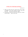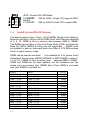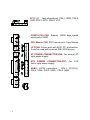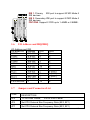
1
Intel 430TX PCI Chipset
Intelligent
MAIN BOARD
ATX586
for
Dual CPUs ATX Factor
TX2
for
AT Factor / Wide SCSI
USER’S MANUAL
version 1.0
UPDATE INFORAMTION
JULY 22, 97
1) When you install ATX power supply, please connect CASE
STANDBY to front panel connector CN9/JP9 , pin 19-20
Power On. Then turn on ATX power supply.
2) The difference between TX2 and TX3 is that TX3 is without
SCSI port/chip. Others are the same.
2
CONTENT
Preface ..................................................................
1
CHAPTER 1
Hardware Installation for
ATX586
1.1 One Jumper to Set CPU.....................…
1.2 Two Jumper to Set CPU.........…
…
…
…
…
1.3
Other
Hardware
Jumpers.........................
1.4
Install
System
DRAM
Memory...............
1.5
Install IDE, I/O and Front
Panel........…
…
.
1.6
I/O
Address
And
IRQ................................
1.7
Jumpers
List.............................................
1.8
Pin
Definition
for
Cable
Connection........
4
CHAPTER
2
PNP
BIOS
SETUP.......................
2.1
BIOS
Setup...............................................
2.2
Standard
Setup.........................................
2.3
BIOS
Features
Setup...............................
2.4
Chipset
Features
Setup............................
2.5
Power
Management
Setup.......................
4
6
7
8
10
12
12
13
15
15
15
16
17
17
3
2.6
Configuration.............................
2.7
Peripherals..............................
2.8
AWARD
Code.........................
PNP/PCI
18
Integrated
18
Post
19
CHAPTER 3
EIDE & FLASH BIOS
SETUP......
Part
I.
Installation
Ultra
EIDE
Driver...............
Part
II.
Update
Flash
BIOS.............................
24
4
BIOS
24
48
CHAPTER 4
Hardware Installation for TX2
4.1 One Jumper to Set CPU.....................…
4.2 Two Jumper to Set CPU.........…
…
…
…
…
4.3
Other
Hardware
Jumpers.........................
4.4
Install
System
DRAM
Memory...............
4.5
Install IDE, I/O and Front
Panel........…
…
.
4.6
I/O
Address
And
IRQ................................
4.7
Jumpers
List.............................................
4.8
Pin
Definition
for
Cable
Connection........
49
50
52
53
54
56
58
58
59
5
Preface
Inside the Document
This document describes setup ATX586 Dual Pentium Main Board with
Intel 430TX PCI CHIPSET, resulting in Ultra IDE performance.
ATX586 is for ATX platform with dual processors design, including
Enhance I/O chip (SMC 669 compatible). There is an option that
installing “ 82093AA” supports two Intel Pentium (MMX) CPU, said
Dual Processors. Under single processor, the user installs Intel
+
Pentium 75-233Mhz, MMX, AMD K5/K6-PR 233, CYRIX CX6x86 200 .
Excepting above mentioned, ATX586 is designed with Auto
Switching between 3.3v and 2.8v CPU (when you use single CPU
only), front panel connector and Smart Jumper Setting for
different CPU.
The package for ATX586 including:
þ ATX586 mother board
þ Two IDE drive ribbon cable for 4 devices
þ One Floppy ribbon cable for 2 devices
þ One Ultra IDE device disk
þ This user’ s manual
Chapter
1 is about positions, jumpers and connectors for
ATX586. Due to the board supports full range of Pentium CPU MMX
75Mhz-233Mhz, AMD K5/K6-PR233, CYRIX 6x86 CX 200+ .
Chapter 2
is for BIOS setup. If you want to use external I/O card,
you can disable the I/O function in BIOS and then install a card on slot.
You also modify the COM1 and COM2 as COM3 and COM4 in
BIOS. Finally, the BIOS is PnP function. It auto detects the PCI
IRQ, ISA IRQ and HDD mode. Chapter 3
is for IDE DRIVER
installation and how to upgrade BIOS.
6
(Chapter
4 is about positions, jumpers and connectors for TX2.
Due to the board supports full range of Pentium CPU MMX 75Mhz+
233Mhz, AMD K5/K6-PR233, CYRIX 6x86 CX 200 .)
Simple features:
²
Intel 430 TX PCISET. 82439TX System Controller (MTXC),
82371AB PIIX4 PCI to ISA / IDE Xcelerator, 82093AA I/O
Advanced Programmable Interrupt Controller (IOAPIC).
²
Compatible SMC 669 super I/O on board.
²
Supports full range of Pentium Processor Family, up to Intel
+.
Pentium MMX-233Mhz, AMD K6-PR-233, CX 6x86 200
is an auto- switching mode from
²
There
3.3v to 2.8v.
Installing (option) 82093AA to let the board supports two
Intel Pentium or MMX CPU at the same board for ATX586.
It is perfect to run the same voltage CPU!
²
Support SDRAM/EDO/Fast page DRAM, 72-pin SIMM socket *
4pcs, 168-pin DIMM socket * 2pcs.
256MB.
²
6-1-1-1 for SDRAM; 5-2-2-2 for EDO; 6-3-3-3 for FP.
64-MB DRAM cacheability.
back only.
²
2 pairs/4 banks up to
Direct Mapped organization-write
Supports 256K and 512K Pipelined Burst SRAM.
PCI V2.1 compatible. Concurrent PCI, enhanced CPU/PCI/ISA
performance.
²
Provides Multiprocessor Interrupt Management: dynamic interrupt
distribution routing interrupt to the lowest priority processor;
software programmable control of interrupt inputs; off loads
interrupt related traffic from the memory bus.
7
²
24 Programmable Interrupts: 13 ISA supported; 4 PCI; 1 interrupt/
SMI# rerouting; 2 motherboard ; 1 interrupt used for INTR input; 3
general purpose; independently programmable for edge/level
sensitivity interrupts; each interrupt can be programmed to
respond to active high or low
inputs.
²
4 * 32-bit PCI, 4 * 16 bit ISA Slots for ATX586
²
2 * Ultra EIDE, support 4 IDE devices. EPP/ECP/SPP printer port.
2 * 16550 UART serial ports. PS/2 mouse port. IR, infrared, port,
option for FIR, fast infrared.
²
IDE controller:
2 * USB, universal serial bus, ports.
Independent timing of up to 4 drives. PIO mode
4 transfers up to 14 Mbytes/sec. Supports “ Ultra 33” synchronous
DMA mode transfers up to 33 Mbytes/sec.
Integrated 8*32-bit
buffer for IDE PCI Burst transfers.
²
Dual Power Supply.
on board to
Has both AT and ATX power connectors
support AT or ATX power supply with soft-on/off
features.
²
Built-in AWARD PCI/ISA Plug and Play Flash BIOS GREEN
BIOS
²
Two-mega flash recovery BIOS ROM.
&&&
8
Chapter
1
Hardware
Installation For ATX586
1.1
One Jumper to Set CPU , Simple Jumper
No more CPU jumper setting when you use Single Processor
Intel 133Mhz,
+,
CYRIX 166
AMD K5-133 CPU.
You just install CPU directly and Power On. (At the moment, JP6: 12 and JP7: 2-3 SHORT; JP8/JP9: 1-2 SHORT )
A: Using Intel CPU (Ensuring JP8/JP9: 1-2 SHORT)
CPU Speed
JP6
JP7
Intel 100Mhz
1-2 SHORT 1-2 SHORT
Intel 166Mhz
2-3 SHORT 2-3 SHORT
Intel 200Mhz
2-3 SHORT 1-2 SHORT
Intel 233Mhz
1-2 SHORT 1-2 SHORT
B: Using AMD K5/K6 (Ensuring JP8/9: 1-2 SHORT)
CPU Speed
JP6
JP7
AMD K5-100
1-2 SHORT 1-2 SHORT
AMD K5/K6-PR-166 2-3 SHORT 2-3 SHORT
AMD K6-PR200
2-3 SHORT 1-2 SHORT
AMD K6-PR233
1-2 SHORT 1-2 SHORT
C: Using CYRIX 6x86 CPU ( Ensuring JP6: 1-2 and JP7: 2-3 SHORT)
CPU Speed
JP8
JP9
CX 133+, 55Mhz
2-3 SHORT 2-3 SHORT
CX 150+, 60Mhz
2-3 SHORT 1-2 SHORT
CX 200+, 75Mhz
1-2 SHORT 2-3 SHORT
When you want to install two CPU, they are perfect are the same
voltage 2.8v (P55C) or 3.3v(P54C). Different voltage can’t be
used together. Installing the 1st CPU at U4 socket!
9
Map of ATX586 Mother Board
Default Setting for Intel Pentium 133Mhz,
AMD K5-133,CYRIX P166+ ,512K PB Cache
1.2
10
Two-Jumper Setting for CPU
JP6/JP7: Set CPU External Bus Frequency Rate (BF1, BF0)
JP6/JP7: 1-2, SHORT for
Intel 90/100Mhz, MMX
233Mhz, AMD K5 75-133,
AMD K6 PR233Mhz
JP6: 1-2 and JP7: 2-3
SHORT
for Intel 120/
+
133 Mhz, CYRIX 120 +
200 (Default)
JP6/JP7: 2-3 SHORT for
Intel
MMX150/166Mhz,
AMD K6 PR166Mhz
means BF0.
NON-ACTIVE)
JP6: 2-3 SHORT and JP7:
1-2 SHORT for Intel MMX
180/ 200Mhz,and AMD
K6 PR200.
(JP6 means BF1 and JP7
When 2-3 short means ACTIVE, 1-2 short means
11
JP8/9: Set CPU External Bus Frequency Selection (FS0, FS1, FS2)
JP8: 1-2 and JP9: 2-3
SHORT : 75Mhz for CX
+
200
JP8/9:1-2 SHORT: 66
+
Mhz for CX 166 , AMD
K6, MMX. Intel/AMD
100/133/ 166/ 200 /
233Mhz (Default)
JP8: 2-3 and JP9: 1-2
SHORT : 60Mhz for CX
+,
150
Intel/AMD
90/120/150
/180Mhz
CPU
+
JP8/9: 2-3 SHORT: 55Mhz for CX133
1.3 Other Hardware Jumpers
J1: Set the CPU Type: when you install two CPUs please use J1 to
indicate the Voltage of CPU. If you only install one CPU, skip this
part
à OPEN for P55C(Intel MMX, AMD K6,
CYRIX 6x86L CPU. Default. 2.8v
à
12
1-2, 3-4, 5-6, 7-8 SHORT indicates Intel
P54C (AMD K5 and CYRIX 6x86). 3.3v
only
JP15: 2MB FLASH BIOS ONLY
2-3 SHORT for normal (set by factory).
Default.
1-2 SHORT reserved for factory set only.
JP16: Select FLASH BIOS
2-3 SHORT for 5v Flash BIOS, normal,
Default..
1-2 SHORT for 12v Flash BIOS (set by
factory),
JP18: Choose Power Supply
SHORT: AT style power supply
OPEN: ATX style power supply
JP13: CMOS. When you forget the password, clear CMOS,
restart!
2-3 SHORT for normal. Default.
3-4 SHORT to clear CMOS (power must be off).
OPEN for external battery installed.
It is an important jumper. When BIOS setting is changed by
user becoming unstable in system board, or I/O don’ t work
properly, reset CMOS RAM data ( default setup.)
JP2: Set Cache. Don’ t change it by users!
2-3 SHORT: 512K PB SRAM. Default.
1-2 SHORT: 256K PB SRAM
13
JP12: Choose CPU SMI Mode
1-2 SHORT: SMI by PIIX4 ( Single CPU request SMI),
Default.
2-3 SHORT: SMI by IOAPIC (Dual CPU request SMI)
1.4
Install System DRAM Memory
The board supports 2pcs 72-pin, 32-bit SIMMs (Single Inline Memory
Modules) and 2pcs 168-pin, 64-bit DIMM (Dual Inline Memory Modules)
of 4, 8, 16, 32MB to form a memory size between 8MB to 128MB.
The SIMMs can be 60ns or 70ns Fast Page Mode (FPM), or Enhanced
Data Out (EDO) (BEDO & Parity are not supported). SIMMs must
be installed in pairs so that each bank (see Map of ATX-586)contains
64-bit of same memory chips.
DIMM can be used as one bank. It is available for 3.3v (power level)
Unbuffered Synchronous DRAM (SDRAM) or EDO DRAM of either 8,
16, 32, 64, 128MB, to form a memory size between 8MB to 128MB.
SIMM and DIMM can be used together, but the limitations are two
banks and max memory size 128MB. 2pcs 72-pin SIMM is one bank
and 1pce DIMM is one bank too.
Bank 0
1MB * 32 SS
1MB * 32 SS
1MB * 32 SS
1MB * 32 SS
1MB * 32 SS
2MB * 32 DS
2MB * 32 DS
2MB * 32 DS
2MB * 32 DS
2MB * 32 DS
4MB * 32 SS
4MB * 32 SS
4MB * 32 SS
4MB * 32 SS
4MB * 32 SS
14
Bank 1
X
1MB * 32 SS
2MB * 32 DS
4MB * 32 SS
8MB * 32 DS
X
1MB * 32 SS
2MB * 32 DS
4MB * 32 SS
8MB * 32 DS
X
1MB * 32 SS
2MB * 32 DS
4MB * 32 SS
8MB * 32 DS
TOTAL
8MB
16MB
24MB
40MB
72MB
16MB
24MB
32MB
48MB
80MB
32MB
40MB
48MB
64MB
96MB
8MB * 32 DS
8MB * 32 DS
8MB * 32 DS
8MB * 32 DS
8MB * 32 DS
16MB * 32SS
16MB * 32SS
1.5
X
1MB * 32 SS
2MB * 32 DS
4MB * 32 SS
8MB * 32 DS
X
16MB * 32SS
64MB
72MB
80MB
96MB
128MB
128MB
256MB
Install IDE, Enhanced I/O and Front Panel Connectors
There is a special design that CN9 is for Key Lock, Sleep/Resume SW,
Speaker, IDE LED, TB SW, Reset SW, and Turbo LED. It is
convenient for you to connect the cable from front board of Case.
CN9: 1-5, Key Lock - Keyboard lock switch
& power LED connector. 1. Power LED (+),
2. N/C, 3. GND, 4. Key lock, 5. GND
CN9: 7-8, Turbo Switch.
CN9: 10-13, Speaker - Connect to the
system's speaker for beeping. 10. Speaker, 11.
GND, 12. GND, 13. VCC.
CN9: 14-15, IDE LED Indicator - LED ON
when on board PCI IDE HDD activities.
CN9: 19-20, Turn on power when ATX power
supply is on sleep mode
CN9: 22-23, Reset - Short to restart system.
CN9: 25-26, Turbo LED Indicator - LED ON
when high speed (CN9: 7-8 SHORT).
15
JP17: IR, fast infrared port. PIN-1: IRRX, PIN-2:
GND; PIN-3: IRTX; PIN-4: VCC
COM1-2/CN1-CN5: Support 16550 high speed
serial ports/ UART.
PS/2 Mouse CN2: PS/2 mouse port. 5-pin Mouse:
LPT/CN4: Printer port with ECP/ PP. bi-direction.
It can be used with external IDE/ SCSI device.
AT POWER CONNECTOR/CN6: For normal AT
style power supply
ATX POWER CONNECTOR/CN7: For ATX
factor style power supply
USB1/: 4-PIN connectors.
PIN-1: VCC(5V),
PIN-2: USB-, PIN-3: USB+, PIN-4: GND
16
IDE 1: Primary IDE port to support ATAPI Mode 5
IDE devices
IDE 2: Secondary IDE port to support ATAPI Mode 5
IDE devices.
FDC/CN8: Support 2 FDD up to 1.44MB or 2.88MB .
1.6
I/O Address and IRQ/DRQ
I/O Address and IRQ
On Board I/O
Address
GAME
200-20F
COM1
3F8-3FF
COM2
2F8-2FF
COM3
3E8-3EF
COM4
2E8-2EF
IDE1
1F0-1F7
IDE2
170-177
LPT1
378-37F
LPT2
278-27F
LPT3
3BC-3BF
FDD1
3F0-3F7
PS/2 MOUSE X
1.7
IRQ
X
4
3
3
3
14
15
7
7
7
6
12
DRQ
X
X
X
X
X
X
X
3 (ECP)
3 (ECP)
3 (ECP)
2
X
Jumpers and Connectors List
ITEMS
DESCRIPTION
JP2
1-2 for 256K Cache,
JP6
Set CPU External Bus Frequency Rate (BF0, BF1)
JP7
Set CPU External Bus Frequency Rate (BF0, BF1)
3-4 for 512K Cache
17
JP8
Set CPU External Bus Frequency (FS0, FS1, FS2)
JP9
Set CPU External Bus Frequency (FS0, FS1, FS2)
JP12
Choose CPU SMI Mode
JP13
2-3 Normal CMOS, 3-4 CMOS Clear
JP15
Select Recovery BIOS
JP16
2-3 for 5v Flash BIOS, 1-2 for 12v
JP17
IR Connector
JP18
Choose Power Supply
J1
Indicate the CPU voltage
CN1
COM1
CN2
PS/2 MOUSE Connector
CN3
Keyboard
CN4
Parallel Port
CN5
COM2
CN6
AT Power Supply
CN7
ATX Power Supply Connector
CN8
Floppy Drive
CN9
Front Panel Connector
USB1
USB Connector
IDE1-2
IDE Drive connector
&&&
18
Connector
19
Chapter
2
AWARD, PnP
GREEN BIOS
SETUP
2.1
BIOS
Setup
Powe on the computer and press <DEL> key immediately
and the screen will display you CMOS SETUP UTILITY as
follows:
ROM PCI/ISA BIOS (2A59GT4A)
CMOS SETUP UTILITY
AWARD SOFTWARE, INC.
STANDARD CMOS SETUP
INTEGRATED PERIPHERALS
BIOS FEATURES SETUP
SUPERVISOR PASSWORD
CHIPSET FEATURES SETUP
USER PASSWORD
POWER MANAGEMENT SETUP
IDE HDD AUTO DETECTION
PNP/PCI CONFIGURATION
HDD LOW LEVEL FORMAT
LOAD BIOS DEFAULTS
SAVE & EXIT SETUPG
LOAD SETUP DEFAULTS
EXIT WITHOUT SAVING
Esc : Quit
↑↓←→: Select Item
F10 : Save & Exit Setup
(Shift) F2: Change Color
Time, Date, Hard Disk Type.......
2.2
Standard CMOS Setup
The STANDARD CMOS SETUP allows user to configure
system setting such as current date and time, type
20
of hard disk drive installed in the system, floppy
drive type, and the type of display monitor.
ROM PCI/ISA BIOS (2A59GT4A)
STANDARD CMOS SETUP
AWARD SOFTWARE, INC.
Date (mm:dd:yy)
Time (hh:mm:ss)
HARD DISKS
Primary Master:
Primary Slave:
Secondary Master:
Secondary Slave:
: Wed, Jan 5 2000
:0:
0:0
TYPE
NONE
NONE
NONE
NONE
SIZE
0
0
0
0
CYLS
0
0
0
0
HEADS
0
0
0
0
PRECOMP
0
0
0
0
Drive A: 1.2M, 5.25 in
Drive B: None
LANDZ
0
0
0
0
SECTOR
0
0
0
0
Base Memory:
Extended Memory:
Other Memory:
--------------------------Total Memory:
Video: EGA/VGA
Halt On: All Errors
áâàß: Select Item
(Shift) F2: Change Color
Esc: Quit
F1: Help
2.3
Pu/Pd/+/-: Modify
BIOS Features Setup
ROM PCI/ISA BIOS (2A59GT4A)
BIOS FEATURES UTILITY
AWARD SOFTWARE, INC.
Virus Warning
CPU Internal Cache
External Cache
Quick Power On Self Test
Boot Sequence
Swap Floppy Drive
Boot Up Floppy Seek
Boot Up NumLock Status
Boot Up System Speed
Gate A20 Option
Typematic Rate Setting
Typematic Rate (Chars/Sec)
Typematic Delay *Msec)
Security Option
PCI/VGA
Palette Snoop
: Disable
: Enabled
: External
: Disable
: A,C
: Disable
: Enabled
: On
: High
: Fast
: Disabled
:6
: 250
: Setup
: Disabled
Video BIOS Shadow
C8000-CBFFF Shadow
CC000-CFFFF Shadow
D0000-D3FFF Shadow
D4000-D7FFF Shadow
D8000-DBFFF Shadow
DC000-DFFFF Shadow
: Enabled
: Disabled
: Disabled
: Disabled
: Disabled
: Disabled
: Disabled
↑↓←→: Select Item
F1 : Help
F5 : Old Values
F6: Load BIOS Defaults
PU/PD/+/- : Modify
(Shift)F2 : Color
21
MODE
-----------------------------
640K
3072K
384K
--------------4096K
OS Select for DRAM
>64MB
2.4
: NONOS2
F7 : Load Setup Defaults
Chipset Features Setup
ROM PCI/ISA BIOS (2A59GT4A)
CHIPSET FEATURES SETUP
AWARD SOFTWARE, INC.
Auto Configuration
Fast EDO path Select
Refresh RAS# Assertion
ISA Bus Clock
: Enabled
: 60ns
:3
:6
:3
:3
:x222/x333
:1
: Disabled
: 4 CLKS
: PCICLK/4
System BIOS Cacheable
Video BIOS Cacheable
8 Bit I/O Recovery Time
16 Bit I/O Recovery Time
Memory Hole At 15M-16M
Peer Concurrency
Passive
Release
: Disabled
: Disabled
:1
:1
: Disabled
: Enabled
: Enable
DRAM Timing
DRAM RAS# Precharge Time
DRAM R/W Leadoff Timing
DRAM RAS To Cas Relay
DRAM Read Burst(EDO?FP)
DRAM Write Burst Timing
Fast MA To RAS# Delay CLK
2.5
DRAM Fast Leadoff
Delayed Transaction
: Disabled
: Disabled
↑↓←→: Select Item
F1 : Help
F5 : Old Values
F6: Load BIOS Defaults
F7 : Load Setup Defaults
PU/PD/+/- : Modify
(Shift)F2 : Color
Power Management Setup
ROM PCI/ISA BIOS (2A59GT4A)
POWER MANAGEMENT SETUP
AWARD SOFTWARE, INC.
Power Management
PM Control by APM
Video Off Method
Modem Use IRQ
Doze Mode
Standby Mode
Suspend Mode
HDD Power Down
: User Define
: Yes
** Wake Up Events In Doze
IRQ3 (Wake-Up Event)
IRQ4 (Wake-Up Event)
IRQ8 (Wake-Up Event)
IRQ12 (Wake-Up Event)
& Standby **
: ON
: ON
: ON
: ON
22
: V/H SYNC+Blank
:3
: 1 Min
: 1 Min
: 1 Min
: I Min
**power Down &
IRQ3 (COM2)
IRQ4 (COM1)
IRQ5
(LPT2)
IRQ6
(Floppy Disk)
IRQ7 (LPT1)
IRQ8 (RTC ALARM)
IRQ9 (IRQ2 Redir)
IRQ10 (Reserved)
IRQ11 (Reserved)
IRQ12 (PS/2 Mouse)
IRQ13 (Coprocessor)
IRQ14 (Hard Disk)
IRQ15 (Reserved)
↑↓←→: Select Item
F1 : Help
F5 : Old Values
F6: Load BIOS Defaults
F7 : Load Setup Defaults
Resume Events **
: ON
: ON
: ON
: OFF
: ON
: OFF
: ON
: ON
: ON
: ON
: ON
: ON
: ON
PU/PD/+/- : Modify
(Shift)F2 : Color
2.6
PNP/PCI Configuration
ROM PCI/ISA BIOS (2A56GT5A)
PNP/PCI CONFIGURATION
AWARD SOFTWARE, INC.
Resources Controlled By
Reset Configuration Data
: Manual
: Enabled
IRQ-3 assigned to
IRQ-4 assigned to
IRQ-5 assigned to
IRQ-7 assigned to
IRQ-9 assigned to
IRQ-10 assigned to
IRQ-11 assigned to
IRQ-12 assigned to
IRQ-14 assigned to
IRQ-15 assigned to
DMA-0 assigned to
DMA-1 assigned to
DMA-5 assigned to
DMA-6 assigned to
DMA-7 assigned to
: Legacy ISA
: Legacy ISA
: Legacy ISA
: Legacy ISA
: Legacy ISA
: Legacy ISA
: Legacy ISA
: Legacy ISA
: Legacy ISA
: Legacy ISA
: Legacy ISA
: Legacy ISA
: Legacy ISA
: Legacy ISA
: Legacy ISA
:
2.7
PCI IRQ Actived By
PCI IDE IRQ Map To
primary IDE INT#
Secondary IDE INT#
Used Mem Base Addr
↑↓←→: Select Item
F1 : Help
F5 : Old Values
F6: Load BIOS Defaults
F7 : Load Setup Defaults
: Level
: PCI-AUTO
:A
:B
: N/A
PU/PD/+/- : Modify
(Shift)F2 : Color
Integrated Peripherals
ROM PCI/ISA BIOS (2A59GT5A)
INTEGRATED PERIPHERALS
AWARD SOFTWARE, INC.
IDE HDD block Mode
IDE Promary Master PIO
IDE Primary Slave PIO
IDE Secondary Master PIO
IDE Secondary Slave PIO
On-chip Primary PCI IDE
On-Chip Secondary PCI IDE
Onboard FDD Controller
Onboard Serial Port 1
Onboard Serial Port 2
UART 2 Mode
Onboard Parallel Port
Onboard Parallel Mode
: Enabled
: Auto
: Enabled
: Auto
: Auto
: Auto
: Enabled
: Enabled
: Enabled
: 3F8/IRQ4
: 2F8/IRQ3
: Standard
:378H/IRQ7
: SPP
:
2.8
USB Controller
↑↓←→: Select Item
F1 : Help
F5 : Old Values
F6: Load BIOS Defaults
F7 : Load Setup Defaults
PU/PD/+/- : Modify
(Shift)F2 : Color
AWARD BIOS Post Code
23
POST
(hex)
C0
C1
C3
C5
01-02
03
04
05
06
07
BE
09
0A
0B
24
Description
1. Turn off OEM specific cache, shadow...
2. Initialize all the standard devices with default values
standard devices includes:
-DMA controller (8237), -Programmable Interrupt
Controller (8259), -Programmable Interval Timer
(8254), -RTC chip
Auto-detection of onboard DRAM & Cache
1. Test system BIOS checksum
2. Test the first 256K DRAM
3. Expand the compressed codes into temporary DRAM area
including the compressed System BIOS & Option ROMs
Copy the BIOS from ROM into E0000-FFFFF shadow RAM so
that POST will go faster
Reserved
Initialize EISA registers (EISA BIOS only)
Reserved
1. Keyboard Controller Self-Test
2. Enable Keyboard Interface
Reserved
Verifies CMOS’s basic R/W functionality
Program defaults values into chipset according to the
MODBINable Chipset
Default Table
1. Program the configuration register of Cyrix CPU according
to the MODBINable Cyrix Register Table
2. OEM specific cache initialization (if needed)
1. Initialize the first 32 interrupt vectors with corresponding
Interrupt handlers;Initialize INT no from 33-120 with
Dummy(Suprious); Interrupt Handler.
2. Issue CPUID instruction to identify CPU type
3. Early Power Management initialization (OEM specific)
1. Verify the RTC time is valid or not
2. Detect bad battery
0C
0D
0E
0F
10
11
12-13
14
15
16
17
19
1A1D
3. Read CMOS data into BIOS stack area
4. PnP initializations including (PnP BIOS only)
-Assign CSN to PnP ISA card
-Create resource map from ESCD
5. Assign IO & Memory for PCI devices (PCI BIOS only)
Initialization of the BIOS Data Area (40 : 0N − 40:FF)
1. Program some of the Chipset’s value according to Setup.
(Early Setup Value Program)
2. Measure CPU speed for display & decide the system
clock speed
3. Video initialization including Monochrome,CGA,EGA / VGA.
If no display device found, the speaker will beep
1. Initialize the APIC (Multi-Processor BIOS only)
2. Test video RAM (If Monochrome display device found)
3. Show messages including:
-Award Logo, Copyright string, BIOS Date code
& Part No.
-OEM specific sign on messages
-Energy Star Logo (Green BIOS ONLY)
-CPU brand, type & speed
-Test system BIOS checksum(NonCompress
Version only)
DMA channel 0 test
DMA channel 1 test
DMA page registers test
Reserved
Test 8254 Timer 0 Counter 2.
Test 8259 interrupt mask bits for channel 1
Test 8259 interrupt mask bits for channel 2
Reserved
Test 8259 functionality
Reserved
25
1E
1F-29
30
31
32
33-3B
3C
3D
3E
3F-40
BF
41
42
43
44
45
46-4D
4E
4F
26
If EISA NVM checksum is good, execute EISA initialization
(EISA BIOS only)
Reserved
Detect Base Memory & Extended Memory Size
1. Test Base Memory from 256K to 640K
2. Test Extended Memory from 1M to the top of memory
1. Display the Award Plug & Play BIOS Extension
message (PnP BIOS only)
2. Program all onboard super I/O chips (if any) including
COM ports, LPT ports, FDD port... according to
setup
value
Reserved
Set flag to allow users to enter CMOS Setup Utility
1. Initialize Keyboard
2. Install PS2 mouse
Try to turn on Level 2 cache
Note: Some chipset may need to turn on the L2 cache in this
stage. But usually, the cache is turn on later in POST 61h
Reserved
1. Program the rest of the Chipset’s value according to
Setup. (Later Setup Value Program)
2. If auto-configuration is enabled, programmed the chipset
with pre-defined values in the MODBINable AutoTable
Initialize floppy disk drive controller
Initialize Hard drive controller
If it is a PnP BIOS, initialize serial & parallel ports
Reserved
Initialize math coprocessor.
Reserved
If there is any error detected (such as video, kb...), show all the
error messages on the screen & wait for user to press <F1> key
1. If password is needed, ask for password
2. Clear the Energy Star Logo (Green BIOS only)
50
51
52
53
60
61
62
Write all CMOS values currently in the BIOS stack area back
into the CMOS
Reserved
1. Initialize all ISA ROMs
2. Later PCI initializations (PCI BIOS only)
-assign IRQ to PCI devices
-initialize all PCI ROMs
3. PnP Initializations (PnP BIOS only)
-assign IO, Memory, IRQ & DMA to PnP ISA
devices
-initialize all PnP ISA ROMs
4. Program shadows RAM according to Setup settings
5. Program parity according to Setup setting
6. Power Management Initialization
-Enable/Disable global PM
-APM interface initialization
1. If it is NOT a PnP BIOS, initialize serial & parallel
ports
2. Initialize time value in BIOS data area by translate the
RTC time value into a timer tick value
Setup Virus Protection (Boot Sector Protection) functionality
according to Setup setting
1. Try to turn on Level 2 cache
Note: if L2 cache is already turned on in POST 3D, this
part will be skipped
2. Set the boot up speed according to Setup setting
3. Last chance for Chipset initialization
4. Last chance for Power Management initialization (Green
BIOS only)
5. Show the system configuration table
1. Setup daylight saving according to Setup value
2. Program the NUM Lock, typematic rate & typematic
speed according to Setup setting
27
63
FF
&&&
28
1. If there is any changes in the hardware configuration,
update the ESCD information (PnP BIOS only)
2. Clear memory that have been used
3. Boot system via INT 19H
System Booting. This means that the BIOS already pass the
control right to the operating system
Chapter
3
Quick Installation Guide
Ultra IDE Driver
and
Update Flash BIOS
for Intel TX Chipset
Thise Chapter includes two parts: one is to instal Enhance IDE Driver
and the other is to update main board BIOS.
PART 1. Installation IDE driver:
Dear Customer,
Thank you for choosing the Intel PIIX Bus Master IDE Drivers. This
production release of the drivers provides support for Intel PCIsets.
To install the drivers, follow the steps below:
1.
For all drivers: execute the appropriate self-extracting archive.
Windows 95* archive - bmide_95.exe
Windows NT* archive - bmide_nt.exe
IBM OS/2* archive
- bmideos2.exe
This will place the SETUP files in a subdirectory on your hard disk.
2.
For all drivers: run the setup program.
Click on SETUP.EXE from Windows* File Manager/Explorer
OR
Execute Program/Run from the Program Manager.
3.
Driver Installation
For the Windows 95 Driver:
[See auto install procedures.]
29
[If using OEM Version of Windows 95 CD-ROM on PIIX3 based
systems see also " 82371SB PIIX3 Application Note #3 Microsoft
Windows 95* Support for PIIX3 IDE Controller".]
For the IBM OS/2 and Windows NT Drivers:
After running SETUP, follow the installation instructions in the
README.TXT file which is extracted to the driver installation
directory.
The Driver Version Numbers included in this release are:
Windows 95 Driver - version 2.61
Windows NT Driver - version 1.59
IBM OS/2 Driver
- version 2.05
Sincerely,
PCIsets Product Line Marketing
PCI Components Division
Intel Corporation
*Other brands and names are the properties of their respective owners
****************************************************
PIIX Bus Master IDE Drivers for Windows 95*
Installation, Usage, and Release Note Information
NOTE: This document refers to desktop systems with
the following Intel PCIset devices:
82371FB (PIIX1), 82371SB (PIIX3) or 82371AB (PIIX4) in
conjunction with the following Intel PCIsets:
430FX, 430HX, 430TX, 430VX and 440FX
The terms "PIIX", "82371xB" refer to any/all of the
following Intel PCIset devices: 82371FB, 82371SB,
82371AB
Also, the term "processor" refers to the Pentium(R) processor,
the Pentium(R) processor with MMX(tm) technology, the
Pentium(R) Pro processor, and the Pentium(R) II processor
ONLY.
****************************************************************************
30
******************************************************************************
INTRODUCTION
******************************************************************************
This document describes the installation procedure and usage
information for the PIIX Bus Master IDE Drivers for Windows 95*. Also
included are release notes describing any problems or issues with the
software which were known at the time of shipment.
****************************************************************************
CONTENTS OF THIS DOCUMENT
****************************************************************************
This document contains the following sections:
1.
2.
3.
4.
5.
6.
7.
8.
System Requirements
Contents of the Distribution Package
Installing the Software
Verifying Installation of the Software
De-installing the Software
Troubleshooting
Identifying the Software Version Number
Release Notes
8A. IDE Devices Supported By the Driver
8B. Applications Supported By the Driver
8C. Large (>528MB) IDE Fixed Disk Drive Support By the
Driver
8D. Release-Specific Troubleshooting Information
8E. Revision History
8F. Release Testing Information
****************************************************************************
1. SYSTEM REQUIREMENTS
****************************************************************************
This section describes system requirements for the PIIX Bus Master
IDE Device Driver for Windows 95*. Refer to the Release Notes
section of this document for additional information regarding this
release.
NOTE: This driver has been designed for and tested with Windows
95* only.
This driver will only install on systems with Windows 95*.
31
1.
The system must contain a supported Intel processor and chip set
configuration:
Chip set: Intel 430FX, 430HX, 430TX, 430VX and 440FX chip
sets.
Processor: Intel Pentium(R), Pentium(R) with MMX(TM)
Technology, Pentium(R) Pro, and Pentium(R) II devices ONLY.
2.
Ensure that a mouse is connected to the system.
3.
One of the following versions of Windows 95* must be
installed on the system prior to running utility program.
Windows 95* 4.00.950
(Retail)
Windows 95* 4.00.950a (OSR1)
Windows 95* 4.00.950b (OSR2 without USB Supplement)
Windows 95* 4.00.950b (OSR2.1 with USB Supplement)
4.
This utility should only be used on desktop systems. The
utility must not be executed on notebook or portable systems
with or without dock.
5.
It is assumed that the BIOS properly initialized the 82371xB IDE
interface for Bus Master IDE operation.
6.
There are no other non-82371xB IDE controllers (add-in IDE
controller or sound card with IDE) enabled on the system.
****************************************************************************
2. CONTENTS OF THE DISTRIBUTION PACKAGE
****************************************************************************
The Intel PIIX Bus Master IDE Driver for Windows 95*, Version 3.00
release package contains the following items:
Date
Time
------04/15/97 12:00a
BMIDE_95.EXE
04/15/97 12:00a
README.TXT
04/15/97 12:00a
03/28/97 12:00a
03/28/97 12:00a
03/28/97 12:00a
32
Size
----
29,268
45,312
69,592
320,411
File
----
PIIXDRV.Z
SETUP.EXE
SETUP.INS
_INST32I.EX_
03/28/97
03/28/97
12:00a
12:00a
6,128
179,689
_SETUP.DLL
_SETUP.LIB
****************************************************************************
3. INSTALLING THE SOFTWARE
****************************************************************************
This installation procedure is specific only to the version of the driver
and installation file included in this package.
This subsection describes how to install the software on a system
where Windows 95* is installed.
NOTE:
1.
2.
Record the location of the Windows 95* directory before
installing the driver.
Check the System Requirements. Windows 95* must be fully
installed and running on the system prior to running this
software.
Close any running applications.
3.
Remove references to installed real-mode IDE device drivers in
the AUTOEXEC.BAT and CONFIG.SYS files (especially any
drivers that control ATAPI CD-ROM and special IDE features).
Use the Notepad utility to do this.
4.
The driver files are stored in an integrated application setup
program. This program is a Windows 95* program that allows the
driver files to be INSTALLED or DE-INSTALLED.
Execute the driver setup program.
Run SETUP.EXE.
5.
Click 'Next' on Welcome Screen to read and agree to the license
agreement. View the text file and choose File\Exit to close
Notepad and continue. NOTE: If you click 'No', program will
terminate.
33
6. Click 'Yes' if you agree to continue.
the
program will terminate.
7.
NOTE:
If you click 'No',
Select 'INSTALL', to install the PIIX Bus Master IDE Device
Driver when prompted to do so.
NOTE: if the driver is currently installed on the system,
SETUP will ask you whether or not you want to continue. Follow
the prompts on the screen to Install the driver if desired.
8.
Click 'OK' to restart the system when prompted to do so.
9.
Follow the screen instructions and use default settings to
complete the setup when Windows 95* is re-started.
Upon re-start, Windows 95* will display that it has found an Intel
PCI Bus Master IDE controller hardware and is installing hardware
for it.
If a "New Hardware Found" dialog box is displayed requesting
the
location of the drivers, use the mouse to click on the scrollbar
and click on the <Windows 95* directory>\System\IOSubSys
path:
For example:
a. Click on 'C:\WINDOWS\SYSTEM\IOSUBSYS\'
b. Click 'OK'.
10.
Select 'Yes',
when prompted to re-start Windows 95*.
NOTE: After installation, the following driver and related files
are stored as listed.
<Windows 95* directory>\System\IOSubSys\IDEATAPI.MPD
<Windows 95* directory>\System\IOSubSys\PIIXVSD.VXD
<Windows 95* directory>\INF\IDEATAPI.INF
****************************************************************************
4. VERIFYING INSTALLATION OF THE DRIVER
****************************************************************************
34
This installation verification procedure is specific only to the version of
the driver and installation file included in this package.
This subsection describes how to verify installation of the software on
a system where Windows 95* is installed.
This installation verification procedure is specific only to the version of
the driver and installation file included in this package.
If the system does not operate reliably or fails to boot when the driver
is installed, De-install the driver. Refer to the RELEASE NOTES
section for more information.
In order to verify the installation of the driver:
1.
Open the Control Panel folder.
2.
Invoke the System applet.
3.
Click on the Device Manager tab.
4.
Select the View Devices by Type option.
connected to the system will be displayed.
A list of the devices
5.
Click on the Hard Disk Controllers record.
will be listed.
One of two cases
For CASE 1, there could be up to three instances listed:
Intel 82371XX PCI Bus Master IDE Controllers
Primary Bus Master IDE Controller
Secondary Bus Master IDE Controller
Go to step 6 for CASE 1.
For CASE 2, there could be up to two instances listed:
Intel PIIX PCI Bus Master IDE Controller
Intel PIIX PCI Bus Master IDE Controller
Go to step 7 for CASE 3.
NOTE FOR ALL CASES:
a. The content of the text strings is dependent on the
driver's INF file (named IDEATAPI.INF in the driver's
install directory).
35
As a result, the individual controller descriptions
may vary slightly from what is listed above. In this
case, select the closest match.
NOTES FOR CASE 1:
b. XX in 82371XX, shown in CASE 1 may be:
FB,
SB, AB.
c. Depending on your current system configuration,
only one of the instances displayed for the Primary
or the Secondary IDE controllers may be displayed.
d. The order in which the individual hard disk controller
instances
are listed may vary.
NOTE FOR CASE 2:
e. Depending on the current system configuration, only
one of the instances may be displayed.
6.
Verify the Intel 82371xx PCI Bus Master IDE Controllers Driver
listing.
NOTES:
a. A yellow mark on an instance is NORMAL if no
devices are connected to that controller.
b.
If only one instance is present, there should be no
yellow
warning symbol next to it.
If a yellow warning symbol appears in error (cannot be attributed to
either of Steps 6a or 6b), the driver may not be installed and/or
working properly.
****************************************************************************
5. DE-INSTALLING THE SOFTWARE
****************************************************************************
This de-installation procedure is specific only to the version of the
driver and installation file included in this package.
This subsection describes how to install the software on a system
where Windows 95* is installed.
NOTE:
36
Record the location of the Windows 95* directory before
de-installing the driver.
1.
2.
3.
Check the System Requirements. Windows 95* must be fully
installed and running on the system prior to running this software.
Close any running applications.
The driver de-installer is stored in an integrated application setup
program. This program is a Windows 95* program that allows
the driver files to be INSTALLED or DE-INSTALLED.
Execute the driver setup program.
Run SETUP.EXE.
4.
Click 'Next' on Welcome Screen to read and agree to the license
agreement. View the text file and choose File\Exit to close
Notepad and continue. NOTE: If you click 'No', program will
terminate.
5.
Click 'Yes' if you agree to continue.
the
program will terminate.
6.
Select 'DE-INSTALL', to install the PIIX Bus Master IDE Device
Driver when prompted to do so.
NOTE:
If you click 'No',
NOTE: if the driver is not currently installed on the system,
SETUP will exit.
7.
Click 'OK' to restart the system when prompted to do so.
8.
Follow the screen instructions and use default settings to
complete the setup when Windows 95* is re-started.
Upon re-start, if Windows 95* if responds with an "Update Device
Driver Wizard" dialog box (applies to systems with Windows 95*
Version 950B) then follow the UPDATE DEVICE DRIVER
WIZARD directions section, otherwise go to the NON-WIZARD
directions.
37
NON-WIZARD directions:
A. Select 'Windows default driver', A "New Hardware
Found" dialog box will request a driver location.
B. Select 'Yes' to restart the system when prompted to
do so.
Step C may happen several times.
UPDATE DEVICE DRIVER WIZARD directions:
A. Select 'Next',
search for drivers.
A Wizard dialog box requests to
B. Select 'Finish', The Wizard dialog box will indicate it
found a driver in the <Windows 95* directory>\INF
directory.
C. Select 'Yes' to restart the system when prompted to
do so. Step C may happen several times.
D.
4.
Go to step 4, De-Installation process is complete.
De-Install process is complete.
****************************************************************************
6. TROUBLESHOOTING
****************************************************************************
The following procedure assumes that the hardware/software
requirements from above have been satisfied. The following
procedure also assumes that the installation of the driver was
performed as described in the 'Verifying Installation of the Driver'
section. Refer to the 'Release Notes' section of the document for
additional information.
COMMON PROBLEMS:
****************************
1.
The device is incompatible with PCI Bus Master IDE operation.
This is due to the fact that the device does not work properly
when
38
accessed in a PCI Bus Master IDE fashion.
Contact the
device
manufacturer for more information.
2.
Verify the length of the cables that are being used to connect the
IDE or ATAPI devices to the primary and secondary PIIX IDE
interfaces. The length of these cables from END-TO-END
should not exceed 18 inches (0.46 m). Furthermore, the
capacitance of the cable should not exceed 35 pF.
3.
A conflict between the PIIX Bus Master IDE driver and a realmode ATAPI CD-ROM or IDE device driver may occur if the realmode driver references have not been properly removed from the
AUTOEXEC.BAT and/or CONFIG.SYS files. This conflict
occurs when the PIIX Bus Master IDE driver attempts to access
the legacy ISA IDE resources to control the PIIX. ALL
REFERENCES TO REAL-MODE DRIVERS (IDE or ATAPI) IN
THE TOEXEC.BAT
AND CONFIG.SYS MUST BE REMOVED.
****************************************************************************
7. IDENTIFYING THE SOFTWARE VERSION NUMBER
****************************************************************************
The driver's version can be determined by reading Windows*
properties embedded in the driver file.
The driver version can be obtained by querying the driver file's
properties under File Manager.
NOTE: After installation, the following driver and related files
are stored as listed.
<Windows 95* directory>\System\IOSubSys\IDEATAPI.MPD
<Windows 95* directory>\System\IOSubSys\PIIXVSD.VXD
<Windows 95* directory>\INF\IDEATAPI.INF
1.
Under Windows 95*, invoke the "Explorer" application.
2.
Select the path containing the driver file.
<Windows 95* directory>\System\IOSubSys
39
For example,
C:\WINDOWS\SYSTEM\IOSUBSYS
3.
Select the driver file, "IDEATAPI.MPD".
4.
Open the "File" menu.
5.
Click on the "Properties" item.
6.
Click on the "Version" tab.
7.
The IDEATAPI.MPD driver's version should be listed in the
'Product Version' portion of the dialog.
****************************************************************************
8. RELEASE NOTES
****************************************************************************
The release notes describe the current known state of the PIIX Bus
Master IDE Driver for Windows 95*, Version 3.00 at the time of release.
The release notes are divided into the following sections:
8A.
8B.
8C.
IDE Devices Supported By the Driver
Applications Supported By the Driver
Large (>528MB) IDE Fixed Disk Drive Support By the
Driver
8D. Release-Specific Troubleshooting Information
8E. Revision History
8F. Release Testing Information
****************************************************************************
8A. IDE DEVICES SUPPORTED BY THE DRIVER
****************************************************************************
The Intel PIIX Bus Master IDE driver supports only specific ATA/ATAPI
device types. The Intel driver should not be installed if the system is
equipped with any of the non-supported ATAPI devices.
The Intel PIIX Bus Master IDE driver supports the following devices
connected to the PIIX IDE interface:
- ATA fixed disk
- ATAPI CD-ROM devices
40
The Intel driver does not support the following types of device in the
system:
- ATAPI Tape Drives
- ATAPI CD-ROM Changer Drives
- ATAPI DVD-ROM Drives
- ATAPI Writeable CD Drives
- ATA/ATAPI ZIP*, LS-120*, Cartridge, Optical, Removable
Media Drives
- IDE Fixed Disk Drives larger than 8.4GBbytes
During initialization, the driver will auto-identify all the devices
connected to the PIIX IDE interface. Depending on the capabilities
of the devices connected to the system, the driver will initialize the
PIIX IDE interface for bus mastering operation.
Only drives identified as bus master capable will be accessed as a bus
master; all other drives will be accessed in a PIO-only fashion. In
general, bus mastering is possible for ATA/ATAPI devices that support
the following DMA timing modes:
Single Word DMA Mode 2
Multi-Word DMA Mode 1
Multi-Word DMA Mode 2
Ultra DMA Mode 0
Ultra DMA Mode 1
Ultra DMA Mode 2
These devices will be accessed by the driver in either a bus mastering
or a PIO-fashion, depending on the specific transfer conditions.
Devices that do not support the DMA timing modes listed above, or
whose PIO timings are faster than their DMA timings, will be accessed
in a PIO-fashion ONLY.
For more information and a list of tested devices, see the 'Devices
Tested' section of this document.
****************************************************************************
8B.
APPLICATIONS SUPPORTED BY THE DRIVER
****************************************************************************
41
Advanced CD-ROM applications/features have not been tested with
this driver. This driver does not support Microsoft SMART IOCTL
API and any mobile IDE features on portable PCs (notebooks). If
any problem is encountered, de-install the driver.
The driver supports general CD-ROM operations such as:
- File transfers
- Data streaming
- Audio
The driver does not support the following applications:
- Enhanced CD Applications such as VideoCD*, CDPlus*
- Multi-CD changers
- Applications used Microsoft SMART IOCTL API
- Ontrack Disk Manager and EZ-Driver* API
- Mobile IDE features on Notebooks
****************************************************************************
8C.
LARGE IDE FIXED DISK DRIVE (>528MB) SUPPORT BY
THE DRIVER
****************************************************************************
Intel recommends that the "Auto" mode of disk recognition should be
used in most systems' BIOS setup option when installing new disk
drives. Some older systems may not support the large disk drives
because of BIOS limitations. Users are encouraged to contact their
system provider for the system or BIOS upgrade before installing the
Intel driver for large drive support.
Intel PIIX Bus Master IDE driver for Windows 95* supports the
following fixed disk geometry translation mechanisms. Do not install
the Intel driver if the system does not support them or the drive is not
configured to use them.
- Standard Cylinder-Head-Sector (CHS) translation in BIOS
- Logical Block Addressing (LBA) mode
- BIOS Disk Services INT13h, Function 08h to report the drive
geometry parameters
The Intel PIIX Bus Master IDE driver for Windows 95* does not support
the certain disk geometry translation mechanisms. The user should
use the default Microsoft Windows 95* IDE driver if the system uses
the following translation mechanisms.
- All other BIOS translation schemes not supported by
42
the driver.
- Any software translation mechanisms, such as Ontrack
Disk Manager*, EZ-Drive*, or master boot record
hooking.
****************************************************************************
8D. RELEASE-SPECIFIC TROUBLESHOOTING INFORMATION
****************************************************************************
Verifying the installation of the driver and other generic troubleshooting
is discussed in the "TROUBLESHOOTING" section above. This
section describes release-specific troubleshooting.
This section contains a list of known problems with certain system
configurations discovered during testing of the driver. A list of all
storage devices tested with the driver is given below in the "RELEASE
TESTING INFORMATION" section of this document.
If the solution given to any of the problems listed below is to de-install
the driver, follow the de-installation instructions outlined above in the
"DE-INSTALLING THE SOFTWARE" section.
In general, if the system fails to operate reliably, the recommendation
isto de-install the PIIX Bus Master driver.
Q1>
Windows 95* doesn't recognize or see CD-ROM drive on the
secondary IDE
interface after system is restarted.
A1>
Some ATAPI CD-ROM drives may need to be placed on the
same cable, as a
slave, to a Hard Disk drive, which is
configured as a Master. Below is a list of some CDROM drives that meet this requirement. Generally,
with
the exception of the devices listed below, the
recommended configuration for a single ATAPI CD-ROM drive
on a cable is as a Master.
Mitsumi* FX400
XM5302B
Sony*
CDU55E
XM5602B
Sony*
NEC* CDR251
Toshiba*
NEC* CDR261
Toshiba*
CDU76E
NEC* CDR271
43
Torisan* CDR-C3G
Torisan* CDR-S1G
Q2>
NEC* CDR272
NEC* CDR273
There is an Exclamation(!) or Question(?) mark next to the
primary or secondary IDE controller instance under Device
Manager where devices are connected.
-ORThe secondary IDE controller instance is missing under
Device Manager and devices are connected to this cable.
A2>
There are several possible causes for this issue:
1. Your CD-ROM drive may need be configurated as a
slave drive. Please refer to Item A1 for a detailed
description.
2. There is a hardware conflict in the system. Only TWO
IDE
channels are allowed in a system. The driver will not
operate on
systems that have a non-Intel IDE
controller or a sound card with an IDE interface. The
driver should not be de-installed on these systems.
3. The system BIOS may not have initialized the
82371xB IDE controller properly. Again, please
contact your system provider for BIOS upgrade. If the
system fails to operate reliably, de-install the driver.
Q3>
The system does not operate reliably
the driver is installed.
-OR-
or fails to boot when
The system fails to boot in NORMAL (non SAFE-MODE)
mode when the driver
is installed.
A3>
Please de-install the driver. Please make sure that your
system meets the system requirements of the driver and you
don't have any non- supported IDE devices or applications
installed on the system.
Please refer to the Release Notes section for supported
devices and applications.
44
Q4>
One or more of the IDE/ATAPI drives on the system fail to
perform correctly and/or is not recognized by the driver.
A4>
Ensure devices on the system are connected according to the
manufacturers' documentation. Please make sure that you
don't have any
non-supported IDE devices or applications
installed on the system.
Please refer to the release note
for supported devices and applications.
If the system fails to operate reliably, de-install the driver.
Q5>
The CD-ROM drive fails to perform correctly after the driver
has been installed (e.g. audio CD-ROMs or some advanced CDROM applications don't operate correctly).
A5>
Please ensure that ONLY supported IDE devices or
applications are installed on the system. Please refer to the
release note for supported devices and applications.
A conflict between the PIIX Bus Master IDE driver and a
DOS real-mode ATAPI CD-ROM device driver may have
occurred. This conflict occurs when both the real-mode driver
and the PIIX Bus Master IDE driver attempt to access the
resources of the PIIX controller. If the drive fails to operate
in the case that there is NO real-mode driver for the device is
installed, de-install the driver.
If the system fails to operate reliably, de-install the driver.
Q6>
The driver does not support the following CD-ROM drives.
Gallant GCD-R542B
Mitsumi FX400
Torisan S1G
Torisan C3G
Toshiba XM-5302B
Wearnes CDD-220
Wearnes CDD-620
Wearnes CDD-820
45
A6>
Q7>
Do not install the driver on a system equipped with these CDROM drives. There are no plans to support these drives with
the PIIX Bus Master river.
The driver does not support
Conner CFA850A
Maxtor 71626A
Maxtor 71260AT
the following fixed disk drives:
A7> Do not install the driver on a system equipped with these fixed
disk drives. There are no plans to support these drives with the PIIX
Bus aster driver.
Q8>
Windows 95 fails to report the actual size of the drive.
-ORData loss or system hang has occurred after installing the
PIIX Bus Master driver.
A8>
If your disk drive is > 528MB, you should check and compare
the capacity of the drive before and after installing PIIX Bus
Master IDE driver.
If the system fails to operate reliably, de-install the driver.
It is recommended to de-install the system in Safe mode:
Press the "F8" function key when you see "Starting Windows 95";
Select "Safe mode"; and de-install the Intel driver after the
system has re-booted.
Q9>
How can I play MS-DOS based CD-ROM games? -ORI could not access my CD-ROM drive in MS-DOS real mode.
A9>
Your CD-ROM drive is not available in MS-DOS mode because
CD-ROM
real-mode driver is not loaded.
There is a
conflict between Intel PIIX Bus Master IDE driver and a DOS
real-mode ATAPI CD-ROM device driver.
This conflict occurs when both the real-mode driver and the
PIIX Bus Master IDE driver attempt to access the resources of
the PIIX controller.
46
To workaround the issue, you can create a custom startup
configuration that loads CD-ROM real-mode driver. The game
will run in exclusive MS-DOS mode using its own MS-DOS
configuration.
To Create a Exclusive MS-DOS Mode For MS-DOS CD-ROM
Games:
1. Right-click the game's executable file in My Computer
2. Click on Properties
3. Click on Advanced...
4. In the Advanced dialog box, click on MS-DOS mode
5. Select "Specify a new MS-DOS configuration" to edit
the CONFIG.SYS and AUTOEXEC.BAT files.
6. Please refer to your CD-ROM manual for the proper
command line settings of CD-ROM real-mode driver
and
MSCDEX.EXE in CONFIG.SYS and AUTOEXEC.BAT
files.
7.
Please refer to game manual for the required system
environment settings.
*** Sample CONFIG.SYS File ***
DOS=HIGH,UMB
DEVICE=C:\WINDOWS\HIMEM.SYS
DEVICE=C:\nec_ide.sys /D:MSCD000
*** Sample AUTOEXEC.BAT ***
SET PROMPT=$p$g
MSCDEX.EXE /D:MSCD000 /m:10
****************************************************************************
8E. REVISION HISTORY INFORMATION
****************************************************************************
The Revision History describes the incremental feature and
documentation changes of the different Intel PIIX Bus Master IDE for
Windows 95* Driver releases.
*********************************
47
VERSION 2.64 RELEASE
*********************************
This subsection describes the Intel PIIX Bus Master IDE Driver for
Windows 95*, Version 2.64 (May, 1996), Release.
1. Driver only supports systems with the Intel PCI Bus Master IDE
Controllers:
- Intel 82371FB PCI Bus Master IDE Controller (PIIX)
- Intel 82371SB PCI Bus Master IDE Controller (PIIX3)
2. Driver supports Windows 95* Retail and OSR1 releases.
3. Driver uses PCI Bus Master IDE accesses on devices that capable
of
- Single Word DMA Mode 2
- Multi Word DMA Modes 1-2
4. Driver uses PIO mode(0-4) accesses on devices that do not support
PCI Bus Master IDE.
5. Driver provides full auto- and re-configuration for all ATA/ATAPI
devices and the Intel PCI Bus Master IDE Controllers on the system.
********************************
VERSION 3.00 RELEASE
********************************
This subsection describes the differences between Intel PIIX Bus
Master IDE Driver for Windows 95*, Version 3.00 (April, 1997) and
Version 2.64 (May, 1996), Releases.
1. Added driver installation support for Windows 95* 950B(OSR2,
OSR2.1) Releases.
2. Added PCI Bus Master IDE transfer support for all devices that
support:
- Ultra DMA Mode 0
- Ultra DMA Mode 1
- Ultra DMA Mode 2
3. Added support the Intel 82371AB PCI Bus Master IDE Controllers.
48
4. Added support to use BIOS Disk Services INT13h, function 08h, to
determine fixed disk drive geometry parameters.
5. Added documentation clarifications to README.TXT.
****************************************************************************
8F. RELEASE TESTING INFORMATION
****************************************************************************
This section contains information on how the driver was tested,
including a list of storage devices used in testing. If any problems
are encountered running the driver with devices listed below, refer to
the
"RELEASE-SPECIFIC TROUBLESHOOTING INFORMATION" section
above for more detailed information.
The following fixed disk drives were tested with the PIIX Bus Master
IDE Driver:
Conner*:
CFA540A
CFA1275A
CFS425A
CFS850A
CFS1275A
IBM*:
DALA-3540
DALA-31080
Maxtor*:
7540AV
71626AP
Quantum*:
FB540A
FB640A
FB1080A
FB1280A
LPS270A
TRB420A
TRB850A
49
Seagate*:
ST5660A
ST5850A
ST51080A
ST31220A
ST31270A
ST32140A
Western Digital*:
AC2420
AC2510
AC2700
AC2850
AC31000
AC31600
AC21000
The following ATAPI CD-ROM drives were tested with the PIIX Bus
Master IDE Driver:
Hitachi*:
CDR-7930
CDR-8130
Mitsumi*:
FX400
FX600S
FX600T
FX810T
FX120T
NEC*:
CDR271
CDR272
CDR273
CDR1300A
CDR1400A
Panasonic*:
CR581
CD-574B
50
CR-583-B
Sanyo*:
CRD-S54P
Sony*:
CDU55E
CDU76E
CDU77E
CDU311-GI
TEAC*:
CD44E
CD56E
Toshiba*:
XM5302B
XM5602B
XM5702
****************************************************************************
Intel is making no claims of usability, efficacy or warranty. The
SOFTWARE USE AND DISTRIBUTION LICENSE AGREEMENT
completely defines the license and use of the PIIX Bus Master IDE
Driver.
****************************************************************************
Information in this document is provided in connection with Intel
products. No license, express or implied, by estoppel or otherwise, to
any intellectual property rights is granted by this document. Except
as provided in Intel's Terms and Conditions of Sale for such products,
Intel assumes no liability whatsoever, and Intel disclaims any express
or implied warranty, relating to sale and/or use of Intel products
including liability or warranties relating to fitness for a particular
purpose, merchantability, or infringement of any patent, copyright or
other intellectual property right. Intel products are not intended for use
in medical, life saving, or life sustaining applications.
****************************************************************************
Intel Corporation disclaims all warranties and liabilities for the use
of this document and the information contained herein, and assumes
no responsibility for any errors which may appear in this document, nor
51
does Intel make a commitment to update the information contained
herein. Intel reserves the right to make changes to this document at
any time, without notice.
****************************************************************************
Third-party brands and names are the property of their respective
owners. Copyright (c) Intel Corporation, 1995-1997
Document Header Revision Information:
Revision:
1.0 $
Date:
Apr 23 1997 21:40:28 $
Installation and Usage Documentation Revision
Information:
Revision:
1.0 $
Date:
Apr 23 1997 21:47:10 $
Release Note Revision Information:
Revision:
1.0 $
Date:
Apr 23 1997 21:50:26 $
Release Testing Revision Information:
Revision:
1.0 $
Date:
Apr 23 1997 17:41:24 $
Disclaimer Revision Information:
Revision:
1.0 $
Date:
Apr 23 1997 17:41:06 $
52
PART II. Update Flash BIOS
Because the BIOS of Pentium Triton main board is Flash BIOS, there
are two methods to update BIOS. Before programming the BIOS.
( THIS MODIFICATION IS UNDER THE SUPPLIER‘S PERMISSION
AND FOR QUALIFIED ENGINEER.)
BIOS is writeable so that don‘ t write anything in the BIOS local
address from FFF0:E000 - FFF0:FFFF. Keep BIOS ROM data is
available.
From the BIOS of new main board to old main
board:
1. Perform the command, AWDFLASH. The command is
in the BIOS of new main board, sub directory of AWARD.
2. Save BIOS.OLD and save it to another disk.
3. Program the BIOS.OLD of the disk to old main board.
From disk to old main board:
1.
2.
Get the disk from your supplier. Usually EIDE Driver
include the update function.
Program the file, TX.BIN, of disk to old main board.
qqq
53
Chapter
4
Hardware
Installation For TX2
TX2 is for AT platform for single processors design, including Enhance
I/O chip (SMC 669 compatible) resulting in ultra IDE performance.
Another difference is that TX2 can be installed AHA Wide SCSI chip
to offer internal or external SCSI driver. It puts a RAID slot also. Of
course, TX2 supports Intel Pentium 75-233Mhz, MMX, AMD K5/K6-PR
+
233, CYRIX CX6x86 200 . Not to mention, it has Auto Switching
between 3.3v and 2.8v CPU.
You can review the content of Preface for parts of specification. The
main differences between ATX586 and TX2 is as follows:
1. ATX586 is ATX factor, but TX2 is AT factor;
2. ATX586 supports dual processors, but TX2 is only for single
processor;
3. ATX586 can’ t be installed SCSI on board, but TX2 does;
4. TX2 is only with 3 * 32-bit PCI, 3 * 16 bit ISA Slots, and 1 RAID for
TX2.
TX2 also has smart setting design. In words, set a quick jumper to
change CPU and a connector module for front panel.
The package for TX2 including:
þ TX2 mother board
þ One set I/O cable bracket
þ One IDE drive ribbon cable for 2 devices
þ One Floppy ribbon cable for 2 devices
þ One Ultra IDE device disk
þ This user’ s manual
þ SCSI cable for TX2 only.
54
4.1
One Jumper to Set CPU , Simple Jumper
No more CPU jumper setting when you use
Intel 133Mhz,
+,
CYRIX 166
AMD K5-133 CPU.
You just install CPU directly and Power On. (At the moment, JP8:2-3,
4-5 SHORT; JP5: OPEN )
A: Using Intel CPU (Ensuring JP5: OPEN)
CPU Speed
JP8
Intel 100Mhz
1-2, 4-5 SHORT
Intel 166Mhz
2-3, 5-6 SHORT
Intel 200Mhz
1-2, 5-6 SHORT
Intel 233Mhz
1-2, 4-5 SHORT
B: Using AMD K5/K6 (Ensuring JP5: OPEN)
CPU Speed
JP8
AMD K5-100
1-2, 4-5 SHORT
AMD K5/K6-PR166 2-3, 5-6 SHORT
AMD K6-PR200
1-2, 5-6 SHORT
AMD K6-PR233
1-2, 4-5 SHORT
C: Using CYRIX 6x86 CPU ( Ensuring JP8: 2-3, 4-5 SHORT)
CPU Speed
JP5
CX 133+, 55Mhz
1-3, 2-4 SHORT
CX 150+, 60Mhz
1-3 SHORT, 2-4 OPEN
CX 200+, 75Mhz
2-4 SHORT, 1-3 OPEN
55
Map of TX2 Mother Board
Default Setting for Intel Pentium 133Mhz,
AMD K5-133,CYRIX P166+ , 512K PB Cache
56
4.2
Two-Jumper Setting for CPU
JP8: Set CPU External Bus Frequency Rate (BF0, BF1)
JP8:1-2/4-5, SHORT for Intel
90/100Mhz, MMX 233Mhz,
AMD K5 75-133, AMD K6
PR233Mhz
JP8: 2-3/4-5 SHORT
for
Intel 120/ 133Mhz, CYRIX
+
+
120 -200 (Default)
JP8: 2-3/5-6 SHORT for Intel
MMX150/ 166 Mhz, AMD K6
PR166Mhz
JP8: 1-2/5-6 SHORT for Intel
MMX 180/ 200Mhz,and AMD
K6 PR200.
(JP8:1 to 3 means BF0 and JP8:4 to 6 means BF1. When 2-3 short
means ACTIVE, 1-2 short means NON-ACTIVE)
57
JP5: Set CPU External Bus Frequency Selection (FS0, FS1)
JP5: 1-3/2-4 SHORT: 55Mhz
+
for CX133
JP5: 1-3 SHORT : 60Mhz for
+,
CX
150
Intel/AMD
90/120/150/180Mhz
JP5:OPEN: 66 Mhz for CX
+
166 ,
AMD
K6,
MMX.
Intel/AMD
100/133/166/200/233Mhz
(Default)
JP5: 2-4 SHORT : 75Mhz for CX 200+
4.3
Other Hardware Jumpers
JP7: Set the CPU Type
à OPEN for P55C, Intel MMX, AMD K6, CYRIX 6x86L.
Default. 2.8v
à
1-2, 3-4 SHORT indicates Intel P54C, AMD K5 and
CYRIX. 3.3v only
JP4: Select FLASH BIOS
1-2 SHORT for 12v Flash BIOS (set by factory)
2-3 SHORT for 5v Flash BIOS (normal). Default.
JP6: Choose Power Supply
SHORT: AT style power supply. Default.
OPEN: ATX style power supply
58
JP10: CMOS. When you forget the password, clear CMOS,
restart!
2-3 SHORT for normal. Default.
3-4 SHORT to clear CMOS (power must be off).
OPEN for external battery installed. It is an important jumper.
When BIOS setting is changed by user becoming unstable in
system board, or I/O don’ t work properly, reset CMOS RAM
data ( default setup.)
JP1: Set SCSI port power down mode.
SHORT: Power-down mode
OPEN: Normal Power mode. Default.
JP2: RAID function.
OPEN: RAID function enable
1-2, 3-4 SHORT: RAID function disable.
JP3: Wide SCSI function
SHORT: Enable Wide SCSI function
OPEN: Disable Wide SCSI function.
4.4
Default.
Default
Install System DRAM Memory
The board supports 2pcs 72-pin, 32-bit SIMMs (Single Inline Memory
Modules) and 2pcs 168-pin, 64-bit DIMM (Dual Inline Memory Modules)
of 4, 8, 16, 32MB to form a memory size between 8MB to 128MB.
The
59
SIMMs can be 60ns or 70ns Fast Page Mode (FPM), or Enhanced
Data Out (EDO) (BEDO & Parity are not supported). SIMMs must
be installed in pairs so that each bank (see Map of TX2)contains 64-bit
of same memory chips.
DIMM can be used as one bank. It is available for 3.3v (power level)
Unbuffered Synchronous DRAM (SDRAM) or EDO DRAM of either 8,
16, 32, 64, 128MB, to form a memory size between 8MB to 128MB.
SIMM and DIMM can be used together, but the limitations are two
banks and max memory size 128MB. 2pcs 72-pin SIMM is one bank
and 1pce DIMM is one bank too.
Bank 0
1MB * 32 SS
1MB * 32 SS
1MB * 32 SS
1MB * 32 SS
1MB * 32 SS
2MB * 32 DS
2MB * 32 DS
2MB * 32 DS
2MB * 32 DS
2MB * 32 DS
4MB * 32 SS
4MB * 32 SS
4MB * 32 SS
4MB * 32 SS
4MB * 32 SS
8MB * 32 DS
8MB * 32 DS
8MB * 32 DS
8MB * 32 DS
8MB * 32 DS
16MB * 32SS
16MB * 32SS
60
Bank 1
X
1MB * 32 SS
2MB * 32 DS
4MB * 32 SS
8MB * 32 DS
X
1MB * 32 SS
2MB * 32 DS
4MB * 32 SS
8MB * 32 DS
X
1MB * 32 SS
2MB * 32 DS
4MB * 32 SS
8MB * 32 DS
X
1MB * 32 SS
2MB * 32 DS
4MB * 32 SS
8MB * 32 DS
X
16MB * 32SS
TOTAL
8MB
16MB
24MB
40MB
72MB
16MB
24MB
32MB
48MB
80MB
32MB
40MB
48MB
64MB
96MB
64MB
72MB
80MB
96MB
128MB
128MB
256MB
4.5
Install IDE, Enhanced I/O and Front Panel Connectors
There is a special design that JP9 is for Key Lock, Sleep/Resume SW,
Speaker, IDE LED, TB SW, Reset SW, and Turbo LED. It is
convenient for you to connect the cable from front board of Case.
JP9: 1-5, Key Lock - Keyboard lock switch &
power LED connector. 1. Power LED (+), 2.
N/C, 3. GND, 4. Key lock, 5. GND
JP9: 7-8, Turbo Switch.
JP9: 10-13, Speaker - Connect to the system's
speaker for beeping. 10. Speaker, 11. GND, 12.
GND, 13. VCC.
JP9: 14-15, IDE LED Indicator - LED ON when
on board PCI IDE HDD activities.
JP9: 19-20, Power On SMI, Sleep/Resume
Switch - Short to sleep mode. A key strobe
or mouse movement ( mouse driver exists).
The system will instantly " wake up" , GREEN
FUNCTION .
JP9: 22-23, Reset - Short to restart system.
JP9: 25-26, Turbo LED Indicator - LED ON
when high speed (CN9: 7-8 SHORT).
J11: IR, fast infrared port. PIN-1: IRRX, PIN-2:
GND; PIN-3: IRTX; PIN-4: VCC
61
ATX POWER CONNECTOR/J1: For ATX factor style power supply
AT POWER CONNECTOR/J2: For normal AT style power supply
PS/2 Mouse J4: PS/2 mouse port. 5-pin Mouse:
COM1-2/J5-6: Support 16550 high speed serial ports/ UART.
LPT/J7: Printer port with ECP/ PP. bi-direction. It can be used with
external IDE/ SCSI device.
FDC/J8: Support 2 FDD up to 1.44MB or 2.88MB .
SCSI CONNECTOR/J9: AHA SCSI port
Wide SCSI CONNECTOR/J10: AHA Wide SCSI port
USB1: 4-PIN connectors. PIN-1: VCC(5V), PIN-2: USB-, PIN-3:
USB+, PIN-4: GND
IDE 1: Primary IDE port to support ATAPI Mode 5 IDE
devices
IDE 2: Secondary IDE port to support ATAPI Mode 5 IDE
devices.
4.6
62
I/O Address and IRQ/DRQ
I/O Address and IRQ
On Board I/O
Address
GAME
200-20F
COM1
3F8-3FF
COM2
2F8-2FF
COM3
3E8-3EF
COM4
2E8-2EF
IDE1
1F0-1F7
IDE2
170-177
LPT1
378-37F
LPT2
278-27F
LPT3
3BC-3BF
FDD1
3F0-3F7
PS/2 MOUSE X
4.7
IRQ
X
4
3
3
3
14
15
7
7
7
6
12
DRQ
X
X
X
X
X
X
X
3 (ECP)
3 (ECP)
3 (ECP)
2
X
Jumpers and Connectors List
ITEMS
DESCRIPTION
JP1
SCSI Port Power Down Mode
JP2
RAID Function Jumper
JP3
Wide SCSI Function Jumper
JP4
Flash BIOS, 12v or 5v
JP5
Set CPU External Bus Frequency ,CPU Type for clock
JP6
Choose AT or ATX
JP7
CPU Voltage, 2.8v or 3.3v
JP8
Set CPU External Bus Frequency (BF0, BF1)
JP9
Front Panel Connector
JP10
2-3 Normal CMOS, 3-4 CMOS Clear
J1
ATX Power Supply Connector
J2
AT Power Supply Connector
Power Supply
63
J3
Key Board Connector
J4
PS/2 Mouse Connector
J5
COM2 Port
J6
COM1 Port
J7
Parallel Port
J8
Floppy Drive Port
J9
SCSI Port
J10
Wide SCSI Port
J11
IR Connector
USB1
USB Connector
IDE1-2
IDE Drive connector
4.8
Pin Definition for Cable Connection
There are two cables for COM1 and COM2.
Each cable is
connected to 10-pin IDC connector.
The pin definitions for
COM1/COM2 are as follows:
9-pin D-Sub Definition
10-pin IDC
Pin-1
CD, Carrier Detect
Pin-1 (IN)
Pin-2
RXD, Receive Data
pin-3 (IN)
Pin-3
TXD, Transmit Data
Pin-5 (OUT)
Pin-4
DTR, Data Terminal Ready
Pin-7 (OUT)
Pin-5
GND, Signal Ground
Pin-9
Pin-6
DSR, Data Set Ready
Pin-2 (IN)
Pin-7
RTS, Request To Send
Pin-4 (OUT)
Pin-8
CTS, Clear To Send
Pin-6 (IN)
Pin-9
RI, Ring Indicator
Pin-8 (IN)
25-pin D-Sub
Pin-8
Pin-6
Pin-3
64
Definition
CD, Carrier Detect
DSR, Data Set Ready
RXD, Receive Data
10-pin IDC
Pin-1 (IN)
Pin-2(IN)
Pin-3 (IN)
Pin-4
Pin-2
Pin-5
Pin-20
Pin-22
Pin-7
RTS, Request To Send
TXD, Transmit Data
CTS, Clear To Send
DTR, Data Terminal Ready
RI, Ring Indicator CTS
GND, Signal Ground
Pin-4 (OUT)
Pin-5 (OUT)
Pin-6 (IN)
Pin-7 (OUT)
Pin-8 (IN)
Pin-9
&&&
65