1
I2C Bootloader Datasheet BootLdrI2C V 2.40
001-13258 Rev. *J
I2C Bootloader
Copyright © 2007-2012 Cypress Semiconductor Corporation. All Rights Reserved.
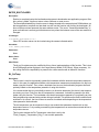
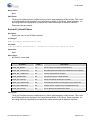
PSoC® Blocks
Resources
Digital
Analog CT
API Memory (Bytes)
Analog SC
Flash
RAM
Pins (per
External I/O)
CY7C603xx, CY7C64215, CY8C21x12, CY8C21x45, CY8C22x45, CY8C23x33, CY8C24x9x, CY8C28x43,
CY8C28x52, CY8C29/27/24/21x3x, CY8CPLC20, CY8CLED04/08/16, CY8CLED0xD, CY8CLED0xG,
CY8CLED16P01, CY8CTST110, CY8CTMG110, CY8CTST120, CY8CTMG120, CY8CTMA120, CY8C20x24,
CY8C20x34
Slave (full API support)
0
0
0
2560
6-128
2
Slave (no API support)
0
0
0
2144
6-128
2
Features and Overview
Industry standard Philips I2C-bus compatible interface
Enables you to reprogram a PSoC device using the I2C system bus instead of in-system programming
pins
The BootLdrI2C User Module implements a bootloader that can reprogram the PSoC device over the I2C
interface. The PSoC device already gives an in-system serial programming interface (ISSP) that allows
downloading new code into the device. However, the bootloader allows a code update to occur through an
industry standard communication interface, such as I2C. This user module can be useful for any device
that has to be reprogrammed in the field. The bootloading information can be sent through an I2C master
device, such as a CY3240 (USB to I2C bridge) or an in-system host processor.
The I2C bootloader requires the I2C Hardware User Module. It does not preclude the use of the I2C bus for
other functions within the PSoC device. The I2C bootloader uses a separate I2C address for its associated
functions. All of the code for the I2C bootloader is programmed in a protected area of EEPROM and
cannot be accidentally overwritten.
Cypress Semiconductor Corporation
Document Number: 001-13258 Rev. *J
•
198 Champion Court
•
San Jose, CA 95134-1709
•
408-943-2600
Revised September 28, 2012
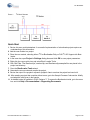
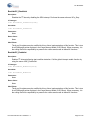
I2C Bootloader
Figure 1.
I2C Block Diagram
Quick Start
1. Review this user module datasheet. A successful implementation of a bootloader project requires an
understanding of this information.
2. Add the user module to a project.
3. Place the user module, selecting either I2C for Bootloader Only or Full I2C API Support with Bootloader.
4. In the menu bar, open Project > Settings dialog box and click OK to save project parameters.
5. Right-click the user module icon and select Boot Loader Tools.
6. Click Get Files. The files boot.tpl, custom.lkp, and flashsecurity.example files are placed in the
project root directory.
7. Close the BootLoader Tools wizard.
8. Generate the source code and compile the project.
9. Review the output file <project>.mp and <project>.hex to see how the project has been built.
10. After creating a project that compiles without errors, go to the Sample Firmware Code section. Modify
and adapt the code given in the sample.
11. A detailed tutorial is available in PSoC Designer™. To access the Bootloader tutorial, go to the menu
bar, and click Help > Documentation > Supporting Documents.
Document Number: 001-13258 Rev. *J
Page 2 of 39
I2C Bootloader
Functional Description
The bootloader is located in a section of Flash memory defined by you (using user module parameters).
This memory space is (must be) write-protected to prevent any accidental modification or corruption. The
reset vector is modified so that when the processor is reset, the bootloader is executed.
The following operations are carried out by the bootloader:
1. When reset, the bootloader calculates a checksum for the Flash user code and verifies it with a checksum written to the last two bytes of Flash memory. If the checksum matches, the previous programming attempt has been successful and the bootloader branches to the beginning of the user code and
the user code can execute.
2. If the checksum does not match, the bootloader executes customizable user code to perform system
critical tasks (such as turning on a fan) and then enters the bootloader mode, where it waits for a 8byte bootloader key from the master. If the previous bootloading has failed (for example, if there was a
power transient), the program enters the bootloader mode due to a checksum mismatch.
3. When the bootloader receives a valid bootloader key from the master, it responds with a status byte
informing the master that it is ready to receive the Flash image.
4. The master sends the updated user code in 64-byte packets with some encoding bytes.
5. The bootloader writes the user code to the Flash. When all the Flash pages are written successfully,
the bootloader performs a Flash verify operation and then a software reset to start the user code.
Note The I2C master must wait 100 ms after each block write, before reading the block status byte to
allow the Flash block write operation.
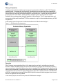
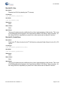
The bootloader portion of the user module gives a method to organize the memory map and major code
functional blocks into areas that are compatible with device reprogramming. The memory organization of
the project is considerably different from that of a conventional PSoC Designer project. Modifications to
the memory map are necessary to meet the minimum device functionality requirements while the device
application is being reprogrammed. Effectively, a project incorporating a bootloader contains two
independent programs supporting different functions. Figure 2 shows the Bootloader memory
organization.
After a project incorporating a bootloader is deployed, the memory locations highlighted in gray are never
reprogrammed. The memory locations highlighted in green may be altered by running the bootloader.
I2C and Sleep
Special care must be taken when using I2C with a project that goes to a sleep state. Before the project
enters a sleep state, follow these steps for proper sleep entry and I2C handling:
1. Ensure that all I2C traffic is complete.
2. Disable the I2C by calling the Stop API.
3. Configure the I2C pins to a analog High-Z drive mode.
Follow these steps when the part wakes from sleep:
1.
2.
3.
4.
Ensure that there is no active I2C traffic.
Enable the I2C by calling the Start API.
Configure the I2C pins to Open-Drain Drives Low drive mode.
Enable Interrupts.
Document Number: 001-13258 Rev. *J
Page 3 of 39
I2C Bootloader
Theory of Operation
Creating a project with a bootloader requires several nonstandard modifications to the PSoC Designer
standard model. To facilitate this, the BootLdrI2C User Module gives customized files and specialized
tools to assist you in bootloader project development. The special tools are accessed by switching to the
Device Editor view and right-clicking the BootLdrI2C User Module icon. In addition to the tools and files
given as part of the user module, a host application example is given as part of the user module
installation that can demonstrate the basic capability of the bootloader. This PC-based application and
source code for Microsoft Visual Studio® 2005 is contained in a .zip file in the installation directory of PSoC
Programmer 3:
[Install path]\Cypress\Programmer\3.xx\Bootloaders\BootLdrI2C\BootLoaderHostApp\…
Figure 2.
Bootloader Memory Organization
Overview
PSoC Designer uses standardized files, built-in data about the part family, and attributes of specific
devices to create compilable projects and correct API definitions. A project with a bootloader requires a
memory map that is considerably different from that of a standard PSoC Designer project. Selection of the
memory areas represents a core design decision that is maintained throughout the life of the design. While
a project without the requirements of a bootloader simply allows the compiler and linker to allocate RAM
and ROM, a bootloader must group RAM and ROM in specific areas so that the program does not crash
while a new application is being loaded.
In the memory layout, there are six key areas of ROM that are managed:
Document Number: 001-13258 Rev. *J
Page 4 of 39
I2C Bootloader
The first is blocks 0 and 1 of ROM. These blocks contain critical interrupt vectors and restart vectors.
Because it is nearly impossible to control read access to these blocks by any operating device, they
are never erased and reprogrammed. The first two blocks of ROM must not be modified and cannot be
placed in any other location.
The second memory area is the relocatable interrupt table. This table may consist of one or two blocks
depending on the architecture of the device. This area contains interrupt and general purpose vectors
to give a jump table for interrupts or code entries that may be altered when a new application is loaded
using the bootloader. For example, this area contains the application start address. The bootloader is
able to use this address to start the new application after the checksum has been validated at power
up. This area is placed at block 2 and 3. After the application and bootloader are deployed, the contents in this area may be rewritten, but its location must not be modified. The characteristics of this
area are similar to the checksum area described in the next section.
The third area of ROM defined is the checksum area. This area is placed at block 4 and it contains
important data that the bootloader software uses to download and verify the foreground application.
The checksum area contains the start address and size in blocks of the foreground application. The
first two bytes of the checksum block are a checksum of the checksum block itself. The last two bytes
are the checksum of the runtime application. The structure of the checksum block contains space for
you to define your own data in addition to that used by the bootloader. This structure is exposed as a
C-structure definition and may be modified as long as data used by the bootloader utility is not
changed or repositioned within the block.
The fourth area of memory to be defined is the area containing the bootloader code itself. This area is
started at block 5. After the project or device containing the bootloader is deployed, this area is not
reprogrammable and cannot be field upgraded.
The fifth area is reserved for customer's data. This may contain configuration data that must persist
through an upgrade using bootload. As shown in the memory map, this area is optional. You can use
the Standard Memory Map if there is no custom data.
The sixth memory area is the application area. This area holds the application image. Because the
code size of the "Bootloader Code" area is expandable, the starting address of this area is adjustable.
The "Appliaction_Start_Block" parameter (in properties window) allows users to set the application
starting address accordingly. This area should occupy all remaining memory.
If your application has code that must always be operational, including during a bootload process, the
design of the BootLdrI2C User Module can allow sufficient customization to accommodate this. The best
way to accomplish this is to add this code to the bootloader ROM area using the assembler AREA
directive. Any RAM used by your code during the bootload process needs to be added to the RAM area
defined for the bootloader.
Definition of Memory Areas in the User Module Parameters
The BootLdrI2C User Module parameters enable you to customize where major program elements are
placed in ROM. The defaults in the user module should give a working initial setup. Use these settings
until a complete project is successfully compiled. After you have a compiled project, you can see the
program memory map and .hex output file to determine how to optimize your program structure. If you
reconfigure the parameters and accidentally create memory area conflicts, it may be difficult to determine
the correct locations without a valid memory map to look at.
Bootloader Utility
The BootLdrI2C User Module gives a complete utility that coexists with a foreground (primary) application.
When the device is started or reset, the bootloader utility is always invoked. Once invoked at system
startup, the bootloader validates the foreground application by calculating a checksum on the foreground
application ROM area. The calculated checksum is compared to the one stored in the checksum block
Document Number: 001-13258 Rev. *J
Page 5 of 39
I2C Bootloader
(which is created with the application). If the two checksums are equal, the bootloader utility allows the
foreground application to execute. If the two checksums are not equal, the bootloader enters a wait loop
for a host application to download a valid application. It also enables its own I2C subsystem to allow the
host to transmit data. When the host system observes this interface enabled, it may choose to execute its
own set of applications. Two download file formats for downloading an application to a target are
automatically supported by the user module tools. The first is an output file named <project_name>.txt and
the second is an output file named <project_name>.dld. Each of these download file formats is supported
by a different demonstration tool.
Download Methods
1. The .txt file can be downloaded by using the CY3240 USB-I2C bridge kit. The associated tool can be
used to download the .txt file format as explained in AN45683. For more information on how to use the
CY3240 USB-I2C bridge, see the application note AN2352 “PSoC®1 Communication - I2C-USB Bridge
Usage”. This method is also discussed in the Appendix of this user module datasheet.
2. A second method of downloading an application is also supported. This method is more complicated
than the previous method, but may give more information on developing a custom I2C download
application for the finished product. A brief discussion of this host application is given here. An example
application and source code is given in the installation directory of PSoC Programmer 3:
[Install path]\Cypress\Programmer\3.xx\Bootloaders\BootLdrI2C\BootLoaderHostApp\…
Two applications are given for demonstrating the I2C bootloader. The first is a PSoC 27000 based
application (a complete PSoC project is included) that is capable of translating RS-232 communication
containing embedded bootloader download records to I2C packets sent to the Bootloader application.
Source code is given for this PSoC project. It can be easily adapted to other PSoC Device architectures.
The second application is a Microsoft Visual Studio application, I2C Bootloader Host, given with an
installer and source code for modification. It can read and parse the download file <fiilename>.dld and
transmit it to the PSoC project mentioned earlier in this section. Source code for this application is also
given for use with Microsoft Visual Studio 2005. This application is for demonstration purposes only and is
not intended for production use or resale.
Note
In some cases, you may need to install the file mscomm32.ocx in your computer. Download this
file from the Microsoft website and install it using the Windows/ accessories/command prompt window and the command:
> regsvr32 mscomm32.ocx
The file regsvr32.exe is in the Windows installation folder windows/system32 (winXP).
The file mscomm32.ocx is available for download from the Microsoft website by searching for the filename
“mscomm32.ocx".
Bootloader Tools
Several tools are available from the shortcut menu accessed by right-clicking on the user module icon.
Select BootLoader Tools from the dropdown menu.
The “Get Files" selections add special versions of boot.tpl, custom.lkp, and HTLinkOpts.lkp that can be
placed in the project or removed. From the main menu, select Tools Restore Default Boot files to remove
these. If the BootLdrI2C User Module is removed, the option to restore the default boot files is no longer
available from the user module icon and can be accessed from the tools tab in the main menu of PSoC
Designer.
Document Number: 001-13258 Rev. *J
Page 6 of 39
I2C Bootloader
Generate Checksum – After your project builds correctly, you can use the bootloader tools to create and
autovalidate checksums. When the bootloader tools selection screen is accessed, the project code is
generated and a complete compile of the entire project is executed. Next, a checksum calculation is
performed on the resulting hex file, which is compared to a checksum stored by the user module. If the
checksums do not match, a message is displayed. You can recalculate and store a new checksum if you
want. If build or compile errors occur in the automated generate and build invoked by the Bootloader Tools
and no hex file is successfully created, an error is reported but no error debug information is displayed in
the build dialog of PSoC Designer. Error reporting is suppressed when the generate and build is invoked
from the automation interface. To debug build errors, it is necessary to use the conventional build and
generate process external to the bootloader tools menu.
Generate dld file – This tool item derives a download file from the hex project output file. This file contains
only the hex blocks that are reprogrammed by the bootloader including the checksum block. The Host
Demonstration application is capable of reading this file and downloading it to a working project
incorporating a bootloader. This download file can be deployed to a field application to upgrade a PSoC
device.
The dld and txt download files are generated by the BootLdrI2C User Module tool and listed in “Output
Files” in Workspace Explorer.
Checksum Semiautomatic Generation
After your project is built and compiled without errors, the application checksum must be generated. The
application checksum is created using one of the utilities accessed by right-clicking on the BootLdrI2C
User Module icon in the Device Editor view and selecting Bootloader Tools. An application checksum
(previously calculated or default) is stored as a hidden user module parameter. When the Bootloader Tools
menu page is invoked, any previous checksum is validated against the one calculated on the current
output\<prj_name>.hex file. Necessarily the checksum cannot be generated before a successful compile.
After a checksum is created, it must be integrated into the compiled files. This requires a second compile.
Special Files Given
You can access several important files by opening the Bootloader Tools menu and selecting Get Files. A
device specific boot.tpl file is placed in the main project directory along with a file called custom.lkp
(ImageCraft), HTLinkOpts.lkp (Hi Tech) and a predefined flashsecurity.txt file. The original versions of
these files are placed in the project backup directory. The purpose of each file is briefly described:
Boot.tpl. – This file contains a relocatable and nonrelocatable definition of interrupt vector tables and
device specific boot setup, which is specified in a relocatable area of the ROM instead of the fixed location
specified in the standard boot.tpl file.
Custom.lkp – When source generation takes place, the custom.lkp file is populated with autogenerated
ROM areas for major code blocks as defined in the user module parameters. Do not modify the following
code blocks in the custom.lkp file:
-bSSCParmBlk: Contains specified critical RAM used during flash operations.
-bBootloader
-bBLChecksum
-bUserAPP: Changes to any of the last three lines result in an error dialog indicating the inability of the
project to detect the correct custom.lkp file.
During code generation, each of the last three lines of the custom.lkp file are rewritten under control of the
code generation software. Changes made within or below the last three lines either cause an error or are
simply lost. You can make changes to the rest of the custom.lkp file. To debug the memory allocation of
the project, comment out all three lines mentioned earlier by inserting a semicolon in the first space. This
Document Number: 001-13258 Rev. *J
Page 7 of 39
I2C Bootloader
allows the linker to place code automatically and can be helpful in determining application code size
requirements.
HTLinkOpts.lkp – When source generation takes place, the HTLinkOpts.lkp file is populated with
autogenerated ROM areas for major code blocks as defined in the user module parameters. Do not modify
the code blocks in the HTLinkOpts.lkp file:
-L-ACODE... & -L-AROM... Lines contain data giving the overall ROM size.
-L-PPD_startup... contains linker directives to locate bootloader specific ROM areas
-L-P
-L-Pbss0= Changes to any of the last several lines result in an error dialog indicating the inability of the
project to detect the correct HTLinkOpts.lkp file.
During code generation, several of the last lines of the HTLinkOpts.lkp file are rewritten under the control
of the code generation software. Changes made within or below the last three lines either cause an error
or are simply lost.
Flashsecurity.example – This is a default file that is laid out according to the default memory map specified
by the default user module parameters. To create the final project, you may have to manually modify this
file according the final memory map and application size for the deployed device and firmware. This is not
the file that is directly used by PSoC Designer. If for some reason the project is updated or tagged for out
of data files, it is inconvenient to have the flashsecurity file overwritten. This would then require repeated
modification by the developer. The given file flashsecurity.example may be edited and renamed as
necessary.
Flashsecurity.txt – This is a default file given by PSoC Designer. The data in this file is added to the .hex
file and instructs the device how to manage access to the internal ROM memory. If memory blocks are
protected in from Write access, the bootloader does not work. Because read and write protection is built
into the programmed PSoC, this file must be correctly configured before the first deployment of the
bootloader.
I2C Interrupt Processing
The standard BootLdrI2C User Module optionally gives a foreground copy of the I2C interrupt processing
module. This code is placed in upgradable memory along with APIs to operate a fully featured I2C slave.
The bootloader itself maintains an internal utility that processes I2C data that is addressed to the
bootloader. This is to overcome the problem of executing code that is being rewritten (this is not a good
programming practice).
Block Entry of Parameters
All memory parameters are entered in the bootloader in Blocks numbered from 0x00 through 0xFF for 16K
devices, 0x00 through 0x7F for 8K devices and 0x00 through 0x1FF for 32K devices. Although this is not
the most convenient format to enter memory addressees, it prevents accidental assignment of partial
block addresses to different sections of the memory map. The PSoC devices in question are only capable
of storing 64 byte flash blocks (128 byte for some device families), and this is a simple way to correctly
maintain the boundaries between different sections of the project code.
Most PSoC parts have 64 byte block sizes. Some new PSoC devices have 128 byte blocks. Two key facts
are:
1. Any Bootloader must write to Flash.
2. PSoC can only write to flash “Block" by “Block.
So for bootloader applications, it is more useful to think of memory as a group of “Blocks" to be written.
Document Number: 001-13258 Rev. *J
Page 8 of 39
I2C Bootloader
To translate from Blocks to absolute addresses, multiply: Abs_addr = block_number X Block Size. Block_0
starts at addr 0, Block_n starts at address n x Block_size. All blocks are delimited in hex for the bootloader
parameters, so a hex address can be obtained by multiplying by 0x40 (64-byte blocks) or 0x80 (128-byte
blocks).
Hex output files contain an absolute address for each line. Regardless of the block size of the device in
question (0x40/0x80), the hex output file breaks the code into lines of 64(d)/0x40 bytes per line. As a
result, for a 64 byte block device each line represents a block of code. For a 128 byte block device, two
lines from the hex file go into a block (because block 0 starts at address 0, 128 byte blocks must be
ALWAYS considered to have an “even" half representing the lower (address) half and an “odd" half
representing the upper (address) half).
See a hex file and become familiar with the flash block size for the part that you are working with.
Host Application Debugging
An application with a built-in bootloader may be difficult to debug. As a result, there are additional
adjustments that can be made within the BootLdrI2C User Module files. These are contained in the file
BootLdrI2C_Bootloader.inc. This file has a section that contains the following equates:
BOOT_TIMEOUT:
CHECKSUM_ON_CKSUMBLK:
EQU
EQU
40
1
;set to zero to make timeout infinite
;Apply a checksum to the checksum block
;(adds compile steps and code to verify)
The BOOT_TIMEOUT equate enables you to lengthen, shorten, or make infinite code that timeouts if no
communication is received from a host after your command calls the bootloader. This may be useful when
developing or debugging the host application.
The second equate controls the use of the checksum inside the checksum block. If this equate is set to 0,
no verification is done on the checksum inside the checksum block. A checksum verification is still
performed on the entire user application area as defined in the user module parameters.
Placement
The I2CHW User Module allows two choices of SCL and SDA P1[5]/P1[7] or P1[0]/P1[1] and does not
require any digital or analog PSoC blocks. There are no placement restrictions. Placement of multiple I2C
modules is not possible because the I2C module uses a dedicated PSoC resource block and interrupt.
Document Number: 001-13258 Rev. *J
Page 9 of 39
I2C Bootloader
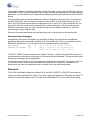
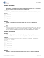
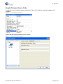
Parameters and Resources
Default parameters are for informational purposes only. Defaults in your project may be tailored to the
block size of the part in use, or may have been adjusted to give adequate sizes of code areas. After your
project is compiled and tested, you can adjust block sizes to optimize memory use.
Figure 3.
Default Parameters
Figure 3 shows the default user module parameters. Periodically, these parameters may be updated in the
source code of the user module, and may differ from the given example.
All buffer names are written to describe their use by an I2C master. For example, the I2Cs_pRead_Buf
refers to the location in RAM containing data to be read by the I2C master.
Slave_Addr_HEX
This is a Slave and MultiMasterSlave parameter. It selects the 7-bit slave address that is used by the
I2C master to address the slave or the MultiMasterSlave when it is in slave mode. Valid selections are
Document Number: 001-13258 Rev. *J
Page 10 of 39
I2C Bootloader
from 0x00-0x7F. Because this is the upper 7 bits of the address, the actual address appears to be
doubled inside the code.
Boot_Loader_Addr_HEX
Selects the 7-bit slave address that is used by the I2C master to address the I2C BootLoader slave
device. Valid selections are from 0 - 7Fh. Because this is the upper 7 bits of the address, the actual
address appears to be doubled inside the code. The parameter value must differ from the
Slave_Addr_HEX parameter value.
Read_Buffer_Types
Selects what types of buffers are supported for data reads. Two selections are available: RAM ONLY
or RAM OR FLASH. Selection of RAM ONLY removes code and variables required to support direct
Flash-ROM reads. Select RAM OR FLASH to give code and variable support for reading either RAM
buffers or Flash-ROM buffers to transmit data to the master. Select RAM OR FLASH to enable
support for API calls to select whether a RAM- or Flash-read buffer is used.
Communication_Service_Type
This parameter enables you to select between an interrupt based data processing strategy and a
polled strategy. In the interrupt based strategy, a transfer is initiated against a predefined buffer. Data
is then moved in or out of the buffer as quickly as possible in the background. An ISR routine is
included which handles data movement. When you select the polled data processing strategy, you
are in control of when data movement takes place. To implement a polled strategy, you must periodically call the function BootLdrI2C_Poll() (see the I2C.h files for the exact instance name). Each time
the polling function is called, a single byte is transferred. Other I2C functions are used identically. The
polled communication strategy may be used in a situation where interrupt latency is critically important
(and asynchronous communication interrupts may cause problems). Another use is when you want
absolute control of when data is transferred. A drawback of polling is that when the I2C state machine
is enabled, the bus is stalled automatically after each byte until the polling function is called.
The polling function is available only for the Slave and MultiMasterSlave implementations of I2C. The
Single Master implementation offers API functions to support byte-wise data transfers.
Using the polling function from an interrupt is not recommended. The definition of a timed interrupt to
call the poll function may call the function so often that no other data processing can take place. The
poll service is not re-entrant and the function cannot be called until it completes its processing.
I2C Clock
Specifies the desired clock speed at which to run the I2C interface. There are three I2C_Clock speeds
available:
50K Standard
100K Standard
400K Fast (when CPU_Clk_speed is greater than 6 MHz)
I2C_Pin
Selects the pins from Port 1 to be used for I2C signals. PSoC Designer automatically selects the
proper drive mode for these pins. Note that all pins on Port 1 other than SCL, SDA and the optional
interrupt pin are set to HI-Z analog mode during bootloading.
CPU_Clk_speed_(CY8C27xA)
Note
This parameter is available only for parts in the CY8C27xxx family.
Document Number: 001-13258 Rev. *J
Page 11 of 39
I2C Bootloader
Specifies the range of CPU clock speeds under which a CY8C27xxx silicon revision A device operates. The CY8C27xA refers to the older CY27xxx devices that are no longer recommended for new
designs. In the PSoC Designer device catalog, the CY8C27x silicon revision A are at the bottom of
the catalog and are preceded with a “Not Recommended for New Designs" notice. They can be differentiated from the new version in that the new versions of the parts have the letter ‘X’ in the part name.
The letter X is used to designate Pb-free parts. This parameter is needed to ensure that special code
handling is inserted at higher CPU clock speeds and eliminated to avoid unnecessary overhead at
lower CPU clock frequencies.
CPU_Clk_speed_(CY8C27xA) value
Use
6 MHz or less
Use this setting if the CPU clock speed is 6 MHz or less. This eliminates
any unnecessary code.
Above 6 MHz (CY8C27x A ONLY)
Use this setting if the CPU clock speed is above 6 MHz and the chip used
is from the CY8C27xxx silicon revision A family. This ensures proper
functionality of the user module at the cost of some additional overhead.
Not CY8C27xA
Use this setting for any chip outside the CY8C27xxx silicon revision A
device family. This applies to any CY8C29/24/22xxx part or the
CY8C27xxx parts that have the letter ‘X’ in their part number in the device
catalog. Choosing this value eliminates unnecessary code.
Parameters defined for the bootloader enable you to define where a major program block is located
when the program is compiled and linked. In some cases, a project may be developed on a 27xxx
POD that uses an older revision of silicon (and so requires these clock speed specific settings), while
the target part is a newer version of silicon. No significant project impact is experienced by including
the clock speed parameters appropriate for older silicon in newer devices.
ApplicationCode_Start_Block
This is the first block of code assigned to the User Application. This code must be bootloadable/writeable. This parameter is also used by the Bootloader Tools to determine which blocks of code should
be processed for a .dld file and which blocks of code to calculate checksums on. This variable is propagated into the checksum block for use when the bootloader utility automatically verifies the application checksum.
The default address specified by the parameter block default may be calculated by multiplying the
device block size (0x40 or 0x80) times the block in the parameter.
Bootloader_Key
This is the key value prepended to the transactions sent to the bootloader application, representing
an extra verification step. This step ensures that the bootloader upgrade utility is not accidentally
invoked.
The default value "0001020304050607".
Flash_Program_Temperature_Deg_C
This is the typical programming temperature expected when the device is reprogrammed. Programming the device at a different temperature than that specified in this parameter may adversely effect
program retention.
Matching the program temperature parameter to the actual temperature during bootload impacts
memory retention and the maximum number of write cycles. PSoC implements a stronger flash write
Document Number: 001-13258 Rev. *J
Page 12 of 39
I2C Bootloader
at colder temperatures. Bootloading at significantly lower temperatures than the parameter setting
may result in reduced memory retention. For this reason, you must take precautions to ensure that
the bootloader is never operated more than 20°C from the value in this parameter. See the Cypress
device specification for more information.
Ignore_N_I2C_Prefix_Bytes
Note
The RS-232 to I2C translator project sends 2 prefix bytes to the device. As a result, the correct setting for this parameter when using the given demonstration applications is 2. This is also used for
certain SM-bus protocols based on I2C. This parameter enables you to configure the Bootloader to
ignore a variable number of prefix bytes.
BootLdrI2C_ver
This is the version of the bootloader. It is currently not used by the internal firmware, but is available
as part of the Checksum block. You can set it up and use it to verify the correct version of bootloader
executable code.
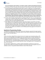
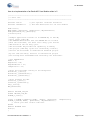
I2C Topology Selection Options
When placing a BootLdrI2C User Module, you must decide which I2C topology to implement for the
bootloader project.
I2C Operation for Bootloader only: This option gives I2C communication for the bootloader only. No
user module API support is included for I2C slave communications. Select this option if your application uses I2C communication for bootloading only.
Full I2C API Support with Bootloader: This option gives code to support the application use of I2C in
addition to Bootloader through I2C. Select this option if you plan to use I2C communication in your
application for other purposes besides bootloading.
Figure 4.
I2C Topology Options
Document Number: 001-13258 Rev. *J
Page 13 of 39
I2C Bootloader
Common Problems
Updating Bootloader Projects, Service Pack Upgrades, and Compilers
Avoid changes to the PSoC Developer environment when using a bootloader application. This includes
not updating PSoC Designer, not updating the BootLdrI2C User Module, and not changing the compiler.
The reason behind this is that initially the bootloader and application are compiled together, but after a
bootloadable system is deployed, only the application section is reprogrammed. A new or revised
application must be compiled with the identical version of the BootLdrI2C User Module, so that the new
application matches the bootloader from the original deployment. Ideally, all versions of the elements in
the development environment are compatible. However, in the case of a bootloader, it is essential to
maintain that compatibility. By not changing the development environment compatibility, risks can be
eliminated.
Although multiple compilers are supported by PSoC Designer, a bootloader compiled under one compiler
may not be compatible with an application compiled under another. Also, the implementation of RAM
paging may differ from one compiler to the other. Another difficulty is that, because a bootloader and
application are compiled together, it is not possible debug a bootloader/application pair that had
mismatches in the development tools used.
RAM Allocation Problems With the HI-TECH Compiler
Some user modules use the memory in large arrays or use a large amount of RAM on page 0.
The default location for user module memory is page 0.
The bootloader demands memory at the lowest locations of page 0.
The default for HI-TECH local variables and for InterruptRAM is page 0.
With these items competing for space on RAM page 0, it is possible to run out of memory on page 0. If this
is a problem, select Project -> Settings -> Compiler, and add a line to the Options box for HI-TECH:
--AUTOBANK=1
This option moves automatic C variables to memory page 1. You can choose any memory page up to the
maximum available for the device in use. See the HI-TECH manual for further information about the -AUTOBANK option.
Internal Use of the Watch Dog Timer
Coordination with the watchdog timer is linked to the global parameter: WATCHDOG_ENABLE contained
in the file globalparams.inc. If the project uses a watchdog timer, conditionally compiled code linked to the
global parameter automatically sets the watchdog during bootload checksum and download operations.
The CPU clock speed effects how fast the watchdog timer is updated. A practical minimum setting for the
watchdog timer is about 0.125s.
Improper Settings in Flashsecurity.txt
The default settings for this file are set when the project is created. An example configuration is given in
the file “Flashsecurity.example". Flashsecurity.example is given with the BootLoader Tools - Get Files user
module menu item. The map must allow flash write at all the locations that are eventually bootloaded. One
strategy is to make all blocks writeable. Another is to take a moment to layout your memory map now and
edit this file accordingly. No matter which strategy is chosen, taking action at the beginning of the project is
quicker than debugging it later. You must write-protect the areas of code used by the bootloader
executable. Failure to correctly map flash security can be a contributing factor in a broken system and an
extremely difficult debug task.
Document Number: 001-13258 Rev. *J
Page 14 of 39
I2C Bootloader
For development and debugging purposes, a flash security of 'U' (unprotected) is recommended for the
application area. For final production, a flash security setting of 'R' (read protected) is recommended on
the application area to prevent external reads and writes from occurring.
Incorrect Relocatable Code Start Address (Linker Parameter ImageCraft Compiler Only)
The memory map for a bootloader project is considerably different than that for a conventional project. As
a result, the relocatable code start address usually needs to be altered. This is a common source of the
errors generated by the linker when it attempts to write more than one block code to the same address.
This parameter can be changed in the Relocate code start address filed in the Project > Settings > Linker
tab. Calculate the absolute hex start address as a little more than the highest block used by the bootloader
code, or to occupy an unused area of ROM. For the I2C version of the bootloader setting, this value to
0xA40 should be adequate (if the default values of the other parameters are used).
Note
When unplacing the BootLdrI2C User Module, the Relocatable Code Start Address does not reset
to its original value. You must change it back manually to save ROM space.
Memory Overlap
To correct the relocatable code start address (see previous section), use a leading semicolon to comment
out the last three lines of the custom.lkp file, attempt to build the file again, and examine the resulting
memory map. Memory overlap problems are difficult to diagnose, because they prevent output files from
being generated. Modifying the custom.lkp file may allow the linker to place object blocks, which then
gives a starting point to correct the memory overlap root cause.
Power Stability
Power noise, glitches, brownout, slow power ramp, and poor connections can cause difficult to diagnose
problems with flash programming. Program execution is rapid in comparison to power ramps, and in some
cases, a part may still have changing power levels when flash programming takes place. One example is
a status write to flash at power up. You must evaluate your use model and the potential for changing
power supply conditions during flash operations. Poor power stability may contribute to nonfunctional parts
and may cause poor flash retention.
Downloading a New File Causes the Device to Stop Working
It is possible to unintentionally construct applications with no facility to enter the bootloader utility. For
example, a main{} function with a simple while(1); loop never returns and never enters the bootloader. As
a result, it cannot be reprogrammed after it begins executing (as long as it has a correct checksum). There
are multiple strategies to address this problem. No default method is included in this user module. A few
suggestions are:
1. Apply a reset condition that allows a period of time when the bootloader is enabled when the device
first powers up. By setting timeout parameters, the device could be configured to enter the bootloader
upon reset, and exit to the foreground application when the timeout expires.
2. Set a test at some point in the code that causes the device to enter the bootloader. This could be switch
closure or holding a port pin low/high.
3. Enable the I2C application resource and create an I2C command that causes the device to
enter the bootloader. Generally, if I2C is enabled by the main routine, the bootloader address can
be used to cause the device to enter the bootloader.
4. Use the Watch Dog Timer to reset the device if it is not serviced regularly. This could be combined with
one of the previous strategies to allow a WDT interrupt to initiate a bootloadable state. When reset
Document Number: 001-13258 Rev. *J
Page 15 of 39
I2C Bootloader
from a watch dog timer reset condition, it is possible to monitor a status bit associated with the watchdog timer to detect that this is the cause of the reset condition (see the Technical Reference Manual).
5. Two projects have been developed and the bootloader in each is different in some subtle way. Remember that bootloading implies that programming part of a device is taking place. This implies that the
implementation of the bootloader for each of two mutually reprogrammable applications must be identical. All bootloader parameters and relocatable code start addresses must be identical (that is, different from first application block). Debug strategies for this problem include comparison of the two hex
files in question, paying particular attention to the areas of hex code used by the bootloader. Another
method is to compare the <project>.lst files. The bootloader uses some redirect vectors to allow certain application address parameters to change. All these jump vectors must match for an application
and a bootloader. After a bootloader is deployed to a field application, there is no way to alter the code
within it. A future application must still ‘agree’ about where mutually used jump vectors are stored.
6. The PSoC based translator app hangs when a bootload operation fails. There is an if-def based timeout that can be configured to allow the PSoC base translator to drop a communication attempt after a
variable software loop. For debugging purposes, you can turn this software switch on or off. Examine
the source code of the project for the timeout switch.
7. Power Stability. Power noise, glitching, brownout, slow power ramp poor connections. All of these
power problems can cause difficult to diagnose problems with flash programming. Program execution
is rapid with respect to power ramps, and in some cases, a part may still have changing power levels
when flash programming takes place. One example is a status write to flash at power up. You must
evaluate your use model and the potential for changing power supply conditions during flash operations. Poor power stability may contribute to non functional parts and may appear to be the result of
poor flash retention.
Application Programming Interface
The Application Programming Interface (API) firmware gives high level commands that support sending
and receiving multi-byte transfers. Read buffers may be set up in RAM or Flash memory. Write buffers can
only be set up in the RAM memory.
Note
In this, as in all user module APIs, the values of the A and X register may be altered by calling an API
function. It is the responsibility of the calling function to preserve the values of A and X before the call if
those values are required after the call. This “registers are volatile" policy was selected for efficiency
reasons and has been in force since version 1.0 of PSoC Designer. The C compiler automatically takes
care of this requirement. Assembly language programmers must ensure their code observes the policy,
too. Though some user module API function may leave A and X unchanged, there is no guarantee they
may do so in the future.
For Large Memory Model devices, it is also the caller's responsibility to preserve any value in the
CUR_PP, IDX_PP, MVR_PP, and MVW_PP registers. Even though some of these registers may not be
modified now, there is no guarantee that will remain the case in future releases.
Document Number: 001-13258 Rev. *J
Page 16 of 39
I2C Bootloader
ENTER_BOOTLOADER
Description:
Routine to completely setup the bootloader and prepare to download a new application program. After
this routine is called, it does not return unless a timeout or reset occurs.
The GenericBootloaderEntry function name is always located at the same physical ROM address, so
that an application compiled at a later date can still use this function call to enter the bootloader. All
three of these routines represent the same address vector. The vector “GenericBootloaderEntry" is
given so that there is an entry point that does not vary when the instance name of the user module is
changed.
C Prototype:
void ENTER_BOOTLOADER(void);
Other API function names can be invoked using the names indicated earlier.
Assembler:
lcall ENTER_BOOTLOADER
Parameters:
None
Return Value:
None
Side Effects:
The A and X registers may be modified by this or future implementations of this function. This is true
for all RAM page pointer registers in the Large Memory Model (CY8C29xxx). When necessary, it is
the calling function's responsibility to preserve the values across calls to fastcall16 functions.
BL_SetTemp
Description:
This function is used to dynamically update the bootloader with the latest die temperature measurement. In this case, the application obtains a die temperature measurement and passes it to the bootloader using this function. Then, when a bootload event occurs, the bootloader programs the flash
optimally based on the temperature passed to it using this function.
It is recommended that you periodically measure (or otherwise determine) the device's die temperature during run time. Every time the die temperature is measured, it should be passed to the bootloader using this function. The bootloader uses the die temperature passed to it to optimally vary the
flash programming erase and write periods during a bootload. This optimizes the flash's retention and
endurance. As a result, the time it takes to execute a bootload varies depending on the temperature
value passed to the bootloader.
The die temperature can be measured using a user module that measures the device's on-chip
temperature sensor. Or, by reading or measuring the temperature from some other external device or
temperature sensor.
This function rewrites the Die Temperature value that is set by the
"Flash_Program_Temperature_Deg_C" user module parameter.
Document Number: 001-13258 Rev. *J
Page 17 of 39
I2C Bootloader
C Prototype:
void BL_SetTemp (CHAR cTemp);
Assembler:
mov A, cTemp
lcall BL_SetTemp
Example Code:
void main(void)
{
CHAR cDieTemp = -20; // Allocate a variable to hold the die temperature
// Use -20C as the default value
...
// Measure die temperature here and copy to cDieTemp variable
BL_SetTemp(cDieTemp); // Update Bootloader with real die temperature
ENTER_BOOTLOADER(); // Run the BootLoader
...
}
Parameters:
cTemp: Die Temperature in Celsius degrees.
Return Value:
None
Side Effects:
The A and X registers may be modified by this or future implementations of this function. This is true
for all RAM page pointer registers in the Large Memory Model (CY8C29xxx). When necessary, it is
the calling function's responsibility to preserve the values across calls to fastcall16 functions.
BootLdrI2C_Start
Description:
Empty routine given for compatibility.
C Prototype:
void
BootLdrI2C_Start(void);
Assembler:
lcall BootLdrI2C_Start
Parameters:
None
Return Value:
None
Side Effects:
The A and X registers may be modified by this or future implementations of this function. This is true
for all RAM page pointer registers in the Large Memory Model (CY8C29xxx). When necessary, it is
the calling function's responsibility to preserve the values across calls to fastcall16 functions.
Document Number: 001-13258 Rev. *J
Page 18 of 39
I2C Bootloader
BootLdrI2C_DisableInt
Description:
Disables the I2C slave by disabling the SDA interrupt. Performs the same action as I2Cs_Stop.
C Prototype:
void
BootLdrI2C_DisableInt(void);
Assembler:
lcall BootLdrI2C_DisableInt
Parameters:
None
Return Value:
None
Side Effects:
The A and X registers may be modified by this or future implementations of this function. This is true
for all RAM page pointer registers in the Large Memory Model (CY8C29xxx). When necessary, it is
the calling function's responsibility to preserve the values across calls to fastcall16 functions.
BootLdrI2C_EnableInt
Description:
Enables I2C interrupt allowing start condition detection. Call the global interrupt enable function by
using the macro: M8C_EnableGInt.
C Prototype:
void
BootLdrI2C_EnableInt(void);
Assembler:
lcall BootLdrI2C_EnableInt
Parameters:
None
Return Value:
None
Side Effects:
The A and X registers may be modified by this or future implementations of this function. This is true
for all RAM page pointer registers in the Large Memory Model (CY8C29xxx). When necessary, it is
the calling function's responsibility to preserve the values across calls to fastcall16 functions.
Document Number: 001-13258 Rev. *J
Page 19 of 39
I2C Bootloader
BootLdrI2C_Poll() and BootLdrI2C_BootLdr_Poll()
Description:
Used when the Communication_ Service_Type parameter is set to Polled. This function gives a user
controlled entry into the I/O processing routine. If Communication_Service_Type parameter is set to
Interrupt, the function does nothing.
C Prototype:
void BootLdrI2C_Poll(void);
void BootLdrI2C_BootLdr_Poll(void);
Assembler:
lcall BootLdrI2C_Poll
lcall BootLdrI2C_BootLdr_Poll
Parameters:
None
Return Value:
None
Side Effects:
One I2C event is processed each time this routine is called and status variables are updated. An event
constitutes either an error condition, an I/O byte, or in certain cases, a stop condition. There are three
possible results from calling this routine:
1. No action if no data is available.
2. Reception or transmission of an address or data byte if one is available.
3. Processing of a stop ‘event’ when an external master has completed its write operation. When a stop
state is processed at the end of a write operation, only status variables are updated. If an I2C byte is
pending when a stop state is processed, the I2CHW_Poll function must be called again to process it.
The I2CHW_Poll() function has no effect if Communication_Service_Type is set to Interrupt. When a
start/restart condition and an address is detected on the bus the bus is stalled until the I2CHW_Poll()
function is called. If the address is NAK’ed, subsequent bytes transferred for that transaction are
ignored until another start/restart and address is detected. Otherwise, the I2C bus is stalled for each
data byte until the I2CHW_Poll() function is called. The I2C data is stalled by the I2C hardware until
this function is called if the Communication_Service_Type is set to Polled. For received data, the bus
is stalled at the end of the byte and before an ACK/NAK is generated by holding the SCL (clock) line
low. For transmitted data, the bus is stalled immediately after the ACK/NAK bit is generated externally.
These two functions are compatible with the following restrictions: If the Bootloader is active and can
be entered by an external application I2C command, the API BootLdrI2C_BootLdr_Poll() must be
used. If an I2C address that is not the Bootloader address is detected, this address is tested and
passed on to the foreground I2C interrupt process, which also tests the address. If the Bootloader is
inactive, use of the BootLdrI2C_Poll() API does not give the I2C address to the internal bootloader
data process routine. The address and subsequent data is instead passed directly to the foreground
routine.
Document Number: 001-13258 Rev. *J
Page 20 of 39
I2C Bootloader
BootLdrI2C_Stop
Description:
Disables the I2CHW by disabling the I2C interrupt.
C Prototype:
void
BootLdrI2C_Stop(void);
Assembler:
lcall BootLdrI2C_Stop
Parameters:
None
Return Value:
None
Side Effects:
The A and X registers may be modified by this or future implementations of this function. This is true
for all RAM page pointer registers in the Large Memory Model (CY8C29xxx). When necessary, it is
the calling function's responsibility to preserve the values across calls to fastcall16 functions.
BootLdrI2C_EnableSlave
Description:
Enables the I2C Slave function for the I2C HW block by setting the Enable Slave bit in the I2C_CFG
register.
C Prototype:
void
BootLdrI2C_EnableSlave(void);
Assembler:
lcall BootLdrI2C_EnableSlave
Parameters:
None
Return Value:
None
Side Effects:
The A and X registers may be modified by this or future implementations of this function. This is true
for all RAM page pointer registers in the Large Memory Model (CY8C29xxx). When necessary, it is
the calling function's responsibility to preserve the values across calls to fastcall16 functions.
Document Number: 001-13258 Rev. *J
Page 21 of 39
I2C Bootloader
BootLdrI2C_DisableSlave
Description:
Disables the I2C Slave function by clearing the Enable Slave bit in the I2C_CFG register.
C Prototype:
void
BootLdrI2C_DisableSlave(void);
Assembler:
lcall BootLdrI2C_DisableSlave
Parameters:
None
Return Value:
None
Side Effects:
The A and X registers may be modified by this or future implementations of this function. This is true
for all RAM page pointer registers in the Large Memory Model (CY8C29xxx). When necessary, it is
the calling function's responsibility to preserve the values across calls to fastcall16 functions.
The following API are available only for FullAPISupport:
BootLdrI2C_InitWrite
Description:
The BootLdrI2C_InitWrite routine initializes a data buffer pointer for the slave to use to deposit data,
and zeroes the value of a count byte for the same buffer.
C Prototype:
void
BootLdrI2C_InitWrite(BYTE * pBootLdrI2C_WriteBuf, BYTE
BootLdrI2C_Write_Count);
Assembler:
mov A, Write_Count
push A
move A, >pWriteBuf
push A
mov A, <pWriteBuf
push A
lcall BootLdrI2C_InitWrite
Parameters:
pWriteBuf: A pointer to a RAM buffer location. Write_Count: The length of the write buffer.
Return Value:
None
Side Effects:
The A and X registers may be modified by this or future implementations of this function. The same
is true for all RAM page pointer registers in the Large Memory Model (CY8C29xxx). When necessary,
it is the calling function's responsibility to preserve the values across calls to fastcall16 functions.
Document Number: 001-13258 Rev. *J
Page 22 of 39
I2C Bootloader
BootLdrI2C_InitRamRead
Description:
The BootLdrI2C_InitRamRead routine initializes a data buffer pointer for the slave to use to retrieve
data from, and zeroes the value of a count byte for the same buffer.
C Prototype:
void BootLdrI2C_InitRamRead(BYTE * pBootLdrI2C_ReadBuf, BYTE
BootLdrI2C_Read_Count);
Assembler:
mov A, Read_Count
push A
move A, >pReadBuf
push A
mov A, <pReadBuf
push A
lcall BootLdrI2C_InitRamRead
Parameters:
pReadBuf: A pointer to a RAM buffer location. Read_Count: The length of the read buffer.
Return Value:
None
Side Effects:
The A and X registers may be modified by this or future implementations of this function. This is true
for all RAM page pointer registers in the Large Memory Model (CY8C29xxx). When necessary, it is
the calling function's responsibility to preserve the values across calls to fastcall16 functions.
BootLdrI2C_InitFlashRead
Description:
The BootLdrI2C_InitFlashRead routine initializes a flash data buffer pointer for the slave to use to
retrieve data from, and zeroes the value of a count byte for the same buffer.
C Prototype:
void BootLdrI2C_InitFlashRead(const BYTE * pBootLdrI2C_flashaddr,
BootLdrI2C_Read_CountHI);
unsigned int
Assembler:
mov A, >Read_Count
push A
mov A, <Read_Count
push A
move A, >pflashaddr
push A
mov A, <pflashaddr
push A
lcall BootLdrI2C_InitFlashRead
Parameters:
pflashaddr: A pointer to a Flash data buffer location. Read_Count: The length of the read buffer.
Document Number: 001-13258 Rev. *J
Page 23 of 39
I2C Bootloader
Return Value:
None
Side Effects:
The A and X registers may be modified by this or future implementations of this function. This is true
for all RAM page pointer registers in the Large Memory Model (CY8C29xxx). When necessary, it is
the calling function's responsibility to preserve the values across calls to fastcall16 functions.
Read status bits are cleared.
BootLdrI2C_bReadI2CStatus
Description:
Returns the value in the I2CStatus variable.
C Prototype:
BYTE
BootLdrI2C_bReadI2CStatus(void);
Assembler:
lcall BootLdrI2C_bReadI2CStatus ; Accumulator contains the status on return
Parameters:
None
Return Value:
bI2CStatus - status data
Constant
Value
Description
I2CHW_RD_NOERR
01h
Data is read by the master, normal ISR exit.
I2CHW_RD_ OVERFLOW
02h
More data bytes were read by the master than were available.
I2CHW_RD_ COMPLETE
04h
A read is initiated and is complete.
I2CHW_READFLASH
08h
The next read is from a Flash location.
I2CHW_WR_NOERR
10h
Data is successfully written by the master.
I2CHW_WR_OVERFLOW
20h
The master has written too many bytes for the write buffer.
I2CHW_WR_COMPLETE
40h
A master write is completed by a new address or stop.
I2CHW_ISR_ACTIVE
80h
The I2C ISR has not exited and is active.
Side Effects:
The A and X registers may be modified by this or future implementations of this function. This is true
for all RAM page pointer registers in the Large Memory Model (CY8C29xxx). When necessary, it is
the calling function's responsibility to preserve the values across calls to fastcall16 functions.
Document Number: 001-13258 Rev. *J
Page 24 of 39
I2C Bootloader
BootLdrI2C_ClrRdStatus
Description:
Clears the status bits in the Control/Status register, but does not alter buffer addresses, counts, or the
Flash/Ram Read bit.
C Prototype:
void
BootLdrI2C_ClrRdStatus(void);
Assembler:
lcall BootLdrI2C_ClrRdStatus
Parameters:
None.
Return Value:
None
Side Effects:
The A and X registers may be modified by this or future implementations of this function. This is true
for all RAM page pointer registers in the Large Memory Model (CY8C29xxx). When necessary, it is
the calling function's responsibility to preserve the values across calls to fastcall16 functions.
BootLdrI2C_ClrWrStatus
Description:
Clears the status bits in the Control/Status register, but does not alter buffer addresses, counts, or the
Flash/Ram Read bit.
C Prototype:
void
BootLdrI2C_ClrWrStatus(void);
Assembler:
lcall BootLdrI2C_ClrWrStatus
Parameters:
None.
Return Value:
None
Side Effects:
The A and X registers may be modified by this or future implementations of this function. This is true
for all RAM page pointer registers in the Large Memory Model (CY8C29xxx). When necessary, it is
the calling function's responsibility to preserve the values across calls to fastcall16 functions.
Document Number: 001-13258 Rev. *J
Page 25 of 39
I2C Bootloader
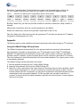
Sample Firmware Source Code
Configure the user module parameters as shown in Figure 5, for both the assembly language and C
examples.
Figure 5.
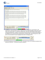
User Module Parameters
Ensure that the code start address is set correctly.
Figure 6.
Setting Code Start Address
Document Number: 001-13258 Rev. *J
Page 26 of 39
I2C Bootloader
Here is an implementation of an BootLdrI2C User Module written in C:
//---------------------------------------------------------------------// C main line
//---------------------------------------------------------------------#include <m8c.h>
#include "PSoCAPI.h"
// part specific constants and macros
// PSoC API definitions for all user modules
BYTE result;
WORD wAddr, wByteCount, cTemperature, wByteReadCount;
BYTE pbDataDest[10], pbData[10];
void main(void)
{
//example application consists of an EEPROM UM, an LED UM,
//and a 16-bit timer UM.
//the EEPROM demonstrates that the EEPROM UM can co-exist
//with the bootloader, the timer sets a duty cycle and the
//LED blinks at the set duty cycle.
//The bootloader UM provides the capability to modify
//the project (LED duty cycles are conveniently visible.)
//and use the bootloader to download the modified project.
//by the time the main() function is executed the project
//has already been checksummed and verified by the bootloader.
//init EEPROM data
wAddr = 0;
wByteCount = 64;
wByteReadCount = 10;
cTemperature = 25;
//start the bootloader running in the background
BootLdrI2C_1_Start();
BootLdrI2C_1_EnableSlave();
BootLdrI2C_1_EnableInt();
//start blinking the LED
Counter24_1_Start();
Counter24_1_EnableInt();
LED_1_Start();
M8C_EnableGInt;
#define INCLUDE_LIB_API
#ifdef INCLUDE_LIB_API
E2PROM_1_Start();
result = E2PROM_1_bE2Write( wAddr, pbData, wByteCount,
E2PROM_1_E2Read( wAddr, pbDataDest, wByteReadCount);
// Insert your main routine code here.
#endif
#define BUSMODE 0xf5
while(1)
{
Document Number: 001-13258 Rev. *J
cTemperature);
Page 27 of 39
I2C Bootloader
asm("nop");
}
}
Here is an implementation of the BootLdrI2C User Module written in assembly language:
;--------------------------------------------------------------------; Assembly main line
;--------------------------------------------------------------------include "m8c.inc"
include "memory.inc"
include "PSoCAPI.inc"
; part specific constants and macros
; Constants & macros for SMM/LMM and Compiler
; PSoC API definitions for all user modules
export _main
_main:
;
lcall
lcall
lcall
Insert your main assembly code here.
BootLdrI2C_1_Start
BootLdrI2C_1_EnableSlave
BootLdrI2C_1_EnableInt
//start blinking the LED
lcall Counter24_1_Start
lcall Counter24_1_EnableInt
lcall LED_1_Start
M8C_EnableGInt
.terminate:
jmp .terminate
}
Document Number: 001-13258 Rev. *J
Page 28 of 39
I2C Bootloader
Configuration Registers
This section describes the PSoC Resource Registers used or modified by the BootLdrI2C User Module.
Table 1.
Resource I2C_CFG: Bank 0 reg[D6] Configuration Register
Bit
Value
7
Reserved
6
PinSelect
5
Bus Error
IE
4
Stop IE
3
Clock
Rate[1]
2
Clock
Rate[0]
1
0
Enable
Master
Enable
Slave
Pin Select: Selects either SCL and SDA as P1[5]/P1[7] or P1[0]/P1[1].
Bus Error Interrupt Enable: Enable I2C interrupt generation on a Bus Error.
Stop Error Interrupt Enable: Enable an I2C interrupt on an I2C Stop condition.
Clock Rate[1,0]: Select from 3 valid Clock rates; 50, 100, and 400 Kbps (400 Kbps when CPU_Clk_speed
is greater than 6 MHz).
Enable Master: Enable the I2C HW block as a bus Master.
Enable Slave: Enable the I2C HW block as a bus Slave.
Table 2.
Resource I2C_SCR: Bank 0 reg[D7] Status Control Register
Bit
Value
7
Bus Error
6
Lost Arb
5
4
Stop Status ACK out
3
Address
2
Transmit
1
0
Last Rec’d Byte
Bit (LRB)
Complete
Bus Error: Indicates a Bus Error condition is detected.
Lost Arbitration: In MultiMaster mode indicates loss of arbitration for this device (the device does not
control the bus).
Stop Status: An I2C stop condition has been detected.
ACK out: direct the I2C block to Acknowledge (1) or Not Acknowledge (0) a received byte.
Address: Received or transmitted byte is an address.
Last Received Bit (LRB): Value of last received bit (bit 9) in a transmit sequence, status of Ack/Nak from
destination device.
Byte Complete: 8 data bits have been received. For Receive Mode, the bus is stalled waiting for an
Ack/Nak. For Transmit Mode Ack Nak has also been received (see LRB) and the bus is stalled for the next
action to be taken.
Table 3.
Resource I2C_DR: Bank 0 reg[D8] Data Register
Bit
Value
7
6
5
4
3
2
1
0
Data
Document Number: 001-13258 Rev. *J
Page 29 of 39
I2C Bootloader
Received or Transmitted data. To transmit data, this register must be loaded before a write to the
I2C_SCR register. Received data is read from this register. It may contain an address or data.
Table 4.
Resource I2C_MSCR: Bank 0 reg[D9] Master Status Control Register
Bit
Value
7
Reserved
6
Reserved
5
Reserved
4
Reserved
3
Bus Busy
2
Master
Mode
1
Restart
Gen
0
Start Gen
Bus Busy: Master Only, set when any bus Start condition is detected, cleared when a Stop condition is
detected.
Master Mode: Indicates the device is currently operating as a bus Master.
Restart Gen: Master only, may be set to generate a repeat start for the I2C bus.
Start Gen: Master Only, When bus becomes idle, generate an I2C bus start and transmit an I2C address
using data in the data register (I2C_DR).
Appendix
The following section contains additional information that maybe useful when creating an I2C bootloader.
Using the USBtoIIC Bridge GUI Application
The USBtoIIC bridge and the associated GUI is the preferred method to download to the bootloader.
More information is available in the application note “I2C Bootloader Using CY3240 I2C-USB Bridge",
AN45683. This application note discusses the format of the <project_name>.txt file and a procedure to
bootload a project. In addition, it gives information about a tool to convert the .dld format to a .txt format.
This is not necessary for the devices described in this user module datasheet. The <project_name>.txt file
is automatically generated.
The USBtoIIC bridge is briefly discussed in this section:
1. Start the application program for the CY3240 USBtoIIC Bridge.
2. Import the <projectname>.txt file into the USBtoIIC Bridge GUI.
3. Select File > Open, and browse to the output directory of the project that you want to bootload. Locate
the file named <projectname>.txt. It may be necessary to choose the file-type as “all files" in the file
browser window. If this file is not present, you may have to regenerate it using the bootloader tools that
are described in this user module datasheet. The file may take a few seconds to load after it is
selected. To check if the file has loaded completely, right-click in the lower window; if a menu appears,
then the GUI is ready.
Document Number: 001-13258 Rev. *J
Page 30 of 39
I2C Bootloader
4. Connect the CY3240 USBtoIIC bridge to the target system. Use the GUI to set the power to the
required level. This power can be used to supply power to the target depending on the power requirements of the target system. The status bar at the bottom of the GUI must indicate that the bridge is
connected and powered. In addition, ensure that the “Send all strings" box is checked at the bottom of
the USBtoIIC GUI to send the entire download file. By unchecking the “Send all strings" box, small
pieces of the download file may be highlighted and sent for testing purposes.
5. Click the Send button to download the new code. The status of various I2C transactions appears in the
status area. Note that “+" denotes a successful transaction.
Document Number: 001-13258 Rev. *J
Page 31 of 39
I2C Bootloader
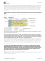
Bootloader I2C Download (.dld file) Format
This section briefly discusses the format of the file <project_name>.dld:
Two sample download records are shown in the following figures – the first, third, and the last. These
records consist of actual data that would be transmitted between the I2C master and a slave to be
bootloaded. The format of the records is described in this section.
Figure 7.
Sample Record
Figure 8 shows the format of the first record:
Figure 8.
First Download Record
Every line begins with a control byte. The two control bytes used by the download protocol are:
70 – Slave address 38 write. The address is not considered part of the byte count.
71 – Slave address 38 read. The expected response to a slave address read is 0x20, success. Other
possible responses are listed in Table 5:
Document Number: 001-13258 Rev. *J
Page 32 of 39
I2C Bootloader
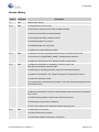
Table 5.
Slave Address Read Responses
Code
Meaning
0x20
Bootload mode (Success). Received 'Enter bootloader' command with valid
bootLoader Key.
0x02
Image verify error. The checksum of application and relocatable interrupt
vector areas calculated by the bootloader does not match the checksum
received from the Host.
0x04
Flash checksum error. The flash block content does not match the data
received from Host.
0x08
Flash protection error. Flash block cannot be rewritten because its flash
protection level does not allow this.
0x10
Comm checksum error. Received a packet with incorrect checksum.
0x40
Invalid bootloader key. A packet with the incorrect bootLoaderKey value was
received.
0x80
Invalid command error. Unknown command was received.
For details, see the BootLoader operation flowchart at the end of this document.
Slave address write commands do not require responses, so the next two bytes of each of the slave
address write lines is an I2C prefix that the bootloader ignores. Use the Ignore_N_I2C_Prefix_Bytes
parameter to set the number of prefix bytes used in your application.
The first and third lines of the sample download record contain bootloader commands. The bootloader
commands listed in Table 6 are used:
Table 6.
Bootloader Commands
Command
Meaning
FF38
Enter bootloader
FF39
Write block
FF3B
Exit bootloader
All bootloader commands must be sent with the bootloader key. The bootloader ignores commands that
are not sent with the proper key. You can set the bootloader key with the Bootloader_Key parameter.
Bootloader Write Block Command
Most of the commands sent to the bootloader are write block commands. The format of each of the write
block commands is identical. The third block contains the checksum information. The format of the
checksum block is discussed in this section. Each of the other write block command transmits a 64-byte
hex record to the bootloader in five packets totalling 78 bytes (neglecting addresses and discarded
prefixes).
The first line of the write block command contains a control byte, an ignored 2-byte I2C prefix, the write
block command, the bootloader key, the block number being transmitted, and the first four bytes of data.
The block number in this example is 0x0002, which corresponds to ROM address 0x0080.
Document Number: 001-13258 Rev. *J
Page 33 of 39
I2C Bootloader
The next three lines contain only the control byte, the I2C prefix, and 16 bytes of data. The last line of the
write block command contains the control byte, the I2C prefix, the final 12 bytes of data, and two 1-byte
checksums. The first checksum, 0x9A in this example, is the checksum of the data bytes for this record.
The second checksum, 0x8A in this example, is the checksum of the entire 77 byte record, excluding
address bytes and prefixes. Address bytes and prefixes are verified internally by the bootloader as they
are received.
At the conclusion of the write block command, another status request is sent and it results in the response
shown.
All the blocks transmitted have the same format. The third block contains the checksum information.
Figure 9 shows the format of this record:
Figure 9.
Third (Checksum)
The third record contains the checksum block (note that the block number is always 0x0004). The data in
the record is described in this section.
The first line contains a control byte, an I2C prefix, the bootloader write block command, the bootloader
key, and the block number just as the other records did. The next two bytes contain an optional checksum
for the remainder of the block, 0x0E8C in this case. The last two bytes of the line contain the hex address
of the Relocatable Interrupt Vectors Table (see Figure 2 for more information).
The second line of the record contains a control byte and an I2C prefix, followed by a two byte value that
represents the hex address of the ApplicationCode_Start_Block user module parameter calculated from
block 0x29. The next two bytes are the hex address of the end of Application Code calculated from block
0xFF. This is followed by two bytes that are the application size in blocks. The final two byte real data
value on this line is the bootloader version number from the BootLdrI2C_ver parameter. The remainder of
the line is empty data space.
The next two lines contain additional empty data space. The last line of the checksum block contains
empty data space until the last four bytes of the line. The last four bytes contain a two byte application
checksum calculated by the bootloader, a one byte block checksum from the Intel hex record, and finally
the checksum of the entire 77 byte record, excluding address bytes and prefixes. Address bytes and
prefixes are verified internally by the bootloader as they are received.
The next line contains another status request and response.
The bootloader exit command consists of control byte 70, a two byte prefix, the bootloader exit command
0xFF3B, and the bootloader key.
Document Number: 001-13258 Rev. *J
Page 34 of 39
I2C Bootloader
Figure 10 shows the last download record:
Figure 10. Last Download Record
The last line is a final status request and possibly a response. When the exit bootloader command is
received, the target system immediately executes an internal reset and begins verifying the checksum for
the downloaded application. This is done using the parameters given in the checksum block. Depending
on the speed of the host system, the bootloader may already have begun its reset process before the
master is able to receive a valid status byte. For this reason, the status (0x20) may not always be present.
Instead, the address 0x71 may simply be NAK’ed.
BootLdrI2C and E2PROM User Module Coexistence
When you place an E2PROM User Module in a Bootloader project, allocate the E2PROM blocks in the
Customer Reserved Blocks area. This area is between the Bootloader Code Area and the Application
Document Number: 001-13258 Rev. *J
Page 35 of 39
I2C Bootloader
Code Area (see Bootloader Memory Organization for information). This ensures that the E2PROM blocks
are not part of the Application Code Area, and are not calculated as part of the Application checksum.
Document Number: 001-13258 Rev. *J
Page 36 of 39
I2C Bootloader
Figure 11. BootloaderI2C User Module Operation Flowchart
Document Number: 001-13258 Rev. *J
Page 37 of 39
I2C Bootloader
Version History
Version
Originator
Description
1.2
DHA
Added Version History
2.00
DHA
1. Reorganized the memory map.
2. Placed Reloc Interrupt Vectors Table at address 0x0080.
3. Placed Checksum Block at address 0x0100.
4. Placed Bootloader Start at address 0x0140.
5. Added SetTemperature() function.
6. Added Bootloader API Jump Table.
7. Updated user module Parameters table.
2.10
DHA
1. Replaced .Literal and .EndLiteral statement with .nocc around the SSC call.
2. Removed export `@INSTANCE_NAME`_EnterBootloader statement.
3. Added user code section for I2C address compare customization.
2.20
DHA
1. Updated the initialization of Application_Checksum_Block and
TWO_Block_Relocatable_Interrupt_Table.
2. Added support to display bootloader output files in Workspace Explorer.
3. Updated the description in the "Improper Settings in Flashsecurity.txt" section.
4. Added "I2C and Sleep" section.
5. Corrected paths to the flashsecurity.example, custom.lkp and boot.tpl templates for the
CY8C27x43 devices.
2.30
DHA
1. Updated area declarations to support Imagecraft optimization.
2. Added more information in this user module datasheet about the checksum calculation
in the *.iic file.
3. Added javascript updates to enhance the wizard performance.
4. Added program temperature initialization.
5. Fixed issues related to the coexistence with the watchdog timer.
2.40
DHA
1. Added output in csv format.
2. Added CY20X34 device support.
3. Limited BootLoaderKey parameter to 16 symbols.
Document Number: 001-13258 Rev. *J
Page 38 of 39
I2C Bootloader
Note
PSoC Designer 5.1 introduces a Version History in all user module datasheets. This section documents high level descriptions of the differences between the current and previous user module versions.
Document Number: 001-13258 Rev. *J
Revised September 28, 2012
Page 39 of 39
Copyright © 2007-2012 Cypress Semiconductor Corporation. The information contained herein is subject to change without notice. Cypress Semiconductor Corporation assumes no responsibility
for the use of any circuitry other than circuitry embodied in a Cypress product. Nor does it convey or imply any license under patent or other rights. Cypress products are not warranted nor intended
to be used for medical, life support, life saving, critical control or safety applications, unless pursuant to an express written agreement with Cypress. Furthermore, Cypress does not authorize its
products for use as critical components in life-support systems where a malfunction or failure may reasonably be expected to result in significant injury to the user. The inclusion of Cypress products
in life-support systems application implies that the manufacturer assumes all risk of such use and in doing so indemnifies Cypress against all charges.
PSoC Designer™ and Programmable System-on-Chip™ are trademarks and PSoC® is a registered trademark of Cypress Semiconductor Corp. All other trademarks or registered trademarks
referenced herein are property of the respective corporations.
Any Source Code (software and/or firmware) is owned by Cypress Semiconductor Corporation (Cypress) and is protected by and subject to worldwide patent protection (United States and foreign),
United States copyright laws and international treaty provisions. Cypress hereby grants to licensee a personal, non-exclusive, non-transferable license to copy, use, modify, create derivative works
of, and compile the Cypress Source Code and derivative works for the sole purpose of creating custom software and or firmware in support of licensee product to be used only in conjunction with
a Cypress integrated circuit as specified in the applicable agreement. Any reproduction, modification, translation, compilation, or representation of this Source Code except as specified above is
prohibited without the express written permission of Cypress.
Disclaimer: CYPRESS MAKES NO WARRANTY OF ANY KIND, EXPRESS OR IMPLIED, WITH REGARD TO THIS MATERIAL, INCLUDING, BUT NOT LIMITED TO, THE IMPLIED WARRANTIES
OF MERCHANTABILITY AND FITNESS FOR A PARTICULAR PURPOSE. Cypress reserves the right to make changes without further notice to the materials described herein. Cypress does not
assume any liability arising out of the application or use of any product or circuit described herein. Cypress does not authorize its products for use as critical components in life-support systems
where a malfunction or failure may reasonably be expected to result in significant injury to the user. The inclusion of Cypress' product in a life-support systems application implies that the manufacturer
assumes all risk of such use and in doing so indemnifies Cypress against all charges.
Use may be limited by and subject to the applicable Cypress software license agreement.