1
IDE Guide
Document # 001-42655 Rev *B
Cypress Semiconductor
198 Champion Court
San Jose, CA 95134-1709
Phone (USA): 800.858.1810
Phone (Intnl): 408.943.2600
http://www.cypress.com
Copyrights
Copyrights
Copyright © 2002-2009 Cypress Semiconductor Corporation. The information contained herein is
subject to change without notice. Cypress Semiconductor Corporation assumes no responsibility for
the use of any circuitry other than circuitry embodied in a Cypress product. Nor does it convey or
imply any license under patent or other rights. Cypress products are not warranted nor intended to
be used for medical, life support, life saving, critical control or safety applications, unless pursuant to
an express written agreement with Cypress. Furthermore, Cypress does not authorize its products
for use as critical components in life-support systems where a malfunction or failure may reasonably
be expected to result in significant injury to the user. The inclusion of Cypress products in life-support
systems application implies that the manufacturer assumes all risk of such use and in doing so
indemnifies Cypress against all charges.
PSoC Designer™, Programmable System-on-Chip™, and PSoC Express™ are trademarks and
PSoC® is a registered trademark of Cypress Semiconductor Corp. All other trademarks or registered trademarks referenced herein are property of the respective corporations.
Any Source Code (software and/or firmware) is owned by Cypress Semiconductor Corporation
(Cypress) and is protected by and subject to worldwide patent protection (United States and foreign),
United States copyright laws and international treaty provisions. Cypress hereby grants to licensee a
personal, non-exclusive, non-transferable license to copy, use, modify, create derivative works of,
and compile the Cypress Source Code and derivative works for the sole purpose of creating custom
software and or firmware in support of licensee product to be used only in conjunction with a
Cypress integrated circuit as specified in the applicable agreement. Any reproduction, modification,
translation, compilation, or representation of this Source Code except as specified above is prohibited without the express written permission of Cypress.
Disclaimer: CYPRESS MAKES NO WARRANTY OF ANY KIND, EXPRESS OR IMPLIED, WITH
REGARD TO THIS MATERIAL, INCLUDING, BUT NOT LIMITED TO, THE IMPLIED WARRANTIES
OF MERCHANTABILITY AND FITNESS FOR A PARTICULAR PURPOSE. Cypress reserves the
right to make changes without further notice to the materials described herein. Cypress does not
assume any liability arising out of the application or use of any product or circuit described herein.
Cypress does not authorize its products for use as critical components in life-support systems where
a malfunction or failure may reasonably be expected to result in significant injury to the user. The
inclusion of Cypress' product in a life-support systems application implies that the manufacturer
assumes all risk of such use and in doing so indemnifies Cypress against all charges.
Use may be limited by and subject to the applicable Cypress software license agreement.
2
PSoC Designer IDE Guide, Document # 001-42655 Rev *B
Contents
1. Introduction
1.1
1.2
1.3
1.4
1.5
1.6
7
Application Overview ................................................................................................................8
1.1.1 Chip-Level Editor...........................................................................................................8
1.1.2 System-Level Editor ......................................................................................................9
1.1.3 Code Editor ...................................................................................................................9
1.1.4 Build Manager .............................................................................................................10
1.1.5 Board Monitor..............................................................................................................10
1.1.6 Debugger ....................................................................................................................11
1.1.7 Getting Help ................................................................................................................11
Chapter Overviews .................................................................................................................11
Support ...................................................................................................................................12
1.3.1 Technical Support Systems.........................................................................................12
1.3.2 Product Upgrades .......................................................................................................12
Conventions............................................................................................................................12
1.4.1 Acronyms ....................................................................................................................13
References .............................................................................................................................14
Revision History......................................................................................................................14
2. Chip-Level Editor
15
2.1
2.2
Chip-Level Editor Overview ....................................................................................................16
Create a Project......................................................................................................................17
2.2.1 Clone a Project............................................................................................................19
2.2.2 Updating Existing Projects ..........................................................................................19
2.3 Placing User Modules.............................................................................................................19
2.3.1 Rotating a Placement..................................................................................................21
2.3.2 Setting User Module Parameters ................................................................................21
2.3.3 Global Resources........................................................................................................22
2.4 Project Backup Folder ............................................................................................................27
2.5 Specifying Interconnects.........................................................................................................27
2.5.1 Connecting User Modules...........................................................................................28
2.5.2 Digital Interconnect Row Input Window ......................................................................34
2.5.3 Digital Interconnect Row Output Window....................................................................35
2.6 Specifying the Pinout ..............................................................................................................37
2.6.1 Port Connections.........................................................................................................37
2.6.2 Port Drive Modes ........................................................................................................42
2.6.3 Port Interrupts .............................................................................................................43
2.7 Tracking Device Space...........................................................................................................44
2.8 Design Rule Checker..............................................................................................................45
2.9 Generating Application Files...................................................................................................46
2.10 Source Files Generated by Generate Project Operation ........................................................47
2.10.1 About the boot.asm File ..............................................................................................47
2.11 Configuration Data Sheets......................................................................................................48
2.12 APIs and ISRs ........................................................................................................................48
PSoC Designer IDE Guide, Document # 001-42655 Rev *B
3
Copyrights
2.12.1 Working with ISRs ...................................................................................................... 49
2.12.2 Interrupt Vectors and the Chip-Level Editor ................................................................ 50
2.13 Dynamic Reconfiguration ....................................................................................................... 52
2.13.1 Adding Configurations ................................................................................................ 52
2.13.2 Deleting Configurations ..............................................................................................53
2.13.3 Renaming Configurations ........................................................................................... 54
2.13.4 Employing Dynamic Reconfiguration .......................................................................... 54
3. System-Level Editor
3.1
3.2
3.3
3.4
3.5
3.6
3.7
3.8
3.9
3.10
3.11
3.12
3.13
3.14
4. Code Editor
4.1
4
59
System-Level Editor Overview ............................................................................................... 60
Create a New Project ............................................................................................................. 61
3.2.1 Add Design Elements ................................................................................................. 61
3.2.2 Use Pop Up Menus..................................................................................................... 62
3.2.3 Use Navigation Tools .................................................................................................. 63
3.2.4 Use the Design Toolbar ..............................................................................................63
3.2.5 Delete Elements.......................................................................................................... 64
3.2.6 Save a Design ............................................................................................................ 64
Simulating Your Design .......................................................................................................... 64
3.3.1 Widgets ....................................................................................................................... 64
3.3.2 Navigation Tools ......................................................................................................... 64
3.3.3 LOG.csv File ............................................................................................................... 65
3.3.4 Simulation Controls..................................................................................................... 65
Drivers .................................................................................................................................... 65
3.4.1 Driver Types................................................................................................................ 65
Valuators ................................................................................................................................ 66
3.5.1 Interface Valuator........................................................................................................66
3.5.2 Transfer Function Valuator.......................................................................................... 66
Transfer Functions.................................................................................................................. 67
3.6.1 Transfer Function Types ............................................................................................. 67
Authoring New Design Elements............................................................................................ 69
Selecting a Configuration ....................................................................................................... 70
3.8.1 Configuration Properties ............................................................................................. 70
3.8.2 BOM Vendor ............................................................................................................... 71
3.8.3 Assign Pins Automatically........................................................................................... 71
Assigning Pins ........................................................................................................................ 71
3.9.1 Pin Color Legend ........................................................................................................ 72
3.9.2 Lock Pins .................................................................................................................... 72
3.9.3 Unassign All Pins........................................................................................................ 72
3.9.4 Auto Assign................................................................................................................. 72
Generating Output .................................................................................................................. 72
Developing Complex Designs ................................................................................................ 73
3.11.1 Preparing Your Design................................................................................................ 73
Programming PSoC Flash Memory........................................................................................ 78
Monitoring Your Design .......................................................................................................... 79
3.13.1 Monitoring Your Board With the I2C-USB Bridge ....................................................... 80
3.13.2 Monitoring Your Board with Other Interfaces .............................................................. 82
Tuning Your Design................................................................................................................ 82
87
File Definitions and Recommendations ................................................................................. 87
4.1.1 File Types and Extensions .......................................................................................... 88
4.1.2 Project File System ..................................................................................................... 89
PSoC Designer IDE Guide, Document # 001-42655 Rev *B
4.2
4.1.3 boot.asm .....................................................................................................................90
4.1.4 main.asm/main.c .........................................................................................................90
4.1.5 PSoCConfig.asm.........................................................................................................90
4.1.6 Additional Generated Files..........................................................................................90
Working in Code Editor...........................................................................................................92
4.2.1 Modifying Files ............................................................................................................92
4.2.2 Adding New Files ........................................................................................................93
4.2.3 Adding Existing Files...................................................................................................93
4.2.4 Removing Files ...........................................................................................................93
4.2.5 Searching Files ...........................................................................................................94
5. Assembler
5.1
5.2
5.3
5.4
5.5
5.6
5.7
5.8
95
Accessing the Assembler .......................................................................................................95
The M8C Microprocessor (MCU)............................................................................................95
5.2.1 Address Spaces ..........................................................................................................96
5.2.2 Instruction Format .......................................................................................................96
5.2.3 Addressing Modes ......................................................................................................96
5.2.4 Destination of Instruction Results................................................................................97
Assembly File Syntax .............................................................................................................97
List File Format .......................................................................................................................97
Assembler Directives ..............................................................................................................98
Instruction Set ........................................................................................................................99
Compile and Assemble Files ..................................................................................................99
Calling Assembly Functions From C.....................................................................................100
6. Build Manager
6.1
6.2
6.3
6.4
103
Building a Project..................................................................................................................103
C Compiler............................................................................................................................104
6.2.1 ImageCraft Compiler Options....................................................................................104
6.2.2 HI-TECH Compliler Options ......................................................................................105
Linker ....................................................................................................................................105
6.3.1 ImageCraft Specific Linker Options...........................................................................106
6.3.2 HI-TECH Specific Linker Configuration Options........................................................106
6.3.3 Customizing Linker Actions.......................................................................................106
Librarian................................................................................................................................107
7. Debugger
109
7.1
7.2
7.3
7.4
7.5
Debugger Components.........................................................................................................109
Menu Options .......................................................................................................................111
Connecting to the ICE...........................................................................................................112
Downloading to the Pod........................................................................................................113
Debug Strategies ..................................................................................................................114
7.5.1 Trace .........................................................................................................................115
7.5.2 Break Points..............................................................................................................116
7.5.3 CPU and Register Views...........................................................................................117
7.5.4 Watch Variables ........................................................................................................118
7.5.5 Dynamic Event Points ...............................................................................................119
7.5.6 End Point Data ..........................................................................................................123
I2C Debugger........................................................................................................................124
7.6.1 Connecting to the ICE ...............................................................................................124
7.6.2 Enable Debug Mode .................................................................................................124
7.6.3 Downloading to the Device .......................................................................................125
7.6
PSoC Designer IDE Guide, Document # 001-42655 Rev *B
5
Copyrights
7.7
7.6.4 Debug Strategies for I2C Debugger ..........................................................................125
7.6.5 Break Points..............................................................................................................125
7.6.6 Watch Variables ........................................................................................................126
Programming the Part ..........................................................................................................130
8. Flash Protection
8.1
8.2
8.3
6
133
FPMP and PSoC Designer...................................................................................................133
About flashsecurity.txt ..........................................................................................................134
FPMP File Errors ..................................................................................................................135
PSoC Designer IDE Guide, Document # 001-42655 Rev *B
1.
Introduction
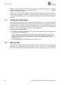
PSoC Designer™ is two tools in one. It combines a full featured integrated development environment (IDE) (the Chip-Level Editor) with a powerful visual programming interface (the System-Level
Editor). The two tools require and support two different design processes:
In the Chip-Level Editor you specify exactly how you want the device configured. This allows you
direct access to all of the features of your PSoC device and complete control over the routing, system resource use, and firmware development:
1. Choose a base device to work with.
2. Choose user modules that configure the PSoC device for the functionality you need in your system.
3. Configure the user modules for your chosen application and connect them to each other and to
the proper pins.
4. Generate your project. This prepopulates your project with APIs and libraries that you can use to
program your application.
5. Program in C for rapid development, assembly language to get every last drop of performance, or
a combination of both.
In the System-Level Editor you solve design problems the same way you might think about the system:
1. Select input and output devices based upon system requirements.
2. Add a communication interface and define the interface to the system (registers).
3. Define when and how an output device changes state based upon any/all other system devices.
4. Based upon the design, automatically select one or more PSoC Mixed-Signal Controllers that
match system requirements.
5. PSoC Designer completely and correctly generates all embedded code, then compiles and links
it into a programming file for a specific PSoC device.
6. You can then open the project in Interconnect view to review and further configure your design.
All views of the project share a common code editor, builder, and common debug, emulation, and
programming tools. The System-Level Editor creates a special environment that allows the visual
interface to function. This special environment is not created if you choose a Chip-level Project. You
can start with a system-level project and switch to the chip-level view, but the converse is not true.
PSoC Designer IDE Guide, Document # 001-42655 Rev *B
7
Introduction
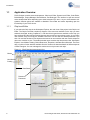
1.1
Application Overview
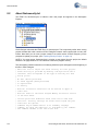
PSoC Designer contains several subsystems: Chip-Level Editor, System-Level Editor, Code Editor,
Build Manager, Project Manager, Board Monitor, and Debugger. The interface is split into several
active windows that differ depending upon which subsystem you are in. As you move between subsystems, different options are enabled or disabled in the toolbar and menus depending upon the
functionality of your PSoC device.
1.1.1
Chip-Level Editor
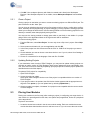
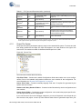
If you select the Chip view in the Workspace Explorer, the main view of the project is the Chip-Level
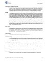
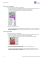
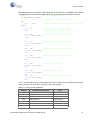
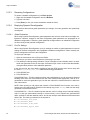
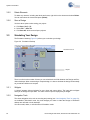
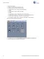
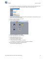
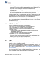
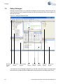
Editor. The Chip-Level Editor contains a diagram of the resources available on the chip you have
selected; the digital, analog, CapSense™, and other block types that are available on the chip you
have selected and the interconnections between them as well as connections to pins. As you place
user modules, they will occupy the available resources. You can alter the default placement if you
wish. You use this window to route inputs and resources to user modules and user module outputs to
other user modules or pins. The default window layout contains the Interconnect view, Workspace
Explorer, User Module Catalog, Global Resources, Properties, and Data Sheet Windows. There are
also a number of other windows available from the View menu that show details of different aspects
of PSoC Designer. You can rearrange the work area to suit your own work style.
Figure 1-1. PSoC Designer Interconnect View
Chip View
Menus
User Module
Catalog
Data Sheet
Global
Resources
Resource
Placement
Workspace Explorer
Properties
8
PSoC Designer IDE Guide, Document # 001-42655 Rev *B
Introduction
1.1.2
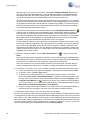
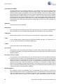
System-Level Editor
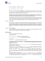
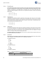
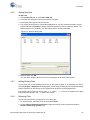
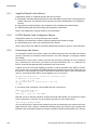
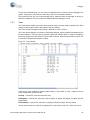
The PSoC Designer System-Level Editor contains three desktops: Design, Simulation, and Monitor,
which are selectable with the four subtabs shown in Figure 1-2. When you select each of the different tabs, the look and use of the main area changes to accommodate the specifics of that desktop.
The default window layout contains the Driver Catalog, Workspace Explorer, Properties, and
Datasheet Windows. There are also a number of other windows available from the View menu that
show details of different aspects of PSoC Designer. You can rearrange the work area to suit your
own work style. These desktops are described in more detail later.
Figure 1-2. PSoC Designer System View
Menus
System View
Driver
Catalog
Workspace Explorer
Datasheet
Properties
Subtabs
The menus allow you to perform various tasks, including opening new or existing designs, as well as
saving, closing, building, and programming designs. Most of these commands are available regardless of the areas in which you work.
1.1.3
Code Editor
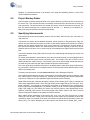
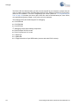
The workspace editor is a full-featured text editor designed for editing C and assembly code in your
project. You can use the application editor to create and edit application files.The default window layout contains the Code Editor and Find Results. There are also a number of other windows available
PSoC Designer IDE Guide, Document # 001-42655 Rev *B
9
Introduction
from the View menu that show details of different aspects of PSoC Designer. You can rearrange the
work area to suit your own work style.
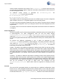
Figure 1-3. PSoC Designer Code Editor
1.1.4
Build Manager
The Build Manager is a largely invisible utility that controls the various portions of the build process
including the compiler (or compilers), assembler, and linker, and manages the process of building
your project and preparing it to download to a target device.
The only visible portions of the Build Manager in the PSoC Designer application are the Build menu
and the Build options in the Tools > Options dialog.
1.1.5
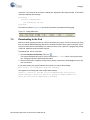
Board Monitor
The board monitor allows you to monitor the target board of an Express project. The project must
have an appropriate communication interface driver. The board monitor is capable of displaying the
real time results of driver tuners and interface valuators at intervals from one sample per second to
256 samples per second.
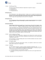
Figure 1-4. The Board Monitor Variables Chart
10
PSoC Designer IDE Guide, Document # 001-42655 Rev *B
Introduction
1.1.6
Debugger
The debugger has multiple windows that allow you to interact with and observe the code execution
on the target PSoC device. The debugger is tightly integrated with the rest of the IDE, and there is no
separate debugger view. Instead, there are a number of different windows that you can use to monitor the status of various parts of your target board while debugging, including the following:
1.1.7
Break Points
Memory
Watch Variables
Events
Trace
Output
Getting Help
The Help menu contains several different options for obtaining more information about how to use
PSoC Designer. The Help -> Help Topics window contains information about how PSoC Designer
works. For additional information, the Help -> Documentation selection opens a window showing all
of the PDF documentation available with PSoC Designer, including this IDE Guide.
When you first launch PSoC Designer, the Start Page opens in the main application window. This
start page contains panes that help you get started quickly using PSoC Designer.
1.2
Recent Projects allows you to open any previous saved project, create a new project, or browse
to find projects that are not displayed in Recent Projects.
Express Design Catalog allows you to choose among numerous preconfigured PSoC Designer
designs. These are fully functioning PSoC Designer designs, many of which can be built and programmed on Cypress Evaluation Boards and Kits to give you full functioned examples.
PSoC Shortcuts provides a shortcuts to PSoC resources that you may find helpful.
Chapter Overviews
This table briefly describes the contents of each chapter in this guide.
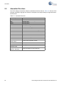
Table 1-1. Chapter Overviews
Chapter
Description
Introduction
Describes the purpose of this guide, provides an application overview and
descriptions of each chapter, supplies product support and upgrade information, and lists documentation conventions and references for more information.
Chip-Level Editor
Describes the chip-level editor that allows you to work directly with the
resources available on a PSoC device, select and configure user modules,
and route inputs, outputs, and other resources to and from them.
System-Level Editor
Describes the system-level editor that allows you to create projects for
PSoC devices at an abstracted system level, where you to select and configure various design elements, such as inputs, outputs, valuators, and
interfaces.
Code Editor
In this chapter you learn how to create the project code.
PSoC Designer IDE Guide, Document # 001-42655 Rev *B
11
Introduction
Table 1-1. Chapter Overviews (continued)
Chapter
1.3
Description
Assembler
In this chapter you receive high-level guidance on programming assembly
language source files for the PSoC device.
Build Manager
In this chapter you learn the details of building a project, discover more
about the C Compiler as well as the basic, transparent functions of the system Linker and Loader, and Librarian.
Debugger
In this chapter you learn how to download your project to the In-Circuit Emulator (ICE), use debug strategies, and program the part.
Flash Protection
Flash Program Memory Protection (FPMP) allows you to select one of four
protection (or security) modes for each 64-byte block within the Flash,
based upon the particular application.
Support
Free support for PSoC Designer is available online at http://www.cypress.com. Resources include
training seminars, discussion forums, application notes, PSoC consultants, TightLink technical support email/knowledge base, and application support technicians.
Before using the Cypress support services, know the version of PSoC Designer installed on your
system. To quickly determine the version of PSoC Designer, click Help > About PSoC Designer.
1.3.1
Technical Support Systems
Enter a support request into the TightLink Technical Support System with a guaranteed response
time of four hours or view and participate in discussion threads about a wide variety of PSoC device
topics at http://www.cypress.com/support/login.cfm.
1.3.2
Product Upgrades
Cypress provides upgrades and version enhancements for PSoC Designer free of charge. You can
order the upgrades from your distributor on CD-ROM or download them directly from the Cypress
web under Software and Drivers. Also provided are critical updates to system documentation under
Design Support > Design Resources > More Resources or go to http://www.cypress.com.
1.4
Conventions
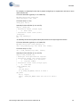
Here are the conventions used throughout this guide.
Table 1-2. Documentation Conventions
Convention
Courier New
Usage
Displays file locations and source code:
C:\ …cd\icc\, user entered text
Italics
Displays file names and reference documentation:
sourcefile.hex
12
PSoC Designer IDE Guide, Document # 001-42655 Rev *B
Introduction
Table 1-2. Documentation Conventions (continued)
Convention
[bracketed, bold]
Usage
Displays keyboard commands in procedures:
[Enter] or [Ctrl] [C]
File > New Project
Represents menu paths:
File > New Project > Clone
Bold
Displays commands, menu paths and selections, and icon
names in procedures:
Click the Debugger icon, and then click Next.
Text in gray boxes
1.4.1
Displays cautions or functionality unique to PSoC Designer or
the PSoC device.
Acronyms
These are the acronyms used throughout this guide.
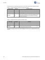
Table 1-3. Acronyms
Acronym
Description
ADC
analog-to-digital converter
API
application programming interface
BOM
bill of material
C
(refers to the C programming language)
DAC
digital-to-analog converter
DRC
design rule checker
EPP
enhanced parallel port
FPMP
Flash program memory protection
grep
global regular expression print
ICE
in-circuit emulator
IDE
integrated development environment
IO
input/output
ISR
interrupt service routine
MCU
microcontroller unit
MHz
megahertz
OBM
on-board monitor
OHCI
open host controller interface
PWM
pulse width modulator
RAM
random access memory
ROM
read only memory
SSC
system supervisory call
UART
universal asynchronous receiver transmitter
UHCI
universal host controller interface
USB
universal serial bus
PSoC Designer IDE Guide, Document # 001-42655 Rev *B
13
Introduction
1.5
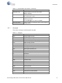
References
This guide is part of a larger documentation suite for the PSoC Designer application. It is meant as a
reference, not as the complete source of information. For the most up-to-date information, go to
http://www.cypress.com. The documentation listed here provides more specific information on a variety of topics:
1.6
PSoC Designer Help Topics (Online Help)
PSoC Designer Base Project Author Guide
PSoC Designer Channel Author Guide
PSoC Designer Driver Author Guide
PSoC Designer Transfer Function Author Guide
PSoC Designer Development Kit Getting Started Guide
PSoC Programmer Guide
Various PSoC Designer application notes and data sheets
Revision History
Table 1-4. Revision History
Revision
14
PDF
Creation
Date
Origin
of
Change
Description of Change
**
May 27, 2008
FSU
Put changes to the original PSoC Designer IDE Guide in a new template and assigned a
Spec Number.
*A
August 14, 2008
FSU
Changed some screen captures. Added many previously undocumented global parameters.
*B
March 24, 2009
PYRS
Added content relating to compilers and large scale updates
PSoC Designer IDE Guide, Document # 001-42655 Rev *B
2.
Chip-Level Editor
The Chip-Level Editor allows you to work directly with the resources available on a PSoC device,
select and configure user modules, such as analog to digital converters (ADCs), timers, amplifiers,
and others, and route inputs, outputs, and other resources to and from them.
Figure 2-1. Chip-Level Editor Desktop
PSoC Designer IDE Guide, Document # 001-42655 Rev *B
15
Chip-Level Editor
2.1
Chip-Level Editor Overview
The Chip-Level Editor gives you complete control over Chip-Level Projects resource use, routing,
and firmware. You choose a specific chip at the beginning of this process:
1. Create a Project
This is the first step in both processes, but after naming your project, the first thing that you do in
a Chip-Level Project is select a PSoC device.
2. Select a PSoC Device
There are a large number of PSoC devices in the PSoC family with more being added all the
time. Some are general purpose devices with varying amounts of general purpose digital and
analog resources while others are more specialized with onboard peripherals suited to specific
solutions such as wireless, LED control, or capacitive sensing. Consult the Cypress web site for a
wide variety of literature and contact information for people that can help you choose the right
device for your design.
3. Choose User Modules
PSoC devices have programmable analog and digital blocks that can be configured for a wide
variety of uses. User Modules configure these programmable blocks to behave as a specific
peripheral, such as an analog to digital converter, a timer, or a pulse width modulator. You choose
user modules based on what you need the PSoC device to do for you.
4. Configure the User Modules
Each user module has a set of parameters that allow you to configure it to meet your needs. For
example, a CapSense user module must be configured to detect signals coming from capacitive
sensing components in a wide variety of configurations, so it has a large number of configurable
parameters. A design rule checker can alert you to potential problems with your design as you
work.
5. Connect The User Modules
Each user module will have inputs, outputs, and interrupts that can be routed internally to and
from other user modules, and externally to and from pins. The PSoC devices have a very flexible
routing system, but resources are limited and it may take some experimentation to find the optimal routing and placement for all of the user modules.
6. Generate Your Project
This prepopulates your project with APIs and libraries that you can use to program your application.
7. Write Your Program
Write your program in C for rapid development, assembly language to get every last drop of performance from the MCU, or a combination of both. You have a choice of third party C compilers
and assemblers for PSoC devices.
8. Build and Debug Your Program
Build and test your program. Use PSoC Designer in conjunction with one of the PSoC emulators.
PSoC Designer has a powerful built in debugger.
9. Program the Device
Cypress has a variety of programmers that you can use to program your production parts.
Your design is now complete. The remainder of this chapter is organized just like the above outline
with additional details on each of the steps.
16
PSoC Designer IDE Guide, Document # 001-42655 Rev *B
Chip-Level Editor
2.2
Create a Project
In order to program the desired functionality into a PSoC device, you need to first create a project
directory in which the files and device configurations reside.
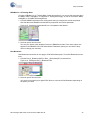
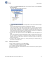
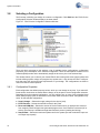
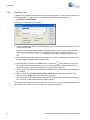
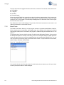
1. To start a new project, select New Project from the File menu.
Figure 2-2. New Project Dialog Box
The System-Level Editor creates a special environment that allows it to generate all necessary
program code based on the elements and logic in the System-Level Project. If you start with an
System-Level Project, you can eventually edit in the Chip-Level Editor. The converse is not true.
If you start with a Chip-Level Project, the environment necessary to generate code from SystemLevel designs is not initiated and System-Level Editor functions are disabled in that project.
2. Choose a name and location for the project. By default, a project is created inside a workspace
with the same name as the project, the project is stored in the project directory. If you plan to create multiple projects in a single workspace (for example, if your project will use multiple PSoC
devices), click Create a directory for workspace and supply a name for the first project. When
you are finished, click Next.
PSoC Designer IDE Guide, Document # 001-42655 Rev *B
17
Chip-Level Editor
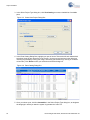
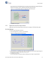
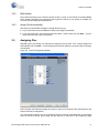
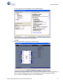
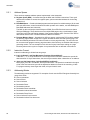
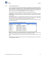
3. In the Select Project Type dialog box, click View Catalog to access a detailed list of available
parts.
Figure 2-3. Create New Project Dialog Box
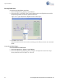
4. In the Parts Catalog Dialog Box, highlight your part of choice. Tabs at the left and characteristic
selections along the top narrow the list of devices. You have several options in this dialog box
including layout display, viewing part image, and sorting part selection (by clicking on a chosen
column title). Click Select to save your selection and exit the dialog box.
Figure 2-4. Parts Catalog Dialog Box
5. Once you select a part, click C or Assembler, in the Select Project Type dialog box, to designate
the language in which you want the system to generate the “main” file.
18
PSoC Designer IDE Guide, Document # 001-42655 Rev *B
Chip-Level Editor
6. Click OK. Your workspace directory with folders is created and is listed in the Workspace
Explorer. If the Workspace Explorer is not visible, choose Workspace Explorer from the View
menu.
2.2.1
Clone a Project
Cloning a project is used when you want to convert an existing project to a different PSoC part. The
part is referred to as the “base” part.
You can clone an existing project at any point of its existence: before, during, or after device configuration, assembly-source programming, or project debugging. Cloning copies the existing project but
allows you to change the base device. Use the cloning method to move an existing project from one
directory to another, rather than physically moving the files.
You must use the cloning method to change parts within a part family in the middle of a project
design. Refer to the Application Notes on the Cypress web site for assistance.
To clone an existing project:
1. From the File menu, select New Project. You can only clone a Chip-Level project. Select ChipLevel .
2. Select a name and location for your new application and click OK.
3. In the Clone project box click browse and find the .SOC or .CMX file of the project you want to
clone.
4. Choose whether you want to choose a new base device or not. If you do, select View Catalog to
select a new device.
5. Choose C or assembler for the language of the main file. Click OK.
2.2.2
Updating Existing Projects
If you download a newer version of PSoC Designer, you may need to update existing projects created with an earlier version of PSoC Designer. Most project updates are done automatically; however, some need to be done manually depending upon project specifics. Manual project updates are
described at the end of this chapter.
To update a PSoC project for compatibility:
1. Open PSoC Designer.
2. Access the project to update.
At this point, PSoC Designer checks to see if the project is compatible with the new version of
PSoC Designer.
3. If your project needs to be updated, the Old Version window appears with the appropriate message text. Click Update (or you can update later by selecting Update later...).
4. Once the update is complete, click Finish. Your project is now compatible with the current version
of PSoC Designer.
2.3
Placing User Modules
Placing user modules is the first step (after creating a project) in configuring your target device. A
user module is a preconfigured function that, once placed and programmed, works as a peripheral
on the target device.
To place a user module:
1. Locate the desired user module in the the user module catalog. Each user module has a user
module data sheet that describes what it is and how to use it. If you do not see the user module
PSoC Designer IDE Guide, Document # 001-42655 Rev *B
19
Chip-Level Editor
data sheet when you click on a user module, select View > Datasheet Window. Right-click on
the user module and select Place. Some user modules have wizards or configuration screens
that appear before the user module can be placed. These will differ by user module. The user
module will be placed in the first available PSoC block in the Interconnect view.
The user module block reference names appear above the currently active blocks. For example,
an ADC10 has one digital block used as a counter (CNT) and two analog blocks, one for the analog to digital conversion (ADC) and the other for a voltage ramp (RAMP). The name of the user
module is separate from these user module block function names. This is because a multiblock
user module may have distinct block actions.
2. If you want to use a placement other than the default, click the Next Allowed Placement icon
to advance the user module to the next available location (active/anchor identified as green, nonactive as blue) or use the faster drag-and-drop capability. Click the target placer (identified as
green and blue highlights) and drag-and-drop the user module to a new location. If a user module
has multiple blocks, it may be possible to drag individual blocks onto a free block. Repeat this
procedure until you have identified the exact location for the user module.
The Next Allowed Placement button shows the next possible set of PSoC blocks in which a user
module may be placed, regardless of any currently placed user modules. If you cannot place the
user module in the highlighted location due to a lack of resources, a Resource Allocation message flashes in the lower-left corner of PSoC Designer. Placement is not possible if another user
module occupies the PSoC block, or if a placed user module is using another resource which the
highlighted user module requires.
3. When you identify the location, click the Place User Module icon
Place.
, or right-click and select
Once you place the module, it appears on the device, color-coded, bearing the designated name
of the chosen PSoC block. In the Interconnect frame, the inactive target placers (blue highlights)
of multi-block user modules are now identified by a group name across the top.
Some user modules do not consume visible resources in the interconnect view when they are
placed. Examples of this include LCD, I2C Master, I2C Slave and software only user modules.
4. At this time, you can print, save, clear or unplace, and name or rename the placed user module.
To print your placement view, right-click anywhere in the Interconnect view and select Print.
To save your work, click File > Save project.
To clear all user module placements (i.e., remove them from their location on the PSoC
blocks), click Interconnect > Clear All Placements. To unplace one particular module, rightclick it (in either the Interconnect view or the Workspace Explorer) and select Unplace or click
the Unplace User Module icon
. This does not remove user modules from PSoC Designer
or from your collection. Your unplaced user modules shown in the Workspace Explorer under
Interconnect > Loadable Configurations > User Modules.
To name or rename user modules, select the user module either in the Workspace Explorer or
the Interconnect view, and type a new name in the user module Properties window.
5. Repeat this process (steps 1-4) for all user modules in your design.
For each user module you add, the system updates the data in the Resource Meter with the number
of occupied PSoC blocks, along with estimated RAM and ROM usage for the current set of selected
user modules. The RAM and ROM numbers grow or shrink depending upon wizard settings and
other user module parameter adjustments. If you select a user module that requires more resources
than are currently available, PSoC Designer does not allow the selection. If you do not see the
Device Resource Meter go to the View menu and select Resource Meter.
20
PSoC Designer IDE Guide, Document # 001-42655 Rev *B
Chip-Level Editor
If user modules are already placed, then there are some cases when user module placement fails
even if it appears that sufficient PSoC blocks remain unallocated. In such cases, the already placed
user modules are using resources that the selected user module requires.
There are several user modules that require topology selection (i.e., filters). Right-click on the module in the Aplication Explorer after it is placed and click User Module Selection Options. Make the
topology choice according to your application.
Some user modules have associated wizards to assist in configuration. To access a wizard, select
the user module in the Workspace Explorer and then right click the mouse. If a wizard exists, it
appears in the menu choices.
To Remove a User Module:
To remove user modules from your collection, select the user module in the Workspace Explorer and
press [Delete], or right-click the user module and select Delete. This does not remove user modules
from PSoC Designer, just from your collection.
If you add or remove user modules after generating application files, you need to regenerate the
application files (as well as reconfigure required settings). For further details, see “Generating Application Files” on page 46.
2.3.1
Rotating a Placement
In a group placement of two or more user modules, press the [Space Bar] to rotate and see the
placement options around the anchor block of a multi-block user module.
Select the anchor block by clicking on one of the blocks in which the user module is placed. Now
press the [Space Bar]. The block your cursor is on becomes the anchor block. As you press the
[Space Bar], the remaining required blocks rotate to the options that surround the anchor block.
For optimum placement, you may need to switch anchor blocks as well as drag-and-drop the set
around the interface to view all options.
2.3.2
Setting User Module Parameters
Setting User Module Parameters configures the user module to behave the way you want it to and
connects the user module to the external pins and other user modules and resources. You connect
to user modules through the output and input parameters of the PSoC blocks. The interconnection
buses provide interconnection paths between the external pins and to other digital user modules.
Once you place the user module, the parameters are updated with applicable names. When you single-click a user module, you view its parameters under Properties. If you do not see the Properties
window, go to the View menu and select Properties Window. User Module Parameters
To update the User Module Parameters:
PSoC Designer IDE Guide, Document # 001-42655 Rev *B
21
Chip-Level Editor
1. Click each drop-arrow (in parameter value fields) and make your selections.
Some parameters are integer values. Set these values by clicking the up/down arrows, or doubleclick the value and type in the value. If you type a value that is out of range, an error message
appears in the lower-left corner.
2. Repeat this process for all placed user modules.
2.3.3
Global Resources
Global Resources are hardware settings that determine the underlying operation of the part (for the
entire application). For example, the CPU clock designates the clock speed of the M8C.
Note that Global Resource options differ slightly for each device family.
To update and save Global Resources:
1. Click each drop-arrow (in parameter value fields) and make your selections.
Some parameters in Global Resources are specified as integer values (such as 24V1 and 24V2).
Set these values by clicking the up/down arrows or double-clicking the value and typing over
them. If you enter an out of range value, you see a dialog box specifying the acceptable range.
Click OK to close the dialog box.
2. The current settings for the Global Resources can be saved as default settings. Right-click on
any Global Resource name and select Update Default Values. This action saves all Global
Resource settings to the \Preferences directory under the PSoC Designer installation path.
Use these settings for any other project by right-clicking any Global Resource name and selecting Restore Default Values. If no custom default values are saved, then the menu item and the
right-click to Restore Default Settings restore the factory default Global Resource Settings.
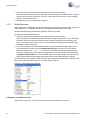
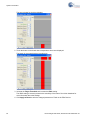
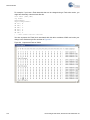
The Global Resources available in PSoC Designer are shown and described briefly. Different PSoC
Devices have different global resources. The figure shown is typical.
Figure 2-5. Global Resources Example.
8 Bit Capture or FreeRun Prescaler
Selects which 8 bits of the 16-bit Free Running Timer are captured when in bit mode.
22
PSoC Designer IDE Guide, Document # 001-42655 Rev *B
Chip-Level Editor
32K_Select
The 32K_Select parameter allows selection of the internal 32 kHz oscillator or an external crystal
oscillator. A complete discussion of the implications of this selection is found in the PSoC Technical
Reference Manual.
A_Buf_Power
A_Buf_Power allows the user to select the power level for the analog output buffers of the PSoC.
These buffers are used to supply internal analog signals to external pins on the PSoC. Power levels
may affect the frequency response and current drive capability of the output buffers. Complete tables
for the AC Analog Output Buffer Specifications and DC Analog Output Buffer Specifications are contained in the applicable device data sheet.
AGNDBypass
A provision is made in some versions of the PSoC device to provide an external AGND bypass
capacitor to reduce the small amounts of switching noise present on the internal AGND. This feature
is switched on and off using the AGNDBypass global parameter. Typical values for the external
bypass capacitor are 0.01 μF and should not generally exceed 10 μF. The recommended value is 1
μF.
Analog Power
This parameter controls the power to the analog section of the PSoC. Power is controlled in three
stages:
1. All Analog Blocks Off
2. Continuous Time Blocks ON/Switched Capacitor Blocks OFF
3. Continuous Time Blocks ON/Switched Capacitor Blocks ON
For each of the two 'ON' cases, select reference drive levels of high, medium, and low to choose the
current drive capability for the internal reference buffers. All selections of this parameter, whether
used as a User Module Parameter or this Global Resource, need to agree. This selection affects the
total power consumption of the PSoC. Each user module using the reference and the opamp block
associated with it adds slightly to the power consumed by the device. Since the internal reference is
used as an integral part of most switched capacitor circuits, the current drive capability has an impact
on the speed at which the switched capacitor block operates. In general, higher settings for this
parameter allow switched capacitor circuits to operate at higher clock rates, at the expense of higher
power consumption. To estimate the current (and power) consumption per opamp block, refer to the
applicable table in the data sheet for the part: DC Operation Amplifier Specifications (ISOA).
Capture Clock
Selects the clock source for the Timer Capture Clock (TCAPCLK).
Capture Clock/N
Selects the Capture Clock divider value. The TCAPCLK will be Capture Clock source divided by N.
Capture Edge
Selects whether the capture timer data register has the First Hold data or the Most Recent edge
data. This option applies to all four capture timers.
PSoC Designer IDE Guide, Document # 001-42655 Rev *B
23
Chip-Level Editor
CLKOUT Source
Selects one of the clocks, internal SysClk, external, low power 32 KHz, or CPUCLK to be output
directly on port P0[1].
CPU_Clock
The CPU_Clock selection allows the selection of the M8C clock speed from 93.75 kHz to 24 MHz.
The CPU clock is derived directly from the SysClock. Use an external 32 kHz oscillator and the PLL
Ext_Lock to improve clock accuracy. A discussion of the main oscillator is contained in the PSoC
Technical Reference Manual.
Crystal OSC
Selects the external crystal oscillator when enabled. The external crystal oscillator shares pads
CLKIN and CLKOUT with two GPIOs; P0.0 and P0.1, respectively.
Crystal OSC Xgm
XGM is the amplifier transconductance setting and selects the calibration for the external crystal
oscillator.
EFTB
The external crystal oscillator is passed through the EFTB filter when this option is enabled.
FreeRun Timer and Free Run Timer/N
Selects clock source for 16-bit free-running timer. The free-running timer generates an interrupt at a
1024-µs rate. It can also generate an interrupt when counter overflow occurs at every 16.384 ms.
The combination of the FreeRun Timer and the FreeRun Timer divider are used to obtain the
FreeRun Timer rate.
Low V Detect
Selects the level of the supply voltage at which the low voltage detect interrupt is generated.
LVD ThrottleBack
This parameter allows you to configure the PSoC to lower its own CPU clock speed under low voltage conditions. Use of this parameter and the bit it controls is discussed in the PSoC Technical Reference Manual. Not all PSoC devices incorporate this parameter and bit.
Opamp Bias
Performance of the internal opamps are tailored based upon the application under development by
selecting high or low bias conditions for the analog section of the PSoC. Selecting high bias causes
the opamp to consume more current but also increases its bandwidth and switching speed, lowering
its output impedance. To estimate the current (and power) consumption per opamp block, including
the effect from high or low selection of opamp Bias, refer to the applicable table in the data sheet for
the part: DC Operation Amplifier Specifications (ISOA). To estimate the effect on AC opamp parameters, refer to the applicable AC Operational Amplifier Specifications in the device data sheet.
PLL_Mode
The PSoC Technical Reference Manual discusses use of the phase-locked loop mode.
24
PSoC Designer IDE Guide, Document # 001-42655 Rev *B
Chip-Level Editor
Power Setting [Vdd/SysClock Freq]
This parameter allows you to select the SysClock frequency and nominal operating voltage. Based
upon the SysClock selected, the Internal Main Oscillator (IMO) is set with appropriate calibration settings. Since many internal clocks are derived from the SysClock, you see significant device powerconsumption savings by lowering the SysClock frequency, if the implemented design permits it.
Ref Mux
The Ref Mux source selection is used to control the range and (potential) accuracy of various analog
resources. The reference chosen controls the maximum voltage that is input to a switched capacitor
circuit and output from a switched capacitor circuit. Both the analog ground level and the peak-topeak voltage are selected using this parameter. Values specified with the Ref Mux parameter are in
pairs and consist of [AGND level ± full scale]. Keep in mind that selecting Vdd (supply voltage) as a
reference level couples Vdd changes into the AGND input of internal resources. This directly affects
absolute accuracy of measurements. Using the internal bandgap reference results in better accuracy
but may not offer an exact Vdd/2 input reference. Choices of ± full-scale values also offer a number
of options. These full-scale values may be based on the PSoC internal references or on external
input voltages. The ± full scale values present constraints similar to those for AGND in terms of Vdd
variation and absolute range of input/output. Individual design criteria dictate the best selection for
the AGND and ± full-scale values. Further discussion of the analog reference can be found in the
PSoC Technical Reference Manual.
Sleep_Timer
The Sleep_Timer parameter selects the timing of the sleep interrupt, if enabled. When the sleep
interrupt is active, and the processor is in a sleep state, it is awakened at the rate specified with this
parameter. The Watchdog Reset, if enabled, occurs after three rollover events in the sleep timer (if
the Watchdog counter is not reset). A complete discussion of the relation of these two elements is
found in the PSoC Technical Reference Manual.
Supply Voltage
Selects the nominal operating voltage to be either 3.3V or 5V.
SwitchModePump
An integrated switch mode pump circuit is available for operation of the device from very low voltage
sources. The pump requires a few external components and can be configured to automatically turn
on as supply voltage drops. Further discussion of the switch mode pump is found in the PSoC Technical Reference Manual.
SysClock_Source and SysClock*2 Disable
These parameters allow you to select the 24 MHz system SysClock from an internal or external
source. The SysClock*2 Disable parameter allows the internal 48 MHz clock to be shut off. A complete discussion of system clocking is found in the PSoC Technical Reference Manual.
Timer Clock
Selects the clock source for the 12-bit down counting internal timer (TIMERCLK).
Timer Clock/N
Selects the Timer Clock divider value. The TIMERCLK will be Timer Clock source divided by N.
PSoC Designer IDE Guide, Document # 001-42655 Rev *B
25
Chip-Level Editor
Trip Voltage [LVD (SMP)]
A precision POR circuit is integrated into the PSoC. This parameter allows the user to select voltage
levels that the PSoC uses to internally monitor its supply voltage. Two levels are specified in the
parameter with the syntax <LVD (SMP)>. LVD is the value at which the internal low voltage comparator asserts its control signal. SMP is the level at which the integrated switch mode pump is enabled.
Although selection of SMP is implicit in the selection of LVD, if no switch mode pump circuitry is
used, the part is reset if supply voltage falls too low. At the point when the supply voltage exceeds
the threshold level, the part resumes operation as if the power was switched off and on (POR). Further discussion of the switch mode pump and low voltage detect is found in the PSoC Technical Reference Manual.
USB Clock
Selects the source for the USB SIE.
USB Clock/2
This option divides the USB clock source by 2 when the source is an external crystal oscillator.
When the USB clock is the internal 24 MHz Oscillator, then the divide by 2 is always enabled.
V Keep-alive
Allows voltage regulator to source upto 20 µA of current when the voltage regulator is disabled.
V Reg
A 3.3 V regulator output is placed on the pin P1[2] when Enabled, and when Vcc is above 4.35 V. A
1 µF min, 2 µF max capacitor is required on VREG output.
V Reset
Selects the Power on Reset (POR) voltage level.
VC1 and VC2
These resources are clocks that can be chained to provide various internal clock frequencies used
for digital or analog blocks. A complete discussion of system clocking is found in the PSoC Technical
Reference Manual.
VC3_Source and VC3_Divider
VC3 is a system clock resource similar to the VC1 and VC2 resources. The main difference between
it and VC1 and VC2 is that VC3 may be chained from one of several clock sources and may not be
used as an input clock as flexibly as VC1 and VC2. You cannot use it as a direct input to the analog
section of the PSoC. It can be used as an input to a digital PSoC block and then used to derive a
clock that can be used in many more places. For this reason, it is important to evaluate clocking
options as a PSoC design is being developed. Often, rearranging clock sources according to where
they are most easily connected solves clocking problems. A complete discussion of system clocking
is found in the PSoC Technical Reference Manual.
Watchdog Enable
This parameter activates the Watchdog Timer. The Watchdog Timer is based on a counter that
counts three sleep timer events. To prevent system reset, you must clear this counter before three
sleep timer state events occur, or the PSoC is internally reset. The duration of each sleep timer
event is selected using the Sleep_Timer parameter in the Global Resources frame of PSoC
26
PSoC Designer IDE Guide, Document # 001-42655 Rev *B
Chip-Level Editor
Designer. A complete discussion of the relation of the sleep and watchdog timers is in the PSoC
Technical Reference Manual.
2.4
Project Backup Folder
PSoC Designer maintains a backup folder in the project directory for files that were removed from
the source tree. This includes files that are manually removed and files removed due to cloning or
code generation. The backup folder only retains the version of the file that was last removed. The
files are named identically to the original project file and the \lib directory is not retained (i.e.,
library files are placed directly under the backup folder).
2.5
Specifying Interconnects
Interconnectivity allows communication between user modules, PSoC blocks, pins, and other onchip resources.
Connections are shown as lines between elements, special symbols, or flag connectors. Flag connectors are used when the connection is made to a point where drawing a line results in a cluttered
display, with the legend indicating the origin of the connection. Connections to pins are shown as
lines from interconnection buses. The interconnection bus structure depends on the PSoC device
selected and can consist of one or more levels of buses between the digital PSoC blocks and the
pins.
Connections between analog PSoC blocks and pins are made through the analog input muxes and
output buses.
Pin names are duplicated in several places, since they are multifunctional, and are highlighted when
used with lines showing their current connection state. The location of the pin to which a line is
drawn indicates the usage of the pin. Lines drawn to the pins on the left edge indicate that the pins
are used as inputs, while the right edge indicates the pins are used as output.
Pins in the upper groups indicate connection to the digital network, while lower groups indicate analog connections. Lines drawn from multiple locations on the same pin indicate that the shown combination is electrically valid.
To specify interconnections, click the Interconnect folder in the Workspace Explorer.
User module interconnections consist of connections to surrounding PSoC blocks, output bus, input
bus, internal system clocks and references, external pins, and analog output buffers. Multiplexers
may also be configured to route signals throughout the PSoC block architecture.
Digital PSoC blocks are connected through the Global_IN and Global_OUT buses to external pins
and to other digital PSoC blocks. There are eight Global_IN and eight Global_OUT bus lines, numbered 0 through 7. For external pin connections, the number of the Global bus line corresponds to
the bit number of the associated port. For example, Global_IN_0 can connect to pins associated with
P0[0], P1[0], P2[0], etc. The Global_OUT buses can drive the inputs to other digital PSoC blocks.
However, all Global_OUT lines do not reach all digital PSoC blocks. Refer to the PSoC Technical
Reference Manual for details on the global bus interconnections.
When setting output parameters to the Global_OUT lines, only one PSoC block drives a single
Global_OUT line at a time. Global_OUT lines used by a user module are not available to other user
modules for output. For example, if two timer user modules are placed and the first timer is set to use
Global_OUT_1 for output, attempting to set the output for the second timer to Global_OUT_1 fails.
PSoC Designer IDE Guide, Document # 001-42655 Rev *B
27
Chip-Level Editor
2.5.1
Connecting User Modules
These procedures show you how to make certain types of connections.
Global In
Global In connections apply to a PSoC device in this manner:
CY8C25xxx/26xxx as Global In: Input Port Connections.
All other PSoC devices as Global In Odd and Global In Even: Input Port Connections and Global
Connections.
To set Global In connections:
1. Click on the target Globalxxx vertical line.
2. Select the pin to connect to.
3. Select the global input to output connection (if active).
4. Click OK.
You see a line connecting the digital input port to the global vertical line.
Global Out
Global Out connections apply to a PSoC device in this manner:
CY8C25xxx/26xxx as Global Out: Output Port Connections.
All other PSoC devices as Global Out Odd and Global Out Even: Output Port Connections and
Global Connections.
To set Global Out connections:
28
PSoC Designer IDE Guide, Document # 001-42655 Rev *B
Chip-Level Editor
1. Click on the target Globalxxx vertical line.
2. Select the global input to output connection (if active) and the port.
3. Click OK.
You see a line connecting the digital output port to the global vertical line.
Analog Clock Select
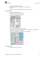
To set Analog Clock Select connections:
1. Click on the target AnalogClock_x_Select Mux.
Figure 2-6. The AnalogClock_0_Select Mux
2. Select a DBAxx or DBBxx PSoC block (as applies).
You see a line from the right side of DBxxx to the input of the AnalogClock_x_Select Mux. The
mux switch shows a connection to this input.
Figure 2-7. The AnalogClock_0_Select Set to Connect to DBB30
Analog Column Clock
To set Analog Column Clock connections:
PSoC Designer IDE Guide, Document # 001-42655 Rev *B
29
Chip-Level Editor
1. Click on the target AnalogColumn_Clock_x Mux.
Figure 2-8. Setting the AnalogColumn_Clock_0 Mux
2. Select a device-specific option from the menu.
You see that the AnalogColumn_Clock_x Mux has a line connecting your chosen option to the
mux output.
Analog Column Input Mux
To set Analog Column Input Mux connections:
1. Click on the target AnalogColumn_InputMUX_x.
Figure 2-9. Setting the AnalogColumn_InputMUX_3
2. Select a port from the menu.
You see a connection between the output of AnalogColumn_InputMUX_x and the analog input
port.
Analog Column Input Select
To set Analog Column Input Select connections:
1. Click on the target AnalogColumn_InputSelect_x.
Figure 2-10. Setting the AnalogColumn_InputSelect_1
2. Select appropriate AnalogColumn_InputMUX_x from the menu.
You see that your chosen AnalogColumn_InputSelect_x has a line inside that connects the output of AnalogColumn_InputMUX_x to its output.
30
PSoC Designer IDE Guide, Document # 001-42655 Rev *B
Chip-Level Editor
Analog Output Buffer
The Analog Output Buffers can be connected to the associated port pin or turned off. To set Analog
Output Buffer connections:
1. Click on the target AnalogOutBuf_x.
Figure 2-11. Setting the AnalogOutBuf_2
2. Select a port from the menu.
You see a line that connects the AnalogOutBuf_x triangle to the analog output port.
Clock Input for a Digital Block
To set Clock Input connections on a digital block:
1. Click the clock input triangle on the digital block where your target user module is placed. Note
that the clock input triangle is not active for all blocks when a user module uses more than one
block. Also note that the name “Clock Input” is determined by a specified user module parameter.
Figure 2-12. Setting the Clock Input for an ADCINC User Module
2. Select an option from the menu. You see your chosen input option displayed next to the clock
input triangle.
Your choice option also appears in the Control Clock field under User Module Parameters (where
you can click the drop-arrow to change your selection).
PSoC Designer IDE Guide, Document # 001-42655 Rev *B
31
Chip-Level Editor
Enable Input for a Digital Block
To set the Enable Input connection on a digital block:
1. Click the Enable text label on the digital block where your target user module is placed. Note that
the name Enable Input is determined by a specified user module parameter.
Figure 2-13. Setting the Enable Input for an 8-bit Counter User Module
2. Select an option from the menu.
You see your chosen input option displayed next to the Enable text label. Your choice option also
appears in the Enable field under User Module Parameters (where you can click the drop-arrow
to change your selection).
Output for a Digital Block
To set Output connections on a digital block:
1. Click the Output text label on the digital block where your target user module was placed. Note
that the name Output is determined by a specified user module parameter.
Figure 2-14. Setting the CompareOut on an 8-bit Pulse Width Modulator User Module
2. Select an option from the menu (None, Global_OUT_x for CY8C25xxx/26xxx, or
Row_x_Output_x for all other PSoC devices).
You see your chosen option displayed (with a connection) next to the Output text label. Your
choice option also appears in the Output field under User Module Parameters (where you can
click the drop-arrow to change your selection).
32
PSoC Designer IDE Guide, Document # 001-42655 Rev *B
Chip-Level Editor
RBotMux for a CT Analog Block
To select a RBotMux for a CT Analog Block, follow this procedure. You can use this procedure when
the NMux, PMux, AnalogBus, or CompBus CT Analog Block apply, as well as for ACMux, BMux,
AnalogBus, or CompBus SC Analog Blocks.
1. Click the RBotMux text label on the analog block where your target user module was placed.
Note that the name RBotMux is determined by a specified user module parameter.
Figure 2-15. Setting the Comparator Bus on a Comparator User Module
2. Select an option from the menu.
You see your chosen option displayed next to the RBotMux text label. Your choice option also
appears in the RBotMux field under User Module Parameters (where you can click the droparrow to change your selection).
Row Broadcast
Row Broadcast connections do not apply to CY8C25xxx/26xxx parts. To set Row Broadcast connections:
1. Click the Row_0_Broadcast (BC0) or Row_1_Broadcast (BC1) horizontal line.
Figure 2-16. Setting the Row_0_Broadcast Line
2. Select an option from the menu.
You see a line connecting to a digital PSoC block or to the other Row Broadcast, depending on
the option you chose.
PSoC Designer IDE Guide, Document # 001-42655 Rev *B
33
Chip-Level Editor
Comparator Analog LUT
Comparator Analog LUT connections do not apply to CY8C25xxx/26xxx parts. To set Comparator
Analog LUT connections:
1. Click the AnalogLUT_x box. (Its symbol is identified in the Comparator x line along each column
of analog PSoC blocks.)
2. Select an option from the menu.
You see connections on the device interface reflecting your A or B selection with associated
symbols.
2.5.2
Digital Interconnect Row Input Window
The Digital Interconnect Row Input window connections do not apply to CY8C25xxx/26xxx parts.
Connection to Global Input
To set a Connection to Global Input:
1. Click on the white box or the line of the target Row_x_Input_x. (A tool tip will appear to identify
your selection.)
Figure 2-17. Digital Interconnect Row Input
2. Click on the Row_x_Input_x Mux in the Digital Interconnect Row Input floating window and select
a Global Input from the menu. (You immediately see a connection from the mux to the Global
34
PSoC Designer IDE Guide, Document # 001-42655 Rev *B
Chip-Level Editor
Input vertical line.) In this floating window you can also click the white box to toggle the Synchronization value for Row_x_Input_x. Options include SysClk_Sync and Async
Figure 2-18. Synchronization Options for Digital Interconnect Row Inputs
3. Click Close when finished.
2.5.3
Digital Interconnect Row Output Window
Digital Interconnect Row Output Window connections do not apply to CY8C25xxx/26xxx parts.
Row Logic Table Input
To set Row Logic Table Input connections:
1. Click on the target Row_x_Output_x Logic Table Box.
Figure 2-19. Digital Interconnect Row Output
2. Click on the Row_x_LogicTable_Input_0 Mux in the Digital Interconnect Row Output floating window and select an input or output option from the menu.
3. Click Close when finished.
You see connections on the device interface reflecting your row input or output selection.
PSoC Designer IDE Guide, Document # 001-42655 Rev *B
35
Chip-Level Editor
Row Logic Table Select
To set Row Logic Table Select connections:
1. Click on the target Row_x_Output_x Logic Table Box.
2. Click on the Row_x_LogicTable_Select_x logical operation box in the Digital Interconnect Row
Output floating window and select an option from the menu
Figure 2-20. Logical Operations in Digital Interconnect Row Output
3. Click Close when finished.
You see connections on the device interface reflecting your A or B input selection with associated
symbol.
Connection to Global Output
To set connections to Global Output:
1. Click on the target Row_x_Output_x Logic Table Box.
2. Click on the target Row_x_Output_x_Drive_x triangle in the Digital Interconnect Row Output
floating window and select an option from the menu.
36
PSoC Designer IDE Guide, Document # 001-42655 Rev *B
Chip-Level Editor
Once you open the Digital Interconnect Row Global Output window, you can select Row Logic
Table Input, Row Logic Table Select, and Connections to Global Output without closing the window.
Figure 2-21. Digital Interconnect Row Global Output
3. Click the Close button when finished.
You see a connection from the Row_x_Output_x Logic Table Box to the chosen
GlobalOutEven_x vertical line.
2.6
Specifying the Pinout
Specifying the pinouts is the next step to configuring your target device. This converts the pins to the
configurable PSoC resources.
To restore the default pinout, click the Restore Default Pinout button
.
Be careful when connecting to pins. The pin settings can be modified either by setting elements to
connect to pins or by setting the pin directly.
Setting the pin directly connects the pin to the appropriate element and disconnects it from any other
element. To have multiple connections to the same pin, make connections from the element to the
pin. For example, suppose a connection to a pin, an analog input mux and an analog output buffer,
simultaneously, is desired. P0[2] can connect to the analog input mux for column 1 and to the analog
output buffer for column 3. The connections must be made from the analog input mux and the analog output buffer. Setting the pin to Default disconnects the pin from both digital buses, but does not
affect analog connections.
2.6.1
Port Connections
You make port connections in three ways:
Click the port icons and make settings in the device interface
Click the pin and make settings in the device pinout
Change port-related fields in the Global or User Module properties windows
These procedures show you how to make certain types of port connections.
PSoC Designer IDE Guide, Document # 001-42655 Rev *B
37
Chip-Level Editor
Analog Input
To set Analog Input connections.
1. Click on the target Port_0_x.
2. From the Select menu select AnalogInput.
Figure 2-22. Select AnalogInput for a Port
3. Click OK.
On the device you see the new designation color coded according to the legend along side the
device. The port name and selection also appears in the port-related fields underneath User
Module Parameters (where you can click the drop-arrow to change your selection).
Default Input
To set Default Input connections:
1. Click on the target Port_x_x.
2. From the Select menu select Default.
Figure 2-23. Select Default Input for a Port
3. Click OK.
On the device pinout frame you see the designation color coded according to the legend along
side the device. The port name, the Select column value of StdCPU, and the drive mode of High
Z Analog also appears in the port-related fields underneath User Module Parameters (where you
can click the drop-arrows to change your selections).
38
PSoC Designer IDE Guide, Document # 001-42655 Rev *B
Chip-Level Editor
Global_IN_x
Global_IN_x connections apply to a PSoC device in this manner:
CY8C25xxx/26xxx as Global_IN_x.
All other PSoC devices as GlobalIn[Odd/Even]_x.
To set Global_IN_x connections:
1. Click on the target Port_x_x.
2. From the Select menu select the device-specific Global IN option.
Figure 2-24. Select Global IN for a Port
3. Click OK.
On the device you see the designation color coded according to the legend next to the device.
The port name, the Select column value of your chosen option, and the drive mode of High Z
appear in the port-related fields underneath User Module Parameters (where you can click the
drop-arrows to change your selections).
You also see a line between the digital input port and the Global IN vertical line.
Global_OUT_x
Global_OUT_x connections apply to a PSoC device in this manner:
CY8C25xxx/26xxx as Global_OUT_x.
All other PSoC devices as GlobalOUT[Odd/Even]_x.
To set Global_OUT_x connections:
1. Click on the target Port_x_x.
2. From the Select menu select the device-specific Global OUT option.
Figure 2-25. Select Global OUT for a Port
3. Click OK.
On the device you see the designation color coded according to the legend next to the device.
The port name, the Select column value of your chosen option, and the drive mode of Strong
appear in the port-related fields underneath User Module Parameters (where you can click the
drop-arrows to change your selections).
You also see a line between the Global OUT vertical line and the digital output port.
PSoC Designer IDE Guide, Document # 001-42655 Rev *B
39
Chip-Level Editor
StdCPU
To set StdCPU connections:
1. Click on the target Port_x_x or select the port from the menu.
2. From the Select menu select StdCPU.
Figure 2-26. Select StdCPU for a Port
3. Click OK.
On the device you see the designation color coded according to the legend next to the device.
The port name and StdCPU also appear in the port-related fields underneath User Module
Parameters (where you can click the drop-arrow to change your selection).
XtalOut
To set the XtalOut connection:
1. Click on Port_1_0 (P1[1]) or select Port_1_0 from the menu.
2. From the Select menu select XtalOut.
Figure 2-27. Select XtalOut for Port 1 0
3. Click OK.
On the device you see the designation color coded according to the legend next to the device.
The port name, XtalOut, and the drive mode of High Z also appear in the port-related fields
underneath User Module Parameters (where you can click the drop-arrow to change your
selection).
XtalIn
To set the XtalIn connection:
1. Click on Port_1_1 (P1[1]) or select Port_1_1 from the menu.
40
PSoC Designer IDE Guide, Document # 001-42655 Rev *B
Chip-Level Editor
2. From the Select menu select XtalIn.
Figure 2-28. Select CXtalOut for Port 1 1
3. Click OK.
On the device you see the designation color coded according to the legend next to the device.
The port name, XtalIn, and the drive mode of High Z also appear in the port-related fields underneath User Module Parameters (where you can click the drop-arrow to change your selection).
ExternalGND
To set the ExternalGND connection:
1. Click on Port_2_4 (P2[4]) or select Port_2_4 from the menu.
2. From the Select menu select ExternalAGND.
Figure 2-29. Set External Ground for Port 2 4
3. Click OK.
On the device you see the designation color coded according to the legend next to the device.
The port name and ExternalGND appear in the port-related fields underneath User Module
Parameters (where you can click the drop-arrow to change your selection).
In the device interface you see that all lines from P2[4] are gone.
Ext Ref
To set the Ext Ref connection:
1. Click on Port_2_6 (P2[6]) or select P2[6] from the menu.
2. From the Select menu select ExtRef.
Figure 2-30. Set External Reference for Port 2 6
3. Click OK.
PSoC Designer IDE Guide, Document # 001-42655 Rev *B
41
Chip-Level Editor
On the device you see the designation color coded according to the legend next to the device.
The port name and Ext Ref also appear in the port-related fields underneath User Module Parameters (where you can click the drop-arrow to change your selection).
In the device interface you see that all lines from P2[6] are gone.
I2C SDA
To set the I2C SDA connection (this connection is only available for CY8C27xxx parts):
1. Click on Port_1_5 (P1[5]) or select P1[5] from the menu.
2. From the Select menu select I2C SDA.
Figure 2-31.
3. Click OK.
On the device you see the designation color coded according to the legend next to the device.
The port name, I2C SDA, and the drive mode of Open Drain High also appear in the port-related
fields underneath User Module Parameters (where you can click the drop-arrow to change your
selection).
In the device interface you see that all lines from Port_1_5 are gone.
I2C SCL
To set the I2C SCL connection (this connection is only available for CY8C27xxx parts):
1. Click on Port_1_7 (P1[7]) or select P1[7] from the menu.
2. From the Select menu select I2C SCL.
Figure 2-32.
3. Click OK.
On the device you see the designation color coded according to the legend next to the device.
The port name, I2C SCL, and the drive mode of Open Drain High also appear in the port-related
fields underneath User Module Parameters (where you can click the drop-arrow to change your
selection).
In the device interface you see that all lines from Port_1_7 are gone.
2.6.2
Port Drive Modes
Port drive modes can be specified in one location, in three ways:
42
Click the port icons and make settings in the device interface
PSoC Designer IDE Guide, Document # 001-42655 Rev *B
Chip-Level Editor
Click the pin and make settings in the device pinout
Change port-related fields in the Global or User Module properties windows
Port drive modes apply to a PSoC device in this manner:
CY8C25xxx/26xxx options include High Z, Pull Down, Pull Up, and Strong.
All other PSoC device options include High Z, High Z Analog, Open Drain High, Open Drain Low,
Pull Down, Pull Up, Strong, and Strong Slow.
To specify a port drive mode:
1. Click on the target Port_x_x.
2. From the Drive menu select the port drive mode option.
The port name and the drive mode of your choice appears in the port-related fields underneath
User Module Parameters (where you can click the drop-arrows to change your selections).
2.6.3
Port Interrupts
These procedures show you how to work with certain types of port interrupts.
ChangeFromRead
To specify a ChangeFromRead interrupt:
1. Click on the target Port_x_x.
2. From the Interrupt menu select ChangeFromRead.
Figure 2-33. Set Port Interrupt to Change From Read
3. Click OK.
The port name and ChangeFromRead appears in the port-related fields underneath User Module
Parameters (where you can click the drop-arrows to change your selections).
DisableInt
To disable interrupts:
1. Click on the target Port_x_x.
2. From the Interrupt menu select DisableInt.
Figure 2-34. Set Port Interrupt to Disable
PSoC Designer IDE Guide, Document # 001-42655 Rev *B
43
Chip-Level Editor
3. Click OK.
The port name and DisableInt appears in the port-related fields underneath User Module Parameters (where you can click the drop-arrows to change your selections).
FallingEdge
To specify FallingEdge interrupt:
1. Click on the target Port_x_x.
2. From the Interrupt menu select FallingEdge.
Figure 2-35. Set Port Interrupt to Falling Edge
3. Click OK.
The port name and FallingEdge appears in the port-related fields underneath User Module
Parameters (where you can click the drop-arrows to change your selections).
RisingEdge
To specify RisingEdge interrupt:
1. Click on the target Port_x_x.
2. From the Interrupt menu select RisingEdge.
Figure 2-36. Set Port Interrupt to Rising Edge
3. Click OK.
The port name and RisingEdge appears in the port-related fields underneath User Module
Parameters (where you can click the drop-arrows to change your selections).
2.7
Tracking Device Space
Tracking the available space and memory of configurations for your device is something you do
intermittently throughout the process of configuring your target device. You need to monitor device
space and memory resources so you are aware, on an ongoing basis, of the capacity and limitations
you are working with on the microcontroller unit (MCU).
You can monitor device space and memory with the Resource Meter. If you do not see the Resource
meter, select Resource Meter from the View menu. Resources are updated as each user module is
placed.
44
PSoC Designer IDE Guide, Document # 001-42655 Rev *B
Chip-Level Editor
The resource meter tracks Analog Blocks, Digital Blocks, RAM, ROM, and the use of device specific
special resources such as the decimator, CapSense™ blocks, or I2C controller. As you place user
modules, you can view how many analog and digital PSoC blocks you have available and how many
you have used. RAM and ROM monitors track the amount RAM and ROM required to employ each
selected user module.
Figure 2-37. PSoC Block Resource Meter
2.8
Design Rule Checker
The Design Rule Checker (DRC) operates on a collection of predetermined rules associated with
elements in a project database. Once started, the DRC runs and then communicates the results of a
“rule” evaluation.
The DRC is designed to point out potential errors or rule violations in your project that might eventually pose problems. The DRC does not impose limitations or prevent you from proceeding with your
project “as is.” It simply notifies you of PSoC user module, software, and hardware elements you
may not be aware of when configuring and sourcing your device. It is an additional tool to provide
support for user-configuration.
The PSoC Designer collection of rules is being updated on an ongoing basis. A few sample DRC
rules include:
A project uses a Phase Locked Loop (PLL) but has not been configured with an External Crystal
The device is set to 24 MHz and 3V operation
The device is set to 48 MHz and 3V for Digital Clock Operation
Failure to set required parameters or connections
P0[1] and P0[0] Pins not High-Z with External Crystal
3.3V Indicating ICE is 5V Supply Only
Global Bus with Signal Pulse Width < 1/12 MHz
Phase Consistency Between Output to Input of SC blocks
PWM/Counter/Timer with Pulse Width > Period
Inappropriate Ground and Reference Level Selections
To run the Design Rule Checker, go to: Tools > Design Rule Checker.
In a matter of seconds, you can review the results of the rule evaluation in the Results tab of the Output Status window.
PSoC Designer IDE Guide, Document # 001-42655 Rev *B
45
Chip-Level Editor
You can run the DRC at any time or any number of times during project development. To run it automatically each time you generate application files, go to: Tools > Options > Interconnect Editor >
General.
You can also set specifics regarding the level of rule checking and result detail, go to:
Tools > Options > Tools > DRC tab.
2.9
Generating Application Files
Generating application files is the final step to configuring your target device. When you generate
application files, PSoC Designer takes all device configurations and updates existing assembly
source and C Compiler code and generates API (Application Programming Interface) and ISR (Interrupt Service Routine) shells. At this time, the system also creates a data sheet based on your part
configurations that can be accessed in the Chip-Level Editor (see “Configuration Data Sheets” on
page 48). Generate Application is executed automatically during the application editor build process,
when needed.
Once this process is complete, you can enter the Code Editor and begin programming the desired
functionality into your (now configured) device. For further details regarding programming, see
“Code Editor” on page 55 and “Assembler” on page 95.
You can generate application files from any view. To do this, click the Generate/Build Application icon
. The Generate Project Status window will inform you of the progress of the build.
Figure 2-38. Output Status During Application Generation
Full details of the build are sent to the Output window. If the Output window is not visible, select Output from the View menu.
Figure 2-39. The Output Window with Build Messages
NOTE: It is important to note that if you modify any device configurations, you must re-generate the
application files before you resume source programming.
46
PSoC Designer IDE Guide, Document # 001-42655 Rev *B
Chip-Level Editor
2.10
Source Files Generated by Generate Project Operation
Table 2-1 lists and describes the source files generated by the Generate Project operation.
Table 2-1. Source Files Generated by Generate Application
Name
Overwritten
Description
…/lib/PSoCConfig.asm
Yes
Configuration loaded upon system access
…/lib/PSoCCOnfigTBL.asm
Yes
Contains chip configuration
Boot.asm
Yes
Boot code and initial interrupt table
…/lib/<User module name>.asm
Yes
User module API source
…/lib/<User module name>.h
Yes
User module API C include header
…/lib/<User module name>.inc
Yes
User module API assembly include
…/lib/<User module name>INT.asm
Yes*
User module interrupt .asm file (if needed)
…/lib/<Project name>API.h
Yes
Project API include header
…/lib/<Project
Name>_GlobalParameters.inc
Yes
Project parameters include
main.asm
No
Main code
*
User code markers can be used to preserve sections in the file.
NOTE: If you undo placement of a user module but leave it in your selected collection and generate
application files, associated .asm files remain (just not be updated). If you undo placement and
delete a user module from your collection then generate application files, all associated .asm files
are deleted (removed from source tree project files).
2.10.1
About the boot.asm File
When device configuration files are generated, the boot.asm file is updated. Among other things, this
file includes a jump table for interrupt handlers. (Additional details regarding this file are found in “File
Definitions and Recommendations” on page 87.)
The entries in the interrupt table are handled automatically for interrupts employed by user modules.
For example, a Timer8 User Module uses an interrupt. The interrupt-vector number depends on
which PSoC block is assigned to the Timer8 instance; vector 2 for PSoC digital block 0, vector 3 for
block 1, and so on.
During the device configuration process, the ISR name is added to the appropriate interrupt-vector
number. The interrupt handler is included in a file that is named instance_nameint.asm, where
instance_name is the name given to the user module. For example, if the user module is named
Timer8_1, then the ISR source file is named Timer8_1INT.asm. All API files generated during the
device configuration process follow this naming convention. The following are the API files that
would be generated for a user module named Timer8_1:
Timer8_1.inc
Timer8_1.h
Timer8_1.asm
Timer8_1INT.asm
The boot.asm file is based on a file named boot.tpl. You can make changes to boot.tpl and those
changes are reflected in boot.asm whenever the application is generated. Do not change any strings
with the form `@INTERRUPT_nn` where nn = 0 to 15. These substitution strings are used
when device configuration application files are generated. However, you can replace substitution
PSoC Designer IDE Guide, Document # 001-42655 Rev *B
47
Chip-Level Editor
strings if you safely define the interrupt vector and install your own handler. If there is no interrupt
handler for a particular interrupt vector, the comment string “// call void_handler” is inserted
in place of the substitution string.
NOTE: If you install an interrupt handler and make changes directly to boot.asm, the changes are
not preserved if application generation is executed after you make the changes. If you make
changes to boot.asm that you do not want overwritten, hard code the change in boot.tpl (template for
boot.asm).
2.11
Configuration Data Sheets
Once you have configured your device and generated application files, you can produce, view, or
print a data sheet based upon how you configured your project device. The configuration data sheet
is self-contained in its own folder in the project directory and can be viewed independently of PSoC
Designer by opening configreport.xml in Internet Explorer. (If you need to move or send someone
the file, you must move/send the entire directory of \ConfigDataSheet.)
To produce and view a data sheet:
1. Select View > Configuration Data Sheet. This opens an independent browser window that shows
the current configuration data sheet.
NOTE: If changes were made in the Device Editor and a “Generate Application” was not performed, then PSoC Designer shows a dialog box asking for verification before performing Generate Application. If you select No, then the data sheet reflects the configuration before the
changes were made.
2. To print the data sheet click the standard Print icon or File > Print.
2.12
APIs and ISRs
APIs (Application Programming Interfaces) and ISRs (Interrupt Service Routines) are also generated
during the device configuration process in the form of *INT.asm, .h, and .inc files. These files provide
the device interface and interrupt activity framework for source programming. Figure 2-40, illustrates
48
PSoC Designer IDE Guide, Document # 001-42655 Rev *B
Chip-Level Editor
an .h file for configurations of a 16-bit PWM (Pulse Width Modulator) created during application-code
generation:
Figure 2-40. PWM_FAN0.h
Once you generate the device configuration application code, the files for APIs and ISRs are located
in the source tree of Workspace Explorer under the Library Source Files and Library Header Files
folders.
NOTE: If you modify any ISR file and then re-generate your application, changes are not overwritten
if they are placed between user code markers included in the *int.asm file. Source code outside of
the user code marker regions is overwritten and is always re-generated. However, if a user module
is renamed and the application is re-generated, any user modifications within the user code markers
are not updated with the instance name. Any use of the user module instance name within user code
markers must be manually updated.
Figure 2-41. Place Your Custom Code Here
2.12.1
Working with ISRs
The CPU has up to 26 interrupts: 6 fixed function and 20 configurable.
Reset
Supply Monitor
PSoC Designer IDE Guide, Document # 001-42655 Rev *B
49
Chip-Level Editor
4 Analog Columns
VC3
GPIO
16 Digital Blocks
I2C
Sleep Timer
The configurable interrupts include 16 digital blocks and 4 analog columns. The definition (for example, interrupt vector action) of a configurable interrupt depends on the user module that occupies the
block or uses the analog column.
The Chip-Level Editor handles the details of getting user module parameters into source code, so
that the project is configured correctly at startup and exposes subroutines that make for ease-of-use.
Exposing subroutines that make user module parameters easy to use involves PSoC Designer adding files to your project. These files are known as Application Program Interfaces (APIs). Typically,
one of these user module files, added to your project, is an interrupt handler.
Aside from adding API files to your project, the Chip-Level Editor also inserts a call or jump to the
user module’s interrupt handler in the startup source file, boot.asm.
2.12.2
Interrupt Vectors and the Chip-Level Editor
Figure 2-42 shows an example of how an interrupt handler is dispatched in the interrupt vector table,
using a device from the CY8C27xxx part family. Shown below is the Timer32 User Module mapped
to PSoC blocks 00, 01, 02, and 03. An interrupt is generated by the hardware when terminal count is
reached. The last PSoC Block (or MSB byte) of Timer32 generates the terminal count interrupt.
Figure 2-42. Timer32 on Four Digital PSoC Blocks
50
PSoC Designer IDE Guide, Document # 001-42655 Rev *B
Chip-Level Editor
When the application is generated, code is produced for the Timer32_1 User Module. The interrupt
vector table is also altered with the addition of the call to the timer interrupt handler in boot.asm.
org
0
;Reset Interrupt Vector
IF (TOOLCHAIN & HITECH)
;
jmp
__Start
;C compiler fills in this vector
ELSE
jmp
__Start
;First instruction executed following a Reset
ENDIF
org
halt
04h
;Supply Monitor Interrupt Vector
;Stop execution if power falls too low
org
08h
;Analog Column 0 Interrupt Vector
// call void_handler
reti
org
0Ch
;Analog Column 1 Interrupt Vector
// call void_handler
reti
org
10h
;Analog Column 2 Interrupt Vector
// call void_handler
reti
org
14h
;Analog Column 3 Interrupt Vector
// call void_handler
reti
org
18h
;VC3 Interrupt Vector
// call void_handler
reti
org
1Ch
;GPIO Interrupt Vector
// call void_handler
reti
org
20h
;PSoC Block DBB00 Interrupt Vector
// call void_handler
reti
Table 2-2 shows how boot.asm vector names map to fixed, analog column, and PSoC block (configurable) interrupts. Not all of these are shown in the code example.
Table 2-2. boot.asm Interrupt Names
Address
Data Sheet Interrupt Name
Type
00h
Reset
Fixed
04h
Supply Monitor
Fixed
08h
Analog Column 0
Analog Column
0Ch
Analog Column 1
Analog Column
10h
Analog Column 2
Analog Column
14h
Analog Column 3
Analog Column
18h
VC3
Fixed
PSoC Designer IDE Guide, Document # 001-42655 Rev *B
51
Chip-Level Editor
Table 2-2. boot.asm Interrupt Names (continued)
1Ch
GPIO
Fixed
20h
DBB00
PSoC Block
24h
DBB01
PSoC Block
28h
DCB02
PSoC Block
2Ch
DCB03
PSoC Block
30h
DBB10
PSoC Block
34h
DBB11
PSoC Block
38h
DCB12
PSoC Block
3Ch
DCB13
PSoC Block
40h
DBB20
PSoC Block
44h
DBB21
PSoC Block
48h
DCB22
PSoC Block
4Ch
DCB23
PSoC Block
50h
DBB30
PSoC Block
54h
DBB31
PSoC Block
58h
DCB32
PSoC Block
5Ch
DCB33
PSoC Block
60h
I2C
Fixed
64h
Sleep Timer
Fixed
Continuing the example, 2Ch corresponds to DCB03. There are no interrupt handlers at DBB00,
DBB01, and DCB02 (20h, 24h, and 28h) because a 32-bit Timer User Module only requires the interrupt at the end of the chain.
In many cases the actual interrupt handling code is “stubbed” out. You can modify the content of this
stubbed handler to suit your needs. Any subsequent device reconfiguration will not overwrite your
work in the handler if the modification is done in boot.tpl.
2.13
Dynamic Reconfiguration
The PSoC resources are configured using latch-based registers. These registers can be changed
on-the-fly, allowing for new functions to be created as needed during the execution of the application
program.
Reconfiguring resources in this manner is called Dynamic Reconfiguration. User modules are an
abstraction of register settings that enable a high-level function. A set of user modules is called a
configuration. The application can switch in and out of configurations in real-time, allowing for overuse of the chip resources. This is akin to memory overlaying. It is up to the application to ensure that
configurations are not reconfigured while they are being used.
A loadable configuration consists of one or more placed user modules with module parameters, Global Resources, set pinouts, and generated application files. PSoC projects can consist of one or
multiple loadable configurations.
2.13.1
Adding Configurations
To add loadable configurations to your PSoC project:
52
PSoC Designer IDE Guide, Document # 001-42655 Rev *B
Chip-Level Editor
1. Right click the Loadable Configuration folder in the Workspace Explorer and select New Loadable Configuration.
Figure 2-43. Add a New Loadable Configuration
2. You see a new folder with a default name of Configx where x is the number of alternate configurations.
Select the configuration folders to switch from one configuration to the other.
There is always at least one folder with the project name when a project is created. This folder
represents the base configuration. The base configuration has special characteristics. You cannot delete the base configuration. The new configuration, by default, has global settings and pin
settings identical to the base configuration. Additional configuration folders appear in alphabetical
order from left to right, beginning after the base configuration tab.
3. To change the name right-click the folder and select Rename. The new name appears on the
folder.
NOTE: One requirement for Dynamic Reconfiguration is that user module instance names must
be unique across all configurations. This requirement eliminates confusion in code generation.
Otherwise, all other icon and menu-item functions are identical to projects that do not employ
additional configurations.
4. Proceed with the configuration process (i.e., selecting and placing user modules, setting up
parameters, and specifying pinout).
2.13.2
Deleting Configurations
To delete a loadable configuration from your PSoC project:
1. Right click on the loadable configuration and select Delete.
2. You are asked to confirm the deletion. Click OK.
Once you delete a configuration, all associated source files are removed from the project (if application files were generated).
PSoC Designer IDE Guide, Document # 001-42655 Rev *B
53
Chip-Level Editor
2.13.3
Renaming Configurations
To rename a loadable configuration in your PSoC project:
1. Right click the loadable configuration and click Rename.
2. Type the new name.
3. Press [Enter] or click your cursor somewhere outside the folder.
2.13.4
Employing Dynamic Reconfiguration
These sections discuss how global parameters, pin settings, and code generation are dynamically
reconfigured.
2.13.4.1
Global Parameters
When using Dynamic Reconfiguration, global parameters are set in the same manner as single configurations. However, changes to the base configuration global parameters are propagated to all
additional configurations. Therefore, global parameter changes made to an additional configuration
are done locally to that particular configuration.
2.13.4.2
Port Pin Settings
When using Dynamic Reconfiguration, port pin settings are similar to global parameters in that all
settings in the base configuration are propagated to additional configurations. When manually set,
port pin settings become local to the configuration.
To set port pin interrupts:
1. Open the Interconnect View of Chip-Level Editor.
2. Click the pin you want to set and select the Interrupt type you want.
3. The default pin interrupt setting is Disable. If all pin interrupts are set to disable, there is no additional code generated for the pin interrupts. If at least one pin is set to a value other than disable,
code generation performs some additional operations.
In the boot.asm file, the vector table is modified so that the GPIO interrupt vector has an entry with
the name ProjectName_GPIO_ISR. Additional files being generated are:
PSoCGPIOINT.asm
PSoCGPIOINT.inc
PSoCGPIOINT.asm – This file contains an export and a placeholder so you can enter its pin interrupt
handling code. Enter user code between the user code markers where appropriate. This file is regenerated for each code generation cycle, but the user code will be carried forward if it is within the
user code markers.
NOTE: When opening an old project that contains a PSoCGPIOINT.asm file where user code is
entered, the user code must be copied from the backup copy in the \Backup folder into the newly
generated PSoCGPIOINT.asm file.
PSoCGPIOINT.inc – This file contains equates that are useful in writing the pin interrupt handling
code. For each pin (with enabled interrupt or custom name), a set of equates are generated that
define symbols for the data address and bit, and for the interrupt mask address and bit associated
with the pin. The naming convention for the equates is:
54
CustomPinName_Data_ADDR
CustomPinName_MASK
CustomPinName_IntEn_ADDR
CustomPinName_Bypass_ADDR
PSoC Designer IDE Guide, Document # 001-42655 Rev *B
Chip-Level Editor
CustomPinName_DriveMode_0_ADDR
CustomPinName_DriveMode_1_ADDR
CustomPinName_IntCtrl_0_ADDR
CustomPinName_IntCtrl_1_ADDR
The CustomPinName used in the substitution is replaced by the name entered for the pin during
code generation. Custom pin naming allows you to change the name of the pin. The name field is
included in the pin parameter area of the pinout diagram.
The Name column in the Pin Parameter Grid shows the names assigned to each of the pins. The
default name shows the port and bit number. To rename the pin, double-click the name field and type
the custom name. Note that the name must not include any embedded spaces.
The effect of the name is primarily used in code generation when the pin interrupt is enabled. The pin
name is appended to the equates that are used to represent the address and bit position associated
with the pin for interrupt enabling and disabling, as well as testing the state of the port data.
2.13.4.3
Code Editor
There are no direct changes in Code Editor with regards to Dynamic Reconfiguration. The additional
files generated are placed in the Library Source and Library Headers folders of the source tree.
Library source files that are associated with an additional configuration are shown under a folder with
the name of the configuration. This partitions the files so that the source tree view is not excessively
long.
2.13.4.4
Code Generation
When configurations are present, additional code is generated to enable the application to load or
operate with the configurations. PSoCConfig.asm is generated.
PSoCConfig.asm
The static file PSoCConfig.asm contains:
Exports and code for:
LoadConfigInit – Configuration initialization function
LoadConfig_projectname – Configuration loading function
Code only for:
LoadConfig – General load registers from a table
For projects with additional configurations, a variable is added to the project that tracks the loaded
configurations. The LoadConfig_projectname function sets the appropriate bit in the active configuration status variable.
Additional functions named LoadConfig_ConfigurationName are generated with exports that
load the respective configuration.
For each LoadConfig_xxx function, an UnloadConfig_xxx function is generated and exported
to unload each configuration, including the base configuration. The UnloadConfig_xxx_Bankn
functions are similar to the LoadConfig_xxx functions except that they load an
UnloadConfigTBL_xxx_Bankn and clear a bit in the active configuration status variable. In these
functions, the global registers are restored to a state that depends on the currently active configuration.
With regard to the base configuration, UnloadConfig_xxx and ReloadConfig_xxx functions are
also generated. These functions load and unload only user modules contained in the base configuration. When the base configuration is unloaded, the ReloadConfig_xxx function must be used to
PSoC Designer IDE Guide, Document # 001-42655 Rev *B
55
Chip-Level Editor
restore the base configuration user modules. The ReloadConfig_xxx function ensures the integrity of the write only shadow registers. Respective load tables are generated for these functions in
the PSoCConfigTBL.asm file.
An
additional
unload
function
is
generated
UnloadConfig_Total function loads these tables:
UnloadConfigTBL_Total_Bank0
UnloadConfigTBL_Total_Bank1
as
UnloadConfig_Total.
The
These tables include the unload registers and values for all PSoC blocks. The active configuration
status variable is also set to ‘0’. The global registers are not set by this function.
The name of the base configuration matches the name of the project. The project name is changed
to match the base configuration name if you change the name of the base configuration (from the
project name).
A C callable version of each function is defined and exported so that these functions are called from
a C program.
PSoCConfigTBL.asm
The PSoCConfigTBL.asm file contains the personalization data tables used by the functions defined
in PSoCConfig.asm. For static configurations, there are only two tables defined;
LoadConfigTBL_projectname_Bank0 and LoadConfigTBL_projectname_Bank1, which
support the LoadConfig_projectname function. These tables personalize the entire global register set and all registers associated with PSoC blocks that are used by user modules placed in the
project.
For projects with additional configurations, a pair of tables are generated for each
LoadConfig_xxx function generated in PSoCConfig.asm. The naming convention follows the
same pattern as LoadConfig_xxx and uses two tables: LoadConfigTBL_xxx_Bank0 and
LoadConfigTBL_xxx_Bank1. These tables are used by UnloadConfig_xxx. The labels for
these tables are exported at the top of the file.
Loading – The tables for the additional configurations’ loading function differ from the base configuration load table. The additional configuration tables only include those registers associated with
PSoC blocks that are used by user modules placed in the project, and only those global registers
with settings that differ from the base configuration. If the additional configuration has no changes to
the global parameters or pin settings, only the placed user module registers are included in the
tables.
Unloading – The tables for additional configurations’ unloading functions include registers that deactivate any PSoC blocks that were used by placed user modules, and all global registers which
were modified when the configuration was loaded. The registers and the values for the PSoC blocks
are determined by a list in the device description for bit fields to set when unloading a user module,
and are set according to the type of PSoC block. The exceptions are the
UnloadConfigTBL_Total_Bankn tables, which include the registers for unloading all PSoC
blocks.
boot.asm
The boot.asm file is generated similarly to a project that has no additional configurations, unless
there are one or more configurations that have user modules placed in such a way that common
interrupt vectors are used between configurations. In this case, the vector entry in the interrupt vector table will show the line ljmp Dispatch_INTERRUPT_n instead of a user module defined ISR.
56
PSoC Designer IDE Guide, Document # 001-42655 Rev *B
Chip-Level Editor
2.13.4.5
PSoCDynamic Files
Three files are generated when additional configurations are present in a project:
PSoCDynamic.inc
PSoCDynamic.asm
PSoCDynamicINT.asm
PSoCDynamic.inc
The PSoCDynamic.inc file is always generated. It contains a set of equates that represent the bit
position in the active configuration status variable, and the offset to index the byte in which the status
bit resides, if the number of configurations exceeds eight. A third equate for each configuration indicates an integer index representing the ordinal value of the configuration.
PSocDynamic.asm
The PSoCDynamic.asm file is always generated. It contains exports and functions that test whether
or not a configuration is loaded. The naming convention for these functions is IsOverlayNameLoaded.
PSoCDynamicINT.asm
The PSoCDynamicINT.asm file is generated only when the user module placement between configurations results in both configurations using a common interrupt vector. The reference to the
Dispatch_INTERRUPT_n function is resolved in this file. For each conflicting interrupt vector, one
of these ISR dispatch sets is generated. The ISR dispatch has a code section that tests the active
configuration and loads the appropriate table offset into a jump table immediately following the code.
The length of the jump table and the number of tests depends on the number of user modules that
need the common vector, rather than the total number of configurations. The number of conflicts can
equal the number of configurations, if each configuration utilizes the common interrupt vector. Generally, there will be fewer interrupt conflicts on a per-vector basis.
2.13.4.6
Active Configurations Display
The set of currently active configurations is displayed in the Config tab of the memory map during
Debugger halts. The display lists all project configurations with the status for each currently loaded
configuration marked Active.
Note: The display is not valid immediately after a reset. The PSoC initialization code must run before
the Config tab display is valid.
2.13.4.7
IO Register Labels
The Debugger IO register bank labels (Bank 0, Bank 1) are updated to match the user modules
defined in the currently active configurations.
2.13.4.8
Limitations
The new displays are based on a bitmap of loaded configurations maintained by the LoadConfig
and UnloadConfig routines, which are generated by the Chip-Level Editor. This bitmap can get out
of synchronization with the actual device configuration in several ways:
The bitmap’s RAM area can be accidentally overwritten.
If overlapping (conflicting) configurations are loaded at the same time, the register labels will be
scrambled.
PSoC Designer IDE Guide, Document # 001-42655 Rev *B
57
Chip-Level Editor
58
If an overlapping configuration is loaded and then unloaded, register labels from the original configuration will be used, even though some PSoC blocks will have been cleared by the last
UnloadConfig routine.
PSoC Designer IDE Guide, Document # 001-42655 Rev *B
3.
System-Level Editor
The System-Level Editor allows you to select and configure various design elements, such as
inputs, outputs, valuators, and interfaces.
This desktop is where you create your designs. The main area is empty when you create a new
project. The top contains the toolbar. The areas surrounding the design area are configurable, and
can contain a variety of windows available from the View menu.
Figure 3-1. System-Level Editor Design Desktop
PSoC Designer IDE Guide, Document # 001-42655 Rev *B
59
System-Level Editor
3.1
System-Level Editor Overview
The System-Level Editor gives you the ability to rapidly create a project in a visual design environment that represents the way you think about the design: Inputs, Outputs, Logic, and Communication. These are represented in PSoC Designer’s Express interface as Inputs, Outputs, Valuators,
and Interfaces.
1. Create a Project
Your first step is to create a new project in PSoC Designer. To make an Express design, you will
choose the System-Level Editor Project. This will create a blank workspace that you can use to
create your design.
2. Create Your Design
Your first step is to select the various types of inputs and outputs you want your design to have.
Then you will add a communication interface so that this design can communicate with other
parts of your design or with a PC host. Then you will design the logic functions that respond to
inputs and trigger outputs. This can be done with state machines, table lookups, and other logic
functions.
3. Simulate Your Design
Once you have modeled your logic, you can switch to the simulation view and simulate system
inputs and watch the system respond with modeled outputs. You can switch back and forth
between the design and simulation views to fine tune your logic.
4. Select a Configuration
When you begin the build process, PSoC Designer will recommend one or more PSoC devices
that is capable of running your system. You choose one of the available devices
5. Assign Pins
If your project requires special routing (for example, if part of your board layout is already
designed or you need to route digital communication away from sensitive analog measurements)
you can manually assign inputs and outputs to pins. Or you can allow PSoC Designer to assign
pins for you.
6. Generate Output
When you choose to generate your design, PSoC Designer completely and correctly generates
all embedded code, then compiles and links it into a programming file for a specific PSoC device.
7. Program Your Device
PSoC Desinger will create a bill of materials (BOM) required for your design. You can then create
your test board and use PSoC Programmer to download your firmware to the target device.
8. Monitor Your Design
You can use the communication protocols that you built into your design, such as USB or I2C, to
monitor your design in PSoC Designer. The monitor interface is very similar to the simulation
interface except it monitors actual device performance in real time.
Your design is now complete. If you want to look under the hood at how PSoC Designer used the
onboard resources, change the routing, or tweak the code in the debugger, you can switch to the
Interconnect View and PSoC Designer’s powerful Chip-Level Editor. The remainder of this chapter is
organized just like the above outline with additional details on each of the steps.
60
PSoC Designer IDE Guide, Document # 001-42655 Rev *B
System-Level Editor
3.2
Create a New Project
Click File → New Project, or [Ctrl] + [Shift] + [N], to start with a new blank design. You will be
prompted to name and save your design immediately.
3.2.1
Add Design Elements
You create designs by selecting the tab that contains the type of design element you want to add
(Inputs, Outputs, Valuators, or Interfaces) from the Driver Catalog, see Figure 3-2, and then dragging
and dropping elements from the Driver catalog, see Figure 3-2.
Figure 3-2. Driver Catalog
PSoC Designer IDE Guide, Document # 001-42655 Rev *B
61
System-Level Editor
As you go through the Drivers and Valuators list in the Driver Catalog, A Current Device Description
window (Figure 3-3) opens and provides information about the most recent device you have
selected. If you do not see the window, choose Datasheet Window from the View menu.
Figure 3-3. Current Device Description Window
Immediately after you release the driver on the desktop, the Add Output Driver window appears.
This window allows you to rename your driver and set any properties that you wish as you add the
driver. The driver datasheet is displayed in the Add Output Driver window to aid you in assigning
property values. You can go back later and edit properties at any time. When you are finished editing
properties, click OK to place the driver in your design.
Elements added to the desktop appear as icons (Figure 3-4). Click and drag elements to any location on the desktop.
Figure 3-4. Element Icons on the Desktop
3.2.2
Use Pop Up Menus
When you right click a design element, you have access to these functions:
62
Transfer Function – Opens a window to edit the transfer function logic, change the input(s), or
select another transfer function (not applicable to input and interface drivers, and interface valuators).
Properties – Opens a window to configure the element.
Datasheet – Displays the driver datasheet.
Rename – Opens a dialog box to change the name of the element.
Delete – Deletes the selected element.
PSoC Designer IDE Guide, Document # 001-42655 Rev *B
System-Level Editor
3.2.3
Replace – Brings up a catalog of drivers and lets you replace the existing driver with the one chosen from the catalog (not applicable to valuators).
Use Navigation Tools
Some designs get large, and elements may not all fit in the same desktop. You can press and hold
[Ctrl] and click the mouse to zoom in, press and hold [Ctrl] + [Shift] and click the mouse to zoom
out, and press and hold [Alt] and drag the mouse to Pan.
3.2.4
Use the Design Toolbar
The design toolbar, shown in Figure 3-5, provides these commands:
Figure 3-5. Design Toolbar
Single Select (default) – Allows you to select a single element.
Multi-Select – Allows you to select single and multiple elements;
also used for duplication.
Text – Allows you to create text labels in your design.
Box – Allows you to draw boxes in your design.
3.2.4.1
Select Multiple Elements
Click Multi-Select and then click one or more elements. Notice how each element is surrounded by
a dotted box. If you click a selected element, it becomes unselected.
3.2.4.2
Move Multiple Elements
When you select multiple elements with the Multi-Select tool, you can move them as a group by
dragging them the same way you move a single element.
3.2.4.3
Duplicate Elements
9. Click Multi-Select and select one or more elements.
10.Right-click and select Duplicate Objects.
The duplicated elements display on the desktop with “copy” as part of their name.
11. To rename the new elements, right-click and select Rename.
3.2.4.4
Create a Text Label
1. Click Text and then click on the desktop.
2. In the Text Tool dialog, type the appropriate text. If desired, select color and font.
3. If desired, click the Hyperlink Text option and enter the URL.
3.2.4.5
Create a Box
Click Box and then draw a box on the desktop.
PSoC Designer IDE Guide, Document # 001-42655 Rev *B
63
System-Level Editor
3.2.5
Delete Elements
To delete any element, including text labels and boxes, right click on the element and select Delete.
You can also select an element and press [Delete].
3.2.6
Save a Design
You have three options when saving your project:
3.3
Click Save, [Ctrl] + [S]
Select File → Save As
Click Save All, which saves all open projects
Simulating Your Design
The Simulation desktop (Figure 3-6) allows you to simulate your design.
Figure 3-6. Simulation Desktop
Simulation Controls
Widgets
There is no limit to the number of times you can switch back and forth between the Design and Simulation desktops. When constructing a complex design, it is best to simulate the design incrementally
as you add and define more outputs.
3.3.1
Widgets
A “widget” appears during simulation for every input and output device. The input device widgets
allow you to change the input state. The state of each output is displayed by its widget.
3.3.2
Navigation Tools
The same navigation tools, such as zooming and panning (see “Use Navigation Tools” on page 63),
are available in Simulation mode. Any view changes you make on either the Design or Simulation
desktop are reflected on both desktops.
You cannot add, delete, or edit elements in Simulation mode.
64
PSoC Designer IDE Guide, Document # 001-42655 Rev *B
System-Level Editor
3.3.3
LOG.csv File
When you run simulation manually, PSoC Designer creates a simulation log file in comma separated
or value format called LOG.csv. This file contains columns for the input values and the output values.
Each row of the simulation file represents one iteration of the control loop.
You may edit this file offline using Excel or any other CSV compatible spreadsheet program. Edits
include adding rows, deleting rows, and setting the input values of each row to simulate a desired
input. This file can then be saved as another CSV file. Do not save it as LOG.csv, because it is overwritten by PSoC Designer.
3.3.4
Simulation Controls
These controls allow you to execute a simulation with CSV a file as input instead of manual input.
The Load button loads the desired CSV file.
The VCR-like buttons then run through the simulation. Play to start it; Pause to pause it (if you
are fast enough to spot where to pause it); Rewind to return to the beginning of the simulation.
After you complete the playback of the simulation file, open the LOG.csv file to observe the output
results.
3.4
Drivers
PSoC Designer System-Level Editor has a catalog of devices used to acquire real world inputs, as
well as devices used in real world output functions. These devices are known as drivers. A driver
appears as a single building block used in the construction of a system. It is usually associated with
a physical piece of hardware, such as a temperature sensor.
3.4.1
Driver Types
The three driver types are Input, Output, and Interface. Input drivers are used for acquiring data from
sensor devices, such as a temperature or voltage reading. An output driver is used for a device controlled by the PSoC Designer application, such as a fan or heater. Interface drivers are used to give
external devices access to system variables for providing status or controlling the external devices.
For a description of any specific driver, refer to its data sheet in the PSoC Designer.
3.4.1.1
Input Driver
Input drivers are intended for devices that gather data by sensing the external environment. Typical
devices that require an input driver include:
3.4.1.2
Voltage Measurement
Temperature Sensor
Switch and Button
Keypad
Output Driver
Output drivers are used for devices controlled by the generated transfer functions to stimulate the
external environment. Typical devices that require an output driver include:
Fan
LED
Relay
Seven Segment LED
PSoC Designer IDE Guide, Document # 001-42655 Rev *B
65
System-Level Editor
Output drivers implement these transfer functions:
PriorityEncoder
StatusEncoder
TableLookup
See “Transfer Functions” on page 67 for a description of these functions.
3.4.1.3
Input/Output Driver
Input/Output drivers combine input and output functionality. They provide the ability to both get and
set the driver’s value. Typical Input/Output drivers include:
3.4.1.4
Quasi Bi-directional Logic Pins
Real time clock
Interface Driver
An interface driver is a drop in object that implements a communication protocol with external entities. It is meant for system monitoring and control of the PSoC Designer project. Standard interfaces
such as I2C are the most common for this type of application. I2C, USB, and wireless USB are examples of available interface drivers.
The I2C slave interface exposes input driver, output driver, and valuator values to an I2C master that
can monitor and/or manipulate their values. The Board Monitor in PSoC Designer uses the I2C interface to monitor your PSoC prototypes. PSoC Designer has a built in I2C master that recieves and
displays input, output, and valuator values in the Board Monitor.
3.5
Valuators
A valuator is a value stored in memory. There are two types of valuators: Interface and Transfer
Function.
3.5.1
Interface Valuator
Interface valuators are values manipulated through a communication interface by external hardware
if an appropriate interface driver is included in the project.
Interface valuators may be continuous with a range of –32767 to +32767 or discrete with a range of
0 to 255. A default value may be specified and is used by the system until updated by the communication interface.
Configure the valuator's default value so that if the external hardware does not change an interface
valuator, it functions as a constant.
3.5.2
Transfer Function Valuator
Transfer function valuators are values determined by transfer function operations on input drivers,
output drivers, and/or other valuators.
Transfer function valuators provide these transfer function types:
66
LoopDelay – The output value is a one-control-loop-old version of the input.
PriorityEncoder – The output value depends upon the highest priority input condition that evaluates true. Highest priority is at the top, lowest is at the bottom of the list.
SetPointRegion – The output value is based upon the defined input regions created by the
entered thresholds.
PSoC Designer IDE Guide, Document # 001-42655 Rev *B
System-Level Editor
StateMachine – The new output state is based upon the current state and the result of evaluating
all transition expressions associated with the current state.
StatusEncoder – The output value depends upon all input conditions that evaluate true. The
conditions are evaluated from top to bottom in order.
TableLookup – The output value is defined by the combinations of inputs states. Not all combinations need to set the output.
LiteralCode – The output value is defined by the result of your function, written in a subset of the
C language.
Refer to Transfer Functions below for more information about these functions.
3.6
Transfer Functions
The term Transfer Function refers to the behavioral definition of output drivers and valuators.
3.6.1
Transfer Function Types
PSoC Designer contains these types of transfer functions:
3.6.1.1
LoopDelay
SetPointRegion
StateMachine
PriorityEncoder
StatusEncoder
TableLookup
LiteralCode
LoopDelay
A LoopDelay provides a way to compare current data to previous data. For example, a loop delay is
used during temperature measurement to measure temperature variation and adjust PWM fan
speed accordingly.
3.6.1.2
SetPointRegion
Set points convert a range of input values into a set number of regions. When a new setpoint threshold is added, it divides the region in which it lies into two regions. Set points are useful in converting
a continuous range of values into a set number of discrete regions.
Hysteresis, also known as deadband, is used to provide a region where a change in the input does
not produce a change in the output. Hysteresis is useful for reducing rapid short-term reversals in a
control state due to sensor characteristics or noise. The default Hysteresis value is 0.
3.6.1.3
StateMachine
A StateMachine is a behavior model composed of states and transitions. A state stores information
about the past (i.e., it reflects the input changes from the system start to the present moment). A
transition is a state change governed by a user-defined rule that must be satisfied to execute the
change.
StateMachine valuator outputs two values: its state and the occurrence of a transition between
states. Output drivers and other valuators use the StateMachine output to govern their activities. The
StateMachine is useful for setting different operation modes for the application or for managing complex processes.
PSoC Designer IDE Guide, Document # 001-42655 Rev *B
67
System-Level Editor
3.6.1.4
PriorityEncoder
A PriorityEncoder provides a method to generate a single output value using only the highest priority
true input. PriorityEncoders are often used to combine multiple hierarchical input states into a single
valuator. For example, use a PriorityEncoder to command a fan to turn at the certain speed commanded by multiple temperature input sensors. A PriorityEncoder operation is similar to the following
pseudo code:
If x1 then y1
Else If x2 then y2
Else If x3 then y3
Else If x4 then y4
3.6.1.5
StatusEncoder
A StatusEncoder provides a method to generate a single output value using one or many inputs,
while allowing multiple simultaneous valid expressions. StatusEncoders are often used to combine
multiple input states into a single valuator used for interface communication. A StatusEncoder operation is similar to the following pseudo code:
If x1 then y1
If x2 then y2
If x3 then y3
If x4 then y4
3.6.1.6
TableLookup
The TableLookup transfer function maps every possible combination of input values to output values
in a one-to-one relationship. The TableLookup has additional flexibility by allowing the outputs to be
expressions rather than just constant values. Input combinations that are not mapped to an output
result in no change to the previously existing output value.
An example application of the table lookup is to turn a fan on when a button is pushed, and to turn
the fan off when the button is released.
3.6.1.7
LiteralCode
Each instance of the LiteralCode transfer function allows you to write a single function using a subset
of the C language. The following subset of the C language is supported:
Repetition structures:
do
while
for
break
continue
Selection structures:
if
else
switch
Standard C operators.
Table 3-1. C Operators Supported in the LiteralCode Transfer Function
Operator Type
Assignment
68
Supported Operators
= += –= *= /= %= &= |= ^= <<= >>=
PSoC Designer IDE Guide, Document # 001-42655 Rev *B
System-Level Editor
Table 3-1. C Operators Supported in the LiteralCode Transfer Function
Operator Type
Math
Bitwise
Conditional
Unary
+
&
?
+
Supported Operators
– * / %
| ^ << >>
&& || < > <= >=
= ~ !
Local variable declaration.
Read only access to project variables and values.
Math functions.
Table 3-2. Math Functions Supported in the LiteralCode Transfer Function
Function Type
Supported Functions
Trigonometric
sin(), cos(), tan(), asin(), acos(), atan(), atan2()
Exponential and Logarithmic exp(), pow(), log(), sqrt()
Other functions
ceil(), floor(), abs(), fabs()
Pointers are not supported.
3.7
Authoring New Design Elements
You can create new transfer functions, drivers, and channels through authoring; however, this guide
does not cover that process. For information on authoring, contact Cypress for the appropriate
authoring guide:
PSoC Designer Driver Author Guide
PSoC Designer Channel Author Guide
PSoC Designer Transfer Function Author Guide
PSoC Designer IDE Guide, Document # 001-42655 Rev *B
69
System-Level Editor
3.8
Selecting a Configuration
The first step in building your design is to select a configuration. Click Build and the PSoC Device
Configuration Selection window displays, as shown below.
Figure 3-7. PSoC Device Configuration Selection Window
There are three main parts to this window: a list of available device configurations, configuration
properties, and a description of the selected configuration. There are also options to select a bill of
materials (BOM) vendor and to automatically assign the drivers to pins on the selected chip.
This window allows you to choose your desired PSoC device along with some system options that
include defining system voltage and program loop update rate. It only shows the PSoC configurations that meet the input and output requirements of your design. The configurations are listed in
order from least to most expensive.
3.8.1
Configuration Properties
Each configuration has default property values, which you can change at any time. If you select different values, the choices are saved with the design, as is the part or device configuration selection.
Depending upon the selected configuration, you can configure one or more of the properties listed
below. Each property option is described in more detail under the section called “Configurable Properties” for the selected configuration.
70
Supply Voltage – Selects the supply voltage for the device (Vdd).
Flash Interface – Selects the external access for the Flash.
Reserved ROM Size – Selects the amount of device Flash memory (in bytes) that is reserved
from usage by PSoC Designer auto-generated program code. If an interface is selected (I2C or
similar), this memory is available through that interface's protocol (reading and writing).
Sample Rate – Selects the maximum update rate for the system (the rate at which the input-control-output loop repeats).
PSoC Designer IDE Guide, Document # 001-42655 Rev *B
System-Level Editor
3.8.2
BOM Vendor
This pull down list allows you to select a specific vendor (or none) to view the bill of materials (BOM).
Some vendors participate in an agreement with Cypress so that once your design is complete you
can order the necessary parts automatically.
3.8.3
Assign Pins Automatically
This check box allows PSoC Designer to assign the pins for you.
3.9
If you check this box and click OK, the build process begins immediately.
If you uncheck this box, the OK button becomes a Next... button. When you click Next..., you proceed to the next step in the build process.
Assigning Pins
Depending upon your design, you may want to assign the pins yourself. If so, uncheck Assign Pins
Automatically and click Next... on the Configuration Selection window to open the User Pin Assignment window.
Figure 3-8. User Pin Assignment Window
PSoC Designer automatically assigns the drivers to pins on the selected chip and displays a chip
footprint and the pin assignment.
You can manually reassign any pin by dragging the blue rectangle associated with its input/output
driver off the top of the pin. As you drag, you see that one or more pins on the footprint are high-
PSoC Designer IDE Guide, Document # 001-42655 Rev *B
71
System-Level Editor
lighted in green. The green highlighting indicates that those pins will accept the driver you assigned.
Drop the blue rectangle on any one of these pins.
When you finish assigning pins, click Next for the last step in the build process.
3.9.1
Pin Color Legend
When you select and drag a driver, all pins are outlined in one of three colors: green, orange, or
black.
Green indicates the pin is a legal placement and unblocked.
Orange indicates the pin is a legal placement but another driver placement blocks it.
Black indicates the pin is not a legal placement.
Note A legal and blocked placement may be blocked by another driver’s selected internal resources.
If it continues to be difficult, start over and place the difficult drivers first.
3.9.2
Lock Pins
Locking the pins prevents PSoC Designer from changing the pin assignments on this design. This is
useful when your design has been finalized with all of the drivers that you will use in the final design
and your only changes are likely to be parameter changes.
3.9.3
Unassign All Pins
Returns all drivers to the unassigned state.
3.9.4
Auto Assign
This window provides a button to automatically assign any currently unassigned drivers to available
pins. Whenever there is a problem with a complex pin assignment, drag all drivers off of their pins
and select Auto Assign to see how pins are assigned without conflict.
3.10
Generating Output
During the build process, PSoC Designer performs the application generation, translating the graphical and textual design information into PSoC hardware specific configuration and firmware, running
PSoC Designer transparently to perform the low-level code generation, and then compiling and linking this information into a PSoC programming file (hex file).
72
PSoC Designer IDE Guide, Document # 001-42655 Rev *B
System-Level Editor
When the hex file generation is complete, PSoC Designer compiles the design and programming
information into a set of custom reports, and then presents the information on the BOM/Schematic
desktop.
Figure 3-9. BOM/Schematic Desktop
.
The BOM Schematic desktop shows the resulting pin assignments on the device. The desktop also
includes hypertext links to the BOM, data sheet, and schematic custom created for your design.
Click on any hyperlink to view the output in a separate window.
3.11
Developing Complex Designs
The pin assignment process is straight forward with what seems like little complexity. This is by
design. PSoC Designer is a tool that removes the complexity from the chip programming process.
There are times however, when preparing a complex design, that conflicts arise. At the end of the
process you find that you cannot assign a value to a specific pin because PSoC Designer, as a part
of the build process, assigned a different value.
This section provides information to help you understand the processes that create those assignments and what you can do with your design to make the results error and conflict free.
3.11.1
Preparing Your Design
To illustrate the design process, this section takes you through the entire design process. The example is designed to cause pin assignment conflicts, so you can see the process of eliminating them.
This example uses:
Two Watchdog timers (WDG)
Two PWMs
One voltage input
One I2C Slave
One Generic pin
One interface
PSoC Designer IDE Guide, Document # 001-42655 Rev *B
73
System-Level Editor
1. Open PSoC Designer
2. Create a new project with an appropriate name.
3. Create the inputs and outputs using these names:
WDG (Drivers > Input > Timing > External WatchDog)
WDG1
PWM (Drivers > Output > PWM > any PWM)
PWM1
mVolts (Drivers > Input > Voltage Input > DC > Any DC input)
InterfaceSlave (Interface > Communication > I2C > Slave with Address Pins)
GenPin (Input > Digital Input > Generic Pin > Any generic pin)
LED (Output > Display > LED > 7-Segment > Single Digit > Common Anode)
When you are done the screen looks like this
.
4. Click Save and then choose Generate/Build ‘yourproject’ Project from the Build menu.
5. Select the target device configuration and properties.
74
PSoC Designer IDE Guide, Document # 001-42655 Rev *B
System-Level Editor
For this example select CY8C29466, 28-Pin PDIP/SSOP/SOIC.
Make certain to select Assign pins automatically.
Click OK.
6. When the build system completes you see this screen.
Automatic pin assignment failed because of conflicts between the drivers. You now begin the process of manually assigning drivers to the unassigned pins so that you solve this problem.
Now you place the unassigned drivers on of the available pins.
PSoC Designer IDE Guide, Document # 001-42655 Rev *B
75
System-Level Editor
7. Clear all pin assignments by clicking the Unassign All Pins button.
The result is a screen that looks like this.
All the drivers are now listed on the right of the screen as unassigned drivers.
8. When you click a driver the ports to which you can assign it are highlighted in green. Begin with
LED_bit0.
9. Drag InterfaceSlave_i2c I2CsCLPin to pin 13. The SDAPin will automatically assign to pin 15.
76
PSoC Designer IDE Guide, Document # 001-42655 Rev *B
System-Level Editor
10.Select each of the other drivers and repeat the process until all the drivers are assigned and the
screen looks like this.
The build is now complete and you are ready to move to the next step: programming the part.
The process illustrated here seems simple. You add inputs, outputs, and an interface. Then you
select a part and build the file. If there are conflicts such as encountered in this example you reassign the drivers and complete the process. PSoC Designer automatically takes care of all the underlying complexity and puts everything in the proper place.
PSoC Designer creates a .soc file that allows you to open the project Interconnect view. This allows
you to further customize your design. In addition you are able to use the interconnect view to see the
complexity of your design. Here are two views of the pin assignment for this sample project.
PSoC Designer IDE Guide, Document # 001-42655 Rev *B
77
System-Level Editor
Table 3-3. PSoC Designer and PSoC Designer 4.3 Design Views
PSoC Express
PSoC Designer 4.4
Your seemingly simple design is, in fact, complex and ready for further customization.
3.12
Programming PSoC Flash Memory
When you are satisfied with your design and completed build, you need to program and test your
PSoC device.
Click Program to launch the PSoC Programmer application.
Figure 3-10. PSoC Programmer Application
78
PSoC Designer IDE Guide, Document # 001-42655 Rev *B
System-Level Editor
The application loads with the PSoC Designer hex file in memory. Follow instructions in the PSoC
Programmer User Guide to program the PSoC device.
When you are done programming, exit the PSoC Programmer application. Not exiting the application may cause some communication errors between PSoC Designer and PSoC Programmer.
3.13
Monitoring Your Design
The board monitor is a debugging tool similar to the simulation tab, except that it is designed to be
used while attached to a prototype board through a communication interface that allows you to monitor changes in the various design elements in real time.
The default communication for the board monitor is I2C uses the CY3240-I2USB I2C to USB Bridge
Debugging/Communication Kit. This allows you to monitor the board using the same ISSP (In System Serial Programming) connector that you use to program it.
Figure 3-11. Monitoring Desktop
Monitor Controls
Widgets
PSoC Designer IDE Guide, Document # 001-42655 Rev *B
79
System-Level Editor
The monitor desktop looks very similar to the simulation desktop, except that you are monitoring live
values from your prototype board. The board monitor also enables the use of the variables chart window that allows you to track any or all of your system variables in real time.
Figure 3-12. Variables Chart Window
The variables chart allows you to track all or any combination of system variables in real time on a
chart. You can choose which of the available variables appear in the chart window by checking or
clearing the box next to the variable name.
The variables chart supports three different vertical scaling modes:
Table 3-4.
Automatic Scaling The Variables Window uses a preset algorithm to choose a scale that will allow
all selected variables to be displayed.
Manual Scaling
Deselect the Auto Scale box and enter a minimum and maximum value for the Y
scale. Only those traces that fall within the selected range will be displayed.
Data Normalized Select the Normalize button and all of the selected variables will be normalized
to a Manual Scale so that they can be viewed on a common scale that you choose. Each variable is
scaled according to that variables Minimum and Maximum. So if a variable has a
max of 5 and a minimum of -5 and the actual values recorded range from -4 to 4,
the data points will be graphed over the middle 80% of the chosen range.
3.13.1
Monitoring Your Board With the I2C-USB Bridge
The easiest method of monitoring your board is to use the CY3240-I2USB I2C to USB Bridge
Debugging/Communication Kit. The I2C to USB Bridge is a quick and easy link from any design or
application’s I2C bus to a PC via USB for design testing, debugging and communication.
1. Open your design in PSoC Designer.
80
PSoC Designer IDE Guide, Document # 001-42655 Rev *B
System-Level Editor
2. If your design does not already have an I2C interface, choose an I2C slave communication interface, and place it on your design. Leave the I2C_Address at the default value of 4.
3. When you do pin assignment for the project, the I2C pins will default to P1[7] and P1[5]. You will
need to move them to P1[0] and P1[1].
4. Build your project and program your board.
5. Switch to the Monitor desktop.
6. Plug the I2C-USB Bridge into your board.
7. Plug the USB cable into the I2C-USB Bridge.
8. Plug the USB Cable into your PC.
The board monitor displays Connected.
9. Choose the correct power setting.
Board Powered if the board has its own power
5V Supplied or 3.3V Supplied to power the board from the USB bus.
10.Press the Play button to begin monitoring the board.
The board monitor displays Running.
PSoC Designer IDE Guide, Document # 001-42655 Rev *B
81
System-Level Editor
11. Interacting with the controls on the board will register in the board monitor in real time.
3.13.2
Monitoring Your Board with Other Interfaces
If you use USB, or some other interface in your design, you will need to write your own firmware to
communicate with the board monitor.
3.14
Tuning Your Design
Most drivers in PSoC Designer are very simple. They have a few easily modifiable parameters, the
results of which are easy to predict. In many cases the simulation desktop is all that is needed to
make adjustments and get everything working as you expect. There are a few drivers, however, that
have complex settings, that interact with the real world in subtle ways, or both. These drivers require
in-circuit testing and modifications that were not previously possible with PSoC Designer. Examples
of this are capacitive sensing applications, and high brightness LEDs.
The parameters that you set in PSoC Designer are written to Flash memory on the PSoC device.
The firmware loads these values into registers when the device boots. Normally, to change a parameter setting on your prototype hardware, you make a change to the parameter in PSoC Designer,
rebuild the project, and reprogram the part. This can be a time consuming process for complex
designs that require multiple small changes to get them ‘just right.’
To help with this, PSoC Designer now has tuners available for a few of its more complex drivers. A
tuner the result of a combination of some additional PSoC firmware and a custom visual interface. If
a driver has a tuner associated with it, one of its properties will be Expose Tuning Values. Setting
Expose Tuning Values to Yes adds a small loop to the firmware that periodically copies the parameter settings from Flash to the associated register at run time. The visual interface of the tuner will
allow you to both monitor the device at run time, and also make changes to properties and write
those parameter changes to Flash. You can then choose to write those values back to the parameter
settings in PSoC Designer, or discard the changes and try again.
To enable tuning in your design, you must do two things in PSoC Designer:
1. Set Expose Tuning Values to Yes for all drivers that you want to tune.
82
PSoC Designer IDE Guide, Document # 001-42655 Rev *B
System-Level Editor
2. Make sure that the Flash Interface is Enabled in the Device Configuration properties when you
choose the device for your project.
Exposing tuning values adds some extra code to your design, so you may want to make sure that
you set Expose Tuning Values to No before you do your final build, especially if resources are tight
or you are trying to fit your final design into a smaller, less expensive part.
The following example shows the process of tuning a driver. This example shows tuning of a
CapSense button on a CY3203 CSA CapSense board. To set it up, choose a CSA Properties driver
to set global CSA properties, several CSA buttons, a Diplexed Slider, and an I2C interface. See the
PSoC Express CapSense Guide for details on how to set up this project. Build the project and set up
the board monitor as shown in “Monitoring Your Design” on page 79.
1. In the board monitor desktop, right click on a tunable driver.
PSoC Designer IDE Guide, Document # 001-42655 Rev *B
83
System-Level Editor
The tuner window for the driver displays.
2. Touch the button on the board that corresponds to driver tuner displayed.
The button is more sensitive than it needs to be.
3. Increase the Finger Threshold and increase the IDAC setting.
The IDAC setting is inversely related to the sensitivity of the button. See driver datasheet for
more information about the settings.
4. Click Apply to Board to write the changed parameter to Flash on the PSoC device.
84
PSoC Designer IDE Guide, Document # 001-42655 Rev *B
System-Level Editor
5. To see exactly where a button triggers you can move your finger slowly on to the button. Do this
to observe that the Finger Threshold is higher now than it was before.
6. Place a finger fully on the button to observe that it is less sensitive now.
7. Click OK to save the values from the tuner window back to properties in PSoC Designer. Clicking
Cancel discards your changes, and retains the original properties settings.
PSoC Designer IDE Guide, Document # 001-42655 Rev *B
85
System-Level Editor
86
PSoC Designer IDE Guide, Document # 001-42655 Rev *B
4.
Code Editor
In this chapter you learn how to create the project code.
4.1
File Definitions and Recommendations
Once you complete your device configuration, you are ready to create the application code. This is
done in the Code Editor subsystem.
To access the Code Editor, double click any source file in the Workspace Explorer.
Figure 4-1. Code Editor View
The Workspace Explorer is shown in the right frame of Figure 4-1. This tree maintains the list of files
that include configurations files, user module source and header files, boot files, and user application
code.
PSoC Designer IDE Guide, Document # 001-42655 Rev *B
87
Code Editor
4.1.1
File Types and Extensions
When you create a project, a root directory with three folders is generated at the location you specify.
The name of the root directory is the project name and the names of the three folders are lib
(Library), obj (Objects), and output (for files generated by a project build).
■
The lib folder contains user module Library Source files.
■
The obj folder contains intermediate files generated during the compiling/assembling of .c and
assembly source files.
■
The output folder contains the project.hex file (used for debugging and device programming), the
listing file, and other files that contain debug information.
Table 4-1 lists the PSoC Designer project file types and extensions. Most of these files are editable
and appear in the left frame of the system interface inside the folder bearing the project name. For
more details regarding files and recommended usage see “Project File System” on page 89.
Table 4-1. File Types and Extensions
Type
88
Extension
Location
Description
Address Map
.mp
…\output folder under
project directory
Generated during the build process. Identifies
global symbol addresses and other attributes
of output.
ASM Includea
.inc
ASM Include Headers in
source tree
Editable Assembly language include file (generated for APIs).
Assembly of C
.s
Found near the C file
Assembly generated from the C source code.
Assembly Sourcea
.asm
Source Files\ Library
Source in source tree
Editable assembly language source file (created initially, added, or generated for APIs).
C Header
.h
C Headers in source tree
Editable language include file (generated for
APIs).
C Sourcea
.c
Source Files in source tree
Compiler language file that can be added to
the project.
CFG File
.cfg
Folder under project directory
Project configuration file that can be imported
and exported for Dynamic Reconfiguration.
CMX File
.cmx
Debug Symbols
.dbg
…\output folder under
project directory
Generated during the build process. Used by
the Debugger subsystem.
Full
Program Listing
.lst
…\output folder under
project directory
Full program listing. Used by the Single-Step
ASM function.
HEX File
.hex
…\output folder under
project directory
Output file in Intel HEX format generated during the build process. This file alone will be
downloaded to the ICE for project debugging.
Library/Archive
.a
…\lib\libpsoc.a but Libraries can be anyplace
A collection of object files, created by
ilibw.exe.
Make
.mk
Menu under Project > Open Customize the Build/Make process for a particlocal.mk file
ular PSoC Designer project.
Object Module
.o
…\obj folder under project
directory
Intermediate, relocatable object file generated
during assembly and compilation.
Project
Databasea
.soc
Project directory
Project file accessed under File > Open
Project.
Relative Source
Listing
.lis
…\obj folder under project
directory
Relative address listing file generated by the
assembler.
PSoC Designer IDE Guide, Document # 001-42655 Rev *B
Code Editor
Table 4-1. File Types and Extensions<Italic> (continued)
Type
Extension
Location
Description
ROM File
.rom
…\output folder under
project directory
This file is a legacy (M8A M8B) program image
output file.
Template
.tpl
Project directory
Editable template file.
Templatea
.tpl
Installation directory under
…\Templates then copied
to project directory
Template files used to generate project files
(boot.tpl > boot.asm).
Text
Document
.txt
Project directory
Text document that contains system information.
WNP File
.wnp
Project directory
Persistence file unique to PSoC Designer.
Contains project information restored each
time the project is opened.
XML
Documenta
.xml
Project directory
Device resource file.
a. If you are using a version control system to track project process, copy the above checked files including m8c.inc (as the only .inc file) and
not including boot.asm (as it is recreated during the device configuration process). Also include any *INT.asm files that have been modified.
All other project files will be regenerated during the device application configuration process.
4.1.2
Project File System
The project file system (workspace explorer) setup is like a standard file system. To access and edit
files simply double-click the target file. Open files appear in the main window to the right of the
source tree. The maximum number of characters allowed per line is 2,048.
Figure 4-2. Source Tree
The source tree contains these file folders:
Chip View Folder – Contains the Loadable Configurations folder that contains one or more configurations. Each of the loadable configurations contains the user modules for the configuration. For
more information see “Dynamic Reconfiguration” on page 52.
Source Files Folder – Contains assembly language code and C Compiler files generated by the
system and user modules.
Headers and Library Headers Folders – Contains include files added by device configurations and
user modules.
Library Source Folder – Contains the project configuration .asm as well other project-specific reference files generated by device configuration.
If you view the source tree in the Debugger subsystem, you see an Output tab. In the Output tab you
have access to the project .lst and .mp files. Because these files are generated output from your
PSoC Designer IDE Guide, Document # 001-42655 Rev *B
89
Code Editor
assembled and linked source, they are read only. You can also access the Output tab on the source
tree in the Code Editor by selecting Tools > Options > Code Editor tab and unchecking Enable Output.
4.1.3
boot.asm
This startup file resides in the source tree under Source Files and is important because it defines the
boot sequence. The components of the boot sequence are:
■
Defines and allocates the reset and interrupt vectors.
■
Initializes device configuration.
■
Initializes C environment if using the C Compiler.
■
Calls main to begin executing the application code.
When a project is created, the template file, boot.tpl, is copied into the project directory. Each time
the project is generated, the boot.asm file is generated from the local boot.tpl file.
boot.asm is re-generated every time device configurations change and application files are generated. This is done to make certain that interrupt handlers are consistent with the configuration. If you
make changes to boot.asm that you do not want overwritten, modify the local project boot.tpl file and
then re-generate file.
4.1.4
main.asm/main.c
If the C complier is not enabled, then the main.asm file is generated for applications written in
Assembly language. If the C Compiler is enabled, the main.c file is generated for a C program. This
file resides in the source tree under Source Files and is important because it holds the _main label
that is referenced from the boot sequence.
4.1.5
PSoCConfig.asm
This is a required Library Source file because it contains the configuration that is loaded at system
power-up.
PSoC Designer overwrites PSocConfig.asm when a device configuration changes and application
files are regenerated, with no exceptions. To manipulate bits, all part register values reside in this file
for your reference.
4.1.6
Additional Generated Files
Additional files are generated in association with user modules and Dynamic Reconfiguration.
Psocgpioint.inc – This file contains additional information pertaining to pin GPIO write only register
shadows. If a pin group is defined in a register set for which register shadows are allocated, then a
set of three macros are defined for each register shadow to read, set, or clear the particular bit within
the register associated with the pin. The names of the macros are keyed to the custom name
assigned to the pin and are:
■
GetCustomName_registerName
■
SetCustomName_registerName
■
ClearCustomName_registerName
CustomName is the custom name set for the pin, and registerName is the associated register
name for which a register shadow is allocated.
90
PSoC Designer IDE Guide, Document # 001-42655 Rev *B
Code Editor
The registerName registers vary with the chip device description and include all registers associated
with the GPIO ports. For the CY8C25xxx/26xxx device family, registers include:
■
Bypass
■
DriveMode_0
■
DriveMode_1
■
IntCtrl_0
■
intCtrl_1
■
IntEn
For all other PSoC device families, registers include:
■
GlobalSelect
■
DriveMode_0
■
DriveMode_1
■
DriveMode_2
■
IntCtrl_0
■
IntCtrl_1
■
IntEn
The register shadow allocation is determined by user modules and Dynamic Reconfiguration. As the
register allocation changes, the macro generation changes accordingly.
Psocgpioint.h – This file contains the same information as Psocgpioint.inc except that it is in a form
needed for C code. In the case of the register shadows, this file does not generate macros, but
rather defines a symbol that allows manipulation of the shadow as a global variable. For each register shadow associated with a custom pin definition, a variable named CustomName
_registerNameShadow is defined, where CustomName and registerName are the same as
previously defined for Psocgpioint.inc. The variable name is then used to manipulate the shadow
register. For example, to set a pin value to ‘1’ within the port, do this:
CustomName_registerNameShadow |= CustomName_MASK;
CustomName_registerName_ADDR = CustomName_registerNameShadow;
Globalparams.h – This file has the same contents as globalparams.inc, except it also has #define
statements.
PSoC Designer IDE Guide, Document # 001-42655 Rev *B
91
Code Editor
4.2
Working in Code Editor
Before you begin adding and modifying files, take a few moments to navigate Code Editor, take
inventory of your current files, and map out what you plan to do and how you plan to do it.
4.2.1
Modifying Files
When you are ready to program and modify assembly language source files, double-click the target
file located in the file source tree. The file opens and appears in the main active window. You can
open multiple files simultaneously. Table 4-2 details the menu options available for modifying source
files.
Table 4-2. Menu Options for Modifying Source Files
Icon
Option
Compile/Assemble
Menu
Shortcut
Build > Compile
[Ctrl] [F7]
Build Current Project
Build > Build Project
Generate and Build All Build > Generate/Build All
Projects
Projects
92
Feature
Compiles or assembles the
open, active file (.c or .asm)
[Shift] [F6]
Build
Build > Generate/Build current project
[F6]
Builds the entire project and
links applicable files
New File
File > New
[Ctrl] [N]
Adds a new file to the project
Open File
File > Open
[Ctrl] [O]
Opens an existing file in the
project
Indent
Indents specified text
Outdent
Outdents specified text
Comment
[Ctrl][E]+[C]
Comments selected text
Uncomment
[Ctrl][E]+[U]
Uncomments selected text
Toggle Bookmark
Edit > Bookmarks > Toggle
Bookmark
[Ctrl] [B] +
[T]
Toggles the bookmark: Sets/
removes user-defined bookmarks used to navigate source
files
Clear Bookmarks
Edit > Bookmarks > Clear
Bookmarks
[Ctrl] [B] +
[C]
Clears all user-defined bookmarks
Next Bookmark
Edit > Bookmarks > Next
Bookmark
[Ctrl] [B] +
[N]
Goes to next bookmark
Previous Bookmark
Edit > Bookmarks >
Previous Bookmark
[Ctrl] [B] +
[P]
Goes to previous bookmark
Find Text
Edit > Find and Replace
[Ctrl] [F]
Find specified text
Undo
Edit > Undo
[Ctrl] [Z]
Undo last action
Redo
Edit > Redo
[Ctrl] [Y]
Redo last action
PSoC Designer IDE Guide, Document # 001-42655 Rev *B
Code Editor
4.2.2
Adding New Files
To add a file:
1. Click the New File icon or select File > New File.
2. In the New File dialog box, select a file from the File types.
3. In the Name field, type the name for the file.
4. The current project directory is the default destination for your file. Uncheck the Add to current
project field and click Browse to identify a different location if you do not want the default. The
Browse button is only enabled if you uncheck the Add to current project field.
Figure 4-3. New File Dialog Box
5. When finished, click OK.
Your new file is added to the file source tree and appears in the main active window.
4.2.3
Adding Existing Files
You are also able to add existing source files to your project (either C or assembly). Do this by
accessing Project > Add File and identifying the source file (by locating the file with the file dialog).
Keep in mind that you add a copy of your original file to the project, not the original itself.
If the existing file you want to add is under a lib folder (…\lib), this file is added to the Library
Source tree and resides in the lib folder of the project.
4.2.4
Removing Files
You can remove files from your project in one of two ways:
1. To remove the file, right-click on the file and select Delete.
2. Access Project > Remove from Project or right-click the file in the source tree and select
Remove from Project ([Delete] key).
PSoC Designer IDE Guide, Document # 001-42655 Rev *B
93
Code Editor
4.2.5
Searching Files
In addition to the standard Find/Replace feature in PSoC Designer, you can search for specific text
inside specific files. To search for text in any single file or combination of multiple files:
1. Click Edit > Find and Replace.
Figure 4-4. Find and Replace Dialog Box
2. In the Find what field of the Find in Files dialog box, type or click the drop-arrow to choose a previously searched word.
Search by standard grep (Global Regular Expression Print) methods. Grep searches the input
files for lines containing a match to a given pattern list. For options, see grep.pdf in the \Documentation\Supporting Documents subdirectory of the PSoC Designer installation directory.
3. In the In files/file types field, type or click the drop-arrow to choose a previously searched file or
file type. Separate multiple files by using a comma.
4. Select the folder or files from the Look In menu or select the
button button, to search a different project directory than the directory of your current open project. When Look In is set to
Current Document or All Open Documents, the File Types Filter is ignored.
5. Click a check in the specifics: Match whole word, Match case, Search subdirectories, and Search
up, if desired.
6. When finished, click Find Next, Find In Files, or Mark All (to highlight all occurences of the
found text). Click Close to close the Find in Files dialog box.
7. The results of the Find In Files search is diplayed in the Output window. Double-click to open the
file. The cursor is placed at the beginning of the found text.
The Mark All and Replace All functions only work when Look In is set to Current Document or All
Open Documents. It will not mark or replace text in unopened documents.
94
PSoC Designer IDE Guide, Document # 001-42655 Rev *B
5.
Assembler
In this chapter you receive high-level guidance on programming assembly language source files for
the PSoC device. For comprehensive details, see the PSoC Designer Assembly Language User
Guide.
5.1
Accessing the Assembler
The assembler is an application accessed from within PSoC Designer, much like the C Compiler.
This application is run as a batch process. It operates on assembly language source to produce executable code. This code is then compiled and built into a single executable file that is downloaded
into the In-Circuit Emulator (ICE), where the functionality of the PSoC device is emulated and
debugged.
The project source files appear in the left frame, called the source tree. Double-click individual files
so they appear in the main active window where you add and modify code using the standard cut,
copy, paste edit icons.
5.2
The M8C Microprocessor (MCU)
The Microprocessor (MCU) is an enhanced 8-bit microprocessor core. It is optimized to be small and
fast.
There are five internal registers, see Table 5-1. All registers are 8 bits wide except the PC, which is
composed of two 8-bit registers (PCH and PCL) which together form a 16-bit register.
Table 5-1. MCU Internal Registers
Register
Accumulator
Flag
Index
Stack Pointer
Program Counter
Abbreviation
A
F
X
SP
PC
PSoC Designer IDE Guide, Document # 001-42655 Rev *B
95
Assembler
5.2.1
Address Spaces
There are three separate address spaces implemented in the Assembler:
■
Register Space (REG) – Accessed through the MOV and LOGICAL instructions. There are 8
address bits available to access the register space, plus an extended address bit via the Flag
register bit 4.
■
Data RAM Space – Contains the data/program stack and space for variable storage. All the read
and write instructions, as well as instructions which operate on the stacks, use data RAM space.
Data RAM addresses are 8 bits wide.
The M8C is able to directly access 256 bytes of RAM. Some PSoC devices have more than a
256-byte RAM page. These devices access multiple RAM pages using a combination of page
mode bits in the Flag and Paging registers of the register address space. See the PSoC device
data sheets and the PSoC Technical Reference Manual for details.
■
5.2.2
Program Memory Space – Organized into 256 byte pages, such that the PCH register contains
the memory page number and the PCL register contains the offset into that memory page. The
M8C automatically advances PCH when it needs to cross a page boundary. The user need not
be concerned with program memory page boundaries, because they are invisible within the programming module. The one exception to this is that non-jump instructions ending on a page
boundary take an extra cycle to complete. Jump instructions are not affected in this manner.
Instruction Format
Instruction addressing is divided into two groups:
5.2.3
■
Logic, Arithmetic, and Data Movement Functions (Unconditional) –
These are 1-, 2-, or 3-byte instructions. The first byte of the instruction contains the opcode for
that instruction. In 2-byte instructions, the second byte contains either a data value or an address.
■
Jump and Call Instructions, including INDEX (Conditional) –
Most jumps, plus CALL and INDEX, are 2-byte instructions. The opcode is contained in the upper
4 bits of the first instruction byte and the destination address is stored in the remaining 12 bits.
For program memory sizes larger than 4 KB, a 3-byte format is used.
Addressing Modes
Ten addressing modes are supported. For examples of each see the PSoC Designer Assembly Language User Guide.
96
■
Source Immediate
■
Source Direct
■
Source Indexed
■
Destination Direct
■
Destination Indexed
■
Destination Direct Immediate
■
Destination Indexed Immediate
■
Destination Direct Direct
■
Source Indirect Post Increment
■
Destination Indirect Post Increment
PSoC Designer IDE Guide, Document # 001-42655 Rev *B
Assembler
5.2.4
Destination of Instruction Results
The result of a given instruction is stored in the destination, which is placed next to the opcode in the
assembly code. This allows for a given result to be stored in a location other than the accumulator.
Direct and indexed addressed data RAM locations, as well as the X register, are additional destinations for some instructions. The AND instruction, in Table 5-2, is a good illustration of this feature
(i2 = second instruction byte, i3 = third instruction byte). The ordering of the operands within the
instruction determines where the result of the instruction is stored.
Table 5-2. Destination of AND Instruction
Syntax
AND A, expr
AND A, [expr]
AND A, [X + expr]
AND [expr], A
AND [X + expr], A
AND [expr], expr
AND [X + expr], expr
5.3
Operation
acc ← acc & i2
acc ← acc & [i2]
acc ← acc & [x + i2]
[i2] ← acc & [i2]
[x + i2] ← acc & [x + i2]
[i2] ← i3 & [i2]
[x + i2] ← i3 & [x + i2]
Assembly File Syntax
Assembly language instructions reside in source files with .asm extensions in the source tree of the
Workspace Explorer. Each line of the source file may contain five keyword types of information.
Table 5-3 supplies critical details about each keyword type.
Table 5-3. Keyword Types
Keyword Type
Label
Mnemonic
Operands
Expression
Comment
Critical Details
A symbolic name followed by a colon (:)
An assembly language keyword
Follows the Mnemonic
Is usually addressing modes with labels and must be enclosed by parentheses
Can follow Operands or Expressions and start in any column if the first non-space character is either a C++ style comment (//) or semicolon (;)
Instructions in an assembly file have one operation on a single line. For readability, separate each
keyword type by tabbing once or twice (approximately 5-10 white spaces). See the PSoC Designer
Assembly Language User Guide for type definitions and an example of assembly file syntax.
5.4
List File Format
When you build a project, a listing file with an .lst extension is created. The listing shows how the
assembly program is mapped into a section of code beginning at address 0. The linking (building)
process will resolve the final addresses. This file also provides a listing of errors and warnings, and a
reference table of labels.
.lst files are viewed after a project build in the Debugger subsystem under the Output tab of the
source tree.
Also generated during a build (in addition to the .lst file) are .rom, .mp, .dbg, and .hex files. The .hex
is used for debugging and programming. The .mp contains global symbol addresses and other
attributes of output.
PSoC Designer IDE Guide, Document # 001-42655 Rev *B
97
Assembler
5.5
Assembler Directives
The PSoC Designer Assembler allows the assembler directives listed in Table 5-4. See the PSoC
Designer Assembly Language User Guide for descriptions and sample listings of supported assembler directives.
Table 5-4. Assembler Directives
Symbol
AREA
ASCIZ
BLK
BLKW
DB
DS
DSU
DW
DWL
ELSE
ENDIF
EQU
EXPORT
IF
INCLUDE
.LITERAL,
.ENDLITERAL
MACRO/ENDM
ORG
.SECTION,
.ENDSECTION
Suspend - OR F,0
Resume - ADD SP,0
98
Assembler Directive
Area
NULL Terminated ASCII String
RAM Byte Block
RAM Word Block
Define Byte
Define ASCII String
Define UNICODE String
Define Word
Define Word with Little Endian Ordering
Alternative Result of IF…ELSE…ENDIF
End of IF…ELSE…ENDIF
Equate Label to Valuable Value
Export
Conditional Assembly
Include Source File
Prevent Code Compression of Data
Macro Definition Start/End
Area Origin
Section for Dead-Code Elimination
Suspend and Resume Code Compressor
PSoC Designer IDE Guide, Document # 001-42655 Rev *B
Assembler
5.6
Instruction Set
To access a complete instruction in detail within PSoC Designer, click your cursor on the target
instruction in the file and press [F1]. Table 5-5 lists the notation used for the instructions. See the
PSoC Designer Assembly Language User Guide for the complete instruction set.
Table 5-5. Instruction Set Notation
Notation
A
CF
expr
F
k
k1
k2
PC
SP
X
ZF
5.7
Description
Accumulator
Carry Flag
Expression
Flags (ZF, CF, and Others)
Operand 1 Value
First Operand of 2 Operands
Second Operand of 2 Operands
PCH, PCL
Stack Pointer
X Register
Zero Flag
Compile and Assemble Files
Once you complete programming all assembly language source (in addition to any .c source), you
are ready to compile and assemble the group of files. Compiling translates source code into object
code. (The Linker then combines modules and supplies real values to symbolic addresses, thereby
producing machine code.) Each time you compile and assemble, the most prominent, open source
file is compiled. PSoC Designer can decipher the difference between C and assembly language
files, and compile and assemble accordingly.
To compile the source files for your project, click the Compile/Assemble icon
.
PSoC Designer employs a make utility. Each time you click the Compile/Assemble or Build icon, the
utility automatically determines which files of a large application (manual or generated) were modified and need recompiling, then issues commands to recompile them. For further details, see
make.pdf in the \Documentation\Supporting Documents subdirectory of the PSoC Designer
installation directory.
PSoC Designer IDE Guide, Document # 001-42655 Rev *B
99
Assembler
The Output Status (or error-tracking) window of Code Editor is where the status of file compiling and
assembling resides. Each time you compile and assemble files, the Output Status window is cleared
and the current status is entered as the process occurs.
Figure 5-1. Output Status Window
When compiling is complete, you the see the number of errors. Zero errors signify that the compilation and assemblage was successful. One or more errors indicate problems with one or more files.
This process reveals syntax errors. Such errors include missing input data and undeclared
identifier. For a list of all identified compile (and build) errors with solutions see the PSoC
Designer Assembly Language User Guide. For further details on compiling and building see “Building a Project” on page 103 in this guide.
At any time you can ensure a clean compile and assemble (or build) by accessing Project > Clean,
then clicking the Compile/Assemble or Build icon. The “clean” deletes all lib\libPSoc.a,
obj\*.o, and lib\obj\*.o files. These files are regenerated upon a compile or build (in addition
to normal compile and build activity).
5.8
Calling Assembly Functions From C
When one C function calls another, the compiler uses a simple layout for passing arguments that the
caller and callee use to initialize and the access the values. Although you can use the same layout
when a C function calls an assembly language routine, it is best to use of the alternate fastcall16
calling convention. Fastcall16 is directly supported by the C compiler though use of a pragma directive and is often more efficient than the convention used by C. In fact, fastcall16 is identical to the C
calling convention except for simple cases when the parameters are passed and/or returned in the
CPU A and X registers. All user module API functions implement the fastcall16 interface for this reason.
There are four conditions to meet when using the fastcall16 interface:
100
■
The function must be tagged with a C #pragma fastcall16 directive
■
The function needs a C function prototype
■
The assembly function name must be the C function name prefixed with an underscore
character (_).
■
The assembly function name must be exported.
PSoC Designer IDE Guide, Document # 001-42655 Rev *B
Assembler
For example, an assembly function that is passed a single byte as a parameter and has no return
value looks like this:
C function declaration (typically in a .h header file)
#pragma fastcall16 send_byte
void send_byte( char val);
C function call (in a .c file)
send_byte( 0x37);
Assembly function definition (in an .asm file)
export _send_byte
; Fastcall16 inputs (single byte)
;
A – data value
; Fastcall16 return value (none)
_send_byte:
mov reg[ PRT1DR],A
ret
An assembly function that is passed two bytes and returns one byte might look like this:
C function declaration (typically in a .h header file)
#pragma fastcall16 read_indexed_reg
char read_indexed_reg( char bank, char index);
C function call (in a .c file)
val = read_indexed_reg( 0x01, index);
Assembly function definition (in an .asm file)
export read_indexed_reg
; Read byte from specified IO register
; Fastcall16 inputs (two single bytes)
;
A – bank number (0 or non-zero)
;
X – register number
; Fastcall16 return value (single byte)
;
A – read data
_read_indexed_reg:
cpl A
jnz get_data:
or F, FLAG_XIO_MASK; switch to bank 1
get_data:
mov A, reg[X]
and F, ~FLAG_XIO_MASK; make sure we’re in bank 0
ret
PSoC Designer IDE Guide, Document # 001-42655 Rev *B
101
Assembler
Functions with more complex input parameters or return values can be written using these tables.
Table 5-6. Pragma Fastcall16 Conventions for Argument Passing
Argument Type
Single Byte
Two Single Bytes
Double Byte
Pointer
Register
A
A, X
X, A
A, X
All Others
None
Argument Register
The argument is passed in A.
The first argument is passed in A, the second in X.
The MSB is passed in X, the LSB in A.
The MSB is passed in A, the LSB in X.
Arguments are stored on the stack in standard byte order and in
reverse order or appearance. In other words, the MSB of the last
actual parameter is pushed first and the LSB of the first actual
parameter is pushed last.
Table 5-7. Pragma Fastcall16 Conventions for Return Value
Return Type
Return
Register
Single Byte
Double Byte
Pointer
A
X, A
A, X
All Others
None
Comment
The argument is returned in A.
The MSB is passed in X, the LSB in A.
The MSB is passed in A, the LSB in X.
Use a pass-by-reference parameter or global variable instead of
returning arguments longer than 16 bits.
Note that the #pragma fastcall16 has replaced #pragma fastcall and use of #pragma fastcall is deprecated.
102
PSoC Designer IDE Guide, Document # 001-42655 Rev *B
6.
Build Manager
In this chapter you learn the details of building a project, discover more about the C Compiler as well
as the basic, transparent functions of the system Linker and Loader, and Librarian. For comprehensive details on the C Compiler, see the PSoC Designer C Language Compiler User Guide.
6.1
Building a Project
Building a project compiles and assembles all source files and selectively assembles library source
files. The build process performs the compile and assemble of project files then links to all the
project’s object modules (and libraries), creating a .hex file that is easily downloaded for debugging.
Switching to the debugger causes the build process to recompile and link the project as needed.
To build the current project, either click the Build icon
press [F7].
, select Build > Build from the menu, or
PSoC Designer uses GNU Make version 3.79 to manage the build process. Each time you click the
Compile/Assemble or Build icon, make determines which source files were modified and issues
commands to recompile them and link the project.
For further details, see make.pdf in the \Documentation\Supporting Documents subdirectory
of PSoC Designer install directory.
The build process creates object modules in the obj or \lib\obj subdirectory of the project directory.
The linking produces the final project image in the output folder of the project directory.
The .hex file can be downloaded to the ICE. Other files in the folder provide reference for you and
the Debugger subsystem. The .lst file contains a complete listing of the project, the .dbg file contains
debug information, the .mp file contains a memory map, and the .idata file contains initialized data.
At any time you can ensure a clean build by accessing Project > Clean then clicking the Build icon.
The “clean” deletes all lib\libPSoc.a, obj\*.o and lib\obj\*.o files. These files are regenerated on a build (in addition to normal build activity).
PSoC Designer IDE Guide, Document # 001-42655 Rev *B
103
Build Manager
Each time you build your project, the Output Status window in Code Editor is cleared and the current
status is entered as the process occurs.
Figure 6-1. Output Status Window
When the build is complete, you see the number of errors and warnings. Zero errors signify a successful build. One or more errors indicate problems with one or more files. If there are errors, the
program image (.hex file) is available for download to the ICE. For a list of all identified compile and
build errors with solutions see the PSoC Designer Assembly Language User Guide.
6.2
C Compiler
In addition to the development tools provided by Cypress Semiconductor, third party development
tools are available for PSoC devices. This gives developers a choice of tools when working with
PSoC devices. For information on how to install and use third party compilers with PSoC Designer,
refer to documentation supplied by the manufacturer of the tool.
The iMAGEcraft compiler enables you to quickly create a complete C application for a PSoC device.
Its built-in macro assembler allows assembly language code to seamlessly merge with C code.
The compiler compiles each .c source file to an .s assembly file. The assembler then translates each
.asm or .s file into a relocatable object file, .o. After all the files are translated into object files, the
builder and linker combine them together to form an executable file.
The iMAGEcraft C Compiler comes complete with embedded libraries providing port and bus operations, standard keypad and display support, and extended math functionality. For comprehensive
details on the C Compiler, see the PSoC Designer C Compiler User Guide.
To set compiler options in PSoC Designer, select Project Settings > Build > Compiler. You can select
a compiler option from the compilers you have installed. Depending on the compiler selected, the
settings will differ.
6.2.1
ImageCraft Compiler Options
The ImageCraft specific compiler configuration options are as follows:
104
■
Macro Defines specifies macros on the command line to the compiler.
■
Macro Undefines undefines any predefined compiler macros.
■
Checking Optimize Math Functions for Speed causes math functions optimized for speed to be
included in the application at the cost of additional Flash and/or RAM footprint.
■
Checking the Enable MAC checkbox enables a multiply-accumulate register (if available on the
chip) to be used in support of math functions (for fast multiplication).
■
Compiler Data Flow Optimization
PSoC Designer IDE Guide, Document # 001-42655 Rev *B
Build Manager
■
The Enable Paging checkbox is used to enable or disable large memory model appliations (applications using more than 256 bytes of RAM) on target chips with more than 256 bytes of RAM.
Unchecking this box for these chip restricts RAM usage to the first 256 bytes and decreases program execution time and size associated with manipulating RAM paging registers.
■
Stack Page is an indicator of the RAM page on which the stack will be allocated for a large memory model application.
■
Stack Page Offset enables setting the start address of the stack for a large memory model application such that the stack page can be shared between the stack and static variables.
■
Code Compression Techologies are used to reduce the application's Flash footprint.
Condensation (duplicate code), is a search of the binary code image for instruction sequences that
occur multiple times. These instruction sequences are placed into subroutines. Each occurrence of a
repeated instruction sequence is then replaced with a call to the applicable subroutine.
Sublimation (eliminate unused user module APIs) is the elimination of usused assembly code
bounded by the .section and endsection directives in AREA UserModules. If execution flow does not
go to the label immediately below the .section directive, the entire block of code up to the next .endsection directive is removed.
Refer to the ImageCraft C Compiler Guide for more information.
6.2.2
HI-TECH Compliler Options
Listed below are the HI-TECH specific compiler configuration options:
■
Macro Defines allows you to define macros on the command line to the compiler.
■
Macro Undefines allows you to undefine any predefined compiler macros.
■
Warning Level specifies the minimum warning message level allowed for output.
■
Optimization Settings
❐
Checking the Global checkbox enables global optimization and the Level dropdown list
selects the global optimization level.
❐
Checking the Assembler checkbox enables assembler optimization.
■
Options allows you to enter any command line compiler options
■
The Switch to Lite Mode button adds a command line option for the Pro compiler to compile using
Lite mode. This button is applicable only to the Pro compiler and has no effect on the Lite compiler, which compiles in Lite mode regardless of this option setting.
Refer to the HI-TECH C(R) PRO for the PSoC(R) Mixed-Signal Array Pro guide for more information.
6.3
Linker
The linking functions in the build process are transparent to the user. Building your project links all
the programmed functionality of the source files (including device configuration) into a .hex file,
which is the file used for downloading and debugging.
The linking process links intermediate object and library files generated during compilation and
assembly, checks for unresolved labels, and then creates a .hex and a .lst file, as well as assorted .o
and .dbg files. For descriptions of these files, refer to “Source Files Generated by Generate Project
Operation” on page 47.
To set linker options in PSoC Designer, select Project Settings > Build > Linker. This screen configures the linker specific options based on the compiler selection made in the Compiler screen. The
Selected C compiler box indicates which compiler (and linker) is currently selected.
PSoC Designer IDE Guide, Document # 001-42655 Rev *B
105
Build Manager
6.3.1
ImageCraft Specific Linker Options
Configuration options of imagecraft specific linker are as follows:
■
Relocatable code start address specifies the first Flash address for the linker to start placing relocatable code areas. This address may be entered in decimal or hexadecimal but is displayed in
decimal.
■
Object/library modules specifies a list of libraries to link in addition to the default library.
■
Additional library path specifies a library path alternative to the default.
Refer to the ImageCraft C Compiler Guide for more information.
6.3.2
HI-TECH Specific Linker Configuration Options
Configuration options of Hi-tech specific linker are as follows:
■
Warning Level specifies the minimum warning message level allowed for output.
■
Options allows you to enter any command line linker options
Refer to the HI-TECH C(R) PRO for the PSoC(R) Mixed-Signal Array Pro guide for more information.
6.3.3
Customizing Linker Actions
To customize the actions of the Linker, create a file called custom.lkp in the root folder of the project
(see the Command Line Compiler Overview section in the PSoC Designer C Language Compiler
User Guide).
Be aware that in some cases, creating a text file and renaming it preserves the .txt file extension
(e.g., custom.lkp.txt). If this occurs, you cannot use custom commands. The make reads the contents of custom.lkp and appends these commands to the Linker action.
A typical use for the custom.lkp capability is to define a custom relocatable code AREA. For example, to create code in a separate code AREA that should be located in the upper 2K of the Flash, use
this feature. For this example, the custom code AREA is called ‘BootLoader’. If you were developing
code in C for the BootLoader AREA, use this pragma in your C source file:
#pragma text:BootLoader// switch the code below from
// AREA text to BootLoader
// ... Add your Code ...
#pragma text:text // switch back to the text
// AREA
If you develop code in assembly, use the AREA directive in this manner:
AREA BootLoader(rom,rel)
; ... Add your Code ...
AREA text ; reset the code AREA
Now that you have code that should be located in the BootLoader AREA, you can add your custom
Linker commands to custom.lkp. For this example, type this line in the custom.lkp file:
-bBootLoader:0x3800.0x3FFF
You can verify that your custom Linker settings were used by checking the Use verbose build messages field in the Tools > Options > Builder tab. Build the project, then view the Linker settings in the
Build tab of the Output Status window (or check the location of the BootLoader AREA in the .mp file).
106
PSoC Designer IDE Guide, Document # 001-42655 Rev *B
Build Manager
6.4
Librarian
The library and archiving features of PSoC Designer provide system storage and reference.
There are two types of Librarian files (located in the source tree): Library Source and Library Headers. Source file types include archived and assembly language such as libPSoc.a and PSocConfig.asm. Header files are intermediate reference and include files created during application code
generation and compilation. Both types are generated and used by PSoC Designer and are unique
to each specific project.
PSoC Designer IDE Guide, Document # 001-42655 Rev *B
107
Build Manager
108
PSoC Designer IDE Guide, Document # 001-42655 Rev *B
7.
Debugger
In this chapter you learn how to download your project to the In-Circuit Emulator (ICE), use debug
strategies, and program the part. For additional information about the ICE and the development kit,
refer to Application Note AN2018, Care and Feeding of ICE Pods at http://www.cypress.com/.
Some PSoC devices do not use an external emulator (ICE cube or ICE-4000) for debugging.
Instead, the PSoC Designer I2C Debugger debugs on-chip through a 5-pin ISSP header and
MiniProg3. This section highlights the differences between the debuggers explained in previous sections and the I2C Debugger supported by these devices.
7.1
Debugger Components
The PSoC Designer Debugger provides in-circuit emulation that allows you to test the project in a
hardware environment, while viewing and debugging device activity in a software environment. The
PSoC In-Circuit Emulator (ICE) Debugging Kit contains these components as shown in Figure 7-1.
Note that the CAT5 Patch Cable should be no longer than 1 foot. It must also have 8 wires in order to
connect from the ICE to the Pod (some data CAT5 cables have only four wires).
Figure 7-1. Basic Development Kit Components
There are separate user guides for two of the key debugger components:
■
PSoC ICE User Guide
■
PSoC Programmer User Guide
PSoC Designer IDE Guide, Document # 001-42655 Rev *B
109
Debugger
The PSoC ICE User Guide teaches you how to connect the ICE to your computer, configure the software to enable communication and debugging between PSoC Designer and the Pod, and troubleshoot the ICE installation. The PSoC Programmer User Guide (referred in 7.7 “Programming the
Part“ on page 130) teaches you how to open a HEX file, select a communication port, set a device,
set a programming mode, program, verify, read, and run a checksum.
The following PSoC part families support I2C debugging:
■
CY8CTMA300
■
CY8CTMG300
■
CY8CTST300
I2C debugging requires the following components:
110
■
PSoC Designer 5.0 SP4 or later
■
PSoC Programmer 3.05 or later
■
A MiniProg3
■
A USB cable
■
A Target board with a 5-pin ISSP header (common with other PSoC devices)
PSoC Designer IDE Guide, Document # 001-42655 Rev *B
Debugger
7.2
Menu Options
The Debugger and ICE toolbars incorporate the most important Debugger functions.
A listing of all Debugger menu options is available in Table 7-1.
The I2C debugger does not use an external emulator and does not support the following:
■
Events Window
■
Trace Window
■
Trace Mode
All other debug functions are fully supported.
Table 7-1. Debugging Menu Options
Icon
Menu/Tool Tip
Shortcut
Feature
Connect
Connects PSoC Designer to ICE
Download to
Emulator
Downloads project .hex file to hardware emulator (Pod).
This file holds all device configurations and source-code
functionality
Execute
Program
Switches into Debugging subsystem, connects, downloads .hex, runs... all from one click
Go
[F5]
Starts debugger
Run to Cursor
[F6]
Creates a temporary (invisible) breakpoint at the current
cursor location in the source code and runs the application to that point.
Stop/Halt
[Shift][F5]
Stops debugger
Reset
[Ctrl] [Shift] [F5]
Resets the device to a PC value of ‘0’ and restarts the
debugger
Step Intoa
[F11]
Steps into next statement
Step Out
[Shift] [F11]
Steps out of current function
Step Overa
[F10]
Steps over next statement
Step ASM
[Shift][F10]
If the current line of code is C code, the line is located in
the.lst file and that line is executed.
Refresh M8C
Views
Get Next Trace
Data
Refreshes the data in the Memory, CPU Registers, and
Watch Variables debugger windows with current data from
the emulator.
When the debugger halts, the trace data window is loaded
with the latest 64 lines of trace data. This button retrieves
an additional 64 lines.
a. If C source lines are compiled into assembly code that branches the execution path (such as lcall or call instructions), the Debugger
attempts to step into the source file of the destination address. For library code such as multiplication and division, a call to the library
assembly code is made but the original source file is not available in the project. Step Into then gives the message “No source available
for step operation.” Step Over can be used instead of step into for this situation.
PSoC Designer IDE Guide, Document # 001-42655 Rev *B
111
Debugger
7.3
Connecting to the ICE
You must establish a communication link between the PC and the ICE. This is done by choosing the
appropriate ‘port’. To make the Debugger port selection select the Project > Settings > Debugger
tab.
Figure 7-2. Debugger Project Settings - LPT1
The “ICE connected to:” list shows parallel ports (i.e., LPT1…3) supporting the original PSoC ICE.
The definition of the USB ports are determined by this coding:
USB/yywwTxxx
Where:
yy: Year the ICE was manufactured
ww: Work week the ICE was manufactured
T:
Type of USB connection where:
C: ICE Cube
D: USB Adapter/Dongle for a legacy ICE
xxx: Manufacturing sequence number
Once you have set your debugger port, and are connected to your ICE, check the PC to ICE communication link by using the Connect button
112
or by selecting the Debug > Connect/Disconnect
PSoC Designer IDE Guide, Document # 001-42655 Rev *B
Debugger
menu item. The results of the connection attempt are displayed in the Output window. A successful
connection displays this message:
Connecting . . .
ICE Port: USB/0611C003
Pod powered by the ICE
Connected.
The status bar shown in Figure 7-3 also shows information associated with debugging.
Figure 7-3. Debug Status Bar.
7.4
Downloading to the Pod
Before you begin a debug session you need to download your project .hex file to the pod. By doing
this, you load the ROM addressing data into the emulation bondout device (chip on the pod). A general rule to follow before downloading is to make sure there is not a part in the programming socket
of the Pod. Otherwise, debug sessions may fail.
To download the .hex file to the Pod:
1. Click the Download to Emulator (Pod) icon
.
The system downloads the project .hex file located in the …\output folder of your project directory. A progress indicator reports download status.
2. Once the download is complete, the pod can be directly connected to and debugged on your specific circuit board.
If you cannot debug your project with the current pod, you receive this message:
This project is incompatible with the Pod/Chip.
This appears in the Debug tab of the Output Status window:
Unable to connect to ICE due to pod incompatibility with project.
Found: debugger version 6a, pod ID 8, pod micro CY8C25/26xxx rev D
Check the Project/Pod compatibility document.
PSoC Designer IDE Guide, Document # 001-42655 Rev *B
113
Debugger
7.5
Debug Strategies
Debugger commands allow you to read and write program and data memory, read and write IO registers, read and write CPU registers and RAM, set and clear breakpoints, and provide program run,
halt, and step control.
Figure 7-4. Debugger Subsystem View
Main Menu/
Toolbars
Area
Source Tree
Window
Watch Variable
Window
Edit
Window
Memory
Window
Output
Window
Registers
Window
Break Points
Window
In the status bar of the Debugger subsystem you find ICE connection indication, debugger target
state information, and Accumulator, X, Stack Pointer, Program Counter, and Flag register values.
114
PSoC Designer IDE Guide, Document # 001-42655 Rev *B
Debugger
To help with troubleshooting, you can view your application source files inside the Debugger subsystem. If the project source tree is not showing, click View > Workspace Explorer.
The project files that you view in the debugger will be read-only while the debugger is running or
halted at a breakpoint. The source files are editable when the debugger is reset.
7.5.1
Trace
The Trace feature enables you to track and log device activity at either a high or detailed level. Such
activity includes register values, data memory, and time stamps.
The Trace window is displayed when Debug > Windows > Trace is chosen.
The Trace window displays a continuous, configurable listing of project symbols and operations from
the last breakpoint. (The trace shows symbolic, rather than address data, to enhance readability.)
Each time program execution starts, the trace buffer is cleared. When the trace buffer becomes full,
it continues to operate and overwrite old data.
Figure 7-5. Trace Window
Configure the Trace window by selecting either Debug > Trace Mode or Tools > Options from the
menu. Configuration options include:
PC Only – Lists the PC value and instruction only.
PC/Registers – Lists the PC, instruction, data, A register, X register, SP register, F register, and ICE
external input.
PC/Timestamp – Lists the PC, instruction, A register, ICE external input, and time stamp.
You can save the trace as a text file by selecting File > Save Trace.txt or File > Save Trace.txt as.
PSoC Designer IDE Guide, Document # 001-42655 Rev *B
115
Debugger
The trace log entries are logged before the instruction is executed. The contents of those entries are:
■
PC Register
■
A Register
■
Data Bus
■
External Signals
When using the ICE-4000, the external input value is the binary representation of the 8 center pins
on the 10-pin ICE header. The right and left outside pins are connected to ground while the inputs
accept a 5-volt TTL level signal. The time stamp is displayed as a 32-bit relative count of clock cycles
from the CPU clock source.
The default size of trace is 256 kilobytes. This provides 128K trace instructions in trace mode 1 and
32K trace instructions in trace modes 2 and 3.
7.5.2
Break Points
The Break Point feature allows you to stop program execution at predetermined address locations.
When a break point is encountered, the program stops at the address of the break point, without
executing the address code. Once halted, the program is restarted using the available menu or icon
options.
To set break points, first open the file to debug. Do this from the Workspace Explorer. (If your project
file Workspace Explorer is currently not showing, click View > Workspace Explorer.) Break points are
created by right clicking your mouse at targeted points and selecting Insert Break Point. You can
view and remove active break points in the Break Points window. To open the Break Points window,
select Debug > Windows > Break Points.
Figure 7-6. Debug Break Points Window
You can also view the exact line and column for each break point (or wherever you click your cursor
in the file) across the bottom of PSoC Designer.
116
PSoC Designer IDE Guide, Document # 001-42655 Rev *B
Debugger
7.5.3
CPU and Register Views
There are five areas that are readable and writable during debugging: CPU Registers, Bank Registers 0, Bank Registers 1, RAM, and Flash. The CPU Registers are shown in their own window
(Debug > Windows > Registers) and in the notification area at the bottom of PSoC Designer. The
other four areas can be viewed in the Memory Window (Debug > Windows > Memory). Select one of
the four memory areas from the Address Space box. Each is described below.
NOTE: Use caution when changing register values; they can alter hardware functions.
CPU Registers – This window allows you to examine and change the contents of the CPU registers.
Data is entered in hexadecimal notation. CPU register values can be viewed across the bottom of
PSoC Designer.
Bank Registers 0 and 1 – You can scroll through the register bank to view the values in the register
bank. Type a new value into the Offset to scroll directly to that offset. Click next to a value and type
a new value for the register. All values must be entered in hexadecimal notation.
Note that you cannot change some registers because they are read only. Some registers are write
only and cannot be read.
Figure 7-7. Bank 0 Registers in the Memory Window
RAM – View a RAM memory page. RAM locations can be modified by clicking the data at the specific location and typing in the new value. Data is entered in hexadecimal notation.
Flash – The Flash window displays the data stored in Flash. This is the program memory; it is read
only.
The current status of all locations can be saved to a .txt file by right-clicking at the top of the window
and selecting Save or Save As.
PSoC Designer IDE Guide, Document # 001-42655 Rev *B
117
Debugger
7.5.4
Watch Variables
Watch Variables can be set by right clicking a variable in a source file and selecting Add Watch. You
can also select Global Variables.
Right-click Add, Delete, or Properties in the Watch/Global Name window to add, delete, or modify
values. Note that if you change a variable type (or other settings in the window) and close the
project, the next time you access that project the variable types and settings are the same.
Figure 7-8. Watch Variables Window
By default, all variable values are shown in hexadecimal. Right-click inside the Watch Variables window to display the toggle to show variable values in decimal instead. When the value of a watch variable changes (during program execution), the changed values are presented in red. Values that did
not change during the execution are presented in black.
If the selected watch variable is not within the current context of the debugger, the variable is shown
as disabled. Once you have a program with Local Variables and the Debugger has halted in a function where they are contained, you see the value of the variable.
You cannot change Variable names. You can cut, copy, paste, and delete values (not names) when
the debugger is halted in a context where the variable exists. Double-click to highlight then right-click
to choose an option. The variable will be shown in red if it is stored in Flash. You cannot alter the
value of variables stored in Flash in the Watch Variable window. For better viewing, you can adjust
the column width of the Local Name window by dragging the heading row column dividers.
The default action for using the Delete option is to set the value to zero (including Floating point
types).
The Local Variables are not “alive” when the program has halted at the initial function scope, for
example:
void cgentest_009(void)
{-------------------------- HALT, NO Locals
uInt32 u32var0;
uInt32 u32var1
-.-.-.-.-.-.-.-.-.-. etc -.-.-.-.-.-.-.-.-.-.
As discussed in “Menu Options” on page 111, you can use the Single Step icon to step through the
project .lst file.
118
PSoC Designer IDE Guide, Document # 001-42655 Rev *B
Debugger
7.5.4.1
Array Types Added to Global and Local Watch Variables
Array types were added to both Global and Local Watch Variables. Global and Local Watch Variable
array types must originate in C and not be exported from an .asm file. For example:
//-------------------------------char sC[5];
signed char signedC[5];
int siI[5];
unsigned int uiI[5];
float fA[5];
long slL[5];
unsigned long uslL[5];
//------------------------------The example above shows declarations for all the supported array types.
The elements are displayed horizontally, separated by commas in both the Watch/Global Name and
Local Name windows. The radix can be changed from decimal to hexadecimal for all array types
except floats.
7.5.5
Dynamic Event Points
The Events window is selectable by clicking Debug > Events. It allows you to perform complex
debugging by configuring conditional breaks and traces.
While breakpoints allow you to select a program location and halt, Dynamic Event Points provide
multiple sequences of logical combinations and have multiple potential actions. Breakpoints allow
you to select locations within a program to stop, look around, and determine, “How did I get here?”
However, debugging is enhanced by the ability to stop and collect information about the target program based upon specified conditions. An example scenario is “when variable OutputV gets set to
zero, turn trace buffer on.”
Dynamic Event Points help simplify the debugging process by providing this capability. They monitor
the processor to determine a match with logical operations of Program Counter (PC), data bus, data
address, instruction type, external logic signals, X Register, Accumulator, Stack Pointer, and Flags.
Typically, breakpoints have one logical input (PC) and one action (Break). Dynamic Event Points, on
the other hand, trigger actions when the specified logical condition occurs. An event point can trigger
the following actions: break, turn trace on or off, decrement the input counter, initiate an external trigger, trigger the trace buffer, and enable an event sequence (these actions are triggered only with the
ICE-4000).
In summary, Dynamic Event Points provide you with the ability to:
7.5.5.1
■
Define complex breakpoints.
■
Characterize multiple test cases to be monitored and logically sequenced.
■
Perform any of the following actions: break, turn the trace on, turn the trace off, or set an external
trigger using the ICE-4000.
Configuring Events
Use the Events Window to enable or disable event settings anytime during a debug session. To configure events:
1. Click Debug > Windows > Events to access debugger events.
2. Click your cursor in the first row, labeled ‘0’.
3. Below the rows are options for 8 and 16 bit threads. Check one or both depending on the needs
of your project. Enabling both thread options activates the Combinatorial Operator field.
PSoC Designer IDE Guide, Document # 001-42655 Rev *B
119
Debugger
4. Fill in the applicable thread fields (i.e., Low Compare, Input Select, High Compare, Input Mask),
as well as state logic fields (i.e., Next State, Match Count).
As you make your selection in the Input Select drop-down, you see details in the grayed-out,
scrollable box below. Also, use Match Count to specify the number of times an event task occurs
before it performs the selected action.
The input mask for 8-bit threads is applied to the high and low range comparison values, as well
as to the input select value. This is done to support range comparisons on subsets of the bits in
the input select value. All comparisons take place within the bits specified by the input mask.
Other bits are ignored.
The range values are masked during event editing when the thread states are saved by the Apply
button or by switching to a thread state. For example, if the entered low compare value is 06 HEX
and the input mask value is 05 HEX, the low compare value after the mask is applied is 04 HEX.
The input select value is masked at run time.
5. When finished, click Apply. The individual event is now configured and its information appears at
row 0.
If you forget to apply your entries, you are prompted to save. Click Yes or No.
To clear all events in the dialog box, click Clear All. To disable all events in the dialog box, click
Disable All.
6. Click row 1 and repeat steps 3-5 to configure another event. Repeat this process for each additional event. (You can configure up to 65 events.)
7. Click Close to exit the dialog box. All entries are saved.
As you run events, you can view messages regarding the status in the Debug tab of the Output Status window. For instance, if you check Break as part of an event, “Hit Event state break” appears in
the Output Status window as the debugger hits the event.
For complete training on debugging and Dynamic Event Points, try PSoC Designer Module 3:
Debugging with PSoC. Review and sign up under Training > On-Demand at
http://www.cypress.com/.
7.5.5.2
Typical Event Uses
The many potential uses for events include:
120
■
Find a stack overflow. See Stack Overflow Errors under Invalid Memory Reference in PSoC
Designer Online Help System at Help > Help Topics.
■
Detect jmp or call out of program. See Code that will Corrupt Stack under Invalid Memory Reference in PSoC Designer Online Help System at Help > Help Topics.
■
Trace a specific range of code.
■
Find when a register is written (with optional matching data value).
■
Drive an external signal on interrupt(s) using the ICE-4000.
■
Measure interrupt latency.
■
Break the ‘n’th time a line of code is executed (match count).
■
Break on Carry Flag status.
■
Break on signals from customer target board.
■
Wait for certain number of instructions.
■
Count sleep periods.
■
Break on specific data in Accumulator on certain instructions (PC).
■
Collect trace data reads or writes to specified register.
■
Find memory write.
PSoC Designer IDE Guide, Document # 001-42655 Rev *B
Debugger
7.5.5.3
Event Examples
Here are a few examples for common events.
Find Memory Write
To break on a memory write to address 20h, execute the following example steps.
1. Access the Debugger Events dialog box by clicking Debug > Windows > Events.
2. Choose BITFIELD in the Parameter box.
The small help box in the lower left describes the BITFIELD input. Bit 1 is the RAM write flag.
3. Bit 1 is the focus bit of this example; therefore, you need to mask the other bits. The Input Mask
field allows you to hide bits that you do not care about. It is an 8-bit number. Set bits in the input
mask to mark the bits that you care about (e.g., 0F to get the low four bits, FF to get all eight bits,
01 to get the low bit, 80 to get the high bit, C0 to get the top two bits, etc.). Pick 02 for the input
mask to get the RAM write bit.
4. Any masked bits need to be zeros in the compare fields. You can see in the help box that the
focus bit is active low. It is a ‘0’ when the RAM write is happening. This means you can just set
both compare values to ‘0’.
5. Pick MEM_DA for the input select. (If you picked MEM_DA_DB, you could check the address
and the data value.) Note that this selection is different for the ICE Cube support of the
CY8C29x66 devices.
6. Set both compare values to ‘20’, your desired address.
7. Pick AND for your Combinatorial Operator.
8. Press the Break check box. This makes the debugger halt when it sees the RAM write.
9. Click Apply.
Stack Overflow
To create an event to break when the Stack Pointer reaches FF:
PSoC Designer IDE Guide, Document # 001-42655 Rev *B
121
Debugger
1. Access the Debugger Events dialog box by clicking Debug > Events.
Figure 7-9. Stack Overflow Events Dialog Box
2. Set the Input select drop-down to SP.
3. Set both the Low compare and High compare values to 00FF.
4. Check the Break check box in the State Logic fields.
5. Click Apply, then close the Events window.
The Register A Value, Trace On and Off, and Match Count
To create an event to turn the Trace Off at PC16=0000, turn the Trace On when Register A gets the
value 0x32, and then turn the Trace Off and Break after Register A gets the value 0x32 ten times.
1. Access the Debugger Events dialog box (click on Debug > Windows > Events).
2. Click on the State 0 event.
3. Set Input select to PC16, Low compare to 0000, and High compare to 0000.
4. Under State Logic set Next state to 1 and check Trace Off.
5. Click Apply to save.
6. Click on the State 1 event.
7. Turn on the 8-bit thread by checking Enable 8-Bit Thread.
8. Set Input Select to A, Low compare and High compare to 32, and leave the Input Mask at FF.
9. Under State Logic set Next state to 2 and check Trace On and Break.
10.Click Apply to save.
11. Click on the State 2 event.
122
PSoC Designer IDE Guide, Document # 001-42655 Rev *B
Debugger
12.Set Input select to A, Low compare and High compare to 32, and leave the Input Mask at FF.
13.Under State Logic set Next state to 3, the Match Count to 10, and check Trace Off and Break.
14.Click Apply to save, then close the Events window.
7.5.6
End Point Data
If your project includes one of the USB user modules, you can display USB endpoint data captured
from the emulator in a debug window. To do so, select Debug > Windows > USB Endpoint Data. This
creates a file named USB Data.txt that captures and displays endpoint data every time the debugger
is halted.
To define Areas, use Debug > Configure USB Data Tracking.
For example:
PMA0_WA: 00
PMA1_WA: 00
PMA2_WA: 00
PMA3_WA: 00
PMA4_WA: 00
PMA5_WA: 00
PMA6_WA: 00
PMA7_WA: 00
PMA0_RA:
PMA1_RA:
PMA2_RA:
PMA3_RA:
PMA4_RA:
PMA5_RA:
PMA6_RA:
PMA7_RA:
00
00
00
00
00
00
00
00
Area 1 Data...
0x00: 8A 47 6F
0x10: B8 6C C4
0x20: 06 9D 43
0x30: 8C 0C 9A
0x40: C8 31 02
0x50: E5 A0 00
0x60: 8E C3 F4
0x70: 1C F8 7B
0x80: 1A 1A 80
0x90: 33 DB 13
0xA0: 01 E7 A1
0xB0: 48 81 96
0xC0: 9C BC 0A
0xD0: D2 6C 51
0xE0: 5E 2D C1
0xF0: 33 34 84
84
A8
8D
F0
8E
1A
30
52
0B
A3
24
16
FC
36
70
C7
01
19
6C
E4
5A
C1
01
12
48
8B
04
F3
96
19
73
07
35
31
22
AA
14
0E
FD
97
1E
44
4A
51
D5
3E
97
2E
2A
71
EE
21
50
EA
12
E6
09
D9
99
1C
17
AE
F5
82
28
41
92
62
74
6E
43
3C
3D
3B
D8
9D
CF
E2
61
EA
14
99
88
80
AB
59
38
0C
4E
51
83
1C
61
99
57
76
46
4A
3B
FA
38
46
52
56
AB
DC
63
2F
20
5E
00
9C
00
89
33
48
6F
9A
95
92
38
00
C4
92
FD
04
3D
24
93
AC
61
C6
15
50
20
2C
2C
2D
EF
36
14
A1
CB
63
F3
CE
93
9E
6C
33
D1
89
CA
1D
88
2A
C4
C6
77
2B
B3
11
A0
E3
21
06
EF
05
42
A3
4A
AE
09
A9
E5
7D
5D
8D
16
66
E4
1F
71
B5
B4
BD
28
5F
E4
D1
97
41
60
28
27
22
DA
98
94
D6
3A
32
18
6D
57
D0
33
20
Area 2 Data...
0x03: 84 35 2A 01
Area 3 has zero length
Area 4 has zero length
PSoC Designer IDE Guide, Document # 001-42655 Rev *B
123
Debugger
7.6
I2C Debugger
7.6.1
Connecting to the ICE
An important setting for each PSoC Designer project is the ICE Device that will be used for debugging. For I2C debugging you will need to select the MiniProg3 from the list of ICE Devices in the
Project > Settings > Debugger tab. The ICE Device list shows only hardware that can be used for
the project that is currently opened.
MiniProg3 can support up to 100mA in 5V, 3.3V, 2.5V, 1.8V, or you can choose to supply the power
externally.
Pod Clock Frequency is only effective in debug mode. It supports 50 kHz, 100 kHz, 400 kHz,
750 kHz, 1 MHz and 1.5 MHz. By default, it is set to 100 kHz. Choose the option that best fits the target hardware. The fastest operable setting will depend on the project SysClk setting and on bus
capacitance. Refer to the applicable PSoC device data sheet for guidance.
Figure 7-10. Debugger Project Settings
Once you have set your ICE device, and are connected, check the communication link by using the
Connect button
or by selecting the Debug > Connect/Disconnect menu item. The results of the
connection attempt are displayed in the Output window and the status bar
Figure 7-11. Debug Status Bar
7.6.2
Enable Debug Mode
Before you generate your project, Debug Mode must be enabled in the Global Resources window.
During code generation, extra code necessary for debugging will be added to the hex file automati-
124
PSoC Designer IDE Guide, Document # 001-42655 Rev *B
Debugger
cally. A hex file generated with Debug Mode enabled will not run on the PSoC device unless it is connected to the Debugger. Before generating production code, disable debug mode.
Figure 7-12. Debug Mode Enabled
7.6.3
Downloading to the Device
Before you begin a debug session you need to download your project .hex file to the target device.
To download the .hex file to the device:
1. Click the Download to Emulator (Pod) icon .
The system downloads the project .hex file located in the …\output folder of your project directory. A progress indicator reports download status.
2. Once the download is complete, the pod can be directly connected to and debugged on your specific circuit board.
7.6.4
Debug Strategies for I2C Debugger
Debug strategies for the I2C debugger are similar to those shown in the current IDE guide, except
that Trace and Events are not available. Debugging using the I2C debugger supports fewer break
points than an external emulator does. The section “Watch Variables” on page 118 is not specific to
the I2C debugger, but is a new feature that is not yet documented in the PSoC Designer IDE Guide.
7.6.5
Break Points
The Break Point feature allows you to stop program execution at predetermined address locations.
When a break point is encountered, the program stops at the address of the break point, without
executing the address code. Once halted, the program is restarted using the available menu or icon
options.
To set break points, first open the file to debug. Do this from the Workspace Explorer. (If your project
file Workspace Explorer is currently not showing, click View > Workspace Explorer.) Break points are
created by right clicking your mouse at targeted points and selecting Insert Break Point. You can
view and remove active break points in the Break Points window. To open the Break Points window,
select Debug > Windows > Break Points.
PSoC Designer IDE Guide, Document # 001-42655 Rev *B
125
Debugger
The I2C Debugger doesn’t use the external emulator and has a limited number of break points.
Active Break points will be shown with solid icon as shown in Figure 7-13:
Figure 7-13. Breakpoints Window
7.6.6
Watch Variables
The WatchWindow subsystem distinguishes between watch variables that were declared in the
project source code and watch variables that were created through the Watch Window pop-up
menu, Define arbitrary watch.
The dialog box for editing watch variables (and creating new arbitrary ones) is shown in Figure 7-14
Figure 7-14. Edit Watch Dialog
7.6.6.1
Display Format
The 'Display As' property controls how the value will be displayed when the Watch Window is not set
to display its variables in hexadecimal format. There are 5 possible settings for the display format.
Table 7-2. Data Display versus Format
Format
Decimal
126
Types of Data that Can be Displayed
All Data Types
PSoC Designer IDE Guide, Document # 001-42655 Rev *B
Debugger
Table 7-2. Data Display versus Format
Format
Types of Data that Can be Displayed
Hexadecimal
All Data Types
Binary
All Data Types
ASCII
One-byte data types - char and unsigned char
Unicode
Two-byte data types - int, unsigned int, short,
unsigned short, pointer
Usually, the contents of the watch variable's memory location are displayed and modifiable in the
Value field. There are two conditions when the data is not displayed in the Value field:
1. When the Data Type of the watch variable is 'struct' the memory contents will not be displayed in
the 'Value' field.
2. When the 'Elements' field is greater than 1 and the 'Display As' value is not ASCII (non-character
array) the memory contents will not be displayed in the 'Value' field.
Figure 7-15. A char Array Not Displayed as ASC
When the Display As property is changed, the value from memory is displayed in the Value field. If
you changed the Value and did not click OK before changing the Display As value, the data change
is lost.
When a display format is applied to an array or a struct watch variable, all the elements (or fields) of
the variable are displayed in the selected format.
PSoC Designer IDE Guide, Document # 001-42655 Rev *B
127
Debugger
To display a single element or field of an array or struct, select just that element from the Watch Window and then edit the format of just that element.
Figure 7-16. Items Displayed in their Configured Data Formats
The image of the Watch Window shown in Figure 7-17 shows a single watch variable named
yStruct, of type YourStruct. It contains 4 fields named myStruct, msArray, iArray and f.
The display format of the msArray field is set to Binary. Every data element contained in msArray
is displayed in binary format. The format of iArray and f are the default of Decimal.
The display format of each field of yStruct.myStruct was set individually. The display format of
yStruct.myStruct.a is Hexadecimal. The format of yStruct.myStruct.b is Decimal, and the
format of yStruct.myStruct.c is set to ASCII.
128
PSoC Designer IDE Guide, Document # 001-42655 Rev *B
Debugger
Checking the Hexadecimal item in the Watch Window's pop-up menu toggles all data in the window
to hexadecimal format. When Hexadecimal is un-checked, the data formats return to their original
display format.
Figure 7-17. Items Displayed in Hexadecimal Format
Note that when the native format of an item has been set to Hexadecimal, toggling the Watch Window Hexadecimal setting will appear to have no effect on that item.
7.6.6.2
Arbitrary vs Project-Defined Watch Variables
For watch variables that were declared in the project source code, only the Value and Display As
properties can be changed. The Watch Name, Memory Bank, Addr, Elements and Data Type cannot be changed for these variables.
All the parameters can be configured on arbitrary watch variables.
Watch Variables must have names. If you do not specify the name of an arbitrary watch variable
before you click OK, the watch variable will not be added to the watch variables shown in the Watch
Window.
PSoC Designer IDE Guide, Document # 001-42655 Rev *B
129
Debugger
7.7
Programming the Part
Programming the part is done once debugging is complete. By doing this, you store the ROM data
directly in the Flash memory of the part. The Cypress device can be reprogrammed many times due
to its Flash Program Memory. Figure 7-18 shows the Pod Programming Socket that is connected to
a CAT5 cable.
Only the five required serial programming pins are available on the programming socket. These
required pins are the same pins that make up the Serial Programming Header (Vdd, Vss, XRES,
P1[1] SCLK, and P1[0] SDATA). You cannot use the programming socket for emulation. Note the
position of Pin 1 on the programming socket to ensure correct operation.
Figure 7-18. ICE Cube and YProgrammer
Make sure the pod is not connected to a circuit board (your development board or the PSoC pup)
when you program the part. Otherwise, programming (the part) may fail.
To program the part, place the part in the programming socket on the pod, then select Program >
PSoC Programmer to launch PSoC Programmer. PSoC Programmer is a standalone device programming application. If PSoC Programmer is not installed, the icon is grayed out. It can be downloaded from the Cypress web site. Using this PSoC Designer accessory you can quickly program,
read, verify, and checksum. Refer to the PSoC Programmer’s User Guide for additional information.
130
PSoC Designer IDE Guide, Document # 001-42655 Rev *B
Debugger
Alternatively, the device can be programmed on the target board using the Serial Programming
Header on the Pod. The five connections that must be made from the Serial Programming Header to
the pins on the target device are listed in Table 7-3.
Table 7-3. Header to Device Pin Connections
Header Pin
1
2
3
4
5
Device Pin
Vdd
Vss
XRES
P1 [1]/SCLK
P1 [0]/SDATA
NOTE: Note: It is important to note that there is a limit to the amount of current that can be supplied
to the Vdd pin from the emulator pod (500 mA at 5V). If you draw greater current through the Vdd pin
on the programming header, this could damage the emulator. You must supply the connections on
the target board for serial programming in the system.
Once part programming is complete, you test the program part directly on your development circuit
board.
PSoC Designer IDE Guide, Document # 001-42655 Rev *B
131
Debugger
132
PSoC Designer IDE Guide, Document # 001-42655 Rev *B
8.
Flash Protection
Flash Program Memory Protection (FPMP) allows you to select one of four protection (or security)
modes for each 64-byte block within the Flash, based upon the particular application.
8.1
FPMP and PSoC Designer
PSoC Designer has a rudimentary mechanism that enables you to set security modes in your Flash
program memory. The security (or protection) is set from within PSoC Designer on a per project
basis. The protection mechanism is implemented using the System Supervisor Call instruction
(SSC). When this command is executed, two bits of data programmed into the Flash selects the protection mode. Table 8-1 lists the available protection options.
Table 8-1. Flash Program Memory Protection Options
Mode Bits
00
01
10
11
Mode Name
Unprotected
Factory Upgrade
Field Upgrade
Full Protection
External Read
Enabled
Disabled
Disabled
Disabled
External Write
Enabled
Enabled
Disabled
Disabled
Internal Write
Enabled
Enabled
Enabled
Disabled
Mode Code
U
F
R
W
A simple text file called flashsecurity.txt is used as the medium for the Flash security. This text file
contains comments describing how to alter the Flash security. PSoC Designer validates the correctness of the Flash security data before it is used.
NOTE: The flashsecurity.txt file for PSoC Designer v. 2.xx and higher projects that use Flash writes
must be set to the correct protection modes. The defaults are set to full-protect mode. To change the
protection mode, the part must be bulk erased and re-programmed using the flash security settings.
PSoC Designer IDE Guide, Document # 001-42655 Rev *B
133
Flash Protection
8.2
About flashsecurity.txt
The FPMP file, flashsecurity.txt, is added to each new project and appears in the Workspace
Explorer.
Figure 8-1. flashsecurity.txt in Source Tree
PSoC Designer also adds the FPMP file to a cloned project. This is especially useful when cloning
projects created with earlier versions of PSoC Designer because earlier versions did not carry this
feature. Note that if you do clone a project created in an earlier version of PSoC Designer, you are
prompted to update your project, (see “Updating Existing Projects” on page 19).
NOTE: If, for some reason, flashsecurity.txt is missing or was deleted from the project, the default
behavior is to apply Mode Bit 11 Full Protection to the entire program memory.
This information contains instructions on modifying flashsecurity.txt and appears at the beginning of
this file in PSoC Designer.
134
;
;
;
;
;
;
;
;
;
Edit this file to adjust the Flash security for this project.
Flash security is provided by marking a 64-byte block with a
character that corresponds to the type of security for that
block, given:
;
;
;
;
Note #1: Protection characters can be entered in upper or
lower case.
Note #2: Refer to the Flash Program Memory Protection section
in the Data Sheet.
;
;
;
;
;
;
Various parts with different Flash sizes can
this file. Security settings for Flash areas
limit will be ignored.
Comments may be added similar to an assembly
comment, by using the semicolon (;) followed
The comment extends to the end of the line.
W:
R:
U:
F:
Full (Write protected)
Field Upgrade (Read protected)
Unprotected
Factory
be used with
beyond the part
language
by your comment.
PSoC Designer IDE Guide, Document # 001-42655 Rev *B
Flash Protection
Figure 8-2 is an example of a flashsecuriy.txt file.
Figure 8-2. Example of flashsecurity.txt
8.3
FPMP File Errors
PSoC Designer lets you know when FPMP file errors occur. A dialog box appears, if you edit or enter
the wrong information in the flashsecurity.txt file, when you are downloading to the ICE or programming a part. A message also appears in the Build tab of the Output Status window.
Figure 8-3. FPMP Error in Output Status Window
PSoC Designer IDE Guide, Document # 001-42655 Rev *B
135
Flash Protection
For example, if you have a Flash data table that can be changed using a Flash write routine, you
might have assembly code that looks like this:
area Table (ROM, ABS)
org 3C80h
widgetTable:
export WidgetTable
db 57h ; W
db 49h ; I
db 44h ; D
db 47h ; G
db 45h ; E
db 54h ; T
; …. More table entries continue
You then unprotect the Flash block associated with this table at address 3C80h and make your
change in the flashsecurity.txt file as shown in Figure 8-4.
Figure 8-4. Unprotected Flash at 3C80h
136
PSoC Designer IDE Guide, Document # 001-42655 Rev *B
Appendix A. Troubleshooting
This appendix presents solutions for some potential system problems.
A.1
Troubleshooting the Chip-Level Editor
Problem:
You cannot read the fine print in the User Interface that shows the interconnect
view.
Solution:
Place the cursor in the center of the diagram. Right-click the mouse and select
Zoom In from the menu. You can also hold the CTRL key and click the image itself
Figure 1-1. Reading the Fine Print
To move the image to a different location on the screen, hold down the ALT key,
click in the image with the mouse and drag the image to a place where you want it
on the screen.
To zoom out, hold down the CTRL+SHIFT keys and click.
PSoC Designer IDE Guide, Document # 001-42655 Rev *B
137
A.2
138
Troubleshooting the Code Editor
Problem:
You cannot see the Output tab in the Project window.
Solution:
From the View menu select Output.
Problem:
When building the project, you see this error message: “process_begin: CreateProcess((null), C:\DOCUME~1\bok\LOCALS~1\Temp\make81222.bat, ...)
failed make (e=2): The system cannot find the file specified.”.
Solution:
Rebuild the project, making certain that no other instances of PSoC Designer are
building at the same time.
Problem:
When compiling, you see this warning: “!W warning: area ‘<project_name>’ not
defined in startup file './obj/boot.o' and does not have an link time address.”
Solution:
This is a bug in PD4.2, see the release notes for more details.
PSoC Designer IDE Guide, Document # 001-42655 Rev *B
A.3
A.4
Troubleshooting the Debugger
Problem:
User cannot connect to a pod.
Solution:
There are a few possible issues that may cause this problem. One way to begin
the solution process is to create a decision tree that lists the issue and presents
potential causes.
Problem:
While debugging, you see the message “Invalid Memory Reference.”
Solution:
Similar to previous solution.
Problem:
User cannot connect to ICE.
Solution:
Similar to the previous solution.
ICE Configuration
Problem:
It is possible to incorrectly configure the ICE for use with a POD in PSoC
Designer, even though the settings appear to be correct in a certain location.
Solution:
There are two places in PSoC designer to adjust Programmer/Emulator settings:
Go into Tools > Options > Debugger tab and uncheck Use default ICE connection
for all projects.
Go into Project > Settings > Debugger tab, select the ICE from the pull down
menu, Select OK for ICE to power pod and in Power supply voltage, select 3.3v.
A.5
Incorrect Code Compilation
Problem:
Code does not compile correctly after “*** Warning: File has modification time in
the future” is received.
The application is built and a warning: “*** Warning: File has modification time in
the future” is generated at compile time. Any code changes are not updated in the
final build and not executed at run time.
Cause
The compiler checks to see if the source file is newer than the output file before
regenerating the output file. If the output file is sent to you from a time zone that is
several hours ahead, then the output file is newer than the source file that you just
modified. Therefore, the source file is not compiled.
Solution:
Use the “rebuild all” function to delete all of the output files and regenerate them
using the existing code.
PSoC Designer IDE Guide, Document # 001-42655 Rev *B
139
A.6
I2C Hot Swapping
Problem:
The PSoC does not function independently as a hot swap controller with I2C.
The protection diodes on the GPIO pins attached to the I2C bus load the bus if the
PSoC Vdd is separate from the I2C power supply and is powered down.
Solution:
We have a workaround fix. Please find attached block in PDF format.
Figure 1-2. I2C Hot Swapping
PSoC
S
D
I2C SDA
Pin 1_5
BSS145
G
D
I2C SCL
S
Pin 1_7
BSS145
G
Pin X (to enable I2C)
100k
Notes:
Place the N channel FETs used in this block so that the source of the FETs
attaches to the PSoC GPIO pin (otherwise the body diodes in the FETs will conduct in the same way as the protection diodes).
This drawing illustrates the BSS145 from Infineon, but you may select something
less expensive as long as they are N ch FETs with an RdsON rating for Vgs <=
PSoC Vdd. For example, if PSoC Vdd = 3.5V you need an NCH FET with a specified Rds ON for a Vgs <= 3.5V (such as the BSS145).
Setting “Pin X” drive mode to “strong” and writing a 1 to the pin Drive Register
enables the PSoC on the I2C bus. Write a 0 to the pin drive register to disable the
I2C.
A.7
Manually Turning off the Analog Section
Problem:
For situations where low quiescent current is required, such as sleep, you need to
to shutoff the entire analog section. To completely shut off the analog section of
the PSoC, manually write to the ARF_CR register. You should read about the
ARF_CR register, in the Technical Reference Manual (TRM), before changing this
register.
Solution:
To turn off the Analog Section use the following code snippet.
ARF_CR &= ~0x03;
Trace is “grayed out” while in debug mode if no breakpoints are set.
A.8
140
Trace Issues
Problem:
Debug > Trace is grayed out in the title menu of PSoC Designer 4.2 SP2 when in
Debug mode if user is running.
Solution:
Set a breakpoint or click Break on the toolbar. This activates the selections in the
drop down menu.
PSoC Designer IDE Guide, Document # 001-42655 Rev *B
A.9
Using an External USB Hub
Problem:
Use an external USB hub to program your PSoC TWICE as fast.
The time it takes to program a PSoC is often reduced when the PSoC is connected to an external USB hub. This is because of the Intel chipset based USB
found on many computers.
There are three common USB hub systems: UHCI, OHCI, and EHCI. UHCI and
OHCI were developed for the original USB 1.1 spec. UHCI was designed by Intel
and is a bare-bones implementation. OHCI is more aggressive and is more widely
used. OHCI is much more efficient and attempts to make better use of the bandwidth. UHCI merely adheres to the basic specification. EHCI is designed for the
2.0 (high speed specification) used to communicate to all high-speed devices.
Solution:
External 2.0 Hubs operate very aggressively, like the old OHCI interface. Most
external Hubs are much more complex than internal Intel chipset based hubs, and
make much better use of the available bandwidth. If you have a computer with the
Intel USB chipset, connecting a 2.0 hub between your PC and your device
increases the data transfer rate. Programming the PSoC is usually TWICE as fast!
This speed increase carries over to other applications as well. The amount of
speed increase depends upon the driver used by the Host PC and the type of
USB transmission (bulk, isochronous, etc.).
A.10
POD Detection Problem
Problem:
While in PSoC Designer you see this error message: Cannot detect a pod.
Solution:
1. Check all connections. Make certain that the ICE is powered and is connected
to the computer.
2. Make sure the ICE driver is correctly installed. Try uninstalling it and reinstalling
it.
3. Make sure you are using the correct POD for the part selected in PSoC
Designer. A CY8C29000 POD only emulates CY8C29x parts.
4. Check your PSoC Designer options. There are two places in PSoC Designer to
adjust Programmer/Emulator settings:
Select Tools > Options > Debugger tab and uncheck Use default ICE connection
for all projects”.
Select Project > Debugger, select the ICE from the drop down menu, click OK for
ICE to power pod radio button and under Power supply voltage, click 3.3v.
5. Start a TightLink Case about the issue. Include as many details about the
project and hardware setup as possible. You may have defective hardware.
PSoC Designer IDE Guide, Document # 001-42655 Rev *B
141
A.11
Project Cloning Warnings
Problem:
You clone a project and receive what seem to be strange errors or warnings.
Solution:
To convert your project between device types, select Start New Project. Then
select Clone a Configuration and type a name for your new project. In the existing configuration window, select the project to clone and the new device type into
which to migrate your project. Select Finish. The new version of your project may
require modification if you migrated to a part with fewer resources.
Unfortunately, this migration tool does not always migrate the boot.tpl file correctly.
To fix this issue delete the boot.tpl and boot.asm file from the project directory and
restart PSoC Designer. This forces PSoC Designer to regenerate the boot.tpl file.
A.12
AreaName Not Defined
Problem:
Warning: area 'AreaName’ not defined in startup file ./obj/boot.o and does
not have an link time address.” applies to assembly code as well.
C compiler generates extraneous warning message relating to RAM AREAS.
In projects that make use of RAM AREAs that are not explicitly defined in the
boot.asm, the linker may generate the warning message “Warning: area 'AreaName? not defined in startup file './obj/boot.o' and does not have an link time
address.
Solution:
A.13
You may ignore this message. The warning my also safely be ignored in projects
that only use assembler.
General Troubleshooting Issues
Problem:
You undocked a minibar, and then closed it by clicking the ‘x’ on the upper right
corner. Now, you cannot get the minibar back.
Solution:
From the menu select Tools > Options > Toolbars tab. Select the minibars to display. This restores the closed minibar.
Figure 1-3. Toolbar OPtions Menu
142
PSoC Designer IDE Guide, Document # 001-42655 Rev *B
Problem:
You have minibars stacked on the left side of the screen pushing down the viewable screen area.
Solution:
Increase size of the window and move minibars to the desired location. Then
switch to another PSoC Designer state to memorize the layout of the current
state. Repeat this process for the Chip-Level Editor, the Code Editor, and the
Debugger because PSoC Designer memorizes their layouts independently.
PSoC Designer IDE Guide, Document # 001-42655 Rev *B
143
144
PSoC Designer IDE Guide, Document # 001-42655 Rev *B
Appendix B. Build Process
This appendix describes the build utilities and process and provides examples for PSoC Designer.
B.1
Build Utilities
The build utilities are single-purpose applications that contribute to the build process. Table B-1 presents a list of these utilities. These utilities/programs are installed in the Tools folder beneath the root
installation of PSoC Designer.
Table B-1. Utilities and Programs
Utility/Program
iasm8c.exe
iccomm8c.exe
iccm8c.exe
ilinkm8c.exe
ilstm8c.exe
icppw.exe
ilibw.exe
icc.exe
Developed By
ImageCraft
Description
Assembler
ImageCraft
Compiler/Assembler/Linker “Engine”
ImageCraft
Compiler
ImageCraft
Linker
ImageCraft
Produces a complete program listing (LST)
ImageCraft
Preprocessor for compiler
ImageCraft
Librarian works on an archive file (.a)
CMS
Wraps compiler (iccm8c) but validates license
Creates an Intel HEX file from a ROM file and applies security
records.
makehex.exe
CMS
psocmakemake.exe
CMS
verLst.exe
CMS
mkdepend.exe
make.exe
sed.exe
CMS
Adds PSoC and ImageCraft version information to the program
listing file.
Creates a project-specific dependency file (Project.dep)
GNU
Make “Engine” version 3.79
GNU
Formatting utility used within the Makefile version 3.02
Creates a project-specific make file (Project.mk)
Make and sed are standard tools with documentation in the Documentation/Supporting Documents folder of the PSoC Designer installation directory.
PSoC Designer IDE Guide, Document # 001-42655 Rev *B
145
B.2
Make Process
B.2.1
Environment Variables
PATH: Change the path to add the PSoC designer tools directory.
Example:
PATH=c:\program files\cypress microsystems\psoc designer\tools;%PATH%
DEVICE: The name of the device.
Example: DEVICE=CY8C24794
BASEDEVICE: The tools/include subdirectory of the PSoC Designer install directory that contains the include files for the DEVICE.
Example: BASEDEVICE=CY8C24090
LASTROM: The last location in ROM.
Example: LASTROM=0x3fff
B.2.2
MAKE Invocations
PSoC Designer sets the environment variables as indicated above and calls MAKE as follows:
make
make
make
make
–f <installdir>/tools/makefile clean
PROJNAME=<projectname> -f <installdir>/tools/makefile makemake
–f <installdir>/tools/makefile depend
–f <installdir>/tools/makefile
Make invocations are executed from the project root folder.
B.2.3
Build Files
This section describes the files used by the build process. Except for ‘Makefile’, these files reside in
the local project folder.
B.2.3.1
Makefile
This file is a general-purpose MAKE file for all PSoC projects. Therefore, use care when changing
the actions in this file, because they apply to all PSoC builds. This file is located in the tools folder, off
the main PSoC Designer installation path.
The relevant makefile targets are:
Makemake target
When you use the psocmakemake.exe utility, this target produces the project.mk from the
project.SOC file (see Section B.2.3.2 project.mk).
Depend target
This runs mkdepend.exe with the appropriate arguments to generate include file dependencies.
All target
This is the default target that compiles, links, and builds.
Clean target
This removes all object files.
146
PSoC Designer IDE Guide, Document # 001-42655 Rev *B
B.2.3.2
project.mk
Project.mk is generated by psocmakemake.exe from environment variables and the project’s .soc
file. It is rewritten by the PSoC Designer build process.
This section describes what these symbolic variables are and gives examples of what values they
can have. Figure B-1 shows an example of a project.mk file for the c24 project using a CY8C24423
device.
Figure B-1. Example PROJECT.MK file
PROJNAME=c24
DEVICE=CY8C24423
BASEDEVICE=CY8C24000B
PROJPATH=C:/temp/BASEPA~1/c24
PSOCDIR=C:/PROGRA~1/CYPRES~1/PSOCDE~1
INCLUDE_PATH=C:/PROGRA~1/CYPRES~1/PSOCDE~1/tools/include/CY8C24~1
CSRCS=
LIBCSRCS=
ASMSRCS= main.asm
LIBASMSRCS= delsig8_1.asm delsig8_1int.asm psocconfig.asm psocconfigtbl.asm
OBJECT_SOURCES= main.asm
FILLVALUE=0x30
LASTROM=0xfff
LASTRAM=0xff
CODECOMPRESSOR=
MORE_CFLAGS=-Wf-Osize
RELSTART=0x150
CDEFINES=
LIBS=
LIB_PATH=
ENABLE_ALIGN_SHIFT=0
LMM=
SYS_INC_CONTENTS:=SYSTEM_STACK_PAGE:_equ_...etc…
SYSTEM_TOOLS=1
CONFIG_NAMES=c24
The section provides a description of each of the symbolic names found in a project.mk file. You can
look at the master make file in an editor and use a text search utility to see how these symbolic
names are used.
PROJNAME – Helps the master make file create the file name for the .hex, .lst, and .map files.
DEVICE – Not actually used by the master make file, but used by the psocmakemake.exe utility to
get things out of the device description XML files. This is a shell environment variable that is set
before running the ‘makemake’ target.
BASEDEVICE – Used to help create the proper path to a device family specific library. This is a shell
environment variable that is set before running the ‘makemake’ target.
PROJPATH – Helps create a path to link in the project’s user module library (libpsoc.a)
PSOCDIR – Helps form a path to invoke a sub-make target called ‘expanded_lib_prereq’. This is
also used in formulating other paths.
INCLUDE_PATH – PSoC Designer version 4.2 with Service Pack 1 has a limitation to the use of this
make variable in the master make file. The makemake target (psocmakemake.exe process) essentially creates only one path for this variable using the PSOCDIR and BASEDEVICE values. The
PSoC Designer IDE Guide, Document # 001-42655 Rev *B
147
master make file also statically adds an include paths to ./lib and %PSOCDIR%/tools/include. However, assume a project had a local.mk file that wanted to add additional include paths to common
folders that where located away from the project folder using a statement like:
INCLUDE_PATH:=$(INCLUDE_PATH);../common
The assignment, in the master make file, to CY_INCLUDE_PATH receives the potential list of
include folders. A list of include paths breaks the path creation that forms variables that produce the
memory.inc file. The solution is to modify the master make file assignment to:
CXY_INCLUDE_PATH=$(subst ;, ,$(INCLUDE_PATH))
CY_INCLUDE_PATH=$(firstword $(CXY_INCLUDE_PATH))
Notice that in the INCLUDE_PATH example for the local.mk file you must use a colon/equals to
break any recursion. Also, notice that the include paths are separated by a colon. This colon is
replaced in the master make file by a –I.
CSRCS – This is a (white space separated) list of C files in the root folder of the project. This list is
provided as an argument to the ‘depend’ target (mkdepends.exe process). The master make file was
not designed to add source files outside of the project directory structure.
LIBCSRCS – This is not used since the master make file is not yet made to ‘compile’ C library files.
ASMSRCS – This is a (white space separated) list of assembly files in the root folder of the project.
LIBASMSRCS – This is a list of project assembly files in the ‘lib’ folder of the project. These files are
added to the project by the Chip-Level Editor and are stored in the project SOC file, which the ‘makemake’ target (psocmakemake.exe process) extracts.
OBJECT_SOURCES – This variable basically governs the link order. The ‘makemake’ target puts
the files in alphabetical order. However, if you wish to change the link order you can revise the order
of the file list assigned to this variable. See Section B.4.4 Change Link Order on page 152 for an
example.
FILLVALUE – This variable is used as a linker argument (e.g. –F0x30) to fill empty areas between
code and by the MakeHex.exe utility to fill HEX records from the last code record to the end of
FLASH with the fill character. A halt (e.g. 0x30) opcode is used.
LASTROM – This is the FLASH size of the device. It is a shell environment variable that is set before
running the ‘makemake’ target. It is used in the link process of the master make file.
LASTRAM – This variable comes from the opts.txt file and gives the last RAM address. The PSoC
Designer build system “asks” the Chip-Level Editor for this value. This value is not really used in the
master make file because most devices that do not have paged RAM are 256 bytes. For example
this value is 0x7FF for a 2K RAM device and 0xFF for a 256 byte device.
LAST_DATARAM – This variable only shows up in the project.mk file when the project has multiple
pages of RAM and paging is enabled. The value is equal to the address of the last RAM byte that
could be used for data, just before the stack. This value relates to the Stack Page Offset GUI in the
Compiler settings of PSoC Designer. For example, if you have a stack page offset of zero (0), with
the stack on Page 7, your LAST_DATARAM value is 0x6FF. For example, with a stack page offset of
0x20 (stack on page 7) you get a value, for this variable, of 0x71F.
148
PSoC Designer IDE Guide, Document # 001-42655 Rev *B
CODECOMPRESSOR – This is used by the linker in the master make file. PSoC Designer’s
Project > Settings Compiler GUI shows two options for the Code Compression Technologies:
(1) Condensation and (2) Sublimation. These GUI options are only shown for non-RAM-paged
device projects. Using the shell environment does not limit you to use these options:
-O: Condensation (or duplicate code removal)
-elim: UserModules: Sublimation (unused User Module API elimination)
For example:
CODECOMPRESSOR=-O -elim:UserModules
MORE_CFLAGS – This variable adds ImageCraft commands when compiling C files. The PSoC
Designer ImageCraft compiler settings will hide or allow certain settings based on the project device.
For example, for a device that does not have a hardware Multiplier/Accumulator (MAC) the value in
MORE_CFLAGS is set to ‘-Wf-nomac’.
-Wf-nomac:
Does not generate code to use the MAC.
-Wf-Osize:
Uses calls to math library functions instead of inlining the code.
-Wf-LMM8:
Tells the compiler to generate paged RAM code for eight pages.
-D_LMM:
Needed for C code using >1 page of RAM.
-g -e -c:
These are always used by the master make file. They are, respectively, add
debug information, accept C++ comments, and compile file only.
RELSTART – This is the relocatable start address, for example 0x140. This is the starting address
for the text area (above the TOP area).
CDEFINES – This is added to a command line for compiling C source files. ‘Defines’ are prefixed
with a ‘-D’ and un-defines are prefixed with a ‘-U’. For example:
CDEFINES=-DSET_SPI –DMAX=2 –UADD_DBG
LIBS – This is a list of object (.o) and library (.a) files that you wish to link in from outside the project.
The elements must be separated by white space.
LIB_PATH – These are folder locations that should hold the LIBS. Elements in this list should be
separated by semicolons (;). Short (e.g., 8.3) path names should be used.
ENABLE_ALIGN_SHIFT – This is not used.
LMM – This helps the master make file when a project wishes to use paged RAM. The values are a
1 or nothing.
SYS_INC_CONTENTS – The value (e.g., list) for this variable is quite long. This value is a mechanism used by PSoC Designer to push information about memory settings into an include file that the
master make file creates. Possibly, the additional elements in this list could be added so that you can
put your ‘equates’ in the memory include file. The master make file effectively creates the memory
include file by redirecting memhead.tpl from the proper device include folder to the top of the memory include file. Then each element in this list is placed in the memory include file after replacing
‘_equ_’ with ‘ equ ‘ (spaces added where underscores were). The remainder of the memory include
file comes from the redirection of the memfoot.tpl file (in the proper devices include folder). Again,
reading the master make file and understanding this will help a lot.
SYSTEM_TOOLS – This value is 1 for ImageCraft.
CONFIG_NAMES – This lists (white space separated) the overlay (or configuration) names created
in the device editor. This helps the master make file create linker switches to ensure that the RAM
data declared in User Modules gets located on the same RAM page for each overlay.
PSoC Designer IDE Guide, Document # 001-42655 Rev *B
149
B.2.3.3
Local.mk
This file contains additional make instructions. It is not touched by the make process. Here you can
add and/or modify the build variables set in project.mk.
B.2.3.4
project.dep
Created by the ‘mkdepend’ via the make depend command. This file contains the include dependencies for the project. It is rewritten by the build process.
B.2.3.5
local.dep
This file contains additional file dependencies and make commands. It is not touched by the make
process.
Since this is the last thing in the make file, assignments here override those in the main make file.
See B.4.2 Boot Loader Example on page 151.
B.2.3.6
custom.lkp
This is a ‘legacy’ file inserted via sed into the linker arguments. This is typically used to locate ‘areas’
with the -b switch (for example: -bfoo:0x1C00.0x1FFF)
B.2.3.7
opts.txt
This is a file created by PSoC Designer to take the GUI settings for the compiler and linker and
translate them to ImageCraft arguments and other MAKE variables used by the master make file.
The contents of this file gets pulled into the project.mk file
B.3
Moving the Build System to Another PC
Typically when there is an interest in using the shell build environment it is because you wish to create a PSoC HEX file with a minimum build environment on another workstation.
Archive or move the tools folder and all its subfolders. This ensures the same compiler version/
release and the same include and library files.
B.3.1
ImageCraft License key
If you are using C source files then you want to make sure that the workstation you intend to compile
files on has a valid compiler license. The utility program icc.exe is a wrapper for the ImageCraft compiler. This wrapper validates the compiler license stored in the registry. The wrapper looks for the
compiler license in this registry key:
HKEY_LOCAL_MACHINE\SOFTWARE\Cypress MicroSystems\PSoC Designer\AddIn\Compilers\IMAGECRAFT
There should be a String value (REG_SZ) in this key named COMPILER_LICENSE. Its values are
your license (case sensitive). Create this key by exporting the key and then importing it onto another
PC or add it manually. This registry key location changed in PSoC Designer version 4.2 (icc.exe).
Earlier versions of icc.exe look for the license in the ‘AddIn’ key.
You then need to put your PSoC project files in a folder on the other PC. When you build your project
on the other machine make sure that the PSOCDIR variable, as well as other path-related variables
(e.g. INCLUDE_PATH), in a project.mk or local.mk file, point to the appropriate paths.
150
PSoC Designer IDE Guide, Document # 001-42655 Rev *B
B.4
Examples
B.4.1
Batch Build File
This is a .bat file that builds a project; here PSoC Designer is installed in c:\a\pd
set PSOCTOOLS=c:\a\pd\tools
set PATH=%PSOCTOOLS%;c:\winnt\system32;c:\winnt
set DEVICE=CY8C24423B
set BASEDEVICE=CY8C24000B
set LASTROM=0xFFF
make -f %PSOCTOOLS%\Makefile clean
make PROJNAME=aa -f %PSOCTOOLS%\Makefile makemake
make –f %PSOCTOOLS%\Makefile depend
make -f %PSOCTOOLS%\Makefile
B.4.2
Boot Loader Example
This ‘make’ trick allows a project to have a block of RAM that is shared between a boot-loader and
the boot-loaded code. This trick tells the linker to begin RAM allocation at some point other than
location 0. In this example we will have this RAM scratch pad area from RAM address 0 to 4.
In the project's local.mk file add a ‘new’ MAKE variable as follows:
STARTRAM:=0x5
In the project’s local.dep file add this line:
DATARAM:=-bdata:$(STARTRAM).0xFF
Now in your boot loader code use an absolute RAM area to declare variables in this ‘hidden/shared’
area like:
AREA Foo(RAM,ABS)
ORG 0
export _Z1, _Z2, _Z3, _Z4
_Z1: blk 1
_Z2: blk 1
_Z3: blk 1
_Z4: blk 2
PSoC Designer IDE Guide, Document # 001-42655 Rev *B
151
B.4.3
Add External Files to the Project
This is a trick for local.mk to have a ‘custom’ rule to build/add files outside of the project folder.
# CSRCS is used by makedepends to get the external headers/dependencies
CSRCS:=$(CSRCS) ../common/foo.c
OBJECT_SOURCES:=$(OBJECT_SOURCES) foo.c
# new rule to tell MAKE to get C files from ../common
# DON'T have files in COMMON with the same name as this project's Source
# Files because we won't know which file MAKE will build last.
obj/%.o : ../common/%.c
ifeq ($(ECHO_COMMANDS),novice)
echo $(call correct_path,$<)
endif
$(CCMD) $(CFLAGS) $(CDEFINES) $(INCLUDEFLAGS) $(DEFAULTCFLAGS) -o $@
$(call correct_path,$<)
B.4.4
Change Link Order
# The CSRCS and ASMSRCS lists are found in project.mk.
# project.mk is generated by psocmakemake.exe and reflects
# the project settings (e.g. files, linker options, part family)
# Alter the filter patterns to change the
# link order.
C_MY_SORT=$(filter s%.c, $(CSRCS))
C_MY_SORT+=$(filter m%.c, $(CSRCS))
C_THE_REST= $(filter-out $(C_MY_SORT), $(CSRCS))
C_ORDER =$(C_MY_SORT) $(C_THE_REST)
ASM_MY_SORT=$(filter j%.asm, $(ASMSRCS))
ASM_MY_SORT+=$(filter h%.asm, $(ASMSRCS))
ASM_THE_REST=$(filter-out $(ASM_MY_SORT), $(ASMSRCS))
ASM_ORDER=$(ASM_MY_SORT) $(ASM_THE_REST)
OBJECT_SOURCES=$(C_ORDER) $(ASM_ORDER)
# Note: Changes/edits to this file will not re-link
# the project since this file is not a prerequisite
# condition for the Link 'target'.
152
PSoC Designer IDE Guide, Document # 001-42655 Rev *B
Glossary
A)
active windows
Subsystem-related windows that are open and workable.
analog PSoC blocks
Basic programmable opamp circuits. There are SC (switched capacitor) and CT (continuous time) blocks. These blocks can be interconnected to provide ADCs, DACs,
multi-pole filters, gain stages, and much more.
Application Program- A series of software routines that comprise an interface between a computer applicaming Interface (API) tion and lower-level services and functions (for example, user modules and libraries).
APIs serve as building blocks for programmers that create software applications.
Code Editor
PSoC Designer subsystem where users edit and program C Compiler and assembly
language source files.
assemble (combined Assembling, in PSoC Designer, translates all relative-addressed code into a single
with compiling)
.rom file with absolute addressing.
B
build/link
Building your project in PSoC Designer links all the programmed functionality of the
source files and loads it into a .rom file, which is the file you download for debugging
and programming.
C
compile (combined
with assembling)
Compiling, in PSoC Designer, takes the most prominent, open file and translates the
code into object source code with relative addresses.
D
debugger
A hardware and software system that allows the user to analyze the operation of the
system under development. A debugger usually allows the developer to step through
the firmware one step at a time, set break points, and analyze memory.
PSoC Designer IDE Guide, Document # 001-42655 Rev *B
153
Glossary
design (export/
import)
One or more loadable configurations that can be exported from a project then imported
and used in a new or existing project. A loadable configuration consists of one or more
“placed” user modules with module parameters, Global Resources, set pinouts, and
generated application files.
design browser
Venue to identify reusable designs for import to PSoC Designer projects.
Chip-Level Editor
PSoC Designer subsystem where you choose/configure your device.
digital PSoC blocks
The 8-bit logic blocks that can act as a counter, timer, serial receiver, serial transmitter,
CRC generator, pseudo-random number generator, or SPI.
dynamic reconfigura- Dynamic Reconfiguration allows for applications to dynamically load and unload contion
figurations. With this feature, your single PSoC MCU can have multiple functions.
F
family of devices
PSoC family of devices consists of several device groups: CY8C21xxx, CY8C22xxx,
CY8C24xxx, CY8C25xxx, CY8C26xxx, CY8C27xxx, CY8C29xxx
I
ICE-4000
The in-circuit emulator that allows users to test the project in a hardware environment,
while viewing the debugging device activity in a software environment (PSoC
Designer).
ice-Cube
In-Circuit Emulator (ICE) that replaces the ICE-4000 and USB adapter for seamless
USB connection, debugging, and programming.
interrupt service rou- A block of code that normal code execution is diverted to when the M8C receives a
tine (ISR)
hardware interrupt. Many interrupt sources may each exist with its own priority and
individual ISR code block. Each ISR code block ends with the RETI instruction, returning the device to the point in the program where it left normal program execution.
L
link/build
Linking your project in PSoC Designer links all programmed functionality of the source
files (with absolute addressing) and loads it into a .rom file, which is the file you download for debugging and programming.
M
M8C
154
An 8-bit Harvard Architecture microprocessor. The microprocessor coordinates all
activity inside a PSoC by interfacing to the Flash, SRAM, and register space.
PSoC Designer IDE Guide, Document # 001-42655 Rev *B
Glossary
miniProg1
Developmental programmer that provides a low-cost solution for learning about, programming and evaluating the PSoC.
P
pod
Part of the ICE that emulates functionality, in which debugging occurs.
PSoC
Cypress MicroSystems’ Programmable System-on-Chip (PSoC) mixed signal array.
PSoC™ and Programmable System-on-Chip™ are trademarks of Cypress MicroSystems, Inc.
PSoCEval1
Evaluation board that provides a low-cost solution for learning about, programming,
and evaluating the PSoC.
PSoC blocks
See analog blocks and digital blocks.
PSoC Designer
The software for Cypress MicroSystems’ Programmable System-on-Chip technology.
PSoC Programmer
New, multi-functional programming software accessible from within PSoC Designer.
S
source tree
Project file system displayed by default in left frame of Workspace Explorer.
subsystem
PSoC Designer has three subsystems: Chip-Level Editor, Code Editor, and Debugger.
U
USB adapter
Port connection to work the ICE in PSoC Designer v. 4.1 or later.
user modules
Accessible, preconfigured function that, once placed and programmed, will work as a
peripheral in the target device.
PSoC Designer IDE Guide, Document # 001-42655 Rev *B
155
Glossary
156
PSoC Designer IDE Guide, Document # 001-42655 Rev *B
Index
A
address spaces 96
addressing modes 96
analog input connection 38
analog section, manually turning off
troubleshooting 140
application editor
adding existing files 93
adding new files 93
additional generated files 90
file definitions and recommendations 87
modifying files 92
removing files 93
searching files 94
troubleshooting 138
working in 92
application files, generating 46
application programming interfaces 48
AreaName not defined, troubleshooting 142
assembler
accessing 95
address spaces 96
addressing modes 96
clean compile/assemble/build 100
compiling/assembling files 99
destination of instruction results 97
directives 98
file syntax 97
instruction format 96
instruction set 99
list file format 97
microprocessor (MCU) 95
assembling and compiling files 99
assembly functions, calling from C 100
B
backup folder for projects 27
bank register 0 and 1 window 118
boot.asm file
about 47
code generation 56
in application editor 90
breakpoints 117
build utilities 145
builder
building a project 103
C compiler 104
library source 107
PSoC Designer IDE Guide, Document # 001-42655 Rev *B
linker/loader 105
C
C compiler 104
Chip-Level Editor 11
code generation 55
active configurations display 57
boot.asm 56
IO register labels 57
limitations 57
PSoCConfigTBL.asm 56
PSoCDynamic files 57
compatibility with existing projects 19
compiler
C compiler 104
compiling and assembling files 99
components of the debugger 109
configuring events, debugger 120
connecting user modules 28–34
connection to global input 34
connection to global output 36
CPU register window 118
creating
a project directory 17
customizing linker actions 106
D
debugger
breakpoints 117
components 109
configuring events 120
connecting to the ICE 112
CPU register window 118
debug strategies 115
development kit 109
downloading to pod 114
dynamic event points 120
event examples 122
flash memory window 118
header to device pin connections 132
local watch variables 119
menu options 111
programming the part 130
RAM memory window 118
registers 0 and 1 window 118
trace 116
trace log entries 117
157
Copyrights
troubleshooting 139
typical event uses 121
watch variables 119
default input connection 38
design rule checker 45
running 45
development kit 109
device editor
interrupt vectors 50
troubleshooting 137
digital interconnect row input window 34
dynamic event points 120
dynamic reconfiguration
add configurations 52
application editor 55
code generation 55
delete configurations 53
global parameters 54
port pin settings 54
rename configurations 54
E
event examples
find memory write 122
register A value, trace on and off, and match count 123
stack overflow 122
F
file definitions and recommendations in application editor 87
file errors in FPMP 135
file syntax 97
file types and extensions 88
flash memory window 118
flash program memory protection
file errors 135
flashsecurity.txt file 134
options 133
flashsecurity.txt file 133, 134
G
general troubleshooting issues 142
generating application files 46–47
global resources 22–26
global variables 119
Globalparams.h file 91
globalparams.inc file 91
H
headers and library header folders 89
hot swapping, I2C troubleshooting 140
158
PSoC Designer IDE Guide, Document # 001-42655 Rev *B
I
I2C hot swapping, troubleshooting 140
ICE
connecting to PC 112
troubleshooting 139
ICE, connecting to 112
icons
generate application 46
interconnect view 27
next allowed placement 20
options for modifying files 92
place user module 20
restore default pinout 37
undo place user module 20
incorrect code compilation, troubleshooting 139
instruction format 96
instruction set notation 99
interconnections
analog clock select 29
analog column clock 29
analog column input mux 30
analog column input select 30
analog output buffer 31
comparator analog LUT 34
connection to global input 34
connection to global output 36
CT analog block RBotMux 33
digital block clock input 31
digital block output 32
digital interconnect row input window 34
digital interconnect row output window 35
enable digital block input 32
global in 28
global out 28
row broadcast 33
row logic table input 35
row logic table select 36
selection of ACMux, BMux, AnalogBus and CompBus for SC analog block 33
selection of NMux, PMux, AnalogBus and CompBus for CT analog block 33
synchronization 35
interconnectivity in user modules 27
interrupt service routines, ISRs 48
interrupt vectors in device editor 50
interrupts, port 43
ISRs ??–49
L
lib (librarian) file folder 88
library headers 107
library source 88, 107
library source folder 89
linker/loader 105
list file format 97
M
main.asm file 90
main.c file 90
PSoC Designer IDE Guide, Document # 001-42655 Rev *B
159
Copyrights
make process 146
make utility 99
menu options in the debugger 111
microprocessor (MCU) 95
N
name user modules 20
O
obj (objects) file folder 88
options for modifying source files 92
output file folder 88
output tab 89
P
parameters, user modules 21
parts catalog 18
pinout specification 37
placing user modules 19–??
POD detection, troubleshooting 141
port connections
analog input 38
analog output buffer 38
default input 38
Ext Ref 41
ExternalGND 41
Global_IN_x 39
Global_OUT_x 39
I2C SDA 42
StdCPU 40
XtalIn 40
XtalOut 40
port drive modes 42
port interrupts
ChangeFromRead 43
DisableInt 43
FallingEdge 44
RisingEdge 44
programming parts in debugger 130
project
backup folder 27
building 103
file system 89
project cloning warnings, troubleshooting 142
PSoC dynamic files 57
PSoCConfig.asm file 55
in application editor 90
PSoCConfigTBL.asm file 56
PSoCgpioint.h file 91
PSoCgpioint.inc file 90
R
RAM memory window 118
registers
160
PSoC Designer IDE Guide, Document # 001-42655 Rev *B
internal 95
removing user modules 21
rename user modules 20
resource manager 19
resource meter 44
rotating user modules 21
row logic table input 35
row logic table select 36
S
shadow registers 90
source files folder 89
source files generated by generate application operation 47
source tree 89
stack overflow, event examples 122
system interface 88
system supervisor call 133
T
trace issues, troubleshooting 140
trace window 116
tracking device space 44
troubleshooting
analog section, manually turning off 140
application editor 138
AreaName not defined 142
debugger 139
device editor 137
general troubleshooting issues 142
I2C hot swapping 140
ICE configuration 139
incorrect code compilation 139
POD detection 141
project cloning warnings 142
trace issues 140
USB hub 141
U
updating user module parameters 21
USB hub, troubleshooting 141
user modules
deploying interconnectivity 27
global resources 22–26
name 20
placing 19–??
removing 21
rename 20
restore default pinout 37
restore global resource defaults 22
rotating a placement 21
setting parameters 21
specifying pinout 37
tracking device space 44
PSoC Designer IDE Guide, Document # 001-42655 Rev *B
161
Copyrights
V
version control system 89
W
watch variables
array types 119
global 119
working in application editor 92
working with ISRs 49
write only register shadows 90
162
PSoC Designer IDE Guide, Document # 001-42655 Rev *B