1
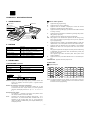
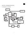
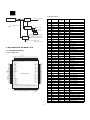
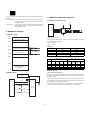
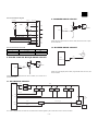
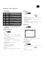
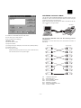
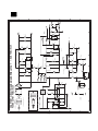
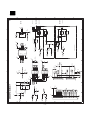
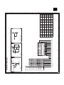
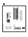
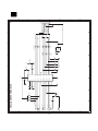
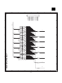
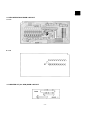
Top and Bottom of a Page : -38.1mm
XE-A201US
q SERVICE MANUAL
CODE : 00ZXEA201USME
ELECTRONIC
CASH REGISTER
MODEL
XE-A201
SRV KEY : Not necessary
PRINTER : M-T51
(U and A version)
CONTENTS
CHAPTER 1. SPECIFICATIONS...................................................................... ..... 1
CHAPTER 2. OPTIONS......................................................................................... 5
CHAPTER 3. MASTER RESET AND PROGRAM RESET.................................... 5
CHAPTER 4. HARDWARE DESCRIPTION........................................................... 6
CHAPTER 5. TEST FUNCTION............................................................................12
CHAPTER 6. IPL (INITIAL PROGRAM LOADING) FUNCTION...........................15
CHAPTER 7. CIRCUIT DIAGRAM AND PWB LAYOUT.......................................17
PARTS GUIDE
Parts marked with "!" are important for maintaining the safety of the set. Be sure to replace these parts with specified
ones for maintaining the safety and performance of the set.
SHARP CORPORATION
This document has been published to be used
for after sales service only.
The contents are subject to change without notice.
XE-A201US
CHAPTER 1. SPECIFICATIONS
■ Machine state symbols
1. APPEARANCE
Rear view
Front view
Customer display
(Pop-up type)
Operator display
Printer cover
P:
Appears during programming.
E:
Appears when an error is detected.
o:
Appears when the subtotal is displayed or when the amount
tendered is smaller than the sales amount.
c:
Appears when the [CONV] key is pressed to calculate a subtotal
in foreign currency.
F:
Appears when a transaction is finalized by pressing the [CA/AT/
NS], [CHK] or [CH] key.
C:
Appears when the change due amount is displayed.
Receipt paper
Power cord
Mode switch
Keyboard
Drawer lock
E-E : May appear in the far-left three positions at the timing of key
entry when the electronic journal (EJ) memory is full. (Depending on programming.)
RS-232C connector
Drawer
L:
Appears when the voltage of the installed batteries is under the
required level. You must replace with new ones within two days.
L:
Appears when the batteries are not installed, or the installed
batteries are dead. You must replace with new ones immediately.
•:
May appear right below the eighth and ninth places at the timing
of finalization of a transaction when the electronic journal (EJ)
memory is nearly full.
Also appears right below the tenth place when power save
mode is effective.
H:
Appears when the print head release lever is in the lifted position.
2. RATING
XE-A201
Weight
16.8lb (7.6kg)
Dimensions
330 (W) x 428 (D) x 280 (H) mm
13.0 (W) x 16.9 (D) x 11.0 (H) inches
Power source
AC 120V (m10%), 60Hz
Power consumption
Stand-by 7W, Operating 34.5W (max.)
Working temperature
0°C~40°C (32°F to 104°F)
3. KEYBOARD
PPPPPPPPPP : Appears when the paper is out.
2) KEY LIST
1) KEYBOARD LAYOUT
■ Keyboard layout
Type
Normal keyboard
Key position
STD/MAX 53
Key pitch
19 (W) x 19 (H) mm
Key layout
CONV
RA %1
Fixed type
RCPT
/PO
–
Customer display (Pop-up type)
Operator display
DC
Clerk code
SHIFT
ESC
BS
DC SHIFT NUMBER
SPACE
7
8
4
5
1
2
0
CL
9
6
3
00
PLU
/SUB
4
DEPT
#
DEPT
SHIFT
A
F
K
P
20
24
28
32
B
8
19
3
C
7
18
2
D
E
12
H
6
I
11
J
16
M
10
N
15
O
R
30
14
25
9
Q
31
26
21
5
L
27
22
17
1
G
23
CLK#
S
29
13
T
TAX AUTO
U
X
TAX1
SHIFT
TAX2
SHIFT
V
Y
CHK CH
W
Z
MDSE
SBTL
#/TM
SBTL
CA/AT/NS
Note: The small characters on the bottom or lower right in each key
indicates functions or characters which can be used for character entries for text programming.
Amount: Appears in the far-right eight (max.) positions. When the
amount is negative, the minus symbol “-” appears before
the amount.
Number of repeats for repetitive registrations:
The number of repeats is displayed, starting at “2” and
incremental with each repeat. When you have registered
ten times, the display will show “0.” (2 3 3 ..... 9 3 0 3 1 3
2 ... )
Receipt function status:
The indicator “_” appears in the RCPT OFF position when
the receipt function is in the OFF status.
Time:
NUMBER
VOID RFND
PLU/SUB
DEPT REPEAT
RCPT
OFF
%2
•
@/FOR
Appears in the far-right six positions (hour-minute - ”A” or
hour-minute - ”P”) in the OP X/Z, REG, or MGR mode. “A” is
displayed in the morning (AM), and “P” in the afternoon
(PM). In the REG or MGR mode, press the [#/TM/SBTL] key
to display the time.
–1–
XE-A201US
■ Key names
The mode switch has these settings:
KEY TOP
OFF:
DESCRIPTION
2
Paper feed key
RA
OP X/Z: To take individual clerk X or Z reports, and to take flash
reports.
Received-on account key
RCPT/PO
Receipt print/Paid-out key
VOID
It can be used to toggle receipt state “ON” and “OFF” by
pressing he [RCP/PO] key.
Void key
ESC
This mode locks all register operations. (AC power turns off.)
No change occurs to register data.
Escape key
REG:
For entering sales.
CONV
Conversion key
PGM:
To program various items.
%1, %2
Percent 1and 2 key
VOID:
Enters into the void mode. This mode allows correction after
finalizing a transaction.
MGR:
For manager’s entries. The manager can use this mode for
an override entry.
RFND
Refund key
-
Discount key
@/FOR
Multiplication key
n
CL
0-9,00
Decimal point key
X1/Z1: To take the X/Z report for various daily totals.
Clear key
X2/Z2: To take the X/Z report for periodic (weekly or monthly) consolidation.
Numeric Keys
PLU/SUB
PLU/Subdepartment key
DEPT#
Department code entry key
DEPT SHIFT
Department shift key
CLK#
Clerk code entry key
Dept1-32
5. DISPLAY
1) OPERATOR DISPLAY
Department keys
TAX
Tax key
Tax 1 SHIFT
Tax 1 shift key
Tax 2 SHIFT
Tax 2 shift key
AUTO
Charge key
MDSE SBTL
: 1 line
Color of display
Check key
CH
: LED numeric display
Number of line
Number of positions : 10 positions numeric display
Automatic sequence key
CHK
Display device
: Yellow / Green
Character form
: 7 segment + DP
Character size
: Numeric 14.2 (H) x 7.9 (W) mm
Layout:
Merchandise subtotal key
#/TM/SBTL
Non-add code/Time display/Subtotal key
CA/AT/NS
Total/Amount tender/Non Sale key
0 . 1 . 2 . 3 . 4 . 5 . 6 . 7 . 8 . 9 .
2) CUSTOMER DISPLAY
4. MODE SWITCH
Display device
: LED
Number of line
: 1 line
1) LAYOUT
Number of positions : 7 positions
• Rotary type
Color of display
: Yellow / Green
Style
: Pop up type
Manager key (MA)
MA
MA
OP
VOID
Operator key (OP)
: 14.2mm (H) x 7.9mm (W)
3 . 4 . 5 . 6 . 7 . 8 . 9 .
X2/Z2
OP
PGM
MGR
X1/Z1
: 7 segment + Dp
Character size
Layout:
REG
OPX/Z
OFF
Character form
The mode switch can be operated by inserting one of the two supplied
mode keys - manager (MA) and operator (OP) keys. These keys can
be inserted or removed only in the “REG” or “OFF” position.
–2–
XE-A201US
Segment
• Print speed
: Approximate 52mm/s (Approximate 10 l/s)
• Paper feed speed : Approximate 52mm/s (Approximate 10 l/s)
Display
position
Description
(Manual feed)
: Approximate 52mm/s (Approximate 10 l/s)
Amount
1-8
Minus sign
2-10
-: Floating
Error
8-10
Exx:xx = error code
• Paper end sensor : Set up
• Reliability
: Mechanism LIFE 6 million lines used to highquality thermal paper
PGM Mode
10
P
• Cutter
CASH, CHECK,
CHARGE
10
F: Light up when a registration is
finalized by depressing CASH,
CHECK, CHARGE key
• Near end sensor : No
: Manual Cutter
SUB TOTAL/
short tender
10
o
Change
10
C: Light up whenever the change
due amount appears in the display.
Currency
Conversion
10
c: Light up whenever the foreign
amount appears in the display.
Department
9-10
PLU
7-10
2) Paper
• Paper roll dimension : 57.5 m 0.5mm in width
Max. 80mm
in diameter
• Paper quality
No zero-suppressed
: High-quality thermal paper
paper thickness: 0.06 to 0.08mm
Nihon seisi thermal paper : TF50KS-E
Oji thermal paper
: PD150R,
PD160R
No zero-suppressed
Repeat
8
Endless count, starting from 2.
3) Logo stamp
Receipt OFF
9
_
• No
DC
_: Double size character entry status
SHIFT
_: Shift character entry status
NUMBER
_: Number character entry status
Clerk No.
2, 3
-xx-: clerk number
EJ FULL
8-10
E-E: Light up when EJ memory is
FULL at the timing of key entry (by
PGM selection).
Low Battery
10
L:
No Battery
10
L:
4) Printing area
Number of thermal head heater elements 288 dots
(4.75)
48 (288 dots)
(4.75)
print area
(max.24 characters)
0.167
Decimal Point
Display
position
Decimal point
7-1
TAB
4-1
EJ near full
8, 9
Description
57.5±0.5
(Paper dimension)
(by PGM selection)
6. PRINTER
1) Printer
• Part number
: M-T51
• NO. of station
: 1 (Receipt of journal)
• Validation
: No.
• Printing system
: Line thermal
• No. of dot
: 288 dots
• Dot pitch
: Horizontal 0.167mm
Vertical
0.174mm
• Font
: 10 dots (W) u 24 dots (H)
• Printing capacity : max. 24 characters
• Character size
: 1.67mm (W) u 4.17mm (H) at 10 u 24 dots
• Print pitch
: Column distance
Row distance
2.0mm
5.21mm
–3–
(units : mm)
XE-A201US
7. DRAWER
8. BATTERY
[OUTLINE]
1) MEMORY BACK UP BATTERY
• Standard equipment: Yes (1)
For memory back up, the dry battery AA (3 pieces) are needed.
• Max. number of additional drawers: 1
1. Memory holding time:
Approx. 1 year after New dry batteries are installed.
• The drawer consists of:
2. Battery exchange method:
1) Drawer box (outer case) and drawer
When the low battery symbol “L” lights up, replace the batteries (3
AA) by the following method;
2) Money case
3) Coin case
1) Power on the ECR.
4) Lock (attached to the drawer)
2) Mode switch turn to “REG” mode.
3) Remove the OLD dry batteries (3 pieces).
[SPECIFICATION]
4) Insert the NEW dry batteries (3 pieces).
1) DRAWER BOX AND DRAWER
5) Confirm the low battery symbol “L” is off.
Model name of the drawer box
SK415
Size
330 (W) x 418 (D) x 98 (H) mm
13 (W) x 16.5 (D) x 3.9 (H) inches
Material
Metal
Bell
–
Release lever
Standard equipment: situated at
the bottom
Drawer open sensor
–
Separation from the main unit
2) LOW BATTERY
Low battery indication will appear on the left side of display when the
battery voltage is low.
CASE 1:
The machine can indicate the low battery condition. (Always)
CASE 2:
2) MONEY CASE
Disallowed
Separation of the bill compartments from the coin
compartments
Allowed
Bill separator
–
Number of compartments
4B/5C
When numeric entry or item entry is done.
Battery condition will not appear.
Exceptionally, when the power is restored after a power failure, the
low battery condition will appear on the display only when the battery is low.
And the indicator will disappear after any key entry.
–
Separation from the drawer
When any numeric entry & any item entry is not done or
just after finalization.
[Display sample]
“
“L
“L
0.00” : Battery is OK.
0.00” : Low battery (You have to change the batteries.)
0.00” : No battery (You have to change the batteries
immediately.)
After finalization
Layout:
“F
“L
“L
12.34” : Battery is OK.
12.34” : Low battery. (“L” indicate instead of “F”.)
12.34” : No battery. (“L” indicate instead of “F”.)
Note: “NO BATTERY”: When the “NO BATTERY” is display, the master reset is executed at the timing of “POWER
ON” after the “POWER OFF”.
4B/5C
3) LOCK (LOCK KEY : LKGIM7331BHZZ)
• Location of the lock: Front
• Method of locking and unlocking:
To lock, insert the drawer lock key into the lock
and turn it 90 degrees counter clockwise.
To unlock, insert the drawer lock key and turn it
90 degrees clockwise.
ck
unlo
Lo
SK1-1
SK1-1
• Key No:
ck
–4–
XE-A201US
CHAPTER 2. OPTIONS
1. OPTIONS (No)
2. SERVICE OPTIONS (No)
3. SUPPLIES
NO
1
PARTS CODE
PRICE
RANK
TPAPR6656RC05
BA
PARTS CODE
PRICE
RANK
BU
NAME
Thermal roll paper
DESCRIPTION
5 ROLLS/PACK 70 φ
4. SPECIAL SERVICE TOOLS
NO
NAME
1
RS-232 Loop-back connector
UKOK-6705RCZZ
2
POS tools (IPL Software)
UKOG-2360BHZZ
DESCRIPTION
CHAPTER 3. MASTER RESET AND PROGRAM RESET
1. MASTER RESETTING
2. PROGRAM RESETTING
(INITIALIZATION)
Master resetting clears the entire memory and resumes initial values.
Master resetting can be accomplished by using the following procedure:
This resetting resumes the initial program without clearing memory.
Procedure A:
Procedure:
This resetting can be operated at below sequence in PGM mode.
1) Plugin the AC cord to the wall outlet.
1) Unplug the AC cord from the wall outlet.
2) Set the mode switch to REG position.
2) Wait over 1 muinite for discharging.
3) Let the ECR be witout the memory backup battery.
3) Set the mode switch to the PGM position.
4) Unplug the AC cord from the wall outlet.
4) While holding down the FEED key, plugin the AC
cord to the wall outlet.
5) Wait over 1 minute for discharging.
Note: In case power failure occurs when the machine has no battery
attached to it, the master reset operation is automatically performed after the power has been restored.
6) Plugin the AC cord to the wall outlet.
The master reset can also be accomplished in the following case.
In case power failure occurs when the machine has no battery
attached to it, the master reset operation is automatically performed after the power has been restored.
(This is because if power failure occurs with no battery attached to
the machine, all the memories are lost and the machine does not
work properly after power recovery; this requires the master reset
operation.)
–5–
XE-A201US
CHAPTER 4. HARDWARE DESCRIPTION
1. HARDWARE BLOCK DIAGRAM
POWER SUPPLY
STANDARD
DRAWER.
CPU
Data bus
DRIVER , SENSOR
ROM : 256K Byte
RAM : 20K Byte
RAM
Address
bus
128K Byte
POPUP
Seg. DRIVER
PRINTER
M-T51
FRONT
LED
4 to 16
DECORDER
Dig. DRIVER
PAPER TAKE
UP MOTOR
KEYBOARD
MODE SWITCH
KEY SCAN SIGNAL
KEY RETURN SIGNAL
RS232C
DRIVER
RS232
–6–
XE-A201US
2) Pin description
TRANSFORMER
PQ1CG2032
V0 24V
Drawer
Pin
No.
/POFF detect point
PQ1CG2032
VLED 5.7V
VCC 5V
VDD 5V
Battery
Function
1
SOUT4
P96
In
2
CLK4
P95
In
Key IN
Key IN
3
TB4IN
P94
In
Key IN
4
TB3IN
P93
In
Key IN
5
SOUT3
P92
In
Key IN
6
SIN3
P91
In
Key IN
7
CLK3
P90
In
Key IN
VDD
BYTE
VDD
In
9
CNVss
CNVss
In
Normal : L
VH, VP (8V)
PRINTER HEAD, MOTOR
PAPER TAKEUP MOTOR
10
XCIN
XCIN
In
Calender clock :32.768KHz
11
XCOUT
XCOUT
In
Calender clock :32.768KHz
12
/RESET
/RESET
13
XOUT
XOUT
2. DESCRIPTION OF MAIN LSI’S
2-1. CPU (M30624FGAFP)
SIN4
AVCC
VREF
AN0
AVSS
AN1
AN2
AN3
AN4
AN5
AN6
AN7
D0
D1
D2
D3
D4
D5
D6
D7
D8
D9
D10
D11
D12
100
99
98
97
96
95
94
93
92
91
90
89
88
87
86
85
84
83
82
81
80
79
78
77
76
P97
VDD
VDD
TH
GND
P101
Vref
P103
P104
P105
LATCH
DTS
D0
D1
D2
D3
D4
D5
D6
D7
P10
P11
P12
P13
PH1
1) Pin configuration
M30624FGAFP
D13
D14
D15
A0
A1
A2
A3
A4
A5
A6
A7
VSS
A8
VCC
A9
A10
A11
A12
A13
A14
A15
A16
A17
A18
A19
75
74
73
72
71
70
69
68
67
66
65
64
63
62
61
60
50
58
57
56
55
54
53
52
51
PH2
PH3
PH4
A0
A1
A2
A3
A4
A5
A6
A7
GND
A8
VDD
A9
A10
A11
A12
A13
A14
A15
A16
A17
NC
NC
P74
P73
CLK
P71
DAT
P67
P66
/FRES
P64
FSD
FRD
FSCK
DR1
/RDY
/HOLD
VCC
NC
NC
/RD
NC
/WR
/CS3
/RAS1
BUSY
/ROS1
26
27
28
29
30
31
32
33
34
35
36
37
38
39
40
41
42
43
44
45
46
47
48
49
50
TA2OUTW
TA1IN/V
TA1OUT/V
TB5IN
TB5OUT
TXD1
RXD1
CLK1
CLKS1
TXD0
RXD0
CLK0
/RTS0
/RDY
ALE
/HOLD
/HLDA
CBCLK
/RD
/BHE
/WR
/CS3
/CS2
/CS1
/CS0
SOUT4
CLK4
TB4IN
TB3IN
SOUT3
SIN3
CLK3
BYTE
CNVss
XCIN
XCOUT
/RESET
XOUT
Vss
XIN
Vcc
NMI
INT2
INT1
INT0
TA4IN/U
TA4OUT/U
TB3IN
TBEOUT
TA2INW
In/
Out
8
ON/OFF Control (MODE SW,
/POFF, CPU P105)
1
2
3
4
5
6
7
8
9
10
11
12
13
14
15
16
17
18
19
20
21
22
23
24
25
SIGNAL
NAME
ON/OFF Control (MODE SW)
LM2574
+ Tr.
P96
P95
P94
P93
P92
P91
P90
VDD
GND
XCIN
XCOUT
/RESET
XOUT
GND
XIN
VDD
VDD
CTCRL
/FRDY
P-OFF
MOTOR
BUZ1
P77
P76
P75
SYMBOL
–7–
In
Reset
Out
Open
Booting : H
14
Vss
Vss
In
Vss
15
XIN
XIN
In
System clock
16
Vcc
VDD
In
VDD
17
NMI
P85
In
Not used
18
INT2
P84
Out
PRINTER/STB2
19
INT1
/RDY
In
NU FMC (/RDY)
20
INT0
P-OFF
21
TA4IN/U
MOTOR
Out
In
Paper take up motor drive
22
TA4OUT/U
BUZ1
Out
Buzzer drive
23
TB3IN
P77
In
RS232 :DR
24
TBEOUT
P76
In
RS232 :CS
25
TA2INW
P75
In
RS232 :CD
26
TA2OUTW
P74
Out
RS232 :ES
27
TA1IN/V
P73
Out
Drawer drive 2
28
TA1OUT/V
CLK2
Out
Printer data clock
29
TB5IN
P71
Out
NU FMC (BUSY)
30
TB5OUT
TXD2
Out
Print data
31
TXD1
P67
Out
RS232 :SD
32
RXD1
P66
In
RS232 :RD
33
CLK1
/FRES
Out
NU FMC (/FRES)
34
CTS1/RTS1
P64
Out
RS232 :RS
35
TXD0
FSD
Out
FMC :Send data
36
RXD0
FRD
37
CLK0
FSCK
Out
FMC :Shift clock
38
/RTS0
DR1
Out
Drawer drive 1
39
CLKOUT
/RDY
In
40
ALE
NC
41
/HOLD
/HOLD
42
/HLDA
NC
Out
NOT USE
43
CBCLK
BCLK
Out
BCLK
44
/RD
/RD
Out
Read
45
/BHE
NC
Out
NOT USE
46
/WR
/WR
Out
Write
47
/CS3
CS3
Out
Display segment latch
48
/CS2
/CS2
Out
Chip select :for RAM
49
/CS1
/CS1
Out
EPM Control
50
/CS0
/CS0
Out
Chip select :for ROM
51
A19
A19
Out
Address bus :19
52
A18
A18
Out
Address bus :18
In
Out
In
Power off
FMC :Receive data
/RDY (CGROM)
NOT USE
/BOOT MODE
XE-A201US
Pin
No.
SYMBOL
SIGNAL
NAME
In/
Out
53
A17
A17
Out
Address bus :17
54
A16
A16
Out
Address bus :16
55
A15
A15
Out
Address bus :15
56
A14
A14
Out
Address bus :14
57
A13
A13
Out
Address bus :13
58
A12
A12
Out
Address bus :12
59
A11
A11
Out
Address bus :11
60
A10
A10
Out
Address bus :10
Out
61
A9
A9
62
VCC
VDD
63
A8
A8
64
VSS
VSS
65
A7
A7
Out
Address bus :7
66
A6
A6
Out
Address bus :6
67
A5
A5
Out
Address bus :5
68
A4
A4
Out
Address bus :4
69
A3
A3
Out
Address bus :3
70
A2
A2
Out
Address bus :2
71
A1
A1
Out
Address bus :1
72
A0
A0
Out
Address bus :0
73
P17
ENA2
Out
Paper feed motor :ENA2
74
P16
ENA1
Out
Paper feed motor :ENA1
75
P15
IN2
Out
Paper feed motor :IN2
76
P14
IN1
Out
Paper feed motor :IN1
77
P13
P13
Out
Key/Display
78
P12
P12
Out
Key/Display
79
P11
P11
Out
Key/Display
80
P10
P10
Out
Key/Display
81
D7
D7
InOut
Data bus :7
82
D6
D6
InOut
Data bus :6
In
Out
In
3. CLOCK GENERATOR
Function
1) CPU
15
XIN
13
XOUT
12MHz
CPU
Address bus :9
R
330
11
XCOUT
VDD
X1
32.768KHz
Address bus :8
10
XCIN
VSS
83
D5
D5
InOut
Data bus :5
84
D4
D4
InOut
Data bus :4
85
D3
D3
InOut
Data bus :3
86
D2
D2
InOut
Data bus :2
87
D1
D1
InOut
Data bus :1
88
D0
D0
InOut
Data bus :0
89
AN7
STB1
Out
Printer head strobe
90
AN6
LATCH
Out
Printer data latch
91
AN5
P105
Out
Printer head voltage ON
92
AN4
P104
Out
CG ROM Bank
93
AN3
P103
In
94
AN2
Vref
In
NU Vret
95
AN1
P101
In
Printer head voltage
check
96
AVSS
VSS
In
VSS
97
AN0
TH
In
Print head temperature check
C
18P
C
27P
Two oscillators are connected to the CPU.
The basic clock X2 is supplied from a 12MHz oscillator.
If the CPU was not operating properly, the signal does not appear on
this line in most cases.
The sub-clock X1 generates 32.768KHz which is primarily used to
update the internal RTC (real time clock).
During the standby mode, it keeps oscillating to update the clock and
monitoring the power recovery.
4. RESET CIRCUIT
VDD
MODE SWITCH
SRV' position
VDD
IC
S-80928ANMP
R
CPU
R
11
R
C
/RESET
C
(1) When the mode switch is placed in the “SRV” position, the reset
signal is sent to the CPU to reset the hardware.
(2) When VDD t 2.8V, a reset signal is outputted from the reset IC.
(S-80928ANMP)
VBAT
5. P-OFF CIRCUIT
VCC
R15
2.7K
VLED
R16
9.1KG
R20
2.7K
R19
98
VREF
VDD
In
VDD
99
AVCC
VDD
In
VDD
C14
1uF/50V
R17
56K
0
3
8
5
8
7
1
100
SIN4
P97
In
Key IN
R18
IC4A
BA10393
4
3.9K
ZD4
MTZJ5.1B
–8–
/POFF
6
2
IC4B
BA10393
4
C15
0.1uF
P-OFF
XE-A201US
The P-OFF signal detects two signals by two comparators and sent to
the CPU.
7. PRINTER CONTROL CIRCUIT
V0 (24V) signal: If the power voltage V0 (24V) falls bellow the specified level, the P-OFF signal is driver to LOW by the
comparator ICAA.
1) Paper feed motor circuit
VLED signal:
VH
If the LED/Logic power voltage VLED falls below the
specified level, the P-OFF signal is driven to LOW by
the comparator IC4B.
VCC
CPU
PH1
PH3
PH2
6. MEMORY CIRCUIT
A
/A
B
/B
IC13
PH4
MOTOR
LB1838M
1) Address map
00000h
Stepping motor control
00400h
The 2-phase, bi-polar stepping motor is driven at a constant voltage by
LB1838M (made by SANYO).
CPU internal RAM
20kbytes
05400h
1 step: 0.087mm
1 dot:
2 steps
CPU port
06000h
/CS3 area
06000h - 07FFFh
Segment latch address
No.
CPU port
Signal used
76
P14
IN1
75
P15
IN2
74
P16
ENA1
73
P17
ENA2
08000h
External S-RAM : 128kbytes
/CS2 area
08000h - 27FFFh
(128kbytes area)
28000h
40000h
Drive step
Driver IC input
(CPU output)
STEP
C0000h
CPU internal ROM
256kbytes
IN1
IN2
ENA1
Motor drive signal
ENA2
A
B
/A
/B
(OUT1) (OUT3) (OUT2) (OUT4)
1
L
L
H
H
H
H
L
2
H
L
H
H
L
H
H
L
L
3
H
H
H
H
L
L
H
H
4
L
H
H
H
H
L
L
H
FFFFFh
2) Print circuit
2) RAM control
Thermal head configuration
As shown in the equivalent circuit in the figure, thermal head consists
of heating elements and head drivers which drives and controls those
heating elements.
Power supply circuit
or
Dry battery
The serial print data input through the DATA IN (D1) is transferred to
the shift register synchronizing with the CLOCK (CP) and stored in the
latch register by the LATCH (LA) signal.
CS2
A0-A16
A0-A16
A0-A16 VCC
D0-7
D0-7
VDD
/CS2
VDD
The head conduction signals (print commands 1 ~ 6) turn the gate on
to conduct the heating element corresponding to the print data.
I/O0-7
/CS2
/CS1
S-RAM
CPU
VCC
/RD
VCC
/WR
/RD
/WR
128K byte
IC
/OE
/WE
–9–
XE-A201US
9. DRAWER DRIVE CIRCUIT
Thermal head block daigram
Dot #288
Dot #1
V0
5,6,18,19
VP
FB2
9,10,14,15
GND
C80
CPU
CN5
11
STB1
13
(38pin)
LAT
16
Shift register
MOTOR
Q9
STB2
7
Latch register
/RTS0
R102
DR1
CLK
17
When the DR1 signal from the CPU is HIGH, Q9 is turned on to operate the solenoid.
DAT
12
VCC
Connector
10. BUZZER DRIVE CIRCUIT
Thermal head strobe terminals
STB No.
Dot No.
Number of dots
1
1 ~ 144
144
2
145 ~ 288
144
VCC
BZ
BZ
470
8. PAPER TAKE UP MOTOR DRIVE CIRCUIT
CPU
VH
TA4OUT/U
22pin
C79
CPU
CN5
TA4IN/U
MOTOR
MOTOR
R101
Q13
(21pin)
When the pulse signal (about 4KHz) is generated from the CPU, the
buzzer sounds.
When the MOTOR signal from the CPU is HIGH, Q1 is turned on to
operate the motor.
11. KEYBOARD CIRCUIT
P10-13
P10-13
HC138
/S0-9
/S0-7
/S0-9
P10-13
HC138
/S0-7
/S1
/S3
/S4
Paper
feed key
Head up
sensor
Paper end
sensor
/S8-9
Key
Matrix
Mode
Switch
/S0 - 9
/S9
RS232
/CI
signal
P92-97
P92-97
P90
CPU
P91
P91
D0-7
/CS3
D0-7
G1',G2',
G3'G4',G5',
G6',G7
a,b,c,d,e,f,g,dp
74HC374
/CS3
Front
display
A',B',C',D',E',F',G',DP'
Four P10-13 signals from the CPU are converted into 16 strobe signals by two 74HC138 for use in various functions.
– 10 –
Pop-up
display
XE-A201US
1) Keyboard
5) Paper end sensor
Scan signal:
Scan signal:
10 /S0-9 signals
1 /S4 signal
Return signal: 6 P92-97 signals
Return signal: 1 P91 signal
The keys are read by the key matrix following the above signals.
The paper end sensor state is read by the above signals.
2) Mode switch
Scan signal:
Receipt near end sensor
Near end detected
Near end not detected
P91
Low
High
8 /S0-7 signals
Return signal: 1 P90 signal
6) RS232/CI signal detection
The positions are read by the above signals.
Scan signal:
Scan
signal
/S0
/S1
/S2
/S3
/S4
/S5
/S6
/S7
Mode
switch
position
SRV
PGM
(OFF)
TIME
REG
MGR
X1/Z1
X2/Z2
1 /S9 signal
Return signal: 1 P91 signal
The RS232/CI signal is detected by the above signals.
3) Paper feed key
Scan signal:
RS232 /CI signal
/CI signal detected
/CI signal not detected
P91
Low
High
7) Display
1 /S1 signal
Scan signal:
Return signal: 1 P91 signal
10 /S0-9 signals
The above 10 scan signals are used as the following digit signals.
The paper feed key is read by the above signals.
Digit signal:
4) Head up sensor
Scan signal
/S0
/S1
/S2 /S3
Scan signal:
Digit signal: G1’
Front
G2’
G3’ G4’ G5’ G6’ G7’ G8’ G9’ G10’
Digit signal: G1’
Pop-up
G2’
G3’ G4’ G5’ G6’ G7’
1 /S3 signal
Return signal: 1 P91 signal
The Head up sensor state is read by the above signals.
Head up sensor
Head up detected
Head up not detected
Low
High
P91
/S4
/S5
/S6 /S7
/S8
Segment signal : Segment signals: a, b, c, d, e, f, g, and DP are output by the IC:74HC374, using the data bus signal:D0-7 from the CPU as an input signal and the
chip select signal:/CS3 as a latch signal.
12. RS232 CIRCUIT
P75
P66
P67
P74
R2OUT
CD
R2IN
RD
R1OUT
T3IN
T2IN
R1IN
SD
T3OUT
ER
T2OUT
HIN211
CPU
P77
P64
P76
P91
/S9
R4OUT
T1IN
R5OUT
R3OUT
DR
R4IN
RS
T1OUT
CS
R5IN
R3IN
CI
1
CD
2
RD
3
SD
4
ER
5
GND
6
DR
7
RS
8
CS
9
CI
D-SUB 9pin connector
/S5
The signals from the CPU are converted by the HIN211 into the RS232 level to input and output them.
– 11 –
XE-A201US
CHAPTER 5. TEST FUNCTION
1. TEST ITEMS
2) KEY CODE
1 Key operation
The test items are as follows:
NO.
Code
1
100
Display buzzer test
2
101
Key code
3
102
Printer test
4
104
Keyboard test
5
105
mode switch test
6
106
Printer sensor test
7
107
Clock display test
8
110
Drawer 1 open & sensor test
101
Description
9
120
External RAM test
10
121
CPU internal RAM test
11
140
CPU internal ROM test
12
160
AD conversion port test
13
500
RS232C test
14
550
Sleep mode test
RCPT/PO
2 Test procedure
Display
KEY CODE
3 Check that:
KEY code: Every time a key is pressed, the code of that key is displayed as a decimal number.
When a key is pressed twice or pressed in an incorrect manner, --will be displayed.
4 End of testing
You can exit the test mode by turning the mode switch to a position
other than the SRV mode. The printer prints as follows:
101
3) PRINTER TEST
1 Key operation
102
2. DESCRIPTION OF EACH DIAGNOSTIC
PROGRAM
2 Test procedure
1) DISPLAY BUZZER TEST
Display
1 Key operation
100
2 Test procedure
Display at front side
1.2.3.4.5.6.7.8.9.0.
4.5.6.7.8.9.0.
3 Check that:
After that, all segments turn on (about 1 sec)
Display at front side
----------------ZZZZZ
----------------ZZZZZ
----------------ZZZZZ
3 lines of 24 Z's are printed.
The decimal point will shift in steps of 1 digit from the lower digit to
the upper (every 200 m sec).
Display at operator side
1 2 3 4 5 6 7 8 9 0
ZZZZZZ
ZZZZZZ
ZZZZZZ
RCPT/PO
Display at operator side
RCPT/PO
The print is free from contamination, blur, and uneven density.
4 End of testing
8.8.8.8.8.8.8.8.8.8.
8.8.8.8.8.8.8.
The test will end automatically.
4) KEYBOARD TEST
This mode is repeated.
At the same time, the buzzer sounds continuously.
1 Key operation
3 Check that:
104
A) Each position is correctly displayed.
RCPT/PO
2 Test procedure
B) The brightness of each number is uniform.
The keyboard is checked using the sumcheck data of the key code.
C) The buzzer sound is normal.
Display
4 End of testing
1 0 4
KEY CODE
You can exit the test mode by pressing any key. The following is
printed.
3 Check:
100
A) The content of completion print
– 12 –
XE-A201US
4 End of testing
3 Check that:
When the test ends normally
When an error occurs
104
E- ~ - 104
“-” blinks and the clock counts up.
4 End of testing
Note: Calculation of key sumcheck data
The hard code (hexadecimal number) at the position (excluding
feed key) where there is an input data contact is added.
However, the end key (CA/AT/NS) is not added.
This data to which hard codes have been added is converted
into a decimal number value, which will become the sumcheck
data that will be entered when the Diag is started.
When any key is pressed, the date and time are printed and the
test mode will terminated.
Display
1 0 6
year month day
1 Key operation
1 Key operation
110
RCPT/PO
RCPT/PO
2 Test procedure
2 Test procedure
Display
hour min sec
8) DRAWER 1 OPEN AND SENSOR TEST
5) MODE SWITCH TEST
105
XXXXXX - XXXXXX
1 0 5
Display
X
1 1 0
X
X: O = DRAWER OPEN
C = DRAWER CLOSED
MODE: _PGM_VOID_OFF_OP X/Z_REG_MGR_X1/Z1_X2/Z2____PGM
x :
1
2
9
3
4
5
6
7
1
3 Check that:
The above x must be read in the correct order. (If the contact is
open, 9 will be displayed.)
A) The drawer opens normally.
B) The sensor correctly indicates the status of the drawer 1.
3 Check:
* On the XE-A201, “C” (CLOSED) is always displayed.
The display during testing and the content of the completion print.
4 End of testing
4 End of testing
When the test ends normally:
When an error occurs:
You can exit the test mode by pressing any key. The printer prints
the following.
105
E- ~ - 105
110
6) PRINTER SENSOR TEST
9) EXTERNAL RAM TEST
1 Key operation
106
1 Key operation
RCPT/PO
120
2 Test procedure
2 Test procedure
Check the status of paper end sensor and head up sensor.
7-segment display:
1 0 6
The standard 128 Kbyte RAM is checked.
The contents of the memory are lost after this test.
RAM(08000H ~ 27FFFH area) is tested in the following procedure:
X Y
3 Check the following:
X:1 - Paper present
O - Out of paper
a) Data in the test area is stored.
Y:1 - Head DOWN
O - Head UP
b) Write “00H”
4 End of testing
c) Read and compare “00H” and then write”55H”
d) Read and compare “55H” and then write”AAH”
You can exit the test mode by pressing any key and the printer
prints the following:
e) Read and compare “AAH”
106
f) Restore stored data.
If an error occurs at a step, the error is printed.
If an error does not occur, the following addresses are checked.
7) CLOCK TEST
1 Key operation
107
RCPT/PO
Addresses to be checked:
10000H , 10001H , 10002H , 10004H , 10008H
10010H , 10020H , 10040H , 10080H ,
10100H , 10200H , 10400H , 10800H ,
11000H , 12000H , 14000H , 18000H ,
20000H
RCPT/PO
2 Test procedure
Displayed digit:
8 7 6 5 4 3 2 1
7-segment display:
Display
hour
min
sec
1 2 0
3 Check:
Blinks at an interval of 0.5 sec.
A) The completion print.
– 13 –
XE-A201US
4 End of testing
4 End of testing
The test will automatically be terminated and the printer prints as
follows:
The program ends after printing.
When the test ends normally.
When the test ends abnormally. Ex- ~ -
120
120
*****
x = 1: Data error
x = 2: Address error
When the test ends normally.
ROM
When the test ends abnormally. E- ~ ROM
When an error occurs, the printer outputs the error message and
then the address where the error has occurred in the area ****.
12) AD conversion port
1 Key operation
10) CPU internal RAM test
160
1 Key operation
121
140
******** (CPU CODE)
******** (Version)
140
******** (CPU CODE)
******** (Version)
RCPT/PO
2 Test procedure
RCPT/PO
The test program displays the voltage of each AD port.
2 Test procedure
1. Head temperature
The test program checks internal RAM of the CPU.
The contents of the memory are lost after this test.
RAM (00400H - 053FFH area) is tested in the following procedure.
2. Head voltage
3. Battery voltage
1 6 0 1
1 6 0 2
1 6 0 3
XXX
XXX
XXXX
3 End of testing
a) Data in the test area is stored.
You can exit the test mode by pressing any key.
The printer prints the follwing.
b) Write “00H”
160
c) Read and compare “00H” and then write “55H”
d) Read and compare “55H” and then read “AAH”
13) RS232C test
e) Read and compare “AAH”
Install the RS232C loopback connector. (UKOG-6705RCZZ)
f) Stored data is restored.
1 Key operation
If an error occurs at a step, the error is printed.
If an error does not occur, the following addresses are checked.
Addresses to be checked:
500
2 Test procedure
01000H , 01001H , 01002H , 01004H , 01008H
01010H , 01020H , 01040H , 01080H ,
01100H , 01200H , 01400H , 01800H ,
02000H , 04000H
Display
Control signal check
OUT PUT
/ER
/RS
OFF
OFF
OFF
ON
ON
OFF
ON
ON
1 2 1
3 Check:
The completion print.
The test program ends after printing.
7-segment display:
121
121
5 0 0
The completion print.
4 End of testing
Completion print
RS TEST OK
Error print
RS TEST **NG**ERxx
xx
Contents of the error
01
ER DR error
02
ER CI error
03
RS CD error
04
RS CD error
05
SD RD error
DATA data
06
SD RD error
DATA error/framing error
If an error occurs, the printer outputs the error message and then
the address where the error has occurred in the area ****.
11) CPU internal ROM test
1 Key operation
RCPT/PO
2 Test procedure
The test program checks that the checksum of the CPU internal
flash ROM (C0000H - FFFFFH) is correct.
The lower two digits of the checksum should be 10H.(pending)
Display
IN PUT
/CI
/CD
OFF
OFF
OFF
ON
ON
OFF
ON
ON
3 Check:
*****
x = 1: Data error
x = 2: Address error
140
/DR
OFF
OFF
ON
ON
/CS
OFF
ON
OFF
ON
Data communication check
A loopback test of 256-byte data between SD-RD is performed.
DATA: $00 - $FF BAUD RATE: 9600 BPS
4 End of testing.
When the test ends normally.
When the test ends abnormally. Ex- ~ -
RCPT/PO
1 4 0
3 Check:
The completion print.
– 14 –
XE-A201US
14) Sleep mode test
3 Check that:
1 Key operation
550
RCPT/PO
A) The display goes off (excluding Decimal point)
B) The system turns active when any key is pressed.
2 Test procedure
4 End of testing
The test program checks the system in SLEEP MODE (The display
goes off and the Decimal point comes on) and then waits for any
status change (KEY input or RS PORT change).
The test program will automatically be terminated and the printer
prints the following.
550
CHAPTER 6. IPL (INITIAL PROGRAM LOADING) FUNCTION
5) Close the cabinet.
The application program of the XE-A201 is written into the Flash ROM
in the CPU.
6) Turn on the AC Power.
(At this time, ECR looks like inactive, but ECR waits the ROM data
from PC.)
Since the CPU supplied as a service part does not include the application program in it, the application program must be written when the
CPU is replaced with a new one.
<IPL software on PC>
To write the application program into the Flash ROM, connect the PC
and the XE-A201 with an RS-232C cable, and execute the PC software (PosUtilityTool2).
7) Copy the following files in "PosUtilityTool2" into the hard disk of
PC.
Postool2.exe
* Use the RS-232C cable provided together with the XE-A201 product, or use a D-Sub 9pin cross cable employed in conventional
communication between ECR-ECR.
A201u.ROM
8) Boot "Postool2.exe."
* PosUtilityTool2 includes the ROM data to be written into the CPU
as well as the IPL program.
9) Push [Add Files] in the screen.
[Related parts/Tool]
11) By pushing [Send] in the screen, the ROM data is sent from PC to
ECR.
The address counter is shown on PC and counts up.
PARTS NAME
PARTS CODE
CPU (without application
program)
VHI30624FGA-1
PosUtilityTool2
UKOG-2360BHZZ
10) Select the ROM DATA file. (File name: A201u.ROM)
LOCATION
No.
12) After about 3-minuites, the message "Complete" is shown on PC.
IC5
[IPL PROCEDURE]
1) Connect the XE-A201 and PC with an RS-232C cable.
<XE-A201 side>
2) Turn off the AC Power. (& remove batteries.)
3) Open the cabinet.
4) Change the IPL JUMPER PIN (SP1) to the rear side.
SP1
SP1
Default
When IPL
<After booting>
<Main PWB>
– 15 –
XE-A201US
APPENDIX: RS232C CABLE
The RS-232C cable (QCNWG3190BHZZ) provided together with the
XE-A201 is used to connect the XE-A201 and a PC when using the
customer support tool or performing IPL.
When using the cable, connect the core side of the cable to the XEA201 as shown in the figure below.
PC
XE-A201
RS232C
CABLE
<After pushing "Add Files">
CORE
*1 COM Port is selectable between COM1 and 2.
*2 For "Send Type", select "Direct".
The accessory RS-232C cable has the following internal
connections:
*3 Do not select "Extra Setting".
<XE-A201 side>
(Equivalent to a cross cable used in the conventional connection of
ECR-ECR)
12) Turn on the AC Power.
13) Open the cabinet.
14) Change the Jumper PIN (SP1) to the front side. (default position)
9PIN D-SUB
9PIN D-SUB
15) Close the cabinet.
16) Turn on the AC Power.
Master Reset will be performed. If not, power off the XE-A201,
wait 1miniute and turn on the power again.
SD
RD
DTR
DSR
RTS
DCD
CTS
– 16 –
SD
3
3
SD
RD
2
2
RD
RTS
7
7
RTS
DCD
1
1
DCD
DTR
4
4
DTR
DSR
6
6
DSR
CTS
8
8
CTS
SG
5
5
SG
: TRANSMITTED DATA
: RECEIVED DATA
: DATA TERMINAL READY
: DATA SET READY
: REQUEST TO SEND
: DATA CARRIER DETECTOR
: CLEAR TO SEND
– 17 –
A
B
C
D
8
ZD4
MTZJ5.1B
C14
1uF/50V
0
3.9K
R18
9.1KG
R16
R244
for JAPAN
0
2
3
OFF - OPEN
ON - GND
IC4A
BA10393
R17
5273-02A
1
2
CN1
1
VCC
7
F1
2.7K
R20
245
6
5
4
8
NOT USE
/VON
IC4B
BA10393
VLED
D1
6
6
0.1uF
C15
C10
0.1uF
7
CP301
UL/CSA 2.0A/125V
T3.15AL
(with HOLDER)
C1
MYLOR
0.033uF
MODE SW
P-OFF
4
8
56K
R19
POWER TRANS
100V
VO
+20% INPUT & NO LOAD: VOUT< =40V
POWER TRANS
220V-230V
120V
POWER SUPPLY PWB CIRCUIT
for EUROPE
USA
R15
2.7K
7
5
Q3
KRA106S
/POFF
T1.0AL
F3
/VOFF
/POFF
VPON
D4
D3
R1
5
IC1
C11
220uF/50V
NOT USE
5
1
IC3
1SS353
D11
3
4
3
4
HEAT SINK
VOUT=1.26X(1+R2/R1)
1
0
4
2
7
Q2
KRC106S
H:OFF
6,8pin:N.C
L:ON
3 LM2574
1
5
2
PQ1CG2032FZ
5
2
PQ1CG2032FZ
HEAT SINK
R114
24K
IC2
1SS133
D5
R241
22K
C4
220uF/50V
ZD3
MTZJ5.1B
10K
R11
1SS133
1SS133
2.2K
R113
C2
3300uF
50V
180uH
/VOFF
4
RB060L40
D10
L1
63uH
560
R14
10K
R13
<- CLOSE TO
REGURATOR
1000uF
16V
C5
<- CLOSE TO
REGURATOR
910F
R7
2.7KF
R6
VOUT=1.23X(1+R2/R1)
D2
FMB-G24H
IPEAK>12A :100%
C12
0.02uF(M)
220uH
IPEAK>2.2A
L3
/VOFF
RB060L40
D6
5.6K
R3
NOT INSTALL
10(FUSE)
with FUSE
R2
IPEAK>2.2A
L2
Q4
KRC106S
51
R12
4
3
3
VO
1000uF/35V
C13
10uF/10V,OS
C6
NOT USE
3.6KF
R5
20KF
R4
1. MAIN PWB CIRCUIT
L:OFF
H,OPEN:ON
/VPON
Q1
KTD998
Q1:HEAT SINK
CHAPTER 7. CIRCUIT DIAGRAM AND PWB LAYOUT
8
VO
PTZ6.2A
ZD2
VLED
C7
ZD1
2
330uF
16V
C8
VCC +5V
VLED +5.8V
VH
VH +7.5V
PTZ9.1B
330uF
16V
VO:23.8V
NOT USE
1N4002
D8
1N4002
D7
C3
4700uF
16V
2
0.1uF(M)
C9
R8
220
D9
RB721Q
VCC
R9
3.3M
1
2
CN2
VBAT
1/4
1
5267-02A(BLUE)
100
R246
22K
R10
VDD
1
A
B
C
D
XE-A201US
– 18 –
A
B
C
D
/RD
/CS0
2
CST12.0MTW
X3
8
1
3
NOT INSTALL
C36
1000pF
R54
240
VCC
100pF*8(C28-C35)
ENA1
ENA2
IN1
IN2
KST3
KST2
KST1
KST0
10K
10K
A
2
1
Vcc:14pin
GND:7pin
74F32
IC10A
VCC
330pF
C40
C31
10K
C60
0.1uF
3
C33
10K
R42
C34
10K
R43
R57
C37
100pF
820
R56
3.3K
BCLK
1
2
3
4
VCC
FS781
3
2
8
7
6
5
1
2
3
VCC
1
C
L
P
R
4
7
NC
Q
Q
6
5
C38
4
5
2200pF
R46
R47
R48
R49
R50
R51
R52
R53
P97
C24
10K
R29
11
12
/RDY
VCC
74F74
CLK
D
1
3
C
L
P
R
1
0
VCC
10uF/10V
IC11B
Q
Q
VDD
C39
100K
C25
10K
R30
IC5
C27
10K
R32
81
82
83
84
85
86
87
88
89
90
91
92
93
94
95
96
97
98
99
100
D7
D6
D5
D4
D3
D2
D1
D0
AN7
AN6
AN5
AN4
AN3
AN2
AN1
AVSS
AN0
VREF
AVCC
SIN4
M30624FGFP
C26
10K
R31
6
8
9
6
/RESET
220pF
C62
for JAPAN
SHORT LINE
5
C45
10K
C46
10K
R64
VCC
R63
0Si:INSTALL
18pF
C43
R59
47K
32.768KHz
27pF
C44
R60
330
X1
1
2
3
5
/CS0
/RD
D[0..7]
A[0..19]
CST12.0MTW
X2
R61
0
/CS0
/RD
VCC
R62
33
1 1 1 1 1 1 1 1 1 1 2 2 2 2 2 2 2 2 2 2 3
1 2 3 4 5 6 7 8 9 0 1 2 3 4 5 6 7 8 9 0 1 2 3 4 5 6 7 8 9 0
C48
10K
R66
C49
10K
R67
A0
D0
D1
D2
D3
D4
D5
D6
D7
C55
15
17
19
21
24
26
28
30
16
18
20
22
25
27
29
31
1
44
33
12
14
13
10uF/10V
10K
R77
4
LH5388WS(CGROM)
VCC
A0
A1
A2
A3
A4
A5
A6
A7
A8
A9
A10
A11
A12
A13
A14
A15
A16
A17
A18
A19
VSS
VDD
10K
R87
100pF
C57
10K
C59
0.1uF
10K
R75
C52
10K
R70
4
R76
C51
10K
R69
KANJI ROM
D0
D1
D2
D3
D4
D5
D6
D7
D8
D9
D10
D11
D12
D13
D14
D15/A-1
NC
NC
BHE
CE/CE
OE/OE
VSS
IC12
/FRES
FSCK
FRD
FSD
150pF
C58
R81
47K
50
49
48
47
46
45
44
43
42
41
40
39
38
37
36
35
34
33
32
31
C50
10K
R68
C55(for JAPAN)
150pF*10(C45-C54)
C47
10K
R65
CS0
CS1
CS2
CS3
WR
BHE
RD
CBCLK
HLDA
HOLD
ALE
CLKOUT
RTS0
CLK0
RXD0
TXD0
T
T
T A
TT A
CLKS1
A4 T T AA1 T
CLK1
S TT S
C XR
4 O T B A 2 1 O T B RXD1
OC B B OS C B NX C E X
I I I I U B E 2 OI U B 5
U L 4 3 U I L Y V C O S O V X V N N N N N T 3 O I U N T 5 O TXD1
T K I I T N K T S I U E U S I C MT T T / / I U N T / / I U
4 4 N N 3 3 3 E S N T T T S N C I 2 1 0 U U N T W WV V N T
DDDDDDDDAA A AA AA A V AV AA A AA A AA A AA
8 9 1 1 1 1 1 1 0 1 2 3 4 5 6 7 S8 C9 1 1 1 1 1 1 1 1 1 1
0 1 2 3 4 5
S C 0 1 2 3 4 5 6 7 8 9
8 7 7 7 7 7 7 7 7 7 7 6 6 6 6 6 6 6 6 6 6 5 5 5 5 5 5 5 5 5
0 9 8 7 6 5 4 3 2 1 0 9 8 7 6 5 4 3 2 1 0 9 8 7 6 5 4 3 2 1
"H":BOOT ON
SHORTPIN
SP1
P96
P95
P94
P93
P92
P91
P90
FOR DM,TM,SAMPLES
VCC
100
100
100
100
100
100
100
100
VDD
R58
0.1uF
C42
P100
P101
NOT INSTALL
0.1uF
C41
C23
10K
R28
CGBANK
C107
4.7UF/16V
S-80928ANMP
SII
OUT
VDD
VSS
IC15
VCC
VBAT
VCC
CD
10K
C22
10K
R27
150pF*8(C20-C27)
C21
10K
R26
R45
C20
10K
R25
VCC
/STB1
/LAT
VPON
C19
10K
R24
Vcc:14pin
GND:7pin
74F74
CLK
D
IC11A
C61
0.1uF
VDD
XIN
S0
XOUT
FSOUT
S1
VSS
LF
IC7
47K
R55
C35
10K
R44
VDD
INSTALL
<- OR ->
C32
10K
R41
C18
10K
R23
7
100pF*4(C16-C19)
C17
10K
10K
C16
R22
R21
PLACE NEAR CPU!!!
/RESET
R91
3.3K
R
C30
10K
R40
10K
10K
R39
R36
R35
0.5Si:INSTALL
KIA431A
K
IC6
C29
10K
10K
C28
R38
R37
VCC
R34
A7
A6
A5
A4
A3
A2
A1
A0
R33
D7
D6
D5
D4
D3
D2
D1
D0
|LINK
|POWER.SCH
|DRIVER.SCH
|RS.SCH
CPU PWB CIRCUIT
8
23
11
10
9
8
7
6
5
4
42
41
40
39
38
37
36
35
34
3
2
43
32
C54
10K
R72
A1
A2
A3
A4
A5
A6
A7
A8
A9
A10
A11
A12
A13
A14
A15
A16
A17
A19
47K
R83
47K
R84
P66
P67
/RDY
DR1
/RD
BCLK
/WR
/CS2
DR2
P74
P75
P76
P77
/STB2
MOTOR
/POFF
VCC
/CS3
DAT
BZ
C64
VCC
PIEZO BZ
CLK
3
NOT INSTALL
10uF/10V,OS
470
R86
VCC
0.1uF
C63
VCC
TP2
30pF
C56
P64
A[0..19]
D[0..7]
R79
10k
VCC
R85
10K
R80
47K
TP1
A19
R74
10K
VCC
CGBANK
10K
R73
A8
A9
A10
A11
A12
A13
A14
A15
A16
A17
/CS0
R78
47K
VCC
VCC
47K
R82
C53
10K
R71
3
A[0..19]
D[0..7]
A16
A14
A12
A7
A6
A5
A4
A3
A2
A1
A0
D0
D1
D2
D0
D1
D2
D3
D4
D5
D6
D7
Q0
Q1
Q2
Q3
Q4
Q5
Q6
Q7
NC
A16
A14
A12
A7
A6
A5
A4
A3
A2
A1
A0
I/O0
I/O1
I/O2
VSS
IC9
10uF/50V
C67
VDD
VCC
A15
CS2
WE
A13
A8
A9
A11
OE
A10
CS1
T/O7
I/O6
I/O5
I/O4
I/O3
74HC374
OC
CLK
D0
D1
D2
D3
D4
D5
D6
D7
IC8
2
LP621024D-T 70ns
1
2
3
4
5
6
7
8
9
10
11
12
13
14
15
16
C66
0.1uF
1
11
3
4
7
8
13
14
17
18
2
32
31
30
29
28
27
26
25
24
23
22
21
20
19
18
17
D7
D6
D5
D4
D3
A10
A13
A8
A9
A11
A15
C65
0.1uF
VDD
VCC
Vcc:20pin
GND:10pin
2
5
6
9
12
15
16
19
a
b
c
d
e
f
g
dp
a
b
c
d
e
f
g
dp
VDD
VCC
30pF
C69
10K
/CS2
/RD
/WR
2/4
R89
30pF
C68
VCC
1
C70
150pF
10K
R90
R88
10K
1
A
B
C
D
XE-A201US
– 19 –
A
B
C
D
P101
/S3
34
33
32
31
30
29
28
27
26
25
24
23
22
21
20
19
18
17
16
15
14
13
12
11
10
9
8
7
6
5
4
3
2
1
8
1SS133
D13
VCC
G
a
b
c
d
e
f
g
dp
2SK2731
/S3
/S4
/S5
/S6
/S0
/S1
/S2
/S7
/S8
/RESET
P90
P91
P92
P93
P94
P95
P96
P97
/S9
/VON
Q8
KRC111S
P91
1SS133
CN3
Q7
0.1uF
a
b
c
d
e
f
g
dp
/S3
/S4
/S5
/S6
C74
7
0.1uF
VLED
PE
S
VH
Q6
MTD2955V
G
10K
R95
NOT INSTALL
C72
0.1uF
HUPS
/S0
/S1
/S2
/S7
/S8
/RESET
P90
P91
P92
P93
P94
P95
P96
P97
/S9
/VON
/VPON
C71
S
10KF
R93
MAX 9A
R94
D
VH
10KF
D12
52045-3445
P91
P91
/S4
7
DRIVER PWB CIRCUIT
8
D
/S7
KST0
KST1
KST2
KST3
1
2
3
4
5
6
7
8
9
10
11
12
CN4A
VP
VCC
2K
R98
ONLY HOLE
1
2
3
4
5
6
7
8
9
10
11
12
CN4B
ONLY HOLE
JP1
6
VP
P100
6
10K
R99
4.7K
R100
1
2
3
4
5
6
7
8
1
2
3
4
5
6
7
8
VCC
Y0
Y1
Y2
Y3
Y4
Y5
Y6
C73
330pF
30KF
R96
VCC
Y0
Y1
Y2
Y3
Y4
Y5
Y6
TH
TH
C75
47uF
50V
0.1uF
HUPS
16
15
14
13
12
11
10
9
16
15
14
13
12
11
10
9
C77
CLK
/B
/A
PE
/STB1
/STB2
/LAT
A
B
74HC138
A
B
C
G2A
G2B
G1
Y7
GND
IC17
74HC138
A
B
C
G2A
G2B
G1
Y7
GND
IC16
VCC
C97
0.1uF
C96
0.1uF
VCC
DAT
0.1uF
C76
10K
R97
5
VCC
/S8
/S9
/S0
/S1
/S2
/S3
/S4
/S5
/S6
5
IN1
IN2
VCC
ENA1
ENA2
C98
10uF/16V
VCC
VCC
7
14
6
9
2
13
1
4
DR2
P91
/S6
DR1
8
3
5
12
10
4
11
1K
R105
F6
KRC111S
1SS133
2SD2212
Q11
VDR
A
/A
B
/B
VDR
3
MOTOR
4.7K
R104
C66673
FB2
C82
0.1uF
C80
0.1uF
FB OR JUMPER WIRE
VH
R103
22K
FB5
3
C66673
C78
10uF/50V
A
/A
B
/B
FB5,FB6,FB7:JUMPER WIRE
VDR
Q10
F4
T0.5AL
Q9
2SD2212
T500mA/250V
D14
VO
VCONT
OUT1
OUT2
OUT3
OUT4
VS1
VS2
FB4:JUMPER WIRE
P91
1K
R102
/S6
LB1838M
GND
GND
IN1
IN2
ENA1
ENA2
VCC
IC13
4
F5
C81
0.1uF
C83
0.1uF
1K
R101
C79
0.1uF
C66673
FB3
Q13
2SD2212
2
C66673
FB7
C66673
FB6
C66673
FB4
FB OR JUMPER WIRE
T400mA/250V
VH
2
3
2
1
CN6
5046-03A
3
2
1
CN8
5046-03A
3
2
1
CN7
5045-03A
5267-02A
1
2
CN5
3/4
1
RIGHT-ANGLE CON
DRAWER2
RIGHT-ANGLE CON
DRAWER1
STRAIGHT CON
MOTOR
1
A
B
C
D
XE-A201US
– 20 –
A
B
C
D
7
2.7K
/S9
/S8
/S7
/S6
/S5
/S4
/S3
/S2
/S1
/S0
/S1
8
1.25mm FPC CN
12
11
10
9
8
7
6
5
4
3
2
1
CN21
KID65083
INPUT
1
2
P
9
2
3
P
9
3
23
22
21
31
30
29
28
27
26
12
CN22
1.25mm FPC CN
P
9
1
35
34
33
32
42
41
40
39
25
24
3K
7.2K
4
9
8
7
6
5
4
3
2
1
P
9
4
7
5
P
9
5
11
10
20
19
18
17
16
15
14
13
6
P
9
6
47
46
45
44
43
53
52
38
37
36
GND
7
P
9
7
59
58
57
56
55
54
51
50
49
48
OUTPUT
COMMON
8
KEY MATRIX PWB CIRCUIT
8
9
1
0
/
S
7
10
6
1
1
/
S
6
9
1
2
MODE SW
2SD2170
B
6
/
S
5
8
1
3
/
S
4
7
1
4
/
S
3
3.5K
6
1
5
M
O
R
5
300
1
6
/
S
2
4
/
S
1
5
1
7
E
C
5
3
1
8
/
S
0
2
1
9
/
R
E
S
E
T
1
2
0
G
N
D
2
1
4.7K
/
V
O
N
2
2
G
N
D
4
48
49
37
25
24
36
13
1
47K
12
PF
KRA101M, KRA106S
INPUT
4
COMMON
OUTPUT
3
50
38
26
14
2
3
51
39
27
15
3
52
40
28
16
4
53
41
29
17
5
2
2
54
42
30
18
6
55
43
31
19
7
56
44
32
20
8
57
45
33
21
9
1
58
46
34
22
10
1
59
47
35
23
11
4/4
A
B
C
D
XE-A201US
– 21 –
A
B
C
D
7
8
52044-3445
FROM MAIN
D24
D25
D26
D27
D28
D29
D30
/S3
/S4
/S5
/S6
/S7
/S8
/S9
34
33
32
31
30
29
28
27
26
25
24
23
22
21
20
19
18
17
16
15
14
13
12
11
10
9
8
7
6
5
4
3
2
1
G1'
G2'
G3'
G4'
G5'
G6'
G7'
A'
B'
C'
D'
E'
F'
G'
DP'
/S3
/S4
/S5
/S6
G1'
G2'
G3'
G4'
G5'
G6'
G7'
A'
B'
C'
D'
E'
F'
G'
DP'
/S0
/S1
/S2
/S7
/S8
/RESET
P90
P91
P92
P93
P94
P95
P96
P97
/S9
/VON
a
b
c
d
e
f
g
dp
D23
/S2
CN23
D22
/S1
VCC
D21
D31
/S0
/S1
52045-1245
1
2
3
4
5
6
7
8
9
10
11
15
14
13
12
11
10
9
8
7
6
5
4
3
2
1
CN24
52806-1510
/S3
/S4
/S5
/S6
/S0
/S1
/S2
/S7
/S8
/RESET
P90
P91
P92
P93
P94
P95
P96
P97
/S9
/VON
A
B
C
D
E
F
G
dp
7
POP UP
C104
100uF/16V
PLACE NEAR CONNECTER
1SS133
1SS133
1SS133
1SS133
1SS133
1SS133
1SS133
1SS133
1SS133
1SS133
1SS133
12
CN21
C105
0.1uF
VLED
VLED
P[91..97]
2. KEY INTERFACE PWB CIRCUIT
8
6
P[91..97]
6
VCC
P
9
1
2
P
9
2
KID65083AP
10PIN : NC
9 PIN :GND
/S[0..9]
1
CN22
52044-2245
P
9
3
4
P
9
4
5
P
9
5
5
/S[0..9]
or DTA143ESA
KRA101M X 10
47K * 7EA
3
1
'
d
p
1
8
P
9
6
7
P
9
7
12K
R209
2
g
1
7
IC23B
G
'
120
G
1
0
R219
'
/
S
7
P90
1
0
Q20
KTA1664
9
120
Q32
R201
R202
R203
R204
R205
R206
R207
8
R218
12K
R208
IC23A
D
P
6
2.54mm Pitch
KEY&MODE SW
5
/
S
6
Q33
1
1
3
G
9
'
F
'
f
1
6
/
S
4
4
Q34
100pF
C106
47K
IC23C
120
R220
1
3
R228
Q21
KTA1664
12K
R210
P90
/
S
5
VCC
1
2
4
1
4
12K
R211
M
D
R
4
e
1
5
E
'
IC23D
120
R221
Q22
KTA1664
G
8
'
/
S
3
1
5
/
S
2
Q35
1
6
12K
R212
/
S
1
1
8
/
S
0
G
7
'
5
1
9
Q36
IC23E
D
'
1
4
d
120
R222
Q23
KTA1663
1
7
3
120
R223
6
Q24
KTA1663
G
6
'
2
1
c
1
3
2
2
Q37
G
5
'
120
R224
Q25
KTA1663
R214
12K
7
/VON
/RESET
/VON
IC23F
C
'
/RESET
R213
12K
2
0
3
b
1
2
B
'
IC23G
Q31
G
4
'
120
R225
Q26
KTA1663
12K
R215
8
a
1
1
A
'
Q30
R216
12K
2
IC23H
120
R226
Q27
KTA1663
G
3
'
2
Q29
G
2
'
120
R227
Q28
KTA1663
R217
12K
G
1
'
|LINK
|POPUP.SCH
Q38
Q39
KTA1663
VLED
1
VLED
1
1/1
A
B
C
D
XE-A201US
– 22 –
A
B
C
D
7
6
8
7
ONLY HOLE
1
2
3
4
5
6
7
8
9
10
11
12
CN4D
ONLY HOLE
1
2
3
4
5
6
7
8
9
10
11
12
CN4C
6
3. PRINTER I/F (for D/M) PWB CIRCUIT
8
5
5
4
4
VP
VCC
/A
/B
1
2
3
4
5
6
7
8
9
10
11
12
13
14
15
16
17
18
19
20
21
22
23
24
25
26
CN31
00 6208 010 126 001
PE
HUPS
3
B
A
TH
CLK
DAT
/STB2
/STB1
/LAT
3
2
2
1
1
1/1
A
B
C
D
XE-A201US
– 23 –
A
B
C
D
P91
/S9
P76
P77
P75
P66
P67
P74
P64
7
7
16
15
5
P75
8
P91
/S9
1SS353
7
19
P76
6
24
22
P77
26
8
P66
21
20
0.1uF
14
P67
Q14
KRC111S
10K
C86
C85
0.1uF
R243
6
D16
(BUSY:FOR BOOT)
R242
10K
12
6
P74
P64
10K
R247
4. RS232C DRIVER PWB CIRCUIT
8
IC14
HIN211
/EN
R5OUT
R4OUT
R3OUT
R2OUT
R1OUT
T4IN
T3IN
T2IN
T1IN
C2-
C2+
C1-
C1+
0.1uF
C84
1
0
V
C
C
1
0
1
1
VCC
/SHDN
R5IN
R4IN
R3IN
R2IN
R1IN
T4OUT
T3OUT
T2OUT
T1OUT
V-
V+
25
18
23
27
4
9
28
1
3
2
17
13
5
5
C90
0.1uF
C89
C91
1000pF*5
C87
0.1uF
C92
VCC
4
C93
C88
10uF/50V
4
C94
VCC
100ohm*5
R112
R111
R110
R109
R108
3
jumper
JP4
FB15
FB14
FB13
FB12
FB11
FB10
FB9
FB8
EFCB322513TS X 8
3
JP3
/CI
/RS
/CS
/DR
/CD
RD
/SD
/ER
2
2
/CI 5V
/DR
/RS
/CS
/CD
RD
/SD
/ER
1
1
87203-6066
1
2
3
4
5
6
7
8
9
CN9
1/1
A
B
C
D
XE-A201US
– 24 –
A
B
C
D
7
8
27
27
DP'
R7
R8
G'
7
0
3 8
27
R6
F'
5 1 9 1 2 4 6 7
LED9
S568GWA
G7'
5. REAR DISPLAY PWB CIRCUIT
8
1
4
G6'
LED8
D568GWA
1
3
G5'
5
1
4
G4'
LED7
D568GWA
1
3
G3'
4
1
4
G2'
LED6
D568GWA
3
1
3
G1'
27
R5
6
E'
27
R4
D'
5
27
R3
C'
4
27
R2
B'
27
R1
3
A'
4 1 1 1 2 3 1 1 9 7 1 5 6 8 1 1 4 1 1 1 2 3 1 1 9 7 1 5 6 8 1 1 4 1 1 1 2 3 1 1 9 7 1 5 6 8 1 1
7 8
5 6
2
0 1
7 8
5 6
2
0 1
7 8
5 6
2
0 1
6
G1'..G7'
2
2
G1'
G2'
G3'
G4'
G5'
G6'
G7'
A'
B'
C'
D'
E'
F'
G'
DP'
1/1
1
52807-1510
1
2
3
4
5
6
7
8
9
10
11
12
13
14
15
CN31
1
A
B
C
D
XE-A201US
– 25 –
A
B
C
D
7
8
7
1
4
LED5
D568GWA
1
3
G
9
'
6
1
4
G
8
'
LED4
D568GWA
1
3
G
7
'
5
1
4
G
6
'
LED3
D568GWA
1
3
G
5
'
4
1
4
G
4
'
LED2
D568GWA
1
3
G
3
'
1
4
G
2
'
3
LED1
D568GWA
1
3
G
1
'
6
30
30
D
P
'
R234
R233
G
'
30
R235
F
'
5
30
R236
E
'
30
R237
D
'
4
30
R238
C
'
30
R239
B
'
3
30
R240
A
'
4 1 1 1 2 3 1 1 9 7 1 5 6 8 1 1 4 1 1 1 2 3 1 1 9 7 1 5 6 8 1 1 4 1 1 1 2 3 1 1 9 7 1 5 6 8 1 1 4 1 1 1 2 3 1 1 9 7 1 5 6 8 1 1 4 1 1 1 2 3 1 1 9 7 1 5 6 8 1 1
7 8
5 6
2
0 1
7 8
5 6
2
0 1
7 8
5 6
2
0 1
7 8
5 6
2
0 1
7 8
5 6
2
0 1
'
G
1
0
6. DISPLAY PWB CIRCUIT
8
2
2
|LINK
|POPUP.SCH
1
1
1/1
A
B
C
D
XE-A201US
A. side
1. MAIN PWB LAYOUT
PWB LAYOUT
XE-A201US
– 26 –
B. side
XE-A201US
– 27 –
XE-A201US
2. KEY INTERFACE PWB LAYOUT
A. side
B. side
3. PRINTER I/F (for D/M) PWB LAYOUT
– 28 –
XE-A201US
4. REAR DISPLAY PWB LAYOUT
5. DISPLAY PWB LAYOUT
– 29 –
Top and Bottom of a Page : -38.1mm
XE-A201US
q
COPYRIGHT ã 2001 BY SHARP CORPORATION
All rights reserved.
Printed in Japan.
No part of this publication may be reproduced,
stored in a retrieval system, or transmitted.
In any form or by any means,
electronic, mechanical, photocopying, recording, or otherwise,
without prior written permission of the publisher.
SHARP CORPORATION
Information Systems Group
Products Quality Assurance Department
Yamatokoriyama, Nara 639-1186, Japan
2001 October Printed in Japan
t