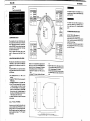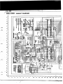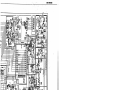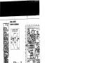
1
FEB. 6,1984
SDE-1000 3000
SDE-1000/3000
ISDE-3000 |
Front
LED SLB-26URS RED
Button
'(2247053700)
(15029132)
First Edition
LEDSLB-26UR5 RED
Display panel
(15029132)
(2221071300)
pPot K1611008FE-100KB
(13219361)
Knob ORN
RED/GRN
(2247025900)
(15029148)
Button
\
LED GL-9HD12 RED
(15029152)
LEDSLB-26YYHLYEL
(2221031100)
LED GL-3AR1 RED
(2247054200) \
L- LED SLB 26GG5F GRN
(1S029159)
Control panel
(2247054700)
LEDGL9ND2
PHOTO SDE-3000
SPECIFICATIONS
Button
(15029158)
Button
(2247054300)
(15029110)
Button
(2247057700)
Fluorescent display FIP16A5R
(15029710)
Power Switch SDG A 3P
(13129124)
Button
Button
(2247024000)
(2247054100)
Rear
Pot. EVH-6PA361B54
Jack
(13219214)
HU 531701-100
GND terminal
Rear panel
Knob
(13449240)
(13459123)
(2221031300)
(2247023900)
6
\
Bushing BU4801
Jack
Jack
Switch SUF-12
(12369511)
HLJ 531701-010
HLJ 5317 01-030
(13129338)
(13449238)
(13449239)
ISDE-10001 Front
LEDGL-9HD12 RED
(15029152)
LEDSLB-26YYHLYEL
(15029159)
Button
Button
Button
(2247054500)
(2247053500)
(2247053700)
Pot. K1611008FE
Pot. K1611008FE
Pot. K1611008FE
LED SLB-26UR5 RED
100KD (13219361)
50KB (13219360)
50KA (13219359)
Knob ORN
Knob GRN
Knob BLU
Display panel
(15029132)
(2247025900)
(2247026000)
(2247026200)
Button
(2221071400)
(2247053800)
\
\
LED SLB 26GG5F GRN
Pot. K1611008FE
Pot. K1611008FE
Fluorescent display
LED GL-3AR1 RED
(15029158)
50KB (13219360)
50KB (13219360)
Power Switch SDGA 3P
FIP5A8B
(15029110)
Knob YE L
Knob BLU
(13129124)
(2247026100)
(2247026200)
Conrol panel
(2221031200)
Rear
GND terminal
(13459123)
Bushing BU4801
(12369511)
(15029709)
Button
(2247024000)
Button
(2247054000)
FEB. 5,1984
SDE-1000/3000
12
3
4
5
6
EXPLODED VIEW
7
8
9
10
11
\2
13
14
16
17
21
22
2H
SDE-1000/3000
24
2^
2b
4x8 BLK binding-^
M4 internal tooth
3x8 BLK binding
f
3x8 BLK binding
3x6 BLK binding
4x12 BLK oval
4x12 BLK
(1000): SDE-1000, (3000): SDE-3000
Control panel
2221031200
(1000)
2221031100
-Display panel
(3000)
2221071400
(1000)
(3000)
-Fluorescent display
15029709
FIP5A8B
15029710
(1000)
FIP16A5R
(3000)
7411608005
7411708005
(s) -PCB holder
(1000)
(3000)
221903JB01
(3000)
Button BLK
7411706026
•-Cushion
13129338
2226022200
-Button WHT
2219031900
-Push switch
2215040100
-Push switch
2214020700
--Power board
(jo}-LED holder
(3000)
^Jy-Joint A
13129337
(12)— Connection rod
13129124
(m- Joint B
12369410
SUF-12
12470514
7411609000
(i4)— Line cord strain relief
(1000)
7411606032
'li 5}-Push switch
2215040200
Q*y~ Button assembly
2247090300
2247090100
-Main board
2247090200
2247024000
2221071300
(4)-Switch board
^7 J—Button assembly
&■
1702B
7411709000
• - Insulation sheet
2216052701
--GND terminal
13459123
SUE-12
SDGA3P
oval
SDE-1000/3000
FEB. 5.1984
PARTS LIST
2247054500
2247054600
2247054700
2247054800
CASE
Button
TIME
Button
DEPTH
Button
OUT
Button
RATE
(SDE-3000)
(SDE-3000)
(SDE-3000)
SWITCH
(SDE-1000)
(SDE-1000)
(SDE-1000)
(SDE-1000)
(SDE-1000)
(SDE-3000)
(SDE-3000)
(SDE-3000)
(SDE-3000)
(SDE-3000)
(SDE-1000)
(SDE-3000)
reed relay
(SDE-3000)
(SDE-3000)
JACK
13449238
HLJ5317-01-010
13449239
HLJ5317-01-030
13449240
HLJ5317-01-100
TRANSFORMER
22450348N0
22450349D0
22450350N0
(SDE-1000)
(SDE-1000)
(SDE-1000)
22450351D0
(SDE-1000)
2244023800
2244023900
12449236
100/117V
220/240V
100/117V
220/240V
(SDE-1000)
(SDE-1000)
(SDE-3000)
(SDE-3000)
COIL
(SDE-1000)
(SDE-3000)
LPF S097624
LPF S097623
OSC S097614
LI
(SDE-3000)
PCB
7411606032
Main board
(pcb 2291058201)
7411607001
LED board
7411608005
7411706026
Main board
7411707001
LED board
7411708005
7411709000
Switch board
Power supply board
(pcb
(pcb
(pcb
(pcb
(pcb
(pcb
Fuses,
capacitor Cl
Switch board
Fuse labels,
2291058300)
2291058400)
2291057901)
2291058000)
2291058100)
2291058500)
(SDE-1000)
(SDE-1000)
(SDE-1000)
(SDE-3000)
(SDE-3000)
(SDE-3000)
excluded.
Specify model and line voltage
when ordering for complete assy.
7411711002
(SDE-3000)
(SDE-3000)
RAM board
Analog SW board
(pcb 2291083800)
(pcb 2291091900)
Substitutive for HI-302 and HI-303.
No replaceable part.
(SDE-3000)
POTENTIOMETER
(SDE-3000)
13219361
K1611008FE
13299101
EVT-R4SA00B14
See P.20.
100KB
trimmer
(SDE-3000)
SDE-1000/3000
(SDE-1000)
(SDE-1000)
(SDE-1000)
(SDE-1000)
(SDE-1000)
(SDE-3000)
(SDE-3000)
(SDE-3000)
FUSE
12559105
12559510
1A
CEE
T400mA
12559504
CEE
T100mA
12559506
CEE
T160mA
100/117V
220/240V
220/240V
220/240V
(SDE-1000)
(SDE-3000)
IC
15229811
MB63H101
15179141
MSM80C49-44RS
M5K4164NP-20
M54563
SN74LS48N
HD14001 BP
HD14011 BP
HD14049 BP
HD14174 BP
15169355
15159101H0
15159104H0
15159112H0
15159133
15189111J1
15189163
15219116
15189136
15189141
15199106F0
15169102H0
15169117H0
15169356
15219108
15189152
15159115H0
1599104F0
15169301H0
15169311H0
15169332H0
15169357
15159105H0
15159129H0
15189160
15219120
15159513
15159523
15159522
15189161
15189118J0
15229802
15159316
TRANSISTOR
15119701
2SA968-Y
15119125
2SA1115-F
15129130
2SC1583-F
15129704
2SC2238-Y
15129137
2SC2603-F
15129602
2SD667-C
15129118
2SC1923-R
(SDE-3000)
FET
SGA
15179315
15159702
FEB. 5,1984
NJM311D
MB3761M
IR2E02
M5218L
NJM4562DD
yA7805UC
HD7406P
HD7407P
SN74LS628N
NE570N
15139108
2SK150-GR
15019125
CPU
64K D-RAM
Transistor array
7-Segments decoder
Quad 2 Input NOR
Quad 2 Input NAND
Inverter
Dual D-Flip-Flop
Comparators
Voltage detector
LED Driver
OP Amp
OP Amp
Three Terminal Voltage Regulator
Hex O.C. Inverters
Hex O.C. Buffers
VCO
Compandor
OP AMP
HD14066 BP
yA7812
UC
Analog Switch
HD74LS00
HD74LS74P
Quad 2 Input NAND
Dual D-Flip-Flop
Three Terminal Voltage Regulator
HD74LS157P
74LS283
HD14013 BP
HD14053 BP
TDB0119
Dual D-Flip-Flop
AM6012
D/A Converter
2 to 1 Data Selectors
4 bit Binary Full Adders
Triple 2-channel Multiplexer
Dual Voltage Comparator
HI-201-5
HI-302-5
HI-303-5
Quad Analog Switch
Dual Analog Switch
Dual Analog Switch
HA-2525-5
OP Amp
TC4514 BP
2SK30ATM-GR
2SK117-GR
(SDE-3000)
DIODE
Gate array (Main Controller)
NJM5534D
NJM082DR
BA662 A
15139103
15139106
OP Amp
VCA
4 to 16 Line Decoder
(SDE-1000)
(SDE-1000)
(SDE-1000)
(SDE-1000)
(SDE-1000)
(SDE-1000)
(SDE-1000)
(SDE-3000)
(SDE-3000)
(SDE-3000)
(SDE-3000)
(SDE-3000)
(SDE-3000)
(SDE-3000)
(SDE-3000)
(SDE-3000)
(SDE-3000)
(SDE-3000)
(SDE-3000)
(SDE-3000)
(SDE-3000)
(SDE-3000)
1SS-133
15019251
1N4007
15019236
W-02
15019525
RD5.6EB-2
Zener
15029132
SLB-26UR5
LED RED
15029159
SLB-26YYHL
LED YEL
15029158
SLB-26GG5F
LED GRN
15029152
GL-9HD12
LED
15029110
GL-3AR1
LED RED
Rectifier Bridge
RED
15019103
1S-2473
15019557
RD15EB-3
15019209T0
S5500G
15029148
GL-9ND2
LED RED/GRN
15029111
GL-3PG1
LED GRN
(SDE-1000)
(SDE-3000)
(SDE-3000)
(SDE-3000)
150192490X
KV1226X
Varicap
(SDE-3000)
or KV1226Y
Zener
(150192490Y)
FEB. 5,1984
SDE-1000/3000
CAPACITOR
13549884M0
ECQM-6103MZ
O.OlyF
1OOV
Polypropylene
13589455M0
13589456M0
ECQ-U2A103MF
220/240V
117V
Polypropylene
ECQ-U1A103MC
O.OlyF
O.OlyF
13639154M0
ECEA1CS102
13639194M0
ECEA1VS102
13639923M0
ECEA1CN470S
YM92PS122-2A
O,OO12yF
YM92PS152-2A
O.OO15yF
CS15E1VR22K1S 0.22yFx2
YM92PS102-2A
O.OOlyF
CS15E1V4R7K1S
4.7yF/35V
ECEA1CS222
2200yF/16V
ECEA1HS471
470yF/50V
ECEA1CN100S
10yF/16V
13589139Y0
1358914OY0
13619703NA
13589138Y0
13619711N0
13639155M0
13639213M0
13639922M0
1000yF/16V
1000yF/35V
47yF/16V
Polypropylene
Electro
Electro
Bi-polar,
electro
Polypropylene ±1% (SDE-1OOO)
Polypropylene ±1% (SDE-1000)
set of pair, selected (SDE-1000)
Polypropylene ±1% (SDE-3000)
Tantalum bead (SDE-3000)
Electro (SDE-3000)
Electro (SDE-3000)
Bi-polar, electro (SDE-3000)
OTHERS
12389718
2216031201
2216052701
2214020700
2215040100
2215040200
PX-1
11.0MHz
Xtal
Insulation spacer (vinyl sheet)
Insulation sheet
(fibre, L-shaped)
Connection rod
Joint A
Joint B
13439127
.13439157
Connector housing 5045-11A IIP
Connector housing 5045-13A 13P
2341043200
2341043300
Connector wiring assy IIP
Connector wiring assy 13P
12569111
CR1/3N
2226022200
Cushion
3V
Lithium Battery
2225021001
2225021100
2225011200
2216031300
13439120
13439123
13429143
2341017100
2341018000
2341030700
2225021501
13439125
13429145
2341043400
2341030300
Shield board (metal, L-shaped)
Shield board (metal, flat)
Shield sheet (foiled paper)
Insulation spacer (vinyl chloride)
Connector housing 5045-04A 4P
Connector housing 5045-07A 7P
Connector-housing EMC-S0760 7P
Connector wiring assy 4P
Connector wiring assy 7P
Connector wiring assy 7P
Shield board (metal, U-shaped)
Connector housing 5045-090A 9A
Connector housing EMCS0960 9P
Connector wiring assy 9P
Connector wiring assy 9P
13439514
13439516
2215050900
13459123
12369511
12369410
Connector PS-30 SD-S4TS1-1 30P female
Connector PS-30 PA-S4T1-A1 30P male
Spacer 13mmL HEX threaded
GND terminal
Cord bushing BU4801
Line cord strain relief 1702B
PS board
LED board
SW board
LED board
(SDE-1000)
(SDE-1000)
(SDE-1000)
(SDE-1000)
(SDE-1000)
(SDE-1000)
(SDE-1000)
(SDE-1000)
(SDE-1000)
(SDE-3000)
(SDE-3000)
(SDE-3000)
(SDE-3000)
(SDE-3000)
(SDE-3000)
(SDE-3000)
(SDE-3000)
SDE-1000/3000
CIRCUIT DESCRIPTIONS
General Description
SDE-1000/3000, Digital Delay Line, use RAMs as memory device in which
audio signals are stored by means of PCM (Pulse Coded Modulation) method.
The delay unit first samples the input audio signal to have a series of discrete
values of the signal amplitude at point.
Each of sampled pulses is digitalized and stored into RAM cells as a binary
coded data which, when a specified time passed, is read, restored to analog
value, then injected into audio path as a delayed signal. The process can well
be compared to that of conventional tape echo machine as shown in Fig. 1.
RAM cells correspond to the tape and the RAM accessing to a Record/Play
back head.
In operation R/P head first functions as a playback head and will read a group
of RAM cells being in touch with, then quickly changes to a recording head
to record digital data being fed from the A/D converter into the same cells.
The head steps to the next cell group and repeats the read and write opera
tions, then to the third, fourth and so on continuously until the time deter
mined by DELAY TIME button comes. When the delay time has passed, the
head leaves the remaining cells unused and jumps to the first cell group where
it reads the previously stored data and writes the new data. The number of
cell groups the head can see is based on DELAY TIME setting and the travel
ling speed of the head slows down one-half when in TIME X2 mode. In other
HEAD AMP
FEB. 5.1984
SAMPLE & HOLD
The Head Amp interfaces the unit wih a variety of input signals so that the
ICs 5A and 5B, together with C13 extract a portion of the input signal at
unit can operate with adequate signal * noise and without execessive limiting
SAH rate. The sampled audio is fed through Q8 to pin 2 of IC2 where it is
across the dynamic range of the signa Although this amp has a gain range of
compared with 12 step voltages on pin 3 to have its analog voltage repre
1 to 24, VR-6 (INPUT ATT) attenuass the delay signal as it is rotated from
sented by digital code through A/D conversion.
FCW position to CCW. The unit's overll gain is unity at FCW.
NOTE: SAH rate is constant regardless of DELAY TIME setting, but varies
NOTE: Minor modifications are madeon SDE-1000 head amp and associated
when TIME X2, DELAY TIME X1/X1.5 or MODULATION is enabled.
circuits to provide more headroom without sacrificing tonal quality and
sound level. Refer to Engineering Chage in SDE-1000 section in this manual.
FEEDBACK/MIXING
The delay signal is mixed again with aiew direct signal when 0V is placed on
Q51 gate, and out of the delay line whn -14V is on the gate.
PREEMPHASIS
This stage boosts higher frequency corents to provide a good S/N ratio.
GAIN: unity at 1kHz and 2.5 at 10kH
INPUT jack
1 kHz
A/D CONVERTER
words, the length of the tape varies with Delay Time and the speed with
Delay Time Range (also X1—X1.5 setting and MOD rate).
The A/D Converter employed here is of Successive Approximation consisting
The following description breaks major circuits down into Analog and Digital,
of SAR (Successive Approximation Registers in IC12, Main Controller), ICs 3
and 4 which boost TTL compatible to 12V, RM-1 ladder resistor which adds
starting with SDE-1000 circuits most of which are also found in SDE-3000,
then goes through the circuits featuring SDE-3000. One major difference be
TP-2
tween two models are their time delay ranges: SDE-3000 four times the SDE-
TIME X2 OFF
1000 in RAM memory capacity.
a corresponding analog weight to individual bit, Q9 and Q10 follower and
comparator IC2.
In operation, SAR first sets the highest bit (MSB) register to H (1) whose
output is, after given the highest voltage at RM-1, compared with sampled
audio at IC2 input. If MSB is larger than the sampled audio, it is reset to L(0)
by a H from IC2 (D IN).
TP-2
TIME X2 ON
0.2 ms/div
If smaller, kept set and applied once more together with the second highest
bit register output (H) that is one-half the highest in voltage. The process
repeats for MSBs while the combination of SAR outputs is approaching to
the sampled audio level. During the process, D IN is also transferred to
RAMs IC9-IC11 to record H or L of all the bits which, when grouped into 12
bits, are the data of the sampled portion of audio input signal.
LPF-1
An 'Anti-aliasing filter including tw filters of different cutoff point. Only
one filter is connected to the next stge at a time. Pressing TIME X2 switch
causes the Control Logic (IC14, etc to place a ground to the gate of 027
and -14V to Q28, limiting the filir's output bandwidth within 10Hz-
8kHz. Disengaging the X2 switch corlucts Q28 and cuts off Q27, extending
the bandwidth to 17kHz. Control Lgic also cuts off both FETs for 7 sec
after power is first applied to the un; and during HOLD ON mode or while
Delay Time button is manuplated.
* Aliasing — The type of distortioi that is found in "sampled" signal pro
cessing system when the signal has frtjuency components which exceed half
the sampling frequency.
COMPRESSOR
RAM MEMORY CELLS
This stage logarithmically reduces trudynamic range of the signal before it is
digitalized.
SDE-1000
See P. 13 for SDE-3000
Fig. 1
NOTE: For detailed descriptions olS/H, A/D, D/A, Main Controller and
RAM, see corresponding sections in S E-3000 description.
FEB. 5,1984
SDE-1000/3000
D/A CONVERTER
As the name implies, IC12 Main Controller is the heart of the Delay Line. All
the delay circuits will not work correctly should the Main Controller fail to
A0-A7
When the time determined by DELAY TIME has passed, some parts of A/D
receive adequate clocks from IC23.
These pins feed RAMs with addresses: Refresh, Row and Column. Since the
number of RAM cells involved in data storage is varied with DELAY TIME
setting, the numbers of Row and Column addresses are also changed accord
system serve as D/A converter. RAM stored 12-bit data is transferred in time
sequence (3 bits parallel x 4 times) from each RAM OUT pin to IC12 where
IC12 PIN DESCRIPTION
they are so arranged that they are fed simultaneously via D11-D10, ICs 3,4,
RM-1, Q9 and Q10 to S/H IC5C and IC5D.
ingly while Refresh addresses are issued for all the RAM cells.
SAH & RNG 1
SAH determines the rate of sampling being performed at IC5 which gates on a
EXPANDER
One half IC15 NE570 exponentially amplifies delayed audio to restore it to
the original dynamic range.
LPF-2
Falling edges of RAS (Row Address Strobe) enable each RAM to latch Row
SAH intervals from 22.9/is to 45.8/us
address (W/R cycle) or Refresh address into its designated cells.
DIN
CAS1-CAS3
D IN accepts a series of H or L from the comparator IC2, resetting register(s)
The configuration analogues to LPF-1, providing 19kHz bandwidth when
Q48 is ON, or 9.5kHz when Q49 is selected by TIME X2 switch. Being an
interporating filter, it smoothes staircase-like out of the waveform. As just for
LPF-1, mute signals are applied from Control Logic IC14.
DE-EMPHASIS
in SAR on H to omit it from the subsequent comparisons.
IC29 and associated components reduce higher frequency components in the
ponse to flat.
PHASE SELECTOR
Q45, when conducted, change IC28 into an inverter, reversing the delay out
put phase with respect to the direct signal.
DOUT
OUT (pin 14) while related CAS is low.
These Hs and Ls on D IN are also transferred to RAMs (IC9-IC11) and stored
as a set of 12-bit data which represint the amplitude of a portion of input
D0-D11
During A/D conversion cycle these pins represent comparison data from
internal SAR. During D/A cycle, sinultaneously output 12-bit RAM stored
data which have been read from eaci RAM in time sequence (3-bits x 4) and
temporarily buffered in internal threi registers.
DATA & SHI FT (SIFT)
DELAY PHASE "OFF"
As mentioned in general descriptio,
Interruption(s) for Switch scan and LED/numerical displays.
RAM cells used for sound memory <e
INPUT
varied with time delay. IC12contds
ance
with
DELAY
TIME
DA>
received at SHIFT rate. The DATAIs
a serial stream of 16 bits and'vti
MIXED
change between:
OUT jack
,
INPUT
MINIM
P20(DATA)
RAMs accessing sequence in accod-
P21 (SHIFT)
CPU
(IC21)
.
P22(X1.5INH)
P23 (MUTE A)
^ P23 (MUTE B)
16 bits—,
MSB
LSB
0000
000
at 0ms setting am
0011
111
at maximum settg
IC17
Q2(TIMEX2)
- Q4 (MOD)
11 (SDE-3000)
The
DATA/SHIFT
are
transmit^
MIXED
only after DELAY TIME or PRESf
OUT jack
button is released.
DELAY OUT (VR4)
at CENTER
The DATA is accompanied by sevel
mute
signals
to
cancel
unwantl
signals.
MUTE A:
MAIN CONTROLLER
active low when DEL/
TIME
button
is
mai-
plated.
IC12 63H-101
RAMs IC9—IC11 latch Column addresses on negative edges of cocurrent
Column Address Strobes (CAS1CAS3) which also serve as Chip select, and
read memory cell respectively. The data read are routed to the RAM D
signal (sampled audio) being fed to I(2 pin 2.
delay line to compensate for preemphasis, restoring the overall frequency res
a specially designed gate array for controlling digital delay
system. It clocks most of delay related sequences such as A/D, D/A, S/H,
RAM accessing, etc. in time with clocks generated at the internal timing gene
rator which in turn is clocked on MSCK delivered from CLOCK Generator
IC23. With TIME X2 button activated IC12 has an H on RNG 1 pin and slows
down all timing sequences by one-half except REFRESH cycle. The clock fre
quency can be varied by the external voltages to be applied on FC pin or PA
pin.
RS(RAS) 16
high SAH. When TIME X2 is engaged, RNG 1 turns from L to H, lengthening
MUTE B:
active low while PREST
is pressed.
To shorten the Mute periods, TIC
X2, MOD., and X1.5 are disabled.
TIME/MEMORY
DELAY TIME DATA
L
SDE-1000/3000
FEB. 5,1984
MAIN CONTROLLER BLOCK DIAGRAM
IC12 (SDE-1000)/IC31 (SDE-3000)
CO
CO
CO
CM
CO
CO
CO
A
A
If)
00
CO
in
in
in
in
CO
in
CM
in
—
in
o
in
5
CO
CO
00
CO
00
t
in
CO
CO
CO
A
A
5
i
(O
s
A
DATA SELECTORS
DATA SELECTORS
***REHASH COUNTER
ck
*>ck ADDRESS COUNTER
RAM BANK SELECTOR
PRESETTABLE ADDRESS COUNTER
SET
t T T T T T f T T T T T T
DATA SELECTORS
TIMING GENERATOR
DIVIDE BY 216
ck
SHIFT REGISTERS
D-FLIP-FLOPS
A
DATA SELECTORS
SEL
A
A
g
u
o
o
CM
V
V
in
CO
V
CO
O)
CO
oo
q
V
o
CM
Q
G
Q
V
V
V
CM
CM
CO
CM
in
CM
oo
CM
CM
8
CO
CM
CO
FEB. 5.1984
SDE-1000/3000
MAIN CONTROLLER TIMING DIAGRAM
IC12 (SDE-1000)/IC31 (SDE-3000)
o
MSCK
SAH
DIN
D 11
D10
D 9
D 8
D 7
D 6
D 5
D A
D 3
D 2
D 1
D 0
DOUT
A0-A7
R/W MODEt
RS16-64
J
REFRESH MODE-i
RS16-64
CAS
CAS
CAS
J
1
2
3
R/W MODE-i
wr
-I
RAM 1
RAM 2
RAM 3
DB 0 -l OFFSET DAT/
DB 1-1 «*»«**
DB
DB
DB
DB
DB
DB
2
3
RASFORCOMfWCINQRAM
CAS FOR OOMPWCING RAM
5
6
7
I
R/W MODE
RS16-64
REFRESH MODE
RS16-64
DB 2
I
I
SDE-1000/3000
MSCK, HDCK & CLOCK GENERATOR
CONTROL SIGNALS IN DIFFE RENT MODES
The frequency of Clock Generator is as follows (approx):
2.7MHz at Normal
1.7MHz at TIME X1.5
2.7M-3.3MHZ at MOD max.
1.7M-2MHz at TIME X1.5/M0D max.
FEB. 5,1984
CPU
The CPU is provided with a battery backup to retain switch, delay time and
preset settings.
MSCK - Clocks the internal Timing Generator that
times the most of digital circuits.
HDCK - The frequency of HDCK is MSCK or 43Hz at normal mode.
Used by the CPU as a time base for calibrating Delay Time display.
The CPU fails to read switches and jacks if HDCK period is outside
7m-50ms.
RAM 1-RAM 3
12-bit data read from three RAMs are fed through these pins to internal
three shift registers for temporary storage. All the buffered bits are placed on
D0-D11 at a time to form a 12-bit parallel data to be applied to D/A con
verter for reproducing a part of delay signal.
During HOLD ON the A/D converter remains active but cannot receive
input signal. The comparator output is inhibited from being written into
RAMs.
TO
-
Decides the operation mode of the CPU:
+5V--
SDE-1000
0V-- - SDE-3000
T1
—
Receives Clock pulses through IC12 HDCK pin. The clock serves
as a time base to enable the CPU to calibrate Delay Time Display
and is ignored by the CPU when Modulation is ON and MOD
Foot control jack disengaged. (See HDCK, Main Controller.)
P20 (DATA)
-
Send memory access control data after every delay time
P21 (SHIFT)
-
settings (see DATA/SHIFT, Main Controller).
P23
-
P10
-
Becomes "L" for muting.
(See timing chart in DATA, SHIFT, Main Controller.)
P11
P12
Read SW1-SW10 through the matrix in combination with P24P27 and DB7.
-
Input from PRESET SHIFT jack. A rising edge of this input steps
PRESET memory.
RAMs(IC9-IC11)
P13
-
MODULATION FOOT CONTROL jack input.
With MODULATION ON and this input at low, CPU ignores T1
Record the results of Successive Approximation, from MSB (D11) to LSB
input. For example, rotation of DELAY TIME X1-X1.5does not
(DO), sharing 12 bits - 4 specific bits for each as shown in the table at the
change TIME display.
beginning of General Description.
P14
-
HOLD jack input.
When H, readings of TIME UP or DOWN and PRESET memory
are inhibited.
P15
PLAY MATE jack input. Active rising edge.
P16
Rising edge from this pin latches the following logic codes made
by DB0-DB3 into Analog Control IC17.
TIME X2, DELAY PHASE, MOD and FEEDBACK
P24
Output of switch scan signals which are read through P10 and
P2'7
P11.
DB7
DBO
Besides Control signals for IC17, these pins deliver numerical
DB3
data to fluorescent display via IC18 7-seg-decoder.
DB6: Dot Point signal.
DB4
-
Send LED lighting signals.
DB5
NOTE:
When P10, P11, P12 and P15 pins receive signals almost at the
same time, the CPU gives priority to the signal first read. Example:
PRESET SHIFT and Front Panel switches are disabled when PLAY
MATE has been activated.
10
CORRECTION
PAGE 10
MSCK, HDCK & CLOCK GENERATOR
The frequency of Clock Generator is as follows (approx):
2.7MHz at Normal
1.7MHz at TIME X1.5
2.7M-3.3MHz at MOD max.
1.7M-2M
MSCK — Clocks the internal Timing Generato
EXPLODED VIEW
MSCK
times the most of digital circuits.
SDE-1000/3000
^ "'
i i
HDCK - The frequency of HDCK is\M^J>br 43Hz at normal mode.
Used by the CPU as a time base for calibrating Delay Time display.
The CPU fails to read switches and jacks if HDCK period is outside
7m-50ms.
3
^^^^N^.>X^N\'v>:^
]
flRflRRRARflfiR RPPPQQpRRPQRP ° I
SDE-1000
7411608005
illlllillll Hill Iflttliliiillil—
SDE-3000
o
Switch
KBF1O9O6(13169621)
7411708005
rr~i
r~n
i
i
i
[
i
i
m
FEB. 6.1984
n
SDE-1000/3000
SDE-3000 DESCRIPTION
CV LINEARIZER
The following sections concentrate to the circuits particular to SDE-3000.
The output voltage at IC49A pin 1 is normally 0V.
time, the D/A converter outputs the same successive voltages which are
For other circuits not described, refer to those in SDE-1000.
Has a unique voltage response curve to compensate for nonlinear V/C charac
attenuated by IC10 by 1, 10 and 100'respectively before comparison. Conse
teristic of D62 varicap in VCO circuit.
quently, the A/D converter has a higher resolution 100 times that of direct
The ideal companding system will work as follows:
With 100V, 10V and IV input applied to the comparator (IC8) at different
HEAD AMP
conversion at 1V input. The same procedure takes place, when RAM stored
Has a gain range of 2dB(1.26) to 30dB(31.6).
nal level. Examples of companding effects are shown in the photos below.
DELAY OUT/PHASE SELECT
level, especially at a border of ranges where companding system works even
data are D/Aed as a delay signal, to correctly restore the voltage to the origi
Note that waveforms at TP-1 will change drastically as the input varies in
for one waveform cycle of low frequencies.
This stage has 9.9dB gain. When TR78 is conducted, the delay out is 180°
These phenomenons should be made familiar to the eye of observer to avoid
out of the direct signal.
misjudging.
MIXED OUT
INPUT
Changes its gain with UNIGAIN settings:
7dBwithUNIGAINat
100Hz
+4dB
-3dB with UNIGAIN at -20dB
CVIN
Level shifts 0 to +12V inputs to ±4V.
IC31 MAIN CONTROLLER
INV OUT
DBO, DB1
Address offset data fx companding RAMs.
Level shifts ±4V inputs to 0 to +12V.
DB4
Strobe . Latches data from companding RAMs into IC32 on
TP-1
5V/div
(See COMPANDING RAMs.)
rising edge.
MOD DEPTH
DB5, DB6
Controls the amplitude of CV from CV IN or LFO with 0 to +5V coming via
Signals D/Aor A/D cycle.
Cycle
DB5
DB6
D/A
H
L
A/D
L
H
IC27Afrom RM8..
DATA COMPANDING
Suppose the voltages ranging from IV to 100V are read with 100V scale,
Audio signals are digitalized with a 12-bit Analog to Digital Converter before
stored into RAM. In ordinary D/A conversion, the number of significant
digits decreases as input signal level decreases, lowering relative resolution.
The reason is well illustrated by comparing A/D system to a voltmeter.
smaller voltages cannot be read accurately. The meter has to be switched
down to lower ranges to allow the pointer stay around the middle of the
scale. The same concept, named companding, is applied to SDE-3000 A/D
conversion circuits.
■ A/D cycle
- D/A cycle (RAM stored data)
INPUT
40Hz, +5dBm
IC8 pin 2
2V/div
Companding
Input Signal
Q
Peak
Hold
IC2, IC3
isr
Comparator
IC6, IC7
■
Companding
RAMs
TP-1
IC41
10V/div
IC43
5ms/div
RAMs
INPUT
IC1
40Hz, +5dBm
I
IC12
IC8 pin 2
2V/div
TP-1
10V/div
5 /is/div
Fig. 2
11
SDE-100073000
PEAK HOLD & COMPARATOR (ICs 6 and 7)
FEB. 5,1984
When in delay mode (D/A cycle, IC31 DB5=H and DB6=L), companding data
is latched into IC32 on rising edge of DB4, selected by IC34 (pin 1=H), gated
The positive and negative peaks of a samped signal are peak-held and detected
by IC35C and D, then routed to IG10. With this companding data applied
at IC6 and IC7 respectively, resulting in a logic code as shown in the table
IC10 determines the range of analog voltage from D/A converter IC15 and
below. The code is latched into IC33 at SAH rate, passes through IC34 (data
IC14, restoring RAMs (IC1-IC12) stored data to the original signal level.
selector) on "L" DB5 (A/D cycle), and through ICs 35C and D and reaches
pins 6 and 9 of IC10 D/A attenuator. IC10 switches ON or OFF its analog
DIAGNOZING DELAY SOUND
- Isolating Defective RAM -
►For SDE-1000, see para. 5 and 6.
►Also see P.22 for failure examples.
When a trouble is found in the delay sound, the circuits first to be checked
RAMs IC1-IC12 on RAM BOAHD
will be those shown in the block diagram (Fig. 2, P.11).
gates to provide for correct D/A output level.
As mentioned earlier, during success ve approximation of a sampled signal,
comparison results are stored into th ee RAMs, being designated by RS-, in 3
bits parallel x 4 serial format to represent the signal in 12 bit data. RAMs
used for storing are always from those in RS16 (ICs 12, 8 and 4) to RS64
(ICs 9, 5 and 1) depending on delay title settings.
In short delay settings those RAMs of RS16 are repeatedly used while those
in RS64 are left out of storing. This concept becomes important when
troubleshooting RAMs. (Refer to the table on P.13).
They are closely related to each other. Of these, companding circuit effects to
both A/D and D/A conversions and the D/A converter becomes a part of A/D
converter during A/D cycle. However, the most difficult to point out is a
RAM since 14 RAMs are involved in the delay line. Consequently, this section
describes fault isolation procedure on the assumption that a specific RAM is
defective.
Before going into RAM sections, other related circuits must be checked for
proper function. These checkings also give hints for troubleshooting associ
ated circuits.
NOTE: The number of RAM cells engaged in sound delay are dependent on
CONTROL SIGNALS IN DIFFERENT MODES
delay time and the level of input signal while companding circuit acts with
changes in input sound level. Unless otherwise directed DELAY TIME should
be set at the longest and the input signal level varied widely when checking.
USE MONITOR for help checking irregular sound.
1. BRIEF CHECKING
With relatively large signal applied to the unit's input jack, observe TP-1 (IC14
pin 6); Adjust the scope to display the waveform similar to that in the photo
below.
Check steps of A/D cycle traces for 1/2-changes in voltage. If not, widely vary
the input level and check whether companding circuit is ill affecting.
When A/D conversion seems defective, proceed to para. 5.
This logic code is also sent through IC33 to companding RAMs IC41 and
IC43 while A/Ded input signal data is sent from comparator IC8 to RAM
board via IC31. In other words, audio input is stored into two locations with
different information separated—meter's pointer deflection reading into IC1—
IC12 on the RAM board, and meter range into companding RAMs.
COMPANDING RAMs (IC41 and 43)
As shown in the Main Controller Timing Chart (see RAM1-RAM3) and RAM
table, A/D data for a sampled signal is stored into three RAMs (in the same
R'S section) four times starting from MSB 3 bits (D11-D9).
On the contrary, companding data is stored into IC41 and IC43 once for the
signal. However, since the same addresses are used for both RAM groups,
companding RAMs cannot make use of the remaining three addresses if suit
able modification is made on them. IC31 issues address-offset data from DBO
Irrelevant to Power-ON mute sue as MUTE A and MUTE B. All "0
dur
ing Power-ON MUTE periods.
and DB1 to IC38 and IC36 (Address Adder) which adds 0 to 3 as the memory
banks change from RS16 to RS32, RS32 to RS48 and so on.
2. DISCONNECTING COMPANDING CIRCUIT
INPUT 100Hz
IC41 (IC43)
Companding circuit affects to both A/D and D/A converters. Disconnect the
DIN
companding when checking the both circuits.
a. Disolder and remove the ground lead of R165 connecting to pin 6 of IC10.
b. Jumper wire across pin 6 of IC14 (TP-1) and pin 2 of IC8 to bypass IC10.
TP-1
If companding circuit seems defective, proceed to the next para.
1C41T1C33)
DOUT
12
DIN of IC31
TP-1
Freed from comDandinq effect
n
A/D staircase must step by 1/2 in amplitude. If not, or
uncertain because of lower bits, check suspective bit(s)
onD11-D0of IC31.
P.B.HJR.H.
READ/ WRITE POINTER
RS 64 18k WORD
RS 16 16k WORD
The waveform (and sound) will be disturbed at the
moment when defective bit is reproduced. Check for
jitter or glitch (pulse) at TP-1. If doubtful, proceed to
I IC36. IC38
Companding
RAMS
IC41. IC43
3. COMPANDING CIRCUIT
When companding circuit seems malfunctioning, track
para 6.
6. PINPOINTING DEFECTIVE RAM
Set DELAY TIME for 1600ms (see para. 4).
Feed D IN of IC31 with +5V or 0V (para. 5).
Connect scope to the bus of RAMs including suspective
RAM. If the RAM is not defined yet, may have to be re
peated for the other 2 buses.
the logic code from peak hold output to IC10 (see the
For confirmation, first disconnect suspective RAM's D
OUT by cutting off the pattern to the bus, then observe
table in "Peak Hold and Comparator" in the Circuit De
scription, SDE-3000). During a tracking the input signal
the RAM D OUT directly.
must be set at a level for unchanged code. Then change
RS 32 16k WORD
input level for another logic code.
Verify the identical code throughout A/D and D/A
cycles.
If a difference exists, check RAMs IC41 and
IC43.
4. ISOLATING RAM GROUPs (RS16-RS64)
When delay time at which defective sound is reproduced
is determined, it is easier to point out the RAM group
Ideally, this can be accomplished by applying DC volt
containing the ill cell by referring to the table on the
ages (of max. or min. that can be accomodated by A/D
right.
system) to the input of the comparator IC8. Alternative
The DELAY DISPLAY can be a great help to measure
to this is pulling up or down of D IN (IC31 pin 31).
the time when abnormal sound occurs on the border of
a. Disconnect D42 cathode from TR97 (circuit dia.
two RAM groups.
a. With
MODULATION
TP-1.
c. Connect a length of wire to D42 anode (or DIN of
IC31) and touch the other end of the wire to ground
point. A reversed waveform "B" will appear.
F-22).
OFF,
set
TIME
to
the
b. A staircase "A" as shown in the figure will be seen at
D/A cycle is also inverted when the delay time comes;
its amplitude being equal to that at the end of A/D
cycle.
maximum.
b. Adjust DELAY TIME (X1-X1.5) on the rear panel for
1600ms display.
c. With MODULATION DEPTH "0", push MOD to ON.
d. Re-set TIME to around suspective time. For example,
if a noise pops closely at the middle of the delay
time, set TIME for 800ms. If the noise disappears,
failure may be located anywhere in a RAM of RS48.
Some errors may exist in relationship between the
delay time and the RAM address increment (+1ms).
In this critical case, refer to the next para.
It is difficult to detect failure in lower bits, also proceed
to the next para.
5. ALL "1" & ALL "0" CHECKS
Using sine wave as a test signal has adverse effects, that
is, data in conversion system, RAM memory, etc. vary
status from time to time as the input changes in level.
When DC voltage at constant level is applied as an input
signal, these data bits will stay at "1" or "0" at least for
a certain period.
Oil
,D10.D9, 08. , 06 , D5 ,
D4
, D3 .
D2
, Dl
DO
13
SDE-1000/3000
FEB. 5,1984
SDE-1000 ENGINEERING CHANGE
Earier SDE-1000's have factory-modifications on INPUT Switch, Head Amp,
Expander and Compressor as shown in the table below. The modifications add
the following features (one by one) to the unit when it is used with UNIGAIN set in -20dBm.
*
When need arises to implement one o1 the aboves to a given unit with serial
number prior to 374800, the final values in the bottom of list should be ap
plied since these improvements closely elate to each other.
Exceptions are R271 and R272 whichcan be solely implemented for reduc
Greater Delay circuit headroom with better balance of Direct/Delay
ing noise from compander.
sounds in volume.
*
Higher frequency response of the Delay line.
*
Greater S/N ratio in Delay sound.
NOTE: Changed parts are mounted ii place on the parts side of the PCBs of
2291058202 and subsequent versions.
Cut pattern here and
bridge with 1k (R272)
Cut pattern here and
LOCATIONS
R39, R42(SW1 A)
bridge with 1k (R271)
R45(SW1B)/R108(IC8)/R224, C114(Q55)
C124(VR6-SW1A) R40(SW1C)/R145, R272(IC15 pin 5)/
R271(IC15pin 12)
C48(Q13-Q18)
R1890C30 pin 2)/R260(Q57)/R58, R6KQ18-JK3)
14
FEB. 5,1984
SDE-1000/3000
SDE-1000 ADJUSTMENT
1.
LEVEL METER CALIBRATION
1-1. Set UNIGAIN (Rear panel) to -20dBm.
1-2. Connect audio generator (AG) to INPUT jack and
6.
EXPANDER TOTAL HARMONIC DISTORTION
OFF
1-3. Set RT8 at the point where +3dB LED just com
TEST POINT: DELAY OUT (connect to scope - -
pletely fades out.
set AG for -20dBm, 1kHzf sine.
DC coupling)
5-1. Set DELAY TIME to X1 and UNIGAIN to
2.
DELAY TIME
MVTATT
DELAY OUT
SRoland
5-2. Feed the same signal as for 4-2.
5-3. Adjust RT3 for straight DC line.
5-4. Set scope V IN to AC coupling.
6.
-OFF
2-1. Set DELAY TIME (VR1, Rear panel) to XI.
2-3. Adjust RT6 for 379 ± 1ms reading.
2-2. Press and hold DELAY TIME button until DELAY
2-4. Repeat step 2-2. If the reading changes, readjust
TIME display reads maximum value.
3.
check for pop or rumble noise. If noticeable, check
for absence of R271 and R272 (see table on the fac
ing page) which are effective to the problem.
FREQUENCY RESPONSE
■"Fl/TATT
FEEDBACK
DELAY OUT
SH^Roland
TUSSTj
RT6for379±1ms.
□
COMPRESSOR LEVEL LINEARITY
WUTATT
FEEDBACK
-OFF
06LAV OUT
(BRoland
TEST POINT: DELAY OUT (connect to AC voltmeter)
6-1. Set DELAY TIME to X1 and UNIGAIN to -20
dBm.
-20dBm, 1kHz, sine.
-OFF
3-1. Set DELAY TIME (Rear panel) to X1 and UNI
GAIN to-20dBm.
3-2. Connect AG to INPUT jack and set for -10dBm,
1kHz, sine.
3-4. Reset AG to -60dBm. Adjust RT1
for -60 ±
Adjust RT4 for -30.2dBm reading.
-30dBm.
6-6. Adjust INPUT ATT for -30dBm reading.
6-3. Adjust INPUT ATT for -30dBm reading.
6-7. Reset AG to 5kHz, -30dBm.
Adjust VR5 for -30.2dBm reading.
0.5dBm reading.
3-5. VR4 and RT1 interact Repeat from 3-2 through
6-4. Reset AG to 8.5kHz.
6-5. Press DELAY TIME X2 (ON). Reset AG to400Hz,
6-2. Connect AG to INPUT jack and set AG output for
7.
FEEDBACK
3-4.
3-3. Adjust DELAY OUT (VR4) for -10dBm reading.
4.
Adjust scope VAR as necessary.
5-6. Connect amplifier/speaker to DELAY OUT and
-20dBm.
FEEDBACK
5-5. Repeatedly rotating INPUT ATT over its full travel,
fine adjust RT3 for minimum DC drift.
T ATT
FEEDBACK
DELAY OUT
BRoland
COMPRESSOR TOTAL HARMONIC DISTORTION
• <** i
OFF-
TEST POINT: DELAY OUT (connect to scope)
7-1. Set DELAY TIME to X1 and UNIGAIN to -20
OFF
TEST POINT: TP2 (connect to oscilloscope - DC coupling)
4-1. Set DELAY TIME to X1 and UNIGAIN to -20
dBm.
4-2. Connect AG to INPUT jack and set for 1kHz, sine,
burst tone (4-0-4 cycles). Adjust AG output level so
that the first bottoms (a) are at +1V on the scope.
dBm.
I
ON
7-2. Apply a signal (e.g. -30dBm, 1kHz, sine) to INPUT
jack for an instant and adjust RT7 for continual re
peats at a level.
7-3. Verify decaying repeats with FEEDBACK at 7.5.
4-3. Adjust RT2 for straight DC level.
4-4. Set scope V IN to AC coupling.
4-5. Repeatedly rotating INPUT ATT over its full travel,
fine adjust RT2 for minimum DC drift.
Adjust scope VAR as necessary.
15
SDE-1000/3000
SWITCH BOARD
7411608005
SDE-1000
MAIN BOARD
7411606031
(pcb 2291058400)
(pcb 2291058201)
See P.19 for POWEFSUPPLY BOARD
View from foil side
iw?
^r^PPIpl|J||m^
f
1/"'
^#111
tV kaftM»\
il^V'^a"'
©C5s'.*—-
Ml
X
•xPi»_9*»
;
Itt^tt > 0*"0 0 I
® ® ® ® ® ®
-
S
S
2 g
s
LED BOARD
7411607001
(pcb 2291058300)
View from foil side
16
FEB. 5,1984
ID
CD
O
o
o
o
UJ
T
a
CO
t
N
SSS88
ice
clilsssassas
BBBBBBBBBBBBBBBBBB
1
X
1
5
1
>
MT-74116060
r
c
T
CO
T
OC
O
1—"
MAIN BOARD
BBBBBSBBfi
UNLESS OHCRWISE SPEDFIEO ALL <*0> TflANSiSTORS
ON MAIN eOtitOARE 2SAII6
UNLESS OTHERWISE 8FEOFIED ALL NPN TRANSISTORS
ON MAM BOARD ARE 2SC26O3
>■
UNLESS OTHERWISE SPEOFCD ALL DIODES
ARE ISSI33
1
c
ii
c
\
1—r~"—r
|
Control Logic
SWITCH BOARD
—I—T
POWER SUPPLY BOARD
VtJ-VtJ t1V«OOmA«IODtF
f IN
r
PT RATING IDC.
fit*** • 1&6V » ? #tttmA IQOfeF 1N
—r~~i
c
c
tn
CO
CM
in
til
8
FOOT CONTROL I
MODULATION
Q
$
CIRCUIT OlAGfiAM
f
I
I
DC SUPPLY, TO 4053
IC5i1,12,13,16.17
-MB *
I
I
2SC2603
I ?**
I R2ir
f^i8
39K
| 33K
I
I
I
—
-t8
♦7
IT— —
LED BOARD
7411707001
(pdb 22910581000)
View from fort side
S
T
U
V
■til
w
X
SWITCH BOARD
7411708005
(pcb 2291058100)
View from foil side
Y
t
FEB. 5,1984
SDE-1000/3000
a
6
10
9
,
11
,
12
,
13
,
Buffer
Selector T*t2S:2sceosr
14
,
16
,
16
.
17
. 18
20
19
.
21
22
* ^Comparator
__
r
r
£ tMP,ll,ta,t? (4089
tCt?:NJM00t
tFO
ll^ain Board MT41^O6o1
VII
1t» :t4l
100 :<M1
10
11
:D46
:t49
a
:W«29
109O41
»
:*27
19
»?
0
;*•!?
tar
: Y*2?
111
10
11
:U*29
:U-39
n
19
12
13
or
HO :U41
4 !y44
016
t P-59S
11? :IM9
119 :O9?
:V21
IB
:V-21
>U20
if «22
0 1O24
00
01
02
03
04
28
3A
38
j H29
M
0
17
109 :F-J9
100 tO41
112
119
114
110
:U-5*
!ft«38
;8iJ8
tft-SB
:M0
:M41
IA till
:O10
:Y49
:W»
tVJB
119 :L4l
:C1B
:l*20
tG40
?A i022
?8
I.
iC«22
121 :C4
122 sea
124 :C1I
129 :L-9
128 :*1O
12? :04
128 :O8
18
198
16C :K12
1?A :M12
1T9
18
18
20
21
N 12
L*1
:t-33
tl*3B
32 :
23A:O29
138 :Q-19
120 :C4
123 :Cit
13C :
14 .020
MB tMI
net 112
12A:nottittd
128 :M2
12C si-it*
13A :<Ht
138 M2
94
:L^4
38
:C49
28
027
t?A:844
3?8:8-18
38A :M4
288 L14
28 :ai8
30
31
32A £31
338 M1
33A B31
338 031
34
39A :M1?
398 M42
3BC :C-32
390 :042
39 :F2f
3?A :U-18
378 :U10
38 :048
39
L18
:M1B
:M-24
"' ,0
[tWV OUT. |
448 :M8
48
n
:J»t4
6
468 :X-21
4?
48
:IM1
:U>28
81
:T49
U22
49A:U29
498 :O27
50A:W^4
908 :X29
SW1B:M2
SW1C.1 :O3
Sf
SW2A.B:B-2
40C :L-20
40O :M17
:M0
42A :8-10
41
c
8W2O:I?
429
O23
420 :84
42i :M-24
42F
43
42C
c
18
♦ *
'• •
i,i-t. | ti.t.i"'*
u'-
• -'^j
r.;, •;•
.'•■-•:
■::- ■ ---• r^.-::--.--;f
SDE1000/3000
i.
6
t
37
,
38
,
39
,
40
.
42
41
,.
43
,
44
B
Switch Board
8W4117-080
C
D
E
F
RAM BOARD
7411711002
(pcb 2291083800)
View from foil side
G
H
I
J
«
K
♦»
IJK8
I***
L
M
N
as
O
P
ui
$lslE
o
tstmiJMki
a
R
8
PT RATIHOS
Rtdlted I3JBVOC«t
VtlVt*
t
MVOC
■
U
V
h
POWER SUPPLY BOARD
7411709000
(pcb22d1058500)
Common to SOE tOOO and SOE^OOO f mm. Fuie
label*. Capacitor Ci wsto&BA. Specify modal and
line voltage when ordering lot complete my.
w
SDE-1000/SDE-3QMJtit
X
■
Y
I^IYMa^lU'J'li Board f>s4U7-Q90|
z
19
■■■?'.;.
.»
■l.
. DUAL SPOT HI-303 ft HI-307
DUAL OWt HI-30i ft M1-30S
|TOP VIEW)
NClT
J*
01
•1
JL
u
o$
11)04
01
pot
«1
1*1
v-
ANALOG SWITCH BOARD 22*1091900
Temtiorarily used for SN 372900-396099
- Substitute for ICB HI-302 and IC10 MI-303 -
_
Analog Swrtteh Board 2291091900 1* aqulwrient to Hl-303 and H14102 In
operation and H Stalled on «m* un»U baetu» ^^r^"^^;
When the PCB needs replacing, use
ty.
*o
A
OrO
Tr: 9SCfMBm TSCIIMBtw 7SC9603
01-04: IS1473
OOO
ot
rco. o, loo**
■■ 'I
SDE-3000 ADJUSTMENT
1.
VOLTAGES CHECK
IC24
4514
8.'tltv8
Front Panel
2.
i;^l"®fdp
S
INPUT LEVEL METER
IEW)
OFF
2-1 Set UNIGAIN (Rear panel) to +4dBm.
2-2. Connect audio generator (AG) to INPUT Jack and
23. Set VR2«t the point where +3dBm LED Juttcom
pletely fedes out.
set AG output for +4dBm, 1kHz, sine.
3.
VCO
3-1. Set DELAY TIME (Rear panel) to XI.
3-2. Press and hold DELAY TIME button until TIME
display reads maximum value.
4.
3-3. Press TIME X2 (ON).
34. Adjust LI for 301011ms reading.
NOTE: A TIME display change delays 1 tec behind a
coll adjustment.
LFORATE
TEST POINT: MODULATION CV INV OUT
(connect to oscilloscope)
4.1. Press and hold RATE button until RATE display
. • reads 09.
4-2. Adjust VR7 for lOOms/cycle.
5.
ov
100m*
FREQUENCY RESPONSE
□ =:•
TEST POINT: DELAY OUT (connect to AC voltmeter)
8-1. Set UNIGAIN (Rear panel) to 44dBm and OELAY
82. Connect AO
Set AO lor -lOdBm.
1kHi. sine.
B-3. Adjust INPUT ATT lor -10dBm reading.
6.
8-1. Sat DELAY TIME to X1.
82.Turn VR3 fully clockwise. All INPUT level LEOs
wUMIflhtupftom-20to-t6.
8-3. Gradually reverse VR3 until 48 and +3 LEDs 90 off
completely.
D/A OFFSET
TEST POINT: TP-1 (connect to scope, Y-axb or V
IN-DCcouple)
)
)
Connect TP-2 to X-axis or EXT TRIG.
o
o
)
8-6. Press DELAY TIME X2 (ON).
Reset AO lor «OW"«. - reiSm.
B4. Adjust INPUT ATT for -lOdBm reading.
B-7. Reset AG to -10dBm, BkHf.
Adjuit VRB for -10.2d.Bm reading.
FEEDBACK
-ALL OFF
7.
&4.. Reset AG to 8.6kHt.
Adjust VR4 for -10.2dBm rereading.
>1*S«t UNIGAIN to -20dBm and DELAY TIME to
^
AG to INPUT lack. Set AG for -IBdBm.
UjQHt.slne.
^scope's VOLTS/DIVA/AR to show a pattern
te^Nl In the photo.
"A" Is on the center
6-4, Oonflrwtht following:.
VWth FEEDBACK
FEEDBACK M\
M\
at SI.. +3 *nd -HI light asaln
« one by
Wlfh FEEDBACK 79, aili level LEDs go o«
axA**m
SDE-1000/3000
FEB. 5,1984
MAIN BOARD
SDE-3000
7411706026
(pcb 2291057901)
2
3
4
5
6
7
8
9
10
11
12
13
14
15
16
17
18
19
20
21
22
SW2
UNIGAIN(SUF-12)
<r~> ;E F' C
on
+4dBm
-20dBm
i3> t:
'o '
t
;o ;A b
OFF
; u
SW1
BYPASS(SUE-12)
Top View
SW1
BYPASS(SUE-12)
° :F e: °:
OFF
-20dBm
o !
b" o
:o •
d
,o .d c: o,
o1
t
r6 ;B a!
+4dBm
'O '
ON
F1. -
SW2
UNIGAIN(SUF12)
Bottom View
21
SDE-1000/3000
EXAMPLES OF RAM FAILURE
—No data on one RAM pin of Main Controller-
INPUT
-18dBm 1kHz
FEB. 5,1984
UM1 (IC11)
RAM2 (IC10)
RAM3 (IC9)
RAM1
RAM2
RAM3
SDE-1000
TP-3
5V/div
INPUT
-18dBm 1kHz
RAM1 defective
RAM17&
RAM1 (IC11)
IC16 pin6
2V/div
0.2ms/div
IC28 pin6
5V/div
TP-3
TP-3
5V/div
5V/div
0.2ms/div
TP-1
20V/div
5/is/div
SDE-3000
INPUT
-10dBm 1kHz
TP-1
INPUT
-10dBm 1kHz
All RAMs intact
TR45/TR50
emitter
0.2ms/div
TP-1
TP-1
TR45/TR50
emitter
TP-2
5Ms/div
22