1
Freescale Semiconductor, Inc.
Motorola, Inc.
ARCHIVED BY FREESCALE SEMICONDUCTOR, INC. 2005
ARCHIVED BY FREESCALE SEMICONDUCTOR, INC. 2005
Freescale Semiconductor, Inc...
M68EZ328ADS v2.0
Application Development System
User’s Manual
Revision 1.0
JAN 19, 2000
Preliminary
Motorola reserves the right to make changes without further notice to any product herein to improve
reliability, function, or design. Motorola does not assume any liability arising out of the application or
use of any product, circuit, or software described herein; neither does it convey any license under its
patent rights nor the rights of others. Motorola products are not designed, intended, or authorized for use
as components in systems intended for surgical implant into the body, or other applications intended to
support life, or for any other application in which the failure of the Motorola product could create a
situation where personal injury or death may occur. Should Buyer purchase or use Motorola products for any
such intended or unauthorized application, Buyer shall indemnify and hold Motorola and its officers,
employees, subsidiaries, affiliates, and distributors harmless against all claims, costs, damages, and
expenses, and reasonable attorney fees arising out of, directly or indirectly, any claim of personal injury
or death associated with such unintended or unauthorized use, even if such claim alleges that Motorola was
negligent regarding the design or manufacture of the part. Motorola and the
are registered trademarks
of Motorola Ltd.
For More Information On This Product,
Go to: www.freescale.com
Freescale Semiconductor, Inc.
ARCHIVED BY FREESCALE SEMICONDUCTOR, INC. 2005
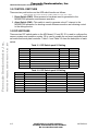
TABLE OF CONTENTS
ARCHIVED BY FREESCALE SEMICONDUCTOR, INC. 2005
Freescale Semiconductor, Inc...
Section 1
General Information
1.1
1.2
1.3
1.4
1.4.1
1.4.2
Introduction ................................................................................................... 1-6
Features........................................................................................................ 1-6
Related Documentation ................................................................................ 1-7
Technical Support ......................................................................................... 1-7
M68EZ328ADS v2.0 ................................................................................... 1-7
Debugger .................................................................................................... 1-7
Section 2
Quick Installation Guide
2.1
2.2
2.3
2.3.1
2.3.2
2.3.3
Overview ....................................................................................................... 2-8
Equipments Required ................................................................................... 2-8
Installation Procedure ................................................................................... 2-8
Prepare the M68EZ328ADS v2.0 board ..................................................... 2-8
Connecting M68EZ328ADS v2.0 to PC.................................................... 2-11
Installing software debugger ..................................................................... 2-11
Section 3
Hardware Description and Board Operation
3.1
3.2
3.3
3.4
3.5
3.6
3.6.1
3.6.2
3.6.3
3.6.4
3.7
3.8
3.9
3.9.1
3.9.2
3.10
3.11
3.12
3.13
MOTOROLA
Overview ..................................................................................................... 3-16
Control Switches ......................................................................................... 3-17
DIP Switches............................................................................................... 3-17
Operation Modes ........................................................................................ 3-18
LED Indicators ............................................................................................ 3-18
Memory ....................................................................................................... 3-19
Memory Map ............................................................................................. 3-19
FLASH Memory ........................................................................................ 3-19
EMU ROM ............................................................................................... 3-20
EDO DRAM .............................................................................................. 3-21
UART and IRDA.......................................................................................... 3-22
Debug Port.................................................................................................. 3-23
LCD and Touch Panel Interface.................................................................. 3-23
LCD Interface............................................................................................ 3-23
Touch Panel Interface............................................................................... 3-24
Single Tone Generator................................................................................ 3-25
Logic Analyzer Interface ............................................................................. 3-25
ExPANSION Connectors ............................................................................ 3-25
Power Supply.............................................................................................. 3-26
M68EZ328ADS v2.0 USER’S MANUAL
For More Information On This Product,
Go to: www.freescale.com
i
Freescale Semiconductor, Inc.
Table of Contents
Appendix A
Comparison of M68EZ328ADS Version 1.x and 2.0
ARCHIVED BY FREESCALE SEMICONDUCTOR, INC. 2005
A.1
A.2
Hardware ....................................................................................................A-28
Software......................................................................................................A-28
Appendix B
Resistive Touch Panel Operation
B.1
General Concepts of Resistive Panels .......................................................B-30
ARCHIVED BY FREESCALE SEMICONDUCTOR, INC. 2005
Freescale Semiconductor, Inc...
Appendix C
Programming On-board Flash Memory
C.1
C.2
C.3
C.4
C.5
Overview .................................................................................................... C-32
Elements for programming the flash .......................................................... C-32
Method ....................................................................................................... C-33
Offset Address of ROM Image................................................................... C-33
Executing ProgRam Command Sequence ................................................ C-34
Appendix D
Monitor Initialization Code
D.1
D.2
Initialization Code of Metrowerks Monitor (Reset.S) .................................. D-40
Initialization Code of SDS Monitor (Monitor.H) .......................................... D-44
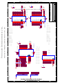
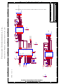
Appendix E
Schematics
E.1
MOTOROLA
M68EZ328ADS v2.0 ...................................................................................E-54
M68EZ328ADS v2.0 USER’S MANUAL
For More Information On This Product,
Go to: www.freescale.com
ii
Freescale Semiconductor, Inc.
Table of Contents
ARCHIVED BY FREESCALE SEMICONDUCTOR, INC. 2005
Freescale Semiconductor, Inc...
ARCHIVED BY FREESCALE SEMICONDUCTOR, INC. 2005
iii
M68EZ328ADS v2.0 USER’S MANUAL
For More Information On This Product,
Go to: www.freescale.com
MOTOROLA
Freescale Semiconductor, Inc.
ARCHIVED BY FREESCALE SEMICONDUCTOR, INC. 2005
ARCHIVED BY FREESCALE SEMICONDUCTOR, INC. 2005
Freescale Semiconductor, Inc...
LIST OF ILLUSTRATIONS
2-1
2-2
2-3
2-4
2-5
2-6
3-1
3-2
3-3
3-4
3-5
3-6
3-7
3-8
3-9
3-10
3-11
3-12
2-1
2-2
C-1
C-2
M68EZ328ADS v2.0 Key Component Layout .................................................... 2-9
Default DIP Switch Options for Metrowerks monitor ........................................ 2-10
DIP Switch Options for SDS monitor................................................................ 2-10
Connecting PC to Debug Port of M68EZ328ADS v2.0 .................................... 2-11
Debug Pop-Up Window of SDS v7.4................................................................ 2-14
Connection Setting inside Debug Pop-up Window of SDS v7.4 ...................... 2-15
M68EZ328ADS v2.0 Functional Block Diagram............................................... 3-16
Interface of Flash Memories............................................................................. 3-19
Interface of EMU ROM ..................................................................................... 3-20
Interface of EDO DRAMs ................................................................................. 3-21
UART and IRDA Interface. ............................................................................... 3-22
Serial Port Pin Assignment............................................................................... 3-22
Debug Port Interface ........................................................................................ 3-23
LCD and Touch Panel Connector Pin Assignment .......................................... 3-23
Touch Panel Controller Interface...................................................................... 3-24
Single Tone Generator ..................................................................................... 3-25
Logic Analyzer Connectors .............................................................................. 3-25
Power Connectors............................................................................................ 3-27
Resistive Touch Panel......................................................................................B-30
Determination of X,Y Position ..........................................................................B-31
Method of programming on-board Flash memory ........................................... C-33
Flash Program Algorithm................................................................................. C-38
MOTOROLA
M68EZ328ADS v2.0 USER’S MANUAL
For More Information On This Product,
Go to: www.freescale.com
iv
Freescale Semiconductor, Inc.
ARCHIVED BY FREESCALE SEMICONDUCTOR, INC. 2005
ARCHIVED BY FREESCALE SEMICONDUCTOR, INC. 2005
Freescale Semiconductor, Inc...
LIST OF TABLES
3-1
3-2
3-3
3-4
3-5
3-6
3-7
A-1
A-2
DIP Switch pack S1 Setting.............................................................................. 3-17
DIP Switch pack S2 Setting.............................................................................. 3-17
Operation Mode Setting ................................................................................... 3-18
Function of LED Indicators ............................................................................... 3-18
M68VZ328ADS v2.0 Default Memory Map ...................................................... 3-19
Signal Assignment for Touch Panel Controller................................................. 3-24
Pin Assignments of P4 ..................................................................................... 3-26
Comparison of M68EZ328ADS v1.x and v2.0..................................................A-28
Software Change for using M68EZ328ADS v2.0 .............................................A-28
MOTOROLA
M68EZ328ADS v2.0 USER’S MANUAL
For More Information On This Product,
Go to: www.freescale.com
v
Freescale Semiconductor, Inc.
SECTION 1
GENERAL INFORMATION
ARCHIVED BY FREESCALE SEMICONDUCTOR, INC. 2005
1.1 INTRODUCTION
ARCHIVED BY FREESCALE SEMICONDUCTOR, INC. 2005
Freescale Semiconductor, Inc...
The DragonBallTM-EZ (MC68EZ328) Application Development System (M68EZ328ADS) is
designed to supply users with an environment to develop MC68EZ328 based application
software. Moreover, this board can be used as a reference for real-life product design.
M68EZ328ADS provides several interface ports for application software and target board
debug purpose.
DragonBallTM-EZ ADS altogether has two versions released for customers. This is the second version. The board design and layout in second version has been changed a great deal.
It includes simplifying the design for enhancing production quality and the easiness to use.
However, most of the interfaces to external peripherals remain unchanged in order to provide high degree of compatibility with previous version. For more details on the changes,
Please refer to Appendix A .
This document will discuss the usage and system details of the M68EZ328ADS v2.0.
1.2 FEATURES
• MC68EZ328 CPU
• Memory Subsystem
—2 MB FLASH (Expandable to 4MB)
—8 MB EDO DRAM
• Debug ports
—One RS232 serial port interface to MC68EZ328 internal UART
—One External RS232 serial port connecting to on-board UART chip
—Direct logic analyzer interface to system bus
• LCD and Touch Panel Interface
—MC68EZ328 LCD interface
—Burr-Brown 12-bit touch panel controller ADS7843E available for pen input
• LED Indicators
—Red LED for power
—Green LED for system heart beat
—Yellow LED for status of MC68EZ328 pin PD0
—Yellow LED for status of MC68EZ328 pin PD1
• Board operation mode support
—MC68EZ328 EMU mode
—MC68EZ328 normal mode
—MC68EZ328 bootstrap mode
• Debug Monitor
—MetroWerks Codewarrior Target Monitor using serial port
MOTOROLA
M68EZ328ADS v2.0 USER’S MANUAL
For More Information On This Product,
Go to: www.freescale.com
1-6
General Information
Freescale Semiconductor, Inc.
—SDS source-level debugger monitor by Software Development System Inc. using serial port
• Clock Source
ARCHIVED BY FREESCALE SEMICONDUCTOR, INC. 2005
—32.768KHz for MC68EZ328 internal PLL
• Power Supply
—3.0V - 3.3V main power supply
1.3 RELATED DOCUMENTATION
The following documents can be used as references when using M68EZ328ADS.
• MC68EZ328 Product Information
ARCHIVED BY FREESCALE SEMICONDUCTOR, INC. 2005
Freescale Semiconductor, Inc...
• MC68EZ328 User’s Manual
1.4 TECHNICAL SUPPORT
1.4.1 M68EZ328ADS v2.0
For getting the latest information, please visit our web page:
http://www.mot.com/SPS/WIRELESS/products/DragonBall.html
http://www.apspg.com/products/dragonballez/mc68ez328.html
1.4.2 Debugger
There are three source-level debuggers for DragonBallTM-EZ. The contact information is
listed below.
1. Metrowerks
http://www.metrowerks.com
2. Single Step Development
http://www.sdsi.com
3. Microtek SLD
http://www.microtekintl.com
1-7
M68EZ328ADS v2.0 USER’S MANUAL
For More Information On This Product,
Go to: www.freescale.com
MOTOROLA
Freescale Semiconductor, Inc.
SECTION 2
QUICK INSTALLATION GUIDE
ARCHIVED BY FREESCALE SEMICONDUCTOR, INC. 2005
2.1 OVERVIEW
This section provides a description of the evaluation module, requirements, quick installation and test information. Detailed information on the M68EZ328ADS v2.0 design and operation is provided in the remaining sections of this manual.
2.2 EQUIPMENTS REQUIRED
ARCHIVED BY FREESCALE SEMICONDUCTOR, INC. 2005
Freescale Semiconductor, Inc...
The following equipments are required to use with the M68EZ328ADS Application Development System, some of them are already bundled with the ADS package.
• Power supply − 3.0V-3.3V, 1500mA, with 2 mm female (inside positive) power connector
• RS-232 cable (DB9 male to DB9 female)
• IBM PC compatible computer (486 class or higher) running Windows 3.1 and DOS 6.0
(or higher), or Windows 95, with an RS-232 serial port capable of 9600-115200 bit per
second operation
2.3 INSTALLATION PROCEDURE
Please follow the procedure below to set up M68EZ328ADS.
1. Prepare the M68EZ328ADS v2.0 board
2. Connect the M68EZ328ADS v2.0 board to PC and power supply
3. Install software debugger
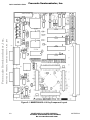
2.3.1 Prepare the M68EZ328ADS v2.0 board
Locate the DIP switches on the M68EZ328ADS v2.0 board and select appropriate monitor
and debug port for your debugger.
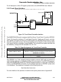
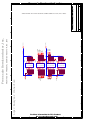
Figure 2-2 shows the factory default DIP switches settings. This setting selects to use Metroworks monitor. Figure 2-3 shows the DIP switches setting of using SDS monitor.
For detail description of each switch. Pls. refer to Table 3-1 and Table 3-2.
For additional information on the M68EZ328ADS v2.0 and its components. Pls refer to Section 3 .
MOTOROLA
M68EZ328ADS v2.0 USER’S MANUAL
For More Information On This Product,
Go to: www.freescale.com
2-8
Quick Installation Guide
Freescale Semiconductor, Inc.
ARCHIVED BY FREESCALE SEMICONDUCTOR, INC. 2005
Freescale Semiconductor, Inc...
ARCHIVED BY FREESCALE SEMICONDUCTOR, INC. 2005
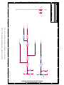
Figure 2-1. M68EZ328ADS v2.0 Key Component Layout
2-9
M68EZ328ADS v2.0 USER’S MANUAL
For More Information On This Product,
Go to: www.freescale.com
MOTOROLA
Quick Installation Guide
Freescale Semiconductor, Inc.
Monitor and Debug port selection
INC. 2005
S2ARCHIVED BY FREESCALE SEMICONDUCTOR,
S1
ON
ON
1 2 3
4 5 6 7 8
1 2 3
4 5 6 7 8
ARCHIVED BY FREESCALE SEMICONDUCTOR, INC. 2005
Freescale Semiconductor, Inc...
Figure 2-2. Default DIP Switch Options for Metrowerks monitor
S1
ON
S2
ON
1 2 3
4 5 6 7 8
1 2 3
4 5 6 7 8
Figure 2-3. DIP Switch Options for SDS monitor
2-10
M68EZ328ADS v2.0 USER’S MANUAL
For More Information On This Product,
Go to: www.freescale.com
MOTOROLA
Quick Installation Guide
Freescale Semiconductor, Inc.
2.3.2 Connecting M68EZ328ADS v2.0 to PC
Figure 2-4 shows connections among the PC, the external power supply and the M68E
Z328ADS v2.0 board.
Use the
steps
to complete cableINC.
connections:
ARCHIVED
BY following
FREESCALE
SEMICONDUCTOR,
2005
Host Computer
COM1
/ COM2
Debug Port
ARCHIVED BY FREESCALE SEMICONDUCTOR, INC. 2005
Freescale Semiconductor, Inc...
RS232 Cable
EZ UART
3.0-3.3V
Power Supply
M68VZ328ADS
Figure 2-4. Connecting PC to Debug Port of M68EZ328ADS v2.0
For most evaluation platforms, serial communication is the primary channel to link up PC
with the target board. Both Metrowerks Codewarrior and Software Development System
(SDS) debug monitor support serial communication through UART port. The procedure are
as follows.
1. Connect a RS232 cable from COM port (COM1 or COM2) to connector P2 of
M68EZ328ADS v2.0.
2. Connect the power supply +3V or power adaptor to the P1 of M68EZ328ADS v2.0
3. Turn on the power supply. The RED LED will flash and the GREEN LED will illuminate
when power is correctly applied.
2.3.3 Installing software debugger
The following software debugger supports M68EZ328ADS v2.0:
• Metrowerks Codewarrior
• Single Step Development System
• SLD
Metrowerks Codewarrior
A simple procedure for using Metrowerks Codewarrior Target Monitor:
2-11
M68EZ328ADS v2.0 USER’S MANUAL
For More Information On This Product,
Go to: www.freescale.com
MOTOROLA
Quick Installation Guide
Freescale Semiconductor, Inc.
1. Install the Metrowerks Codewarrior IDE
2. Run Codewarrior IDE program.
ARCHIVED BY FREESCALE SEMICONDUCTOR, INC. 2005
Freescale Semiconductor, Inc...
ARCHIVED
BYwith
FREESCALE
3. Open a new
project file
EmbeddedSEMICONDUCTOR,
68k Stationery. INC. 2005
4. Select ADS_68EZ328 Stationery for new project.
2-12
M68EZ328ADS v2.0 USER’S MANUAL
For More Information On This Product,
Go to: www.freescale.com
MOTOROLA
Quick Installation Guide
Freescale Semiconductor, Inc.
5. Choose "Enable Debugger" from the "Project" pull-down menu.
ARCHIVED BY FREESCALE SEMICONDUCTOR, INC. 2005
Freescale Semiconductor, Inc...
ARCHIVED BY FREESCALE SEMICONDUCTOR, INC. 2005
6. Change the connection settings in the Debug Settings Windows.
2-13
M68EZ328ADS v2.0 USER’S MANUAL
For More Information On This Product,
Go to: www.freescale.com
MOTOROLA
Quick Installation Guide
Freescale Semiconductor, Inc.
7. Edit the code inside the Codewarrior IDE program.
8. Press F5 to run the program.
ARCHIVED BY
FREESCALE SEMICONDUCTOR, INC. 2005
Single Step Development
System
A simple procedure for using Single Step Debugger:
1. Install the Single Step Debugger on your PC.
2. Run Single Step Debugger
4. Inside the Debug pop-up window, choose the object file to download or "debug without
file" as shown in Figure 2-5, select the serial port (COM1 or COM2 ...) according to the
serial port of the PC connecting to the ADS, disable "hardware flow control" and the
baud rate should be 115200bps as shown in Figure 2-6.
ARCHIVED BY FREESCALE SEMICONDUCTOR, INC. 2005
Freescale Semiconductor, Inc...
3. Choose Debug in the File pull-down menu to open the Debug pop-up window.
5. The file should be downloaded and then you can start your development. (For details,
please refer to the SingleStep User’s Manual).
Figure 2-5. Debug Pop-Up Window of SDS v7.4
2-14
M68EZ328ADS v2.0 USER’S MANUAL
For More Information On This Product,
Go to: www.freescale.com
MOTOROLA
Quick Installation Guide
Freescale Semiconductor, Inc.
ARCHIVED BY FREESCALE SEMICONDUCTOR, INC. 2005
Freescale Semiconductor, Inc...
ARCHIVED BY FREESCALE SEMICONDUCTOR, INC. 2005
Figure 2-6. Connection Setting inside Debug Pop-up Window of SDS v7.4
2-15
M68EZ328ADS v2.0 USER’S MANUAL
For More Information On This Product,
Go to: www.freescale.com
MOTOROLA
Freescale Semiconductor, Inc.
SECTION 3
HARDWARE DESCRIPTION AND BOARD OPERATION
ARCHIVED BY FREESCALE SEMICONDUCTOR, INC. 2005
3.1 OVERVIEW
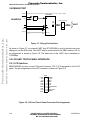
Figure 3-1 shows the block diagram of M68EZ328ADS v2.0.
Logic Analyzer
Address Bus
Extension
Data Bus
Control Bus
ARCHIVED BY FREESCALE SEMICONDUCTOR, INC. 2005
Freescale Semiconductor, Inc...
MC68EZ328
UART SIGNALS
PWMO
Connector
RESET
Extension
Connectors
FLASH
FLASH
1M x 16-bit
1M x 16-bit
UART
CHIP
EDO DRAM
4M x 16-bit
Debug
Port
Single
Tone
Generator
IRDA
UART
and
IRDA
Interface
UART
Touch
Panel
Controller
Reset
Power
Connector
Circuit
4-bit LCD
LCD Connectors
RESET
GND
ABORT
GND
Figure 3-1. M68EZ328ADS v2.0 Functional Block Diagram
MOTOROLA
M68EZ328ADS v2.0 USER’S MANUAL
For More Information On This Product,
Go to: www.freescale.com
3-16
Freescale
Hardware Description and Board
Operation
Semiconductor, Inc.
3.2 CONTROL SWITCHES
There are two push buttons on the ADS which function as follows:
ARCHIVED BY FREESCALE SEMICONDUCTOR, INC. 2005
1. Reset Switch (SW2): When pressed, a hardware reset is generated to the
MC68EZ328 processor and resumes operation.
2. Abort Switch (SW1): This switch is used to generate a level 7 interrupt to the
MC68EZ328 processor for aborting normal software execution and returning control
to the debug monitor.
ARCHIVED BY FREESCALE SEMICONDUCTOR, INC. 2005
Freescale Semiconductor, Inc...
3.3 DIP SWITCHES
There are two DIP switch packs on the ADS board, S1 and S2. S1 is used to configure the
memory system and operation modes. S2 is used to enable the on-board peripheral such
as buzzer and touch panel controller. Table 3-1 and Table 3-2 show the description of each
switch.
Table 3-1. DIP Switch pack S1 Setting
Switch
S1-1
S1-2
S1-3
S1-4
S1-5
S1-6
S1-7
S1-8
FUNCTION
UART Transceiver
IrDA Module
Buzzer
Pen IRQ
Chip Select of Touch Panel Controller
Unused
Unused
Unused
ON
Enable
Enable
Enable
Enable
Enable
OFF
Disable
Disable
Disable
Disable
Disable
Table 3-2. DIP Switch pack S2 Setting
Switch
S2-1
S2-2
S2-3
S2-4
S2-5
S2-6
S2-7
S2-8
3-17
FUNCTION
CSA0 - FLASH0
CSA1 - FLASH1
CSD0 - EDO DRAM
EMU Mode
Bootstrap Mode
Monitor Select
Unused
Unused
ON
Connected
Connected
Connected
Enable
Enable
SDS
M68EZ328ADS v2.0 USER’S MANUAL
For More Information On This Product,
Go to: www.freescale.com
OFF
Disconnected
Disconnected
Disconnected
Disable
Disable
Metrowerks
MOTOROLA
Freescale Semiconductor,
Inc. and Board Operation
Hardware Description
3.4 OPERATION MODES
M68EZ328ADS v2.0 supports three operation modes of MC68EZ328: EMU Mode, Normal
Mode and Bootstrap
Mode.BY
Selection
of these
operation modesINC.
is controlled
by DIP switch
ARCHIVED
FREESCALE
SEMICONDUCTOR,
2005
S2-8. Operation mode has to be selected before resetting the system. Mode is not allowed
to change during normal running. Table 3-3 shows the operation mode configuration.
Table 3-3. Operation Mode Setting
ARCHIVED BY FREESCALE SEMICONDUCTOR, INC. 2005
Freescale Semiconductor, Inc...
DIP Switch S2-4
ON
OFF
ON
OFF
DIP Switch S2-5
OFF
OFF
ON
ON
Operation Mode
EMU
Normal
Bootstrap
Bootstrap
Normal Mode - After power up or system reset in this mode, CSA0 is default to cover the
whole memory map except MC68EZ328 internal registers and EMU space. Also, as reset
vector fetch is at the beginning of CSA0 space, CSA0 should be connected to the boot ROM
in which the first two words are reset vectors.
Bootstrap Mode - When this mode is selected, the DragonBall-EZ will start its embedded
bootloader. User can use this mode to do simple debugging or reprogram the flash memories. For detailed bootstrap mode operation, please refer MC68EZ328 user’s manual.
EMU Mode - When this mode is selected, the reset vectors are generated internally by the
ICE module of MC68EZ328. The first instruction fetch is at $FFFC0020. Therefore, in EMU
mode the debug monitor of MC68EZ328ADS v2.0 is located beginning at $FFFC0020.
EMUCS is always running in 8-bit data bus mode covering the address space from
$FFFC0000 to $FFFD0000
3.5 LED INDICATORS
There are four LED indicators on the ADS which function as shown in Table 3-4.
Table 3-4. Function of LED Indicators
Reference #
LED3
LED4
LED1
LED2
Color
Yellow
Yellow
Red
Green
Name
PD0
PD1
Heart Beat
Power
Function
Status of PD0
Status of PD1
Blinking heart beat indicates the system is "alive"
Power is applied to the system with right polarity
The LED3 is connected to a counter. The counter is toggled by address line A1.
MOTOROLA
M68EZ328ADS v2.0 USER’S MANUAL
For More Information On This Product,
Go to: www.freescale.com
3-18
Freescale
Hardware Description and Board
Operation
Semiconductor, Inc.
3.6 MEMORY
M68EZ328ADS v2.0 provides on-board Flash memory and EDO DRAM, for application
development. They
can be enabled
or disabled
individually by setting
corresponding DIP
ARCHIVED
BY FREESCALE
SEMICONDUCTOR,
INC. the
2005
switches.
3.6.1 Memory Map
The default memory map of M68EZ328ADS v2.0 in normal mode is shown in Table 3-5. The
chip select range to all of the memory are software programmable. Users can reconfigure
the memory map for their applications.
ARCHIVED BY FREESCALE SEMICONDUCTOR, INC. 2005
Freescale Semiconductor, Inc...
Table 3-5. M68VZ328ADS v2.0 Default Memory Map
System Address
$00000000-$007FFFFF
$00800000-$009FFFFF
$00A00000-$00BFFFFF
$00C00000-$00FBFFFF
$FFFC0000-$FFFCFFFF
$FFFD0000-$FFFDFFFF
$FFFFF000-$FFFFFFFF
Memory
8MB EDO DRAM
2MB FLASH BANK0
2MB FLASH BANK1
Unused
EMU Monitor
Debug Port
MC68EZ328 Internal Register
Assigned Chip Select
CSD0
CSA0
CSA1
EMUCS
EMUCS
-
3.6.2 FLASH Memory
VCC VCC
MC68EZ328
CSA1
CSA0
1MX16-Bit FLASH
S2-2
CE
1MX16-Bit FLASH
S2-1
CE
A[1..20]
A[0..19]
D[0..15]
D[0..15]
OE
OE
WE
WE
FLASH1
FLASH0
Figure 3-2. Interface of Flash Memories
M68EZ328ADS v2.0 supports up to two 2M-byte Flash memory chips. However, only one
bank is installed when the board is shipped out from the factory. Figure 3-2. shows the interface of them. They are chip-selected by *CSA0 and *CSA1 signals. The connection of these
*CSAx signals to the Flash memories is controlled by DIP switches S2-1 and S2-2.
3-19
M68EZ328ADS v2.0 USER’S MANUAL
For More Information On This Product,
Go to: www.freescale.com
MOTOROLA
Freescale Semiconductor,
Inc. and Board Operation
Hardware Description
When S2-1 is ON, *CSA0 is connected to FLASH0. When S2-2 is ON, *CSA1 is connected
to FLASH1. In Normal Mode, FLASH0 is the boot ROM. User can reprogram Flashes with
their own application program. For more details on flash memory programming, please refer
to Appendix C .ARCHIVED BY FREESCALE SEMICONDUCTOR, INC. 2005
3.6.3 EMU ROM
8x8-Bit EMU ROM
EMUCS
OE
WE
ARCHIVED BY FREESCALE SEMICONDUCTOR, INC. 2005
Freescale Semiconductor, Inc...
MC68EZ328
A16
OR
Gate
CS
OE
WE
A[0..15]
A[0..15]
D[8..15]
D[8..15]
Figure 3-3. Interface of EMU ROM
The M68EZ328ADS v2.0 is equipped with one 64K-byte EMU ROM. Figure 3-3 shows the
interface of the EMU ROM. This EMU ROM has already been programmed with the SDS
monitor and the Metrowerks monitor when the board is shipped out from the factory.
MOTOROLA
M68EZ328ADS v2.0 USER’S MANUAL
For More Information On This Product,
Go to: www.freescale.com
3-20
Freescale
Hardware Description and Board
Operation
Semiconductor, Inc.
3.6.4 EDO DRAM
VCC
ARCHIVED BY FREESCALE SEMICONDUCTOR, INC. 2005
4MX16-Bit EDO DRAM
S2-3
MC68EZ328
CSC0
CSD0
CSD1
ARCHIVED BY FREESCALE SEMICONDUCTOR, INC. 2005
Freescale Semiconductor, Inc...
OE
DWE
RAS
UCAS
LCAS
OE
WE
A[1..13]
A[0..12]
D[0..15]
D[0..15]
Figure 3-4. Interface of EDO DRAMs
Figure 3-4. shows the interface of EDO DRAMs. M68EZ328ADS v2.0 supports one bank of
4Mx16-bit EDO DRAMs. The EDO DRAM is enabled by turning DIP switch S2-3 on.
3-21
M68EZ328ADS v2.0 USER’S MANUAL
For More Information On This Product,
Go to: www.freescale.com
MOTOROLA
Freescale Semiconductor,
Inc. and Board Operation
Hardware Description
3.7 UART AND IRDA
ARCHIVED BY FREESCALE SEMICONDUCTOR, INC. 2005
MC68VZ328
RS232 Transceiver
ARCHIVED BY FREESCALE SEMICONDUCTOR, INC. 2005
Freescale Semiconductor, Inc...
TXD
RXD
RTS
CTS
VCC
P9
UART
EN
S1-1
VCC
Buffer
IRDA
GND
EN
S1-2
EN
PD4
Figure 3-5. UART and IRDA Interface.
Figure 3-5 shows the UART and IRDA module. The M68EZ328ADS v2.0 has one RS232
serial ports P9. P9 is using the UART of MC68EZ328. It is 9-pin female D-Type connectors
containing the signals as shown in Figure 3-6. The transceivers for UART can be enabled
by turning the DIP switch S1-1 on.
NC
TXD
RXD
NC
GND
1
2
3
4
5
6
7
8
9
NC
CTS
RTS
NC
Figure 3-6. Serial Port Pin Assignment
The IrDA transceiver is provided and connected to DragonBall’s UART Port only with a
buffer in between for controlling its ON/OFF. If IrDA is being used, S1-1 should be switched
OFF and S1-2 should be switched ON. Then, the enable/disable of IRDA is totally controlled
by software through PD4 (Port D4).
MOTOROLA
M68EZ328ADS v2.0 USER’S MANUAL
For More Information On This Product,
Go to: www.freescale.com
3-22
Freescale
Hardware Description and Board
Operation
Semiconductor, Inc.
3.8 DEBUG PORT
ARCHIVED BY FREESCALE SEMICONDUCTOR,
INC. 2005
ST16C2552A
EMUCS
MC68EZ328
A16
OR
Gate
CS
RS232 Transceiver
OE
ARCHIVED BY FREESCALE SEMICONDUCTOR, INC. 2005
OE
Freescale Semiconductor, Inc...
TXD
RXD
CTS
RTS
WE
A[0..2]
A[0..2]
D[8..15]
D[8..15]
WE
P8
UART
EN
Figure 3-7. Debug Port Interface
As shown in Figure 3-7, an external UART chip ST16C2552A is used to provide one more
debug port on the ADS board. This UART chip is connected with the DB9 connector P8. Its
pin assignment is shown in Figure 3-6. The baud rate of this UART chip is defaulted to
115200bps.
3.9 LCD AND TOUCH PANEL INTERFACE
3.9.1 LCD Interface
M68EZ328ADS consists of one LCD panel connector, P10. P10 is designed for 4-bit LCD
panel. The pin assignments of the LCD connector is shown in Figure 3-8.
LACD
LLP
VO
GND
LD0
LD2
GND
PB1
TOP
LEFT
P10
2
1
4
3
6
5
8
7
9 10
11 12
13 14
15 16
17 18
19 20
LFRM
LCLK
VCC
VEE
LD1
LD3
LCONTRAST
NC
BOTTOM
RIGHT
Figure 3-8. LCD and Touch Panel Connector Pin Assignment
3-23
M68EZ328ADS v2.0 USER’S MANUAL
For More Information On This Product,
Go to: www.freescale.com
MOTOROLA
Freescale Semiconductor,
Inc. and Board Operation
Hardware Description
For full description of the LCD signals, please refer to the MC68EZ328 User’s Manual.
3.9.2 Touch Panel Interface
ARCHIVED BY FREESCALE SEMICONDUCTOR, INC. 2005
TOP
Touch Panel
MC68EZ328
VCC
RIGHT
LEFT
BOTTOM
S1-5
PB6
S1-4
SPMCLK
ARCHIVED BY FREESCALE SEMICONDUCTOR, INC. 2005
Freescale Semiconductor, Inc...
IRQ5
ADS7843
CS
PENIRQ
DCLK
DIN
DOUT
SPMTXD
SPMRXD
Figure 3-9. Touch Panel Controller Interface
The M68EZ328ADS board is equipped with Burr-Brown Touch Panel Controller ADS7843.
Figure 3-9 shows the interface of Touch Panel Controller. Totally one I/O signal, one interrupt capable I/O signal and one set of SPIM signals from MC68EZ328 are used to implement the touch panel circuitry. All of these signals can be shared for other devices when
touch panel interface controller is being disabled. The on-board touch panel controller can
be disabled by turning both DIP switches S1-4, S1-5 off.
Table 3-6. Signal Assignment for Touch Panel Controller
Signals
SPMRXD, SPMTXD, SPMCLK
~IRQ5
PB6
Function
This set of serial port interface signals performs data transfer with
ADS7843. For detailed operation on the SPI port, please refer to the
MC68EZ328 User’s Manual.
This signal is a MC68EZ328 interrupt capable I/O pin.
This MC68EZ328 general I/O signal is used to select the ADS7843 on data
transfer.
The ADS7843 is a 12-bit sampling analog-to-digital converter (ADC) with a synchronous
serial interface and low on-resistance switches for touch screens. The ADS7843 communicates with MC68EZ328 through SPI (Serial Peripheral Interface). In this case, ADS7843 is
a slave, and MC68EZ328 is a master. For the detailed operation of ADS7843, please refer
to its datasheet. The datasheet is available at the following web site.
http://www.burr-brown.com
For more details on the operation of resistive touch panel, please refer to Appendix B .
MOTOROLA
M68EZ328ADS v2.0 USER’S MANUAL
For More Information On This Product,
Go to: www.freescale.com
3-24
Freescale
Hardware Description and Board
Operation
Semiconductor, Inc.
3.10 SINGLE TONE GENERATOR
VCC
S1-5 FREESCALE SEMICONDUCTOR, INC. 2005
ARCHIVED BY
BC847
PWMO
MC68VZ328
CitiSound CHB-03E
GND
ARCHIVED BY FREESCALE SEMICONDUCTOR, INC. 2005
Freescale Semiconductor, Inc...
Figure 3-10. Single Tone Generator
Citizen single tone generator CHB-03E is provided on M68EZ328ADS v2.0. As shown in
Figure 3-10, a simple transistor circuit is used to interface the CHB-03E with the PWMO pin
of MC68EZ328.
3.11 LOGIC ANALYZER INTERFACE
To provide an convenient way of connecting on-board signals to a logic analyzer, ADS board
provides five 10x2-pin headers for direct plug-in. Pin assignments to these five headers are
shown in Figure 3-11.
POD3
POD2
POD1
2
4
6
8
10
12
14
16
18
20
2
4
6
8
10
12
14
16
18
20
2
4
6
8
10
12
14
16
18
20
1
CLKO 3
D14 5
D12 7
D10 9
D8 11
D6 13
D4 15
D2 17
D0 19
1
D15
EMUCS 3
D13
RSTIN 5
D11
EMUCS 7
D9
LWE 9
D7 CONTRAST 11
D5
LCLK 13
D3
LFRM 15
D1
LD2 17
GND
LD0 19
EMUIRQ
OE
UWE
DTACK
LACD
LLP
LD3
LD1
GND
CSA0
CSA1
CSB1
RAS1
CAS1
A22
A20
A18
A16
1
3
5
7
9
11
13
15
17
19
POD4
CSA0
CSB0
RAS0
CAS0
A23
A21
A19
A17
GND
DTACK
A14
A12
A10
A8
A6
A4
A2
A0
1
3
5
7
9
11
13
15
17
19
2
4
6
8
10
12
14
16
18
20
A15
A13
A11
A9
A7
A5
A3
A1
GND
Figure 3-11. Logic Analyzer Connectors
3.12 EXPANSION CONNECTORS
The M68EZ328ADS v2.0 provides basic features for software development and evaluation.
If user wants to add application subsystem to M68EZ328ADS v2.0, it can utilize the signals
provided on 32x3 local bus connector (P4). Some of these MC68EZ328 signals are used by
the on-board modules. If users want to use any of these signals for their daughter card, the
corresponding on-board module may have to be disabled to avoid contention.
The pin assignments for extension connectors are shown in Table 3-7.
3-25
M68EZ328ADS v2.0 USER’S MANUAL
For More Information On This Product,
Go to: www.freescale.com
MOTOROLA
Freescale Semiconductor,
Inc. and Board Operation
Hardware Description
ARCHIVED BY FREESCALE SEMICONDUCTOR, INC. 2005
Freescale Semiconductor, Inc...
Table 3-7. Pin Assignments of P4
Pin#
1
2
3
4
5
6
7
8
9
10
11
12
13
14
15
16
17
18
19
20
21
22
23
24
25
26
27
28
29
30
31
32
A
B
C
GND
GND
GND
ARCHIVED
BY FREESCALE SEMICONDUCTOR,
INC. 2005
D0/PA0
D1/PA1
D2/PA2
D3/PA3
D4/PA4
D5/PA5
D6/PA6
D7/PA7
D8
D9
D10
D11
D12
D13
D14
D15
CSA0
PF7/CSA1
PB0/CSB0
PB1/CSB1
PB2/CSC0/RAS0
PB3/CSC1/RAS1
PB4/CSD0/CAS0
PB5/CSD1/CAS1
PB6/TOUT/TIN
PB7/PWMO1
PC0/LD0
PC1/LD1
PC2/LD2
PC3/LD3
PC4/LFRM
PC5/LLP
PC6/LCLK
PC7/LACD
PD0/INT0
PD1/INT1
PD2/INT2
PD3/INT3
PD4/IRQ1
PD5/IRQ2
PD6/IRQ3
PD7/IRQ6
PE0/SPMTXD
PE1/SPMRXD
PE2/SPMCLK
PE3/DWE/UCLK
PE4/RXD
PE5/TXD
PE6/RTS
PE7/CTS
PF0/LCONTRAST
PF1/IRQ5
PF2/CLKO
PG1/A0
MA0/A1
MA1/A2
MA2/A3
MA3/A4
MA4/A5
MA5/A6
MA6/A7
MA7/A8
MA8/A9
MA9/A10
MA10/A11
MA11/A12
MA12/A13
MA13/A14
MA14/A15
MA15/A16
A17
A18
A19
PF3/A20
PF4/A21
PF5/A22
PF6/A23
PG2/EMUIRQ
PG3/HIZ/P/D
PG4/EMUCS
PG5/EMUBRK
PG0/BUSW/DTACK
RESET
OE
UWE
LWE
PK2/LDS
PK3/UDS
PK1/R/W
NC
VCC
VCC
VCC
3.13 POWER SUPPLY
There are two power input connectors on the ADS, P1 and P2. P1 is designed for external
3V DC main power supply, which supplies power to the MC68EZ328 processor and most of
the on-board components. P2 is used for LCD driver (VEE) power supply. If an LCD panel
MOTOROLA
M68EZ328ADS v2.0 USER’S MANUAL
For More Information On This Product,
Go to: www.freescale.com
3-26
Freescale
Hardware Description and Board
Operation
Semiconductor, Inc.
is connected to the ADS, the LCD driver can be powered by this VEE input. Figure 3-12
locates the power connectors and their polarity.
ARCHIVED BY FREESCALE SEMICONDUCTOR, INC. 2005
P2
GND
VEE
EZ UART
P1
_
GND
ARCHIVED BY FREESCALE SEMICONDUCTOR, INC. 2005
Freescale Semiconductor, Inc...
Debug Port
3.0-3.3V
+
M68EZ328ADS
Figure 3-12. Power Connectors
3-27
M68EZ328ADS v2.0 USER’S MANUAL
For More Information On This Product,
Go to: www.freescale.com
MOTOROLA
Freescale Semiconductor,
Inc.
Comparison of M68EZ328ADS
Version 1.x and 2.0
APPENDIX A
COMPARISON OF M68EZ328ADS VERSION 1.X AND 2.0
ARCHIVED BY FREESCALE SEMICONDUCTOR, INC. 2005
This section describes the difference between the M68EZ328ADS version 1.x and 2.0. If
user is not upgrading the development platform from M68EZ328ADS v1.x to v2.0, this section can be ignored.
A.1 HARDWARE
Table A-1 shows the difference between the M68EZ328ADS v1.x and v2.0.
Table A-1. Comparison of M68EZ328ADS v1.x and v2.0
ARCHIVED BY FREESCALE SEMICONDUCTOR, INC. 2005
Freescale Semiconductor, Inc...
Descriptions
Version 1.x
Version 2.0
2M-byte Flash Memory using one
Flash Memory
2M-byte Flash Memory using four AT29BV040 MBM29LV160T (expandable to 4M-byte Flash
Memory)
SRAM
256K-byte SRAM
No SRAM
4M-byte
EDO
DRAM
using
the
WE
signal
of
8M-byte
EDO DRAM using the DWE signal of
EDO DRAM
MC68EZ328
MC68EZ328
Touch Panel Interface MAXIM MAX1249 and four transistors
Burr-Brown ADS7843E
Expansion Socket Same pin assignment
Same pin assignment
LCD Connector
Same pin assignment
Same pin assignment
IrDA
No
HSDL-3201
ADI Port and MC68681 Serial Port with max.
ST16C2552A Serial Port with max. baud rate =
Debug Port
baud rate = 57600bps
115200bps
Buzzer
No
Citizen CHB-03E
Bus Width
8-bit/16-bit
16-bit only
A.2 SOFTWARE
Table A-2 shows the software change in M68EZ328ADS v2.0.
Table A-2. Software Change for using M68EZ328ADS v2.0
Items
Descriptions
The
new
ADS
is
equipped
with
different
memory device. So, the initizalization code needs to
Initizalization Code be changed.
Touch Panel
Controller Device Burr-Brown ADS7843E is used. A new device driver is required.
Driver
Pin 12 (DWE/UCLK/PE3) of MC68EZ328 is programmed as DWE signals for on-board EDO
DWE
DRAM. It cannot be used as Port or UCLK again.
IrDA
The IrDA module needs to be enabled by setting PD4 to zero.
MOTOROLA
M68EZ328ADS v2.0 USER’S MANUAL
For More Information On This Product,
Go to: www.freescale.com
A-28
Freescale
Semiconductor,
Comparison of M68EZ328ADS
Version 1.x and
2.0
Inc.
ARCHIVED BY FREESCALE SEMICONDUCTOR, INC. 2005
Freescale Semiconductor, Inc...
ARCHIVED BY FREESCALE SEMICONDUCTOR, INC. 2005
A-29
M68EZ328ADS v2.0 USER’S MANUAL
For More Information On This Product,
Go to: www.freescale.com
MOTOROLA
Freescale Semiconductor, Inc.
APPENDIX B
RESISTIVE TOUCH PANEL OPERATION
ARCHIVED BY FREESCALE SEMICONDUCTOR, INC. 2005
M68VZ328ADS features pen input through a resistive-film sensing panel. This type of panel
provides high flexibility by accepting input form any kind of stimulus including fingers, which
is most suitable for portable use. User can select a specific touch panel or order an LCD
module which includes a touch resistive panel. This section describes the basic concepts of
pen input and the required interface with the M68VZ328ADS.
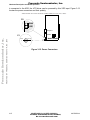
B.1 GENERAL CONCEPTS OF RESISTIVE PANELS
ARCHIVED BY FREESCALE SEMICONDUCTOR, INC. 2005
Freescale Semiconductor, Inc...
Basically, resistive panel consists of two transparent resistive layers separated by insulating
spacers as shown in Figure 2-1.
Figure 2-1. Resistive Touch Panel
Transparent Resistive Layer - resistive material such as an indium tin oxide (ITO) film is
coated on dielectric (insulating) substrate, usually glass on bottom and plastic on top for
actuation.
Bars - highly conductive material such as silver ink, about 1000 times more conductive than
ITO.
Spacers - Non-conducting ink, adhesive, or other material such as Mylar is used to separate
the two opposite conductive layers.
MOTOROLA
M68EZ328ADS v2.0 USER’S MANUAL
For More Information On This Product,
Go to: www.freescale.com
B-30
Freescale
Resistive Touch Panel Operation
Semiconductor, Inc.
The resistive panel works by applying a voltage gradient across one conductive layer and
measuring the voltage at the point of contact with the opposing conductive layer. For
instance, as shown in Figure 2-2, the resistive film acts as a series of resistors.
ARCHIVED BY FREESCALE SEMICONDUCTOR, INC. 2005
Freescale Semiconductor, Inc...
ARCHIVED BY FREESCALE SEMICONDUCTOR, INC. 2005
Figure 2-2. Determination of X,Y Position
When a point is contacted, it means the two opposing conductive layers come into electrical
contact. The x position of actuation can be determined by measuring the output voltage of
the y layer. At the same time, the y position can be find out by measuring the x layer. The
exact position can be determined by referencing the output voltage to the distance relationship.
B-31
M68EZ328ADS v2.0 USER’S MANUAL
For More Information On This Product,
Go to: www.freescale.com
MOTOROLA
Freescale Semiconductor, Inc.
APPENDIX C
PROGRAMMING ON-BOARD FLASH MEMORY
ARCHIVED BY FREESCALE SEMICONDUCTOR, INC. 2005
C.1 OVERVIEW
It is recommended that user should have a basic understanding of bootstrap mode operation
of MC68EZ328 before reading the material below. For more details on Bootstrap mode,
please refer to the MC68EZ328 user’s manual.
ARCHIVED BY FREESCALE SEMICONDUCTOR, INC. 2005
Freescale Semiconductor, Inc...
The Flash memory on the ADS board cannot be written directly. A special program command sequence is required to unlock it before starting the write process. A flash program is
therefore provided with the ADS board for helping users to do re-programming. The sections
below will describe the program and provide further information about the process and other
required elements.
C.2 ELEMENTS FOR PROGRAMMING THE FLASH
The following files are necessary for programming the Flash memory
1. EZTOOLS including BBUG.EXE and STOB.EXE
2. INIT.B - b-record for initializing the ADS
3. ERASE.B - b-record for erasing the flash memory
4. FLASHNML.B - b-record for programming flash. ROM image is copied from RAM area
to the Flash memory area
5. ROM.B - ROM image of user program in b-record/s-record format.
MOTOROLA
M68EZ328ADS v2.0 USER’S MANUAL
For More Information On This Product,
Go to: www.freescale.com
C-32
Freescale
Programming On-board Flash
Memory
Semiconductor, Inc.
C.3 METHOD
ARCHIVED BY FREESCALE SEMICONDUCTOR, INC. 2005
FLASH Program
System RAM
ROM Image
ARCHIVED BY FREESCALE SEMICONDUCTOR, INC. 2005
Freescale Semiconductor, Inc...
offset
Copy the ROM Image from
system RAM to Flash
Memory by the flash Program.
Flash Memory
Figure C-1. Method of programming on-board Flash memory
Flash memory can be programmed in bootstrap mode. First, a ROM image and a flash program are downloaded to the system memory by loading their b-records. Then, run the flash
program. It will execute the Flash program command sequence and copy the ROM image
from the system RAM to the Flash memory. The detailed steps are as follows.
1. Force the MC68EZ328 into bootstrap mode by turning S2-8 on and pressing RESET
switch once.
2. Use BBUG.EXE or TERMINAL program to communicate with the M68EZ328ADS
through RS232 port of a PC.
3. Initialize the internal registers of DragonBall-VZ by loading the INIT.B.
4. Make sure the Flash Memory is blank. Load ERASE.B to erase the flash memory
when needed.
5. Load FLASHNML.B (the Flash Program) and ROM.B (the ROM image) to system
RAM (EDO DRAM on M68EZ328ADS).
6. Execute the Flash Program by using the execution B-record. For example, if the starting address of Flash Program is 0x4000, the execution B-record is then "0000400000".
C.4 OFFSET ADDRESS OF ROM IMAGE
Figure C-1 shows that the ROM image is first put to the system RAM before it is copied to
Flash. In order to create S-record/B-record with download address different from its execution address, an OFFSET is sometimes required to be specified in downloading program.
C-33
M68EZ328ADS v2.0 USER’S MANUAL
For More Information On This Product,
Go to: www.freescale.com
MOTOROLA
Freescale
Programming On-board Flash
Memory
Semiconductor, Inc.
For example, when using SDS’s DOWN.EXE to generate the s-record, the "-w offset"
parameter can be used to specify this offset value. Please refer to the SingleStep User
Guide for using this command.
ARCHIVED BY FREESCALE SEMICONDUCTOR, INC. 2005
C.5 EXECUTING PROGRAM COMMAND SEQUENCE
Listed below is the source code of the flash Program which contains the necessary steps to
write the flash memory MBM29LV160T. It executes the flash program command sequence
and copies the ROM image from RAM area to the Flash memory area on ADS board. Figure
C-2 shows the flow chart of this program. Different brands of Flash memory may have different program command sequences, please refer to their datasheets for more details.
ARCHIVED BY FREESCALE SEMICONDUCTOR, INC. 2005
Freescale Semiconductor, Inc...
XREF
STKTOP
OFFSET1
OFFSET2
equ $AAA
equ $554
TIME
equ $FFF
*****************************************************************
ECHO
MACRO
CHAR
bsr
TXD_RDY
nop
nop
nop
move.b #CHAR,$FFFFF907
ENDM
*****************************************************************
ENABLE MACRO
move.w #$00AA,(A5) ; Unlock Flash
move.w #$0055,(A6)
move.w #$00A0,(A5)
ENDM
*****************************************************************
SECTION parameter
pSOURCE
DC.L
$00010000
pTARGET
DC.L
$01000000
pSIZE
DC.L
$00010000
pFLASH
DC.L
$01000000
pERROR
pFINISH
pERROR_ADDRESS
DC.L
$0
DC.L
$0
DC.L
$0
DC.L
STKTOP
*****************************************************************
SECTION code
START
MOVEA.L #STKTOP,a7
;re-istall stack pointer in case bootstrap mode
MOVE.L
MOVE.L
move.l
C-34
#0,pERROR
#0,pFINISH
#0,pERROR_ADDRESS
M68EZ328ADS v2.0 USER’S MANUAL
For More Information On This Product,
Go to: www.freescale.com
MOTOROLA
Freescale
Programming On-board Flash
Memory
Semiconductor, Inc.
move.l pSOURCE,A0
move.l pTARGET,A1
move.l
pSIZE,D0
ARCHIVED
BY FREESCALE SEMICONDUCTOR, INC. 2005
move.l
move.l
pFLASH,A5
pFLASH,A6
*******************************************
* BreakPoint Here if program flash in SDS *
*******************************************
add.l
add.l
#OFFSET1,A5
#OFFSET2,A6
;*****************************************
; Input Parameters:
;
a0 - (Long) Source Address
;
a1 - (Long) Target Address
;
d0 - (Long) Byte Size
;
a5 - (long) Flash Starting Address Offset1
;
a6 - (long) Flash Starting Address Offset2
;*****************************************
ARCHIVED BY FREESCALE SEMICONDUCTOR, INC. 2005
Freescale Semiconductor, Inc...
**************************************************
move.l
move.l
a0,a2
a1,a3
; a2 as source
; a3 as target
clr.l
clr.b
d1
d5
; clear d1 as counter
; clear d5 as ECHO counter
ENABLE
move.w
(a2),(a3)
; Copy source to target
clr.l
d4
; clear d4 as polling counter
cmp.l
bgt
add.l
move.w
move.w
cmp.w
bne
#TIME,d4
ERROR
#1,d4
(a2),d2
(a3),d3
d2,d3
POLLING
add.l
add.l
add.l
#2,a2
#2,a3
#2,d1
cmp.b
bne
ECHO
ECHO
add.b
#0,d5
NO_W
'W'
0
#1,d5
PROGRAM
POLLING
NO_W
C-35
; if d4>#TIME, bra ERROR
; d4++
; Compare (a0),(a1)
; End of POLLING
M68EZ328ADS v2.0 USER’S MANUAL
For More Information On This Product,
Go to: www.freescale.com
MOTOROLA
Freescale
Programming On-board Flash
Memory
cmp.l
ble
d0,d1
PROGRAM
Semiconductor, Inc.
; if d1<=d0, bra PROGRAM
ARCHIVED BY FREESCALE SEMICONDUCTOR, INC. 2005
clr.b
clr.l
d5
d1
;clear d5 as ECHO counter
;clear d1 as counter
VERIFIY
ARCHIVED BY FREESCALE SEMICONDUCTOR, INC. 2005
Freescale Semiconductor, Inc...
;*****************************************
; Input Parameters:
;
a0 - (Long) Source Address
;
a1 - (Long) Target Address
;
d0 - (Long) Byte Size
;
a5 - (long) Flash Starting Address Offset 1
;
a6 - (long) Flash Starting Address Offset 2
;*****************************************
move.l a0,a2
;a2 & a3 are used to store the starting address
move.l a1,a3
;for comparing.
NO_V
cmp.b
bne
ECHO
ECHO
add.b
#0,d5
NO_V
'V'
0
#1,d5
move.w
move.w
cmp.w
bne
(a2)+,d2
(a3)+,d3
d2,d3
ERROR
add.l
#2,d1
cmp.l
ble
d0,d1
VERIFIY
bra
; if d1<=d0, bra CHECK
FINISH
****************************************************************************
TXD_RDY
move.l
d7,-(a7)
btst.b
beq.s
move.w
sub.w
bne.b
move.l
rts
#5,$FFFFF906
POLLTXD
#$0FFF,d7
#1,d7
LP_RDY
(a7)+,d7
; Push d7
POLLTXD
LP_RDY
; bra if TXAVAIL not SET
; Restore d7
****************************************************************************
FINISH
ECHO
ECHO
ECHO
C-36
'\n'
'P'
'A'
M68EZ328ADS v2.0 USER’S MANUAL
For More Information On This Product,
Go to: www.freescale.com
MOTOROLA
Freescale
Programming On-board Flash
Memory
Semiconductor, Inc.
ECHO
'S'
ECHO
'S'
ECHO
'\n'
ECHO
0
ARCHIVED
BY FREESCALE SEMICONDUCTOR, INC. 2005
ECHO
0
ECHO
0
ECHO
0
ECHO
0
ECHO
0
move.l #1,pFINISH
bra
BOOTSTRAP
************************************************************
ECHO
ECHO
ECHO
ECHO
ECHO
ECHO
ECHO
ECHO
ECHO
ECHO
ECHO
ECHO
ECHO
sub.l
move.l
move.l
bra
ARCHIVED BY FREESCALE SEMICONDUCTOR, INC. 2005
Freescale Semiconductor, Inc...
ERROR
'\n'
'E'
'R'
'R'
'O'
'R'
'\n'
0
0
0
0
0
0
#1,a3
a3,pERROR_ADDRESS
#1,pERROR
BOOTSTRAP
************************************************************
BOOTSTRAP
jmp
$FFFFFF44
************************************************************
END
C-37
M68EZ328ADS v2.0 USER’S MANUAL
For More Information On This Product,
Go to: www.freescale.com
MOTOROLA
Freescale
Programming On-board Flash
Memory
Semiconductor, Inc.
ARCHIVED BY FREESCALE SEMICONDUCTOR, INC. 2005
Freescale Semiconductor, Inc...
ARCHIVED BY FREESCALE SEMICONDUCTOR, INC. 2005
Figure C-2. Flash Program Algorithm
C-38
M68EZ328ADS v2.0 USER’S MANUAL
For More Information On This Product,
Go to: www.freescale.com
MOTOROLA
Freescale
Programming On-board Flash
Memory
Semiconductor, Inc.
ARCHIVED BY FREESCALE SEMICONDUCTOR, INC. 2005
Freescale Semiconductor, Inc...
ARCHIVED BY FREESCALE SEMICONDUCTOR, INC. 2005
C-39
M68EZ328ADS v2.0 USER’S MANUAL
For More Information On This Product,
Go to: www.freescale.com
MOTOROLA
Freescale Semiconductor, Inc.
APPENDIX D
MONITOR INITIALIZATION CODE
ARCHIVED BY FREESCALE SEMICONDUCTOR, INC. 2005
D.1 INITIALIZATION CODE OF METROWERKS MONITOR (RESET.S)
MON_STACKTOP.equ$4100;
M328BASE
Above is TOO low, try this
.equ $FFFFF000
ARCHIVED BY FREESCALE SEMICONDUCTOR, INC. 2005
Freescale Semiconductor, Inc...
; SIM28 System Configuration Registers
SCR
.equ
(M328BASE+$000)
; Chip Select Registers
GRPBASEA
.equ
GRPBASEB
.equ
GRPBASEC
.equ
GRPBASED
.equ
CSA
.equ
CSB
.equ
CSC
.equ
CSD
.equ
DRAMCFG
.equ
DRAMCTL
.equ
EMUCS
.equ
CSCTR
.equ
(M328BASE+$100)
(M328BASE+$102)
(M328BASE+$104)
(M328BASE+$106)
(M328BASE+$110)
(M328BASE+$112)
(M328BASE+$114)
(M328BASE+$116)
(M328BASE+$C00)
(M328BASE+$C02)
(M328BASE+$118)
(M328BASE+$150)
; PLL Registers
PLLCR
.equ
PLLFSR
.equ
PLLTSR
.equ
(M328BASE+$200) ; Control Reg
(M328BASE+$202) ; Freq Select Reg
(M328BASE+$204) ; Test Reg
; Power Control Registers
PCTLR
.equ
(M328BASE+$206) ; Control Reg
; Interrupt Registers
IVR
.equ
ICR
.equ
IMR
.equ
ISR
.equ
IPR
.equ
(M328BASE+$300)
(M328BASE+$302)
(M328BASE+$304)
(M328BASE+$30C)
(M328BASE+$310)
;
;
;
;
;
Interrupt
Interrupt
Interrupt
Interrupt
Interrupt
Vector Reg
Control Reg
Mask Reg
Status Reg
Pending Reg
; PIO Registers
PADIR
PADATA
PAPUEN
.equ
.equ
.equ
PBDIR
PBDATA
PBPUEN
PBSEL
.equ
.equ
.equ
.equ
PCDIR
PCDATA
.equ
.equ
MOTOROLA
; Port A Registers
(M328BASE+$400) ; Direction Reg
(M328BASE+$401) ; Data Reg
(M328BASE+$402) ; Pullup Enable Reg
; Port B Registers
(M328BASE+$408) ; Direction Reg
(M328BASE+$409) ; Data Reg
(M328BASE+$40A) ; Pullup Enable Reg
(M328BASE+$40B) ; Select Reg
; Port C Registers
(M328BASE+$410) ; Direction Reg
(M328BASE+$411) ; Data Reg
M68EZ328ADS v2.0 USER’S MANUAL
For More Information On This Product,
Go to: www.freescale.com
D-40
Monitor Initialization Code
(M328BASE+$412) ; Pull-down Enable Reg
(M328BASE+$413) ; Select Reg
; Port D Registers
PDDIR
.equ
(M328BASE+$418)
; Direction INC.
Reg 2005
ARCHIVED BY FREESCALE SEMICONDUCTOR,
PDDATA
.equ
(M328BASE+$419) ; Data Reg
PDPUEN
.equ
(M328BASE+$41A) ; Pullup Enable Reg
PDSEL
.equ
(M328BASE+$41B) ; port D select
PDPOL
.equ
(M328BASE+$41C) ; Polarity Reg
PDIRQEN
.equ
(M328BASE+$41D) ; IRQ Enable Reg
PDIRQEDGE
.equ
(M328BASE+$41F) ; IRQ Edge Reg
; Port E Registers
PEDIR
.equ
(M328BASE+$420) ; Direction Reg
PEDATA
.equ
(M328BASE+$421) ; Data Reg
PEPUEN
.equ
(M328BASE+$422) ; Pullup Enable Reg
PESEL
.equ
(M328BASE+$423) ; Select Reg
; Port F Registers
PFDIR
.equ
(M328BASE+$428) ; Direction Reg
PFDATA
.equ
(M328BASE+$429) ; Data Reg
PFPUEN
.equ
(M328BASE+$42A) ; Pullup Enable Reg
PFSEL
.equ
(M328BASE+$42B) ; Select Reg
; Port G Registers
PGDIR
.equ
(M328BASE+$430) ; Direction Reg
PGDATA
.equ
(M328BASE+$431) ; Data Reg
PGPUEN
.equ
(M328BASE+$432) ; Pullup Enable Reg
PGSEL
.equ
(M328BASE+$433) ; Select Reg
ARCHIVED BY FREESCALE SEMICONDUCTOR, INC. 2005
Freescale Semiconductor, Inc...
PCPDEN
PCSEL
Freescale Semiconductor, Inc.
.equ
.equ
; PWM Registers
PWMC
.equ
PWMS
.equ
PWMCNT
.equ
(M328BASE+$500) ; Control Reg
(M328BASE+$502) ; Sample Reg
(M328BASE+$504) ; Count Reg
; Timer Registers
TCTL
TPRER
TCMP
TCR
TCN
TSTAT
D-41
.equ
.equ
.equ
.equ
.equ
.equ
; Timer 1 Registers
(M328BASE+$600) ; Control Reg
(M328BASE+$602) ; Prescalar Reg
(M328BASE+$604) ; Compare Reg
(M328BASE+$606) ; Capture Reg
(M328BASE+$608) ; Counter
(M328BASE+$60A) ; Status Reg
; SPI Registers
SPIMDATA
.equ
SPIMCONT
.equ
(M328BASE+$800) ; Control/Status Reg
(M328BASE+$802) ; Data Reg
; UART Registers
USTCNT
.equ
UBAUD
.equ
UARTRX
.equ
UARTTX
.equ
UARTMISC
.equ
UARTNIPR
.equ
(M328BASE+$900)
(M328BASE+$902)
(M328BASE+$904)
(M328BASE+$906)
(M328BASE+$908)
(M328BASE+$90A)
; LCDC Registers
LSSA
.equ
LVPW
.equ
(M328BASE+$A00) ; Screen Start Addr Reg
(M328BASE+$A05) ; Virtual Page Width Reg
;
;
;
;
;
;
Status Control Reg
Baud Control Reg
Rx Reg
Tx Reg
Misc Reg
None-Integer Prscaler reg
M68EZ328ADS v2.0 USER’S MANUAL
For More Information On This Product,
Go to: www.freescale.com
MOTOROLA
Monitor Initialization Code
ARCHIVED BY FREESCALE SEMICONDUCTOR, INC. 2005
Freescale Semiconductor, Inc...
LXMAX
LYMAX
LCXP
LCYP
LCWCH
LBLKC
LPICF
LPOLCF
LACDRC
LPXCD
LCKCON
LRRA
LPOSR
LFRCM
LGPMR
LPWM
Freescale Semiconductor, Inc.
.equ
(M328BASE+$A08) ; Screen Width Reg
.equ
(M328BASE+$A0A) ; Screen Height Reg
.equ
(M328BASE+$A18) ; Cursor X Position
.equ
(M328BASE+$A1A)
; Cursor Y Position
ARCHIVED BY FREESCALE
SEMICONDUCTOR,
INC. 2005
.equ
(M328BASE+$A1C) ; Cursor Width & Height Reg
.equ
(M328BASE+$A1F) ; Blink Control Reg
.equ
(M328BASE+$A20) ; Panel Interface Config Reg
.equ
(M328BASE+$A21) ; Polarity Config Reg
.equ
(M328BASE+$A23) ; ACD (M) Rate Control Reg
.equ
(M328BASE+$A25) ; Pixel Clock Divider Reg
.equ
(M328BASE+$A27) ; Clocking Control Reg
.equ
(M328BASE+$A29) ; Refresh Rate Adjust reg
.equ
(M328BASE+$A2D) ; Panning Offset Reg
.equ
(M328BASE+$A31) ; Frame Rate Control Mod Reg
.equ
(M328BASE+$A33) ; Gray Palette Mapping Reg
.equ
(M328BASE+$A36) ; contrast control Reg
; RTC Registers
RTCHMSR
RTCALM0R
RTCDAY
RTCWD
RTCCTL
RTCISR
RTCIENR
RSTPWCH
.equ
.equ
.equ
.equ
.equ
.equ
.equ
.equ
(M328BASE+$B00)
(M328BASE+$B04)
(M328BASE+$B08)
(M328BASE+$B0A)
(M328BASE+$B0C)
(M328BASE+$B0E)
(M328BASE+$B10)
(M328BASE+$B12)
;ICEM registers
ICEMACR
ICEMAMR
ICEMCCR
ICEMCMR
ICEMCR
ICEMSR
.equ
.equ
.equ
.equ
.equ
.equ
(M328BASE+$D00)
(M328BASE+$D04)
(M328BASE+$D08)
(M328BASE+$D0A)
(M328BASE+$D0C)
(M328BASE+$D0E)
;
;
;
;
;
;
;
;
Hrs Mins Secs Reg
Alarm Register
RTC date reg
RTC watch dog timer reg
Control Reg
Interrupt Status Reg
Interrupt Enable Reg
Stopwatch Minutes
****************************************************************************
*
RESET OPTIONS
****************************************************************************
.section .reset
rom_base:
;-SECTIONrom_reset - SP, start addr & space for Exception Vectors
.DC.LMON_STACKTOP; stack pointer
.DC.Lrom_start
; program counter
;--
D-42
.org0x10
.externemu_lvl7_handler
jmp
emu_lvl7_handler
; int7 handler (in EMU mode) goes here
.org0x20
; initial code starts at offset 0x20
SECTIONrom_code
M68EZ328ADS v2.0 USER’S MANUAL
For More Information On This Product,
Go to: www.freescale.com
MOTOROLA
Monitor Initialization Code
Freescale Semiconductor, Inc.
.global ___reset
___reset:
rom_start:
ARCHIVED BY FREESCALE SEMICONDUCTOR, INC. 2005
#$9,PGSEL
#$2410,PLLCR
#MON_STACKTOP,A7
#$2700,sr
#$1C,SCR
#0,RTCWD
#$03,PFSEL
#$00,PBSEL
#$00,PESEL
#$08,ICEMCR
#$07,ICEMSR
;*****************************
; Init Code for 512Kx16 Flash
;*****************************
move.w #$0400,GRPBASEA
move.w #$0189,CSA
ARCHIVED BY FREESCALE SEMICONDUCTOR, INC. 2005
Freescale Semiconductor, Inc...
move.b
move.w
move.l
move.w
move.b
move.w
move.b
move.b
move.b
move.w
move.w
;
;
;
;
;
;
;
;
;
;
;
config PG0/DTACK to GPI/O,input
sysclk = VCO/1, enable clko
Install stack pointer
mask off all interrupts
enable bus error timeout bit
disable watch dog
select A23-A20, CLKO, CSA1
Config port B for chip select A,B,C and D
select *DWE
disable ICEM vector hardmap
clear level 7 interrupt
; GROUPA BASE(FLASH), Start address=0x800000
; 2MB each, 0ws, FLASH,
;**********************************
; Init Code 4Mx16 (12/10) EDO DRAM
;**********************************
move.w #$8F00,DRAMCFG
; DRAM Memory Config Register
; Col Address = PA1-PA10; Row Address = PA11-PA22
move.w #$9667,DRAMCTL
; DRAM Control Register, 0ws
move.w #$0000,GRPBASED
; GROUPA BASE(DRAM),
;Start address=0x000000-0x7FFFFF
move.w #$069F,CSD
; enable DRAM cs
;**********************************
; Init Code for EMUCS
;**********************************
move.w #$30,EMUCS
; 3ws
clr.l
clr.l
clr.l
clr.l
clr.l
clr.l
clr.l
clr.l
d0
d1
d2
d3
d4
d5
d6
d7
;**********************************************************************
;
;
LCD Temp init for screen protection
;
;**********************************************************************
move.b
move.b
D-43
#0,PCSEL
#0,PCPDEN
M68EZ328ADS v2.0 USER’S MANUAL
For More Information On This Product,
Go to: www.freescale.com
MOTOROLA
Monitor Initialization Code
Freescale Semiconductor, Inc.
;**********************************************************************
; Interrupt controller
;**********************************************************************
ARCHIVED BY FREESCALE SEMICONDUCTOR, INC. 2005
Freescale Semiconductor, Inc...
move.l
#$4000,LSSA
move.w
#160,LXMAX
move.w
#239,LYMAX
move.b ARCHIVED
#10,LVPWBY FREESCALE SEMICONDUCTOR, INC. 2005
move.b
#$08,LPICF
move.b
#$01,LPOLCF
move.b
#$00,LACDRC
move.b
#$02,LPXCD
move.b
#$14,LRRA
move.b
#$00,LPOSR
move.b
#$00,LCKCON
; disable LCDC
move.b
#$80,LCKCON
; enable LCDC, 0ws, 16-bit
move.b #$40,IVR
move.l #$007fffff,IMR; mask all interrupts except *EMUIRQ,
; since it is used for the abort
button
; on this board
.extern__start
JMP __start ; jump to MW startup code
D.2 INITIALIZATION CODE OF SDS MONITOR (MONITOR.H)
.option list="off"
****************************************************************************
*
EZ328EMU.H - Configuration file for Motorola's M68EZ328ADS
****************************************************************************
****************************************************************************
*
CPU OPTIONS
****************************************************************************
opt
M328BASE
p=68000
equ $FFFFF000
; SIM28 System Configuration Registers
SCR
equ
(M328BASE+$000)
; Chip Select Registers
GRPBASEA
equ
(M328BASE+$100)
GRPBASEB
equ
(M328BASE+$102)
GRPBASEC
equ
(M328BASE+$104)
GRPBASED
equ
(M328BASE+$106)
CSA
equ
(M328BASE+$110)
CSB
equ
(M328BASE+$112)
CSC
equ
(M328BASE+$114)
CSD
equ
(M328BASE+$116)
DRAMCFG
equ
(M328BASE+$C00)
D-44
M68EZ328ADS v2.0 USER’S MANUAL
For More Information On This Product,
Go to: www.freescale.com
MOTOROLA
Monitor Initialization Code
DRAMCTL
EMUCS
CSCTR
Freescale Semiconductor, Inc.
equ
equ
equ
(M328BASE+$C02)
(M328BASE+$118)
(M328BASE+$150)
ARCHIVED BY FREESCALE SEMICONDUCTOR, INC. 2005
; PLL Registers
PLLCR
equ
PLLFSR
equ
PLLTSR
equ
(M328BASE+$200) ; Control Reg
(M328BASE+$202) ; Freq Select Reg
(M328BASE+$204) ; Test Reg
; Interrupt Registers
IVR
equ
ICR
equ
IMR
equ
ISR
equ
IPR
equ
ARCHIVED BY FREESCALE SEMICONDUCTOR, INC. 2005
Freescale Semiconductor, Inc...
; Power Control Registers
PCTLR
equ
(M328BASE+$206) ; Control Reg
(M328BASE+$300)
(M328BASE+$302)
(M328BASE+$304)
(M328BASE+$30C)
(M328BASE+$310)
;
;
;
;
;
Interrupt
Interrupt
Interrupt
Interrupt
Interrupt
Vector Reg
Control Reg
Mask Reg
Status Reg
Pending Reg
; PIO Registers
D-45
PADIR
PADATA
PAPUEN
equ
equ
equ
PBDIR
PBDATA
PBPUEN
PBSEL
equ
equ
equ
equ
PCDIR
PCDATA
PCPDEN
PCSEL
equ
equ
equ
equ
PDDIR
PDDATA
PDPUEN
PDSEL
PDPOL
PDIRQEN
PDIRQEDGE
equ
equ
equ
equ
equ
equ
equ
PEDIR
PEDATA
PEPUEN
PESEL
equ
equ
equ
equ
PFDIR
PFDATA
PFPUEN
PFSEL
equ
equ
equ
equ
PGDIR
PGDATA
equ
equ
; Port A Registers
(M328BASE+$400) ; Direction Reg
(M328BASE+$401) ; Data Reg
(M328BASE+$402) ; Pullup Enable Reg
; Port B Registers
(M328BASE+$408) ; Direction Reg
(M328BASE+$409) ; Data Reg
(M328BASE+$40A) ; Pullup Enable Reg
(M328BASE+$40B) ; Select Reg
; Port C Registers
(M328BASE+$410) ; Direction Reg
(M328BASE+$411) ; Data Reg
(M328BASE+$412) ; Pull-down Enable Reg
(M328BASE+$413) ; Select Reg
; Port D Registers
(M328BASE+$418) ; Direction Reg
(M328BASE+$419) ; Data Reg
(M328BASE+$41A) ; Pullup Enable Reg
(M328BASE+$41B) ; port D select
(M328BASE+$41C) ; Polarity Reg
(M328BASE+$41D) ; IRQ Enable Reg
(M328BASE+$41F) ; IRQ Edge Reg
; Port E Registers
(M328BASE+$420) ; Direction Reg
(M328BASE+$421) ; Data Reg
(M328BASE+$422) ; Pullup Enable Reg
(M328BASE+$423) ; Select Reg
; Port F Registers
(M328BASE+$428) ; Direction Reg
(M328BASE+$429) ; Data Reg
(M328BASE+$42A) ; Pullup Enable Reg
(M328BASE+$42B) ; Select Reg
; Port G Registers
(M328BASE+$430) ; Direction Reg
(M328BASE+$431) ; Data Reg
M68EZ328ADS v2.0 USER’S MANUAL
For More Information On This Product,
Go to: www.freescale.com
MOTOROLA
Monitor Initialization Code
PGPUEN
PGSEL
Freescale Semiconductor, Inc.
equ
equ
(M328BASE+$432) ; Pullup Enable Reg
(M328BASE+$433) ; Select Reg
; PWM Registers
ARCHIVED BY FREESCALE SEMICONDUCTOR, INC. 2005
PWMC
equ
(M328BASE+$500) ; Control Reg
PWMS
equ
(M328BASE+$502) ; Sample Reg
PWMCNT
equ
(M328BASE+$504) ; Count Reg
; Timer Registers
ARCHIVED BY FREESCALE SEMICONDUCTOR, INC. 2005
Freescale Semiconductor, Inc...
TCTL
TPRER
TCMP
TCR
TCN
TSTAT
D-46
equ
equ
equ
equ
equ
equ
; Timer 1 Registers
(M328BASE+$600) ; Control Reg
(M328BASE+$602) ; Prescalar Reg
(M328BASE+$604) ; Compare Reg
(M328BASE+$606) ; Capture Reg
(M328BASE+$608) ; Counter
(M328BASE+$60A) ; Status Reg
; SPI Registers
SPIMDATA
equ
SPIMCONT
equ
(M328BASE+$800) ; Control/Status Reg
(M328BASE+$802) ; Data Reg
; UART Registers
USTCNT
equ
UBAUD
equ
UARTRX
equ
UARTTX
equ
UARTMISC
equ
UARTNIPR
equ
(M328BASE+$900)
(M328BASE+$902)
(M328BASE+$904)
(M328BASE+$906)
(M328BASE+$908)
(M328BASE+$90A)
;
;
;
;
;
;
Status Control Reg
Baud Control Reg
Rx Reg
Tx Reg
Misc Reg
None-Integer Prscaler reg
; LCDC Registers
LSSA
equ
LVPW
equ
LXMAX
equ
LYMAX
equ
LCXP
equ
LCYP
equ
LCWCH
equ
LBLKC
equ
LPICF
equ
LPOLCF
equ
LACDRC
equ
LPXCD
equ
LCKCON
equ
LRRA
equ
LPOSR
equ
LFRCM
equ
LGPMR
equ
LPWM
equ
(M328BASE+$A00)
(M328BASE+$A05)
(M328BASE+$A08)
(M328BASE+$A0A)
(M328BASE+$A18)
(M328BASE+$A1A)
(M328BASE+$A1C)
(M328BASE+$A1F)
(M328BASE+$A20)
(M328BASE+$A21)
(M328BASE+$A23)
(M328BASE+$A25)
(M328BASE+$A27)
(M328BASE+$A29)
(M328BASE+$A2D)
(M328BASE+$A31)
(M328BASE+$A33)
(M328BASE+$A36)
;
;
;
;
;
;
;
;
;
;
;
;
;
;
;
;
;
;
Screen Start Addr Reg
Virtual Page Width Reg
Screen Width Reg
Screen Height Reg
Cursor X Position
Cursor Y Position
Cursor Width & Height Reg
Blink Control Reg
Panel Interface Config Reg
Polarity Config Reg
ACD (M) Rate Control Reg
Pixel Clock Divider Reg
Clocking Control Reg
Refresh Rate Adjust reg
Panning Offset Reg
Frame Rate Control Mod Reg
Gray Palette Mapping Reg
contrast control Reg
; RTC Registers
RTCHMSR
RTCALM0R
RTCDAY
RTCWD
RTCCTL
(M328BASE+$B00)
(M328BASE+$B04)
(M328BASE+$B08)
(M328BASE+$B0A)
(M328BASE+$B0C)
;
;
;
;
;
Hrs Mins Secs Reg
Alarm Register
RTC date reg
RTC watch dog timer reg
Control Reg
equ
equ
equ
equ
equ
M68EZ328ADS v2.0 USER’S MANUAL
For More Information On This Product,
Go to: www.freescale.com
MOTOROLA
Monitor Initialization Code
RTCISR
RTCIENR
RSTPWCH
Freescale Semiconductor, Inc.
equ
equ
equ
(M328BASE+$B0E) ; Interrupt Status Reg
(M328BASE+$B10) ; Interrupt Enable Reg
(M328BASE+$B12) ; Stopwatch Minutes
ARCHIVED BY FREESCALE SEMICONDUCTOR, INC. 2005
equ
equ
equ
equ
equ
equ
(M328BASE+$D00)
(M328BASE+$D04)
(M328BASE+$D08)
(M328BASE+$D0A)
(M328BASE+$D0C)
(M328BASE+$D0E)
****************************************************************************
*
ADDRESSING OPTIONS
****************************************************************************
;INTERVAL:
equ
2
INTERVAL:
equ
1
****************************************************************************
*
I/O DEVICE OPTIONS
****************************************************************************
*****************************************************************
*
WARNING: This file redefines _usr_gchar bypassing the BSP
*
*****************************************************************
ARCHIVED BY FREESCALE SEMICONDUCTOR, INC. 2005
Freescale Semiconductor, Inc...
;ICEM registers
ICEMACR
ICEMAMR
ICEMCCR
ICEMCMR
ICEMCR
ICEMSR
****************************************
* Setting for ST16C2552
****************************************
#define DEV_IN ST16C2552
#define DEV_OUT ST16C2552
BASE_IN:
equ
$FFFD0000
;
BASE_OUT:
equ
$FFFD0000
;
BAUD_IN:
equ
576
;
BAUD_OUT:
equ
576
;
base
base
baud
baud
address
address
rates = BAUD_IN/100 bps
rates = BAUD_OUT/100 bps
****************************************
* Setting for EZ-UART
****************************************
;#define DEV_IN EZUART
;#define DEV_OUT EZUART
;BASE_IN:
equ
$fffd8000
;BASE_OUT:
equ
$fffd8000
;BAUD_IN:
equ
1152
;BAUD_OUT:
equ
1152
;
;
;
;
base
base
baud
baud
address
address
rates =
rates =
****************************************
* Seting for ADI PORT on EZ-ADS
****************************************
;#define DEV_IN ADIPORT
;#define DEV_OUT ADIPORT
;BASE_IN:
equ
$fffd8000
;BASE_OUT:
equ
$fffd8000
;BAUD_IN:
equ
0
;BAUD_OUT:
equ
0
;
;
;
;
base
base
baud
baud
address of input device
address of output device
rates not applicable
rates not applicable
not applicable
not applicable
115200 bps
115200 bps
****************************************
D-47
M68EZ328ADS v2.0 USER’S MANUAL
For More Information On This Product,
Go to: www.freescale.com
MOTOROLA
Monitor Initialization Code
Freescale Semiconductor, Inc.
*****************************************************
* Seting for MC68681 on EZ-ADS with BaudRate=57600bps
*****************************************************
;#define DEV_IN
MC68681
;#define DEV_OUT
MC68681
;#define PNAME_IN A
;#define PNAME_OUT A
;BASE_IN:
equ
$fffd0001
; base address of input device
;BASE_OUT:
equ
$fffd0001
; base address of output device
;BAUD_IN:
equ
0
;BAUD_OUT:
equ
0
;ACR_VAL:
equ
$60
;IRQ_MASK:
equ
$00
;;;;;;;;;;;;;;;;;;;;;;;;;;;;;;;;;;;;
ARCHIVED BY FREESCALE SEMICONDUCTOR, INC. 2005
Freescale Semiconductor, Inc...
* Seting for MC68681 on EZ-ADS
*
Supported baudrate: 19200
*
9600
****************************************
ARCHIVED BY FREESCALE SEMICONDUCTOR, INC. 2005
;#define DEV_IN
MC68681
;#define DEV_OUT
MC68681
;#define PNAME_IN A
;#define PNAME_OUT A
;BASE_IN:
equ
$fffd0001
; base address of input device
;BASE_OUT:
equ
$fffd0001
; base address of output device
;BAUD_IN:
equ
19200
; baud rates (bits/sec)
;BAUD_OUT:
equ
19200
; baud rates (bits/sec)
;ACR_VAL:
equ
$80
; choose baud set 2 (bit#7=1)
;IRQ_MASK:
equ
$00
;;;;;;;;;;;;;;;;;;;;;;;;;;;;;;;;;;;;
****************************************************************************
*
INTERRUPT BEHAVIOR OPTIONS
****************************************************************************
#define STOP_LEVEL
7
#define VECT_STOP
$47
; ABORT interrupt
; **************************************************
; If your board hardware requires you to clear the
; "read" interrupt, then you must include the necessary
; code inside the INT_RCLEAR macro below.
; **************************************************
INT_RCLEAR:
macro
endm
; **************************************************
; "stop" interrupt
; We will only stop the target if the ABORT switch is pressed. We
; will not stop for HOST_NMI or EXT_NMI interrupts.
; The Non-Maskable Interrupt status is in the NMI_STATUS register
; which is in even-byte locations at NMI_STATUS. Bit #0 of the
; first byte at NMI_STATUS indicates that the ABORT switch was pressed.
; **************************************************
INT_STOP:
macro
D-48
M68EZ328ADS v2.0 USER’S MANUAL
For More Information On This Product,
Go to: www.freescale.com
MOTOROLA
Monitor Initialization Code
move.w
or.w
endm
INT_DOG:
Freescale Semiconductor, Inc.
#$7,ICEMSR
#$FF80,ISR
; clear level 7 interrupt
; return non-zero in D0 if ABORT
ARCHIVED BY FREESCALE SEMICONDUCTOR, INC. 2005
macro
endm
USR_DONE:
endm
ARCHIVED BY FREESCALE SEMICONDUCTOR, INC. 2005
Freescale Semiconductor, Inc...
; **************************************************
; Macros for use at application startup (EXEC)
; and stop (DONE). Normally these are empty.
; **************************************************
USR_EXEC:
macro
endm
macro
****************************************************************************
*
RESET OPTIONS
****************************************************************************
; **************************************************
; Contents of the "usr_reset" section. In the usual
; case, this is two longwords long, with the first word
; containing the value with which the processor
; loads up its stack pointer, and the second of
; which is the value with which the processor
; loads up its program counter. This will bring up
; the monitor on a hardware reset.
; **************************************************
USR_RESET:
macro
dc.l
MON_STACKTOP
; stack pointer (default)
dc.l
reset$$$
; program counter (default)
dcb.l
6,0
endm
; **************************************************
; Hard reset macro - contains very high priority
; instructions which must be executed immediately
; upon a hardware reset.
; **************************************************
RESET_HARD:
move.b
move.w
move.l
move.w
move.b
move.w
move.b
move.b
move.b
move.w
D-49
macro
#$9,PGSEL
#$2410,PLLCR
#MON_STACKTOP,A7
#$2700,sr
#$1C,SCR
#0,RTCWD
#$03,PFSEL
#$00,PBSEL
#$00,PESEL
#$08,ICEMCR
;
;
;
;
;
;
;
;
;
;
config PG0/DTACK to GPI/O,input
sysclk = VCO/1, enable clko
Install stack pointer
mask off all interrupts
enable bus error timeout bit
disable watch dog
select A23-A20, CLKO, CSA1
Config port B for chip select A,B,C and D
select *DWE
disable ICEM vector hardmap
M68EZ328ADS v2.0 USER’S MANUAL
For More Information On This Product,
Go to: www.freescale.com
MOTOROLA
Monitor Initialization Code
move.w
Freescale Semiconductor, Inc.
#$07,ICEMSR
; clear level 7 interrupt
;**********************************
; Init Code 4Mx16 (12/10) EDO DRAM
;**********************************
move.w #$8F00,DRAMCFG
; DRAM Memory Config Register
; Col Address = PA1-PA10; Row Address = PA11-PA22
move.w #$9667,DRAMCTL
; DRAM Control Register, 0ws
move.w #$0000,GRPBASED
; GROUPA BASE(DRAM), Start address=0x0000000x7FFFFF
move.w #$069F,CSD
; enable DRAM cs
ARCHIVED BY FREESCALE SEMICONDUCTOR, INC. 2005
Freescale Semiconductor, Inc...
;*****************************
; Init CodeARCHIVED
for 512Kx16
Flash
BY FREESCALE
SEMICONDUCTOR, INC. 2005
;*****************************
move.w #$0400,GRPBASEA
; GROUPA BASE(FLASH), Start address=0x800000
move.w #$0189,CSA
; 2MB each, 0ws, FLASH,
;**********************************
; Init Code for EMUCS
;**********************************
move.w #$30,EMUCS
; 3ws
clr.l
clr.l
clr.l
clr.l
clr.l
clr.l
clr.l
clr.l
d0
d1
d2
d3
d4
d5
d6
d7
;**********************************************************************
;
;
LCD Temp init for screen protection
;
;**********************************************************************
move.b
move.b
#0,PCSEL
#0,PCPDEN
move.l
move.w
move.w
move.b
move.b
move.b
move.b
move.b
move.b
move.b
move.b
move.b
#$4000,LSSA
#160,LXMAX
#239,LYMAX
#10,LVPW
#$08,LPICF
#$01,LPOLCF
#$00,LACDRC
#$02,LPXCD
#$14,LRRA
#$00,LPOSR
#$00,LCKCON
#$80,LCKCON
; disable LCDC
; enable LCDC, 0ws, 16-bit
;**********************************************************************
D-50
M68EZ328ADS v2.0 USER’S MANUAL
For More Information On This Product,
Go to: www.freescale.com
MOTOROLA
Monitor Initialization Code
Freescale Semiconductor, Inc.
;
; Initialize I/O to avoid contention
;
;**********************************************************************
ARCHIVED BY FREESCALE SEMICONDUCTOR, INC. 2005
;
TBD since the contention does not affect ADS operation
;**********************************************************************
;
; Program Interrupt Controller
;
;**********************************************************************
;enable NMI interrupt
endm
ARCHIVED BY FREESCALE SEMICONDUCTOR, INC. 2005
Freescale Semiconductor, Inc...
move.b #$40,IVR
move.l #$007FFFFF,IMR
; **************************************************
; Soft reset macro - contains instructions
; which must be executed upon a processor reset.
; **************************************************
RESET_SOFT:
macro
MC68681ctur
MC68681ctlr
; ***************************************
; * Setting for MC68681
; ***************************************
.if "\{DEV_IN}"=="MC68681"
equ (BASE_IN+OFF6)
equ (BASE_IN+OFF7)
move.b #IRQ_MASK,MC68681imr ;set value of IMR
move.b #ACR_VAL,MC68681acr
;set value of ACR
; Setting for baudrates = 57600bps
move.b #00,MC68681ctur
move.b #02,MC68681ctlr ; divider=2
.endif
endm
****************************************************************************
*
OTHER DEFINITIONS
****************************************************************************
USER_DEFS:
macro
; ***************************************
; * Setting for MC68681
; ***************************************
.if "\{DEV_IN}"=="MC68681"
xdef MC68681acr
xdef MC68681imr
SECTION
usr_ram
MC68681acr: ds.b 1 ;ACR register
D-51
M68EZ328ADS v2.0 USER’S MANUAL
For More Information On This Product,
Go to: www.freescale.com
MOTOROLA
Monitor Initialization Code
Freescale Semiconductor, Inc.
MC68681imr: ds.b 1 ;IMR register
.endif
ARCHIVED BY FREESCALE SEMICONDUCTOR, INC. 2005
Freescale Semiconductor, Inc...
endm
ARCHIVED BY FREESCALE SEMICONDUCTOR, INC. 2005
D-52
M68EZ328ADS v2.0 USER’S MANUAL
For More Information On This Product,
Go to: www.freescale.com
MOTOROLA
Monitor Initialization Code
Freescale Semiconductor, Inc.
ARCHIVED BY FREESCALE SEMICONDUCTOR, INC. 2005
Freescale Semiconductor, Inc...
ARCHIVED BY FREESCALE SEMICONDUCTOR, INC. 2005
D-53
M68EZ328ADS v2.0 USER’S MANUAL
For More Information On This Product,
Go to: www.freescale.com
MOTOROLA
Freescale Semiconductor, Inc.
APPENDIX E
SCHEMATICS
ARCHIVED BY FREESCALE SEMICONDUCTOR, INC. 2005
ARCHIVED BY FREESCALE SEMICONDUCTOR, INC. 2005
Freescale Semiconductor, Inc...
E.1 M68EZ328ADS V2.0
MOTOROLA
M68EZ328ADS v2.0 USER’S MANUAL
For More Information On This Product,
Go to: www.freescale.com
E-54
8
9
10
M68EZ328ADS
2.0
D
E
F
G
G
H
H
I
I
J
J
3
4
5
6
7
8
9
10
1
C
F
1
B
E
2
A
Last Updated: Teddy Wong on 5 Nov, 1999
File Name: EZADS20.DSN
Version:
Schematic:
D
ARCHIVED BY FREESCALE SEMICONDUCTOR, INC. 2005
2
3
4
5
6
C
2 Dai King St, Tai Po Ind Est, Tai Po, NT, Hong Kong.
For More Information On This Product,
Go to: www.freescale.com
7
B
Motorola Semiconductors Hong Kong Ltd.
A
ARCHIVED BY FREESCALE SEMICONDUCTOR, INC. 2005
Freescale Semiconductor, Inc...
Freescale Semiconductor, Inc.
A
~INT1
1
~INT1
~INT0
000
R53
000
R51
13
11
VCC
LD[0..3]
~CSA0
~CSA1
~CSB0
~CSB1
~RAS0
~RAS1
~CAS0
~CAS1
~RSTIN
~OE
~UWE
~LWE
R49
2K
2
MC74HC14AD
12
MC74HC14AD
U11F
10
LED3
R54
R52
VCC
300
VCC
~INT0
D[0..15]
LD0/PC0
LD1/PC1
LD2/PC2
LD3/PC3
LFRM/PC4
LLP/PC5
LCLK/PC6
LACD/PC7
CONTRAST/PF0
CSA0
CSA1
CSB0/PB0
CSB1/PB1
CSC0/RAS0/PB2
CSC1/RAS1/PB3
CSD0/CAS0/PB4
CSD1/CAS1/PB5
BBUSW/DTACK
RESET
OE
UWE/WE
LWE
A[0..23]
~INT1
3
D[0..15]
46
45
44
43
42
41
39
38
37
57
56
55
54
53
52
51
50
~CSA0
~CSA1
~CSB0
~CSB1
~RAS0
~RAS1
~CAS0
~CAS1
LD0
LD1
LD2
LD3
LFRM
LLP
LCLK
LACD
CONTRAST
76
77
79
80
81
~DTACK
~RSTIN
~OE
~UWE
~LWE
LED4
YELLOW LED
300
YELLOW LED
LFRM
LLP
LCLK
LACD
CONTRAST
U11E
C25
0.1u
VCC
4
0&(=
A16
~EMUCS
1
22p
2
4
MC74HC14AD
U13A
5
4
2
1
MC74HC32AD
U12B
MC74HC32AD
U12A
SPMTXD/PE0
SPMRXD/PE1
SPMCLK/PE2
PE3
RXD/PE4
TXD/PE5
RTS/PE6
CTS/PE7
INT0/PD0
INT1/PD1
INT2/PD2
INT3/PD3
IRQ1/PD4
IRQ2/PD5
IRQ3/PD6
IRQ6/PD7
IRQ5/PF1
6
22p
5
CLKO
EMUIRQ
HIZ/P/D
EMUCS
BST/EMUBRK
PWMO/PB7
TOUT/TIN/PB6
3
C24
Address Decoder
C23
32.768k
Y1
EZ_VDD
5
SPMTXD
SPMRXD
SPMCLK
~DWE
RXD
TXD
~RTS
~CTS
PWMO
TOUT/TIN
~EMUIRQ
~HIZ
~EMUCS
~EMUBRK
9
10
11
12
13
14
15
16
47
48
18
19
20
21
~CSUARTX
~CSBOOT
0.1u
C22
CLKO
~INT0
~INT1
~INT2
~INT3
~IRQ1
~IRQ2
~IRQ3
~IRQ6
~IRQ5
+
C17
0.1u
36
35
34
33
32
30
29
28
27
U1
VCC
VCC
330
4.7u
C21
C18
0.1u
R50
VCC
6
C19
0.1u
VCC
~EMUIRQ
~HIZ
~EMUCS
~EMUBRK
PWMO
TOUT/TIN
SPMTXD
SPMRXD
SPMCLK
~DWE
RXD
TXD
~RTS
~CTS
~INT0
~INT1
~INT2
~INT3
~IRQ1
~IRQ2
~IRQ3
~IRQ6
~IRQ5
VCC
C26
0.1u
6
VCC
EZ_VDD
EZ_VDD
JP2
JP1
VCC
VCC
8
Wednesday, January 05, 2000
Date:
7
Document Number
EZADS20.DSN
Size
B
M68EZ328ADS
Sheet
2
8
of
2 Dai King Street, Tai Po Industrial Estate, Tai Po, NT, Hong Kong.
10
Rev
2.0
0RWRUROD6HPLFRQGXFWRUV+RQJ.RQJ/LPLWHG
Title
C20
0.1u
7
ARCHIVED BY FREESCALE SEMICONDUCTOR, INC. 2005
D
C
~INT0
For More Information On This Product,
Go to: www.freescale.com
B
LD[0..3]
~DTACK
A[0..23]
3
PA0/D0
PA1/D1
PA2/D2
PA3/D3
PA4/D4
PA5/D5
PA6/D6
PA7/D7
D8
D9
D10
D11
D12
D13
D14
D15
75
74
73
72
71
70
69
68
66
65
64
63
62
61
60
59
D0
D1
D2
D3
D4
D5
D6
D7
D8
D9
D10
D11
D12
D13
D14
D15
GND
GND
GND
GND
GND
8
31
49
67
87
2
A0
A1
A2
A3
A4
A5
A6
A7
A8
A9
A10
A11
A12
A13
A14
A15
A16
A17
A18
A19
A20
A21
A22
A23
82
83
84
85
86
88
89
90
91
92
93
94
95
96
98
99
100
1
2
3
4
5
6
7
A0
MD0/A1
MD1/A2
MD2/A3
MD3/A4
MD4/A5
MD5/A6
MD6/A7
MD7/A8
MD8/A9
MD9/A10
MD10/A11
MD11/A12
MD12/A13
A14
A15
A16
A17
A18
A19
PF3/A20
PF4/A21
PF5/A22
PF6/A23
PLLGND
EXTAL
XTAL
PLLVDD
CLKO/PF2
22
23
24
25
26
97
78
58
40
17
VDD
VDD
VDD
VDD
VDD
1
ARCHIVED BY FREESCALE SEMICONDUCTOR, INC. 2005
Freescale Semiconductor, Inc...
D
C
B
A
Freescale Semiconductor, Inc.
A
A[0..23]
D[0..15]
1
D[0..15]
A[0..23]
D0
D1
D2
D3
D4
D5
D6
D7
D8
D9
D10
D11
D12
D13
D14
D15
A0
A1
A2
A3
A4
A5
A6
A7
A8
A9
A10
A11
A12
A13
A14
A15
A16
A17
A18
A19
A20
A21
A22
~OE
C11
0.1u
2
~CSBOOT
~OE
~UWE
VCC
~DWE
~DRAM0
~CAS0
~CAS1
~OE
13
14
38
37
36
33
32
31
30
29
28
27
24
23
22
21
20
19
WE
RAS
LCAS
UCAS
OE
A12
A11
A10
A9
A8
A7
A6
A5
A4
A3
A2
A1
A0
U7
3
VCC
NC
NC
NC
NC
NC
NC
NC
NC
DQ15
DQ14
DQ13
DQ12
DQ11
DQ10
DQ9
DQ8
DQ7
DQ6
DQ5
DQ4
DQ3
DQ2
DQ1
DQ0
INSTALL (R29, R31, R33, R36, R38)
12
11
10
9
8
7
6
5
27
26
23
25
4
28
29
3
2
30
1
22
24
31
A0
A1
A2
A3
A4
A5
A6
A7
A8
A9
A10
A11
A12
A13
A14
A15
A16
~CSBOOT
~OE
~UWE
4M X 16 13/9
O0
O1
O2
O3
O4
O5
O6
O7
3
AT29LV010A-25JI
CE
OE
WE
A0
A1
A2
A3
A4
A5
A6
A7
A8
A9
A10
A11
A12
A13
A14
A15
A16
A17
A18
U9
13
14
15
17
18
19
20
21
EMU ROM
D8
D9
D10
D11
D12
D13
D14
D15
INSTALL (R30, R31, R33, R35, R37)
4M X 16 12/10 INSTALL (R31, R33, R35, R37)
1M X 16 12/8
~DWE
~DRAM0
~CAS0
~CAS1
D15
D14
D13
D12
D11
D10
D9
D8
D7
D6
D5
D4
D3
D2
D1
D0
4
5
6
29
31
33
35
38
40
42
44
30
32
34
36
39
41
43
45
INSTALL
Am29LV800B
5
INSTALL
Am29LV160B/MBM29LV160
R12, R14
6
R12, R14, R15
R12, R14, R15, R17
Am29DL322C/Am29DL323C
INSTALL
R12, R14, R17, R18, R19
13
14
15
* 47
* 12
VCC
R12
R14
R17
R19
D0
D1
D2
D3
D4
D5
D6
D7
D8
D9
D10
D11
D12
D13
D14
D15
MBM29LV160T-90PFTN
4K7
4K7
4K7
A20 000
VCC
13
14
15
* 47
* 12
VCC
R4
R5
R7
R9
29
31
33
35
38
40
42
44
30
32
34
36
39
41
43
45
MBM29LV160T-90PFTN
4K7
4K7
4K7
A20 000
VCC
D0
D1
D2
D3
D4
D5
D6
D7
D8
D9
D10
D11
D12
D13
D14
D15
Am29LV640DU/Am29LV641DU INSTALL
~DWE
~DRAM0
~CAS0
~CAS1
C9
0.1u
INSTALL R4, R5
VCC
INSTALL R4, R5, R6
Am29LV800B
INSTALL R4, R5, R6, R7
Am29LV160B/MBM29LV160
Am29DL322C/Am29DL323C
Am29LV640DU/Am29LV641DU INSTALL R4, R5, R7, R8, R9
DEFAULT
uPD42S65165G5-A60
11
15
16
17
18
34
35
40
49
48
47
46
44
43
42
41
10
9
8
7
5
4
3
2
DEFAULT
4
EDO DRAM
1M X 16 10/10 INSTALL (R29, R32, R34, R35)
~DWE
~DRAM0
~CAS0
~CAS1
~OE
R35 *
R36
A10 000
A8
000
A1
A2
A7
A6
A5
A4
A3
A9
A8 000
A10 000
R37 *
R38
R33 *
R34
000
000
A11
A8
R31 *
R32
R29
R30
000
000
000
000
A12
A9
~OE
A13
2
(I)
VCC
(I)
A21
~CSROM0
~OE
~UWE
26
28
11
A1
A2
A3
A4
A5
A6
A7
A8
A9
A10
A11
A12
A13
A14
A15
A16
A17
A18
A19
25
24
23
22
21
20
19
18
8
7
6
5
4
3
2
1
48
17
16
9
10
CE
OE
WE
A0
A1
A2
A3
A4
A5
A6
A7
A8
A9
A10
A11
A12
A13
A14
A15
A16
A17
A18
A19
A20
~CSROM1
~OE
~UWE
26
28
11
USER FLASH1
A21
25
24
23
22
21
20
19
18
8
7
6
5
4
3
2
1
48
17
16
9
10
A1
A2
A3
A4
A5
A6
A7
A8
A9
A10
A11
A12
A13
A14
A15
A16
A17
A18
A19
USER FLASH0
CE
OE
WE
A0
A1
A2
A3
A4
A5
A6
A7
A8
A9
A10
A11
A12
A13
A14
A15
A16
A17
A18
A19
A20
000
000
000
000
*
*
A20
A22
~CSROM1
~OE
~UWE
R18
R15
VCC
C10
0.1u
C8
0.1u
A20
A22
~CSROM0
~OE
~UWE
R8
R6
VCC
8
7
Wednesday, January 05, 2000
Date:
M68EZ328ADS
Document Number
EZADS20.DSN
Size
B
Title
Sheet
3
8
of
2 Dai King Street, Tai Po Industrial Estate, Tai Po, NT, Hong Kong.
10
Rev
2.0
0RWRUROD6HPLFRQGXFWRUV+RQJ.RQJ/LPLWHG
NC
BYTE
RESET
WP/ACC
RY/BY
DQ0
DQ1
DQ2
DQ3
DQ4
DQ5
DQ6
DQ7
DQ8
DQ9 TSOP
DQ10
DQ11
DQ12
DQ13
DQ14
DQ15/A-1
U8
NC
BYTE
RESET
WP/ACC
RY/BY
DQ0
DQ1
DQ2
DQ3
DQ4
DQ5
DQ6
DQ7
DQ8
DQ9 TSOP
DQ10
DQ11
DQ12
DQ13
DQ14
DQ15/A-1
U6
VCC
7
ARCHIVED BY FREESCALE SEMICONDUCTOR, INC. 2005
D
C
B
1
ARCHIVED BY FREESCALE SEMICONDUCTOR, INC. 2005
37
VCC
VCC
1
6
12
25
VCC
VCC
VCC
VCC
GND
GND
GND
GND
26
39
45
50
46
27
VSS
VSS
37
VSS
VSS
Memory
For More Information On This Product,
Go to: www.freescale.com
46
27
Freescale Semiconductor, Inc...
D
C
B
A
Freescale Semiconductor, Inc.
A
For More Information On This Product,
Go to: www.freescale.com
2
2
TOP
VCC
C43
0.1u
2R2
R57
BOTTOM
RIGHT
+
3
C42
22u
(XMAX,YMAX)
LCD SCREEN
VCC
LEFT
(0,0)
3
R58
VCC
~PEN_CS
SPMCLK
SPMTXD
SPMRXD
~PEN_IRQ
C44
0.1u
10
4
~PEN_CS
SPMCLK
SPMTXD
SPMRXD
9
6
13
15
16
14
12
10
1
~CSB1
VEE
VCC
ADS7843E
Vref
GND
IN3
IN4
CS
PENIRQ
DCLK
DIN
X+
DOUT
Y+
XBUSY
Y-
VCC
VCC
U17
VR1
VR_10K
~PEN_IRQ
4
7
8
2
3
4
5
11
000
R61
LD0
LD2
LACD
LLP
5
BOTTOM
RIGHT
TOP
LEFT
5
LD0
LD2
LACD
LLP
2
4
6
8
10
12
14
16
18
20
6
HEADER 10X2
1
3
5
7
9
11
13
15
17
19
P10
LD1
LD3
CONTRAST
LFRM
LCLK
Connector for 4-Bit LCD
6
VCC VEE
8
7
Wednesday, January 05, 2000
Date:
M68EZ328ADS
Document Number
EZADS20.DSN
Size
B
Title
Sheet
4
8
of
2 Dai King Street, Tai Po Industrial Estate, Tai Po, NT, Hong Kong.
10
Rev
2.0
0RWRUROD6HPLFRQGXFWRUV+RQJ.RQJ/LPLWHG
LD1
LD3
CONTRAST
LFRM
LCLK
7
ARCHIVED BY FREESCALE SEMICONDUCTOR, INC. 2005
D
C
B
1
Touch Panel & LCD
1
ARCHIVED BY FREESCALE SEMICONDUCTOR, INC. 2005
Freescale Semiconductor, Inc...
D
C
B
A
Freescale Semiconductor, Inc.
A
For More Information On This Product,
Go to: www.freescale.com
1
VCC
C36
0.1u
2
~RTS
TXD
RXD
~CTS
0805_1u
C40
~UART_EN
VCC
D[8..15]
A[0..2]
~OE
~UWE
RST_UARTX
~CSUARTX
~RTS
TXD
RXD
~CTS
C41
0805_1u
22p
C33
Y2
1M
C37
0805_1u
3.6864MHz
R56
D8
D9
D10
D11
D12
D13
D14
D15
A0
A1
A2
VCC
26
25
24
23
22
21
20
19
18
17
16
15
28
XTAL1
XTAL2
D0
D1
D2
D3
D4
D5
D6
D7
A0
A1
A2
VCC
C5+
C5RIMON
VSS
STB
RX1
RX2
RX3
TX1
RX4
TX2
RX5
TX3
INTA
INTB
TXRDYA
TXRDYB
MC145583VF
C2C1+
C1VDD
DO1
DO2
DO3
DI1
DO4
DI2
DO5
DI3
C2+
U16
3
U15
IOR
IOW
RESET
CS
CHSEL
ST16C2552
11
13
2
3
4
5
6
7
8
9
10
14
15
34
17
1
32
24
20
21
18
16
C34
33p
R55
4K7
3
3
4
5
6
7
8
9
10
11
12
13
14
1
4
C35
0.1u
5
9
4
8
3
7
2
6
1
P9
C2C1+
C1VDD
DO1
DO2
DO3
DI1
DO4
DI2
DO5
DI3
C2+
U14
41
29
42
30
43
31
40
28
C39
0805_1u
5
DB9 FEMALE
UART
VCC
26
25
24
23
22
21
20
19
18
17
16
15
28
35
19
VCC
0805_1u
C27
MON_SEL0
MON_SEL1
MON_SEL2
C31
0805_1u
MC145583VF
C38
C30
0805_1u
VCC
5
36
23
37
27
38
26
39
25
0805_1u
DSRA
DSRB
CDA
CDB
RIA
RIB
CTSA
CTSB
MFA
MFB
RTSA
RTSB
DTRA
DTRB
TXA
TXB
RXA
RXB
4
C32
0.1u
6
C5RIMON
VSS
STB
RX1
RX2
RX3
TX1
RX4
TX2
RX5
TX3
C5+
6
3
4
5
6
7
8
9
10
11
12
13
14
1
0805_1u
C28
5
9
4
8
3
7
2
6
1
DEBUG PORT
DB9 FEMALE
P8
8
7
Wednesday, January 05, 2000
Date:
M68EZ328ADS
Document Number
EZADS20.DSN
Size
B
Title
Sheet
5
8
of
2 Dai King Street, Tai Po Industrial Estate, Tai Po, NT, Hong Kong.
10
Rev
2.0
0RWRUROD6HPLFRQGXFWRUV+RQJ.RQJ/LPLWHG
C29
0805_1u
7
ARCHIVED BY FREESCALE SEMICONDUCTOR, INC. 2005
D
C
B
UART Ports
2
32
44
VCC
VCC
GND
GND
12
22
1
ARCHIVED BY FREESCALE SEMICONDUCTOR, INC. 2005
Freescale Semiconductor, Inc...
D
C
B
A
Freescale Semiconductor, Inc.
8
9
10
For More Information On This Product,
Go to: www.freescale.com
A
B
C
C
RXD
TXD
~IRDA_EN
D
D
U3A
6
2
U3B
MC74HC125AD
5
R40
10K
3
E
MC74HC125AD
E
C2
1u
+
VCC
VCC
F
C3
0.1u
C1
0.1u
VCC
VCC
F
1
4
3
5
7
6
G
HSDL-3201
GND
AGND
VCC
SD
TXD
RXD
000
R39
VCC
G
U2
H
H
J
I
Wednesday, January 05, 2000
Date:
M68EZ328ADS
Document Number
EZADS20.DSN
Size
B
Title
Sheet
6
J
of
2 Dai King Street, Tai Po Industrial Estate, Tai Po, NT, Hong Kong.
10
Rev
2.0
0RWRUROD6HPLFRQGXFWRUV+RQJ.RQJ/LPLWHG
I
ARCHIVED BY FREESCALE SEMICONDUCTOR, INC. 2005
1
2
3
4
5
6
7
IrDA
B
4
8
VLED
A
1
ARCHIVED BY FREESCALE SEMICONDUCTOR, INC. 2005
Freescale Semiconductor, Inc...
9
10
1
2
3
4
5
6
7
8
Freescale Semiconductor, Inc.
A
For More Information On This Product,
Go to: www.freescale.com
1
SW2
PUSHBUTTON
ABORT
VCC
RESET
SW1
PUSHBUTTON
R48
100K
R46
300K
+
+
C16
4.7u
C13
4.7u
2
2
9
1
2
8
MC74HC14AD
U11D
MC74HC14AD
U11A
5
3
4
3
MC74AC05D
U10C
6
MC74HC14AD
U11B
3
~EMUIRQ
4
5
6
~RSTIN
MC74HC14AD
U11C
RST_UARTX
4
~EMUIRQ
~RSTIN
RST_UARTX
3
1
5
5
MC74AC05D
U10B
4
MC74AC05D
U10A
2
6
6
~BOOTSTRAP
~EMU
VCC
C14
0.1u
VCC
C15
0.1u
8
7
Wednesday, January 05, 2000
Date:
M68EZ328ADS
Document Number
EZADS20.DSN
Size
B
Title
Sheet
7
8
of
2 Dai King Street, Tai Po Industrial Estate, Tai Po, NT, Hong Kong.
10
Rev
2.0
0RWRUROD6HPLFRQGXFWRUV+RQJ.RQJ/LPLWHG
7
ARCHIVED BY FREESCALE SEMICONDUCTOR, INC. 2005
D
C
B
VCC
Reset Circuit
1
ARCHIVED BY FREESCALE SEMICONDUCTOR, INC. 2005
Freescale Semiconductor, Inc...
D
C
B
A
Freescale Semiconductor, Inc.
A
For More Information On This Product,
Go to: www.freescale.com
P1
TONE_OUT
1
C4
0.1u
A1
A1
VCC
5
3
2
9
6
MC14521BD
VDD
VSS
RST
IN1
IN2
U4
Q18
Q19
Q20
Q21
Q22
Q23
Q24
OT1
OT2
+
C5
220u
C6
0.1u
R44
100K
D1
2
VCC
1K
R43
1
Test Point - VCC
TP1
BZ1
10
11
12
13
14
15
1
7
4
GND
VEE
P2
3
CitiSound CHB-03E
R45
33R
BC847AWT1
Q1
VCC
Single Tone Generator
VCC
3
1
2
1
2
MC74HC14D
U5A
C7
0.1u
330
4
XVEE
R42
D2
4
5
POWER
HEART BEAT
TOUT/TIN
~IRQ5
PWMO
~IRQ1
~CSA0
~CSA1
~RAS0
~EMU
~BOOTSTRAP
LED2
GREEN LED
330
R41
LED1
RED LED
VCC
5
~CSA0
~CSA1
~RAS0
VSS
VDD
6
1
2
3
4
5
6
7
8
9
10
11
12
13
14
15
16
6
GND
SW DIP-8
S2
8
7
6
5
4
3
2
1
VCC
16
15
14
13
12
11
10
9
RP2
4K7 X 4
SW DIP-8
S1
RP1
4K7 X 4
VCC
VCC
VCC
R59
4K7
4K7 X 4
RP3
~CSROM0
~CSROM1
~DRAM0
~EMUIRQ
~EMUBRK
MON_SEL0
MON_SEL1
MON_SEL2
R60
4K7
VCC
~PEN_CS
~PEN_IRQ
TONE_OUT
~IRDA_EN
~UART_EN
~CSROM0
~CSROM1
~DRAM0
~EMUIRQ
~EMUBRK
MON_SEL0
MON_SEL1
MON_SEL2
8
7
Wednesday, January 05, 2000
Date:
M68EZ328ADS
Document Number
EZADS20.DSN
Size
B
Title
Sheet
8
8
of
2 Dai King Street, Tai Po Industrial Estate, Tai Po, NT, Hong Kong.
10
Rev
2.0
0RWRUROD6HPLFRQGXFWRUV+RQJ.RQJ/LPLWHG
7
ARCHIVED BY FREESCALE SEMICONDUCTOR, INC. 2005
D
C
B
VCC
MISC
2
ARCHIVED BY FREESCALE SEMICONDUCTOR, INC. 2005
8
7
6
5
1
2
3
4
1
1
+
2
8
7
6
5
1
2
3
4
8
7
6
5
1
2
3
4
Freescale Semiconductor, Inc...
D
C
B
A
Freescale Semiconductor, Inc.
A
For More Information On This Product,
Go to: www.freescale.com
3
1
2
3
~DTACK
~CSA0
~CSA1
~CSB1
~RAS1
~CAS1
~RSTIN
~EMUCS
~LWE
CONTRAST
LCLK
LFRM
LD2
LD0
CLKO
CLKO
A14
A12
A10
A8
A6
A4
A2
A0
~CSA0
~CSA1
~CSB1
~CSC1
~CSD1
A22
A20
A18
A16
~RSTIN
~EMUCS
~LWE
CONTRAST
LCLK
LFRM
LD2
LD0
D14
D12
D10
D8
D6
D4
D2
D0
4
4
2
4
6
8
10
12
14
16
18
20
1
3
5
7
9
11
13
15
17
19
2
4
6
8
10
12
14
16
18
20
2
4
6
8
10
12
14
16
18
20
1
3
5
7
9
11
13
15
17
19
1
3
5
7
9
11
13
15
17
19
2
4
6
8
10
12
14
16
18
20
1
3
5
7
9
11
13
15
17
19
POD4
POD1
POD2
POD3
A15
A13
A11
A9
A7
A5
A3
A1
~CSA0
~CSB0
~CSC0
~CSD0
A23
A21
A19
A17
~EMUIRQ
~OE
~UWE
~DTACK
LACD
LLP
LD3
LD1
D15
D13
D11
D9
D7
D5
D3
D1
5
A[0..26]
~CSA0
~CSB0
~RAS0
~CAS0
~EMUIRQ
~OE
~UWE
~DTACK
LACD
LLP
LD3
LD1
D[0..15]
5
A[0..26]
D[0..15]
6
6
8
7
Wednesday, January 05, 2000
Date:
M68EZ328ADS
Document Number
EZADS20.DSN
Size
B
Title
Sheet
9
8
of
2 Dai King Street, Tai Po Industrial Estate, Tai Po, NT, Hong Kong.
10
Rev
2.0
0RWRUROD6HPLFRQGXFWRUV+RQJ.RQJ/LPLWHG
7
ARCHIVED BY FREESCALE SEMICONDUCTOR, INC. 2005
D
C
B
2
Logic Analyzer Connectors
1
ARCHIVED BY FREESCALE SEMICONDUCTOR, INC. 2005
Freescale Semiconductor, Inc...
D
C
B
A
Freescale Semiconductor, Inc.
A
For More Information On This Product,
Go to: www.freescale.com
1
2
~DTACK
~OE
~LWE
A1
A3
A5
A7
A9
A11
A13
A15
~CAS0
~RAS0
~CSB0
~CSA0
D14
D12
D10
D8
D6
D4
D2
D0
CLKO
~IRQ6
~IRQ2
~INT3
~INT1
CONTRAST
LCLK
LFRM
LD2
LD0
TOUT/TIN
A17
A19
A21
A23
SPMRXD
~DWE
TXD
~CTS
~HIZ
~EMUBRK
VCC
~DTACK
~OE
~LWE
A1
A3
A5
A7
A9
A11
A13
A15
~CAS0
~RAS0
~CSB0
~CSA0
D14
D12
D10
D8
D6
D4
D2
D0
VCC
CLKO
~IRQ6
~IRQ2
~INT3
~INT1
CONTRAST
LCLK
LFRM
LD2
LD0
TOUT/TIN
VCC
A17
A19
A21
A23
SPMRXD
~DWE
TXD
~CTS
~HIZ
~EMUBRK
VCC
2
4
6
8
10
12
14
16
18
20
22
24
26
28
2
4
6
8
10
12
14
16
18
20
22
24
26
28
2
4
6
8
10
12
14
16
18
20
22
24
26
28
2
4
6
8
10
12
14
16
18
20
22
24
26
28
3
HEADER 14X2
1
3
5
7
9
11
13
15
17
19
21
23
25
27
P7
HEADER 14X2
1
3
5
7
9
11
13
15
17
19
21
23
25
27
P6
HEADER 14X2
1
3
5
7
9
11
13
15
17
19
21
23
25
27
P5
HEADER 14X2
1
3
5
7
9
11
13
15
17
19
21
23
25
27
P3
3
~RSTIN
~UWE
A0
A2
A4
A6
A8
A10
A12
A14
A16
VCC
~CAS1
~RAS1
~CSB1
~CSA1
D15
D13
D11
D9
D7
D5
D3
D1
VCC
~IRQ5
~IRQ3
~IRQ1
~INT2
~INT0
LACD
LLP
LD3
LD1
PWMO
~CAS1
VCC
A18
A20
A22
SPMTXD
SPMCLK
RXD
~RTS
~EMUIRQ
~EMUCS
VCC
~RSTIN
~UWE
A0
A2
A4
A6
A8
A10
A12
A14
A16
~CAS1
~RAS1
~CSB1
~CSA1
D15
D13
D11
D9
D7
D5
D3
D1
~IRQ5
~IRQ3
~IRQ1
~INT2
~INT0
LACD
LLP
LD3
LD1
PWMO
~CAS1
A18
A20
A22
SPMTXD
SPMCLK
RXD
~RTS
~EMUIRQ
~EMUCS
4
4
D0
D3
D6
D9
D12
D15
~CSB0
~RAS1
TOUT/TIN
LD1
LFRM
LACD
~INT2
~IRQ2
SPMTXD
~DWE
~RTS
~IRQ5
A1
A4
A7
A10
A13
A16
A19
A22
~HIZ
~DTACK
VCC ~UWE
5
5
D0
D3
D6
D9
D12
D15
~CSB0
~RAS1
TOUT/TIN
LD1
LFRM
LACD
~INT2
~IRQ2
SPMTXD
~DWE
~RTS
~IRQ5
A1
A4
A7
A10
A13
A16
A19
A22
~HIZ
~DTACK
~UWE
P4A
*
*
*
*
*
*
*
*
*
*
*
*
*
*
*
*
*
*
*
*
*
*
*
*
*
*
*
*
*
*
*
*
VCC
VME 32x3 FEMALE
A1
A2
A3
A4
A5
A6
A7
A8
A9
A10
A11
A12
A13
A14
A15
A16
A17
A18
A19
A20
A21
A22
A23
A24
A25
A26
A27
A28
A29
A30
A31
A32
6
D1
D4
D7
D10
D13
~CSA0
~CSB1
~CAS0
PWMO
LD2
LLP
~INT0
~INT3
~IRQ3
SPMRXD
RXD
~CTS
CLKO
A2
A5
A8
A11
A14
A17
A20
A23
~EMUCS
~RSTIN
~LWE
6
P4B
*
*
*
*
*
*
*
*
*
*
*
*
*
*
*
*
*
*
*
*
*
*
*
*
*
*
*
*
*
*
*
*
VCC
D2
D5
D8
D11
D14
~CSA1
~RAS0
~CAS1
LD0
LD3
LCLK
~INT1
~IRQ1
~IRQ6
SPMCLK
TXD
CONTRAST
A0
A3
A6
A9
A12
A15
A18
A21
~EMUIRQ
~EMUBRK
~OE
VME 32x3 FEMALE
B1
B2
B3
B4
B5
B6
B7
B8
B9
B10
B11
B12
B13
B14
B15
B16
B17
B18
B19
B20
B21
B22
B23
B24
B25
B26
B27
B28
B29
B30
B31
B32
P4C
*
*
*
*
*
*
*
*
*
*
*
*
*
*
*
*
*
*
*
*
*
*
*
*
*
*
*
*
*
*
*
*
VME 32x3 FEMALE
C1
C2
D2
C3
D5
C4
D8
C5
D11
C6
D14
C7
~CSA1
C8
~RAS0
C9
~CAS1
C10
LD0
C11
LD3
C12
LCLK
C13
~INT1
C14
~IRQ1
C15
~IRQ6
SPMCLK C16
C17
TXD
CONTRASTC18
C19
A0
C20
A3
C21
A6
C22
A9
C23
A12
C24
A15
C25
A18
C26
A21
~EMUIRQ C27
~EMUBRK C28
C29
~OE
C30
C31
C32
8
Wednesday, January 05, 2000
Date:
7
Document Number
EZADS20.DSN
Size
B
M68EZ328ADS
Sheet
10
8
of
2 Dai King Street, Tai Po Industrial Estate, Tai Po, NT, Hong Kong.
10
Rev
2.0
0RWRUROD6HPLFRQGXFWRUV+RQJ.RQJ/LPLWHG
Title
D1
D4
D7
D10
D13
~CSA0
~CSB1
~CAS0
PWMO
LD2
LLP
~INT0
~INT3
~IRQ3
SPMRXD
RXD
~CTS
CLKO
A2
A5
A8
A11
A14
A17
A20
A23
~EMUCS
~RSTIN
~LWE
7
ARCHIVED BY FREESCALE SEMICONDUCTOR, INC. 2005
D
C
B
2
Test pin & VME connector
1
ARCHIVED BY FREESCALE SEMICONDUCTOR, INC. 2005
Freescale Semiconductor, Inc...
D
C
B
A
Freescale Semiconductor, Inc.