1
AV AMPLIFIER
DSP-A595a
SERVICE MANUAL
IMPORTANT NOTICE
This manual has been provided for the use of authorized YAMAHA Retailers and their service personnel.
It has been assumed that basic service procedures inherent to the industry, and more specifically YAMAHA
Products, are already known and understood by the users, and have therefore not been restated.
WARNING:
Failure to follow appropriate service and safety procedures when servicing this product
may result in personal injury, destruction of expensive components, and failure of the
product to perform as specified. For these reasons, we advise all YAMAHA product
owners that any service required should be performed by an authorized YAMAHA
Retailer or the appointed service representative.
IMPORTANT: The presentation or sale of this manual to any individual of firm does not constitute
authorization, certification or recognition of any applicable technical capabilities,
or establish a principle-agent relationship of any form.
The data provided is believed to be accurate and applicable to the unit(s) indicated on the cover. The research,
engineering, and service departments of YAMAHA are continually striving to improve YAMAHA products.
Modifications are, therefore, inevitable and specifications are subject to change without notice or obligation
to retrofit. Should any discrepancy appear to exist, please contact the distributor's Service Division.
WARNING:
Static discharges can destroy expensive components. Discharge any static electricity
your body may have accumulated by grounding yourself to the ground buss in the unit
(heavy gauge black wires connect to this buss).
IMPORTANT: Turn the unit OFF during disassembly and part replacement. Recheck all work before
you apply power to the unit.
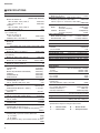
■ CONTENTS
TO SERVICE PERSONNEL ........................................... 1
AMP ADJUSTMENT ..................................................... 19
REMOTE CONTROL PANELS ....................................... 1
REAR PANELS ............................................................... 2
IC DATA .................................................................. 20~30
DISPLAY DATA ........................................................... 31
SPECIFICATIONS ....................................................... 3~4
INTERNAL VIEW ............................................................ 5
BLOCK DIAGRAM .................................................. 32~33
PRINTED CIRCUIT BOARD ................................... 34~47
DISASSEMBLY PROCEDURES .................................... 5
SELF DIAGNOSIS FUNCTION ................................ 6~17
SCHEMATIC DIAGRAM ......................................... 48~53
PARTS LIST ............................................................ 54~67
FACTORY PRESET ...................................................... 18
REMOTE CONTROL TRANSMITTER ......................... 68
100678
DSP-A595a
■ TO SERVICE PERSONNEL
1. Critical Components information.
Components having special characteristics are marked and must be
replaced with parts having specifications equal to those originally
installed.
WALL
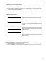
2. Leakage Current Measurement (For 120V Model only).
OUTLET
When service has been completed, it is imperative that you verify that
all exposed conductive surfaces are properly insulated from supply
circuits.
Meter impedance should be equivalent to 1500 ohm shunted by 0.15µF.
Leakage current must not exceed 0.5mA.
Be sure to test for leakage with the AC plug in both polarities.
EQUIPMENT
UNDER TEST
•
•
•
AC LEAKAGE
TESTER OR
EQUIVALENT
INSULATING
TABLE
WARNING: CHEMICAL CONTENT NOTICE!
The solder used in the production of this product contains LEAD. In addition, other electrical/electronic and/or plastic (where
applicable) components may also contain traces of chemicals found by the California Health and Welfare Agency (and possibly
other entities) to cause cancer and/or birth defects or other reproductive harm.
DO NOT PLACE SOLDER, ELECTRICAL/ELECTRONIC OR PLASTIC COMPONENTS IN YOUR MOUTH FOR ANY REASON
WHATSOEVER!
Avoid prolonged, unprotected contact between solder and your skin! When soldering, do not inhale solder fumes or expose eyes
to solder/flux vapor!
If you come in contact with solder or components located inside the enclosure of this product, wash your hands before handling
food.
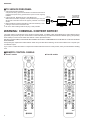
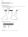
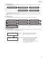
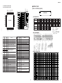
■ REMOTE CONTROL PANELS
▼ R and T models
1
▼ B and G models
RAV174
RAV175
V383640 US
V38650 EU
DSP-A595a
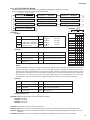
■ REAR PANELS
▼ R model
▼ T model
▼ B model
▼ G model
2
DSP-A595a
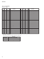
■ SPECIFICATIONS
■AUDIO SECTION
Minimum RMS Output Power Per Channel
(Power Amp. Section)
MAIN L/R, REAR L/R
20Hz to 20kHz, 0.04% THD, 8Ω
65W+65W
1kHz, 0.07% THD, 8Ω
80W+80W
CENTER
20Hz to 20kHz, 0.04% THD, 8Ω
65W
1kHz, 0.07% THD, 8Ω
80W
Maximum Power (EIAJ)
R, T models only
MAIN L/R, REAR L/R
1kHz, 10% THD, 8Ω
105W+105W
CENTER, 1kHz, 10% THD, 8Ω
105W
Dynamic Power Per Channel (IHF)
MAIN L/R
8/6/4/2Ω
90W+90W/110W+110W/135W+135W/160W+160W
DIN Standard Output Power Per Channel
G model only
MAIN L/R, 1kHz, 0.7% THD, 4Ω
110W+110W
IEC Power
G model only
MAIN L/R, 1kHz, 0.04% THD, 8Ω
75W+75W
Power Band Width
MAIN L/R, 0.1% THD, 35W, 8Ω
10Hz to 50kHz
Damping Factor (SPEAKER A)
MAIN L/R, 20Hz to 20kHz, 8Ω
60
Input Sensitivity/Input Impedance
PHONO (MM)
2.5mV/47kΩ
CD etc.
150mV/47kΩ
MAIN L/R (EXTERNAL DECODER)
150mV/47kΩ
CENTER
150mV/40kΩ
SURROUND L/R
150mV/40kΩ
SUB WOOFER
150mV/40kΩ
Maximum Input Signal Level (1kHz)
PHONO (MM), 0.1% THD
100mV
CD etc. (EFFECT ON), 0.5% THD
2.2V
Output Level/Output Impedance
REC OUT
150mV/1.2kΩ
SUB WOOFER (MAIN SP : SMALL)
2.1V/1.2KΩ
B,G models only
PRE OUT
4V/1.2KΩ
Headphone Jack Rated Output/Impedance
CD etc., Input=1kHz, 150mV, RL=8Ω
0.5V/390Ω
Frequency Response(20Hz to 20kHz)
CD etc., MAIN
0±0.5dB
RIAA Equalization Deviation
PHONO (MM)
0±0.5dB
Total Harmonic Distortion(20Hz to 20kHz)
PHONO (MM) to REC OUT (1V)
0.02%
CD etc.(EFFECT OFF) to MAIN SP OUT(35W/8Ω)
0.025%
Signal-to-Noise Ratio(IHF-A Network)
PHONO (MM), Input 5mV shorted, REC OUT
R, T models
86dB
B, G models
81dB
CD etc,(EFFECT OFF), Input 150mV shorted, SP OUT
96dB
3
Residual Noise(IHF-A Network)
MAIN L/R, SP OUT
150µV
Channel Separation(Vol. –30dB, EFFECT OFF)
PHONO, Input shorted, 1kHz/10kHz
60dB/55dB
CD etc, Input 5.1kΩ terminated, 1kHz/10kHz
60dB/45dB
Tone Control Characteristics
BASS
: Boost/Cut
±10dB(50Hz)
: Turnover Frequency
350Hz
TREBLE : Boost/Cut
±10dB(20kHz)
: Turnover Frequency
3.5kHz
Filter Characteristics
MAIN, REAR SP SMALL : H.P.F.
fc=90Hz, 12dB/oct.
SUB WOOFER : L.P.F.
fc=90Hz, 18dB/oct.
■VIDEO SECTION
Video Signal Type
R model
NTSC/PAL
T, B, G models
PAL
Video Signal Level
1Vp-p/75Ω
S-Video Signal Level
Y:1Vp-p/75Ω,C:0.286Vp-p/75Ω
Maximum Input Level
1.5Vp-p
Signal-to-Noise Ratio
50dB
Monitor Output Frequency Response(–3dB) 5Hz~10MHz
■GENERAL
Power Supply
R model
AC110/120/220/240V, 50/60Hz
T model
AC220V, 50Hz
B, G models
AC230V, 50Hz
Power Consumption
R, T models
310W
B, G models
300W
Maximum Power Consumption
R model only
5CH Simultaneous output, 10% THD
650W
AC Outlet
R, T models, Switched x 3
100W max(Total)
B model, Switched x 1
100W max
G model, Switched x 2
100W max(Total)
Dimensions(W x H x D)
435 x 151 x 391mm
(17-1/8" x 5-15/16" x 15-3/8")
Weight
12.5kg(27Ibs. 9 oz)
Accessories
Remote Control Transmitter x 1
Battery (siza "AA", "R06") x 2
* Specifications subject to change without notice.
R ......... General model
T .......... China model
B ......... British model
G ......... European model
DSP-A595a
21.5
(7/8")
● DIMENSIONS
WARNING
Do not change the IMPEDANCE SELECTOR switch
391(15-3/8")
IMPEDANCE SELECTOR
435(17-1/8")
151(5-15/16")
21
(27/32")
130(5-3/32")
20
(13/16")
349.5(13-3/4")
setting while the power to this unit is on, otherwise
this unit may be damaged.
Manufactured under license from Digital Theater
Systems, Inc. US Pat. No. 5,451,942 and other wirldwide patents issued and pending. "DTS", "DTS
Digital Surround", are trademarks of Digital Theater
Systems, Inc. Copyright 1996 Digital Theater
Systems, inc. All rights reserved.
Units: mm (inch)
4
DSP-A595a
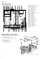
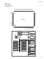
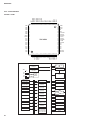
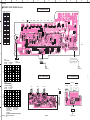
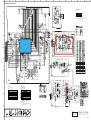
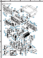
■ INTERNAL VIEW
1 2
3 4 5 6
7
8
9
0
A
B
1 POWER TRANSFORMER
2 P.C.B. MAIN (3)
3 P.C.B. OPERATION (7)
(R, T models only)
4 P.C.B. OPERATION (3)
5 P.C.B. MAIN (4)
6 P.C.B. MAIN (8)
7 P.C.B. OPERATION (6)
8 P.C.B. MAIN (2)
9 P.C.B. MAIN (1)
0 P.C.B. VIDEO
A P.C.B. INPUT (1)
B P.C.B. INPUT (3)
C P.C.B. MAIN (5)
D P.C.B. OPERATION (5)
E P.C.B. OPERATION (4)
F P.C.B. MAIN (7)
G P.C.B. OPERATION (1)
H P.C.B. MAIN (6)
I P.C.B. INPUT (4)
J P.C.B. OPERATION (2)
K P.C.B. DSP
#7
#8
#14
#9
#13
C
D
E
F
G
H
I
J K
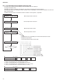
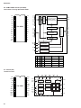
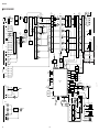
■ DISASSEMBLY PROCEDURES
(Remove parts in disassembly order as numbered.)
Top Cover
2
1. Removal of Top Cover
Remove 4 screws (1) and 4 screws (2) in Fig. 1.
1
2. Removal of Front Panel
a. Remove 5 knobs.
b. Remove 6 screws (3) in Fig. 1.
3
1
3
Knobs
Front Panel
Fig.1
5
DSP-A595a
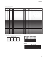
■ SELF DIAGNOSIS FUNCTION
1. PURPOSE AND OPERATION
The DSP-A595a has a Self Diagnosis Function to locate a faulty part, if any, by inspecting and taking
measurements.
There are 11 main items in the diagnostic menu and some of them have sub-menu items as listed below.
No.
MAIN MENU
1
ANALOG THROUGH
1. MAIN BYPASS
2. DSP 0dB
7A–88 ("1" [DSP mode])
–––
2
DSP THROUGH
1. YSS918–SRAM
2. YSS918
3. DSP FULL BIT
7A–89 ("2" [DSP mode])
–––
–––
3
AC–3/DTS THROUGH
1. STATUS (BINARY FORM)
–––
4
PRO LOGIC
1. CENTER LARGE
2. EFFECT OFF
7A–8A ("3" [DSP mode])
–––
5
SPEAKERS SET
1.
2.
3.
4.
7A–8B ("4" [DSP mode])
7A–8C ("5" [DSP mode])
7A–8D ("6" [DSP mode])
7A–8E ("7" [DSP mode])
SUB MENU
5.
6.
7.
8.
9.
MAIN : SMALL 0dB
MAIN : LARGE 0dB
MAIN : LARGE –10dB
LFE/BASS : MAIN
CENTER : NONE
LFE/BASS : MAIN
LFE/BASS : SWFR
CENTER : NONE
CENTER : SMALL
REAR : SMALL
FRONT MIX
REMOTE CONTROL CODE (KEY)
7A–8F ("8" [DSP mode])
7A–90 ("9" [DSP mode])
7A–91 ("0" [DSP mode])
–––
7A–12 ("ENTER" [DSP mode])
6
EFFECT OFF
/DISPLAY CHECK
1. EFFECT OFF
2. VFD DISP OFF
3. VFD DISP ALL
4. CHECKED PATTERN
5. RELEASE DATE
–––
–––
–––
–––
–––
7
MANUAL TEST
1. ALL
2. MAIN L
3. CENTER
4. MAIN R
5. REAR R
6. REAR L
7. LFE
–––
–––
–––
–––
–––
–––
–––
8
FACTORY PRESET
1. INHIBIT(Inhibit Memory Init)
2. RESERVED (Init. Memory)
–––
–––
9
AD DATA CHECK
1. – – –
2. KEY
3. TUNING SIGNAL
4. DC PROTECTION
5. PS PROTECTION
–––
–––
–––
10
STATUS
1. DSP CPU STATUS
2. CHANNEL STATUS
3. VERSION INFORMATION
4. CHECK SUM
5. BSI0 (AC3/DTS)
6. BSI1
7. BSI2
8. BSI3
9. BSI4
10. BSI5
–––
–––
–––
–––
–––
–––
–––
–––
–––
–––
11
VERSION CHECK
/DSP CPU SUM
/EXIT
1. MAIN MC CHECK SUM
2. SUB MC CHECK SUM
3. MAIN M.C. VERSION
4. SUB M.C. VERSION
5. PORT INFORMATION
6. EXIT
–––
–––
–––
–––
6
DSP-A595a
2. BEGINNING AND CANCELLATION
(1) STARTING UP THE FUNCTION AND THE DISPLAY
After starting up, menu No. 1 is selected.
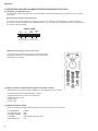
A. How to start diagnostic program
Using the front panel keys of the main unit.
Plug in the AC power cord , and, with Power OFF, hold down the "INPUT MODE" and "+" keys simultaneously (Step 1),
and then press the "STANDBY/ON" key (Step 2).
Submenu No. 1 of the Diagnosis Main Menu No. 1 will start.
FRONT PANEL
"STANDBY/ON" key
SET
MENU
"INPUT MODE" key
"+" key
TIME/
LEVEL
–
INPUT MODE
+
STANDBY/ON
Step2. Press the "STANDBY/ON" key
Step1. Hold down the "INPUT MODE"
and "+" key simultaneously.
B. Settings for start-up of diagnostic program
The settings used when starting the diagnostic program are as follows.
1. EFFECT LEVEL
CHANNEL
:
CENTER R SUR
LEVEL (dB)
0
0
L SUR
SWFR
0
0
2. MUTING
3. INPUT (VIDEO)
: DVD/LD (DVD/LD)
4. CENTER SPEAKER
5. REAR SPEAKER
: LARGE
6. MAIN SPEAKER
7. LFE/BASS OUT
: SWFR
: OFF
: LARGE
: LARGE
C. Start-up display
The protection function information appears on the front panel display of the main unit.
7
DSP-A595a
● FL display at start-up of diagnostic program
When the diagnostic program has started, the history (*2) of the protection function (*1) is displayed. If the protection
function has been activated in the past, the type and voltage value are displayed. After a few seconds the diagnosis
function menu will appear.
(*1) If a faulty condition is detected such as excessive current, a bad power supply or excessive amplifier DC offset,
the Power will be switched OFF automatically.
(*2) The protection records will be cleared when "RESERVED" is selected in diagnosis menu No. 8 and FACTORY
PRESET is engaged.
● History of protection function
Each case of the history of the protection function is displayed as shown below.
Appears when the protection function has not been activated.
1 DVD/LD
NO PROTECT
1 DVD/LD
I PROTECT
1 DVD/LD
PS : 21%
Appears when the power protection function has been activated.
For the % value, the voltage at that point is shown by 5V/100%.
When power is turned on in an abnormal status, power will turn off
after half a second.
1 DVD/LD
DC : 19%
Appears when the power amp DC protection function has been
activated.
For the % value, the voltage at that point is shown by 5V/100%.
When power is turned on in an abnormal status, power will turn off
after two seconds.
Appears when the current protection function has been activated.
When power is turned on in an abnormal status, the power relay
will come on, protection will operate immediately, and power will
turn off.
(2) EXITING METHOD
The diagnosis function can be exited by any of the following procedures. Take care with the setting of backup memory
initialization menu (diagnosis No. 8) when releasing the diagnosis function:
1. Select diagnosis menu No. 11/submenu No. 6 "EXIT".
2. Press the "STANDBY/ON" key on the main unit or "STANDBY" key on the remote control to turn power off.
8
DSP-A595a
3. OPERATION AND DISPLAY WHEN STARTING DIAGNOSIS FUNCTION
(1) Selection of diagnostic menu
The diagnostic menu and the sub-menu can be selected by using the front panel keys of the main unit or the remote
control unit.
● Selection by using the front panel keys
The main menu can be changed cyclically by using the "TV SPORTS" and "DISCO" keys, and the submenu,
by using the "ROCK CONCERT" and "CONCERT HALL" keys. The "DISCO" or "CONCERT HALL" key will increase
the main or submenu number.
FRONT PANEL
TV
SPORTS
DISCO
Main menu
Reverse Forward
ROCK
CONCERT
CONCERT
HALL
Sub menu
Reverse Forward
● Selection by using the remote control unit
The remote control codes in the menu list (see right column
on page 6) correspond to the DSP program test and effect keys.
See the figure on the right.
DSP
7A
(2) Other functions available while diagnosis function is active
Listed below are the other functions available while the diagnosis function is active.
•
•
•
•
•
Selecting input source (Tape monitor/Ext. decoder)
Adjusting effect level (Center, Rear, Subwoofer)
Adjusting master volume
Muting on/off
Power on/off
(3) Diagnosis default status
When not otherwise specified, default settings and values in each menu are as follows:
•
•
•
•
•
9
All “SPEAKERS”
ALL electronic VRs
DYNAMIC RANGE
LFE LEVEL
CENTER DELAY
:
:
:
:
:
LARGE
0dB
MAX
0dB (DOLBY DIGITAL, DTS)
0ms
DSP-A595a
4. CONTENTS OF DIAGNOSIS FUNCTION
This section describes the contents of the self diagnosis function in detail.
No.1 ANALOG THROUGH
The input is fixed to analog (A/D). There are two submenus.
1. MAIN BYPASS
1 DVD/LD
MAIN BYPAS
The MAIN L/R signals bypass the analog circuits to be output.
For CENTER/LFE, FRONT L/R and REAR L/R, the MAIN L/R signals via the DSP are output without
being processed (through). (Remote control code 7A-88: "1" key [DSP mode])
CODEC.AD
AC3D2av(YSS918)
DA
AK4320
ANALOG IN
L/R
MAIN L
MAIN R
AK4526A
DECODER
L/R
DSP
DIR2
L/R
CODEC.DA
REAR L
REAR R
L/R
DIGITAL IN
L/R
YM3436
: This shows that the device is not operating.
1 DVD/LD
AK4526A
CENTER
SUBWOOFER
• INPUT : DVD/LD (Analog signal)
(Lch and Rch, 1KHz, –20dBV)
• OUTPUT : SPEAKERS
MAIN L : 23.8 dBV REAR L : 23.7 dBV
MAIN R : 23.8 dBV REAR R : 23.7 dBV
CENTER: 23.7 dBV
1M SRAM
2. DSP 0dB
FRONT L
FRONT R
DSP 0DB
MAIN L/R, CENTER/LFE, FRONT L/R and REAR L/R pass through the DSP without being
processed.
CODEC.AD
AC3D2av(YSS918)
DA
AK4320
ANALOG IN
L/R
MAIN L
MAIN R
AK4526A
DECODER
L/R
DSP
DIR2
L/R
CODEC.DA
REAR L
REAR R
L/R
DIGITAL IN
L/R
YM3436
1M SRAM
: This shows that the device is not operating.
FRONT L
FRONT R
AK4526A
CENTER
SUBWOOFER
• INPUT : DVD/LD (Analog signal)
(Lch and Rch, 1KHz, –20dBV)
• OUTPUT : SPEAKERS
MAIN L : 23.7 dBV REAR L : 23.6 dBV
MAIN R : 23.7 dBV REAR R : 23.6 dBV
CENTER: 23.6 dBV
10
DSP-A595a
No.2 DSP THROUGH
The input is automatically discriminated by signal detection and switched with priorities AC-3 (DOLBY
DIGITAL)>DTS Digital Surround>Audio>analog. There are the following three submenus.
2 DVD/LD
1. YSS918-SRAM
YSS918SRAM
MAIN L/R are input to the DSP via AC3D2av, pass through SRAM, and are then output to all channels without
being processed. (Remote control code 7A-89: "2" key [DSP mode])
CODEC.AD
AC3D2av(YSS918)
DA
AK4320
ANALOG IN
L/R
MAIN L
MAIN R
AK4526A
DECODER
L/R
DSP
DIR2
L/R
CODEC.DA
L/R
DIGITAL IN
CENTER
SUBWOOFER
REAR L
REAR R
L/R
AK4526A
YM3436
FRONT L
FRONT R
L/R L/R
1M SRAM
2. YSS918
2 DVD/LD
• INPUT : DVD/LD (Analog signal)
(Lch and Rch, 1KHz, –20dBV)
• OUTPUT : SPEAKERS
MAIN L : 23.7 dBV REAR L : 23.5 dBV
MAIN R : 23.7 dBV REAR R : 23.5 dBV
CENTER: 23.6 dBV
YSS918
MAIN L/R are input to the DSP via AC3D2av, and then output to all channels without being processed.
CODEC.AD
AC3D2av(YSS918)
DA
AK4320
ANALOG IN
L/R
MAIN L
MAIN R
AK4526A
DECODER
L/R
DSP
DIR2
L/R
YM3436
1M SRAM
: This shows that the device is not operating.
2 DVD/LD
CODEC.DA
FRONT L
FRONT R
REAR L
REAR R
L/R
DIGITAL IN
3. DSP FULL BIT
L/R
AK4526A
CENTER
SUBWOOFER
• INPUT : DVD/LD (Analog signal)
(Lch and Rch, 1KHz, –20dBV)
• OUTPUT : SPEAKERS
MAIN L : 23.8 dBV REAR L : 23.8 dBV
MAIN R : 23.8 dBV REAR R : 23.8 dBV
CENTER: 23.8 dBV
DSP FULL
MAIN L/R are input to the DSP via AC3D2av, and then output to all channels without being processed.
The head margin is disabled, and DSP outputs digital full-bit signals.
Same as the above menu, except that the digital data is output to DA with full bits.
• INPUT : DVD/LD (Analog signal)
(Lch and Rch, 1KHz, –20dBV)
• OUTPUT : SPEAKERS
MAIN L : 13.8 dBV REAR L : 22.8 dBV
MAIN R : 13.8 dBV REAR R : 22.8 dBV
CENTER: 16.8 dBV
11
DSP-A595a
No.3 AC-3/DTS THROUGH
The input is digital signal only. AC-3 (DOLBY DIGITAL) or DTS Digital Surround decoding operation is executed,
according to the input source.
bit 0
bit 7
1. STATUS(BINARY FORM)
3 DVD/LD
3T00000001
AC-3 (DOLBY DIGITAL) decoded signals are output to each channel via AC3D2av.
CODEC.AD
AC3D2av(YSS918)
DA
AK4320
ANALOG IN
L/R
MAIN L
MAIN R
AK4526A
DSP
DECODER
CODEC.DA
DOLBY DIGITAL
or
C/LFE
PRO LOGIC
or
DTS
LS/RS
DIR2
DIGITAL IN
C/LFE
LS/RS
YM3436
CENTER
SUBWOOFER
AK4526A
REAR L
REAR R
: This shows that the device is not operating.
1M SRAM
AC-3 Status Info. : bit 7 6 5
(Invalid in DTS)
1 0 0
4
0
3 2 1
0 0 0
0
0
IEC958 digital data bit
IEC958 commercial-use device bit
IEC958 digital format error
Demodulator muting (without RF signal)
1 for audio other than PCM linear audio
1 during red DTS lock
1 during DTS decode OK
1 during AC-3 decode OK
No.4 PRO LOGIC
The input is automatically discriminated by PCM Audio>analog. DTS Digital Surround is disabled.
The submenu is switched between PRO LOGIC (AUTO BALANCE OFF) and EFFECT OFF.
1. CENTER LARGE
4 DVD/LD
P. LGC C:L
The input is automatically detected whether it is PCM Audio or analog. With analog, PCM Audio or AC-3 (DOLBY DIGITAL) 2/0 input, the L, R, C and S signals are PRO LOGIC decoded and output. With AC-3 (DOLBY DIGITAL) other
than 2/0, PRO LOGIC does not operate, and AC-3 (DOLBY DIGITAL) playback is executed. (Remote control code
7A-8A: "3" key [DSP mode])
CODEC.AD
AC3D2av(YSS918)
DA
AK4320
ANALOG IN
L/R
MAIN L
MAIN R
AK4526A
DSP
DECODER
CODEC.DA
DOLBY DIGITAL
or
PRO LOGIC
or
DTS
DIR2
DIGITAL IN
C
C
S
S
YM3436
1M SRAM
2. EFFECT OFF
4 DVD/LD
EFFECT OFF
CENTER
AK4526A
REAR L
REAR R
• INPUT : DVD/LD (Analog signal)
(Lch and Rch, or Lch only, 1KHz, –20dBV)
• OUTPUT : SPEAKERS
(INPUT : Lch and Rch ) (INPUT : Lch only)
MAIN L : –15.4 dBV
REAR L : 23.8 dBV
MAIN R : –14.2 dBV
REAR R : –25.0 dBV
CENTER: 26.6 dBV
CENTER : –12.5 dBV
REAR L : –6.0 dBV
REAR L : –6.0 dBV
REAR R : –6.5 dBV
REAR R : –6.2 dBV
MAIN L/R are bypassed and output.
12
DSP-A595a
No.5 SPEAKERS SET
The input is automatically discriminated by AC-3(DOLBY DIGITAL)>DTS Digital Surround>PCM Audio>analog.
There are the following 9 submenu items: The signal from the DSP block is normally in the effect off status for menu
items 1-4. For other menu items, the same signal as in 2. DSP THROUGH: YSS918 menu is output.
5 DVD/LD
MAIN:S 0DB
5 DVD/LD
MAIN:L 0DB
5 DVD/LD
MAIN:L —10
5 DVD/LD
B:MAIN C:N
5 DVD/LD
LFE/B:MAIN
5 DVD/LD
LFE/B:SWFR
5 DVD/LD
C:NONE
5 DVD/LD
C:S REAR:S
5 DVD/LD
FRONT MIX
The analog switches in each submenu are set as follows:
REMOTE
CODE
7A-8B
LARGE
LARGE
SMALL
MAIN
LEVEL
0dB
7A-8C
LARGE
LARGE
LARGE
MAIN:L -10
7A-8D
LARGE
LARGE
B:MAIN C:N
7A-8E
NONE
LARGE
SUB MENU
1
MAIN:S 0DB
2
MAIN:L 0DB
3
4
CENTER SP REAR SP
MAIN SP
LFE/BASS
OUTPUT
SWFR
MAIN L/R
0dB
SWFR
MAIN L/R
LARGE
-10dB
SWFR
MAIN L/R
LARGE
0dB
MAIN
MAIN L/R
5
LFE/B:MAIN
7A-8F
LARGE
LARGE
LARGE
0dB
MAIN
LFE -> L/R
6
LFE/B:SWFR
7A-90
LARGE
LARGE
LARGE
0dB
SWFR
LFE -> SWFR
7
C:NONE
7A-91
8
C:S REAR:S
9
FRONT MIX
7A-12
NONE
LARGE
LARGE
0dB
SWFR
CENTER -> L/R
SMALL
SMALL
LARGE
0dB
SWFR
CENTER/REAR
LARGE
LARGE
LARGE
0dB
SWFR
FRONT -> L/R
LARGE: Mode in which speakers with high bass-sound playback capability (large unit) are used. Full frequency band
widths is output.
SMALL : Mode in which speakers with low bass-sound playback capability (small unit) are used. Frequncies below 90 Hz
are mixed with the channel specified by LFE/BASS.
NONE: Mode in which center speaker is not used. The center audio signal is reduced by 3 dB and mixed into MAIN L/R.
LFE/B: MAIN
: Mode in which subwoofer speaker is not used. The subwoofer audio signal is reduced by 4.5 dB and mixed into
MAIN L/R. But because of the phase difference, the MAIN L/R output is not simply summed.
Purpose of the submenu as follows:
SUB MENU
13
PURPOSE
1
MAIN:S 0DB
Verification of the High and low pass filter response and gain in the bass redirection mode.
2
MAIN:L 0DB
Reference of the sub menu No. 1 and 2.
3
MAIN:L -10
Verification of the effect in the main level function.
4
B:MAIN C:N
Verification of the mixing circuit effect to the main channel.
5
LFE/B:MAIN
Verification of the bass mix gain.
6
LFE/B:SWFR
Verification of the LFE maximum output.
7
C:NONE
Verification of the center mix gain.
8
C:S REAR:S
Verification of the high and low pass filter response and gain in the bass redirection mode.
9
FRONT MIX
Verification of the front mix gain.
DSP-A595a
No.6 DISPLAY CHECK
Check program for FL display. The display status will change as follows with submenu operation. The signal is
processed with EFFECT OFF.
6 DVD/LD
DISP CHECK
Initial display
All segments turn off
6 DVD/LD
All segments turn on
9902161625
Release date display
Segments light in lattice form
All segments are turned on and off to detect defects in the FL driver and FL display segments. Then the FL driver
operation is checked by the dimmer control.
Finally, all segments are turned on and off alternately (in lattice form), to check for a short-circuit between adjacent
segments.
No.7 MANUAL TEST
The noise generator built into the DSP outputs test noise from the channel specified by the submenu.
7 DVD/LD
TEST ALL
7 DVD/LD
TEST MAINL
7 DVD/LD
TEST CNTR
7 DVD/LD
TEST MAINR
7 DVD/LD
TEST REARR
7 DVD/LD
TEST REARL
7 DVD/LD
TEST LFE
No.8 FACTORY PRESET
The initialization of the back-up RAM, which contains effect level, DSP program, set menu contents, etc. is reserved
or inhibited. The Signal is processed with EFFECT OFF.
8 DVD/LD
PRESET INH
1. INHIBIT:
Inhibits initialization of the back-up RAM.
Specify this option protect user set Values.
8 DVD/LD
PRESET RES
2. RESERVED: Reserve to initialization of the back-up RAM.
(The RAM is actually initialized when power
is turned on next time.) Specify this option
at the factory preset or to reset the RAM.
For the contents of the initialization, see page 18.
The protection data is also reset.
14
DSP-A595a
No.9 AD DATA CHECK
The A/D conversion values of the main CPU which detects key scan, protection, etc. are displayed in % (100%: 5V).
All signal processing before this menu is executed will be held.
The keys on the main unit cannot be operated to detect the values of all keys in the K1/K2/K3/K4 and SI.
Operating the "CONCERT HALL" key and turning the rotary encoder (input selector on the main unit) will switch the
submenu.
9 DVD/LD
AD DATACHK
9 DVD/LD
K99999999
Press the "CONCERT HALL "key.
K1/K2/K3/K4: Panel key on main unit
See Table 1.
K1 K2 K3 K4
Turning the rotary encoder.
SI: Tuner signal level
9 DVD/LD
SI
0
9 DVD/LD
DC
7
Turning the rotary encoder.
DC: DC protection value
(normal value: 1-13)
9 DVD/LD
PS
40
Press the "CONCERT HALL"key.
PS: Power voltage protection value
(normal value: 28-54)
Press the "CONCERT HALL"key.
Table 1
AD Value
0
11
23
36
51
67
84
K1
K2
TAPE/MD MON
/EXT. DECODER
K3
ROCK
CONCERT
CONCERT
HALL
SET
MENU
TIME/
LEVEL
–
+
K4
EFFECT
/DTS
SURROUND
ENHANCED
MOVIE
THEATER
MONO
MOVIE
TV
SPORTS
INPUT MODE
Cautions:
1. If K1/K2/K3/K4 are more than ±4% from the reference values, normal operation will not be executed.
2.If DC and PS are outside the normal values, the protection function will operate and power will turn off.
15
DISCO
DSP-A595a
No.10 STATUS FROM DSP MICOM
The status data from the DSP microprocessor is sequentially displayed in a hexadecimal number.
All signal processing before this menu is executed will be held.
STATUS
1st 2nd 3rd 4th
10 DVD/LD 0 00000000
10 DVD/LD 1 00000000
10 DVD/LD 2 00000000
10 DVD/LD 3 00000000
10 DVD/LD 4 00000000
10 DVD/LD 5 00000000
10 DVD/LD 6 00000000
10 DVD/LD 7 00000000
10 DVD/LD 8 00000000
bit
[STATUS 0]
<1st Byte>
Mute request
bit3
bit6
fs
bit2
bit5
000B:Analog 001B:32kHz
010B:44.1kHz 011B:48kHz
Others:Don't care
bit1
bit0
acmod
0000B:1+1
0010B:2/0
0100B:2/1
0110B:2/2
1000B:7.1
0001B:1/0
0011B:3/0
0101B:3/1
0111B:3/2
acmod: If it is 1000B or more with DTS 7.1 signal, the DSP block will be muted.
<2nd Byte>
bit7
AC-3 decode OK
bit3
Demodulator muting (without RF signal)
bit6
DTS decode OK
bit2
IEC958 digital format error
bit5
Red DTS record
(Flashes and lights)
1 for audio other than PCM
linear audio
bit1
IEC958 commercial use device bit
bit0
IEC958 digital data bit
bit4
7 6 5 4
Indicate
bit7
bit4
0 0
Indicate
10 DVD/LD 9 00000000
[Note]
0
1
2
3
4
5
6
7
8
9
A
B
C
D
E
F
3 2 1 0
bit
3
7
0
0
0
0
0
0
0
0
1
1
1
1
1
1
1
1
2
6
0
0
0
0
1
1
1
1
0
0
0
0
1
1
1
1
1
5
0
0
1
1
0
0
1
1
0
0
1
1
0
0
1
1
0
4
0
1
0
1
0
1
0
1
0
1
0
1
0
1
0
1
IEC958: Standard to identify the PCM bit stream signal. Digital format error refers to a digital signal with the
sampling frequency undefined (neither 44.1k, 32k nor 48k). Since the operation of each device cannot be
assured at fs outside specifications, the sub-microprocessor handles this status as the forced analog mode
(ignored even if decoding is OK from the detection terminal level), and selects the signal from the analog input
terminal. Since the sub-microprocessor transmits 000B (analog) for STATUS#0 bits 4-6 to the main
microprocessor, the main microprocessor visually operates in the same way as with digital unlocking.
<3rd Byte>
bit7
AC3 KARAOKE
bit3
On-board write mode
bit6
DIR2 LOCKN
bit2
The number of digital inputs is 2 (equivalent to 595)
bit5
DIR2 ERR
bit1
DSP is AC3D2 (DTS present)
bit4
AC3D MUTE
bit0
RF DEM present
<4th Byte> Always “00”
[STATUS 1] IEC958 channel status bits 00-31 available from DIR2
<1st-byte> bits 00-07
<2nd-byte> bits 08-15
<3rd-byte> bits 16-23
<4th-byte> bits 24-31
[STATUS 2] 4-byte ASCII code of sub CPU version data
[STATUS 3] Displays the check sum of sub microprocessor program area with ASCII 4 bytes in a hexadecimal number.
[STATUS 4] Displays the bit stream information contained in AC-3(DOLBY DIGITAL)/DTS Digital Surround signal from the
first byte.
[STATUS 5-9] Displays the bit stream information contained in AC-3(DOLBY DIGITAL) signal from the first byte.
16
DSP-A595a
No.11 CPU VERSION/CHECK SUM/PORT INFO/EXIT DIAG
The check sum, version and port setting of main CPU/DSP CPU are displayed.
The signal is EFFECT OFF.
Operating the submenu will finish self-diagnosis, and ordinary operation mode will be restored.
The suffix letter ("B" in the following) of version indication is for compatibility of communications between the main and
DSP microprocessors.
Combining microprocessors with different suffixes will make normal operation impossible.
11 DVD/LD
M-SM:XXXXX
Main microprocessor check sum
11 DVD/LD
S-SM:XXXXX
DSP microprocessor check sum
11 DVD/LD
M-VER:Z04B
Main microprocessor version
11 DVD/LD
S-VER:Z08B
DSP microprocessor version
One suffix letter is for compatibility of communications between the main
and DSP microprocessors.
* Use microprocessors with the same suffix.
11 DVD/LD
P:00000000
bit
7
1
6
0
5
0
4
0
3
0
2
0
1
0
0
0
Always absent (0)
Always absent (0)
Tuner Mode V1 (✽1)
Tuner Mode V2 (✽1)
Always absent (0)
Always absent (0)
Model Type RDS (✽2)
Model Type DSP-A (✽2)
EXIT
✽1
Hi=1, Low=0
Tuner Mode V2 (Port 96)
Tuner Mode V1 (Port 95)
*1
*2
*3
*4
✽2
0
0
1
0
*2
0
1
*3
1
1
*4
AM:531–1611kHz/9kHz FM: 76.0–90.0MHz/100kHz (J model)
AM:530–1710kHz/10kHz FM: 87.5–107.9MHz/200kHz (U, C models)
AM:531–1611kHz/9kHz FM: 87.5–108.0MHz/50kHz (R, T, A, B, G, L models)
AM: 530-1710kHz/10kHz FM:87.5-108.0 MHz/100kHz (R, T models)
Hi=1, Low=0
Model Type DSP-A(Port 83) 1
Model Type RDS(Port 70)
0
17
*1
DSP-A595a
0 RX-V595aRDS 0
1
0
RX-V595a
HTR-5150
DSP-A595a
■ FACTORY PRESET
All of the system settings are initially set from the factory as follows.
● INPUT (VIDEO)
DVD/LD (DVD/LD)
● EFFECT LEVEL
EFFECT CHANNEL
CENTER
RIGHT SURROUND
LEFT SURROUND
SUBWOOFER
PRESET VALUE
0 dB
0 dB
0 dB
0 dB
● DSP PROGRAM
INPUT
V-AUX
VCR
VDV/LD
TV/DBS
TAPE/MD
TUNER
CD
PHONO
DSP PROGRAM
DOLBY PRO LOGIC
PRO LOGIC ENHANCED
70mm MOVIE THEATER
DIGITAL/DTS MOVIE THEATER
TV SPORTS
ROCK CONCERT
DISCO
ROCK CONCERT
CONCERT HALL
DELAY PRESET VALUE
20ms
20ms
20ms
16ms
9ms
49ms
40ms
16ms
44ms
● SET MENU
No.
1.
2.
3.
4.
5.
6.
7.
8.
9.
10.
11.
SET MENU
CENTER SPEAKER [CNTR>]
REAR SPEAKER [REAR>]
MAIN SPEAKER [MAIN>]
LFE/BASS OUT [BASS>]
MAIN LEVEL [M. LVL>]
DOLBY DIGITAL LFE LEVEL [D. D. LFE]
DYNAMIC RANGE [D. RNG]
DTS LFE LEVEL [DTS LFE]
CENTER DELAY [C. DELAY]
MEMORY GUARD [GUARD]
INPUT MODE (TV/DBS) [INPUT]
PRESET VALUE
LARGE
LARGE
LARGE
SW (SUBWOOFER)
NRML (NORMAL)
0 dB
MAX
0 dB
0 ms
OFF
AUTO
18
DSP-A595a
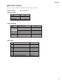
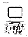
■ AMP ADJUSTMENT
Confirmation of Idling Current of Main Amplifier
• Right after power is turned on, confirm that the voltage across the
terminals of R688(Main Lch),R690(Main Rch), R692(Center),
R694(Rear Lch), R696(Rear Rch) are between 0.1mVand 5.0mV.
• If it exceeds 5.0mV, open (cut off) R571 (Main Lch), R577 (Main
Rch), R589 (Center), R595 (Rear Lch), R583 (Rear Rch) and
•
reconfirm the voltage again.
Confirm that the voltage is 0.25mV ~ 15.0mV after 60 minutes.
0.1mV ~ 5.0mV
(DC)
R583
Q523
R692
R688(Lch)
R690(Rch)
R692(Cch)
R694(RLch)
R696(RRch)
R595
R696
Q525
Cut off
R589
MAIN (1)
R694
Q524
R571(Lch)
R577(Rch)
R589(Cch)
R595(RLch)
R583(RRch)
Note)
• If R571, R577, R589, R595
and
R583 have already been cut off
MAIN (7)
and idling current does not flow,
reconnect R571, R577, R589,
R690
Q522
•
R577
R595 and R583.
Q521 ~ Q525 are transistors for
temperature correction.
Apply silicone grease to contact
surface with the heat sink.
R688
Q521
R571
19
Front Panel
DSP-A595a
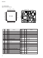
■ IC DATA
S47/PF7
S46/PF6
S45/PF5
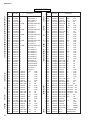
S44/PF4
S43/PF3
S42/PF2
S41/PF1
S40/PF0
VDD4
S39/PE7
S38/PE6
S37/PE5
S36/PE4
S35/PE3
S34/PE2
S33/PE1
S32/PE0
S31/PD7
S30/PD6
S29/PD5
S28/PD4
S27/PD3
S26/PD2
S25/PD1
S24/PD0
S23/PC7
S22/PC6
S21/PC5
S20/PC4
VP
IC800 : LC876564A-5M19
8 bit Main µ-COM
80 79 78 77 76 75 74 73 72 71 70 69 68 67 66 65 64 63 62 61 60 59 58 57 56 55 54 53 52 51
81
50
82
83
49
48
84
85
47
46
86
87
45
44
88
89
43
42
90
91
41
40
TOP VIEW
92
93
39
38
94
95
37
36
96
97
35
34
98
99
33
32
100
31
S19/PC3
S18/PC2
S17/PC1
S16/PC0
VDD3
S15/T15
S14/T14
S13/T13
S12/T12
S11/T11
S10/T10
S9/T9
S8/T8
S7/T7
S6/T6
S5/T5
S4/T4
S3/T3
S2/T2
S1/T1
1 2 3 4 5 6 7 8 9 10 11 12 13 14 15 16 17 18 19 20 21 22 23 24 25 26 27 28 29 30
P16
P17
P30
P31
P32
P33
P34
P35
P36
P37
/RES
XT1
XT2
VSS1
CF1
CF2
VDD1
P80/AN0
P81/AN1
P82/AN2
P83/AN3
P84/AN4
P85/AN5
P86/AN6
P87/AN7
P70/INT0
P71/INT1
P72/INT2
P73/INT3
S0/T0
S48/PG0
S49/PG1
S50/PG2
S51/PG3
P00
P01
P02
P03
VSS2
VDD2
P04
P05
P06
P07
P10/SO0
P11/SI0
P12/SCK0
P13/SO1
P14/SI1
P15/SCK1
INTERRUPT
CONTROL
/RES
CF1
CF2
CF
Xtal
PLA
FLUSH ROM
STANDBY
CONTROL
RC
XT1
XT2
IR
CLOCK
GENERATOR
PC
BUS INTERFACE
ACC
SERIAL I/O 0
(SO0,SI0,SCK0)
PORT 0
(P00-P07)
B REGISTER
SERIAL I/O 1
(SO1,SI1,SCK1)
PORT 1
(P10-P18)
C REGISTER
TIMER 0
PORT 3
(P30-P34)
TIMER 1
PORT 7
(P70-P73)
BASE TIMER
PORT 8
(P80-P87)
VFD CONTROLLER
(S0-S51)
ADC
NOISE REJECTION
FILTER(INT0-INT3)
SMALL SIGNAL
DETECTOR
ALU
PSW
RAR
RAM
STACK POINTER
WATCH DOG
TIMER
20
DSP-A595a
IC800 : LC876564A-5M19
8 bit Main µ-COM
Pin
No.
1
2
3
4
5
6
7
8
9
10
11
12
13
14
15
16
17
18
19
20
21
22
23
24
25
Pin
I/O
Name
P16
FLA-CLK I/O
P17
FLA-I/O I/O
P30
FLA-SEL I/O
P31
T-MUTE O
P32 DSP-MTS O
P33 DSP-STM I
P34 DSR-SCK O
P35 DSP-RTN I
P36 DSP-TRQ I
P37 DSP-RESET O
/RES
/RES
XT1
T-/ST
I
XT2
Vss1
Vss1
CF1
CF2
VDD1
VDD1
P80/AN0 KEY1
I
P81/AN1 KEY2
I
P82/AN2 KEY3
I
P82/AN3 KEY4
I
P84/AN4 T-METER I
P85/AN5 PRO1
I
P86/AN6 PRO2
I
P85/AN5 PRO3
I
Port
Function
Flash clock
Flash input/output
Flash select
Tuner mute (L: ON)
Transmit data for Sub µ-COM
Receive data from Sub µ-COM
Clock for Sub µ-COM
Clock from Sub µ-COM
Transmit request from Sub µ-COM
Reset for Sub µ-COM
System reset
Stereo from Tuner
Unconnected
Ground
Ceramic Oscillator Connected (10MHz)
Ceramic Oscillator Connected (10MHz)
Power supply
Key 1 AD input
Key 2 AD input
Key 3 AD input
Key 4 AD input
Tuner meter AD input
Protection 1 detect (PRD)
∗1
Protection 2 detect (PRI)
∗1
Protection 3 detect (PRV1)
∗1
Pin
No.
26
27
28
29
30
31
32
33
34
35
36
37
38
39
40
41
42
43
44
45
46
47
48
49
50
∗1 Protection 1, 2 and 3 detect
• After a few seconds the Power ON, and protection detect start.
21
Protection 1
Detection
Abnormal DC of the amplifier.
Protection 2
Protection 3
Abnormal overcurrent of the amplifier.
Abnormal Voltage of the amplifier.
Port
Pin
Name
PDT
FMT
I/O
Function
P70/INT0
I Power down detect
P71/INT1
O Full mute (L : ON)
P72/INT2
I/O Unconnected
P73/INT3 REMOTE I Remote Control signal
S0/T0
G1
O FL Grid 1
S1/T1
G2
O FL Grid 2
S2/T2
G3
O FL Grid 3
S3/T3
G4
O FL Grid 4
S4/T4
G5
O FL Grid 5
S5/T5
G6
O FL Grid 6
S6/T6
G7
O FL Grid 7
S7/T7
G8
O FL Grid 8
S8/T8
G9
O FL Grid 9
S9/T9
G10
O FL Grid 10
S10/T10
G11
O FL Grid 11
S11/T11
G12
O FL Grid 12
S12/T12
G13
O FL Grid 13
S13/T13
G14
O FL Grid 14
S14/T14
G15
O FL Grid 15
S15/T15
G16
O FL Grid 16
VDD3
VDD3
Power supply
S16/PC0
P1
O FL Segment 1
S17/PC1
P2
O FL Segment 2
S18/PC2
P3
O FL Segment 3
S19/PC3
P4
O FL Segment 4
DSP-A595a
IC800 : LC876564A-5M19
8 bit Main µ-COM
Pin
No.
51
52
53
54
55
56
57
58
59
60
61
62
63
64
65
66
67
68
69
70
71
72
73
74
75
Pin
I/O
Name
VP
VP
S20/PC4
P5
O
S21/PC5
P6
O
S22/PC6
P7
O
S23/PC7
P8
O
S24/PD0
P9
O
S25/PD1
P10
O
S26/PD2
P11
O
S27/PD3
P12
O
S28/PD4
P13
O
S29/PD5
P14
O
S30/PD6
P15
O
S31/PD7
P16
O
S32/PE0
P17
O
S33/PE1
P18
O
S34/PE2
P19
O
S35/PE3
P20
O
S36/PE4
P21
O
S37/PE5
P22
O
S38/PE6 RDS SELECT I
S39/PE7
VDD4
VDD4
S40/PF0
S41/PF1 EFFECT-RY O
S42/PF2 SP-RY O
Port
Function
FL Segment 5
FL Segment 6
FL Segment 7
FL Segment 8
FL Segment 9
FL Segment 10
FL Segment 11
FL Segment 12
FL Segment 13
FL Segment 14
FL Segment 15
FL Segment 16
FL Segment 17
FL Segment 18
FL Segment 19
FL Segment 20
FL Segment 21
FL Segment 22
Model Type RDS
Unconnected
Power supply
Unconnected
Effect relay
Speaker relay
∗2 Model Type
• Model Type select to the order of DSP, RDS, V595a.
Hi = 1, Low = 0
Model
Type
∗2
Pin
No.
76
77
78
79
80
81
82
83
84
85
86
87
88
89
90
91
92
93
94
95
96
97
98
99
100
Pin
I/O
Function
Name
S43/PF3 POWER-RY O Power relay
S44/PF4 –10dB
O –10 dB select (L : –10dB)
S45/PF5
/VCR
O VCR select inhibit (H : inhibit)
S46/PF6
Unconnected
S47/PF7 STANDBY-SW I Standby / on (H : ON)
S48/PG0 ROTARY-A I Rotary encoder A
S49/PG1 ROTARY-B I Rotary encoder B
S50/PG2 DSP-A.SEL I Model Type DSP-A
S51/PG3
P00
VOL.DN O Volume down
P01
VOL.UP O Volume up
P02
V-SEL1 O Video selector 1
P03
V-SEL2 O Video selector 2
VSS2
VSS2
Ground
VDD2
VDD2
Power supply
P04 CE-INPUT O Chip enable for INPUT
P05
CE-VR O Chip enable for VOLUME
P06 CE-TUNER O Chip enable for TUNER
P07
/CERDS O Chip enable for RDS
P10/SO0 V1/RDS-DATA O RDS data V1 market
P11/SI0 V2/RDS-DATA O RDS data V2 market
P12/SCK0 RDS-CLK O Clock for RDS
P13/SO2
SDT
O Serial data
P14/SI1 TUN-SIN I Serial data from Tuner
P15/SCK1 SCK
O Serial clock
Port
∗2
∗3
∗3
∗4
∗4
∗3 Video selector 1 and 2
Hi = 1, Low = 0
Video Selector 1(VSEL0) 2(VSEL1)
V-AUX
0
0
DSP
RDS
V595a
DSP-A.SEL
1
0
0
VCR
DVD/LD
1
0
0
1
RDS SELECT
0
1
0
TV/DBS
1
1
∗4 Markets
Market
J
V2
V1
0
0
Hi = 1, Low = 0
U, C
R, T, A, B, G, L
1
0
0
1
R, T
1
1
22
DSP-A595a
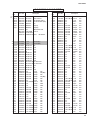
IC14 : LC875164A-5K20
PB7
P27/INT5
P26/INT5
P25/INT5
P24/INT5
P23/INT4
P22/INT4
P21/INT4
P20/INT4
P07
P06
P05
P04
P03
P02
P01
P00
VSS2
VDD2
PWM0
8 bit Sub µ-COM
60 59 58 57 56 55 54 53 52 51 50 49 48 47 46 45 44 43 42 41
PB6
PB5
PB4
PB3
PB2
PB1
PB0
VSS3
VDD3
PC7
PC6
PC5
PC4
PC3
PC2
PC1
PC0
PA0
PA1
PA2
61
40
62
63
39
38
64
65
37
36
66
67
35
34
68
69
33
32
70
71
31
30
TOP VIEW
72
73
29
28
74
75
27
26
76
77
25
24
78
79
23
22
80
21
PWM1
SI2P3
SCK2
SI2
SO2
P17/PWM
P16/PWL
P15/SCK1
P14/SI1
P13/SO1
P12/SCK0
P11/SI0
P10/SOO
P34
P33
P32
P31
P30
P87/AN7
P86/AN6
PA3
PA4
PA5
P70/INT0
P71/INT1
P72/INT2
P73/INT3
/RES
XT1
XT2
VSS1
CF1
CF2
VDD1
P80/AN0
P81/AN1
P82/AN2
P83/AN3
P84/AN4
P85/AN5
1 2 3 4 5 6 7 8 9 10 11 12 13 14 15 16 17 18 19 20
IR
INTERRUPT
CONTROL
/RES
CF1
CF2
XT1
XT2
ROM
STANDBY
CONTROL
CF
RC
Xtal
PLA
CLOCK
GENERATOR
PC
SERIAL I/O 0
(SO0,SI0,SCK0)
BUS INTERFACE
ACC
SERIAL I/O 1
(SO1,SI1,SCK1)
PORT 0
(P00-P07)
B REGISTER
SERIAL I/O 2
(SO2,SI2,SCK2)
PORT 1
(P10-P18)
C REGISTER
TIMER 0
PORT 3
(P30-P34)
TIMER 1
PORT 7
(P70-P73)
TIMER 4
PORT 8
(P80-P87)
TIMER 5
ADC
PWM0
NOISE REJECTION
FILTER(INT0-INT3)
PWM1
PORT 2
(P20-P27)
BASE TIMER
PARALLEL
INTERFACE
PORT A (PA0-PA5)
PORT B (PB0-PB7)
PORT C (PC0-PC7)
ALU
PSW
RAR
23
RAM
STACK POINTER
WATCH DOG
TIMER
DSP-A595a
IC14 : LC875164A-5K20
8 bit Sub µ-COM
Pin
No.
1
2
3
4
5
6
7
8
9
10
11
12
13
14
15
16
17
18
19
20
21
22
23
24
25
26
27
28
29
30
31
32
33
34
35
36
37
38
39
40
Port
PA3
PA4
PA5
P70/INT0
P71/INT1
P72/INT2
P73/INT3
/RES
XT1
XT2
VSS1
CF1
CF2
VDD1
P80/AN0
P81/AN1
P82/AN2
P83/AN3
P84/AN4
P85/AN5
P86/AN6
P87/AN7
P30
P31
P32
P33
P34
P10/SO0
P11/SI0
P12/SCK0
P13/SO1
P14/SI1
P15/SCK1
P16/PWM
P17/PWM
SO2
SI2
SCK2
SI2P3
PWM1
Pin
Name
CDO
/ICDI
/KM1
LOCKN
ERRD
ERRA
NONPCM
/RES
XT1
XT2
VSS1
CF1
CF2
VDD1
NC
NC
NC
NC
NC
NC
NC
NC
/ICAK
CEAK
/ICAC
CEAC2
CEAC1
TXAC
RXAC
CLKAC
RSRV
TRXOB
CLKOB
NC
NC
STM
MTS
CKIF
WCIF
TRQ
I/O
Function
I Receive data from DIR2
O Initial clear for DIR2
O Switching DIR2 forced (analog) mode
IRQ PLL lock flag
IRQ DIR 2 error detect
IRQ AC3D2av mute detect
IRQ AC3D2av AC-3 data detect
– Reset from Main µ-COM
I Connected to VDD1
I Unconnected
G Ground
Ø Ceramic Oscillator Connected (10kHz)
Ø Ceramic Oscillator Connected (10kHz)
+5V +5V power supply
O Unconnected
O Unconnected
O Unconnected
O Unconnected
O Unconnected
O Unconnected
O Unconnected
O Unconnected
O Initial clear for CODEC AD/DA
O Chip enable for CODEC AD/DA
O Initial clear for AC3D2av
O Chip enable 2 for AC3D2av
O Chip enable 1 for AC3D2av
TX Transmit data for AC3D2av and CODEC AD/DA
RX Receive data from AC3D2av
CLK Clock for AC3D2av and CODEC AD/DA
Ipu Not used (Normal)
I/O Not used (Normal)
I Not used (Normal)
I Unconnected
I/O Unconnected
TX Transmit data for Main µ-COM
RX Receive data from Main µ-COM
RXCK Clock from Main µ-COM
O Clock for Main µ-COM
O Transmit request for Main µ-COM
Pin
No.
41
42
43
44
45
46
47
48
49
50
51
52
53
54
55
56
57
58
59
60
61
62
63
64
65
66
67
68
69
70
71
72
73
74
75
76
77
78
79
80
Pin
I/O
Function
Name
NC
OL Unconnected
VDD2 +5V +5V power supply
VSS2
G Ground
NC
I/O Unconnected
NC
I/O Unconnected
NC
I/O Unconnected
NC
I/O Unconnected
NC
I/O Unconnected
NC
I/O Unconnected
NC
I/O Unconnected
NC
I/O Unconnected
NC
I/O Unconnected
NC
I/O Unconnected
NC
I/O Unconnected
NC
I/O Unconnected
NC
I/O Unconnected
NC
I/O Unconnected
NC
I/O Unconnected
NC
I/O Unconnected
NC
I/O Unconnected
NC
I/O Unconnected
NC
I/O Unconnected
DSP
Ipu Connected to VSS3
MUTO Ipu Unconnected (Fixed H)
LDC/O
I LD Coaxial/Optical detect
CDC/O
I Fixed H
RF
Ipu Connected to VSS3 (Switched L)
VSS3
G Ground
VDD3 +5V +5V power supply
NC
I/O Unconnected
NC
I/O Unconnected
VER
Ipu Connected to VSS3 (Switched L)
DRB
O Unconnected
DRA
O Unconnected
DIC
O Unconnected
DIB
O Digital input selector control B
∗1
DIA
O Digital input selector control A
∗1
DMT
O L/R D/A converter mute
CLD
O Chip select for DIR2
CCK
O Serial clock for DIR2
Port
PWM0
VDD2
VSS2
P00
P01
P02
P03
P04
P05
P06
P07
P20/INT4
P21/INT4
P22/INT4
P23/INT4
P24/INT5
P25/INT5
P26/INT5
P27/INT5
PB7
PB6
PB5
PB4
PB3
PB2
PB1
PB0
VSS3
VDD3
PC7
PC6
PC5
PC4
PC3
PC2
PC1
PC0
PA0
PA1
PA2
∗1 Digital input selector control
Hi = 1, Low = 0
Input
DVD/LD
DIB
0
DIA
0
TV/DBS
1
0
24
DSP-A595a
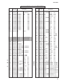
IC3 : YM3436DK (DIR2)
FS0 34
KMO
VSSA
VDDA
PCO
CTLP
CTLN
TST2
LR
LOCKN
P256
XO
XI
KM2
KM1
SKSY
/IC
23 /IC
25 CTLN
24 VDDA
27 NC
26 PCO
29 GNDA
28 CTLP
31 KM2
30 TSTN
33 FS1
32 KM0
Digital Format Interface Receiver
32
29 24 26 28 25 17 38 15 14 13
12 31
22
11
23
22 KM1
21 DOM0
EXTW 36
20 DOM1
DDIN 37
19 DIM0
LR 38
18 DIM1
TOP VIEW
VDD 39
17 TST2
ERR 40
16 GND
EMP 41
15 LOCKN
CDO 42
14 P256
CCK 43
13 XO
CLD 44
12 XI
EXTW
SEL
DDIN
ERR
CSM
EMP
FS1
FS0
SYSTEM
CLOCK
TIMING
GENERATOR
PLL
Pin
Name
DAUX
I
2
3
HDLT
DOUT
O
O
4
VFL
5
6
7
8
VFL
8
7
6
DATA CLOCK
CONTROLLER
EIAJ (AES/EBU)
DIGITAL AUDIO
INTERFACE
DECODER
40
35
41
33
34
S/P
BUFFER
P/S
2
16 39 30
GND
1 18 19
HDLT
CCK
42
DAUX
DIM1
DIM0
43
3
DOUT
20
DOM1
DOM0
21
CDO
44
CLD
SKSY 11
MCA 10
MCB 9
WC 8
MCC 7
OPT 5
SYNC 6
VFL 4
DOUT 3
HDLT 2
DAUX 1
25
Pin
4
9
37
SERIAL INTERFACE
No.
1
5
MCA
MCB
WC
MCC
SYNC
OPT
10
36
VDD
TSTN
CSM 35
Pin
Pin
Auxiliary input for audio data
No.
26
Name
PCO
Asynchronous buffer operation flag (NC)
Audio data output
27
28
NC
CTLP
O
Parity flag output (NC)
29
GNDA
OPT
SYNC
MCC
WC
O
O
O
O
Fs x 1 Synchronous output signal for DAC (NC)
Fs x 1 Synchronous output signal for DSP (NC)
Fs x 64Bit clock output
Fs x 1Word clock output
30
31
32
TSTN
KM2
KM0
I
I
I
Test terminal. Open for normal use
Clock mode switching input 2 (GND)
Clock mode switching input 0 (GND)
9
MCB
O
Fs x 128Bit clock output
33
FS1
O
Channel status sampling frequency display
output 1 (NC)
10
11
MCA
SKSY
O
I
Fs x 256Bit clock output
Clock synchronization control input
34
FS0
O
12
XI
I
Crystal oscillator connection or external
clock input
35
CSM
I
13
14
15
XO
P256
LOCKN
O
O
O
Crystal oscillator connection
VCO oscillator clock connection (NC)
PLL lock flag
36
EXTW
I
37
38
DDIN
LR
I
O
External synchronous auxiliary input word
clock (GND)
EIAJ (AES/EBU) data input
PLL word clock output (NC)
16
17
GND
TST2
O
Logic section power (GND)
PLL time constant switching output (NC)
39
40
VDD
ERR
O
Logic section power (+5V)
Data error flag output
18
19
DIM1
DIM0
I
I
Data input mode selection
Data input mode selection
41
EMP
O
20
DOM1
I
Data output mode selection (GND)
21
22
DOM0
KM1
I
I
Data output mode selection (GND)
Clock mode switching input 1
42
CDO
O
23
24
/IC
VDDA
I
Initial clear from Sub µ-COM
VCO section power (+5V)
43
CCK
I
25
CTLN
I
VCO control input N
44
CLD
I
I/O
Function
I/O
O
I
Function
PLL phase comparison output
VCO control input P (GND)
VCO section power (GND)
Channel status sampling frequency display
output 0 (NC)
Channel status output method selection(GND)
Channel status emphasis control code
output (NC)
3-wire type microcomputer interface data
output
3-wire type microcomputer interface clock
output
3-wire type microcomputer interface load
input
DSP-A595a
VSS
RAMD7
RAMD6
RAMD5
RAMD4
RAMD3
RAMD2
RAMD1
RAMD0
VDD1
RAMA2
SCK
SI
SO
/CS
/CSB
RAMA3
TEST
/IC
RAMA4
VSS
RAMA5
RAMA6
/SDBCK0
SURENC
KARAOKE
MUTE
CRC
NONPCM
VDD2
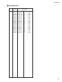
IC4 : YSS918D-F (AC3D2av)
DSP + AC-3 (Digital Dolby)/Pro Logic/DTS Digital Surround Decoder
80 79 78 77 76 75 74 73 72 71 70 69 68 67 66 65 64 63 62 61 60 59 58 57 56 55 54 53 52 51
VDD
SDWCK0
SDBCK0
SDIA0
SDIA1
RAMA1
RAMA0
RAMWEN
RAMOEN
VSS
VDD
IPORT7
IPORT6
IPORT5
IPORT4
IPORT3
IPORT2
IPORT1
IPORT0
VSS
81
50
82
83
49
48
84
85
47
46
86
87
45
44
88
89
43
42
TOP VIEW
90
91
PVSS
SDWCK1
SDBCK1
SDOB0
SDOB1
SDOB2
RAMA7
RAMA8
RAMA9
VDD2
VSS
OPORT7
OPORT6
OPORT5
OPORT4
OPORT3
OPORT2
OPORT1
OPORT0
VDD1
41
40
92
93
39
38
94
95
37
96
97
35
34
98
99
33
32
36
100
31
65 /CSB
OPORT0~7
~
39
32
69 SCK
68 SI
67 SO
66 /CS
~
92
99
IPORT0~7
VDD1
RAMCEN
RAMA16
RAMA15
SDIB0
SDIB1
SDIB2
XI
XO
VSS
AVDD
SDIB3
TEST
TEST
OVFB
DTSDATA
AC3DATA
SDOB3
CPO
AVSS
VDD
SDOA2
SDOA1
SDOA0
RAMA14
RAMA13
RAMA12
RAMA1
1
RAMA10
VSS
1 2 3 4 5 6 7 8 9 10 11 12 13 14 15 16 17 18 19 20 21 22 23 24 25 26 27 28 29 30
MICROPROCESSOR
INTERFACE
CONTROL
SIGNALS
CONTROL
SIGNALS
SDIBCKSEL
SDOBCKSEL
SDIB INTERFACE
SDOB INTERFACE
L,R
Ls,Rs
C,LFE
SDIBSEL
STREAM0~7
EXTERNAL RAM
INTERFACE
OPERATING
CLOCK (25MHz)
DELAY
RAM
RAMOEN 89
87,86,70,64,61,
59,58,44~42,
29~25,4,3
RAMCEN 2
79
72
45 SDOB2
18 SDOB3
15 OVFB
RAMWEN 88
RAMD0~7
5
6
7
12
SDIBO
SDIB1
SDIB2
SDIB3
~
46 SDOB1
DATA
RAM
ERAMUSE
SDOA0 24
SDOA1 23
SDOA2 22
XO 9
CPO 19
PLL
24x16
SUB DSP
47 SDOB0
RAMA0~16
24x24
MAIN DSP
AC-3/
PRO LOGIC/
DTS
DECODER
SDIBCKSEL
SDOA INTERFACE
SDIA INTERFACE
INPUT
BUFFER
XI 8
56
55
54
53
17
16
52
CRC
SURENC
KARAOKE
MUTE
CRC
AC3DATA
DTSDATA
NONPCM
SDIASEL
SDI : SERIAL DATA INPUT
SDO : SERIAL DATA OUTPUT
SDIA1 85
48 SDBCK1
49 SDWCK1
CONTROL REGISTERS
/SDBCK0 57
SDBCK0 83
SDWCK0 82
SDIA0 84
COEFFICIENT
PROGRAM
RAM
26
DSP-A595a
IC4 : YSS918D-F (AC3D2av)
DSP + AC-3 (Digital Dolby)/Pro Logic/DTS Digital Surround Decoder
No.
27
Name
I/O
Function
1
2
VDD1
RAMCEN
O
+5V power supply
RAM chip enable output terminal (normally unconnected)
3
RAMA16
O
RAM address output terminal 16, connected to external 1M SRAM address
4
5
RAMA15
SDIB0
O
I
RAM address output terminal 15, connected to external 1M SRAM address
Serial data input B terminal 0 (normally connected to ground)
6
SDIB1
I
Serial data input B terminal 1 (normally connected to ground)
7
8
SDIB2
XI
I
I
Serial data input B terminal 2 (normally connected to ground)
Crystal oscillator connection external clock input terminal
O
9
XO
10
VSS
Crystal oscillator connection (normally unconnected)
11
12
AVDD
SDIB3
13
TEST
14
TEST
15
16
OVFB
DTSDATA
17
18
19
AC3DATA
SDOB3
CPO
20
21
AVSS
VDD
22
23
24
SDOA2
SDOA1
SDOA0
O
O
O
Serial data output A terminal 2 (normally unconnected)
Serial data output A terminal 1 (normally unconnected)
Serial data output A terminal 0, PCM output terminal (AC-3/PRO LOGIC/DTS: L/R output)
25
26
RAMA14
RAMA13
O
O
RAM address terminal 14 output terminal, connected to external 1M SRAM address
RAM address terminal 13 output terminal, connected to external 1M SRAM address
27
28
29
30
RAMA12
RAMA11
RAMA10
VSS
O
O
O
RAM address terminal 12 output terminal, connected to external 1M SRAM address
RAM address terminal 11 output terminal, connected to external 1M SRAM address
RAM address terminal 10 output terminal, connected to external 1M SRAM address
Ground
31
32
VDD1
OPORT0
O
+5V power supply
Output port terminal 0, dolby pro logic signal output
33
34
35
OPORT1
OPORT2
OPORT3
O
O
O
Output port terminal 1, (normally unconnected)
Output port terminal 2, (normally unconnected)
Output port terminal 3, (normally unconnected)
36
37
38
39
OPORT4
OPORT5
OPORT6
OPORT7
O
O
O
O
Output port terminal 4, (normally unconnected)
Output port terminal 5, (normally unconnected)
Output port terminal 6, (normally unconnected)
Output port terminal 7, (normally unconnected)
40
41
VSS
VDD2
42
43
RAMA9
RAMA8
O
O
44
RAMA7
O
RAM address output terminal 7 , connected to external 1M SRAM address
45
46
SDOB2
SDOB1
O
O
Serial data output B terminal 2, PCM output
Serial data output B terminal 1, PCM output
47
48
49
50
SDOB0
SDBCK1
SDWCK1
VSS
O
I
I
Serial data output B terminal 0, PCM output
Serial data bit clock input terminal 1
Serial data word clock input terminal 1
Ground
Ground
I
+3V power supply
Serial data input B terminal 3 (normally unconnected)
Test terminal (normally unconnected)
Test terminal (normally unconnected)
O
O
O
O
O
Overflow detect terminal (normally unconnected)
DTS data detect terminal (normally unconnected)
AC-3 data detect terminal (normally unconnected)
Serial data output B terminal 3 (normally unconnected)
PLL output terminal (connected to AVSS through external analog filter)
Ground
+3V power supply
Ground
+3V power supply
RAM address output terminal 9 , connected to external 1M SRAM address
RAM address output terminal 8 , connected to external 1M SRAM address
DSP-A595a
IC4 : YSS918D-F (AC3D2av)
DSP + AC-3 (Digital Dolby)/Pro Logic/DTS Digital Surround Decoder
No.
Name
51
52
VDD2
NONPCM
I/O
O
+3V power supply
non-PCM data output terminal, non-PCM data detect
Function
53
54
CRC
MUTE
O
O
CRC output terminal (normally unconnected)
Mute output terminal, output data mute detect
55
56
57
KARAOKE
SURENC
/SDBCK0
O
O
O
Karaoke output terminal (normally unconnected)
Surround encoder output terminal (normally unconnected)
Inverted signal of serial data bit clock output terminal 0 (normally unconnected)
58
59
RAMA6
RAMA5
O
O
RAM address output terminal 6, connected to external 1M SRAM address
RAM address output terminal 5, connected to external 1M SRAM address
60
VSS
61
62
63
RAMA4
/IC
TEST
O
I
RAM address output terminal 4, connected to external 1M SRAM address
Initial clear input terminal
Test terminal (normally unconnected)
64
65
RAMA3
/CSB
O
I
RAM address output terminal 3, connected to external 1M SRAM address
Chip select B input terminal,coefficient and program RAM chip select signal input
66
67
68
69
70
71
72
73
74
75
/CS
SO
SI
SCK
RAMA2
VDD1
RAMD0
RAMD1
RAMD2
RAMD3
I
O
I
I
O
I/O
I/O
I/O
I/O
Chip select input terminal, microprocessor interface chip select signal input
Serial data output terminal, microprocessor interface serial data output
Serial data input terminal, microprocessor interface and coefficient and program RAM serial data input
Serial clock intput terminal, microprocessor interface and coefficient and program RAM serial clock input
RAM address output terminal 2, connected to external 1M SRAM address
+5V power supply
RAM data bus terminal 0, connected to external 1M SRAM data
RAM data bus terminal 1, connected to external 1M SRAM data
RAM data bus terminal 2, connected to external 1M SRAM data
RAM data bus terminal 3, connected to external 1M SRAM data
76
77
78
79
RAMD4
RAMD5
RAMD6
RAMD7
I/O
I/O
I/O
I/O
RAM data bus terminal 4, connected to external 1M SRAM data
RAM data bus terminal 5, connected to external 1M SRAM data
RAM data bus terminal 6, connected to external 1M SRAM data
RAM data bus terminal 7, connected to external 1M SRAM data
80
81
VSS
VDD2
82
83
SDWCK0
SDBCK0
I
I
Serial data word clock input terminal 0
Serial data bit clock input terminal 0
84
85
86
SDIA0
SDIA1
RAMA1
I
I
O
Serial data input A terminal 0, AC-3/DTS bit stream (or PCM) data input
Serial data input A terminal 1 (normally connected to ground)
RAM address output terminal 1, connected to external 1M SRAM address
87
88
RAMA0
RAMWEN
O
O
RAM address output terminal 0, connected to external 1M SRAM address
RAM write enable output terminal, connected to external 1M SRAM write enable
89
90
RAMOEN
VSS
O
RAM output enable output terminal, connected to external 1M SRAM output enable
Ground
91
92
VDD
IPORT7
I
+3V power supply
Input port terminal 7 (normally connected to ground)
93
94
IPORT6
IPORT5
I
I
Input port terminal 6 (normally connected to ground)
Input port terminal 5 (normally connected to ground)
95
IPORT4
I
Input port terminal 4 (normally connected to ground)
96
97
IPORT3
IPORT2
I
I
Input port terminal 3 (normally connected to ground)
Input port terminal 2 (normally connected to ground)
98
99
100
IPORT1
IPORT0
VSS
I
I
Input port terminal 1 (normally connected to ground)
Input port terminal 0 (normally connected to ground)
Ground
Ground
Ground
+3V power supply
28
DSP-A595a
32 VCC
A3
2
31 A2
A4
3
30 CE2
A5
4
29 /WE
A6
5
28 A1
A7
6
27 A0
A8
7
26 A16
A9
8
A10
9
24 /OE
A11 10
23 A14
A12 11
22 /CE1
A13 12
21 D8
D1 13
20 D7
D2 14
19 D6
D3 15
18 D5
GND 16
17 D4
TOP VIEW
25 A15
A0
A1
A2
A3
A4
A5
A6
A7
A8
27
A9
A10
A11
A12
A13
A14
A15
A16
8
28
31
2
3
4
5
18
512
32 VCC
16 GND
131072-word x 8 bit
MEMORY ARRAY
(512-row X 2048-column)
6
2048
7
I/O DATA CONTROL
1
ROW INPUT
BUFFER
NC
ROW ADDRESS
DECODER
IC5 : M5M51288BKJ-20LTEL (1M SRAM)
131072-word x 8 bit High Speed Static RAM
COLUMN I/O
9
10
11
12
23
25
26
256
COLUMN ADDRESS
DECODER
16
COLUMN INPUT
BUFFER
/CE1 22
CHIP SELECT
CE2 30
/WE 29
WRITE CONTROL
/OE 24
OUTPUT CONTROL
/CE1 CE2 /WE /OW
Mode
Data I/O
Power
L
X
X
Non-selectable
High impedance
On
H
X
X
X
Non-selectable
High impedance
Standby
L
H
L
X
Write mode
Input
On
L
H
H
L
Read mode
Output
On
L
H
H
H
High impedance
On
X
NOTE) H: High Level
L: Low level
X: Don't care
IC7 : AK4320 (DA)
1 bit D/A Converter
CKS 1
23 DZF
DG 3
22 VREF
XTO 4
21 AG
XTI 5
20 AVDD
/PD 6
19 VCOM
SDAT 8
DIF1
DEM0
DEM1
AVDD
AG
14
15
12
13
20
21
24 ZMUT
DVDD 2
BICK 7
DIF0
TOP VIEW
18 OUTL
17 OUTR
LRCK 9
16 VCNT
SMUT 10
15 DIF1
HOLD 11
14 DIF0
DEM0 12
13 DEM1
LRCK 9
BICK 7
DE-EMPHASIS
CONTROL
8x
INTERPOLATOR
∆∑
MODULATOR
SCF
CTF
18 OUTL
8x
INTERPOLATOR
∆∑
MODULATOR
SCF
CTF
17 OUTR
SDAT 8
/PD 6
SMUT 10
HOLD 11
ZMUT 24
DZF 23
CLOCK
OSC/DIVIDER
16 VCNT
5
4
1
XTI XTO CKS
29
19 VCOM
SERIAL INPUT
INTERFACE
2
3
22
DVDD
DG
VREF
13 D1
14 D2
15 D3
17 D4
18 D5
19 D6
20 D7
21 D8
DSP-A595a
■ DISPLAY DATA
IC6 : AK4526A-VQ (CODEC AD/DA)
1
33
VREFL
OCKS
2
32
RIN+
M/S
3
31
RIN–
BICK
4
30
LIN+
LRCK
5
29
LIN–
SDTI1
6
28
ROUT1
SDTI2
7
27
LOUT1
SDTI3
8
26
ROUT2
SDTO
9
25
LOUT2
CAD0 22
CAD1 21
ICKS0 20
ICKS1 19
XTS 18
/PD 17
LOUT3
DVSS 16
ROUT3
23
DVDD 15
24
11
MCKO 14
10
DFS
DEM0 13
DAUX
DEM1 12
LIN+
30
LIN–
29
RIN+
32
RIN–
31
ADC
ADC
HPF
HPF
LOUT1
27
VR
LPF
DAC
ROUT1
28
VR
LPF
DAC
Audio
I/F
1/2
VR
LPF
DAC
ROUT2
26
VR
LPF
DAC
MCKI
PATTERN AREA
BICK
DEM
5
LRCK
4
BICK
10
DAUX
13
11
DEM0
DEM1
DFS
1
SDOS
9
SDTO
12
SDIN1
ROUT3
VR
23
LPF
VR
24
LPF
• PIN CONNECTION
Pin No.
DAC
DAC
1
Pin No.
6
SDTI1
7
SDTI2
8
SDTI3
2
3
4
5
6
7
8
9
10 11 12 13 14 15 16 17 18 19 20 21 22 23 24 25
CONNECTION F1 F1 NP NP NC NC NC NC NC NC NC P22 P21 P20 P19 P18 P17 P16 P15 P14 P13 P12 P11 P10 P9
SDIN2
SDIN3
LOUT2
1
MCLK
SDOUT
25
y
Clock Gen.
LRCK
LOUT2
● V800 : 16-BT-59GK (V2421800)
39
MCKO
OCKS
2
SDOS
TOP VIEW
14
34 VCOM
35 VREFH
36 AVDD
37 AVSS
38 XTI
39 MCKI
40 P/S
41 /CS
42 CCLK
43 CDTI
44 CDTO
20 bit 6 channel A/D, D/A Converter
26 27 28 29 30 31 32 33 34 35 36 37 38 39 40 41 42 43 44 45 46 47 48 49 50
CONNECTION P8 P7 P6 P5 P4 P3 P2 P1 IC NP Fd Fd NP IC 16G15G14G13G12G 11G10G 9G 8G 7G 6G
Pin No.
51 52 53 54 55 56 57 58 59 60 61 62 63 64 65
CONNECTION 5G 4G 3G 2G 1G NC NC NC NC NC NC NP NP F2 F2
• GRID ASSIGNMENT
Pin
No.
1
2
3
Pin
Name
SDOS
OCKS
M/S
4
BICK
I/O
Audio serial data clock,
bit clock input from Main µ-COM
5
LRCK
I/O
Input/Output channel clock,
word clock input from Main µ-COM
6
7
8
SDTI1
SDTI2
SDTI3
I
I
I
DAC Audio serial data input 1-3,
PCM input from AC3D2av
O
Audio serial data output,audio
data for DIR2
9
SDTO
I/O
I
I
I
Function
Connected to ground (digital)
Connected to ground (digital)
Connected to ground (digital)
10
11
12
DAUX
DFS
DEM1
I
I
I
13
14
15
16
17
DEM0
MCKO
DVDD
DVSS
/RD
I
O
18
19
20
21
XTS
ICKS1
ICKS0
CAD1
I
I
I
I
Connected to ground (analog)
Connected to ground (analog)
Connected to ground (analog)
Connected to ground (analog)
22
CAD0
I
Connected to ground (analog)
I
Connected to ground (digital)
Connected to ground (digital)
Connected to ground (digital)
Unconnected
Power supply (digital)
Ground (digital)
Power down and reset, initial clear
from Sub µ-COM
Pin
No.
23
24
25
26
27
28
29
30
31
32
33
Pin
Name
LOUT3
ROUT3
LOUT2
ROUT2
LOUT1
ROUT1
LIN–
LIN+
RIN–
RIN+
VREFL
34
35
VCOM
VREFH
36
AVDD
Power supply (analog)
37
38
AVSS
XTI
39
MCKI
I
Ground (analog)
Unconnected
External master clock input, FsX256
Bit clock from DIR2
40
P/S
I
Connected to ground (digital)
I/O
Function
O
O
O
O
O
O
I
I
I
I
I
Lch analog output 3, for CENTER
Rch analog output 3, for LFE
Lch analog output 2, for REAR
Rch analog output 2, for REAR
Lch analog output 1, for FRONT
Rch analog output 1, for FRONT
Lch analog negative input, from MAIN
Lch analog positive input, from MAIN
Rch analog negative input, from MAIN
Rch analog positive input, from MAIN
Connected to ground (analog)
O
I
Common voltage output
Connected to power supply (analog)
41
/CS
I
Chip select in serial mode, chip enable
from Sub µ-COM
42
CCLK
I
Control data clock in serial mode,
clock from Sub µ-COM
I
Control data input in serial mode,
Tramsmit data from Sub µ-COM
43
44
CDTI
CDTO
O
NOTE 1) F1, F2 ........ Filament
2) NP .............. No pin
3) NC .............. No connection
4) DL .............. Datum Line
5) 1G~16G ..... Grid
6) IC ............... Internal connection
7) Fd terminals are to be supplied
through 51kΩ from Ec.
• ANODE CONNECTION
16G
15G
14G
13G
12G
11G
10G
9G
8G
P1
1a
a
1a
a
a
a
a
a
a
P2
P3
P4
P5
P6
P7
P8
P9
1b
1c
1d
1e
1f
1g
1h
1j
b
c
d
e
f
g
h
j
1b
1c
1d
1e
1f
1g
1h
1j
b
c
d
e
f
g
h
j
b
c
d
e
f
g
h
j
b
c
d
e
f
g
h
j
b
c
d
e
f
g
h
j
b
c
d
e
f
g
h
j
b
c
d
e
f
g
h
j
P10
P11
P12
P13
1k
1m
1n
1p
k
m
n
p
1k
1m
1n
1p
k
m
n
p
k
m
n
p
k
m
n
p
k
m
n
p
k
m
n
p
P14
1r
r
1r
r
r
r
r
–
–
t
–
P15
P16
Unconnected
(Left)
2a
P17 2b,2c
P18
2d
P19 2e,2f
P20
30
(RT)
2g
P21 2j,2p
P22
(Right)
(PTY)
2m
(CT)
2a
2b
B1
–
2c
B2
–
2d
B3
–
2e
B4
2f
B5
2g
S3
(PS)
–
7G
~5G
a
4G
3G
2G
1G
a
a
a
a
b
c
d
e
f
g
h
j
b
c
d
e
f
g
h
j
b
c
d
e
f
g
h
j
b
c
d
e
f
g
h
j
b
c
d
e
f
g
h
j
k
m
n
p
k
m
n
p
k
m
n
p
k
m
n
p
k
m
n
p
k
m
n
p
r
r
r
r
r
r
r
t
t
t
t
t
t
t
–
–
–
–
–
–
–
–
–
–
–
–
S1
–
–
S2
–
–
–
–
–
–
–
–
–
–
–
–
–
–
–
31
DSP-A595a
■ BLOCK DIAGRAM
1
TV/DBS
INPUT SELECTOR
IC101
AUDIO SIGNAL
L
30
6
47
8
FL
29
IC103
27
26
IC109B
23
7
6
6
27
7
5
24
LFE
CENTER
6
IC107A
7
5
3
2
4
IC802B
1
8
6
RY501
Q502
Q811
4
BASS TREBLE
VR800 VR801
IC110
IC402A
14
7
5
IC402B
3
1
3
VR802
15
22
28
6
8
RAM
IC5
IC403A
8
9
IC107B
29
23
C
1
3
IC403B
23
R
22
IC13A
L
IN
25
RL
3
7
1
3
14
7
5
24
1
3
OUT
R
21
20
11
10
INHIBIT
IC101
DSP
CONTROL
VR401
RR
7
12
SUB µ-COM
IC14
13
5
EXTERNAL
DECODER
INPUT
R
CENTER
RDS
CONTROL
(NOT USED)
R
MOTOR
DRIVE
INPUT/
VIDEO/
S VIDEO
SELECTOR
CONTROL
RCE
RDT
DEST/RDO
RCK
/ST
Q800
Q510,519,520,
525,542,545,
543A/C
~ 10
78 , 87 , 88 , 91
86 85
77
92
94
24
95
25
96
75
TCE
INPUT
SELECTER
A
B
MAIN µ-COM
IC800
93
99
26
17
81
82
90
46
72
18
76
~
15
16
30
SW801
~
45 , 47
XL800
12
U800
~
50 , 52
~
SPRY
FL DISPLAY
V800
S VIDEO
1
REMOTE
SENSOR
2
F1
65 65
Q556
RESET
RESET
Q803,D805
PDT
POWER DOWN DETECT
Q805,D811,812
VDD1
BACK-UP D809
(MEMORY)
VDD2
VDD3
VDD4
(J,B,G models)
J807
S12
Q808, D816
(R,T models)
Q806,D813
D806
D815
T800
REGULATOR
RY800
Q807
PRY
Q552
D513
MAIN,
CENTER,
REAR
AMP
+B
D762,763
+RYV
F804
–B
D451
+25
F2
INPEDANCE
SELECTOR
SW761
D751
J809
AC OUTLETS
Q721,
722
-25
MONITOR
OUT
CENTER
RY501
MAIN SPEAKER
RY502
CENTER SPEAKER
RY503
REAR SPEAKER
Q553
EFFECT-RY
69
~ 33 , 40 ~ 55
OVER
CURRENT
DETECT
+B,-B,+25,-25,
+12A,+12B,+5D,-12
51
29
STANBY/ON
VIDEO
AUX
MAIN
Q548
PRO3
VP
21
23
OUT
REAR
Q546,547
PRO2
D808
OPERATION
KEY
SW802~806,
810~815,
817,822~824
Q549,550
SPEAKER RELAY DRIVE
11
22
VCR
VIDEO SIGNAL
MAIN
SUBWOOFER
PRO1
4
TV/DBS
+12A
-12B
J,R,T models
D452
J809
IC725,
724,
722
AC OUTLET
-12
IN
D453
VCR
B model
F803
+5D
OUT
IC723
G model
32
L
L
REAR
R (SURROUND)
27
SW800
VIDEO
S-VIDEO SELECTOR
& AMP
IC301,302,IC304,305
B.G models only
MUTE
DRIVE
Q801,802
12
METER
DO
DVD/LD
+
FMC
97
TMUTE
Q305,306
–
Q505
–10dB
74
TUNER
CONTROL
(NOT USED)
IN
–
RY503
R
SUBWOOFER
MONITOR
OUT
+
M
23
VIDEO AMP &
SELECTOR
IC303
REAR
(SURROUND)
R
15
L
MAIN
DVD/LD
–
IC404
XL2
VIDEO AUX
+
CENTER
5
3 IN
(PLAY) R
TAPE/MD
4 OUT L
(REC)
R
SURROUND
R
Q724
L
L
B
L
IC13B
26
A
RY502
REAR
POWER AMP
IC111
R
L
B
CENTER
Q504
2
VCR
L
CENTER
POWER AMP
Q508,515,516,
523,534,537,
531A/C
A
SW711
Q509,517,518,
524,538,541
539A/C
IC106B
DAC
IC6
MAIN
POWER AMP
Q507,513,514,
522,530,533,
531A/C
Q503
2
7
5
MAIN
Q501
Q810
IC103
SUB
WOOFER
IC103
2
7
TONE
CONTROL
IC801
IC401B
1
3
25
IC109A
1
26
20
IC103
26
3
5
IC103
H,P,F
21
IC108A
IC11B
FR
IC802A
1
3
27
7
5
1
3
IC103
IC106A
4
5
SELECTOR SWITCH
30
1
3
IC8,9
2
R
R
3
R
IC401A
IC108B
H,P,F
SPEAKER
7
1 CD
DVD/LD
27
28
L
L
IC10B
IC11A
45
3
33
AC OUTLETS
OUTPUT
5
4
SPEAKER RELAY
A/D
IC6
TAPE
MONITOR
IC102
IC103
4
8
17
~
L
R
DAC
IC7
9
R
L
2
11
DSP
+
DIGITAL/
PRO-LOGIC/
DTS
DECODER
IC4
R
PHONO
1
7
5
1
L
IC104A/B
3
1
L
MUTING
OPTICAL SIGNAL
DETECTOR
IC351
18
10
13
2 TUNER
VIDEO
AUX
8
DIR
IC3
XL1
OPTICAL
24
84
-10dB
3
12
OPTICAL
TV/DBS
37
13
9
BALANCE
8
7
LEVEL CONTROL
DVD/LD
IC2
INPUT
SELECTOR
IC352
PHONES
MAIN
POWER AMP
Q506,511,512,
521,529,Q527A/C
MAIN
LEVEL
VR401
IC103
LEVEL CONTROL
IC351
10
6CH
SELECTOR
IC102
6 GANG MOTOR VOLUME
13
~
DIGITAL
SIGNAL
COAXIAL
IC10A
A
B
C
D
E
F
G
H
DSP-A595a
■ PRINTED CIRCUIT BOARD (Foil side)
1
P. C. B. DSP
TO: INPUT (1)
P. C. B. DSP
TO: INPUT (3)
TO: INPUT (1)
#1
#3
#6
L
E
FL
C
RL
E
LIN
ISL1
+15VD
DSIG
+12
–5V
WCIF
CKIF
MTS
STM
R
E
FR
LFE
RR
RIN
LDC/0
ISL0
DG
–12
+5VD
DG
TRQ
/SBR
2
17
16
M5M51288BKJ-20LTEL
41
60
40
61
LC875164A-5K20
8
8
5
1
1
4
uPC4570G2
8
1
1
HD74HC02FP
14
8
5
NJM2904M
1
4
8
YSS918D-F
uPC4570G2
8 5
8
81
5
1
4
4
uPC4570G2
IN
uPC29M331-E1
COM
OUT
80
5
4
32
1
51
50
uPC4570G2
1
3
6
5
80
20
uPC4570G2
4
21
100
31
30
1
1
23
33
22
7
34
23
YM3436DK
33
22
34
13
AK4526A-VQ
24
AK4320
44
12
11
1
44
12
4
11
1
12
1
5
5
6
● Semiconductor Location
Ref. No.
Ref. No.
Location
IC1
D1
F3
IC2
D2
F3
IC3
D3
G4
IC4
D4
G4
IC5
D5
G4
IC6
D6
G4
IC7
D7
G4
IC8
D8
G4
IC9
D9
F4
IC10
D10
G4
IC11
D11
G4
IC13
D12
G4
IC14
D13
D4
IC15
D14
D4
D15
D4
D16
D4
D17
D4
Location
B3
E3
B4
A3
A3
C4
D4
C3
C3
D3
D3
C3
B3
B3
Ref. No.
Q1
Q2
Q3
Q4
Q5
Q6
Q7
Q8
Q9
Q10
Q11
Q12
Q13
Q14
Location
H4
G4
G4
H3
G3
G3
G3
G3
G3
G3
G3
H3
G3
D4
Point 6
Pin 13 of IC14
V : 2V/div
H : 50nsec/div
AC range
1 : 1probe
Point 5
Pin 13 of IC3
V : 2V/div
H : 50nsec/div
AC range
1 : 1probe
0V
0V
2V
SAMPLE
50ns
E-34/J-32
2V
SAMPLE
50ns
E-35/J-33
A
B
C
D
E
F
H
G
DSP-A595a
■ PRINTED CIRCUIT BOARD (Foil side)
P. C. B. OPERATION (1)
1
2
● Semiconductor Location
Ref. No.
Location
D800
C2
D801
C2
D802
C2
D803
C2
C2
D805
D806
C3
D807
C2
D808
E3
D809
C3
D811
C3
C3
D812
D813
C3
IC800
E2
IC801
D5
IC802
E5
Q800
F3
E3
Q801
Q802
E3
Q803
C2
Q805
C3
Q806
C3
Q810
E5
E5
Q811
EFFECT
/DTS
SURROUND
MOVIE
THEATER
ENHANCED
MONO
MOVIE
TV
SPORTS
ROCK
CONCERT
DISCO
CONCERT
HALL
SET
MENU
TIME/
LEVEL
INPUT MODE
+
-
1 100
STANDBY/ON
INPUT
VCR.V-AUX.TV/DBS.DVD/LD.CD.TUNER.PHONO
VO
VC
G
A
81
4
9
M1
A
64
31
3
B
COM
80
-5
30
5V
65
87
LC
TAPE/MD MON
SEL
/EXT.
DECODER
CLK
RESET
MG
DATA
50 51
65 64
61 60
55
50
45
40 39
37 36
30
34
25
20
15
10
5
2
1
3
W801
YE
MG
PRY
S12
SPRY
PRI
PRO
VP
PRV1
CRY
TO:
POWER
TRANSFORMER
RCK
RCE
DO
/ST
METER
/SBR
TRQ
MG
RTN
VUP
SCK
CETC
VSEL0
/VCR
FMT
Point 3
(Pin 16 of IC800)
V : 2V/div
H : 50nsec/div
AC range
1 : 1 probe
RDT
DEST/RDO
TCE
TMUTE
STM
MTS
CKIF
MG
VDN
PRV2
SDT
CELC
VSEL1
–10dB
W802
YE
W803
#14
#8
TO: MAIN (1)
TO: INPUT (1)
0V
4
P. C. B. OPERATION (2)
P. C. B. OPERATION (4)
2V
SAMPLE
50ns
Point 4
CH1 : Pin 11 of IC800
CH2 : Emitter of Q806
V : 2V/div
H : 0.5sec/div
DC range
1 : 1probe
VIDEO AUX
BASS
TREBLE
S VIDEO
BALANCE
VIDEO
L
AUDIO
TO:
INPUT (1)
#9
W805
CH1
5
0V
(CH1)
NJM2068LD
1
CH2
0V
(CH2) 2V
E-36/J-34
1
8
2V
SAMPLE
0.5s
With the POWER
Disconnect the
switch turned ON,
power cord from
connect the
the AC outlet.
power cord to the
AC outlet.
This waveform is not available by pushing the
power switch ON and OFF.
#13
Y
C
Y
VE
AXL
E
AXR
6
NJM2068LD
8
+12A
–12
TIR
E
TIL
E
TOR
E
TOL
E
–10dB
#13
E-37/J-35
TO: INPUT (2)
R
A
B
C
D
E
F
H
G
DSP-A595a
P. C. B. OPERATION (6)
■ PRINTED CIRCUIT BOARD (Foil side)
P. C. B. OPERATION (5)
•
TO: POWER TRANSFORMER
J, R and T models
P. C. B. OPERATION (3)
SWITCHED
100W MAX. TOTAL
AC OUTLETS
R, T models only
J, R and T Models
● Semiconductor Location
Ref. No.
D814
D815
D816
Q807
Q808
J only
Location
C3
A2
A2
A2
A2
2
TO: POWER TRANSFORMER
1
W451
BL
MG
S12
PRY
NC
#17
+B4
–B4
+B2
E
–B2
+B3
DG
VG
W815
W812
GY
#15
TO: MAIN (1)
W813
BR
#17
TO: OPERATION (6)
3
W813
BR
W812
GY
W808
RE
W806
YE
W810
OR
W807
WH
W809
BE
W811
BR
W813
BR
W812
GY
TO: MAIN (7)
● Semiconductor Location
TO:
OPERATION (3)
(R, T models only)
240V
220V
110V
120V
4
B and G Models
● Semiconductor Location
Ref. No.
D814
D815
Q807
Location
C5
A5
A5
1-2
2-3
3-4
4-5
/
/
/
/
5-6
6-7
7-8
8-1
VOLTAGE SELECTOR
5
6
4
7
8
3
B
model
only
5
Location
G2
G3
G2
R and T models only
P. C. B. OPERATION (7)
B and G models
P. C. B. OPERATION (3)
G
model
only
Ref. No.
D451
D452
D453
•
•
SWITCHED
100W MAX. (B model)
100W MAX. TOTAL (G model)
AC OUTLETS
TO:
OPERATION (3)
(J, B, G models only)
TO:
OPERATION (7)
(R, T models only)
2
1
MG
S12
PRY
NC
W807
WH
W815
W812
GY
6
W809
BE
W810
OR
W811
BR
W810
OR
W813
BR
#15
TO: MAIN (1)
W808
RE
TO: OPERATION (6) (R, T models only)
TO: OPERATION (6)
E-38/J-36
E-39/J-37
A
B
C
D
E
F
H
G
DSP-A595a
■ PRINTED CIRCUIT BOARD (Foil side)
P. C. B. MAIN (1)
1
B, G models only
#14
B, G only
W803
W504
RE
TO: MAIN (3)
MG
S12
PRY
NC
BE
PRV1
+RYV
+RYV
R
R
RE
RE
L
L
LE
LE
BL
TO: OPERATION (1)
#16
#15
W761
W815
TO: MAIN (4)
Black
R
R
R
BR
AR
AL
BL
L
L
E
Red
C704
C708
Black
MAIN
R
R
BR
AR
AL
BL
L
L
E
SPEAKERS
–
W701
B, G models only
–
L
+
B
A
SPEAKERS
ON OFF
C707
B, G
models only
B, G models only
C703
P. C. B. MAIN (5)
Red
R
R
RE
RE
L
L
LE
LE
+
Location
E2
E1
E1
F2
B2
C2
F2
D2
E2
B2
C3
C3
D3
A
B
E-40/J-38
Ref. No.
Q542
Q543A
Q543C
Q545
Q546
Q547
Q548
Q549
Q550
Q551
Q552
Q553
Q556
P. C. B. MAIN (2)
OUTPUT
MAIN
6
Location
C2
C2
F2
D2
E2
C3
C3
F3
E3
B1
C1
F1
D1
E1
B2
C1
B1
C2
C2
D1
C1
D2
F2
F1
F1
F1
D2
D1
D1
E2
TO: OPERATION (3)
L
5
Ref. No.
D507
D508
D509
D510
D511
D512
D513
D514
D515
Q521
Q522
Q523
Q524
Q525
Q526
Q527A
Q527C
Q529
Q530
Q531A
Q531C
Q533
Q534
Q535A
Q535C
Q537
Q538
Q539A
Q539C
Q541
R
W503
● Semiconductor Location
4
+
–
#15
#16
REAR
R (SURROUND) L
#14
3
MG
PRY
S12
SPRY
PRI
PRD
VP
PRV1
CRY
PHONES
E-41/J-39
SPEAKERS
CENTER
B, G only
OUTPUT
CENTER
REAR
(SURROUND)
L
R
TO: IMAIN (6)
2
+B
NFL
VL
NFR
VR
NFRL
VRL
NFRR
VRR
NFC
VC
–B
E
A
B
C
D
E
F
H
G
DSP-A595a
■ PRINTED CIRCUIT BOARD (Foil side)
1
P. C. B. MAIN (3)
P. C. B. MAIN (7)
P. C. B. MAIN (6)
P. C. B. MAIN (4)
TO: INPUT (1)
TO: MAIN (1)
#10
#16
W761
+RYV
+RYV
RRV1
TO: MAIN (1)
FMT
L
E
R
E
C
E
RL
E
RR
RE
BE
TO:
OPERATION (5)
BL
#16
W504
TO: POWER TRANSFORMER
2
W751
PRV1
E
E
E
W768 VI
(J only)
W766
OR
W765
BE
NJM7812FA
W763
OR
VG
DG
+B3
–B2
E
+B2
–B4
+B4
IN COM OUT
PRV1
E
E
E
3
#17
#10
W764
BE
#11
W752 RE
NJM79M12FA
NJM78M05FA
IN COM OUT
IMPEDANCE SELECTOR
W753 RE
TO: IMAIN (1)
4
+B
NFL
VL
NFR
VR
NFRL
VRL
NFRR
VRR
NFC
VC
–B
E
IN COM OUT
W769 VI
(J only)
DG
DG
VG
+12A
+12B
–12
+5D
E
E
–25
+25
#11
TO:
INPUT (1)
P. C. B. MAIN (8)
• Except J model
5
6
● Semiconductor Location
Ref. No.
Ref. No.
Location
Q501
D501
E4
Q502
D502
D3
Q503
D503
E3
Q504
D721
G3
Q505
D722
G3
Q506
D751
A4
Q507
D762
C3
Q508
D763
C2
Q509
IC722
G3
Q510
IC723
G4
Q511
IC724
G3
Q512
Location
D2
E2
F2
E2
F2
D3
E3
F3
E3
F3
D3
D4
Ref. No.
Q513
Q514
Q515
Q516
Q517
Q518
Q519
Q520
Q557
Q721
Q722
Location
E3
E4
F3
F4
E3
E4
F3
F4
F4
G3
G3
E-42/J-40
E-43/J-41
A
B
C
D
E
F
H
G
DSP-A595a
■ PRINTED CIRCUIT BOARD (Foil side)
1
P. C. B. INPUT (1)
TO: DSP
R
E
FR
LFE
RR
RIN
–12
+5VD
DG
TRQ
/SBR
TO: DSP
#3
#6
L
E
FL
C
RL
E
LIN
+12
–5V
WCIF
CKIF
MTS
STM
2
● Semiconductor Location
Ref. No.
Location
D101
E2
D102
E3
D103
E2
D104
E3
IC101
F4
IC102
F4
IC103
E4
IC104
G2
IC106
E2
IC107
D3
IC108
E4
IC109
E4
IC110
C3
IC111
D3
IC112
C4
IC113
D4
Q101
F4
8
#3
#6
1
PHONO
1
CD
2
TUNER
TC9299P
TC9299P
#7
15
16
15
16
8
15
16
8
#10
DVD/LD
LC78211
#12
LC78213
M5220L
AUDIO SIGNAL
1
LC78212
M5220L
uPC4570HA
TAPE/MD
OUT
IN
1
30
1
30
1
30
1
9
1
uPC4570HA
3 (PLAY) 4 (REC)
16
1
16
1
#11
1
9
#8
TV/DBS
RDT
DEST/RDO
TCE
TMUTE
STM
MTS
CKIF
MG
VDN
PRV2
SDT
CELC
VSEL1
–10dB
L
R
9
8
9
8
#9
#8
RCK
RCE
DO
/ST
METER
/SBR
TRQ
MG
RTN
VUP
SCK
CETC
VSEL0
/VCR
FMT
NJM2068LD
1
+12A
–12
TIR
E
TIL
E
TOR
E
TOL
E
–10dB
1
9
8
#9
W805
3
uPC4570HA
M5220L
TO:
OPERATION (4)
4
B, G only
IN
6
E-44/J-42
TO: MAIN (7)
TO: INPUT (4)
TO: INPUT (3)
E-45/J-43
TO:VIDEO
OUTPUT
#12
#7
TO: MAIN (6)
W101
SUB
WOOFER
W102
AXR
E
AXL
E
VSEL0
VSEL1
/VCR
+12V
OUT
LI
E
CI
RLI
LO
E
RO
LFEO
RRO
–12
VDN
+10
VCR
E
RI
LFEI
RRI
E
E
CO
RLO
+12A
VUP
VG
#7
#11
#10
5
DG
DG
VG
+12A
+12B
–12
+10
+5D
E
E
–25
+25
GR
E
GL
E
GSW
E
GC
E
GRR
E
GRL
TO:
OPERATION (1)
RR
E
RL
E
C
E
R
E
L
FMT
A
B
C
D
E
F
H
G
DSP-A595a
■ PRINTED CIRCUIT BOARD (Foil side)
1
P. C. B. VIDEO
OUT
VCR
TO:
INPUT (1)
IN
9
9
1
9
#12
9
LA7956
AXR
E
AXL
VE
Y
C
V
1
1
LA7956
#13
LA7956
VCR
OUT
IN
S VIDEO
1
10
LB1641
DVD/LD
16
1
TV/DBS
OPTICAL
HD74HC153P
DIGITAL SIGNAL
9
DVD/LD
14
8
1
LA7956
MONITOR
OUT
1
DVD/LD
+12A
/VCR
VSEL1
VSEL0
E
AXL
E
AXR
W
DVD/LD
DIGITAL
SURROUND
L
TC74HCU04AP
1
9
#7
TO: INPUT (1)
#12
W101
LA7956
B, G only
1
4
uPC4570C
8
5
1
B, G only
4
uPC4570C
8
5
B, G only
1
4
uPC4570C
8
5
+10
VDN
–12
RRO
LFEO
RO
E
LO
RLI
CI
E
LI
VIDEO SIGNAL
CENTER
R
EXTERNAL DECODER INPUT
MAIN
SUB WOOFER
8
7
DSIG
+5D
ISL1
#1
#1
DG
ISL0
LDC/0
L
R
3
B, G only
GR
E
GL
E
GSW
E
GC
E
GRR
E
GRL
TO: DSP
VG
VUP
+12A
RLO
CO
E
E
RRI
LFE
RI
E
VIDEO
#7
W102
#7
TO: INPUT (1)
2
4
MONITOR
OUT
P. C. B. INPUT (4)
TV/DBS
P. C. B. INPUT (3)
W301
#13
TO:
OPERATION (2)
VOLUME
5
● Semiconductor Location
Ref. No.
Location
D351
A3
D352
A3
IC351
B3
IC352
B4
6
● Semiconductor Location
Ref. No.
Location
D401
D4
IC401
D3
IC402
D3
IC403
C3
IC404
D4
E-46/J-44
● Semiconductor Location
Ref. No.
Location
IC301
G3
IC302
G4
IC303
G3
IC304
G4
IC305
G3
Q305
G3
Q306
G3
Q307
G3
E-47/J-45
A
B
C
D
E
F
H
G
DSP-A595a
■ SCHEMATIC DIAGRAM (VIDEO)
1
S-VIDEO SELECTOR
& AMP
VIDEO SELECTOR
& AMP
0
6.0
4.5
0
3.8
3.8
3.8
VIDEO
SIGNAL
11.6
3.8
0
5.2
4.5
3.8
0
3.8
3.8
DVD/LD
10.8
VIDEO
SIGNAL
TO INPUT (1)
CB101
page E-50/J-48
2
DVD/LD
C-8
0
5.3
4.5
0
TV/DBS
10.8
3.8
3.8
VCR
IN
VIDEO
TO OPE (2)
CB807
page E-52/J-50
S VIDEO
J-2
VCR
IN
VCR
OUT
11.6
3
6.0
5.2
0
4.5
3.8
5.3
0
10.8
3.8
3.8
6.0
6.0
6.5
7.0
VCR
OUT
0
MONITOR
OUT
0
3.8
4
0
5.3
4.5
0
10.8
3.8
MONITOR
OUT
VIDEO
5
PIN CONNECTION DIAGRAM OF
TRANSISTORS AND IC’s.
2SC1740S(R,S)
B
6
47
E-48/J-46
C
E
2SC1815(Y)
E
C
IC301~305 : LA7956
Video Switch
LA7956
Conditions
• INPUT
• VOLUME
• IMPEDANCE
SELECTOR
• PRO LOGIC
B
48
E-49/J-47
→ CD
→ minimum(–∞)
→ Upper
→ On
All voltages are measured with a 10MΩ/V DC electric volt meter.
Components having special characteristics are marked
and
must be replaced with parts having specifications equal to those
originally installed.
★ Schematic diagram is subject to change without notice.
★
★
A
C
B
D
E
G
F
H
I
J
K
L
M
N
DSP-A595a
■ SCHEMATIC DIAGRAM (INPUT)
1
REAR L
TO DSP CB6
page E-53/J-51 N-4
TO OPE(4) CB802
page E-52/J-50 H-4
FRONT L
VOLUME AMP
MAIN L
MAIN L
(DSP)
MAIN L
MAIN L
(DSP)
11.7
8
0
3
1
0
0
2
CENTER
PHONO(MM)
EQ AMP
2
CENTER/SUB WOOFER/FRONT/REAR AMP
CENTER
23.3
11.4
0 3
0 2
03
8
MAIN L
8
0
0
1
02
1
0.1
0
MAIN L
0 6
0
7
0
0
CENTER
CENTER
0
0
4
5
-11.6
11.7
3
0.1 0.1 0.1
0.1 6
7
0.1
5
8
1
0
0
2
-23.0
7
0
0
0.1
5 4
0 6
0
0
0
0
4
FRONT L
0
3
06
1
0
0
AUDIO
SIGNAL
TO MAIN(6) CB501
page E-51/J-49 A-5
-11.3
INPUT SELECTOR
0
23.3
8
7
0
0 0 0
05
0 0 5
06
MAIN L
7
8
0 0 0
0
0
0
0
0
4.8
0
0
0
-11. 7
REAR L
REAR L
11.7
3
06
0
0
8
0
2
1,9
8
07
0
0
0
11.9
4 .8
0
0
0
0
0 3
0 6
2
0 4
5
0
7
0
4
6
1
0
MAIN L(DSP)
0
0
0
0
0
0
FRONT
L
0 3
1,9
8
5
4 .8
0
11.9
0
10.0
OUT
(REC)
4
7
0.5
03
02
0
11.9
0.7
0 0
TAPE/MD
MOTOR DRIVE
REAR L
-23.0
1.7
1.7
10.0
0
1.1
03
DSP AMP
0
0
0
2
0
0.5
1,9
-11.6
0.7
0 0
11.9
0
0
-11. 7
0 0 0 0
0
0
0
0
11 .9
04
0
0
4.8
0
0
0
0
0
4
5
-11.7
IN
(PLAY)
3
1
0
0
0
0
MAIN L
-11.6
11.9
2
0
4
5
SPEAKER LEVEL
CONTROL
23.3
4
7
0
CENTER
0
0
MAIN
CONTROL
0 6
0 0
0 0
0 7
0
8
0
0
6
0
0
0
5
0
4
-23.0
0
0
-11.7
0
0 3
0
0
-11.7
1
0
TO MAIN(7) CB721
page E-51/J-49 J-9
0 0 0 0
2
0 4
5
0 2
6CH
SELECTOR
6
EXTERNAL
DECODER
INPUT
11 .9
11 .9
0
0
0
0
11.9
11.9
0
0
-11.8
0
4.8
4.8
0 -11.6
DIGITAL SELECTOR
0
4.8
3.0
2.5
MUTING
0.3
COAXIAL
4. 8
0
0
0
0
0.3
0.3
0
OUTPUT
SUB
WOOFER
-11. 8
0
4.8
4.8
SURROUND
OUT
-11. 8
0
4.8
4.8
7
11 .9
11 .9
IN
0
0
0
0
IC103 : LC78212
Analog Function Switch
L1 1
30 R1
L2 2
29 R2
28 R3
27 RCOM1
L4 5
26 R4
L5 6
25 R5
L6 7
24 R6
14 D1
CK 8
UPC4570HA
TC74HCU04AP
UPC4570C
LB1641
Anode
8
Cathode
E
C
9
10
HD74HC153P
TC9299P
LC78211
LC78212
LC78213
+
–
1Y 2
13 6A
13 NC
2A 3
12 6Y
12 A-GND
2Y 4
11 5A
11 CS2
3A 5
10 5Y
10 STB
3Y 6
9 4A
Vss 7
8 4Y
14 IN
9 DATA
R-ch
TO DSP CB1
page E-53/J-51 C-1
4.3
4. 8
0
DIGITAL IN
:NOT USED
1
IC401~403 : µPC4570C
Dual OP-Amp
A OUT
+
–
2
3 4 5
6
7 8
OUT2
+Vcc
M5220L
–IN2
NJM2068MD
+IN2
2SC2878(A, B)
14 VDD
IC106, 112, 113 : µPC4570HA
Dual OP-Amp
IC104 : NJM2068LD
IC107~109 : M5220L
Dual OP-Amp
–Vcc
HZS5C2TD
HZS11B2TD
1A 1
0
13 CE
–IN1
1SS133
1SS176
HSS104
STROBE GENERATOR
15 CL
PIN CONNECTION DIAGRAM OF DIODES, TRANSISTORS AND IC’s.
10
GND 7
LEVEL SHIFT REGISTER (13bit) LEVEL
SHIFTER
SHIFTER
+IN1
SHIFT RESISTER
A-GND 5
CS1 6
LEVEL SHIFTER
LATCH
R-ch
DATA
LATCH
NC 4
20 RCOM3
CONTROL,
11
19
16
12
18
S 17
IN 3
21 R8
L8 10
LCOM3
VDD
Vss
VEE
RES
L-ch
DATA
LATCH
15 OUT
L-ch
23 RCOM2
22 R7
LCOM2 8
L7 9
VDD
16
OUT 2
OUT1
L3 3
LCOM1 4
Vss
1
IC352 : HD74HC153P
Dual 4 to Data Selectors
IC351: TC74HCU04AP
Hex Inverters
IC110,111 : TC9299P
Electric Controlled Volume
4.8
4.8
OPTICAL
IC102 : LC78213
Analog Function Switch
9
0
TO DSP CB3
page E-53/J-51 D-10
TO VIDEO CB301
page E-49/J-47 D-4
IC101 : LC78211
Analog Function Switch
4.8
4 .3
0.3
TO OPE(1) CB800
page E-52/J-50 A-5
0
OPTICAL
0
0
0
DIGITAL
SIGNAL
8
0
V+
A –IN
B OUT
A +IN
B –IN
V–
B +IN
IC404 : LB1641
Motor Driver
Conditions
• INPUT
• VOLUME
• IMPEDANCE
SELECTOR
• PRO LOGIC
→ CD
→ minimum(–∞)
→ Upper
→ On
All voltages are measured with a 10MΩ/V DC electric volt meter.
Components having special characteristics are marked
and
must be replaced with parts having specifications equal to those
originally installed.
★ Schematic diagram is subject to change without notice.
★
★
B
E-50/J-48
A
C
B
D
E
G
F
H
I
J
K
L
M
N
DSP-A595a
■ SCHEMATIC DIAGRAM (MAIN)
1
REGULATOR
MAIN (1),(2),(5),(6)
MAIN POWER AMP
29.4
12.8
43.5
13.4
0
0
43.5(30.2)
OUTPUT
0.5
0.5
2
C751 752
8200/56
8200/56
(V317930) (VV95180)
8200/56
(VV95180)
:NOT USED
0
L
0
-41.7
6
MAIN
0
-1.1
-11.6
R
0
0.6
0
0
43.3
0
-0.5
0.6
MAIN L
43.5(30.2)
1.0
0.6
43.4
1.0
MAIN POWERAMP
MUTE
MAIN (3),(4),(7),(8)
-42.5
SPEAKERS
0
-0.6
-0.6
0
0
-1.1
1.1
L
A
-43.5
(-30.3)
0
R
-41.7
-43.5
(-30.3)
MAIN
L
-42.3
L
B
3
R
MAIN
L
RELAY
DRIVE
43.5(30.2)
1.0
43.5(30.2)
0.5
0.5
1.0
0.6
MUTE
0
0
0
-0.5
0
0.6
0.6
-1.1
0
0
PHONES
-11.6
-41.7
-42.5
4
0
-0.6
-0.6
-1.1
-43.5
(-30.3)
1.1
20.3
0
0
0.1
0
-43.5
(-30.3)
-41.7
0.1
0.6
REAR POWER AMP
-42.3
TO OPE(1) CB803
page E-52/J-50 H-3
0
:NOT USED
43.3
0
B
A
SPEAKERS
REAR
POWER AMP
-42.5
-29.8
43.5(30.2)
1.0
43.5(30.2)
43.3
0.5
1.0
TO INPUT(1) CB109
page E-50/J-48 C-3
0
-30.2
TO OPE(3)CB806
page E-52/J-50 H-6
0.5
REAR L
5
0
-0.4
0
0
MUTE
-1.1
0.6
0.6
0
0
-11.6
0
-41.7
0
-42.5
0
REAR L
-0.6
0
0
-0.6
-1.1
-43.5
(-30.3)
1.1
OUTPUT
-43.5
(-30.3)
-41.7
POWER SUPPLY
L
43.5
(30.2)
-42.3
6
REAR
(SURROUND)
43.5(30.2)
R
1.0
43.5(30.2)
0.5
0.5
1.0
43.3
29.4
0
0
-0.4
MUTE
0.6
0
CENTER
AC68.4
-11.6
0
7
-1.1
0.6
0
-43.5
(-30.3)
RELAY
DRIVE
0
-41.6
-42.5
0
-0.6
0
AC48.0
0
-0.6
-43.5
(-30.3)
-1.1
-1.1
CENTER
-41.6
L
-43.5
(-30.3)
REAR
(SURROUND)
CENTER POWER AMP
-42.3
CENTER
SPEAKERS
0
20.4
0.1
R
CENTER
IMPEDANCE
SELECTOR
CENTER
POWER AMP
43.5(30.2)
20.3
1.0
43.5(30.2)
0.5
0.5
8
43.3
1.0
0
0.1
0.1
0.7
0
23.9
29.3
0
24.6
-0.5
MUTE
0
0.6
0.6
0
-1.1
0
0
0
-11.6
-41.6
42.5
-0.6
-0.6
0
0
-1.1
-43.5
(-30.3)
-1.1
-41.6
-43.5
(-30.3)
-42.3
0
0
CENTER
TO INPUT(1) CB110
page E-50/J-48 L-5
0
-24.2
-29.7
-23.6
9
-19.5
0
1SS133
HZS242TD
1SS176
HZS302TD
HSS104
1SS270A
1T2
HZS12C2TD Anode
D5SB20
2SC1740S(R,S)
B
Cathode
E-51/J-49
C
2SA893A(D,E)
2SA970(GR,BL)
2SA1015(Y)
2SC1815(Y)
2SC1890A(D,E)
2SC2229(O,Y)
2SC2240(GR,BL)
2SC2878(A,B)
2SA1708(S,T)
2SC4488(S,T)
2SA1492(O,P,Y)
2SA1695(O,P,Y)
2SC3856(O,P,Y)
2SC4468(O,P,Y)
NJM7812FA
NJM78M05FA
1.OUTPUT
2.COMMON
3.INPUT
E
E
C
B
E
11.9
18.8
0
0
REGULATOR
PIN CONNECTION DIAGRAM OF DIODES, TRANSISTORS AND IC’s.
10
9.5
5.0
TO OPE(5) CB451
page E-52/J-50 H-9
-11.8
C
B
NJM79M12FA
1.COMMON
2.INPUT
3.OUTPUT
Conditions
• INPUT
• VOLUME
• IMPEDANCE
SELECTOR
• PRO LOGIC
→ CD
→ minimum(–∞)
→ Upper
→ On
All voltages are measured with a 10MΩ/V DC electric volt meter.
Components having special characteristics are marked
and
must be replaced with parts having specifications equal to those
originally installed.
★ Schematic diagram is subject to change without notice.
★
★
A
C
B
D
E
G
F
H
I
J
K
L
M
N
DSP-A595a
■ SCHEMATIC DIAGRAM (OPERATION)
IC801, 802 : NJM2068LD
Dual OP-Amp
VIDEO
#13
3 4 5
6
7 8
–IN2
OUT2
+Vcc
+IN2
2
–Vcc
OUT1
2
1
+
–
–IN1
TO INPUT(2) CB302
page E-50/J-48 D-5
+
–
+IN1
TO
POWER
TRANSFORMER
-22.2
-22.2
-27.3
-27.3
-27.3
-27.2
-27.2
-27.2
-27.2
-27.0
-27.0
-27.0
-27.0
-27.0
-27.0
-27.0
~
-27.0
-27.0
-29.6
S VIDEO
-8.9
-19.6
~
~
~
-24.5
-29.3
-24.2
~
-29.3
-26.6
-24.1
-29.3
-26.7
-29.3
-29.5
-29.5
-29.5
-29.5
-29.5
-29.5
-22.2
-22.2
-27.4
1
• IC800: LC876564A-5M19→See page E-20/J-18~E-22/J-20
AUDIO
-22.7
-29.7
OPE(2),(3),(4)
3
4
TONE CONTROL
TO MAIN(1) CB505
page E-51/J-49 I-4
4.8
3.2
4.8
-29.7
~
~
-24.5
-29.3
-24.2
-29.3
~
-26.6
-24.1
-29.3
-26.7
-29.3
-29.5
-29.5
-29.5
-29.5
-29.5
4.8
-29.5
4.8
4.7
4.8
0
0
-11.7
4.8
4.8
4.8
0
0.1
~
4.3
SYSTEM & DSP
CONTROL
0
4.8
4.8
0
4.8
5.5
5.5
13.2
-27.0
-27.0
0
-27.0
6.1
4.8
-27.0
LC876564A-5M19
-27.0
-27.0
0
-27.0
4.4
-27.0
-27.2
4.5
-27.2
-11.6
-11.6
0
13.1
0
0.1
13.2
0
0
0
0.1
-11.7
12.4
NJM2068LD -11.7
-27.2
0.1
4.8
-27.2
5.0
-27.3
4.8
-27.3
0
0
4.8
0
0.1
TO INPUT(1) CB104
page E-50/J-48 G-8
4.8
-27.0
4.8
0
0
-8.9
4.8
6.5
5.8
-27.3
4.8
4.8
4.4
1.9
0
0.3
0
0
0
0
0
4.8
2.5
2.1
0
5.0
4. 8
~
~
4.8
~
~
4.8
4.8
0
4.8
0
0
5
0
0
~
TO INPUT(1) CB108
page E-50/J-48 I-1
0
0
4.8
-11.7
0
0
0
-19 .6
4.8
4
4.1
11.8
0
0
4.1
NJM2068LD
0
11.8
0.1
MAIN L
+5V
SUB POWER SUPPLY
3
AC12.6
13.1
13.1
6
0.3
0
0
0.2
0
0
0
TO MAIN(1) CB506
page E-51/J-49 I-5
0.3
1.9
0
0.7
0
0
:NOT USED
:USED
0
4.1
4.1
7
TAPE/MD MON
/EXT.DECODER
POWER SUPPLY
AC6.5
29.3
OPE(1)
Point 3
(Pin 16 of IC800)
V : 2V/div
H : 50nsec/div
AC range
1 : 1 probe
8
-29.7
Point 4
CH1 : Pin 11 of IC800
CH2 : Emitter of Q806
V : 2V/div
H : 0.5sec/div
DC range
1 : 1probe
AC47.7
VOLTAGE
SELECTOR
18.8
-19.5
AC31.2
#17
0V
(CH1)
CH2
2V
9
SAMPLE
0V
(CH2) 2V
50ns
2V
SAMPLE
With the POWER
switch turned ON,
connect the
power cord to the
AC outlet.
0.5s
TO MAIN(7) CB722
page E-51/J-49 M-9
CH1
0V
10.0
0
9.4
Disconnect the
power cord from
the AC outlet.
This waveform is not available by pushing the
power switch ON and OFF.
PIN CONNECTION DIAGRAM OF DIODES, TRANSISTORS AND IC’s.
10
1SS133
1SS176
HSS104
HZS5B2TD
HZS6C2TD
HZS7B2TD
HZS7C2TD
HZS12B2TD
S1NB20
2SA933A(Q,R)
2SC1740S(R,S)
DTA144ES
DTC144ES
2SC2878(A,B)
2SC4488(S,T)
2SD2396(J,K) NJM2068LD
LC876564A-5M19
Anode
8
Cathode
B
C
E
E
C
B
Conditions
• INPUT
• VOLUME
• IMPEDANCE
SELECTOR
• PRO LOGIC
→ CD
→ minimum(–∞)
→ Upper
→ On
All voltages are measured with a 10MΩ/V DC electric volt meter.
Components having special characteristics are marked
and
must be replaced with parts having specifications equal to those
originally installed.
★ Schematic diagram is subject to change without notice.
★
★
E-52/J-50
A
C
B
D
E
G
F
H
I
J
K
L
M
N
DSP-A595a
■ SCHEMATIC DIAGRAM (DSP)
TO INPUT(3) CB354
page E-50/J-48 N-8
1
2
AK4526A-VQ
AK4526VQ
DIGITAL
IN
4.9
03
8
0
2
0
4
0
Point 5
Pin 13 of IC3
V : 2V/div
H : 50nsec/div
AC range
1 : 1probe
4.9
4.9
2.1
0
0
0
0
4
Point 6
Pin 13 of IC14
V : 2V/div
H : 50nsec/div
AC range
1 : 1probe
0
0
0
0
0
0
0
0
DIR
4.9
4.8
0
3.1
0
4.9
2.4
0
2.4
2.4
2.4
0
YSS918D-F
4.8
4.8
4 .8
2.4
0
4.8
0
2.3
DSP + DOLBY DIGITAL/
PRO-LOGIC/DTS DECODER
0
2. 3
0. 9
4. 6
0. 1
0
3.1
0
0
0
0
0
0
0
0
0
50ns
0
2.4
2.4
0
0
1.4
2.4
2.4
2.4
3.1
0
4.8
2.4
4.8
2.4
11.8
8
0
0
0
0
2. 4
2. 4
0
0
1. 4
2. 8
0
0
2.4
2.4
ADC/DAC
6
5
2.4
2.4
2.4
2.4
2.4
2.4
2.4
2.4
2.4
0
0
2.4
0
2.4
2V
SAMPLE
0
~
~
2.4
~
~
~
0
3.1
1.6
0
3.1
0
2.3
0
0
~
~
4.7
DAC
0
2.4
0
2.3
4.9
2.4
2.4
6
DSP AMP
A –IN
B OUT
~
~
A +IN
B –IN
4.4
V–
B +IN
0
0.6
Vcc
4Y
4B
4A
3Y
3B
3A
14
13
12
11
10
9
8
0
7
0
1.0
1.0
0
0
0.1
~
0.1
0.1
0.1
0.1
0
~
2.4
4 .9
2 .4
2 .4
~
2 .4
0
4 .8
0
0
0
11.8
0
0
0
0
FRONT L
- 11.2
0
0
0
-11.2
- 11.2
0.2
0.2
0
-11.7
0
0
0.2
0
0
-11.7
0
0
0
~
0
0
4.9
4.9
4.9
4.9
4.9
0
0.5
MUTE
DRIVE
0
0
0
- 11.2
0
2.2
2.5
4.9
4.9
4.9
0
4.8
4.8
0
0
4.4
4.9
0
• IC3: YM3436DK
→See page E-25/J-23
• IC4: YSS918D-F
CENTER
- 11.2
0
GND
6
2B
5
2A
2Y
1B
1A
1Y
4
MAIN
L
0
0.6
0
0
4.9
3
2. 3
4. 9
2. 4
0
0
0
2
0
4.8
4.8
0
-11.2
0
4 .9
0
0. 5
RAM
0
0
0
4.9
7
1
0
0
4. 9
IC2 : HD74HC02FPEL
Quad 2 Input NOR
6
4.9
3.3
0
→See page E-26/J-24~E-28/J-26
• IC5: M5M51288BKJ-20LTEL
8
0
0
0.5
~
~
DSP
CONTROL
4.9
0
0
~
~
2.4
2.4
2.4
2.4
2.4
2.4
2.4
V+
11.8
- 11.2
2. 4
0
0
4. 8
0
4.9
~
~
1 2.3
4.7
2.4
4.7
4.6
2.3
0.9
52.4
4
A OUT
6
0
0
4. 8
0
2.4
2.9
2.8
IC1 : NJM2904M
IC8~13 : uPC4570G2
Dual OP AMP
2.4
0
0
0
2
2.3 3
2
2.4
-11.7
0
3
2.4
1
4.7
5
50ns
8
2
2.4
- 11.2
5
11.8
3 2.4
0
2.3
2.3
MAIN L
(DSP)
2.4
-11.7
1
4.6
4.8
0
4.9
5
2.4
4.8
0V
2.4
2.4
MUTING
4.7
4.7
7
2.4
6
2.4
7
2.4
2.4
2.4
AK4526A-VQ
0V
SAMPLE
~
L.P.F
3. 1
2. 4
2. 4
2. 9
0
2V
4.9
4.9
0
0
0
TO INPUT(1) CB102
page E-50/J-48 D-1
6
4.7
2.4
4.9
0
0
1.0
1.0
0
0
0.1
0.1
0.1
0.1
7
0
0
4.9
4.9
10
7
4. 7
0
4.9
0
0
0
0
0
0
4.9
0
0
0
5
13
12
8
9
0
0
3
4.9 14
0.2
11.8
0
0
→See page E-29/J-27
• IC6: AK4526A-VQ
0
0
REAR L
- 11.2
0
0
→See page E-30/J-28
• IC7: AK4320
- 11.2
→See page E-29/J-27
• IC14: LC875164A-5K20
0
0
→See page E-23/J-21~E-24/J-22
0
-11.7
0
9
TO INPUT(1) CB106
page E-50/J-48 I-8
PIN CONNECTION DIAGRAM OF DIODES, TRANSISTORS AND IC’s.
1SS355
2SC3326(A,B)
DTA144EKA
DTC144EKA
10
UPC29M33T-E1
NJM2904M
uPC4570G2
HD74HC02FPEL
AK4320-VM-E1
M5M51288BKJ-20LTEL
24
E-53/J-51
LC875164A-5K20
YSS918D-F
13
Anode
Cathode
AK4526A-VQ
12
Conditions
• INPUT
• VOLUME
• IMPEDANCE
SELECTOR
• PRO LOGIC
→ CD
→ minimum(–∞)
→ Upper
→ On
All voltages are measured with a 10MΩ/V DC electric volt meter.
Components having special characteristics are marked
and
must be replaced with parts having specifications equal to those
originally installed.
★ Schematic diagram is subject to change without notice.
★
★
DSP-A595a
PARTS LIST
■ ELECTRICAL PARTS
■ WARNING
Components having special characteristics are marked
and must be
replaced with parts having specifications equal to those originally installed.
● Carbon resistors (1/6W or 1/4W) are not included in the ELECTRICAL PARTS
List. For the part Nos. of the carbon resistores, refer to the last page.
● Chip resistors are listed on page 64.
ABBREVIATIONS IN THIS LIST ARE AS FOLLOWS:
C. A. EL. CHP
C. CE
C. CE. ARRAY
C. CE. CHP
C. CE. ML
C. CE. M. CHP
C. CE. SAFTY
C. CE. TUBLR
C. CE. SMI
C. EL
C. MICA
C. ML. FLM
C. MP
C. MYLAR
C. MYLAR. ML
C. PAPER
C. PLS
C. POL
C. POLY
C. PP
C. TNTL
C. TNT. CHP
C. TRIM
CN
CN. BS. PIN
CN. CANNON
CN. DIN
CN. FLAT
CN. POST
COIL. MX. AM
COIL. AT. FM
COIL. DT. FM
COIL. MX. FM
COIL. OUTPT
DIOD. ARRAY
DIODE. BRG
DIODE. CHP
DIODE. VAR
DIOD. Z. CHP
DIODE. ZENR
DSCR. CE
FER. BEAD
FER. CORE
FET. CHP
FL. DSPLY
FLTR. CE
FLTR. COMB
FLTR. LC. RF
GND. MTL
GND. TERM
HOLDER. FUS
IC. PRTCT
JUMPER. CN
JUMPER. TST
L. DTCT
L. EMIT
:
:
:
:
:
:
:
:
:
:
:
:
:
:
:
:
:
:
:
:
:
:
:
:
:
:
:
:
:
:
:
:
:
:
:
:
:
:
:
:
:
:
:
:
:
:
:
:
:
:
:
:
:
:
:
:
CHIP ALUMI. ELECTROLYTIC CAP
CERAMIC CAP
CERAMIC CAP ARRAY
CHIP CERAMIC CAP
MULTILAYER CERAMIC CAP
CHIP MULTILAYER CERAMIC CAP
RECOGNIZED CERAMIC CAP
CERAMIC TUBULAR CAP
SEMI CONDUCTIVE CERAMIC CAP
ELECTROLYTIC CAP
MICA CAP
MULTILAYER FILM CAP
METALLIZED PAPER CAP
MYLAR FILM CAP
MULTILAYER MYLAR FILM CAP
PAPER CAPACITOR
POLYSTYRENE FILM CAP
POLYESTER FILM CAP
POLYETHYLENE FILM CAP
POLYPROPYLENE FILM CAP
TANTALUM CAP
CHIP TANTALUM CAP
TRIMMER CAP
CONNECTOR
CONNECTOR, BASE PIN
CONNECTOR, CANNON
CONNECTOR, DIN
CONNECTOR, FLAT CABLE
CONNECTOR, BASE POST
COIL, AM MIX
COIL, FM ANTENNA
COIL, FM DETECT
COIL, FM MIX
OUTPUT COIL
DIODE ARRAY
DIODE BRIDGE
CHIP DIODE
VARACTOR DIODE
CHIP ZENER DIODE
ZENER DIODE
CERAMIC DISCRIMINATOR
FERRITE BEADS
FERRITE CORE
CHIP FET
FLUORESCENT DISPLAY
CERAMIC FILTER
COMB FILTER MODULE
LC FILTER, EMI
GROUND PLATE
GROUND TERMINAL
FUSE HOLDER
IC PROTECTOR
JUMPER CONNECTOR
JUMPER, TEST POINT
LIGHT DETECTING MODULE
LIGHT EMITTING MODULE
LED. DSPLY
LED. INFRD
MODUL. RF
PHOT. CPL
PHOT. INTR
PHOT. RFLCT
PIN. TEST
PLST. RIVET
R. ARRAY
R. CAR
R. CAR. CHP
R. CAR.FP
R. FUS
R. MTL. CHP
R. MTL. FILM
R. MTL. OXD
R. MTL. PLAT
RSNR. CE
RSNR. CRYS
R. TW. CEM
R. WW
SCR. BND. HD
SCR. BW. HD
SCR. CUP
SCR. TERM
SCR. TR
SUPRT. PCB
SURG. PRTCT
SW. TACT
SW. LEAF
SW. LEVER
SW. MICRO
SW. PUSH
SW. RT. ENC
SW. RT. MTR
SW. RT
SW. SLIDE
TERM. SP
TERM. WRAP
THRMST. CHP
TR. CHP
TR. DGT
TR. DGT. CHP
TRANS
TRANS. PULS
TRANS. PWR
TUNER. AM
TUNER. FM
TUNER. PK
VR
VR. MTR
VR. SW
VR. SLIDE
VR. TRIM
:
:
:
:
:
:
:
:
:
:
:
:
:
:
:
:
:
:
:
:
:
:
:
:
:
:
:
:
:
:
:
:
:
:
:
:
:
:
:
:
:
:
:
:
:
:
:
:
:
:
:
:
:
:
LED DISPLAY
LED, INFRARED
MODULATOR, RF
PHOTO COUPLER
PHOTO INTERRUPTER
PHOTO REFLECTOR
PIN, TEST POINT
PLASTIC RIVET
RESISTOR ARRAY
CARBON RESISTOR
CHIP RESISTOR
FLAME PROOF CARBON RESISTOR
FUSABLE RESISTOR
CHIP METAL FILM RESISTOR
METAL FILM RESISTOR
METAL OXIDE FILM RESISTOR
METAL PLATE RESISTOR
CERAMIC RESONATOR
CRYSTAL RESONATOR
TWIN CEMENT FIXED RESISTOR
WIRE WOUND RESISTOR
BIND HEAD B-TITE SCREW
BW HEAD TAPPING SCREW
CUP TITE SCREW
SCREW TERMINAL
SCREW, TRANSISTOR
SUPPORT, P. C. B.
SURGE PROTECTOR
TACT SWITCH
LEAF SWITCH
LEVER SWITCH
MICRO SWITCH
PUSH SWITCH
ROTARY ENCODER
ROTARY SWITCH WITH MOTOR
ROTARY SWITCH
SLIDE SWITCH
SPEAKER TERMINAL
WRAPPING TERMINAL
CHIP THERMISTOR
CHIP TRANSISTOR
DIGITAL TRANSISTOR
CHIP DIGITAL TRANSISTOR
TRANSFORMER
PULSE TRANSFORMER
POWER TRANSFORMER ASS'y
TUNER PACK, AM
TUNER PACK, FM
FRONT-END TUNER PACK
ROTARY POTENTIOMETER
POTENTIOMETER WITH MOTOR
POTENTIOMETER WITH ROTARY SW
SLIDE POTENTIOMETER
TRIMMER POTENTIOMETER
Note) Those parts marked with "#" are not included in the P. C. B. Ass'y.
54
DSP-A595a
P. C. B. DSP
Schm
Ref
✻
CB1
CB3
CB6
C1
C2
C3
C4
C5
C6
C7
C8
C9
C10
C11
C12
C13
C14
C20
C21
C22
C23
C24
C25
C26
C27
C28
C29
C30
C31
C32
C33
C34
C35
C36
C44
C45
C46
C47
C48
C49
C50
C51
C52
C53
C54
C55
C56
C59
C60
C61
C62
C63
PART NO.
V4035900
VQ044200
VQ044500
VQ044600
UB245100
UB052100
UB052100
UB245100
UB052100
UB052100
UB245100
VJ900700
UB013100
UB245100
UR818100
UB245100
UR818100
UB245100
VJ900700
UB245100
UB013470
VJ900900
UB245100
UB245100
UB052100
UB052100
UB052100
UB052100
UB052100
UB052100
UB245100
UB245100
UB245100
UB245100
UB245100
UB245100
UB245100
UB245100
UR818100
VJ900700
UB245100
UR818330
UB245100
UR818330
UB245100
UB245100
UR829100
UR818330
UR829100
UR818100
UB012470
UB245100
UB245100
✻ New Parts
55
Description
P.C.B.
CN.BS.PIN
CN.BS.PIN
CN.BS.PIN
C.CE.M.CHP
C.CE.M.CHP
C.CE.M.CHP
C.CE.M.CHP
C.CE.M.CHP
C.CE.M.CHP
C.CE.M.CHP
C.CE.M.CHP
C.CE.M.CHP
C.CE.M.CHP
C.EL
C.CE.M.CHP
C.EL
C.CE.M.CHP
C.CE.M.CHP
C.CE.M.CHP
C.CE.M.CHP
C.CE.M.CHP
C.CE.M.CHP
C.CE.M.CHP
C.CE.M.CHP
C.CE.M.CHP
C.CE.M.CHP
C.CE.M.CHP
C.CE.M.CHP
C.CE.M.CHP
C.CE.M.CHP
C.CE.M.CHP
C.CE.M.CHP
C.CE.M.CHP
C.CE.M.CHP
C.CE.M.CHP
C.CE.M.CHP
C.CE.M.CHP
C.EL
C.CE.M.CHP
C.CE.M.CHP
C.EL
C.CE.M.CHP
C.EL
C.CE.M.CHP
C.CE.M.CHP
C.EL
C.EL
C.EL
C.EL
C.CE.M.CHP
C.CE.M.CHP
C.CE.M.CHP
DSP
6P
11P
13P
0.1uF
100pF
100pF
0.1uF
100pF
100pF
0.1uF
33pF
1000pF
0.1uF
100uF
0.1uF
100uF
0.1uF
33pF
0.1uF
4700pF
39pF
0.1uF
0.1uF
100pF
100pF
100pF
100pF
100pF
100pF
0.1uF
0.1uF
0.1uF
0.1uF
0.1uF
0.1uF
0.1uF
0.1uF
100uF
33pF
0.1uF
330uF
0.1uF
330uF
0.1uF
0.1uF
1000uF
330uF
1000uF
100uF
470pF
0.1uF
0.1uF
25V
50V
50V
25V
50V
50V
25V
50V
50V
25V
6.3V
25V
6.3V
25V
50V
25V
50V
50V
25V
25V
50V
50V
50V
50V
50V
50V
25V
25V
25V
25V
25V
25V
25V
25V
6.3V
50V
25V
6.3V
25V
6.3V
25V
25V
10V
6.3V
10V
6.3V
50V
25V
25V
Schm
Ref
PART NO.
C64
C65
C66
C67
C68
C69
C70
C71
C72
C73
C74
C75
C76
C77
C78
C79
C81
C82
C83
C84
C85
C86
C88
C89
C90
C91
C92
C93
C94
C95
C96
C97
C98
C99
C100
C101
C102
C103
C104
C106
C107
C109
C110
C111
C112
C113
C115
C116
C117
C118
C119
C120
C121
UR818330
UB245100
UR818330
UB245100
UB245100
UR818330
UB245100
UR818100
UR818100
UB245100
UR847100
UB245100
UR818100
UB245100
UB245100
UB245100
UR837470
UR818100
UB245100
UB245100
UB245100
UB245100
UA953150
UA953150
UR847100
UR847100
UR847100
UR847100
UR847100
UR847100
UR847100
UR847100
UR847100
UR847100
UA952100
UA952100
UA952100
UA952100
UR847100
UA952100
UA952100
UR847100
UR847100
UB245100
UR818470
UR828220
UR847100
UR847100
UR847100
UA952100
UA952100
UR847100
UR847100
✻ New Parts
Description
C.EL
C.CE.M.CHP
C.EL
C.CE.M.CHP
C.CE.M.CHP
C.EL
C.CE.M.CHP
C.EL
C.EL
C.CE.M.CHP
C.EL
C.CE.M.CHP
C.EL
C.CE.M.CHP
C.CE.M.CHP
C.CE.M.CHP
C.EL
C.EL
C.CE.M.CHP
C.CE.M.CHP
C.CE.M.CHP
C.CE.M.CHP
C.MYLAR
C.MYLAR
C.EL
C.EL
C.EL
C.EL
C.EL
C.EL
C.EL
C.EL
C.EL
C.EL
C.MYLAR
C.MYLAR
C.MYLAR
C.MYLAR
C.EL
C.MYLAR
C.MYLAR
C.EL
C.EL
C.CE.M.CHP
C.EL
C.EL
C.EL
C.EL
C.EL
C.MYLAR
C.MYLAR
C.EL
C.EL
330uF
0.1uF
330uF
0.1uF
0.1uF
330uF
0.1uF
100uF
100uF
0.1uF
10uF
0.1uF
100uF
0.1uF
0.1uF
0.1uF
47uF
100uF
0.1uF
0.1uF
0.1uF
0.1uF
1500pF
1500pF
10uF
10uF
10uF
10uF
10uF
10uF
10uF
10uF
10uF
10uF
100pF
100pF
100pF
100pF
10uF
100pF
100pF
10uF
10uF
0.1uF
470uF
220uF
10uF
10uF
10uF
100pF
100pF
10uF
10uF
6.3V
25V
6.3V
25V
25V
6.3V
25V
6.3V
6.3V
25V
25V
25V
6.3V
25V
25V
25V
16V
6.3V
25V
25V
25V
25V
50V
50V
25V
25V
25V
25V
25V
25V
25V
25V
25V
25V
50V
50V
50V
50V
25V
50V
50V
25V
25V
25V
6.3V
10V
25V
25V
25V
50V
50V
25V
25V
DSP-A595a
P. C. B. DSP & P. C. B. VIDEO
Schm
Ref
PART NO.
C122
C123
C124
C125
C126
C127
C128
C129
C130
C131
C132
C133
C134
C135
C136
C137
C138
C139
C140
C141
D1
D2
D3
D4
D5
D6
D7
D8
D9
D10
D11
D12
D13
D14
D15
D16
D17
G1
G2
G3
G4
IC1
IC2
IC3
IC4
IC5
IC6
IC7
IC8
IC9
IC10
IC11
IC13
UA952100
UR837220
UR847100
UR837220
UA952100
UR847100
UR847100
UR837470
UR837470
UB052100
UB052100
UB052100
UB052100
UB052100
UB052100
UB052100
UB245100
UB052100
UB052100
UB052100
VT332900
VT332900
VT332900
VT332900
VT332900
VT332900
VT332900
VT332900
VT332900
VT332900
VT332900
VT332900
VT332900
VT332900
VT332900
VT332900
VT332900
VR463400
VR463400
VR463400
VR463400
XR038A00
XL091A00
XG948E00
XV304B00
XV457A00
XV951A00
XR361A00
XF291A00
XF291A00
XF291A00
XF291A00
XF291A00
✻ New Parts
Description
C.MYLAR
C.EL
C.EL
C.EL
C.MYLAR
C.EL
C.EL
C.EL
C.EL
C.CE.M.CHP
C.CE.M.CHP
C.CE.M.CHP
C.CE.M.CHP
C.CE.M.CHP
C.CE.M.CHP
C.CE.M.CHP
C.CE.M.CHP
C.CE.M.CHP
C.CE.M.CHP
C.CE.M.CHP
DIODE
DIODE
DIODE
DIODE
DIODE
DIODE
DIODE
DIODE
DIODE
DIODE
DIODE
DIODE
DIODE
DIODE
DIODE
DIODE
DIODE
TERM.GND
TERM.GND
TERM.GND
TERM.GND
IC
IC
IC
IC
IC
IC
IC
IC
IC
IC
IC
IC
100pF
50V
22uF
25V
10uF
25V
22uF
25V
100pF
50V
10uF
25V
10uF
25V
47uF
16V
47uF
16V
100pF
50V
100pF
50V
100pF
50V
100pF
50V
100pF
50V
100pF
50V
100pF
50V
0.1uF
25V
100pF
50V
100pF
50V
100pF
50V
1SS355
1SS355
1SS355
1SS355
1SS355
1SS355
1SS355
1SS355
1SS355
1SS355
1SS355
1SS355
1SS355
1SS355
1SS355
1SS355
1SS355
D3.5 TP00385
D3.5 TP00385
D3.5 TP00385
D3.5 TP00385
NJM2904M OP AMP
HD74HC02FPEL NOR
YM3436DK
YSS918D-F
M5M51288BKJ-20LTEL
AK4526A-VQ
AK4320-VM-E1
uPC4570G2
uPC4570G2
uPC4570G2
uPC4570G2
uPC4570G2
Schm
Ref
PART NO.
IC14
IC15
Q1
Q2
Q3
Q4
Q5
Q6
Q7
Q8
Q9
Q10
Q11
Q12
Q13
Q14
R30
R36
R37
R39
R43
R44
R45
R47
R114
R115
XL1
XL2
XV260E00
XU965A00
VV655300
VV655300
VV655300
VD303700
VD303700
VD303700
VD303700
VD303700
VD303700
VD303700
VD303700
VD303700
VD303700
VV655700
HV753220
HV753220
HV753220
HV753100
HV754100
HV754100
HV753100
HV753100
HV753220
HV753220
Vi552000
VQ791000
IC
IC
TR.DGT
TR.DGT
TR.DGT
TR
TR
TR
TR
TR
TR
TR
TR
TR
TR
TR.DGT
R.CAR.FP
R.CAR.FP
R.CAR.FP
R.CAR.FP
R.CAR.FP
R.CAR.FP
R.CAR.FP
R.CAR.FP
R.CAR.FP
R.CAR.FP
RSNR.CRYS
RSNR.CE
LC875164A-5K20 CPU
uPC29M33T-E1 3.3V
DTA144EKA
DTA144EKA
DTA144EKA
2SC3326 A,B
2SC3326 A,B
2SC3326 A,B
2SC3326 A,B
2SC3326 A,B
2SC3326 A,B
2SC3326 A,B
2SC3326 A,B
2SC3326 A,B
2SC3326 A,B
DTC144EKA
2.2Ω
1/4W
2.2Ω
1/4W
2.2Ω
1/4W
1Ω
1/4W
10Ω
1/4W
10Ω
1/4W
1Ω
1/4W
1Ω
1/4W
2.2Ω
1/4W
2.2Ω
1/4W
12.288MHz
10MHz
CB301
CB302
C301
C302
C303
C304
C305
C306
C307
C308
C309
C310
C311
C312
C313
C314
C315
C316
C317
C318
C319
V4035800
VK026700
Vi878500
VF466800
VF466800
VF466800
VF466800
VF467000
UR837100
UR829100
VF467000
UR837470
UR829100
VF466800
VF467000
UR837100
VF466800
UR837330
VF467000
UR837470
UR837330
UR837100
P.C.B.
CN.BS.PIN
CN.BS.PIN
C.CE.TUBLR
C.CE.TUBLR
C.CE.TUBLR
C.CE.TUBLR
C.CE.TUBLR
C.EL
C.EL
C.CE.TUBLR
C.EL
C.EL
C.CE.TUBLR
C.CE.TUBLR
C.EL
C.CE.TUBLR
C.EL
C.CE.TUBLR
C.EL
C.EL
C.EL
VIDEO
8P
7P
100pF
100pF
100pF
100pF
1000pF
10uF
1000uF
1000pF
47uF
1000uF
100pF
1000pF
10uF
100pF
33uF
1000pF
47uF
33uF
10uF
✻
Description
50V
50V
50V
50V
50V
16V
10V
50V
16V
10V
50V
50V
16V
50V
16V
50V
16V
16V
16V
✻ New Parts
56
DSP-A595a
P. C. B. VIDEO & P. C. B. MAIN
57
Schm
Ref
PART NO.
C320
C321
C322
C323
C324
C325
C326
C327
C328
C329
C330
C331
C332
IC301
IC302
IC303
IC304
IC305
JK301
JK302
PJ301
PJ302
Q305
Q306
Q307
R334
R337
VF467000
UR829100
UR837100
UR837100
UR829100
UR837470
UR837470
UR837470
UR839100
UR837100
UR837100
UR837100
UR837100
XH436A00
XH436A00
XH436A00
XH436A00
XH436A00
VP113600
VP113600
VV852500
VV325000
iC1815I0
iC1815I0
iC174020
HV753220
HV754100
C.CE.TUBLR
C.EL
C.EL
C.EL
C.EL
C.EL
C.EL
C.EL
C.EL
C.EL
C.EL
C.EL
C.EL
IC
IC
IC
IC
IC
CN.DIN
CN.DIN
JACK.PIN
JACK.PIN
TR
TR
TR
R.CAR.FP
R.CAR.FP
1000pF
50V
1000uF
10V
10uF
16V
10uF
16V
1000uF
10V
47uF
16V
47uF
16V
47uF
16V
1000uF
16V
10uF
16V
10uF
16V
10uF
16V
10uF
16V
LA7956
LA7956
LA7956
LA7956
LA7956
2P
2P
3P
2P
2SC1815 Y
2SC1815 Y
2SC1740S R,S
2.2Ω
1/4W
10Ω
1/4W
V3003700
V3003800
CB501 Vi878800
CB502 VQ961600
CB503 VQ963400
CB504 VQ585000
CB505 VK025300
CB506 VK024800
CB507 VK024700
CB701 VQ585000
CB702 VQ585100
CB711 VQ585100
CB721 Vi879000
CB722 Vi878600
CB751 Vi878200
CB761 Vi878200
CB762 Vi878100
C501
VJ599100
C502
VJ599100
C503
UR847100
C504
UR847100
C505
UR847100
C506
UR847100
✻ New Parts
P.C.B.
P.C.B.
CN.BS.PIN
CN
CN.BS.PIN
CN.BS.PIN
CN.BS.PIN
CN.BS.PIN
CN.BS.PIN
CN.BS.PIN
CN.BS.PIN
CN.BS.PIN
CN.BS.PIN
CN.BS.PIN
CN.BS.PIN
CN.BS.PIN
CN.BS.PIN
C.CE.TUBLR
C.CE.TUBLR
C.EL
C.EL
C.EL
C.EL
MAIN(RT)
MAIN(BG)
10P
13P
13P
8P
9P
4P
3P
8P
9P
9P
12P
8P
4P
4P
3P
0.1uF
50V
0.1uF
50V
10uF
25V
10uF
25V
10uF
25V
10uF
25V
Description
Schm
Ref
PART NO.
C507
UR837470
C508
UR847100
C509
UR847100
C510
FG651330
C510
UA952220
C511
VQ645600
C512
FG651330
C512
UA952220
C513
VQ645600
C514
FG651330
C514
UA952220
C515
UA952100
C516
FG651330
C516
UA952220
C517
UA952470
C518
FG651330
C518
UA952220
C519
UA952470
C520
VQ245400
C521
UR838100
C522
UA953100
C523
VQ245400
C524
UR838100
C525
UA953100
C526
VQ245400
C527
UR837470
C528
UA953100
C529
VR516400
C530
UR837470
C531
UA953100
C532
VR516400
C533
UR837470
C534
UA953100
C535
UR867470
C536
UR867470
C537
UR867470
C538
UR867470
C539
UR867470
C540
VK347900
C541
VQ645600
C542
VK399200
C543
UR867470
C544
VQ645600
C545
VQ645600
C546
VK399200
C547
UR867470
C548
VQ645600
C549
VR325000
C550
UR867470
C551
VR325000
C552
VR325000
C553
UR867470
C554
VR325000
✻ New Parts
Description
C.EL
C.EL
C.EL
C.CE
C.MYLAR
C.MYLAR
C.CE
C.MYLAR
C.MYLAR
C.CE
C.MYLAR
C.MYLAR
C.CE
C.MYLAR
C.MYLAR
C.CE
C.MYLAR
C.MYLAR
C.PP
C.EL
C.MYLAR
C.PP
C.EL
C.MYLAR
C.PP
C.EL
C.MYLAR
C.CE
C.EL
C.MYLAR
C.CE
C.EL
C.MYLAR
C.EL
C.EL
C.EL
C.EL
C.EL
C.EL
C.MYLAR
C.MYLAR.ML
C.EL
C.MYLAR
C.MYLAR
C.MYLAR.ML
C.EL
C.MYLAR
C.MYLAR
C.EL
C.MYLAR
C.MYLAR
C.EL
C.MYLAR
47uF
10uF
10uF
33pF
220pF
100pF
33pF
220pF
100pF
33pF
220pF
100pF
33pF
220pF
470pF
33pF
220pF
470pF
33pF
100uF
1000pF
33pF
100uF
1000pF
33pF
47uF
1000pF
15pF
47uF
1000pF
15pF
47uF
1000pF
47uF
47uF
47uF
47uF
47uF
470uF
100pF
0.39uF
47uF
100pF
100pF
0.39uF
47uF
100pF
100pF
47uF
100pF
100pF
47uF
100pF
16V
25V
25V
50V(RT)
50V(BG)
50V
50V(RT)
50V(BG)
50V
50V(RT)
50V(BG)
50V
50V(RT)
50V(BG)
50V
50V(RT)
50V(BG)
50V
200V
16V
50V
200V
16V
50V
200V
16V
50V
500V
16V
50V
500V
16V
50V
50V
50V
50V
50V
50V
63V
50V
50V
50V
50V
50V
50V
50V
50V
100V
50V
100V
100V
50V
100V
DSP-A595a
P. C. B. MAIN
Schm
Ref
PART NO.
C555
C556
C557
C558
C559
C560
C561
C562
C563
C566
C567
C568
C569
C570
C573
C574
C575
C576
C577
C578
C579
C580
C581
C582
C701
C702
C703
C704
C705
C706
C707
C708
C711
C712
C713
C722
C723
C725
C726
C727
C728
C729
C731
C733
C734
C751
C752
C753
C754
C761
C762
C763
C764
VR325000
UR867470
VR325000
UA954680
UA954680
UA954680
UA954680
UA954680
UR866470
UJ778330
UJ778330
UR866470
UR866470
UR818100
VF466900
VF466900
VF466900
VF466900
UA954220
UA954100
UA954100
UA954220
UA954220
UR847100
VF466900
VF466900
UA954220
UA954220
UA954220
UA954220
UA954100
UA954100
UA954100
UA954100
UA954100
UR867470
UR867470
UR838100
UR847470
UR838100
UR847470
UR867470
UR865470
UR857470
UR857470
VV951800
VV951800
VS745400
VS745400
UR868100
VS745400
VS745400
UA954680
✻ New Parts
Description
C.MYLAR
C.EL
C.MYLAR
C.MYLAR
C.MYLAR
C.MYLAR
C.MYLAR
C.MYLAR
C.EL
C.EL
C.EL
C.EL
C.EL
C.EL
C.CE.TUBLR
C.CE.TUBLR
C.CE.TUBLR
C.CE.TUBLR
C.MYLAR
C.MYLAR
C.MYLAR
C.MYLAR
C.MYLAR
C.EL
C.CE.TUBLR
C.CE.TUBLR
C.MYLAR
C.MYLAR
C.MYLAR
C.MYLAR
C.MYLAR
C.MYLAR
C.MYLAR
C.MYLAR
C.MYLAR
C.EL
C.EL
C.EL
C.EL
C.EL
C.EL
C.EL
C.EL
C.EL
C.EL
C.EL
C.EL
C.POL.MTL
C.POL.MTL
C.EL
C.POL.MTL
C.POL.MTL
C.MYLAR
100pF
47uF
100pF
0.068uF
0.068uF
0.068uF
0.068uF
0.068uF
4.7uF
330uF
330uF
4.7uF
4.7uF
100uF
470pF
470pF
470pF
470pF
0.022uF
0.01uF
0.01uF
0.022uF
0.022uF
10uF
470pF
470pF
0.022uF
0.022uF
0.022uF
0.022uF
0.01uF
0.01uF
0.01uF
0.01uF
0.01uF
47uF
47uF
100uF
47uF
100uF
47uF
47uF
0.47uF
47uF
47uF
6800uF
6800uF
0.1uF
0.1uF
100uF
0.1uF
0.1uF
0.068uF
100V
50V
100V
50V
50V
50V
50V
50V
50V
63V
63V
50V
50V
6.3V
50V(BG)
50V(BG)
50V(BG)
50V(BG)
50V(BG)
50V(BG)
50V(BG)
50V(BG)
50V(BG)
25V
50V(BG)
50V(BG)
50V(BG)
50V(BG)
50V(BG)
50V(BG)
50V(BG)
50V(BG)
50V(BG)
50V(BG)
50V(BG)
50V
50V
16V
25V
16V
25V
50V
50V
35V
35V
56V(BG)
56V(BG)
100V
100V
50V
100V
100V
50V(BG)
!
!
!
!
!
!
!
Schm
Ref
PART NO.
Description
C765
C766
D501
D502
D503
D507
D508
D509
D510
D511
D512
D513
D514
D515
D721
D722
D751
D762
D763
HS501
IC722
IC723
IC724
JK711
L501
L502
L503
L504
L505
PJ501
PJ701
Q501
Q502
Q503
Q504
Q505
Q506
Q507
Q508
Q509
Q510
Q511
Q512
Q513
Q514
Q515
Q516
Q517
Q518
Q519
Q520
Q521
Q522
UA954680
UA952220
VM975700
VD631600
VD631600
VN008700
VN008700
VN008700
VN008700
VN008700
VM976300
VM976500
VM976300
VM976300
VM976300
VM976300
VN011400
VS997800
VS997800
V2692300
XD343A00
XJ604A00
XJ608A00
V2700900
VU038200
VU038200
V2604200
V2604200
V2604200
V2803000
V2802800
iC287820
iC287820
iC287820
iC287820
iC287820
VP883000
VP883000
VP883000
VP883000
VP883000
VP883000
VR325600
VP883000
VR325600
VP883000
VR325600
VP883000
VR325600
VP883000
VR325600
iC174020
iC174020
C.MYLAR
0.068uF 50V(BG)
C.MYLAR
220pF
50V
DIODE.ZENR HZS12C2TD 12V
DIODE
1SS133,176,HSS104
DIODE
1SS133,176,HSS104
DIODE
1SS270A
DIODE
1SS270A
DIODE
1SS270A
DIODE
1SS270A
DIODE
1SS270A
DIODE.ZENR HZS242TD 24V
DIODE.ZENR HZS302TD 30V
DIODE.ZENR HZS242TD 24V
DIODE.ZENR HZS242TD 24V
DIODE.ZENR HZS242TD 24V
DIODE.ZENR HZS242TD 24V
DIODE.BRG D5SB20 5A 200V
DIODE
1T2
DIODE
1T2
HEAT.SINK BPUE36-30
IC
NJM79M12FA
IC
NJM78M05FA
IC
NJM7812FA
JACK.PHONE JY-6317-03-030GD
COIL
0.95uH
COIL
0.95uH
COIL
1uH
COIL
1uH
COIL
1uH
JACK.PIN
4P(BG)
JACK.PIN
2P(BG)
TR
2SC2878 A,B
TR
2SC2878 A,B
TR
2SC2878 A,B
TR
2SC2878 A,B
TR
2SC2878 A,B
TR
2SA893A D,E
TR
2SA893A D,E
TR
2SA893A D,E
TR
2SA893A D,E
TR
2SA893A D,E
TR
2SA893A D,E
TR
2SC2229 O,Y
TR
2SA893A D,E
TR
2SC2229 O,Y
TR
2SA893A D,E
TR
2SC2229 O,Y
TR
2SA893A D,E
TR
2SC2229 O,Y
TR
2SA893A D,E
TR
2SC2229 O,Y
TR
2SC1740S R,S
TR
2SC1740S R,S
✻ New Parts
58
DSP-A595a
P. C. B. MAIN
!
!
!
!
!
!
!
!
!
!
!
!
!
!
!
!
!
!
!
!
!
!
!
!
!
!
!
!
!
!
!
!
!
!
!
Schm
Ref
PART NO.
Q523
Q524
Q525
Q526
Q527
Q529
Q530
Q531
Q533
Q534
Q535
Q537
Q538
Q539
Q541
Q542
Q543
Q545
Q546
Q547
Q548
Q549
Q550
Q551
Q552
Q553
Q556
Q557
Q721
Q722
R516
R538
R545
R552
R559
R566
R567
R568
R569
R571
R572
R573
R574
R575
R577
R578
R579
R580
R581
R583
R584
R585
R586
iC174020
iC174020
iC174020
VP872700
VR355900
VP872600
VP872700
VR355900
VP872600
VP872700
VR355900
VP872600
VP872700
VR355900
VP872600
VP872700
VR355900
VP872600
VP883100
VP883100
VP883100
VP883100
VP883100
iA097030
VP872600
iC224030
iC224030
iC224030
iC1815I0
iA1015I0
HV756180
HV754470
HV754470
HV754470
HV754470
HV754470
VP941500
VP941500
HV756270
HV755820
HV756100
VP941500
VP941500
HV756270
HV755820
HV756100
VP941500
VP941500
HV756270
HV755820
HV756100
VP941500
VP941500
✻ New Parts
59
Description
TR
TR
TR
TR
TR.PAIR
TR
TR
TR.PAIR
TR
TR
TR.PAIR
TR
TR
TR.PAIR
TR
TR
TR.PAIR
TR
TR
TR
TR
TR
TR
TR
TR
TR
TR
TR
TR
TR
R.CAR.FP
R.CAR.FP
R.CAR.FP
R.CAR.FP
R.CAR.FP
R.CAR.FP
R.MTL.OXD
R.MTL.OXD
R.CAR.FP
R.CAR.FP
R.CAR.FP
R.MTL.OXD
R.MTL.OXD
R.CAR.FP
R.CAR.FP
R.CAR.FP
R.MTL.OXD
R.MTL.OXD
R.CAR.FP
R.CAR.FP
R.CAR.FP
R.MTL.OXD
R.MTL.OXD
2SC1740S R,S
2SC1740S R,S
2SC1740S R,S
2SC4488 S,T
2SA1695/C4468 OPY
2SA1708 S,T
2SC4488 S,T
2SA1695/C4468 OPY
2SA1708 S,T
2SC4488 S,T
2SA1695/C4468 OPY
2SA1708 S,T
2SC4488 S,T
2SA1695/C4468 OPY
2SA1708 S,T
2SC4488 S,T
2SA1695/C4468 OPY
2SA1708 S,T
2SC1890A D,E
2SC1890A D,E
2SC1890A D,E
2SC1890A D,E
2SC1890A D,E
2SA970 GR,BL
2SA1708 S,T
2SC2240 GR,BL
2SC2240 GR,BL
2SC2240 GR,BL
2SC1815 Y
2SA1015 Y
1.8KΩ
1/4W
47Ω
1/4W
47Ω
1/4W
47Ω
1/4W
47Ω
1/4W
47Ω
1/4W
4.7KΩ
1W
4.7KΩ
1W
2.7KΩ
1/4W
820Ω
1/4W
1KΩ
1/4W
4.7KΩ
1W
4.7KΩ
1W
2.7KΩ
1/4W
820Ω
1/4W
1KΩ
1/4W
4.7KΩ
1W
4.7KΩ
1W
2.7KΩ
1/4W
820Ω
1/4W
1KΩ
1/4W
4.7KΩ
1W
4.7KΩ
1W
!
!
!
!
!
!
!
!
!
!
!
!
!
!
!
!
!
!
!
!
!
!
!
!
Schm
Ref
PART NO.
R587
R589
R590
R591
R592
R593
R595
R596
R597
R598
R599
R602
R603
R605
R607
R608
R610
R611
R612
R614
R615
R616
R617
R619
R624
R629
R634
R639
R644
R649
R652
R655
R657
R659
R662
R663
R665
R666
R688
R690
R692
R694
R696
R711
R712
R729
R731
R763
R764
R769
R770
RY501
RY502
HV756270
HV755820
HV756100
VP941500
VP941500
HV756270
HV755820
HV756100
VP940100
HV753470
HV755330
HV753470
HV753470
HV755330
HV753470
HV753470
HV755330
HV753470
HV753470
HV755330
HV753470
HV753470
HV755330
HV753470
VP939800
VP939800
VP939800
VP939800
VP939800
HV754100
HV754100
HV754100
HV754100
HV754100
VP940700
HV755100
VP940700
VP940700
HZ003780
HZ003780
VU981700
VU981700
VU981700
VP944500
VP944500
HV753100
VP939600
HV753100
HV753100
VP939800
VP939800
VK438300
VU566700
✻ New Parts
Description
R.CAR.FP
R.CAR.FP
R.CAR.FP
R.MTL.OXD
R.MTL.OXD
R.CAR.FP
R.CAR.FP
R.CAR.FP
R.MTL.OXD
R.CAR.FP
R.CAR.FP
R.CAR.FP
R.CAR.FP
R.CAR.FP
R.CAR.FP
R.CAR.FP
R.CAR.FP
R.CAR.FP
R.CAR.FP
R.CAR.FP
R.CAR.FP
R.CAR.FP
R.CAR.FP
R.CAR.FP
R.MTL.OXD
R.MTL.OXD
R.MTL.OXD
R.MTL.OXD
R.MTL.OXD
R.CAR.FP
R.CAR.FP
R.CAR.FP
R.CAR.FP
R.CAR.FP
R.MTL.OXD
R.CAR.FP
R.MTL.OXD
R.MTL.OXD
R.MTL.PLAT
R.MTL.PLAT
R.MTL.PLAT
R.MTL.PLAT
R.MTL.PLAT
R.MTL.OXD
R.MTL.OXD
R.CAR.FP
R.MTL.FLM
R.CAR.FP
R.CAR.FP
R.MTL.OXD
R.MTL.OXD
RELAY
RELAY
2.7KΩ
1/4W
820Ω
1/4W
1KΩ
1/4W
4.7KΩ
1W
4.7KΩ
1W
2.7KΩ
1/4W
820Ω
1/4W
1KΩ
1/4W
33Ω
1W
4.7Ω
1/4W
330Ω
1/4W
4.7Ω
1/4W
4.7Ω
1/4W
330Ω
1/4W
4.7Ω
1/4W
4.7Ω
1/4W
330Ω
1/4W
4.7Ω
1/4W
4.7Ω
1/4W
330Ω
1/4W
4.7Ω
1/4W
4.7Ω
1/4W
330Ω
1/4W
4.7Ω
1/4W
10Ω
1W
10Ω
1W
10Ω
1W
10Ω
1W
10Ω
1W
10Ω
1/4W
10Ω
1/4W
10Ω
1/4W
10Ω
1/4W
10Ω
1/4W
330Ω
1W
100Ω
1/4W
330Ω
1W
330Ω
1W
0.22+0.22Ω 5W
0.22+0.22Ω 5W
0.22+0.22Ω 3W
0.22+0.22Ω 3W
0.22+0.22Ω 3W
390Ω
1W
390Ω
1W
1Ω
1/4W
2.2Ω
1W
1Ω
1/4W
1Ω
1/4W
10Ω
1W(BG)
10Ω
1W(BG)
DH24D2-OT/M2
DG24D2-OS/M
DSP-A595a
P. C. B. MAIN & P. C. B. INPUT
Schm
Ref
RY503
SW711
SW761
SW761
TE501
TE701
TE701
!
✻
✻
CB101
CB102
CB103
CB104
CB105
CB106
CB108
CB109
CB110
CB351
CB352
CB353
CB354
CB401
C101
C102
C103
C104
C105
C106
C107
C108
C109
C110
C111
C112
C113
C114
C115
C116
C117
C118
C119
C120
C121
C122
C123
PART NO.
Description
VK438300
VV523900
VZ361100
VZ361100
V2984800
VC313700
VK506200
VJ828000
BB071360
VR264300
EP600140
RELAY
DH24D2-OT/M2
SW.PUSH
PBS-YM-001
SW.SLIDE
SL13B-022-AMC1
SW.SLIDE
SL13B-022-AMC1(BG)
TERM.SP
6P
TERM.SP
8P(RT)
TERM.SP
8P(BG)
PIN
IMSA-6024-03E
SCR.TERM 8.3x13
PLATE.GND
SCR.BND.HD 3x10
MFZN2-BL
V4036500
V4036600
Vi878600
VM923600
Vi878900
VQ047900
VM689000
VM859500
VK025500
VF728200
VK025600
V2508700
V2508700
Vi878900
VQ044200
VQ045300
UR866220
UA952100
UA952220
UA952100
UA952220
UR866220
VF467300
VK533900
VK533900
UA952100
UA952100
UA952100
UA952100
FG651470
FG651470
UA952100
UA952100
UA952100
UA952100
VF466800
VF466800
VF466700
VF466700
P.C.B.
INPUT(RT)
P.C.B.
INPUT(BG)
CN.BS.PIN 8P
CN.BS.PIN 13P
CN.BS.PIN 11P
CN
29P
CN.BS.PIN 23P
CN.BS.PIN 11P
CN.BS.PIN 11P
CN.BS.PIN 10P
CN.BS.PIN 12P
CN.PHOT.SN 1P GP1F37R
CN.PHOT.SN 1P GP1F37R
CN.BS.PIN 11P
CN.BS.PIN 6P
CN.BS.PIN 23P
C.EL
2.2uF
50V
C.MYLAR
100pF
50V(BG)
C.MYLAR
220pF
50V
C.MYLAR
100pF
50V(BG)
C.MYLAR
220pF
50V
C.EL
2.2uF
50V
C.CE.TUBLR 0.01uF
16V
C.PP
100pF
200V
C.PP
100pF
200V
C.MYLAR
100pF
50V
C.MYLAR
100pF
50V
C.MYLAR
100pF
50V
C.MYLAR
100pF
50V
C.CE
47pF
50V
C.CE
47pF
50V
C.MYLAR
100pF
50V
C.MYLAR
100pF
50V
C.MYLAR
100pF
50V
C.MYLAR
100pF
50V
C.CE.TUBLR 100pF
50V
C.CE.TUBLR 100pF
50V
C.CE.TUBLR 47pF
50V
C.CE.TUBLR 47pF
50V
✻ New Parts
Schm
Ref
PART NO.
C124
C125
C126
C127
C128
C129
C130
C131
C132
C133
C134
C135
C136
C137
C138
C139
C142
C143
C145
C146
C147
C148
C149
C150
C151
C152
C153
C154
C155
C156
C157
C158
C159
C160
C161
C162
C163
C164
C165
C166
C167
C168
C169
C170
C171
C172
C173
C174
C175
C176
C177
C178
C179
UA655220
VF467300
UR866220
UR828220
UR837470
UA953100
UA653910
UA954330
UA653910
UA954330
UA953100
UR828220
UR837470
UR866220
UR837470
UR837470
VJ599100
VJ599100
UA954180
UA954680
UR837220
UR847100
UR847100
UR837220
UR837100
UR847100
UR837100
UA952100
UA952100
UR837100
UR847100
UR837100
UR837100
UR837100
VJ599100
VJ599100
UA952100
UA952100
UA954270
UA954270
UR847100
UR847100
UA952100
UR837470
UR837470
UA952100
UR847100
UR847100
UA954270
UA954270
VJ599100
VJ599100
UR837470
Description
C.MYLAR
C.CE.TUBLR
C.EL
C.EL
C.EL
C.MYLAR
C.MYLAR
C.MYLAR
C.MYLAR
C.MYLAR
C.MYLAR
C.EL
C.EL
C.EL
C.EL
C.EL
C.CE.TUBLR
C.CE.TUBLR
C.MYLAR
C.MYLAR
C.EL
C.EL
C.EL
C.EL
C.EL
C.EL
C.EL
C.MYLAR
C.MYLAR
C.EL
C.EL
C.EL
C.EL
C.EL
C.CE.TUBLR
C.CE.TUBLR
C.MYLAR
C.MYLAR
C.MYLAR
C.MYLAR
C.EL
C.EL
C.MYLAR
C.EL
C.EL
C.MYLAR
C.EL
C.EL
C.MYLAR
C.MYLAR
C.CE.TUBLR
C.CE.TUBLR
C.EL
0.22uF
0.01uF
2.2uF
220uF
47uF
1000pF
9100pF
0.033uF
9100pF
0.033uF
1000pF
220uF
47uF
2.2uF
47uF
47uF
0.1uF
0.1uF
0.018uF
0.068uF
22uF
10uF
10uF
22uF
10uF
10uF
10uF
100pF
100pF
10uF
10uF
10uF
10uF
10uF
0.1uF
0.1uF
100pF
100pF
0.027uF
0.027uF
10uF
10uF
100pF
47uF
47uF
100pF
10uF
10uF
0.027uF
0.027uF
0.1uF
0.1uF
47uF
50V
16V
50V
10V
16V
50V
50V
50V
50V
50V
50V
10V
16V
50V
16V
16V
50V
50V
50V
50V
25V
25V
25V
25V
16V
25V
16V
50V
50V
16V
25V
16V
16V
16V
50V
50V
50V
50V
50V
50V
25V
25V
50V
16V
16V
50V
25V
25V
50V
50V
50V
50V
16V
✻ New Parts
60
DSP-A595a
P. C. B. INPUT
Schm
Ref
PART NO.
C180
C181
C182
C183
C184
C185
C186
C187
C188
C189
C190
C191
C192
C197
C198
C199
C200
C201
C351
C352
C353
C354
C355
C356
C357
C358
C359
C360
C361
C362
C363
C364
C365
C366
C367
C368
C369
C401
C402
C403
C404
C405
C406
C407
C408
C409
C410
C411
C412
C413
C414
C415
C416
UR837470
UR837470
UR837470
UR847470
UR847470
UR866470
VJ599100
VJ599100
UR866470
UR866470
VJ599100
VJ599100
UR866470
UR837100
UR837100
UR837100
UR837100
UR828220
VG278400
VG278400
VG278400
VG278400
VG278400
VG278400
VF467300
VJ599100
UR847220
VG276600
VJ599100
VJ599100
VJ599100
VG278400
VF466600
VF467000
VJ599100
VJ599100
UR828100
UR866220
VK533900
VK533900
UR866220
UR866220
UR866220
UR866220
UR866220
UN866100
UR838100
VG277000
UA953100
UR818100
UA953100
UR818100
VG277000
✻ New Parts
61
Description
C.EL
C.EL
C.EL
C.EL
C.EL
C.EL
C.CE.TUBLR
C.CE.TUBLR
C.EL
C.EL
C.CE.TUBLR
C.CE.TUBLR
C.EL
C.EL
C.EL
C.EL
C.EL
C.EL
C.CE.TUBLR
C.CE.TUBLR
C.CE.TUBLR
C.CE.TUBLR
C.CE.TUBLR
C.CE.TUBLR
C.CE.TUBLR
C.CE.TUBLR
C.EL
C.CE.TUBLR
C.CE.TUBLR
C.CE.TUBLR
C.CE.TUBLR
C.CE.TUBLR
C.CE.TUBLR
C.CE.TUBLR
C.CE.TUBLR
C.CE.TUBLR
C.EL
C.EL
C.PP
C.PP
C.EL
C.EL
C.EL
C.EL
C.EL
C.EL
C.EL
C.CE.TUBLR
C.MYLAR
C.EL
C.MYLAR
C.EL
C.CE.TUBLR
47uF
47uF
47uF
47uF
47uF
4.7uF
0.1uF
0.1uF
4.7uF
4.7uF
0.1uF
0.1uF
4.7uF
10uF
10uF
10uF
10uF
220uF
220pF
220pF
220pF
220pF
220pF
220pF
0.01uF
0.1uF
22uF
22pF
0.1uF
0.1uF
0.1uF
220pF
10pF
1000pF
0.1uF
0.1uF
100uF
2.2uF
100pF
100pF
2.2uF
2.2uF
2.2uF
2.2uF
2.2uF
1uF
100uF
33pF
1000pF
100uF
1000pF
100uF
33pF
16V
16V
16V
25V
25V
50V
50V
50V
50V
50V
50V
50V
50V
16V
16V
16V
16V
10V
50V
50V
50V
50V
50V
50V
16V
50V
25V
50V
50V
50V
50V
50V
50V
50V
50V
50V
10V
50V
200V
200V
50V
50V
50V
50V
50V
50V
16V
50V(BG)
50V
6.3V
50V
6.3V
50V(BG)
Schm
Ref
PART NO.
Description
C417
C418
C419
C420
C421
C422
C423
C424
C425
C426
C427
C428
C429
C430
C431
C432
C433
C434
C435
C436
D101
D102
D103
D104
D351
D352
D401
IC101
IC102
IC103
IC104
IC106
IC107
IC108
IC109
IC110
IC111
IC112
IC113
IC351
IC352
IC401
IC402
IC403
IC404
L351
L352
PJ101
PJ102
PJ103
PJ104
PJ105
PJ351
UR838100
UR838100
VG277000
VG287600
UA952100
UR818100
UA952100
UR818100
VG287600
VG277000
UR838100
UR838100
VG277000
UA952100
UR818100
UA952100
UR818100
VG277000
UR838100
VJ599100
VM975300
VM975300
VM975300
VM975300
VD631600
VD631600
VM974200
XP894A00
XP896A00
XP895A00
XM356A00
XB247A00
iG092000
iG092000
iG092000
XR040A00
XR040A00
XB247A00
XB247A00
iG142200
XT208A00
XC520A00
XC520A00
XC520A00
XF494A00
GE901970
GE901970
VQ260900
VV306900
VV306900
VU857800
VK437600
V2874800
C.EL
100uF
16V
C.EL
100uF
16V
C.CE.TUBLR 33pF
50V(BG)
C.EL
100uF
25V
C.MYLAR
100pF
50V
C.EL
100uF
6.3V
C.MYLAR
100pF
50V
C.EL
100uF
6.3V
C.EL
100uF
25V
C.CE.TUBLR 33pF
50V(BG)
C.EL
100uF
16V
C.EL
100uF
16V
C.CE.TUBLR 33pF
50V(BG)
C.MYLAR
100pF
50V
C.EL
100uF
6.3V
C.MYLAR
100pF
50V
C.EL
100uF
6.3V
C.CE.TUBLR 33pF
50V(BG)
C.EL
100uF
16V
C.CE.TUBLR 0.1uF
50V
DIODE.ZENR HZS11B2TD 11V
DIODE.ZENR HZS11B2TD 11V
DIODE.ZENR HZS11B2TD 11V
DIODE.ZENR HZS11B2TD 11V
DIODE
1SS133,176,HSS104
DIODE
1SS133,176,HSS104
DIODE.ZENR HZS5C2TD 5.0V
IC
LC78211
IC
LC78213
IC
LC78212
IC
NJM2068LD
IC
uPC4570HA
IC
M5220L
IC
M5220L
IC
M5220L
IC
TC9299P
IC
TC9299P
IC
uPC4570HA
IC
uPC4570HA
IC
TC74HCU04AP
IC
HD74HC153P MPX
IC
uPC4570C
IC
uPC4570C
IC
uPC4570C
IC
LB1641
COIL
68uH
COIL
68uH
JACK.PIN
4P
JACK.PIN
4P
JACK.PIN
4P
JACK.PIN
6P
JACK.PIN
1P
JACK.PIN
6P
✻ New Parts
DSP-A595a
P. C. B. INPUT & P. C. B. OPERATION
Schm
Ref
PART NO.
PJ352
Q101
R141
R154
R155
R156
R214
R215
R216
R217
R231
R232
R373
R411
R412
R435
VR401
VY667700
iC287820
HV755100
HV755100
HV753220
HV753220
HV753220
HV753220
HV753220
HV753220
HV753220
HV753220
HV753220
HV754100
HV754100
HV754100
VV613500
JACK.PIN
TR
R.CAR.FP
R.CAR.FP
R.CAR.FP
R.CAR.FP
R.CAR.FP
R.CAR.FP
R.CAR.FP
R.CAR.FP
R.CAR.FP
R.CAR.FP
R.CAR.FP
R.CAR.FP
R.CAR.FP
R.CAR.FP
VR
CB451
CB800
CB802
CB803
CB804
CB805
CB806
CB807
CB810
CB811
CB812
CB813
CB814
C451
C452
C453
C454
C455
C456
C457
C458
C459
C460
C461
C462
C800
C801
C802
C803
V4036800
V4036900
V4037000
VK026700
VU272900
Vi878900
Vi878700
VP206500
VP206500
Vi878200
VK025100
VP206500
VP206500
VG879900
VP206500
VP206500
UR868330
UR868330
UR749680
VE326400
UR749220
VE326400
VS745400
UR73A100
VJ599100
VJ599100
VE326400
VE326400
UR866220
VG278900
VG278900
VJ599100
P.C.B.
OPERATION(RT)
P.C.B.
OPERATION(B)
P.C.B.
OPERATION(G)
CN.BS.PIN 8P
CN
29P
CN.BS.PIN 11P
CN.BS.PIN 9P
HOLDER.FUSEYF-52BC(RT)
HOLDER.FUSEYF-52BC(RT)
CN.BS.PIN 4P
CN.BS.PIN 7P
HOLDER.FUSEYF-52BC(G)
HOLDER.FUSEYF-52BC(G)
CN.BS.PIN 2P
HOLDER.FUSEYF-52BC
HOLDER.FUSEYF-52BC
C.EL
330uF
50V
C.EL
330uF
50V
C.EL
6800uF 25V
C.MYLAR.ML 0.22uF
50V
C.EL
2200uF 25V
C.MYLAR.ML 0.22uF
50V
C.POL.MTL 0.1uF
100V
C.EL
10000uF 16V
C.CE.TUBLR 0.1uF
50V
C.CE.TUBLR 0.1uF
50V
C.MYLAR.ML 0.22uF
50V
C.MYLAR.ML 0.22uF
50V
C.EL
2.2uF
50V
C.CE.TUBLR 680pF
50V
C.CE.TUBLR 680pF
50V
C.CE.TUBLR 0.1uF
50V
✻
✻
✻
!
!
!
✻ New Parts
Description
1P
2SC2878 A,B
100Ω
1/4W
100Ω
1/4W
2.2Ω
1/4W
2.2Ω
1/4W
2.2Ω
1/4W
2.2Ω
1/4W
2.2Ω
1/4W
2.2Ω
1/4W
2.2Ω
1/4W
2.2Ω
1/4W
2.2Ω
1/4W
10Ω
1/4W
10Ω
1/4W
10Ω
1/4W
A100KΩ
!
!
!
!
Schm
Ref
PART NO.
Description
C804
C805
C806
C807
C808
C809
C810
C811
C812
C813
C814
C817
C818
C819
C821
C823
C824
C825
C826
C826
C827
C828
C829
C830
C831
C832
C833
C834
C835
C836
C837
C838
C839
C840
C841
C842
C843
C844
C845
C846
C847
D451
D452
D453
D800
D801
D802
D803
D805
D806
D807
D808
D809
UR866100
VJ599100
UR819100
UR819100
VU545000
VJ599100
UR837100
UR866220
VJ599100
UR838330
UR838330
UR866100
UR866220
UR866220
UR866100
VJ599100
VJ599100
VJ599100
UR848220
UR848330
UR837470
UA655120
VK533800
VK533800
UA655120
UR837470
VF466800
VF466800
FG613100
UR896470
Vi716700
UR847100
UA954330
UA954330
UR847100
UA954100
UR847100
VQ645600
VQ645600
UR847100
VS741700
VR253700
VR253700
VR253700
VD631600
VD631600
VM974100
VD631600
VD631600
VD631600
VM974100
VM974700
VD631600
C.EL
1uF
50V
C.CE.TUBLR 0.1uF
50V
C.EL
1000uF 6.3V
C.EL
1000uF 6.3V
C.EL
47000uF 5.5V
C.CE.TUBLR 0.1uF
50V
C.EL
10uF
16V
C.EL
2.2uF
50V
C.CE.TUBLR 0.1uF
50V
C.EL
330uF
16V
C.EL
330uF
16V
C.EL
1uF
50V
C.EL
2.2uF
50V
C.EL
2.2uF
50V
C.EL
1uF
50V
C.CE.TUBLR 0.1uF
50V
C.CE.TUBLR 0.1uF
50V
C.CE.TUBLR 0.1uF
50V
C.EL
220uF
25V(RT)
C.EL
330uF
25V(BG)
C.EL
47uF
16V
C.MYLAR
0.12uF
50V
C.PP
47pF
200V
C.PP
47pF
200V
C.MYLAR
0.12uF
50V
C.EL
47uF
16V
C.CE.TUBLR 100pF
50V
C.CE.TUBLR 100pF
50V
C.CE
1000pF 50V(RT)
C.EL
4.7uF
100V(RT)
C.MYLAR
0.01uF
50V
C.EL
10uF
25V
C.MYLAR
0.033uF 50V
C.MYLAR
0.033uF 50V
C.EL
10uF
25V
C.MYLAR
0.01uF
50V
C.EL
10uF
25V
C.MYLAR
100pF
50V
C.MYLAR
100pF
50V
C.EL
10uF
25V
C.CE.SAFTY 0.01uF
275V
DIODE.BRG S1NB20 1.0A 200V
DIODE.BRG S1NB20 1.0A 200V
DIODE.BRG S1NB20 1.0A 200V
DIODE
1SS133,176,HSS104
DIODE
1SS133,176,HSS104
DIODE.ZENR HZS5B2TD 5.0V
DIODE
1SS133,176,HSS104
DIODE
1SS133,176,HSS104
DIODE
1SS133,176,HSS104
DIODE.ZENR HZS5B2TD 5.0V
DIODE.ZENR HZS7B2TD 7.0V
DIODE
1SS133,176,HSS104
✻ New Parts
62
DSP-A595a
P. C. B. OPERATION
!
!
!
!
!
!
!
Schm
Ref
PART NO.
Description
D811
D812
D812
D813
D814
D815
D816
F800
F803
F804
F804
HS801
IC800
IC801
IC802
JK800
PJ800
Q800
Q801
Q802
Q803
Q805
Q806
Q807
Q808
Q810
Q811
R451
R452
R878
R881
R904
R906
RY800
SW800
SW801
SW802
SW803
SW804
SW805
SW806
SW810
SW811
SW812
SW813
SW814
SW815
SW817
SW822
SW823
SW824
SW831
T800
VD631600
VM974400
VM974600
VM974500
VD631600
VR253700
VM975300
KB000790
VT942900
KB000790
VS823300
VR506800
XW629A00
XM356A00
XM356A00
V2589500
VV852700
VG721700
iA093320
iA093320
VG722000
iA093320
VP872700
iC174020
VR510800
iC287820
iC287820
HV753100
HV753100
VP939800
VP939800
HV756560
HV756560
V2712300
VT140300
VG392900
VG392900
VG392900
VG392900
VG392900
VG392900
VG392900
VG392900
VG392900
VG392900
VG392900
VG392900
VG392900
VG392900
VG392900
VG392900
VA961800
XC084A00
DIODE
1SS133,176,HSS104
DIODE.ZENR HZS6B2TD 6.0V(RT)
DIODE.ZENR HZS7A2TD 7.0V(BG)
DIODE.ZENR HZS6C2TD 6.0V
DIODE
1SS133,176,HSS104
DIODE.BRG S1NB20 1.0A 200V
DIODE.ZENR HZS11B2TD 11V(RT)
FUSE
T4.0A 250V(RT)
FUSE
TH2.5A 250V(G)
FUSE
T4.0A 250V(BG)
FUSE
T8.0A 125V(RT)
HEAT.SINK PUH16-25(RT)
IC
LC876564A-5M19 CPU
IC
NJM2068LD
IC
NJM2068LD
CN
1P
JACK.PIN
3P
TR.DGT
DTA144ES
TR
2SA933S Q,R
TR
2SA933S Q,R
TR.DGT
DTC144ES
TR
2SA933S Q,R
TR
2SC4488 S,T
TR
2SC1740S R,S
TR
2SD2396 J,K(RT)
TR
2SC2878 A,B
TR
2SC2878 A,B
R.CAR.FP
1Ω
1/4W
R.CAR.FP
1Ω
1/4W
R.MTL.OXD 10Ω
1W
R.MTL.OXD 10Ω
1W
R.CAR.FP
5.6KΩ
1/4W(RT)
R.CAR.FP
5.6KΩ
1/4W(RT)
RELAY
DC SDT-S-112LMR
SW.RT.ENC EC16B12204
SW.TACT
SKHVAA
SW.TACT
SKHVAA
SW.TACT
SKHVAA
SW.TACT
SKHVAA
SW.TACT
SKHVAA
SW.TACT
SKHVAA
SW.TACT
SKHVAA
SW.TACT
SKHVAA
SW.TACT
SKHVAA
SW.TACT
SKHVAA
SW.TACT
SKHVAA
SW.TACT
SKHVAA
SW.TACT
SKHVAA
SW.TACT
SKHVAA
SW.TACT
SKHVAA
SW.TACT
SKHVAA
VOLT.SELCT ESE-37247-F(RT)
TRANS.PWR (BG)
✻ New Parts
63
Schm
Ref
!
T800
!
✻ TE800
!
TE800
TE800
U800
V800
VR800
VR801
VR802
XL800
!
PART NO.
XT331A00
V4746500
VU543300
VU543400
VU591000
V2421800
VP741800
VP741900
VP742000
VQ791000
BB071360
VS588900
V3422300
EP600140
✻ New Parts
Description
TRANS.PWR (RT)
OUTLET.AC 3P(RT)
OUTLET.AC 1P(B)
OUTLET.AC 2P(G)
L.DTCT
GP1U271X
FL.DSPLY
16-BT-59GK
VR
B20KΩ
VR
G25KΩ
VR
MN100KΩ
RSNR.CE
10MHz
SCR.TERM 8.3x13
SHEET
SPACER
FL-WIDE
SCR.BND.HD 3x10
MFZN2-BL
DSP-A595a
■ Chip Resistors
Schm
Ref
PART NO.
RD250000
RD254470
RD255100
RD255330
RD256100
RD256120
RD256150
RD256220
RD256330
RD256470
RD256680
RD256820
RD257100
RD257120
RD257470
RD258100
RD258470
RD259100
Description
R.CAR.CHP
R.CAR.CHP
R.CAR.CHP
R.CAR.CHP
R.CAR.CHP
R.CAR.CHP
R.CAR.CHP
R.CAR.CHP
R.CAR.CHP
R.CAR.CHP
R.CAR.CHP
R.CAR.CHP
R.CAR.CHP
R.CAR.CHP
R.CAR.CHP
R.CAR.CHP
R.CAR.CHP
R.CAR.CHP
0Ω
47Ω
100Ω
330Ω
1KΩ
1.2KΩ
1.5KΩ
2.2KΩ
3.3KΩ
4.7KΩ
6.8KΩ
8.2KΩ
10KΩ
12KΩ
47KΩ
100KΩ
470KΩ
1MΩ
1/10W
1/10W
1/10W
1/10W
1/10W
1/10W
1/10W
1/10W
1/10W
1/10W
1/10W
1/10W
1/10W
1/10W
1/10W
1/10W
1/10W
1/10W
✻ New Parts
64
A
B
C
D
DSP-A595a
■ EXPLODED VIEW
1
1-4
171
162
162
3-2
(5)
2-1 (4)
101
162
124
123
2-23
25
2-8
1-1
122
2
2-1 (1)
121
2-11
2-23
171
30
8
(4)
2-24
2-12
2-21
162
16
JK
Ass'y
166 (R,T only)
166
VR
Ass'y
17
163
SW
Ass'y
166
2-1 (2)
160 (B,G only)
2-18
VR
Ass'y
128
160
161
160
160
3
2-22
162
2-21
170
2-17
2-21
2-15
2-1 (6)
3-2
3-14
(4)
3-11
3-2
(7)
2-1 (7)
(R,T only)
3-2
21
(8)
176
3-2
3-2
136
(2)
(1)
103
168
2-1 (5)
3-1
15
167
162
3-3
3-13
8
105
4
(3)
9
129
3-12
8
167
3-2
2-1
(3)
162
155
112
3-20
3-2
167
168
(6)
138
162
23
B model
5
26
22
139
(G only)
163
(1)
(3)
109
135
131
24
6
167
178
102
103
160
G model
139
163
160
(G only)
155
110
160
120
200-1
103
6
65
200
162
132
DSP-A595a
■ MECHANICAL PARTS
✻
✻
✻
✻
✻
✻
✻
✻
✻
!
!
!
!
!
✻
✻
✻
Ref.
No.
1- 1
1- 1
1- 4
2- 1
2- 1
2- 1
2- 8
2-11
2-12
2-12
2-15
2-15
2-17
2-17
2-18
2-18
2-21
2-22
2-23
2-24
3- 1
3- 2
3- 2
3- 3
3-11
3-12
3-13
3-14
3-20
6
8
8
9
15
15
16
16
16
17
21
22
23
24
25
26
30
101
101
102
103
103
103
105
PART NO.
V3827000
V3827100
V2468600
V4036800
V4036900
V4037000
MF229160
V2460700
V2465500
V2465600
V2466700
V2466800
V2467900
V2468000
V2468300
V2468400
EP600830
VN413300
VT669300
EP630220
V2463200
V3003700
V3003800
VV849300
V2461000
VQ368500
VK173200
VT669300
VQ368600
V4035900
V4036500
V4036600
V4035800
XV317A00
XV319B00
VN363700
VV437300
VZ542500
V2438700
VU590000
VZ625600
MF106250
MF211140
MF123180
MF113140
V2126000
VV121300
VV121500
V2460600
V3963200
V3963300
V3963400
V2460800
Description
FRONT PANEL
FRONT PANEL
ESCUTCHOEN
P.C.B. ASS’Y
P.C.B. ASS’Y
P.C.B. ASS’Y
S FLEXIBLE FLAT CABLE C&C
SUB CHASSIS
BUTTON CASE
BUTTON CASE
BUTTON INPUT
BUTTON INPUT
ESCUTCHEON, VOL
ESCUTCHEON, VOL
ESCUTCHEON, PJ
ESCUTCHEON, PJ
BIND HEAD B-TITE SCREW
BIND HEAD BONDING B-T. SCREW
PW HEAD B-TITE SCREW
BIND HEAD P-TITE SCREW
HEAT SINK
P.C.B. ASS’Y
P.C.B. ASS’Y
SHEET
SUPPORT, TR
PUSH RIVET
SCREW, TRANSISTOR
PW HEAD B-TITE SCREW
PUSH RIVET
P.C.B. ASS’Y
P.C.B. ASS’Y
P.C.B. ASS’Y
P.C.B. ASS’Y
POWER TRANSFORMER
POWER TRANSFORMER
POWER CORD ASS’Y
POWER CORD ASS’Y
POWER CORD ASS’Y
CORD STOPPER
BINDING TIE
BINDING TIE
FLEXIBLE FLAT CABLE
S FLEXIBLE FLAT CABLE
FLEXIBLE FLAT CABLE
FLEXIBLE FLAT CABLE
DAMPER
TOP COVER
TOP COVER
CHASSIS
REAR PANEL
REAR PANEL
REAR PANEL
FRAME, TRANSFORMER
Remarks
Ref.
No.
109
110
112
120
121
121
122
122
123
123
124
124
128
129
131
131
132
132
135
136
138
139
155
160
161
162
163
166
167
168
170
171
171
176
178
Markets
BL
TI
OPERATION
OPERATION
OPERATION
29P 160mm
TAPE/MD MONI.
TAPE/MD MONI.
3x8
3x8
3x8-8
3x8
(RT)
(B)
(G)
BL
TI
BL
TI
BL
TI
BL
TI
FCRM3-BL
MFZN2-BL
MFC2
ZMC2-BL
MAIN
MAIN
19x24
(RT)
(BG)
P3545-B
3x15 SP FCM3
3x8-8
MFC2
P3555-B
DSP
INPUT
INPUT
VIDEO
(RT)
(BG)
(RT)
(BG)
(G)
(B)
(RT)
✻ 200
✻ 200
200-1
10P1
CBTD001B
SE140 L=140
6P 250mm
11P 140mm
23P 180mm
13P 140mm
T2x10x20
PART NO.
V2461100
VZ332800
V2460900
VS025000
VV148800
VV148900
V2467600
V2467700
VV311000
VV311400
V2467300
V2467400
V2469400
V3153900
V2468800
V2468900
V2469100
V2469200
VR264400
VQ948200
V2879500
V3198100
VQ368600
VN413300
VY731200
EP600830
EP600250
EG330030
VT669300
VT669400
21991500
21991500
VH313200
AA627310
03700480
Description
SHIELD CASE
SHIELD CASE COVER
FRAME
LEG
KNOB
KNOB
KNOB, ENC
KNOB, ENC
KNOB
KNOB
BUTTON
BUTTON
SHEET, WINDOW
SHHET
PLATE SIDE L
PLATE SIDE L
PLATE SIDE R
PLATE SIDE R
SPACER
SPACER
SPACER PCB-M
DAMPER
PUSH RIVET
BIND HEAD BONDING B-T. SCREW
BONDING HEAD TAPPING SCREW
BIND HEAD B-TITE SCREW
BIND HEAD B-TITE SCREW
BIND HEAD SCREW
PW HEAD B-TITE SCREW
PW HEAD B-TITE SCREW
PW HEAD S-TITE SCREW
PW HEAD S-TITE SCREW
BW HEAD S-TITE SCREW
GROUND TERMINAL
HEXAGONAL CAP NUT
ACCESSORIES
V3836400 REMOTE CONTROL TRANSMITTER
V3836500 REMOTE CONTROL TRANSMITTER
XX702560 LID
BATTERY, MANGANESE
Remarks
D60xH21
VOLUME
VOLUME
INPUT
INPUT
BASS,TREBLE,BAL.
BASS,TREBLE,BAL.
SPEAKERS
SPEAKERS
130
130
130
130
H8
FL
Markets
BL
TI
BL
TI
BL
TI
BL
TI
BL
TI
BL
TI
GUARD
P3555-B
3x8
3x10
3x8
3x8
3x6
3x8-8
3x15-8
4x8-10
4x8-10
4x8-10
(G)
MFZN2-BL
MFNI33
FCRM3-BL
ZMC2-Y
FCRM3-BL
MFC2
MFC2
FCRM3-BL
FCRM3-BL
FNM3-BL
4.0
MFNI33
RAV174
RAV175
SMKSI
SUM-3,AA,R06
BL
TI
(RT)
(BG)
103RRC-140-01R
BL
TI
(RT)
(B)
(G)
✻ New Parts
✻ New Parts
66
67
DSP-A595a
Parts List for Carbon Resistors
■ REMOTE CONTROL TRANSMITTER
(RAV174 or RAV175)
SCHEMATIC DIAGRAM
K10 K20 K30
K9
K19 K29
K8
K18 K28
K7
K17 K27 K37
K6
K16 K26 K36
K5
K4
K3
K2
K1
• R and T models → RAV174
• B and G models → RAV175
ROTARY SW
Key arrangement
MODE
9:AMP/TUNER
8:MD/TAPE
IC2:
SC501054DW(U,C,R,T,L)
SC501055DW(A,B,G)
7:CD
6:DSP
K15 K25 K35
1
2
4:DVD_MENU
K13 K23 K33
3
3:VCR
K12 K22 K32
4
2:CABLE/DSS
K11 K21 K31
12
5
6
1:TV
COMMON
SET UP CHECK LINE
7
8
36
35
34
33
32
31
30/WAKE UP
29/DATA
28/BUSY
27/INDI
26
25
24
23
22
21
20
19
9
10
11
D1
D0
P13
P12
P11
P10
P03
P02
P01
P00
P43
P42
P41
P40
P33
P32
P31
P30
12
13
14
IC1
M34570M4-081FP
T2
PB0
OSC1
PB1
OSC2
PB2
VDD
PB3
IRQ
PB4
RESET
PB5
IRO
PB6
VSS
PB7
LPRST
PA0
PC3
PA1
PC2
PA2
PC1
PA3
PC0
PA4
PA7
PA5
PA6
28
26
25/WAKE UP
1
23
4
22
7
/INDI.
18
/BUSY
17
/DATA
D2
D3
D4
D5
D6
D7
D8
D9/TOUT
P20
P21/INT
RESET
CNVSS
XOUT
XIN
VSS
VDCE
VDD
CARR
1
2
3
4
5
6
7
8
9
10
11
12
13
14
15
16
17
18
C3
0.1µF
X1
15
14
10
16
18
17
22
16
30
15
19
25
D3(1/2)
20
4MHz
24
32
D3(2/2)
1SS181
R4
R5
100kΩ
33
D2
D4(2/2)
23
C5
0.1µF
29
35
34
37
36
D1
S1D303C-01
R3
220Ω
26
28
R1
2.0Ω(1/4W)
2
2.1V IC3
3
31
27
SLR-342VC
INDICATOR(RED_LED)
D5
RLS-73
1
C2
220µF
9
8
11
19
6
5
21
20
3
2
24
D4(1/2)
1SS184
R2
C1
47µF
ROTARY
SW
X2
4MHz
C4
0.1µF
27
T1
BAT
1.5VX2
1MΩ
21
62Ω
47Ω
13
R6
IC2
5:DVD/LD
K14 K24 K34
Value
R7
10kΩ
Q1
2SC3265
List of the fixed code
MODE
Key
No. Key Name ID #
1
1
2
2
3
3
4
4
5
5
6
6
7
7
8
8
9
9
10
DSP
11
0
12
POWER
13
STANDBY
14
ENTER
15
CLEAR
16
EFFECT
17
CH+
18
CH–
19
MUTE
20
VOL+
21
TV VOL–
22
TV VOL+
23
SKIP–
24
DISPLAY
25
SLEEP
26
PLAY
27
PAUSE
28
STOP
29
SKIP+
30
VOL–
31
TV INPUT
32
TV POWER
33
REC
34
FF
REW
35
MENU
36
TITLE
37
TV
0047/0037
CH1
CH2
CH3
CH4
CH5
CH6
CH7
CH8
CH9
CH0
7A-1D
CH Select
––––
Surround
CH+
CH–
Mute
––––
Display
Sleep
VCR Play
VCR Pause
VCR Stop
––––
VCR REC
VCR FF
VCR REW
––––
––––
Cable/DSS
VCR
DVD Menu
DVD/LD
2566/2455(DSS)
3060/3072
––––
4545(DVD)
CH1
CH1
7C-94
7A-15
CH2
CH2
7C-95
7A-16
CH3
CH3
7C-96
7A-18
CH4
CH4
7C-97
7A-17
CH5
CH5
7C-98
7A-54
CH6
CH6
7C-99
7A-0F
CH7
CH7
7C-9A
7A-14
CH8
CH8
7C-9B
7A-55
CH9
CH9
7C-9C
7A-13
Shift of only Ten key in DSP Mode
CH0
CH0
7C-93
7A-87
Power
Power
7A-1D
7A-1E
CH Select
CH Select
7C-9D
––––
+100
––––
7C-9F
––––
7A-56
CH+
CH+
7C-8B
CH–
CH–
7C-8A
7A-1C
7A-1A
TV VOL–
TV VOL+
Left
––––
7C-B5
7C-B9
Display
Display
7C-9E
7C-A6
7A-57
Menu Select
Play
7C-B8
7C-82
Up
Pause
7C-B4
7C-83
Down
Stop
7C-B3
7C-85
Right
––––
7C-B6
7C-BA
7A-1B
TV Input
TV Power
––––
REC
––––
––––
Recall
FF
7C-B7
7C-AE
––––
REW
7C-AC
7C-AB
Menu
––––
7C-B2
7C-AD
––––
––––
7C-B1
7C-AA
– – – – : No Code
67
ID# : RAV174/RAV175
DSP
––––
7A-88
7A-89
7A-8A
7A-8B
7A-8C
7A-8D
7A-8E
7A-8F
7A-90
––––
7A-91
7A-12
7A-85
7A-10
7A-11
7A-53
7A-C2
––––
7A-98
7A-99
7A-52
––––
––––
7A-58
7A-59
7A-9C
7A-86
CD
6187
Tape/MD
AMP/Tuner
8524(Tape)
––––
7A-15
7A-16
7A-18
7A-17
7A-54
7A-0F
7A-14
7A-55
7A-13
Shift of only Ten key in DSP Mode
7A-87
7A-1D
7A-1E
––––
––––
7A-12
––––
––––
7A-85
7A-56
7A-4F
––––
7A-10
7A-50
––––
7A-11
7A-1C
7A-1A
TV VOL–
TV VOL+
7A-0B
7A-07
7A-53
79-0B
––––
7A-C2
7A-57
7A-08
7A-00
––––
7A-09
––––
7A-98
7A-09
7A-03
7A-99
7A-0A
7A-40
7A-52
7A-1B
TV Input
7A-06
––––
TV Power
––––
7A-04
––––
7A-0C
7A-02
7A-58
7A-0D
7A-01
7A-59
––––
––––
7A-9C
––––
––––
7A-86
1.0 Ω
1.8 Ω
2.2 Ω
3.3 Ω
4.7 Ω
5.6 Ω
10 Ω
15 Ω
22 Ω
27 Ω
33 Ω
39 Ω
47 Ω
56 Ω
68 Ω
75 Ω
82 Ω
91 Ω
100 Ω
110 Ω
120 Ω
150 Ω
160 Ω
180 Ω
200 Ω
220 Ω
270 Ω
330 Ω
390 Ω
430 Ω
470 Ω
510 Ω
560 Ω
680 Ω
820 Ω
910 Ω
1.0 kΩ
1.2 kΩ
1.5 kΩ
1.8 kΩ
2.0 kΩ
2.2 kΩ
2.4 kΩ
2.7 kΩ
3.0 kΩ
3.3 kΩ
3.6 kΩ
3.9 kΩ
4.7 kΩ
5.1 kΩ
5.6 kΩ
6.8 kΩ
8.2 kΩ
9.1 kΩ
❊: Not available
1/4W Type Part No.
3100
HJ35 3180
HJ35 3220
HJ35 3330
HJ35 3470
HJ35 3560
HF45 4100
HJ35 4150
HF45 4220
HJ35 4270
HF45 4330
HJ35 4390
HF45 4470
HF45 4560
HF45 4680
HF45 4750
HF45 4820
HF45 4910
HF45 5100
HJ35 5110
HF45 5120
HF45 5150
HJ35 5160
HF45 5180
HF45 5200
HF45 5220
HF45 5270
HF45 5330
HF45 5390
HF45 5430
HF45 5470
HF45 5510
HF45 5560
HF45 5680
HF45 5820
HF45 5910
HF45 6100
HF45 6120
HF45 6150
HF45 6180
HJ35 6200
HF45 6220
HJ35 6240
HF45 6270
HF45 6300
HF45 6330
HJ35 6360
HF45 6390
HF45 6470
HF45 6510
HF45 6560
HF45 6680
HF45 6820
HF45 6910
HJ35
1/6W Type Part No.
Value
3100
❊
HF85 3220
HF85 3330
HF85 3470
HF85 3560
HF45 4100
HF85 4150
HF45 4220
HF85 4270
HF45 4330
HF85 4390
HF45 4470
HF45 4560
HF45 4680
HF45 4750
HF45 4820
HF45 4910
HF45 5100
HF85 5110
HF45 5120
HF45 5150
❊
HF45 5180
HF45 5200
HF45 5220
HF45 5270
HF45 5330
HF45 5390
HF45 5430
HF45 5470
HF45 5510
HF45 5560
HF45 5680
HF45 5820
HF45 5910
HF45 6100
HF45 6120
HF45 6150
HF45 6180
HF85 6200
HF45 6220
HF85 6240
HF45 6270
HF45 6300
HF45 6330
HF85 6360
HF45 6390
HF45 6470
HF45 6510
HF45 6560
HF45 6680
HF45 6820
HF45 6910
10 kΩ
11 kΩ
12 kΩ
13 kΩ
15 kΩ
18 kΩ
22 kΩ
24 kΩ
27 kΩ
30 kΩ
33 kΩ
36 kΩ
39 kΩ
47 kΩ
51 kΩ
56 kΩ
62 kΩ
68 kΩ
82 kΩ
91 kΩ
100 kΩ
110 kΩ
120 kΩ
150 kΩ
180 kΩ
220 kΩ
270 kΩ
300 kΩ
330 kΩ
390 kΩ
470 kΩ
560 kΩ
680 kΩ
820 kΩ
1.0 MΩ
1.2 MΩ
1.5 MΩ
1.8 MΩ
2.2 MΩ
3.3 MΩ
3.9 MΩ
4.7 MΩ
HF85
1/4W Type Part No.
HF45
HF45
HJ35
HF45
HF45
HF45
HF45
HF45
HJ35
HF45
HF45
HF45
HF45
HF45
HF45
HF45
HF45
HF45
HF45
HF45
HF45
HF45
HF45
HF45
HF45
HJ35
HF45
HF45
HF45
HJ35
HF45
HJ35
HJ35
HJ35
HF45
HJ35
HJ35
HJ35
HJ35
HJ35
HJ35
HJ35
7100
7110
7120
7130
7150
7180
7220
7240
7270
7300
7330
7360
7390
7470
7510
7560
7620
7680
7820
7910
8100
8110
8120
8150
8180
8220
8270
8300
8330
8390
8470
8560
8680
8820
9100
9120
9150
9180
9220
9330
9390
9470
1/6W Type Part No.
7100
7110
HF85 7120
HF45 7130
HF45 7150
HF45 7180
HF45 7220
HF45 7240
HF85 7270
HF45 7300
HF45 7330
HF45 7360
HF45 7390
HF45 7470
HF45 7510
HF45 7560
HF45 7620
HF45 7680
HF45 7820
HF45 7910
HF45 8100
HF45 8110
HF45 8120
HF45 8150
HF45 8180
HF85 8220
HF45 8270
HF45 8300
HF45 8330
HF85 8390
HF45 8470
HF85 8560
HF85 8680
HF85 8820
HF45 9100
❊
HF85 9150
HF85 9180
HF85 9220
HF85 9330
❊
HF85 9470
HF45
HF45
1/4W Type
1/4W Type
HJ35
10mm
HF45
1/6W Type
HF85
5mm
1992