1
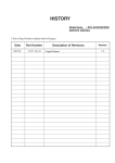
REVISION HISTORY
WAX3
PART NO. : 9-872-959-01
MODEL
KLV-26V300A
KLV-26V300A
KLV-26V300A
KLV-26V300A
KLV-32V300A
KLV-32V300A
KLV-32V300A
KLV-32V300A
KLV-40V300A
KLV-40V300A
KLV-40V300A
KLV-40V300A
KLV-46V300A
KLV-46V300A
KLV-46V300A
KLV-46V300A
NO.
SUFFIX
DATE
SUPP / CORR
1
-01
2007/4
__
DESCRIPTION
1st Issue
CHASSIS
SERVICE MANUAL
MODEL
KLV-26V300A
KLV-26V300A
KLV-26V300A
KLV-26V300A
KLV-32V300A
KLV-32V300A
KLV-32V300A
KLV-32V300A
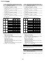
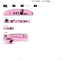
COMMANDER
DEST.
RM-GA008
E
RM-GA008
Middle East
RM-GA008
Ocenia
RM-GA008
Saudi Arabia
RM-GA008
E
RM-GA008
Middle East
RM-GA008
Ocenia
RM-GA008
Saudi Arabia
KLV-26/32V300A
WAX3
MODEL
KLV-40V300A
KLV-40V300A
KLV-40V300A
KLV-40V300A
KLV-46V300A
KLV-46V300A
KLV-46V300A
KLV-46V300A
KLV-40/46V300A
CHASSIS
COMMANDER
DEST.
RM-GA008
E
RM-GA008
Middle East
RM-GA008
Ocenia
RM-GA008
Saudi Arabia
RM-GA008
E
RM-GA008
Middle East
RM-GA008
Ocenia
RM-GA008
Saudi Arabia
RM-GA008
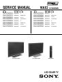
LCD COLOR TV
KLV-26/32/40/46V300A
RM-GA008
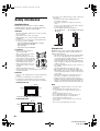
TABLE OF CONTENTS
Section
Title
Page
Section
Page
4. DIAGRAMS
4-1. Block Diagram ........................................................... 39
4-1-1. BG1 (1/3) Block Diagram .............................. 39
4-1-2. BG1 (2/3), H1, H3, H4 and UT Diagrams ..... 40
4-1-3. BG1 (3/3) and U1 Diagrams ........................... 42
4-2. Circuit Boards Location ............................................ 44
4-3. Schematic Diagram Information ............................... 44
4-3-1. BG1 Board — (001) ....................................... 45
4-3-2. BG1 Board — (002) ....................................... 46
4-3-3. BG1 Board — (003) ....................................... 48
4-3-4. BG1 Board — (004) ....................................... 50
4-3-5. BG1 Board — (005) ....................................... 52
4-3-6. BG1 Board — (006) ....................................... 54
4-3-7. BG1 Board — (007) ....................................... 56
4-3-8. BG1 Board — (008) ....................................... 58
4-3-9. BG1 Board — (009) ....................................... 60
4-3-10. G1H, G3, D1 & D2 Boards
Schematic Diagram .................................................... 62
4-3-11. H1 Board Schematic Diagram ...................... 63
4-3-12. H3 Board Schematic Diagram ...................... 64
4-3-13. H4 Board Schematic Diagram ...................... 66
4-3-14. U1 Board Schematic Diagram ...................... 67
4-3-15. UT Board Schematic Diagram ..................... 69
4-4. Voltage Measurement and Waveforms ...................... 71
4-5. Printed Wiring Boards ............................................... 73
4-6. Semiconductors .......................................................... 81
Safety Check Out/Leakage Test ............................................ 3
Caution Handling ...................................................................... 4
Lead free information ............................................................... 4
Self Diagnostic Function ........................................................ 5
1. DISASSEMBLY
1-1. Rear Cover Removal .................................................... 7
1-2. Vesa Bracket Assembly Removal ................................ 9
1-3. H1 Board Removal .................................................... 11
1-4. U1 Board Removal .................................................... 11
1-5. G1H Board Removal ................................................. 12
1-6. G3 and D1 Boards Removal ...................................... 13
1-7. DTT Shield, UT and BG1 Boards Removal ............. 14
1-8. D2 Board Removal .................................................... 15
1-9. Inlet, AC (with noise filter) Removal ........................ 15
1-10. Speaker, H3 and H4 Boards Removal ....................... 17
1-11. LCD Panel Removal .................................................. 18
2. WIRE DRESSING
2-1.
(KLV-26V300A)
2-2.
(KLV-32V300A)
2-3.
(KLV-40V300A)
2-4.
(KLV-46V300A)
Title
...................................................... 20
...................................................... 22
...................................................... 25
...................................................... 29
3. SERVICE ADJUSTMENTS
3-1. How to enter Service Mode ....................................... 34
3-2. Signal Level Adjustment ........................................... 34
3-3. Gamma Adjustment ................................................... 36
3-4. White Balance Adjustment ........................................ 37
3-5. Panel Replacement ..................................................... 38
3-6. Board Replacement .................................................... 38
5. EXPLODED VIEWS
5-1. Rear Cabinet and Stand Assy .................................... 83
5-2. Frame and Cover ........................................................ 85
5-3. Chassis-1 .................................................................... 87
5-4. Chassis-2 .................................................................... 88
5-5. H3, H4 Boards and Speaker ...................................... 90
5-6. Bezel Assy and LCD Panel ........................................ 91
5-7. Accessories and Packing Materials ........................... 92
6. ELECTRICAL PARTS LIST .............................................. 95
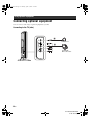
OPERATING INSTRUCTIONS
CAUTION
SAFETY-RELATED COMPONENT WARNING!!
SHORT CIRCUIT THE ANODE OF THE PICTURE TUBE AND THE
ANODE CAP TO THE METAL CHASSIS, CRT SHIELD, OR
CARBON PAINTED ON THE CRT, AFTER REMOVING THE
ANODE.
COMPONENTS IDENTIFIED BY SHADING AND MARK ! ON THE
SCHEMATIC DIAGRAMS, EXPLODED VIEWS AND IN THE
PARTS LIST ARE CRITICAL TO SAFE OPERATION. REPLACE
THESE COMPONENTS WITH SONY PARTS WHOSE PART
NUMBERS APPEAR AS SHOWN IN THIS MANUAL OR IN
SUPPLEMENTS PUBLISHED BY SONY.
–2–
KLV-26/32/40/46V300A
RM-GA008
USE CAUTION WHEN HANDLING THE LCD PANEL
When installing the LCD panel, be sure you are grounded by using a
wrist band.
When installing the LCD panel on the wall, the LCD panel must be
secured using the 4 mounting holes on the rear cover.
1). do not press on the panel or frame edge to avoid the risk of electric
shock.
2). do not scratch or press on the panel with any sharp objects.
3). do not leave the module in high temperatures or in areas of high
humidity for an extended period of time.
4). do not expose the LCD panel to direct sunlight.
5). avoid contact with water. It may cause a short circuit within the
module.
6). disconnect the AC adapter when replacing the backlight (CCFL)
or inverter circuit.
(High voltage occurs at the inverter circuit at 650Vrms)
7). always clean the LCD panel with a soft cloth material.
8). use cere when handling the wires or connectors of the inverter
circuit. Damaging the wires may cause a short.
9). protect the panel from ESD to avoid damaging the electronic circuit
(C-MOS).
LEAKAGE TEST
The AC leakage from any exposed metal part to earth ground and from
all exposed metal parts to any exposed metal part having a return to
chassis, must not exceed 0.5 mA (500 microamperes). Leakage current
can be measured by any one of three methods.
1. A commercial leakage tester, such as the Simpson 229 or RCA
WT-540A. Follow the manufacturers’ instructions to use these
instructions.
2. A battery-operated AC milliampmeter. The Data Precision 245
digital multimeter is suitable for this job.
3. Measuring the voltage drop across a resistor by means of a VOM
or battery-operated AC voltmeter. The “limit” indication is 0.75
V, so analog meters must have an accurate low voltage scale. The
Simpson’s 250 and Sanwa SH-63TRD are examples of passive
VOMs that are suitable. Nearly all battery-operated digital
multimeters that have a 2 VAC range are suitable (see Figure A).
To Exposed Metal
Parts on Set
SAFETY CHECK-OUT
After correcting the original service problem, perform the following
safety checks before releasing the set to the customer:
1. Check the area of your repair for unsoldered or poorly soldered
connections. Check the entire board surface for solder splashes
and bridges.
2. Check the interboard wiring to ensure that no wires are
“pinched” or contact high-wattage resistors.
3. Check that all control knobs, shields, covers, ground straps, and
mounting hardware have been replaced. Be absolutely certain
that you have replaced all the insulators.
4. Look for unauthorized replacement parts, particularly
transistors, that were installed during a previous repair. Point
them out to the customer and recommend their replacement.
5. Look for parts which, though functioning, show obvious signs of
deterioration. Point them out to the customer and recommend
their replacement.
6. Check the line cords for cracks and abrasion. Recommend the
replacement of any such line cord to the customer.
7. Check the antenna terminals, metal trim, “metallized” knobs,
screws, and all other exposed metal parts for AC leakage. Check
leakage as described below.
0.15 µF
1.5 kΩ
AC
Voltmeter
(0.75 V)
Earth Ground
Fig. A. Using an AC voltmeter to check AC leakage.
WARNING!!
SAFETY-RELATED COMPONENT WARNING!!
COMPONENTS IDENTIFIED BY SHADING AND MARK !
ON THE SCHEMATIC DIAGRAMS, EXPLODED VIEWS
AND IN THE PARTS LIST ARE CRITICAL FOR SAFE
OPERATION. REPLACE THESE COMPONENTS WITH
SONY PARTS WHOSE PART NUMBERS APPEAR AS
SHOWN IN THIS MANUAL OR IN SUPPLEMENTS
PUBLISHED BY SONY. CIRCUIT ADJUSTMENTS THAT
ARE CRITICAL FOR SAFE OPERATION ARE IDENTIFIED
IN THIS MANUAL. FOLLOW THESE PROCEDURES
WHENEVER CRITICAL COMPONENTS ARE REPLACED
OR IMPROPER OPERATION IS SUSPECTED.
–3–
KLV-26/32/40/46V300A
RM-GA008
CAUTION
example 1
The circuit boards used in these models have been processed using
Lead Free Solder. The boards are identified by the LF logo located
close to the board designation e.g. U1 etc [ see example ]. The
servicing of these boards requires special precautions to be taken as
outlined below.
It is strongly recommended to use Lead Free Solder material in order to guarantee optimal quality of new solder joints.
Lead Free Solder is available under the following part numbers :
Part number
Diameter
7-640-005-19
0.3mm
Remarks
0.25Kg
7-640-005-20
0.4mm
0.50Kg
7-640-005-21
0.5mm
0.50Kg
7-640-005-22
0.6mm
0.25Kg
7-640-005-23
0.8mm
1.00Kg
7-640-005-24
1.0mm
1.00Kg
7-640-005-25
1.2mm
1.00Kg
7-640-005-26
1.6mm
1.00Kg
Due to the higher melting point of Lead Free Solder the soldering iron tip temperature needs to be set to 370 degrees
centigrade. This requires soldering equipment capable of accurate temperature control coupled with a good heat recovery
characteristics.
For more information on the use of Lead Free Solder, please refer to http://www.sony-training.com
–4–
KLV-26/32/40/46V300A
RM-GA008
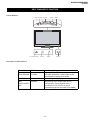
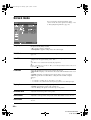
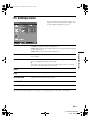
SELF DIAGNOSTIC FUNCTION
Control Buttons
MENU TV/VIDEO
PICTURE OFF/TIMER
VOLUME
STANDBY
CHANNEL
POWER
POWER
SENSOR
Description of LED Indictors
LED
LED Descriptions
Lighting Spec Overviews
Green Lights at power ON.
Power/REC/
Red/Green:
Red Lights during REC. Amber Lights during
Timer REC LED two LEDS
Timer Recording. Aging-failure notice.
STANDBY LED Red: One LED
Lights during standby. Aging-failure notice.
Red Lights during Timer activation. Amber Lights
Timer/Picture
Red/Green:
during Picture OFF. Amber Lights during
OFF/
two LEDS
communication. Communication LED is
Communication
controlled by a main-micro in response
LED
to the blinking/Lighting commands from EMMA.
–5–
KLV-26/32/40/46V300A
RM-GA008
LED display control
STATUS
POWER LED
STANDBY LED
NOTES
Power On
Green Lights
Off
Standby
Off
Red Lights
Aging
Green flashes
Off
Classify the aging time by the green-blinking
patterns (see descriptions below)
Failure
Off
Red flashes
Classify the trouble causes by the number of
Red blinking (see descriptions below)
Microcomputer is in a normal state. (*1)
Microcomputer is in a Sleep state.
(*1) This status is no more described here for various statuses are detected with only three LED.
When safety shutdown occurs, LED display reports the cause by using the Lighting patterns as indicated below. Since there are
various failure items in WAX model. Light blinking is used so that shutdown causes can be judged from the number of blinking times.
The items corresponding to the number of blinking times are indicated as follows
Failure LED Displays
MONITORING ITEMS
NUMBER OF STANDBY LED
(RED) BLINKING TIMES
2
Main power supply voltage error
DC_ALERT 1
3
DC_ALERT 2
4
DC_ALERT 3
5
Backlight error
6
Internal temperature error
7
Audio error
8
Fan error (HFR model only)
9
Digital FE error
10
Trident error
11
*Each of the above blinking is repeated every 2 seconds
LED displays during Aging
Condition
When AGING_TIMER > 0
LED Displays
Green (0.5 Sec) t Off (0.5 sec) t Green (0.5 sec) t Off (0.5 sec)
When AGING_TIMER = 0
Green (3.0 sec) t Off (3.0 sec) t Green (3.0 sec) t Off (3.0 sec)
–6–
KLV-26/32/40/46V300A
RM-GA008
SECTION 1
DISASSEMBLY
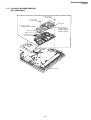
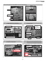
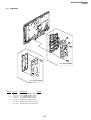
1-1. REAR COVER REMOVAL
(a) KLV-26/32V300A
2 Two screws
(+PSW 5 X 16)
3 Three screws
(+BVTP 3 X 12)
1 Fourteen screws
(+BVTP2 4 X 16)
4 Lift to remove Rear Cover
(b) KLV-40V300A
2 Three screws
(+BVTP 3 X 12)
3 Four screws
(+PSW 5 X 16)
1 Fifteen screws
(BVTP2 4 X 16)
4 Lift to remove Rear Cover
–7–
KLV-26/32/40/46V300A
RM-GA008
(c) KLV-46V300A
2 Three screws
(+BVTP 3 X 12)
3 Four screws
(+PSW 5 X 16)
1 Nineteen screws
(BVTP2 4 X 16)
4 Lift to remove Rear Cover
–8–
KLV-26/32/40/46V300A
RM-GA008
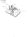
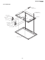
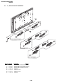
1-2. VESA BRACKET ASSEMBLY REMOVAL
(a) KLV-26/32V300A
KLV-26V300A
3 One screw
(+PSW 5 X 16)
5 One screw
(+PSW 5 X 16)
4 Vesa assy bracket (L)
KLV-32V300A
6 Vesa assy bracket (R)
7 One screw
(+PSW 5 X 16)
8 Vesa assy bracket (L)
0 One screw
(+PSW 5 X 16)
1 Three screws
(+PSW 5 X 16)
9 One screw
(+BVTP 3 X 12)
2 Stand assy
qa Vesa assy bracket (R)
–9–
KLV-26/32/40/46V300A
RM-GA008
(b) KLV-40/46V300A
3 One screw
(+PSW 5 X 16)
7 One screw
(+PSW 5 X 16)
4 Vesa assy bracket (L)
(KLV-40V300A)
8 Vesa assy bracket (R)
(KLV-40V300A)
6 One screw
(+BVST 3 X 8)
5 Vesa assy bracket (L)
(KLV-46V300A)
1 Four screws
(+PSW 5 X 16)
2
9 Vesa assy bracket (R)
(KLV-46V300A)
– 10 –
Stand assy
KLV-26/32/40/46V300A
RM-GA008
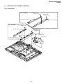
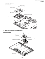
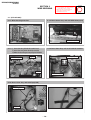
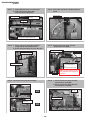
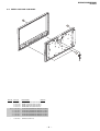
1-3. H1 BOARD REMOVAL
1 Disconnect CN101
Cover, button
H1 board
Multi Button
3 Lift tabs to
remove board
2
1-4. U1 BOARD REMOVAL
3 One screw
(+BVTP 3 X 12)
1 One Connector CN201
2 U1 board
5 One screw (grounding)
(+PSW 3 X 5)
4 Holder side jack (S)
(KLV-26V300A)
Holder side jack (M)
(KLV-32/40V300A)
Holder side jack (L)
(KLV-46V300A)
Side terminal (AG)
– 11 –
KLV-26/32/40/46V300A
RM-GA008
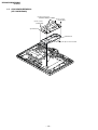
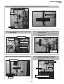
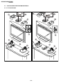
1-5. G1H BOARD REMOVAL
(KLV-26/32V300A)
1 Three Connectors
CN6102, CN6201, CN6202 3 Two screws
(+PSW 3SG)
2 Two screws
(+PSW 3SG)
4 G1H board
6 Bracket G1
5 Lift clips to remove board
– 12 –
KLV-26/32/40/46V300A
RM-GA008
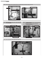
1-6. G3 AND D1 BOARDS REMOVAL
(KLV-40/46V300A)
6 Four screws
(+PSW 3SG)
2 Four screws
(+PSW 3SG)
7 G3 board
1 Three connectors
CN6600, CN6701, CN6707
5 Six connectors
CN6000, CN6202,
CN6203, CN6204,
CN6501, CN6502
4 D1 board
MDF connector
3 Lift tabs and clips
to remove boards
MDF connector
– 13 –
KLV-26/32/40/46V300A
RM-GA008
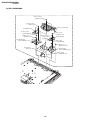
1-7. DTT SHIELD, UT AND BG1 BOARDS REMOVAL
1 Three screws
(+BVST 3 X 8)
3 One screw
(+BVST 3 X 8)
2 Two screws
(SP4-40UNC)
3 Four screws
(+BVST 3 X 8)
4 Shield, DTT (Top) GA
6 Eight screws
(+BVST 3 X 8)
Wire Harness
9 Five screws
(+PSW 3 X 5)
5 Nine connectors
CN2000, CN3008, CN3500,
CN4001, CN4002, CN4003,
CN4500, CN5504, CN8001
7 BG1 and UT boards
qa Five screws
(+PSW 3 X 5)
6 One screw
(+PSW 3 X 5)
8 Harness
with connector (LVCD)
0 Shield, DTT (bottom) GA
– 14 –
KLV-26/32/40/46V300A
RM-GA008
1-8. D2 BOARD REMOVAL
(KLV-46V300A)
4 Four screws
(+PSW 3SG)
3 Two connectors
CN6900, CN6950
5 D2 board
MDF connector
2 Lift clips to remove board
1 Bracket D2
MDF connector
1-9. INLET, AC (WITH NOISE FILTER) REMOVAL
1 Two screws
(+BVTP2 4 X 16)
(a) KLV-26/32V300A
2 Cover, under (M)
3 Two screws
(+PSW M4 X 8)
4 Two screws
(+KTT 3 X 10 (S TYPE))
6 One screw
(PSW M4 X 8)
5 LCD bracket bottom (26/32)
7 AC inlet
Bezel assy
– 15 –
KLV-26/32/40/46V300A
RM-GA008
(b) KLV-40/46V300A
1 Two screws
(BVTP2 4 X 16)
5 Two screws
(+PSW 5 X 12)
2 Cover, under (M)
7 Stand holder
8 Two screws
(+PSW M5 X 8)
q; One screw
(BVTP2 4 X 16)
4 Two screws
(+PSW 5 X 12)
qf Two screws
(+KTT 3 X 10
(S TYPE))
qs LCD bracket,
bottom (40/46) L assy
6 Stand holder
8 Two screws
(+PSW M5 X 8)
7 One screw
(BVTP2 4 X 16)
3 Inlet, AC
(with noise filter)
9 LCD bracket,
bottom (40/46) R assy
qd One screw
(+PSW M4 X 8)
– 16 –
KLV-26/32/40/46V300A
RM-GA008
1-10. SPEAKER, H3 and H4 BOARDS REMOVAL
5 Loudspeaker
(13 X 7 cm)
6 Loudspeaker
(13 X 7 cm)
KLV-46V300A
5 Loudspeaker
(5.5 X 15.5 cm)
6 Loudspeaker
(5.5 X 15.5 cm)
KLV-40V300A
5 Loudspeaker
(4.2 X 15 cm)
6 Loudspeaker
(4.2 X 15 cm)
2 H3 board
KLV-26V/32V300A
1 One connector CN301
3 One connector CN401
4 H4 board
– 17 –
KLV-26/32/40/46V300A
RM-GA008
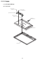
1-11. LCD PANEL REMOVAL
(a) KLV-26/32V300A
1 Two screws
(+BVTP2 4 X 16)
2 Two screws
(+PSW M4 X 8)
3 LCD bracket top (26/32)
4 Three screws
(+BVTP2 4 X 16)
5 Harness
with connector
6 LCD panel
Bezel assy
– 18 –
KLV-26/32/40/46V300A
RM-GA008
(b) KLV-40/46V300A
5 Harness
with connector
4 Two screws
(BVTP2 4 X 16)
2 Two screws
(+PSW M5 X 8)
LCD panel
1 One screw
(BVTP2 4 X 16)
3 Frame top
2 Two screws
(+PSW M5 X 8)
1 One screw
(BVTP2 4 X 16)
3 Frame top
Bezel assy
– 19 –
KLV-26/32/40/46V300A
RM-GA008
SECTION 2
WIRE DRESSING
CAUTION:
1. Do not overpull the wire during dressing
_> avoid disconnection of wires.
2. Make sure wires are kept away from
sharp edges, heatsinks & other
hight-temperature parts.
Legend:
Hook
2-1. (KLV-26V300A)
2-1-1. Wire dressing overview
2-1-2. Dress Conn Assy 14P with Slide Clamp (2X)
Connector Assy 14P
2-1-4. Dress Conn Assy 14P & 13P with G1 bracket's
2-1-3. i) Dress Conn Assy 14P with G1 bracket's hook
ii) Dress Conn Assy 14P & 13P with pin lead (2X)
iii) Make sure Conn Assy are keep away from heatsink
Connector Assy 13P
Pin lead
Connector Assy 14P
Heat Sink
Connector Assy 14P
Connector Assy 13P
2-1-5. Dress Conn Assy 20P with Tape(LCD)
Connector Assy 20P
Tape(LCD)
– 20 –
KLV-26/32/40/46V300A
RM-GA008
2-1-6. Dress Conn Assy 13P, 14P & 20P with
Clamp Edge (M)
2-1-7. Dress Conn Assy 20P (H1 wire) with
Slide Clamp
Connector Assy 13P
Connector assy 20P
(H1 wire)
Clamp Edge(M)
Connector Assy 14P
Connector Assy 20P
2-1-8. i) Apply sheet (Core) C on LCD panel
ii) Dress Conn Assy 20P with Tape (LCD)
2-1-9. Dress SP Conn Assy 4P with FG Clamp to
Top DTT shield
Make sure wire
is not trapped
when install Top
DTT to bottom
DTT shield
Tape(LCD)
SP Connector
Assy 4P
Sheet(Core)C
Connector assy 20P
(H3 wire)
FG Clamp
End of UL tape as
reference line
Make sure Connector assy 20P
is not tight when apply Tape LCD.
2-1-10. Dress SP Conn Assy 4P with
Slide Clamp (2X)
Screw 3X8
2-1-11. i) Dress SP Conn Assy 4P with
G1 bracket's hook (2X)
ii) Dress Conn Assy 20P with
G1 bracket's hook (4X)
Connector Assy 20P
(H4 wire)
Caution : Pull away from
screw boss
Screw boss
Caution : Pull away from
screw boss
– 21 –
Screw boss
KLV-26/32/40/46V300A
RM-GA008
2-1-12. Dress Conn Assy 20P and Conn Assy 4P
underneath AC filter inlet
2-1-13. i) Dress AC inlet wire with G1 bracket's hook
ii) Make sure AC inlet wire is keep away from
heatsink
Connector Assy 20P
(H4 wire)
AC inlet wire
Heat Sink
SP Connector Assy 4P
2-2. (KLV-32V300A)
2-1-14. i) Dress Conn Assy 20P with Side Jade
bracket's hook (2X)
ii) Screw Conn Assy 1P to the direction
2-2-1. Wire Dressing overview
Connector Assy 1P
Connector Assy 20P
2-2-2. i) Dress Conn Assy 14P with G1 bracket's slit
ii) Dress Conn Assy 14P&13P with G1 bracket's hook (3X) & pin lead (2X)
iii) Make sure Conn Assy 14P & 13P are keep away from heat sink
Connector Assy 13P
Pin lead
Connector Assy 14P
Pin lead
Connector Assy 14P
Heat Sink
Connector Assy 13P
– 22 –
KLV-26/32/40/46V300A
RM-GA008
2-2-3. Dress LVDS cable with Sheet(Core)C and put under Connector assy 13P & 14P.
Connector Assy 13P & 14P
LVDS cable
Put LVDS cable straight
Sheet (Core)C
2-2-4. Dress Connector Assy 13P, 14P & 20P with
Clamp Edge(M)
2-2-5. i) Dress Connector Assy 11P & 12P at G3
bracket's hook.
ii) Dress Connector Assy 11P & 12P with
Sheet(Core)C.
Connector Assy 13P
Sheet (Core)C
Clamp Edge(M)
Connector Assy 14P
Connector Assy 20P
Make sure do not
over pull wire when
apply sheet
Connector Assy 13P & 14P
2-2-6. Dress Connector Assy 20P with Tape(LCD)
2-2-7. i) Apply Sheet(Core)C on LCD panel
ii) Dress Connector Assy 20P with
Tape(LCD)
Connector Assy 20P
Connector assy 20P
Sheet(Core)C
Tape(LCD)
Make sure Connector assy 20P
is not tight when apply Tape LCD.
Tape(LCD)
– 23 –
KLV-26/32/40/46V300A
RM-GA008
2-2-8. Dress Connector Assy 20P(H1 wire) with Tape(LCD) & Slide Clamp.
Connector assy 20P
(H1 wire)
Tape(LCD)
2-2-9. Dress SP Connector Assy 4P with
FG Clamp to Top DTT shield
2-2-10. Dress SP Connector assy 4P with slide
clamp (2X)
Make sure wire is
not trapped
when install Top
DTT to bottom DTT
shield
SP Connector
Assy 4P
FG Clamp
Caution : Pull away from
screw boss
End of UL tape as
reference line
Screw 3X8
Screw boss
2-2-11. i) Dress Connector Assy 20P (H4 wire) & SP Connector Assy 4P with G1 bracket's hook (4X)
ii) Apply Sheet(Core)C on LCD panel
iii) Dress Connector Assy 20P (H4 wire) with Tape(LCD)
Tape(LCD)
Connector Assy 20P
(H4 wire)
Sheet(Core) C
SP Connector Assy 4P
Screw boss
Make sure Connector assy 20P(H4 wire)
is not tight when apply Tape LCD.
Caution : Pull away from screw boss
– 24 –
KLV-26/32/40/46V300A
RM-GA008
2-2-12. Dress Connector assy 20P and SP Connector
Assy 4P underneath AC filter inlet
2-2-13. i) Dress AC inlet wire with G1 bracket's hook
ii) Make sure AC inlet wire is keey away from
from heat sink
AC inlet wire
SP Connector Assy 4P
Heat Sink
Connector Assy 20P
(H4 wire)
2-2-14. i) Dress Connector Assy 20P with
Side Jack bracket's hook
ii) Screw Connector Assy 1P to the direction
2-2-15. Screw Connector Assy 1P to the direction
Connector Assy 1P
Connector Assy 20P
Connector Assy 1P
2-3. (KLV-40V300A)
2-3-1. Wire dressing overview.
– 25 –
KLV-26/32/40/46V300A
RM-GA008
2-3-2. Dress LVDS cable with Sheet(Core)C and put under Connector assy 12 & 11P
Put LVDS cable straight
LVDS cable
Connector Assy 12P & 11P
Sheet (Core)C
2-3-3. Dress Connector Assy 11P, 12P & 20P with
Clamp Edge(M)
2-3-4. i) Dress Connector Assy 11P & 12P at G3
bracket's hook
ii) Dress Connector Assy 11P & 12P
with Sheet(Core)C
Connector Assy 12P
Sheet (Core)C
Clamp Edge(M)
Connector Assy 11P
Connector Assy 11P
Connector Assy 20P
Connector Assy 12P
2-3-5. Dress Connector Assy 20P with Tape(LCD)
Connector Assy 20P
Tape(LCD)
– 26 –
KLV-26/32/40/46V300A
RM-GA008
2-3-6. Dress Connector Assy 20P(H1 wire) with Tape(LCD)(2X)
Tape(LCD)
Connector assy 20P
(H1 wire)
Tape(LCD)
2-3-7. i) Apply Sheet(Core)C on LCD panel
ii) Dress Connector Assy 20P with Tape(LCD)
2-3-8. Dress SP Connector Assy 4P with FG Clamp
to Top DTT shield
SP Connector Assy 4P
Connector assy 20P
Tape(LCD)
Make sure wire is
not trapped
when install Top
DTT to bottom DTT
shield
Follow panel's marking
Sheet(Core)C
End of UL tape as
reference line
Make sure Connector assy 20P
is not tight when apply Tape LCD.
Screw 3X8
FG Clamp
2-3-9. Dress SP Connector assy 4P with slide
clamp(3X) and Tape(LCD)
2-3-10. Dress Connector Assy 20P (H4 wire) &
SP Connector Assy 4P with G3 bracket's
hook(2X), Slide Clamp(3X) & Tape(LCD)
Tape(LCD)
Connector Assy 20P
(H4 wire)
Screw boss
Tape(LCD)
Caution : Pull away from
screw boss
Caution :
Pull away
from
screw boss
Screw boss
– 27 –
SP Connector Assy 4P
KLV-26/32/40/46V300A
RM-GA008
2-3-11. i) Apply Sheet(Core)C on LCD panel
ii) Dress Connector Assy 20P
(H4 wire) with Tape(LCD)
2-3-12. Dress AC inlet wire with G3 bracket's
hook
AC inlet wire
Connector Assy 20P
(H4 wire)
Sheet(Core) C
Tape(LCD)
Make sure Connector assy 20P(H4 wire)
is not tight when apply Tape LCD.
2-3-13. i) Dress Connector Assy 20P with Slide
Clamp & Side Jack bracket's hook
ii) Screw Connector Assy 1P to the direction
2-3-14. Dress Connector Assy 2P with
G3 bracket's hook(2X)
Connector Assy 2P
Connector Assy 20P
60+/-5mm
Make sure Connector
Assy 2P with black UL
tape
is inserted to panel side.
Connector Assy 1P
OK
2-3-15. Connector Assy 2P NG example
Caution :
Make sure Connector Assy 2P is
fully complete insert to panel &
D1 board
2-2-16 i) Dress Connector Assy 7P with
G3 bracket's hook(5X)
ii) Dress Connector Assy 8P with
G3 bracket's hook(2X)
Connector
Assy 8P
NG
Over pull to bottom
Connector Assy 7P
Over pull to right
(Rear view)
NG
– 28 –
KLV-26/32/40/46V300A
RM-GA008
2-4. (KLV-46V300A)
2-4-1. Wire dressing overview
2-4-2. Dress LVDS cable with Sheet(Core)C and put under Connector assy 13P & 3P
LVDS cable
Connector Assy 13P
Put LVDS cable straight
Connector Assy 3P
Sheet (Core)C
2-4-3. Dress Connector Assy 11P, 12P & 20P with
Clamp Edge(M)
2-4-4. i) Dress Connector Assy 11P & 12P at
G3 bracket's hook
ii) Dress Connector Assy 11P & 12P with
Sheet(Core)C
Connector Assy 12P
Connector Assy 11P
Clamp Edge(M)
Connector Assy 11P
Connector Assy 20P
Connector Assy 12P
– 29 –
Sheet (Core)C
KLV-26/32/40/46V300A
RM-GA008
2-4-5. Dress Connector Assy 20P with Tape(LCD)
2-4-6. Dress Connector Assy 20P(H1 wire) with
Tape(LCD)(2X)
Connector Assy 20P
Tape(LCD)
Connector assy 20P
(H1 wire)
Tape(LCD)
Tape(LCD)
2-4-7. i) Apply Sheet(Core)C on LCD panel
ii) Dress Connector Assy 20P with Tape(LCD)
2-4-8. Dress SP Connector Assy 4P with
FG Clamp to Top DTT shield
Connector assy 20P
Make sure wire is
not trapped
when install Top
DTT to bottom
DTT shield
Tape(LCD)
SP Connector Assy 4P
Sheet(Core)C
FG Clamp
End of UL tape as
reference line
Make sure Connector assy 20P
is not tight when apply Tape LCD.
Screw 3X8
2-4-9. Dress SP Connector assy 4P with slide
clamp(3X) and Tape(LCD)
2-4-10. Dress Connector Assy 20P (H4 wire)
& SP Connector Assy 4P with Slide
Clamp(3X) & Tape(LCD)(2X)
Tape(LCD)
Connector Assy 20P
(H4 wire)
SP Connector Assy 4P
Caution :
Pull away
from
screw
boss
Tape(LCD)
Screw boss
Caution : Pull away from
screw boss
Screw boss
– 30 –
KLV-26/32/40/46V300A
RM-GA008
2-4-11. i) Apply Sheet(Core)C on LCD panel
ii) Dress Connector Assy 20P (H4 wire)
with Tape(LCD)
2-4-12. Dress AC inlet wire with G3 board's hook
AC inlet wire
Connector Assy 20P
(H4 wire)
Sheet(Core) C
Tape(LCD)
Make sure Connector assy 20P(H4 wire)
is not tight when apply Tape LCD.
2-4-13. i) Dress Connector Assy 20P with Slide
Clamp & Side Jack bracket's hook
ii) Screw Connector Assy 1P to the direction
2-4-14. Dress Connector Assy 2P with
G3 bracket's hook(2X)
60+/-5mm
Connector Assy 20P
Connector Assy 2P
OK
Connector Assy 1P
Make sure Connector Assy 2P with black
UL tape is inserted to panel side.
Caution :
Make sure Connector Assy 2P is fully complete
insert to panel & D1 board
2-4-15. Connector Assy 2P NG example
Over pull to right
(Rear view)
Over pull to bottom
NG
NG
– 31 –
KLV-26/32/40/46V300A
RM-GA008
2-4-16. Dress Connector Assy 2P with D2 bracket's hook(3X)
Connector Assy 2P NG example
Over pull to left
(Rear view)
OK
50+/-5mm
NG
Connector Assy 2P
Make sure Connector Assy 2P with black
UL tape is inserted to panel side.
Over pull to bottom
NG
Caution :
Make sure Connector Assy 2P is fully complete insert to panel & D1 board
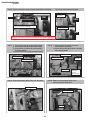
2-4-17. i) Dress Connector Assy 7P with G3 bracket's hook(5X)
ii) Dress Connector Assy 8P with G3 bracket's hook(2X)
iii) Dress Connector assy 3P with G3 board's hook(2X) &
G3 bracket's hook(1X)
iv) Dress Connector Assy 13P with G3 bracket's hook(1X)
2-4-18. i) Dress Connector Assy 13P with
D2 bracket's hook(1X)
ii) Dress Connector Assy 3P & 13P with
Sheet(Core)C(4X)
Connector Assy 8P
Connector Assy 8P
Connector Assy 7P
Connector Assy 13P
Connector
Assy 3P
Connector Assy 13P
Sheet(Core)C
Sheet(Core)C
Connector Assy 3P
2-4-19. Screw Connector Assy 1P to the direction
Dress
Connector
assy 3P
above this line
2-4-20. Make sure Connector Assy 1P is
keey away from heat sink
Connector Assy 1P
Connector Assy 1P
Heat Sink
– 32 –
KLV-26/32/40/46V300A
RM-GA008
Please be careful of the following when perform
servicing.
1. Please protect caution items.
Parts that considered as caution or critical item when
servicing are shown by critical label or seal on cabinet,
chasis, parts etc.
Please make sure to protect these caution notes and
Intruction Manual.
4. On a safety as before, attaching parts and leading wiring
by using insulated material such as tube and tape, there
are also parts that taken from printed wiring boards.
Therefore when doing the internal wiring by leading or using
clamper, make sure wires are kept away from sharp edges,
heat sink and high temperature or high pressure parts.
2. Beware with electric shock
Live chassis can caused electric shock because its
connected to the ac power line. Therefore, please use
isolation transformer and gloves when changing parts or
remove plug. Please remember that there is high voltage
during servicing.
5. Safety after sevicing
For safety, please check whether removed screws, parts
and wires are same as before. And check there is no
deterioration of seviced parts. Please make an insulation
checking between plug and external metal parts.
3. Use specification parts.
Some parts has its characteristic such as fire retardancy
and voltage value specification. Therefore, please use the
same specification to replace parts. Parts identified by
shading and critical mark on the schematic diagrams,
exploded views, and in the part list are critical for safe
operation. Replace these parts with Sony parts whose part
numbers appear as shown in this manual or in supplements
published by Sony. Circuit adjustments that are critical for
safe operation are identified in this manual. Follow these
procedures whenever critical parts are replaced or improper
operation is suspected.
6. Do not fix internal of power supply board/inverter.
For safety, please do not perform service at the power
supply board or inverter.
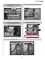
TO INSERT THE MDF CONNECTOR
The connector might not be properly locked when only pressed from the middle.
Be sure to press both sides to confirm it is property locked/
1 Press the middle
part of the connector
to insert till it locks.
2 Press the right
side to confirm it is
locked.
– 33 –
3 Press the left
side to confirm it is
locked.
KLV-26/32/40/46V300A
RM-GA008
SECTION 3 SERVICE ADJUSTMENTS
3-1.
3. LED lighting pattern during aging
How to enter Service Mode
In case that AGING_TIMER > 0
3-1-1.
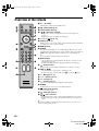
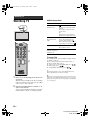
Service adjustments to this model can be
performed using the supplied Remote
Commander RM-GA008
Green (0.5s) ➔ off (0.5s) ➔ Green (0.5s) ➔ off (0.5s)
Notes: Green (Power LED is ON/OFF)
1. Turn on the power to the TV set and enter into the stand-by mode.
2. Press the following sequence of buttons on the Remote
Commander.
+ i+ + 5 + – +
(STBY)
(ON SCREEN
DISPLAY)
(CH 5)
(VOLUME –)
(POWER)
In case that AGING_TIMER = 0
Green (3.0s) ➔ off (3.0s) ➔ Green (3.0s) ➔ off (3.0s)
Notes: Green (Power LED is ON/OFF)
Note:
If set has been put on surface down, brightness surface irregularity is
caused by static electricity. If so be, turn set over or keep it upright
more than 30 seconds. As surface irregularity is vanished away, then
check the set.
3-2.
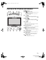
3. The following menu will then appear on the screen.
DC_DET
DC_ALERT1
DC_ALERT2
DC_ALERT3
BACKLIGHT
TEMPERATURE
AUDIO
DFE
B-ENGINE
HFR
Signal Level Adjustment
3-2-1.
0
0
0
0
0
0
0
0
0
0
Set up of AD calibration 1 adjustment for
terrestrial analog
The following adjustments are done via ECS.
1. Send ECS_ADJUST_LEVEL_SETTING_INIT command
2. Ensure noise reduction NR=3 (high),
hreg_P4_cvd2_85 [2:0] = 0
ADJ_COLOR_PAL = 4 (for GA)
3. Set up correspond value to resistors below
4. Move to the relevant command using the up or down arrow buttons
on the remote commander.
5. Press the right arrow button to enter into the required menu item.
6. Press the ‘Menu’ button on the remote commander to quit the
service mode when all adjustments have been completed.
Adjustment for RF (GAmodel_Y75%,C75%_w/oSetup)
Note:
– After carrying out the service adjustments, to prevent the customer
accessing the ‘Service Menu’ switch the TV set OFF and then
ON.
Screen size
V26" V32" V40" V46" D32" D40" D46"
TAGET_Y_RF
160
160
160
160
160
160
160
TCD3_CONT_PAL_RF 128
128
128
128
128
128
128
TCD3_SAT_PAL_RF
128
128
128
128
128
128
128
TCD3_HUE_PAL_RF
128
128
128
128
128
128
128
Adjustment for Video (GAmodel_Y75%,C75%w/oSetup)
3-1-2.
Aging
1. Aging setting
i. Set no signal and monitor as aging mode.
2. Aging condition
i. Aging condition before white balance adjustment is as
follows;
Supply Voltage : Rating
Time
: 20 minutes or over
(AGING_TIMER registor setting)
Ambient temp : 22 ~ 28°C
Brightness
: Brightness is set by aging mode
Input
: Set no signal except digital and analog RF
(video/component/PC)
Screen size
V26" V32" V40" V46" D32" D40" D46"
TAGET_Y_V
160
160
160
160
160
160
160
TCD3_CONT_*_V
128
128
128
128
128
128
128
TCD3_SAT_*_V
128
128
128
128
128
128
128
TCD3_HUE_*_V
128
128
128
128
128
128
128
Note for Input Signal [GA model] (PAL) included black and white,
75% Y and 75% C, without set up
– 34 –
KLV-26/32/40/46V300A
RM-GA008
3-2-2.
Y signal calibration 1 adjustment for
terrestrial analog
3-2-5.
1. Input color bar via terrestrial analog
2. Send ECS command: ADJUST_TCD3_CONT_RF. Wait success
receive data.
3. Read value of S-REG_APL_LUMA via ECS. Then confirm that
the value is within the range of below table.
4. Read value of S-REG_TCD3_CONTRAST via ECS.
1. Input 75% color bar signal via Video1 input.
2. Send ECS command: ADJUST_TCD3_CONT_V. Wait success
receive data.
3. Read value of S-REG: APL_LUMA via ECS and confirm that
the values are in corresponding range of below table.
Note :
Y signal calibration adjustment target of terrestrial analog input.
AD-AdjustRF Spec.
Spec.
Reference register name
SREG_TARGET
_Y_RF±2
S-REG_APL_LUMA
3-2-3.
1. Send command: ADJUST_TCD3_HUE_RF from ECS. Wait
success receive data.
2. Read S-REG_AVE_VAL_B_AREA0 via ECS
(READ_AREA = 0)
3. Read S-REG_AVE_VAL_B_AREA6 via ECS
(READ_AREA = 6)
4. Confirm that 8 bits of MSB of 2) and 3) are in the range of below
table.
Specification
SREG_AVE_VAL_B
_AREA* difference
±2
5. Read S-REG: TCD3_SATURATION via ECS.
6. Restore the original value SREG_NR = 4 (high)
7. Send ECS command: ADJUST_LEVEL_SETTING_CLR blue
level only.
As for READ_AREA number and position.
0
1
2
3
4
5
6
Spec.
Reference register name
S-REG_APL_LUMA
SREG_TARGET
_Y_V±2
Note: When both S video and video (CVBS) are connected, select
video (CVBS) by setting SREG_S_INPUT <0> = 0
Change back this data after adjustment
Note for Input signal
[GA model] (PAL, NTSC)
Included black and white, 75% Y and 75% C, without set up.
3-2-6.
C signal of video Input/HUE calibration 1
adjustment (PAL for AEP, GA)
1. Input 75% color bar signal via video1 input.
2. Send command: ECS_ADJUST_TCD3_HUE_V via ECS. Wait
success receive data
3. Read S-REG_AVE_VAL_B_AREA0 via ECS
4. Read S-REG_AVE_VAL_B_AREA6 via ECS
5. Confirm that 8 bits of MSB of 3) and 4) are in the range of below
table
Reference item
Specification
SREG_AVE_VAL_B
_AREA* difference
±2
6. Read S-REG_AVE_VAL_B_AREA2 via ECS (GA-NTSC)
7. Read S-REG_AVE_VAL_B_AREA4 via ECS
8. Confirm that 8 bits of MSB of 6) and 7) are in the range of below
table (GA-NTSC)
7
Note:
If it is adjusted other signal (other color system), it needs restoring the
value for changed SREGS and sending the ADJUST_LEVEL_
SETTING_CLR before signal changing.
3-2-4.
AD-AdjustVideo Spec.
4. Read value of S-REG: TCD3_CONTRAST via ECS. Set offset
of V input for S input setting by u-com internal.
C signal of terrestrial analog Input/HUE
calibration 1 adjustment
Reference item
Y signal calibration-1 adjustment of video
input. (PAL for AEP, GA)
Reference item
Specification
SREG_AVE_VAL_B
_AREA* difference
±2
9. Read S-REG_TCD3_SATURATION via ECS
10. Read S-REG_TCD3_HUE via ECS. (GA-NTSC)
As for READ_AREA number and position
Step before AD calibration-1 adjustment of
video Input
1. Send ECS command: ADJUST_LEVEL_SETTING_INIT. Wait
success recieve data
2. Set SREG_NR=1 (low), hreg_P4_cvd2_85 [2:0] = 0
SREG_ADJ_COLOR_PAL = 4 (for GA)
3. Set up correspond value to following resistors
SREG_TARGET_Y_V
[For AEP, GA (Video-PAL)]
SREG_TCD3_CONT_PAL_V
SREG_TCD3_SAT_PAL_V
SREG_TCD3_HUE_PAL_V
– 35 –
0
1
2
3
4
5
6
7
KLV-26/32/40/46V300A
RM-GA008
3-2-7.
Restoring original setting
3-3-3.
1. Restore the original value SREG_NR = 2 (mid)
2. Send ECS command: ADJUST_LEVEL_SETTING_CLR Blue
level only. S Input set offset of V input.
3-2-8.
Setup before adjustment Y signal of video
Input. (NTSC for GA)
1. Send ECS command: ADJUST_LEVEL_SETTING_INIT wait
success Receive Data.
2. Set SREG_NR = 1 (low), hreg_P4_CVD2_85 [2:0] = 0
SREG_ADJ_COLOR_PAL = 1 (for GA)
3. Set up correspond value to following resistors.
SREG_TARGET_Y_V (for GA NTSC)
[FOR GA (Video-NTSC)
SREG_TCD3_CONT_OFST_V
SREG_TCD3_SAT_OFST_V
SREG_TCD3_HUE_OFST_V
3-2-9.
1. Set up SREG_TEST_G_LEVEL =102
2. Measure brightness B
3. Set up SREG_MEASURE_GAM_01 =
(brightness B/brightness A)* 10000
4. Send the command: Gamma_Tbl_search_1
3-3-4.
3-3-5.
Note for process of (5)
SREG_G_GAM
_IDX_OFST
calculation valueA
1. Input 75% color bar signal via video1 input
2. Implement 2) to 10) of item 3-2-6
offset value C
1. Restore the original value SREG_NR = 2 (mid)
2. Send ECS command: ADJUST_LEVEL_SETTING_CLR
Gamma adjustment
20inchs
temp75_temp
<11500
2
1
26inchs
temp75_temp
<11500
11500=<temp75 12100=<temp
_temp<12100 75_temp
2
1
32inchs
temp75_temp
<11500
11500=<temp75 12100=<temp
_temp<12100 75_temp
2
1
40inchs
temp75_temp
<11500
11500=<temp75 12100=<temp
_temp<12100 75_temp
2
1
46inchs
temp75_temp
<10900
10900=<temp75 11250=<temp75 12200=<temp75
_temp<11250 _temp<12200 _temp
3
2
The following adjustments are done via ECS
Note:
Before Gamma adjustment can begin the set needs to do as follows
Aging time : 20 minutes since it is cooled.
Ambient temperature : 22 Degree - 28 Degree.
1. Set: SREG_BRIGHT = 50
2. i) Set up SREG_COL_MTRX_IDX_OFF = 4
ii) Set up SREG_COL_MTRX_IDX_L = 4
iii) Set up SREG_COL_MTRX_IDX_M = 4
iv) Set up SREG_COL_MTRX_IDX_H = 4
3. Set up SREG_G_GAM_IDX_OFST = 15
4. Wait for setting of 3)
3-3-2.
[Calculation]
SREG_G_GAM
_IDX_OFST = A - C - D
Value C: offset value
(relationship value &
temp75_temp, see underbelow)
Value D: offset value for Bright.
SREG_G_GAM
_IDX_OFST
Set to SREG
3-2-11. Restoring original setting
Set up adjustment mode
Set the register
1. Calculate SREG_G_GAM_IDX_OFST as below formula and
table
3-2-10. C signal of video Input/HUE calibration 1
adjustment. (NTSC for GA)
3-3-1.
Set up Trident internal SG and measure
brightness
1. Set up SREG_TEST_G_LEVEL = 153
2. Measure brightness C
3. Set up SREG_MEASURE_GAM_02 =
(brightness C/brightness A)* 10000
4. Send command : Gamma_Tbl search_2
5. Wait for calculation process in µCOM
(SREG_G_GAM_IDX_OFST)
Y signal calibration-1 adjustment of video
input. (NTSC for GA)
1. Input 75% color bar signal via video1 input
2. Implement 2), 3) and 4) of item 3-2-5
3-3.
Set up Trident internal SG and measure
brightness
11500=<temp75 12100=<temp
_temp<12100 75_temp
0
0
0
0
1
0
2. Set SREG_G_GAM_IDX_OFST as the value of 1)
Reference: If the set does not power off, it can be separated Gamma
and WB adjustment. In this case, please restore the setting as follows;
1. Set SREG_COL_MTRX_IDX_OFF = 3
SREG_COL_MTRX_IDX_L = 3
SREG_COL_MTRX_IDX_M = 3
SREG_COL_MTRX_IDX_H = 3
2. Send ECS command: CSC_BYPASS_INIT_CLR
Set up Trident internal SG and measure
brightness
1. Set up SREG_TEST_G_LEVEL = 204
2. Measure brightness A
– 36 –
KLV-26/32/40/46V300A
RM-GA008
3-4.
11. Set SREG_WB_GAM_R06-07 and SREG_WB_GAM_B06 ~ 07
as follows;
[When ADJ data SREG_WB_GAM_B05 > 154]
[ADJ data SREG_WB_GAM_R05 > 128]
SREG_WB_GAM_R (B) 06 = SREG_WB_GAM_R (B) 05
- [SREG_WB_GAM_R (B) 05 - SREG_WB_GAM_R (B) 04] /2
SREG_WB_GAM_R (B) 07 = 128
[ADJ data SREG_WB_GAM_R05 = < 128]
SREG_WB_GAM_B06 = SREG_WB_GAM_B05
- [SREG_WB_GAM_B05-SREG_WB_GAM_B04] /2
SREG_WB_GAM_B07 = 128
SREG_WB_GAM_R06 = SREG_WB_GAM_R07
= SREG_WB_GAM_R05
[When ADJ data SREG_WB_GAM_B05 = < 154]
SREG_WB_GAM_R (B) 06 = SREG_WB_GAM_R (B) 07
= SREG_WB_GAM_R (B)_05
White balance adjustment
Adjust the following items via ECS
3-4-1.
i)
ii)
iii)
iv)
Initial setting for white balance
Set up SREG_COL_MTRX_IDX_OFF = 3
Set up SREG_COL_MTRX_IDX_L = 3
Set up SREG_COL_MTRX_IDX_M = 3
Set up SREG_COL_MTRX_IDX_H = 3
3-4-2.
White balance adjustment when color
temperature is “cool”
1. Set up SREG_COLOR_TEMP = 0 (Cool)
Reference: To separate GAMMA & WB adjustment, operate the
following initial setting before WB adjustment
- Send ECS command: CSC_BYPASS_INIT_SET
3-4-3.
White balance adjustment when color
temperature is “Neutral”
2. Set SREG_TEST_G_LEVEL = 204 (80 IRE)
3. Adjust values of SREG_WB_GAM_R (B) 05 to be the chroma
in below table
4. Set SREG_TEST_G_LEVEL = 128 (50 IRE)
5. Adjust values of SREG_WB_GAM_R (B) 04 to be the chroma
in below table
6. Set SREG_TEST_G_LEVEL = 76 (30 IRE)
7. Adjust values of SREG_WB_GAM_R (B) 03 to be the chroma
in below table
8. Set SREG_TEST_G_LEVEL = 51 (20 IRE)
9. Adjust values of SREG_WB_GAM_R (B) 02 to be chroma in
below table
1. Set up SREG_COLOR_TEMP = 1 (Neutral)
2. Set SREG_TEST_G_LEVEL = 204 (80 IRE)
3. Adjust values of SREG_WB_R (B) 05_OFST to be the chroma
in the below table
4. Set SREG_TEST_G_LEVEL = 128 (50 IRE)
5. Adjust values of SREG_WB_R (B) 04_OFST to be the chroma
in the below table
6. Set SREG_TEST_G_LEVEL = 76 (30 IRE)
7. Adjust values of SREG_WB_R (B) 03_OFST to be the chroma
in the below table
8. Set SREG_TEST_G_LEVEL = 51 (20 IRE)
9. Adjust values of SREG_WB_R (B) 02_OFST to be chroma in
the below table
The target of White balance adjustment when color temperature is “Cool”.
The target of White balance adjustment when color temperature is “Neutral”.
Internal SREG SPEC
signal _Test_G
(IRE) _LEVEL
20
51
0.5->0.7->1JND
.0014->.00196->.0028
30
76
0.5->0.7->1JND
.0014->.00196->.0028
50
128
0.5->0.7JND
0.0014->0.00196
80
204
0.3->0.5JND
0.0008->0.0014
x
y
u'
v'
x
y
u'
v'
x
y
u'
v'
x
y
u'
v'
x
y
u'
v'
target
26"
32"
40"
46"
0.2719
0.2788
0.1875
0.4325
0.2751
0.2732
0.1921
0.4292
0.2728
0.2688
0.1921
0.4259
0.2748
0.2758
0.1908
0.4309
0.2739
0.2779
0.1893
0.4322
0.2724
0.2662
0.1929
0.4241
0.2726
0.2705
0.1913
0.4270
0.2754
0.2754
0.1914
0.4308
0.2745
0.2795
0.1891
0.4333
0.2729
0.2670
0.1929
0.4247
0.2723
0.2702
0.1912
0.4268
0.2758
0.2759
0.1916
0.4312
0.2734
0.2741
0.1904
0.4296
0.2743
0.2717
0.1921
0.4281
0.2730
0.2719
0.1910
0.4281
0.2744
0.2757
0.1906
0.4308
Internal SREG SPEC
signal _Test_G
(IRE) _LEVEL
20
51
0.5->0.7->1JND
.0014->.00196->.0028
30
76
0.5->0.7->1JND
.0014->.00196->.0028
50
128
0.5->0.7JND
0.0014->0.00196
80
204
0.3->0.5JND
0.0008->0.0014
10. Set SREG_WB_GAM_R( B) 01 as follows;
SREG_WB_GAM_R (B) 01
= SREG_WB_GAM_R (B) 02
+ [SREG_WB_GAM_R (B) 02-SREG_WB_GAM_R (B) 03]
x
y
u'
v'
x
y
u'
v'
x
y
u'
v'
x
y
u'
v'
target
26"
32"
40"
46"
0.2818
0.2839
0.1929
0.4373
0.2849
0.2867
0.1941
0.4395
0.2838
0.2843
0.1943
0.4378
0.2827
0.2860
0.1928
0.4388
0.2813
0.2878
0.1910
0.4397
0.2841
0.2883
0.1929
0.4404
0.2833
0.2893
0.1919
0.4409
0.2822
0.2889
0.1912
0.4405
0.2806
0.2790
0.1940
0.4339
0.2821
0.2823
0.1938
0.4363
0.2849
0.2846
0.1950
0.4382
0.2843
0.2875
0.1934
0.4399
0.2820
0.2812
0.1941
0.4356
0.2830
0.2843
0.1936
0.4377
0.2852
0.2850
0.1950
0.4385
0.2847
0.2883
0.1933
0.4405
10. Set values of SREG_WB_GAM_R (B) 01_OFST as follows;
SREG_WB_R (B) 01_OFST
= SREG_WB_R (B) 02_OFST
+ [SREG_WB_R (B) 02_OFST-SREG_WB_R (B) 03_OFST]
11. Set values of SREG_WB_R06 ~ 07_OFST and
WB_B 06 ~ 07_OFST as follows;
SREG_WB_R (B) 07_OFST
= SREG_WB_R (B) 05_OFST
+ [SREG_WB_R (B) 05_OFST-SREG_WB_R (B) 04_OFST]
SREG_WB_R (B) 06_OFST
= SREG_WB_R (B) 05_OFST
+ [SREG_WB_R (B) 05_OFST-SREG_WB_R (B) 04_OFST] /2
12. Send ECS command: COLOR_SAVE
– 37 –
KLV-26/32/40/46V300A
RM-GA008
3-4-4.
White balance adjustment when color
temperature is “Warm 1”
3-4-5.
White balance adjustment when color
temperature is “Warm 2”
1. Set up SREG_COLOR_TEMP = 2 (warm 1)
2. Set SREG_TEST_G_LEVEL = 204 (80 IRE)
3. Adjust values of SREG_WB_R (B) 05_OFST to be the chroma
in the below table
4. Set SREG_TEST_G_LEVEL = 128 (50 IRE)
5. Adjust values of SREG_WB_R (B) 04_OFST to be the chroma
in the below table
6. Set SREG_TEST_G_LEVEL = 76 (30 IRE)
7. Adjust values of SREG_WB_R (B) 03_OFST to be the chroma
in the below table
8. Set SREG_TEST_G_LEVEL = 51 (20 IRE)
9. Adjust values of SREG_WB_R (B) 02_OFST to be the chroma
in the below table
1. Set up SREG_COLOR_TEMP = 3 (Warm 2)
2. Set SREG_TEST_G_LEVEL = 204 (80 IRE)
3. Adjust values of SREG_WB_R (B) 05_OFST to be the chroma
in below table
4. Set SREG_TEST_G_LEVEL = 128 (50 IRE)
5. Adjust values of SREG_WB_R (B) 04_OFST to be the chroma
in below table
6. Set SREG_TEST_G_LEVEL = 76 (30 IRE)
7. Adjust values of SREG_WB_R (B) 03_OFST to be the chroma
in below table
8. Set SREG_TEST_G_LEVEL = 51 (20 IRE)
9. Adjust values of SREG_WB_R (B) 02_OFST to be the chroma
in below table.
The target of White balance adjustment when color temperature is “Warm1”.
The target of White balance adjustment when color temperature is “Warm2”.
Internal SREG SPEC
signal _Test_G
(IRE) _LEVEL
target
26"
32"
40"
Internal SREG SPEC
signal _Test_G
(IRE) _LEVEL
46"
target
26"
32"
40"
46"
0.3231
0.3253
0.2065
0.4679
0.3327
0.3494
0.2039
0.4818
0.3222
0.3273
0.2051
0.4688
0.3264
0.3377
0.2040
0.4749
0.3119
0.3097
0.2048
0.4575
0.3135
0.3069
0.2071
0.4561
0.3248
0.3271
0.2070
0.4691
0.3166
0.3161
0.2056
0.4618
0.3133
0.3130
0.2045
0.4596
0.3157
0.3090
0.2078
0.4577
0.3261
0.3283
0.2075
0.4699
0.3185
0.3182
0.2061
0.4633
<-
20
51
0.5->0.7->1JND
.0014->.00196->.0028
30
76
0.5->0.7->1JND
.0014->.00196->.0028
50
128
0.5->0.7JND
0.0014->0.00196
80
204
0.3->0.5JND
0.0008->0.0014
x
y
u'
v'
x
y
u'
v'
x
y
u'
v'
x
y
u'
v'
0.2898
0.2991
0.1929
0.4479
0.2861
0.2929
0.1926
0.4436
0.2866
0.2939
0.1926
0.4443
0.2883
0.2974
0.1925
0.4467
0.2869
0.2975
0.1914
0.4465
0.2880
0.2981
0.1920
0.4471
0.2885
0.2991
0.1919
0.4477
0.2895
0.2997
0.1924
0.4483
0.2880
0.2911
0.1947
0.4428
0.2871
0.2903
0.1943
0.4421
0.2887
0.2976
0.1927
0.4469
0.2922
0.3003
0.1942
0.4490
20
0.2890
0.2943
0.1942
0.4449
0.2887
0.2917
0.1950
0.4432
0.2895
0.2996
0.1925
0.4482
0.2934
0.3018
0.1945
0.4501
51
0.5->0.7->1JND
.0014->.00196->.0028
30
76
0.5->0.7->1JND
.0014->.00196->.0028
50
128
0.5->0.7JND
0.0014->0.00196
80
204
0.3->0.5JND
0.0008->0.0014
10. Set values of SREG_WB_GAM_R (B) 01_OFST as follows
SREG_WB_R (B) 01_OFST
= SREG_WB_R (B) 02 OFST
+ [SREG_WB_R (B) 02 OFST-SREG_WB_R (B) 03_OFST]
11. Set values of SREG_WB_R06 ~ 07_OFST and WB_B06 ~
07_OFST as follows;
SREG_WB_R (B) 07_OFST
= SREG_WB_R (B) 05_OFST
+ [SREG_WB_R (B) 05_OFST-SREG_WB_R (B) 04_OFST]
SREG_WB_R (B) 06_OFST
= SREG_WB_R (B) 05_OFST
+ [SREG_WB_R (B) 05_OFST-SREG_WB_R (B) 04_OFST] /2
12. Send ECS command: COLOR_SAVE
x
y
u'
v'
x
y
u'
v'
x
y
u'
v'
x
y
u'
v'
0.3191
0.3261
0.2034
0.4677
0.3238
0.3245
0.2074
0.4675
0.3326
0.3403
0.2073
0.4772
0.3136
0.3255
0.1998
0.4666
10. Set values of SREG_WB_GAM_R (B) 01_OFST as follows;
SREG_WB_R (B) 01_OFST
= SREG_WB_R (B) 02_OFST
+ [SREG_WB_R (B) 02_OFST-SREG_WB_R (B) 03_OFST]
11. Set values of SREG_WB_R06 ~ 07_OFST and
WB_B06 ~ 07_OFST as follows
SREG_WB_R (B) 07_OFST
= SREG_WB_R (B) 05_OFST
+ [SREG_WB_R (B) 05_OFST-SREG_WB_R (B) 04_OFST]
SREG_WB_R (B) 06_OFST
= SREG_WB_R (B) 05_OFST
+ [SREG_WB_R (B) 05_OFST-SREG_WB_R (B) 04_OFST] /2
12. Send ECS command: COLOR_SAVE
3-5.
Panel Replacement
When replacing the panel please reset the gamma and white balance
before performing W/B for new panel.
3-6.
3-6-1.
Board Replacement
BG1 Board Replacement
When replacing the BG1 board please readjust the AD and readjust
the W/B.
– 38 –
KLV-26/32/40/46V300A
RM-GA008
SECTION 4
DIAGRAMS
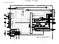
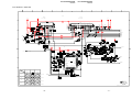
4-1.
BLOCK DIAGRAM
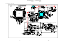
4-1-1.
BG1 (1/3) BLOCK DIAGRAM
TU7000
Q3001
SCL (TU)
SCL_5V_TUNER
SDA_5V_TUNER
AFT
APC
AGC_READ
SDA (TU)
Q7015
AFT OUT
Q7002
B
TO
BG1 BOARD
(3/3)
A
TO
BG1 BOARD
(1/3)
AGC_MUTE
MSP_RST
APC
Q7014
AGC
Q7001
IC7000
12
13
AUDIO
2
22
Q7005
27
26
TV_L
TV_R
TV_CVBS
DET OUT
BG1(1/3) (TUNER)
– 39 –
KLV-26/32/40/46V300A
KLV-26/32/40/46V300A
RM-GA008
RM-GA008
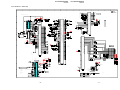
4-1-2. BG1 (2/3), H1, H3, H4 AND UT BLOCK DIAGRAMS
IC4500
VIDEO PROCESSOR
D1
D1_IN_Y
D1_IN_CB
D1_IN_CR
D1_IN_Y
D1_IN_CB
D1_IN_CR
Y_G2
PB_B2
PR_R2
FB1
S1
Q5001
Y/CV,C
VSW_OUT_Y/CV
VSW_OUT_C
D2_IN_Y
D2_IN_CB
D2_IN_CR
BUFFER
D2
D2_IN_Y
D2_IN_CB
D2_IN_CR
IC3001
CPU
HP_DET
IC3007
TEMP SENSOR
1
SDA
2
SCL
REC_MUTE
TO
BG1 BOARD
(3/3)
79
78
21
119
118
XTALI
17
107
113
LINE_MUTE
1
2
3
5
CN3004
Q3006
4
6
3,16
2,17
RES
MD0
RXD
TXD
TO
UT BOARD
CN8003
IC3002
FLASH ROM
A1-A20
20
D16-D23
18
8
A
TRIDENT BUS
AD0-AD7
8
DQ
8
19
Q3005
IC5504
ALE_PX
4
4
5
CS_PX
17
18
16
15
WR#
RD#
ALE
CPU_CS
19
DSDA
6
DSCL
7
RX0RX0+
RX1RX1+
RX2RX2+
RXCRXC+
151
99
100
SCL_5V_TUNER
SDA_5V_TUNER
AFT
APC
B
APC
1
2
3
4
MSP_RST
RGB
PC IN
J1710
PS5000
39
SDO
SCK
WS
AUDIOCLK
77
76
74
73
71
70
68
67
64
63
8
9
11
12
14
15
5
6
HDMI3.3V
Q5505
IC5510
21
23
22
9
10
11
Q5503
7
4
14
15
PWR5V
IC5501
AUDIO
1
3
4
6
7
9
10
12
16
15
J5502
D2+
D2D1+
D1D0+
D0CLK+
CLKDDC DAT
DDC CLK
19
HPD
1
3
4
6
7
9
10
12
16
15
J5503
D2+
D2D1+
D1D0+
D0CLK+
CLKDDC DAT
DDC CLK
19
HPD
Q5509
62
15
14
12
11
9
8
6
5
3
2
IC5501
Q5509
J1720
80
HDMI_RST_1
L
HDMI_RST_3
HDMI_RST_2
AUDIO
IC4900
DDR SDRAM
Q8000
Q8003
TO
BG1 (2/3) BOARD
CN3004
Q8002
4
6
RXD
TXD
3,16
2,17
IC8001
22
CN8003
RES
MD0
122
152
159
164
31
80
156
129
130
76
20
11
115
114
24
12
IC8000
+D3.3V
23
MD
MA
DQS
DQM
REC_R_LED
POWER/RESERVE_LED
ON_TIMER_LED
PIC_MUTE_LED
STBY_LED
SENSOR_DET
SIRCS
D_IRO
POWER_KEY
KEY
IC3005
EEPROM
5
8
SDA_A
6
SCL_A
7
NVM_WP
MVREF
MCK0
MCK0#
MA0-31
MA0-11
DQS0-3
DQM0-3
32
12
4
4
CKE,WE#,CS#,RAS#
CAS#,BA0,BA1
7
MVREF
MCLK0
MCLK0#
68
IC8002
R
DQ
A
DQS
DM
CN3008
3
6
VREF
CK
CK
REC/RESERVE_LED
PWR/RESERVE_LED
CN351
3
6
Q303,304
D305
LED
SW
POWER
Q301,302
5
7
ON_TIMER_LED
PICTURE_OFF_LED
5
7
LED
SW
4
STBY_LED
4
Q305
LED SW
8
BL_IN
8
9
2
10
VD3.3V
STBY3.3V
SIRCS
9
2
D302
PIC OFF
D308
STANDBY
IC320
Q320
Q3004
ILLUM
SENSOR
STBY3.3V
IC3008
IC3004
RESET
+D5V
HDMI IN
SDA
SCL
SDA
SCL
84
60
101
AGC_READ
AGC_MUTE
TO
BG1 BOARD
(1/3)
38
6
116
117
77
105
AFT
6
SCL
5
SDA
7
WC
PC_H
PC_V
AD
71
INV.
IC5000
NVM
IC5001
INV.
19
2
3
TO
PANEL UNIT
VIN
5
3
IC5500
AD0-7
28
DQ OE#
11
CE# WE#
IC4511
30
PC_R
PC_G
PC_B
PC_H
PC_V
IC4702
BUS SW
IC4701
BUS SW
149
112
81
111
32
Q4014,4015
INV.
X3009
CN4500
RA+
RARB+
RBRC+
RCRD+
RDRCLK+
RCLKRERE+
DCC_LUT_SEL2/HF_CONT2
DCC_LUT_SEL0/3.3V/2.5V_ALERT
DCC_LUT_SEL1/C1.5/P1.5_ALERT
GND
J5000
PC_R
PC_G
PC_B
AIN_HS
AIN_VS
3
2
XTALO
X3001
64
HDMI_I2S
TO
PANEL UNIT
1
INT1
5
INT2
6
SCL
7
SDA
133
142
120
121
66
PC_IN_L
PC_IN_R
DVI_IN_L
DVI_IN_R
CN4003
DPB_VS
DP_VS
RESET
IC3009
CLOCK QSC
155
26
139
HP_MUTE
AU_PROT
X_DSP_RST
PANEL12V
X4500
VBLK
INPUT_V
RESET_TR
128
141
158
Q3003
X_DSP_MUTE
SP_MUTE
DIMMER
BACKLIGHT
INV_ERR
BALANCER_ERR
CVBS1
C
Y_G3
PB_B3
PR_B3
157
138
161
62
123
V_DET
TV_M_HSYNC
F
Y/CV
C
Q5000
BUFFER
3
1
7
5
11
9
19
17
15
13
21
23
35
31
33
6
26,28
30,32,
34,36,
38,40
TA1P
TA1M
TB1P
TB1M
TC1P
TC1M
TD1P
TD1M
TCLK1P
TCLK1M
TEIM
TEIP
D3.3V
STBY3.3V
CN401
Q3007
IC401
10
ICD
ICS
Q8004,8005
CN8002
TO
PANEL UNIT
1
2
3
50
7
8
64
29
62
25
26
58
56
57
14
15
CN3500
CN8001
2
2
RST_MICRO
5 INT_USB_HOST 5
6
6
RPLY_USB
7
7
HOST_ST0
8
8
HOST_ST1
SR_CLK
10
10
SIR_OUT
11
11
SIR_IN
12
12
LOG_TXD
14
14
15
15
LOG_RXD
143
132
22
23
SIRCS
89-92
86-88
94
95
93
141
POWER2 1
2
IC4703
4
104
103
102
106
105
BG1 (2/3) (MAIN MICON, VSW-TRIDENT/DDR, HDMI-PC)
UT (USB HOST MICRO)
– 40 –
H3
(LED)
STBY3.3V
19
POWER_INT
20
KEY1
CN101
2
3
S101
POWER
KEY
S102-S107
9
8
7
6
12
11
10
14
2
3
4
5
– 41 –
CN3003
ICD0
ICD1
ICD2
ICD3
ICS0
ICS1
ICS2
ICLK
XTRST
XRSTIN
XINIT
BREAK
H4 (OPTICAL
SENSOR)
H1
(KEY)
KLV-26/32/40/46V300A
KLV-26/32/40/46V300A
RM-GA008
RM-GA008
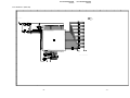
4-1-3. BG1 (3/3) AND U1 BLOCK DIAGRAMS
Q7006-7010
Q7013,7016,7017
VIDEO
TV_CVBS
TV_L
TV_R
A
SYNC
SEP.
Q7000
BUFFER
IC4800
AV SW
AUDIO L
AUDIO R
VIDEO
27
/
TO
BG1 BOARD
(1/3)
3
5
4
6
1
J1000
V1_IN_Y
3
7
V1_IN_C
V1_IN_S2SW
4
1
2
VIDEO IN 1
13
15
17
18
V1_IN_SSW
V1_IN_V
VIDEO
Q4800,4801
/
16
Y1
C1
S1
/
V1
/
20
SDA
19
SCL
Y/CV
C
AUDIO
D1/D2_IN_Y
D1/D2_IN_CB
D1/D2_IN_CR
IC2002
AUDIO DSP
VIDEO
HDMI_I S
/ 26
63
64
60
61
/
DVI_IN_L
DVI_IN_R
PC_IN_L
PC_IN_R
FM/AM
60
57
58
54
55
J1101
X_DSP_RST
HP_DET
X_DSP_MUTE
REC_MUTE
SCS_IN_R
/
/
/
2
45
Q2023
PR
D1_IN_AU_L
L
Q2012,2013,2016-2018
DC DET.
AUDIO L
AUDIO R
Q7012
35
L2024,2025
Q2010
Q2006
Q2030
L
AUDIO
IC2008
R
Q2008
Q2031
96
D2_IN_Y
Y
X2001
D2_IN_CB
PB
SDA_B_5V
SCL_B_5V
D2_IN_CR
PR
D2_IN_AU_L
L
AUDIO
XTAL_IN
/
97
XTAL_OUT
31
I2C_DA
32
I2C_CL
37
RESETQ
/
25
24
Q7000
IC2010
Q7000
HP
AMP
Q2042
7
OPTICAL OUT
Q2032
IC2011
Q2045
Q2020
Q2040
D2_IN_AU_R
R
J1701
AMP
D1_IN_AU_R
R
CN2000
L+
LR+
R-
Q7013
IC2004
84
85
Q2007
AUDIO
L2022,2023
39,40
41,42
19,20
21,22
AUDIO R
/
/
/
49
/
50
/
46
/
47
/
D1_IN_CR
9
AUDIO L
Q2024
D1_IN_CB
PB
IC2009
AUDIO AMP
IC2006
86
87
D1_IN_Y
Y
TO
BU BOARD
CN1001
IC2005
V3_IN_AU_R
R
F
D12V
V3_IN_AU_L
AUDIO
HD/DVD IN 2
2
/ 23
/ 25
/ 24
/
/
/
/
HDMI_I2S
DVI_IN_L
DVI_IN_R
PC_IN_L
PC_IN_R
AU_PROT
SP_MUTE
LINE_MUTE
HP_MUTE
V3_IN_V
L(MONO)
VSW_OUT_Y/CV
VSW_OUT_C
V_DET
TV_M_HSYNC
SDA_DEVICE
SCL_DEVICE
V1_IN_AU_R
R
HD/DVD IN 1
Y/CV
C
BUFFER
V1_IN_AU_L
L(MONO)
VIDEO IN 3
/
35
34
S VIDEO
2
Q2019
Q2046
Q2037,2043
Q2029
36
IC2014
J1200
IC2003
L
82
83
J201
3
S VIDEO
1
Q2021,2022
4
CN201
18
14
8
1
5
6
10
9
13
15
2
VIDEO
VIDEO IN
2
MONITOR
R
L
AUDIO
R
V2_IN_V
V2_IN_Y
V2_IN_C
V2_IN_AU_L
V2_IN_AU_R
V2_IN_SSW
V2_IN_S2SW
HP_OUT_AU_L
HP_OUT_AU_R
HP_DET
CN1400
18
14
8
1
5
6
10
9
13
15
IC2013
51
52
HP_OUT_AU_L
HP_OUT_AU_R
HP_DET
J202
U1
(SIDE INPUT)
– 42 –
BG1 (3/3)
I/O/AUDIO/VSW-TRIDENT/
POWER-DC_ALERT
– 43 –
KLV-26/32/40/46V300A
RM-GA008
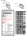
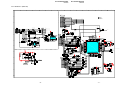
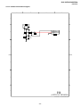
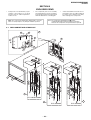
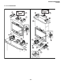
4-2.
CIRCUIT BOARDS LOCATION
KLV-26/32V300A
KLV-40/46V300A
H1 Board
H1 Board
D2 Board (KLV-46V300A)
UT Board
UT Board
U1 Board
U1 Board
D1 Board
BG1 Board
BG1 Board
G1H Board
G3 Board
H3 Board
4-3.
H4 Board
SCHEMATIC DIAGRAM INFORMATION
Note:
• All capacitors are in µF unless otherwise noted.(pF:µµF)
Capacitors without voltage indication are all 50V.
• Indication of resistance, which does not have one for rating
electrical power, is as follows.
Device
Circuit
Terminal name
Collector
Base
Transistor
All resistors are in ohms.
Diode
: nonflammable resistor.
: fusible resistor
¢
: internal component.
: panel designation or adjustment for repair.
All variable and adjustable resistors have characteristic curve B
unless otherwise noted.
• All voltages are in V.
•
: earth-ground
•
: earth-chassis
• All voltages are in V.
• Readings are taken with a 10 MΩ digital multimeter.
• Readings are taken with a color-bar signal input.
• Voltage variations may be noted due to normal
production tolerances.
•
✽
: Cannot be measured.
• NO MARK : PAL
• Circled numbers are waveform references.
•
: B +bus.
•
: B –bus.
•
k : signal path.
Reference information
RESISTOR
: RN
METAL FILM
: RC
SOLID
: FPRD
NONFLAMMABLE CARBON
: FUSE
NONFLAMMABLE FUSIBLE
: RW
NONFLAMMABLE WIREWOUND
: RS
NONFLAMMABLE METAL OXIDE
: RB
NONFLAMMABLE CEMENT
COIL
: LF-8L
MICRO INDUCTOR
CAPACITOR : TA
TANTALUM
: PS
STYROL
: PP
POLYPROPYLENE
: PT
MYLAR
: MPS
METALIZED POLYESTER
: MPP
METALIZED POLYPROPYLENE
: ALB
BIPOLAR
: ALT
HIGH TEMPERATURE
: ALR
HIGH RIPPLE
The component identified by shading and
mark ! are critical for safety. Replace only with
part number specified.
Cathode
Anode
Diode
Anode
(NC)
Cathode
Diode
Anode
(NC)
Common
Diode
Anode
Diode
Cathode
Common
Anode
Cathode
Common
Diode
Anode
Anode
Common
Diode
Anode
Anode
Common
Diode
Cathode
Cathode
Common
Diode
Diode
Transistor
(FET)
Cathode
Anode
Anode
Cathode
Drain
Cathode
Cathode
Anode
Anode
Source
Gate
D
D
G
Transistor
(FET)
Drain
Source
Gate
Transistor
(FET)
Source
Drain
Gate
Transistor
Emitter
Collector
Base
Transistor
Transistor
G
S
S
D
D
G
G
S
S
C1
C2
E1
E2
C1
C2
E1
E2
E1
E2
C2 B1 E1
B1
B2
E2 B2 C1
C1 B2 E2
E1 B1 C2
B1
Transistor
C1 B2 E2
B2
E1 B1 C2
Transistor
C1 B2 E2
Transistor
E2 B1 E1
B2
C2
C2
E2
E1(B2)
E2
E2
C1
E1(B2)
C2
C2
C1
C2
B1
B1
C2
(B2)
E2 E1 B1
C2
C1
C1(B2)
C1(B2)
(B2)
B1 E1 E2
C1
Transistor
B1
E1 B1 C2
C2
– 44 –
Emitter
Cathode
Transistor
Note: The components identified by mark contain
confidential information. Strictly follow the instructions
whenever the components are repaired and /or replaced.
Emitter
Collector
Base
•
•
•
•
•
Note:
Printed symbol
Transistor
Pitch: 5 mm
Rating electrical power 1/4W (CHIP: 1/10W)
•
H4 Board
H3 Board
B1
C1
KLV-26/32/40/46V300A
RM-GA008
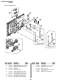
4-3-1. BG1 Board – (Block 001)
WAX3 BG1 BOARD INFORMATION
NO
001
002
003
004
005
006
007
008
009
FUNCTION
COVER
I/O
AUDIO
MAIN MICON
VSW - TRIDENT
DDR
HDMI - PC
POWER - DC_ALERT
TUNER
Note: “BG1” board is divided into 9 blocks.
Each is named by its function and block “number”.
E.g.: Main MICON ( 004 /009), which means block “004” of 009.
Joint connection can be identified using the function name
Eg:--> V_BLK 005:10J
Meaning: Block 004 joint “V_BLK” is connected to
Block 005 joint “V_BLK” located at grid 10J.
BG1
(001/009)
B-WAX3(07)-...-BG1(001)-26/32/40/46V300A
– 45 –
KLV-26/32/40/46V300A
KLV-26/32/40/46V300A
RM-GA008
RM-GA008
4-3-2. BG1 Board --- (Block 002)
1
2
3
4
R1029
1K
1/16W
CHIP
R1002
220
1/10W
RN-CP
R1005
220
1/10W
RN-CP
VD1005
XX
2
B
R1006
XX
A_V2_IN_AU_L,A_V2_IN_AU_R
C1002
XX
R1
V2
GRN 1
D
BLU 3
4
VD1106
RED 5
6
WHT 7
RED 9
10
14
RED 15
R1103
220
1/10W
16
18
ComponentInput2
RED 19
20
F
VD1109
J1101
10P
GND
OLD GND_T
I
GND
1
SPDIF_OUT
2
DTV_TXD1
3
GND
4
R7001
XX
R7002
XX
R7003
XX
GND
5
DTV_RXD1
6
7
GND
8
R7004 XX
GND
9
R7005 XX
DTLOG_TXD1
10
DTLOG_RXD1
11
GND
12
GND
13
C1100 R1106 R1112
1M 2.2K
XX
1/16W 1/16W
CHIP CHIP
PWR_ERR
14
GND
15
GND
16
Y_OUT
17
GND
18
GND
19
PB_OUT
20
PR_OUT
21
GND
22
GND
23
SVIDEO_C_OUT
24
CVBS_Y_OUT
25
GND
26
GND
27
AUDIO_LOUT
28
AUDIO_ROUT
29
GND
30
C1109
1UF
25V
22
1/16W
CHIP
VD1102 C1117 R1136
XX
XX
22
50V
1/16W
CH
C1120
XX
R1138
CH
22
50V
VD1115
1/16W
GND
VD1105
R1105 R1117 R1123
OLD GND_A XX
220
220 220
1/10W 1/10W 1/10W R1113
C1110
C1101 R1107 2.2K
R1124
1UF
XX 1M 1/16W
25V
XX
50V 1/16W CHIP
CH CHIP
C1102 R1108 R1114
R1125
XX
1M 2.2K
C1111
XX
50V 1/16W 1/16W
1UF
CHIP CHIP
CH
25V
C1107
XX
GND
OLD GND_A
VD1114
R1127
220
1/10W R1129
220
1/10W
R7031
XX
FB1230
XX
UART0_TXD
004:2B
UART0_RXD
004:2B
DTT_ERR
004:9B
R1231
XX
R1261
XX
R7013 XX
R7014
XX
VD1710
VD1711
J1710
GND
OLD GND_D
GND
OLD GND_T
C1711
XX
R1712
2.2K
1/16W
CHIP
R1710 R1711
1M
1M
1/16W 1/16W
VD1721 VD1720
C1720
XX
R
C1721
XX
J1720
2P
R1721
1M
1/16W
CHIP
GND
FB7021
XX
L
VIN_6V5
5
VIN_6V5
6
GND
7
CN7001
XX
OLD GND_D
GND
OLD GND_T
C1260
XX
25V
B
HP_IN_GND
11
GND
12
HP_DET
15
GND
16
GND
17
V2_IN_V
18
D5V
19
GND
20
R1409 0 CHIP
A_V2_IN_AU_R
C1407
XX
R1430
XX
FB1400 0UH A_HP_OUT_AU_L
003:16H
C1408
XX
FB1401
0UH
C1403
0.001UF
50V
R1432
XX
A_V2_IN_C
A_V2_IN_S2SW
R1411 0 CHIP
A_HP_OUT_AU_R
003:16H
HP_DET
004:13E
R1406
XX
R1412 0 CHIP
R1433
XX
R1434
XX
R1436
XX
R1437
XX
C1409
XX
A_V2_IN_Y
R1435
XX
R1438
XX
R1413
XX
A_V2_IN_V
C1404
XX
GND_HP
R1407
XX
REG5V
A_V2_IN_SSW
R1410 0 CHIP
R1431
XX
GND
OLD GND_T
R1408
XX
5V
GND
VideoInput2
REF.1400~1499
OLD GND_D
GND
OLD GND_T
GND
OLD GND_D
GND
OLD GND_A
GND
C1035
XX
A_D2_IN_AU_L,A_D2_IN_AU_R
A_D2_IN_AU_R
TU_9V
REG5V
C1230
XX
16V
B
DTV_IN_Y
005:11A
C1231
XX
16V
R1246
XX
R1240
XX
Q1231
XX
DTV_IN_CB
005:11A
Q1232
XX
R1241
XX
AUS-D Comp Buffer
DTV_IN_CR
005:11A
Q1230
XX
R1264
XX
C1261 R1265
XX
XX
25V C1262
B
XX
C1263
XX C1714
1UF
25V
2012
C1715
1UF
25V
2012
AUS_Y
005:4L
AUS-D CVBS Buffer
AUS_C
005:4K
AUDIO_LOUT
003:6F
AUDIO_ROUT
003:6E
D3.3V
R1720
1M
1/16W
CHIP
1
VIN
2
VCC
3
3.3V
GND
GND
OLD GND_T
J1700
XX
Opt/Audio Output
A_AUOUT_AU_L
003:10I
R1724
XX
1/16W
CHIP
50V
R1723
2.2K
1/16W
CHIP
C1724
1UF
25V
2012
C1725
1UF
25V
2012
DVI_IN_L
003:6C
A_AUOUT_AU_R
003:10I
DVI_IN_R
003:6C
R1700
220K
1/16W
CHIP
C1700
XX
R1701
220K
1/16W
CHIP
C1701
XX
50V
CH
REG5V
TO AUDIO
C1723 R1725
0.001UF XX
50V
C1205
XX
MONT_OUT_CV
005:4J
F7001
XX
R7106
XX
CHIP
SPDIF_OUT
003:2C
PC_IN_L
003:6D
PC_IN_R
003:6D
C1712 C1713
XX
XX
UNREG6.5V
4
8
A_D2_IN_AU_L
R1237
XX
R1263
XX
FB1261
XX
R1714 R1715
XX
XX
R1722
2.2K
1/16W C1722
CHIP 0.001UF
L
AUDIO IN
3
C1115
XX
50V
CH
C1118
XX
50V
CH
C1122
XX
50V
CH
R1235 R1238
XX
XX
R1713
2.2K
1/16W
CHIP
J
2
R1245
XX
R1234
XX
R1260
XX
PC_LR IN
1
7
(BLOCK 002)
I/O
C1034
XX
R1239
XX
FB1232
XX
R7012 XX
C1710
XX
GND
16
FB1262
XX
GND
OLD GND_A
GND
15
OLD GND_A
FB1231 R1236
XX
XX
R1262
XX
VIN_10V5
14
BG1
C1406
XX
R1403 XX
D1_IN_CR
R1244
XX
R7032
XX
CN7000
XX
WHT
VIN_10V5
6
V2_IN_C
C1405
XX
C1123
XX
50V
CH
R1233 R1243
XX
XX
CHIP
R1232
XX
C7069
XX
5
V2_IN_SSW
AU_IN_GND
R1414
XX
D1_IN_CB
R1242
XX
R7011
XX
DTAU10V5
V2_IN_AU_R
D1_IN_CB,D1_IN_CR,D1_IN_Y
D1_IN_Y
REF.7000 7050
R7033
XX
K
13
D2_IN_CB,D2_IN_CR,D2_IN_Y
R1134
XX
50V
CH
R1230
XX
R7006 XX
4
A_D1_IN_AU_L,A_D1_IN_AU_R
VD1100
XX C1113
R1115 R1119
220
220
VD1113
1/10W 1/10W
UART_AUS_TXD
004:10A
DTT_RST
004:6E
R7007
XX
3
A_V3_IN_AU_R
L1230
XX
SPDIF_IN
003:2D
UART_AUS_RXD
004:10B
DTV_RST_N
2
GND
A_V3_IN_AU_L,A_V3_IN_AU_R
A_D1_IN_AU_L
C1108
1UF
25V
12
C1106
XX
VD1108
WHT 17
R1139
22
1/16W
CHIP
VD1112 VD1104
XX
C1103 R1110 R1111
XX
1M 2.2K
50V 1/16W
1/16W
CH CHIP CHIP
12 R1100
220
BLU 13 1/10W
ComponentInput1
A_V3_IN_AU_L
GND
OLD GND_A
GRN 11
E
H
C1121
XX
50V
11
A_V2_IN_C,A_V2_IN_S2SW,A_V2_IN_SSW,A_V2_IN_V,A_V2_IN_Y
R1402
XX
A_V2_IN_AU_L
HP_OUT_AU_R 13
V2_IN_Y 14
A_V3_IN_V
005:3J
A_D1_IN_AU_R
VD1107
8
G
R1131
220
1/10W
RN-CP
R1126
R1116
220
220
1/10W
1/10W
RN-CP
RN-CP
R1120 R1130
220
220
1/10W 1/10W
RN-CP RN-CP
2
R1121
XX
for Aus-D
C1104
XX
ComponentInput1
C1105
XX
J1000
OLD GND_A
GND
R1122
XX
R2
VD1004
VD1003
C
C1007 C1016 R1031
R1009 R1015
1M 2.2K
1UF
XX
100
1/16W 1/16WR1023
1/16W
25V
CHIP CHIP XX
CHIP
R1010 R1019 R1021
C1012
220
220
220
0.01UF
1/10W 1/10W 1/10W C1011
R1001
D1005
RN-CP RN-CP RN-CP XX 25V
XX
MAZ8100G0LS0
R1011
R1016 C1008
GND
C1017
2.2K
1M
XX
OLD GND_A
1UF
1/16W
1/16W
25V
CHIP
CHIP R1024
XX
C1018
R1012
C1009
1UF
1M
25V
XX
1/16W
CHIP
R1135
R1017 R1025
22
2.2K
GND
1/16W
VD1101
1/16W XX
CHIP
OLD GND_T
XX
CHIP
R1104
C1114
C1112
220
XX
XX
VD1110
1/10W
CH
RN-CP
50V
VD1103 XX
R1128
C1116
R1137 C1119
R1109
R1118 220 VD1111
22
XX
XX
220
220 1/10W
1/16W
50V
CH
1/10W
CHIP
1/10W RN-CP
50V
RN-CP
RN-CP
C1000
XX
L2
VideoInput3
10
C1401
XX
HP_OUT_AU_L 9
V2_IN_S2SW 10
C1003
XX
VD1002
VideoInput1
D3.3V
AU_IN_GND
C1001
XX
VD1001
L1
9
D3.3V
R1401
CN1400 XX
20P
V2_IN_AU_L 1
R1022
XX
V1
8
A_V1_IN_Y
D1000
MAZ8100G0LS0
C1014
0.01UF
25V
C1010
XX
1
7
A_V1_IN_SSW
OLD GND_A
R1027
100
GND
A_V1_IN_C
R1013 VD1006
1/16W
XX
75
CHIP
D1001
1/10W
MAZ8100G0LS0
A_V1_IN_S2SW
RN-CP
C1004
R1028
R1030
1UF
1K
100
10V
1/16W
1/16W
CHIP
CHIP
A_V1_IN_V
R1007 R1018 R1020
D1008
A_V1_IN_AU_L,A_V1_IN_AU_R
C1020
220
220
220
MAZ8100G0LS0
1/10W 1/10W 1/10W C1019 0.01UF
25V
RN-CP RN-CP RN-CP XX
A_V1_IN_AU_L
R1008
C1006
C1015
1M R1014
XX
1UF
1/16W2.2K
CHIP 1/16W
25V
CHIP
A_V1_IN_AU_R
4
3
6
D1002
MAZ8100G0LS0
R1026
100
1/16W
CHIP
C1013
0.01UF
25V
C1005
XX
A
R1004
220
1/10W
RN-CP
5
A_V1_IN_C,A_V1_IN_S2SW,A_V1_IN_SSW,A_V1_IN_V,A_V1_IN_Y
MON_OUT_AU_L,MON_OUT_AU_R
R1207
XX
R1208
XX
R1209
XX
OLD GND_A
D1009
XX
GND
MON_OUT_AU_L
D1010
XX
MON_OUT_AU_R
C7070
XX
R1702
470
1/16W
CHIP
C1702
XX
50V
CH
VD1702
1
L
2
3 R
VD1703 4
R1703 C1703 VD1701
470 XX
XX
1/16W 50V
CHIP CH
GND
J1701
2P
OLD GND_A
GND
OLD GND_T
R1211
0
C1204
R1204 470UF
VD1202
75
1/10W 10V
XX VD1205
R1201
220K
1/16W
R1202 0 VD1200
C1200 XX
R1205 C1202
XX
220K
XX
50V
1/16W
CH
R1210
XX
V
Q1200
XX
L
Monitor Out
VD1203
R
R1203
0
R1206
220K
1/16W
C1203
XX
50V
CH
GND
OLD GND_D
VD1700
XX
C1201 VD1201
XX
XX
50V
CH
VD1204
J1200
3P
GND
OLD GND_T
B-WAX3(07)-...-BG1(BLOCK 002)-26/32/40/46V300A
- 46 -
- 47 -
KLV-26/32/40/46V300A
KLV-26/32/40/46V300A
RM-GA008
RM-GA008
4-3-3. BG1 Board --- (Block 003)
6
7
D3.3V
R2065
XX
INB
INA VCC
GND
OUTY
R2245
100
1/16W
CHIP
L2009 10UH
D3.3V
R2249
1K
1/16W
CHIP
HDMI_MUTE
003:9F, 003:10K, 003:15J
1 2 3
GND
IC2005
PQ200WNA1ZPH
VADJ
RB2001
100K 1005X4
C2137
0.22UF
25V
B
C2147
XX
C2129
0.1UF
25V
C2153
XX
FB2008 0UH
FB2009 0UH
L2024
22UH
C2148
XX
1
2
RR+
3
L+
4
L-
C2154
XX
C2138
0.22UF
25V
B
1
IC2009
C2120 TPA3100D2PHPR
0.22UF AUDIO AMP
25V
B
2
P24
4
Q2018
C2157 DTC114TUA-T106
0.1UF
25V
CN2000
4P
3
BSLN
GND
Q2017
DTC114EUA-T106
FB2007 0UH
C2128
100UF
35V
P25
AU_PROT
004:9G
C2158
R2205 0.1UF
33K
25V
1/16W
RN-CP
Q2013
RT3AMMM
FB2006 0UH
P27
P26
R2204
100K
1/16W
CHIP
C2136
0.22UF
25V
B
3
4
2
1
P28
C2146
1UF
25V
3
4
2
4
C2127
1UF
25V
GND
OLD GND_D
3
L2025
22UH
2
1
D2020
MAZ8056G0LS0
D2018
MAZ8056G0LS0
C2132
0.22UF
25V
B
C2126
1UF
25V
P31
P30
P29
4
R2232
0
CHIP
P22
P23
P21
P20
P19
P18
LOUTN
LOUTP
LOUTN
LOUTP
VBYP
AGND
BSLP
C2116
0.22UF
25V
B
GND
P32
8 6
Q2012
RT3AMMM
2
1
P37
P39
P38
P41
P40
BSRN
GND
P42
ROUTN
P45
P44
P48
P47
P46
P43
ROUTP
ROUTN
ROUTP
SHUTDOWN
BSRP
MUTE
AVCC
AVCC
FAULT
R2162 P13
P14
P15
R2230 0 CHIP
R2231
XX
D2019
MAZ8056G0LS0
P16
P17
V+
B+ IN
B- IN
B OUT
PVCCL
PVCCL
GND
GND
A OUT
A- IN
A+ IN
V-
R2072
XX
IC2014
TC7SZ32FUTE85R
RB2011
10K
R2123
XX
ATT_SW
003:7F
AUDIO_ROUT
002:4I
AUDIO_LOUT
002:4I
C2180
0.1UF
10V
4
MSTR/SLV
SYNC
P34
P33
1
Q2016
DTC114EUA-T106
C2145
1UF
25V
R2178
100K
1/16W
CHIP
C2159
0.001UF
50V
C2113 C2114
0.01UF 4.7UF
25V
25V
C2133
0.22UF
25V
B
C2139
0.22UF
25V
B
C2179
4.7UF
25V
Q2024
DTA144EUA-T106
A_D2_IN_AU_L
R2651 XX
PGNDL
PGNDL
R2150
R2147 22K
1K
1/16W
1/16W CHIP 4 1
Q2006
R2238
CHIP
R2237
1K
DTC114EUA-T106
3.3K
1/16W
5
2
1/16W SP_MUTE
RN-CP
RN-CP 004:9B
6 3
R2246
Q2010
R2151
3.3K
HN1B01FU-TE85R
47K
R2234 C2177
R2239
ATT_SW
1/16W
1/16W
1K
100K
1UF
CHIP
003:6E
1/16W
1/16W 25V
CHIP
R2163
Q2025
RN-CP
RN-CP
47K
RTAN140M-T111-1
Q2023
1/16W
R2235
HDMI_MUTE
003:10K, 003:5F, 003:15J
DTC114EUA-T106
33K
CHIP
1/16W
SP_SD
RN-CP
004:13E
Q2009
DTC114EUA-T106
Q2030
DTC114EUA-T106
Q2026
RTAN140M-T111-1
A_D2_IN_AU_R
R2650 XX
R2148 R2149
47K
22K
1/16W 1/16W
CHIP
CHIP
R2236
3.3K
1/16W
RN-CP
C2178
4.7UF
25V
GAIN0
GAIN1
ROSC
VREG
AVDD_REF
LINEOUT3R
LINEOUT3L
LINEIN3L
LINEIN3R
LINEIN2L
LINEIN2R
AVSS_LI
R2087
33K
1/16W
R2092
33K
1/16W
LINEIN1L
LINEIN1R
AVDD_LI
R2085
33K
1/16W
R2064
R2062
XX 10K
1/16W
R2068
XX
R2073 1001/16W
R2020
10K
C2042
0.001UF
1/16W
50V
R2074
1K
1/16W
C2044 XX
C2045
0.001UF
C2051
50V
4.7UF
6.3V
C2052
330PF 50V
C2053
330PF
50V
R2091 33K 1/16W
DVDD4
DVSS5
VR_DIG2
AVSS_ESD
/RESET
DVSS4
/MUTE
CS
GPIO1
GPIO2
I2C_SDA1
I2C_SCL1
R2056 6.8K 1/16W
R2057 6.8k 1/16W
A_D1_IN_AU_R
A_D1_IN_AU_L
VCLAMPL
100K
1/16W
R2082 47 1/16W
AVSS_LO
LINEOUT1L
LINEOUT2R
LINEOUT2L
R2075 47 1/16W
R2076 47 1/16W
R2077 47 1/16W
R2078 47 1/16W
R2080 47 1/16W
DACOUT2R
DACOUT2L
AVSS_DAC
AVDD_HP
HPOUTR
DACOUT1R
DACOUT1L
LINEOUT1R
C2039
0.001UF
50V
A_HP_OUT_R
A_HP_OUT_L
R2049 0
C2033
0.1UF
25V
R2063 0
R2070 0
AVSS_ESD
AVSS_HP
HPOUTL
AVDD_HP
AVDD_DAC
XTAL_OUT
XTAL_IN
DVDD1
AVDD_OSC
VR_ANA
MCLKIN
DVSS3
R2044
47
1/16W
DVDD3
I2C_SDA2
I2C_SCL2
RB2002
XX
GND
OLD GND_T
GAIN0
R2279
100K
1/16W
CHIP
C2078
2.2UF
16V
PGNDR
VCLAMPR
P35
7 5 3
R2198
6.8K
1/16W
CHIP
R2199
100K
1/16W
CHIP
L2023
22UH
C2125
0.1UF
25V
24
A_V2_IN_AU_L
P11
P12
PGNDR
LINN
23
A_V2_IN_AU_R
P10
C2102
0.001UF
50V
GND
AGND
LINP
22
R2108 33K 1/16W
R2109 33K 1/16W
P9
C2096
100PF
50V
R2133
CH
22K
1/16W R2211
RN-CP 6.8K
1/16W
RN-CP
R2129
22K
1/16W
RN-CP
P7
P8
C2124
100UF
35V
P36
PVCCR
PVCCR
21
20
19
RB2003
10K
C2063 0.1UF 25V
C2168
0.001UF
50V
B
C2169
0.001UF
50V
B
R2118
4.7K
1/16W
CHIP
R2121
22K
1/16W
RN-CP
R2122
22K
1/16W
RN-CP
P5
P6
C2106
4.7UF
25V
RINP
18
R2023
0
A_V3_IN_AU_R
A_V3_IN_AU_L
C2097
0.1UF
25V
P3
P4
GND
RINN
17
L2005
XX
A_V1_IN_AU_L
R2106 33K 1/16W
R2107 33K 1/16W
R2145
15K
1/16W
RN-CP
C2104
4.7UF
25V
C2105
4.7UF
25V
R2277 C2101
100K 0.001UF
50V
1/16W
CHIP
IC2006
NJM4558V-TE2
R2117
4.7K
1/16W
CHIP
5
A_V1_IN_AU_R
R2104 33K 1/16W
R2105 33K 1/16W
C2054 C2055
4.7UF 0.001UF
50V
25V
5
R2177
100K
1/16W
CHIP
L2022
22UH
36 35 34 33 32 31 30 29 28 27 26 25
C2062 0.1UF 25V
C2074
4.7UF
A_SP_OUT_R 25V
003:6A
A_SP_OUT_L
003:6A
C2075
4.7UF
25V
16
R2202
10K
1/16W
CHIP
D2014
MAZ8091GMLS0
TO DETECT
37
PC_IN_R 002:4I
PC_IN_L 002:4I
R2103 33K 1/16W
P1
P2
38
R2101 33K 1/16W
R2102 33K 1/16W
C2103
4.7UF
25V
39
DVI_IN_L 002:4J
C2094
100PF
50V
CH
16
15
50
47
46
RB2008
100
49
48
44
43
45
42
41
40
F
39
3
38
GND
OLD GND_D
1
37
4
36
35
34
C2024
XX C2027
0.001UF
50V
2
RB2004
100
LINEIN4R
LINEIN4L
R2143 R2210
15K
6.8K
1/16W 1/16W
RN-CP RN-CP
C2085
47UF
16V
40
41
42
AVDD_LI
12V
L2015
10UH
43
LINEIN5L
C2123
470UF
25V
C2119
0.22UF
25V
B
C2115
0.22UF
25V
B
C2111
0.1UF
25V
44
AVSS_LI
LINEIN5R
SDIN2
SDIN1
C2061
0.1UF
25V
R2100 33K 1/16W
0.001UF 50V
4.7UF 25V
330PF 50V
C2164
2.2UF
10V
TV_R 009:11C
TV_L 009:11C
C2165
2.2UF
10V
DVI_IN_R 002:4J
14
MCLKINA
SDIN3
R2098
10K
1/16W
R2099
10K
1/16W
24K 1/16W
XX
13
SCLKINA
LINEIN6R
LINEIN6L
C2112
4.7UF
25V
C2065 1UF 10V
45
46
AVDD_LI
C2064
1UF
10V
R2095
C2066
C2068
C2067
C2172
C2173
330PF
50V
15
2
D2021
MAZ8056G0LS0
9 10 11 12
SDIN1A
LRCLKINA
L2016
22UH
R2227
2.2K
1/16W
RN-CP
7 8
LINEIN7R
LINEIN7L
14
GND
OLD GND_AU
5 6
LINEIN8L
AVSS_LI
IC2002
CXD9890AQ
AUDIO SWITCH / DSP
13
C2121
0.001UF
50V
C2118
0.001UF
50V
R2228
6.8K
1/16W
RN-CP
47
LINEIN8R
12V
48
SDOUT2/SPDIF_OUT
1
C2117
0.001UF
50V
AU_HP12V
3 4
AVDD_LI
LINEIN9L
F2000
4A
24V
13V
C2190
4.7UF
25V C2191
4.7UF
25V
R2229
1K
1/16W
RN-CP
C2095
1UF
25V
AUDIO_13V
1 2
SDOUT1
LRCLKIN
SCLKIN
5
6
77
78
LINEIN9R
DVSS2
SPDIF_IN
4
L2010
10UH
C2060
100UF
6.3V
75 74 73 72 71 70 69 68 67 66 65 64 63 62 61 60 59 58 57 56 55 54 53 52 51
79
80
76
81
84
85
82
83
86
LRCLKOUT
SCLKOUT
E
R2079
XX
87
AVSS_LI
32
F2002 C2013
0.5A 100UF
50V 6.3V
LINEIN10R
LINEIN10L
GPIO3
MCLKOUT
30
FB2015
0UH
R2033
100
1/16W
GPIO4
33
D3.3V
HDMI_SDO
AVDD_ADC
27
26
R2035
47
1/16W
R2207
47
1/16W
BG_REF
LS_SCLKOUT
31
HDMI_WS
V1P5_REF
BIAS_REF
VR_DIG1
3
GND
OLD GND_D
C2059
4.7UF
25V
C2058
0.001UF
50V
AVSS_ADC/REF
DVDD2
2
C2181
XX
FB2016
0UH
LS_LRCKOUT
29
28
RB2012
10K
HDMI_SCK
88
HDMI_MCLK
89
R2156
0
CHIP
HDMI_I2S
90
91
D
92
93
RB2007
10K 1005X4
94
R2026 47 1/16W
95
R2155 XX
0
CHIPC2014
C2016 0.001UF
4.7UF
50V
6.3V
96
R2271
10K
1/16W
CHIP C2015
8 9 10 11 12 13 14 15 16 17 18 19 20 21 22 23 24 25
SPDIF_IN
002:2G
R2270 100
1/16W CHIP
6 7
SPDIF_OUT
002:7I
R2042
47
1/16W
3 4 5
ATT_SW_LINE
003:5J
ATT_SW_HP
003:11H
/VREG_EN
STEST
97
98
1 2
R2154
0
CHIP
R2268
100
1/16W RB2010
10K
CHIP
R2269
10K
1/16W
RB2006
CHIP
10K 1005X4
DVSS1
R2050
1M
1/16W
99
100
C2018
XX
C2041
4.7UF
25V
1
7
2
B
C2086
0.001UF
50V
F2001
1.6A
36V
1
C2022 C2025
0.001UF 4.7UF
50V 6.3V
C2019
4.7UF
25V
C2017
0.001UF
50V
12
AU_13V
R2233 XX
X2001
24.576MHZ
11
8
C2029
9PF
50V
A_MONT_OUT_R
003:6H
A_MONT_OUT_L
003:6H
10
12V
VOUT
C2030
9PF
50V
4
(BLOCK 003)
AUDIO
C
9
AUDIO_12V
VC
BG1
A
8
A_HP_OUT_R
003:11G
A_HP_OUT_L
003:11G
A_SP_OUT_R
003:7D
A_SP_OUT_L
003:7D
A_LINE_OUT_R
003:6J
A_LINE_OUT_L
003:6I
VIN
5
4
3
3
2
2
1
1
12V
C2183
XX
R2217
47K
1/16W
C2186
XX
R2257
XX
R2276
XX
R2281
100K
1/16W
CHIP
R2167
10K
C2131 1/16W
47UF CHIP
16V
C2141
2.2UF
16V
V-
A+ IN
B- IN
A- IN
B OUT A OUT
V+
CHIP
B+ IN
R2181
C2161
0.001UF R2180
4.7K
50V
1/16W
CHIP
100K
1/16W
RN-CP
C2144
100PF
50V
CH
C2143
2.2UF
10V
Q2019
RTAN140M-T111-1
R2213
15K
1/16W
RN-CP
1
C2084 C2092
330PF
50V 2.2UF
10V
CH
R2139
470K
1/16W
CHIP
FB2012
0UH
R2187
470
1/10W
RN-CP
FB2018 0UH
Q2020
RTAN140M-T111-1
R2185
10K
1/16W
CHIP
FB2019
0UH
4
OUT
VCC GND
IN
1
2
3
C
5
R
A_AUOUT_AU_R
002:5J
6
IC2011
RT8H225C-TP-2
C2156
0.1UF
25V
R2200
100K
1/16W
CHIP
LINE_OUT
R2142
470
1/16W
CHIP
C2110
XX
R2248
3.3K
1/16W
CHIP
HP_MUTE
004:7E
HDMI_MUTE
003:5F, 003:9F, 003:10K
6
Q2008
RTAN140M-T111-1
R2153
100K
1/16W
CHIP
5
1
2
4
C
2
Q2007
RTAN140M-T111-1
IN
3
A- IN
IC2004
NJM4558V-TE2
4
R2138
470K
1/16W
C2090 CHIP
0.1UF
25V
8
A OUT
V+
B OUT
B- IN
7
D2017
XX
Q2032
DTC114EUA-T106
3
D2008
XX
MA111-TX
C2108
XX
16V
HDMI_MUTE
003:5F, 003:9F, 003:15J
K
Q2042
XX
R2166 R2169
10K 47K
1/16W 1/16W
CHIP CHIP
A_HP_OUT_AU_R
002:7C
A_HP_OUT_AU_L
002:7B
GND_HP
R2189
470
1/10W
RN-CP
A_AUOUT_AU_L
002:5J
OUT
R2120
47K
1/16W
RN-CP
6
V-
B+ IN
C2171
C2070
0.0027UF
2.2UF
50V
10V
B
R2112
22K
1/16W
C2184
RN-CP
XX R2252
R2113
22K
XX
1/16W
RN-CP
5
R2265
XX
1/16W
CHIP
C2135
2.2UF
10V
C2150
47UF
16V
RTAN140M-T111-1
R2141
470
C2091
2.2UF 1/16W
10V
CHIP
C2081
330PF
50V
CH
R2126
47K
1/16W
RN-CP
C2170
0.0027UF
50V
B
R2251
XX
Q2034
XX
R2219
10K
1/16W
REC_MUTE
004:8B
R2263
XX
1/16W
RN-CP
C2188
2.2UF
10V
IC2008
RT8H225C-TP-2
Q2033
XX
R2256
XX
R2218
100K
1/16W
VCC GND
ATT_SW_LINE
003:2C
3
R
Q2044
XX
R2250
XX
2
Q2041
XX
R2171
4.7K
1/16W
CHIP
L2017 10UH
HP_OUT
FB2017 0UH
Q2045
16V
Q2038
XX
R2131
3.9K
1/16W
RN-CP
R2111
2.2K
1/16W
RN-CP
C2073
2.2UF
A_LINE_OUT_R
003:6A
J
R2130
3.9K
1/16W
RN-CP
R2254
XX R2255 R2278
XX
XX
Q2036
XX
R2272
3.3K
1/16W
RN-CP
C2077
47UF
16V
R2110
C2069 2.2K
2.2UF
1/16W
10V RN-CP
C2185
XX
Q2035
XX
1
R2264
XX
1/16W
CHIP
C2189
XX
25V
R2262
3.3K
1/16W
RN-CP
R2186
470
1/10W
RN-CP
Q2046
RTAN140M-T111-1
A+ IN
I
R2253
XX
Q2022
RTAN140M-T111-1
R2261
XX
1/16W
CHIP
Q2037
XX
Q2043
XX
ATT_SW_HP
003:2C
R2212
15K
1/16W
RN-CP
L2011 10UH
R2273
3.3K
1/16W
RN-CP
R2216
1K
1/16W
4
IC2013
RT8H225C-TP-2
C2175
2.2UF
10V
5
R2184
10K
1/16W
CHIP
R2188
470
1/10W
RN-CP
IC2010
NJM3414AVTE2
C2130
0.1UF
25V
AU_HP12V
Q2040
XX
6
C
C2082
330PF
50V
R2128
10K
1/16W
C2083
2.2UF
10V
A_LINE_OUT_L
003:6A
C2176
XX
OUT
1
R2215
47K
1/16W
IN
2
R2127
5.6K
1/16W
R2115 R2119
47K 47K
1/16W 1/16W
C2174
2.2UF
10V
VCC GND
C2072
2.2UF
10V
C2087
0.1UF
25V
R
3
A_MONT_OUT_R
IC2003
NJM4558V-TE2
GNDB+IN
A+IN B-IN
A-IN
BOUTPUT
AOUTPUT
VCC
8
R2176
47K
1/16W
X_DSP_RST
X_DSP_MUTE
004:9G
INTN
005:3E
AUDIO_DSP_INT
004:6D
I2C_TAS_SCL_2
I2C_TAS_SDA_2
X_DSP_RST
004:6D
4
A_MONT_OUT_L
7
5
C2182
2.2UF
16V
C2071
2.2UF
10V
H
6
C2149
47UF
16V
R2168
4.7K
1/16W C2160
CHIP 0.001UF
50V
R2280
R2260
100K
XX
1/16W
1/16W CHIP
RN-CP
C2187
2.2UF
10V
Q2039
XX
6
5
MON_OUT_AU_L
003:5A
MON_OUT_AU_R
003:5A
MON_OUT
Q2021
RTAN140M-T111-1
C2134
2.2UF
10V
R2259
3.3K
1/16W
RN-CP
C2142
100PF
50V
CH
R2170
C2140 4.7K R2179
2.2UF 1/16W 100K
10V CHIP 1/16W
RN-CP
7
R2241
18K
1/16W
R2214
1K
1/16W
R2258
XX
1/16W
CHIP
8
R2124 R2125
5.6K
10K
1/16W 1/16W
C2080
330PF
50V
R2242
22K
1/16W
HEADPHONE OUTPUTS
R2275
0
C2079
2.2UF
10V
4
C2076
47UF
16V
3
L2014 10UH
2
G
R2274
0
A_HP_OUT_R
003:6A
A_HP_OUT_L
003:6A
1
RB2009 100
Q2029
DTC114EUA-T106
R2247
3.3K
1/16W
CHIP
LINE_MUTE
004:9B
Q2031
DTC114EUA-T106
L
B-WAX3(07)-...-BG1(BLOCK 003)-26/32/40/46V300A
- 48 -
- 49 -
KLV-26/32/40/46V300A
KLV-26/32/40/46V300A
RM-GA008
RM-GA008
4-3-4. BG1 Board --- (Block 004)
DCC_LUT_SEL0/PLL_1.5V_ART//AN3/PF1
79
DCC_SEL_1/CORE_1.5V_ALT/AN2/PF0
78
AFT_IN/AN1
77
KEY/AN0
MD3
MD2
72
71
MD1
70
152 POWER_LED/PC3/PPG3
MD0
69
MICRO_RST/INTX
68
VDDI
X1
67
66
VSS
65
X0
64
VDDE
63
159 ON_TIMER_LED/PD2/DEOP0X
160 NC/PD3/DREQ1
TAS_RST/A23/P57
SP_SD_MUTE/A22/P56
62
61
161 M_H_SYNC/PD4/DACK1X/INT
AGC_MUTE/A21/P55
60
PD5/DEOP1X/INT2
A20/P54
59
DC_ALERT1/PE0/DREQ2/TRG1
PIC_MUTE_LED/PE1/DACK2X/TRG2
A19/P53
A18/P52
58
APC/PE2/DEOP2X/TRG
A17/P51
56
VDDE
IC3001
MB91305PMC-G-BNDE1
R3191
XX
DCC_LUT_SEL1/HF_CONT
005:14I
2
RB3016
10K
ICD3
7
ICD2
8
9
ICD1
ICD0
10
ICS2
11
ICS1
12
ICS0
13
GND
ICLK
14
CN3003
14P
Q3008
RT1P151M-TP-1
STBY_LED
004:10G
Q3002
RT1N151M-TP-1
AC_OFF_DET
004:9J, 008:3B
C3095
XX
C3070
0.01UF
16V
R3008
XX
C3018
XX
R3271
100K
1/16W
D-IRO
004:15E
SIRCS
004:7E
SIRCS
1B
4B
1Y
4A
2A
4Y
2B
2Y
3B
3A
GND
3Y
C3060
0.001UF
50V
A15
A12
A10
A16
C3061
0.001UF
50V
A9
45
A15
VD3102
XX
A6
A7
A5
A4
A3
A2
A1
A0
R3158 100 1/16W
A8
A7
R3224
0
CHIP
A6
A4
A5
A3
A2
A1
EEPROM_WP
004:12B
POWER1
008:3B
AU_PROT
003:16B
HDMI_RST2
007:16G
HDMI_RST3
007:16G
CEC_OUT
007:3I
ALE_PX
005:1D
STBY_LED
004:14D
HDMI_RST1
007:16G
USB_ST0
004:2A
A0
A1
A2
GND
R3247
0
STBY_LED
5
6
ON_TIMER_LED
PWR/RESERVED_LED
7
PICTURE_OFF_LED
8
BL_IN
9
VD3.3V
10
11
SIRCS
STBY3.3V
12
GND
13
STBY3.3V
14
D-IRO(SIRCS)
15
16
GND
D3.3V
17
Ir-Switch
18
GND
19
POWER_INT
20
KEY1
D23
AD6
D22
AD5
D21
C3082
10UF
10V
AD4
D20
C3079 STBY3.3V
0.1UF
10V
C3080
AD3
0.001UF
50V
D19
AD2
D18
AD1
D17
30
29
A4
OE#
28
A3
VSS
27
A2
CE#
26
A1
A0
25
31
USB_ST1
004:2A
AD7
AD0
D16
RD#
OLD GND_D
GND
CS_FRASH
004:9G
WR#
A1
CN3004
18P
1.8VCC
R3170
0UH
C3052
0.1UF
10V
R3246
10K
1/16W
R3245 XX
32
TXD
GND
A17
33
ACC_OFF_ON
005:15H
REC/RESERVE_LED
4
CN3008
20P
34
R3180
10K
1/16W
VDDI
RDX
R3113 22 1/16W CHIP
X_DSP_MUTE
003:4G
CS_FRASH
004:16I
CS_PX
005:2E
RD# R3111 22 1/16W CHIP
D31
VSS
VD3101
XX
WR#
AD0
GND
STBY3.3V
3
35
DQ0
B INT
RXD
36
18
37
17
38
R3295 14
3.9K 15
1/16W
16
39
A2
A4
40
A3
NC
VIN
41
ON/OFFNC
UART0_TXD
13
42
VSS
4
VINVOUT
TRI-GND
12
DQ8
A5
5
C3051
10UF
10V
3
C3048
0.1UF
10V
2
FROM G PWB
11
A5
43
IC3006
S-1132B18-M5T1G
R3169
0
CHIP
TRI-SCL
44
FAN_ERR
004:2D
TRI-SDA
DQ1
A6
24
GND
OLD GND_D
STBY3.3V
9
10
A7
23
B_INT
004:6E
ECS_RXD
004:10B
ECS_TXD
004:10B
MD2
A6
22
INV_MD0
004:5F
8
A7
A17 DQ9
DQ3
21
DTT_LOG UART0_TXD
002:2G, 004:2B
Q3006
RT1N237M-TP-1
UART0_RXD
RY/BY#
DQ10
A18 DQ2
20
Q3005
DTA114TUA-T106
TRI-SDA
005:2F
TRI-SCL
005:2F
MD0
NC
19
VIN
7
A8
RESET#
VCC
NC DQ11
18
5
A18
WE# DQ4
17
UART0_RXD
002:2G, 004:2B
A19
NC DQ12
16
RXD
RES
A19 DQ5
15
4
A8 DQ13
14
R3525
XX
TXD
3
3.3V 6
1
GND
TO MAICOM
Q3501
XX
2
DQ6
A9
13
R3526
XX
GND
A10 DQ14
12
STBY3.3V
RY/BY#
1
A11 DQ7
11
GND
OLD GND_D
J
AC_OFF_DET
004:14E, 008:3B
R3524
XX
R3290
0
CHIP
A12
DQ15/A-1
10
A20
GND
OLD GND_D
A16
A14
BYTE#
A13 VSS
45
A9
R3126
100
1/16W
CHIP
A15
9
R3516
100
1/16W
CHIP
1
2
R3276
XX
8
S1_OFF
004:2D
R3274
100K
1/16W
7
A10
FR_MD2
004:12E
0UH
0UH
R3266
0
C3071 CHIP
100PF
50V
6
A11
R3146
0
CHIP
C3112
0.001UF
50V
0UH
C3074
0.1UF
10V
R3226
220
1/16W
5
A12
3.3V
R3265
0UH
R3275
XX
4
I
R3260
R3261
R3262
R3263
R3264
0UH
IC3002
MX29LV160CTTI-70G
A11
A13
R3293
XX
0UH
0UH
0UH
GND
OLD GND_D
9 10 11 12 13 14 15 16 17 18 19 20 21 22 23 24 25 26 27 28 29 30 31 32 33 34 35 36 37 38 39 40 41 42 43 44
C3033
0.001UF
50V
R3259
A14
A13
8
C3029
0.001UF
50V
0UH
IC3008
TC74VHC132FTEKJ
7
C3024
10UF
10V
FOR H3 PWB
GND
OLD GND_D
R3257
R3258
D-IRO
004:14E
3.3V
VCC
R3515
0
CHIP
A16
STBY3.3V
1A
6
C3022
10UF
10V
O.S.
3.3V
5
H
C3053
10UF
10V
STBY3.3V
RS232_RXD
004:9B
RS232_TXD
004:9B
K
D3.3V
R3249
XX
GND
OLD GND_D
3.3V
ON_TIMER_LED
004:7E
POWER/RESERVE_LED
004:6E
PIC_MUTE_LED
004:7F
SENSOR_DET
004:11D
R3009
XX
4 6 8
KEY/LED/SIRCS
R3256
0UH
C3084
0.001UF
50V
REC_R_LED
004:8B
4
1.8V
R3243
100
1/16W
CHIP
R3255 0UH
D3021
MAZ8056G0LS0
3
R3132
XX
C3076
1UF
10V
C3077
XX
R3267 0
CHIP
C3072
0.001UF
50V
2
R3125
100
1/16W
CHIP
KEY1
D3020
MAZ8056G0LS0
1
TRIDENT_BUS
SCL
SDA_DEVICE
004:8B, 005:12K, 005:3L
SCL_DEVICE
004:9B, 005:12K, 005:3L
BREAK
6
1.8VCC
A17
SDA VCC
IC3007
ADT75ARZ-REEL
RB3015
47
004:9B
5
POWER_KEY
004:8B
KEY
004:12D
A8
POWER_1/P47/SWRX/WRX
USB_HOST_ST0/CS6X/P35
HDMI_RST_1/CS4X/P33
CS1X/P32
CS0X/P31
A18
XRSTIN
XINIT
HP_DET
002:7C
SP_SD
003:10F
AGC_MUTE
009:11C
R3024
100
1/16W
CHIP
Temp Sensor
GND
OLD GND_D
46
AUDIO_MUTE/P30
A19
XTRST
3
4
3
WR0X/DQMUU
46
A20
RB3008
10K
3 5 7
1
UVCC
2
A14
1.8V
VDDE
48
47
R3005
1K
1/16W
R3061
10K
1/16W
7
2 4 6 8 2
TRSTX
R3207 470 1/16W CHIP
XRSTIN
R3208
0
INITX
R3209 CHIP
0
CHIP
R3212
470
1/16W
CHIP
GND
OLD GND_D
FR_MD2
004:11I R3195
R3184 XX
0
R3196
R3185
10K
XX
1/16W
R3186
0
R3197
XX
R3187 R3198
0
XX
R3188 0
CHIP
ICLK
RB3007
10K
1 3 5
4
47
176 D23/P27
51
C3014
0.01UF
16V
3
48
D23
A10
A9
DCC_LUT_SEL0/C1.5V/P1.5V_ALERT
C3006
005:14I
0.01UF
DCC_SEL1/3.3V/2.5V_ALERT
16V
C3016
005:14I
AFT 0.01UF
009:2D 16V
KEY
R3270 100 1/16W
004:15C
ICD3
ICS2 ICS2
ICS1 ICS1
ICS0 ICS0
S1_OFF
C3005
004:8J
0.01UF
16V
C3110
0.1UF
16V PANEL_FAIL
2
2
175 D22/P26
A11
ICD0
1
1
D22
STBY_LED/P46/SCASX/BAAX
49
173 D20/P24
174 D21/P25
D21
ALE_PX/P45/SRASX/LBAX/ASX
A13
A12
172 D19/P23
D20
HDMI_RST_3/MCLKE/P43
CEC_OUT/MCLK/P44
50
171 D18/P22
HDMI_RST_2/SYSCLK/P42
A14
170 D17/P21
AUDIO_PROT/P41/BRQ
53
52
DCC_SEL_0/P40/BGRNTX
54
VSS
VDDE
A15
USB_HOST_ST1/CS7X/P36
HDMI_EEP_WP/RDY/P37
55
VDDI
ACC_SW/FAN_ERR/P34/CS4X
A16/P50
168 VDDI
169 D16/P20
ICD0
008:10C
57
167 VSS
ICD2
5
TRIDENT_BUS
162
DC_ALERT1
163
008:13I
PIC_MUTE_LED
004:15E R3023 164
100 165
APC
1/16W
009:2C
166
D18
D19
C3017
0.001UF
50V
149 DIMMER/PC0/PPG0
150 DTT_RST/SAP_ID/PC1/PPG1
151 B_INT/PC2/PPG2
158 RESET_TR/PD1/DACK0X
D17
R3280
XX
73
IBREAK
ICD3
ICD2
ICD1
6
C3083
0.1UF
10V
PINT
1
D29
D30
C3015
0.001UF
50V
AVCC
156 SIRCS/PC7/RIN/IORDX
157 DCC_LUT_SEL2/FAN_CONT/PD0/DREG
RESET_TR
005:3F
ON_TIMER_LED
004:15D
R3057
XX
R3058 0
DC_ALERT1
74
INITX
SIRCS_IRQ
004:7D
81
80
DC_DET
004:3C
R3218
4.7K
1/16W
CHIP
XRSTIN
R3210 470
1/16W CHIP
PANEL_FAIL/AN5/PF3
LUMI_SEN_DET/AN4/PF2
SENSOR_DET
004:15E
AGC_READ
009:2C
STBY3.3V
ST_ID
009:11C
TRSTX
C3089
XX
82
R3503
XX
X3001
16.5MHz
83
4
84
S1_OFF_DET/AN7/PF5
DC_DET_24V/AN6/PF4
ICS0
8 6
3 1
7 5
AGC_READ/ST_ID/AN8/PF6
ICS1
C3063
0.1UF
10V
STBY3.3V
ICD0
ICD2
ICD1
ICD0
ICD3
ICLK
TRSTX
IBREAK
VSS
VDDE
DCC_LUT_SEL_1/HF_CONT/AN9/PF7
86
85
RST_USB
004:3A
D3022
MA2J1110GLS0
ICD1
RB3006
100
RB3021 100
ECS_TXD/SOUT0
ECS_RXD/SIN0
VDDI
MSP_RST/FMONO/P62/SCK0
DTT_RX/P70/SIN2
USB_CLK/P65/SCK1
USB_SOUT/P64/SOUT1
USB_SIN/P63/SIN
UART_AUS_RXD/MODE/P71/SOUT2
SP_MUTE/P72/SCK2
RS232_RXD/P73/SIN3
DTT_ERR/P75/SCK3
RS232_TXD/P74/SOUT3
BCK_CON/P81/SOUT4
LINE_MUTE/P82/SCK4
POWER5(RLY)/P80/SIN4
SCL_NVM/P83/SCL0
SDA_NVM/P84/SDA0
SCL_TUNER/P90/SCL1
SDA_TUNER/P91/SDA1
SDA_DEVICE/P93/SDA2
SCL_DEVICE/P92/SCL2
SCL_TAS/P94/SCL3
REC_LED/P96/SCL4
SDA_TAS/P95/SDA3
VSS
VDDI
PA3/INT3
VDDE
REC_MUTE/P97/SDA4
ICS0
ICS2
C3066
0.1UF
10V
R3291
100
1/16W
R3219 XX
ICD2
ICLK
TRSTX
IBREAK
ICD3
ECS_TXD
004:13J
ECS_RXD
004:13J
R3190
910
1/16W
RN-CP
2
RB3005
100
AVSS
154 DC_ALERT_3/PC5/TOUT1
155 HP_MUTE/PC6/TOUT2/IOWARK
SDA_EEPROM
R3022
XX
MSP_RST
009:4G
FMONO
009:11C
R3021
0
RB3022 10K
Q3007
DTC114EUA-T106
C3062
10UF
10V
D3007
1PS302
87
AVRH
153 DC_ALERT_2/PC4/TOUTT0
SCL_EEPROM
004:9B
USB_CLK,USB_SIN,USB_SOUT
USB_CLK
R3013 100 1/16W
R3014 100 1/16W
RB3020
100
USB_SOUT
USB_SIN
R3159
XX
R3509 XX
RS232_TXD
004:14K
RS232_RXD
004:14K
SP_MUTE
003:9F
RB3023 CHIP 1/16W R3134
XX
XX
RB3024
10K
RB3010
100
R3015 100 1/16W
3
4
MODE
009:11C
UART_AUS_TXD
002:2G
R3018 XX
002:2H
R3294
XX
R3017
XX
R3200
XX
RB3014
10K
UART_AUS_RXD
002:2G
2
1
DTT_ERR
FL3001
0UH
I2C_TAS_SCL_2
SDA_DEVICE
004:15B, 005:12K, 005:3L
SCL_DEVICE
004:15B, 005:12K, 005:3L
SDA_TUNER
004:3G
SCL_TUNER
004:3G
SDA_EEPROM
004:13A
SCL_EEPROM
004:12A
LINE_MUTE
003:11K
BACKLIGHT
008:10B
HPD_SINK
007:16F
I2C_TAS_SDA_2
REC_MUTE
003:11I
REC_R_LED
004:15D
V_BLK
005:10J
POWER_KEY
004:15C
RB3011
100
4
88
76
75
AD7
HP_MUTE
003:16J
SIRCS
004:14F
DC_ALERT2
008:13J
DC_ALERT3
008:13K
C3009
XX
SCL_TUNER
004:9B
6
4 2 8
ICS1
147 VSS
148 VDDI
D3006
MA2J1110GLS0
GND
OLD GND_D
1
ICS2
144 VDDE
145 UDP
146 UDM
R3279
XX
SDA_TUNER
004:9B
138 V_DET/PB2/INT10/ATRG
139 HP_DET/PB3/INT11/FRCK
AD6
Q3001
SSM6N16FU
POWER2
005:3B, 008:2H, 008:2F, 008:8C
T_ALERM2
004:7A
D16
G
3
7
8
R3049
10K
1/16W
5
8
14 13 12 11 10 9
D2
SCL_5V_TUNER
7
7
G1
GND
OLD GND_D
R3055
XX
RB3004
8 6
100
1
6
INV_MD0
004:11J
Q3003
DTA114TUA-T106
S1
SDA_5V_TUNER
R3054
XX
5 3
5
3.3V
TV_M_HSYNC
009:11D
C3046
C3049
0.001UF 0.001UF
50V
50V 7
4
S2
EEPROM_WP
004:9H
C3081
10UF
10V
3
G2
C3057
0.1UF
10V
Q3004
HN1B01FU-TE85R
C3065
XX
2
3.3V
D1
SCL_5V_TUNER,SDA_5V_TUNER
R3052
100
1/16W
135 TAS_STATUS/PA7/INT7
136 POWER3/PB0/INT8
137 TILT_SEN/B1/INT9
140 CEC_IN/PB4/INT12/ICU0
141 POWER2/PB5/INT13/ICU1
142 T_ALARM2/PB6/INT14/ICU2
143 USB_INT/PB7/INTY15/ICU3
R3165
10K
1/16W
SAP_ID
R3124
009:11C
XX
DCC_LUT_SEL2/HF_CONT2
005:14I
R3056
R3053
XX
0
WRT_PROYT/PA6/INT6
AD5
R3045
10K
1/16W
R3038
10K
1/16W
GND
SDA_A
1
D3.3V
2 4
D28
C3008
XX
5V
R3070 100 1/16W
134
16
3.3V
1
C3088
0.1UF
10V
OLD GND_D GND
R3036
10K
1/16W
CEC_IN
007:2H
R3066
XX
R3223 DIMMER
008:10B
220
1/16W
B_INT CHIP
004:13J
POWER/RESERVE_LED
004:15E
R3123
DTT_RST
XX
002:2G
D3.3V
D5V
R3063
XX
4
3
D27
10K
1/16W
CHIP
USB_INT
004:2A
POWER3
004:2C, 005:14J, 008:2E
SIRCS_IRQ
004:14F
R3062
XX
R3181
D
R3069 100 1/16W
R3514 100 1/16W
R3060
XX
V_DET
009:11E
X_DSP_RST
003:4G
5
R3162
47K
1/16W
CHIP
NVM_WP
E2 SCL_A
1
C3064
XX
RB3017
100
D26
AUDIO_DSP_INT
003:4G
133 T_ALARAM
AD3
AD4
5
1.8V
T_ALARM
004:7A
WRT_PRT
007:15D
V_BLK/PA0/INT0
NMIX
FAN_ERR
CN3501
XX
POWER3
004:7D, 005:14J, 008:2E
FB3511
XX
GND FB3512
XX
FAN_ERR
004:9J
2 4
2
R3193
10K
1/16W
CHIP
D25
4
REG12V
004:2C, 008:2E, 008:4B, 008:5I
1 3
R3168
10K
1/16W
CHIP
3
132131130129128127126125124123122121120119118117116115114113112111110109108107106105104103102101100 99 98 97 96 95 94 93 92 91 90 89
AD2
3
GND
R3103
R3101 3.3K 1/16W
100
1/16W
R3102 100 1/16W
RPLY_USB
004:2A
R3094 0 CHIP
C3012
0.001UF
50V
1.8V
AD1
FAN_DRV
FB3510
XX
R3095
XX
1/16W
CHIP
RPLY_USB
1
2
C3501
XX
25V
B
L3002
0UH
T_ALARM
004:7C
T_ALERM2
004:7D
C3020
XX
INT1
VDD
SDA XOUT
R3010
0
XIN
INT2
R3067
XX
1/16W
CHIP
GND
OLD GND_D
12V
GND
F
SCL
DC_DET
004:11D
C3007
0.01UF
16V
<< STBY3.3V >>
C
E
VSS
IC3009
S-35390A-J8T1G
C3085
0.22F
5.5V
POWER_KEY
R3037
15K
1/16W
RB3019
10K
R3020
220
1/10W
PA1/INT1
R3031
68K
1/16W
RN-CP
C3011
100UF
16V
R3099
XX
1/16W
CHIP
6
RESET
VCC
E0
E1
D24
C3096
XX
R3034
6.8K
1/16W
RN-CP
D3001
XX
REG12V
004:2C, 008:2E, 008:4B, 008:5I
C3010
0.1UF
16V
5
GND
OLD GND_D
6
3.3V
7
D3002
MA785-(TX),SO
8
STBY3.3V
CN3500
15P
R3292
XX
C3044
1UF
10V
VDDI
LOG_RXD
D3.3V
15
VSS
LOG_TXD
15
IC3004
PST3629UL
14
VDDE
14
4
LFBK1608HS601
FB3509
XX
1
GND
3
SIR_IN
13
2
SIR_OUT
12
4
SR_CLK
11
1
10
3
FB3506 0UH
GND
2
FB3501 0UH
LFBK1608HS601
3
4
HOST_ST1
2
8
9
C3019
6PF
50V
CH
C3036
1UF
10V
5
HOST_ST0
OUT
R3167
10K
1/16W
CHIP
6
RPLY_USB
7
GND
R3144
2.2K
1/16W
RN-CP
7
INT_USB_HOST
6
C
8
5
R3030 XX
GND
VDD
13
STBY3.3V
4
STBY3.3V
12
IC3005
M24256-BWMN6TPA
EEPROM
3
3
4
LFBK1608HS601
RESET
C3087
0.1UF
10V
11
2
RST_MICRO
LFBK1608HS601
FB3508
XX
UART0_TXD
002:2G, 004:13I
UART0_RXD
002:2G, 004:13I
B
2
G
LFBK1608HS601
FB3505 0uH
USB_SOUT
USB_SIN
10
3.3V
1
USB_CLK
X3009
32.768kHz
G
USB_CLK,USB_SIN,USB_SOUT
D5V
LFBK1608HS601
LFBK1608HS601
FB3502 0UH
USB_ST1
FB3503
004:9I
USB_ST0 FB3504 0UH
004:9H
9
EMI
RPLY_USB
004:7C
8
RB3018
10K
1
FB3507 0UH
STBY3.3V
FB3500 0UH
7
3.3V
FL3501
0UH
LFBK1608HS601
USB_INT
004:6D
6
<< STBY3.3V >>
EMI
A
5
VVDI
4
USB5V
VDDE
VSS
3
RST_USB
004:13B
2
1
1
GND
OLD GND_D
R3001
0
CHIP
1
STBY3.3V
2
RS232_RXD
3
RS232_TXD
4
GND
GND
OLD GND_D
CN3009
4P
BG1
(BLOCK 004)
MAIN MICON
L
B-WAX3(07)-...-BG1(BLOCK 004)-26/32/40/46V300A
- 50 -
- 51 -
KLV-26/32/40/46V300A
KLV-26/32/40/46V300A
RM-GA008
RM-GA008
4-3-5. BG1 Board --- (Block 005)
3
4
5
6
7
8
9
10
11
12
13
14
15
16
BG1
VSW_OUT_C,VSW_OUT_Y/CV
VSS
VSS
VSS
VSS
VSS
VSS
VSS
VSS
M18
K7
K8
K9
M19
DPA_HS
DPA_VS
TD2M
TD2P
DP_HS
DP_VS
TE2M
TE2P
TCLK2M
K12
M17
M16
K13
K14
N20
N19
L7
L8
L9
N18
N17
N16
L10
P16
L11
L12
P17
P18
L13
L14
P19
P20
R19
R18
R17
R16
T16
T17
T18
T19
IC4500
CXD9903GG
T20
U20
U19
U18
OLD GND_D
R20
V19
V20
W20
25
S4
R4808 100 1/16W
C4808
0.01UF
25V
24
A_REG5V_EMP
005:3K, 005:3K, 005:3J
005:4K, 005:4I, 005:5I
AUS_C
002:4I
R4524
XX
TV_CVBS
009:11F
Analog Tu
H19
G20
F19
E20
RARA+
RB-
GND
GND
GND
2
4
6
7
9
11
RB+
GND
GND
GND
8
10
12
13
15
RCLKRCLK+
GND
GND
14
16
17
RD-
GND
18
19
21
RD+
RE-
GND
GND
20
22
R4530 23
1K
1/16W 25
RE+
GND
R4557 XX
2
1
ACC_OFF_ON D3.3V
004:9I R4531 XX
R4532
100
1/16W
R4534
100
1/16W
R4537
100
1/16W
DPB_0
DPB_1
DPB_2
DPB_3
DPB_4
DPB_5
DPB_6
SCL_BH R4533 XX
005:13K
SDA_BH R4535 XX
005:13K
R4538 XX
R4516 100 1/16W
R4517 XX
R4550
100
1/16W
R4540 XX
DPB_7
DPB_8
DPB_9
DPB_10
DPB_11
DPB_12
DCC_LUT_SEL1/HF_CONT
005:12D
DCC_SEL1/3.3V/2.5V_ALERT
004:11D
DCC_LUT_SEL0/C1.5V/P1.5V_ALERT
004:11D
DCC_LUT_SEL2/HF_CONT2
004:6E
DPB_13
DPB_14
DPB_15
R4555
XX
DPB_18
R4556
XX
Q4502
XX
DPB_22
DPB_23
DPB_VS
DPB_DE
SDA_DEVICE
004:3L, 004:8B, 004:15B
12V
24
26
27
DCC_SEL0/SCL_BH
12V
28
29
31
33
DCC_SEL1/SDA_BH
DCC_LUT_SEL0/3.3V/2.5V_ALERT
12V
12V
30
32
34
35
DCC_LUT_SEL2/HF_CONT2
37
39
DCC_LUT_SEL1/C1.5/P1.5V_ALERT
12V
12V
GND
12V
GND
12V
36
12V
38
40
CN4500
40P
C4531
0.001UF
50V
FB4501
0UH C4530
0.001UF
50V
C4524
0.01UF
16V
POWER3
004:2C, 004:7D, 008:2E
C4526
XX
C4528
470PF
50V
PANEL12V
008:4E, 008:12K
GND
OLD GND_D
GND
OLD GND_D
Q4503
XX
DPB_CLK
DPB_HS
ACC OFF_ON/HF_CONT
C4527
0.01UF
16V
Q4501
XX
DPB_19
DPB_20
DPB_21
R4539
XX
RCRC+
C4525
0.001UF
50V
D3.3V
DPB_16
DPB_17
R4553
XX
SDA_BH
005:15H
SCL_BH
005:15H
SCL_DEVICE
004:3L, 004:9B, 004:15B
GND
OLD GND_D
TRIDENT
23
Mount Mecha A4500
409815711
Mount Mecha A4501
169497421
GND
OLD GND_T
22
21
20
AUS_Y
002:4H
RB4512
10K
L4501
0UH
G19
F20
R4528
XX
1
3
5
L4502
0UH
D20
IC4500
CXD9903GG
D3.3V
A_REG5V_EMP
005:3K, 005:3K, 005:3J
005:4K, 005:4I, 005:5I
TO AUDIO BLOCK
3 1
7 5
L4500
0UH
2
1
4
R4713
XX
V_BLK
004:8B
Q4801
ISA1235AC1TP-1EF
3
E19
TCLK2P
K11
1
3
TC2M
DPA_CLK TC2P
K10
D19
C20
TB2M
TB2P
DPA_23
TO PANEL
2
Y19
Y20
R4545
4.7K
1/16W
J12
J13
J14
DPA_20
DPA_21
DPA_22
1
Y15
J9
J10
J11
TE1P
L4503
0UH
POWER/GROUND
J7
J8
TE1M
DPA_14
B17
DPA_15 TCLK1M
A17
DPA_16
TCLK1P
DPA_17
B20
DPA_18 TA2M
A20
DPA_19
TA2P
2
W13
V13
U13
Y12
DPA_12
DPA_13
4
Y13
(4/4)
A18
B19
A19
L4504
0UH
VSS
VSS
H13
SVP-PX
B18
TD1M
TD1P
DPA_11
R4554
XX
VSS
M10
VSS
M11
VSS
M12
VSS
M13
VSS
M14
VSS
N8
VSS
N9
VSS
N10
VSS
N11
VSS
N12
VSS
N13
VSS
P9
VSS
P10
VSS
P11
VSS
P12
VSS
H11
H12
DPA_9
DPA_10
2
VSS
H8
H9
H10
V14
W14
Y14
B16
A16
TC1M
TC1P
DPA_8
4
VSS
G12
DPA_6
DAP_7
1
VSS
U14
B15
A15
DPA_5
3
A_V1_IN_C,A_V1_IN_S2SW,A_V1_IN_SSW,A_V1_IN_V,A_V1_IN_Y
VSS
G9
G10
G11
TB1M
TB1P
B14
A14
2
VSS
W15
V15
U15
TA1M
TA1P
DPA_2
DPA_3
DPA_4
4
26
C4
V4
VDD
VDD
W16
Y16
DPA_1
2
27
19
SDA
R4804
100
1/16W
CHIP
28
18
CSDET3
Y4
SCL
AUXPORT
29
17
C3
CSDET4
VSS
VSS
VSS
VDD
C18
C19
E16
C16
GND
R4805
470
1/16W
CHIP
30
16
S3
VDD
VDD
VSS
U17
U16
V16
E18
DPA_0
31
15
Y3
VSW_OUT_Y/CV
VSS
VSS
Y17
W17
V17
VSW_OUT_C
32
TEST V5
Q4800
ISA1235AC1TP-1EF
33
COUT3
DCOUT
CSDET2
V6
V3 GND
MONT_OUT_CV
002:5K
R4802
470
1/16W
CHIP
VDD
VDD
VDD
VSS
VSS
Y18
4
34
YOUT3
14
IIC
SDA_DEVICE
004:8B, 004:15B, 005:12K
RB4800
100
VOUT3
13
A_V2_IN_SSW
SCL_DEVICE
004:9B, 004:15B, 005:12K
C2
12
OUT3:
A_V2_IN_C
S2
11
A_V2_IN_S2SW
Video2
Y2
10
OUT1: Monitor-out
BIAS
9
K
V2 COUT2
8
A_REG5V_EMP
005:3J, 005:3K, 005:4K
005:4K, 005:4I, 005:5I
A_REG5V_EMP
005:3J, 005:3K, 005:4K
005:4K, 005:4I, 005:5I
A_V2_IN_V
7
IN6:
OUT2: C-Video
C4802 C4803
XX 1UF
10V
C4804
XX
OLD GND_T
GND A_V2_IN_Y
IN5: AnalogTuner
VOUT1
CSDET1
Y/VOUT2
35
6
IN4: Aus-D
A_V2_IN_C,A_V2_IN_S2SW,A_V2_IN_SSW,
A_V2_IN_V,A_V2_IN_Y
C1
5V
36
A_V1_IN_C
5
IN3: Video2
YOUT1
R4801
100
1/16W
CHIP
C4806
47UF
16V
VSS
V18
W18
C4765
0.001UF
50V
1
4
IN2: Video3
S1
37
3
IN1: Video1
Y1 COUT1
38
A_V1_IN_Y
A_V1_IN_S2SW
A_REG5V_EMP
005:3K, 005:3K, 005:4K
005:4K, 005:4I, 005:5I
TV :
39
2
Video3
BH7641FH I/O list
40
90HEX
IC4800
BH7641FV-E2
A_REG5V_EMP
005:3K, 005:3K, 005:3J
TV
V1
005:4K, 005:4K, 005:5I
ADR VCC
A_V1_IN_V
C4801
XX
C4805
0.1UF
25V
5V
VideoSW
L4800
22UH
VSS
VDD
VDD
VDD
VSS
VSS
M7
REG5V
A_REG5V_EMP
005:3K, 005:3K, 005:3J
005:4K, 005:4K, 005:4I
REF.4800~4899
1
A_V3_IN_V
002:4C
R6
R7
R8
T12
MVREF
006:3C
IC4500
CXD9903GG
A_V1_IN_SSW
J
K5
N6
VDD
VDD
VSS
VSS
C4757
0.1UF
16V
3
Video1
G15
H6
J5
M8
M9
DDR & CPU I/F
I
C4736
0.001UF
50V
R13
R14
(3/4)
H
FL4703 0UH
EMI
G
P6
GND
OLD GND_D
MCLK0
006:4H
MCLK0#
006:5H
R4715
22
1/16W
CHIP
E3
C4732
0.1UF
16V
VDD
W19
D18
C17
D17
E17
D16
1
MVREF
C4724
0.001UF
50V
VSS
VSS
VSS
VDD
VDDH
3
SVP-PX
FB4744 0UH
CS#
006:5G
R4714
22
1/16W
CHIP
D1
E1
F14
G6
VDD
VDD
IC4500
CXD9903GG
2
MCK0
MCK0#
F8
F13
VSS
VSS
PLF2
4
CS1#
MA[0-11]
J4
J3
F7
VSS
MLF1
1
J2
RAS#
K1
WE#
K2
CLKE
C4750
0.001UF
50V
VD1_8
CAS#
006:5G
RAS#
006:5G
WE#
006:5G
CKE
006:5G
J1
EMI
C4731
0.1UF G
16V
C4723
0.001UF
50V
DQM[0-3]
BA0
006:5G
BA1
006:5G
VSS
VDD
VDD
VDD
C4522
XX
GND
OLD GND_D
XTALO
R4
3
CAS#
CS0#
L
DQM[1]
DQM[0]
K3
BA0
K4
BA1
G
FB4706 0UH
VDD
VDD
C4760
0.1UF
16V
L3
M3
N3
P3
R1
XTALI
U2
3
MA[0]
D3.3V-2
LVDS_VSSD
L4
R4509
1M
1/16W
CHIP
C4509
XX
HDMI_33A
R4510
0
CHIP
2
MA[2]
MA[1]
E13
E14
E15
FL4707
0UH
LVDS_VSSO
LVDS_VSSA
VDD
X4500
28.322MHz
C4769
0.001UF
50V
C4762
0.1UF
16V
N4
4
MA[4]
MA[3]
HDMI_33A
DQS[0-3]
DQM[3]
DQM[2]
VDD
M4
FS2
FS1
W1
Y1
D3.3V-2
FB1
1
MA[5]
OLD GND_D
D14
D15
V4
FB2
4
GND
B1
DQM3
A6
DQM2
A9
DQM1
A12
DQM0
C14
C15
DQS[1]
DQS[0]
W4
3
MA8
G4
MA7
G3
MA6
G2
MA5
G1
MA4
H1
MA3
H2
MA2
H3
MA1
H4
MA0
MA[7]
MA[6]
MD[0-31]
DQS[3]
DQS[2]
Y5
3
MA[8]
MD[29]
MD[30]
MD[31]
VREFN_2
U4
4
F2
F3
F4
C4730
0.001UF
50V
C4505
0.1UF
16V
1
F1
MA[10]
MA[9]
MD[24]
MD[25]
VREFP_2
V7
C4502 C4503 C4504
XX
0.1UF 0.1UF
16V 16V
R4542
10K
1/16W
CHIP
GND
OLD GND_D
V11
3
REG5V
MA[11]
PVCC
W7
C4501
XX
C6
C9
N5
P4
VREFN_1 SCDT
RB4510
100
W12
1
HDMI_SCK
HDMI_MCLK
HDMI_SDO
HDMI_WS
2
RB4704
10K
5V
C4717
0.1UF
16V
AVCC
AVCC
Y3 AVDD3_ADC1
TDMS_GND
U9 AVDD3_ADC2
TDMS_GND
TDMS_GND
V3
AVDD3_BG_ASS
W3
TDMS_GND
AVSS_BG_ASS
TDMS_GND
U3 AVDD3_OUTBUF
LVDS_VDDP
Y2
AVSS_OUTBUF
LVDS_VDDO
LVDS_VDDO
U1
AVDDLLPLL
LVDS_VDDA
V1
AVSSLLPLL
LVDS_VDDD
R5
REGVCC LVDS_VSSP
P5
DGND LVDS_VSSO
MD[23]
MD[26]
MD[27]
MD[28]
AVCC
VREFP_1
3
W11
Y11
U12
V12
2
C4702
0.1UF
16V
4
AVSS_ADC1
AVSS_ADC2
T9
AVSS_ADC3
T6
AVSS_ADC4
C4734
0.001UF
50V
G
VSS
SCK
SPDIF
W5
V5
C4500
0.1UF
16V
C12
D2
L5
AUDIOCLK
C
HDMI_I2S
2
PLUG_DET
007:14J
4
D4710
XX
2
F16
C4718
0.1UF
16V
VSS
VSS
AVCC
T7
R4722
0
CHIP
EMI
C4722
0.001UF
50V
VSS
C4774
0.001UF
50V
B3
CVBS1
4
R4525 47 1/16W
T10
1
TRI-SDA
004:13I
TRI-SCL
004:13I
F15
F17
FB4701 0UH
FB4703 0UH
C4814
0.01UF
16V
MD[20]
MD[21]
MD[22]
AVSSAPLL
T5
R4718
XX
CHIPFL4705
0UH
D3.3V-2
MD[17]
MD[18]
MD[19]
C4725
220PF
16V
CH
C4716
0.1UF
16V
AVDDAPLL
U5
AVDD_ADC1
U7
AVDD_ADC2
T8
AVDD_ADC3
U6
AVDD_ADC4
FB4702 0UH
VA1_8
008:8B
MD[14]
MD[15]
MD[16]
T1
VSS
VSS
PWR5V
WS
W2
CVBS_OUT1 SD0
V2
CVBS_OUT2
C4759
0.1UF
16V
G5
H5
AIN_VS
D3.3V-2
DDC_SCL
M5
3
F
RESET_TR
004:7E
3
D9
MD11
A8
ADDR3
MD12
B8
ADDR4
MD13
C8
ADDR5
MD14
D8
ADDR6
MD15
D7
ADDR7
MD16
C7
MD17
B7
ALE
MD18
A7
WR#
MD19
D6
RD#
MD20
A5
MD21
B5
INTN
MD22
A4
MD23
C5
CPU_CS MD24
A3
MD25
A2
SDA
MD26
A1
SCL
MD27
C1
PWM0
MD28
TESTMODE MD29 C2
C3
RESET
MD30
D3
MD31
V5SF
B2
DQS3
B6
MA11
DQS2
B9
MA10
DQS1
B12
MA9
DQS0
R2
VDDM
PC_R
AIN_HSANTSTO
4
D3.3V
1
G17
F18
R4710
4.7K
1/16W
CHIP
MD[10]
MD[11]
MD[12]
MD[13]
VDDM
PC_B
TMDS_CLK+
DDC_SDA
U11
T11
D2
3
G16
D10
VDDM
T4
PAVDD2
R3
PAVSS2
DSDA
DSCL
PC_G
G1
11
H16
GND
OLD GND_D
MD[8]
MD[9]
VDDM
VDDM
E6
E9
E10
E11
E12
F5
F6
V9
0.1UF 16V
TMDS_CLK-
S1
B8
G18
B10
C10
FB4705
0UH
C4721
0.001UF
50V
VDDM
C4507
VSW_OUT_C
E5
L2
L1
1
12
10
GND
D3.3V
R4712
4.7K
1/16W
INTN
003:4G
MD10
ADDR1
ADDR2
A10
MD[5]
MD[6]
MD[7]
VL1_8
008:8C
VDDM
VDDM
VDDR
VSSR
VSSR
T3
PAVDD1
T2
PAVSS1
PX_PLF2
005:12D R4720 R4721
XX
0
FL4706
CHIP
0UH
EMI
C4740
0.001UF
C4726 G
0.1UF
50V
16V
C4713
0.0027UF
50V
B
VDDM
VDDR
VSW_OUT_Y/CV
D11
D13
TMDS_RX2+
L4507
0UH
13
9
B7
H18
H20
ADDR0
MD[3]
MD[4]
VDDM
VDDM
VDDM
C4773
0.001UF
50V
TMDS_RX2-
P1
S2
B6
A8
H17
RB4701
100
MD7
MD8
MD9
AD_7
MD[2]
VDDM
VDDH
C4758
0.1UF
16V
RXCRXC+
TMDS_RX1+
G2
14
8
A7
5
15
7
B5
7
16
6
B4
A6
6 4 2
B3
A5
8
5
A4
MD5
MD6
AD_6
D12
C11
B11
A11
MD[0]
MD[1]
E7
VDDH
D4
D5
PB_B3
PR_R3
TMDS_RX1-
N1
P2
RX2RX2+
Y_G3
TO HDMI
N2
D1
K16
K17
1
L16
17
4
B2
18
3
A3
L17
MD4
AD_4
AD_5
B13
A13
PX_MLF1
005:12D
VDDM
TMDS_RX0+
RX1+
3
L19
L18
AD_3
C13
E4
VDDH
VDDH
VDDH
M1
RX1-
(BLOCK 005)
VSW - TRIDENT
2
1
3
L20
MD1
MD2
MD3
E8
VDDH
B4
C4
RX0+
PB_R1
4
8 6
7 5
M20
19
2
GND
OLD GND_D
RB4703
100
20
1
R4702
XX
E
3 1
4 2 8
11
10
C4701
0.1UF
16V
7 5
12
2
13
9
6 4
14
8
4
3
CS_PX
004:9G
J16
MD0
AD_1
AD_2
T14
T15
VDDMQ
E2
C4712
0.0027UF
50V
B
15
7
2
N.C. VCC
A
GND
Y
5
1
ALE_PX
004:10G
J17
AD_0
N15
P15
R15
T13
C4746 C4752
C4741 0.001UF
0.1UF
10UF
16V
50V
10V
16
6
R4703
XX
R4705
IC4701
C4780
XX
SN74CBTLV3245APWR 0.1UF
16V
NC VCC
OLD GND_D
RD#
GND
A1
OE
WR#
A2
B1
J19
J18
C4739
0.1UF
16V
GND
OLD GND_D
VDDM
VDDM
VDDH
PX_PLF2
005:6C
17
5
B8
K18
K19
K20
J20
H15
C4720
0.001UF
50V
GND
OLD GND_D
RB4702
100
VDDMQ
D3.3V
18
4
GND
VDDH
EMI
C4705 G
0.1UF
16V
C4708
0.001UF
50V
R4708
XX
IC4511
74LVC1G04GW-125
OR
VDDH
FL4701
0UH
C4704
10UF
10V
4
19
3
C4779
1UF
10V
GND
OLD GND_D
D
Exclusive
L4701
0UH
C4778
0.1UF
16V
5
C4703
XX
2 3
20
2
C
1
1
C4781
IC4702
SN74CBTLV3245APWR 0.1UF
16V
NC VCC
AD0
OE
A1
AD1
A2
B1
AD2
A3
B2
AD7
A4
B3
AD5
A5
B4
AD3
A6
B5
AD4
A7
B6
AD6
A8
B7
R4518
XX
IC4703
TC7SH86FUT5RSOYJF
R4723
10K
1/16W
CHIP
R4709
XX
TRIDENT_BUS
3.3V
PX_MLF1
005:6C
POWER2
004:7D, 008:2H,
008:2F, 008:8C
B
D3.3V
RX0-
PB_B1
W6 Y_G2
Y9
PB_B2
W8
PR_R2
Y6
C4516
R4508 22 1/16W 0.1UF C4517
Y10
16V
D2_IN_CB
R4501 22 1/16W C4518 0.1UF
V8
16V
D2_IN_CR
0.1UF
R4502
16V
22
1/16W PC_G C4519 0.1UF 16V
Y7
007:5D
PC_B C4520 0.1UF 16V W10
007:5D C4521
U8
0.1UF 16V
PC_R
007:5D
V10
PC_H
007:7E
U10
PC_V
007:7F
C4506 0.1UF 16V
Y4
D2_IN_Y
D3.3V
STBY3.3V
R4512
CHIP
0
C4514
0.1UF
16V
C4515
0.1UF
16V
R4506 22
R4507 22 1/16W
Y_G1
TMDS_RX0-
4 2
D1_IN_CB
D1_IN_CR
C4513 0.1UF 16V
M2
6
■SVP-PXP DDR & CPU I/F, POWER & GND
V6
W9
Y8
8
R4558
DTV_IN_Y
XX
002:4G
R4559 XX
DTV_IN_CB
002:4G
DTV_IN_CR
R4560
XX
002:4H
R4505 22 1/16W
D1_IN_Y
A
L4505
0UH
2
HDMI
1
IC4500
Mount Mecha A4502
169497421
GND
OLD GND_D
GND
OLD GND_D
B-WAX3(07)-...-BG1(BLOCK 005)-26/32/40/46V300A
- 52 -
- 53 -
KLV-26/32/40/46V300A
KLV-26/32/40/46V300A
RM-GA008
RM-GA008
4-3-6. BG1 Board --- (Block 006)
1
2
4
3
5
6
7
8
9
10
11
12
13
14
A
BG1
(BLOCK 006)
DDR
■DDR_SDRAM 128Mbit
3
1
2
7
5
3
1
8
6
4
MD[23]
7
5
8
6
DQ8
DQ7
DQ6
DQ5
DQ4
DQ3
DQ2
DQ1
DQ0
DM3
DM2
DM1
8
5
6 4
B10 NC
G3
NC
G10
NC
K11
NC
K12 NC
L2
NC
L3
NC
M2
NC
K8
RFU1
L9
RFU2
3
5 7
3
1
8
6
4
2
5
3
1
7
8
5 7
3
1
R4916 22 1/16W
R4917 22 1/16W
R4918 22 1/16W
R4919 22 1/16W
DQM[2]
MD[13]
MD[12]
MD[14]
MD[15]
RB4911
22
DQM[0]
DQM[3]
DQM[1]
NC
A11
A10
K5
A9
L7
A8/AP
8
4
A5
G11
A2
MD[11]
RB4910
22
B1
A4
2
DQM[0-3]
MD[0-31]
B-WAX3(07)-...-BG1(BLOCK 006)-26/32/40/46V300A
2
3
1
MA[6]
MA[7]
MA[9]
MA[8]
7
8 6
C2
MD[9]
MD[8]
MD[10]
7
3
1
3
1
7
5
5
MA[0-11]
MCLK0#
005:5H
DQS[0-3]
MCLK0
005:5H
R4906
R4909
51
51
1/16W
1/16W
RN-CP
RN-CP
C4914
0.01UF
16V
4 2
M10
A7
8 6
B3
6
RB4903
10
4
L6
2
MA[3]
7
MA[4]
5
RB4902
10
10
3
MA[0]
1
MA[11]
MA[10]
MA[5]
MA[2]
MA[1]
A0
BA1
BA0
DQS3
DQS2
DQS1
DQS0
A1
L5
A2
M6
A3
M7
A4
L8
A5
M8
A6
M9
L10
CK
DM0
D1
C1
B5
A6
A11
G2
MD[31]
RB4909
22
7
DQ9
MD[30]
F12
H11
H12
J11
J12
5
DQ10
MD[29]
MD[28]
3
DQ11
E11
E12
F11
1
DQ13
DQ12
R49070 CHIP
L11
CKE
R4908 10 1/16W M11
005:5G RB4900
M1
WE#
10
005:5G
L1
CS#
005:5G
K1
RAS#
005:5G
K2
CAS#
R4910
DQS[1] 005:5G
22 1/16W A1
R4911 22 1/16W G12
DQS[3]
R4912 22 1/16W G1
DQS[0]
R4913 22 1/16W A12
DQS[2]
R4914 10 1/16W M3
BA0
005:5G
RB4901 BA1
R4915 10 1/16W
L4
10
005:5G
M4
M5
R49050 CHIP
DQ14
7
DQ15
MD[27]
RB4908
22
5
DQ16
IC4900
EM6A9320BI-5MGM
F1
F2
E1
E2
3
VDDQ
A3
VSSQ
A10
VSSQ
C3
VSSQ
C4
VSSQ
C5
VSSQ
C8
VSSQ
C9
VSSQ
C10
VSSQ
D5
VSSQ
D8
VSSQ
E4
VSSQ
E9
VSSQ
F4
VSSQ
F9
VSSQ
G4
VSSQ
G9
VSSQ
H4
VSSQ
H9
VSSQ
J4
VSSQ
J9
VSSQ
MD[24]
MD[25]
MD[26]
1
DQ17
6
DQ18
VDDQ
4
DQ19
VDDQ
H1
H2
2
VDDQ
J1
8
DQ20
RB4907
22
D12
J2
6
DQ21
VDDQ
MD[7]
4
DQ22
MD[4]
MD[5]
MD[6]
2
DQ23
MD[1]
MD[3]
MD[2]
8
DQ24
B12
C11
C12
MD[0]
6
DQ25
A9
4
DQ26
2
DQ27
8
DQ28
6
DQ29
RB4906
22
A7
B8
A8
4
DQ30
1
2
VDD
VDD
VDD
VDD
VDD
VDD
VDD
VSS
VSS
VDD
VSS
VSS
VSS
VSS
VSS
VSS
VSS
VSS
VSS_THERMAL
VSS_THERMAL
DQ31
VDDQ
G
H
VSS_THERMAL
4
C6
C7
D3
K3
D10
K6
K7
D4
K10
D6
J5
J6
D7
J7
D9
J8
E5
E6
K4
K9
F5
F6
E7
F7
F8
G5
G6
G7
G8
H5
H6
E8
VSS_THERMAL
VSS_THERMAL
VSS_THERMAL
VSS_THERMAL
VSS_THERMAL
VSS_THERMAL
VSS_THERMAL
VSS_THERMAL
VSS_THERMAL
VSS_THERMAL
VDDQ
VDDQ
E3
VDDQ
E10
VDDQ
F3
VDDQ
F10
H3
F
VDDQ
WE
GND
OLD GND_D
VDDQ
B9
VDDQ
B11
VDDQ
D2
VDDQ
D11
H10
J3
J10
E
MD[18]
MD[17]
MD[20]
2
B7
VSS_THERMAL
B6
VREF
MCL
B4
VSS_THERMAL
C4907
0.0047UF
50V
CAS
C4905
XX
RAS
C4903
0.1UF
16V
VSS_THERMAL
EMI
G
B2
CS
D
L4900
0UH
C4909 C4910 C4911 C4915 C4916 C4917 C4918
100PF 100PF 100PF 100PF 100PF 100PF 100PF
50V 50V 50V 50V
50V 50V 50V
CH CH
CH
CH
CH
CH
CH
CKE
C4900
XX
C4908
0.01UF
16V
CK
FL4900
0UH
MD[16]
MD[21]
MD[22]
RB4905
22
R4901
XX
L12
M12
VDDMQ
H7
C
C4913
0.1UF
16V
VDDQ
MVREF
005:5H
2
C4904
0.01UF
16V
H8
L4901
0UH
C4912
0.1UF
16V
R4900
0UH
MD[19]
RB4904
22
R4903
1K
1/16W
RN-CP
C4901
XX
C4919
FL4901 100PF
0UH 50V
CH
EMI
C4906 G
100UF
6.3V
R4904
1K
1/16W
RN-CP
C4902
0.01UF
16V
4
6
VDDMQO
5 7
8
B
I
J
K
L
- 54 -
- 55 -
15
16
KLV-26/32/40/46V300A
KLV-26/32/40/46V300A
RM-GA008
RM-GA008
4-3-7. BG1 Board --- (Block 007)
1
2
3
4
5
6
7
8
9
10
11
12
13
14
15
16
A
TO U2 PWB
B
RESER
1
SCL
2
SDA
3
CEC
4
GND_D
5
TMDS CLK-
6
TMDS CLK+
7
GND_D
8
BG1
CEC
007:4I, 007:9E, 007:9I
R5636
XX
R5599 XX
R5600 XX
TMDS DATA 0- 9
TMDS DATA 0+ 10
RXC_2R+
RX0_2R-
R5601 XX
RX0_2R+
R5602 XX
RX1_2R-
R5603 XX
R5604 XX
R5605 XX
R5606 XX
RX1_2R+
RX2_2RRX2_2R+
GND 11
TMDS DATA 1- 12
TMDS DATA 1+ 13
GND_D
(BLOCK 007)
HDMI-PC
RXC_2R-
14
TMDS DATA 2- 15
TMDS DATA 2+ 16
19
3
L5501
0UH
CEC
007:4I, 007:9B, 007:9E
3
7
RX0_2R-
RXC_2R-
RXC_2R+
RX1_2R-
RX0_2R+
RX2_2R-
10UF
10V
25V
C5524
C5522
0.01UF
25V
C5523
0.01UF
C5519
0.01UF
25V
0.01UF
25V
C5517
L5503
0UH
RB5508
47K
4
36
Z1
35
B21
Y1
34
68
A21
Vcc
33
69
Vcc
Z2
32
70
B22
Y2
31
71
A22
GND
30
72
GND
Z3
29
73
B23
Y3
28
74
A23
Vcc
27
75
Vcc
Z4
26
76
B24
Y4
25
77
A24
GND
24
78
GND
S3
23
79
Vcc
S2
22
80
HPD1
S1
21
C5525
0.01UF
25V
2
4
R5552
10
1/16W
CHIP
3
1
5
4
2
1
4
2
SDAA SDAB
TMDS_RX0-
C5527
0.01UF
25V
GND
EN
DDC_SCL
DDC_SDA
3.3V
GND
OLD GND_D
TMDS_RX1C5526
0.01UF
25V
TMDS_RX1+
TMDS_RX2TMDS_RX2+
TMDS_CLK+,TMDS_CLK-,TMDS_RX0+,TMDS_RX0-,TMDS_RX1+,TMDS_RX1-,TMDS_RX2+,TMDS_RX2R5651
1K
HDMI
1/16W
CHIP
HDMI_RST3
004:10G
HDMI_RST2
R5652
1K
004:10G
1/16W
HDMI_RST1
CHIP
R5653 004:9G
1K
1/16W
CHIP
RX2_3R+
RX2_3R-
C5520
RX1_3R+ 0.01UF
25V
RX1_3R-
RX0_3R+
RX0_3R-
R5594
33K
1/16W
RN-CP
R5593
3.3K
1/16W
RN-CP
R5591
3.3K
1/16W
RN-CP
R5592
3.3K
1/16W
RN-CP
GND
OLD GND_D
RXC_3R-
RXC_3R+
R5583
XX
HDMI5V_2
HDMI5V
R5551
10
1/16W
CHIP
FB5501
0UH
R5650
0
CHIP
C5528
0.1UF
16V
RX1_3R+
VD5527
VD5526
VD5524
VD5522
VD5519
VD5515
VD5512
4
2
3
RB5511
47K
GND
B
GND
C
9
1
A
10
13
INH
11
14
12
15
5
RB5505
100
3YO 1Y0
8
6
4
SDA
R5524
100K
1/16W
7
SCL
E
R5543
100
1/16W
3.3V
C5529
0.001UF
50V
R5531
100K
1/16W
HPD_DET1
007:10D
G
REG5V
D3.3V
HDMI3.3V
PLUG_DET
005:13B
C5533
0.1UF
16V
3Y1 1COM
3COM 1Y1
EMI
GND
OLD GND_D
2Y0 2COM
6
7
3
A2
4
HPD_DET3
007:11H
2Y1 VCC
5
WP
3
R5546
XX
HPD_DET2
007:9C R5523
100K
1/16W
4
2
A0
1
2
R5534
4.7K
1/16W
8
1
VCC
D5528
MA2J1110GLS0
IC5510
SN74LV4053APWR
R5584
XX
FL5502
0UH
C5530
10UF
10V
3
HDMI5V_2
C5505
0.1UF
16V
D5516
MA2J1110GLS0
IC5503
BR24L02F-WE2
HDMI3.3V
RX2_3R+
16
VD5510
4
3
2
3
1
1
2
HDMI3.3V
GND
OLD GND_D
VD5513
3
VCCA VCCB
SCLA SCLB
C5521
0.01UF
25V
1
R5556
10
1/16W
CHIP
OLD GND_D
A1
IC5504
PCA9517DP.118
TMDS_RX0+
RX1_3R-
R5553 10
1/16W CHIP
L5504
0UH
K
2
5V
TMDS_CLK+
NC
PRE
9 10 11 12 13 14 15 16 17 18 19 20
Vcc
8
GND
7
A14
6
B14
5
Vcc
4
A13
A12
3
B13
B12
2
GND
Vcc
VSADJ
2
OE
NC
Vcc
HPD3
B31
GND
SCL3
SDA3
Vcc
B32
A31
B33
A32
GND
A33
Vcc
NC
B34
A34
GND
GND
GND
67
RX2_3R-
GND
L
GND
66
4
RB5507
47
TMDS_CLK-
RX0_3RR5549
10
1/16W
R5550 CHIP
10
1/16W
CHIP
RX0_3R+
6
E
D2+
65
RXC_3RR5548
10
1/16W
CHIP
L5502
0UH
VD5501
8
E
D1+
D2-
37
1
HDMI3.3V
4
2
R5512
1K
1/16W
RN-CP
4
D0+
38
GND
A11
VD5523
VD5520
R5547
10
1/16W
CHIP
3
DOE
RX1_2R+
RX2_2R+
3
4
HPD_DET3
007:13K
C5510
0.01UF
25V
S
2
E
CLK+
9
J
R5538
47K
1/16W
CHIP
Q5505
2SK2036TE85L
Q5512
XX
1
CEC
CLK-
D1-
HDMI5V
007:9D
HPD_3
007:11H
1
NC
10
R5630
0
E
DDC DAT
DDC CLK
11
Q5623
DTC114EUA-T106
GND
OLD GND_D
0.01UF
25V
HPD_3
007:9H
HDMI3.3V
R5505
10
1/16W
CHIP
12
TO HDMI JACK
CEC
007:9B, 007:9E, 007:9I
DDC +5V
HPD_SINK
004:9B
1
2
RB5504
100
3
D5620
MA2SD32008S0
HPD
13
CEC
CEC_OUT
004:10G
J5503
R5631
220
1/16W
CHIP
C5621
XX
CHIP
R5511
10K
1/16W
HDMI_3
14
TO MAIN MAICON
4
15
R5639
XX
3.3V
Q5510
DTC114EUA-T106
Q5622
2SC4154TP-1EF
R5640
XX
2
RX2_1R+
C5514
0.01UF
25V
1
R5649
0
R5628
10K
1/16W
CHIP
16
C5622
XX
R5648
XX
17
TO MAIN MAICON
R5625
22K
1/16W
CHIP
C5513
RX2_1R-
VD5509
VD5506
18
I
C5620
0.1UF
10V
R5629
27K
1/16W
CHIP
19
R5641
XX
Q5621
2SC4154TP-1EF
RX1_1R+
39
SCL_SINK
SCL2
B11
5
R5622
10K
1/16W
CHIP
R5626
XX
R5623
1K
1/16W
CHIP
RX1_1R-
R5530
100
1/16W
7
H
Q5620
ISA1602AM1TP-1EF
HDMI5V_2
0.01UF
25V
40
SDA_SINK
SDA2
64
C5518
RXC_3R+ 0.01UF
25V
SDA
RX0_1R+
HPD_SINK
HPD2
63
GND
6
4
E
C5512
RX0_1R-
Vcc
62
SCL1
3
SCL
HDMI5V
3
61
SDA1
WP
A2
3.3V
NC
2
A0
STBY3.3V
RXC_1R+
RB5510
47K
R5519
4.7K
1/16W
8
1
VCC
RXC_1R-
3
1
A1
R5558
10K
1/16W
CHIP
R5573
47
1/16W
60 59 58 57 56 55 54 53 52 51 50 49 48 47 46 45 44 43 42 41
C5511
0.01UF
25V
R5537
XX
D5525
MA2J1110GLS0
IC5501
BR24L02F-WE2
CEC_IN
004:7D
VD5518
VD5514
VD5511
C5502
0.1UF
16V
D5508
MA2J1110GLS0
R5624
22K
1/16W
1
2
4
4
HDMI3.3V
G
3.3V
4
2
2
3
VD5507
GND
OLD GND_D
IC5500
TMDS341APFCR
RX1_1R-
R5564 10 RX1_1R+
1/16W CHIP
RX2_1RR5565 10 RX2_1R+
1/16W CHIP
R5566
10
1/16W
CHIP
2
VD5504
4A
4Y
GND
GND
OLD GND_D
R5563
10
1/16W
CHIP
SIGN3899
1
VD5503
5Y
3Y
1
L5508
0UH
1
L5507
0UH
4
E
D2+
4
2
SIGN3895
HPD_1
007:9D
5
D1E
D1+
D2-
RX0_1RR5561
10
1/16W
R5562 CHIP
10
1/16W
RX0_1R+
CHIP
3
1
SIGN3893
4
R5020
XX
R5016
1K
1/16W
CHIP
E
D0+
2
5
4
D5003
M1MA152WK-T1
E
CLK+
DO-
CEC
007:9B, 007:9B, 007:9I
6
6
VSS SDA
R5019
100K
1/16W
CHIP
CLK-
L5506
0UH
7
7
SCL
CEC
R5560
10
1/16W RXC_1R+
CHIP
HDMI3.3V
8
WC
E2
DDC CLK
NC
R5559
10
1/16W
CHIP
3
8
E1
3
FB5003
XX
R5037
XX
PC_V
005:11B
E
DDC DAT
3
5A
3A
7
1
6Y
2Y
6
IC5001
TC74LCX14FTEKJ
6A
2A
1
3
Vcc
2
4
1Y
VD5005
VD5003
RB5001
10K
D5002
MAZ8056G0LS0
D5000
MAZ8056G0LS0
1A
RN-CP
RN-CP
RN-CP
RN-CP
RN-CP
RN-CP
R5017 150 1/10W
R5018 150 1/10W
150 1/10W
150 1/10W
150 1/10W
150 1/10W
R5012
R5013
R5014
R5015
VD5006
VD5002
VD5004
6
1
11
7
2
12
8
13
3
4
5
15 14
10
9
D5001
MAZ8056G0LS0
5
HPD_2
007:9C
RXC_1R-
L5505
0UH
1
4
DDC +5V
2
3
HPD
3
2
J5502
2
VCC
2
FB5005
0UH
8
S
1
1
E0
D3.3V REG5V
F
D5006
XX
9
Q5503
2SK2036TE85L
HPD_DET1
007:14K
C5509
0.01UF
25V
R5503
10K
1/16W
R5501
10
1/16W
CHIP
4
D5004
XX
IC5000
M24C02-WMN6TB
10
1
C5006
100PF
50V
CH
C5002
0.1UF
16V
11
5
R5030
22
1/16W
12
6
GND
OLD GND_D
13
WRT_PRT
004:7C
GND
OLD GND_D
R5529
47K
1/16W
7
PC-SCL
HDMI_1
R5038
XX
8
RB5002
47
14
Q5507
DTC114EUA-T106
RB5502
XX
9
E
C5009
0.01UF
16V
PC_H
005:11B
C5005
100PF
50V
CH
PC-SDA
R5002 R5003
XX
XX
C5008
1UF
10V
R5029
22
1/16W
CHIP
R5504
1K
1/16W
RN-CP
10
PC-V
FB5004
0UH
GND
007:5D, 007:5D, 007:5D, 007:5D
R5522
100
1/16W
CHIP
HDMI3.3V
11
GND
PC-H
R5646
XX
Q5511
XX
12
PC_B
R5023
22
1/10W
RN-CP
WP_2
007:9C
HDMI5V
007:9H
HPD_1
R5647 007:11F
0
CHIP
13
PC_G
GND
OLD GND_D
14
PS5000 0.5A 50V
R5000 0
JIG25
PC_R
R5022
22
1/10W
RN-CP
R5635
XX
Q5509
DTC114EUA-T106
15
PC-B
GND
007:5D, 007:5D, 007:5D, 007:5D
PC_R
005:11B
GND
007:5D, 007:5D, 007:5D, 007:5D
PC_G
D3.3V-2
005:11B
GND
007:5D, 007:5D, 007:5D, 007:5D
PC_B
005:11B
FB5006
GND
0UH
007:5D, 007:5D, 007:5D, 007:5D
GND
HPD_2
007:13E
HPD_DET2
007:13J
WP_2
007:14D
16
PC-G
TO Trident
17
PC-R
FB5002 0UH
FB5000 0UH
R5021
22
1/10W
RN-CP
21
18
D
FB5001 0UH
RESER
R5508
XX
CN5504
XX
BLK
19
BLK
15P
J5000
20
RB5509
10K
18
WP
3
17
HPD
1
GND_D
PLUG DET
C
FL5501
0UH
EMI
3.3V
G
C5531
0.1UF
16V
C5532
XX
GND
OLD GND_D
GND
OLD GND_D
VD5517
B-WAX3(07)-...-BG1(BLOCK 007)-26/32/40/46V300A
- 56 -
- 57 -
KLV-26/32/40/46V300A
KLV-26/32/40/46V300A
RM-GA008
RM-GA008
4-3-8. BG1 Board --- (Block 008)
1
2
3
4
5
6
7
8
9
10
11
12
13
14
15
16
A
STBY3.3V
R4017
0
R4037
0
CHIP
R4028
6.8K
1/16W
C4018
56PF
50V
CH
R4032
120K
1/16W
RN-CP
R4033
39K
1/16W
RN-CP
3
4
G
S
6 5 4
D D S
D
5
D D G
1 2 3
6
D4007
R4018
0
INV_ERR
4
GND
5
BALANCER_ERR
}
TO D
CN4003
5P
WHT
Q4015
DTC114EUA-T106
ET4001
D3.3V-2
ET4002
XX
ET4003
ET4004
ET4005
ET4006
D3.3V
C4041
470PF
50V
3.3V
R4035
0
C4046
100PF
50V
CH
C4042 C4043 C4044 C4045
470PF 470PF 470PF 470PF
50V 50V
50V 50V
D4010
1SMA5915BT3G
IC4002
MM1662FTRE
GND
OLD GND_D
BACKLINGHT
3
C4035 C4034 C4033
0.01UF 4.7UF 0.01UF
25V
6.3V 25V
FB4004
0UH
L4002
4.7UH
C4016
10UF
10V
DIMMER
2
FB4056
0UH
C4053
0.01UF
25V
B
E
C4014
0.015UF
25V
B
1
GND
OLD GND_D
R4034
0
Q4008
RTQ045N03TR
R4058
10K
1/16W
CHIP
R4086
10K
1/16W
CHIP
TO TRIDENT
R4022
XX
R4019
0
D D
1 2
D
C4005
4.7UF
25V
PANEL12V
005:16J, 008:12K
R4055
XX
R4050
33K
1/16W
C4021
0.1UF
16V
C4022
100UF
6.3V
I
G
O
C4024
0.1UF
16V
C4025
100UF
6.3V
VDDMQO
E
R4045
0
POWER3
004:7D, 004:2C, 005:14J
Q4012
UPA1716G-E2
8 7 6 5
D4 D3 D2 D1
ET4007
ET4008
Q4011
DTC114EUA-T106
POWER2
004:7D, 005:3B, 008:2H, 008:8C
R4046
XX
E
PANEL5V
008:2D
D4012
MAZ8150G0LS0
R4049
330K
1/16W
C4029
1UF
25V
R4025
XX
R4005
15K
1/16W
RN-CP
Q4006
RSQ035P03TR
S1 S2 S3 G
1 2 3 4
REG12V
004:2C, 004:2C, 008:4B, 008:5I
9
GND
12V
CSCP1
CSCP2
R4023
10K
1/16W
FB4010 0UH
R4040
15K
1/16W
RN-CP
R4031
6.8K
1/16W
RN-CP
C4015
0.001UF
50V
C4010 C4011
0.1UF 1UF
25V
16V
F4003
XX
F4005
5A
24V
-INE1
-INE2
10
6
C4040
0.001UF
50V
11
GND
12
GND
5
C4009
0.033UF
16V
B
13
4
R4012
68K
1/16W
RN-CP
FB2
8
REG12V
GND
FB1
7
REG12V
3
RT
6
REG12V/PANEL5V
2
CTL
5
C4049
XX
1
R4021
15K
1/16W
RN-CP
4
FB4058 R4052
0
0UH
CHIP
FB4001
0UH
VB
FB4006 0UH
FB4007
0UH
Q4014
DTC114EUA-T106
POWER2
004:7D, 005:3B, 008:2F, 008:8C
14
3
CN4002
6P
WHT
R4010
47K
1/16W R4014
C4008
6.8K
RN-CP 1/16W
0.001UF
C4003
50V
RN-CP
56PF
50V R4011
47K
CH
1/16W
RN-CP
D3.3V
FB4005
0UH
R4047
2.2K
1/16W
CHIP
PANEL_FAIL
004:12D
C4031
XX
R4024 R4026
XX
0
15
2
F4004
XX
R4048
470
1/10W
RN-CP
R4060
10K
1/16W
CHIP
C4020
XX
16
VH
Vcc
OUT1_1
OUT2_1
OUT1_2
OUT1_2
1
C4054
100UF
6.3V
E
VL1_8
005:6D
C4012
1UF
25V
IC4001
BD9853AFV-E2
R4015
XX
D
C4019
XX
C4048
XX
VD1_8
GND
OLD GND_D
C
PANEL5V
008:2E
C4013
10UF
10V
DIMMER
004:6E
BACKLIGHT
004:9B
E
R4020
0
VA1_8
005:6D
E
CN4001
12P
WHT
R4016
0
R4036
0
CHIP
E
12
C4004
4.7UF
25V
FB4055
0UH
L4001
4.7UH
E
GND
F4001
3.15A
24V
3
11
C4002
100UF
16V
FB4002
C4051 0UH
XX
2
GND
REG12V
004:2C, 004:2C, 008:2E, 008:5I
4
10
Q4007
RTQ045N03TR
S
9
UNREG6.5V
5
UNREG6.5V
3.15A
D
8
AU_GND
Q4005
RSQ035P03TR
FB4003
C4001 0UH
0.001UF
50V
UNREG6.5V
GND
OLD GND_AU
E
7
E
6
D4008
1SMA5915BT3G
AU_13V
AU_GND
POWER1
004:10H
AC_OFF_DET
004:14E, 004:9J
AU_13V
D4006
MA24D5000BS0
5
6 5 4
D D S
AU_13V
FB4011
0UH
FB4009
0UH
FB4008
0UH
D D G
1 2 3
4
1
3
AC_OFF_DET
D D G
POWER_ON
{
C4050
XX
6
2
D
1
GND
MA24D5000BS0
TO G
B
STBY3.3V
{
ET4009
XX
GND
OLD GND_D
ET4010
E
GND
OLD GND_D
F
GND
OLD GND_A
D5V
D4050
UDZ-TE-17-6.8B
FL4052
G 0UH
GND
OLD GND_A
GND
VIN
VC
VOUT
VADJ
GND
1
2
3
4
5
AU_9V
AU_+8V
L4056
10UH
AU_HP12V
L4055
47UH
C4077
100UF
16V
C4078
0.47UF
16V
GND
J
R4090
4.7K
1/16W
RN-CP
R4091
680
1/16W
RN-CP
GND
C4079
C4083
C4082 4.7UF 47UF
4.7UF 25V 16V
25V
R4092
2.2K
1/16W
RN-CP
C4081
47UF
16V
D4056
DTZ10B
D4057
MA111-TX
C4075
2.2UF
6.3V
GND
OLD GND_A
FB4053
0UH
EMI
IC4052
PQ200WNA1ZPH
R4070
100K
1/16W
AU_5V
REG5V
TU5V
L4054
10UH
R4069
10K
1/16W
C4072
1UF
50V
GND
OLD GND_D
EMI
G
GND
OLD GND_D
C4064
0.1UF
16V
REG12V
004:2C, 004:2C, 008:2E, 008:4B
REF
ON/OFF
DC OUT
C4084
4.7UF
25V
C4085
4.7UF C4076
47UF
25V
16V
C4058
0.22UF
25V
EN
4
L4053
10UH
I
C4063
0.1UF
16V
FL4051
0UH
FB
R4068
270K
1/16W
FB4051
0UH
D5V
R4085
1.5K
1/16W
RN-CP
C4056
XX
16V
C4055
100UF
6.3V
5
GND OSC
5
L4051
47UH
4
VSW VIN
6
2
3
R4083
0
CHIP
R4067
39K
1/16W
IC4050
PQ6CU12X2APQ
3
1
C4052
1UF
50V
GND
USB5V
OLD GND_D
D5V
R4084
4.7K
1/16W
RN-CP
TU5V
L4050
10UH
C4065
1UF
50V
D4054
MA2Z720001S0
2
PQ070XNA1ZPH
UNREG6.5V
F4050
3.15A
24V
L4052
47UH
TU32V
C4062
0.1UF
16V
IC4051
R4066
1K
1/16W
CHIP
H
HDMI5V
FB4050
0UH
DC INPUT
G
1
POWER2
004:7D, 005:3B, 008:2H, 008:2F
POWER CCT FOR GA ONLY
C4073
1UF
50V
GND
OLD GND_A
F4051 D4052 D4053
XX XX
XX
24V
D3.3V
DTAU10V5
R4008
10K
1/16W
CHIP
3.3V
FB4054
XX
C4074
XX
R4087
10K
1/16W
CHIP
1608
R4073
XX
1/10W
RN-CP
GND
OLD GND_D
R4013
100K
1/16W
CHIP
VDDMQO
Q4017
DTC114TUA-T106
Q4016
DTC114TUA-T106
GND
D5V
DCALERT1
D4004
XX
C4006
XX
DC_ALERT1
004:7F
TRIDENT
GND
OLD GND_D
R4006
100K
1/16W
CHIP
GND
R4007
150K
1/16W
CHIP
DCALERT2
C4007
XX
D4005
XX
DC_ALERT2
004:7E
FE
GND
OLD GND_D
PANEL12V
005:16J, 008:4E
K
R4042
100K
1/16W
CHIP
DCALERT3
PANEL5V
R4043
33K
1/16W
CHIP
C4026
XX
25V
B
GND
OLD GND_D
D4011
XX
DC_ALERT3
004:7E
BG1
(BLOCK 008)
POWER-DC_ALERT
POWER SUPPLY For Trident
L
B-WAX3(07)-...-BG1(BLOCK 008)-26/32/40/46V300A
- 58 -
- 59 -
KLV-26/32/40/46V300A
KLV-26/32/40/46V300A
RM-GA008
RM-GA008
4-3-9. BG1 Board --- (Block 009)
1
3
2
4
7
6
5
8
10
9
11
12
A
A
TUNER
Malti-Tuner
NTSC-Tuner
For GA / CH Model
For TWN,C/M Model
R7108
47K
1/16W
R7000
1K
1/16W
R7116
10K
1/16W
GND
GND
R7102
XX
C7010
68PF
50V
FB7009
XX
FB7001
0UH
R7019
100
1/16W
RN-CP
AU_+8V
AU_5V
8V
35
SC1_IN_L
NC
NC
NC
AGNDC
AHVSS
CAPL_M
36
AVSS
MONO_IN
VREFTOP
SC1_IN_R
37
AHVSUP
NC
SC1_OUT_L
SC1_OUT_R
VREF1
IC7000
MSP3417G-QG-B8V3-T
NC
DACM_L
DACM_R
VREF2
RESETQ
TP
DVSS
TP
I2C_DA
TP
TP
DVSUP
I2C_CL
R7062
100
1/16W
R7061
100
1/16W
L7015
10UH
R7104
100
1/16W
CHIP
A5V_DD
R_OUT
A9V_MPX
L_OUT
R7046
XX
CHIP
CHIP
R7065
47K
1/16W
RN-CP
C7039
0.1UF
16V
C7020
47UF
6.3V
R7027
1K
1/16W
CHIP
GND
R7028
1K
1/16W
CHIP
GND
OLD GND_A
OLD GND_A
GND
C7058 R7078
0.1UF 3.9K
16V 1/16W
Q7007
2SC4154TP-1EF
C7044
R7069 0.1UF
R7077
56K
100
16V
Q7009
1/16W
1/16W
2SC4154TP-1EF
CHIP
R7068
22K
1/16W C7053
RN-CP 2.2UF
16V
C
C7091
XX
C7089
100UF
16V
GND
C7059
0.001UF
25V
C7060 R7082
2.2UF 4.7K
16V 1/16W
R7080
R7079 1K
1K 1/16W
1/16W CHIP
CHIP
R7074
R7070 R7071 R7072
10K
1.5K 1.5K 1.5K
1/16W
1/10W 1/10W 1/10W
RN-CP
RN-CP RN-CP RN-CP
C7064
0.1UF
16V
GND
Q7008
2SA1576A-T106-QR
C7052
0.0022UF
50V
D
C7062
47UF
16V
GND
OLD GND_A
TV_M_HSYNC
004:5F
R7117 0 CHIP
Q7017
2SC4154TP-1EF
R7089
0
CHIP
R7085
XX
E
C7061
100UF
16V
C7057
0.0047UF R7075
3.9K
50V 1/16W
B RN-CP
R7081 R7076
4.7K 2.7K
1/16W 1/16W
CHIP RN-CP
C7066 R7088 R7084
0.022UF 4.7K
1M
16V 1/16W 1/16W
CHIP CHIP
B
C7051
0.0022UF
50V
R7087
4.7K
1/16W
R7083
XX
Q7016
Q7010 2SC4154TP-1EF
ISA1235AC1TP-1EF
R7073
2.2K
1/16W
CHIP
C7063
0.1UF
16V
GND
OLD GND_A
R7064
1K
1/16W
CHIP
Q7006
2SC4081-R
R7067
1M
1/16W C7049
CHIP 0.22UF
C7055
0.0022UF
50V
B
C7042
4.7UF
6.3V
B
V_DET
004:6D
6.3V
B
TV_CVBS
005:5K
GND
OLD GND_T
C7045
220PF
16V
C7046
0.1UF
10V
C7041
47UF
6.3V
R7066
100K
1/16W
Q7005
DTC114EUA-T106
F
22
21
20
19
18
FB7019
0UH
17
15
14
16
NC
13
NC
STANDBYQ
12
ADR_SEL
33 32 31 30 29 28 27 26 25 24 23
38
C7050
0.1UF
10V
34
39
D_CTR_I/O0
40
41
42
D_CTR_I/O1
9 10 11
MSP_RST
004:10A
43
44
TP
8
GND
GND
GND
GND
GND
GND
OLD GND_D OLD GND_D OLD GND_D OLD GND_D OLD GND_D
C7081
C7085
C7077
XX 50V
XX 50V
XX
7
H
SCL_5V_TUNER
OLD GND_D
XTAL_OUT
FB7018
0UH
SDA_5V_TUNER
GND
GND
GND
GND
GND
GND
OLD GND_D OLD GND_D OLD GND_D OLD GND_D OLD GND_D
C7084
C7076
C7080
XX
XX
XX 50V
XTAL_IN
6
WB
V
C7083
XX
50V
R7055
Q7003
2SC3052EF-T1-LEF 1K
1/10W
TESTEN
5
C/M
S
R7053
XX
ANA_IN-
4
R7051
XX
C7071
470PF
50V
ANA_IN1+
3
C7026
120PF
50V
AVSUP
2
C7027 C7028 C7036
XX 0.0047UF 100PF
Q7004
50V
50V
R7056
ISA1235AC1TP-1EF
100K
1/16W
C7030
1.5PF 0.25PF
R7050
R7052
50V
1K
47
1/10W
1/16W
C7031
CHIP
1.5PF 0.25PF
L7010
50V
8.2UH
1
R7048
4.7K
1/16W
C7054
47UF
16V
C7048
10UF
16V
C7038 C7040
0.1UF 10UF
25V 16V
C7037
10UF
16V
C7034
0.1UF
10V
C7035
0.001UF
50V
R7054
4.7K
1/16W
F
FB7022
0UH
C7090
0.1UF
16V
GND
Q7013
2SA1576A-T106-QR
Q7000
2SC3775
R7105
0
CHIP
L7016
10UH
C7043
0.1UF
25V
TP
TP_CO
C7033
47UF
6.3V
FB7017
0UH
C7025
XX
L7014
10UH
5V
L7012
10UH
L7009
10UH
C7079
100PF
50V
R7025
100
1/16W
RN-CP
MSP
X7000
18.432MHZ
SCL_5V_TUNER
SDA_5V_TUNER
FB7002
0UH
C
D3.3V
L7018
22UH
C7022
XX
16V
R7103
2.2K
1/10W
RN-CP
E
GA
F_MONO
AU_9V
C7016
0.1UF
16V
SCL_5V_TUNER,SDA_5V_TUNER
20
AGC_MUTE
004:13F
FMONO
004:10A
MODE
004:9B
SAP_ID
004:6E
ST_ID
004:13C
L7008
10UH
XX
R7020
100
1/16W
RN-CP
C7075
XX
50V
MODE
R7044
XX
R7037
XX
D
G
SAP_ID
ST_ID
D_IF2
AGND
5V
R7049
XX
R7047 XX
FB7013
XX
FB7012
XX
FB7011
XX
OLD GND_A
GND
5V
GND
OLD GND_A
TV_L
003:6C
TV_R
003:6C
D3.3V
R7038
R7115
XX
G
FB7014
XX
C7021
0.001UF
50V
B
R7017
100K
1/16W
C7008
68PF
50V
R7018
100K
1/16W
FL7001
XX
EMI
R7110 XX
Q7015
2SC3052EF-T1-LEF
R7113
2.7K
1/16W
G
OLD GND_A
GND
R7109
XX
5V
R7114
100
1/16W
B
R7090
XX
C7024
XX
16V
EMI
C7032
XX
C7029
XX
Q7001
DTC114EKA-T146
R7039 FB7008
XX
0UH
Q7002
DTC114EKA-T146
L7011
XX
C7023
XX
D7003
RB501V-40TE-17
R7111
1K
1/16W
IF_AGC
IF_OUT
NC
APC
AS(IF)
DET OUT
AFT OUT
5V(IF)
VIF
SCL
SDA
NC
GND
OLD GND_A
C7073
XX
FL7000
XX
R7086
1M
1/16W
R7107
100
1/16W
C7072
XX
C7019
XX
R7035
0
R7029
XX
C7087
XX
C7018
XX
Q7014
C7007
2SC3052EF-T1-LEF
XX
AGC_READ
004:13C
APC
004:7F
AFT
004:7F
C7012
XX
50V
B
L7013
XX
FB7015
XX
C7056
0.022UF
16V
C
GND
OLD GND_A
R7016
0
CHIP
R7021
XX
C7000
XX
50V
R7041
22K
1/16W
FB7004
0UH
FB7000
0UH
C7088
XX
C7002
470UF
16V
L7002
XX
R7024
XX
1/16W
CHIP
R7040
XX
CHIP
C7006
33PF
50V
AU_9V
TU7001
XX
A5V_VIF
FB7010
AFT_OUT
XX
DET_OUT
L7001
10UH
TU_9V
TU5V
5V
ADR
TU_SDA
R7034
TU_SCL
XX
FB7007
AGC_IN
XX
A5V
5V
C7009
10UF
16V
C7004
33PF
50V
5V(TU)
B
30V
AGC
R7015
XX
AS(TU)
TU7000
BTF-BG421Z
D_IF1
TU32V
Audio out/SIF OUT
TU5V
G
C7047
0.1UF
10V
FB7016
0UH
OLD GND_D
GND
OLD GND_A
GND
GND
GND
GND
GND
GND
OLD GND_D OLD GND_D OLD GND_D OLD GND_D OLD GND_D OLD GND_D
C7082
C7078
C7086
XX
XX
XX 50V
BG1
(BLOCK 009)
TUNER
AUS-D
GND
GND
GND
GND
GND
GND
OLD GND_D OLD GND_D OLD GND_D OLD GND_D OLD GND_D
OLD GND_D
B-WAX3(07)-...-BG1(BLOCK 009)-26/32/40/46V300A
- 60 -
- 61 -
H
KLV-26/32/40/46V300A
RM-GA008
4-3-10. G1H, G3, D1 & D2 Boards Schematic Diagram
1
2
3
4
5
6
7
A
B
C
Due to complexity of the board G1H (KLV-26/32V300A), G3 (KLV-40/46V300A), D1 40 (KLV-40V300A) and
D1 46, D2 (KLV-46V300A), performing component level field repairs is not recommended. If service is
required, complete board replacement is required, therefore schematic are not included. For part number
information refer to the Exploded view or Electrical Parts lists section of this manual.
D
E
F
G
H
I
J
– 62 –
KLV-26/32/40/46V300A
RM-GA008
4-3-11. H1 Board Schematic Diagram
1
2
3
4
A
A
2
3
R106
XX
5 14
POWER
S101
D101
XX
C101
XX
B
B
S107
S106
S105
S104
R101
150
1/10W
RN-CP
S103
3 4
5
1
2
4
1
2
5
R102
220
1/10W
CH-
3
3
5
R103
330
1/10W
RN-CP
CH+
4
1
VOL-
2
R104
560
1/10W
RN-CP
3
5 14
VOL+
2
3
5
R105
1.1K
1/10W
RN-CP
4
1
INPUT SEL
2
5
2
C103
XX
3
4
1
HOME
MENU
WEGAGATE
R108
XX
S102
R107
0
C102
XX
1
GND
2
POWER INT
3
KEY1
CN101
3P
D102
XX
1
GND
2
GND
CN102
2P
C
C
D
D
E
E
F
F
H1
(KEY)
B-WAX3(07)-...-H1.-26/32/40/46V300A
- 63 -
KLV-26/32/40/46V300A
KLV-26/32/40/46V300A
RM-GA008
RM-GA008
4-3-12. H3 Board Schematic Diagram
1
2
3
4
5
6
8
7
A
A
STBY 3.3V
STBY 3.3V
C301
XX
Q302
Q303
DTC114EUA-T106 DTC114EUA-T106
D303
XX
TIMER[RED]
D305
CL-165HR/SYG-D-T
ON_TIMER
6
7
PWR/RESERVE
PICTURE_OFF
8
BL_IN
9
VD3.3V
CN301
9P
Q304
DTC114EUA-T106
D306
XX
TIMER REC[RED&GREEN]
REC[RED]
Data Telecom.[RED&GREEN blink]
5
Q305
DTC114EUA-T106
D304
XX
D307
XX
IC320
TPS853SONY
R322
1K
1/10W
POWER[GREEN]
TIMER[RED]
High: LED on
Low: LED off
STANDBY[RED]
R327
0
3.3V
R320
XX
STANDBY[RED]
POWER[GREEN]
PICTURE OFF[RED&GREEN]
B
D308
SML-512UWT86
C
U/C
AEP
GA
STBY_LED
5
R321
33K
1/10W
R324
XX
R323
10K
1/10W
D320
XX
Q320
ISA1602AM1TP-1EF
C320
1UF
10V
4
1
2
1
3
2
3
C323
47UF
6.3V
C322
0.1UF
16V
R325
0
4
5
GND
3
1
D302
CL-165HR/SYG-D-T
PICTURE OFF[RED&GREEN]
J
4
V STBY
N.C.
D301
XX
STBY3.3V
REC/RESERVE
G R
4
2
3
1
2
Q301
DTC114EUA-T106
4
G R
B
R305
2.2K
1/10W
RN-CP
R304
1K
1/10W
RN-CP
R303
1K
1/10W
RN-CP
GND
2
3
VCC OUT
R302
1K
1/10W
RN-CP
R301
1K
1/10W
RN-CP
1
C
R328
1.5K
1/10W
R326
150K
1/10W
D
D
LED
Optical Sensor
E
E
F
H3
(LED)
B-WAX3(07)-...-H3.-26/32/40/46V300A
- 64 -
- 65 -
F
KLV-26/32/40/46V300A
RM-GA008
4-3-13. H4 Board Schematic Diagram
4
3
2
1
A
A
1
B
R401
470
1/10W
RN-CP
C401
220PF
50V
B
5
GND
OUT
4
VCC
IC401
GP1UE26RK0VF
2
3
C402
10UF
6.3V
C403 R402
XX 47
1/10W
RN-CP
1
SIRCS
2
STBY3.3V
3
GND
B
CN401
3P
D401
XX
C
C
D
D
E
E
F
F
H4
(OPTICAL SENSOR)
B-WAX3(07)-...-H4.-26/32/40/46V300A
- 66 -
KLV-26/32/40/46V300A
KLV-26/32/40/46V300A
RM-GA008
RM-GA008
4-3-14. U1 Board Schematic Diagram
1
2
3
4
5
6
8
7
A
A
ET201
E
J202
C212
XX
HP
C213
XX
R219
0
CHIP
VD201
VARISTOR
C214
XX
VD202
VARISTOR
B
ET202
C215
0.001UF
50V
B
R220
0
CHIP
E
C211
XX
VD203
VARISTOR
B
R203
100
1/10W
RN-CP
S
3
Video IN 2
1
C
4
2
R208
220
1/10W
RN-CP
VD204
VARISTOR
V
L
R201
220
1/10W
RN-CP
R218
0
CHIP
R202
220
C200
1/10W 0.01UF
RN-CP 25V
B
R204
75
C201
1/10W 0.01UF
RN-CP 25V
B
VD207
VARISTOR
VD206
VARISTOR
R200
220
1/10W
RN-CP
R209
220
1/10W
RN-CP
C202
1UF
10V
R210 C203
220 0.01UF
1/10W 25V
RN-CP B
R213 C205
2.2K XX
1/10W
R214
XX
R216 C208
2.2K XX
1/10W
R217
XX
C206
1UF
25V
R
C207
XX
J201
VD205
VARISTOR
D
D202
XX
D203
MA8100
R205
100
1/10W
RN-CP
V2_IN_AU_L
3
AU_IN_GND
4
GND
5
V2_IN_AU_R
6
V2_IN_SSW
7
AU_IN_GND
8
V2_IN_C
9
HP_OUT_AU_L
10
V2_IN_S2SW
11
HP_IN_GND
12
GND
13
HP_OUT_AU_R
14
V2_IN_Y
15
HP_DET
16
GND
17
GND
18
V2_IN_V
19
D5V
20
GND
C216
XX
R206
1K
1/10W
RN-CP
R207
1K
1/10W
RN-CP
R211
100
1/10W
RN-CP
D204
MA8100
R212
1M
1/10W
RN-CP
C204
XX
D201
XX
3.3V 1
2
C209
1UF
25V
C217
XX
5V
D3.3V
1
TAB(CONTACT)
CN202
C
CN201
20P
R215
1M
1/10W
RN-CP
D
E
E
F
F
U1
(SIDE INPUT)
B-WAX3(07)-...-U1.-26/32/40/46V300A
- 67 -
- 68 -
KLV-26/32/40/46V300A
KLV-26/32/40/46V300A
RM-GA008
RM-GA008
4-3-15. UT Board Schematic Diagram
2
3
R8000
430K
1/16W
CHIP
2
3
NOISE
VOUT
5
1
GND
R8013
0
CHIP C8016
0.1UF
10V
B
RST_MAIN_MICRO
C8006
0.1UF
10V
B
4
C8010
15PF
50V
CH
D5V
2
RST_MICRO
3
STBY3.3V
4
GND
5
INT_USB_HOST
6
RPLY_USB
7
HOST_ST0
8
HOST_ST1
9
GND
SR_CLK
10
SR_CLK
SIR_IN
11
SIR_OUT
SIR_OUT
12
SIR_IN
13
GND
14
LOG_TXD
15
LOG_RXD
1
LOG_TXD
2
LOG_RXD
3
GND
STBY3.3V
3.3V
C8011
15PF
50V
CH
R8007
10K
1/16W
IC8001
MB90F337PFM-GE1
USB_HOST_MICRO
R8012
10K
1/16W
R8021
10K
1/16W
R8022
10K
1/16W
RPLY_USB
R8044
XX
R8045
0
P10
P11
P12
P13
55
P61
HOST_ST1
26
56
SIN_MAIN
HOST_STO
25
57
SOT_MAIN
P54
24
58
SCK_MAIN
RST
23
59
P65
MDO
22
60
SCL0
MD1
21
61
SDA0
MD2
20
62
RPLY_USB
VSS
19
63
P41
P53
18
64
RST_MAIN_MICRO
1
2
3
4
5
6
7
8
P06
31
P05
30
INT_USB
29
SCK1_DTAU
32
SIR_OUT_DTAU
P07
9 10 11 12 13 14 15 16
17
GA/AUS
R8020
10K
1/16W
RN-CP
R8016
47
1/16W
Q8001
DTC114EUA-T106
R8033
D3.3V XX
R8014 47 1/16W
R8015 47 1/16W
RST_MICRO
R8038
10K
1/16W
B
R8032
XX
3.3V
R8017 47 1/16W
R8030 47 1/16W
R8039
10K
1/16W
R8037
10K
1/16W
CN8004
XX
C
R8031 47 1/16W
R8023 47 1/16W
1
GND
2
TXD
3
RXD
4
RES
5
VIN
6
MD0
7
MD1
8
MD2
9
NC
10
SCK0
R8027 47 1/16W
11
SIN0
R8026 47 1/16W
12
SOT0
13
NC
14
NC
15
NC
16
NC
17
NC
18
GND
R8041
XX
Q8003
RT1N237M-TP-1
R8042
10K
1/16W
RST_JIG
R8043
0
CHIP
Q8002
DTC114EUA-T106
C8013
0.1UF
10V
B
C8012
0.1UF
10V
B
C8008
10UF
16V
SIR_IN_DTAU
27
SCKO
P02
SOTO/TX_DATA
P60
SINO/RX_DATA
54
L8001
10UH
C8007
0.1UF
10V
B
P14
P15
P16
P17
P20
P21
P22
P23
X0
X1
P24
28
HCON
R8036
47
1/16W
RN-CP
PO3
VCC
D3.3V
RST_MAIN_MICRO
STBY3.3V
P27
HVP
RPLY_USB
53
HVM
R8008
47
1/16W
RN-CP
R8011
47
1/16W
P26
VSS
SR_CLK
P25
52
VCC
C
R8024
4.7K
1/16W
CHIP
R8010
47
1/16W
SLEEP/STOP_MODE
51
DVP
SIR_IN
SIR_OUT
RST_JIG
C8014
0.1UF
10V
R8035
10K
1/16W
50
DVM
4
Q8000
DTC114EUA-T106
VCC
VSS
3
R8034
2.2K
1/16W
RN-CP
R8009
47
1/16W
R8018
XX
49
VBUS
IC8002
PST3629UL
R8001
47
1/16W
R8019 RN-CP
10K
1/16W
RN-CP
RST_MICRO
C8015
1UF
10V
VSS
C8009
0.1UF
10V
B
C8005
47UF
6.3V
C8002
0.1UF
10V
B
USB_POWER
OUT
D
Q8005
UPA1716G-E2
D5V
1 2 3 4
S1 S2 S3 G
8 7 6 5
D4 D3 D2 D1
R8040
10K
1/16W
5V C8001
47UF
6.3V
C8003
0.1UF
10V
B
R8002
XX
E
R8006
22
1/16W
RN-CP
F
12V
1
GND
2
FAN_DRV
3
GND
4
FAN_ERR
5
FB8003
XX
C8018
XX
12V
R8048
XX
GND
C8020
XX
ADJ
12V
C8019
XX
VOUT
IC8003
XX
ON/xOFF
R8004
24K
1/16W
CHIP
VIN
D8001
PGB1010603NR
R8003
24K
1/16W
CHIP
1
2
3
4
5
R8051
XX
1
3 2
D+
R8005
22
1/16W
RN-CP
D8000
PGB1010603NR
4
CN8002
4P
D-
D
CN8003
18P
USB_POWER
Q8004
DTC114EUA-T106
E
12
CN8001
PWB15P
1
48 47 46 45 44 43 42 41 40 39 38 37 36 35 34 33
RESET
C
VDD
11
A
D3.3V
3.3V
2
10
STBY3.3V
C8004
47UF
10V
C8000
0.01UF
25V
B
1
9
8
D5V
CONTVIN
GND
7
D5V
IC8000
TAR5S33TE85R
B
6
X8000
6MHz
A
5
4
L8000
10UH
1
C8021
XX
FB8004
XX
C8017
XX
R8047
XX
C8022
XX
TO DTAU FAN
FB001
XX
FAN_ERR
R8049
XX
CN8005
XX
STBY3.3V
FB002
XX
C8024
XX
FAN_ERR
R8050
XX
C8023
XX
Q8007
XX
1
FAN
2
FAN_ERR
3
GND
F
CN8006
XX
R8046
XX
G
G
H
H
UT
(USB HOST MICRO)
B-WAX3(07)-...-UT.-26/32/40/46V300A
- 69 -
- 70 -
KLV-26/32/40/46V300A
RM-GA008
4-4. VOLTAGE MEASUREMENT AND WAVEFORMS
BG1 BOARD VOLTAGE LIST AND WAVEFORMS
Ref
IC2005
IC2009
IC3006
IC3007
IC3009
Pin No.
1
2
3
4
5
1
2
3
4
5
6
7
8
9
10
11
12
13
14
15
16
17
18
19
20
21
22
23
24
25
26
27
28
29
30
31
32
33
34
35
36
37
38
39
40
41
42
43
44
45
46
47
48
1
2
3
4
5
1
2
3
4
5
6
7
8
1
2
3
4
5
6
7
8
Voltage[v]
16.2
16.1
8.9
2.5
0
0
1.7
1.7
0
1.4
1.6
3.7
3.9
0
3.8
1.6
0
0
1.0
3.9
1.2
0.1
11.1
0
0
0
0
11.1
0
0
16.2
16.1
0
0
11.5
11.5
0
0
16.2
16.2
0
0
4.1
0
0
0
0
11.1
15.6
16.2
0
16.2
16.2
3.2
0
3.2
0
1.7
3.2
3.2
0
0
0
0
3.2
3.2
(3.2)[0]
0.4
0.2
0
3.1
3.1
3.1
3.0
Ref
IC4001
IC4702
IC4800
Pin No.
1
2
3
4
5
6
7
8
9
10
11
1
2
3
4
5
6
7
8
9
10
11
12
13
14
15
16
17
18
19
20
1
2
3
4
5
6
7
8
9
10
11
12
13
14
15
16
17
18
19
20
21
22
23
24
25
26
27
Voltage[v]
11.9
11.1
3.7
4.9
0.5
0.5
0.5
1.2
1.2
0.5
0.7
0
1.3
1.2
1.4
0
0.8
0.9
0.7
0.5
0
0.5
0.8
0.7
0.8
1.1
1.2
1.2
1.4
0
3.3
1.2
0
1.2
0
2.6
4.6
1.2
2.6
4.7
0
4.7
4.7
1.2
0
1.2
0
2.5
4.5
3.1
3.1
1.2
0.2
1.2
0
2.5
4.7
1.7
Ref
1.120Vp-p
2 NTSC
1.360Vp-p
35
1.400Vp-p
28
29
– 71 –
0
4.7
1.0
3 PAL
2.160Vp-p
3 NTSC
2.800Vp-p
IC5000
IC5001
IC5500
1.160Vp-p
Voltage[v]
0
1.7
0.5
1.4
1.8
2 PAL
1 PAL
1 NTSC
Pin No.
30
31
32
33
34
36
37
38
39
40
1
2
3
4
5
6
7
8
1
2
3
4
5
6
7
8
9
10
11
12
13
14
1
2
3
4
5
6
7
8
9
10
11
12
13
1.4
0.5
1.7
4.7
4.7
0
0
0
0
(3.0)[2.8]
(3.0)[2.8]
0.6
2.8
0
3.3
3.3
0
3.2
0
0
0
3.2
0
3.2
3.1
0.2
3.2
0
4.7
4.7
0
3.2
3.3
0
3.2
0
0
3.3
3.2
3.2
KLV-26/32/40/46V300A
RM-GA008
BG1 BOARD VOLTAGE LIST AND WAVEFORMS
Ref
Pin No.
14
15
16
17
18
19
20
21
22
23
24
25
26
27
28
29
30
31
32
33
34
35
36
37
38
Voltage[v]
3.3
3.2
0
3.3
*
0
0
0
3.2
0.2
0
3.1
3.0
3.3
3.2
2.8
0
3.2
2.8
3.2
2.8
3.2
0
0
4.9
Ref
Pin No.
39
40
41
42
43
44
45
46
47
48
49
50
51
52
53
54
55
56
57
58
59
60
61
62
63
Voltage[v]
4.9
0
0
0
3.2
0
0.4
0.4
0
3.3
3.2
3.3
3.3
3.2
0
3.3
3.3
3.2
3.3
3.2
0
0
3.3
0
4.7
– 72 –
Ref
Q4012
Pin No.
64
65
66
67
68
69
70
71
72
73
74
75
76
77
78
79
80
1
2
3
4
5
6
7
8
Voltage[v]
4.7
0
0
3.2
3.3
3.3
3.3
3.3
0
3.3
3.3
3.3
3.3
3.3
0
3.2
0
11.9
11.9
11.9
1.0
11.9
11.9
11.9
11.9
KLV-26/32/40/46V300A
RM-GA008
RM-GA008
R2200
R2264
L2017
ET4001
R2227
R2184
R2188
R2186
Q2019
Q2020
R2187
R2189
R2185
R2228
C2192
FB2007
CN2000
D2020
C2123
L2024
L2025
C2119
L2016
C2117
C2118
F2000
C4901
RB4906
C4022
L4901
ET4005
C4044
R3001
CN4500
C4530
D3022
R3038
R3036
R3515
R3069
RB3016
R3062
RB3011
RB3010
RB3004
C3053
C3022
C3052
R3257
R3265
CN4003
C4902
R3263
R3261
R3259
Q4015
FB2017
CN3009
CN3003
C4531
C4016
Q4008
R4033 R4025
R4031 R4032 C4014
R4040 C4018
R4028 C4015
R4024
R4019
R4018
R4022
C4009
R4021
C4010
R4015
C4057
C4051
R4012
R4011 R4010
C4003 R4005
R4014
C4008 Q4007
R4020
R4016
C4001
FB4003
C4004
C2115
R2163 C2111
Q4005
CN4001
L4001
C4013
C4525
C4524
C4055
C2114
C4005
Q4006
Q4011
R4046
R4045
D4053
D4052
R2112
Q2025
R2238
C2120 D2019
C4025
C4919
R4900
R3526
R3525
C4002
FB7021
F4005
FL4901
C4906
R4912
RB4907
RB4911
X3001
R3255
R3276
F3001
C3095
R4913
C3112
R3524
FB3511
FB3512
R7106
R4055
L2011
C2033
R4904
C4913
R4911
RB4910
RB4904
IC4511
Q4501
R4702
R4557
Q2007
L2010
C2177
C2058
C2041
C2059
C4046
FB3510
C4088
C2062
C2019
R2155
C2014
C4912
C2016
FB5501
C5530 C5528
C5527
R4714
R4918
RB4703
R4709
R3005
FB4051
FB3507
FB3500
FB3502
R3126 FB3503
R3125 FB3504
FB3505
FB3501
FB3506
FB3509
F4001
C4526
R4050
C4040
C4029 FB4058
R4049 FB4001
D4012
F4004
R4052
C2176
C2110 Q2008
Q2022
L2015
C2085
D2022
C2063
C2044
R2062
RB2011
R2072
R5599
R5600
R5601
R5602
R5603
R5604
R5605
R5606 C5529
R5558
IC5500
R4907
L4507
L4504
L4503
F2002
R5592
R5593
R5594
R5591
R5556
R5553
R5552
R5551
R5550
R5549
R5548
R5547
C4730
A4502
Q5509 Q5507
VD5507
Q5511
RB5507
L4500
L4502
L4501
IC4500
R3066
R5522
Q5510
R4722
R4066
L4053
IC3002
C4076
VD5522
VD5524
VD5527
L5501
L5502
L5504
R4919
R4917
C4520
C4511
C4521
C4512
C4519
C4516
C4513
C4506
C4059
C7075
C7076
C7077
C7078
C7082
C7079
C7080
C7081
FL4051
IC3001
C7083
C7084
C7085
C7086
RB4702
R4532
R4708
C4065
FB4050
C4087
D4054
C1714
C1725
FB2015
VD5518
L5506
VD5514
VD5504
L5508
VD5503
D5006
IC5001 RB5001
RB5002
C4020
R4037
R4542
R1236
R1239
R7004
R7002
R3509
R7031 R7032
D1008
C1020
R7012
D5003
D5001
PS5000
R4508
R4505
R4560
R4559
C1230
C1003 R1009
VD1002
R1015
C1007
R1023
R5000
J5000
D5004
C1014
R1029
C1010
R1026
C1013
R1002 D1000
C4803
X3009
R3030
C3085
C3011
C3019 R3010 C3020
R3020
IC3009
RB3018 RB3019
C3096
R1237
R1240
R1246
C4049
VD1001
R1014
C1006
R1022
C4073
C7052
C7051
C7048
IC3007
F7001
C1001
R1012 VD1004
R1017
C1009
R1025
R1010
R1201
27
C1262
C7096
C7097
CN8005
C8024
R1001
VD1003
R1016
C1008
R1024
C4805
C4806
JL007
Q4800
C1121
VD1112
VD1104
C4804
RB4800
C1112
CN7000
C7032
C8019
Q8001
L8000
C8022
C8005
C8004
R8053
CN8006
ET4009
C1715
FB002
CN4002
R4901
IC2013
C8020
FB001
C4074 Q4012
C7069
FB4054
F4051
R4073
C7070
CN7001
D4006
C3016
D1009
D1010
Q3501
R4017
FB4011 C4050 FB4008
FB4009
C4072
CN3501
C3501
FB4002
R3063
FB2019
FB2018
C2073
CN3500
D4010
D4007
C4053
C3062
R4035
R4034
C4054
R3256
R3267
L4002
R4048 R4086
C3006
C2156
IC2008
C4089
R3275
R3264
R3262
R3260
R3258
CN3008
ET4002
R7005
R3018
R3200
L4051
R3061
C3014
R3195
R3196
R3270
R3197
R3188
R3198
C3089
R3209
C3110
RB3006
RB3005
C3072
R3290
C4052
R7001
R7003
L4050
R3132
RB3021
R3294
R3170
R3060
R3181
Q4503
R4554
R4555
C3048
FB4501
C3088
Q4502
R4553
R4556
C4701
R3123
D4050
VD3102
R3111 R3113
VD3101
L4052
IC3006
R4910
C4780
IC4702
C4781
C4062
C3051
Q2045
RB4908
R4916
R4705
A4500
A4501
R3169
C2116 R2162
R4905
RB4905
R4510
RB4909
R4715
R4509
RB4510
FB1230 R1230
R1243 R1233
Q1231 R1242
R7011
R7013
FB8004
R8033
R8032
C8006
R8013
ET4004
IC2009
IC4900
R5584
X4500
C4522
FB4705
CN3004
CN5504
R5636 R4903
R5583
FL5502
RB5502
VD5519
VD5515
L5503
C4509
C4721
C4726
J5503
D3002
R7006
R7007
C4011
C4012
R2236
R2237 C2102
R2239
C2022
C5532
VD5526
R5649
R5647
C5006
FB1231 R1231
R1245 R1234
Q1232 R1244
FB1232 R1232
R1238 R1235
Q1230 R1241
C1231
ET4003
C3083
C3081
IC4001
C2128
C2179
C2039
Q2024
C2075
C2025
R2279
Q2026
R2235
C2105 C2106
C2124
FB2008
C2121
C2129
FB2009
C2153 C2154 C2148
R2234
Q2023
C2074
C2018
RB2010
RB2006
C5523
C5531
FL5501
R5559
R2207
R5560
R5561
R5562
R5563
R5564
R5565
R5566
Q5512
R5648
R5646
L5507
RB2002
R2056
R2057
VD5520
VD5511
C2015
R2042
C2024
C2027
R2245
C2183
L5505
VD5523
J5502
R5037
VD5512
VD5501 VD5510
R5038
R1018
R1007 C3010
R1020
C1019
L1230
R3247
C7024
FB4056
FB4010
FB4007
FB4006
FB4005
C4035
C2147
FB2006
C2125
C2104
C2067
R2154
R2156
C2045
C2054 C2051
C2055
L2005
C2013
L2009
C2068
C2061
C2178
C2101
R2277
C2112
C2103
IC2005
L2022
L2023
R2229
R2113
C2077
C2060
C2076
C2095
C2086
C2150
C2131
R2123
C2149
Q2043
IC2011
R2248
Q2032
R2153
R2247
Q2031
R2218
R1725
C1723
R1723
VD1721
C1721
R1721
C1724
C5005
IC5000
C5002
R1004
R1005
VD1005 R1030
C1005 C4801
C7054
C7033
Q7015
Q4801
L4800
C1114
R1116
R1109
R1104
C7022
C7095
FB7009
C7098
IC8000
R8000
C8007
R1261
R1260
R1263
R1262
FB1261 FB1262
C1261 C1260
R1265 R1264
C1115
D4056
16
13
CN8001
X8000
C8011
C8008
C8000
C8002
R8045
R8044
C8010
C8013
C1203
R1206
VD1201
VD1204
C1201
C1002
VD1200 R1205
VD1203 C1202
C1200
R4808
C1118
L4056
TU7001
9
C8016
R8026
R8027
L8001
IC8001
R8017
R8030
R8038
R8031
R8023
R8042
R8016 R8015
VD1106
R1110
C1104
R1121
C1108
C1122
C4079
CN8003
C8012
R8005
R8006
– 74 –
– 73 –
R5019
R5016 R5020
D5002
FB5005
FB5003
VD1006
R1013
D1002
C1004 R1028
D1005
R1027
C1012 R1031 D1001
C4802
C1204
R1131
C1123
R1130
R1139
R1128
FB7022
C7037
R7113
R7116
R7115
C8009
R8036
C8003
R8009
R8010
R8011
R8008
R8040
J1000
7
8
C8001
R8004
D8001
R8056
R8057
D8000
R4090
R4091
Q8005
CN8004
1-873-903-11
(1-728-706-11)
D5000
ET4006
C1011
R1021
R1019
R1135
VD1110
VD1101
R7000
R7114
C7021
Q7001
H
R1724
C1722
R1722
VD1720
C1720
R1720
R1715
C1713
R1712
R1711
C1711
VD1711
VD1710
R5022
R5021
C1034
R5023
R5013 R5017
R5014
R5015
R5012 R5018 R5029 R5030 FB5004
VD5004 VD5002 VD5006 VD5003 VD5005 C5008
R5003 R5002 C5009
FB5002 FB5001 FB5000
C
R2219
R1714
C1712
R1713
R1710
C1710
R1008
R4802
R4805
R4801
C4808
R4804
R1134
R1105 C1113
R1103 VD1113
R1100 VD1100
FB4053
E
C1016
IC4800
C4081
F
C1015
R1011
C1000
C1018
C1017
R1203
J1200
L4055
R1117 R1127
C1401
R1115 R1129 R1123
R1119
R1401
R1136
C1117
VD1114
VD1102
R1138
C1120
VD1115
VD1105
ET4010
I
UT
R1006
C1409
CN1400
J1101
R1402
R1403
FB1400
R1414
FB2012
FB1401
ET4008
J
C1408 C1407
C1406
G
R1202
R1406
C1405 R1407
R1408 C1403
D
R1111 C1103
VD1107
C1100
R1106
C1105
R1122
C1109
R1112
A
10
9
8
7
6
5
4
3
2
1
[USB HOST MICRO]
UT
[I/O/AUDIO/MAIN µCON/VSW.TRIDENT/DDR/HDMI.PC/POWER.DC_ALERT/TUNER.MSP]
BG1
BG1 1-873-902-11
(1-728-706-11)
J1701
B
PRINTED WIRING BOARDS
4-5.
KLV-26/32/40/46V300A
– BG1 & UT Board – (Component Side)
ET4007
L2014 Q2021
J1720
J1710
J1700
C4077
C7041
C4064
L7014
R7033
C1263
C7040
R7014
TU7000
1
1
L7001
C7000
C7002
FB3508
C4063
FL3501
CN8002
R8003
R8014
KLV-26/32/40/46V300A
KLV-26/32/40/46V300A
RM-GA008
RM-GA008
– BG1 & UT Board – (Conductor Side)
1
2
3
4
5
6
7
8
9
10
IC8002
R8037
R8039
R8034
JL009
JL010
C4528
C4527
C8014
F4003
Q8003
Q8000
R8051
R8049
R8050
R8043
R8024
L4505
C8018
JL001
JL005
JL003
C8017
JL006
JL004
JL008
R4088
R8052
R8055
R8054
R8058
R4089
D4011
R4043
C4026
R4042
R8048
R8022
R8021
R8012
JL002
R8001
R8002
C4056
C8023
R8046
FB8003
R8007
R8019
C8021
1-873-903-11
(1-728-706-11)
UT
R8035
Q8004
D4008
A
IC8003
R8041
R8020
R8018
C8015
Q8002
B
R3527
R4023
R4026
R4060
R4058
C4033
C4034
Q4014
D4005
R4007
C4007
R4006
Q3002
R3516
R3266
R3243
D3020
Q3008
C3084
R3008
C3070
R3271
R3226
C3071
R3249
C3024
FL3001
R3274
C3049
R3292
C3074
C3046
RB3020
R3167
C3065
Q3005
R3180
R3280
R3279
Q3007
C4918 C4911
C4910
C4907
C4915
C4908 C4917
C4900
C4021
C2181
C4024
F2001
C2138
FB2016
R5641
R5640
R5626
C2139
R5629
D5620
R5628
Q4017
C2133
R2265
Q2046
R2259
Q2039
R2168 C2134 R2260
R2258
C2140
Q2040
Q2037 C2189
R2170
C2142
R2179
R2263
R2181
C2144
R2272
R2252
R2276
C2070
R2131
R2171 R2176 R2169
R2166 R2167
IC2010
C2130
C2187
R2274
R2280
C2072
C2083
Q2036
Q2034 R2253 R2275
R2250 R2281
Q2033 Q2042
C2184
C2190
C2132
C2191
C2160
C2141
C2161
C2135
R2262
C2188
R2261
Q2041
Q2035 C2185
C2079
C2092
R2251
Q2012
R2199
C2157
Q2018
R2198
Q2017 Q2016 D2014
C2137
R2150
C2136
R2149
R2148
C2168
R2122
C2146
R2178
C2158
R2204
C2159
R2202
R2147
Q2010
Q2013
R2205
R2177
C2126
Q2006
R2151
R2119
R2115
C2084
R2213
C2171 R2111
RB2001
C2127
R2233
R2230
R2231
R2129
D2021 Q2009
R2133
C2094
R2143
R2210
R2121
C2145
R2232
D2018
Q2030
C2096
R2246
C2078
C2066
C2164
C2080 C2071
C4058
C2113
R2211
IC2006
C2097
R2117
C2173
C2064
C2065
R2095
C2172
C2165
R2125 R2124
R2145
R2063
R2070
R2075
R2076
R2077
R2078
R2080
R2082
C2169
R2118
R2050
R2099
C2030
C2029
X2001
R2049
C2017
R2023
R2271
R2269
R2268
IC4002
R5623
R5624
R5639
R5508
IC5510
R2270
R2026
R2257
C2174
R2254
R2255
C2175
Q2038
C2186
R2217
R2216
C1106
R1124
R1113
C1101
R1107
VD1108
C1111
R1125
C1107
R1700
R1702
VD1700
C1702
C1701
R1703
VD1701
IC2003
C2082
R2128 R2127
C4904
R5631
Q5623
Q4016
R4087
R4008
R4013
R5523
R5524
C5517
R2273
C2069
R2110 R2130
C2182
R1035
R1114
R1108
C1102
VD1109
C1700
VD1702
R1701
R2256
Q2044
R2241
R2242
R2214
R2215
C2087
R3295
R3208
C3066
R3218
R5652
R5651
R2098
R2101 R2100
R2278
IC3005
C4717
C4909
RB5509
IC5504
R5635
R5531
R5653
R2102
R2103
R2104
R2105
R2106
R2107
R2120 R2126
IC2004
R2139
R2142
C2091 R2138
R2141
C2170
R2212
C2081
C2090
– 75 –
R3049
Q5620
D4004
Q5621
R5630 C5621 C5620
R5625 Q5622
R5622
C5622
C2052
C2053
C2042
R2074
R5530
VD5506
RB5510
R2064
R5519 Q2029 R2065
R2249 R2068
C2180
R2020
IC2014 R2073
C5502
IC5501
VD5509
I
RB5504
RB2009
R2651
R2650 R2085
R2087
R2091
R2092
R2109
R2108
RB2004
RB2008
D5525
D5508
R1034
RB3017
R3045
C3008
Q3001
C3009
C4006
C5511
IC2002
L4900
C4916
R4909
C5533
RB2007
RB2012
R2033
R2035
R2044
R2079
RB2003
R5546
R3168
C4045
R4906
RB5508
R5573
C5513
C5512
R5537
C5524
R5511
C5522
C5525
C5514
R5650
D5528
Q5503
Q5505
R5512
R1033
C5518
C5520
R5504
R5503
RB5511 D5516 C5510 R5529
R5538 C5509
C5505
VD5513
R1137
R5505
R5534
R5543
C5526
C5521
IC5503
RB5505
VD5517
R1207
R1208
R1126
R1120
R1118
C1205
C1119
C1116
VD1111
VD1103
VD1202
VD1205
C5519
FL4900
C4741
RB4903
RB4902
RB4901
R1032
C1404
R1413
R1438
R1437
R1436
R1210
R1211
R1412
R1435
R1434
R1433
R1411
Q1200
C1110
R3162
C3044
Q3004
C3064
R3193
C3057
L4701
C4704
C4759
C4746
C4773
C4816
R4908
R4915
C4903
C4905
C4817
C4736
C4914
R5501
VD1703
C1703
RB3022
RB3023
RB3014
R4539
R4540
D4710
FB4701
C4031
FB4744
C4758
C4774
C4752
RB4900
C4705
C4757
RB4704
C4815
R4914
C4762
C4750
C4708
R4721
C4740
R4036
C4713
C4083
R1410
R1432
R1431
R1430
R1409
C4518
C4814
FB4703
FB5006
H
C4760
C4716
R4558
R4507
R4502
R1204
R1209
C4720
C4723
FL4707
C4725
R4713
C4765
FL4701
R4525
C4769
R4501
R4506
RB4701
F4006
FB4706
C4731
RB4512
BG1 1-873-902-11
(1-728-706-11)
FL4706
C4712
R4720
C4502
FB4702
C4501
C4505 C4500
C4019
C4504 C4503
C4734
R4718
FL4705
C4514 C4510
C4722
C4507 C4515
C4718
C4082
C4517
R7090
R4150
R4151
R4152
IC3008
Q3006
FL4703
C4818
C4724
C4732
R4710
R4545
FB4004
C4739
C4078
R4517
R4538
R4535
R4533
R4531
R4537
R4534
R4530
C4702
R4524
R4528
C4042
C4048
R7062
D4057
FL7001
F
R3070
R4712
C3012
D3006
R3165
R3223
D3021
C3077
C3076
RB3007
R3210
R3219
R4518
FB4055
IC4052
R3103
R7066
C7047
C7046
Q7005
R3514
R4703
C4703
R4723
C4779
C4778
R4512
R3015
IC4701
C3082
C7045
FB7019
FB7018
R7061
R7105 R7028
R7104 R7027
R7103
X7000
Q7013
C7071
R3134
R3101
R4550
R3053
R3056 R4516
R3057
R3058
R3067
C3015
R3055
R3095 R3099 C3017
R3246
C3079
IC4703
R7075 C7057
R7084 R7088 C7066
Q7009 R7069 C7053
Q7016
C7044 Q7007
R7065 C7039
R7068 C7090
R7080
R7079
C7089
C7064
Q7008
R7081
R7076
C7055
C7091
R7071
R7072
R7070
C7042
R7073
C7062
D7003
Q7006
C7061
L7015
R7089
L7018
R7067
C7049
R3102
RB3024
R3054
C3080
FL4052
R3014
R3013
R3094
C3029
FB7016
R3207
Q3003
C7031
Q7010 R7077
C7058 C7059
C7056
R7078
R7074
C7060
Q7017
R7082
R7086
R7085
R7087 R7083
R7117
C7063
R3191
R3159
C3033
C4084
IC4051
C3060
R3052
C4085
IC4050
C4075
IC7000
R7056
C4086
R4067
R4069
R3245
C7035
C7034
R7109
R7110
R7047
R7049
C1035
L4054
C7038 C7043
C7028
C7036
R7054
C7030
R7111
R7041
Q7000
R7019
R7020
L7008
Q7014
FB7011
FB7012
R7044
FB7013
R7046
FB7014
L7009 L7016
C7050
R7035
Q7002
C7009
E
Q7004
R7029
FB7008
R7107
L7012
R7039
C7020
C7016
R7040
R7102
R7025
R7021
R7108
27
R4070
R7052
R7064
C7008
FB7001
FB7002
C7101 C7102
L7010
R7050
R7048
C7027
R7055
R3293
16
13
R4083
R4084
R4085
R4068
9
7
C7025
Q7003
R7053
C7026
8
1
R7051 FB7017
1
R3024
R3158
R3023
R3503
R3009
RB3008
C3061
R3022
R3224
D
C7010
C3005
R3034
C7100
R3017
R3124
R3021
C7099
C4043
L3002
R3037
R3190
R3184
R3185
R3186
R3187
RB3015
C3018
C3007
R3212
F4050
C7029
FB7015
R7037
C7093 C7094
R3291
J
R3031
D3001
D3007
IC3004
L7013
R3144
C3063
FL7000
C7023
L7011
C7092
R7038
R7034
R7018
C7072
L7002
FB7010
C7007
C7073
R7016
R7017
FB7004
FB7000
C7087
C7004
R7015
C7018
FB7007
C7088
C7019
R7024
C7012
C7006
G
C4041
C3087
C3036
C
R4047
R3146
R2180
C2143
– 76 –
G1H
[(POWER SUPPLY) (KLV-26/32V300A)]
G3
KLV-26/32/40/46V300A
KLV-26/32/40/46V300A
RM-GA008
RM-GA008
[(POWER SUPPLY (KLV-40/46V300A)]
D1
[(INVERTER) (KLV-40/46V300A)]
D2
[(INVERTER) (KLV-46V300A)]
Due to complexity of the board, performing component level field repairs is not recommended.
If service is required, complete board replacement is required, therefore schematic are not included.
For part number information refer to the Exploded view or Electrical Parts lists section of this manual.
– 77 –
– 78 –
H1
H3
[KEY]
H4
[LED]
[OPTICAL SENSOR]
KLV-26/32/40/46V300A
KLV-26/32/40/46V300A
RM-GA008
RM-GA008
U1
[SIDE INPUT]
– H1 Board –
JL101
JL102
D102
C102
D101
C101
3
JL103
1
EP
GW GN
0-000-000-03
(000000003)
– H3 Board –
1
0-000-000-03
10
(000000003)
O
VCC
– H4 Board –
– U1 Board –
J201
J202
EP
GW GN
M
D
1-872-983-13
(172841113)
CN202
– 79 –
– 80 –
KLV-26/32/40/46V300A
RM-GA008
4-6. SEMICONDUCTORS
DIODE
2
ANODE
1
3
3
3
ANODE
2
CATHODE
MA111-TX
2
1
CATHODE
1
DTZ10B
M1MA152WK-T1
MA8091-M
RB501V-40TE-17
SML-512UWT86 (LED)
UDZ-TE-17-6.8B
1PS302
1SMA5915BT3G
CL-165HR/SYG-D-T
TRANSISTOR
CATHODE
ANODE
D
C
D
D
D
B
MA2SD32008S0
MA8056
MA8100
MA8150-TX
1
ANODE
MA2Z720001S0
PGB1010603NR
C
C
FR
B
S
E
CATHODE
S
2
2SC3052EF-T1-LEF
2SC4081-R
2SC4154TP-1EF
2SK2036(TE85L)
DTA114TUA-T106
DTC114EKA-T146
C
6
5
4
1
2
3
S
G
UPA1716G-E2
RSQ035P03TR
SSM6N16FU
C
6
5
4
1
2
3
OY
E
2SA1576A-T106-QR
B
2SC3775
B
E
E
DTA144EUA-T106
DTC114EUA-T106
DTC114TUA-T106
HN1B01FU-TE85R
B
E
RT1N151M-TP-1
RT1N237M-TP-1
RT1P151M-TP-1
RTQ045N03TR
IC
SOP
1
8
5
1
4
TOP VIEW
Small Outline L-leaded
Package
Pin 8~98
1
TOP VIEW
NJM4558V-TE2
MB91305PMC-G-BNDE1
SN74CBTLV3245APWR
S-1132B18-M5T1G
– 81 –
PST3629UL
ADT75ARZ-REEL
KLV-26/32/40/46V300A
RM-GA008
IC
40
21
8
7
6
5
9
LO2
51
50
75
BH7641FV
76
16
YMLLLLSG4
CXD9890Q
1
2
3
4
26
20
100
1
1
1
8
BD9853AFV-E2
BH7641FV-E2
BR24L02F-WE2
33
6
1
1
32
44
5
2
4
MM1662FTRE
PQ070XNA1ZPH
PQ200WNA1ZPH
1
6
2
5
3
4
PQ6CU12X2APQ
RT8H225C-TP-2
8
5
1
4
4
S-35390A-J8T1G
5
2
3
36
24
4
8
1
7
TC74LCX14FT(EKJ)
TC74VHC132FT(EKJ)
1
5
2
13
3
1
2
14
25
37
48
1
4
3
1
5
1
11
MSP3417G-QG-B8V3 NJM3414AV(TE2)
4
PCA9517DP.118
5
12
1
MB90F337PFM-GE1
8
23
22
25
5
8
M24256-BWMN6TP(A)
M24C02-WMN6T(B)
34
17
64
1
GP1UE26RK0VF
CXD9890Q
33
49
48
25
4
12
3
TAR5S33 (TE85R)
TC7SH86FU(T5RSOYJF) TC7SZ32FU(TE85R)
– 82 –
TPA3100D2PHPR
TPS853(SONY)
KLV-26/32/40/46V300A
RM-GA008
SECTION 5
EXPLODED VIEWS
Components not identified by a part
number or description are stocked
because they are seldom required for
routine service.
•
The component parts of an assembly
are indicated by the reference numbers
in the far right column of the part list and
within the dotted lines of the diagram.
•
* Items marked with an asterisk are not
stocked since they are seldom required
for routine service. Except some delay
when ordering these components.
•
Note: The components identified by mark contain
confidential information. Strictly follow the instructions
whenever the components are repaired and /or replaced.
NOTE: The components identified by shading and ! mark are
critical for safety. Replace only with part number specified.
5-1. REAR CABINET AND STAND ASSY
1
g
j
j
j
2
1
r
j
6
6
6
7
7
7
7
5
8
4
4
4
4
4
4
4
4
4
4
4
4
4
4
4
4
4
4
4
3
4
4
4
4
4
KLV-26V/32V300A
3
3
KLV-40V300A
– 83 –
KLV-46V300A
KLV-26/32/40/46V300A
RM-GA008
REF. NO. PART NO.
1
2
3
4
5
6
X-2179-346-1
X-2178-163-1
X-2178-208-1
X-2178-185-1
* 3-106-086-01
X-2176-635-1
X-2176-636-1
X-2176-637-1
3-094-362-01
3-094-449-01
DESCRIPTION
REMARK
COVER (26V), REAR ASSY (KLV-26V300A)
COVER (32V), REAR ASSY (KLV-32V300A)
COVER, REAR(40V) ASSY (KLV-40V300A)
COVER, REAR(46V) ASSY (KLV-46V300A)
COVER, ECS
STAND (M_WS) ASSY (KLV-26/32V300A)
STAND (ML_WS) ASSY (KLV-40V300A)
STAND (L_WS) ASSY (KLV-46V300A)
FOOT (15X30)
0RNAMENTAL PANEL(40S) (KLV-40V300A)
7
8
3-094-356-03
3-094-385-02
3-094-406-02
3-095-049-01
4-103-642-21
COVER, NECK (M) (KLV-26/32V300A)
COVER, NECK (ML) (KLV-40V300A)
COVER, NECK (L) (KLV-46V300A)
CAP, END (KLV-40/46V300A)
EMBLEM, SONY NO.8 (KLV-26/32V300A)
d
e
g
j
k
2-580-602-01
2-580-606-01
2-580-608-01
2-580-640-01
2-580-644-01
SCREW, +PSW M4X12
SCREW, +PSW M5X8
SCREW, +PSW M5X16
SCREW, +BVTP2 4X16
SCREW, +KTP2 3X8
q
r
3-097-433-01
7-685-648-79
SCREW, SPECIAL HEAD M4X8
SCREW +BVTP 3X12 TYPE2 IT-3
– 84 –
KLV-26/32/40/46V300A
RM-GA008
5-2. FRAME AND COVER
5-2-1. KLV-26/32V300A
55
54
51
62
52
53
r
63
c
j
57
58
59
KLV-26V300A
59
56
KLV-32V300A
– 85 –
KLV-26/32/40/46V300A
RM-GA008
5-2-2. KLV-40/46V300A
55
51
54
52
63
53
r
j
e
j
e
60
61
KLV-40V300A
56
60
f
61
f
KLV-46V300A
j
REF. NO. PART NO.
51
52
53
54
55
* 3-098-469-01
* 3-106-084-01
3-217-630-01
* 3-106-085-01
A-1220-504-C
A-1220-318-A
X-2177-959-1
56
57
58
59
60
*
*
*
*
*
3-106-082-01
3-106-083-01
X-2177-963-1
X-2177-964-1
X-2177-977-1
X-2177-957-1
X-2179-213-1
DESCRIPTION
REMARK
REF. NO. PART NO.
SIDE, TERMINAL(AG)
HOLDER, SIDE JACK(S) (KLV-26V300A)
HOLDER, SIDE JACK(M) (KLV-32/40V300A)
HOLDER, SIDE JACK(L) (KLV-46V300A)
U1 MOUNT
H1 MOUNT
BUTTON, MULTI ASSY
61
62
63
e
f
j
r
COVER, UNDER(M) (KLV-26/32V300A)
COVER, UNDER(L) (KLV-40/46V300A)
VESA ARM(26)L ASSY (KLV-26V300A)
VESA ARM(26)R ASSY (KLV-26V300A)
VESA ARM(32) ASSY (KLV-32V300A)
VESA ARM(40)L ASSY (KLV-40V300A)
VESA ARM(46)L ASSY (KLV-46V300A)
– 86 –
* X-2177-958-1
* X-2179-214-1
2-697-510-04
4-092-814-02
2-580-606-01
2-580-607-01
2-580-640-01
7-685-648-79
DESCRIPTION
REMARK
VESA ARM(40)R ASSY (KLV-40V300A)
VESA ARM(46)R ASSY (KLV-46V300A)
COVER, MS/USB
CUSHION D (Except KLV-26V300A)
SCREW, +PSW M5X8
SCREW, +PSW M5X12 (KLV-40/46V300A)
SCREW, +BVTP2 4X16
SCREW +BVTP 3X12 TYPE2 IT-3
KLV-26/32/40/46V300A
RM-GA008
5-3. CHASSIS-1
102
103
p
o
p
KLV-40V/46V300A
101
KLV-26V/32V300A
REF. NO. PART NO.
101
DESCRIPTION
REMARK
103
A-1289-454-A
A-1289-455-A
A-1236-528-A
A-1236-531-A
A-1314-501-A
G1H 26 COMPLETE (KLV-26V300A)
G1H 32 COMPLETE (KLV-32V300A)
D1 40 COMPLETE (KLV-40V300A)
D1 46 COMPLETE (KLV-46V300A)
G3 COMPLETE (KLV-40/46V300A)
o
p
2-674-965-31
2-674-965-41
SCREW, +PSW 3SG (KLV-26/32V300A)
SCREW, +PSW 3SG (KLV-40/46V300A)
102
– 87 –
KLV-26/32/40/46V300A
RM-GA008
5-4. CHASSIS-2
j
e
j
e
KLV-40V/46V300A
152
p
KLV-46V300A
a
158
155
157
a
156
a
151
a
153
j
c
i
e
h
a
n
f
e
154
j
f
j
– 88 –
KLV-26/32/40/46V300A
RM-GA008
REF. NO. PART NO.
151 ! 1-821-380-11
! 1-819-729-14
152
153
DESCRIPTION
REMARK
INLET, AC (WITH NOISE FILTER) (KLV-26V300A)
INLET, AC (WITH NOISE FILTER)
(Except KLV-26V300A)
D2 COMPLETE (KLV-46V300A)
BG1 MOUNT (SERVICE) (KLV-26V300A)
BG1 MOUNT (SERVICE) (KLV-32V300A)
BG1 MOUNT (SERVICE) (KLV-40V300A)
BG1 MOUNT (SERVICE) (KLV-46V300A)
COVER, UNDER(M) (KLV-26/32V300A)
COVER, UNDER(L) (KLV-40/46V300A)
TUNER, FSS BTF-BG421Z
155
A-1247-497-A
A-1271-130-A
A-1271-129-A
A-1257-032-A
A-1271-128-A
3-106-082-01
3-106-083-01
8-597-615-00
156
1-834-155-11
a
c
e
f
h
2-580-591-01
2-580-600-01
2-580-606-01
2-580-607-01
2-580-626-01
SCREW, +PSW M3X5
SCREW, +PSW M4X8
SCREW, +PSW M5X8
SCREW, +PSW M5X12 (KLV-40/46V300A)
SCREW, SP 4-4O UNC
i
j
p
n
s
2-580-629-01
2-580-640-01
2-674-965-41
2-596-649-01
7-685-872-09
SCREW, +BVST 3X8
SCREW, +BVTP2 4X16
SCREW, +PSW 3SG (KLV-46V300A)
+KTT 3X10 (S TYPE)
SCREW +BVTT 3X8 (S) (KLV-46V300A)
154
HARNESS WITH CONNECTOR (LVDS)
(KLV-26V300A)
1-834-157-11 HARNESS WITH CONNECTOR (LVDS)
(KLV-32V300A)
1-834-158-21 HARNESS WITH CONNECTOR (LVDS)
(KLV-40V300A)
1-834-159-21 HARNESS WITH CONNECTOR (LVDS)
(KLV-46V300A)
157
1-831-554-11 CABLE ASSY (15P DSUB CONNECTOR)
158 * A-1313-723-A UT COMPLETE
Note: The components identified by mark contain
confidential information. Strictly follow the instructions
whenever the components are repaired and /or replaced.
– 89 –
KLV-26/32/40/46V300A
RM-GA008
5-5. H3, H4 BOARDS AND SPEAKER
201
204
202
205
201
KLV-26V/32V300A
205
207
206
202
KLV-40V300A
206
203
KLV-46V300A
REF. NO. PART NO.
201
DESCRIPTION
202
203
204
205
1-826-649-11
1-826-648-11
1-826-647-11
1-826-646-11
A-1220-319-A
X-2176-950-1
206
207
X-2176-951-1 BAFFLE (46J) ASSY
A-1220-320-A H4 MOUNT
REMARK
LOUD SPEAKER (4.2X15CM) (KLV-26V300A)
LOUD SPEAKER (4.2X15CM) (KLV-32V300A)
LOUD SPEAKER (5.5X15.5CM) (KLV-40V300A)
LOUD SPEAKER (13X7CM) (KLV-46V300A)
H3 MOUNT
BAFFLE (40J) ASSY
– 90 –
203
KLV-26/32/40/46V300A
RM-GA008
5-6. BEZEL ASSY AND LCD PANEL
251
252
j
REF. NO. PART NO.
251
DESCRIPTION
REMARK
252 !
!
!
!
!
X-2177-962-1
X-2177-976-1
X-2177-956-1
X-2177-973-1
1-802-368-12
1-802-380-12
1-802-410-11
1-802-409-11
1-802-409-21
BEZEL (26SG) ASSY (KLV-26V300A)
BEZEL (32SG) ASSY (KLV-32V300A)
BEZEL (40SG) ASSY (KLV-40V300A)
BEZEL(46SG) ASSY (KLV-46V300A)
LCD PANEL (26INCH WXGA TFT) (KLV-26V300A)
LCD PANEL (32INCH WXGA TFT) (KLV-32V300A)
LCD PANEL (40INCH WXGA TFT) (KLV-40V300A)
LCD PANEL (46INCH WXGA TFT) (KLV-46V300A)
LCD PANEL (46INCH WXGA TFT) (KLV-46V300A)
j
2-580-640-01
SCREW, +BVTP2 4X16
– 91 –
KLV-26/32/40/46V300A
RM-GA008
5-7. ACCESSORIES AND PACKING MATERIALS
5-7-1. KLV-26/32V300A
KLV-26V300A
KLV-32V300A
309
308
303
305
309
308
305
303
304
304
305
305
310
310
302
302
306
306
307
307
301
301
306
306
– 92 –
KLV-26/32/40/46V300A
RM-GA008
5-7-2. KLV-40/46V300A
KLV-40V300A
KLV-46V300A
309
305
308
303
309
308
305
303
304
304
305
305
307
306
310
301
301
302
306
310
302
306
311
312
306
307
311
2
1
– 93 –
1
KLV-26/32/40/46V300A
RM-GA008
REF. NO. PART NO.
301 ! 1-833-118-11
! 1-830-611-11
! 1-833-117-11
! 1-832-937-11
! 1-834-176-11
! 1-834-176-21
! 1-834-220-11
302
1-480-251-11
9-885-110-80
303 * X-2102-511-2
304
3-198-185-11
3-198-185-21
3-198-185-31
3-198-185-41
305 *
*
*
*
3-094-967-01
3-094-970-01
3-094-973-01
3-094-976-01
DESCRIPTION
REMARK
REF. NO. PART NO.
POWER-SUPPLY CORD SET
(KLV-26/32/46V300A(E/ME/SA))
POWER-SUPPLY CORD SET
(KLV-26/32/46V300A(ME))
POWER-SUPPLY CORD SET
(KLV-26/32V300A(OCE))
POWER-SUPPLY CORD SET
(KLV-26/32/46V300A(SA))
POWER-SUPPLY CORD SET
(KLV-40V300A(E/ME/SA))
POWER-SUPPLY CORD SET (KLV-40V300A(OCE))
POWER-SUPPLY CORD SET (KLV-46V300A(OCE))
REMOTE COMMANDER (RM-GA008)
BATTERY COVER REMOTE COMMANDER
BAG ASSY, RUDDER LOCK
MANUAL, INSTRUCTION
MANUAL, INSTRUCTION
(KLV-26/32/40/46V300A(E/ME))
MANUAL, INSTRUCTION
(KLV-26/32/40/46V300A(ME/SA))
MANUAL, INSTRUCTION
(KLV-26/32/40/46V300A(ME))
CUSHION, UPPER (KLV-26V300A)
CUSHION, UPPER (KLV-32V300A)
CUSHION, UPPER (KLV-40V300A)
CUSHION, UPPER (KLV-46V300A)
– 94 –
306 *
*
*
*
307 *
*
*
*
308
309
310
3-094-966-01
3-094-969-01
3-094-972-01
3-094-975-01
3-094-968-01
3-094-971-01
3-094-974-01
3-094-977-01
X-2055-089-2
2-591-689-01
2-595-155-02
DESCRIPTION
CUSHION, LOWER (KLV-26V300A)
CUSHION, LOWER (KLV-32V300A)
CUSHION, LOWER (KLV-40V300A)
CUSHION, LOWER (KLV-46V300A)
INDIVIDUAL CARTON
INDIVIDUAL CARTON
INDIVIDUAL CARTON
INDIVIDUAL CARTON
LOCK ASSY, RUDDER
BELT
CLAMP
311 * 2-639-807-01
312 * 3-094-978-01
JOINT (KLV-46V300A)
TRAY (KLV-46V300A)
l
m
SCREW, WOOD 3.8X20
SCREW, CION (M6X18)
2-580-663-01
2-593-320-02
REMARK
KLV-26/32/40/46V300A
The components identified by shading
and mark ! are critical for safety.
Replace only with part number specified.
NOTE:
REF NO. PART NO.
SECTION 6
ELECTRICAL PARTS LIST
DESCRIPTION
REMARK
REF NO. PART NO.
• Items marked " ∗ " are not stocked since
they are seldom required for routine
service. Some delay should be anticipated when ordering these items.
The components identified by shading
and mark ! are critical for safety.
Replace only with part number specified.
• All variable and adjustable resistors have
characteristic curve B, unless otherwise
noted.
The components identified by mark contain
confidential information. Strictly follow the
instructions whenever the components are
repaired and /or replaced.
REF NO. PART NO.
A4500
A4501
A4502
RM-GA008
The components identified by mark contain
confidential information. Strictly follow the
instructions whenever the components are
repaired and /or replaced.
DESCRIPTION
REMARK
A-1271-130-A
A-1271-129-A
A-1257-032-A
A-1271-128-A
BG1 MOUNT (SERVICE) (KLV-26V300A)
BG1 MOUNT (SERVICE) (KLV-32V300A)
BG1 MOUNT (SERVICE) (KLV-40V300A)
BG1 MOUNT (SERVICE) (KLV-46V300A)
************************************
2-586-175-11
SHEET B, RADIATION
4-098-157-11
1-694-974-21
1-694-974-21
HEAT SINK (DTT)
CONTACT TERMINAL
CONTACT TERMINAL
REF NO. PART NO.
<CAPACITOR>
DESCRIPTION
REMARK
• All resistors are in ohms
• F : nonflammable
CAPACITORS
• MF : µF, PF : µµF
COILS
• MMH : mH, UH : µH
DESCRIPTION
REMARK
C2053
C2054
1-162-959-11
1-100-911-11
CERAMIC CHIP
CERAMIC CHIP
330PF
4.7UF
5.00%
10%
50V
25V
C2055
C2058
C2059
C2060
C2061
1-100-905-11
1-100-905-11
1-100-911-11
1-126-392-11
1-114-325-11
CERAMIC CHIP
CERAMIC CHIP
CERAMIC CHIP
ELECT CHIP
CERAMIC CHIP
0.001UF
0.001UF
4.7UF
100UF
0.1UF
10%
10%
10%
20.00%
10%
50V
50V
25V
6.3V
25V
C2062
C2063
C2064
C2065
C2067
1-114-325-11
1-114-325-11
1-112-781-11
1-112-781-11
1-100-911-11
CERAMIC CHIP
CERAMIC CHIP
CERAMIC CHIP
CERAMIC CHIP
CERAMIC CHIP
0.1UF
0.1UF
1UF
1UF
4.7UF
10%
10%
10%
10%
10%
25V
25V
10V
10V
25V
C1004
C1012
C1013
C1014
C1015
1-112-781-11
1-112-777-11
1-112-777-11
1-112-777-11
1-100-912-11
CERAMIC CHIP
CERAMIC CHIP
CERAMIC CHIP
CERAMIC CHIP
CERAMIC CHIP
1UF
0.01UF
0.01UF
0.01UF
1UF
10%
10%
10%
10%
10%
10V
25V
25V
25V
25V
C2068
C2069
C2070
C2071
C2072
1-100-905-11
1-112-064-11
1-112-064-11
1-112-064-11
1-112-064-11
CERAMIC CHIP
CERAMIC CHIP
CERAMIC CHIP
CERAMIC CHIP
CERAMIC CHIP
0.001UF
2.2UF
2.2UF
2.2UF
2.2UF
10%
10%
10%
10%
10%
50V
10V
10V
10V
10V
C1016
C1017
C1018
C1020
C1108
1-100-912-11
1-100-912-11
1-100-912-11
1-112-777-11
1-100-912-11
CERAMIC CHIP
CERAMIC CHIP
CERAMIC CHIP
CERAMIC CHIP
CERAMIC CHIP
1UF
1UF
1UF
0.01UF
1UF
10%
10%
10%
10%
10%
25V
25V
25V
25V
25V
C2073
C2074
C2075
C2076
C2077
1-114-330-11
1-100-764-21
1-100-764-21
1-126-396-11
1-126-396-11
CERAMIC CHIP
ELECT CHIP
ELECT CHIP
ELECT CHIP
ELECT CHIP
2.2UF
4.7UF
4.7UF
47UF
47UF
10%
20%
20%
20.00%
20.00%
16V
25V
25V
16V
16V
C1109
C1110
C1111
C1204
C1403
1-100-912-11
1-100-912-11
1-100-912-11
1-128-396-11
1-100-905-11
CERAMIC CHIP
CERAMIC CHIP
CERAMIC CHIP
ELECT CHIP
CERAMIC CHIP
1UF
1UF
1UF
470UF
0.001UF
10%
10%
10%
20%
10%
25V
25V
25V
10V
50V
C2078
C2079
C2080
C2081
C2082
1-114-330-11
1-112-064-11
1-162-959-11
1-162-959-11
1-162-959-11
CERAMIC CHIP
CERAMIC CHIP
CERAMIC CHIP
CERAMIC CHIP
CERAMIC CHIP
2.2UF
2.2UF
330PF
330PF
330PF
10%
10%
5.00%
5.00%
5.00%
16V
10V
50V
50V
50V
C1714
C1715
C1722
C1723
C1724
1-100-912-11
1-100-912-11
1-100-905-11
1-100-905-11
1-100-912-11
CERAMIC CHIP
CERAMIC CHIP
CERAMIC CHIP
CERAMIC CHIP
CERAMIC CHIP
1UF
1UF
0.001UF
0.001UF
1UF
10%
10%
10%
10%
10%
25V
25V
50V
50V
25V
C2083
C2084
C2085
C2086
C2087
1-112-064-11
1-162-959-11
1-126-396-11
1-100-905-11
1-114-325-11
CERAMIC CHIP
CERAMIC CHIP
ELECT CHIP
CERAMIC CHIP
CERAMIC CHIP
2.2UF
330PF
47UF
0.001UF
0.1UF
10%
5.00%
20.00%
10%
10%
10V
50V
16V
50V
25V
C1725
C2013
C2014
C2016
C2017
1-100-912-11
1-126-392-11
1-100-905-11
1-112-046-11
1-100-905-11
CERAMIC CHIP
ELECT CHIP
CERAMIC CHIP
CERAMIC CHIP
CERAMIC CHIP
1UF
100UF
0.001UF
4.7UF
0.001UF
10%
20.00%
10%
10%
10%
25V
6.3V
50V
6.3V
50V
C2090
C2091
C2092
C2094
C2095
1-114-325-11
1-112-064-11
1-112-064-11
1-162-927-11
1-100-912-11
CERAMIC CHIP
CERAMIC CHIP
CERAMIC CHIP
CERAMIC CHIP
CERAMIC CHIP
0.1UF
2.2UF
2.2UF
100PF
1UF
10%
10%
10%
5.00%
10%
25V
10V
10V
50V
25V
C2019
C2022
C2025
C2027
C2029
1-100-911-11
1-100-905-11
1-112-046-11
1-100-905-11
1-164-849-11
CERAMIC CHIP
CERAMIC CHIP
CERAMIC CHIP
CERAMIC CHIP
CERAMIC CHIP
4.7UF
0.001UF
4.7UF
0.001UF
9PF
10%
10%
10%
10%
0.50PF
25V
50V
6.3V
50V
50V
C2096
C2097
C2101
C2102
C2103
1-162-927-11
1-114-325-11
1-100-905-11
1-100-905-11
1-100-764-21
CERAMIC CHIP
CERAMIC CHIP
CERAMIC CHIP
CERAMIC CHIP
ELECT CHIP
100PF
0.1UF
0.001UF
0.001UF
4.7UF
5.00%
10%
10%
10%
20%
50V
25V
50V
50V
25V
C2030
C2033
C2039
C2041
C2042
1-164-849-11
1-114-325-11
1-100-905-11
1-100-911-11
1-100-905-11
CERAMIC CHIP
CERAMIC CHIP
CERAMIC CHIP
CERAMIC CHIP
CERAMIC CHIP
9PF
0.1UF
0.001UF
4.7UF
0.001UF
0.50PF
10%
10%
10%
10%
50V
25V
50V
25V
50V
C2104
C2105
C2106
C2111
C2112
1-100-764-21
1-100-764-21
1-100-764-21
1-114-325-11
1-100-764-21
ELECT CHIP
ELECT CHIP
ELECT CHIP
CERAMIC CHIP
ELECT CHIP
4.7UF
4.7UF
4.7UF
0.1UF
4.7UF
20%
20%
20%
10%
20%
25V
25V
25V
25V
25V
C2045
C2051
C2052
1-100-905-11
1-112-046-11
1-162-959-11
CERAMIC CHIP
CERAMIC CHIP
CERAMIC CHIP
0.001UF
4.7UF
330PF
10%
10%
5.00%
50V
6.3V
50V
C2113
C2114
C2115
1-112-777-11
1-100-764-21
1-115-340-11
CERAMIC CHIP
ELECT CHIP
CERAMIC CHIP
0.01UF
4.7UF
0.22UF
10%
20%
10.00%
25V
25V
25V
– 95 –
KLV-26/32/40/46V300A
RM-GA008
The components identified by mark contain
confidential information. Strictly follow the
instructions whenever the components are
repaired and /or replaced.
BG1
REF NO. PART NO.
DESCRIPTION
REMARK
REF NO. PART NO.
The components identified by shading
and mark ! are critical for safety.
Replace only with part number specified.
DESCRIPTION
REMARK
C2116
C2117
1-115-340-11
1-100-905-11
CERAMIC CHIP
CERAMIC CHIP
0.22UF
0.001UF
10.00%
10%
25V
50V
C3007
C3010
1-100-906-11
1-100-916-11
CERAMIC CHIP
CERAMIC CHIP
0.01UF
0.1UF
10%
10%
16V
16V
C2118
C2119
C2120
C2121
C2123
1-100-905-11
1-115-340-11
1-115-340-11
1-100-905-11
1-112-797-11
CERAMIC CHIP
CERAMIC CHIP
CERAMIC CHIP
CERAMIC CHIP
ELECT CHIP
0.001UF
0.22UF
0.22UF
0.001UF
470UF
10%
10.00%
10.00%
10%
20%
50V
25V
25V
50V
25V
C3011
C3012
C3014
C3015
C3016
1-117-681-11
1-100-905-11
1-100-906-11
1-100-905-11
1-100-906-11
ELECT CHIP
CERAMIC CHIP
CERAMIC CHIP
CERAMIC CHIP
CERAMIC CHIP
100UF
0.001UF
0.01UF
0.001UF
0.01UF
20.00%
10%
10%
10%
10%
16V
50V
16V
50V
16V
C2124
C2125
C2126
C2127
C2128
1-112-800-11
1-114-325-11
1-100-912-11
1-100-912-11
1-112-800-11
ELECT CHIP
CERAMIC CHIP
CERAMIC CHIP
CERAMIC CHIP
ELECT CHIP
100UF
0.1UF
1UF
1UF
100UF
20%
10%
10%
10%
20%
35V
25V
25V
25V
35V
C3017
C3019
C3022
C3024
C3029
1-100-905-11
1-162-911-11
1-112-066-11
1-112-066-11
1-100-905-11
CERAMIC CHIP
CERAMIC CHIP
CERAMIC CHIP
CERAMIC CHIP
CERAMIC CHIP
0.001UF
6PF
10UF
10UF
0.001UF
10%
0.50PF
10%
10%
10%
50V
50V
10V
10V
50V
C2129
C2130
C2131
C2132
C2133
1-114-325-11
1-114-325-11
1-126-396-11
1-115-340-11
1-115-340-11
CERAMIC CHIP
CERAMIC CHIP
ELECT CHIP
CERAMIC CHIP
CERAMIC CHIP
0.1UF
0.1UF
47UF
0.22UF
0.22UF
10%
10%
20.00%
10.00%
10.00%
25V
25V
16V
25V
25V
C3033
C3036
C3044
C3046
C3048
1-100-905-11
1-112-781-11
1-112-781-11
1-100-905-11
1-100-907-11
CERAMIC CHIP
CERAMIC CHIP
CERAMIC CHIP
CERAMIC CHIP
CERAMIC CHIP
0.001UF
1UF
1UF
0.001UF
0.1UF
10%
10%
10%
10%
10%
50V
10V
10V
50V
10V
C2134
C2135
C2136
C2137
C2138
1-112-064-11
1-112-064-11
1-115-340-11
1-115-340-11
1-115-340-11
CERAMIC CHIP
CERAMIC CHIP
CERAMIC CHIP
CERAMIC CHIP
CERAMIC CHIP
2.2UF
2.2UF
0.22UF
0.22UF
0.22UF
10%
10%
10.00%
10.00%
10.00%
10V
10V
25V
25V
25V
C3049
C3051
C3052
C3053
C3057
1-100-905-11
1-112-066-11
1-100-907-11
1-112-066-11
1-100-907-11
CERAMIC CHIP
CERAMIC CHIP
CERAMIC CHIP
CERAMIC CHIP
CERAMIC CHIP
0.001UF
10UF
0.1UF
10UF
0.1UF
10%
10%
10%
10%
10%
50V
10V
10V
10V
10V
C2139
C2140
C2141
C2142
C2143
1-115-340-11
1-112-064-11
1-114-330-11
1-164-874-11
1-112-064-11
CERAMIC CHIP
CERAMIC CHIP
CERAMIC CHIP
CERAMIC CHIP
CERAMIC CHIP
0.22UF
2.2UF
2.2UF
100PF
2.2UF
10.00%
10%
10%
5.00%
10%
25V
10V
16V
50V
10V
C3060
C3061
C3062
C3063
C3066
1-100-905-11
1-100-905-11
1-112-066-11
1-100-907-11
1-100-907-11
CERAMIC CHIP
CERAMIC CHIP
CERAMIC CHIP
CERAMIC CHIP
CERAMIC CHIP
0.001UF
0.001UF
10UF
0.1UF
0.1UF
10%
10%
10%
10%
10%
50V
50V
10V
10V
10V
C2144
C2145
C2146
C2149
C2150
1-164-874-11
1-100-912-11
1-100-912-11
1-126-396-11
1-126-396-11
CERAMIC CHIP
CERAMIC CHIP
CERAMIC CHIP
ELECT CHIP
ELECT CHIP
100PF
1UF
1UF
47UF
47UF
5.00%
10%
10%
20.00%
20.00%
50V
25V
25V
16V
16V
C3070
C3071
C3072
C3074
C3076
1-100-906-11
1-164-874-11
1-100-905-11
1-100-907-11
1-112-781-11
CERAMIC CHIP
CERAMIC CHIP
CERAMIC CHIP
CERAMIC CHIP
CERAMIC CHIP
0.01UF
100PF
0.001UF
0.1UF
1UF
10%
5.00%
10%
10%
10%
16V
50V
50V
10V
10V
C2156
C2157
C2158
C2159
C2160
1-114-325-11
1-114-325-11
1-114-325-11
1-100-905-11
1-100-905-11
CERAMIC CHIP
CERAMIC CHIP
CERAMIC CHIP
CERAMIC CHIP
CERAMIC CHIP
0.1UF
0.1UF
0.1UF
0.001UF
0.001UF
10%
10%
10%
10%
10%
25V
25V
25V
50V
50V
C3079
C3080
C3081
C3082
C3083
1-100-907-11
1-100-905-11
1-112-066-11
1-112-066-11
1-100-907-11
CERAMIC CHIP
CERAMIC CHIP
CERAMIC CHIP
CERAMIC CHIP
CERAMIC CHIP
0.1UF
0.001UF
10UF
10UF
0.1UF
10%
10%
10%
10%
10%
10V
50V
10V
10V
10V
C2161
C2164
C2165
C2168
C2169
1-100-905-11
1-112-064-11
1-112-064-11
1-162-964-11
1-162-964-11
CERAMIC CHIP
CERAMIC CHIP
CERAMIC CHIP
CERAMIC CHIP
CERAMIC CHIP
0.001UF
2.2UF
2.2UF
0.001UF
0.001UF
10%
10%
10%
10.00%
10.00%
50V
10V
10V
50V
50V
C3084
C3085
C3087
C3088
C3110
1-100-905-11
1-125-623-11
1-100-907-11
1-100-907-11
1-100-916-11
CERAMIC CHIP
DOUBLE LAYER
CERAMIC CHIP
CERAMIC CHIP
CERAMIC CHIP
0.001UF
0.22F
0.1UF
0.1UF
0.1UF
10%
5.5V
10%
10%
10%
50V
10V
10V
16V
C2170
C2171
C2172
C2173
C2174
1-162-979-11
1-162-979-11
1-162-959-11
1-162-959-11
1-112-064-11
CERAMIC CHIP
CERAMIC CHIP
CERAMIC CHIP
CERAMIC CHIP
CERAMIC CHIP
0.0027UF
0.0027UF
330PF
330PF
2.2UF
10.00%
10.00%
5.00%
5.00%
10%
50V
50V
50V
50V
10V
C3112
C4001
C4002
C4003
C4004
1-100-905-11
1-100-905-11
1-117-681-11
1-164-868-11
1-100-911-11
CERAMIC CHIP
CERAMIC CHIP
ELECT CHIP
CERAMIC CHIP
CERAMIC CHIP
0.001UF
0.001UF
100UF
56PF
4.7UF
10%
10%
20.00%
5.00%
10%
50V
50V
16V
50V
25V
C2175
C2177
C2178
C2179
C2180
1-112-064-11
1-100-912-11
1-100-764-21
1-100-764-21
1-100-907-11
CERAMIC CHIP
CERAMIC CHIP
ELECT CHIP
ELECT CHIP
CERAMIC CHIP
2.2UF
1UF
4.7UF
4.7UF
0.1UF
10%
10%
20%
20%
10%
10V
25V
25V
25V
10V
C4005
C4008
C4009
C4010
C4011
1-100-911-11
1-100-905-11
1-164-677-11
1-100-916-11
1-100-912-11
CERAMIC CHIP
CERAMIC CHIP
CERAMIC CHIP
CERAMIC CHIP
CERAMIC CHIP
4.7UF
0.001UF
0.033UF
0.1UF
1UF
10%
10%
10.00%
10%
10%
25V
50V
16V
16V
25V
C2182
C2187
C2188
C2190
C2191
1-114-330-11
1-112-064-11
1-112-064-11
1-100-911-11
1-100-911-11
CERAMIC CHIP
CERAMIC CHIP
CERAMIC CHIP
CERAMIC CHIP
CERAMIC CHIP
2.2UF
2.2UF
2.2UF
4.7UF
4.7UF
10%
10%
10%
10%
10%
16V
10V
10V
25V
25V
C4012
C4013
C4014
C4015
C4016
1-100-912-11
1-112-066-11
1-164-245-11
1-100-905-11
1-112-066-11
CERAMIC CHIP
CERAMIC CHIP
CERAMIC CHIP
CERAMIC CHIP
CERAMIC CHIP
1UF
10UF
0.015UF
0.001UF
10UF
10%
10%
10.00%
10%
10%
25V
10V
25V
50V
10V
C2192
C3005
C3006
1-114-325-11
1-100-906-11
1-100-906-11
CERAMIC CHIP
CERAMIC CHIP
CERAMIC CHIP
0.1UF
0.01UF
0.01UF
10%
10%
10%
25V
16V
16V
C4018
C4021
C4022
1-164-868-11
1-100-916-11
1-165-667-21
CERAMIC CHIP
CERAMIC CHIP
ELECT CHIP
56PF
0.1UF
100UF
5.00%
10%
20%
50V
16V
6.3V
– 96 –
KLV-26/32/40/46V300A
The components identified by shading
and mark ! are critical for safety.
Replace only with part number specified.
REF NO. PART NO.
RM-GA008
The components identified by mark contain
confidential information. Strictly follow the
instructions whenever the components are
repaired and /or replaced.
DESCRIPTION
REMARK
BG1
REF NO. PART NO.
DESCRIPTION
REMARK
C4024
C4025
1-100-916-11
1-165-667-21
CERAMIC CHIP
ELECT CHIP
0.1UF
100UF
10%
20%
16V
6.3V
C4702
C4704
1-100-916-11
1-112-066-11
CERAMIC CHIP
CERAMIC CHIP
0.1UF
10UF
10%
10%
16V
10V
C4029
C4033
C4034
C4035
C4041
1-100-912-11
1-112-777-11
1-112-046-11
1-112-777-11
1-112-774-11
CERAMIC CHIP
CERAMIC CHIP
CERAMIC CHIP
CERAMIC CHIP
CERAMIC CHIP
1UF
0.01UF
4.7UF
0.01UF
470PF
10%
10%
10%
10%
10%
25V
25V
6.3V
25V
50V
C4705
C4708
C4712
C4713
C4716
1-100-916-11
1-100-905-11
1-162-979-11
1-162-979-11
1-100-916-11
CERAMIC CHIP
CERAMIC CHIP
CERAMIC CHIP
CERAMIC CHIP
CERAMIC CHIP
0.1UF
0.001UF
0.0027UF
0.0027UF
0.1UF
10%
10%
10.00%
10.00%
10%
16V
50V
50V
50V
16V
C4042
C4043
C4044
C4045
C4046
1-112-774-11
1-112-774-11
1-112-774-11
1-112-774-11
1-164-874-11
CERAMIC CHIP
CERAMIC CHIP
CERAMIC CHIP
CERAMIC CHIP
CERAMIC CHIP
470PF
470PF
470PF
470PF
100PF
10%
10%
10%
10%
5.00%
50V
50V
50V
50V
50V
C4717
C4718
C4720
C4721
C4722
1-100-916-11
1-100-916-11
1-100-905-11
1-100-905-11
1-100-905-11
CERAMIC CHIP
CERAMIC CHIP
CERAMIC CHIP
CERAMIC CHIP
CERAMIC CHIP
0.1UF
0.1UF
0.001UF
0.001UF
0.001UF
10%
10%
10%
10%
10%
16V
16V
50V
50V
50V
C4052
C4053
C4054
C4055
C4057
1-165-629-91
1-162-970-11
1-165-667-21
1-165-667-21
1-100-905-11
CERAMIC CHIP
CERAMIC CHIP
ELECT CHIP
ELECT CHIP
CERAMIC CHIP
1UF
0.01UF
100UF
100UF
0.001UF
10%
10.00%
20%
20%
10%
50V
25V
6.3V
6.3V
50V
C4723
C4724
C4725
C4726
C4730
1-100-905-11
1-100-905-11
1-164-882-11
1-100-916-11
1-100-905-11
CERAMIC CHIP
CERAMIC CHIP
CERAMIC CHIP
CERAMIC CHIP
CERAMIC CHIP
0.001UF
0.001UF
220PF
0.1UF
0.001UF
10%
10%
5.00%
10%
10%
50V
50V
16V
16V
50V
C4058
C4059
C4062
C4063
C4064
1-115-340-11
1-100-905-11
1-100-916-11
1-100-916-11
1-100-916-11
CERAMIC CHIP
CERAMIC CHIP
CERAMIC CHIP
CERAMIC CHIP
CERAMIC CHIP
0.22UF
0.001UF
0.1UF
0.1UF
0.1UF
10.00%
10%
10%
10%
10%
25V
50V
16V
16V
16V
C4731
C4732
C4734
C4736
C4739
1-100-916-11
1-100-916-11
1-100-905-11
1-100-905-11
1-100-916-11
CERAMIC CHIP
CERAMIC CHIP
CERAMIC CHIP
CERAMIC CHIP
CERAMIC CHIP
0.1UF
0.1UF
0.001UF
0.001UF
0.1UF
10%
10%
10%
10%
10%
16V
16V
50V
50V
16V
C4065
C4072
C4073
C4075
C4076
1-126-193-11
1-126-193-11
1-126-193-11
1-125-838-11
1-126-204-11
ELECT CHIP
ELECT CHIP
ELECT CHIP
CERAMIC CHIP
ELECT CHIP
1UF
1UF
1UF
2.2UF
47UF
20.00%
20.00%
20.00%
10%
20.00%
50V
50V
50V
6.3V
16V
C4740
C4741
C4746
C4750
C4752
1-100-905-11
1-112-066-11
1-100-905-11
1-100-905-11
1-100-916-11
CERAMIC CHIP
CERAMIC CHIP
CERAMIC CHIP
CERAMIC CHIP
CERAMIC CHIP
0.001UF
10UF
0.001UF
0.001UF
0.1UF
10%
10%
10%
10%
10%
50V
10V
50V
50V
16V
C4077
C4078
C4079
C4081
C4082
1-117-681-11
1-112-780-11
1-126-204-11
1-126-204-11
1-100-911-11
ELECT CHIP
CERAMIC CHIP
ELECT CHIP
ELECT CHIP
CERAMIC CHIP
100UF
0.47UF
47UF
47UF
4.7UF
20.00%
10%
20.00%
20.00%
10%
16V
16V
16V
16V
25V
C4757
C4758
C4759
C4760
C4762
1-100-916-11
1-100-916-11
1-100-916-11
1-100-916-11
1-100-916-11
CERAMIC CHIP
CERAMIC CHIP
CERAMIC CHIP
CERAMIC CHIP
CERAMIC CHIP
0.1UF
0.1UF
0.1UF
0.1UF
0.1UF
10%
10%
10%
10%
10%
16V
16V
16V
16V
16V
C4083
C4084
C4085
C4086
C4087
1-100-911-11
1-100-911-11
1-100-911-11
1-112-780-11
1-126-204-11
CERAMIC CHIP
CERAMIC CHIP
CERAMIC CHIP
CERAMIC CHIP
ELECT CHIP
4.7UF
4.7UF
4.7UF
0.47UF
47UF
10%
10%
10%
10%
20.00%
25V
25V
25V
16V
16V
C4765
C4769
C4773
C4774
C4778
1-100-905-11
1-100-905-11
1-100-905-11
1-100-905-11
1-100-916-11
CERAMIC CHIP
CERAMIC CHIP
CERAMIC CHIP
CERAMIC CHIP
CERAMIC CHIP
0.001UF
0.001UF
0.001UF
0.001UF
0.1UF
10%
10%
10%
10%
10%
50V
50V
50V
50V
16V
C4089
C4500
C4502
C4503
C4505
1-117-681-11
1-100-916-11
1-100-916-11
1-100-916-11
1-100-916-11
ELECT CHIP
CERAMIC CHIP
CERAMIC CHIP
CERAMIC CHIP
CERAMIC CHIP
100UF
0.1UF
0.1UF
0.1UF
0.1UF
20.00%
10%
10%
10%
10%
16V
16V
16V
16V
16V
C4779
C4780
C4781
C4803
C4805
1-112-781-11
1-100-916-11
1-100-916-11
1-112-781-11
1-114-325-11
CERAMIC CHIP
CERAMIC CHIP
CERAMIC CHIP
CERAMIC CHIP
CERAMIC CHIP
1UF
0.1UF
0.1UF
1UF
0.1UF
10%
10%
10%
10%
10%
10V
16V
16V
10V
25V
C4506
C4507
C4513
C4514
C4515
1-100-916-11
1-100-916-11
1-100-916-11
1-100-916-11
1-100-916-11
CERAMIC CHIP
CERAMIC CHIP
CERAMIC CHIP
CERAMIC CHIP
CERAMIC CHIP
0.1UF
0.1UF
0.1UF
0.1UF
0.1UF
10%
10%
10%
10%
10%
16V
16V
16V
16V
16V
C4806
C4808
C4814
C4902
C4903
1-126-396-11
1-112-777-11
1-100-906-11
1-100-906-11
1-100-916-11
ELECT CHIP
CERAMIC CHIP
CERAMIC CHIP
CERAMIC CHIP
CERAMIC CHIP
47UF
0.01UF
0.01UF
0.01UF
0.1UF
20.00%
10%
10%
10%
10%
16V
25V
16V
16V
16V
C4516
C4517
C4518
C4519
C4520
1-100-916-11
1-100-916-11
1-100-916-11
1-100-916-11
1-100-916-11
CERAMIC CHIP
CERAMIC CHIP
CERAMIC CHIP
CERAMIC CHIP
CERAMIC CHIP
0.1UF
0.1UF
0.1UF
0.1UF
0.1UF
10%
10%
10%
10%
10%
16V
16V
16V
16V
16V
C4904
C4906
C4907
C4908
C4909
1-100-906-11
1-126-392-11
1-112-776-11
1-100-906-11
1-164-874-11
CERAMIC CHIP
ELECT CHIP
CERAMIC CHIP
CERAMIC CHIP
CERAMIC CHIP
0.01UF
100UF
0.0047UF
0.01UF
100PF
10%
20.00%
10%
10%
5.00%
16V
6.3V
50V
16V
50V
C4521
C4524
C4525
C4527
C4528
1-100-916-11
1-100-906-11
1-100-905-11
1-100-906-11
1-112-774-11
CERAMIC CHIP
CERAMIC CHIP
CERAMIC CHIP
CERAMIC CHIP
CERAMIC CHIP
0.1UF
0.01UF
0.001UF
0.01UF
470PF
10%
10%
10%
10%
10%
16V
16V
50V
16V
50V
C4910
C4911
C4912
C4913
C4914
1-164-874-11
1-164-874-11
1-100-916-11
1-100-916-11
1-100-906-11
CERAMIC CHIP
CERAMIC CHIP
CERAMIC CHIP
CERAMIC CHIP
CERAMIC CHIP
100PF
100PF
0.1UF
0.1UF
0.01UF
5.00%
5.00%
10%
10%
10%
50V
50V
16V
16V
16V
C4530
C4531
C4701
1-100-905-11
1-100-905-11
1-100-916-11
CERAMIC CHIP
CERAMIC CHIP
CERAMIC CHIP
0.001UF
0.001UF
0.1UF
10%
10%
10%
50V
50V
16V
C4915
C4916
C4917
1-164-874-11
1-164-874-11
1-164-874-11
CERAMIC CHIP
CERAMIC CHIP
CERAMIC CHIP
100PF
100PF
100PF
5.00%
5.00%
5.00%
50V
50V
50V
– 97 –
KLV-26/32/40/46V300A
RM-GA008
The components identified by mark contain
confidential information. Strictly follow the
instructions whenever the components are
repaired and /or replaced.
BG1
REF NO. PART NO.
DESCRIPTION
REMARK
REF NO. PART NO.
C4918
C4919
1-164-874-11
1-164-874-11
CERAMIC CHIP
CERAMIC CHIP
100PF
100PF
5.00%
5.00%
50V
50V
C5002
C5005
C5006
C5008
C5009
1-100-916-11
1-164-874-11
1-164-874-11
1-112-781-11
1-100-906-11
CERAMIC CHIP
CERAMIC CHIP
CERAMIC CHIP
CERAMIC CHIP
CERAMIC CHIP
0.1UF
100PF
100PF
1UF
0.01UF
10%
5.00%
5.00%
10%
10%
16V
50V
50V
10V
16V
C5502
C5505
C5509
C5510
C5511
1-100-916-11
1-100-916-11
1-112-777-11
1-112-777-11
1-112-777-11
CERAMIC CHIP
CERAMIC CHIP
CERAMIC CHIP
CERAMIC CHIP
CERAMIC CHIP
0.1UF
0.1UF
0.01UF
0.01UF
0.01UF
10%
10%
10%
10%
10%
16V
16V
25V
25V
25V
C5512
C5513
C5514
C5517
C5518
1-112-777-11
1-112-777-11
1-112-777-11
1-112-777-11
1-112-777-11
CERAMIC CHIP
CERAMIC CHIP
CERAMIC CHIP
CERAMIC CHIP
CERAMIC CHIP
0.01UF
0.01UF
0.01UF
0.01UF
0.01UF
10%
10%
10%
10%
10%
25V
25V
25V
25V
25V
C5519
C5520
C5521
C5522
C5523
1-112-777-11
1-112-777-11
1-112-777-11
1-112-777-11
1-112-777-11
CERAMIC CHIP
CERAMIC CHIP
CERAMIC CHIP
CERAMIC CHIP
CERAMIC CHIP
0.01UF
0.01UF
0.01UF
0.01UF
0.01UF
10%
10%
10%
10%
10%
25V
25V
25V
25V
25V
C5524
C5525
C5526
C5527
C5528
1-112-066-11
1-112-777-11
1-112-777-11
1-112-777-11
1-100-916-11
CERAMIC CHIP
CERAMIC CHIP
CERAMIC CHIP
CERAMIC CHIP
CERAMIC CHIP
10UF
0.01UF
0.01UF
0.01UF
0.1UF
10%
10%
10%
10%
10%
10V
25V
25V
25V
16V
C5529
C5530
C5531
C5533
C5620
1-100-905-11
1-112-066-11
1-100-916-11
1-100-916-11
1-100-907-11
CERAMIC CHIP
CERAMIC CHIP
CERAMIC CHIP
CERAMIC CHIP
CERAMIC CHIP
0.001UF
10UF
0.1UF
0.1UF
0.1UF
10%
10%
10%
10%
10%
50V
10V
16V
16V
10V
C7002
C7004
C7006
C7008
C7009
1-127-931-21
1-164-862-11
1-164-862-11
1-164-870-11
1-124-779-00
ELECT CHIP
CERAMIC CHIP
CERAMIC CHIP
CERAMIC CHIP
ELECT CHIP
470UF
33PF
33PF
68PF
10UF
20%
5.00%
5.00%
5.00%
20.00%
16V
50V
50V
50V
16V
C7010
C7016
C7020
C7021
C7026
1-164-870-11
1-100-916-11
1-165-708-11
1-164-937-11
1-164-876-11
CERAMIC CHIP
CERAMIC CHIP
ELECT CHIP
CERAMIC CHIP
CERAMIC CHIP
68PF
0.1UF
47UF
0.001UF
120PF
5.00%
10%
20%
10.00%
5.00%
50V
16V
6.3V
50V
50V
C7028
C7030
C7031
C7033
C7034
1-112-776-11
1-162-906-11
1-162-906-11
1-165-708-11
1-100-907-11
CERAMIC CHIP
CERAMIC CHIP
CERAMIC CHIP
ELECT CHIP
CERAMIC CHIP
0.0047UF
1.5PF
1.5PF
47UF
0.1UF
10%
0.25PF
0.25PF
20%
10%
50V
50V
50V
6.3V
10V
C7035
C7036
C7037
C7038
C7039
1-100-905-11
1-164-874-11
1-126-394-11
1-100-566-91
1-100-916-11
CERAMIC CHIP
CERAMIC CHIP
ELECT CHIP
CERAMIC CHIP
CERAMIC CHIP
0.001UF
100PF
10UF
0.1UF
0.1UF
10%
5.00%
20.00%
10.00%
10%
50V
50V
16V
25V
16V
C7040
C7041
C7042
C7043
C7044
1-126-394-11
1-165-708-11
1-127-760-11
1-100-566-91
1-100-916-11
ELECT CHIP
ELECT CHIP
CERAMIC CHIP
CERAMIC CHIP
CERAMIC CHIP
10UF
47UF
4.7UF
0.1UF
0.1UF
20.00%
20%
10%
10.00%
10%
16V
6.3V
6.3V
25V
16V
C7045
C7046
C7047
C7048
C7049
1-164-882-11
1-100-907-11
1-100-907-11
1-126-394-11
1-165-887-91
CERAMIC CHIP
CERAMIC CHIP
CERAMIC CHIP
ELECT CHIP
CERAMIC CHIP
220PF
0.1UF
0.1UF
10UF
0.22UF
5.00%
10%
10%
20.00%
10%
16V
10V
10V
16V
6.3V
The components identified by shading
and mark ! are critical for safety.
Replace only with part number specified.
DESCRIPTION
REMARK
C7050
C7051
C7052
C7053
C7054
1-100-907-11
1-164-939-11
1-164-939-11
1-100-743-91
1-126-396-11
CERAMIC CHIP
CERAMIC CHIP
CERAMIC CHIP
CERAMIC CHIP
ELECT CHIP
0.1UF
0.0022UF
0.0022UF
2.2UF
47UF
10%
10.00%
10.00%
20%
20.00%
10V
50V
50V
16V
16V
C7055
C7056
C7057
C7058
C7059
1-164-939-11
1-107-819-11
1-100-581-81
1-100-916-11
1-115-416-11
CERAMIC CHIP
CERAMIC CHIP
CERAMIC CHIP
CERAMIC CHIP
CERAMIC CHIP
0.0022UF
0.022UF
0.0047UF
0.1UF
0.001UF
10.00%
10.00%
10%
10%
5.00%
50V
16V
50V
16V
25V
C7060
C7061
C7062
C7063
C7064
1-100-743-91
1-117-681-11
1-126-396-11
1-100-916-11
1-100-916-11
CERAMIC CHIP
ELECT CHIP
ELECT CHIP
CERAMIC CHIP
CERAMIC CHIP
2.2UF
100UF
47UF
0.1UF
0.1UF
20%
20.00%
20.00%
10%
10%
16V
16V
16V
16V
16V
C7066
C7071
C7079
C7089
C7090
1-107-819-11
1-164-935-11
1-164-874-11
1-117-681-11
1-100-916-11
CERAMIC CHIP
CERAMIC CHIP
CERAMIC CHIP
ELECT CHIP
CERAMIC CHIP
0.022UF
470PF
100PF
100UF
0.1UF
10.00%
10.00%
5.00%
20.00%
10%
16V
50V
50V
16V
16V
C7101
C7102
1-164-870-11
1-164-870-11
CERAMIC CHIP
CERAMIC CHIP
68PF
68PF
5.00%
5.00%
50V
50V
<CONNECTOR>
* CN1400
* CN2000
CN3003
CN3004
* CN3008
1-819-928-11
1-819-461-11
1-779-331-51
1-779-936-51
1-819-928-11
HEADER ASSENBLY 20P
HEADER ASSEMBLY FOR PWB
CONNECTOR, FFC/FPC 14P
CONNECTOR, FFC/FPC 18P
HEADER ASSENBLY 20P
CN3009
CN3500
* CN4001
CN4002
* CN4003
1-820-181-11
1-820-192-11
1-820-550-11
1-819-463-11
1-819-333-11
HEADER ASSEMBLY (PRINT PWB)
HEADER ASSEMBLY (PRINT PWB) 15P
HEADER ASSEMBLY FOR PWB
HEADER ASSEMBLY FOR PWB
HEADER ASSEMBLY FOR PWB
CN4500
1-819-106-12
HEADER ASSENBLY 40P
<DIODE>
D1000
D1001
D1002
D1005
D1008
6-501-758-01
6-501-758-01
6-501-758-01
6-501-758-01
6-501-758-01
DIODE MAZ8100G0LS0
DIODE MAZ8100G0LS0
DIODE MAZ8100G0LS0
DIODE MAZ8100G0LS0
DIODE MAZ8100G0LS0
D2014
* D2018
* D2019
* D2020
* D2021
6-501-756-01
6-501-732-01
6-501-732-01
6-501-732-01
6-501-732-01
DIODE MAZ8091GMLS0
DIODE MAZ8056G0LS0
DIODE MAZ8056G0LS0
DIODE MAZ8056G0LS0
DIODE MAZ8056G0LS0
D2022
D3002
D3006
D3007
* D3020
8-719-422-46
8-719-071-87
6-501-817-01
8-719-077-59
6-501-732-01
DIODE MA8056
DIODE MA785-(TX),SO
DIODE MA2J1110GLS0
DIODE 1PS302
DIODE MAZ8056G0LS0
* D3021
D3022
D4006
D4007
D4008
6-501-732-01
6-501-817-01
6-501-657-01
6-501-657-01
6-501-528-01
DIODE MAZ8056G0LS0
DIODE MA2J1110GLS0
DIODE MA24D5000BS0
DIODE MA24D5000BS0
DIODE 1SMA5915BT3G
D4010
D4012
D4050
6-501-528-01
6-501-774-01
8-719-056-83
DIODE 1SMA5915BT3G
DIODE MAZ8150G0LS0
DIODE UDZ-TE-17-6.8B
– 98 –
KLV-26/32/40/46V300A
The components identified by shading
and mark ! are critical for safety.
Replace only with part number specified.
REF NO. PART NO.
RM-GA008
The components identified by mark contain
confidential information. Strictly follow the
instructions whenever the components are
repaired and /or replaced.
DESCRIPTION
REMARK
D4054
D4056
8-719-076-88
8-719-977-28
DIODE MA2Z720001S0
DIODE DTZ10B
D4057
* D5000
* D5001
* D5002
D5003
8-719-404-50
6-501-732-01
6-501-732-01
6-501-732-01
8-719-050-38
DIODE MA111-TX
DIODE MAZ8056G0LS0
DIODE MAZ8056G0LS0
DIODE MAZ8056G0LS0
DIODE M1MA152WK-T1
D5508
D5516
D5525
D5528
D5620
6-501-817-01
6-501-817-01
6-501-817-01
6-501-817-01
6-500-813-01
DIODE MA2J1110GLS0
DIODE MA2J1110GLS0
DIODE MA2J1110GLS0
DIODE MA2J1110GLS0
DIODE MA2SD32008S0
D7003
ET4001
ET4003
ET4004
ET4005
8-719-058-24
1-780-482-11
1-780-482-11
1-780-482-11
1-780-482-11
DIODE RB501V-40TE-17
EARTH TERMINAL
EARTH TERMINAL
EARTH TERMINAL
EARTH TERMINAL
ET4006
ET4007
ET4008
ET4010
1-780-482-11
1-780-482-11
1-780-482-11
1-780-482-11
EARTH TERMINAL
EARTH TERMINAL
EARTH TERMINAL
EARTH TERMINAL
BG1
REF NO. PART NO.
DESCRIPTION
REMARK
FB4008
FB4009
FB4010
1-400-591-22
1-400-591-22
1-400-591-22
FERRITE
FERRITE
FERRITE
0UH
0UH
0UH
FB4011
FB4050
FB4051
FB4053
FB4055
1-400-591-22
1-400-794-21
1-400-794-21
1-400-794-21
1-400-089-21
FERRITE
FERRITE
FERRITE
FERRITE
FERRITE
0UH
0UH
0UH
0UH
0UH
FB4056
FB4058
FB4501
FB4701
FB4702
1-414-445-11
1-400-089-21
1-469-669-21
1-400-794-21
1-400-110-21
FERRITE
FERRITE
FERRITE
FERRITE
FERRITE
0UH
0UH
0UH
0UH
0UH
FB4703
FB4705
FB4706
FB4744
FB5000
1-400-110-21
1-400-110-21
1-400-110-21
1-400-177-21
1-469-100-21
FERRITE
FERRITE
FERRITE
FERRITE
FERRITE
0UH
0UH
0UH
0UH
0UH
FB5001
FB5002
FB5004
FB5005
FB5006
1-469-100-21
1-469-100-21
1-469-100-21
1-400-110-21
1-469-100-21
FERRITE
FERRITE
FERRITE
FERRITE
FERRITE
0UH
0UH
0UH
0UH
0UH
FB5501
FB7000
FB7001
FB7002
FB7004
1-469-100-21
1-469-775-21
1-414-760-21
1-414-760-21
1-469-775-21
FERRITE
FERRITE
FERRITE
FERRITE
FERRITE
0UH
0UH
0UH
0UH
0UH
FB7008
FB7016
FB7017
FB7018
FB7019
1-469-324-21
1-400-794-21
1-400-794-21
1-400-040-22
1-400-040-22
FERRITE
FERRITE
FERRITE
FERRITE
FERRITE
0UH
0UH
0UH
0UH
0UH
FB7022
1-400-499-21
FERRITE
0UH
<FUSE>
F2000
F2001
F2002
F3001
F4001
1-576-958-21
1-576-913-11
1-576-646-11
1-576-646-11
1-576-603-21
FUSE
FUSE
FUSE
FUSE
FUSE
4A
1.6A
0.5A
0.5A
3.15A
24V
36V
50V
50V
24V
F4005
F4006
F4050
1-576-933-21
1-576-913-11
1-576-603-21
FUSE
FUSE
FUSE
5A
1.6A
3.15A
24V
36V
24V
<FERRITE BEAD>
FB1400
FB1401
FB2006
FB2007
FB2008
1-400-807-21
1-400-807-21
1-400-089-21
1-400-089-21
1-400-089-21
FERRITE
FERRITE
FERRITE
FERRITE
FERRITE
0UH
0UH
0UH
0UH
0UH
FB2009
FB2012
FB2015
FB2016
FB2017
1-400-089-21
1-400-807-21
1-400-212-22
1-400-110-21
1-400-807-21
FERRITE
FERRITE
FERRITE
FERRITE
FERRITE
0UH
0UH
0UH
0UH
0UH
FB2018
FB2019
FB3500
FB3501
FB3502
1-400-807-21
1-400-807-21
1-414-445-11
1-414-445-11
1-414-445-11
FERRITE
FERRITE
FERRITE
FERRITE
FERRITE
0UH
0UH
0UH
0UH
0UH
FB3503
FB3504
FB3505
FB3506
FB3507
1-414-445-11
1-414-445-11
1-414-445-11
1-414-445-11
1-414-445-11
FERRITE
FERRITE
FERRITE
FERRITE
FERRITE
0UH
0UH
0UH
0UH
0UH
FB4001
FB4002
FB4003
FB4004
FB4005
1-400-089-21
1-400-110-21
1-400-089-21
1-400-794-21
1-414-445-11
FERRITE
FERRITE
FERRITE
FERRITE
FERRITE
0UH
0UH
0UH
0UH
0UH
FB4006
FB4007
1-414-445-11
1-414-445-11
FERRITE
FERRITE
0UH
0UH
<FILTER>
FL3001
FL3501
FL4051
FL4052
FL4701
1-234-177-21
1-234-177-21
1-234-177-21
1-234-177-21
1-234-177-21
FERRITE
FERRITE
FERRITE
FERRITE
FERRITE
0UH
0UH
0UH
0UH
0UH
FL4703
FL4705
FL4706
FL4707
FL4900
1-234-177-21
1-234-177-21
1-234-177-21
1-234-177-21
1-234-177-21
FERRITE
FERRITE
FERRITE
FERRITE
FERRITE
0UH
0UH
0UH
0UH
0UH
FL4901
FL5501
FL5502
1-234-177-21
1-234-177-21
1-234-177-21
FERRITE
FERRITE
FERRITE
0UH
0UH
0UH
<IC>
IC2002
IC2003
IC2004
IC2005
IC2006
6-711-253-01
8-759-278-58
8-759-278-58
6-708-762-01
8-759-278-58
IC CXD9890AQ
IC NJM4558V-TE2
IC NJM4558V-TE2
IC PQ200WNA1ZPH
IC NJM4558V-TE2
IC2008
IC2009
IC2010
6-709-927-01
6-710-904-01
8-759-359-49
IC RT8H225C-TP-2
IC TPA3100D2PHPR
IC NJM3414AV(TE2)
– 99 –
KLV-26/32/40/46V300A
RM-GA008
The components identified by mark contain
confidential information. Strictly follow the
instructions whenever the components are
repaired and /or replaced.
BG1
REF NO. PART NO.
DESCRIPTION
REMARK
IC2011
IC2013
6-709-927-01
6-709-927-01
IC RT8H225C-TP-2
IC RT8H225C-TP-2
IC2014
IC3001
IC3002
IC3004
IC3005
8-759-592-48
6-708-219-01
6-709-971-01
6-703-175-01
6-710-121-01
IC TC7SZ32FU(TE85R)
IC MB91305PMC-G-BNDE1
IC MX29LV160CTTI-70G
IC PST3629UL
IC M24256-BWMN6TP(A)
IC3006
IC3007
IC3008
IC3009
IC4001
6-709-512-01
6-709-731-01
6-707-867-01
6-709-517-01
6-710-922-01
IC S-1132B18-M5T1G
IC ADT75ARZ-REEL
IC TC74VHC132FT(EKJ)
IC S-35390A-J8T1G
IC BD9853AFV-E2
IC4002
IC4050
IC4051
IC4052
IC4500
6-708-862-01
6-710-968-01
6-708-603-01
6-708-762-01
6-710-843-01
IC MM1662FTRE
IC PQ6CU12X2APQ
IC PQ070XNA1ZPH
IC PQ200WNA1ZPH
IC CXD9903GG
IC4511
IC4701
IC4702
IC4703
IC4800
6-710-366-01
8-759-651-59
8-759-651-59
6-706-491-01
6-710-903-01
IC 74LVC1G04GW-125
IC SN74CBTLV3245APWR
IC SN74CBTLV3245APWR
IC TC7SH86FU(T5RSOYJF)
IC BH7641FV-E2
IC4900
IC5000
IC5001
IC5500
IC5501
6-710-708-01
6-704-600-01
6-707-846-01
6-710-819-01
6-704-001-01
IC EM6A9320BI-5MGM
IC M24C02-WMN6T(B)
IC TC74LCX14FT(EKJ)
IC TMDS341APFCR
IC BR24L02F-WE2
IC5503
IC5504
IC5510
IC7000
6-704-001-01
6-708-758-01
8-759-596-34
6-702-714-11
IC BR24L02F-WE2
IC PCA9517DP.118
IC SN74LV4053APWR
IC MSP3417G-QG-B8V3-T
<JACK>
J1000
J1101
J1200
J1701
J1710
1-780-487-11
1-821-064-11
1-821-226-11
1-820-765-11
1-820-638-11
S TERMINAL BLOCK
PHONO JACK 10P
PHONO JACK 3P
PHONO JACK 2P
JACK (SMALL TYPE)
J1720
J5000
J5502
J5503
1-820-765-11
1-821-013-11
1-818-737-11
1-818-737-11
PHONO JACK 2P
DSUB CONNECTOR
HDMI CONNECTOR
HDMI CONNECTOR
REF NO. PART NO.
The components identified by shading
and mark ! are critical for safety.
Replace only with part number specified.
DESCRIPTION
REMARK
L4051
L4052
L4053
L4054
L4055
1-481-081-11
1-416-511-11
1-416-740-11
1-469-555-21
1-481-081-11
INDUCTOR
INDUCTOR
INDUCTOR
INDUCTOR
INDUCTOR
47UH
47UH
10UH
10UH
47UH
L4056
L4500
L4501
L4502
L4503
1-416-740-11
1-457-360-21
1-457-360-21
1-457-360-21
1-457-360-21
INDUCTOR
INDUCTOR
INDUCTOR
INDUCTOR
INDUCTOR
10UH
0UH
0UH
0UH
0UH
L4504
L4505
L4507
L4701
L4800
1-457-360-21
1-400-177-21
1-457-360-21
1-400-794-21
1-469-557-21
INDUCTOR
FERRITE
INDUCTOR
FERRITE
INDUCTOR
0UH
0UH
0UH
0UH
22UH
L4900
L4901
L5501
L5502
L5503
1-400-794-21
1-400-794-21
1-457-223-11
1-457-223-11
1-457-223-11
FERRITE
FERRITE
INDUCTOR
INDUCTOR
INDUCTOR
0UH
0UH
0UH
0UH
0UH
L5504
L5505
L5506
L5507
L5508
1-457-223-11
1-457-223-11
1-457-223-11
1-457-223-11
1-457-223-11
INDUCTOR
INDUCTOR
INDUCTOR
INDUCTOR
INDUCTOR
0UH
0UH
0UH
0UH
0UH
L7001
L7008
L7009
L7010
L7012
1-416-344-11
1-469-555-21
1-412-058-11
1-412-990-41
1-412-058-11
INDUCTOR
INDUCTOR
INDUCTOR
INDUCTOR
INDUCTOR
10UH
10UH
10UH
8.2UH
10UH
L7014
L7015
L7016
L7018
1-412-058-11
1-469-555-21
1-412-058-11
1-469-557-21
INDUCTOR
INDUCTOR
INDUCTOR
INDUCTOR
10UH
10UH
10UH
22UH
<IC LINK>
PS5000
1-576-646-11
FUSE
0.5A
<TRANSISTOR>
<COIL>
Q2006
Q2007
Q2008
Q2009
Q2010
8-729-028-96
6-551-677-01
6-551-677-01
8-729-028-96
8-729-013-28
TRANSISTOR DTC114EUA-T106
TRANSISTOR RTAN140M-T111-1
TRANSISTOR RTAN140M-T111-1
TRANSISTOR DTC114EUA-T106
TRANSISTOR HN1B01FU-TE85R
L2009
L2010
L2011
L2014
L2015
1-469-555-21
1-469-555-21
1-469-555-21
1-469-555-21
1-469-555-21
INDUCTOR
INDUCTOR
INDUCTOR
INDUCTOR
INDUCTOR
10UH
10UH
10UH
10UH
10UH
Q2012
Q2013
Q2016
Q2017
Q2018
6-551-271-01
6-551-271-01
8-729-028-96
8-729-028-96
8-729-028-97
TRANSISTOR RT3AMMM
TRANSISTOR RT3AMMM
TRANSISTOR DTC114EUA-T106
TRANSISTOR DTC114EUA-T106
TRANSISTOR DTC114TUA-T106
L2016
L2017
L2022
L2023
L2024
1-481-083-11
1-412-058-11
1-457-429-11
1-457-429-11
1-457-429-11
INDUCTOR
INDUCTOR
INDUCTOR
INDUCTOR
INDUCTOR
22UH
10UH
22UH
22UH
22UH
Q2019
Q2020
Q2021
Q2022
Q2023
6-551-677-01
6-551-677-01
6-551-677-01
6-551-677-01
8-729-028-96
TRANSISTOR RTAN140M-T111-1
TRANSISTOR RTAN140M-T111-1
TRANSISTOR RTAN140M-T111-1
TRANSISTOR RTAN140M-T111-1
TRANSISTOR DTC114EUA-T106
L2025
L3002
L4001
L4002
L4050
1-457-429-11
1-400-794-21
1-457-195-11
1-457-195-11
1-469-555-21
INDUCTOR
FERRITE
INDUCTOR
INDUCTOR
INDUCTOR
22UH
0UH
4.7UH
4.7UH
10UH
Q2024
Q2025
Q2026
Q2029
Q2030
8-729-028-91
6-551-677-01
6-551-677-01
8-729-028-96
8-729-028-96
TRANSISTOR DTA144EUA-T106
TRANSISTOR RTAN140M-T111-1
TRANSISTOR RTAN140M-T111-1
TRANSISTOR DTC114EUA-T106
TRANSISTOR DTC114EUA-T106
– 100 –
50V
KLV-26/32/40/46V300A
The components identified by shading
and mark ! are critical for safety.
Replace only with part number specified.
REF NO. PART NO.
RM-GA008
The components identified by mark contain
confidential information. Strictly follow the
instructions whenever the components are
repaired and /or replaced.
DESCRIPTION
REMARK
BG1
REF NO. PART NO.
DESCRIPTION
REMARK
Q2031
Q2032
Q2045
Q2046
Q3001
8-729-028-96
8-729-028-96
6-551-677-01
6-551-677-01
6-551-387-01
TRANSISTOR DTC114EUA-T106
TRANSISTOR DTC114EUA-T106
TRANSISTOR RTAN140M-T111-1
TRANSISTOR RTAN140M-T111-1
TRANSISTOR SSM6N16FU
R1014
R1015
R1016
R1017
R1018
1-218-957-11
1-218-957-11
1-218-957-11
1-218-957-11
1-218-831-11
RES-CHIP
RES-CHIP
RES-CHIP
RES-CHIP
METAL CHIP
2.2K
2.2K
2.2K
2.2K
220
5%
5%
5%
5%
0.50%
1/16W
1/16W
1/16W
1/16W
1/10W
Q3002
Q3003
Q3004
Q3005
Q3006
6-551-420-01
8-729-028-74
8-729-013-28
8-729-028-74
6-550-260-01
TRANSISTOR RT1N151M-TP-1
TRANSISTOR DTA114TUA-T106
TRANSISTOR HN1B01FU-TE85R
TRANSISTOR DTA114TUA-T106
TRANSISTOR RT1N237M-TP-1
R1019
R1020
R1021
R1026
R1027
1-218-831-11
1-218-831-11
1-218-831-11
1-218-941-81
1-218-941-81
METAL CHIP
METAL CHIP
METAL CHIP
RES-CHIP
RES-CHIP
220
220
220
100
100
0.50%
0.50%
0.50%
5%
5%
1/10W
1/10W
1/10W
1/16W
1/16W
Q3007
Q3008
Q4005
Q4006
Q4007
8-729-028-96
6-551-424-01
6-550-828-01
6-550-828-01
6-550-355-01
TRANSISTOR DTC114EUA-T106
TRANSISTOR RT1P151M-TP-1
TRANSISTOR RSQ035P03TR
TRANSISTOR RSQ035P03TR
TRANSISTOR RTQ045N03TR
R1028
R1029
R1030
R1031
R1100
1-218-953-11
1-218-953-11
1-218-941-81
1-218-941-81
1-218-831-11
RES-CHIP
RES-CHIP
RES-CHIP
RES-CHIP
METAL CHIP
1K
1K
100
100
220
5%
5%
5%
5%
0.50%
1/16W
1/16W
1/16W
1/16W
1/10W
Q4008
Q4011
Q4012
Q4014
Q4015
6-550-355-01
8-729-028-96
8-729-054-36
8-729-028-96
8-729-028-96
TRANSISTOR RTQ045N03TR
TRANSISTOR DTC114EUA-T106
TRANSISTOR UPA1716G-E2
TRANSISTOR DTC114EUA-T106
TRANSISTOR DTC114EUA-T106
R1103
R1104
R1105
R1106
R1107
1-218-831-11
1-218-831-11
1-218-831-11
1-218-989-11
1-218-989-11
METAL CHIP
METAL CHIP
METAL CHIP
RES-CHIP
RES-CHIP
220
220
220
1M
1M
0.50%
0.50%
0.50%
5%
5%
1/10W
1/10W
1/10W
1/16W
1/16W
Q4016
Q4017
Q4800
Q4801
Q5503
8-729-028-97
8-729-028-97
6-551-696-01
6-551-696-01
8-729-028-28
TRANSISTOR DTC114TUA-T106
TRANSISTOR DTC114TUA-T106
TRANSISTOR ISA1235AC1TP-1EF
TRANSISTOR ISA1235AC1TP-1EF
TRANSISTOR 2SK2036(TE85L)
R1108
R1109
R1110
R1111
R1112
1-218-989-11
1-218-831-11
1-218-989-11
1-218-957-11
1-218-957-11
RES-CHIP
METAL CHIP
RES-CHIP
RES-CHIP
RES-CHIP
1M
220
1M
2.2K
2.2K
5%
0.50%
5%
5%
5%
1/16W
1/10W
1/16W
1/16W
1/16W
Q5505
Q5507
Q5509
Q5510
Q5620
8-729-028-28
8-729-028-96
8-729-028-96
8-729-028-96
6-551-699-01
TRANSISTOR 2SK2036(TE85L)
TRANSISTOR DTC114EUA-T106
TRANSISTOR DTC114EUA-T106
TRANSISTOR DTC114EUA-T106
TRANSISTOR ISA1602AM1TP-1EF
R1113
R1114
R1115
R1116
R1117
1-218-957-11
1-218-957-11
1-218-831-11
1-218-831-11
1-218-831-11
RES-CHIP
RES-CHIP
METAL CHIP
METAL CHIP
METAL CHIP
2.2K
2.2K
220
220
220
5%
5%
0.50%
0.50%
0.50%
1/16W
1/16W
1/10W
1/10W
1/10W
Q5621
Q5622
Q5623
Q7000
Q7001
8-729-620-13
8-729-620-13
8-729-028-96
8-729-047-14
8-729-027-43
TRANSISTOR 2SC4154TP-1EF
TRANSISTOR 2SC4154TP-1EF
TRANSISTOR DTC114EUA-T106
TRANSISTOR 2SC3775
TRANSISTOR DTC114EKA-T146
R1118
R1119
R1120
R1123
R1126
1-218-831-11
1-218-831-11
1-218-831-11
1-218-831-11
1-218-831-11
METAL CHIP
METAL CHIP
METAL CHIP
METAL CHIP
METAL CHIP
220
220
220
220
220
0.50%
0.50%
0.50%
0.50%
0.50%
1/10W
1/10W
1/10W
1/10W
1/10W
Q7002
Q7003
Q7004
Q7005
Q7006
8-729-027-43
8-729-620-07
6-551-696-01
8-729-028-96
8-729-905-35
TRANSISTOR DTC114EKA-T146
TRANSISTOR 2SC3052EF-T1-LEF
TRANSISTOR ISA1235AC1TP-1EF
TRANSISTOR DTC114EUA-T106
TRANSISTOR 2SC4081-R
R1127
R1128
R1129
R1130
R1131
1-218-831-11
1-218-831-11
1-218-831-11
1-218-831-11
1-218-831-11
METAL CHIP
METAL CHIP
METAL CHIP
METAL CHIP
METAL CHIP
220
220
220
220
220
0.50%
0.50%
0.50%
0.50%
0.50%
1/10W
1/10W
1/10W
1/10W
1/10W
Q7007
Q7008
Q7009
Q7010
Q7013
8-729-620-13
8-729-026-53
8-729-620-13
6-551-696-01
8-729-026-53
TRANSISTOR 2SC4154TP-1EF
TRANSISTOR 2SA1576A-T106-QR
TRANSISTOR 2SC4154TP-1EF
TRANSISTOR ISA1235AC1TP-1EF
TRANSISTOR 2SA1576A-T106-QR
R1134
R1135
R1136
R1137
R1138
1-218-933-11
1-218-933-11
1-218-933-11
1-218-933-11
1-218-933-11
RES-CHIP
RES-CHIP
RES-CHIP
RES-CHIP
RES-CHIP
22
22
22
22
22
5%
5%
5%
5%
5%
1/16W
1/16W
1/16W
1/16W
1/16W
Q7014
Q7015
Q7016
Q7017
8-729-620-07
8-729-620-07
8-729-620-13
8-729-620-13
TRANSISTOR 2SC3052EF-T1-LEF
TRANSISTOR 2SC3052EF-T1-LEF
TRANSISTOR 2SC4154TP-1EF
TRANSISTOR 2SC4154TP-1EF
R1139
R1201
R1202
R1203
R1204
1-218-933-11
1-218-981-11
1-218-990-81
1-218-990-81
1-218-285-11
RES-CHIP
RES-CHIP
SHORT CHIP
SHORT CHIP
METAL CHIP
22
220K
0
0
75
5%
5%
1/16W
1/16W
5%
1/10W
R1205
R1206
R1211
R1409
R1410
1-218-981-11
1-218-981-11
1-216-864-11
1-218-990-81
1-218-990-81
RES-CHIP
RES-CHIP
SHORT CHIP
SHORT CHIP
SHORT CHIP
220K
220K
0
0
0
5%
5%
1/16W
1/16W
R1411
R1412
R1700
R1701
R1702
1-218-990-81
1-218-990-81
1-218-981-11
1-218-981-11
1-218-949-11
SHORT CHIP
SHORT CHIP
RES-CHIP
RES-CHIP
RES-CHIP
0
0
220K
220K
470
5%
5%
5%
1/16W
1/16W
1/16W
<RESISTOR>
R1002
R1004
R1005
R1007
R1008
1-218-831-11
1-218-831-11
1-218-831-11
1-218-831-11
1-218-989-11
METAL CHIP
METAL CHIP
METAL CHIP
METAL CHIP
RES-CHIP
220
220
220
220
1M
0.50%
0.50%
0.50%
0.50%
5%
1/10W
1/10W
1/10W
1/10W
1/16W
R1009
R1010
R1011
R1012
R1013
1-218-989-11
1-218-831-11
1-218-989-11
1-218-989-11
1-218-285-11
RES-CHIP
METAL CHIP
RES-CHIP
RES-CHIP
METAL CHIP
1M
220
1M
1M
75
5%
0.50%
5%
5%
5%
1/16W
1/10W
1/16W
1/16W
1/10W
– 101 –
KLV-26/32/40/46V300A
RM-GA008
The components identified by mark contain
confidential information. Strictly follow the
instructions whenever the components are
repaired and /or replaced.
BG1
REF NO. PART NO.
DESCRIPTION
REMARK
REF NO. PART NO.
R1703
R1710
R1711
R1712
R1713
1-218-949-11
1-218-989-11
1-218-989-11
1-218-957-11
1-218-957-11
RES-CHIP
RES-CHIP
RES-CHIP
RES-CHIP
RES-CHIP
470
1M
1M
2.2K
2.2K
5%
5%
5%
5%
5%
1/16W
1/16W
1/16W
1/16W
1/16W
R1720
R1721
R1722
R1723
R2020
1-218-989-11
1-218-989-11
1-218-957-11
1-218-957-11
1-218-965-11
RES-CHIP
RES-CHIP
RES-CHIP
RES-CHIP
RES-CHIP
1M
1M
2.2K
2.2K
10K
5%
5%
5%
5%
5%
1/16W
1/16W
1/16W
1/16W
1/16W
R2023
R2026
R2033
R2035
R2042
1-218-990-81
1-218-937-11
1-218-941-81
1-218-937-11
1-218-937-11
SHORT CHIP
RES-CHIP
RES-CHIP
RES-CHIP
RES-CHIP
0
47
100
47
47
5%
5%
5%
5%
1/16W
1/16W
1/16W
1/16W
R2044
R2049
R2050
R2056
R2057
1-218-937-11
1-218-990-81
1-218-989-11
1-218-963-11
1-218-963-11
RES-CHIP
SHORT CHIP
RES-CHIP
RES-CHIP
RES-CHIP
47
0
1M
6.8K
6.8K
5%
1/16W
5%
5%
5%
1/16W
1/16W
1/16W
R2063
R2064
R2070
R2073
R2074
1-218-990-81
1-218-965-11
1-218-990-81
1-218-941-81
1-218-953-11
SHORT CHIP
RES-CHIP
SHORT CHIP
RES-CHIP
RES-CHIP
0
10K
0
100
1K
5%
1/16W
5%
5%
1/16W
1/16W
R2075
R2076
R2077
R2078
R2080
1-218-937-11
1-218-937-11
1-218-937-11
1-218-937-11
1-218-937-11
RES-CHIP
RES-CHIP
RES-CHIP
RES-CHIP
RES-CHIP
47
47
47
47
47
5%
5%
5%
5%
5%
1/16W
1/16W
1/16W
1/16W
1/16W
R2082
R2085
R2087
R2091
R2092
1-218-937-11
1-218-971-11
1-218-971-11
1-218-971-11
1-218-971-11
RES-CHIP
RES-CHIP
RES-CHIP
RES-CHIP
RES-CHIP
47
33K
33K
33K
33K
5%
5%
5%
5%
5%
1/16W
1/16W
1/16W
1/16W
1/16W
R2095
R2098
R2099
R2100
R2101
1-220-199-81
1-218-965-11
1-218-965-11
1-218-971-11
1-218-971-11
RES-CHIP
RES-CHIP
RES-CHIP
RES-CHIP
RES-CHIP
24K
10K
10K
33K
33K
5%
5%
5%
5%
5%
1/16W
1/16W
1/16W
1/16W
1/16W
R2102
R2103
R2104
R2105
R2106
1-218-971-11
1-218-971-11
1-218-971-11
1-218-971-11
1-218-971-11
RES-CHIP
RES-CHIP
RES-CHIP
RES-CHIP
RES-CHIP
33K
33K
33K
33K
33K
5%
5%
5%
5%
5%
1/16W
1/16W
1/16W
1/16W
1/16W
R2107
R2108
R2109
R2110
R2111
1-218-971-11
1-218-971-11
1-218-971-11
1-208-691-11
1-208-691-11
RES-CHIP
RES-CHIP
RES-CHIP
METAL CHIP
METAL CHIP
33K
33K
33K
2.2K
2.2K
5%
5%
5%
0.50%
0.50%
1/16W
1/16W
1/16W
1/16W
1/16W
R2112
R2113
R2115
R2117
R2118
1-208-715-11
1-208-715-11
1-208-927-11
1-218-961-11
1-218-961-11
METAL CHIP
METAL CHIP
METAL CHIP
RES-CHIP
RES-CHIP
22K
22K
47K
4.7K
4.7K
0.50%
0.50%
0.50%
5%
5%
1/16W
1/16W
1/16W
1/16W
1/16W
R2119
R2120
R2121
R2122
R2124
1-208-927-11
1-208-927-11
1-208-715-11
1-208-715-11
1-208-905-11
METAL CHIP
METAL CHIP
METAL CHIP
METAL CHIP
METAL CHIP
47K
47K
22K
22K
5.6K
0.50%
0.50%
0.50%
0.50%
0.50%
1/16W
1/16W
1/16W
1/16W
1/16W
R2125
R2126
1-208-911-11
1-208-927-11
METAL CHIP
METAL CHIP
10K
47K
0.50%
0.50%
1/16W
1/16W
The components identified by shading
and mark ! are critical for safety.
Replace only with part number specified.
DESCRIPTION
REMARK
R2127
R2128
R2129
1-208-905-11
1-208-911-11
1-208-715-11
METAL CHIP
METAL CHIP
METAL CHIP
5.6K
10K
22K
0.50%
0.50%
0.50%
1/16W
1/16W
1/16W
R2130
R2131
R2133
R2138
R2139
1-208-697-11
1-208-697-11
1-208-715-11
1-218-985-11
1-218-985-11
METAL CHIP
METAL CHIP
METAL CHIP
RES-CHIP
RES-CHIP
3.9K
3.9K
22K
470K
470K
0.50%
0.50%
0.50%
5%
5%
1/16W
1/16W
1/16W
1/16W
1/16W
R2141
R2142
R2143
R2145
R2147
1-218-949-11
1-218-949-11
1-208-711-11
1-208-711-11
1-218-953-11
RES-CHIP
RES-CHIP
METAL CHIP
METAL CHIP
RES-CHIP
470
470
15K
15K
1K
5%
5%
0.50%
0.50%
5%
1/16W
1/16W
1/16W
1/16W
1/16W
R2148
R2149
R2150
R2151
R2153
1-218-973-11
1-218-969-11
1-218-969-11
1-218-973-11
1-218-977-11
RES-CHIP
RES-CHIP
RES-CHIP
RES-CHIP
RES-CHIP
47K
22K
22K
47K
100K
5%
5%
5%
5%
5%
1/16W
1/16W
1/16W
1/16W
1/16W
R2154
R2155
R2156
R2162
R2163
1-218-990-81
1-218-990-81
1-218-990-81
1-218-977-11
1-218-973-11
SHORT CHIP
SHORT CHIP
SHORT CHIP
RES-CHIP
RES-CHIP
0
0
0
100K
47K
5%
5%
1/16W
1/16W
R2166
R2167
R2168
R2169
R2170
1-218-965-11
1-218-965-11
1-218-961-11
1-218-973-11
1-218-961-11
RES-CHIP
RES-CHIP
RES-CHIP
RES-CHIP
RES-CHIP
10K
10K
4.7K
47K
4.7K
5%
5%
5%
5%
5%
1/16W
1/16W
1/16W
1/16W
1/16W
R2171
R2176
R2177
R2178
R2179
1-218-961-11
1-218-973-11
1-218-977-11
1-218-977-11
1-208-935-11
RES-CHIP
RES-CHIP
RES-CHIP
RES-CHIP
METAL CHIP
4.7K
47K
100K
100K
100K
5%
5%
5%
5%
0.50%
1/16W
1/16W
1/16W
1/16W
1/16W
R2180
R2181
R2184
R2185
R2186
1-218-961-11
1-208-935-11
1-218-965-11
1-218-965-11
1-218-839-11
RES-CHIP
METAL CHIP
RES-CHIP
RES-CHIP
METAL CHIP
4.7K
100K
10K
10K
470
5%
0.50%
5%
5%
0.50%
1/16W
1/16W
1/16W
1/16W
1/10W
R2187
R2188
R2189
R2198
R2199
1-218-839-11
1-218-839-11
1-218-839-11
1-218-963-11
1-218-977-11
METAL CHIP
METAL CHIP
METAL CHIP
RES-CHIP
RES-CHIP
470
470
470
6.8K
100K
0.50%
0.50%
0.50%
5%
5%
1/10W
1/10W
1/10W
1/16W
1/16W
R2200
R2202
R2204
R2205
R2207
1-218-977-11
1-218-965-11
1-218-977-11
1-208-923-11
1-218-937-11
RES-CHIP
RES-CHIP
RES-CHIP
METAL CHIP
RES-CHIP
100K
10K
100K
33K
47
5%
5%
5%
0.50%
5%
1/16W
1/16W
1/16W
1/16W
1/16W
R2210
R2211
R2212
R2213
R2214
1-208-703-11
1-208-703-11
1-208-711-11
1-208-711-11
1-218-953-11
METAL CHIP
METAL CHIP
METAL CHIP
METAL CHIP
RES-CHIP
6.8K
6.8K
15K
15K
1K
0.50%
0.50%
0.50%
0.50%
5%
1/16W
1/16W
1/16W
1/16W
1/16W
R2215
R2216
R2217
R2218
R2219
1-218-973-11
1-218-953-11
1-218-973-11
1-218-977-11
1-218-965-11
RES-CHIP
RES-CHIP
RES-CHIP
RES-CHIP
RES-CHIP
47K
1K
47K
100K
10K
5%
5%
5%
5%
5%
1/16W
1/16W
1/16W
1/16W
1/16W
R2227
R2228
R2229
1-208-691-11
1-208-703-11
1-208-683-11
METAL CHIP
METAL CHIP
METAL CHIP
2.2K
6.8K
1K
0.50%
0.50%
0.50%
1/16W
1/16W
1/16W
– 102 –
KLV-26/32/40/46V300A
The components identified by shading
and mark ! are critical for safety.
Replace only with part number specified.
REF NO. PART NO.
RM-GA008
The components identified by mark contain
confidential information. Strictly follow the
instructions whenever the components are
repaired and /or replaced.
DESCRIPTION
REMARK
REF NO. PART NO.
R2230
R2232
1-218-990-81
1-218-990-81
SHORT CHIP
SHORT CHIP
0
0
R2234
R2235
R2236
R2237
R2238
1-208-935-11
1-208-923-11
1-208-695-11
1-208-695-11
1-208-683-11
METAL CHIP
METAL CHIP
METAL CHIP
METAL CHIP
METAL CHIP
100K
33K
3.3K
3.3K
1K
0.50%
0.50%
0.50%
0.50%
0.50%
1/16W
1/16W
1/16W
1/16W
1/16W
R2239
R2241
R2242
R2245
R2246
1-208-683-11
1-208-713-11
1-208-715-11
1-218-941-81
1-218-959-11
METAL CHIP
METAL CHIP
METAL CHIP
RES-CHIP
RES-CHIP
1K
18K
22K
100
3.3K
0.50%
0.50%
0.50%
5%
5%
1/16W
1/16W
1/16W
1/16W
1/16W
R2247
R2248
R2249
R2259
R2262
1-218-959-11
1-218-959-11
1-218-953-11
1-208-695-11
1-208-695-11
RES-CHIP
RES-CHIP
RES-CHIP
METAL CHIP
METAL CHIP
3.3K
3.3K
1K
3.3K
3.3K
5%
5%
5%
0.50%
0.50%
1/16W
1/16W
1/16W
1/16W
1/16W
R2268
R2269
R2270
R2271
R2272
1-218-941-81
1-218-965-11
1-218-941-81
1-218-965-11
1-208-695-11
RES-CHIP
RES-CHIP
RES-CHIP
RES-CHIP
METAL CHIP
100
10K
100
10K
3.3K
5%
5%
5%
5%
0.50%
1/16W
1/16W
1/16W
1/16W
1/16W
R2273
R2274
R2275
R2277
R2279
1-208-695-11
1-218-990-81
1-218-990-81
1-218-977-11
1-218-977-11
METAL CHIP
SHORT CHIP
SHORT CHIP
RES-CHIP
RES-CHIP
3.3K
0
0
100K
100K
0.50%
1/16W
5%
5%
1/16W
1/16W
R2280
R2281
R3001
R3005
R3010
1-218-977-11
1-218-977-11
1-216-864-11
1-208-683-11
1-218-990-81
RES-CHIP
RES-CHIP
SHORT CHIP
METAL CHIP
SHORT CHIP
100K
100K
0
1K
0
5%
5%
1/16W
1/16W
0.50%
1/16W
R3013
R3014
R3015
R3020
R3021
1-218-941-81
1-218-941-81
1-218-941-81
1-216-813-11
1-218-990-81
RES-CHIP
RES-CHIP
RES-CHIP
METAL CHIP
SHORT CHIP
100
100
100
220
0
5%
5%
5%
5%
1/16W
1/16W
1/16W
1/10W
R3023
R3024
R3031
R3034
R3036
1-218-941-81
1-218-941-81
1-208-931-11
1-208-703-11
1-218-965-11
RES-CHIP
RES-CHIP
METAL CHIP
METAL CHIP
RES-CHIP
100
100
68K
6.8K
10K
5%
5%
0.50%
0.50%
5%
1/16W
1/16W
1/16W
1/16W
1/16W
R3037
R3038
R3045
R3049
R3052
1-208-711-11
1-218-965-11
1-218-965-11
1-218-965-11
1-218-941-81
METAL CHIP
RES-CHIP
RES-CHIP
RES-CHIP
RES-CHIP
15K
10K
10K
10K
100
0.50%
5%
5%
5%
5%
1/16W
1/16W
1/16W
1/16W
1/16W
R3053
R3058
R3061
R3069
R3070
1-218-990-81
1-218-990-81
1-218-965-11
1-218-941-81
1-218-941-81
SHORT CHIP
SHORT CHIP
RES-CHIP
RES-CHIP
RES-CHIP
0
0
10K
100
100
5%
5%
5%
1/16W
1/16W
1/16W
R3094
R3101
R3102
R3103
R3111
1-218-990-81
1-218-959-11
1-218-941-81
1-218-941-81
1-218-933-11
SHORT CHIP
RES-CHIP
RES-CHIP
RES-CHIP
RES-CHIP
0
3.3K
100
100
22
5%
5%
5%
5%
1/16W
1/16W
1/16W
1/16W
R3113
R3125
R3126
R3144
R3146
1-218-933-11
1-218-941-81
1-218-941-81
1-208-691-11
1-218-990-81
RES-CHIP
RES-CHIP
RES-CHIP
METAL CHIP
SHORT CHIP
22
100
100
2.2K
0
5%
5%
5%
0.50%
1/16W
1/16W
1/16W
1/16W
BG1
DESCRIPTION
REMARK
R3158
R3162
R3165
R3167
R3168
1-218-941-81
1-218-973-11
1-218-965-11
1-218-965-11
1-218-965-11
RES-CHIP
RES-CHIP
RES-CHIP
RES-CHIP
RES-CHIP
100
47K
10K
10K
10K
5%
5%
5%
5%
5%
1/16W
1/16W
1/16W
1/16W
1/16W
R3169
R3170
R3180
R3181
R3186
1-216-864-11
1-400-794-21
1-218-965-11
1-218-965-11
1-218-990-81
SHORT CHIP
FERRITE
RES-CHIP
RES-CHIP
SHORT CHIP
0
0UH
10K
10K
0
5%
5%
1/16W
1/16W
R3188
R3190
R3193
R3195
R3196
1-218-990-81
1-208-886-81
1-218-965-11
1-218-990-81
1-218-965-11
SHORT CHIP
METAL CHIP
RES-CHIP
SHORT CHIP
RES-CHIP
0
910
10K
0
10K
0.50%
5%
1/16W
1/16W
5%
1/16W
R3198
R3207
R3208
R3209
R3210
1-218-990-81
1-218-949-11
1-218-990-81
1-218-990-81
1-218-949-11
SHORT CHIP
RES-CHIP
SHORT CHIP
SHORT CHIP
RES-CHIP
0
470
0
0
470
5%
1/16W
5%
1/16W
R3212
R3218
R3223
R3224
R3226
1-218-949-11
1-218-961-11
1-218-945-11
1-218-990-81
1-218-945-11
RES-CHIP
RES-CHIP
RES-CHIP
SHORT CHIP
RES-CHIP
470
4.7K
220
0
220
5%
5%
5%
1/16W
1/16W
1/16W
5%
1/16W
R3243
R3246
R3247
R3255
R3256
1-218-941-81
1-218-965-11
1-218-990-81
1-400-591-22
1-400-591-22
RES-CHIP
RES-CHIP
SHORT CHIP
FERRITE
FERRITE
100
10K
0
0UH
0UH
5%
5%
1/16W
1/16W
R3257
R3258
R3259
R3260
R3261
1-400-591-22
1-400-591-22
1-400-591-22
1-400-591-22
1-400-591-22
FERRITE
FERRITE
FERRITE
FERRITE
FERRITE
0UH
0UH
0UH
0UH
0UH
R3262
R3263
R3264
R3265
R3266
1-400-591-22
1-400-591-22
1-400-591-22
1-400-591-22
1-216-864-11
FERRITE
FERRITE
FERRITE
FERRITE
SHORT CHIP
0UH
0UH
0UH
0UH
0
R3267
R3270
R3271
R3274
R3290
1-216-864-11
1-218-941-81
1-218-977-11
1-218-977-11
1-218-990-81
SHORT CHIP
RES-CHIP
RES-CHIP
RES-CHIP
SHORT CHIP
0
100
100K
100K
0
5%
5%
5%
1/16W
1/16W
1/16W
R3291
R3295
R3514
R3515
R3516
1-218-941-81
1-208-697-11
1-218-941-81
1-218-990-81
1-218-941-81
RES-CHIP
METAL CHIP
RES-CHIP
SHORT CHIP
RES-CHIP
100
3.9K
100
0
100
5%
0.50%
5%
1/16W
1/16W
1/16W
5%
1/16W
R4005
R4006
R4007
R4008
R4010
1-208-711-11
1-218-977-11
1-218-979-11
1-218-965-11
1-208-927-11
METAL CHIP
RES-CHIP
RES-CHIP
RES-CHIP
METAL CHIP
15K
100K
150K
10K
47K
0.50%
5%
5%
5%
0.50%
1/16W
1/16W
1/16W
1/16W
1/16W
R4011
R4012
R4013
R4014
R4016
1-208-927-11
1-208-931-11
1-218-977-11
1-208-703-11
1-218-990-81
METAL CHIP
METAL CHIP
RES-CHIP
METAL CHIP
SHORT CHIP
47K
68K
100K
6.8K
0
0.50%
0.50%
5%
0.50%
1/16W
1/16W
1/16W
1/16W
R4017
R4018
1-218-990-81
1-218-990-81
SHORT CHIP
SHORT CHIP
0
0
– 103 –
KLV-26/32/40/46V300A
RM-GA008
The components identified by mark contain
confidential information. Strictly follow the
instructions whenever the components are
repaired and /or replaced.
BG1
REF NO. PART NO.
DESCRIPTION
REMARK
R4019
R4020
R4021
1-218-990-81
1-218-990-81
1-208-711-11
SHORT CHIP
SHORT CHIP
METAL CHIP
0
0
15K
R4023
R4026
R4028
R4031
R4032
1-218-965-11
1-218-990-81
1-208-703-11
1-208-703-11
1-218-978-11
RES-CHIP
SHORT CHIP
METAL CHIP
METAL CHIP
RES-CHIP
10K
0
6.8K
6.8K
120K
R4033
R4034
R4035
R4036
R4037
1-208-721-11
1-216-295-91
1-216-864-11
1-216-864-11
1-216-864-11
METAL CHIP
SHORT CHIP
SHORT CHIP
SHORT CHIP
SHORT CHIP
R4040
R4042
R4043
R4045
R4047
1-208-711-11
1-218-977-11
1-218-971-11
1-216-864-11
1-218-957-11
R4048
R4049
R4050
R4052
R4058
REF NO. PART NO.
0.50%
1/16W
5%
1/16W
0.50%
0.50%
5%
1/16W
1/16W
1/16W
39K
0
0
0
0
0.50%
1/16W
METAL CHIP
RES-CHIP
RES-CHIP
SHORT CHIP
RES-CHIP
15K
100K
33K
0
2.2K
0.50%
5%
5%
1/16W
1/16W
1/16W
5%
1/16W
1-218-839-11
1-218-983-11
1-218-971-11
1-216-864-11
1-218-965-11
METAL CHIP
RES-CHIP
RES-CHIP
SHORT CHIP
RES-CHIP
470
330K
33K
0
10K
0.50%
5%
5%
1/10W
1/16W
1/16W
5%
1/16W
R4060
R4066
R4067
R4068
R4069
1-218-965-11
1-218-953-11
1-208-721-11
1-218-982-11
1-208-707-11
RES-CHIP
RES-CHIP
METAL CHIP
RES-CHIP
METAL CHIP
10K
1K
39K
270K
10K
5%
5%
0.50%
5%
0.50%
1/16W
1/16W
1/16W
1/16W
1/16W
R4070
R4083
R4084
R4085
R4086
1-219-606-11
1-218-990-81
1-208-699-11
1-208-687-11
1-218-965-11
METAL CHIP
SHORT CHIP
METAL CHIP
METAL CHIP
RES-CHIP
100K
0
4.7K
1.5K
10K
0.50%
1/16W
0.50%
0.50%
5%
1/16W
1/16W
1/16W
R4087
R4150
R4151
R4152
R4501
1-218-965-11
1-208-699-11
1-208-883-81
1-208-691-11
1-218-933-11
RES-CHIP
METAL CHIP
METAL CHIP
METAL CHIP
RES-CHIP
10K
4.7K
680
2.2K
22
5%
0.50%
0.50%
0.50%
5%
1/16W
1/16W
1/16W
1/16W
1/16W
R4502
R4505
R4506
R4507
R4508
1-218-933-11
1-218-933-11
1-218-933-11
1-218-933-11
1-218-933-11
RES-CHIP
RES-CHIP
RES-CHIP
RES-CHIP
RES-CHIP
22
22
22
22
22
5%
5%
5%
5%
5%
1/16W
1/16W
1/16W
1/16W
1/16W
R4509
R4510
R4512
R4516
R4525
1-218-989-11
1-218-990-81
1-218-990-81
1-218-941-81
1-218-937-11
RES-CHIP
SHORT CHIP
SHORT CHIP
RES-CHIP
RES-CHIP
1M
0
0
100
47
5%
1/16W
5%
5%
1/16W
1/16W
R4530
R4532
R4534
R4537
R4542
1-218-953-11
1-218-941-81
1-218-941-81
1-218-941-81
1-218-965-11
RES-CHIP
RES-CHIP
RES-CHIP
RES-CHIP
RES-CHIP
1K
100
100
100
10K
5%
5%
5%
5%
5%
1/16W
1/16W
1/16W
1/16W
1/16W
R4545
R4550
R4710
R4712
R4714
1-218-961-11
1-218-941-81
1-218-961-11
1-218-961-11
1-218-933-11
RES-CHIP
RES-CHIP
RES-CHIP
RES-CHIP
RES-CHIP
4.7K
100
4.7K
4.7K
22
5%
5%
5%
5%
5%
1/16W
1/16W
1/16W
1/16W
1/16W
R4715
R4721
R4722
1-218-933-11
1-216-864-11
1-216-864-11
RES-CHIP
SHORT CHIP
SHORT CHIP
22
0
0
5%
1/16W
The components identified by shading
and mark ! are critical for safety.
Replace only with part number specified.
DESCRIPTION
REMARK
R4723
R4801
1-218-965-11
1-218-941-81
RES-CHIP
RES-CHIP
10K
100
5%
5%
1/16W
1/16W
R4802
R4804
R4805
R4808
R4900
1-218-949-11
1-218-941-81
1-218-949-11
1-218-941-81
1-400-794-21
RES-CHIP
RES-CHIP
RES-CHIP
RES-CHIP
FERRITE
470
100
470
100
0UH
5%
5%
5%
5%
1/16W
1/16W
1/16W
1/16W
R4903
R4904
R4905
R4906
R4907
1-208-683-11
1-208-683-11
1-218-990-81
1-208-652-11
1-218-990-81
METAL CHIP
METAL CHIP
SHORT CHIP
METAL CHIP
SHORT CHIP
1K
1K
0
51
0
0.50%
0.50%
1/16W
1/16W
0.50%
1/16W
R4908
R4909
R4910
R4911
R4912
1-218-929-11
1-208-652-11
1-218-933-11
1-218-933-11
1-218-933-11
RES-CHIP
METAL CHIP
RES-CHIP
RES-CHIP
RES-CHIP
10
51
22
22
22
5%
0.50%
5%
5%
5%
1/16W
1/16W
1/16W
1/16W
1/16W
R4913
R4914
R4915
R4916
R4917
1-218-933-11
1-218-929-11
1-218-929-11
1-218-933-11
1-218-933-11
RES-CHIP
RES-CHIP
RES-CHIP
RES-CHIP
RES-CHIP
22
10
10
22
22
5%
5%
5%
5%
5%
1/16W
1/16W
1/16W
1/16W
1/16W
R4918
R4919
R5000
R5012
R5013
1-218-933-11
1-218-933-11
1-216-864-11
1-218-827-11
1-218-827-11
RES-CHIP
RES-CHIP
SHORT CHIP
METAL CHIP
METAL CHIP
22
22
0
150
150
5%
5%
1/16W
1/16W
0.50%
0.50%
1/10W
1/10W
R5014
R5015
R5016
R5017
R5018
1-218-827-11
1-218-827-11
1-218-953-11
1-218-827-11
1-218-827-11
METAL CHIP
METAL CHIP
RES-CHIP
METAL CHIP
METAL CHIP
150
150
1K
150
150
0.50%
0.50%
5%
0.50%
0.50%
1/10W
1/10W
1/16W
1/10W
1/10W
R5019
R5021
R5022
R5023
R5029
1-218-977-11
1-216-801-11
1-216-801-11
1-216-801-11
1-218-933-11
RES-CHIP
METAL CHIP
METAL CHIP
METAL CHIP
RES-CHIP
100K
22
22
22
22
5%
5%
5%
5%
5%
1/16W
1/10W
1/10W
1/10W
1/16W
R5030
R5501
R5503
R5504
R5505
1-218-933-11
1-218-929-11
1-208-911-11
1-208-683-11
1-218-929-11
RES-CHIP
RES-CHIP
METAL CHIP
METAL CHIP
RES-CHIP
22
10
10K
1K
10
5%
5%
0.50%
0.50%
5%
1/16W
1/16W
1/16W
1/16W
1/16W
R5511
R5512
R5519
R5522
R5523
1-208-911-11
1-208-683-11
1-218-961-11
1-218-941-81
1-218-977-11
METAL CHIP
METAL CHIP
RES-CHIP
RES-CHIP
RES-CHIP
10K
1K
4.7K
100
100K
0.50%
0.50%
5%
5%
5%
1/16W
1/16W
1/16W
1/16W
1/16W
R5524
R5529
R5530
R5531
R5534
1-218-977-11
1-218-973-11
1-218-941-81
1-218-977-11
1-218-961-11
RES-CHIP
RES-CHIP
RES-CHIP
RES-CHIP
RES-CHIP
100K
47K
100
100K
4.7K
5%
5%
5%
5%
5%
1/16W
1/16W
1/16W
1/16W
1/16W
R5538
R5543
R5547
R5548
R5549
1-218-973-11
1-218-941-81
1-218-929-11
1-218-929-11
1-218-929-11
RES-CHIP
RES-CHIP
RES-CHIP
RES-CHIP
RES-CHIP
47K
100
10
10
10
5%
5%
5%
5%
5%
1/16W
1/16W
1/16W
1/16W
1/16W
R5550
R5551
R5552
R5553
R5556
1-218-929-11
1-218-929-11
1-218-929-11
1-218-929-11
1-218-929-11
RES-CHIP
RES-CHIP
RES-CHIP
RES-CHIP
RES-CHIP
10
10
10
10
10
5%
5%
5%
5%
5%
1/16W
1/16W
1/16W
1/16W
1/16W
– 104 –
KLV-26/32/40/46V300A
The components identified by shading
and mark ! are critical for safety.
Replace only with part number specified.
REF NO. PART NO.
RM-GA008
The components identified by mark contain
confidential information. Strictly follow the
instructions whenever the components are
repaired and /or replaced.
DESCRIPTION
REMARK
R5558
R5559
R5560
R5561
R5562
1-218-965-11
1-218-929-11
1-218-929-11
1-218-929-11
1-218-929-11
RES-CHIP
RES-CHIP
RES-CHIP
RES-CHIP
RES-CHIP
10K
10
10
10
10
5%
5%
5%
5%
5%
1/16W
1/16W
1/16W
1/16W
1/16W
R5563
R5564
R5565
R5566
R5573
1-218-929-11
1-218-929-11
1-218-929-11
1-218-929-11
1-218-937-11
RES-CHIP
RES-CHIP
RES-CHIP
RES-CHIP
RES-CHIP
10
10
10
10
47
5%
5%
5%
5%
5%
1/16W
1/16W
1/16W
1/16W
1/16W
R5591
R5592
R5593
R5594
R5622
1-208-695-11
1-208-695-11
1-208-695-11
1-208-923-11
1-218-965-11
METAL CHIP
METAL CHIP
METAL CHIP
METAL CHIP
RES-CHIP
3.3K
3.3K
3.3K
33K
10K
0.50%
0.50%
0.50%
0.50%
5%
1/16W
1/16W
1/16W
1/16W
1/16W
R5623
R5624
R5625
R5628
R5629
1-218-953-11
1-218-969-11
1-218-969-11
1-218-965-11
1-218-970-11
RES-CHIP
RES-CHIP
RES-CHIP
RES-CHIP
RES-CHIP
1K
22K
22K
10K
27K
5%
5%
5%
5%
5%
1/16W
1/16W
1/16W
1/16W
1/16W
R5630
R5631
R5647
R5649
R5650
1-218-990-81
1-218-945-11
1-218-990-81
1-218-990-81
1-218-990-81
SHORT CHIP
RES-CHIP
SHORT CHIP
SHORT CHIP
SHORT CHIP
0
220
0
0
0
5%
1/16W
R5651
R5652
R5653
R7000
R7016
1-218-953-11
1-218-953-11
1-218-953-11
1-218-953-11
1-216-295-91
RES-CHIP
RES-CHIP
RES-CHIP
RES-CHIP
SHORT CHIP
1K
1K
1K
1K
0
5%
5%
5%
5%
1/16W
1/16W
1/16W
1/16W
R7017
R7018
R7019
R7020
R7025
1-208-935-11
1-208-935-11
1-218-941-11
1-218-941-11
1-218-941-11
METAL CHIP
METAL CHIP
RES-CHIP
RES-CHIP
RES-CHIP
100K
100K
100
100
100
0.50%
0.50%
5%
5%
5%
1/16W
1/16W
1/16W
1/16W
1/16W
R7027
R7028
R7035
R7041
R7048
1-218-953-11
1-218-953-11
1-218-990-81
1-208-715-11
1-218-961-11
RES-CHIP
RES-CHIP
SHORT CHIP
METAL CHIP
RES-CHIP
1K
1K
0
22K
4.7K
5%
5%
1/16W
1/16W
0.50%
5%
1/16W
1/16W
R7050
R7052
R7054
R7055
R7056
1-216-821-11
1-218-937-11
1-218-961-11
1-216-821-11
1-218-977-11
METAL CHIP
RES-CHIP
RES-CHIP
METAL CHIP
RES-CHIP
1K
47
4.7K
1K
100K
5%
5%
5%
5%
5%
1/10W
1/16W
1/16W
1/10W
1/16W
R7061
R7062
R7064
R7065
R7066
1-218-941-81
1-218-941-81
1-218-953-11
1-208-927-11
1-218-977-11
RES-CHIP
RES-CHIP
RES-CHIP
METAL CHIP
RES-CHIP
100
100
1K
47K
100K
5%
5%
5%
0.50%
5%
1/16W
1/16W
1/16W
1/16W
1/16W
R7067
R7068
R7069
R7070
R7071
1-218-989-11
1-208-715-11
1-218-941-81
1-216-823-11
1-216-823-11
RES-CHIP
METAL CHIP
RES-CHIP
METAL CHIP
METAL CHIP
1M
22K
100
1.5K
1.5K
5%
0.50%
5%
5%
5%
1/16W
1/16W
1/16W
1/10W
1/10W
R7072
R7073
R7074
R7075
R7076
1-216-823-11
1-218-957-11
1-208-911-11
1-208-697-11
1-218-958-11
METAL CHIP
RES-CHIP
METAL CHIP
METAL CHIP
RES-CHIP
1.5K
2.2K
10K
3.9K
2.7K
5%
5%
0.50%
0.50%
5%
1/10W
1/16W
1/16W
1/16W
1/16W
R7077
R7078
1-208-929-81
1-208-697-11
METAL CHIP
METAL CHIP
56K
3.9K
0.50%
0.50%
1/16W
1/16W
BG1
REF NO. PART NO.
DESCRIPTION
REMARK
R7079
R7080
R7081
1-218-953-11
1-218-953-11
1-218-961-11
RES-CHIP
RES-CHIP
RES-CHIP
1K
1K
4.7K
5%
5%
5%
1/16W
1/16W
1/16W
R7082
R7084
R7086
R7087
R7088
1-218-961-11
1-218-989-11
1-218-989-11
1-218-961-11
1-218-961-11
RES-CHIP
RES-CHIP
RES-CHIP
RES-CHIP
RES-CHIP
4.7K
1M
1M
4.7K
4.7K
5%
5%
5%
5%
5%
1/16W
1/16W
1/16W
1/16W
1/16W
R7089
R7103
R7104
R7105
R7107
1-218-990-81
1-216-825-11
1-218-941-81
1-218-990-81
1-218-941-81
SHORT CHIP
METAL CHIP
RES-CHIP
SHORT CHIP
RES-CHIP
0
2.2K
100
0
100
5%
5%
1/10W
1/16W
5%
1/16W
R7108
R7111
R7113
R7114
R7116
1-218-973-11
1-218-953-11
1-218-958-11
1-218-941-81
1-218-965-11
RES-CHIP
RES-CHIP
RES-CHIP
RES-CHIP
RES-CHIP
47K
1K
2.7K
100
10K
5%
5%
5%
5%
5%
1/16W
1/16W
1/16W
1/16W
1/16W
R7117
1-218-990-81
SHORT CHIP
0
<RESISTOR BRIDGE>
RB2001
RB2003
RB2004
RB2006
RB2007
1-234-381-21
1-239-698-11
1-239-674-81
1-234-378-21
1-234-378-21
RES, NETWORK 100K (1005X4)
RESISTOR, NETWORK 10K
RESISTOR, NETWORK 100
RES, NETWORK 10K (1005X4)
RES, NETWORK 10K (1005X4)
RB2008
RB2009
RB2010
RB2011
RB2012
1-239-674-81
1-239-674-81
1-239-698-11
1-239-698-11
1-239-698-11
RESISTOR, NETWORK 100
RESISTOR, NETWORK 100
RESISTOR, NETWORK 10K
RESISTOR, NETWORK 10K
RESISTOR, NETWORK 10K
RB3004
RB3005
RB3006
RB3007
RB3008
1-234-372-11
1-234-372-11
1-234-372-11
1-234-378-21
1-234-378-21
RES, NETWORK 100 (1005X4)
RES, NETWORK 100 (1005X4)
RES, NETWORK 100 (1005X4)
RES, NETWORK 10K (1005X4)
RES, NETWORK 10K (1005X4)
RB3010
RB3011
RB3014
RB3015
RB3016
1-234-372-11
1-234-372-11
1-239-698-11
1-239-670-81
1-239-698-11
RES, NETWORK 100 (1005X4)
RES, NETWORK 100 (1005X4)
RESISTOR, NETWORK 10K
RESISTOR, NETWORK 47
RESISTOR, NETWORK 10K
RB3017
RB3018
RB3019
RB3020
RB3021
1-239-674-81
1-239-698-11
1-239-698-11
1-239-674-81
1-239-674-81
RESISTOR, NETWORK 100
RESISTOR, NETWORK 10K
RESISTOR, NETWORK 10K
RESISTOR, NETWORK 100
RESISTOR, NETWORK 100
RB3022
RB3024
RB4510
RB4512
RB4701
1-239-698-11
1-239-698-11
1-234-372-11
1-239-698-11
1-234-372-11
RESISTOR, NETWORK 10K
RESISTOR, NETWORK 10K
RES, NETWORK 100 (1005X4)
RESISTOR, NETWORK 10K
RES, NETWORK 100 (1005X4)
RB4702
RB4703
RB4704
RB4800
RB4900
1-234-372-11
1-234-372-11
1-239-698-11
1-239-674-81
1-234-369-21
RES, NETWORK 100 (1005X4)
RES, NETWORK 100 (1005X4)
RESISTOR, NETWORK 10K
RESISTOR, NETWORK 100
RES, NETWORK 10 (1005X4)
RB4901
RB4902
RB4903
RB4904
RB4905
1-234-369-21
1-234-369-21
1-234-369-21
1-234-370-21
1-234-370-21
RES, NETWORK 10 (1005X4)
RES, NETWORK 10 (1005X4)
RES, NETWORK 10 (1005X4)
RES, NETWORK 22 (1005X4)
RES, NETWORK 22 (1005X4)
– 105 –
KLV-26/32/40/46V300A
RM-GA008
The components identified by mark contain
confidential information. Strictly follow the
instructions whenever the components are
repaired and /or replaced.
BG1 D1 D2
G1H G3 H1
REF NO. PART NO.
DESCRIPTION
REMARK
REF NO. PART NO.
The components identified by shading
and mark ! are critical for safety.
Replace only with part number specified.
DESCRIPTION
RB4906
RB4907
RB4908
RB4909
RB4910
1-234-370-21
1-234-370-21
1-234-370-21
1-234-370-21
1-234-370-21
RES, NETWORK 22 (1005X4)
RES, NETWORK 22 (1005X4)
RES, NETWORK 22 (1005X4)
RES, NETWORK 22 (1005X4)
RES, NETWORK 22 (1005X4)
VD5514
VD5515
VD5517
VD5518
VD5519
1-802-245-11
1-802-245-11
1-802-245-11
1-802-245-11
1-802-245-11
ESD SUPPRESSOR
ESD SUPPRESSOR
ESD SUPPRESSOR
ESD SUPPRESSOR
ESD SUPPRESSOR
RB4911
RB5001
RB5002
RB5504
RB5505
1-234-370-21
1-239-698-11
1-239-670-81
1-239-674-81
1-239-674-81
RES, NETWORK 22 (1005X4)
RESISTOR, NETWORK 10K
RESISTOR, NETWORK 47
RESISTOR, NETWORK 100
RESISTOR, NETWORK 100
VD5520
VD5522
VD5523
VD5524
VD5526
1-802-245-11
1-802-245-11
1-802-245-11
1-802-245-11
1-802-245-11
ESD SUPPRESSOR
ESD SUPPRESSOR
ESD SUPPRESSOR
ESD SUPPRESSOR
ESD SUPPRESSOR
RB5507
RB5508
RB5509
RB5510
RB5511
1-239-670-81
1-239-706-81
1-239-698-11
1-239-706-81
1-239-706-81
RESISTOR, NETWORK 47
RESISTOR, NETWORK 47K
RESISTOR, NETWORK 10K
RESISTOR, NETWORK 47K
RESISTOR, NETWORK 47K
VD5527
1-802-245-11
ESD SUPPRESSOR
<TUNER>
TU7000
8-597-615-00
TUNER, FSS BTF-BG421Z
REMARK
<CRYSTAL>
X2001
X3001
X3009
X4500
X7000
1-813-462-11
1-813-070-21
1-813-784-21
1-813-773-11
1-813-991-11
VIBRATOR, CRYSTAL 24.576MHZ
PIEZOELECTRIC OSCILLATOR
VIBRATOR, CRYSTAL
VIBRATOR, CRYSTAL
VIBRATOR, CRYSTAL(SMD18.432MHZ)
<VARISTOR>
*********************************************************************
VD1001
VD1002
VD1003
VD1004
VD1005
1-802-078-11
1-802-078-11
1-802-078-11
1-802-078-11
1-802-078-11
VARISTOR (SMD)
VARISTOR (SMD)
VARISTOR (SMD)
VARISTOR (SMD)
VARISTOR (SMD)
VD1006
VD1106
VD1107
VD1108
VD1109
1-802-078-11
1-802-078-11
1-802-078-11
1-802-078-11
1-802-078-11
VARISTOR (SMD)
VARISTOR (SMD)
VARISTOR (SMD)
VARISTOR (SMD)
VARISTOR (SMD)
VD1110
VD1111
VD1112
VD1113
VD1114
1-802-090-21
1-802-090-21
1-802-090-21
1-802-090-21
1-802-090-21
VARISTOR, CHIP
VARISTOR, CHIP
VARISTOR, CHIP
VARISTOR, CHIP
VARISTOR, CHIP
VD1115
VD1203
VD1204
VD1205
VD1702
1-802-090-21
1-802-090-21
1-802-090-21
1-802-090-21
1-802-090-21
VARISTOR, CHIP
VARISTOR, CHIP
VARISTOR, CHIP
VARISTOR, CHIP
VARISTOR, CHIP
VD1703
VD1710
VD1711
VD1720
VD1721
1-802-090-21
1-802-078-11
1-802-078-11
1-802-078-11
1-802-078-11
VARISTOR, CHIP
VARISTOR (SMD)
VARISTOR (SMD)
VARISTOR (SMD)
VARISTOR (SMD)
VD5002
VD5003
VD5004
VD5005
VD5006
1-802-078-11
1-802-078-11
1-802-078-11
1-802-078-11
1-802-078-11
VARISTOR (SMD)
VARISTOR (SMD)
VARISTOR (SMD)
VARISTOR (SMD)
VARISTOR (SMD)
VD5501
VD5503
VD5504
VD5506
VD5507
1-805-774-21
1-802-245-11
1-802-245-11
1-802-245-11
1-802-245-11
VARISTOR, CHIP
ESD SUPPRESSOR
ESD SUPPRESSOR
ESD SUPPRESSOR
ESD SUPPRESSOR
VD5509
VD5510
VD5511
VD5512
VD5513
1-802-245-11
1-802-245-11
1-802-245-11
1-802-245-11
1-802-245-11
ESD SUPPRESSOR
ESD SUPPRESSOR
ESD SUPPRESSOR
ESD SUPPRESSOR
ESD SUPPRESSOR
A-1236-528-A
A-1236-531-A
A-1247-497-A
A-1289-454-A
A-1289-455-A
A-1314-501-A
D1 40 COMPLETE (KLV-40V300A)
D1 46 COMPLETE (KLV-46V300A)
D2 COMPLETE (KLV-46V300A)
G1H COMPLETE (KLV-26V300A)
G1H COMPLETE (KLV-32V300A)
G3 COMPLETE (KLV-40/46V300A)
*******************************
Due to the complexity of this board, performing component level field repairs is not
recommended. If service is required, complete board replacement is required.
*********************************************************************
A-1220-318-A H1 MOUNT
***********
<CAPACITOR>
<CONNECTOR>
* CN101
* CN102
1-820-180-11
1-819-472-11
HEADER ASSEMBLY (PRINT PWB)
HEADER ASSEMBLY FOR PWB
<RESISTOR>
R101
R102
R103
R104
R105
1-218-827-11
1-218-831-11
1-218-835-11
1-218-841-11
1-218-848-11
METAL CHIP
METAL CHIP
METAL CHIP
METAL CHIP
METAL CHIP
150
220
330
560
1.1K
R107
1-216-864-11
SHORT CHIP
0
0.50%
0.50%
0.50%
0.50%
0.50%
<SWITCH>
S101
S102
S103
S104
S105
– 106 –
1-572-595-11
1-572-595-11
1-572-595-11
1-572-595-11
1-572-595-11
SWITCH, TACTILE (REFLOW TYPE)
SWITCH, TACTILE (REFLOW TYPE)
SWITCH, TACTILE (REFLOW TYPE)
SWITCH, TACTILE (REFLOW TYPE)
SWITCH, TACTILE (REFLOW TYPE)
1/10W
1/10W
1/10W
1/10W
1/10W
KLV-26/32/40/46V300A
The components identified by shading
and mark ! are critical for safety.
Replace only with part number specified.
REF NO. PART NO.
S106
S107
1-572-595-11
1-572-595-11
The components identified by mark contain
confidential information. Strictly follow the
instructions whenever the components are
repaired and /or replaced.
DESCRIPTION
REMARK
REF NO. PART NO.
SWITCH, TACTILE (REFLOW TYPE)
SWITCH, TACTILE (REFLOW TYPE)
RM-GA008
H1 H3 H4 U1
DESCRIPTION
REMARK
<CONNECTOR>
* CN401
1-820-297-11
*********************************************************************
A-1220-319-A H3 MOUNT
***********
HEADER ASSEMBLY (PRINT PWB)
<IC>
IC401
6-600-502-01
HIC GP1UE26RK0VF
<RESISTOR>
<CAPACITOR>
C320
C322
C323
1-112-781-11
1-107-826-11
1-126-205-11
CERAMIC CHIP
CERAMIC CHIP
ELECT CHIP
1UF
0.1UF
47UF
10%
10.00%
20.00%
10V
16V
6.3V
<DIODE>
D302
D305
D308
8-719-085-26
8-719-085-26
6-500-817-01
R401
R402
1-216-817-11
1-216-805-11
METAL CHIP
METAL CHIP
470
47
5%
5%
1/10W
1/10W
**********************************************************************
DIODE CL-165HR/SYG-D-T
DIODE CL-165HR/SYG-D-T
DIODE (LED) SML-512UWT86
A-1220-504-C U1 MOUNT
***********
<CAPACITOR>
<IC>
IC320
6-600-447-01
IC TPS853(SONY)
<TRANSISTOR>
Q301
Q302
Q303
Q304
Q305
8-729-028-96
8-729-028-96
8-729-028-96
8-729-028-96
8-729-028-96
TRANSISTOR DTC114EUA-T106
TRANSISTOR DTC114EUA-T106
TRANSISTOR DTC114EUA-T106
TRANSISTOR DTC114EUA-T106
TRANSISTOR DTC114EUA-T106
Q320
6-551-699-01
TRANSISTOR ISA1602AM1TP-1EF
C200
C201
C202
C203
C206
1-162-970-11
1-162-970-11
1-112-781-11
1-162-970-11
1-100-912-11
CERAMIC CHIP
CERAMIC CHIP
CERAMIC CHIP
CERAMIC CHIP
CERAMIC CHIP
0.01UF
0.01UF
1UF
0.01UF
1UF
10.00%
10.00%
10%
10.00%
10%
25V
25V
10V
25V
25V
C209
C215
1-100-912-11
1-162-964-11
CERAMIC CHIP
CERAMIC CHIP
1UF
0.001UF
10%
10.00%
25V
50V
<CONNECTOR>
* CN201
CN202
1-819-928-11
1-695-915-11
HEADER ASSENBLY 20P
TAB (CONTACT)
<RESISTOR>
<DIODE>
R301
R302
R303
R304
R305
1-216-821-11
1-216-821-11
1-216-821-11
1-216-821-11
1-216-825-11
METAL CHIP
METAL CHIP
METAL CHIP
METAL CHIP
METAL CHIP
1K
1K
1K
1K
2.2K
5%
5%
5%
5%
5%
1/10W
1/10W
1/10W
1/10W
1/10W
R321
R322
R323
R325
R326
1-216-839-11
1-216-821-11
1-216-833-11
1-216-864-11
1-216-847-11
METAL CHIP
METAL CHIP
METAL CHIP
SHORT CHIP
METAL CHIP
33K
1K
10K
0
150K
5%
5%
5%
1/10W
1/10W
1/10W
5%
1/10W
R327
R328
1-216-864-11
1-216-823-11
SHORT CHIP
METAL CHIP
0
1.5K
5%
1/10W
*********************************************************************
A-1220-320-A H4 MOUNT
***********
<CAPACITOR>
C401
C402
1-162-960-11
1-100-909-11
CERAMIC CHIP
CERAMIC CHIP
220PF
10UF
10.00%
10%
50V
6.3V
D203
D204
ET201
ET202
8-719-423-03
8-719-423-03
1-780-482-11
1-780-482-11
DIODE MA8100
DIODE MA8100
EARTH TERMINAL
EARTH TERMINAL
<JACK>
J201
J202
1-780-489-11
1-815-325-11
S TERMINAL BLOCK (RIGHT)
JACK
<RESISTOR>
R200
R201
R202
R203
R204
1-218-831-11
1-218-831-11
1-218-831-11
1-216-809-11
1-218-285-11
METAL CHIP
METAL CHIP
METAL CHIP
METAL CHIP
METAL CHIP
220
220
220
100
75
0.50%
0.50%
0.50%
5%
5%
1/10W
1/10W
1/10W
1/10W
1/10W
R205
R206
R207
R208
R209
1-216-809-11
1-216-821-11
1-216-821-11
1-218-831-11
1-218-831-11
METAL CHIP
METAL CHIP
METAL CHIP
METAL CHIP
METAL CHIP
100
1K
1K
220
220
5%
5%
5%
0.50%
0.50%
1/10W
1/10W
1/10W
1/10W
1/10W
– 107 –
KLV-26/32/40/46V300A
RM-GA008
The components identified by mark contain
confidential information. Strictly follow the
instructions whenever the components are
repaired and /or replaced.
U1 UT
REF NO. PART NO.
DESCRIPTION
REMARK
REF NO. PART NO.
R210
R211
R212
R213
R215
1-218-831-11
1-216-809-11
1-216-857-11
1-216-825-11
1-216-857-11
METAL CHIP
METAL CHIP
METAL CHIP
METAL CHIP
METAL CHIP
220
100
1M
2.2K
1M
0.50%
5%
5%
5%
5%
1/10W
1/10W
1/10W
1/10W
1/10W
R216
R218
R219
R220
1-216-825-11
1-216-864-11
1-216-864-11
1-216-864-11
METAL CHIP
SHORT CHIP
SHORT CHIP
SHORT CHIP
2.2K
0
0
0
5%
1/10W
<VARISTOR>
VD201
VD202
VD203
VD204
VD205
1-804-988-21
1-804-988-21
1-804-988-21
1-804-988-21
1-804-988-21
VARISTOR, CHIP (1608)
VARISTOR, CHIP (1608)
VARISTOR, CHIP (1608)
VARISTOR, CHIP (1608)
VARISTOR, CHIP (1608)
VD206
VD207
1-804-988-21
1-804-988-21
VARISTOR, CHIP (1608)
VARISTOR, CHIP (1608)
* A-1313-723-A UT COMPLETE
**************
<CAPACITOR>
C8000
C8001
C8002
C8003
C8004
1-100-567-81
1-126-205-11
1-125-777-11
1-125-777-11
1-128-994-21
CERAMIC CHIP
ELECT CHIP
CERAMIC CHIP
CERAMIC CHIP
ELECT CHIP
0.01UF
47UF
0.1UF
0.1UF
47UF
10%
20.00%
10.00%
10.00%
20%
25V
6.3V
10V
10V
10V
C8005
C8006
C8007
C8008
C8009
1-126-205-11
1-125-777-11
1-125-777-11
1-124-779-00
1-125-777-11
ELECT CHIP
CERAMIC CHIP
CERAMIC CHIP
ELECT CHIP
CERAMIC CHIP
47UF
0.1UF
0.1UF
10UF
0.1UF
20.00%
10.00%
10.00%
20.00%
10.00%
6.3V
10V
10V
16V
10V
C8010
C8011
C8012
C8013
C8014
1-164-854-11
1-164-854-11
1-125-777-11
1-125-777-11
1-100-907-11
CERAMIC CHIP
CERAMIC CHIP
CERAMIC CHIP
CERAMIC CHIP
CERAMIC CHIP
15PF
15PF
0.1UF
0.1UF
0.1UF
5.00%
5.00%
10.00%
10.00%
10%
50V
50V
10V
10V
10V
C8015
C8016
1-112-781-11
1-125-777-11
CERAMIC CHIP
CERAMIC CHIP
1UF
0.1UF
10%
10.00%
10V
10V
<CONNECTOR>
1-820-192-11
1-794-548-21
1-779-936-51
HEADER ASSEMBLY (PRINT PWB)15P
CONNECTOR, USB(A)
CONNECTOR, FFC/FPC 18P
<DIODE>
D8000
D8001
6-500-701-01
6-500-701-01
DIODE PGB1010603NR
DIODE PGB1010603NR
IC8000
IC8001
IC8002
8-759-695-94
6-806-871-01
6-703-175-01
<IC>
IC TAR5S33(TE85R)
IC MB90F337PFM-GE1
IC PST3629UL
DESCRIPTION
REMARK
<COIL>
L8000
L8001
1-469-555-21
1-469-555-21
INDUCTOR
INDUCTOR
10UH
10UH
<TRANSISTOR>
Q8000
Q8001
Q8002
Q8003
Q8004
8-729-028-96
8-729-028-96
8-729-028-96
6-550-260-01
8-729-028-96
TRANSISTOR DTC114EUA-T106
TRANSISTOR DTC114EUA-T106
TRANSISTOR DTC114EUA-T106
TRANSISTOR RT1N237M-TP-1
TRANSISTOR DTC114EUA-T106
Q8005
8-729-054-36
TRANSISTOR UPA1716G-E2
<RESISTOR>
*********************************************************************
CN8001
CN8002
CN8003
The components identified by shading
and mark ! are critical for safety.
Replace only with part number specified.
R8000
R8001
R8003
R8004
R8005
1-220-214-11
1-208-855-81
1-220-199-81
1-220-199-81
1-208-643-11
RES-CHIP
METAL CHIP
RES-CHIP
RES-CHIP
METAL CHIP
430K
47
24K
24K
22
5%
0.50%
5%
5%
0.50%
1/16W
1/16W
1/16W
1/16W
1/16W
R8006
R8007
R8008
R8009
R8010
1-208-643-11
1-208-911-11
1-208-855-81
1-208-855-81
1-208-855-81
METAL CHIP
METAL CHIP
METAL CHIP
METAL CHIP
METAL CHIP
22
10K
47
47
47
0.50%
0.50%
0.50%
0.50%
0.50%
1/16W
1/16W
1/16W
1/16W
1/16W
R8011
R8012
R8013
R8014
R8015
1-208-855-81
1-208-911-11
1-218-990-81
1-208-855-81
1-208-855-81
METAL CHIP
METAL CHIP
SHORT CHIP
METAL CHIP
METAL CHIP
47
10K
0
47
47
0.50%
0.50%
1/16W
1/16W
0.50%
0.50%
1/16W
1/16W
R8016
R8017
R8019
R8020
R8021
1-208-855-81
1-208-855-81
1-208-911-11
1-208-911-11
1-208-911-11
METAL CHIP
METAL CHIP
METAL CHIP
METAL CHIP
METAL CHIP
47
47
10K
10K
10K
0.50%
0.50%
0.50%
0.50%
0.50%
1/16W
1/16W
1/16W
1/16W
1/16W
R8022
R8023
R8024
R8026
R8027
1-208-911-11
1-208-855-81
1-218-961-11
1-208-855-81
1-208-855-81
METAL CHIP
METAL CHIP
RES-CHIP
METAL CHIP
METAL CHIP
10K
47
4.7K
47
47
0.50%
0.50%
5%
0.50%
0.50%
1/16W
1/16W
1/16W
1/16W
1/16W
R8030
R8031
R8034
R8035
R8036
1-208-855-81
1-208-855-81
1-208-691-11
1-208-911-11
1-208-855-81
METAL CHIP
METAL CHIP
METAL CHIP
METAL CHIP
METAL CHIP
47
47
2.2K
10K
47
0.50%
0.50%
0.50%
0.50%
0.50%
1/16W
1/16W
1/16W
1/16W
1/16W
R8037
R8038
R8039
R8040
R8042
1-208-911-11
1-208-911-11
1-208-911-11
1-208-911-11
1-208-911-11
METAL CHIP
METAL CHIP
METAL CHIP
METAL CHIP
METAL CHIP
10K
10K
10K
10K
10K
0.50%
0.50%
0.50%
0.50%
0.50%
1/16W
1/16W
1/16W
1/16W
1/16W
R8043
R8045
R8054
R8055
R8058
1-218-990-81
1-218-990-81
1-218-990-81
1-218-990-81
1-218-990-81
SHORT CHIP
SHORT CHIP
SHORT CHIP
SHORT CHIP
SHORT CHIP
0
0
0
0
0
<CRYSTAL>
X8000
– 108 –
1-795-537-21
VIBRATOR, CRYSTAL
KLV-26/32/40/46V300A
The components identified by shading
and mark ! are critical for safety.
Replace only with part number specified.
REF NO. PART NO.
DESCRIPTION
RM-GA008
The components identified by mark contain
confidential information. Strictly follow the
instructions whenever the components are
repaired and /or replaced.
REMARK
REF NO. PART NO.
DESCRIPTION
REMARK
Sony Corporation
9-872-959-01
Sony EMCS (Malaysia) Sdn. Bhd.
TV Operations of Pan Asia
– 109 –
English
2007.4
010COV.book Page 1 Thursday, April 19, 2007 9:10 AM
3-198-185-11(2)
LCD Colour TV
Operating Instructions
Before operating the TV, please read the
“Safety information” section of this manual.
Retain this manual for future reference.
KLV-46V300A
KLV-40V300A
KLV-32V300A
KLV-26V300A
© 2007 Sony Corporation
KLV-46/40/32/26V300A
3-198-185-11(2)
010COV.book Page 2 Thursday, April 19, 2007 9:10 AM
Introduction
Thank you for choosing this Sony product.
Before operating the TV, please read this manual
thoroughly and retain it for future reference.
Trademark information
• HDMI, the HDMI logo and High-Definition Multimedia
Interface are trademarks or registered trademarks of
HDMI Licensing LLC.
WARNING
• To prevent the risk of electric shock, if the AC power cord
or plug is damaged, do not insert the plug into the AC
power outlet. This plug cannot be used and should be
destroyed.
• To prevent the risk of fire or electric shock, do not expose
the TV set to rain or moisture.
• Dangerously high voltages are present inside the TV set.
Do not open the cabinet. Refer servicing to qualified
personnel only.
The illustrations used in this manual are of the
KLV-32V300A unless otherwise stated.
2 GB
KLV-46/40/32/26V300A
3-198-185-11(2)
010COV.book Page 3 Thursday, April 19, 2007 9:10 AM
Table of Contents
Start-up Guide
4
Safety information .....................................................................................................................8
Precautions ...............................................................................................................................9
Overview of the remote ........................................................................................................10
Overview of the TV buttons and indicators ........................................................................11
12
Watching TV
Watching TV............................................................................................................................12
14
Using Optional Equipment
Connecting optional equipment...............................................................................................14
Viewing pictures from the connected equipment ....................................................................17
Using HDMI control .................................................................................................................18
19
Using MENU Functions
Navigating through menus ......................................................................................................19
Picture menu ...........................................................................................................................20
Sound menu............................................................................................................................22
Screen menu...........................................................................................................................24
Set-up menu............................................................................................................................25
PC Settings menu ...................................................................................................................29
Channel Set-up menu .............................................................................................................30
32
Additional Information
Specifications ..........................................................................................................................32
Troubleshooting ......................................................................................................................34
3 GB
KLV-46/40/32/26V300A
3-198-185-11(2)
010COV.book Page 4 Thursday, April 19, 2007 9:10 AM
Start-up Guide
Before use
To insert batteries into the remote
Push and lift the cover to open.
1: Connecting an
antenna/cable/VCR
Connecting an antenna/cable
Antenna cable
(not supplied)
~
• Observe the correct polarity when inserting batteries.
• Do not use different types of batteries together or mix old
and new batteries.
• Dispose of batteries in an environmentally friendly way.
Certain regions may regulate the disposal of batteries.
Please consult your local authority.
• Handle the remote with care. Do not drop or step on it, or
spill liquid of any kind onto it.
• Do not place the remote in a location near a heat source, a
place subject to direct sunlight, or a damp room.
AC power cord (supplied)
Connecting an antenna/cable and VCR
AC power cord
(supplied)
Antenna cable
(not supplied)
L
L
(MONO)
R
R
1
S video cable
(not supplied)
3
Audio/Video
cable
(not
supplied)
Antenna cable
(not supplied)
VCR
4 GB
KLV-46/40/32/26V300A
3-198-185-11(2)
010COV.book Page 5 Thursday, April 19, 2007 9:10 AM
4: Connecting the AC
power cord
Start-up Guide
2: Preventing the TV
from toppling over
KLV-32/26V300A
KLV-46/40V300A
* Type of AC power cord supplied (with or without ferrites
core) varies depending on the countries.
5: Performing the initial
set-up
3: Bundling the cables
,
~
The hook of the cable holder can be opened from either sides
depending on attaching position.
1
3,4,7
6
Continued
5 GB
KLV-46/40/32/26V300A
3-198-185-11(2)
010COV.book Page 6 Thursday, April 19, 2007 9:10 AM
Selecting the language
1
Connect the TV to your AC power outlet
(110-240 V AC, 50/60 Hz).
2
Press 1 on the top edge of the TV.
When you turn on the TV for the first time, the
“Language” menu appears on the screen.
3
Press F/f to select the language displayed
on the menu screens, then press .
Adjusting the viewing
angle of the TV
This TV can be adjusted within the angles shown
below.
Adjust the angle left and right (swivel)
Top view
English
Front
Auto-tuning the TV
4
Press G/g to select “OK”, then press
.
The TV starts searching for all available channels.
This may take some time, please be patient and do
not press any buttons on the TV or remote.
If a message appears for you to confirm the
antenna connection
No programmes found. Please connect antenna
(aerial) and select “Confirm” to start auto-tuning
again. If 100 channels are found, auto-tuning is
stopped.
5
When the “Programme Sorting” menu
appears on the screen, follow the steps of
“Programme Sorting” (page 30).
If you do not change the order in which the channels
are stored on the TV, go to step 6.
6
Press MENU to exit.
The TV has now tuned in all the available channels.
7
Press G/g to select the desired setting in
“Display this menu next time?” dialogue,
then press to exit.
z
If “Yes” is selected and the TV is turned off by pressing
1 on the TV, or is disconnected from the AC power
outlet, the auto start-up procedure restarts the next time
the TV is turned on.
6 GB
KLV-46/40/32/26V300A
3-198-185-11(2)
010COV.book Page 7 Thursday, April 19, 2007 9:10 AM
Start-up Guide
Detaching the TableTop Stand from the TV
Do not remove the Table-Top Stand for any reason
other than to wall-mount the TV.
B For KLV-46V300A/KLV-40V300A
Soft cloth
Table-Top Stand
B For KLV-32V300A/KLV-26V300A
Soft cloth
Table-Top Stand
~
For bracket installation, refer to the instruction guide
provided by the Wall-Mount Bracket model for your TV.
Sufficient expertise is required in installing this TV,
especially to determine the strength of the wall for
withstanding the TV’s weight. For product protection and
safety reasons, Sony strongly recommends that you use
the Wall-Mount Bracket model designed for your TV
and the wall-mounting of your TV should be performed
by Sony dealers or licensed contractors.
7 GB
KLV-46/40/32/26V300A
3-198-185-11(2)
010COV.book Page 8 Thursday, April 19, 2007 9:10 AM
Safety information
Installation/Set-up
Install and use the TV set in accordance with the
instructions below in order to avoid any risk of fire,
electrical shock or damage and/or injuries.
Installation
• To ensure proper ventilation and prevent the collection of
dirt or dust:
– Do not lay the TV set flat, install upside down,
backwards, or sideways.
– Do not place the TV set on a shelf, rug, bed or in a
closet.
– Do not cover the TV set with a cloth, such as curtains,
or items such as newspapers, etc.
– Do not install the TV set as shown below.
Air circulation is
blocked.
• The TV set should be installed near an easily accessible
AC power outlet.
• Place the TV set on a stable, level surface.
• Only qualified service personnel should carry out wall
installations.
• For safety reasons, it is strongly recommended that you
use Sony accessories, including:
– KLV-46V300A/KLV-40V300A/KLV-32V300A:
Wall-mount bracket SU-WL500
– KLV-26V300A:
Wall-mount bracket SU-WL100
Wall
AC power cord
Transporting
• Before transporting the TV set,
disconnect all cables.
• Two or more people are needed to
transport a large TV set.
• When transporting the TV set by
hand, hold it as shown on the right.
Do not put stress on the LCD panel.
• When lifting or moving the TV set,
hold it firmly from the bottom.
• When transporting the TV set, do
not subject it to jolts or excessive
vibration.
• When transporting the TV set for
repairs or when moving, pack it using the original carton
and packing material.
Ventilation
• Never cover the ventilation holes or insert anything in the
cabinet.
• Leave space around the TV set as shown below.
• It is strongly recommended that you use a Sony wallmount bracket in order to provide adequate air-circulation.
Installed on the wall
30 cm
10 cm
Handle the AC power cord and outlet as follows in
order to avoid any risk of fire, electrical shock or
damage and/or injuries:
– The shape of AC power plug, which is supplied with the
TV set, varies depending on the regions. Be sure to
connect the appropriate supplied AC power cord with
the plug that fits into the AC power outlet.
– Connect the TV set using a three-wire grounding type
AC power plug to a AC power outlet with a protective
earthing connection.
– Use only Sony supplied AC power cords, not those of
other brands.
– Insert the plug fully into the AC power outlet.
– Operate the TV set on a 110-240 V AC supply only.
– When wiring cables, be sure to unplug the AC power
cord for your safety and take care not to catch your feet
on the cables.
– Disconnect the AC power cord from the AC power
outlet before working on or moving the TV set.
– Keep the AC power cord away from heat sources.
– Unplug the AC power plug and clean it regularly. If the
plug is covered with dust and it picks up moisture, its
insulation may deteriorate, which could result in a fire.
Notes
10 cm
10 cm
Leave at least this space around the set.
Installed with stand
30 cm
10 cm
Wall
Air circulation is blocked.
10 cm
• Do not use the supplied AC power cord on any other
equipment.
• Do not pinch, bend, or twist the AC power cord
excessively. The core conductors may be exposed or
broken.
• Do not modify the AC power cord.
• Do not put anything heavy on the AC power cord.
• Do not pull on the AC power cord itself when
disconnecting the AC power cord.
• Do not connect too many appliances to the same AC
power outlet.
• Do not use a poor fitting AC power outlet.
6 cm
Leave at least this space around the set.
8 GB
KLV-46/40/32/26V300A
3-198-185-11(2)
010COV.book Page 9 Thursday, April 19, 2007 9:10 AM
Prohibited Usage
Do not install/use the TV set in locations,
environments or situations such as those listed below,
or the TV set may malfunction and cause a fire,
electrical shock, damage and/or injuries.
Location:
Outdoors (in direct sunlight), at the seashore, on a ship or
other vessel, inside a vehicle, in medical institutions, near
flammable objects (candles, etc).
Environment:
Places that are hot, humid, or excessively dusty; where
insects may enter; where it might be exposed to mechanical
vibration; unstable locations; near water, rain, moisture or
smoke.
Situation:
Do not use when your hands are wet, with the cabinet
removed, or with attachments not recommended by the
manufacturer. Disconnect the TV set from AC power outlet
and antenna during lightning storms.
Broken pieces:
• Do not throw anything at the TV set. The screen glass may
break by the impact and cause serious injury.
• If the surface of the TV set cracks, do not touch it until you
have unplugged the AC power cord. Otherwise electric
shock may result.
When not in use
• If you will not be using the TV set for several days, the TV
set should be disconnected from the AC power for
environmental and safety reasons.
• As the TV set is not disconnected from the AC power
when the TV set is just turned off, pull the plug from the
AC power outlet to disconnect the TV set completely.
• However, some TV sets may have features that require the
TV set to be left in standby to work correctly.
For children
• Do not allow children to climb on the TV set.
• Keep small accessories out of the reach of children, so that
they are not mistakenly swallowed.
If the following problems occur...
Turn off the TV set and unplug the AC power cord
immediately if any of the following problems
occur.Ask your dealer or Sony service centre to have
it checked by qualified service personnel.
When:
– AC power cord is damaged.
– Poor fitting of AC power outlet.
– TV set is damaged by being dropped, hit or having
something thrown at it.
– Any liquid or solid object falls through openings in the
cabinet.
Precautions
Viewing the TV
• View the TV in moderate light, as viewing the TV in poor
light or during long period of time, strains your eyes.
• When using headphones, adjust the volume so as to avoid
excessive levels, as hearing damage may result.
LCD Screen
• Although the LCD screen is made with high-precision
technology and 99.99% or more of the pixels are effective,
black dots may appear or bright points of light (red, blue,
or green) may appear constantly on the LCD screen. This
is a structural property of the LCD screen and is not a
malfunction.
• Do not push or scratch the front filter, or place objects on
top of this TV set. The image may be uneven or the LCD
screen may be damaged.
• If this TV set is used in a cold place, a smear may occur in
the picture or the picture may become dark. This does not
indicate a failure. These phenomena disappear as the
temperature rises.
• Ghosting may occur when still pictures are displayed
continuously. It may disappear after a few moments.
• The screen and cabinet get warm when this TV set is in
use. This is not a malfunction.
• The LCD screen contains a small amount of liquid crystal
and mercury. The fluorescent tube used in this TV set also
contains mercury. Follow your local ordinances and
regulations for disposal.
Handling and cleaning the screen surface/cabinet of
the TV set
Be sure to unplug the AC power cord connected to the TV set
from AC power outlet before cleaning.
To avoid material degradation or screen coating degradation,
observe the following precautions.
• To remove dust from the screen surface/cabinet, wipe gently
with a soft cloth. If dust is persistent, wipe with a soft cloth
slightly moistened with a diluted mild detergent solution.
• Never use any type of abrasive pad, alkaline/acid cleaner,
scouring powder, or volatile solvent, such as alcohol,
benzene, thinner or insecticide. Using such materials or
maintaining prolonged contact with rubber or vinyl
materials may result in damage to the screen surface and
cabinet material.
• When adjusting the angle of the TV set, move it slowly so
as to prevent the TV set from moving or slipping off from
its table stand.
Optional Equipment
Keep optional components or any equipment emitting
electromagnetic radiation away from the TV set. Otherwise
picture distortion and/or noisy sound may occur.
Disposal of Old Electrical & Electronic Equipment
(Applicable in the European Union and other
European countries with separate collection
systems)
This symbol is on the remote control.
9 GB
KLV-46/40/32/26V300A
3-198-185-11(2)
010COV.book Page 10 Thursday, April 19, 2007 9:10 AM
Overview of the remote
1 "/1 – TV standby
Turns the TV on and off from standby mode.
2 A/B – Dual Sound (page 23)
3 Coloured buttons (page 12)
/
4
– Input select / Text hold
• Displays the connected equipment list and selects the input source
(page 17).
• In Text mode (page 12): Holds the current page.
5
F/f/G/g/
(page 12, 19)
6 TOOLS (page 13, 17)
Enables you to access various viewing options and change/make adjustments
according to the source and screen mode.
7 MENU (page 19)
8 THEATRE
You can set Theatre Mode on or off. When Theatre Mode is set to on, the
optimum audio output (if the TV is connected with an audio system using an
HDMI cable) and picture quality for film videos are automatically set.
~
If you turn the TV off, Theatre Mode is also turned off.
9 Number buttons
• Selects channels. For channel numbers 10 and above, enter the second
digit quickly (page 30).
• In Text mode: Enters the three digit page number to select the page.
0
– Previous channel
Returns to the previous channel watched (for more than five seconds).
qa PROG +/-/
/
• Selects the next (+) or previous (-) channel (page 12).
• In Text mode (page 12): Selects the next ( ) or previous (
) page.
qs % – Mute (page 12, 17)
qd 2 +/- – Volume (page 17)
qf / – Text (page 12)
qg a – TV mode (page 17)
Switches to a TV display when displaying external input.
qh RETURN
Returns to the previous screen of any displayed menu.
qj
– Picture freeze (page 12)
Freezes the TV picture.
– Wide mode (page 13)
qk
ql
/
– Info / Text reveal
• Displays information such as current channel number and screen mode.
• In Text mode (page 12): Reveals hidden information (e.g. answers to a
quiz).
z
The number 5, PROG + and A/B buttons have tactile dots. Use the tactile dots as
references when operating the TV.
10 GB
KLV-46/40/32/26V300A
3-198-185-11(2)
010COV.book Page 11 Thursday, April 19, 2007 9:10 AM
Overview of the TV buttons and indicators
(page 19)
1
2
/
– Input select / OK
• Displays the connected equipment list and selects
the input source (page 17).
• In TV menu: Selects the menu or option, and
confirms the setting.
3 2 +/-/
/
• Increases (+) or decreases (-) the volume.
• In TV menu: Moves through the options right (
or left ( ).
4 PROG +/-/
)
/
• Selects the next (+) or previous (-) channel.
• In TV menu: Moves through the options up (
down ( ).
) or
5 1 – Power
Turns the TV on or off.
~
To disconnect the TV from the AC power completely,
pull the plug from the AC power outlet.
6 Light sensor (page 28)
Do not put anything over the sensor, as its function may
be affected.
7
/
– Picture Off / Timer indicator
• Lights up in green when the picture is turned off
(page 28).
• Lights up in amber when the timer is set (page 27).
8 1 – Standby indicator
Lights up in red when the TV is in standby mode.
9 " – Power indicator
• Lights up in green when the TV is turned on.
• Flashes while the remote is being operated.
q;
– Remote sensor
Receives IR signals from the remote.
11 GB
KLV-46/40/32/26V300A
3-198-185-11(2)
010COV.book Page 12 Thursday, April 19, 2007 9:10 AM
Watching TV
Watching TV
Additional operations
To
Press
Freeze the picture
(Picture freeze)
.
Press once to remove the small
window.
Press again to return to single
picture mode.
~
This function is not available for
Twin Picture and PC input source.
2
Access the
Programme index
table
MENU.
Select “Programme List” by
pressing F/f, then press .
Next, select the desired channel
by pressing F/f, then press .
Mute the sound
%.
Press again to restore.
Turn on the TV
without sound from
standby mode
%.
To access Text
2
Press /. Each time you press /, the display changes
cyclically as follows:
Text t Text over the TV picture (mix mode) t
No Text (exit the Text service)
To select a page, press the number buttons or / .
To hold a page, press
/ .
To reveal hidden information, press / .
~
Text language displays can be either English, Persian or
French depending on your broadcast signal.
z
1
Press 1 on the top edge of the TV to turn
on the TV.
When the TV is in standby mode (the 1 (standby)
indicator on the TV front panel is red), press "/1
on the remote to turn on the TV.
2
When four coloured items appear at the bottom of the Text
page, Fastext is available. Fastext allows you to access pages
quickly and easily. Press the corresponding coloured button
to access the page.
Press the number buttons or PROG +/- to
select a TV channel.
To select channel numbers 10 and above using the
number buttons, enter the second digit quickly.
12 GB
KLV-46/40/32/26/20S300A
3-198-185-11(2)
010COV.book Page 13 Thursday, April 19, 2007 9:10 AM
To change the wide mode manually
Press
repeatedly to select the desired wide mode.
For PC Input
Normal
For TV, Video, HD/DVD or HDMI (other than PC Input)
Displays the picture in
its original pixel size.
Bars are shown at the
top, bottom, and both
sides for small picture.
Wide Zoom*
Full 1
Stretches the original
picture to fill the
screen vertically.
Normal
Displays the 4:3
picture in its original
size. Side bars are
shown to fill the 16:9
screen.
Watching TV
Enlarges the centre
portion of the picture.
The left and right
edges of the picture
are stretched to fill the
16:9 screen.
Full 2
Stretches the Full 1
picture horizontally to
fill the 16:9 screen.
Full
Stretches the 4:3
picture horizontally, to
fill the 16:9 screen.
Using the Tools menu
Zoom*
Displays
cinemascopic (letter
box format)
broadcasts in the
correct proportions.
Press TOOLS to display the following options when
viewing a TV programme.
Options
Description
Close
Closes the Tools menu.
Picture Mode
See page 20.
* Parts of the top and bottom of the picture may be cut off.
Sound Mode
See page 22.
~
Speaker
See page 26.
You cannot select “Normal” for HD signal source pictures.
i Volume
Adjusts the volume of the
headphones.
Sleep Timer
See page 27.
Power Saving
See page 28.
z
• When “Auto Wide” is set to “On”, the TV will
automatically select the best mode to suit the input from an
external equipment (page 24).
• You can adjust the position of the picture when selecting
“Zoom”. Press F/f to move up or down the picture
(e.g. to read subtitles).
13 GB
KLV-46/40/32/26/20S300A
3-198-185-11(2)
010COV.book Page 14 Thursday, April 19, 2007 9:10 AM
Using Optional Equipment
Connecting optional equipment
You can connect a wide range of optional equipment to your TV.
Connecting to the TV (side)
2
A
Headphones
R
S VHS/Hi8/
DVC camcorder
R
L(MONO)
2
L (MONO)
B
14 GB
KLV-46/40/32/26V300A
3-198-185-11(2)
010COV.book Page 15 Thursday, April 19, 2007 9:10 AM
Connecting to the TV (rear)
C
Audio system
DVD player
For service use only
PC
(HDMI output)
Using Optional Equipment
Blu-ray disc
player
1
(RGB)
Y
2
Digital video
camera
PB/CB
PR/CR
L
R
L
L
L
(MONO)
D
L
R
R
R
R
3
1
IN
1
2
PC IN
Hi-Fi audio
PC
H equipment
Video game
equipment
E
G
DVD player without
component video output
DVD player with
component video output
F
VCR
DVD recorder
VCR
Continued
15 GB
KLV-46/40/32/26V300A
3-198-185-11(2)
010COV.book Page 16 Thursday, April 19, 2007 9:10 AM
Jacks
Input symbol on
screen
Ai
Description
Connect to the i jack to listen to sound from the TV on
headphones.
B
2 or
2, and
2
C HDMI IN 1 or 2
Video 2 or
Video 2
Connect to the S video jack
2 or the video jack
2, and
the audio jacks
2. To avoid picture noise, do not connect the
camcorder to the video jack
2 and the S video jack
2 at
the same time. If you connect mono equipment, connect to the
L(MONO) jack
2.
HDMI 1 or
HDMI 2
Connect to the HDMI IN 1 or 2 jack if the equipment has an
HDMI jack. The digital video and audio signals are input from
the equipment. In addition, when HDMI control compatible
equipment is connected, communication with the connected
equipment is supported. Refer to page 27 to set-up this
communication. If the equipment has a DVI jack, connect the
DVI jack to the HDMI IN 2 jack through a DVI - HDMI
adaptor interface (not supplied), and connect the equipment’s
audio out jacks to the audio in the HDMI IN 2 jacks.
~
• The HDMI jacks only support the following video inputs: 480i,
480p, 576i, 576p, 720p (50/60 Hz), 1080i (50/60 Hz) and 1080p
(50/60 Hz).
• Be sure to use only an HDMI cable that bears the HDMI logo
(recommended Sony HDMI cable).
• When connecting an audio system with HDMI jack, be sure to
also connect to the audio output jacks
(refer H in page 15)
to listen to the sound from the TV on audio system.
D PC IN
E
and
F
PC
1 or
1 or 3,
1 or 3
Connect to the PC IN
(RGB) jack and the audio jack
It is recommended to use a PC cable with ferrites.
Video 1 or
Video 1 or
Video 3
/
.
Connect to the S video jack
1 or the video jack
1 or 3,
and the audio jacks
1 or 3. To avoid picture noise, do not
connect the camcorder to the video jack
1 and the S video
jack
1 at the same time. If you connect mono equipment,
connect to the L(MONO) jack
1 or 3.
Connect to the video output jack
to record the image from
the TV. Connect to the audio output jacks
to record the
sound from the TV on DVD recorder or VCR. To turn off the
sound of the TV speakers, set “Speaker” to “Audio System”
(page 26). If you connect mono equipment, connect to the L
jack
.
~
The monitor output jacks cannot support HD/DVD, HDMI and PC
signals source pictures, also digital audio signal for sound.
G
H
/
1 or 2
HD/DVD 1 or
HD/DVD 2
Connect to the component jacks and the audio jacks
/
or 2. For better picture quality, component connection is
recommended if your DVD player has a component video
output.
1
Connect to the audio output jacks
to listen to the sound
from the TV on Hi-Fi audio equipment. To turn off the sound of
the TV speakers, set “Speaker” to “Audio System” (page 26).
16 GB
KLV-46/40/32/26V300A
3-198-185-11(2)
010COV.book Page 17 Thursday, April 19, 2007 9:10 AM
Viewing pictures from
the connected
equipment
z
Press
/ on the top edge of the TV to display the
connected equipment list and select the desired input source.
You can also press F/f to select the desired input source.
Then wait for 2 seconds to display the selected input source.
Additional operations
Description
Twin Picture (except
PC input mode)
See page 18.
PIP (in PC input
mode only)
See page 18.
Single Picture (in
Returns to single picture mode.
Twin Picture and PIP
mode only)
Audio Swap (in PIP
mode only)
See page 18.
Auto Adjustment (in
PC input mode
(except HDMI PC
input) only)
See page 29.
Horizontal Shift (in
See page 29.
PC input mode only)
Vertical Shift (in PC
input mode only)
See page 29.
i Volume
Adjusts the volume of the
headphones.
Sleep Timer (except
PC input mode)
See page 27.
Power Saving
See page 28.
Using Optional Equipment
Turn on the connected equipment, then
press
/ to display the connected
equipment list. Press F/f to select the
desired input source, then press . (The
highlighted item is selected if 2 seconds
pass without any operation after pressing
F/f.) When the input source is set to “Skip”
in the “Video Labels” under the “AV Set-up”
menu (page 26), that input does not appear
in the list.
Options
To
Press
~
Return to normal TV
mode
a.
The options displayed vary depending on the input source.
Change the volume of
the connected HDMI
control compatible
audio system
2 +/-.
Mute the sound of the
connected HDMI
control compatible
audio system
%.
Press again to restore.
Using the Tools menu
Press TOOLS to display the following options when
viewing pictures from connected equipment.
Options
Description
Close
Closes the Tools menu.
Picture Mode (except See page 20.
PC input mode)
Display Mode (in PC See page 20.
input mode only)
Sound Mode
See page 22.
Speaker
See page 26.
Continued
17 GB
KLV-46/40/32/26V300A
3-198-185-11(2)
010COV.book Page 18 Thursday, April 19, 2007 9:10 AM
To view two pictures simultaneously - Twin
Picture
You can view two pictures (external input and TV
programme) on the screen simultaneously.
Connect the optional equipment (page 14, 15), and
make sure that images from the equipment appear on
the screen (page 17).
~
• This function is not available for a PC input source.
• You cannot change the size of the pictures.
• The picture on the right cannot be displayed and no sound
when the viewed external input is Video 1 or S Video 1,
Video 2 or S Video 2, or Video 3.
• The picture and sound from the monitor output jacks
/
(refer F in page 15) will follow the left
picture. However, if audio output jacks
(refer H in
page 15) are connected, the sound will follow TV speaker.
1
2
Press TOOLS to display the Tools menu.
Press number buttons or PROG +/- to
select the TV channel.
To connect the HDMI control compatible
equipment
To make the HDMI control settings
To return to single picture mode
Press
or RETURN.
z
The picture framed in green is audible. You can switch the
audible picture by pressing G/g.
To view two pictures simultaneously - PIP
(Picture in Picture)
You can view two pictures (PC input and TV
programme) on the screen simultaneously.
Connect a PC (page 15), and make sure that images
from a PC appear on the screen (page 17).
~
• You cannot display resolutions higher than WXGA (1360
× 768 pixels).
• “Power Management” is not available in PIP mode
(page 29).
• The sound will follow TV speaker when audio output
jacks
(refer H in page 15) are connected.
1
2
The HDMI control function allows equipment to
control each other using HDMI CEC (Consumer
Electronics Control) specified by HDMI.
You can perform interlocked control operations
between Sony HDMI control compatible equipment
such as a TV, DVD recorder with hard disk and audio
system by connecting the equipment with HDMI
cables.
Be sure to correctly connect and set the compatible
equipment to use the HDMI control function.
Connect the compatible equipment and the TV with an
HDMI cable. When connecting an audio system with
HDMI jack, be sure to also connect to the audio output
jacks
(refer H in page 15) to listen to the sound
from the TV on audio system. For details, see page 15.
Press F/f to select “Twin Picture”, then
press .
The picture from connected equipment is
displayed on the left and the TV programme is
displayed on the right.
3
Using HDMI control
HDMI control must be set on both the TV side and the
connected equipment side. See “HDMI Set-up”
(page 27) for the TV side settings. See the operating
instructions of the connected equipment for setting
details.
HDMI interlock control functions
• Turns the connected equipment off automatically
when the TV is turned off.
• Turns the TV on automatically when the connected
equipment is turned on. TV automatically switches
to the input in which the equipment is connected
when the equipment starts to play.
• If you turn on a connected audio system while the
TV is on, the input switches to the audio from the
audio system.
• Adjusts the volume and mutes the sound of a
connected audio system.
Press TOOLS to display the Tools menu.
Press F/f to select “PIP”, then press
.
The picture from the connected PC is displayed with
full size and the TV programme is displayed on the
bottom right corner.
You can use F/f/G/g to move the TV programme
screen position.
3
Press number buttons or PROG +/- to
select the TV channel.
To return to single picture mode
Press RETURN.
z
You can switch the audible picture by selecting “Audio
Swap” from the Tools menu.
18 GB
KLV-46/40/32/26V300A
3-198-185-11(2)
010COV.book Page 19 Thursday, April 19, 2007 9:10 AM
Using MENU Functions
Navigating through
menus
“MENU” allows you to enjoy various convenient
features of this TV. You can easily select channels or
inputs sources and change the settings for your TV.
3 Settings
Displays the “Settings” menu where most of the
advanced settings and adjustments are
performed.
1 Press F/f to select a menu icon, then
press .
2 Press F/f/G/g to select an option or
adjust a setting, then press .
For details about settings, see page 20 to 31.
~
The options you can adjust vary depending on the
situation. Unavailable options are greyed out or not
displayed.
2
1
Using MENU Functions
1
2
Press MENU.
Press F/f to select an option, then press
.
To exit the menu, press MENU.
1 Programme List
Displays available TV channels.
• To watch the desired channel, select the
channel, then press .
• To assign a label to a channel, select “Edit
Programme Labels”, then see page 30.
2 External Inputs
Selects equipment connected to your TV.
• To watch the desired external input, select the
input source, then press .
• To assign a label to an external input, select
“Edit Video Labels”, then see page 26.
• To see a list of the connected HDMI control
compatible equipment, select “HDMI Device
Selection”.
19 GB
KLV-46/40/32/26V300A
3-198-185-11(2)
010COV.book Page 20 Thursday, April 19, 2007 9:10 AM
Picture menu
Picture
TV
Target Inputs
Picture Mode
Reset
Colour
Hue
Colour Temperature
Sharpness
Noise Reduction
MPEG Noise Reduction
Select:
Target Inputs
Set:
You can select the options listed below on the
“Picture” menu. To select options in “Settings”, refer
to “Navigating through menus” (page 19).
Vivid
40
60
Cool
18
Low
Exit: MENU
Selects whether to apply settings made in the “Picture” menu to all inputs, or only to
the input currently being watched.
“All”: Applies settings to all inputs.
“Viewing Only”: Applies settings only to the current input.
~
“Target Inputs” is not available for a PC input source.
Picture Mode
Selects the picture mode except for PC input source.
“Vivid”: For enhanced picture contrast and sharpness.
“Standard”: For standard picture. Recommended for home entertainment.
“Cinema”: For optimum picture quality of film videos.
Display Mode
Selects the display mode for PC input source.
“Video”: For video images.
“Text”: For text, charts or tables.
~
The options displayed vary depending on the input source.
Reset
Resets all the “Picture” settings except “Target Inputs”, “Picture Mode” and
“Display Mode” to the factory settings.
Backlight
Adjusts the brightness of the backlight.
~
“Backlight” is not available when you set “Power Saving” to “High” (page 28).
Picture
Increases or decreases picture contrast.
Brightness
Brightens or darkens the picture.
Colour
Increases or decreases colour intensity.
~
“Colour” is not available for a PC input source.
20 GB
KLV-46/40/32/26V300A
3-198-185-11(2)
010COV.book Page 21 Thursday, April 19, 2007 9:10 AM
Hue
Increases or decreases the green tones and red tones.
~
“Hue” can only be adjusted for an NTSC colour system (e.g., U.S.A. video tapes).
Colour Temperature
Adjusts the whiteness of the picture.
“Cool”: Gives the white colours a blue tint.
“Neutral”: Gives the white colours a neutral tint.
“Warm 1”/“Warm 2”: Gives the white colours a red tint. “Warm 2” gives a redder
tint than “Warm 1”.
~
“Warm 1” and “Warm 2” are not available when “Picture Mode” is set to “Vivid”.
Sharpness
Sharpens or softens the picture.
~
“Sharpness” is not available for a PC input source.
Noise Reduction
Reduces the picture noise (snowy picture) in a weak broadcast signal.
“Auto”: Automatically reduces the picture noise.
“High”/“Medium”/“Low”: Modifies the effect of the noise reduction.
“Off”: Turns off the “Noise Reduction” feature.
~
• “Auto” is not available when watching external inputs or when “Target Inputs” is set to
“All”.
• “Noise Reduction” is not available for a PC input source.
Choose either “High”, “Medium”, “Low” or “Off”.
~
“MPEG Noise Reduction” is not available for a PC input source.
Advanced Settings
Customizes the “Picture” function in more detail. When you set “Picture Mode” to
“Standard” or “Cinema”, you can set/change these settings.
“Reset”: Resets all the advanced settings to the factory settings.
“Black Corrector”: Enhances black areas of the picture for stronger contrast.
“Adv. Contrast Enhancer”: Automatically adjusts “Backlight” and “Picture” to
the most suitable settings judging from the brightness of the screen. This setting is
especially effective for dark images scenes. It will increase the contrast distinction
of the darker picture scenes.
“Gamma”: Adjusts the balance between bright and dark areas of the picture.
“Clear White”: Emphasizes white colours.
“Live Colour”: Makes colours more vivid.
“Colour Space”: Changes the colour reproduction gamut. “Wide” reproduces the
vivid colour and “Normal” reproduces the standard colour.
Using MENU Functions
MPEG Noise Reduction Reduces the picture noise in MPEG-compressed video.
~
• “Advanced Settings” is not available for a PC input source or when “Picture Mode” is set to
“Vivid”.
• “Colour Space” is not available for KLV-26V300A.
• “Live Colour” is not available when “Colour Space” is set to “Normal”.
21 GB
KLV-46/40/32/26V300A
3-198-185-11(2)
010COV.book Page 22 Thursday, April 19, 2007 9:10 AM
Sound menu
You can select the options listed below on the
“Sound” menu. To select options in “Settings”, refer
to “Navigating through menus” (page 19).
Sound Booster
Speaker Link
Mono
On
Target Inputs
Selects whether to apply settings made in the “Sound” menu to all inputs, or only to
the input currently being watched.
“All”: Applies settings to all inputs.
“Viewing Only”: Applies settings only to the current input.
Sound Mode
“Dynamic”: Enhances treble and bass.
“Standard”: For standard sound. Recommended for home entertainment.
“Custom”: Flat response.
Reset
Resets all the “Sound” settings except “Target Inputs”, “Sound Mode”, “Dual
Sound” and “i Speaker Link” to the factory settings.
Treble
Adjusts higher-pitched sounds.
Bass
Adjusts lower-pitched sounds.
Balance
Emphasizes left or right speaker balance.
Intelligent Volume
Keeps a constant volume level even when volume level gaps occur (e.g., adverts tend
to be louder than programmes).
Volume Offset
Adjusts the volume level of the current input relative to other inputs, when “Target
Inputs” is set to “Viewing Only”.
Surround
“S-FORCE Front Surround”: Available for normal stereo broadcast and 5.1ch
digital broadcast surround audio, and the audio input from connected equipment.
“Simulated Stereo”: Adds a surround-like effect to mono programmes.
“Off”: Converts and reproduces 5.1ch and other digital broadcast surround audio as
normal stereo audio (2ch). Reproduces the original audio of other broadcasts as it is.
Sound Booster
Gives sound more impact by compensating for phase effects in speakers.
Choose either “High”, “Low” or “Off”.
~
“Sound Booster” is available when “Sound Mode” is set to “Custom”.
22 GB
KLV-46/40/32/26V300A
3-198-185-11(2)
010COV.book Page 23 Thursday, April 19, 2007 9:10 AM
Dual Sound
Selects the sound from the speaker for a stereo or bilingual broadcast.
The selection varies, depending on the Broadcasting.
Broadcasting
Selection
NICAM stereo
Stereo (stereo sound)
Mono (regular sound)
NICAM bilingual
Main (main sound)
Sub (sub sound)
Mono (regular sound)
NICAM monaural
Main (main sound)
Mono (regular sound)
A2 (German) stereo
Stereo (stereo sound)
Mono (regular sound)
A2 (German) bilingual
Main (main sound)
Sub (sub sound)
~
z
• NICAM is receivable in following countries/regions. Hong Kong, Singapore, New Zealand,
Malaysia, Thailand, etc.
• A2 (German) is receivable in following countries/regions. Australia, Malaysia, Thailand,
etc.
• If you select other equipment connected to the TV, set “Dual Sound” to “Stereo”, “Main” or
“Sub”. However, when the external equipment connected to the HDMI jack is selected, this
is fixed to “Stereo”, except HDMI IN 2 with DVI analogue sound input.
i Speaker Link
Using MENU Functions
• If the signal is very weak, the sound becomes monaural automatically.
• If the stereo sound is noisy when receiving a NICAM programme, select “Mono”. The sound
becomes monaural, but the noise is reduced.
• The “Dual Sound” setting is memorized for each programme position.
• You cannot receive a stereo broadcast signal when “Mono” is selected for the programme
position.
• You cannot receive stereo or dual sound when “Low” or “High” is selected in “Audio Filter”
(page 31).
Turns the TV’s internal speakers on/off when headphones are connected.
“On”: Sound is output only from headphones.
“Off”: Sound is output from both the TV and headphones.
23 GB
KLV-46/40/32/26V300A
3-198-185-11(2)
010COV.book Page 24 Thursday, April 19, 2007 9:10 AM
Screen menu
You can select the options listed below on the
“Screen” menu. To select options in “Settings”, refer
to “Navigating through menus” (page 19).
Target Inputs
Selects whether to apply settings made in the “Screen” menu to all inputs, or only to
the input currently being watched.
“All”: Applies settings to all inputs.
“Viewing Only”: Applies settings only to the current input.
Wide Mode
For details about the wide mode, see “To change the wide mode manually”
(page 13).
Auto Wide
Automatically changes the wide mode according to the input signal from an external
equipment. To keep your setting, select “Off”.
~
“Auto Wide” is not available when watching TV programmes.
z
Even if “Auto Wide” is set to “On” or “Off”, you can always modify the format of the screen
by pressing
repeatedly.
4:3 Default
Selects the default screen mode for use with 4:3 broadcasts.
“Wide Zoom”: Displays conventional 4:3 broadcasts with an imitation wide screen
effect.
“Normal”: Displays conventional 4:3 broadcasts in the correct proportions.
“Off”: Keeps the current “Wide Mode” setting when the channel or input is
changed.
~
• “4:3 Default” is available only if “Auto Wide” is set to “On”.
• “4:3 Default” is not available when watching TV programmes or for a HD input signal.
Display Area
Adjusts the screen area for displaying the picture.
“Normal”: Displays the picture in the original size.
“-1”/“-2”: Enlarges the picture to hide the edge of the picture.
Horizontal Shift
Adjusts the horizontal position of the picture.
Vertical Shift
Adjusts the vertical position of the picture when “Wide Mode” is set to “Zoom”.
Vertical Size
Adjusts the vertical size of the picture when “Wide Mode” is set to “Wide Zoom” or
“Zoom”.
24 GB
KLV-46/40/32/26V300A
3-198-185-11(2)
010COV.book Page 25 Thursday, April 19, 2007 9:10 AM
Set-up menu
You can select the options listed below on the
“Set-up” menu. To select options in “Settings”, refer
to “Navigating through menus” (page 19).
Auto Start-up
Cinema Drive
AV Set-up
HDMI Set-up
Starts the initial set-up to select the language and tune in all available channels.
Usually, you do not need to do this operation because the language will have been
selected and channels already tuned when the TV was first installed (page 5).
However, this option allows you to repeat the process (e.g., to retune the TV after
moving house, or to search for new channels that have been launched by
broadcasters).
Language
Selects the language in which the menus are displayed.
Cinema Drive
Provides smoother picture movement when playing DVD or VCR images taken on
film, reducing picture blur and graininess.
“Auto”: Provides smoother picture movement than the original film video. Use this
setting for standard use.
“Off”: Turns off the “Cinema Drive” feature.
~
• If the image contains irregular signals or too much noise, “Cinema Drive” will be
automatically turned off even if “Auto” is selected.
• “Cinema Drive” is not available for a PC input source.
Using MENU Functions
Auto Start-up
Continued
25 GB
KLV-46/40/32/26V300A
3-198-185-11(2)
010COV.book Page 26 Thursday, April 19, 2007 9:10 AM
AV Set-up
Video Labels
Assigns a name to any equipment connected to the side and rear jacks. The name will
be displayed briefly on the screen when the equipment is selected. You can skip input
signals from connected equipment that you do not want displayed on the screen.
1 Press F/f to select the desired input source, then press .
2 Press F/f to select the desired option below, then press .
Equipment labels: Uses one of the preset labels to assign a name to connected
equipment.
“Edit:”: Creates your own label. Follow steps 2 to 4 of “Programme Labels”
(page 30).
“Skip”: Skips an unnecessary input source.
Auto S Video
Selects the input signal from S video jacks
1 or 2 when
/
1 or 2 jacks are
both connected.
“On”: Switches automatically between the S video jack and the composite video
jacks depending on the cable connection.
“Off”: Activates the composite video jacks.
Speaker
Turns on/off the TV’s internal speakers.
“TV Speaker”: The TV speakers are turned on in order to listen to the TV’s sound
through the TV speakers.
“Audio System”: The TV speakers are turned off in order to listen to the TV’s sound
only through your external audio equipment connected to the audio output jacks.
When connected with an HDMI control compatible equipment, you can turn the
connected equipment on interlocked with the TV. This setting must be made after
connecting the equipment.
Audio Out
“Variable”: The audio output from your audio system can be controlled by the TV’s
remote.
“Fixed”: The audio output of the TV is fixed. Use your audio receiver’s volume
control to adjust the volume (and other audio settings) through your audio system.
~
“Audio Out” is not available for audio system connected to the TV using the HDMI jacks.
Colour System
Selects the colour system (“Auto”, “PAL”, “SECAM”, “NTSC3.58”, “NTSC4.43”
or “PAL60”) according to the composite video signal from the input source.
26 GB
KLV-46/40/32/26V300A
3-198-185-11(2)
010COV.book Page 27 Thursday, April 19, 2007 9:10 AM
HDMI Set-up
This is used to set the HDMI control compatible equipment connected to the HDMI
jacks. Note that the interlock setting must also be made on the connected HDMI
control compatible equipment side.
HDMI Control
Sets whether to interlock the HDMI control compatible equipment and the TV.
When set to “On”, the following menu items can be performed.
Auto Devices Off
When this is set to “On”, the HDMI control compatible equipment turns off
automatically when the TV is turned off (interlock function).
Auto TV On
When this is set to “On”, the TV turns on automatically when the HDMI control
compatible equipment is turned on (interlock function).
Device List Update
Creates or updates the “HDMI Device List”. Up to 11 HDMI control compatible
equipment items can be connected, and up to 5 equipment items can be connected to
a single jack. Be sure to update the “HDMI Device List” when you change the HDMI
control compatible equipment connections or settings.
HDMI Device List
Displays the connected HDMI control compatible equipment.
~
You cannot use “HDMI Set-up” when an HDMI control compatible audio system is interlocked
with the TV.
Sets the timer to turn on/off the TV.
Sleep Timer
Sets a period of time after which the TV automatically switches itself into standby
mode.
When the “Sleep Timer” is activated, the
(Timer) indicator on the TV front panel
lights up in amber.
z
• If you turn off the TV and turn it on again, “Sleep Timer” is reset to “Off”.
• A notification message appears on the screen one minute before the TV switches to standby
mode.
Using MENU Functions
Timer Settings
On Timer
Sets the timer to turn on the TV from standby mode.
“Day”: Selects the day on which you want to activate the “On Timer”.
“Time”: Sets the time to turn on the TV.
“Duration”: Selects the time period after which the TV automatically switches to
standby mode again.
“Volume Set-up”: Sets the volume for when the timer turns on the TV.
Clock Set
Allows you to adjust the clock manually.
Continued
27 GB
KLV-46/40/32/26V300A
3-198-185-11(2)
010COV.book Page 28 Thursday, April 19, 2007 9:10 AM
Power Saving Settings
Power Saving
Selects the power saving mode to reduce the power consumption of the TV.
When “Picture Off” is selected, the picture is turned off and the
(Picture Off)
indicator on the TV front panel lights up in green. The sound remains unchanged.
Power Consumption
Displays the power consumption level of the selected power saving mode.
When “Display” is selected, power consumption level will be displayed on the
screen when you press / or turn on the TV.
Light Sensor
“On”: Automatically optimizes the picture settings according to the ambient light in
the room.
“Off”: Turns off the “Light Sensor” feature.
~
• Be sure not to put anything over the sensor, as its function may be affected.
• “Light Sensor” is not available when you set “Power Saving” to “High” (page 28).
Product Information
Displays your TV’s product information.
All Reset
Resets all settings to the factory settings and then displays the “Auto Start-up”
screen.
~
• Be sure not to turn the TV off during this period (it takes about 30 seconds) or press any
buttons.
• All settings, including language, auto tuned channels, etc. will be reset.
28 GB
KLV-46/40/32/26V300A
3-198-185-11(2)
010COV.book Page 29 Thursday, April 19, 2007 9:10 AM
PC Settings menu
You can select the options listed below on the “PC
Settings” menu. To select options in “Settings”, refer
to “Navigating through menus” (page 19).
Off
Selects a screen mode for displaying input from your PC.
“Normal”: Displays the picture in its original size.
“Full 1”: Enlarges the picture to fill the display area, keeping its original horizontalto-vertical aspect ratio.
“Full 2”: Enlarges the picture to fill the display area.
Reset
Resets all the “PC Settings” except “Wide Mode” and “Power Management” to the
factory settings.
Auto Adjustment
Automatically adjusts the display position and phase of the picture when the TV
receives an input signal from the connected PC.
z
“Auto Adjustment” may not work well with certain input signals. In such cases, manually
adjust “Phase”, “Horizontal Shift” and “Vertical Shift”.
Phase
Adjusts the phase when the screen flickers.
Pitch
Adjusts the pitch when the picture has unwanted vertical stripes.
Horizontal Shift
Adjusts the horizontal position of the picture.
Vertical Shift
Adjusts the vertical position of the picture.
Power Management
Switches the TV to standby mode if no signal is received for 30 seconds.
Using MENU Functions
Wide Mode
z
You can refer to PC Input Signal Reference Chart (page 33) for supported signals and “Resolution:” value displayed.
29 GB
KLV-46/40/32/26V300A
3-198-185-11(2)
010COV.book Page 30 Thursday, April 19, 2007 9:10 AM
Channel Set-up menu
You can select the options listed below on the
“Channel Set-up” menu. To select options in
“Settings”, refer to “Navigating through menus”
(page 19).
1 Digit Direct
When “1 Digit Direct” is set to “On”, you can select a channel using one preset
number button (0 - 9) on the remote.
~
When “1 Digit Direct” is set to “On”, you cannot select channel numbers 10 and above entering
two digits using the remote.
Auto Tuning
Tunes in all the available channels.
This option allows you to retune the TV after moving house, or to search for new
channels that have been launched by broadcasters.
Programme Sorting
Changes the order in which the channels are stored on the TV.
1 Press F/f to select the channel you want to move to a new position, then
press .
2 Press F/f to select the new position for your channel, then press .
Programme Labels
Assigns a channel name of your choice up to five letters or numbers. The name will
be displayed briefly on the screen when the channel is selected.
1 Press F/f to select the channel you want to name, then press .
2 Press F/f to select the desired letter or number (“_” for a blank space),
then press g.
If you input a wrong character
Press G/g to select the wrong character. Then, press F/f to select the correct
character.
To delete all the characters
Select “Reset”, then press
.
3 Repeat the procedure in step 2 until the name is completed.
4 Select “OK”, then press .
Programme Block
Blocks an individual channel from being watched.
1 Press F/f to select the channel you want to block, then press
2 Press F/f to select “Block”, then press .
To watch the channel, select “Allow”.
.
30 GB
KLV-46/40/32/26V300A
3-198-185-11(2)
010COV.book Page 31 Thursday, April 19, 2007 9:10 AM
Manual Programme
Preset
Before selecting “Label”/“AFT”/“Audio Filter”/“Skip”/“Colour System”/“Signal
Booster”, press PROG +/- to select the programme number with the channel. You
cannot select a programme number that is set to “Skip” (page 31).
Programme/TV System/VHF or UHF
Presets programme channels manually.
1 Select “Programme”, then press .
2 Press F/f to select the programme number you want to manually tune
(if tuning a VCR, select channel 00), then press RETURN.
3 Press F/f to select “TV System”, then press .
4 Press F/f to select your TV broadcast systems, then press .
5 Press F/f to go to the frequency range indication (“VHF Low”, “VHF
High” or “UHF”), then press .
6 Tune the channels as follows:
Press G/g to search for the next available channel. When a channel has been found,
the search will stop. To continue searching, press G/g.
Repeat the procedure above to preset other channels manually.
Label
Assigns a name of your choice, up to five letters or numbers, to the selected channel.
This name will be displayed briefly on the screen when the channel is selected.
To input characters, follow steps 2 to 4 of “Programme Labels” (page 30).
Audio Filter
Improves the sound for individual channels in the case of distortion in mono
broadcasts. Sometimes a non-standard broadcast signal can cause sound distortion or
intermittent sound muting when watching mono programmes.
If you do not experience any sound distortion, we recommend that you leave this
option set to the factory setting “Off”.
~
Using MENU Functions
AFT
Allows you to fine-tune the selected programme number manually if you feel that a
slight tuning adjustment will improve the picture quality.
You can adjust the fine tuning over a range of -15 to +15. When “On” is selected, the
fine tuning is performed automatically.
You cannot receive stereo or dual sound when “Low” or “High” is selected.
Skip
Skips unused channels when you press PROG +/- to select channels. (You can still
select a skipped channel using the number buttons.)
Colour System
Selects the colour system (“Auto”, “PAL”, “SECAM”, “NTSC3.58”, “NTSC4.43”
or “PAL60”) according to the channel.
Signal Booster (Intelligent Signal Booster)
Improves the picture quality if the TV signal is too strong or weak.
Press F/f to select either “Off” if the signal is too strong (picture distorted; picture
with lines; signal interference) or “Auto” if the signals is weak (snowy picture), then
press .
Signal Level
Displays the signal level for programme currently being watched.
weak
good
31 GB
KLV-46/40/32/26V300A
3-198-185-11(2)
010COV.book Page 32 Thursday, April 19, 2007 9:10 AM
Additional Information
Specifications
Model name
System
Panel System
TV System
Colour System
Channel Coverage
Sound Output
Input/Output jacks
Antenna
1, 2
1, 2, 3
1, 2, 3
1, 2
1, 2
KLV-46V300A
KLV-40V300A
KLV-32V300A
KLV-26V300A
LCD (Liquid Crystal Display) Panel
B/G, I, D/K, M
PAL, PAL60, SECAM, NTSC4.43, NTSC3.58
B/G: VHF: E2 to E12/ UHF: E21 to E69/ CATV: S01 to S03, S1 to S41
VHF: 0 to 12, 5A, 9A/ UHF: 28 to 69/ CATV: S01 to S03, S1 to S44 (Australia only)
VHF: 1 to 11/ UHF: 21 to 69/ CATV: S01 to S03, S1 to S41 (New Zealand only)
I:
UHF: B21 to B69/ CATV: S01 to S03, S1 to S41
D/K: VHF: C1 to C12, R1 to R12/ UHF: C13 to C57, R21 to R60/ CATV: S01 to S03, S1 to S41,
Z1 to Z39
M: VHF: A2 to A13/ UHF: A14 to A79/ CATV: A-8 to A-2, A to W+4, W+6 to W+84
10 W + 10 W
75 ohm external terminal
S video input (4-pin mini DIN)
Video input (phono jack)
Audio input (phono jacks): 500 mVrms, Impedance: 47 kilohms
Supported formats: 1080p (50/60 Hz), 1080i (50/60 Hz), 720p (50/60 Hz), 576p, 576i, 480p, 480i
Y: 1 Vp-p, 75 ohms, 0.3V sync negative/PB/CB: 0.7 Vp-p, 75 ohms/PR/CR: 0.7 Vp-p, 75 ohms
Audio input (phono jacks): 500 mVrms, Impedance: 47 kilohms
Video output (phono jack)
Audio output (phono jacks)
HDMI IN 1, 2
PC IN
(RGB)
PC IN
Video: 1080p (50/60 Hz), 1080i (50/60 Hz), 720p (50/60 Hz), 576p, 576i, 480p, 480i
Audio: Two channel linear PCM
32, 44.1 and 48 kHz, 16, 20 and 24 bits
Analogue audio input (phono jacks): 500 mVrms, Impedance: 47 kilohms (HDMI IN 2 only)
PC Input (D-sub 15-pin) (see page 33)
G: 0.7 Vp-p, 75 ohms, non Sync on Green/B: 0.7 Vp-p, 75 ohms/
R: 0.7 Vp-p, 75 ohms/HD: 1-5 Vp-p/VD: 1-5 Vp-p
PC audio input (minijack)
Audio output (phono jacks)
i
Power and others
Power Requirements
Screen Size (inches)
Display Resolution
Power Consumption
Dimensions
with stand (mm)
(w × h × d)*
without stand (mm)
Mass*
with stand (kg)
without stand (kg)
Headphones jack
110–240 V AC, 50/60 Hz
46
40
32
26
1,366 pixels (horizontal) × 768 lines (vertical)
Indicated on the rear of the TV.
1114 × 782 × 306
981 × 696 × 265
790 × 581 × 214
656 × 504 × 214
1114 × 730 × 115
981 × 643 × 110
790 × 530 × 100
656 × 452 × 96
31
24
16
13
26
20
14
Optional Accessories Wall-Mount bracket
SU-WL500
11
SU-WL100
* Dimensions and mass are approximate values.
Design and specifications are subject to change without notice.
32 GB
KLV-46/40/32/26V300A
3-198-185-11(2)
010COV.book Page 33 Thursday, April 19, 2007 9:10 AM
PC Input Signal Reference Chart
Signals
VGA
SVGA
XGA
WXGA
Horizontal (Pixel)
Vertical (Line)
Horizontal
frequency
(kHz)
Vertical
Standard
frequency (Hz)
640
480
31.5
60
VGA
640
480
37.5
75
VESA
720
400
31.5
70
VGA-T
800
600
37.9
60
VESA Guidelines
800
600
46.9
75
VESA
1024
768
48.4
60
VESA Guidelines
1024
768
56.5
70
VESA
1024
768
60
75
VESA
1280
768
47.4
60
VESA
1280
768
47.8
60
VESA
1360
768
47.7
60
VESA
• This TV’s PC input does not support Sync on Green or Composite Sync.
• This TV’s PC input does not support interlaced signals.
• For the best picture quality, it is recommended to use the signals (boldfaced) in the above chart with a 60 Hz vertical frequency
from a personal computer. In plug and play, signals with a 60 Hz vertical frequency will be selected automatically.
Additional Information
33 GB
KLV-46/40/32/26V300A
3-198-185-11(2)
010COV.book Page 34 Thursday, April 19, 2007 9:10 AM
Troubleshooting
Check whether the 1 (standby) indicator is
flashing in red.
When it is flashing
The self-diagnosis function is activated.
1 Count how many 1 (standby) indicator
flashes between each two second break.
For example, the indicator flashes three times, then
there is a two second break, followed by another
three flashes, etc.
2
Press 1 on the top edge of the TV to turn it
off, disconnect the AC power cord, and
inform your dealer or Sony service centre of
how the indicator flashes (number of
flashes).
When it is not flashing
1 Check the items listed below.
2 If the problem still persists, have your TV
serviced by qualified service personnel.
Picture
No picture (screen is dark) and no sound
• Check the antenna/cable connection.
• Connect the TV to the AC power outlet, and press 1 on
the top edge of the TV.
• If the 1 (standby) indicator lights up in red, press "/1.
No picture or no menu information from equipment
connected to the video input jack
• Press
/
to display the connected equipment list,
then select the desired input.
• Check the connection between the optional equipment and
the TV.
Double images or ghosting
• Check the antenna/cable connection.
• Check the antenna location and direction.
Only snow and noise appear on the screen
• Check if the antenna is broken or bent.
• Check if the antenna has reached the end of its serviceable
life (three to five years in normal use, one to two years at
the seaside).
Distorted picture (dotted lines or stripes)
• Keep the TV away from electrical noise sources such as
cars, motorcycles, hair-dryers or optional equipment.
• When installing optional equipment, leave some space
between the optional equipment and the TV.
• Check the antenna/cable connection.
• Keep the antenna cable away from other connecting
cables.
• Broadcast signals are too strong. Turn off or disconnect
the booster if it is in use.
Picture or sound noise when viewing a TV channel
• Select “Manual Programme Preset” in the “Channel Setup” menu and adjust “AFT” (Automatic Fine Tuning) to
obtain better picture reception (page 31).
• Select “Noise Reduction” in the “Picture” menu to reduce
the noise in the picture (page 21).
Good picture, but noisy sound
• The TV system setting is inappropriate.
• If the sound of all the channels are noisy, perform “Auto
Tuning” in the “Channel Set-up” menu to preset the
channel again (page 30).
• If the sound of some channels is noisy, select the channel,
then perform “Manual Programme Preset” in the
“Channel Set-up” menu, and select the appropriate TV
system (“TV System”) (page 31).
Some tiny black points and/or bright points appear
on the screen
• The picture of a display unit is composed of pixels. Tiny
black points and/or bright points (pixels) on the screen do
not indicate a malfunction.
No colour on programmes
• Select “Reset” in the “Picture” menu to return to the
factory settings (page 20).
No colour or irregular colour when viewing a
signal from the Y, PB/CB, PR/CR jacks of
/
1
or 2
• Check the connection of the Y, PB/CB, PR/CR jacks of
/
1 or 2.
• Make sure that the Y, PB/CB, PR/CR jacks of
/
1 or
2 are firmly seated in their respective jacks.
Picture flashes initially when changing to HDMI
mode or switching on the TV with HDMI mode
• This is probably caused by the authentication process
between HDMI equipment and the TV. It does not
indicate a malfunction.
Sound
No sound, but good picture
• Press 2 +/– or % (Mute).
• Check if the “Speaker” is set to “TV Speaker” from the
“AV Set-up” menu in “Set-up” menu (page 26).
Stereo broadcast sound switches on and off, or is
distorted; the sound switches between stereo and
monaural frequently
• The antenna connection is loose or the antenna cable is
damaged. Check the cable and connection on the TV,
VCR, and on the wall (page 4).
• Adjust the antenna direction for the minimum
interference. Contact a Sony dealer for advice.
• Signal transmission is low. Try using a booster.
Otherwise, use the fine tuning (“AFT”) function
(page 31).
34 GB
KLV-46/40/32/26V300A
3-198-185-11(2)
010COV.book Page 35 Thursday, April 19, 2007 9:10 AM
General
The TV turns off automatically (the TV enters
standby mode)
• Check if the “Sleep Timer” is activated, or confirm the
“Duration” setting of “On Timer” (page 27).
The TV turns on automatically
• Check if the “On Timer” is activated (page 27).
Some input sources cannot be selected
• Select “Video Labels” in the “AV Set-up” menu and
cancel “Skip” of the input source (page 26).
The remote does not function
• Replace the batteries.
The “Store Display Mode: On” message appears
on the screen
• Select “All Reset” in the “Set-up” menu (page 28).
The wide screen mode changes spontaneously
when “Auto Wide” is “On”
• During a transition between two programmes, the TV
detects the optimum wide screen mode. During this
period, an irregular wide screen mode may appear.
• The wide mode is switched automatically according to the
revised signal with a Wide ID signal.
• The “Auto Wide” feature stops working temporarily when
you press
, and resumes after a while. To fix in the
manually selected wide screen mode, set “Auto Wide” to
“Off” in the “Screen” menu (page 24).
Additional Information
Text display is incomplete or garbled
• Your area may not be able to receive Text. Text is
displayed only in the area that is covered by Text services.
• The antenna connection is loose or the antenna cable is
damaged. Check the cable and connection on the TV,
VCR, and on the wall (page 4).
• Adjust the antenna direction. Contact a Sony dealer for
advice.
• Signal transmission is too low. Try using a booster.
• Using the fine tuning (“AFT”) function may improve the
picture (page 31).
Cannot play shooting games
• Some shooting games which involve pointing a light beam
at the TV screen with an electronic gun or rifle cannot be
used with your TV. For details, see the instruction manual
supplied with the video game software.
The TV cabinet creaks
• Changes in room temperature sometimes make the TV
cabinet expand or contract, causing a noise. This does not
indicate a malfunction.
Static discharge is felt when touching the TV
cabinet
• This is the same static discharge that is felt when touching
metal door handles or car doors especially when the air is
dry, for example in winter. This does not indicate a
malfunction.
Weak signal (signal level indicator displayed in
red)
• Check the antenna/cable connection.
• Set the “Signal Booster” to “Auto” (page 31) or try using
an external booster.
35 GB
KLV-46/40/32/26V300A
3-198-185-11(2)
010COV.book Page 36 Thursday, April 19, 2007 9:10 AM
Printed in Malaysia
KLV-46/40/32/26V300A
3-198-185-11(2)