1
MF1359-02
CMOS 32-BIT SINGLE CHIP MICROCOMPUTER
S1C33
ASIC DESIGN GUIDE
Embedded Array S1X50000 Series
NOTICE
No part of this material may be reproduced or duplicated in any form or by any means without the written
permission of Seiko Epson. Seiko Epson reserves the right to make changes to this material without notice.
Seiko Epson does not assume any liability of any kind arising out of any inaccuracies contained in this material
or due to its application or use in any product or circuit and, further, there is no representation that this material
is applicable to products requiring high level reliability, such as medical products. Moreover, no license to any
intellectual property rights is granted by implication or otherwise, and there is no representation or warranty that
anything made in accordance with this material will be free from any patent or copyright infringement of a third
party. This material or portions thereof may contain technology or the subject relating to strategic products under
the control of the Foreign Exchange and Foreign Trade Law of Japan and may require an export license from
the Ministry of International Trade and Industry or other approval from another government agency.
MS-DOS, Windows, Windows 95, Windows 98 and Windows NT are registered trademarks of Microsoft Corporation, U.S.A.
PC/DOS, PC/AT, PC/2, VGA, EGA and IBM are registered trademarks of International Business Machines Corporation, U.S.A.
NEC PC-9800 Series and NEC are registered trademarks of NEC Corporation.
All other product names mentioned herein are trademarks and/or registered trademarks of their respective owners.
2001 All rights reserved.
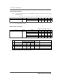
The information of the product number change
Starting April 1, 2001, the product number will be changed as listed below. To order from April 1,
2001 please use the new product number. For further information, please contact Epson sales
representative.
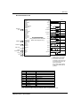
Configuration of product number
Devices
S1
C
33104
F
0A01
00
Packing specification
Specification
Package (D: die form; F: QFP)
Model number
Model name (C: microcomputer, digital products)
Product classification (S1: semiconductor)
Development tools
S5U1
C
33L01
D1
1
00
Packing specification
Version (1: Version 1 ∗2)
Tool type (D1: Development Tool ∗1)
Corresponding model number (33L01: for S1C33L01)
Tool classification (C: microcomputer use)
Product classification
(S5U1: development tool for semiconductor products)
∗1: For details about tool types, see the tables below. (In some manuals, tool types are represented by one digit.)
∗2: Actual versions are not written in the manuals.
Comparison table between Comparison table between new and previous
new and previous number number of development tools
S1C33 Family processors
Previous No.
E0C33A104
E0C33202
E0C33204
E0C33208
E0C33209
E0C332T01
E0C332L01
E0C332L02
E0C332S08
E0C332129
E0C33264
E0C332F128
Previous No.
CC33
CF33
COSIM33
GRAPHIC33
HMM33
JPEG33
MON33
MELODY33
PEN33
ROS33
SOUND33
SMT33
TS33
USB33
VOX33
VRE33
New No.
S1C33104
S1C33202
S1C33204
S1C33208
S1C33209
S1C33T01
S1C33L01
S1C33L02
S1C33S01
S1C33221
S1C33222
S1C33240
New No.
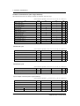
S5U1C33000C
S5U1C330C1S
S5U1C330C2S
S5U1C330G1S
S5U1C330H1S
S5U1C330J1S
S5U1C330M2S
S5U1C330M1S
S5U1C330P1S
S5U1C330R1S
S5U1C330S1S
S5U1C330S2S
S5U1C330T1S
S5U1C330U1S
S5U1C330V1S
S5U1C330V2S
Development tools for the S1C33 Family
Previous No.
New No.
Previous No.
New No.
ICE33
S5U1C33104H
DMT33LIF
S5U1C330L1D1
EM33-4M
S5U1C33104E
DMT33SMT
S5U1C330S1D1
PRC33001
S5U1C33104P1
DMT33LCD26
S5U1C330L2D1
POD33001
S5U1C33104P2
DMT33LCD37
S5U1C330L3D1
ICD33
S5U1C33000H
EPOD33001
S5U1C33208E1
DMT33004
S5U1C33104D1
EPOD33001LV
S5U1C33208E2
DMT33004PD
S5U1C33104D2
EPOD33208
S5U1C33208E3
DMT33005
S5U1C33208D1
EPOD33208LV
S5U1C33208E4
DMT33005PD
S5U1C33208D2
EPOD332L01LV
S5U1C33L01E1
DMT33006LV
S5U1C33L01D1
EPOD332T01
S5U1C33T01E1
DMT33006PDLV
S5U1C33L01D2
EPOD332T01LV
S5U1C33T01E2
DMT33007
S5U1C33208D3
EPOD33209
S5U1C33209E1
DMT33007PD
S5U1C33208D4
EPOD33209LV
S5U1C33209E2
DMT33008LV
S5U1C33T01D1
EPOD332128
S5U1C33220E1
DMT33008PDLV
S5U1C33T01D2
EPOD332128LV
S5U1C33220E2
DMT332S08LV
S5U1C33S01D1
EPOD332S08LV
S5U1C33S01E1
DMT332S08PDLV
S5U1C33S01D2
MEM33201
S5U1C33001M1
DMT33209LV
S5U1C33209D1
MEM33201LV
S5U1C33001M2
DMT33209PDLV
S5U1C33209D2
MEM33202
S5U1C33002M1
DMT332F128LV
S5U1C33240D1
MEM33202LV
S5U1C33002M2
DMT33MON
S5U1C330M1D1
MEM33203
S5U1C33003M1
DMT33MONLV
S5U1C330M2D1
MEM33203LV
S5U1C33003M2
DMT33AMP
S5U1C330A1D1
MEM33DIP42
S5U1C330D1M1
DMT33AMP2
S5U1C330A2D1
MEM33TSOP48
S5U1C330T1M1
DMT33AMP3
S5U1C330A3D1
EPOD176CABLE
S5U1C33T00E31
DMT33AMP4
S5U1C330A4D1
EPOD100CABLE
S5U1C33S00E31
DMT33CF
S5U1C330C1D1
EPOD33SRAM5V
S5U1C33000S
DMT33CPLD400KLV S5U1C330C2D1
EPOD33SRAM3V
S5U1C33001S
Contents
Contents
Chapter 1 Product Overview ................................................................ 1
1.1 Introduction ........................................................................... 1
1.2 Interface and Design Process Flowchart .............................. 3
Chapter 2 C33 Macro Specifications .................................................... 7
2.1
2.2
2.3
2.4
2.5
2.6
Overview ............................................................................... 7
Block Diagram ...................................................................... 8
C33 Macro Pins .................................................................. 10
Special Signals ................................................................... 15
Clock and Reset Signals .................................................... 15
Electrical Characteristics .................................................... 17
2.6.1 Absolute Maximum Ratings .................................................. 17
2.6.2 Recommended Operating Conditions ..................................... 18
2.6.3 DC Characteristics .............................................................. 20
2.6.4 Current Consumption ........................................................... 21
2.6.5 A/D Converter Characteristics ............................................... 22
2.6.6 AC Characteristics .............................................................. 24
2.6.6.1 Symbol Description ...................................................... 25
2.6.6.2 AC Characteristics Measurement Condition ...................... 26
2.6.6.3 AC Characteristics Tables (I/O Buffer Pins) ....................... 27
2.6.6.4 AC Characteristics Timing Charts (I/O Buffer Pins) ............. 37
2.6.6.5 AC Characteristics Tables (User Logic Interface) ............... 43
2.6.6.6 AC Characteristics Timing Charts (User Logic Interface) ...... 45
2.6.6.7 Oscillation Characteristics ............................................. 49
2.6.6.8 PLL Characteristics ...................................................... 51
Chapter 3 C33 Test Functions ........................................................... 52
3.1 Test Function Overview ...................................................... 52
3.2 DC/AC Test Mode (TST_DCT Mode) ................................. 53
3.2.1 Procedure to Enter Test Mode .............................................. 53
3.2.2 Test Mode ........................................................................ 54
3.3 User Circuit Test Mode (TST_USER Mode) ...................... 59
3.3.1 Procedure to Enter Test Mode .............................................. 59
3.3.2 Test Mode ........................................................................ 60
S1C33 ASIC DESIGN GUIDE
EMBEDDED ARRAY S1X50000 SERIES
EPSON
i
Contents
Chapter 4 Special Operations in ASICs that Include C33 Macros ...... 62
4.1 Special Operations ............................................................. 62
4.2 Verifying the C33 Macro Specifications .............................. 62
4.3 Verifying the Constraints on the Pin Arrangement ............. 63
4.3.1 Constraints on PLL, Low-speed, and High-speed Oscillator Circuit
Pins ................................................................................. 63
4.3.2 Constraints on A/D Converter Pins ......................................... 63
4.3.3 Number of Power Supply Pins ............................................... 63
4.3.4 Floorplan .......................................................................... 63
4.4 Connections between User I/O, User Circuits, and C33
Macros ................................................................................ 65
4.4.1 Connections between C33 Macros and User Circuits ................. 65
4.4.2 Connections between C33 Macros and User I/O ....................... 65
4.4.3 Notes on the Use of 5 V Tolerant I/O Cells ............................... 65
4.4.4 Connections between C33 Macros and User I/O ....................... 66
4.5 Test Pattern Creation ......................................................... 67
4.5.1 DC/AC Test Pattern Creation ................................................ 67
4.5.2 C33 Macro/User Circuit Connection Verification Test Pattern
Creation ........................................................................... 67
Chapter 5 Simulation .......................................................................... 68
Design Flowchart ............................................................................. 68
System Level Simulation .................................................... 70
Test Pattern Creation ......................................................... 70
Simulation Environment ...................................................... 71
5.4.1 Operating Environment ........................................................ 71
5.4.2 Installation Procedure .......................................................... 71
5.5 Running a Simulation ......................................................... 72
5.5.1 Preparing for Simulation ...................................................... 72
5.5.2 Sample Simulation Execution ............................................... 72
5.5.3 Simulation Execution Script .................................................. 73
5.5.4 Test Bench Structure .......................................................... 74
5.6 Evaluation Program Creation ............................................. 76
5.6.1 asm33 Assembler Prototype ................................................. 76
5.1
5.2
5.3
5.4
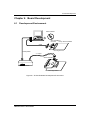
Chapter 6 Board Development ........................................................... 79
6.1 Development Environment ................................................. 79
6.2 Evaluation Board Design .................................................... 82
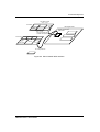
Chapter 7 Mounting ............................................................................ 85
7.1 Precautions on Mounting .................................................... 85
7.2 Others ................................................................................. 89
ii
EPSON
S1C33 ASIC DESIGN GUIDE
EMBEDDED ARRAY S1X50000 SERIES
1 Product Overview
Chapter 1 Product Overview
1.1
Introduction
This product, abbreviated here as "C33," is an ASIC macro family that consists of Seiko Epson's
independently developed S1C33000 Series 32-bit CPU core and macros for a wide range of peripheral
functions. The C33 macros can be integrated on Seiko Epson's 0.35 µm embedded ASIC family
(S1X50000 Series) ICs. SRAM, ROM, and flash memory ASIC memory macros that share the same
process technology can be integrated on the same chip. Thus Seiko Epson provides a complete ASIC
microcontroller design environment, and makes ASIC products (S1C33ASIC) that include C33
macros available to our customers.
The C33 CPU features a RISC architecture. Despite the small size of this CPU core, it provides an
extremely powerful instruction set that allows compilers to generate compact code. The C33 macros
provide the following features.
• High speed and high performance:
Operation from DC to 60 MHz. ASICs with on chip
ROM can operate at up to 50 MHz, and ASICs without
ROM can operate at up to 60 MHz.
• Powerful instruction set:
16-bit fixed length, 105 basic instructions.
• Instruction execution cycle:
Most instructions are executed in a single cycle.
• Multiply and accumulate operation:
16 bits × 16 bits + 64 bits. Multiply and accumulate
operations are executed in 2 clock cycles,
thus achieving 25 MOPS at 50 MHz.
• Registers:
Sixteen 32-bit general-purpose registers and five 32-bit
special registers.
• Address space:
256 MB linear address space (28-bit addresses) shared
by code, data, and I/O registers.
• External bus interface:
15 configurable memory areas
Direct connection to external memory.
• Interrupts:
Reset, NMI, up to 128 external interrupts, 4 software
interrupts, and two instruction execution exceptions
• Reset:
Cold reset, hot reset, and boot from area 10.
• Low-power modes:
Sleep mode and halt mode.
• Harvard architecture:
Instruction fetch and data load/store operations are
executed in parallel.
• User interface:
Allows software controlled insertion of wait cycles
(up to 7 cycles).
Supports #WAIT pin handshake control.
Large memory space for user logic (up to 16M bytes)
BCU registers allow internal software access to areas 4
through 18.
Large numbers of interrupt request signals from the
user logic may be connected to the interrupt controller.
S1C33 ASIC DESIGN GUIDE
EMBEDDED ARRAY S1X50000 SERIES
EPSON
1
1 Product Overview
• Other features:
Little endian (Certain areas can be set up for big endian
operation.)
*: In addition to this documents, you will also find the following documents of use when
designing ASICs.
• S1L50000 SERIES ASIC DESIGN GUIDE
• S1L50000 SERIES MSI Cell Library (I/O)
• S1X50000 SERIES MSI Cell Library (Internal cells)
• S1C332XX Series Technical Manual
• S1C33 Family ASIC Macro Manual
• EVALUATION BOARD MANUAL
2
EPSON
S1C33 ASIC DESIGN GUIDE
EMBEDDED ARRAY S1X50000 SERIES
1 Product Overview
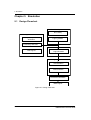
1.2
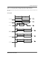
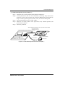
Interface and Design Process Flowchart
Determination of the specifications
for the S1C33 ASIC product
EPOD development
(*)
Software development
IC design
OS development
Evaluation board
development
Application development
Target board
development
Bulk design
Metal design
User circuit development
FPGA circuit
development
Functional verification in
an actual end product
ROM data issued
(*)EPOD: ROM emulation board
ES samples
Customer verification
Start of mass production
Figure 1.1 Total Product Development Process Flowchart
S1C33 ASIC DESIGN GUIDE
EMBEDDED ARRAY S1X50000 SERIES
EPSON
3
1 Product Overview
Table 1.1 Work Involved in Each Step of S1C33ASIC Development
Development step
Work involved
Specifications verification
• Selection of C33 macros and modules used
• Fixing the specifications of the user logic
• Verifying the package and pin assignment
specifications
• Verifying the test design specifications
• Verifying the EPOD specifications
Development environment preparation
• Design kit start-up (S1X50000 Series and C33
design kit)
User logic design
• Schematic capture, functional notation, logic
synthesis
• User logic simulation
Combined simulation
• Chip level net list creation
• Chip level simulation program creation (C33
assembler code)
• Chip level simulation
Design rule check
• SNRC(*)
Bulk signoff
• Floorplan creation (macro layout, pin assignment)
Finalizing the bulk size
Pre-simulation
• Pre-simulation
Test design
• ATPG (user logic block)
P&R
• Automatic placement and routing, CTS insertion
• Back annotation SDF creation
Post-simulation
• Post-simulation
ROM code handling
• Finalizing the internal ROM code
• ROM code data conversion
Metal signoff
Test production flow
Sample shipment, evaluation, switchover to
mass production
(*) SNRC: Net list rule checker
4
EPSON
S1C33 ASIC DESIGN GUIDE
EMBEDDED ARRAY S1X50000 SERIES
1 Product Overview
User Responsibility
Seiko Epson Responsibility
Investigation
Specification request
Verification of CPU and chip specifications
Approval to start development
Library creation
Provision of a design kit
Library
User logic design
Pin arrangement table
Provisional net list
Development
specifications
document
C33 design kit
S1X50000 Series design kit
Floorplan
Preliminary P&R
Bulk signoff
User logic design
Pre-simulation
Net list
Test patterns (apf)
Pre-simulation
P&R
User logic design
Post-simulation
sdf
ROM data
Internal ROM program creation
Inspection and verification
Post-simulation
Simulation
results
Logic specifications
confirmation verification document
Metal signoff
Mask creation
Figure 1.2 Division of Responsibility in the Development Process
(Development Flowchart Organized by Responsibility)
Continued on following page.
S1C33 ASIC DESIGN GUIDE
EMBEDDED ARRAY S1X50000 SERIES
EPSON
5
1 Product Overview
User Responsibility
Seiko Epson Responsibility
TS (test sample)
production
Functional evaluation
ES (engineering
sample) production
Overall evaluation
Qualification of mass
production
ES approval
6
EPSON
S1C33 ASIC DESIGN GUIDE
EMBEDDED ARRAY S1X50000 SERIES
2 C33 Macro Specifications
Chapter 2 C33 Macro Specifications
2.1
Overview
The C33 macro model has the structure described below. Seiko Epson provides a combination of these
elements as specified by user options.
! C33_CORE
• C33 core macros
• CPU, BCU (bus control unit), ITC (Interrupt controller), DBG (debugging unit), and highspeed oscillator circuit (including PLL circuit) macros
• About 60,000 gates
• Hard macro
! C33_PERI
• C33 digital peripheral function macros
• 4-channel 8-bit timer, 6-channel 16-bit timer, prescaler, 2-channel serial interface, watchdog
timer, clock timer, low-speed oscillator circuit (32 kHz), and I/O port macros
• About 20,000 gates
• Soft macros
! C33_AD
• C33 analog peripheral function macros
• 8-channel input and 10-bit successive-approximation converters
• Conversion time: 10 µs
• About 10,000 gates
• Hard macros
! C33_DMA
• C33 DMA function macros
• 4-channel high-speed DMA and 128-channel intelligent DMA macros
• About 10,000 gates
• Hard macros
(*)
• Soft macro: Net list or RTL macro for which the layout is not fixed.
• Hard macro: Net list macro for which the layout is fixed.
S1C33 ASIC DESIGN GUIDE
EMBEDDED ARRAY S1X50000 SERIES
EPSON
7
2 C33 Macro Specifications
2.2
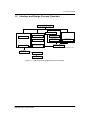
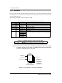
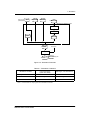
Block Diagram
DMA
Internal RAM
(area 0)
Internal ROM
(area 10)
C33_CORE
PAD_
CORE
(1) Required pins
PAD_
CORE_
OPTION
(2) Optional pins
(CPU,BCU,ITC,CLG,DBG)
(4) User pins
SBUS
User logic
interface
C33 CORE BLOCK
C33_PERI
User logic
(PSC,T8,T16,SIO,PORT)
PAD_
PERI
(3) Peripheral
function pins
ADC
Figure 2.1 C33 Macro Block Diagram
Terminology
8
BCU:
Bus control unit
ITC:
Interrupt controller
CLG:
Clock generator (oscillator circuit, PLL, and clock divider circuits built in)
DBG:
Debugging function block (On-chip ICE)
C33_CORE:
Functional blocks such as CPU, BCU, ITC, CLG, and DBG blocks
PAD_CORE:
I/O pad block for C33_CORE blocks
EPSON
S1C33 ASIC DESIGN GUIDE
EMBEDDED ARRAY S1X50000 SERIES
2 C33 Macro Specifications
SBUS:
Bus control block that has an address/data bus structure connected to the
user logic.
C33_PERI:
C33 peripheral function blocks. These blocks include prescaler, 8-bit timer
(4 channels), 16-bit timer (6 channels), serial interface (2 channels), port
(input, output, and I/O), and clock timer blocks.
PSC:
Prescaler
T8:
8-bit timer
SIO:
Serial interface
PAD_PERI:
I/O pads for the C33_PERI blocks
Internal ROM (area 10):Basically, area 10 is for user use as an on-chip mask ROM.
[16-bit data bus]
ASIC ROM is placed in this area.
(0 to 2 MB)
Internal RAM (area 0): Area 0 is used for on-chip data SRAM. This is high-speed access SRAM
[8-bit data bus]
that requires no wait cycle.
(0 to 128 KB)
ASIC RAM is allocated to this area.
[Byte write × 32 bits]
ADC:
A/D converter
S1C33 ASIC DESIGN GUIDE
EMBEDDED ARRAY S1X50000 SERIES
EPSON
9
2 C33 Macro Specifications
2.3
(1)
(2)
(3)
(4)
C33 Macro Pins
C33 Macro - Required pins (pad connections)
C33 Macro - Optional pins (pad connections)
C33 Macro - Peripheral function pins (pad connections)
C33 Macro - User pins (chip internal connections)
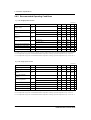
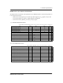
(1) C33 Macro - Required pins (pad connections) (57 pins)
These required pins must be connected to IC package pins.
Table 2.3.1 Required Pins
Connection: PAD_CORE
Cell name
(****)
Name
I/O
P_A23 to P_A0
I/O(*)
XHBC1T
24-bit address bus. A0 is shared with the #BSL pin
function.
P_D15 to P_D0
I/O
XHBC1T
16-bit data bus
P_CE10EX
I/O(*)
XHBC1T
Area 10 chip enable/test clock
P_RD_X
I/O(*)
XHBC1T
Read strobe
P_WRL_X
I/O(*)
XHBC1T
Lower byte write strobe
P_WRH_X
I/O(*)
XHBC1T
Upper byte write strobe
P_BCLK
O
XHTB1T
Bus clock
P_NMI_X
I
XHIBHP2
Pull-up
Nonmaskable interrupt
P_RESETX
I
XHIBHP2
Pull-up
Reset signal
P_X2SPDX
I
XHIBC
P_TST
I
XITST1
Pull-down
Test mode
P_EA10M1
I
XHIBHP2
Pull-up
Area 10 boot mode specification bit 1 (**)
P_EA10M0
I
XHIBC
XLBH2P2T
Pull-u/d
Function
Double-speed mode (The CPU clock operates at a
frequency twice that of the bus clock.)
Area 10 boot mode specification bit 0 (**)
P_DSIO
I/O
Pull-up
On-chip ICE serial I/O
P_OSC4
O
XLLOT
High-speed oscillator output
P_OSC3
I
XLLIN
High-speed oscillator input (oscillator element connection)
P_PLLS1
I
XHIBC
PLL mode specification bit 1 (***)
P_PLLS0
I
XHIBC
PLL mode specification bit 0 (***)
P_PLLC
O
XLLIN
PLL capacitor connection
(*)
Functions as an input in test mode.
(**) Refer to table 2.3.3 for the setting values.
(***) P_PLLS[1:0] pin settings
00: PLL unused. (The OSC3 input is used as the system clock.)
01: 4 × mode. fin = 10 to 15 MHz, fout = 40 to 60 MHz
11: 2 × mode. fin = 10 to 30 MHz, fout = 20 to 60 MHz
(****) The type can be modified as specified by the customer.
Refer to the "S1L50000 SERIES MSI Cell Library" manual for more information on the cell type.
10
EPSON
S1C33 ASIC DESIGN GUIDE
EMBEDDED ARRAY S1X50000 SERIES
2 C33 Macro Specifications
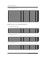
(2) C33 Macro - Optional pins (pad connections) (12 pins)
Table 2.3.2 Optional Pins
Connection: PAD_CORE_OPTION
Name
I/O
Cell name
Pull-u/d
Function
P_LCAS_X
O
XHTB1T
DRAM lower byte CAS signal
P_HCAS_X
O
XHTB1T
DRAM upper byte CAS signal
P_CE10IN
O
XHTB1T
Internal ROM emulation area (area 10) chip enable
P_CE9_X
I/O
XHBC1T
Chip enable (area 9 or area 17)
P_CE8_X
I/O
XHBC1T
Chip enable (area 8 or area 14) or the area 8 and 14
DRAM strobe
P_CE7_X
I/O
XHBC1T
Chip enable (area 7 or area 13) or the area 7 and 13
DRAM strobe
P_CE6_X
I/O
XHBC1T
Chip enable (area 6)
P_CE5_X
I/O
XHBC1T
Chip enable (area 5 or area 15)
P_CE4_X
I/O
XHBC1T
Chip enable (area 4 or area 11)
P_CE3_X
O
XHTB1T
Chip enable (area 3)
P_EMEMRD
O
XHTB1T
Internal ROM emulation area (area 10) read strobe
P_EA10M2
I
XHIBC
Area 10 boot mode specification bit 2
(*)
Pins P_CE4_X to P_CE9_X function as output pins due to test circuit modifications.
The customer can select whether or not each of the above optional pins is connected to a pad. If the
pin is not connected to a pad, it can be used as an internal signal with the same meaning. In that case,
the fan-in and fan-out values are equivalent to those for XBF2 from the S1X50000 library.
Table 2.3.3 P_EA10M2, P_EA10M1, and P_EA10M0 Settings
(Area 10 Boot Mode) Function
P_EA10M2
P_EA10M1
P_EA10M0
Function
0
0
0
Internal ROM emulation
0
0
1
Reserved
0
1
0
Internal ROM
0
1
1
External ROM
1
0
0
Reserved
1
0
1
Reserved
1
1
0
Reserved
1
1
1
Internal flash ROM
S1C33 ASIC DESIGN GUIDE
EMBEDDED ARRAY S1X50000 SERIES
EPSON
11
2 C33 Macro Specifications
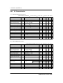
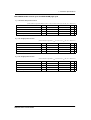
(3) C33 Macro - Peripheral function pins (pad connections) (44 pins)
Table 2.3.4 Peripheral Function Pins
Connection: PAD_PERI
Name
P_K67
P_K66
P_K65
P_K64
P_K63
P_K62
P_K61
P_K60
I/O
I
I
I
I
I
I
I
I
P_K54
P_K53
P_K52
P_K51
P_k50
I
I
I
I
I
XHIBHP2
XHIBHP2
XHIBHP2
XHIBHP2
XHIBHP2
P_P35
P_P34
P_P33
P_P32
P_P31
P_P30
I/O
I/O
I/O
I/O
I/O
I/O
XHBH1T
XHBH1T
XHBH1T
XHBH1T
XHBH1T
XHBH1T
I/O shared function port. When /CFP35(D5/0x402DC) = 0 (default)
I/O shared function port. When /CFP34(D4/0x402DC) = 0 (default)
I/O shared function port. When /CFP33(D3/0x402DC) = 0 (default)
I/O shared function port. When /CFP32(D2/0x402DC) = 0 (default)
I/O shared function port. When /CFP31(D1/0x402DC) = 0 (default)
I/O shared function port. When /CFP30(D0/0x402DC) = 0 (default)
P_P27
P_P26
P_P25
P_P24
P_P23
P_P22
I/O
I/O
I/O
I/O
I/O
I/O
XHBH1T
XHBH1T
XHBH1T
XHBH1T
XHBH1T
XHBH1T
P_P21
I/O XHBH1T
P_P20
P_P16
P_P15 *
I/O XHBH1T
I/O XHBH1T
I/O XHBH1T
P_P14 *
I/O XLBH2T
P_P13 *
I/O XLBH2T
P_P12 *
I/O XLBH2T
P_P11 *
I/O XLBH2T
P_P10 *
I/O XLBH2T
I/O shared function port. When /CFP27(D7/0x402D8) = 0 (default)
I/O shared function port. When /CFP26(D5/0x402D8) = 0 (default)
I/O shared function port. When /CFP25(D5/0x402D8) = 0 (default)
I/O shared function port. When /CFP24(D4/0x402D8) = 0 (default)
I/O shared function port. When /CFP23(D3/0x402D8) = 0 (default)
I/O shared function port. When /CFP22(D2/0x402D8) = 0 (default)
I/O shared function port. When /CFP21(D1/0x402D8) and
CFEx2(D2/0x40LDF) = 0 (default)
I/O shared function port. When /CFP20(D0/0x402D8) = 0 (default)
I/O shared function port. When /CFP16(D6/0x402D4) = 0 (default)
I/O shared function port. When /CFP15(D5/0x402D4) = 0 (default)
I/O shared function port. When /CFP14(D4/0x402D4) and
CFEx0(D0/0x402DF) = 0 (default)
I/O shared function port. When /CFP13(D3/0x402D4) and
CFEx1(D1/0x402DF) = 0 (default)
I/O shared function port. When /CFP12(D2/0x402D4) and
CFEx0(D0/0x402DF) = 0 (default)
I/O shared function port. When /CFP11(D1/0x402D4) and
CFEx1(D1/0x402DF) = 0 (default)
I/O shared function port. When /CFP10(D0/0x402D4) and
CFEx1(D1/0x402DF) = 0 (default)
12
Cell name Pull-u/d
Function
XHIBCLIN**
Input port. When /CFK67(D7/0x402C3) = 0 (default)
XHIBCLIN**
Input port. When /CFK66(D6/0x402C3) = 0 (default)
XHIBCLIN**
Input port. When /CFK65(D5/0x402C3) = 0 (default)
XHIBCLIN**
Input port. When /CFK64(D4/0x402C3) = 0 (default)
XHIBCLIN**
Input port. When /CFK63(D3/0x402C3) = 0 (default)
XHIBCLIN**
Input port. When /CFK62(D2/0x402C3) = 0 (default)
XHIBCLIN**
Input port. When /CFK61(D1/0x402C3) = 0 (default)
XHIBCLIN**
Input port. When /CFK60(D0/0x402C3) = 0 (default)
Pull-up
Pull-up
Pull-up
Pull-up
Pull-up
Input port. When /CFK54(D4/0x402C0) = 0 (default)
Input port. When /CFK53(D3/0x402C0) = 0 (default)
Input port. When /CFK52(D2/0x402C0) = 0 (default)
Input port. When /CFK51(D1/0x402C0) = 0 (default)
Input port. When /CFK50(D0/0x402C0) = 0 (default)
EPSON
S1C33 ASIC DESIGN GUIDE
EMBEDDED ARRAY S1X50000 SERIES
2 C33 Macro Specifications
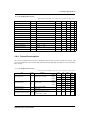
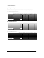
Connection: PAD_PERI
Name
I/O
Cell name
P_P07
I/O XHBH1T
P_P06
I/O XHBH1T
P_P05
I/O XHBH1T
P_P04
I/O XHBH1T
P_P03
P_P02
P_P01
P_P00
I/O
I/O
I/O
I/O
XHBH1T
XHBH1T
XHBH1T
XHBH1T
P_OSC2
O
XLLOT
P_OSC1
I
XLLIN
(*)
(**)
Pull-u/d
Function
I/O shared function port. When /CFP07(D7/0x402D0) and
CFEx7(D7/0x402DF) = 0 (default)
I/O shared function port. When /CFP06(D6/0x402D0) and
CFEx6(D6/0x402DF) = 0 (default)
I/O shared function port. When /CFP05(D5/0x402D0) and
CFEx5(D5/0x402DF) = 0 (default)
I/O shared function port. When /CFP04(D4/0x402D4) and
CFEx4(D4/0x402LDF) = 0 (default)
I/O shared function port. When /CFP03(D3/0x402DC) = 0 (default)
I/O shared function port. When /CFP02(D2/0x402DC) = 0 (default)
I/O shared function port. When /CFP01(D1/0x402DC) = 0 (default)
I/O shared function port. When /CFP00(D0/0x402DC) = 0 (default)
Low-speed oscillator (OSC1) output
Low-speed oscillator (OSC1) input (32 kHz oscillator
element connection or external clock input)
Pins P_P10 to P_P14 are used as S5U1C33000H interface pins.
Analog input and digital input shared function input buffer
The customer can select whether or not each of the above optional pins is connected to a pad. If the
pin is not connected to a pad, it can be used as an internal signal with the same meaning. In that case,
the fan-in and fan-out values are equivalent to those for XBF2 from the S1X50000 Series library.
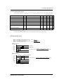
(4) C33 Macro - User logic interface pins (chip internal connections)
When the corresponding area is in on-chip mode due to BCU register settings, the following signals
and bus lines will be active when the bus is operational.
The C33 memory area is divided into 19 areas (area 0 through area 18). Basically, areas 4 to 18 are
external (off-chip) memory areas, and areas 0 to 3 are internal (on-chip) memory areas. The operating
conditions for these areas, such as type of memory used (SRAM, ROM, RAM, DRAM), device size
(8-bit or 16-bit data width), and timing (wait cycles and output disable cycles) are set using the BCU
registers. Additionally, it is also possible, using other BCU registers, to set up specific areas in areas
4 to 18 as external areas on the external bus and to have the other areas function as internal areas on
the internal bus as described later in this section.
Even in cases where specific areas as set up as on-chip (i.e. on the internal bus) areas, the operating
conditions for those areas, such as type of memory used (SRAM, ROM, RAM, DRAM), device size
(8-bit or 16-bit data width), and timing (wait cycles and output disable cycles), can be set in the same
way with the BCU registers.
S1C33 ASIC DESIGN GUIDE
EMBEDDED ARRAY S1X50000 SERIES
EPSON
13
2 C33 Macro Specifications
Table 2.3.5 User Logic Interface Pins
Connection: User logic
Pin
I/O
U_ADDR[23:0]
O
XBF4
Address bus
U_DOUT[15:0]
O
XBF4
Output data bus
U_DIN[15:0]
I
XAO22V
Input data bus
U_CE10_X
O
XBF4
User logic chip enable
U_CE9_X
O
XBF4
User logic chip enable
U_CE8_X
O
XBF4
User logic chip enable
U_CE7_X
O
XBF4
User logic chip enable
U_CE6_X
O
XBF4
User logic chip enable
U_CE5_X
O
XBF4
User logic chip enable
U_CE4_X
O
XBF4
User logic chip enable
U_WRL_X
O
XBF4
Lower byte write strobe
U_WRH_X
O
XBF4
Upper byte write strobe
U_RD_X
O
XBF4
Read strobe
U_WAIT_X
I
XAO22V
Wait signal
U_P3_PIN[5:0]
O
XBF2
P3 port input value (Separated test input)
U_P2_PIN[7:0]
O
XBF2
P2 port input value (Separated test input)
U_P1_PIN[6:0]
O
XBF2
P1 port input value (Separated test input)
U_P0_PIN[7:0]
O
XBF2
P0 port input value (Separated test input)
U_K5_PIN[4:0]
O
XBF2
K5 port input value (Separated test input)
U_BUSMD[2:0]
O
XBF2
Bus cycle status signal
U_BUSSZ[1:0]
O
XBF2
Bus size signal
U_BCLK
O
XBF4
Bus clock
U_OSC1CLK
O
XBF4
Low-speed oscillator circuit output
U_OSC3CLK
O
XBF4
High-speed oscillator circuit output
U_PLLCLK
O
XBF4
PLL circuit output
U_BCUCLK
O
XCRBF6
BCU clock (CTS support)
U_PERICLK
O
XCRBF6
Peripheral circuit clock (CTS support)
U_RST_X
O
XBF4
Reset signal
TST_USER
O
XBF2
User circuit test mode
TST_TA
O
XBF16
I/O cell TA pin connection signal
TST_TE_X
O
XBF16
I/O cell TE pin connection signal
TST_TS
O
XBF16
I/O cell TS pin connection signal
14
Cell name (fanout)
Function
EPSON
S1C33 ASIC DESIGN GUIDE
EMBEDDED ARRAY S1X50000 SERIES
2 C33 Macro Specifications
2.4
Special Signals
The U_BUSSZ[1:0] and U_BUSMD[2:0] signals indicate the state of the bus cycle currently
executing on the chip external bus and the internal bus (the internal bus including the on-chip user
logic). First, when U_BUSSZ[1:0] is 11, the bus is in the idle state, and the U_BUSMD[2:0] signals
have no meaning. This indicates that the neither the CPU nor the DMA controller is executing a
meaningful bus cycle. When U_BUSSZ[1:0] is not 11, U_BUSSZ[1:0] itself indicates the bus
operation data cycle at that point and U_BUSMD[2:0] indicates the bus state.
Table 2.4 Bus Cycle States
U_BUSMD[2:0]
U_BUSSZ[1:0]
2.5
000
001
010
011
100
101
110
111
00
01
10
11
CPU instruction fetch cycle
CPU vector fetch cycle
CPU data read cycle
CPU data write cycle
CPU stack read cycle
CPU stack write cycle
DMA data read cycle
DMA data write cycle
Byte (8 bits)
Half word (16 bits)
Word (32 bits)
Idle state
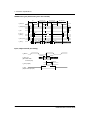
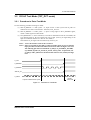
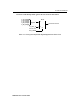
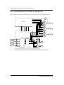
Clock and Reset Signals
There are 6 clock signals that can be connected to the user logic as follows.
U_PLLCLK, U_OSC1CLK, U_OSC3CLK, U_BCLK, U_BCUCLK, U_PERICLK
Figure 2.2 presents an overview of the clock and reset signals. U_OSC3CLK is the output from the
high-speed oscillator circuit (OSC3), and U_PLLCLK is the output from the PLL circuit. This means
that the frequency of the U_PLLCLK signal is determined by the inputs to pin P_PLLS1 and
P_PLLS0. For example, if the OSC3 oscillator frequency is 20 MHz, P_PLLS1 is 1, and P_PLLS0 is
0, then these clocks will have the following frequencies.
U_PLLCLK=40MHz,
U_OSC3CLK=20MHz
Note that the phases of these clocks do not match the phases of the CPU and BCU internal clocks due
to clock tree synthesis. Since both U_OSC3CLK and U_PLLCLK are generated from the OSC3 clock,
they will stop when the CPU executes a SLP instruction until sleep mode is cleared. Furthermore,
when the OSC3 oscillator starts operating again due to the factor that cleared sleep mode, the
U_OSC3CLK and U_PLLCLK signals will be unstable for a certain period, normally about 10 ms.
U_OSC1CLK is the output from the low-speed oscillator circuit.
U_BCUCLK and U_PERICLK are clocks to which the same clock tree synthesis applied as that for
the clocks used by the C33 core.
U_BCLK is the bus clock output from the BCU. Refer to the description of the bus clocks in the
"S1C33 Family ASIC Macro Manual" for more information on the bus clocks.
S1C33 ASIC DESIGN GUIDE
EMBEDDED ARRAY S1X50000 SERIES
EPSON
15
2 C33 Macro Specifications
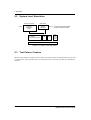
The U_RST_X signal outputs the value of the P_RESETX pad pin shown in the figure.
C33 MACRO
PLL
U_PLLCLK
P_OSC1
OSC1
U_OSC1CLK
P_OSC3
OSC3
U_OSC3CLK
CLG
CPU
CLOCK TREE
PERIPHERAL
CLOCK TREE
U_PERICLK
CLOCK TREE
U_BCUCLK
BCU
P_X2SPD
U_BCLK
P_RESETX
U_RST_X
Figure 2.2 On-Chip User Circuit Clock and Reset Signals
Table 2.5 Clock Operating Modes
Halt mode
Halt 2 mode
SLP mode
Debug mode*
U_PERICLK
RUN
RUN
STOP
STOP
U_BCUCLK
RUN
STOP
STOP
RUN
(*) Debug mode is the mode used when debugging with the S5U1C33000H.
16
EPSON
S1C33 ASIC DESIGN GUIDE
EMBEDDED ARRAY S1X50000 SERIES
2 C33 Macro Specifications
2.6
Electrical Characteristics
The C33 macro I/O cell library is designed based on the S1L50000 Series. Therefore, the electrical
characteristics are basically the same as those of the S1L50000 Series. However, since the C33 macros
include function blocks, such as CPU, DMA, PLL, oscillator, and A/D converter blocks, that have
unique and special characteristics, this manual stipulates the electrical characteristics for this product.
The C33 macros include I/O buffers, such the data bus and the I/O ports. The default I/O buffer setup
is based on that of the S1C33209 general-purpose product. Refer to section 2.3, "C33 Macro Pins" for
detailed information.
2.6.1 Absolute Maximum Ratings
1) Single power source
(VSS=0V)
Item
Symbol
Supply voltage
VDD
Input voltage
VI
Output voltage
VO
Output current per pin
IOUT
Analog power voltage
Analog input voltage
Storage temperature
Condition
Rated value
Unit
-0.3 to +4.0
V
-0.3 to VDD+0.5*1
1
*
V
-0.3 to VDD+0.5*
V
±30
mA
AVDD
-0.3 to +7.0
V
AVIN
-0.3 to AVDD+0.3
V
TSTG
-65 to +150
°C
*1: Voltages in the range -0.3 to +7.0 V are allowable for n-channel open-drain bidirectional buffers, IDC and IDH system
input buffers, and failsafe cells.
2) Dual power source
(VSS=0V)
Item
Supply voltage
Input voltage
Output voltage
Rated value
Unit
HVDD
Symbol
Condition
-0.3 to +7.0
V
LVDD
-0.3 to +4.0
V
-0.3 to HVDD+0.5*1
-0.3 to VDD+0.5*1
-0.3 to HVDD+0.5*1
-0.3 to LVDD+0.5*1
2
V
±30(±50* )
mA
-65 to +150
°C
HVI
LVI
HVO
LVO
Output current per pin
IOUT
Storage temperature
TSTG
*
V
V
V
*1: Voltages in the range -0.3 to +7.5 V are allowable for n-channel open-drain bidirectional buffers, LIDC and LIDH system
input buffers, and HIDC and HIDH system input buffers.
*2: Applies to 24 mA output current buffers.
S1C33 ASIC DESIGN GUIDE
EMBEDDED ARRAY S1X50000 SERIES
EPSON
17
2 C33 Macro Specifications
2.6.2 Recommended Operating Conditions
1) 3.3V single power source
(VSS=0V)
Item
Supply voltage
Input voltage
Symbol
Condition
VDD
Min.
Typ.
Max.
Unit
3.00
3.30
3.60
V
2.70
3.00
3.30
V
V
VSS
–
VDD*1
ROM-less model and 3.0±0.3V
–
–
60
MHz
ROM model and 3.0±0.3V
–
–
50
MHz
–
32.768
–
KHz
0
25
70*2
°C
3
VI
CPU oprerating clock
frequency
fCPU
Low-speed oscillation
frequency
fOSC1
Operating temperature
Ta
-40
25
85*
°C
Input rise time (normal input)
tri
–
–
100
ns
Input fall time (normal input)
Tj=0 to 85°C
Tj=-40 to 125°C
tfi
–
–
100
ns
Input rise time (schmitt input) tri
–
–
10
ms
Input fall time (schmitt input)
–
–
10
ms
tfi
*
*1: Either 5.25 V or 5.5 V is possible for n-channel open-drain bidirectional buffers and LIDC and LIDH system input buffers.
*2: This temperature range is the recommended ambient temperature assuming a junction temperature of Tj = 0 to 85 °C.
*3: This temperature range is the recommended ambient temperature assuming a junction temperature of Tj = -40 to 125 °C.
2) 2.0V single power source
(VSS=0V)
Item
Symbol
Condition
Min.
Typ.
Max.
Unit
Supply voltage
VDD
1.80
2.00
2.20
V
Input voltage
VI
VSS
–
VDD*1
V
CPU oprerating clock
frequency
fCPU
–
–
20
MHz
Low-speed oscillation
frequency
fOSC1
–
32.768
–
KHz
Operating temperature
Ta
0
25
70*2
°C
-40
25
85*3
°C
Input rise time (normal input)
tri
–
–
100
ns
Input fall time (normal input)
tfi
–
–
100
ns
Input rise time (schmitt input) tri
–
–
10
ms
Input fall time (schmitt input)
–
–
10
ms
Tj=0 to 85°C
Tj=-40 to 125°C
tfi
*
*1: Either 5.25 V or 5.5 V is possible for n-channel open-drain bidirectional buffers and LIDC and LIDH system input buffers.
*2: This temperature range is the recommended ambient temperature assuming a junction temperature of Tj = 0 to 85 °C.
*3: This temperature range is the recommended ambient temperature assuming a junction temperature of Tj = -40 to 125 °C.
18
EPSON
S1C33 ASIC DESIGN GUIDE
EMBEDDED ARRAY S1X50000 SERIES
2 C33 Macro Specifications
3) 3.3 V/5.0 V dual power source
(VSS=0V)
Item
Symbol
Min.
Typ.
Max.
Unit
4.75
5.00
5.25
V
4.50
5.00
5.50
V
3.00
3.30
3.60
V
2.70
3.00
3.30
V
HVI
VSS
–
HVDD
V
LVI
VSS
–
VSS
–
ROM-less model and 3.0±0.3V
–
–
60
MHz
ROM model and 3.0±0.3V
–
–
50
MHz
–
32.768
–
KHz
0
25
70*2
°C
3
Supply voltage (high voltge)
HVDD
Supply voltage (low voltge)
LVDD
Input voltage
CPU operating clock frequency
fCPU
Low-speed oscillation frequency
fOSC1
Operating temperature
Ta
Condition
Tj=0 to 85°C
-40
25
85*
°C
Input rise time (normal input)
tri
Tj=-40 to 125°C
–
–
100
ns
Input fall time (normal input)
tfi
–
–
100
ns
Input rise time (schmitt input)
tri
–
–
10
ms
Input fall time (schmitt input)
tfi
–
–
10
ms
*
1
*1: Either 5.25 V or 5.5 V is possible for n-channel open-drain bidirectional buffers and LIDC and LIDH system input buffers.
*2: This temperature range is the recommended ambient temperature assuming a junction temperature of Tj = 0 to 85 °C.
*3: This temperature range is the recommended ambient temperature assuming a junction temperature of Tj = -40 to 125 °C.
4) 2.0V/3.3V dual power source
(VSS=0V)
Min.
Typ.
Max.
Unit
Supply voltage (high voltge)
Item
HVDD
3.00
3.30
3.60
V
Supply voltage (low voltge)
LVDD
1.80
2.20
2.20
V
HVI
VSS
–
HVDD*1
1
Input voltage
Symbol
Condition
V
LVI
VSS
–
LVDD*
V
CPU operating clock frequency
fCPU
–
–
20
MHz
Low-speed oscillation frequency
fOSC1
–
32.768
–
KHz
0
25
70*2
°C
-40
25
3
85*
°C
–
–
50
ns
100
ns
–
–
50
ns
–
–
–
–
Operating temperature
Input rise time (normal input)
Input fall time (normal input)
Input rise time (schmitt input)
Input fall time (schmitt input)
Ta
Htri
Ltri
Htri
Ltri
Htri
Ltri
Htri
Ltri
*
100
ns
5
ms
10
ms
5
ms
10
ms
*1: Either 5.25 V or 5.5 V is possible for n-channel open-drain bidirectional buffers and the LIDC and LIDH system or HIDC
and HIDH system input buffers.
*2: This temperature range is the recommended ambient temperature assuming a junction temperature of Tj = 0 to 85 °C.
*3: This temperature range is the recommended ambient temperature assuming a junction temperature of Tj = -40 to 125 °C.
S1C33 ASIC DESIGN GUIDE
EMBEDDED ARRAY S1X50000 SERIES
EPSON
19
2 C33 Macro Specifications
2.6.3 DC Characteristics
1) 3.3V/5.0V dual power source
(Unless otherwise specified: HVDD=4.5V to 5.5V, LVDD=2.7V to 3.6V, VSS=0V, Ta=–40 to +85°C)
Item
Symbol
Min.
Typ.
Max.
Unit
-1
–
1
µA
IOZ
-1
–
1
µA
High-level output voltage
VOH
IOH=-3mA, VDD=Min.
VDD
-0.4
–
–
V
Low-level output voltage
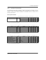
VOL
IOL=3mA, VDD=Min.
–
–
0.4
V
High-level input voltage
VIH
CMOS level, VDD=Max.
3.5
–
–
V
Low-level input voltage
VIL
CMOS level, VDD=Min.
–
–
1.0
V
Positive trigger input voltage
Input leakage current
ILI
Off-state leakage current
Condition
VT+
CMOS schmitt
2.0
–
4.0
V
Negative trigger input voltage VT-
CMOS schmitt
0.8
–
3.1
V
Hysteresis voltage
VH
CMOS schmitt
0.3
–
–
V
Pull-up resistor
RPU
VI=0V
60
120
288
KΩ
Pull-down registor
RPD
VI= VDD (#ICEMD)
30
60
144
KΩ
Input pin capacitance
CI
f=1MHz, VDD=0V
–
–
10
pF
Output pin capacitance
CO
f=1MHz, VDD=0V
–
–
10
pF
I/O pin capacitance
CIO
f=1MHz, VDD=0V
–
–
10
pF
*
2) 3.3V single power source
(Unless otherwise specified: VDD=2.7V to 3.6V, VSS=0V, Ta=–40 to +85°C)
Min.
Typ.
Max.
Unit
Input leakage current
Item
ILI
Symbol
Condition
-1
–
1
µA
Off-state leakage current
IOZ
-1
–
1
µA
High-level output voltage
VOH
IOH=-2mA, VDD=Min.
VDD
-0.4
–
–
V
Low-level output voltage
VOL
IOL=2mA , VDD=Min.
High-level input voltage
VIH
CMOS level, VDD=Max.
Low-level input voltage
VIL
CMOS level, VDD=Min.
Positive trigger input voltage
VT+
LVTTL schmitt
Negative trigger input voltage
VT-
LVTTL schmitt
0.6
Hysteresis voltage
VH
LVTTL schmitt
–
–
0.4
V
2.4
–
–
V
–
–
0.4
V
1.1
–
2.4
V
–
1.8
V
0.1
–
–
V
Other than DSIO
80
200
480
kΩ
DSIO
Pull-up resistor
RPU
VI =0V
40
100
240
kΩ
Pull-down registor
RPD
VI =VDD(#ICEMD)
40
100
240
kΩ
Input pin capacitance
CI
f=1MHz, VDD=0V
–
–
10
pF
Output pin capacitance
CO
f=1MHz, VDD=0V
–
–
10
pF
I/O pin capacitance
CIO
f=1MHz, VDD=0V
–
–
10
pF
20
EPSON
*
S1C33 ASIC DESIGN GUIDE
EMBEDDED ARRAY S1X50000 SERIES
2 C33 Macro Specifications
3) 2.0V single power source
(Unless otherwise specified: VDD=1.8V to 2.2V, VSS=0V, Ta=–40 to +85°C)
Item
Symbol
Condition
Min.
Typ.
Max.
Unit
Input leakage current
ILI
-1
–
1
µA
Off-state leakage current
IOZ
-1
–
1
µA
High-level output voltage
VOH
IOH=-0.6mA, VDD=Min.
VDD-0.2
–
–
V
Low-level output voltage
VOL
IOL=0.6mA, VDD=Min.
–
–
0.2
V
High-level input voltage
VIH
CMO level, VDD=Max.
1.6
–
–
V
Low-level input voltage
VIL
CMO level, VDD=Min.
–
–
0.3
V
Positive trigger input voltage
VT+
CMO schmitt
0.4
–
1.6
V
Negative trigger input voltage
VT-
CMO schmitt
0.3
–
1.4
V
Hysteresis voltage
VH
CMO schmitt
0
–
–
V
Pull-up resistor
RPU
VI=0V
60
240
600
KΩ
Pull-down registor
RPD
VI=VDD(#ICEMD)
30
120
300
KΩ
Input pin capacitance
CI
f=1MHz, VDD=0V
–
–
10
pF
Output pin capacitance
CO
f=1MHz, VDD=0V
–
–
10
pF
I/O pin capacitance
CIO
f=1MHz, VDD=0V
–
–
10
pF
*
2.6.4 Current Consumption
The current consumption of C33 ICs is defined as that for the C33 macro block VDD system. The
current consumption of user circuits and functional blocks other than C33 macros is not included in
these ratings.
1) 3.3V single power source
(Unless otherwise specified: VDD=2.7V to 3.6V, VSS=0V, Ta=–40 to +85°C)
Item
Operating current
Operating current
Symbol
IDD1
IDD2
Condition
When CPU is operating
HALT mode
Min.
Typ.
Max.
Unit
20MHz
–
25
35
mA
33MHz
–
40
60
mA
50MHz
–
65
85
mA
20MHz
–
12
16
mA
33MHz
–
20
26
mA
50MHz
–
30
40
mA
Operating current
IDD3
HALT2 mode, 20MHz
–
1.8
2.5
mA
Operating current
IDD4
Sleep mode
–
1
30
µA
When clock timer only is operating
OSC1oscillation: 32KHz
–
7
–
µA
Clock timer operation current IDDCT
S1C33 ASIC DESIGN GUIDE
EMBEDDED ARRAY S1X50000 SERIES
EPSON
*
21
2 C33 Macro Specifications
2) 2.0V single power source
(Unless otherwise specified: VDD=1.8V to 2.2V, VSS=0V, Ta=–40 to +85°C)
Item
Symbol
Condition
Min.
Typ.
Max.
Unit
Operating current
IDD1
When CPU is operating
20MHz
–
13
19
mA
Operating current
IDD2
HALT mode
20MHz
–
6
9
mA
Operating current
IDD3
HALT2 mode, 20MHz
20MHz
–
0.4
1.0
mA
Operating current
IDD4
Sleep mode
–
1
30
µA
Clock timer operation current
IDDCT
When clock timer only is
operating
OSC1oscillation: 32KHz
–
1.5
–
µA
Unit
*
3) Analog power current
Item
Symbol
AD converter
operating current
Condition
AIDD1
Min.
Typ.
Max.
AVDD=HVDD=4.5V to 5.5V
–
800
1400
VDD=AVDD=2.7V to 3.6V
–
500
800
*
µA
Current consumption measurement condition:
VIH=VDD, VIL=0V, output pins are open, VDD current is not included
No.
OSC3
OSC1
CPU
Other peripheral circuits
1
On
Off
Stop
Stop
2
On
Off
HALT mode
Stop
Stop
3
On
Off
HALT2 mode
Stop
Stop
4
Off
Off
SLEEP mode
Stop
Stop
5
Off
On
HALT mode
Run
Stop
Stop
A/D converter only operated,
conversion clock frequency=2MHz
6
On
Normal operation
Clock timer
*1
Off
HALT mode
*1: The values of current consumption while the CPU is operating were measured when a test program that consists of 55%
load instructions, 23% arithmetic operation instructions, 1% mac instruction, 12% branch instructions and 9% ext
instruction is being executed in the built-in RAM continuously.
2.6.5 A/D Converter Characteristics
1) 3.3V/5.0V dual power source
(Unless otherwise specified: HVDD=AVDD=4.5V to 5.5V, VSS=AVSS=0V, Ta=-40 to +85°C, ST[1:0]=11)
Item
Symbol
Min.
Typ.
Max.
Unit
–
10
–
bit
5
–
–
µs
0
2
4
LSB
-2
–
2
LSB
-3
–
3
LSB
EDL
-3
–
3
LSB
AIMP
–
–
5
KΩ
ACIN
–
–
45
pF
Resolution
–
Conversion time
tADC
Zero scale error
EZS
Full scale error
EFS
Integral linearity error
EIL
Differential linearity error
Permissible signal source impedance
Analog input capacitance
Condition
ST[1:0]=00(Min.), 11(Max.)
Best straight line method
*
1
* Note 1: Indicates the minimum value when A/D clock = 4MHz (maximum clock frequency in 5V system).
22
EPSON
S1C33 ASIC DESIGN GUIDE
EMBEDDED ARRAY S1X50000 SERIES
2 C33 Macro Specifications
2) 3.3V single power source
(Unless otherwise specified: VDD=AVDD=2.7V to 3.6V, VSS=AVSS=0V, Ta=0 to +70°C, A/D converter clock input
f=2MHz, ST[1:0]=11)
Item
Symbol
Min.
Typ.
Max.
Unit
–
10
–
bit
10
–
–
µs
0
2
4
LSB
-2
–
2
LSB
-3
–
3
LSB
EDL
-3
–
3
LSB
AIMP
–
–
5
KΩ
ACIN
–
–
45
pF
Resolution
–
Conversion time
tADC
Zero scale error
EZS
Full scale error
EFS
Integral linearity error
EIL
Differential linearity error
Permissible signal source impedance
Analog input capacitance
Condition
ST[1:0]=00(Min.), 11(Max.)
Best straight line method
*
1
Note 1: Indicates the minimum value when A/D clock = 2MHz (maximum clock frequency in 3V system).
Note 2: • Be sure to use as VDDE = AVDD.
• The A/D converter cannot be used when the S1C33209/204/202 is used with a 2V power source.
A/D conversion error
V[000]h
V'[000]h
V[3FF]h
V'[3FF]h
= Ideal voltage at zero-scale point (=0.5LSB)
= Actual voltage at zero-scale point
= Ideal voltage at full-scale point (=1022.5LSB)
= Actual voltage at full-scale point
AVDD - VSS
210 - 1
V'[3FF]h - V'[000]h
1LSB' =
210 - 2
1LSB =
■ Zero scale error
Digital output (hex)
004
Ideal conversion characteristic
003
002
V[000]h
(=0.5LSB)
Actual conversion characteristic
Zero scale error EZS =
001
(V'[000]h - 0.5LSB') - (V[000]h - 0.5LSB)
[LSB]
1LSB
V'[000]h
000
VSS
Analog input
■ Full scale error
V[3FF]h (=1022.5LSB)
V'[3FF]h
Digital output (hex)
3FF
3FE
Full scale error EFS =
3FD
(V'[3FF]h + 0.5LSB') - (V[3FF]h + 0.5LSB)
[LSB]
1LSB
Actual conversion characteristic
3FC
Ideal conversion characteristic
3FB
AVDD
Analog input
S1C33 ASIC DESIGN GUIDE
EMBEDDED ARRAY S1X50000 SERIES
EPSON
23
2 C33 Macro Specifications
■ Integral linearity error
3FF
Digital output (hex)
3FE
V'[3FF]h
3FD
Integral linearity error EL =
VN' - VN
[LSB]
1LSB'
VN VN'
003
Actual conversion characteristic
002
Ideal conversion characteristic
001
V'[000]h
000
VSS
Analog input
AVDD
■ Differential linearity error
Digital output (hex)
N+1
Ideal conversion characteristic
N
Actual conversion characteristic
N-1
V'[N]h
Differential linearity error ED =
N-2
V'[N-1]h
V'[N]h - V'[N-1]h
- 1 [LSB]
1LSB'
Analog input
2.6.6 AC Characteristics
The C33 macro block AC characteristics fall into two major sets.
One is the AC characteristics for the I/O buffer pins built into the C33 macros. These characteristics
stipulate the timing conditions for the interface with circuits outside the chip. These AC characteristics
are listed in section 2.6.6.3, "AC Characteristics Tables (I/O Buffer Pins)" and the timing charts are
shown in section 2.6.6.4, "AC Characteristics Timing Charts (I/O Buffer Pins)."
The other set is the AC characteristics for the signals that connect the C33 macro blocks to the user
circuits on the same chip. These AC characteristics are listed in section 2.6.6.5, "AC Characteristics
Tables (User Logic Interface)" and the timing charts are shown in section 2.6.6.6, "AC Characteristics
Timing Charts (User Logic Interface)."
The C33 macro bus interface can connect a wide range of external memory types, from SRAM and
ROM to EDO DRAM and burst ROM. The bus interface with chip internal user logic can only be used
as an SRAM type interface.
24
EPSON
S1C33 ASIC DESIGN GUIDE
EMBEDDED ARRAY S1X50000 SERIES
2 C33 Macro Specifications
2.6.6.1
Symbol Description
tCYC: Bus-clock cycle time
• In x1 mode,
tCYC = 50 nS (20 MHz) when the CPU is operated with a 20-MHz clock
tCYC = 30 nS (33 MHz) when the CPU is operated with a 33-MHz clock
• In x2 mode,
tCYC = 50 nS (20 MHz) when the CPU is operated with a 40-MHz clock
tCYC = 40 nS (25 MHz) when the CPU is operated with a 50-MHz clock
tCYC = 33 nS (30 MHz) when the CPU is operated with a 60-MHz clock
WC: Number of wait cycles
Up to 7 wait cycles can be specified using the BCU control register. It is also possible to extend the
number of wait cycles by inputs (wait request inputs) to the P_P30 (#WAIT) pin or the U_WAIT_X
pin when it is necessary.
The minimum number of read cycles with no wait (0) inserted is 1 cycle.
The minimum number of write cycles with no wait cycle (0) inserted is 2 cycles. It does not change
even if 1-wait cycle is set. The write cycle is actually extended when 2 or more wait cycles are set.
When inserting wait cycles by controlling the wait request inputs from external circuits, the
sampling timing of the wait request input requires careful attention. Read cycles are terminated on
the cycle that the negation of the wait request input was sampled. Write cycles are terminated on
the cycle following the cycle that the negation of the wait request input was sampled.
C1, C2, C3, Cn: Cycle number
C1 indicates the first cycle when the BCU transfers data from/to an external memory or another
device. Similarly, C2 and Cn indicate the second cycle and nth cycle, respectively.
Cw: Wait cycle
Indicates that the cycle is wait cycle inserted.
S1C33 ASIC DESIGN GUIDE
EMBEDDED ARRAY S1X50000 SERIES
EPSON
25
2 C33 Macro Specifications
2.6.6.2
AC Characteristics Measurement Condition
Signal detection level:
Input signal
High level
VIH = VDD - 0.4 V
Low level
VIL = 0.4 V
Output signal High level
VOH = 1/2 VDD
Low level
VOL = 1/2 VDD
The following applies when OSC3 is external clock input:
Input signal
High level VIH = 1/2 VDD
Low level
Input signal waveform:
VIL = 1/2 VDD
Rise time (10% → 90% VDD) 5 ns (I/O buffer pins)
Fall time (90% → 10% VDD) 5 ns (I/O buffer pins)
Output load capacitance: CL = 50 pF (I/O buffer pins only)
F/O = 1 (User logic interface)
26
EPSON
S1C33 ASIC DESIGN GUIDE
EMBEDDED ARRAY S1X50000 SERIES
2 C33 Macro Specifications
2.6.6.3
AC Characteristics Tables (I/O Buffer Pins)
The tables in this section stipulate the timing of the interface between the C33 macros and circuits
external to the chip.
External clock input characteristics
Note: These AC characteristics apply to input signals from outside the IC.
1) 3.3V/5.0V dual power source
(Unless otherwise specified: HVDD=4.5V to 5.5V, LVDD=2.7V to 3.6V, VSS=0V, Ta=–40 to 85°C)
Item
Symbol
Min.
High-speed clock cycle time
tC3
30
P_OSC3 clock input duty
tC3ED
45
P_OSC3 clock input rise time
P_OSC3 clock input fall time
Max.
Unit
*
ns
55
%
tIF
5
ns
tIR
5
ns
P_BCLK high-level output delay time
tCD1
35
ns
P_BCLK low-level output delay time
tCD2
35
ns
Minimum reset pulse width (P_RESETX input)
tRST
6 × tCYC
ns
Note: The input to the OSC3 pin must be in the range VSS to LVDD.
2) 3.3V single power source
(Unless otherwise specified: VDD=2.7V to 3.6V, VSS=0V, Ta=–40 to 85°C)
Item
Symbol
Min.
High-speed clock cycle time
tC3
30
P_OSC3 clock input duty
tC3ED
45
P_OSC3 clock input rise time
P_OSC3 clock input fall time
Max.
Unit
*
ns
55
%
tIF
5
ns
tIR
5
ns
P_BCLK high-level output delay time
tCD1
35
ns
P_BCLK low-level output delay time
tCD2
35
ns
Minimum reset pulse width (P_RESETX input)
tRST
6×tCYC
ns
Note: The input to the OSC3 pin must be in the range VSS to VDD.
3) 2.0V single power source
(Unless otherwise specified: VDD=1.8V to 2.2V, VSS=0V, Ta=–40 to 85°C)
Item
Symbol
Min.
High-speed clock cycle time
tC3
30
P_OSC3 clock input duty
tC3ED
45
P_OSC3 clock input rise time
tIF
P_OSC3 clock input fall time
P_BCLK high-level output delay time
P_BCLK low-level output delay time
tCD2
Minimum reset pulse width (P_RESETX input)
tRST
Max.
Unit
55
%
5
ns
tIR
5
ns
tCD1
60
ns
60
ns
6 × tCYC
*
ns
ns
Note: The input to the OSC3 pin must be in the range VSS to VDD.
S1C33 ASIC DESIGN GUIDE
EMBEDDED ARRAY S1X50000 SERIES
EPSON
27
2 C33 Macro Specifications
BCLK clock output chracteristics
Note: These AC characteristic values are applied only when the high-speed oscillation circuit
is used.
1) 3.3V/5.0V dual power source
(Unless otherwise specified: HVDD=4.5V to 5.5V, LVDD=2.7V to 3.6V, VSS=0V, Ta=–40 to 85°C)
Item
P_BCLK clock output duty
Symbol
tCBD
Min.
Max.
Unit
40
60
%
*
2) 3.3V single power source
(Unless otherwise specified: VDD=2.7V to 3.6V, VSS=0V, Ta=–40 to 85°C)
Item
P_BCLK clock output duty
Symbol
tCBD
Min.
Max.
Unit
40
60
%
*
3) 2.0V single power source
(Unless otherwise specified: VDD=1.8V to 2.2V, VSS=0V, Ta=–40 to 85°C)
Item
P_BCLK clock output duty
Symbol
tCBD
Min.
Max.
Unit
40
60
%
*
Common characteristics
1) 3.3/5.0V dual power source
(Unless otherwise specified: HVDD=4.5V to 5.5V, LVDD=2.7V to 3.6V, VSS=0V, Ta=–40 to 85°C)
Item
28
Symbol
Min.
Max.
Unit
Address delay time
tAD
–
8
ns
P_CEx delay time (1)
tCE1
–
8
ns
P_CEx delay time (2)
tCE2
–
8
ns
Wait setup time
tWTS
15
–
ns
Wait hold time
tWTH
0
–
ns
Read signal delay time (1)
tRDD1
8
ns
Read data setup time
tRDS
12
ns
Read data hold time
tRDH
0
ns
Write signal delay time (1)
tWRD1
8
ns
Write data delay time (1)
tWDD1
10
ns
Write data delay time (2)
tWDD2
0
10
ns
Write data hold time
tWDH
0
EPSON
*
ns
S1C33 ASIC DESIGN GUIDE
EMBEDDED ARRAY S1X50000 SERIES
2 C33 Macro Specifications
2) 3.3V single power source
(Unless otherwise specified: VDD=2.7V to 3.6V, VSS=0V, Ta=–40 to 85°C)
Item
Symbol
Min.
Max.
Unit
Address delay time
tAD
–
10
ns
P_CEx delay time (1)
tCE1
–
10
ns
P_CEx delay time (2)
tCE2
–
10
ns
Wait setup time
tWTS
15
–
ns
Wait hold time
tWTH
0
–
ns
Read signal delay time (1)
tRDD1
10
ns
Read data setup time
tRDS
15
ns
Read data hold time
tRDH
0
ns
Write signal delay time (1)
tWRD1
10
ns
Write data delay time (1)
tWDD1
10
ns
Write data delay time (2)
tWDD2
0
10
ns
Write data hold time
tWDH
0
*
ns
3) 2.0V single power source
(Unless otherwise specified: VDD= 1.8V to 2.2V, VSS=0V, Ta=–40 to 85°C)
Min.
Max.
Unit
Address delay time
Item
tAD
Symbol
–
20
ns
P_CEx delay time (1)
tCE1
–
20
ns
P_CEx delay time (2)
tCE2
–
20
ns
Wait setup time
tWTS
40
–
ns
Wait hold time
tWTH
0
–
ns
Read signal delay time (1)
tRDD1
20
ns
Read data setup time
tRDS
40
ns
Read data hold time
tRDH
0
ns
Write signal delay time (1)
tWRD1
20
ns
Write data delay time (1)
tWDD1
20
ns
Write data delay time (2)
tWDD2
0
20
ns
Write data hold time
tWDH
0
*
ns
SRAM read cycle
1) 3.3/5.0V dual power source
(Unless otherwise specified: HVDD=4.5V to 5.5V, LVDD=2.7V to 3.6V, VSS=0V, Ta=–40 to 85°C)
Item
Symbol
Min.
Max.
Unit
8
ns
Read signal delay time (2)
tRDD2
Read signal pulse width
tRDW
Read address access time (1)
tACC1
tCYC(1+WC)-20
ns
Chip enable access time (1)
tCEAC1
tCYC(1+WC)-20
ns
Read signal access time (1)
tRDAC1
tCYC(0.5+WC)-20
ns
S1C33 ASIC DESIGN GUIDE
EMBEDDED ARRAY S1X50000 SERIES
EPSON
tCYC(0.5+WC)-8
*
ns
29
2 C33 Macro Specifications
2) 3.3V single power source
(Unless otherwise specified: VDD=2.7V to 3.6V, VSS=0V, Ta=–40 to 85°C)
Item
Symbol
Min.
Max.
Unit
10
ns
Read signal delay time (2)
tRDD2
Read signal pulse width
tRDW
Read address access time (1)
tACC1
tCYC(1+WC)-25
ns
Chip enable access time (1)
tCEAC1
tCYC(1+WC)-25
ns
Read signal access time (1)
tRDAC1
tCYC(0.5+WC)-25
ns
tCYC(0.5+WC)-10
*
ns
3) 2.0V single power source
(Unless otherwise specified: VDD=1.8V to 2.2V, VSS=0V, Ta=–40 to 85°C)
Item
Symbol
Read signal delay time (2)
tRDD2
Read signal pulse width
tRDW
Read address access time (1)
tACC1
Chip enable access time (1)
Read signal access time (1)
Min.
Max.
Unit
10
ns
tCYC(0.5+WC)-10
*
ns
tCYC(1+WC)-60
ns
tCEAC1
tCYC(1+WC)-60
ns
tRDAC1
tCYC(0.5+WC)-60
ns
SRAM write cycle
1) 3.3V/5.0V dual power source
(Unless otherwise specified: HVDDE=4.5V to 5.5V, LVDD=2.7V to 3.6V, VSS=0V, Ta=–40 to 85°C)
Item
Symbol
Write signal delay time (2)
tWRD2
Write signal pulse width
tWRW
Min.
Max.
Unit
8
ns
tCYC(1+WC)-10
*
ns
2) 3.3V single power source
(Unless otherwise specified: VDD=2.7V to 3.6V, VSS=0V, Ta=–40 to 85°C)
Item
Symbol
Write signal delay time (2)
tWRD2
Write signal pulse width
tWRW
Min.
Max.
Unit
10
ns
tCYC(1+WC)-10
*
ns
3) 2.0V single power source
(Unless otherwise specified: VDD=1.8V to 2.2V, VSS=0V, Ta=–40 to 85°C)
Item
30
Symbol
Write signal delay time (2)
tWRD2
Write signal pulse width
tWRW
EPSON
Min.
tCYC(1+WC)-20
Max.
Unit
20
ns
*
ns
S1C33 ASIC DESIGN GUIDE
EMBEDDED ARRAY S1X50000 SERIES
2 C33 Macro Specifications
DRAM access cycle common characteristics
The #RAS and #CAS symbols in the stipulations for the DRAM interface in the following tables are
to be interpreted as follows.
• #RAS refers to that signal any one of the chip enable signals (P_CEX signals) set up by the
bus controller (BCU) to operate as a RAS signal for the DRAM.
• #CAS refers to the P_HCAS_X or the P_LCAS_X signal.
1) 3.3V/5.0V dual power source
(Unless otherwise specified: HVDD=4.5V to 5.5V, LVDD=2.7V to 3.6V, VSS=0V, Ta=–40 to 85°C)
Item
Symbol
Min.
Max.
Unit
10
ns
10
ns
#RAS signal delay time (1)
tRASD1
#RAS signal delay time (2)
tRASD2
#RAS signal pulse width
tRASW
#CAS signal delay time (1)
tCASD1
10
ns
#CAS signal delay time (2)
tCASD2
10
ns
#CAS signal pulse width
tCASW
Read signal delay time (3)
tRDD3
Read signal pulse width (2)
tRDW2
Write signal delay time (3)
tWRD3
Write signal pulse width (2)
tWRW2
tCYC(2+WC)-10
*
ns
tCYC(0.5+WC)-5
ns
10
tCYC(2+WC)-10
ns
ns
10
tCYC(2+WC)-10
ns
ns
2) 3.3V single power source
(Unless otherwise specified: VDD=2.7V to 3.6V, VSS=0V, Ta=–40 to 85°C)
Item
Symbol
Min.
Max.
Unit
10
ns
10
ns
#RAS signal delay time (1)
tRASD1
#RAS signal delay time (2)
tRASD2
#RAS signal pulse width
tRASW
#CAS signal delay time (1)
tCASD1
10
ns
#CAS signal delay time (2)
tCASD2
10
ns
#CAS signal pulse width
tCASW
Read signal delay time (3)
tRDD3
Read signal pulse width (2)
tRDW2
Write signal delay time (3)
tWRD3
Write signal pulse width (2)
tWRW2
S1C33 ASIC DESIGN GUIDE
EMBEDDED ARRAY S1X50000 SERIES
EPSON
tCYC(2+WC)-10
ns
tCYC(0.5+WC)-10
ns
10
tCYC(2+WC)-10
ns
ns
10
tCYC(2+WC)-10
*
ns
ns
31
2 C33 Macro Specifications
3) 2.0V single power source
(Unless otherwise specified: VDD=1.8V to 2.2V, VSS=0V, Ta=–40 to 85°C)
Item
Symbol
Min.
Max.
Unit
#RAS signal delay time (1)
tRASD1
20
ns
#RAS signal delay time (2)
tRASD2
20
ns
#RAS signal pulse width
tRASW
#CAS signal delay time (1)
tCASD1
#CAS signal delay time (2)
tCASD2
#CAS signal pulse width
tCASW
Read signal delay time (3)
tRDD3
Read signal pulse width (2)
tRDW2
Write signal delay time (3)
tWRD3
Write signal pulse width (2)
tWRW2
tCYC(2+WC)-20
*
ns
20
ns
20
ns
tCYC(0.5+WC)-20
ns
20
tCYC(2+WC)-20
ns
ns
20
tCYC(2+WC)-20
ns
ns
DRAM random access cycle and DRAM fast-page cycle
1) 3.3V/5.0V dual power source
(Unless otherwise specified: HVDD=4.5V to 5.5V, LVDD=2.7V to 3.6V, VSS=0V, Ta=–40 to 85°C)
Item
Symbol
Min.
Max.
Unit
Column address access time
tACCF
tCYC(1+WC)-25
ns
#RAS access time
tRACF
tCYC(1.5+WC)-25
ns
#CAS access time
tCACF
tCYC(0.5+WC)-25
ns
*
2) 3.3V single power source
(Unless otherwise specified: VDD=2.7V to 3.6V, VSS=0V, Ta=–40 to 85°C)
Max.
Unit
Column address access time
Item
tACCF
Symbol
Min.
tCYC(1+WC)-25
ns
#RAS access time
tRACF
tCYC(1.5+WC)-25
ns
#CAS access time
tCACF
tCYC(0.5+WC)-25
ns
*
3) 2.0V single power source
(Unless otherwise specified: VDD=1.8V to 2.2V, VSS=0V, Ta=–40 to 85°C)
Item
32
Max.
Unit
Column address access time
tACCF
Symbol
tCYC(1+WC)-60
ns
#RAS access time
tRACF
tCYC(1.5+WC)-60
ns
#CAS access time
tCACF
tCYC(0.5+WC)-60
ns
EPSON
Min.
*
S1C33 ASIC DESIGN GUIDE
EMBEDDED ARRAY S1X50000 SERIES
2 C33 Macro Specifications
EDO DRAM random access cycle and EDO DRAM page cycle
1) 3.3V/5.0V dual power source
(Unless otherwise specified: HVDD=4.5V to 5.5V, LVDD=2.7V to 3.6V, VSS=0V, Ta=–40 to 85°C)
Item
Symbol
Min.
Max.
Unit
Column address access time
tACCE
tCYC(1.5+WC)-25
ns
#RAS access time
tRACE
tCYC(2+WC)-25
ns
#CAS access time
tCACE
tCYC(1+WC)-15
ns
Read data setup time
tRDS2
20
*
ns
2) 3.3V single power source
(Unless otherwise specified: VDD=2.7V to 3.6V, VSS=0V, Ta=–40 to 85°C)
Max.
Unit
Column address access time
Item
tACCE
Symbol
Min.
tCYC(1.5+WC)-25
ns
#RAS access time
tRACE
tCYC(2+WC)-25
ns
#CAS access time
tCACE
tCYC(1+WC)-20
ns
Read data setup time
tRDS2
20
*
ns
3) 2.0V single power source
(Unless otherwise specified: VDD=1.8V to 2.2V, VSS=0V, Ta=–40 to 85°C)
Max.
Unit
Column address access time
Item
tACCE
tCYC(1.5+WC)-60
ns
#RAS access time
tRACE
tCYC(2+WC)-60
ns
#CAS access time
tCACE
tCYC(1+WC)-60
ns
Read data setup time
tRDS2
S1C33 ASIC DESIGN GUIDE
EMBEDDED ARRAY S1X50000 SERIES
Symbol
EPSON
Min.
20
*
ns
33
2 C33 Macro Specifications
Burst ROM read cycle
1) 3.3V/5.0V dual power source
(Unless otherwise specified: HVDD=4.5V to 5.5V, LVDD=2.7V to 3.6V, VSS=0V, Ta=–40 to 85°C)
Item
Symbol
Min.
Max.
Unit
Read address access time (2)
tACC2
tCYC(1+WC)-20
ns
Chip enable access time (2)
tCEAC2
tCYC(1+WC)-20
ns
Read signal access time (2)
tRDAC2
tCYC(0.5+WC)-20
ns
Burst address access time
tACCB
tCYC(1+WC)-20
ns
*
2) 3.3V single power source
(Unless otherwise specified: VDD=2.7V to 3.6V, VSS=0V, Ta=–40 to 85°C)
Max.
Unit
Read address access time (2)
Item
tACC2
Symbol
Min.
tCYC(1+WC)-25
ns
Chip enable access time (2)
tCEAC2
tCYC(1+WC)-25
ns
Read signal access time (2)
tRDAC2
tCYC(0.5+WC)-25
ns
Burst address access time
tACCB
tCYC(1+WC)-25
ns
*
3) 2.0V single power source
(Unless otherwise specified: VDD=1.8V to 2.2V, VSS=0V, Ta=–40 to 85°C)
Item
Symbol
Max.
Unit
tCYC(1+WC)-60
ns
tCEAC2
tCYC(1+WC)-60
ns
tRDAC2
tCYC(0.5+WC)-60
ns
tACCB
tCYC(1+WC)-60
ns
Read address access time (2)
tACC2
Chip enable access time (2)
Read signal access time (2)
Burst address access time
Min.
*
External bus master and NMI
The #BUSRE0, #BUSACK, and #NMI symbols in the external bus master and NMI timing
stipulations in the following tables are to be interpreted as follows.
34
#BUSRE0:
When the P_34 pin is set up as bus request signal input from an external bus master.
#BUSACK:
When the P_35 pin is set up as the bus acknowledge signal output to an external bus
master.
#NMI:
The P_NMI_X input
EPSON
S1C33 ASIC DESIGN GUIDE
EMBEDDED ARRAY S1X50000 SERIES
2 C33 Macro Specifications
1) 3.3V/5.0V dual power source
(Unless otherwise specified: HVDD=4.5V to 5.5V, LVDD=2.7V to 3.6V, VSS=0V, Ta=–40 to 85°C)
Item
Symbol
Min.
Max.
Unit
#BUSREQ signal setup time
tBRQS
15
ns
#BUSREQ signal hold time
tBRQH
0
ns
#BUSACK signal output delay time
tBAKD
10
ns
High-impedance → output delay time
tZ2E
10
ns
Output → high-impedance delay time
tB2Z
10
ns
#NMI pulse width
tNMIW
30
*
ns
2) 3.3V single power source
(Unless otherwise specified: VDD=2.7V to 3.6V, VSS=0V, Ta=–40 to 85°C)
Item
Symbol
Min.
Max.
Unit
#BUSREQ signal setup time
tBRQS
15
ns
#BUSREQ signal hold time
tBRQH
0
ns
#BUSACK signal output delay time
tBAKD
10
ns
High-impedance → output delay time
tZ2E
10
ns
Output → high-impedance delay time
tB2Z
10
ns
#NMI pulse width
tNMIW
30
*
ns
3) 2.0V single power source
(Unless otherwise specified: VDD=1.8V to 2.2V, VSS=0V, Ta=–40 to 85°C)
Item
Symbol
Min.
Max.
Unit
#BUSREQ signal setup time
tBRQS
40
#BUSREQ signal hold time
tBRQH
0
#BUSACK signal output delay time
tBAKD
20
ns
High-impedance → output delay time
tZ2E
20
ns
Output → high-impedance delay time
tB2Z
20
ns
#NMI pulse width
tNMIW
S1C33 ASIC DESIGN GUIDE
EMBEDDED ARRAY S1X50000 SERIES
EPSON
90
*
ns
ns
ns
35
2 C33 Macro Specifications
Input, Output and I/O port
The tables in this section stipulate the AC characteristics of the P_Pxx and P_Kxx ports.
1) 3.3V/5.0V single power source
(Unless otherwise specified: HVDD=4.5V to 5.5V, LVDD=2.7V to 3.6V, VSS=0V, Ta=–40 to 85°C)
Item
Symbol
Min.
Input data setup time
tINPS
20
Input data hold time
tINPH
10
Output data delay time
tOUTD
P_Kxx-port interrupt
SLEEP, HALT2 mode
input pulse width
Others
tKINW
Max.
Unit
*
ns
ns
20
ns
30
ns
2 × tCYC
ns
2) 3.3V single power source
(Unless otherwise specified: VDD=2.7V to 3.6V, VSS=0V, Ta=–40 to 85°C)
Item
Symbol
Min.
Max.
Unit
Input data setup time
tINPS
20
ns
Input data hold time
tINPH
10
ns
Output data delay time
tOUTD
P_Kxx-port interrupt
SLEEP, HALT2 mode
input pulse width
Others
tKINW
20
*
ns
30
ns
2 × tCYC
ns
3) 2.0V single power source
(Unless otherwise specified: VDD=1.8V to 2.2V, VSS=0V, Ta=–40 to 85°C)
Item
Min.
Max.
Unit
Input data setup time
tINPS
40
ns
Input data hold time
tINPH
20
ns
Output data delay time
36
Symbol
tOUTD
P_Kxx-port interrupt
SLEEP, HALT2 mode
input pulse width
Others
tKINW
EPSON
30
*
ns
90
ns
2 × tCYC
ns
S1C33 ASIC DESIGN GUIDE
EMBEDDED ARRAY S1X50000 SERIES
2 C33 Macro Specifications
2.6.6.4
AC Characteristics Timing Charts (I/O Buffer Pins)
This section presents the timing charts for the interface between the C33 macros and chip-external
circuits.
Clock
(1) When an external clock is input (in x1 speed mode):
tC3
tC3H
tC3ED = tC3H/tC3
P_OSC3
(High-speed clock)
tIF
tIR
tC3
tCD1
tCD2
P_BCLK
(Clock output)
tC1
tC1H
tC1ED = tC1H/tC1
P_OSC1
(Low-speed clock)
(2) When the high-speed oscillation circuit is used for the operating clock:
tC3
tCBH
tCBD = tCBH/tC3
P_BCLK
(Clock output)
SRAM read cycle (basic cycle: 1 cycle)
tC3
P_BCLK
tAD
tAD
tCE1
tCE2
P_A[23:0]
P_CEx
tRDD1
tRDD2
tRDW
P_RD_X
tCEAC1
tACC1
tRDAC1
P_D[15:0]
tRDS
tWTS
tRDH
*1
tWTH
P_P30
(Wait input)
∗1 tRDH is measured with respect to the first signal change (negation) from among the P_RD, P_CEx, or the
P_A[23:0] signals.
S1C33 ASIC DESIGN GUIDE
EMBEDDED ARRAY S1X50000 SERIES
EPSON
37
2 C33 Macro Specifications
SRAM read cycle (when a wait cycle is inserted)
C1
Cw (wait cycle)
Cn (last cycle)
P_BCLK
tAD
tAD
tCE1
tCE2
P_A[23:0]
P_CEx
tRDD1 (C1 only)
tRDD2
tRDW
P_RD_X
tCEAC1
tACC1
tRDAC1
P_D[15:0]
tWTS
tWTH
tWTS
tWTH
tRDS
tRDH *1
P_P30
(Wait input)
∗1 tRDH is measured with respect to the first signal change (negation) from among the P_RD, P_CEx, or the
P_A[23:0] signals.
SRAM write cycle (basic cycle: 2 cycles)
C1
C2
P_BCLK
tAD
tAD
tCE1
tCE2
P_A[23:0]
P_CEx
tWRD1
tWRD2
tWRW
P_WRx_X
tWDD1
tWDH
P_D[15:0]
tWTS
tWTH
P_P30
(Wait input)
38
EPSON
S1C33 ASIC DESIGN GUIDE
EMBEDDED ARRAY S1X50000 SERIES
2 C33 Macro Specifications
SRAM write cycle (when wait cycles are inserted)
C1
Cw (wait cycle)
Cw (wait cycle)
Wait cycle follows
Last cycle follows
Cn (last cycle)
P_BCLK
tAD
tAD
tCE1
tCE2
P_A[23:0]
P_CEx
tWRD1
tWRD2
tWRW
P_WRx_X
tWDD1
tWDH
P_D[15:0]
tWTS
tWTH tWTS
tWTH tWTS
tWTH
P_P30
(Wait input)
DRAM random access cycle (basic cycle)
Data transfer #1
RAS1
Next data transfer
CAS1
PRE1 (precharge)
RAS1'
CAS1'
P_BCLK
tAD
tAD
tAD
P_A[23:0]
tRASD1
tRASD2
tRASW
P_CEx
(RAS output)
tCASD1
tCASD2
tCASW
P_HCAS_X/
P_LCAS_X
tRDD1
tRDD3
tRDW2
P_RD_X
tCACF
tRACF
tACCF
tRDS
D[15:0]
(Read)
tRDH *1
tWRD1
tWRD3
tWRW2
P_WRL_X
tWDD1
tWDD2
P_D[15:0]
(Write)
∗1 tRDH is measured with respect to the first signal change (negation) of either the P_RD or the P_A[23:0] signals.
S1C33 ASIC DESIGN GUIDE
EMBEDDED ARRAY S1X50000 SERIES
EPSON
39
2 C33 Macro Specifications
DRAM fast-page access cycle
Data transfer #1
RAS1
Data transfer #2
CAS1
CAS2
Next data transfer
PRE1 (precharge)
RAS1'
P_BCLK
tAD
tAD
tAD
P_A[23:0]
tRASD1
tRASD2
tRASW
P_CEx
(RAS output)
tCASD1
tCASD2
tCASW
P_HCAS_X/
P_LCAS_X
tRDD1
tRDD3
tRDW2
P_RD_X
tCACF
tACCF
tRACF
tACCF
tRDS
P_D[15:0]
(Read)
*1
tRDH
tRDS
*1
tRDH
tWRD1
tWRD3
tWRW2
P_WRL_X
tWDD1
tWDD2
tWDD2
P_D[15:0]
(Write)
∗1 tRDH is measured with respect to the first signal change (negation) of either the P_RD or the P_A[23:0] signals.
EDO DRAM random access cycle (basic cycle)
Data transfer #1
RAS1
Next data transfer
CAS1
PRE1 (precharge)
RAS1'
CAS1'
P_BCLK
tAD
tAD
tAD
P_A[23:0]
tRASD1
tRASD2
tRASW
P_CEx
(RAS output)
tCASD1
tCASD2
tCASW
P_HCAS_X/
P_LCAS_X
tRDD1
tRDD3
tRDW2
P_RD_X
tCACE
tRACE
tACCE
tRDS2
P_D[15:0]
(Read)
tWRD1
tRDH *1
tWRD3
tWRW2
P_WE
tWDD1
tWDD2
D[15:0]
∗1 tRDH is measured with respect to the first signal change (negation) of either the P_RD or the P_RASx signals.
40
EPSON
S1C33 ASIC DESIGN GUIDE
EMBEDDED ARRAY S1X50000 SERIES
2 C33 Macro Specifications
EDO DRAM page access cycle
Data transfer #1
RAS1
Data transfer #2
CAS1
CAS2
Next data transfer
PRE1 (precharge)
RAS1'
P_BCLK
tAD
tAD
tAD
P_A[23:0]
tRASD1
tRASD2
tRASW
P_CEx
(RAS output)
tCASD1
tCASD2
tCASW
P_HCAS_X/
P_LCAS_X
tRDD1
tRDD3
tRDW2
P_RD_X
tACCE
tCACE
tRACE
tRDS tRDH
tRDS
tRDH *1
tACCE
P_D[15:0]
(Read)
tWRD1
tWRD3
tWRW2
P_WRL_X
tWDD1
tWDD2
tWDD2
D[15:0]
(Write)
∗1 tRDH is measured with respect to the first signal change from among the P_RD (negation), P_RASx
(negation), or the #CAS (fall) signals.
DRAM CAS-before-RAS refresh cycle
CBR refresh cycle
CCBR1
CCBR2
CCBR3
P_BCLK
tRASD1
P_CEx
(RAS output)
tRASD2
tCASD1
tCASD2
P_HCAS_X/
P_LCAS_X
P_WRL_X
DRAM self-refresh cycle
Self-refresh mode setup
Self-refresh mode
Self-refresh mode canceration
6-cycle precharge
(Fixed)
P_BCLK
tRASD1
P_CEx
(RAS output)
tCASD1
tRASD2
tCASD2
P_HCAS_X/
P_LCAS_X
S1C33 ASIC DESIGN GUIDE
EMBEDDED ARRAY S1X50000 SERIES
EPSON
41
2 C33 Macro Specifications
Burst ROM read cycle
SRAM read cycle
Burst cycle
Burst cycle
Burst cycle
P_BCLK
tAD
tAD
P_A[23:2]
tAD
tAD
tAD
tAD
tAD
P_A[1:0]
tCE1
tCE2
P_CEx
tRDD1
tRDD2
P_RD_X
tACC2
tCEAC
tRDAC2
tRDS
tACCB
tACCB
tRDS
tACCB
tRDS
tRDS
P_D[15:0]
tRDH
tRDH
tRDH
tRDH*1
∗1 tRDH is measured with respect to the first signal change (negation) from among the P_RD, P_CEx, or the
P_A[23:0] signals.
External bus master and NMI timing
P_BCLK
tBRQS
tBRQH
P_P34(#BUSREQ)
Valid input
tBAKD
P_P35(#BUSACK)
tZ2E
eBUS_OUT signals *1
tB2Z
eBUS_OUT signals *1
tNMIW
P_NMI
*1 eBUS_OUT indicates the following pins:
P_A[23:0], P_RD_X, P_WRL_X, P_WRH_X, P_HCAS_X, P_LCAS_X, P_CEx[17:4], P_D[15:0]
Input, output and I/O port timing
P_BCLK
tINPS
Kxx, Pxx
(input: data read
from the port)
tINPH
Valid input
tOUTD
Pxx, Rxx (output)
tKINW
Kxx
(K-port interrupt input)
42
EPSON
S1C33 ASIC DESIGN GUIDE
EMBEDDED ARRAY S1X50000 SERIES
2 C33 Macro Specifications
2.6.6.5
AC Characteristics Tables (User Logic Interface)
The tables in this section stipulate the timing of the interface between the C33 macros and the user
logic on the same chip. (Note that these timing values must be verified by simulation at the end of the
development process.)
External clock input characteristic
This table stipulates the AC characteristics for VDD in the range 3.0 to 3.6 V.
Consult your Seiko Epson representative for details on AC characteristics under other conditions.
(Unless otherwise specified: VDD = 3.0 to 3.6 V, VSS = 0 V, Ta = -40 to 85°C)
Min.
Max.
Unit
*
Low-speed clock cycle time
tC1
–
–
ns
1
U_OSC1CLK clock duty
tUC1D
45
55
%
High-speed clock cycle time
tC3
30
–
ns
U_OSC3CLK clock duty
tU3D
40
60
%
U_PLLCLK clock cycle time
tUPLL
16.66
–
ns
U_PLLCLK clock duty
tUCPD
40
60
%
U_PLLCLK clock delay time
tUCDP
–
5
ns
U_BCLK clock cycle time
tCBCLK
16.66
–
ns
U_BCLK clock duty
tUCBD
40
60
%
U_BCLK clock delay time
tUCDB
–
13
ns
U_PERICLK clock cycle time
tCPSC
16.66
–
ns
U_PERICLK clock duty
tVPD
40
60
%
U_PERICLK clock delay time
tUDP
–
10
ns
U_BCUCLK clock cycle time
tCBCU
16.66
–
ns
U_BCUCLK clock duty
tUBD
40
60
%
U_BUCLK clock delay time
tUDB
–
10
ns
Reset assert delay time
tURA
–
10
ns
Reset deassert delay time
tURD
–
6
ns
Minimum reset pulse width
tURST
6 tcyc
–
ns
Item
Symbol
Note 1: For the OSC1 clock cycle time, the frequency adjustment range is 50 ppm at fOSC1 = 32.768 MHz. Refer to section
2.6.6.7, "Oscillator Characteristics" for details.
Note 2: The AC characteristics for the clocks shown above assume that the clocks are generated by the OSC1 and OSC3
oscillator circuits.
S1C33 ASIC DESIGN GUIDE
EMBEDDED ARRAY S1X50000 SERIES
EPSON
43
2 C33 Macro Specifications
Common Characteristics (User Logic Interface)
The VDD and VSS levels are always used for the interface with user logic.
(Unless otherwise specified: VDD=3.0V to 3.6V, VSS=0V, Ta=–40 to 85°C)
Item
Symbol
Min.
Max.
Unit
Address delay time
tUAD
–
7
ns
U_CEX delay time (1)
tUCE1
–
7
ns
U_CEX delay time (2)
tUCE2
–
7
ns
Wait setup time
tUWTS
10
–
ns
Wait hold time
tUWTH
0
–
ns
Read signal delay time (1)
tURDD1
7
ns
Read data setup time
tURDS
13
ns
Read data hold time
tURDH
0
ns
Write signal delay time (1)
tUWRD1
7
ns
Write data delay time (1)
tUWDD1
7
ns
Write data delay time (2)
tUWDD2
0
7
ns
Write data hold time
tUWDH
0
*
ns
SRAM read cycle
(Unless otherwise specified: VDD=2.7V to 3.6V, VSS=0V, Ta=–40 to 85°C)
Item
Symbol
Min.
Max.
7
Unit
Read signal delay time (2)
tURDD2
Read signal pulse width
tURDW
Read address access time (1)
tUACC1
tCYC(1+WC)-20
ns
Chip enable access time (1)
tUCEAC1
tCYC(1+WC)-20
ns
Read signal access time (1)
tURDAC1
tCYC(0.5+WC)-20
ns
tCYC(0.5+WC)-7
*
ns
ns
SRAM write cycle
(Unless otherwise specified: VDD=3.0V to 3.6V, VSS=0V, Ta=–40 to 85°C)
Item
Symbol
Write signal delay time
tWRD2
Write signal pulse width
tWRW
Min.
Max.
7
tCYC(1+WC)-7
Unit
*
ns
ns
Input, Output, I/O Ports (User Logic Interface)
(Unless otherwise specified: VDD=3.0V to 3.6V, VSS=0V, Ta=–40 to 85°C)
Item
44
Symbol
Min.
Max.
Unit
Input data setup time
tUINPS
10
ns
Input data hold time
tUINPH
5
ns
Output data delay time
tUOUTD
K-port interrupt
SLEEP, HALT2 mode
tUKINW
input pulse width
Others
EPSON
10
*
ns
30
ns
2 × tCYC
ns
S1C33 ASIC DESIGN GUIDE
EMBEDDED ARRAY S1X50000 SERIES
2 C33 Macro Specifications
2.6.6.6
AC Characteristics Timing Charts (User Logic Interface)
This section presents the timing charts for the interface between C33 macros and the user logic on the
same chip.
Clock signals
tC1
tUC1H
tUC1L
tUC1D= tUC1H
tC2
U_OSC1CLK
tC3
tUC3H
tUC3L
tU3D=
U_OSC3CLK
tUC3H
tC3
tUPLL
tUCDP
tUCPH
tUCPL
tUCPD= tUCPH
tUPLL
U_PLLCLK
tUCDB
tCBCLK
tUCBH
tUCBL
tUCBD= tUCBH
tCBCLK
U_BCLK
(Default output)
tUDP
tCPSC
tUPH
tUPL
tUPD= tUPH
tCPSC
U_PERICLK
tCBCU
tUDB
tUBH
tUBL
tUBD= tCBH
tCBCU
U_BCUCLK
S1C33 ASIC DESIGN GUIDE
EMBEDDED ARRAY S1X50000 SERIES
EPSON
45
2 C33 Macro Specifications
Reset
P_RESETX
U_BCUCLK
tURST
tURA
tURD
U_RST_X
SRAM read cycle (Basic cycle: 1 cycle)
tC3
U_BCUCLK
tAD
tAD
tCE1
tCE2
U_ADDR[23:0]
U_CEx
tRDD1
tRDD2
tRDW
U_RD_X
tCEAC1
tACC1
tRDAC1
U_DIN[15:0]
tRDS
tWTS
tRDH
*1
tWTH
U_WAIT_X
∗1 tRDH is measured with respect to the first signal change (negation) of either the P_RD, P_CEx, or the
P_A[23:0] signals.
46
EPSON
S1C33 ASIC DESIGN GUIDE
EMBEDDED ARRAY S1X50000 SERIES
2 C33 Macro Specifications
SRAM read cycle (when a wait cycle is inserted)
C1
Cw (wait cycle)
Cn (last cycle)
U_BCUCLK
tAD
tAD
tCE1
tCE2
U_ADDR[23:0]
U_CEx
tRDD1 (C1 only)
tRDD2
tRDW
U_RD_X
tCEAC1
tACC1
tRDAC1
U_DIN[15:0]
tWTS
tWTH
tWTS
tWTH
tRDS
tRDH *1
U_WAIT_X
∗1 tRDH is measured with respect to the first signal change (negation) of either the P_RD, P_CEx, or the
P_A[23:0] signals.
SRAM write cycle (basic cycle: 2 cycles)
C1
C2
U_BCUCLK
tAD
tAD
tCE1
tCE2
U_ADDR[23:0]
U_CEx
tWRD1
tWRD2
tWRW
U_WRL_X/
U_WRH_X
tWDD1
tWDH
U_DOUT[15:0]
tWTS
tWTH
U_WAIT_X
S1C33 ASIC DESIGN GUIDE
EMBEDDED ARRAY S1X50000 SERIES
EPSON
47
2 C33 Macro Specifications
SRAM write cycle (when wait cycles are inserted)
C1
Cw (wait cycle)
Cw (wait cycle)
Wait cycle follows
Last cycle follows
Cn (last cycle)
U_BCUCLK
tAD
tAD
tCE1
tCE2
U_ADDR[23:0]
U_CEx
tWRD1
tWRD2
tWRW
U_WRL_X/
U_WRH_X
tWDD1
tWDH
U_DOUT[15:0]
tWTS
tWTH tWTS
tWTH tWTS
tWTH
U_WAIT_X
Input, output and I/O port timing
U_BCLK
tUINPS
U_Kxx, Pxx
(input: data read
from the port)
tUINPH
Valid input
tUOUTD
U_Pxx (output)
tUKINW
U_Kxx
(K-port interrupt input)
48
EPSON
S1C33 ASIC DESIGN GUIDE
EMBEDDED ARRAY S1X50000 SERIES
2 C33 Macro Specifications
2.6.6.7
Oscillation Characteristics
Oscillation characteristics change depending on conditions (board pattern, components used, etc.).
Use the following characteristics as reference values. In particular, when a ceramic or crystal
oscillator is used, use the oscillator manufacturer recommended values for constants such as
capacitance and resistance.
OSC1 crystal oscillation
(Unless otherwise specified: crystal=C-002RX∗1, 32.768kHz, Rf1=20MΩ, CG1=CD1=15PF∗2)
Item
Operating temperature
Symbol
Ta
Condition
Min.
Typ.
Max.
Unit
VDD=2.7 to 3.6V
-40
85
°C
VDD=1.9 to 2.2V
-40
85
°C
VDD=1.8 to 2.2V
0
70
°C
*
∗1 Q11C02RX: Crystal resonator made by Seiko Epson
∗2 "CG1=CD1=15pF" includes board capacitance.
(Unless otherwise specified: crystal=C-002RX∗1, VDD=3.3V, VSS=0V, crystal=C-002RX∗1 CG1=CD1=10PF, Rf1=20MΩ, Ta=25°C)
Item
Symbol
Oscillation start time
tSTA1
External gate/drain capacitance
CG1, CD1
Frequency/IC deviation
f/IC
Frequency/power voltage deviation
f/V
f/CG
Frequency adjustment range
Condition
Min.
Typ.
Max.
Unit
3
sec
5
25
pF
-10
10
ppm
CG=15pF
-10
10
ppm/V
CG=5 to 25pF
50
*
ppm
*1 Q11C02RX: Crystal resonator made by Seiko Epson
*2 "CG1=CD1=15pF" includes board capacitance.
(Unless otherwise specified: crystal=C-002RX∗1, VDD=2.0V, VSS=0V, crystal=C-002RX∗1 CG1=CD1=10PF, Rf1=20MW, Ta=25°C)
Item
Symbol
Condition
Min.
Oscillation start time
tSTA1
External gate/drain capacitance
CG1, CD1
Frequency/IC deviation
f/IC
Frequency/power voltage deviation
f/V
CG=15pF
Frequency adjustment range
f/CG
CG=5 to 25pF
50
Typ.
Max.
Unit
3
sec
5
25
pF
-10
10
ppm
-10
10
ppm/V
*
ppm
∗1 Q11C02RX: Crystal resonator made by Seiko Epson
*2 "CG1=CD1=15pF" includes board capacitance.
S1C33 ASIC DESIGN GUIDE
EMBEDDED ARRAY S1X50000 SERIES
EPSON
49
2 C33 Macro Specifications
OSC3 crystal oscillation
Note: A "crystal resonator that uses a fundamental" should be used for the OSC3 crystal
oscillation circuit.
(Unless otherwise specified: VSS=0V, crystal=MA-306∗1, 33.8688MHz, Rf2=1MΩ, CG1=CD1=15pF∗2, Ta=25°C)
Item
Oscillation start time
Symbol
tSTA3
Condition
Min.
Typ.
Max.
Unit
VDD=3.3V
10
ms
VDD=2.0V
25
ms
*
*1 Q22MA306: Crystal resonator made by Seiko Epson
*2 "CG1=CD1=15pF" includes board capacitance.
OSC3 ceramic oscillation
(Unless otherwise specified: VSS=0V, Ta=25°C)
Item
Oscillation start time
Symbol
tSTA3
Max.
Unit
10MHz ceramic oscillator
Condition
10
ms
16MHz ceramic oscillator
10
ms
20MHz ceramic oscillator
10
ms
250MHz ceramic oscillator
5
ms
33MHz ceramic oscillator
5
ms
Recommended constants
Note:
No.
Ceramic oscillator
CG2(pF)
CD2(pF)
Rf2(ΜΩ)
Min.
Power voltage
range (V)
Typ.
*
Remarks
1
CST10.0MTW
30
30
1
1.8 to 2.2
(Murata Mfg. corporation) *1
2
CST16.00MXTW0C1
5
5
1
1.8 to 2.2
(Murata Mfg. corporation)
3
CST20.00MXTW0H1
5
5
1
1.8 to 2.2
(Murata Mfg. corporation)
4
CST25.00MXW0H1
5
5
1
2.7 to 3.6
(Murata Mfg. corporation)
5
CST33.00MXZ040
Open
Open
1
2.7 to 3.6
(Murata Mfg. corporation)
*1 This oscillator has a tendency to rise to the frequency of 0.3%.
50
EPSON
S1C33 ASIC DESIGN GUIDE
EMBEDDED ARRAY S1X50000 SERIES
2 C33 Macro Specifications
2.6.6.8
PLL Characteristics
Setting the PLLS0 and PLLS1 pins (recommended operating condition)
VDD=2.7V to 3.6V
PLL
PLLS0
Mode
Fin (OSC3 clock)
Fout
1
1
×2
10 to 25MHz
20 to 50MHz
0
1
×4
10 to 12.5MHz
40 to 50MHz
0
0
PLL not used
–
–
PLLSL
PLLS0
Mode
Fin (OSC3 clock)
Fout
1
1
×2
10MHz
20MHz
0
0
PLL not used
–
–
VDD=2.0V ± 0.2V
PLL characteristics
(Unless otherwise specified: VDD =2.7V to 3.6V, VSS=0V, crystal oscillator=SG-8002∗1, R1=4.7kΩ, C1=100pF, C2=5pF, Ta=-40 to +85°C)
Item
Symbol
Jitter (peak jitter)
tpj
Lockup time
tpll
Condition
Min.
Typ.
-1
Max.
Unit
1
ns
1
ms
*
∗1 Q3204DC: Crystal oscillator made by Seiko Epson
(Unless otherwise specified: VDD=2.0V±0.2V, VSS=0V, crystal oscillator=SG-8002∗1, R1=4.7kΩ, C1=100pF, C2=5pF, Ta=-40 to +85°C)
Item
Symbol
Jitter (peak jitter)
tpj
Lockup time
tpll
Condition
Min.
-2
Typ.
Max.
Unit
2
ns
2
ms
*
∗1 Q3204DC: Crystal oscillator made by Seiko Epson
S1C33 ASIC DESIGN GUIDE
EMBEDDED ARRAY S1X50000 SERIES
EPSON
51
3 C33 Test Functions
Chapter 3 C33 Test Functions
3.1
Test Function Overview
The C33 macros provide an extensive set of test modes for testing and pre-shipment inspection of the
C33 CPU core, I/O, and user circuits. Of these, the following two test modes are provided for use by
the user. Note that the test mode is set up by the four pins P_TST, P_RESETX, P_X2SPD, and
P_EA10M0, which are C33 macro required pins.
(1) DC/AC test mode (TST_DCT mode)
This mode allows the testing of all I/O pins to be controlled from the test input pins, and makes
DC/AC testing easy to perform. The C33 macros include the TCIR test circuit, which is
recommended for the S1X50000 Series, and XACPI, which is used for AC path measurement.
DC/AC testing uses the TCIR and XACPI functions. The following 4 DC/AC tests can be
performed by using the C33 macro built-in TCIR circuit.
a. DC tests
1. Quiescent current drain measurement
2. Output characteristics (VOH/VOL) measurement
3. Input logic level validation
b. AC test
1. Special-purpose AC path measurement
(2) User circuit test mode (TST_USER mode)
In this test mode, addresses, data, read, write, chip enable, and data bus direction control
functionality can all be controlled directly from pads. This mode allows to access user circuit
internal registers.
Note that the C33 system clock stops in this test mode.
52
EPSON
S1C33 ASIC DESIGN GUIDE
EMBEDDED ARRAY S1X50000 SERIES
3 C33 Test Functions
3.2
DC/AC Test Mode (TST_DCT mode)
3.2.1 Procedure to Enter Test Mode
Use the following procedure entering test mode.
(1) With P_RESETX = 0 and P_TST = 0, input at least 4 clock cycles from P_OSC3 to
stabilize the C33 macro internal state. After that, set P_TST to 1.
(2) With P_RESETX = 0 and P_TST = 1, input 4 rising edges on the P_X2SPDX signal,
which is stable signal in normal mode.
(3) Set P_RESETX to 1. At this transition, C33 mode is determined to DC/AC Test Mode, the
C33 internal signal tst_dct will switch from low to high. (The tst_dct signal being at the
high level indicates that the IC in DC/AC Test Mode.)
Note that the tst_dct signal can be monitored by AAA.tst_dct.
Note 1: AAA is the instance name of the C33 macro.
Note 2: Since it is possible for the chip to switch to another mode, be sure to hold all
input pins that can affect the initial state fixed at either the high or low level.
The following pins must be held fixed: P_NMI_X, P_EA10M0, P_EA10M1,
P_EA10M2, P_DSIO, P_PLLS0, P_PLLS1, and P_OSC1. In particular, the
P_NMI_X and P_DSIO must be held at their inactive state, namely the high
level.
P_TST
P_RESETX
P_X2SPDX
AAA.tst_dct
P_OSC3
DC/AC
Test mode
Input of at least 4 clock cycles
Figure 3.1 Transition to Test Mode
S1C33 ASIC DESIGN GUIDE
EMBEDDED ARRAY S1X50000 SERIES
EPSON
53
3 C33 Test Functions
3.2.2 Test Mode
In the DC/AC test mode, the user I/O cells are controlled by the C33 macro user pin internal signals,
namely the TST_TA, TST_TE_X, and TST_TS signals. Note that when P_TST is high, the I/O pullup/pull-down resistors are set to the inactive state.
The control and output pins function as follows in this test mode.
Table 3.1 DC/AC Test Mode External Pin Functions
External pin
P_X2SPDX
P_EA10M1
P_EA10M0
P_A1
P_BCLK
I/O
In
In
In
Out
Out
Function
The TCIR IP0 pin
The TCIR IP1 pin
The TCIR IP2 pin
Output pin for the special-purpose AC path measurement mode
Output pin for input logic level verification mode
Table 3.2 Test Mode Signals for DC/AC Test Mode
Macro internal signal
tst_dct
I/O
Out
Function
Goes to 1 when the chip enters DC/AC test mode
Measurement Mode Descriptions (The following descriptions are identical to those provided in the
S1L50000 SERIES DESIGN GUIDE.)
1) Quiescent current drain measurement mode
• High-impedance mode: bidirectional pins function as inputs, and 3-state outputs go to the
high-impedance state.
P_X2SPDX (IP0) ... Fixed at the high level
P_EA10M1 (IP1) ... Fixed at either high or low (Either can be selected.)
P_EA10M0 (IP2) ... Fixed at the high level
• Output mode: both bidirectional pins and 3-state output pins go to the output state.
P_X2SPDX (IP0 ... Fixed at the high level
P_EA10M1 (IP1) ... Fixed at either high or low (Either can be selected.)
P_EA10M0 (IP2) ... Fixed at the low level
2) Output characteristics (VOH/VOL) measurement mode
P_X2SPDX (IP0) ... Fixed at the high level
P_EA10M1 (IP1) ... High level or low level input
This input state is output to all output cells and bidirectional cells (if
EA10MD0 is low).
P_EA10M0 (IP2) ... Controls the bidirectional pin mode.
High ... High-impedance (input) mode
Low ... Output mode
54
EPSON
S1C33 ASIC DESIGN GUIDE
EMBEDDED ARRAY S1X50000 SERIES
3 C33 Test Functions
3) Input logic level verification mode
P_X2SPDX (IP0) ... Fixed at the high level
P_EA10M1 (IP1) ... Fixed at either high or low (Either can be selected.)
P_EA10M0 (IP2) ... Fixed at the high level
Test pins ... High or low level input
... Outputs a high or low level.
P_BCLK
4) Special-purpose AC path measurement mode
P_X2SPDX (IP0) ... Fixed at the low level
P_EA10M1 (IP1) ... Data (high or low level) input
P_EA10M0 (IP2) ... Fixed at the high level
P_A1
... Data (high or low level) output (the state of P_EA10M1)
<APF Format Example>
$RATE
$STROBE
$RESOLUTION
$NODE
P_RESETX
P_X2SPDX
P_TST
P_OSC3
P_EA10M1
P_EA10M0
P_BCLK
P_A1
P_D15
P_D14
P_D13
P_D12
P_D11
P_D10
P_D9
P_D8
P_D7
P_D6
P_D5
P_D4
P_D3
P_D2
P_D1
P_D0
BIO1
OUT1
OUT1
$ENDNODE
100000
85000
0.001ns
IU
I
ID
P
IU
I
O
B
B
B
B
B
B
B
B
B
B
B
B
B
B
B
B
B
B
0
0
0
0
0
20000
0
50000
0
75000
75000
75000
75000
75000
75000
75000
75000
75000
75000
75000
75000
75000
75000
75000
75000
0
S1C33 ASIC DESIGN GUIDE
EMBEDDED ARRAY S1X50000 SERIES
EPSON
55
3 C33 Test Functions
$PATTERN
#
#
#
#
#
#
#
#
#
#
#
#
PPPPPPPPPPPPPPPPPPPPPPPPBOO
________________________IUU
RXIOEEBADDDDDDDDDDDDDDDDOTT
E2CSAAC11111119876543210112
SSEC11L 543210
EPM300K
TDD MM
XX 10
IIIPIIOBBBBBBBBBBBBBBBBBBOO
U D U
0
1
2
3
4
5
6
7
8
9
10
11
12
14
15
20
25
30
35
36
40
41
45
46
47
50
52
55
57
60
63
65
68
70
73
75
78
80
85
88
90
93
95
98
100
103
105
56
000P00LXXXXXXXXXXXXXXXXXHLX
000P00LXXXXXXXXXXXXXXXXXHLH
000P00LL0000000000000000HLH
000P00LL0000000000000000HLH
001P00L000000000000000000ZL
001P00L000000000000000000ZL
Test mode input sequence
011P00L000000000000000000ZL
001P00L000000000000000000ZL
011P00L000000000000000000ZL
001P00L000000000000000000ZL
011P00L000000000000000000ZL
001P00L000000000000000000ZL
001P00L000000000000000000ZL
111P00XLLLLLLLLLLLLLLLLLLLL
Quiescent current drain measurement (Bidirectional pins in
111P11X000000000000000000ZH
input mode and 3-state pins in the high-impedance state)
111P01X000000000000000000ZH
Quiescent current drain measurement (Bidirectional pins
111P10XHHHHHHHHHHHHHHHHHHHH
and 3-state pins in output mode)
111P00XLLLLLLLLLLLLLLLLLLLL
111P00XLLLLLLLLLLLLLLLLLLLL
111P11X000000000000000000ZH
Output characteristics (VOH/VOL) measurement
111P11XHHHHHHHHHHHHHHHHHHZH
111P10XHHHHHHHHHHHHHHHHHHHH ⋅⋅⋅⋅⋅⋅ All outputs: high level
111P10XHHHHHHHHHHHHHHHHHHHH
111P11X000000000000000000ZH
111P01X000000000000000000ZH
111P01X000000000000000000ZH
111P00XLLLLLLLLLLLLLLLLLLLL ⋅⋅⋅⋅⋅⋅ All outputs: low level
111P00XLLLLLLLLLLLLLLLLLLLL
111P11X000000000000000000ZH
111P11X000000000000000000ZH
101P11XHHHHHHHHHHHHHHHHHHHH
101P11XHHHHHHHHHHHHHHHHHHHH
101P01XLHHHHHHHHHHHHHHHHHHH
101P01XLHHHHHHHHHHHHHHHHHHH
Special-purpose AC path measurement
101P11XHHHHHHHHHHHHHHHHHHHH
101P11XHHHHHHHHHHHHHHHHHHHH
(Used to measure the delay from P_EA10M1 to
101P01XLHHHHHHHHHHHHHHHHHHH
P_A1.)
101P01XLHHHHHHHHHHHHHHHHHHH
101P11XHHHHHHHHHHHHHHHHHHHH
111P11X000000000000000000ZH
111P11X000000000000000000ZH
111P11H000000000000000000ZH
Input logic level verification (Created by Seiko
111P11H000000000000000000ZH
Epson.)
111P11L000000000000000000ZH
Monitors the high/low level inputs to a certain input
111P11L000000000000000000ZH
pin from the P_BCLK pin.
111P11H000000000000000000ZH
(This cannot be simulated.)
111P11H000000000000000000ZH
EPSON
S1C33 ASIC DESIGN GUIDE
EMBEDDED ARRAY S1X50000 SERIES
3 C33 Test Functions
108
110
113
115
118
120
123
125
128
130
133
135
140
111P11L000000000000000000ZH
111P11L000000000000000000ZH
111P01L000000000000000000ZH
111P11H000000000000000000ZH
111P01H000000000000000000ZH
111P01H000000000000000000ZH
111P01L000000000000000000ZH
111P01L000000000000000000ZH
111P01H000000000000000000ZH
111P01H000000000000000000ZH
111P01L000000000000000000ZH
111P01L000000000000000000ZH
111P01L000000000000000000ZH
Since this example is the result of simulating
forcing high/low data on the XITST1 (P_TST)
LG pin, the high/low state can be verified from the
P_BCLK pin.
$ENDPATTERN
#
# EOF
S1C33 ASIC DESIGN GUIDE
EMBEDDED ARRAY S1X50000 SERIES
EPSON
57
58
Group: A
P_OSC3 = X
tst_ta = x
tst_te_x = x
tst_ts = x
P_BCLK = x
LG = x
P_A1 = x
P_D%[15:0] = 'h xxxx
tst_dct = x
P_EA110M0 = 0
P_EA10M1 = 0
P_X2SPDX = 0
P_TST = 0
P_RESETX = 0
DC/AC test mode
input sequence
x
x
0
Cursor1 = 0 ps
x
Quiescent
current drain
measurement
Bidirectional:
input
3-state:
high
0000
Quiescent
current drain
measurement
Bidirectional:
output
3-state:
output
FFFF
2,000,000
0000
Output characteristics
(VOH/VOL) measurement
FFFF
4,000,000
FFFF
6,000,000
Special-purpose AC
path measurement
Input: P_EA10M1
Output: P_A1
8,000,000
Input level verification
Input: Arbitrary input pin
In simulation, high/low levels are
forced on the XITST1 LG pin.
Output: P_BCLK
11,213,008 ps
Cursor2 = 11,213,008 ps
3 C33 Test Functions
Figure 3.2 Sample Pattern Waveforms
EPSON
S1C33 ASIC DESIGN GUIDE
EMBEDDED ARRAY S1X50000 SERIES
3 C33 Test Functions
3.3
User Circuit Test Mode (TST_USER mode)
3.3.1 Procedure to Enter Test Mode
The following presents the procedure entering test mode.
(1) With P_RESETX = 0 and P_TST = 0, input at least 4 clock cycles from P_OSC3 to
stabilize the C33 macro internal state. After that, set P_TST to 1. After that, system clock
input is disabled internally in the C33 macros.
(2) With P_RESETX = 0 and P_TST = 1, input 1 rising edge on the P_EA10M0 signal, which
is stable signal in normal mode. At this transition, C33 mode is determined to User Circuit
Test Mode, the TST_USER macro pin will switch from low to high.
(The TST_USER signal being at the high level indicates that the IC in User Circuit Test
Mode.)
(3) Set P_RESETX to 1.
Caution: Since it is possible for the chip to switch to another mode, be sure to hold all
input pins that can affect the initial state fixed at either the high or low level. The
following pins must be held fixed: P_NMI_X, P_X2SPD, P_EA10M1,
P_EA10M2, P_DSIO, P_PLLS0, P_PLLS1, and P_OSC1. In particular, the
P_NMI_X and P_DSIO must be held at their inactive state, namely the high
level.
P_TST
P_RESETX
P_EA10M0
TST_USER
P_OSC3
TST_USER mode
Furthermore,
C33 system clock input
is disabled.
Input of at least 4 clock cycles
Figure 3.3 Transition to User Circuit Test Mode
S1C33 ASIC DESIGN GUIDE
EMBEDDED ARRAY S1X50000 SERIES
EPSON
59
3 C33 Test Functions
3.3.2 Test Mode
In user circuit test mode, the clock, address, data, read, write, chip enable, and data bus direction
control signals can be controlled from external pins. This allows direct control of user circuits without
using C33 CPU operation.
The external pins function as follows in this test mode.
Table 3.3 User Circuit Test Mode External Pin Functions
External pin
P_A[17:0]
P_RD_X
P_WRL_X
P_WRH_X
P_X2SPDX
P_D[15:0]
I/O
In
In
In
In
In
I/O
P_CE10EX
In
Macro pin
U_ADDR[17:0]
U_RD_X
U_WRL_X
U_WRH_X
U_DOUT[15:0]
U_DIN[15:0]
U_BCLK
U_OSC1CLK
U_OSC3CLK
U_PLLCLK
U_BCUCLK
U_PERICLK
Function
Address input
Read signal
Low byte write signal
High byte write signal
Data bus direction control: 1: Read (output), 0: Write (input)
Data input in write mode
Data output in read mode
Clock input
(In user circuit test mode, all 5 pins function as P_CE10EX input.)
Table 3.4 Test Mode Signals in User Circuit Test Mode
Macro pin
TST_USER
I/O
Out
Function
Goes to 1 when the IC enters user circuit test mode.
Caution: In user circuit test mode, system clock supply is stopped since the C33 core block
is stopped. Therefore, the test clock (P_CE10EX) must be used for clock supply
to the user circuit block in user test mode.
MUX
Test clock
(P_CE10EX)
System clock
1
User clock
0
S
TST_USER
(Test mode signal)
U_BCLK
U_OSC1CLK
U_OSC3CLK
U_PLLCLK
U_BCUCLK
U_PERICLK
Figure 3.4 Clock Supply in User Circuit Test Mode
60
EPSON
S1C33 ASIC DESIGN GUIDE
EMBEDDED ARRAY S1X50000 SERIES
3 C33 Test Functions
Caution: Provide the chip enable signal to the user circuit as shown below.
U_P3_PIN[5:0]
U_P2_PIN[7:0]
U_P1_PIN[6:0]
U_P0_PIN[7:0]
U_K5_PIN[4:0]
MUX
Arbitrary
signals
U_CEx_X
x: 4,5,6,7,8,9
1
To the user circuit
0
S
TST_USER
Figure 3.5 Creating the Chip Enable Signal Supplied to the User Circuit
S1C33 ASIC DESIGN GUIDE
EMBEDDED ARRAY S1X50000 SERIES
EPSON
61
4 Special Operations in ASICs that Include C33 Macros
Chapter 4 Special Operations in ASICs that Include
C33 Macros
4.1
Special Operations
This chapter describes certain special operations that arise when developing ASICs that include C33
macros in the S1X50000 Series. Refer to the S1L50000 SERIES DESIGN GUIDE for information not
provided in this chapter.
4.2
Verifying the C33 Macro Specifications
In the verification stage for ASICs that include C33 macros, the customer must verify the following
items in advance. Seiko Epson releases the C33 macro library based on these specifications.
1) C33 macro module selection
Refer to section 2.1, "Overview," and inform us of which modules will be used, whether or not
internal RAM/ROM is used, and other items.
2) C33 option pad selection
Refer to section 2.3, "C33 Macro Pins," and inform us which, if any, of the C33 optional pins
are not required.
3) C33 user pin selection
Refer to section 2.3, "C33 Macro Pins," and inform us which, if any, C33 optional pads must
be provided as C33 pins (internal signals) with the same function.
4) C33 macro pin I/O cell type selection
Refer to section 2.3, "C33 Macro Pins," and the "S1L50000 SERIES MSI Cell Library"
document, and inform us of the C33 macro pin I/O cell types.
62
EPSON
S1C33 ASIC DESIGN GUIDE
EMBEDDED ARRAY S1X50000 SERIES
4 Special Operations in ASICs that Include C33 Macros
4.3
Verifying the Constraints on the Pin Arrangement
The chip floorplan will differ depending on the chip size and the C33 macro modules selected. The
following constraints on the pin arrangement arise due to these variations. Please consult your Seiko
Epson ASIC representative when verifying the pin arrangement.
4.3.1 Constraints on PLL, Low-speed, and High-speed Oscillator
Circuit Pins
The positions of the PLL pin (P_PLLC) and the two high-speed oscillator circuit pins (P_OSC3 and
P_OSC4) depend on the layout of the C33 macros. The positions of the low-speed oscillator circuit
pins (P_OSC1 and P_OSC2) depend on the position of the low-speed oscillator circuit. These pins
should be flanked by either power supply pins or, at least by input pins whose values do not change.
(Refer to the example shown in figure 4.1.)
4.3.2 Constraints on A/D Converter Pins
The positions of the analog power supply (AVDD) and analog input pins (P_K60 to P_K67) depend
on the position of the A/D converter macro. While the A/D converter macro can be moved up, down,
left, or right on the chip, there are cases where its position is constrained by the size of the chip and
the positions of other macros. The power supply (AVDD) for the A/D converter macro and the A/D
converter I/O cells is isolated from the other power supplies (HVDD and LVDD). I/O cells for the
separate power supply flank the A/D converter I/O cells. This means that pins other than A/D
converter pins must not be located in the AVDD area. (Refer to the example shown in figure 4.1. Note
that only the VDD system is a separate power supply and that VSS is shared.)
4.3.3 Number of Power Supply Pins
Refer to the S1L50000 SERIES ASIC DESIGN GUIDE for details on the number of power supply
pins.
4.3.4 Floorplan
Figure 4.1 presents an example of the floorplan for a device for which all of the blocks (C33_CORE,
C33_DMA, C33_ADC, and C33_PERI) have been selected. Note that this figure is an example of a
floorplan, and does not indicate the relationships between the sizes of the blocks and I/O areas. As a
result, the actual sizes of the blocks and I/O areas on the chip differ from those shown.
S1C33 ASIC DESIGN GUIDE
EMBEDDED ARRAY S1X50000 SERIES
EPSON
63
AVDD
Separate power
supply cell
P_K62
P_K61
P_K60
Separate power
supply cell
4 Special Operations in ASICs that Include C33 Macros
VSS
P_PLLC
VSS
C33_DMA
C33_ADC
C33_CORE
HVDD
P_OSC3
P_OSC4
VSS
C33_PERI
User circuits
VSS
P_OSC1
P_OSC2
HVDD
Figure 4.1 Sample Floorplan and Pin Constraints
64
EPSON
S1C33 ASIC DESIGN GUIDE
EMBEDDED ARRAY S1X50000 SERIES
4 Special Operations in ASICs that Include C33 Macros
4.4
Connections between User I/O, User Circuits, and C33
Macros
4.4.1 Connections between C33 Macros and User Circuits
The connections between C33 macros and user circuits are handled by connecting the required pins
as desired from the C33 macro user pins. Since the user pins can be controlled from external pins in
user circuit test mode, there is no need to add special test circuits.
4.4.2 Connections between C33 Macros and User I/O
As a basic policy, I/O with built-in test functions is used for user I/O, and the user I/O is connected to
the C33 macros as listed in the table below. This connection method allows the DC/AC test mode
functions provided by the C33 macros to be used. This means that there is no need to add DC/AC test
circuits in the user circuits.
C33 macro pins
TST_USER
TST_TA
TST_TE_X
TST_TS
Usage
Use this signal to set user circuits to the test state.
Connect this signal to the I/O cell TA pin.
Connect this signal to the I/O cell TE pin.
Connect this signal to the I/O cell TS pin.
4.4.3 Notes on the Use of 5 V Tolerant I/O Cells
Note that since there are no I/O cells with built-in test functions in the S1X50000 Series 5 V tolerant
I/O cells, the C33 macro DC/AC test mode cannot be used. If these cells are used, the user must
provide the following test patterns for the pins that use the 5 V tolerant I/O cells.
A. Input logic level verification:
Test patterns in which all inputs transition from the
0 to 1 state, and patterns in which all inputs
transition from the 1 to 0 state.
B. Output characteristics (VOH/VOL):
Test patterns for which all outputs transition from
the low to high levels, and patterns in which all
outputs transition from the high to low levels.
C. Bidirectional pins:
Test patterns which meet both conditions A and B
above.
S1C33 ASIC DESIGN GUIDE
EMBEDDED ARRAY S1X50000 SERIES
EPSON
65
4 Special Operations in ASICs that Include C33 Macros
4.4.4 Connections between C33 Macros and User I/O
Figure 4.2 shows examples of connections between C33 macros and user circuits and user I/O.
A
E
User circuit
TA
TE
BIO1
TS
A
OUT1
TS
TST_USER
U_RD_X
U_WRL_X
U_DOUT
U_DIN
U_ADDR
E
TA
TE
A
TA
OUT2
TS
Test circuit
TCIR
P_X2SPD
IP0
TA
TST_TA
P_EA10M1
IP1
TE
TST_TE_X
A
E
TA
P_EA10M0
IP2
TS
TST_TS
TS
P_TST
TST
VTI
ACO
P_A1
TE
A
TA
VTO
P_BCLK
TS
XITST1
C33 macro
Figure 4.2 Example of Connection Between C33 Macros and User I/O
66
EPSON
S1C33 ASIC DESIGN GUIDE
EMBEDDED ARRAY S1X50000 SERIES
4 Special Operations in ASICs that Include C33 Macros
4.5
Test Pattern Creation
4.5.1 DC/AC Test Pattern Creation
Of the DC/AC test items, the user must create all the test patterns except the input level verification
test. Refer to section 3.2, "DC/AC Test Mode," in this document and the S1L50000 SERIES DESIGN
GUIDE for more information on test pattern creation.
4.5.2 C33 Macro/User Circuit Connection Verification Test Pattern
Creation
While the test patterns for verifying user circuit functionality must be created to operate in user circuit
test mode, in addition to this functional verification, the user must also create test patterns to verify
the connections between the C33 macros and the user circuits. These connection verification test
patterns must be created in accordance with the contents of chapter 5, "Simulation," in this document.
These test patterns must include patterns that operate the C33 blocks and access the user circuits, as
well as patterns that can observe, from outside the IC, all signals that connect C33 macros to user
circuits. Below, we present the flowchart for an example of verifying connection of the address, data,
chip enable, read, and write signals that connect to the user circuits.
(1) Set up the areas allocated for user circuits internal access by setting the BCU register.
(Set an arbitrary bit in 0x48132/D[F:8] to 1.)
↓
(2) Write an arbitrary data value to an arbitrary register in the user circuits.
↓
(3) Read out the register written in step (2).
↓
(4) Write the read data to an arbitrary address in an external area that does not exist on the chip.
Verify the following signals during the above sequence.
(2) Verify the address (U_ADDR), data (U_DOUT), chip enable (U_CEx_X), and write
(U_WRL_X/U_WRH_X) connections.
(3) Verify the address (U_ADDR), data (U_IN), chip enable (U_CEx_X), and read (U_RD_X)
connections.
(4) The read data is output from P_D[15:0] by writing that read data to an external area. These
values are then the expected values for the test pattern.
S1C33 ASIC DESIGN GUIDE
EMBEDDED ARRAY S1X50000 SERIES
EPSON
67
5 Simulation
Chapter 5 Simulation
5.1
Design Flowchart
User circuit development
RTL coding
Bulk Design
Development specification
verification
Logic synthesis
Preliminary Net P&R
Logic verification
Bulk signoff
Logic simulation
Metal design
Pre-simulation
Post-simulation
C33 Vector verification
Metal signoff
Figure 5.1 Design Flowchart
68
EPSON
S1C33 ASIC DESIGN GUIDE
EMBEDDED ARRAY SSL50000 SERIES
5 Simulation
External memory model
(SRAM,DRAM)
Verilog netlist
C33 MACRO
C33 ASM code
Test bench creation script
C33 Assembler
LST2ROM
Stimulus
ROM code
EPSON Lib
Test Bench
Verilog-XL
Trace file
Waveform display file
Figure 5.2 Simulation Flowchart
Table 5.1 Simulation Conditions
Simulation condition
C33 hard macros
(CPU core, DMA)
User logic, C33 soft macros
T0 timing
No SDF
No SDF
Forward Annotation
Assumed wiring SDF
Assumed wiring SDF
Back Annotation
Post-layout SDF
Post-layout SDF
Note: Current there is only a gate level simulation model.
S1C33 ASIC DESIGN GUIDE
EMBEDDED ARRAY S1X50000 SERIES
EPSON
69
5 Simulation
5.2
System Level Simulation
CC33
Personal computer
Workstation
C compiler
Assembler
Linker
Simple
assembler
C33 custom
microcontroller model
ROM
AS33
RAM
An assembler-based evaluation
program is loaded into ROM.
ASIC
and
other
technologies
Verilog simulator
Figure 5.3 System Level Simulation
5.3
Test Pattern Creation
When the logic design is complete, the next step is test pattern creation. Test patterns are not only used
in simulation to verify operation of the circuit design, but are also used in product pre-shipment inspection.
70
EPSON
S1C33 ASIC DESIGN GUIDE
EMBEDDED ARRAY SSL50000 SERIES
5 Simulation
5.4
Simulation Environment
5.4.1 Operating Environment
The standard simulation environment that Seiko Epson supports with the C33 product consists of the
following. Contact your Seiko Epson representative for details on using other environments.
Machine : Sun workstation
OS:
Solaris 2.5.1 or 2.6
Verilog :
Verilog-XL 2.6 or later
5.4.2 Installation Procedure
The C33 simulation environment is provided on CD-ROM.
Create the direct for installation and define "C33"as an environment variable with that directory as
its value. Execute the script "c33_install.csh" from the CD-ROM to install the environment.
csh> mkdir {install directory}
csh> setenv C33 {install_directory}
csh> cd {CD-ROM directory}
csh> c33_install.csh
The directory structure will be as follows after the installation.
$C33/bin
Tool directory
$C33/lib
Library directory
$C33/lib/C33_lib
C33 library
$C33/lib/Megacell
Megacell library
$C33/lib/Epsonlib
Gate array cell library
$C33/sim
Simulation directory
$C33/sim/asm
C33 assembler program
$C33/sim/verilog
Verilog simulation
$C33/sim/verilog/ENV
Verilog environment
$C33/sim/verilog/ENV/bin
Verilog startup tool
$C33/sim/verilog/ENV/tb
Test bench components (C33)
$C33/sim/verilog/ENV/user_tb Test bench components (user)
$C33/sim/verilog/Sample
Sample simulation directory
$C33/sim/verilog/Sample/t0
t0 delay simulation environment
$C33/sim/verilog/Sample/ba
Back annotation environment
S1C33 ASIC DESIGN GUIDE
EMBEDDED ARRAY S1X50000 SERIES
EPSON
71
5 Simulation
The C33 macro net list consists of the hard macros, the soft macros, and the I/O cells used. The libraries shown above include a sample that forms the S1C33208, which is a general-purpose model in the
C33 Series that uses the C33 macros. Seiko Epson provided hard macros are included in the megacell
library.
5.5
Running a Simulation
5.5.1 Preparing for Simulation
The following setup is required prior to executing a simulation.
1) Define the C33 environment variable to point to the install directory.
2) Set up your system so that the verilog command runs the Verilog simulator.
csh> verilog
:
VERILOG-XL 2.8
Valid host command options:
-f <filename>
read host command arguments from file
:
:
3) Edit the environment setup file as required.
The file $C33/bin/SETUP performs the settings required in the C33 simulation environment.
5.5.2 Sample Simulation Execution
The following procedure executes the sample simulation.
csh> cd $C33/sim/verilog/Sample/t0
csh> mv trc trc_back
csh> ./qa_sample.csh
The results of the simulation will be stored in the following directory. Compare the results here to the
backed up results in the trc_back directory.
$C33/sim/verilog/Sample/t0/trc/sample/... Output directory
72
sample_f10emux1.log:
Log file
sample_f10emux1.tb:
Test bench file
sample_f10emux1.trc:
Trace output file
EPSON
S1C33 ASIC DESIGN GUIDE
EMBEDDED ARRAY SSL50000 SERIES
5 Simulation
5.5.3 Simulation Execution Script
The C33 simulation is executed by the following script.
$C33/sim/verilog/Sample/t0/verilog.boo
$C33/sim/verilog/Sample/t0/qa_sample.csh
$C33/sim/verilog/ENV/bin/c33_sim.csh
The file verilog.boo is a shell script that sets up the Verilog simulator startup command options
and actually starts the Verilog simulator.
The file qa_sample.csh is a script that prepares to manage the operations associated with running
the simulation using the file c33_sim.csh.
The file c33_sim.csh executes the following sequence of operations.
• Generates the C33 machine language code that is read into the Verilog ROM model.
• Generates the test bench for the Verilog simulation.
• Starts the Verilog simulator using the verilog.boo file.
Format of the file c33_sim.csh
c33_sim.csh ASM file [option...]
ASM_file: Name of the C33 assembler program file
The following options can be used.
(There must be no spaces around the equal signs (=) in the options.)
trc=file
: Specifies the name of the file to which the trace results are output.
cycle=n
: Specifies the number of simulation execution cycles.
tcyc=n
: Specifies the cycle time for the simulation. (Units: ns)
tb=file
: Specifies a test bench component file. This option may be used
multiple times.
incl=file
: Specifies a file that lists test bench component files. This option
may be used in conjunction with the tb= option. This option may
be used multiple times.
debug
: Used to debug the test bench environment. The verilog.boo
file is not run if this option is specified.
S1C33 ASIC DESIGN GUIDE
EMBEDDED ARRAY S1X50000 SERIES
EPSON
73
5 Simulation
Example 1) Normal simulation
csh> c33_sim.csh sample.asm trc=test1 tcyc=100 cycle=300
tb=abc.tb tb=def.tb
The file sample.asm is input and executed at 10 MHz (10 ns) for 300 cycles. The files
abc.tb and def.tb are added to the test bench. The output file is ./trc/sample/
test1.trc.
A directory with the same name as the ASM_file is created in the trc directory, and the
results of the Verilog simulation are stored in a file with the name specified with the trc=
option.
Example 2) Debug simulation
csh> debug_sample.csh
>>> verilog debug files copied to directory --> ./samplex_f10emux1
>>> edit test bench samplex_f10emux1.tb
>>> run verilog with following command
source $C33/bin/SETUP
cd samplex_f10emux1
verilog.boo samplex_f10emux1.tb
The debug_sample.csh file consists of the qa_sample.csh file with the debug option added. In this case, a directory with the same name as the ASM_file is created, and the files necessary
for simulation are set up. To execute a Verilog simulation, execute the Source of the SETUP file,
switch to the generated directory, and execute verilog.boo with the test bench as the argument.
5.5.4 Test Bench Structure
The test bench consists of the assembled test bench component files specified by the "tb=" and
"incl=" options to the c33_sim.csh script. Directories are searched in the following order to
find these files.
(1) The tb directory where the simulation is performed.
(2) The user shared test bench in $C33/sim/verilog/ENV/user_tb
(3) The C33 shared test bench in $C33/sim/verilog/ENV/c33_tb
If multiple files with the same name exist in two or more of the above directories, the first file found
by the search procedure will be used.
When c33_sim.csh generates a test bench, it uses the "//_ _" format (two forward slashes and
two underscores) in places where component files are used as test benches.
The locations of the files can be displayed easily by using grep to search for the test bench files.
74
EPSON
S1C33 ASIC DESIGN GUIDE
EMBEDDED ARRAY SSL50000 SERIES
5 Simulation
csh> grep //_ _ samplex_f10emux1.tb
//_ _.../sim/verilog/ENV/tb/header.tb
//_ _.../sim/verilog/ENV/tb/c33_chip.tb
//_ _.../sim/verilog/ENV/tb/pll_00.tb
//_ _.../sim/verilog/ENV/tb/c33_init.tb
//_ _.../sim/verilog/ENV/tb/osc1_5MHz.tb
//_ _.../sim/verilog/ENV/tb/mode_x1spd.tb
//_ _.../sim/verilog/ENV/tb/ea10md_00.tb
//_ _.../sim/verilog/ENV/tb/ea3md_0.tb
//_ _.../sim/verilog/ENV/tb/mode_normal.tb
//_ _.../sim/verilog/ENV/tb/top1.tb
//_ _.../sim/verilog/Sample/t0/tb/cpu_trace.tb
( "..." indicates the actual installation directory.)
The c33_sim.csh script replaces the character string "TRACE_FILE" in the test bench with the
name of the output file name specified by tb = option. Therefore, it is possible to output a trace
file or a waveform file with the name of the output file using a common test bench component file.
S1C33 ASIC DESIGN GUIDE
EMBEDDED ARRAY S1X50000 SERIES
EPSON
75
5 Simulation
5.6
Evaluation Program Creation
5.6.1 asm33 Assembler Prototype
The procedure for using the asm33 assembler prototype and limitations on its use are described below.
Other issues follow the contents of the S1C33 Family C Compiler Package Manual. Refer to that manual for more information.
(1) Running asm33
After executing $C33/bin/SETUP, enter the following command.
csh > asm33 <source file>
Input file:
source file
Output lst file: (*.lst)
Example: asm33 test.asm
This creates the file test.lst.
When this command is executed, the following message is output to standard output, and the
LST file (*.lst) is created in the current directory.
Assembler33 Rev1.4 (Proto)
Copyright (C) SEIKO EPSON CORP. 1995
When the assembly completes without error, the following message will be output to
standard output.
Assembler complete.
If an assembly error occurs, the source file, line number, and error information will be output
to standard output.
The following message will be output to standard output if the argument is missing or if
multiple file names are specified.
Usage:
asm33 filename
filename:Assembler source file
Output:
Listing file (.lst)
Example:
asm33 test.asm
76
EPSON
S1C33 ASIC DESIGN GUIDE
EMBEDDED ARRAY SSL50000 SERIES
5 Simulation
(2) Limitations on registers, values, and labels
• Character set
There are 3 delimiters: space, tab and comma.
If the first character is:
.
; Pseudoinstruction
; Number
0x[0-9a-fA-F]*
a-z,A-Z,_ ; Label or instruction
; Comment
;
A single line can hold any one of label definition (label:), instruction, or
pseudoinstruction.
Only lower case letters may be used in instruction and register names.
Both upper and lower case may be used in labels.
%rs, %rd, %ra, %rb : General-purpose registers(%r0, %r1, %r2 -%r15)
: Special-purpose registers (%sp, %psr, %alr,
%ss, %sd, %sp
%ahr)
immediate values
: 0x0-0xffffffff (hexadecimal only)
LABEL@rh
: bit22-31[12:3] For jp,call,jrcc instructions
LABEL@rm
: bit9-21
LABEL@rl
: bit1-8(sign9[8:1]) For jp,call,jrcc
instructions
For jp,call,jrcc instructions
(3) Allowed pseudoinstructions
.org imm32
: Address specification, only for increasing values of the
address
.half imm16
: 16-bit data
(4) Limitations
1) Only a single source file can be assembled.
2) Labels cannot be used with instructions other than jp,call and jrcc.
3) Of the extended instructions, only the 32-bit immediate value load instructions can be
used.
Example: xld.w %r0,0xabcd1234
4) Jump instructions that require an immediate value extended instruction must be coded
as following order. (A syntax error results if this is not obeyed.)
extLABEL@rh
extLABEL@rm
extLABEL@rm -or- jp LABEL@rl
jpLABEL@rl
S1C33 ASIC DESIGN GUIDE
EMBEDDED ARRAY S1X50000 SERIES
EPSON
77
5 Simulation
5) Jump instructions that require an immediate value extended instruction must be coded
successively after the extended instruction. (A syntax error results if this is not obeyed.)
ext LABEL@rh
ext LABEL@rm
jp LABEL@rl
×
ext LABEL@rh
ext LABEL@rh
[Other instruction] -or- ext LABEL@rm
ext LABEL@rm
[Other instruction]
jp LABEL@rl
jpLABEL@rl
6) The maximum number of lines per source file is 65536 lines.
78
EPSON
S1C33 ASIC DESIGN GUIDE
EMBEDDED ARRAY SSL50000 SERIES
6 Board Development
Chapter 6 Board Development
6.1
Development Environment
S5U1C33000C
EPSON
S5U1C330M1D1
I/F board
33 chip S5U1C330M2S
Serial
User target board
Serial/parallel
4, 10 pins
S5U1C33XXXE
S5U1C33000H
User target board
Figure 6.1 S1C33 Software Development Environment
S1C33 ASIC DESIGN GUIDE
EMBEDDED ARRAY S1X50000 SERIES
EPSON
79
6 Board Development
• Host computer
• Personal computer running Windows 95, 98, or NT
• Software tools
• S5U1C33000
- Provides tools from a C compiler to a debugger
• Hardware and debugging tools
• S5U1C33000H (Minimal pin count ICE)
- Support for C33 model 2 or later
• S5U1C330M2S and S5U1C330M1D1
- Provides a simple debugging environment
• S5U1C33XXXE
- Adapter board used during ASIC design
The following development software is also available.
• Real-time OS
• S5U1C330R1S
- Conforms to the ITRON 3.0 specifications
• Middleware
• S5U1C330V2S
- Audio compression and expansion. Supports a variety of compression types, from
ADPCM to original techniques. Conversation speed modification software is also
supported.
• S5U1C330V2S
- Voice recognition engine
• S5U1C330J1S
- Supports JPEG compression and expansion
• S5U1C330M1S, S5U1C330S1S
- Supports music performance, from simplified PWM playback to WAVE sound
source playback.
• Demonstration boards and other items
• S5U1C33104D1, S5U1C33208D1, S5U1C33041D1
- Evaluation boards that can evaluate the above set of middleware with the 33A104
and 33209.
• FLS33(provided with the C33 version 2)
- Utility that allows AMD and Intel type flash memory to be erased and written from
the debugger
80
EPSON
S1C33 ASIC DESIGN GUIDE
EMBEDDED ARRAY S1X50000 SERIES
6 Board Development
Fast SRAM X 16bit
ACC = 15 ns
S1C332XX
User target board
Others
Fast SRAM X 8 bit
ACC = 15 ns
During hardware and
software development
S1C332XX
EPGA
or
Gate Array
SRAM
IC With S1C33 macro
PAD Pattern
Flash
Others
For mass production
Figure 6.2 S5U1C33XXE QFP Interface
S1C33 ASIC DESIGN GUIDE
EMBEDDED ARRAY S1X50000 SERIES
EPSON
81
6 Board Development
6.2
Evaluation Board Design
Determination of the C33 ASIC product package specifications
EPOD design
Target development
Evaluation board development
Circuit development
Circuit development
Circuit design
OR
Manufacturing
Manufacturing
ES samples
Manufacturing
Functional verification in
an actual end product
Issuing as ROM
Figure 6.3 Board Development Flowchart
82
EPSON
S1C33 ASIC DESIGN GUIDE
EMBEDDED ARRAY S1X50000 SERIES
6 Board Development
(1) Board development process (example 1)
Step 1:
Determine the C33 ASIC product package and pin arrangement.
Step 2:
Perform performance and user circuit evaluation by creating a target board (mass
production version), and, at the same time, creating an EPOD board with an FPGA by
using a C33209 (a general-purpose product). Also, start software development.
Step 3:
Design and manufacture the C33 ASIC product.
Step 4:
Mount the C33 ASIC product in the target board, verify software operation, and
perform final evaluation.
Step 5:
Release to production.
S5U1C33XXXE that includes an FPGA and provides a QFP interface
Target board (mass production version)
S1C33 CPU, BCU basic
peripheral functions, and
internal RAM
S1C33209
or else
During board and
software development
SRAM
Flash
Internal ROM
emulation
FPGA
others
QFP I/F
Pad pattern for the IC
with internal S1C33
macros
ROM. RAM, flash memory, G/A, and other devices
C33 ASIC manufacturing
For mass production
C33 ASIC product
Figure 6.4 Board Development Structure (Example 1)
S1C33 ASIC DESIGN GUIDE
EMBEDDED ARRAY S1X50000 SERIES
EPSON
83
6 Board Development
(2) Board development process (example 2)
Use the following procedure when the package and pin arrangement cannot be determined
initially.
Step 1:
Create an evaluation board using the C33209 (general-purpose product), FPGA, and
the required memory. Evaluate the performance and the FPGA circuit. Also, start
software development at this time.
Step 2:
Create the target board (mass production version), and at the same time design and
manufacture the C33 ASIC.
Step 3:
Mount the C33 ASIC on the target board, verify software operation, and perform final
evaluation.
Step 4:
Release to production.
Target board (evaluation version)
Either S1C33209 that includes an FPGA or
a circuit block equivalent to that product
ROM. RAM, flash memory,
G/A, and other devices
S1C33 CPU, BCU basic
peripheral functions, and
internal RAM
S1C33209 pin
pattern
Target board (mass production version)
S1C33209
or else
During board and
software development
SRAM
Flash
Internal ROM
emulation
FPGA
ROM. RAM, flash memory,
G/A, and other devices
others
QFP I/F
Pin pattern for the IC
with internal S1C33
macros
C33 ASIC manufacturing
For mass production
C33 ASIC product
Figure 6.5 Board Development Structure (Example 2)
84
EPSON
S1C33 ASIC DESIGN GUIDE
EMBEDDED ARRAY S1X50000 SERIES
7 Mounting
Chapter 7 Mounting
7.1
Precautions on Mounting
The following shows the precautions when designing the board and mounting the IC.
Oscillation Circuit
• Oscillation characteristics change depending on conditions (board pattern, components used, etc.).
In particular, when a ceramic oscillator or crystal oscillator is used, use the oscillator
manufacturer's recommended values for constants such as capacitance and resistance.
• Disturbances of the oscillation clock due to noise may cause a malfunction. Consider
the following points to prevent this:
(1) Components which are connected to the OSC3 (OSC1), OSC4 (OSC2) and PLLC
pins, such as oscillators, resistors and capacitors, should be connected in the shortest
line.
(2) As shown in the figure below, make a VSS pattern as large as possible at circumscription of the OSC3 (OSC1) and OSC4 (OSC2) pins and the components connected to these pins. The same applies to the PLLC pin.
Furthermore, do not use this VSS pattern to connect other components than the oscillation system.
OSC3, OSC4
PLLC
VSS
OSC4
PLLC
OSC3
VSS
VSS
Figure 7.1 Sample VSS Pattern
(3) When supplying an external clock to the OSC3 (OSC1) pin, the clock source should
be connected to the OSC3 (OSC1) pin in the shortest line.
Furthermore, do not connect anything else to the OSC4 (OSC2) pin.
• In order to prevent unstable operation of the oscillation circuit due to current leak
between OSC3 (OSC1) and VDD, please keep enough distance between OSC3
(OSC1) and VDD or other signals on the board pattern.
S1C33 ASIC DESIGN GUIDE
EMBEDDED ARRAY S1X50000 SERIES
EPSON
85
7 Mounting
Reset Circuit
• The power-on reset signal which is input to the P_RESETX pin changes depending
on conditions (power rise time, components used, board pattern, etc.). Decide the
time constant of the capacitor and resistor after enough tests have been completed
with the application product.
• In order to prevent any occurrences of unnecessary resetting caused by noise during
operating, components such as capacitors and resistors should be connected to the
P_RESETX pin in the shortest line.
Power Supply Circuit
• Sudden power supply variation due to noise may cause malfunction. Consider the following points to prevent this:
(1) The power supply should be connected to the VDD, VSS and AVDD pins with patterns as short and large as possible.
In particular, the power supply for AVDD affects A/D conversion precision.
(2) When connecting between the VDD and VSS pins with a bypass capacitor, the pins
should be connected as short as possible.
VDD
VDD
VSS
VSS
Figure 7.2 Bypass Capacitor Connection Example
86
EPSON
S1C33 ASIC DESIGN GUIDE
EMBEDDED ARRAY S1X50000 SERIES
7 Mounting
Recommended Circuit
A[23:0]
VDD
D[23:0]
VDDE
#RD
AVDDE
#EMEMRD
#DRD
DSIO
#GARD
#GAAS
TST
#WRL/#WR#WE
#WRH/BSH
EA3MD
#DWR
#HCAS
EA10MD0
#LCAS
#CExx/#RASx
#CE10EX
EA10MD1
#CE10IN
#WAIT
#X2SPD
#BCLK
#BUSREQ
#BUSACK
PLLC
S1C33209/204/202
#BUSGET
#NMI
[The potential of the substrate
PLLS0
External
Bus
#DMAREQx
#DMAACKx
#DMAENDx
HSDMA
OSC3
A/D input
#ADTRG
ADx
OSC1
EXCLx
TMx
T8UFx
OSC2
kxx
I/O
Pxx
R1
C2
C1
X`tal2
or CR
Rf2
PLLS1
SINx
SOUTx
#SCLKx
#SRDYx
Input
*1
(back of the chip) is VSS.]
Serial I/O
Timer
input/output
3.3V
OSC4
X`tal1
Rf1
CG2
CD2
CG1
CD1
#RESET
Vss
∗1: When the PLL is not used,
leave the PLLC pin open.
∗2: The portion of the circuit
enclosed in wide lines must
be mounted as close to the
device as possible.
Also, power supply should
be as short and as wide as
possible.
X'tal1
CG1
CD1
Rf1
X'tal2
CR
CG2
CD2
Rf2
R1
C1
C2
Crystal oscillator
Gate capacitor
Drain capacitor
Feedback resistor
Crystal oscillator
Ceramic oscillator
Gate capacitor
Drain capacitor
Feedback resistor
Resistor
Capacitor
Capacitor
32.768 kHz
10 pF
10 pF
10 MΩ
33 MHz (Max.)
33 MHz (Max.)
10 pF
10 pF
1 MΩ
4.7 kΩ
100 pF
5 pF
Note: The above table is simply an example, and is not guaranteed to work.
S1C33 ASIC DESIGN GUIDE
EMBEDDED ARRAY S1X50000 SERIES
EPSON
87
7 Mounting
Arrangement of Signal Lines
• In order to prevent generation of electromagnetic induction noise caused by mutual
inductance, do not arrange a large current signal line near the circuits that are sensitive to noise such as the oscillation unit and analog input unit.
• When a signal line is parallel with a high-speed line in long distance or intersects a
high-speed line, noise may generated by mutual interference between the signals and
it may cause a malfunction.
Do not arrange a high-speed signal line especially near circuits that are sensitive to
noise such as the oscillation unit and analog input unit.
K60 (AD0)
OSC4
OSC3
Large current signal line
High-speed signal line
VSS
Large current signal line
High-speed signal line
Figure 7.3 Prohibited Pattern
Precautions for Visible Radiation (when bare chip is mounted)
• Visible radiation causes semiconductor devices to change the electrical characteristics. It may cause this IC to malfunction. When developing products which use this
IC, consider the following precautions to prevent malfunctions caused by visible radiation.
(1) Design the product and implement the IC on the board so that it is shielded from visible radiation in actual use.
(2) The inspection process of the product needs an environment that shields the IC from
visible radiation.
(3) As well as the face of the IC, shield the back and side too.
88
EPSON
S1C33 ASIC DESIGN GUIDE
EMBEDDED ARRAY S1X50000 SERIES
7 Mounting
7.2
Others
The positions (layout) of the following pins is extremely important to prevent incorrect operation of
the end device when the C33 macros are used. In some cases, we may request consultation with the
customer concerning these positions, depending on the pin arrangement table created by the customer.
P_OSC4, P_OSC3, P_OSC2, P_OSC1, P_PLLC,
P_K67, P_K66, P_K65, P_K64, P_K63, P_K62, P_K61, P_K60
S1C33 ASIC DESIGN GUIDE
EMBEDDED ARRAY S1X50000 SERIES
EPSON
89
International Sales Operations
AMERICA
ASIA
EPSON ELECTRONICS AMERICA, INC.
EPSON (CHINA) CO., LTD.
- HEADQUARTERS 150 River Oaks Parkway
San Jose, CA 95134, U.S.A.
Phone: +1-408-922-0200
Fax: +1-408-922-0238
28F, Beijing Silver Tower 2# North RD DongSanHuan
ChaoYang District, Beijing, CHINA
Phone: 64106655
Fax: 64107319
SHANGHAI BRANCH
4F, Bldg., 27, No. 69, Gui Jing Road
Caohejing, Shanghai, CHINA
Phone: 21-6485-5552
Fax: 21-6485-0775
- SALES OFFICES West
1960 E. Grand Avenue
EI Segundo, CA 90245, U.S.A.
Phone: +1-310-955-5300
Fax: +1-310-955-5400
Central
101 Virginia Street, Suite 290
Crystal Lake, IL 60014, U.S.A.
Phone: +1-815-455-7630
Fax: +1-815-455-7633
Northeast
301 Edgewater Place, Suite 120
Wakefield, MA 01880, U.S.A.
Phone: +1-781-246-3600
Fax: +1-781-246-5443
Southeast
3010 Royal Blvd. South, Suite 170
Alpharetta, GA 30005, U.S.A.
Phone: +1-877-EEA-0020 Fax: +1-770-777-2637
EPSON HONG KONG LTD.
20/F., Harbour Centre, 25 Harbour Road
Wanchai, Hong Kong
Phone: +852-2585-4600 Fax: +852-2827-4346
Telex: 65542 EPSCO HX
EPSON TAIWAN TECHNOLOGY & TRADING LTD.
10F, No. 287, Nanking East Road, Sec. 3
Taipei
Phone: 02-2717-7360
Fax: 02-2712-9164
Telex: 24444 EPSONTB
HSINCHU OFFICE
13F-3, No. 295, Kuang-Fu Road, Sec. 2
HsinChu 300
Phone: 03-573-9900
Fax: 03-573-9169
EPSON SINGAPORE PTE., LTD.
EUROPE
No. 1 Temasek Avenue, #36-00
Millenia Tower, SINGAPORE 039192
Phone: +65-337-7911
Fax: +65-334-2716
EPSON EUROPE ELECTRONICS GmbH
SEIKO EPSON CORPORATION KOREA OFFICE
- HEADQUARTERS -
50F, KLI 63 Bldg., 60 Yoido-dong
Youngdeungpo-Ku, Seoul, 150-763, KOREA
Phone: 02-784-6027
Fax: 02-767-3677
Riesstrasse 15
80992 Munich, GERMANY
Phone: +49-(0)89-14005-0
Fax: +49-(0)89-14005-110
SALES OFFICE
Altstadtstrasse 176
51379 Leverkusen, GERMANY
Phone: +49-(0)2171-5045-0
Fax: +49-(0)2171-5045-10
UK BRANCH OFFICE
SEIKO EPSON CORPORATION
ELECTRONIC DEVICES MARKETING DIVISION
Electronic Device Marketing Department
IC Marketing & Engineering Group
421-8, Hino, Hino-shi, Tokyo 191-8501, JAPAN
Phone: +81-(0)42-587-5816
Fax: +81-(0)42-587-5624
Unit 2.4, Doncastle House, Doncastle Road
Bracknell, Berkshire RG12 8PE, ENGLAND
Phone: +44-(0)1344-381700
Fax: +44-(0)1344-381701
ED International Marketing Department Europe & U.S.A.
FRENCH BRANCH OFFICE
ED International Marketing Department Asia
1 Avenue de l' Atlantique, LP 915 Les Conquerants
Z.A. de Courtaboeuf 2, F-91976 Les Ulis Cedex, FRANCE
Phone: +33-(0)1-64862350
Fax: +33-(0)1-64862355
421-8, Hino, Hino-shi, Tokyo 191-8501, JAPAN
Phone: +81-(0)42-587-5814
Fax: +81-(0)42-587-5110
BARCELONA BRANCH OFFICE
Barcelona Design Center
Edificio Prima Sant Cugat
Avda. Alcalde Barrils num. 64-68
E-08190 Sant Cugat del Vallès, SPAIN
Phone: +34-93-544-2490
Fax: +34-93-544-2491
421-8, Hino, Hino-shi, Tokyo 191-8501, JAPAN
Phone: +81-(0)42-587-5812
Fax: +81-(0)42-587-5564
In pursuit of “Saving” Technology, Epson electronic devices.
Our lineup of semiconductors, liquid crystal displays and quartz devices
assists in creating the products of our customers’ dreams.
Epson IS energy savings.
S1C33
ASIC DESIGN GUIDE
ELECTRONIC DEVICES MARKETING DIVISION
EPSON Electronic Devices Website
http://www.epson.co.jp/device/
First issue November, 2000
Printed March, 2001 in Japan
OA