1
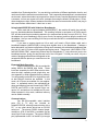
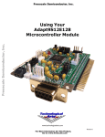
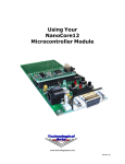
Using Your
Adapt9S12DP256
Evaluation Package
www.technologicalarts.com
Revison 0b
1
1 INTRODUCTION
Congratulations!
With Adapt9S12DP256, you are now ready to explore the power and flexibility of Motorola’s
most advanced 16-bit microcontroller! Whether you’re new to Motorola microcontrollers or you’ve
used some of the earlier ones, such as 68HC05, 68HC11, or 68HC12, you’ll be impressed with the
well thought-out design and implementation of the HCS12 family. And Adapt9S12DP256 gives you
the opportunity to explore this MCUs potential at an incredibly affordable price! Add to that the
proven advantages of the modular design approach, and the wide variety of available accessories,
and you’ll see why you picked a real winner!
Support
To help you get the most out of this product, and to make the experience as enjoyable and
productive as possible, we have put together a comprehensive website with technical support,
resources, and applications information. If you experience any difficulties, or need help with your
application, the World Wide Web is arguably the most valuable resource available to you. There
you’ll find the latest information, software, and troubleshooting help, as well as discussion groups
where you can network with people around the globe to get the answers you need. So if you still
need help, or have questions after reading this manual, visit our website: www.technologicalarts.
com and tap into the collective!
The 9S12DP256 in Perspective
Adapt9S12DP256 was designed as an evaluation and application tool for the Motorola 9S12
microcontroller family. Based on the most feature-packed flavour of the chip, 9S12DP256, it is
perfect for developing applications for any of the lower-function derivatives. The “D” series includes
DP256, DT128, DG256, DJ256, etc. All of these feature some at least one CAN or J1850 interface,
popular in automotive and industrial applications. The lower-cost “A” series excludes these subsystems. All the other subsystems are identical, however, with the differentiating factor being the
amounts each memory type and the quantity of I/O lines.
Adapt12 vs. traditional evaluation boards
Most evaluation and development systems available tend to be too expensive and bulky for
embedding into a real application, so it lies gathering dust once you’ve reached a certain point in the
learning curve. Or maybe you have to come up with clever ways to hack it apart to make it fit inside
your robot. Even then, the prototyping area provided is often limited, and does not lend itself to
re-usability. And what if you burn out a motor driver chip the night before the contest? What a mess
to repair or re-design!
The Adapt12 system solves all of these problems and then some! Since it brings out all I/O
lines and control signals to two standard 50-pin interface connectors, it is modular and re-usable.
Interface cards can be unplugged and upgraded, or the whole system can be re-configured at the
last minute. And with several connector options to choose from, you can use the module in whatever way best suits your needs-- board-stacking, end-to- end (planar), backplane, ribbon cables,
etc. A full range of accesories including backplanes, prototyping cards, and application-specific
cards is available, and more accessories are being developed all the time. Visit our website frequently to see what’s new.
The connector options (“RA1”) supplied in the Evaluation Package support the use of prototyping cards on each of the H1 and H2 I/O connectors, forming a planar arrangement. Advantages of this configuration are easy access of all I/O pins for probing and measurement, and easy
prototyping of your interface circuits. What’s more, the detachable nature of the prototyping cards
means that you can easily replace them with other cards, including some of the application cards
2
available from Technological Arts. You can build up a collection of different application circuits, and
use them all with the same microcontroller board. This is especially advantageous in an educational
environment, where the student can progress from simple to more complex applications throughout
a semester, or from one course to the next-- perhaps even using the board in a final project. In fact,
where budgets are tight, different students can share the same microcontroller module, and plug in
their own interface cards when it’s their turn to use it.
Using Adapt9S12DP256 with Solderless Breadboards
When used with an optional adapter (#ADHDR50-F), the module will easily plug vertically
into any standard solderless breadboard. The resulting footprint is equivalent to a 50-pin narrow
DIP, and has a similar pin-numbering sequence (ie. wraps around the end, from pin 25 to 26). Plug
the adapter into your breadboard, wire up your circuits, as required, and then plug the module into
the adapter. Now you can use DBug12 to load your code into the MCU to evaluate and develop your
application ideas.
If you want to access signals on H2 as well, you’ll need a 50-pin ribbon cable and a
breadboard adapter (#ADIDC50-M) to bring those signals down to the breadboard. Perhaps a
better alternative is a planar configuration utilizing cards mounted with solderless breadboards that
plug into H1 and H2 in place of the supplied prototyping cards. These cards (#AD12SBH1-FRA1
and #AD12SBH2-FRA1, respectively) feature dual-row receptacles (“F”-style connector) next to the
breadboard section, giving you easy access to all of the I/O signals. To build your circuit, it’s just a
matter of plugging wires between the signals on the
receptacles and the places you need them on the
breadboard.
Expanded Mode Operation
A second jumper block (JB1) is provided for
setting MODA and MODB logic levels. These
levels are sensed by the MCU after reset to determine the chip’s operating mode (single-chip, narrow expanded, or wide expanded memory modes).
You will normally run the MCU in single-chip mode,
so that DBug12 functions are available. In this
mode, all I/O ports are available for user applications. In expanded modes, the multiplexed address and data bus lines are formed from PORTA,
PORTB, and PORTK on the second 50-pin connector, H2, and are thus not available as I/O ports.
When operated in this mode, additional memory
can be added externally.
Communications
Two RS-232-compatible serial interface
ports (RX & TX only) are included on
Adapt9S12DP256, allowing communication with a
PC, or any other device which has an RS-232
serial port. The primary RS232 channel (implemented on SCI0 of the MCU) is available via the
usual 9-pin D-sub connector. The second RS232
port (implemented via SCI1 of the MCU) is brought
3
out to a common 4-pin Molex connector. Optional mating connectors and serial cables compatible
with this connector are available from Technological Arts. To maximize versatility, the logic-level
RXD and TXD signals from both SCIs of the MCU are also brought out to the 50-pin headers, for
applications such as MIDI, or for use as general purpose I/O lines. For these applications, jumper
wires on the board can be cut or removed, if necessary.
A factory-installed RS485 option can be accomodated in place of the second RS232 interface, on OEM versions of the module. RS-485 is commonly used in networking industrial control
applications, where long cable lengths and good noise immunity are re
quired.
In passing, it should be mentioned that the MCU supports up to three SPI links, and IIC (also
called I2C). Since these are logic-level protocols for local communications among peripheral chips,
no transceivers are required nor provided. Commonly used SPI and I2C chips include serial
memory, temperature controllers, clock/calendar chips, DACs, MP3 decoders, etc. See the MCU
datasheets for details on these subsystems.
Networks
Up to five Controller Area Networks (CANs) can be accomodated by the MCU. The module
provides physical interface transceivers for the first two. The default board configuration dedicates
these pins to CAN because it connects them to the CAN transceivers. If you wish to use the pins
as general purpose I/O lines instead, it may be necessary to cut one or more circuit board links
associated with them.
2 GETTING STARTED
Power
A 12VDC 300mA power supply is included with the Evaluation Package. It is the recommended power source when you’re starting out. If for some reason it’s not convenient (eg. you don’t
want an extension cord trailing around behind your robot), you can power the module in one of two
ways:
Option 1: connect a DC voltage of 5 Volts or more (maximum 24VDC) via the external power
connector, J1. Your DC supply does not need to be regulated, but should be capable of supplying
at least 100 mA (more if you will be using a BDM pod, or you’re driving other circuits as well). If your
supply is also driving motors, make sure to isolate it before feeding it into the module (to protect it
from electrical noise generated by the motor coils). You can do this by putting inductors (10uH,
nominal) in series with both the + and - leads. Preferably, use the red & black power wire provided.
Red is positive, and black is negative (ground). CAUTION! Make sure you have the polarity
correct!
Option 2: supply regulated 5VDC via the appropriate pins on the 50-pin connector (H1). See
module pinout diagram or schematic included with your manual for the 5V and GROUND pins to
connect to on H1. CAUTION! Double-check your connections before applying power!
Starting DBug12
To run the program that’s in Flash (DBug12, if you haven’t already erased it) select EVB
mode by setting both MODE SELECT jumpers (on JB3) to the 0 position. Connect the supplied
serial cable between the 9-pin connector on your module and a serial port on your computer. (With
some PCs, you will need a 9-pin to 25-pin adapter.) Run any terminal program on your PC. Make
sure your terminal program is set to 9600, parity to NONE, # DATA BITS = 8, and #STOP BITS =
1, and Flow Control set to “Software” or “XON/XOFF”. Apply power to the module, or press the
RESET button (SW1). The DBug12 prompt will appear in your terminal window. Type HELP to get
a list of DBug12 commands.
4
At this point, you should refer to the DBug12 Reference Guide, included on the accompanying CD-ROM, to continue exploring DBug12.
The Demo Program
We’ve included our standard demo program on the CD-ROM to give you a starting point.
This program was written in assembler, and the sourcecode is included so you’re free to hack it all
you want! There are two versions that can be used with DBug12: one is meant to be loaded into
RAM and launched from the monitor prompt (ie. EVB Mode), and the other resides in Flash, and is
loaded in Bootload Mode. Both versions use pseudo-vectors. (See DBug12 Reference Guide if
you’re not familiar with these modes or with the concept of pseudo-vectors).
A third, standalone, version of the demo program has “true vectors”. To load this demo
program into a blank target chip, you’ll need to use a BDM pod that supports the 9S12DP256. Some
possibilities are: a second Adapt9S12DP256 module jumpered for Pod Mode, our MicroBDM12DX,
or our MicroBDM12SX product. By the way, the s19 file for this version of the demo has been run
through the SrecCvrt utility supplied with DBug12. This utility reformats the s19 file generated by the
assembler so that all s1 records have an even number of bytes, and start on an even address, as
these are the requirements for programming the Flash memory. There’s more on this in the section
called “Migrating from the HC912” a little further on in this manual.
New to Motorola MCUs?
If you’ve come from an 8051, PIC, or other background (or have never used microcontrollers
before), you should get up to speed on Motorola MCUs by reading Understanding Small Microcontrollers, found on the CD-ROM. Written by Motorola’s Jim Sibigtroth, principle design engineer
of the HC12 family, this book uses an earlier MCU (68HC05) to introduce you to the basic concepts
and design philosophy.
Migrating from 68HC11
If you are already experienced with the 68HC11 family of microcontrollers, writing programs
for the HCS12 family will not present a big challenge. In fact, you can use your existing 68HC11
assembly code and re-assemble it to run on the CPU12 core, but there are a few things to keep in
mind.
Assembler syntax. You may need to edit your source file to conform to the syntax and
directives requirements of the HC12 assembler you’ll be using. There are several assemblers
available (eg. AS12, MiniIDE, IASM12, MCUez), and each has its own syntax to be aware of.
Register Block. Instead of $1000, the register block default location is $0000, and there are
well over a hundred registers! You’ll need to locate the relevant registers for the subsystems you
plan to use, and make sure they are properly configured.
RAM location. The RAM starts at $1000 and goes to $3FFF. This means you would initialize
the Stack Pointer to $4000 (on the HC12, the stack pointer points to the address following the top
of the stack).
High-speed Bus. The default bus speed is half the crystal frequency of 16 MHz, so it is 8
MHz. If you enable the PLL, it will be even higher (up to 24 MHz). This will mean changing some
initialization values for control registers and revising delay constants if you are using any software
timing loops.
I/O Ports. The digital I/O ports on the HCS12 are more flexible than ever. Besides selecting
the direction of each port pin via a Data Direction Register, there are registers controlling output
drive level (standard and reduced), internal pullup and pulldown resistors, and output logic polarity
(ie. true or inverted logic).
COP Watchdog. On most flavours of HC11, this was enable via a bit in the non-volatile
CONFIG register. On the HC12, it is dynamic, and automatically enabled following reset. Therefore
you have to choose whether you’re going to service it, or disable it.
5
Write-Once Registers. On the HC12, there is no 64-cycle startup window in which you have
to write all the protected registers. Instead, the HC12 implements a WriteOnce rule on sensitie
registers. What this means is that, following reset, you have one chance to write them, then they
become ReadOnly. The advantage of this is that you have more control of when you alter these
register values. To take advantage of this safeguard, you should initialize all the registers that are
crucial, even if the default values are what you want. That way, if your code runs amok, or there are
any glitches which try to change register values, they will be protected.
There are many more differences, and you should make sure to read through the Motorola
App Note (AN1284) on the CD-ROM that details the new instructions and addressing modes of the
68HC12, explaining differences from the 68HC11. The book Programming the Motorola 68HC12
Family (#PMM929, available from Technological Arts) thoroughly covers all the subsystems of the
68HC12, providing highlights of the differences with respect to 68HC11, and is recommended
reading.
Migrating from the 68HC912
You gain a lot more speed, memory, and flexibility, but you have a lot more registers to think
about, and many of their addresses have changed. Gone are the Vfp generator and Flash voltage
switch, since the new Flash technology uses 5V, and has built-in self-timed algorithms for program
and erase functions. But your s-records must contain an even number of bytes, and begin on an
even address boundary if you’re going to “burn” them into Flash. Some assemblers will generate
this format for you but others, such as the included AS12, don’t. Fortunately, Motorola has created
a handy s-record convert utility, included in the DBug12 archive. You simply run it at the DOS
command prompt, supplying the appropriate parameter(s). Besides the ability to generate s1
records of the required format, it can also convert s-records to banked memory format, generating
s2 records which the FLOAD command in DBug12 will use to load your code into paged Flash. The
s-record convert program is bundled in the DBug12 zip distribution file. Be sure to read the documentation carefully. You’ll discover that the utility has a lot of parameters, which you may find a little
confusing. For most cases, here’s all you need:
sreccvt.exe -m C0000 FFFFF 32 -lp -o out.s19 demo.s1
where out.s19 is the resulting file that you’ll load into the MCU, and demo.s1 is your sourcefile
(change the name to whatever suits you).
3.
HARDWARE DESIGN FEATURES
3.1
Using a Precision Voltage Reference
Adapt9S12DP256 uses the 5VDC you supply via your breadboard or the on-board 5-Volt
regulator (if you supply external power via connector J1) as the voltage reference (VRH) for the
analog-to-digital converter on the MCU. If you wish to use a precision voltage reference, you may
insert an LM385 or LM336 or equivalent part in location U2. Make sure it is a TO-92 style package.
Remove jumper W1 only if you wish to use a VRL other than system ground. It is easiest to use a
2.5V version, but you’ll have to make sure none of your analog input voltages will exceed 2.5V, or
you risk burning out the analog input circuits.
3.2
About the On-board Voltage Regulator
Adapt9S12 includes an LM2931T-5 voltage regulator. Housed in a TO-220 package, it is
capable of dissipating about 500 mW at room temperature. Other nice features are: a very low
quiescent current, and low dropout voltage-- it will work with an input voltage down to 5 Volts (or
below), making it quite well-suited to battery operation. It is also designed to withstand reverse
polarity and, if unused, does not present a load to an external regulated 5-Volt supply applied via the
50-pin header H1. One drawback, however, is that it can become unstable and start to oscillate at
6
low temperatures, especially if the input voltage source is connected to J1 via long wires. In the
former circumstance, the on-board 10uF tantalum capacitor can be replaced with a higher value
(47uF or 100uF). To compensate for long lead-in wires, add capacitance of 100uF or so at, or close
to, the J1 connector. A couple of pads are provided on the circuit board to accomodate this.
Heatsinking. Because the regulator is mounted on the underside of the circuit board, with the
package body parallel to the plane of the board, it can be safely attached to a heatsink, if desired.
Another option is to mount the board on a sheet of aluminum, using standoffs. If the appropriate
length is chosen for the standoffs, the tab of the regulator will lie flush with the aluminum sheet, and
can be coated with silicone grease and bolted to the plate (tightening the nut and bolt will require a
little ingenuity).
4.
WRITING SOFTWARE
4.1
Using ICC12 for Windows
Because the register addresses have changed from what they were in HC12, some library
files in ICC12 will need to be re-compiled, using the new header file, if you want to use them. Of
course, if you’re not using library functions, or you are using functions that don’t involve registers,
then there won’t be a problem with the existing versions. The following modified functions are
included on the CD-ROM to get you started:
iochar.c
serial.c
vectors.c
RAM-based program. When operating with DBug12 monitor, you can load programs in the
11K available portion of RAM. Before compiling, set up the linker options with 0x1000 for Data,
0x1200 for Program memory, and set the stack to 0x3C00. If you want to use any interrupts in your
code, modify the base address in the vectors.c file to 0x3E00 (as per DBug12’s implementation of
pseudo-vectors). After compiling to executable, use DBug12’s LOAD command to download the
resulting s-record file using ICC12’s terminal window. Then use G 1200 command to execute your
program.
EEPROM-based program. If you plan to use the JMP-EE function, the code you put into
EEPROM starting at 0x400 is executed automatically every time you reset the board in JMP-EE
mode (no Reset vector required). If you need interrupt vectors, your program will need to copy your
vector entries into the appropriate locations in the RAM-based pseudo-vector table before enabling
interrupts.
Flash-based program. You’ll need to include a pseudo-reset vector at 0xEFFE. And if you’re
planning on using any interrupts, you’ll need to use the pseudo-vector table DBug12 implements in
RAM, starting at 0x3E00. Your program will need to copy the vector entries into the appropriate
locations in the RAM-based pseudo-vector table before enabling interrupts.
MANUAL REVISIONS:
This manual is preliminary, and updates will be posted frequently on the Tech Support webpage.
7