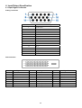
1
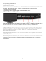
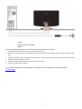
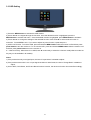
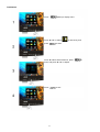
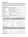
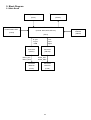
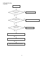
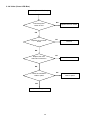
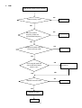
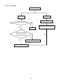
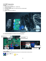
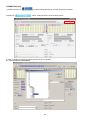
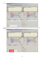
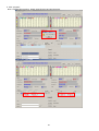
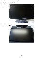
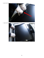
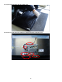
23" LCD Color Monitor
AOC i2430Ve
Service
Service
Service
Horizontal Frequency
30-83 kHz
TABLE OF CONTENTS
Description
Page
Description
Page
Table of Contents…………………..…………………..…...1
6.3.Key Board..……….........................................32
Revision List.…...................................................……......2
6.4.Light Sensor Board...............................................33
Important Safety Notice.….….............................……......3
7.PCB Layout..………..............................................34
1.Monitor Specification..............................………............4
7.1.Main Board………..…........................................34
2.LCD Monitor Description……….…………………….......5
3.Operation Instruction.…………...................……...........6
7.2.Power Board….…..............................................35
3.1.General Instructions....................................…..........6
7.3.Key Board………..…..........................................37
3.2.Control Buttons and Connections...............................6
7.4. Light Sensor Board.….........................................37
3.3.OSD Setting…...........................................................8
8.Maintainability………............................................38
4.Input/Output Specification...............……………….......20
8.1.Equipments and Tools Requirement…...............38
4.1.Input Signal Connector...............………..................20
8.2.Trouble Shooting…..………...............................39
4.2.Preset Display Modes……..........................21
9.FOS Testing………..…………………………………43
4.3.Panel Specification…………..……………………..22
5.Block Diagram….........................................................24
10.Firmware and DDC Instruction……………….….47
5.1.Main Board…..….............................................24
11.White-Balance,Luminance Adjustment…............65
5.2.Power Board…………..…………………………......25
12. Mechanical Instructions………………….....….......67
6.Schematic…………..….........................................26
13.Monitor Exploded View……................................72
6.1.Main Board..…….…...........................................26
14.BOM List…………..……………………….............73
6.2.Power Board..……….........................................30
SAFETY NOTICE
ANY PERSON ATTEMPTING TO SERVICE THIS CHASSIS MUST FAMILIARIZE HIMSELF WITH THE
CHASSIS AND BE AWARE OF THE NECESSARY SAFETY PRECAUTIONS TO BE USED WHEN SERVICING
ELECTRONIC EQUIPMENT CONTAINING HIGH VOLTAGES.
CAUTION: USE A SEPARATE ISOLATION TRANSFOMER FOR THIS UNIT WHEN SERVICING
1
Revision List
Revision
Date
Revision History
Remark
TDAGNT2EWWA4HNE
A00
Jan.-12-2011
Initial release
TDAGNT2DWWA4HNE
TDAGNT2FWWA4HNE
2
Important Safety Notice
Proper service and repair is important to the safe, reliable operation of all AOC Company Equipment. The service
procedures recommended by AOC and described in this service manual are effective methods of performing service
operations. Some of these service operations require the use of tools specially designed for the purpose. The
special tools should be used when and as recommended.
It is important to note that this manual contains various CAUTIONS and NOTICES which should be carefully read in
order to minimize the risk of personal injury to service personnel. The possibility exists that improper service
methods may damage the equipment. It is also important to understand that these CAUTIONS and NOTICES ARE
NOT EXHAUSTIVE. AOC could not possibly know, evaluate and advise the service trade of all conceivable ways in
which service might be done or of the possible hazardous consequences of each way. Consequently, AOC has not
undertaken any such broad evaluation. Accordingly, a servicer who uses a service procedure or tool which is not
recommended by AOC must first satisfy himself thoroughly that neither his safety nor the safe operation of the
equipment will be jeopardized by the service method selected.
Hereafter throughout this manual, AOC Company will be referred to as AOC.
WARNING
Use of substitute replacement parts, which do not have the same, specified safety characteristics may create shock,
fire, or other hazards.
Under no circumstances should the original design be modified or altered without written permission from AOC.
AOC assumes no liability, express or implied, arising out of any unauthorized modification of design.
Servicer assumes all liability.
FOR PRODUCTS CONTAINING LASER:
DANGER-Invisible laser radiation when open AVOID DIRECT EXPOSURE TO BEAM.
CAUTION-Use of controls or adjustments or performance of procedures other than those specified herein may
result in hazardous radiation exposure.
CAUTION -The use of optical instruments with this product will increase eye hazard.
TO ENSURE THE CONTINUED RELIABILITY OF THIS PRODUCT, USE ONLY ORIGINAL MANUFACTURER'S
REPLACEMENT PARTS, WHICH ARE LISTED WITH THEIR PART NUMBERS IN THE PARTS LIST SECTION OF
THIS SERVICE MANUAL.
Take care during handling the LCD module with backlight unit
-Must mount the module using mounting holes arranged in four corners.
-Do not press on the panel, edge of the frame strongly or electric shock as this will result in damage to the screen.
-Do not scratch or press on the panel with any sharp objects, such as pencil or pen as this may result in damage to
the panel.
-Protect the module from the ESD as it may damage the electronic circuit (C-MOS).
-Make certain that treatment person’s body is grounded through wristband.
-Do not leave the module in high temperature and in areas of high humidity for a long time.
-Avoid contact with water as it may a short circuit within the module.
-If the surface of panel becomes dirty, please wipe it off with a soft material. (Cleaning with a dirty or rough cloth may
damage the panel.)
3
Monitor Specifications
4
LCD Monitor Description
The LCD MONITOR will contain a main board, a power board, a key board which house the flat panel control logic,
brightness control logic and DDC.
The power board will provide AC to DC Inverter voltage to drive the backlight of panel and the main board chips
each voltage.
Monitor Block Diagram
LED Drive.
Flat Panel and
LED backlight
PWPC board
(Include: adapter, inverter)
RS232 Connector
For white balance
adjustment in factory
mode
Main Board
Key board
AC-IN
100V-240V
Video signal DDC
HOST Computer
5
3. Operating Instructions
3.1 General Instructions
Press the power button to turn the monitor on or off. The other control knobs are located at front panel of the monitor
(See Figure ). By changing these settings, the picture can be adjusted to your personal preferences.
* The power cord should be connected.
* Press the power button to turn on the monitor. The power indicator will light up.
3.2 Control Buttons and Connections
4:3 or wide image ratio hot key: When there is no OSD, press> continuously to change 4:3 or wide image ratio. (If
the product screen size is 4:3 or input signal resolution is wide format, the hot key is disable to adjust)
e-Sensor hot key. When there is no OSD,Press < continuously to select the e - Sensor mode(e-Sensor mode hot
key may not be available in all mode ls). e-Sensor:The infrared sensor can detect if user is in front of monitor and
adjust monitor brightness automatically to save power. When it is on, we can select the detect range
[Near,Average,Far] by using hot-key.
Auto configure hot key When there is no OSD, press Auto/Source button continuously about 2 second to do auto
configure (Only for the
Source hot key When the OSD is closed, press Source butt on will be Source hot key function. Press Source button
continuously to select the input source showed in the message bar , press Menu/Enter button to change to the
source selected.
6
1.Power
2.Analog (DB-15 VGA cable)
3.Power
To protect equipment, always turn off the PC and LCD monitor before connecting.
1.
Connect the power cable to the AC port on the back of the monitor.
2.
Connect one end of the 15-pin D-Sub cable to the back of the monitor and connect the other end to the computer's D-Sub
port.
3.
(Optional – Requires a video card with DVI port) - Connect one end of the DVI cable to the back of the monitor and connect
the other end to the computer‟s DVI port.
4.
Connect the audio cable to audio in port on the back of the monitor.
5. Turn on your monitor and computer.
If your monitor displays an image, installation is complete. If it does not display an image, please refer
Troubleshooting.
7
3.3 OSD Setting
1) Press the MENU-button to activate the OSD window.
2) Press ◄ or ► to navigate through the functions. Once the desired function is highlighted, press the
MENU-button to activate sub-menu . Once the desired function is highlighted, press MENU-button to activate it.
3) Press ◄ or ► to change the settings of the selected function. Press ◄ or ► to select another function in
sub-menu . Press AUTO to exit . If you want to adjust any other function, repeat steps 2-3.
4) OSD Lock Function: To lock the OSD, press and hold the MENU button while the monitor is off and then press
power button to turn the monitor on. To un-lock the OSD - press and hold the MENU button while the monitor is off
and then press power button to turn the monitor on.
5)e-Sensor hot key: When there is no OSD,Press ◄ continuously to select the e-Sensor mode(e-Sensor mode hot
key may not be available in all models).
Notes:
1) If the product has only one signal input, the item of "Input Select" is disable to adjust.
2) If the product screen size is 4:3 or input signal resolution is wide format, the item of "Image Ratio" is disable to
adjust.
3) One of DCR, Color Boost, and Picture Boost functions is active, the other two function is turned off accordingly.
8
Luminance
Press
(Menu) to display menu.
Press Menu to display MENU
Press ◄ or ► to select
press
(Luminance), and
to enter.
Press ◄ or ►to select submenu, press
enter, and press ◄ or ► to adjust.
Press
to exit.
9
to
Brightness
0-100
Backlight Adjustment
Contrast
0-100
Contrast from Digital-register.
Standard
Standard Mode
Text
Text Mode
Internet
Internet Mode
Game
Game Mode
Movie
Movie Mode
Sports
Sports Mode
Gamma1
Adjust to Gamma1
Gamma2
Adjust to Gamma 2
Gamma3
Adjust to Gamma 3
On/OFF
Enable dynamic contrast ratio
Eco mode
Gamma
DCR
10
Image Setup
Press
(Menu) to display menu.
Press ◄ or ► to select
and press
(Image Setup),
to enter.
Press ◄ or ► to select submenu, press
enter, and press ◄ or ► to adjust.
Press
to
to exit.
Clock
0-100
Adjust picture Clock to reduce Vertical-Line noise.
Phase
0-100
Adjust Picture Phase to reduce Horizontal-Line noise
H.Position
0-100
Adjust the horizontal position of the picture.
V.Position
0-100
Adjust the vertical position of the picture.
11
Color Temperature
Press
(Menu) to display menu.
Press ◄ or ► to select
(Color
Temperature), and press
to enter.
Press ◄ or ► to select submenu, press
enter, and press ◄ or ► to adjust.
Press
to
to exit.
Warm
6500K
Recall Warm Color Temperature from EEPROM.
Normal
7300K
Recall Normal Color Temperature from EEPROM.
Cool
9300K
Recall Cool Color Temperature from EEPROM.
sRGB
User
Recall SRGB Color Temperature from EEPROM.
Red
Red Gain from Digital-register
Green
Green Gain Digital-register.
Blue
Blue Gain from Digital-register
12
Color Boost
Press
(Menu) to display menu.
Press ◄ or ► to select
and press
(Color Boost),
to enter.
Press ◄ or ► to select submenu, press
enter, and press ◄ or ► to adjust.
Press
to
to exit.
Full Enhance
on or off
Disable or Enable Full Enhance Mode
Nature Skin
on or off
Disable or Enable Nature Skin Mode
Green Field
on or off
Disable or Enable Green Field Mode
Sky-blue
on or off
Disable or Enable Sky-blue Mode
AutoDetect
on or off
Disable or Enable AutoDetect Mode
Demo
on or off
Disable or Enable Demo
13
Picture Boost
Press
(Menu) to display MENU.
Press ◄ or ► to select
press
(Picture Boost); and
to enter.
Press ◄ or ► to select Bright Frame. Select “on” to
activate Picture Boost.
Press ◄ or ► to select submenu, press
enter, and press ◄ or ► to adjust.
Press
to exit.
Frame Size
14-100
Adjust Frame Size
Brightness
0-100
Adjust Frame Brightness
Contrast
0-100
Adjust Frame Contrast
H. position
0-100
Adjust Frame horizontal Position
V.position
0-100
Adjust Frame vertical Position
Bright Frame
on or off
Disable or Enable Bright Frame
14
to
OSD Setup
Press
(Menu) to display menu.
Press ◄ or ► to select
and press
(OSD Setup),
to enter.
Press ◄ or ► to select submenu, press
enter, and press ◄ or ► to adjust.
Press
to exit.
OSD Setup
H.Position
0-100
Adjust the horizontal position of OSD
V.Position
0-100
Adjust the vertical position of OSD
Timeout
5-120
Adjust the OSD Timeout
Transparence
0-100
Adjust the transparence of OSD
Language
Select the OSD language
15
to
Extra
Press
(Menu) to display menu.
Press ◄ or ► to select
and press
(OSD Setup),
to enter.
Press ◄ or ► to select submenu, press
to enter, and press ◄ or ► to adjust.
Press
16
to exit.
Auto
Select to Auto Detect input signal
Analog
Select Analog Sigal Source as Input
Digital
Select Digital Sigal Source as Input
Auto Config
yes or no
Auto adjust the picture to default
Image Ratio
wide or 4:3
Select wide or 4:3 format for display
DDC-CI
yes or no
Turn ON/OFF DDC-CI Support
Off Timer
0~24hours
Select timing to turn off the monitor.
Input Select
Show the information of the main image and
Information
sub-image source
17
Reset
Press
(Menu) to display menu.
Press ◄ or ► to select
press
(Reset), and
to enter.
Press◄ or ► to select YES or NO.
Press
Reset
yes or no
to exit.
Reset the menu to default
18
Exit
Press
(Menu) to display menu.
Press ◄ or ► to select
to enter.
Exit
(Exit); and press
Exit the main OSD
LED Indicator
Status
LED Color
Full Power Mode
Blue
Active-off Mode
Orange
19
4. Input/Output Specification
4.1 Input Signal Connector
Analog connectors
Pin Number
1
2
3
4
5
6
7
8
9
10
11
12
13
14
15
15-Pin Side of the Signal Cable
Video-Red
Video-Green
Video-Blue
N.C.
Detect Cable
GND-R
GND-G
GND-B
+5V
Ground
N.C.
DDC-Serial data
H-sync
V-sync
DDC-Serial clock
DVI connectors
Pin No.
1
2
3
4
5
6
7
8
Signal Name
TMDS Data 2TMDS Data 2+
TMDS Data 2/4 Shield
TMDS Data 4TMDS Data 4+
DDC Clock
DDC Data
N.C.
Pin No.
9
10
11
12
13
14
15
16
Signal Name
TMDS Data 1TMDS Data 1+
TMDS Data 1/3 Shield
TMDS Data 3TMDS Data 3+
+5V Power
Ground(for+5V)
Hot Plug Detect
20
Pin No.
17
18
19
20
21
22
23
24
Signal Name
TMDS Data 0TMDS Data 0+
TMDS Data 0/5 Shield
TMDS Data 5TMDS Data 5+
TMDS Clock Shield
TMDS Clock +
TMDS Clock -
4.2 Preset Display Modes
21
4.3 Panel Specification
4.3.1 General Features
LM230WF3 is a Color Active Matrix Liquid Crystal Display with a Light Emitting Diode ( White LED) backlight
The matrix employs a-Si Thin Film Transistor as the active element. It is a transmissive type display operating in the
normally black mode. It has a 23 inch diagonally measured active display area with FHD resolution (1080 vertical by
1920 horizontal pixel array) Each pixel is divided into Red, Green and Blue sub-pixels or dots which are arranged in
vertical stripes. Gray scale or the brightness of the sub-pixel color is determined with a 8-bit gray scale signal for each
dot, thus, presenting a palette of more than 16,7M colors with A-FRC (Advanced Frame Rate Control).
4.3.2 General Specifications
4.3.3 Electrical Characteristics
(Ta= 25± 2℃, VLCD =5.0V, VLCD=5.0V, Fv=60Hz,)
LED Bar Electrical Characteristics
4.3.4Optical Characteristics
22
(Ta=25 °C, VLCD=5V, fV=60Hz Dclk=144MHz, IBL=110mA)
23
5. Block Diagram
5.1 Main Board
Crystal 12MHZ
LCD Interface
(X401) (CN301)
FLASH MEMORY
Scalar NT68668AUFG
Pm25LD020C-SCE
(Include :MCU,ADC,OSD etc)
(U402)
(U401)
DVI
Input
signal
H sync
V sync
RGB D-Sub
DVI
Connector
Connector
(CN101)
(CN102)
DDC1_SCL
DDC1_SDA
DDC2_SCL
DDC2_SDA
EEPROM
EEPROM
M24C02
M24C02
(U101) (U102) 24
Key Control
Interface
(CN401)
5.2 Power Board
AC input
EMI filter
Transformer
Bridge
Rectifier
and Filter
14.5V
Rectifier
diodes
(T901)
5V
Start Resistor
(R904)
Power Switch
(Q901)
PWM Control
LD7750GS
(IC901)
Photo coupler
(IC903)
14.5V
Feedback
Circuit
Regulator
(IC904)
D801
L801
LED
MOSFET
(Q806)
(CN803)
OFF
DIM
PWM Control
MP3389EF
(U801)
25
6. Schematic
6.1 Main Board
715G4002M01000004S
FB102
0R05 1/10W
R103 100OHM1/16W
R104 100OHM1/16W
R106
2.2K 1/16W
R107
2.2K 1/16W
C103
22P 50V
C104
22P 50V
R101
10
5
9
4
8
3
7
2
6
1
DSUB_SCL 15
14
100OHM1/16W
13
DSUB_SDA 12
100OHM1/16W
FB103
VGA_G+
V_Sy nc
C125
100N 16V
VGA_BVGA_B+
ZD101
VGA_G- RLZ5.6B
VGA_G+
VGA_RVGA_R+
VGA_G+
1
2
3
U103
AOZ8105CI
I/O1 I/O4
GNDVDD
I/O2 I/O3
R109
47 OHM 1/16W
C106
47nF 16V
DSUB_B- 5
R110
470 OHM 1/16W
C107
1N 50V
DSUB_SOG 5
R111
10OHM1/16W
C108
47nF 16V
DSUB_G+ 5
R114
47 OHM 1/16W
C110
47nF 16V
DSUB_G- 5
R115
10OHM1/16W
C111
47nF 16V
DSUB_R+ 5
C114
47nF 16V
DSUB_R- 5
C109
5PF 50V
75OHM 1/16W
ESD_VCC
FB101
DET_VGA
6
5
4
VGA_R+
1
VGA_B+
C126
100N 16V
2
0R05 1/10W
R116
11/30/2009
C113
5PF 50V
75OHM 1/16W
VGA_R-
R117
47 OHM 1/16W
VCC3.3
CMVCC1
DSUB_5V
2
DVI_5V
DET_DVI
DVI_HPD
R120 10K+-5%1/16W FB106
11
3
19
22
R133
390K +/-5% 1/16W
DDC2_SCL 5
DDC2_SDA 5
300 OHM
C112
100N 16V
18
17
10
9
2
1
13
12
5
4
21
20
23
24
R126
R127
R128
R129
R130
R131
10OHM1/16W RX0P
10OHM1/16W RX0N
10OHM1/16W RX1P
10OHM1/16W RX1N
10OHM1/16W RX2P
10OHM1/16W RX2N
RX0P
RX0N
RX1P
RX1N
RX2P
RX2N
DET_VGA
R135
100K 1/16W
DET_DVI
R139
220K 1/16W 5%
D101
BAV70
ESD_VCC
DET_CABLE 5
5
5
5
5
5
5
R124
4.7K 1/16W
DDC1_SCL
DDC1_SDA
5 DDC_WP
RXCP
RXCN
1
2
3
I/O1 I/O4
GNDVDD
I/O2 I/O3
ESD_VCC1
6
5
4
1
2
3
C121
100N 16V
U105
AOZ8105CI
I/O1 I/O4
GNDVDD
I/O2 I/O3
ESD_VCC1
6
5
4
1
2
3
C122
100N 16V
U106
AOZ8105CI
I/O1 I/O4
GNDVDD
I/O2 I/O3
FB105
C118
1N 50V
R137
4.7K 1/16W
C120
100N 16V
Key Component
Date
26
Victory
Electronics
Co . ,
G4002-M0D-000-0040-100416
2.0.INPUT
Tuesday , April 27, 2010
Ltd. )
C119
1N 50V
C117
220N16V
U102
8
7
6
5
5 DDC_WP
T P V ( Top
C115
100N 16V
R136
22K 1/16W
R138
4.7K 1/16W
DDC2_SCL
DDC2_SDA
絬隔瓜絪腹
DVI_5V
300 OHM
D102
BAV70
ESD_VCC1
6
5
4
VCC A0
WP
A1
SCL A2
SDA VSS
FB104
ESD_VCC1
U107
AOZ8105CI
1
2
3
4
CAT24C02WI-GT3
300 OHM
RXCP 5
RXCN 5
C116
220N16V
U101
8
7
6
5
3,4,5 CMVCC1
10OHM1/16W
10OHM1/16W
R123
22K 1/16W
R125
4.7K 1/16W
CMVCC1
R132
R134
3
DDC2_SCL
DDC2_SDA
R118 100OHM1/16W
R119 100OHM1/16W
26
25
GND
GND
DAT0+
DAT0DAT1+
DAT1DAT2+
DAT2DAT3+
DAT3DAT4+
DAT4DAT5+
DAT5clk+
clk-
R112
11/30/2009
DSUB_B+ 5
1
1/3shield
2/4shield
0/5shield
clk shield
2
0R05 1/10W
C124
100N 16V
VGA_R+
CN102
JACK
VSY NC
SY NC GND
DDC SCL
DDC SDA
+5V
HPD
1
VGA_G-
2010/1/13
modify type
8
15
6
7
14
16
75OHM 1/16W
DSUB_5V
17
11
ESD_VCC
H_Sy nc
6
5
4
C102
47nF 16V
C105
5PF 50V
2
DDC1_SDA
5 DDC1_SDA
R113
DET_VGA
R105
10OHM1/16W
R108
3
DDC1_SCL
5 DDC1_SCL
16
DSUB_SDA
I/O1 I/O4
GNDVDD
I/O2 I/O3
2
0R05 1/10W
VGA_B-
U104
AOZ8105CI
1
2
3
1
11/30/2009
C127
C128
NC/22P 50VNC/22P 50V
DSUB_SCL
CN101
D-SUB 15P
VGA_B+
DSUB_H 5
DSUB_V 5
1
H_Sy nc R102
V_Sy nc
VCC A0
WP
A1
SCL A2
SDA VSS
1
2
3
4
CAT24C02WI-GT3
OEM MODEL AOC e2040VA
Size
B
TPV MODEL
Rev
C
称爹
<称爹>
e2040VA
PCB NAME
Sheet
2
of
6
PA[0..9]
5 PB[0..9]
PA0
PA1
PA2
PA3
PA4
PA5
PA6
PA7
PA8
PA9
29
27
25
23
21
19
17
15
13
11
9
7
5
3
1
PB[0..9]
PB0
PB1
PB2
PB3
PB4
PB5
PB6
PB7
PB8
PB9
LVA3P
LVA3M
LVACKP
LVACKM
LVA2P
LVA2M
LVA1P
LVA1M
LVA0P
LVA0M
LVB3P
LVB3M
LVBCKP
LVBCKM
LVB2P
LVB2M
LVB1P
LVB1M
LVB0P
LVB0M
LVB0M
LVB1M
LVB2M
LVBCKM
LVB3M
LVA0M
LVA1M
LVA2M
LVACKM
LVA3M
RXO0RXO1RXO2RXOCRXO3RXE0RXE1RXE2RXECRXE3-
CONN
30
28
26
24
22
20
18
16
14
12
10
8
6
4
2
RXO0+
RXO1+
RXO2+
RXOC+
RXO3+
RXE0+
RXE1+
RXE2+
RXEC+
RXE3+
31
5 PA[0..9]
32
CN301
LVB0P
LVB1P
LVB2P
LVBCKP
LVB3P
LVA0P
LVA1P
LVA2P
LVACKP
LVA3P
PANEL_VCC
R301
220 OHM 1/4W
PANEL_VCC
R302
220 OHM 1/4W
C301
100N 16V
FB301
1
2
120 OHM
CMVCC1
C302
22UF 16V
2,4,5 CMVCC1
R306
Q301
AO3401A
Q302
5 PPWR_ON#
LMBT3904LT1G
22K 1/16W
R303
4.7K 1/16W
11/30/2009
R307
NC
C304
100N 16V
NC/AO4411
C303
220N16V
CMVCC1
4
3
2
1
R304
U301
G
S
S
S
100K 1/16W
D
D
D
D
5
6
7
8
R305
10K+-5%1/16W
3D
1
G
2
S
C305
1UF16V
R308
NC/10K1/16W
AO3401L
OEM MODEL AOC e2040VA
Size
B
絬隔瓜絪腹
G4002-M0D-000-0040-100416
TPV MODEL
Rev
C
Key Component
3.0.OUTPUT
PCB NAME
称爹
<称爹>
TPV
Date
27
( Top
Victory
Electronics
Tuesday , April 27, 2010
Co . ,
Ltd. )
Sheet
e2040VA
3
of
6
SOT 252
12
VIN
VOUT(TAB)
ADJ(GND)
1
+12V
1
2
3
4
5
6
7
8
9
10
U702
G1117-33T43UF
3
2
1
2
D707
SR34
Both 223 and 252
foot-print
CMVCC1
1
R707
0R05 1/10W
BKLT-VBRI
BKLT-EN
D708
SR34
R708
NC/0R05 1/10W 5%
CONN
SOT 223
2
11
CMVCC1
CN702
VCC3.3
U701
3
VO
Dropout voltage must
< 0.8V @ 600mA
2
GND
VI
C709
100N 16V
1
C708
100N 16V
C707
22UF 16V
VCC3.3
VCC3.3
1
CMVCC1
SOT 223
D703
SR34
R703
10K+-5%1/16W
3
VI
VO
Dropout voltage must
< 0.8V @ 400mA
2
Q701
LMBT3904LT1G
D704
SR34
Both 223 and 252
foot-print
2
on_BACKLIGHT 5
1
C702
100N 16V
GND
1
BKLT-EN
U704
2
R702
10K+-5%1/16W
R704 22K 1/16W
SOT 252
VCC1.8
C706
100N 16V
C705
100N 16V
1
CMVCC1
GND
U703
NC/AZ1117D-1.8-E1
3
2
IN
OUT
C704
22UF 16V
R705
10K+-5%1/16W
R706
BKLT-VBRI
adj_BACKLIGHT 5
100OHM1/16W
2010/1/25
Add FB703
Place a large Pad
with TOP
C713
100N 16V
FB703
0R05 1/10W
Pad 璶 TOP and Button常璶Τ R712
100K 1/16W
Thermal Pad
BST
SW
VIN
EN
FREQ COMP
GND
FB
U705
1
2
3
4
Pad 璶 TOP and Button 常璶Τ L701
CMVCC1
22uH
CMVCC1 2,3,5
2
9
8
7
6
5
MP1584EN
C710
1N 50V
C711
NC/1N 50V
R713
6.8K +-1% 1/16W
C714
1N 50V
1
D701
SR34
C720
100N 16V
R711
33K 1/16W 5%
R726
100K 1/16W
2010/1/13
180k => 300k
+12V 6
FB702
1
+
2010/1/13
SMD => Dip
C718
180uF 16V
2010/1/25
Add C723
C719
100nF 25V
+
C716
470uF 10V
C717
100N 16V
ZD702
NC/RLZ6.2B
11/30/2009
C716 ぃ 繦獽 ノ,
DC-DC pulse 穦Τ
noise
CN701
2
BEAD
C721
10uF 25V
C723
10uF 25V
R714
1.3K 1%
Add C714
reduce
noise
+12V
C715
1N 50V
2010/1/13
1000p => NC
2
C722
150pF 50V
R727
300K
1
C712
100nF 25V
3
2
1
JACK
2010/1/13
Add C721
T P V ( Top
Size
G4002-M0D-000-0040-100416
TPV MODEL
Rev
C
4.0.POWER
PCB NAME
称爹
<称爹>
Date
28
Victory
Electronics
Tuesday , April 27, 2010
Co . ,
Ltd. )
C
OEM MODEL AOC e2040VA
絬隔瓜絪腹
Key Component
Sheet
e2040VA
4
of
6
VCC1.8
VCC3.3
CVDD
VCC3.3 2,4
AVCC
VCC3.3
DVDD
ADC_VAA
AVCC
CVDD
FB401
0R05OHM1/8W
4 VCC1.8
ADC_BIAS
C415
1UF16V
C438
100N 16V
100N 16V
100N 16V
100N 16V
100N 16V
2
2
2
2
2
2
2
2
28
C422
100N 16V
2 DSUB_H
2 DSUB_V
2 DSUB_SOG
2 DSUB_G+
2 DSUB_G-
17
C424
1UF16V
41
42
B0+
B0-
19
20
21
22
23
R0+
R0-
24
25
2 DSUB_R+
2 DSUB_R-
RX2+
RX2RX1+
RX1RX0+
RX0RXC+
RXC-
51
116
90
2
17
28
26
6
15
52
115
119
43
T0M
T0P
T1M
T1P
T2M
T2P
TCLK1M
TCLK1P
T3M
T3P
T4M
T4P
T5M
T5P
T6M
T6P
TCLK2M
TCLK2P
T7M
T7P
HSY NCI1
VSY NCI1
BIN1+
BIN1SOG1I
GIN1+
GIN1RIN1+
RIN1-
5V_DET
2 DET_CABLE
KEY 1
KEY 2
C425 100N 16V
DDC2_SDA
DDC2_SCL
DDC1_SDA
DDC1_SCL
DDCSDA2
DDCSCL2
DDCSDA1
DDCSCL1
DET_CABLE
R436
1K 1/16W
R437
1K 1/16W
34
35
46
47
30
33
125
126
VCKI
V7
V6
V5
V4
V3
V2
V1
V0
PB7/DDC_SDA1*
PB6/DDC_SCL1*
PB5/DDC_SDA0*
PB4/DDC_SCL0*
PB3/ADC3/INTE1
PB2/ADC2/INTE0
PB1/ADC1
PB0/ADC0
100
99
98
97
96
95
94
93
92
91
88
87
86
85
84
83
82
81
80
79
77
76
75
74
73
72
71
70
69
68
PA0
PA1
PA2
PA3
PA4
PA5
PA6
PA7
PA8
PA9
PB9
PB8
PB7
PB6
PB5
PB4
PB3
PB2
PB1
PB0
PA9
PA8
PA7
PA6
PA5
PA4
PA3
PA2
PA1
PA0
PA[0..9]
62
61
60
59
58
57
56
55
54
PB[0..9] 3
PWMA*
PWMB*
PC7
PC6
PC5
PC4/PWM1
PC3/PWM0
PC2
PC1*
PC0*
P35
P34
P31/TXD
P30/RXD
RSTB
OSCI
40
39
38
37
36
67
66
65
on_BACKLIGHT
LED_GRN/BLUE
LED_ORANGE
R426
1K 1/16W
11/30/2009
adj_BACKLIGHT 4
Volume 6
on_BACKLIGHT 4
POWER_KEY #
AUDIO_MUTE
AUDIO_MUTE 6
PS_O/P
PS_EN
PS_DISTANCE
Panel_ON
PPWR_ON# 3
R431
U402
Vcc
HOLD
C
DIO
SPI_CK
SPI_SI
CMVCC1
0R05 OHM
CMVCC1
VCC3.3
2,3,4 CMVCC1
A25L020AO-F
CMVCC1
VCC3.3
R407
NC/0R05 1/16W
R406
R408
0R05 OHM
VCC3.3
R411
4.7K 1/16W
2010/1/25
Q401
LMBT3906LT1G
PS_O/P
PS_EN
R419
R420
100OHM1/16W
100OHM1/16W
PS_DISTANCE
R422
4.7K 1/16W
CONN
1
2
3
4
5
C408
1UF16V
CONN
LED_R
C433
ZD402
C434
ZD403
C435
LED_GRN/BLUE
R412
10K+-5%1/16W
1
FB408
Q402
LMBT3906LT1G
1
LED_ORANGE
R413
10K+-5%1/16W
1
CMVCC1
R405
330OHM 1/10W
2010/1/25
LED 獹 2
NC/120 OHM
3
6
R418
10K+-5%1/16W
FB409
C436
NC/100N 16V
1
LED_R
2
NC/120 OHM
7
R417
10K1/16W
R404
220 OHM 1/10W
C432
2
LED_G
CN402
ZD401
C431
2
2010/1/25
KEY 1
KEY 2
POWER_KEY #
LED_G
LED_R
3
R428
NC/0R05 1/16W
CN401
1
2
3
4
5
6
7
R409
NC/0R05 1/16W
R410
4.7K 1/16W
R427
0R05 OHM
R433
NC/RLZ5.6B
S
DO
W
Vss
R432
100N 16V
R402
10K+-5%1/16W
8
7
6
5
8
1
2
3
4
9
SPI_CE
SPI_SO
100OHM1/16W
3.9K1/16W
VCC3.3
44
3
109
64
78
101
18
12
9
27
89
63
112
111
NT68668AFG/C
adj_BACKLIGHT
Volume
117
118
103
102
124
123
122
110
121
120
100N 16V
OSCO
DVDD
C429
220N16V
PA7/PWM9*
PA6/PWM8*
PA5/PWM7*
PA4/PWM6*
PA3/PWM5
PA1/PWM3
PA2/PWM4
PA0/PWM2
113
114
NC/RLZ5.6B
X401
R434
14.31818MHZ/32PF
1M 1/16W
128
C428 47pF 50V
INT_VSO
INT_HSO
3.9K1/16W
C427
100N 16V
SPI_CE
SPI_SO
SPI_SI
SPI_CLK
PD4
PD5
PD6
100N 16V
127
2
C426 47pF 50V
1
1
R403
10K+-5%1/16W
12/3/2009
PA[0..9] 3
PB[0..9]
PB0
PB1
PB2
PB3
PB4
PB5
PB6
PB7
PB8
PB9
NC/RLZ5.6B
R435
100OHM1/16W
104
105
106
107
108
48
29
49
50
31
32
DVDD
R401
100N 16V
3.9K1/16W
DDC_WP
2 DDC_WP
WP
C405
C404
4.7UF 10V
C0805
11/30/2009
SPI_CE
SPI_SO
SPI_SI
SPI_CK
WP
GND
DGND
GND
DGND/CGND
DGND/CGND
NC
PGND
AGND
AGND
ADC_GNDA
NC
NC
NC
NC
R416
220K 1/16W 5%
2
2
2
2
ADC_VAA
53
NC
NC
NC
NC
NC
NC
NC
NC
NC
NC
CMVCC1
R415
100K 1/16W
C403
26
NC
REXT
119
C402
100N 16V 100N 16V 100N 16V
100N 16V
C423
4.7UF 10V
C0805
AHS0
AVS0
SOG_DET
G0+
G0-
2 DSUB_B+
2 DSUB_B-
ADC_BIAS
4
5
7
8
10
11
13
14
115
C401
100N 16V
C421
4.7UF 10V
C0805
RX2P
RX2N
RX1P
RX1N
RX0P
RX0N
RXCP
RXCN
16
RX2+
RX2RX1+
RX1RX0+
RX0RXC+
RXC-
DVDD
DVDD
DVDD
DVDD_ZP
116
C437
ADC_BIAS
ADC_VAA33
90
C419
AVCC
AVCC
53
C418
ADC_VAA18
51
C417
U401
CVDD
CVDD
CVDD_ZP
2
FB402
300OHM
100N 16V
R414
470R 1/16W 1%
AVCC
C416
4.7UF 10V
C0805
FB406
NC/300OHMADC_VAA33
ADC_VAA33
PLL_GND
C414
1UF16V
45
C413
4.7UF 10V
C0805
FB405
DVDD
300OHM
C407
52
C439
4.7UF 10V
C0805
15
6
FB407
300OHM
C406
4.7UF 10V
C0805
PLL_DVDD
FB404
300OHM
FB403
300OHM
2010/1/25
LED 獹 T P V ( Top
Size
G4002-M0D-000-0040-100416
TPV MODEL
Rev
C
5.0.SCALER
PCB NAME
称爹
<称爹>
Date
29
Victory
Electronics
Tuesday , April 27, 2010
Co . ,
Ltd. )
C
OEM MODEL AOC e2040VA
絬隔瓜絪腹
Key Component
Sheet
e2040VA
5
of
6
6.2 Power Board
Adapter
715G 901
2 4A
51 OHM +-5% 1/4W
R923
51 OHM +-5% 1/4W R913
R912
51 OHM +-5% 1/4W
430K 1/4W
C926
R922
R967
430K 1/4W
2
430K 1/4W
1
!
+
-
BD901
GBU408
C904
100uF 450V
T901
8
2N2 500V
L902
1.1uH
2
+12V
2
C925
R904
10nF
1N4007
D902
4
47KOHM +-5% 1/4W
C922
D901
1N4007
R907
3
9
10
4
5
2R2 1/4W 5%
C919
+
680UF 25V
R924
+ C921
(NC)10K 1/8W 5%
680UF 25V
C920
4.7uF/25V
C918
NC
6
+ C906
C909
3300pF 250V
47uF/50V
7
11
更改料件
1
0.1uF
!
!
2
3
L901
30mH
IC901
1
2
3
4
C903 0.47UF275V
!
R901
R903
680K 1/4W +-5%
R902
CT
HV
COMPNC
CS VCC
GND OUT
8
7
6
5
R986
20K +-5% 1/8W
Q901
R908 47 OHM 1/4W +-5%
C908 LD7750GS
100K 1/8W
LED2
LED
SMK0965F
220R 1/8W 5%
1
680K 1/4W +-5%
680K 1/4W +-5%
!
C916
D904
V30100C-E3/4W
1
1
+
!
C914
2N2 500V
R906
2200PF2KV
3
4
R914
3
更改料件
430K 1/4W
C912
330pF
NR901
NTCR
R909
R910
10K OHM 1/4W +-5%
R911
0.62OHM2W
2
t
R918
510 OHM +-1% 1/4W
PC123X2Y FZOF
0.001uF
C901
0.001uF
C902
R968
2.2KOHM 1/10W
R919
9.76K1/4W
2
F901
FUSE
IC903
3
!
R920 10R 1/4W
1
4
!
C911
0.01uF
C915 R917
0.022uF/50V
IC904
4.7KOHM +-5% 1/4W
R916
2K49 1/8W 1%
水波纹干扰对策
R921
C923
1U 25V
3
1 MOHM +-5% 1/4W
2
!
1
CN901
SOCKET
OEM MODEL
HP X20/X22/X23LED
Size
絬隔瓜絪腹
G901-1-15-X-3-100201
TPV MODEL
ADPCA1248HA1
Rev
1.0
Key Component
02.ADAPTER
PCB NAME
称爹
<称爹>
T P V ( Top
Date
30
Victory
Electronics
Co . ,
Wednesday , June 30, 2010
Ltd. )
Sheet
715G901-1-15
2
of
2
A3
Converter 715G4119P01002004C
GATE
Q806
1
2
3
4
CN801
8
7
6
5
D801
L801
1
2
11
22uH
12
ON/OFF
DIM
1
2
3
4
5
6
7
8
9
10
11
12
13
14
C801 0.47uF 50V
R806
1K 1/10W
C802 68NF 50V
R807 100K 1/10W
R808
1K 1/10W
R810 100K 1/10W
R818
0R05 1/4W
C808
NC
R802 200K 1/10W 5%
R803
30K 1/10W 1%
+14.5V
R819
30K 1/10W 1%
MP3389EF
NC
NC
VIN
VFAULT
VCC
GATE
COMP
PGND
EN
ISENSE
DBRT
OVP
GND
LED1
OSC
LED2
ISET
LED3
BOSC
LED4
LED12
LED5
LED11
LED6
LED10
LED7
LED9
LED8
28
27
26
25
24
23
22
21
20
19
18
17
16
15
DR
4.7UF 100V
+
GATE
OVP
R801
C803
47N 50V
R805
300K +-5% 1/8W
+
C810
10 OHM 1% 1/4WNC
Q801
NC/AOD4126
C804
47N 50V
C805
220P 100V
OVP
R809
R815
R813 R814
1R 1/8W 5%
NC
7.5K +-1% 1/10W
R812
NC
R811
R804
100K 1/10W
C806
100pF 50V
0.3 OHM
0.3 OHM
1
2
3
4
R828 1 OHM +-5% 1/8W
Q802
NC/MMBT3904
R825
NC
R8271 OHM +-5% 1/8W
6
R824
NC
R821
Q804
NC/RK7002FD5T116
R823
Q805
NC
NC/RK7002FD5T116
CONN
R817
NC
GATE
DR
CN802
5
C809
100UF 50V
C810
SK310B
U801
+
E-Pad
ON/OFF
DIM
29
1
2
3
4
5
6
7
8
9
10
CONN
D1
D1
D2
D2
APM8005KCTRG
L802NC/22uH
+14.5V
S1
G1
S2
G2
NC
Q803
DR
R829 0R05OHM1/8W
R826
R830
CN803
1
2
0R05OHM1/8W
3.3R 1/8W 5%
R831
1 OHM +-5% 1/8W
R822
10K 1/10W
CONN
NC/MMBT3906
T P V ( Top
絬隔瓜絪腹
Key Component
Date
31
Victory
Electronics
Co . ,
G4119-P2A-000-0040-2-100826
01.CONVERTER
Ltd. )
OEM MODEL
e940swa
TPV MODEL
LNPCA9401AHD1
PCB NAME
Sheet
1
715G4119-P2A-000-004C
2
of
Size
Rev
称爹
Custom
B
ODM MODEL
6.3 Key Board
2
3
1
715G4014K01000004C
LED001
LED
0.1uF 50V
0R01 1/10W
R003
R004
2KOHM 1% 1/10W
1K 1/10W
SGND
SW005
SW
OK
LBADC2
LBADC1
MENU
C002
0.1uF 50V
2KOHM 1% 1/10W
R002
AUTO
CONN
C001
R001
UP
LBADC1
LBADC2
DC_POWERON
LED_1#
LED_2#
DOWN
1
2
3
4
5
6
SW004
SW
POWER
CN001
SW003
SW
SW002
SW
SW001
SW
(2.0K) 1.118V
AUTO(0)
0V
DOWN(2K)
1.118V
MENU(1K)
0.673V
SGND
(AUTO)
(DOWN-)
(UP+)
(MENU)
(Power)
LED
CONNECTOR
OEM MODEL N/A
Size
絬隔瓜絪腹
T P V ( Top
TBD
TPV MODEL
e2040V
Rev
Key Component
2.0.key
PCB NAME
TBD
Sheet
2
Date
32
Victory
Electronics
Co . ,
Thursday , Nov ember 05, 2009
Ltd. )
of
2
称爹
B
D
<称爹>
6.4 Light Sensor Board
715G3995T01000004C
VCC
R017
NC
R014
1K 1/16W 5%
5
+
7
R012
NC/100R 1/16W 5%
R015
100K 1/16W 5%
6
-
U012B
LM358DR
R026
NC
3
+
1
IR_TX
R011
NC/100R 1/16W 5%
2
-
U012A
LM358DR
1
VCC_IN
VCC_IN
R018
33 OHM 1/8W
R023
33 OHM 1/8W
C015
100N 16V
C020
100N 16V
VCC_IN
2
R020
1K 1/16W 5%
Q012
SST2222A
SEN_ON
R021
1K 1/16W 5%
1
VCC
Q011
MMBT2907AK
3
R019
1K 1/16W 5%
NC/UDZSNP5.6B ZD012
1
2
2
R016
100K1/16W
2
LED011
LED
NC/UDZSNP5.6B ZD013
1
2
NC/UDZSNP5.6B
1
2
3
4
5
SEN_ON
MX_OUTPUT
IR_TX
VCC
R024
10K 1/16W 5%
VCC
C016
100N 16V
CN011
CONN
VCC
C018
100N 16V
U013
R025
100R 1/16W 5%
U011
R022
10K 1/16W 5%
MX_OUTPUT
1
2
3
4
NC/UDZSNP5.6B ZD011
SEN_ON
MX_OUTPUT
IR_TX
1
100N 16V
ZD014
1
2
8
8
SST2222A
4
+
Q013
100uF 16V
C013
C011
1uF 16V
C012
100N 16V
VCC
VCC
4
C019
IR_TX
R013
4K7 1/16W 5%
VCC
VDD
VSS
GP5/T1CKI/P1A*/OSC1/CLKIN
GP0/AN0/CIN+/P1B/ICSPDAT
GP4/AN3/CIN1-/T1G/P1B*/OSC2/CLKOUT
GP1/AN1/CIN0-/VREF/ICSPCLK
GP3/T1G*/MCLR/VPP
GP2/AN2/T0CKI/INT/COUT/CCP1/P1A
8
7
6
5
C017
100N 16V
IR_RX
3
2
IR_RX 1
VCC
GND
VOUT
KSM-603TM2M
PIC12F615-I/SN
OEM MODEL 40TH
Size
絬隔瓜絪腹
T P V ( Top
G3995-T01-000-0040-100415
TPV MODEL
40TH
Rev
Key Component
PIC12F615-I/SN
PCB NAME
Power Sensor
Date
Victory
Electronics
Co . ,
Ltd. )
Sheet
Friday , April 16, 2010
33
2
of
2
称爹
A
A
<称爹>
7. PCB Layout
7.1 Main Board
715G4002M01000004S
34
7.2 Power Board
Adapter 715G 901
2 4A
35
Converter 715G4119P01002004C
36
7.3 Key Board
715G3371
2
7.4 Light Sensor Board
715G3995T01000004C
37
8. Maintainability
8.1 Equipments and Tools Requirement
1.
Voltmeter.
2.
Oscilloscope.
3.
Pattern Generator.
4.
DDC Tool with an IBM Compatible Computer.
5.
Alignment Tool.
6.
LCD Color Analyzer.
7.
Service Manual.
8.
User Manual.
38
8.2 Trouble Shooting
1.No Power
No power
NG
Check power cable is
tightened?
Re-plug the power cable
OK
NG
Check Power “On/Off”
is “On”?
Turn on the Power “On/Off” switch
OK
NG
Check the LED
indicate is OK?
Check the AC power
OK
Replace the converter board
NG
Replace main board and check connections
NG
Replace key board and check connections
39
2. No Video (Power LED Blue)
No Video (Power LED Blue)
Press the power
button is OK?
NG
Replace the main board
OK
Replace the converter
board
OK
The end
NG
Replace the main
board and connection
OK
The end
NG
Check the LVDS/FFC
cable or panel
NG
Replace the key board
40
OK
Replace the LVDS/FFC
cable or panel
3.
DIM
DIM (image overlap, focus or flicker)
OK
Reset in factory mode
The end
NG
Set to the optimal
frequency, select the
recommended frequency
OK
The end
NG
Readjust the phase and pixel
clock in the user mode
OK
The end
NG
Pull out signal cable and
check “Self Test Feature
Check” is ok?
OK
Check the signal cable
and the PC
NG
NG
OK
Replace the main board
NG
Replace the panel
OK
41
The end
4. Color is not optimal
Color is not optimal
Color shift
Miss color
Reset the factory mode
Replace the signal cable
NG
OK
NG
In the user mode, set the” color
settings” until customer satisfy
The end
Pull out the signal cable
and check the screen
color display is normal?
NG
OK
NG
Replace the signal cable or PC
Replace the main board
42
9. FOS Testing
9.1 Brightness Measurement
Max. Brightness>250 cd/㎡(typ).
Test conditions:
- Center of display
- Video input (RGB) = 0,700V for Analog Input
- Brightness control is set to max
- Contrast control is set to max.
Min. brightness measurement:
< 45% of Max luminance (max luminance = max contrast + max brightness)
Test conditions: - Center of display
- Video input (RGB) = 0.700V for Analog Input
- Brightness control is set to min.
- Contrast control is set to min.
9.2 Patterns Testing
Item
Waterwave
noise
Mura
LCD
bubble
Condition
(Resolution, Commended
test paten)
Normal picture
1.1920x1080 (60 Hz)
2. White pattern
1. 1920x1080 (60 Hz)
2. Black pattern or White
pattern.
1. 1920x1080 (60 Hz)
2. Black pattern or White
pattern
43
Abnormal Picture
Cross line
Half line
H-Line
V-Line
H-Strip
1. 1920x1080 (60 Hz)
2. Black pattern
1. 1920x1080 (60 Hz)
2. Black pattern or White
pattern
1. 1920x1080 (60 Hz)
2. Black pattern, Red
pattern, Green pattern or
Blue pattern.
1. 1920x1080 (60 Hz)
2. Black pattern or White
pattern
1 1920x1080 (60 Hz)
2. Black pattern, Gray scale
pattern, Red pattern, Green
pattern or blue pattern .
44
V-Strip
1. 1920x1080 (60 Hz)
2. Black pattern, Gray scale
pattern, Red pattern, Green
pattern or blue pattern .
Abnormal
display
1. 1920x1080 (60 Hz)
2. Gray scale pattern
Gray defect
1. 1920x1080 (60 Hz)
2. Gray scale pattern
Video noise
1. 1920x1080 (60 Hz)
2. Gray scale pattern
Color tint
1. 1920x1080 (60 Hz)
2. Gray scale pattern
45
Gray scale
failure
Light
leakage
Fuzzy
video
1. 1920x1080 (60 Hz)
2. Gray scale pattern
1. 1920x1080 (60 Hz)
2. Black pattern or White
pattern
1. 1920x1080 (60 Hz)
2. Pane picture
46
10.Firmware and DDC Instruction
10.1Firmware Instruction(TSUM IC ISP for exemple NT68676)
Step 1:OPERATION CONDITIONS:
1) An i486 (or above) personal computer or compatible.
2) Microsoft operation system Windows 95/98/2000/XP.
3) ISPTool programs programs.
4) Printer cable and VGA cable.
5) ISP board (PN: 715GT034-B,715GT048-1 or715GT035-A).
6) ISP Firmware/Software
Step 2:Connection:
1) LPT cable connect PC and ISP board ;
2) VGA cable connect monitor and ISP board ;
3) Reference picture as below
NO1. TPV Part No. : 715GT048-1 or 715GT035-A(715GT048-1 or 715GT035-A)
NO2. TPV Part No : 715GT034-B(NEW LCD EDID TOOL :715GT034-B)
To PC LPT Port
Connect 12V power
To Monitor
47
ISP TOOL front side
ISP TOOL reverse side
Step 3: Programming:
1. Double-click the icon
to install Port95nt print driver,
2. Install tool programme
2.1 decompress
PS:NT68168F Scale IC must use V4.566 version.
2.2 Double-click
3. ISP Tool
3.1. Choose ”writer” as follow picture.
48
.
3.2.Double-click icon
and run it:
4.Click TOOL “Option”, ”FE2P Mode Enable” TOOL show“√”
49
5.Click tool “Option” choose” Setup ISP tool” and then choose LPT Port,the next ,choose NVT Type (default),click
“Auto Detect”to choose the appropriate speed。Click”Confirm change”。
6.Click“Load File” to use the proper software:
50
Click“Auto”
AUTO
Click “Send MX2026 CMD”
Click“AUTO”,when appear “pass” as follow picture that burning is successful:
51
Note: After installation, you must restart the PC to take the setup to effect.
Step4:Check whether the FW version is correct, then do “Auto Color” and “Reset”.
a. For VGA, if can’t use the recommended optimal resolution; for DVI, if no video with PC source, while picture is
normal with chroma source, it’s the reason for “DDC Loss”, so pls do DDC programming.
b. When the monitor connects the DVD or other play devices with DVI->HDMI cable, and play the HD video with
copyright, while the low-resolution, snowflake point or no video with normal audio; But picture is normal with PC
source, pls programming the “HDCP code” or replace the new main board. (Pls refer to the “HDCP code”
programming as below)
Step5:HDCP Write SOP
I. Prepare condition:
1. Prepare one PC and the system is WIN98/NT/2000/XP, make sure the PC have Print Port.
2. Install Port95nt Software, the way of the install Port95 (LPT PORT drive):
a. selects the software of Port95nt.exe, and run it,
b. After install ok, restart the PC.
3. Connect the cable and Jig:
a. Use the Print cable to connect the PC and HDCP card.
b. Connect the VGA cable with the ISP record card, the picture of Print cable, VGA cable and ISP card as below:
DC 12V
Connect to PC LPT
Connect to Monitor
Connect to Signal Source
(e.g.: Chroma/PC etc)
ISP Tool TPV P/N: 715GT034-B
52
II. HDCP Write Step:
Step1. Double click “HDCP20091026.exe”
Step2. Click “Load HDCP…”. choose the corresponding “*.BIN” by scaler IC (MST Scaler) ,then click “Open” as
below.
53
Step3. Pls choose the item remarked in red (i.e.: New CMD/Only Connect One Monitor/MST Scaler), then click
“Start” to write HDCP, when display “Monitor 1 PASS” means Write OK.
54
III. Check HDCP.
USE “Blu-Ray Disc” DVD to check whether the monitor with DVI connector displays normally.
If error message appeared “
” as below:
1. Check whether the HDCP writer is correct.
2. Check whether the tool is correct or not, and check the connection between PC, Monitor and tool. In addition,
check whether the tool’s power supply is available.
3. If still no work, pls modify the “config.ini” as below, and then try again.
Modify Step: Right click “config.ini”-> Open with “Notepad”->”OK”-> Modify the HDCP value (350->500,
150->300, 500->700)->Save.
PS: You can also open “config.ini” directly if you have opened it through “Open with ‘Notepad’ ” before.
55
56
350 ->500
150 ->300
500 ->700
57
10.2 DDC Instruction
Tool list:
1. DDC board:715GT034-B
2. Software (WA.DAT&WD.DAT&*. CONFIG.INI)
3. LPT driver software
4. LPT cable, D-SUB CABLE ,DVI CABLE and DVI to HDMI CABLE
5. 12V( Adapter)
6. TPVDDCHDMI and TPVDDC6.0
7. PC
Tool picture
For VGA&DVI BURNING: DDC Board as the follow picture:
TO PC LPT
DC 12V power
VGA
LCD DVI port
DVI
Install software:
Note:Burning softsare and EDID data must be put in the same folder as follow picture:
58
VGA&DVI Burning:
1.Double-click the icon “
Double-click
” to install Port95nt print driver, and then restart the computer.
, select “Analog and DVI” show as follow picture
2. Click “Load file” and select as follow picture.then click “LCDDDC”
EX: DDCModelName:CHIMEI96VS
59
3. Click “ok” show as follow picture.
4.Input same SN twice and date. Click “Pragram” to burn. When appear “pass” as follow picture that burning is
successful.
60
5. Click “program”,
Note:1. Appear fault as follow , please input SN twice and burning again.
61
Note:2. When appear “pass” as follow picture that burning is successful.
Note3:Click “Read both” show as follow picuture..If read SN and model name are same as before inputing as before
that burning is successful.
62
Note4:Appear fault as follow, please check the connection of LPT cable , Tool adapter cable and LCD power.
Note5:Appear fault as follow,please check the connection of VGA and the connection of DVI
63
Note6:
If the burn software is unsuccessfulll, appear fault:
1. For VGA,the resolution will be not the best achieve.
2. For DVI,No picture,no sound.
If program failed, in VGA mode, you can’t use the optimal resolution.
When Read is OK, program is NG, pls do take following action:
1. For VGA,cut off the 9th pin (connect the monitor).
2. For DVI, cut off the 14th pin (the shortest pin, power supply).
3. Connect the EEPROM WP pin to ground.
64
11. White- Balance, Luminance Adjustment
Approximately 30 minutes should be allowed for warm up before proceeding white balance adjustment.
How to setting MEM channel you can reference to chroma 7120 user guide or simple use “SC” key and
“NEXT” Key to modify xyY value and use “ID” key to modify the TEXT description Following is the procedure to do
white-balance adjust .
1. Setting the color temp.
A. 6500K color
Warm color temp. parameter is x=313±30, y=329±30, Y>150cd/ m2(typ)
B. 7300K color
Normal color temp. parameter is x=302±30 ,y=318±30, Y>150cd/ m2(typ)
C. 9300K color
Cool color temp. parameter is
x=283±30, y=297±30, Y>150cd/ m2(typ)
D. sRGB color:
sRGB color temp. parameter is x=313±30, y=329±30, Y>150cd/ m2(typ)
2. Enter into the factory mode:
Press the MENU button, pull out the power cord, then plug the power cord. Then the factory OSD will be at the
left top of the panel.
3. Bias adjustment:
Set the Contrast
to 50; Adjust the Brightness
to 90.
4. Gain adjustment:
A. Adjust Warm (6500K) color-temperature
1. Switch the chroma-7120 to RGB-Mode (with press “MODE” button)
2. Switch the MEM.channel to Channel 3 (with up or down arrow on chroma 7120)
3. The LCD-indicator on chroma 7120 will show x=313±30, y=329±30, Y>150cd/ m2(typ)
4. Adjust the RED on factory window until chroma 7120 indicator reached the value R=100
5. Adjust the GREEN on factory window until chroma 7120 indicator reachedthe value G=100
6. Adjust the BLUE on factory window until chroma 7120 indicator reached the value B=100
7. Repeat above procedure (item4, 5, 6) until chroma 7120 RGB value meet the tolerance =100±2
B. Adjust Normal (7300K) color-temperature
1. Switch the chroma-7120 to RGB-Mode (with press “MODE” button)
2. Switch the MEM.channel to Channel 4(with up or down arrow on chroma 7120)
3. The LCD-indicator on chroma 7120 will show x=302±30, y=318±30, Y>150cd/ m2(typ)
4. Adjust the RED on factory window until chroma 7120 indicator reached the value R=100
5. Adjust the GREEN on factory window until chroma 7120 indicator reachedthe value G=100
6. Adjust the BLUE on factory window until chroma 7120 indicator reached the value B=100
7. Repeat above procedure (item 4, 5, 6) until chroma 7120 RGB value meet the tolerance =100±2
65
C. Adjust Cool (9300K) color-temperature
1. Switch the Chroma-7120 to RGB-Mode (with press “MODE” button)
2. Switch the MEM. Channel to Channel 9 (with up or down arrow on chroma 7120)
3. The LCD-indicator on chroma 7120 will show x=283±30, y=297±30, Y>150cd/ m2(typ)
4. Adjust the RED on factory window until chroma 7120 indicator reached the value R=100
5. Adjust the GREEN on factory window until chroma 7120 indicator reached the value G=100
6. Adjust the BLUE on factory window until chroma 7120 indicator reached the value B=100
7. Repeat above procedure (item 4, 5, 6) until chroma 7120 RGB value meet the tolerance =100±2
D. Adjust sRGB color-temperature
1. Switch the chroma-7120 to RGB-Mode (with press “MODE” button)
2. Switch the MEM.channel to Channel 10 (with up or down arrow on chroma 7120)
3. The LCD-indicator on chroma 7120 will show x=313±30, y=329±30, Y>150cd/ m2(typ)
4. Adjust the RED on factory window until chroma 7120 indicator reached the value R=100
5. Adjust the GREEN on factory window until chroma 7120 indicator reachedthe value G=100
6. Adjust the BLUE on factory window until chroma 7120 indicator reached the value B=100
7. Repeat above procedure (item 4, 5, 6) until chroma 7120 RGB value meet the tolerance =100±2
E. Turn the Power-button off to quit from factory mode.
66
12. Mechanical Instructions
1. Put monitor on the EPE cushion
2. Put monitor front side upwards and top side face to yourself.
67
3.Open the top side of front bezel with fingers.
4. Open whole front bezel with a special disassembly tool.
68
5.Put panel side downwards and take off back cover
6.Remove lamp cable\ aluminum foil\KEPC\ e-SENSOR BOARD\ hexagonal screws.
69
7.Turn over main frame and remove screws
70
8.Judge the failure position ,disassemble CNPC or CBPC or e-SENSOR BOARD or KEPC and repair
71
13.Monitor Exploded View
72
14. BOM List
Note: The parts information listed below are for reference only, and are subject to change without notice. Please go
to http://cs.tpv.com.cn/hello1.asp for the latest information.
TDAGNT2EWWA4HNE
Location
HDCP-L
E09504
E09501
E09501
E09503
E09503
E09502
E09502
E09505
E09505
E750
E09504
Part No.
040G 581 26704
040G 58162435A
052G 1150 C
052G 1186
052G 1211 B
052G 2191 A
070GHDCP500HDC
095G176J 6E03
095G8018 3DE36
095G8018 3TE36
095G8022 5DE01
095G8022 5TE01
095G8022 7TE01
095G8022 7WE01
095G802210TE01
095G802210WE01
0D1G1030 8120
705GHA34030
705GHA34059
750GBG230F3B13N000
A34G2365DAVA1M0130
H01G6009 1
H15G0035501101
H33G0022 1 1L
H33G0023AED 1B
H40G 58361512A
H40G 58361513A
H40G 58461523A
H41G780961522A
H44GD009101
H44GD009201
H44GD009615 1A
H45G 77 6
H45G 87 1 20
H45G 87 1810H A
H52G6025 16 58
H70G201061546A
Q45G 76 28 H A
Q50G 4 10
Q52G 1185 99
Q52G6019 14
S95G176T6E03
705GHA34030
0Q1G 130 8120
A34G1867DAV 1M0130
H15G0042101
705GHA34059
0M1G1740 10120
0Q1G 140 8120
Description
SHIPPING LABEL
P/N LABEL FOR MANUAL PE BAG
INSULATING TAPE
SMALL TAPE
Conductive Tape 85mm *40mm *0.09mm
PAPER TAPE
NO-SUGGEST HDCP CODE
FFC CABLE 6P 308 1.0
HARNESS 30P-30P 330MM
HARNESS 30P-30P 330MM
HARNESS 5P(A1253)-5P(A1253) 260MM
HARNESS 5P(A1253)-5P(A1253) 260MM
HARNESS 7P(1253)-6P(1253) 130
HARNESS 7P-6P 130MM
HARNESS 10P(A1253)-10P(A1253) 90
HARNESS 10P(A1253)-10P(A1253) 90MM
screw
2440 BASE ASS'Y
i2340v REAR COVER_STAND ASS'Y
PANEL LM230WF3-SLB1 GZ LGD
BEZEL FOR i2340
Screw
MAIN FRAME FOR i2340
LENS_AOC_L201WA-2040LED
KEY PAD_AOC_L201WA-2040LED
esensor LABEL
win7 EPEAT EPA LABEL
I2340Ve POP LABEL
e2040v QSG
PULP
PULP
I2340Ve CARTON
PE PACKING
EPE COVER
EPE COVER FOR BASE
mylar
I2340Ve CD MANUAL
PE BAG FOR MANUAL
TIE (Y1900221)
big carton tape for aoc
TAPE
FFC CABLE 6PIN P1.0MM 308MM
2440 BASE ASS'Y
SCREW 42A9930011
BASE FOR 2440
BASE BRACKET
i2340v REAR COVER_STAND ASS'Y
SCREW 42A9940008
SCREW T4X8
73
Remark
2nd source
2nd source
2nd source
2nd source
2nd source
SMTCA-U402
E08903
E08903
E08903
E08901
C718
C716
FB702
CN701
CN101
CN102
X401
CN402
CN401
CN702
U401
U704
U705
U702
U103
U104
U105
U106
U107
U102
U101
U402
Q401
Q402
Q302
Q701
Q301
R406
R408
R427
R115
R111
R105
R134
R132
A34G1865DBA 1B0100
A34G1866DBA 1B0100
A34G2366DAV 1M0100
A37G0164012
756GHACB A1073
100GANGD000W11
808GI2340VETPE
089G1745CAA 9
089G1745GAA 9
089G1745HAA 9
089G420A15N IS
H26G 800504 2B
H40G 24N61538A
H40G 58261572A
H40G 58461536A
H41G780961540A
CBPC9NRA1H5
040G 45762412B
067G204V181 3K
067G204V471 2K
071G 5526A H
088G 304 11 C
088G 35315FVCL
088G 35424F VC
093G 2251B J
Q55G 23524
Q55G 100625
033G8032 5F HR
033G8032 7F HR
033G803210F HR
056G 562328
056G 563113
056G 563215
056G 563512
056G 662502
056G 662502
056G 662502
056G 662502
056G 662502
056G1133 34
056G1133 34
056G2233 11
057G 417517
057G 417517
057G 417518
057G 417518
057G 763940
061G0402000 JY
061G0402000 JY
061G0402000 JY
061G0402100 JY
061G0402100 JY
061G0402100 JY
061G0402100 JY
061G0402100 JY
STAND
STAND
REAR COVER FOR i2340
HINGE_ASS¡¯Y
MAIN BOARD-CBPC9NRA1H5
MCU ASS'Y-056G2233 11
I2340VE Chinese Taipei ASS'Y
DVI CABLE 1500
DVI CABLE
DVI CABLE 1.5M
AC POWER CORD 1500MM TAIWAN
barcode
I2340VE TW ID LABEL
AOC TW WARRANTY LABEL
I2340VE TW CARTON LABEL
TW WARRANTY BOOKLIST
MAIN BOARD
CBPC LABEL
CS CAP 180uF 16V 8*8 mm
CS CAP 470uF 10V 8*8 mm
CORE 6.0X3.5X3.5 127 25% 3.5X6.0
DC POWER JACK 3P 2.5mm
D-SUB CONN 15P V/T 10.5mm WITH SCREW
DVI CONN 24P V/T WITH SCREW
CRYSTAL 12MHZ NXS12.000AC30F-KAB10
WELDING FLUX WITHOUT PB
TIN STICK_LOW ARGENTUM
CONNECTOR
CONNECTOR
CONNECTOR 10P 1.25
IC Scaler NT68668AUFG QFP-128
IC G1117-18T63Uf 1A/1.8V SOT-223
IC DC/DC MP1584EN SOIC8E
IC G1117-33T43UF 1A/3.3V TO-252
IC ESD AZC199-04S.R7G SOT23-6L
IC ESD AZC199-04S.R7G SOT23-6L
IC ESD AZC199-04S.R7G SOT23-6L
IC ESD AZC199-04S.R7G SOT23-6L
IC ESD AZC199-04S.R7G SOT23-6L
M24C02-WMN6TP
M24C02-WMN6TP
IC Pm25LD020C-SCE SIOC-8(150mil) 2M
Tra LMBT3906LT1G -200mA/-40V SOT-23 LRC
Tra LMBT3906LT1G -200mA/-40V SOT-23 LRC
TRA LMBT3904LT1G 200mA/40V SOT-23 LRC
TRA LMBT3904LT1G 200mA/40V SOT-23 LRC
MOSFET AO3401A SOT-23
NO-SUGGEST RST CHIPR MAX 0R05 OHM 1/16W
NO-SUGGEST RST CHIPR MAX 0R05 OHM 1/16W
NO-SUGGEST RST CHIPR MAX 0R05 OHM 1/16W
NO-SUGGEST RST CHIPR 10 OHM +-5% 1/16W Y
NO-SUGGEST RST CHIPR 10 OHM +-5% 1/16W Y
NO-SUGGEST RST CHIPR 10 OHM +-5% 1/16W Y
NO-SUGGEST RST CHIPR 10 OHM +-5% 1/16W Y
NO-SUGGEST RST CHIPR 10 OHM +-5% 1/16W Y
74
2nd source
2nd source
R131
R130
R129
R128
R127
R126
R706
R435
R420
R419
R401
R119
R118
R113
R104
R103
R101
R437
R436
R426
R413
R412
R705
R703
R702
R418
R417
R403
R402
R305
R120
R726
R712
R415
R306
R135
R434
R714
R106
R107
R704
R304
R136
R123
R139
R416
R727
R711
R433
R432
R431
R133
R109
R114
R117
061G0402100 JY
061G0402100 JY
061G0402100 JY
061G0402100 JY
061G0402100 JY
061G0402100 JY
061G0402101 JY
061G0402101 JY
061G0402101 JY
061G0402101 JY
061G0402101 JY
061G0402101 JY
061G0402101 JY
061G0402101 JY
061G0402101 JY
061G0402101 JY
061G0402101 JY
061G0402102 JY
061G0402102 JY
061G0402102 JY
061G0402103 JY
061G0402103 JY
061G0402103 JY
061G0402103 JY
061G0402103 JY
061G0402103 JY
061G0402103 JY
061G0402103 JY
061G0402103 JY
061G0402103 JY
061G0402103 JY
061G0402104 JY
061G0402104 JY
061G0402104 JY
061G0402104 JY
061G0402104 JY
061G0402105 JY
061G04021301FY
061G0402222 JY
061G0402222 JY
061G0402223 JY
061G0402223 JY
061G0402223 JY
061G0402223 JY
061G0402224 JY
061G0402224 JY
061G0402304 JF
061G0402333 JY
061G04023901FY
061G04023901FY
061G04023901FY
061G0402394 JY
061G0402470 JY
061G0402470 JY
061G0402470 JY
NO-SUGGEST RST CHIPR 10 OHM +-5% 1/16W Y
NO-SUGGEST RST CHIPR 10 OHM +-5% 1/16W Y
NO-SUGGEST RST CHIPR 10 OHM +-5% 1/16W Y
NO-SUGGEST RST CHIPR 10 OHM +-5% 1/16W Y
NO-SUGGEST RST CHIPR 10 OHM +-5% 1/16W Y
NO-SUGGEST RST CHIPR 10 OHM +-5% 1/16W Y
NO-SUGGEST RST CHIPR 100 OHM +-5% 1/16W
NO-SUGGEST RST CHIPR 100 OHM +-5% 1/16W
NO-SUGGEST RST CHIPR 100 OHM +-5% 1/16W
NO-SUGGEST RST CHIPR 100 OHM +-5% 1/16W
NO-SUGGEST RST CHIPR 100 OHM +-5% 1/16W
NO-SUGGEST RST CHIPR 100 OHM +-5% 1/16W
NO-SUGGEST RST CHIPR 100 OHM +-5% 1/16W
NO-SUGGEST RST CHIPR 100 OHM +-5% 1/16W
NO-SUGGEST RST CHIPR 100 OHM +-5% 1/16W
NO-SUGGEST RST CHIPR 100 OHM +-5% 1/16W
NO-SUGGEST RST CHIPR 100 OHM +-5% 1/16W
NO-SUGGEST RST CHIPR 1KOHM +-5% 1/16W YA
NO-SUGGEST RST CHIPR 1KOHM +-5% 1/16W YA
NO-SUGGEST RST CHIPR 1KOHM +-5% 1/16W YA
NO-SUGGEST RST CHIPR 10KOHM +-5% 1/16W Y
NO-SUGGEST RST CHIPR 10KOHM +-5% 1/16W Y
NO-SUGGEST RST CHIPR 10KOHM +-5% 1/16W Y
NO-SUGGEST RST CHIPR 10KOHM +-5% 1/16W Y
NO-SUGGEST RST CHIPR 10KOHM +-5% 1/16W Y
NO-SUGGEST RST CHIPR 10KOHM +-5% 1/16W Y
NO-SUGGEST RST CHIPR 10KOHM +-5% 1/16W Y
NO-SUGGEST RST CHIPR 10KOHM +-5% 1/16W Y
NO-SUGGEST RST CHIPR 10KOHM +-5% 1/16W Y
NO-SUGGEST RST CHIPR 10KOHM +-5% 1/16W Y
NO-SUGGEST RST CHIPR 10KOHM +-5% 1/16W Y
RST CHIPR 100KOHM +-5% 1/16W YAGEO
RST CHIPR 100KOHM +-5% 1/16W YAGEO
RST CHIPR 100KOHM +-5% 1/16W YAGEO
RST CHIPR 100KOHM +-5% 1/16W YAGEO
RST CHIPR 100KOHM +-5% 1/16W YAGEO
RST CHIPR 1000KOHM 1/16W YAGEO
RST CHIPR 1K3 +-1% 1/16W YAGEO
RST CHIPR 2.2KOHM +-5% 1/16W YAGEO
RST CHIPR 2.2KOHM +-5% 1/16W YAGEO
RST CHIPR 22KOHM +-5% 1/16W YAGEO
RST CHIPR 22KOHM +-5% 1/16W YAGEO
RST CHIPR 22KOHM +-5% 1/16W YAGEO
RST CHIPR 22KOHM +-5% 1/16W YAGEO
RST CHIPR 220KOHM +-5% 1/16W YAGEO
RST CHIPR 220KOHM +-5% 1/16W YAGEO
RST 0402 300K 5% 1/16W FENGHUA
RST CHIPR 33KOHM £«-5£¥ 1/16W YAGEO
RST CHIP 3.9KOHM 1% YAGEO
RST CHIP 3.9KOHM 1% YAGEO
RST CHIP 3.9KOHM 1% YAGEO
RST CHIP R 390K +/-5% 1/16W YAGEO
NO-SUGGEST RST CHIPR 47 OHM 5% 1/16W YAG
NO-SUGGEST RST CHIPR 47 OHM 5% 1/16W YAG
NO-SUGGEST RST CHIPR 47 OHM 5% 1/16W YAG
75
R414
R110
R422
R411
R410
R303
R138
R137
R125
R124
R713
R108
R112
R116
R707
R102
FB703
FB103
FB102
FB101
R404
R405
FB401
R302
R301
C107
C118
C119
C714
C422
C425
C427
C431
C432
C433
C434
C435
C437
C438
C702
C705
C706
C708
C709
C713
C717
C720
C112
C115
C120
C121
C122
C124
C125
C126
061G04024700FY
061G0402471 JY
061G0402472 JY
061G0402472 JY
061G0402472 JY
061G0402472 JY
061G0402472 JY
061G0402472 JY
061G0402472 JY
061G0402472 JY
061G04026801FY
061G0402750 JY
061G0402750 JY
061G0402750 JY
061G0603000 JF
061G0603000 JF
061G0603000 JF
061G0603000 JF
061G0603000 JF
061G0603000 JF
061G0603221 JF
061G0603331 JF
061G0805000 JF
061G1206221 JF
061G1206221 JF
065G040210232K
065G040210232K
065G040210232K
065G040210232K
065G040210412K
065G040210412K
065G040210412K
065G040210412K
065G040210412K
065G040210412K
065G040210412K
065G040210412K
065G040210412K
065G040210412K
065G040210412K
065G040210412K
065G040210412K
065G040210412K
065G040210412K
065G040210412K
065G040210412K
065G040210412K
065G040210412K
065G040210412K
065G040210412K
065G040210412K
065G040210412K
065G040210412K
065G040210412K
065G040210412K
A
A
A
A
Y
Y
Y
Y
Y
Y
Y
Y
Y
Y
Y
Y
Y
Y
Y
Y
Y
Y
Y
Y
Y
Y
Y
Y
Y
Y
RST CHIP 470R 1/16W 1%
RST CHIPR 470OHM +-5% 1/16W YAGEO
RST CHIPR 4.7KOHM +-5% 1/16W YAGEO
RST CHIPR 4.7KOHM +-5% 1/16W YAGEO
RST CHIPR 4.7KOHM +-5% 1/16W YAGEO
RST CHIPR 4.7KOHM +-5% 1/16W YAGEO
RST CHIPR 4.7KOHM +-5% 1/16W YAGEO
RST CHIPR 4.7KOHM +-5% 1/16W YAGEO
RST CHIPR 4.7KOHM +-5% 1/16W YAGEO
RST CHIPR 4.7KOHM +-5% 1/16W YAGEO
RST CHIP 6K8 1/16W 1%
NO-SUGGEST RST CHIPR 75OHM +-5% 1/16W YA
NO-SUGGEST RST CHIPR 75OHM +-5% 1/16W YA
NO-SUGGEST RST CHIPR 75OHM +-5% 1/16W YA
RST CHIPR MAX 0R05 1/10W FENGHUA
RST CHIPR MAX 0R05 1/10W FENGHUA
RST CHIPR MAX 0R05 1/10W FENGHUA
RST CHIPR MAX 0R05 1/10W FENGHUA
RST CHIPR MAX 0R05 1/10W FENGHUA
RST CHIPR MAX 0R05 1/10W FENGHUA
ST CHIPR 220 OHM +-5% 1/10W FENGHUA
RST CHIPR 330OHM +-5% 0603
RST CHIPR 0 OHM +-5% 1/8W FENGHUA
RST CHIPR 220 OHM +-5% 1/4W FENGHUA
RST CHIPR 220 OHM +-5% 1/4W FENGHUA
CAP 0402 1NF K 50V X7R
CAP 0402 1NF K 50V X7R
CAP 0402 1NF K 50V X7R
CAP 0402 1NF K 50V X7R
CAP CHIP 0402 100N 16V X7R +/-10%
CAP CHIP 0402 100N 16V X7R +/-10%
CAP CHIP 0402 100N 16V X7R +/-10%
CAP CHIP 0402 100N 16V X7R +/-10%
CAP CHIP 0402 100N 16V X7R +/-10%
CAP CHIP 0402 100N 16V X7R +/-10%
CAP CHIP 0402 100N 16V X7R +/-10%
CAP CHIP 0402 100N 16V X7R +/-10%
CAP CHIP 0402 100N 16V X7R +/-10%
CAP CHIP 0402 100N 16V X7R +/-10%
CAP CHIP 0402 100N 16V X7R +/-10%
CAP CHIP 0402 100N 16V X7R +/-10%
CAP CHIP 0402 100N 16V X7R +/-10%
CAP CHIP 0402 100N 16V X7R +/-10%
CAP CHIP 0402 100N 16V X7R +/-10%
CAP CHIP 0402 100N 16V X7R +/-10%
CAP CHIP 0402 100N 16V X7R +/-10%
CAP CHIP 0402 100N 16V X7R +/-10%
CAP CHIP 0402 100N 16V X7R +/-10%
CAP CHIP 0402 100N 16V X7R +/-10%
CAP CHIP 0402 100N 16V X7R +/-10%
CAP CHIP 0402 100N 16V X7R +/-10%
CAP CHIP 0402 100N 16V X7R +/-10%
CAP CHIP 0402 100N 16V X7R +/-10%
CAP CHIP 0402 100N 16V X7R +/-10%
CAP CHIP 0402 100N 16V X7R +/-10%
76
C301
C419
C418
C417
C407
C405
C403
C402
C401
C304
C712
C719
C722
C103
C104
C429
C303
C117
C116
C428
C426
C114
C111
C110
C108
C106
C102
C105
C109
C113
C715
C710
C305
C408
C414
C415
C424
C439
C423
C421
C416
C413
C406
C404
C721
C723
C302
C704
C707
FB301
FB407
FB405
FB404
FB403
FB402
065G040210412K
065G040210412K
065G040210412K
065G040210412K
065G040210412K
065G040210412K
065G040210412K
065G040210412K
065G040210412K
065G040210412K
065G040210427Z
065G040210427Z
065G040215131J
065G040222031J
065G040222031J
065G040222417Z
065G040222417Z
065G040222417Z
065G040222417Z
065G040227031J
065G040227031J
065G040247312K
065G040247312K
065G040247312K
065G040247312K
065G040247312K
065G040247312K
065G040250931J
065G040250931J
065G040250931J
065G060310232K
065G060310232K
065G060310512K
065G060310512K
065G060310512K
065G060310512K
065G060310512K
065G0805475A2K
065G0805475A2K
065G0805475A2K
065G0805475A2K
065G0805475A2K
065G0805475A2K
065G0805475A2K
065G120610625K
065G120610625K
065G120622617Z
065G120622617Z
065G120622617Z
071G 56K121 M
071G 56V301 B
071G 56V301 B
071G 56V301 B
071G 56V301 B
071G 56V301 B
Y
Y
Y
Y
Y
Y
Y
Y
Y
Y
T
T
Y
A
A
A
A
A
A
A
A
A
A
A
A
A
A
A
A
A
F
F
A
A
A
A
A
Y
Y
Y
Y
Y
Y
Y
Y
Y
Y
Y
Y
CAP CHIP 0402 100N 16V X7R +/-10%
CAP CHIP 0402 100N 16V X7R +/-10%
CAP CHIP 0402 100N 16V X7R +/-10%
CAP CHIP 0402 100N 16V X7R +/-10%
CAP CHIP 0402 100N 16V X7R +/-10%
CAP CHIP 0402 100N 16V X7R +/-10%
CAP CHIP 0402 100N 16V X7R +/-10%
CAP CHIP 0402 100N 16V X7R +/-10%
CAP CHIP 0402 100N 16V X7R +/-10%
CAP CHIP 0402 100N 16V X7R +/-10%
NO-SUGGEST 0402 0.1UF 25V Y5V
NO-SUGGEST 0402 0.1UF 25V Y5V
CHIP 150pF 50V NPO YAGEO
CAP 0402 22PF J 50V NPO
CAP 0402 22PF J 50V NPO
NO-SUGGEST CAP CHIP 0402 220nF Z 16V Y5V
NO-SUGGEST CAP CHIP 0402 220nF Z 16V Y5V
NO-SUGGEST CAP CHIP 0402 220nF Z 16V Y5V
NO-SUGGEST CAP CHIP 0402 220nF Z 16V Y5V
CAP 0402 27PF 50V NPO
CAP 0402 27PF 50V NPO
8.31HIP 0402 47nF K 16V X7R
8.31HIP 0402 47nF K 16V X7R
8.31HIP 0402 47nF K 16V X7R
8.31HIP 0402 47nF K 16V X7R
8.31HIP 0402 47nF K 16V X7R
8.31HIP 0402 47nF K 16V X7R
CAP 0402 5PF J 50 NPO
CAP 0402 5PF J 50 NPO
CAP 0402 5PF J 50 NPO
CAP CHIP 0603 1NF K 50V X7R
CAP CHIP 0603 1NF K 50V X7R
CAP 0603 1UF 10% 16V X7R
CAP 0603 1UF 10% 16V X7R
CAP 0603 1UF 10% 16V X7R
CAP 0603 1UF 10% 16V X7R
CAP 0603 1UF 10% 16V X7R
CAP CHIP 0805 4.7UF K 10V X7R
CAP CHIP 0805 4.7UF K 10V X7R
CAP CHIP 0805 4.7UF K 10V X7R
CAP CHIP 0805 4.7UF K 10V X7R
CAP CHIP 0805 4.7UF K 10V X7R
CAP CHIP 0805 4.7UF K 10V X7R
CAP CHIP 0805 4.7UF K 10V X7R
CAP CHIP 1206 10uF K 25V X5R
CAP CHIP 1206 10uF K 25V X5R
NO-SUGGEST CHIP 1206 22UF Z 16V Y5V
NO-SUGGEST CHIP 1206 22UF Z 16V Y5V
NO-SUGGEST CHIP 1206 22UF Z 16V Y5V
CHIP BEAD 120OHM 6A MGLB2012-120T-LF
CHIP BEAD 0805 300OHM BULLWILL
CHIP BEAD 0805 300OHM BULLWILL
CHIP BEAD 0805 300OHM BULLWILL
CHIP BEAD 0805 300OHM BULLWILL
CHIP BEAD 0805 300OHM BULLWILL
77
FB104
FB105
FB106
L701
D101
D102
ZD101
D708
D707
D704
D701
D703
CN301
E080
IC903
NR901
C903
C925
C902
C901
C909
C919
C921
C904
D901
D902
D904
Q901
L902
L901
T901
LED2
CN901
D902
D901
GND1
GND2
GND4
GND3
071G 59G301
071G 59G301
071G 59G301
073G253S521 H
093G 64 42 L
093G 64 42 L
093G 39GA01 T
093G3004 3
093G3004 3
093G3004 3
093G3004 3
093G3004 3
311GW125A30ACH
715G4002M01000004S
ADPCA1248HD1
040G 154501 1
040G 45762412B
045G 88525 E
052G 1211 A
056G 139 3A
061G 58901 WT
063G107K474 6S
065G 1K103 2E6921
065G305M1022EP
065G305M1022EP
065G306M3322BP
067G215C6814RV
067G215C6814RV
067G215Y10115L
071G 55 30
071G 55 30
071G 55 30
071G 55 30
073G 253191 H
073L 174 40H1G
080GL19T507 N
081G 2 3 1P
087G 50132A DL
089G 171535 G
093G 5212T52T
093G 5212T52T
705GHA93004
705GQA57011
709G 901 HM001
715G 901 2 4A6437
H33G0024 1 1C
H33G0025 GM T 18
H33G0026 GM T 18
Q09G6014 1
Q09G6014 1
Q09G6014 1
Q09G6014 1
Q40G000162429A
Q40G000362427A
Q40G375B690 1A
CHIP BEAD 300OHM
CHIP BEAD 300OHM
CHIP BEAD 300OHM
SMD CHOKE 22UH 20% 3.3A HF
DIODE LBAV70LT1G SOT-23 LRC
DIODE LBAV70LT1G SOT-23 LRC
RLZ5.6B
SM340A
SM340A
SM340A
SM340A
SM340A
WAFER 1.25mm 30P
MAIN BOARD PCB
ADAPTER BOARD
HI-POT GND LABEL
CBPC LABEL
PE BAG
Tasma aluminiowa
PC123Y22FZOF SHARP
NTC 1R 15% SCK10015LSY001 BY THINKING
0.47UF +-10%
CAP CER 10NF K 1KV Y5U
CAP Y2 1000PF M 250VAC
CAP Y2 1000PF M 250VAC
Y1 CAP 3300PF M 250VAC
EC ZLH 680UF 25V 10*16
EC ZLH 680UF 25V 10*16
EC 100UF 20% 450V 18*35.5
FERRITE BEAD 4.0*2*3
FERRITE BEAD 4.0*2*3
FERRITE BEAD 4.0*2*3
FERRITE BEAD 4.0*2*3
IND CHOKE 1.1uH DADON
LINE FILTER 30.0mH MIN
X'FMR 2.0MH 5% 25UH MAX
LED GPG2603T/R006-35A GUANGPU
AC SOCKET 3PIN
DC POWER CORD 1000MM
DIODE 1N4007-AO DO-41
DIODE 1N4007-AO DO-41
D904 ASS'Y
Q901 ASS'Y
CONSUMPTIVE ASS'Y
ADAPTER BOARD PCB
LENS
BOTTOM COVER_ADAPTER
TOP COVER_ADAPTER
PIN
PIN
PIN
PIN
LABEL
LABEL
LABEL
78
BD901
D904
HS1
Q901
HS2
E55
IC901
R968
C908
R986
R909
R916
R920
R910
R921
R907
R967
R922
R914
R906
R908
R917
R904
R923
R913
R912
R918
R903
R902
R901
R919
C911
C922
C923
C915
C912
C914
C916
C920
T901
CN901
L901
IC904
R911
C926
C906
F901
J901
Q52G 1205106
093G 50460900
005G 42 1
012G 372 1
093G 60310
0M1G 930 6120
Q90G0171 1
057G 667924
0M1G 930 6120
Q90G0168 1
055G 23524
Q51G 6 4509
Q55G 100625
056G 379530
061G0603222 JT
061G0805104 JT
061G0805203 JT
061G0805221 JT
061G08052491FT
061G1206100 JT
061G1206103 JT
061G1206105 JF
061G1206229 JT
061G1206434 JF
061G1206434 JF
061G1206434 JF
061G1206434 JF
061G1206470 JT
061G1206472 JT
061G1206473 JT
061G1206510 JT
061G1206510 JT
061G1206510 JT
061G12065100FT
061G1206684 JT
061G1206684 JT
061G1206684 JT
061G12069761FT
065G080510332K F
065G080510432K A
065G080510522K T
065G080522332K F
065G080533131J F
065G120622272K Y
065G120622272K Y
065G120647522K T
006G 31 4
006G 31500
006G 31502
056G 158 10 T
061G152M62852T SY
065G 2K222 2T6921
067G 2154707NT
084G 56 4W
095G 90 23
CU FOIL
BRIDGE 4A/800V GBU408 LITEON
CUSHION
SILICONE RUBBER
DIODE V30100C-E3/4W 30A/100V TO-220AB
screw
heat sink
MOSFET SMK0965F
screw
HEAT SINK
WELDING FLUX WITHOUT PB
GLUE_RTV
TIN STICK_LOW ARGENTUM
AC/DC CONVERTER LD7750GS SOP-8
RST CHIP 2K2 1/10W 5% TZAI YUAN
RST CHIPR 100KOHM +- 5% 1/8W TZAI YUAN
RST CHIPR 20K +-5% 1/8W TZAI YUAN
RST CHIP 220R 1/8W 5% TZAI YUAN
RST CHIP 2K49 1/8W 1%
RST CHIPR 10 OHM +-5% 1/4W TZAI YUAN
RST CHIPR 10KOHM +-5% 1/4W TZAI YUAN
RST CHIPR 1 MOHM +-5% 1/4W FENGHUA
RST CHIPR 2R2 +-5% 1/4W TZAI YUAN
RST CHIPR 430KOHM +-5% 1/4W FENGHUA
RST CHIPR 430KOHM +-5% 1/4W FENGHUA
RST CHIPR 430KOHM +-5% 1/4W FENGHUA
RST CHIPR 430KOHM +-5% 1/4W FENGHUA
RST CHIPR 47 OHM +-5% 1/4W TZAI YUAN
RST CHIP R 4K7 1/4W +/-5%
RST CHIPR 47 KOHM +-5% 1/4W TZAI YUAN
RST CHIPR 51 OHM +-5% 1/4W TZAI YUAN
RST CHIPR 51 OHM +-5% 1/4W TZAI YUAN
RST CHIPR 51 OHM +-5% 1/4W TZAI YUAN
RST CHIPR 510R 1/4W +-1% TZAI YUAN
RST CHIPR 680 KOHM +-5% 1/4W TZAI YUAN
RST CHIPR 680 KOHM +-5% 1/4W TZAI YUAN
RST CHIPR 680 KOHM +-5% 1/4W TZAI YUAN
RST CHIPR 9.76 KOHM +-1% 1/4W TZAI YUAN
CAP 0805 10NF K 50V X7R
CAP CHIP 0805 0.1UF K 50V X7R
CAP 0805 1UF 10% 25V X7R
CAP 0805 22NF K 50V X7R
CAP CHIP 0805 330PF J 50V NPO
CER 1206 2N2 500V X7R 10%
CER 1206 2N2 500V X7R 10%
CAP CHIP 1206 4.7uF K 25V X7R
1.7MM RIVET
EYELET
1.5MM RIVET
LDO IC AZ431AZ-AE1 TO-92 150MA 40V TO-92
RST MOFR 0.62 OHM +-5% 2WS
CAP CER 2200PF K 2KV Y5P
KY50VB47M-TP5 6.3*11
FUSE 4A 250V
JUMPER WIRE
79
J902
J903
SW001
SW002
SW003
SW004
SW005
CN001
R002
R004
R003
R001
C002
C001
LED001
E715
E715
C807
C809
CN803
CN801
U801
Q806
R832
R833
R819
R806
R808
R822
R804
R807
R810
R803
R802
R809
R826
R838
R837
R836
R835
R815
R805
R818
R812
R813
R801
C806
C802
C805
095G 90 23
095G 90 23
709G 901 HA001
715G 901 2 156403
KEPC9HC2
077G603S AI HJ
077G603S AI HJ
077G603S AI HJ
077G603S AI HJ
077G603S AI HJ
033G8032 6F HR
061G0603000 FF
061G06031001FF
061G06032001FF
061G06032001FF
065G060310432K A
065G060310432K A
081G 14 12 GP
715G4014K01000004C
715G4014K01000004S
LNPCAD481GHD1
040G 45762412B
067G215C4799KV
067G215P1017KV
709G3823 HM001
033G8019 6K H JS
033G803210F HR
056G 700 5
057G 763947
061G0603000 JT
061G0603000 JT
061G06031002FT
061G0603102 JF
061G0603102 JF
061G0603103 JF
061G0603104 JF
061G0603104 JF
061G0603104 JF
061G06032402FT
061G06033003FF
061G06036801FF
061G0805000 JF
061G0805109 JT
061G0805109 JT
061G0805109 JT
061G0805109 JT
061G0805109 JY
061G0805304 JY
061G1206000 JF
061G12061007FF
061G12061007FF
061G12061009FT
065G060310131J F
065G060368332K F
065G080522141J Y
JUMPER WIRE
JUMPER WIRE
CONSUMPTIVE ASS'Y
ADAPTER BOARD PCB
KEY BOARD
TACT SWITCH AI 2PIN SEALED
TACT SWITCH AI 2PIN SEALED
TACT SWITCH AI 2PIN SEALED
TACT SWITCH AI 2PIN SEALED
TACT SWITCH AI 2PIN SEALED
CONNECTOR 6P 1.25
RST CHIPR MAX0R01 1/10W FENGHUA
RST CHIPR 1 KOHM +-1% 1/10W FENGHUA
RST CHIP 2KOHM 1% 1/10W FENGHUA
RST CHIP 2KOHM 1% 1/10W FENGHUA
CAP CHIP 0603 100nF K 50V X7R
CAP CHIP 0603 100nF K 50V X7R
CHIP LED GPTD1210YBC5-D
KEY BOARD PCB
KEY BOARD PCB
CONVERTER BOARD
CBPC LABEL
EC 4.7UF 20% 100V EM 8*9
EC 100UF 20% 50V 10X9
COMSUPTIVE ASS'Y
FPC CONN 1.0mm 6P
CONNECTOR 10P 1.25
IC LED driver MP3389EF TSSOP28
MOSFET APM8005KCTRG SOP-8
RST CHIP MAX 0R05 1/10W TZAI YUAN
RST CHIP MAX 0R05 1/10W TZAI YUAN
RST CHIP 10K 1/10W 1%
RST CHIPR 1K OHM +-5% 1/10W FENGHUA
RST CHIPR 1K OHM +-5% 1/10W FENGHUA
RST CHIPR 10K OHM +-5% 1/10W FENGHUA
RST CHIPR 100KOHM 5% 1/10W FENGHUA
RST CHIPR 100KOHM 5% 1/10W FENGHUA
RST CHIPR 100KOHM 5% 1/10W FENGHUA
RST CHIPR 24K +-1% 1/10W TZAI YUAN
RST CHIPR 300KOHM 1/10W FENGHUA
RST CHIPR 6.8KOHM +-1% 1/10W FENGHUA
RST CHIPR 0 OHM +-5% 1/8W FENGHUA
RST CHIP 1R 1/8W 5% TZAI YUAN
RST CHIP 1R 1/8W 5% TZAI YUAN
RST CHIP 1R 1/8W 5% TZAI YUAN
RST CHIP 1R 1/8W 5% TZAI YUAN
RST CHIP 1R 1/8W 5% YAGEO
RST CHIPR 300K +-5% 1/8W YAGEO
RST CHIPR MAX0R05 1/4W FENGHUA
RST 1206 0.1R 1% 1/4W
RST 1206 0.1R 1% 1/4W
RST CHIP R 10ohm 1/4W +/-1%
CAP CHIP 0603 100PF J 50V NPO
CAP CHIP 0603 68NF K 50V X7R
CAP CHIP 0805 220P 100V NP0 +/-5%
80
2nd source
C804
C803
C801
L801
D801
U013
C019
LED011
U012
U011
Q011
Q012
Q013
R025
R027
R021
R020
R019
R014
R022
R024
R015
R016
R013
R023
R018
C012
C013
C015
C016
C017
C018
C020
C011
E715
CN011
E715
065G080547332K Y
065G080547332K Y
065G080547422K Y
073G253S 19 H
093G 60S907 T
715G4119P01002004C
LSPC9HC2
056G 627911
067G305M1013KV
081G IR 7 GP
H12G6200 13
056G 192 25
056G1125200
057G 417 16 T
057G 761 18 T
057G 761 18 T
061G0402101 JY
061G0402102 JY
061G0402102 JY
061G0402102 JY
061G0402102 JY
061G0402102 JY
061G0402103 JY
061G0402103 JY
061G0402104 JY
061G0402104 JY
061G0402472 JY
061G0805330 JT
061G0805330 JT
065G040210412K Y
065G040210412K Y
065G040210412K Y
065G040210412K Y
065G040210412K Y
065G040210412K Y
065G040210412K Y
065G060310517Z Y
715G3995T01000004C
033G8032 5F HR
715G3995T01000004S
CAP CHIP 0805 47N 50V X7R +/-10%
CAP CHIP 0805 47N 50V X7R +/-10%
CAP CHIP 0805 0.47UF K 25V X7R
SMD CHOKE 33uH+-20% 3A
SCHOTTKY B3100B 3A 100V SMB
CONVERTER BOARD PCB
LIGHT SENSOR BOARD
IR 38KHZ KSM-603TM2M
105 摄氏度 100UF +-20% 16V
IR LED GP1303T12A/940-2-35
RUBBER
D-AMP AS358MTR-E1 SOIC-8
IC MCU PIC12F615-I/SN SOIC-8
MMBT2907
TEST ONLY SST2222A 0.4 60 SMT3
TEST ONLY SST2222A 0.4 60 SMT3
NO-SUGGEST RST CHIPR 100 OHM +-5% 1/16W
NO-SUGGEST RST CHIPR 1KOHM +-5% 1/16W YA
NO-SUGGEST RST CHIPR 1KOHM +-5% 1/16W YA
NO-SUGGEST RST CHIPR 1KOHM +-5% 1/16W YA
NO-SUGGEST RST CHIPR 1KOHM +-5% 1/16W YA
NO-SUGGEST RST CHIPR 1KOHM +-5% 1/16W YA
NO-SUGGEST RST CHIPR 10KOHM +-5% 1/16W Y
NO-SUGGEST RST CHIPR 10KOHM +-5% 1/16W Y
RST CHIPR 100KOHM +-5% 1/16W YAGEO
RST CHIPR 100KOHM +-5% 1/16W YAGEO
RST CHIPR 4.7KOHM +-5% 1/16W YAGEO
RST CHIP 33R 1/8W 5% TZAI YUAN
RST CHIP 33R 1/8W 5% TZAI YUAN
CAP CHIP 0402 100N 16V X7R +/-10%
CAP CHIP 0402 100N 16V X7R +/-10%
CAP CHIP 0402 100N 16V X7R +/-10%
CAP CHIP 0402 100N 16V X7R +/-10%
CAP CHIP 0402 100N 16V X7R +/-10%
CAP CHIP 0402 100N 16V X7R +/-10%
CAP CHIP 0402 100N 16V X7R +/-10%
CAP 0603 1UF -20%+80% 16V Y5V
IR BOARD PCB
CONNECTOR
IR BOARD PCB
81
2nd source