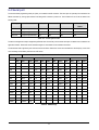
1
REG10J0001-0100
Renesas Starter Kit for H8SX1582
User's Manual
RENESAS SINGLE-CHIP MICROCOMPUTER
H8SX FAMILY
Rev.1.00
Revision date:25.11.2005
Renesas Technology Europe Ltd.
www.renesas.com
D005961_11
Table of Contents
Table of Contents ...................................................................................................................................................ii
Chapter 1. Preface .................................................................................................................................................4
Chapter 2. Purpose ................................................................................................................................................5
Chapter 3. Power Supply ......................................................................................................................................6
3.1. Requirements ..............................................................................................................................................6
3.2. Power – Up Behaviour................................................................................................................................6
Chapter 4. Board Layout.......................................................................................................................................7
4.1. Component Layout......................................................................................................................................7
4.2. Board Dimensions.......................................................................................................................................8
Chapter 5. Block Diagram.....................................................................................................................................9
Chapter 6. User Circuitry ...................................................................................................................................10
6.1. Switches.....................................................................................................................................................10
6.2. LEDs ..........................................................................................................................................................10
6.3. Potentiometer............................................................................................................................................10
6.4. Serial port.................................................................................................................................................. 11
6.5. LCD Module ..............................................................................................................................................12
6.6. Option Links..............................................................................................................................................13
6.7. Oscillator Sources .....................................................................................................................................14
6.8. Reset Circuit..............................................................................................................................................14
Chapter 7. Modes.................................................................................................................................................15
7.1. FDT Settings .............................................................................................................................................15
7.1.1. Boot mode............................................................................................................................................16
7.1.2. User Boot mode ..................................................................................................................................17
7.1.3. User Mode ...........................................................................................................................................18
Chapter 8. Programming Methods .....................................................................................................................19
8.1. Serial Port Programming .........................................................................................................................19
8.2. E10A Header .............................................................................................................................................19
Chapter 9. Headers..............................................................................................................................................20
9.1. Microcontroller Headers ...........................................................................................................................20
9.2. Application Headers..................................................................................................................................24
Chapter 10. Code Development ..........................................................................................................................26
10.1. Overview..................................................................................................................................................26
10.2. Compiler Restrictions .............................................................................................................................26
10.3. Mode Support ..........................................................................................................................................26
10.4. Breakpoint Support ................................................................................................................................26
10.5. Code located in RAM ..............................................................................................................................26
10.6. HMon Code Size ......................................................................................................................................26
10.7. Memory Map ...........................................................................................................................................28
ii
10.8. Baud Rate Setting...................................................................................................................................29
10.9. Interrupt mask sections .........................................................................................................................29
Chapter 11. Component Placement ....................................................................................................................30
Chapter 12. Additional Information ...................................................................................................................31
REVISION HISTORY .........................................................................................................................................32
iii
Chapter 1. Preface
Cautions
This document may be, wholly or partially, subject to change without notice.
All rights reserved. No one is permitted to reproduce or duplicate, in any form, a part or this entire document without the written
permission of Renesas Technology Europe Limited.
Trademarks
All brand or product names used in this manual are trademarks or registered trademarks of their respective companies or
organisations.
Copyright
© Renesas Technology Europe Ltd. 2005. All rights reserved.
© Renesas Technology Corporation. 2005. All rights reserved.
Website:
http://www.renesas.com/
Glossary
BRR
Baud Rate Register
ERR
Error Rate
HMON
Embedded Monitor
RTE
Renesas Technology Europe Ltd.
RSK
Renesas Starter Kit
RSO
Renesas Solutions Corp.
4
Chapter 2.Purpose
This RSK is an evaluation tool for Renesas microcontrollers.
Features include:
•
Renesas Microcontroller Programming.
•
User Code Debugging.
•
User Circuitry such as switches, LEDs and potentiometer(s).
•
Sample Application.
•
Sample peripheral device initialisation code.
The CPU board contains all the circuitry required for microcontroller operation.
This manual describes the technical details of the RSK hardware. The Quick Start Guide and Tutorial Manual provide details of the
software installation and debugging environment.
5
Chapter 3.Power Supply
3.1.Requirements
This CPU board operates from a 5V power supply.
A diode provides reverse polarity protection only if a current limiting power supply is used.
All CPU boards are supplied with an E8 debugger. This product is able to power the CPU board with up to 300mA. When the CPU board is
connected to another system that system should supply power to the CPU board.
All CPU boards have an optional centre positive supply connector using a 2.0mm barrel power jack.
Warning
The CPU board is neither under not over voltage protected. Use a centre positive supply for this board.
3.2.Power – Up Behaviour
When the RSK is purchased the CPU board has the ‘Release’ or stand alone code from the example tutorial code pre-programmed into the
Renesas microcontroller. On powering up the board the user LEDs will start to flash. Switch 2 will cause the LEDs to flash at a rate
controlled by the potentiometer.
6
Chapter 4.Board Layout
4.1.Component Layout
The following diagram shows top layer component layout of the board.
Application Board
Interface
JA5
Reset Switch
RS2332 Serial
JA1
LCD Display
Power
Power LED
J2
Microcontroller
Pin Headers
E8 Header
J3
J1
User LEDs
E10A
Debugger
J4
JA6
JA2
Boot LED
Application Board
Interface
Potentiometer
Figure 4-1: Board Layout
7
User Switches
4.2.Board Dimensions
The following diagram gives the board dimensions and connector positions. All through hole connectors are on a common 0.1” grid for easy
interfacing.
3.81mm
5.00mm
45.00mm
Serial D9
SKT
JA3
JA1
JA5
JA4
14.00mm
R
E
S
J2
80.01mm
Optional LCD connec tor
Optional Expansion Bus connec tor
with micriocontroller pin1
MC
U
J1 - Applies to connecter
RING
85.00mm
100.00mm
J3
E8
Other
J4
JA2
JA6
SW
3
POT
SW
2
27.00mm
35.56 mm
Corners x4
3mm radius
43.18 mm
50.80 mm
Short Board = 85 mm
86.36mm
115.00mm
120.00mm
Figure 4-2 : Board Dimensions
8
SW
1
Chapter 5.Block Diagram
Figure 5-1 shows the CPU board components and their connectivity.
Power Jack Option
Application Board
Headers
Microcontroller Pin
Headers
Boot mode pins
Boot Circuitry
Microcontroller
Debug Header Option
RESET pin
RESn
D-type latch
BOOT & BOOTn signals
Serial Connector Option
ADC Input
IRQ pin
IRQ pin
IRQ pin
SW2
SW3
Potentiometer
RES
BOOT
SWITCHES
LEDs
User: 4 LEDS
1Green, 1Orange, 2Red
Power: Green
Boot: Orange
Figure 5-1: Block Diagram
Figure 5-2 shows the connections to the RSK.
S
W
2
S
W
3
POT
JA2
Othe
r
JA6
J1 - Applies to
connecter with
micriocontroller pin1
E8
Optional LCD
connector
Optional Expansion Bus
connector
J4
MC
U
J3
Computer
Figure 5-2 : RSK Connctions
9
R
E
S
JA4
Serial D9
SKT
JA3
J2
JA1
JA5
RIN
G
S
W
1
Chapter 6.User Circuitry
6.1.Switches
There are four switches located on the CPU board. The function of each switch and its connection are shown in Table 6-1.
Switch
Function
Microcontroller
RES
When pressed; the CPU board microcontroller is reset.
RESn
SW1/BOOT*
Connects to an IRQ input for user controls.
IRQ8-A, Pin 58
The switch is also used in conjunction with the RES switch to place
(Port 2, pin 0)
the device in BOOT mode when not using the E8 debugger.
SW2*
Connects to an IRQ line for user controls.
IRQ9-A , Pin59
(Port 2, pin 1)
SW3*
Connects to the ADC trigger input. Option link allows connection to
ADTRG, Pin 57
IRQ line. The option is a pair of 0R links.
(Port 1, pin 7)
OR
IRQ10-A, Pin 60
(Port 2, pin 2)
Table 6-1: Switch Functions
*Refer to schematic for detailed connectivity information.
6.2.LEDs
There are six LEDs on the CPU board. The green ‘POWER’ LED lights when the board is powered. The orange BOOT LED indicates the
device is in BOOT mode when lit. The four user LEDs are connected to an IO port and will light when their corresponding port pin is set low.
Table 6-2, below, shows the LED pin references and their corresponding microcontroller port pin connections.
LED Reference (As
Microcontroller Port Pin
Microcontroller Pin
shown on silkscreen)
function
Number
Polarity
LED0
Port I 0
113
Active Low
LED1
Port I 1
115
Active Low
LED2
Port I 2
118
Active Low
LED3
Port I 3
12
Active Low
Table 6-2:LED Port
6.3.Potentiometer
A single turn potentiometer is connected to AN0 of the microcontroller. This may be used to vary the input analog voltage value to this pin
between AVCC and Ground.
10
6.4.Serial port
The microcontroller programming serial port (SCI4) is connected to the E8 connector. This serial port can optionally be connected to the
RS232 transceiver by moving option resistors and fitting the D connector in position J9. The connections to be moved are listed in the
following table.
Description
Function
Fit For E8
Remove for E8
Fit for RS232
Remove for
RS232
SCI4 Tx
Programming Serial Port
R15
R14
R14
R15
SCI4 Rx
Programming Serial Port
R12
R13
R13
R12
SCI4 Clk
Programming Serial Port
R10
NA
NA
NA
Table 6-3 - Serial Option Links
The board is designed to accept a straight through RS232 cable. A secondary microcontroller serial port is available and connected to the
application headers. Please refer to the schematic diagram for more details on the available connections.
The serial baud rates supported by this CPU board are shown below. Note: these values are calculated from the frequency value of the
main oscillating source fitted by default on this CPU board.
6MHz x 4 = 24MHz
N
Asynchronous Serial Baud Rate Evaluation
0
BRR
1
Rate
ERR
BRR
2
Rate
ERR
BRR
3
Rate
ERR
110
300
BRR
Rate
ERR
106
110
-0.44
155
300
0.16
38
300
0.16
1200
155
1202
0.16
38
1202
0.16
9
1172
-2.34
2400
77
2404
0.16
19
2344
-2.34
4
2344
-2.34
4800
155
4808
0.16
38
4808
0.16
9
4688
-2.34
1
5859
22.07
9600
77
9615
0.16
19
9375
-2.34
4
9375
-2.34
0
11719
22.07
19200
38
19231
0.16
9
18750
-2.34
1
23438
22.07
38400
19
37500
-2.34
4
37500
-2.34
0
46875
22.07
57600
12
57692
0.16
2
62500
8.51
115200
6
107143
-6.99
1
93750
-18.62
230400
2
250000
8.51
250000
2
250000
0.00
375000
1
375000
0.00
750000
0
750000
0.00
Table 6-4 : BRR Settings
11
6.5.LCD Module
A LCD module can be connected to the connector J13. Any module that conforms to the pin connections and has a KS0066u compatible
controller can be used with the tutorial code. The LCD module uses a 4bit interface to reduce the pin allocation. No contrast control is
provided; this must be set on the display module.
Table 6-5 shows the pin allocation and signal names used on this connector.
The module supplied with the CPU board only supports 5V operation.
J13
Pin
Circuit Net Name
Device
Pin
Circuit Net Name
Device
Pin
Pin
1
Ground
-
2
5V Only
-
3
No Connection
-
4
DLCDRS
51
5
R/W (Wired to Write only)
-
6
DLCDE
55
7
No Connection
-
8
No connection
-
9
No Connection
-
10
11
DLCD4
68
12
DLCD5
67
13
DLCD6
66
14
DLCD7
61
-
Table 6-5 LCD Module Connections
12
6.6.Option Links
Table 6-6 below describes the function of the option links contained on this CPU board. The default configuration is indicated by BOLD
text.
Option Link Settings
Reference
R10
Function
Fitted
Programming
Connects SCK to E8
Alternative (Removed)
SCK disconnected from E8
Serial Port
R12
R15
R13
R14
R62
Related To
R12, R13,
R14, R15
Programming
Connects E8 to Programming
Serial Port
Serial port.
Programming
Connects E8 to Programming
Serial Port
Serial port.
Programming
Connects RS232 port to
Serial Port
Programming SCI port
Programming
Connects RS232 port to
Serial Port
Programming SCI port
RS232 Driver
Enables RS232 Serial Transceiver
MUST be removed if R13 fitted.
R13
Should be removed if R14 fitted.
R14
MUST be removed if R12 fitted.
R12
Should be removed if R15 fitted.
R15
MUST be removed if R18 Fitted
R18, R13,
R14
R18
RS232 Driver
Disables RS232 Serial
MUST be removed if R62 Fitted
Transceiver
R62, R13,
R14
Connects Alternate serial to D
Disconnects Alternate serial from D
connector
connector.
Connects Alternate serial to D
Disconnects Alternate serial from D
connector
connector.
Connects Alternate Serial to
Should be removed if External serial
RS232 Transceiver
device.
Connects Alternate Serial to
MUST be removed if External serial
RS232 Transceiver
device.
External
Connects External Ring header
Disconnects sensitive microcontroller
Oscillator
pins to Microcontroller
signals from external pins.
External
Connects External Ring header
Disconnects sensitive microcontroller
Oscillator
pins to Microcontroller
signals from external pins.
R46
Power
Supply to microcontroller
Fit Low ohm resistor to measure current
R63
R63
Analogue Power
Connects 5V supply to
Analogue supply MUST be provided from
JA1
Analogue supply
external interface pins.
Connects SW3 to Analogue
Disconnected
R59
Disconnected
R58
R36
R31
R35
R37
R53
R55
R58
Serial Connector
Serial Connector
Alternate Serial
Alternate Serial
SW3
R31
R36
R37, JA6
R35, JA6
R55
R53
Trigger input
R59
SW3
Connects SW3 to IRQ input
Table 6-7: 2-Pin jumpers
13
6.7.Oscillator Sources
A crystal oscillator is fitted on the CPU board and used to supply the main clock input to the Renesas microcontroller. Table 6-8 details
the oscillators that are fitted and alternative footprints provided on this CPU board:
Component
Value : Package
Crystal (X1)
Fitted
6MHz : HC/49U
Manufacturer
Approved
See www.renesas.com for details
CPU board
Magna Frequency Components
X6M0GCBE494SM*
C-Mac
LFXTAL017159
Table 6-8: Oscillators / Resonators
Warning: When replacing the default oscillator with that of another frequency, the debugging monitor will not function unless the following
are corrected:
•
FDT programming kernels supplied are rebuilt for the new frequency
•
The supplied HMON debugging monitor is updated for baud rate register settings.
The user is responsible for code written to support operating speeds other than the default. See the HMON User Manual for details of
making the appropriate modifications in the code to accommodate different operating frequencies.
6.8.Reset Circuit
The CPU Board includes a simple latch circuit that links the mode selection and reset circuit. This provides an easy method for swapping
the device between Boot Mode, User Boot Mode and User mode. This circuit is not required on customers boards as it is intended for
providing easy evaluation of the operating modes of the device on the RSK. Please refer to the hardware manual for more information on
the requirements of the reset circuit.
The reset circuit operates by latching the state of the boot switch on pressing the reset button. This control is subsequently used to modify
the mode pin states as required.
The mode pins should change state only while the reset signal is active to avoid possible device damage.
The reset is held in the active state for a fixed period by a pair of resistors and a capacitor. Please check the reset requirements carefully to
ensure the reset circuit on the user’s board meets all the reset timing requirements.
14
Chapter 7.Modes
The CPU board supports User mode, Boot mode and User Boot mode. User mode may be used to run and debug user code, while Boot
mode may only be used to program the Renesas microcontroller with program code. User Boot mode can only be used to program the
User Mat (the main area of 768Kbytes of Flash ROM on the device). It does not support programming of the user boot area. User Boot
mode is used to run a user supplied boot-loader program stored in the user boot MAT (the smaller area, 8Kbytes, of Flash ROM). To
program the user boot MAT, the device must be in Boot mode. Further details of programming the MATs are available in the H8SX/1582
hardware manual.
When using the E8 debugger supplied with the RSK the mode transitions are executed automatically. The CPU board provides
the capability of changing between User and Boot / User Boot modes using a simple latch circuit. This is only to provide a
simple mode control on this board when the E8 is not in use.
To manually enter boot mode, press and hold the SW1/BOOT. The mode pins are held in their boot states while reset is pressed and
released. Release the boot button. The BOOT LED will be illuminated to indicate that the microcontroller is in boot mode.
More information on the operating modes can be found in the device hardware manual.
7.1.FDT Settings
In the following sections the tables identify the FDT settings required to connect to the board using the E8Direct debugger interface. The ‘A’
interface is inverted on the RSK board. This is to ensure the board can function in a known state when the E8 is connected but not
powered. The E8 Debugger contains the following ‘pull’ resistors.
E8 Pin
Resistor
A
Pull Down (100k)
B
Pull Up (100k)
C
Pull Down (100k)
D
Pull Up (100k)
Table 7-1: E8 Mode Pin drives
15
7.1.1.Boot mode
The boot mode settings for this CPU board are shown in Table 7-2 below:
MD1
MD0
LSI State after Reset
FDT Settings
End
1
0
A
Boot Mode
0
B
0
Table 7-2: Mode pin settings
The following picture shows these settings made in the E8Direct configuration dialog from HEW.
Figure 7-1: Boot Mode FDT configuration
16
7.1.2.User Boot mode
A Note on Mats:
The H8SX/1582 possesses two distinct areas of Flash, User MAT (768KByte) and User Boot MAT (8KByte). The User Boot MAT is a
separate area of FLASH from User MAT, intended to hold user boot code.
A custom boot stub could be programmed into User Boot MAT which allows programming and erasing of the User MAT in User Mode,
without erasing the contents of the User Boot MAT. Once User Boot Mode is entered, code contained in the User Boot MAT is executed.
This differs to Boot mode, as Boot mode erases all User MAT and requires an auto-baud on a fixed SCI port to be performed. The
existence of the User Boot Mat therefore allows an alternative communications port to be used for further code download to the User MAT.
Programming of the User Boot Mat may only be performed in boot mode.
The user may place the H8SX/1582 device provided on a CPU board for the H8SX1582 board in user boot mode by fitting jumper J13. The
Boot procedure must then be performed for entry into user boot mode. The Boot LED should light, suggesting a transition to user boot
mode.
The user boot mode settings for this CPU board are shown in Table 7-3 below:
MD1
MD0
LSI State after Reset End
FDT Settings
A
0
1
User Boot Mode
1
Table 7-3: Mode pin settings
17
B
1
7.1.3.User Mode
For the device to enter User Mode, reset must be held active while the microcontroller mode pins are held in states specified for User Mode
operation. 100K pull up and pull down resistors are used to set the pin states during reset.
The H8SX/1582 supports 4 user modes. The memory map in all of these modes is 16Mbyte in size. The default user mode for CPU board
supporting H8SX1582 is 7.
MD1
MD0
LSI State after Reset
FDT Settings
End
1
1
A
User Mode
0
Table 7-4: Mode pin settings
Figure 7-2: User mode FDT configuration
18
B
1
Chapter 8.Programming Methods
All of the Flash ROM on the device (i.e. both MATs) can be programmed when the device is in Boot mode. Once in boot mode, the
boot-loader program pre-programmed into the microcontroller executes and attempts a connection with a host (for example a PC). On
establishing a connection with the microcontroller, the host may then transmit program data to the microcontroller via the appropriate
programming port.
Table 8-1 below shows the programming port for this Renesas Microcontroller and its associated pins
Programming Port Table – Programming port pins and their CPU board signal names
SCI4
TXD4, PIN 5
RXD4, PIN 7
SCK4, PIN 8
CPU board Signal Name
PTTX
PTRX
PTCK
Table 8-1: Serial Port Boot Channel
8.1.Serial Port Programming
This sequence is not required when debugging using the E8 supplied with the kit.
The microcontroller must enter boot mode for programming, and the programming port must be connected to a host for program download.
To execute the boot transition, and allow programs to download to the microcontroller, the user must perform the following procedure:
Connect a 1:1 serial cable between the host PC and the CPU board
Depress the BOOT switch and keep this held down
Depress the RESET switch once, and release
Release the BOOT switch
The Flash Development Toolkit (FDT) is supplied to allow programs to be loaded directly on to the board using this method.
8.2.E10A Header
This device supports an optional E10A debugging interface. The E10A provides additional debugging features including hardware
breakpoints and hardware trace capability. (Check with the website at www.renesas.com or your distributor for a full feature list).
To utilise the E10A the user will need to fit a 14 way boxed header to J7. To enable the E10A functions the user should also fit a jumper link
in position J6.
When J6 is fitted the microcontroller will not operate correctly unless operated via the E10A.
19
Chapter 9.Headers
9.1.Microcontroller Headers
Table 9-1 to Table 9-4 show the microcontroller pin headers and their corresponding microcontroller connections. The header pins
connect directly to the microcontroller pin unless otherwise stated.
J1
Pin
Circuit Net Name
Device
Pin
Circuit Net Name
Device
Pin
Pin
1
SCIbRX
1
2
SCIbCK
2
3
PIN3
3
4
UC_VCC
4
5
PTTX
5
6
GROUND
6
7
PTRX
7
8
PTCK
8
9
TDO
9
10
PIN10
10
11
TRIGb
11
12
LED3
12
13
PIN13
13
14
MO_Up
14
15
MO_Vp
15
16
PIN16
16
17
MO_Wp
17
18
CTSRTS
18
19
PIN19
19
20
PIN20
20
21
PIN21
21
22
PIN22
22
23
TRISTn
23
24
GROUND
24
25
MO_Un
25
26
UC_VCC
26
27
MO_Vn
27
28
MO_UD
28
29
PIN29
29
30
MO_Wn
30
Table 9-1: J1
20
J2
Pin
Circuit Net Name
Device
Pin
Circuit Net Name
Pin
Device
Pin
1
PIN31
31
2
PIN32
32
3
PIN33
33
4
PIN34
34
5
PIN35
35
6
IO_0
36
7
PIN37
37
8
IO_1
38
9
IO_2
39
10
IO_3
40
11
IO_4
41
12
IO_5
42
13
PIN43
43
14
IO_6
44
15
IO_7
45
16
UC_VCC
46
17
IRQ0
47
18
GROUND
48
19
IRQ1
49
20
GROUND
50
21
DLCDRS
51
22
IRQ2
52
23
IRQ3
53
24
SCIaTX
54
25
SCIaRX
55
26
SCIaCK
56
27
ADTRG
57
28
SW1
58
29
SW2
59
30
SW3
60
Table 9-2: J2
21
J3
Pin
Circuit Net Name
Device
Pin
Circuit Net Name
Pin
Device
Pin
1
DLCD7
61
2
GROUND
62
3
PIN63
63
4
UC_VCC
64
5
DLCDE
65
6
DLCD6
66
7
DLCD5
67
8
DLCD4
68
9
TMR0
69
10
TMR1
70
11
PIN71
71
12
PIN72
72
13
PIN73
73
14
TRSTn
74
15
TMS
75
16
TDI
76
17
TCK
77
18
PIN78
78
19
RESn
79
20
NMI
80
21
TRIGa
81
22
UC_VCC
82
23
CON_XTAL
83
24
CON_EXTAL
84
25
GROUND
85
26
EMLE
86
27
SCIcTX
87
28
PIN88
88
29
SCIcRX
89
30
SCIcCK
90
Table 9-3: J3
22
J4
Pin
Circuit Net Name
Device
Pin
Circuit Net Name
Pin
Device
Pin
1
E8_BUSY
91
2
MD1_E8B
92
3
AD4
93
4
AD5
94
5
AD6
95
6
AD7
96
7
AD0
97
8
AD1
98
9
AD2
99
10
AVcc
100
11
AD3
101
12
AVss
102
13
AD_POT
103
14
AVcc
104
15
PIN105
105
16
PIN106
106
17
PIN107
107
18
PIN108
108
19
PIN109
109
20
PIN110
110
21
PIN111
111
22
MD0_E8A
112
23
LED0
113
24
IIC_SDA
114
25
LED1
115
26
PIN116
116
27
IIC_SCL
117
28
LED2
118
29
IIC_EX
119
30
SCIbTX
120
Table 9-4: J4
23
9.2.Application Headers
Table 9-5 and Table 9-6 below show the standard application header connections.
JA1
Pin
Generic Header Name
CPU board
Device
Signal Name
Pin
Pin
Header Name
CPU board
Device
Signal Name
Pin
1
Regulated Supply 1
5V
2
Regulated Supply 1
GROUND
3
Regulated Supply 2
3V3
4
Regulated Supply 2
GROUND
5
Analogue Supply
AVcc
6
Analogue Supply
AVss
102
7
Analogue Reference
AVref
8
ADTRG
ADTRG
57
9
ADC0
I0
AD0
97
10
ADC1
I1
AD1
98
11
ADC2
I2
AD2
99
12
ADC3
I3
AD3
101
13
DAC0
DAC0
14
DAC1
DAC1
15
IOPort
IO_0
36
16
IOPort
IO_1
38
17
IOPort
IO_2
39
18
IOPort
IO_3
40
19
IOPort
IO_4
41
20
IOPort
IO_5
42
21
IOPort
IO_6
44
22
IOPort
IO_7
45
23
Open drain
IRQ3
53
24
I²C Bus - (3rd pin)
IIC_EX
119
25
I²C Bus
IIC_SDA
114
26
I²C Bus
IIC_SCL
117
IRQAEC
100,104
Table 9-5: JA1 Standard Generic Header
JA2
Pin
Generic Header Name
CPU board
Device
Signal Name
Pin
Pin
Header Name
CPU board
Device
Signal Name
Pin
1
Open drain
RESn
79
2
External Clock Input
EXTAL
3
Open drain
NMIn
80
4
Regulated Supply 1
Vss1
5
Open drain output
WDT_OVF
6
Serial Port
SCIaTX
54
7
Open drain
IRQ0
47
8
Serial Port
SCIaRX
55
9
Open drain
IRQ1
49
10
Serial Port
SCIaCK
56
11
Up/down
MO_UD
28
12
Serial Port Handshake
CTS/RTS
18
13
Motor control
MO_Up
14
14
Motor control
MO_Un
25
15
Motor control
MO_Vp
15
16
Motor control
MO_Vn
27
17
Motor control
MO_Wp
17
18
Motor control
MO_Wn
30
19
Output
TMR0
69
20
Output
TMR1
70
21
Input
TRIGa
81
22
Input
TRIGb
11
23
Open drain
IRQ2
52
24
Tristate Control
TRSTn
74
25
SPARE
-
26
SPARE
-
WUP
Table 9-6: JA2 Standard Generic Header
24
84*
JA5
Pin
Generic Header Name
CPU board
Device
Signal Name
Pin
Pin
Header Name
CPU board
Device
Signal Name
Pin
1
ADC4
I4
AD4
93
2
ADC5
I5
AD5
94
3
ADC6
I6
AD6
95
4
ADC7
I7
AD7
96
5
CAN
CAN1TX
6
CAN
CAN1RX
7
CAN
CAN2TX
8
CAN
CAN2RX
9
Reserved
10
Reserved
11
Reserved
12
Reserved
13
Reserved
14
Reserved
15
Reserved
16
Reserved
17
Reserved
18
Reserved
19
Reserved
20
Reserved
21
Reserved
22
Reserved
23
Reserved
24
Reserved
Table 9-7: JA5 Optional Generic Header
JA6
Pin
Generic Header Name
CPU board
Device
Signal
Pin
Pin
Header Name
CPU board
Device
Signal Name
Pin
Name
1
DMA
DREQ
2
DMA
DACK
3
DMA
TEND
4
Standby (Open drain)
STBYn
5
Host Serial
RS232RX
7*
7
Serial Port
9
Serial Port
11
Serial Port
13
SCIdTX
RS232TX
5*
6
Host Serial
SCIdRX
SCIbRX
1
8
Serial Port
SCIbTX
120
Synchronous
SCIcTX
87
10
Serial Port
SCIbCK
2
Synchronous
SCIcCK
90
12
Serial Port
SCIcRX
89
Reserved
14
Reserved
15
Reserved
16
Reserved
17
Reserved
18
Reserved
19
Reserved
20
Reserved
21
Reserved
22
Reserved
23
Reserved
24
Reserved
25
Reserved
26
Reserved
Synchronous
Table 9-8: JA6 Optional Generic Header
* Marked pins are affected by option links.
25
Chapter 10.Code Development
10.1.Overview
Note: For all code debugging using Renesas software tools, the CPU board must either be connected to a PC serial port via a serial cable
or a PC USB port via an E8. An E8 is supplied with the RSK product.
The HMON embedded monitor code is modified for each specific Renesas microcontroller. HMON enables the High-performance
Embedded Workshop (HEW) development environment to establish a connection to the microcontroller and control code execution.
Breakpoints may be set in memory to halt code execution at a specific point.
Unlike other embedded monitors, HMon is designed to be integrated with the user code. HMon is supplied as a library file and several
configuration files. When debugging is no longer required, removing the monitor files and library from the code will leave the user’s code
operational.
The HMON embedded monitor code must be compiled with user software and downloaded to the CPU board, allowing the users’ code to
be debugged within HEW.
Due to the continuous process of improvements undertaken by Renesas the user is recommended to review the information provided on
the Renesas website at www.renesas.com to check for the latest updates to the Compiler and Debugger manuals.
10.2.Compiler Restrictions
The compiler supplied with this RSK is fully functional for a period of 60 days from first use. After the first 60 days of use have expired, the
compiler will default to a maximum of 64k code and data. To use the compiler with programs greater than this size you will need to
purchase the full tools from your distributor.
Warning: The protection software for the compiler will detect changes to the system clock. Changes to the system clock back in
time may cause the trial period to expire prematurely.
10.3.Mode Support
The HMON library is built to support 16Mbyte Advanced Mode only for the H8SX family.
10.4.Breakpoint Support
The device does not include a user break controller. No breakpoints can be located in ROM code. However, code located in RAM may
have multiple breakpoints limited only by the size of the On-Chip RAM. To debug with breakpoints in ROM you need to purchase the
E10A-USB on-chip debugger at additional cost.
10.5.Code located in RAM
Double clicking in the breakpoint column in the HEW code window sets the breakpoint. Breakpoints will remain unless they are double
clicked to remove them. (See the Tutorial Manual for more information on debugging with the HEW environment.)
10.6.HMon Code Size
HMON is built along with the user’s code. Certain elements of the HMON code must remain at a fixed location in memory. The following
table details the HMON components and their size and location in memory. For more information, refer to the map file when building code.
26
Section
RESET_VECTOR
Description
HMON Reset Vector (Vector 0)
Start
Size
Location
(H’bytes)
H’ 0000 0000
0x0004
Required for Start-up of HMON
SCI_VECTORS
HMON Serial Port Vectors (Vector 160, 161, 162, 163)
H’0000 0280
0x000C
PHMON
HMON Code
H’0000 3000
0x278C
CHMON
HMON Constant Data
H’0000 5730
0x0136
BHMON
HMON Un-initialised data
Variable
0x021F
UGenU
FDT Kernel.
H’0000 1000
0xEA8
H’0000 0800
0x0004
This is at a fixed location and must not be moved. Should the
kernel need to be moved it must be re-compiled.
CUser_Vectors
Pointer used by HMON to point to the start of user code.
27
10.7.Memory Map
The memory map shown in this section visually describes the locations of program code sections related to HMON, the FDT kernels and
the supporting code within the ROM/RAM memory areas of the microcontroller.
H'0000
Vectors
H'0800
H'0803
H'1000
RESET Vector
H'0000
H'0003
SCI Vectors
H'0280
H'028B
CUser_Vectors
UGenU FDT Kernel
H'1EA7
H'3000
PHMON
CHMON
H'594F
On-Chip FLASH
ROM
H'BFFFF
H'FF9000
On-Chip RAM
H'FFBBE0
H'FFBDFE
H'FFBE00
H'FFBFFF
BHMON
Stack
H'FFFA00
H'FFFFFF
Internal I/O
REGISTERS
28
10.8.Baud Rate Setting
HMON is initially set to connect at 250000Baud. The value set in the baud rate register for the microcontroller must be altered if the user
wishes to change either the serial communication baud rate of the serial port or the operating frequency of the microcontroller. This value
is defined in the hmonserialconfiguser.h file, as SCI_CFG_BRR (see the Serial Port section for baud rate register setting values). The
project must be re-built and the resulting code downloaded to the microcontroller once the BRR value is changed. Please refer to the
HMON User Manual for further information.
10.9.Interrupt mask sections
HMON has an interrupt priority of 6. The serial port has an interrupt priority of 7. Modules using interrupts should be set to lower than this
value (6 or below), so that serial communications and debugging capability is maintained.
29
Chapter 11. Component Placement
30
Chapter 12. Additional Information
For details on how to use High-performance Embedded Workshop (HEW), refer to the HEW manual available on the CD or installed in the
Manual Navigator.
For information about the H8SX/1582 series microcontrollers refer to the H8SX/1582 Series Hardware Manual
For information about the H8SX/1582 assembly language, refer to the H8 Series Programming Manual
Further information available for this product can be found on the Renesas website at:
http://www.renesas.com/rsk
General information on Renesas Microcontrollers can be found on the following website.
Global: http://www.renesas.com/
31
Renesas Starter Kit for H8SX1582
User's Manual
Renesas Technology Europe Ltd.
Dukes Meadow, Millboard Road, Bourne End Buckinghamshire SL8 5FH, United Kingdom
REG10J0002-0100
Renesas Starter Kit
RSK H8SX1582 Tutorial Manual
RENESAS SINGLE-CHIP MICROCOMPUTER
Rev.1.00
Revision date:25.11.2005
Renesas Technology Europe Ltd.
www.renesas.com
D005963_11
Table of Contents
Table of Contents ...................................................................................................................................................ii
Chapter 1. Preface .................................................................................................................................................3
Chapter 2. Introduction.........................................................................................................................................4
Chapter 3. Tutorial Project Workspace ................................................................................................................5
Chapter 4. Project Workspace...............................................................................................................................6
4.1. Introduction.................................................................................................................................................6
4.2. Creating a new Project Workspace ............................................................................................................6
4.3. Build Configurations and Debug Sessions ................................................................................................7
4.3.1. Build Configuration..............................................................................................................................7
4.3.2. Debug Session.......................................................................................................................................7
Chapter 5. Building the Tutorial Project .............................................................................................................8
5.1. Building Code ..............................................................................................................................................8
5.2. Connecting the debugger............................................................................................................................8
5.3. Connecting to the target with E8Direct & HMon.....................................................................................9
5.3.1. Connecting To HMon..........................................................................................................................12
Chapter 6. Downloading and Running the Tutorial..........................................................................................14
Chapter 7. Project Files.......................................................................................................................................19
7.1. Standard Project Files ..............................................................................................................................19
7.1.1. Initialisation code (Resetprg.c / resetprg.h)......................................................................................19
7.1.2. Board initialisation code (Hwsetup.c / hwsetup.h)...........................................................................20
7.1.3. Main tutorial code (Main.c / main.h).................................................................................................21
Chapter 8. Additional Information .....................................................................................................................22
REVISION HISTORY .........................................................................................................................................23
ii
Chapter 1. Preface
Cautions
This document may be, wholly or partially, subject to change without notice.
All rights reserved. No one is permitted to reproduce or duplicate, in any form, a part or this entire document without the written
permission of Renesas Technology Europe Limited.
Trademarks
All brand or product names used in this manual are trademarks or registered trademarks of their respective companies or
organisations.
Copyright
© Renesas Technology Europe Ltd. 2005. All rights reserved.
© Renesas Technology Corporation. 2005. All rights reserved.
Website:
http://www.renesas.com/
Glossary
BRR
Baud Rate Register
ISR
Interrupt Service Routine
ERR
Error Rate
PWM
Pulse Width Modulation
HMON
Embedded Monitor
CPU
Central Processing Unit
RSK
Renesas Starter Kit
PC
Program Counter
RSO
Renesas Solutions Organisation.
IRQ
Interrupt ReQuest
HEW
High performance Embedded Workshop
NMI
Non-Maskable Interrupt
CCR
Condition Code Register
RTE
ReTurn from Exception
EXR
EXtended control Register
LED
Light Emitting Diode
SR
Status Register
RTC
Real Time Clock
3
Chapter 2.Introduction
This manual is designed to answer, in tutorial form, the most common questions asked about using a Renesas Starter Kit (RSK): The
tutorials help explain the following:
•
How do I compile, link, download, and run a simple program on the RSK?
•
How do I build an embedded application?
•
How do I use Renesas’ tools?
The project generator will create a tutorial project with two selectable build configurations
•
‘Debug’ is a project built with the debugger support included.
•
‘Release’ build demonstrating code suitable for release in a product.
Files referred to in this manual are installed using the project generator as you work through the tutorials. The tutorial examples in this
manual assume that installation procedures described in the RSK Quick Start Guide have been completed. Please refer to the Quick Start
Guide for details of preparing the configuration.
NOTE: These tutorials are designed to show you how to use the RSK and are not intended as a comprehensive introduction to
the High performance Embedded Workshop (HEW) debugger or the compiler tool-chains – please consult the relevant user
manuals for more in-depth information.
4
Chapter 3.Tutorial Project Workspace
The workspace includes all of the files for two build configurations. The tutorial code is common to both the Debug and the Release build
configurations. The tutorial is designed to show how code can be written, debugged then downloaded without the debug monitor in a
‘Release’ situation.
The build configuration menu in High-performance Embedded Workshop (HEW) allows the project to be configured such that certain files
may be excluded from each of the build configurations. This allows the inclusion of the debug monitor within the Debug build, and its
exclusion in the Release build. Contents of common C files are controlled with defines set up in the build configuration optionss and #ifdef
statements within the source files.
Maintaining only one set of project files means that projects are more controllable.
The HMON monitor code is provided in a pre-compiled library for inclusion in the user code. This library must be included in the tool chain
linker settings. There are some configuration options provided to the user. These are provided in the hmonserialconfiguser.c and
hmonconfiguser.c files and the header files; hmonserialconfiguser.h, hmonserialstruct.h, and hmonconfiguser.c. More information on this
is provided in the HMon User Manual.
5
Chapter 4. Project Workspace
4.1.Introduction
HEW is an integrated development tool that allows the user to write, compile, program and debug a software project on any of the Renesas
Microcontrollers. HEW will have been installed during the software installation for the RSK product.
To begin using the RSK, this manual will describe the stages required to create and debug the supplied tutorial code.
4.2.Creating a new Project Workspace
To look at the program, start High-performance Embedded Workshop from the Windows Start Menu or from its icon:
Open a new tutorial workspace from the [File -> New Workspace…] menu or select ‘Create a new project workspace’ when presented with
the ‘Welcome!’ dialog.
The example above shows the New Project Workspace dialog with the RSKH8SX1582 selected.
•
Select the ‘H8S, H8/300’ CPU family and ‘Hitachi H8S,H8/300 Standard’ Tool-chain for the RSK
•
Select the ‘RSKH8SX1582’ Project type for the RSK from the project list.
•
Enter a name for the workspace, all your files will be stored under a directory with this name.
6
•
The project name field will be pre-filled to match the workspace name above; this name may be changed.
Note: HEW allows you to add multiple projects to a workspace. You may add the sample code projects later so you may
wish to choose a suitable name for the Tutorial project now.
•
Click OK to start the RSK Project Generator wizard.
The next dialog presents the example projects available. Choose the Tutorial code which will be explained later in this manual. There is
also an option for Sample code which provides examples for using various peripherals. This will open a new dialog allowing the selection of
many code examples for the peripheral modules of the device. The final option is for an application build where the debugger is configured
but there is no program code. This project is suitable for the user to add code without having to configure the debugger.
•
Select ‘Tutorial’ as the type of project to generate and then click <Next>.
•
Click <Finish> to create the project
The project generator wizard will display a confirmation dialog. Press <OK> to create the project and insert the necessary files.
A tree showing all the files in this project will appear in the HEW Workspace window.
•
To view the file main.c double click on the file in the Workspace window. A new window will open showing the code.
4.3.Build Configurations and Debug Sessions
The workspace that has been created contains two Build Configurations and two Debug Sessions. The Build Configuration allows the
same project to be built but with different compiler options. The options available to the user are described fully in the HEW Users Manual.
4.3.1.Build Configuration
The build configurations are selected from the left hand drop down list on the tool bar. The options available are Debug and Release. The
debug build is configured for use with the debugger. The Release build is configured for final ROM-able code.
A common difference between the two builds may be the optimisation settings. With Optimisation turned on the Debugger may seem to
execute code in an unexpected order. To assist in debugging it is often helpful to turn off optimisation on the code being debugged.
•
Select the Debug Build Configuration.
4.3.2.Debug Session
The debug sessions are selected from the right hand drop down list on the tool bar. The options vary between RSK however one will
always start Debug and include the type of debug interface. The alternate selection will be ‘DefaultSession’. This purpose of the debug
session is to allow the use of different debugger targets or different debugger settings on the same project.
•
Select the ‘Session_H8SX_1582_HMon’
debug session.
7
Chapter 5. Building the Tutorial Project
The tutorial project build settings have been pre-configured in the tool-chain options. To view the tool chain options select the ‘Build’ Menu
item and the relevant tool-chain. This should be the first option(s) on the drop down menu.
The dialog that is displayed will be specific to the selected tool-chain.
The configuration pane on the left hand side will exist on all the
tool-chain options. It is important when changing any setting to be
aware of the current configuration that is being modified. If you
wish to modify multiple or all build configurations this is possible by
selecting ‘All’ or ‘Multiple’ from the ‘Configuration’ drop down list.
•
Review the options on each of the tabs and
‘Category’ drop down lists to be aware of the
options available.
When complete close the dialog box by clicking <OK>.
5.1.Building Code
There are three short cuts available for building the project.
•
Select the ‘Build All’ tool bar button.
This will build everything in the project that has not been excluded from the build. This includes the standard library.
•
Select the ‘Build’ tool bar button.
This will build all files that have changed since the last build. The standard library will not be built unless an option has been
changed.
•
Press ‘F7’
This is equivalent to pressing the ‘Build’ button described above.
•
Build the project now by pressing ‘F7’ or pressing one of the build icons as shown above.
During the build each stage will be reported in the Output Window.
The build will complete with an indication of errors and warnings encountered during the build.
5.2.Connecting the debugger
For this tutorial it is not necessary to provide an external power supply to the board, the power will be provided by the E8 from the USB port.
Please be aware that if you have too many devices connected to your USB port it may be shut down by Windows. If this happens remove
some devices and try again. Alternatively you can provide an external power source, taking care to ensure the correct polarity and voltage.
8
The Quick Start Guide provided with the RSK board gives detailed instructions on how to connect the E8 to the host computer. The
following assumes that the steps in the Quick Start Guide have been followed and the E8 drivers have been installed.
•
Connect the E8 debugger to the USB port on your computer.
•
Connect the E8 Debugger to the target hardware ensuring that it is plugged into the connector marked E8 which is nearest
the power connector.
•
If supplying external power to the board this can be turned on now.
5.3.Connecting to the target with E8Direct & HMon
This section will take you through the process of connecting to the device, programming the Flash and executing the code.
The E8 provides a interface called E8DIRECT to allow HMon embedded debugger to connect to the target device.
To provide flash programming capabilities the FDT Flash configuration wizard must be configured. This process is only required once in a
project. The settings provide information to HMon to allow the re-programming of the device.
•
Select the FDT Wizard from the FDT Tool Bar
If the flash kernel is already configured then a confirmation window will open with the kernel settings. To modify any of the settings just
double click on the item. If FDT is already configured then please proceed to section 5.3.1 Connecting to HMon.
The first stage is to select the specific device from the installed kernels. The installer will have added the kernel to the FDT registry so it will
appear under the device list drop down menu. If for any reason the kernel has to be re-build such as the crystal frequency on the board has
changed, then the installation path is:
<FDT Installation>\Kernels\ProtC\1582\Renesas\1_0_00.RSK
•
Select the Device on the RSK from the drop down
list.
•
In the sub pane, select the kernel version that ends
in ‘.RSK’.
•
Press <Next>.
If you have copied the kernel to another location to modify for a
different crystal frequency, the device will not be listed in the sub
pane. In this case:
•
Press <Other…> and navigate to your modified
kernel.
9
•
Select E8DIRECT as the communication Port
•
Press <Next>.
•
The default settings are suitable for an un-modified
RSK board.
•
Confirm the Crystal Frequency matches the board.
•
Confirm the main clock frequency multiplier.
•
Confirm the peripheral clock multiplier.
•
Press <Next>.
•
Ensure that ‘USER Program Mode’ is
selected.
•
Confirm that ‘Use Default’ is selected.
•
Press <Next>.
10
•
Confirm the default selections of ‘Automatic’
and ‘Advanced’.
•
Press <Next>.
•
The following warning dialog will be
displayed.
•
Press <OK>.
To communicate with the RSK FDT and HMon need to be able to change the operating mode of the microcontroller. To do this there are
settings to control the state of the Mode pins via the E8Direct interface. These settings are confirmed in the following screens.
Unless you are very sure that the mode pin settings need to change. Do not modify the default settings.
Damage to the microcontroller can be sustained with
incorrect settings.
•
Confirm the mode pin settings.
•
Press <Next>.
•
The following warning dialog will be
displayed.
•
Press <OK>.
11
Damage to the microcontroller can be sustained with
incorrect settings.
•
Confirm the mode pin settings.
•
Press <Finish>.
The Flash configuration has now been completed.
If you have changed any workspace settings now is a good time to save the workspace.
•
Select [File’ -> ‘Save Workspace’].
5.3.1.Connecting To HMon
We can now attempt to connect to the target device.
•
Press the Green ‘Connect’ Icon.
HMon is able to discover the internal flash configuration of the device from the FDT kernel we configured earlier. HMon also needs
information on the location of the IO registers and internal / external RAM. This information is stored in a ‘.TCF’ file. The TCF file is supplied
and registered with HEW. As it is possible to have TCF files with slightly different configurations the following dialog is displayed to allow
selection.
•
Select the TCF file that applies to your RSK.
•
Press <OK>.
12
A further dialog will be displayed to confirm if it acceptable to assume only one E8 device will be connected to the host computer while
using this project. This is the preferred operating mode. While it is possible to use more than one E8 device this is not recommended.
•
Press ‘Yes’ to assume only one E8 device is
connected while in this project.
Note: If you have not followed the Quick Start Guide, additional driver messages may be displayed here. Please refer to the Quick Start
Guide for driver installation.
The following dialog allows the selection of the baud rate and power options for connection to the target board and monitor code. The
default settings are shown below. If the target board is modified with a different crystal frequency then this setting will need to be changed.
(Note in this case the kernel will also need to be re-compiled).
•
Confirm the settings shown and press <OK>.
HMon will attempt to connect to the RSK. If it succeeds then the Output window in HEW will show the ‘Connected’ message. In this case
please proceed to Chapter 6.
If the connection fails you will be returned to the previous dialog. This is likely to be caused by a connection error with the RSK and the E8.
It can also be caused if the RSK has not got a working copy of the HMon target code programmed. Check the settings and if all settings are
OK but the connection still fails then a Boot Mode download will be required. Press <Abort>.
•
Select ‘Download HMon using Boot Mode’.
•
Press <OK>.
On completion of the download HMon will automatically re-connect to the monitor and revert back to User programming mode.
13
Chapter 6.Downloading and Running the Tutorial
Once the code has been built in HEW it needs to be downloaded to the RSK.
Now that you are connected to the target you should see an additional category in the workspace view called ‘Download Modules’
•
Right click on the download module listed
and select ‘Download module’
The download options dialog will be displayed.
This dialog provides various options for HMon operation and
downloading. This dialog allows the re-configuration of any
HMon communication settings. Please review the settings in
each tab.
HMon includes a cache of the current device program. This
allows the number of reprogramming cycles to be reduced by
not programming areas of the device that have not changed
between compilations. On first connection the cache is
empty. Selecting ‘Upload and Compare’ will read the program
back from the device before comparing it to the cache.
•
Select any of the download options shown.
•
Press ‘OK’.
On completion the debugger and code are ready to be executed.
To start debugging we need to reset the debugger and target.
•
Press ‘Reset CPU’ on the Debug Tool Bar.
The File window will open the Tutorial code at the entry point. An arrow marks the current position of the program counter.
14
We will now skip over the initialisation code and proceed to the main tutorial.
•
Open the file called ‘resetprg.c’ by double clicking it in the project navigator.
•
Place a breakpoint at the call to main(); by double clicking in the column containing the PC arrow, next to the line to break
at; or selecting the line and pressing F9; or right click on the line and select ‘Toggle breakpoint’
•
Press ‘Reset Go’ on the Debug Tool Bar.
The code will execute to the breakpoint. At this point all the device initialisation will have been completed.
•
Press ‘Step In’ on the Debug Tool Bar.
15
The code window will open ‘main.c’ and show the new position of the program counter.
Support for the LCD display is included in the tutorial code. We do not need to be concerned about the details of the LCD interface – except
that the interface is write-only and so is not affected if the LCD display is attached or not.
•
Insert a breakpoint on the ‘TimerADC();’ function call.
•
Right click on the ‘FlashLEDs();’ function and select ‘Go to cursor’.
The code will run to the selected line and stop. A temporary breakpoint was automatically inserted in the code and then removed when the
program stopped at the breakpoint.
•
Press ‘Step Over’ on the Debug Tool Bar.
16
The code will run and flash the LEDs 200 times. The debugger will not stop running until all 200 flashes have completed or a button is
pressed on the RSK.
•
If the LEDs are still flashing press the SW1 button on the RSK to exit the FlashLEDs() function.
The code will run to the breakpoint we previously set on the Timer function.
There are several versions of the timer function depending upon the peripherals available in the device. The default function is TimerADC
which we shall demonstrate here.
The timer function initialises an interrupt on an available internal timer. On a compare match in the timer module an interrupt is generated.
In the TimerADC code version the interrupt reads the last ADC conversion for the external potentiometer and uses the result to set the next
compare match value. The ADC conversion is then re-started.
The interrupt initialisation is performed as part of the hardware setup. This is located in the file ‘interrupts.c’.
•
Open the file ‘interrupts.c’ by double clicking on the file in the workspace view.
•
Review this file and find the interrupt function that changes the LED pins, INT_TGI1B_TPU1(void)
•
Set a breakpoint on the line where the LED pins are modified.
•
Press ‘Go’ or ‘F5’ to run the code from the current
PC position.
The code will stop in the interrupt routine. It is now possible to step through the interrupt function.
•
Remove the breakpoint in the interrupt by double clicking again before exiting the function.
•
Press ‘Step Over’ to step over the instruction and observe the LEDs turn off.
•
Press ‘Go’ to run the code from the current PC
position.
The code will now run to the infinite loop at the end of Main(). The user LEDs should now be flashing. If the RSK supports an ADC you can
modify the flashing rate by adjusting the potentiometer on the board.
•
Press ‘Stop’ on the debug tool bar.
•
Press ‘CTRL-B’ to open the breakpoint
window.
•
Select ‘Remove All’
•
Press <OK>.
17
•
Open the file ‘main.c’
•
Insert a breakpoint on ‘StaticsTest();’.
The statics test is used to demonstrate that the initialisation has successfully copied all initialised variables from storage in flash to RAM.
•
Press ‘Reset Go’ on the Debug Tool Bar.
The code will stop at the breakpoint. (Press a button to bypass the flashing LED test.)
•
Press ‘Step In’ on the Debug Tool Bar.
It is possible to monitor variables during debugging of the code. To set up a ‘watch’ on a variable place the mouse over the variable. If the
variable is available in the current context a tool-tip will be displayed with the current value of the variable.
•
Hover the mouse over the ‘ucStr’ variable to see the tooltip value. Then Right click on the variable name and select ‘Instant
Watch’.
A dialog will open showing the variable and allowing further details to be explored.
•
Press ‘Add’
The dialog will close and a new pane will open in the workspace containing the variable.
It is possible to see that the string has been successfully initialised to ‘ STATIC ‘.
•
Set a breakpoint on the ‘DisplayString();’ function call inside the loop.
•
Press ‘Go’ to run the code from the current PC
position.
When the program stops you can see the modified string displayed on the second line of the LCD.
Inspection of the watch pane will show that the first character of the variable string has been replaced with the first character of the constant
replacement string.
•
Remove the breakpoint
•
Right click on the ‘DisplayString();’ function call after the loop and select ‘Go to cursor’.
This shows that the variable was initialised at program start up and can be overwritten with ‘TESTTEST’.
The modified string is also displayed on the LCD
You have now run the tutorial code and used many of the common features of the debugger. We suggest that you review the rest of the
tutorial code as many functions have important information on the operation of the code, the compiler directives and comments on when
they should or must be used. Please refer to Chapter 7 for more information on the project files.
18
Chapter 7.Project Files
7.1.Standard Project Files
The RSK tutorials are configured so that it is possible to provide the same tutorial code on multiple RSK products. This allows the
evaluation of the different processor cores using equivalent code. To achieve this the following files are common between all device cores
/ Tool-chains.
Each of the tutorial files has expanded comment text describing the function of each code entry. Please refer to the source code for greater
detail on the purpose and operation of the compiler specific details.
7.1.1.Initialisation code (Resetprg.c / resetprg.h)
This is the entry point of the main tutorial code. Depending upon the compiler used this file may be the actual entry point of the software or
may be called during the initial setup of the environment.
.
Initialisation of the variables used in the C compilers and initialisation of stack pointers are completed in the _INITSCT function for the H8
and SH compilers.
The call to ‘hardwaresetup()’ will initialise the device hardware and peripherals ready for the tutorial software.
The call to ‘main()’ will start the main demonstration code.
19
7.1.2.Board initialisation code (Hwsetup.c / hwsetup.h)
There are four common stages to the configuration of the microcontroller device. The code to demonstrate this is therefore split into four
functions. Each function is written specifically for the device supported. The function calls are shown below.
20
7.1.3.Main tutorial code (Main.c / main.h)
The main tutorial code is common to all tutorial projects. The display initialisation and string display functions operate on the LCD display
module. Check compatibility with a ks0066u controller and pin connection on the schematic before connecting an LCD module not supplied
by Renesas.
21
Chapter 8.Additional Information
For details on how to use High-performance Embedded Workshop (HEW), refer to the HEW User manual available on the CD or from the
Manual Navigator installed with this product.
For more information on the configuration and use of HMon please refer to the HMon User Manual installed from the CD.
Further information available for this product can be found on the Renesas web site at:
http://www.renesas.com/rsk
General information on Renesas Microcontrollers can be found at the following URL.
Global:
http://www.renesas.com/
22
REVISION HISTORY
Rev.
1.00
Description
Date
25.11.2005
Page
Summary
-
First issue
Renesas Starter Kit
Tutorial Manual
Renesas Technology Europe Ltd.
Dukes Meadow, Millboard Road, Bourne End Buckinghamshire SL8 5FH, United Kingdom
REJ10J0807-0200(T)
E8 Emulator
Additional Document for User's Manual
R0E000080KCE00EP2
Renesas Microcomputer Development Environment System
M16C Family / R8C/Tiny Series
Notes on Connecting the R8C/10, R8C/11, R8C/12, and R8C/13
Rev.2.00
Aug. 1, 2005
Keep safety first in your circuit designs!
1. Renesas Technology Corp. puts the maximum effort into making semiconductor products
better and more reliable, but there is always the possibility that trouble may occur with them.
Trouble with semiconductors may lead to personal injury, fire or property damage.
Remember to give due consideration to safety when making your circuit designs, with appropriate measures such as (i) placement of substitutive, auxiliary circuits, (ii) use of nonflammable material or (iii) prevention against any malfunction or mishap.
Notes regarding these materials
1. These materials are intended as a reference to assist our customers in the selection of the
Renesas Technology Corp. product best suited to the customer's application; they do not
convey any license under any intellectual property rights, or any other rights, belonging to
Renesas Technology Corp. or a third party.
2. Renesas Technology Corp. assumes no responsibility for any damage, or infringement of any
third-party's rights, originating in the use of any product data, diagrams, charts, programs,
algorithms, or circuit application examples contained in these materials.
3. All information contained in these materials, including product data, diagrams, charts, programs and algorithms represents information on products at the time of publication of these
materials, and are subject to change by Renesas Technology Corp. without notice due to
product improvements or other reasons. It is therefore recommended that customers contact
Renesas Technology Corp. or an authorized Renesas Technology Corp. product distributor
for the latest product information before purchasing a product listed herein.
The information described here may contain technical inaccuracies or typographical errors.
Renesas Technology Corp. assumes no responsibility for any damage, liability, or other loss
rising from these inaccuracies or errors.
Please also pay attention to information published by Renesas Technology Corp. by various
means, including the Renesas Technology Corp. Semiconductor home page (http://
www.renesas.com).
4. When using any or all of the information contained in these materials, including product data,
diagrams, charts, programs, and algorithms, please be sure to evaluate all information as a
total system before making a final decision on the applicability of the information and
products. Renesas Technology Corp. assumes no responsibility for any damage, liability or
other loss resulting from the information contained herein.
5. Renesas Technology Corp. semiconductors are not designed or manufactured for use in a
device or system that is used under circumstances in which human life is potentially at stake.
Please contact Renesas Technology Corp. or an authorized Renesas Technology Corp.
product distributor when considering the use of a product contained herein for any specific
purposes, such as apparatus or systems for transportation, vehicular, medical, aerospace,
nuclear, or undersea repeater use.
6. The prior written approval of Renesas Technology Corp. is necessary to reprint or reproduce
in whole or in part these materials.
7. If these products or technologies are subject to the Japanese export control restrictions, they
must be exported under a license from the Japanese government and cannot be imported
into a country other than the approved destination.
Any diversion or reexport contrary to the export control laws and regulations of Japan and/ or
the country of destination is prohibited.
8. Please contact Renesas Technology Corp. for further details on these materials or the
products contained therein.
Contents
Section 1 Specifications of the E8 Emulator .............................................................................................................1
Section 2 Connecting the Emulator with the User System .......................................................................................3
Section 3 Pin Assignments of the E8 Connector ......................................................................................................5
Section 4 Example of E8 Connection .......................................................................................................................7
Section 5 Differences between the MCUs and the Emulator...................................................................................11
Section 6 Applicable Tool Chain and Partner Tools ................................................................................................17
Section 1 Specifications of the E8 Emulator
Table 1.1 shows the specifications of the R8C/10, R8C/11, R8C/12 and R8C/13 Groups E8 Emulator.
Table 1.1 Specifications of the R8C/10, R8C/11, R8C/12 and R8C/13 Groups E8 Emulator
Target MCU
M16C/ Family R8C/Tiny Series
R8C/10, R8C/11, R8C/12 and R8C/13 Groups
Usable MCU mode
Single-chip mode
Break function
- Address-match break, 2 points
- PC break (up to 255 points)
- Forcible break
Trace function
Not available
Flash memory programming function
Available
User interface
Clock synchronous serial interface (communicating via P00/P37/CNVss pin)
* UART1 function cannot be used in a user program
Program for the E8 Emulator
ROM size: 2 KB
* Varies depending on the device. For detail, see ”Section 5 Differences
between the MCUs and the Emulator”.
Emulator power supply
Interface with host machine
Unnecessary (USB bus powered, power supplied from the PC)
USB (USB 1.1, full speed)
* Also connectable to host computers that support USB 2.0
Power supply function
Power voltage
Can supply 3.3 V or 5.0 V to the target board (300 mA, max)
R8C/10, R8C/12
R8C/11, R8C/13
3.0--5.5 V (f(XIN)=16MHz)
2.7--5.5 V (f(XIN)=10MHz)
3.0--5.5 V (f(XIN)=20MHz)
2.7--5.5 V (f(XIN)=10MHz)
1
Section 2 Connecting the Emulator with the User System
Before connecting an E8 emulator (hereafter referred to as emulator) with the user system, a connector must be
installed in the user system so that a user system interface cable can be connected. When designing the user system,
refer to Figure 3.1, Pin Assignments of the E8 Connector, and Figure 4.1, Example of E8 Connection, shown in this
manual.
Before designing the user system, be sure to read the E8 emulator user’s manual and the hardware manual for related
MCUs.
Table 2.1 shows the recommended connector for the emulator.
Table 2.1 Recommended Connector
Type Number
2514-6002
Manufacturer
3M Limited
Specifications
14-pin straight type
Connect pins 2, 4, 6, 10, 12, and 14 of the user system connector to GND firmly on the PCB. These pins are used as
electrical GND and to monitor the connection of the user system connector. Note the pin assignments of the user
system connector.
User system interface cable
Connector
User system
Pin 2
Pin 1
Figure 2.1 Connecting the User System Interface Cable to the User System
Notes:
1.
2.
Do not place any components within 3 mm of the connector.
When the emulator is used in the writer mode, connect the emulator similarly to the user system.
3
Section 3 Pin Assignments of the E8 Connector
Figure 3.1 shows the pin assignments of the connector.
Pin 1 mark
Connector
Pin 2
Pin 14
Pin 1
Pin 13
Pin 1 mark
Pin NO.
R8C/10, 11, 12, 13
MCU signals
1
CNVss
2
Vss
3
N.C.
4
Vss
5
P00/AN7/TxD11
6
Vss
7
MODE
8
Vcc
9
N.C.
10
Vss
11
P37/TxD10/RxD1
12
Vss
13
RESET
14
Vss
Figure 3.1 Pin Assignments of the E8 Connector
5
Section 4 Example of E8 Connection
Figure 4.1 shows the connecting example.
Vcc
Vcc
Vcc
Vcc
Pulled-up at
4.7kΩ or more
Vcc
MODE
MODE
P00
P00/TxD11
P37
P37/RxD1
CNVss
CNVss
R8C/13
R8C/12
R8C/11
R8C/10
Vcc
User
logic
*
RESET
RESET
Vss
Pulled-up at
4.7kΩ or more
Pulled-down at
4.7kΩ or more
User system
14-pin 2.54-mm-pitch
connector
*: Open-colloctor buffer
Figure 4.1 Example of E8 Connection
In the ‘Writing Flash memory’ mode, where the user program is simply written to the flash memory, the specification
of connection between the E8 and the MCU is the same as that shown in Figure 4.1.
7
Notes: 1. P00 and P37 pins are used by the E8 emulator. Pull up and connect the emulator and MCU pins.
Vcc
User system
connector
P00
P37
5
Vcc
Pulled-up at
4.7kΩ or more
P00/TxD11
11
P37/RxD1
R8C/13
R8C/12
R8C/11
R8C/10
Figure 4.2 Connection of E8 Emulator and MCU
2. The E8 emulator uses the MODE pin for the MCU control and the forced break control. Connect the E8
emulator to the MCU pins through pull-up.
Vcc
User system
connector
MODE
7
Pulled-up at
4.7kΩ or more R8C/13
R8C/12
MODE
R8C/11
R8C/10
Figure 4.3 Connection of E8 Emulator and MODE Pin
3. The E8 emulator uses the CNVss pin for the MCU control and communication. Connect the E8 emulator to
the MCU pins through pull-down.
User system
connector
CNVss
Pulled-down at
4.7kΩ or more
1
CNVss
R8C/13
R8C/12
R8C/11
R8C/10
Figure 4.4 Connection of E8 Emulator and CNVss Pin
8
4. The RESET pin is used by the E8 emulator. Create the following circuit by connecting the open-collector
output buffer so that reset input can be accepted from the E8 emulator.
Vcc
User system
connector
RESET
User
logic
*
13
RESET
Pulled-up at
4.7kΩ or more
R8C/13
R8C/12
R8C/11
R8C/10
*: Open-collector buffer
Figure 4.5 Example of a Reset Circuit
5. Connect Vss and Vcc with the Vss and Vcc of the MCU, respectively.
6. Connect nothing with N.C.
7. The amount of voltage permitted to input to Vcc must be within the guaranteed range of the microcomputer.
9
8. Figure 4.6 shows the interface circuit in the E8 emulator. Use this figure as a reference when determining
the pull-up resistance value.
Emulator control circuit
User system connector
100kΩ
Vcc
8
74LVC125A
100kΩ
*
22Ω
CNVss
22Ω
P37
1
11
100kΩ
10kΩ 1MΩ
22Ω
22Ω
22Ω
P00
MODE
5
7
RESET
13
74LVC125A
* Power of the upper 74LVC125A is supplied from Vcc in the user system connector.
Figure 4.6 Interface Circuit in the Emulator (Reference)
10
Section 5 Differences between the MCUs and the Emulator
1. Program area for the E8 emulator
Table 5.1 lists the program area for the E8 emulator.
Do not change this area, otherwise the E8 emulator will not operate normally. In this case, restart the Highperformance Embedded Workshop with the ‘Download emulator firmware’ mode.
Table 5.1 Program Area for the E8 Emulator
Group
R8C/10
R8C/11
R8C/12
Type
Number
ROM Size
Programming
Area
Program Area for E8 Emulator
Data Area
Vector Area
ROM Area
R5F21102
8 KB
-
-
R5F21103
12 KB
-
C000h-C7FFh
R5F21104
16 KB
-
R5F21112
8 KB
-
-
R5F21113
12 KB
-
-
R5F21114
16 KB
-
R5F21122
8 KB
4 KB
R5F21123
12 KB
4 KB
R5F21124
16 KB
4 KB
FFE4h-FFE7h,
FFE8h-FFEBh,
FFECh-FFEFh,
FFF4h-FFF7h,
FFF8h-FFFBh
C000h-C7FFh
2000h-27FFh
or [Note]
C000h-C7FFh
R8C/13
R5F21132
8 KB
4 KB
-
R5F21133
12 KB
4 KB
-
R5F21134
16 KB
4 KB
2000h-27FFh
or [Note]
C000h-C7FFh
Note: If your MCU is R5F21124 or R5F21134, the dialog box shown in Figure 5.1 is displayed when starting up the
High-performance Embedded Workshop. Select the location of a program for the E8 emulator with this dialog box.
The location of the program area is 2000h-27FFh and C000h-C7FFh when selecting ‘Data Flash Area’ and ‘User
Flash Area’, respectively.
When the High-performance Embedded Workshop is started with the ‘Does not download emulator firmware’
mode, select the area where the firmware has been written to previously.
Figure 5.1 [Firmware Location] Dialog Box
11
2. ID code of flash memory
When starting up the High-performance Embedded Workshop in ‘Does not download emulator firmware’ mode, the
dialog box shown in Figure 5.2 is displayed. Then input the 7 bytes ID code (Table 5.2) written to the flash memory.
When starting up in ‘Download emulator firmware’ mode or ‘Writing Flash memory’ mode, the flash memory,
including ID code, will be initialized to “FFh”. When starting up in ‘Does not download emulator firmware’ mode,
the flash memory, including ID code, will not be initialized. When the user program is downloaded, contents of the
user program are input as ID code regardless of the mode at startup.
Table 5.2 ID Code Storage Area of R8C/10, 11, 12 and 13
Address
FFDFh
FFE3h
FFEBh
FFEFh
FFF3h
FFF7h
FFFBh
Description
First byte of ID code
Second byte of ID code
Third byte of ID code
Fourth byte of ID code
Fifth byte of ID code
Sixth byte of ID code
Seventh byte of ID code
Figure 5.2 [ID Code] Dialog Box
[Note on Writing in ID code mode]
When the ID code is specified by the -ID option of the lmc30, download the MOT file or HEX file. When the X30 file
is downloaded, the ID code is not effective. When downloading the X30 file, specify the ID code using an assembler
directive command such as “.BYTE”. The file to which the ID code specified by the assembler directive command
“.ID” is output varies depending on the version of the assembler. For details, refer to the user’s manual of the assembler.
12
3. When the emulator system is initiated, it initializes the general registers and part of the control registers as shown in
Table 5.3.
Table 5.3 Register Initial Values at Emulator Power-On
Status
Emulator
Power-On
Register
PC
R0 to R3 (bank 0, 1)
A0, A1 (bank 0, 1)
FB (bank 0, 1)
INTB
USP
ISP
SB
FLG
Initial Value
Reset vector value in the vector address table
0000h
0000h
0000h
0000h
0000h
05FFh
0000h
0000h
4. Operation clock during a break
As the emulator is controlled independent of a user’s system clock during a user program break, it operates with the
internal high-speed on-chip oscillator (approx. 8 MHz).
5. Reset
To reset the MCU when debugging by the E8 emulator, select [Debug] -> [Reset CPU] or use the RESET command.
If the emulator is reset differently, the E8 cannot be controlled.
6. Memory access during emulation execution
When referring or modifying the memory contents, the user program is temporarily halted. For this reason, realtime
emulation cannot be performed.
7. The emulator communicates with the MCUs by using the MODE, RESET , P00, P37 and CNVss pins.
8. The power consumed by the MCU increases by several mA or over 10 mA. This is because the user power supply
drives one 74LVC125A to make the communication signal level match the user-system power-supply voltage.
9. The emulator uses up to four-word stack pointer when a user program breaks. Accordingly, reserve the four-word
addresses for the stack area.
10. When debugging, the flash memory is frequently re-written by the E8 emulator. Therefore, do not use an MCU that
has been used for debugging.
Also, as the program for the E8 emulator is written into the MCU while debugging, do not save the contents of the
MCU’s flash memory that have been used for debugging or use them as the ROM data for products.
13
11 SFR used by the program for the E8 emulator
The SFR listed in Table 5.4 is used by the program for the E8 emulator as well as the user program. Do not change
the value in the memory window, etc., by other than the user program.
The SFR listed in Table 5.5 is used by the program for the E8 emulator, not user program. Do not change the
registers, otherwise the E8 cannot be controlled.
The SFRs listed in Table 5.4 and 5.5 are not initialized by selecting [Debug] -> [Reset CPU] or with the RESET
command. If their contents are referred to, a value that has been set in the program for the E8 emulator will be read.
Table 5.4 SFR Used by Program for E8 Emulator (1)
Address
0006h
0007h
0008h
000Ah
000Bh
000Ch
Register
System clock control register 0
System clock control register 1
High-speed on-chip oscillator control register 0
Protect register
High-speed on-chip oscillator control register 1
Oscillation stop detection register
Symbol
CM0
CM1
HR0
PRCR
HR1
OCD
Bit
Bit 6
Bits 4, 6 and 7
Bits 0 and 1
Bits 0 and 1
All bits
Bit 2
Table 5.5 SFR Used by Program for E8 Emulator (2)
Address
00A8h
00A9h
00AAh, 00ABh
00ACh
00ADh
00AEh, 00AFh
00B0h
Register
UART1 transmit/receive mode register
UART1 bit rate register
UART1 transmit buffer register
UART1 transmit/receive control register 0
UART1 transmit/receive control register 1
UART1 receive buffer register
UART transmit/receive control register 2
Symbol
Bit
U1MR
U1BRG
U1TB
U1C0
U1C1
U1RB
UCON
All bits
All bits
All bits
All bits
All bits
All bits
Bits 1, 5 and 6
Notes on using
the E8 emulator
*1
*1
*1
*1
*1
*1
*2
*1 Do not change the value of the register.
*2 Do not change the value of the bits listed above. When operating this register, change it by a bit operating
instruction, etc.
12. Interrupts used by the E8 emulator program
The BRK instruction interrupt, address match interrupt and single-step interrupt are used by the E8 emulator
program. Therefore, make sure the user program does not use these interrupts.
13. Peripherals used by the E8 emulator program
UART1 is used by the E8 emulator. Do not use UART1 by the user program.
14. Reserved area
The addresses not specified in the Hardware Manual for R8C/10, R8C/11, R8C/12 and R8C/13 Groups are reserved
area. Do not change the contents. Otherwise, the E8 emulator cannot be controlled.
15. Debugging in the stop mode or wait mode
When using the stop mode or wait mode on a user program, firstly disable the automatic update in the watch
window or fix the display in the memory window so that the memory access will not occur during execution. In
addition, do not operate the window until the program stops at the breakpoint by setting the breakpoint at the
processing unit where the stop mode or wait mode is cancelled.
14
16. Debugging of a watchdog timer
During the program for the E8 emulator operation, the watchdog timer is being refreshed. Note that if a memory is
accessed via the memory reference or modification, the watchdog timer will be refreshed through the intervention of
the program for the E8 emulator.
17. Peripheral I/Os during a break
During a break, although interrupts are not accepted, peripheral I/Os continue to be operated. For example, a timer
interrupt is not accepted although counting a timer is continued when a user program is stopped by a break after
operating a timer.
15
18. Exceptional step operation
a) Software-interrupt instruction
STEP operation cannot be performed by continuously executing the internal processing of instructions
(undefined, overflow, BRK, and INT) which generates a software interrupt.
<Example> INT instruction
NOP
NOP
INT#3
NOP
JMP MAIN
Passes through if the STEP operation is carried out.
INT_3:
NOP
NOP
NOP
REIT
The address at which the program should be stopped.
b) INT instruction
Debugging of the program using the INT instruction should be used with the GO command by setting a software
break for the internal processing of the INT instruction.
<Example>
NOP
INT #3
NOP
JMP MAIN
Execution with the GO command
INT_3:
NOP Break
NOP
REIT
19. “Run to cursor” function
The "Run to cursor" function is realized by using an address match break. Therefore, when you execute the "Run to
cursor" command, all the address match breaks you set become invalid, while all the PC breaks remain valid.
20. Note on PC break point
When downloading a user program after changing it, the address setting of a PC break may not be corrected
normally depending on the changes. After downloading a user program, please check the setting of a PC break by
event point window and reset it.
21. Note on debugging in CPU rewrite mode
CPU rewrite mode can be executed only for the data area. If the CPU rewrite mode is executed for the program area,
E8 emulator will run out of control.
When rewriting the data area, do not halt the user program after setting the CPU rewrite mode until releasing it. If
you do so, the E8 emulator may run out of control. Cancel the automatic renewal in the watch window in advance
and select fixing display in the memory window to prevent a memory access from occurring while executing the
user program.
To check the data after executing the CPU rewrite mode, halt the program after releasing the CPU rewrite mode and
see the memory window etc.
16
Section 6 Applicable Tool Chain and Partner Tools
With the R8C/Tiny Series E8 emulator, you can debug a module created by the inhouse tool chain and third-party
products listed in Table 6.1 below.
Table 6.1 Applicable Tool Chain and Partner Tools
Tool chain
Partner tools
M3T-NC30WA V.5.20 Release 1 or later
NC8C V.5.30 Release 1 or later
TASKING M16C C/C++/EC++ Compiler V.2.3r1 or later
IAR EWM16C V.2.12 or later
17
E8 Emulator
Addtional Document for User's Manual