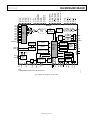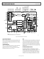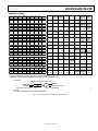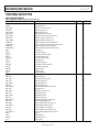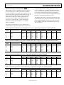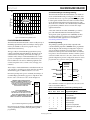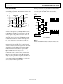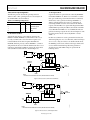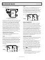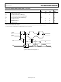
1
MicroConverter® Multichannel 24-/16-Bit ADCs with Embedded 62 kB Flash and Single-Cycle MCU ADuC845/ADuC847/ADuC848 Data Sheet FEATURES High resolution Σ-Δ ADCs 2 independent 24-bit ADCs on the ADuC845 Single 24-bit ADC on the ADuC847 and single 16-bit ADC on the ADuC848 Up to 10 ADC input channels on all parts 24-bit no missing codes 22-bit rms (19.5 bit p-p) effective resolution Offset drift 10 nV/°C, gain drift 0.5 ppm/°C chop enabled Memory 62-kbyte on-chip Flash/EE program memory 4-kbyte on-chip Flash/EE data memory Flash/EE, 100-year retention, 100 kcycle endurance 3 levels of Flash/EE program memory security In-circuit serial download (no external hardware) High speed user download (5 sec) 2304 bytes on-chip data RAM 8051-based core 8051-compatible instruction set High performance single-cycle core 32 kHz external crystal On-chip programmable PLL (12.58 MHz max) 3 × 16-bit timer/counter 24 programmable I/O lines, plus 8 analog or digital input lines 11 interrupt sources, two priority levels Dual data pointer, extended 11-bit stack pointer Power Normal: 4.8 mA max @ 3.6 V (core CLK = 1.57 MHz) Power-down: 20 µA max with wake-up timer running Specified for 3 V and 5 V operation Package and temperature range: 52-lead MQFP (14 mm × 14 mm), −40°C to +125°C 56-lead LFCSP (8 mm × 8 mm), −40°C to +85°C APPLICATIONS Multichannel sensor monitoring Industrial/environmental instrumentation Weigh scales, pressure sensors, temperature monitoring Portable instrumentation, battery-powered systems Data logging, precision system monitoring FUNCTIONAL BLOCK DIAGRAM AVDD ADuC845 AVCO CURRENT SOURCE IEXC1 IEXC2 AIN1 BUF PGA PRIMARY 24-BIT S-D ADC 12-BIT DAC BUF DAC MUX AGND AIN10 AINCOM AUXILIARY 24-BIT S-D ADC TEMP SENSOR REFIN2+ DUAL 16-BIT S-D DAC PWM0 MUX DUAL 16-BIT PWM PWM1 REFIN2– REFIN– REFIN+ EXTERNAL VREF DETECT INTERNAL BAND GAP VREF SINGLE-CYCLE 8061-BASED MCU RESET Rev. C DVDD POR DGND PLL AND PRG CLOCK DIV OSC XTAL1 WAKE-UP/ RTC TIMER 3 × 16 BIT TIMERS BAUD RATE TIMER 4 × PARALLEL PORTS POWER SUPPLY MON WATCHDOG TIMER UART, SPI, AND I 2C SERIAL I/O 04741-001 On-chip peripherals Internal power-on reset circuit 12-bit voltage output DAC Dual 16-bit Σ-Δ DACs On-chip temperature sensor (ADuC845 only) Dual excitation current sources (200 µA) Time interval counter (wake-up/RTC timer) UART, SPI®, and I2C® serial I/O High speed dedicated baud rate generator (incl. 115,200) Watchdog timer (WDT) Power supply monitor (PSM) 62 kBYTES FLASH/EE PROGRAM MEMORY 4 kBYTES FLASH/EE DATA MEMORY 2304 BYTES USER RAM XTAL2 Figure 1. ADuC845 Functional Block Diagram Document Feedback Information furnished by Analog Devices is believed to be accurate and reliable. However, no responsibility is assumed by Analog Devices for its use, nor for any infringements of patents or other rights of third parties that may result from its use. Specifications subject to change without notice. No license is granted by implication or otherwise under any patent or patent rights of Analog Devices. Trademarks and registered trademarks are the property of their respective owners. One Technology Way, P.O. Box 9106, Norwood, MA 02062-9106, U.S.A. Tel: 781.329.4700 ©2004–2012 Analog Devices, Inc. All rights reserved. Technical Support www.analog.com ADuC845/ADuC847/ADuC848 Data Sheet TABLE OF CONTENTS Specifications..................................................................................... 4 ADC SFR Interface..................................................................... 39 Abosolute Maximum Ratings ....................................................... 10 ADCSTAT (ADC Status Register) ........................................... 40 ESD Caution ................................................................................ 10 ADCMODE (ADC Mode Register)......................................... 41 Pin Configurations and Function Descriptions ......................... 11 ADC0CON1 (Primary ADC Control Register) ..................... 43 General Description ....................................................................... 15 ADC0CON2 (Primary ADC Channel Select Register) ........ 44 8052 Instruction Set ................................................................... 18 SF (ADC Sinc Filter Control Register) .................................... 46 Timer Operation ......................................................................... 18 ICON (Excitation Current Sources Control Register) .......... 47 ALE ............................................................................................... 18 Nonvolatile Flash/EE Memory Overview ............................... 48 External Memory Access ........................................................... 18 Flash/EE Program Memory ...................................................... 49 Complete SFR Map .................................................................... 19 User Download Mode (ULOAD)............................................. 50 Functional Description .................................................................. 20 Using Flash/EE Data Memory .................................................. 51 8051 Instruction Set ................................................................... 20 Flash/EE Memory Timing ........................................................ 52 Memory Organization ............................................................... 22 DAC Circuit Information .......................................................... 53 Special Function Registers (SFRs) ............................................ 24 Pulse-Width Modulator (PWM) .............................................. 55 ADC Circuit Information.......................................................... 26 On-Chip PLL (PLLCON) .......................................................... 60 Auxiliary ADC (ADuC845 Only) ............................................ 32 I2C Serial Interface ..................................................................... 61 Reference Inputs ......................................................................... 32 SPI Serial Interface ..................................................................... 64 Burnout Current Sources .......................................................... 32 Using the SPI Interface .............................................................. 66 Reference Detect Circuit ........................................................... 33 Dual Data Pointers ..................................................................... 67 Sinc Filter Register (SF) ............................................................. 33 Power Supply Monitor ............................................................... 68 Σ-∆ Modulator ............................................................................ 33 Watchdog Timer ......................................................................... 69 Digital Filter ................................................................................ 33 Time Interval Counter (TIC) .................................................... 70 ADC Chopping ........................................................................... 34 8052-Compatible On-Chip Peripherals .................................. 73 Calibration ................................................................................... 34 Timers/Counters ........................................................................ 75 Programmable Gain Amplifier ................................................. 35 UART Serial Interface ................................................................ 80 Bipolar/Unipolar Configuration .............................................. 35 Interrupt System ......................................................................... 85 Data Output Coding .................................................................. 36 Interrupt Priority ........................................................................ 86 Excitation Currents .................................................................... 36 Interrupt Vectors ........................................................................ 86 ADC Power-On .......................................................................... 36 Hardware Design Considerations ................................................ 87 Typical Performance Characteristics ........................................... 37 External Memory Interface ....................................................... 87 Functional Description .................................................................. 39 Power Supplies ............................................................................ 87 Rev. C | Page 2 of 108 Data Sheet ADuC845/ADuC847/ADuC848 Power-On Reset Operation........................................................88 QuickStart-PLUS Development System .................................. 94 Power Consumption ...................................................................88 Timing Specifications ..................................................................... 95 Power-Saving Modes ..................................................................88 Outline Dimensions ......................................................................104 Grounding and Board Layout Recommendations .................89 Ordering Guide .........................................................................105 Other Hardware Considerations ...............................................90 QuickStart Development System ..................................................94 REVISION HISTORY 12/12—Rev. B to Rev. C Changes to Figure 3 and Table 3 ...................................................11 Changes to Burnout Current Sources Section.............................32 Change to ADCMODE (ADC Mode Register) Section.............42 Changes to Mode 4 (Dual NRZ 16-Bit Σ-∆ DAC) Section ............58 Change to Hardware Slave Mode Section ....................................63 Updated Outline Dimensions ......................................................104 Changes to Ordering Guide .........................................................105 2/05—Rev. A to Rev. B Changes to Figure 1........................................................................... 1 Changes to the Burnout Current Sources Section ......................32 Changes to the Excitation Currents Section ................................36 Changes to Table 30 ........................................................................47 Changes to the Flash/EE Memory on the ADuC845, ADuC847, ADuC848 Section......................................................................48 Changes to Figure 39 ......................................................................57 Changes to On-Chip PLL (PLLCON) Section ............................60 Added 3 V Part Section Heading ..................................................88 Added 5 V Part Section ..................................................................88 Changes to Figure 70 ......................................................................91 Changes to Figure 71 ......................................................................93 Changes to Table 25 ........................................................................ 43 Changes to Table 26 ........................................................................ 44 Changes to Table 27 ........................................................................ 45 Changes to User Download Mode Section .................................. 50 Added Figure 51 and Renumbered Subsequent Figures ............ 50 Edits to the DACH/DACL Data Registers Section ..................... 53 Changes to Table 34 ........................................................................ 56 Added SPIDAT: SPI Data Register Section ................................. 65 Changes to Table 42 ........................................................................ 67 Changes to Table 43 ........................................................................ 68 Changes to Table 44 ........................................................................ 69 Changes to Table 45 ........................................................................ 71 Changes to Table 50 ........................................................................ 75 Changes to Timer/Counter 0 and 1 Data Registers Section...... 76 Changes to Table 54 ........................................................................ 80 Added the SBUF—UART Serial Port Data Register Section..... 80 Addition to the Timer 3 Generated Baud Rates Section ........... 83 Added Table 57 and Renumbered Subsequent Tables ............... 84 Changes to Table 61 ........................................................................ 86 4/04—Revision 0: Initial Version 6/04—Rev. 0 to Rev. A Changes to Figure 5.........................................................................17 Changes to Figure 6.........................................................................18 Changes to Figure 7.........................................................................19 Changes to Table 5 ..........................................................................24 Changes to Table 24 ........................................................................41 Rev. C | Page 3 of 108 ADuC845/ADuC847/ADuC848 Data Sheet SPECIFICATIONS1 AVDD = 2.7 V to 3.6 V or 4.75 V to 5.25 V, DVDD = 2.7 V to 3.6 V or 4.75 V to 5.25 V, REFIN(+) = 2.5 V, REFIN(–) = AGND; AGND = DGND = 0 V; XTAL1/XTAL2 = 32.768 kHz crystal; all specifications TMIN to TMAX, unless otherwise noted. Input buffer on for primary ADC, unless otherwise noted. Core speed = 1.57 MHz (default CD = 3), unless otherwise noted. Table 1. Parameter PRIMARY ADC Conversion Rate Unit Conditions Hz Hz Bits Bits Chop on (ADCMODE.3 = 0) Chop off (ADCMODE.3 = 1) ≤26.7 Hz update rate with chop enabled ≤80.3 Hz update rate with chop disabled Resolution (ADuC845/ADuC847) Resolution (ADuC848) Output Noise (ADuC845/ADuC847) 5.4 105 16.06 1365 24 24 See Table 11 and Table 15 See Table 13 and Table 17 See Table 10 and Table 14 μV (rms) Output Noise (ADuC848) See Table 12 and Table 16 μV (rms) Output noise varies with selected update rates, gain range, and chop status. Output noise varies with selected update rates, gain range, and chop status. 1 LSB16 Chop on Chop off, offset error is in the order of the noise for the programmed gain and update rate following a calibration. Chop on (ADCMODE.3 = 0) Chop off (ADCMODE.3 = 1) No Missing Codes2 Min Integral Nonlinearity Offset Error3 Typ Max ±15 Offset Error Drift vs. Temperature2 Full-Scale Error4 ADuC845/ADuC847 ADuC848 Gain Error Drift vs. Temperature4 Power Supply Rejection ±3 ppm of FSR μV ±10 ±200 nV/°C nV/°C ±10 ±10 ±0.5 ±0.5 μV μV LSB16 ppm/°C ±20 mV to ±2.56 V ±20 mV to ±640 mV ±1.28 V to ±2.56 V 113 80 dB dB dB AIN = 1 V, ±2.56 V, chop enabled AIN = 7.8 mV, ±20 mV, chop enabled AIN = 1 V, ±2.56 V, chop disabled2 80 PRIMARY ADC ANALOG INPUTS Differential Input Voltage Ranges 5, 6 Bipolar Mode (ADC0CON1.5 = 0) Unipolar Mode (ADC0CON1.5 = 1) ADC Range Matching Common-Mode Rejection DC On AIN Common-Mode Rejection 50 Hz/60 Hz2 On AIN μV 113 dB dB 95 95 90 V ±1.024 × VREF/GAIN 0 – 1.024 × VREF/GAIN ±2 V dB dB Footnotes at end of table. Rev. C | Page 4 of 108 Gain = 1 to 128 VREF = REFIN(+) − REFIN(−) or REFIN2(+) − REFIN2(−) (or Int 1.25 VREF) VREF = REFIN(+) − REFIN(−) or REFIN2(+) − REFIN2(−) (or Int 1.25 VREF) AIN = 18 mV, chop enabled Chop enabled, chop disabled AIN = 7.8 mV, range = ±20 mV AIN = 1 V, range = ±2.56 V 50 Hz/60 Hz ± 1 Hz, 16.6 Hz and 50 Hz update rate, chop enabled, REJ60 enabled AIN = 7.8 mV, range = ±20 mV AIN = 1 V, range = ±2.56 V Data Sheet Parameter ADuC845/ADuC847/ADuC848 Min Typ Max Unit Conditions 75 dB 100 67 dB dB dB nA nA pA/°C pA/°C nA/V pA/V/°C V 50 Hz/60 Hz ± 1 Hz, 16.6 Hz Fadc, SF = 52H, chop on, REJ60 on 50 Hz ± 1 Hz, 16.6 Hz Fadc, SF = 52H, chop on 50 Hz/60 Hz ± 1 Hz, 50 Hz Fadc, SF = 52H, chop off, REJ60 on 50 Hz ± 1 Hz, 50 Hz Fadc, SF = 52H, chop off TMAX = 85°C, buffer on TMAX = 125°C, buffer on TMAX = 85°C, buffer on TMAX = 125°C, buffer on ±2.56 V range, buffer bypassed Buffer bypassed AIN1…AIN10 and AINCOM with buffer enabled V AIN1…AIN10 and AINCOM with buffer bypassed V V µA/V REFIN refers to both REFIN and REFIN2 REFIN refers to both REFIN and REFIN2 Both ADCs enabled Normal Mode Rejection 50 Hz/60 Hz2 On AIN 100 Analog Input Current2 ±1 ±5 Analog Input Current Drift Average Input Current Average Input Current Drift Absolute AIN Voltage Limits2 Absolute AIN Voltage Limits2 EXTERNAL REFERENCE INPUTS REFIN(+) to REFIN(–) Voltage REFIN(+) to REFIN(–) Range2 Average Reference Input Current Average Reference Input Current Drift NOXREF Trigger Voltage ±5 ±15 ±125 ±2 AGND + 0.1 AGND − 0.03 AVDD − 0.1 AVDD + 0.03 2.5 1 AVDD ±1 ±0.1 0.3 0.65 nA/V/°C V Common-Mode Rejection DC Rejection 50 Hz/60 Hz Rejection2 90 dB dB Normal Mode Rejection 50 Hz/60 Hz2 75 dB 100 dB 67 dB 100 dB 5.4 105 16.06 1365 24 24 See Table 19 and Table 21 See Table 18 and Table 20 ±15 ±3 ±0.25 10 200 ±0.5 ±0.5 80 80 Hz Hz Bits Bits AUXILIARY ADC (ADuC845 Only) Conversion Rate No Missing Codes2 Resolution Output Noise Integral Nonlinearity Offset Error3 Offset Error Drift2 Full-Scale Error4 Gain Error Drift4 Power Supply Rejection 125 ppm of FSR µV LSB16 nV/°C nV/°C LSB16 ppm/°C dB dB Footnotes at end of table. Rev. C | Page 5 of 108 NOXREF (ADCSTAT.4) bit active if VREF > 0.3 V, and inactive if VREF > 0.65 V AIN = 1 V, range = ±2.56 V 50 Hz/60 Hz ± 1 Hz, AIN = 1 V, range = ±2.56 V, SF = 82 50 Hz/60 Hz ±1 Hz, AIN = 1 V, range = ±2.56 V, SF = 52H, chop on, REJ60 on 50 Hz ± 1 Hz, AIN = 1 V, range = ±2.56 V, SF = 52H, chop on 50 Hz/60 Hz ± 1 Hz, AIN = 1 V, range = ±2.56 V, SF = 52H, chop off, REJ60 on 50 Hz ± 1 Hz, AIN = 1 V, range = ±2.56 V, SF = 52H, chop off Chop on Chop off ≤26.7 Hz update rate, chop enabled 80.3 Hz update rate, chop disabled Output noise varies with selected update rates. 1 LSB16 Chop on Chop off Chop on Chop off AIN = 1 V, range = ±2.56 V, chop enabled AIN = 1 V, range = ±2.56 V, chop disabled ADuC845/ADuC847/ADuC848 Parameter AUXILIARY ADC ANALOG INPUTS (ADuC845 Only) Differential Input Voltage Ranges5, 6 Bipolar Mode (ADC1CON.5 = 0) Unipolar Mode (ADC1CON.5 = 1) Average Analog Input Current Analog Input Current Drift Absolute AIN/AINCOM Voltage Limits2, 7 Min Data Sheet Typ Max Unit Conditions V V nA/V pA/V/°C V REFIN = REFIN(+) − REFIN(−) (or Int 1.25 VREF) REFIN = REFIN(+) − REFIN(−) (or Int 1.25 VREF) 75 dB 100 67 dB dB 100 dB 50 Hz/60 Hz ± 1 Hz, 16.6 Hz Fadc, SF = 52H, chop on, REJ60 on 50 Hz ± 1 Hz, 16.6 Hz Fadc, SF = 52H, chop on 50 Hz/60 Hz ± 1 Hz, 50 Hz Fadc, SF = 52H, chop off, REJ60 on 50 Hz ± 1 Hz, 50 Hz Fadc, SF = 52H, chop off ±VREF 0 – VREF 125 ±2 AGND − 0.03 AVDD + 0.03 Normal Mode Rejection 50 Hz/60 Hz2 On AIN and REFIN ADC SYSTEM CALIBRATION Full-Scale Calibration Limit Zero-Scale Calibration Limit Input Span DAC Voltage Range Resistive Load Capactive Load Output Impedance ISINK DC Specifications 8 Resolution Relative Accuracy Differential Nonlinearity Offset Error Gain Error AC Specifications2, 8 Voltage Output Settling Time Digital-to-Analog Glitch Energy INTERNAL REFERENCE ADC Reference Reference Voltage Power Supply Rejection Reference Tempco DAC Reference Reference Voltage Power Supply Rejection Reference Tempco TEMPERATURE SENSOR (ADuC845 Only) Accuracy Thermal Impedance +1.05 × FS −1.05 × FS 0.8 × FS 2.1 × FS 0 – VREF 0 – AVDD 10 100 0.5 50 V V V V V kΩ pF Ω µA 12 DACCON.2 = 0 DACCON.2 = 1 From DAC output to AGND From DAC output to AGND ±1 Bits LSB LSB mV % % AVDD range VREF range 15 10 µs nVs Settling time to 1 LSB of final value 1 LSB change at major carry ±3 −1 ±50 ±1 1.25 − 1% 1.25 45 100 1.25 + 1% V dB ppm/°C 2.5 – 1% 2.5 50 ±100 2.5 + 1% ±1% V dB ppm/°C ±2 90 52 °C °C/W °C/W Footnotes at end of table. Rev. C | Page 6 of 108 Guaranteed 12-bit monotonic Chop enabled Initial tolerance @ 25°C, VDD = 5 V Initial tolerance @ 25°C, VDD = 5 V MQFP LFCSP Data Sheet Parameter TRANSDUCER BURNOUT CURRENT SOURCES AIN+ Current ADuC845/ADuC847/ADuC848 Min AIN− Current Initial Tolerance at 25°C Drift EXCITATION CURRENT SOURCES Output Current Initial Tolerance at 25°C Drift Initial Current Matching at 25°C Drift Matching Line Regulation (AVDD) Load Regulation Output Compliance2 POWER SUPPLY MONITOR (PSM) AVDD Trip Point Selection Range AVDD Trip Point Accuracy DVDD Trip Point Selection Range DVDD Trip Point Accuracy Typ Unit Conditions −100 nA 100 nA AIN+ is the selected positive input (AIN4 or AIN6 only) to the primary ADC AIN− is the selected negative input (AIN5 or AIN7 only) to the primary ADC ±10 0.03 % %/°C 200 ±10 200 ±1 20 1 0.1 µA % ppm/°C % ppm/°C µA/V µA/V V AGND AVDD − 0.6 2.63 2.63 CRYSTAL OSCILLATOR (XTAL1 AND XTAL2) Logic Inputs, XTAL1 Only2 VINL, Input Low Voltage VINH, Input Low Voltage VT− VT+ − VT− Input Currents Port 0, P1.0 to P1.7, EA RESET 35 −180 −20 Input Capacitance 10 AVDD = 5 V ± 5% Four trip points selectable in this range TMAX = 85°C TMAX = 125°C Four trip points selectable in this range TMAX = 85°C TMAX = 125°C 0.8 0.4 V V V V pF pF DVDD = 5 V DVDD = 3 V DVDD = 5 V DVDD = 3 V 0.8 0.4 V V V DVDD = 5 V DVDD = 3 V 3.0 2.5 1.4 1.1 0.85 V V V V V DVDD = 5 V DVDD = 3 V DVDD = 5 V DVDD = 3 V DVDD = 5 V or 3 V ±10 ±10 105 ±10 −660 −75 µA µA µA µA µA µA pF VIN = 0 V or VDD VIN = 0 V, DVDD = 5 V VIN = DVDD, DVDD = 5 V, internal pull-down VIN = DVDD, DVDD = 5 V VIN = 2 V, DVDD = 5 V VIN = 0.45 V, DVDD = 5 V All digital inputs 2.0 Port 2, Port 3 Matching between both current sources V % % V % % 18 18 1.3 0.95 0.8 0.4 0.3 Available from each current source 4.63 ±3.0 ±4.0 4.63 ±3.0 ±4.0 3.5 2.5 XTAL1 Input Capacitance XTAL2 Output Capacitance LOGIC INPUTS All inputs except SCLOCK, RESET, and XTAL12 VINL, Input Low Voltage VINH, Input Low Voltage SCLOCK and RESET Only (Schmidt Triggered Inputs)2 VT+ Max Rev. C | Page 7 of 108 ADuC845/ADuC847/ADuC848 Parameter LOGIC OUTPUTS (All Digital Outputs except XTAL2) VOH, Output High Voltage2 Min Data Sheet Typ Unit Conditions DVDD = 5 V, ISOURCE = 80 µA DVDD = 3 V, ISOURCE = 20 µA ISINK = 8 mA, SCLOCK, SDATA ISINK = 1.6 mA on P0, P1, P2 10 V V V V µA pF 600 3 2 ms ms ms 20 20 20 µs µs µs 30 30 µs µs 2.4 2.4 VOL, Output Low Voltage 0.4 0.4 ±10 Floating State Leakage Current2 Floating State Output Capacitance START-UP TIME At Power-On After Ext RESET in Normal Mode After WDT RESET in Normal Mode From Power-Down Mode Oscillator Running Wake-Up with INT0 Interrupt Wake-Up with SPI Interrupt Wake-Up with TIC Interrupt Oscillator Powered Down Wake-Up with INT0 Interrupt Wake-Up with SPI Interrupt FLASH/EE MEMORY RELIABILITY CHARACTERISTICS Endurance 9 Data Retention 10 POWER REQUIREMENTS Power Supply Voltages AVDD 3 V Nominal AVDD 5 V Nominal DVDD 3 V Nominal DVDD 5 V Nominal 5 V Power Consumption Normal Mode 11, 12 DVDD Current PLLCON.7 = 1 100,000 100 Cycles Years 2.7 4.75 2.7 4.75 3.6 5.25 3.6 5.25 ALE Off WDT V V V V 4.75 V < DVDD < 5.25 V, AVDD = 5.25 V 40 50 20 30 AVDD Current Typical Additional Peripheral Currents (AIDD and DIDD) Primary ADC Auxiliary ADC (ADuC845 Only) Power Supply Monitor DAC Dual Excitation Current Sources Controlled via WDCON SFR PLLCON.7 = 0 25 AVDD Current Power-Down Mode11, 12 DVDD Current Max 10 31 180 mA mA µA Core clock = 1.57 MHz Core clock = 12.58 MHz 53 µA µA µA µA µA µA TMAX = 85°C; OSC on; TIC on TMAX = 125°C; OSC on; TIC on TMAX = 85°C; OSC off TMAX = 125°C; OSC off TMAX = 85°C; OSC on or off TMAX = 125°C; OSC on or off 5 V VDD, CD = 3 33 1 3 1 0.5 30 60 200 mA mA µA µA µA −20 10 µA µA Footnotes at end of table. Rev. C | Page 8 of 108 DACH/L = 000H 200 µA each. Can be combined to give 400 µA on a single output. PCON.4 = 1 (see Table 6) Data Sheet Parameter PWM −Fxtal −Fvco TIC 3 V Power Consumption Normal Mode11, 12 DVDD Current ADuC845/ADuC847/ADuC848 Min Typ Max 3 0.5 1 Conditions µA mA µA 2.7 V < DVDD < 3.6 V, AVDD = 3.6 V 9 AVDD Current Power-Down Mode11, 12 DVDD Current Unit 20 29 14 21 4.8 11 180 mA mA µA Core clock = 1.57 MHz Core clock = 6.29 MHz (CD = 1) ADC not enabled 26 µA µA µA µA µA µA TMAX = 85°C; OSC on; TIC on TMAX = 125°C; OSC on; TIC on TMAX = 85°C; OSC off TMAX = 125°C; OSC off TMAX = 85°C; OSC on or off TMAX = 125°C; OSC on or off 20 AVDD Current 1 3 Temperature range is for ADuC845BS; for the ADuC847BS and ADuC848BS (MQFP package), the range is –40°C to +125°C. Temperature range for ADuC845BCP, ADuC847BCP, and ADuC848BCP (LFCSP package) is –40°C to +85°C. 2 These numbers are not production tested but are guaranteed by design and/or characterization data on production release. 3 System zero-scale calibration can remove this error. 4 Gain error drift is a span drift. To calculate full-scale error drift, add the offset error drift to the gain error drift times the full-scale input. 5 In general terms, the bipolar input voltage range to the primary ADC is given by the ADC range = ±(VREF 2RN )/1.25, where: VREF = REFIN(+) to REFIN(–) voltage and VREF = 1.25 V when internal ADC VREF is selected. RN = decimal equivalent of RN2, RN1, RN0. For example, if VREF = 2.5 V and RN2, RN1, RN0 = 1, 1, 0, respectively, then the ADC range = ±1.28 V. In unipolar mode, the effective range is 0 V to 1.28 V in this example. 6 1.25 V is used as the reference voltage to the ADC when internal VREF is selected via XREF0/XREF1 or AXREF bits in ADC0CON2 and ADC1CON, respectively. (AXREF is available only on the ADuC845.) 7 In bipolar mode, the auxiliary ADC can be driven only to a minimum of AGND – 30 mV as indicated by the auxiliary ADC absolute AIN voltage limits. The bipolar range is still –VREF to +VREF. 8 DAC linearity and ac specifications are calculated using a reduced code range of 48 to 4095, 0 V to VREF, reduced code range of 100 to 3950, 0 V to VDD. 9 Endurance is qualified to 100 kcycle per JEDEC Std. 22 method A117 and measured at –40°C, +25°C, +85°C, and +125°C. Typical endurance at 25°C is 700 kcycles. 10 Retention lifetime equivalent at junction temperature (TJ) = 55°C per JEDEC Std. 22, Method A117. Retention lifetime based on an activation energy of 0.6 eV derates with junction temperature. 11 Power supply current consumption is measured in normal mode following the power-on sequence, and in power-down modes under the following conditions: Normal mode: reset = 0.4 V, digital I/O pins = open circuit, Core Clk changed via CD bits in PLLCON, core executing internal software loop. Power-down mode: reset = 0.4 V, all P0 pins and P1.2 to P1.7 pins = 0.4 V. All other digital I/O pins are open circuit, core Clk changed via CD bits in PLLCON, PCON.1 = 1, core execution suspended in power-down mode, OSC turned on or off via OSC_PD bit (PLLCON.7) in PLLCON SFR. 12 DVDD power supply current increases typically by 3 mA (3 V operation) and 10 mA (5 V operation) during a Flash/EE memory program or erase cycle. 1 General Notes about Specifications • DAC gain error is a measure of the span error of the DAC. • The ADuC845BCP, ADuC847BCP, and ADuC848BCP (LFCSP package) have been qualified and tested with the base of the LFCSP package floating. The base of the LFCSP package should be soldered to the board, but left floating electrically, to ensure good mechanical stability. • Flash/EE memory reliability characteristics apply to both the Flash/EE program memory and Flash/EE data memory. Rev. C | Page 9 of 108 ADuC845/ADuC847/ADuC848 Data Sheet ABOSOLUTE MAXIMUM RATINGS TA = 25°C, unless otherwise noted. Table 2. Parameter AVDD to AGND AVDD to DGND DVDD to DGND DVDD to DGND AGND to DGND1 AVDD to DVDD Analog Input Voltage to AGND2 Reference Input Voltage to AGND AIN/REFIN Current (Indefinite) Digital Input Voltage to DGND Digital Output Voltage to DGND Operating Temperature Range Storage Temperature Range Junction Temperature θJA Thermal Impedance (MQFP) θJA Thermal Impedance (LFCSP) Lead Temperature, Soldering Vapor Phase (60 sec) Infrared (15 sec) ________________________ 1 2 Rating –0.3 V to +7 V –0.3 V to +7 V –0.3 V to +7 V –0.3 V to +7 V –0.3 V to +0.3 V –2 V to +5 V –0.3 V to AVDD + 0.3 V –0.3 V to AVDD + 0.3 V 30 mA –0.3 V to DVDD + 0.3 V –0.3 V to DVDD + 0.3 V –40°C to +125°C –65°C to +150°C 150°C 90°C/W 52°C/W Stresses above those listed under Absolute Maximum Ratings may cause permanent damage to the device. This is a stress rating only; functional operation of the device at these or any other conditions above those listed in the operational sections of this specification is not implied. Exposure to absolute maximum rating conditions for extended periods may affect device reliability. 215°C 220°C AGND and DGND are shorted internally on the ADuC845, ADuC847, and ADuC848. Applies to the P1.0 to P1.7 pins operating in analog or digital input modes. ESD CAUTION ESD (electrostatic discharge) sensitive device. Electrostatic charges as high as 4000 V readily accumulate on the human body and test equipment and can discharge without detection. Although this product features proprietary ESD protection circuitry, permanent damage may occur on devices subjected to high energy electrostatic discharges. Therefore, proper ESD precautions are recommended to avoid performance degradation or loss of functionality. Rev. C | Page 10 of 108 Data Sheet ADuC845/ADuC847/ADuC848 P0.1/AD1 P0.0/AD0 ALE PSEN 46 45 44 43 EA P0.2/AD2 52 47 53 48 P0.5/AD5 P0.4/AD4 DVDD 54 DGND P0.3/AD3 P0.6/AD6 55 50 P1.0/AIN1 P0.7/AD7 56 EA ALE PSEN P0.0/AD0 P0.1/AD1 P0.2/AD2 P0.3/AD3 DVDD DGND P0.4/AD4 P0.5/AD5 P0.6/AD6 P0.7/AD7 PIN CONFIGURATIONS AND FUNCTION DESCRIPTIONS P1.1/AIN2 P1.2/AIN3/REFIN2+ 1 38 P2.6/PWM1 2 42 41 P1.2/AIN3/REFIN2+ 3 37 P2.5/PWM0 P1.3/AIN4/REFIN2– 3 40 P2.5/PWM0 P1.3/AIN4/REFIN2– 4 AVDD 5 36 P2.4/T2EX AVDD AGND 4 39 P2.4/T2EX DGND AGND REFIN– 6 REFIN+ P1.4/AIN5 8 P1.5/AIN6 35 DGND Figure 2. 52-Lead MQFP Pin Configuration DGND DVDD P2.1/MOSI P2.0/SCLOCK (SPI) SDATA 28 21 27 20 P3.3/INT1 DVDD 04741-002 SCLOCK (I2C) P3.5/T1 P3.6/WR P3.7/RD DGND P3.4/T0 P3.3/INT1 DVDD P3.2/INT0 P3.1/TxD P3.0/RxD DAC RESET 14 15 16 17 18 19 20 21 22 23 24 25 26 14 P3.7/RD SCLK (I2C) 13 26 AINCOM/DAC DAC P3.2/INT0 27 SDATA P3.6/WR 12 19 28 P2.0/SCLOCK (SPI) P3.1/TxD P1.7/AIN8/IEXC2 12 AINCOM/DAC 13 25 P2.2/MISO P1.7/AIN8/IEXC2 32 31 30 29 P3.5/T1 P2.3/SS/T2 11 24 33 P1.6/AIN7/IEXC1 18 29 P2.1/MOSI 17 P1.6/AIN7/IEXC1 11 9 23 10 30 P2.2/MISO RESET 31 P2.3/SS/T2 P3.0/RxD P1.4/AIN5 9 P1.5/AIN6 10 DGND XTAL2 XTAL1 P3.4/T0 35 34 22 TOP VIEW (Not to Scale) 32 XTAL1 7 16 TOP VIEW (Not to Scale) P2.6/PWM1 38 37 36 33 XTAL2 REFIN+ 8 5 P2.7/PWMCLK ADuC845/ADuC847/ ADuC848 34 DVDD 15 ADuC845/ADuC847/ADuC848 AIN9 AGND 6 REFIN– 7 AIN10 PIN 1 IDENTIFIER P1.1/AIN2 2 NOTES 1. THE EXPOSED PADDLE MUST BE LEFT UNCONNECTED. 04741-003 49 39 P2.7/PWMCLK 51 52 51 50 49 48 47 46 45 44 43 42 41 40 P1.0/AIN1 1 Figure 3. 56-Lead LFCSP Pin Configuration Table 3. Pin Function Descriptions Pin No: 52-MQFP 1 Pin No: 56-LFCSP 56 Mnemonic P1.0/AIN1 Type 1 I 2 1 P1.1/AIN2 I 3 2 P1.2/AIN3/REFIN2+ I 4 3 P1.3/AIN4/REFIN2− I 5 6 --7 8 4 5 6 7 8 AVDD AGND AGND REFIN− REFIN+ S S S I I Description By power-on default, P1.0/AIN1 is configured as the AIN1 analog input. AIN1 can be used as a pseudo differential input when used with AINCOM or as the positive input of a fully differential pair when used with AIN2. P1.0 has no digital output driver. It can function as a digital input for which 0 must be written to the port bit. As a digital input, this pin must be driven high or low externally. On power-on default, P1.1/AIN2 is configured as the AIN2 analog input. AIN2 can be used as a pseudo differential input when used with AINCOM or as the negative input of a fully differential pair when used with AIN1. P1.1 has no digital output driver. It can function as a digital input for which 0 must be written to the port bit. As a digital input, this pin must be driven high or low externally. On power-on default, P1.2/AIN3 is configured as the AIN3 analog input. AIN3 can be used as a pseudo differential input when used with AINCOM or as the positive input of a fully differential pair when used with AIN4. P1.2 has no digital output driver. It can function as a digital input for which 0 must be written to the port bit. As a digital input, this pin must be driven high or low externally. This pin also functions as a second external differential reference input, positive terminal. On power-on default, P1.3/AIN4 is configured as the AIN4 analog input. AIN4 can be used as a pseudo differential input when used with AINCOM or as the negative input of a fully differential pair when used with AIN3. P1.3 has no digital output driver. It can function as a digital input for which 0 must be written to the port bit. As a digital input, this pin must be driven high or low externally. This pin also functions as a second external differential reference input, negative terminal. Analog Supply Voltage. Analog Ground. A second analog ground is provided with the LFCSP version only. External Differential Reference Input, Negative Terminal. External Differential Reference Input, Positive Terminal. Footnotes at end of table. Rev. C | Page 11 of 108 ADuC845/ADuC847/ADuC848 Data Sheet Pin No: 52-MQFP 9 Pin No: 56-LFCSP 9 Mnemonic P1.4/AIN5 Type 1 I 10 10 P1.5/AIN6 I 11 11 P1.6/AIN7/IEXC1 I/O 12 12 P1.7/AIN8/IEXC2 I/O 13 13 AINCOM/DAC I/O 14 ---- 14 15 DAC AIN9 O I ---- 16 AIN10 I 15 17 RESET I 16–19 22–25 18–21 24–27 P3.0–P3.7 I/O 16 17 18 19 22 23 24 18 19 20 21 24 25 26 P3.0/RxD P3.1/TxD P3.2/INT0 P3.3/INT1 P3.4/T0 P3.5/T1 P3.6/WR 25 27 P3.7/RD Description On power-on default, P1.4/AIN5 is configured as the AIN5 analog input. AIN5 can be used as a pseudo differential input when used with AINCOM or as the positive input of a fully differential pair when used with AIN6. P1.0 has no digital output driver. It can function as a digital input for which 0 must be written to the port bit. As a digital input, this pin must be driven high or low externally. On power-on default, P1.5/AIN6 is configured as the AIN6 analog input. AIN6 can be used as a pseudo differential input when used with AINCOM or as the negative input of a fully differential pair when used with AIN5. P1.1 has no digital output driver. It can function as a digital input for which 0 must be written to the port bit. As a digital input, this pin must be driven high or low externally. On power-on default, P1.6/AIN7 is configured as the AIN7 analog input. AIN7 can be used as a pseudo differential input when used with AINCOM or as the positive input of a fully differential pair when used with AIN8. One or both current sources can also be configured at this pin. P1.6 has no digital output driver. It can, however, function as a digital input for which 0 must be written to the port bit. As a digital input, this pin must be driven high or low externally. On power-on default, P1.7/AIN8 is configured as the AIN8 analog input. AIN8 can be used as a pseudo differential input when used with AINCOM or as the negative input of a fully differential pair when used with AIN7. One or both current sources can also be configured at this pin. P1.7 has no digital output driver. It can, however, function as a digital input for which 0 must be written to the port bit. As a digital input, this pin must be driven high or low externally. All analog inputs can be referred to this pin, provided that a relevant pseudo differential input mode is selected. This pin also functions as an alternative pin out for the DAC. The voltage output from the DAC, if enabled, appears at this pin. AIN9 can be used as a pseudo differential analog input when used with AINCOM or as the positive input of a fully differential pair when used with AIN10 (LFCSP version only). AIN10 can be used as a pseudo differential analog input when used with AINCOM or as the negative input of a fully differential pair when used with AIN9 (LFCSP version only). Reset Input. A high level on this pin for 16 core clock cycles while the oscillator is running resets the device. This pin has an internal weak pull-down and a Schmitt trigger input stage. P3.0 to P3.7 are bidirectional port pins with internal pull-up resistors. Port 3 pins that have 1s written to them are pulled high by the internal pull-up resistors, and in that state can be used as inputs. As inputs, Port 3 pins being pulled externally low source current because of the internal pull-up resistors. When driving a 0-to-1 output transition, a strong pull-up is active for one core clock period of the instruction cycle. Port 3 pins also have the various secondary functions described below. Receiver Data for UART Serial Port. Transmitter Data for UART Serial Port. External Interrupt 0. This pin can also be used as a gate control input to Timer 0. External Interrupt 1. This pin can also be used as a gate control input to Timer 1. Timer/Counter 0 External Input. Timer/Counter 1 External Input. External Data Memory Write Strobe. This pin latches the data byte from Port 0 into an external data memory. External Data Memory Read Strobe. This pin enables the data from an external data memory to Port 0. Rev. C | Page 12 of 108 Data Sheet Pin No: 52-MQFP 20, 34, 48 21, 35, 47 26 Pin No: 56-LFCSP ADuC845/ADuC847/ADuC848 28 Mnemonic DVDD DGND SCLK (I2C) Type 1 S S I/O 27 29 SDATA I/O 28–31, 36–39 30–33, 39– 42 P2.0–P2.7 I/O 28 30 P2.0/SCLOCK (SPI) 29 31 P2.1/MOSI 30 32 P2.2/MISO 31 33 P2.3/SS/T2 36 39 P2.4/T2EX 37 38 39 32 33 40 41 42 34 35 P2.5/PWM0 P2.6/PWM1 P2.7/PWMCLK XTAL1 XTAL2 40 43 EA 41 44 PSEN O 42 45 ALE O 22, 36, 51 23, 37, 38, 50 I O Description Digital Supply Voltage. Digital Ground. Serial Interface Clock for the I2C Interface. As an input, this pin is a Schmitttriggered input. A weak internal pull-up is present on this pin unless it is outputting logic low. This pin can also be controlled in software as a digital output pin. Serial Data Pin for the I2C Interface. As an input, this pin has a weak internal pull-up present unless it is outputting logic low. Port 2 is a bidirectional port with internal pull-up resistors. Port 2 pins that have 1s written to them are pulled high by the internal pull-up resistors, and in that state can be used as inputs. As inputs, Port 2 pins being pulled externally low source current because of the internal pull-up resistors. Port 2 emits the middle and high-order address bytes during accesses to the 24-bit external data memory space. Port 2 pins also have the various secondary functions described below. Serial Interface Clock for the SPI Interface. As an input this pin is a Schmitttriggered input. A weak internal pull-up is present on this pin unless it is outputting logic low. Serial Master Output/Slave Input Data for the SPI Interface. A strong internal pull-up is present on this pin when the SPI interface outputs a logic high. A strong internal pull-down is present on this pin when the SPI interface outputs a logic low. Master Input/Slave Output for the SPI Interface. A weak pull-up is present on this input pin. Slave Select Input for the SPI Interface. A weak pull-up is present on this pin. For both package options, this pin can also be used to provide a clock input to Timer 2. When enabled, Counter 2 is incremented in response to a negative transition on the T2 input pin. Control Input to Timer 2. When enabled, a negative transition on the T2EX input pin causes a Timer 2 capture or reload event. If the PWM is enabled, the PWM0 output appears at this pin. If the PWM is enabled, the PWM1 output appears at this pin. If the PWM is enabled, an external PWM clock can be provided at this pin. Input to the Crystal Oscillator Inverter. Output from the Crystal Oscillator Inverter. See the Hardware Design Considerations section for a description. External Access Enable, Logic Input. When held high, this input enables the device to fetch code from internal program memory locations 0000H to F7FFH. No external program memory access is available on the ADuC845, ADuC847, or ADuC848. To determine the mode of code execution, the EA pin is sampled at the end of an external RESET assertion or as part of a device power cycle. EA can also be used as an external emulation I/O pin, and therefore the voltage level at this pin must not be changed during normal operation because this might cause an emulation interrupt that halts code execution. Program Store Enable, Logic Output. This function is not used on the ADuC845, ADuC847, or ADuC848. This pin remains high during internal program execution. PSEN can also be used to enable serial download mode when pulled low through a resistor at the end of an external RESET assertion or as part of a device power cycle. Address Latch Enable, Logic Output. This output is used to latch the low byte (and page byte for 24-bit data address space accesses) of the address to external memory during external data memory access cycles. It can be disabled by setting the PCON.4 bit in the PCON SFR. Rev. C | Page 13 of 108 ADuC845/ADuC847/ADuC848 Pin No: 52-MQFP 43–46, 49–52 1 Pin No: 56-LFCSP 46–49, 52– 55 Mnemonic P0.0–P0.7 EP EPAD Data Sheet Type 1 I/O Description These pins are part of Port 0, which is an 8-bit open-drain bidirectional I/O port. Port 0 pins that have 1s written to them float, and, in that state, can be used as high impedance inputs. An external pull-up resistor is required on P0 outputs to force a valid logic high level externally. Port 0 is also the multiplexed low-order address and data bus during accesses to external data memory. In this application, Port 0 uses strong internal pull-ups when emitting 1s. Exposed Pad. For the LFCSP, the exposed paddle must be left unconnected. I = input, O = output, S = supply. Rev. C | Page 14 of 108 Data Sheet ADuC845/ADuC847/ADuC848 GENERAL DESCRIPTION The ADuC845, ADuC847, and ADuC848 are single-cycle, 12.58 MIPs, 8052 core upgrades to the ADuC834 and ADuC836. They include additional analog inputs for applications requiring more ADC channels. The ADuC845, ADuC847, and ADuC848 are complete smart transducer front ends. The family integrates high resolution Σ-Δ ADCs with flexible, up to 10-channel, input multiplexing, a fast 8-bit MCU, and program and data Flash/EE memory on a single chip. The ADuC845 includes two (primary and auxiliary) 24-bit Σ-Δ ADCs with internal buffering and PGA on the primary ADC. The ADuC847 includes the same primary ADC as the ADuC845 (auxiliary ADC removed). The ADuC848 is a 16-bit ADC version of the ADuC847. The ADCs incorporate flexible input multiplexing, a temperature sensor (ADuC845 only), and a PGA (primary ADC only) allowing direct measurement of low-level signals. The ADCs include on-chip digital filtering and programmable output data rates that are intended for measuring wide dynamic range and low frequency signals, such as those in weigh scale, strain gage, pressure transducer, or temperature measurement applications. The devices operate from a 32 kHz crystal with an on-chip PLL generating a high frequency clock of 12.58 MHz. This clock is routed through a programmable clock divider from which the MCU core clock operating frequency is generated. The microcontroller core is an optimized single-cycle 8052 offering up to 12.58 MIPs performance while maintaining 8051 instruction set compatibility. The available nonvolatile Flash/EE program memory options are 62 kbytes, 32 kbytes, and 8 kbytes. 4 kbytes of nonvolatile Flash/EE data memory and 2304 bytes of data RAM are also provided on-chip. The program memory can be configured as data memory to give up to 60 kbytes of NV data memory in data logging applications. On-chip factory firmware supports in-circuit serial download and debug modes (via UART), as well as single-pin emulation mode via the EA pin. The ADuC845, ADuC847, and ADuC848 are supported by the QuickStart™ development system featuring low cost software and hardware development tools. Rev. C | Page 15 of 108 P0.1 (AD1) P0.2 (AD2) P0.3 (AD3) P0.4 (AD4) P0.5 (AD5) P0.6 (AD6) P0.7 (AD7) P1.0/AIN1 P1.1/AIN2 P1.2/AIN3/REFIN2+ P1.3/AIN4/REFIN2– P1.4/AIN5 P1.5/AIN6 P1.6/AIN7/IEXC1 P1.7/AIN8/IEXC2 P2.0/SCLK (A8/A16) P2.1/MOSI (A9/A17) P2.2/MISO (A10/A18) P2.3/SS/T2 (A11/A19) P2.4/T2EX (A12/A20) P2.5/PWM0 (A13/A21) P2.6/PWM1 (A14/A22) P2.7/PWMCLK (A15/A23) P3.0 (RxD) P3.1 (TxD) P3.2 (INT0) P3.3 (INT1) P3.4 (T0) P3.5 (T1) P3.6 (WR) P3.7 (RD) Data Sheet P0.0 (AD0) ADuC845/ADuC847/ADuC848 46 47 48 49 52 53 54 55 56 1 2 3 9 10 11 12 30 31 32 33 39 40 41 42 18 19 20 21 24 25 26 27 AIN1 56 1 AIN3 2 AIN4 3 AIN5 9 ADuC845 BUF PRIMARY ADC 24-BIT - ADC PGA ADC CONTROL AND CALIBRATION 12-BIT VOLTAGE OUTPUT DAC DAC CONTROL AIN MUX AIN6 10 AIN7 11 ADC CONTROL AND CALIBRATION AUXILIARY ADC 24-BIT - ADC AIN8 12 AIN9 15 DUAL 16-BIT - DAC PWM CONTROL 62 kBYTES PROGRAM/ FLASH/EE BAND GAP REFERENCE TEMP SENSOR 2 DATA POINTERS 11-BIT STACK POINTER 41 PWM1 39 T2EX DOWNLOADER DEBUGGER 19 44 43 45 30 31 32 33 28 29 34 35 SS SCLK SDATA XTAL1 XTAL2 OSC MISO I2C SERIAL INTERFACE MOSI 18 SPI SERIAL INTERFACE SCLK 17 21 INT1 ALE 23 37 38 50 UART TIMER EA 51 RxD 22 36 20 INT0 WAKE-UP/ RTC TIMER SINGLE-PIN EMULATOR UART SERIAL PORT RESET 6 AGND AVDD 5 POWER SUPPLY MONITOR 33 T2 PLL WITH PROG. CLOCK DIVIDER POR 4 MCU CORE 25 T1 PSEN IEXC2 12 WATCHDOG TIMER 200A CURRENT SOURCE MIX IEXC1 11 24 T0 16-BIT COUNTER TIMERS SINGLECYCLE 8052 TxD 200A DGND 7 2304 BYTES USER RAM 4 kBYTES DATA/ FLASH/EE VREF DETECT DVDD REFIN– 40 PWM0 MUX 42 PWMCLK AINCOM/DAC 13 8 14 DAC DUAL 16-BIT PWM AIN10 16 REFIN+ BUF NOTES 1. THE PIN NUMBERS REFER TO THE LFCSP PACKAGE ONLY. Figure 4. Detailed Block Diagram of the ADuC845 Rev. C | Page 16 of 108 04741-004 AIN2 P0.1 (AD1) P0.2 (AD2) P0.3 (AD3) P0.4 (AD4) P0.5 (AD5) P0.6 (AD6) P0.7 (AD7) P1.0/AIN1 P1.1/AIN2 P1.2/AIN3/REFIN2+ P1.3/AIN4/REFIN2– P1.4/AIN5 P1.5/AIN6 P1.6/AIN7/IEXC1 P1.7/AIN8/IEXC2 P2.0/SCLK (A8/A16) P2.1/MOSI (A9/A17) P2.2/MISO (A10/A18) P2.3/SS/T2 (A11/A19) P2.4/T2EX (A12/A20) P2.5/PWM0 (A13/A21) P2.6/PWM1 (A14/A22) P2.7/PWMCLK (A15/A23) P3.0 (RxD) P3.1 (TxD) P3.2 (INT0) P3.3 (INT1) P3.4 (T0) P3.5 (T1) P3.6 (WR) P3.7 (RD) ADuC845/ADuC847/ADuC848 P0.0 (AD0) Data Sheet 46 47 48 49 52 53 54 55 56 1 2 3 9 10 11 12 30 31 32 33 39 40 41 42 18 19 20 21 24 25 26 27 AIN1 56 1 AIN3 2 AIN4 3 AIN5 9 ADuC847 BUF PRIMARY ADC 24-BIT - ADC PGA ADC CONTROL AND CALIBRATION 12-BIT VOLTAGE OUTPUT DAC DAC CONTROL AIN MUX AIN6 10 DUAL 16-BIT - DAC AIN7 11 PWM CONTROL AIN8 12 AIN10 16 62 kBYTES PROGRAM/ FLASH/EE BAND GAP REFERENCE 2 DATA POINTERS 11-BIT STACK POINTER 41 PWM1 POWER SUPPLY MONITOR 19 44 43 45 30 31 32 33 28 29 34 35 SS SCLK SDATA XTAL1 XTAL2 OSC MISO 18 I2C SERIAL INTERFACE MOSI 17 SPI SERIAL INTERFACE SCLK 23 37 38 50 21 INT1 ALE 51 UART TIMER EA 22 36 20 INT0 WAKE-UP/ RTC TIMER SINGLE-PIN EMULATOR UART SERIAL PORT RxD 6 33 T2 39 T2EX DOWNLOADER DEBUGGER RESET 5 AGND AVDD MCU CORE 25 T1 PLL WITH PROG. CLOCK DIVIDER POR 4 WATCHDOG TIMER PSEN IEXC2 12 24 T0 16-BIT COUNTER TIMERS SINGLECYCLE 8052 200A CURRENT SOURCE MIX IEXC1 11 2304 BYTES USER RAM TxD 200A DGND 7 4 kBYTES DATA/ FLASH/EE VREF DETECT DVDD REFIN– 40 PWM0 MUX 42 PWMCLK AINCOM/DAC 13 8 14 DAC DUAL 16-BIT PWM AIN9 15 REFIN+ BUF NOTES 1. THE PIN NUMBERS REFER TO THE LFCSP PACKAGE ONLY. Figure 5. Detailed Block Diagram of the ADuC847 Rev. C | Page 17 of 108 04741-070 AIN2 P2.6/PWM1 (A14/A22) P2.7/PWMCLK (A15/A23) P3.0 (RxD) P3.1 (TxD) P3.2 (INT0) P3.3 (INT1) P3.4 (T0) P3.5 (T1) P3.6 (WR) P3.7 (RD) 3 P2.5/PWM0 (A13/A21) 2 P2.4/T2EX (A12/A20) 1 P2.3/SS/T2 (A11/A19) 56 P2.2/MISO (A10/A18) P1.1/AIN2 55 P2.1/MOSI (A9/A17) P1.0/AIN1 54 P2.0/SCLK (A8/A16) P0.7 (AD7) 53 P1.6/AIN7/IEXC1 P0.6 (AD6) 52 P1.7/AIN8/IEXC2 P0.5 (AD5) 49 P1.4/AIN5 P0.4 (AD4) 48 P1.5/AIN6 P0.3 (AD3) 47 P1.2/AIN3/REFIN2+ P0.2 (AD2) 46 P1.3/AIN4/REFIN2– P0.1 (AD1) Data Sheet P0.0 (AD0) ADuC845/ADuC847/ADuC848 9 10 11 12 30 31 32 33 39 40 41 42 18 19 20 21 24 25 26 27 AIN1 56 AIN2 1 AIN3 2 AIN4 3 AIN5 9 ADuC848 BUF PRIMARY ADC 16-BIT S-D ADC PGA ADC CONTROL AND CALIBRATION 12-BIT VOLTAGE OUTPUT DAC DAC CONTROL AIN MUX AIN6 10 DUAL 16-BIT S-D DAC AIN7 11 PWM CONTROL AIN8 12 AIN10 16 62 kBYTES PROGRAM/ FLASH/EE BAND GAP REFERENCE PLL WITH PROG. CLOCK DIVIDER 200µA DOWNLOADER DEBUGGER RxD TxD 44 43 45 30 31 32 33 28 29 34 35 XTAL2 19 PWM0 41 PWM1 42 PWMCLK 24 T0 25 T1 33 T2 39 T2EX 20 INT0 21 INT1 OSC XTAL1 18 I2C SERIAL INTERFACE SDATA 17 SPI SERIAL INTERFACE SCLK 23 37 38 50 RESET 51 DGND 22 36 DVDD 6 AGND 5 AVDD 4 UART TIMER SS UART SERIAL PORT POR MISO IEXC2 12 40 WAKE-UP/ RTC TIMER MOSI CURRENT SOURCE MIX IEXC1 11 DAC POWER SUPPLY MONITOR SCLK 200µA WATCHDOG TIMER MCU CORE 2 × DATA POINTERS 11-BIT STACK POINTER 16-BIT COUNTER TIMERS ALE 7 VREF DETECT SINGLE-PIN EMULATOR REFIN– 4 kBYTES DATA/ FLASH/EE EA 8 SINGLECYCLE 8052 PSEN REFIN+ 2304 BYTES USER RAM 14 MUX DUAL 16-BIT PWM AIN9 15 AINCOM/DAC 13 BUF 04741-072 NOTES 1. THE PIN NUMBERS REFER TO THE LFCSP PACKAGE ONLY. Figure 6. Detailed Block Diagram of the ADuC848 8052 INSTRUCTION SET ALE Table 4 documents the number of clock cycles required for each instruction. Most instructions are executed in one or two clock cycles resulting in 12.58 MIPs peak performance when operating at PLLCON = 00H. On the ADuC834, the output on the ALE pin is a clock at 1/6th of the core operating frequency. On the ADuC845, ADuC847, and ADuC848, the ALE pin operates as follows. For a single machine cycle instruction, ALE is high for the entire machine cycle. For a two or more machine cycle instruction, ALE is high for the first machine cycle and then low for the remainder of the machine cycles. TIMER OPERATION Timers on a standard 8052 increment by one with each machine cycle. On the ADuC845, ADuC847, and ADuC848, one machine cycle is equal to one clock cycle; therefore, the timers increment at the same rate as the core clock. EXTERNAL MEMORY ACCESS The ADuC845, ADuC847, and ADuC848 do not support external program memory access, but the parts can access up to 16 MB (24 address bits) of external data memory. When accessing external RAM, the EWAIT register might need to be programmed in order to give extra machine cycles to MOVX commands to allow for differing external RAM access speeds. Rev. C | Page 18 of 108 Data Sheet ADuC845/ADuC847/ADuC848 COMPLETE SFR MAP WCOL SPE SPIM CPOL CPHA SPR1 SPR0 0 FEH 0 FDH 0 FCH 0 FBH 0 FAH 1 F9H 0 F8H 0 F7H 0 F6H 0 F5H 0 F4H 0 F3H 0 F2H 0 F1H 0 F0H 0 MDO EFH E7H 0 EEH D7H CFH RD B7H EA AFH A7H 0 CEH SM0 9FH 0 BEH 1 B5H EADC 0 C4H PS 0 BCH 0 AEH 0 ADH 1 SM1 0 9EH T0 1 B4H ET2 A5H ES 0 0 9DH ACH 1 A4H SM2 RS0 0 D3H TCLK PRE0 T1 1 B6H REN 0 9CH OV EXEN2 0 CBH 0 BBH 0 ABH 1 A3H CNT2 WDE PT0 0 AAH 0 9AH TF1 1 96H TR1 1 95H 1 94H TF0 TR0 1 93H 1 92H IE1 IT1 1 EX0 0 A8H 1 A0H TI 0 1 RI 0 99H IE0 0 1 B0H 1 A1H 1 91H RESERVED 00H 00H 0 98H 0 T2 1 90H 1 IT0 8FH 0 8EH 0 8DH 0 8CH 0 8BH 0 8AH 0 89H 0 88H 0 87H 1 86H 1 85H 1 84H 1 83H 1 82H 1 81H 1 80H 1 E9H xxH EAH xxH OF0M OF0L 00H NOT USED DACH FCH 00H RESERVED 00H BITS D8H 00H xxH E2H ADC0L GN0H2 EBH xxH OF0H 00H xxH E3H ADC0M NOT AVAILABLE ON ADuC848 D9H GN1L2 00H ADuC845 ONLY EDH xxH OF1L xxH E4H ADC0H DBH 00H GN1H2 ECH 00H D1H T2CON BITS C8H RESERVED 00H C0H B8H 00H B9H BITS B0H FFH B1H IE BITS 00H A9H P2 BITS ADC1M DCH 00H SF FFH 98H 00H BITS 90H ADC1H ADuC845 ONLY DDH 00H ICON 88H 80H 00H 00H RESERVED 00H RESERVED 45H TL2 CCH D5H RESERVED CDH PWM0H PWM1L EDATA1 BCH 00H ADC1L EDATA2 00H RESERVED RESERVED RESERVED RESERVED HTHSEC1 MIN1 HOUR1 EDARL 9AH 00H RESERVED 00H I2CADD 9BH A4H BEH 00H RESERVED 00H EDARH C7H A5H 00H T3FD 00H EDATA4 BFH 00H SPH 00H PWMCON CFG845/7/8 00H AFH INTVAL A6H 00H A7H T3CON 00H DPCON 00H EWAIT RESERVED 55H RESERVED 00H EDATA3 AEH A3H 53H RESERVED B7H SEC1 00H DEH PLLCON D7H 00H RESERVED I2CDAT PSMCON DFH 00H RESERVED A2H 00H PWM1H 00H B4H 00H B3H RESERVED ADuC845 ONLY DEH RESERVED RESERVED BDH 00H RESERVED 00H 00H TH2 00H ADC0CON2 C6H RESERVED TMOD 00H 89H FFH 81H TL0 00H 8AH 07H 82H SP P0 BITS CBH D4H A0H B2H SPIDAT 9DH RESERVED 00H 9EH 00H 9FH 00H RESERVED RESERVED RESERVED TH1 RESERVED RESERVED FFH TCON BITS A1H 99H P1 RCAP2H RESERVED SBUF SCON 00H RESERVED xxH E6H A 0H TIMECON A0H BITS 00H IEIP2 A8H D3H 00H PWM0L P3 00H CHIPID C2H ECON 07H RCAP2L RESERVED 10H IP BITS D2H CAH WDCON BITS 08H RESERVED ADuC845 ONLY ADuC845 ONLY D0H RESERVED xxH OF1H xxH E5H ADuC845 ONLY DAH RESERVED ADuC845 ONLY ADCMODE ADC0CON1 ADC1CON PSW BITS E1H RESERVED 00H F7H ADuC845 ONLY E0H DACCON FDH 7FH GN0M2 GN0L2 ACC BITS I2CADD1 F2H I2CCON E8H DACL FBH RESERVED F0H BITS RESERVED 05H B BITS 0 RxD ET0 RB8 WDWR 0 B8H TxD 0 A9H 1 A2H 0 PX0 1 B1H EX1 CAP2 0 C0H 0 B9H 1 B2H 0 0 C8H 0 C1H INT0 TB8 0 9BH WDS 0 BAH ET1 0 D0H 0 C9H PX1 INT1 1 B3H TR2 0 C2H PT1 P 0 D1H 0 CAH WDIR 1 C3H FI 0 D2H F8H ADCSTAT T2EX 97H 0 0 0 CCH 0 E2H 0 E8H 0 D8H PT2 0 BDH WR 0 E9H I2CI ERR0 ERR1 NOXREF 0 DCH 0 DBH 0 DAH 0 D9H PRE1 0 C5H 0 EAH I2CTX 0 0 D4H 0 CDH 0 C6H 0 E3H I2CRS 0 E0H RCLK PRE2 0 EBH RS1 0 D5H EXF2 1 A6H CAL I2CM 0 E1H F0 PADC BFH 0 E4H 0 DDH 0 D6H PRE3 C7H RDY1 AC TF2 0 ECH 0 E5H 0 DEH CY MDI 0 EDH 0 E6H RDY0 DFH MCO MDE SPICON BITS 1 THESE SFRs MAINTAIN THEIR PRE-RESET VALUES AFTER A RESET IF TIMECON.0 = 1. 2 CALIBRATION COEFFICIENTS ARE PRECONFIGURED ON POWER-UP TO FACTORY CALIBRATED 00H DPL 00H TL1 8BH 00H DPH 83H 00H TH0 8CH 00H DPP 84H 00H 8DH 00H RESERVED RESERVED PCON 87H 00H VALUES. SFR MAP KEY: THESE BITS ARE CONTAINED IN THIS BYTE. BIT MNEMONIC BIT ADDRESS IE0 89H TCON IT0 0 88H 0 88H RESET DEFAULT BIT VALUE 00H MNEMONIC RESET DEFAULT VALUE SFR ADDRESS SFR NOTE: SFRs WHOSE ADDRESSES END IN 0H OR 8H ARE BIT ADDRESSABLE. Figure 7. Complete SFR Map for the ADuC845, ADuC847, and ADuC848 Rev. C | Page 19 of 108 04741-073 ISPI FFH ADuC845/ADuC847/ADuC848 Data Sheet FUNCTIONAL DESCRIPTION 8051 INSTRUCTION SET Table 4. Optimized Single-Cycle 8051 Instruction Set Mnemonic Arithmetic A A,Rn ADD A,@Ri ADD A,dir ADD A,#data ADDC A,Rn ADDC A,@Ri ADDC A,dir ADD A,#data SUBB A,Rn SUBB A,@Ri SUBB A,dir SUBB A,#data INC A INC Rn INC @Ri INC dir INC DPTR DEC A DEC Rn DEC @Ri DEC dir MUL AB DIV AB DA A Logic ANL A,Rn ANL A,@Ri ANL A,dir ANL A,#data ANL dir,A ANL dir,#data ORL A,Rn ORL A,@Ri ORL A,dir ORL A,#data ORL dir,A ORL dir,#data XRL A,Rn XRL A,@Ri XRL A,#data XRL dir,A XRL A,dir XRL dir,#data CLR A CPL A SWAP A RL A Description Bytes Cycles 1 Add register to A Add indirect memory to A Add direct byte to A Add immediate to A Add register to A with carry Add indirect memory to A with carry Add direct byte to A with carry Add immediate to A with carry Subtract register from A with borrow Subtract indirect memory from A with borrow Subtract direct from A with borrow Subtract immediate from A with borrow Increment A Increment register Increment indirect memory Increment direct byte Increment data pointer Decrement A Decrement register Decrement indirect memory Decrement direct byte Multiply A by B Divide A by B Decimal adjust A 1 1 2 2 1 1 2 2 1 1 2 2 1 1 1 2 1 1 1 1 2 1 1 1 1 2 2 2 1 2 2 2 1 2 2 2 1 1 2 2 3 1 1 2 2 4 9 2 AND register to A AND indirect memory to A AND direct byte to A AND immediate to A AND A to direct byte AND immediate data to direct byte OR register to A OR indirect memory to A OR direct byte to A OR immediate to A OR A to direct byte OR immediate data to direct byte Exclusive-OR register to A Exclusive-OR indirect memory to A Exclusive-OR immediate to A Exclusive-OR A to direct byte Exclusive-OR indirect memory to A Exclusive-OR immediate data to direct Clear A Complement A Swap nibbles of A Rotate A left 1 1 2 2 2 3 1 1 2 2 2 3 1 2 2 2 2 3 1 1 1 1 1 2 2 2 2 3 1 2 2 2 2 3 1 2 2 2 2 3 1 1 1 1 Rev. C | Page 20 of 108 Data Sheet Mnemonic RLC A RR A RRC A Data Transfer MOV A,Rn MOV A,@Ri MOV Rn,A MOV @Ri,A MOV A,dir MOV A,#data MOV Rn,#data MOV dir,A MOV Rn, dir MOV dir, Rn MOV @Ri,#data MOV dir,@Ri MOV @Ri,dir MOV dir,dir MOV dir,#data MOV DPTR,#data MOVC A,@A+DPTR MOVC A,@A+PC MOVX 2 A,@Ri MOVX2 A,@DPTR MOVX2 @Ri,A MOVX2 @DPTR,A PUSH dir POP dir XCH A,Rn XCH A,@Ri XCHD A,@Ri XCH A,dir Boolean CLR C CLR bit SETB C SETB bit CPL C CPL bit ANL C,bit ANL C,/bit ORL C,bit ORL C,/bit MOV C,bit MOV bit,C Branching JMP @A+DPTR RET RETI ACALL addr11 AJMP addr11 ADuC845/ADuC847/ADuC848 Description Rotate A left through carry Rotate A right Rotate A right through carry Bytes 1 1 1 Cycles 1 1 1 1 Move register to A Move indirect memory to A Move A to register Move A to indirect memory Move direct byte to A Move immediate to A Move register to immediate Move A to direct byte Move register to direct byte Move direct to register Move immediate to indirect memory Move indirect to direct memory Move direct to indirect memory Move direct byte to direct byte Move immediate to direct byte Move immediate to data pointer Move code byte relative DPTR to A Move code byte relative PC to A Move external (A8) data to A Move external (A16) data to A Move A to external data (A8) Move A to external data (A16) Push direct byte onto stack Pop direct byte from stack Exchange A and register Exchange A and indirect memory Exchange A and indirect memory nibble Exchange A and direct byte 1 1 1 1 2 2 2 2 2 2 2 2 2 3 3 3 1 1 1 1 1 1 2 2 1 1 1 2 1 2 1 2 2 2 2 2 2 2 2 2 2 3 3 3 4 4 4 4 4 4 2 2 1 2 2 2 Clear carry Clear direct bit Set carry Set direct bit Complement carry Complement direct bit AND direct bit and carry AND direct bit inverse to carry OR direct bit and carry OR direct bit inverse to carry Move direct bit to carry Move carry to direct bit 1 2 1 2 1 2 2 2 2 2 2 2 1 2 1 2 1 2 2 2 2 2 2 2 Jump indirect relative to DPTR Return from subroutine Return from interrupt Absolute jump to subroutine Absolute jump unconditional 1 1 1 2 2 3 4 4 3 3 Footnotes at end of table. Rev. C | Page 21 of 108 ADuC845/ADuC847/ADuC848 Mnemonic SJMP rel JC rel JNC rel JZ rel JNZ rel DJNZ Rn,rel LJMP LCALL 3 addr16 JB bit,rel JNB bit,rel JBC bit,rel CJNE A,dir,rel CJNE A,#data,rel CJNE Rn,#data,rel CJNE @Ri,#data,rel DJNZ dir,rel Miscellaneous NOP Data Sheet Description Short jump (relative address) Jump on carry = 1 Jump on carry = 0 Jump on accumulator = 0 Jump on accumulator ! = 0 Decrement register, JNZ relative Long jump unconditional Long jump to subroutine Jump on direct bit = 1 Jump on direct bit = 0 Jump on direct bit = 1 and clear Compare A, direct JNE relative Compare A, immediate JNE relative Compare register, immediate JNE relative Compare indirect, immediate JNE relative Decrement direct byte, JNZ relative Bytes 2 2 2 2 2 2 3 3 3 3 3 3 3 3 3 3 Cycles 1 3 3 3 3 3 3 4 4 4 4 4 4 4 4 4 4 No operation 1 1 One cycle is one clock. MOVX instructions are four cycles when they have 0 wait state. Cycles of MOVX instructions are 4 + n cycles when they have n wait states as programmed via EWAIT. 3 LCALL instructions are three cycles when the LCALL instruction comes from an interrupt. 1 2 Flash/EE Data Memory MEMORY ORGANIZATION The ADuC845, ADuC847, and ADuC848 contain four memory blocks: • 62 kbytes/32 kbytes/8 kbytes of on-chip Flash/EE program memory • 4 kbytes of on-chip Flash/EE data memory • 256 bytes of general-purpose RAM • 2 kbytes of internal XRAM Flash/EE Program Memory The parts provide up to 62 kbytes of Flash/EE program memory to run user code. All further references to Flash/EE program memory assume the 62-kbyte option. When EA is pulled high externally during a power cycle or a hardware reset, the parts default to code execution from their internal 62 kbytes of Flash/EE program memory. The parts do not support the rollover from internal code space to external code space. No external code space is available on the parts. Permanently embedded firmware allows code to be serially downloaded to the 62 kbytes of internal code space via the UART serial port while the device is in-circuit. No external hardware is required. During run time, 56 kbytes of the 62-kbyte program memory can be reprogrammed. This means that the code space can be upgraded in the field by using a user-defined protocol running on the parts, or it can be used as a data memory. For details, see the Nonvolatile Flash/EE Memory Overview section. The user has 4 kbytes of Flash/EE data memory available that can be accessed indirectly by using a group of registers mapped into the special function register (SFR) space. For details, see the Nonvolatile Flash/EE Memory Overview section. General-Purpose RAM The general-purpose RAM is divided into two separate memories, the upper and the lower 128 bytes of RAM. The lower 128 bytes of RAM can be accessed through direct or indirect addressing. The upper 128 bytes of RAM can be accessed only through indirect addressing because it shares the same address space as the SFR space, which must be accessed through direct addressing. The lower 128 bytes of internal data memory are mapped as shown in Figure 8. The lowest 32 bytes are grouped into four banks of eight registers addressed as R0 to R7. The next 16 bytes (128 bits), locations 20H to 2FH above the register banks, form a block of directly addressable bit locations at Bit Addresses 00H to 7FH. The stack can be located anywhere in the internal memory address space, and the stack depth can be expanded up to 2048 bytes. Reset initializes the stack pointer to location 07H. Any call or push pre-increments the SP before loading the stack. Therefore, loading the stack starts from location 08H, which is also the first register (R0) of Register Bank 1. Thus, if one is going to use more than one register bank, the stack pointer should be initialized to an area of RAM not used for data storage. Rev. C | Page 22 of 108 Data Sheet ADuC845/ADuC847/ADuC848 7FH is possible (by setting CFG845.7/ADuC847.7/ADuC848.7) to enable the 11-bit extended stack pointer. In this case, the stack rolls over from FFH in RAM to 0100H in XRAM. GENERAL-PURPOSE AREA 30H 2FH The 11-bit stack pointer is visible in the SPH and SP SFRs. The SP SFR is located at 81H as with a standard 8052. The SPH SFR is located at B7H. The 3 LSBs of the SPH SFR contain the 3 extra bits necessary to extend the 8-bit stack pointer in the SP SFR into an 11-bit stack pointer. BIT-ADDRESSABLE (BIT ADDRESSES) BANKS SELECTED VIA BITS IN PSW 20H 1FH 11 18H 17H 07FFH 10 10H 0FH FOUR BANKS OF EIGHT REGISTERS R0 TO R7 07H RESET VALUE OF STACK POINTER 01 08H Figure 8. Lower 128 Bytes of Internal Data Memory Internal XRAM CFG845/7/8.7 = 0 The ADuC845, ADuC847, and ADuC848 contain 2 kbytes of on-chip extended data memory. This memory, although onchip, is accessed via the MOVX instruction. The 2 kbytes of internal XRAM are mapped into the bottom 2 kbytes of the external address space if the CFG84x.0 (Table 7) bit is set; otherwise, access to the external data memory occurs just like a standard 8051. Even with the CFG84x.0 bit set, access to the external (off chip), XRAM occurs once the 24-bit DPTR is greater than 0007FFH. FFFFFFH FFFFFFH EXTERNAL DATA MEMORY SPACE (24-BIT ADDRESS SPACE) EXTERNAL DATA MEMORY SPACE (24-BIT ADDRESS SPACE) 000000H CFG845/7/8.0 = 0 CFG845/7/8.0 = 1 04741-009 000000H 2 kBYTES ON-CHIP XRAM 100H FFH 00H 256 BYTES OF ON-CHIP DATA RAM (DATA + STACK) LOWER 256 BYTES OF ON-CHIP XRAM (DATA ONLY) 00H Figure 10. Extended Stack Pointer Operation External Data Memory (External XRAM) There is no support for external program memory access to the parts. However, just like a standard 8051-compatible core, the ADuC845/ADuC847/ADuC848 can access external data memory using a MOVX instruction. The MOVX instruction automatically outputs the various control strobes required to access the data memory. The parts, however, can access up to 16 Mbytes of external data memory. This is an enhancement of the 64 kbytes of external data memory space available on a standard 8051-compatible core. See the Hardware Design Considerations section for details. When accessing external RAM, the EWAIT register might need to be programmed to give extra machine cycles to the MOVX operation. This is to account for differing external RAM access speeds. 000800H 0007FFH CFG845/7/8.7 = 1 04741-010 00H UPPER 1792 BYTES OF ON-CHIP XRAM (DATA + STACK FOR EXSP = 1, DATA ONLY FOR EXSP = 0) 04741-008 00 EWAIT SFR Figure 9. Internal and External XRAM When enabled and when accessing the internal XRAM, the P0 and P2 port pin operations, as well as the RD and WR strobes, do not operate as a standard 8051 MOVX instruction. This allows the user to use these port pins as standard I/O. The internal XRAM can be configured as part of the extended 11-bit stack pointer. By default, the stack operates exactly like an 8052 in that it rolls over from FFH to 00H in the general-purpose RAM. On the ADuC845, ADuC847, and ADuC848, however, it SFR Address: Power-On Default: Bit Addressable: 9FH 00H No This special function register (SFR), when programmed, dictates the number of wait states for the MOVX instruction. The value can vary between 0H and 7H. The MOVX instruction increases by one machine cycle (4 + n, where n = EWAIT number in decimal) for every increase in the EWAIT value. Rev. C | Page 23 of 108 ADuC845/ADuC847/ADuC848 Data Sheet Data Pointer (DPTR) SPECIAL FUNCTION REGISTERS (SFRs) The SFR space is mapped into the upper 128 bytes of internal data memory space and accessed by direct addressing only. It provides an interface between the CPU and all on-chip peripherals. A block diagram showing the programming model of the ADuC845/ADuC847/ADuC848 via the SFR area is shown in Figure 11. All registers except the program counter (PC) and the four general-purpose register banks reside in the SFR area. The SFR registers include control, configuration, and data registers that provide an interface between the CPU and all on-chip peripherals. 62-kBYTE ELECTRICALLY REPROGRAMMABLE NONVOLATILE FLASH/EE PROGRAM MEMORY Stack Pointer (SP and SPH) As mentioned earlier, the parts offer an extended 11-bit stack pointer. The three extra bits needed to make up the 11-bit stack pointer are the three LSBs of the SPH byte located at B7H. To enable the SPH SFR, the EXSP (CFG84x.7) bit must be set; otherwise, the SPH SFR can be neither written to nor read from. S-D ADC Program Status Word (PSW) 04741-011 OTHER ON-CHIP PERIPHERALS TEMPERATURE SENSOR CURRENT SOURCES 12-BIT DAC SERIAL I/O WDT PSM TIC PWM 256 BYTES RAM 2kBYTES XRAM The ADuC845/ADuC847/ADuC848 support dual data pointers. See the Dual Data Pointers section. The SP SFR is the stack pointer, which is used to hold an internal RAM address called the top of the stack. The SP register is incremented before data is stored during PUSH and CALL executions. Although the stack can reside anywhere in on-chip RAM, the SP register is initialized to 07H after a reset. This causes the stack to begin at location 08H. 4-kBYTE ELECTRICALLY REPROGRAMMABLE NONVOLATILE FLASH/EE DATA MEMORY 128-BYTE SPECIAL FUNCTION REGISTER AREA 8051COMPATIBLE CORE The data pointer is made up of three 8-bit registers: DPP (page byte), DPH (high byte), and DPL (low byte). These provide memory addresses for internal code and data memory access. The DPTR can be manipulated as a 16-bit register (DPTR = DPH, DPL), although INC DPTR instructions automatically carry over to DPP, or as three independent 8-bit registers (DPP, DPH, DPL). Figure 11. Programming Model Accumulator SFR (ACC) ACC is the accumulator register, which is used for math operations including addition, subtraction, integer multiplication and division, and Boolean bit manipulations. The mnemonics for accumulator-specific instructions usually refer to the accumulator as A. B SFR (B) The B register is used with the accumulator for multiplication and division operations. For other instructions, it can be treated as a general-purpose scratch pad register. The PSW SFR contains several bits that reflect the current status of the CPU as listed in Table 5. SFR Address: Power-On Default: Bit Addressable: D0H 00H Yes Table 5. PSW SFR Bit Designations Bit No. 7 6 5 4, 3 Name CY AC F0 RS1, RS0 2 1 0 OV F1 P Rev. C | Page 24 of 108 Description Carry Flag. Auxiliary Carry Flag. General-Purpose Flag. Register Bank Select Bits. RS1 RS0 Selected Bank 0 0 0 0 1 1 1 0 2 1 1 3 Overflow Flag. General-Purpose Flag. Parity Bit. Data Sheet ADuC845/ADuC847/ADuC848 ADuC845/ADuC847/ADuC848 Configuration Register (CFG845/CFG847/CFG848) Power Control Register (PCON) The PCON SFR contains bits for power-saving options and general-purpose status flags as listed in Table 6. SFR Address: Power-On Default: Bit Addressable: The CFG845/CFG847/CFG848 SFR contains the bits necessary to configure the internal XRAM and the extended SP. By default, it configures the user into 8051 mode, that is, extended SP, and the internal XRAM are disabled. When using in a program, use the part name only, that is, CFG845, CFG847, or CFG848. 87H 00H No Table 6. PCON SFR Bit Designations Bit No. 7 Name SMOD 6 SERIPD 5 INT0PD 4 3 2 1 ALEOFF GF1 GF0 PD 0 ----- Description Double UART Baud Rate. 0 = Normal, 1 = Double Baud Rate. Serial Power-Down Interrupt Enable. If this bit is set, a serial interrupt from either SPI or I2C can terminate the power-down mode. INT0 Power-Down Interrupt Enable. If this bit is set, either a level (IT0 = 0) or a negative-going transition (IT0 = 1) on the INT0 pin terminates power-down mode. If set to 1, the ALE output is disabled. General-Purpose Flag Bit. General-Purpose Flag Bit. Power-Down Mode Enable. If set to 1, the part enters power-down mode. Not Implemented. Write Don’t Care. SFR Address: Power-On Default: Bit Addressable: AFH 00H No Table 7. CFG845/CFG847/CFG848 SFR Bit Designations Bit No. 7 Name EXSP 6 5 4 3 2 1 0 ------------------XRAMEN Rev. C | Page 25 of 108 Description Extended SP Enable. If this bit is set to 1, the stack rolls over from SPH/SP = 00FFH to 0100H. If this bit is cleared to 0, SPH SFR is disabled and the stack rolls over from SP = FFH to SP = 00H. Not Implemented. Write Don’t Care. Not Implemented. Write Don’t Care. Not Implemented. Write Don’t Care. Not Implemented. Write Don’t Care. Not Implemented. Write Don’t Care. Not Implemented. Write Don’t Care. If this bit is set to 1, the internal XRAM is mapped into the lower 2 kbytes of the external address space. If this bit is cleared to 0, the internal XRAM is accessible and up to 16 MB of external data memory become available. See Figure 8. ADuC845/ADuC847/ADuC848 Data Sheet ADC CIRCUIT INFORMATION The ADuC845 incorporates two 10-channel (8-channel on the MQFP package) 24-bit Σ-∆ ADCs, while the ADuC847 and ADuC848 each incorporate a single 10-channel (8-channel on the MQFP package) 24-bit and 16-bit Σ-∆ ADC. Each part also includes an on-chip programmable gain amplifier and configurable buffering (neither is available on the auxiliary ADC on the ADuC845). The parts also incorporate digital filtering intended for measuring wide dynamic range and low frequency signals such as those in weigh-scale, strain-gage, pressure transducer, or temperature measurement applications. The ADuC845/ADuC847/ADuC848 can be configured as four or five (MQFP/LFCSP package) fully-differential input channels or as eight or ten (MQFP/LFCSP package) pseudo differential input channels referenced to AINCOM. The ADC on each part (primary only on the ADuC845) can be fully buffered internally, and can be programmed for one of eight input ranges from ±20 mV to ±2.56 V (VREF × 1.024). Buffering the input channel means that the part can handle significant source impedances on the selected analog input and that RC filtering (for noise rejection or RFI reduction) can be placed on the analog inputs. If the ADC is used with internal buffering disabled (ADC0CON1.7 = 1, ADC0CON1.6 = 0), these unbuffered inputs provide a dynamic load to the driving source. Therefore, resistor/capacitor combinations on the inputs can cause dc gain errors, depending on the output impedance of the source that is driving the ADC inputs. Table 8 and Table 9 show the allowable external resistance/ capacitance values for unbuffered mode such that no gain error at the 16-bit and 20-bit levels, respectively, is introduced. When used with internal buffering enabled, it is recommended that a capacitor (10 nF to 100 nF) be placed on the input to the ADC (usually as part of an antialiasing filter) to aid in noise performance. The input channels are intended to convert signals directly from sensors without the need for external signal conditioning. With internal buffering disabled (relevant bits set/cleared in ADC0CON1), external buffering might be required. When the internal buffer is enabled, it might be necessary to offset the negative input channel by +100 mV and to offset the positive channel by −100 mV if the reference range is AVDD. This accounts for the restricted common-mode input range in the buffer. Some circuits, for example, bridge circuits, are inherently suitable to use without having to offset where the output voltage is balanced around VREF/2 and is not sufficiently large to encroach on the supply rails. Internal buffering is not available on the auxiliary ADC (ADuC845 only). The auxiliary ADC (ADuC845 only) is fixed at a gain range of ±2.50 V. The ADCs use a Σ-Δ conversion technique to realize up to 24 bits on the ADuC845 and the ADuC847, and up to 16 bits on the ADuC848 of no missing codes performance (20 Hz update rate, chop enabled). The Σ-Δ modulator converts the sampled input signal into a digital pulse train whose duty cycle contains the digital information. A sinc3 programmable low-pass filter (see Table 28) is then used to decimate the modulator output data stream to give a valid data conversion result at programmable output rates. The signal chain has two modes of operation, chop enabled and chop disabled. The CHOP bit in the ADCMODE register enables or disables the chopping scheme. Table 8. Maximum Resistance for No 16-Bit Gain Error (Unbuffered Mode) Gain 1 2 4 8–128 0 pF 111.3 kΩ 53.7 kΩ 25.4 kΩ 10.7 kΩ 50 pF 27.8 kΩ 13.5 kΩ 6.4 kΩ 2.9 kΩ 100 pF 16.7 kΩ 8.1 kΩ 3.9 kΩ 1.7 kΩ External Capacitance 500 pF 4.5 kΩ 2.2 kΩ 1.0 kΩ 480 Ω 1000 pF 2.58 kΩ 1.26 kΩ 600 Ω 270 Ω 5000 pF 700 Ω 360 Ω 170 Ω 75 Ω 1000 pF 1.77 kΩ 880 Ω 430 Ω 195 Ω 5000 pF 440 Ω 220 Ω 110 Ω 50 Ω Table 9. Maximum Resistance for No 20-Bit Gain Error (Unbuffered Mode) Gain 1 2 4 8–128 0 pF 84.9 kΩ 42.0 kΩ 20.5 kΩ 8.8 kΩ 50 pF 21.1 kΩ 10.4 kΩ 5.0 kΩ 2.3 k Ω External Capacitance 100 pF 500 pF 12.5 kΩ 3.2 kΩ 6.1 kΩ 1.6 kΩ 2.9 kΩ 790 Ω 1.3 k Ω 370 Ω Rev. C | Page 26 of 108 Data Sheet ADuC845/ADuC847/ADuC848 Signal Chain Overview (Chop Enabled, CHOP = 0) With chop enabled, the ADC repeatedly reverses its inputs. The decimated digital output words from the Sinc3 filter, therefore, have a positive offset and a negative offset term included. As a result, a final summing stage is included so that each output word from the filter is summed and averaged with the previous filter output to produce a new valid output result to be written to the ADC data register. Programming the Sinc3 decimation factor is restricted to an 8-bit register called SF (see Table 28), the actual decimation factor is the register value times 8. Therefore, the decimated output rate from the Sinc3 filter (and the ADC conversion rate) is With the CHOP bit = 0 (see the ADCMODE SFR bit designations in Table 24), the chopping scheme is enabled. This is the default condition and gives optimum performance in terms of offset errors and drift performance. With chop enabled, the available output rates vary from 5.35 Hz to 105 Hz (SF = 255 and 13, respectively). A typical block diagram of the ADC input channel with chop enabled is shown in Figure 12. The sampling frequency of the modulator loop is many times higher than the bandwidth of the input signal. The integrator in the modulator shapes the quantization noise (which results from the analog-to-digital conversion) so that the noise is pushed toward one-half of the modulator frequency. The output of the Σ-Δ modulator feeds directly into the digital filter. The digital filter then band-limits the response to a frequency significantly lower than one-half of the modulator frequency. In this manner, the 1-bit output of the comparator is translated into a band limited, low noise output from the ADCs. 1 1 f ADC = × × f MOD 3 8 × SF where: fADC is the ADC conversion rate. SF is the decimal equivalent of the word loaded to the filter register. fMOD is the modulator sampling rate of 32.768 kHz. The ADC filter is a low-pass Sinc3 or (sinx/x)3 filter whose primary function is to remove the quantization noise introduced at the modulator. The cutoff frequency and decimated output data rate of the filter are programmable via the Sinc filter word loaded into the filter (SF) register (see Table 28). The complete signal chain is chopped, resulting in excellent dc offset and offset drift specifications and is extremely beneficial in applications where drift, noise rejection, and optimum EMI rejection are important. ANALOG INPUT MUX BUF f CHOP = 1 2 × f ADC As shown in the block diagram (Figure 12), the Sinc3 filter outputs alternately contain +VOS and −VOS, where VOS is the respective channel offset. FIN FMO∆ FCHOP PGA S-∆ MO∆ XOR FA∆C SINC3 FILTER 3 × (8 × SF) AIN + VOS AIN – VOS Figure 12. Block Diagram of the ADC Input Channel with Chop Enabled Rev. C | Page 27 of 108 S-∆ 2 ∆IGITAL OUTPUT 04741-013 FCHOP The chop rate of the channel is half the output data rate: ADuC845/ADuC847/ADuC848 Data Sheet This offset is removed by performing a running average of 2. This average by 2 means that the settling time to any change in programming of the ADC is twice the normal conversion time, while an asynchronous step change on the analog input is not fully reflected until the third subsequent output. See Figure 13. 2 2 t ADC f ADC SYNCHRONOUS CHANGE (I.E. CHANNEL CHANGE) SAMPLE 1 SAMPLE 2 SAMPLE 3 NO/INVALID OUTPUT SAMPLE 1 + SAMPLE 2 2 SAMPLE 4 SAMPLE 5 SAMPLE 6 SAMPLE 3 + SAMPLE 4 2 NO OUTPUT VALID OUTPUT SAMPLE 2 + SAMPLE 3 2 SAMPLE 4 + SAMPLE 5 2 VALID OUTPUT VALID OUTPUT VALID OUTPUT 04741-012 SAMPLE 5 + SAMPLE 6 2 Figure 13. ADC Settling Time Following a Synchronous Change with Chop Enabled ASYNCHRONOUS CHANGE (I.E. DISCONTINUOUS INPUT CHANGE) SAMPLE 1 SAMPLE 2 SAMPLE 3 SAMPLE 4 SAMPLE 5 SAMPLE 6 NO OUTPUT SAMPLE 1 + SAMPLE 2 2 SAMPLE 3 + SAMPLE 4 2 UNSETTLED OUTPUT VALID OUTPUT SAMPLE 2 + SAMPLE 3 2 SAMPLE 4 + SAMPLE 5 2 VALID OUTPUT UNSETTLED OUTPUT SAMPLE 5 + SAMPLE 6 2 VALID OUTPUT Figure 14. ADC Settling Time Following an Asynchronous Change with Chop Enabled Rev. C | Page 28 of 108 04741-014 t SETTLE The allowable range for SF (chop enabled) is 13 to 255 with a default of 69 (45H). The corresponding conversion rates, rms and peak-to-peak noise performances are shown in Table 10, Table 11, Table 12, and Table 13. The numbers are typical and generated at a differential input voltage of 0 V and a common-mode voltage of 2.5 V. Note that the conversion time increases by 0.732 ms for each increment in SF. Data Sheet ADuC845/ADuC847/ADuC848 ADC Noise Performance with Chop Enabled (CHOP = 0) used in the implementation of the modulator. The second source is quantization noise, which is added when the analog input is converted to the digital domain. The device noise is at a low level and is independent of frequency. The quantization noise starts at an even lower level but rises rapidly with increasing frequency to become the dominant noise source. Table 10, Table 11, Table 12, and Table 13 show the output rms noise and output peak-to-peak resolution in bits (rounded to the nearest 0.5 LSB) for some typical output update rates for the ADuC845, ADuC847, and ADuC848. The numbers are typical and are generated at a differential input voltage of 0 V and a common-mode voltage of 2.5 V. The output update rate is selected via the SF7 to SF0 bits in the SF filter register. It is important to note that the peak-to-peak resolution figures represent the resolution for which there is no code flicker within a 6-sigma limit. The numbers in the tables are given for the bipolar input ranges. For the unipolar ranges, the rms noise numbers are in the same range as the bipolar figures, but the peak-to-peak resolution is based on half the signal range, which effectively means losing 1 bit of resolution. The output noise comes from two sources. The first source is the electrical noise in the semiconductor devices (device noise) Table 10. ADuC845 and ADuC847 Typical Output RMS Noise (µV) vs. Input Range and Update Rate with Chop Enabled SF Word 13 23 27 69 255 Data Update Rate (Hz) 105.03 59.36 50.56 19.79 5.35 ±20 mV 1.75 1.25 1.0 0.63 0.31 ±40 mV 1.30 0.95 1.0 0.68 0.38 ±80 mV 1.65 1.08 0.85 0.52 0.34 Input Range ±160 mV ±320 mV 1.5 2.1 0.94 1.0 0.85 1.13 0.7 0.61 0.32 0.4 ±640 mV 3.1 1.87 1.56 1.1 0.45 ±1.28 V 7.15 3.24 2.9 1.3 0.68 ±2.56 V 13.3 7.1 3.6 2.75 1.22 Table 11. ADuC845 and ADuC847 Typical Peak-to-Peak Resolution (Bits) vs. Input Range and Update Rate with Chop Enabled SF Word 13 23 27 69 255 Data Update Rate (Hz) 105.03 59.36 50.56 19.79 5.35 ±20 mV 12 12 12.5 13 14.5 ±40 mV 13 13.5 13.5 14 15 ±80 mV 14 14.5 15 15.5 16 Input Range ±160 mV ±320 mV 15 15.5 15.5 16.5 16 16.5 16 17.5 17 18 ±640 mV 16 16.5 17 17.5 18.5 ±1.28 V 16 17 17 18 19 ±2.56 V 16 16.5 17.5 18 19.5 ±1.28 V 7.15 3.24 2.9 1.3 0.68 ±2.56 V 13.3 7.1 3.6 2.75 1.22 ±1.28 V 16 17 16 16 16 ±2.56 V 16 16 16 16 16 Table 12. ADuC848 Typical Output Noise (µV) vs. Input Range and Update Rate with Chop Enabled SF Word 13 23 27 69 255 Data Update Rate (Hz) 105.03 59.36 50.56 19.79 5.35 ±20 mV 1.75 1.25 1.0 0.63 0.31 ±40 mV 1.30 0.95 1.0 0.68 0.38 ±80 mV 1.65 1.08 0.85 0.52 0.34 Input Range ±160 mV ±320 mV 1.5 2.1 0.94 1.0 0.85 1.13 0.7 0.61 0.32 0.4 ±640 mV 3.1 1.87 1.56 1.1 0.45 Table 13. ADuC848 Typical Peak-to-Peak Resolution (Bits) vs. Input Range and Update Rate with Chop Enabled SF Word 13 23 27 69 255 Data Update Rate (Hz) 105.03 59.36 50.56 19.79 5.35 ±20 mV 12 12 12.5 13 14.5 ±40 mV 13 13.5 13.5 14 15 ±80 mV 14 14.5 15 15.5 16 Input Range ±160 mV ±320 mV 15 15.5 15.5 16 16 16 16 16 16 16 Rev. C | Page 29 of 108 ±640 mV 16 16 16 16 16 ADuC845/ADuC847/ADuC848 Data Sheet Signal Chain Overview with Chop Disabled (CHOP = 1) The settling time to a step input is governed by the digital filter. A synchronized step change requires a settling time of three times the programmed update rate; a channel change can be treated as a synchronized step change. This is one conversion longer than the case for chop enabled. However, because the ADC throughput is three times faster with chop disabled than it is with chop enabled, the actual time to a settled ADC output is significantly less also. This means that following a synchronized step change, the ADC requires three conversions (note: data is not output following a synchronized ADC change until data has settled) before the result accurately reflects the new input voltage. With CHOP = 1, chop is disabled and the available output rates vary from 16.06 Hz to 1.365 kHz. The range of applicable SF words is from 3 to 255. When switching between channels with chop disabled, the channel throughput rate is higher than when chop is enabled. The drawback with chop disabled is that the drift performance is degraded and offset calibration is required following a gain range change or significant temperature change. A block diagram of the ADC input channel with chop disabled is shown in Figure 15. The signal chain includes a multiplex or buffer, PGA, Σ-Δ modulator, and digital filter. The modulator bit stream is applied to a Sinc3 filter. Programming the Sinc3 decimation factor is restricted to an 8-bit register SF; the actual decimation factor is the register value times 8. The decimated output rate from the Sinc3 filter (and the ADC conversion rate) is therefore An unsynchronized step change requires four conversions to accurately reflect the new analog input at its output. Note that with an unsynchronized change the ADC continues to output data and so the user must take unsettled outputs into account. Again, this is one conversion longer than with chop enabled, but because the ADC throughput with chop disabled is faster than with chop enabled, the actual time taken to obtain a settled ADC output is less. 1 × f MOD 8 × SF where: fADC is the ADC conversion rate. SF is the decimal equivalent of the word loaded to the filter register, valid range is from 3 to 255. fMOD is the modulator sampling rate of 32.768 kHz. ANALOG INPUT MUX BUF 3 = 3 × t ADC f ADC The allowable range for SF is 3 to 255 with a default of 69 (45H). The corresponding conversion rates, rms, and peak-to-peak noise performances are shown in Table 14, Table 15, Table 16, and Table 17. Note that the conversion time increases by 0.244 ms for each increment in SF. FIN FMO∆ PGA S-∆ MO∆ FA∆C SINC3 FILTER 8 × SF Figure 15. Block Diagram of ADC Input Channel with Chop Disabled Rev. C | Page 30 of 108 ∆IGITAL OUTPUT 04741-015 f ADC = t SETTLE = Data Sheet ADuC845/ADuC847/ADuC848 ADC Noise Performance with Chop Disabled (CHOP = 1) Table 14, Table 15, Table 16, and Table 17 show the output rms noise and output peak-to-peak resolution in bits (rounded to the nearest 0.5 LSB) for some typical output update rates. The numbers are typical and are generated at a differential input voltage of 0 V and a common-mode voltage of 2.5 V. The output update rate is selected via the SF7 to SF0 bits in the SF filter register. Note that the peak-to-peak resolution figures represent the resolution for which there is no code flicker within a 6-sigma limit. The output noise comes from two sources. The first source is the electrical noise in the semiconductor devices (device noise) used in the implementation of the modulator. The second source is quantization noise, which is added when the analog input is converted to the digital domain. The device noise is at a low level and is independent of frequency. The quantization noise starts at an even lower level but rises rapidly with increasing frequency to become the dominant noise source. The numbers in the tables are given for the bipolar input ranges. For the unipolar ranges, the rms noise numbers are the same as the bipolar range, but the peak-to-peak resolution is based on half the signal range, which effectively means losing 1 bit of resolution. Typically, the performance of the ADC with chop disabled shows a 0.5 LSB degradation over the performance with chop enabled. Table 14. ADuC845 and ADuC847 Typical Output RMS Noise (µV) vs. Input Range and Update Rate with Chop Disabled SF Word 3 13 68 82 255 Data Update Rate (Hz) 1365.33 315.08 59.36 49.95 16.06 Input Range ±20 mV 30.64 2.07 0.85 0.83 0.52 ±40 mV 24.5 1.95 0.79 0.77 0.58 ±80 mV 56.18 2.28 1.01 0.85 0.59 ±160 mV 100.47 3.24 0.99 0.77 0.48 ±320 mV 248.39 8.22 0.79 0.91 0.52 ±640 mV 468.65 13.9 1.29 1.12 0.57 ±1.28 V 774.36 20.98 2.3 1.59 1.16 ±2.56 V 1739.5 49.26 3.7 3.2 1.68 Table 15. ADuC845 and ADuC847 Typical Peak-to-Peak Resolution (Bits) vs. Input Range and Update Rate with Chop Disabled SF Word 3 13 68 82 255 Data Update Rate (Hz) 1365.33 315.08 59.36 49.95 16.06 Input Range ±20 mV 7.5 11.5 13 13 13.5 ±40 mV 9 12.5 14 14 14.5 ±80 mV 9 13.5 14.5 15 15.5 ±160 mV 9 14 15.5 16 16.5 ±320 mV 9 13.5 17 16.5 17.5 ±640 mV 9 14 17 17.5 18.5 ±1.28 V 9 14 17.5 18 18.5 ±2.56 V 9 14 18 18 19 ±1.28 V 774.36 20.98 2.3 1.59 1.16 ±2.56 V 1739.5 49.26 3.7 3.2 1.68 Table 16. ADuC848 Typical Output RMS Noise (µV) vs. Input Range and Update Rate with Chop Disabled SF Word 3 13 69 82 255 Data Update Rate (Hz) 1365.33 315.08 59.36 49.95 16.06 Input Range ±20 mV 30.64 2.07 0.85 0.83 0.52 ±40 mV 24.5 1.95 0.79 0.77 0.58 ±80 mV 56.18 2.28 1.01 0.85 0.59 ±160 mV 100.47 3.24 0.99 0.77 0.48 ±320 mV 248.39 8.22 0.79 0.91 0.52 ±640 mV 468.65 13.9 1.29 1.12 0.57 Table 17. ADuC848 Typical Peak-to-Peak Resolution (Bits) vs. Input Range and Update Rate with Chop Disabled SF Word 3 13 68 82 255 Data Update Rate (Hz) 1365.33 315.08 59.36 49.95 16.06 ±20 mV 7.5 11.5 13 13 13.5 ±40 mV 9 12.5 14 14 14.5 ±80 mV 9 13.5 14.5 15 15.5 Input Range ±160 mV ±320mV 9 9 14 13.5 15.5 16 16 16 16 16 Rev. C | Page 31 of 108 ±640mV 9 14 16 16 16 ±1.28 V 9 14 16 16 16 ±2.56 V 9 14 16 16 16 ADuC845/ADuC847/ADuC848 Data Sheet When an external reference voltage is used, the primary ADC sees this internally as a 2.56 V reference (VREF × 1.024). Therefore, any calculations of LSB size should account for this. For instance, with a 2.5 V external reference connected and using a gain of 1 on a unipolar range (2.56 V), the LSB size is (2.56/224) = 152.6 nV (if using the 24-bit ADC on the ADuC845 or ADuC847). If a bipolar gain of 4 is used (±640 mV), the LSB size is (±640 mV)/224) = 76.3 nV (again using the 24-bit ADC on the ADuC845 or ADuC847). AUXILIARY ADC (ADUC845 ONLY) Table 18. ADuC845 Typical Output RMS Noise (µV) vs. Update Rate with Chop Enabled SF Word 13 23 27 69 255 Data Update Rate (Hz) 105.03 59.36 50.56 19.79 5.35 µV 17.46 3.13 4.56 2.66 1.13 Table 19. ADuC845 Typical Peak-to-Peak Resolution (Bits) vs. Update Rate1 with Chop Enabled SF Word 13 23 27 69 255 1 Data Update Rate (Hz) 105.03 59.36 50.56 19.79 5.35 Bits 15.5 18 17.5 18 19.5 In applications where the excitation (voltage or current) for the transducer on the analog input also drives the reference inputs for the part, the effect of any low frequency noise in the excitation source is removed because the application is ratiometric. If the parts are not used in a ratiometric configuration, a low noise reference should be used. Recommended reference voltage sources for the ADuC845/ADuC847/ADuC848 include ADR421, REF43, and REF192. ADC converting in bipolar mode. Table 20. ADuC845 Typical Output RMS Noise (µV) vs. Update Rate with Chop Disabled SF Word 3 13 66 69 81 255 Data Update Rate (Hz) 1365.33 315.08 62.06 59.36 50.57 16.06 µV 1386.58 34.94 3.2 3.19 3.14 1.71 The reference inputs provide a high impedance, dynamic load to external connections. Because the impedance of each reference input is dynamic, resistor/capacitor combinations on these pins can cause dc gain errors, depending on the output impedance of the source that is driving the reference inputs. Reference voltage sources, such as those mentioned above, for example, the ADR421, typically have low output impedances, and, therefore, decoupling capacitors on the REFIN± or REFIN2± inputs would be recommended (typically 0.1 µF). Deriving the reference voltage from an external resistor configuration means that the reference input sees a significant external source impedance. External decoupling of the REFIN± and/or REFIN2± inputs is not recommended in this type of configuration. Table 21. ADuC845 Peak-to-Peak Resolution (Bits) vs. Update Rate with Chop Disabled SF Word 3 13 66 69 81 255 Data Update Rate (Hz) 1365.33 315.08 62.06 59.36 50.57 16.06 The ADuC845/ADuC847/ADuC848 can also be configured to use the on-chip band gap reference via the XREF0/1 bits in the ADC0CON2 SFR (for primary ADC) or the AXREF bit in ADC1CON (for auxiliary ADC (ADuC845 only)). In this mode of operation, the ADC sees the internal reference of 1.25 V, thereby halving all the input ranges. A consequence of using the internal band gap reference is a noticeable degradation in peakto-peak resolution. For this reason, operation with an external reference is recommended. Bits 9 14.5 18 18 18 19 BURNOUT CURRENT SOURCES REFERENCE INPUTS The ADuC845/ADuC847/ADuC848 each have two separate differential reference inputs, REFIN± and REFIN2±. While both references are available for use with the primary ADC, only REFIN± is available for the auxiliary ADC (ADuC845 only). The common-mode range for these differential references is from AGND to AVDD. The nominal external reference voltage is 2.5 V, with the primary and auxiliary (ADuC845 only) reference select bits configured from the ADC0CON2 and ADC1CON (ADuC845 only), respectively. The primary ADC on the ADuC845 and the ADC on the ADuC847 and ADuC848 incorporate two 100 nA constant current generators that are used to detect a failure in a connected sensor. One sources current from the AVDD to AIN(+), and one sinks current from AIN(−) to AGND. These currents are only configurable for use on AIN5/AIN6 and/or AIN7/AIN8 in differential mode only, from the ICON.6 bit in the ICON SFR (see Table 30). These burnout current sources are also available only with buffering enabled via the BUF0/BUF1 bits in the ADC0CON1 SFR. Once the burnout currents are turned on, a current flows in the external transducer circuit, and a measurement Rev. C | Page 32 of 108 Data Sheet ADuC845/ADuC847/ADuC848 REFERENCE DETECT CIRCUIT The main and auxiliary (ADuC845 only) ADCs can be configured to allow the use of the internal band gap reference or an external reference that is applied to the REFIN± pins by means of the XREF0/1 bit in the Control Registers AD0CON2 and AD1CON (ADuC845 only). A reference detection circuit is provided to detect whether a valid voltage is applied to the REFIN± pins. This feature arose in connection with strain-gage sensors in weigh scales where the reference and signal are provided via a cable from the remote sensor. It is desirable to detect whether the cable is disconnected. If either of the pins is floating or if the applied voltage is below a specified threshold, a flag (NOXREF) is set in the ADC status register (ADCSTAT), conversion results are clamped, and calibration registers are not updated if a calibration is in progress. Note that the reference detect does not look at REFIN2± pins. If, during either an offset or gain calibration, the NOEXREF bit becomes active, indicating an incorrect VREF, updating the relevant calibration register is inhibited to avoid loading incorrect data into these registers, and the appropriate bits in ADCSTAT (ERR0 or ERR1) are set. If the user needs to verify that a valid reference is in place every time a calibration is performed, the status of the ERR0 and ERR1 bits should be checked at the end of every calibration cycle. SINC FILTER REGISTER (SF) The number entered into the SF register sets the decimation factor of the Sinc3 filter for the ADC. See Table 28 and Table 29. The range of operation of the SF word depends on whether ADC chop is on or off. With chop disabled, the minimum SF word is 3 and the maximum is 255. This gives an ADC throughput rate from 16.06 Hz to 1.365 kHz. With chop enabled, the minimum SF word is 13 (all values lower than 13 are clamped to 13) and the maximum is 255. This gives an ADC throughput rate of 5.4 Hz to 105 Hz. See the fADC equation in the ADC description preceding section. An additional feature of the Sinc3 filter is a second notch filter positioned in the frequency response at 60 Hz. This gives simultaneous 60 Hz rejection to whatever notch is defined by the SF filter. This 60 Hz filter is enabled via the REJ60 bit in the ADCMODE register (ADCMODE.6). The notch is valid only for SF words ≥ 68; otherwise, ADC errors occur, and, the notch is best used with an SF word of 82d giving simultaneous 50 Hz and 60 Hz rejection. This function is useful only with an ADC clock (modulator rate) of 32.768 kHz. During calibration, the current (user-written) value of the SF register is used. Σ-∆ MODULATOR A Σ-∆ ADC usually consists of two main blocks, an analog modulator, and a digital filter. For the ADuC845/ADuC847/ ADuC848, the analog modulator consists of a difference amplifier, an integrator block, a comparator, and a feedback DAC as shown in Figure 16. ANALOG INPUT DIFFERENCE AMP COMPARATOR INTEGRATOR HIGH FREQUENCY BIT STREAM TO DIGITAL FILTER DAC 04741-016 of the input voltage on the analog input channel can be taken. When the resulting voltage measured is full scale, the transducer has gone open circuit. When the voltage measured is 0 V, this indicates that the transducer has gone short circuit. The current sources work over the normal absolute input voltage range specifications. Figure 16. Σ-∆ Modulator Simplified Block Diagram In operation, the analog signal is fed to the difference amplifier along with the output from the feedback DAC. The difference between these two signals is integrated and fed to the comparator. The output from the comparator provides the input to the feedback DAC so the system functions as a negative feedback loop that tries to minimize the difference signal. The digital data that represents the analog input voltage is contained in the duty cycle of the pulse train appearing at the output of the comparator. This duty cycle data can be recovered as a data-word by using a subsequent digital filter stage. The sampling frequency of the modulator loop is many times higher than the bandwidth of the input signal. The integrator in the modulator shapes the quantization noise (that results from the analog-to-digital conversion) so that the noise is pushed toward one-half of the modulator frequency. DIGITAL FILTER The output of the ∑-∆ modulator feeds directly into the digital filter. The digital filter then band-limits the response to a frequency significantly lower than one-half of the modulator frequency. In this manner, the 1-bit output of the comparator is translated into a band-limited, low noise output from the part. The ADuC845/ADuC847/ADuC848 filter is a low-pass, Sinc3 or [(SINx)/x]3 filter whose primary function is to remove the quantization noise introduced at the modulator. The cutoff frequency and decimated output data rate of the filter are programmable via the SF (Sinc filter) SFR as listed in Table 28 and Table 29. Figure 22, Figure 23, Figure 24, and Figure 25 show the frequency response of the ADC, yielding an overall output rate of 16.6 Hz with chop enabled and 50 Hz with chop disabled. Also detailed in these plots is the effect of the fixed 60 Hz drop-in notch filter (REJ60 bit, ADCMODE.6). This fixed filter can be enabled or disabled by setting or clearing the REJ60 bit in the ADCMODE register (ADCMODE.6). This 60 Hz drop-in notch filter can be Rev. C | Page 33 of 108 ADuC845/ADuC847/ADuC848 Data Sheet enabled for any SF word that yields an ADC throughput that is less than 20 Hz with chop enabled (SF ≥ 68 decimal). ADC CHOPPING The ADCs on the ADuC845/ADuC847/ADuC848 implement a chopping scheme whereby the ADC repeatedly reverses its inputs. The decimated digital output words from the Sinc3 filter, therefore, have a positive and negative offset term included. As a result, a final summing stage is included in each ADC so that each output word from the filter is summed and averaged with the previous filter output to produce a new valid output result to be written to the ADC data SFRs. The ADC throughput or update rate is listed in Table 29. The chopping scheme incorporated into the parts results in excellent dc offset and offset drift specifications, and is extremely beneficial in applications where drift, noise rejection, and optimum EMI performance are important. ADC chop can be disabled via the chop bit in the ADCMODE SFR (ADCMODE.3). Setting this bit to 1 (logic high) disables chop mode. CALIBRATION The ADuC845/ADuC847/ADuC848 incorporate four calibration modes that can be programmed via the mode bits in the ADCMODE SFR detailed in Table 24. Every part is calibrated before it leaves the factory. The resulting offset and gain calibration coefficients for both the primary and auxiliary (ADuC845 only) ADCs are stored on-chip in manufacturingspecific Flash/EE memory locations. At power-on or after a reset, these factory calibration registers are automatically downloaded to the ADC calibration registers in the part’s SFR space. To facilitate user calibration, each of the primary and auxiliary (ADuC845 only) ADCs have dedicated calibration control SFRs, which are described in the ADC SFR Interface section. Once a user initiates a calibration procedure, the factory calibration values that were initially downloaded during the power-on sequence to the ADC calibration SFRs are overwritten. The ADC to be calibrated must be enabled via the ADC enable bits in the ADCMODE register. Even though an internal offset calibration mode is described in this section, note that the ADCs can be chopped. This chopping scheme inherently minimizes offset errors and means that an offset calibration should never be required. Also, because factory 5 V/25°C gain calibration coefficients are automatically present at power-on, an internal full-scale calibration is required only if the part is operated at 3 V or at temperatures significantly different from 25°C. If the part is operated in chop disabled mode, a calibration may need to be done with every gain range change that occurs via the PGA. The ADuC845/ADuC847/ADuC848 each offer internal or system calibration facilities. For full calibration to occur on the selected ADC, the calibration logic must record the modulator output for two input conditions: zero-scale and full-scale points. These points are derived by performing a conversion on the different input voltages (zero-scale and full-scale) provided to the input of the modulator during calibration. The result of the zero-scale calibration conversion is stored in the offset calibration registers for the appropriate ADC. The result of the full-scale calibration conversion is stored in the gain calibration registers for the appropriate ADC. With these readings, the calibration logic can calculate the offset and the gain slope for the input-to-output transfer function of the converter. During an internal zero-scale or full-scale calibration, the respective zero-scale input or full-scale input is automatically connected to the ADC inputs internally. A system calibration, however, expects the system zero-scale and system full-scale voltages to be applied externally to the ADC pins by the user before the calibration mode is initiated. In this way, external errors are taken into account and minimized. Note that all ADuC845/ADuC847/ADuC848 ADC calibrations are carried out at the user-selected SF word update rate. To optimize calibration accuracy, it is recommended that the slowest possible update rate be used. Internally in the parts, the coefficients are normalized before being used to scale the words coming out of the digital filter. The offset calibration coefficient is subtracted from the result prior to the multiplication by the gain coefficient. From an operational point of view, a calibration should be treated just like an ordinary ADC conversion. A zero-scale calibration (if required) should always be carried out before a full-scale calibration. System software should monitor the relevant ADC RDY0/1 bit in the ADCSTAT SFR to determine the end of calibration by using a polling sequence or an interrupt driven routine. If required, the NOEXREF0/1 bits can be monitored to detect unconnected or low voltage errors in the reference during conversion. In the event of the reference becoming disconnected, causing a NOXREF flag during a calibration, the calibration is immediately halted and no write to the calibration SFRs takes place. Internal Calibration Example With chop enabled, a zero-scale or offset calibration should never be required, although a full-scale or gain calibration may be required. However, if a full internal calibration is required, the procedure should be to select a PGA gain of 1 (±2.56 V) and perform a zero-scale calibration (MD2...0 = 100B in the ADCMODE register). Next, select and perform full-scale calibration by setting MD2...0 = 101B in the ADCMODE SFR. Now select the desired PGA range and perform a zero-scale calibration again (MD2..0 = 100B in ADCMODE) at the new PGA range. The reason for the double zero-scale calibration is that the internal calibration procedure for full-scale calibration automatically selects the reference in voltage at PGA = 1. Rev. C | Page 34 of 108 Data Sheet ADuC845/ADuC847/ADuC848 The primary ADC incorporates an on-chip programmable gain amplifier (PGA). The PGA can be programmed through eight different ranges, which are programmed via the range bits (RN0 to RN2) in the ADC0CON1 register. With an external 2.5 V reference applied, the unipolar ranges are 0 mV to 20 mV, 0 mV to 40 mV, 0 mV to 80 mV, 0 mV to 160 mV, 0 mV to 320 mV, 0 mV to 640 mV, 0 V to 1.28 V and 0 V to 2.56 V, while in bipolar mode the ranges are ±20 mV, ±40 mV, ±80 mV, ±160 mV, ±320 mV, ±64 0 mV, ±1.28 V, and ±2.56 V. These ranges should appear on the input to the on-chip PGA. The ADC rangematching specification of 2 µV (typical with chop enabled) means that calibration need only be carried out on a single range and need not be repeated when the ADC range is changed. This is a significant advantage compared to similar The configuration of the inputs (unipolar vs. bipolar) is shown in Figure 17. AIN1 AIN1 FULLY DIFFERENTIAL AIN2 AIN2 Rev. C | Page 35 of 108 AIN3 AIN4 AIN5 AIN6 AIN7 AIN8 AIN9 AIN10 AIN3 FULLY DIFFERENTIAL AIN4 AIN5 FULLY DIFFERENTIAL AIN6 AIN7 FULLY DIFFERENTIAL AIN8 AIN9 FULLY DIFFERENTIAL AINCOM Figure 17. Unipolar and Bipolar Channel Pairs AIN10 AINCOM 04741-017 PROGRAMMABLE GAIN AMPLIFIER ADuC845/ADuC847/ADuC848 CSP PACKAGE In bipolar mode, the zero-scale calibration determines the midscale point of the ADC (800000H) or 0 V. ADuC845/ADuC847/ADuC848 CSP PACKAGE Perform a system calibration at the required PGA range to be used since the ADC scales to the differential voltages that are applied to the ADC during the calibration routines. INPUT 9 Perform a system full-scale or gain calibration by setting the MD2...0 bits in the ADCMODE register to 111B. INPUT 10 Apply a full-scale differential voltage across the ADC inputs again at the same common-mode voltage. INPUT 7 2. The modes of operation for the ADC are fully differential mode or pseudo differential mode. In fully differential mode, AIN1 to AIN2 are one differential pair, and AIN3 to AIN4 are another pair (AIN5 to AIN6, AIN7 to AIN8, and AIN9 to AIN10 are the others). In differential mode, all AIN(−) pin names imply the negative analog input of the selected differential pair, that is, AIN2, AIN4, AIN6, AIN8, AIN10. The term AIN(+) implies the positive input of the selected differential pair, that is, AIN1, AIN3, AIN5, AIN7, AIN9. In pseudo differential mode, each analog input is paired with the AINCOM pin, which can be biased up or tied to AGND. In this mode, the AIN(−) implies AINCOM, and AIN(+) implies any one of the ten analog input channels. INPUT 8 Perform a system zero-scale or offset calibration by setting the MD2...0 bits in the ADCMODE register to 110B. INPUT 5 Apply a differential voltage of 0 V to the selected analog inputs (AIN+ to AIN−) that are held at a common-mode voltage. INPUT 6 1. For example, if AIN(−) is biased to 2.5 V (tied to the external reference voltage) and the ADC is configured for a unipolar analog input range of 0 mV to >20 mV, the input voltage range on AIN(+) is 2.5 V to 2.52 V. On the other hand, if AIN(−) is biased to 2.5 V (again the external reference voltage) and the ADC is configured for a bipolar analog input range of ±1.28 V, the analog input range on the AIN(+) is 1.22 V to 3.78 V, that is, 2.5 V ± 1.28 V. INPUT 3 System Calibration Example With chop enabled, a system zero-scale or offset calibration should never be required. However, if a full-scale or gain calibration is required for any reason, use the following typical procedure for doing so. The analog inputs of the ADuC845/ADuC847/ADuC848 can accept either unipolar or bipolar input voltage ranges. Bipolar input ranges do not imply that the part can handle negative voltages with respect to system AGND, but rather with respect to the negative reference input. Unipolar and bipolar signals on the AIN(+) input on the ADC are referenced to the voltage on the respective AIN(−) input. AIN(+) and AIN(−) refer to the signals seen by the ADC. INPUT 4 Note that for internal calibration to be effective, the AIN− pin should be held at a steady voltage, within the allowable commonmode range to keep it from floating during calibration. BIPOLAR/UNIPOLAR CONFIGURATION INPUT 1 This procedure also applies when chop is disabled. mixed-signal solutions available on the market. The auxiliary (ADuC845 only) ADC does not incorporate a PGA, and the gain is fixed at 0 V to 2.50 V in unipolar mode, and ±2.50 V in bipolar mode. INPUT 2 Therefore, the full-scale endpoint calibration automatically subtracts the offset calibration error, it is advisable to perform an offset calibration at the same gain range as that used for fullscale calibration. There is no penalty to the full-scale calibration in redoing the zero-scale calibration at the required PGA range because the full-scale calibration has very good matching at all the PGA ranges. ADuC845/ADuC847/ADuC848 Data Sheet DATA OUTPUT CODING EXCITATION CURRENTS When the primary ADC is configured for unipolar operation, the output coding is natural (straight) binary with a zero differential input voltage resulting in a code of 000...000, a midscale voltage resulting in a code of 100...000, and a full-scale voltage resulting in a code of 111...111. The output code for any analog input voltage on the main ADC can be represented as follows: The ADuC845/ADuC847/ADuC848 contain two matched, software-configurable 200 µA current sources. Both source current from AVDD, which is directed to either or both of the IEXC1 (Pin 11 whose alternate functions are P1.6/AIN7) or IEXC2 (Pin 12, whose alternate functions are P1.7/AIN8) pins on the device. These currents are controlled via the lower four bits in the ICON register (Table 30). These bits not only enable the current sources but also allow the configuration of the currents such that 200 µA can be sourced individually from both pins or can be combined to give a 400 µA source from one or the other of the outputs. These sources can be used to excite external resistive bridge or RTD sensors (see Figure 71). Code – (AIN × GAIN × 2N)/(1.024 × VREF) where: AIN is the analog input voltage. GAIN is the PGA gain setting, that is, 1 on the 2.56 V range and 128 on the 20 mV range, and N = 24 (16 on the ADuC848). The output code for any analog input voltage on the auxiliary ADC can be represented as follows: ADC POWER-ON The ADC typically takes 0.5 ms to power up from an initial start-up sequence or following a power-down event. Code = (AIN × 2N)/(VREF) with the same definitions as used for the primary ADC above. When the primary ADC is configured for bipolar operation, the coding is offset binary with negative full-scale voltage resulting in a code of 000...000, a zero differential voltage resulting in a code of 800…000, and a positive full-scale voltage resulting in a code of 111...111. The output from the primary ADC for any analog input voltage can be represented as follows: Code = 2N−1[(AIN × GAIN)/(1.024 ×VREF) + 1] where: AIN is the analog input voltage. GAIN is the PGA gain, that is, 1 on the ±2.56 V range and 128 on the ±20 mV range. N = 24 (16 on the ADuC848). The output from the auxiliary ADC in bipolar mode can be represented as follows: Code = 2N−1 [(AIN/VREF) + 1] Rev. C | Page 36 of 108 Data Sheet ADuC845/ADuC847/ADuC848 0 –10 –20 –20 –30 –30 –40 –40 –50 –60 –70 –50 –60 –70 –80 –80 –90 –90 –100 –100 –110 –110 –120 0 10 20 30 40 50 60 70 FREQUENCY (Hz) 80 90 100 110 –120 10 Figure 18. Filter Response, Chop On, SF = 69 Decimal 30 50 70 90 110 130 150 170 190 210 230 250 SF (Decimal) 04741-021 GAIN (dB) 0 –10 04741-018 GAIN (dB) TYPICAL PERFORMANCE CHARACTERISTICS Figure 21. 60 Hz Normal Mode Rejection vs. SF, Chop On 10 –10 –10 –30 AMPLITUDE (dB) –70 –90 –110 –70 –90 –110 –130 160.1 170.1 04741-022 170.1 04741-023 150.1 160.1 140.1 130.1 120.1 110.1 90.1 –150 100.1 100 80.1 90 70.1 80 60.1 40 50 60 70 FREQUENCY (Hz) 50.1 30 40.1 20 30.1 10 20.1 0 0.1 –130 04741-019 –150 –50 10.1 AMPLITUDE (dB) –30 –50 FREQUENCY (Hz) Figure 19. Filter Response, Chop On, SF = 255 Decimal Figure 22. Chop Off, Fadc = 50 Hz, SF = 52H 0 10 –10 –10 –20 –30 –30 AMPLITUDE (dB) –50 –60 –70 –80 –90 –50 –70 –190 –110 –100 150.1 140.1 130.1 120.1 110.1 100.1 90.1 80.1 70.1 –150 60.1 110 130 150 170 190 210 230 250 SF (Decimal) 50.1 90 40.1 70 30.1 50 20.1 30 0.1 –120 10 10.1 –130 –110 04741-020 GAIN (dB) –40 FREQUENCY (Hz) Figure 20. 50 Hz Normal Mode Rejection vs. SF Word, Chop On Figure 23. Chop Off, SF = 52H, REJ60 Enabled Rev. C | Page 37 of 108 Data Sheet 0 –20 –20 –40 –40 –120 04741-024 –120 95 100 –100 50 55 60 65 70 75 80 85 90 –100 FREQUENCY (Hz) FREQUENCY (Hz) Figure 24. Chop On, Fadc = 16.6 Hz, SF = 52H Figure 25. Chop On, Fadc = 16.6 Hz, SF = 52H, REJ60 Enabled Rev. C | Page 38 of 108 04741-025 –80 95 100 –80 –60 50 55 60 65 70 75 80 85 90 –60 0 5 10 15 20 25 30 35 40 45 AMPLITUDE (dB) 0 0 5 10 15 20 25 30 35 40 45 AMPLITUDE (dB) ADuC845/ADuC847/ADuC848 Data Sheet ADuC845/ADuC847/ADuC848 FUNCTIONAL DESCRIPTION ADC SFR INTERFACE The ADCs are controlled and configured via a number of SFRs that are mentioned here and described in more detail in the following sections. Table 22. ADC SFR Interface Name ADCSTAT ADCMODE ADC0CON1 ADC0CON2 ADC1CON SF ICON ADC0L/M/H ADC1L/M/H OF0L/M/H OF1L/H GN0L/M/H GN1L/H Description ADC Status Register. Holds the general status of the primary and auxiliary (ADuC845 only) ADCs. ADC Mode Register. Controls the general modes of operation for primary and auxiliary (ADuC845 only) ADCs. Primary ADC Control Register 1. Controls the specific configuration of the primary ADC. Primary ADC Control Register 2. Controls the specific configuration of the primary ADC. Auxiliary ADC Control Register. Controls the specific configuration of the auxiliary ADC. ADuC845 only. Sinc Filter Register. Configures the decimation factor for the Sinc3 filter and, therefore, the primary and auxiliary (ADuC845 only) ADC update rates. Current Source Control Register. Allows user control of the various on-chip current source options. Primary ADC 24-bit (16-bit on the ADuC848) conversion result is held in these three 8-bit registers. ADC0L is not available on the ADuC848. Auxiliary ADC 24-bit conversion result is held in these two 8-bit registers. ADuC845 only. Primary ADC 24-bit offset calibration coefficient is held in these three 8-bit registers. OF0L is not available on the ADuC848. Auxiliary ADC 16-bit offset calibration coefficient is held in these two 8-bit registers. ADuC845 only. Primary ADC 24-bit gain calibration coefficient is held in these three 8-bit registers. GN0L is not available on the ADuC848. Auxiliary ADC 16-bit gain calibration coefficient is held in these two 8-bit registers. ADuC845 only. Rev. C | Page 39 of 108 ADuC845/ADuC847/ADuC848 Data Sheet ADCSTAT (ADC STATUS REGISTER) This SFR reflects the status of both ADCs including data ready, calibration, and various (ADC-related) error and warning conditions including REFIN± reference detect and conversion overflow/underflow flags. SFR Address: Power-On Default: Bit Addressable: D8H 00H Yes Table 23. ADCSTAT SFR Bit Designation Bit No. 7 Name RDY0 6 RDY1 5 CAL 4 NOXREF 3 ERR0 2 1 0 ERR1 ––– ––– Description Ready Bit for the Primary ADC. Set by hardware on completion of conversion or calibration. Cleared directly by the user, or indirectly by a write to the mode bits, to start calibration. The primary ADC is inhibited from writing further results to its data or calibration registers until the RDY0 bit is cleared. Ready Bit for Auxiliary (ADuC845 only) ADC. Same definition as RDY0 referred to the auxiliary ADC. Valid on the ADuC845 only. Calibration Status Bit. Set by hardware on completion of calibration. Cleared indirectly by a write to the mode bits to start another ADC conversion or calibration. Note that calibration with the temperature sensor selected (auxiliary ADC on the ADuC845 only) fails to complete. No External Reference Bit (only active if primary or auxiliary (ADuC845 only) ADC is active). Set to indicate that one or both of the REFIN pins is floating or the applied voltage is below a specified threshold. When set, conversion results are clamped to all 1s. Only detects invalid REFIN±, does not check REFIN2±. Cleared to indicate valid VREF. Primary ADC Error Bit. Set by hardware to indicate that the result written to the primary ADC data registers has been clamped to all 0s or all 1s. After a calibration, this bit also flags error conditions that caused the calibration registers not to be written. Cleared by a write to the mode bits to initiate a conversion or calibration. Auxiliary ADC Error Bit. Same definition as ERR0 referred to the auxiliary ADC. Valid on the ADuC845 only. Not Implemented. Write Don’t Care. Not Implemented. Write Don’t Care. Rev. C | Page 40 of 108 Data Sheet ADuC845/ADuC847/ADuC848 ADCMODE (ADC MODE REGISTER) Used to control the operational mode of both ADCs. SFR Address: Power-On Default: Bit Addressable: D1H 08H No Table 24. ADCMODE SFR Bit Designations Bit No. 7 6 Name ––– REJ60 5 ADC0EN 4 ADC1EN (ADuC845 only) 3 CHOP 2, 1, 0 MD2, MD1, MD0 Description Not Implemented. Write Don’t Care. Automatic 60 Hz Notch Select Bit. Setting this bit places a notch in the frequency response at 60 Hz, allowing simultaneous 50 Hz and 60 Hz rejection at an SF word of 82 decimal. This 60 Hz notch can be set only if SF ≥68 decimal, that is, the regular filter notch must be ≤60 Hz. This second notch is placed at 60 Hz only if the device clock is at 32.768 kHz. Primary ADC Enable. Set by the user to enable the primary ADC and place it in the mode selected in MD2–MD0 below. Cleared by the user to place the primary ADC into power-down mode. Auxiliary (ADuC845 only) ADC Enable. Set by the user to enable the auxiliary (ADuC845 only) ADC and place it in the mode selected in MD2–MD0 below. Cleared by the user to place the auxiliary (ADuC845 only) ADC in power-down mode. Chop Mode Disable. Set by the user to disable chop mode on both the primary and auxiliary (ADuC845 only) ADC allowing a three times higher ADC data throughput. SF values as low as 3 are allowed with this bit set, giving up to 1.3 kHz ADC update rates. Cleared by the user to enable chop mode on both the primary and auxiliary (ADuC845 only) ADC. Primary and Auxiliary (ADuC845 only) ADC Mode Bits. These bits select the operational mode of the enabled ADC as follows: MD2 MD1 MD0 0 0 0 ADC Power-Down Mode (Power-On Default). 0 0 1 Idle Mode. In idle mode, the ADC filter and modulator are held in a reset state although the modulator clocks are still provided. 0 1 0 Single Conversion Mode. In single conversion mode, a single conversion is performed on the enabled ADC. Upon completion of a conversion, the ADC data registers (ADC0H/M/L and/or ADC1H/M/L (ADuC845 only)) are updated. The relevant flags in the ADCSTAT SFR are written, and power-down is re-entered with the MD2−MD0 accordingly being written to 000. Note that ADC0L is not available on the ADuC848. 0 1 1 Continuous Conversion. In continuous conversion mode, the ADC data registers are regularly updated at the selected update rate (see the Sinc Filter SFR Bit Designations in Table 28). 1 0 0 Internal Zero-Scale Calibration. Internal short automatically connected to the enabled ADC input(s). 1 0 1 Internal Full-Scale Calibration. Internal or external REFIN± or REFIN2± VREF (as determined by XREF bits in ADC0CON2 and/or AXREF (ADuC845 only) in ADC1CON (ADuC845 only) is automatically connected to the enabled ADC input(s) for this calibration. 1 1 0 System Zero-Scale Calibration. User should connect system zero-scale input to the enabled ADC input(s) as selected by CH3–CH0 and ACH3–ACH0 bits in the ADC0CON2 and ADC1CON (ADuC845 only) registers. 1 1 1 System Full-Scale Calibration. User should connect system full-scale input to the enabled ADC input(s) as selected by CH3–CH0 and ACH3–ACH0 bits in the ADC0CON2 and ADC1CON (ADuC845 only) registers. Rev. C | Page 41 of 108 ADuC845/ADuC847/ADuC848 Data Sheet Notes on the ADCMODE Register • Any change to the MD bits immediately resets both ADCs (auxiliary ADC only applicable to the ADuC845). A write to the MD2–MD0 bits with no change in contents is also treated as a reset. (See the exception to this in the third note of this section.) • If the parts are powered down via the PD bit in the PCON register, the current ADCMODE bits are preserved, that is, they are not reset to default state. Upon a subsequent resumption of normal operating mode, the ADCs restarts the selected operation defined by the ADCMODE register. • If ADC1CON1 and ADC1CON2 are written when ADC0EN = 1, or if ADC0EN is changed from 0 to 1, both ADCs are also immediately reset. In other words, the primary ADC is given priority over the auxiliary ADC and any change requested on the primary ADC is immediately responded to. Only applicable to the ADuC845. • • On the other hand, if ADC1CON is written to or if ADC1EN is changed from 0 to 1, only the auxiliary ADC is reset. For example, if the primary ADC is continuously converting when the auxiliary ADC change or enable occurs, the primary ADC continues undisturbed. Rather than allow the auxiliary ADC to operate with a phase difference from the primary ADC, the auxiliary ADC falls into step with the outputs of the primary ADC. The result is that the first conversion time for the auxiliary ADC is delayed by up to three outputs while the auxiliary ADC update rate is synchronized to the primary ADC. Only applicable to ADuC845. If the ADC1CON write occurs after the primary ADC has completed its operation, the auxiliary ADC can respond immediately without having to fall into step with the primary ADCs output cycle. Once ADCMODE has been written with a calibration mode, the RDY0/1 (ADuC845 only) bits (ADCSTAT) are reset and the calibration commences. On completion, the appropriate calibration registers are written, the relevant bits in ADCSTAT are written, and the MD2–MD0 bits are reset to 000B to indicate that the ADC is back in powerdown mode. • Any calibration request of the auxiliary ADC while the temperature sensor is selected fails to complete. Although the RDY1 bit is set at the end of the calibration cycle, no update of the calibration SFRs takes place, and the ERR1 bit is set. ADuC845 only. • Calibrations performed at maximum SF (see Table 28) value (slowest ADC throughput rate) help to ensure optimum calibration. • The duration of a calibration cycle is 2/Fadc for chop-on mode and 4/Fadc for chop-off mode. Rev. C | Page 42 of 108 Data Sheet ADuC845/ADuC847/ADuC848 ADC0CON1 (PRIMARY ADC CONTROL REGISTER) ADC0CON1 is used to configure the primary ADC for buffer, unipolar, or bipolar coding, and ADC range configuration. SFR Address: Power-On Default: Bit Addressable: D2H 07H No Table 25. ADC0CON1 SFR Bit Designations Bit No. 7, 6 Name BUF1, BUF0 5 UNI 4 3 2, 1, 0 ––– ––– RN2, RN1, RN0 Description Buffer Configuration Bits. BUF1 BUF0 Buffer Configuration 0 0 ADC0+ and ADC0− are buffered 0 1 Reserved 1 0 Buffer Bypass 1 1 Reserved Primary ADC Unipolar Bit. Set by the user to enable unipolar coding; zero differential input results in 000000H output. Cleared by the user to enable bipolar coding; zero differential input results in 800000H output. Not Implemented. Write Don’t Care. Not Implemented. Write Don’t Care. Primary ADC Range Bits. Written by the user to select the primary ADC input range as follows: RN2 RN1 RN0 Selected primary ADC input range (VREF = 2.5 V) 0 0 0 ±20 mV (0 mV–20 mV in unipolar mode) 0 0 1 ±40 mV (0 mV–40 mV in unipolar mode) 0 1 0 ±80 mV (0 mV–80 mV in unipolar mode) 0 1 1 ±160 mV (0 mV–160 mV in unipolar mode) 1 0 0 ±320 mV (0 mV–320 mV in unipolar mode) 1 0 1 ±640 mV (0 mV–640 mV in unipolar mode) 1 1 0 ±1.28 V (0 V–1.28 V in unipolar mode) 1 1 1 ±2.56 V (0 V–2.56 V in unipolar mode) Rev. C | Page 43 of 108 ADuC845/ADuC847/ADuC848 Data Sheet ADC0CON2 (PRIMARY ADC CHANNEL SELECT REGISTER) ADC0CON2 is used to select a reference source and channel for the primary ADC. SFR Address: Power-On Default: Bit Addressable: E6H 00H No Table 26. ADC0CON2 SFR Bit Designations Bit No. 7, 6 Name XREF1, XREF0 5 4 3, 2, 1, 0 ––– ––– CH3, CH2, CH1, CH0 Description Primary ADC External Reference Select Bit. Set by the user to enable the primary ADC to use the external reference via REFIN± or REFIN2±. Cleared by the user to enable the primary ADC to use the internal band gap reference (VREF = 1.25 V). XREF1 XREF0 0 0 Internal 1.25 V Reference. 0 1 REFIN± Selected. 1 0 REFIN2± (AIN3/AIN4) Selected. 1 1 Reserved. Not Implemented. Write Don’t Care. Not Implemented. Write Don’t Care. Primary ADC Channel Select Bits. Written by the user to select the primary ADC channel as follows: CH3 CH2 CH1 CH0 Selected Primary ADC Input Channel. 0 0 0 0 AIN1–AINCOM 0 0 0 1 AIN2–AINCOM 0 0 1 0 AIN3–AINCOM 0 0 1 1 AIN4–AINCOM 0 1 0 0 AIN5–AINCOM 0 1 0 1 AIN6–AINCOM 0 1 1 0 AIN7–AINCOM 0 1 1 1 AIN8–AINCOM 1 0 0 0 AIN9–AINCOM (LFCSP package only; not a valid selection on the MQFP package) 1 0 0 1 AIN10–AINCOM (LFCSP package only; not a valid selection on the MQFP package) 1 0 1 0 AIN1–AIN2 1 0 1 1 AIN3–AIN4 1 1 0 0 AIN5–AIN6 1 1 0 1 AIN7–AIN8 1 1 1 0 AIN9–AIN10 (LFCSP package only; not a valid selection on the MQFP package) 1 1 1 1 AINCOM–AINCOM Note that because the reference-detect does not operate on the REFIN2± pair, the REFIN2± pins can go below 1 V. Rev. C | Page 44 of 108 Data Sheet ADuC845/ADuC847/ADuC848 ADC1CON (AUXILIARY ADC CONTROL REGISTER) (ADuC845 ONLY) ADC1CON is used to configure the auxiliary ADC for reference, channel selection, and unipolar or bipolar coding. The auxiliary ADC is available only on the ADuC845. SFR Address: Power-On Default: Bit Addressable: D3H 00H No Table 27. ADC1CON SFR Bit Designations Bit No. 7 6 Name ––– AXREF 5 AUNI 4 3, 2, 1, 0 ––– ACH3, ACH2, ACH1, ACH0 1 Description Not Implemented. Write Don’t Care. Auxiliary (ADuC845 only) ADC External Reference Bit. Set by the user to enable the auxiliary ADC to use the external reference via REFIN±. Cleared by the user to enable the auxiliary ADC to use the internal band gap reference. Auxiliary ADC cannot use the REFIN2± reference inputs. Auxiliary (ADuC845 only) ADC Unipolar Bit. Set by the user to enable unipolar coding, that is, zero input results in 000000H output. Cleared by the user to enable bipolar coding, zero input results in 800000H output. Not Implemented. Write Don’t Care. Auxiliary ADC Channel Select Bits. Written by the user to select the auxiliary ADC channel. ACH3 ACH2 ACH1 ACH0 Selected Auxiliary ADC Input Range (VREF = 2.5 V). 0 0 0 0 AIN1–AINCOM 0 0 0 1 AIN2–AINCOM 0 0 1 0 AIN3–AINCOM 0 0 1 1 AIN4–AINCOM 0 1 0 0 AIN5–AINCOM 0 1 0 1 AIN6–AINCOM 0 1 1 0 AIN7–AINCOM 0 1 1 1 AIN8–AINCOM 1 0 0 0 AIN9–AINCOM (not a valid selection on the MQFP package) 1 0 0 1 AIN10–AINCOM (not a valid selection on the MQFP package) 1 0 1 0 AIN1–AIN2 1 0 1 1 AIN3–AIN4 1 1 0 0 AIN5–AIN6 1 1 0 1 AIN7–AIN8 1 1 1 0 Temperature Sensor 1 1 1 1 1 AINCOM–AINCOM Note the following about the temperature sensor: When the temperature sensor is selected, user code must select the internal reference via the AXREF bit and clear the AUNI bit (ADC1CON.5) to select bipolar coding. Chop mode must be enabled for correct temperature sensor operation. The temperature sensor is factory calibrated to yield conversion results 800000H at 0°C (ADC chop on). A +1°C change in temperature results in a +1 LSB change in the ADC1H register ADC conversion result. The temperature sensor is not available on the ADuC847 or ADuC848. Rev. C | Page 45 of 108 ADuC845/ADuC847/ADuC848 Data Sheet SF (ADC SINC FILTER CONTROL REGISTER) The SF register is used to configure the decimation factor for the ADC, and therefore, has a direct influence on the ADC throughput rate. SFR Address: Power-On Default: Bit Addressable: D4H 45H No Table 28. Sinc Filter SFR Bit Designations SF.7 0 SF.6 1 SF.5 0 SF.4 0 SF.3 0 SF.2 1 SF.1 0 SF.0 1 The bits in this register set the decimation factor of the ADC. This has a direct bearing on the throughput rate of the ADC along with the chop setting. The equations used to determine the ADC throughput rate are Fadc (Chop On) = 1 × 32.768 kHz 3 × 8 × SFword where SFword is in decimal. Fadc (Chop Off) = 1 × 32.768 kHz 8 × SFword where SFword is in decimal. Table 29. SF SFR Bit Examples Chop Enabled (ADCMODE.3 = 0) SF (Decimal) SF (Hexadecimal) 13 1 0D 69 45 82 52 255 FF Fadc (Hz) 105.3 19.79 16.65 5.35 Tadc (ms) 9.52 50.53 60.06 186.77 Tsettle (ms) 19.04 101.1 120.1 373.54 Chop Disabled (ADCMODE.3 = 1) SF (Decimal) SF (Hexadecimal) 3 03 69 45 82 52 255 FF Fadc (Hz) 1365.3 59.36 49.95 16.06 Tadc (ms) 0.73 16.84 20.02 62.25 Tsettle (ms) 2.2 50.52 60.06 186.8 1 With chop enabled, if an SF word smaller than 13 is written to this SF register, the filter automatically defaults to 13. During ADC calibration, the user-programmed value of SF word is used. The SF word does not default to the maximum setting (255) as it did on previous MicroConverter® products. However, for optimum calibration results, it is recommended that the maximum SF word be set. Rev. C | Page 46 of 108 Data Sheet ADuC845/ADuC847/ADuC848 ICON (EXCITATION CURRENT SOURCES CONTROL REGISTER) The ICON register is used to configure the current sources and the burnout detection source. SFR Address: Power-On Default: Bit Addressable: D5H 00H No Table 30. Excitation Current Source SFR Bit Designations Bit No. 7 6 Name ––– ICON.6 5 4 3 2 1 0 ICON.5 ICON.4 ICON.3 ICON.2 ICON.1 ICON.0 Description Not Implemented. Write Don’t Care. Burnout Current Enable Bit. When set, this bit enables the sensor burnout current sources on primary ADC channels AIN5/AIN6 or AIN7/AIN8. Not available on any other ADC input pins or on the auxiliary ADC (ADuC845 only). Not Implemented. Write Don’t Care. Not Implemented. Write Don’t Care. IEXC2 Pin Select. 0 selects AIN8, 1 selects AIN7 IEXC1 Pin Select. 0 selects AIN7, 1 selects AIN8 IEXC2 Enable Bit (0 = disable). IEXC1 Enable Bit (0 = disable). A write to the ICON register has an immediate effect but does not reset the ADCs. Therefore, if a current source is changed while an ADC is already converting, the user must wait until the third or fourth output at least (depending on the status of the chop mode) to see a fully settled new output. Both IEXC1 and IEXC2 can be configured to operate on the same output pin thereby increasing the current source capability to 400 µA. Rev. C | Page 47 of 108 ADuC845/ADuC847/ADuC848 Data Sheet NONVOLATILE FLASH/EE MEMORY OVERVIEW The ADuC845/ADuC847/ADuC848 incorporate Flash/EE memory technology on-chip to provide the user with nonvolatile, in-circuit reprogrammable code and data memory space. Like EEPROM, flash memory can be programmed in-system at the byte level, although it must first be erased, in page blocks. Thus, flash memory is often and more correctly referred to as Flash/EE memory. EPROM TECHNOLOGY Flash/EE Memory Reliability The Flash/EE program and data memory arrays on the ADuC845/ADuC847/ADuC848 are fully qualified for two key Flash/EE memory characteristics: Flash/EE memory cycling endurance and Flash/EE memory data retention. IN-CIRCUIT REPROGRAMMABLE FLASH/EE MEMORY TECHNOLOGY 04741-026 SPACE EFFICIENT/ DENSITY EEPROM TECHNOLOGY All the following sections use the 62-kbyte program space as an example when referring to program and ULOAD mode. For the 64-kbyte part, the ULOAD area takes up the top 6 kbytes of the program space, that is, from 56 kbytes to 62 kbytes. For the 32-kbyte part, the ULOAD space moves to the top 8 kbytes of the on-chip program memory, that is., from 24 kbytes to 32 kbytes. No ULOAD mode is available on the 8-kbyte part since the bootload area on the 8-kbyte part is 8 kbytes long, so no usable user program space remains. The kernel still resides in the protected area from 62 kbytes to 64 kbytes. Figure 26. Flash/EE Memory Development Overall, Flash/EE memory represents a step closer to the ideal memory device that includes nonvolatility, in-circuit programmability, high density, and low cost. The Flash/EE memory technology allows the user to update program code space incircuit, without needing to replace onetime programmable (OTP) devices at remote operating nodes. Flash/EE Memory on the ADuC845, ADuC847, ADuC848 The ADuC845/ADuC847/ADuC848 provide two arrays of Flash/EE memory for user applications—up to 62 kbytes of Flash/EE program space and 4 kbytes of Flash/EE data memory space. Also, 8-kbyte and 32-kbyte program memory options are available. All examples and references in this datasheet use the 62-kbyte option; however, similar protocols and procedures are applicable to the 32-kbyte and 8-kbyte options unless otherwise noted, provided that the difference in memory size is taken into account. The 62 kbytes Flash/EE code space are provided on-chip to facilitate code execution without any external discrete ROM device requirements. The program memory can be programmed in-circuit, using the serial download mode provided, using conventional third party memory programmers, or via any user-defined protocol in user download (ULOAD) mode. The 4-kbyte Flash/EE data memory space can be used as a general-purpose, nonvolatile scratchpad area. User access to this area is via a group of seven SFRs. This space can be programmed at a byte level, although it must first be erased in 4-byte pages. Endurance quantifies the ability of the Flash/EE memory to be cycled through many program, read, and erase cycles. In real terms, a single endurance cycle is composed of four independent, sequential events: 1. Initial page erase sequence 2. Read/verify sequence 3. Byte program sequence 4. Second read/verify sequence In reliability qualification, every byte in both the program and data Flash/EE memory is cycled from 00H to FFH until a first fail is recorded, signifying the endurance limit of the on-chip Flash/EE memory. As indicated in the Specifications table, the ADuC845/ADuC847/ ADuC848 Flash/EE memory endurance qualification has been carried out in accordance with JEDEC Specification A117 over the industrial temperature range of –40°C, +25°C, +85°C, and +125°C. (The LFCSP package is qualified to +85°C only.) The results allow the specification of a minimum endurance figure over supply and temperature of 100,000 cycles, with an endurance figure of 700,000 cycles being typical of operation at 25°C. Retention is the ability of the Flash/EE memory to retain its programmed data over time. Again, the parts have been qualified in accordance with the formal JEDEC Retention Lifetime Specification (A117) at a specific junction temperature (TJ = 55°C). As part of this qualification procedure, the Flash/EE memory is cycled to its specified endurance limit described previously, before data retention is characterized. This means that the Flash/EE memory is guaranteed to retain its data for its full specified retention lifetime every time the Flash/EE memory is reprogrammed. It should also be noted that retention lifetime, based on an activation energy of 0.6 eV, derates with TJ as shown in Figure 27. Rev. C | Page 48 of 108 Data Sheet ADuC845/ADuC847/ADuC848 Serial Downloading (In-Circuit Programming) 300 The ADuC845/ADuC847/ADuC848 facilitate code download via the standard UART serial port. The parts enter serial download mode after a reset or a power cycle if the PSEN pin is pulled low through an external 1 kΩ resistor. Once in serial download mode, the hidden embedded download kernel executes. This allows the user to download code to the full 62 kbytes of Flash/EE program memory while the device is in circuit in its target application hardware. RETENTION (Years) 250 200 ADI SPECIFICATION 100 YEARS MIN. AT TJ = 55C 150 100 50 60 70 90 80 TJ JUNCTION TEMPERATURE (C) 100 110 Figure 27. Flash/EE Memory Data Retention FLASH/EE PROGRAM MEMORY The ADuC845/ADuC847/ADuC848 contain a 64-kbyte array of Flash/EE program memory. The lower 62 kbytes of this program memory are available to the user for program storage or as additional NV data memory. The upper 2 kbytes of this Flash/EE program memory array contain permanently embedded firmware, allowing in-circuit serial download, serial debug, and nonintrusive single-pin emulation. These 2 kbytes of embedded firmware also contain a power-on configuration routine that downloads factory calibrated coefficients to the various calibrated peripherals such as ADC, temperature sensor, current sources, band gap, and references. These 2 kbytes of embedded firmware are hidden from the user code. Attempts to read this space read 0s; therefore, the embedded firmware appears as NOP instructions to user code. A PC serial download executable (WSD.EXE) is provided as part of the ADuC845/ADuC847/ADuC848 Quick Start development system. Application Note uC004 fully describes the serial download protocol that is used by the embedded download kernel. This application note is available at www.analog.com/microconverter. Parallel Programming The parallel programming mode is fully compatible with conventional third-party flash or EEPROM device programmers. A block diagram of the external pin configuration required to support parallel programming is shown in Figure 29. In this mode, Ports 0 and 2 operate as the external address bus interface, P3 operates as the external data bus interface, and P1.0 operates as the write enable strobe. P1.1, P1.2, P1.3, and P1.4 are used as general configuration ports that configure the device for various program and erase operations during parallel programming. +5V ADuC845/ ADuC847/ ADuC848 COMMAND P1.4–P1.1 TIMING P1.7–P1.5 In normal operating mode (power-on default), the 62 kbytes of user Flash/EE program memory appear as a single block. This block is used to store the user code as shown in Figure 28. EMBEDDED DOWNLOAD/DEBUG KERNEL PERMANENTLY EMBEDDED FIRMWARE ALLOWS CODE TO BE DOWNLOADED TO ANY OF THE 62 kBYTES OF ON-CHIP PROGRAM MEMORY. THE KERNEL PROGRAM APPEARS AS NOP INSTRUCTIONS TO USER CODE. P3.7–P3.0 EA ENABLE P1.0 RESET DATA GND VDD 04741-030 0 40 04741-028 50 Figure 29. Flash/EE Memory Parallel Programming FFFFH 2kBYTE F800H The command words that are assigned to P1.1, P1.2, P1.3, and P1.4 are described in Table 31. Table 31. Flash/EE Memory Parallel Programming Modes USER PROGRAM MEMORY P1.4 0 F7FFH 62kBYTE 0000H 04741-029 62 kBYTES OF FLASH/EE PROGRAM MEMORY ARE AVAILABLE TO THE USER. ALL OF THIS SPACE CAN BE PROGRAMMED FROM THE PERMANENTLY EMBEDDED DOWNLOAD/DEBUG KERNEL OR IN PARALLEL PROGRAMMING MODE. Figure 28. Flash/EE Program Memory Map in Normal Mode In normal mode, the 62 kbytes of Flash/EE program memory can be programmed by serial downloading and by parallel programming. Port 1 Pins P1.3 P1.2 0 0 1 0 1 0 0 1 1 0 1 0 0 1 1 1 0 1 1 0 All other codes Rev. C | Page 49 of 108 P1.1 0 0 0 1 1 0 1 Programming Mode Erase Flash/EE Program, Data, and Security Mode Program Code Byte Program Data Byte Read Code Byte Read Data Byte Program Security Modes Read/Verify Security Modes Redundant ADuC845/ADuC847/ADuC848 Data Sheet USER DOWNLOAD MODE (ULOAD) However, most of the Flash/EE program memory can also be written to during run time simply by entering ULOAD mode. In ULOAD mode, the lower 56 kbytes of program memory can be erased and reprogrammed by the user software as shown in Figure 30. ULOAD mode can be used to upgrade the code in the field via any user-defined download protocol. By configuring the SPI port on the ADuC845/ADuC847/ADuC848 as a slave, it is possible to completely reprogram the 56 kbytes of Flash/EE program memory in under 5 s (see Application Note uC007, “User Download Mode” at www.analog.com/microconverter). Alternatively, ULOAD mode can be used to save data to the 56 kbytes of Flash/EE memory. This can be extremely useful in data logging applications where the parts can provide up to 60 kbytes of data memory on-chip (4 kbytes of dedicated Flash/EE data memory also exist). The upper 6 kbytes of the 62 kbytes of Flash/EE program memory (8 kbytes on the 32-kbyte parts) are programmable only via serial download or parallel programming. This means that this space appears as read-only to user code; therefore, it cannot be accidentally erased or reprogrammed by erroneous code execution, making it very suitable to use the 6 kbytes as a bootloader. A bootload enable option exists in the Windows® serial downloader (WSD) to “Always RUN from E000H after Reset.” If using a bootloader, this option is recommended to ensure that the bootloader always executes correct code after reset. Programming the Flash/EE program memory via ULOAD mode is described in the Flash/EE Memory Control SFR section of ECON and also in Application Note uC007 (www.analog.com/microconverter). 62 kBYTES OF USER CODE MEMORY USER BOOTLOADER SPACE THE USER BOOTLOADER SPACE CAN BE PROGRAMMED IN DOWNLOAD/DEBUG MODE VIA THE KERNEL BUT IS READ ONLY WHEN EXECUTING USER CODE USER DOWNLOADER SPACE EITHER THE DOWNLOAD/DEBUG KERNEL OR USER CODE (IN ULOAD MODE) CAN PROGRAM THIS SPACE EMBEDDED DOWNLOAD/DEBUG KERNEL PERMANENTLY EMBEDDED FIRMWARE ALLOWS CODE TO BE DOWNLOADED TO ANY OF THE 32 kBYTES OF ON-CHIP PROGRAM MEMORY. THE KERNEL PROGRAM APPEARS AS NOP INSTRUCTIONS TO USER CODE. FFFFH 2kBYTE F800H NOT AVAILABLE TO USER USER BOOTLOADER SPACE 32 kBYTES OF USER CODE MEMORY THE USER BOOTLOADER SPACE CAN BE PROGRAMMED IN DOWNLOAD/DEBUG MODE VIA THE KERNEL BUT IS READ ONLY WHEN EXECUTING USER CODE USER DOWNLOADER SPACE EITHER THE DOWNLOAD/DEBUG KERNEL OR USER CODE (IN ULOAD MODE) CAN PROGRAM THIS SPACE 8000H 8kBYTE 6000H 5FFFH 24kBYTE 0000H Figure 31. Flash/EE Program Memory Map in ULOAD Mode (32-kbyte Part) ULOAD mode is not available on the 8-kbyte Flash/EE program memory parts. Flash/EE Program Memory Security The ADuC845/ADuC847/ADuC848 facilitate three modes of Flash/EE program memory security: the lock, secure, and serial safe modes. These modes can be independently activated, restricting access to the internal code space. They can be enabled as part of serial download protocol, as described in Application Note uC004, or via parallel programming. Lock Mode This mode locks the code memory, disabling parallel programming of the program memory. However, reading the memory in parallel mode and reading the memory via a MOVC command from external memory are still allowed. This mode is deactivated by initiating an ERASE CODE AND DATA command in serial download or parallel programming modes. Secure Mode This mode locks the code memory, disabling parallel programming of the program memory. Reading/verifying the memory in parallel mode and reading the internal memory via a MOVC command from external memory are also disabled. This mode is deactivated by initiating an ERASE CODE AND DATA command in serial download or parallel programming modes. FFFFH 2kBYTE F800H F7FFH 6kBYTE E000H Serial Safe Mode dFFFH 56kBYTE 0000H 04741-031 EMBEDDED DOWNLOAD/DEBUG KERNEL PERMANENTLY EMBEDDED FIRMWARE ALLOWS CODE TO BE DOWNLOADED TO ANY OF THE 62 kBYTES OF ON-CHIP PROGRAM MEMORY. THE KERNEL PROGRAM APPEARS AS NOP INSTRUCTIONS TO USER CODE. The 32-kbyte memory parts have the user bootload space starting at 6000H. The memory mapping is shown in Figure 31. 04741-074 Figure 28 shows that it is possible to use the 62 kbytes of Flash/EE program memory available to the user as one single block of memory. In this mode, all the Flash/EE memory is read-only to user code. Figure 30. Flash/EE Program Memory Map in ULOAD Mode (62-kbyte Part) This mode disables serial download capability on the device. If serial safe mode is activated and an attempt is made to reset the part into serial download mode, that is, RESET asserted (pulled high) and de-asserted (pulled low) with PSEN low, the part interprets the serial download reset as a normal reset only. It therefore does not enter serial download mode, but executes only a normal reset sequence. Serial safe mode can be disabled only by initiating an ERASE CODE AND DATA command in parallel programming mode. Rev. C | Page 50 of 108 BYTE 3 (0FFEH) BYTE 4 (0FFFH) 3FEH BYTE 1 (0FF8H) BYTE 2 (0FF9H) BYTE 3 (0FFAH) BYTE 4 (0FFBH) 03H BYTE 1 (000CH) BYTE 2 (000DH) BYTE 3 (000EH) BYTE 4 (000FH) 02H BYTE 1 (0008H) BYTE 2 (0009H) BYTE 3 (000AH) BYTE 4 (000BH) 01H BYTE 1 (0004H) BYTE 2 (0005H) BYTE 3 (0006H) BYTE 4 (0007H) 00H BYTE 1 (0000H) BYTE 2 (0001H) BYTE 3 (0002H) BYTE 4 (0003H) BYTE ADDRESSES ARE GIVEN IN BRACKETS Programming either Flash/EE data memory or Flash/EE program memory is done through the Flash/EE memory control SFR (ECON). This SFR allows the user to read, write, erase, or verify the 4 kbytes of Flash/EE data memory or the 56 kbytes of Flash/EE program memory. 04741-032 BYTE 2 (0FFDH) EDATA4 SFR ECON—Flash/EE Memory Control SFR BYTE 1 (0FFCH) EDATA3 SFR The 4 kbytes of Flash/EE data memory are configured as 1024 pages, each of 4 bytes. As with the other ADuC845/ADuC847/ ADuC848 peripherals, the interface to this memory space is via a group of registers mapped in the SFR space. A group of four data registers (EDATA1–4) holds the 4 bytes of data at each page. The page is addressed via the EADRH and EADRL registers. Finally, ECON is an 8-bit control register that can be written to with one of nine Flash/EE memory access commands to trigger various read, write, erase, and verify functions. A block diagram of the SFR interface to the Flash/EE data memory array is shown in Figure 32. 3FFH PAGE ADDRESS (EADRH/L) USING FLASH/EE DATA MEMORY EDATA2 SFR ADuC845/ADuC847/ADuC848 EDATA1 SFR Data Sheet Figure 32. Flash/EE Data Memory Control and Configuration Table 32. ECON—Flash/EE Memory Commands ECON Value 01H Read 02H Write 03H 04H Verify 05H Erase Page 06H Erase All 81H ReadByte 82H WriteByte 0FH EXULOAD F0H ULOAD Command Description (Normal Mode, Power-On Default) 4 bytes in the Flash/EE data memory, addressed by the page address EADRH/L, are read into EDATA1–4. Results in 4 bytes in EDATA1–4 being written to the Flash/EE data memory, at the page address given by EADRH (0 ≤ EADRH < 0400H). Note that the 4 bytes in the page being addressed must be pre-erased. Reserved. Verifies that the data in EDATA1–4 is contained in the page address given by EADRH/L. A subsequent read of the ECON SFR results in a 0 being read if the verification is valid, or a nonzero value being read to indicate an invalid verification. 4-byte page of Flash/EE data memory address is erased by the page address EADRH/L. 4 kbytes of Flash/EE data memory are erased. The byte in the Flash/EE data memory, addressed by the byte address EADRH/L, is read into EDATA1 (0 ≤ EADRH/L ≤ 0FFFH). The byte in EDATA1 is written into Flash/EE data memory at the byte address EADRH/L. Configures the ECON instructions (above) to operate on Flash/EE data memory. Enters ULOAD mode; subsequent ECON instructions operate on Flash/EE program memory. Command Description (ULOAD Mode) Not implemented. Use the MOVC instruction. Bytes 0 to 255 of internal XRAM are written to the 256 bytes of Flash/EE program memory at the page address given by EADRH/L (0 ≤ EADRH/L < E0H). Note that the 256 bytes in the page being addressed must be pre-erased. Reserved. Not implemented. Use the MOVC and MOVX instructions to verify the Write in software. 64-byte page of FLASH/EE program memory addressed by the byte address EADRH/L is erased. A new page starts when EADRL is equal to 00H, 80H, or C0H. The entire 56 kbytes of ULOAD are erased. Not implemented. Use the MOVC command. The byte in EDATA1 is written into Flash/EE program memory at the byte address EADRH/L (0 ≤ EADRH/L ≤ DFFFH). Enters normal mode, directing subsequent ECON instructions to operate on the Flash/EE data memory. Enables the ECON instructions to operate on the Flash/EE program memory. ULOAD entry mode. Rev. C | Page 51 of 108 ADuC845/ADuC847/ADuC848 Data Sheet Example: Programming the Flash/EE Data Memory A user wants to program F3H into the second byte on Page 03H of the Flash/EE data memory space while preserving the other 3 bytes already in this page. A typical program of the Flash/EE data array involves 1. Setting EADRH/L with the page address. 2. Writing the data to be programmed to the EDATA1–4. 3. Writing the ECON SFR with the appropriate command. Step 1: Set Up the Page Address Address registers EADRH and EADRL hold the high byte address and the low byte address of the page to be addressed. The assembly language to set up the address may appear as MOV EADRH, #0 MOV EADRL, #03H ;Set Page Address Pointer Step 2: Set Up the EDATA Registers Write the four values to be written into the page into the four SFRs EDATA1–4. Unfortunately, the user does not know three of them. Thus, the user must read the current page and overwrite the second byte. MOV ECON, #1 ;Read Page into EDATA1-4 MOV EDATA2, #0F3H ;Overwrite Byte 2 Step 3: Program Page A byte in the Flash/EE array can be programmed only if it has previously been erased. Specifically, a byte can be programmed only if it already holds the value FFH. Because of the Flash/EE architecture, this erasure must happen at a page level; therefore, a minimum of 4 bytes (1 page) are erased when an erase command is initiated. Once the page is erased, the user can program the 4 bytes in-page and then perform a verification of the data. MOV MOV MOV MOV ECON, #5 ECON, #2 ECON, #4 A, ECON FLASH/EE MEMORY TIMING Typical program and erase times for the parts are as follows: Normal Mode (Operating on Flash/EE Data Memory) Command Bytes Affected READPAGE 4 bytes 25 machine cycles WRITEPAGE 4 bytes 380 µs VERIFYPAGE 4 bytes 25 machine cycles ERASEPAGE 4 bytes 2 ms ERASEALL 4 kbytes 2 ms READBYTE 1 byte 10 machine cycles WRITEBYTE 1 byte 200 µs ULOAD Mode (Operating on Flash/EE Program Memory) WRITEPAGE 256 bytes 15 ms ERASEPAGE 64 bytes 2 ms ERASEALL 56 kbytes 2 ms WRITEBYTE 1 byte 200 µs A given mode of operation is initiated as soon as the command word is written to the ECON SFR. The core microcontroller operation is idled until the requested program/read or erase mode is completed. In practice, this means that even though the Flash/EE memory mode of operation is typically initiated with a two-machine-cycle MOV instruction (to write to the ECON SFR), the next instruction is not executed until the Flash/EE operation is complete. This means that the core cannot respond to interrupt requests until the Flash/EE operation is complete, although the core peripheral functions such as counter/timers continue to count as configured throughout this period. ;ERASE Page ;WRITE Page ;VERIFY Page ;Check if ECON = 0 (OK!) Although the 4 kbytes of Flash/EE data memory are factory preerased, that is, byte locations set to FFH, it is good programming practice to include an ERASEALL routine as part of any configuration/set-up code running on the parts. An ERASEALL command consists of writing 06H to the ECON SFR, which initiates an erase of the 4-kbyte Flash/EE array. This command coded in 8051 assembly language would appear as MOV ECON, #06H ;ERASE all Command ;2ms duration Rev. C | Page 52 of 108 Data Sheet ADuC845/ADuC847/ADuC848 DAC CIRCUIT INFORMATION The ADuC845/ADuC847/ADuC848 incorporate a 12-bit, voltage output DAC on-chip. It has a rail-to-rail voltage output buffer capable of driving 10 kΩ/100 pF, and has two selectable ranges, 0 V to VREF and 0 V to AVDD. It can operate in 12-bit or 8-bit mode. The DAC has a control register, DACCON, and two data registers, DACH/L. The DAC output can be programmed to appear at Pin 14 (DAC) or Pin 13 (AINCOM). In 12-bit mode, the DAC voltage output is updated as soon as the DACL data SFR is written; therefore, the DAC data registers should be updated as DACH first, followed by DACL. The 12bit DAC data should be written into DACH/L right-justified such that DACL contains the lower 8 bits, and the lower nibble of DACH contains the upper 4 bits. DACCON Control Register SFR Address: Power-On Default: Bit Addressable: FDH 00H No Table 33. DACCON—DAC Configuration Commands Bit No. 7 6 5 4 Name ––– ––– ––– DACPIN 3 DAC8 2 DACRN 1 DACCLR 0 DACEN Description Not Implemented. Write Don’t Care. Not Implemented. Write Don’t Care. Not Implemented. Write Don’t Care. DAC Output Pin Select. Set to 1 by the user to direct the DAC output to Pin 13 (AINCOM). Cleared to 0 by the user to direct the DAC output to Pin 14 (DAC). DAC 8-Bit Mode Bit. Set to 1 by the user to enable 8-bit DAC operation. In this mode, the 8 bits in DACL SFR are routed to the 8 MSBs of the DAC, and the 4 LSBs of the DAC are set to 0. Cleared to 0 by the user to enable 12-bit DAC operation. In this mode, the 8 LSBs of the result are routed to DACL, and the upper 4 MSB bits are routed to the lower 4 bits of DACH. DAC Output Range Bit. Set to 1 by the user to configure the DAC range of 0 V to AVDD. Cleared to 0 by the user to configure the DAC range of 0 V to 2.5 V (VREF). DAC Clear Bit. Set to 1 by the user to enable normal DAC operation. Cleared to 0 by the user to reset the DAC data registers DACL/H to 0. DAC Enable Bit. Set to 1 by the user to enable normal DAC operation. Cleared to 0 by the user to power down the DAC. DACH/DACL Data Registers These DAC data registers are written to by the user to update the DAC output. SFR Address: Power-On Default: Bit Addressable: DACL (DAC data low byte)—FBH DACH (DAC data high byte)—FCH 00H (both registers) No (both registers) Rev. C | Page 53 of 108 ADuC845/ADuC847/ADuC848 Data Sheet Using the DAC VDD The on-chip DAC architecture consists of a resistor string DAC followed by an output buffer amplifier, the functional equivalent of which is shown in Figure 33. VDD–50mV VDD–100mV AVDD VREF R OUTPUT BUFFER 100mV R 14 0mV FFFH 000H HIGH-Z DISABLE (FROM MCU) 04741-034 50mV R Figure 34. Endpoint Nonlinearities Due to Amplifier Saturation Figure 33. Resistor String DAC Functional Equivalent Features of this architecture include inherent guaranteed monotonicity and excellent differential linearity. As shown in Figure 33, the reference source for the DAC is user-selectable in software. It can be either AVDD or VREF. In 0 V-to-AVDD mode, the DAC output transfer function spans from 0 V to the voltage at the AVDD pin. In 0 V-to-VREF mode, the DAC output transfer function spans from 0 V to the internal VREF (2.5 V). The DAC output buffer amplifier features a true rail-to-rail output stage implementation. This means that, unloaded, each output is capable of swinging to within less than 100 mV of both AVDD and ground. Moreover, the DAC’s linearity specification (when driving a 10 kΩ resistive load to ground) is guaranteed through the full transfer function except Codes 0 to 48 in 0 V-to-VREF mode; Codes 0 to 100; and Codes 3950 to 4095 in 0 V-to-VDD mode. 5 DAC LOADED WITH 0FFFH 4 Linearity degradation near ground and VDD is caused by saturation of the output amplifier; a general representation of its effects (neglecting offset and gain error) is shown in Figure 34. The dotted line indicates the ideal transfer function, and the solid line represents what the transfer function might look like with endpoint nonlinearities due to saturation of the output amplifier. Note that Figure 34 represents a transfer function in 0-to-VDD mode only. In 0 V-to-VREF mode (with VREF < VDD), the lower nonlinearity would be similar, but the upper portion of the transfer function would follow the ideal line to the end, showing no signs of the high-end endpoint linearity error. 3 2 1 DAC LOADED WITH 0000H 0 0 5 10 SOURCE/SINK CURRENT (mA) 15 04741-035 04741-033 R The endpoint nonlinearities shown in Figure 34 become worse as a function of output loading. Most data sheet specifications assume a 10 kΩ resistive load to ground at the DAC output. As the output is forced to source or sink more current, the nonlinear regions at the top or bottom, respectively, of Figure 34 become larger. With larger current demands, this can significantly limit output voltage swing. Figure 35 and Figure 36 illustrate this behavior. Note that the upper trace in each of these figures is valid only for an output range selection of 0 V to AVDD. In 0 Vto-VREF mode, DAC loading does not cause high-side voltage nonlinearities while the reference voltage remains below the upper trace in the corresponding figure. For example, if AVDD = 3 V and VREF = 2.5 V, the high-side voltage is not affected by loads of less than 5 mA. But around 7 mA, the upper curve in Figure 36 drops below 2.5 V (VREF), indicating that at these higher currents, the output is not capable of reaching VREF. OUTPUT VOLTAGE (V) R Figure 35. Source and Sink Current Capability with VREF = AVDD = 5 V Rev. C | Page 54 of 108 Data Sheet ADuC845/ADuC847/ADuC848 3 PULSE-WIDTH MODULATOR (PWM) The ADuC845/ADuC847/ADuC848 has a highly flexible PWM offering programmable resolution and an input clock. The PWM can be configured in six different modes of operation. Two of these modes allow the PWM to be configured as a Σ-Δ DAC with up to 16 bits of resolution. A block diagram of the PWM is shown in Figure 38. OUTPUT VOLTAGE (V) DAC LOADED WITH 0FFFH 2 1 12.583MHz (FVCO) EXTERNAL CLOCK ON P2.7 32.768kHz (FXTAL) DAC LOADED WITH 0000H CLOCK SELECT PROGRAMMABLE DIVIDER 0 0 5 10 SOURCE/SINK CURRENT (mA) 15 04741-036 32.768kHz/15 16-BIT PWM COUNTER Figure 36. Source and Sink Current Capability with VREF = AVDD = 3 V P2.5 COMPARE MODE PWM0H/L P2.6 PWM1H/L 04741-038 For larger loads, the current drive capability may not be sufficient. To increase the source and sink current capability of the DAC, an external buffer should be added as shown in Figure 37. Figure 38. PWM Block Diagram The PWM uses control SFR, PWMCON, and four data SFRs: PWM0H, PWM0L, PWM1H, and PWM1L. 14 PWMCON (as described in Table 34) controls the different modes of operation of the PWM as well as the PWM clock frequency. PWM0H/L and PWM1H/L are the data registers that determine the duty cycles of the PWM outputs at P2.5 and P2.6. 04741-037 ADuC845/ ADuC847/ DAC ADuC848 Figure 37. Buffering the DAC Output The internal DAC output buffer also features a high impedance disable function. In the chip’s default power-on state, the DAC is disabled and its output is in a high impedance state (or threestate) where it remains inactive until enabled in software. This means that if a zero output is desired during power-on or power-down transient conditions, a pull-down resistor must be added to each DAC output. Assuming that this resistor is in place, the DAC output remains at ground potential whenever the DAC is disabled. To use the PWM user software, first write to PWMCON to select the PWM mode of operation and the PWM input clock. Writing to PWMCON also resets the PWM counter. In any of the 16-bit modes of operation (Modes 1, 3, 4, 6), user software should write to the PWM0L or PWM1L SFRs first. This value is written to a hidden SFR. Writing to the PWM0H or PWM1H SFRs updates both the PWMxH and the PWMxL SFRs but does not change the outputs until the end of the PWM cycle in progress. The values written to these 16-bit registers are then used in the next PWM cycle. Rev. C | Page 55 of 108 ADuC845/ADuC847/ADuC848 Data Sheet PWMCON PWM Control SFR SFR Address: Power-On Default: Bit Addressable: AEH 00H No Table 34. PWMCON PWM Control SFR Bit No. 7 6, 5, 4 Name ––– PWM2, PWM1, PWM0 3, 2 PWS1, PWS0 1, 0 PWC1, PWC0 Description Not Implemented. Write Don’t Care. PMW Mode Selection. PWM2 PWM1 PWM0 0 0 0 Mode 0: PWM disabled. 0 0 1 Mode 1: Single 16-bit output with programmable pulse and cycle time. 0 1 0 Mode 2: Twin 8-bit outputs. 0 1 1 Mode 3: Twin 16-bit outputs. 1 0 0 Mode 4: Dual 16-bit pulse density outputs. 1 0 1 Mode 5: Dual 8-bit outputs. 1 1 0 Mode 6: Dual 16-bit pulse density RZ outputs. 1 1 1 Mode 7: PWM counter reset with outputs not used. PWM Clock Source Divider. PWS1 PWS0 0 0 Selected clock. 0 1 Selected clock divided by 4. 1 0 Selected clock divided by 16. 1 1 Selected clock divided by 64. PWM Clock Source Selection. PWC1 PWC0 0 0 FXTAL/15 (2.184 kHz). 0 1 FXTAL (32.768 kHz). 1 0 External input on P2.7. 1 1 FVCO (12.58 MHz). PWM Pulse Width High Byte (PWM0H) SFR Address: Power-On Default: Bit Addressable: B2H 00H No Table 35. PWM0H: PWM Pulse Width High Byte PWM0H.7 0 R/W PWM0H.6 0 R/W PWM0H.5 0 R/W PWM0H.4 0 R/W PWM0H.3 0 R/W PWM0H.2 0 R/W PWM0H.1 0 R/W PWM0H.0 0 R/W PWM0L.4 0 R/W PWM0L.3 0 R/W PWM0L.2 0 R/W PWM0L.1 0 R/W PWM0L.0 0 R/W PWM Pulse Width Low Byte (PWM0L) SFR Address: Power-On Default: Bit Addressable: B1H 00H No Table 36. PWM0L: PWM Pulse Width Low Byte PWM0L.7 0 R/W PWM0L.6 0 R/W PWM0L.5 0 R/W Rev. C | Page 56 of 108 Data Sheet ADuC845/ADuC847/ADuC848 PWM Cycle Width High Byte (PWM1H) SFR Address: Power-On Default: Bit Addressable: B4H 00H No Table 37. PWM1H: PWM Cycle Width High Byte PWM1H.7 0 R/W PWM1H.6 0 R/W PWM1H.5 0 R/W PWM1H.4 0 R/W PWM1H.3 0 R/W PWM1H.2 0 R/W PWM1H.1 0 R/W PWM1H.0 0 R/W PWM Cycle Width Low Byte (PWM1L) SFR Address: Power-On Default: Bit Addressable: B3H 00H No Table 38. PWM1L: PWM Cycle Width Low Byte PWM1L.7 PWM1L.6 PWM1L.5 PWM1L.4 PWM1L.3 PWM1L.2 PWM1L.1 PWM1L.0 0 0 0 0 0 0 0 0 R/W R/W R/W R/W R/W R/W R/W R/W Mode 0 Mode 2 (Twin 8-Bit PWM) In Mode 0, the PWM is disabled, allowing P2.5 and P2.6 to be used as normal digital I/Os. In Mode 2, the duty cycle and the resolution of the PWM outputs are programmable. The maximum resolution of the PWM output is 8 bits. Mode 1 (Single-Variable Resolution PWM) In Mode 1, both the pulse length and the cycle time (period) are programmable in user code, allowing the resolution of the PWM to be variable. PWM1H/L sets the period of the output waveform. Reducing PWM1H/L reduces the resolution of the PWM output but increases the maximum output rate of the PWM. For example, setting PWM1H/L to 65536 gives a 16-bit PWM with a maximum output rate of 192 Hz (12.583 MHz/65536). Setting PWM1H/L to 4096 gives a 12-bit PWM with a maximum output rate of 3072 Hz (12.583 MHz/4096). PWM0H/L sets the duty cycle of the PWM output waveform as shown in Figure 39. PWM1L sets the period for both PWM outputs. Typically, this is set to 255 (FFH) to give an 8-bit PWM, although it is possible to reduce this as necessary. A value of 100 could be loaded here to give a percentage PWM, that is, the PWM is accurate to 1%. The outputs of the PWM at P2.5 and P2.6 are shown in Figure 40. As can be seen, the output of PWM0 (P2.5) goes low when the PWM counter equals PWM0L. The output of PWM1 (P2.6) goes high when the PWM counter equals PWM1H and goes low again when the PWM counter equals PWM0H. Setting PWM1H to 0 ensures that both PWM outputs start simultaneously. PWM1L PWM COUNTER PWM1H/L PWM COUNTER PWM0H PWM0L PWM0H/L PWM1H P2.5 P2.6 Figure 39. PWM in Mode 1 Figure 40. PWM Mode 2 Rev. C | Page 57 of 108 04741-040 P2.5 04741-039 0 0 ADuC845/ADuC847/ADuC848 Data Sheet Mode 3 (Twin 16-Bit PWM) Mode 4 (Dual NRZ 16-Bit Σ-∆ DAC) In Mode 3, the PWM counter is fixed to count from 0 to 65536, giving a fixed 16-bit PWM. Operating from the 12.58 MHz core clock results in a PWM output rate of 192 Hz. The duty cycle of the PWM outputs at P2.5 and P2.6 are independently programmable. Mode 4 provides a high speed PWM output similar to that of a Σ-Δ DAC. Typically, this mode is used with the PWM clock equal to 12.58 MHz. As shown in Figure 41, while the PWM counter is less than PWM0H/L, the output of PWM0 (P2.5) is high. Once the PWM counter equals PWM0H/L, PWM0 (P2.5) goes low and remains low until the PWM counter rolls over. Similarly, while the PWM counter is less than PWM1H/L, the output of PWM1 (P2.6) is high. Once the PWM counter equals PWM1H/L, PWM1 (P2.6) goes low and remains low until the PWM counter rolls over. In this mode, both PWM outputs are synchronized, that is, once the PWM counter rolls over to 0, both PWM0 (P2.5) and PWM1 (P2.6) go high. In this mode, P2.5 and P2.6 are updated every PWM clock (80 ns in the case of 12.58 MHz). Over any 65536 cycles (16-bit PWM), PWM0 (P2.5) is high for PWM0H/L cycles and low for (65536 – PWM0H/L) cycles. Similarly, PWM1 (P2.6) is high for PWM1H/L cycles and low for (65536 – PWM1H/L) cycles. If PWM1H is set to 4010H (slightly above one-quarter of FS), typically P2.6 is low for three clocks and high for one clock (each clock is approximately 80 ns). Over every 65536 clocks, the PWM compromises for the fact that the output should be slightly above one-quarter of full scale, by having a high cycle followed by only two low cycles. PWM0H/L = C000H CARRY OUT AT P2.5 16-BIT 0 1 1 1 0 1 0 1 1 0 0 65536 PWM COUNTER PWM1H/L 80µs 16-BIT 16-BIT PWM0H/L 12.583MHz LATCH 0 P2.5 16-BIT 0 CARRY OUT AT P2.6 16-BIT 80µs PWM1H/L = 4000H 04741-042 Figure 41. PWM Mode 3 04741-041 P2.6 16-BIT Figure 42. PWM Mode 4 For faster DAC outputs (at lower resolution), write 0s to the LSBs that are not required with a 1 in the LSB position. If, for example, only 12-bit performance is required, write 0001 to the 4 LSBs. This means that a 12-bit accurate Σ-Δ DAC output can occur at 3 kHz. Similarly, writing 00000001 to the 8 LSBs gives an 8-bit accurate Σ-Δ DAC output at 49 kHz. Rev. C | Page 58 of 108 Data Sheet ADuC845/ADuC847/ADuC848 Mode 5 (Dual 8-Bit PWM) In Mode 5, the duty cycle and the resolution of the PWM outputs are individually programmable. The maximum resolution of the PWM output is 8 bits. PWM1L The output resolution is set by the PWM1L and PWM1H SFRs for the P2.5 and P2.6 outputs, respectively. PWM0L and PWM0H set the duty cycles of the PWM outputs at P2.5 and P2.6, respectively. Both PWMs have the same clock source and clock divider. PWM COUNTERS PWM0H/L = C000H PWM1H CARRY OUT AT P2.5 PWM0L 0 1 16-BIT 1 1 0 1 1 PWM0H 0 318µs 04741-043 P2.6 16-BIT 16-BIT P2.5 3.146MHz Figure 43. PWM Mode 5 16-BIT LATCH 16-BIT Mode 6 (Dual RZ 16-Bit Σ-∆ DAC) If PWM1H is set to 4010H (slightly above one-quarter of FS), typically P2.6 is low for three full clocks (3 × 80 ns), high for one-half a clock (40 ns), and then low again for one-half a clock (40 ns) before repeating itself. Over every 65536 clocks, the PWM compromises for the fact that the output should be slightly above one-quarter of full scale by leaving the output high for two half clocks in four every so often. 0 0, 3/4, 1/2, 1/4, 0 0 0 1 0 0 0 CARRY OUT AT P2.6 16-BIT 318µs PWM1H/L = 4000H Figure 44. PWM Mode 6 Mode 7 In Mode 7, the PWM is disabled, allowing P2.5 and P2.6 to be used as normal. For faster DAC outputs (at lower resolution), write 0s to the LSBs that are not required with a 1 in the LSB position. If, for example, only 12-bit performance is required, write 0001 to the 4 LSBs. This means that a 12-bit accurate Σ-Δ DAC output can occur at 3 kHz. Similarly, writing 00000001 to the 8 LSBs gives an 8-bit accurate Σ-Δ DAC output at 49 kHz. Rev. C | Page 59 of 108 04741-044 Mode 6 provides a high speed PWM output similar to that of a Σ-Δ DAC. Mode 6 operates very similarly to Mode 4; however, the key difference is that Mode 6 provides return to zero (RZ) Σ-Δ DAC output. Mode 4 provides non-return-to-zero Σ-Δ DAC outputs. RZ mode ensures that any difference in the rise and fall times does not affect the Σ-Δ DAC INL. However, RZ mode halves the dynamic range of the Σ-Δ DAC outputs from 0 V− to AVDD down to 0 V to AVDD/2. For best results, this mode should be used with a PWM clock divider of 4. ADuC845/ADuC847/ADuC848 Data Sheet ON-CHIP PLL (PLLCON) The ADuC845/ADuC847/ADuC848 are intended for use with a 32.768 kHz watch crystal. A PLL locks onto a multiple (384) of this to provide a stable 12.582912 MHz clock for the system. The core can operate at this frequency or at binary submultiples of it to allow power saving when maximum core performance is not required. The default core clock is the PLL clock divided by 8 or 1.572864 MHz. The ADC clocks are also derived from the PLL clock, with the modulator rate being the same as the crystal oscillator frequency. The control register for the PLL is called PLLCON and is described as follows. The 5 V parts can be set to a maximum core frequency of 12.58 MHz (CD2...0 = 000) while at 3 V, the maximum core clock rate is 6.29 MHz (CD2...0 = 001). The CD bits should not be set to 000b on the 3 V parts. The 3 V parts are limited to a core clock speed of 6.29 MHz (CD = 1). PLLCON PLL Control Register SFR Address: Power-On Default: Bit Addressable: D7H 53H No Table 39. PLLCON PLL Control Register Bit No. 7 Name OSC_PD 6 LOCK 5 4 3 ––– LTEA FINT 2, 1, 0 CD2, CD1, CD0 Description Oscillator Power-Down Bit. If low, the 32 kHz crystal oscillator continues running in power-down mode. If high, the 32.768 kHz oscillator is powered down. When this bit is low, the seconds counter continues to count in power-down mode and can interrupt the CPU to exit power-down. The oscillator is always enabled in normal mode. PLL Lock Bit. This is a read-only bit. Set automatically at power-on to indicate that the PLL loop is correctly tracking the crystal clock. After powerdown, this bit can be polled to wait for the PLL to lock. Cleared automatically at power-on to indicate that the PLL is not correctly tracking the crystal clock. This might be due to the absence of a crystal clock or an external crystal at power-on. In this mode, the PLL output can be 12.58 MHz ± 20%. After the part wakes up from power-down, user code can poll this bit to wait for the PLL to lock. If LOCK = 0, the PLL is not locked. Not Implemented. Write Don’t Care. EA Status. Read-only bit. Reading this bit returns the state of the external EA pin latched at reset or power-on. Fast Interrupt Response Bit. Set by the user to enable the response to any interrupt to be executed at the fastest core clock frequency. Cleared by the user to disable the fast interrupt response feature. This function must not be used on 3 V parts. CPU (Core Clock) Divider Bits. This number determines the frequency at which the core operates. CD2 CD1 CD0 Core Clock Frequency (MHz) 0 0 0 12.582912. Not a valid selection on 3 V parts. 0 0 1 6.291456 (Maximum core clock rate allowed on the 3 V parts) 0 1 0 3.145728 0 1 1 1.572864 (Default core frequency) 1 0 0 0.786432 1 0 1 0.393216 1 1 0 0.196608 1 1 1 0.098304 On 3 V parts (ADuC84xBCPxx-3 or ADuC84xBSxx-3), the CD settings can be only CD = 1; CD = 0 is not a valid selection. If CD = 0 is selected on a 3 V part by writing to PLLCON, the instruction is ignored, and the previous CD value is retained. The Fast Interrupt bit (FINT) must not be used on 3 V parts since it automatically sets the CD bits to 0, which is not a valid setting. Rev. C | Page 60 of 108 Data Sheet ADuC845/ADuC847/ADuC848 I2C SERIAL INTERFACE The ADuC845/ADuC847/ADuC848 support a fully licensed I2C serial interface. The I2C interface is implemented as a full hardware slave and software master. SDATA (Pin 27 on the MQFP package and Pin 29 on the LFCSP package) is the data I/O pin. SCLK (Pin 26 on the MQFP package and Pin 28 on the LFCSP package) is the serial interface clock for the SPI interface. The I2C interface on the parts is fully independent of all other pin/function multiplexing. The I2C interface incorporated on the ADuC845/ADuC847/ADuC848 also includes a second address register (I2CADD1) at SFR Address F2H with a default power-on value of 7FH. The I2C interface is always available to the user and is not multiplexed with any other I/O functionality on the chip. This means that the I2C and SPI interfaces can be used at the same time. Note that when using the I2C and SPI interfaces simultaneously, they both use the same interrupt routine (Vector Address 3BH). When an interrupt occurs from one of these, it is necessary to interrogate each interface to see which one has triggered the ISR request. The four SFRs that are used to control the I2C interface are described next. I2CCON—I2C Control Register SFR Address: Power-On Default: Bit Addressable: E8H 00H Yes Table 40. I2CCON SFR Bit Designations Bit No. 7 Name MDO 6 MDE 5 MCO 4 MDI 3 I2CM 2 I2CRS 1 I2CTX 0 I2CI Description I2C Software Master Data Output Bit (master mode only). This data bit is used to implement a master I2C transmitter interface in software. Data written to this bit is output on the SDATA pin if the data output enable bit (MDE) is set. I2C Software Output Enable Bit (master mode only). Set by the user to enable the SDATA pin as an output (Tx). Cleared by the user to enable the SDATA pin as an input (Rx). I2C Software Master Clock Output Bit (master mode only). This bit is used to implement the SCLK for a master I2C transmitter in software. Data written to this bit is output on the SCLK pin. I2C Software Master Data Input Bit (master mode only). This data bit is used to implement a master I2C receiver interface in software. Data on the SDATA pin is latched into this bit on an SCLK transition if the data output enable (MDE) bit is 0. I2C Master/Slave Mode Bit. Set by the user to enable I2C software master mode. Cleared by the user to enable I2C hardware slave mode. I2C Reset Bit (slave mode only). Set by the user to reset the I2C interface. Cleared by the user code for normal I2C operation. I2C Direction Transfer Bit (slave mode only). Set by the MicroConverter if the I2C interface is transmitting. Cleared by the MicroConverter if the I2C interface is receiving. I2C Interrupt Bit (slave mode only). Set by the MicroConverter after a byte has been transmitted or received. Cleared by the MicroConverter when the user code reads the I2CDAT SFR. I2CI should not be cleared by user code. Rev. C | Page 61 of 108 ADuC845/ADuC847/ADuC848 Data Sheet I2CADD—I2C Address Register 1 Function: Holds one of the I2C peripheral addresses for the part. It may be overwritten by user code. Application Note uC001 at http://www.analog.com/microconverter describes the format of the I2C standard 7-bit address. 9BH 55H No SFR Address: Power-On Default: Bit Addressable: I2CADD1—I2C Address Register 2 Function: SFR Address: Power-On Default: Bit Addressable: Same as the I2CADD. F2H 7FH No I2CDAT—I2C Data Register Function: The I2CDAT SFR is written to by user code to transmit data, or read by user code to read data just received by the I2C interface. Accessing I2CDAT automatically clears any pending I2C interrupt and the I2CI bit in the I2CCON SFR. User code should access I2CDAT only once per interrupt cycle. 9AH 00H No SFR Address: Power-On Default: Bit Addressable: Software Master Mode The main features of the MicroConverter I2C interface are • Only two bus lines are required: a serial data line (SDATA) and a serial clock line (SCLOCK). • An I2C master can communicate with multiple slave devices. Because each slave device has a unique 7-bit address, single master/slave relationships can exist at all times even in a multislave environment. • The ability to respond to two separate addresses when operating in slave mode. • On-chip filtering rejects <50 ns spikes on the SDATA and the SCLOCK lines to preserve data integrity. DVDD I2C SLAVE 1 I2C SLAVE 2 Figure 45. Typical I2C System 04741-045 I2C MASTER The ADuC845/ADuC847/ADuC848 can be used as an I2C master device by configuring the I2C peripheral in master mode and writing software to output the data bit-by-bit. This is referred to as a software master. Master mode is enabled by setting the I2CM bit in the I2CCON register. To transmit data on the SDATA line, MDE must be set to enable the output driver on the SDATA pin. If MDE is set, the SDATA pin is pulled high or low depending on whether the MDO bit is set or cleared. MCO controls the SCLOCK pin and is always configured as an output in master mode. In master mode, the SCLOCK pin is pulled high or low depending on the whether MCO is set or cleared. To receive data, MDE must be cleared to disable the output driver on SDATA. Software must provide the clocks by toggling the MCO bit and reading the SDATA pin via the MDI bit. If MDE is cleared, MDI can be used to read the SDATA pin. The value of the SDATA pin is latched into MDI on a rising edge of SCLOCK. MDI is set if the SDATA pin is high on the last rising edge of SCLOCK. MDI is cleared if the SDATA pin is low on the last rising edge of SCLOCK. Software must control MDO, MCO, and MDE appropriately to generate the start condition, slave address, acknowledge bits, data bytes, and stop conditions. These functions are described in Application Note uC001. Rev. C | Page 62 of 108 Data Sheet ADuC845/ADuC847/ADuC848 Hardware Slave Mode After reset, the ADuC845/ADuC847/ADuC848 default to hardware slave mode. Slave mode is enabled by clearing the I2CM bit in I2CCON. The parts have a full hardware slave. In slave mode, the I2C address is stored in the I2CADD register. Data received or to be transmitted is stored in the I2CDAT register. Once enabled in I2C slave mode, the slave controller waits for a start condition. If the parts detect a valid start condition, followed by a valid address, followed by the R/W bit, then the I2CI interrupt bit is automatically set by hardware. The I2C peripheral generates a core interrupt only if the user has preconfigured the I2C interrupt enable bit in the IEIP2 SFR as well as the global interrupt bit, EA, in the IE SFR. Therefore, MOV IEIP2, #01h SETB EA ;Enable I2C Interrupt An autoclear of the I2CI bit is implemented on the parts so that this bit is cleared automatically upon read or write access to the I2CDAT SFR. MOV I2CDAT, A MOV A, I2CDAT ;I2CI auto-cleared ;I2CI auto-cleared If for any reason the user tries to clear the interrupt more than once, that is, access the data SFR more than once per interrupt, the I2C controller stops. The interface then must be reset by using the I2CRS bit. The I2CTX bit contains the R/W bit sent from the master. If I2CTX is set, the master is ready to receive a byte; therefore the slave transmits data by writing to the I2CDAT register. If I2CTX is cleared, the master is ready to transmit a byte; therefore the slave receives a serial byte. Software can interrogate the state of I2CTX to determine whether it should write to or read from I2CDAT. Once the part has received a valid address, hardware holds SCLOCK low until the I2CI bit is cleared by software. This allows the master to wait for the slave to be ready before transmitting the clocks for the next byte. The I2CI interrupt bit is set every time a complete data byte is received or transmitted, provided that it is followed by a valid ACK. If the byte is followed by a NACK, an interrupt is not generated. The part continues to issue interrupts for each complete data byte transferred until a stop condition is received or the interface is reset. When a stop condition is received, the interface resets to a state in which it is waiting to be addressed (idle). Similarly, if the interface receives a NACK at the end of a sequence, it also returns to the default idle state. The I2CRS bit can be used to reset the I2C interface. This bit can be used to force the interface back to the default idle state. The user can choose to poll the I2CI bit or to enable the interrupt. In the case of the interrupt, the PC counter vectors to 003BH at the end of each complete byte. For the first byte, when the user gets to the I2CI ISR, the 7-bit address and the R/W bit appear in the I2CDAT SFR. Rev. C | Page 63 of 108 ADuC845/ADuC847/ADuC848 Data Sheet SPI SERIAL INTERFACE MISO (Master In, Slave Out Pin) The ADuC845/ADuC847/ADuC848 integrate a complete hardware serial peripheral interface (SPI) interface on-chip. SPI is an industry-standard synchronous serial interface that allows 8 bits of data to be synchronously transmitted and received simultaneously, that is, full duplex. Note that the SPI pins are multiplexed with the Port 2 pins, P2.0, P2.1, P2.2, and P2.3. These pins have SPI functionality only if SPE is set. Otherwise, with SPE cleared, standard Port 2 functionality is maintained. SPI can be configured for master or slave operation and typically consists of Pins SCLOCK, MISO, MOSI, and SS. SCLOCK (Serial Clock I/O Pin) Pin 28 (MQFP Package), Pin 30 (LFCSP Package) The master clock (SCLOCK) is used to synchronize the data transmitted and received through the MOSI and MISO data lines. A single data bit is transmitted and received in each SCLOCK period. Therefore, a byte is transmitted/received after eight SCLOCK periods. The SCLOCK pin is configured as an output in master mode and as an input in slave mode. In master mode, the bit rate, polarity, and phase of the clock are controlled by the CPOL, CPHA, SPR0, and SPR1 bits in the SPICON SFR (see Table 41). In slave mode, the SPICON register must be configured with the same phase and polarity (CPHA and CPOL) as the master. The data is transmitted on one edge of the SCLOCK signal and sampled on the other. Pin 30 (MQFP Package), Pin 32 (LFCSP Package) The MISO pin is configured as an input line in master mode and an output line in slave mode. The MISO line on the master (data in) should be connected to the MISO line in the slave device (data out). The data is transferred as byte-wide (8-bit) serial data, MSB first. MOSI (Master Out, Slave In Pin) Pin 29 (MQFP Package), Pin31 (LFCSP Package) The MOSI pin is configured as an output line in master mode and an input line in slave mode. The MOSI line on the master (data out) should be connected to the MOSI line in the slave device (data in). The data is transferred as byte-wide (8-bit) serial data, MSB first. SS (Slave Select Input Pin) Pin 31 (MQFP Package), Pin 33 (LFCSP Package) The SS pin is used only when the ADuC845/ADuC847/ ADuC848 are configured in SPI slave mode. This line is active low. Data is received or transmitted in slave mode only when the SS pin is low, allowing the parts to be used in single-master, multislave SPI configurations. If CPHA = 1, the SS input can be pulled low permanently. If CPHA = 0, the SS input must be driven low before the first bit in a byte-wide transmission or reception and must return high again after the last bit in that byte-wide transmission or reception. In SPI slave mode, the logic level on the external SS pin (Pin 31/Pin 33) can be read via the SPR0 bit in the SPICON SFR. The SFR register in Table 41 is used to control the SPI interface. Rev. C | Page 64 of 108 Data Sheet ADuC845/ADuC847/ADuC848 SPICON—SPI Control Register SFR Address: Power-On Default: Bit Addressable: F8H 05H Yes Table 41. SPICON SFR Bit Designations Bit No. 7 Name ISPI 6 WCOL 5 SPE 4 SPIM 3 CPOL 1 2 CPHA1 1, 0 SPR1, SPR0 1 Description SPI Interrupt Bit. Set by the MicroConverter at the end of each SPI transfer. Cleared directly by user code or indirectly by reading the SPIDAT SFR. Write Collision Error Bit. Set by the MicroConverter if SPIDAT is written to while an SPI transfer is in progress. Cleared by user code. SPI Interface Enable Bit. Set by user code to enable SPI functionality. Cleared by user code to enable standard Port 2 functionality. SPI Master/Slave Mode Select Bit. Set by user code to enable master mode operation (SCLOCK is an output). Cleared by user code to enable slave mode operation (SCLOCK is an input). Clock Polarity Bit. Set by user code to enable SCLOCK idle high. Cleared by user code to enable SCLOCK idle low. Clock Phase Select Bit. Set by user code if the leading SCLOCK edge is to transmit data. Cleared by user code if the trailing SCLOCK edge is to transmit data. SPI Bit-Rate Bits. SPR1 SPR0 Selected Bit Rate 0 0 fcore/2 0 1 fcore/4 1 0 fcore/8 1 1 fcore/16 The CPOL and CPHA bits should both contain the same values for master and slave devices. Note that both SPI and I2C use the same ISR (Vector Address 3BH); therefore, when using SPI and I2C simultaneously, it is necessary to check the interfaces following an interrupt to determine which one caused the interrupt. SPIDAT: SPI Data Register SFR Address: Power-On Default: Bit Addressable: 7FH 00H No Rev. C | Page 65 of 108 ADuC845/ADuC847/ADuC848 Data Sheet SPI Interface—Master Mode USING THE SPI INTERFACE In master mode, the SCLOCK pin is always an output and generates a burst of eight clocks whenever user code writes to the SPIDAT register. The SCLOCK bit rate is determined by SPR0 and SPR1 in SPICON. Also note that the SS pin is not used in master mode. If the parts need to assert the SS pin on an external slave device, a port digital output pin should be used. Depending on the configuration of the bits in the SPICON SFR shown in Table 41, the SPI interface transmits or receives data in a number of possible modes. Figure 46 shows all possible ADuC845/ADuC847/ADuC848 SPI configurations and the timing relationships and synchronization among the signals involved. Also shown in this figure is the SPI interrupt bit (ISPI) and how it is triggered at the end of each byte-wide communication. In master mode, a byte transmission or reception is initiated by a byte write to SPIDAT. The hardware automatically generates eight clock periods via the SCLOCK pin, and the data is transmitted via MOSI. With each SCLOCK period, a data bit is also sampled via MISO. After eight clocks, the transmitted byte is completely transmitted (via MOSI), and the input byte (if required) is waiting in the input shift register (after being received via MISO). The ISPI flag is set automatically, and an interrupt occurs if enabled. The value in the input shift register is latched into SPIDAT. SCLOCK (CPOL = 1) SCLOCK (CPOL = 0) SS SAMPLE INPUT (CPHA = 1) DATA OUTPUT ? MSB BIT 6 BIT 5 BIT 4 BIT 3 BIT 2 BIT 1 LSB SPI Interface—Slave Mode ISPI FLAG SAMPLE INPUT DATA OUTPUT MSB BIT 6 BIT 5 BIT 4 BIT 3 BIT 2 BIT 1 LSB ISPI FLAG Figure 46. SPI Timing, All Modes 04741-046 (CPHA = 0) In slave mode, the SCLOCK is an input. The SS pin must also be driven low externally during the byte communication. Transmission is also initiated by a write to SPIDAT. In slave mode, a data bit is transmitted via MISO, and a data bit is received via MOSI through each input SCLOCK period. After eight clocks, the transmitted byte is completely transmitted, and the input byte is waiting in the input shift register. The ISPI flag is set automatically, and an interrupt occurs, if enabled. The value in the shift register is latched into SPIDAT only when the transmission/reception of a byte has been completed. The end of transmission occurs after the eighth clock has been received if CPHA = 1, or when SS returns high if CPHA = 0. Rev. C | Page 66 of 108 Data Sheet ADuC845/ADuC847/ADuC848 DUAL DATA POINTERS DPCON—Data Pointer Control SFR The parts incorporate two data pointers. The second data pointer is a shadow data pointer and is selected via the data pointer control SFR (DPCON). DPCON features automatic hardware post-increment and post-decrement as well as an automatic data pointer toggle. SFR Address: Power-On Default: Bit Addressable: A7H 00H No Table 42. DPCON SFR Bit Designations Bit No. 7 6 Name ---DPT 5, 4 DP1m1, DP1m0 3, 2 DP0m1, DP0m0 Description Not Implemented. Write Don’t Care. Data Pointer Automatic Toggle Enable. Cleared by the user to disable autoswapping of the DPTR. Set in user software to enable automatic toggling of the DPTR after each MOVX or MOVC instruction. Shadow Data Pointer Mode. These bits enable extra modes of the shadow data pointer operation, allowing more compact and more efficient code size and execution. DP1m1 DP1m0 Behavior of the Shadow Data Pointer 0 0 8052 behavior. 0 1 DPTR is post-incremented after a MOVX or a MOVC instruction. 1 0 DPTR is post-decremented after a MOVX or MOVC instruction. 1 1 DPTR LSB is toggled after a MOVX or MOVC instruction. (This instruction can be useful for moving 8-bit blocks to/from 16-bit devices.) Main Data Pointer Mode. These bits enable extra modes of the main data pointer operation, allowing more compact and more efficient code size and execution. DP0m1 0 0 1 1 1 0 ---DPSEL DP0m0 0 1 0 1 Behavior of the Main Data Pointer 8052 behavior. DPTR is post-incremented after a MOVX or a MOVC instruction. DPTR is post-decremented after a MOVX or MOVC instruction. DPTR LSB is toggled after a MOVX or MOVC instruction. (This instruction is useful for moving 8-bit blocks to/from 16-bit devices.) Not Implemented. Write Don’t Care. Data Pointer Select. Cleared by the user to select the main data pointer. This means that the contents of this 24-bit register are placed into the DPL, DPH, and DPP SFRs. Set by the user to select the shadow data pointer. This means that the contents of a separate 24-bit register appear in the DPL, DPH, and DPP SFRs. Note the following: • The Dual Data Pointer section is the only place in which main and shadow data pointers are distinguished. Whenever the DPTR is mentioned elsewhere in this data sheet, active DPTR is implied. MOV DPTR,#0 ;Main DPTR = 0 MOV DPCON,#55H ;Select shadow DPTR ;DPTR1 increment mode ;DPTR0 increment mode ;DPTR auto toggling ON • Only the MOVC/MOVX @DPTR instructions automatically post-increment and post-decrement the DPTR. Other MOVC/MOVX instructions, such as MOVC PC or MOVC @Ri, do not cause the DPTR to automatically post-increment and post-decrement. MOV DPTR,#0D000H ;DPTR = D000H MOVELOOP: CLR A To illustrate the operation of DPCON, the following code copies 256 bytes of code memory at Address D000H into XRAM, starting from Address 0000H. MOVC A,@A+DPTR ;Post Inc DPTR ;Swap to Main DPTR(Data) MOVX @DPTR,A ;Put ACC in XRAM ;Increment main DPTR ;Swap Shadow DPTR(Code) MOV A, DPL JNZ MOVELOOP Rev. C | Page 67 of 108 ;Get data ADuC845/ADuC847/ADuC848 Data Sheet POWER SUPPLY MONITOR The power supply monitor, once enabled, monitors the DVDD and AVDD supplies on the parts. It indicates when any of the supply pins drop below one of four user-selectable voltage trip points from 2.63 V to 4.63 V. For correct operation of the power supply monitor function, AVDD must be equal to or greater than 2.63 V. Monitor function is controlled via the PSMCON SFR. If enabled via the IEIP2 SFR, the monitor interrupts the core by using the PSMI bit in the PSMCON SFR. This bit is not cleared until the failing power supply returns above the trip point for at least 250 ms. The monitor function allows the user to save working registers to avoid possible data loss due to the low supply condition, and also ensures that normal code execution does not resume until a safe supply level is well established. The supply monitor is also protected against spurious glitches triggering the interrupt circuit. The 5 V part has an internal POR trip level of 4.63 V, which means that there are no usable DVDD PSM trip levels on the 5 V part. The 3 V part has a POR trip level of 2.63 V following a reset and initialization sequence, allowing all relevant PSM trip points to be used. PSMCON—Power Supply Monitor Control Register SFR Address: Power-On Default: Bit Addressable: DFH DEH No Table 43. PSMCON SFR Bit Designations Bit No. 7 Name CMPD 6 CMPA 5 PSMI 4, 3 TPD1, TPD0 2, 1 TPA1, TPA0 0 PSMEN Description DVDD Comparator Bit. This read-only bit directly reflects the state of the DVDD comparator. Read 1 indicates that the DVDD supply is above its selected trip point. Read 0 indicates that the DVDD supply is below its selected trip point. AVDD Comparator Bit. This read-only bit directly reflects the state of the AVDD comparator. Read 1 indicates that the AVDD supply is above its selected trip point. Read 0 indicates that the AVDD supply is below its selected trip point. Power Supply Monitor Interrupt Bit. Set high by the MicroConverter if either CMPA or CMPD is low, indicating low analog or digital supply. The PSMI bit can be used to interrupt the processor. Once CMPD and/or CMPA returns (and remains) high, a 250 ms counter is started. When this counter times out, the PSMI interrupt is cleared. PSMI can also be written by the user. However, if either comparator output is low, it is not possible for the user to clear PSMI. DVDD Trip Point Selection Bits. A 5 V part has no valid PSM trip points. If the DVDD supply falls below the 4.63 V point, the part resets (POR). For a 3 V part, all relevant PSM trip points are valid. The 3 V POR trip point is 2.63 V (fixed). These bits select the DVDD trip point voltage as follows: TPD1 TPD0 Selected DVDD Trip Point (V) 0 0 4.63 0 1 3.08 1 0 2.93 1 1 2.63 AVDD Trip Point Selection Bits. These bits select the AVDD trip point voltage as follows: TPA1 TPA0 Selected AVDD Trip Point (V) 0 0 4.63 0 1 3.08 1 0 2.93 1 1 2.63 Power Supply Monitor Enable Bit. Set to 1 by the user to enable the power supply monitor circuit. Cleared to 0 by the user to disable the power supply monitor circuit. Rev. C | Page 68 of 108 Data Sheet ADuC845/ADuC847/ADuC848 WATCHDOG TIMER The watchdog timer generates a device reset or interrupt within a reasonable amount of time if the ADuC845/ADuC847/ ADuC848 enters an erroneous state, possibly due to a programming error or electrical noise. The watchdog function can be disabled by clearing the WDE (watchdog enable) bit in the watchdog control (WDCON) SFR. When enabled, the watchdog circuit generates a system reset or interrupt (WDS) if the user program fails to set the WDE bit within a predetermined amount of time (see the PRE3…0 bits in Table 44). The watchdog timer is clocked from the 32 kHz external crystal connected between the XTAL1 and XTAL2 pins. The WDCOM SFR can be written only by user software if the double write sequence described in WDWR is initiated on every write access to the WDCON SFR. WDCON—Watchdog Control Register SFR Address: Power-On Default: Bit Addressable: C0H 10H Yes Table 44. WDCON SFR Bit Designations Bit No. 7, 6, 5, 4 Name PRE3, PRE2, PRE1, PRE0 3 WDIR 2 WDS 1 WDE 0 WDWR Description Watchdog Timer Prescale Bits. The watchdog timeout period is given by the equation tWD = (2PRE × (29/ fXTAL)) (0 ≤ PRE ≤ 7; fXTAL = 32.768 kHz) PRE3 PRE2 PRE1 PRE0 Timeout Period (ms) Action 0 0 0 0 15.6 Reset or interrupt 0 0 0 1 31.2 Reset or interrupt 0 0 1 0 62.5 Reset or interrupt 0 0 1 1 125 Reset or interrupt 0 1 0 0 250 Reset or interrupt 0 1 0 1 500 Reset or interrupt 0 1 1 0 1000 Reset or interrupt 0 1 1 1 2000 Reset or interrupt 1 0 0 0 0.0 Immediate reset PRE3–PRE0 > 1000b Reserved. Not a valid selection. Watchdog Interrupt Response Enable Bit. If this bit is set by the user, the watchdog generates an interrupt response instead of a system reset when the watchdog timeout period expires. This interrupt is not disabled by the CLR EA instruction, and it is also a fixed, high priority interrupt. If the watchdog timer is not being used to monitor the system, it can be used alternatively as a timer. The prescaler is used to set the timeout period in which an interrupt is generated. Watchdog Status Bit. Set by the watchdog controller to indicate that a watchdog timeout has occurred. Cleared by writing a 0 or by an external hardware reset. It is not cleared by a watchdog reset. Watchdog Enable Bit. Set by the user to enable the watchdog and clear its counters. If this bit is not set by the user within the watchdog timeout period, the watchdog timer generates a reset or interrupt, depending on WDIR. Cleared under the following conditions: user writes 0; watchdog reset (WDIR = 0); hardware reset; PSM interrupt. Watchdog Write Enable Bit. Writing data to the WDCON SFR involves a double instruction sequence. Global interrupts must first be disabled. The WDWR bit is set with the very next instruction, a write to the WDCON SFR. For example: CLR EA ;Disable Interrupts while configuring to WDT SETB WDWR ;Allow Write to WDCON MOV WDCON, #72H ;Enable WDT for 2.0s timeout SETB EA ;Enable Interrupts again (if required) Rev. C | Page 69 of 108 ADuC845/ADuC847/ADuC848 Data Sheet A TIC is provided on-chip for counting longer intervals than the standard 8051-compatible timers can count. The TIC is capable of timeout intervals ranging from 1/128 second to 255 hours. Also, this counter is clocked by the external 32.768 kHz crystal rather than by the core clock, and it can remain active in power-down mode and time long power-down intervals. This has obvious applications for remote battery-powered sensors where regular widely spaced readings are required. Note that instructions to the TIC SFRs are also clocked at 32.768 kHz, so sufficient time must be allowed in user code for these instructions to execute. Six SFRs are associated with the time interval counter, TIMECON being its control register. Depending on the configuration of the IT0 and IT1 bits in TIMECON, the selected time counter register overflow clocks the interval counter. When this counter is equal to the time interval value loaded in the INTVAL SFR, the TII bit (TIMECON.2) is set and generates an interrupt, if enabled. If the part is in power-down mode, again with TIC interrupt enabled, the TII bit wakes up the device and resumes code execution by vectoring directly to the TIC interrupt service vector address at 0053H. The TIC-related SFRs are described in Table 45. Note also that the time based SFRs can be written initially with the current time; the TIC can then be controlled and accessed by user software. In effect, this facilitates the implementation of a real-time clock. A basic block diagram of the TIC is shown in Figure 47. Because the TIC is clocked directly from a 32 kHz external crystal on the parts, instructions that access the TIC registers are also clocked at 32 kHz (not at the core frequency). The user must ensure that sufficient time is given for these instructions to execute. TCEN 32.768kHz EXTERNAL CRYSTAL ITS0 ITS1 8-BIT PRESCALER HUNDREDTHS COUNTER HTHSEC SECOND COUNTER SEC INTERVAL TIMEBASE SELECTION MUX TIEN MINUTE COUNTER MIN HOUR COUNTER HOUR INTERVAL TIMEOUT TIME INTERVAL COUNTER INTERRUPT Rev. C | Page 70 of 108 8-BIT INTERVAL COUNTER EQUAL? INTVAL SFR Figure 47. TIC Simplified Block Diagram 04741-047 TIME INTERVAL COUNTER (TIC) Data Sheet ADuC845/ADuC847/ADuC848 TIMECON—TIC Control Register SFR Address: Power-On Default: Bit Addressable: A1H 00H No Table 45. TIMECON SFR Bit Designations Bit No. 7 6 Name ---TFH 5, 4 ITS1, ITS0 3 ST1 2 TII 1 TIEN 0 TCEN Description Not Implemented. Write Don’t Care. Twenty-Four Hour Select Bit. Set by the user to enable the hour counter to count from 0 to 23. Cleared by the user to enable the hour counter to count from 0 to 255. Interval Timebase Selection Bits. ITS1 ITS0 Interval Timebase 0 0 1/128 Second 0 1 Seconds 1 0 Minutes 1 1 Hours Single Time Interval Bit. Set by the user to generate a single interval timeout. If set, a timeout clears the TIEN bit. Cleared by the user to allow the interval counter to be automatically reloaded and start counting again at each interval timeout. TIC Interrupt Bit. Set when the 8-bit interval counter matches the value in the INTVAL SFR. Cleared by user software. Time Interval Enable Bit. Set by the user to enable the 8-bit time interval counter. Cleared by the user to disable the interval counter. Time Clock Enable Bit. Set by the user to enable the time clock to the time interval counters. Cleared by the user to disable the clock to the time interval counters and reset the time interval SFRs to the last value written to them by the user. The time registers (HTHSEC, SEC, MIN, and HOUR) can be written while TCEN is low. Rev. C | Page 71 of 108 ADuC845/ADuC847/ADuC848 Data Sheet INTVAL—User Timer Interval Select Register Function: User code writes the required time interval to this register. When the 8-bit interval counter is equal to the time interval value loaded in the INTVAL SFR, the TII bit (TIMECON.2) is set and generates an interrupt, if enabled. SFR Address: A6H Power-On Default: 00H Bit Addressable: No Valid Value: 0 to 255 decimal HTHSEC—Hundredths of Seconds Time Register Function: This register is incremented in 1/128-second intervals once TCEN in TIMECON is active. The HTHSEC SFR counts from 0 to 127 before rolling over to increment the SEC time register. SFR Address: A2H Power-On Default: 00H Bit Addressable: No Valid Value: 0 to 127 decimal SEC—Seconds Time Register Function: SFR Address: Power-On Default: Bit Addressable: Valid Value: This register is incremented in 1-second intervals once TCEN in TIMECON is active. The SEC SFR counts from 0 to 59 before rolling over to increment the MIN time register. A3H 00H No 0 to 59 decimal MIN—Minutes Time Register Function This register is incremented in 1-minute intervals once TCEN in TIMECON is active. The MIN SFR counts from 0 to 59 before rolling over to increment the HOUR time register. SFR Address: A4H Power-On Default: 00H Bit Addressable: No Valid Value: 0 to 59 decimal HOUR—Hours Time Register Function: This register is incremented in 1-hour intervals once TCEN in TIMECON is active. The HOUR SFR counts from 0 to 23 before rolling over to 0. SFR Address: A5H Power-On Default: 00H Bit Addressable: No Valid Value: 0 to 23 decimal To enable the TIC as a real-time clock, the HOUR, MIN, SEC, and HTHSEC registers can be loaded with the current time. Once the TCEN bit is high, the TIC starts. To use the TIC as a time interval counter, select the count interval—hundredths of seconds, seconds, minutes, and hours via the ITS0 and ITS1 bits in the TIMECON SFR. Load the count required into the INTVAL SFR. Note that INTVAL is only an 8-bit register, so user software must take into account any intervals longer than are possible with 8 bits. Therefore, to count an interval of 20 seconds, use the following procedure: MOV TIMECON, #0D0H ;Enable 24Hour mode, count seconds, Clear TCEN. MOV INTVAL, #14H ;Load INTVAL with required count interval...in this case 14H = 20 MOV TIMECON, #0D3H ;Start TIC counting and enable the 8bit INTVAL counter. Rev. C | Page 72 of 108 Data Sheet ADuC845/ADuC847/ADuC848 This section gives a brief overview of the various secondary peripheral circuits that are available to the user on-chip. These features are mostly 8052-compatible (with a few additional features) and are controlled via standard 8052 SFR bit definitions. Parallel I/O The ADuC845/ADuC847/ADuC848 use four input/output ports to exchange data with external devices. In addition to performing general-purpose I/O, some are capable of external memory operations, while others are multiplexed with alternate functions for the peripheral functions available on-chip. In general, when a peripheral is enabled, that pin cannot be used as a general-purpose I/O pin. Port 0 Port 0 is an 8-bit open-drain bidirectional I/O port that is directly controlled via the Port 0 SFR (80H). Port 0 is also the multiplexed low-order address and data bus during accesses to external data memory. Figure 48 shows a typical bit latch and I/O buffer for a Port 0 pin. The bit latch (one bit in the port’s SFR) is represented as a Type D flip-flop, which clocks in a value from the internal bus in response to a write to latch signal from the CPU. The Q output of the flip-flop is placed on the internal bus in response to a read latch signal from the CPU. The level of the port pin itself is placed on the internal bus in response to a read pin signal from the CPU. Some instructions that read a port activate the read latch signal, and others activate the read pin signal. See the Read-Modify-Write Instructions section for details. ADDR/DATA Port 1 is also an 8-bit port directly controlled via the P1 SFR (90H). Port 1 digital output capability is not supported on this device. Port 1 pins can be configured as digital inputs or analog inputs. By (power-on) default, these pins are configured as analog inputs, that is, 1 is written to the corresponding Port 1 register bit. To configure any of these pins as digital inputs, the user should write a 0 to these port bits to configure the corresponding pin as a high impedance digital input. These pins also have various secondary functions aside from their analog input capability, as described in Table 46. Table 46. Port 1 Alternate Functions Pin No. P1.2 P1.3 P1.6 P1.7 Alternate Function REFIN2+ (second reference input, +’ve) REFIN2− (second reference input, –‘ve) IEXC1 (200 µA excitation current source) IEXC2 (200 µA excitation current source) READ LATCH INTERNAL BUS DVDD WRITE TO LATCH D Q CL Q LATCH READ PIN P0.x PIN D TO ADC P1.x PIN Q Figure 49. Port 1 Bit Latch and I/O Buffer CL Q LATCH Port 2 04741-048 WRITE TO LATCH Port 1 CONTROL READ LATCH INTERNAL BUS In general-purpose I/O port mode, Port 0 pins that have 1s written to them via the Port 0 SFR are configured as open-drain and, therefore, float. In this state, Port 0 pins can be used as high impedance inputs. This is represented in Figure 48 by the NAND gate whose output remains high as long as the control signal is low, thereby disabling the top FET. External pull-up resistors are, therefore, required when Port 0 pins are used as general-purpose outputs. Port 0 pins with 0s written to them drive a logic low output voltage (VOL) and are capable of sinking 1.6 mA. 04741-068 8052-COMPATIBLE ON-CHIP PERIPHERALS READ PIN Figure 48. Port 0 Bit Latch and I/O Buffer As shown in Figure 48, the output drivers of Port 0 pins are switchable to an internal ADDR and ADDR/DATA bus by an internal control signal for use in external memory accesses. During external memory accesses, the P0 SFR has 1s written to it; therefore, all its bit latches become 1. When accessing external memory, the control signal in Figure 48 goes high, enabling push-pull operation of the output pin from the internal address or data bus (ADDR/DATA line). Therefore, no external pull-ups are required on Port 0 for it to access external memory. Port 2 is a bidirectional port with internal pull-up resistors directly controlled via the P2 SFR. Port 2 also emits the middleand high-order address bytes during accesses to the 24-bit external data memory space. In general-purpose I/O port mode, Port 2 pins that have 1s written to them are pulled high by the internal pull-ups as shown in Figure 50 and, in that state, can be used as inputs. As inputs, Port 2 pins pulled externally low source current because of the internal pull-up resistors. Port 2 pins with 0s written to them drive a logic low output voltage (VOL) and are capable of sinking 1.6 mA. Rev. C | Page 73 of 108 ADuC845/ADuC847/ADuC848 Data Sheet DVDD P2.5 and P2.6 can also be used as PWM outputs, while P2.7 can act as an alternate PWM clock source. When selected as the PWM outputs, they overwrite anything written to P2.5 or P2.6. READ LATCH Table 47. Port 2 Alternate Functions Alternate Function SCLOCK for SPI MOSI for SPI MISO for SPI SS and T2 clock input T2EX alternate control for T2 PWM0 output PWM1 output PWMCLK ADDR CONTROL READ LATCH INTERNAL BUS WRITE TO LATCH INTERNAL BUS WRITE TO LATCH P3.x PIN Q CL Q ALTERNATE INPUT FUNCTION 04741-071 READ PIN Figure 51. Port 3 Bit Latch and I/O Buffer Read-Modify-Write Instructions Some 8051 instructions read the latch while others read the pin. The instructions that read the latch rather than the pins are the ones that read a value, possibly change it, and rewrite it to the latch. These are called read-modify-write instructions, which are listed in Table 49. When the destination operand is a port or a port bit, these instructions read the latch rather than the pin. DVDD DVDD INTERNAL PULL-UP D D INTERNAL PULL-UP LATCH Q CL Q LATCH READ PIN P2.x PIN Table 49. Read-Modify-Write Instructions 04741-069 Pin No. P2.0 P2.1 P2.2 P2.3 P2.4 P2.5 P2.6 P2.7 ALTERNATE OUTPUT FUNCTION Figure 50. Port 2 Bit Latch and I/O Buffer Port 3 Port 3 is a bidirectional port with internal pull-ups directly controlled via the P3 SFR (B0H). Port 3 pins that have 1s written to them are pulled high by the internal pull-ups and, in that state, can be used as inputs. As inputs, Port 3 pins pulled externally low source current because of the internal pull-ups. Instruction ANL ORL XRL JBC CPL INC DEC DJNZ Description Logical AND, for example, ANL P1, A Logical OR, for example, ORL P2, A Logical EX-OR, for example, XRL P3, A Jump if Bit = 1 and clear bit, for example, JBC P1.1, LABEL Complement bit, for example, CPL P3.0 Increment, for example, INC P2 Decrement, for example, DEC P2 Decrement and jump if not zero, for example, DJNZ P3, LABEL Move Carry to Bit Y of Port X Clear Bit Y of Port X Set Bit Y of Port X Port 3 pins with 0s written to them drive a logic low output voltage (VOL) and are capable of sinking 4 mA. Port 3 pins also have various secondary functions as described in Table 48. The alternate functions of Port 3 pins can be activated only if the corresponding bit latch in the P3 SFR contains a 1. Otherwise, the port pin remains at 0. MOV PX.Y, C1 CLR PX.Y1 SETB PX.Y1 Table 48. Port 3 Alternate Functions Read-modify-write instructions are directed to the latch rather than to the pin to avoid a possible misinterpretation of the voltage level of a pin. For example, a port pin might be used to drive the base of a transistor. When 1 is written to the bit, the transistor is turned on. If the CPU reads the same port bit at the pin rather than the latch, it reads the base voltage of the transistor and interprets it as Logic 0. Reading the latch rather than the pin returns the correct value of 1. Pin No. P3.0 P3.1 P3.2 P3.3 P3.4 P3.5 P3.6 P3.7 Alternate Function RxD (UART input pin, or serial data I/O in Mode 0) TxD (UART output pin, or serial clock output in Mode 0) INT0 (External Interrupt 0) INT1 (External Interrupt 1) T0 (Timer/Counter 0 external input) T1 (Timer/Counter 1 external input) WR (external data memory write strobe) RD (external data memory read strobe) ___________________________________________ 1 These instructions read the port byte (all 8 bits), modify the addressed bit, and write the new byte back to the latch. Rev. C | Page 74 of 108 Data Sheet ADuC845/ADuC847/ADuC848 TIMERS/COUNTERS The ADuC845/ADuC847/ADuC848 have three 16-bit timer/ counters: Timer 0, Timer 1, and Timer 2. The timer/counter hardware is included on-chip to relieve the processor core of the overhead inherent in implementing timer/counter functionality in software. Each timer/counter consists of two 8-bit registers: THx and TLx (x = 0, 1, or 2). All three can be configured to operate either as timers or as event counters. When functioning as a timer, the TLx register is incremented every machine cycle. Thus, one can think of it as counting machine cycles. Because a machine cycle on a single-cycle core consists of one core clock period, the maximum count rate is the core clock frequency. When functioning as a counter, the TLx register is incremented by a 1-to-0 transition at its corresponding external input pin: T0, T1, or T2. When the samples show a high in one cycle and a low in the next cycle, the count is incremented. Because it takes two machine cycles (two core clock periods) to recognize a 1-to-0 transition, the maximum count rate is half the core clock frequency. There are no restrictions on the duty cycle of the external input signal, but, to ensure that a given level is sampled at least once before it changes, it must be held for a minimum of one full machine cycle. User configuration and control of all timer operating modes is achieved via three SFRs: TMOD, TCON—Control and Configuration for Timers 0 and 1. T2CON—Control and Configuration for Timer 2. TMOD—Timer/Counter 0 and 1 Mode Register SFR Address: Power-On Default: Bit Addressable: 89H 00H No Table 50. TMOD SFR Bit Designation Bit No. 7 Name Gate 6 C/T 5, 4 M1, M0 Description Timer 1 Gating Control. Set by software to enable Timer/Counter 1 only while the INT1 pin is high and the TR1 control is set. Cleared by software to enable Timer 1 whenever the TR1control bit is set. Timer 1 Timer or Counter Select Bit. Set by software to select counter operation (input from T1 pin). Cleared by software to select the timer operation (input from internal system clock). Timer 1 Mode Select Bits. M1 M0 Description 0 0 1 3 Gate 2 C/T 1, 0 M1, M0 0 1 0 TH1 operates as an 8-bit timer/counter. TL1 serves as 5-bit prescaler. 16-Bit Timer/Counter. TH1 and TL1 are cascaded; there is no prescaler. 8-Bit Autoreload Timer/Counter. TH1 holds a value that is to be reloaded into TL1 each time it overflows. 1 1 Timer/Counter 1 Stopped. Timer 0 Gating Control. Set by software to enable Timer/Counter 0 only while the INT0 pin is high and the TR0 control bit is set. Cleared by software to enable Timer 0 whenever the TR0 control bit is set. Timer 0 Timer or Counter Select Bit. Set by software to the select counter operation (input from T0 pin). Cleared by software to the select timer operation (input from internal system clock). Timer 0 Mode Select Bits. M1 M0 Description 0 0 TH0 operates as an 8-bit timer/counter. TL0 serves as a 5-bit prescaler. 0 1 16-Bit Timer/Counter. TH0 and TL0 are cascaded; there is no prescaler. 1 0 8-Bit Autoreload Timer/Counter. TH0 holds a value that is to be reloaded into TL0 each time it overflows. 1 1 TL0 is an 8-bit timer/counter controlled by the standard Timer 0 control bits. TH0 is an 8-bit timer only, controlled by Timer 1 control bits. Rev. C | Page 75 of 108 ADuC845/ADuC847/ADuC848 Data Sheet TCON—Timer/Counter 0 and 1 Control Register SFR Address: Power-On Default: Bit Addressable: 88H 00H Yes Table 51. TCON SFR Bit Designations Bit No. 7 Name TF1 6 TR1 5 TF0 4 TR0 3 IE11 2 IT11 1 IE01 0 IT01 Description Timer 1 Overflow Flag. Set by hardware on a Timer/Counter 1 overflow. Cleared by hardware when the program counter (PC) vectors to the interrupt service routine. Timer 1 Run Control Bit. Set by the user to turn on Timer/Counter 1. Cleared by the user to turn off Timer/Counter 1. Timer 0 Overflow Flag. Set by hardware on a Timer/Counter 0 overflow. Cleared by hardware when the PC vectors to the interrupt service routine. Timer 0 Run Control Bit. Set by the user to turn on Timer/Counter 0. Cleared by the user to turn off Timer/Counter 0. External Interrupt 1 (INT1) Flag. Set by hardware by a falling edge or by a zero level applied to the external interrupt pin, INT1, depending on the state of Bit IT1. Cleared by hardware when the PC vectors to the interrupt service routine only if the interrupt was transitionactivated. If level-activated, the external requesting source controls the request flag rather than the on-chip hardware. External Interrupt 1 (IE1) Trigger Type. Set by software to specify edge-sensitive detection, that is, 1-to-0 transition. Cleared by software to specify level-sensitive detection, that is, zero level. External Interrupt 0 (INT0) Flag. Set by hardware by a falling edge or by a zero level being applied to the external interrupt pin, INT0, depending on the statue of Bit IT0. Cleared by hardware when the PC vectors to the interrupt service routine only if the interrupt was transitionactivated. If level-activated, the external requesting source controls the request flag rather than the on-chip hardware. External Interrupt 0 (IE0) Trigger Type. Set by software to specify edge-sensitive detection, that is, 1-to-0 transition. Cleared by software to specify level-sensitive detection, that is, zero level. ___________________________________________ 1 These bits are not used to control Timer/Counters 0 and 1, but are used instead to control and monitor the external INT0 and INT1 interrupt pins. Timer/Counter 0 and 1 Data Registers Each timer consists of two 8-bit registers. These can be used as independent registers or combined into a single 16-bit register, depending on the timers’ mode configuration. TH0 and TL0—Timer 0 high and low bytes. SFR Address: 8CH and 8AH, respectively. Power-On Default: 00H and 00H, respectively. TH1 and TL1—Timer 1 high and low bytes. SFR Address: 8DH and 8BH, respectively. Power-On Default: 00H and 00H, respectively. Rev. C | Page 76 of 108 Data Sheet ADuC845/ADuC847/ADuC848 Timer/Counter 0 and 1 Operating Modes Mode 2 (8-Bit Timer/Counter with Autoreload) This section describes the operating modes for Timer/Counters 0 and 1. Unless otherwise noted, these modes of operation are the same for both Timer 0 and Timer 1. Mode 2 configures the timer register as an 8-bit counter (TL0) with automatic reload as shown in Figure 54. Overflow from TL0 not only sets TF0, but also reloads TL0 with the contents of TH0, which is preset by software. The reload leaves TH0 unchanged. Mode 0 (13-Bit Timer/Counter) Mode 0 configures an 8-bit timer/counter. Figure 52 shows Mode 0 operation. Note that the divide-by-12 prescaler is not present on the single-cycle core. CORE CLK1 C/T = 0 INTERRUPT TL0 (8 BITS) TF0 C/T = 1 CORE CLK1 P3.4/T0 CONTROL C/T = 0 TF0 RELOAD TH0 (8 BITS) GATE C/T = 1 P3.4/T0 P3.2/INT0 CONTROL 04741-051 TL0 TH0 (5 BITS) (8 BITS) TR0 INTERRUPT NOTES 1. THE CORE CLOCK IS THE OUTPUT OF THE PLL (SEE THE ON-CHIP PLL SECTION) TR0 Figure 54. Timer/Counter 0, Mode 2 GATE NOTES 1. THE CORE CLOCK IS THE OUTPUT OF THE PLL (SEE THE ON-CHIP PLL SECTION) 04741-049 P3.2/INT0 Figure 52. Timer/Counter 0, Mode 0 In this mode, the timer register is configured as a 13-bit register. As the count rolls over from all 1s to all 0s, it sets the timer overflow flag, TF0. TF0 can then be used to request an interrupt. The counted input is enabled to the timer when TR0 = 1 and either Gate = 0 or INT0 = 1. Setting Gate = 1 allows the timer to be controlled by external input INT0 to facilitate pulsewidth measurements. TR0 is a control bit in the special function register TCON; Gate is in TMOD. The 13-bit register consists of all 8 bits of TH0 and the lower 5 bits of TL0. The upper 3 bits of TL0 are indeterminate and should be ignored. Setting the run flag (TR0) does not clear the registers. Mode 1 (16-Bit Timer/Counter) Mode 1 is the same as Mode 0 except that the Mode 1 timer register runs with all 16 bits. Mode 1 is shown in Figure 53. Mode 3 (Two 8-Bit Timer/Counters) Mode 3 has different effects on Timer 0 and Timer 1. Timer 1 in Mode 3 simply holds its count. The effect is the same as setting TR1 = 0. Timer 0 in Mode 3 establishes TL0 and TH0 as two separate counters. This configuration is shown in Figure 55. TL0 uses the Timer 0 Control Bits C/T, Gate, TR0, INT0, and TF0. TH0 is locked into a timer function (counting machine cycles) and takes over the use of TR1 and TF1 from Timer 1. Therefore, TH0 then controls the Timer 1 interrupt. Mode 3 is provided for applications requiring an extra 8-bit timer or counter. When Timer 0 is in Mode 3, Timer 1 can be turned on and off by switching it out of and into its own Mode 3, or it can still be used by the serial interface as a baud rate generator. In fact, it can be used in any application not requiring an interrupt from Timer 1 itself. CORE CLK/12 CORE CLK1 C/T = 0 TL0 (8 BITS) CORE CLK1 INTERRUPT TF0 C/T = 1 P3.4/T0 C/T = 0 TL0 TH0 (8 BITS) (8 BITS) INTERRUPT CONTROL TF0 TR0 C/T = 1 P3.4/T0 GATE P3.2/INT0 CONTROL TR0 CORE CLK/12 GATE TH0 (8 BITS) INTERRUPT TF1 TR1 NOTES 1. THE CORE CLOCK IS THE OUTPUT OF THE PLL (SEE THE ON-CHIP PLL SECTION) Figure 53. Timer/Counter 0, Mode 1 Figure 55. Timer/Counter 0, Mode 3 Rev. C | Page 77 of 108 04741-052 NOTES 1. THE CORE CLOCK IS THE OUTPUT OF THE PLL (SEE THE ON-CHIP PLL SECTION) 04741-050 P3.2/INT0 ADuC845/ADuC847/ADuC848 Data Sheet T2CON—Timer/Counter 2 Control Register SFR Address: Power-On Default: Bit Addressable: C8H 00H Yes Table 52. T2CON SFR Bit Designations Bit No. 7 Name TF2 6 EXF2 5 RCLK 4 TCLK 3 EXEN2 2 TR2 1 CNT2 0 CAP2 Description Timer 2 Overflow Flag. Set by hardware on a Timer 2 overflow. TF2 cannot be set when either RCLK = 1 or TCLK = 1. Cleared by user software. Timer 2 External Flag. Set by hardware when either a capture or reload is caused by a negative transition on T2EX and EXEN2 = 1. Cleared by user software. Receive Clock Enable Bit. Set by the user to enable the serial port to use Timer 2 overflow pulses for its receive clock in serial port Modes 1 and 3. Cleared by the user to enable Timer 1 overflow to be used for the receive clock. Transmit Clock Enable Bit. Set by the user to enable the serial port to use Timer 2 overflow pulses for its transmit clock in serial port Modes 1 and 3. Cleared by the user to enable Timer 1 overflow to be used for the transmit clock. Timer 2 External Enable Flag. Set by the user to enable a capture or reload to occur as a result of a negative transition on T2EX if Timer 2 is not being used to clock the serial port. Cleared by the user for Timer 2 to ignore events at T2EX. Timer 2 Start/Stop Control Bit. Set by the user to start Timer 2. Cleared by the user to stop Timer 2. Timer 2 Timer or Counter Function Select Bit. Set by the user to select the counter function (input from external T2 pin). Cleared by the user to select the timer function (input from on-chip core clock). Timer 2 Capture/Reload Select Bit. Set by the user to enable captures on negative transitions at T2EX if EXEN2 = 1. Cleared by the user to enable autoreloads with Timer 2 overflows or negative transitions at T2EX when EXEN2 = 1. When either RCLK = 1 or TCLK = 1, this bit is ignored and the timer is forced to autoreload on Timer 2 overflow. Timer/Counter 2 Data Registers Timer/Counter 2 also has two pairs of 8-bit data registers associated with it. These are used as both timer data registers and as timer capture/reload registers. TH2 and TL2—Timer 2 data high byte and low byte. SFR Address: CDH and CCH respectively. Power-On Default: 00H and 00H, respectively. RCAP2H and RCAP2L—Timer 2 capture/reload byte and low byte. SFR Address: CBH and CAH, respectively. Power-On Default: 00H and 00H, respectively. Rev. C | Page 78 of 108 Data Sheet ADuC845/ADuC847/ADuC848 Timer/Counter 2 Operating Modes 16-Bit Capture Mode The following sections describe the operating modes for Timer/Counter 2. The operating modes are selected by bits in the T2CON SFR as shown in Table 53. Capture mode has two options that are selected by Bit EXEN2 in T2CON. If EXEN2 = 0, Timer 2 is a 16-bit timer or counter that, upon overflowing, sets bit TF2, the Timer 2 overflow bit, which can be used to generate an interrupt. If EXEN2 = 1, Timer 2 still performs the above, but a l-to-0 transition on external input T2EX causes the current value in the Timer 2 registers, TL2 and TH2, to be captured into Registers RCAP2L and RCAP2H, respectively. In addition, the transition at T2EX causes Bit EXF2 in T2CON to be set, and EXF2, like TF2, can generate an interrupt. Capture mode is shown in Figure 57. The baud rate generator mode is selected by RCLK = 1 and/or TCLK = 1. Table 53. T2CON Operating Modes CAP2 0 1 X X TR2 1 1 1 0 Mode 16-Bit Autoreload 16-Bit Capture Baud Rate Off 16-Bit Autoreload Mode Autoreload mode has two options that are selected by bit EXEN2 in T2CON. If EXEN2 = 0, when Timer 2 rolls over, it not only sets TF2 but also causes the Timer 2 registers to be reloaded with the 16-bit value in registers RCAP2L and RCAP2H, which are preset by software. If EXEN2 = 1, Timer 2 still performs the above, but with the added feature that a 1-to-0 transition at external input T2EX also triggers the 16-bit reload and sets EXF2. Autoreload mode is shown in Figure 56. CORE CLK1 In either case, if Timer 2 is used to generate the baud rate, the TF2 interrupt flag does not occur. Therefore, Timer 2 interrupts do not occur, so they do not have to be disabled. In this mode, the EXF2 flag can, however, still cause interrupts, which can be used as a third external interrupt. Baud rate generation is described as part of the UART serial port operation in the following section. C/ T2 = 0 TL2 (8 BITS) TH2 (8 BITS) RCAP2L RCAP2H C/ T2 = 1 T2 PIN CONTROL TR2 RELOAD TRANSITION DETECTOR TF2 TIMER INTERRUPT T2EX PIN EXF2 CONTROL 04741-053 EXEN2 *NOTES 1. THE CORE CLOCK IS THE OUTPUT OF THE PLL (SEE THE ON-CHIP PLL SECTION) Figure 56. Timer/Counter 2, 16-Bit Autoreload Mode CORE CLK1 C/ T2 = 0 TL2 (8 BITS) TH2 (8 BITS) TF2 C/ T2 = 1 T2 PIN CONTROL TR2 TIMER INTERRUPT CAPTURE TRANSITION DETECTOR RCAP2L RCAP2H T2EX PIN EXF2 CONTROL EXEN2 *NOTES 1. THE CORE CLOCK IS THE OUTPUT OF THE PLL (SEE THE ON-CHIP PLL SECTION) Figure 57. Timer/Counter 2, 16-Bit Capture Mode Rev. C | Page 79 of 108 04741-054 RCLK (or) TCLK 0 0 1 X ADuC845/ADuC847/ADuC848 Data Sheet UART SERIAL INTERFACE SBUF SFR The serial port is full duplex, meaning that it can transmit and receive simultaneously. It is also receive buffered, meaning that it can begin receiving a second byte before a previously received byte is read from the receive register. However, if the first byte is still not read by the time reception of the second byte is complete, the first byte is lost. The physical interface to the serial data network is via Pins RxD(P3.0) and TxD(P3.1), while the SFR interface to the UART comprises SBUF and SCON, as described below. SCON UART—Serial Port Control Register Both the serial port receive and transmit registers are accessed through the SBUF SFR (SFR address = 99H). Writing to SBUF loads the transmit register, and reading SBUF accesses a physically separate receive register. SFR Address: Power-On Default: Bit Addressable: 98H 00H Yes Table 54. SCON SFR Bit Designations Bit No. 7, 6 Name SM0, SM1 5 SM2 4 REN 3 TB8 2 RB8 1 TI 0 RI Description UART Serial Mode Select Bits. These bits select the serial port operating mode as follows: SM0 SM1 Selected Operating Mode. 0 0 Mode 0: Shift register, fixed baud rate (Core_Clk/2). 0 1 Mode 1: 8-bit UART, variable baud rate. 1 0 Mode 2: 9-bit UART, fixed baud rate (Core_Clk/32) or (Core_Clk/16). 1 1 Mode 3: 9-bit UART, variable baud rate. Multiprocessor Communication Enable Bit. Enables multiprocessor communication in Modes 2 and 3. In Mode 0, SM2 should be cleared. In Mode 1, if SM2 is set, RI is not activated if a valid stop bit was not received. If SM2 is cleared, RI is set as soon as the byte of data is received. In Modes 2 or 3, if SM2 is set, RI is not activated if the received ninth data bit in RB8 is 0. If SM2 is cleared, RI is set as soon as the byte of data is received. Serial Port Receive Enable Bit. Set by user software to enable serial port reception. Serial Port Transmit (Bit 9). The data loaded into TB8 is the ninth data bit transmitted in Modes 2 and 3. Cleared by user software to disable serial port reception. Serial Port Receiver Bit 9. The ninth data bit received in Modes 2 and 3 is latched into RB8. For Mode 1, the stop bit is latched into RB8. Serial Port Transmit Interrupt Flag. Set by hardware at the end of the eighth bit in Mode 0, or at the beginning of the stop bit in Modes 1, 2, and 3. TI must be cleared by user software. Serial Port Receive Interrupt Flag. Set by hardware at the end of the eighth bit in Mode 0, or halfway through the stop bit in Modes 1, 2, and 3. RI must be cleared by software. SBUF—UART Serial Port Data Register SFR Address: Power-On Default: Bit Addressable: 99H 00H No Rev. C | Page 80 of 108 Data Sheet ADuC845/ADuC847/ADuC848 Mode 0 (8-Bit Shift Register Mode) Mode 0 is selected by clearing both the SM0 and SM1 bits in the SFR SCON. Serial data enters and exits through RxD. TxD outputs the shift clock. Eight data bits are transmitted or received. Transmission is initiated by any instruction that writes to SBUF. The data is shifted out of the RxD line. The 8 bits are transmitted with the least significant bit (LSB) first. DATA BIT 1 DATA BIT 6 DATA BIT 7 Figure 58. 8-Bit Shift Register Mode Mode 1 (8-Bit UART, Variable Baud Rate) Mode 1 is selected by clearing SM0 and setting SM1. Each data byte (LSB first) is preceded by a start bit (0) and followed by a stop bit (1). Therefore, 10 bits are transmitted on TxD or are received on RxD. The baud rate is set by the Timer 1 or Timer 2 overflow rate, or a combination of the two (one for transmission and the other for reception). Transmission is initiated by writing to SBUF. The write to SBUF signal also loads a 1 (stop bit) into the 9th bit position of the transmit shift register. The data is output bit-by-bit until the stop bit appears on TxD and the transmit interrupt flag (TI) is automatically set as shown in Figure 59. TxD STOP BIT D0 D1 D2 D3 D4 D5 D6 D7 TI (SCON.1) SET INTERRUPT I.E., READY FOR MORE DATA 04741-056 START BIT RI = 0 Either SM2 = 0 or SM2 = 1 Received stop bit = 1 Mode 2 (9-Bit UART with Fixed Baud Rate) 04741-055 DATA BIT 0 TxD (SHIFT CLOCK) If any of these conditions is not met, the received frame is irretrievably lost, and RI is not set. Reception is initiated when the receive enable bit (REN) is 1 and the receive interrupt bit (RI) is 0. When RI is cleared, the data is clocked into the RxD line, and the clock pulses are output from the TxD line as shown in Figure 58. RxD (DATA OUT) All of the following conditions must be met at the time the final shift pulse is generated: Figure 59. 8-Bit Variable Baud Rate Reception is initiated when a 1-to-0 transition is detected on RxD. Assuming that a valid start bit is detected, character reception continues. The start bit is skipped and the 8 data bits are clocked into the serial port shift register. When all 8 bits have been clocked in, the following events occur: The 8 bits in the receive shift register are latched into SBUF. The 9th bit (stop bit) is clocked into RB8 in SCON. The receiver interrupt flag (RI) is set. Mode 2 is selected by setting SM0 and clearing SM1. In this mode, the UART operates in 9-bit mode with a fixed baud rate. The baud rate is fixed at Core_Clk/64 by default, although by setting the SMOD bit in PCON, the frequency can be doubled to Core_Clk/32. Eleven bits are transmitted or received: a start bit (0), 8 data bits, a programmable 9th bit, and a stop bit (1). The 9th bit is most often used as a parity bit, although it can be used for anything, including a ninth data bit if required. To transmit, the 8 data bits must be written into SBUF. The ninth bit must be written to TB8 in SCON. When transmission is initiated, the 8 data bits (from SBUF) are loaded into the transmit shift register (LSB first). The contents of TB8 are loaded into the 9th bit position of the transmit shift register. The transmission starts at the next valid baud rate clock. The TI flag is set as soon as the stop bit appears on TxD. Reception for Mode 2 is similar to that of Mode 1. The 8 data bytes are input at RxD (LSB first) and loaded onto the receive shift register. When all 8 bits have been clocked in, the following events occur: The 8 bits in the receive shift register are latched into SBUF. The 9th data bit is latched into RB8 in SCON. The receiver interrupt flag (RI) is set. All of the following conditions must be met at the time the final shift pulse is generated: RI = 0 Either SM2 = 0 or SM2 = 1 Received stop bit = 1 If any of these conditions is not met, the received frame is irretrievably lost, and RI is not set. Rev. C | Page 81 of 108 ADuC845/ADuC847/ADuC848 Data Sheet Mode 3 (9-Bit UART with Variable Baud Rate) The Timer 1 interrupt should be disabled in this application. The timer itself can be configured for either timer or counter operation, and in any of its three running modes. In the most typical application, it is configured for timer operation in autoreload mode (high nibble of TMOD = 0010 binary). In that case, the baud rate is given by the formula Mode 3 is selected by setting both SM0 and SM1. In this mode, the 8051 UART serial port operates in 9-bit mode with a variable baud rate determined by either Timer 1 or Timer 2. The operation of the 9-bit UART is the same as for Mode 2, but the baud rate can be varied as for Mode 1. Modes 1 and 3 Baud Rate = In all four modes, transmission is initiated by any instruction that uses SBUF as a destination register. Reception is initiated in Mode 0 when RI = 0 and REN = 1. Reception is initiated in the other modes by the incoming start bit if REN = 1. Timer 2 Generated Baud Rates Baud rates can also be generated by using Timer 2. Using Timer 2 is similar to using Timer 1 in that the timer must overflow 16 times before a bit is transmitted or received. Because Timer 2 has a 16-bit autoreload mode, a wider range of baud rates is possible. UART Serial Port Baud Rate Generation Mode 0 Baud Rate Generation The baud rate in Mode 0 is fixed: Core Clock Frequency 12 Mode 0 Baud Rate = Therefore, when Timer 2 is used to generate baud rates, the timer increments every two clock cycles rather than every core machine cycle as before. It increments six times faster than Timer 1, and, therefore, baud rates six times faster are possible. Because Timer 2 has 16-bit autoreload capability, very low baud rates are still possible. The baud rate in Mode 2 depends on the value of the SMOD bit in the PCON SFR. If SMOD = 0, the baud rate is 1/32 of the core clock. If SMOD = 1, the baud rate is 1/16 of the core clock: 2 SMOD × Core Clock Frequency 32 Timer 2 is selected as the baud rate generator by setting the TCLK and/or RCLK in T2CON. The baud rates for transmit and receive can be simultaneously different. Setting RCLK and/or TCLK puts Timer 2 into its baud rate generator mode as shown in Figure 60. Modes 1 and 3 Baud Rate Generation The baud rates in Modes 1 and 3 are determined by the overflow rate in Timer 1 or Timer 2, or in both (one for transmit and the other for receive). Timer 1 Generated Baud Rates In this case, the baud rate is given by the formula When Timer 1 is used as the baud rate generator, the baud rates in Modes 1 and 3 are determined by the Timer 1 overflow rate and the value of SMOD as follows: Modes 1 and 3 Baud Rate = 1 × Timer 2 Overflow Rate 16 Modes 1 and 3 Baud Rate = Mode 2 Baud Rate Generation Modes 1 and 3 Baud Rate = Core Clock Frequency (16 × [65536 − (RCAP 2 H : RCAP 2 L )]) 2 SMOD × Timer 1 Overflow Rate 32 TIMER 1 OVERFLOW 2 0 CORE CLK1 SMOD C/ T2 = 0 TL2 (8 BITS) T2 PIN 1 CONTROL TH2 (8 BITS) TIMER 2 OVERFLOW 1 0 RCLK C/ T2 = 1 16 1 TR2 TCLK RELOAD 16 RCAP2L T2EX PIN TRANSITION DETECTOR RX CLOCK 0 EXF 2 TX CLOCK RCAP2H TIMER 2 INTERRUPT CONTROL EXEN2 NOTES 1. THE CORE CLOCK IS THE OUTPUT OF THE PLL (SEE THE ON-CHIP PLL SECTION) Figure 60. Timer 2, UART Baud Rates Rev. C | Page 82 of 108 04741-057 Mode 2 Baud Rate = 2 SMOD Core Clock Frequency × 32 (256 − TH1) Data Sheet ADuC845/ADuC847/ADuC848 Timer 3 Generated Baud Rates The high integer dividers in a UART block mean that high speed baud rates are not always possible. Also, generating baud rates requires the exclusive use of a timer, rendering it unusable for other applications when the UART is required. To address this problem, the ADuC845/ADuC847/ADuC848 have a dedicated baud rate timer (Timer 3) specifically for generating highly accurate baud rates. Timer 3 can be used instead of Timer 1 or Timer 2 for generating very accurate high speed UART baud rates including 115200 and 230400. Timer 3 also allows a much wider range of baud rates to be obtained. In fact, every desired bit rate from 12 bps to 393216 bps can be generated to within an error of ±0.8%. Timer 3 also frees up the other three timers, allowing them to be used for different applications. A block diagram of Timer 3 is shown in Figure 61. CORE CLK The appropriate value to write to the DIV2-1-0 bits can be calculated using the following formula where fCORE is defined in PLLCON SFR. Note that the DIV value must be rounded down. Core Clock Frequency log 16 × Baud Rate DIV = log (2) T3FD is the fractional divider ratio required to achieve the required baud rate. The appropriate value for T3FD can be calculated with the following formula: T3FD = ÷ (1 + T3FD/64) Actual Baud Rate = TIMER 1/TIMER 2 Rx CLOCK 1 0 1 0 T3EN Tx CLOCK 04741-058 Rx CLOCK T3 Rx/Tx CLOCK − 64 2 × Core Clock Frequency 2 DIV −1 × (T3FD + 64) For example, to get a baud rate of 9600 while operating at a core clock frequency of 1.5725 MHz, that is, CD = 3, ÷ 2 DIV ÷ 16 2 DIV −1 × Baud Rate Note that T3FD should be rounded to the nearest integer. Once the values for DIV and T3FD are calculated, the actual baud rate can be calculated with the following formula: TIMER 1/TIMER 2 Tx CLOCK FRACTIONAL DIVIDER 2 × Core Clock Frequency DIV = log(1572500/(16 × 9600))/log2 = 3.35 = 3 Note that the DIV result is rounded down. T3FD = (2 × 1572500)/(23−1 × 9600) − 64 = 18 = 12H Figure 61. Timer 3, UART Baud Rate Two SFRs (T3CON and T3FD) are used to control Timer 3. T3CON is the baud rate control SFR, allowing Timer 3 to be used to set up the UART baud rate, and to set up the binary divider (DIV). Therefore, the actual baud rate is 9588 bps, which gives an error of 0.12%. The T3CON and T3FD registers are used to control Timer 3. T3CON – Timer 3 Control Register SFR Address: 9EH Power-On Default: 00H Bit Addressable: No Table 55. T3CON SFR Bit Designations Bit No. 7 Name T3BAUDEN 6 5 4 3 2, 1, 0 DIV2, DIV1, DIV0 Description T3UARTBAUD Enable. Set to enable Timer 3 to generate the baud rate. When set, PCON.7, T2CON.4, and T2CON.5 are ignored. Cleared to let the baud rate be generated as per a standard 8052. Not Implemented. Write Don’t Care. Not Implemented. Write Don’t Care. Not Implemented. Write Don’t Care. Not Implemented. Write Don’t Care. Binary Divider DIV2 DIV1 DIV0 0 0 0 Binary Divider 0. See Table 57. 0 0 1 Binary Divider 1. See Table 57. 0 1 0 Binary Divider 2. See Table 57. 0 1 1 Binary Divider 3. See Table 57. 1 0 0 Binary Divider 4. See Table 57. 1 0 1 Binary Divider 5. See Table 57. 1 1 0 Binary Divider 6. See Table 57. Rev. C | Page 83 of 108 ADuC845/ADuC847/ADuC848 Data Sheet T3FD—Timer 3 Fractional Divider Register See Table 57 for values. SFR Address: Power-On Default: Bit Addressable: 9DH 00H No Table 56. T3FD SFR Bit Designations Bit No. 7 6 5 4 3 2 1 0 Name ------T3FD.5 T3FD.4 T3FD.3 T3FD.2 T3FD.1 T3FD.0 Description Not Implemented. Write Don’t Care. Not Implemented. Write Don’t Care. Timer 3 Fractional Divider Bit 5. Timer 3 Fractional Divider Bit 4. Timer 3 Fractional Divider Bit 3. Timer 3 Fractional Divider Bit 2. Timer 3 Fractional Divider Bit 1. Timer 3 Fractional Divider Bit 0. Table 57. Common Baud Rates Using Timer 3 with a 12.58 MHz PLL Clock Ideal Baud 230400 CD 0 DIV 1 T3CON 81H T3FD 2DH % Error 0.18 115200 115200 0 1 2 1 82H 81H 2DH 2DH 0.18 0.18 57600 57600 57600 0 1 2 3 2 1 83H 82H 81H 2DH 2DH 2DH 0.18 0.18 0.18 38400 38400 38400 38400 0 1 2 3 4 3 2 1 84H 83H 82H 81H 12H 12H 12H 12H 0.12 0.12 0.12 0.12 19200 19200 19200 19200 19200 0 1 2 3 4 5 4 3 2 1 85H 84H 83H 82H 81H 12H 12H 12H 12H 12H 0.12 0.12 0.12 0.12 0.12 9600 9600 9600 9600 9600 9600 0 1 2 3 4 5 6 5 4 3 2 1 86H 85H 84H 83H 82H 81H 12H 12H 12H 12H 12H 12H 0.12 0.12 0.12 0.12 0.12 0.12 Rev. C | Page 84 of 108 Data Sheet ADuC845/ADuC847/ADuC848 INTERRUPT SYSTEM The ADuC845/ADuC847/ADuC848 provide nine interrupt sources with two priority levels. The control and configuration of the interrupt system is carried out through three interrupt-related SFRs: IE IP IEIP2 Interrupt Enable Register Interrupt Priority Register Secondary Interrupt Enable Register IE—Interrupt Enable Register SFR Address: Power-On Default: Bit Addressable: A8H 00H Yes Table 58. IE SFR Bit Designations Bit No. 7 Name EA 6 EADC 5 ET2 4 ES 3 ET1 2 EX1 1 ET0 0 EX0 Description Set by the user to enable all interrupt sources. Cleared by the user to disable all interrupt sources. Set by the user to enable the ADC interrupt. Cleared by the user to disable the ADC interrupt. Set by the user to enable the Timer 2 interrupt. Cleared by the user to disable the Timer 2 interrupt. Set by the user to enable the UART serial port interrupt. Cleared by the user to disable the UART serial port interrupt. Set by the user to enable the Timer 1 interrupt. Cleared by the user to disable the Timer 1 interrupt. Set by the user to enable External Interrupt 1 (INT0). Cleared by the user to disable External Interrupt 1 (INT0). Set by the user to enable the Timer 0 interrupt. Cleared by the user to disable the Timer 0 interrupt. Set by the user to enable External Interrupt 0 (INT0). Cleared by the user to disable External Interrupt 0 (INT0). IP—Interrupt Priority Register SFR Address: Power-On Default: Bit Addressable: B8H 00H Yes Table 59. IP SFR Bit Designations Bit No. 7 6 5 4 3 2 1 0 Name ----PADC PT2 PS PT1 PX1 PT0 PX0 Description Not Implemented. Write Don’t Care. ADC Interrupt Priority (1 = High; 0 = Low). Timer 2 Interrupt Priority (1 = High; 0 = Low). UART Serial Port Interrupt Priority (1 = High; 0 = Low). Timer 1 Interrupt Priority (1 = High; 0 = Low). INT0 (External Interrupt 1) priority (1 = High; 0 = Low). Timer 0 Interrupt Priority (1 = High; 0 = Low). INT0 (External Interrupt 0) Priority (1 = High; 0 = Low). Rev. C | Page 85 of 108 ADuC845/ADuC847/ADuC848 Data Sheet IEIP2—Secondary Interrupt Enable Register SFR Address: Power-On Default: Bit Addressable: A9H A0H No Table 60. IEIP2 Bit Designations Bit No. 7 6 5 4 3 2 Name ---PTI PPSM PSI ---ETI 1 EPSMI 0 ESI Description Not Implemented. Write Don’t Care. Time Interval Counter Interrupt Priority Setting (1 = High, 0 = Low). Power Supply Monitor Interrupt Priority Setting (1 = High, 0 = Low). SPI/I2C Interrupt Priority Setting (1 = High, 0 = Low). This bit must contain 0. Set by the user to enable the time interval counter interrupt. Cleared by the user to disable the time interval counter interrupt. Set by the user to enable the power supply monitor interrupt. Cleared by the user to disable the power supply monitor interrupt. Set by the user to enable the SPI/I2C serial port interrupt. Cleared by the user to disable the SPI/I2C serial port interrupt. INTERRUPT PRIORITY INTERRUPT VECTORS The interrupt enable registers are written by the user to enable individual interrupt sources; the interrupt priority registers allow the user to select one of two priority levels for each interrupt. A high priority interrupt can interrupt the service routine of a low priority interrupt, and if two interrupts of different priorities occur at the same time, the higher level interrupt is serviced first. An interrupt cannot be interrupted by another interrupt of the same priority level. If two interrupts of the same priority level occur simultaneously, the polling sequence, as shown in Table 61, is observed. When an interrupt occurs, the program counter is pushed onto the stack, and the corresponding interrupt vector address is loaded into the program counter. The interrupt vector addresses are shown in Table 62. Table 61. Priority within Interrupt Level Source PSMI WDS IE0 RDY0/RDY1 TF0 IE1 TF1 ISPI/I2CI RI/TI TF2/EXF2 TII Priority 1 (Highest) 2 2 3 4 5 6 7 8 9 11 (Lowest) Description Power Supply Monitor Interrupt Watchdog Timer Interrupt External Interrupt 0 ADC Interrupt Timer/Counter 0 Interrupt External Interrupt 1 Timer/Counter 1 Interrupt SPI/I2C Interrupt UART Serial Port Interrupt Timer/Counter 2 Interrupt Timer Interval Counter Interrupt Table 62. Interrupt Vector Addresses Source IE0 TF0 IE1 TF1 RI + TI TF2 + EXF2 RDY0/RDY1 (ADuC845 only) ISPI/I2CI PSMI TII WDS Rev. C | Page 86 of 108 Vector Address 0003H 000BH 0013H 001BH 0023H 002BH 0033H 003BH 0043H 0053H 005BH Data Sheet ADuC845/ADuC847/ADuC848 HARDWARE DESIGN CONSIDERATIONS This section outlines some of the key hardware design considerations that must be addressed when integrating the ADuC845/ADuC847/ADuC848 into any hardware system. EXTERNAL MEMORY INTERFACE In addition to their internal program and data memories, the parts can access up to 16 Mbytes of external data memory (SRAM). No external program memory access is available. To begin executing code, tie the EA (external access) pin high. When EA is high (pulled up to VDD—see Figure 70), user program execution starts at Address 0 in the internal 62-kbyte Flash/EE code space. When executing from internal code space, accesses to the program space above F7FFH (62 kbytes) are read as NOP instructions. Note that a second very important function of the EA pin is described in the Single-Pin Emulation Mode section under the Other Hardware Considerations section. Figure 62 shows a hardware configuration for accessing up to 64 kbytes of external data memory. This interface is standard to any 8051-compatible MCU. SRAM D0–D7 (DATA) P0 LATCH ALE RD OE WR WE 04741-059 A8–A15 MOV DPP, #10h ;Set addr to 100000h MOV DPH, #00h MOV DPL, #00h MOV A, #'B' ;Write Char ‘B’ (42h) MOVX @DPTR,A ;Move to DPP:DPH:DPL addr POWER SUPPLIES The parts’ operational power supply voltage range is 2.7 V to 5.25 V. Although the guaranteed data sheet specifications are given only for power supplies within 2.7 V to 3.6 V and 4.75 V to 5.25 V (±5% of the nominal 5 V level), the chip functions equally well at any power supply level between 2.7 V and 5.25 V. Separate analog and digital power supply pins (AVDD and DVDD, respectively) allow AVDD to be kept relatively free of the noisy digital signals often present on a system DVDD line. In this mode, the part can also operate with split supplies, that is, using different voltage supply levels for each supply. For example, the system can be designed to operate with a DVDD voltage level of 3 V and the AVDD level can be at 5 V, or vice versa, if required. A typical split-supply configuration is shown in Figure 64. A0–A7 P2 The following example shows the code used to write data to external data memory. Figure 62. External Data Memory Interface (64-kbyte Address Space) DIGITAL SUPPLY If access to more than 64 kbytes of RAM is desired, a feature unique to the MicroConverter allows addressing up to 16 Mbytes of external RAM simply by adding another latch as shown in Figure 63. ANALOG SUPPLY 10µF 10µF + – + – 22 36 51 0.1µF ADuC845/ ADuC847/ ADuC848 SRAM 23 D0–D7 (DATA) P0 37 38 LATCH A0–A7 50 ALE A16–A23 RD OE WR WE 04741-060 LATCH AVDD 4 ADuC845/ ADuC847/ ADuC848 DGND 0.1µF 5 AGND 6 Figure 64. External Dual-Supply Connections (56-Lead LFCSP Pin Numbering) A8–A15 P2 DVDD 04741-061 ADuC845/ ADuC847/ ADuC848 In either implementation, Port 0 (P0) serves as a multiplexed address/data bus. It emits the low byte of the data pointer (DPL) as an address, which is latched by ALE prior to data being placed on the bus by the parts (write operation) or the external data memory (read operation). Port 2 (P2) provides the data pointer page byte (DPP) to be latched by ALE, followed by the data pointer high byte (DPH). If no latch is connected to P2, DPP is ignored by the SRAM, and the 8051 standard of 64-kbyte external data memory access is maintained. Figure 63. External Data Memory Interface (16-Mbtye Address Space) As an alternative to providing two separate power supplies, AVDD can be kept quiet by placing a small series resistor and/or ferrite bead between it and DVDD, and then decoupling AVDD separately to ground. An example of this configuration is shown in Figure 65. In this configuration, other analog circuitry (such Rev. C | Page 87 of 108 ADuC845/ADuC847/ADuC848 Data Sheet 5 V Part as op amps and voltage reference) can be powered from the AVDD supply line as well. For DVDD below 4.5 V, the internal POR holds the part in reset. As DVDD rises above 4.5 V, an internal timer times out for approximately 128 ms before the part is released from reset. The user must ensure that the power supply has reached a stable 4.75 V minimum level by this time. Likewise on power-down, the internal POR holds the part in reset until the power supply drops below 1 V. Figure 67 illustrates this operation. DIGITAL SUPPLY BEAD 1.6Ω 10µF 22 AVDD 4 36 DVDD 51 0.1µF 23 ADuC845/ ADuC847/ ADuC848 0.1µF 5 4.5V TYP 37 DGND DVDD AGND 6 1.0V TYP 128ms TYP 128ms TYP 1.0V TYP 04741-062 38 50 Figure 65. External Single-Supply Connections (56-Lead LFCSP Pin Numbering) 04741-087 10µF + – INTERNAL CORE RESET Notice that in both Figure 64 and Figure 65 a large value (10 µF) reservoir capacitor sits on DVDD and a separate 10 µF capacitor sits on AVDD. Also, local decoupling capacitors (0.1 µF) are located at each VDD pin of the chip. As per standard design practice, be sure to include all of these capacitors and ensure that the smaller capacitors are closer than the 10 µF capacitors to each VDD pin with lead lengths as short as possible. Connect the ground terminal of each of these capacitors directly to the underlying ground plane. Finally, note that, at all times, the analog and digital ground pins on the part must be referenced to the same system ground reference point. It is recommended that the LFCSP paddle be soldered to ensure mechanical stability but be floated with respect to system VDDs or grounds. POWER-ON RESET OPERATION An internal power-on reset (POR) is implemented on the ADuC845/ADuC847/ADuC848. Figure 67. 5 V Part POR Operation POWER CONSUMPTION The DVDD power supply current consumption is specified in normal and power-down modes. The AVDD power supply current is specified with the analog peripherals disabled. The normal mode power consumption represents the current drawn from DVDD by the digital core. The other on-chip peripherals (such as the watchdog timer and power supply monitor) consume negligible current and are therefore included with the normal operating current. The user must add any currents sourced by the parallel and serial I/O pins, and those sourced by the DAC to determine the total current needed at the ADuC845/ ADuC847/ADuC848 DVDD and AVDD supply pins. Also, current drawn from the DVDD supply increases by approximately 5 mA during Flash/EE erase and program cycles. 3 V Part POWER-SAVING MODES For DVDD below 2.63 V, the internal POR holds the part in reset. As DVDD rises above 2.63 V, an internal timer times out for typically 128 ms before the part is released from reset. The user must ensure that the power supply has at least reached a stable 2.7 V minimum level by this time. Likewise on power-down, the internal POR holds the part in reset until the power supply drops below 1 V. Figure 66 illustrates the operation of the internal POR. Setting the power-down mode bit, PCON.1, in the PCON SFR described in Table 6, allows the chip to be switched from normal mode into full power-down mode. 2.63V TYP 1.0V TYP 128ms TYP 128ms TYP 1.0V TYP 04741-063 DVDD INTERNAL CORE RESET In power-down mode, both the PLL and the clock to the core are stopped. The on-chip oscillator can be halted or can continue to oscillate, depending on the state of the oscillator power-down bit (OSC_PD) in the PLLCON SFR. The TIC, driven directly from the oscillator, can also be enabled during power-down. However, all other on-chip peripherals are shut down. Port pins retain their logic levels in this mode, but the DAC output goes to a high impedance state (three-state) while ALE and PSEN outputs are held low. There are five ways to terminate power-down mode: • Figure 66. 3 V Part POR operation Rev. C | Page 88 of 108 Asserting the RESET Pin Returns to normal mode. All registers are set to their reset default value and program execution starts at the reset vector once the RESET pin is de-asserted. Data Sheet • • ADuC845/ADuC847/ADuC848 Cycling Power All registers are set to their default state and program execution starts at the reset vector approximately 128 ms later. Time Interval Counter (TIC) Interrupt If the OSC_PD bit in the PLLCON SFR is clear, the 32 kHz oscillator remains powered up even in power-down mode. If the time interval counter (wake-up/RTC timer) is enabled, a TIC interrupt wakes the part from power-down mode. The CPU services the TIC interrupt. The RETI at the end of the TIC ISR returns the core to the next instruction after that one the enabled power-down. • SPI Interrupt If the SERIPD bit in the PCON SFR is set, an SPI interrupt, if enabled, wakes up the part from power-down mode. The CPU services the SPI interrupt. The RETI at the end of the ISR returns the core to the next instruction after the one that enabled power-down. • INT0 Interrupt If the INT0PD bit in the PCON SFR is set, an external interrupt 0, if enabled, wakes up the part from powerdown. The CPU services the interrupt. The RETI at the end of the ISR returns the core to the next instruction after the one that enabled power-down. Wake-Up from Power-Down Latency Even with the 32 kHz crystal enabled during power-down, the PLL takes some time to lock after a wake-up from power-down. Typically, the PLL takes about 1 ms to lock. During this time, code executes, but not at the specified frequency. Some operations, for example, UART communications, require an accurate clock to achieve the specified 50 Hz/60 Hz rejection from the ADCs. Therefore, it is advisable to wait until the PLL has locked before proceeding with normal code execution. The following code can be used to wait for the PLL to lock: WAITFORLOCK: MOV A, PLLCON JNB ACC.6, WAITFORLOCK GROUNDING AND BOARD LAYOUT RECOMMENDATIONS As with all high resolution data converters, special attention must be paid to grounding and PC board layout of ADuC845/ ADuC847/ADuC848-based designs in order to achieve optimum performance from the ADCs and DAC. Although the parts have separate pins for analog and digital ground (AGND and DGND), the user must not tie these to separate ground planes unless the two ground planes are connected together very close to the part as shown in the simplified example in Figure 68a. In systems where digital and analog ground planes are connected together somewhere else (at the system’s power supply, for example), they cannot be connected again near the part since a ground loop would result. In these cases, tie the AGND and DGND pins of the part to the analog ground plane, as shown in Figure 68b. In systems with only one ground plane, ensure that the digital and analog components are physically separated onto separate halves of the board such that digital return currents do not flow near analog circuitry and vice versa. The parts can then be placed between the digital and analog sections, as shown in Figure 68c. In all of these scenarios, and in more complicated real-life applications, keep in mind the flow of current from the supplies and back to ground. Make sure that the return paths for all currents are as close as possible to the paths the currents took to reach their destinations. For example, do not power components on the analog side of Figure 68b with DVDD since that would force return currents from DVDD to flow through AGND. Also, try to avoid digital currents flowing under analog circuitry, which could happen if the user placed a noisy digital chip on the left half of the board in Figure 68c. Whenever possible, avoid large discontinuities in the ground plane(s) (such as are formed by a long trace on the same layer), since they force return signals to travel a longer path. Make all connections directly to the ground plane, with little or no trace separating the pin from its via to ground. If the crystal is powered down during power-down, an additional delay is associated with the startup of the crystal oscillator before the PLL can lock. Typically taking about 150 ms, 32 kHz crystals are inherently slow to oscillate. During this time before lock, code executes, but the exact frequency of the clock cannot be guaranteed. For any timing-sensitive operations, it is recommended to wait for lock by using the lock bit in PLLCON as previously shown. An alternative way of saving power in power-down mode is to slow down the core clock by using the CD bits in the PLLCON register. Rev. C | Page 89 of 108 ADuC845/ADuC847/ADuC848 Data Sheet Table 63. CHIPID Values for Σ-Δ MicroConverter Products a. PLACE ANALOG COMPONENTS HERE Part ADuC816 ADuC824 ADuC836 ADuC834 ADuC845/ADuC847/ADuC848 PLACE DIGITAL COMPONENTS HERE AGND DGND CHIPID 1xH 0xH 3xH 2xH AxH Clock Oscillator b. PLACE ANALOG COMPONENTS HERE As described earlier, the core clock frequency for the ADuC845/ ADuC847/ADuC848 is generated from an on-chip PLL that locks onto a multiple (384 times) of 32.768 kHz. The latter is generated from an internal clock oscillator. To use the internal clock oscillator, connect a 32.768 kHz parallel resonant crystal between XTAL1 and XTAL2 as shown in Figure 69. PLACE DIGITAL COMPONENTS HERE AGND DGND ADuC845/ADuC847/ADuC848 XTAL1 32 PLACE DIGITAL COMPONENTS HERE GND 12pF 32.768kHz TO INTERNAL PLL 33 XTAL2 12pF Figure 68. System Grounding Schemes 04741-065 PLACE ANALOG COMPONENTS HERE 04741-064 c. Figure 69. Crystal Connectivity to ADuC845/ADuC847/ADuC848 If the user plans to connect fast logic signals (rise/fall time < 5 ns) to any of the ADuC845/ADuC847/ADuC848’s digital inputs, add a series resistor to each relevant line to keep rise and fall times longer than 5 ns at the parts’ input pins. A value of 100 Ω or 200 Ω is usually sufficient to prevent high speed signals from coupling capacitively into the part and affecting the accuracy of ADC conversions. When using the LFCSP package, it is recommended that the paddle underneath the chip be soldered to the board to provide maximum mechanical stability. However, it is recommended that this paddle not be grounded but left floating. All results and specifications contained in this data sheet are taken or recorded with the paddle floating. System Self-Identification In some hardware designs, it may be advantageous for the software to be able to identify the host MicroConverter. The CHIPID SFR is a read-only register located at SFR address C2H. The upper nibble of this SFR designates the MicroConverter within the Σ-Δ ADC family. User software can read this SFR to identify the host MicroConverter and therefore execute slightly different code if required. The CHIPID SFR reads as follows for the Σ-Δ ADC family of MicroConverter products. Note that the ADuC845/ADuC847/ADuC848 are treated as one part as far as the CHIPID is concerned. As shown in the typical external crystal connection diagram in Figure 69, two internal 12 pF capacitors are provided on-chip. These are connected internally, directly to the XTAL1 and XTAL2 pins. The total input capacitance at both pins is detailed in the Specifications table. Note that the total capacitance required for a particular crystal must be in accordance with the crystal manufacturer. However, in most cases, no additional external capacitance is required above that already supplied on-chip. OTHER HARDWARE CONSIDERATIONS In-Circuit Serial Download Access Nearly all ADuC845/ADuC847/ADuC848 designs can take advantage of the in-circuit reprogrammability of the chip. This is accomplished by a connection to the parts’ UART, which requires an external RS-232 chip for level translation if downloading code from a PC. Basic configuration of an RS-232 connection is shown in Figure 70 with a simple ADM3202based circuit. If users would rather not include an RS-232 chip on the target board, refer to Application Note uC006, “A 4-Wire UART-to-PC Interface” available at www.analog.com/microconverter, for a simple (and zero-costper-board) method of gaining in-circuit serial download access to the part. Rev. C | Page 90 of 108 Data Sheet ADuC845/ADuC847/ADuC848 DOΩNLOAD/DEBUG ENABLE JUMPER (NORMALLY OPEN) 1kΩ DVDD 1kΩ 11 P1.6/IEXC1/AIN7 4 AVDD 5 AGND 6 AGND XTAL2 35 7 REFIN– XTAL1 34 8 REFIN+ 56 P1.0/AIN1 1 P1.1/AIN2 AVDD ADuC845/ADuC847/ADuC848 RTD TxD DVDD 32.768kHz RxD RESET RREF 5.6kΩ LFCSP PACKAGE 17 18 19 DGND 0.1µF DVDD 200µA/400µA EXCITATION CURRENT 43 EA PSEN 44 2-PIN HEADER FOR EMULATION ACCESS (NORMALLY OPEN) 22 36 RESET ACTIVE HIGH. (NORMALLY OPEN) DVDD 51 23 37 38 50 0.1µF DVDD RS-232 INTERFACE1 STANDARD D-TYPE SERIAL COMMS CONNECTOR TO PC HOST ADM3202 0.1µF C1+ V+ 0.1µF VCC GND 0.1µF 1 C1– T1OUT 2 C2+ R1IN 3 C2– R1OUT 4 V– T1IN 5 T2OUT T2IN 6 R2OUT 7 R2IN 8 NOTES 1. EXTERNAL UART TRANSCEIVER INTEGRATED IN SYSTEM OR AS PART OF AN EXTERNAL DONGLE AS DESCRIBED IN APPLICATION NOTE uC006. 04741-088 9 Figure 70. UART Connectivity in Typical System In addition to the basic UART connections, users also need a way to trigger the chip into download mode. This is accomplished via a 1 kΩ pull-down resistor that can be jumpered onto the PSEN pin, as shown in Figure 70. To get the parts into download mode, connect this jumper and powercycle the device (or manually reset the device, if a manual reset button is available), and it is ready to receive a new program serially. With the jumper removed, the device powers on in normal mode (and runs the program) whenever power is cycled or RESET is toggled. Note that PSEN is normally an output and that it is sampled as an input only on the falling edge of RESET, that is, at power-on or upon an external manual reset. Note also that if any external circuitry unintentionally pulls PSEN low during power-on or reset events, it could cause the chip to enter download mode and fail to begin user code execution. To prevent this, ensure that no external signals are capable of pulling the PSEN pin low, except for the external PSEN jumper itself or the method of download entry in use during a reset or power-cycle condition. Embedded Serial Port Debugger From a hardware perspective, entry to serial port debug mode is identical to the serial download entry sequence described previously. In fact, both serial download and serial port debug modes are essentially one mode of operation used in two different ways. Rev. C | Page 91 of 108 ADuC845/ADuC847/ADuC848 Data Sheet The serial port debugger is fully contained on the device, unlike ROM monitor type debuggers, and, therefore, no external memory is needed to enable in-system debug sessions. Single-Pin Emulation Mode Built into the ADuC845/ADuC847/ADuC848 is a dedicated controller for single-pin in-circuit emulation (ICE). In this mode, emulation access is gained by connection to a single pin, the EA pin. Normally on the 8051 standard, this pin is hardwired either high or low to select execution from internal or external program memory space. Note that external program memory or execution from external program memory is not allowed on the devices. To enable single-pin emulation mode, users need to pull the EA pin high through a 1 kΩ resistor as shown in Figure 70. The emulator then connects to the 2-pin header also shown in Figure 70. To be compatible with the standard connector that comes with the single-pin emulator available from Accutron Limited (www.accutron.com), use a 2-pin 0.1-inch pitch Friction Lock header from Molex (www.molex.com) such as part number 22-27-2021. Be sure to observe the polarity of this header. As shown in Figure 70, when the Friction Lock tab is at the right, the ground pin should be the lower of the two pins when viewed from the top. Typical System Configuration A typical ADuC845/ADuC847/ADuC848 configuration is shown in Figure 70. Figure 70 also includes connections for a typical analog measurement application of the parts, namely an interface to a resistive temperature device (RTD). The arrangement shown is commonly referred to as a 4-wire RTD configuration. Here, the on-chip excitation current sources are enabled to excite the sensor. The excitation current flows directly through the RTD generating a voltage across the RTD proportional to its resistance. This differential voltage is routed directly to one set of the positive and negative inputs of the ADC (AIN1, AIN2, respectively in this case). The same current that excited the RTD also flows through a series resistance, RREF, generating a ratiometric voltage reference, VREF. The ratiometric voltage reference ensures that variations in the excitation current do not affect the measurement system since the input voltage from the RTD and reference voltage across RREF vary ratiometrically with the excitation current. Resistor RREF must, however, have a low temperature coefficient to avoid errors in the reference voltage overtemperature. RREF must also be large enough to generate at least a 1 V voltage reference. The preceding example shows just a single differential ADC connection using a single reference input pair. The ADuC845/ ADuC847/ADuC848 have the capability of connecting to five differential inputs directly or ten single-ended inputs (LFCSP package only) as well as having a second reference input. This arrangement means that different sensors with different reference ranges can be connected to the part with the need for external multiplexing circuitry. This arrangement is shown in Figure 71. The bridge sensor shown can be a load cell or a pressure sensor. The RTD is shown using a reference voltage derived from the RREF resistor via the REFIN± inputs, and the bridge sensor is shown using a divided down AVDD reference via the REFIN2± inputs. Rev. C | Page 92 of 108 Data Sheet ADuC845/ADuC847/ADuC848 DOΩNLOAD/DEBUG ENABLE JUMPER (NORMALLY OPEN) 1kΩ DVDD 1kΩ 11 P1.6/IEXC1/AIN7 200µA/400µA EXCITATION CURRENT AVDD ADuC845/ADuC847/ADuC848 4 AVDD 0.1µF DGND LFCSP PACKAGE 5 AGND RTD DVDD 6 AGND XTAL2 35 7 REFIN– XTAL1 34 8 REFIN+ RREF 5.6kΩ 56 P1.0/AIN1 1 P1.1/AIN2 R 2 P1.2/AIN3/REFIN2+ 15 AIN9 R 16 AIN10 TxD 17 18 19 DVDD RxD DVDD DGND 3 P1.3/AIN4/REFIN2– RESET 22 36 RESET ACTIVE HIGH. (NORMALLY OPEN) DVDD 51 23 37 38 50 0.1µF DVDD RS232 CONNECTION Figure 71. Dual Reference Typical Connectivity Rev. C | Page 93 of 108 04741-067 AVDD 43 EA PSEN 44 2-PIN HEADER FOR EMULATION ACCESS (NORMALLY OPEN) ADuC845/ADuC847/ADuC848 Data Sheet QuickStart DEVELOPMENT SYSTEM QuickStart-PLUS DEVELOPMENT SYSTEM The QuickStart Development System is an entry-level, low cost development tool suite supporting the ADuC8xx MicroConverter product family. The system consists of the following PC-based (Windows®-compatible) hardware and software development tools: The QuickStart-PLUS development system offers users enhanced nonintrusive debug and emulation tools. The system consists of the following PC-based (Windows-compatible) hardware and software development tools: Hardware: Hardware: Software: Miscellaneous: Evaluation board and serial port programming cable. Serial download software. CD-ROM documentation and prototype evaluation board. Software: A brief description of some of the software tools and components in the QuickStart system follows. Miscellaneous: Download—In-Circuit Serial Downloader The serial downloader is a Windows application that allows the user to serially download an assembled program (Intel® hexadecimal format file) to the on-chip program flash memory via the serial COM port on a standard PC. Application Note uC004 details this serial download protocol and is available from www.analog.com/microconverter. ASPIRE—IDE The ASPIRE® integrated development environment is a Windows application that allows the user to compile, edit, and debug code in the same environment. The ASPIRE software allows users to debug code execution on silicon using the MicroConverter UART serial port. The debugger provides access to all on-chip peripherals during a typical debug session as well as single-step, animate (automatic single stepping), and break-point code execution control. Note that the ASPIRE IDE is also included as part of the QuickStart-PLUS system. As part of the QuickStart-PLUS system the ASPIRE IDE also supports mixed level and C source debugging. This is not available in the QuickStart system where the program is limited to assembly only. Rev. C | Page 94 of 108 Prototype Board, Accutron NonIntrusive Single-Pin Emulator. ASPIRE Integrated Development Environment. Features full C and Assembly emulation using the Accutron single-pin emulator. CD-ROM documentation. Data Sheet ADuC845/ADuC847/ADuC848 TIMING SPECIFICATIONS AC inputs during testing are driven at DVDD – 0.5 V for Logic 1 and 0.45 V for Logic 0. Timing measurements are made at VIH min for Logic 1 and VIL max for Logic 0 as shown in Figure 72. For timing purposes, a port pin is no longer floating when a 100 mV change from load voltage occurs. A port pin begins to float when a 100 mV change from the loaded VOH/VOL level occurs as shown in Figure 72. CLOAD for all outputs = 80 pF, unless otherwise noted. AVDD = 2.7 V to 3.6 V or 4.75 V to 5.25 V, DVDD = 2.7 V to 3.6 V or 4.75 V to 5.25 V; all specifications TMIN to TMAX, unless otherwise noted. Table 64. CLOCK INPUT (External Clock Driven XTAL1) Parameter 32.768 kHz External Crystal Typ Max 30.52 6.26 6.26 9 9 0.098 1.57 12.58 0.636 10.2 0.636 0.08 Min tCK tCKL tCKH tCKR tCKF 1/tCORE tCORE tCYC XTAL1 Period XTAL1 Width Low XTAL1 Width High XTAL1 Rise Time XTAL1 Fall Time Core Clock Frequency 1 Core Clock Period 2 Machine Cycle Time 3 Unit µs µs µs ns ns MHz µs µs ADuC845/ADuC847/ADuC848 internal PLL locks onto a multiple (512 times) of the 32.768 kHz external crystal frequency to provide a stable 12.58 MHz internal clock for the system. The core can operate at this frequency or at a binary submultiple called Core_Clk, selected via the PLLCON SFR. 2 This number is measured at the default Core_Clk operating frequency of 1.57 MHz. 3 ADuC845/ADuC847/ADuC848 machine cycle time is nominally defined as 1/Core_Clk. 1 0.45V 0.2DVDD + 0.9V TEST POINTS 0.2DVDD – 0.1V VLOAD – 0.1V VLOAD VLOAD + 0.1V TIMING REFERENCE POINTS Figure 72. Timing Waveform Characteristics Rev. C | Page 95 of 108 VLOAD – 0.1V VLOAD VLOAD – 0.1V 04741-077 DVDD – 0.5V ADuC845/ADuC847/ADuC848 Data Sheet Table 65. EXTERNAL DATA MEMORY READ CYCLE Parameter RD Pulse Width Address Valid After ALE Low Address Hold After ALE Low RD Low to Valid Data In Data and Address Hold After RD Data Float After RD ALE Low to Valid Data In Address to Valid Data In ALE Low to RD or WR Low Address Valid to RD or WR Low RD Low to Address Float RD or WR High to ALE High 12.58 MHz Core Clock Max Min 125 120 290 6.29 MHz Core Clock Max 48 100 0 0 150 170 230 625 350 470 130 190 255 375 15 35 60 120 ALE (O) t WHLH PSEN (O) tLLDV t RLRH tLLWL RD (O) tAVWL tRLDV tAVLL tRHDZ tLLAX tRHDX tRLAZ PORT 0 (I/O) A0�A7 (OUT) DATA (IN) tAVDV PORT 2 (O) A16�A23 A8 A15 Figure 73. External Data Memory Read Cycle Rev. C | Page 96 of 108 04741-078 tRLRH tAVLL tLLAX tRLDV tRHDX tRHDZ tLLDV tAVDV tLLWL tAVWL tRLAZ tWHLH Min 60 60 145 Unit ns ns ns ns ns ns ns ns ns ns ns ns Data Sheet ADuC845/ADuC847/ADuC848 Table 66. EXTERNAL DATA MEMORY WRITE CYCLE Parameter tWLWH tAVLL tLLAX tLLWL tAVWL tQVWX tQVWH tWHQX tWHLH 12.58 MHz Core Clock Min Max 65 60 65 130 190 60 120 380 60 WR Pulse Width Address Valid After ALE Low Address Hold After ALE Low ALE Low to RD or WR Low Address Valid to RD or WR Low Data Valid to WR Transition Data Setup Before WR Data and Address Hold After WR RD or WR High to ALE High Min 130 120 135 6.29 MHz Core Clock Max 260 375 120 250 755 125 Unit ns ns ns ns ns ns ns ns ns ALE (O) tWHLH PSEN (O) t LLWL t WLWH WR (O) t AVWL t QVWX t LLAX A0�A7 PORT 2 (O) tWHQX t QVWH DATA A16�A23 04741-079 tAVLL V8 A15 Figure 74. External Data Memory Write Cycle Table 67. I C-COMPATIBLE INTERFACE TIMING Parameter 2 Parameter tL tH tSHD tDSU tDHD tRSU tPSU tBUF tR tF tSUP1 SCLCK Low Pulse Width SCLCK High Pulse Width Start Condition Hold Time Data Setup Time Data Hold Time Setup Time for Repeated Start Stop Condition Setup Time Bus Free Time Between a Stop Condition and a Start Condition Rise Time of Both SCLCK and SDATA Fall Time of Both SCLCK and SDATA Pulse Width of Spike Suppressed ____________________________________________ 1 Input filtering on both the SCLOCK and SDATA inputs suppresses noise spikes less than 50 ns. Rev. C | Page 97 of 108 Min 1.3 0.6 0.6 100 Max 0.9 0.6 0.6 1.3 300 300 50 Unit µs µs µs µs µs µs µs µs ns ns ns ADuC845/ADuC847/ADuC848 Data Sheet tSUP SDATA (I/O) LSB MSB tDSU tPSU MSB tDSU 2-7 8 tL tF tDHD tR tRSU tH 1 PS ACK tDHD tSHD SCLK (I) tR 9 tSUP STOP START CONDITION CONDITION 1 S(R) REPEATED START Figure 75. I2C-Compatible Interface Timing Rev. C | Page 98 of 108 tF 04741-080 tBUF Data Sheet ADuC845/ADuC847/ADuC848 Table 68. SPI MASTER MODE TIMING (CPHA = 1) Parameter Min tSL tSH tDAV tDSU tDHD tDF tDR tSR tSF SCLOCK Low Pulse Width1 SCLOCK High Pulse Width1 Data Output Valid After SCLOCK Edge Data Input Setup Time Before SCLOCK Edge Data Input Hold Time After SCLOCK Edge Data Output Fall Time Data Output Rise Time SCLOCK Rise Time SCLOCK Fall Time Typ 635 635 Max 50 100 100 10 10 10 10 25 25 25 25 ____________________________________________ Characterized under the following conditions: a. Core clock divider bits CD2, CD1, and CD0 in PLLCON SFR set to 0, 1, and 1, respectively, that is, core clock frequency = 1.57 MHz. b. SPI bit-rate selection bits SPR1 and SPR0 in SPICON SFR set to 0 and 0, respectively. SCLOCK (CPOL = 0) tSH tSL tSR SCLOCK (CPOL = 1) tDAV tDF tSF tDR MOSI MSB MISO MSB IN tDSU BITS 6–1 BITS 6–1 LSB LSB IN 04741-081 1 tDHD Figure 76. SPI Master Mode Timing (CHPA = 1) Rev. C | Page 99 of 108 Unit ns ns ns ns ns ns ns ns ns ADuC845/ADuC847/ADuC848 Data Sheet Table 69. SPI MASTER MODE TIMING (CPHA = 0) Parameter Min tSL tSH tDAV tDOSU tDSU tDHD tDF tDR tSR tSF Typ 635 635 Max 50 150 100 100 10 10 10 10 25 25 25 25 Characterized under the following conditions: a. Core clock divider bits CD2, CD1, and CD0 in PLLCON SFR set to 0, 1, and 1, respectively, that is, core clock frequency = 1.57 MHz. b. SPI bit-rate selection bits SPR1 and SPR0 in SPICON SFR set to 0 and 0, respectively. SCLOCK (CPOL = 0) tSH tSL tSF tSR SCLOCK (CPOL = 1) tDAV tDOSU tDF tDR MOSI MSB MISO MSB IN tDSU BITS 6–1 BITS 6–1 LSB LSB IN 04741-082 1 SCLOCK Low Pulse Width1 SCLOCK High Pulse Width1 Data Output Valid After SCLOCK Edge Data Output Setup Before SCLOCK Edge Data Input Setup Time Before SCLOCK Edge Data Input Hold Time After SCLOCK Edge Data Output Fall Time Data Output Rise Time SCLOCK Rise Time SCLOCK Fall Time tDHD Figure 77. SPI Master Mode Timing (CHPA = 0) Rev. C | Page 100 of 108 Unit ns ns ns ns ns ns ns ns ns ns Data Sheet ADuC845/ADuC847/ADuC848 Table 70. SPI SLAVE MODE TIMING (CPHA = 1) Parameter Min 0 SS to SCLOCK Edge SCLOCK Low Pulse Width SCLOCK High Pulse Width Data Output Valid After SCLOCK Edge Data Input Setup Time Before SCLOCK Edge Data Input Hold Time After SCLOCK Edge Data Output Fall Time Data Output Rise Time SCLOCK Rise Time SCLOCK Fall Time SS High After SCLOCK Edge Typ Max 330 330 50 100 100 10 10 10 10 25 25 25 25 0 SS tSFS tSS SCLOCK (CPOL = 0) tSH tSL tSR tSF SCLOCK (CPOL = 1) tDAV tDF MISO MOSI MSB BITS 6–1 BITS 6–1 MSB IN tDSU tDR tDHD Figure 78. SPI Slave Mode Timing (CHPA = 1) Rev. C | Page 101 of 108 LSB LSB IN 04741-083 tSS tSL tSH tDAV tDSU tDHD tDF tDR tSR tSF tSFS Unit ns ns ns ns ns ns ns ns ns ns ns ADuC845/ADuC847/ADuC848 Data Sheet Table 71. SPI SLAVE MODE TIMING (CPHA = 0) Parameter Min 0 SS to SCLOCK Edge SCLOCK Low Pulse Width SCLOCK High Pulse Width Data Output Valid After SCLOCK Edge Data Input Setup Time Before SCLOCK Edge Data Input Hold Time After SCLOCK Edge Data Output Fall Time Data Output Rise Time SCLOCK Rise Time SCLOCK Fall Time Data Output Valid After SS Edge SS High After SCLOCK Edge Typ Max 330 330 50 100 100 10 10 10 10 25 25 25 25 20 SS tSFS tSS SCLOCK (CPOL = 0) tSH tSL tSF tSR SCLOCK (CPOL = 1) tDAV tDOSS tDF MISO MOSI MSB MSB IN tDSU tDR BITS 6–1 BITS 6–1 LSB LSB IN 04741-084 tSS tSL tSH tDAV tDSU tDHD tDF tDR tSR tSF tDOSS tSFS tDHD Figure 79. SPI Slave Mode Timing (CHPA = 0) Rev. C | Page 102 of 108 Unit ns ns ns ns ns ns ns ns ns ns ns ns Data Sheet ADuC845/ADuC847/ADuC848 Table 72. UART TIMING (SHIFT REGISTER MODE) Parameter Min Serial Port Clock Cycle Time Output Data Setup to Clock Input Data Setup to Clock Input Data Hold After Clock Output Data Hold After Clock Min Variable Core_Clk Typ Max 12tcore 662 292 0 22 tXLXL TxD (OUTPUT CLOCK) SET RI OR SET TI tQVXH tXHQX RxD (OUTPUT DATA) BIT 1 LSB BIT 6 tDVXH RxD (INPUT DATA) LSB tXHDX BIT 1 Figure 80. UART Timing in Shift Register Mode Rev. C | Page 103 of 108 BIT 6 MSB 04741-086 TXLXL TQVXH TDVXH TXHDX TXHQX 12.58 MHz Core_Clk Typ Max 954 Unit ns ns ns ns ns ADuC845/ADuC847/ADuC848 Data Sheet OUTLINE DIMENSIONS 14.15 13.90 SQ 13.65 2.45 MAX 1.03 0.88 0.73 27 39 26 40 SEATING PLANE 7.80 REF TOP VIEW 2.10 2.00 1.95 0.23 0.11 VIEW A PIN 1 52 7° 0° 0.25 MIN 10.20 10.00 SQ 9.80 (PINS DOWN) 10° 6° 2° 14 13 1 0.10 COPLANARITY 0.38 0.22 LEAD WIDTH 0.65 BSC LEAD PITCH VIEW A ROTATED 90° CCW COMPLIANT TO JEDEC STANDARDS MO-112-AC-1 Figure 81. 52-Lead Metric Quad Flat Package [MQFP] (S-52-2) Dimensions shown in millimeters 0.30 0.23 0.18 0.60 MAX 0.60 MAX 43 PIN 1 INDICATOR 7.85 7.75 SQ 7.65 1 0.50 BSC 6.25 6.10 SQ 5.95 EXPOSED PAD 29 TOP VIEW 1.00 0.85 0.80 SEATING PLANE 0.80 MAX 0.65 TYP 12° MAX SIDE VIEW PIN 1 INDICATOR 56 42 0.50 0.40 0.30 14 28 15 BOTTOM VIEW 0.05 MAX 0.02 NOM COPLANARITY 0.20 REF 0.08 FOR PROPER CONNECTION OF THE EXPOSED PAD, REFER TO THE PIN CONFIGURATION AND FUNCTION DESCRIPTIONS SECTION OF THIS DATA SHEET. COMPLIANT TO JEDEC STANDARDS MO-220-VLLD-2 Figure 82. 56-Lead Lead Frame Chip Scale Package [LFCSP_VQ] 8 mm × 8 mm Body, Very Thin Quad (CP-56-1) Dimensions shown in millimeters Rev. C | Page 104 of 108 0.25 MIN 6.50 REF 06-07-2012-A 8.10 8.00 SQ 7.90 Data Sheet ADuC845/ADuC847/ADuC848 ORDERING GUIDE Model 1, 2, 3 ADuC845BSZ62-5 ADuC845BSZ62-5-RL ADuC845BSZ62-3 ADuC845BSZ8-5 ADuC845BSZ8-5-RL ADuC845BSZ8-3 ADuC845BCPZ62-5 ADuC845BCPZ62-3 ADuC845BCPZ8-5 ADuC845BCPZ8-3 ADuC847BSZ62-5 ADuC847BSZ62-3 ADuC847BSZ32-5 ADuC847BSZ32-3 ADuC847BSZ8-5 ADuC847BSZ8-3 ADuC847BCPZ62-5 ADuC847BCPZ62-3 ADuC847BCPZ8-5 ADuC847BCPZ8-3 ADuC848BSZ62-5 ADuC848BSZ62-3 ADuC848BSZ32-5 ADuC848BSZ32-3 ADuC848BSZ8-5 ADuC848BSZ8-3 ADuC848BCPZ62-5 ADuC848BCPZ62-3 ADuC848BCPZ8-5 ADuC848BCPZ8-3 EVAL-ADuC845QSZ EVAL-ADuC845QSPZ EVAL-ADuC847QSZ EVAL-ADUC-CABLE1Z Temperature Range −40°C to +125°C −40°C to +125°C −40°C to +125°C −40°C to +125°C −40°C to +125°C −40°C to +125°C −40°C to +85°C −40°C to +85°C −40°C to +85°C −40°C to +85°C −40°C to +125°C −40°C to +125°C −40°C to +125°C −40°C to +125°C −40°C to +125°C −40°C to +125°C −40°C to +85°C −40°C to +85°C −40°C to +85°C −40°C to +85°C −40°C to +125°C −40°C to +125°C −40°C to +125°C −40°C to +125°C −40°C to +125°C −40°C to +125°C −40°C to +85°C −40°C to +85°C −40°C to +85°C −40°C to +85°C Package Description 52-Lead MQFP, Lead Free, 62-kbyte, 5 V 52-Lead MQFP, Lead Free, 62-kbyte, 5 V 52-Lead MQFP, Lead Free, 62-kbyte, 3 V 52-Lead MQFP, Lead Free, 8-kbyte, 5 V 52-Lead MQFP, Lead Free, 8-kbyte, 5 V 52-Lead MQFP, Lead Free, 8-kbyte, 3 V 56-Lead LFCSP_VQ, Lead Free, 62-kbyte, 5 V 56-Lead LFCSP_VQ, Lead Free, 62-kbyte, 3 V 56-Lead LFCSP_VQ, Lead Free, 8-kbyte, 5 V 56-Lead LFCSP_VQ, Lead Free, 8-kbyte, 3 V 52-Lead MQFP, Lead Free, 62-kbyte, 5 V 52-Lead MQFP, Lead Free, 62-kbyte, 3 V 52-Lead MQFP, Lead Free, 32-kbyte, 5 V 52-Lead MQFP, Lead Free, 32-kbyte, 3 V 52-Lead MQFP, Lead Free, 8-kbyte, 5 V 52-Lead MQFP, Lead Free, 8-kbyte, 3 V 56-Lead LFCSP_VQ, Lead Free, 62-kbyte, 5 V 56-Lead LFCSP_VQ, Lead Free, 62-kbyte, 3 V 56-Lead LFCSP_VQ, Lead Free, 8-kbyte, 5 V 56-Lead LFCSP_VQ, Lead Free, 8-kbyte, 3 V 52-Lead MQFP, Lead Free, 62-kbyte, 5 V 52-Lead MQFP, Lead Free, 62-kbyte, 3 V 52-Lead MQFP, Lead Free, 32-kbyte, 5 V 52-Lead MQFP, Lead Free, 32-kbyte, 3 V 52-Lead MQFP, Lead Free, 8-kbyte, 5 V 52-Lead MQFP, Lead Free, 8-kbyte, 3 V 56-Lead LFCSP_VQ, Lead Free, 62-kbyte, 5 V 56-Lead LFCSP_VQ, Lead Free, 62-kbyte, 3 V 56-Lead LFCSP_VQ, Lead Free, 8-kbyte, 5 V 56-Lead LFCSP_VQ, Lead Free, 8-kbyte, 3 V QuickStart Development System QuickStart-PLUS Development System QuickStart Development System ADuC Serial Downloader Cable for UART The -3 and -5 in the Model column indicate the DVDD operating voltage. Z = RoHS-Compliant Part. 3 The QuickStart Plus system can only be ordered directly from Accutron. It can be purchased from the website www.accutron.com. 1 2 Rev. C | Page 105 of 108 Package Option S-52-2 S-52-2 S-52-2 S-52-2 S-52-2 S-52-2 CP-56-1 CP-56-1 CP-56-1 CP-56-1 S-52-2 S-52-2 S-52-2 S-52-2 S-52-2 S-52-2 CP-56-1 CP-56-1 CP-56-1 CP-56-1 S-52-2 S-52-2 S-52-2 S-52-2 S-52-2 S-52-2 CP-56-1 CP-56-1 CP-56-1 CP-56-1 ADuC845/ADuC847/ADuC848 Data Sheet NOTES Rev. C | Page 106 of 108 Data Sheet ADuC845/ADuC847/ADuC848 NOTES Rev. C | Page 107 of 108 ADuC845/ADuC847/ADuC848 Data Sheet NOTES Purchase of licensed I2C components of Analog Devices or one of its sublicensed Associated Companies conveys a license for the purchaser under the Philips I2C Patent Rights to use these components in an I2C system, provided that the system conforms to the I2C Standard Specification as defined by Philips. ©2004–2012 Analog Devices, Inc. All rights reserved. Trademarks and registered trademarks are the property of their respective owners. D04741-0-12/12(C) Rev. C | Page 108 of 108