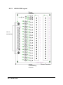
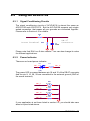
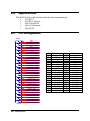
1
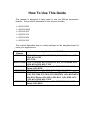
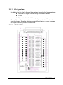
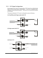
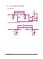
NuDAQ ®
ACLD Series
Termination Boards
User’s Guide
@Copyright 1995~2000 ADLINK Technology Inc.
All Rights Reserved.
Manual Rev. 2.32: June 7, 2000
The information in this document is subject to change without prior notice
in order to improve reliability, design and function and does not represent
a commitment on the part of the manufacturer.
In no event will the manufacturer be liable for direct, indirect, special,
incidental, or consequential damages arising out of the use or inability to
use the product or documentation, even if advised of the possibility of
such damages.
This document contains proprietary information protected by copyright. All
rights are reserved. No part of this manual may be reproduced by any
mechanical, electronic, or other means in any form without prior written
permission of the manufacturer.
Trademarks
NuDAQ is a registered trademark of ADLink Technology Inc.
Other product names mentioned herein are used for identification
purposes only and may be trademarks and/or registered trademarks of
their respective companies.
Getting service from ADLINK
Customer Satisfaction is always the most important thing for ADLINK
Tech Inc. If you need any help or service, please contact us and get it.
ADLINK Technology Inc.
Web Site
http://www.adlink.com.tw
Sales & Service [email protected]
Technical
NuDAQ
[email protected]
Support
NuDAM
[email protected]
NuIPC
[email protected]
NuPRO
[email protected]
Software
[email protected]
AMB
[email protected]
TEL
+886-2-82265877
FAX
+886-2-82265717
Address
9F, No. 166, Jian Yi Road, Chungho City, Taipei, 235
Taiwan, R.O.C.
Please inform or FAX us of your detailed information for a prompt,
satisfactory and constant service.
Detailed Company Information
Company/Organization
Contact Person
E-mail Address
Address
Country
TEL
FAX
Web Site
Questions
Product Model
Environment to Use
OS
Computer Brand
M/B : CPU :
Chipset : Bios :
Video Card :
Network Interface Card :
Other :
Challenge Description
Suggestions for ADLink
Contents
Chapter 1 ACLD-9185............................................. 1
1.1 Introduction ................................................................... 1
1.1.1
1.1.2
Features.............................................................................................1
Specifications ..................................................................................2
1.2 Installation ..................................................................... 2
1.2.1
1.2.2
1.2.3
1.2.4
What you have.................................................................................2
ACLD-9185 Layout..........................................................................3
Power Source Setting....................................................................4
Connect to add-on card ................................................................5
1.3 Usage .............................................................................. 5
1.4 Connector Pin Assignments..................................... 6
1.5 Applications .................................................................. 6
Chapter 2 ACLD-9182A.......................................... 7
2.1 Introduction ................................................................... 7
2.1.1
2.1.2
Features.............................................................................................7
Specifications ..................................................................................8
2.2 Installation ..................................................................... 8
2.2.1
2.2.2
2.2.3
What you have.................................................................................8
ACLD-9182A's Layout....................................................................9
Connect to add-on card ................................................................9
2.3 Usage ............................................................................10
2.3.1
2.3.2
2.3.3
Input Mode Setting .......................................................................10
Adjust Threshold for Isolated Mode ........................................11
Customize the Current Limit Resistor.....................................11
2.4 Connector Pin Assignments...................................12
Contents • i
2.5 Applications ................................................................13
Chapter 3 ACLD-8125........................................... 14
3.1 Introduction .................................................................14
3.2 Installation ...................................................................14
3.2.1
3.2.2
3.2.3
What you have...............................................................................15
ACLD-8125 Layout........................................................................15
Connect to add-on card ..............................................................16
3.3 How to use ACLD-8125.............................................16
3.3.1
3.3.2
3.3.3
ACL-8125 Connections................................................................16
CJC Output Configurations........................................................17
Circuit Diagram of ACLD-8125 ..................................................18
3.4 Connector Pin Assignments...................................19
3.5 Expamle for temperature measuring by using
the ACL-8112 and ACLD-8125 ................................20
3.6 Applications ................................................................21
Chapter 4 ACLD-9178........................................... 22
4.1 Introduction .................................................................22
4.4.1
Features...........................................................................................22
4.2 Installation ...................................................................22
4.2.1
4.2.2
What you have...............................................................................23
ACLD-9178 Layout........................................................................23
4.3 Signal Conditioning Circuits...................................24
4.4 Pin Assignment ..........................................................25
4.5 Applications ................................................................26
ii • Contents
Chapter 5 ACLD-9188........................................... 27
5.1 Introduction .................................................................27
5.1.1
Features...........................................................................................27
5.2 Installation ...................................................................28
5.2.1
5.2.2
What you have...............................................................................28
ACLD-9188 Layout........................................................................28
5.3 Signal Conditioning Circuits...................................29
5.4 Pin Assignment ..........................................................29
5.5 Applications ................................................................30
Chapter 6 ACLD-9138........................................... 31
6.1 Introduction .................................................................31
6.2 Installation ...................................................................31
6.2.1
6.2.2
What you have...............................................................................31
ACLD-9138 Layout......................................................................32
6.3 Using the ACLD-9138................................................33
6.3.1
6.3.2
Signal Conditioning Circuits......................................................33
Power Indicator .............................................................................33
6.4 Applications ................................................................34
6.5 Pin Assignment ..........................................................34
Product Warranty/Service......................................................35
Contents • iii
How To Use This Guide
This manual is designed to help users to use the ADLink termination
boards. The products described in this manual include:
Ø ACLD-9185
Ø ACLD-9182A
Ø ACLD-8125
Ø ACLD-9178
Ø ACLD-9188
Ø ACLD-9138
The manual describes how to modify settings on the daughter board to
meet your applications.
Termination
Applications for NuDAQ
Boards
ACLD-9185 PCI-9111 Series, ACL-8312/8316, ACL-8112 Series, ACL8216, ACL-6126,
ACL-7120
ACLD-9182A PCI-9111 Series, ACL-8312/8316, ACL-8112 Series, ACL8216, ACL-6126, ACL-7120
ACLD-8125 PCI-9112, PCI-9111 Series, ACL-8312/8316, ACL-8112
Series, ACL-8126
ACLD-9178 ACL-8312/8316, ACL-8216, ACL-6126, ACL-7120
ACLD-9188 PCI-9114 Series, PCI-9111 Series, PCI-6208 Series, PCI8133, PCI-7200, PCI-7230, PCI-7250/7251, ACL-8312/8316,
ACL-8112 Series, ACL-8216, ACL-8111, ACL-6126, ACL7130, ACL-9188, ACL-7225
ACLD-9138 PCI-9112, PCI-9111 Series, ACL-8312/8316, ACL-8112
Series, ACL-8216
1
ACLD-9185
This chapter describes how to install and use the ACLD-9185.
1.1
Introduction
The ACLD-9185 is a 16-channel SPDT form C relay output board. It
provides 16 electromechanical SPDT relays, which can be used by any
ACL series or PCI series boards with digital output channels on 20-pin flat
ribbon connector.
You can use the 16 on-board relays to control power switches. Each of
them matches with one LED to indicate its ON/OFF status and consumes
about 33mA when energized. When all relays on the board are active,
the board takes about 0.53 A from the computer's 12 volts power supply.
When the current driving capability of the 12V power source is not enough,
the ACLD-9185 has a jumper switch allowing the users to connect an
external +12V power source.
1.1.1
Features
The ACLD-9185 Relay Actuator Card provides the following features:
l 16 Single-Pole-Double-Throw relays
l LED indicators to show activated relays
l On-board relay driving circuits
l 120V/1 Amp contact rating
l Simple to program
l Controlled through TTL/CMOS signals or digital output ports
of any ACL and PCI series board
ACLD-9185 • 1
l Screw terminal for easily wiring
1.1.2
Specifications
Output Channels
Relay Type
Contact rating
Breakdown Voltage
Release time
Operate time
Relay ON time
Relay OFF time
Total switching time
Insulation Resistance
Life Expectancy
Power Consumption
Power supply
Size
Connectors
1.2
16
16 SPDT ( Form C )
120V AC/DC, 1A
1000V AC/DC min..
5 msec max.
5 msec max..
3 msec typical
3 msec typical
10 msec typical
100 mega Ohms min.
> 5 million operations at full load
+12V , 33mA for each relay, total 0.53A if
all relay are energized +5V, less than 0.2A
+12V from the PC-Bus
203 mm X 132mm
20-pin flat cable
Installation
To install and operate the ACLD-9185, you can follow the following steps:
Ø Check what you have in the box
Ø Check the PCB
Ø Set jumper (set power source)
Ø Make connection to add-on cards
Ø Program the add-on cards
1.2.1
What you have
In addition to this User's Manual, the package includes the following items:
l ACLD-9185 Relay Output Board
l Cable
l Nylon standoffs for table-top or panel mounting
If any of these items was missed or damaged, contact the dealer whom
you purchased. Save the shipping materials and carton in case you want
to ship or store the product in the future.
2 • ACLD-9185
1.2.2
ACLD-9185 Layout
+5V
CN1
CN3
+12V
CN2
CN4
NO0
NC0
COM0
NO7
NC7
COM7
K0
K8
K1
K9
K2
K10
K3
K11
K4
K12
K5
K13
K6
K14
K7
K15
NO8
NC8
COM8
NO15
NC15
COM15
ACLD-9185 • 3
1.2.3
Power Source Setting
The ACLD-9185's power source can come from internal source (provided
from the PC bus via the CN1 20-pin connector) or external source
(provided by external power supply). The +5V is used to drive the TTL
buffer circuits and the LED on board. The +12V is used to drive the
Relays. The description of power source is specified as following table:
Internal power
External power
+12V
+5V
+12V
+5V
Provided by PC bus via the CN1 20-pin
connector
Provided by external DC source via
connector CN3
The power sources can be selected by setting jumpers according to the
following table.
Internal +5V
Internal +12V
+5V
(d e f a u l t )
+12V
External +5V
External +12V
+5V
+12V
Internal +5V
External +12V
+5V
+12V
External +5V
Internal +12V
+5V
+12V
4 • ACLD-9185
1.2.4
Connect to add-on card
The ACLD-9185 can be controlled with NuDAQ ISA or PCI add-on cards.
The configurations of connection are shown in the following diagram.
Please make sure to connect to the digital output port of the add-on cards
with correct pin-assignment.
ACLD-9185
1.3
Usage
The function diagram of Form C relays on the ACLD-9185 is shown here.
NO
NO
COM
NC
Control Bit = High (1)
COM
NC
Control Bit = Low (0)
This relay has three contacts: NC (Normal Closed), NO (Normal Open),
and COM (Common). The COM post, located at the middle, can make
contact either NO post or NC post. When the control bit is high (1), the
COM post and NO post are contacted. If the control bit is low (0), the
COM post and NC post make contact.
In normal power-up and reset, the relay is in low status.
ACLD-9185 • 5
1.4
Connector Pin Assignments
The relationship between connector pins, relay contacts, LED's, and on
the ACLD-9185 is shown in the following table:
CN1
PIN
1
2
3
4
5
6
7
8
9
10
11
12
13
14
15
16
17
18
19
20
1.5
RELAY
K0
K1
K2
K3
K4
K5
K6
K7
K8
K9
K10
K11
K12
K13
K14
K15
RELAY Contacts
COM0 NC0
COM1 NC1
COM2 NC2
COM3 NC3
COM4 NC4
COM5 NC5
COM6 NC6
COM7 NC7
COM8 NC8
COM9 NC9
COM10 NC10
COM11 NC11
COM12 NC12
COM13 NC13
COM14 NC14
COM15 NC15
Ground
Ground
+5 DC
+12 DC
NO0
NO1
NO2
NO3
NO4
NO5
NO6
NO7
NO8
NO9
NO10
NO11
NO12
NO13
NO14
NO15
Applications
The ACLD-9185 could be used on our following products:
ü
PCI-9111Series
ü
PCI-9112
ü
ACL-8312/8316
ü
ACL-8112 Series
ü
ACL-8216
ü
ACL-6126, ACL-7120
6 • ACLD-9185
LED
0
1
2
3
4
5
6
7
8
9
10
11
12
13
14
15
2
ACLD-9182A
This chapter describes how to install and use the ACLD-9182A.
2.1
Introduction
The ACLD-9182A is a 16-channel opto-isolated digital input board, which
can be connected by any ACL or PCI series digital input board with D/I
channels of 20-pin flat ribbon connectors. It is a good solution for
preventing floating potential and ground loop problems.
Each input channel has a red LED to indicate the ON/OFF status. If the
input voltage is high, the LED will be on otherwise the LED is off. AC or
DC input is selectable by setting the jumpers. And you do not need to
care the polarity.
2.1.1
Features
l 16 Opto-Isolated digital input channels
l For use with 20-pin digital input connector of NuDAQ cards
l AC or DC polarity-free digital input
l Screw terminals for easy wiring
l On board LEDs to indicate the input logic status
ACLD-9182A • 7
2.1.2
Specifications
Number of channel
Opto-coupler
Input impedance
Threshold voltage
Isolation voltage
Input mode
Response time
Connector
Screw Terminal
Indication Display
Size
2.2
16
4N35
1.2K ohm
1.5 VDC
1000 VDC(channel to channel
and channel to ground)
Isolation and dry contact input
range
20uSec without AC filter
20-Pin
Flat
Ribbon
Cable
Connector
5mm wiring spacing, 18-22 AWG
16 LEDs
205 mm X 114 mm
Installation
To install and operate the ACLD-9182A, please follow the following steps:
Ø Check what you have in the box
Ø Check the PCB
Ø Make connection to add-on cards
Ø Program the add-on cards
2.2.1
What you have
In addition to this User's Manual, the package includes the following items:
l ACLD-9182A Photo coupler input Board
l Cable
l Nylon standoffs for table-top or panel mounting
If any of these items was missed or damaged, contact the dealer whom
you purchased. Save the shipping materials and carton in case you want
to ship or store the product in the future.
8 • ACLD-9182A
2.2.2
ACLD-9182A's Layout
+12V
JA15
JB15
JB7
JA7
GND
+5V
JA14
JB14
JB6
JA6
GND
+15-
JA13
JB13
JB5
JA5
+7-
+14-
JA12
JB12
JB4
JA4
+6-
+13-
JA11
JB11
JB3
JA3
+5-
+12-
JA10
JB10
JB2
JA2
+4-
+11-
JA9
JB9
JB1
JA1
+3-
+10-
JA8
JB8
JB0
JA0
+2-
+9-
+1-
+8-
+0-
TB2
2.2.3
CN1
TB1
Connect to add-on card
The ACLD-9182A can be controlled with NuDAQ ISA or PCI add-on cards.
The configurations of connection are shown in the following diagram.
Please make sure to connect to the digital output port of the add-on cards
with correct pin-assignment.
ACLD-9182
ACLD-9182A • 9
2.3
Usage
By setting the JAn and JBn jumpers, you can choose the isolated or dry
input(see the 2.3.1). And adjust threshold for isolated mode by tuning
VR1(see 2.3.2).
2.3.1
Input Mode Setting
There are 2 jumpers (JAn and JBn, n = 0 ~ 15) associated with each
digital input channel for configuring the channel as isolated or nonisolated (Dry Contact) input. The digital input channels and their
corresponding jumper is shown below.
Each channel comes equipped with a pair of jumpers for either isolated or
non-isolated selection. If the jumper plugs are installed on the upper
posts of JAn, and JBn (n =0..15), the channel n is configured as
ISOLATED, otherwise the jumper plugs should be installed on the lower
posts to configure as Non-isolated.
For channel 0~7 (n=0..7)
Input Signal
Selection
JAn
JBn
Isolated
Non-isolated
I
I
I
I
For channel 8~15 (n=8..15)
Input Signal
Selection
JAn
JBn
10 • ACLD-9182A
Isolated
Non-isolated
N
2.3.2
Adjust Threshold for Isolated Mode
The input isolated mode of the ACLD-9182A is actually driven by current
instead of voltage level. The logic low means the input leakage current
should be less than 1mA, otherwise the input status will be treated as
logic High (1).
To avoid the logic high voltage as low, the ACLD-9182A is equipped with
a variable resistor VR1, which is used to adjust the threshold level for all
the 16 isolated input channels.
RV
DIn+
4K
+5V
DInAdjusting procedures:
1 Apply a +5V voltage source at DIH and DIL along with a 4K Ohms
resistor. The resistor limits input current to about 1mA.
2 Adjust the VR1 until the LED0 is off.
Follow the adjusting procedures, if channel 0's input voltage is low, and
the input leakage current is less than 1mA, the input status is considered
as logical low (TTL 0). To prevent higher input leakage current, you can
change the 3.9K Ohms resistor by a lower one, and use the above
procedures to meet your requirements.
2.3.3
Customize the Current Limit Resistor
The default voltage input range of the ACLD-9182A is from 0V to 24V. To
accept higher voltage input, you should replace the current limit resistor,
RA0...RA15, for each channel.
The current rating of the 4N35 photocoupler is about 60mA. It is
recommended that the input current is within 20mA. If you want to
choose the proper current limit resistor, please use the following formula
to calculate the input current( IF).
Vin = IF X Ri
Pw = Vin X IF
ACLD-9182A • 11
Where
Vin : Input voltage
IF: Input current
Pw : Power rating
Ri : Current Limit resistor
For example:
If the input voltage is 40V, then the maximum input current is within
20mA, using the above formula :
Ri = 40 (V) / 20 (mA) = 2 KΩ
Pw = 40 (V) X 20 (mA) = 0.8 W
You should choose a 2KΩ resistor and the power rating of this resistor
should be 1 Watt.
2.4
Connector Pin Assignments
The relationship between connector CN1's pins (below), terminal blocks
(TB1 & TB2), LED's, and their related jumpers are shown in the following
table :
CN1 PIN
NO.
1
2
3
4
5
6
7
8
9
10
11
12
13
14
15
16
17
18
19
** 20
12 • ACLD-9182A
D/I
Channel
DI 0
DI 1
DI 2
DI 3
DI 4
DI 5
DI 6
DI 7
DI 8
DI 9
DI 10
DI 11
DI 12
DI 13
DI 14
DI 15
TB1 & TB2
LABEL
TB1 0+,0TB1 1+,1TB1 2+,2TB1 3+,3TB1 4+,4TB1 5+,5TB1 6+,6TB1 7+,7TB2 8+,8TB2 9+,9TB2 10+,10TB2 11+,11TB2 12+,12TB2 13+,13TB2 14+,14TB2 15+,15GND
GND
+5V
+12V
LED
NO.
0
1
2
3
4
5
6
7
8
9
10
11
12
13
14
15
RELATED
JUMPER
JA0, JB0
JA1, JB1
JA2, JB2
JA3, JB3
JA4, JB4
JA5, JB5
JA6, JB6
JA7, JB7
JA8, JB8
JA9, JB9
JA10, JB10
JA11, JB11
JA12, JB12
JA13, JB13
JA14, JB14
JA15, JB15
** Pin-20 (+12V) depends on the output form digital input connector, such
as ACL-8111, ACL-8112 are +12V, but it is strobe signal on ACL-7120.
2.5
Applications
The ACLD-9182A could be used on following products:
ü
PCI-9111 Series
ü
ACL-8312/8316
ü
ACL-8112 Series
ü
ACL-8216,
ü
ACL-6126
ü
ACL-7120.
ACLD-9182A • 13
3
ACLD-8125
This chapter describes how to install and use the ACLD-8125.
3.1
Introduction
The ACLD-8125 is a signal conditioning termination board with build-in
cold junction temperature sensor. It has the following features:
Ø On board signal conditioning circuits for every analog input channels
Ø Cold junction temperature sensor
Ø Build-in screw terminals for wiring
Ø 37-pin D-sub connector
3.2
Installation
To install and operate the ACLD-8125, pleas e follow the following steps:
Ø Check what you have in the box
Ø Check the PCB
Ø Make connection to add-on cards
Ø Program the add-on cards
14 • ACLD-8125
3.2.1
What you have
In addition to this User's Manual, the package includes the following items:
l ACLD-8125 Signal Conditi oning Termination Board
l Cable
l Nylon standoffs for table-top or panel mounting
If any of these items was missed or damaged, contact the dealer whom
you purchased. Save the shipping materials and carton in case you want
to ship or store the product in the future.
3.2.2
ACLD-8125 Layout
ACLD-8125 • 15
3.2.3
Connect to add-on card
The ACLD-8125 can be used with NuDAQ ISA or PCI add-on cards. The
configurations of connection are shown in the following diagram. Please
make sure to connect to the digital output port of the add-on cards with
correct pin-assignment.
ACLD-8125
3.3
How to use ACLD-8125
3.3.1
ACL-8125 Connections
The ACL-8125 comes equipped with a DB-37 female connector; this
board is designed for ACL-8112/8216/8316 and PCI-9111/9112 series
cards for convenient wiring. This board provides two kinds of wiring style:
single-ended and differential. The connections are illustrated as following
figures.
(1) Single-ended connection
RAO
AIOH
AIO
RBO
CO
AGND
AGND
(2) Differential connection
RAO
AIOH
GHOH
RDO
CCO
AIOL
CHOL
16 • ACLD-8125
3.3.2
CJC Output Configurations
An on-board Cold Junction Compensation (CJC) circuit is provided by the
ACLD-8125 for thermcouple measurement. The CJC is connected with
Channel 0 of the internal connector. The circuit of CJC and CH0 is shown
as following:
The jumper setting for CJC output configuration are as following:
(1) Fully Differential Single-ended with CJC
J P 1
1
2
3
C I O H
J P 1 : 1 - 2
CJC
C H O H
Circuits
C
J C
C irc u itry
J P 2 : 1 - 2
J P 2
C H O L
1
2
3
C H O L
(2) Single-ended with CJC
J P 1
1
2
3
A I O L
J P 1 : 1 - 2
AIO
J P 2 : 2 - 3
J P 2
AI8
1
2
3
CJC
C JC
Circuits
C irc u i t r y
AI8
(3) Disable CJC
A IO
H
J P 1
A IO
A ILO
A I8
J P 2
1
2
3
C H O H
1
2
3
C H O L
A IO
J P 1 : 2 - 3
J P 2 : 2 - 3
A I8
ACLD-8125 • 17
3.3.3
Circuit Diagram of ACLD-8125
(1) CJC Circuit
+12V
3
RD0
USER
CD0 USER
AI8
D2
LM334
RA8
0
2
R16
68.1%1
C0
USER
JP1
2
AIH0
RB8
USER
C8
USER
JP2
2
RB0
USER
3
3
1
AI0
RA0
0
2 AIL8
D1
LM335
3
1
1
1
VR1
10K
(2) Signal Conditioning Circuit
RD1
USER
CD1
AI1
RA1
0
AIH1
RB1
USER
18 • ACLD-8125
C1
USER
USER
AI9
RA9
0
AIL9
RB9
USER
C9
USER
3.4
Connector Pin Assignments
Pin assignment of CN1
Pin
1
2
3
4
5
6
7
8
9
10
11
12
13
14
15
16
17
18
19
Description
AIH0
AIH1
AIH2
AIH3
AIH4
AIH5
AIH6
AIH7
AGND
AGND
VREF
EXTREF2
+12V
AGND
DGND
CNT0_OUT
EXT_TRG
NC
VCC
Pin
20
21
22
23
24
25
26
27
28
29
30
31
32
33
34
35
36
37
Description
AIL8
AIL9
AIL10
AIL11
AIL12
AIL13
AIL14
AIL15
AGND
AGND
AO1
EXTREF1
AO2
CNT0_GATE
GATE
NC
NC
CNT0_CLK
Pin Assignment of CN2A
Pin
1
2
3
4
5
6
7
8
9
10
11
12
Description
AGND
AI14
AI6
AGND
AI12
AI4
AGND
AI10
AI2
AGND
AI8
AI0
ACLD-8125 • 19
Pin Assignment of CN2B
Pin
1
2
3
4
5
6
7
8
9
10
11
12
Description
AGND
AI15
AI6
AGND
AI13
AI5
AGND
AI11
AI3
AGND
AI9
AI1
Pin Assignment of CN3
Pin
1
2
3
4
5
6
7
8
9
10
11
12
13
14
3.5
Description
VREF
AO1
EXTREF1
AGND
EXTREF2
AGND
CNT0_CLK
CNT0_GATE
CNT0_OUT
DGND
GATE
EXT_TRG
DGND
VCC
Expamle for temperature measuring by
using the ACL-8112 and ACLD-8125
There is an on-board CJC circuit. The CJC is connected with Channel 0
of the internal connector. It can be used for obtaining environment
temperature.
1) ACLD-8125 JP1 : 1+2 JP2 : 2+3
2) ACL-8112 JP9 : +/- 5V range
20 • ACLD-8125
3) Now you can read the CJC voltage by reading channel 0 of ACL-8112
4) If the environment temperature is 25 degree. The voltage you read is
about 2.98 V
5)
V(mV)=T('K)*10(mV/'K)
T('K)=T('C)+273('K)
2.98V=2980mV=(25+273)*10mV
when the JP9 on the ACL-8112 is +/-5V range.
3.6
Applications
The ACLD-8125 could be used on following products:
ü
PCI-9112
ü
PCI-9111 Series
ü
ACL-8312/8316
ü
ACL-8112 Series
ü
ACL-8216.
ACLD-8125 • 21
4
ACLD-9178
This chapter describes how to install and use the ACLD-8125.
4.1
Introduction
The ACLD-9178 is a universal screw terminal panel with convenient
connection points for 20-pin flat cable connector.
The ACLD-9178 is designed for establishing external signal conditioning
circuits. For example, you can easily construct a low-pass filter, attenuator
or current-to-voltage converter by adding resistors and capacitors onto
the reserved circuit pads.
4.4.1
Features
The ACLD-9178 screw terminal board provides the following features:
l Low cost universal screw terminals
l Signal conditioning circuits built-in.
l Table-top mounting using nylon standoffs
l 40 terminal points for two 20-pin flat cable connectors.
l Controlled through TTL/CMOS signals or digital output ports
of any ACL series board
4.2
Installation
To install and operate the ACLD-9178, please follow the steps:
Ø Check what you have in the box
22 • ACLD-9178
Ø Check the PCB
Ø Make connection to add-on cards
Ø Program the add-on cards
4.2.1
What you have
In addition to this User's Manual, the package includes the following items:
l ACLD-9178 Screw Terminal Board
l
Cable
l Nylon standoffs for panel mounting.
If any of these items was missed or damaged, contact the dealer whom
you purchased. Save the shipping materials and carton in case you want
to ship or store the product in the future.
4.2.2
ACLD-9178 Layout
CNB
Signal
Conditioning
Circuits
CNA
B20
B18
B16
B14
B12
B10
B08
B06
B04
B02
A20
A18
A16
A14
A12
A10
A08
A06
A04
A02
B19
B17
B15
B13
B11
B09
B07
B05
B03
B01
A19
A17
A15
A13
A11
A09
A07
A05
A03
A01
ACLD-9178 • 23
4.3
Signal Conditioning Circuits
The ACLD-9178 is suitable for specifically passive signal conditioning
components. The following circuits are examples of signal conditioning for
screw connector A1 and A2.
Flat cable
connector
R1A
1
R1B
A1
C1
2
A2
Screw
Terminal
Ø Straight-through connection (Default setting)
1
A1
2
A2
R1A = Short ( 0 Ω)
R1B and C1 = Open
Ø Single-ended Voltage Attenuator
R1A
1
R1B
2
R2A = Short( 0 Ω), C1 = Open,
Attenuation = R1B / ( R1A + R1B)
Example : 10: 1 voltage attenuator
R1A = 9K Ω, and R1B = 1K Ω
Attenuation = 1 / (1 + 9)
24 • ACLD-9178
A1
I
A2
Ø Low-pass filter (Single-ended Input)
R1A
A1
1
C1
2
A2
R2A = Short ( 0 Ω), R1B = Open
ƒ3dB = 1 / ( 2πR1A C1)
Example : 1.6 KHz low pass filter:
R1A = 10K Ω, C1 = 0.01 µF
Ø 0-20mA Current-loop Input
1
A1
I
R1B
2
A2
R1A = Short( 0 Ω), C1 = Open,
R1B = 250Ω ( 0.05% tolerance) for 0 to 5V VDC signal Converter.
4.4
Pin Assignment
Pin assignment of CAN
Pin
1
2
3
4
5
6
7
8
9
10
Description
A1
A2
A3
A4
A5
A6
A7
A8
A9
A10
Pin
11
12
13
14
15
16
17
18
19
20
Description
A11
A12
A13
A14
A15
A16
A17
A18
A19
A20
ACLD-9178 • 25
Pin assignment of CNB
Pin
1
2
3
4
5
6
7
8
9
10
4.5
Description
B1
B2
B3
B4
B5
B6
B7
B8
B9
B10
Pin
11
12
13
14
15
16
17
18
19
20
Applications
The ACLD-9178 could be used on following products:
ü
ACL-8312/8316
ü
ACL-8216
ü
ACL-6126
ü
ACL-7120
26 • ACLD-9178
Description
B11
B12
B13
B14
B15
B16
B17
B18
B19
B20
5
ACLD-9188
This chapter describes how to install and use the ACLD-9138.
5.1
Introduction
The ACLD-9188 is a universal screw terminal board, which provides
convenient connection points for 20-pin flat ribbon cable or shielded cable
with 37-pin D-type connector. This panel is designed for field signal wiring
in industrial applications.
For example, you can easily construct a low-pass filter, attenuator or
current-to-voltage converter by adding resistors and capacitors onto the
reserved circuit pads.
5.1.1
Features
The ACLD-9188 industrial terminal board provides the following features:
l Low cost universal screw terminals
l Black pads accommodate applications such as break
detection, low-pass filter, current shut and voltage attenuator.
l Industrial type terminal blocks permit heavy-duty and reliable
connection of signals.
l 40 screw terminal points for two 20-pin flat cable or DB-37
connectors.
ACLD-9188 • 27
5.2
Installation
5.2.1
What you have
In addition to this User's Manual, the package includes the following items:
l ACLD-9188 Industrial Terminal Board
l Cable
l Nylon standoffs for table-top or panel mounting.
If any of these items was missed or damaged, contact the dealer whom
you purchased. Save the shipping materials and carton in case you want
to ship or store the product in the future.
5.2.2
ACLD-9188 Layout
D
B
C
N
C
N
C
N
28 • ACLD-9188
C
N
5.3
Signal Conditioning Circuits
The signal conditioning circuits of ACLD-9188 is the same as the circuits
on ACLD-8125. Please refer to Section 4.3 for details.
You can connect the card and this terminal board with a DB-37 cable. The
CN3 and CN1 are connected together, and so are the CN2 and CN4. If
your application is sensitive signal, we suggest that please do not use flat
cable connector and screw connector at the same time.
5.4
Pin Assignment
A1 to A20 is CN1.
B1 to B20 is CN2.
For example, the first field of the table means that A1(CN3-1), CN1-1,
CN5-1 are connected together.
A1
A2
A3
A4
A5
A6
A7
A8
A9
A10
A11
A12
A13
A14
A15
A16
A17
A18
A19
A20
CN1-1
CN1-2
CN1-3
CN1-4
CN1-5
CN1-6
CN1-7
CN1-8
CN1-9
CN1-10
CN1-11
CN1-12
CN1-13
CN1-14
CN1-15
CN1-16
CN1-17
CN1-18
CN1-19
CN1-20
CN5-1
CN5-20
CN5-2
CN5-21
CN5-3
CN5-22
CN5-4
CN5-23
CN5-5
CN5-24
CN5-6
CN5-25
CN5-7
CN5-26
CN5-8
CN5-27
CN5-9
CN5-28
CN5-10
CN5-29
B1
B2
B3
B4
B5
B6
B7
B8
B9
B10
B11
B12
B13
B14
B15
B16
B17
B18
B19
B20
CN2-1
CN2-2
CN2-3
CN2-4
CN2-5
CN2-6
CN2-7
CN2-8
CN2-9
CN2-10
CN2-11
CN2-12
CN2-13
CN2-14
CN2-15
CN2-16
CN2-17
CN2-18
CN2-19
CN2-20
CN5-11
CN5-30
CN5-12
CN5-31
CN5-13
CN5-32
CN5-14
CN5-33
CN5-15
CN5-34
CN5-16
CN5-35
CN5-17
CN5-36
CN5-18
CN5-37
CN5-19
-
ACLD-9188 • 29
5.5
Applications
The ACLD-9188 could be used on following products:
ü
PCI-9114 Series
ü
PCI-9111 Series
ü
PCI-6208 Series
ü
PCI-8133,
ü
PCI-7200
ü
PCI-7230
ü
PCI-7250/7251
ü
ACL-8312/8316
ü
ACL-8112 Series
ü
ACL-8216
ü
ACL-8111
ü
ACL-6126
ü
ACL-7130
ü
ACL-7225.
30 • ACLD-9188
6
ACLD-9138
This chapter describes how to install and use the ACLD-9138.
6.1
Introduction
The ACLD-9138 is an universal screw terminal board with 16 singleended channels on board signal conditioning circuit. It could be used on
our PCI and ACL series cards. There is a DB-37 connector. You can add
your signal conditioning circuits on it. It provides the following features:
Ø 16 single-ended channels with on board signal conditioning circuits(pin
1-8, 20-27).
Ø Build-in screw terminals for wiring
Ø 37-pin D-sub connector
Ø On board LED for power status.
6.2
Installation
6.2.1
What you have
In addition to this User's Manual, the package includes the following items:
l ACLD-9138 Industrial Terminal Board
l Two 20-pin 1-meter flat cable
If any of these items was missed or damaged, contact the dealer whom
you purchased. Save the shipping materials and carton in case you want
to ship or store the product in the future.
ACLD-9138 • 31
6.2.2
ACLD-9138 Layout
Power
Indicator
DB-37
connector
Signal
Conditioning
Circuits
32 • ACLD-9138
Screw Terminal
6.3
Using the ACLD-9138
6.3.1
Signal Conditioning Circuits
The signal conditioning circuits of ACLD-9138 is almost the same as
ACLD-8125 and ACLD-9178. But the ACLD-9138 supports only singleended connection, that means all your grounds are connected together.
Please refer to Section 4.3 for details.
RA0
0
Screw Terminal
RB0
C0
USER
DB-37
Connector
Please note that RA0 is a 0-ohm resistor. You can also change its value
for different applications.
6.3.2
Power Indicator
There are on board power indicator.
D1
CN1_19
R1
CN1_15
LED
The power LED is crossed between pin 19 and 15 of the DB-37 connector.
And the pin 9, 10, 28, 29 are connected to the external ground (GND of
the screw terminal).
CN1_9
CN1_28
CN1_10
CN1_29
RG1
0 / NU
RG2
0 / NU
RG3
0 / NU
RG4
0 / NU
If your application is not been listed in section 6.4, you should take care
about six pins listed above.
ACLD-9138 • 33
6.4
Applications
The ACLD-9138 could be used with the following products:
ü
PCI-9112
ü
PCI-9111 Series
ü
ACL-8312/8316
ü
ACL-8112 Series,
ü
ACL-8216.
6.5
Pin Assignment
CN1
1
20
2
21
3
22
4
23
5
24
6
25
7
26
8
27
9
28
10
29
11
30
12
31
13
32
14
33
15
34
16
35
17
36
18
37
19
34 • ACLD-9138
AI0
AI8
AI1
AI9
AI2
AI10
AI3
AI11
AI4
AI12
AI5
AI13
AI6
AI14
AI7
AI15
CN1_9
CN1_28
CN1_10
CN1_29
CN1_11
CN1_30
CN1_12
CN1_31
CN1_13
CN1_32
CN1_14
CN1_33
CN1_15
CN1_34
CN1_16
CN1_35
CN1_17
CN1_36
CN1_18
CN1_37
CN1_19
Pin
1
2
3
4
5
6
7
8
9
10
11
12
13
14
15
16
17
18
19
Meaning
AI0
AI1
AI2
AI3
AI4
AI5
AI6
AI7
CN1_9
CN1_10
CN1_11
CN1_12
CN1_13
CN1_14
CN1_15
CN1_16
CN1_17
CN1_18
CN1_19
Pin
20
21
22
23
24
25
26
27
28
29
30
31
32
33
34
35
36
37
Meaning
AI8
AI9
AI10
AI11
AI12
AI13
AI14
AI15
CN1_28
CN1_29
CN1_30
CN1_31
CN1_32
CN1_33
CN1_34
CN1_35
CN1_36
CN1_37
Product Warranty/Service
Seller warrants that equipment furnished will be free from defects in
material and workmanship for a period of one year from the confirmed
date of purchase of the original buyer and that upon written notice of any
such defect, Seller will, at its option, repair or replace the defective item
under the terms of this warranty, subject to the provisions and specific
exclusions listed herein.
This warranty shall not apply to equipment that has been previously
repaired or altered outside our plant in any way as to, in the judgment of
the manufacturer, affect its reliability. Nor will it apply if the equipment has
been used in a manner exceeding its specifications or if the serial number
has been removed.
Seller does not assume any liability for consequential damages as a
result from our products uses, and in any event our liability shall not
exceed the original selling price of the equipment.
The equipment warranty shall constitute the sole and exclusive remedy of
any Buyer of Seller’s equipment and the sole and exclusive liability of the
Seller, its successors or assigns, in connection with equipment purchased
and in lieu of all other warranties expressed implied or statutory, including,
but not limited to, any implied warranty of merchant ability or fitness and
all other obligations or liabilities of seller, its successors or assigns.
The equipment must be returned postage-prepaid. Package it securely
and insure it. You will be charged for parts and labor if you lack proof of
date of purchase, or if the warranty period is expired.
Product Warranty/Service • 35