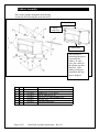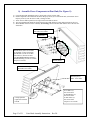
1
Service Dept.
6033 De Soto Ave.
Woodland Hills, CA 91367
P. 818-575-3600
F. 818-676-1585
E. [email protected]
***WARNING!!!***
Dangerous and lethal potentials are
present in this product!!
Before proceeding any further, the service center
is warned that caution must be used when
troubleshooting, repairing and testing the circuits
in this unit. High voltage AC line-connected
potentials are present in the circuits used in this
unit.
All work performed on this unit must be done
with an isolation transformer connected between
the power circuit’s input and the AC line in order
to prevent electric shock, especially when
connecting test equipment to the circuit. Extreme
caution must be used when working on this
product!!!
AX3 Universal Power Amp Rev C.sch-1 - Tue Dec 18 15:51:47 2001
AX3 Universal Power Amp Rev C.sch-2 - Tue Dec 18 15:51:46 2001
AX3 Universal Power Amp Rev C.sch-3 - Tue Dec 18 15:51:45 2001
HDII LINE FILTER Rev B.sch-1 - Tue Mar 06 13:35:42 2001
AX3 HEAD SPKR OUT REV A.sch-1 - Tue Jun 05 14:23:51 2001
AX3 COMBO UI Left Rev C.sch-1 - Tue Mar 26 11:14:19 2002
AX3 COMBO UI Left Rev C.sch-2 - Tue Mar 26 11:14:21 2002
AX3 COMBO UI Left Rev C.sch-3 - Tue Mar 26 11:14:23 2002
AX3_COMBO_UI_Right_REV_A.sch-1 - Tue Jun 05 11:40:07 2001
AX3_COMBO_UI_Right_REV_A.sch-2 - Tue Jun 05 11:40:08 2001
AX3_GUITAR IN_REV_A.sch-1 - Tue Jun 05 11:17:46 2001
LINE 6
Vetta HD Parts List
Items: 99 VETTA HD US
Level
Seq Component-Item Component-Description
Qty-Per-Parent
====================================================================================================================================
Parent Item: 99 VETTA HD US AMP Vetta Head 120V US
1
10 21-30-0009-2
CAB DIL 10 PIN .100 PITCH
10 EA
.0 A Y N
1.000000
1
20 21-30-0026
CAB DIL RBN 26 PIN 8.0
10 EA
.0
A Y
N
1.000000
1
30 21-34-0006
PITCH
CAB SIL 2 PIN 1.95" .156"
10 EA
.0
A Y
N
1.000000
1
40 21-34-0007-2
CAB ASSY SIL 4 PIN 2mm X 12.0
IN 26 AWG RED F-F
10 EA
.0
A Y
N
1.000000
1
50 21-34-0008-2
CAB SIL 4 PINS .156 IN PITCH
10.0 IN LG
10 EA
.0
A Y
N
1.000000
1
60 21-34-0014-2
CAB SIL 8 PINS .156 IN PITCH
13.0 IN LG
10 EA
.0
A Y
N
1.000000
1
70 21-34-0015
CAB SIL 5 PIN .079 IN PITCH
5.4 IN LG
10 EA
.0
A Y
N
1.000000
1
80 21-34-0018
10 EA
.0
A Y
N
1.000000
1
90 21-34-0021-2
CAB SIL 6 PINS .156 IN PITCH
12.5 IN LG
10 EA
.0
A Y
N
1.000000
CAB SIL 2 PIN .295 IN PITCH
1
100 21-34-1116
Cable, Earthing
green with yellow strip
10 EA
.0
A Y
N
1.000000
1
110 21-37-1160
CABLE PWR UL/CSA SJT 8.2ft Blk 10 EA
EL-302 w/GND EL70
.0
A Y
N
1.000000
1
120 24-06-0002
10 EA
.0
A Y
N
1.000000
1
130 30-00-0018
SCREW 6-32 SLFTPG x.75 FLH
PHILLIPS
10 EA
.0
A Y
N
4.000000
1
140 30-00-0025
10 EA
.0
A Y
N
4.000000
1
150 30-00-0375
SCR 6-32 x .375 LG PHILLIPS PN 10 EA
H STL BLK OXIDE
.0
A Y
N
6.000000
1
160 30-00-0607
SCR 6-32 x 7/16 PHIL PN HD
STL w/LK WASH ZINC
.0
A Y
N
38.000000
SWITCH ROCKER 2
SCREW 4-40 x.187 PNH
10 EA
LINE 6
Vetta HD Parts List
====================================================================================================================================
1
170 30-00-1012
SCREW #10-32 X 1/2 PHILLIPS
PAN ZINC
10 EA
.0
A Y
N
4.000000
1
180 30-00-1124
SCR 10-32 x 1 1/2 LG OVAL CT
SK PHH STL BLK
10 EA
.0
A Y
N
4.000000
1
200 30-00-4250
SCR SHEET METAL PAN HEAD
SLF TAP. 4 x.250" w/BLK OXIDE
10 EA
.0
A Y
N
4.000000
1
210 30-00-8375
SCR SHEET METAL #8 x.375" PPH
SELF TAP w/BLK OXIDE
10 EA
.0
A Y
N
2.000000
1
220 30-03-0001
WASHER #10 EXTERNAL TOOTH
LOCKWASHER ZINC
10 EA
.0
A Y
N
4.000000
1
230 30-03-0011
WASHER FINISHING #10 CTS
K BLK OXIDE
10 EA
.0
A Y
N
4.000000
1
240 30-15-0004
SPACER .13THKx.63OD NYLON
MUDGE 5610-82-.125
10 EA
.0
A Y
N
1.000000
1
250 30-24-0003
10 EA
.0
A Y
N
6.000000
1
260 30-27-0025
KNOB SM ENCDR .55Dx.57 H
IMP ABS MICROTEX
10 EA
.0
A Y
N
5.000000
1
280 30-27-0027
KNOB LGE ENCDR .80Dx.60 H
IMP ABS MICROTEX
10 EA
.0
A Y
N
2.000000
1
290 30-27-0031
BEZEL LEFT AX3 1.5x5.8x.28 H
IMP ABS BLK
10 EA
.0
A Y
N
1.000000
1
300 30-27-0032
LENS, BEZEL, MAIN 4.3x2.2
LEXAN SMOKED - VETTA
10 EA
.0
A Y
N
1.000000
1
310 30-27-0033
LENS, BEZEL, LEFT, 4.3x1.2
LEXAN SMOKED - VETTA
10 EA
.0
A Y
N
1.000000
1
320 30-27-0034
ABS BLK
BEZEL MAIN VETTA 4.6x.28 H IMP 10 EA
.0
A Y
N
1.000000
1
330 30-27-0042
GROM ENCDR VETTA .50DIAx.04
NYLON WHT/SM
10 EA
.0
A Y
N
7.000000
1
340 30-40-0001
AMP SEL
10 EA
.0
A Y
N
1.000000
1
350 30-40-0002
GASKET VIB DPG 2.0x5.7
EDIT SEL
10 EA
.0
A Y
N
1.000000
1
360 30-40-0003
1.2x5.6
10 EA
.0
A Y
N
1.000000
1
370 30-45-2000
KNOB POT PLASTIC BLACK w/WHITE 10 EA
INDICATOR LINE
.0
A Y
N
10.000000
TIE CABLE 4" CLEAR
GASKET VIB DPG 1.24x1.79
GASKET VIB DPG CHAN SEL
LINE 6
Vetta HD Parts List
====================================================================================================================================
1
380 30-51-0040
EXP SLOT COV 7.7x2.2 20 GA
10 EA
.0 A Y N
1.000000
STL BLK PWD COAT
1
390 30-51-0076
COV CHAS VETTA HD 27.3x7.8 EG
STL ELEC GALV
10 EA
.0
A Y
N
1.000000
1
400 30-51-0093
CLIP MAIN BEZEL .52x.26 EG STL 10 EA
.0
A Y
N
2.000000
1
410 30-51-0095
CHASSIS BRACE 7.7x6.7 EG STEEL 10 EA
.0
A Y
N
2.000000
1
Ref: added per EO# 0133806
420 30-51-0096
CLIP WIRE SMALL BEZEL
10 EA
.364x.256x.150 SPR TEM CS WIRE
.0
A Y
N
1.000000
1
430 30-51-0102
PUSH RETAINER .45X.250
10 EA
.0
A Y
N
1.000000
1
440 30-75-0010
PEDAL SWITCH RUBBER PAD
10 EA
.0
A Y
N
1.000000
1
450 40-00-0000
CHART PATCH VETTA
10 EA
.0
A Y
N
1.000000
1
460 40-00-0001
MANUAL USERS VETTA
10 EA
.0
A Y
N
1.000000
1
470 40-00-0073
SHEET ACCESSORY DOMESTIC
10 EA
.0
A Y
N
1.000000
1
480 40-10-0001
Foam, Corner Lam. PE
6.25*6.25*6.25 1.75 thk
10 EA
.0
A Y
N
8.000000
1
500 40-10-0018
CARTON SHIPPING VETTA HD
10 EA
.0
A Y
N
1.000000
1
510 40-16-0003
BROCHURE HANGING VETTA
10 EA
.0
A Y
N
1.000000
1
520 40-20-0010
BAG PLASTIC 43"x38"x.004 CLEAR 10 EA
.0
A Y
N
1.000000
1
530 40-20-0011
BAG PLASTIC 10 x 16 2 mil
10 EA
.0
A Y
N
1.000000
1
540 40-25-0008
LABEL ETL AX3/HDII LINE6 2"x1" 10 EA
.0
A Y
N
1.000000
1
550 40-25-0015
LABEL GROUND SYMBOL
10 EA
.0
A Y
N
1.000000
1
560 40-25-0020
LABEL INSPECTION QUALITY
10 EA
.0
A Y
N
2.000000
1
570 40-25-0100
LABEL BAR CODE SERIAL NUMBER
4-PANEL LABEL
10 EA
.0
A Y
N
1.000000
LINE 6
Vetta HD Parts List
====================================================================================================================================
1
580 40-25-0103
STICKER VERSION 1.1 VETTA
10 EA
.0 A Y N
1.000000
1
590 40-25-0150
Sticker, Vetta Disclaimer
10 EA
.0
A Y
N
1.000000
1
600 40-25-0254
LABEL LOGO LINE 6 PREMIUM
10 EA
.0
A Y
N
1.000000
1
610 40-25-2000
STICKER OUTPUT AX3 REV-A
10 EA
.0
A Y
N
1.000000
1
620 50-00-0039
ASSY KEYCAPS AMP SEL VETTA
10 EA
.0
A Y
N
1.000000
1
630 50-00-0042
ASSY KEYCAPS CHAN SEL VETTA
10 EA
.0
A Y
N
1.000000
1
640 50-00-0043
ASSY KEYCAPS EDIT SEL VETTA
10 EA
.0
A Y
N
1.000000
1
650 50-00-0099
PCBA INPUT GUITAR VETTA
10 EA
.0
A Y
N
1.000000
2
10 01-00-0102
RES 1K 5% 0805
10 EA
.0
A Y
N
2.000000
2
20 01-00-0105
Ref: r4,R121
RES 1M 5% 0805
10 EA
.0
A Y
N
1.000000
2
30 01-00-0202
Ref: R122
RES 2K 5% 0805
10 EA
.0
A Y
N
1.000000
2
40 03-46-0104
Ref: r5
CAP X7R 0.1uF 50V 20% 1206
10 EA
.0
A Y
N
1.000000
2
50 03-50-0470
Ref: C62
CAP NPO 47pF 50V 10% 0805
10 EA
.0
A Y
N
1.000000
2
60 03-52-0473
Ref: C89
CAP X7R 47nF 50V 20% 0805
10 EA
.0
A Y
N
2.000000
2
70 11-10-0601
Ref: C37,C170
FERRITE BEAD 600R @100MHZ 1206 10 EA
.0
A Y
N
1.000000
2
80 12-54-0134
SO-8
Ref: L31
IC OP AMP - OPA134UA SM
10 EA
.0
A Y
N
1.000000
10 EA
Ref: J2
.0
A Y
N
1.000000
2
Ref: U17
90 21-00-6617
JACK 1/4" TRS 6-PIN PCB MT
HORIZ TH W/CHROME HRDWARE
LINE 6
Vetta HD Parts List
====================================================================================================================================
2
100 21-20-0205
HDR PCB MT SIL 5-PIN x 2mm
FEMALE SHRD VERT MT TH
10 EA
.0
A Y
N
1.000000
2
110 30-18-3030
10 EA
.0
A Y
N
1.000000
PCBA OUTPUT SPEAKER
10 EA
.0
A Y
N
1.000000
CAP NPO 1nF 50V 5% 0805
10 EA
.0
A Y
N
4.000000
Ref: J27
CLIP GND PCB .30x.30x.07
Ref: J35
1
660 50-00-0104
2
20 03-50-0102
2
Ref: C47,C53-54,C63
30 21-00-6616
JACK 1/4" TRS 6-PIN PCB MT
HORIZ TH
10 EA
.0
A Y
N
4.000000
2
Ref: J16,J18,J28,J30
40 21-20-0204
HDR PCB MT SIL 4-PIN x 2mm
FEMALE SHRD VERT MT TH
10 EA
.0
A Y
N
1.000000
2
Ref: H3
50 21-20-1564
HDR PCB MT SIL 4-PIN X .156
MALE VERT-MNT FRIC-LOCK
10 EA
.0
A Y
N
1.000000
2
Ref: J8
60 24-09-0128
SWITCH SLIDE DPDT RA PCB MT
ON-OPEN-ON SWEETA SPA-128
10 EA
.0
A Y
N
1.000000
2
70 30-18-3030
10 EA
.0
A Y
N
4.000000
PCBA INTERFACE USER LEFT VETTA 10 EA
.0
A Y
N
1.000000
.0
A Y
N
15.000000
Ref: SW1
CLIP GND PCB .30x.30x.07
Ref: J42-J45
1
670 50-00-0106
2
10 01-00-0102
RES 1K 5% 0805
2
20 01-00-0103
Ref: R6,R8-11,R16,R28,R31,R36,R39,R41,R43,R45,R55,R61
RES 10K 5% 0805
23.000000
2
30 01-00-0152
Ref: R32-35,R47-53,R56-59,R62-63,R79-84
RES 1.5K 5% 0805
1.000000
Ref: R4
10 EA
LINE 6
Vetta HD Parts List
====================================================================================================================================
2
40 01-00-0472
RES 4.7K 5% 0805
10 EA
.0 A Y N
9.000000
2
50 01-00-0752
Ref: R13-14,R20-26
RES 7.5K 5% 0805
10 EA
.0
A Y
N
1.000000
2
97 01-24-1100
Ref: R3
RES 110R 1% 0805
10 EA
.0
A Y
N
7.000000
2
98 01-24-11R8
Ref: R17-19,R29-30,R37-38
RES 11.8R 1% 0805
10 EA
.0
A Y
N
5.000000
2
100 01-24-3401
Ref: R12,R46,R77-78,R85
RES 3.40K 1% 0805
10 EA
.0
A Y
N
1.000000
2
110 01-24-4321
Ref: R2
RES 4.32K 1% 0805
10 EA
.0
A Y
N
1.000000
2
115 01-24-78R7
Ref: R1
RES 78.7R 1% 0805
10 EA
.0
A Y
N
16.000000
2
Ref: R5,R7,R15,R27,R40,R42,R44,R54,R60,R64-67,R69,R75-76
120 01-48-0103
POT MONO 10KB LINEAR TAPER
10 EA
.0 A Y N
25 mm D-SHAFT
6.000000
Ref: R68,R70-74
CAP ELEC 10uF 50V 20% RADIAL
10 EA
.0
A Y
N
6.000000
150 03-52-0103
Ref: C1-2,C16-17,C23-24
CAP X7R 10nF 50V 20% 0805
10 EA
.0
A Y
N
2.000000
2
160 03-52-0104
Ref: C3-4
CAP X7R 0.1uF 50V 20% 0805
10 EA
.0
A Y
N
16.000000
2
170 03-52-0473
Ref: C5-15,C18-20,C25-26
CAP X7R 47nF 50V 20% 0805
10 EA
.0
A Y
N
1.000000
2
Ref: C21
180 06-34-0016
DIODE SWITCHING 75V 200mA
6nS SOT-23 SM BAS16LT1
10 EA
.0
A Y
N
15.000000
2
Ref: D39,D42-55
190 09-10-4401
TRANS NPN SMALL-SIGNAL MBT4401 10 EA
SOT-23 SM
.0
A Y
N
7.000000
2
Ref: Q1,Q4-5,Q7-10
200 09-10-4403
TRANS PNP SMALL-SIGNAL MBT4403 10 EA
SOT-23 SM
Ref: Q2-3,Q6,Q11-16
.0
A Y
N
9.000000
2
130 03-18-0106
5/11/5
2
LINE 6
Vetta HD Parts List
====================================================================================================================================
2
210 12-64-1543
IC ADC 10 BIT 11 CHANNEL SM
TLC1543CDW
10 EA
.0
A Y
N
1.000000
2
Ref: U10
220 12-72-0050
IC PRECISION TEMPERATURE
SENSOR SOT-23 SM LM50CIM3
10 EA
.0
A Y
N
1.000000
2
Ref: U11
230 15-62-0002
IC 74HC02 QUAD 2-INPUT NOR
SO-14 SM
10 EA
.0
A Y
N
1.000000
2
Ref: U2
240 15-62-0074
IC 74HC74 FLIP-FLOP DUAL
D-TYPE 2-IN SO-14 SM
10 EA
.0
A Y
N
1.000000
2
Ref: U1
250 15-62-0138
IC 74HC138 DECODER/DEMUX
3-8 LINE SO-16 SM
10 EA
.0
A Y
N
1.000000
2
Ref: U8
260 15-62-0273
IC 74HC273 FLIP-FLOP D-TYPE
8-BIT SO-20 SM
10 EA
.0
A Y
N
3.000000
2
Ref: U3-5
270 15-64-0541
IC 74HCT 541 OCTAL BUF/DRIVER
3-S 8 SM
10 EA
.0
A Y
N
2.000000
2
Ref: U6-7
290 18-21-0002
LED ORANGE 3mmX2mm SM
Kingbrite APK3020SEC
10 EA
.0
A Y
N
17.000000
2
Ref: D8,D16,D24-38
335 21-20-1302
HDR PCB MT DIL 26-PIN 2X13-100 10 EA
VERT MT TH
.0
A Y
N
1.000000
2
Ref: h12
340 21-20-2006
HDR PCB MT SIL 6-PIN 1x6x.100
MALE VRT-MNT TH
10 EA
.0
A Y
N
2.000000
2
Ref: H2,H4
350 21-20-2028
HDR PCB MT DIL 28-PIN 2x14x100 10 EA
MALE RT ANG TH
.0
A Y
N
1.000000
2
Ref: J2
370 24-12-0120
ENCODER ROTARY VERT MT 24 STEP 10 EA
INCR 20mmSH/F TH RE120-40
.0
A Y
N
5.000000
2
Ref: E8,E10-13
380 24-12-1120
ENCODER 12-STEP ALPHA
RE120-40-20F-12P TH
10 EA
.0
A Y
N
2.000000
Ref: E9,E14
STANDOFF .343 (.710 LG)
10 EA
.0
A Y
N
4.000000
STANDOFF .470 LG PLASTIC
10 EA
.0
A Y
N
4.000000
2
390 30-12-0001
PLASTIC
2
400 30-12-0002
LINE 6
Vetta HD Parts List
====================================================================================================================================
2
401 30-15-0044
2
10 EA
.0
A Y
N
1.000000
402 30-27-0003
BTN FR CHAN SEL UI PNL VETTA
1.058x5.484 BLK ABS NA/
10 EA
.0
A Y
N
1.000000
2
403 30-27-0004
BUT FR AMP BTN UI PNL VETTA
1.058x1.615 BLK ABS N/A
10 EA
.0
A Y
N
1.000000
2
405 30-65-0002
TAPE POLYESTER w/RBR ADHESIVE
6mil 19mm X 10mm
10 EA
.0
A Y
N
1.000000
2
406 30-75-0010
PEDAL SWITCH RUBBER PAD
10 EA
.0
A Y
N
1.000000
2
415 50-00-0007
ASSY BUTTON PAD AMP SELECT X0
10 EA
.0
A Y
N
1.000000
2
416 50-00-0008
ASSY BUTTON PAD CHANNEL
SELECT X0
10
.0
A Y
N
1.000000
2
420 50-00-0114
PCBA DISPLAY LCD 192x48
GRAPHIC VETTA
10 EA
.0
A Y
N
1.000000
10 EA
.0
A Y
N
1.000000
3
10 18-30-0003
GRAPHIC
3
20 21-20-2001
HDR PCB MT SIL 2-PIN X .100
MALE VRT-MNT TH
10 EA
.0
A Y
N
1.000000
3
30 21-20-2003
HDR PCB MT SIL 3-PIN x .100
MALE VERT-MT TH
10 EA
.0
A Y
N
1.000000
3
Ref: J4
40 21-20-2216
HDR PCB MT DIL 16 PIN 2x8x.100 10 EA
MALE VERT MT TH
.0
A Y
N
1.000000
3
Ref: J1
50 30-63-1111
FOAM, 1/8" THK, 1/2" SQ, ADH O 10 EA
NE SD, 3M NO. 4508
.0
A Y
N
4.000000
2
1
TAPE TEFLON AND FOAM 7" x .5"
DISPLAY LCD - 192 X 48
430 50-00-0115
PCBA DISPLAY LCD 1x16
CHARACTER VETTA
10 EA
.0
A Y
N
1.000000
3
10 18-30-0002
DISPLAY LCD - 1 X 16
CHARACTER
10 EA
.0
A Y
N
1.000000
3
20 21-20-2016
HDR PCB MT SIL 16 PIN 1x16x100 10 EA
MALE VERT MT TH
.0
A Y
N
1.000000
.0
A Y
N
1.000000
680 50-00-0107
PCBA INTERFACE USER RGT VETTA
10 EA
LINE 6
Vetta HD Parts List
====================================================================================================================================
2
10 01-48-0103
POT MONO 10KB LINEAR TAPER
10 EA
.0 A Y N
1.000000
25 mm D-SHAFT
2
Ref: R64
20 01-48-8103
POT MONO 10KB LINEAR TAPER
CENTER DETENT 25mm D-SHFT
2
30 03-52-0104
2
10 EA
.0
A Y
N
3.000000
10 EA
.0
A Y
N
5.000000
Ref: C21-22,C27-29
40 06-34-0016
DIODE SWITCHING 75V 200mA
6nS SOT-23 SM BAS16LT1
10 EA
.0
A Y
N
2.000000
2
Ref: D40-41
50 18-12-0001
LED 3-DIGIT 7-SEG YEL w/DP
Ledtech LM3633-11-11BWRN TH
10 EA
.0
A Y
N
1.000000
2
Ref: D9
60 18-21-0002
LED ORANGE 3mmX2mm SM
Kingbrite APK3020SEC
10 EA
.0
A Y
N
20.000000
2
Ref: D1-7,D10-15,D17-23
70 21-20-1028
HDR PCB MT DIL 28 PIN 2x14x100 10 EA
FEMALE RT ANGLE TH
.0
A Y
N
1.000000
2
Ref: J1
75 30-27-0001
FR ISLN EDIT SEL VETTA
5.483x1.807 BLK ABS N/A
10 EA
.0
A Y
N
1.000000
2
90 50-00-0009
ASSY BUTTON PAD EDIT SELECT X0 10 EA
.0
A Y
N
1.000000
Ref: R65-67
CAP X7R 0.1uF 50V 20% 0805
1
690 50-00-0108
ASSY ARTWORK OVERLAY
10 EA
.0
A Y
N
1.000000
1
700 50-00-0109
Assy, VETTA Chassis w/artwork
10 EA
.0
A Y
N
1.000000
1
710 50-00-0120
PCBA MAIN VETTA HD
10 EA
.0
A Y
N
1.000000
RES 0R 5% 0805
10 EA
.0
A Y
N
1.000000
10 EA
.0
A Y
N
11.000000
2
5 01-00-0000
2
10 01-00-0101
Ref: R161
RES 100R 5% 0805
2
15 01-00-0103
Ref: R2,r133-134,r136,r141,r162-163,r167-168,r171-172
RES 10K 5% 0805
Ref: R18,R24,R29-30,R33,R37,R41,R53,R61,R65-69,R72,R78-79,R91,R93,R112,R114,R122-123,R128,R143-146,R178,R184
30.000000
LINE 6
Vetta HD Parts List
====================================================================================================================================
2
20 01-00-0104
RES 100K 5% 0805
10 EA
.0
A Y
N
4.000000
2
25 01-00-0105
Ref: R8,R26,R175,R177
RES 1M 5% 0805
10 EA
.0
A Y
N
2.000000
2
30 01-00-0122
Ref: R20,R38
RES 1.2K 5% 0805
10 EA
.0
A Y
N
2.000000
2
35 01-00-0132
Ref: R107,R120
RES 1.3K 5% 0805
10 EA
.0
A Y
N
2.000000
2
40 01-00-0150
Ref: R169-170
RES 15R 5% 0805
10 EA
.0
A Y
N
2.000000
2
45 01-00-0152
Ref: R126,R138
RES 1.5K 5% 0805
10 EA
.0
A Y
N
1.000000
2
50 01-00-0200
Ref: R94
RES 20R 5% 0805
10 EA
.0
A Y
N
2.000000
2
55 01-00-0221
Ref: R165-166
RES 220R 5% 0805
10 EA
.0
A Y
N
3.000000
2
65 01-00-0302
Ref: R3,R16-17
RES 3K 5% 0805
10 EA
.0
A Y
N
8.000000
2
70 01-00-0332
Ref: R27,R32,R55,R57,R80-81,R111,R115
RES 3.3K 5% 0805
10 EA
.0
A Y
N
3.000000
2
75 01-00-0362
Ref: R86,R164, R185
RES 3.6K 5% 0805
10 EA
.0
A Y
N
2.000000
2
80 01-00-0363
Ref: R43-44
RES 36K 5% 0805
10 EA
.0
A Y
N
4.000000
2
85 01-00-0392
Ref: R46-47,R71,R75
RES 3.9K 5% 0805
10 EA
.0
A Y
N
4.000000
2
90 01-00-0431
Ref: R42,R50,R70,R77
RES 430R 5% 0805
10 EA
.0
A Y
N
1.000000
Ref: R158
LINE 6
Vetta HD Parts List
====================================================================================================================================
2
95 01-00-0470
RES 47R 5% 0805
10.000000
2
100 01-00-0471
Ref: R89,R92,R103-105,R108-109,R113,R117,R119
RES 470R 5% 0805
10 EA
.0 A Y
N
3.000000
2
105 01-00-0472
Ref: R9,R202-203
RES 4.7K 5% 0805
10 EA
.0
A Y
N
2.000000
2
110 01-00-0473
Ref: R121, R180
RES 47K 5% 0805
10 EA
.0
A Y
N
2.000000
2
115 01-00-0511
Ref: R85,R176
RES 510R 5% 0805
10 EA
.0
A Y
N
1.000000
2
120 01-00-0562
Ref: R106
RES 5.6K 5% 0805
10 EA
.0
A Y
N
4.000000
2
125 01-00-0621
Ref: R45,R56,R59,R73
RES 620R 5% 0805
10 EA
.0
A Y
N
8.000000
2
130 01-00-0681
Ref: R34,R49,R54,R58,R82,R90,R95,R99
RES 680R 5% 0805
10 EA
.0
A Y
N
4.000000
2
135 01-04-0362
Ref: R1,R45-15,R19
RES 3.6K 5% 1206
10 EA
.0
A Y
N
2.000000
2
140 01-04-0752
Ref: R12-13
RES 7.5K 5% 1206
10 EA
.0
A Y
N
1.000000
2
145 01-24-1001
Ref: R97
RES 1.00K 1% 0805
10 EA
.0
A Y
N
18.000000
Ref: R6-7,R21-23,R63-64,R88,R100,R118,R127,R129,R137,R139-140,
R159-160,R179
2
150 01-24-1102
RES 11.0K 1% 0805
10 EA
.0
A Y
N
4.000000
2
165 01-24-2001
Ref: R51-52,R60,R74
RES 2.00K 1% 0805
10 EA
.0
A Y
N
3.000000
2
170 01-24-2002
Ref: R96,R101-102
RES 20.0K 1% 0805
10 EA
.0
A Y
N
1.000000
Ref: R174
LINE 6
Vetta HD Parts List
====================================================================================================================================
2
180 01-24-3401
RES 3.40K 1% 0805
10 EA
.0 A Y N
3.000000
2
185 01-24-4321
Ref: R62,R76,R25
RES 4.32K 1% 0805
10 EA
.0
A Y
N
1.000000
2
190 01-24-4751
Ref: R87
RES 4.75K 1% 0805
10 EA
.0
A Y
N
26.000000
Ref: R4-5,R10-11,R28,R39,R98,R124-125,R130-131,R135,R142,R147-154
R192-196
2
195 01-24-4752
2
Ref: R31
200 01-60-0472
RES NETWORK 4.7K BUSSED
1/8W 5% SM
2
205 03-18-0105
5/11/5
2
210 03-18-0106
5/11/5
RES 47.5K 1% 0805
10 EA
.0
A Y
N
1.000000
10 EA
.0
A Y
N
4.000000
Ref: R156-157,R197-198
CAP ELEC 1uF 50V 20% RADIAL
10 EA
.0
A Y
N
8.000000
Ref: C6-8,C14-16,C42,C46
CAP ELEC 10uF 50V 20% RADIAL
10 EA
.0
A Y
N
35.000000
Ref: C1,C3-5,C9,C11,C13,C18-21,C23-24,C26-27,C29-31,C33-36,
C38-41,C44-45,C49-52,C61,C178,C193
2
220 03-46-0104
CAP X7R 0.1uF 50V 20% 1206
10 EA
.0
A Y
N
4.000000
2
225 03-50-0101
Ref: C55-57,C59
CAP NPO 100pF 50V 10% 0805
10 EA
.0
A Y
N
2.000000
2
230 03-50-0102
Ref: c94,c105
CAP NPO 1nF 50V 5% 0805
10 EA
.0
A Y
N
33.000000
Ref: c28,c43,c47,c53-54,c58,c60,c65,c67-74,c76-79,c98-99,c107-108
c111,c114,c118,c121,c139,c144,c153,c158,C10
2
245 03-50-0222
CAP NPO 2.2nF 50V 20% 0805
2
250 03-50-0470
Ref: C100,C110,C115-117,C132,C155-156
CAP NPO 47pF 50V 10% 0805
10 EA
2
8.000000
.0
A Y
N
Ref: C106,C112,C122-123
255 03-52-0473
10 EA
.0 A Y N
Ref: 2,12,17,22,25,32,37,48,62,63,66,75,83,86,90,92,95,96,101/3/4,113,119/20,124-126,128,129,131,133/38
140-143,146,148,149/51, 152,154,159-161,166-169,171-175,177,179-182,184,192,194-219
4.000000
92.000000
LINE 6
Vetta HD Parts List
====================================================================================================================================
2
270 03-52-0102
CAP X7R 1nF 50V 20% 0805
10 EA
.0
A Y
N
4.000000
2
272 03-52-0103
Ref: C84,C89,C91,C93
CAP X7R 10nF 50V 20% 0805
10 EA
.0
A Y
N
1.000000
2
275 03-52-0104
Ref: c176
CAP X7R 0.1uF 50V 20% 0805
10 EA
.0
A Y
N
6.000000
2
280 03-52-0224
Ref: C64,C82,C85,C87-88,C164
CAP X7R 0.22uf 25V 20% 0805
10 EA
.0
A Y
N
2.000000
2
285 03-52-0473
Ref: C145,C147
CAP X7R 47nF 50V 20% 0805
.0
A Y
N
88.000000
10 EA
Ref: 2,12,17,22,25,32,37,48,62,63,66,75,83,86,90,92,95,101,103,
119,120,124-126,128,129,131,133-138,140-143,146,148,149,151,
2
287 03-52-0562
152,154,159-161,166-169,171-175,179-182,184,192,194-219
CAP X7R 5.6nF 50V 10% 0805
10 EA
.0 A Y N
2.000000
2
288 03-52-0822
Ref: c109,c127
CAP X7R 8.2nF 50V 20% 0805
10 EA
.0
A Y
N
4.000000
2
290 03-52-1471
Ref: c97,c102,c130,c162
CAP X7R 470pF 100V 20% 0805
10 EA
.0
A Y
N
2.000000
2
Ref: C80-81
295 06-34-0016
DIODE SWITCHING 75V 200mA
6nS SOT-23 SM BAS16LT1
10 EA
.0
A Y
N
10.000000
2
Ref: D1-6,D11,D14-16
300 09-10-4401
TRANS NPN SMALL-SIGNAL MBT4401 10 EA
SOT-23 SM
.0
A Y
N
8.000000
2
Ref: Q2-3,Q6-7,Q9-12
305 09-10-4403
TRANS PNP SMALL-SIGNAL MBT4403 10 EA
SOT-23 SM
.0
A Y
N
4.000000
2
310 11-00-3000
DIP4 TH
2
315 11-00-4000
EH13HS
Ref: Q1,Q4-5,Q8
CRYSTAL OSCILLATOR 30MHz 3.3V
10 EA
.0
A Y
N
1.000000
Ref: Y3
CRYSTAL 40.00MHZ DIP8 TH
10 EA
.0
A Y
N
1.000000
Ref: Y1
LINE 6
Vetta HD Parts List
====================================================================================================================================
2
320 11-10-0601
FERRITE BEAD 600R @100MHZ 1206 10 EA
.0 A Y N
29.000000
2
Ref: L1-25,L27-30
325 11-40-2430
BATTERY 3V LITHIUM COSMOS
CR2430 3P-TH
10 EA
.0
A Y
N
1.000000
Ref: BAT2
IC REG +3.3V T0-220 TH
10 EA
.0
A Y
N
1.000000
2
330 12-02-1086
LM1086
2
335 12-02-7805
Ref: U8
IC REG +5v 1.5 Amp TH
10 EA
.0
A Y
N
2.000000
2
340 12-02-7815
Ref: U6,U25
IC REG +15V 1AMP TO-220 TH
10 EA
.0
A Y
N
1.000000
2
345 12-02-7915
7915
Ref: U7
IC REG -15V 1AMP TO-220 TH
10 EA
.0
A Y
N
1.000000
2
350 12-54-0074
Ref: U5
IC OP-AMP TL074 SM
10 EA
.0
A Y
N
1.000000
2
355 12-54-0084
Ref: U14
IC OP AMP QUAD TL084CD SM
10 EA
.0
A Y
N
2.000000
2
360 12-54-4393
Ref: U23-24
IC DAC 96KHZ SM
10 EA
.0
A Y
N
2.000000
2
Ref: U20-21
365 12-54-5538
IC OP-AMP DUAL LO NOISE
NE5532AD8 SM SO-8
10 EA
.0
A Y
N
6.000000
2
Ref: U4,U10-11,U13,U18,U22
370 12-62-4053
IC SWITCH-ANALOG TRIPLE 2-CHAN 10 EA
TSSOP-16 SM CD4053BPW
.0
A Y
N
1.000000
2
Ref: U15
375 12-64-4223
IC CONVERTER CODEC 24--BIT
CS4223 SM
10 EA
.0
A Y
N
1.000000
2
Ref: U16
380 12-64-5383
IC ADC 24 Bit, 96KHz SM 28 SOP 10 EA
mfg p/n# AK5383
.0
A Y
N
1.000000
2
Ref: U19
385 15-40-6138
IC 6N138 OPTO-ISOLATOR
DIP-8 TH
10 EA
.0
A Y
N
1.000000
10 EA
.0
A Y
N
1.000000
2
390 15-64-0014
6 SM
AK4393VF
Ref: U1
IC 74HCT14 HEX INVERTER
Ref: U33
LINE 6
Vetta HD Parts List
====================================================================================================================================
2
395 15-64-0245
IC 74HCT245 OCTAL BUF
LINE DRIVER 3-S 8 SM
10 EA
.0
A Y
N
1.000000
2
Ref: U30
400 15-64-0541
IC 74HCT 541 OCTAL BUF/DRIVER
3-S 8 SM
10 EA
.0
A Y
N
1.000000
2
Ref: U31
405 15-65-0000
IC 74LCX00 LOW VOLTAGE CMOS
QUAD 2 INPUT NAND SO-14 SM
10 EA
.0
A Y
N
1.000000
2
Ref: U17
410 15-65-0014
IC 74LCX14 LOW VOLTAGE CMOS
INV HEX SCHMITT TRIGGER SM
10 EA
.0
A Y
N
3.000000
2
Ref: U3,U12,U34
415 15-65-0074
IC 74LCX74M LOW VOLT CMOS
DUAL D-FLIP FLOP SM
10 EA
.0
A Y
N
1.000000
2
Ref: U32
420 15-65-0244
IC 74LCX16244MTD LOW VOLT
CMOS OCTAL BUS BUFFER 3-S SM
10 EA
.0
A Y
N
1.000000
2
Ref: U41
425 15-65-0245
IC 74LCX16245MEA LOW VOLT
CMOS OCTAL BUS TRANSCEIVER SM
10 EA
.0
A Y
N
1.000000
2
Ref: U42
430 15-67-0488
IC RS-485/422 TRANSCEIVER
MAX488ECSA SO-8 SM
10 EA
.0
A Y
N
1.000000
2
Ref: U9
435 15-70-1610
IC DRAM 1M X 16 SDRAM
HY57V161610DTC-7 SM
10 EA
.0
A Y
N
2.000000
2
Ref: U37-38
440 15-72-1021
IC SRAM 64K X 16
CY7C1021V33-15ZC SM
10 EA
.0
A Y
N
1.000000
2
Ref: U29
445 15-84-5206
IC MPU COLDFIRE MCU
MCF5206EFT QFP160 SM
10 EA
.0
A Y
N
1.000000
2
Ref: U27
450 15-86-1065
IC DSP SHARC
ADSP-21065LKS-240 MQFP208 SM
10 EA
.0
A Y
N
2.000000
2
Ref: U35-36
455 15-92-1817
IC RESET 3.3V 5% ACTIVE-HI SM
SOT-23 DS1817R-5/T&R
10 EA
.0
A Y
N
1.000000
2
Ref: U2
460 21-00-6616
JACK 1/4" TRS 6-PIN PCB MT
HORIZ TH
10 EA
.0
A Y
N
4.000000
Ref: J8,J10,J12,J14
LINE 6
Vetta HD Parts List
====================================================================================================================================
2
465 21-04-5075
JACK DIN 5-PIN FEMALE MIDI
10 EA
.0 A Y N
2.000000
PCB-MNT RT-ANG LN 05075
2
Ref: P1-2
470 21-08-0013
JACK XLR MALE PCB MNT RT ANG
TH NEUTRIK-NC3MAH
10 EA
.0
A Y
N
2.000000
2
Ref: J20-21
475 21-16-0045
JACK RJ-45 8-PIN FEMALE
PCB-MNT RT-ANG
10 EA
.0
A Y
N
1.000000
2
Ref: J19
480 21-20-0030
HDR PCB MT DIL 30-PIN 2x15x
.100 MALE SHRD VERT MT TH
10 EA
.0
A Y
N
1.000000
2
Ref: H7
485 21-20-0204
HDR PCB MT SIL 4-PIN x 2mm
FEMALE SHRD VERT MT TH
10 EA
.0
A Y
N
1.000000
2
Ref: H3
490 21-20-0205
HDR PCB MT SIL 5-PIN x 2mm
FEMALE SHRD VERT MT TH
10 EA
.0
A Y
N
1.000000
2
Ref: J26
495 21-20-0206
HDR PCB MT SIL 6-PIN x 2mm
FEMALE SHRD VERT MT TH
10 EA
.0
A Y
N
1.000000
2
Ref: H2
500 21-20-1010
HDR PCB MT DIL 10-PIN 2x5x.100 10 EA
MALE SHRD VERT MT TH
.0
A Y
N
1.000000
2
Ref: H12
505 21-20-1302
HDR PCB MT DIL 26-PIN 2X13-100 10 EA
VERT MT TH
.0
A Y
N
1.000000
2
Ref: H9
510 21-20-1568
HDR PCB MT SIL 8-PIN X .156
MALE VERT-MNT FRIC-LOCK
10 EA
.0
A Y
N
1.000000
2
Ref: J49
520 21-34-1116
Cable, Earthing
green with yellow strip
10 EA
.0
A Y
N
1.000000
2
525 24-09-0222
10 EA
.0
A Y
N
1.000000
2
Ref: SW1
530 30-00-0607
SCR 6-32 x 7/16 PHIL PN HD
STL w/LK WASH ZINC
10 EA
.0
A Y
N
3.000000
2
540 30-06-0006
NUT HEX NO.4 STL ZINC
10 EA
.0
A Y
N
2.000000
2
550 30-18-3030
CLIP GND PCB .30x.30x.07
10 EA
.0
A Y
N
7.000000
2
555 30-51-0029
Ref: J1,J38-40,J46-48
HEATSINK AL BLK ANODIZED
Ref: P4
SWITCH SLIDE DPDT
1.000000
LINE 6
Vetta HD Parts List
====================================================================================================================================
2
560 30-51-0057
HEAT SINK, BLACK ANODIZED AL,
WAKEFIELD #287-1AB
10 EA
.0
A Y
N
1.000000
Ref: P5
2
570 45-02-0001
IC PROGRAMMED FLASH v1.10
AX3 HEAD
10 EA
.0
A Y
N
1.000000
2
575 45-06-0000
10 EA
.0
A Y
N
1.000000
10 EA
.0
A Y
N
1.000000
10 EA
.0
A Y
N
1.000000
3
1
IC PROGRAMMED PLD REV B AX3
10 15-96-3232
IC PLD 32 CELL/32I/O LATTICE
(AMD)M4A3-32/32-10VC TQFP44 SM
720 50-00-0152
ASSY FINAL CABINET VETTA HD
2
10 30-00-0007
SCREW No.10-12 FL HD PHILLIPS
WOOD x.75
10 EA
.0
A Y
N
1.000000
2
20 30-00-0008
x.75
10 EA
.0
A Y
N
2.000000
2
30 30-00-1032
SCR 10-32 x 1 1/4 OVAL CT
SK PHH NICKEL
10 EA
.0
A Y
N
2.000000
2
34 30-51-0074
ALY
HDL BRKT TOP VETTA 11x3.7 AL
10 EA
.0
A Y
N
1.000000
2
35 30-51-0075
HDL BRKT VETTA 11.0x3.0 AL AL
10 EA
.0
A Y
N
1.000000
2
40 30-57-0580
HANDLE/STRAP HEAVY DUTY BLACK
10 EA
.0
A Y
N
1.000000
2
50 30-60-0002
LOGO LINE 6 FLAT BLACK
7.8x1.9 OVAL
10 EA
.0
A Y
N
1.000000
2
55 30-63-0010
INSULATION, VOLARAPOLYOLEFIN F 10 EA
OAM, 26.5 x 1/4 x 1/16
.0
A Y
N
1.000000
2
70 50-00-0151
ASSY CABINET VETTA HD
10 EA
.0
A Y
N
1.000000
3
20 30-00-6839
STEEL
SCR WD 10-12 x 7/8" PHIL PN
10 EA
.0
A Y
N
4.000000
3
22 30-00-9812
NICKEL
SCR NO.8 x 3/4 LG PHH TRUSS
10 EA
.0
A Y
N
16.000000
3
25 30-06-0010
NUT-T 10-32 STL
10 EA
.0
A Y
N
2.000000
SCREW 10-12 OVAL HD PHILLIPS
LINE 6
Vetta HD Parts List
====================================================================================================================================
3
30 30-30-0002
CORNER, PRTCTR STL PWD CT
10 EA
.0 A Y N
8.000000
MATTE SIL
MFR:C1824PCS
1
3
55 30-36-0003
COVER VINYL BLACK 23oz.
TAURUS/BLACK SHEETING
3
70 30-75-0008
BLACK
730 50-00-1102
10 YD
.0
A Y
N
.750000
FOOT RUBBER 1.50" I.D. x .75"H 10 EA
.0
A Y
N
4.000000
ASSY FINAL POWER SUPPLY AX3 HD 10 EA
.0
A Y
N
1.000000
SCREW #4-40 X 3/8 Socket CAP
10 EA
.0
A Y
N
11.000000
10 EA
.0
A Y
N
4.000000
2
10 30-00-0440
ALLOY
2
20 30-00-0607
SCR 6-32 x 7/16 PHIL PN HD
STL w/LK WASH ZINC
2
30 30-00-1632
STL BLK
SCR 6-32x3/8 PNH PHH TAP TITE 10 EA
.0
A Y
N
2.000000
2
40 30-00-2632
SCR 6-32 x .500 LG SHCS BLK
10 EA
.0
A Y
N
3.000000
2
50 30-03-0400
ZINC
WASHER #4 SPLIT LOCKWASHER
10 EA
.0
A Y
N
11.000000
2
55 30-03-0425
WASHER,#4,0.125" ID,.233" OD,
.018 HEIGHT,ZINC PLATE
10 EA
.0
A Y
N
5.000000
2
60 30-03-0600
ZINC
WASHER #6 SPLIT LOCKWASHER
10 EA
.0
A Y
N
3.000000
2
70 30-03-0606
WASHER #6 FLAT ZINC
10 EA
.0
A Y
N
3.000000
2
80 30-15-0404
SHOULDER BUSHING TO-220 VALPAK 10 EA
NY04-040-140-012TWG
.0
A Y
N
4.000000
2
90 30-51-0158
2
BRACKET MOUNTING FHD 2 P/S
10 EA
.0
A Y
N
1.000000
100 30-51-6001
Heat sink, HD 2 P/S#1
10 EA
.0
A Y
N
1.000000
2
110 30-51-6002
Ref: H4
Heat sink, HD 2 P/S#2
10 EA
.0
A Y
N
1.000000
2
Ref: H5
120 30-63-4002
INSULATOR, THERMAL, MFG PN#
K6-AC-104 TO-247
10 EA
.0
A Y
N
2.000000
10 EA
.0
A Y
N
4.000000
2
130 30-63-4005
PAD THERMAL TO-220
BERG-400-7-54
2
135 30-63-5050
GAP-PAD VO-SOFT .125"THK x .50 " x .50"
3.000000
LINE 6
Vetta HD Parts List
====================================================================================================================================
2
140 50-00-0102
PCBA POWER SUPPLY VETTA HD
10 EA
.0
A Y
N
1.000000
3
10 01-00-0100
RES 10R 5% 0805
10 EA
.0
A Y
N
2.000000
3
20 01-00-0101
Ref: R51-52
RES 100R 5% 0805
10 EA
.0
A Y
N
5.000000
Ref: R22-23,R38,R53,R59
3
30 01-00-0200
RES 20R 5% 0805
10 EA
.0
A Y
N
2.000000
3
40 01-00-0684
Ref: R7-8
RES 680K 5% 0805
10 EA
.0
A Y
N
4.000000
10 EA
.0
A Y
N
2.000000
Ref: R5,R37,R46,R54
3
50 01-20-0102
RES METAL OXIDE 1K 2W 5% TH
S/B 01-22-0102
3
Ref: R49-50
60 01-20-0390
RES METAL OXIDE 39R 2W 5% TH
S/B 01-22-0390
10 EA
.0
A Y
N
2.000000
3
Ref: R33,R36
70 01-20-0473
RES METAL OXIDE 47K 2W 5% TH
S/B 01-22-0473
10 EA
.0
A Y
N
2.000000
3
Ref: R1-2
80 01-20-0623
RES METAL OXIDE 62K 1W 5% TH
S/B 01-21-0623
10 EA
.0
A Y
N
1.000000
3
Ref: R60
90 01-20-0750
RES METAL OXIDE 75R 2W 5% TH
S/B 01-22-0750
10 EA
.0
A Y
N
2.000000
10 EA
.0
A Y
N
3.000000
10 EA
.0
A Y
N
3.000000
.0
A Y
N
3.000000
3
100 01-24-1001
Ref: R34-35
RES 1.00K 1% 0805
Ref: R4,R6,R42
3
110 01-24-1002
RES 10.0K 1% 0805
3
120 01-24-1003
Ref: R27,R44,R56
RES 100K 1% 0805
10 EA
Ref: R3, R32,R43
LINE 6
Vetta HD Parts List
====================================================================================================================================
3
122 01-24-1241
RES 1.24K 1% 0805
10 EA
.0
A Y
N
1.000000
10 EA
.0
A Y
N
3.000000
Ref: R40
added on ECO# 130403
3
130 01-24-1503
RES 150K 1% 0805
Ref: R10,R18-19,R37
Deleted R37 on ECO# 130403
3
150 01-24-2210
RES 221R 1% 0805
10 EA
.0
A Y
N
1.000000
3
165 01-24-2322
Ref: R28
RES 23.2K 1% 0805
10 EA
.0
A Y
N
1.000000
3
170 01-24-2742
Ref: R31
RES 27.4K 1% 0805
10 EA
.0
A Y
N
3.000000
10 EA
.0
A Y
N
1.000000
10 EA
.0
A Y
N
4.000000
Ref: R16-17,R20
3
172 01-24-3652
RES 36.5K 1% 0805
Ref: R12
3
180 01-24-4751
RES 4.75K 1% 0805
Ref: R13,R24,R26,R30
3
190 01-24-4752
RES 47.5K 1% 0805
10 EA
.0
A Y
N
4.000000
3
200 01-24-47R5
Ref: R9,R11,R25,R39
RES 47.5R 1% 0805
10 EA
.0
A Y
N
1.000000
3
210 01-24-6191
Ref: R29
RES 6.19K 1% 0805
10 EA
.0
A Y
N
3.000000
3
215 01-24-6813
Ref: R14-15,R41
RES 681K 1% 0805
10 EA
.0
A Y
N
1.000000
Ref: R37
LINE 6
Vetta HD Parts List
====================================================================================================================================
3
220 01-70-0009
3
10 EA
.0
A Y
N
1.000000
Ref: PTC1
230 03-00-0331
CAP CER DISC 330pF 1000V 10%
TH 6/4.5/5
10 EA
.0
A Y
N
2.000000
3
Ref: C30-31
240 03-00-0471
CAP CER DISC 470pF 1000V 10%
TH 6/4.5/5
10 EA
.0
A Y
N
2.000000
3
Ref: C29,C32
260 03-10-0228
CAP ELEC 2200uF 10V 20% 105C
LowZ 0.04R RADIAL 12.5/25/5
10 EA
.0
A Y
N
1.000000
10 EA
.0
A Y
N
3.000000
10 EA
.0
A Y
N
2.000000
10 EA
.0
A Y
N
2.000000
3
3
270 03-14-0476
6.3/7/5
THERMISTOR PTC 16V .1A TH
Ref: C35
CAP ELEC 47uF 25V 20% RADIAL
Ref: C16,C19,C41
280 03-14-1227
CAP ELEC 220uF 25V 20% RADIAL
LowZ 0.15R RADIAL 8/15/5
Ref: C33-34
3
290 03-16-1108
CAP ELEC 1000uF 35V 20% 105C
LowZ 0.04R RADIAL 12.5/31.5/5
3
Ref: C3,C6
300 03-20-0227
CAP ELEC 220uF 63V 20% 105C
LowZ 0.07R RADIAL 12.5/20/5
10 EA
.0
A Y
N
2.000000
3
Ref: C4-5
310 03-22-0108
CAP ELEC 1000uF 200V 20% SNAP- 10 EA
IN RADIAL 25/50/10
.0
A Y
N
2.000000
3
Ref: C1-2
320 03-24-0223
CAP MET-POLY 22nF 250V 10% TH
10.3/4.4/7.5/7.5
10 EA
.0
A Y
N
1.000000
3
Ref: C56
330 03-41-0224
CAP X-CAP 0.22uF 275VAC 20%
POLYPROYPYLENE 18/9.5/17.5/15
10 EA
.0
A Y
N
1.000000
3
Ref: C42
335 03-42-0471
CAP Y-CAP 470pF 250VAC 20% TH
CER DISC 8D/7/7.5
10 EA
.0
A Y
N
3.000000
3
340 03-50-0102
10 EA
.0
A Y
N
1.000000
3
350 03-52-0101
10 EA
.0
A Y
N
1.000000
Ref: c43-c45
CAP NPO 1nF 50V 5% 0805
Ref: C39
CAP X7R 100pF 50V 20% 0805
Ref: C37
LINE 6
Vetta HD Parts List
====================================================================================================================================
3
360 03-52-0103
CAP X7R 10nF 50V 20% 0805
10 EA
.0
A Y
N
1.000000
3
365 03-52-0104
Ref: C13
CAP X7R 0.1uF 50V 20% 0805
10 EA
.0
A Y
N
3.000000
Ref: C23-24,C54
3
370 03-52-0221
CAP X7R 220pF 50V 20% 0805
10 EA
.0
A Y
N
1.000000
3
380 03-52-0471
Ref: C12
CAP X7R 470pF 50V 20% 0805
10 EA
.0
A Y
N
2.000000
3
390 03-52-0473
Ref: C17,C38
CAP X7R 47nF 50V 20% 0805
10 EA
.0
A Y
N
6.000000
10 EA
.0
A Y
N
9.000000
10 EA
.0
A Y
N
3.000000
10 EA
.0
A Y
N
1.000000
10 EA
.0
A Y
N
1.000000
10 EA
.0
A Y
N
2.000000
Ref: C18,C40,C46-48,C53
3
400 03-52-1103
CAP X7R 10nF 100V 10% 0805
Ref: C7-11,C20-21,C22,C49,
3
410 03-52-1471
CAP X7R 470pF 100V 20% 0805
Ref: C28,C36,C52
3
3
3
420 06-08-0068
DIODE ZENER 6.8V 5% 1W
DO-41 TH 1N4736A
Ref: D26
430 06-16-0008
DIODE BRIDGE-RECT 8A 600V
4-PIN SIL TH KBU8J
450 06-24-0460
MUR460
Ref: D1
DIODE ULTRAFAST 4A 600V TH
3
Ref: D5,D10
460 06-24-1660
DIODE ULTRAFAST DUAL 8A 600V
COM CATHODE MUR1660CT
10 EA
.0
A Y
N
4.000000
3
Ref: D6-9
470 06-28-8418
DIODE ZENER 18V 5% 350mW
SOT-23 SM BZX84C18 Ref: D14,D24,D40
10 EA
.0
A Y
N
3.000000
LINE 6
Vetta HD Parts List
====================================================================================================================================
3
480 06-32-0160
DIODE ULTRAFAST 600V 1A
DO-214A SM MURS160
10 EA
.0
A Y
N
3.000000
10 EA
.0
A Y
N
1.000000
Ref: D4,D13,D16
3
482 06-32-1045
DIODE SCHOTTKY 45V 10A
D2PAK SM MBRB1045
3
Ref: D11
490 06-34-0016
DIODE SWITCHING 75V 200mA
6nS SOT-23 SM BAS16LT1
10 EA
.0
A Y
N
9.000000
3
Ref: D3,D17-19,D21-23,D35,D37
500 09-06-0460
TRANS MOSFET N-CHAN PWR 500V
0.27R TO-247AC TH IRFP460
10 EA
.0
A Y
N
2.000000
3
Ref: Q1-2
510 09-06-7002
TRANS MOSFET N-CHAN 60V 7R5
SOT-23 SM 2N7002
10 EA
.0
A Y
N
6.000000
3
Ref: Q8,Q12-15,Q17
520 09-10-4401
TRANS NPN SMALL-SIGNAL MBT4401 10 EA
SOT-23 SM
.0
A Y
N
1.000000
3
Ref: Q10
530 09-10-4403
TRANS PNP SMALL-SIGNAL MBT4403 10 EA
SOT-23 SM
.0
A Y
N
7.000000
3
Ref: Q3-7,Q9,Q16
540 11-10-0002
INDUCTOR CUR-SENSING TH
PREMIER MAGNETICS PM-CI02
10 EA
.0
A Y
N
1.000000
3
Ref: T2
550 11-10-0584
XFMR OFFLINE GATE DR TH
PULSE P0584
10 EA
.0
A Y
N
1.000000
3
Ref: T3
565 11-10-0831
INDUCTOR POWER FORWARD
CONVERTER ICE ICA-0831
10 EA
.0
A Y
N
1.000000
3
Ref: L2
570 11-30-0617
XFMR VERT BOBBIN 49/v20/-1rtg
ICE ICA-0617
10 EA
.0
A Y
N
1.000000
3
Ref: T1
580 11-30-0633
XFMR HOUSE-KEEPING
ICE ICA-0633
10 EA
.0
A Y
N
1.000000
3
Ref: T4
590 12-62-0234
IC CONTROLLER PWM
POWER-INTERGRATIONS TOP234G SM
10 EA
.0
A Y
N
1.000000
3
Ref: U1
600 15-68-3844
IC CONTROLLER PWM SO-8
UC3844D8
Ref: U2
10 EA
.0
A Y
N
1.000000
LINE 6
Vetta HD Parts List
====================================================================================================================================
3
610 21-20-0006
HDR PCB-MT SIL 6-PIN x.100
MALE FRIC-LCK VERT-MT TH
10 EA
.0
A Y
N
2.000000
3
Ref: H1-2
620 21-20-1566
HDR PCB MT SIL 6-PIN X .156
MALE VERT-MNT FRIC-LOCK
10 EA
.0
A Y
N
1.000000
3
Ref: H6
630 21-20-1568
HDR PCB MT SIL 8-PIN X .156
MALE VERT-MNT FRIC-LOCK
10 EA
.0
A Y
N
1.000000
3
Ref: H7
640 21-20-2010
HDR PCB MT DIL 10-PIN 2x5x100
MALE SHRD VERT
10 EA
.0
A Y
N
1.000000
10 EA
.0
A Y
N
1.000000
Ref: H3
3
660 21-20-4002
HDR PCB MT SIL 2-PIN x .312
MALE RT ANG FRICT LOCK TH
3
Ref: J2
670 21-20-5002
HDR PCB MT SIL 2-PIN x .312
MALE VRT MNT FRIC LOCK TH
10 EA
.0
A Y
N
1.000000
3
Ref: J1
675 21-29-0000
WIRE 20AWG 48.00mm INSUL
SOLID STRIP-TINNED ENDS
10 EA
.0
A Y
N
1.000000
PCBA LINE FILTER
10 EA
.0
A Y
N
1.000000
RES CARBON FILM 150K 1/4W 5%
10 EA
.0
A Y
N
2.000000
Ref: T2
1
740 50-00-4001
2
10 01-12-0154
TH
2
Ref: R1-R2.
20 01-70-0516
THERMISTOR INRUSH 0.5R@16A
5/22/7.8 TH
10 EA
.0
A Y
N
1.000000
2
Ref: RT1.
30 03-00-1102
CAP Y-CAP 1nF 250VAC 20% CER
DISC 8D/7/7.5
10 EA
.0
A Y
N
2.000000
2
Ref: C3-C4.
40 03-41-0224
CAP X-CAP 0.22uF 275VAC 20%
POLYPROYPYLENE 18/9.5/17.5/15
10 EA
.0
A Y
N
1.000000
10 EA
.0
A Y
N
2.000000
2
50 11-10-3501
FILTER
Ref: C1.
INDUCTOR COMMON MODE LINE
ICE LF-35040-0044
Ref: L1-2
LINE 6
Vetta HD Parts List
====================================================================================================================================
2
60 21-14-8301
CON IEC ANGLED 10A IEC320
10 EA
.0 A Y N
1.000000
POWER-COMPONENTS 83011172
Ref: J1.
70 21-20-5002
HDR PCB MT SIL 2-PIN x .312
MALE VRT MNT FRIC LOCK TH
2
2
90 21-34-1806
126MM
Ref: J2.
CABLE EARTHING w/EYELET 18AWG
10 EA
.0
A Y
N
1.000000
10 EA
.0
A Y
N
1.000000
.0
A Y
N
2.000000
.0
A Y
N
1.000000
Ref: Solder to through hole clip on pn# 21-14-8301 at M4
100 21-48-9521
CLIP FUSE HOLDER
10 EA
2
Ref: F,F1.
105 24-19-8250
FUSE 8 AMP 250V 5X20mm FAST
ACTING Littlefuse 217 or eqiv
2
10 EA
Ref: f,f1(install into fuse clip holders,pn# 21-48-9521).
1
750 50-00-9101
ASSY FINAL POWER AMP VETTA HD
10 EA
.0
A Y
N
1.000000
2
10 30-00-0010
SCREW 8-32 x.562 SCH CAP SCR
10 EA
.0
A Y
N
10.000000
2
20 30-03-0002
STEEL
WASHER #8 .293 x.174x .040
10 EA
.0
A Y
N
12.000000
2
30 30-06-0007
NUT .344 HEX 8-32 STEEL ZINC
10 EA
.0
A Y
N
10.000000
2
40 30-51-0059-2
HEATSINK 6.0 IN LG AL ALY
10 EA
.0
A Y
N
1.000000
2
50 30-51-0073
CLAMP HEATSINK TO-220
1.3x.45x.35" CR STEEL 1018
10 EA
.0
A Y
N
10.000000
2
60 30-63-4001
PAD THERMAL TO-247
BERG-400AC-7-102
10 EA
.0
A Y
N
8.000000
2
70 30-63-4005
PAD THERMAL TO-220
BERG-400-7-54
10 EA
.0
A Y
N
4.000000
2
80 30-63-5050
GAP-PAD VO-SOFT .125"THK x .50 10 EA
" x .50"
.0
A Y
N
1.000000
3
10 01-00-0000
RES 0R 5% 0805
10 EA
.0
A Y
N
1.000000
3
50 01-00-0334
Ref: R166
RES 330K 5% 0805
Ref: R7,R78,R84
3.000000
LINE 6
Vetta HD Parts List
====================================================================================================================================
3
60 01-00-0393
RES 39K 5% 0805
10 EA
.0
A Y
N
4.000000
3
70 01-00-05R1
Ref: R2,R25,R145-146
RES 5.1R 5% 0805
10 EA
.0
A Y
N
8.000000
3
Ref: R27-28,R47-48,R59,R95,R115,R136
90 01-20-02R2
RES METAL OXIDE 2.2R 2W 5% TH 10 EA
S/B 01-22-02R2
.0
A Y
N
2.000000
.0
A Y
N
8.000000
3
Ref: R23,R69
100 01-20-0R22
RES METAL OXIDE 0.22R 2W 5% TH 10 EA
S/B 01-22-0R22
3
110 01-24-1001
Ref: R19,R21,R30,R54,R94,R104,R106,R138
RES 1.00K 1% 0805
10 EA
.0
A Y
N
4.000000
3
120 01-24-1002
Ref: R36,R109,R119,R128
RES 10.0K 1% 0805
.0
A Y
N
19.000000
10 EA
Ref: R49,R51-52,R62,R64,R67,R70,R73,R86-87,R97,R101,R108,R111,
R142,R144,R147,R150-151,
3
130 01-24-1003
RES 100K 1% 0805
18.000000
Ref: R8,R13,R15,R26,R33,R35,R50,R55,R76-77,R79,R85,R130,R134,
R143,R159-161
3
140 01-24-1004
RES 1.00M 1% 0805
9.000000
3
150 01-24-1102
Ref: R31,R34,R74,R99,R121,R129,R149,R153,R155
RES 11.0K 1% 0805
10 EA
.0 A Y
N
2.000000
3
160 01-24-1242
Ref: R6,R83
RES 12.4K 1% 0805
10 EA
.0
A Y
N
4.000000
3
170 01-24-1500
Ref: R22,R24,R88,R152
RES 150R 1% 0805
10 EA
.0
A Y
N
15.000000
Ref: R3,R5,R12,R16,R18,R38,R44,R46,R96,R103,R105,R116-117,R123
R127
3
180 01-24-1502
RES 15.0K 1% 0805
3
190 01-24-2001
Ref: R39,R118
RES 2.00K 1% 0805
2.000000
Ref: R60,R65,R148,R154
4.000000
LINE 6
Vetta HD Parts List
====================================================================================================================================
3
210 01-24-2492
RES 24.9K 1% 0805
10 EA
.0
A Y
N
2.000000
3
211 01-24-2493
Ref: R57,R114
RES 249K 1% 0805
10 EA
.0
A Y
N
1.000000
3
215 01-24-2742
Ref: R63
RES 27.4K 1% 0805
10 EA
.0
A Y
N
8.000000
3
225 01-24-3161
Ref: R9,R17,R20,R53,R75,R93,R110,R139
RES 3.16K 1% 0805
10 EA
.0
A Y
N
2.000000
3
227 01-24-3482
Ref: R40,R126
RES 34.8K 1% 0805
10 EA
.0
A Y
N
2.000000
3
260 01-24-4750
Ref: R89,R141
RES 475R 1% 0805
10 EA
.0
A Y
N
15.000000
3
270 01-24-4751
Ref: R1,R4,R10-11,R41-42,R58,R61,R92,R102,R107,R112,R137,R157-158
RES 4.75K 1% 0805
10 EA
.0 A Y N
3
280 01-24-4752
Ref: R37,R71,R81,R98,R100,R120,R122,R124-125,R132-133,R135
RES 47.5K 1% 0805
10 EA
.0 A Y N
2.000000
3
290 01-24-4753
Ref: R32,R131
RES 475K 1% 0805
10 EA
.0
A Y
N
1.000000
3
295 01-24-4992
Ref: R56
RES 49.9K 1% 0805
10 EA
.0
A Y
N
2.000000
3
300 01-24-6041
Ref: R43,R90
RES 6.04K 1% 0805
10 EA
.0
A Y
N
3.000000
3
310 01-24-6492
Ref: R14,R72,R91
RES 64.9K 1% 0805
10 EA
.0
A Y
N
1.000000
3
320 01-24-8251
Ref: R66
RES 8.25K 1% 0805
10 EA
.0
A Y
N
1.000000
3
325 01-24-8871
10 EA
.0
A Y
N
2.000000
Ref: R80
RES 8.87K 1% 0805
Ref: R113,R140
12.000000
LINE 6
Vetta HD Parts List
====================================================================================================================================
3
330 01-24-9092
3
3
3
3
10 EA
.0
A Y
N
4.000000
Ref: R29,R45,R68,R82
340 01-70-0080
THERMISTOR 80C PTC TH
100/300/200
10 EA
.0
A Y
N
1.000000
Ref: RT1
350 03-12-0107
CAP ELEC 100uF 16V 20% RADIAL
6.3/11/5
10 EA
.0
A Y
N
3.000000
10 EA
.0
A Y
N
4.000000
10 EA
.0
A Y
N
1.000000
10 EA
.0
A Y
N
2.000000
Ref: C1,C3
CAP ELEC 0.47uF 50V 20% RADIAL 10 EA
.0
A Y
N
1.000000
Ref: C9
CAP ELEC 47uF 100V 20% RADIAL
10 EA
.0
A Y
N
4.000000
360 03-18-0105
5/11/5
RES 90.9K 1% 0805
Ref: C18,C22,C25
CAP ELEC 1uF 50V 20% RADIAL
Ref: C54-57
375 03-18-0227
CAP ELEC 220uF 50V 20%
RADIAL 10/12.5/5
3
380 03-18-0336
5/11/5
3
390 03-18-0474
5/11/5
3
400 03-22-0476
10/15/5
Ref: C8
CAP ELEC 33uF 50V 20% RADIAL
3
Ref: C38-41
410 03-24-0334
CAP 0.33uF 250V 5% FILM-POLY
TH 12.5/6.5/11.5/7.5
10 EA
.0
A Y
N
2.000000
3
Ref: C6,C11
420 03-32-0473
CAP POLYESTER 47nF 250V 10% TH 10 EA
7.9/4.5/7.4/5
.0
A Y
N
2.000000
3
430 03-52-0101
Ref: C42-43
CAP X7R 100pF 50V 20% 0805
10 EA
.0
A Y
N
2.000000
3
450 03-52-0222
Ref: C2,C7
CAP X7R 2.2nF 50V 20% 0805
10 EA
.0
A Y
N
1.000000
3
460 03-52-0223
Ref: C16
CAP X7R 22nF 50V 10% 0805 SM
10 EA
.0
A Y
N
4.000000
3
470 03-52-0470
Ref: C19,C36,C45-46
CAP X7R 47pF 50V 20% 0805
10 EA
.0
A Y
N
8.000000
3
480 03-52-0473
Ref: C4-5,C14-15,C47-50
CAP X7R 47nF 50V 20% 0805
Ref: C10,C17,C20-21,C24,C27-28,C32-35,C37,C44,C51-53
16.000000
LINE 6
Vetta HD Parts List
====================================================================================================================================
3
482 03-52-1220
3
10 EA
.0
A Y
N
2.000000
Ref: C13,c26
490 06-12-1045
DIODE SCHOTTKY 45V 10A
TO-220AC TH MBR1045
10 EA
.0
A Y
N
2.000000
3
Ref: D8,D12
500 06-28-8412
DIODE ZENER 12V 5% 350mW
SOT-23 SM BZX84C12
10 EA
.0
A Y
N
3.000000
3
Ref: D6-7,D17
510 06-28-8418
DIODE ZENER 18V 5% 350mW
SOT-23 SM BZX84C18
10 EA
.0
A Y
N
1.000000
3
Ref: D21
520 06-28-8439
DIODE ZENER 3.9V 5% 350mW
SOT-23 SM BZX84C3V9
10 EA
.0
A Y
N
1.000000
3
Ref: D10
530 06-28-8468
DIODE ZENER 6.8V 5% 350mW
SOT-23 SM BZX84C6V8
10 EA
.0
A Y
N
8.000000
3
Ref: D1,D13-14,D16,D19-20,D22-23
540 06-34-0016
DIODE SWITCHING 75V 200mA
10 EA
6nS SOT-23 SM BAS16LT1
.0
A Y
N
11.000000
Ref: D2-5,D9,D11,D15,D18,D24-25,D34
TRANS PNP SMALL-SIGNAL 2N4403 10 EA
.0
A Y
N
1.000000
Ref: Q35
TRANS NPN SMALL-SIGNAL 2N5551
10 EA
.0
A Y
N
6.000000
3
Ref: Q21,Q23,Q34,Q38,Q50-51
570 09-06-0006
TRANS POWER-MOSFET N-CHAN
10 EA
MTP50N06V TH TO-220
.0
A Y
N
2.000000
3
Ref: Q2,Q12
585 09-06-0251
TRANS MOSFET N-CHAN 200V
.075R TO-247 TH IRFP250N
10 EA
.0
A Y
N
8.000000
3
Ref: Q9,Q10,Q13-14,Q46-49
590 09-10-0042
TRANS NPN POWER 300V 200mA
SOT-23 SM MMBTA42
10 EA
.0
A Y
N
3.000000
3
Ref: Q3,Q37,Q42
600 09-10-0092
TRANS SMALL-SIGNAL PMBTA92
SOT-23 SMD
10 EA
.0
A Y
N
5.000000
3
Ref: Q1,Q24,Q27,Q41,Q43
610 09-10-4401
TRANS NPN SMALL-SIGNAL MBT4401 10 EA
.0 A Y N
SOT-23 SM
Ref: Q4-5,Q11,Q16,Q18,Q26,Q28-29,Q32,Q39-40,Q45
3
550 09-00-4403
TH
3
560 09-00-5551
TH
CAP X7R 22pF 200V 20% 0805
12.000000
LINE 6
Vetta HD Parts List
====================================================================================================================================
3
620 09-10-4403
TRANS PNP SMALL-SIGNAL MBT4403 10 EA
SOT-23 SM
A Y
N
13.000000
3
Ref: Q6-8,Q15,Q17,Q19-20,Q22,Q25,Q33,Q36,Q44,Q52
630 09-10-4416
TRANS SMALL-SIGNAL SST4416
10 EA
.0 A Y
N-CHANNEL J-FET
N
2.000000
3
640 12-54-0084
3
Ref: Q30-31
IC OP AMP QUAD TL084CD SM
.0
10 EA
.0
A Y
N
1.000000
Ref: U10
650 12-54-1082
IC OP-AMP DUAL TLC082CD
SINGLE-SUPPLY SM
10 EA
.0
A Y
N
3.000000
3
Ref: U2,U6,U9
660 12-54-1084
IC OP-AMP QUAD TLC084CD
SINGLE-SUPPLY SM
10 EA
.0
A Y
N
3.000000
3
670 12-58-0339
10 EA
.0
A Y
N
1.000000
3
Ref: U7
680 12-62-4066
IC SWITCH QUAD BI 14-PIN SM
TI CD4066BM
10 EA
.0
A Y
N
2.000000
3
Ref: U1,U8
690 21-20-0204
HDR PCB MT SIL 4-PIN x 2mm
FEMALE SHRD VERT MT TH
10 EA
.0
A Y
N
1.000000
3
Ref: P4
700 21-20-1564
HDR PCB MT SIL 4-PIN X .156
MALE VERT-MNT FRIC-LOCK
10 EA
.0
A Y
N
1.000000
3
Ref: P2
710 21-20-1566
HDR PCB MT SIL 6-PIN X .156
MALE VERT-MNT FRIC-LOCK
10 EA
.0
A Y
N
1.000000
3
Ref: P3
720 21-20-2010
HDR PCB MT DIL 10-PIN 2x5x100
MALE SHRD VERT
10 EA
.0
A Y
N
1.000000
Ref: U3-5
IC COMPARATOR QUAD LM339D SM
Ref: P1
Engineering
CONFIDENTIAL
VETTA Theory of Operation
M.D. / G.S
December 20, 2001
- The * sign next to a control signal name indicates that this control is active low
The Vetta Combo electronic circuitry is distributed across 8 PCBs:
- Vetta Power supply PCB
- Vetta Main PCB
- Vetta Power amplifier PCB
- Vetta U.I. (User Interface) Left PCB
- Vetta U.I. Right PCB
- Vetta Guitar Input PCB
- Vetta Headphone Output PCB
- Vetta Speaker Output PCB
Power supply system:
On the Power Supply PCB:
The main components of the power supply system are located on the power supply PCB. This
is a switch mode power supply. Directly connected to the AC input is the line filter. The line
filter limits the noise that the power supply injects into the AC line. L1 and L2 are common
mode inductors, which work with “Y-caps” C6, 7, 43, 44, 45 to filter common mode noise.
Common mode noise is on both the line and neutral. A Y-cap is connected from line or neutral
to the chassis. The chassis should be connected to earth ground. There are two X-caps - C3, 43
which are connected from line to neutral and they filter differential noise. Service note: Both
X and Y caps go through special testing from the safety agencies and should only be replaced
with approved parts.
The fuse F1 provides protection in case of a failure in the primary circuit. Service note: It is
very unlikely that this fuse will blow without a catastrophic failure. Never replace the fuse and
apply power before repairing any failed components.
The negative temperature coefficient (NTC) thermistor RT1 limits inrush current when the unit
is cold.
D1, C1, and C2 comprise a full-wave, or voltage doubler rectifier circuit. If a jumper is
installed across J5, the unit is in voltage doubler mode and the nominal AC input range will be
100 to 120VAC. If no jumper is present the range is 200 to 240VAC. When the jumper is set
properly for the available AC, the DC voltage across C1, C2 is a roughly constant 350VDC.
Service note: If no jumper is installed (240VAC mode), and the unit is operated at 120VAC, it
will function but it will not be able to output full power. If the opposite condition is present
(jumper in 240VAC) the unit will get damaged (350V across 200V caps). Obviously, great
care should be taken to avoid this condition.
The power converter is a flyback topology (The correct term for the magnetic element in a
flyback converter is a coupled inductor but it is commonly referred to as a flyback transformer.
VETTA Theory of Operation………………Line 6 confidential ……………………………. Page 1 of 18
An inductor can store energy while an ideal transformer transfers energy but does not store it.
We won’t buck tradition so we’ll call it a flyback transformer).
The basic operation is to apply the input voltage across T2-A by turning on Q3, 15. Energy is
stored in T2 and all of the secondary diodes are reverse biased. When Q3, 15 turn off, the
stored energy is transferred to the outputs. As the voltage fly’s back, the secondary diodes are
forward biased. Voltage clamp D17, C22, R17, 18, 20 limits the voltage across Q3, 15 by
providing a path for primary current flow while the energy is being transferred from primary to
secondary. The secondary voltages will track each other quite well as long as a nominal load is
applied: Service note: This supply is not designed to be operated with no load, and this
condition may over stressed the output caps. Constructing a test fixture with the following
resistors will allow test bench operation: 390Ω 10W from J6.2 – J6.3; 390Ω 10W from J6.4 –
J6.5; 10Ω 2W from J6.5 – J6.6; 330Ω 2W from J2.1 – J2.2; 330Ω 2W from J2.3 – J2.2; 10Ω
10W from J2.4 – J2.5
A buck regulator consisting of IC U3 Inductor L6 and Capacitor C59 regulates the voltage
generated by winding T2_B. This generates an 8V regulated output. Also, the voltages
generated by the T2_D winding are stepped down to ±18 V by the linear regulators U8 and U9.
The Voltage Feedback circuit monitors secondary voltages (+8Pre, +45Pre, -45Pre and
PS_Valid). The PS_VALID signal is AC coupled into the feedback and does not play a part in
determining the DC output voltages. Transistors Q1, 4, 5, 8, 9, 10, 12 comprise a circuit that
does level shifting, voting and output voltage switching. The regulation scheme looks at +8Pre,
+45Pre, and -45Pre and decides which is at, or below, their nominal regulation point and
regulates this output. The other outputs are ignored and allowed to exceed their regulation
points.
This circuit controls the duty cycle of the primary switching through the opto-isolator U1 and
shunt regulator U4 on the secondary side. On the primary side, controller IC U2 (U2 is itself
supplied by the T2_E secondary winding) drives the gates of the main MOSFETs through
buffer transistors Q2, 11. This provides the voltage regulation feed back loop. A thermal
protection circuits monitors the temperature of the primary components through the thermistor
NTC2, and shut down the controller IC U2 if necessary.
The sequence of events at application of power is as follows: C1, 2 are charged and current
flows through R1, 2. The PWM chip U2 is in a low power mode and the main MOSFETs are
not being switched. When the voltage at +HK (house keeping) reaches about 17V, the PWM
chip starts running and the main MOSFETs start switching. The current supplied by R, 1 is not
sufficient to allow continued operation so the voltage at +HK drops. If the secondary voltages
ramp up properly, then winding T2-E will power +HK before it drops to the lower cut off point
of about 10V. If there is a short on the output or one of several other failures, the PWM will
shutoff at +HK=10V and +HK will start to charge again. This charge and discharge cycle will
continue at a rate of several Hz. Service note: Do not attempt to monitor primary voltages
with an oscilloscope. The safest method is to use an isolation transformer. Removing the
‘scope ground connection or “floating” the scope is potentially lethal for the technician or
others that may come in contact with the ‘scope.
VETTA Theory of Operation………………Line 6 confidential ……………………………. Page 2 of 18
In addition the Z_SELECT signal controls the voltage feedback circuit and allows to select
one of two sets for DC output values:
On connector J6 to
On connector J2 to
the Power Amp
the Main PCB
+ LO - LO –HI +20V -20V PS_Valid +8V
If Z_SELECT is set at +15V
+32 -32 -36 +18 -18
+20
+8
If Z_SELECT is set at 0V (or floating) +45 -45 -50 +18 -18
+30
+8
This feature is used to adjust the voltage rail of the power amps (+LO and – LO) in function of
the speaker impedance that they currently drive. For 8 Ohm load the Z-select line will be left
floating and the supply will provide ±45 Volts. For 4 Ohm load the Z-select line will be pulled
to 15V and the supply will provide only ±32 Volts. This will result in the same maximum
audio power on each load setup.
The PS_VALID validate the other supplies. A high level indicates that all the supplies are
within a valid range. This line will also go low before any of the supply start to drop
significantly.
Note that the ground references for the voltages on J6 (to power amp) and J2 (to main PCB)
are not connected together on the supply. The same is true of the AGND and DGND signal on
J2. They will be connector together only through the Main PCB and Power Amp PCB.
On the Main PCB:
The ±18V (labeled ±20V on the connector J49) are further stepped down and regulated ±15V
by the linear regulators U7 and U8. These ±15V supplies directly drive a number of Op amps
on the main board and on the power amp PCB. The ±15V are both further filtered by an RC
network (R165 and R166) to create the ±15V_IN supplies, which are used by the op amps of
the guitar input circuitry. This extra filtering removed any possibility of supply induced audio
feedback between the audio output and input stages. Finally, the ±15V are also delayed and
slowly ramped up over a two seconds period after the main power is turned on (detected by the
state of PS_VALID) by the circuitry around Q2 and Q1. The resulting ±15VDEL supplies are
used by the op amp U14 which drives the Direct output connectors. This setup limits the audio
thump, which would otherwise appear on the direct outputs when the main power is turned ON
or OFF.
The +8V is stepped down and regulated to +5VA (A= Analog) by U25, +5V by U6 and +3.3V
by U8.
The +5VA is used only for the Audio converters U19, U20, U18, and U16.
The +5V supplies the logic on the Main PCB and the U.I. PCBs.
The 3.3V supplies the logic on the main PCB including the microprocessor (Coldfire) U27 and
the two Sharc DSPs U35 and U36.
The +8V also directly supplies the FBX (Foot Controller Option) where it will be regulated
down to 5V.
VETTA Theory of Operation………………Line 6 confidential ……………………………. Page 3 of 18
While the main power is turned ON, the 3.3V supply the SRAM U29. When the main power is
OFF the SRAM supply is maintained (to avoid memory lost) by the battery BAT2 voltage. The
battery voltage should be above 2.7V. If it drops below the battery should be replaced. The
current draw on the battery, while the main power is OFF, should be less than 3.7 micro amps.
This will correspond to a maximum voltage of 100mV across R185. With this maximum
current, and a fresh battery, the battery life should be a minimum of six years.
On the U.I. PCBs:
After arriving on the U.I. Left PCB, the +5V and its ground (GND) are separated into two local
signal pairs +5V/ GND and +5VA/AGND. The separation between these pairs is only achieved
through the U.I. PCB layout. The +5VA/AGND drives the 10 potentiometers and the front
panel ADC U10. The +5V/ GND drives all other circuits on the front panel PCBs. This setup
improves the potentiometer jitters immunity.
VETTA Theory of Operation………………Line 6 confidential ……………………………. Page 4 of 18
VETTA Theory of Operation………………Line 6 confidential ……………………………. Page 5 of 18
Audio system:
On the Main PCB:
There are four independent audio circuits on the main PCB. The only audio connection
between them is through the DSP signal path.
Guitar input (Page 7 of 8 of Main PCB schematics):
The guitar input is first buffered and amplified on the Guitar Input PCB before it reaches the
Main PCB at connector J26 (15Vpp @ 5Vpp at the guitar jack). An analog switch made of U15
and U22 allows for selecting the input signal either from J26, or from an optional I/O PCB
connected to the main PCB at connector H2. This option board is currently not available, and
until then this switch will not be used and is permanently switched to the J26 input (= The
Guitar/Line_Select control signal should be at 3.3V). After the switch, the signal is spliced into
two branches. R96 and R23 divide by 3 the upper branch to +/-2.5 VPP (@ 5Vpp at guitar
input). C40 allows this signal to be DC biased at +2.5V by the ADC input. Q7 and Q8 clip the
signal to a maximum range of 0/5V. The signal then enters the right channel of the ADC U19.
In the lower branch, U22-B adds a gain of 5.3 to the signal. C39 allows this signal to be DC
biased at +2.5V by the ADC input. D14 and D15 limit the maximum signal swing to a -0.6V
/+5.6V range before entering the left channel of ADC U19. The net result is that the ADC left
channel is feed by a signal 16 times larger than the one on the right channel. Once these signals
are converted and moved into the DSP#1, the DSP code will monitor the amplitude of the
signals and use the one of the two versions most appropriate for the current input level. This
scheme allows for significantly improving the signal noise and low-level distortion
performance of the ADC.
Direct output (Page 5 of 8 of Main PCB schematics):
The direct output audio circuit supplies the audio signals to the Direct ¼”jacks and XLR
Outputs. The digital signal from DSP#2 feeds DAC U21. The left and right differential outputs
of the DAC are amplified and Low Pass filtered (FC = 31KHz) by U18_A and B. U18 outputs
directly feed the headphone amplifier made of U24 and U23. They also feed a differential
buffer made of U14 which drives the XLR balanced outputs, and, through a divider made of
R12/R6 R13/R7, the ¼” unbalanced outputs. Notice that U14 is supplied by ±15VDEL
supplies (see Main PCB power supply operation for the justification).
Power Amp output (Page 6 of 8 of Main PCB schematics):
The power amp output audio circuit supplies the audio signals to the power amp differential
inputs. The digital signal from DSP#2 feeds DAC U20. The left and right differential outputs
of the DAC are amplified and Low Pass filtered (FC = 31KHz) by U13_A and U4_A. Their
outputs directly feed the left and right positive inputs of the power amp through connector
H12. (U39 shown on schematic version C was removed and bypassed by an ECO prior to
FCS). U13_B and U4_B invert the signal and feed the left and right negative inputs of the
power amp.
Effect loop (Page 6 of 8 of Main PCB schematics):
The effect loop audio circuit provides a path to bring the analog FX Return signals into the
DSP#2 and to bring DSP#2 digital audio output to the analog FX Send.
FX Return:
VETTA Theory of Operation………………Line 6 confidential ……………………………. Page 6 of 18
Diodes D3/D4 and D5/D11 protect the op amp U10 from overdriving and electrostatic
discharges. R44/R170 and R43/R169 attenuate the FX Return signal from the maximum
specified 20Vpp to 5Vpp. R44 and R43 also protect the input of the CODEC ADC in case the
voltage would exceed +/-2.5V. C14 and C15 allow the signal to be DC biased at +2.5V by the
ADC input. D8/D7 and D10/D9 are not installed on the PCB. The ADC output of CODEC U16
feed DSP#2.
FX Send:
The differential outputs of CODEC U16 DAC are amplified and low pass filtered (31KHz) by
U11_A and B. U11 outputs feed the FX Loop ¼” jack (20Vpp max)
On the Power Amp PCB:
The differential inputs at connector P1 feeds the two power amps. Notice that the gain of the
power amp is conditioned by the status of the Z-Select line. This allows for setting the
maximum power amp output swing, and power, in function of the current load impedance (4 or
8 Ohm). Notice also that the power amp can be muted by the POWERAMP_MUTE* signal
(0V = muted, above 3V = un-muted)
On the Speaker Output PCB:
The function of SPLIT switch on the Speaker Output PCB is described in the VETTA User
Manual. The wiring of the ¼” jack J9 is such that if no jack is plugged into it, the split switch
SW2 default to the Split OFF position. This was designed so that if no external speaker is
plugged in the LEFT speaker output jack the split switch will have no effect on the speaker
signals routing.
VETTA Theory of Operation………………Line 6 confidential ……………………………. Page 7 of 18
VETTA Theory of Operation………………Line 6 confidential ……………………………. Page 8 of 18
Clock system:
Except when the digital I/O option board is used (currently not available), all the clocks are
contained within the Main PCB.
There are two master clocks: CLK_30 (30MHz) and CLK_40 (40MHz).
The crystal oscillator Y3 generates the CLK_30 clock. Its only purpose is to set the execution
speed of the two Sharc DSP U35 and U36.
The crystal oscillator Y1 generates the CLK_40 clock. It has a number of distinct functions:
1). It sets the execution speed of the microprocessor U27 and drives all its peripheral access
timing through the PLD U28.
2) It provides the run rate for the MIDI and FBX interface (internally generated in U27).
3) After being divider by four by the flip-flop U32 it becomes the 256FS_CLK (10MHz) which
is the master clock for the audio sample rate. U17 implements a two-way switch, which allows
for using an alternate clock generated on a future digital I/O option card. This card is not
currently available and the switch should always be set to the U32 divider branch (= the
SEL_LOCAL/OPTION* control signal should remain high). The 256FS_CLK drives the
CODEC U16, which generates the FS-CLK (256FS_CLK/256= 39.0625KHz) and the
64FS_CLK (FS_CLK * 64 = 2.5MHz) signals. After buffering by U34 the 256FS_CLKB,
64FS_CLKB1, and FS_CLKB1 clocks drive the guitar input ADC U19 and the direct and
power amp output ADC U21 and U20. Also, after buffering by U3, the 64FS_CLKB2, and
FS_CLKB2 drive the DSP #1 and #2 to synchronize the DSP processing with the converters
sample rate.
VETTA Theory of Operation………………Line 6 confidential ……………………………. Page 9 of 18
VETTA Theory of Operation………………Line 6 confidential ……………………………. Page 10 of 18
Bus system:
DSP #1 U35 and #2 U36 share a common 32 bit wide data bus named DSP_DATA[00:31] and
a 24 bit wide address bus named DSP_ADDR[00:23]. These buses allow for communication
between the DSPs and with the SDRAM. The SDRAM can be configured either with two
1Meg. by 16 ICs (U37 and U38) or two 4 Meg. by 16 ICs (U39 and U40). The current Main
board is stuffed with U37 and U38 (1Meg.) (U39 and U40 are not installed on the PCB). Since
each SDRAM IC is only 16 bit data wide they each carry only half of the DSP data bus. U37
and U38 are accessed together as a single 1 Meg by 32 bit wide SDRAM with U37 carrying
the 16 less significant bits and U38 carrying the 16 most significant bits. These two busses also
permit communication between the DSPs and the microprocessor U27. The address bus lower
10 bits [00:09] can be driven by the microprocessor through the tri-state gate U41. The lower
16 bit of the data bus [00:15] can be bidirectionaly connected to the microprocessor address
bus through the bidirectional buffer U42. This interface permits to move the DSP code from
the microprocessor flash memory U26 into the DSP memory upon power on initialization. It
also permits to send new parameters to the DSP when a new patch is recalled or a U.I. control
is changed. This interface must be working for the DSP to run valid code after power on.
On the microprocessor side, the 32-bit data bus is called HOST_D[00:31], and the 24-bit
address bus is HOST_A[00:21] (bit 22 and 23 are not used). Through these buses the
microprocessor can access the FLASH memory U26 that holds the microprocessor and DSP
code. The data to the FLASH is bidirectional allowing the microprocessor to transfer new code
from MIDI to the FLASH thus allowing reprogramming the VETTA software operations from
the outside. These buses also connect to the SRAM U29, which is permanently supplied by a
battery, and hold the user defined data setups.
Finally, to allow bidirectional communication with the U.I. PCB, bit 24 to 32 of the data bus
are bidirectionaly buffered by U30 to the U.I. bus FB_D[00:07]. U31 buffers the 3 less
significant bits of the address bus.
VETTA Theory of Operation………………Line 6 confidential ……………………………. Page 11 of 18
VETTA Theory of Operation………………Line 6 confidential ……………………………. Page 12 of 18
I/O system:
The following Input and Output (I/O) signals control the VETTA operations
GUITAR_IN_SENSE
This input signal is generated on the Guitar Input PCB and read on the Main PCB by an I/O pin
of DSP #1. It is high when a jack is plugged in the guitar input and low otherwise.
When this signal is read low (= no jack plugged in), the DSP mutes the audio signal path in
order to keep the noise on the audio outputs at a minimum
On the Option Board (not available yet):
LINE_IN_SENSE (USED ONLY WITH OPTION BOARD PRESENT)
This input signal is generated on the option board (when present) and read on the Main PCB by
an I/O pin It is high when a jack is plugged in the Line input of the option board and low
otherwise. As with the GUITAR INPUT, muting is applied to the DSP if the LINE input is
selected and no jack is present (=Low).
Option card ID reading (USED ONLY WITH OPTION BOARD PRESENT)
If an option card is installed, the firmware can read from it an eight-bit serial ID code unique to
that type of card. If no card is installed the ID read will be 0FFh
The IDs currently assigned are:
000h =
Digital OUT only card
001h =
Digital IN and OUT card
…
Unused
0FFh =
No card
Hardware version reading
The three lines BDM_DDATA0 = bit 0, BDM_DDATA1 = bit 1, and BDM_DDATA2 = bit 2
can be read at anytime by the microprocessor U27 to determine what hardware revision of the
Main PCB hardware is being used. The code read is determined by the set up of the three
resistors R125, R130, and R131 that can be installed to be either pull down or pull up.
This allows for future version of the firmware to automatically adapt to older Main PCB
hardware version. The first board version released in the market had code 0 (= all three
resistors are wired to be pull down). If necessary, following version code will increment by 1.
Seven hardware IDs from 0 to 06h are allowed. The hardware differences of relevance to the
firmware between the Main PCB versions will be documented in ECOs. Code 07h is reserved
for test mode.
Test mode reading
When, while during the firmware initialization, the three lines BDM_DDATA0 = bit 0,
BDM_DDATA1 = bit 1, and BDM_DDATA2 = bit 2 are read all high (07h) by the
microprocessor U27, it signals that the MAIN BOARD is being tested (likely on a bed of nail
fixture), and that the test firmware should be executed instead of the regular firmware. Those
three lines can be forced high by the tester’s bed of nail by forcing the right side of R125,
R130, and R131 to 5 volts.
VETTA Theory of Operation………………Line 6 confidential ……………………………. Page 13 of 18
Z-SELECT status reading (CURRENTLY UNUSED)
The status of the Z_SELECT signal can be read by the microprocessor U27 through the circuit
made of Q6 and Q9 (page 8 of 8 of the Main PCB). The reading is done in two paths.
- First the BDN-DDATA3 line is read while the Option_Sel_3* line is held low. This first
reading brings bit 0 of the Z_Select status.
- The BDN-DDATA3 line is read again while the Option_Sel_3* line is held high. This
second reading brings bit 1 of the Z_Select status.
- The status of the Z_Select is then determined as follows
4 Ohm (+15V) 0
8 Ohm (open)
16 Ohm (-15V)
Bit 0
1
1
1
Bit 1
1
0 (used only on VETTA Head)
GUITAR/LINE*_SELECT (USED ONLY WITH OPTION BOARD PRESENT)
This output control line, generated by an I/O pin of DSP #1, controls the analog switch made of
U15 and U22 (page 7 of 8 in Main PCB) and selects which one of the GUITAR or LINE jack
(on the option board) is active. A high level (3.3V) selects the GUITAR jack and a low level
selects the LINE jack. Due to the possible presence of different DC offset level on each input
an audio click could appears on the output when this signal is switched. To avoid this the
following switching sequence is used:
1) Ramp the amplitude of the DSP audio path to 0 over approximately 20ms second
2) Switch the GUITAR/LINE_SELECT Line.
3) Ramp the amplitude of the DSP audio path back to its original level over approximately
20ms second
NOTES:
- On all three VETTA versions the LINE INPUT is available only if a DIG I/O card is installed. Therefore if a
DIG I/O card is not installed the GUITAR / LINE selection page is not available on the menu.
RESET-IO*
This output line, generated by an I/O pin of DSP #1, resets the main ADC, both DACs, the
effect loop CODEC, and the option card (when present). It is pulsed low for a few
microseconds as soon as the firmware starts to run.
FX_RET_SENSE
This input signal, generated by effect return ¼” jack J10 (page 6 of 8 of the Main PCB), is read
by an I/O pin of the DSP #1. It is high when a jack is plugged in the FX LOOP RETURN jack
and low otherwise. When no jack is sensed on this input (= low), the DSP Direct Level on the
diagram below is set a 1 and the Effect Level at zero.
Direct level
FX LOOP SEND
FX LOOP RETURN
Effect level
VETTA Theory of Operation………………Line 6 confidential ……………………………. Page 14 of 18
POWERAMP_MUTE *
This output signal is generated by an I/O pin of DSP #1. When low it mutes the power amps. It
is kept low from the start up of the firmware until all DSP code is downloaded and running, all
memory is cleared, and the +/- 15DEL (delayed +/- 15 V supplies) are up. This last item takes
about 2 seconds from the time the AC power is turned ON. The POWERAMP_MUTE* signal
is combined with the PS_VALID signal (see power supply PCB) by D16, R175 and R174
(page 6 of 8 of the Main PCB). This arrangement helps muting the power amp as soon as the
power supply starts to fall, and therefore limits the amount of audio thump when the power is
turned OFF.
MONO/STEREO*
This input signal is generated on the Speaker Output PCB, and is read by an I/O pin of DSP #1.
Since the VETTA Combo always runs in stereo, it is grounded and will always read low. This
signal will be used in the VETTA Head.
When the unit is running in VETTA COMBO mode (as determined by a flag stored in the flash
memory) the MONO/STEREO* input is ignored and the unit defaults to stereo.
Z_SELECT
The Z_Select line is an analog signal generated on the Speaker Output PCB. Its level indicates
the current setting of the Power Amp output impedance. Its analog voltage level versus
speaker’s impedance setting is a as follows:
4 Ohm
= +15V
8 Ohm
= 0V (or open)
16 Ohm
= -15V (Used only on VETTA Head)
The status of the Z_SELECT line affects two parameters in the VETTA
1) It changes the gain of the power amp (see Audio System)
2) It changes the rail voltages of the power amp (see Power Supply System)
HEADPHONE_SENSE
This input signal is generated on the Headphone Output PCB, and is read by an I/O pin of DSP
#1. It is high when a jack is connected to the headphone output jack and low otherwise. When
a jack is connected into the Headphone Output (presumably a headphone), the DSP signal
going to the power amp DAC (U20) is muted.
When the unit is running in VETTA HEAD mode (as determined by a flag stored in the flash
memory) the status of this line is ignored and the mode default to “no headphone plugged in”
(= do not turn off the power amp).
LCD Temperature compensation:
Because a fair amount of heat is generated in the Vetta chassis, and because the contrast of the
U.I. LCDs is significantly affected by this heat, the VETTA implement a compensation scheme
to automatically adjust the LCD contrast setting in function of the chassis internal temperature.
To this effect, the temperature under the large graphic LCD is sensed on the U.I. Left PCB by
U11 (page 1 of 3 of U.I. left half). This IC generates a DC voltage proportional to the sensed
VETTA Theory of Operation………………Line 6 confidential ……………………………. Page 15 of 18
temperature (GRAPHICLCD_TEMP line). This voltage is digitized by the U.I. ADC U10
(page 2 of 3) and read by the main PCB microprocessor. The microprocessor code uses this
temperature reading, plus two other parameters, to determine the required LCD contrast
through the following process:
1) According to the VETTA version an initial value is selected which optimize the viewing
angle as follows:
- Bottom for VETTA Combo
- Front for VETTA Rack (not available)
- Top for VETTA Head
2) The front panel temperature reading is scaled by a function and added to this initial value.
This automatically corrects for the LCD contrast change with temperature.
3) The U.I. user adjustable LCD contrast setting is scaled by a function and added
The scaling functions, initial values and contrast values are different for the graphic and
alphanumeric LCD, but the temperature reading is common to both.
The following diagram represents the firmware flowchart for one of the LCD
Initial value for Combo
Initial value for Head
Initial value for Rack
VETTA
VERSION
FRONT PANEL TEMPERATURE READING
Function
U.I. CONTRAST SETING
Function
LCD CONTRAST Pulse With Modulator
LCD Bias Voltage
The result of this computation is used to control the duty cycle of two100Hz pulse generators
implemented by the main PCB microprocessor U27 and the two U.I. PCB flip-flops U1-4 and
U1-B. Each of these flip-flops output is then rectified by Q18, R4 and C24 for the graphic LCD
and R1, R3 and C23 for the character LCD. This produces two negative voltages proportional
to the generator’s duty cycle. These voltages are then sent to the LCDs contrast adjustment pin.
While the Vetta is in test mode (power the unit with the REVERB switch depressed), the
software does not perform the temperature compensation algorithm. For this reason, when the
Vetta is running in test mode, and the unit had had a chance to significantly warm up, the
contrast of the LCD will be significantly off.
U.I. potentiometers:
The 10 U.I. potentiometers (6 on the left side, and 4 on the right side) provide a voltage from 0
to 5V. These voltages are digitized by the U.I. ADC U10. The resulting serial stream is read by
the Main PCB microprocessor U27.
VETTA Theory of Operation………………Line 6 confidential ……………………………. Page 16 of 18
U.I. LEDs:
All of the U.I. LEDs (except the LCD’s backlight LEDs) are multiplexed in a 15 row by 5column matrix. The rows of the matrix are driven by U4, U3 and the associated 16 buffer
transistors. The columns of the matrix are directly driven by U9. The multiplexing cycle is
about 10ms long. The matrix driver circuit resides on the Left U.I. PCB (page 3 of 3 of left U.I.
PCB).
U.I. Switches and encoders:
All of the U.I. switches are read in a 5 by 7 matrix. One side of the matrix is driven by U5, and
the other by U7 (page 2 of 3 of left U.I. PCB). The encoders, except E8 (program select), are
read in a 12 by 2 matrix driven by U6 and U4. E8 is read directly by U6. Notice that the
encoders are 24 positions except for E9 (amp select) and E14 (Page).
U.I. LCDs:
Both LCD modules are written to and read from through the U.I. PCB parallel bus FP_D[0:7].
Their electronic is supplied with the +5V. Their backlight LED are also supplied from the 5V
through current limiting resitors, R46 for the graphic LCD and R12 for the Character LCD.
VETTA Theory of Operation………………Line 6 confidential ……………………………. Page 17 of 18
VETTA Theory of Operation………………Line 6 confidential ……………………………. Page 18 of 18
Vetta Head Mechanical Assy.
Rev. D1
MAY 21, 2002
Engineering
Forward and Notes
The information in this booklet applies the Vetta Head.
This booklet deals with the assembling the major sub-assemblies, the final product, and
quality/inspection considerations. See also the Related Electrical assembly documentation, for major
considerations in assembling the electrical components of the PCBs (through the soldering process and
preparation of the board for addition of custom components).
A note on the text: the illustrations in this book are for reference only. In some cases, color and
geometry of illustrations may not accurately reflect the color or exact geometry of actual parts.
•
•
•
•
•
Unless otherwise noted, all dimensions are in inches.
Part identifying notes are in this format: Description (Part Number)
Drawings are not to scale.
Torque value tolerance +/- .5 in.-lbs. Do not over tighten any components.
For clarity, not all component details are shown. This is especially true with respect to cable
assemblies. They are often omitted from views to provide a clearer picture of the material
discussed. Do not be confused by the absence (or unexpected presence) of any component in
the illustrations in this book.
Page 1 of 51
Vetta Head Assembly Instructions Rev D1
Vetta Head Mechanical Assembly Instructions
Table of Contents
Forward and Notes ........................................................................................................................ 1
Cabinet Assembly .......................................................................................................................... 3
a) Attach the Corners and Rubber Feet.............................................................................. 4
b) Attach foam strips to cabinet........................................................................................... 5
c) Test and inspect the Cabinet Assembly .......................................................................... 5
Power Amp Assembly.................................................................................................................... 6
a) Bend Power Components ................................................................................................. 6
b) Attach power components and pads ............................................................................... 7
c) Attach the Power Amp PCB to the Heat Sink................................................................ 9
d) Secure PCB Assy with the device clamps. ...................................................................... 9
The Power Supply Assembly ...................................................................................................... 11
a) PCB Assembly Notes (See Figure 1): ............................................................................ 12
b) Assemble Power Components to Heat Sink (See Figure 2):........................................ 13
c) Attach Heat Sink / Power Device assembly to PCB..................................................... 14
d) Assemble PCBA & Heat Sink Assembly to Power Supply Bracket:.......................... 15
The Chassis Assembly ................................................................................................................. 16
a) Attach the Expansion Slot Cover Plate......................................................................... 17
b) Insert the Line Filter board ........................................................................................... 17
c) Insert the Power Supply PCB ........................................................................................ 18
d) Attach the Speaker Output PCB ................................................................................... 18
e) Insert the Power Amp Assembly ................................................................................... 19
f) Attach Foam Block to the chassis and the Main Board PCB .................................... 20
g) Inspect the Completed Sub-Assembly........................................................................... 22
The User Interface (UI) PCBs.................................................................................................... 23
a) Place Standoffs and Displays ......................................................................................... 24
b) Pre-assemble Button Assemblies ................................................................................... 25
c) Place Button Assemblies................................................................................................. 26
d) Inspect the UI PCBs........................................................................................................ 27
The Chassis Cover Assembly ...................................................................................................... 28
a) Attach the Overlay, foam pads & shoulder washers ................................................... 29
b) Attach the Bezels............................................................................................................. 31
c) Position Keycaps ............................................................................................................. 32
d) Attach the UI PCBs and Guitar Input Jack to the Chassis Cover ............................. 33
e) Inspect the Completed UI Panel Sub-Assembly........................................................... 34
Cable Assemblies ......................................................................................................................... 35
a) Connect the Cable Assemblies & tie wrap positioning................................................ 36
b) Set the voltage jumpers .................................................................................................. 40
Completing the Electrical Chassis.............................................................................................. 41
a) Attach the Chassis Cover Assembly to the Sub-Chassis w/braces ............................. 42
Completing the Unit .................................................................................................................... 44
a) Assemble the Handle Bracket........................................................................................ 45
b) Attach the Line 6 Logo ................................................................................................... 46
c) Insert the Chassis into the Cabinet. .............................................................................. 46
d) Place the Bezel Lenses ………………………………………………………………… 47
e) Attach the Knobs ............................................................................................................ 48
d) Set shipping configuration ............................................................................................. 49
Test and Inspect the Completed Unit . …………………………………..50
Pack-out List…………………………………………………………..…..51
Page 2 of 51
Vetta Head Assembly Instructions Rev D1
Cabinet Assembly
Refer to this graphic throughout the following
section for aid in locating the parts discussed.
Cabinet Top
Cabinet
Front Face
Cabinet base
Cabinet Base
The first step in
assembling the unit is
to assemble the
cabinet. In some
cases, the vendor of
the cabinet may have
done this. If the
cabinet is fully preassembled, this step
may be skipped.
ITEM
QTY
LINE6 PART NO
1
1
30-33-0002
CABINET, Vetta HD
2
8
30-30-0001
CORNER PROTECTOR STEEL PWD COAT MATTE SIL
3
4
30-75-0008
RUBBER FOOT, 1.5 x .75, BLACK
4
16
30-00-9812
SCR, #8, TRUSS HD, PH, ZN
5
4
30-00-6839
SCR, #10 X 1.25 , WOOD (RUBBER FOOT)
6
2
30-00-0017
NUT, TEE, 10-32
7
2
30-63-0010
INSULATING FOAM STRIP
Page 3 of 51
DESCRIPTION
Vetta Head Assembly Instructions Rev D1
a) Attach the Corners and Rubber Feet
Attach the eight corner protectors to the cabinet (30-30-0001) using 16 - #8 truss head Phillips
screw (30-00-0017). Refer to figure below for correct orientation of corner parts.
Corner protector (30-30-0001)
Note: mount so screws (30-000017) attach at sides and top of
cabinet.
Attach Rubber Feet (30-75-0008) at base.
Use #10 screw (30-00-6839)
These screws should have a
torque rating of 10 in-lbs. Do
not over tighten.
Attach the rubber feet to the base of the cabinet following the dimensions specified below.
Attach 4 rubber feet (30-48-1686) to the base of the cabinet using 4 #10 wood screws (30-006839). ENSURE THAT THE FEET ARE MOUNTED TO THE CORRECT DIMENSION –
SEE FIGURE AT BASE OF PAGE.
Front face of cabinet.
Base of cabinet.
Appearance of feet when correctly mounted
Page 4 of 51
Vetta Head Assembly Instructions Rev D1
b) Attach foam strips to cabinet.
Attach foam stripping (30-63-4001) to the full length of the inside surface of the cabinet.
Apply 2 stacked layers to the inside of front face as shown in the figure below.
Inside of front face
Overlay 2 strips of foam tape
(30-63-4001)
Approximate positioning
for foam tape
c) Test and inspect the Cabinet Assembly
When the cabinet assembly is complete, check it for any defects in craftsmanship. Things to
pay attention to include but are not limited to:
•
•
Tearing or damage to the vinyl covering.
Flush insertion of all corner guards and screws.
Page 5 of 51
Vetta Head Assembly Instructions Rev D1
Power Amp Assembly
ITEM
1
2
3
4
5
6
7
8
9
QTY
10
1
10
1
10
12
1
8
4
LINE6 PART NO
30-00-0010
50-00-0101
30-51-0073
30-51-0059-2
30-06-0007
30-03-0002
30-63-5050
30-63-4001
30-63-4005
DESCRIPTION
SCREW, 8-32, x562 SCH CAP SCR
PCBA AMP 2x100 WATT HEAD AX3
CLAMP, DEVICE,
HEAT SINK
NUT, HEX, 8-32, .344
WASHER, .293 x .174 x. 040
GAP-PAD VO-SOFT .125"THK x.5 x.5
THERMAL PAD, TO - 247
THERMAL PAD, TO-220
a) Bend Power Components
Bend Power Component leads using the Line 6 supplied Bend Tool as shown. Do not trim the
leads.
Power Transistor (4)
P/N 09-06-0251
Position Power
Component with
marking side DOWN
Page 6 of 51
Vetta Head Assembly Instructions Rev D1
.
To completely bend
leads, push a flat
edge against lead tips.
Completed
b) Attach power components and pads
Install Power Components (09-06-0250) on bottom side of PCB. Orient the component so that
the terminal edge points towards the center of the board, while the opposite face points out
toward the edge of the PCB. When properly installed the edge of the Power Component should
meet the edge of the PCB. Insure that the components are lying flush against PCB (see figure
below).
Page 7 of 51
Vetta Head Assembly Instructions Rev D1
Orient power components as
shown in figure
Thermistor – note
orientation when
bent down.
Install thermistor on bottom side of PCB. Solder down with minimum lead length then bend
down toward the center of the PCB (see figure above). Apply the thermal pads flat against the
power components and thermistor as shown in the figure below. Be sure to fully cover the
device with the pads.
T0-220 pads 30-63-4005
- applied to the 4 small power devices
Gap pad
30-63-5050
T0-247 pads _30-63-4001
- applied to the 8 large power devices
Gap pads (3 per)
30-63-5050
Page 8 of 51
Vetta Head Assembly Instructions Rev D1
c) Attach the Power Amp PCB to the Heat Sink
Remove the adhesive backing from the thermal pads attached to the power devices in the
previous step. Attach the PCB onto the surface of the heat sink centering it vertically and
horizontally as shown below.
Center the PCB assy to the
heat sink vertically and
horizontally
d) Secure PCB Assy with the device clamps.
Finish securing the PCB assy to the heat sink using the device clamps. 10 clamps (30-51-0073)
will be used to secure the board. Each clamp is secured using a #8 Socket head cap screw
(“SHCS”) (30-00-0010), lock washer (30-03-0002) and hex nut (30-06-0007). Tighten to a
torque of 10-12 in/lbs.
Hex nut (30-06-0007)
Slide nut through T-slot
8-32 SHCS, 30-00-0010
Lock washer, 30-03-0002.
Ridges on the underside of
clamp engage the ridge on the
heat sink and slots in the PCB
when the device is correctly
mounted.
Ridges on underside of
clamp
Ridge on edge of heatsink
Slot in PCB
Page 9 of 51
Note: ridge on clamp butts against
heatsink ridge when correctly
mounted
Vetta Head Assembly Instructions Rev D1
View when fully secured:
To secure each device clamp follow the figure below. Note the 8 edge clamps bolt though the
side hole on the clamp while the 2 central clamps bolt though the central hole in the clamp.
NOTE 1: for these 8 clamps, the SHCS passes
though the edge hole in the device clamp when
securing to the heat sink
NOTE 2: for these 2 clamps, the SHCS
passes though the center hole in the
clamp. These also use 2 Washers (# 3003-0002) per, otherwise the screw will
bottom out on the heatsink.
NOTE 3: The corner clamps
on both sides secure only to
the power device and not to
the PCB. Keep the clamps
close to PCB side of the
device.
When the device clamps are secured the Power Amp assembly is complete
Remainder of this page intentionally left blank.
Page 10 of 51
Vetta Head Assembly Instructions Rev D1
The Power Supply Assembly
Apply RTV at
base & sides,
of large caps.
ITEM
QTY
LINE6 PART NO
1
1
50-00-0102
PCBA POWER SUPPLY Vetta HD
2
1
30-51-6002
HEAT SINK, HD P/S#2
3
1
N/A (BREAKAWAY)
4
1
30-51-0158
BRACKET, MOUNTING POWER SUPPLY
5
4
30-00-0607
SCR 6-32 x 7/16 LG PHILLIPS PN
6
1
30-51-6001
HEAT SINK, HD 2 P/2#1
7
4
30-15-0404
SHOULDER BUSHING TO-220 VALPAK
8
5
30-03-0425
FLAT WASHER, #4.
9
11
30-03-0400
WASHER #4 SPLIT LOCKWASHER
10
11
30-00-0440
SCREW #4-40 X 3/8 Socket CAP
11
3
30-03-0606
WASHER #6 FLAT ZINC
12
3
30-03-0606
WASHER #6 SPLIT LOCKWASHER
13
3
30-00-2632
SCR 6-32 x .500 LG SHCS BLK
14
2
30-63-4001
THERMAL PAD, TO - 247
15
5
30-63-4005
THERMAL PAD, TO-220
16
2
30-00-1632
SCR, 6-32 x 3/8 LG, PH, SELF TAPPING
Page 11 of 51
DESCRIPTION
BRACE, POWER SUPPLY
Vetta Head Assembly Instructions Rev D1
a) PCB Assembly
Power Supply Board: (35-00-4000)
a) Check orientation of all headers. All headers must be mounted flush to PCB.
b) Check orientation of all electrolytic capacitors.
c) Check for solder bridges between pins of all through-hole components.
d) Verify that the correct parts were installed for all through-hole transistors.
e) Install D5 & D10 with vertical lead preparation.
Note
orientation of
Headers
Use 20-gauge solid
wire UL Approved
105 rated for
current sense
transformer
The center pin of
these 3 pin headers
Shall be pulled.
Page 12 of 51
Vetta Head Assembly Instructions Rev D1
b) Assemble Power Components to Heat Sink (See Figure 2):
a) Clean the Heat Sink installation area by wiping with a clean, lint-free cloth.
b) Install components onto Heat Sinks as shown. Properly locate (4) TO-220 diodes and (1) thermistor device.
Properly locate (2) TO-247 devices and (1) bridge rectifier.
c) These devices shall be parallel to two edges of the Heat Sink as shown.
d) The four Thermal Pads should lie flat between the Heat Sink and the TO-220 diodes and TO-247 devices.
e) With a DMM, check for NULL continuity (no shorting) between the Heat Sink and the tabs of the four TO220 diodes.
Note orientation of groove on
Heat sink (30-51-6002)
Thermistor
Thermal Pads (4) P/N 30-63-4005
#4-40 SHCS (5) P/N 30-00-0440
Split Washer (5) P/N 30-03-0400
Flat washer (5) P/N 30-03-0425
(NO WASHER SUBSTITUTIONS)
Shoulder Bushing (4) P/N 30-15-0404
Torque to 6-8 in-lbs.
TO-220 diodes
Note orientation of groove on
Heat sink (30-51-6001)
Thermal pad (2)
Part# 30-63-4002
Lead preparation
required for interface
to PCB.
Page 13 of 51
Vetta Head Assembly Instructions Rev D1
#6-32 SHCS (3)
P/N 30-00-2632
#6 Split Washer (3)
P/N 30-03-0600
#6 Flat washer (3)
P/N 30-03-0606.
Torque to 10-12 in-lbs.
c) Attach Heat Sink / Power Device assembly to PCB
a) Secure Heat Sink assemblies with 6 to 8 in-lbs. of torque then solder the device leads.
b) Apply RTV to large Capacitors (Dow or GE NovaSil or Novagard.) as shown below & in initial assembly
breakdown dwg.
(6) #4-40 SHCS (6) P/N 30-00-0440,
(6) # 4 Split washer (6) 30-03-0400
Apply a 1 inch long Silicone
Bead where the two Capacitors
meet (this side and opposite side)
And at the base.
APPLY RTV SILICON, TO THE
SIDES & BASE OF THE
LARGE CAPS.
Page 14 of 51
Vetta Head Assembly Instructions Rev D1
d) Assemble PCBA & Heat Sink Assembly to Power Supply Bracket:
a.
b.
Assemble the PCBA to the mounting bracket using (4) #6-32 x7/16 (P/N 30-00-0607). Torque the screws to
10-12 in-lbs.
Attach the Power Supply Brace with (2) self-tapping 6-32 Pan Head screws (P/N 30-00-1632) as shown.
Screw heads shall be fully seated against the Brace.
Bracket (30-51-0158)
Page 15 of 51
Note orientation of cutout
relative to cable headers
Vetta Head Assembly Instructions Rev D1
The Chassis Assembly
Refer to this graphic
throughout the following
section for aid in locating
the parts discussed.
ITE QTY
M
1
1
LINE6 PART NO
50-00-0109
REV DESCRIPTION
B
ASSY, ARTWORK, CHASSIS
2
1
50-00-4001
N/A PCBA, FHD 2, LINE FILTER
3
6
30-00-0607
N/A SCR 6-32 x 7/16 LG PHILLIPS PN
4
1
30-51-0040
5
6
30-00-0375
6
1
50-00-0104
7
8
N/A [INCL ASSY]
8
4
30-00-0018
9
1
N/A (REF ONLY)
10
2
30-00-1012
11
1
50-00-0094
12
4
30-00-4250
N/A SCR, #4-32 x .25, SH METAL, PN HD, BL OXIDE
13
1
50-00-9101
N/A ASSY, POWER AMP HEAD VETTA
14
2
30-03-0001
N/A WASHER #10 EXTERNAL TOOTH LOCKWASHER ZINC
15
2
30-00-0610
N/.A #6-32 x .437 CAPTIVE STAR WASHER
Page 16 of 51
B
COVER PLATE, EXPANSION SLOT
N/A SCR 6-32 x .375 LG PHI PN HD, BL OXIDE
X3 PCBA, OUTPUT SPEAKER, Vetta HD
N/A NUT, JACK
N/A SCR, 6-32 x 3/4 LG, PHILLIPS FH, STL
N/A ASSY, PWER SUPPLY
N/A SCREW #10-32 X 1/2 PHILLIPS PAN ZINC
B
PCBA, MAIN, AX3
Vetta Head Assembly Instructions Rev D1
a. Attach the Expansion Slot Cover Plate
Attach the expansion slot cover (30-51-0040) to the chassis using 6 6-32x.375 black oxide
screws (30-00-0375) These screws are to be tightened to a torque setting of 6 in-lbs. Do not
over tighten.
6-32 screws
Expansion slot cover
b. Insert the Line Filter board and Secure Ground
Mount the AC receptacle PCB assy (50-00-4001) to the chassis. Ensure that the plastic
receptacle passes through the hole in the sheet metal (see figure below). Secure using 3 #6-32 x
.437 Phillips screws w/ captive washers (30-00-0607) and 2 #6-32 x .625 Phillips screws w/
captive washers (30-00-0610). NOTE: the 2 longer screws mount directly through the plastic
AC receptacle as shown below.
3 #6-32 x .437 screws
(30-00-0607), mount
directly to holes in PCB.
Tighten to 6-8 in/lbs
torque.
2 #6-32 x .625 screws (30-00-0610),
mount through holes in AC receptacle.
Tighten to 6-8 in/lbs.
Ensure that plastic
receptacle passes
through hole in sheet
metal
The line filter PCB assy comes with a pre-attached
grounding cable. Attach cable to the stud as shown using
a #6 screw (30-00-0607). Tighten to 6-8 in/lbs. Attach
grounding label (40-25-0015) to area indicated.
Page 17 of 51
Vetta Head Assembly Instructions Rev D1
a) Insert the Power Supply PCB
The power supply assembly (50-00-1102) is mounted onto the base of the chassis using 2 #1032 screws (30-00-1012) with a #10 external tooth lockwasher (30-03-0001) mounted on each
screw. Tighten to a torque of 10 in/lbs. Note the orientation of the assembly and that it sits
upon an embossment on the chassis base.
Location for mounting
power supply assembly
Face sheet metal bracket
of heat sink assy towards
back face of chassis.
Back face of
chassis
Back face of
chassis
#10 screw (30-00-1012) with
lockwasher (30-03-0001)
b) Attach the Speaker Output PCB
Attach the Output PCB Assy (50-00-0104) to the chassis through the indicated through holes.
Hand tighten the ¼ plastic jack nuts. Note PCB switch orientation on figure. Secure the PCB
with 4 ¼ in plastic jack nuts (parts included with PCB assy).
Note switch on PCB
mounted closest to edge.
Mounting position for
Output PCB assy.
Page 18 of 51
Vetta Head Assembly Instructions Rev D1
c) Insert the Power Amp Assembly
Insert the heat sink sub-assembly into the chassis (30-51-0043). The unit is secured using 4 #632 self-tapping flat head Phillips screws (30-00-0018). ENSURE THAT THE ASSEMBLY IS
PROPERLY ORIENTED IN THE CHASSIS BEFORE SECURING (SEE FIGURE BELOW).
Tighten to a torque of 8-10 in/lbs.
Install screws though
noted holes.
NOTE ORIENTATION OF
CORRECTLY INSTALLED
POWER AMP ASSEMBLY:
The 10-pin ribbon connector
points towards the expansion slot
cover.
Page 19 of 51
Vetta Head Assembly Instructions Rev D1
d) Attach Foam Block to the chassis and the Main Board PCB
Cut foam block (#30-75-0010) into 1/3 of length. Attach the block to the indicated position
adjacent to the RJ45 jack opening (just below the expansion slot cover).
Position so foam block
lies about 1/16 from
hole opening
When Main PCB is
installed (next step),
ensure the board
engages foam similar
to this view
Position foam about 3/8 in below
this edge
The MAIN PCB goes in next. Place the PCB on the PEMs in the chassis and slide the jacks
through the appropriate cutouts as shown. WHEN CORRECTLY INSTALLED THE JACK
FACES SHOULD PASS THEOUGH THE THOUGH HOLES. ENSURE THE RJ45
PROJECTS THOUGH ITS RESPECTIVE OPENING.
Begin by placing and partially tightening the (3) #6-32 x .375 lg. pan head Phillips screw w/
captive star lock washers (30-00-0607) that attach through the PCB. Tighten these screws only
partially. The back-panel screws MUST be tightened before locking these screws down.
Note: In spite of the warning, a screwdriver may be used to help insert the screws and partially
tighten them, but they must not be fully tightened until after the back panel screws are placed
and tightened. The “No Screwdrivers” graphic is simply to highlight this. The reasons for this
are detailed in the note at the end of this section.
Page 20 of 51
Vetta Head Assembly Instructions Rev D1
(4) #4 tapping screws (3000-4250) hold the XLR
jacks to the back panel.
Flush the jacks with the
back panel, insert the
screws, and tighten to 4
in-lbs.
(4) Plastic jack nuts
should be placed next.
Flush the jacks with the
back panel, insert the nuts,
and tighten to 4-5 in-lbs.
The PCB Screws must now be tightened the rest of the way. They should be tightened to a
torque of 6 in-lbs.
Note: These screws must be left loose until this step for 3 main reasons: (1) It is the easiest
way to get all of the screws to line up. (2) It will help prevent cracking in the solder joints
on the jacks and (3) it will ensure grounding points will make electrical contact with the
chassis.
FYI: If the PCB screws are tightened prior to inserting and tightening the back panel
screws, the fixed board may not align properly, creating high shear stress on the jack pins.
Conversely, if the PCB screws have not been placed and finger tightened to rough locate
the board prior to the back panel screws, there is a possibility of misalignment with the
PEMS. Forcing this misalignment back into alignment while the back panel screws are
tight will have the same effect of heightening shear stress on the jack pins and may crack
the solder joints.
Page 21 of 51
Vetta Head Assembly Instructions Rev D1
e) Inspect the Completed Sub-Assembly
After completing the sub-assembly, inspect it to ensure that everything is correctly placed.
Check that:
•
•
•
•
•
Check that the power amp assembly is mounted in the correct orientation.
Check that the all PCB standoff holes have been secured (12 screws total).
Check that the power switch is snapped flush into the chassis in the correct
orientation.
Check that all screws and nuts securing the output jack have been installed
and are secure (4 screws, 8 plastic nuts).
Check that the RJ45 jack protrudes through the square hole in the chassis and
is flush with the back face of the chassis.
If the assembly passes the above tests, move on to the next step. Correct any problems
immediately. If you have any quality questions, consult your supervisor.
Page 22 of 51
Vetta Head Assembly Instructions Rev D1
The User Interface (UI) PCBs
Before the user interface PCBs can be attached to the chassis cover, it is first necessary to
assemble the button arrays and LCDs.
The UI Left PCB
ITEM
QTY
LINE6 PART NO
1
1
50-00-0106
PCB ASSY, USER INTERFACE, LEFT
DESCRIPTION
2
1
50-00-0006
ASSEMBLY, AMP SELECT
3
1
50-00-0038
ASSEMBLY, CHANNEL SELECT
4
4
30-12-0001
RICHCO P/N DLCBST-3-01
5
1
50-00-0114
PCB ASSY, DISPLAY, 192 x 48
6
4
30-12-0002
RICHCO P/N LMSP-3-01
7
1
50-00-0115
PCB ASSY, DISPLAY, 1 X 16
8
1
N/A (BREAK AWAY, 50-00-0107)
PCB ASSY, LED
Note empty hole orientation
when mounted on board
The UI Right PCB.
Refer to this graphic
throughout the following
section for aid in locating
the parts discussed.
ITEM
QTY
LINE6 PART NO
1
1
50-00-0107
2
1
50-00-0031
Page 23 of 51
DESCRIPTION
PCB ASSY, INTERFACE, USER
RIGHT
ASSY, FINAL, EDIT SEL
Vetta Head Assembly Instructions Rev D1
a) Place Standoffs and Displays
The LCDs (50-00-0114) & (50-00-0115) must be attached to the left (larger) PCB. Both
displays are attached with snap-in plastic standoffs. Place the standoffs through the predrilled
holes in the UI board PCB until their locking fingers are fully engaged. After placing four
standoffs for each display, snap the respective display into place on the standoffs. BOTH
DISPLAY PCB ASSEMBLIES CONTAIN LEADS THAT WILL PASS THROUGH
HOLES AND INTO HEADERS ON THE UNDERSIDE OF THE UI – PCB. ENSURE
THAT THESE LEADS PASS SMOOTHLY THOUGH THE DRILL HOLES
WITHOUT BENDING. Note foam strip placement , under the small LCD. When snapped in
place, do not solder.
Small LCD assy –
- standoffs: 30-12-0001
- PCB holes M5,M6,M7,M8
ENSURE ALL LEADS
PASS INTO UI
CONNECTORS WITHOUT
BENDING!!
Large LCD assy –
- Standoffs: 30-12-0002
- PCB holes M1,
M2,M3,M4
Remove the led PCB assy assembly from the UI board – right (50-00-0107). This is soldered
onto the UI board – left (50-00-0106) at position H2. The LED PCB assembly is mounted onto
the plastic standoff already mounted onto the UI-left (see figure below). Orient the assembly
according to the figure. When fully positioned on the standoffs
the face of the led should be at the same level and parallel with the LCD assemblies. Solder
when mounted.
Page 24 of 51
Vetta Head Assembly Instructions Rev D1
Small Display Module.
Add 1 Foam piece (approx 1”) #30-75-0010,
Under small Display module #50-00-0115.
UI-PCB headers
LED assy
(note orientation)
Trim leads and cover with
tape specified in the PCB
assy instructions
b) Pre-assemble Button Assemblies
Solder LED PCB only when these
surfaces are parallel and equal height
The button assemblies must be partially pre-assembled. Each button assembly consists of a
rubber keypad, a plastic isolation frame, and an array of keycaps affixed to a Mylar retainer.
The boxed pullout graphic at the left shows the
backside of the button pad assembly. The holes
in the rubber pad mate with the indicator pegs in
the plastic. The Mylar keycap assembly just rests
in place at this stage. The front panel of the
respective model will later retain it.
Note: The (3) button assemblies are all assembled in a similar fashion.
Page 25 of 51
Vetta Head Assembly Instructions Rev D1
Amp Select
Button assembly
Channel Select
Button Assembly
These attach to UI – left board
(see diagram on page 22)
Edit Select
Button Assembly
This attaches to UI –right
board
Button Assembly Part No. Reference Chart
Rubber Pad
Isolation Frame
Keycap Array
Amp select
50-00-0007
30-27-0004
50-00-0039
Channel select
50-00-0008
30-27-0003
50-00-0042
Edit Select
50-00-0009
30-37-0001
50-00-0043
c) Place Button Assemblies
Insert the button assemblies into the PCB as shown in the graphic below. Each button frame
has a set of alignment pins that will guide it to its proper location. A pair of locking fingers
will snap into routed holes in the board. Ensure that each frame is securely locked into place
and is situated flush with the face of the PCB.
Note: The Mylar
keycap assemblies do
not lock to the
isolation frames and
may be set aside until
it is time assemble the
chassis cover.
Page 26 of 51
Vetta Head Assembly Instructions Rev D1
Polyester Tape (#30-65-0002)
strips should cover these exposed
pins.
Add 2 White Foam (#30-15-0044) squares
Over Pins of LED display. 2 Strips of
Polyester tape (#30-65-0002), can be added
on top of the foam, or prior to foam
application.
Replace Large display Module.
Add 2 Rubber Pads (#30-75-0010)
As shown.
d) Inspect the UI PCBs
The UI PCBs should now be completed sub-assemblies. Check to make sure that:
1. All button assemblies are securely snapped in place and depress reliably. Ensure that
Rubber keypads sit naturally under the button frames and are not twisted or deformed
2. All soldered components are securely fixed to the PCB and are mechanically
functional.
• Visually inspect pots and encoders to see that parts are perpendicular to the board
surface. If the stem of a component is skewed, correct the problem immediately.
• Make sure all pots have nuts
• Make sure 3 out of the 4 pots in the right UI board are center click.
• Lightly pull on the stems of all potentiometers and encoders to ensure that the
component is properly fixed and that the part is not defective (i.e. the stem does not
detach from the component). If a component fails this test, DO NOT attempt to fix
the broken component. Discard and replace the component immediately.
• Spin the stem of each component to verify smooth consistent feel and function.
• Mark the PCBA with the appropriate Assembly Rev letter.
When inspection process is complete, set the front panel PCB sub-assembly aside.
Page 27 of 51
Vetta Head Assembly Instructions Rev D1
The Chassis Cover Assembly
Refer to this graphic
throughout the following
section for aid in locating
the parts discussed.
ITEM
QTY
LINE6 PART NO
1
1
31-51-0076
DESCRIPTION
CHASSIS, COVER, Vetta HD
2
1
50-00-0108
ASSY, ARTWORK, OVERLAY
3
1
30-27-0031
BEZEL, LEFT, AX3
4
1
30-27-0034
BEZEL, MAIN, AX3
5
7
30-27-0042
SHOULDER WASHER, ENCODER
6
1
24-06-0002
ROCKER SWITCH
7
1
N/A (REF ONLY)
PCB ASSY WITH SUB ASSY
8
1
N/A (REF ONLY)
PCB ASSY WITH KEYPAD ASSY
9
1
30-15-0004
WASHER, SPACER
10
1
50-00-0099
PCBA, INPUT GUITAR, AX3
12
1
30-27-0027
KNOB, ENCODER LG.
13
10
30-27-0026
KNOB, POT LG.
14
5
30-27-0025
KNOB, SMALL POT
15
17
30-00-0607
SCR 6-32 x 7/16 LG PHILLIPS PN
16
1
30-27-0027
KNOB, ENCODERS LG.
17
1
30-27-0033
LENS, BEZEL, LEFT
18
1
30-37-0032
LENS, LARGE BEZEL
XX
1
30-40-0001
INSERT, VIBRATION DAMPING, AMP SELECT.
XX
1
30-40-0002
INSERT,VIBRATION DAMPING,EDIT SELECT.
XX
1
30-40-0003
XX
2
30-65-0004
INSERT,VIBRATION DAMPING,CHANNEL
SELECT.
TAPE, ENCODER SHAFT.
XX
2
30-51-0093
CLIP, LARGE BEZEL.
Page 28 of 51
Vetta Head Assembly Instructions Rev D1
XX
4
30-00-0025
SCREW,4-40 x 3/16”LG,PPH. ( Large bezel)
XX
1
30-51-0096
SPRING CLIP (small bezel)
XX
1
30-51-0102
PUSH NUT RETAINER (small bezel)
a)
Attach the Foam pads, Overlay and Shoulder Washers
BEFORE BEGINNING ENSURE THAT THE CHASSIS COVER (30-51-0076) IS
CLEAN AND CLEAR OF DEBRIS.
First, attach the Foam vibration key pads to the PCBA side of the Chassis cover.
Use the orientation blocks, as shown, to align these with the button cut-outs.
Channel select Foam pad.
#30-40-0003
Edit Select Foam pad.
#30-40-0002
Amp select Foam Pad.
#30-40-0001
Foam Pad orientation blocks. These are
affixed on a plate, to fit thru the chassis cutouts, to help align the pads.
Page 29 of 51
Vetta Head Assembly Instructions Rev D1
a) cnd……Remove from the overlay (50-00-0108) the self-adhesive cover sheet and place
into the alignment fixture, adhesive side up. Position the overlay as indicated on the fixture.
Position the chassis cover over the alignment fixture, and orient so the alignment pins come
through the chassis cover. Before applying the cover onto the overlay ensure that the piece is
correctly oriented and not backwards. Bring the cover down onto the overlay, and apply
pressure. Remove the protecting film from the overlay. USE GLOVES FROM THIS POINT
ON WHEN HANDLING THE COVER.
MAKE SURE THE ¼ INCH JACK
HOLES AND POWER SWITCH
HOLES ARE ALIGNED
Page 30 of 51
Vetta Head Assembly Instructions Rev D1
There are (6) encoders knob treatments (30-27-0042) used on this product. They are to be
placed in the holes indicated below. Insert them onto the front (or overlay side) of the chassis .
1 washer is being left off the assembly, as shown below.
Each treatment has a set of locking fingers that snaps into
place. Make sure that each treatment sits flush with the
surface of the cover.
Overlay side of the
chassis
DO NOT
INSTALL this
one.
Due to the
rotation stiffness.
Install shoulder washers to these 6 locations
b) Attach the Bezels
Once the overlay is in place, the next step is to attach the bezels. There are two bezels, the
large LCD bezel (30-27-0034), and the small LCD bezel (30-27-0031). The bezels have
locking fingers that will snap into place though the cutouts in the chassis cover. Apply smooth
even pressure to the top of each bezel until it snaps into place.
The Large Bezel is finally secured with (4) Screws #30-00-0025 4-40 x 3/16” lg PPH, torque 4
in/lbs, and 2 Retaining clips (#30-51-0093) as shown.
Page 31 of 51
Vetta Head Assembly Instructions Rev D1
Screw, 4-40 X 3/16” lg, PPH.
#30-00-0025. (4 PER)
Torque to 4 in/lbs.
Clip, Large Bezel.
#30-51-0093 (2 PER)
Insert clip through the small bezel boss,
as shown.
#30-51-0096
SPRING CLIP
With Small bezel in place, snap the
spring clip over the metal lip.
Page 32 of 51
#30-51-0102 Push Nut
Retainer. Press firmly over the
small bezel shaft.
Make sure bezel is fully seated.
Vetta Head Assembly Instructions Rev D1
c) Position Keycaps
Insert the key caps (50-00-0039, 50-00-0042, 50-00-0043) into their respective through holes
(see figure below). Ensure that the text is oriented correctly (see figure).
Position for Edit sel.
Assy (50-00-0043)
Position for channel
sel. Assy (50-00-0042)
Position Amp sel.
Assy (50-00-0039)
VERTICAL ORIENTATION
FOR TEXT
d) Attach the UI PCBs and Guitar Input Jack to the Chassis Cover
The right and left UI panels connect vie a 28-pin surface mount connector mounted to the
backside of each PCB. Connect the 2 as shown in the figure below. Use firm pressure to ensure
good electrical contact.
Ensure that the plastic display frames and rubber keypads have not become dislodged and are
still fully snapped into the UI PCB’s. Now mount the connected boards to the chassis cover.
Use #6 captive star machine screws (30-00-0607). 7 screws secure the smaller right UI board,
and 9 screws secure the right. Tighten to a torque of 6-8 in/lbs.
Page 33 of 51
Vetta Head Assembly Instructions Rev D1
CONNECT LEFT AND RIGHT
BOARDS AS SHOWN
Position of the surface mount
connector and header on the UI
panel
Attach the guitar input jack assembly (50-00-0099)) to the chassis cover as shown below.
Insert a spacer washer (30-15-0004) under the jack nut as shown in the figures below. Orient
the PCB of the jack assembly to face the UI-PCB.
50-00-0099
positioned here
NOTE ORIENTATION OF
PCB FACES UI-PCB
Spacer washer
Jack Nut
Page 34 of 51
Vetta Head Assembly Instructions Rev D1
Note: Place spacer
washer (30-15-0004) on
panel front, then secure
jack with nut.
e) Snap in Power Switch
Snap in the Power Switch to the rectangular hole indicated below. For correct mounting ensure
that the “O” symbol on the switch is oriented as indicated in the figure.
f) Inspect the Completed UI Panel Sub-Assembly
After completing the sub-assembly inspect it to ensure that everything is correctly placed.
Check that:
•
All knobs are uniformly seated and appear straight. If a knob is visibly skewed,
check for proper insertion and correct the problem immediately.
• Knobs turn smoothly and do not scrape the cover.
• Check that all knobs potentiometer knobs can turn to exactly the 12:00 position
• Pull on each knob until it starts to slide off the stem, then reposition it to its proper
height. This will help identify defective components. The knob must have the
ability to be removed without unseating the stem of its encoder or potentiometer.
• Check that the encoders have negligible wiggle (for missing or incorrect insertion
of the encoder shoulder washers).
• Check that all keycap assemblies have been mounted correctly in the up orientation.
• Test the buttons to ensure that they all have a uniform feel and are not pinched
under the cover. All buttons should depress and pop up freely.
• Re-examine the front panel for cosmetic defects. Look for any marks, scratches or
blemishes. Check for smudges or other defects in the silk-screening.
If the assembly passes the above tests, move on to the next step. Correct any problems
immediately. If you have any quality questions, consult your supervisor.
Page 35 of 51
Vetta Head Assembly Instructions Rev D1
Cable Assemblies
a) Connect the Cable Assemblies
Before securing the completed chassis cover assy to the completed chassis assy, all cables need
to be connected. Use the table below to reference where the cables connect. The photos
following the table in this section reference the cables listed below. Use the table and photos
together to correctly complete this section.
Due to the very repetitive nature of this section, it will be very short on text. Keep the
following things in mind while connecting the cable assemblies:
• Connect all cable assemblies securely.
• Connectors should be fully engaged with PCB header shrouds.
• Some headers on the PCB’s will not be used and will be left empty.
Vetta CABLE TABLE
No.
1
2
3
4
5
6
7
8
9
10
Line6PartNo Description
PCB Position*
21-34-0007-2 Amp-Output, Z-sel
P4-H3
21-34-0008-2 Amp Output, 4pin
P2-J8
21-34-0021-2 Pwr Supply – Pwr Amp
H6-P3
21-34-0014-2 Pwr Supply – Main PCB
H7-J49
21-30-0009-2 Pwr Amp – Main PCB
P1-H12
21-34-0008
21-34-0006
21-34-0015
21-30-0026
40-25-0015
Page 36 of 51
Main Power Switch
Cable
Voltage Jumper
Guitar Input
UI – Main PCB
Grounding cable
J1-J2
J2
J26-guitar PCB
H9-H12
--
Vetta Head Assembly Instructions Rev D1
No. of
Pins
4
4
6
8
10
Wire color
Red
Red
Orange
White
Grey (ribbon)
2
2
5
26
1
White/Black
White
White
Grey (ribbon)
Green
Inset view for cables 1,2,3:
Output PCB Assy
Inset for cables 6 and 7:
View for cables 8
and 9
Page 37 of 51
Vetta Head Assembly Instructions Rev D1
-CABLE TIE POSITIONS. (6 places)-
Secure the main switch cable (#6 above) to
the chassis, using a ziptie as shown in the
adjacent figure. The ziptie will secure to the
chassis by passing it though a lance in the
sheetmetal as shown .
1
2.
ATTACH cable #21-34-0008, TO #2 down
RIGHT CLAMP ONLY
\
3.
ATTACH CABLE (21-34-0021) TO
PEM STUD.
4.
ATTACH CABLE (21-34-0021) TO SUPPORT
STRAP
Page 38 of 51
Vetta Head Assembly Instructions Rev D1
MIDDLE CLAMP ZIP TIE
( SAME AS No.2 ABOVE)
5.
LOOP CABLE (21-340007), AND TIE CLOSE TO
HEADER, AS SHOWN.
6. ZIP TIE CLOSE TO
SPADE CONNECTORS, AT
THE MAIN SWITCH.
Note on Cable 8: Twist this cable
before connecting as shown in the
figure here.
8
Page 39 of 51
Vetta Head Assembly Instructions Rev D1
b) Set the voltage jumpers
The correct voltage jumper configuration is as follows:
Voltage:
100 – 120
220-240
Jumper
On
Off
Fuse:
8 amp (#24-19-8250)
4 amp (#24-19-4250)
Place voltage sticker on the chassis just below where the fuse and jumper are set.
IF VOLTAGE IS SET TO 220-240V , IMMEDIATELY APPLY TO BACK
SURFACE OF CHASSIS A SECOND VOLTAGE STICKER (#40-25-0011)
INDICATING THIS JUMPER/FUSE CONFIGURATION. POSITION
THE STICKER ADJACENT TO THE AC RECEPTICLE COVERING
THE 100-120V POWER RATING ALREADY SILKSCREENED ONTO
THE METALWORK.
IF VOLTAGE SETTING IS SET TO 100-120, THEN NO STICKER IS
NECCESSARY (The chassis artwork already specifies this value).
Page 40 of 51
Vetta Head Assembly Instructions Rev D1
Completing the Electrical Chassis
Refer to this
graphic throughout
this section for aid
in locating the
parts discussed.
ITEM
QTY
LINE6 PART NO
REV
DESCRIPTION
1
1
N/A (REF ONLY)
X0
ASSY, CHASSIS - COMPLETE
2
1
N/A (REF ONLY)
X0
ASSY, CHASSIS COVER
3
2
30-00-1012
N/A
SCREW #10-32 X 1/2 PHILLIPS PAN ZINC
4
8
30-00-0607
N/A
SCR 6-32 x 7/16 LG PHILLIPS PN
5
2
30-03-0001
N/A
WASHER #10 EXTERNAL TOOTH LOCKWASHER ZINC
x
2
30-51-0095
N/a
CHASSIS BRACE (NOT SHOWN ABOVE)
a) Attach the Chassis Cover Assembly to the Sub-Chassis
Before proceeding, verify that all cable assemblies are properly attached. Connect the cable
assemblies between the cover and chassis as described in the previous section. Connect the
guitar cable from the main board up to the guitar jack PCB on the cover. Connect the main
ribbon cable from the main board up to the UI-left panel. Connect the cable for the main switch
the power supply and to the power switch.
2 Chassis Brace’s are assembled at this point, to strengthen the assembly.
Page 41 of 51
Vetta Head Assembly Instructions Rev D1
Attach chassis cover to base using 8 #6-32 captive star washer screws (30-00-0607).
4 are used at the top of the assembly ( MAKE SURE THAT THE 2 OUTER SCREWS GO
THROUGH THE ENDS OF THE 2 BRACES)
Other 4 are used on the front (see below) AGAIN, MAKE SURE THAT THE 2 OUTER
SCREWS GO THROUGH THE ENDS OF THE 2 BRACES. Finish the subassembly by
securing the power supply frame as described at the bottom of the page. Tighten to a torque of
6-8 in/lbs.
Page 42 of 51
Vetta Head Assembly Instructions Rev D1
6-32 screw (30-00-0607)
( 8 count for assembly)
Chassis cover assy
(reference only)
Does not show
Braces.
Chassis base assy
(reference only)
Does not show
Braces.
Secure power supply frame to the chassis
cover using 2 #10-32 pan head Phillips
(30-00-1012) with #10 external tooth
lockwasher (30-03-0001).
Page 43 of 51
Vetta Head Assembly Instructions Rev D1
Completing the Unit
Refer to this graphic
throughout the rest of
this section for aid in
locating the parts
discussed.
11
Page 44 of 51
ITEM
QTY
LINE6 PART NO
DESCRIPTION
1
1
ASSY, CHASSIS AND COVER
2
1
N/A (REF
ONLY)
30-51-0152
3
1
30-51-0074
HANDLE BRACKET TOP
3
1
30-51-0075
HANDLE BRACKET BOTTOM
CABINET, Vetta HD
4
1
30-60-0002
LOGO, OVAL HANDLE BRCKT
5
2
30-00-1032
SCREW, 10-32 X 1.25 OVAL HD PH, NICKEL
6
1
30-00-0019
SCREW, #6-32 x 1/2, SELF TAPP, FLAT HD, PHIL
7
2
30-00-0023
SCR, #10, OVAL HEAD PHILLIPS, ZN
8
1
30-57-0580
HANDLE STRAP
9
4
30-00-1124
#10-32 x 1.5” OVAL HD PH, BLK
10
4
30-03-0011
WASHER, FINISHING, #10, BL OXIDE
11
2(pls)
30-63-0010
INSULATION, FOAM STRIP
Vetta Head Assembly Instructions Rev D1
a) Assemble the Handle Bracket
Center the handle strap into the recesses of the top handle bracket – NOTE ORIENTATION
OF THE GROOVES IN THE STRAP (see below). Hold the front handle bracket against the
front of the cabinet as shown below. With the strap held in the recess, place the Top handle
bracket onto the Front handle Bracket.. ASSURE ALLIGNMET BETWEEN EDGES OF
TOP AND FRONT BRACKET –SEE BOLD NOTE BELOW. At this point fasten the 2
Top Bracket using #10-32 machine screws only. Tighten to a torque of 8-10 in/lbs.
Handle strap assy
(30-57-0580)
#10-32 oval head machine screws
(30-00-1032)
Note orientation of
handle strap with
groves on top
Top handle bracket
30-51-0074
Front handle bracket
30-51-0075
#10 x 1-inch oval head Phil
wood screw (30-00-0023)
Note that these 2 edges align
when handle bracket pieces
are properly mounted.
Vetta disclaimer sticker.
P/N 40-25-0150
Page 45 of 51
Vetta Head Assembly Instructions Rev D1
Now affix the Front Handle Bracket using the #6 wood screw (30-00-0019, see below left).
Finish securing the Top Handle Bracket to the cabinet using 2 #10 oval HD wood screws (3000-0023) as shown below (right side).
.
b) Attach the Line 6 Logo
Peel off the backing from the logo piece (30-60-0002) to reveal the pressure sensitive adhesive,
center the logo in the bracket depression, and firmly press the logo into place.
c) Insert the Chassis into the Cabinet.
Before mounting the chassis into the cabinet, punch through the vinyl into the pre-drilled holes
in the chassis base. Approximate location for the holes is shown below.
Slide the completed chassis assembly into the cabinet unit the overlay on chassis cover sits
against the inside face of the front cover. Secure the chassis using 4 #10 (30-00-1124) screws
mounted with 4 #10 finish washers (30-03-0011).
Page 46 of 51
Vetta Head Assembly Instructions Rev D1
The chassis will sit directly against back of the
cabinet front face when correctly installed.
Secure the chassis using 4
#10 (30-00-1124) screws
mounted with 4 #10 finish
washers (30-03-0011).
d) Place the Bezel Lenses
The bezel lenses must be placed next. The LCD bezels each have a smoked lens that attaches
with pressure sensitive adhesive. Gloves must be worn at this stage. Remove the adhesive
protection film. Carefully center the lens, and firmly press it into place.
Make sure that the
lenses are centered in
the bezels, that they are
undamaged, and that
they do not have any
fingerprints on them.
Page 47 of 51
Vetta Head Assembly Instructions Rev D1
e) Attach the Knobs
The next step in assembling the cover sub-assembly is placing the knobs on the component
stems. The knobs are standardized across multiple Line 6 products.
The large encoder knob also has a spacing finger. DO NOT REMOVE the spacing finger from
the encoder knob (30-27-0027).
Check to ensure that the small encoder knob has been chosen correctly. It must NOT have a
white indicator line that shows its orientation. (Line 6 stocks a very similar small potentiometer
knob that has a line).
30-27-0024
30-27-0027
30-45-2000
30-27-0025
Simply orient the knob such that the D-shaped hole matches the stem of a component and slide
it down until it rests on the step in the component shaft. The knobs are not to bottom out on the
face of the product or the knob treatments.
Large Encoder pot shafts have a strip of tape applied,
from the Flat surface, across the top. (Not shown here).
#30-65-0004 (1 on each).
This prevents the knobs from coming loose.
Page 48 of 51
Vetta Head Assembly Instructions Rev D1
P/N 40-25-2000
f) Set shipping configuration
Configurations for shipping are:
1.
2.
3.
Page 49 of 51
XLR: set to “ground” position.
All POT’s: set to zero,
EXCEPT for “Global” knobs - these should be set to 12:00
o’clock.
Ohm select switch set to 8 ohm.
Vetta Head Assembly Instructions Rev D1
Test and Inspect the Completed Unit
To help ensure maximum quality of all products, it is the responsibility of the assembler to
complete a post assembly inspection prior to sending the unit on to electrical testing and final
inspection. This should help achieve one goal: no unit shall ever be returned from test and
inspection for rework because of a mechanical defect that could have been corrected at the
assembly stage. Remember that things that have already been inspected during assembly may
have been inadvertently damaged during the assembly process. With this in mind, fully inspect
the unit for mechanical defects. Things to look for include:
• Cosmetic damage to any visible surface of the unit. This includes but is not limited to:
defects to the silk-screening – both front and back panel, dents, dings or scratches in all
outer surfaces, smooth even surface color of the front panel, even paint coverage and
texture to the top cover, scratched or fingerprinted lenses, scratches or fingerprints on
buttons, damage to button text or keycaps, and/or visible process marks on knobs and
other plastic parts.
•
Proper complete assembly of all parts. This includes but is not limited to: Presence of
all parts, flush full insertion of all screws. Even consistent spacing of knobs, proper
centering of lenses in cutouts, etc.
•
Proper mechanical function of all components. This includes re-testing all knobs for
smooth consistent feel, testing all buttons for proper feel.
•
Add stickers for inspection, serial number and AC voltage.
If there is any question about the quality of a unit, consult a supervisor for guidance. If the unit
passes assembly inspection, the unit is complete and ready to proceed to electrical testing, final
inspection, pack and ship.
Page 50 of 51
Vetta Head Assembly Instructions Rev D1
-PACK-OUT LIST-1. # 40-00-0000…CHART, PATCH , Vetta. (1 PER)
2. # 40-00-0001…MANUAL, USERS, Vetta. (1 PER) Rev.B & above only.
3. # 40-00-0073…ACCESSORY SHEET, DOMESTIC. (1 PER) US MODELS
ONLY.
4. # 40-10-0001…FOAM CORNER, PE-LAM 1.5spf HD2. (8 PER)
5. # 40-10-0018…CARTON, SHIPPING, Vetta HEAD. (1 PER)
6. # 40-20-0010…PLASTIC BAG 43”x 38”. (1 PER)
7. # 40-20-0011…BAG, PLASTIC, 10”x 16”, 2 mil. (1 PER ) for lit pack.
8. # 40-25-0020…LABEL, QUALITY INSPECTION. (2 PER)
9. # 40-25-0101…LABEL, BARCODE SERIAL NUMBER. (1 SET PER)
10. # 40-25-0150…STICKER, VETTA DISCLAIMER. (1 PER)
11. #40-25-0254…LABEL, PREMIUM LINE 6 (RED) (1 PER)
Page 51 of 51
Vetta Head Assembly Instructions Rev D1
Engineering
Vetta and FBX Service Hints
If the PS_VALID line is inadvertently short-circuited, D15 on the power supply will
almost certainly fail. This will keep the audio from appearing on the Direct Outputs, and
possibly on the speaker outputs.
If the main FETs (Q3 & Q15) on the power supply are shorted, a series of components
will most likely fail. Replace R21, R7, R55, R49, R12, R11, R15, D4, Q3, Q15, Q11, Q2,
and U2.
If unit locks up intermittently and or settings aren’t remembered after power cycle, check
SRAM battery to ensure voltage isn’t significantly below 3V. Replace the battery if it is
below 2.7V and check the SRAM current consumption by measuring less than 100mV
across R185.
If 7 segment numeric display behaves erratically, check to ensure proper insulation
between pins and chassis on header connecting numeric display PCB to U.I. PCB.
If displays show garbled information or none at all, check to ensure proper seating of
ribbon cable from main board to U.I. board. Note: obvious but common.
Be extremely cautious when removing knobs for the three global controls. The shafts on
these pots will pull out easily. The suggested method is to hold the shaft of the pot from
the inside of the chassis with pliers while pulling the knob off. If the shaft breaks, the pot
CAN be replaced without removing the entire U.I. board. The method is to first cut the
pins of the pot, remove it and then de-solder and remove the pins remaining in the board.
If the power supply must be removed from the unit, it is not necessary to remove the
speaker output PCB. There is a hole in this board, which allows for accessing the power
amp screw below. A magnetic screwdriver is handy to put the screw back in.
Be very careful while working on the power supply PCB. The PCB section between the
AC receptacle and the transformer has high voltages.
Notice that the power connectors have a lever, which must be pressed to unplug them.
Also while pulling or pushing on these connector, try to support the PCB with the other
hand to avoid excessive stress.
Both power connectors on the speaker output board are 4 pin wide. The PCB screening
shows which one plug where.
Vetta and FBX Service Hints
Page 1 of 2
If the DC bias voltage at the input pin 25, 24, 4, or 5 of the guitar input ADC U19 is
significantly off from its nominal value of 2.5V (less than 1.8V or more than 3.2V), the
part is probably bad. The same is true for Pin 22,23, 20 or 21 of the DAC U20 and U21,
and for pin 17,16,20,19,23,24,26, or 25 of the CODEC U16.
When troubleshooting the amp PCB by itself, you can power just the +/-15V rails and
check almost the entire audio path. Once that is checked then bring up the main rails and
check to see if the proper bias rails are all correct. This process allows for easier
troubleshooting before applying the high voltage rails.
If the software locks up when changing amp models, either the battery is not working or
dead, or the Model Defaults are bad. Model Defaults are loaded via MIDI SysEx from
the Save pages, and can be loaded from a working amp or from a MIDI SysEx computer
program.
Vetta and FBX Service Hints
Page 2 of 2
Vetta Self Test Procedure
These tests should be used to confirm a customer complaint or as a final test
at the completion of a repair. Failure of any of these tests may indicate a
problem within that section’s underlying circuit and not just a failure of the
surface component. In these cases, further troubleshooting in the failing
circuit should be performed.
1. Hold down Reverb Button while powering the unit up.
Small LCD will display “1 SRAM Test”
Large right LCD will display 4 lines of text:
“Press TREMOLO to decrement test” (press to step down through
different tests.)
“Press “GATE” to increment test (press to step up through different
tests)
“Press COMPRESS to execute test” (press to start an individual test)
“Press REVERB to exit” (press to exit an individual test)
Press COMP to start 1st test. When first test is complete, the right
display will read out either pass or fail. Press GATE to advance to test
#2.
2.Switch test #2
Press COMP to start test
Press each of the 33 buttons, the large right LCD should display
DOWN when each button is pressed and UP when the button is
released.
Press both the Preset and User buttons to exit Test 2.
Press the Gate button once to advance to Test #3.
3.LED Test #3
Press the COMP button to start test.
All 33 button LEDs should light
All segments on the small LED board (“888”) should light
All 4 small LEDs below the large right LCD should light
Each individual LED should light sequentially.
Press GATE once to advance to Test #4.
4.Character LCD Test #4
Press COMP button to start test
All 16 blocks on the small left LCD should fill.
Press GATE once to advance to Test #5.
5. Graphic LCD Test #5
Press COMP button to start test.
The large right LCD should fill and then clear.
A vertical line will run from right to left on the right LCD.
Then a horizontal line will run from bottom to top.
Press GATE to advance to test #6
6.Encoder Test #6
Press the COMP button to start test
Rotate all 7 black encoder knobs. The large right LCD
should display changing numbers as each of the encoders
is turned.
Press REVERB to exit test.
Press GATE button to advance to test #7.
7. POTS test #7
Press the COMP button to start test.
Rotate all 10 silver pots. The large right LCD should display 000
when pot is fully to the left and 127 when fully to the right.
Press REVERB to exit test.
Press GATE to advance to test #8
8. MIDI Test
A midi cable must be connected from the Midi In port to the Midi Out
port for this test.
After midi cable is in, press COMP to begin Midi Test.
Large right LCD will display test results (pass or fail/error)
Press REVERB to exit test.
Press GATE to advance to test #9
9. FB Test
This test requires a special RJ45 loopback connector. If you do not
have this connector, simply press GATE to advance to next test.
With the loopback connector connected, hit the COMP to begin test.
Large right LCD will display test results (Pass or fail/error)
Press REVERB to exit test.
Press GATE to advance to next test.
10. & 11. Currently these are empty tests. Press GATE to advance past these
tests.
12.InitDefaults?
This is not an actual test routine but is used for resetting amp model
and effects parameter defaults back to what was originally loaded in
via flash. This is useful if a user has customized one or more of his or
her amp models or effects and decides he or she wants to go back to
the defaults loaded during the last flash update. Please note: this does
not affect the presets, just the amp and effect default settings.
Press COMP to execute the initialization or GATE to skip ahead.
13.UploadCode?
Again not a test but a way to off-load the current operating system
from the Vetta to a Midi data filer, computer or another Vetta via
Midi. Press COMP to begin uploading or GATE to skip ahead.
14.Upload Factory?
This will off-load the factory presets loaded in the Vetta to a Midi
data filer, computer or another Vetta via Midi.
Press COMP to begin uploading the current factory presets or GATE
to skip ahead.
15.Rcv Factory?
This will prepare Vetta to receive a Midi SysEx data dump of a
factory preset bank from a Midi data filer, computer or other Vetta.
Press COMP to prepare the Vetta to receive a factory preset midi
dump or GATE to skip ahead. NOTE: After COMPRESS is
pressed, the Vetta will erase it’s factory and user presets as well as the
internal back up memory before it will receive the new file.
16.Burn in LEDs?
This will turn on all LED’s until the REVERB button is pressed to
exit. To begin LED burn-in, press COMPRESS.
If you press COMP, the Vetta will call Test #1 (SRAM) back up. To
exit test mode, press REVERB.
Vetta Software Upgrade Procedure
The Vetta’s software is upgraded via a Midi SysEx data dump to the Vetta’s
Flash memory; there is no replaceable EPROM. To perform an upgrade to
Vetta, you will need either a Midi data filer or a computer with Midi SysEx
software as well as the new software code and a standard Midi cable (or
joystick-to-midi cable). New code can also be imported from another Vetta.
Connect the midi cable from the Midi out port of your transmitting device to
the Vetta’s MIDI In port (If your computer has a soundcard that utilizes the
joystick port for midi operations, you will need a Midi-to-joystick cable.)
After the midi connections are made and the unit from which you are
transmitting the software is ready with the proper code, follow the
instructions below.
(Note: To find the current software version in the Vetta, press System
Setup and turn the PAGE knob clockwise to the last page. The right display
should read “V e t t a Version 1.0x”, denoting the current software
version.)
1. Turn Vetta’s power button on while holding down COMP. The right
LCD will display “Software Update…Press EDIT to continue. Press TAP to
cancel”
2.Press EDIT to enter software update mode or TAP to exit update mode.
3.The right LCD will say “WARNING!! This cannot be undone! Are you
sure? Press SAVE to continue. Press TAP to Cancel”. Press Save to
proceed. The amp will now erase the current operating system software
from its memory. Please note: if you exit the procedure now and try to use
the amp, it will light up but the amp will not function as there is no operating
software.
4. After the amp has cleared out the old software, the right display will read
“Ready for Software Download”. Tell your Midi Data filer, Computer Midi
SysEx software or 2nd Vetta to send the new Vetta Operating system
software. (To send the software out of the 2nd Vetta, you must go into the
self test mode. To do this, power up the 2nd Vetta while holding down it’s
REVERB button. Proceed to TEST #13, “Upload Code”. Press COMP to
begin sending the software).
5. After amp has received the new software, the right display will read
“Software download complete. Press SAVE to run new software”
6. Press SAVE and the Vetta will go into play mode.
7. If program load is slow switching from channel to channel, you will need
to reset the program memory. Press SAVE and scroll to page 10, "RESET
FACTORY". Press SAVE while on this page to reset the Factory Bank.
The right LCD will read "…restoring FACTORY bank…". When this
process is complete, scroll to page 11, "RESET USER" and press SAVE
once again. The right LCD will now read "…restoring USER bank…".
Press TAP when the process is complete.
6033 De Soto Ave.
Woodland Hills, CA 91367
P. 818-575-3600
F. 818-676-1585
E. [email protected]
Vetta’s presets (Factory and User) can be reset from the internal back
up memory within the amp. To do this, hit the Save button and scroll to
the appropriate reset page (Factory or User from back up memory).
You can also install new Factory or User banks via Midi Data dump. To
do this, hit the Save button and scroll to the appropriate receive page
(“Receive MIDI Factory Bank?” or “Receive MIDI USER Bank?”)
It is also possible to receive a Factory bank (Rcv Factory?) from within
the test mode. See Self test #16. Please note, when importing a Factory
bank in this way, the Factory bank will expand into the User bank as
well.
To re-install or upgrade the operating system, please see the section
titled “Software Install/Upgrade/Version”.