1
DRX-1
DRX-1
DVD RECORDER
DRX-1
SERVICE MANUAL
IMPORTANT NOTICE
This manual has been provided for the use of authorized YAMAHA Retailers and their service personnel.
It has been assumed that basic service procedures inherent to the industry, and more specifically YAMAHA Products, are already
known and understood by the users, and have therefore not been restated.
WARNING:
Failure to follow appropriate service and safety procedures when servicing this product may result in personal
injury, destruction of expensive components, and failure of the product to perform as specified. For these reasons,
we advise all YAMAHA product owners that any service required should be performed by an authorized
YAMAHA Retailer or the appointed service representative.
IMPORTANT: The presentation or sale of this manual to any individual or firm does not constitute authorization, certification or
recognition of any applicable technical capabilities, or establish a principle-agent relationship of any form.
The data provided is believed to be accurate and applicable to the unit(s) indicated on the cover. The research, engineering, and
service departments of YAMAHA are continually striving to improve YAMAHA products. Modifications are, therefore, inevitable
and specifications are subject to change without notice or obligation to retrofit. Should any discrepancy appear to exist, please
contact the distributor's Service Division.
WARNING:
Static discharges can destroy expensive components. Discharge any static electricity your body may have
accumulated by grounding yourself to the ground buss in the unit (heavy gauge black wires connect to this buss).
IMPORTANT: Turn the unit OFF during disassembly and part replacement. Recheck all work before you apply power to the unit.
■ CONTENTS
TO SERVICE PERSONNEL ...................................... 2~3
PREVENTION OF ELECTRO STATIC DISCHARGE ............. 4
LOCALE MANAGEMENT INFORMATION ................... 4
FRONT PANELS ............................................................ 5
REMOTE CONTROL ...................................................... 5
REAR PANELS .............................................................. 6
SPECIFICATIONS ...................................................... 6~8
DISASSEMBLY PROCEDURES ................................... 9
SERVICE POSITION .............................................. 10~11
DIAGNOSTIC SOFTWARE ................................... 12~41
FAULTFINDING TREES ........................................ 42~68
ALIGNMENTS ........................................................ 69~71
CIRCUIT DESCRIPTIONS ..................................... 72~90
ABBREVIATION LIST ........................................... 91~96
IC DATA ............................................................... 97~105
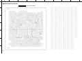
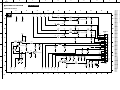
BLOCK DIAGRAM ............................................. 107~108
WIRING DIAGRAM .................................................... 109
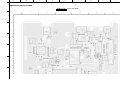
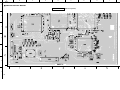
PRINTED CIRCUIT BOARD .............................. 110~143
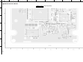
SCHEMATIC DIAGRAM .................................... 144~186
EXPLODED VIEW .............................................. 187~188
MECHANICAL PARTS LIST ..................................... 189
EXPLODED VIEW (FRONT ASS'Y) .......................... 190
MECHANICAL PARTS LIST (FRONT ASS'Y) ......... 191
MECHANICAL PARTS LIST (ACCESSORIES) ....... 191
100821
P.O.Box 1, Hamamatsu, Japan
1
DRX-1
DRX-1
■ TO SERVICE PERSONNEL
1. Critical Components Information
Components having special characteristics are marked s
and must be replaced with parts having specifications equal
to those originally installed.
WALL
OUTLET
2. Leakage Current Measurement (For 120V Models Only)
When service has been completed, it is imperative to verify
that all exposed conductive surfaces are properly insulated
from supply circuits.
●
Meter impedance should be equivalent to 1500 ohm shunted
by 0.15µF.
EQUIPMENT
UNDER TEST
AC LEAKAGE
TESTER OR
EQUIVALENT
INSULATING
TABLE
●
Leakage current must not exceed 0.5mA.
●
Be sure to test for leakage with the AC plug in both polarities.
THE DVD AUDIO/VIDEO RECEIVER SHOULD NOT BE ADJUSTED OR REPAIRED BY ANYONE EXCEPT PROPERLY
QUALIFIED SERVICE PERSONNEL.
CAUTION
1120: FOR CONTINUED PROTECTION AGAINST RISK OF FIRE, REPLACE ONLY WITH SAME TYPE 2.5A, 250V FUSE.
CAUTION
1120: REPLACE WITH SAME TYPE 2.5A, 250V FUSE.
ATTENTION
1120: UTILISER UN FUSIBLE DE RECHANGE DE MEME TYPE DE 2.5A, 250V.
WARNING: CHEMICAL CONTENT NOTICE!
The solder used in the production of this product contains LEAD. In addition, other electrical/electronic and /or plastic
(where applicable) components may also contain traces of chemicals found by the California Health and Welfare Agency
(and possibly other entities) to cause cancer and/or birth defects or other reproductive harm.
DO NOT PLACE SOLDER, ELECTRICAL/ELECTRONIC OR PLASTIC COMPONENTS IN YOUR MOUTH FOR ANY REASON WHATSOEVER!
Avoid prolonged, unprotected contact between solder and your skin! When soldering, do not inhale solder fumes or expose
eyes to solder/flux vapor!
If you come in contact with solder or components located inside the enclosure of this product, wash your hands before
handling food.
WARNING: Laser Safety
This product contains a laser beam component. This component may emit invisible, as well as visible radiation, which may
cause eye damage. To protect your eyes and skin from laser radiation, the following precautions must be used during
servicing of the unit.
1) When testing and/or repairing any component within the product, keep your eyes and skin more than 30 cm away from
the laser pick-up unit at all times. Do not stare at the laser beam at any time.
2) Do not attempt to readjust, disassemble or repair the laser pick-up, unless noted elsewhere in this manual.
3) CAUTION: Use of controls, adjustments or performance of procedures other than those specified herein may result in
hazardous radiation exposure.
Laser Emitting conditions:
1) When the Top Cover is removed and the "STANDBY/ON" SW is turned to the "ON" position, the laser component will emit
a beam for several seconds to detect if a disc is present. During this time (5 - 10 sec.) the laser may radiate through the
lens of the laser pick-up unit. Do not attempt any servicing during this period!
If no disc is detected, the laser will stop emitting the beam. When a disc is loaded, you will not be exposed to any laser
emissions.
2) The laser power level can be adjusted with the VR on the pick-up PWB. However, this level has been set by the factory prior to
shipping from the factory. Do not adjust this laser level control unless instruction is provided elsewhere in this manual.
Adjustment of this control can increase the laser emission level from the device.
2
DRX-1
DRX-1
Laser Diode Properties
Type:
Wave length:
Output Power:
(out of objective)
Beam divergence:
InGaAIP Semiconductor laser (DVD)
AlGaAs Semiconductor laser (CD)
660 nm (DVD)
780 nm (VCD/CD)
20 mW (DVD writing)
0.8 mW (DVD reading)
0.3mW (CD reading)
82 degree (DVD)
54 degree (CD)
VARO!
: AVATTAESSA JA SUOJALUKITUS OHITETTAESSA OLET ALTTIINA NÄkymÄTTÖMÄLLE LASERSÄTEILYLLE. ÄLÄ KATSO SÄTEESEEN.
VARNING!
: OSYNLIG LASERSTRÅLNING NÄR DENNA DEL ÄR ÖPPNAD OCH SPÄRREN ÄR URKOPPLAD.
BETRAKTA EJ STRÅLEN.
WARNING
The use of optical instruments with this product will increase eye hazard.
Repair handling should take place as much as possible with a disc loaded inside the player
U, A, B, G models
CLASS 1
LASER PRODUCT
A, B, G models
CAUTION :
Visible and invisible laserradiation
when open.
Avoid exposure to beam.
CAUTION :
Visible and invisible laserradiation
when open.
Avoid exposure to beam.
CLASS 1
LASER PRODUCT
WARNING LOCATION: REAR PANEL
CAUTION VISIBLE AND INVISIBLE LASER RADIATION.WHEN OPEN AVOID EXPOSURE TO BEAM
ADVARSEL SYNLIG OG USYNLIG LASERSTRÅLING VED ÅBNING UNDGÅ UDSÆTTELSE FOR STRÅLING
ADVARSEL SYNLIG OG USYNLIG LASERSTRÅLING NÅR DEKSEL ÅPNES UNNGÅ EKSPONERING FOR STRÅLEN
VARNING SYNLIG OCH OSYNLIG LASERSTRÅLNING NÄR DENNA DEL ÄR ÖPPNAD BETRAKTA EJ STRÅLEN
VARO!AVATTAESSA OLET ALTTIINA NÄKYV¨ALLE JA NÄKYMÄTTÖMÄLLE LASER SÄTEILYLLE. ÄLÄ KATSO SÄTEESEEN
VORSICHT SICHTBARE UND UNSICHTBARE LASERSTRAHLUNG WENN ABDECKUNG GEÖFFNET NICHT DEM STRAHL AUSSETSEN
DANGER VISIBLE AND INVISIBLE LASER RADIATION.WHEN OPEN AVOID DIRECT EXPOSURE TO BEAM
ATTENTION RAYONNEMENT LASER VISIBLE ET INVISIBLE EN CAS D’OUVERTURE EXPOSITION DANGEREUSE AU FAISCEAU
Warning for power supply
The primary side of the power supply carries live mains voltage when the player is connected to the mains even
when the player is switched off !
This primary area is not shielded so it is possible to touch copper tracks and/or components when servicing the player.
Service personnel have to take precautions to prevent touching this area or components in this area .
The primary side of the power supply has been indicated with a lightening stroke and a stripe-marked print on the printed
wiring board
Note:
The screws on the DVDR mechanism (position 1 in on the exploded view drawing) may never be touched, removed
or re-adjusted.
Handle the DVDR mechanism with care when the unit has to be exchanged!
The DVDR mechanism is very sensitive for dropping or giving shocks.
3
DRX-1
DRX-1
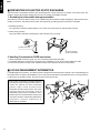
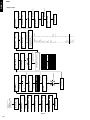
■ PREVENTION OF ELECTRO STATIC DISCHARGE
The laser diode in the DVDR mechanism may be damaged due to static electricity from clothes or the human body. Use
caution to prevent electrostatic damage when servicing or handling the DVDR mechanism.
1. Grounding for electrostatic damage prevention
Some devices, such as the DVD recorder, use an optical pickup (laser diode) that will be damaged by static electricity in the
working environment. Only attempt service after ensuring that all grounding procedures have been completed.
1. Worktable grounding
Put a grounded conductive material (sheet) or iron sheet on the area where the optical pickup is placed.
2. Human body grounding
Use an anti-static wrist strap to discharge the static electricity from your body.
Anti-static wrist strip
1M
Conductive material
(sheet) or steel sheet
2. Handling Precautions for DVDR mechanism
1. Handle the DVDR mechanism gently, as it is an extremely high-precision assembly.
2. The flexible cable lines may break if an excessive force is applied to it. Use caution when handling the cable.
3. The semi-fixed resistor for laser power adjustment should not be adjusted. Do not turn the resistor.
■ LOCALE MANAGEMENT INFORMATION
Locale Management Information : This DVD recorder is designed and manufactured to respond to the Locale Management
Information that is recorded on the DVDR disc. If the Locale number described on the DVDR disc does not correspond to the
Locale number of this DVD recorder, this DVD recorder cannot play this disc.
This product incorporates copyright protection
technology that is protected by method claims of
certain U.S. patents and other intellectual
property rights owned by Macrovision
Corporation and other rights owners. Use of this
copyright protection technology must be
authorized by Macrovision Corporation, and is
intended for home and other limited viewing uses
only unless otherwise authorized by Macrovision
Corporation. Reverse engineering or
disassembly is prohibited.
4
5
2
1
6
2
3
5
4
2
5
4
DRX-1
DRX-1
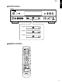
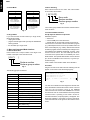
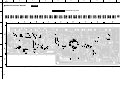
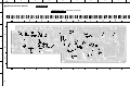
■ FRONT PANELS
U model
NATURAL SOUND DVD VIDEO RECORDER
DRX-1
STANDBY
STANDBY
/ON
REC
DV
S VIDEO
VIDEO
L
AUDIO
R
TITLE
SEARCH
REC VOLUME
AUTO/MAN
MANUAL
CHANNEL
A model
B model
G model
■ REMOTE CONTROL
MONTER
A/CH
1
2
3
4
5
6
7
8
9
+
CH
–
+
–
VOL
SELECT CLEAR
MUTE
0
TIMER
RETURN
OK
ENTER
TOP MENU
SYSTEM
MENU
EDIT
TITLE/CHAP
SUBTITLE AUDIO ANGLE ZOOM
A–B SHUFFLE SCAN
REPEAT
SKIP
PLAY
SEARCH/SLOW
PAUSE
STOP
REC
REC MODE
DIMMER
TV SHIFT
DVD RECORDER
5
DRX-1
DRX-1
■ REAR PANELS
U model
A, B, G models
■ SPECIFICATIONS
DISC FORMATS SUPPORTED
Disc type
Playback
DVD+RW
•
DVD+R
•
DVD-RW (Video format) •
DVD-R
•
DVD-Video
•
SVCD
•
Video CD
•
Audio CD
•
CD-R
•
CD-RW
•
Recording
•
•
—
—
—
—
—
—
—
—
RECORDABLE DISC FORMATS
Medium
DVD+RW: Phase-Change ReWritable
DVD+R: dye-based
Diameter
12 cm
Capacity (single side) 4.7 Gbyte
Recording time
HQ 60’ 9.72 Mbit/s
SP+ 150’ 4.06 Mbit/s
EP 240’ 2.54 Mbit/s
EP+ 360’ 1.69 Mbit/s
TV Standard
Scan Frequency
Number of lines
Playback
Recording
Internal tuner
6
A, B, G models
PAL/SECAM
50Hz
625
•
•
•
U model
NTSC
60Hz
525
•
•
•
VIDEO FORMAT
Digital Compression
MPEG2 for DVD
MPEG1 for VCD
VIDEO RESOLUTION 50Hz 60Hz
DVD-Video/
DVD+RW(HQ/SP+)
• Horiz. Resolution
720 pixels1
• Vertical Resolution 576 lines
DVD+RW (EP/EP+)
• Horiz. Resolution
360 pixels2
• Vertical Resolution 576 lines
VCD
• Horiz. Resolution
352 pixels
• Vertical Resolution 288 lines
1 equivalent to 500 lines on your TV
2 equivalent to 250 lines on your TV
720 pixels1
480 lines
360 pixels2
480 lines
352 pixels
240 lines
VIDEO PERFORMANCE
DA Converter
10-bit
AD Converter
9-bit
Signal handling
Components
Video Output
1 Vpp into 75 Ohm
S-video Output
Y: 1 Vpp into 75 Ohm
C: 0.300 Vpp into 75 Ohm
Component/Progressive out Y: 1Vpp into 75 Ohm (U model)
Pb: 0.7 Vpp into 75 Ohm (U model)
Pr: 0.7 Vpp into 75 Ohm (U model)
RGB Output
0.7 Vpp into 75 Ohm (A, B, G models)
DRX-1
• DTS
Multi-channel
• MPEG1
2-channel
Uncompressed digital (SPDIF)
• PCM
2-channel
16, 20, 24 bit
fs 48 kHz
AUDIO PERFORMANCE
DA Converter
24 bit
AD Converter
16 bit
DVD
fs 96 kHz
fs 48 kHz
Video CD
fs 44.1 kHz
Audio CD
fs 44.1 kHz
Signal-Noise (1kHz)
105 dB
Dynamic Range (1kHz) 100 dB
Crosstalk (1kHz)
110 dB
Distortion/Noise (1kHz) 90 dB
Recording
2-channel
16 bit, fs 48 kHz
—
—
—
4 Hz - 44 kHz
4 Hz - 22 kHz
4 Hz - 20 kHz
4 Hz - 20 kHz
PROGRAMMING
Number of events
6; 1 year; Daily/Weekly
Programming mode
OTR, Remote
Timer programming
Manual, the VCR Plus+ system (U model)
Manual, VIDEO Plus+, NexTView Link (B model)
Manual, SHOWVIEW, NexTView Link (G model)
Manual, G-CODE, NexTView Link (A model)
Record Control and
transmitter identification PDC, VPS (B, G models)
DRX-1
AUDIO FORMAT
Compressed digital
Playback
• Dolby Digital (AC-3) Multi-channel
CABINET
Dimensions (WxHxD) 435 x 120 x 330 (17 x 4.8 x 13 inches)
Net Weight
13.9 lb. (6.3 kg)
Front Panel
3mm Aluminum
ACCESSORIES
- Remote Control with separately-packed batteries
- 2-core power cord
- Component video cable (U nodel)
- SCART cable (A, B, G models)
- S-Video cable
- Antenna cable
- Audio cable (x 2: U model / x 1: A, B, G models)
- Video cable
- DVD+RW disc
If any item is damaged or missing, please inform your
supplier without delay.
Keep the packaging materials; you may need them to
transport your Recorder in the future.
* Specifications are subject to change without notice due
to product improvements.
U ........ U.S.A. model
B ........ British model
G ........ Europe model
A ........ Australia model
DISC RECORDING
- One-Touch Recording (OTR)
- Safe Recording
- Direct Recording (A, B, G models)
- Append
- Divide
- Erase
- Automatic/Manual Chapter Marker insertion
- Disc write lock
- Index Picture Screen
- Custom Index Pictures
- Automatic/Manual Audio Recording Level
DISC PLAYBACK
- Auto Resume (20 disc)
- Play / Stop / Pause
- Fast Forward/Backward (three speeds)
- Step Forward/Backward
- Slow (three speeds)
- Title / Track Select
- Next / Previous Title / Track / Chapter
- Repeat (Chapter / Title / All) or (Track / All)
- A-B Repeat
- Intro Scan
- Perfect Still with digital multi-tap filter
- Zoom (x1.33, x2, x4) with picture enhancement
- Pan
GENERAL FUNCTIONALITY
- 3D sound (SRS TruSurround)
- Beep Feedback for Remote Control
- Backup Presets & Timer Events: 1 year
- Backup Clock & Calendar: 7 hours
- Time & Date Download
POWER SUPPLY
Power supply
U model
100 - 120V, 60Hz
A, B, G models
220 - 240V, 50/60 Hz
Power consumption Operation
U model
36 W
A, B, G models
33 W
Low-power standby 3 W
7
DRX-1
DRX-1
VCR Plus+ and PlusCode are registered trademarks
of Gemstar Development Corporation.The VCR Plus+
system is manufactured under license from Gemstar
Development Corporation.
Pats. 5,307,173; 5,335,079; 4,908,713; 4,751,578;
and 4,706,121
Manufactured under license from Dolby Laboratories.
“Dolby,” “Pro Logic” and the double-D symbol are
trademarks of Dolby Laboratories. Confidential
Unpublished Works.
©1992-1997 Dolby Laboratories, Inc. All rights
reserved.
"DTS" and "DTS Digital Soround" are registered
trademarks of Digital Theater Systems, Inc.
DCDi is a trademark of Faroudja, a division of Sage
Inc.
This product incorporates copyright protection
technology that is protected by method claims of
certain U.S. patents and other intellectual property
rights owned by Macrovision Corporation and other
rights owners.
Use of this copyright protection technology must be
authorized by Macrovision Corporation, and is
intended for home and other limited viewing uses only
unless otherwise authorized by Macrovision
Corporation. Reverse engineering or disassembly is
prohibited.
TRUSURROUND,
, and symbol
are
trademarks of SRS Labs,Inc. TRUSURROUND
technology is manufactured under license from SRS
Labs, Inc.
G-CODE is a registered trademark of Gemstar
Development Corporation.
The G-CODE system is manufactured under license
from Gemstar Development Corporation.
8
VIDEO Plus+ and PlusCode are registered
trademarks
of the Gemstar Development Corporation.The VIDEO
Plus+ system is manufactured under license from
Gemstar Development Corporation.
SHOWVIEW is a registered trademark of Gemstar
Development Corporation.The SHOWVIEW system is
manufactured under licence from Gemstar
Development Corporation.
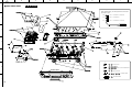
Display board 1001
⇒ Remove 8 screws 31 → 38
(board → front)
⇒ demount the board
IR/STBY Board 1001
⇒ remove screws 41+42
(board → front)
⇒ demount the board
for screws 21, 34 and 35
for screws 32
for screws 22, 31 and 33
2.7 mm
2.2 mm
1.7 mm
T10
T8
T6
mounting
↑
↓
demounting
Digital board 1001
⇒ Remove the connections
⇒ Remove 4 scrws 207 → 210
(Digital board → frame 181)
⇒ demount the board.
DVIO board 1005 (DVDR985)
⇒ Remove 2 scrws 217 and 218
(DVIO board → frame 181)
⇒ Release the snaps of 2 spacers
(DVIO board → Digital board)
⇒ demount carefully the board.
(board to board connection to
the Digital board)
FRONT AV Board 1007
⇒ remove screws 48+49
(board → front)
⇒ demount the board
Analog board 1003
⇒ remove the connections
⇒ remove 1 screw (215)
(board → frame)
⇒ remove screws 271 → 279
(cinches → backplate)
⇒ remove nut 269
(tuner → backplate)
⇒ release the snaps of 4 spacers
185 → 188 (board → frame)
⇒ demount the board
When disassembling, use the special screw driver with
tip shape in figure.
FRONT DV Board 1006 (DVDR985)
⇒ Remove scrw 17
(board → front)
⇒ demount the board
Front assy
⇒ open the tray and remove the
tray front 65
⇒ remove 4 screws 75 → 78
(front assy → frame 181)
⇒ unlock the front from the
frame by releasing
successively 6 snaps.
(1 on the left, 2 in the middle,
1 on the reight and 2 in the
bottom of the frame. The
snaps in the bottom can be
released inside the set via the
holes in the bottom.)
Cover 151
⇒ Remove 9 screws
171 → 174 at both sides
175 → 179 at the rearside
⇒ Lift the cover at the
rearside tp remove
Switched Operating Power supply 1002
⇒ Remove the connections
⇒ Remove screws 204 → 206
(board → frame)
⇒ Remove screw 268
(mains inlet → backplate)
⇒ Release the snaps of 2 spacers
186 and 184 (board → frame)
⇒ Demount the board
Front
Fr
ont Panel
Panel
Frame
⇒ Via a hole in the frame and by way of a
screwdriver, it is possible tp unlock the tray.
Push the white pin of the slider at the bottom
side of the loader to the left.
⇒ Open the unlocked tray.
In case the loader is defective and cannot
be opened electrically, you can open the
tray as follows:
Manually removal of tray front 65
DVDR LOADER 81
⇒ Remove the connections
⇒ Remove 4 screws (192 → 195)
(air filter 196 → loader 81)
⇒ Remove screw 196
(air filter inlet 191 → frame 181)
⇒ Remove air filter assy
⇒ Open the tray and remove the
tray front 65
⇒ Remove 4 screws 200 → 203
(loader 81 → frame 181)
⇒ Demount the DVDR loader
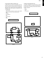
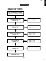
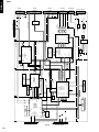
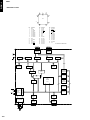
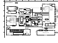
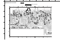
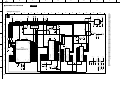
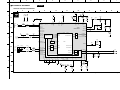
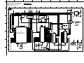
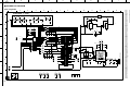
■ DISASSEMBLY PROCEDURES
DRX-1
See exploded view for item numbers
DRX-1
9
DRX-1
DRX-1
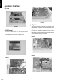
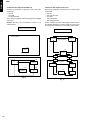
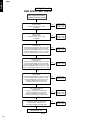
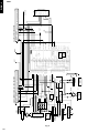
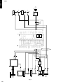
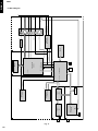
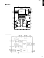
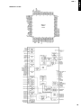
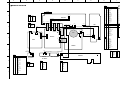
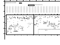
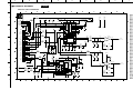
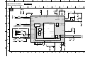
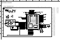
■ SERVICE POSITION
DVIO 2
● Front
Front
Photo 4
● Digital board
Photo 1
● DVIO board
To put the DVIO board in a service position, an
extender board must be used. This extender board can
be ordered with codenumber 3104 128 07770.
After demounting of DVIO board, the top side of the
digital board is in reach. To reach the bottom side of the
digital board, the DVDR module must be demounted
together with the digital board. Connected to each
other, the assembly can be set in a service position. In
this position, the bottom side of the digital board and the
servo board are in reach to be serviced.
Digital 1
DVIO Extender
Photo 5
Photo 2
Digital 2
DVIO 1
Photo 6
Photo 3
10
DRX-1
DRX-1
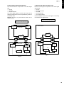
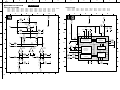
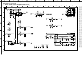
● Analog board
1.
2.
3.
4.
To put the analog board in service position, demount
the assembly of analog board and backplate as follows:
Remove 3 screws from the backplate to the frame
Remove the screw from the backplate to the mains inlet
of the power supply
Remove the screw of the analog board to the frame
Release the snaps of the 4 spacers of the analog board
to the frame.
Turn the assembly of the backplate and the analog
board against the loader.
Analog (A, B, G models)
Photo 7
Analog (U model)
Photo 8
11
DRX-1
DRX-1
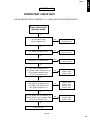
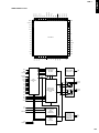
■ DIAGNOSTIC SOFTWARE
Due to the complexity of the DVD recorder, the time to find
a defect in the recorder can become long. To reduce this
time, the recorder has been equipped with Diagnostic and
Service software (DS). The DS offers functionality to
diagnose the DVDR hardware and tests the following:
•
Interconnections between components
•
Accessibility of components
•
Functionality of the audio and video paths
This functionality can be accessed via several interfaces:
1.
End user/Dealer script interface
2.
Player script interface
3.
Menu and command interface
1.2 Contents
Unplug the power cord
Hold key <PLAY> pressed
while you plug the recorder
During the test, the following display
is shown: the counter counts down
from the number of nuclei to be run
before the test finishes. Example:
SET O.K.?
NO
YES
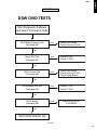
1. End User/Dealer Script Interface
1.1 Description
The End user/Dealer script interface gives a diagnosis on
a stand alone DVD recorder; no other equipment is
needed. During this mode, a number of hardware tests
(nuclei) are automatically executed to check if the recorder
is faulty. The diagnosis is simply a "fail" or "pass"
message. If the message "FAIL" appears on the display,
there is apparently a failure in the recorder. If the message
"PASS" appears, the nuclei in this mode have been
executed successfully. There can be still a failure in the
recorder because the nuclei in this mode don't cover the
complete functionality of the recorder.
Counter Nucleus Name
To exit DEALER SCRIPT, unplug the power cord
Fig. 1
The End use/Dealer script executes all diagnostic nuclei
that do not need any user interaction and are meaningful
on a standalone DVD recorder. The nuclei called in the
End user/Dealer script are the following:
Description
22
104
HostdSdramWrR
checks all memory locations of the 4MB SDRAM
21
106
HostdDramWrR
checks all the DRAM connected to the microprocessor of the digital board
20
123
HostdI2cNvram
checks the data line (SDA) and the clock line (SCL) of the I2C bus between the host
decoder and NVRAM
19
202
SAA7118I2c
checks the interface between the Host I2C controller and the AVENC SAA7118 Video
Input Processor
18
200
VideoEncI2c
checks the interface between the host I2C controller and Empress SAA6752
17
207
AudioEncI2c
checks the I2C connection between the host decoder and Empress SAA6752
16
204
AudioEncAccess
tests the HIO8 interface lines between the host decoder and the audio encoder
15
203
AudioEncSramAccess
checks the access of the SRAM by the audio encoder (address and data lines).
14
205
AudioEncSramWrR
tests the SRAM connected to the audio encoder
13
206
AudioEncInterrupt
tests the interrupt line between the host decoder and the audio encoder
12
300
VsmAccess
checks whether the VSM interrupt controllers and DRAM are accessible
11
303
VsmInterrupt
checks both interrupt lines between the VSM and the host decoder
10
302
VsmSdramWrR
tests the entire SDRAM of the VSM
9
1400
Clock11_289MHz
switches the A_CLK of the micro clock to 11.2896 MHz
8
1401
Clock12_288MHz
switches the A_CLK of the micro clock to 12.288 MHz
7
601
BeS2Bengine
checks the S2B interface with the Basic Engine by sending an echo command
6
500
DisplayEcho
checks the interface between the host processor and the slave processor on the
display board
5
700
AnalogueEcho
checks the interface between the host processor and the microprocessor on the
analogue board
4
12
711
AnalogueNvram
checks the NVRAM on the analogue board
DRX-1
DRX-1
3
706
AnalogueTuner
checks whether the tuner on the analogue board is accessible
2
901
LoopAudioUserDealer
This nucleus tests the components on the audio signal path The host decoder
- The analogue board
- The audio encoder
- The VSM
On the analogue board the audio is internally looped back to the digital board
1
906
LoopVideoUserDealer
Nucleus for testing the components on the video signal system path:
- The VIP
- The video encoder
- The VSM
- The host decoder
- The analogue board
On the analogue the video signal is internally routed back to the digital board.•5.2
Player Script Interface
2. Player Script Interface
2.1 Description
The Player script will give the opportunity to perform a test
that will determine which of the DVD recorder's modules
are faulty, to read the error log and to perform an
endurance loop test. To successfully perform the tests, the
DVD recorder must be connected to a TV set.
To be able to check results of certain nuclei, the player
script expects some interaction of the user (i.e. to approve
a test picture or a test sound). Some nuclei (e.g. nuclei
that test functionality of the DVDR module) require that a
DVD+RW disc is inserted.
Only tests within the scope of the diagnostic software will
be executed hence only faults within this scope can be
detected.
2.2 Structure of the Player Script
The player script consists of a set of nuclei testing the
hardware modules in the DVD recorder: the Display PWB,
the Digital PWB, the Analogue In/Out PWB and the DVDR
module.
Nuclei run by the player test need some user interaction;
in the next table this interaction is described. The player
test is done in two phases:
• Interactive tests: this part of the player test depends
strongly on user interaction and input to determine
nucleus results and to progress through the full test.
Reading the error log information can be useful to
determine any errors that occurred recently during
normal operation of the DVD player.
• The loop test will perform the same nuclei as the dealer
test, but it will loop through the list of nuclei indefinitely.
STEP DESCRIPTION
NUCLEUS
1
Press OPEN/CLOSE and PLAY at the same time and POWER ON the recorder to start the playerscript
2
2
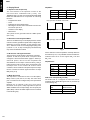
The local display shows FPSEGMENTS. Press PLAY to start the test.
502
First the starburst pattern is lit, then the horizontal segments are lit, followed by the vertical segments and
the last test is light all segments test. After each of the 4 tests the user has to confirm that the correct
pattern was lit.
Press PLAY to confirm that the correct pattern was lit (four times if the FPSEGMENTS test was
successful).
Press RECORD to indicate that the correct pattern was not successfully lit.
Press STOP to skip this nucleus.
3
The local display shows FPLABELS. Press PLAY to start the test.
Press PLAY to confirm that all labels are lit.
Press RECORD to indicate that not all labels are lit.
Press STOP to skip this nucleus.
503
4
The local display shows FPLIGHT ALL. Press PLAY to start the test.
Press PLAY to confirm that everything was lit.
Press RECORD to indicate that not all patterns are lit.
Press STOP to skip this nucleus.
520
13
DRX-1
DRX-1
14
STEP DESCRIPTION
NUCLEUS
5
The local display shows FPLED. Press PLAY to start the test.
Press PLAY to confirm that the led is lit.
Press RECORD to indicate that the led is not lit.
Press STOP to skip this nucleus.
504
6
The local display shows FPFLAP OPEN. Press PLAY to start the test.
Press PLAY to confirm that the flap has opened.
Press RECORD to indicate that the flap did not open.
Press STOP to skip this nucleus.
522
7
The local display shows FPKEYBOARD. Press PLAY to start the test.
505
Attention all keys have to be pressed to get a positive result!
Press PLAY for more than one second to confirm that all the keys were pressed and shown on the local
dis-play.
If not all the keys were pressed, a FAIL message will appear on the local display.
Press RECORD for more than one second to indicate that not all keys were pressed and shown on the
local display.
Press STOP for more than one second to skip this nucleus.
8
The local display shows FPREMOTE CONTROL. Press PLAY to start the test.
506
Press PLAY to confirm that a key on the remote control was pressed and shown on the local display. Only
one key has to be pressed to get a successful result.
Press RECORD to indicate that the key on the remote control was pressed but not shown on the local
display.
Press STOP to skip this nucleus.
9
The local display shows FPDIMMER. Press PLAY to start the test.
Press PLAY to confirm that the text on the local display was dimmed.
Press RECORD to indicate that the text on the local display was not dimmed.
Press STOP to skip this nucleus.
518
10
The local display shows FPBEEPER. Press PLAY to start the test.
Press PLAY to confirm that the beeper on the front panel sounded.
Press RECORD to indicate that the beeper on the front panel did not sound.
Press STOP to skip this nucleus.
514
11
The local display shows FPFLAP CLOSE. Press PLAY to start the test.
Press STOP to skip this nucleus.
523
12
The local display shows ROUTE VIDEO. Press PLAY to start the test.
Press STOP to skip this nucleus.
712
13
The local display shows ROUTE AUDIO. Press PLAY to start the test.
Press STOP to skip this nucleus.
713
14
The local display shows COLOUR-BAR ON. Press PLAY to start the test.
Press STOP to skip this nucleus.
120
15
The local display shows PINK NOISE ON. Press PLAY to start the test.
Press STOP to skip this nucleus.
115
16
The local display shows PINK NOISE OFF. Press PLAY to start the test.
Press STOP to skip this nucleus.
116
17
The local display shows SINE ON. Press PLAY to start the test.
Press STOP to stop the sine.
Press STOP to skip this nucleus.
117
18
The local display shows COLOUR-BAR OFF. Press PLAY to start the test.
Press STOP to skip this nucleus.
121
19
The local display shows BERESET. Press PLAY to start the test.
Press STOP to skip this nucleus.
603
20
The local display shows BETRAY OPEN. Press PLAY to start the test.
Press STOP to skip this nucleus.
616
21
The local display shows BETRAY CLOSE. Press PLAY to start the test.
Press STOP to skip this nucleus.
615
DRX-1
NUCLEUS
22
The local display shows BEWRITE READ. Press PLAY to start the test.
Press STOP to skip this nucleus.
617
23
The local display shows BETRAY OPEN. Press PLAY to start the test.
Press STOP to skip this nucleus.
616
24
The local display shows BETRAY CLOSE. Press PLAY to start the test.
Press STOP to skip this nucleus.
615
25
The local display shows READ ERRORLOG. Press PLAY to start the test.
Press STOP to skip this nucleus.
If the player test succeeded, the user/dealer script will start in an endless loop.
If the player test failed, the local display will display FAIL and the error code
633
DRX-1
STEP DESCRIPTION
Remark
In case of failure, the display shows " FAIL XXXXXX ". The
description of the shown error code can be retrieved in the
survey of Nuclei Error Codes (paragraph 5.4). Once an
error occurs, it is not possible to continue the player script.
Unplug the set and restart the player script. By pressing
the STOP key, it is possible to jump over the failure and to
continue the player script.
15
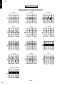
Fig. 2
PRESS <PLAY> IF OK
PRESS <STOP> TO ABORT
PRESS <PLAY> IF OK
PRESS <STOP> TO ABORT
PRESS <PLAY> IF OK
PRESS <STOP> TO ABORT
PRESS <STOP>
TO SKIP TEST
PRESS <PLAY> IF OK
PRESS <RECORD> IF NOT OK
PRESS <PLAY>
TO START TEST
CHAPTER
PCM
EP+
MPEG
CHAPTER
HQ SP L:P
-30
-20
DD DIGITAL DTS
SAVCD
-10
PCM
EP+
0
TOTAL
OVER
MANUAL
MONITOR
TOTAL
MANUAL
MONITOR
DIGITAL
TIMER
REMAIN
SAT
AM
NICAM
PM
CHANNEL
STEREO
RECORD
VPS/PDC
SAP
DECODER
-30
DIGITAL
AM
PM
-20
NICAM
TIMER
REMAIN
SAT
CHANNEL
-10
0
STEREO
RECORD
VPS/PDC
OVER
SAP
DECODER
LED BECOMES RED
PRESS <STOP>
TO SKIP TEST
PRESS <PLAY> IF OK
PRESS <RECORD> IF NOT OK
-40
TRACK TIME
PRESS <STOP>
TO SKIP TEST
PRESS <PLAY> IF OK
PRESS <RECORD> IF NOT OK
TRACK TIME
PRESS <STOP>
TO SKIP TEST
PRESS <PLAY> IF OK
PRESS <RECORD> IF NOT OK
PRESS <PLAY>
TO START TEST
-40
DVD
PROLOGIC
TRACK
RW
TITLE
PRESS <PLAY>
TO START TEST
DTS
HQ SP L:P
DD DIGITAL
SAVCD
MPEG
DVD
PROLOGIC
TRACK
RW
TITLE
PRESS <PLAY>
TO START TEST
I
FRONTPANEL TEST
PRESS ALL KEYS AT LEAST ONCE
SEE TABLE FOR KEY CODES
XX TIMES
PRESSED
PRESS <STOP>
TO SKIP TEST
PRESS <STOP>
TO SKIP TEST
MANUAL UP
MANUAL DOWN
CHANNEL UP
CHANNEL DOWN
AUTOMAN
REC VOLUME
STANDBY/ON
OPEN/CLOSE
STOP
PLAY
RECORD
FRONT KEY NAME
00B
00C
009
00A
008
007
005
006
00D
00E
001
002
003
004
FRONT KEY CODE
PRESS <PLAY> MORE THAN 1S IF TEST IS OK
PRESS <RECORD> MORE THAN 1S IF TEST IS NOT OK
HEXADECIMAL
KEY CODE
PRESS <PLAY>
TO START TEST
PRESS <PLAY>
TO START TEST
PRESS <STOP>
TO SKIP TEST
PRESS AT LEAST ONE KEY
ON THE REMOTE CONTROL
SEE TABLE FOR RC KEY CODES
XX TIMES
PRESSED
EE
ONLY FOR TV
ONLY FOR TV
1E
1F
ONLY FOR TV
01
02
03
04
05
06
07
08
09
00
C8
EE
F7
85
4B
4E
13
1D
3B
2A
1C
94
MONITOR
ON/OFF
STOP
REC/OTR
PLAY
REVERSE
PAUSE
FORWARD
PREVIOUS
EDIT
NEXT
DISC
SYSTEM
UP
LEFT
RIGHT
DOWN
RETURN
OK
CLEAR
TIMER
SELECT
VOL +
VOL CH +
CH MUTE
1
2
3
4
5
6
7
8
9
0
T/C
A/CH
ZOOM
ANGLE
SUBTITLE
AUDIO
DIM
REPEAT
REPEAT A-B
SCAN
SHUFFLE
REC MODE
0C
31
37
2C
29
30
28
21
CF
20
54
0F
58
5A
5B
59
83
5C
41
FE
FA
RC KEY CODE
RC KEY NAME
TO EXIT TEST: PRESS ONE OF FOLLOWING KEYS
ON THE LOCAL KEYBOARD
PRESS <PLAY> IF TEST IS OK
PRESS <RECORD> IF TEST IS NOT OK
HEXADECIMAL
RC KEY CODE
PRESS <PLAY>
TO START TEST
PRESS <PLAY> IF OK
PRESS <RECORD> IF NOT OK
BEEP IS AUDIBLE
PRESS <PLAY> IF OK
PRESS <RECORD> IF NOT OK
PRESS <STOP>
TO SKIP TEST
DIGITAL BOARD TEST
PRESS <PLAY>
TO START TEST
PRESS <PLAY>
TO START TEST
Player script
II
Hold 2 keys
<OPEN/CLOSE> + <PLAY>
simultaneously pressed while
you plug the recorder
I
16
II
Unplug the power cord
DRX-1
DRX-1
DRX-1
DRX-1
FRONTPANEL
TEST
DIGITAL BOARD &
ANALOG BOARD
TEST
BASIC ENGINE
TEST
press <PLAY> to execute
press < STOP > to skip
press <PLAY> to execute
press <NEXT > to skip
press <PLAY> to execute
press < STOP > to skip
press <PLAY> to execute
press <STOP> to skip
INSERT DVD +RW DISC TO EXECUTE
WRITE / READ TEST
press <PLAY> to execute
press < STOP > to skip
press <PLAY> to execute
press <STOP> to skip
press <PLAY> to execute
press < STOP > to skip
press <PLAY> to execute
press <NEXT > to skip
press <PLAY> to execute
press <NEXT > to skip
press <PLAY> to execute
press <STOP> to skip
press <PLAY> to execute
press < STOP > to skip
press <PLAY> to execute
press <STOP> to skip
press <STOP> to continue
<PLAY>
IF ERROR
press <STOP> to skip
press <PLAY> to execute
IF NO ERROR
PRESS <STOP>
TO STEP DOWN
NO ERRORS LOGGED
PRESS <STOP>
TO STEP DOWN
PRESS <RECORD>
TO STEP UP
PRESS <RECORD>
TO STEP UP
PRESS <PLAY> TO CONTINUE
IF ERROR
To exit PLAYER SCRIPT, unplug the power cord
Fig. 3
2.3 Error Log
Explanation:
The application errors will be logged in the NVRAM. The
maximum number of error bytes that will be visible is 19.
The last reported error is shown as DN D0000000, the
oldest visible error as D0000000 UP and the errors in
between as DN D0000000 UP. DN stands for DOWN, UP
stands for UPWARDS. The shown
D error codes are identical to the Nuclei Error Codes
(paragraph 4).
17
DRX-1
DRX-1
2.4 Trade Mode
IF TRADE MODE OFF
IF TRADE MODE ON
UNPLUG THE RECORDER
UNPLUG THE RECORDER
PRESS 2 KEYS
SIMULTANEOUSLY
3.2 Error Handling
Each nucleus returns an error code. This code contains
six numerals, which means:
[ XX YY ZZ ]
Error code
Nucleus number
Nucleus group number
PRESS 2 KEYS
SIMULTANEOUSLY
<STOP> + <OPEN/CLOSE>
<STOP> + <OPEN/CLOSE>
PLUG THE RECORDER
PLUG THE RECORDER
RECORDER IS IN TRADE MODE
WHEN PRESSING FRONT
KEYS, THE RECORDER
DOESN'T RESPOND
RECORDER IS IN NORMAL MODE
WHEN PRESSING FRONT
KEYS, THE RECORDER
WILL RESPOND
Fig. 6
The nucleus group numbers and nucleus numbers are the
same as above.
Fig. 4
2.5 Virgin Mode
If you want that the recorder starts up in Virgin mode,
follow this procedure:
• Unplug the recorder
• plug the recorder again while you keep the STAND BY/
ON key pressed
• the set starts up in Virgin mode.
3. Menu and Command Mode Interface
3.1 Nuclei Numeration
Each nucleus has a unique number of four digits. This
number is the input of the command mode.
[ XX YY
]
Nucleus number
Nucleus group number
Fig. 5
The following groups are defined:
18
Group number
Group name
0
Basic / S cripts
1
Host decoder (Sti5508 and memory)
2
Audio / video encoder (DVDR only)
3
VSM (DVDR only)
4
NVRAM
5
Front Panel
6
Basic Engine
7
Analogue board (DVDR only)
8
DVIO (DVDR only)
9
Loop nuclei (DVDR only)
10
Library sub nuclei (I2C nuclei)
11
User interface
12
Furore (SACD only)
13
DAC (SACD only)
14
Miscellaneous
3.3 Command Mode Interface
Set-Up Physical Interface Components
Hardware required:
• Service PC
• one free COM port on the Service PC
• special cable to connect DVD recorder to Service PC
The service PC must have a terminal emulation program
(e.g. OS2 WarpTerminal or Procomm) installed and must
have a free COM port (e.g. COM1). Activate the terminal
emulation program and check that the port settings for the
free COM port are: 19200 bps, 8 data bits, no parity, 1 stop
bit and no flow control. The free COM port must be
connected via a special cable to the RS232 port of the
DVD recorder. This special cable will also connect the test
pin, which is available on the connector, to ground (i.e.
activate test pin).
Code number of PC interface cable: 3122 785 90017
Activation
Plug the recorder to the mains and the following text will
appear on the screen of the terminal (program):
DVD Video Recorder Diagnostic Software version 84
Basic SDRAM Data bus test passed
Basic SDRAM Address bus test passed
Basic SDRAM Device test passed
(M) enu,
DD:>
(C) ommand or (S) 2B-interface?
[M] : @ C
Fig. 7
The first line indicates that the Diagnostic software has
been activated and contains the version number. The next
lines are the successful result of the SDRAM
interconnection test and the basic SDRAM test. The last
line allows the user to choose between the three possible
interface forms. If pressing C has made a choice for
Command Interface, the prompt ("DD>") will appear. The
diagnostic software is now ready to receive commands.
The commands that can be given are the numbers of the
nuclei.
DRX-1
Host Decoder [01]
[xxyy]
Nuclei
Number
100
Checksum Flash
101
Flash Write Access 1
102
Flash Write Access 2
103
Flash Write Read
104
SdRam Write Read
105
SdRam Write Read Fast
106
Dram Write Read
107
Dram Write Read Fast
108
Hardware Version
109
Mute On
110
Mute Off
115
Pink Noise On
116
Pink Noise Off
117
Sine On
118
Sine Burst 1kHz
119
Sine Burst 12kHz
120
Colour-bar On
121
Colour-bar Off
122
NvramWrR
123
NvramI2c
130
Boot Version
131
Application Version
132
Diagnostics Version
133
Download Version
134
Write / read I2C message to / from digital board
135
Video Test Signal On
136
Video Test Signal Off
137
Macrovision Off
Audio Video Decoder [02]
[xxyy]
Nuclei
Number
200
Video Encoder I2C
202
SAA7118 I2C
203
Audio Encoder SRAM Access
204
Audio Encoder Access
205
Audio Encoder SRAM Write Read
206
Audio Encoder Interrupts
207
Audio Encoder I2C
208
SAA7118 select input
209
Empress Version
DRX-1
Command Overview
We provide an overview of the nuclei and their numbers.
This overview is preliminary and subject to modifications.
VSM [03]
[xxyy]
Nuclei
Number
300
Register Access
301
SDRAM Access
302
SDRAM Write Read
303
Interrupt lines
304
VSM Interconnection
305
UART
NVRAM [04]
[xxyy]
Nuclei
Number
400
Reset
401
Read
402
Modify
403
UniqueNr Read
404
Read Error Log
407
Reset Error Log
409
Line2 Region-Code Reset
410
UniqueNr Store
Front Panel [05]
[xxyy]
Nuclei
Number
500
Echo
501
Version
502
Segment
503
Label
504
Led
505
Keyboard
506
Remote-Control
507
Segment Starburst
508
Segment Vertical
509
Segment Horizontal
514
Beeper
515
Discbar
516
Discbar Dots
517
Vu / Grid
518
Dimmer
519
Blinking
520
Light All Segments
522
Flap Open
523
Flap Close
19
DRX-1
DRX-1
Basic Engine [06]
[xxyy]
[xxyy]
Number
Nuclei
Number
718
Download Version
600
S2B Pass
720
Bargraph Level Adjustment
601
S2B Echo
721
Clock correction
602
Version
722
Clock reference
603
Reset
723
Re-virginise Recorder
604
Focus On
724
Flash Checksum
605
Focus Off
725
Tuner frequency selection
606
Disc Motor On
727
Set virgin bit
607
Disc Motor Off
728
Clear Virgin Bit
608
Radial On
729
Write / read I2C message to / from analogue board
609
Radial Off
730
Store external presets
615
Tray In
731
Get slash version
616
Tray Out
732
AFC Reference Voltage Tuner
617
Write Read
618
Write Read Endless Loop
DVIO [08]
619
Selftest
[xxyy]
620
BE Test
Number
621
Laser Test
800
Check DVIO board presence
622
Spindle (Disc) Motor Test
801
Reset DVIO
623
Focus Test
802
DVIO Access
624
Sledge Motor Test
803
Get DVIO error codes
625
Sledge Motor Slow
804
Get DVIO module Ids
626
Tilt
805
Execute DVIO module SelfTest
627
EEPROM Read
806
Set DVIO led on.
628
EEPROM Write
807
Set DVIO led off.
629
Optimise Jitter
630
Radial ATLS Calibration
Loop Nuclei [09]
631
Get Statistics Information
[xxyy]
632
Reset Statistics Information
Number
Nuclei
Nuclei
900
Digital Audio Loop
Analog Board [07]
901
User / Dealer Audio Loop
[xxyy]
902
Digital Video Loop
Nuclei
Number
20
Nuclei
903
Digital Video VBI Loop
700
Echo
904
System Video Loop
703
Boot Version
905
System Video VBI Loop
704
Hardware Version
906
User / Dealer Video Loop
705
Clock Adjust
907
User / Dealer Video VBI Loop
706
Tuner
908
System Audio Loop SCART
707
Frequency Download
909
System Audio Loop CINCH
708
Data Slicer
910
Digital DVIO Video Loop
709
Sound Processor
911
System Video Vip
710
AV Selector
711
Nvram
712
Route Video
713
Route Audio
715
Set Slash Version
716
Application Version
717
Diagnostics Version
DRX-1
[xxyy]
Nuclei
Number
1400
Clock 11.289 MHz
1401
Clock 12.288 MHz
1412
Progressive Scan I2C
1413
Progressive Scan test image on
1414
Progressive Scan test image off
1415
Progressive Scan Route Enable
1416
Progressive Scan Route Disable
Scripts [00]
[xxyy]
Nuclei
Number
1 Us
erDealer Script
2 Pl
ayer Script
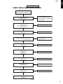
3.4 Menu Mode Interface
Activation
Plug the recorder to the mains and the following text will
appear on the screen of the terminal (program):
DVD Video Recorder Diagnostic Software version 84
Basic SDRAM Data bus test passed
Basic SDRAM Address bus test passed
Basic SDRAM Device test passed
(M) enu,
(C) ommand or (S) 2B-interface?
[M] : @ m
Main Menu
1.
2.
3.
4.
5.
6.
7.
8.
9.
Digital Board
Analog Board
Front Panel
Basic Engine
DVIO
Progressive Scan Board
Loop tests
Log
Scripts
DRX-1
Menu Structure
The following menu structure is given after starting up the
DVD recorder in menu mode. The symbol -> indicates that
the current menu choice will invoke the display of a
submenu.
Miscellanious [14]
->
->
->
->
->
->
->
->
->
Select>
Fig. 8
The first line indicates that the Diagnostic software has
been activated and contains the version number. The next
lines are the successful result of the SDRAM
interconnection test and the basic SDRAM test. The last
line allows the user to choose between the three possible
interface forms. If pressing M has made a choice for Menu
Interface, the Main Menu will appear.
Main Menu
1.Digital Board
2.Analogue Board
3.Front Panel
4.Basic Engine
5.DVIO
6.Progressive Scan Board
7.Loop Tests
8.Log
9.Scripts
->
->
->
->
->
->
->
->
->
Digital Board Menu
1.Host Decoder
2.VSM
3.AVENC
4.NVRAM
->
->
->
->
Host Decoder Menu
1.Flash Checksum
2.Flash1 Write Access
3.Flash2 Write Access
4.Flash Write/Read
5.Host SDRAM Write/Read
6.Host SDRAM Fast Write/Read
7.Host DRAM Write/Read
8.Host DRAM Fast Write/Read
9.I2C NVRAM
10.NVRAM Write/Read
11.Engine S2B Echo
12.Versions
13.Audio Mute
14.Colourbar
15.Pink Noise
16.Sine Generate
->
->
->
->
->
Digital Board Versions Menu
1.Hardware Version
2.Bootcode version
3.Applications Version
4.Diagnostics Version
5.Download Version
Audio Mute Menu
1.Audio Mute On
2.Audio Mute Off
Colourbar Menu
1.Colourbar On
2.Colourbar Off
Pink Noise Menu
1.Pink Noise On
2.Pink Noise Off
21
DRX-1
DRX-1
Sine Generate Menu
1.Sine On
2.Sine Burst 1kHz
3.Sine Burst 12kHz
VSM Menu
1.Register Access
2.SDRAM Access
3.VSM SDRAM Write/Read
4.Interrupt Lines
5.VSM Interconnection
6.UART
AVENC Menu
1.Empress
2.Video Input Processors
->
->
Empress Menu
1.Version number
Video Input Processors Menu
1.SAA7118 I2C Access
NVRAM Menu
1.Read Error Log
2.Reset Error Log
3.Read DVIO Unique ID
Analogue Board Menu
1.Echo
2.Obsolete
3.Route Video Input back to Digital board
4.Route Audio Input back to Digital board
5.Flash Checksum
6.Versions
->
7.Components
->
8.Re-virginize Recorder
->
Analogue Board Versions Menu
1.Hardware Version
2.Bootcode version
3.Application version
4.Diagnostics version
5.Download version
Analogue Components Menu
1.Tuner
2.Data Slicer
3.Sound Processor
4.AV Selector
5.NVRAM
Analogue Board Re-virginize Menu
1.Re-virginize Recorder
2.Set Virgin-bit
3.Clear Virgin-bit
4.Store external presets
22
Front Panel Menu
1.Echo
2.Version
3.Flap Control ->
4.Segment Test ->
5.Light Labels
6.Led test
7.Keyboard test
8.Remote Control
9.Beep
10.Disc Bar
11.Disc Bar Dots
12.Vu Grid
13.Dimmer
14.Blink
15.Light All Segments
Flap Control Menu
1.Open Flap
2.Close Flap
Segment Test Menu
1.Starburst
2.Light Horizontal Segments
3.Light Vertical Segments
4.Light All Segments
Basic Engine Menu
1.Reset
2.S2B Pass-through
3.S2B Echo
4.Focus On
5.Focus Off
6.Version
7.Self Test
8.Get Self Test Result
9.Basic Engine Test
10.Laser Test
11.Focus Test
12.Tilt Test
13.Optimise Jitter
14.Statistics Info
15.Log
16.Spindle Motor
17.Radial
18.Sledge
19.Tray
Basic Engine Error Log
1.Read Error Log
2.Reset Error Log
Basic Engine Spindle Motor Menu
1.Spindle Motor On
2.Spindle Motor Off
3.Spindle Motor Test
->
->
->
->
->
DRX-1
DRX-1
Basic Engine Radial Menu
1.Radial On
2.Radial Off
3.Radial Initialisation
4.Radial ATLS Calibration
Script Menu
1.User/Dealer Script
2.Player Script
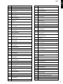
4. Nuclei Error Codes
In the following table the error codes will be described.
Basic Engine Sledge Menu
1.Sledge test
2.Sledge test slow
Basic Engine Tray Menu
1.Tray In
2.Tray Out
DVIO Menu
1.Check Presence
2.Reset
3.Access
4.Error Codes
5.Module Identifiers
6.Led
->
DVIO Led Menu
1.Led On
2.Led Off
Progressive Scan Board Menu
1.I2C Access
2.Test Image On
3.Test Image Off
Loop Tests Menu
1.Digital Board Loops
2.User/Dealer Loops
3.System Loops
4.Basic Engine Loops
->
->
->
->
Digital Board Loops Menu
1.Obsolete
2.Digital Video Loop
3.Digital Video Loop VBI
User/Dealer Loops Menu
1.User/Dealer Audio Loop
2.User/Dealer Video Loop
3.User/Dealer Video Loop VBI
System Loops Menu
1.System Video Loop
2.System Video Loop VBI
3.System Audio Loop SCART(EURO)
4.System Audio Loop CINCH (NAFTA)
Basic Engine Loops Menu
1.Basic Engine write read
2.Basic Engine write read endless loop
Log Menu
1.Read Error Log
2.Reset Error Log
Error
Nr Error String
10000
“Checksum is OK”
10001
“segment name Checksum doesn’t match”” or
“”seg-ment name segment not found”
10100
“”
10101
“FLASH 1 Write access test failed”
10200
“”
10201
“FLASH 2 Write access test failed”
10300
“”
10301
“FLASH write test failed”
10302
“FLASH write command failed”
10303
“FLASH write test done max. number of times”
10400
“”
10401
“HostDec SDRAM Memory data bus test goes
wrong.”
10402
“ HostDec SDRAM Memory address bus test
goes wrong.”
10403
“ HostDec SDRAM Physical memory device
test goes wrong.”
10500
“”
10501
“ HostDec SDRAM Memory data bus test
goes wrong.”
10502
“ HostDec SDRAM Memory address bus test
goes wrong.”
10503
“ HostDec SDRAM Physical memory device
test goes wrong.”
10600
“”
10601
“HostDec DRAM Memory data bus test goes
wrong.”
10602
“HostDec DRAM Memory address bus test
goes wrong.”
10603
“HostDec DRAM Physical memory device test
goes wrong.”
10700
“”
10701
“HostDec DRAM Memory data bus test goes
wrong.”
10702
“HostDec DRAM Memory address bus test
goes wrong.”
10703
“HostDec DRAM Physical memory device test
goes wrong.”
10800
“Host Decoder version(cut) number: version
number””Digital hardware version”
10801
“Can not find version in FLASH.”
10900
“”
10901
“Error muting audio”
11000
“”
11001
“Error demuting audio”
23
DRX-1
DRX-1
24
Error
Nr Error String
Error
Nr Error String
11500
“”
13700
“”
11501
“Init of I2C failed”
13701
“Turning off MacroVision failed”
11502
“The selection of the clock source failed”
20000
“”
11504
“The demute of the audio failed”
20001
“I2C bus busy before start”
11600
“”
20002
“Video Encoder access time-out”
11601
“Init of I2C failed”
20003
“No acknowledge from Video Encoder”
11602
“The mute of the audio failed”
20004
11700
“”
“No data send/received to or from Video
Encoder”
11701
“Init of I2C failed”
20005
“SAA7118 VIP can not be initialised”
11702
“The muting of the audio failed”
20200
“”
11703
“The demute of the audio failed”
20201
“I2C bus busy before start”
11704
“The selection of the clock source failed”
20202
“SAA7118 VIP access time-out”
11707
“Setup of Front panel failed”
20203
“No acknowledge from SAA7118 VIP”
11708
“Sine on Front panel keyboard failed”
20204
“No data received from SAA7118 VIP”
11800
“”
20300
“”
11801
“Init of I2C failed”
20301
11802
“The muting of the audio failed”
“Error audio encoder SRAM access cannot
initial-ise I2C”
11803
“The demute of the audio failed”
20302
“Error audio encoder SRAM access cannot
reset DSP through I2C”
20303
“Error audio encoder SRAM access cannot
down-load boot”
20304
“Error audio encoder cannot download test
code”
20305
“Error audio encoder cannot obtain result of
test”
20306
“Error audio encoder SRAM access stuck-atzero data line “
20307
“Error audio encoder SRAM access stuck-atone data line “
20308
“Error audio encoder SRAM access stuck-atone address line “
20309
“Error audio encoder SRAM access address
line address line x is connected to data line
data line y”
20310
“Error audio encoder SRAM access address
lines address line x and address line y are
connected “
20311
“Error audio encoder SRAM access data lines
data line x and data line y are connected “
20312
“Error audio encoder SRAM access illegal
data re-ceived”
11804
“The selection of the clock source failed”
11805
“Error cannot start VSM audio in port”
11900
“”
11901
“Init of I2C failed”
11902
“The muting of the audio failed”
11903
“The demute of the audio failed”
11904
“The selection of the clock source failed”
11905
“Error cannot start VSM audio in port”
12000
“”
12001
“Invalid input”
12100
“”
12200
“”
12201
“I2C bus busy before start”
12202
“NVRAM access time-out”
12203
“No NVRAM acknowledge”
12204
“NVRAM time-out”
12205
“NVRAM Write/Read back failed”
12300
“”
12301
“I2C bus busy before start”
12302
“NVRAM read access time-out”
12303
“No NVRAM read acknowledge”
20400
“”
12304
“NVRAM read failed”
20401
13000
“Bootcode application version : bootversion”
“Error audio encoder access cannot initialise
I2C”
13001
“Can not find version in FLASH.”
20402
13100
“Recorder application
recorderversion”
“Error audio encoder access cannot reset
DSP through I2C”
20403
“Error audio encoder accessing ICR register”
20404
“Error audio encoder access stuck-at-zero of
data line “
20405
“Error audio encoder access stuck-at-one of
data line “
20406
“Audio encoder access data lines data line x
and data line y are interconnected “
version
:
13101
“Can not find version in FLASH.”
13200
“Diagnostics application version : diagversion”
13201
“Can not find version in FLASH.”
13300
“Download application
downloadversion”
13301
“Can not find version in FLASH.”
version
:
DRX-1
Nr Error String
Error
Nr Error String
“”
20902
“I2C bus busy before start”
20501
“Error audio encoder SRAM WRR cannot
initialise I2C”
20903
“EMPRESS access time-out”
20904
“No acknowledge from the EMPRESS”
“Error audio encoder SRAM WRR cannot
reset DSP through I2C”
20905
“No data send to the EMPRESS”
“Error audio encoder WRR cannot download
boot”
20906
“No data received from the EMPRESS”
30000
“”
30001
“VSM SDRAM Bank1 Memory databus test
goes wrong.”
30002
“VSM SDRAM Bank1 Memory addressbus
test goes wrong.”
30003
“VSM SDRAM Bank1 Physical memory
device test goes wrong.”
30004
“ VSM SDRAM Bank2 Memory databus test
goes wrong.”
30005
“ VSM SDRAM Bank2 Memory addressbus
test goes wrong.”
30006
“ VSM SDRAM Bank2 Physical memory
device test goes wrong.”
30007
“VSM SDRAM Bank1 VSM interrupt register A
has a -stuck at- error for value:”
20502
20503
20504
“Error audio encoder cannot download test
code”
20505
“Error audio encoder SRAM WRR cannot
obtain result of test”
20506
“Error audio encoder WRR SRAM stuck-atzero data bit “
20507
“Error audio encoder WRR SRAM stuck-atone data bit “
20508
“Error audio encoder WRR SRAM data lines
data line x and data line y are connected”
20509
“Error audio encoder WRR SRAM illegal data
re-ceived”
20600
“”
20601
“Error audio encoder interrupt cannot initialise
I2C”
30008
20602
“Error audio encoder interrupt cannot reset
DSP through I2C”
“VSM SDRAM Bank2 VSM interrupt register A
has a -stuck at- error for value:”
30100
“”
30101
“VSM SDRAM Bank1 Memory databus test
goes wrong.”
30102
“VSM SDRAM Bank1 Memory addressbus
test goes wrong.”
30103
“VSM SDRAM Bank1 Physical memory
device test goes wrong.”
20603
“Error audio encoder cannot download test
code”
20604
“Error occurred accessing VSM”
20605
“Audio encoder interrupt not received”
20606
“Error occurred while activating the encoder”
20607
“Error audio encoder interrupt cannot initialise
em-press”
30104
“ VSM SDRAM Bank2 Memory databus test
goes wrong.”
20608
“Error occurred while getting interrupt reason”
30105
20700
“”
“ VSM SDRAM Bank2 Memory addressbus
test goes wrong.”
20701
“Error audio encoder I2C cannot reset DSP
through I2C”
30106
“ VSM SDRAM Bank2 Physical memory
device test goes wrong.”
20702
“Error audio encoder cannot download boot”
30200
“”
20703
“Error audio encoder cannot download TEST
code”
30201
“VSM SDRAM Bank1 Memory databus test
goes wrong.”
20704
“Error audio encoder I2C bus busy”
30202
20705
“Error audio encoder I2C cannot write slave
ad-dress”
“VSM SDRAM Bank1 Memory addressbus
test goes wrong.”
30203
20706
“Error audio encoder I2C no acknowledge received”
“VSM SDRAM Bank1 Physical memory
device test goes wrong.”
30204
20707
“Error audio encoder I2C cannot send/receive
da-ta”
“ VSM SDRAM Bank2 Memory databus test
goes wrong.”
30205
20708
“Error audio encoder received data through
I2C was invalid”
“ VSM SDRAM Bank2 Memory addressbus
test goes wrong.”
30206
“ VSM SDRAM Bank2 Physical memory
device test goes wrong.”
20800
“”
20801
“I2C access failed.”
30300
“”
20802
“SAA7118 VIP can not be initialised.”
30301
20803
“Invalid input”
“VSM interrupt register A has a -stuck at- error
for value:”
20900
“B1.B2. B3.B4. B5.B6. B7.B8. B9.B10.
B11.B12.”
30302
“VSM interrupt register B has a -stuck at- error
for value:”
20901
“Firmware download of EMPRESS failed”
30303
“Interrupt A wasn’t raised.”
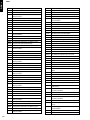
DRX-1
Error
20500
25
DRX-1
DRX-1
Error
Nr Error String
Error
Nr Error String
30304
“Interrupt B wasn’t raised.”
50103
30305
“Interrupts A and B were raised.”
“The frontpanel could not be accessed by the
ana-logue board.”
30400
“”
50200
“”
30401
“VSM SDRAM Bank1 Memory databus test
goes wrong.”
50204
“Execution of the command on the analogue
board failed.”
30402
“VSM SDRAM Bank1 Memory addressbus
test goes wrong.”
50205
“The frontpanel could not be accessed by the
ana-logue board.”
30403
“VSM SDRAM Bank1 Physical memory
device test goes wrong.”
50206
“The frontpanel did not show a starburst.”
50207
“The user skipped the FP-which pattern test.”
30404
“ VSM SDRAM Bank2 Memory databus test
goes wrong.”
50208
“The user returned an unknown confirmation:
con-firmation”
30405
“ VSM SDRAM Bank2 Memory addressbus
test goes wrong.”
50209
“The frontpanel did not show horizontal
segments.”
30406
“ VSM SDRAM Bank2 Physical memory
device test goes wrong.”
50210
“The frontpanel did not show vertical
segments.”
30500
“”
50300
“”
30501
“Communication with the analogue board
fails.”
50304
“Execution of the command on the analogue
board failed.”
30502
“Echo test to analogue board returned wrong
string.”
50305
“The frontpanel could not be accessed by the
ana-logue board.”
40000
“”
50306
“The frontpanel did not light all labels.”
40001
“NVRAM Reset; I2C failed”
50307
40100
“NVRAM address = 0xaddress -> Byte value =
0xvalue”
“The user skipped the rest of the FP-label
test.”
50308
40101
“NVRAM Read; I2C failed”
“The user returned an unknown confirmation:
con-firmation”
40102
“NVRAM Read; Invalid input”
50400
“”
40200
“”
50404
40201
“NVRAM Modify; I2C failed”
“Execution of the command on the analogue
board failed.”
40202
“NVRAM Modify; Invalid input”
50405
“The frontpanel could not be accessed by the
ana-logue board.”
40300
“DV Unique ID = id”
50406
“The LED’s could not be turned on.”
40301
“NVRAM Read DV Unique ID; I2C failed”
50407
40400
“\r\n Error log:\r\n errorString \r\n “
“The user skipped the rest of the FP-LED
test.”
40401
“NVRAM error log; I2C failed”
50408
40402
“NVRAM error log is invalid”
“The user returned an unknown confirmation:
con-firmation”
40403
“Front panel failed”
50500
“”
40700
“”
50502
“Front panel Keyboard; test failed”
“NVRAM error log reset; I2C failed”
50503
“Front panel Keyboard; test aborted”
50504
“Front panel Keyboard; not all keys were
pressed”
40701
40900
“Region code Change counter is reset”
40901
“NVRAM region code reset; I2C failed”
41000
“”
50505
“Front panel keyboard I2C connection failed”
41001
“NVRAM Store DV Unique ID; I2C failed”
50506
“Unable to get slashversion”
41002
“NVRAM Store DV Unique ID; Invalid input”
50600
“”
50000
“”
50602
“Front panel Remote control; test failed”
“Execution of the command on the analogue
board failed.”
50603
“Front panel Remote control; test aborted”
50604
50008
“The frontpanel could not be accessed by the
ana-logue board.”
“Front panel remote control; can not access
FP”
50605
50009
“The echo from the frontpanel processor was
not correct.”
“Front panel remote control; no user input received”
50700
“”
50100
“ Front panel version: FPversion “
50701
50102
“Execution of the command on the analogue
board failed.”
“Execution of the command on the analogue
board failed.”
50702
“The frontpanel could not be accessed by the
ana-logue board.”
50007
26
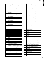
DRX-1
Nr Error String
Error
Nr Error String
“The frontpanel did not show a starburst.”
51701
50704
“The user skipped the FP-starburst test.”
“Execution of the command on the analogue
board failed.”
50705
“The user returned an unknown confirmation:
con-firmation”
51702
“The frontpanel could not be accessed by the
ana-logue board.”
50800
“”
51703
“The VU grid did not display properly.”
50801
“Execution of the command on the analogue
board failed.”
51704
“The user skipped the VU gridtest.”
51705
50802
“The frontpanel could not be accessed by the
ana-logue board.”
“The user returned an unknown confirmation:
con-firmation”
51800
“”
50803
“The frontpanel did not show vertical
segments.”
51801
“Execution of the command on the analogue
board failed.”
50804
“The user skipped the FP-vertical segments
test.”
51802
“The frontpanel could not be accessed by the
ana-logue board.”
50805
“The user returned an unknown confirmation:
con-firmation”
51803
“The frontpanel could not be dimmed.”
51804
“The user skipped the FP-Dim test.”
50900
“”
51805
50901
“Execution of the command on the analogue
board failed.”
“The user returned an unknown confirmation:
con-firmation”
51900
“”
50902
“The frontpanel could not be accessed by the
ana-logue board.”
51901
“Execution of the command on the analogue
board failed.”
50903
“The frontpanel did not show horizontal
segments.”
51902
“The frontpanel could not be accessed by the
ana-logue board.”
50904
“The user skipped the FP-horizontal
segments test.”
51903
“The frontpanel did not show segments
blinking.”
50905
“The user returned an unknown confirmation:
con-firmation”
51904
“The user skipped the FP-blinking test.”
51400
“”
51905
“The user returned an unknown confirmation:
con-firmation”
51401
“Execution of the command on the analogue
board failed.”
52000
“”
52001
“Execution of the command on the analogue
board failed.”
52002
“The frontpanel could not be accessed by the
ana-logue board.”
51402
“The frontpanel could not be accessed by the
ana-logue board.”
51403
“The beeper did not sound.”
51404
“The user skipped the FP-Beep test.”
52003
“The frontpanel did not show all segments lit.”
51405
“The user returned an unknown confirmation:
con-firmation”
52004
“The user skipped the FP-light all segments
test.”
51500
“”
52005
51501
“Execution of the command on the analogue
board failed.”
“The user returned an unknown confirmation:
con-firmation”
52200
“”
51502
“The frontpanel could not be accessed by the
ana-logue board.”
52201
“Communication with Analogue Board fails.”
52202
“Frontpanel can not be accessed by the
Analogue Board.”
51503
“The discbar did not display properly.”
51504
“The user skipped the discbar test.”
52300
“”
51505
“The user returned an unknown confirmation:
con-firmation”
52301
“Communication with Analogue Board fails.”
51600
“”
52302
“Frontpanel can not be accessed by the
Analogue Board.”
51601
“Execution of the command on the analogue
board failed.”
60000
“”
51602
“The frontpanel could not be accessed by the
ana-logue board.”
60100
“”
60101
51603
“The discbar dots did not display properly.”
“Basic Engine returned error number
0xerrornumber”
51604
“The user skipped the discbar dots test.”
51605
“The user returned an unknown confirmation:
con-firmation”
51700
“”
60102
“Parity error from Basic Engine to Serial”
60103
“Communication time-out error”
60104
“Unexpected response from Basic Engine”
60105
“Echo loop could not be closed”
DRX-1
Error
50703
27
DRX-1
DRX-1
Error
Nr Error String
Error
Nr Error String
60106
“Wrong echo pattern received”
61502
“Parity error from Basic Engine to Serial”
60200
“Version: nr1.nr2.nr3”
61503
“Communication time-out error”
60201
“Basic Engine returned error number
0xerrornumber”
61504
“Unexpected response from Basic Engine”
61600
“”
60202
“Parity error from Basic Engine to Serial”
61601
60203
“Communication time-out error”
“Basic Engine returned error number
0xerrornumber”
60204
“Unexpected response from Basic Engine”
61602
“Parity error from Basic Engine to Serial”
60205
“Front Panel failed.”
61603
“Communication time-out error”
60300
“”
61604
“Unexpected response from Basic Engine”
60301
“Basic-Engine time-out error”
61700
“”
60400
“”
61701
“BE tray-in command failed”
60401
“Basic Engine returned error number
0xerrornumber”
61702
“BE read-TOC command failed”
61703
“BE VSM interrupt initialisation failed”
60402
“Parity error from Basic Engine to Serial”
61704
“BE set irq command failed”
60403
“Communication time-out error”
61705
“BE no disc or wrong disc inserted”
60404
“Unexpected response from Basic Engine”
61706
“BE rec-pause command failed”
60405
“Focus loop could not be closed”
61707
“BE VSM BE out DMA initialisation failed”
60500
“”
61708
“BE VSM BE out initialisation failed”
60501
“Basic Engine returned error number
0xerrornumber”
61709
“BE VSM BE out DMA start failed”
61710
“BE VSM BE out start failed”
60502
“Parity error from Basic Engine to Serial”
60503
“Communication time-out error”
60504
“Unexpected response from Basic Engine”
60600
“”
60601
“Basic Engine returned error number
0xerrornumber”
60602
“Parity error from Basic Engine to Serial”
60603
“Communication time-out error”
60604
“Unexpected response from Basic Engine”
60700
“”
60701
“Basic Engine returned error number
0xerrornumber”
60702
“Parity error from Basic Engine to Serial”
60703
“Communication time-out error”
60704
“Unexpected response from Basic Engine”
60800
“”
60801
28
“Basic Engine returned error number
0xerrornumber”
60802
“Parity error from Basic Engine to Serial”
60803
“Communication time-out error”
60804
“Unexpected response from Basic Engine”
60805
“Radial loop could not be closed”
60900
“”
60901
“Basic Engine returned error number
0xerrornumber”
60902
“Parity error from Basic Engine to Serial”
60903
“Communication time-out error”
60904
“Unexpected response from Basic Engine”
61500
“”
61501
“Basic Engine returned error number
0xerrornumber”
61711
“BE rec command failed”
61712
“BE VSM out underrun error occurred”
61713
“BE record complete interrupt not raised”
61714
“BE get irq command failed”
61715
“BE no interrupt was raised by BE”
61716
“BE VSM DMA out not finished”
61717
“BE stop command after writing failed”
61718
“BE VSM Sector processor initialisation failed”
61719
“BE VSM sector processor DMA initialisation
failed”
61720
“BE VSM sector processor DMA start failed”
61721
“BE VSM sector processor start failed”
61722
“BE seek command failed”
61723
“BE VSM sector processor error occurred”
61724
“BE read timeout occurred”
61725
“BE stop command after reading failed”
61726
“BE difference found in data at disc sector
0xdiscsector”
61727
“This nucleus cannot be executed because
the Self-Test failed”
61800
“”
61801
“BE i2c initialisation failed”
61802
“This nucleus cannot be executed because
the Self-Test failed”
61900
“”
61901
“The SelfTest failed with result: 0xnr1 0xnr2
0xnr3”
61902
“Basic Engine returned error number
0xerrornumber”
61903
“Parity error from Basic Engine to Serial”
61904
“Communication time-out error”
DRX-1
Nr Error String
Error
Nr Error String
61905
“Unexpected response from Basic Engine”
62900
“”
62000
“”
62901
62001
“Self-Test : errorstring1 Laser-Test :
errorstring2 SpindleM-Test: errorstring3
Sledg-eM-Test : errorstring4 Focus-Test :
errorstring5”
“Basic Engine returned error number
0xerrornumber”
62100
“The forward sense level is 0xlevel”
62101
“Basic Engine returned error number
0xerrornumber”
62902
“Parity error from Basic Engine to Serial”
62903
“Communication time-out error”
62904
“Unexpected response from Basic Engine”
62905
“Radial loop could not be closed”
63000
“”
63001
“Basic Engine returned error number
0xerrornumber”
62102
“Parity error from Basic Engine to Serial”
62103
“Communication time-out error”
62104
“Unexpected response from Basic Engine”
62200
“”
62201
“The BE-self-diagnostic-spindle-motor-test
failed”
62202
“Basic Engine returned error number
0xerrornumber”
62203
“Parity error from Basic Engine to Serial”
62204
“Communication time-out error”
62205
“Unexpected response from Basic Engine”
63102
“Parity error from Basic Engine to Serial”
62300
“”
63103
“Communication time-out error”
62301
“The BE-focus-test failed”
63104
“Unexpected response from Basic Engine”
62302
“Basic Engine returned error number
0xerrornumber”
63200
“”
63201
62303
“Parity error from Basic Engine to Serial”
“Basic Engine returned error number
0xerrornumber”
63002
“Parity error from Basic Engine to Serial”
63003
“Communication time-out error”
63004
“Unexpected response from Basic Engine”
63100
“ Number of times Tray went Open/Closed :
nr1”” Total hours the CD laser was on : nr2"”
Total hours the DVD laser was on : nr3"” Total
hours the write laser was on : nr4"
63101
“Basic Engine returned error number
0xerrornumber”
62304
“Communication time-out error”
63202
“Parity error from Basic Engine to Serial”
62305
“Unexpected response from Basic Engine”
63203
“Communication time-out error”
62400
“”
63204
“Unexpected response from Basic Engine”
62401
“The BE-self-diagnostic-sledge-motor-test
failed”
63300
62402
“Basic Engine returned error number
0xerrornumber”
62403
“Parity error from Basic Engine to Serial”
Momentary errors (Byte 1 - Byte 7) : 0xb1
0xb2 0xb3 0xb4 0xb5 0xb6 0xb7 Cumulative
errors (Byte 1 - Byte 7): : 0xb1 0xb2 0xb3 0xb4
0xb5 0xb6 0xb7 Fatal errors (Oldest Youngest) : : 0xb1 0xb2 0xb3 0xb4 0xb5
62404
“Communication time-out error”
63301
“Basic Engine returned error number
0xerrornumber”
62405
“Unexpected response from Basic Engine”
62500
“”
62600
“”
62700
“BE EEPROM address = address -> Byte
value = 0xvalue”
62701
“Basic Engine returned error number
0xerrornumber”
62702
“Parity error from Basic Engine to Serial”
62703
“Communication time-out error”
62704
“Unexpected response from Basic Engine”
62705
“BE read EEPROM; invalid input”
62800
“”
62801
“Basic Engine returned error number
0xerrornumber”
62802
“Parity error from Basic Engine to Serial”
62803
“Communication time-out error”
62804
“Unexpected response from Basic Engine”
62805
“BE write EEPROM; invalid input”
63302
“Parity error from Basic Engine to Serial”
63303
“Communication time-out error”
63304
“Unexpected response from Basic Engine”
63400
“”
63401
“Basic Engine returned error number
0xerrornumber”
63402
“Parity error from Basic Engine to Serial”
63403
“Communication time-out error”
63404
“Unexpected response from Basic Engine”
63500
“”
63501
“Basic Engine returned error number
0xerrornumber”
63502
“Parity error from Basic Engine to Serial”
63503
“Communication time-out error”
63504
“Unexpected response from Basic Engine”
63505
“errorstring _the basic engine will reject all
player commands”
63900
“”
DRX-1
Error
29
DRX-1
DRX-1
30
Error
Nr Error String
Error
Nr Error String
63901
“Basic Engine returned error number
0xerrornumber”
64201
“BE i2c initialisation failed”
64202
63902
“Parity error from Basic Engine to Serial”
“This nucleus cannot be executed because
the Self-Test failed”
63903
“Communication time-out error”
70000
“Echo test OK”
63904
“Unexpected response from Basic Engine”
70001
“Echo test returned wrong string.”
64000
“BE OPU number = opunumber”
70002
“Communication with Analogue Board fails”
64001
“Basic Engine returned error number
0xerrornumber”
70300
“SoftwareVersion”
70301
64002
“Parity error from Basic Engine to Serial”
“Can not find segment in FLASH ROM on the
Ana-logue Board”
64003
“Communication time-out error”
70302
“Communication with Analogue Board fails”
64004
“Unexpected response from Basic Engine”
70400
“HardwareVersion”
64100
“The data was successfully written on and
read from a DVD disc”
70401
“Can not find segment in FLASH ROM on the
Ana-logue Board”
64101
“The tray-in command failed”
70402
“Communication with Analogue Board fails”
64102
“The read-TOC command failed”
70500
“Clock adjusted OK”
64103
“The VSM interrupt initialisation failed”
70501
“Can not adjust the clock on the Analogue
Board.”
70502
“Wrong date/time text size.”
64104
“The set irq command failed”
64105
“No disc or wrong disc inserted”
64106
“The rec-pause command failed”
70503
“Communication with Analogue Board fails”
64107
“The VSM BE out DMA initialisation failed”
70600
“Tuner accessibility test OK”
64108
“The VSM BE out initialisation failed”
70601
64109
“The VSM BE out DMA start failed”
“Can not access tuner on the Analogue
Board.”
64110
“The VSM BE out start failed”
64111
“The rec command failed”
64112
“The VSM out underrun error occurred”
64113
“The record complete interrupt was not raised”
64114
“The get irq command failed”
64115
“There was no interrupt raised by BE”
64116
70602
“Communication with Analogue Board fails”
70700
“Frequency download OK”
70701
“Wrong frequency table size.”
70702
“Can not download the frequency table into
the an-alogue NVRAM.”
70703
“Can not download the frequency table into
the an-alogue NVRAM.”
“The VSM DMA did not finished”
70704
“Communication with Analogue Board fails”
64117
“The stop command after writing failed”
70800
“Data slicer test OK”
64118
“The VSM Sector processor initialisation
failed”
70801
“Test of the Data slicer on the Analogue Board
fails.”
64119
“The VSM sector processor DMA initialisation
failed”
70802
“Communication with Analogue Board fails”
70900
“Sound Processor test OK”
70901
“Test of the Sound Processor on the Analogue
Board fails.”
64120
“The VSM sector processor DMA start failed”
64121
“The VSM sector processor start failed”
64122
“The seek command failed”
70902
“Communication with Analogue Board fails”
64123
“The VSM sector processor error occurred”
71000
“AV Selector test OK”
64124
“The read timeout occurred”
71001
64125
“The stop command after reading failed”
“Test of the AV Selector on the Analogue
Board fails.”
64126
“There was a difference found in data at a
specific disc sector”
71002
“Communication with Analogue Board fails”
71100
“NVRAM test OK”
64127
“The result of the self test contains errors”
71101
64128
“An error interrupt was raised by BE”
“Test of the NVRAM on the Analogue Board
fails.”
64129
“The calibrate-record command failed”
71102
“Communication with Analogue Board fails”
64130
“To many retries”
71200
“Video routing on the Analogue Board OK”
64131
“BE update RAI command after writing failed”
71201
64132
“BE find first recordable address command
failed”
“Routing the video on the Analogue Board
fails.”
71202
“Invalid input.”
64133
“DVD+R disc is full”
71203
“Communication with Analogue Board fails”
64200
“”
71300
“Audio routing on the Analogue Board OK”
DRX-1
DRX-1
Error
Nr Error String
Error
Nr Error String
71301
“Routing the audio on the Analogue Board
fails.”
73002
“Communication with Analogue Board fails”
73100
71302
“Invalid input.”
“0xslashversion”” where slashversion is the
slash version read from the analogue board”
71303
“Communication with Analogue Board fails”
73101
“Error while reading out slash version.”
71500
“”
73102
“I2C Write error.”
71501
“Invalid slash version, default slash version is
set.”
73103
“I2C Read error.”
73104
“Communication with Analogue Board fails”
“Setting the slash version on the Analogue
Board fails.”
73200
“”
73201
“Storing the Reference Voltage for the Tuner
failed”
“Invalid input.”
71502
71503
“Communication with Analogue Board fails”
71600
“ApplicationVersion”
73202
71601
“Can not find segment in FLASH ROM on the
Ana-logue Board”
73203
“Communication with Analogue Board fails”
80000
“The DVIO module is present in the system.”
80001
“The DVIO module is not present in the
system.”
80100
“The DVIO module has been reset OK.”
80101
“The DVIO module is not present in the
system.”
71602
“Communication with Analogue Board fails”
71700
“DiagnosticsVersion”
71701
“Can not find segment in FLASH ROM on the
Ana-logue Board”
71702
“Communication with Analogue Board fails”
71800
“DownloadVersion”
80102
“The DVIO module could not be reset.”
71801
“Can not find segment in FLASH ROM on the
Ana-logue Board”
80103
“Could not initialise I2C before Reset.”
71802
“Communication with Analogue Board fails”
80200
“The accessibility of the DVIO module is OK.”
72300
“”
80201
“The DVIO board is not present in this DVDR.”
72000
“”
72001
“Adjusting BarGraphLevel failed”
72002
“Communication with Analogue Board fails”
72100
“”
72101
“Storing clock correction failed”
72102
“Value out of range : default value stored “
72103
“Invalid input.”
72104
“Communication with Analogue Board fails”
72200
“”
72201
“Initialising the 1Hz signal on the Clock IC
failed”
72202
“Communication with Analogue Board fails”
72301
“Clearing the NVRAM on the Analogue Board
fails”
72302
“Communication with Analogue Board fails”
72400
“segment checksum is : checksum which is
cor-rect”” for every segment”
72401
“segment could not be found”” or “”segment
check-sum is : checksumC ,however it should
be : check-sumE”” for every segment”
80202
“Could not initialise I2C.”
80203
“Unable to reset the DVIO module.”
80204
“Unable to receive the reset indication from
the DVIO module.”
80205
“Unable to send the configuration to the DVIO
module.”
80206
“Unable to download the chip ID to the DVIO
mod-ule.”
80207
“Unable to set the mode of the DVIO module
to IDLE.”
80208
“Software Error in
HandleStateAwaitin-gReply!!”
80209
“Maximal number of retries reached by
HandleS-tateSending!!”
80210
“Maximal number of retries (NACKs) reached
(HandleStateSending)”
80211
“We tried to receive a reply for
DVIO_MAX_RETRIES_ACKREPLY times !!”
80212
“We tried to receive a reply for
DVIO_MAX_RETRIES_REPLY times !!”
80213
“We tried to receive an Ack for
DVIO_MAX_RETRIES_ACK times!!”
80214
“VSM UART error timeout transmitting
command”
function
72402
“Communication with Analogue Board fails”
72900
“Date received”
72901
“Data returned”
80215
“VSM UART error timeout receiving reply”
72902
“Communication on I2C-bus failed on the
Ana-logue Board fails.”
80216
“VSM UART frame error occurred receiving
from DVIO board”
80217
“VSM UART parity error occurred receiving
from DVIO board”
80218
“The confirmation/indication from the DVIO
module is invalid.”
72903
“Communication with Analogue Board fails”
73000
“”
73001
“Storing the external presets on the Analogue
Board fails”
31
DRX-1
DRX-1
32
Error
Nr Error String
Error
Nr Error String
80300
“The accessibility of the DVIO module is OK.”
80412
80301
“The DVIO board is not present in this DVDR.”
“We tried to receive a reply for
DVIO_MAX_RETRIES_REPLY times !!”
80302
“Could not initialise I2C.”
80413
80303
“Unable to reset the DVIO module.”
“We tried to receive an Ack for
DVIO_MAX_RETRIES_ACK times!!”
80304
“Unable to receive the reset indication from
the DVIO module.”
80414
“VSM UART error timeout transmitting
command”
80305
“Unable to send the configuration to the DVIO
module.”
80415
“VSM UART error timeout receiving reply”
80416
80306
“Unable to download the chip ID to the DVIO
mod-ule.”
“VSM UART frame error occurred receiving
from DVIO board”
80417
80307
“Unable to set the mode of the DVIO module
to IDLE.”
“VSM UART parity error occurred receiving
from DVIO board”
80418
80308
“Software Error in
HandleStateAwaitin-gReply!!”
“The confirmation/indication from the DVIO
module is invalid.”
80500
“”
80309
“Maximal number of retries reached by
HandleS-tateSending!!”
80501
“The DVIO board is not present in this DVDR.”
80502
“The I2C could not be initialised.”
80310
“Maximal number of retries (NACKs) reached
(HandleStateSending)”
80503
“The DVIO module could not be reset.”
80504
80311
“We tried to receive a reply for
DVIO_MAX_RETRIES_ACKREPLY times !!”
“Unable to receive the reset indication from
the DVIO module.”
80505
80312
“We tried to receive a reply for
DVIO_MAX_RETRIES_REPLY times !!”
“Unable to send the configuration to the DVIO
module.”
80506
80313
“We tried to receive an Ack for
DVIO_MAX_RETRIES_ACK times!!”
“Unable to download the chip ID to the DVIO
mod-ule.”
80507
80314
“VSM UART error timeout transmitting
command”
“Unable to set the mode of the DVIO module
to IDLE.”
80508
80315
“VSM UART error timeout receiving reply”
“Software Error in HandleStateAwaitingReply
func-tion!”
80316
“VSM UART frame error occurred receiving
from DVIO board”
80509
“Maximal number of retries reached by
HandleS-tateSending!”
80317
“VSM UART parity error occurred receiving
from DVIO board”
80510
“Maximal number of retries (NACK’s) reached
“”(HandleStateSending)”
80318
“The confirmation/indication from the DVIO
module is invalid.”
80511
“We tried to receive a reply for
DVIO_MAX_RETRIES_ACKREPLY times!”
80512
“We tried to receive a reply for
DVIO_MAX_RETRIES_REPLY times!”
80513
“We tried to receive an Acknowledge for
DVIO_MAX_RETRIES_ACK times!”
80514
“VSM UART error timeout transmitting
command”
80515
“VSM UART error timeout receiving reply”
80516
“VSM UART frame error occurred receiving
from DVIO board”
function
80400
“The accessibility of the DVIO module is OK.”
80401
“The DVIO board is not present in this DVDR.”
80402
“Could not initialise I2C.”
80403
“Unable to reset the DVIO module.”
80404
“Unable to receive the reset indication from
the DVIO module.”
80405
“Unable to send the configuration to the DVIO
module.”
80406
“Unable to download the chip ID to the DVIO
mod-ule.”
80517
80407
“Unable to set the mode of the DVIO module
to IDLE.”
“VSM UART parity error occurred receiving
from DVIO board”
80518
80408
“Software Error in
HandleStateAwaitin-gReply!!”
“The confirmation/indication from the DVIO
module is invalid.”
80519
80409
“Maximal number of retries reached by
HandleS-tateSending!!”
“Setting the DVIO module in/out diagnostics
mode failed”
function
80520
“Invalid input”
“Getting the errors of the self-test failed”
80410
“Maximal number of retries (NACKs) reached
(HandleStateSending)”
80521
80522
“Self-test failed”
80411
“We tried to receive a reply for
DVIO_MAX_RETRIES_ACKREPLY times !!”
80600
“”
80601
“The DVIO board is not present in this DVDR.”
80602
“The I2C could not be initialised.”
DRX-1
Nr Error String
Error
Nr Error String
“The DVIO module could not be reset.”
80713
80604
“Unable to receive the reset indication from
the DVIO module.”
“We tried to receive an Acknowledge for
DVIO_MAX_RETRIES_ACK times!”
80714
80605
“Unable to send the configuration to the DVIO
module.”
“VSM UART error timeout transmitting
command”
80715
“VSM UART error timeout receiving reply”
80606
“Unable to download the chip ID to the DVIO
mod-ule.”
80716
“VSM UART frame error occurred receiving
from DVIO board”
80607
“Unable to set the mode of the DVIO module
to IDLE.”
80717
“VSM UART parity error occurred receiving
from DVIO board”
80608
“Software Error in HandleStateAwaitingReply
func-tion!”
80718
“The confirmation/indication from the DVIO
module is invalid.”
80609
“Maximal number of retries reached by
HandleS-tateSending!”
80719
“Setting the DVIO module in/out diagnostics
mode failed”
80610
“Maximal number of retries (NACK’s) reached
“”(HandleStateSending)”
90121
“Error: audio data in host memory contains
wrong frequency: frequency Hz”
80611
“We tried to receive a reply for
DVIO_MAX_RETRIES_ACKREPLY times!”
90122
“Error: audio data in host memory contains silence!”
80612
“We tried to receive a reply for
DVIO_MAX_RETRIES_REPLY times!”
90123
“There is no correct audio frame in the buffer”
90124
“The audio frame has an illegal version bit”
80613
“We tried to receive an Acknowledge for
DVIO_MAX_RETRIES_ACK times!”
90125
“The audio frame has an illegal bitrate-index”
80614
“VSM UART error timeout transmitting
command”
90126
“The audio frame has an illegal sampling rate”
90127
“The CRC of the audio frame is wrong”
80615
“VSM UART error timeout receiving reply”
80616
“VSM UART frame error occurred receiving
from DVIO board”
80617
“VSM UART parity error occurred receiving
from DVIO board”
90128
“The audio frame is not MPEG-I layer II !”
90129
“Error cannot de-mute DAC on analogue
board”
90200
“”
90201
“Initialisation of I2C failed”
“Initialisation of VIP and EMPIRE failed”
80618
“The confirmation/indication from the DVIO
module is invalid.”
90202
90203
“Initialisation of PLL / Link failed.”
80619
“Setting the DVIO module in/out diagnostics
mode failed”
90204
“Next descriptor address set wrong.”
90205
“Turning on the colourbar failed”
80700
“”
90206
80701
“The DVIO board is not present in this DVDR.”
“No I2C communication possible to start video
en-coder.”
80702
“The I2C could not be initialised.”
90207
“Starting the video encoder failed.”
80703
“The DVIO module could not be reset.”
90208
80704
“Unable to receive the reset indication from
the DVIO module.”
“Transfer of data from video encoder to VSM
failed.”
90209
“Stopping the encoder failed.”
“Unable to send the configuration to the DVIO
module.”
90210
“Turning off the colourbar failed.”
90211
“Cannot intialize hostdecoder parallel input”
“Unable to download the chip ID to the DVIO
mod-ule.”
90212
“Cannot initialise VSM AV-out DMA port”
80707
“Unable to set the mode of the DVIO module
to IDLE.”
90213
“Cannot initialise VSM AV-out port”
90214
“Cannot start VSM AV-out DMA port”
80708
“Software Error in HandleStateAwaitingReply
func-tion!”
90215
“Cannot start VSM AV-out port”
90216
“Maximal number of retries reached by
HandleS-tateSending!”
“Transfer of data from VSM to host decoder
failed.”
90217
“Maximal number of retries (NACK’s) reached
“”(HandleStateSending)”
“VSM and Hostdec memory do not match
(com-pared after transfer)”
90218
“We tried to receive a reply for
DVIO_MAX_RETRIES_ACKREPLY times!”
“Decoding of the video data in the
hostdecoder memory failed”
90219
“We tried to receive a reply for
DVIO_MAX_RETRIES_REPLY times!”
“The data in the hostdecoder is not equal to a
col-ourbar”
90220
“The video encoder did not return the Group
Of Picture count.”
80705
80706
80709
80710
80711
80712
DRX-1
Error
80603
33
DRX-1
DRX-1
Error
Nr Error String
Error
Nr Error String
90221
“The video encoder did not receive data from
the VIP.”
90420
“The video encoder did not return the Group
Of Picture count.”
90223
“Initialisation of VIP and EMPRESS failed”
90421
90224
“The video encoder did not return the current
sta-tus.”
“The video encoder did not receive data from
the VIP.”
90422
90225
“The video encoder timed out in BUSY mode.
(no VIP input)”
“Execution of the command on the analogue
board failed.”
90423
“Initialisation of VIP and EMPRESS failed”
90226
“The video encoder did not return the current
bi-trate.”
90424
“The video encoder did not return the current
sta-tus.”
90227
“The video encoder did not switch to
ENCODING mode.”
90425
“The video encoder timed out in BUSY mode.
(no VIP input)”
90228
“The video encoder could not start from
STOP/ IDLE mode.”
90426
“The video encoder did not return the current
bi-trate.”
90229
“The video encoder did not switch from IDLE
to STOP mode.”
90427
“The video encoder did not switch to
ENCODING mode.”
90300
“”
90428
90301
“Initialisation of I2C failed”
“The video encoder could not start from
STOP/IDLE mode.”
90302
“I2C communication to VIP failed”
90429
“The video encoder did not switch from IDLE
to STOP mode.”
90500
“”
90501
“Initialisation of I2C failed”
90303
“Initialisation of VIP failed”
90304
“Generation of Close Caption data failed”
90305
“VIP not locked to video signal”
90306
“Initialisation of VBI Extractor failed”
90307
“No CC data received”
90308
“Closed Caption data overrun”
90309
“Closed Caption data does not match”
90310
“Switch off ColourBar failed”
90400
“”
90401
“Initialisation of I2C failed”
90402
“Initialisation of VIP and EMPIRE failed”
90403
“Initialisation of PLL / Link failed.”
90404
“Next descriptor address set wrong.”
90405
“Turning on the colourbar failed”
90406
“No I2C communication possible to start video
en-coder.”
“I2C communication to VIP failed”
“Initialisation of VIP failed”
90504
“Generation of Close Caption data failed”
90505
“VIP not locked to video signal”
90506
“Initialisation of VBI Extractor failed”
90507
“No CC data received”
90508
“Closed Caption data overrun”
90509
“Closed Caption data does not match”
90510
“Switch off ColourBar failed”
90511
“Execution of the command on the analogue
board failed.”
90600
“”
90601
“Initialisation of I2C failed”
90602
“Initialisation of VIP and EMPIRE failed”
90603
“Initialisation of PLL / Link failed.”
90407
“Starting the video encoder failed.”
90408
“Transfer of data from video encoder to VSM
failed.”
90604
“Next descriptor address set wrong.”
90409
“Stopping the encoder failed.”
90605
“Turning on the colourbar failed”
90410
“Turning off the colourbar failed.”
90606
90411
“Cannot intialize hostdecoder parallel input”
“No I2C communication possible to start video
en-coder.”
90412
“Cannot initialise VSM AV-out DMA port”
90607
“Starting the video encoder failed.”
90413
“Cannot initialise VSM AV-out port”
90608
“Transfer of data from video encoder to VSM
failed.”
90414
“Cannot start VSM AV-out DMA port”
90415
“Cannot start VSM AV-out port”
90416
“Transfer of data from VSM to host decoder
failed.”
90417
90418
90419
34
90502
90503
“VSM and Hostdec memory do not match
(com-pared after transfer)”
“Decoding of the video data in the
hostdecoder memory failed”
“The data in the hostdecoder is not equal to a
col-ourbar”
90609
“Stopping the encoder failed.”
90610
“Turning off the colourbar failed.”
90611
“Cannot intialize hostdecoder parallel input”
90612
“Cannot initialise VSM AV-out DMA port”
90613
“Cannot initialise VSM AV-out port”
90614
“Cannot start VSM AV-out DMA port”
90615
“Cannot start VSM AV-out port”
90616
“Transfer of data from VSM to host decoder
failed.”
DRX-1
Nr Error String
Error
Nr Error String
90617
“VSM and Hostdec memory do not match
(com-pared after transfer)”
90812
“Error cannot initialise host decoder audio in”
90813
90618
“Decoding of the video data in the
hostdecoder memory failed”
“Error loop audio user/dealer cannot start
audio en-coder”
90619
“The data in the hostdecoder is not equal to a
col-ourbar”
90620
“The video encoder did not return the Group
Of Picture count.”
90621
“The video encoder did not receive data from
the VIP.”
90814
“Error cannot start VSM audio in DMA port”
90815
“Error starting the 12kHz audio-sine”
90816
“Error transfer data from audio encoder to
VSM”
90817
“Error cannot start VSM AV out DMA port”
90818
“Error cannot start VSM AV out port”
90819
“Error transfer data from VSM to host
decoder”
90820
“Error: audio data in host memory and VSM
mem-ory differ”
90622
“Execution of the command on the analogue
board failed.”
90623
“Initialisation of VIP and EMPRESS failed”
90624
“The video encoder did not return the current
sta-tus.”
90821
90625
“The video encoder timed out in BUSY mode.
(no VIP input)”
“Error: audio data in host memory contains
wrong frequency: frequency Hz”
90822
90626
“The video encoder did not return the current
bi-trate.”
“Error: audio data in host memory contains silence!”
90823
“There is no correct audio frame in the buffer”
90824
“The audio frame has an illegal version bit”
90825
“The audio frame has an illegal bitrate-index”
“The audio frame has an illegal sampling rate”
90627
“The video encoder did not switch to
ENCODING mode.”
90628
“The video encoder could not start from
STOP/IDLE mode.”
90826
90827
“The CRC of the audio frame is wrong”
90629
“The video encoder did not switch from IDLE
to STOP mode.”
90828
“The audio frame is not MPEG-I layer II !”
90829
90700
“”
“Error cannot de-mute DAC on analogue
board”
90701
“Initialisation of I2C failed”
90900
“”
90702
“I2C communication to VIP failed”
90901
“Error routing the audio back to the digital
board.”
90703
“Initialisation of VIP failed”
90704
“Generation of Close Caption data failed”
90902
“Error cannot initialise I2C”
90705
“VIP not locked to video signal”
90903
“Error cannot initialise VIP”
90706
“Initialisation of VBI Extractor failed”
90904
“Error cannot set ADC enable pin”
90707
“No CC data received”
90905
“Error cannot set VSM audio clock”
90708
“Closed Caption data overrun”
90906
“Error preparing the 12kHz audio-sine”
90709
“Closed Caption data does not match”
90907
“Error cannot initialise audio encoder”
90710
“Switch off ColourBar failed”
90908
“Error cannot initialise VSM audio in port”
90711
“Execution of the command on the analogue
board failed.”
90909
“Error cannot initialise VSM audio in DMA
port”
90800
“”
90910
90801
“Error routing the audio back to the digital
board.”
“Error cannot initialise VSM audio out DMA
port”
90911
“Error cannot initialise audio VSM out port”
“Error cannot initialise I2C”
90912
“Error cannot initialise host decoder audio in”
90803
“Error cannot initialise VIP”
90913
90804
“Error cannot set ADC enable pin”
“Error loop audio user/dealer cannot start
audio en-coder”
90805
“Error cannot set VSM audio clock”
90914
“Error cannot start VSM audio in DMA port”
90806
“Error preparing the 12kHz audio-sine”
90915
“Error starting the 12kHz audio-sine”
90916
“Error transfer data from audio encoder to
VSM”
90802
90807
“Error cannot initialise audio encoder”
90808
“Error cannot initialise VSM audio in port”
90809
“Error cannot initialise VSM audio in DMA
port”
90810
“Error cannot initialise VSM audio out DMA
port”
90811
“Error cannot initialise audio VSM out port”
90917
“Error cannot start VSM AV out DMA port”
90918
“Error cannot start VSM AV out port”
90919
“Error transfer data from VSM to host
decoder”
DRX-1
Error
35
DRX-1
DRX-1
Error
Nr Error String
Error
90920
“Error: audio data in host memory and VSM
mem-ory differ”
141301 “Progressive Scan Route Enable failed”
90921
“Error: audio data in host memory contains
wrong frequency: frequency Hz”
141400 “”
90922
“Error: audio data in host memory contains silence!”
141402 “Turning off test image in Hostdecoder failed”
90923
“There is no correct audio frame in the buffer”
90924
“The audio frame has an illegal version bit”
90925
“The audio frame has an illegal bitrate-index”
90926
“The audio frame has an illegal sampling rate”
90927
“The CRC of the audio frame is wrong”
90928
“The audio frame is not MPEG-I layer II !”
90929
“Error cannot de-mute DAC on analogue
board”
140000 “”
140001 “I2C to Clock failed”” or “”I2C initialisation
failed”
140100 “”
140101 “I2C to Clock failed”” or “”I2C initialisation
failed”
141200 “”
Nr Error String
141302 “Generating test image in Hostdecoder failed”
141401 “Progressive Scan Route Disable failed”
141500 “”
141501 “Progressive Scan Board I2C failed”
141600 “”
141601 “Progressive Scan Board I2C failed”
5. Loop tests
The following loops can be distinguished:
• Loops performed on the digital board only
• User Dealer loops performed on the digital and
analogue board
• System loops performed via an external connection:
outputs are looped back to the inputs.
5.1 Nucleus 900: Digital Audio Loop
This nucleus tests the audio path through the digital board
141201 “Progressive Scan Board I2C bus busy”
NUCLEUS 900: AUDIO LOOP DIGITAL
141211 “Progressive Scan Board I2C FLI2200 bus
busy”
141212 “Progressive Scan Board I2C FLI2200 read
access time-out”
141213 “Progressive Scan Board I2C FLI2200 no read
ac-knowledge”
ANALOGUE BOARD
141214 “Progressive Scan Board I2C FLI2200 read
failed”
141215 “Progressive Scan Board I2C FLI2200 write
ac-cess time-out”
141216 “Progressive Scan Board I2C FLI2200 no
write ac-knowledge”
141217 “Progressive Scan Board I2C FLI2200 write
failed”
141218 “Progressive Scan Board I2C FLI2200 failed”
141221 “Progressive Scan Board I2C AD7196 bus
busy”
141222 “Progressive Scan Board I2C AD7196 read
access time-out”
DIGITAL BOARD
7500
7200
VIP
VIP_ICLK: 27MHz
STI 5508
141223 “Progressive Scan Board I2C AD7196 no read
ac-knowledge”
7403
141224 “Progressive Scan Board I2C AD7196 read
failed”
141225 “Progressive Scan Board I2C AD7196 write
ac-cess time-out”
141226 “Progressive Scan Board I2C AD7196 no
write ac-knowledge”
141227 “Progressive Scan Board I2C AD7196 write
failed”
141228 “Progressive Scan Board I2C AD7196 failed”
141300 “”
36
EMPRESS
GND
Fig. 9
7100
VSM
DRX-1
DRX-1
5.2 Nucleus 901: Audio User Dealer Loop
A PCM audio sine of 12kHz is generated in the Host
Decoder for a while and sent to the analogue board. The
signal coming from the analogue board is encoded again
and sent to the memory of the host decoder for
comparison. This nucleus tests the components on the
audio signal path:
• Host decoder
• Flex connection between connector 1602 (digital
board) and connector 1900 (analogue board)
• DAC
• Op-amp
• Scart switch IC
• ADC
• Audio Encoder
• VIP
• VSM
5.3 Nucleus 902: Digital Video Loop
A colourbar generated in the host decoder is looped
through the VIP, Empire, and VSM and checked again in
the host decoder. The following components are tested on
the video signal path:
• VIP
• Empire
• VSM
• Host decoder
NUCLEUS 902: DIGITAL VIDEO LOOP
ANALOGUE BOARD
NUCLEUS 901: AUDIO USER DEALER LOOP
7507
ANALOGUE BOARD
STV6410
7507
7002
DIGITAL BOARD
STV6410
7500
7200
7004
7100
ADC
DAC
1900
connector
1900
connector
1602
connector
1602
connector
VIP
VIP_ICLK: 27MHz
STI 5508
7403
EMPRESS
7100
VSM
DIGITAL BOARD
7500
I2S
VIP
I2S
7200
VIP_ICLK: 27MHz
STI 5508
Fig. 11
7403
EMPRESS
7100
VSM
Fig. 10
37
DRX-1
DRX-1
5.4 Nucleus 903: Digital Video VBI Loop
Nucleus for testing the components on the video VBI
signal path:
• The VIP
• The VSM
• The Host Decoder
This is done by using the internal test signal source (digital
board only)
Remark: this test is only successful if nucleus 121 is
carried out first.
5.5 Nucleus 904: System Video Loop
Nucleus for testing the components on the video signal
system path:
• The VIP
• The video encoder
• The VSM
• The host decoder
• The analogue board
On the analogue board the video signal will be routed to
the SCART (EUROPE) or CINCH (NAFTA). There it will
be looped back externally by means of the proper cable.
NUCLEUS 903: DIGITAL VIDEO VBI LOOP
NUCLEUS 904: SYSTEM VIDEO LOOP
ANALOGUE BOARD
SCART AUX
SCART TV
ANALOGUE BOARD
7507
STV6410
7507
STV6410
1954
1954
connector
DIGITAL BOARD
1601
7500
7200
VIP
connector
7500
VIP_ICLK: 27MHz
connector
DIGITAL BOARD
STI 5508
VIP
VIP_ICLK: 27MHz
VSM
STI 5508
7403
EMPRESS
Fig. 12
Fig. 13
38
7200
7100
7403
EMPRESS
1601
connector
7100
VSM
DRX-1
DRX-1
5.6 Nucleus 905: System Video VBI Loop
This nucleus tests the components on the video signal
path:
• The VIP
• The VSM
• The Host Decoder
The video CVBS signal is routed to the output of the
analogue board where it will be looped back by means of
an external cable.
Remark: this test is only successful if nucleus 121 is
carried out first.
5.7 Nucleus 906: Video User Dealer Loop
Nucleus for testing the components on the video signal
system path:
• The VIP
• The video encoder
• The VSM
• The host decoder
• The analogue board
On the analogue board, the video signal is internally
routed back to the digital board.
NUCLEUS 906: VIDEO USER DEALER LOOP
NUCLEUS 905: SYSTEM VIDEO VBI LOOP
ANALOGUE BOARD
SCART AUX
SCART TV
ANALOGUE BOARD
7507
STV6410
7507
STV6410
1954
1954
connector
1954
connector
1954
connector
connector
1601
1601
connector
7500
connector
DIGITAL BOARD
VIP
connector
1601
VIP_ICLK: 27MHz
1601
DIGITAL BOARD
connector
7500
7200
7200
VIP
VIP_ICLK: 27MHz
STI 5508
STI 5508
7100
7403
7403
7100
EMPRESS
EMPRESS
VSM
VSM
Fig. 15
Fig. 14
39
DRX-1
DRX-1
5.8 Nucleus 907: Video VBI User Dealer Loop
This nucleus tests the components on the video VBI signal
path:
• The VIP
• The VSM
• The Host Decoder
The signal is routed back internally on the analogue board
Remark: this test is only successful if nucleus 121 is
carried out first.
5.9 Nucleus 908: System Audio Loop Scart (Europe)
Nucleus for testing the components on the audio signal
path:
• The hostdecoder
• The analogue board
• The audio encoder
• The VSM
On the analogue board, audio is passed to the SCART
connector, where a SCART cable needs to be used to loop
back the audio signal to the digital board.
NUCLEUS 907: VIDEO VBI USER DEALER LOOP
NUCLEUS 908: SYSTEM AUDIO LOOP SCART
ANALOGUE BOARD
SCART AUX
SCART TV
ANALOGUE BOARD
7507
7507
STV6410
STV6410
7002
7100
7004
1954
1954
connector
connector
1601
DAC
ADC
1900
1900
connector
connector
1601
connector
connector
1602
connector
DIGITAL BOARD
7500
1602
connector
DIGITAL BOARD
7200
7500
VIP
VIP_ICLK: 27MHz
7200
STI 5508
VIP
VIP_ICLK: 27MHz
7100
7403
VSM
7403
EMPRESS
EMPRESS
Fig. 16
Fig. 17
40
STI 5508
7100
VSM
DRX-1
DRX-1
5.10 Nucleus 909: System Audio Loop CINCH (Nafta)
Nucleus for testing the components on the audio signal
path:
• The hostdecoder
• The analogue board
• The audio encoder
• The VSM
On the analogue board the audio is passed to the CINCH
connector, where a CINCH cable needs to be used to loop
back the audio signal to the digital board.
NUCLEUS 909: SYSTEM AUDIO LOOP CINCH
CINCH IN
(NAFTA)
CINCH OUT
(NAFTA)
ANALOGUE BOARD
7507
STV6410
7002
7100
7004
DAC
ADC
1900
1900
connector
1602
connector
connector
DIGITAL BOARD
1602
connector
7500
7200
VIP
VIP_ICLK: 27MHz
STI 5505
7403
EMPRESS
7100
VSM
Fig. 18
41
DRX-1
DRX-1
■ FAULTFINDING TREES
1. General-1
PLAYBACK MODE
Plug Recorder
to the mains.
No disc loaded
Standby LED changes
from green to red.
Display shows time
NOK
Check PSU(see chapter 2)
Check Analog PCB(see chapter 4)
Check Display PCB(see chapter 5)
OK
Press "STOP" button
Standby LED changes
from Red to Green.
Display shows successively
"READING"
"NO DISC"
OK
NOK
Check Trade Mode(see DIAGNOSTIC
SOFTWAE chapter 2.4)
Check Display PCB(see chapter 5)
Check Digital PCB(see chapter 3)
Press "OPEN/CLOSE" button
Display shows successively
"OPENING"
"TRAY OPEN"
Tray is open
NOK
Check Display PCB(see chapter 5)
Check Basic Engine(see chapter 3)
NOK
Check Digital PCB(see chapter 3)
Check Basic Engine(see chapter 3)
NOK
Check Digital PCB(see chapter 3)
Check Analog PCB(see chapter 4)
OK
Insert DVD Disc
Press "OPEN/CLOSE" button
Display shows successively
"CLOSING"
"READING"
Recorder starts playback of
DVD-disc
OK
Audio & Video OK ?
OK
Playback DVD OK
Fig. 1
42
DRX-1
DRX-1
1. General-2
RECORD MODE
Insert DVDR Disc
Display shows:
- Disc content
- Source
- DVD+RW
- Disc Bar
NOK
- Check Basic Engine(see chapter 3)
OK
Press NEXT button to
select empty title
Press "RECORD" button
Recording starts
NOK
OK
- Check Analog PCB(see chapter 4)
- Check Digital PCB(see chapter 3)
- Check Basic Engine(see chapter 3)
- Check DVDR Disc
Press "STOP" button
Menu update
Check recorded title
NOK
- Check Basic Engine(see chapter 3)
- Check DVDR Disc
OK
Recording OK
Fig. 2
43
DRX-1
DRX-1
2. Power Supply
Remove all the connectors from the PSU
Check DC voltages on connector 0205:
+12Vstby, +5V2stby, -5Nstby, -Vgnstby, +33Vstby
None of the voltages are present
+12Vstby and +5V2stby are OK.
All voltages are present.
Check +12Vreg circuit:
- D6210, C2210, C2212
Check +Vreg circuit:
- D6240, C2240, C2242
Check Prot_3V3 circuit:
- D6215, C2214, C2215,
- R3520, R3521, D6520
Check +33Vstby circuit:
- D6200, C2200, R3200, D6201, R3201
Check -5Nstby circuit:
- D6220, C2220, IC7220, C2222, C2221
Check FLYB circuit:
- D6221, T7241, R3220, R3221, R3222,
R3223.
Check -Vgnstby circuit:
- D6230, C2230, R3230, D6231, R3233,
R3234, C2235.
Standby voltages are oke. Check DC
voltages on connectors 0207 and 0209.
Connector 0207:
+3V3, +5V, -5V, +12V.
Connector 0209:
+3V3, +12V, +5V, -5V, STBY_ctrl.
Connect PSU to a mains isolated variac.
Turn the input voltage up and measure
voltage across C2125. Do not exceed
max. mains voltage indicated on player.
This voltage must be +/- 1.41 x Vin AC.
If not OK, check supply path of failed
supply voltages.
Check if STBY_ctrl is LOW.
- Check standby control path via digital
board to analog board.
Check primary circuit:
- F1120, D6151, D6152, D6153, D6154,
- R3120, L5120, L5520, C2125.
If fuse 1120 is defective, always check
Q7125, D6145, T7140, Rsense (R3133,
R3134, R3135, R3136 and R3137).
Check with an oscilloscope Vds and Vg
of Q7125.
NO
Is PSU ticking?
YES
Check power switch circuit:
- Q7125, D6130, D3131, D6132
- D6145, D6146, L5125
- C2136
- R3131, R3132, R3133, R3134
- R3135, R3136, R3137, R3146
Check start-up circuit:
- R3125, R3126, R3141, R3132
- Q7125, L5131, R3150, C2146
If oke, the power supply seems to be ok.
Check the other boards in the player
for the cause of the overload.
Check Control circuit
- T7140, D6141, D6142, L5131,
- C2144, C2145, C2147, C2151
- R3151, R3147, R3148, R3150
Check Regulation circuit
- T7251, Q7200, R3250, R3253
- R3254, R3255, R3256, C2251
Check Overvoltage circuit
- T7142, D6143, D6144,
- R3149, R3144, C2152, C2142
Check Overload circuit
- T7141, T7143, R3145, R3143,
- R3142, C2143.
Fig. 3
44
Check +12V circuit:
must be present for the other voltages
- Q7511, T7512, D6511, D6512,
- R3511, R3513, R3514, L551, C2512.
Check +3V3 circuit:
- Q7520, Q7521, L5520, C2521, F1520,
- R3522, R3523, R3524, R3525, C2520.
Check +5V circuit:
- Q7501, Q7502, L5501, C2502, R3501
- R3502, R3503, R3504, C2540.
Check +3V3E circuit:
- Q7505, Q7506, D6505, L5505, C2506,
- R3505, R3506, R3507, R3508, C2502.
Check -5V circuit:
- Q7515, D6515, L5515, C2515, R3515.
DRX-1
DRX-1
3. Digital Board-1
START UP DSW
NOT OK
OK
Check Power Supplies on con. 1900
(ION should be LOW)
NOK
- Check connection to PSU
- Check Power Supply
OK
Check that Sysclk_5505 on I819
appears earlier then Resetn_5505
is high on I202
NOK
- Check IC 7202
- Check IC 7916-C
- Check IC 7801
OK
Check VDD_STi(+3V3) on I272
Check VDDA(+3V3) on I275
Check VDDA_PCM(+3V3) on I252
NOK
- Check IC 7202
- Check R 3266
- Check L 5200, 5201 and 5202
OK
Check EMI_PROCCLK(50MHz)
on I181
NOK
- Check IC 7100
OK
Check if F201 is HIGH and I201 is LOW
Check if I208 is LOW and I209 is HIGH
NOK
- Check IC 7202
- Check L 5200
OK
Check TCK (HIGH) on I247
Check TDI (HIGH) on I248
Check TMS (HIGH) on I249
Check TRST (LOW) on I250
NOK
- Check IC 7202
OK
Check if service pin is LOW on testpoint I207
NOK
- Check Jumper 4206
OK
Check VDD_MEM(+3V3) on I306
Check VDD_MEM1(+3V3) on I310
NOK
- Check L 5300
- Check L 5302
NOK
- Check L 5100
- Check L 5101
NOK
- Check IC 7202
- Check IC 7305
OK
Check VCC3_VSM(+3V3) on I100
Check VCC3_VSM_MEM(+3V3) on I141
OK
Check LOW pulses on EMI_CE3n
on pin 126 of IC 7202
OK
Check activity on EMI_CE3n(pin1 of IC 7305)
Check activity on ROMH_CEn(pin6 of IC 7305)
Check activity on EMI_OEn(pin29 of IC 7301)
NOK
- Check IC 7305
- Check IC 7301
- Check IC 7202
OK
Check if FLASH_OEn is LOW on I245
Check if EMI_RWn is HIGH(pin133 of IC7202)
NOK
- Check IC 7202
- Check IC 7302 and IC 7304
- Check IC 7100
OK
Check for short circuits or open circuits on the
IC pins which are connected to the EMI-bus
OK
START UP DSW
OK
Fig. 4
45
DRX-1
DRX-1
3. Digital Board-2
POWER PART CHECK DIGITAL BOARD
USE DIGITAL BOARD CIRCUIT DIAGRAMS 1 2, 3, 4, 5, 7 AND 8 AND DIGITAL BOARD BOTTOM VIEW TESTPOINTS
Power On and exit
stand-by mode
OK
Check +3V3 on Testpoints I905
Check +12V on Testpoint I907
Check +5V on Testpoint I906
Check -5V on Testpoint I908
NOK
OK
NOK
Vcc3_VSM(+3V3) on testpoint I100
Vcc3_VSM_mem(+3V3) on testpoint I141
Vdd_sti(+3V3) on tespoint I244
check L5100
NOK
NOK
check L5101
check L5200
OK
NOK
Vdd_flash_L(+3V3) on testpoint I304
Vdd_flash_H1(+3V3) on testpoint I301
check L5300
NOK
check L5302
OK
VDD_EMP(+3V3) on tespoint I413
NOK
VDD_EMP_CORE(+3V3) on tespoint I412
check L5404
NOK
check IC7404
OK
VDDA_7118(+3V3) on testpoint I509
NOK
VDDA_1A_7118(+3V3) on testpoint I508
VDDA_2A_7118(+3V3) on testpoint I510
VDDA_3A_7118(+3V3) on testpoint I513
VDDA_4A_7118(+3V3) on testpoint I514
VDDX_7118(+3V3) on testpoint I518
check L5507
NOK
check L5500
NOK
check L5501
NOK
check L5502
NOK
NOK
check L5503
check L5508
OK
VDDE_7118(+3V3) on testpoint I511
VDDI_7118(+3V3) on testpoint I515
VDD_LVC32(+3V3) on testpoint I526
NOK
NOK
NOK
check L5506
check L5505
check L5504
OK
VDD5_OSC(+5V) on tespoint I925
VCC5_4046(+5V) on testpoint I130
NOK
NOK
VCC3_CLK_BUF(+3V3) on testpoint I930
check L5905
check L5103
NOK
check L5907
OK
Power Part OK
CL 16532145_046.eps
031201
Fig. 5
46
- Check connection to PSU
- Check PSU
DRX-1
DRX-1
3. Digital Board-3
RESET & CLOCK CHECK DIGITAL BOARD
USE DIGITAL BOARD CIRCUIT DIAGRAMS 1,2,7 AND 8 AND DIGITAL BOARD BOTTOM VIEW TESTPOINTS
Power on and exit
stand-by mode
NOK
Resetn(+3V3) on testpoint I912
- Check IC7902
- Check D6900
- Check R3924 and R3925
OK
Resetn_BE(+3V3) on testpoint I126
Resetn_DVIO(+3V3) on testpoint I659
Resetn_VE(+3V3) on testpoint I206
NOK
- Check IC7702
- Check IC7200
- Check IC7403
OK
Sysclk_VSM_5508(27MHz) on testpoint I917
Sysclk_ProgScan(27MHz) on testpoint I920
Sysclk_Empress(27MHz) on testpoint I924
NOK
- Check Oscillator 7906
- Check IC7904
- Check R3906, R3908 and R3917
OK
ACC_ACLK_PLL(12MHz) on testpoint I902
NOK
- Check Oscillator 7906
- Check IC7900
- Check R3901
OK
ACC_ACLK_OSC(12MHz) on testpoint I143
NOK
- Check IC7102
- Check R3125
OK
EMI_PROCCLK(60MHz) on testpoint I170
NOK
- Check IC7200
- Check R3208
- Check IC7100
OK
NOK
VIP_ICLK(27MHz) on testpoint I101
- Check IC7500
- Check IC7100
- Check R3505
OK
Reset- & clock signals are OK
Fig. 6
47
DRX-1
DRX-1
3. Digital Board-4
DSW MEMORY TESTS
Start Diagnostic Software
and select Command mode
Flash Checksum
Command: 100
NOK
- Check IC 7301
- Check IC 7302
OK
Flash 1 Write Access
Command: 101
NOK
- Check IC 7301
OK
Flash 2 Write Access
Command: 102
NOK
- Check IC 7302
OK
Flash Write/Read
Command: 103
NOK
- Check IC 7301
- Check IC 7302
OK
SDRAM Write/Read
Command: 104
NOK
- Check IC 7300
OK
SDRAM Write/Read fast
Command: 105
NOK
- Check IC 7300
OK
NVRAM I2C Test
Command: 123
NVRAM Write Read Test
Command: 122
NOK
OK
MEMORY PART OK
Fig. 7
48
- Check I2C-signals
- Check 7201
DRX-1
DRX-1
3. Digital Board-5
DSW VSM TESTS
Start Diagnostic Software
and select Command mode
VSM Interconnection Test
Command: 304
NOK
- Check IC 7100
OK
SDRAM Access Test
Command: 301
NOK
- Check IC 7101
OK
SDRAM Write/Read Test
Command: 302
NOK
- Check IC 7100
- Check IC 7101
NOK
- Check IC 7100
- Check IC 7101
OK
VSM Interrupt Test
Command: 303
OK
VSM Connection to analog board Test
Command: 305
NOK
- Check IC 7100
- Check connection to analog
board
OK
VSM PART OK
Fig. 8
49
DRX-1
DRX-1
3. Digital Board-6
DSW AUDIO PART CHECK
Start Diagnostic Software
and select Command mode
Audio Clock Test
Command: 1400
Measure ACC_ACLK_PLL on I902
(11.289MHz)
NOK
- Check IC 7900
- Check IC 7906
- Check IC 7100
OK
Audio Clock Test
Command: 1401
Measure ACC_ACLK_PLL on I902
(12.288MHz)
NOK
- Check IC 7900
- Check IC 7906
- Check IC 7100
OK
Host Pink Noise ON
Command: 115
Check AD_BCLK(3.072MHz) on pin14 of con.1602
Check AD_WCLK(48KHz) on pin12 of con.1602
Check AD_ACLK(12.288MHz) on pin9 of con.1602
Check AD_DATAO(Activity) on pin11 of con.1602
Check AD_SPDIF33(Activity) on pin2 of con.1602
NOK
- Check IC 7202
- Check IC 7200
NOK
- Check IC 7202
- Check IC 7200
NOK
- Check IC 7100
- Check IC 7403
OK
Host Pink Noise OFF
Command: 116
Check AD_BCLK(3.072MHz) on pin14 of con.1602
Check AD_WCLK(48KHz) on pin12 of con.1602
Check AD_ACLK(12.288MHz) on pin9 of con.1602
Check AD_DATAO(No Activity) on pin11 of con.1602
Check AD_SPDIF33(No Activity) on pin2 of con.1602
OK
Audio I2S Encoding Path Test
Command: 900
Check AE_BCLK(3.072MHz) on pin21 of con.1602
Check AE_WCLK(48KHz) on pin20 of con.1602
Check AE_DATAI(Activity) on pin18 of con.1602
Check AE_DATAO(Activity) on testpoint I155
Check AE_ACLK on pin16 of con. 1602
OK
Video Encoding Path Test
Command: 902
Check VIP_ICLK(27MHz) on testpoint I101
Check VIP_VS(50Hz) on pin1 of IC7502
Check VE_DSn(Activity) on testpoint I104
Check VE_DTACKn(Activity) on testpoint I103
NOK
- Check IC 7100
- Check IC 7500
- Check IC 7502
OK
Mute ON Test --> Command: 109
Check Mute level(high) on testpoint I609
Mute OFF Test --> Command: 110
Check Mute Level(low) on testpoint I609
OK
AUDIO PART OK
Fig. 9
50
NOK
- Check IC 7200
- Check IC 7202
DRX-1
DRX-1
3. Digital Board-7
DSW VIDEO PART CHECK
Start Diagnostic Software
and select Command mode
Gateway Test to Analog Board
Command: 700
NOK
- Check Analog Board
- Check IC 7100
OK
Color Bar ON Test
Command: 120
OK
Check Red Video Out on pin 5 of con.1601
Check Green Video Out on pin 3 of con.1601
Check Blue Video Out on pin 1 of con.1601
Check CVBS Video Out on pin 11 of con.1601
Check Y-Video Out on pin 9 of con.1601
Check C-Video Out on pin 7 of con.1601
NOK
- Check T7600, T7601, T7603
T7604, T7605 and T7606
- Check IC 7200
OK
Check HSYNC on testpoint I221
Check VSYNC on testpoint I701
NOK
- Check IC 7200
- Check IC 7701
- Check IC 7702
OK
Color Bar OFF Test
Command: 121
OK
VBI(Vertical Blanking Interval) Loopback Test
Command: 903
Check the Color Bar on the TV creen
NOK
- Check IC 7200
- Check IC 7500
- Check IC 7100
OK
VIDEO PART OK
Fig. 10
51
DRX-1
DRX-1
3. Digital Board-8
VIDEO PART CHECK PROGRESSIVE SCAN
Start Diagnostic Software
and select Command mode
Generate NTSC Testpicture
Command: 135 10 1
Switch off Macrovision
Command: 137
Route PS to Analog Board
Command: 1415
Route Video on Analog Board
Command: 712
Check activity on Yy_OUT(0:7) of IC7801
Check activity on Cr_OUT(0:7) of IC7801
Check activity on Cb_OUT(0:7) of IC7801
NOK
- Check IC 7800
- Check IC 7801
NOK
- Check IC 7701 and IC 7702
- Check IC 7200
OK
Check HSOUT on testpoint I824
Check VSOUT on testpoint I825
OK
Check DAC-A/Y on testpoint I808
Check DAC-B on testpoint I809
Check DAC-C on testpoint I812
NOK
- Check IC 7801
OK
Check Y-signal on testpoint I821
Check Cb-signal on testpoint I822
Check Cr-signal on testpoint I823
OK
Video Part Progressive Scan OK
Fig. 11
52
NOK
- Check IC 7802
- Check IC 7803
- Check R3801, R3812 and R3819
DRX-1
DRX-1
3. Digital Board-9
DSW BASIC ENGINE TESTS
Start Diagnostic Software
and select Command mode
Basic Engine S2B Echo Test
Command: 601
NOK
- Check IC 7202
- Check Basic Engine
OK
Basic Engine Tray Open Test
Command: 616
NOK
- Check Basic Engine
OK
Insert a DVDRW video disc
OK
Basic Engine Tray Close Test
Command: 615
NOK
- Check Basic Engine
OK
Basic Engine S2B Write Read Test
Command: 617
NOK
- Check Basic Engine
- Check IC 7100
OK
BASIC ENGINE PART OK
Fig. 12
53
DRX-1
DRX-1
3. Digital Board-10
Waveforms Digital Board
Sysclk_5505
Sysclk_VSM
2V / div DC
20ns / div
2V / div DC
acc_aclk_pll
27M_clk_PS
2V / div DC
20ns / div
2V / div DC
10ns / div
2V / div DC
VIP_ICLK
2V / div DC
10ms / div
VSM_M_CLK
20ns / div
2V / div DC
Fig. 13
54
50ns / div
DSP_clk
EMI_PROCCLK
2V / div DC
20ns / div
20ns / div
DRX-1
DRX-1
3. Digital Board-11
Waveforms Digital Board
AD_WCLK; AE_WCLK
2V / div AC
10us / div
AD_DATAO; AE_DATAO; AE_DATAI
2V / div AC
5us / div
R_OUT
200mV / div AC
20us / div
20us / div
VSYNC
2V / div DC
2V / div AC
200ns / div
AD_SPDIF
2V / div AC
250ns / div
G_OUT
CVBS_OUT
200mV / div AC
AD_BCLK; AE_BCLK
200mV / div AC
2V / div AC
I401
50ns / div
VIP_VS
2V / div DC
5ms / div
B_OUT
20us / div
Y_OUT
200mV / div AC
AD_ACLK
200mV / div AC
20us / div
C_OUT
20us / div
200mV / div AC
20us / div
HSYNC
20ms / div
2V / div DC
20ms / div
Fig. 14
55
DRX-1
DRX-1
3. Digital Board-12
Waveforms Digital Board
500mV / div AC
10us / div
10us / div
10ms / div
Y-signal
500mV / div AC
2V / div DC
2V / div DC
10us / div
500mV / div AC
20us /div
Fig. 15
56
500mV / div AC
10us / div
VSOUT
20us / div
2V / div DC
10ms / div
YUV_IN
10ms / div
Cb-signal
Y_OUT; Cr_OUT; Cb_OUT
2V / div DC
10us / div
VS_IN
FRAME_IN
2V / div DC
500mV / div AC
HS_IN
DAC-C
500mV / div AC
Cr-signal
DAC-A/Y
DAC-B
2V / div DC
10ms / div
HSOUT
10us / div
2V / div DC
10us / div
Measurement Point Overview for A, B, G models -2
4. Analog Board-1
DRX-1
Measurement Point Overview for A, B, G models -1
DRX-1
Fig. 16
57
Measurement Point Overview for A, B, G models -3
Measurement Point Overview for U model -1
DRX-1
DRX-1
4. Analog Board-2
Fig. 17
58
Measurement Point Overview for U model -3
4. Analog Board-3
DRX-1
Measurement Point Overview for U model -2
DRX-1
Fig. 18
59
DRX-1
DRX-1
4. Analog Board-4
Power Part Check
Check internal Power supply voltages
5M on testpoint F9340
NOK
check Fuse 1327
12STBY on testpoint F810
NOK
check Fuse 1326
NOK
check IC 7332
NOK
check
NOK
check Fuse 1325
NOK
check
8STBY on pin 3 of IC7332
8SW on testpoint F9336
5STBY on testpoint F9333
5SW on testpoint F303
5STBY2 on testpoint F900
5STBY_uP on IC7803
NOK
NOK
- ISTBY HIGH?
- T7329, T7324, MOSFET7321
- ISTBY HIGH?
- T7329, T7324, MOSFET7323
check L5901, IC7900
check L5903, IC7803
OK
Power Part OK
Fig. 19
60
DRX-1
DRX-1
4. Analog Board-5
DSW CHECK ANALOGUE BOARD
Start Diagnostic Software
and select Command mode
Echo Test Analogue Board
Command: 700
NOK
- Check Reset signal(+5V) on F902
- Check Clock(20MHz) on I915
- Check connection to Digital Board
- Check IC 7803
OK
Boot Code Version Test
Command: 703
Analogue Flash Checksum Test
Command: 724
NOK
- Check IC 7906
OK
Hardware Version Check
Command: 704
NOK
- Check IC 7906
OK
Clock Adjust Test
Command: 705 2001 07 16 09 15 45
NOK
(YYYY MM DD HH MM SS)
- Check IC 7811
- Check x-tal 1602
OK
Tuner Test
Command: 706
NOK
- Check tuner 1705
OK
Frequency Download Test
Command: 707
NVRAM Test
Commdo: 711
NOK
- Check IC 7815
OK
Data Slicer Test
Command: 708
NOK
- Check IC 7990
OK
Sound Processor Test
Command: 709
NOK
- Check IC 7600
OK
Audio Video Selector Test
Command: 710
NOK
- Check IC 7507
OK
DCW CHECK ANALOGUE
BOARD OK
Fig. 20
61
DRX-1
DRX-1
4. Analog Board-6
Routing Audio and Video
Route Video
Nucleus Number: 712
Description
This nucleus routes the video signals on the analogue
board to the destination determined by the input
parameters.
The paths that are available for video routing and their
description(Europe version)
The paths that are available for video routing and their
description (Nafta region) routed to the digital board.
PATH ID DESCRIPTION
00
Input signal is VIDEO(CVBS) from digital
board and will be re-routed back to the digital
board.
01
Input signal is from FRONT VIDEO(CVBS) IN
and will be routed to the digital board.
02
Input signal is from REAR VIDEO(CVBS) IN
and will be routed to the digital board.
PATH ID DESCRIPTION
00
Input signal is VIDEO(CVBS) from digital
board and will be re-routed back to the digital
board.
03
Input signal is from FRONT S-VIDEO(Y/C) IN
and the signal received will be routed to the
digital board.
01
Input signal is from FRONT VIDEO(CVBS) IN
and will be routed to the digital board.
04
Input signal is from REAR S-VIDEO(Y/C) IN
and will be routed to the digital board.
02
Input signal is from REAR VIDEO(CVBS) IN
and will be routed to the digital board.
05
Input signal is from YUV IN and will be routed
to the digital board.
03
Input signal is from FRONT S-VIDEO(Y/C)
and will be routed to the digital board.
06
No routing.
07
No routing.
04
Input signal is from REAR S-VIDEO(Y/C) and
will be routed to the digital board.
08
05
Input signal is CVBS from SCART1 and will be
routed to the digital board.
Input signal is VIDEO(CVBS) from ANTENNA
IN and will be routed to VIDEO(CVBS) OUT
and .
09
06
Input signal is CVBS from SCART2 and will be
routed to the digital board.
Input signal is from YUV IN and will be routed
to YUV OUT.
10
No routing.
07
No routing.
11
No routing.
08
Input signal is VIDEO(CVBS) from ANTENNA
IN and will be routed to SCART1.
12
09
Input signal is VIDEO(CVBS) from SCART1
and will be routed to SCART2.
Input signal is from REAR VIDEO(CVBS) IN
and will be routed to REAR VIDEO(CVBS)
OUT.
13
10
Input signal is VIDEO(CVBS) from SCART2
and will be routed to SCART1.
Input signal is from FRONT VIDEO(CVBS) IN
and will be routed to REAR VIDEO(CVBS)
OUT.
11
No routing.
14
12
Input signal is from REAR VIDEO(CVBS) IN
and will be routed to SCART1 and SCART2.
Input signal is from REAR S-VIDEO(Y/C) IN
and will be routed to REAR S-VIDEO(Y/C)
OUT.
13
Input signal is from FRONT VIDEO(CVBS) IN
and will be routed to SCART1.
15
14
Input signals VIDEO(CVBS and Y/C) from
SCART 1 will be routed to SCART2.
Input signal is from FRONT S-VIDEO(Y/C) IN
and will be routed to REAR S-VIDEO(Y/C)
OUT.
16
No routing.
15
Input signal is from REAR S-VIDEO(Y/C) IN
and will be routed to SCART2.
17
16
Input signal is from FRONT S-VIDEO(Y/C) IN
and will be routed to SCART2.
17
No routing
Signal path is routed from digital board RGB
to REAR VIDEO(YUV) OUT and from REAR
VID-EO(YUV) IN to digital board YUV and
from digital board CVBS to digital board
CVBS.
18
No routing
18
19
Input signals VIDEO(RGB and FAST
BLANKING) from SCART2 will be routed to
the corresponding pins of SCART1.
Signal path is routed from digital board CVBS
to REAR VIDEO(CVBS) OUT and from REAR
VID-EO(CVBS) IN to digital board CVBS.
19
Signal path is routed from digital board YC to
REAR S-VIDEO(YC) OUT and from REAR SVID-EO(YC) IN to digital board YC.
20
21
62
Signal path is routed from digital board RGB
to RGB SCART1 and from RGB SCART2 to
digital board YUV and from digital board
CVBS to digital board CVBS.
Signal path is routed from digital board YC to
REAR S-VIDEO(YC) OUT and from REAR SVID-EO(YC) IN to digital board YC.
Example
DD:> 712 01
71200: Video routing on the Analogue Board OK.
Test OK @
DRX-1
DRX-1
4. Analog Board-7
Route Audio
Nucleus Number: 713
Description
This nucleus routes the audio on the analogue board to
the destination determined by the input parameters.
The paths that are available for audio routing and their
description (Europe version)
PATH ID DESCRIPTION
00
01
Input signal is VIDEO(CVBS) from digital
board and will be re-routed back to the digital
board.
Input signal is from FRONT AUDIO IN and will
be routed to the digital board.
PATH ID DESCRIPTION
00
Input signal is VIDEO(CVBS) from digital
board and will be re-routed back to the digital
board.
01
Input signal is from FRONT AUDIO IN and will
be routed to the digital board.
02
Input signal is from REAR AUDIO IN 2 and will
be routed to the digital board.
03
Input signal is from FRONT AUDIO IN and will
be routed to the digital board.
04
No routing.
05
No routing.
06
No routing.
07
No routing.
08
Input signal is VIDEO(CVBS) and AUDIO from
AN-TENNA IN and will be routed to
VIDEO(CVBS) OUT and REAR CINCH OUT
2.
02
Input signal is from REAR AUDIO IN and will
be routed to the digital board.
03
Input signal is AUDIO from SCART1 and will
be routed to the digital board.
04
Input signal is AUDIO from SCART2 and will
be routed to the digital board.
09
No routing.
05
No routing.
10
06
No routing.
Input signal is from REAR AUDIO CINCH IN 2
and will be routed to REAR AUDIO CINCH
OUT 2.
07
No routing.
11
08
Input signal is VIDEO(CVBS) and AUDIO from
AN-TENNA IN and will be routed to SCART1.
Input signal is from FRONT AUDIO CINCH IN
and will be routed to REAR AUDIO CINCH
OUT 2.
09
Input signal is VIDEO(CVBS) and AUDIO from
SCART1 and will be routed to SCART2.
12
No routing.
13
No routing.
Input signal is VIDEO(CVBS) and AUDIO from
SCART2 and will be routed to SCART1.
14
No routing.
11
Input signal is AUDIO from dvio board and will
be routed to SCART1.
15
No routing.
16
12
No routing.
Input signal is AUDIO from dvio board and will
be routed to AUDIO CINCH OUT 2.
13
No routing.
17
No routing.
14
No routing.
18
No routing.
15
No routing.
19
No routing.
16
No routing.
20
17
Input signal is from REAR AUDIO IN and will
be routed to SCART1.
Input signal is from digital board and will be
routed to the REAR AUDIO OUT 1 and input
signal is from REAR AUDIO IN 2 and will be
routed to the digital board.
18
Input signal is from FRONT AUDIO IN and will
be routed to SCART1.
21
Input signal is from digital board and will be
routed to the REAR AUDIO OUT 1 and input
signal is from REAR AUDIO IN 1 and will be
routed to the digital board.
22
Input signal is from digital board and will be
routed to the REAR AUDIO OUT 2 and input
signal is from REAR AUDIO IN 1 and will be
routed to the digital board.
10
The paths that are available for audio routing and their
description (Nafta region)
EXAMPLE
DD:> 713 00
71300: Audio routing on the Analogue Board OK.
Test OK @
63
DRX-1
DRX-1
5. Display Board
TROUBLESHOOTING DISPLAY BOARD
Check supply voltage
NO DISC
POWER ON
Connector1916-2
Connector1916-3
Connector1916-11
Connector1916-12
12STBY
VGNSTB
5STBY
5M
+12V
-32V
+5V
+5.2V
Check filament voltage
NO
DISPLAY?
Testpoint F105
12STBYSI
AC voltage is created via oscillator circuit (7152-7153).
Check heater voltage on testpoints F102 and F101
+12V
3.2VAC, -24,4VDC, 42 kHz.
Check oscillator frequency of 12MHz at pin 91 of IC7156
YES
Key Function
Check I2C bus SDA / SCL nucleus 500 of diagnostic software
Check version of software nucleus 501 of diagnostic software
Diagnostic software : Player script of Front panel
NO
Diagnostic software “Player script” : Keyboard test.
Check appropriate key and resistor
YES
Check if voltage at connector 1915-2 is 5V when power on (green light)
Standby LED ?
NO
Check if voltage at base of Tr 7141 is 2V when power on (green light).
Check if voltage at base of Tr7141 is 0V when switching to standby (red light)
Diagnostic software “Player script” : LED test.
YES
Check presence of low pulses at pin 5 of connector 1917 while pressing a key on remote control.
Remote control?
NO
Check IR receiver 7140.
Diagnostic software “Player script” : Remote control test.
YES
DISPLAY PCB OK.
Fig. 21
64
DRX-1
DRX-1
6. DVIO Board-1
POWER PART CHECK DVIO
USE DVIO BOARD CIRCUIT DIAGRAMS 1 2, 3, 4 AND 5 AND DVIOTOPVIEWTESTPOINTS
Power On and exit
stand-by mode
OK
+5V on testpoint F536
NOK
Check connector 1500
to Digital board
NOK
Check L 5200
Check IC 7203
NOK
Check IC 7204
Check IC 7208
+3V3 on testpoint F531
OK
+5V_PROC on testpoint F212
OK
PSEN(+5V) on testpoint F203
OK
+3V3_FPGA on testpoint F311
+3V3_FPGA_CONF on testpoint F312
+3V3_SRAM on testpoint F313
+3V3_PLL on testpoint F325
NOK
Check L 5302
Check L 5303
Check L 5304
OK
+3V3_IEEE_PLL on testpoint F138
+3V3_IEEE_A on testpoint F139
+3V3_IEEE_D on testpoint F140
+3V3_LINK on testpoint F141
NOK
Check L 5106
Check L 5109
Check L 5110
Check L 5103
OK
+Vcc_DV_RAM(+3V3) on testpoint F417
+35V_DV_EDO(+3V3) on testpoint F425
+3V3_DV on testpoint F416
NOK
Check L 5404
Check L 5403
Check L 5402
OK
Power Part OK
Fig. 22
65
DRX-1
DRX-1
6. DVIO Board-2
RESET & CLOCK CHECK DVIO
USE DVIO BOARD CIRCUIT DIAGRAMS 2, 3, 4 AND 5 AND DVIO TOP VIEW TEST POINTS
Power On and exit
stand-by mode
Enable DVIO board:
- press channel up or down
untill the display shows CAM3
- press tuner key in order to
switch to the DV-source
The red LED above the
DV-input will light up.
NOK
OK
Check Reset signal (LOW)
on testpoint F214
NOK
- Check connection
to Front DVIO
- Check IC 7203
- Check T 7207
- Check R 3203
- Check IC 7203
- Check T 7202
OK
Check uP clock
on testpoint F201
(11,05MHz)
NOK
- Check x-tal1200
- Check IC 7203
- Check R 3201
OK
Check CLOCKAUDTMP
on testpoint F303
(8,192MHz)
NOK
- Check IC 7303
- Check IC 7307
- Check R 3315
OK
Check Clock 27MHz
on testpoint F305
NOK
- Check IC 7308
- Check IC 7303
- Check R 3317
OK
Check Clock 27M_DV
on testpoint F307
(27MHz)
NOK
- Check IC 7308
- Check IC 7404
- Check R 3318
OK
Check Clock 27M_CON
on testpoint F308
(27MHz)
OK
Reset- and clock signals
are OK
Fig. 23
66
NOK
- Check IC 7308
- Check IC 7500
- Check R 3319
DRX-1
DRX-1
6. DVIO Board-3
DSW DVIO TESTS
Start Diagnostic Software
and select Command mode
DVIO Board Presence Test
Command: 800
NOK
- Check DVIO Board
- Check Connector 1500
NOK
- Check IC7303
- Check IC 7203
OK
Reset DVIO Test
Command: 801
OK
DVIO Access Test
Command: 802
NOK
- Check DVIO Board
- Check Connector 1500
- Check Digital Board
OK
DVIO Module ID's Test
Command: 804
NOK
- Check IC 7303
- Check IC 7404
OK
DVIO Selftest
Command: 805
NOK
Check ERROR LIST
in COMPAIR
OK
DVIO DSW CHECK OK
Fig. 24
67
DRX-1
DRX-1
6. DVIO Board-4
Waveforms DVIO
uP_clock
2V / div DC
Clockaudtmp
100ns / div
2V / div DC
Clock 27MHz
2V / div DC
Clock 27M_DV
20ns / div
2V / div DC
Clock 27M_CON
2V / div DC
20ns / div
Fig. 25
68
50ns / div
20ns / div
DRX-1
1. Alignment Instructions Analogue Board
Alignments Analog PCB Eur
ADJUSTMENT INSTRUCTIONS ANALOGUE BOARD
Test equipment:
1. Dual-trace oscilloscope
Voltage range : 0.001 ~ 50 V/div
Frequency : DC ~ 50 MHz
Probe : 10:1, 1:1
2. DVM (Digital voltmeter)
3. Frequency counter
4. Sinus generator
Sinus : 0 ~ 50 MHz
5. Test pattern generator
How to read the adjustment procedures:
DVDR mode:
Example using:
DVDR TUNER
Connecting point
(Test Point) of
measuring
equipment
Test signal
required for the
adjustment and
feed-in point
Adjustment
component
TP
ADJ.
MODE
Pin 2 of
Con.1911
(FMRV)
R3054
TUNER
DISC
Disc
Disc needed for
adjustment
INPUT
FrequencyCounter
Measuring
equipment
3,800MHz
±10kHz
Adjustment
Specification
1.1 AFC Adjustment:
Purpose: Correct adjustment of demodulator AFC - circuit
Symptom, if incorrectly set:
Bad or disturbed TV channel reception.
PAL - AFC adjustment [5703]:
TP
ADJ.
L5703
DISC
Symptom, if incorrectly set:
Picture jitter if input level is too low and picture distortion
if input level is too high.
TP
Tuner
1705
Pin 11
(F700,
IF-out)
ADJ.
R3707
DISC
MODE
INPUT
Set tuned to
channel 27
4,5mV(74dBµV)
on aerial input
PAL white picture,
audio IF on,
no modulation
MEAS.EQ.
SPEC.
Oscilloscope
Video Pattern
Generator
550mVpp +/-50mV
(use a 10:1 probe )
1.3 Attenuating the 40.4 MHz [5702]: (SECAM only)
Service tasks after replacement of coil 5702:
Purpose: To attenuate the band I carrier rests.
Symptom, if incorrectly set:
Bad picture quality when the filter attenuates the picture
carrier (38.9MHz).
TP
ADJ.
OFW
1700
Pin 1
(F704)
L5702
MODE
TUNER
INPUT
40.4 MHz, 300mVrms
at Tuner 1705, Pin 11
(F700, IF-out)
MEAS.EQ.
SPEC.
Oscilloscope,
Sinus Generator,
Counter
adjust minimum
amplitude
SPEC.
Front End (FV)
Service tasks after replacement of IC 7703, coil L5702 and
L5703:
IC 7703
Pin 17
(I976)
1.2 HF - AGC adjustment [3707]:
Service tasks after replacement of IC 7703:
Purpose: Set amplifier control.
DISC
MEAS.EQ.
DRX-1
■ ALIGNMENTS
MODE
INPUT
TUNER
38,9MHz 500mVpp
at Tuner 1705, Pin 11
(F700, IF-out)
MEAS.EQ.
SPEC.
DC Voltmeter
Frequ. Generator
2,5V ±0,2V
If the adjustment is correct the signal at pin 1 of OFW
[1700] must be smaller than the input signal amplitude by
at least 5 dB.
2. Reprogramming Procedure of NVM on the
Analogue PCB
The NVM, item 7815, on the Analogue board contains the
following factory settings:
1. Bargraph 0dB correction factor
2. Clock correction factor
3. AFC reference value
4. Slash version
The settings 1,2 and 3 are stored in the NVM during the
production of the analogue board.
The slash version is stored at the end of the production
line of the set.
In case of failure, the NVM must be replaced by an empty
device. By way of commands via the Diagnostic Software
or via ComPair, the factory settings must be restored in
the NVM.
69
DRX-1
DRX-1
2.1 Bargraph 0db Alignment
For an exact functionality of the bar graph in the display, a
correction factor for the left and the right channel is stored
in the NVM.
Procedure:
• Put the set in DSW command mode
• route Audio path from Audio front connectors to digital
with the following command:
DD:> 713 01
• apply a sine wave of 1 kHz, 1.65 Vrms (0 dB) to the
front connectors, audio left and right
• store 0 dB bar graph level with command 720
DD:>720
Reset of Slash Version
Use command 729 to reset the analogue board to the
default setting.
Procedure:
• Put the set in DSW command mode
• Execute command 729 with the following parameters:
DD:> 729 w 0xA0 3 0x07 0xD0 0x00
• Leave the DSW command mode and start up the set in
application mode No background is visible on the TV
screen. The analogue board is ready to accept the
appropriate slash version.
3. Rework Procedure IEEE Unique Number
2.2 Clock Correction Adjustment
To guarantee an exact function of the real time clock, an
adjustment of the clock frequency is possibe and stored in
the NVM.
Procedure:
• Connect a pull up resistor of 10k between pin 7 and 8 of
the clock IC PCF8593T, item 7811, on the analogue
PCB
• put the set in service command mode
• execute command 722 to initiate that a 1 Hz signal is
available on pin 7 of the clock IC
DD:>722
• measure the frequency of the Clock Crystal with an
accuracy of ±1(s. Normally the measured frequency
must be between 999902 (s and 1000097 (s. If the
frequency is outside this range, the clock IC must be
replaced.
• Execute command 721 with the measured frequency
as an input parameter
example:
DD:>721 1000023
3.1 Scope:
The procedure describes how to upgrade sets with a
unique number after repair. This unique number is stored
in the NVRAM (item 7201) of the digital board at the end of
the production line.
This procedure is only valid or necessary when:
• The digital board is replaced
• NVRAM on the digital board is replaced
• NVRAM is cleared
In all other cases the repaired set retains its unique
number.
The procedure defines several means to re-assure the
unique number depending on the possibilities of repair or
the state the faulty set is in.
2.3 AFC Reference Voltage Tuner
This function stores the reference voltage for the tuner in
the NVM. Before this value can be stored, the AFC
adjustment, described in the adjustment instructions of the
analogue board, must be carried out.
Procedure:
• Adjust AFC circuit
• Calculate the reference value
• Execute command 732 and use the calculated
reference value as parameter
example:
DD:>732 128
3.3 Procedure A
1. Connect defective digital board to PC via serial cable
(3122 785 90017)
2. start up hyper terminal or any other serial terminal via
the correct settings (DSW command mode interface)
3. read out existing unique number via nucleus 403
example:
DD:> 403
40300: DV Unique ID = 00D7A1FC6C
Test OK @
4. note read out
5. program new digital board via nucleus 410
example: DD:> 410 00D7A1FC6C
41000:
Test OK @
The set has now the original unique number
2.4 Slash Version
The slash version is stored with command 715 followed by
the slash version as parameter.
70
3.2 Handling:
State of Original (Defective) Board:
1. The digital board starts up in Diagnostics Mode: follow
procedure A to retrieve the valid unique number
2. The digital board does NOT start up in Diagnostics
Mode: follow procedure B.
DRX-1
DRX-1
3.4 Procedure B
1. Note the serial number of the set example:
AH050136130156
– AH = production centre Hasselt. According to UAW500: A=1 and H=8
– 05 = change code (this is not used for this calculation)
– 01 = YEAR
– 36 = Production WEEK
– 130156 = Lot and SERIAL number
2. Calculate the unique number: this number always
exists out of 10 hexadecimal numbers.
3. First 5 numbers: First we calculate a decimal number
according to the formula below: 35828*YEAR + 676*
WEEK + 26*A + H + 8788 The figures are fixed, YEAR
+ WEEK + factory code ( A + H) are variable
Example: 35828*01+676*36+26*1+8+8788 = 68986
(decimal) Then we translate the decimal number to a
hexadecimal number.
example: 68986 (decimal)= 10D7A (hex)
4. Last 5 numbers: The last 5 numbers exist out of the Lot
and SERIAL number. We have to translate the decimal
number to the next 5 hexadecimal numbers:
Example: 130156 (decimal) = 1FC6C (hex)
5. Program new digital board via nucleus 410 Therefore
we use the 10 hexadecimal numbers we calculated
above:
example:
DD:> 410 10D7A1FC6C
41000:
Test OK @
The set has now its original unique numbe
71
DRX-1
DRX-1
■ CIRCUIT DESCRIPTION
1. Multi-Mode SOPS 50PS203
1.1. Why Multi-Mode SOPS?
Using ordinary SOPS results in a decrease of the
efficiency at low output loads due to the increase of the
switching frequency.
The Multi-Mode SOPS will reduce the switching frequency
at low loads but still preserves valley switching.
1.2. Block Diagram
Rectifier
Lightning
Protection
Vi
6200
5131
33Vstby
EMI
FILTER
MAINS
4
6201
6211
2260
6210
2125
+12Vstby
2210
6215
+ Vb
Overvoltage
protection
Overload
protection
7142
7141
2140
+12Vreg
2
6140
7125
Power
switch
3141
2141
+3V9
2214
6221
FLYB
2146
feed forward
7140
2211
7220
6220
7143
-5Nstby
2220
Rsense
Control
-Vreg
2222
6230
6142
-Vgnstby
2220
8
2151
6144
6143
6231
2235
6240
7
5.2Vstby
2240
2241
7200
7251
Regulation
+12Vreg
Fig. 1
1.3. Circuit Description
Input Circuit
The input circuit consists of a lightning protection circuit
and an EMI filter.
The lightning protection comprises R3120, sparkgaps
1124 and 1125. D6128, 6129, C2127 and R3129 are
optional.
L5110, L5115, C2120 and L5120 form the EMI filter. It
prevents inflow of noises into the mains.
Primary Rectifier/smoothing Circuit
The AC input is rectified by diodes 6151,6152, 6153, 6154
and smoothed into C2125. The voltage over C2125 is
approximately 300V. It can vary from 200V to 390V.
Start Circuit
This circuit is formed by R3125, 3126, R3141, C2140 and
R3132.
72
When the power plug is connected to the mains voltage,
the MOSFET 7125 will start conducting as soon as the
gate voltage reaches a treshold value. A current starts to
flow in primary winding 2-4. The MOSFET will be fed
forward via winding 7-8, R3150 and C2146.
+Vb Supply and Negative Regulation Voltage
The positive part of the voltage over winding 7-8 will be
rectified via R3150, D6140 and charged via R3140 into
C2140. The voltage over C2140 has a value of +30 till
+40V. This value depends on the value of the mains
voltage Vi and the load.
The negative part of the voltage over winding 7-8 will be
rectified via R3150, D6142 and charged into C2151. The
voltage over C2151 has a value of -15V and is used as
regulation voltage.
DRX-1
Overvoltage Protection Circuit
This circuit consists of R3149, D6144, 6143, R3144,
C2142 and T7142.
When the regulation circuit is interrupted due to an error in
the control loop, the regulated output voltage will increase
(overvoltage). This overvoltage is sensed on the primary
winding 7-8.
When an overvoltage is detected, the circuit will start up
the thyristor circuit T7141-7143. The power supply will
come in a hiccup mode as long as the error in the control
loop is present.
Power Switch Circuit
This circuit comprises MOSFET 7125, Rsense formed by
R3133, 3134, 3135, 3136 and 3137, R3131, R3132,
D6146.
Diodes 6130, 6131 and 6132 protect the control circuit in
case of failure of the MOSFET.
Secondary Rectifier/Smoothing Circuit
There are 6 rectifier/smoothing circuits on the secondary
side.
Each voltage depends on the number of windings of the
transformer.
From these circuits a lot of voltages are derived and fed to
3 connectors. The following voltages are present at the
output: Connector 209
Functional use: to Digital board + Dvio board
1. +3V3(for dig pcb + DVio)
2. +3V3(for dig pcb + DVio)
3. +3V3(for dig pcb + DVio)
4. +3V3(for dig pcb + DVio)
5. GND(for dig pcb + DVio)
6. +12V(for dig pcb + DVio)
7. GND(for dig pcb + DVio)
8. GND(for dig pcb + DVio)
9. +5V(for dig pcb + DVio)
10. STBY control(for dig pcb + DVio)
11. GND(for dig pcb + DVio)
12. -5V(for dig pcb + DVio)
The +12V is switched off by the STBY_ctrl signal.
When the +12V is switched off, also the +3V3, +5V and 5V are switched off. All these voltages are low drop
regulated.
Connector 0205
Functional use: to analogue board + display board + flap
motor ‘STBY’ indicates that the voltage will not be
switched off in the standby situation.
1. +12VSTBY(= +12V Standby, for display heating,
8Vstby)
2. +5VSTBY(= +5V Standby; general use)
3. -5NSTBY(= -5V Standby; neg. voltage for drivers)
4. VGNSTBY(= -32V Standby; for display grids)
5. +33STBY(= +33V Standby; for tuner)
6. FLYB(flyback pulse for power fail + measurement)
7. GNDA(Ground for the analogue board)
Connector 0207
Functional use: to engine
1. +3V3(for engine servo board)
2. +5V(for engine servo board)
3. GND(for engine servo board)
4. +4V6E(for engine analog part)
5. GND(for engine servo board)
6. -5V(for engine servo board)
7. GND(for engine motor currents)
8. +12V(for engine motor currents)
Regulation Circuit
The regulation circuit comprises opto-coupler 7200, which
isolates the base voltage of transistor 7140 at the primary
side from a reference component 7251 at the secondary
side. The TL431(7251) can be represented by two
components:
• a very stable and accurate reference diode
• a high gain amplifier
K
R
2.5V
A
Fig. 2
TL431 will conduct from cathode to anode when the
reference is higher than the internal reference voltage of
about 2.5V. If the reference voltage is lower, the cathode
current is almost zero.
The cathode current flows through the LED of the optocoupler.
The collector current of the opto-coupler will adjust the
feedback level of the error voltage at the emittor of T7140.
Overload Protection Circuit
This circuit consists of R3145, C2143, a thyristor circuit
formed by T7141 and T7143, R3143 and R3142. When
the output is shortened, the thyristor circuit will start to
conduct and switch off the supply voltage over C2140.
This results in a switching off of the drain current of the
MOSFET 7125 and the output will be disabled. The start
circuit will try to start up the power supply again. If the
circuit is still shortened, the complete start and stop
sequence will repeat. The power supply comes in a hiccup
mode (is ticking).
DRX-1
Control Circuit
The control circuit exists of T7140, D6141, C2144 and
2145, C2147, R3147 and 3148.
This circuit is fed by supply voltage +Vb via R 3141. This
circuit controls the conduction time and the switching
frequency of the power switch circuit. It switches off the
MOSFET as soon as the voltage over Rsense reaches a
certain value. This value depends on the error voltage at
the emittor of T7140, which can be positive or negative (+/
- 0,66V). The voltage fed back by the regulation circuit
defines this error voltage.
73
DRX-1
DRX-1
2. Display Board
2.1 Operation Unit DC (DC Part)
The core element of the operation unit DC is the
microcontroller TMP88CU77ZF [7156]. The
TMP88CU77ZF is an 8 bit microcontroller fitted with 96kB
ROM and 3kB RAM and is responsible for following
functions:
• Integrated VFD driver
• Timer
• Evaluation of the keyboard matrix
• Decoding the remote control commands from the infrared receiver pos. 6170
• Activation of the display
• Motor driver
The system clock is generated with the 12MHz quartz
(Pos. 1153).
2.2 Evaluation of the Keyboard Matrix
There are 15 different keys on the display board. A resistor
network is used to generate a specific direct voltage value,
depending on the key pressed, via the resistors 3145,
3171, 3183 and 3194 on the analog/digital (A/D) ports
(7156 Pin 17, 18, 19, 20). Pressing keys simultaneously
may lead to undesired functions!
2.3 IR Receiver and Signal Evaluation
The IR receiver [7140] contains a selectively controlled
amplifier as well as a photo-diode. The photo-diode
changes the received transmission (approx. 940nm) in
electrical pulses, which are then amplified and
demodulated. On the output of the IR receiver [7140], a
pulse sequence with TTL-level, which corresponds to the
envelope curve of the received IR remote control
command, can be measured. This pulse sequence is input
into the controller for further signal evaluation via input
IRR [7156, pin 2].
2.4 Motor Driver Flap
The flap-motor is controlled via the 2 Port-Pins (MD1,
MD2) of the P (7156, Pin 12, Pin 100). The motor driver
part is constructed as a bridged dual power operational
amplifier.
Between the IC outputs (7120, Pin1, Pin3) and a
Boucherot circuit (2121, 3126) suppresses a spurious
3MHz oscillation from the output stage. The two ports-pins
(MD1, MD2) of the P are PWM-outputs and are controlled
in the following way:
74
Flap Motor:
off
MD1
MD2
H
L
open
H
PWM(H)
close
L
PWM(L)
Duty Cycle 50% for OPEN and CLOSE
Duty Cycle app. 10% for CLOSE
Duty Cycle app. 10% for OPEN
Fig. 3
For the detection of the end-positions of the flap there are
two switches (1178, 1179) installed and the information is
evaluated from the P via the signals SW_1178 and
SW_1179.
Flap Switches:
open
SW1
SW2
L
H
closed
H
L
moving
H
H
error
L
L
2.5 Bi-Color LED (Standby and ON)
The STBY-LED is a red/green bi-color-LED and is
controlled via the STBYLED-signal of the P (7156 Pin 10)
in the following way:
Colour of STBY
LED
Status of the Set
red
STBY
green
ON
DRX-1
3.1 Microprocessor TMP93C071F
The microcontroller „AIO“ TMP93C071F is a 16bit
microcontroller with internal ROM and 8kB RAM. It
includes the
following functions:
• A/D converters
• composite sync input
• I2C bus interface
Following connection to the mains, a positive pulse on the
reset input on the P is generated by the reset-IC TL7705
(Pos.7900).
The system clock is generated with the 20MHz quartz
(Pos. 1994).
3.2 Bus Systems
The communication between the P and the other
functional groups is via the I2C-bus (SDA, SCL). The clock
rate is approx. 95kHz.
Functional groups on the I2C bus:
• E2PROM ST24E16 (Pos. 7815)
• Tuner (Pos. 1705)
• Matrix-switch STV6410 (Pos. 7507)
• Audio IC / MSP (Pos. 7600)
• Display board (Pos. 1987)
• VPS-IC (Pos. 7990).
3.3 E2PROM
The E2PROM ST24E16 (Pos. 7815) is an electric erasable
and programmable, non-volatile memory. The E2PROM
stores data specific to the device, such as the AFCreference value, clock-correction- factor, etc. The data is
accessed by the P via the I2C-bus.
3.4 VPS, PDC, Teletext (Europe Only)
The STV5348 (Pos. 7990) is a VPS, PDC, and Teletext
Decoder with an external 13,875Mhz quartz.
The following data formats are identified:
• VPS (Timer data and station name)
• PDC Format 2 (Timer data and station name)
• PDC Format 1 (station name and time)
• TXT header line (time for „time download“)
3.5 FOME
The FOME-circuit compares the video signal coming from
the tuner and the one coming from the Scart-plug 1. If the
video-signals are identical the output of the FOME-circuit
is low.
3.6 Fan Control
The fan control circuit is necessary to control the speed of
the cabinet fan (Pos. 1984) according to the requirements
in temperature and noise. The temperature is measured
via an NTC on the display board (Pos. 3145). When the
temperature is lower than 25° C the fan-voltage is approx.
5V and will reach approx. 10V at a temperature of 40° C. It
is also possible to switch off the fan via the control line
ION_FAN. The circuit generates also two control-signals:
TEMP goes to the P and BE_FAN is the control-line for the
basic engine fan.
DRX-1
3. Analog Board Europe (A, B, G models)
3.7 Power Supply
The 5SW and 8SW supply are switched off in case of
standby from the P via the ISTBY-line. This is possible for
power-save.
The ISTBY-line must be low in case of STBY. There is also
a „power fail“ circuit on the PS-schematic which is
necessary to mute AUDIO when IPFAIL is low.
3.8 Front End (TU, AP Part)
The Front End Comprises the Following Parts:
• Tuner [1705]
• IF amplifier & video demodulator IC TDA 9818 [7703]
• Sound processor MSP3415G [7600]
IF Selection
The IF frequency of the video carrier is 38.9 MHz for all
systems except SECAM L' (33.9 MHz).
A quasi-split audio system is used. Separate surfacewave filters (SAW) are required. [1700], [1701] for video,
[1702] for audio. [1700] Is switched into the signal path for
DK/I-SECAM L/L' reception, if the signal SAWS is “high”.
In this case the switches [7701], [7702] are open and the
diode [6700] is conducting. [1701] is switched into the
signal path for BG reception, if the signal SAWS is “low”.
Then the switch [7708] is open and the diode [6701] is
conducting. For DK/I-SECAM L/L' reception, an additional
circuit for suppressing the adjacent channel audio carrier
is provided, which is set using coil [5702] to maximum
suppression at 40.4MHz.
IF Demodulator
TDA 9818
The IF signal from the tuner is processed by the
demodulator IC TDA 9818 [7703]. The signal PSS to pin3
switches between demodulation of positive SECAM and
negative PAL modulated video carriers. A QSS-audio-IF
signal SIF1 is generated for demodulation in the sound
processor [7600]. The audio-IF carrier is selected in the
audio SAW filter [1702]. This filter is switched for SECAM
L’. If the signal SB1 is “high”, the switch [7707] is closed
and the diode [6702] is not conducting. For all other
standards the diode [6702] is conducting and the switch
[7707] is open. The output signal from this SAW filter is
first processed in the TDA 9818. Audio carriers are
converted from the tuner IF level into the audio IF position
and further processed in the audio demodulator [7600].
The AFC coil [5703] on the TDA 9818 is adjusted so that
when a frequency of 38.90 MHz is supplied to the IF output
of the tuner, the AFC voltage on pin 17 of the TDA 9818 is
2.5V. The setting of the picture carrier frequency for
SECAM L in the TDA 9818 is achieved by connecting pin 7
of the IC via a resistor [3702] to earth. The switch [7700]
and the signal SB1 "high" do this. The HF-AGC is set
using the AGC controller [3707] so that, with a sufficiently
large antenna input signal (74 dBV), the voltage at the IF
output of the tuner [1705] pin 11 is 500 mVpp. This setting
must be carried out, when the audio carrier is switched off.
The demodulated video signal appears on pin 16 [7703].
The demodulator AGC voltage at pin4 is used to
75
DRX-1
DRX-1
determine the antenna signal strength after a buffer [7705]
with the signal AGC_MUTE. In the opposite direction this
line may be used to mute the demodulator to avoid cross
talk in all cases, where the tuner signal is not needed. In
this case a „high“ signal is sent via AGC_MUTE and the
conducting diode [6703] to pin4. The video trap [1703]
reduces adjacent channel video and sound carrier
remainders in the video for BG standards. For all other
standards the switch [7704] and signal TS "low" bypass
this trap. In this cases the selectivity of the SAW filter
[1700] is sufficient. A frequency response correction is
achieved by the inductance [5009] for not BG standards.
This correction is not preferred for SECAM L' and
therefore shorts circuited by [7709], if the signal SB1 is
“high”. The demodulated video signal VFV is available
after the buffer and limiting stage for noise peaks [7706].
The FM-PLL demodulator function of TDA 9818 is not
used and deactivated by the resistor [3726].
Audio Demodulator
Sound processor MSP 3415G
The MSP 3415G [7600] is a multistandard sound
processor which can demodulate FM Mono/Stereo,
NICAM and AM signals. The incoming signal is first
controlled and then digitised. The digital signal is then
demodulated in 2 separate channels. In the first MSP
channel, FM and NICAM (B/G/I/D/K) are demodulated,
whereas in the second MSP channel, FM and are
demodulated again (NICAM L corresponds to NICAM B/
G). These demodulated signals are selected digitally in
the I/O and switched to the D/A converter on the outputs.
Amplitude and bandwidth of the demodulated audio
signals can be determined in the MSP using the
corresponding commands via the I2C bus. The audio
signal from the tuner is available at the pins 30 AFER and
31 AFEL.
3.9 Input/Output Video-Routing (A, B, G models)
General Description:
The complete Video- I/O-switching is basically realised by
the I/O switch STV6410A. It is controlled via IIC-Bus-0
(SDA/SCL) by the all in one C on the analogue board. The
STV 6410 has three YCVBS switches, three chroma
switches and one RGB switch. All switches have 6-dB
amplification on the outputs.
The YCVBS inputs have bottom clamp, the chroma inputs
have average clamp, and the RGB inputs have bottom
clamp circuits at the inputs. The R/C inputs can be
switched to average clamp for chroma signals via I2C bus.
The IC has also one slow blanking monitor and one fast
blanking switch for fast RGB insertion (see detailed
description in chapter 1.5). Two pre-selectors BA 7652 are
additionally used: One for switching between Rear CVBS,
Y- Rear and Front, the second for switching between
Chroma- Rear and Front signal. Both pre-selectors are
controlled via IS1 and IS2 from the analogue board C.
CVBS Signals:
There are four CVBS input connection possibilities: Front
76
chinch (E6), Rear Chinch (E4), Scart 1 (E1) and Scart 2 (E2).
Rear Chinch In is routed via the pre selector BA 7652; the
other signals are connected direct to the STV 6410. The
selected CVBS signal is routed to Rear Chinch Out (via BA
7660, 6dB amplification, 75 Ohm driver) and to Scart 1.
Independent of the input signal quality (CVBS, S-Video or
RGB) the digital board supplies also S-Video and RGB
signals to the corresponding socket.
S-Video Signals:
There are also four S-Video input connection possibilities:
Front In (E5), Rear In (E3), Scart 1 and Scart 2. For SVideo from Scart this option has to be switched on in the
OSD menu.
The pre-selectors and the STV 6410 do the signal
selection (for detailed routing see overview). Also the
video quality will be S-Video, the digital board supplies
also CVBS to the corresponding sockets. The S-Video
signal that is coming from the digital board is routed via BA
7660 (6-dB amplification and 75-Ohm driver) to the SVideo Rear Out socket.
RGB Signals:
The Scart 2 RGB input signal (Decoder socket) is
connected to the RGB switch of STV 6410 and to the
digital board in parallel.
The RGB from Scart 2 is routed to Scart 1 in low power
standby mode. The direct connection (not via STV 6410) is
for loop through and REC. The RGB signal, which is
coming from the digital board, is connected to the RGB
encoder input of the STV6410 and is routed to Scart 1 in
all other modes.
As the Scart-connection can carry either RGB- or Y/Csignals it is necessary to define the available and selected
signal-property.
While Pin15 of Scart (Red or Chroma-upstream) is fully
handled via STV6410A the Pin7 (Blue or Chromadownstream) has to be extra set.
• Scart1: Pin42 of C (SC1YC_H-line):
– Low ( Blue-Out on SC1
– High ( Chroma-In on SC1
• Scart2: Pin41 of C (SC2RGB_H-line):
– Low ( Chroma-Out on SC2
– High ( Blue-In on SC2
Detection of Status-Information
Pin-8 (Slow-Blank):
Level-detection of Pin-8 (Scart-1 and -2) is realised by
using STV6410A. It can be readout via IIC-Bus by the CCC. To obtain the status of Scart1-Pin8, Bit 0 & 1 of register
06h must be set to 0 (Input-mode). The corresponding bits
for verification of Scart2-Pin8-status are set to input-mode
as default.
Meaning of Read-Register-Bits:
• Bit 7 & 6: not used
• Bit 5 & 4: Status Scart-2/Pin8:
– 0 1 Low-level
– 1 0 Medium-level (16:9)
– 1 1 High-level (4:3)
DRX-1
Pin-16 (Fast Blank):
Only the status/level of Scart-2/Pin16 must be detected;
this is realised by using PortC3/AIN14 (Pin25) of the CC-C
as an Analogue-input.
• ADC-value lower or equal 24h ( Pin16 low (no RGBsignals)
• ADC-value greater 24h ( Pin16 high (RGB present on
Scart-2)
To avoid misdetection a “software-integration” (result is
first valid if it was 3-times the same) must be implemented,
determination has to be done approx. every 47msec (no
multiple of V-sync).
WSS on Y/C-Plug:
Picture-Ratio-Information (16:9 or 4:3) on SVHSconnections is coded via the average DC-level of the
Chroma-signal-line, detection is realised by using an
analogue-input-port of the CC-C.
• ADC- value lower or equal 40h ( 4:3-picture-ratio
delivered
• ADC-value greater 40h ( 16:9-picture-ratio available on
plug
Y/C-Rear is determined via Port40/AIN3 (Pin14) of CC
(WSRI-line) and Port41/AIN4 (Pin15) is used for Y/C-Front
(WSFI-line).
Generation of Status-Information
Pin-8 (Slow Blank):
Only on Scart-1 the Slow-Blank-Status (Level of Pin8)
must be created, which is done via IIC-Bus-register 06h
(Bits 0 & 1) of the STV6410A.
Pin-16 (Fast Blank):
Only the status/level of Pin16-Scart1 must be controlled;
this is realised by using the FB-switch-capabilities of the
STV6410A, which are set via IIC-Bus-register 04h (bits 4
& 5).
WSS on Y/C-Plug:
The appropriate DC-level on Chroma-signal-line for Y/CRear-Out is produced via Port57 (Pin10) of the CC-C
(WSRO-line).
• 4:3 - Picture-ratio supported on Y/C-Plug: Port57 set to 0
• 16:9 - Picture-ratio supported on Y/C-Plug: Port57 set to 1
3.10 Audio Routing Analogue board (Europe / Nafta)
General Description:
The Audio- I/O switching is realised by the STV6410 I/O
switch.
By I2C Bus (SDA-0/SCL-0) it is possible to control all the
Audio in- and outputs (for detailed Information we refer to
the STV6410 routing overview).
Analog audio coming from DV-Board and second rear
DRX-1
• Bit 3 &2: not used
• Bit 1 & 0: Status Scart-1/Pin8:
– 0 1 Low-level
– 1 0 Medium-level (16:9)
– 1 1 High-level (4:3)
Cinch input is routed via MSP3415 to the STV 6410. After
selecting the audio source via STV 6410, the signal must
be transformed into the digital domain. For this, the UDA
1360TS (ADC) is responsible. An input-voltage of up to
2Vrms can be handled from the IC´ s. For further
processing, the UDA 1360TS (ADC) delivers the data-in
I2S format to the digital-board. After a certain delay the
(processed) data come back from the digital board to the
UDA 1328 (DAC). The UDA 1328 (DAC) transforms the
I2S data back into the analog domain and feeds the signals
direct to the MC33078 (OPV). From the MC33078 (OPV)
the signals are delivered back to the STV 6410 and also
direct to the 2nd rear out Cinch. The other outputs (Scart,
Cinch) are supported by the STV 6410.
Detailed Description STV 6410:
The STV 6410 is an I2C bus controlled audio and video
switch matrix, which is able to handle audio input signals
up to 2 Vrms.
The used outputs are equipped with internal level
adjustment possibility. Low distortion and very good
channel separation is a typical peculiarity of this IC. The
output resistance is very low and the frequency bandwidth
is up to 50 kHz.
Detailed Description UDA 1360:
The UDA 1360TS is a stereo Analog-to-Digital Converter
employing bitstream conversion techniques.
The UDA supports the I2S-bus data format and the MSBjustified data format with word lengths of up to 20 bits. The
IC supports also 2Vrms input signals and is designed for
3V3 supply voltage.
The device is able to handle system clocks of 256fs and
384fs.
Typical THD+N at 0dB is -85dB and a S/N performance up
to 97dB is possible.
Detailed Description UDA 1328:
The UDA1328 is a 6 channel DAC employing bitstream
conversion techniques, which can be used either in L3
microcontroller mode or in static pin mode.
The UDA 1328 supports the I2S-bus data format with word
lengths of up to 24 bits.
Digital sound features can be controlled with the L3
interface.
System clock can be set to 256fs or 384fs.
The Device also provides 2 high quality differential
outputs.
Typical THD+N at 0dB is -95dB and a S/N of up to 106dB
is possible.
Supply voltage is 3V3.
Detailed Description MC 33078:
The MC33078 is a dual operational amplifier for audio
applications.
It offers low voltage noise (4.5nV / Hz ) and high
frequency performances (15MHz Gain Bandwidth
product, 7V/s slew rate).
In addition the MC33078 has a very low distortion
(0.002%).
77
Fig. 4
Y
FOME
6
1959
Rear Cinch In (E4)
CVBS
5
CVBS
Rear Cinch Out
IS2
IS1
1953 CVBSFIN
Front Cinch In (E6 CVBS)
VFV
1959
7
6
FRONT
END
TU
7
7
6
BA7660
D_C
D_CVBS
6
6
D_R
D_G
D_B
1954
C
D_Y
4
1955
Y/C Rear Out
FROM FRONT
A/V BOARD
4
3
6
SC2RGB_H
WSRO
7
2
4
5
1
5
7400
WU to
AIO1
7430
20
Y/C Rear In
(E3)
5
BA7652
Wake
up
15
(Y/CVBS)
VideoOut
19
3
Y
(Y/CVBS)
VideoIn
7
C
1955
5
7401
16 8
WSRI
11
4
5
2
Y/C Front In
(E5 SVID)
1953
WSFI
4
CFIN
BA7652
3
FROM FRONT
A/V BOARD
YFIN
3
6
34
I2 C
1
SDA 22
SCL 21
RIN_AUX 37
RIN_VCR 47
RIN_TV 56
RIN_STB 39
RIN_ENC 43
LIN_AUX 35
LIN_VCR 49
LIN_TV 53
LIN_STB 41
LIN_ENC 45
YIN_ENC 38
YIN_AUX 26
YCVBSIN_TV 52
CVBSIN_STB
YCVBSIN_VCR 50
YCVBSIN_ENC 36
CIN_TV 54
YCVBSIN_AUX 24
CIN_VCR 48
CIN_ENC 40
RCIN_AUX 28
C SWITCH
RGB SWITCH
FB SWITCH
C SWITCH
C SWITCH
L_ENC
L_STB
L_VCR
L_AUX
R_AUX
R_VCR
R_STB
R_ENC
MUTE
L_ENC
L_STB
L_TV
L_AUX
R_ENC
R_STB
R_AUX
R_TV
MUTE
L_ENC
L_STB
L_TV
L_VCR
R_VCR
R_TV
R_STB
R_ENC
MUTE
L_ENC
L_STB
L_TV
L_VCR
L_AUX
R_ENC
R_STB
R_TV
R_VCR
R_AUX
MUTE
TV SWITCH
VCR SWITCH
AUX SWITCH
CINCHSWITCH
Y/CVBS SWITCH
CVBS_STB
CVBS/Y_ENC
CVBS/Y_AUX
CVBS/Y_TV
Y_AUX
Y_ENC
MUTE
R/C_ENC
C_ENC
C_TV
C_AUX
MUTE
Y/CVBS SWITCH
CVBS/Y_ENC
CVBS/Y_VCR
CVBS_STB
CVBS/Y_TV
Y_ENC
MUTE
R/C_ENC
C_ENC
C_VCR
C_TV
MUTE
Y/CVBS SWITCH
CVBS/Y_AUX
CVBS/Y_ENC
CVBS/Y_VCR
CVBS_STB
Y_AUX
Y_ENC
MUTE
R/C_AUX
R/C_ENC
C_ENC
C_VCR
MUTE
GIN_AUX 30
RCIN_ENC 42
GIN_ENC 44
BIN_AUX 32
4V
0V
AIO 1
B_ENC
B_AUX
G_ENC
G_AUX
R/C_ENC
R/C_AUX
MUTE
I2C BUS
DECODER
BIN_ENC 46
FBIN_AUX 18
FBIN_ENC 19
1
4
1950-2
R/C G B/C BL SW AudInL AudOutL AudInR AudOutR
SCART 2 DOWN TO VCR / SAT / DVD / DECODER
-14dB
-14dB
6dB
6dB
6dB
6dB
6dB
6dB
6dB
-14dB
SLOW BLANK,
I/O MONITOR
TRAP
0/6dB
0/6dB
STEREO/
MONO
STEREO/
MONO
STEREO/
MONO
0/6dB
0/6dB
-14dB
6dB
6dB
STV6410
7507
64 ROUT_TV
2 LOUT_TV
8 AOUT_RF
60 ROUT_VCR
62 LOUT_VCR
4 ROUT_AUX
6 LOUT_AUX
58 ROUT_CINCH
59 LOUT_CINCH
31 SLB_AUX
27 SLB_VCR
25 SLB_TV
7 YCVBSOUT_VCR
5 COUT_VCR
X
15 YCVBSOUT_AU
13 COUT_AUX
3 YCVBS/OUT_TV
11 FILTER
9 VOUT_RF
1 RCOUT_TV
63 GOUT_TV
61 BOUT_TV
17 FBOUT_TV
FOME
4
20
(Y/CVBS)
VideoIn
19
15
1950-1
VD to
AIO1
7
16
8
6
3
1
4
A_YCVBS
A_C
A_ B
A_G
A_R
to VIP
SAA7718
1954
SC1YC_H
2
R/C G B/C BL SW AudInL AudOutL AudInR AudOutR
11
VPS
(Y/CVBS)
VideoOut
SCART 1 UP TO TV / MONITOR
TO DIGITAL BOARD
78
FROM DIGITAL BOARD
DRX-1
DRX-1
6410-02.EPS
AL
4
6
I2S
AFCRI
AFCLI
AR
AL
Rear Cinch
1958
out
FROM
DIGITAL
BOARD
1900
1953
Front Cinch in
FRONT
END
FROM
FRONT
A/V BOARD
3
DAC
UDA1328
12
SIF1
DVAR
DVAL
ARCLI
ARCLI
1705 7703
DV-Audio in
1960
FROM
AR
DVIO
BOARD
8
5
1958
Rear Cinch in
41
40
38
15
7
7002
11
MC33078
12
2
MSP3415
8
19
37
7001
20
ALDAC
ARDAC
30 AFER
6
3
2
4
1
I2C
1
4
GIN_ENC 44
CIN_VCR 48
CIN_ENC 40
RCIN_AUX 28
RCIN_ENC 42
CIN_TV 54
34
SDA 22
SCL 21
RIN_AUX 37
RIN_VCR 47
RIN_TV 56
RIN_STB 39
RIN_ENC 43
LIN_AUX 35
LIN_VCR 49
LIN_TV 53
LIN_STB 41
LIN_ENC 45
YIN_ENC 38
YIN_AUX 26
YCVBSIN_TV 52
CVBSIN_STB
YCVBSIN_VCR 50
YCVBSIN_ENC 36
4V
0V
C SWITCH
RGB SWITCH
FB SWITCH
C SWITCH
C SWITCH
6dB
6dB
6dB
6dB
6dB
L_ENC
L_STB
L_VCR
L_AUX
R_AUX
R_VCR
R_STB
R_ENC
MUTE
L_ENC
L_STB
L_TV
L_AUX
R_ENC
R_STB
R_AUX
R_TV
MUTE
L_ENC
L_STB
L_TV
L_VCR
R_VCR
R_TV
R_STB
R_ENC
MUTE
L_ENC
L_STB
L_TV
L_VCR
L_AUX
R_ENC
R_STB
R_TV
R_VCR
R_AUX
MUTE
TV SWITCH
VCR SWITCH
AUX SWITCH
CINCHSWITCH
6dB
0/6dB
-14dB
-14dB
-14dB
0/6dB
0/6dB
0/6dB
STEREO/
MONO
STEREO/
MONO
STEREO/
MONO
SLOW BLANK,
I/O MONITOR
64 ROUT_TV
2 LOUT_TV
8 AOUT_RF
60 ROUT_VCR
62 LOUT_VCR
4 ROUT_AUX
6 LOUT_AUX
58 ROUT_CINCH
59 LOUT_CINCH
31 SLB_AUX
27 SLB_VCR
25 SLB_TV
7 YCVBSOUT_VCR
5 COUT_VCR
15 YCVBSOUT_AUX
13 COUT_AUX
3 YCVBS/OUT_TV
11 FILTER
9 VOUT_RF
1 RCOUT_TV
61 BOUT_TV
17 FBOUT_TV
19
63 GOUT_TV
STV6410
7507
20
(Y/CVBS) (Y/CVBS)
VideoIn VideoOut
6dB
TRAP
4
6dB
-14dB
Y/CVBS SWITCH
CVBS_STB
CVBS/Y_ENC
CVBS/Y_AUX
CVBS/Y_TV
6dB
Y_AUX
Y_ENC
MUTE
R/C_ENC
C_ENC
C_TV
C_AUX
MUTE
Y/CVBS SWITCH
CVBS/Y_ENC
CVBS/Y_VCR
CVBS_STB
CVBS/Y_TV
Y_ENC
MUTE
R/C_ENC
C_ENC
C_VCR
C_TV
MUTE
Y/CVBS SWITCH
CVBS/Y_AUX
CVBS/Y_ENC
CVBS/Y_VCR
CVBS_STB
Y_AUX
Y_ENC
MUTE
R/C_AUX
R/C_ENC
C_ENC
C_VCR
MUTE
GIN_AUX 30
BIN_AUX 32
B_ENC
B_AUX
G_ENC
G_AUX
R/C_ENC
R/C_AUX
MUTE
I2C BUS
DECODER
BIN_ENC 46
FBIN_AUX 18
FBIN_ENC 19
YCVBSIN_AUX 24
1950-2
AudInL AudOutL AudInR AudOutR
31 AFEL
8
SW
7600
16
R/C G B/C BL
SCART 2 DOWN TO VCR/ SAT/ DVD/ DECODER
15
11
7
8
SW
6
3
2
1
ADC
7004
UDA1360
12
1950-1
AudInL AudOutL AudInR AudOutR
to AudioLevel meter
16
R/C G B/C BL
SCART 1 UP TO TV/ MONITOR
6410-02.EPS
(Y/CVBS) (Y/CVBS)
VideoIn VideoOut
I2S
1900
TO
DIGITAL
BOARD
DRX-1
7
DRX-1
Fig. 5
79
DRX-1
DRX-1
4. Analog Board Nafta version
4.1 Microprocessor TMP93C071F
The microcontroller „AIO“ TMP93C071F is a 16bit
microcontroller with internal ROM and 8kB RAM. It
includes the following functions:
• A/D converters
• composite sync input
• I2C bus interface
The following connection to the mains, a positive pulse on
the reset input on the P is generated by the reset-IC
TL7705 (Pos.7900).
The system clock is generated with the 20MHz quartz
(Pos. 1994).
4.2 Bus Systems
The communication between the P and the other
functional groups is via the I2C-bus (SDA, SCL). The clock
rate is approx. 95kHz.
Functional groups on the I2C bus:
• E2PROM ST24E16 (Pos. 7815)
• Tuner (Pos. 1705)
• Matrix-switch STV6410 (Pos. 7507)
• Audio IC / MSP (Pos. 7600)
• Display board (Pos. 1987)
4.3 E2PROM
The E2PROM ST24E16 (Pos. 7815) is an electric erasable
and writeable, non-volatile memory. The E2PROM stores
data specific to the device, such as the AFC-reference
value, clock-correction- factor, etc. The data is accessed
by the P via the I2C-bus.
4.4 FOME
The FOME (Follow Me) -circuit compares the video signal
coming from the tuner and the one coming from the Scartplug 1. If the video-signals are identical the output of the
FOME-circuit is low.
4.5 Fan Control
The fan control circuit is necessary to control the speed of
the cabinet fan (Pos. 1984) according to the requirements
in temperature and noise. The temperature is measured
via an NTC on the display board (Pos. 3145). When the
temperature is lower than 25° C the fan-voltage is approx.
5V and will reach approx. 10V at a temperature of 40° C. It
is also possible to switch off the fan via the control line
ION_FAN. The circuit generates also two control-signals:
TEMP goes to the P and BE_FAN is the control-line for the
basic engine fan.
4.6 Power Supply
The 5SW and 8SW supply are switched off in case of Stby
from the P via the ISTBY-line. This is possible for powersave. The ISTBY-line must be low in case of STBY. There
is also a „power fail“ circuit on the PS-schematic which is
necessary to mute AUDIO when IPFAIL is low.
80
4.7 Front End (TU, AP Part)
The front end comprises the following parts:
• Tuner [1705]
• IF amplifier & video demodulator IC TDA 9817 [7703]
• Sound processor MSP3445G [7600]
IF Selection
The IF frequency of the video carrier is 45.75 MHz. A
quasi-split audio system is used. Separate surface-wave
filters (SAW) are required. [1701] for video, [1702] for
audio.
IF Demodulator
TDA 9817
The IF signal from the tuner is processed by the
demodulator IC TDA 9817 [7703]. A QSS-audio-IF signal
SIF1 is generated for demodulation in the sound
processor [7600]. Audio carriers are converted from the
tuner IF level into the audio IF position and further
processed in the audio demodulator [7600]. The AFC coil
[5703] on the TDA 9817 is adjusted so that when a
frequency of 45.75 MHz is supplied to the IF output of the
tuner, the AFC voltage on pin 17 of the TDA 9817 is 2.5V.
The HF-AGC is set using the AGC controller [3707] so
that, with a sufficiently large antenna input signal (74 dBV)
the voltage at the IF output of the tuner [1705] pin 11 is 500
mVpp. This setting must be carried out, when the audio
carrier is switched off. The demodulated video signal
appears on pin 16 [7703].
The demodulator AGC voltage at pin4 is used to
determine the antenna signal strength after a buffer [7705]
with the signal AGC_MUTE. In the opposite direction this
line may be used to mute the demodulator to avoid
crosstalk in all cases, where the tuner signal is not
needed. In this case a „high“ signal is sent via AGC_MUTE
and the conducting diode [6703] to pin4. The video trap
[1703] reduces adjacent channel video and sound carrier
remainders in the video. The demodulated video signal
VFV is available after the buffer and limiter stage for noise
peaks [7706]. The FM-PLL demodulator function of TDA
9817 is not used and deactivated by the resistor [3726].
Audio Demodulator
Sound processor MSP 3445G
The MSP 3445G [7600] is a NTSC sound processor.
Amplitude and bandwidth of the demodulated audio
signals can be determined in the MSP using the
corresponding commands via the I2C bus. The audio
signal from the tuner is available at the pins 30 AFER and
31 AFEL.
4.8 Video-Routing (Nafta Version)
General Description:
The complete Video- I/O-switching is basically realised by
the I/O switch STV6410A, which is controlled via IIC-Bus0 (SDA/SCL) by the all in one C on the analogue board.
The STV 6410 has three YCVBS, three chroma, and one
RGB switch which is not used in the Nafta I/O. All switches
have 6-dB amplification on the outputs. The YCVBS inputs
DRX-1
CVBS Signals:
There are two CVBS input connection possibilities: Front
chinch (E5) and Rear Chinch In (E3). Both CVBS sources
are connected direct to the STV 6410 and routed to Rear
Out 1 and Rear Out 2 via the 75-Ohm driver BA 7623. Both
CVBS output sockets are connected to BA 7623 in
parallel.
Independent of the input signal quality (CVBS, S-Video or
Y/UV) the digital board supplies also S-Video and Y/UV
signals to the corresponding sockets.
S-Video Signals:
There are also two S-Video input connection possibilities:
Front (E4) and Rear (E2) S-Video In which are connected
to the pre-selector IC's BA 7652. One is used for Y, the
other for Chroma switching. The output of the pre-selector
switches is connected to the STV 6410, and then the
signal is routed via the 75-Ohm driver BA 7623 to the Rear
Out S-Video socket.
Also the video quality will be S-Video, the digital board
supplies also CVBS and Y/UV to the corresponding
sockets.
Y/UV Signals:
The Y/UV In signal is routed direct to the digital board,
there is no Y/UV IN -> Y/UV Out loop through in low power
standby. As the digital board supplies only RGB signals, a
RGB Y/UV matrix is used. This matrix consists of the
operational amplifier TSH95 which generates the U and V
signals according the formulas: 2U=B-0,338R-0,661G,
2V=R-0,838G-0,161B. Then the signals are routed to the
UV Output sockets via the 75-Ohm driver BA 7623. The
corresponding Y signal is coming from the digital board via
the STV 6410. The 75 Ohm Y socket is driven by the 75Ohm driver BA 7623 and finally connected to the of the Y/
UV Output.
Detection of Status-Information
WSS on Y/C-Plug:
• Picture-Ratio-Information (16:9 or 4:3) on SVHSconnections is coded via the average DC-level of the
Chroma-signal-line, detection is realised by using an
analogue-input-port of the CC-C.
• ADC- value lower or equal 40h ( 4:3-picture-ratio
delivered
• ADC-value greater 40h ( 16:9-picture-ratio available on
plug
DRX-1
have bottom clamp, the chroma inputs have average
clamp, and the RGB switch has bottom clamp circuits at
the inputs. The R/C inputs can be switched to average
clamp for chroma signals via I2C bus.
Two pre-selectors BA 7652 are additionally used: One for
switching between Y- Rear and Front, the second for
switching between Chroma- Rear and Front signal. Both
pre-selectors are controlled via IS1 and IS2 from the
analogue board C.
• Y/C-Rear is determined via Port40/AIN3 (Pin14) of CC
(WSRI-line) and Port41/AIN4 (Pin15) is used for Y/CFront (WSFI-line).
Generation of Status-Information
WSS on Y/C-Plug:
The appropriate DC-level on Chroma-signal-line for Y/CRear-Out is produced via Port57 (Pin10) of the CC-C
(WSRO-line).
• 4:3 - Picture-ratio supported on Y/C-Plug: Port57 set to
0
• 16:9 - Picture-ratio supported on Y/C-Plug: Port57 set
to 1
4.9 Audio routing Analogue board (Europe / Nafta)
General Description:
The Audio- I/O switching is realised by the STV6410 I/O
switch.
By I2C Bus (SDA-0/SCL-0) it is possible to control all the
Audio in- and outputs (for detailed Information we refer to
the STV6410 routing overview).
Analog audio coming from DV-Board and second rear
Cinch input is routed via MSP3415 to the STV 6410. After
selecting the audio source via STV 6410, the signal must
be transformed into the digital domain. For this, the UDA
1360TS (ADC) is responsible. An input-voltage of up to
2Vrms can be handled from the IC´ s. For further
processing, the UDA 1360TS (ADC) delivers the data-in
I2S format to the digital-board. After a certain delay the
(processed) data come back from the digital board to the
UDA 1328 (DAC). The UDA 1328 (DAC) transforms the
I2S data back into the analog domain and feeds the signals
direct to the MC33078 (OPV). From the MC33078 (OPV)
the signals are delivered back to the STV 6410 and also
direct to the 2nd rear out Cinch. The other outputs (Scart,
Cinch) are supported by the STV 6410.
Detailed Description STV 6410:
The STV 6410 is an I2C bus controlled audio and video
switch matrix, which is able to handle audio input signals
up to 2 Vrms.
The used outputs are equipped with internal level
adjustment possibility. Low distortion and very good
channel separation is a typical peculiarity of this IC. The
output resistance is very low and the frequency bandwidth
is up to 50 kHz.
Detailed Description UDA 1360:
The UDA 1360TS is a stereo Analog-to-Digital Converter
employing bitstream conversion techniques.
The UDA supports the I2S-bus data format and the MSBjustified data format with word lengths of up to 20 bits. The
IC supports also 2Vrms input signals and is designed for
3V3 supply voltage.
The device is able to handle system clocks of 256fs and
384fs.
Typical THD+N at 0dB is -85dB and a S/N performance up
to 97dB is possible.
81
DRX-1
DRX-1
Detailed Description UDA 1328:
The UDA1328 is a 6 channel DAC employing bitstream
conversion techniques, which can be used either in L3
microcontroller mode or in static pin mode.
The UDA 1328 supports the I2S-bus data format with word
lengths of up to 24 bits.
Digital sound features can be controlled with the L3
interface.
System clock can be set to 256fs or 384fs.
The Device also provides 2 high quality differential
outputs.
Typical THD+N at 0dB is -95dB and a S/N of up to 106dB
is possible.
Supply voltage is 3V3.
Detailed Description MC 33078:
The MC33078 is a dual operational amplifier for audio
applications.
It offers low voltage noise (4.5nV / Hz ) and high
frequency performances (15MHz Gain Bandwidth
product, 7V/s slew rate).
In addition the MC33078 has a very low distortion
(0,002%).
82
5
1
1997
D_B
D_G
D_R
1954
4
IS2
IS1
1953
Front Cinch In
FRONT
END
D_CVBS
D_C
D_Y
4
CVBS
CVBSFIN
VFV
V
U
10 7200
Matrix
Rear Cinch In
FROM FRONT
A/V BOARD
3
From Digital Board
4
2
5
5
1
5
BA7652
C
WSRI
1955
Y/C Rear In 1955
Y
3
7
YS_IN
V
Y
5
Y/C Front In
FROM FRONT
A/V BOARD
1953
WSFI
4
5
BA7652
1955
CFIN
7
4
GIN_AUX 30
CIN_VCR 48
CIN_ENC 40
RCIN_AUX 28
RCIN_ENC 42
CIN_TV 54
34
SDA 22
SCL 21
RIN_AUX 37
RIN_VCR 47
RIN_TV 56
RIN_STB 39
RIN_ENC 43
LIN_AUX 35
LIN_VCR 49
LIN_TV 53
LIN_STB 41
LIN_ENC 45
YIN_ENC 38
YIN_AUX 26
YCVBSIN_TV 52
CVBSIN_STB
YCVBSIN_VCR 50
4V
0V
C SWITCH
RGB SWITCH
FB SWITCH
C SWITCH
6dB
6dB
6dB
6dB
6dB
L_ENC
L_STB
L_VCR
L_AUX
R_AUX
R_VCR
R_STB
R_ENC
MUTE
L_ENC
L_STB
L_TV
L_AUX
R_ENC
R_STB
R_AUX
R_TV
MUTE
L_ENC
L_STB
L_TV
L_VCR
R_VCR
R_TV
R_STB
R_ENC
MUTE
L_ENC
L_STB
L_TV
L_VCR
L_AUX
R_ENC
R_STB
R_TV
R_VCR
R_AUX
MUTE
TV SWITCH
VCR SWITCH
AUX SWITCH
CINCHSWITCH
-14dB
0/6dB
-14dB
-14dB
0/6dB
0/6dB
0/6dB
7 YCVBSOUT_VCR
6 LOUT_AUX
58 ROUT_CINCH
59 LOUT_CINCH
31 SLB_AUX
27 SLB_VCR
25 SLB_TV
STEREO/
MONO
STEREO/
MONO
64 ROUT_TV
2 LOUT_TV
8 AOUT_RF
60 ROUT_VCR
62 LOUT_VCR
STEREO/
MONO 4
ROUT_AUX
SLOW BLANK,
I/O MONITOR
5 COUT_VCR
15 YCVBSOUT_AUX
13 COUT_AUX
3 YCVBS/OUT_TV
11 FILTER
9 VOUT_RF
1 RCOUT_TV
63 GOUT_TV
6dB
6dB
TRAP
1955
17 FBOUT_TV
61 BOUT_TV
STV6410
6dB
-14dB
Y/CVBS SWITCH
CVBS_STB
CVBS/Y_ENC
CVBS/Y_AUX
CVBS/Y_TV
6dB
Y_AUX
Y_ENC
MUTE
R/C_ENC
C_ENC
C_TV
C_AUX
MUTE
Y/CVBS SWITCH
CVBS/Y_ENC
CVBS/Y_VCR
CVBS_STB
CVBS/Y_TV
Y_ENC
MUTE
R/C_ENC
C_ENC
C_VCR
C_TV
MUTE
C SWITCH
Y/CVBS SWITCH
CVBS/Y_AUX
CVBS/Y_ENC
CVBS/Y_VCR
CVBS_STB
Y_AUX
Y_ENC
MUTE
R/C_AUX
R/C_ENC
C_ENC
C_VCR
MUTE
GIN_ENC 44
BIN_AUX 32
B_ENC
B_AUX
G_ENC
G_AUX
R/C_ENC
R/C_AUX
MUTE
YCVBSIN_ENC 36
1
7516
I2C BUS
DECODER
BIN_ENC 46
FBIN_AUX 18
FBIN_ENC 19
7
7
7
BA7623
YCVBSIN_AUX 24
I2C
4
5
V_CON
YFIN
3
C_IN
U
U_CON
4
U
6
7
7
7
1
6
7430
V
1957
FOME
BA7623
Y
YUV Out / Monitor
6
Y
1997
C
1955
1997
1
WSRO
A_YCVBS
A_C
A_U
A_Y
A_V
to VIP
4
1
AIO,VD
CVBS
Rear Out 2
CVBS
Rear Out 1
Y/C Rear Out
6
to Digital Board
YUV In 1956
DRX-1
4
DRX-1
Fig. 6
83
6410-02.EPS
84
Fig. 7
9
I2S
1953
AFCRI
DAC
UDA1328
9
AR1_IN
AL1_IN
1958
AR2_IN
AL2_IN
AFCLI
Front Cinch in
FROM
FRONT
A/V BOARD
4
1900
AR
AL
Rear Cinch in 1
AR
AL
Rear Cinch in 2
SIF1
1959
DVAR
DVAL
1705 7703
FRONT
END
FROM
DIGITAL
BOARD
5
5
3
AL
AR
1960
DV-Audio in
FROM
DVIO
BOARD
7
40
7001
41
7002
MC33078
9
2
MSP3435
7
ARDAC
ALDAC
7600
30 AFER
31 AFEL
1
GIN_AUX 30
CIN_VCR 48
CIN_ENC 40
RCIN_AUX 28
RCIN_ENC 42
34
SDA 22
SCL 21
RIN_AUX 37
RIN_VCR 47
RIN_TV 56
RIN_STB 39
RIN_ENC 43
LIN_AUX 35
LIN_VCR 49
LIN_TV 53
LIN_STB 41
LIN_ENC 45
YIN_ENC 38
YIN_AUX 26
YCVBSIN_TV 52
CVBSIN_STB
YCVBSIN_VCR 50
YCVBSIN_ENC 36
CIN_TV 54
4V
0V
C SWITCH
RGB SWITCH
FB SWITCH
C SWITCH
C SWITCH
6dB
6dB
6dB
6dB
6dB
L_ENC
L_STB
L_VCR
L_AUX
R_AUX
R_VCR
R_STB
R_ENC
MUTE
L_ENC
L_STB
L_TV
L_AUX
R_ENC
R_STB
R_AUX
R_TV
MUTE
L_ENC
L_STB
L_TV
L_VCR
R_VCR
R_TV
R_STB
R_ENC
MUTE
L_ENC
L_STB
L_TV
L_VCR
L_AUX
R_ENC
R_STB
R_TV
R_VCR
R_AUX
MUTE
TV SWITCH
VCR SWITCH
AUX SWITCH
CINCHSWITCH
6dB
0/6dB
TRAP
-14dB
-14dB
-14dB
0/6dB
0/6dB
0/6dB
STEREO/
MONO
STEREO/
MONO
STEREO/
MONO
SLOW BLANK,
I/O MONITOR
64 ROUT_TV
2 LOUT_TV
8 AOUT_RF
60 ROUT_VCR
62 LOUT_VCR
4 ROUT_AUX
6 LOUT_AUX
58 ROUT_CINCH
59 LOUT_CINCH
31 SLB_AUX
27 SLB_VCR
25 SLB_TV
7 YCVBSOUT_VCR
5 COUT_VCR
15 YCVBSOUT_AUX
13 COUT_AUX
3 YCVBS/OUT_TV
11 FILTER
9 VOUT_RF
1 RCOUT_TV
61 BOUT_TV
63 GOUT_TV
6dB
17 FBOUT_TV
7507
STV6410
6dB
-14dB
Y/CVBS SWITCH
CVBS_STB
CVBS/Y_ENC
CVBS/Y_AUX
CVBS/Y_TV
6dB
Y_AUX
Y_ENC
MUTE
R/C_ENC
C_ENC
C_TV
C_AUX
MUTE
Y/CVBS SWITCH
CVBS/Y_ENC
CVBS/Y_VCR
CVBS_STB
CVBS/Y_TV
Y_ENC
MUTE
R/C_ENC
C_ENC
C_VCR
C_TV
MUTE
Y/CVBS SWITCH
CVBS/Y_AUX
CVBS/Y_ENC
CVBS/Y_VCR
CVBS_STB
Y_AUX
Y_ENC
MUTE
R/C_AUX
R/C_ENC
C_ENC
C_VCR
MUTE
GIN_ENC 44
BIN_AUX 32
B_ENC
B_AUX
G_ENC
G_AUX
R/C_ENC
R/C_AUX
MUTE
I2C BUS
DECODER
BIN_ENC 46
FBIN_AUX 18
YCVBSIN_AUX 24
I2C
4
4
FBIN_ENC 19
to AudioLevel meter
9
7004
I2S
1900
AR
AL
Rear Cinch
out 2 1958
AR
AL
Rear Cinch
out 1 1959
UDA1360
ADC
4
4
TO
DIGITAL
BOARD
DRX-1
DRX-1
6410-02.EPS
DRX-1
5.1 Record Mode
Video Part
Analog Video input signals CVBS, YC and UV(RGB for
EURO and YUV for USA) are routed via the analog board
to connector 1601 and sent to IC7500 SAA7118 (Video
Input Processor).
Digital video input signals (DV_IN_DATA(7:0)) are sent
from the DIVIO board through the connector 1603 and
further also to IC7500.
IC7500 (VIP) encodes the analog video to digital video
and processes the digital video to a digital video stream
(CCIR656 format). This output stream (VIP_YUV[7:0])
goes to IC7403 SAA6752H (EMPRESS) and to IC7100
Versatile Stream Manager. The latter uses the data for
VBI (vertical blanking interval) extraction.
IC7403 (EMPRESS) encodes the digital video stream into
a MPEG2 video stream that is fed to IC7100 (VSM).
Audio Part
I2S audio is sent from the analog board to IC7403
EMPRESS via connector 1602. The EMPRESS
compresses I2S audio data into an AC3 audio stream
which is fed to IC7100 (VSM).
Front-End I2S
IC7100 (VSM) interfaces directly to the different hardware
modules such as Basic Engine, EMPRESS IC7403,
MPEG decoder IC7200 (Sti5508) and buffers the data
streams that are coming from or going to these hardware
modules.
In IC7100 (VSM), the video MPEG2 stream and the audio
AC3 stream are multiplexed into a I2S packetized stream.
The serial data are sent to the Basic Engine to be
recorded.
Loop-Through
The multiplexed audio and video stream in the VSM is fed
back via the parallel front-end interface to IC7200
(Sti5508). This IC decodes the MPEG stream into analog
video and I2S audio.
The video and audio signals are routed to the analog
board via connectors 1601 and 1602. During recording,
the recorded signal is present at the outputs of the analog
board.
5.2 Playback Mode
During playback, the serial data from the Basic Engine is
going directly to the Sti5505 via the serial front-end I2S
interface.
The Sti5508 is a MPEG & Audio/video decoder and has
the following outputs:
• To the analog board:
– analog video RGB, YC, CVBS
– I2S audio (PCM format)
– SPDIF audio (digital audio output)
• To the Progressive scan board:
– digital video YC(7:0).
DRX-1
5. Digital Board
5.3 S2B Interface
The S2B interface between the VSM (IC7100) and the
Servo processor MACE3 controls the Basic Engine during
record and playback mode.
5.4 System Clock
System clocks(27MHz) of VSM, Sti5508, EMPRESS and
Progressive Scan are generated by oscillator 7906
5.5 Audio Clock
During record mode, the audio clock ACC_ACLK_OSC is
generated by IC7102 (PLL) because then, the audio clock
must be sychronized with the incoming video (VIP_FID)
from the VIP.
During playback mode, the audio clock ACC_ACLK_PLL
is generated by the clock synthesizer IC7900 (MK2703S).
Both ACC_ACLK_OSC(also goes to the EMPRESS as
ACLK_EMP) and ACC_ACLK_PLL are fed to the VSM.
This IC selects the appropriate clock to the STI5508. The
EMPRESS IC derives from the incoming ACLK_EMP the
I2S audio encoder clocks AE_BCLK and AE_WCLK which
are sent to the VSM.
5.6 On/Off
The digital board is not powered in standby mode. Control
signal ION, coming from the analog board, will enable the
PSU and power the digital board.
• ION = High: the digital board is in powered down
standby mode
• ION = Low: the power supply to the digital board is
enabled
5.7 Reset
Control signal IRESET_DIG, controlled by the
microprocessor on the analog board is sent to the RESET
LOGIC circuit.
• IRESET_DIG = Low in standby mode
• IRESET_DIG = High: the whole system is reset and the
Digital board is waked up.
5.8 I2C Bus
Sti5508 is master of the I2C bus. The following IC's are
controlled by the I2C bus:
• IC7201 NVRAM
• IC7403 EMPRESS
• IC7500 VIP
• IC7700 FLI2200 Video Deinterlacer Line Doubler
• IC7801 ADV7196 Video Denc
5.9 EMI Bus
The following IC's are connected to the External Memory
Interface bus (EMI) which functions as system bus:
• IC7301 and 7302: Flash memories which contain the
application and diagnostic software
• IC7100: VSM
• IC7200: MPEG AV Decoder
85
SERVO BOARD
1100
SERVO BOARD
3
1
FRONT-END I2S
PLL
74HCT9046AD
ACC_PWM VIP_FID
7102
VIP_FID
ACC_PWM
BE_LOADN 2
RESETn_BE 9
5
EMI_D(15:0)
EMI_A(21:1)
EMI_CTRL
2M*16
FLASH
4
4
7100
I2C
7301
6
7302
9
P_SCAN_YUV(7:0)
AD_BCLK
AD_DATAO
AD_WCLK
AD_SPDIF
R_OUT
G_OUT
B_OUT
C_OUT
CVBS_OUT
Y_OUT
4M*16
SDRAM
7300
AE_DATAI
ANALOG VIDEO
I2C BUS
SCL
SDA
AE_BCLK
AE_WCLK
5
DIGITAL VIDEO
AUDIO PCM I2S & SPDIF
6
AD_ACLK
(playback)
7200
6
AE_ACLK
(record)
5508_HS
5508_ODD_EVEN
HD_M_AD(13:0)
HD_M_DQ(15:0)
HD_M_CTRL
STi5508
EMI BUS
EMI_D(15:0)
EMI_A(21:1)
EMI_CONTROL
BE_LOADN
1
ANA_WE
RSTN_DVIO
6
RSTN_BE
LOAD_DVN
MPEG
AV
DECODER
AD_ACLK
ACLK_EMPRESS
7403
7401
VIP_HS
VIP_VS
VIP_ICLK
ACLK_EMP
SAA6752H
EMPRESS
SMD(15:0)
SMA(17:0)
SM_CTRL
256K*16
SRAM
VIP_YUV(7:0)
I2S AUDIO
AC3
A_EMPRESS(13:0)
D_EMPRESS(15:0)
SD_CTRL
7402
OPTION
DIGITAL VIDEO(CCIR656)
SCL
SDA
D_PAR_D(7:0)
D_PAR_CTRL
SCL
SDA
7201
CTRL
4M*16
SDRAM
9 SYSCLK_EMPRESS
2
VIDEO MPEG2
9
MUTEN
NVRAM
5
9
9
6
2
AD_ACLK
ACC_ACLK_OSC
VIP_YUV(7:0)
AE_BCLK_VSM
AE_WCL_VSM
AE_DATAO
DSn
DTACKn
VE_DATA(7:0)
UART1
UART2
SYSCLK_VSM
VIP_ICLK
D_PAR_D(7:0)
D_PAR_CTRL
VERSATILE
STREAM
MANAGER
VSM_M_A(13:0)
VSM_M_D(15:0)
VSM_M_CTRL
BE_BCLK
BE_WCLK
BE_DATA_RD
BE_DATA_WR
BE_SYNC
BE_FLAG
BE_V4
UART3
BE_FAN 6
S2B
4M*16
SDRAM
7101
4
VIP_ICLK
VIP_FID
7701-7702
VS
EXTRACTOR
I2C
7
CLOCK & SYNC
1
5
8
9
ADDRESS
1
7900
8
7
4
2
7700
5
7501
CLK_27MHZ
HSOUT
VSOUT
V_OUT(9:0)
U_OUT(9:0)
SYSCLK_PROGSCAN
SYSCLK_VSM_5508
7904
CLOCK
BUFFER
9
7801
7906
I2C
27MHz
OSC
SCL
SDA
DAC_C
DAC_B
DAC_A
RESETn_DVIO
RESETn_BE
RESETn
LOW
PASS
LOW
PASS
LOW
PASS
9
7902
Cb
Cr
Y
1603
5
1
VIP_FB
BE_FAN
RESET
LOGIC
7702
2
2
6
RSTN_DVIO
RSTN_BE
IRESET_DIG
VIDEO
FILTER
2
2
MUTEN
AE_BCLK
AE_WCLK
AE_DATAI
8
-5V
+5V
+12V
+3V3
6
ION
2 AE_ACLK
2 AD_ACLK
8
ION
IRESET_DIG
ANA_WE
RS232 GATEWAY TO ANALOG BOARD
RESET
7803
7803
7802
I 2 S AUDIO IN
9
RESETN_DIVIO
ANALOG VIDEO
2
LOAD_DVN
VIDEO
FILTERS AMPLIFIER
+5V +3V3 +12V
ADV7196
VIDEO DENC
Y_OUT(9:0)
6
VIP_FB
SYSCLK_PROGSCAN
2
SYSCLK_EMPRESS
MK2703S
1
ACC_ACLK_PLL
CLK_27MHZ
FRAME_IN
VS_IN
HS_IN
YUV_IN(7:0)
SCL
SDA
7800
CTRL
FLI2200
VIDEO
DEINTERLACER
LINE DOUBLER
DATA
7500
V_IN_7118
R_IN_7118
U_IN_7118
B_IN_7118
Y_IN_7118
G_IN_7118
C_IN_7118
CVBS_Y_IN_7118_A
CVBS_Y_IN_7118_B
CVBS_Y_IN_7118_C
SDRAM
64M*32
SAA7118
VIP
DV_IN_DATA(7:0)
DV_IN_VS
DV_IN _HS
DV_IN_CLK
SYSCLK_PROGSCAN
I2C
SCL
SDA
VIP_YUV(7:0)
VIP_HS
VIP_FID
VIP_VS
VIP_ICLK
24M576
RS232 DIVIO GATEWAY
6
DVIO BOARD
1900
1901
1800
1602
1601
1600
ANALOG
BOARD
ANALOG
BOARD
ANALOG
BOARD
ANALOG
BOARD
SERVICE
INTERFACE
86
POWER SUPPLY
Fig. 8
SYSCLK_VSM_5508
DRX-1
DRX-1
DRX-1
DRX-1
6. Divio Board
6.1 Short Description of the Module:
The DVIO Module is a decoder for DV streams. Input is a
stream from a DV-camcorder IEEE1394. Outputs are
CCIR656 Video and Analog audio (L+R). A serial control
interface is present.
The following picture shows the location of the DVIO
Module inside the DVDR set.
Description DIVIO Module
ADC (analog PCB)
Analog
audio L+R
LED
IEEE1394
camcorder
Front DV PCB
5.10 Progressive Scan
Description
The progressive scan part is integrated in the Digital
Board and built around the SAGE Fli2200 de-interlacer /
line doubler (7701). This I2C controlled de-interlacer uses
a 64Mbit SDRAM (32bit x 2M) to perform high quality
deinterlacing (meshing).
The de-interlacer gets his digital YUV input data from the
STi5508 (7200). The format of the digital YUV input to the
SAGE is CCIR656 with separated Hsync, Vsync and odd/
even signal running on 27Mhz.
Because the STi5508 doesn't have a Vsync output the
odd/even output of this IC has to be translated to a Vsync
signal.
Some glue logic has been added to extract the vertical
sync.
The glue logic circuit consists of Flip-Flop IC 74HC74D
(7701) and EXOR 74LVC86 (7702). The next diagram
shows how the vertical sync is extracted.
Digital
Audio I2S
Audio
Encoder
(dig. PCB)
On/Off
DVIO Module
Digital video
CCIR656
IEEE1394
Control Misc.
Video
Encoder
(dig. PCB)
Control RS232
Host decoder STi5505
(dig. PCB)
Vertical Sync
Fig. 10
FRAME_IN
(odd/even)
HS_IN
pin 6 IC7102
VS_IN
Fig. 9
The output of the de-interlacer (4:4:4 progressive video) is
fed to the Analog Devices ADV71967 MacroVision
compliant DENC (7801).
The YUV current output of the DENC is fed via a low pass
filter to the single supply output opamps AD8061/8062
(7802-7803).
The analog video is fed via a 7 poled flex to the analog
board where the YUV 2FH cinch connectors are located.
87
88
Fig. 11
LED
INPUT
1101
PDI1394
P25
PHY
11.05 MHz
RXD
TXD
RTSN
CTSN
Microprocessor
P89C51RD
2 MICROPROCESSOR
24.576 MHz
4
Isolated domain
1 1394 INTERFACE
3 FIFO & CONTROL
SERIAL INTERFACE
7203
7101
uP BUS
PDI1394
L21
LINK
SRAM
7103
7307
Tuneable audio clock
(+/- 256 x fs)
Tuneable clock
(+/- 27Mhz)
7308
7201
9
LINK DATA
CLOCKGENAUD
CLKAUDTMP
CLOCKGENVID
LINK CONTROLE
DRAM
7300
ROM
27 MHz
7304
7303
AUD_SDO
AUD_SDI
AUD_SDI
2
DIGITAL
VIDEO AUD_BCLK
STREAM AUD_WS
7404
7402 - 7403
DV DECODER
NW700
FPGA/EPLD
CLOCK27M
(SYSTEM CLOCK)
HOST
AD
BUS
CLK27M_DV
CLK27M_CON
4 DV CODEC
DV_HS_OUT
DV_VS
SRAM
2
7301
YUV(7:0)
AUDIO DAC
UDA1334ATS
AUD_SDI
AUD_BCLK
AUD_WS
CLOCK DELAY
7500
5 AUDIO & VIDEO OUTPUT
2
7506
ANALOG AUDIO RIGHT
ANALOG AUDIO LEFT
TRISTATE BUFFER
7505
DV_VS
DV_HS_OUT
SERIAL INTERFACE
AUD_SDI
AUD_BCLK
AUD_WS
YUV(7:0)
CLK27M
1501
1500
DRX-1
DRX-1
6.2 Block Diagram
DRX-1
Reset
The FPGA controls the reset signals on the board. This
has the advantage that it is possible to reset the board
both from software and hardware.
IEEE1394 Interface
The 1394 interface consists of a PDI1394P25 physical
layer and a PDI1394L40 link layer.
It has the following features:
• S200 operation (200 megabit per second)
• One i.Link port (4 pin)
• AV link port
The board reset NRESET will reset the whole board, and
the software reset can reset everything except the
microprocessor itself. Power-on reset is implemented by
adding pull-ups and pull-downs to the reset inputs of the
devices. Since the FPGA will tri-state all the pins during
configuration, reset is active during configuration time.
After configuration of the FPGA, the reset signals are
driven inactive. The NRESET signal is used to reset the
DVIO board. After reset, the tri-state buffers to connector
1500 are disabled.
Micro-Controller
The 89C51RD2 processor has a 8051 cpu with the
following extra features:
• 64 kilobyte of flash memory as program memory
• 1 kilobyte of internal data memory
• watchdog timer
• PCA outputs
• Power control modes
• Speed allowed up to 33 MHz but used at 11.0592 MHz
• On board ISP(In Circuit Programming) functionality
ISP
By use of In Circuit Programming, it is possible to update
the software of the DVIO board that is in the 89C51RD2.
ISP can be made active by resetting the processor and
keeping the ISPN pin low during reset. During ISP, the
ISPN signal on the board has to be kept low. A
programming voltage of 5V is always present at the Vpp
pin. When the ISP mode is active, the new program can be
sent to the microprocessor through the serial port.
DRX-1
6.3 Functional Description
The DVIO module consists of the following blocks (see
blockdiagram):
1. IEEE1394 Interface
• PDI1394P25(7101)
• PDI1394L40(7103)
2. Micro-controller
• 89C51RD2(7203)
• 32kb SRAM(7201)
3. FIFO and Control
• FPGA/EPLD(7303)
• SRAM(7301)
• Clock generation(7307, 7308)
– Independently tuneable audio and video clock,
implemented with FPGA and PLL
4. DV-Decoder
• NW700(7404)
• EDO DRAM(7402, 7403)
5. Audio & Video output
• Audio DAC UDA1334ATS(7602)
• Clock delay(7500)
• Tristate buffer(7505)
Reset
SOFTWARE RESET
NRESET
FPGA
PDI1394L21
DVIO BOARD
DIGITAL BOARD
89C51RD+
NW701
Fig. 12
Clock Circuit
There are 2 clocks to consider in the system, this is the
video clock and the audio clock. These two clocks do not
have a relation, so these clocks must be considered
independently.
The video clock is approximately 27 MHz. When data is
flowing from an external source that is supposed to have
the same frequency, it does not have exactly the same
clock. Because of this, buffers may under-run of over-run.
Since the clock can not be directly recovered from the
1394 interface, there has to be another solution. This
solution is a tuneable clock that is adjusted to the required
frequency to process at the rate of the incoming data.
The hardware implementation of such a tuneable clock is
as follows:
Fifo and Control
In decode mode, an isochronous AV-stream is flowing
through the IEEE1394 Interface into the FPGA. The FPGA
stores the data in a FIFO buffer (ping-pong buffer type, i.e.
2 buffers that can hold one whole frame each).
89
DRX-1
DRX-1
Clock Circuit
ClockGen
Raw clock
(FPGA)
PLL
(CY2071)
regular clock
slowloopfilter
Fig. 13
The same can be applied for the audio clock. For this
clock, a frequency of 8.192 MHz, 11.2896 MHz or 12.228
MHz is required. This depends on the sample-rate
frequency(32kHZ, 44.1kHZ or 48kHZ)of the audio signal.
DV Decoder
The AV-data will go from the FIFO to the NW700. The
NW700 decodes the stream into video data in 656 format
and audio data in I2S format.
The microprocessor has the ability to read the status
registers of the NW700 through the FPGA. By reading
these registers, extra data from the DV stream, that is not
decoded into audio or video, can be sent to the digital
board using pin TXD of the serial interface. This data
includes time stamp and some more.
Audio & Video Output
The audio I2S data are sent to audio DAC UDA1334.
Analog audio left and right signals are connected to the
analog board.
The tristate buffer enables the digital video stream to the
Video Input Processor on the digital board when the DV
source is selected.
The clock delay synchronizes the AV clock with the AV
data at the output.
90
DRX-1
DRX-1
■ ABBREVIATION LIST
Digital Board
+12V
+12V Power Supply
+2V5_FLI
+2V5 Power Supply for FLI
+2V5_PLL
+2V5 Power Supply for PLL
+3V3
+3V3 Power Supply
+3V3_ANA
+3V3 Power Supply Analogue
+3V3_DD
+3V3 Power Supply Digital
+3V3_FLI
+3V3 Power Supply for FLI
+5V
+5V Power Supply
+5V_BUFFER
+5V Power Supply for Video Filters
5508_HS
Horizontal Synchronisation from Host Decoder to
Progressive Scan
5508_ODD_EVEN
Odd - Even control from Host Decoder to Progressive
Scan
-5V
-5V Power Supply
-5V_BUFFER
-5V Power Supply for Video Filters
A_EMPRESS(13:0)
EMPRESS address output to SDRAM
ACC_ACLK_OSC
Audio Clock PLL output sync with incoming video for
record
ACC_ACLK_PLL
Audio Clock PLL output for play back
ACLK_EMP
EMPRESS audio clock output
AD_ACLK
Audio Decoder Clock
AD_BCLK
Audio Decoder I2S bit clock
AD_DATAO
Audio Decoder Output data (PCM)
AD_SPDIF33
Audio digital output to the analog board
AD_WCLK
Audio Decoder I2S word clock
AE_ACLK
Audio Encoder Clock
AE_ACLK_OEN
Audio Encoder Clock Output Enable
AE_BCLK
Audio Encoder I2S bit clock
AE_BCLK_DV
Audio Encoder I2S bit clock to DVIO
AE_BCLK_VSM
Audio Encoder I2S bit clock to VSM
AE_DATAI
Audio Encoder Input data (PCM)
AE_DATAI_DV
Audio Encoder Input data (PCM) from DVIO
AE_DATAO
Audio Encoder Output data (PCM)
AE_WCLK
Audio Encoder I2S word clock
AE_WCLK_DV
Audio Encoder I2S word clock to DVIO
AE_WCLK_VSM
Audio Encoder I2S word clock to VSM
ANA_WE
Analogue write enable
ANA_WE_LV
Analogue write enable Low Voltage
B_IN_VIP
Video blue input to Video Input Processor
B_OUT
Video blue output from Host Decoder
B_OUT_B
Filtered blue video output
BA
Bank Address
BCLK_CTL_SERVICE
Bitclock control Service Interface
BE_BCLK
Basic Engine I2S bit clock
BE_BCLK_VSM
Basic Engine I2S bit clock to VSM
BE_CPR
Basic Engine Control Processor ready to accept data
BE_DATA_RD
Basic Engine Data read
BE_DATA_WR
Basic Engine Data write
BE_FAN
Basic Engine FAN
BE_FLAG
Basic Engine error flag
BE_IRQN
Basic Engine interrupt request
BE_LOADN
Basic Engine LOAD(LOW active)
BE_RXD
Basic Engine S2B received data
BE_SUR
Basic Engine servo unit ready to accept data (S2B)
BE_SYNC
Basic Engine sector/abs time sync
BE_TXD
Basic Engine S2B transmitted data
BE_V4
Basic Engine versatile input pin
91
DRX-1
DRX-1
BE_WCLK
Basic Engine I2S word clock
C_IN
Video Chrominance input
C_IN_VIP
Chrominance input to Video Input Processor
C_OUT
Chrominance output from Host Decoder
C_OUT_B
Filtered Chrominance output
CAS
Column Address strobe
CB_OUT(9:0)
Chrominance Blue out
CLK4
SDRAM clock
CPUINT0
Control processor unit interrupt
CPUINT1
Control processor unit interrupt
CR_OUT(9:0)
Chrominance Red out
CTS1P
Clear to send (Service Interface)
CVBS_OUT
Composite video output out of the Host Decoder
CVBS_OUT_B
Filtered Composite video output
CVBS_OUT_B_VIP
Composite video output to Video Input Processor(digital
board
video loop)
CVBS_Y_IN
Composite video/Luminance input
CVBS_Y_IN_A
Composite video/Luminance input to Video Input
Processor
CVBS_Y_IN_B
Composite video/Luminance input to Video Input
Processor
CVBS_Y_IN_C
Composite video/Luminance input to Video Input
Processor
D_ADDR(10:0)
Address bus
D_DATA(29:0)
Data bus
D_EMPRESS(15:0)
SDRAM data input/output of EMPRESS
D_PAR_D(7:0)
Front-end parallel interface data (record)
D_PAR_DVALID
Front-end parallel interface data valid
D_PAR_REQ
Front-end parallel interface request
D_PAR_STR
Front-end parallel interface strobe
D_PAR_SYNC
Front-end parallel interface sync
92
DV_IN_CLK
Digital Video in clock from DVIO board
DV_IN_DATA(7:0)
Digital Video in data bus from DVIO board
DV_IN_HS
Digital Video in horizontal synchronisation from DVIO
board
DV_IN_VS
Digital Video in vertical synchronisation from DVIO board
EMI_A(21:1)
External Memory Interface Address Bus(Host Decoder)
EMI_BE0N
External Memory Interface Lower byte enable(Host
Decoder)
EMI_BE1N
External Memory Interface Upper byte enable(Host
Decoder)
EMI_CAS0N
External Memory Interface SDRAM column address
strobe(Host Decoder)
EMI_CE1N
External Memory Interface VSM Lower bank enable
EMI_CE2N
External Memory Interface VSM Higher bank enable
EMI_CE3N
External Memory Interface flash IC's enable
EMI_D(15:0)
External Memory Interface Data Bus(Host Decoder)
EMI_PROCCLK
External Memory Interface Processor Clock(Host
Decoder)
EMI_RWN
External Memory Interface Read/Write control signal(Host
Decoder)
EMI_WAIT
External Memory Interface Wait state request(Host
Decoder)
EMPRESS_BOOT
EMPRESS BOOT select input
EMPRESS_IRQN
EMPRESS Interrupt request output
FLASH_OEN
FLASH output enable control signal
G_IN_VIP
Video green input to Video Input Processor
G_OUT
Video green output from Host Decoder
G_OUT_B
Filtered green video output from Host Decoder
GNDD
Digital Ground
HD_M_AD(13:0)
Host Decoder SDRAM address bus
HD_M_CASN
Host Decoder SDRAM column address strobe
HD_M_CLK
Host Decoder SDRAM clock
HD_M_CS0N
Host Decoder SDRAM chip select
DRX-1
DRX-1
HD_M_DQ(15:0)
Host Decoder SDRAM data bus
HD_M_DQML
Host Decoder SDRAM data mask enable(Lower)
HD_M_DQMU
Host Decoder SDRAM data mask enable(Upper)
HD_M_RASN
Host Decoder SDRAM row address strobe
HD_M_WEN
Host Decoder SDRAM write enable
HSOUT
Horizontal synchronisation OUT
ION
Inverted ON: Enable the power supply for the digital board
when LOW
IRESET_DIG
Initialisation of the digital board, HIGH when power ON
JTAG3_TCK
JTAG Test Clock
JTAG3_TD_VIP_TO_VE
JTAG Transmitted Data Video Input Processor to Video
Encoder
JTAG3_TD_VSM_TO_VIP
JTAG Transmitted Data Versatile Stream Manager to
Video
Input Processor
JTAG3_TMS
JTAG Test Mode Select
JTAG3_TRSTN
JTAG Test part ResetN
LOAD_DVN
LOAD Digital Video(LOW active)
MUTEN
Mute enable
MUTEN_LV
Mute enable Low Voltage
P_SCAN_YUV(7:0)
Progressive Scan digital video bus
R_IN_VIP
Video Red input to Video Input Processor
R_OUT
Video Red output from Host Decoder
R_OUT_B
Filtered Red Video output from Host Decoder
RAS
Row Address Strobe
RESETN
Reset Host Decoder
RESETN_BE
System reset basic engine (buffered)
RESETN_DVIO
System reset Digital Video Input Output (buffered)
RESETN_VE
System reset Video Encoder
ROMH_CEN
Flash 2 chip enable
ROML_CEN
Flash 1 chip enable
RSTN_BE
Reset control of basic engine
RSTN_DVIO
Reset control of DVIO
RTS1P
Ready To Send data to service serial interface
RX1P
Receive data from service serial interface
SCL
I2C bus clock
SD_CASN
SDRAM Column Address strobe output (active LOW)
SD_CLK
SDRAM clock output
SD_CLKE
SDRAM clock enable output
SD_CSN
SDRAM
SD_DQM(1:0)
SDRAM data mask enable output
SD_RASN
SDRAM row address strobe output
SD_WEN
SDRAM write enable output
SDA
I2C bus data
SEL_ACLK1
Select audio clock(playback)
SM_CS3N
SRAM chip select
SM_LBN
SRAM lower bank
SM_OEN
SRAM output enable
SM_UBN
SRAM upper bank
SM_WEN
SRAM write enable
SMA(17:0)
SRAM address output
SMD(15:0)
SRAM data input/output
SYSCLK_EMPRESS
System clock EMPRESS
SYSCLK_PROGSCAN
System clock Progressive Scan
SYSCLK_VSM_5508
System clock VSM and Host decoder
TX1P
Transmit data to service serial interface
U_IN
Video U input
U_IN_VIP
Video U input to Video Input Processor
V_IN
Video V input
V_IN_VIP
Video V input to Video Input Processor
93
DRX-1
DRX-1
VCC3_CLK_BUF
Power supply 3V3 clock buffer
VCC3_VSM
Power supply 3V3 Versatile Stream Manager
VCC3_VSM_MEM
Power supply 3V3 Versatile Stream Manager Memory
VCC5_4046
Power supply 5V to PLL IC
VDD_125
Power supply 5V to buffer 7202
VDD_CORE
Sti5508 Core supply voltage 2.5V
VDD_EMP
Empress supply voltage 3.3V
VDD_EMP_CORE
Empress Core supply voltage 2.5V
VDD_FLASH_H
Flash 7301 supply voltage
VDD_FLASH_L
Flash 7302 supply voltage
VDD_LVC32
Power supply LVC32
VDD_PCM
Power supply Audio decoder of Sti5508
VDD_PLL
Power supply PLL audio decoder of Sti5508
VDD_RGB
Power supply video encoder of Sti5508
VDD_STI
Power supply of Sti5508
VDD_YCC
Power supply video encoder of Sti5508
VDD5_MK2703
Power supply MK2703
VDD5_OSC
Power supply Oscillator
VDDA1A_7118
Power supply for analog input of VIP
VDDA2A_7118
Power supply for analog input of VIP
VDDA3A_7118
Power supply for analog input of VIP
VDDA4A_7118
Power supply for analog input of VIP
VDDE_7118
Power supply digital for peripheral cells of VIP
VDDI_7118
Power supply digital for core of VIP
VDDX_7118
Power supply for crystal oscillator of VIP
VE_DATA(7:0)
Video Encoder data Bus
VE_DSN
Video Encoder Data Strobe
VE_DTACKN
Video Encoder Data Transfer acknowledge
VIP_ERROR
Video Input Processor error
94
VIP_FB
Video Input Processor Fast Blanking
VIP_FID_FF
Video Input Processor field indentifier to Flip Flop
VIP_HS
Video Input Processor horizontal synchronisation
VIP_ICLK
Video Input Processor input Clock
VIP_IDQ
Video Input Processor output data qualifier
VIP_IGP1
Video Input Processor input general purpose 1
VIP_INT
Video Input Processor interrupt
VIP_RTS1
Video Input Processor ready to send
VIP_VS
Video Input Processor vertical synchronisation
VIP_YUV(7:0)
Video Input Processor digital video(CCIR 656)
VS_IN
Vertical synchronisation IN
VSM_M_A(13:0)
Versatile Stream Manager SDRAM address bus
VSM_M_CASN
Versatile Stream Manager SDRAM column address
strobe
VSM_M_CLKEN
Versatile Stream Manager SDRAM clock enable
VSM_M_CLKOUT
Versatile Stream Manager SDRAM clock out
VSM_M_D(15:0)
Versatile Stream Manager SDRAM data bus
VSM_M_LDQM
Versatile Stream Manager SDRAM lower data mask
enable
VSM_M_RASN
Versatile Stream Manager SDRAM row address strobe
VSM_M_UDQM
Versatile Stream Manager SDRAM upper data mask
enable
VSM_M_WEN
Versatile Stream Manager SDRAM write enable
VSM_UART1_CTSN
Versatile Stream Manager UART1 clear to send to analog
board (UART1 is gateway to analog board)
VSM_UART1_RTSN
Versatile Stream Manager UART2 clear to send to DVIO
board
(UART2 is gateway to DIVIO board)
VSM_UART1_RX
Versatile Stream Manager UART1 ready to send to analog
board
VSM_UART1_TX
Versatile Stream Manager UART2 ready to send to DVIO
board
VSM_UART2_CTSN
Versatile Stream Manager UART1 received data to analog
board
DRX-1
DRX-1
VSM_UART2_RTSN
Versatile Stream Manager UART2 received data to DVIO
board
VSM_UART2_RX
Versatile Stream Manager UART1 transmitted data to
analog
board
VSM_UART2_TX
Versatile Stream Manager UART2 transmitted data to
DVIO
board
VSOUT
Vertical synchronisation OUT
WE
Write Enable
Y_IN
Luminance input from analog board
Y_OUT
Luminance output from Host Decoder
Y_OUT_B
Filtered luminance output
YY_OUT(9:0)
Luminance output from FLI
Divio Board
+35V_DV_EDO
+3V3 Power supply EDO Bus IC7404
+3V3
+3V3 Power supply
+3V3_DLY
+3V3 Power supply for IC7500
+3V3_DV
+3V3 Power supply for IC7404
+3V3_FPGA
+3V3 Internal Power supply for IC7303
+3V3_FPGA_CONF
+3V3 Power supply for IC 7300
+3V3_IEEE_A
+3V3 Analogue Power supply for PHY IC 7101
+3V3_IEEE_D
+3V3 Digital Power supply for PHY IC 7101
+3V3_IEEE_PLL
+3V3 PLL Power supply for PHY IC 7101
+3V3_LINK
+3V3 Power supply IC7103
+3V3_PLL
+3V3 Power supply IC7307 & IC7308
+3V3_SRAM
+3V3 Power supply IC7301, IC7302, IC7305 & IC7306
+5V
+5V Power supply
+5V_PROC
+5V Power supply IC7200, IC7201, IC7203 & IC7208
+VCC_DV_RAM
+3V3 Power supply for DV_RAM (IC7400--> IC7404)
1394_RSTN
Reset of LINK IC (7103) and PHY IC (7101)
A(0:8)
Address lines
AUD_BCLK
Audio Bit Clock
AUD_MUTE
Audio Mute
AUD_SDI
Audio Serial Data Input
AUD_SDO_CON
Audio Serial Data Output to buffer IC 7505
AUD_SDO_DAC
Audio Serial Data Output to DAC IC 7506
AUD_WS_701
Audio Word Select to DV CODEC IC 7404
AUD_WS_OUT
Audio Word Select to buffer IC 7505
BUFENN_AUD
Buffer Enable Audio
BUFENN_VID
Buffer Enable Video
CCLK
Configuration Clock
CLK27M
27MHz Clock
CLK27M_CON
27MHz Clock to Digital Board
CLK27M_DV
27MHz Clock Digital Video Codec
CLK27M_OSC
27MHz Clock IC7304
CLOCKGENAUD
Clock generator Audio
CLOCKGENVID
Clock generator Video
CTSN
Clear to Send
DATA
Data from config ROM
DONE
Indication of the completion of the configuration process
DOUT
Serial configuration data output
DV_ASN
DVCODEC Address Strobe
DV_DRQN
DVCODEC Data Request Interrupt
DV_DSLN
DVCODEC Data Strobe Lower 8 bits
DV_DSUN
DVCODEC Data Strobe Upper 8 Bits
DV_DTACKN
DVCODEC Data Transfer Acknowledge
DV_ERRN
DVCODEC Error Interrupt
DV_HS_IN
DVCODEC Horizontal synchronisation In
DV_HS_OUT
DVCODEC Horizontal synchronisation Out
DV_LCN
DVCODEC Last Code Interrupt
95
DRX-1
DRX-1
DV_PDN
DVCODEC Power Down
DV_RSTN
DVCODEC System Reset for NW701
DV_RWN
DVCODEC Read/Write control signal
DV_VS
DVCODEC Vertical synchronisation
FIFOA_A(0:15)
FIFO buffer A Address bus
FIFOA_OEN
FIFO buffer A Output enable
FIFOA_WEN
FIFO buffer A Write enable
HAD(0:7)
Host Address/Data bus for register settings of IC7404
INITN
Initiate Configuration
IO(0:30)
Data bus of IC7404
ISPN
In System Program Line (used for programming IC7203)
LCASN
Lower Column Address strobe for IC7404 DRAMS
LINK_AVCLK
LINK IC Audio/Video Interface Clock
LINK_AVFSYNC
LINK IC Audio/Video frame sync
LINK_AVREADY
LINK IC Audio/Video data ready to send
LINK_AVSYNC
LINK IC Audio/Video packet sync
LINK_AVVALID
LINK IC Audio/Video data valid
LINK_CSN
LINK IC chip select
LINK_INTN
LINK IC interrupt
LINKFIFO_DQ(0:7)
Audio Video data interface
PA(0:15)
SRAM processor address
PAD(0:7)
SRAM processor data
PALE
Processor Address Latch Enable
PHY_CNA
PHY 1394 cable not active
PHY_LPS
LINK IC power status
PINT0N
Processor interrupt 0
PINT1N
Processor interrupt 1
PRDN
Processor read
PROGRAMN
Low active input to initiate a configuration cycle
96
PRSTN
Processor reset
PWRN
Processor write
RASN
Row address strobe
RESETN
DVIO board reset
RTSN
System Reset
RXD
Receive Data
SRAMCE0N
SRAM processor chip enable 0
SRAMRDN
SRAM processor output enable
TCK
Boundary scan Test Clock
TDI
Boundary scan Test Data Input
TDO
Boundary scan Test Data Output
TDO_CONF
Boundary scan Test Data Output from IC 7309
TMS
Boundary scan Test Mode Select
TXD
Transmitted Data
UCASN
Upper column address strobe
WEN
Write Enable control signal to SRAM
YUV(0:7)
Digital Video
DRX-1
DRX-1
■ IC DATA
UDA1328T: IC7001
VSSD
VDDD
21
20
9
UDA1328T
23
BCK
WS
DATAI12
DATAI34
DATAI56
10
24
11
12
CONTROL
INTERFACE
DIGITAL
INTERFACE
13
25
18
19
14
17
26
VOLUME/MUTE/DE-EMPHASIS
STATIC
MUTE
DEEM1
DEEM0
L3CLOCK
L3DATA
L3MODE
DS
INTERPOLATION FILTER
TEST1
SYSCLK
VOUT1P
VOUT1N
27
8
16
22
6-CHANNEL NOISE SHAPER
DAC
28
DAC
31
DAC
VOUT3
1
2
VOUT2P
VOUT2N
5
7, 15
VOUT4
DAC
4
6
TEST2
DAC
DAC
VOUT5
32
29
TEST3
3
VOUT6
30
MGR979
VDDA
n.c.
VSSA
Vref
UDA1360TS: IC7004
97
DRX-1
DRX-1
BA7660FS: IC7430
MUTE 1
STV6410: IC7507
98
16 VCC
15 OUTA1
INA
2
GND
3
INB
4
GND
5
12 OUTB2
N.C.
6
11 N.C.
INC
7
GND
8
6dB
75
14 OUTA2
6dB
6dB
75
75
13 OUTB1
10 OUTC1
9 OUTC2
MUTE (1pin)
H
3ch MUTE
L
NORMAL
DRX-1
DRX-1
TMP93C071: IC7803
99
DRX-1
DRX-1
STV5348: IC7990
UDA1334TS: IC7506
100
input
digital
audio
digital
video
input
GPIO
host interrupt
I2C-bus
AUDIO
INTER
FACE
ROM
reset
RESET
CONTROL
AUDIO
COMPRESSION
RAM
I2C
FRONT-END
VIDEO
system
clock
reference
SAA6752HS
MIPS
CPU
RAM
PI-bus
VIDEO
COMPRESSION
SDRAM-INTERFACE
STREAM DOMAIN SCHEDULER
ROM
boundary scan
DEBUG
ONLY
STATIC
MEM
OUTPUT
INTER
FACE
CLOCK
STREAM
MULTIPLEXER
TAP
REFERENCE
SYSTEM
CLOCK
audio clock
output
MPEG
clock
external
27 MHz
52
1
208
53
System Clock
Output
SAA6752HS
157
104
SDRAM
105
156
SAA6752HS: IC7403
DRX-1
16 bit 16 Mbit or 16 bit 64 Mbit
DRX-1
101
102
G PO
D ecoder O utput C ontrol
XTAL
X-Port
Y C bC rS
Analog Input C ontrol
Video
C lock
C bC r
H -Port
Audio
C lock
C bC r
Vertical S caling
H orizontal Fine(Phase-) Scaling
LLC 2
LLC
Pow er-O n C ontrol
Pow er Supply
S
VBI D ata S licer
B oundary Scan
Video/Text Arbiter
Text
F IFO
Video FIFO
AGNDA
S
R AW
SDA
AG ND
S ynchronization
Y
YC bC r
O utput F orm atter I-P ort
AO U T
AI44
AI4D
S
Processing
Lum inance
Cr
Cb
S
F IR -P refilter
Prescaler
BC S-Scaler
AI43
Analog4
+
AD C 4
S
Y
C O M B Filter
C hrom inance
Processing
Cr
Line F IFO Buffer
AI42
Analog3
+
AD C 3
C
Processing
B
Y
Cb
Scaler Event C ontroller
ITR I
ITR D Y
ID Q
IC LK
IPD (7:0)
IG P H
IG P V
IG P 0
IG P 1
Bottom View
AI41
AI3D
AI34
AI33
AI32
AI31
AI24
AI2D
CE
R AW
C om ponents
R
G
F ast Sw itch D elay
2nd Task IIC R egister M ap Scaler
1st Task IIC R egister M ap Scaler
P
N
M
L
K
J
H
G
F
E
D
C
B
A
AI23
Analog2
+
AD C 2
A nalog1
+
AD C 1
IIC R egister M A P
IN T_A
SCL
AI22
AI21
AI14
AI1D
AI13
C LKE XT
AI12
TE ST
A I11
FSW
AD P(8:0)
C ontrol
R ES O N
AD -Port
DRX-1
DRX-1
SAA7118: IC7500
MXXxxx
SAA7118
SAA7108E
SAA7109E
1 2 3 4 5 6 7 8 9 10 11 12 13 14
YC bCr
TM S
TC K
TR S TN
TD I
TD O
A SC LK
A LR C LK
A M C LK
A M XC LK
H P D (7:0)
X TR I
X RV
XRH
XDQ
X C LK
X PD (7:0)
XRDY
X TO U T
X TALI
X TAL
RTC O
RTS1
RTS0
V XD D
V XS S
VDDE
V SS E
VDDI
V SS I
VDDA
V SS A
DRX-1
DRX-1
DGND
DGND
DVDD
DVDD
XO
XI
PLLGND
PLLGND
PLLV DD
NC
NC
RESET
AV DD
AV DD
AGND
AGND
58PDI1394P25: IC7101
64
63
62
61
60
59
58
57
56
55
54
53
52
51
50
49
LREQ 1
48 AGND
SYSCLK 2
47 NC
CNA 3
46 NC
CTL0 4
45 NC
CTL1 5
44 NC
D0 6
43 NC
D1 7
42 AVDD
D2 8
41 R1
PDI1394P25
D3 9
40 R0
D4 10
39 AGND
D5 11
38 TPBIAS0
D6 12
37 TPA0+
D7 13
36 TPA0±
PD 14
35 TPB0+
LPS 15
34 TPB0±
RECEIVED DATA
DECODER/
RETIMER
/ISO
28
29
30
31
32
AGND
27
AVDD
PC2
26
AVDD
PC1
25
TEST0
PC0
24
TEST1
C/LKON
LPS
23
DVDD
22
TESTM
21
DVDD
20
CPS
19
ISO
18
DGND
33 AGND
17
DGND
NC 16
CABLE POWER
DETECTOR
CPS
C/LKON
SYSCLK
LREQ
CTL0
CTL1
D0
CABLE PORT 0
LINK
INTERFACE
I/O
TPA0+
TPA0±
D1
D2
D3
D4
D5
D6
D7
ARBITRATION
AND CONTROL
STATE MACHINE
LOGIC
TPB0+
TPB0±
PC0
PC1
PC2
CNA
R0
R1
TPBIAS0
BIAS VOLTAGE
AND
CURRENT
GENERATOR
CRYSTAL
OSCILLATOR,
PLL SYSTEM,
AND CLOCK
GENERATOR
PD
/RESET
XI
XO
TRANSMIT
DATA
ENCODER
103
DRX-1
DRX-1
P89C51RD: IC7203
6
1
40
7
39
LCC
17
29
18
Pin
1
2
3
4
5
6
7
8
9
10
11
12
13
14
15
Pin
16
17
18
19
20
21
22
23
24
25
26
27
28
29
30
Function
NIC*
P1.0/T2
P1.1/T2EX
P1.2/ECI
P1.3/CEX0
P1.4/CEX1
P1.5/CEX2
P1.6/CEX3
P1.7/CEX4
RST
P3.0/RxD
NIC*
P3.1/TxD
P3.2/INT0
P3.3/INT1
28
Pin
31
32
33
34
35
36
37
38
39
40
41
42
43
44
Function
P3.4/T0
P3.5/T1
P3.6/WR
P3.7/RD
XTAL2
XTAL1
VSS
NIC*
P2.0/A8
P2.1/A9
P2.2/A10
P2.3/A11
P2.4/A12
P2.5/A13
P2.6/A14
Function
P2.7/A15
PSEN
ALE/PROG
NIC*
EA/VPP
P0.7/AD7
P0.6/AD6
P0.5/AD5
P0.4/AD4
P0.3/AD3
P0.2/AD2
P0.1/AD1
P0.0/AD0
VCC
* NO INTERNAL CONNECTION
P0.0±P0.7
P2.0±P2.7
PORT 0
DRIVERS
PORT 2
DRIVERS
VCC
VSS
RAM ADDR
REGISTER
PORT 0
LATCH
RAM
PORT 2
LATCH
FLASH
8
B
REGISTER
STACK
POINTER
ACC
PROGRAM
ADDRESS
REGISTER
TMP1
TMP2
BUFFER
ALU
SFRs
TIMERS
PSW
PC
INCREMENTER
P.C.A.
8
16
PSEN
ALE
EAVPP
TIMING
AND
CONTROL
RST
INSTRUCTION
REGISTER
PROGRAM
COUNTER
PD
DPTR'S
MULTIPLE
PORT 1
LATCH
PORT 3
LATCH
PORT 1
DRIVERS
PORT 3
DRIVERS
P1.0±P1.7
P3.0±P3.7
OSCILLATOR
XTAL1
104
XTAL2
DRX-1
DRX-1
FLI2200
Ext. Syncs
PIXCLK
10
Input
Signal
Formatter
2
Output
Signal
Formatter
Motion Compensation,Film
Mode Detection
and Bad Edit Correction
YU V/
RGB/
YCrCb
Control
Interface and
Registers
140
150
160
1
130
10
120
20
110
30
100
80
70
60
50
40
90
VSS
ADDR4
ADDR5
ADDR6
ADDR7
ADDR8
ADDR9
ADDR10
VSS
VDD33
BSEL
CASN
RASN
WEN
MEMCLKO
YCLKO
CCLKO
VSS
VDD33
TESTO0
TESTO1
TEST0
FILM
TEST1
FSYNC
VDD25
VSS
VDD33
B/CbOUT0
B/CbOUT1
B/CbOUT2
B/CbOUT3
B/CbOUT4
B/CbOUT5
B/CbOUT6
B/CbOUT7
VSS
VDD33
B/CbOUT8
B/CbOUT9
H/CSYNCO
VSYNC/CREFO
HREFO
VREFO
DADDR0
MODE
SDA
SCL
RESETB
TEST3
TEST2
NOMEM
OE
VDD25
VSS
IFORMAT2
IFORMAT1
IFORMAT0
OFORMAT2
OFORMAT1
OFORMAT0
N/P/IN/OUT
VDD33
VSS
G/YOUT9
G/YOUT8
G/YOUT7
G/YOUT6
G/YOUT5
G/YOUT4
G/YOUT3
G/YOUT2
VDD33
VSS
G/YOUT1
G/YOUT0
R/CrOUT9
R/CrOUT8
R/CrOUT7
R/CrOUT6
R/CrOUT5
R/CrOUT4
R/CrOUT3
VDD33
VSS
R/CrOUT2
R/CrOUT1
R/CrOUT0
VDD33
VSS
HSYNCREFI
VSYNCREFI
FIELDIN
B/CbIN0
B/CbIN1
B/CbIN2
B/CbIN3
B/CbIN4
B/CbIN5
B/CbIN6
B/CbIN7
B/CbIN8
B/CbIN9
VDD25
VSS
G/YIN0
G/YIN1
G/YIN2
G/YIN3
G/YIN4
G/YIN5
G/YIN6
G/YIN7
G/YIN8
G/YIN9
R/CrIN0
R/CrIN1
R/CrIN2
R/CrIN3
R/CrIN4
VDD33
VSS
R/CrIN5
R/CrIN6
R/CrIN7
R/CrIN8
R/CrIN9
PIXCLK
TEST4
AVDD
AVSS
DADDR1
170
DATA29
DATA28
DATA27
DATA26
DATA25
DATA24
DATA23
DATA22
VSS
VDD33
DATA21
DATA20
DATA19
DATA18
DATA17
DATA16
DATA15
VSS
VDD25
DATA14
DATA13
DATA12
DATA11
DATA10
VSS
VDD33
DATA9
DATA8
DATA7
DATA6
DATA5
VSS
VDD33
DATA4
DATA3
DATA2
DATA1
DATA0
VSS
VDD33
ADDR0
ADDR1
ADDR2
ADDR3
DADDR
SDA
SCL
10
Deinterlacer Core with DCDi™,
RGB /YUV/
YCrCb/D1
Sync
Out
Sync
Generator
PLL/Clock
Generator
105
DRX-1
DRX-1
106
MEMO
A
B
C
D
E
F
G
H
I
J
DRX-1
1
■ BLOCK DIAGRAM
U model
ANALOG
FAN
12VDC
INTELLIGENT
CONTROL
AUDIO L
AUDIO R
FRONT
Analog input
1911
1953
2
AFCLI
2
A1
1
AFCRI
CVBSFIN
3
A1
4
V1
A1
9
ANALOG AUDIO VIDEO
A1
3
V1
4
6
8SW
CFIN
8
S-VIDEO
V2
INPUT/OUTPUT
8SW
7
+3V3
DRAM
V3
9
+12V
CONTROL
uP
CFIN
8
+5V
AUDIO DIGITAL
CVBSFIN
6
1500
DVIO
V3
9
YFIN
AFCLI
5
V2
7
AFCRI
2
5
CVBS
YFIN
DV_HS_OUT
8051
DV_VS
DV CODEC
DV_CLK
VSM_UART2 4
FRONT
Digital Video input
1101
AUDIO L/R
1
AUDIO L/R
A2
4
ANA_R
ANA_L
Y
CVBS_OUT_B
V9
CVBS-RGB-Y/C
CVBS_Y_IN
Y_IN
C_IN
60
V8
DATA
&CONTROL
A2
YUV-YCVBS/C
U_IN
SRAM
V7
3
PROCESSING &
SOURCE
SELECTION
1954
V_IN
AUDIO DAC
FPGA
IEEE 1394
ANALOG AUDIO L/R
V6
LINK
4
V5
PHY
AUDIO OPTICAL
1960
1501
V4
4
(DATA+CONTROL+PSU)
4
YUV(7:0)
1001
RC6 IN
P50
1
Y_OUT_B
V10
C_OUT_B
V11
R_OUT_B
V12
G_OUT_B
V13
B_OUT_B
V14
Cb
12
14
16
PROG. SCAN
OUT
Cr
18
20
22
Y
22 20 18 16 14
DIGITAL
DVD & RW ENGINE
1402
4
TRAY CONTROL
AUDIO MPEG1
I2S
VSM
BE_FAN
SERVO
10
VIDEO INPUT
PROCESSING
20
21
MPEG
ANAL.VIDEO
AV
DECODER
DIGITAL VIDEO
+ HOST
(Sti5508)
FRONT-END I2S or //
READ
Cr
1
A3
S-VIDEO
1900
AUDIO ENCODER I2S
ADC
AD_DATAI
S-VIDEO
COAX_IN
3
DIG. AUDIO
OPT_IN
4
2
SPDIF
7
MUTEN
9
AD_ACLK
CVBS
CVBS
A4
LASER
5
S2B
2MB
SDRAM
S2B
WRITE
FLI2200
Video
Deinterlacer
Line Doubler
EMI BUS
Y
-5V
GND
ION
+5V
U
DRAM
FLASH 4MB
3
4
5
6
7
8
1
2
3
4
5
1
8
6
4
2
1
8
6
4
2
1
2
6
7
AD_DATAO
12
AD_WCLK
14
AD_BCLK
AUDIO PCM I2S
DAC
1800
9
8
VIDEO
DENC
RS232
CVBS
1962
Y
Cr
Cr
Cb
V
1900
1000
1
11
Y
GND
GND
+12V
GND
+3V3
+3V3
+3V3
+3V3
+12V
GND
-5V
GND
GND
+5V
+3V3
5
+4V6E
SDRAM
COMP.
VIDEO
6
AE_BCLK
18
BE_LOADN
DISC
ION
5
Cb
4
IRESET_DIG
1602
AE_WCLK
Stream
Manager
RESETN_BE
VSM_UART1
MPEG VIDEO
ENCODING
EMPRESS
VIDEO MPEG2
1982
1600
DIG.VIDEO
1902
FRONT-END I2S
7
1601
1501
SDRAM
ANTENNE INPUT
CLOCK
&
BACKUP
Cb
1903
TUNER
TV OUT
10 11 12
2
INFRA RED
EYE
GND
FLYB
+33Vstby
+5V2stby
+12Vstby
PSU
INT/IPOR1
-Vgnstby
SERVICE
PSU
PSU
-5Nstby
1981
I2C
1
2
3
4
5
6
7
1
2
3
4
5
6
7
SCL
SDA
IPOR1
INT
5M
+12Vstby
5STBY
1915
-Vgnstby
1932
7
6
2
3 11 12
9
5
6
8
1917
TITLE
TRACK
CHAPTER
TOTAL
TRACK TIME
REMAIN
CHANNEL
5STBY
1916
DIGITAL PCB
VPS/PDC
AM
1
2
3
4
5
6
7
8
9
10 11 12
PM
FRONT PROCESSOR
7
DISPLAY
OPEN/CLOSE
PLAY
STOP
RECORD
REC-LEVEL
RELEASE
CHANNEL
MANUAL
TRACK
SEARCH
GND
8
+12V
GND
7
FLYB
6
-5V
+33Vstby
GND
-Vgnstby
+4V6E
5
-5Nstby
GND
4
+5V2stby
+5V
3
+12Vstby
2
-5V
1
ION
OVER
SAP
+5V
-10
0
STEREO
GND
-20
NICAM
+3V3
GND
-30
DIGITAL
0205
0207
GND
-40
MANUAL
0209
DECODER
GND
OVER
RECORD
+12V
0
PCM
TIMER
+3V3
-10
DTS
SAT
+3V3
-20
AC-3
MONITOR
+3V3
-30
MPEG
EP+
+3V3
-40
PROLOGIC
HQ SP L:P
ENGINE
SAVCD
I
RW
II
DVD
MAINS
AC
POWER SUPPLY UNIT
107
A
B
C
D
E
F
G
H
I
J
DRX-1
1
■ BLOCK DIAGRAM
A, B, G model
ANALOG
FAN
12VDC
INTELLIGENT
CONTROL
AUDIO L
AUDIO R
FRONT
Analog input
1911
1953
2
AFCLI
2
A1
1
AFCRI
CVBSFIN
3
A1
4
V1
A1
9
A1
3
V1
4
6
8SW
CFIN
DVIO
V3
9
YFIN
V2
INPUT/OUTPUT
8SW
7
+3V3
DRAM
V3
9
+12V
CONTROL
uP
CFIN
8
+5V
AUDIO DIGITAL
CVBSFIN
6
1500
8
S-VIDEO
AFCLI
5
V2
7
AFCRI
2
ANALOG AUDIO VIDEO
5
CVBS
P50
1
YFIN
DV_HS_OUT
8051
DV_VS
DV CODEC
DV_CLK
VSM_UART2 4
FRONT
Digital Video input
YUV(7:0)
CVBS_Y_IN
Y_IN
C_IN
60
CVBS_OUT_B
V9
CVBS-RGB-Y/C
DATA
&CONTROL
1
A2
4
AUDIO L/R
ANA_R
ANA_L
1954
V8
SRAM
A2
AUDIO L/R
YUV-YCVBS/C
U_IN
IEEE 1394
3
V7
AUDIO DAC
V_IN
FPGA
ANALOG AUDIO L/R
V6
LINK
4
V5
PHY
PROCESSING &
SOURCE
SELECTION
1960
1501
1101
4
V4
1001
(DATA+CONTROL+PSU)
4
AUDIO OPTICAL
Y_OUT_B
V10
C_OUT_B
V11
R_OUT_B
V12
G_OUT_B
V13
B_OUT_B
V14
SCART II
AUXI/O
12
14
16
18
20
22
22 20 18 16 14
DIGITAL
DVD & RW ENGINE
1402
TRAY CONTROL
AUDIO MPEG1
I2S
VSM
BE_FAN
SERVO
VIDEO INPUT
PROCESSING
READ
S2B
WRITE
ANAL.VIDEO
1
6
A3
1900
AUDIO ENCODER I2S
AE_BCLK
ADC
AD_DATAI
18
MPEG
AV
DECODER
+ HOST
(Sti5508)
FRONT-END I2S or //
S2B
ION
5
SCARTI
TO TV
- I/O
4
IRESET_DIG
1602
AE_WCLK
LASER
5
1982
VSM_UART1
20
21
BE_LOADN
DISC
1600
10
Stream
Manager
RESETN_BE
1601
DIG.VIDEO
MPEG VIDEO
ENCODING
EMPRESS
VIDEO MPEG2
FRONT-END I2S
7
4
1501
SDRAM
1902
S-VIDEO
COAX_IN
3
OPT_IN
S-VIDEO
4
2
SPDIF
7
MUTEN
9
AD_ACLK
CVBS
A4
11
DIG. AUDIO
AD_DATAO
12
AD_WCLK
14
AD_BCLK
AUDIO PCM I2S
DAC
CVBS
EMI BUS
SDRAM
DRAM
3
4
5
6
7
8
1
2
3
4
5
6
7
8
CLOCK
&
BACKUP
1903
1
8
6
4
2
1
8
6
4
2
1
2
2MB
SDRAM
RS232
1900
1000
1
FLASH 4MB
-5V
GND
ION
+5V
GND
GND
+12V
GND
+3V3
+3V3
+3V3
+3V3
+12V
GND
-5V
GND
+4V6E
GND
+5V
+3V3
5
ANTENNE INPUT
TUNER
TV OUT
10 11 12
9
2
INFRA RED
EYE
GND
FLYB
-Vgnstby
-5Nstby
I2C
1
2
3
4
5
6
7
1
2
3
4
5
6
7
SCL
SDA
IPOR1
INT
5M
+12Vstby
5STBY
-Vgnstby
1932
1915
6
+12Vstby
PSU
INT/IPOR1
+33Vstby
SERVICE
PSU
PSU
+5V2stby
1981
7
2
3 11 12
9
5
6
8
1917
TITLE
TRACK
CHAPTER
TOTAL
TRACK TIME
REMAIN
CHANNEL
5STBY
1916
DIGITAL PCB
VPS/PDC
AM
1
2
3
4
5
6
7
8
9
10 11 12
PM
FRONT PROCESSOR
7
DISPLAY
108
OPEN/CLOSE
PLAY
STOP
RECORD
REC-LEVEL
RELEASE
CHANNEL
MANUAL
TRACK
SEARCH
+12V
GND
GND
8
FLYB
7
-Vgnstby
-5V
+33Vstby
GND
6
-5Nstby
+4V6E
5
+5V2stby
GND
4
+12Vstby
+5V
3
-5V
2
ION
OVER
SAP
+5V
-10
0
STEREO
+3V3
GND
-20
NICAM
1
GND
-30
DIGITAL
0205
0207
GND
-40
MANUAL
0209
DECODER
GND
OVER
RECORD
+12V
0
PCM
TIMER
+3V3
-10
DTS
SAT
+3V3
-20
AC-3
MONITOR
+3V3
-30
MPEG
EP+
+3V3
-40
PROLOGIC
HQ SP L:P
ENGINE
SAVCD
I
RW
II
DVD
POWER SUPPLY UNIT
MAINS
AC
A
B
C
D
E
F
G
H
I
J
DRX-1
■ WIRING DIAGRAM
1962
1
GND
Y
GND
Cb
GND
Cr
GND
ANALOG
1984
1
21
8006
ANA_R
GNDA
GNDA
ANA_L
1900
1982
22
1
1954
10
1
22
8006
pH-pH LF SHIELDED
3
1960
1953
1981
1
8002
1
2
3
4
7
ONLY FOR NAFTA
8015
1962
7
6
5
4
3
2
1
8001
8015
1800
1
2
3
4
5
6
7
2
12 1
9
1
1932
4
1
8007
pH
EH
EH
15
14
13
12
11
10
9
8
7
6
5
4
3
2
1
DVIO
8
1000
1
1
0209
0207
1
1
2
EH
7
12
8
8003
0205
1
8008
1402
DIGITAL
4
30
15 1101 1
1
15 1100
1501
60
BOARD
TO
BOARD
FAN
pH
1
2
1
1201
60
1601
1
1
1501
1
4
1600
SERVICE
INTERFACE
1500
4
1
1101
1800
1
22
1900 12 1 1603 7
1602
1
1 10
1601 1954
22
21
20
19
18
17
16
15
14
13
12
11
10
9
8
7
6
5
4
3
2
1
GNDD
SPDIF
COAX_IN
OPT_IN
+5V
+3V3
MUTEN
GNDD
AD_ACLK
GNDD
AD_DATAO
AD_WCLK
GNDD
AD_BCLK
GNDD
AD_ACLK
GNDD
AD_DATAI
GNDD
AE_WCLK
AE_BCLK
GNDD
1
2
3
4
5
6
7
8
9
10
11
12
13
14
15
16
17
18
19
20
21
22
SERVO
22
21
20
19
18
17
16
15
14
13
12
11
10
9
8
7
6
5
4
3
2
1
B_OUT_B
GNDD
G_OUT_B
GNDD
R_OUT_B
GNDD
C_OUT_B
GNDD
Y_OUT_B
GNDD
CVBS_OUT_B
GNDD
GNDD
CVBS_Y_IN
GNDD
C_IN
GNDD
Y_IN
GNDD
U_IN
GNDD
V_IN
8004
1100 1402
EH
1 7
8002
1602 1900
8003
PSU
7
8009
22
8001
1
2
3
4
5
6
7
8
9
10
11
12
13
14
15
16
17
18
19
20
21
22
FAN
EH
8004
1
1600 1982
1
2
3
4
5
6
7
8
9
10
11
12
13
14
15
GNDD
GNDD
NC
GNDD
BE_DATA_WR
GNDD
BE_SYNC
GNDD
BE_FLAG
GNDD
BE_BCLK
GNDD
BE_DATA_RD
GNDD
BE_WCLK
16
17
18
19
20
21
22
23
24
25
26
27
28
29
30
GNDD
BE_RXD
GNDD
BE_TXD
BE_CPR
BE_IRQn
BE_SUR
BE_V4
GNDD
BE_LOAD
GNDD
BE_FAN
RESETn_BE
GNDD
GNDD
1
2
3
4
5
6
10
9
8
7
6
5
7
4
8
3
9
2
10
1
GNDD
FB
BE_FAN
ANA_WE
ION
VSM_UART1_RTSn
(D_RDY)
VSM_UART1_CTSn
(A_RDY)
VSM_UART1_TX
(D_DATA)
VSM_UART1_RX
(A_DATA)
IRESET_DIG
1101
15
14
13
12
11
10
9
8
7
6
5
4
3
2
1
5
pH-pH LF SHIELDED
1
7
1917
1911
WIRE WRAP
1915
1
1
8014
9
7
4
12
1
1001 1002
1000
1
4
8011
1200 1100
6
7
1
2
3
4
5
6
7
8
9
10
11
12
13
14
15
16
17
18
19
20
21
22
23
24
24
23
22
21
20
19
18
17
16
15
14
13
12
11
10
9
8
7
6
5
4
3
2
1
GND
YUV_IN(7)
GND
YUV_IN(6)
+3V3
YUV_IN(5)
+3V3
YUV_IN(4)
+5V
YUV_IN(3)
GND
YUV_IN(2)
GND
YUV_IN(1)
GND
YUV_IN(0)
GND
CLK_27MHZ
GND
HS_IN
FRAME_IN
SCL
SDA
GND
FRONT
DV INPUT
1
2
3
4
FRONT
AV INPUT
TPB1TPB1+
TPA1TPA1+
1
2
3
4
5
6
7
8
9
IR & STANDBY
1
pH
1916
12
DISPLAY
1918
1
2
1
2
3
4
5
6
7
+12Vstby
+5V2stby
-5Nstby
-Vgnstby
+33Vstby
FLYB
GND
1
2
3
4
5
6
7
8
8009
+3V3
+5V
GND
+4V6E
GND
-5V
GND
+12V
1
2
3
4
5
6
7
8
9
10
11
12
+3V3
+3V3
+3V3
+3V3
GNDD
+12V
GNDD
GNDD
+5V
ION(STBY_ctrl
GNDD
-5V
8011
8005
8013
8008
8007
8005
8013
IEEE WIRE
AFCRI
GNDA
AFCLI
VBSFIN
GNDV
8SW
CFIN
GNDV
YFIN
1
2
3
4
5
6
7
8
9
10
11
12
TEMP_SENSE
12VSTBY
VGNSTBY
-GNDD
IPOR1
SDA
GNDD
SCL
INT
RC
5STBY
5M
109
A
B
C
D
E
F
G
H
I
J
DRX-1
1
■ PRINTED CIRCUIT BOARD
A, B, G model
POWER SUPPLY P. C. B.
0101 A1
0125 B3
0200 A3
0201 A7
0202 A5
0205 A6
0207 B6
2
3
4
5
6
7
110
0209 B6
0210 A5
0221 A6
0240 A5
0260 A5
0290 B5
1120 B1
1520 B5
2119 A2
2120 B1
2125 B2
2126 B2
2127 B1
2129 A3
2130 A3
2131 A4
2136 A3
2147 B4
2200 A5
2210 A5
2211 A6
2212 A5
2214 A5
2215 A5
2220 B5
2221 A7
2230 A5
2235 A7
2240 A5
2241 A6
2242 A4
2502 B6
2506 B7
2512 A6
2515 B7
2521 B6
3120 B1
3122 B1
3123 A1
3125 B2
3126 B2
3127 A3
3128 A3
3129 B2
3131 B3
3132 B3
3133 A2
3134 A3
3135 A3
3141 B3
3146 B3
3148 B2
3149 A3
3150 B3
3152 B3
3200 A6
3223 A6
3230 A6
3250 A5
3254 A4
3501 B7
3514 A6
5110 A1
(Top View)
5115 A1
5120 A2
5121 A1
5125 A3
5131 A4
5210 A6
5240 A5
5501 A7
5505 A7
5511 A6
5515 B7
5520 B5
6125 A3
6128 B1
6129 B1
6130 A3
6131 A3
6132 A3
6140 B3
6142 B2
6143 B2
6151 B2
6152 A2
6153 A2
6154 A2
6200 B4
6201 A7
6210 A5
6211 A6
6215 A5
6220 B4
6221 A4
6230 A4
6231 A7
6240 A4
6505 A7
6512 A6
6515 B7
7125 A3
7200 B4
7220 B5
7251 B4
7502 A7
7520 A5
7521 A6
9110 B1
9115 A1
9207 B6
9209 B6
9214 A4
9215 A4
9220 B5
9221 A6
9222 A7
9250 B4
9251 B4
9511 A6
9512 A6
9520 A5
9521 A5
A
B
C
D
E
F
G
H
I
J
DRX-1
1
■ PRINTED CIRCUIT BOARD
A, B, G model
POWER SUPPLY P. C. B.
2
2139
2140
2141
2142
A2
A2
A3
A2
2143
2144
2145
2146
A2
A2
A2
A3
2151
2152
2153
2201
A2
B3
A3
B7
2222
2223
2251
2501
A5
B7
A4
A7
2511
2513
2520
3139
B6
A6
B6
A3
3140
3142
3143
3144
A4
A2
A2
A2
3145
3147
3151
3201
A2
A4
A2
B6
3220
3221
3222
3233
B6
B6
B6
B7
3234
3253
3255
3256
(Bottom View)
B7
A4
A4
A4
3502
3503
3504
3511
B7
B7
B6
B6
3512
3513
3515
3516
B6
B7
B7
A7
3520
3521
3522
3523
B5
B5
B6
B6
3524
3525
6141
6144
B6
B6
A3
A3
6145
6146
6511
6520
A3
B3
B6
B5
7140
7141
7142
7143
A2
A2
A2
A2
7241
7501
7511
7512
B6
A7
B6
B7
7515 B7
3
4
PART 1
PART 2
5
6
7
111
A
B
C
D
E
DRX-1
1
■ PRINTED CIRCUIT BOARD
A, B, G model
POWER SUPPLY P. C. B.
2
3
4
5
6
7
112
(Part 1 Top View)
F
G
H
I
J
A
B
C
D
E
F
G
H
I
J
DRX-1
1
■ PRINTED CIRCUIT BOARD
A, B, G model
POWER SUPPLY P. C. B.
(Part 2 Top View)
2
3
4
5
6
7
113
A
B
C
D
E
F
G
H
I
J
DRX-1
1
■ PRINTED CIRCUIT BOARD
DISPLAY P. C. B.
(Top View)
2
3
4
IR & STANDBY P. C. B.
(Top View)
DISPLAY P. C. B.
(Bottom View)
5
6
IR & STANDBY P. C. B.
7
114
(Bottom View)
A
B
C
D
E
F
G
H
I
J
DRX-1
1
■ PRINTED CIRCUIT BOARD
FRONT AV INPUT P. C. B.
FRONT DV INPUT P. C. B.
2
3
2100
2101
2102
2103
2104
2105
2106
3100
3101
3102
3103
3104
3105
3106
3107
3108
3109
3111
3112
A3
A3
A3
A2
A2
A2
A1
A3
A3
A3
A3
A3
A2
A2
A2
A2
A2
A1
A1
1910
1911
A2
A2
4
3113
4101
4102
6100
6101
6102
6103
6104
7100
7101
A1
A3
A2
A3
A3
A2
A1
A1
A3
A2
0002
0003
1000
1001
1002
2000
2001
2002
2003
2004
2005
3000
5000
5001
6000
6001
C1
A2
C1
B2
C2
B1
B1
B2
A1
C1
C2
B2
B2
B2
B1
A1
5
CL 16532095_035.eps
080801
6
7
115
A
B
C
D
E
F
G
H
I
J
DRX-1
1
■ PRINTED CIRCUIT BOARD
U model
ANALOG P. C. B.
1324
1325
1326
1327
1600
1700
1701
1702
1703
1705
1802
1900
1910
1911
1932
1941
1942
1943
1945
1948
1951
2
C9
C8
C9
C6
C7
C9
B9
B9
B8
A9
A3
B1
C3
C3
C9
A2
A3
A4
A3
A3
B4
1953
1954
1955
1956
1957
1958
1959
1960
1961
1962
1980
1981
1982
1983
1984
1987
1992
1993
1994
1996
1997
C7
B4
A8
A8
A7
A5
A6
C7
A7
A7
B3
C5
B3
A1
B1
C6
A2
A1
B2
C9
A9
2000
2003
2004
2006
2007
2010
2011
2012
2013
2015
2017
2018
2020
2021
2022
2023
2024
2025
2026
2028
2029
B5
A4
A4
A4
A5
A5
A5
A5
A5
A4
A5
A5
B1
B1
B1
B1
B1
B1
B1
A4
B1
2030
2201
2203
2328
2330
2331
2332
2334
2400
2403
2405
2406
2407
2408
2423
2430
2431
2438
2440
2444
2471
A3
A5
B5
C8
A4
A5
C8
A8
A8
A8
A8
A8
A8
A8
B6
A9
A9
A9
A9
A2
A3
2475
2476
2477
2478
2479
2486
2500
2501
2502
2503
2508
2509
2510
2512
2515
2517
2518
2519
2520
2521
2522
A2
A3
A3
A2
A3
A3
B7
B7
A6
A5
A6
A5
A6
B6
A6
B6
A6
A6
B7
B6
B6
2523
2525
2528
2529
2530
2532
2533
2534
2535
2536
2538
2539
2541
2542
2549
2550
2551
2553
2554
2555
2557
A5
C6
B6
B6
B6
C6
C6
A5
B7
B6
B6
B7
B7
B7
B6
B6
A7
B4
A7
B4
A8
2558
2559
2560
2600
2602
2605
2608
2612
2622
2624
2625
2700
2703
2708
2714
2716
2717
2718
2800
2804
2806
A7
A7
A8
B7
B7
B8
B8
B7
C8
C7
C7
A9
C9
A8
B8
B9
B9
B8
A4
B3
A4
2810
2811
2812
2813
2816
2817
2818
2820
2831
2901
2905
2918
2970
2980
2982
2983
2984
2985
3000
3001
3005
B4
A3
B4
A3
B3
B3
A3
A3
A4
B1
B5
A1
A1
A4
A1
A2
A2
A1
A5
A5
A5
3006
3008
3009
3010
3011
3012
3018
3021
3022
3028
3029
3032
3110
3207
3208
3210
3211
3214
3400
3401
3402
A5
A4
A5
A4
A5
A5
A5
A5
A5
A4
A5
A5
C4
B5
B5
B5
B5
B5
B3
B3
A8
3403
3404
3409
3412
3413
3414
3415
3431
3432
3433
3441
3470
3471
3472
3474
3475
3477
3478
3479
3480
3483
A8
A8
A8
A8
A8
A8
A8
A9
A8
A9
A7
A3
A3
A3
A3
A3
A2
A2
A2
A2
A2
(Overview Top View)
3500
3501
3503
3504
3505
3506
3525
3556
3557
3558
3559
3560
3600
3601
3603
3707
3802
3804
3807
3815
3818
B7
B7
B7
B7
B7
B7
B6
B7
B7
B7
B7
B7
C8
C8
C8
A9
B3
B3
A4
A4
B3
3819
3821
3822
3829
3830
3832
3837
3839
3840
3841
3844
3847
3848
3850
3852
3854
3855
3857
3859
3860
3861
C6
B3
A3
A3
A3
A4
A3
B3
B2
B2
B2
B2
B3
A5
A5
A3
A5
B4
A5
B3
B4
3862
3865
3867
3868
3869
3870
3872
3874
3875
3876
3877
3878
3879
3880
3881
3882
3883
3884
3885
3886
3887
B4
B2
A2
A2
A2
A2
A3
A3
B3
B4
A3
A3
A3
A2
A3
B4
B3
A3
A2
B3
B4
3888
3890
3891
3892
3896
3898
3901
3903
3904
3905
3906
3908
3910
3911
3912
3916
3917
3918
3920
3921
3923
B4
B2
A3
A3
B3
B4
B1
B2
B2
B2
A1
B2
B2
B1
B1
B2
B2
B1
A2
A1
A2
3924
3940
3941
3942
3943
3944
3946
3947
3948
3967
3968
3969
3970
3971
3972
3973
3975
3976
3977
3979
3980
A1
A2
A2
A1
A1
A1
A1
A1
A2
A2
A2
A2
A2
A2
A2
A2
A2
A2
A1
A1
A2
3981
3982
3983
3984
3985
3987
3988
3989
3990
3991
3992
3996
3997
4405
4406
4801
4901
4902
4903
4906
4970
A1
A1
A1
A2
A2
A2
A2
A2
B7
A2
A8
A2
A2
B4
B4
C5
A1
A1
A1
B4
A2
4971
5000
5002
5003
5400
5430
5470
5501
5600
5601
5602
5701
5702
5703
5704
5705
5706
5707
5902
6000
6471
3
Part 1
4
5
6
7
116
Part 2
A2
A4
A3
B2
A8
A8
A3
A7
B8
C8
C7
B9
C9
B9
B9
C9
B9
A8
B2
A5
A3
6805
6807
6970
6971
6972
7000
7001
7002
7004
7005
7200
7321
7323
7332
7400
7401
7430
7432
7470
7500
7501
A3
B2
A1
A1
A1
A5
A4
A5
A4
A4
B5
C8
C8
A4
A8
A8
A9
A2
A2
B7
B7
7507
7513
7514
7515
7516
7517
7600
7705
7800
7803
7804
7805
7806
7807
7809
7810
7811
7812
7813
7815
7900
B6
B4
B7
B7
A7
B7
B7
C9
A4
B2
A5
B3
A5
B4
B4
B4
A3
B3
A3
B2
B1
7901
7902
7903
7904
7906
7970
7971
7972
7973
7974
7975
B1
A2
A1
A1
A1
A1
A1
A2
A1
A1
A1
A
B
C
D
E
F
G
H
I
J
DRX-1
1
■ PRINTED CIRCUIT BOARD
U model
ANALOG P. C. B.
(Part 1 Top View)
2
3
4
5
6
7
117
A
B
C
D
E
DRX-1
1
■ PRINTED CIRCUIT BOARD
U model
ANALOG P. C. B.
2
3
4
5
6
7
118
(Part 2 Top View)
F
G
H
I
J
A
B
C
D
E
F
G
H
I
J
DRX-1
1
■ PRINTED CIRCUIT BOARD
U model
ANALOG P. C. B.
2
2001
2002
2005
2008
2009
2014
2016
2019
2027
2100
2101
2102
2103
2103
2104
2106
2200
2202
2316
A6
A3
A6
A3
A6
A3
A3
A6
A7
C7
C7
C7
C7
C7
C7
C6
A3
B5
B4
2321
2322
2323
2324
2324
2325
2326
2329
2340
2347
2348
2401
2402
2409
2432
2433
2434
2435
2445
C2
C2
C2
A6
B4
A6
B4
C1
A3
A4
B4
A1
A2
A2
A1
A3
A3
A3
A9
2472
2473
2474
2481
2485
2505
2506
2507
2511
2513
2531
2544
2545
2546
2552
2601
2603
2604
2606
A8
A7
A7
A6
A7
B4
A4
B4
B5
B4
B4
A4
A4
A3
A3
C3
B3
B2
B2
2607
2609
2610
2616
2617
2620
2621
2623
2701
2702
2704
2705
2706
2707
2709
2710
2711
2712
2713
B2
C3
B3
B3
B3
B3
B3
C3
C1
C1
A1
B2
B2
B1
B2
B1
C1
B1
A1
2715
2802
2805
2807
2808
2809
2814
2815
2819
2821
2822
2823
2827
2832
2900
2902
2903
2904
2906
B1
B6
B7
A7
B8
B8
A7
A7
A6
A7
B7
A7
C1
A6
B8
B9
B9
A9
B5
2907
2908
2909
2910
2911
2912
2913
2914
2915
2916
2917
2981
3002
3003
3004
3007
3013
3014
3015
B9
B8
A9
B8
B8
A7
B9
B8
B8
B7
B8
A8
A6
A6
A6
A5
B9
B9
B9
3016
3017
3019
3020
3023
3024
3025
3026
3027
3030
3100
3101
3102
3103
3104
3105
3106
3107
3108
B9
A5
A6
A5
A6
A6
B9
B9
B9
B9
C7
C7
C7
C7
C7
C7
C7
C7
C7
3109
3111
3112
3113
3200
3209
3212
3213
3215
3218
3219
3220
3221
3222
3321
3322
3323
3325
3326
C6
C6
C6
C6
B5
B5
B5
B5
B5
B5
B5
B5
B5
B5
C1
C1
C1
C2
C2
3329
3335
3336
3337
3337
3338
3339
3340
3343
3365
3366
3367
3374
3405
3406
3407
3408
3410
3411
A4
C2
C1
A3
C2
C1
C1
C1
A3
A4
A2
A2
A3
A2
A1
A1
A1
A5
A5
3416
3417
3418
3419
3420
3421
3436
3439
3440
3442
3443
3444
3447
3448
3452
3453
3454
3473
3476
A5
A5
A4
A4
A4
A4
A1
A1
A1
A3
A3
A8
A8
A8
A9
A9
A8
A8
A7
(Overview Bottom View)
3481
3482
3484
3502
3507
3509
3510
3511
3512
3513
3514
3524
3526
3527
3528
3552
3555
3562
3563
A6
A7
A7
A4
A4
A4
A4
A5
A5
A4
A4
B4
A4
A3
A3
A3
A3
A4
A4
3564
3568
3569
3570
3571
3572
3575
3576
3602
3606
3607
3700
3701
3702
3703
3704
3705
3706
3708
A5
A2
A3
A3
A3
A3
A3
A3
B2
B3
B3
BI
A1
B1
A1
C1
B2
B2
C1
3709
3710
3711
3712
3713
3714
3715
3716
3717
3718
3719
3720
3721
3722
3723
3724
3726
3727
3728
B2
C2
A1
B1
B1
C1
B2
A1
B2
B1
B1
A1
B2
B2
C2
B1
B2
B2
B2
3729
3730
3800
3805
3809
3810
3811
3813
3816
3820
3823
3823
3824
3826
3828
3831
3833
3833
3834
B1
B1
B6
B7
A6
A6
A6
B6
B7
B7
B7
B7
B7
B7
B7
B7
B8
B7
B8
3836
3838
3842
3843
3843
3846
3849
3851
3853
3858
3871
3873
3889
3893
3894
3895
3899
3900
3902
B7
A7
A7
A7
A7
B8
A7
A7
A5
A4
B7
A7
B8
A7
C1
C1
B8
B8
B8
3907
3909
3913
3914
3915
3919
3925
3974
3978
4101
4102
4320
4601
4701
4702
4905
4999
5001
5004
B8
B8
B9
B8
B8
B9
B8
A5
A9
C7
C7
C1
B3
C1
B1
A9
A9
A6
B9
5700
5901
5903
5904
6100
6101
6102
6103
6104
6402
6403
6405
6430
6431
6432
6434
6436
6437
6438
A1
B5
B8
A9
C7
C7
C6
C6
C6
A2
A2
A1
A2
A2
A1
A1
A9
A8
A9
6439
6440
6441
6470
6504
6508
6509
6510
6511
6512
6600
6700
6701
6702
6703
6802
6803
6900
6901
A3
A3
A3
A8
A3
A3
A3
A2
A3
A2
B2
C1
C1
B1
C1
A6
A7
A4
A4
6902
6903
7100
7101
7201
7322
7324
7329
7330
7331
7502
7503
7504
7505
7700
7701
7702
7703
7704
A5
A5
C7
C7
B5
C2
C2
C2
C1
C1
A4
A4
A5
A4
B1
B1
C1
B1
B2
7706
7707
7708
7816
7817
7905
7907
7908
7909
B2
B1
B1
A6
A7
B8
B8
B9
B9
3
4
5
6
PART 1
PART 2
7
119
A
B
C
D
E
DRX-1
1
■ PRINTED CIRCUIT BOARD
U model
ANALOG P. C. B.
2
3
4
5
6
7
120
(Part 1 Bottom View)
F
G
H
I
J
A
B
C
D
E
F
G
H
I
J
DRX-1
1
■ PRINTED CIRCUIT BOARD
U model
ANALOG P. C. B.
(Part 2 Bottom View)
2
3
4
5
6
7
121
A
B
C
D
E
F
DRX-1
1
■ PRINTED CIRCUIT BOARD
U model
ANALOG P. C. B.
2
3
4
5
6
7
122
(Testlands Top View)
G
H
I
J
A
B
C
D
E
F
G
H
I
J
DRX-1
1
■ PRINTED CIRCUIT BOARD
U model
ANALOG P. C. B.
(Testlands Bottom View)
2
3
RCVBSIn
RCVBSOut1
RCVBSOut2
AGC
RSVHSCIn
RSVHSYIn
RSVHSCOut
RSVHSYOut
AROut_1
GNDV
V_IN
ALOut_1
AROut_2
ALOut_2
DIG OUT H
Y_IN
U_IN
ARIn_1
Y_OUT
FAN_IN
RC IN
OPT OUT
ALIn_1
DIG OUT L
GNDFV
ARIn_2
4
FAN_OUT
ALIn_2
DAINCOAX
ALDAC
ARDAC
INT Clock
SYNC
IF
5SW
5STBY2
8SW
SDA1
5
GNDD
SCL1
D_PCMCLK
A_WCKL
DAOUT
GNDFV
IF-In
ADATA
GNDV
A_V
A_U
A_Y
FB
BE_FAN
ION
IRESET_DIG
A_RDY
D_RDY
SCL
D_BCLK
IReset
3VD
D_DATA
GNDA
12STBY
A_YCVBS
D_CVBS
D_Y
D_C
D_WCLK
A_DAT
GNDD
A_C
6
A_PCMCLK
D_DATAO
D_KILL
A_BCLK
DAINOPT
D_R
D_G
DVAR
FLYB
33STBY
VGNSTBY
5NSTBY
GNDV
GNDA
DVAL
CFIN
5V
12V
AFCRI
AFCLI
CVBSFIN
8SW
YFIN
D_B
SDA
5M
INT
5STB
RC
SCL
IPOR1
VGNSTBY
7
123
A
B
C
D
E
F
DRX-1
1
■ PRINTED CIRCUIT BOARD
A, B, G model
ANALOG P. C. B.
2
3
4
5
6
7
124
(Overview Top View)
G
H
I
J
A
B
C
D
E
F
G
H
I
J
DRX-1
1
■ PRINTED CIRCUIT BOARD
A, B, G model
ANALOG P. C. B.
(Part 1 Top View)
2
3
4
5
6
7
125
A
B
C
D
E
DRX-1
1
■ PRINTED CIRCUIT BOARD
A, B, G model
ANALOG P. C. B.
2
3
4
5
6
7
126
(Part 2 Top View)
F
G
H
I
J
A
B
C
D
E
F
G
H
I
J
DRX-1
1
■ PRINTED CIRCUIT BOARD
A, B, G model
ANALOG P. C. B.
(Overview Bottom View)
2
3
4
5
6
7
127
A
B
C
D
E
DRX-1
1
■ PRINTED CIRCUIT BOARD
A, B, G model
ANALOG P. C. B.
2
3
4
5
6
7
128
(Part 1 Bottom View)
F
G
H
I
J
A
B
C
D
E
F
G
H
I
J
DRX-1
1
■ PRINTED CIRCUIT BOARD
A, B, G model
ANALOG P. C. B.
(Part 2 Bottom View)
2
3
4
5
6
7
129
A
B
C
D
E
F
DRX-1
1
■ PRINTED CIRCUIT BOARD
A, B, G model
ANALOG P. C. B.
2
3
4
5
6
7
130
(Testlands Top View)
G
H
I
J
A
B
C
D
E
F
G
H
I
J
DRX-1
1
■ PRINTED CIRCUIT BOARD
A, B, G model
ANALOG P. C. B.
(Testlands Bottom View)
2
3
RCVBSIn
RCVBSOut
Gout_SC1
RSVHSCIn
RSVHSYIn
RSVHSCOut
AGC
GNDFV
RSVHSYOut
8_SC1
YCVBSOut_SC1
P50_SC1
BC_SC1
RCOut_SC1
AROut_SC1
ARIn_SC1
YCVBSIN_SC1 FBOut_SC1 GNDV
GNDV
ALOut_SC1
YCVBSIN_SC2 FBin_SC2
RCin_SC2
RCAROut
RCALOut
ALIn_SC1
DIG OUT H
ARCLI
GNDA
OPT OUT
ARCRI
DIG OUT L
FAN_IN
8_SC2 ALOut_SC2 AROut_SC2
Gin_SC2
BC_SC2
GNDA
FAN_OUT
4
ARIn_SC2
DAINCOAX
ALDAC
INT Clock
ARIn_SC2
SYNC
ARDAC
IF
5SW
8SW
5STBY2
SDA1
GNDD
SCL1
5
D_PCMCLK
A_WCKL
DAOUT
GNDFV
IF-In
40.4
ADATA
GNDV
A_V
A_U
A_Y
FB
BE_FAN
ION
IRESET_DIG
A_RDY
D_RDY
SCL
D_BCLK
IReset
3VD
D_DATA
GNDA
12STBY
A_YCVBS
D_CVBS
D_Y
D_C
D_WCLK
A_DAT
GNDD
A_C
6
A_PCMCLK
D_DATAO
D_KILL
A_BCLK
DAINOPT
D_R
D_G
DVAR
FLYB
33STBY
VGNSTBY
5NSTBY
AFCRI
AFCLI
CVBSFIN
8SW
GNDA
DVAL
CFIN
5V
12V
YFIN
D_B
SDA
INT
SCL
5M
5STB
IPOR1
RC
5M
VGNSTBY
7
131
A
B
C
D
DRX-1
1
■ PRINTED CIRCUIT BOARD
DVIO P. C. B.
2
3
4
5
6
7
132
(Overview Top View)
E
F
G
H
I
J
A
B
C
D
E
F
G
H
I
J
DRX-1
1
■ PRINTED CIRCUIT BOARD
DVIO P. C. B.
(Part 1 Top View)
2
3
4
5
6
7
133
A
B
C
D
E
F
DRX-1
1
■ PRINTED CIRCUIT BOARD
DVIO P. C. B.
2
3
4
5
6
7
134
(Part 2 Top View)
G
H
I
J
A
B
C
D
E
F
G
H
I
J
DRX-1
1
■ PRINTED CIRCUIT BOARD
DVIO P. C. B.
(Testlands Bottom View)
2
3
4
5
6
7
135
A
B
C
D
E
F
G
H
I
J
DRX-1
1
■ PRINTED CIRCUIT BOARD
DIGITAL P. C. B.
(Overview Top View)
PART 1
2
3
4
5
PART 2
6
7
136
1100
1101
1200
1500
1600
1601
1602
1603
1800
1900
1901
2100
2101
2102
2103
2109
2110
2111
2112
2113
2114
2116
2117
2118
2119
2127
2129
2130
2131
2132
2134
2135
2136
2138
2139
2140
2141
2142
2143
2144
2145
2146
2147
2148
2149
2150
2151
2152
2153
2154
2200
2201
2203
2204
2205
2206
2207
2208
2209
2210
2211
2212
2213
2215
2216
2217
2218
2219
2220
2221
2222
2223
2225
2226
2227
2228
2230
2231
2304
2305
A4
A3
A4
C2
A1
A1
C1
C2
B1
A2
A1
B2
B3
B3
B3
A3
A3
A3
A3
A3
A3
A2
A2
A2
A2
A3
B3
B2
B2
A4
A4
B3
A3
A3
B3
A3
A3
A3
A3
A3
A3
A2
A4
A4
A4
A4
A4
A3
B2
B2
A4
A4
A4
B4
A4
A5
B4
A4
A5
A4
A5
A5
A4
A4
B4
B4
B5
B5
A5
A5
A4
A4
A4
B4
B4
A5
A4
A3
B4
B4
2311
2403
2411
2412
2413
2417
2418
2419
2420
2421
2422
2423
2424
2425
2426
2427
2428
2429
2430
2431
2432
2433
2434
2437
2438
2439
2440
2441
2442
2444
2512
2513
2514
2515
2516
2517
2518
2519
2520
2530
2539
2540
2541
2542
2545
2600
2601
2602
2603
2604
2608
2609
2610
2611
2612
2613
2614
2618
2619
2620
2621
2622
2623
2624
2628
2629
2630
2631
2632
2633
2634
2635
2636
2700
2701
2702
2703
2704
2705
2706
A5
A1
A2
B1
B1
A2
A2
B2
A1
A1
A1
A1
B1
A2
B2
A2
A2
A2
A1
A1
A2
A2
A2
A2
A2
A1
A1
A2
A2
A1
C1
C1
C1
C2
C1
B1
B1
B2
B1
C2
C1
C1
C1
B2
C2
A5
A5
A5
C1
C1
B1
B1
A5
A5
A5
B1
B2
B1
B2
A5
A5
A5
C1
C1
A1
B1
A1
C1
A1
B2
A1
B2
A5
B4
B4
B4
C4
C4
C4
C4
2707
2708
2709
2710
2711
2712
2713
2714
2715
2716
2717
2719
2720
2723
2724
2725
2726
2727
2800
2817
2821
2824
2829
2834
2837
2903
2904
2907
2908
2909
2912
2914
3100
3101
3102
3103
3104
3105
3106
3107
3108
3109
3110
3117
3118
3119
3120
3121
3122
3123
3124
3125
3126
3127
3128
3129
3130
3131
3132
3133
3134
3135
3136
3137
3138
3200
3202
3203
3204
3208
3209
3211
3213
3214
3215
3216
3217
3218
3219
3220
C4
C4
C4
C4
C4
B4
B4
B4
B3
B4
B4
B4
C4
C4
C5
C4
C4
C4
C3
C4
B1
C3
B1
B1
C3
A2
A2
B3
B2
A2
A1
B3
B3
B3
B3
B2
A4
A4
A3
A2
A3
A3
A3
A3
B1
B2
B3
B3
B3
B3
B3
B2
B3
A3
A3
A3
B3
A4
A4
A4
A4
A4
A3
B2
B2
A4
A3
A5
A4
A3
B5
A4
B4
B4
A4
B4
B4
B4
A4
A4
3221
3222
3223
3224
3225
3226
3227
3228
3233
3234
3235
3236
3237
3242
3243
3244
3245
3400
3401
3403
3408
3409
3410
3500
3501
3601
3602
3603
3604
3605
3609
3610
3611
3612
3613
3614
3615
3619
3620
3621
3622
3623
3624
3625
3629
3630
3631
3632
3633
3634
3635
3636
3637
3638
3700
3701
3702
3704
3707
3708
3709
3711
3712
3713
3714
3715
3716
3717
3718
3719
3801
3807
3808
3812
3816
3818
3819
3824
3825
3907
B4
B4
B4
A3
A3
B4
A5
A4
B4
A4
A4
A5
A5
B4
B4
A5
A5
A1
A1
A1
B1
B1
B1
C1
C1
A5
A5
A5
B1
B1
B1
B2
A5
A5
A5
B2
A1
A1
C2
A5
A5
C1
A5
C1
B1
A1
B2
B1
A1
B2
C1
A1
C1
A1
B4
B3
B3
C4
B4
B4
C4
C4
C4
C5
B4
B5
B5
B5
B4
B4
C3
C3
C3
C3
C3
C3
C3
C3
C3
A3
3909
4102
4103
4104
4105
4108
4109
4110
4501
4600
4601
4602
4700
4701
5100
5101
5102
5103
5200
5201
5202
5203
5205
5206
5209
5210
5212
5300
5302
5400
5402
5403
5404
5500
5501
5502
5503
5504
5505
5506
5507
5508
5509
5600
5602
5603
5606
5607
5700
5701
5702
5809
5810
5903
5904
5907
7100
7102
7103
7200
7203
7204
7403
7404
7500
7501
7503
7600
7602
7603
7605
7700
7703
7802
7803
B4
A3
B3
A3
B3
B2
B2
B2
C1
C1
C1
C1
C5
C5
A2
A3
A4
B3
A4
A5
A5
A4
A4
B5
A4
A4
A4
B4
B4
A2
A1
A2
A2
B1
B1
B1
B2
C1
C1
C1
C1
B2
C2
A5
A5
A5
A1
A1
C4
C4
B3
C4
B3
B3
A1
B3
A3
B3
A4
A4
A4
B5
A2
A2
C2
C1
C2
A5
A1
A5
A5
B4
C5
C3
C3
A
B
C
D
E
F
G
H
I
J
DRX-1
1
■ PRINTED CIRCUIT BOARD
DIGITAL P. C. B.
2
(Part 1 Top View)
PART 1
3
4
5
6
7
137
A
B
C
D
E
F
DRX-1
1
■ PRINTED CIRCUIT BOARD
DIGITAL P. C. B.
2
3
4
5
6
PART 2
7
138
(Part 2 Top View)
G
H
I
J
A
B
C
D
E
F
G
H
I
J
DRX-1
1
■ PRINTED CIRCUIT BOARD
DIGITAL P. C. B.
PART 1
2
3
4
5
6
PART 2
7
(Overview Bottom View)
2104
2105
2106
2107
2108
2115
2120
2121
2122
2123
2124
2125
2126
2128
2137
2202
2214
2224
2229
2300
2301
2302
2303
2306
2307
2308
2309
2310
2312
2402
2404
2405
2406
2407
2408
2409
2410
2414
2415
2416
2435
2436
2443
2446
2500
2501
2502
2503
2504
2505
2506
2507
2508
2509
2510
2511
2521
2522
2523
2524
2525
2526
2527
2528
2529
2531
2532
2533
2534
2535
2536
2537
2538
2543
2544
2565
2605
2606
2607
2615
2616
2617
2625
2626
2627
2718
2721
2722
A3
A3
A3
A3
A3
B3
A4
A3
A3
A3
A3
A3
A3
A3
A3
B5
A2
A2
B3
A2
A2
A2
A1
A2
A2
A2
A2
A2
B3
A5
A4
B4
B4
B4
A4
A4
B4
B4
B4
B4
B4
B4
A4
A5
C5
C5
C5
C5
C4
C4
C4
C4
C4
C4
C4
C4
C5
C4
C4
C5
C5
C4
C4
C4
C4
C5
C4
C5
C5
C5
C5
C5
C4
C5
C4
C5
A1
A1
A1
A1
A1
A1
A1
A1
A1
B2
B1
B1
2802
2803
2804
2805
2806
2807
2808
2809
2810
2811
2812
2813
2814
2815
2816
2818
2819
2820
2822
2823
2826
2827
2828
2831
2832
2833
2835
2836
2900
2901
2902
2906
2911
2915
2916
3111
3112
3113
3114
3115
3116
3201
3205
3206
3207
3212
3229
3230
3231
3232
3238
3239
3240
3241
3300
3301
3402
3404
3405
3406
3407
3502
3503
3504
3505
3506
3507
3508
3509
3513
3515
3600
3606
3607
3608
3616
3617
3618
3626
3627
3628
3703
3705
3706
3710
3720
3800
3802
B2
C2
C2
B2
B2
B2
C2
C2
B1
B1
C1
C1
C2
C2
C3
C2
B3
B2
C3
C2
C2
C2
C3
C2
C2
C3
C2
C2
A4
A4
A4
B4
B3
B3
B2
B5
B5
B4
B4
A3
A3
B5
B5
B5
B4
B5
A2
A1
A1
A2
A1
A1
A1
A1
B2
B3
B4
A4
B4
A4
A4
C5
C5
C5
C5
C5
C5
C4
C4
C5
C4
B4
A1
A1
A1
A1
A1
A1
A1
A1
A1
C2
B2
B2
C2
C2
B1
B2
3803
3804
3805
3806
3809
3810
3811
3813
3814
3815
3817
3820
3821
3822
3823
3826
3827
3828
3900
3901
3902
3903
3904
3906
3908
3910
3911
3912
3913
3914
3915
3916
3917
3918
3919
3920
3921
3922
3923
3924
3925
4100
4101
4106
4107
4300
4301
4406
4409
4500
4702
5204
5207
5208
5211
5601
5604
5605
5800
5801
5802
5803
5804
5805
5806
5807
5808
5900
5901
5905
6500
6900
7101
7104
7201
7202
7300
7301
7302
7303
7401
7402
7502
7504
7601
7604
7606
7701
C3
C3
C2
B2
C2
B2
C2
C3
C3
C2
C2
C2
C3
C3
C2
C2
C2
B1
B3
B4
B4
B4
B3
B3
B3
A5
A5
A4
A5
B1
B1
A5
B3
A5
A5
B3
A5
A5
A5
B2
B2
A3
A3
B4
B3
B2
B3
B5
B4
C5
B1
A1
B5
B3
A1
A1
A1
A1
C2
C3
C3
C2
C3
C3
C2
C3
C3
A3
A4
B3
C5
B2
A3
A3
B5
B4
A2
A2
B2
B3
A5
A4
C4
C5
A1
A1
A1
B1
7702
7800
7801
7900
7901
7902
7904
7905
7906
B1
B1
C2
B4
B4
B2
B3
A5
B3
139
A
B
C
D
E
F
DRX-1
1
■ PRINTED CIRCUIT BOARD
DIGITAL P. C. B.
2
PART 1
3
4
5
6
7
140
(Part 1 Bottom View)
G
H
I
J
A
B
C
D
E
F
G
H
I
J
DRX-1
1
■ PRINTED CIRCUIT BOARD
DIGITAL P. C. B.
(Part 2 Bottom View)
2
PART 2
3
4
5
6
7
141
A
B
C
D
E
F
G
H
I
DRX-1
1
■ PRINTED CIRCUIT BOARD
DIGITAL P. C. B.
(Testlands Bottom View)
Resetn_BE
+3V3
Resetn
+3V3 +3V3 +12V +3V3 +5V
Resetn_VE
-5V
2
3
+3V3
+3V3
Sysclk_Empress
EMI_PROCCLK
Sysclk_ProgScan
AE_DATAO
4
ACC_ACLK_OSC
Sysclk_VSM_5508
+3V3
VSYNC
VE_DSn
VE_DTACKn
HSYNC
+3V3
5
ACC_ACLK_PLL
+3V3
+3V3
Mute
VIP_ICLK
6
+3V3
VSOUT
7
HSOUT
DAC-A/Y
DAC-B
142
DAC-C
Cr
Cb
Y
+5V
Reset_DVIO
+5V
+3V3 +3V3
+3V3
+3V3
+3V3
+3V3
+3V3
J
A
B
C
D
E
F
G
H
I
J
DRX-1
1
■ PRINTED CIRCUIT BOARD
DIGITAL P. C. B.
2
3
4
5
6
7
F214
F247
F248
F249
F250
F264
F265
F931
F932
F933
F934
F935
I100
I101
I102
I103
I104
I105
I106
I107
I108
I109
I110
I111
I112
I113
I114
I115
I116
I117
I118
I119
I120
I121
I122
I123
I124
I125
I126
I127
I128
I129
I130
I131
I132
I133
I134
I136
I137
I138
I140
I141
I142
I143
I145
I147
I149
I152
I153
I154
I155
I156
I157
I158
I159
I160
I161
I162
I163
I164
I165
I166
I167
I168
I169
I170
I171
I172
I173
I174
A3
A2
A2
A2
A2
A2
A3
A4
A4
A5
A4
A4
A4
C5
C5
B4
B4
B3
B3
B3
B3
B4
B3
A2
B5
B5
B5
B5
C3
C3
C4
C4
A4
A3
B3
A2
B4
A2
A3
A2
A4
A2
B3
A3
B1
A3
A3
A3
A2
A3
A3
A4
A3
B4
A3
B4
B3
B3
B5
B3
B3
A3
A3
B4
A5
B3
B3
C4
A3
B4
A3
B4
A3
C5
A3
A3
A3
A3
A3
A3
I175
I176
I177
I178
I179
I180
I181
I182
I183
I184
I186
I187
I188
I200
I201
I202
I203
I204
I205
I206
I207
I208
I209
I210
I211
I212
I213
I215
I216
I217
I218
I219
I220
I221
I222
I223
I224
I225
I226
I227
I228
I229
I230
I231
I232
I233
I234
I235
I236
I237
I238
I239
I240
I241
I242
I243
I244
I245
I246
I251
I252
I253
I254
I255
I256
I257
I258
I259
I260
I261
I262
I263
I264
I265
I266
I267
I268
I269
I270
I271
A3
A3
A3
A3
A3
A3
A3
B3
A2
A3
A3
A3
A3
A2
B3
A5
A3
C3
A2
A4
A2
B3
B4
A2
A2
A2
A2
B5
A1
A2
A2
A1
A1
B2
B2
A2
A1
A2
A2
A2
A2
B5
A2
A2
A2
A2
A4
A4
B4
A2
A2
B5
A4
B2
B1
B1
A2
A1
A2
A1
A2
A2
A1
A1
A2
C5
A2
A2
A1
A1
A1
A1
A2
B5
A2
A2
B2
B2
A2
B1
I300
I301
I302
I303
I304
I305
I306
I307
I308
I309
I400
I401
I402
I403
I404
I405
I406
I407
I408
I409
I410
I412
I413
I414
I415
I416
I500
I501
I502
I503
I504
I505
I506
I507
I508
I509
I510
I511
I512
I513
I514
I515
I516
I517
I518
I519
I520
I521
I522
I523
I524
I525
I526
I527
I528
I529
I530
I531
I532
I533
I535
I536
I537
I538
I540
I543
I551
I552
I553
I555
I600
I601
I602
I603
I604
I605
I606
I607
I608
I609
(Mapping Testlands)
A2
A2
A2
B2
B3
B3
A3
B3
A3
B3
A4
A4
B4
A4
B4
B4
B4
A4
A5
A4
A4
B4
A4
B4
B4
B4
C5
C5
C5
C5
C5
C5
C5
C5
C5
C5
B5
C4
C5
B5
B4
C5
C5
C5
C4
C5
C4
C4
C4
C4
C4
C5
C5
C5
C4
C5
C5
C5
C5
C4
C5
C4
C5
C4
C5
C5
C5
C4
C4
C4
A5
A5
A5
C5
A5
A5
A5
A5
A5
B5
I610
I611
I612
I613
I614
I615
I616
I617
I618
I619
I621
I622
I623
I624
I625
I626
I627
I628
I629
I630
I631
I632
I633
I634
I635
I636
I637
I638
I639
I640
I641
I642
I643
I644
I645
I646
I647
I649
I650
I651
I652
I653
I654
I655
I656
I657
I658
I659
I660
I661
I662
I663
I664
I665
I666
I667
I668
I669
I670
I671
I700
I701
I702
I703
I704
I705
I706
I707
I708
I709
I710
I711
I712
I713
I714
I715
I716
I717
I718
I719
A5
B5
A5
B5
A5
B5
A5
A5
C4
A5
A1
A1
A1
A1
A1
A1
B4
C4
A5
C4
C4
C4
B4
C4
C5
C4
C5
C5
C5
C5
B5
A5
A5
A5
B5
C4
A5
C5
B4
B5
B5
B5
B4
B4
B5
C4
C4
C3
B5
B5
C5
B4
B5
C4
C5
B5
B4
B4
A5
B5
B2
B1
B1
C2
C2
C2
C2
C2
C2
C1
B3
C2
C2
A1
C2
C2
B3
B3
B3
B3
I720
I721
I722
I723
I724
I725
I726
I727
I728
I729
I730
I731
I732
I733
I734
I735
I800
I801
I802
I803
I805
I806
I807
I808
I809
I810
I811
I812
I813
I814
I815
I816
I817
I818
I819
I820
I821
I822
I823
I824
I825
I826
I827
I828
I829
I830
I831
I832
I833
I834
I835
I836
I837
I838
I839
I840
I841
I842
I843
I844
I845
I846
I847
I848
I849
I850
I851
I852
I868
I869
I870
I871
I872
I873
I874
I875
I876
I877
I878
I879
B3
B2
B3
B2
B2
B3
B2
B2
A1
A1
A1
A1
B2
B2
B1
B1
C4
C3
C3
C3
C3
C3
C3
C2
C2
C3
C3
C2
C2
C1
B2
B2
B2
C2
C3
C3
C3
C3
C3
B2
B2
C3
C3
C3
C3
C3
C3
C3
C3
B3
B3
B2
C3
C3
C3
C3
C3
C3
C2
C2
C2
B3
B2
B2
B2
B2
B1
B1
C2
C2
B2
C3
C3
B2
C2
C2
C3
C2
C3
C3
I880
I881
I882
I883
I884
I900
I901
I902
I903
I904
I905
I906
I907
I908
I909
I911
I912
I913
I915
I916
I917
I918
I919
I920
I921
I922
I923
I924
I925
I926
I927
I928
I930
I931
I932
I933
C3
C3
C3
C2
C2
B4
B4
B4
B4
B2
A4
A4
A4
A5
B4
B3
A3
B3
B3
B3
B3
A5
B3
B3
A5
A5
B3
A4
B3
A5
A5
A5
B3
A5
B2
B3
143
A
B
C
D
E
F
G
H
I
J
DRX-1
1
■ SCHEMATIC DIAGRAM
A, B, G model
POWER SUPPLY
1
2
3
4
5
6
7
8
9
10
11
12
POWER SUPPLY
33K
2201
3201
6201
2211
100u
680u
2210
2214
6130
2m2
0260
MECHPART
13
Vreg
6240
17
+5Vstby
1u
BYW29EX
0240
Heatsink
3221
7220
L7905
BAV21
6220
11
IN
3
GND
E
-5Nstby
OUT
1
2220
220u
2152
BYV27-200
22K
-5V
2
BAV21 BZX284-B15
330p
D
3220
6221
7
6144
FLYB
4K7
3222
4K7
16
6143
3223
BC857B
7241
2K2
8
+5V
5240
2241
3127
220K
3128
2130
5125
+3V9
STPS745FP
100n
3151
2143
100n
E
C
100u
68R
+12Vstby
10u
+3.9V
6215
12
2240
3150
1R5
1R5
3133
6142
BAV21
1N4004
2221
2223
2K2
2K2
2144
2145
100K
3147
2K2
470n
10u
-13V
1R5
3134
3135
22K
BYW29EX
B
+12V
5210
100u
22K
68p
6211
Vd
3149
3145
3152
6210
0210
Heatsink
Vs
100n
2147
100R
2153
3148
2151
7140
BC847B
470n
Vg
47R
3146
-0.07V
(-0.3V)
7143
BC847B
3132
470p
7125
STP5NB60FP
+33Vstby
15
6131
47R
2146
220p
BAV21
6146
2K7
BAS216
3131
6145
BAS216
6140
6141
BAS216
22K
3141
2141
3139
470p
2140
100n
100K
3142
3143
100n
1K
3140
BC857B
7141
2142
D
1K
4
3144
220p
BC847B
7142
2139
220R
C
6125
47p
MECHPART
0125
2136
1M
+33V
+12Vreg
6132
1M
30V
(20V)
2K7
2
83R
3
3125
3200
10
14
1N4004 1N4004 1N4004
3126
10n
6154
1N4006
BYD33J
3 5120 4
1125
6152
1N4006
2129
220K
UF1922P4
2
1
68u
2u2
6153
1N4006
2125
5115
1n
0101-1
HSC0528 1
6151
1N4006
5131
CT286D8
4
6200
BYD33J
47u
300V
220n
2120
3122
1n
2119
B
680K
VALUE
2u2
V
5110
3120
HSC0528 2
1120
2200
1124
0101-2
A
+33Vctrl
100n
2131
BZX79-C33
A
1000u
2
0290
Heatsink
5
18
0205
2251
3253
3255
3254
47K
22n
7251
TL431CZ
4K7
470R
+12Vstby
1
+5Vstby
2
2235
330u
10K
3234
10K
3233
47R
-Vgnstby
6231
F
2230
100u
BYD33J
BZX79-C33
3230
6230
-5Nstby
3
-Vgnstby
4
+33Vstby
5
FLYB
6
7
EH-B
F
+4.4V
(+1.7V)
Vreg
1
TCET1102
7200
6
3250
G
3256
3
+12Vreg
G
4K7
470R
(.....V) MEASURED IN STANDBY
2
Prot_3V3
Vdrain (no disc loaded)
Vdrain (standby)
Vgate (no disc loaded)
Vgate(standby)
Vsource(standby)
Vsource (no disc loaded)
H
H
50V/div DC
5us/div
50V/div DC
5us/div
10V/div DC
5us/div
10V/div DC
5
6
5us/div
500mV/div DC
5us/div
500mV/div DC
5us/div
7
1
144
2
3
4
7
8
9
10
11
12
0101-1 B1
0101-2 A1
0125 C6
0205 F12
0210 C8
0240 D8
0260 D8
0290 E9
1120 A2
1124 A4
1125 B4
2119 B4
2120 B3
2125 B6
2126 B6
2127 A4
2129 B6
2130 B7
2131 A7
2136 C7
2139 D3
2140 C4
2141 D4
2142 D2
2143 E3
2144 E4
2145 E4
2146 C5
2147 D5
2151 E5
2152 E7
2153 D5
2200 B9
2201 B10
2210 B9
2211 B10
2212 B9
2214 C9
2215 C9
2220 E9
2221 E10
2222 E10
2223 E10
2230 F9
2235 F10
2240 D9
2241 D10
2242 D9
2251 G9
3120 B3
3122 B3
3123 B2
3125 B5
3126 B5
3127 B7
3128 B7
3129 A5
3131 C6
3132 C6
3133 D6
3134 D6
3135 D6
3139 D4
3140 C5
3141 C4
3142 C3
3143 D3
3144 D2
3145 D4
3146 D5
3147 D5
3148 E5
3149 E7
3150 D6
3151 E4
3152 D5
3200 A10
3201 B10
3220 E11
3221 E11
3222 D11
3223 D11
3230 F9
3233 F9
3234 F10
3250 G8
3253 G9
3254 G10
3255 G9
3256 G9
5110 A3
5115 B3
5120 B4
5121 B4
5125 C7
5131 B7
5210 B10
5240 D9
6125 B7
6128 A4
6129 A5
6130 D7
6131 D7
6132 D7
6140 C5
6141 D4
6142 D6
6143 E6
6144 E6
6145 C4
6146 C6
6151 B5
6152 B5
6153 B5
6154 B5
6200 A9
6201 B10
6210 B9
6211 B9
6215 C9
6220 E8
6221 E8
6230 F8
6231 F9
6240 D9
7125 C6
7140 D4
7141 D3
7142 D2
7143 D3
7200 G7
7220 E9
7241 D11
7251 G8
9110 A3
9115 B3
A
B
C
D
E
F
G
H
I
J
DRX-1
1
■ SCHEMATIC DIAGRAM
A, B, G model
POWER SUPPLY
1
2
3
4
5
6
7
8
9
10
11
12
POWER SUPPLY
2
A
0209
1
+3V3
2
+3V3
3
+3V3
0221
MECHPART
0207
1
+3V3
5520
1520
2u2
3A15
MP
+3V3
7520
STP16NE06 2520
1
3523
2K2
3522
1K
3521
3
680R
22n
BAS216
100u
Prot_3V3
7
4
8
10
STBY_ctrl
11
8
4K7
7521
TL431CZ
12
-5V
3524
+12V
B
9
+5V
7
+12V
2
6
3
6
-5V
3
C
5
+12V
5
2521
1K5
6520
4
+3V3
EH-B
2
+5V
+4V6
3525
510R
B
3520
+3V9
A
EH-B
C
5501
2502
D
4K7
BZX79-C6V8
10K
6515
+4V6
10u
+33Vctrl
100n
+12V
2513
10u
E
2511
3511
10K
7512
BC847B
100n
10K
STBY_ctrl
3514
47K
5
5511
2512
2515
10K
3516
3515
+12V
5505
100u
BYV10-40
7511
2506
6505
+12Vreg
IRLML2502
E
+5V
-5V
100u
4K7
7502
TL431CZ
3504
2
6512
1N4004
5515
10u
+12V
100u
IRLML2502
3513
-5Nstby
6511
7515
3
BZX284-C8V2
3503
680R
2K2
3501
22n
1
100u
4K7
2501
D
3502
7501
IRLML2502
4
+5V
2u2
3512
+5Vstby
F
F
0200
6
0200 G10
0201 G11
0202 G11
0207 B8
0209 A10
0221 B3
1520 B4
2501 D4
2502 D5
2506 F4
2511 E9
2512 E10
2513 E11
2515 E8
2520 B4
2521 B5
3501 D3
3502 D4
3503 D4
3504 E4
3511 E9
3512 E9
3513 F9
3514 E10
3515 E7
3516 E7
3520 B3
3521 C3
3522 C3
3523 C4
3524 C4
3525 B4
5501 C4
5505 E4
5511 D10
5515 D7
5520 B4
6505 E3
6511 E9
6512 D9
6515 E7
6520 B2
7501 D3
7502 E3
7511 E9
7512 E9
7515 D7
7520 B3
7521 C3
0201
0202
G
G
H
H
7
1
2
3
4
5
6
7
8
9
10
11
12
145
A
B
C
D
E
F
G
H
I
J
DRX-1
1
■ SCHEMATIC DIAGRAM
DISPLAY
1
3
4
6
5
0
10
NICAM
20
DIGITAL
30
MANUAL
40
PCM
OVER
AC-3
10
MPEG
20
DISPLAY HOLDER
PROLOGIC
30
40
2K2
6152
I101
I100
6169
BAW56W
22K
3155
3158
100n
2155
C
7152
I102
3153
6168
BAW56W
6155
BAW56W
6159
1N4148
6157
6166
1N4148
1N4148
1N4148
6158
TITLE
67 68 69
B
3160
C
F109
78
I150
77
I151
76
I153
75
I158
PH-B
1916
I157
I162
83
10K
10K
3166
I172
270R
I173
3168
7157
BC847BW
5STBY
15
5
7
8
9
10
11
12
97
NC*
98
99
100
1
NC* NC*
2
3
4
P87
25
26
NC*
27
28
17
18
19
20
21
22
23
24
VASS
P47
P46
P45
P44
P43
P42
P41
P40
P53
P4
P52
P51
P50
P07
P06
P05
P5
P04
P03
P02
P01
P00
P17
P16
P15
P14
P13
P12
P11
6
30
8-BIT
A/D
CONV
31
96
93
BAW56W
BAW56W
6174
BAW56W
94
F116
10K
1163
10n
SEARCH
1165
TITLE
GNDD
3194
5STBY
2177
220
470
3197
TITLE
1157
3177
I188
2K2
10K
3180
1K
1158
1K
I
GNDD
GNDD
7
GNDD
2
3
4
5
H
10K
2179
10K 3147
I166
3146
220
I167
5STBY
I180
REC VOLUME
1166
I180
1167
I165
I164
F114
F113
4100
470
1K
3186
2K2
I180
3187
I179
CHANNEL
4K7
PLAY
1168
3188
1169
STOP
I178
10K
3189
I177
3145
<
SEARCH
GND_FC
3151
1159
I401
<
CHANNEL
GNDD
3178
GNDD
REC VOLUME
GND_FC
I175
2K2
I187
12STBYSI
7164
GNDD
5STBY
GNDD
1160
EARTH SPRING
1u
GNDD
5STBY
5STBY
5STBY
AUTO-MAN
REC VOLUME
0204
EARTH SPRING
2K2
3148
3165
BC847BW
GNDD
47K
5STBY
7166
I185
0203
EARTH SPRING
<
2175
BC847BW
2K2
0202
<
PDTC124EU
I197
1K
EARTH SPRING
3190
7165
1170
MCL4148
GNDD
2K2
GNDD
GNDD
RECORD
6198
I176
I184
2K2
3183
3
7
GNDD
GNDD
4151
7
7
I400
5STBY
5STBY
OPTION
10n
GNDD 7160-A
7160-B
HEF4093BT 14
HEF4093BT 14
1
5
4
2
10 6
9
7
3192
0201
G
1K
10n
1162
11
F129
2173
100n
47u
7160-C
HEF4093BT 14
8
5STBY
5STBY
1
F
15p
P2
I406
3171
7160-D
HEF4093BT 14
12
GNDD
GNDD
I404
2170
stbyled
P10
P33
P32
16
P0
10K
F134
6173
I143
14
3156
Key in
NC
P1
10n
1171
5STBY
5STBY
5STBY
2169
1156
F133
GNDD
GNDD
I402
3170
MCL4148
GNDD GNDD
2151
2150
5
OPTION
2163
10n
F121
470p
2167
3173
IRR
CST
2165
PF0
13
6156
I199
13
F132
I156
XOUT 91
LOW FR
I168
F130
GNDD
6171
I142
HIGH FR
Hz
4M7
temp_sense
6
15p
12M
3174
5STBY1 GNDD
1917
F136
GENERATOR
2162
GNDD
I155
XIN 89
PF1
I403
GNDD
CABLE TREE
1
CLOCK
WATCHDOG
TC1
TC2
GNDD
100R
10u
2
ETC1
SIO0/1
TIMING GENERATOR
TIMER
4K7 I174
5STBY
5M
5150
F135
INTERFACES
SIO3
I2C BUS
F122
3172
GNDD
5STBY
3
TC4
TEST 95
STANDBY CONTROLLER
TIME BASE
TIMER
16-BIT
TIMER/
COUNTERS
EXPANSION
TIMER/
COUNTER 1
SERIAL
P3
220n
4
SYSTEM CONTROLLER
82
2171
F131
PF2
P31
RC
3167
PF3
8-BIT
TIMER/
COUNTER
P30
INT
I171
E
OPTION
INTERRUPT CONTROLLER
PE0
1K5
9 F125
10 F126
I170
10K
3182
SCL
RAM
RESET_ 92
270R
GNDD
8 F124
3164
I198
7 F123
VDD3 51
TLCS-870/X
CPU
DATA MEMORY
PE1
OPEN/CLOSE
SDA
PROGRAM MEMORY
ROM
PE2
10n
IPOR1
5STBY1
VDD2 32
PF
84
10K
I161
GNDD
3154
85
3193
86
I160
3169
I159
6 F120
PE3
PF4
12STBY
5 F119
12 F128
5STBY 5STBY
VGNSTBY
4 F118
11 F127
5STBY
100p
3 F117
temp_sensor
10K
2 F115
VGNSTBY1
PE4
74
2168
1 F112
7
BAW56W
6172
I149
F111
1153
68K
GNDD
VKK 87
VDD1 88
100n
79
100n
I147
VSS2 90
VFT DRIVE CIRCUIT
PE5
2159
3161
P6
P7
2158
80
P8
GNDD
I146
P9
PD
PE6
P22
GNDD
PE7
81
68K
GNDD
3162
GNDD
BZX384-C2V7
GNDD
6154
E
I152
D
VSS1 29
I144
I145
7155
BC847BW
9100
I154
100n
2174
100n
2161
100n
2160
100n
2156
GNDD
P90
PD0
VGNSTBY1
7156
TMP88CU77F
P21
VGNSTBY
12STBY
P20
5STBY
VGNSTBY1
I141
40
P67
I140
39
P66
I139
38
P65
I138
37
P64
I137
36
P63
I136
35
P62
I135
34
P61
I134
33
P60
I133
48
P77
I132
47
P76
I131
46
P75
I130
45
P74
I129
44
P73
I128
43
P72
I127
42
P71
I126
41
P70
I125
57
P86
I124
56
P85
I123
55
P84
I122
54
P83
I121
53
P82
I120
52
P81
I119
50
P80
I118
49
P97
I117
65
P96
I116
64
P95
I115
63
P94
I114
62
P93
I113
61
P92
I112
60
P91
I111
59
PD7
I110
58
PD6
I107
73
PD5
I106
72
PD4
I109
71
PD3
I108
70
PD2
I105
69
PD1
I104
1N4148
6176
1N4148
6178
1N4148
6180
68
VAREF
5M
I148
G
67
PE
VGNSTBY
VGNSTBY1
4
F
66
10K
1N4148
6182
F110
5
BAW56W
6170
6175
1N4148
6177
1N4148
{P(37:0),G(15:0),P(77)}
GNDD
D
3163
6179
GNDD
1N4148
5K6
6181
5K6
1N4148
3159
10n
3150
47K
5R6
BC847BW
100n
2157
5R6
MCL4148
7151
I103
3157
2180
146
A
STN3NE06
F108
BC847BW
6151
TRACK
1N4148
CHAPTER
6167
TOTAL
TIME TRACK
1N4148
REMAIN
GNDD
7153
DVD+RW
6 7 8 9 10 11 12 13 14 15 16 17 18 19 20 21 22 23 24 25 26 27 28 29 30 31 32 33 34 35 36 37 38 39 40 41 42 43 44 45 46 47 48 49 50 51 52 53 54 55 56 57 58 59 60 61 62 63 64
47n
3
SAVCD
BAW56W
1 2 3
2152
GNDD
HQ
6165
CHANNEL
1N4148
B
SP
6164
L:P
1N4148
MONITOR
VGNSTBY1
6196
SAT
AM
1N4148
6195
1N4148
6193
1N4148
6191
1N4148
6189
1N4148
6187
1N4148
6185
6183
1N4148
1
TIMER
PM
VPS/PDC
3
GNDD
RECORD
1N4148
6194
1N4148
6192
1N4148
6190
1N4148
6188
1N4148
6186
1N4148
6184
1N4148
6
5
4
22K
3152
10u
330u
2154
DTS
0
6197
I
13
VGNSTBY1
S16977-03
F107
H
12
6161
BAW56W
F104
STEREO
DECODER
5153
6
11
BZX284-C6V8
F105
F106
GNDD
10
6150
F103
1150
I SAP
OVER
7150
BJ801GNK
VGNSTBY1
F101
F102
5151
9
0206
250mA
PSC
A
8
12STBYSI
II
2
7
6160
BAW56W
12STBY
2
6
7
8
9
10
11
12
13
0201 I1
0202 I2
0203 I3
0204 I4
0206 A12
1150 A1
1153 F13
1156 I5
1159 I9
1160 I9
1162 I8
1163 H12
1167 H9
1168 H9
1169 H9
1170 H8
1171 H8
1174 I10
1916 E1
1917 H1
2150 H2
2151 H2
2152 B2
2154 B1
2155 B1
2156 E1
2157 D1
2158 E12
2159 E13
2160 E1
2161 E2
2162 E13
2163 F13
2165 F13
2167 G2
2168 G1
2169 H4
2170 I8
2171 G3
2173 H8
2174 E2
2175 H11
2177 I12
2179 H12
2180 C1
3145 H13
3146 H10
3147 H11
3148 G9
3150 C1
3151 I6
3152 A1
3153 C2
3154 F3
3155 B1
3156 I7
3157 C3
3158 B1
3159 C1
3160 C2
3161 E4
3162 E4
3163 D1
3164 F3
3165 I6
3166 F3
3167 G3
3168 G3
3169 F2
3170 G5
3171 I8
3172 G1
3173 G1
3174 G3
3177 I9
3178 I9
3180 I8
3182 H5
3183 H8
3186 H9
3187 H9
3188 H9
3189 H8
3190 H8
3192 I1
3193 F2
3194 I13
3197 I10
4100 G10
4151 H5
5150 H1
5151 A1
5153 A2
6150 A4
6151 C1
6152 B9
6154 E3
6155 A13
6156 G3
6157 A13
6158 A13
6159 A13
6160 A11
6161 A12
6164 A12
6165 A12
6166 A12
6167 A13
6168 A13
6169 B9
6170 D12
6171 D13
6172 C13
6173 D13
6174 C13
6175 D4
6176 D4
6177 D4
6178 D4
6179 D4
6180 D4
6181 D3
6182 D3
6183 B3
6184 A3
6185 B3
6186 A3
6187 B4
6188 A4
6189 B4
6190 A4
6191 B4
6192 A4
6193 B4
6194 A5
6195 B5
6196 A5
6197 B6
6198 H6
7150 A5
7151 C1
7152 C2
7153 C2
7155 E4
7156 D12
7157 G2
7160-A H4
7160-B H4
7160-C H3
7160-D H3
7164 I6
7165 H6
7166 I6
9100 E3
F101 A3
F102 A2
F103 A2
F104 A1
F105 A1
F106 A1
F107 B1
F108 B2
F109 C3
F110 D1
F111 E13
F112 F1
F113 G10
F114 G10
F115 F1
F116 H11
F117 F1
F118 F1
F119 F1
F120 F1
F121 H7
F122 H7
F123 F1
F124 G1
F125 G1
F126 G1
F127 G1
F128 G1
F129 H5
F130 H2
F131 H1
F132 I1
F133 I1
F134 I1
F135 I1
F136 I1
A
B
C
D
E
F
G
H
I
J
DRX-1
1
■ SCHEMATIC DIAGRAM
FRONT AV INPUT
3
4
5
6
OPTION
7
8
8SW_FC
2
8SW_FC
1
F200
3101
8
I300
2101
1K
I301
7100
BC847BW
1u
GND_FC
4K7
3104
3103
680K
4101
3102
2102
YKC22-0489 7
1910-B
1M
6100
6
330p
AR
A
100n
A
2100
3100
470K
2
F201
GND_FC
3105
OPTION
C
3106
11
2104
1K
I303
7101
BC847BW
1u
C
GND_FC
4K7
3109
3108
4102
2105
YKC22-048910
1910-C
1M
6101
9
3107
AL/MONO
I302
330p
4
F202
B
8SW_FC
GND_FC
100n
GND_FC
2103
GND_FC
8SW_FC
GND_FC
470K
GND_FC
8SW_FC
DF3A6.8FU
B
680K
3
1
F204
2
F205
3
3110
F207
4
150R
F208
5
F209
6
F210
7
F212
8
F213
9
DF3A6.8FU
GND_FC
GND_FC
D
6102
3111
13
YKC22-0489
1910-A
F211
GND_FC
GND_FC
GND_FC
GND_FC
75R
CVBS
5
GND_FC
F206
12
DF3A6.8FU
GND_FC
GND_FC
1911
F203
AFCRI_FC
GND_FC
AFCLI_FC
CVBSFIN_FC
GND_FC
8SW_FC
CFIN_FC
GND_FC
YFIN_FC
6103
75R
GND_FC
3112
PH-S
E
D
1910-A D1
1910-B B1
1910-C C1
1910-D F1
1911 D8
2100 A6
2101 A5
2102 B3
2103 C6
2104 C5
2105 D3
2106 F2
3100 A5
3101 A3
3102 B4
3103 B5
3104 B6
3105 C5
3106 C3
3107 D4
3108 D5
3109 D6
3110 D4
3111 D2
3112 E2
3113 F2
4101 B4
4102 D4
6100 A3
6101 C3
6102 D3
6103 E3
6104 F3
7100 A6
7101 C6
F200 A2
F201 B1
F202 C2
F203 D7
F204 D7
F205 D7
F206 D2
F207 D7
F208 D7
F209 D7
F210 D7
F211 E1
F212 E7
F213 E7
I300 A3
I301 A5
I302 C3
I303 C5
I304 F2
E
GND_FC
DF3A6.8FU
5
3
GND_FC
4
2
1910-D
GND_FCGND_FC
F
75R
1
GND_FC
6104
3113
2106
I304
F
DF3A6.8FU
100n
6
YKC22-0489
GND_FC
GND_FC
7
1
2
3
4
5
6
7
8
147
A
B
C
D
E
F
G
H
I
J
DRX-1
■ SCHEMATIC DIAGRAM
FRONT DV INPUT
IR AND STANDBY
I312
A
7143
BC857BW
4K7
I314
7141
PDTC124EU
3
3137
I313
7142
BC847BW
4K7
B
6140
GND LTL-14CHJ
2
GND
B
5VSTBY
2
F301
3
F302
4
F303 key in 3142
5
F304 IRR
6
F305
CABLE TREE
NC
I317
5VSTBY
stbyled
I315
1140
I319
3141
STBY
47K
I318
GND
2 VS
CTRL
CIRCUIT
GND
1 OUT
22u
DEM
2140
2
GND GND1394
GND GND1394
B
1000
54030
1001
1318141 5
1
5000
DLW31S
2
6 7 8
GND1394
4
3
3
4
5001
2
C
6
5
1
DLW31S
6001
GND1394
C
310412124452
0002
4n7
4n7
BAND
PASS
AGC PIN
GND
4
GND1394
2002
EARTH SPRING
0003
1M
3000
GND1394
INP
3 GND
3
A
B
D
7
148
1
7140
TSOP2236
6
2
A
SM6T
GND
GND
1002
PH-S
D
GND
E
5V
2003
5VSTBY
F306 temp_sense
DVIO FRONT BOARD
7145
BC847BW
4K7
I320
1
C
7144
BC857BW
4K7
3140
7
10K
3138
F300
t
2322640
D
3149
1
5
I316
220R
1915
3135
C
3139
5VSTBY
4
390R
1
3
2005
3136
6000 A2
6001 C2
2
4n7
I311
A
5000 B2
5001 C2
1n
390R
3144
10K
3143
I310
3999
1
2000
5VSTBY
2
2003 D2
3000 D2
TLMH3100
5VSTBY
IR and Standby Panel
2001 A1
2002 D2
2004
4
1002 A1
2000 A2
6000
3
1000 B1
1001 B2
4n7
2
0002 C3
0003 D3
2001
1
1140 D2
1915 C1
2140 E2
3135 D1
3136 A3
3137 B3
3138 C3
3139 C4
3140 D2
3141 D3
3142 D2
3143 A3
3144 A4
3149 C3
3999 A2
6140 B4
7140 D4
7141 A2
7142 B4
7143 A4
7144 C4
7145 D4
F300 C1
F301 C1
F302 C1
F303 D1
F304 D1
F305 D1
F306 D1
I310 A4
I311 A2
I312 A3
I313 B3
I314 A4
I315 D4
I316 C4
I317 C3
I318 D3
I319 D2
I320 D3
1n
1
GND
GND
E
1
2
3
D
A
B
C
D
E
F
G
H
I
J
DRX-1
1
■ SCHEMATIC DIAGRAM
U model
ANALOG: All in One 1
21
I974
22
I859
23
24
3860
27
8SW
F812
P47|AIN10
PC0|AIN11
IPOR_EPG
SCL1
PH-B
INT_EPG
SDA1
A_YCVBS
GNDD
8
7
6
4
5
3
1980
2
not used
100R
P65|PWM9
PC1|AIN12
P64|PWM8
PC2|AIN13
P63|PMW7
PC3|AIN14
PA5|PWM3|HWR_
PC4|AIN15
PA3|PWM2
P80|CTLIN
PWM1
P81|DFGIN
PWM0
P82|RMTIN
PA2|CR|TPG00
P83|EXT
PA1|HA|TPG05
P84|DPGIN
PA0|PV|PH
P85|CFGIN
P97|TPG11
P86|CSYNCIN
P87|COMPIN
36
37
38
39
P96|TPG10
3
100R 5,2V 5
SCL
110 I842
VSS
109 I843
4 0V
WC_
5,2V
6 0V
7
GNDD
107 I845
3840
106 I846
100R
102 I948
3844
100R
101 I848
1K
3846
100 I849
3847
1K
99
I862
3K3
98
I863
3889
97
I864
1K
96
I865
95
I867
91
SCL
3841
12STBY
VGNSTBY
GNDD
GNDD
89
SDA
88
GNDD
87
SCL
86
85
84
42 I852
100n
F8101 2
2
F8102 3
3
F8103 4
4
F8104 5
5
F8105 6
6
F8106 7
7
F8107 8
8
F8108 9
9
F8109 10
10
F8110 11
11
PH-B
GNDD
IPOR1
GNDD
SCL
INT
RC
5STBY
12
5M
5M
from PS
I892
100R
IPOR
MCL4148
G
3
4
CALENDAR
18p
5
F8203
3
F8204
4
F8205
5
3875
F8206
6
1K
F8207
7
F8208
8
F8209
9
F8210
10
I813
I822
F808
GNDD
A_DATA
D_DATA
H
A_RDY
D_RDY
ION
BE_FAN
FB
GNDD
I
FMN
GNDD
7
8
9
10
11
BE_FAN
from FACO
RC
YUV_ON
ISTBY
SW_CAB_FAN
to FACO
5STBY2
SW_BE_FAN
to FACO
FL_READY
GNDD
6
WE
to AIO2
VMUTE
GNDD
2
WE
ADDRESS
REGISTER
SATCO
SDA
SCL
GNDA
GNDA
2
A_YCVBS
0,1V
GNDA
CLOCK /
ION_FAN
to FACO
I878
1
F8202
DIVIDER
CONTROL
LOGIC
1982
F8201
IRESET_DIG
I877
7813
BC847BW
F
PH-B
7811
PCF8593T
4
5,1V
E
SDA
not used
10K
3890
10K
only for SW fan control3916
only for SW fan control 3917
2K2
100R
3885
I854
3870
I855
3K3
10K
VGNSTBY
F8111
GNDD
TEMP_SENSE
12STBY
40
not used
3869
I856
3868
I857
3923
I858
3867
1K
3884
D
1981 GNDD 1987
1
1
3865
41 I853
TEMP_SENSE
GNDD
GNDD
100R
F8112 4801
2823
not used
100p
2809
100p
not used
2808
SDA
3874
TEMP
from FACO
470K
3887
47R
C
108 I844
VSS
3881
100K
3886
I880
100R I946
F_MODE
119 I841
0V
2 0V
3914
2K2
2K2
3834
3833
100R
3836
not used
10K
3823
PB4|SDA1
P66|PWM10
100R
5STBY2
GNDA
BC857BW
7812
GNDD
VGNSTBY
12STBY
5STBY
5STBY2
5SW
8SW
5NSTBY
F8008
F8007
F8006
F8005
F8003
F8001
100p
2805
not used
100p
5SW
GNDD
A_YCVBS
1
3805
2K2
SDA1
to TU, AP
2K2
not used
100R
PB5|SCL1
I833 3819
I832 3818
100R
I831
P50|INT4|TI3
P67|PWM11
TMP93C071
not used
470u
not used
2813
220m
2811
10K
10K
P51|INT3|TI2
7803-B
P46|AIN9
E2
SDA
10K
100R 3878
22K
I888 3882
P70|TXD
I945
1
10n
2817
3877
I881
2,5V
2 OSCO OSCILLATOR
4,8V
F803
7 INT_
0V
3 RESET
I874
RESET
5,1V
I875
6 SCL
2
5,1V
I C-BUS
I876
5 SDA
INTERFACE
5,1V
2818
1u
SYNC 3
GNDA
3888
P71|RXD
3880
330R
I887
1
3873
3872
2815
10n
2814
I885 2816 I882 3883
5
7
P72|CTS_
P44|AIN7
3915
0V
E0
ST24E16
7815 E1
6807
5,1V
8
VDD
I872
10K
V.SEPA
6
GND
I
P43|AIN6
35
GNDD
1 OSCI
DT-38
32K768
SYNC
SEPA
GNDD
1802
PHASE
COMP
330R
3876
I871
1n
7
VCC
8
2 HD
4
BAS385
6805
3861
100n
2812
H
P73|SDA0
P45|AIN8
B
12K
5SW
6
P42|AIN5
GNDD
GNDD
I870
GNDA
H.OSC
P75|SO0
P74|SCL0
3898
10K
P77|SCK0
120 F800
VCC
10K
GNDD
GNDD
PB3|SCK1
PB2|SO1|SI1
P41|AIN4
3879
5SW
1
34
5STBY2
1n
2810
GNDD
not used
4906
7810
BA7046F
33
PDTA124EU
7807
F804
I899
I886
10K
I898
2K2
3857
100n
2827
220K
31
7809
BC847BW
GNDA
29
I970 30
32
I897
22K
G
4K7
GNDD
10K
5
GNDA
3896
5SW
28
5SW
5NSTBY
PWR
3895
not used
3830
1
P40|AIN3
100R
22K
3859
100K
3858
26
I896
5STBY2 5STBY 12STBY VGNSTBY GNDD
5STBY2
5STBY
20
I866
25
3862
5SW
5,2V
10K
100K
I839
4K7
5SW
F
5NSTBY 8SW
A
8
3899
3845
not used
I973
100K
GNDD
GNDD
I903
3891
I894 3855
3894
3828
I983
10K
10K
19
2
P95|TPG13
3893
I838
4K7
6K8
FLYB
SCL1
to TU, AP
2804
17
18
KIR
GNDA
AIO1
5STBY2
P76|SI0
for SATCONTROL only
10K
GNDD
IPFAIL
GNDD
P94|TPG04
3892
10K
3849
22K
3852
3853
100K
16
I976
10K
E
F8004
100R
3
P93|TPG03
3843
7805
BC847BW
GNDA 5NSTBY BC857BW
7806
I893
14
F8002
3826
F811
P57|TI0|AIN2
P92|TPG02
4u7
5STBY2
I830 3816
I829
15
P52|INT2|TI1
I977
I972
P56|TI4|AIN1
P91|TPG01
2822
I975 3851
100R
3871
14
P53|INT1
10
I978
3850
4K7
not used
10K
3835
10K
3839
I979
8K2
KIL
4
3804
3802
I818
I817
4K7
3820
3824
I971
5STBY
100K
IS1
IS2
AFC
WSRO
WSRI
I821
I819
I815
I837
2802
470n
9
3848
47K
D
I980
P54|INT0
P55|TI5|AIN0
4
I861
5STBY2
I891
8
5
P90|TPG12
5STBY
7
GNDD
I981
10K
BC857BW
I890 7804
AGC_MUTE
VD
GNDD
3831
GNDD
6
100R
C
4u7
I807
GNDD
to EPG
13
5STBY2 5STBY2
10K
MCL4148
7817
BC847BW
I810
GNDD
5SW
12
8K2
10K
12STBY
1K 1%
3
3854
3832
100K
11
5SW
11
100R
3825
9
2821
680K
3837
3829
11
3838
470n
6
6803
3800
3821
7800-C
TL074
8
4
4K7
3842
7800-B
TL074
2820 I809
10
7 I808
10
5SW
GNDD
4
470n
GNDD
GNDD
F802 2806 I806 5
100K
ARADC
9
GNDD
GNDD
10K
B
8
3809
470n
GNDD
WU
2832
4K7
3813
I836
I804
GNDD
7
GNDD
GNDD
5NSTBY
2807
3822
7816
BC847BW
I801
GNDD
I800
12STBY
6
F810
GNDD
11
470n
5
GNDD
MCL4148
680K
47u
13
3811
3810
11
100K
3807
F801 2800
3815
ALADC
7800-D
TL074
14 6802
4
470n
2
1K 1%
A
4
7800-A
TL074
2819 I803
1 I802
12
100K
2
2831
100n
All In One 1
3
4
WSFI
3
12STBY
I820
2
I816
1
12
13
14
1802 H5
1980 A10
1981 D13
1982 H14
1987 D14
2800 A1
2802 A4
2804 A9
2805 A10
2806 B1
2807 B4
2808 D12
2809 D13
2810 F3
2811 G6
2812 G1
2813 G6
2814 H4
2815 H5
2816 H3
2817 H3
2818 I6
2819 A2
2820 B2
2821 B4
2822 C4
2823 D14
2827 F2
2831 A3
2832 A4
3800 B4
3802 A8
3804 A9
3805 A10
3807 A2
3809 B4
3810 A2
3811 A4
3813 A4
3815 A2
3816 B8
3818 B9
3819 B9
3820 B6
3821 B5
3822 A1
3823 B10
3824 C4
3825 C6
3826 A10
3828 B10
3829 B2
3830 E6
3831 C4
3832 C1
3833 B12
3834 B13
3835 B6
3836 B11
3837 B2
3838 B4
3839 C6
3840 C10
3841 D11
3842 B4
3843 D6
3844 D10
3845 D6
3846 D11
3847 D10
3848 D3
3849 D4
3850 D3
3851 D4
3852 D2
3853 D1
3854 C2
3855 E3
3857 F4
3858 E2
3859 E2
3860 E5
3861 F4
3862 F3
3865 E10
3867 G8
3868 G9
3869 G9
3870 G9
3871 B8
3872 G5
3873 G6
3874 G7
3875 H12
3876 H3
3877 H5
3878 I5
3879 F6
3880 I9
3881 I5
3882 I1
3883 H3
3884 G7
3885 G10
3886 I4
3887 I3
3888 I1
3889 D11
3890 G11
3891 D6
3892 D6
3893 D6
3894 F1
3895 F2
3896 E6
3898 G2
3899 E11
3914 C14
3915 C13
3916 G11
3917 G11
3923 G8
4801 D13
4906 G2
6802 A3
6803 B3
6805 F6
6807 F14
7800-A A2
7800-B B2
7800-C B3
7800-D A3
7803-B D8
7804 D2
7805 D3 I975 D4
7806 E2 I976 D7
7807 F5 I977 C7
7809 F4 I978 C7
7810 H1 I979 C7
7811 H7 I980 C7
I981 C7
7812 I3
I983 F11
7813 I5
7815 C13
7816 A3
7817 B3
F800 C10
F8001 A10
F8002 A10
F8003 A11
F8004 A11
F8005 A11
F8006 A11
F8007 A11
F8008 A11
F801 A1
F802 B1
F803 H5
F804 G6
F808 I10
F810 A9
F8101 D13
F8102 E13
F8103 E13
F8104 E13
F8105 E13
F8106 E13
F8107 E13
F8108 E13
F8109 F13
F811 A9
F8110 F13
F8111 F13
F8112 D13
F812 F7
F8201 H14
F8202 H14
F8203 H14
F8204 H14
F8205 H14
F8206 H14
F8207 H14
F8208 I14
F8209 I14
F8210 I14
I800 A1
I801 A3
I802 A2
I803 A2
I804 B3
I806 B1
I807 C3
I808 B2
I809 B2
I810 C3
I813 I11
I815 A5
I816 A5
I817 A6
I818 A6
I819 A6
I820 A5
I821 A6
I822 I9
I829 B8
I830 B8
I831 B9
I832 B9
I833 B9
I836 A5
I837 A5
I838 D7
I839 D7
I841 C10
I842 C10
I843 C10
I844 C10
I845 C10
I846 D10
I848 D10
I849 D10
I852 F10
I853 F10
I854 G9
I855 G9
I856 G9
I857 G8
I858 G8
I859 D7
I861 G8
I862 D10
I863 D10
I864 D10
I865 E10
I866 D7
I867 E10
I870 G5
I871 H5
I872 H5
I874 H5
I875 H5
I876 I5
I877 I6
I878 I5
I880 I4
I881 I4
I882 H3
I885 H3
I886 G2
I887 I1
I888 I1
I890 D1
I891 D2
I892 F14
I893 E2
I894 E2
I896 F3
I897 F4
I898 F4
I899 G2
I903 F11
I945 C13
I946 C14
I948 D10
I970 E7
I971 D7
I972 C7
I973 E7
I974 D7
149
A
B
C
D
E
F
G
H
I
DRX-1
1
■ SCHEMATIC DIAGRAM
U model
ANALOG: All in One 2
1
2
3
4
5
6
8
9
10
11
12
13
14
AIO2
Pos. 3920, 3921,3922, 7902,7903, 7904 are for "ON-BOARD-PROGRAMMING"
FL_READY
TS
SAWS
SB1
PSS
2
IPOR
All In One 2
7
5STBY2
5STBY2
5STBY2
10K
47K
3900
6
3902
5
RESET
VS
RESETQ_ SENSE
A
8
7
4K7
RESIN_
I942 1 REF
CT
2
3
I943
2901
10n
47u
GNDD
4K7
10K
2900
3911
A
3901
7900
TL7705
3918
I905
B
GNDD
GNDD
F942
F943
F926
10n
7909
PDTC124EU
C
GNDD
PDTA124EU
7908
BSH111
7902
2913
not used
GNDD
10K
3919
1K
1K
3905
3904
1K
3903
3920
220K
4901
not used
3
F937
2903
5STBY2
12STBY
not used
100n
2902
12STBY
B
4
220n
GND
I902
GNDD
GNDD
5,1V
C
7901
PMBT2369
I847 3912
WE
0V
F902
10K
F935
44
D0
F936
43
D2
D1
D0
H
59
13
3925
F901
117
0,2V
F915
F916
F917
F918
F919
F920
F921
F922
F923
30
A9
A8
D7
44
A7
D6
42
A6
D5
40
D4
38
A5
A4
D3
35
A3
D2
33
A2
D1
31
A1
D0
29
A0
DQ10
A10
DQ9
A9
DQ8
A8
DQ7
A7
DQ6
DQ5
DQ4
DQ3
A2
6
A11
7
8
A9
A5
18
A8
A6
19
A7
A7
A6
A12
21
A5
A4
A4
A13
23
A3
A8
A2
24
A2
A9
25
A1
A11
A1
A10
37
not used
F941
2909
2918
10n
2907
3913
33K
7905
5STBY_F
116
0,1V
A14
22
A3
A0
A3
A4
A5
VCC
3906
A12
20
DQ1
DQ0
5
A6
DQ2
7906
I915
I914
VSS1
VSS2
32
F914
NC
DVCC2
ADREF
AM8|16_
DVCC3
113 2,2V 112
2,1V
114
A10
F913
A11
DQ11
A1
28
3
27
28
22
4
20
25
23
26
27
D7
19
18
5
D6
6
D5
17
D4
16
D3
15
D2
13
D1
12
D0
7
8
9
10
11
12
11
5STBY_uP
5,1V
A15
A14
WE_
A13
OE_
A12
CE1_
A11
CE2
29
F
24
22
5STBY_uP
30
A10
A9
A8
A7
I|O7
A6
I|O6
A5
A4
A3
I|O5
I|O4
I|O3
A2
I|O2
A1
I|O1
A0
VCC I|O0
21
D7
20
D6
19
D5
18
D4
17
D3
15
D2
14
D1
13
D0
G
5STBY2
5STBY_uP
5STBY
F900
I947
32
7907
GNDD
100n
GNDD
GNDD
5903
5901
100MHZ
100MHZ
GNDD
GNDD
GNDD
GNDD
GNDD
I
220K
not used
GNDD
F940
C900
5904
100MHZ
3924
4903
7904
BSH111
12STBY
100n
33p
27p
2910
2911
AT-49
20M00
GNDD
GNDD
1994
I
not used
5STBY 5STBY2
5STBY2
GNDD
7
1
150
2
3
4
5
6
H
100n
D1
45
34
A0
A13
A16
2906
F934
D3
A11
A12
A14
4
2
31
5STBY2
D2
D4
F912
DQ12
3
14
10
A14 GND
9
A13
8
A12
WE_
7
A11
OE_
6
A10
CE_
5
A9
4
A8
3
A7
I|O7
2
A6
I|O6
1
A5
I|O5
26
I|O4
A4
25
A3
I|O3
24
A2
I|O2
23
I|O1
A1
21
A0
VCC I|O0
47u
46
36
GNDD
GND
2905
F933
D5
A12
A13
A15
NC
5STBY
47
D3
48
F911
DQ13
A16
2
1
1u
D4
F932
D6
39
A14
16
GNDD
2904
D5
F931
D7
41
A13
A15
DQ14
A17
1
100n
49
A14
F910
DQ15|A-1
A18
48
100n
6
F930
50
43
17
2917
G
D6
F929
D8
A15
A16
2916
D7
D9
A16
45
GNDD
A19
100n
51
D10
A17
RB_
E
F925
16
2915
52
D11
F908
F909
26
E_
A18
A18
15
F924
100n
53
F906
11
28
G_
13
A17
220K
not used
2914
54
GNDD
D12
TMP93C071
F904
F905
14
A19
D
GNDD
12
W_
9
I936
F903
GNDD
47
CY62256
GNDD
7803-A
D15
D13
I934
12STBY
RP_
M29F800AT
55
RD_
D14
81 0V
5,1V
80
P24|A20
0V
79
A19
78
A18
77
A17
76
A16
75
A15
74
A14
73
A13
72
A12
71
A11
70
A10
69
A9
68
A8
67
A7
66
A6
65
A5
64
A4
63
A3
62
A2
61
A1
60
A0
BYTE_
10
GNDD
57
56
I935
GNDD
58
27p
F
103
I938
82 0,1V
P26|A22
PB0|XT1
5
2908
Bead
PA4|WR_
PB1|XT2
I904
P60|PWM4|CS0_
X1
5902
83 5,1V
P27|A23
7903
BSH111
F939 3921
not used
46 27
11
P25|A21
X2
F928
90
12
104
22R
I984
92
DGND2|ADGND
F927
105
111
DVCC1
EA_
94
P62|PWM6|CS2_
5,1V
I901 93
P61|PWM5|CS1_
115
RESET_
I900
DGND3
100R
3909
E
5,1V
5,1V
118
GNDD
CY62128
GNDD
DGND1
3910
1K
not used
3908
100R
3907
100R
4
GNDD GNDD
5STBY_uP
4902
D
100K
5,1V
F938
7
8
9
10
11
12
13
14
1994 I3
2900 A2
2901 B14
2902 B13
2903 B14
2904 H14
2905 H14
2906 H14
2907 D14
2908 F1
2909 H6
2910 I3
2911 I3
2913 C7
2914 H12
2915 H13
2916 H13
2917 H13
2918 I6
3900 A13
3901 A12
3902 A3
3903 B4
3904 B5
3905 B5
3906 E9
3907 D1
3908 D1
3909 E1
3910 D1
3911 A12
3912 C13
3913 D13
3918 A6
3919 B8
3920 B3
3921 D11
3924 I7
3925 H3
4901 B3
4902 D10
4903 I8
5901 H14
5902 F1
5903 H13
5904 I6
7803-A F3
7900 A14
7901 C13
7902 C3
7903 D11
7904 I7
7905 H9
7906 H7
7907 H11
7908 B7
7909 C7
C900 I14
F900 H14
F901 H2
F902 C2
F903 E4
F904 E4
F905 E4
F906 F4
F908 F4
F909 F4
F910 F4
F911 F4
F912 F4
F913 F4
F914 G4
F915 G4
F916 G4
F917 G4
F918 G4
F919 G4
F920 G4
F921 H4
F922 H4
F923 H4
F924 E8
F925 E11
F926 C3
F927 E1
F928 F1
F929 G1
F930 G1
F931 G1
F932 G1
F933 G1
F934 H1
F935 H1
F936 H1
F937 B3
F938 D10
F939 D11
F940 I7
F941 H8
F942 C13
F943 C12
I847 C13
I900 E1
I901 E1
I902 B2
I904 F1
I905 B7
I914 I3
I915 I3
I934 E4
I935 E4
I936 E4
I938 E4
I942 B13
I943 B14
I947 H14
I984 E1
J
A
B
C
D
E
F
G
H
I
J
DRX-1
1
■ SCHEMATIC DIAGRAM
U model
ANALOG: TUBER / DEMODULATOR
3
4
SDA1
3716
4K7
3714
1n
5SW
GNDFV
F701
4
I707 3,3V 1
2
5
I708 3,3V 2
5SW
19
18
6u8
5701
18K
10u
2708
10n
2707
100n
GNDFV
F303
GNDFV
17
21
B
20
VOLTAGE
REFERENCE
VIDEO DEMODULATOR
AND AMPLIFIER
8
C
QSS MIXER
INTERCARRIER MIXER
AM DEMODULATOR
SIF
AMPLIFIER
GNDFV
16
2V
VCO
TWD
FPLL
VIF
AMPLIFIER
3,2V 24
6K8
2K2
3713
3712
2712
1n
GNDFV
5V
2,7V
7
A
7700
PDTC124EU
GNDFV
3V
2,7V
6
GNDFV
3,5V
4
8
GNDFV
2,5V
15
18K
2705
1
7
22
3,2V 23
3
1SS356
SB1
AFC
DETECTOR
I706 1
GNDFV 6701
I718
0V
AFC
3709
4
10p
GNDFV
220n
2710
1701
OFWM3953M
F700
GNDFV
3705
330R
2
TUNER VIF
AGC
AGC
GNDFV
not used
not used
5SW
TDA9817
14
GNDFV
1u
I717
3
8
5704
I763 A3
I764 E1
10
5703
6
3,1V
7703
3
F703
AFC-ADJUST
0,9V
7701
PDTC124EU
7702
PDTC124EU
5
22K
5 3,3V
2711
C
I709
4 3,3V
1
2
12 13 14 15
F702
9
I714
1700
OFWK3953M
2u2 low leakage
7
I712 2709 I713 3706
8
100n 2703
I711
3708
AGC-ADJUST
1
I705
6
GND
100R
6
220p
100R
100u
2716
NC
I758 B1
I759 A1
I760 A1
I761 A1
I762 A3
I751 E5
I752 D5
I753 E3
I756 B1
I757 B1
GNDFV GNDFV
2
GNDFV
10
SDA
I757
4
GNDFV
AS
SCL
8
2706
6u8
33K
5706 I762
3700
22u
3703
150K
2700
Bead
5700
47n
GNDFV 4
I756
3720
5
100R
IF
I735 E9
I736 D9
I737 D10
I739 D7
I741 D7
I730 E10
I731 E10
I732 E10
I733 E9
I734 D10
5SW
5702
3
120p
5SW
6700
SCL1
I758 2713
2u2
2717
B
7KMY
I704
11
I714 B8
I715 A4
I717 A10
I718 A10
I719 E7
40,4-ADJUST
I703 2701 I715
I763
GNDFV
2
3
TU
I709 A7
I710 B7
I711 B7
I712 B8
I713 A8
5K6
2702
7
9
VCC +33V
I704 B4
I705 B5
I706 C5
I707 C6
I708 C6
7
GNDFV
I759
1705
UV1336K 1
AGC
6
F702 C1
F703 B6
F705 A3
I701 A4
I703 A4
680R
GNDFV GNDFV
3711
7707 E3
7708 E2
F303 B10
F700 C2
F701 C2
TU
not used
I760
GNDFV
5
7702 C4
7703 B7
7704 E10
7705 E7
7706 E9
3702
4K7
5705
3
10u
I761
6701 C4
6702 E3
6703 E6
7700 A10
7701 B5
5704 C2
5705 A1
5706 A3
5707 E10
6700 B3
I701
3701
5SW
A
4702 E5
5700 A2
5701 A9
5702 A5
5703 A8
3727 E8
3728 E9
3729 E4
3730 E4
4701 D4
4
F705
Tuner/Demod.
33STBY
3721 E10
3722 E10
3723 E7
3724 D7
3726 D9
3716 B1
3717 E9
3718 E3
3719 E2
3720 B1
I710
2
3711 A1
3712 C4
3713 C5
3714 C4
3715 E9
0,7V
1
3706 A8
3707 A7
3708 A4
3709 A9
3710 D10
3707
3701 A3
3702 A10
3703 A2
3704 A3
3705 A9
2715 D7
2716 A3
2717 A1
2718 E8
3700 A3
470p
2710 A8
2711 C3
2712 C3
2713 A1
2714 D7
2704
2705 A9
2706 A7
2707 A9
2708 A10
2709 A8
1SS356
2
2700 A2
2701 A4
2702 A4
2703 A7
2704 A7
3704
1700 A5
1701 C5
1702 D5
1703 E10
1705 A1
FM-PLL DEMODULATOR
SIF INTERCARRIER
AGC MODE SWITCH
4701
GNDFV
GNDFV
GNDFV
SB1
GNDFV
33STBY
5SW
GNDFV
7
1
2
3
4
5
6
7
5K6
3726
3715
15u
1703
EFC 4,5MHz
GNDFV
3K3
3722
3728
330R
3727
1
7706
BC857BW
I730
5707
100R
1K
3717
47u
2718
VFV
MCL4148
GNDFV
BC857BW
7704
I733
I732
SIF1
6703
AGC_MUTE
5K6
5K6
D
TS
I735
2K7
7705
BC847C
5SW
I719
33STBY
GNDFV
PSS
3729
7707
BC847BW
3730
7708
PDTC124EU
4K7
SAWS
3718
I764
GNDFV
5SW
GNDFV
E
11
100R
5SW
not used
4702
4K7
3719
1SS356
I753
GNDFV
GNDFV
100K
6
5SW
I751
10
I734 3710 I737
GNDFV
3723
not used
I739
680R
5
3
6702
9
13
not used
3724
2
I741
1n
4
2715
1
2u2
I752
2V 12
I736
2714
D
5,2V 3
2,8V 5
1702
OFWM9370M
3
E
3721
I731 270R
2
GNDFV GNDFV
GNDFV
8
9
10
151
A
B
C
D
E
F
G
H
I
J
DRX-1
1
■ SCHEMATIC DIAGRAM
U model
ANALOG: IN / OUT 1
KIR
from AIO1
KIL
from AIO1
7501
BC857BW
2K7
2K2
3501
2K2
100K
3528
I569
I568
3509
47u
470R
3510 I501
3527
I540
52
7503
BC817-25W(COL)
4K7
GNDA
GNDA
I548
51
GNDA
GNDA
152
2
GNDV
4
F
GNDV
OUT2 7
OUT3 6
5
6
7
1m0
I518
3537
75R
GNDV
3576
100K
75R
3545
2554
I517
I520
1m0
I521
1m0
I506
3575
100K
75R
3552
2557
I544
2560
GNDV
82K
3571
GNDV
12
H
1
U_OUT
I
V_OUT
13
6509
DF3A6.8FU
F5901
GNDV
F5902
2
6504
DF3A6.8FU
1957-B
YKC21-4010 3
F5905
1957-A
YKC21-4010 6
F5906
5
Y_OUT
10n
VD
11
GNDV
2540
to AIO1
GNDV
V_CON
from YUV_CON
U_CON
from YUV_CON
3K3
3555
F5801
6508
DF3A6.8FU
1
10
GNDV
GNDV
10u
2559
10u
2558
GNDV
V_IN
2
1956-B
YKC21-4010 3
9
82K
3569
8
GNDV
3574
100K
G
75R
F5802
GNDV
F5805
Y_IN
5
1956-A
YKC21-4010 6
3567
6511
DF3A6.8FU
6512
DF3A6.8FU
F5806
GNDV
Y_IN
to IO2
GNDV
75R
U_IN
16 10u
I512
AFEL
from AP
AFER
from AP
I513
3568
GNDV
GNDV
75R
GNDV
16 10u
2539
1u
2550
I509
YS_IN
from IO2
D_R
to YUV_CON
to YUV_CON
D_G
FMN
D_B
to YUV_CON
21 F5421
22 F5422
D_B
GNDV
D_G
GNDV
D_R
GNDV
D_C
GNDV
D_Y
GNDV
GNDV
D_CVBS
GNDV
GNDV
A_YCVBS
A_C
Y_IN
GNDV
GNDV
U_IN
GNDV
3566
6510
DF3A6.8FU
GNDV
20 F5420
19
18 F5418
17
16 F5416
15
14 F5414
13
12 F5412
11
9 F5409
10 F5410
8
7 F5407
6
5 F5405
3 F5403
4
2 F5402
GNDV
I510
I511
2535
3
to IO3
75E
from / to Digital Board
7
1
GNDV
GNDV
1954
CF_IN
to IO2
GNDV
V_IN
PH-B
GNDA
YF_IN
to IO2
GNDV
YF_IN
8SW
CF_IN
GNDV
CVBSFIN
AFCLI
GNDA
AFCRI
from Front A/V Board
1 F5401
F5309
9
8
C570
YCVBS_OUT
10u
5501
VCC
OUT1 8
2 IN1
1u 10
2524
100n
1u
2529
1u
2538
1u
2536
2549
GNDV
1u 10
2530
8SW
F5306
F5307
7
6
F5303
F5304
5
4
3
F5301
2
1
1953
I
GNDV
GNDV GNDV GNDV GNDV
GNDV
GNDA
22n
2551
3572
3570
4u7
2534
2523
7516
BA7623F 5
GND
1
10u 16
GNDV
E
75E
2533
GNDV
F510
75E
GNDV
GNDV
YKC21-3620
1959-B
1u
2423
GNDA
470K
GNDA
2532
GNDV
GNDA
D
I550
49
4 IN3
100n
GNDA
AR
6
5STBY
50 I549
2531
H
AL
5
100R
GNDV
6
470p
3563
I581
6901
I539
53
100n
2507
I547
54
100K
25
4
GNDA
GNDA
I586
3 IN2
G
10u 16
2544
3526
6900
GNDA
4u7
2519
7502
BC817-25W(COL)
4K7
2508
REAR_OUT 1
100R
DF3A6.8FU
470R
3507 I500
GNDA
55
C
DF3A6.8FU
56
GNDA
GNDA
F509
3562
I580
470p
57
1u 10
C_IN
from IO2
YKC21-3620
1958-B
DF3A6.8FU
3529
100K
4u7
50
47u
8STBY
4u7
I557
3502
25
58
I538
I537
I536
I535
I534
2510
60 I589
I541
I533
I592
I532
I530
I531
2526
2515
4u7
1u
2525
10
GNDV
GNDA
59
33 34 35 36 37 38 39 40 41 42 43 44 45 46 47 48
8STBY
4K7 I505
100K
61
100n
LIN-VCR
4u7
50
2503
2502
YCVBSIN-VCR
I585
GNDA
LOUT-TV
RCOUT-TV
ROUT-AUX
YCVBSOUT-TV
LOUT-AUX
COUT-VCR
YCVBSOUT-VCR
AOUT-RF
GNDV3
VOUT-RF
VCCV3
FILTER
VREF
62 I588
10
BIN-AUX
2528
VFV
from TU
GNDV2
YCVBSIN-TV
GIN-AUX
1u 10
F
COUT-AUX
LIN-TV
7505
BC817-25W(COL)
GNDA
100u
32
RCIN-AUX
SLB-AUX
AR
6
F512
GNDA
I545
63
2521
I529
CIN-TV
GNDV1
5
100R
3514
6903
470R
470p
47u
3565
I504
64 I546
2520
2522
31
VCCA
SLB-VCR
CIN-VCR
I528
1u 10
YIN-AUX
RIN-VCR
29
30
RIN-TV
BIN-ENC
I527
GNDA
SLB-TV
LIN-ENC
2516
GNDV
1u 10
28
YCVBSIN-AUX
GIN-ENC
I526
GOUT-TV
LOUT-CINCH
RIN-ENC
27
2517
ROUT-TV
ROUT-CINCH
RCIN-ENC
GNDV
CVBSR_IN
from IO2
1
VCC12
LIN-STB
26
2
SDA
CIN-ENC
I525
GNDV
3
ROUT-VCR
RIN-STB
25
4
SCL
YIN-ENC
I543
5
BOUT-TV
RIN-AUX
24
1u
6
GNDA
2547
3513
25
ADD
YCVBSIN-ENC
I542
7
7504
BC817-25W(COL)
I503
B
AL
GNDA
2518
470K
I570
I572
I574
I590
I573
I591
100n
2506
4K7
4
GNDA
LOUT-VCR
100n
100n
47p
2513
2511
47p
23
2548
8
5NSTBY
100R
GNDA
FBIN-ENC
LIN-AUX
21
22
100R
GNDV
5
I575
I576
VCCV2
20
FBIN-AUX
CVBSIN-STB
19
FBOUT-TV
VCCV1
I514
YR_IN
from IO2
E
18
I515
3525
100R
2512
4
17
I555
I556
3524
SCL
from AIO1
SDA
from/to AIO1
I554
YCVBSOUT-AUX
GNDV
12STBY
D
100n
2505
3K9
GNDV
7507
STV6410A 16 15 14 13 12 11 10 9
GNDV
GNDV
GNDA
F513
3564
I502
3512
GNDV
3559
100n
2541
C
5NSTBY
GNDV
I571
GNDV
3K3
3560
3990
470K
22K
3558
I558
GNDV
WU
to AIO1
NC
7
DF3A6.8FU
470R
470p
3511
47u
6902
2509
2546
8STBY
GNDV
VCC_HA
EH-B
25
3
4
REAR_OUT 2
I559
8STBY
A
6
GNDV
GNDV
HPL
5
5NSTBY
47u
100n
I458
4406
5STBY
2552
B
47K
7517
BC847BW
3505
7514
BC857BW
2542 I560
5NSTBY
HPR
GNDA
F341 3
I561 3556
47K
3557
I563
GNDA
not used 4405
8STBY
4
1951
2
GNDA
5STBY
BC857BW
7515
7513-B
MC33078
7
6
GNDA
2K7
5STBY
8
4 2553
GNDV
3504
5STBY
F340 1
5
GNDV
12STBY
5STBY
3500
5NSTBY
8SW
not used
7513-A
100n
MC33078
GNDA
1
to headphone
C_OUT
to IO3
YS_OUT
to IO3
from DAC
from DAC
ARDAC
ALDAC
ARADC
to ADC, AIO1
3503
ALADC
to ADC, AIO1
to AIO1
220R
8
1951 A14 6512 H9
I576 C4
6900 D13 I580 D12
1953 I1
6901 E13 I581 E12
1954 I3
1956-A I8 6902 B13 I585 D7
1956-B I9 6903 C13 I586 E7
1957-A I12 7500 A5
I588 D7
I589 D7
1957-B I13 7501 A6
1958-B C14 7502 D12 I590 C5
1959-B D14 7503 E12 I591 C5
2423 F8
7504 B12 I592 F5
2500 A5
7505 C12
2501 A6
7507 C4
2502 C8
7513-A A12
2503 C8
7513-B A13
7514 B2
2505 C4
7515 B2
2506 C5
2507 E9
7516 F11
2508 E10 7517 B3
2509 B10 C570 I3
2510 D10 F340 A14
F341 A14
2511 E2
F509 D13
2512 E2
2513 E3
F510 E14
2515 G4
F512 C13
2516 E2
F513 B13
F5301 I1
2517 E2
2518 C10 F5303 I1
F5304 I1
2519 G5
F5306 I1
2520 F7
2521 F8
F5307 I1
F5309 I2
2522 F2
2523 F9
F5401 I3
2524 G7
F5402 I3
2525 F3
F5403 I3
F5405 I4
2526 F4
F5407 I4
2528 G2
F5409 I4
2529 G6
F5410 I4
2530 H5
2531 G1
F5412 I5
2532 H2
F5414 I5
2533 H3
F5416 I5
F5418 I5
2534 F9
F5420 I6
2535 H7
F5421 I6
2536 G5
2538 G6
F5422 I6
F5801 I10
2539 H8
2540 I11
F5802 I10
2541 C1
F5805 I9
2542 B3
F5806 I9
2544 D13 F5901 H14
2545 E13 F5902 H13
2546 B13 F5905 I13
2547 C13 F5906 I12
2548 E3
I458 A14
2549 G6
I500 D12
2550 H7
I501 E12
2551 F12 I502 B12
2552 F12 I503 B12
2553 A12 I504 C12
2554 G14 I505 C12
2555 A12 I506 G13
2557 G13 I509 I7
2558 H10 I510 G8
2559 H11 I511 H7
2560 G12 I512 I8
I513 I7
3500 B5
I514 D3
3501 B6
3502 D11 I515 D3
3503 A5
I517 G14
3504 B5
I518 G14
3505 B6
I520 G13
3506 A6
I521 G13
3507 D11 I525 E3
3509 E11 I526 E3
3510 E11 I527 E3
3511 B12 I528 F3
3512 B11 I529 F3
3513 C11 I530 F4
3514 C11 I531 F5
3524 D1
I532 F5
3525 D2
I533 F5
3526 D10 I534 F6
3527 E10 I535 F6
3528 B10 I536 F6
3529 C10 I537 F6
3537 H14 I538 F6
3545 H13 I539 E7
3552 H12 I540 E7
3555 I11
I541 F5
3556 B4
I542 E3
3557 B4
I543 E3
3558 B2
I544 G12
3559 C2
I545 D7
3560 B3
I546 D7
3562 D13 I547 E7
3563 E13 I548 E7
3564 B13 I549 F7
3565 C13 I550 F7
I554 D3
3566 H8
3567 H10 I555 D3
I556 D3
3568 H9
3569 G11 I557 F6
3570 F10 I558 B2
3571 G11 I559 B2
3572 F11 I560 B3
3574 G12 I561 B4
3575 G13 I563 B2
3576 G14 I564 A6
I566 A6
3990 B2
4405 A14 I568 C6
4406 A14 I569 C6
5501 F12 I570 C6
6504 H13 I571 C6
6508 H12 I572 C6
6509 H14 I573 C6
I574 C5
6510 H8
6511 H10 I575 C5
I/O 1
2555
3
100n
8STBY
14
8STBY
2
I566
I564
BC857BW
7500
13
2545
from PS
100n
GNDV
12
GNDV
12STBY
GNDV
11
10
9
8
GNDV
5STBY
from PS
5NSTBY
from PS
from PS
A
8SW
from PS
8STBY
2501
2500
100n
2
7
5STBY
3506
5STBY
A_YCVBS
AR2_IN
from IO2
AL2_IN
from IO2
AR1_IN
from IO2
AL1_IN
from IO2
In / Out 1
6
5
4
220R
3
2
1
14
A
B
C
D
E
F
G
H
I
J
DRX-1
1
■ SCHEMATIC DIAGRAM
U model
ANALOG: IN / OUT 2
5STBY
10
5STBY2
9
from AIO2
8
5STBY
5STBY2 5STBY2
7
from PS
6
Y_IN
from IO2
WSRI
to AIO1
In / Out 2
5
IS1
from AIO1
4
IS2
from AIO1
3
CVBSR_IN
to IO1
2
YR_IN
to IO1
1
I/O 2
1B
1 IN1
GND 8
2 CTLA
OUT 7
3 IN2
GNDV
GNDV
REAR_IN
F5202
CVBS
4
YKC21-4157
1997-A
IN3 5
I416
I406
GNDV
C
GNDV
2405
75R
C
3408
4
YS_IN
to IO1
100R
6405
DF3A6.8FU
B
I417
VCC 6
4 CTLB
3407
2
GNDV
LOGIC
GNDV
GNDV
5STBY2
47u
6402
DF3A6.8FU
100n
75R
3406
2401
GNDV
75R
3405
B
6403
DF3A6.8FU
5STBY
7400
BA7652AF
10n
100R
2B
3
100R
3404
2403
4B
F5504
100n
Y/C IN
3403 I402 2400 I404
F5503
2402
3B
Y
C
10u
5400
10n
A
2409
3400
100K
3401
3402
GNDV
1955-B
TCX0310
100K
REAR_IN
S-CONN
A
100K
2
YF_IN
from IO1
10n
GNDV
GNDV
REAR1_IN
AL /
MONO
5STBY
7401
BA7652AF
D
5STBY
YKC21-3620 2
1959-A
5
100K
AR
3419
F5105
3
V
1
3418
D
GNDV
F5104
GNDA
GNDA
1 IN1
GND 8
2 CTLA
OUT 7
3 IN2
VCC 6
I414
C_IN
to IO1
I411
E
10K
I412
3413
GNDV
2408
GNDV
GNDA
100K
CTLB
OUT
L
L
IN1
H
L
IN2
L
H
IN3
H
H
MUTE
F
GNDV
WSFI
to AIO1
CTLA
AL1_IN
to IO1
AR1_IN
to IO1
AL2_IN
to IO1
GNDA
AR2_IN
to IO1
GNDA
3417
F
V
3416
GNDA
CF_IN
from IO1
1n
10K
GNDA
3414
YKC21-3620 2
1958-A
100K
6
3415
IN3 5
100n
5STBY
LOGIC
4 CTLB
10K
100K
3411
V
1
F5103
I410
1n
F5101
3
2406
3412
AL /
MONO
AR
3410
E
REAR2_IN
GNDA
GNDV
2407
I409
GNDA
10K
3409
100K
3421
V
3420
GNDA
1952-A C1
1955-B A1
1958-A F1
1959-A D1
2400 B5
2401 B2
2402 C9
2403 C9
2405 C9
2406 E4
2407 E8
2408 E9
2409 A6
3400 A5
3401 A5
3402 A3
3403 B4
3404 B4
3405 B2
3406 B2
3407 C4
3408 C2
3409 E5
3410 E2
3411 E2
3412 E5
3413 E9
3414 F9
3415 F9
3416 F2
3417 F2
3418 D2
3419 D2
3420 E2
3421 E2
5400 A8
6402 B4
6403 B3
6405 C3
7400 B6
7401 D6
F5101 E2
F5103 E2
F5104 D2
F5105 D2
F5202 C2
F5503 A2
F5504 B2
I402 B5
I404 B5
I406 C5
I409 E4
I410 E5
I411 E8
I412 E8
I414 E9
I416 C8
I417 B10
7
1
2
3
4
5
6
7
8
9
10
153
A
B
C
D
E
F
G
H
I
J
DRX-1
1
■ SCHEMATIC DIAGRAM
U model
ANALOG: IN / OUT 3
3
5STBY
from PS
In / Out 3
4
5SW
from PS
2
5STBY2
from AIO2
1
5
6
7
8
5STBY
I/O 3
10u
5430
5STBY
5SW
I430
VCC
OUT1 8
3 IN2
22n
GNDV
2440
I434
1m0
DF3A6.8FU
GNDV
3440
I439
OUT2 7
75E
GND
I432
3
GNDV
1
C_OUT
DF3A6.8FU
GNDV
GNDV
from IO1
2334
GNDV
I441
2438
I452
F337
4A
1K5
F342
DF3A6.8FU
from AIO1
for PROGRESSIVE SCAN only
F6204
F6101
3441
SATCO
560p
U_OUT
2
V_OUT
6440
GNDV
GNDV DF3A6.8FU F6105
Y_OUT
6 YKC21-4010
1961-A
GNDV
6441
GNDV
DF3A6.8FU
7
154
2
3
4
5
6
7
E
3 YKC21-4010
1961-B
10n
no used
GNDV
GNDV
1
F6102
5
F6106
2435
7
6
5
4
3
6439
GNDV DF3A6.8FU
FMN
1962
from AIO1
GNDD
RC
GNDD
GNDV
F6206 3443
to AIO1
GNDD
560p
2433
2K2
1K
1
BZM55-C6V8
6438
1n
2445
2
YKC21-3478
1993
GNDV
3442
3453 I459
F330
3
F6202
GNDD
2434
GNDD
3452
100u
2444
E
1
D
GNDV
1
1992
YKB21-5130 GNDD
RC IN
6431
10R
10R
7432
3
6
C
7
WSRO
BC327-40
47K
6
GNDV
10n
I450
5
68R
2430
3448
GNDV
3433
2
2
I449
3447
F339
5
Y/C OUT
GNDV
I453
SATCONTROL
3454
I451 3444
6437
BAV99W
Y
C
1955-C
TCX0310
DF3A6.8FU
6436
BAV99W
GNDD
6430
4K7
for SATCONTROL only
3A
75R
GNDV
GNDV
I442
3431
5SW
F338
B
2A
100n
5SW
REAR_OUT
S_CONN
1A
3432
100K
3992
C
YKC21-4157
1997-B
1955-A
TCX0310
GNDV
1m0
4
CVBS
F511
100K
I438
OUT3 6
from IO1
F
REAR_OUT 2
1
6434
75R
3436
4 IN3
YS_OUT
D
A
YKC21-4157
1997-C
F5201
75E
I431
B
I436 GNDV
6
GNDV
CVBS
75E
from IO1
3
47u
7430
BA7623F 5
2 IN1
YCVBS_OUT
2431
A
5
6432
75R
2432
2
REAR_OUT 1
F5205
3439
5STBY2
9
8
9
F
1955-A B9
1955-C C9
1961-A F9
1961-B E9
1962 F6
1992 E1
1993 F1
1997-B B9
1997-C A9
2334 B5
2430 D6
2431 A4
2432 A5
2433 E8
2434 E8
2435 F8
2438 C5
2440 A5
2444 E4
2445 F2
3431 C6
3432 B7
3433 C7
3436 B6
3439 A7
3440 A7
3441 D7
3442 E7
3443 F7
3444 D4
3447 D2
3448 D3
3452 E5
3453 E3
3454 D4
3992 C6
5430 A4
6430 B8
6431 C8
6432 A7
6434 B7
6436 D5
6437 D2
6438 F2
6439 E8
6440 F8
6441 F8
7430 A3
7432 D4
F330 E2
F337 B8
F338 B8
F339 D1
F342 D1
F511 B8
F5201 A8
F5205 A8
F6101 D9
F6102 E9
F6105 F9
F6106 F9
F6202 E7
F6204 D7
F6206 F7
I430 A2
I431 B2
I432 B2
I434 B5
I436 A4
I438 B4
I439 A6
I441 B6
I442 C6
I449 D3
I450 D4
I451 D4
I452 D4
I453 D5
I459 E3
A
B
C
D
E
F
G
H
I
J
DRX-1
1
■ SCHEMATIC DIAGRAM
U model
ANALOG: SOUND PROCESSING
1
2
4
3
5
6
Sound Processing
8
7
9
AP
8SW
GNDA
I602
100n
2603
RESETQ
17 I2S_DA_IN1
56p
I620
2609
I619
SIF1
S1...4
FM1
FM2
NICAM A
NICAM B
3 ANA_INDEMODULATOR
2 ANA_IN+
I2SL/R
I2SL/R
DACM_R
D/A
LOUDSPEAKER R
10n
4K7
3602
2608
GNDA
C
I622
B
GNDD
I606
22
21 I2S_DA_IN2
2607
2604
5600
I605
19
26
10u
16 I2S_DA_OUT
DVSUP
6600
7600
MSP3445G
11
10n
STBYQ
15 I2S_WS
10u
2602
10n
10u
2601
2600
10u
GNDD
10u
B
34
MCL4148
3
14 I2S_CL
33
2606
100R
42
2605
SDA1
10K
CAPL_M
13 I2C_DA
3603
4
AHVSUP
12 I2C_CL
100R
9
VREFTOP
I624
I623
8
D_CTR_IO1
3601
ADR_CL
18 10
A
3600
GNDA
5SW
SCL1
5SW
I604
I603
GNDD
ADR_SEL
8SW
I601
TESTEN
GNDA
I600
C670
D_CTR_IO0
A
4601
5SW
8SW
2
GNDD
GNDD
LOUDSPEAKER
DACM_L
LOUDSPEAKER L
27
D/A
GNDD
C
56p
4
2610
10n
DFP
F6002
3
GND
4
DVAL
F6004
2u2
3606
41 SC1_IN_R
2625
1K
3607
40 SC1_IN_L
A/D
SCART-L
HEADPHONE R
SCART-R
HEADPHONE L
2u2
38 SC2_IN_R
SC1_OUT_R
30
SC1_OUT_L
31
AFER
D/A
SCART-L
AFEL
D/A
37 SC2_IN_L
29
35
39
44
23 24 28 32
20
1
XTAL_OUT
XTAL_IN
NC
TP
AVSUP
DVSS
AVSS
ASG
VREF1
VREF2
25
AHVSS
SCART Switching Facilities
E
D
GNDA
SCART-R
1K
EH-B
4u7
5
7
GNDA
1n
2
A/D
2624
2616
GND
1
F6001
GNDA
5
DVAR
from DV - Board
D
1960
2612
I607
AGNDC 36
2617
IDENT
1n
IDENT
43 MONO_IN
1600 F6
1960 D1
2600 A5
2601 A6
2602 A6
2603 A7
2604 A8
2605 B8
2606 B8
2607 C1
2608 C9
2609 C2
2610 C8
2612 D8
2616 E7
2617 E8
2620 F6
2621 F7
2622 F5
2623 F5
2624 D1
2625 D1
2626 D1
2627 E1
3600 A8
3601 B1
3602 B9
3603 B1
3606 D2
3607 D2
4601 A5
5600 A8
5601 F5
5602 F5
6600 B8
7600 B6
C670 A2
F6001 D1
F6002 D1
F6004 D1
I600 A4
I601 A6
I602 A6
I603 A7
I604 A7
I605 B7
I606 B7
I607 D7
I609 F7
I611 F6
I612 F5
I613 F5
I619 C2
I620 C1
I622 C2
I623 B2
I624 B2
E
GNDA
6
10u
2622
2623
10u
100u
GNDA
GNDA
HC-49/U
18M432
GNDD
F
3p3
F
I612
I609
2621
5601 I613 5602
1600
3p3
5SW
2620
GNDD
10n
GNDA
I611
6
GNDD
7
1
2
3
4
5
6
7
8
9
155
A
B
C
D
E
F
G
H
I
J
DRX-1
1
■ SCHEMATIC DIAGRAM
U model
ANALOG: POWER SUPPLY
1
2
4
5
6
7
8
9
PS
5M
Power Supply
3
12STBY
2
A
A
8STBY
2325
GNDA
GNDA
GNDA
220u
OUT
2
330n
47u
2324
2330
not used
GND
100n
2331
F9344
GNDA
I345
3
IN
B
GNDA
F9336
2
F3202
3
F3203
4
F3204
5
3338
I340
3321
220K
100u
D
7324
PDTC124EU
GNDA
I341
GNDA
GNDA
7330
7331
BC847BW
BC847BW
1324
F9333
5STBY
470n
5NSTBY
to DAC_ADC,YUV,
AIO1, IO1
to AIO1
VGNSTBY
to TU
33STBY
to AIO1
FLYB
IPFAIL
to DAC_ADC,AIO1
3336
5.2V / 0V
7322
BC847BW
F
5STBY
not used
47R
GNDA
I325 3322
GNDA
6
E
10K
220K
3340
2329
GNDA
F9332
1A
PSC
5SW
GNDA
100u
12.3V / 0V
F9330
E
2328
10K
3326
100K
100n
3337
I339
47n
GNDA
220K
5STBY
C
F9341
GNDA
3325
EH-B
2322
F3207
2SK2839
7
500mA
PSC
7323
6
F9342
5SW
2323
GNDA
F3205
F3206
1325
F9338
F9347
250mA
FLYB
5
F9343
5.3V / 0V
1996 not used
33STBY
17.9V / 0V
4320
VGNSTBY
GNDA
F9346
220K
5V
220K
100n
2321
2SK2839
7321
F3201
12V
5NSTBY
D
1
3339
4
I326
0V / 5.3V
I337 0V / 5.3V
3323
10K
I338
7329
BC847BW
3335
ISTBY
4K7
GNDA
GNDA
7
1
156
B
I324
1932
C
2332
33STBY
1A
PSC
1326
500mA
PSC
8SW
1327
3
1
F9345
F9350
F9349
7332
2
3
4
5
6
7
8
9
F
1324 E8
1325 C8
1326 B2
1327 B2
1932 C1
1996 D4
2321 C6
2322 D6
2323 D6
2324 B3
2325 B4
2328 C8
2329 E2
2330 B3
2331 B4
2332 B8
3321 C7
3322 E6
3323 F6
3325 D6
3326 D7
3335 F9
3336 F8
3337 D6
3338 D3
3339 D2
3340 E2
4320 D4
7321 C5
7322 F6
7323 D5
7324 D7
7329 F8
7330 E2
7331 E3
7332 A4
F3201 C1
F3202 C1
F3203 C1
F3204 C1
F3205 C1
F3206 D1
F3207 D1
F9330 E8
F9332 E9
F9333 E9
F9336 B6
F9338 C8
F9341 C9
F9342 C8
F9343 C8
F9344 A2
F9345 B2
F9346 C2
F9347 C2
F9349 A2
F9350 B2
I324 C6
I325 F5
I326 F6
I337 F8
I338 F8
I339 D6
I340 E2
I341 D3
I345 A4
A
B
C
D
E
F
G
H
I
J
DRX-1
1
■ SCHEMATIC DIAGRAM
U model
ANALOG: AUDIO CONVERTER
2
1
3
5
4
7
6
9
8
11 WS
I035
12 DI12
3V3DD
16 SYSCLK
GNDD
47p
1%
1
2
5NSTBY
8STBY
1%
4K7
GNDA
2007
3012
D
1%
8STBY
4K7 1%
2008
2010
3V3DD
I013
2019
GNDD
1R5
16
9 100n
VDDA VDDD
1R5
3019
100n
GNDA
7 PWON
47K
1 VINL
CLOCK
CONTROL
ADC
VREF 2
8
I027
I019
11 BCK
I018
12 WS
ADC
4
2014
GNDA
DC-CANCEL
FILTER
VSSD VSSA
10
15
I023
100n
GNDA
GNDA
GNDA
DIGITAL DATAO 13
INTERFACE
6 SFOR
E
ALDAC
to IO1, IO3
6
I022
3 VINR
GNDA
7002-B
MC33078
F011
7
GNDA
VREFP 5
VREFN 4
100n
I016
3024
100n
I012
I026
1%
3011
4K7
I011
2012
47p
GNDA
3018
7004 GNDA
UDA1360TS
14 FSEL
5NSTBY
3022
I014
3032
F
5K1 1%
2018
220p
GNDD
I020
7
GNDA
3029
1%
5
not used
12K
47p
2022
GNDD
1n
3021
3013
F
I039
GNDA
3V3DD
8 SYSCLK
1%
47p
47u
12K
I037
I017
2021
from IO1
3020
not used
ARADC
47u
2015
GNDD
2020
from IO1
I015
22R
ALADC
6
GNDA GNDA
2009
GNDD
GNDD
GNDA
2013
I038
22R
22R
not used
1
5001
E
F0001
2001
GNDD
2
Bead
A_BCLK
5K1
3017
2027
3014
3015
3009
4K7
3V3DD
F0002
C
1R5
3010
1R5
ARDAC
to IO1, IO3
2
3008
GNDD GNDD GNDD
not used
GNDD
A_WCLK
3
not used
F0003
VREFA
30
I030
47u
4
1%
3V3DD
2011
5
F0005
I025
47u
GNDD
6
22R
4K7
VO6 5
VSSA
3
1 F010
1%
3006
VO4 2
7002-A
MC33078
3
220p
GNDA
3023
A_DAT
5
7
OUT
GND
3016
not used
GNDD
DAC'S
I024
330p
IN
2023
A_PCMCLK
4K7
100n
2017
F0007
GNDD
D
8
GNDD
GNDD
I010
47u
GNDD
F0009
D_BCLK
9
VO2N 31
7005
LF33CV
GNDD
GNDD
10
29 VO1N
VDDA
6
I029
F0011
11
3005
3007
100u
2030
F0012
D_WCLK
GNDD
I009
4 VO5
2003
12
VO2P 32
10u
13
22R
2028
D_DATA0
14
3030 GNDD
F0014
47K
GNDD
15
GNDD
DS 26
28 VO1P
1 VO3
100n
C
F0016
16
47p
4
17
GNDD
not used
GNDD
D_PCMCLK
10u
GNDD
D_IKILL
5002
GNDD
3VD
5003
18 F0017 5004
2029
19
5VD
B
TST2 22
VOL/MUTE/DEEMPH
NC INTERPOL FILTER
15
NOISE SHAPER
8
330p
DAINOPT
7
2002
20
L3MODE 17
100n
2006
Bead
GNDD
L3DATA 19
4R7
2016
21
5NSTBY
GNDD
I036
3003
DAINCOAX
8STBY
L3CLK 18
3028
5000
GNDD
DEEM0 25
2005
22
DAOUT
B
27 TST1
GNDD
DEEM1 24
47u
to DIGIO
22R
5VDD
22R
22R
3027
3026
GNDD
I031
MUTE 23
14 DI56
10K
3
3025
GNDD
1900
FMN
13 DI34
A
10K
I034
I032
STATIC 9
3002
F014
DAOUT
to DIGIO
DECIMATION
FILTER
from DIGIO
GNDD
CONTROL
INTERFACE
I033
100K
BC857BW
7000
GNDD
20
VSSD
DIGITAL
INTERFACE
10K
3004
47p
not used
2026
47p
F013
DAINCOAX
3001
7001
UDA1328T 21
VDDD
10 BCK
22n
2004
from DIGIO
I028
22n
GNDD
GNDD
not used
DAINOPT
2025
MCL4148
47p
F012
2024
IPFAIL
from AIO1
A
GNDD
GNDD
6000
I001
2000
4K7
3V3DD
3000
2
from PS
DAC_ADC
from PS
Audio Converter
3
GNDA
GNDD GNDA
GNDD
4
5
GNDA
6
7
8
1900 B1
2000 A4
2001 E1
2002 C7
2003 C4
2004 C4
2005 D5
2006 D5
2007 D8
2008 D7
2009 D4
2010 E8
2011 E6
2012 E6
2013 E1
2014 E8
2015 F1
2016 F5
2017 F6
2018 F8
2019 E5
2020 F2
2021 F2
2022 E3
2023 D3
2024 A2
2025 A3
2026 A3
2027 D3
2028 D3
2029 C3
2030 C3
3000 A2
3001 A7
3002 A6
3003 B4
3004 A3
3005 B7
3006 C7
3007 C7
3008 C6
3009 C8
3010 C6
3011 D6
3012 D6
3013 F2
3014 D2
3015 E2
3016 D2
3017 D7
3018 E6
3019 E6
3020 F1
3021 F1
3022 F8
3023 E3
3024 E3
3025 B2
3026 A2
3027 B2
3028 F5
3029 C8
3030 C2
3032 F8
5000 B3
5001 E1
5002 B2
5003 B1
5004 B1
6000 A1
7000 A6
7001 A4
7002-A B8
7002-B E8
7004 E4
7005 C3
F0001 E1
F0002 E2
F0003 D2
F0005 D2
F0007 D2
F0009 D2
F0011 C2
F0012 C2
F0014 C2
F0016 C2
F0017 B1
F010 C9
F011 E9
F012 A1
F013 A1
F014 A1
I001 A1
I009 B6
I010 C6
I011 D6
I012 D6
I013 D5
I014 F6
I015 E3
I016 E3
I017 F3
I018 F3
I019 F3
I020 F3
I022 E8
I023 F5
I024 B8
I025 C8
I026 D8
I027 E8
I028 A4
I029 C4
I030 C5
I031 A6
I032 A7
I033 A4
I034 A4
I035 A4
I036 B4
I037 E3
I038 F1
I039 F1
9
157
A
B
C
D
E
F
G
H
I
J
DRX-1
■ SCHEMATIC DIAGRAM
U model
I212 C2
I213 D1
I214 D2
I215 C1
I207 B1
I208 B4
I210 B2
I211 C2
4
2
5STBY
I202
3212
D_G
from IO1
3215
5K62 1%
DAOUT
from DAC_ADC
4970
7470-A
PC74HCU04D
1
A
Y
I490
2
470R
A
Y
4
5
I489
A
Y
A
Y
10
1K 1%
3219
6
3214
1K5 1%
A
Y
F4204
3481
GNDD
DAOUT
100R
from DAC_ADC
E
I226
750R 1%
3222
2K2 1%
GNDD
100n
5
GNDD
GNDV
3220
1K
I224
U_CON
1%
to I/O 1
E
GNDD
1
VCC
OPTICAL
OUT
VIN
GND
E
5VDD
not used
DAINOPT
to DAC_ADC
1 VCC
1K
F4205
3
OUT
2 GND
U = B/2 - 0,169R - 0,331G
V = R/2 - 0,419G - 0,081B
GNDD
7
158
2
D
1943
GP1FA550TZ
GNDD
3482
1
C
2
3
6
3221
75R
3473
F488
12
1941-B
YKC21-3600
5VDD
2
2481
I225
10R
D
1K 1%
3218
D
I216
13
GNDD
4
33p
D
7200-B
TSH95
7
3483 I496
560R
7470-F
PC74HCU04D
5
BZX284-C6V8
6
7470-E
PC74HCU04D
11
I214
1
GNDD
I492 2476
100n
7470-C
PC74HCU04D
3480
to I/O 1
2
GNDD
10u
7470-B
PC74HCU04D
3
2K2
3211
100n
2479
1948
YKC21-3416
4971
V_CON
1K 1%
not used
not used
1K5 1%
I213
150p
6470
2472
GNDD GNDD
3478
3213
5
3
I486
B
GNDD
75R
6RG
GNDD
C
3476
47R
C
DIGITAL
OUT
1
GNDD
I487
100n
GNDV
I215
6
1
A
Ground not connected
1945 to the rear plane
YKC21-3479
F4202 2
3484
3210
C
GNDD
not used
2485
5K62 1%
560R
GNDD
4
2
GNDD
2475
8
5470
3
DIGITAL
IN
GNDD
BZX284-C6V8
2
1
2912
I212
3209
I208
F4102
F4203 3
5VD1
3479
D_B
from IO1
I211
not used
3
I485
not used
1K 1%
3208
B
GNDD
not used
6471
1K 1%
GNDD
F4103
1941-A
YKC21-3600
5
100n
7200-A
TSH95
1
3
DAINCOAX
to DAC_ADC
3477
D_R
from IO1
4
I210
3207
1u
10K
B
I207
GNDD
I495
5VDD
B
100n
100R
3475
GNDV
I497
A
7
7201
PDTC124EU
9
Vss
2474
YUV_ON
from AIO1
Y
3472
1n
11
GNDV
DIGIO
GNDD
2471
7470-D
14 PC74HCU04D
Vcc
9
2478
5STBY 5NSTBY
4
not used
150p
I204
7200-C
TSH95
10
12
8
5VD1
3471
3470
22K
47u
3200
A
I203
5VDD
from DAC_ADC
3
GNDV
GNDV
3
5VD1
I490 C2
I492 C3
I495 A1
I496 D3
I497 A2
F4204 D2
F4205 E4
F488 D3
I485 A2
I486 B1
I487 B3
I489 C1
7470-D A1
7470-E D2
7470-F D2
F4102 A4
F4103 A4
F4202 B4
F4203 B4
5VDD
A
13
GNDV
2
Digital In / Out
15
GNDV
GNDV
2203
47u
22n
2201
2200
5NSTBY
from PS
5STBY
from PS
A
2202
7200-D
4
TSH95
16
22n
I201
14
1
YUV_CON
4971 C2
5470 B2
6470 A3
6471 C3
7470-A C2
7470-B C2
7470-C C2
3479 C1
3480 C2
3481 D2
3482 E3
3483 D3
3484 D4
4970 C1
2473
5NSTBY
3474
5STBY
RGB-YUV-Conv.
3472 A2
3473 A3
3474 A2
3475 A1
3476 B3
3477 B1
3478 C1
2479 C3
2481 E2
2485 C4
2486 B1
2912 D3
3470 A1
3471 A2
2472 A3
2473 B3
2474 B3
2475 B1
2476 C3
2477 A1
2478 D3
1941-A A4
1941-B C4
1942 E4
1943 D4
1945 A4
1948 B4
2471 A3
100K
3
I216 D4
I224 E3
I225 D2
I226 E2
100K
2
I201 A2
I202 A3
I203 A4
I204 A4
10n
1
7200-B D3
7200-C A2
7200-D A2
7201 B4
330R
3220 E3
3221 E1
3222 E2
7200-A B3
3214 E2
3215 C3
3218 D2
3219 D2
2477
3210 C2
3211 D2
3212 C2
3213 D2
2486
3200 A4
3207 B2
3208 C1
3209 C2
100K
2200 A1
2201 A1
2202 A3
2203 A3
ANALOG: DIGITAL IN / OUT
not used
ANALOG: RGB-YUV CONVERTER
100K
1
3
4
1
2
3
4
1942
GP1FA550RZ
OPTICAL
IN
E
A
B
C
D
E
F
G
H
I
J
DRX-1
1
■ SCHEMATIC DIAGRAM
U model
ANALOG: FAN CONTROL
12STBY
3967
3968
10R
10R
5
3969
3996
10R
10R
FACO
100n
3978
10K
125mA
MP13
100u
5K6
for SW contr. only
4K7
F814 F806
GNDD
MOT
2
GNDD
EH-B
7972
BC847BW
I931 3989
from AIO1
ION_FAN
from AIO1
SW_BE_FAN
11
1n
12STBY
8
7970-A
LM324D I930
3984
1
BE_FAN
to AIO1
1K
11
56K
3975
t
3974
not used
F807
4
I933 2
9
11
1K
3
56K
I926
3973
TEMP_SENSE
from AIO1
GNDD
GNDD
12STBY
18K
LM324D
4 7970-C
3982
10
3983
33K
27K
3971
6
12STBY
D
220K
3988
GNDD GNDD
3970 I923
C
10K
10n
13
10K
22K
33K
delete for
SW contr.
2983
I928
LM324D
7970-D
14
4
3941
for SW contr. only
3948
3980 I929
12
1K
3940
GNDD
to FAN
1984
3987
470R
3972
10u
2970
10K 7974
BC847BW
I927
2984
12STBY
1
MCL4148
delete for SW contr. GNDD
3985
I925
3943
12STBY
3991
2982
6972
B
F813
F805
6970
MCL4148
12STBY
BC636
7971
4905
7975
BSH111
from AIO1
E
1K
MCL4148
5
3944
ION_FAN
D
7
7970-B
4
LM324D
5SW
220K
5
I922
3979
not used
6
I920
for SW contr. only GNDD
12STBY
C
5SW
11
22K
7973
BC847BW
B
10n
GNDD
3942
SW_CAB_FAN
from AIO1
I921
6971
2K2
2985
GNDD
A
for SW contr. only
3947
3946 I932
2981
22K 2980
12STBY
3977
A
100u
12STBY
3
4
4
I932 A1
I933 E3
12STBY
from PS
Fan Control
I924 E3
I925 C3
I926 E2
I927 D1
I928 D1
I929 C3
I930 E4
I931 D5
5SW
from PS
3
F806 C5
F807 E1
F813 B5
F814 C4
I920 A2
I921 A3
I922 A4
I923 D2
10R
2
7970-C E3
7970-D D2
7971 B5
7972 C5
7973 B1
7974 C1
7975 B2
F805 B5
10R
1
3996 A4
3997 A5
4905 B4
6970 B3
6971 B4
6972 C3
7970-A E4
7970-B B3
3982 E3
3983 E3
3984 E5
3985 C1
3987 C4
3988 E1
3989 D5
3991 D1
3974 E1
3975 E2
3976 E2
3977 A2
3978 A5
3979 B4
3980 D3
3981 E4
1983
2
3948 C3
3967 A3
3968 A3
3969 A4
3970 D2
3971 E1
3972 C3
3973 E2
3997
2985 A3
3940 C4
3941 D4
3942 A1
3943 C1
3944 B1
3946 A1
3947 A4
1983 B5
1984 C5
2970 C2
2980 A2
2981 A2
2982 B3
2983 D4
2984 D1
E
GNDD
3981
GNDD
3976
GNDA
7
1
GNDD
2
82K
15K
TEMP
to AIO1
I924
3
4
5
159
A
B
C
D
E
F
G
H
I
J
DRX-1
1
■ SCHEMATIC DIAGRAM
A, B, G model
ANALOG: All in One 1
4K7
6K8
10K
3830
3860
28
PC3|AIN14
PA5|PWM3|HWR_
PC4|AIN15
PA3|PWM2
P80|CTLIN
PWM1
P81|DFGIN
PWM0
P82|RMTIN
PA2|CR|TPG00
P83|EXT
PA1|HA|TPG05
P84|DPGIN
PA0|PV|PH
P85|CFGIN
P97|TPG11
P86|CSYNCIN
P87|COMPIN
36
37
38
39
P96|TPG10
GNDD
VGNSTBY
12STBY
3
4 0V
5,2V
6 0V
7
3914
109 I843
0V
2 0V
108 I844
107 I845
3840
106 I846
100R
102 I948
3844
100R
101 I848
1K
3846
100 I849
3847
1K
99
I862
3K3
98
I863
3889
97
I864
1K
96
I865
95
I867
100R I946
2K2
3834
2K2
3833
100R
3836
not used
10K
3823
C
SCL
3841
12STBY
GNDD
GNDD
89
SDA
88
GNDD
87
SCL
86
100n
D
GNDD 1987
1981
1
1
VGNSTBY
100R
TEMP_SENSE
2823
100p
not used
2809
100p
F8112 4801
GNDD
GNDD
3865
91
not used
SDA
2808
PB4|SDA1
100R
100R
PB5|SCL1
I833 3819
P50|INT4|TI3
1K
P51|INT3|TI2
I832 3818
100R
I831 3817
I830 3816
P52|INT2|TI1
I829
P63|PMW7
PC2|AIN13
5STBY2
5STBY
8
F8008
5SW
7
F8007
8SW
6
not used
F8003
5NSTBY
IPOR_EPG
PH-B
INT_EPG
5
F8006
4
F8001
100p
not used
2805
F8005
3
2
1980
1
2K2
F811
100p
2804
not used
F810
SCL1
GNDD
SDA1
5SW
A_YCVBS
GNDD
A_YCVBS
from VPS
SDA1
to TU, AP, VPS
3805
3804
2n2
100K
2K2
3802
FOME
from FOME
SCL1
to TU, AP, VPS
2801
not used
P64|PWM8
10K
3879
85
84
42
F8101 2
2
F8102 3
3
F8103 4
4
F8104 5
5
F8105 6
6
12STBY
VGNSTBY
GNDD
IPOR1
F8106 7
7
8
F8108 9
9
F8109 10
10
F8110 11
11
PH-B
41
E
SDA
F8107 8
GNDD
SCL
INT
RC
5STBY
12
5M
F
PH-B
5M
F8111
40
6807
GNDD
100R
100R
3890
100R
3864
3863
100R
2K2
3885
100R
I854
3870
I855
3K3
3869
10K
I856
3868
100R
I858
1K
3884
470u
not used
2813
220m
2811
10K
P65|PWM9
from PS
I892
MCL4148
G
5STBY2
I880
2
3
4
5
5
3875
F8206
6
1K
F8207
7
10K
3880
D_DATA
F8208
8
3814 for SAA7118 (VIP) only F8209
9
I813
GNDD
F8210
6
7
8
9
10
11
ION
WE
BE_FAN
FB
10
GNDD
FBIN_SC2
WE
12
BE_FAN
RC
YUV_ON
GNDD
13
H
D_RDY
FMN
ISTBY
TEMP
GNDD
SW_CAB_FAN
GNDA
7
SW_BE_FAN
GNDA
GNDA
A_YCVBS
0,1V
4
GNDD
FL_READY
I878
F808
7813
BC847BW
F8204
100R
4
I877
5,1V
3
F8205
ADDRESS
REGISTER
SC1YC_H
10K
47R
F8203
A_RDY
CLOCK /
VSS
3881
3886
CONTROL
LOGIC
SC2RGB_H
3887
BC857BW
7812
I881
2
A_DATA
VMUTE
100R
GNDA
I 2 C-BUS
INTERFACE
1
IRESET_DIG
DIVIDER
CALENDAR
6 SCL
5,1V
5 SDA
5,1V
1982
F8201
F8202
5STBY2
I822
100R
I876
7811
PCF8593T
SATCO
I875
12K
ION_FAN
3878
470K
100K
TMP93C071
P66|PWM10
PC1|AIN12
for HDR only
6805
3877
SCL
SDA
GNDA
I888 3882
3873
2,5V
2 OSCO OSCILLATOR
4,8V
F803
7 INT_
0V
3 RESET
I874
RESET
5,1V
330R
I887
22K
10K
3872
18p
2815
10n
2814
I882 3883
2817
5
3888
P70|TXD
P67|PWM11
1
10n
1u
2816
5,1V
8
VDD
I872
2818
I885
SYNC 3
GND
1
P44|AIN7
P71|RXD
E2
SCL
VSS WC_
GNDD
1 OSCI
DT-38
32K768
6
SYNC
SEPA
V.SEPA
GNDD
1802
PHASE
COMP
330R
3876
7
VCC
8
I871
2 HD
4
P72|CTS_
E0
ST24E16
7815 E1
3874
5SW
1n
H
H.OSC
GNDD
GNDD
I870
100n
2812
1
P43|AIN6
PC0|AIN11
B
0V
110 I842
3898
10K
7810
GNDA
BA7046F
P73|SDA0
P47|AIN10
GNDD
IPOR
F804
GNDD
P42|AIN5
35
GNDD
5SW
I886
P74|SCL0
I857
I898
10K
3861
1n
2810
G
GNDD
33
34
5STBY2
7809
BC847BW
22K
not used
4906
PDTA124EU
7807
F812
BAS385
I896
3862
31
GNDD
I897
16_SC2
30
I970
32
2K2
3857
GNDA
5
160
27
29
5SW
100n
2827
220K
3895
5SW
I899
I
26
47K
3894
6
3896
3859
100K
3858
100K
3866
5NSTBY
5SW
P41|AIN4
7803-B
VGNSTBY
GNDD
VCC
5STBY
24
P75|SO0
P45|AIN8
12STBY
5STBY2
100R 5,2V 5
10K
23
P40|AIN3
P46|AIN9
5STBY2
5STBY
SDA
F_MODE
3899
22
I859
8SW
5SW
119 I841
I903
I974
100R
4K7
P76|SI0
3897
10K
3849
21
P77|SCK0
P57|TI0|AIN2
120 F800
100R
for SW contr. (FACO) only 3916
20
I866
PB3|SCK1
I983
I839
3891 not used
FLYB
GNDA
8SW
5,2V
for SW contr. (FACO) only 3917
10K
10K
4K7
not used
5NSTBY
3915 I945
I852
3893
3845
IPFAIL
F
GNDD
A
8
I853
19
I973
100K
5SW
14
5STBY2
PB2|SO1|SI1
P95|TPG13
I838
P56|TI4|AIN1
for SATCONTROL only
5STBY2
3892
1
I861
10K
2
P94|TPG04
17
18
3
P93|TPG03
I971
4
P92|TPG02
16
P54|INT0
P55|TI5|AIN0
5
P91|TPG01
15
25
GNDA
100R
3871
14
KIR
E
GNDD
3856
100K
10
I976
10K
I894 3855
GNDD
3828
100R
GNDD
6
P90|TPG12
4u7
GNDD
F8004
100R
13
AIO1
F8002
3826
P53|INT1
3839
10K
10K
9
I979
I972
7805
BC847BW
GNDA 5NSTBY BC857BW
7806
I893
I980
I977
3843
100K
3852
220R
3812 I835
10K
3835
4K7
3820
10K
3821
470n
3825
7
8
I978
I975 3851
to EPG
12
5STBY2 5STBY2
3850
4K7
27K
3801
GNDD
GNDD
2822
5SW
GNDD
3867
47K
I891
5STBY
3853
I982
10K
3848
5STBY2
3824
5SW
11
6K8
100R
GNDD
KIL
100K
7801
BC847BW
GNDD
I810 3831
5STBY
4
220p
2803
I818
I817
I819
I821
I815
4u7
10K
BC857BW
I890 7804
3808
I981
GNDD
GNDD
10
GNDD
10K
2821
GNDD
I807
GNDD
P50
IS1
IS2
WSRO
WSRI
WSFI
VD
I837
I836
470n
680K
2802
4K7
3813
GNDD GNDD
3800
680K
7817
BC847BW
3
GNDD
WU
100n
47u
MCL4148
11 12STBY
9
3803
BAS385 I823
33K
GNDD
2807
9
1K
3854
3832
100K
6803
4K7
470n
1%
11
4 7800-C
TL074
8
3838
6
D
GNDD
I804 3809
GNDD
3837
470n
C
2832
2831
11 12STBY
3811
3810
100K
MCL4148
7800-B
TL074
2820 I809
7 I808
10
8
5STBY2
GNDD
10K
4
7
5NSTBY
100K
B
13
6
6801
7800-D
TL074
14 6802
7816
BC847BW
I801
GNDD
F802 2806 I806 5
2K7 1%
3822
GNDD
ARADC
4
470n
3842
3815
11
2K7 1%
A
100K
2
2
7800-A
TL074
2819
I803 12
1 I802
3807
4
470n
1K 1%
F801 2800 I800 3
12STBY
3829
ALADC
5
I820
All In One 1
4
AFC
3
AGC_MUTE
2
I816
1
14
I
1802 H4
1980 A10
1981 D13
1982 H14
1987 D14
2800 A1
2801 A8
2802 A4
2803 A7
2804 A9
2805 A9
2806 B1
2807 B4
2808 D12
2809 D12
2810 F3
2811 G6
2812 G1
2813 G6
2814 H4
2815 H5
2816 H3
2817 H3
2818 I6
2819 A2
2820 B2
2821 B4
2822 C4
2823 D14
2827 F2
2831 A3
2832 A4
3800 B4
3801 A7
3802 A8
3803 A8
3804 A9
3805 A9
3807 A2
3808 A7
3809 B4
3810 A2
3811 A4
3812 B6
3813 A4
3814 I13
3815 A2
3816 B8
3817 B9
3818 B9
3819 B9
3820 B6
3821 B5
3822 A1
3823 B10
3824 C4
3825 C5
3826 A10
3828 A10
3829 B2
3830 E6
3831 C4
3832 C1
3833 B12
3834 B12
3835 B6
3836 B11
3837 B2
3838 B4
3839 C6
3840 C10
3841 C11
3842 B4
3843 D5
3844 D10
3845 D5
3846 D11
3847 D10
3848 D3
3849 D4
3850 D2
3851 D4
3852 D1
3853 D1
3854 C2
3855 E3
3856 B7
3857 F4
3858 E1
3859 E2
3860 E6
3861 G5
3862 F3
3863 F10
3864 F10
3865 E10
3866 E5
3867 G8
3868 G9
3869 G9
3870 G9
3871 B8
3872 G5
3873 G6
3874 G7
3875 H13
3876 H3
3877 H5
3878 I4
3879 F6
3880 H8
3881 I5
3882 I1
3883 H3
3884 G7
3885 G9
3886 I4
3887 I2
3888 I1
3889 D11
3890 G11
3891 D6
3892 D6
3893 D5
3894 E1
3895 F2
3896 F6
3897 G8
3898 G2
3899 D11
3914 C14
3915 C13
3916 F11
3917 F11
4801 D13
4906 G2
6801 A7
6802 A3
6803 B3
6805 F6
6807 F13
7800-A A2
7800-B B2
7800-C B3
7800-D A3
7801 A7
7803-B D8
7804 D1
7805 D3
7806 E2
7807 F5
7809 F4
7810 H1
7811 H7
7812 I3
7813 I5
7815 B13
7816 A3
7817 B3
F800 C10
F8001 A10
F8002 A10
F8003 A11
F8004 A11
F8005 A11
F8006 A11
F8007 A11
F8008 A11
F801 A1
F802 B1
F803 H5
F804 G5
F808 I10
F810 A9
F8101 D13
F8102 E13
F8103 E13
F8104 E13
F8105 E13
F8106 E13
F8107 E13
F8108 E13
F8109 F13
F811 A9
F8110 F13
F8111 F13
F8112 D13
F812 F6
F8201 H13
F8202 H13
F8203 H13
F8204 H13
F8205 H13
F8206 H13
F8207 H13
F8208 I13
F8209 I13
F8210 I13
I800 A1
I801 A3
I802 A2
I803 A2
I804 B3
I806 B1
I807 C3
I808 B2
I809 B2
I810 C3
I813 I11
I815 A5
I816 A5
I817 A6
I818 A6
I819 A6
I820 A5
I821 A5
I822 I9
I823 A7
I829 B8
I830 B8
I831 B9
I832 B9
I833 B9
I835 A6
I836 A5
I837 A5
I838 D6
I839 D6
I841 C10
I842 C10
I843 C10
I844 C10
I845 C10
I846 C10
I848 D10
I849 D10
I852 F10
I853 F10
I854 G9
I855 G9
I856 G9
I857 G8
I858 G8
I859 D7
I861 G8
I862 D10
I863 D10
I864 D10
I865 D10
I866 D6
I867 E10
I870 G5
I871 H4
I872 H5
I874 H5
I875 H5
I876 H5
I877 I6
I878 I5
I880 I4
I881 I4
I882 H3
I885 H2
I886 G1
I887 I1
I888 I1
I890 D1
I891 D2
I892 F14
I893 E2
I894 D2
I896 F3
I897 F4
I898 F5
I899 F2
I903 F11
I945 B13
I946 C14
I948 D10
I970 E7
I971 D6
I972 C6
I973 E6
I974 D6
I975 D3
I976 D6
I977 C6
I978 C6
I979 C6
I980 C6
I981 C6
I982 A7
I983 F11
A
B
C
D
E
F
G
H
I
J
DRX-1
1
■ SCHEMATIC DIAGRAM
A, B, G model
ANALOG: All in One 2
1
2
3
4
5
6
9
11
10
12
13
14
1994 I3
2900 A2
2901 B14
2902 B13
2903 B14
2904 H14
2905 H14
2906 H14
2907 D14
AIO2
Pos. 3920, 3921,3922, 7902,7903, 7904 are for "ON-BOARD-PROGRAMMING"
FL_READY
TS
SAWS
SB1
PSS
IPOR
All In One 2
8
7
5STBY2
5STBY2
5STBY2
3902
10n
4K7
10K
47K
5
RESET
VS
RESETQ_ SENSE
RESIN_
I942 1 REF
CT
A
8
7
2
3
I943
47u
2900
3900
10K
6
2901
GNDD
4K7
A
3911
GND
5STBY2
12STBY
I905
B
GNDD
GNDD
F942
F943
F926
C
10n
7909
PDTC124EU
3
GNDD
PDTA124EU
7908
BSH111
7902
2913
not used
GNDD
10K
3919
1K
3905
1K
3904
1K
3903
3920
220K
4901
not used
F937
not used
2903
12STBY
B
4
100n
2902
I902
220n
2
3901
7900
TL7705
3918
C
7901
PMBT2369
I847 3912
5,1V
GNDD
GNDD
WE
0V
F902
10K
5,1V
44
F936
43
D2
D1
D0
H
59
13
3925
F901
117
0,2V
F921
F922
F923
VSS1
VSS2
A9
30
A8
44
D7
A7
D6
42
A6
D5
40
38
D4
A5
A4
D3
35
A3
D2
33
A2
D1
31
A1
D0
29
A0
A11
DQ10
A10
DQ9
A9
DQ8
A8
DQ7
A7
DQ6
DQ5
DQ4
DQ3
A13
A1
5
A12
6
A11
7
A9
A5
18
A8
A6
A7
A6
21
A5
A4
A7
A12
A14
22
A4
A13
23
A3
A8
A3
A2
24
A2
A9
25
A1
A11
A1
A10
37
not used
F941
2909
2918
10n
2907
33K
7905
5STBY_F
116
0,1V
A3
8
A5
A0
A2
A4
20
VCC
3906
4
19
DQ1
DQ0
A0
A6
DQ2
7906
I915
I914
NC
DVCC2
ADREF
AM8|16_
DVCC3
113 2,2V 112
2,1V
114
F920
32
DQ11
A14
28
2
31
3
27
28
22
4
20
25
23
26
27
D7
19
18
6
D5
17
D4
16
D3
15
D2
13
D1
12
5
D6
7
8
9
10
11
D0
12
11
5STBY_uP
5,1V
A16
A15
WE_
A14
A13
OE_
A12
CE1_
A11
CE2
29
F
24
22
5STBY_uP
30
A10
A9
A8
A7
I|O7
A6
I|O6
A5
A4
A3
I|O5
I|O4
I|O3
A2
I|O2
A1
I|O1
A0
VCC I|O0
21
D7
20
D6
19
D5
18
D4
17
D3
15
D2
14
D1
13
D0
G
5STBY2
5STBY_uP
5STBY
F900
I947
32
7907
GNDD
100n
GNDD
GNDD
5903
5901
100MHZ
100MHZ
GNDD
GNDD
GNDD
GNDD
not used
GNDD
GNDD
I
220K
C900
5904
100MHZ
3924
F940
4903
7904
BSH111
12STBY
100n
33p
27p
2910
I
2911
AT-49
20M00
GNDD
1994
GNDD
H
100n
F935
F919
34
A10
A12
3
14
10
A14 GND
9
A13
8
A12
WE_
7
A11
OE_
6
A10
CE_
5
A9
4
A8
3
A7
I|O7
2
I|O6
A6
1
A5
I|O5
26
I|O4
A4
25
A3
I|O3
24
A2
I|O2
23
I|O1
A1
21
A0
VCC I|O0
2906
45
D1
D3
A11
DQ12
GNDD
5STBY2
D2
F934
D4
A12
36
A13
A15
GND
47u
46
F918
39
DQ13
2
NC
5STBY
47
F933
D5
F917
A13
A14
1
2905
F932
D3
D6
F916
41
A15
DQ14
16
GNDD
1u
48
D7
A14
DQ15|A-1
A16
2904
49
D4
D0
6
F931
50
43
A17
1
100n
D5
F930
F915
A15
A18
48
2917
D6
F929
D8
F914
45
A16
100n
D7
D9
F913
A16
RB_
17
2916
51
D10
F912
A17
15
GNDD
A19
100n
52
D11
F910
F911
A18
E
F925
16
2915
53
F908
F909
26
E_
A18
100n
54
GNDD
F906
G_
13
A17
F924
2914
5
D12
TMP93C071
F905
11
28
CY62128
55
D13
F904
14
A19
not used
12
W_
9
I936
F903
D
GNDD
GNDD
220K
47
CY62256
56
D14
I934
12STBY
RP_
M29F800AT
F
7803-A
D15
81 0V
P25|A21
5,1V
80
P24|A20
0V
79
A19
78
A18
77
A17
76
A16
75
A15
74
A14
73
A13
72
A12
71
A11
70
A10
69
A9
68
A8
67
A7
66
A6
65
A5
64
A4
63
A3
62
A2
61
A1
60
A0
BYTE_
10
GNDD
57
RD_
I935
GNDD
58
I938
82 0,1V
P26|A22
PB0|XT1
100R
103
PB1|XT2
I904
X1
3907
PA4|WR_
83 5,1V
P27|A23
7903
BSH111
F939 3921
not used
46 27
11
P60|PWM4|CS0_
X2
F928
90
12
104
22R
I984
92
105
111
DVCC1
EA_
F927
115
RESET_
94
P62|PWM6|CS2_
5,1V
I901 93
P61|PWM5|CS1_
DGND2|ADGND
E
I900
DGND3
100R
3909
4
GNDD
5,1V
DGND1
3910
1K
not used
3908
100R
4907
GNDD
118
G
GNDD GNDD
5STBY_uP
4902
D
3913
F938
100K
5,1V
2909 H6
2910 I3
2911 I3
2913 C7
2914 H12
2915 H13
2916 H13
2917 H13
2918 I6
3900 A13
3901 A12
3902 A3
3903 B4
3904 B5
3905 B5
3906 E9
3907 E1
3908 D1
3909 E1
3910 D1
3911 A12
3912 C13
3913 D13
3918 A6
3919 B8
3920 B3
3921 D11
3924 I7
3925 H3
4901 B3
4902 D10
4903 I8
4907 D1
5901 H14
5903 H13
5904 I6
7803-A F3
7900 A14
7901 C13
7902 C3
7903 D11
7904 I7
7905 H9
7906 H7
7907 H11
7908 B7
7909 C7
C900 I14
F900 H14
F901 H2
F902 C2
F903 E4
F904 E4
F905 E4
F906 F4
F908 F4
F909 F4
F910 F4
F911 F4
F912 F4
F913 F4
F914 G4
F915 G4
F916 G4
F917 G4
F918 G4
F919 G4
F920 G4
F921 H4
F922 H4
F923 H4
F924 E8
F925 E11
F926 C3
F927 E1
F928 F1
F929 G1
F930 G1
F931 G1
F932 G1
F933 G1
F934 H1
F935 H1
F936 H1
F937 B3
F938 D10
F939 D11
F940 I7
F941 H8
F942 C13
F943 C12
I847 C13
I900 E1
I901 E1
I902 B2
I904 F1
I905 B7
I914 I3
I915 I3
I934 E4
I935 E4
I936 E4
I938 E4
I942 B13
I943 B14
I947 H14
I984 E1
not used
5STBY 5STBY2
5STBY2
GNDD
7
1
2
3
4
5
6
7
8
9
10
11
12
13
14
161
A
B
C
D
E
F
G
H
I
J
DRX-1
1
■ SCHEMATIC DIAGRAM
A, B, G model
ANALOG: TUNER / DEMODULATOR
1700 B5
1701 C5
1702 D5
1703 E10
1705 B2
2705 A9
2706 A7
2707 A10
2708 A10
2709 A8
2700 A3
2701 A4
2702 A4
2703 A7
2704 A7
2715 D7
2716 A3
2717 A1
2718 E8
3700 A3
2710 A8
2711 C3
2712 D3
2713 A1
2714 D7
1
2
3711 A1
3712 D4
3713 D5
3714 C4
3715 D10
3706 A8
3707 A7
3708 A4
3709 A9
3710 D10
3701 A6
3702 A9
3703 A2
3704 A4
3705 A9
2
3721 E10
3722 E9
3723 E7
3724 D7
3725 E9
3716 C1
3717 E8
3718 E4
3719 C2
3720 B1
3
4701 C4
4702 E5
5009 E9
5700 A2
5701 A10
3726 D9
3727 E8
3728 E8
3729 E5
3730 E5
4
5707 E10
6700 B4
6701 C4
6702 E4
6703 E6
5702 A5
5703 B9
5704 E3
5705 A1
5706 A3
5
7700 A10
7701 B5
7702 C5
7703 B7
7704 D10
7705 E7
7706 E9
7707 E4
7708 D2
7709 E9
6
F704 B5
F705 A4
I701 A6
I703 A4
I704 B4
F303 B10
F700 C3
F701 C3
F702 C2
F703 B6
I706 C5
I707 C6
I708 C6
I709 A7
I710 B7
7
I711 A7
I712 B8
I713 A8
I714 B8
I717 A9
I732 E9
I733 E10
I734 D10
I735 E8
I736 D9
I718 A10
I719 E7
I720 A4
I730 E10
I731 E10
8
I737 D10
I739 D7
I741 D7
I751 E4
I752 D4
9
I760 A1
I761 A1
I762 A3
I763 A3
I764 D3
I753 E4
I756 B1
I757 B1
I758 B1
I759 A1
10
Tuner/Demod.
TU
5
SDA1
100R
8
I706 1
5
GNDFV
6u8
5701
18K
3705
F303
3V
5V
GNDFV
17
21
I708
3
5SW
5,2V 3
2,8V 5
1
2V 12
9
13
10
4
5
6
7
5K6
3726
SB1
680R
6u8
5009
3725
1K
3717
47u
100R
4K7
15u
1703
7709
BC847BW
I735
VFV
SIF1
330R
3
2 TPS
GNDFV
GNDFV
GNDFV
8
GNDFV
9
E
3721
I731 270R
3K3
2K7
3728
3727
1
7706
BC857BW
I730
I733
5707
3722
1n
3724
2718
GNDFV
I732
I719
GNDFV
AGC_MUTE
MCL4148
100K
GNDFV
3
2715
2714
6703
D
BC857BW
7704
3715
GNDFV
7705
BC847C
5K6
GNDFV
2
5SW
GNDFV
PSS
7707
BC847BW
GNDFV
2u2
6K8
GNDFV
3729
3710
100R I737
5SW
3723
4702
not used
4K7
GND
3
GNDFV
GNDFV
L
H
H
L
3713
2K2
1SS356
GNDFV
11
I734
I739
2
5
3718
5704
SEC L'
6702 I751
SB1
L
L
H
L
1702
OFWK9656M
5K6
H
L
H
L
I753
3730
H
L
L
H
1
4
SAWS
PSS
SB1
SAWS
TS
SEC L
E
PAL I
PAL D/K
SEC D/K
PAL B/G
SEC B/G
6
I752
1u
1n
GNDFV
10u
FM-PLL DEMODULATOR
SIF INTERCARRIER
AGC MODE SWITCH
3712
2712
C
8
QSS MIXER
INTERCARRIER MIXER
AM DEMODULATOR
SIF
AMPLIFIER
3,2V 24
2V
VIDEO DEMODULATOR
AND AMPLIFIER
I736
7708
PDTC124EU
B
16
VCO
TWD
FPLL
VIF
AMPLIFIER
3,3V 2
I741
I764
20
VOLTAGE
REFERENCE
GNDFV
5SW
D
10n
2708
2707
100n
18K
2705
3709
GNDFV
2,7V
18
GNDFV
2,7V
I714
3706
330R
220n
2u2 low leakage
I712 2709 I713
19
3,2V 23
4K7
3714
4701
not used
1SS356
6701
4K7
3719
7
3,3V 1
I707
5
162
6
GNDFV
TUNER VIF
AGC
AGC
GNDFV
7
4
GNDFV GNDFV
AFC
DETECTOR
4
2
1n
F701
14
1701
OFWG3956M
7702
PDTC124EU
F700
15
GNDFV
GNDFV
5SW
22
5703
TDA9818
3
F703
7701
PDTC124EU
2711
7703
5 3,3V
2
A
AFC
3
7KMY
N750
3,5V
11
4
8p2
7700
PDTC124EU
GNDFV
1
2
2710
SB1
7
6
2,5V
1700
OFWK3953M
I704
8
I718
0V
5SW
5SW
AFC-ADJUST
3,1V
GNDFV
4 3,3V
1
F702
GNDFV
22K
I710
F704
12 13 14 15
C
100n 2703
I711
7
2706
8
3707
3708
1
I709
6
GND
6
470p
4K7
2702
NC
SDA
3716 I757
2
GNDFV
10
SCL
AGC-ADJUST
0,9V
NC|ADC
4
5K6
0,7V
AS
GNDFV GNDFV
GNDFV
5702
3
120p
1SS356
4
IF
7KMY
I717
3702
TS
100R
3
TU
2701 I720
220p
6700
GNDFV
3720 I756
7
9
VCC +33V
I701
2704
I703
3704
6u8
5706
I762
100u
2716
2
B
4
680R
100R
33K
22u
3700
3703
150K
2700
5700
Bead
1705
UV1316K 1
AGC
GNDFV
SCL1
5SW
I763
I758
GNDFV
3701
40,4-ADJUST
47n
2u2
2717
3
GNDFV GNDFV
I759
3711
I760
2713
A
5SW
10u
5705 I761
33STBY
F705
10
A
B
C
D
E
F
G
H
I
J
DRX-1
1
■ SCHEMATIC DIAGRAM
A, B, G model
ANALOG: IN /OUT 1
KIL
from AIO1
KIL
2
3
1K
10n
2551
1u
V
3511
100n
7510
BC847BW
I505
100R
GNDV
7512
BC847BW
I522
GNDV
GNDA
GNDA GNDA
17A
GNDV
18A
I507
19A
10
GNDV
GNDV
12
13
0350808190
1950-3
MT2
GNDA GNDV
VD
to AIO1
10K
I
GNDV
GNDV
3554
75R
C570
11
GNDV
H
GNDV
from / to IO4
9
21A
MT1
3555
6508
F534
150R
GNDA
6505
DF3A6.8FU
3552
1K
3553
3547
AROUT_SC2
ARIN_SC2
ALOUT_SC2
ALIN_SC2
FBIN_SC2
8_SC2
GIN_SC2
BIN_SC2
RCIN_SC2
YCVBSOUT_SC2
YCVBSIN_SC2
BC_KILL_DC
from IO4
COUT_SC2
GNDV
20A
GNDV
I521
G
GNDV
F531
GNDV
6506
100n
7513
BC847BW
100R
SC1YC_H
from AIO1
RCOUT
16A
F530
3549
GNDV
1K
3550
10u 16
GNDV
GNDV
FBOUT
GNDV
AFEL
from AP
GNDV
14A
15A
GNDV
2534
3551
13A
F527
5STBY
GNDV
8
F
12A
F525
I512
I513
to IO3
AFER
from AP
D_Y
D_CVBS
to IO3
to IO3
D_C
D_B
P50
I508 3545
6504
5STBY
I520
7
10A
11A
GNDV
1K
3546
GNDV
I510
I511
6
GNDV
F515
F524
5STBY
GNDV
10u 16
2535
V
3530
100K
3529
I524 3536
68R
FMN
5
470p
2546
470p
2545
3519
100K
P50
2527
3543
1u
22 F5422
21 F5421
GNDV
D_G
GNDV
D_R
D_C
GNDV
GNDV
D_Y
GNDV
D_CVBS
GNDV
GNDV
A_YCVBS
GNDV
A_C
A_G
GNDV
A_B
GNDV
4
8A
9A
GOUT
I554 3548 I506
from / to Digital Board
ALIN
7A
8SC1
GNDA
GNDV
20 F5420
19
18 F5418
17
16 F5416
15
14 F5414
13
12 F5412
11
10 F5410
9 F5409
8
7 F5407
6
5 F5405
4
3 F5403
2 F5402
1 F5401
GNDV
1954
A_R
from YUV _CON
from YUV _CON
A_B
A_R
from YUV _CON
A_G
CFIN
to IO2
YFIN
to IO2
YFIN
GNDV
8SW
CFIN
GNDV
CVBSFIN
1
GNDV
F5309
9
8
F5306
F5307
7
6
F5304
5
4
F5303
3
AFCLI
GNDA
from Front A/V Board
delete for HDR
GNDV
GNDV
GNDV GNDVGNDV GNDV
6A
GNDV
F536
F521
68R
BC817-25W(COL) I551
GNDV
7511
I552
3544
2550
F519
GNDV
100R
GNDA
GNDV
GNDV
2549
1u
1u
BZM55-C6V8
6500
1K
3514
100K
3515
3526
68R
7508
BC847BW
E
GNDA
5A
GNDA
1n
GNDA
I553
3537
GNDV
ALOUT
4A
BZM55-C6V8
470R
BC817-25W(COL)
7515
I555
3534 I523
3A
GNDA
BZM55-C6V8
2523
7509
BC847BW
I587
3540
3535
5STBY
GNDA
6503
100n
I550
3532
470R
5STBY
AROUT
2A
ARIN
BZM55-C6V8
1u 10
50 I549
2539
8SW
10u 16
10u 16
2533
2532
F5301
2
1
AFCRI
PH-B
7
GNDV
GNDV
GNDV
1953
I
GNDV
GNDV
D
1A
F518
68R
GNDA
V
SCART 1
F516
BZM55-C6V8
I548
51
I543
6502
2518
not used
V
F513
GNDV
470R
6507
52
I540
I542
BZM55-C6V8
100n
47K
3531
3533
I539
BZM55-C15
53
6501
2514
3538
I547
68R
4401
100R
F517
82R
54
GNDA
4400
not used
3523
GNDA
50
1u
2524
1u
3520
3562
4u7
GNDV
55
GNDA
2515
100R
2525
V
I541
GNDV
2538
2537
1u
2536
100n
3563
100R
GNDA
2530
2531
C
3517
2540
3528
I586
100n
2529
I537
I535
I534
I536
I533
4K7
GNDA
4K7
G
7506
BC817-25W(COL)
KIL
CVBS
6 YKC21-4157
1952-C
GNDV
7505
BC817-25W(COL)
I584
470R
3527 I504
470R
49
3522
5
I582
GNDA
1K
56
75R
1950-1
GNDA
57
100K
25
3539
LIN-VCR
59
58
I556
1u
H
GNDA
2nd REAR_OUT
3516
4K7
47u
I538
I557
I532
3542
100n
2507
YCVBSIN-VCR
60
470R
470R I531
I530
100n
3541
2526
GNDV
2528
6
8 YKC21-4159
1951-C
F511
3513
470R
3518 I583
I544 GNDA
2510
4K7
BIN-AUX
61
33 34 35 36 37 38 39 40 41 42 43 44 45 46 47 48
1u
A
GNDV
KIR
50
I585
10K
3568
SLB-AUX
I509
4u7
3567
VREF
I545
100n
YCVBSIN-TV
GIN-AUX
8STBY
YCVBSIN
from IO2
CIN
from IO2
V
3508
470p
2547
470p
P50
50
4u7
2503
2548
KIR
from AIO1
P50
from AIO1
YCVBSIN_SC1
to FOME
50
I568
RCOUT-TV
LOUT-TV
YCVBSOUT-TV
ROUT-AUX
LOUT-AUX
LIN-TV
GNDV1
F
VFV
from TU
from DAC
2K7
3501
I569
I571
I570
I573
I572
I574
AOUT-RF
VOUT-RF
GNDV3
VCCV3
FILTER
COUT-AUX
COUT-VCR
2506
I575
CIN-TV
RCIN-AUX
1u
5
AR
B
GNDV
2509
25
62
10
32
SLB-VCR
63
100u
I529
VCCA
I546
2521
31
YIN-AUX
64
2520
2522
I528
RIN-TV
CIN-VCR
1u
29
30
SLB-TV
RIN-VCR
I527
GNDA
BIN-ENC
2519
GNDV
1u
28
GOUT-TV
YCVBSIN-AUX
LIN-ENC
I526
ROUT-TV
LOUT-CINCH
GIN-ENC
2517
47u
ROUT-CINCH
RIN-ENC
27
100n
7504
BC847BW
I502
GNDA
2508
VCC12
RCIN-ENC
26
GNDV
2516
3512
GNDA
1
SDA
LIN-STB
GNDV
2
ROUT-VCR
CIN-ENC
I525
3
SCL
RIN-STB
25
GNDV
1u
24
4
BOUT-TV
YIN-ENC
100n
2513
47p
2512
47p
2511
I516
5
ADD
RIN-AUX
22
23
6
LOUT-VCR
YCVBSIN-ENC
I515
3525
7
FBIN-ENC
LIN-AUX
21
GNDV2
VCCV2
I514
100R
E
YCVBSOUT-AUX
100n
GNDV
20
FBIN-AUX
VCCV1
100R
19
FBOUT-TV
CVBSIN-STB
SCL
from AIO1
SDA
from AIO1
18
GNDV
3524 GNDV
1K
BAS385
2544
100K
3570
D
17
8
YCVBSOUT-VCR
100n
2505
GNDV
3521
I518
AL
9
GNDA
I503
GNDV
7507
STV6410A 16 15 14 13 12 11 10 9
6509
GNDA
100R
GNDV
I517
7503
BC817-25W(COL)
GNDA
8STBY
3K3
22K
3561
470K
3560
3K9
2541
100n
3559
12STBY
16_SC2
to AIO1
3565
7
100R
4K7
GNDV
GNDV GNDV
4
8STBY
5NSTBY
GNDV
470R
3510 I501
GNDA
F510
GNDA
I581
2504
GNDV
C
100R
7502
BC817-25W(COL)
I560
8STBY
3558
WU
to AIO1
F509
3564
5STBY
I559
I558
2nd REAR_OUT
I580
BZM55-C6V8
100n
I/O 1
not used
GNDA
GNDV
14
GNDV
2542
GNDV
100n
I563
7514
BC857BW
7517
BC857BW
3
BC847BW 47K
I576
B
13
3509
KIR
47K
3557
7516
12
4K7
COUT_SC2
3556
I561
YCVBSIN_SC1
5STBY
YCVBSIN_SC2
GNDV
5STBY
11
470R
3507 I500
2502
2K2
GNDV
5STBY
10
7501
BC857BW
2K2
2K7
12STBY
3504
5STBY
8SW
I566
4u7
I564
BC857BW
7500
8STBY
from DAC
GNDV
9
ARDAC
GNDV
5STBY
ALDAC
100n
ARADC
to ADC, AIO1
2501
100n
ALADC
to ADC, AIO1
2500
8
3502
A
5NSTBY
7
3506
A_YCVBS
BIN_SC2
GIN_SC2
RCIN_SC2
from PS
from PS
5STBY
3500
2
from PS
from PS
from PS
to YUV_CON
6
3505
In / Out 1
5
220R
4
3503
3
220R
2
to AIO1, VPS
1
14
1950-1 E14
1950-3 H14
1951-C A14
1952-C C14
1953 I1
1954 I3
2500 A5
2501 A6
2502 A8
2503 B8
2504 B13
2505 C4
2506 C5
2507 C9
2508 C11
2509 C11
2510 D11
2511 E2
2512 E2
2513 E3
2514 E9
2515 E12
2516 E2
2517 E2
2518 E9
2519 E2
2520 F7
2521 F8
2522 F2
2523 F9
2524 H5
2525 H2
2526 F4
2527 F12
2528 G2
2529 G6
2530 G2
2531 G2
2532 H1
2533 H1
2534 H12
2535 H7
2536 G6
2537 G6
2538 G6
2539 H7
2540 I14
2541 C1
2542 B3
2544 D2
2545 D13
2546 D14
2547 A13
2548 B13
2549 G7
2550 G9
2551 G10
3500 A5
3501 A6
3502 A11
3503 A5
3504 A6
3505 A6
3506 A7
3507 A12
3508 A13
3509 A11
3510 A12
3511 B14
3512 B12
3513 B13
3514 C13
3515 C12
3516 C13
3517 C14
3518 C12
3519 D12
3520 D14
3521 D3
3522 D12
3523 D14
3524 D2
3525 D2
3526 D11
3527 D12
3528 E9
3529 E13
3530 E13
3531 E8
3532 E11
3533 F12
3534 F11
3535 F9
3536 F12
3537 F10
3538 F12
3539 F9
3540 F10
3541 G5
3542 G5
3543 G11
3544 G9
3545 G13
3546 G12
3547 I12
3548 H11
3549 H12
3550 H12
3551 H11
3552 H13
3553 I12
3554 I14
3555 H14
3556 B4
3557 B4
3558 C2
3559 C2
3560 B2
3561 B3
3562 D13
3563 C14
3564 A13
3565 A13
3567 F8
3568 F8
3570 D2
4400 H3
4401 H3
6500 C13
6501 F12
6502 F13
6503 F13
6504 G13
6505 H14
6506 H13
6507 E12
6508 I13
6509 D2
7500 A5
7501 A7
7502 A12
7503 B12
7504 B13
7505 D13
7506 D12
7507 C4
7508 F12
7509 F9
7510 G12
7511 F10
7512 H12
7513 H12
7514 B2
7515 F9
7516 B3
7517 B2
C570 I13
F509 A13
F510 A13
F511 B14
F513 E14
F515 F14
F516 E14
F517 E14
F518 E14
F519 E13
F521 F14
F524 F13
F525 G14
F527 G14
F530 H13
F5301 I1
F5303 I1
F5304 I1
F5306 I1
F5307 I1
F5309 I2
F531 G13
F534 I13
F536 E14
F5401 I3
F5402 I3
F5403 I3
F5405 I4
F5407 I4
F5409 I4
F5410 I4
F5412 I5
F5414 I5
F5416 I5
F5418 I6
F5420 I6
F5421 I6
F5422 I6
I500 A12
I501 A12
I502 B12
I503 C13
I504 D12
I505 G11
I506 H11
I507 H11
I508 G13
I509 C12
I510 H7
I511 H7
I512 I7
I513 I7
I514 D4
I515 D4
I516 E4
I517 D2
I518 D3
I520 I11
I521 H13
I522 H12
I523 F11
I524 F12
I525 E4
I526 E4
I527 E4
I528 F4
I529 F4
I530 F5
I531 F5
I532 F5
I533 G6
I534 G6
I535 G6
I536 G6
I537 G6
I538 F6
I539 E7
I540 E7
I541 E9
I542 E9
I543 E11
I544 D11
I545 D9
I546 D9
I547 E7
I548 E7
I549 F7
I550 F7
I551 F10
I552 G10
I553 F10
I554 H11
I555 G8
I556 F8
I557 F6
I558 C1
I559 B2
I560 B3
I561 B3
I563 B2
I564 A6
I566 A6
I568 C6
I569 C6
I570 C6
I571 C6
I572 C6
I573 C6
I574 C6
I575 C5
I576 C4
I580 A12
I581 A12
I582 C13
I583 C13
I584 D12
I585 D7
I586 E7
I587 F9
163
A
B
C
D
E
F
G
H
I
J
DRX-1
1
■ SCHEMATIC DIAGRAM
A, B, G model
ANALOG: IN /OUT 2
4
5
6
IS2
from AIO1
2410
10n
5SW
8
5SW
5SW
1B
3B
3
4B
F5503
3403
F5504
3404
I404
2400
10n
1 IN1
GND 8
2 CTLA
OUT 7
6402
DF3A6.8FU
GNDV
100n
75R
3406
2401
75R
3405
GNDV
6403
DF3A6.8FU
5SW
7400
BA7652AF
100R
2B
B
I402
100R
10u
5400
3419
100K
100K
3418
GNDV
Y
C
10
A
1955-B
TCX0310
Y/C IN
9
100K
A
3402
REAR_IN
S-CONN
GNDV
2
7
5SW
from PS
3
IS1
from AIO1
2
WSRI
to AIO1
1
3 IN2
B
I417
YCVBSIN
to IO1
VCC 6
REAR_IN
YKC21-4158
1959-A
100R
2404
I406
GNDV
C
GNDV
GNDV
10n
6405
DF3A6.8FU
4
47u
2403
I416
2405
YFIN
from IO1
10n
75R
CVBS
I407
3407
F5202
IN3 5
4 CTLB
GNDV
2
3408
4
C
GNDV
100n
GNDV
GNDV
2402
LOGIC
5SW
2
D
GNDV
4
YKC21-4157
1952-A
GNDV
D
7401
BA7652AF
GNDV
not used
5SW
5
GND 8
2 CTLA
OUT 7
I410
3 IN2
VCC 6
1n
5SW
E
LOGIC
I412
1
GNDV
6
2408
GNDV
2411
GNDV
10n
WSFI
to AIO1
GNDA
ARCRI
to AP
GNDA
3414
100K
V
GNDA
CFIN
from IO1
1n
ARCLI
to AP
not used
3417
F
2
3416
YKC21-4159
1951-A
CTLA CTLB OUT
IN1
L
L
H
L
IN2
L
H
IN3
H
H
MUTE
10K
3
GNDV
IN3 5
3415
4 CTLB
100K
GNDA
I411
10K
GNDA
CIN
to IO1
3413
GNDA
10K
YKC21-3620
1958-A
2406
I414
100n
I409
2
GNDV
2407
100K
3411
3
V
F5103
10K
3409
1
3412
E
1 IN1
F5101
3410
REAR_IN
AL /
MONO
AR
7
1
164
2
3
4
5
6
7
8
9
10
F
1951-A F1
1952-A D1
1955-B A1
1958-A E1
1959-A C1
2400 B5
2401 B2
2402 C9
2403 C9
2404 C4
2405 C9
2406 E4
2407 E8
2408 E9
2410 A4
2411 F10
3402 A3
3403 B4
3404 B4
3405 B2
3406 B2
3407 C3
3408 C2
3409 E5
3410 E2
3411 E2
3412 E5
3413 E9
3414 F9
3415 F9
3416 F2
3417 F2
3418 A5
3419 A6
5400 A8
6402 B4
6403 B3
6405 C2
7400 B6
7401 D6
F5101 D2
F5103 E2
F5202 C2
F5503 B2
F5504 B2
I402 B5
I404 B5
I406 C5
I407 C4
I409 E4
I410 E5
I411 E8
I412 E8
I414 E9
I416 C8
I417 B10
A
B
C
D
E
F
G
H
I
J
DRX-1
1
■ SCHEMATIC DIAGRAM
A, B, G model
ANALOG: IN /OUT 3
2
5SW
from PS
3
4
5SWS
5SW
I432
82K
3435
100K
10n
47u
2432
2431
4A
NC2
1
6dB
GNDV
I441
2440
22u
100u
2441
GNDV
I440
1955-C
TCX0310
68R
5
1
I436
OC2 9
WSRO
from AIO1
GNDV
22u
not used
2438
100n
I438
B
GNDV
1
GNDV
3
F336
3436
YKC21-4158
1959-B
GNDV
6432
CVBS
GNDV
C
1
KIRC
from DAC_ADC
2449
from DAC_ADC
100n
DF3A6.8FU
KILC
5SW
10R
4K7
2K2
3420
3439
220R
220R
I454
100R
3442
I455
2
4
10u
10u
3450
2443
3421
3445
220R
220R
100K
2442
3
5
3451
6
KIR
from AIO1
KIL
GNDA
from AIO1
from DAC
ARDAC
from DAC
ALDAC
7
1
delete for HDR
GNDD
from AIO1
GNDD
SATCO
GNDD
I446
4K7
to AIO1
GNDD
7431
BC817-25W(COL)
GNDA
RC
for RC only
6
GNDA
7
5NSTBY
F331
4
AL
F334
5
AR
6
GNDA
3446
I456
I457
7433
GNDA
GNDA
100R
BC817-25W(COL)
5
4
AL
6
AR
YKC21-4159
1951-B
GNDA
7
GNDA
GNDA
8
E
YKC21-3620
1958-B
GNDA
4904
1991
NC
D
3440
DF3A6.8FU
3441
I459
BZM55-C6V8
6438
1n
2445
YKC21-3478
VCC_HA
5
DF3A6.8FU
3452
GNDD
1K
3
HPL
4
EH-B
I445
2
RC IN
4406
GNDA
6
3453
I458
5NSTBY
4K7
F330
F341 3
8STBY
4
6439
GNDD
GNDA
GNDA
GNDD
for SATCONTROL only
GNDA
HPR
2
GNDA
5STBY
100K
YKB21-5130
100u
2444
1
6
6440
BC327-40
5NSTBY
7402
BC817-25W(COL)
1956
7434-B
MC33078
7
YKC21-4157
1952-B not used
F340 1
4405
470p
10R
3401
3
1992
2450
100n
7432
47K
1K5
F9203
I450
8
470p
3448
4
2446
2
I449
3447
F9202
not used
5
GNDA
I453
SATCONTROL
MC33078
1
2
I451
5
3454
3444
GNDD
6437
BAV99W
7434-A
8
7403
BC817-25W(COL)
4K7
6436
BAV99W
D
3
3400
I452
3
GNDV
GNDV
GNDA
2447
5SW
F
7
GNDV
DF3A6.8FU
6431
22u
2448
I437
I439
8STBY
E
6
4K7
2436
6430
3433
3431
I435
100u
S_CONN
DF3A6.8FU
GNDV
2434
I434
OC1 10
75E
8 GND3
GNDV
A
GNDV
GNDV
75R
C
Y
C
to headphone
4
100n
3423
from IO1
F337
100K
OB2 12
7 INC
75R
10n
3424
470K
GNDV
2437
3A
75E
5 GND2
D_C
F338
OB1 13
6dB
6 NC1
3432
2A
2430
5SWS
OA2 14
4 INB
GNDV
3437
22u
OA1 15
75E
3 GND1
I431
GNDV
D_CVBS
from IO1
6dB
I433
3438
GNDV
82K
3434
3425
470K
2439
B
2 INA
5SWS
82K
3
1A
10u
5430
3455
100K
I430
VCC 16
4404
3426
2433
22u
9
REAR_OUT
7430
BA7660FS
1 MUTE
VMUTE
from IO1
8
5SW
470K
5SW
D_Y
7
1955-A
TCX0310
A
from AIO1
6
GNDV
5SWS
5STBY2 5STBY
5
not used
2
5STBY
from PS
5STBY2
from AIO2
1
GNDA
9
not used
F
1951-B F9
1952-B C9
1955-A A9
1955-C B9
1956 D9
1958-B E9
1959-B C9
1991 F1
1992 E1
2430 B6
2431 A4
2432 A5
2433 A1
2434 A4
2436 B5
2437 C1
2438 C5
2439 B1
2440 B4
2441 B5
2442 F5
2443 F5
2444 E3
2445 F2
2446 E7
2447 F8
2448 B4
2449 C7
2450 D7
3400 D4
3401 D4
3420 E5
3421 F5
3423 C1
3424 B1
3425 B1
3426 A1
3431 B6
3432 A7
3433 B7
3434 B1
3435 A6
3436 C7
3437 B1
3438 B5
3439 E6
3440 E8
3441 E5
3442 E6
3444 D3
3445 F6
3446 F8
3447 D2
3448 D2
3450 F5
3451 F6
3452 E4
3453 E3
3454 D3
3455 A2
4404 A4
4405 D9
4406 D9
4904 F4
5430 A4
6430 A8
6431 B8
6432 C8
6436 D4
6437 D1
6438 F2
6439 E8
6440 F8
7402 D5
7403 D5
7430 A2
7431 E7
7432 D3
7433 F7
7434-A D7
7434-B D8
F330 E2
F331 E9
F334 E9
165
A
B
C
D
E
F
G
H
I
J
DRX-1
1
■ SCHEMATIC DIAGRAM
A, B, G model
ANALOG: IN /OUT 4
I479
3460
100R
GNDA
4u7
GNDA
GNDA
3465
3464
100K
50
3
GNDA
3466
I480
100R
25
I473
3467
7461
BC817-25W(COL)
100K
BZM55-C15
6462
75R
GNDV
14B
GNDV
15B
16B
3
4
5
GNDV
BZM55-C6V8
6463
DF3A6.8FU
6466
75R
75R
3481
6465
19B
20B
YCVBSIN
GNDV
GNDV
F5021
7
8
21B
GNDV
GNDV
F
GNDV
YCVBSIN_SC2
to IO1
6
E
YCVBSOUT
3483
YCVBSOUT_SC2
from IO1
FBIN_SC2
to IO1, AIO1
RCIN_SC2
to IO1
GIN_SC2
to IO1
8_SC2
to IO1
BIN_SC2
to IO1
SC2RGB_H
from AIO1
7
GNDV
18B
F5020
GNDV
68R
FBIN
17B
F5019
I476 3484
GNDV
I478
GNDV
GNDV
BC_KILL_DC
to IO1
13B
F5015
150R
7464
BC847BW
GNDV
GNDV
3485
1K
COUT_SC2
from IO1
D
11B
GNDV
I471 3486
3482 I477
F
166
10B
F5011
12B
GNDV
BZM55-C6V8
1u
2469
MCL4148
6468
GNDV
BZM55-C6V8
6464
75R
3480
2465
390R
3457
GNDV
GNDV 100n
2
8SC2
GNDV
RCIN
100R
1
not used
BIN/COUT
9B
F5016
I483
GNDV
4403
8B
GNDV
6461
47K
3477
GNDV
5STBY
GNDV
7B
GNDV
F5010
10n
2466
GNDA
7463
BC817-25W(COL)
1K5
3458
5NSTBY
ALIN
BZM55-C6V8
I460
4K7
6
GNDV
GIN
not used
3479
C
6B
F5007
P50
to I/O 1
GNDV
GNDA
I482
ALOUT
4B
5B
GNDA
F5008
470R
ARIN
GNDA
GNDA
3478
GNDV
E
F5004
3474
BZM55-C6V8
1%
3476
1K
3475
6460
68R
I461
4K7
10K
3459
3489
5
GNDA
3473
AROUT
3B
GNDV
I463
7466
BC817-25W(COL)
2B
F5003
50
7462
BC847BW
470R
D
GNDA
GNDA F5006
GNDA
1B
F5002
GNDV
I462
I481
GNDA
4u7
82R
3472
2463
3470
C
100n
2464
I465
1950-2
F5001
3471
5STBY
SCART 2
100K
3469
4K7
470p
470R
47u
B
GNDA
3488
V
I474
3468
2462
2468
B
V
GNDA
V
2461
100K
3463
5NSTBY
A
V
7460
BC817-25W(COL)
3462
I472
3461
470p
25
I469
4
9
3487
470R
47u
5NSTBY
from PS
5STBY
from PS
I464
4K7
5STBY
8
I/O 4
2460
A
7
6
2467
2
5
AROUT_SC2
from IO1
KIR
from AIO1
ARIN_SC2
to IO1
ALIN_SC2
In / Out 4
4
ALOUT_SC2
from IO1
3
KIL
from AIO1
2
to IO1
1
9
1950-2 C9
2460 A5
2461 B5
2462 B5
2463 C5
2464 C2
2465 E6
2466 E2
2467 A7
2468 B7
2469 E2
3457 E6
3458 E2
3459 D1
3460 A6
3461 A6
3462 A8
3463 A5
3464 B7
3465 B8
3466 B6
3467 B6
3468 B8
3469 C5
3470 C6
3471 C8
3472 C1
3473 D3
3474 D5
3475 D2
3476 D3
3477 D5
3478 D7
3479 E2
3480 E6
3481 E7
3482 F5
3483 F7
3484 F8
3485 F6
3486 F8
3487 A8
3488 B8
3489 D1
4403 D8
6460 D3
6461 D5
6462 D8
6463 E7
6464 E7
6465 F7
6466 F9
6468 E1
7460 A7
7461 B7
7462 C2
7463 E3
7464 F6
7466 D1
F5001 C9
F5002 C9
F5003 C9
F5004 C9
F5006 C8
F5007 D9
F5008 D9
F5010 D9
F5011 D9
F5015 E9
F5016 E9
F5019 E9
F5020 E9
F5021 F9
I460 D2
I461 D3
I462 C1
I463 D2
I464 A6
I465 C5
I469 A5
I471 F8
I472 A7
I473 B7
I474 B6
I476 F8
I477 E5
I478 F6
I479 A7
I480 B7
I481 D1
I482 D2
I483 E2
A
B
C
D
E
F
G
H
I
J
DRX-1
1
■ SCHEMATIC DIAGRAM
A, B, G model
ANALOG: SOUND PROCESSING
1
2
3
4
5
6
7
8
9
Sound Processing
AP
8SW
GNDA
100n
2603
10u
RESETQ
17 I2S_DA_IN1
22
10n
2604
5600
I620
56p
2609
I619
SIF1
S1...4
FM1
FM2
NICAM A
NICAM B
3 ANA_INDEMODULATOR
2 ANA_IN+
I2SL/R
I2SL/R
DACM_R
D/A
LOUDSPEAKER R
2608
GNDA
C
I622
B
GNDD
I606
21 I2S_DA_IN2
2607
4K7
10n
I605
3602
19
26
10u
16 I2S_DA_OUT
DVSUP
MCL4148
7600
MSP3415G
11
10u
GNDD
STBYQ
15 I2S_WS
10u
2602
10u
2601
10n
34
2606
B
33
CAPL_M
QFP44
14 I2S_CL
42
6600
3
10K
2605
100R
4
9
AHVSUP
13 I2C_DA
3603
D_CTR_IO1
12 I2C_CL
100R
8
ADR_SEL
I624
I623
ADR_CL
3601
A
3600
GNDA
18 10
SCL1
I604
I603
GNDD
VREFTOP
5SW
I601
D_CTR_IO0
8SW
GNDA
2600
4601
C670
TESTEN
A
SDA1
I602
5SW
I600
8SW
2
GNDD
5SW
GNDD
LOUDSPEAKER
DACM_L
LOUDSPEAKER L
27
D/A
GNDD
56p
C
4
2610
4
DVAL
F6004
2u2
EH-B
5
2625
3606
41 SC1_IN_R
1K
3607
40 SC1_IN_L
A/D
SCART-L
HEADPHONE R
A/D
SCART-R
HEADPHONE L
38 SC2_IN_R
1K
25
29
35
39
DVSS
AVSS
1K
ASG
3605
ARCLI
2u2
31
SCART Switching Facilities
AHVSS
2615 I615
SC1_OUT_L
AFER
AFEL
D/A
37 SC2_IN_L
VREF2
2u2
E
I614
30
2616
I617
SC1_OUT_R
D/A
44
AVSUP
3604
ARCRI
NC
23 24 28 32
20
D
GNDA
SCART-L
VREF1
2614 I616
4u7
SCART-R
1K
2612
I607
1
5
7
1n
3
GND
2u2
36
XTAL_OUT
F6002
AGNDC
XTAL_IN
2
2624
TP
F6001
GNDA
from DV - Board
D
GND
1
10n
DFP
2617
1960
DVAR
IDENT
1n
IDENT
43 MONO_IN
E
GNDA
GNDA
1600 F7
1960 D1
2600 A6
2601 A6
2602 A7
2603 A7
2604 A9
2605 B8
2606 B8
2607 C2
2608 C9
2609 C2
2610 C8
2612 D8
2614 E1
2615 E1
2616 E8
2617 E8
2620 F7
2621 F7
2622 F5
2623 F6
2624 D2
2625 D2
3600 A8
3601 B1
3602 B9
3603 B2
3604 E2
3605 E2
3606 D2
3607 D2
4601 A5
5600 A8
5601 F5
5602 F6
6600 B9
7600 B6
C670 A3
F6001 D1
F6002 D1
F6004 D1
I600 A4
I601 A6
I602 A7
I603 A7
I604 A8
I605 B7
I606 B7
I607 D8
I609 F7
I611 F7
I612 F6
I613 F5
I614 E2
I615 E2
I616 E2
I617 E2
I619 C2
I620 C1
I622 C2
I623 B2
I624 B2
6
10u
2622
GNDA
HC-49/U
18M432
3p3
F
10n
10u
100u
2623
F
2620
5601 I613 5602 I612
I609
2621
5SW
1600
3p3
GNDD
GNDA
I611
6
GNDD
GNDA
GNDD
7
1
2
3
4
5
6
7
8
9
167
A
B
C
D
E
F
G
H
I
J
DRX-1
■ SCHEMATIC DIAGRAM
A, B, G model
ANALOG: FOLLOW ME
2
I951 B2
I952 B2
I953 C2
I954 C3
I963 E1
3951
2
GNDV
7990
STV5348
5
1 CVBS
6
2
4
TIME BASE
GNDV
33K
R 8
DISPLAY
3993 I988 16 SCL
3994 I989 17 SDA
B 10
INTERFACE
7
GNDV
26
GNDV
11
Y 15
14
13
E
3995
10K
GNDV
168
VFV
YCVBSIN_SC1
1
2
3
4
47u
INTERFACE
I2C BUS
E
1
D
G9
I963
7
2991
100n
2990
I990
CTRL
Address
BLAN 12
25 VSSO
100R
E
GNDV
COR_
GNDV
Data
SYNTHETIZER
100R
SDA1
MEMORY
VSSD
GNDV
I999
TEST2
C
27
FREQUENCY
33K
3964
3966
2957
SCL1
23 XTO
47K
I992 3991
8 PAGES
OSCILLATOR
I998
GNDV
9
8
3963
180p
I961
33K
2956
GNDV
33K
3965
I960
2955
10M
GNDV
E
3962
6
33K
3961
180p
I959
3960
33K
10M
GNDV
2954
2n2
D
24 XTI
20
3990
47K
1u
I957
2953
I958
1u
5SW
2n2
3959
4
GNDV
2952
5SW
I956
5
11
10
D
21 VCR_|TV
TEST1
CTRL
2996
22p
D
PROCESSING
RGBREF
22p
HC-49/U
13M875
GNDV
7950-C
LM339D
DV_ 19 I991
DATA
DATA EXTRACTION
Address
2995
7950-A
LM339D
DATA DECODING
ODD_|EVEN
I997
14
2
13
7950-D
LM339D
3
SYNCHRONIZING
Data
GNDV
3958
4K7
100n
Data
Clock
I987
C
B
22
100n
1990
I955
2992
18
VSSA
C
2K2
28 CBLK
I996
I954
4K7
3955 I962
5SW
5SW
2994 I995
GNDV
VDDA
3992
B
I993
B
GNDV
GNDV
L23
10u
GNDV
GNDV
MA_|SL
GNDV
BC847BW
7951
7952
BC847BW
2951
2993
I952
GNDV
VDDD
GNDV
6
3953
15K
I953
10u
5990
A
CLAMPING
5
4
5SW
I994
2K2
I997 C1
I998 D1
I999 D1
5SW
47K
12
A
4
3957
I994 B1
I995 C1
I996 C1
3
GNDV
3954
3956
I991 C4
I992 C4
I993 B2
5SW
22K
C
I988 D1
I989 D1
I990 B4
5SW
100K
1
7
3
5SW
5991 A3
7990 B1
I987 E3
5991
I951
3952
4K7
3994 E1
3995 E3
5990 A4
VPS
A
4K7
B
3991 C4
3992 B2
3993 D1
FOME
7950-B
LM339D
3
2995 C1
2996 D1
3990 C4
1
4
3950
A
2992 A3
2993 B1
2994 C1
1990 D1
2990 A4
2991 A4
FFB
100n
I959 D3
I960 E1
I961 E3
I962 C2
F950
GNDV
2950
I955 C1
I956 D1
I957 D1
I958 D3
3
Follow Me
2
7950 D4
7951 B2
7952 B3
F950 A3
FOME
1
3966 E4
7950 A2
7950 D2
7950 D2
3962 E2
3963 E3
3964 E3
3965 E2
POL
3958 C3
3959 D1
3960 D3
3961 E1
3954 B1
3955 C2
3956 C1
3957 C1
STTV
3950 A1
3951 A3
3952 B1
3953 B3
A_YCVBS
2954 D2
2955 D4
2956 E1
2957 E3
5SW
2950 A1
2951 B3
2952 D2
2953 D4
ANALOG: VPS
100n
1
2
3
4
A
B
C
D
E
F
G
H
I
J
DRX-1
1
■ SCHEMATIC DIAGRAM
A, B, G model
ANALOG: POWER SUPPLY
1
2
3
4
6
5
7
8
9
PS
5M
Power Supply
2
12STBY
A
A
8STBY
GNDA
GNDA
GNDA
100u
2325
2
not used
OUT
100n
2331
GND
330n
47u
2324
2330
not used
delete for HDR
I345
3
IN
GNDA
GNDA
F3201
2
F3202
3338
3339
220K
5STBY
5
I340
220K
3321
GNDA
I341
100u
7324
PDTC124EU
GNDA
GNDA
7330
7331
BC847BW
BC847BW
1324
3
4
5NSTBY
to AIO1, DAC_ADC,YUV,
IO1, IO3, IO4
to AIO1
to TU
VGNSTBY
7
33STBY
to AIO1
IPFAIL
FLYB
E
5
not used
5STBY
5.2V / 0V
7322
BC847BW
I326
0V / 5.3V
10K
3336
47R
I325 3322
GNDA
GNDA
F
2
F9333
1A
PSC
to DAC_ADC,AIO1
GNDA
F9332
5STBY
470n
2329
3340
220K
GNDA
1
100u
D
12.3V / 0V
5SW
6
2328
10K
3326
GNDA
F9330
E
F9341
I339
D
GNDA
100K
F3207
220K
7
100n
F3206
3337
6
F9347
47n
5
F3205
3325
GNDA
F3204
2SK2839
2322
FLYB
4
C
F9342
5SW
500mA
PSC
2323
33STBY
F3203
1325
F9338
F9343
5.3V / 0V
7323
VGNSTBY
17.9V / 0V
250mA
3
5NSTBY
F9346
not used
12V
5V
100n
2SK2839
2321
7321
1
1996
C
GNDA
I324
1932
4320
4
2332
33STBY
1A
PSC
1326
8SW
220K
EH-B
B
F9336
500mA
PSC
B
1327
3
1
F9345
F9340
F9344
7332
I337 0V / 5.3V
3323
10K
I338
7329
BC847BW
GNDA
3335
ISTBY
1324 E8
1325 C8
1326 B2
1327 B2
1932 C1
1996 D4
2321 C6
2322 D6
2323 D6
2324 B3
2325 B4
2328 C8
2329 E2
2330 B3
2331 B4
2332 B8
3321 C7
3322 E6
3323 F6
3325 D6
3326 D7
3335 F9
3336 F8
3337 D6
3338 D3
3339 D2
3340 E2
4320 D4
7321 C5
7322 F6
7323 D5
7324 D7
7329 F8
7330 E2
7331 E3
7332 A4
F3201 C1
F3202 C1
F3203 C1
F3204 C1
F3205 C1
F3206 D1
F3207 D1
F9330 E8
F9332 E9
F9333 E9
F9336 B6
F9338 C8
F9340 B2
F9341 C9
F9342 C9
F9343 C8
F9344 A3
F9345 B3
F9346 C2
F9347 C2
I324 C6
I325 F6
I326 F6
I337 F8
I338 F8
I339 D6
I340 E2
I341 D3
I345 A4
F
4K7
GNDA
6
7
8
9
169
A
B
C
D
E
F
G
H
I
J
DRX-1
1
■ SCHEMATIC DIAGRAM
A, B, G model
ANALOG: AUDIO CONVERTER
GNDD
F0009
F0007
IN GND OUT
5
GNDD
4
2027
F0003
GNDA GNDA
GNDA
I011
3011
I012
3012
4K7 1%
3V3DD
MC33078
7
VREFN 4
I027
100n
47u
VREF 2
2012
ADC
100K
E
F011
ALDAC
to IO1, IO3
6
4
2014
GNDD
100n
GNDA
5NSTBY
from PS
8STBY
I014
47u
VSSD VSSA
5NSTBY
from PS
DATAO 13
6 SFOR
10
I023
GNDA
GNDA
2017
DIGITAL
INTERFACE
12 WS
GNDA
DC-CANCEL
FILTER
100n
11 BCK
I018
1%
ADC
3022
5K1
15
3032
F
1%
2018
220p
I020
GNDD
GNDA
GNDD GNDA
GNDA
8STBY
5NSTBY
5STBY
7
170
22K
3042
7002-B
8
VREFP 5
4R7
2016
I019
GNDD
1
100K
GNDA
GNDA
GNDA
2011
CLOCK
CONTROL
3 VINR
1%
3021
12K
3041
2010
1R5
1R5
3019
GNDD
I022
3013
F
100n
9
VDDA VDDD
DECIMATION
FILTER
1 VINL
47p
47u
I039
16
3018
47K
47p
not used 2022
3023
47K
3040
8STBY
2019
100n
8 SYSCLK
7 PWON
22K
D
1%
I013
3028
12K
4K7
I026
3020
not used 2021
ARADC
from IO1
I016
47p
2015
GNDA
7004
UDA1360TS
3024
I017
47u
2007
5
GNDD
GNDD
not used 2020
ALADC
from IO1
I038
3039
3038
GNDA
3V3DD
2009
I037
GNDA
GNDA
4K7
3V3DD
I015
3029
1%
1R5
not used
14 FSEL
GNDA
2013
2001
5001
6
Bead
E
1
22R
22R
22R
GNDD
F0001
GNDD
2
3015
1n
not used
A_BCLK
F0002
22K
10K
5K1
GNDD GNDD GNDD
GNDD
3014
3009
A_WCLK
3
C
1R5
3010
5STBY
A_DAT
F0005
ARDAC
to IO1, IO3
2
3008
from PS
6
22R
I030
MC33078
1 F010
220p
GNDA
3016
47p
7
GNDD
30
I029
GNDD
not used 2023
A_PCMCLK
GNDD
8
GNDD
GNDD
VREFA
3
1%
3V3DD
7005
LF33CV
D_BCLK
9
VSSA
6
I025
GNDA
100n
GNDD
10
GNDD
11
GNDD
4K7
3
1%
3006
VO6 5
5NSTBY
7002-A
1%
F0011
D_WCLK
4 VO5
VDDA
B
4K7
F0012
4K7
3017
22R
I010
I024
2002
3030
3005
GNDA
GNDA
2008
F0014
I009
VO4 2
47u
12
DAC'S
47u
D_DATA0
VO2N 31
2004
13
VO2P 32
29 VO1N
2003
GNDD
GNDD
14
GNDA
10u
15
D_PCMCLK
KIRC
to IO3
GNDD
28 VO1P
1 VO3
2028
GNDD
GNDD
16
BC857BW
7008
4K7
DS 26
2006
F0016
not used 2029
D_IKILL
2030
3VD
17
10K
GNDD
100n
10u
TST2 22
2005
5004
3036
A
KILC
to IO3
5STBY
7010
BC847BW
100K
L3MODE 17
VOL/MUTE/DEEMPH
NC INTERPOL FILTER
NOISE SHAPER
8
15
100n
F0017
5002
L3DATA 19
7
100u
18
5003
3037
BC857BW
7007
4K7
7009
BC847BW
L3CLK 18
16 SYSCLK
47p
19
5VD
4K7
DEEM1 24
GNDD
I036
3003
5VDD
20
3V3DD
3043
I031
DEEM0 25
3033
5STBY
I032
3034
7000
1%
22R
3027
22R
3025
Bead
21
27 TST1
GNDD
5000
22
DAINCOAX
12 DI12
DAINOPT
5
GNDD
STATIC 9
MUTE 23
14 DI56
DAOUT
D
BC857BW
3002
22R
3026
I035
to DIGIO
GNDD
C
VSSD
DIGITAL
INTERFACE
11 WS
13 DI34
1900
FMN
4
VDDD
5STBY
GNDD
CONTROL
INTERFACE
I034
GNDD
B
20
F014
DAOUT
3
21
4K7
10 BCK
to DIGIO
5NSTBY GNDA
100K
7001
UDA1328T
3035
GNDD
5STBY
digital silence muting
3007
I033
7011
BC847BW
3001
9
8
330p
DAINCOAX
from DIGIO
I028
7
330p
F013
GNDD
6
100K
from DIGIO
GNDD
22n
A
2024
F012
DAINOPT
GNDD
5
2000
GNDD
3V3DD
4K7
10K
MCL4148
3004
3000
4K7
47p
not used
3044
4
2026
6000
47p
not used
IPFAIL
from AIO1
47p
I001
2
3
22n
2
2025
1
2
3
4
5
6
7
8
9
1900 B1
2000 A4
2001 E1
2002 C7
2003 C4
2004 C4
2005 D5
2006 D5
2007 D8
2008 D7
2009 D4
2010 E8
2011 E6
2012 E6
2013 E1
2014 E8
2015 F1
2016 F5
2017 F6
2018 F8
2019 E5
2020 F2
2021 F2
2022 E3
2023 D3
2024 A2
2025 A3
2026 A3
2027 D3
2028 D3
2029 C3
2030 C3
3000 A2
3001 A6
3002 A6
3003 B4
3004 A3
3005 B7
3006 C7
3007 C7
3008 C6
3009 C8
3010 C6
3011 D7
3012 D7
3013 F2
3014 D2
3015 E2
3016 D2
3017 D7
3018 E6
3019 E6
3020 F2
3021 F2
3022 F8
3023 E3
3024 E3
3025 B2
3026 A2
3027 B2
3028 F5
3029 C8
3030 C3
3032 F8
3033 A8
3034 A8
3035 A7
3036 B8
3037 B7
3038 B7
3039 B9
3040 B9
3041 A9
3042 A9
3043 A6
3044 A2
5000 B3
5001 E1
5002 B3
5003 B1
5004 B1
6000 A1
7000 A6
7001 A4
7002-A B8
7002-B E8
7004 E4
7005 C3
7007 A9
7008 B9
7009 A8
7010 B7
7011 A7
F0001 E1
F0002 E2
F0003 D2
F0005 D2
F0007 D2
F0009 D2
F0011 C2
F0012 C2
F0014 C2
F0016 C2
F0017 B1
F010 C9
F011 E9
F012 A1
F013 A1
F014 A1
I001 A1
I009 B6
I010 C6
I011 D6
I012 D6
I013 D5
I014 F6
I015 E3
I016 E3
I017 F3
I018 F3
I019 F3
I020 F3
I022 E8
I023 F5
I024 B8
I025 C8
I026 D8
I027 E8
I028 A4
I029 C4
I030 C5
I031 A6
I032 A6
I033 A4
I034 A4
I035 A4
I036 B4
I037 E3
I038 F1
I039 F1
A
B
C
D
E
F
G
H
I
J
DRX-1
■ SCHEMATIC DIAGRAM
A, B, G model
4
not used
3491
5VDD
5STBY 5NSTBY
3204
B
I208
3205
not used for SA7118
15K
3206
2480
2
I212
5
C
8
DAOUT
from DAC_ADC
3490
4470
7470-A
PC74HCU04D
1
A
Y
I490
2
470R
A
3495
5
I489
2K2
A
6
A
6
3218
I225
1K5 1%
I226
3221
1K2
1K5 1%
3222
4K7 1%
10
3224
560R
4201
delete for
HDR
to I/O 1
A_B
GNDD
GNDD
5
GNDD
1943
GP1FA550TZ
1
OPTICAL
OUT
VIN
GND
not used
5VDD
E
1
to I/O 1
1942
GP1FA550RZ
E
VCC
3498
DAINOPT
to DAC_ADC
1%
D
VCC
GNDD
3220
1K
GNDD
F488
C
2
3
GNDD
E
12
F4204
3497
A_R
100R
Y
I486
1941-B
YKC21-3600
5VDD
100R
to I/O 1
100R
3225
A
3429
4
2
DAOUT
from DAC_ADC
A_G
100R
I224
3219
Y
D
3223
GNDV
E
4202
I216
D
2481
750R 1%
3214
1K 1%
4K7 1%
3215
3213
4203
7200-B
TSH95
7
5
4K7 1%
6
7470-F
PC74HCU04D
1K5 1%
3212
GIN_SC2
from IO1
Y
I492
2470
100n
7470-E
PC74HCU04D
13
I215
4
7470-C
PC74HCU04D
I213
I214
Y
1
GNDD
10u
7470-B
PC74HCU04D
3
GNDV
3211
2479
4471
GNDD
C
not used
not used
11
D
GNDD
2
750R 1%
3210
5K62 1%
6K8 1%
GNDD
GNDD GNDD
1948
YKC21-3416
47R
3209
I497
B
GNDD
3
BZX284-C6V8
I211
3208
6RG
DIGITAL
OUT
1
3443
3
75R
100n
7200-A
TSH95
1
1K5 1%
150p
33p
3207
RCIN_SC2
from IO1
3494 F4202 2
6
1
Ground not connected
to the rear plane
100n
750R 1%
I210
GNDD
GNDD
2473 I487
2477
I209
5VD1
3496
4
2
not used
3456
1K 1%
B
4
A
1945
F4203 3 YKC21-3479
2484
GNDV
GNDV
5470
3
not used
DAINCOAX
to DAC_ADC
DIGITAL
IN
GNDD
GNDD
I485
10n
2486
7201
PDTC124EU
9
GNDV
B
10K
GNDD
1
5
2474
YUV_ON
from AIO1
I205
GNDD
100K
11
I204
100K
3203
3202
12
15K
3201
7200-C
TSH95
10
F4102
1941-A
YKC21-3600
100n
100K
GNDD
3
75R
I496 100n
3493
3427
100R
7
F4103
not used
2485
Vss
2471
A
BZX284-C6V8
Y
7470-D
PC74HCU04D
14
3428
Vcc
9
GNDD
GNDD
I206
1K 1%
BIN_SC2
from IO1
4
DIGIO
5VD1
3492
GNDV
I495
I203
I207
C
3
330R
3499
22K
3200
2203
GNDV
A
8
1u
GNDV
A
5VD1
2483
13
750R 1%
5NSTBY
from PS
5STBY
from PS
22n
15
GNDV
3
2202
47u
22n
2201
2200
14
7200-D
4
TSH95
16
I490 C2
I492 C3
I495 A1
I496 A2
I497 B1
F4204 D3
F4205 E4
F488 D4
I485 A2
I486 D3
I487 B3
I489 C1
Digital In / Out
I202
I201
GNDV
YUV_CON
7470-D A1
7470-E C2
7470-F D2
F4102 A4
F4103 A4
F4202 B4
F4203 A4
4471 C2
5470 B2
6470 A3
6471 C3
7470-A C2
7470-B C2
7470-C C2
3494 B3
3495 C2
3496 C1
3497 D2
3498 E3
3499 A1
4470 C1
2
5VDD
5STBY
A
1
5STBY
5NSTBY
3429 D3
3443 D4
3456 B1
3490 C1
3491 A1
3492 A2
3493 A3
2481 E2
2483 A1
2484 D3
2485 B4
2486 B1
3427 A2
3428 A2
1n
RGB-YUV-Conv.
2471 A3
2472 A3
2473 B3
2474 B3
2477 D3
2479 C3
2480 B1
1941-A A4
1941-B C4
1942 E4
1943 D4
1945 A4
1948 B4
2470 C3
100n
3
I226 E2
I213 D1
I214 D2
I215 D1
I216 D3
I224 E2
I225 E2
not used
6471
2
I207 A1
I208 B3
I209 C2
I210 C2
I211 C1
I212 C2
150p
6470
1
2
I201 A2
I202 A3
I203 A4
I204 A4
I205 A3
I206 A2
4203 D4
7200-A C3
7200-B D3
7200-C A3
7200-D A2
7201 B4
2472
3222 E2
3223 D4
3224 E4
3225 E4
4201 D4
4202 D4
3214 D2
3215 E2
3218 E1
3219 E2
3220 E3
3221 E1
100K
3208 C1
3209 C1
3210 C2
3211 D1
3212 D1
3213 D1
3202 B2
3203 B2
3204 B3
3205 B3
3206 B3
3207 C1
47u
2200 A1
2201 A1
2202 A3
2203 A3
3200 A4
3201 A1
ANALOG: DIGITAL IN / OUT
not used
ANALOG: RGB-YUV-CONVERTER
5VDD
from DAC_ADC
1
1K
Y` = R - V x 1,402
U = B/2 - 0,169R - 0,331G
V = R/2 - 0,419G - 0,081B
F4205
3
OUT
GND
2
GNDD
OPTICAL
IN
7
1
2
3
4
1
2
3
4
171
A
B
C
D
E
F
DRX-1
1
■ SCHEMATIC DIAGRAM
A, B, G model
ANALOG: FAN CONTROL
1
7970-C E3
7970-D D2
7971 B5
7972 D5
7973 B1
7974 C2
7975 C2
F805 B5
3996 A4
3997 A5
4905 C5
6970 C3
6971 C4
6972 C3
7970-A E4
7970-B B3
3982 E3
3983 F3
3984 E5
3985 D1
3986 E1
3987 C4
3988 E1
3989 D5
2
3
I932 B1
I933 E3
I924 F3
I925 C3
I926 F2
I927 D1
I928 D1
I929 D4
I930 E4
I931 D5
F806 C5
F807 F1
F813 B5
F814 C5
I920 B2
I921 B3
I922 B4
I923 E2
4
5
7
7970-B
LM324D
BSH111
C
3980
7970-D
4 LM324D
33K
10K
3940
10R
GNDD
GNDD
EH-B
I931 3989
10K
13
1n
3970 I923
12STBY
GNDD GNDD
1
56K
3975
t
not used
3974
GNDA
18K
GNDD
2
39K
F
3981
GNDD
15K
3976
GNDD
BE_FAN
to AIO1
1K
2
11
9
11
1K
E
7970-A
LM324D
4
1 I930 3984
I933
56K
I926
3973
7970-C
LM324D
8
4
3982
10
3983
33K
27K
3971
3988
3
F
from AIO1
GNDD
GNDD
12STBY
12STBY
F807
D
ION_FAN
from AIO1
SW_BE_FAN
220K
TEMP_SENSE
from AIO1
172
2
7972
BC847BW
22K
delete for
SW contr.
C
MOT
11
2984
3986
I928
3941
F814 F806
10n
12
I929
2983
I927
6
7
1K
for SW contr. only
GNDD
14
E
3987
470R
3948
delete for SW contr.
5K6
3985
12STBY
GNDD
MCL4148
10u
10K
1
I925
2970
3943
ION_FAN
from AIO1
B
1984
12STBY
6972
7974
BC847BW
F813
125mA
MP13
MCL4148
220K
D
2982
12STBY
3972
4
F805
not used
6970
3944
4K7
7975
5
4
5
GNDD
A
12STBY
BC636
7971
1K
6971
for SW contr. only
5SW
1983
5SW
I922
3979
I921
4905
6
for SW contr. only
7973
BC847BW
3997
3947
10n
11
I920
10R
for SW contr. only
10K
GNDD
12STBY
3978
100n
10R
100u
from AIO1
3996
10R
2985
22K
SW_CAB_FAN
3969
10R
3942
2K2
B
100u
GNDD
I932
12STBY 3946
3968
10R
MCL4148
3
2981
2980
22K
3977
A
3967
from PS
FACO
12STBY
5SW
Fan Control
12STBY
from PS
2
3974 F1
3975 F2
3976 F3
3977 A2
3978 B5
3979 B4
3980 D3
3981 F4
3948 D2
3967 A3
3968 A3
3969 A4
3970 E2
3971 E1
3972 C3
3973 F2
2985 B3
3940 C4
3941 D4
3942 B1
3943 C1
3944 C1
3946 B1
3947 B4
1983 C5
1984 C5
2970 C2
2980 A2
2981 A3
2982 C3
2983 D4
2984 E1
TEMP
to AIO1
I924
3
4
5
G
H
I
J
A
B
C
D
E
F
G
H
I
J
DRX-1
1
■ SCHEMATIC DIAGRAM
DVIO: 1394 INTERFACE
1
2
3
4
5
6
7
8
9
3V3_A
3V3_D
1394 INTERFACE
3V3_A
26
PC1
27
PC2
28
SUS|RES
19
1901
F0104
CABLE
PORT0
F0103
F0102
TPB0P
36
TPB0N
LREQ
ARBITRATION
AND CONTROL
STATE MACHINE
LOGIC
1u
LPS
59
DIRECT
50
SCLK
2
LKON
58
GND
TPA1N
CTL1
6
F420 3416
22R
CTL1
D0
8
F400
22R
3417
PHY_D(0)
D1
9
F401 3418
22R
PHY_D(1)
22R
3419
PHY_D(2)
LINK
INTERFACE
I/O
44
TPB1P
43
TPB1N
11
D3
12
D4
14
D5
15
D6
17
18
GND
GND
GND
GND
GND
F403
F404
3420 22R
PHY_D(3)
F405
22R 3421
PHY_D(4)
F406
3422 22R
PHY_D(5)
F407
22R 3423
PHY_D(6)
F408 3424
22R
C
GND
PHY_D(0:7)
D
PHY_D(7)
48
TPBIAS1
34
RI1
VOLTAGE
AND
CURRENT
GENERATOR
RECEIVE DATA
29
IC(AL)1
DECODER AND
51
IC(AL)2
RETIMER
CPS
32
24
33
52
53
1
7
AGND
13
16
21
64
55
CABLE
POWER
STATUS
DGND
10p
2412
RESETB
GND
GND
3V3_D
F425
ENCODER
35
XO
TRANSMIT DATA
42
22
XI
49
4402 F410
E
3
3V3_D
CRYSTAL
OSCILLATOR
PLL
SYSTEM
AND
TRANSMIT
CLOCK
GENERATOR
F422
7401
74LVC1GU04 5
2
1
6401
3412
TPBIAS0
330R
41
CX-11F
24M576
10p
8K2
2413
3409
100n
D2
4
TLMH3100
3
F
F412
GND
10K
45
23
F413
1400
to be 9K1 0.5%
2420
100n
2419
100n
2418
100n
2417
100n
2416
47u
F
2415
100MHZ
LKON
CTL0
57
GND
F414
22R
3415
IC(DL)
3V3_D
5401
SCLK
F418 3414
3V3_A
GND
100n
2408
100n
GND
F423
F411
GND
2407
100n
2406
100n
100n
2404
47u
2403
2405
GND
3413
LPS
22R
F409
GND
F415 10K
LPS
22R
D7
100MHZ
GND
22R
F419
3V3_A
6
F424 3400
5
5
E
3410
CTL0
CABLE
PORT1
5400
LREQ
F417 22R
TPA1P
GND
3V3
F416 3403
46
GND
D
63
{CTL0,CTL1,SCLK,LKON,LPS,LREQ}
100n
2401
4
62
TEST
56R 1%
3402
56R 1%
3405
5K1
3406
270p
2402
37
F122
F402
C
56R 1%
3401
F0101
1
B
3V3_D
2400
2
3V3_D
61
SPD
3408
3
4401
100K
4
56R 1%
B
8 7 6 5
3404
3
FROM FRONT
DV INPUT PCB
GND
3407
31
25
PC0
F421
10K
TPA0N
30
only for development
38
CMC
3411
TPA0P
GND
F0106
39
A
AVDD
GND
DVDD
40
47
54
4
10
20
7400
UPD72852
56
A
60
2
GND
GND
GND
GND
only for development
GND
1400 F3
1901 B1
2400 F8
2401 C2
2402 C2
2403 E1
2404 E1
2405 E2
2406 E2
2407 E2
2408 E2
2412 F4
2413 F3
2415 F1
2416 F1
2417 F2
2418 F2
2419 F2
2420 F2
3400 C8
3401 C2
3402 C2
3403 B8
3404 C2
3405 C2
3406 C2
3407 A8
3408 F7
3409 F3
3410 C8
3411 C9
3412 E9
3413 C8
3414 C8
3415 C8
3416 C8
3417 C8
3418 D8
3419 D8
3420 D8
3421 D8
3422 D8
3423 D8
3424 D8
4401 B7
4402 E4
5400 E1
5401 F1
6401 F9
7400 A4
7401 E8
F0101 B2
F0102 B2
F0103 B2
F0104 B2
F0106 A1
F122 C2
F400 C7
F401 D7
F402 C2
F403 D7
F404 D7
F405 D7
F406 D7
F407 D7
F408 D7
F409 E2
F410 E4
F411 E3
F412 F7
F413 E4
F414 F2
F415 C7
F416 B7
F417 C7
F418 C7
F419 C7
F420 C7
F421 A7
F422 E7
F423 E4
F424 C7
F425 E7
GND
7
1
2
3
4
5
6
7
8
9
173
10K
174
7
1
2
4
3563
1R
3V3_LINK
3
22R
33
{APWM,AMCLK44,AMCLK48}
VSSQ
47 41 10
4
HS_CLK
PROGRAMMING
REGISTER
LWCBR
MD(0:15)
37 NC
LQDM
5
LCBR
LWE
LRAS
6
CLK 35
3557
CKE 34
22R
MCLK
3447
RAS_ 17
CS_ 18
3559
CAS_ 16
3560 22R
MCAS
WE_ 15
22R 3561
MWE
DQMH 36
22R
MRAS
10K
DQML 14
VSS
10K
7
3452
3448
10K
8
10K
9
D(9)
D(10)
D(13)
D(14)
D(15)
10K
10K 3496
10K
3451
10
11
45
D(15)
GND
12
14
GND
VSS1
VSS2
not used
13
47K
F437
3479
100n
3
F0204
4
F0205
5
5434
100MHZ
MA(0)
only for development
H
not used
GND
14
100n
2
F0203
2445
F0202
100n
100n
2456
GND
10K
3499
GND
13
100n
3V3
2443
100n
3V3_LINK +5V
10K
3498
10K
3497
F0201
2448
3V3
2442
100n
2V5
2455
7431
UPD72893
100n
2454
100n
2453
100n
10K
not used
3V3_RAM
2440
100n
2438
100n
2452
{INT,IOR,RWZ,CS}
3V3_LINK
IOR
RWZ
CS
INT
PD(0:15)
12
100n
100n
2437
100n
2435
2451
GND
2447
100n
2446
100n
100n
2434
100n
5431
27
16
2444
100n
2441
10u
F439
F442 10K 3425
AD(1:10)
10K
47K
3470
RESTB
HS_CLK
G
46
A18
17
A(17)
A(16)
2433
100n
GND
A17
A16
48
1
100n
2439
100MHZ
13
A15
A(15)
A(14)
2450
F430
10
2
3
5432
A14
187
A13
2432
100MHZ
100n
2436
OUT
DQ15|A-1
A(13)
GND
DQ14
A(12)
2V5
AD(10)
AD(9)
AD(8)
AD(7)
AD(6)
AD(5)
AD(4)
AD(3)
AD(2)
AD(1)
PD(15)
PD(14)
PD(13)
PD(12)
PD(11)
PD(10)
PD(9)
PD(8)
PD(7)
PD(6)
PD(5)
PD(4)
PD(3)
PD(2)
PD(1)
PD(0)
3461
1K
3453
PHY_D(0:7)
11
9
43
D(14)
4
A(11)
78
A12
5
6
150
149
RXD|P44
TXD|P43
7433
LF25C
DQ13
A11
A10
100MHZ
DQ12
5433
170
41
118
D(13)
GND
DQ11
100n
GND
39
A(10)
2449
IN
36
7
47u
127
A9
A8
A(9)
A(8)
146
145
147
151
SI|P41
SO|P40
SCK|P42
SCS|P45
3V3
D(12)
DQ10
8
A(7)
3V3_LINK
155
154
153
152
204
P34
P33
P32
P31
P30
SIO_CNTI
SIO_CNTO
124
123
120
119
117
121
122
INT
IOCHRDY
IOR
RWZ
CS
DMAACK
DMAREQ
198
D(11)
34
DQ9
18
14
A7
19
63
32
A6
2431
140
DQ8
DQ7
2V5
95
30
A(6)
A(5)
67
20
A(4)
52
A5
21
A(3)
31
DQ6
A4
22
3.3VDD
<TMD>
UNIT D
16-BIT TIMER
<UART?>
INTERF
SERIAL
5
44
DQ5
A3
A(2)
2.5VDD
CORE
CPU
<SCI>
INTERF
SERIAL
PORT4
116
115
114
113
112
111
110
109
108
107
AD10
AD9
AD8
AD7
AD6
AD5
AD4
AD3
AD2
AD1
199
42
40
DQ4
23
24
3V3_F
A2
A1
A(1)
192K BYTE
INTERNAL ROM
HIGH-SPEED
60K BYTE
INTERNAL RAM
HIGH-SPEED
CTRL
MEMORY
PORT3
9
DQ3
DQ2
25
A17
A16
A15
A14
A13
A12
A11
A10
A9
A8
A7
A6
A5
A4
A3
A2
A1
175
174
172
171
169
168
167
165
164
163
162
161
160
159
158
157
156
INTC
143
142
141
139
138
137
136
135
134
133
132
130
129
128
126
125
P_D15
P_D14
P_D13
P_D12
P_D11
P_D10
P_D9
P_D8
P_D7
P_D6
P_D5
P_D4
P_D3
P_D2
P_D1
P_D0
F438
F443
10K
38
A0
F434
F433
A(17)
A(16)
A(15)
A(14)
A(13)
A(12)
A(11)
A(10)
A(9)
A(8)
A(7)
A(6)
A(5)
A(4)
A(3)
A(2)
A(1)
D15
D14
D13
D12
D11
D10
D9
D8
D7
D6
D5
D4
D3
D2
D1
D0
196
194
193
192
191
190
189
186
185
184
183
182
181
180
179
178
106
105
PSSEL1
PSSEL0
10K
3446
F441 10K 3449
F440
3475
35
DQ1
47
15
12
28
26
11
D(15)
D(14)
D(13)
D(12)
D(11)
D(10)
D(9)
D(8)
D(7)
D(6)
D(5)
D(4)
D(3)
D(2)
D(1)
D(0)
WRZ
RDZ
197
202
1
HCLKSEL
HS_CLK
RESETB
PLLAVDD
33
BYTE_
R-B_
RP_
G_
E_
W_
7432
M29W800AT
GND
31
29
22R
DQ0
LCKE
D(12)
LATENCY &
BURST LENGTH
10K 3495
MA(10)
3476
D(8)
22R 3554
D(11)
A10 20
10K
MA(9)
10K
10K
D(7)
3552 22R
D(10)
MA(8)
A9 32
10K 3494
A8 31
3477
D(6)
MA(7)
22R 3550
3473
10K
49 DQ15
3548 22R
1K
10K
3488
48 DQ14
22R 3558
A7 30
10
3487
3556 22R
MD(15)
MA(6')
F
3486
MD(14)
22R 3546
3450
D(5)
46 DQ13
A6 29
D(9)
22R 3555
MA(5)
10K
MD(13)
3544 22R
3478
3485
45 DQ12
MA(4)
A5 28
D(8)
3553 22R
MA(3)
22R 3542
10K 3493
MD(12)
COLUMN
DECODER
177
176
DV CODEC CORE
1K
1K
D(4)
43 DQ11
MWE
MCAS
MRAS
MCLK
HSYNC
FLD
3474
D(3)
22R 3551
3540 22R
A4 27
D(7)
42 DQ10
MD(11)
A3 24
D(6)
MD(10)
MA(2)
10K
40 DQ9
A2 23
22R 3538
MA(1)
10K 3492
22R 3547
3549 22R
3536 22R
9
3484
MD(9)
512Kx16
3534
A1 22
PLLDVDD
D(2)
39 DQ8
74
75
76
77
68
D(1)
3545 22R
A0 21
REGISTER
D(5)
MD(8)
DATA INPUT
D(4)
10K
3530
10K
12 DQ7
BA 19
10K 3491
22R 3543
GND
3483
MD(7)
BANK
SELECT
D(0)
3454
512Kx16
VDD
37
VCC
2 DQ0
MWE
MCAS
MRAS
MCLK
SELECTOR
D(3)
8 DQ4
LDQM
HOST
INTERFACE
D(2)
MD(4)
3537 22R
LWE
GND only for development
10K
6 DQ3
2
3482
22R 3535
7430
MT48LC1M16A1TG
3V3_F
VDDQ
1
MA(0:11)
MA11
MA10
MA9
MA8
MA7
MA6
MA5
MA4
MA3
MA2
MA1
MA0
92
90
89
88
87
86
85
84
83
81
80
79
208
207
206
205
203
IFIROME
IC4
IC3
IC2
IC1
CTL1
CTL0
PHY_D(7)
PHY_D(6)
PHY_D(5)
PHY_D(4)
PHY_D(3)
PHY_D(2)
PHY_D(1)
PHY_D(0)
1
10K 3490
5 DQ2
MD(3)
CONTROL
SYSTEM
BLOCK
TEST
2
3
4
6
7
8
10
11
1905
D(1)
3533 22R
25
8
D(0)
3 DQ1
MD(2)
7
7
10K
MD(1)
22R 3532
3V3_RAM
MA(11)
MA(10)
MA(9)
MA(8)
MA(7)
MA(6)
MA(5)
MA(4)
MA(3)
MA(2)
MA(1)
MA(0)
3564
{MCAS,MRAS,MCLK,MWE}
44 38 13
E
3489
3531
6
3V3_RAM
MD(0)
GND
ADDRESS REGISTER
MD(0:15)
LRAS
22R
REFRESH COUNTER
ROW BUFFER
APWM
LCBR
VD[7:0]
VSYNC
STREAM[7:0]
12
13
CTL1
CTL0
PLLDGND
PHY_D7
PHY_D6
PHY_D5
PHY_D4
PHY_D3
PHY_D2
PHY_D1
PHY_D0
3V3_LINK
GND
ROW DECODER
MD15
MD14
MD13
MD12
MD11
MD10
MD9
MD8
MD7
MD6
MD5
MD4
MD3
MD2
MD1
MD0
73
72
71
70
69
66
65
64
62
61
60
59
58
57
55
54
MD(15)
MD(14)
MD(13)
MD(12)
MD(11)
MD(10)
MD(9)
MD(8)
MD(7)
MD(6)
MD(5)
MD(4)
MD(3)
MD(2)
MD(1)
MD(0)
173
TSSUB
SYNC
PACKETEN
TSRW
IEEE 1394 LINK CORE
I/O CONTROL
AFS2
AFS1
VPWM
VCLKO
VCLKI
ABCK
ALRCK
AEMP2
AEMP1
PCM2
PCM1
AMCLKO
APWM
AMCLK44
AMCLK48
STREAM27|VD7
STREAM26|VD6
STREAM25|VD5
STREAM24|VD4
STREAM23|VD3
STREAM22|VD2
STREAM21|VD1
STREAM20|VD0
39
49
48
53
51
50
ABCK
94
ALRCK
93
100
AEMP1
98
PCM2
97
PCM1
96
101
102
AMCLK44 103
AMCLK48 104
47
46
45
44
43
42
41
40
SELECTOR
AFS2
AFS1
YUV(7)
YUV(6)
YUV(5)
YUV(4)
YUV(3)
YUV(2)
YUV(1)
YUV(0)
148
5
3481
GND
4
COL. BUFFER
YUV(7:0)
TSSUB2
TSERROR2|HSYNC
SYNC2
PACKETEN2|VSYNC
TSRW2|FLD
38
34
37
33
36
56
SENSE AMP
F432
F431
3
OUTPUT BUFFER
GND
10K
10K
LKON
LPS
LREQ
SCLK
2
D
GND
11 DQ6
10K
3471
18
17
16
15
C
TIMING REGISTER
9 DQ5
3541 22R
PCM2
3463
{AFS1,AFS2,ALRCK,ABCK,AEMP1,PCM1,PCM2}
22R 3539
MD(6)
PCM1
LINKON
LPS
LREQ
SCLK
{SCLK,CTL0,CTL1,LREQ,LPS,LKON}
B
LCAS
CLK27M_CON
MD(0)
H
MD(5)
10K
3429
188
3430
10K
3562
3469
GND
10K
3462
10K
3428
3464
MD(1)
10K
ABCK
3465 10K
10K 3431
3460
MD(3)
3468
MD(2)
10K
10K
10K
10K
3427
131
10K 3433
3459
STREAM17
STREAM16
STREAM15
STREAM14
STREAM13
STREAM12
STREAM11
STREAM10
35
3432
3467
PLLAGND
MD(4)
10K
26
25
24
23
22
21
20
19
B
10K
ALRCK
1
3434
3426
10K
MD(5)
3466
MD(6)
10K
3458
10K 3435
10K
MD(7)
3457
10K
3455
3.3GND
A
3436
10K
MD(8)
10K
10K
3456
TSSUB1
TSERROR1
SYNC1
PACKETEN1
TSRW1
195
10K 3437
144
2.5GND
91
3438
4
32
28
30
27
29
D
MD(9)
99
MD(10)
82
10K 3439
C
MD(11)
201
10K
200
3440
10K
MD(12)
GND
3
10K 3441
MD(13)
10K
10K
I
10K 3443
E
3442
6
MD(14)
G
10K
5
3444
F
3V3_LINK
2
MD(15)
1
10K 3445
A
I
166
GND
MA(11)
D(0:15)
NC
GND
50 26
LINK + CODEC
J
DRX-1
■ SCHEMATIC DIAGRAM
DVIO: MICROPROCESSOR
14
3V3_LINK
3472
DV_STATUS
GND
A
3V3_LINK
1
1902
B
GND
C
3V3
3V3_LINK
GND
F435
GND
GND
D
F436
3V3_F
GND
E
22R
F
not used
3480
1K
A(1:17)
RESTB
G
GND
H
I
1902 B14
1905 A6
2431 D11
2432 D12
2433 D12
2434 D12
2435 D12
2436 E12
2437 D13
2438 D13
2439 E12
2440 D13
2441 E12
2442 D14
2443 D14
2444 E12
2445 D14
2446 E13
2447 E13
2448 E14
2449 C11
2450 C12
2451 C12
2452 C13
2453 C13
2454 C13
2455 C13
2456 C14
3425 A8
3426 H2
3427 H2
3428 H2
3429 H3
3430 I3
3431 I2
3432 I2
3433 I2
3434 I2
3435 I2
3436 I2
3437 I2
3438 I1
3439 I1
3440 I1
3441 I1
3442 I1
3443 I1
3444 I1
3445 I1
3446 B4
3447 H7
3448 I8
3449 B5
3450 A9
3451 I8
3452 H8
3453 A5
3454 G1
3455 E1
3456 E1
3457 F1
3458 F1
3459 F1
3460 G1
3461 A5
3462 G1
3463 E1
3464 F1
3465 F1
3466 F1
3467 F1
3468 G1
3469 G1
3470 A6
3471 F3
3472 A10
3473 A10
3474 A9
3475 B9
3476 A10
3477 A9
3478 A10
3479 G14
3480 G14
3481 I9
3482 I10
3483 I10
3484 I10
3485 I11
3486 I11
3487 I11
3488 I11
3489 I9
3490 I10
3491 I10
3492 I10
3493 I10
3494 I11
3495 I11
3496 I11
3497 B13
3498 B13
3499 A13
3530 F7
3531 F4
3532 F4
3533 F4
3534 F7
3535 G4
3536 G7
3537 G4
3538 G7
3539 G4
3540 G7
3541 G4
3542 G7
3543 G4
3544 G7
3545 G4
3546 G7
3547 G4
3548 G7
3549 H4
3550 H7
3551 H4
3552 H7
3553 H4
3554 H7
3555 H4
3556 H4
3557 H7
3558 H4
3559 I7
3560 I7
3561 I7
3562 F2
3563 H2
3564 E4
5431 C12
5432 D11
5433 E11
5434 E14
7430 F6
7431 B10
7432 H9
7433 C11
F0201 B14
F0202 B14
F0203 B14
F0204 B14
F0205 B14
F430 C12
F431 F3
F432 F2
F433 G9
F434 G9
F435 D12
F436 E14
F437 E12
F438 B5
F439 B9
F440 B4
F441 B5
F442 B8
F443 B5
A
B
C
D
E
F
G
H
I
J
DRX-1
1
■ SCHEMATIC DIAGRAM
DVIO: FIFO & CONTROL
2
3
uP- Part
6
5
3838
2813
10u
1K
100n
7805
BC847BW
11
10
12
13
14
22u
6804
2814
3818 F836
A
3802
10K
1n
2822
F829
7803
BC847BW
7804
BC847BW
B
GND
GND
9
22K
5802
F830
F827
RESETn
8
3V3_uP
1K
3819
10K
47K
3817
A
7
3V3_uP
3V3_uP
3V3_uP
3820
2
3V3_uP
4
BAS316
1
B
GND
3V3_uP
GND
GND
RESET_FM
1800
2
F835
VCTL
7806
PDTC144EU
INT
24
10
2
AVREF
RD
WR
WAIT
ASTB
RESET
F819
P0<0:3>
F810
43
44
37
38
3V3_uP
TOFF7
0
1
INTP
2
3
ADTRG
P3<0:7>
0
1
2
3
RTP
4
5
6
7
P1<0:7>
GND
100n
4
2
33
32
31
30
29
28
27
26
RESETn
3828
100R
3
22p
3831
7809
74LVC1G32 5
1
3V3_uP
0
1
2
3
ANI
4
5
6
7
3836
3832
GND
10K
GND
4K7
GND
not used
CS
RWZ
IOR
F817
F820
F818
ISPN
17
18
19
20
21
22
3V3_uP
SCK
SI
SO
INTP4
TI000
TO00
INTP5
TI010
INTP6
TO001
TO01
INTP7
23
RXD00
TXD00
RXD01
TXD01
TO
0
TI
TO
1
TI
TO
2
TI
DATA
F825
6
PD(13)
7
PD(14)
8
PD(15)
F802
F803
330R
7800
PDTC144EU
11
12
13
14
15
16
GND
6 F0406
7
8
9
10
3V3
2817
GND
RESET_FM
3V3_uP
G
VPP
not used
100n
2812
BUFENn_AUD
100n
100n
2810
BUFENn_VID
47u
2818
F815
3827
TXD
H
100MHZ
F816
7808
BSH111
3V3_uP
5801
2807
47K
3829
4 F0404
F0405 5
22p
100K
3822
GND
GND
3V3_uP
3826
2 F0402
F0403 3
not used
{CS,RWZ,IOR,INT}
+5V
F0401 1
100R
3
H
E
1904
RF
F826
3825
4
2
PH-S
To front DV input PCB
F
GND
100n
2
AD(1:10)
3V3_uP
7807
74LVC1G32 5
1
F0302
GND
TXD
2816
1
GND
RXD
6
TLMH3100
1903
F0301
100n
3V3_uP
RXD
6800
3800
F804
10K
G
ADR
PD(8)
PD(9)
PD(10)
PD(11)
PD(12)
100n
3807
70
71
72
TO
73
74
75
1
2
3
4
5
2809
10K
F824
not used
D
GND
+5V
2808
10K
F823
A_MUTE
42
3806
10K
0
1
2
3
4
5
6
7
9
3805
57
58
59
60
61
62
63
64
25
10K
AD(1)
AD(2)
AD(3)
AD(4)
AD(5)
AD(6)
F812
GND
3804
PD(0)
PD(1)
PD(2)
PD(3)
PD(4)
PD(5)
PD(6)
PD(7)
3803 F822
GND
10K not used
10K
3811
3813
not used
10K
3812
F
10K
3810
P4<0:7>
5
45
46
47
48
49
50
51
52
only for development
P5<0:7>
P2<0:6>
E
AD(7)
AD(8)
AD(9)
AD(10)
100n
RESTB
2820
CTSN
53
54
55
56
2803
F809
1K
C
P6<4:7>
F808
GND
3V3_uP
TEST
39
100n
to be 1%
XTAL
40
34
DV_STATUS
GND
3835
F811
36
2821
F839
F801 3808
27p
CPT
2804
1%
BAS316 BZX384-B5V1
6802 F834 6801
F831
4
7811
BC847BW
1K
3816
1%
3K9
3824
GND
2802
VPP
1
5800
3
GND
7802
UPD78F0988A
41
GND
6
27p
35
100n
F800
CX-5F
6M
5
GND
2K2
3839
GND
10K
47u
3821
2805
F838
not used
10n
2811
10K
3801
8
GND
7
GND
D
INHIBIT
F833
4K7
GND
VIN
ADJ
GND
3814
C
VOUT
10K
4
2801
2806
3809
1
1%
3815
330R
1%
BAS316
1K
3823
3
F832
F805
+12V
7801
LM2931D
7810
BC857BW
6803 F837
100K
VPP
100R
GND
GND
GND
GND
GND
10K
10K
3833
3834
GND
10K
3837
I
22p
2819
10K
I
F806
GND
3V3_uP
not used
PD(0:15)
7
1
2
5
3
4
6
7
8
9
10
11
12
13
1800 C6
1903 E13
1904 G12
2801 B6
2802 C6
2803 E13
2804 E13
2805 C2
2806 C5
2807 H11
2808 H12
2809 H12
2810 H13
2811 C1
2812 H13
2813 A2
2814 A5
2816 G3
2817 H3
2818 H3
2819 I2
2820 D5
2821 E6
2822 B2
3800 E11
3801 C1
3802 B5
3803 F4
3804 F2
3805 F2
3806 G2
3807 G2
3808 C7
3809 C5
3810 F2
3811 F3
3812 F3
3813 F3
3814 C2
3815 C3
3816 C3
3817 A3
3818 A5
3819 A4
3820 A2
3821 C2
3822 G2
3823 C3
3824 C3
3825 G3
3826 I2
3827 I3
3828 D5
3829 H2
3831 D4
3832 E4
3833 I6
3834 I6
3835 E3
3836 E2
3837 I3
3838 A2
3839 D2
5800 E12
5801 H12
5802 A1
6800 E12
6801 D3
6802 D3
6803 C1
6804 A6
7800 E11
7801 B4
7802 C8
7803 A4
7804 A4
7805 A3
7806 C4
7807 G2
7808 H2
7809 D5
7810 B2
7811 E1
F0301 E13
F0302 E13
F0401 G12
F0402 G13
F0403 G12
F0404 G13
F0405 G12
F0406 G13
F800 B7
F801 C7
F802 E11
F803 E10
F804 G4
F805 B8
F806 I4
F808 C7
F809 D7
F810 D7
F811 C7
F812 G8
F815 H6
F816 H6
F817 E7
F818 E7
F819 C7
F820 E7
F822 F4
F823 F4
F824 F4
F825 G4
F826 G4
F827 A3
F829 A5
F830 A2
F831 D2
F832 C3
F833 C3
F834 D3
F835 C4
F836 A5
F837 C2
F838 C2
F839 E2
14
175
A
B
C
D
E
F
G
H
I
J
DRX-1
1
■ SCHEMATIC DIAGRAM
DVIO: DVCODEC
1
2
3
4
5
6
7
8
9
10
11
12
Interface + DAC
B
GND
GND
100n
F563
100n
2500
GND
GND
7507-A
74LV74 14
GND
4
Clock delay
GND
not used
A
3V3_32KHz
2527
100MHZ
7
7
3V3_32KHz
5505
47R
GND
GND
7
5500
8 F501
3500
7
10 9
11
47R
7
4500
4507
3V3
14
14
6
5
F567
+3V3_dly
7500-D
74LVC04A
14
4
3511
3
F502
CLK27M_CON
14
2
3V3
+3V3_dly
7500-E
74LVC04A
47R
14
1
+3V3_dly
7500-C
74LVC04A
47R
A
7500-B
74LVC04A
14
not used
+3V3_dly
3512
2
7500-A
74LVC04A
+3V3_dly
3501
+3V3_dly
13
F565
7507-B
74LV74 14
F564
5
10
F566
3
PCM1
9
PCM1_NEW
B
11
2
12
4501
3502
F509
3503
47R
F507
F506
47R
3504
F505
F504
3505
47R
F503
F510
7
18p
46
47
48
51
GND
TXD
F549
6
GND
GND
GND
4504
54
55
56
57
58
59
60
5504
F525
5503
F526
6 SYSCLK|PLL1
F561
8 MUTE
F
SFOR1 7
INTERPOLATION FILTER
A_MUTE
F560
AEMP1
9 DEEM|CLKO
F553 3517 F540 2514
CTSN
50
53
PLL0 10
SFOR0 11
not used
F539
100R
F547
52
PLL
DE-EMPHASIS
RXD
GND
49
3 DATAI
VDDD
DIGITAL
INTERFACE
GND
NOISE SHAPER
ISPN
G
F536
PCM1_NEW
VDDA
47u
14 VOL
VOR 16
F544
F545
VSSA
15
VSSD
2522 F541
3518
VREF-DAC
5
12
F548
F542
F543
100R
47u
4
GND
GND
GND
GND
GND
GND
GND
PH-S
1501
G
H
To digital PCB
YUV(7:0)
2
3
GND
H
1
To analog PCB - Sound Processing
45
2 WS
10n
F538
4503
+5V
1 BCK
F552
2524
GND
not used
1503 F537
750mA F
42
44
3
F551
3520
GND
39
40 F523 F528
4
1
GND
4
13
220K
GND
38
F550 43
7501
74LVC1GU04 5
2
100n
100n
GND
GND
RESETn
GND
ALRCK
100n
2526
not used
37
F562 41
not used
2512
GND
7506
UDA1334ATS
E
47u
2508
47u
+12V
100n
2507
DAC
36
4502
3V3
2525
35
GND
34
18p
2533
18p
2532
18p
18p
2530
2531
47R
32
3V3_LINK
2534
750mA F
3519
F557
3516
31
F535 33
F532 F533
ALRCK_NEW
30
F534 29
1502
47u
28
ABCK
2521
26
27
2506
47u
3V3
25
GND
GND
24
GND
GND
GND
GND
23
GND
18p
22
F530 F531
F558
3515
5
21
DAC
220K
F556
20
GND
18p
2515
47R
47R
F
18
19
10n
F555
Buffer
16
3V3
F517
GND
15
F521 17
F559
3514
F554
14
2520
22
23
12
100n
19
20
4
11
F518 13
100n
1
27
26
47R
4
D
2529
30
29
PCM1_NEW
ALRCK_NEW
F529
10
GND
ABCK
16
17
8
9
GND
3
GND
GND
F516
7
GND
1
3510
C
GND
GND
GND
13
14
GND
6
GND
36
35
GND
4
5
GND
11
12
2
100n
38
37
F515
not used
8
9
33
32
F514
F513
1
3
GND
GND
F512
47R
5
6
GND
3
GND
F527
47R
18p
2
3508
3509
2519
1
47R
F524
2 GND
3
44
43
41
40
F522
2518
1
GND
2513
E
39
45
1
47R
18p
4
47
46
28
34
GND
F511
2517
YUV(0)
YUV(1)
YUV(2)
YUV(3)
YUV(4)
YUV(5)
YUV(6)
YUV(7)
3507
F520
15
21
18p
24
EN1
EN2
EN3
EN4
2516
48
25
BUFENn_AUD
10
GND
1
GND
3506
F519
4
VC
BUFENn_VID
D
7 18 31 42
1500
179161
GND
GND
100n
7508
74LVC1GU04 5
2
1
ABCK
not used
7505
74LVT16244
3V3_32KHz
100n
2504 100n
GND
7
GND
2523
100n 2503
2511
2502 100n
8
2528
18p
C
13
6
47R
2509
2501
18p
5501
100n
2510
3
100MHZ
2505
1
DAC
F508
3V3
{ALRCK,ABCK,PCM1,AEMP1,AMCLKO}
Shielding connection on mounting holes
0007
1
I
1
1909
0006
0005
1
1908
0004
1906
0003
1
1907
+3V3_dly
7500-F
74LVC04A
14
13
12
I
Hole 3.6 mm
Hole 4.9mm
OPTION
7
7
GND
GND
1
176
GND
GND
2
3
4
GND
5
GND
GND
6
GND
7
8
9
10
11
12
13
14
0003 I4
0004 I5
0005 I5
0006 I6
0007 I7
1500 C7
1501 H14
1502 E9
1503 F9
1906 I8
1907 I9
1908 I9
1909 I9
2500 A6
2501 C3
2502 C3
2503 C3
2504 C3
2505 C3
2506 E12
2507 E12
2508 E12
2509 C5
2510 C6
2511 C6
2512 E12
2513 E7
2514 G11
2515 C6
2516 D5
2517 D6
2518 D6
2519 D6
2520 F9
2521 F9
2522 G13
2523 G10
2524 G14
2525 H12
2526 H13
2527 A11
2528 C12
2529 F9
2530 F5
2531 F5
2532 F6
2533 F6
2534 E10
3500 B5
3501 B3
3502 B5
3503 B5
3504 C5
3505 C5
3506 D5
3507 D5
3508 D5
3509 D5
3510 E5
3511 B3
3512 B2
3514 E5
3515 F5
3516 F5
3517 G10
3518 G13
3519 G11
3520 G13
4500 A3
4501 B2
4502 F9
4503 G9
4504 G10
4507 A12
5500 A5
5501 C4
5503 E12
5504 E12
5505 A10
7500-A A1
7500-B A2
7500-C A2
7500-D A4
7500-E A3
7500-F I1
7501 F10
7505 D4
7506 E11
7507-A B11
7507-B B13
7508 C11
F501 A5
F502 A3
F503 C7
F504 C5
F505 C7
F506 C5
F507 B7
F508 B5
F509 B7
F510 B5
F511 D7
F512 D7
F513 D7
F514 D7
F515 E7
F516 E6
F517 F10
F518 D7
F519 D5
F520 D5
F521 E7
F522 D5
F523 F8
F524 D5
F525 E12
F526 E12
F527 E3
F528 F8
F529 E5
F530 E7
F531 E7
F532 E9
F533 E9
F534 F7
F535 F7
F536 F11
F537 F9
F538 G7
F539 G9
F540 G11
F541 G13
F542 G14
F543 G14
F544 G13
F545 G11
F547 G9
F548 G13
F549 H7
F550 G7
F551 F11
F552 F11
F553 G10
F554 E5
F555 F5
F556 F5
F557 F6
F558 F6
F559 E6
F560 G10
F561 F11
F562 F7
F563 A10
F564 B12
F565 B10
F566 B12
F567 A10
A
B
C
D
E
F
G
H
I
J
DRX-1
1
■ SCHEMATIC DIAGRAM
DVIO: AUDIO & VIDEO OUTPUT
1
2
3
4
5
6
8
7
9
4
GND
F621
F619
3
5
1/4 PLL1 XTAL
CLK512FS
1/6
XTALI
8
1/8
TEST
4
7
F620
2610
CLKA
1/4 PLL2
1/6
DVSS
OE
FSEL1
100n
F623
16
F618
14
F622
5V_PLL
C
C
7602
74HCT1G04 5
GND
100n
+5V
GND
F609 2
4 F611 3600
F601
2601
100MHZ
10u
F614
220K
470n
3608
470n
2614
2602
220K
NC
3 1
Audio CLOCK
100n
GND
10
GND
F605
2.5V 15
IN2
2.5V 16
IN1
4
BW
5
BWB
VCC
+
1%
100n
5.1V
SW3
3
E
3614
FB
100K
3V3_AC
CT2
2.4V
13
VCTL
SW
VCO
FOUT
1/2
FADJ
not used
GND
9
F615
4603
2.6V
8
100n
7608
74LVC1GU04
3610
18K 1%
GND
GND
GND
{APWM,AMCLK44,AMCLK48}
2613
7
5.1V
GND
2606
1n
5K1
CT1
11
3613 F616
F604
12
2.1V
1R
180K
4602
2.1V
3604
3607
1%
33K
22p
F624
6
2615
F
2
T
GND
GND
GND
SW2
3-10p
2618
GND
1
not used
2605
10K
3612
2604
7
6
SW1
2.4V
GND
not used
13
14
3605
12
8
VO
not used
10K 1%
5V_PLL
11
E
D
560K
10
10K
3609
9
2603
GND
3606
3618
7606-B
74LV74 14
10K
3V3_AC
3602
7604
BA7082F
GND
3V3_AC
5
3V3_AC
5V_PLL
5600
APWM
AFS1
2612
4
B
not used
9
CLK16M
10K
13
7
GND
AVDD
CLK33M
10
FSEL
4609
1
VDD2
15
XTALO
FSEL
1
1R
AMCLK48
CLK27M
3616
6
3603
7605
BU2288FV
3
11
F610
A
GND
AVSS
Host CLOCK
4608
AMCLK44
100n
VSS2
4606
100n
12
7606-A
74LV74 14
5
GND
2609
GND
GND
GND
5601
6
GND
GND
4605
not used
100n
5603
2
GND
100MHZ
3V3_AC
100MHZ
2607
DVDD
27MHz
2
2611
2
D
3V3_AC
3V3
100n
GND
5602
2608
3
not used
B
3V3_AC
10K
OUT
18p
2619
1R
3
2
1
3617
4
4604
5
F603 3601
HS_CLK
not used
7601
4 FXO-31FL
VDD
1
TS
OSC
100n
7600
74LVC1GU04
2617
A
3
3V3_AC
3V3_AC
100n
100n
2
3V3_LINK
+5V
2600
GND
3V3_LINK
2616
GND
2
F617
100n
5
1
3
GND
4 F606
GND
F
2600 B4
2601 C5
2602 D3
2603 D5
2604 E3
2605 E2
2606 F8
2607 A8
2608 B7
2609 A8
2610 B9
2611 A5
2612 C3
2613 E9
2614 D3
2615 F3
2616 A2
2617 B4
2618 E3
2619 B1
3600 D3
3601 A1
3602 D5
3603 B3
3604 F8
3605 F7
3606 E2
3607 F3
3608 D4
3609 F6
3610 F7
3612 E2
3613 F8
3614 E9
3616 C9
3617 A6
3618 E1
4602 F3
4603 F7
4604 A4
4605 A5
4606 B2
4608 B2
4609 C2
5600 C5
5601 A8
5602 A4
5603 A8
7600 A2
7601 A3
7602 C2
7604 D4
7605 B8
7606-A B5
7606-B D1
7608 F8
F601 D4
F603 A1
F604 F3
F605 D2
F606 F9
F609 D2
F610 B3
F611 D3
F614 D4
F615 F6
F616 F8
F617 F8
F618 B9
F619 B7
F620 B9
F621 B6
F622 C6
F623 B9
F624 F2
7
1
2
3
4
5
6
7
8
9
177
A
B
C
D
E
F
G
H
I
J
DRX-1
1
■ SCHEMATIC DIAGRAM
DIGITAL: VSM, BUFFER MEMORY AND BIT ENGINE INTERFACE
1100
1101
2100
2101
2102
2103
2104
2105
C1
H1
A4
A5
A5
A5
A5
A5
2106
2107
2108
2109
2110
2111
2112
2113
2
A5
A5
A5
A5
A5
A5
A5
A5
2114
2115
2116
2117
2118
2119
2120
2121
1
A5
A6
A6
A6
A6
A4
B15
B15
2
2122
2123
2124
2125
2126
2127
2128
2129
B14
B14
B13
B13
B12
B12
B3
G13
3
2130
2131
2132
2134
2135
2136
2137
2138
4
G15
H15
B1
D1
G13
F1
G4
G1
2139
2140
2141
2142
2143
2144
2145
2146
G13
G2
G2
G2
H1
H1
H1
A4
2147
2148
2149
2150
2151
2152
3100
3101
6
5
D1
E1
E1
E1
F1
G1
D11
F10
3102
3103
3104
3105
3106
3107
3108
3109
8
7
E3
D11
C2
D2
F2
C3
F3
F3
3110
3111
3112
3113
3114
3115
3116
3117
F3
B3
B3
B3
B2
E3
E3
D11
9
3118
3119
3120
3121
3122
3123
3124
3125
D11
F10
G15
G12
H12
H12
H12
G14
10
3126
3127
3128
3129
3130
3131
3132
3133
H12
G3
G2
H2
H12
D2
E2
E2
11
3134
3135
3136
3137
3138
4100
4101
4102
12
E2
E2
G1
B2
B2
C15
H4
F6
4103
4104
4105
5100
5101
5102
5103
7100
13
F7
G6
G7
A4
A12
B1
F13
B4
7101
7102
7103
7104
14
VERSATILE STREAM MANAGER (VSM), BUFFER MEMORY & BITENGINE INTERFACE
B14
G13
C1
H4
15
DIGITAL VIDEO(CCIR656)
MPEG2 VIDEO
100n
100n
100n
100n
VSM_M_A(13:0)
VCC3_VSM_MEM
I153
I154
I155
48 DQ12
50 DQ13
51 DQ14
53 DQ15
JTAG3_TCK
1
I188
2
2K2
2K2
3101
SDRAM
10p
2144
22p
2145
10p
2143
2
3
A7 32
DECODE
COMMAND
A8 33
E
VSSQ
52 46 12
6
5103 I130
I149
ACC_ACLK_OSC
OPTION
VCC5_4046
4u7
+5V
100n
3125
GNDD
3
14
3121
BE_LOADN
2129
I107 6
68p
I108
3122 12K
3123 1R I182 3124
2K
3130
3K
7
11
12
15
9
5
NTH5G16P
3
I109
I110
I122
Encoding
Audio PLL
7102
16
74HCT9046AD
4108
SYSTEM_CONTROL
VCC
COMPI PC1O|PCPO
SIGI
PC2O
G
2
13
I105
3120 I106
15K
C1A
PLL
2130
C1B
R1
2u2
R2
DEMO
RB
VCOO
10
4
I124
VCOI
2154
10n
OPTION
INH
GNDD
1
GNDD
7
8
9
10
11
12
OPTION
GND
3126 220K
6
F
JTAG_CHAIN3
22R
SYSTEM ADDRESS BUS
5
4100
A6 31
GNDD
t
4
100n
100n
2120
2121
100n
100n
2122
A5 30
AUDIO ENCODER DATA STREAM BUS
OPTION
178
A4 29
8
4101
GNDD
1
COUNTER
REFRESH
VSS
54 41 28
GNDD
7
D
A3 26
A9 34
NC
GNDD
OPTION
A2 25
A10 22
40 36
NC
1
A0 23
A1 24
BANK
CTRL
LOGIC
COLUMN
DEDCODER
GNDD
H
C
GNDD
BA1 21
COLUMN
ADDR
COUNTER/
LATCH
SYSTEM DATA BUS
4
VSM_M_RASn
100n
47R
RAS_ 18 I140
A11 35
JTAG3_TD_VSM_TO_VIP
JTAG3_TMS
JTAG3_TRSTn
VIP_FID_FF
7104
5 74HC1G04GW
GNDD
VSM_M_CASn
2153
BE_FAN
VSM_M_WEn
CAS_ 17 I175
ADDRESS REGISTER
22R
3118
GNDD
AE_BCLK_VSM
AE_WCLK_VSM
AE_DATAO
I158
I160
I162
I164
I166
I/O GATING
DQM DATA LOGIC
READ DATA LATCH
WRITE DRIVERS
DATA INPUT REGISTER
10K
47 DQ11
4107
3128
47R
3129
2123
100n
100n
2124
DATA OUTPUT REGISTER
ACLK_EMP
AE_ACLK
22R
3117
10K
3100
4110
45 DQ10
OPTION
WE_ 16 I174
BA0 20
ROW
ADDR
MUX
42 DQ8
3119
HO_D15
HO_D14
HO_D13
HO_D12
HO_D11
HO_D10
HO_D9
HO_D8
HO_D7
HO_D6
HO_D5
HO_D4
HO_D3
HO_D2
HO_D1
HO_D0
VCC3_VSM
I152
CS_ 19 I173
SENSE AMPLIFIERS
44 DQ9
VSM_M_CLKEN
CLK 38 I171VSM_M_CLKOUT
206
207
1
2
3
4
6
7
8
9
11
12
13
14
16
17
HO_A22
HO_A21
HO_A20
HO_A19
HO_A18
HO_A17
HO_A16
HO_A15
HO_A14
HO_A13
HO_A12
HO_A11
HO_A10
HO_A9
HO_A8
HO_A7
HO_A6
HO_A5
HO_A4
HO_A3
HO_A2
HO_A1
27
28
179
180
184
185
186
187
188
189
190
191
193
194
195
196
197
198
199
200
202
203
204
205
100n
2125
2127
98
96
93
91
88
86
83
81
82
84
87
89
92
94
97
99
68
65
69
63
66
64
61
59
56
54
53
55
58
60
M_A13
M_A12
M_A11
M_A10
M_A9
M_A8
M_A7
M_A6
M_A5
M_A4
M_A3
M_A2
M_A1
M_A0
72
71
74
70
76
75
79
M_CASn
M_RASn
M_Wen
M_UDQM
M_LDQM
25
M_CLKOUT
M_CLKEN
M_D15
M_D14
M_D13
M_D12
M_D11
M_D10
M_D9
M_D8
M_D7
M_D6
M_D5
M_D4
M_D3
M_D2
M_D1
M_D0
174
3103
CKE 37 I167
CTRL
LOGIC
REG MODE
DQMH DQML
RESETn_BE
3
2
1101
FMN
11 DQ6
B
GNDD
22u
GNDD
I126
10 DQ5
ACC_ACLK_PLL
I147
1
2131
I181
4
8 DQ4
OPTION
4104
47p
10p
2141
10p
2142
10p
6
5
I142
I184
I143
I132
+3V3
27 14
VDD
2139
47R
OPTION
2140
7
GNDD
47R
2138
OPTION
1R
2152
3136
7 DQ3
2135
3127
5 DQ2
13 DQ7
GNDD
4105
I180
4 DQ1
100MHZ
BE_IRQn
3
BANK0
MEMORY
ARRAY
(4,096x256x16)
4106
47R
9
BANK0
ROWADDR
LATCH &
DECODER
2 DQ0
4109
47R
3110
VIP_ERROR
VE_DTACKn
VE_DSn
GNDD
3109
I179
49 43
VSM_M_UDQMI172 39 DQMH
I102
I103
I104
7101
MT48LC4M16A2TG-7E
GNDD
VSM_M_LDQM I169 15 DQML
160
51
158
159
143
157
162
163
164
165
166
172
173
GNDD
VDDQ
GNDD
GNDD
I178
11
I168
VIP_ICLK
GNDD
3108
I101
4103
47R
GNDD
47p
8
201
183
169
156
144
126
108
95
85
73
62
52
41
31
15
5
VIP_INT
BE_SERIAL
3106
TCK
TDI
TDO
TMS
TRSTn
TEST0
TEST1
EXT_INT3
BE_WCLK
12
10
171
EXT_INT0
170
EXT_INT1
168
EXT_INT2
167
OPTION
3135
I159
I161
I163
I165
HO_BEN1
HO_BEN0
5508_odd_even
BE_V4
9
10K
CPUINT0
CPUINT1
HO_RWn
3102
50
49
20
3111
3112
3113
EMPRESS_IRQn
VCC3_VSM
I156
I157
HO_WAIT
HO_PROCCLK
BE_DATA_RD
1R
OPTION
2136
I177
3134
142
128
127
109
110
111
112
113
114
115
117
118
119
120
121
122
123
124
125
176
I145
I170
14
BE_BCLK
I137
AE_CS
131
133
134
136
137
138
139
140
141
AE_BCLK
177
AE_WCLK
178
AE_DATA
19
18
OPTION
10p
I176
15
CPUINT0
CPUINT1
1R
2151 GNDD
1
10K
10K
VSS_182
10p
3133
1R
OPTION
2150 GNDD
3
2
VCC3_VSM
VCC3_VSM
BE_FLAG
I186
I187
182
VSS_130
130
VSS_78
78
VSS_26
26
10p
3132
3115
3116
VSS_208
VSS_192
VSS_175
VSS_161
VSS_150
VSS_135
VSS_116
VSS_100
VSS_90
VSS_80
VSS_67
VSS_57
VSS_46
VSS_36
VSS_21
VSS_10
2149 GNDD
4
D_PAR_DVALID
D_PAR_SYNC
D_PAR_STR
ACC_ACLK_DAI
ACC_ACLK_DEC
ACC_ACLK_OSC
ACC_ACLK_PLL
ACC_FID
ACC_PWM
208
192
175
161
150
135
116
100
90
80
67
57
46
36
21
10
5
BE_SYNC
1R
OPTION
VSM
D_PAR_REQ
D_PAR_D0
D_PAR_D1
D_PAR_D2
D_PAR_D3
D_PAR_D4
D_PAR_D5
D_PAR_D6
D_PAR_D7
D_PAR_DVALID
D_PAR_SYNC
D_PAR_STR
D_V4
D_WCLK
24
OPTION
10p
3131
1R
2148 GNDD
6
G
OPTION
10p
7
13
BE_DATA_WR
30
33
34
39
40
42
43
35
37
38
29
32
45
44
I134
I138 155
I133 154
I136 132
10p
2147 GNDD
8
F
3105
10p
TO BITENGINE
10
DVDR VERSATILE STREAM MANAGER
D_PAR_REQ
2134 GNDD 47R
9
BE_BCLK
BE_WCLK
BE_DATI
BE_DATO
BE_SYNC
BE_FLAG
BE_V4
VSS_155
VSS_154
VSS_132
VSS_24
I111
101
102
103
104
105
106
107
100n 2137
12
VDD_181
181
VDD_129
129
VDD_77
77
VDD_25
4K7
4K7
4K7
3107
I128
D_PAR_D(7:0)
11
6
10R
13
D
5
I120
I121
I123
I125
I127
I129
I131
VE_VIP_ERROR
VE_DTACKn
VE_DSn
VE_D0
VE_D1
VE_D2
VE_D3
VE_D4
VE_D5
VE_D6
VE_D7
VE_D8
VE_D9
VE_D10
VE_D11
VE_D12
VE_D13
VE_D14
VE_D15
UART2_RTSn
HO_CSLn
HO_CSHn
GNDD
14
E
149
UART2_RX
151
UART2_TX
153
UART2_CTSn
152
UART1_CTSn
22
23
GND
2
15
3114
BE_BCLK_VSM
BE_WCLK
BE_DATA_RD
BE_DATA_WR
BE_SYNC
BE_FLAG
BE_V4
47R
GNDD
I116
I117
I118
I119
VBI_ICLK
VBI_IPD0
VBI_IPD1
VBI_IPD2
VBI_IPD3
VBI_IPD4
VBI_IPD5
VBI_IPD6
VBI_IPD7
4102
3104
4
SYSCLK
RESETn
145
UART1_RX
146
UART1_TX
147
UART1_RTSn
148
VSM_UART2_RX
VSM_UART2_TX
VSM_UART2_CTSn
VSM_UART2_RTSn
3
47
48
2128
1n
GNDD I112
I113
I114
I115
OPTION
2132
100n
GNDD
7103
NC7SZ58 5
6
VCC
BCLK_CTL_SERVICE
1
1100
FMN
RESETn
VSM_UART1_RX
VSM_UART1_TX
VSM_UART1_RTSn
VSM_UART1_CTSn
I183
5102
+3V3
3138
3137
SYSCLK_VSM_5508
UART2
4
7100
SAA7333HL
VDD_201
VDD_183
VDD_169
VDD_156
VDD_144
VDD_126
VDD_108
VDD_95
VDD_85
VDD_73
VDD_62
VDD_52
VDD_41
VDD_31
VDD_15
VDD_5
B
C
4K7
UART1
4K7
4K7
3
100MHZ
100MHZ I100
+5V +5V +5V +5V +5V +5V
I141
5101
+3V3
VCC3_VSM
4u7
2126
5100
+3V3
A
VSM_M_D(15:0)
2115
2116
2117
2118
2119
GNDD
A
4u7
2146 100n
2100 100n
2101 100n
2102 100n
2103 100n
2104 100n
2105 100n
2106 100n
2107 100n
2108 100n
2109 100n
2110 100n
2111 100n
2112 100n
2113 100n
2114 100n
{VSM_M_LDQM,VSM_M_UDQM,VSM_M_WEn,VSM_M_RASn,VSM_M_CASn,VSM_M_CLKEN,VSM_M_CLKOUT}
13
GNDD
14
15
GNDD
H
A
B
C
D
E
F
G
H
I
J
DRX-1
1
■ SCHEMATIC DIAGRAM
DIGITAL: AV DECODER STI5508
10
11
F265
AV decoder : STI5508
5210
5202
VDD_RGB
10K
5201
VDD_YCC
5203
7203
LF25C
VDD_PLL
5204
+3V3
100n
4u7
2230
VDD_STI
10K
3202
GNDD
AUDIO_OUT
14
3 AD_ACLK
2
AE_ACLK
7
127
126
125
IRQ0
IRQ1
TDO
TMS
TRST
C
VDD_125
7202-A
74HCT125D
10K
I200
F249
F250
3211
F214
F248
F247
100MHZ
10K
3225
GNDD
113
112
111
110
109
TCK
TDI
PIO4-4
PIO4-5
PIO4-6
PIO4-7
IN
B
100n 2208
2206
100n
100n
2209
CPUINT0
33R
33R
33R
33R
33R
33R
33R
33R
4
3
2
1
4
3
2
1
39
40
41
42
43
44
45
46
PIO4-0
PIO4-1
PIO4-2
PIO4-3
GND
GNDD
3224
3236-D
3236-C
3236-B
3236-A
3237-D
3237-C
3237-B
3237-A
6
7
8
9
10
11
12
13
PIO3-0
PIO3-1
PIO3-2
PIO3-3
PIO3-4
5205
I266
OUT
I267
2210
3219
10K
10K
FMN
1200
204
205
206
207
208
1
2
3
PIO3-5
PIO3-6
PIO3-7
A
OPTION
VDD_PCM
I240
100MHZ
5211
5209
VDD_CORE
1
GNDD
I243
I241
I242
+5V
2
GNDD
3215
10K
VDD_STI
I264
3
100n
3220
3244 10K
3245 10K
VDD_STI
VDD_STI
P_SCAN_YUV(7:0)
3242 10K
10K
3240
3243 10K
10K
3238
3241 10K
OPTION
3239
BCLK_CTL_SERVICE
D_PAR_D(7:0)
OPTION
+3V3
VDD_CORE
4
5
6
7
8
5
6
7
8
{BCLK_CTL_SERVICE,TX1P,RX1P,RTS1P,CTS1P}
HW version
control
14
5
2231
PIO2-0
PIO2-1
PIO2-2
PIO2-3
PIO2-4
PIO2-5
VDD_STI
10K
3226
TRIGGER-IN
TRIGGER-OUT
I207
I237
I238
I235
I234
194
195
196
197
200
201
202
203
PIO0-7
PIO1-0
PIO1-1
PIO1-2
PIO1-3
PIO1-4
PIO1-5
I201
I203
I204
I205
I206
I208
I209
I236
186
187
188
189
190
191
192
193
GNDD
PIO0-0
PIO0-1
PIO0-2
PIO0-3
PIO0-4
PIO0-5
PIO0-6
10K
3213
131
F264
124
RESET
CPU-WAIT
115
PWM1
CPU-ADR20
CPU-ADR21
173
174
175
176
177
178
179
180
181
182
183
CPU-ADR11
CPU-ADR12
CPU-ADR13
CPU-ADR14
CPU-ADR15
CPU-ADR16
CPU-ADR17
CPU-ADR18
CPU-ADR19
CPU-ADR7
CPU-ADR8
CPU-ADR9
CPU-ADR10
161
162
163
164
165
166
167
168
169
170
CPU-ADR1
CPU-ADR2
CPU-ADR3
CPU-ADR4
CPU-ADR5
CPU-ADR6
D
CPU-DATA13
CPU-DATA14
CPU-DATA15
CPU-DATA8
CPU-DATA9
CPU-DATA10
CPU-DATA11
CPU-DATA12
151
152
153
154
155
156
157
158
7200
STI5508
100R
100R
3218
3217
RESETn
1n
2200
GNDD
10K
GNDD
3200
C
GNDD
SYSTEM ADDRESS BUS
SYSTEM DATA BUS
VDD_STI
GNDD
VDD_STI
10K
100R
4
GNDD
EMI_WAIT
3221
10K
3222
10K
ANA_WE_LV
BE_LOADN
LOAD_DVN
Flash_Oen
RESETn_VE
AE_ACLK_OEn
SEL_ACLK1
MUTEN_LV
3223
VSS
NVRAM
GNDD
3233
3206
I215
10K
10K
OPTION
2K2
100R
3216
I268
I269
3205
VDD_STI
VDD_STI
I229
5
3214
SDA
3209
3K3
GNDD GNDD
GNDD
GNDD
33p
B
100n
8
VCC
1K5
2202
M24C64
1
E0
2
E1
3
E2
6
SCL
I239 7
WC_
1K5
7201
3212
100MHZ
2207
I265
3201
5207
33p
+3V3
3
RSTN_DVIO
EMPRESS_BOOT
RSTN_BE
I2C BUS
13
DCU
connector
7
6
PIO2-6
PIO2-7
A
GNDD
2204
2
12
5212
9
2228
8
2205
7
100n
6
100n
5
CPUINT1
4
AE_ACLK_OEn
IRQ2
3
22n
2
2K2
2201
1
VDD-PCM
48
VSS-PCM
49
1
GNDD
I251
VDD_PCM
D
GNDD
VDD-PLL
4
E
148
147
146
145
144
143
142
141
SYSTEM CONTROL
I270
F
SYSTEM
USE
MEMORY interface
PORT 0 I/O
PORT 1 I/O
PORT 2 I/O
PORT 3 I/O
PORT 4 I/O
IRQ
JTAG
135
117
118
VDD_PLL
I202
123
VSS-PLL
GNDD
DAC-PCMOUT1
53
I218
54
I211
CPU-DATA0
E
CPU-RAS1
CPU-RW
CPU-BE0
CPU-BE1
CPU-CAS0
CPU-CAS1
CPU-CE1
CPU-CE2
CPU-CE3
AC3
LPCM
MPEG1/2
uP ST20cpu
DAC-SCLK
DAC-PCMOUT0
DAC-PCMCLK
DAC-LRCLK
SPDIF-OUT
AUDIO
DECODER
51
52
55
56
57
I254
I255
I256
I257
I258
3227
3203
3228
22R
22R
22R
3204
100R
CSn
CPU-CE0
CPU-OE
CPU-PROCLK
ADC-SCLK
ADC-LRCLK
ADC-DATA
ADC-PCMCLK
KARAOKE
22R
I210
I212
I213
I217
103
104
105
106
3234-D 4
3234-C 3
3234-B 2
3234-A 1
5
6
7
8
4K7
4K7
4K7
4K7
GNDD
A/V/Sub
MPEG
DECODER
Video
demultiplexer
R-OUT
G-OUT
B-OUT
VIDEO
ENCODER
C-OUT
CV-OUT
Y-OUT
2
3
4
5
6
7
8
PWM2
PWM0
PIX-CLK
V-REF-YC
V-REF-RG
I-REF-YC
I-REF-RG
120
35
28
36
29
3230
13K
3231
3K9
I227
I226
13K
3K9
100n
2229
I223
I225
1%
100MHZ
1%
GNDD
7202-B
74HCT125D
1%
14
6
5
10K
3207
MUTEN_LV
7
4
GNDD
11
H
5208
+5V
GNDD GNDD
10
ANA_WE
VDD_125
3229
SYSCLK_VSM_5508
5508_HS
5508_odd_even
VDD_RGB
11
13
GNDD
9
14
12
7
3232
VSS-YCC
31
116
VSS-RGB
24
114
I221
VDD-YCC
30
I219
I222
VDD-RGB
VSS15
23
VDD2-58
199
ANA_WE_LV
GNDD GNDD
1%
VDD_YCC
2226
100n
GNDD
OUT
GNDD
4u7
VDD_CORE
GND
2218
IN
2227
100n
GNDD
I220
VDD2-57
171
VSS13
VSS11
150
2225
100n
GNDD
2224
100n
GNDD
2223
100n
GNDD
2222
100n
GNDD
7204
LF25C
100n
100MHZ
2219
OPTION
7
1
2221
100n
GNDD
2220
100n
GNDD
+3V3
198
VDD2-56
149
172
VSS9
94
121
VDD2-54
65
VSS7
VSS5
64
VDD2-55
VDD2-53
38
96
VSS3
37
119
VSS2
VDD2-52
15
VDD2-51
4u7
GNDD
SDRAM Interface
I230
I228
I232
I245
I246
I253
I259
I231
3235
2217
100n
GNDD
2216
100n
GNDD
2215
100n
GNDD
2214
100n
GNDD
2213
100n
GNDD
2212
100n
GNDD
2211
100n
GNDD
1R
14
SMI-CS0
SMI-CS1
SMI-CAS
SMI-RAS
SMI-WE
SMI-CLKIN
SMI-CLKOUT
SMI-DQML
SMI-DQMU
74
75
77
76
78
82
95
79
80
185
SMI-DATA6
SMI-DATA7
SMI-DATA8
SMI-DATA9
SMI-DATA10
SMI-DATA11
SMI-DATA12
SMI-DATA13
SMI-DATA14
SMI-DATA15
VSS14
184
SMI-DATA0
SMI-DATA1
SMI-DATA2
SMI-DATA3
SMI-DATA4
SMI-DATA5
VDD3-37
160
7202-D
74HCT125D
5206 I271
VDD_STI
I
G
VDD_125
84
85
86
87
88
89
90
91
92
93
97
98
99
100
101
102
VSS12
159
SMI-ADR9
SMI-ADR10
SMI-ADR11
SMI-ADR12
SMI-ADR13
VDD3-36
137
SMI-ADR0
SMI-ADR1
SMI-ADR2
SMI-ADR3
SMI-ADR4
SMI-ADR5
SMI-ADR6
SMI-ADR7
SMI-ADR8
VSS10
136
69
68
67
66
58
59
60
61
62
63
70
71
72
73
VSS8
VDD3-35
108
VSS6
VDD3-34
83
VSS4
VDD3-33
81
ADDRESS
100MHZ
2203
+3V3
I244
I260
I261
I262
I263
I216
I224
27
26
25
33
34
32
SDRAM CONTROLLER
DATA
H
5200
VIDEO_OUT
Subpicture
decoder
Subpicture
2
IS
107
VDD3-32
47
50
VDD3-31
Audio / Video
decoder
VSS1
B-DATA
B-WCLK
B-BCLK
B-FLAG
B-SYNC
B-V4
NRSS-OUT
5
I233
16
20
17
18
19
21
22
4
BE_DATA_RD
BE_WCLK
BE_BCLK
BE_FLAG
BE_SYNC
BE_V4
FRONT-END
Interface
BE_SERIAL
G
F
Audio
5
6
I252
122
DAC-PCMOUT2
138
130
128
129
139
140
134
133
132
3208
CPU-DATA7
CPU-DATA6
CPU-DATA5
CPU-DATA4
CPU-DATA3
CPU-DATA2
CPU-DATA1
12
13
14
MUTEN
I
1200
2200
2201
2202
2203
2204
2205
2206
2207
2208
2209
2210
2211
2212
2213
2214
2215
2216
2217
2218
2219
2220
2221
2222
2223
2224
2225
2226
2227
2228
2229
2230
2231
3200
3201
3202
3203
3204
3205
3206
3207
3208
3209
3211
3212
3213
3214
3215
3216
3217
3218
3219
3220
3221
3222
3223
3224
3225
3226
3227
3228
3229
3230
3231
3232
3233
3234-A
3234-B
3234-C
3234-D
3235
3236-A
3236-B
3236-C
3236-D
3237-A
3237-B
3237-C
3237-D
3238
3239
3240
3241
3242
3243
3244
3245
5200
5201
5202
5203
5204
5205
5206
A11
C5
C11
A3
I2
B4
B13
B13
B5
B13
B12
B14
H3
H3
H3
H3
H4
H4
H4
I10
I9
H8
H9
H9
H9
H10
H10
H10
H10
B12
H13
B13
A10
C5
A4
C12
E13
E13
B4
B4
I13
F1
A8
C11
A5
C6
C6
B10
B8
C7
C7
B11
B10
B6
B6
C7
C12
C12
C8
E13
E13
H12
H12
I12
I12
B6
F13
F13
F13
F13
H8
C10
C10
C10
C10
C10
C10
C10
C10
B9
C9
B9
C9
B9
C9
B9
C9
H2
A13
A13
B13
B13
B14
I9
5207
5208
5209
5210
5211
5212
7200
7201
7202-A
7202-B
7202-D
7203
7204
F214
F247
F248
F249
F250
F264
F265
A2
H13
A13
A14
A13
A13
C2
A2
C13
I14
G14
B14
I9
C11
C10
C10
C11
C11
C6
A11
179
A
B
C
D
E
F
G
H
I
J
DRX-1
1
■ SCHEMATIC DIAGRAM
DIGITAL: AV DECODER MEMORY
1
2
3
4
5
6
7
8
9
10
11
12
13
14
GNDD
16 WE_
B
17 CAS_
2306
GNDD
18 RAS_
2307
GNDD
REFRESH
COUNTER
4u7
19 CS_
2304
4u7
2305
CTRL
LOGIC
38 CLK
100MHZ
MODE REG
D
4
NC
E
VDD_FLASH_L
VDD_FLASH_H
27 46
FLASH 1
G
VSS1
VSS1
F
ROMH_CEn
VSS2
ROML_CEn
20 BA0
24 A1
BANK
CTRL
LOGIC
30 A5
31 A6
32 A7
ADDRESS REGISTER
25 A2
33 A8
100n
100n
100n
2300
2301
2302
B
DQ0 2
BANK0
MEMORY
ARRAY
(4,096x256x16)
SENSE AMPLIFIERS
23 A0
29 A4
DQML 15
DQMH 39
ROW
ADDR
MUX
21 BA1
26 A3
VDDQ
DQML DQMH
I/O GATING
DQM DATA LOGIC
READ DATA LATCH
WRITE DRIVERS
DQ1 4
DQ2 5
DQ3 7
DQ4 8
DQ5 10
DQ6 11
C
DQ7 13
DQ8 42
COLUMN
ADDR
COUNTER/
LATCH
DQ9 44
COLUMN
DEDCODER
34 A9
22 A10
DQ10 45
DQ11 47
DQ12 48
DQ13 50
D
DQ14 51
DQ15 53
35 A11
VSSQ
6
12 46 52
VSS
28 41 54
NC
36 40
GNDD
SDRAM
E
NC
C
100n
7301
GNDD
M29W160DT 37
29
25
VCC
DQ0
A0
31
24
DQ1
A1
23
33
A2
DQ2
22
35
A3
DQ3
21
38
A4
DQ4
40
20
DQ5
A5
42
19
DQ6
A6
44
18
DQ7
A7
30
8
A8
DQ8
7
32
A9
DQ9
34
6
DQ10
A10
36
5
DQ11
A11
39
4
DQ12
A12
41
3
DQ13
A13
43
2
DQ14
A14
45
1
DQ15|A-1
A15
48
A16
17
A17
16
A18
14
9
A19
13
15
RB_
26
E_
10
I303 28
G_
11
W_
12
RP_
47
BYTE_
GNDD
27 46
FLASH 2
GNDD
F
VSS2
3
100n
7302
GNDD
M29W160DT
37
25
29
VCC
A0
DQ0
24
31
A1
DQ1
23
33
A2
DQ2
22
35
A3
DQ3
38
21
A4
DQ4
40
20
DQ5
A5
42
19
DQ6
A6
44
18
DQ7
A7
30
8
DQ8
A8
32
7
DQ9
A9
6
34
A10
DQ10
5
36
A11
DQ11
4
39
A12
DQ12
3
41
A13
DQ13
2
43
A14
DQ14
1
45
A15
DQ15|A-1
48
A16
17
A17
16
A18
14
9
A19
15
13
RB_
26
E_
10
I302 28
G_
11
W_
I304 12
RP_
47
BYTE_
43 49
DATA OUTPUT REGISTER
I301
5302
+3V3
100MHZ
9
BANK0
ROWADDR
LATCH &
DECODER
COMMAND
DECODE
5300
+3V3
3
VDD
37 CKE
VDD_STI
14 27
DATA INPUT REGISTER
VDD_FLASH_H
2303
A
7300
MT48LC4M16A2TG-7E 1
VDD_FLASH_L
2310
2308
4u7
2311
SYSTEM ADDRESS BUS
A
2309
VDD_STI
2
5
100n
I300
100n
SYSTEM DATA BUS
100n
AV Decoder Memory
100n
SDRAM Interface
GNDD
G
SYSTEM CONTROL
{EMI_RWn,FLASH_OEN,EMI_CE2n,EMI_CE3n}
7303-A
74LVC00AD
1
6
2312
7303-B
74LVC00AD
4
14
3
H
I306
VDD_FLASH_L
VDD_FLASH_L
100n
6
2
4300
GNDD
14
OPTION
I307
H
3300
ROMH_CEn
5
47R
7
I305
GNDD
I308
7
GNDD
VDD_FLASH_L
VDD_FLASH_L
7303-C
74LVC00AD
9
7303-D
74LVC00AD
12
14
11
8
I
4301
14
OPTION
I309
3301
ROML_CEn
13
I
47R
10
7
7
GNDD
GNDD
7
1
180
2
3
4
5
6
7
8
9
10
11
12
13
14
2300
2301
2302
2303
2304
2305
2306
2307
2308
2309
2310
2311
2312
3300
3301
4300
4301
5300
5302
7300
7301
7302
7303-A
7303-B
7303-C
7303-D
A14
A14
A14
A13
B8
B6
B6
B9
A13
A13
A13
A11
H7
H8
I8
H9
I9
B5
B8
A11
B8
B6
H6
H7
I6
I7
A
B
C
D
E
F
G
H
I
J
DRX-1
1
■ SCHEMATIC DIAGRAM
DIGITAL: VIDEO ENCODER, EMPRESS
1
2
3
4
5
7
6
8
9
10
11
12
13
14
D_EMPRESS(15:0)
Video Encoder Empress
SMA(17:0)
SMD(15:0)
4u7
100n
2411
100n
100n
2410
2409
100n
100n
2408
VDD_EMP
VDD_EMP_CORE
2407
100n
2404
GNDD
100n
4u7
GNDD
13
14
15
16
29
30
31
D
32
35
4
36
37
38
A1
IO5
A2
IO6
A3
IO7
A4
IO8
A5
IO9
A6
IO10
A7
IO11
A8
IO12
A9
IO13
A10
IO14
A11
IO15
A12
IO16
A13
A14
E
28
NC
A15
A16
GNDD
A17
1
2
3
4
5
18
19
50
52
55
58
60
63
65
68
66
64
61
59
56
54
51
48
104
107
110
112
115
117
120
122
121
118
116
113
111
108
106
103
20
21
22
23
24
25
26
27
42
43
44
VSS
SRAM
F
5
34 12
GNDD
SD-DQ0
SD-DQ1
SD-DQ2
SD-DQ3
SD-DQ4
SD-DQ5
SD-DQ6
SD-DQ7
SD-DQ8
SD-DQ9
SD-DQ10
SD-DQ11
SD-DQ12
SD-DQ13
SD-DQ14
SD-DQ15
SD-DQ16
SD-DQ17
SD-DQ18
SD-DQ19
SD-DQ20
SD-DQ21
SD-DQ22
SD-DQ23
SD-DQ24
SD-DQ25
SD-DQ26
SD-DQ27
SD-DQ28
SD-DQ29
SD-DQ30
SD-DQ31
SD-CSN
SD-CKE
SD-CLK
SD-CASN
SD-RASN
SD-WEN
SD-DQM0
SD-DQM1
SD-DQM2
SD-DQM3
YUV0
YUV1
YUV2
YUV3
YUV4
YUV5
YUV6
YUV7
3K3
3405
36
37
38
40
41
42
43
45
VE_DATA(0)
VE_DATA(1)
VE_DATA(2)
VE_DATA(3)
VE_DATA(4)
VE_DATA(5)
VE_DATA(6)
VE_DATA(7)
VDD_EMP
35
46
31
32
33
G
I404
I405
VE_DSn
I406
156
10K
3403
EMPRESS_IRQn
I407
EMPRESS_BOOT
VDD_EMP
PDO0
PDO1
PDO2
PDO3
PDO4
PDO5
PDO6
PDO7
IDQ
HSYNC
VSYNC
FID
VCLK1
VCLK2
VDD_EMP_CORE
H-IRF
152
TXD
151
RXD
150
CTSN
149
RTSN
7 DQ3
8 DQ4
10 DQ5
11 DQ6
13 DQ7
45 DQ10
47 DQ11
48 DQ12
50 DQ13
82
76
74
73
75
71
70
69
102
100
51 DQ14
53 DQ15
EXTCLK
RESETN
CAS_ 17
VSSCO1
VSSCO2
VSSCO3
VSSCO4
VSSCO5
VSSCO6
A0 23
A1 24
BANK
CTRL
LOGIC
A2 25
COLUMN
DEDCODER
D
A3 26
A4 29
A5 30
A6 31
A7 32
A8 33
A9 34
E
A10 22
VSS
NC
40 36
I400
I401
I409 54 41 28
SDRAM
VSSQ
52 46 12
6
GNDD
A_EMPRESS(13:0)
{SD_CLKE,SD_CLK,SD_CSN,SD_WEN,SD_CASN,SD_RASN,SD_DQM0,SD_DQM1}
F
DIGITAL VIDEO(CCIR656)
11
21
22
23
24
30
VIP_IDQ
I414
I415
4406
VIP_HS
VIP_VS
VIP_FID_FF
VIP_ICLK
I2C BUS
I402
3400
3401
SCL
SDA
100R
100R
3408
3409
3410
22R
22R
22R
G
3402
VDD_EMP
10K
AE_DATAI
AE_BCLK
AE_WCLK
AE_DATAO
AE_BCLK_VSM
AE_WCLK_VSM
ACLK_EMP
GNDD
3406
I403
123
3407
147
180R
OPTION
A1
A1
B11
B11
B11
B11
B11
B11
B11
A12
I13
I13
I13
I12
I12
I12
I12
I12
I12
I12
I11
I11
I11
I11
I11
I11
I11
I10
I10
I10
I3
I3
I3
I3
I3
I3
I3
I2
I2
I2
I2
B13
A1
H9
G9
G9
G13
G4
B13
G4
H10
H9
G8
G8
G8
F13
G12
B12
A2
H1
I10
B2
B12
B8
H2
AUDIO ENCODER DATA STREAM BUS
SYSCLK_EMPRESS
H
47R
GNDD
RESETn_VE
2446
JTAG3_TD_VIP_TO_VE
JTAG3_TMS
JTAG3_TCK
JTAG3_TRSTn
1n
GNDD
JTAG_CHAIN3
5404
+3V3
VDD_EMP
VDD_EMP
100MHZ
2431
25
26
77
78
129
130
VSSP1
VSSP2
VSSP3
VSSP4
VSSP5
VSSP6
VSSP7
VSSP8
VSSP9
VSSP10
VSSP11
VSSP12
VSSP13
VSSP14
VSSP15
VSSP16
VSSP17
VSSP18
VSSP19
VSSP20
C
RAS_ 18
A11 35
12
13
14
15
16
17
18
19
134
TDI
135
TMS
136
TCLK
139
TRSTN
TDO
22p
1R
WE_ 16
BA1 21
COLUMN
ADDR
COUNTER/
LATCH
44 DQ9
127
XTALO
126
XTALI
MPEG2 / AC-3 encoder
GNDD
ROW
ADDR
MUX
I/O GATING
DQM DATA LOGIC
READ DATA LATCH
WRITE DRIVERS
3404
CS_ 19
BA0 20
SENSE AMPLIFIERS
DQMH DQML
CLK 38
REG MODE
42 DQ8
6
SDATA2
7
SCLK2
8
SWS2
9
ACLK
1
10
20
34
44
53
62
72
86
96
105
114
124
138
148
157
166
176
190
200
100n
100n
100n
2432
2433
100n
100n
2434
2435
100n
100n
2436
2438
2437
100n
100n
2439
137
BANK0
MEMORY
ARRAY
(4,096x256x16)
CTRL
LOGIC
I416
VDD_EMP_CORE
OUT
4u7
GND
2440
100n
I
IN
2441
100MHZ
2442
+3V3
I408
7404
LF25C
5 DQ2
94
97
99
98
95
93
90
88
85
84
92
87
89
83
2
SDATA1
3
SCLK1
4
SWS1
141
TEST0
142
TEST1
144
TEST2
140
CLKOUT
5403
4 DQ1
146
SCL
145
SDA
47
I2CADDRSEL
PDOVAL
PDIOCLK
PDOAV
PDIDS
PDOSYNC
VDD_EMP
H
2 DQ0
2443
205
195
185
171
161
153
143
133
119
109
101
91
81
67
57
49
39
29
5
SD-A0
SD-A1
SD-A2
SD-A3
SD-A4
SD-A5
SD-A6
SD-A7
SD-A8
SD-A9
SD-A10
SD-A11
SD-A12
SD-A13
MPEG2 VIDEO
VE_DTACKn
6
EMPRESS
39 DQMH
B
GNDD
CKE 37
BANK0
ROWADDR
LATCH &
DECODER
15 DQML
DECODE
COMMAND
A0
IO4
206
203
201
199
198
169
167
164
162
159
160
163
165
168
170
202
204
207
+3V3
OPTION
VDD
ADDRESS REGISTER
C
IO3
SM-A0
SM-A1
SM-A2
SM-A3
SM-A4
SM-A5
SM-A6
SM-A7
SM-A8
SM-A9
SM-A10
SM-A11
SM-A12
SM-A13
SM-A14
SM-A15
SM-A16
SM-A17
1
COUNTER
REFRESH
9
10
40
27 14
VDDQ
DATA OUTPUT REGISTER
8
UB_
39
3
DATA INPUT REGISTER
3
IO2
41
9
100MHZ
7402
MT48LC4M16A2TG-7E
GNDD
4u7
2430
100n
2429
100n
2428
100n
2427
100n
2426
100n
2425
100n
2424
100n
2423
100n
2422
100n
2421
100n
2420
100n
2419
100n
2418
100n
2417
100n
2416
100n
2415
100n
2414
100n
2413
100n
2412
100n
7
LB_
SM-D0
SM-D1
SM-D2
SM-D3
SM-D4
SM-D5
SM-D6
SM-D7
SM-D8
SM-D9
SM-D10
SM-D11
SM-D12
SM-D13
SM-D14
SM-D15
SM-WEN
SM-OEN
SM-CS0_
SM-CS3N
SM-UB_
SM-LB_
49 43
182
VSSCO8
125
VSSAOSC
181
VSSCO7
OE_
IO1
194
192
189
187
180
178
175
173
174
177
179
186
188
191
193
196
172
158
208
197
155
154
6
7403
SAA6752HS
VDDP19
VDDP18
VDDP17
VDDP16
VDDP15
VDDP14
VDDP13
VDDP12
VDDP11
VDDP10
VDDP9
VDDP8
VDDP7
VDDP6
VDDP5
VDDP4
VDDP3
VDDP2
VDDP1
CS_
183
132
131
80
79
28
27
WE_
17
5400
I413
VDDCO7
VDDCO6
VDDCO5
VDDCO4
VDDCO3
VDDCO2
VDDCO1
VCC
VDDAOSC
128
VDDCO8
184
7401
K6R4016V1CT
33 11
B
I412
4409
100n
2403
100n
2444
A
+3V3
100MHZ
2402
A
{SM_WEN,SM_OEN,SM_CS0N,SM_CS3N,SM_UBN,SM_LBN}
5402
2406
I410
2405
2
2402
2403
2404
2405
2406
2407
2408
2409
2410
2411
2412
2413
2414
2415
2416
2417
2418
2419
2420
2421
2422
2423
2424
2425
2426
2427
2428
2429
2430
2431
2432
2433
2434
2435
2436
2437
2438
2439
2440
2441
2442
2443
2444
2446
3400
3401
3402
3403
3404
3405
3406
3407
3408
3409
3410
4406
4409
5400
5402
5403
5404
7401
7402
7403
7404
I
GNDD
7
1
2
3
4
5
6
7
8
9
10
11
12
13
14
181
A
B
C
D
E
F
G
H
I
J
DRX-1
1
■ SCHEMATIC DIAGRAM
DIGITAL: VIP CVBS Y/C VIDEO INPUT
4
5
4u7
A5
B5
C6
B6
D6
+3V3
3
IGP1
IGP0
IGPV
IGPH
IDP0
IDP1
IDP2
IDP3
IDP4
IDP5
IDP6
IDP7
ICLK
IDQ
ITRDY
ITRI
K13
L14
K14
K12
G14
G12
H11
H14
H13
J14
J13
K11
M14
L13
N12
L12
ASCLK
ALRCLK
AMCLK
AMXCLK
N11
P12
P11
M12
VSSI
VIP_IGP1
VIP_VS
7502-B
74HC74D 14
2
1
10
6
DIGITAL VIDEO(CCIR656)
VIP_VS
VIP_HS
7
9
D
VIP_FID_FF
11
VIP_VS
12
GNDD
13
+3V3
8
7
GNDD
I551 3505 22R
I525
I527
I530
I531
E
VIP_ICLK
VIP_IDQ
VDD_LVC32
I526
5504
+3V3
100MHZ
GNDD
14
Video Input
processor
7501-A
74LVC32AD
1
3
F
GNDD
2
7
JTAG3_TD_VSM_TO_VIP
JTAG3_TRSTn
JTAG3_TCK
JTAG3_TMS
JTAG3_TD_VIP_TO_VE
GNDD
5
2512
TDO
TDI
TRSTN
TCK
TMS
HPD0
HPD1
HPD2
HPD3
HPD4
HPD5
HPD6
HPD7
D14
E11
E13
E12
E14
F13
F14
G13
4
100n
VIDEO FIFO
VERTICAL SCALING
HORIZONTAL FINE(PHASE-) SCALING
LINE FIFO BUFFER
BCS-SCALER
FIR-PREFILTER
PRESCALER
DV_IN_HS
DV_IN_VS
DV_IN_CLK
GNDD
GNDD
G
JTAG_CHAIN3
10K
3508
I538
DV_IN_DATA(0:7)
4u7
100n
100n
100n
100n
100n
100n
2535
2525
2523
2521
2528
2532
B3
E2
G2
J1
L1
M3
K4
H4
F4
D4
C5
C9
D12
H12
M4
M8
M11
C8
C10
F12
J12
M5
SDA M9
P10
SCL
INT_A N9
P9
VXDD
VDDA4A
VDDA3A
VDDA2A
VDDA1A
P3
B2
B13
B14
C3
C4
C12
C13
N1
N2
N3
N13
N14
P2
XRDY
XPD0
XPD1
XPD2
XPD3
XPD4
XPD5
XPD6
XPD7
XCLK
XDQ
XRH
XRV
XTRI
A6
A8
B8
A9
B9
A10
B10
A11
C11
A7
B7
C7
D8
B11
DV_IN_DATA(0)
DV_IN_DATA(1)
DV_IN_DATA(2)
DV_IN_DATA(3)
DV_IN_DATA(4)
DV_IN_DATA(5)
DV_IN_DATA(6)
DV_IN_DATA(7)
XTAL
XTALI
XTOUT
A3
B4
A2
GNDD
I552
VDD_LVC32
VDD_LVC32
14
I529
DV_IN_HS
11
7501-C
74LVC32AD
9
14
8
10
13
7
H
7
2K2
VIP_IGP1
VIP_RTS1
7501-D
74LVC32AD
12
3506
VDDE_7118
18p
CX-11F
24M576
I555
1500
18p
2510
3
+3V3
OPTION
2511
1R
3515
I553
GNDD
VSSE
GNDD
1M
100n
VIDEO/TEXT
ARBITER
BOUNDARY
SCAN
H-PORT
4K7
3507
I505
I535
I537
vip_error
5509
3509
2
EXMCLR
CBCR
X-PORT
XTAL
GPO
I536
I533
VSSA
2545
GND
VBI DATA
SLICER
CBCR
100n
7502-A
74HC74D 14
VIP_INT
+3V3
TEXT
FIFO
RAW
SYNC
VIDEO
CLK
4501
C
2544
SCL
I501
VDDI
1ST TASK IIC REG MAP SCALER
2ST TASK IIC REG MAP SCALER
S
AOUT
VDDE
AUDIO
CLK
S
2540
100n
100n
100n
100n
100n
100n
100n
2536
2526
2524
2522
2529
2533
2537
VDDI_7118
VDDE_7118
2542
Y
YCBCR
100R
+3V3
I2C BUS
D5
D9
D11
G11
L4
L8
L11
D7
D10
F11
J11
L5
L9
LUM
PROC
S
YCBCR
Y
S
VDDA
SCALER EVENT CONTROLLER
YCBCRS
CB
CR
COMB
FIL
+3V3
OUT
RES1
RES2
RES3
RES4
RES5
RES6
RES7
RES8
RES9
RES10
RES11
RES12
RES13
N4
P5
P13
D13
C14
A13
B12
A12
CR
CHROM
PROC
C
G
H
Y
CB
COMP
PROC
RAW
GNDD
7503
FXO-31FT 4
VDD
1
TS
OSC
DECODER OUTPUT CONTROL
R
G
B
C2
L2
A4
M2
J4
H3
E4
C1
I532
M1
AGND
AGNDA
VXSS
VIP ANALOG VIDEO INPUT
F
I504 3501
I507
IIC REGISTER MAP
FAST
SWITCH
DELAY
P4
N5
M10
N10
L10
GNDD
5
CONTROL
VIP_RTS1
E
FSW
A|11
A|12
A|13
A|14
A|1D
A|21
A|22
A|23
A|24
A|2D
A|31
A|32
A|33
A|34
A|3D
A|41
A|42
A|43
A|44
A|4D
ANALOG INPUT CONTROL
M13
CVBS_Y_IN_A
J2
K1
CVBS_Y_IN_BCVBS_OUT_B_VIP
K2
CVBS_Y_IN_C
L3
2501 100n I516 K3
GNDD
C_IN_VIP
G4
2502 100n I517 G3
GNDD
G_IN_VIP
H2
Y_IN_VIP
J3
2503 100n I519 H1
2504 100n I520 E3
GNDD
100n
2505
I521 F2
B_IN_VIP
F3
U_IN_VIP
G1
2506 100n I522 F1
100n
2507
I523 B1
GNDD
2508 100n I524 D2
R_IN_VIP
D1
V_IN_VIP
E1
2509 100n I528 D3
ANALOG1 ANALOG1 ANALOG1 ANALOG1
+ ADC1
+ ADC1
+ ADC1 + ADC1
I512
D
CE
RESON
TEST0
TEST1
TEST2
TEST3
TEST4
TEST5
N6
N8
P8
M7
L7
P7
N7
L6
M6
P6
ADP0
ADP1
ADP2
ADP3
ADP4
ADP5
ADP6
ADP7
ADP8
CLKEXT
3503
1K
AD-PORT
GNDD
4
+3V3
100MHZ
GNDD
GNDD
GNDD
7500
SAA7118E
5505
100R I500 SDA
I503 3500
2K2
4500
VIP_FB
VDDX_7118
OUTPUT FORMATTER I-PORT
OPTION
I506
GNDD
3502
LLC
LLC2
RST0
RST1
RTCO
3513
1n
I502
I515
I518
100MHZ
RESETn
680R
150p
2565
C
6
2514
5508
+3V3
2500
GNDD
100n
I543
VDDA4A_7118
+3V3
B
GNDD
GNDD
2515
2519
GNDD
VDDA3A_7118
2530
100MHZ
GNDD
13
4u7
GNDD
I514
4u7
5503
+3V3
100n
7
4u7
BAT54 COL
6500
5
VIP_IGP1
7504
BC847B
12
5506
100MHZ
2541
6
B
I511
GNDD
100n
2520
14
11
A
2516
100MHZ
4u7
4u7
100n
+3V3
10
+3V3
VDDA2A_7118
I513
5502
2513
7501-B
74LVC32AD
4
I540
GNDD
100MHZ
VDD_LVC32
9
5507
100MHZ
2539
I510
2518
3504
680R
+3V3
3
I509
+3V3
5501
8
VDDA1A_7118
100n
100n
100n
100n
100n
100MHZ
2517
A
7
I508
5500
+3V3
VDDA_7118
VIP CVBS Y/C Video Input
2
6
2531
2534
2538
2527
2543
3
100n
2
4u7
1
GNDD
GNDD
GNDD
OPTION
GNDD
GNDD
GNDD
7
1
182
2
3
4
5
6
7
8
9
10
11
12
13
1500
2500
2501
2502
2503
2504
2505
2506
2507
2508
2509
2510
2511
2512
2513
2514
2515
2516
2517
2518
2519
2520
2521
2522
2523
2524
2525
2526
2527
2528
2529
2530
2531
2532
2533
2534
2535
2536
2537
2538
2539
2540
2541
2542
2543
2544
2545
2565
3500
3501
3502
3503
3504
3505
3506
3507
3508
3509
3513
3515
4500
4501
5500
5501
5502
5503
5504
5505
5506
5507
5508
5509
6500
7500
7501-A
7501-B
7501-C
7501-D
7502-A
7502-B
7503
7504
H3
C4
D2
D2
E2
E2
E2
E2
E2
E2
E2
H3
H4
F11
B3
A5
C3
B5
A4
B3
B3
B4
C7
B7
C7
B7
C7
B7
A6
C7
B7
C5
A6
C8
B7
A6
C7
B7
B7
A6
A6
B7
B8
C4
A6
C11
G2
C1
C7
C7
C3
C1
A1
E8
H7
F3
G5
G3
C2
H3
C2
C7
A4
A3
A4
B3
E11
B8
A8
A6
C4
G2
B1
C3
F11
B2
H7
H6
C10
D11
H2
B1
A
B
C
D
E
F
G
H
I
J
DRX-1
1
■ SCHEMATIC DIAGRAM
DIGITAL: ANALOG P.C.B. CONS. VIDEO IN / OUTPUT
4
5
Analog P.C.B. Cons.
Video In / Output
180R
3615
CVBS_OUT_B
AE_ACLK
I661
AD_BCLK
I644
GNDD
I655
I662
AD_WCLK
2633
3631
100n
1R
3634
2K2
3638
B_IN_VIP
I656
C_IN_VIP
-5V_Buffer
2628
I647
14
U_IN
AD_DATAO
I666
3635
I638
13
100R
I639
12
11
3637
OPTION
AD_ACLK
I667
10
I640
100R
9
3604
V_IN_VIP
I627
MUTEN
2635 I668
R_IN_VIP
I633
3610
100n
1R
3614
GNDD
2619
+3V3
7
+5V
6
5
I611
4
I613
OPTION
100n
8
I609
100R
GNDD
3633
560R
C
15
I637
3625
C_IN
180R
100n
3
3630
16
100R
2614 I663
I654
17
I635
3623
100R
AUDIO OUT
U_IN_VIP
19
18
OPTION
2603
3636
GNDD
20
GNDD
100R
180R
3619
1R
21
I603
Y_IN
100n
CVBS_OUT_B_VIP
22n
100n
CVBS_Y_IN
22
1p
I653
100n
2629
3629
3605
1p
2604
100n
2609
2613
22p
2631
I652
I650
14
I671
22p
2624
2608
G_IN_VIP
I645
75R
2634
I651
100n
560R
B
I643
13
I664
22p
2623
CVBS_Y_IN_C
2632
I642
12
AE_WCLK
AE_DATAI
75R
+5V_Buffer
100n
GNDD
7602
BC847B
I665
2618 I660
I649
100n
CVBS_Y_IN_B
GNDD
11
AUDIO ENCODER
DATA STREAM BUS
75R
4u7
10
9
AE_BCLK
560R
+5V
8
Y_IN_VIP
4u7
A
7
VIP ANALOG VIDEO INPUT
CVBS_Y_IN_A
I629
5606
2630
2
6
ANALOG BOARD INTERFACE AUDIO IN/OUT
3
3609
2
3632
1
3
V_IN
GNDD
GNDD
GNDD
GNDD
GNDD
A
B
C
2
OPTION
1
1602
VDD_125
VIDEO_OUT
7202-C
74HCT125D
14
GNDD
AD_SPDIF33
9
8
I669
3600
GNDD
I641
{V_IN,U_IN,Y_IN,C_IN,CVBS_Y_IN}
D
7
D
10
GNDD GNDD
+5V_Buffer
I600
V_IN
22
DIVIO
34
33
4602
3611
GNDD
56
55
58
57
3608
560R
47p
3607
2607
47p
2606
3606
1K
560R
560R
3603
1K
UART1
-5V_Buffer
IRESET_DIG
+5V_Buffer
9
VSM_UART1_TX
8
VSM_UART1_CTSn
GNDD
7
GNDD
59
47p
2621
12u
1%
GNDD
VSM_UART1_RTSn
1%
C_OUT_B
1%
GNDD
1%
IOn
ANA_WE
R_OUT_B
I616
6
I617
5
I619
4
BE_FAN
3
VIP_FB
2
1
GNDD
GNDD
7604
BC847B
12u
GNDD
GNDD
I625
5604
R_OUT
7605
BC847B
10
VSM_UART1_RX
GNDD
100n
I626
1600
FMN
I615
4u7
100n
3621
60
-5V_Buffer
2625
5602
GNDD
GNDD
GNDD
GNDD
GNDD
-5V_Buffer
7
-5V_Buffer
1
2
3
4
5
G
1
2620
VSM_UART2_RX
560R
I
-5V
+5V_Buffer
C_OUT
2
I614
B_OUT_B
1K
53
4
I612
G_OUT_B
3
3628
54
5
G_OUT_B
GNDD
GNDD
I670
560R
51
GNDD
5607
-5V_Buffer
LOAD_DVN
6
F
GNDD
GNDD
RESETn_DVIO
3627
49
52
GNDD
GNDD
1%
GNDD
+12V
I659
47
50
1%
47p
VSM_UART2_TX
48
1%
2627
VSM_UART2_RTSn
1%
2636
UART2
+5V
Y_OUT_B
47p
H
47p
AE_WCLK
2626
45
12u
12u
3616
46
7603
BC847B
3626
43
I624
5603
Y_OUT
OPTION
7601
BC847B
E
1K
41
3602
AE_BCLK
AE_BCLK_DV
I623
5601
G_OUT
1K
4600
I610
R_OUT_B
3618
31
7
GNDD
560R
32
8
I608
C_OUT_B
100n
3617
OPTION
Y_OUT_B
GNDD
+3V3
47p
29
10
I607
9
2617
30
44
12
I606
CVBS_OUT_B
100n
4u7
27
42
13
{R_OUT_B,G_OUT_B,B_OUT_B,C_OUT_B,CVBS_OUT_B,Y_OUT_B}
2610
47p
28
+3V3
560R
+5V
14
GNDD
2615
2616
25
39
GNDD
15
I605
CVBS_Y_IN
-5V_Buffer
560R
26
40
GNDD
16
+5V_Buffer
VSM_UART2_CTSn
AE_WCLK_DV
+5V
GNDD
GNDD
C_IN
+5V_Buffer
23
37
1%
B_OUT_B
11
21
35
GNDD
1%
-5V_Buffer
24
38
GNDD
CVBS_OUT_B
17
I604
DV_IN_HS
22
36
2602
19
47p
20
2601
17
GNDD
12u
19
18
7606
BC847B
1K
AE_DATAI_DV
18
I646
3613
4601
15
3624
OPTION
AE_DATAI
16
1%
560R
G
13
1%
560R
+3V3
14
I634
3612
+3V3
11
3622
+3V3
12
47p
DV_IN_VS
9
I622
5605
B_OUT
7600
BC847B
12u
2612
GNDD
I658
7
I631
47p
5
I657
8
10
I621
5600
2622
3620
F
2K2
DV_IN_CLK
5
20
I602
Y_IN
47p
I636
6
21
GNDD
I628
2611
I632
3
3601
I630
4
GNDD
I601
U_IN
100n
100n
560R
E
1
2605
2600
560R
I618
1603
84816
2
6
7
8
9
10
11
12
13
ANALOG BOARD
INTERFACE CONTROL
4
1601
+5V_Buffer
ANALOG BOARD INTERFACE VIDEO IN/OUT
DV_IN_DATA(0:7)
6
56R
H
I
1600
1601
1602
1603
2600
2601
2602
2603
2604
2605
2606
2607
2608
2609
2610
2611
2612
2613
2614
2615
2616
2617
2618
2619
2620
2621
2622
2623
2624
2625
2626
2627
2628
2629
2630
2631
2632
2633
2634
2635
2636
3600
3601
3602
3603
3604
3605
3606
3607
3608
3609
3610
3611
3612
3613
3614
3615
3616
3617
3618
3619
3620
3621
3622
3623
3624
3625
3626
3627
3628
3629
3630
3631
3632
3633
3634
3635
3636
3637
3638
4600
4601
4602
5600
5601
5602
5603
5604
5605
5606
5607
H14
D14
C14
E2
E6
E5
E5
C12
C13
E10
E9
E9
A6
A6
G6
G5
G5
A9
B9
F10
G9
G9
A9
C9
H6
I5
I5
C12
C12
H10
I9
I9
C6
A6
A2
C12
A2
B9
B2
C9
H9
D13
E5
E6
F6
B12
A10
E8
E9
F10
A9
C10
G5
G6
H6
C9
B3
G8
G9
G10
B2
F1
I5
I6
A12
I6
A12
I8
I9
I10
A6
C6
B10
B6
C6
B9
B12
B2
B12
B3
G3
G1
G3
E5
G9
I5
G5
I9
E9
A2
H9
7202-C
7600
7601
7602
7603
7604
7605
7606
D12
E6
G10
B3
G6
I10
I6
E10
14
183
A
B
C
D
E
F
G
H
I
J
DRX-1
1
■ SCHEMATIC DIAGRAM
DIGITAL: PROGRESSIVE SCAN
1
2
2
3
4
5
6
7
8
11
12
13
A
I712
OPTION
100n
100n
100n
100n
100n
100n
100n
100n
100n
100n
100n
100n
100n
2719
2717
2712
2711
2727
2710
2709
2706
2705
2704
2703
2702
2700
47u
GNDD
2720
4u7
I705
I704
113
112
TESTO1
TESTO2
41
50
TEST3
51
109
TEST2
167
151
144
137
123
114
105
95
84
73
111
TEST1
TEST0
VDD33-13
VDD33-12
VDD33-11
VDD33-10
VDD33-9
VDD33-8
VDD33-7
VDD33-6
VDD33-5
33
1
158
63
VDD33-4
VDD33-3
VDD33-2
VDD33-1
VDD25-4
107
42
16
54
VDD25-3
TEST4
OUTPUT SIGNALS
DADDR0
DADDR1
MODE
SIGNALS
DATA0
DATA1
SDA
SCL
DATA2
PIXCLK
POWER GND
DATA3
N|P|IN|OUT
DATA4
NOMEM
Cr_OUT(0)
Cr_OUT(1)
Cr_OUT(2)
Cr_OUT(3)
Cr_OUT(4)
Cr_OUT(5)
Cr_OUT(6)
Cr_OUT(7)
Cr_OUT(8)
Cr_OUT(9)
88
87
86
83
82
81
80
79
78
77
C
Yy_OUT(0)
Yy_OUT(1)
Yy_OUT(2)
Yy_OUT(3)
Yy_OUT(4)
Yy_OUT(5)
Yy_OUT(6)
Yy_OUT(7)
Yy_OUT(8)
Yy_OUT(9)
76
75
72
71
70
69
68
67
66
65
Yy_OUT(9:0)
D
Cb_OUT(0)
Cb_OUT(1)
Cb_OUT(2)
Cb_OUT(3)
Cb_OUT(4)
Cb_OUT(5)
Cb_OUT(6)
Cb_OUT(7)
Cb_OUT(8)
Cb_OUT(9)
104
103
102
101
100
99
98
97
94
93
116
Cb_OUT(9:0)
E
I703
117
89
90
91
92
108
I708
I707
110
VSOUT
HSOUT
49
53
58
57
56
61
60
59
I717
I719
I718
I725
I722
I721
I720
3702-B 7
3701-A 8
3702-D 5
3702-C 6
3701-D 5
3701-C 6
3701-B 7
I723
I724
3705
3706
2
1
4
3
4
3
2
4K7
4K7
4K7
4K7
4K7
4K7
4K7
45
RESETn
+3V3_FLI
+3V3_FLI
+3V3_FLI
+3V3_FLI
+3V3_FLI
GNDD
+3V3_FLI
2714
1n
GNDD
46
48
100R
100R
40
GNDD
SDA
SCL
I2C BUS
SYSCLK_PROGSCAN
62
I716
52
3702-A 8
1 4K7
+3V3_FLI
VSS17
+3V3_FLI
G
+3V3_FLI
3714
4K7
4K7
I727
3708
4K7
I726
5
6
7
8
5
6
7
8
5
6
7
8
5
6
7
8
5
6
7
8
3715-D
3715-C
3715-B
3715-A
3716-D
3716-C
3716-B
3716-A
3717-D
3717-C
3717-B
3717-A
3718-D
3718-C
3718-B
3718-A
3719-D
3719-C
3719-B
3719-A
H
4K7
33R
33R
33R
33R
33R
33R
33R
33R
33R
33R
33R
33R
33R
33R
33R
33R
33R
33R
33R
33R
GNDD
4
3
2
1
4
3
2
1
4
3
2
1
4
3
2
1
4
3
2
1
6
3700
I713
BA
3707
43
VSS16
DATA9
AVSS
DATA8
168
DATA7
CAS
OPTION
H
OPTION
GNDD
D_DATA(10)
D_DATA(11)
D_DATA(12)
D_DATA(13)
D_DATA(14)
D_DATA(15)
D_DATA(16)
D_DATA(17)
D_DATA(18)
D_DATA(19)
D_DATA(20)
D_DATA(21)
D_DATA(22)
D_DATA(23)
D_DATA(24)
D_DATA(25)
D_DATA(26)
D_DATA(27)
D_DATA(28)
D_DATA(29)
GNDD
DATA BUS
I
7
1
184
2
3
4
5
6
F
44
47
DATA6
RAS
I
Cr_OUT(9:0)
DATA5
159
150
OFORMAT2
VSS15
149
CASN
BSEL
OFORMAT1
152
148
RASN
OFORMAT0
VSS14
147
IFORMAT2
VSS13
146
IFORMAT1
CONTROL
SIGNALS
INTERFACE
MEMCLKO
WEN
VSS12
143
ADDR10
145
142
OE
IFORMAT0
138
141
RESETB
ADDR9
132
140
ADDR8
124
139
SDRAM
ADDR7
VSS11
121
122
ADDR6
115
33R
33R
33R
33R
33R
33R
33R
33R
33R
33R
FILM
VSS10
2
1
4
3
2
1
4
3
2
1
B|CBOUT7
B|CBOUT9
VSS9
7
8
5
6
7
8
5
6
7
8
120
B|CBOUT6
FSYNC
VSS8
3710-B
3710-A
3711-D
3711-C
3711-B
3711-A
3713-D
3713-C
3713-B
3713-A
119
B|CBOUT5
ADDR5
VSS7
33R
33R
33R
33R
B|CBOUT4
ADDR4
96
4
3
2
1
B|CBOUT3
HREFO
153
5
6
7
8
B|CBOUT2
H|CSYNCO
85
118
3703-D
3703-C
3703-B
3703-A
B|CBOUT1
B|CBOUT8
106
GNDD
WE
126
B|CBOUT0
VSYNC|CREFO
VSS6
G
10p
OPTION
2707
33R
127
G|YOUT9
ADDR3
74
D_DATA(0)
D_DATA(1)
D_DATA(2)
D_DATA(3)
D_DATA(4)
D_DATA(5)
D_DATA(6)
D_DATA(7)
D_DATA(8)
D_DATA(9)
128
125
33R
I714
129
G|YOUT8
ADDR2
64
3712
130
G|YOUT7
ADDR1
VSS5
I715
CLK4
131
55
CONTROL BUS
133
G|YOUT6
YCLKO
34
ADDRESS BUS
F
134
G|YOUT5
VREFO
VSS3
GNDD
135
G|YOUT4
ADDR0
VSS2
GNDD
7
136
G|YOUT3
CCLKO
17
GNDD
33R
33R
33R
33R
33R
33R
33R
33R
33R
33R
G|YOUT2
FIELDIN
VSS1
4702
3
4
1
2
3
4
1
2
3
4
VSYNCREFI
2
I702
3710-C 6
3710-D 5
3709-A 8
3709-B 7
3709-C 6
3709-D 5
3704-A 8
3704-B 7
3704-C 6
3704-D 5
3720
G|YOUT1
LINE DOUBLER
HSYNCREFI
DATA29
6
D_ADDR(0)
D_ADDR(1)
D_ADDR(2)
D_ADDR(3)
D_ADDR(4)
D_ADDR(5)
D_ADDR(6)
D_ADDR(7)
D_ADDR(8)
D_ADDR(9)
D_ADDR(10)
B|CBIN9
176
5
OPTION
1
4
B|CBIN8
175
VS_IN
B|CBIN7
DATA28
3
3
I701
B|CBIN6
174
GNDD
14
DEINTERLACER
B|CBIN5
DATA27
+3V3
15
7
2
5508_odd_even
GNDD
2
5
3
5508_HS
14
B|CBIN4
173
+3V3
4
13
B|CBIN3
DATA26
E
12
100n
7702-A
100n
74LVC86ADB
1
14
GNDD
B|CBIN2
DATA25
2721
B|CBIN1
DATA24
2722
+3V3
7701-A
74HC74D
11
B|CBIN0
DATA23
9
10
G|YIN9
172
8
+3V3
G|YIN8
171
7
G|YIN7
170
6
G|YIN6
DATA22
27
G|YIN5
169
26
G|YIN3
G|YIN4
G|YOUT0
166
25
G|YIN2
R|CROUT9
DATA19
24
R|CROUT8
DATA18
23
G|YIN1
DATA21
22
G|YIN0
DATA20
21
R|CROUT7
164
D
20
R|CRIN9
163
GNDD
19
R|CROUT6
165
GNDD
GNDD
I728
I729
I730
I731
I732
I733
I734
I735
R|CROUT5
DATA17
P_SCAN_YUV(0)
P_SCAN_YUV(1)
P_SCAN_YUV(2)
P_SCAN_YUV(3)
P_SCAN_YUV(4)
P_SCAN_YUV(5)
P_SCAN_YUV(6)
P_SCAN_YUV(7)
R|CROUT4
R|CRIN8
162
P_SCAN_YUV(7:0)
R|CROUT3
R|CRIN7
DATA16
GNDD
7
GNDD
18
7
8
R|CROUT2
R|CRIN6
161
GNDD
13
+3V3
AVDD
39
12
R|CRIN5
TEST
OUTPUT
INPUT SIGNALS
38
DATA15
37
R|CROUT1
TEST
INPUT
POWER
SUPPLY
R|CRIN4
DATA14
36
11
13
R|CROUT0
R|CRIN3
DATA13
14
11
R|CRIN2
160
9
35
GNDD
R|CRIN1
DATA12
10
+3V3
7702-D
74LVC86ADB
12
32
157
14
R|CRIN0
DATA11
31
156
C
30
DATA10
29
+3V3
155
+3V3
154
28
VDD25-1
GNDD
GNDD
VDD25-2
FLI2200
3
B
GNDD
7700
7701-B
74HC74D
5700
+3V3
I706
100n
GNDD
GNDD
GNDD
47u
GNDD
2716
GNDD
2715
4u7
B
I700
+3V3_FLI
+2V5_FLI
5702 I710
+2V5_PLL
VSS4
2723
100n
2725
+3V3
+2V5_FLI
OUT
2
100n
2724
4701
GND
I711
5701
3
IN
2726
1
4u7
I709
100n
100n
100n
100n
7703
LF25C
2718
2713
2708
2701
+2V5_PLL
4700
+5V
5
10
Progressive Scan
A
4
9
7
8
9
10
11
12
13
2700
2701
2702
2703
2704
2705
2706
2707
2708
2709
2710
2711
2712
2713
2714
2715
2716
2717
2718
2719
2720
2721
2722
2723
2724
2725
2726
2727
3700
3701-A
3701-B
3701-C
3701-D
3702-A
3702-B
3702-C
3702-D
3703-A
3703-B
3703-C
3703-D
3704-A
3704-B
3704-C
3704-D
3705
3706
3707
3708
3709-A
3709-B
3709-C
3709-D
3710-A
3710-B
3710-C
3710-D
3711-A
3711-B
3711-C
3711-D
3712
3713-A
3713-B
3713-C
3713-D
3714
3715-A
3715-B
3715-C
3715-D
3716-A
3716-B
3716-C
3716-D
3717-A
3717-B
3717-C
3717-D
3718-A
3718-B
3718-C
3718-D
B9
B8
B9
B9
B9
B8
B8
G3
B8
B8
B8
B8
B8
B8
F13
B6
B7
B8
B8
B8
B11
E2
E3
B3
B2
B2
B3
B8
G11
F11
F11
F11
F11
G11
F11
F11
F11
F6
F6
F6
F6
F6
F6
F6
F6
G11
G11
H11
H11
E6
E6
F6
F6
G6
G6
E6
E6
G6
G6
G6
G6
F3
G6
G6
G6
G6
G11
H7
H7
H7
H7
H8
H8
H8
H7
H8
H8
H8
H8
H8
H8
H8
H8
3719-A
3719-B
3719-C
3719-D
3720
4700
4701
4702
5700
5701
5702
7700
7701-A
7701-B
7702-A
7702-D
7703
H9
H8
H8
H8
F6
A1
B1
E2
B11
A3
B6
B7
E1
C1
E3
C3
A2
A
B
C
D
E
F
G
H
I
J
DRX-1
1
■ SCHEMATIC DIAGRAM
DIGITAL: PROGRESSIVE SCAN
1800
2800
2802
2803
2804
2805
2
D15
B14
B2
B2
B2
B2
2806
2807
2808
2809
2810
2811
B3
B3
B2
B3
B3
B3
1
2812
2813
2814
2815
2816
2817
B3
B3
C11
C12
C12
F12
2
2818
2819
2820
2821
2822
2823
3
C7
C8
C9
C14
C9
C9
2824
2826
2827
2828
2829
2831
4
C14
D11
D12
D12
D14
E11
2832
2833
2834
2835
2836
2837
5
E12
E12
F14
F10
G10
B8
3800
3801
3802
3803
3804
3805
6
G4
C14
B8
C13
C13
C8
3806
3807
3808
3809
3810
3811
7
B8
C14
C14
D10
D6
D11
3812
3813
3814
3815
3816
3817
8
D14
D13
D13
E10
D14
E11
9
3818
3819
3820
3821
3822
3823
E14
E14
E10
E13
E13
F11
10
3824
3825
3826
3827
3828
5800
F14
F14
F11
F11
G4
B12
11
5801
5802
5803
5804
5805
5806
B12
B12
D12
D12
D12
E12
12
5807
5808
5809
5810
7800
7801
13
E12
E12
F12
B8
B1
C6
7802
B14
7803-A D14
7803-B E14
14
15
Progressive Scan
A
A
D_ADDR(7)
64
D_ADDR(8)
65
D_ADDR(9)
66
D_ADDR(10)
24
14
F
21
30
57
69
70
6
73
DQ18
DQ19
A5
A6
DQ20
A7
DQ21
DQ22
A8
A9
DQ23
A10
DQ24
DQ25
NC1
DQ26
NC2
DQ27
NC3
DQ28
NC4
DQ29
NC5
DQ30
NC6
DQ31
6
2u2
I806
3
7 Y5
Yy_OUT(6)
I832
8 Y6
Yy_OUT(7)
I833
Cr_OUT(9:0)
45 D_DATA(21)
47 D_DATA(20)
48 D_DATA(19)
50 D_DATA(18)
I851
I852
9 Y7
8
DELAY
I834
10 Y8
&
I835
11 Y9
GAMMA
Cr_OUT(0)
I846
Cr_OUT(1)
I803
15 CR1
Cr_OUT(2)
I805
16 CR2
Cr_OUT(3)
I815
17 CR3
Cr_OUT(4)
I816
18 CR4
Cr_OUT(5)
I817
19 CR5
Cr_OUT(6)
I847
20 CR6
Cr_OUT(7)
I848
21 CR7
Cr_OUT(8)
I849
22 CR8
Cr_OUT(9)
I850
23 CR9
CGMS
MACROVISION
2X
INTERPOLATION
CHROMA
4:2:2 TO 4:4:4
( 99AF )
CORRECTION
DAC-A|Y 34
11-BIT
DAC
DAC-B 36
GNDD
GNDD
GNDD
2821
3816
GNDD
3817
GNDD
I880
1K2
GNDD
11-BIT
DAC
1K
3818
3820
1K2
3823
CHROMA
4:2:2 TO 4:4:4
( 99AF )
VREF 39
RSET 38
I883
I813
COMP 37
6
7
5806
5807
5808
6u8
10u
2u2
I810
5
8
GNDD
7803-B
AD8062
7
I811
2835 GNDD
75R
4
3824
GNDD
+3V3_ANA
GNDD
I818
GNDD
5809
GNDD
GNDD
3827
2K2
270R
E
I823
OPTION
F
1K
+3V3
100n
3826
1K
3825
D
3819
6
I882
GNDD
GNDD
GNDD
+5V
I881
GNDD
1K2
DAC
CTRL
BLOCK
5
OPTION
DAC-C 32
I812
3
1K
I808
I809
2
4
1K2
GNDD
GNDD
GNDD
GNDD
I884
2836
+3V3_ANA
100n
GND
13 52
51 50 49 48 47 46 45 44 43 42
Cb_OUT(9)I845
Cb_OUT(8)I844
Cb_OUT(7)I843
Cb_OUT(6)I842
Cb_OUT(5)I841
Cb_OUT(4)I840
Cb_OUT(3)I839
Cb_OUT(2)I838
Cb_OUT(1)I837
Cb_OUT(0)I820
Cb_OUT(9:0)
G
AGND
26 33
GNDD
H
GNDD
I822
3812
75R
I879
3815
I807
4
GNDD
11-BIT
SYNC
DAC
7803-A
AD8062
1
2
GNDD
LUMA
99 AF
PATTERN
GENERATOR
&
Yy_OUT(9)
14 CR0
1K2
TEST-
Yy_OUT(8)
51 D_DATA(17)
53 D_DATA(16)
6 Y4
GNDD
1K2
Yy_OUT(5)
I831
3811
3814
Yy_OUT(4)
I830
SHARPNESS
FILTER CTRL
&
ADAPTIVE
FILTER CTRL
1K2
5 Y3
1800
FMN
1
220p
5805
10u
3813
I829
GNDD
GNDD
2829
5804
6u8
18p
Yy_OUT(3)
220p
1K2
1K2
3803
3804
18p
2816
22p
8p2
2814
100n
2820
2822 100n
2823 100n
100n
4K7
2819
3805
I875
2815
+3V3_ANA
4u7
2837
SDA
100R
3802
I874
I873
+3V3_ANA
5803
2828
4 Y2
42 D_DATA(29)
GNDD
GNDD
3809
22p
I828
1K
GNDD
SYNC
GEN
2 Y0
Yy_OUT(2)
39 D_DATA(27)
40 D_DATA(28)
I826
C
OPTION
100n
25 CLKIN
Yy_OUT(1)
37 D_DATA(26)
VSS
100R
3806
SCL
36 D_DATA(25)
12 32 38 46 52 78 84 44 58 72 86
1n
2818
34 D_DATA(24)
NC7
VSSQ
G
2824
TIMING
GENERATOR
27 DV|CLKOUT
3 Y1
33 D_DATA(23)
56
28 VSYNC_|TSYNC_
I827
31 D_DATA(22)
54
I878
GNDD
1K
3808
ANALOG BOARD
63
DQ17
A4
I877
GNDD
3807
+5V
220p
D_ADDR(6)
A3
D_DATA(8)
GNDD
GNDD
2834
62
D_DATA(9)
GNDD
1K2
61
D_ADDR(5)
SDRAM
DQ16
Yy_OUT(0)
82 D_DATA(10)
85
GNDD
VAA
VDD
I821
3801
2
2
I C MPU PORT
GNDD
7802
AD8061
I802
1
75R
1K2
80 D_DATA(11)
83
SDA ALSB
5
4
GNDD
GNDD
12
24 35
1
3822
D_ADDR(4)
A2
10K
SYSCLK_PROGSCAN
79 D_DATA(12)
SCL
41
1K2
60
DQ15
A1
Yy_OUT(9:0) +3V3_DD
77 D_DATA(13)
3810
31
3821
D_ADDR(3)
DQ14
I825
GNDD
30
18p
27
A0
76 D_DATA(14)
VSOUT
29 HSYNC_|SYNC_
3
I876
2833
26
HSOUT
2u2
I801
47u
25
D_ADDR(1)
DQ13
RESET
I824
74 D_DATA(15)
10u
2827
D_ADDR(0)
DQ12
D_DATA(7)
GNDD
6u8
2817
E
BA0
I814 23
BA1
GNDD
D_ADDR(2)
5
DQ11
13
40
5802
22p
ADDRESS BUS
GNDD
22
D_DATA(6)
5801
2832
D
I836
11
7801
ADV7196A
I800
5800
8p2
DQM3
D_DATA(5)
2826
DQ9
D_DATA(4)
10
8p2
DQ8
DQM2
8
B
2800
I872
100n
2831
DQ7
DQM1
D_DATA(3)
I871
GNDD
CB|CR9
DQ6
DQM0
DQ10
BA
+5V
+3V3_DD
CB|CR8
2812 100n
2813 100n
2811 100n
2807 100n
2810 100n
2806 100n
2808 100n
DQ5
RAS_
D_DATA(2)
CB|CR7
59
DQ4
5
7
RESETn
CB|CR6
28
CAS_
D_DATA(1)
CB|CR5
71
DQ2
DQ3
D_DATA(0)
4
CB|CR4
16
4
CS_
WE_
2
CB|CR3
19
DQ1
CB|CR2
18
RAS I870
DQ0
CLK
CB|CR1
CAS I869
VSS
CKE
CB|CR0
20
17
VDDQ
43 29 15 1
10K
C
68
3
10K
GNDD
WE I868
67
2809 100n
GNDD
81 75 55 49 41 35 9
3800
+3V3_FLI
CLK4
2805 100n
2802 100n
2804 100n
GNDD
7800
MT48LC2M32B2TG
CONTROL BUS
I819
5810
+3V3
I2C BUS
3828
B
2803 100n
DATA BUS
+3V3_FLI
3
GNDD GNDD GNDD GNDD
DENC
H
7
1
2
3
4
5
6
7
8
9
10
11
12
13
14
15
185
A
B
C
D
E
F
G
H
I
J
DRX-1
1
■ SCHEMATIC DIAGRAM
DIGITAL: POWER, CLOCK, AND RESET AUDIO CLOCK
2
4
3
5
6
7
8
9
10
11
12
Power, Clock and Reset - AudioClock
I900
VDD5_MK2703
100n 2908
100n
+3V3
3
7901
BC847B
2
1
OUTPUT 27M 4
BUFFER
I909
3901 I902
CRYSTAL
OSC
GND
7902
NCP303
acc_aclk_pll
6900
22R
I904
IRESET_DIG
8 X2
I907
BAT54 COL
2916
3
2
4
I932
INP
OUTP 1 I912
NC RESET
100n
5901
GNDD
+5V
6
7
I906
9
100MHZ
10
2903
CD GND
5
8
BLM31
IOn
RESETn
GNDD
3
-5V
11
I908
100n
GNDD
GNDD
B
12
100n
GNDD
+3V3
GNDD
I913
7702-B
74LVC86ADB
4
RSTN_BE
C
6
3914
C
RESETn_BE
47R
7
7904-E
74LVC04A
14
11
VCC3_CLK_BUF
14
5
VCC3_CLK_BUF
10
GNDD
GNDD
7
7904-A
74LVC04A
14
GNDD
2
1
GNDD
+3V3
D
7
GNDD
A
2904
22n
GNDD
5
100n
GNDD
4K7
I901
3925
3900
47K
3902
OUTPUT CLK 5
BUFFER
1 X1
100K
3903
4
2902
1K5
PLL
CLK SYNTHESIS
AND CTRL CIRC.
6 S1
I903
2
VDD
GNDD
GNDD
7702-C
74LVC86ADB
9
VCC3_CLK_BUF
7904-C
74LVC04A
14
5
6
GNDD
OPTION
12
13
RESETn_DVIO
47R
7
I917
SYSCLK_VSM_5508
GNDD
14
3915
47R
7
7904-F
74LVC04A
3906
10
GNDD
E
1K
I915
VCC3_CLK_BUF
I916
14
8
RSTN_DVIO
3907
4
E
3
2901
GNDD
D
1
2
+12V
7900
MK2703S
SEL_ACLK1
3
I905
100n
GNDD
+3V3
7 S0
I911
BLM31
+3V3
GNDD
B
5900
1900
PH
100MHZ
2900
GNDD
10K
4u7 2907
2
+3V3
2906
100MHZ
+5V
A
I931
3924
5903
13
POWER SUPPLY
1
7
GNDD
GNDD
GNDD
VCC3_CLK_BUF
PH-S
7904-B
74LVC04A
14
4
VCC3_CLK_BUF
3908
I920
+5V
SYSCLK_PROGSCAN
OPTION
+5V
+5V
7905-E
74HCT14D
7905-F
74HCT14D
1
12
11
I921
2
13
G
GNDD
GNDD
1n5
I922
5
3911 F933
3916
-5V
3920
3
14
8
9
22R
7
GND
GNDD
2
GNDD
GNDD
I923
3917
+5V
I926
14
3
I927
4
8
I
1903
1904
1905
1902
GNDD
GNDD
GNDD
GNDD
1901-4
2912
1n5
I928
9
1907
Hole 4.0 mm with Cu
10K
3922
3923
-5V
6K8
186
2
3
4
5
6
7
G
H
6
GNDD
100K
I
GNDD
GNDD
7
1
4
GNDD
1901-6
3921 F935
7
GNDD
GNDD
F934
7905-D
74HCT14D
GNDD
1906
Hole 4.0 mm with Cu
3919
100R
+5V
14
OPTION
3
GNDD
100K
GNDD
SYSCLK_EMPRESS
22R
6K8
7905-B
74HCT14D
7
I924
1K
OUT
3918
7904-D
74LVC04A
3912
7906
FXO-31FT 4
VDD
1
TS
OSC
I933
100n
H
2911
6
100K
+5V
VCC3_CLK_BUF
1
GNDD
1901-3
3913
10K
7
VDD5_OSC
2909
100R
14
6
22R
3904
GNDD
5
GNDD
1901-1
F932
7905-C
74HCT14D
GNDD
GNDD
3910
+5V
7
7
7
F
2
1901-5
14
14
10
I925
7
1901-2
7905-A
74HCT14D
GNDD
GNDD
5905
F931
+5V
GNDD
14
+5V
1901-7
100MHZ
{BCLK_CTL_SERVICE,TX1P,RX1P,RTS1P,CTS1P}
22R
7
100n 2915
4u7 2914
100MHZ
I919
1K
5
3
I930
5907
3909
+3V3
I918
SERVICE CONNECTOR
F
5904
8
9
10
11
12
13
1900
1901-1
1901-2
1901-3
1901-4
1901-5
1901-6
1901-7
1902
1903
1904
1905
1906
1907
2900
2901
2902
2903
2904
2906
2907
2908
2909
2911
2912
2914
2915
2916
3900
3901
3902
3903
3904
3906
3907
3908
3909
3910
3911
3912
3913
3914
3915
3916
3917
3918
3919
3920
3921
3922
3923
3924
3925
5900
5901
5903
5904
5905
5907
6900
7702-B
7702-C
7900
7901
7902
7904-A
7904-B
7904-C
7904-D
7904-E
7904-F
7905-A
7905-B
7905-C
7905-D
7905-E
7905-F
7906
F931
F932
F933
F934
F935
A13
G13
F13
G13
H13
F13
H13
F13
I7
I6
I6
I7
I7
I8
A12
A12
A12
B12
B12
A3
A1
A1
G13
H1
H13
F1
F1
B6
A2
B4
B1
B1
G2
E4
E4
F4
F4
G13
G13
I4
G13
C10
D10
G12
H4
H10
H13
H2
H13
I13
I12
A6
B7
A12
B12
A1
F13
H1
F1
B6
C9
D9
A2
B2
B7
D1
F3
D3
H3
C3
E1
G10
H10
G11
H11
G8
G9
H1
F13
G13
G13
H13
H13
A
B
C
D
E
F
G
H
I
J
DRX-1
1
■ EXPLODED VIEW
U model
When disassembling, use the special screw driver with
tip shape in figure.
2
T10
2.7 mm
for screws 21, 34 and 35
T8
2.2 mm
for screws 32
T6
1.7 mm
for screws 22, 31 and 33
3
4
DVDR LOADER
ANALOG
DVIO
P.S.U.
5
DIGITAL
6
171 ~ 179 for Top Cover
6
204 ~ 210 215 217 218
for P.C.B. and Rear Panel
255 ~ 258 284 ~ 286
6
8
75 ~ 78 for Front Panel
FRONT ASS'Y
10
192 ~ 195 271 ~ 277 279 for plastic parts
15
200 ~ 203 for DVDR Loader
7
187
A
B
C
D
E
F
G
H
I
DRX-1
1
■ EXPLODED VIEW
A, B, G model
When disassembling, use the special screw driver with
tip shape in figure.
2
T10
2.7 mm
for screws 21, 34 and 35
T8
2.2 mm
for screws 32
T6
1.7 mm
for screws 22, 31 and 33
3
4
DVDR LOADER
ANALOG
DVIO
P.S.U.
5
DIGITAL
6
171 ~ 179 for Top Cover
6
6
FRONT ASS'Y
204 ~ 210 215 217 218
for P.C.B. and Rear Panel
255 ~ 258 284 ~ 286
8
75 ~ 78 for Front Panel
10
192 ~ 195 271 ~ 274 276 277 for plastic parts
15
200 ~ 203 for DVDR Loader
7
188
J
DRX-1
■ WARNING
■ MECHANICAL PARTS
Ref.
No.
*
*
*
*
65
65
65
65
75
76
77
78
81
81
151
152
153
154
155
156
171
172
173
174
175
176
177
178
179
181
183
184
185
186
187
188
191
192
193
194
195
196
197
198
199
200
201
202
203
204
205
206
207
208
209
210
211
PART NO.
AAX44090
AAX44120
AAX44110
AAX44100
✻ New Parts
Components having special characteristics are marked s and must be
replaced with parts having specifications equal to those originally installed.
Description
TRAY LID
TRAY LID
TRAY LID
TRAY LID
SCREW 3MX8 WITH SPIKES
SCREW 3MX8 WITH SPIKES
SCREW 3MX8 WITH SPIKES
SCREW 3MX8 WITH SPIKES
BASIC ENGINE
BASIC ENGINE
COVER ASS'Y
SADDLE EDGE DS12SP KITAGAWA
EARTH SPRING
EARTH SPRING
SCR PAN TORX TAP ST ZN BK
SCR PAN TORX TAP ST ZN BK
SCR WASH TORX TAP ST ZN
SCR WASH TORX TAP ST ZN
SCR WASH TORX TAP ST ZN
SCR WASH TORX TAP ST ZN
SCR WASH TORX TAP ST ZN
SCR WASH TORX TAP ST ZN
SCR WASH TORX TAP ST ZN
SCR WASH TORX TAP ST ZN
SCR WASH TORX TAP ST ZN
FRAME
SPACER LOCKING CARD NY 9.8 B
SPACER LOCKING CARD NY 9.8 B
SPACER LOCKING CARD NY 9,8MM
SPACER LOCKING CARD NY 9,8MM
SPACER LOCKING CARD NY 9,8MM
SPACER LOCKING CARD NY 9,8MM
FILTER AIR INLED BOTTOM
SCR PAN TORX TAP ST ZN BK
SCR PAN TORX TAP ST ZN BK
SCR PAN TORX TAP ST ZN BK
SCR PAN TORX TAP ST ZN BK
SCR PAN TORX TAP ST ZN BK
DUST FILTER
FILTER AIR INLET COVER
DC BRUSHLESS FAN
SCR PAN TORX TAP ST ZN BK
SCR PAN TORX TAP ST ZN BK
SCR PAN TORX TAP ST ZN BK
SCR PAN TORX TAP ST ZN BK
SCR PAN TORX TAP ST ZN BK
SCR PAN TORX TAP ST ZN BK
SCR PAN TORX TAP ST ZN BK
SCR PAN TORX TAP ST ZN BK
SCR PAN TORX TAP ST ZN BK
SCR PAN TORX TAP ST ZN BK
SCR PAN TORX TAP ST ZN BK
SPACER CARD NY NT 19.2MM B
3x8
3x8
3x8
3x8
VAE 8015
VAE 8015
3x6
3x6
3x6
3x6
3x6
3x6
3x6
3x6
3x6
3x6
3x6
3x8
3x8
3x8
3x8
3x6
3x15
3x15
3x15
3x15
3x6
3x6
3x6
3x6
3x6
3x6
3x6
Remarks
3104
3104
3104
3104
3104
3104
3104
3104
9305
9305
3104
8204
3104
3104
2511
2511
3139
3139
3139
3139
3139
3139
3139
3139
3139
3104
2422
2422
2422
2422
2422
2422
3104
2511
2511
2511
2511
2511
3104
3104
3104
2511
2511
2511
2511
2511
2511
2511
2511
2511
2511
2511
2422
127
127
127
127
120
120
120
120
025
025
127
056
122
122
077
077
110
110
110
110
110
110
110
110
110
121
015
015
015
015
015
015
124
076
076
076
076
077
123
124
128
077
077
077
077
077
077
077
077
077
077
077
015
13741
13841
13821
13803
40141
40141
40141
40141
81502
81501
13852
65311
00743
00743
00039
00039
40611
40611
40611
40611
40611
40611
40611
40611
40611
24507
16118
16118
19499
19499
19499
19499
07455
50012
50012
50012
50012
00039
30002
07733
93031
00046
00046
00046
00046
00039
00039
00039
00039
00039
00039
00039
19553
Markets
U
A
B
G
U
ABG
Ref.
No.
PART NO.
212
213
214
215
217
218
251
252
253
254
255
256
257
258
266
266
268
270
271
272
273
274
277
278
280
281
284
285
286
s 1002
s 1003
s 1005
8001
8002
8004
8006
8007
8008
8011
8013
Description
SPACER CARD SHIELDED
SADDLE MINI CLAMP TYPE B11.8
SADDLE WIRE NY6/6 23.7MM B
SCR PAN TORX TAP ST ZN BK
SCR PAN TORX TAP ST ZN BK
SCR PAN TORX TAP ST ZN BK
FOOT SILVER ASS'Y
FOOT SILVER ASS'Y
FOOT SILVER ASS'Y
FOOT SILVER ASS'Y
SCR PAN TORX TAP ST ZN BK
SCR PAN TORX TAP ST ZN BK
SCR PAN TORX TAP ST ZN BK
SCR PAN TORX TAP ST ZN BK
BACKPLATE ASS'Y
BACKPLATE ASS'Y
SCR PAN TORX TAP ST ZN BK
EARTH SPRING TUNER
SCR PAN TORX TAP ST ZN BK
SCR PAN TORX TAP ST ZN BK
SCR PAN TORX TAP ST ZN BK
SCR PAN TORX TAP ST ZN BK
SCR PAN TORX TAP ST ZN BK
SCR PAN TORX TAP ST ZN BK
SCR PAN TORX TAP ST ZN BK
SCR PAN TORX TAP ST ZN BK
SCR PAN TORX TAP ST ZN BK
SCR PAN TORX TAP ST ZN BK
SCR PAN TORX TAP ST ZN BK
PSU DVDR1000-2 EURO 50PS203
DVDR ANAL.BOARD E1.5 DSM
NEC DV-BOARD VIENNA
CWAS FLEX DVD 22 70 32S
CWAS FLEX DVD 22 70 32S
CWAS FLEX DVD 10 110 32S
CWAS 04EH/04PH 350 2X2
CWAS 7EH/7EH 360 26S
CWAS 8EH/8PH 280 26S
CWAS 12EH/12PH 420 6+6 26S
CABLE IEEE-1394 4P AMP
3x6
3x6
3x6
3x6
3x6
3x6
3x6
3x8
3x8
3x8
3x8
3x8
3x8
3x8
3x8
3x8
3x6
3x6
3x6
Remarks
8204
2422
2422
2511
2511
2511
3104
3104
3104
3104
2511
2511
2511
2511
3104
3104
2511
3104
2511
2511
2511
2511
2511
2511
2511
2511
2511
2511
2511
3122
3103
3103
3104
3104
3104
3104
3104
3104
3104
3104
056
015
015
077
077
077
127
127
127
127
077
077
077
077
127
127
076
121
076
076
076
076
076
076
076
076
077
077
077
427
608
608
157
157
157
157
157
157
157
128
07961
16901
17636
00039
00039
00039
10742
10742
10742
10742
00039
00039
00039
00039
14751
14741
50012
24472
50012
50012
50012
50012
50012
50012
50012
50012
00039
00039
00039
22713
50362
50265
11641
11641
11531
11601
11552
11562
12172
92921
Markets
U
ABG
✻ New Parts
189
A
B
C
D
E
F
G
H
I
DRX-1
1
■ EXPLODED VIEW (FRONT ASS’Y)
2
3
4
5
6
10
30 ~ 38 for plastic parts
6
17 for plastic parts
7
190
J
DRX-1
■ WARNING
■ MECHANICAL PARTS (Front Ass’y)
Ref.
No.
*
*
*
*
*
*
*
*
*
1
3
4
6
7
12
14
17
20
25
26
29
30
31
32
33
34
35
36
37
38
44
45
46
47
351
352
1001
1006
1007
8005
8009
PART NO.
AAX44140
AAX44060
AAX44040
AAX44160
AAX44150
AAX44170
AAX44050
AAX43990
AAX44000
■ MECHANICAL PARTS (Accessories)
Description
FRONT-ASS'Y-COMPLETE
FRONT PANEL
SUBPANEL ASS'Y
WINDOW
HOLDER RIGHT ASS'Y
PLATE RIGHT
HOLDER LEFT ASS'Y
EMBLEM
SCR PAN TORX TAP ST ZN BK
FILTER
EARTH SPRING
EARTH SPRING
IR WINDOW
SCR PAN TORX TAP ST ZN BK
SCR PAN TORX TAP ST ZN BK
SCR PAN TORX TAP ST ZN BK
SCR PAN TORX TAP ST ZN BK
SCR PAN TORX TAP ST ZN BK
SCR PAN TORX TAP ST ZN BK
SCR PAN TORX TAP ST ZN BK
SCR PAN TORX TAP ST ZN BK
SCR PAN TORX TAP ST ZN BK
EARTH SPRING
EARTH SPRING
EARTH SPRING
EARTH SPRING
LABEL
FOIL THERMO TRANSFER
P.C.B. ASS'Y
PCB ASSY 4319 DVIO-FRONT
FC-BOARD
CWAS 09PH/09PH 420 3X3 SH
CWAS 12PH/12PH 340 6+6 BK
3104
3104
3104
3104
3104
3104
3104
3x6
2511
3104
3104
3104
3104
3x10
2511
3x10
2511
3x10
2511
3x10
2511
3x10
2511
3x10
2511
3x10
2511
3x10
2511
3x10
2511
3104
3104
3104
3104
3103
3103
DISPLAY,IR & STANDBY 3104
FRONT DV INPUT
3104
FRONT AV INPUT
3103
3104
3104
Remarks
127
127
127
127
124
127
120
076
124
121
121
124
076
076
076
076
076
076
076
076
076
121
121
121
121
176
103
128
128
608
157
157
13666
13674
14343
13702
08333
13722
00432
50011
08862
24874
24874
08855
50013
50013
50013
50013
50013
50013
50013
50013
50013
22514
22514
22514
22514
02991
26591
08513
07611
50231
11631
02042
Ref.
No.
Markets
*
*
*
*
*
*
*
*
*
*
*
*
*
s
s
s
s
300
302
303
304
305
306
307
307
308
308
308
308
309
PART NO.
AAX44180
AAX44070
AAX44030
AAX44080
AAX44130
AAX44190
AAX44010
AAX44020
AAX44200
AAX44230
AAX44210
AAX44220
AAX43980
Components having special characteristics are
marked s and must be replaced with parts
having specifications equal to those originally
installed.
Description
ACCESSORIES
REMOTE CONTROL
SCART CABLE
S-VIDEO CABLE
AUDIO PIN CABLE, GOLD PLATED
VIDEO PIN CABLE, GOLD PLATED
AUDIO/VIDEO CABLE, GOLD PLAT
RF CABLE
RF CABLE
POWER CABLE
POWER CABLE
POWER CABLE
POWER CABLE
DVD+RW DISC
BATTERY
1.5m
1.5m
2P 1.5m RE/WH
1P 1.5m YE
3P 1.5m GR/BE/RE
1.5m
1.5m
1.8m
1.8m
1.8m
1.8m
4.7GB
Remarks
3139
3104
3104
3104
3104
3104
3104
3111
3104
8222
4622
4622
9082
9299
238
128
128
157
128
128
128
170
128
641
001
004
100
000
Markets
02431
90582
93041
11022
92491
92771
90403
21592
92561
42821
60591
50291
01504
84913
ABG
U
U
ABG
U
A
B
G
✻ New Parts
300
302
303
304
U model (x2)
A, B, G models (x1)
305
306
307(U model)
307(A,B,G models)
308(U model)
308(A model)
308(B model)
308(G model)
309
✻ New Parts
191
DRX-1
DRX-1
192