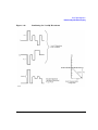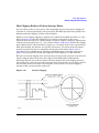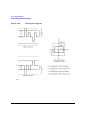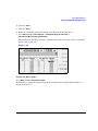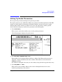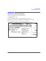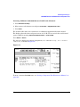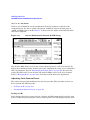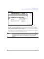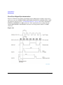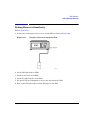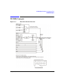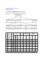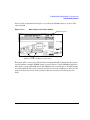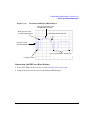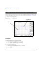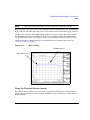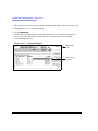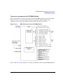
1
User’s Guide
Agilent Technologies
ESG Vector Signal Generator
This guide applies to the signal generator models listed below. Due to our continuing
efforts to improve our products through firmware and hardware revisions, signal generator
design and operation may vary from descriptions in this guide. We recommend that you
use the latest revision of this guide to ensure you have up-to-date product information.
Compare the print date of this guide (see bottom of this page) with the latest revision,
which can be downloaded from the website shown below.
E4438C Vector Signal Generator
www.agilent.com/find/signalgenerators
Part Number: E4400-90503
Printed in USA
January 2003
© Copyright 2001-2003 Agilent Technologies, Inc.
Notice
The material contained in this document is provided “as is”, and is subject to being changed,
without notice, in future editions.
Further, to the maximum extent permitted by applicable law, Agilent disclaims all warranties,
either express or implied with regard to this manual and to any of the Agilent products to
which it pertains, including but not limited to the implied warranties of merchantability and
fitness for a particular purpose. Agilent shall not be liable for errors or for incidental or
consequential damages in connection with the furnishing, use, or performance of this
document or any of the Agilent products to which it pertains. Should Agilent have a written
contract with the User and should any of the contract terms conflict with these terms, the
contract terms shall control.
Questions or Comments about our Documentation?
We welcome any questions or comments you may have about our documentation. Please send
us an E-mail at [email protected].
ii
Contents
1. Signal Generator Overview . . . . . . . . . . . . . . . . . . . . . . . . . . . . . . . . . . . . . . . . . 1
Signal Generator Features . . . . . . . . . . . . . . . . . . . . . . . . . . . . . . . . . . . . . . . . . . . . . . . . .2
Standard Features:. . . . . . . . . . . . . . . . . . . . . . . . . . . . . . . . . . . . . . . . . . . . . . . . . . . . . .2
Options . . . . . . . . . . . . . . . . . . . . . . . . . . . . . . . . . . . . . . . . . . . . . . . . . . . . . . . . . . . . . . . . .4
Front Panel Overview . . . . . . . . . . . . . . . . . . . . . . . . . . . . . . . . . . . . . . . . . . . . . . . . . . . . .7
1. Display . . . . . . . . . . . . . . . . . . . . . . . . . . . . . . . . . . . . . . . . . . . . . . . . . . . . . . . . . . . . .7
2. Softkeys . . . . . . . . . . . . . . . . . . . . . . . . . . . . . . . . . . . . . . . . . . . . . . . . . . . . . . . . . . . . .7
3. Frequency Key . . . . . . . . . . . . . . . . . . . . . . . . . . . . . . . . . . . . . . . . . . . . . . . . . . . . . . .7
4. Amplitude Key . . . . . . . . . . . . . . . . . . . . . . . . . . . . . . . . . . . . . . . . . . . . . . . . . . . . . . .8
5. Knob . . . . . . . . . . . . . . . . . . . . . . . . . . . . . . . . . . . . . . . . . . . . . . . . . . . . . . . . . . . . . . .8
6. Menu Keys . . . . . . . . . . . . . . . . . . . . . . . . . . . . . . . . . . . . . . . . . . . . . . . . . . . . . . . . . .8
7. Save Key . . . . . . . . . . . . . . . . . . . . . . . . . . . . . . . . . . . . . . . . . . . . . . . . . . . . . . . . . . . .8
8. Recall Key . . . . . . . . . . . . . . . . . . . . . . . . . . . . . . . . . . . . . . . . . . . . . . . . . . . . . . . . . . .8
9. EXT 1 INPUT . . . . . . . . . . . . . . . . . . . . . . . . . . . . . . . . . . . . . . . . . . . . . . . . . . . . . . . .8
10. EXT 2 INPUT . . . . . . . . . . . . . . . . . . . . . . . . . . . . . . . . . . . . . . . . . . . . . . . . . . . . . .9
11. Help Key . . . . . . . . . . . . . . . . . . . . . . . . . . . . . . . . . . . . . . . . . . . . . . . . . . . . . . . . . . .9
12. Trigger Key . . . . . . . . . . . . . . . . . . . . . . . . . . . . . . . . . . . . . . . . . . . . . . . . . . . . . . . . .9
13. LF OUTPUT . . . . . . . . . . . . . . . . . . . . . . . . . . . . . . . . . . . . . . . . . . . . . . . . . . . . . .10
14. RF OUTPUT . . . . . . . . . . . . . . . . . . . . . . . . . . . . . . . . . . . . . . . . . . . . . . . . . . . . . . .10
15. Mod On/Off Key . . . . . . . . . . . . . . . . . . . . . . . . . . . . . . . . . . . . . . . . . . . . . . . . . . . .10
16. RF On/Off Key . . . . . . . . . . . . . . . . . . . . . . . . . . . . . . . . . . . . . . . . . . . . . . . . . . . . .10
17. Numeric Keypad . . . . . . . . . . . . . . . . . . . . . . . . . . . . . . . . . . . . . . . . . . . . . . . . . . . .10
18. Incr Set Key . . . . . . . . . . . . . . . . . . . . . . . . . . . . . . . . . . . . . . . . . . . . . . . . . . . . . . .11
19. Arrow Keys . . . . . . . . . . . . . . . . . . . . . . . . . . . . . . . . . . . . . . . . . . . . . . . . . . . . . . . .11
20. Hold Key . . . . . . . . . . . . . . . . . . . . . . . . . . . . . . . . . . . . . . . . . . . . . . . . . . . . . . . . . .11
21. Return Key . . . . . . . . . . . . . . . . . . . . . . . . . . . . . . . . . . . . . . . . . . . . . . . . . . . . . . . .11
22. Display Contrast Increase Key . . . . . . . . . . . . . . . . . . . . . . . . . . . . . . . . . . . . . . . .11
23. Display Contrast Decrease Key . . . . . . . . . . . . . . . . . . . . . . . . . . . . . . . . . . . . . . . .11
24. Local Key. . . . . . . . . . . . . . . . . . . . . . . . . . . . . . . . . . . . . . . . . . . . . . . . . . . . . . . . . .11
25. Preset Key. . . . . . . . . . . . . . . . . . . . . . . . . . . . . . . . . . . . . . . . . . . . . . . . . . . . . . . . .12
26. Standby LED . . . . . . . . . . . . . . . . . . . . . . . . . . . . . . . . . . . . . . . . . . . . . . . . . . . . . .12
27. Line Power LED . . . . . . . . . . . . . . . . . . . . . . . . . . . . . . . . . . . . . . . . . . . . . . . . . . . .12
28. Power Switch . . . . . . . . . . . . . . . . . . . . . . . . . . . . . . . . . . . . . . . . . . . . . . . . . . . . . .12
29. SYMBOL SYNC (Input Connector) . . . . . . . . . . . . . . . . . . . . . . . . . . . . . . . . . . . . .12
30. DATA CLOCK (Input Connector) . . . . . . . . . . . . . . . . . . . . . . . . . . . . . . . . . . . . . .12
31. DATA (Input Connector) . . . . . . . . . . . . . . . . . . . . . . . . . . . . . . . . . . . . . . . . . . . . .13
32. Q (Input Connector) . . . . . . . . . . . . . . . . . . . . . . . . . . . . . . . . . . . . . . . . . . . . . . . . .13
33. I (Input Connector) . . . . . . . . . . . . . . . . . . . . . . . . . . . . . . . . . . . . . . . . . . . . . . . . .13
iii
Contents
Front Panel Display . . . . . . . . . . . . . . . . . . . . . . . . . . . . . . . . . . . . . . . . . . . . . . . . . . . . .
1. Frequency Area . . . . . . . . . . . . . . . . . . . . . . . . . . . . . . . . . . . . . . . . . . . . . . . . . . . . .
2. Annunciators . . . . . . . . . . . . . . . . . . . . . . . . . . . . . . . . . . . . . . . . . . . . . . . . . . . . . . .
3. Digital Modulation Annunciators . . . . . . . . . . . . . . . . . . . . . . . . . . . . . . . . . . . . . .
4. Amplitude Area . . . . . . . . . . . . . . . . . . . . . . . . . . . . . . . . . . . . . . . . . . . . . . . . . . . . .
5. Softkey Label Area . . . . . . . . . . . . . . . . . . . . . . . . . . . . . . . . . . . . . . . . . . . . . . . . . .
6. Error Message Area . . . . . . . . . . . . . . . . . . . . . . . . . . . . . . . . . . . . . . . . . . . . . . . . .
7. Text Area . . . . . . . . . . . . . . . . . . . . . . . . . . . . . . . . . . . . . . . . . . . . . . . . . . . . . . . . . .
8. Active Function Area . . . . . . . . . . . . . . . . . . . . . . . . . . . . . . . . . . . . . . . . . . . . . . . .
Rear Panel Overview . . . . . . . . . . . . . . . . . . . . . . . . . . . . . . . . . . . . . . . . . . . . . . . . . . . .
1. 321.4 IN Connector (Option 300 only) . . . . . . . . . . . . . . . . . . . . . . . . . . . . . . . . . . .
2. BER GATE IN Connector (Option UN7 only) . . . . . . . . . . . . . . . . . . . . . . . . . . . . .
3. BER CLK IN Connector (Option UN7 only) . . . . . . . . . . . . . . . . . . . . . . . . . . . . . .
4. BER DATA IN Connector (Option UN7 only) . . . . . . . . . . . . . . . . . . . . . . . . . . . . .
5. I-bar OUT Connector . . . . . . . . . . . . . . . . . . . . . . . . . . . . . . . . . . . . . . . . . . . . . . . .
6. I OUT Connector . . . . . . . . . . . . . . . . . . . . . . . . . . . . . . . . . . . . . . . . . . . . . . . . . . . .
7. COH CARRIER Output Connector . . . . . . . . . . . . . . . . . . . . . . . . . . . . . . . . . . . . .
8. Q OUT Connector . . . . . . . . . . . . . . . . . . . . . . . . . . . . . . . . . . . . . . . . . . . . . . . . . . .
9. Q-bar OUT Connector . . . . . . . . . . . . . . . . . . . . . . . . . . . . . . . . . . . . . . . . . . . . . . . .
10. EVENT 1 Connector . . . . . . . . . . . . . . . . . . . . . . . . . . . . . . . . . . . . . . . . . . . . . . . .
11. EVENT 2 Connector . . . . . . . . . . . . . . . . . . . . . . . . . . . . . . . . . . . . . . . . . . . . . . . .
12. PATT TRIG IN Connector. . . . . . . . . . . . . . . . . . . . . . . . . . . . . . . . . . . . . . . . . . . .
13. AUX I/O Connector . . . . . . . . . . . . . . . . . . . . . . . . . . . . . . . . . . . . . . . . . . . . . . . . .
14. DIG I/Q I/O Connector . . . . . . . . . . . . . . . . . . . . . . . . . . . . . . . . . . . . . . . . . . . . . .
15. AC Power Receptacle . . . . . . . . . . . . . . . . . . . . . . . . . . . . . . . . . . . . . . . . . . . . . . .
16. GPIB Connector . . . . . . . . . . . . . . . . . . . . . . . . . . . . . . . . . . . . . . . . . . . . . . . . . . .
17. RS 232 Connector . . . . . . . . . . . . . . . . . . . . . . . . . . . . . . . . . . . . . . . . . . . . . . . . . .
18. LAN Connector . . . . . . . . . . . . . . . . . . . . . . . . . . . . . . . . . . . . . . . . . . . . . . . . . . . .
19. TRIG OUT Connector . . . . . . . . . . . . . . . . . . . . . . . . . . . . . . . . . . . . . . . . . . . . . . .
20. BURST GATE IN Connector . . . . . . . . . . . . . . . . . . . . . . . . . . . . . . . . . . . . . . . . .
21. TRIG IN Connector . . . . . . . . . . . . . . . . . . . . . . . . . . . . . . . . . . . . . . . . . . . . . . . . .
22. 10 MHz IN Connector . . . . . . . . . . . . . . . . . . . . . . . . . . . . . . . . . . . . . . . . . . . . . . .
23. SWEEP OUT Connector . . . . . . . . . . . . . . . . . . . . . . . . . . . . . . . . . . . . . . . . . . . . .
24. 10 MHz OUT Connector . . . . . . . . . . . . . . . . . . . . . . . . . . . . . . . . . . . . . . . . . . . . .
25. BASEBAND GEN REF IN Connector . . . . . . . . . . . . . . . . . . . . . . . . . . . . . . . . . .
Digital Personality Revisions for ESG Models . . . . . . . . . . . . . . . . . . . . . . . . . . . . . . . .
14
14
15
17
17
17
17
17
17
18
19
19
20
20
20
20
21
21
22
22
23
23
24
25
26
26
26
27
27
27
28
28
28
28
28
30
2. Basic Operation . . . . . . . . . . . . . . . . . . . . . . . . . . . . . . . . . . . . . . . . . . . . . . . . . . 33
iv
Contents
Using Table Editors . . . . . . . . . . . . . . . . . . . . . . . . . . . . . . . . . . . . . . . . . . . . . . . . . . . . . .34
Table Editor Softkeys . . . . . . . . . . . . . . . . . . . . . . . . . . . . . . . . . . . . . . . . . . . . . . . . . . .35
Modifying Table Items in the Data Fields. . . . . . . . . . . . . . . . . . . . . . . . . . . . . . . . . . .35
Configuring the RF Output . . . . . . . . . . . . . . . . . . . . . . . . . . . . . . . . . . . . . . . . . . . . . . . .36
Configuring a Continuous Wave RF Output . . . . . . . . . . . . . . . . . . . . . . . . . . . . . . . . .36
Configuring a Swept RF Output . . . . . . . . . . . . . . . . . . . . . . . . . . . . . . . . . . . . . . . . . .39
Generating the Modulation Format . . . . . . . . . . . . . . . . . . . . . . . . . . . . . . . . . . . . . . . . .44
Modulating the Carrier Signal . . . . . . . . . . . . . . . . . . . . . . . . . . . . . . . . . . . . . . . . . . . . .46
To Turn the Modulation On . . . . . . . . . . . . . . . . . . . . . . . . . . . . . . . . . . . . . . . . . . . . . .46
To Turn the Modulation Off . . . . . . . . . . . . . . . . . . . . . . . . . . . . . . . . . . . . . . . . . . . . . .46
Creating and Applying User Flatness Correction . . . . . . . . . . . . . . . . . . . . . . . . . . . . . .47
Creating a User Flatness Correction Array . . . . . . . . . . . . . . . . . . . . . . . . . . . . . . . . .47
Using Data Storage Functions . . . . . . . . . . . . . . . . . . . . . . . . . . . . . . . . . . . . . . . . . . . . .54
Using the Memory Catalog . . . . . . . . . . . . . . . . . . . . . . . . . . . . . . . . . . . . . . . . . . . . . .54
Using the Instrument State Register . . . . . . . . . . . . . . . . . . . . . . . . . . . . . . . . . . . . . .55
Enabling Options . . . . . . . . . . . . . . . . . . . . . . . . . . . . . . . . . . . . . . . . . . . . . . . . . . . . . . . .59
Enabling a Software Option. . . . . . . . . . . . . . . . . . . . . . . . . . . . . . . . . . . . . . . . . . . . . .59
3. Basic Digital Operation . . . . . . . . . . . . . . . . . . . . . . . . . . . . . . . . . . . . . . . . . . . 61
Arbitrary (ARB) Waveform Header Files . . . . . . . . . . . . . . . . . . . . . . . . . . . . . . . . . . . . .62
Generating a Header File for a Modulation Format Waveform. . . . . . . . . . . . . . . . . .62
Editing a Header File for a Modulation Format . . . . . . . . . . . . . . . . . . . . . . . . . . . . . .63
Generating a Header File for a Dual ARB Player Waveform Sequence . . . . . . . . . . .69
Editing and Viewing Header Files in the Dual ARB Player . . . . . . . . . . . . . . . . . . . .69
Storing a Header File . . . . . . . . . . . . . . . . . . . . . . . . . . . . . . . . . . . . . . . . . . . . . . . . . . .74
Playing a Waveform File containing a Header . . . . . . . . . . . . . . . . . . . . . . . . . . . . . . .74
Using the Dual ARB Player . . . . . . . . . . . . . . . . . . . . . . . . . . . . . . . . . . . . . . . . . . . . . . .76
Accessing the Dual ARB Player. . . . . . . . . . . . . . . . . . . . . . . . . . . . . . . . . . . . . . . . . . .76
Creating Waveform Segments . . . . . . . . . . . . . . . . . . . . . . . . . . . . . . . . . . . . . . . . . . . .77
Building and Storing a Waveform Sequence. . . . . . . . . . . . . . . . . . . . . . . . . . . . . . . . .79
Playing a Waveform . . . . . . . . . . . . . . . . . . . . . . . . . . . . . . . . . . . . . . . . . . . . . . . . . . . .80
Editing Waveform Sequences. . . . . . . . . . . . . . . . . . . . . . . . . . . . . . . . . . . . . . . . . . . . .81
Storing Waveform Segments to Non-Volatile Memory . . . . . . . . . . . . . . . . . . . . . . . . .82
Loading Waveform Segments from Non-Volatile Memory . . . . . . . . . . . . . . . . . . . . . .83
Local Settings for ARB Waveform Formats and the Dual ARB Player . . . . . . . . . . . . .84
I/Q Attenuator and Filters Settings . . . . . . . . . . . . . . . . . . . . . . . . . . . . . . . . . . . . . . .84
ARB Sample Clock . . . . . . . . . . . . . . . . . . . . . . . . . . . . . . . . . . . . . . . . . . . . . . . . . . . . .86
Waveform Markers . . . . . . . . . . . . . . . . . . . . . . . . . . . . . . . . . . . . . . . . . . . . . . . . . . . . .87
v
Contents
Using Waveform Markers . . . . . . . . . . . . . . . . . . . . . . . . . . . . . . . . . . . . . . . . . . . . . . . . 90
Accessing the Marker Utilities. . . . . . . . . . . . . . . . . . . . . . . . . . . . . . . . . . . . . . . . . . . 90
Placing a Marker at the First Point within a Waveform . . . . . . . . . . . . . . . . . . . . . . 91
Clearing Markers from a Waveform. . . . . . . . . . . . . . . . . . . . . . . . . . . . . . . . . . . . . . . 91
Placing a Marker Across a Range of Points within a Waveform . . . . . . . . . . . . . . . . 92
Placing Repetitively Spaced Markers within a Waveform . . . . . . . . . . . . . . . . . . . . . 93
Setting the Marker Polarity . . . . . . . . . . . . . . . . . . . . . . . . . . . . . . . . . . . . . . . . . . . . . 94
Using the Marker Functions: RF Blanking, ALC Hold, and Alternate Amplitude. . 94
Toggling Markers in the Dual ARB Player . . . . . . . . . . . . . . . . . . . . . . . . . . . . . . . . . 95
Toggling Markers As You Create a Waveform Sequence . . . . . . . . . . . . . . . . . . . . . . 96
Verifying Marker Operation . . . . . . . . . . . . . . . . . . . . . . . . . . . . . . . . . . . . . . . . . . . . . 98
Using Waveform Triggers . . . . . . . . . . . . . . . . . . . . . . . . . . . . . . . . . . . . . . . . . . . . . . . . 99
Using Segment Advance Triggering . . . . . . . . . . . . . . . . . . . . . . . . . . . . . . . . . . . . . . 99
Using External Triggering. . . . . . . . . . . . . . . . . . . . . . . . . . . . . . . . . . . . . . . . . . . . . . . 101
Required Equipment . . . . . . . . . . . . . . . . . . . . . . . . . . . . . . . . . . . . . . . . . . . . . . . . . . 101
Connecting the Equipment. . . . . . . . . . . . . . . . . . . . . . . . . . . . . . . . . . . . . . . . . . . . . 101
Configuring a Custom Multicarrier CDMA State . . . . . . . . . . . . . . . . . . . . . . . . . . . 101
Configuring the Waveform Trigger . . . . . . . . . . . . . . . . . . . . . . . . . . . . . . . . . . . . . . 101
Configuring the Function Generator . . . . . . . . . . . . . . . . . . . . . . . . . . . . . . . . . . . . . 102
Generating the Waveform. . . . . . . . . . . . . . . . . . . . . . . . . . . . . . . . . . . . . . . . . . . . . . 102
Configuring the RF Output . . . . . . . . . . . . . . . . . . . . . . . . . . . . . . . . . . . . . . . . . . . . 102
Understanding Waveform Clipping. . . . . . . . . . . . . . . . . . . . . . . . . . . . . . . . . . . . . . . . 103
How Power Peaks Develop . . . . . . . . . . . . . . . . . . . . . . . . . . . . . . . . . . . . . . . . . . . . . 103
How Peaks Cause Spectral Regrowth . . . . . . . . . . . . . . . . . . . . . . . . . . . . . . . . . . . . 106
How Clipping Reduces Peak-to-Average Power. . . . . . . . . . . . . . . . . . . . . . . . . . . . . 107
FIR Filtering Options . . . . . . . . . . . . . . . . . . . . . . . . . . . . . . . . . . . . . . . . . . . . . . . . . 109
How Clipping Differs from Symbol Offset in W-CDMA . . . . . . . . . . . . . . . . . . . . . . 110
Using Waveform Clipping . . . . . . . . . . . . . . . . . . . . . . . . . . . . . . . . . . . . . . . . . . . . . . . 111
Configuring Circular Clipping . . . . . . . . . . . . . . . . . . . . . . . . . . . . . . . . . . . . . . . . . . 111
Configuring Rectangular Clipping . . . . . . . . . . . . . . . . . . . . . . . . . . . . . . . . . . . . . . . 112
Using Customized Burst Shape Curves . . . . . . . . . . . . . . . . . . . . . . . . . . . . . . . . . . . . 113
Understanding Burst Shape. . . . . . . . . . . . . . . . . . . . . . . . . . . . . . . . . . . . . . . . . . . . 113
Creating a User-Defined Burst Shape Curve . . . . . . . . . . . . . . . . . . . . . . . . . . . . . . 116
Storing a User-Defined Burst Shape Curve . . . . . . . . . . . . . . . . . . . . . . . . . . . . . . . 118
Recalling a User-Defined Burst Shape Curve . . . . . . . . . . . . . . . . . . . . . . . . . . . . . . 118
Generating the Waveform. . . . . . . . . . . . . . . . . . . . . . . . . . . . . . . . . . . . . . . . . . . . . . 119
Configuring the RF Output . . . . . . . . . . . . . . . . . . . . . . . . . . . . . . . . . . . . . . . . . . . . 119
Using Finite Impulse Response (FIR) Filters . . . . . . . . . . . . . . . . . . . . . . . . . . . . . . . . 120
vi
Contents
Creating a User-Defined FIR Filter Using the FIR Table Editor . . . . . . . . . . . . . . .120
Modifying a FIR Filter Using the FIR Table Editor . . . . . . . . . . . . . . . . . . . . . . . . . . .125
Loading the Default Gaussian FIR File . . . . . . . . . . . . . . . . . . . . . . . . . . . . . . . . . . .125
Modifying the Coefficients . . . . . . . . . . . . . . . . . . . . . . . . . . . . . . . . . . . . . . . . . . . . . .126
Storing the Filter to Memory . . . . . . . . . . . . . . . . . . . . . . . . . . . . . . . . . . . . . . . . . . . .127
Differential Encoding . . . . . . . . . . . . . . . . . . . . . . . . . . . . . . . . . . . . . . . . . . . . . . . . . . .128
Differential Data Encoding . . . . . . . . . . . . . . . . . . . . . . . . . . . . . . . . . . . . . . . . . . . . .129
How Differential Encoding Works . . . . . . . . . . . . . . . . . . . . . . . . . . . . . . . . . . . . . . . .130
Using Differential Encoding . . . . . . . . . . . . . . . . . . . . . . . . . . . . . . . . . . . . . . . . . . . .132
User-Defined I/Q Maps . . . . . . . . . . . . . . . . . . . . . . . . . . . . . . . . . . . . . . . . . . . . . . . . . .136
Creating a User-Defined I/Q Map . . . . . . . . . . . . . . . . . . . . . . . . . . . . . . . . . . . . . . . .136
Storing a User-Defined I/Q Map File. . . . . . . . . . . . . . . . . . . . . . . . . . . . . . . . . . . . . .137
Moving I/Q Symbols . . . . . . . . . . . . . . . . . . . . . . . . . . . . . . . . . . . . . . . . . . . . . . . . . . .138
User-Defined FSK Modulation . . . . . . . . . . . . . . . . . . . . . . . . . . . . . . . . . . . . . . . . . . . .140
Modifying a Default FSK Modulation . . . . . . . . . . . . . . . . . . . . . . . . . . . . . . . . . . . . .140
Storing an FSK Modulation . . . . . . . . . . . . . . . . . . . . . . . . . . . . . . . . . . . . . . . . . . . . .141
Creating a User-Defined FSK Modulation . . . . . . . . . . . . . . . . . . . . . . . . . . . . . . . . .141
Creating and Using Bit Files . . . . . . . . . . . . . . . . . . . . . . . . . . . . . . . . . . . . . . . . . . . . .143
Creating a User File . . . . . . . . . . . . . . . . . . . . . . . . . . . . . . . . . . . . . . . . . . . . . . . . . . .143
Renaming and Saving a User File . . . . . . . . . . . . . . . . . . . . . . . . . . . . . . . . . . . . . . . .145
Recalling a User File . . . . . . . . . . . . . . . . . . . . . . . . . . . . . . . . . . . . . . . . . . . . . . . . . .146
Modifying an Existing User File . . . . . . . . . . . . . . . . . . . . . . . . . . . . . . . . . . . . . . . . .146
Applying Bit Errors to a User File . . . . . . . . . . . . . . . . . . . . . . . . . . . . . . . . . . . . . . .148
4. Analog Modulation . . . . . . . . . . . . . . . . . . . . . . . . . . . . . . . . . . . . . . . . . . . . . . 149
Analog Modulation Waveforms . . . . . . . . . . . . . . . . . . . . . . . . . . . . . . . . . . . . . . . . . . . .150
Configuring AM . . . . . . . . . . . . . . . . . . . . . . . . . . . . . . . . . . . . . . . . . . . . . . . . . . . . . . . .151
Setting the Carrier Frequency. . . . . . . . . . . . . . . . . . . . . . . . . . . . . . . . . . . . . . . . . . .151
Setting the RF Output Amplitude . . . . . . . . . . . . . . . . . . . . . . . . . . . . . . . . . . . . . . . .151
Setting the AM Depth and Rate . . . . . . . . . . . . . . . . . . . . . . . . . . . . . . . . . . . . . . . . .151
Turning on Amplitude Modulation . . . . . . . . . . . . . . . . . . . . . . . . . . . . . . . . . . . . . . .151
Configuring FM . . . . . . . . . . . . . . . . . . . . . . . . . . . . . . . . . . . . . . . . . . . . . . . . . . . . . . . .152
Setting the RF Output Frequency . . . . . . . . . . . . . . . . . . . . . . . . . . . . . . . . . . . . . . . .152
Setting the RF Output Amplitude . . . . . . . . . . . . . . . . . . . . . . . . . . . . . . . . . . . . . . . .152
Setting the FM Deviation and Rate. . . . . . . . . . . . . . . . . . . . . . . . . . . . . . . . . . . . . . .152
Activating FM . . . . . . . . . . . . . . . . . . . . . . . . . . . . . . . . . . . . . . . . . . . . . . . . . . . . . . . .152
Configuring ΦM . . . . . . . . . . . . . . . . . . . . . . . . . . . . . . . . . . . . . . . . . . . . . . . . . . . . . . . .153
Setting the RF Output Frequency . . . . . . . . . . . . . . . . . . . . . . . . . . . . . . . . . . . . . . . .153
vii
Contents
Setting the RF Output Amplitude . . . . . . . . . . . . . . . . . . . . . . . . . . . . . . . . . . . . . . .
Setting the FM Deviation and Rate . . . . . . . . . . . . . . . . . . . . . . . . . . . . . . . . . . . . . .
Activating FM . . . . . . . . . . . . . . . . . . . . . . . . . . . . . . . . . . . . . . . . . . . . . . . . . . . . . . .
Configuring Pulse Modulation. . . . . . . . . . . . . . . . . . . . . . . . . . . . . . . . . . . . . . . . . . . .
Setting the RF Output Frequency . . . . . . . . . . . . . . . . . . . . . . . . . . . . . . . . . . . . . . .
Setting the RF Output Amplitude . . . . . . . . . . . . . . . . . . . . . . . . . . . . . . . . . . . . . . .
Setting the Pulse Period and Width. . . . . . . . . . . . . . . . . . . . . . . . . . . . . . . . . . . . . .
Activating Pulse Modulation . . . . . . . . . . . . . . . . . . . . . . . . . . . . . . . . . . . . . . . . . . .
Configuring the LF Output . . . . . . . . . . . . . . . . . . . . . . . . . . . . . . . . . . . . . . . . . . . . . .
Configuring the LF Output with an Internal Modulation Source . . . . . . . . . . . . . .
Configuring the LF Output with a Function Generator Source. . . . . . . . . . . . . . . .
153
153
153
154
154
154
154
154
155
156
157
5. AWGN Waveform Generator . . . . . . . . . . . . . . . . . . . . . . . . . . . . . . . . . . . . . . 159
Configuring the AWGN Generator . . . . . . . . . . . . . . . . . . . . . . . . . . . . . . . . . . . . . . . . 160
Generating the Waveform. . . . . . . . . . . . . . . . . . . . . . . . . . . . . . . . . . . . . . . . . . . . . . 160
Configuring the RF Output . . . . . . . . . . . . . . . . . . . . . . . . . . . . . . . . . . . . . . . . . . . . 160
6. BERT Testing . . . . . . . . . . . . . . . . . . . . . . . . . . . . . . . . . . . . . . . . . . . . . . . . . . . 161
Setting Up a PHS Bit Error Rate Test . . . . . . . . . . . . . . . . . . . . . . . . . . . . . . . . . . . . .
Required Equipment . . . . . . . . . . . . . . . . . . . . . . . . . . . . . . . . . . . . . . . . . . . . . . . . . .
Connecting the Test Equipment. . . . . . . . . . . . . . . . . . . . . . . . . . . . . . . . . . . . . . . . .
Setting the Carrier Frequency and Power Level. . . . . . . . . . . . . . . . . . . . . . . . . . . .
Selecting the Radio Data Format . . . . . . . . . . . . . . . . . . . . . . . . . . . . . . . . . . . . . . . .
Setting the Radio to a Receiver Mode . . . . . . . . . . . . . . . . . . . . . . . . . . . . . . . . . . . .
Selecting the BERT Data Pattern and Total Bits . . . . . . . . . . . . . . . . . . . . . . . . . . .
Selecting the BERT Trigger . . . . . . . . . . . . . . . . . . . . . . . . . . . . . . . . . . . . . . . . . . . .
Starting BERT measurements . . . . . . . . . . . . . . . . . . . . . . . . . . . . . . . . . . . . . . . . . .
Measuring RF Loopback BER with Option 300 . . . . . . . . . . . . . . . . . . . . . . . . . . . . . .
Required Equipment . . . . . . . . . . . . . . . . . . . . . . . . . . . . . . . . . . . . . . . . . . . . . . . . . .
Connecting the Test Equipment. . . . . . . . . . . . . . . . . . . . . . . . . . . . . . . . . . . . . . . . .
Configuring GSM Mode on the Agilent Technologies
E4406A VSA Series Transmitter Tester . . . . . . . . . . . . . . . . . . . . . . . . . . . . . . . . . .
Configuring GSM Mode on the ESG Vector Signal Generator . . . . . . . . . . . . . . . . .
Synchronizing to the BCH Then the TCH . . . . . . . . . . . . . . . . . . . . . . . . . . . . . . . . .
Synchronizing to the TCH . . . . . . . . . . . . . . . . . . . . . . . . . . . . . . . . . . . . . . . . . . . . .
Making Loopback BER Measurements . . . . . . . . . . . . . . . . . . . . . . . . . . . . . . . . . . .
Using Amplitude Sensitivity Search . . . . . . . . . . . . . . . . . . . . . . . . . . . . . . . . . . . . .
Using the External Frame Trigger Function with the EDGE Format . . . . . . . . . . . .
viii
162
162
163
163
164
164
165
165
165
166
166
167
168
169
171
173
175
176
180
Contents
Measuring the Initial Delay Value . . . . . . . . . . . . . . . . . . . . . . . . . . . . . . . . . . . . . . .180
Adjusting the Delay Value . . . . . . . . . . . . . . . . . . . . . . . . . . . . . . . . . . . . . . . . . . . . . .181
Bit Error Rate Tester–Option UN7 . . . . . . . . . . . . . . . . . . . . . . . . . . . . . . . . . . . . . . . .184
Block Diagram . . . . . . . . . . . . . . . . . . . . . . . . . . . . . . . . . . . . . . . . . . . . . . . . . . . . . . .184
Clock Gate Function . . . . . . . . . . . . . . . . . . . . . . . . . . . . . . . . . . . . . . . . . . . . . . . . . . .185
Clock/Gate Delay Function . . . . . . . . . . . . . . . . . . . . . . . . . . . . . . . . . . . . . . . . . . . . .186
Clock Delay Function . . . . . . . . . . . . . . . . . . . . . . . . . . . . . . . . . . . . . . . . . . . . . . . . . .187
Gate Delay Function in the Clock Mode . . . . . . . . . . . . . . . . . . . . . . . . . . . . . . . . . . .188
Triggering . . . . . . . . . . . . . . . . . . . . . . . . . . . . . . . . . . . . . . . . . . . . . . . . . . . . . . . . . . .189
Data Processing . . . . . . . . . . . . . . . . . . . . . . . . . . . . . . . . . . . . . . . . . . . . . . . . . . . . . .192
Repeat Measurements . . . . . . . . . . . . . . . . . . . . . . . . . . . . . . . . . . . . . . . . . . . . . . . . .193
Testing Signal Definitions . . . . . . . . . . . . . . . . . . . . . . . . . . . . . . . . . . . . . . . . . . . . . .194
RF Loopback BER–Option 300 . . . . . . . . . . . . . . . . . . . . . . . . . . . . . . . . . . . . . . . . . . . .195
Synchronization . . . . . . . . . . . . . . . . . . . . . . . . . . . . . . . . . . . . . . . . . . . . . . . . . . . . . .195
Erased Frame Detection . . . . . . . . . . . . . . . . . . . . . . . . . . . . . . . . . . . . . . . . . . . . . . .196
Downlink Errors . . . . . . . . . . . . . . . . . . . . . . . . . . . . . . . . . . . . . . . . . . . . . . . . . . . . . .196
Frame Structure . . . . . . . . . . . . . . . . . . . . . . . . . . . . . . . . . . . . . . . . . . . . . . . . . . . . . .196
7. Bluetooth Signals. . . . . . . . . . . . . . . . . . . . . . . . . . . . . . . . . . . . . . . . . . . . . . . . 199
Accessing the Bluetooth Setup Menu on the ESG . . . . . . . . . . . . . . . . . . . . . . . . . . . . .200
Setting Up Packet Parameters . . . . . . . . . . . . . . . . . . . . . . . . . . . . . . . . . . . . . . . . . . . .201
Setting up Impairments . . . . . . . . . . . . . . . . . . . . . . . . . . . . . . . . . . . . . . . . . . . . . . . . .203
Using Burst . . . . . . . . . . . . . . . . . . . . . . . . . . . . . . . . . . . . . . . . . . . . . . . . . . . . . . . . . . .205
Setting the Burst Power Ramp . . . . . . . . . . . . . . . . . . . . . . . . . . . . . . . . . . . . . . . . . .205
Using Clock/Gate Delay. . . . . . . . . . . . . . . . . . . . . . . . . . . . . . . . . . . . . . . . . . . . . . . . . .206
Turning On a Bluetooth Signal. . . . . . . . . . . . . . . . . . . . . . . . . . . . . . . . . . . . . . . . . . . .207
8. CDMA Digital Modulation . . . . . . . . . . . . . . . . . . . . . . . . . . . . . . . . . . . . . . . . 209
cdma2000 Forward Link Modulation for Component Test . . . . . . . . . . . . . . . . . . . . . .210
Activating a Predefined CDMA Forward Link State . . . . . . . . . . . . . . . . . . . . . . . . .210
Creating a User-Defined CDMA Forward Link State . . . . . . . . . . . . . . . . . . . . . . . .211
cdma2000 Reverse Link Modulation for Component Test. . . . . . . . . . . . . . . . . . . . . . .214
Activating a Predefined cdma2000 Reverse Link State . . . . . . . . . . . . . . . . . . . . . . .214
Creating a User-Defined cdma2000 Reverse Link State . . . . . . . . . . . . . . . . . . . . . .215
Storing a Component Test Waveform to Memory . . . . . . . . . . . . . . . . . . . . . . . . . . . . .218
Recalling a Component Test Waveform . . . . . . . . . . . . . . . . . . . . . . . . . . . . . . . . . . . . .219
Creating a Custom Multicarrier cdma2000 Waveform . . . . . . . . . . . . . . . . . . . . . . . . .220
Opening the Multicarrier cdma2000 Setup Table Editor. . . . . . . . . . . . . . . . . . . . . .220
ix
Contents
Modifying a Multicarrier cdma2000 4-Carrier Template . . . . . . . . . . . . . . . . . . . . .
Activating a Custom Multicarrier cdma2000 Setup . . . . . . . . . . . . . . . . . . . . . . . . .
cdma2000 Forward Link Modulation for Receiver Test . . . . . . . . . . . . . . . . . . . . . . . .
Editing the Base Station Setup . . . . . . . . . . . . . . . . . . . . . . . . . . . . . . . . . . . . . . . . .
Editing Channel Setups . . . . . . . . . . . . . . . . . . . . . . . . . . . . . . . . . . . . . . . . . . . . . . .
Adjusting Code Domain Power. . . . . . . . . . . . . . . . . . . . . . . . . . . . . . . . . . . . . . . . . .
Managing Noise. . . . . . . . . . . . . . . . . . . . . . . . . . . . . . . . . . . . . . . . . . . . . . . . . . . . . .
Generating the Baseband Signal . . . . . . . . . . . . . . . . . . . . . . . . . . . . . . . . . . . . . . . .
Configuring the RF Output . . . . . . . . . . . . . . . . . . . . . . . . . . . . . . . . . . . . . . . . . . . .
cdma2000 Reverse Link Modulation for Receiver Test . . . . . . . . . . . . . . . . . . . . . . . .
Editing the Mobile Setup . . . . . . . . . . . . . . . . . . . . . . . . . . . . . . . . . . . . . . . . . . . . . .
Editing Channel Setups . . . . . . . . . . . . . . . . . . . . . . . . . . . . . . . . . . . . . . . . . . . . . . .
Adjusting Code Domain Power. . . . . . . . . . . . . . . . . . . . . . . . . . . . . . . . . . . . . . . . . .
Managing Noise. . . . . . . . . . . . . . . . . . . . . . . . . . . . . . . . . . . . . . . . . . . . . . . . . . . . . .
Generating the Baseband Signal . . . . . . . . . . . . . . . . . . . . . . . . . . . . . . . . . . . . . . . .
Configuring the RF Output . . . . . . . . . . . . . . . . . . . . . . . . . . . . . . . . . . . . . . . . . . . .
Applying a User-Defined FIR Filter to a cdma2000 Waveform . . . . . . . . . . . . . . . . . .
IS-95A Modulation . . . . . . . . . . . . . . . . . . . . . . . . . . . . . . . . . . . . . . . . . . . . . . . . . . . . .
Creating a Predefined CDMA State . . . . . . . . . . . . . . . . . . . . . . . . . . . . . . . . . . . . .
Creating a User-Defined CDMA State. . . . . . . . . . . . . . . . . . . . . . . . . . . . . . . . . . . .
Applying Changes to an Active CDMA State . . . . . . . . . . . . . . . . . . . . . . . . . . . . . .
Creating a User-Defined Multicarrier CDMA State . . . . . . . . . . . . . . . . . . . . . . . . .
Applying Changes to an Active Multicarrier CDMA State. . . . . . . . . . . . . . . . . . . .
221
222
224
224
224
226
227
228
229
230
230
230
232
234
235
235
236
238
238
239
241
241
243
9. Custom Digital Modulation . . . . . . . . . . . . . . . . . . . . . . . . . . . . . . . . . . . . . . . 245
Using the Arbitrary Waveform Generator . . . . . . . . . . . . . . . . . . . . . . . . . . . . . . . . . .
Using Predefined Custom TDMA Digital Modulation . . . . . . . . . . . . . . . . . . . . . . .
Creating a Custom TDMA Digital Modulation State . . . . . . . . . . . . . . . . . . . . . . . .
Storing a Custom TDMA Digital Modulation State . . . . . . . . . . . . . . . . . . . . . . . . .
Recalling a Custom TDMA Digital Modulation State. . . . . . . . . . . . . . . . . . . . . . . .
Creating a Custom Multicarrier TDMA Digital Modulation State . . . . . . . . . . . . .
Storing a Custom Multicarrier TDMA Digital Modulation State . . . . . . . . . . . . . .
Applying Changes to an Active Multicarrier TDMA Digital Modulation State . . .
Using the Real Time I/Q Baseband Generator . . . . . . . . . . . . . . . . . . . . . . . . . . . . . . .
Selecting Predefined Custom Modulation Modes . . . . . . . . . . . . . . . . . . . . . . . . . . .
Creating User-Defined Custom Modulation . . . . . . . . . . . . . . . . . . . . . . . . . . . . . . .
246
246
247
248
248
249
251
251
252
252
253
10. GPS Modulation. . . . . . . . . . . . . . . . . . . . . . . . . . . . . . . . . . . . . . . . . . . . . . . . 255
x
Contents
Option Overview . . . . . . . . . . . . . . . . . . . . . . . . . . . . . . . . . . . . . . . . . . . . . . . . . . . . . . .256
GPS Concepts. . . . . . . . . . . . . . . . . . . . . . . . . . . . . . . . . . . . . . . . . . . . . . . . . . . . . . . . . .257
Signal Generation Block Diagram. . . . . . . . . . . . . . . . . . . . . . . . . . . . . . . . . . . . . . . .257
Data Modes and Subframe Structures . . . . . . . . . . . . . . . . . . . . . . . . . . . . . . . . . . . .258
Chip Clock Reference . . . . . . . . . . . . . . . . . . . . . . . . . . . . . . . . . . . . . . . . . . . . . . . . . .259
Rear Panel Signal Synchronization. . . . . . . . . . . . . . . . . . . . . . . . . . . . . . . . . . . . . . .260
User Files . . . . . . . . . . . . . . . . . . . . . . . . . . . . . . . . . . . . . . . . . . . . . . . . . . . . . . . . . . .261
Bit Error Rate Test Measurements . . . . . . . . . . . . . . . . . . . . . . . . . . . . . . . . . . . . . . .261
GPS Operation . . . . . . . . . . . . . . . . . . . . . . . . . . . . . . . . . . . . . . . . . . . . . . . . . . . . . . . . .262
Setting Up the GPS Signal . . . . . . . . . . . . . . . . . . . . . . . . . . . . . . . . . . . . . . . . . . . . .262
Configuring the External Reference Clock . . . . . . . . . . . . . . . . . . . . . . . . . . . . . . . . .263
Testing Receiver Sensitivity . . . . . . . . . . . . . . . . . . . . . . . . . . . . . . . . . . . . . . . . . . . . . .265
Setting Up a GPS Bit Error Rate Test . . . . . . . . . . . . . . . . . . . . . . . . . . . . . . . . . . . . . .266
Required Equipment . . . . . . . . . . . . . . . . . . . . . . . . . . . . . . . . . . . . . . . . . . . . . . . . . .266
Connecting the Test Equipment . . . . . . . . . . . . . . . . . . . . . . . . . . . . . . . . . . . . . . . . .267
Setting the Carrier Frequency and Power Level . . . . . . . . . . . . . . . . . . . . . . . . . . . .267
Selecting the Data Format . . . . . . . . . . . . . . . . . . . . . . . . . . . . . . . . . . . . . . . . . . . . . .268
Setting Up the GPS Receiver . . . . . . . . . . . . . . . . . . . . . . . . . . . . . . . . . . . . . . . . . . .268
Selecting the BERT Data Pattern and Total Bits. . . . . . . . . . . . . . . . . . . . . . . . . . . .268
Selecting the BERT Trigger. . . . . . . . . . . . . . . . . . . . . . . . . . . . . . . . . . . . . . . . . . . . .268
Starting BERT measurements . . . . . . . . . . . . . . . . . . . . . . . . . . . . . . . . . . . . . . . . . .269
11. Multitone Waveform Generator . . . . . . . . . . . . . . . . . . . . . . . . . . . . . . . . . . 271
Creating a Custom Multitone Waveform . . . . . . . . . . . . . . . . . . . . . . . . . . . . . . . . . . . .272
Initializing the Multitone Setup Table Editor . . . . . . . . . . . . . . . . . . . . . . . . . . . . . .272
Configuring Tone Powers and Tone Phases . . . . . . . . . . . . . . . . . . . . . . . . . . . . . . . .272
Removing a Tone . . . . . . . . . . . . . . . . . . . . . . . . . . . . . . . . . . . . . . . . . . . . . . . . . . . . .273
Generating the Waveform . . . . . . . . . . . . . . . . . . . . . . . . . . . . . . . . . . . . . . . . . . . . . .273
Configuring the RF Output . . . . . . . . . . . . . . . . . . . . . . . . . . . . . . . . . . . . . . . . . . . . .273
Applying Changes to an Active Multitone Signal . . . . . . . . . . . . . . . . . . . . . . . . . . . . .274
Storing a Multitone Waveform. . . . . . . . . . . . . . . . . . . . . . . . . . . . . . . . . . . . . . . . . . .274
Recalling a Multitone Waveform . . . . . . . . . . . . . . . . . . . . . . . . . . . . . . . . . . . . . . . . .274
12. Real Time TDMA Formats . . . . . . . . . . . . . . . . . . . . . . . . . . . . . . . . . . . . . . . 277
EDGE Framed Modulation . . . . . . . . . . . . . . . . . . . . . . . . . . . . . . . . . . . . . . . . . . . . . . .278
Activating Framed Data Format . . . . . . . . . . . . . . . . . . . . . . . . . . . . . . . . . . . . . . . . .278
Configuring the First Timeslot . . . . . . . . . . . . . . . . . . . . . . . . . . . . . . . . . . . . . . . . . .278
Configuring the Second Timeslot. . . . . . . . . . . . . . . . . . . . . . . . . . . . . . . . . . . . . . . . .278
xi
Contents
Generating the Baseband Signal . . . . . . . . . . . . . . . . . . . . . . . . . . . . . . . . . . . . . . . .
Configuring the RF Output . . . . . . . . . . . . . . . . . . . . . . . . . . . . . . . . . . . . . . . . . . . .
GSM Framed Modulation . . . . . . . . . . . . . . . . . . . . . . . . . . . . . . . . . . . . . . . . . . . . . . .
Activating Framed Data Format . . . . . . . . . . . . . . . . . . . . . . . . . . . . . . . . . . . . . . . .
Configuring the First Timeslot. . . . . . . . . . . . . . . . . . . . . . . . . . . . . . . . . . . . . . . . . .
Configuring the Second Timeslot . . . . . . . . . . . . . . . . . . . . . . . . . . . . . . . . . . . . . . . .
Generating the Baseband Signal . . . . . . . . . . . . . . . . . . . . . . . . . . . . . . . . . . . . . . . .
Configuring the RF Output . . . . . . . . . . . . . . . . . . . . . . . . . . . . . . . . . . . . . . . . . . . .
DECT Framed Modulation . . . . . . . . . . . . . . . . . . . . . . . . . . . . . . . . . . . . . . . . . . . . . .
Activating Framed Data Format . . . . . . . . . . . . . . . . . . . . . . . . . . . . . . . . . . . . . . . .
Configuring the First Timeslot. . . . . . . . . . . . . . . . . . . . . . . . . . . . . . . . . . . . . . . . . .
Configuring the Second Timeslot . . . . . . . . . . . . . . . . . . . . . . . . . . . . . . . . . . . . . . . .
Generating the Baseband Signal . . . . . . . . . . . . . . . . . . . . . . . . . . . . . . . . . . . . . . . .
Configuring the RF Output . . . . . . . . . . . . . . . . . . . . . . . . . . . . . . . . . . . . . . . . . . . .
PHS Framed Modulation . . . . . . . . . . . . . . . . . . . . . . . . . . . . . . . . . . . . . . . . . . . . . . . .
Activating Framed Data Format . . . . . . . . . . . . . . . . . . . . . . . . . . . . . . . . . . . . . . . .
Configuring the First Timeslot. . . . . . . . . . . . . . . . . . . . . . . . . . . . . . . . . . . . . . . . . .
Configuring the Second Timeslot . . . . . . . . . . . . . . . . . . . . . . . . . . . . . . . . . . . . . . . .
Generating the Baseband Signal . . . . . . . . . . . . . . . . . . . . . . . . . . . . . . . . . . . . . . . .
Configuring the RF Output . . . . . . . . . . . . . . . . . . . . . . . . . . . . . . . . . . . . . . . . . . . .
PDC Framed Modulation . . . . . . . . . . . . . . . . . . . . . . . . . . . . . . . . . . . . . . . . . . . . . . . .
Activating Framed Data Format . . . . . . . . . . . . . . . . . . . . . . . . . . . . . . . . . . . . . . . .
Configuring the First Timeslot. . . . . . . . . . . . . . . . . . . . . . . . . . . . . . . . . . . . . . . . . .
Configuring the Second Timeslot . . . . . . . . . . . . . . . . . . . . . . . . . . . . . . . . . . . . . . . .
Generating the Baseband Signal . . . . . . . . . . . . . . . . . . . . . . . . . . . . . . . . . . . . . . . .
Configuring the RF Output . . . . . . . . . . . . . . . . . . . . . . . . . . . . . . . . . . . . . . . . . . . .
NADC Framed Modulation . . . . . . . . . . . . . . . . . . . . . . . . . . . . . . . . . . . . . . . . . . . . . .
Activating Framed Data Format . . . . . . . . . . . . . . . . . . . . . . . . . . . . . . . . . . . . . . . .
Configuring the First Timeslot. . . . . . . . . . . . . . . . . . . . . . . . . . . . . . . . . . . . . . . . . .
Configuring the Second Timeslot . . . . . . . . . . . . . . . . . . . . . . . . . . . . . . . . . . . . . . . .
Generating the Baseband Signal . . . . . . . . . . . . . . . . . . . . . . . . . . . . . . . . . . . . . . . .
Configuring the RF Output . . . . . . . . . . . . . . . . . . . . . . . . . . . . . . . . . . . . . . . . . . . .
TETRA Framed Modulation . . . . . . . . . . . . . . . . . . . . . . . . . . . . . . . . . . . . . . . . . . . . .
Activating Framed Data Format . . . . . . . . . . . . . . . . . . . . . . . . . . . . . . . . . . . . . . . .
Configuring the First Timeslot. . . . . . . . . . . . . . . . . . . . . . . . . . . . . . . . . . . . . . . . . .
Configuring the Second Timeslot . . . . . . . . . . . . . . . . . . . . . . . . . . . . . . . . . . . . . . . .
Generating the Baseband Signal . . . . . . . . . . . . . . . . . . . . . . . . . . . . . . . . . . . . . . . .
Configuring the RF Output . . . . . . . . . . . . . . . . . . . . . . . . . . . . . . . . . . . . . . . . . . . .
xii
278
279
280
280
280
280
280
281
282
282
282
282
282
282
284
284
284
284
284
285
286
286
286
286
286
287
288
288
288
288
288
289
290
290
290
290
290
291
Contents
13. W-CDMA Digital Modulation for Component Test . . . . . . . . . . . . . . . . . . 293
W-CDMA Downlink Modulation . . . . . . . . . . . . . . . . . . . . . . . . . . . . . . . . . . . . . . . . . . .294
Activating a Predefined W-CDMA Downlink State . . . . . . . . . . . . . . . . . . . . . . . . . .294
Creating a User-Defined W-CDMA Downlink State. . . . . . . . . . . . . . . . . . . . . . . . . .295
Storing a W-CDMA Downlink/Uplink State . . . . . . . . . . . . . . . . . . . . . . . . . . . . . . . .299
Recalling a W-CDMA Downlink/Uplink State . . . . . . . . . . . . . . . . . . . . . . . . . . . . . .300
Creating a User-Defined Multicarrier W-CDMA State . . . . . . . . . . . . . . . . . . . . . . .301
Storing a Multicarrier W-CDMA State . . . . . . . . . . . . . . . . . . . . . . . . . . . . . . . . . . . .304
Recalling a Multicarrier W-CDMA State . . . . . . . . . . . . . . . . . . . . . . . . . . . . . . . . . .305
W-CDMA Uplink Modulation . . . . . . . . . . . . . . . . . . . . . . . . . . . . . . . . . . . . . . . . . . . . .306
Creating a Predefined W-CDMA Uplink State . . . . . . . . . . . . . . . . . . . . . . . . . . . . . .306
Creating a User-Defined W-CDMA Uplink State . . . . . . . . . . . . . . . . . . . . . . . . . . . .307
W-CDMA Concepts . . . . . . . . . . . . . . . . . . . . . . . . . . . . . . . . . . . . . . . . . . . . . . . . . . . . .311
Understanding TPC Values . . . . . . . . . . . . . . . . . . . . . . . . . . . . . . . . . . . . . . . . . . . . .313
Understanding TFCI, TPC, and Pilot Power Offsets . . . . . . . . . . . . . . . . . . . . . . . . .314
Calculating Downlink Scramble Codes . . . . . . . . . . . . . . . . . . . . . . . . . . . . . . . . . . . .316
W-CDMA Frame Structures . . . . . . . . . . . . . . . . . . . . . . . . . . . . . . . . . . . . . . . . . . . . . .320
Downlink PICH Frame Structure . . . . . . . . . . . . . . . . . . . . . . . . . . . . . . . . . . . . . . . .320
Downlink PCCPCH + SCH Frame Structure . . . . . . . . . . . . . . . . . . . . . . . . . . . . . . .321
Downlink DPCCH/DPDCH Frame Structure . . . . . . . . . . . . . . . . . . . . . . . . . . . . . . .322
Uplink DPCCH/DPDCH Frame Structure . . . . . . . . . . . . . . . . . . . . . . . . . . . . . . . . .324
14. W-CDMA Downlink Digital Modulation for Receiver Test . . . . . . . . . . . 327
Using W-CDMA Downlink. . . . . . . . . . . . . . . . . . . . . . . . . . . . . . . . . . . . . . . . . . . . . . . .328
Configuring the Base Station Setup . . . . . . . . . . . . . . . . . . . . . . . . . . . . . . . . . . . . . .328
Configuring the Physical Layer . . . . . . . . . . . . . . . . . . . . . . . . . . . . . . . . . . . . . . . . . .329
Configuring the Transport Layer . . . . . . . . . . . . . . . . . . . . . . . . . . . . . . . . . . . . . . . .330
Adjusting Code Domain Power . . . . . . . . . . . . . . . . . . . . . . . . . . . . . . . . . . . . . . . . . .332
Managing Noise . . . . . . . . . . . . . . . . . . . . . . . . . . . . . . . . . . . . . . . . . . . . . . . . . . . . . .333
Generating the Baseband Signal. . . . . . . . . . . . . . . . . . . . . . . . . . . . . . . . . . . . . . . . .334
Applying New Settings. . . . . . . . . . . . . . . . . . . . . . . . . . . . . . . . . . . . . . . . . . . . . . . . .334
Configuring the RF Output . . . . . . . . . . . . . . . . . . . . . . . . . . . . . . . . . . . . . . . . . . . . .335
W-CDMA Downlink Concepts . . . . . . . . . . . . . . . . . . . . . . . . . . . . . . . . . . . . . . . . . . . . .336
DPCH Coding Block Diagram . . . . . . . . . . . . . . . . . . . . . . . . . . . . . . . . . . . . . . . . . . .336
Reference Measurement Channels . . . . . . . . . . . . . . . . . . . . . . . . . . . . . . . . . . . . . . .337
Scramble Codes. . . . . . . . . . . . . . . . . . . . . . . . . . . . . . . . . . . . . . . . . . . . . . . . . . . . . . .339
W-CDMA AWGN Measurements and Bandwidths. . . . . . . . . . . . . . . . . . . . . . . . . . .340
W-CDMA Frame Structures . . . . . . . . . . . . . . . . . . . . . . . . . . . . . . . . . . . . . . . . . . . . . .343
xiii
Contents
Downlink PICH Frame Structure . . . . . . . . . . . . . . . . . . . . . . . . . . . . . . . . . . . . . . . 343
Downlink PCCPCH + SCH Frame Structure . . . . . . . . . . . . . . . . . . . . . . . . . . . . . . 344
Downlink DPCCH/DPDCH Frame Structure . . . . . . . . . . . . . . . . . . . . . . . . . . . . . . 345
15. W-CDMA Uplink Digital Modulation for Receiver Test . . . . . . . . . . . . . . 347
Equipment Setup . . . . . . . . . . . . . . . . . . . . . . . . . . . . . . . . . . . . . . . . . . . . . . . . . . . . . .
ESG—Agilent E4440A PSA Setup . . . . . . . . . . . . . . . . . . . . . . . . . . . . . . . . . . . . . . .
ESG—Base Transceiver Station (BTS) Setup . . . . . . . . . . . . . . . . . . . . . . . . . . . . . .
Understanding the PRACH . . . . . . . . . . . . . . . . . . . . . . . . . . . . . . . . . . . . . . . . . . . . . .
Overview . . . . . . . . . . . . . . . . . . . . . . . . . . . . . . . . . . . . . . . . . . . . . . . . . . . . . . . . . . .
Access Slots . . . . . . . . . . . . . . . . . . . . . . . . . . . . . . . . . . . . . . . . . . . . . . . . . . . . . . . . .
Preamble . . . . . . . . . . . . . . . . . . . . . . . . . . . . . . . . . . . . . . . . . . . . . . . . . . . . . . . . . . .
Message Part . . . . . . . . . . . . . . . . . . . . . . . . . . . . . . . . . . . . . . . . . . . . . . . . . . . . . . . .
Power Control . . . . . . . . . . . . . . . . . . . . . . . . . . . . . . . . . . . . . . . . . . . . . . . . . . . . . . .
Power Control Modes . . . . . . . . . . . . . . . . . . . . . . . . . . . . . . . . . . . . . . . . . . . . . . . . .
Generating a Single PRACH Signal . . . . . . . . . . . . . . . . . . . . . . . . . . . . . . . . . . . . . . .
Configuring the RF Output . . . . . . . . . . . . . . . . . . . . . . . . . . . . . . . . . . . . . . . . . . . .
Selecting the PRACH and Single PRACH Modes . . . . . . . . . . . . . . . . . . . . . . . . . . .
Selecting a Rear Panel Output Trigger . . . . . . . . . . . . . . . . . . . . . . . . . . . . . . . . . . .
Generating the Baseband Signal . . . . . . . . . . . . . . . . . . . . . . . . . . . . . . . . . . . . . . . .
Setting Up the E4440A PSA for the PRACH Signal . . . . . . . . . . . . . . . . . . . . . . . . .
Modifying the PRACH Physical and Transport Layers . . . . . . . . . . . . . . . . . . . . . .
Viewing the Modified PRACH Signal . . . . . . . . . . . . . . . . . . . . . . . . . . . . . . . . . . . .
Generating the AICH for the PRACH Message Transmission. . . . . . . . . . . . . . . . .
Viewing the PRACH Message Using an AICH Trigger . . . . . . . . . . . . . . . . . . . . . .
Using the AICH Feature with a Base Transceiver Station . . . . . . . . . . . . . . . . . . .
Multiple PRACH Overview . . . . . . . . . . . . . . . . . . . . . . . . . . . . . . . . . . . . . . . . . . . . . .
Understanding the 80 ms Transmission/Time Period . . . . . . . . . . . . . . . . . . . . . . .
Understanding the Power Offset Between the Carrier and the Multiple PRACH .
Setting Up a Multiple PRACH Signal. . . . . . . . . . . . . . . . . . . . . . . . . . . . . . . . . . . . . .
Configuring the RF Output . . . . . . . . . . . . . . . . . . . . . . . . . . . . . . . . . . . . . . . . . . . .
Selecting the PRACH and Multiple PRACH Modes . . . . . . . . . . . . . . . . . . . . . . . . .
Selecting the Rear Panel Output Trigger . . . . . . . . . . . . . . . . . . . . . . . . . . . . . . . . .
Generating the Baseband Signal . . . . . . . . . . . . . . . . . . . . . . . . . . . . . . . . . . . . . . . .
Configuring the PRACH Code Setup . . . . . . . . . . . . . . . . . . . . . . . . . . . . . . . . . . . . .
Configuring the PRACH Power Setup . . . . . . . . . . . . . . . . . . . . . . . . . . . . . . . . . . . .
Configuring the PRACH Timing Setup . . . . . . . . . . . . . . . . . . . . . . . . . . . . . . . . . . .
Viewing a Multiple PRACH Signal . . . . . . . . . . . . . . . . . . . . . . . . . . . . . . . . . . . . . .
xiv
348
348
348
350
350
350
351
352
354
360
363
363
363
363
364
364
365
369
369
372
373
375
375
378
380
380
381
381
382
382
388
391
395
Contents
Connecting the ESG to a Base Station . . . . . . . . . . . . . . . . . . . . . . . . . . . . . . . . . . . .397
Overload Testing with Multiple PRACHs—Multiple ESGs . . . . . . . . . . . . . . . . . . . . .398
Connecting the ESG to the Base Transceiver Station . . . . . . . . . . . . . . . . . . . . . . . .400
Configuring the ESGs . . . . . . . . . . . . . . . . . . . . . . . . . . . . . . . . . . . . . . . . . . . . . . . . .401
Setting Up the LF Output as the PRACH Start Trigger Signal . . . . . . . . . . . . . . . .403
DPCH . . . . . . . . . . . . . . . . . . . . . . . . . . . . . . . . . . . . . . . . . . . . . . . . . . . . . . . . . . . . . . . .405
Generating a DPCCH/DPDCH with a Reference Measurement Channel . . . . . . . .405
Configuring the E4440A for Viewing the DPCCH/DPDCH Output . . . . . . . . . . . . .406
Modifying the DPCCH/DPDCH Physical and Transport Layers. . . . . . . . . . . . . . . .407
Setting Up the Compressed Mode . . . . . . . . . . . . . . . . . . . . . . . . . . . . . . . . . . . . . . . .411
Viewing and Adjusting the Compressed Mode Signal . . . . . . . . . . . . . . . . . . . . . . . .414
Configuring the E4440A for Viewing Additive Noise . . . . . . . . . . . . . . . . . . . . . . . . .416
Adding Noise. . . . . . . . . . . . . . . . . . . . . . . . . . . . . . . . . . . . . . . . . . . . . . . . . . . . . . . . .417
Using the Transmit Power Control . . . . . . . . . . . . . . . . . . . . . . . . . . . . . . . . . . . . . . .419
Configuring the UE Setup. . . . . . . . . . . . . . . . . . . . . . . . . . . . . . . . . . . . . . . . . . . . . . . .423
Locating Rear Panel Input Signal Connectors. . . . . . . . . . . . . . . . . . . . . . . . . . . . . . . .424
Configuring Rear Panel Output Signals. . . . . . . . . . . . . . . . . . . . . . . . . . . . . . . . . . . . .426
Accessing the Output Trigger Signal Menu . . . . . . . . . . . . . . . . . . . . . . . . . . . . . . . .426
Selecting an Output Signal . . . . . . . . . . . . . . . . . . . . . . . . . . . . . . . . . . . . . . . . . . . . .426
Deselecting an Output Signal . . . . . . . . . . . . . . . . . . . . . . . . . . . . . . . . . . . . . . . . . . .427
Adjusting Code Domain Power . . . . . . . . . . . . . . . . . . . . . . . . . . . . . . . . . . . . . . . . . . . .429
Scaling to 0 dB . . . . . . . . . . . . . . . . . . . . . . . . . . . . . . . . . . . . . . . . . . . . . . . . . . . . . . .429
Setting Equal Channel Powers . . . . . . . . . . . . . . . . . . . . . . . . . . . . . . . . . . . . . . . . . .430
W-CDMA Uplink Concepts . . . . . . . . . . . . . . . . . . . . . . . . . . . . . . . . . . . . . . . . . . . . . . .431
Data Channel Air Interface Block Diagram . . . . . . . . . . . . . . . . . . . . . . . . . . . . . . . .431
Reference Measurement Channels (RMC) . . . . . . . . . . . . . . . . . . . . . . . . . . . . . . . . .432
Transition between Normal Frame and Compressed Frame. . . . . . . . . . . . . . . . . . .433
Settling Time during User Event for DPCH Compressed Mode . . . . . . . . . . . . . . . .433
Connecting the ESG to a W-CDMA Base Station . . . . . . . . . . . . . . . . . . . . . . . . . . . .434
Connector Assignments for W-CDMA Uplink. . . . . . . . . . . . . . . . . . . . . . . . . . . . . . .435
Signal Descriptions for W-CDMA Uplink . . . . . . . . . . . . . . . . . . . . . . . . . . . . . . . . . .439
Synchronization Diagrams. . . . . . . . . . . . . . . . . . . . . . . . . . . . . . . . . . . . . . . . . . . . . .444
Frame Sync Trigger Status Indicator . . . . . . . . . . . . . . . . . . . . . . . . . . . . . . . . . . . . .451
Special Power Control Considerations When Using DPCCH/DPDCH in Compressed
Mode or PRACH . . . . . . . . . . . . . . . . . . . . . . . . . . . . . . . . . . . . . . . . . . . . . . . . . . . . . .453
W-CDMA AWGN Measurements and Bandwidths. . . . . . . . . . . . . . . . . . . . . . . . . . .454
DPCH Transmit Power Control by an External Signal . . . . . . . . . . . . . . . . . . . . . . .456
DPCCH/DPDCH Frame Structure . . . . . . . . . . . . . . . . . . . . . . . . . . . . . . . . . . . . . . . . .458
xv
Contents
16. Troubleshooting . . . . . . . . . . . . . . . . . . . . . . . . . . . . . . . . . . . . . . . . . . . . . . . 461
If You Encounter a Problem. . . . . . . . . . . . . . . . . . . . . . . . . . . . . . . . . . . . . . . . . . . . . .
Basic Signal Generator Operations. . . . . . . . . . . . . . . . . . . . . . . . . . . . . . . . . . . . . . . .
Cannot Turn Off Help Mode . . . . . . . . . . . . . . . . . . . . . . . . . . . . . . . . . . . . . . . . . . . .
No RF Output . . . . . . . . . . . . . . . . . . . . . . . . . . . . . . . . . . . . . . . . . . . . . . . . . . . . . . .
Signal Loss While Working with Mixers . . . . . . . . . . . . . . . . . . . . . . . . . . . . . . . . . .
Signal Loss While Working with Spectrum Analyzers . . . . . . . . . . . . . . . . . . . . . . .
RF Output Power too Low . . . . . . . . . . . . . . . . . . . . . . . . . . . . . . . . . . . . . . . . . . . . .
No Modulation at the RF Output . . . . . . . . . . . . . . . . . . . . . . . . . . . . . . . . . . . . . . . .
Sweep Appears to be Stalled . . . . . . . . . . . . . . . . . . . . . . . . . . . . . . . . . . . . . . . . . . .
Cannot Turn Off Sweep Mode . . . . . . . . . . . . . . . . . . . . . . . . . . . . . . . . . . . . . . . . . .
Incorrect List Sweep Dwell Time . . . . . . . . . . . . . . . . . . . . . . . . . . . . . . . . . . . . . . . .
List Sweep Information is Missing from a Recalled Register. . . . . . . . . . . . . . . . . .
Data Storage . . . . . . . . . . . . . . . . . . . . . . . . . . . . . . . . . . . . . . . . . . . . . . . . . . . . . . . .
Signal Generator Lock-Up . . . . . . . . . . . . . . . . . . . . . . . . . . . . . . . . . . . . . . . . . . . . . . .
Fail-Safe Recovery Sequence . . . . . . . . . . . . . . . . . . . . . . . . . . . . . . . . . . . . . . . . . . .
Upgrading Firmware . . . . . . . . . . . . . . . . . . . . . . . . . . . . . . . . . . . . . . . . . . . . . . . . . . .
Returning a Signal Generator to Agilent Technologies . . . . . . . . . . . . . . . . . . . . . . . .
xvi
462
463
463
463
463
465
467
467
468
468
468
469
469
471
471
473
474
1 Signal Generator Overview
This chapter provides a general overview of Agilent PSG signal generators and includes the
following major sections:
• “Signal Generator Features” on page 2
• “Options” on page 4
• “Front Panel Overview” on page 7
• “Front Panel Display” on page 14
• “Rear Panel Overview” on page 18
• “Digital Personality Revisions for ESG Models” on page 30
1
Signal Generator Overview
Signal Generator Features
Signal Generator Features
This section provides a list of standard signal generator features.
Standard Features:
• CW output from 250 kHz to 1, 2, 3, 4 or 6 GHz; the high-end frequency is dependent on the
frequency option you purchased with your signal generator
• list and step sweep of frequency and amplitude, with multiple trigger sources
• external diode detector leveling
• user flatness correction
• automatic leveling control (ALC) on and off modes; power calibration in ALC-off mode is
available, even without power search
• 10 MHz reference oscillator with external output
• GPIB, RS-232, and 10BASE-T LAN interfaces
• closed-loop AM
• dc-synthesized FM to 10 MHz rates; deviation depends on the carrier frequency
• phase modulation
• pulse modulation
• a dual function generator that includes the following features:
— 50Ω low frequency output, 0 to 3 Vp
— selectable waveforms: sine, square, positive ramp, negative ramp, triangle, gaussian
noise, uniform noise, swept-sine, and dual-sine
— variable frequency modulation rates
— variable triggering in list and step sweep modes: auto, external, single, or remote
• a pulse generator that includes the following features:
— external pulse
— internal square wave
— selectable internal pulse modes: free-run, triggered (with delay), doublet, and gated;
triggered (with delay), doublet, and gated require an external trigger source
2
Chapter 1
Signal Generator Overview
Signal Generator Features
— adjustable pulse width
— adjustable pulse period
— adjustable pulse delay
• external modulation inputs for AM, FM, and ΦM
• simultaneous modulation configurations
Chapter 1
3
Signal Generator Overview
Options
Options
Tables 1-1 through 1-7 show the available options for your signal generator. They include
hardware, personalities, frequency options, service options, system accessories, and
documentation.
Table 1-1
Option
Description
001
Internal baseband generator with 8 Msample memory
002
Internal baseband generator with 32 Msample memory
005
6-GByte hard drive (Option 001 or 002 required)
1E5
High-stability time base
1EM
Moves front panel connectors to rear panel
300
GSM/EDGE base station loopback BER test capability (requires Options UN7,
001 or 002, 402)
UN7
Internal bit-error-rate analyzer
UNB
High output power with mechanical attenuator
UNJ
Enhanced phase noise performance (includes Option 1E5)
Table 1-2
4
Hardware Options
Signal Generation Personalities
Option
Description
400
3GPP W-CDMA (Option 001 or 002 required)
401
cdma2000 and IS95A CDMA (Option 001 or 002 required)
402
TDMA (includes GSM, EDGE, NADC, PDC, PHS, TETRA, and DECT;
Option 001 or 002 required)
403
Calibrated noise (Option 001 or 002 required)
409
Real-time GPS (Option 001 or 002 required)
Chapter 1
Signal Generator Overview
Options
Table 1-3
Software Personalities
Option
Description
404
cdma2000 1xEV-DO Signal Studio software (Option 001 or 002
and a PC required)
405
Wireless LAN (802.11b) Signal Studio software (Option 001 or 002
and a PC required)
406
Bluetooth™ Signal Studio software (Option 001 or 002 and a PC required)
410
Wireless LAN (802.11a) Signal Studio software (Option 001 or 002
and a PC required)
411
TD-SCDMA (TSM) Signal Studio software (Option 001 or 002 and a PC
required)
NOTE
To ensure an up-to-date list of available software personalities, refer to
www.agilent.com/find/signalstudio.
Table 1-4
Frequency Options
Option
Description
501
250 kHz to 1 GHz frequency range
502
250 kHz to 2 GHz frequency range
503
250 kHz to 3 GHz frequency range
504
250 kHz to 4 GHz frequency range
506
250 kHz to 6 GHz frequency range (requires Option UNJ)
Table 1-5
System Accessories
Option
Description
1CN
Front handle kit
1CP
Rack mount kit with handles
Chapter 1
5
Signal Generator Overview
Options
Table 1-6
Option
Description
0BV
Service documentation (component level)
0BW
Service documentation (assembly level)
ABA
Printed documentation set (English language)
CD1
Documentation/IntuiLink CD-ROM set
Table 1-7
6
Documentation
Service Options
Option
Description
UK6
Commercial calibration certificate with test data
Chapter 1
Signal Generator Overview
Front Panel Overview
Front Panel Overview
Figure 1-1 shows the signal generator front panel. This interface enables you to define,
monitor, and manage input and output characteristics.
Figure 1-1
Front Panel Feature Overview
1. Display
The LCD screen provides information on the current function. Information can include status
indicators, frequency and amplitude settings, and error messages. Labels for the softkeys are
located on the right-hand side of the display. For further description of the front panel display,
refer to “Front Panel Display” on page 14.
2. Softkeys
Softkeys activate the function indicated by the displayed label to the left of each key.
3. Frequency Key
Pressing this hardkey makes frequency the active function. You can change the RF output
frequency or use the menus to configure frequency attributes such as frequency multiplier,
offset, and reference.
Chapter 1
7
Signal Generator Overview
Front Panel Overview
4. Amplitude Key
Pressing this hardkey activates the amplitude function. You can change the RF output
amplitude or use the menus to configure amplitude attributes such as power search, user
flatness, and leveling mode.
5. Knob
Rotating the knob increases or decreases a numeric value or changes a highlighted digit or
character. You can also use the knob to step through lists or select items in a row.
6. Menu Keys
These hardkeys access softkey menus enabling configuration of list and step sweeps, utility
functions, the LF output, and various analog modulation types. For detailed information on
these keys, refer to the Key and Data Field Reference.
7. Save Key
This hardkey accesses a menu of softkeys enabling you to save data in the instrument state
register. The instrument state register is a section of memory divided into 10 sequences
numbered 0 through 9. Each sequence contains 100 registers numbered 00 through 99. Save
allows you to store and recall frequency and amplitude settings. It provides a quick
alternative to reconfiguring the signal generator via the front panel or SCPI commands when
switching between different signal configurations. Once an instrument state has been saved,
all of the frequency, amplitude, and modulation settings can be recalled with the Recall
hardkey.
8. Recall Key
This hardkey restores any instrument state that you previously saved in a memory register.
9. EXT 1 INPUT
This BNC input connector accepts a ±1 Vp signal for AM, FM, and ΦM. For all these
modulations, ±1 Vp produces the indicated deviation or depth. When ac-coupled inputs are
selected for AM, FM, or ΦM and the peak input voltage differs from 1 Vp by more than 3%, the
HI/LO annunciators light on the display. The damage levels are 5 Vrms and 10 Vp.
8
Chapter 1
Signal Generator Overview
Front Panel Overview
This connector can also serve as burst envelope input providing linear control as follows:
0 V = 100% amplitude, –1.00 V = 0% amplitude.
If you configure your signal generator with Option 1EM, this input is relocated to a female
BNC connector on the rear panel.
10. EXT 2 INPUT
This BNC input connector accepts a ±1 Vp signal for AM, FM, ΦM, and pulse modulation.
With AM, FM, or ΦM, ±1 Vp produces the indicated deviation or depth. With pulse
modulation, +1 V is on and 0 V is off.
When ac-coupled inputs are selected for AM, FM, or ΦM and the peak input voltage differs
from 1 Vp by more than 3%, the HI/LO annunciators light on the display. The damage levels
are 5 Vrms and 10 Vp.
If you configure your signal generator with Option 1EM, this input is relocated to a female
BNC connector on the rear panel.
11. Help Key
Press this hardkey to view a short description of any hardkey or softkey. There are two help
modes available on the signal generator; single and continuous. Single mode is the factory
preset condition.
Toggle between single and continuous mode by pressing Utility > Instrument Info/Help Mode >
Help Mode Single Cont.
• When you press the Help key in single mode, help text is provided for the next key you
press without activating the key’s function. Any key pressed afterward exits the help mode
and activates the key’s function.
• When you press the Help key in continuous mode, help text is provided for each subsequent
key press until you press the Help key again or change to single mode. In continuous mode,
pressing the Help key also activates the key’s function (except for the Preset key).
12. Trigger Key
This hardkey initiates an immediate trigger event for a function such as a list or step sweep.
The trigger mode must be set to Trigger Key prior to initiating a trigger event with this
hardkey.
Chapter 1
9
Signal Generator Overview
Front Panel Overview
13. LF OUTPUT
This BNC connector is the output for modulation signals generated by the low frequency (LF)
source function generator. This output is capable of driving 3 Vp (nominal) into a 50Ω load.
If you configure your signal generator with Option 1EM, this output is relocated to a female
BNC connector on the rear panel.
14. RF OUTPUT
This female Type-N connector is the output for RF signals. The source impedance is 50 Ω. The
damage levels are 50 Vdc, 50 W at ≤ 2 GHz, and 25 W at > 2 GHz maximum. The reverse
power protection circuit will trip, however, at nominally 1 W.
If you configure your signal generator with Option 1EM, this output is relocated to a female
Type-N connector on the rear panel.
15. Mod On/Off Key
Pressing this hardkey enables or disables all active modulation formats (AM, FM, ΦM, Pulse,
or I/Q) that are applied to the output carrier signal.
This hardkey does not set up or activate an AM, FM, ΦM, Pulse, or I/Q format; each
individual modulation format must still be set up and activated (for example, AM > AM On) or
nothing will be applied to the output carrier signal when the Mod On/Off hardkey is enabled.
The MOD ON/OFF annunciator, which is always present on the display, indicates whether active
modulation formats have been enabled or disabled with the Mod On/Off hardkey.
16. RF On/Off Key
This hardkey toggles the operating state of the RF signal present at the RF OUTPUT
connector. An annunciator is always visible in the display to indicate whether the RF is
turned on or off.
17. Numeric Keypad
The numeric keypad consists of the 0 through 9 hardkeys, a decimal point hardkey, and a
backspace hardkey (
). The backspace hardkey enables you to backspace or specify a
negative value. When specifying a negative numeric value, the negative sign must be entered
prior to entering the numeric value.
10
Chapter 1
Signal Generator Overview
Front Panel Overview
18. Incr Set Key
This hardkey enables you to set the increment value of the current active function. When this
hardkey is pressed, the increment value of the current active function will appear in the
active entry area of the display. Use the numeric keypad, arrow hardkeys, or the knob to
adjust the increment value.
19. Arrow Keys
The up and down arrow hardkeys are used to increase or decrease a numeric value, step
through displayed lists, or select items in a row of a displayed list. Individual digits or
characters may be highlighted using the left and right arrow hardkeys. Once an individual
digit or character is highlighted, its value can be changed using the up and down arrow
hardkeys.
20. Hold Key
This hardkey blanks the softkey label area and text areas on the display. Softkeys, arrow
hardkeys, the knob, the numeric keypad, and the Incr Set hardkey have no effect once this
hardkey is pressed.
21. Return Key
This hardkey enables you to retrace your key presses. When in a menu with more than one
level (More 1 of 3, More 2 of 3, etc.), the Return key will always return you to the first level of
the menu.
22. Display Contrast Increase Key
This hardkey, when pressed or held, causes the display background to lighten.
23. Display Contrast Decrease Key
This hardkey, when pressed or held, causes the display background to darken.
24. Local Key
This hardkey is used to deactivate remote operation and return the signal generator to front
panel control.
Chapter 1
11
Signal Generator Overview
Front Panel Overview
25. Preset Key
This hardkey is used to set the signal generator to a known state (factory or user-defined).
26. Standby LED
This yellow LED indicates when the signal generator power switch is set to the standby
condition.
27. Line Power LED
This green LED indicates when the signal generator power switch is set to the on position.
28. Power Switch
This switch activates full power to the signal generator when set to the on position, and
deactivates all signal generator functions when in standby mode. In standby mode, the signal
generator remains connected to the line power and power is supplied to some internal circuits.
29. SYMBOL SYNC (Input Connector)
The CMOS compatible SYMBOL SYNC connector accepts an externally supplied symbol sync
for digital modulation applications. The expected input is a TTL or CMOS bit clock signal. It
may be used in two modes. When used as a symbol sync in conjunction with a data clock, the
signal must be high during the first data bit of the symbol. The signal must be valid during
the falling edge of the data clock signal and may be a single pulse or continuous. When the
SYMBOL SYNC itself is used as the (symbol) clock, the CMOS falling edge is used to clock the
DATA signal.
The maximum clock rate is 50 MHz. The damage levels are > +8 and < −4 V.
This female BNC connector is provided on signal generators with Option 001 or 002. On
signal generators with Option 1EM, this input is relocated to a rear panel SMB connector.
When using the real-time W-CDMA uplink personality, this connector should not be used to
connect the external baseband generator data clock. The BASEBAND GEN REF IN connector
should be used instead.
30. DATA CLOCK (Input Connector)
The TTL/CMOS compatible DATA CLOCK connector accepts an externally supplied
data-clock input for digital modulation applications. The expected input is a TTL or CMOS bit
clock signal where the rising edge is aligned with the beginning data bit. The falling edge is
12
Chapter 1
Signal Generator Overview
Front Panel Overview
used to clock the DATA and SYMBOL SYNC signals.
The maximum clock rate is 50 MHz. The damage levels are > +8 and < −4 V.
This female BNC connector is provided on signal generators with Option 001 or 002. On
signal generators with Option 1EM, this input is relocated to a rear panel SMB connector.
31. DATA (Input Connector)
The TTL/CMOS compatible DATA connector accepts an externally supplied data input for
digital modulation applications. The expected input is a TTL or CMOS signal where a CMOS
high is equivalent to a data 1 and a CMOS low is equivalent to a data 0.
The maximum input data rate is 50 Mb/s.The data must be valid on the DATA CLOCK falling
edges. The damage levels are > +8 and < −4 V.
This female BNC connector is provided on signal generators with Option 001 or 002. On
signal generators with Option 1EM, this input is relocated to a rear panel SMB connector.
32. Q (Input Connector)
This connector accepts an externally supplied, analog, quadrature-phase component of I/Q
modulation. The signal level is
= 0.5 Vrms for a calibrated output level. The input
impedance is 50Ω. The damage level is 1 Vrms.
If you configure your signal generator with Option 1EM, this input is relocated to the rear
panel.
33. I (Input Connector)
This connector accepts an externally supplied, analog, in-phase component of I/Q modulation.
The signal level is
= 0.5 Vrms for a calibrated output level. The input impedance is 50Ω.
The damage level is 1 Vrms.
If you configure your signal generator with Option 1EM, this input is relocated to the rear
panel.
Chapter 1
13
Signal Generator Overview
Front Panel Display
Front Panel Display
Figure 1-2 shows the front panel display. The LCD screen will display data fields, annotations,
key press results, softkey labels, error messages, and annunciators that represent various
active functions of the signal generator. Descriptions are provided for each feature of this
interface.
Figure 1-2
Front Panel Display
1. Frequency Area
The current frequency setting is shown in this portion of the display. Indicators are also
displayed in this area when the frequency offset or multiplier is used, the frequency reference
mode is turned on, or an external frequency is used.
14
Chapter 1
Signal Generator Overview
Front Panel Display
2. Annunciators
The display annunciators show the status of some of the signal generator functions, and
indicate error conditions. An annunciator position may be used by more than one function.
This does not create a problem, because only one function that shares an annunciator position
can be active at a given time.
ΦM
This annunciator appears when phase modulation is turned on. If frequency
modulation is turned on, the FM annunciator will replace ΦM.
ALC OFF
This annunciator appears when the ALC circuit is disabled. A second
annunciator, UNLEVEL, will appear in the same position if the ALC is enabled
and is unable to maintain the output level.
AM
This annunciator appears when amplitude modulation is turned on.
ARMED
This annunciator appears when a sweep has been initiated and the signal
generator is waiting for the sweep trigger event.
ATTEN HOLD
This annunciator appears when the attenuator hold function is turned on.
When this function is on, the attenuator is held at its current setting.
BERT
This annunciator appears when the Option UN7 bit error rate test (BERT)
functions are turned on.
ENVLP
This annunciator appears if the burst envelope modulation is turned on.
ERR
This annunciator appears when an error message is placed in the error
queue. This annunciator will not turn off until you have viewed all of the
error messages or cleared the error queue. You can access error messages by
pressing Utility > Error Info.
EXT
This annunciator appears when external leveling is turned on.
EXT1 LO/HI
This annunciator is displayed as either EXT1 LO or EXT1 HI. This
annunciator appears when the ac-coupled signal to the EXT 1 INPUT is less
than 0.97 Vp or greater than 1.03 Vp.
EXT2 LO/HI
This annunciator is displayed as either EXT2 LO or EXT2 HI. This
annunciator appears when the ac-coupled signal to the EXT 2 INPUT is less
than 0.97 Vp or greater than 1.03 Vp.
EXT REF
This annunciator appears when an external frequency reference is applied.
FM
This annunciator appears when frequency modulation is turned on. If phase
modulation is turned on, the ΦM annunciator will replace FM.
Chapter 1
15
Signal Generator Overview
Front Panel Display
L
This annunciator appears when the signal generator is in listener mode and
is receiving information or commands over the GPIB, RS-232, or VXI-11
(LAN) interface.
MOD ON/OFF
This annunciator indicates if the RF carrier is modulated (MOD ON while
there is an active modulation format), or if the modulation is off (MOD OFF).
Either condition of this annunciator is always visible in the display.
The MOD ON annunciator may be showing even when there are no active
modulation formats. This merely indicates that the carrier signal will be
modulated when a modulation format is enabled.
OVEN COLD
This annunciator appears when the temperature of the internal oven
reference oscillator has dropped below an acceptable level. When this
annunciator is on, frequency accuracy is degraded. This condition should
occur only if the signal generator is disconnected from line power. The
annunciator is timed, and automatically turns off after a specified period.
PULSE
This annunciator appears when pulse modulation is turned on.
R
This annunciator appears when the signal generator is remotely controlled
over the GPIB, RS-232, or VXI-11/Sockets (LAN) interface.
RF ON/OFF
This annunciator indicates when the RF signal is present (RF ON) at the RF
OUTPUT, or if the RF signal is not present (RF OFF) at the RF OUTPUT.
Either condition of this annunciator is always visible in the display.
S
This annunciator appears when the signal generator has generated a
service request (SRQ) over the GPIB, RS-232, or VXI-11 (LAN) interface.
SWEEP
This annunciator appears when the signal generator is sweeping in list or
step mode.
T
This annunciator appears when the signal generator is in talker mode and
is transmitting information over the GPIB, RS-232, or VXI-11 (LAN)
interface.
UNLEVEL
This annunciator appears when the signal generator is unable to maintain
the correct output level. The UNLEVEL annunciator is not necessarily an
indication of instrument failure. Unleveled conditions can occur during
normal operation. A second annunciator, ALC OFF, will appear in the same
position when the ALC circuit is disabled.
UNLOCK
This annunciator appears when any of the phase locked loops are unable to
maintain phase lock. You can determine which loop is unlocked by
examining the error messages.
16
Chapter 1
Signal Generator Overview
Front Panel Display
3. Digital Modulation Annunciators
All digital modulation annunciators appear in this location. These annunciators appear only
when the modulation is active, and only one digital modulation can be active at any given
time.
4. Amplitude Area
The current output power level setting is shown in this portion of the display. Indicators are
also displayed in this area when amplitude offset is used, amplitude reference mode is turned
on, external leveling mode is enabled, and when user flatness is enabled.
5. Softkey Label Area
The labels in this area define the function of the softkeys located immediately to the right of
the label. The softkey label will change depending upon the function selected. For detailed
softkey descriptions, refer to the Key and Data Field Reference.
6. Error Message Area
Abbreviated error messages are reported in this space. When multiple error messages occur,
only the most recent message remains displayed. Reported error messages with details can be
viewed by pressing Utility > Error Info.
7. Text Area
This area of the display is used to show status information about the signal generator such as
the modulation status, sweep lists, and file catalogs. This area also enables you to perform
functions such as managing information, entering information, and displaying or deleting
files.
8. Active Function Area
The current active function is shown in this area. For example, if frequency is the active
function, the current frequency setting will be displayed here. If the current active function
has an increment value associated with it, that value is also displayed.
Chapter 1
17
Signal Generator Overview
Rear Panel Overview
Rear Panel Overview
Figure 1-3 shows the signal generator rear panel. The signal generator rear panel provides
input, output, and remote interface connections. Descriptions are provided for each rear panel
connector.
Figure 1-3
Rear Panel Feature Overview
Figure 1-4 shows a portion of the rear panel for signal generators with Option 1EM only.
Option 1EM moves the front panel connectors to the rear panel. For rear panel connector
descriptions for Option 1EM that are not included in this section, refer to “Front Panel
Overview” on page 7.
18
Chapter 1
Signal Generator Overview
Rear Panel Overview
Figure 1-4
1. 321.4 IN Connector (Option 300 only)
Use this female SMB connector to input a down converted 321.4 MHz GSM/EDGE signal for
base transceiver station (BTS) loopback measurements. (Option 300 also requires Options
UN7, 001 or 002, and 402).
2. BER GATE IN Connector (Option UN7 only)
Use this connector to input the clock gate signal for the bit-error-rate measurements. The
clock signal to the BER CLK IN connector is valid only when the signal to this connector is a
high or low, depending on your softkey selection or SCPI command. The damage levels are
> +8 and < −4 V. This connector must be terminated with a TTL-compatible high impedance
or 75Ω load. This connector can be enabled or disabled by a softkey or a SCPI command.
Chapter 1
19
Signal Generator Overview
Rear Panel Overview
3. BER CLK IN Connector (Option UN7 only)
Use this connector to input the clock signal for the bit-error-rate measurements. The rising
(positive) or falling (negative) edge of the signal (selected either by softkey or SCPI command)
causes data on the BER DATA IN connector to be sampled. The damage levels are > +8 and
< −4 V. This connector must be terminated with a TTL-compatible high impedance or 75Ω
load.
4. BER DATA IN Connector (Option UN7 only)
Use this connector to input the data streams for the bit-error-rate measurements. The rising
(positive) or falling (negative) edge of the BER CLK IN signal (selected by the softkey or the
SCPI command) is used to trigger the reading of the data. The damage levels are > +8 and
< −4 V. This connector must be terminated with a TTL-compatible high impedance or 75Ω
load.
5. I-bar OUT Connector
I-bar is used in conjunction with I to provide a balanced baseband stimulus. Balanced signals
are signals present in two separate conductors that are symmetrical relative to ground, and
are opposite in polarity (180 degrees out of phase). The nominal output impedance of this
connector is 50Ω, DC-coupled. The damage levels are > +2 V and < −2 V. The DC origin offset
is typically < 10 mV. The output signal levels into a 50Ω load are as follows:
• 0.5 Vpk, typical, corresponds to one unit length of the I/Q vector.
• 0.69 Vpk (2.84 dB), typical, maximum crest factor for peaks for π/4 DQPSK with
alpha = 0.5.
• 0.71 Vpk (3.08 dB), typical, maximum crest factor for peaks for π/4 DQPSK with
alpha = 0.35.
• Typically 1 Vp-p maximum (Option 001 or 002 only).
This female BNC connector is provided only on signal generators with Option 001 or 002. If
you configure your signal generator with Option 1EM, this output is relocated from a BNC to
an SMB connector.
6. I OUT Connector
The I OUT connector outputs the analog, in-phase component of I/Q modulation from the
internal baseband generator. The nominal output impedance of this connector is 50Ω,
DC-coupled. The damage levels are > +2 V and < −2 V. The DC origin offset is typically
< 10 mV. The output signal levels into a 50Ω load are as follows:
20
Chapter 1
Signal Generator Overview
Rear Panel Overview
• 0.5 Vpk, typical, corresponds to one unit length of the I/Q vector.
• 0.69 Vpk (2.84 dB), typical, maximum crest factor for peaks for π/4 DQPSK with
alpha = 0.5.
• 0.71 Vpk (3.08 dB), typical, maximum crest factor for peaks for π/4 DQPSK with
alpha = 0.35.
• Typically 1 Vp-p maximum (Option 001 or 002 only).
This female BNC connector is provided only on signal generators with Option 001 or 002. If
you configure your signal generator with Option 1EM, this output is relocated from a BNC to
an SMB connector.
7. COH CARRIER Output Connector
The coherent carrier connector outputs RF that is not modulated with AM, pulse, or I/Q
modulation, but is modulated with FM or ΦM. The output power is nominally –2 dBm ±5 dB.
The output frequency range is from 249.99900001 MHz to the maximum specified frequency
of your signal generator. If the RF output frequency is below this range, the coherent carrier
output signal will have the following frequency: Frequency of coherent
carrier = (1E9 − Frequency of RF output) in Hz. The damage levels are 20 Vdc and 13 dBm
reverse RF power.
8. Q OUT Connector
The Q OUT connector outputs the analog, quadrature-phase component of I/Q modulation
from the internal baseband generator. The nominal output impedance of this connector is 50Ω,
DC-coupled. The damage levels are > +2 V and < −2 V. The DC origin offset is typically
< 10 mV. The output signal levels into a 50Ω load are as follows:
• 0.5 Vpk, typical, corresponds to one unit length of the I/Q vector.
• 0.69 Vpk (2.84 dB), typical, maximum crest factor for peaks for π/4 DQPSK with
alpha = 0.5.
• 0.71 Vpk (3.08 dB), typical, maximum crest factor for peaks for π/4 DQPSK with
alpha = 0.35.
• Typically 1 Vp-p maximum (Option 001 or 002 only).
This female BNC connector is provided only on signal generators with Option 001 or 002. If
you configure your signal generator with Option 1EM, this output is relocated from a BNC to
an SMB connector.
Chapter 1
21
Signal Generator Overview
Rear Panel Overview
9. Q-bar OUT Connector
Q-bar is used in conjunction with Q to provide a balanced baseband stimulus. Balanced
signals are signals present in two separate conductors that are symmetrical relative to
ground, and are opposite in polarity (180 degrees out of phase). The nominal output
impedance of this connector is 50Ω, DC-coupled. The damage levels are > +2 V and < −2 V. The
DC origin offset is typically < 10 mV. The output signal levels into a 50Ω load are as follows:
• 0.5 Vpk, typical, corresponds to one unit length of the I/Q vector.
• 0.69 Vpk (2.84 dB), typical, maximum crest factor for peaks for π/4 DQPSK with
alpha = 0.5.
• 0.71 Vpk (3.08 dB), typical, maximum crest factor for peaks for π/4 DQPSK with
alpha = 0.35.
• Typically 1 Vp-p maximum (Option 001 or 002 only).
This female BNC connector is provided only on signal generators with Option 001 or 002. If
you configure your signal generator with Option 1EM, this output is relocated from a BNC to
an SMB connector.
10. EVENT 1 Connector
With Option 001 or 002 installed, this connector outputs a pulse that can be used to trigger
the start of a data pattern, frame, or timeslot. It is adjustable to within plus or minus one
timeslot with one bit of resolution. With Option 401 installed (Option 401 requires Option 001
or 002 hardware), an even second output is generated. A marker is output every two seconds
indicating the beginning of each short code sequence for use in synchronizing CDMA analysis
instruments.
With Option 001 or 002 installed, there is a marker on/off condition associated with each
waveform point. A marker (3.3 V CMOS high when positive polarity is selected; 3.3 V CMOS
low when negative polarity is selected) is output on the EVENT 1 connector whenever a
Marker 1 is turned on in the waveform. (Markers are automatically turned on whenever you
set them in a waveform segment. When you combine waveform segments that contain Marker
1 into a sequence, the markers are automatically turned off until you toggle them on in either
the Edit Selected Waveform Sequence menu or in the Build New Waveform Sequence menu.)
The damage levels for this connector are > +8 V and < −4 V. This female BNC connector is
provided only on instruments with Option 001 or 002. If you configure your signal generator
with Option 1EM, this output is changed from a BNC to an SMB connector. With Option 401
you can select from several different output signals for this connector.
22
Chapter 1
Signal Generator Overview
Rear Panel Overview
11. EVENT 2 Connector
With Option 001 or 002 installed, this connector outputs a data enable signal for gating
external equipment. The output is applicable when the external data is clocked into internally
generated timeslots. Data is enabled when the signal is low. With Option 401 installed
(Option 401 requires Option 001 or 002 hardware), a marker is output on the EVENT 2
connector every 26.67 milliseconds, corresponding to the start of each short code.
With Option 001 or 002 installed, there is a marker on/off condition associated with each
waveform point. A marker (3.3 V CMOS high when positive polarity is selected; 3.3 V CMOS
low when negative polarity is selected) is output on the EVENT 2 connector whenever a
Marker 2 is turned on in the waveform. (Markers are automatically turned on whenever you
set them in a waveform segment. When you combine waveform segments that contain Marker
2 into a sequence, the markers are automatically turned off until you toggle them on in either
the Edit Selected Waveform Sequence menu or in the Build New Waveform Sequence menu.)
The damage levels are > +8 V and < −4 V. This female BNC connector is provided only on
signal generators with Option 001 or 002. On signal generators with Option 1EM, this output
is changed from a BNC to an SMB connector. With Option 401 this connector is used for
system reset output.
12. PATT TRIG IN Connector
This input can accept either a TTL/CMOS low to TTL/CMOS high or TTL/CMOS high to
TTL/CMOS low edge trigger. The minimum trigger input pulse width, high or low, is 100 ns.
The damage levels are > +8 and < −4 V. This female BNC connector is provided only on signal
generators with Option 001 or 002. If you configure your signal generator with Option 1EM,
this input is changed from a BNC to an SMB connector.
With Option 001 and 002 installed, the input to the PATT TRIG IN connector is used to
trigger the internal digital modulation pattern generator to start a single pattern output or to
stop and re-synchronize a pattern that is being continuously output. The trigger edge is
latched and then sampled by the falling edge of the internal data bit clock to synchronize the
trigger with the data bit clock timing. The minimum delay from the trigger edge to the first
bit of the frame is 1.5 to 2.5 bit clock periods.
With Option 001 or 002 installed, this connector is the source for the external trigger for all of
the ARB waveform generator triggers. With Option 401 this connector is used for system reset
trigger input.
Chapter 1
23
Signal Generator Overview
Rear Panel Overview
13. AUX I/O Connector
This connector enables you to access the inputs and outputs of the baseband generator.
Figure 1-5 shows the AUX I/O pin connector configuration.
Figure 1-5
AUX I/O pin configuration
View looking into
rear panel connector
24
Chapter 1
Signal Generator Overview
Rear Panel Overview
14. DIG I/Q I/O Connector
Figure 1-6 shows the DIG I/Q I/O pin connector configuration. This connector is inactive, but
will be available at a future signal generator release.
Figure 1-6
DIG I/Q I/O pin configuration
View looking into
rear panel connector
Chapter 1
25
Signal Generator Overview
Rear Panel Overview
15. AC Power Receptacle
The power cord receptacle accepts a three-pronged cable that is shipped with the signal
generator. The line voltage is connected here.
16. GPIB Connector
The GPIB connector allows communications with compatible devices such as external
controllers. It is functionally equivalent to the LAN and RS 232 connectors.
17. RS 232 Connector
This male DB-9 connector is an RS-232 serial port that can be used for controlling the signal
generator remotely. It is functionally equivalent to the GPIB and LAN connectors. The
following table shows the description of the pinouts. Figure 1-7 on page 27 shows the pin
configuration.
Table 1-8
26
RS 232 Connector
Pin Number
Signal Description
Signal Name
1
No Connection
2
Receive Data
RECV
3
Transmit Data
XMIT
4
+5 V
5
Ground, 0 V
6
No Connection
7
Request to Send
RTS
8
Clear to Send
CTS
9
No Connection
Chapter 1
Signal Generator Overview
Rear Panel Overview
Figure 1-7
18. LAN Connector
LAN based communication is supported by the signal generator via the LAN (local area
network) connector. The LAN connector enables the signal generator to be remotely
programmed by a LAN-connected computer. The distance between a computer and the signal
generator is limited to 100 meters (10BASE-T). For more information about the LAN, refer to
the Getting Started chapter in the Programming Guide.
19. TRIG OUT Connector
This female BNC connector outputs a TTL signal that is asserted high at the start of a dwell
sequence, or at the start of waiting for the point trigger in manual sweep mode. It is asserted
low when the dwell is over, when the point trigger is received, or once per sweep during
an LF sweep. The logic polarity can be reversed.
20. BURST GATE IN Connector
The BURST GATE IN connector accepts a TTL or CMOS signal for gating burst power in
digital modulation applications. The burst gating is used when you are externally supplying
data and clock information. The input signal must be synchronized with the external data
input that will be output during the burst. The burst power envelope and modulated data are
internally delayed and re-synchronized. The input signal must be CMOS high for normal
burst RF power or CW RF output power and CMOS low for RF off. The leading edges must be
synchronous with the DATA CLOCK rising edges. The damage levels are > +8 and < −4 V.
This female BNC connector is provided only on signal generators with Option 001 or 002. If
you configure your signal generator with Option 1EM, this output is changed from a BNC to
an SMB connector. With Option 401, this connector is used for even second synchronization
input.
Chapter 1
27
Signal Generator Overview
Rear Panel Overview
21. TRIG IN Connector
This female BNC connector accepts a TTL or CMOS signal for triggering operations, such as
point-to-point in manual sweep mode or an LF sweep in external sweep mode. Triggering can
occur on either the positive or negative edge. The damage level is ≥ +10 V or ≤ −4 V.
22. 10 MHz IN Connector
This female BNC connector accepts a −3.5 to +20 dBm signal from an external timebase
reference that is within ±10 ppm (standard timebase) or ±1 ppm (high stability timebase). The
nominal input impedance is 50Ω. The signal generator detects when a valid reference signal is
present at this connector and automatically switches from internal to external reference
operation.
23. SWEEP OUT Connector
This female BNC connector provides a voltage range of 0 to +10 V. When the signal generator
is sweeping, the SWEEP OUT signal ranges from 0 V at the beginning of the sweep to +10 V
at the end of the sweep regardless of the sweep width. In CW mode this connector has no
output. The output impedance is less than 1Ω and can drive 2 kΩ.
24. 10 MHz OUT Connector
This female BNC connector provides a nominal signal level of +3.9 dBm ±2 dB, and an output
impedance of 50Ω. The accuracy is determined by the timebase used.
25. BASEBAND GEN REF IN Connector
With Option 001 and 002 installed, the BASEBAND GEN REF IN connector accepts a 0 to
+20 dBm sine wave or TTL square wave signal from an external timebase reference. This
digital modulation reference clock is used by the internal baseband generator for both
component and receiver test applications (only the internal baseband generator can be locked
to this external reference; the RF frequency remains locked to the 10 MHz reference). The
nominal input impedance is 50Ω at 13 MHz, AC-coupled.
With Option 001 or 002 installed, this connector accepts a TTL or > −10 dBm sine wave
external reference at rates from 250 kHz through 100 MHz. The internal clock for the
arbitrary waveform generator is locked to this signal when external reference is selected in
the ARB setup. The minimum pulse width must be > 10 ns. The damage levels are > +8 V and
< −8 V.
This female BNC connector is provided only on signal generators with Options 001 and 002.
On signal generators with Option 1EM, this output is changed from a BNC to an SMB
28
Chapter 1
Signal Generator Overview
Rear Panel Overview
connector.
When using the real-time W-CDMA uplink personality, this connector is used to connect the
external baseband generator data clock.
Chapter 1
29
Signal Generator Overview
Digital Personality Revisions for ESG Models
Digital Personality Revisions for ESG Models
Table 1-9
Format
WCDMA
UL
DL
GSM
E443xB
Int. ARB
E443xB
Real Time
E4438C
Int. ARB
E4438C
Real Time
E443xB/C
Sig Studio
E443xB
Opt #
E4438C
Opt #
3GPP Dec-00
Release
3GPP Dec-00
Release
3GPP Dec-00
Release
3GPP Dec-00
Release
3GPP Sep-02
Release
3GPP Sep-02
Release
3GPP Mar-02
Release
3GPP Mar-02
Release
Correct
Mod/rate/
filter only
July 1996,
V5.2.0
Correct
Mod/rate/
filter only
ETSI TS 100 908 Not offered
(3GPP TS 05.02)
V8.9.0, 2001-04
(Release 1999)
Part of
402
UN8 base
personalities
(not a
separate opt)
400
Not offered
Not offered
ARB=100,
UL & DL
RT=200,
UL & DL
BS BERT
Not offered
Multi-frame
GSM 05.03
Not offered
V3.6.1, Oct 94
GSM 05.03
V8.6.0 Rel. 1999
300
EDGE
GSM 05.03
V8.5.0
Release 1999
Correct
Mod/rate/
filter only
ETSI TS 100 908 Not offered
(3GPP TS 05.02)
V8.9.0, 2001-04
(Release 1999)
202
BS BERT
Not offered
Multi-frame
GSM 05.03
V8.5.0
Release 1999
Not offered
GSM 05.03
V8.6.0 Release
1999
300
cdma2000
3GPP2
C.S0002-0-2
V1.13,
Apr 24, 2001
3GPP2
C.S0002-0-2
V1.13,
Apr 24, 2001
3GPP2
C.S0002-0-2
V1.13,
Apr 24, 2001
3GPP2
C.S0002-0-2
V1.13,
Apr 24, 2001
Not offered
201
401
cdmaONE
IS-95A
Not offered
IS-95A
Not offered
Not offered
101
401
1x-EV
Not offered
Not offered
Not offered
Not offered
IS-856
404
404
Bluetooth
V1.1
Correct
Mod/rate/
filter only
V1.1
Correct
Mod/rate/
filter only
V1.1
406
406
802.11a
Not offered
Not offered
Not offered
Not offered
IEEE Std
410
802.11a-1999
(OFDM)
410
802.11b
Not offered
Not offered
Not offered
Not offered
IEEE Std
405
802.11b-1999
(DSSS)
405
30
Correct
Mod/rate/
filter only
402
Chapter 1
Signal Generator Overview
Digital Personality Revisions for ESG Models
Table 1-9
Format
E443xB
Int. ARB
TD-SCDMA Not offered
(TSM)
Chapter 1
E443xB
Real Time
Not offered
E4438C
Int. ARB
Not offered
E4438C
Real Time
V.3.0.0 Aug-02
Requires Signal
Studio software
E443xB/C
Sig Studio
V.3.0.0
Aug-02
E443xB
Opt #
Not offered
E4438C
Opt #
411
31
Signal Generator Overview
Digital Personality Revisions for ESG Models
32
Chapter 1
2 Basic Operation
33
Basic Operation
Using Table Editors
Using Table Editors
The signal generator table editors enable you to simplify configuration tasks, such as creating
a list sweep. This section familiarizes you with basic table editor functionality using the List
Mode Values table editor as an example.
Press Preset > Sweep/List > Configure List Sweep.
The signal generator displays the List Mode Values table editor, as shown below.
Figure 2-1
Active Function Area
Table Editor Name
Cursor
Table Items
Table Editor Softkeys
Active Function Area
displays the active table item while its value is edited
Cursor
an inverse video identifier used to highlight specific table
items for selection and editing
Table Editor Softkeys
select table items, preset table values, and modify table
structures
Table Items
values arranged in numbered rows and titled columns
(The columns are also known as data fields. For example,
the column below the Frequency title is known as the
Frequency data field).
34
Chapter 2
Basic Operation
Using Table Editors
Table Editor Softkeys
The following table editor softkeys are used to load, navigate, modify, and store table item
values. Press More (1 of 2) to access Load/Store and its associated softkeys.
Edit Item
displays the selected item in the active function area of the display where
the item’s value can be modified.
Insert Row
inserts an identical row of table items above the currently selected row.
Delete Row
deletes the currently selected row.
Goto Row
opens a menu of softkeys (Enter, Goto Top Row, Goto Middle Row, Goto Bottom
Row, Page Up, and Page Down) used to quickly navigate through the table
items.
Insert Item
inserts an identical item in a new row below the currently selected item.
Delete Item
deletes the item from the bottom row of the currently selected column.
Page Up and
Page Down
Load/Store
displays table items that occupy rows outside the limits of the ten-row table
display area.
opens a menu of softkeys (Load From Selected File, Store To File, Delete File,
Goto Row, Page Up, and Page Down) used to load table items from a file in the
memory catalog, or to store the current table items as a file in the memory
catalog.
Modifying Table Items in the Data Fields
To modify existing table items:
1. Use the arrow keys or the knob to move the table cursor over the desired item. In Figure
2-1 on page 34, the first item in the Frequency data field has been selected.
2. Press Edit Item.
The selected item is displayed in the active function area of the display.
3. Use the knob, arrow keys, or the numeric keypad to modify the value.
4. Press Enter.
The modified item is now displayed in the table.
Chapter 2
35
Basic Operation
Configuring the RF Output
Configuring the RF Output
This section will show you how to create continuous wave and swept RF outputs.
Configuring a Continuous Wave RF Output
Using these procedures, you will learn how to set the following parameters:
• RF output frequency
• frequency reference and frequency offset
• RF output amplitude
• amplitude reference and amplitude offset
Setting the RF Output Frequency
1. Press Preset.
This returns the signal generator to the factory-defined state.
NOTE
You can change the preset condition of the signal generator to a user-defined
state. For these examples, however, use the factory-defined preset state (the
Preset Normal User softkey in the Utility menu must be set to Normal).
2. Observe the FREQUENCY area of the display (in the upper left-hand corner).
The value displayed is the maximum specified frequency of the signal generator.
3. Press RF On/Off.
The RF On/Off hardkey must be pressed before the RF signal is available at the
RF OUTPUT connector. The display annunciator changes from RF OFF to RF ON. The
maximum specified frequency is now being output at the RF OUTPUT connector (at the
signal generator’s minimum power level).
4. Press Frequency > 700 > MHz.
The 700 MHz RF frequency is now displayed in the FREQUENCY area of the display and also
in the active entry area.
5. Press Frequency > Incr Set > 1 > MHz.
This changes the frequency increment value to 1 MHz.
36
Chapter 2
Basic Operation
Configuring the RF Output
6. Press the up arrow key.
Each press of the up arrow key increases the frequency by the increment value last set
with the Incr Set hardkey. The increment value is displayed in the active entry area.
7. The down arrow decreases the frequency by the increment value set in the previous step.
Practice stepping the frequency up and down in 1 MHz increments.
You can also adjust the RF output frequency using the knob. As long as frequency is the
active function (the frequency is displayed in the active entry area), the knob will increase
and decrease the RF output frequency.
8. Use the knob to adjust the frequency back to 700 MHz.
Setting the Frequency Reference and Frequency Offset
The following procedure sets the RF output frequency as a reference frequency to which all
other frequency parameters are relative. The frequency initially shown on the display will be
0.00 Hz (the frequency output by the hardware minus the reference frequency). Although the
display changes, the frequency output does not change. Any subsequent frequency changes
are shown as incremental or decremental to 0 Hz.
1. Press Preset.
2. Press Frequency > 700 > MHz.
3. Press Freq Ref Set.
This activates the frequency reference mode and sets the current output frequency
(700 MHz) as the reference value. The FREQUENCY area displays 0.00 Hz, which is the
frequency output by the hardware (700 MHz) minus the reference value (700 MHz). The
REF indicator is activated and the Freq Ref Off On softkey has toggled to On.
4. Press RF On/Off.
The display annunciator has changed from RF OFF to RF ON. The RF frequency at the
RF OUTPUT connector is 700 MHz.
5. Press Frequency > Incr Set > 1 > MHz.
This changes the frequency increment value to 1 MHz.
6. Press the up arrow key.
This increments the output frequency by 1 MHz. The FREQUENCY area display changes to
show 1.000 000 00 MHz, which is the frequency output by the hardware
(700 MHz + 1 MHz) minus the reference frequency (700 MHz). The frequency at the
RF OUTPUT changes to 701 MHz.
Chapter 2
37
Basic Operation
Configuring the RF Output
7. Press Freq Offset > 1 > MHz.
This enters a 1 MHz offset. The FREQUENCY area displays 2.000 000 00 MHz, which is the
frequency output by the hardware (701 MHz) minus the reference frequency (700 MHz)
plus the offset (1 MHz). The OFFS indicator is activated. The frequency at the RF OUTPUT
connector is still 701 MHz.
Setting the RF Output Amplitude
1. Press Preset.
2. Observe the AMPLITUDE area of the display.
The display reads the minimum power level of the signal generator. This is the normal
preset RF output amplitude.
3. Press RF On/Off.
The display annunciator changes from RF OFF to RF ON. The RF signal is now being output
at the minimum power level at the RF OUTPUT connector.
4. Press Amplitude > −20 > dBm.
This changes the amplitude to −20 dBm. The new −20 dBm RF output power is now
displayed in the AMPLITUDE area of the display and also in the active entry area.
Amplitude is still the active function until you press another front panel function key. You
can also change the amplitude using the up and down arrow keys and the knob.
Setting the Amplitude Reference and Amplitude Offset
The following procedure sets the RF output power as an amplitude reference to which all
other amplitude parameters are relative. The amplitude initially shown on the display will be
0 dB (the power output by the hardware minus the reference power). Although the display
changes, the output power does not change. Any subsequent power changes are shown as
incremental or decremental to 0 dB.
1. Press Preset.
2. Press Amplitude > −20 > dBm.
3. Press More (1 of 2) > Ampl Ref Set.
This activates the amplitude reference mode and sets the current output power (−20 dBm)
as the reference value. The AMPLITUDE area displays 0.00 dB, which is the power output
by the hardware (20 dBm) minus the reference value (−20 dBm). The REF indicator is
activated and the Ampl Ref Off On softkey has toggled to On.
38
Chapter 2
Basic Operation
Configuring the RF Output
4. Press RF On/Off.
The display annunciator has changed from RF OFF to RF ON. The power at the
RF OUTPUT connector is −20 dBm.
5. Press Incr Set > 10 > dB.
This changes the amplitude increment value to 10 dB.
6. Use the up arrow key to increase the output power by 10 dB.
The AMPLITUDE area displays 10.00 dB, which is the power output by the hardware
(−20 dBm plus 10 dBm) minus the reference power (−20 dBm). The power at the
RF OUTPUT connector changes to −10 dBm.
7. Press Ampl Offset > 10 > dB.
This enters a 10 dB offset. The AMPLITUDE area displays 20.00 dB, which is the power
output by the hardware (−10 dBm) minus the reference power (−20 dBm) plus the offset
(10 dB). The OFFS indicator is activated. The power at the RF OUTPUT connector is still
−10 dBm.
Configuring a Swept RF Output
The signal generator has two sweep types: step and list.
NOTE
List sweep data cannot be saved within an instrument state, but can be saved
to the memory catalog. For instructions on saving list sweep data, see “Storing
Files” on page 55.
During swept RF output, the FREQUENCY and AMPLITUDE areas of the signal
generator’s display are deactivated, depending on what is being swept.
This section provides an explanation of the differences between step sweep and list sweep.
You will learn two ways to configure the signal generator’s RF output to sweep a defined set of
frequency and amplitude points. You will create a step sweep and then you will use these
points as the basis for a new list sweep.
Step Sweep
When a step sweep is activated, the signal generator sweeps the RF output based on the
values entered for RF output start and stop frequencies and amplitudes, a number of equally
spaced points (steps) to dwell upon, and the amount of dwell time at each point. The
frequency, amplitude, or frequency and amplitude of the RF output will sweep from the start
amplitude/frequency to the stop amplitude/frequency, dwelling at equally spaced intervals
defined by the # Points softkey value.
Chapter 2
39
Basic Operation
Configuring the RF Output
Step sweep provides a linear progression through the start-to-stop frequency and/or
amplitude values. You can toggle the direction of the sweep, up or down. When the Sweep
Direction Down Up softkey is set to Up, values are swept from the start frequency/amplitude to
the stop frequency/amplitude. When set to Down, values are swept from the stop
frequency/amplitude to the start frequency/amplitude.
Configuring and Activating a Single Step Sweep
In this procedure, you will create a step sweep with nine, equally spaced points and the
following parameters:
• frequency range from 500 MHz to 600 MHz
• amplitude from −20 dBm to 0 dBm
• dwell time 500 ms at each point
1. Press Preset.
2. Press Sweep/List.
This opens a menu of sweep softkeys.
3. Press Sweep Repeat Single Cont.
This toggles the sweep repeat from continuous to single.
4. Press Configure Step Sweep.
5. Press Freq Start > 500 > MHz.
This changes the start frequency of the step sweep to 500 MHz.
6. Press Freq Stop > 600 > MHz.
This changes the stop frequency of the step sweep to 600 MHz.
7. Press Ampl Start > −20 > dBm.
This changes the amplitude level for the start of the step sweep.
8. Press Ampl Stop > 0 > dBm.
This changes the amplitude level for the end of the step sweep.
9. Press # Points > 9 > Enter.
This sets the number of sweep points to nine.
10. Press Step Dwell > 500 > msec.
This sets the dwell time at each point to 500 milliseconds.
40
Chapter 2
Basic Operation
Configuring the RF Output
11. Press Return > Sweep > Freq & Ampl.
This sets the step sweep to sweep both frequency and amplitude data. Selecting this
softkey returns you to the previous menu and turns on the sweep function.
12. Press RF On/Off.
The display annunciator changes from RF OFF to RF ON.
13. Press Single Sweep.
A single sweep of the frequencies and amplitudes configured in the step sweep is executed
and available at the RF OUTPUT connector. On the display, the SWEEP annunciator
appears for the duration of the sweep, and a progress bar shows the progression of the
sweep. The Single Sweep softkey can also be used to abort a sweep in progress.
Activating Continuous Step Sweep
Press Sweep Repeat Single Cont.
This toggles the sweep from single to continuous. A continuous repetition of the frequencies
and amplitudes configured in the step sweep are now available at the RF OUTPUT connector.
The SWEEP annunciator appears on the display, indicating that the signal generator is
sweeping, and progression of the sweep is shown by a progress bar.
List Sweep
List sweep allows you to create a list of arbitrary frequency, amplitude, and dwell time values
and sweep the RF output based on the entries in the List Mode Values table.
Unlike a step sweep that contains linear ascending/descending frequency and amplitude
values spaced at equal intervals throughout the sweep, list sweep frequencies and amplitudes
can be entered at unequal intervals, nonlinear ascending/descending, or random order.
For convenience, the List Mode Values table can be copied from a previously configured step
sweep. Each step sweep point’s associated frequency, amplitude and dwell time values are
entered into a row in the List Mode Values table, as the following example illustrates.
Configuring a List Sweep Using Step Sweep Data
In this procedure, you will leverage the step sweep points and change the sweep information
by editing several points in the List Mode Values table editor. For information on using table
editors, see “Using Table Editors” on page 34.
1. Press Sweep Repeat Single Cont.
This toggles the sweep repeat from continuous to single. The SWEEP annunciator is turned
off. The sweep will not occur until it is triggered.
Chapter 2
41
Basic Operation
Configuring the RF Output
2. Press Sweep Type List Step.
This toggles the sweep type from step to list.
3. Press Configure List Sweep.
This opens another menu displaying softkeys that you will use to create the sweep points.
The display shows the current list data. (When no list has been previously created, the
default list contains one point set to the signal generator’s maximum frequency, minimum
amplitude, and a dwell time of 2 ms.)
4. Press More (1 of 2) > Load List From Step Sweep > Confirm Load From Step Sweep.
The points you defined in the step sweep are automatically loaded into the list.
Editing List Sweep Points
1. Press Return > Sweep > Off.
Turning the sweep off allows you to edit the list sweep points without generating errors. If
sweep remains on during editing, errors occur whenever one or two point parameters
(frequency, power, and dwell) are undefined.
2. Press Configure List Sweep.
This returns you to the sweep list table.
3. Use the arrow keys to highlight the dwell time in row 1.
4. Press Edit Item.
The dwell time for point 1 becomes the active function.
5. Press 100 > msec.
This enters 100 ms as the new dwell time value for row 1. Note that the next item in the
table (in this case, the frequency value for point 2) becomes highlighted after you press the
terminator softkey.
6. Using the arrow keys, highlight the frequency value in row 4.
7. Press Edit Item > 545 > MHz.
This changes the frequency value in row 4 to 545 MHz.
8. Highlight any column in the point 7 row and press Insert Row.
This adds a new point between points 7 and 8. A copy of the point 7 row is placed between
points 7 and 8, creating a new point 8, and renumbering the successive points.
42
Chapter 2
Basic Operation
Configuring the RF Output
9. Highlight the frequency item for point 8, then press Insert Item.
Pressing Insert Item shifts frequency values down one row, beginning at point 8. Note that
the original frequency values for both points 8 and 9 shift down one row, creating an entry
for point 10 that contains only a frequency value (the power and dwell time items do not
shift down).
The frequency for point 8 is still active.
10. Press 590 > MHz.
11. Press Insert Item > −2.5 > dBm.
This inserts a new power value at point 8 and shifts down the original power values for
points 8 and 9 by one row.
12. Highlight the dwell time for point 9, then press Insert Item.
A duplicate of the highlighted dwell time is inserted for point 9, shifting the existing value
down to complete the entry for point 10.
Activating List Sweep for a Single Sweep
1. Press Return > Sweep > Freq & Ampl
This turns the sweep on again. No errors should occur if all parameters for every point
have been defined in the previous editing process.
2. Press Single Sweep.
The signal generator will single sweep the points in your list. The SWEEP annunciator
activates during the sweep.
3. Press More (1 of 2) > Sweep Trigger > Trigger Key.
This sets the sweep trigger to occur when you press the Trigger hardkey.
4. Press More (2 of 2) > Single Sweep.
This arms the sweep. The ARMED annunciator is activated.
5. Press the Trigger hardkey.
The signal generator will single sweep the points in your list and the SWEEP annunciator
will be activated during the sweep.
Chapter 2
43
Basic Operation
Generating the Modulation Format
Generating the Modulation Format
The modulation format can be turned on prior to or after setting your signal parameters.
Perform the following steps to turn the modulation format on:
1. Access the first menu within the modulation format.
This menu will show a softkey that has the format’s name associated with off and on. For
example, AM Off On. For some formats, the off/on key may appear in additional menus
other than the first one.
2. Press the modulation format off/on key until On is highlighted.
Figure 2-2 shows the AM modulation format’s first menu with off as the format status, and
Figure 2-3 shows an example of the ESG display when the format is active.
The modulation format is now generated, however the carrier signal is not modulated until
the Mod On/Off key has been set to on. Depending on the modulation format, the signal
generator may require a few seconds to build the signal. Within the digital formats, you may
see a BaseBand Reconfiguring status bar appear on the display. Once the signal is
generated, an annunciator showing the name of the format will appear on the display
indicating that the modulation format is active. For digital formats, the I/Q annunciator will
appear in addition to the name of the modulation format.
Figure 2-2
Modulation Format Off
First AM Menu
Modulation Format is Off
44
Chapter 2
Basic Operation
Generating the Modulation Format
Figure 2-3
Modulation Format On
Active Modulation Format Annunciator
First AM Menu
Modulation format is On
Chapter 2
45
Basic Operation
Modulating the Carrier Signal
Modulating the Carrier Signal
The carrier signal is modulated when the Mod On/Off key is set to on and a modulation format
is active. When the key is set to on, the MOD ON annunciator shows in the display. The MOD OFF
annunciator appears when the key is set to off. The MOD ON annunciator may be showing even
when there are no active modulation formats. This just indicates that the carrier signal will
be modulated when a modulation format is turned on.
To Turn the Modulation On
Press the Mod On/Off key until the MOD ON annunciator appears in the display.
The carrier signal is now modulated with all active modulation formats. This is the factory
default.
To Turn the Modulation Off
Press the Mod On/Off key until the MOD OFF annunciator appears in the display.
The carrier signal is no longer modulated or capable of being modulated when a modulation
format is active.
Figure 2-4
Carrier Signal Modulation Status
Mod set to On—Carrier is Modulated
AM Modulation Format is Active
Mod set to Off—Carrier is
not Modulated
AM Modulation Format is Active
Mod set to On—Carrier is
not Modulated
No Active Modulation Format
46
Chapter 2
Basic Operation
Creating and Applying User Flatness Correction
Creating and Applying User Flatness Correction
User flatness correction allows the digital adjustment of RF output amplitude for up to 1601
frequency points in any frequency or sweep mode. Using an Agilent E4416A/17A or
E4418B/19B power meter (controlled by the signal generator through GPIB) to calibrate the
measurement system, a table of power level corrections is created for frequencies where power
level variations or losses occur. These frequencies may be defined in sequential linear steps or
arbitrarily spaced.
If you do not have an Agilent E4416A/17A or E4418B/19B power meter, or if your power meter
does not have a GPIB interface, the correction values can be manually entered into the signal
generator.
To allow different correction arrays for different test setups or different frequency ranges, you
may save individual user flatness correction tables to the signal generator’s memory catalog
and recall them on demand.
Follow the steps in the next sections to create and apply user flatness correction to the signal
generator’s RF output.
Afterward, follow the steps in “Recalling and Applying a User Flatness Correction Array” on
page 52 to recall a user flatness file from the memory catalog and apply it to the signal
generator’s RF output.
Creating a User Flatness Correction Array
In this example, you will create a user flatness correction array. The flatness correction array
contains ten frequency correction pairs (amplitude correction values for specified frequencies),
from 1 to 4 GHz in 1 GHz intervals.
An Agilent E4416A/17A/18B/19B power meter (controlled by the signal generator via GPIB)
and E4413A power sensor are used to measure the RF output amplitude at the specified
correction frequencies and transfer the results to the signal generator. The signal generator
reads the power level data from the power meter, calculates the correction values, and stores
the correction pairs in the user flatness correction array.
If you do not have the required Agilent power meter, or if your power meter does not have a
GPIB interface, you can enter correction values manually.
Required Equipment
• Agilent E4416A/17A/18B/19B power meter
• Agilent E4413A E Series CW power sensor
Chapter 2
47
Basic Operation
Creating and Applying User Flatness Correction
• GPIB interface cable
• adapters and cables, as required
Configure the Power Meter
1. Select SCPI as the remote language for the power meter.
2. Zero and calibrate the power sensor to the power meter.
3. Enter the appropriate power sensor calibration factors into the power meter as
appropriate.
4. Enable the power meter’s cal factor array.
NOTE
For operating information on your particular power meter/sensor, refer to its
operating guide.
Connect the Equipment
Connect the equipment as shown in Figure 2-5 on page 49.
NOTE
48
During the process of creating the user flatness correction array, the power
meter is controlled by the signal generator via GPIB. No other controllers are
allowed on the GPIB interface.
Chapter 2
Basic Operation
Creating and Applying User Flatness Correction
Figure 2-5
User Flatness Correction Equipment Setup
Configure the Signal Generator
1. Press Preset.
2. Configure the signal generator to interface with the power meter.
a. Press Amplitude > More (1 of 2) > User Flatness > More (1 of 2) > Power Meter > E4416A,
E4417A, E4418B, or E4419B.
b. Press Meter Address > enter the power meter’s GPIB address > Enter.
c. For E4417A and E4419B power meters, press Meter Channel A B to select the power
meter’s active channel.
d. Press Meter Timeout to adjust the length of time before the instrument generates a
timeout error if unsuccessfully attempting to communicate with the power meter.
3. Press More (2 of 2) > Configure Cal Array > More (1 of 2) > Preset List > Confirm Preset.
This opens the User Flatness table editor and presets the cal array frequency/correction
list.
Chapter 2
49
Basic Operation
Creating and Applying User Flatness Correction
4. Press Configure Step Array.
This opens a menu for entering the user flatness step array data.
5. Press Freq Start > 500 > MHz.
6. Press Freq Stop > 1 > GHz.
7. Press # of Points > 10 > Enter.
Steps 4, 5, and 6 enter the desired flatness-corrected frequencies into the step array.
8. Press Return > Load Cal Array From Step Array > Confirm Load From Step Sweep.
This populates the user flatness correction array with the frequency settings defined in the
step array.
9. Press Amplitude > 0 > dBm.
10. Press RF On/Off.
This activates the RF output and the RF ON annunciator is displayed on the signal
generator.
Perform the User Flatness Correction
NOTE
If you are not using an Agilent E4416A/17A/18B/19B power meter, or if your
power meter does not have a GPIB interface, you can perform the user flatness
correction manually. For instructions, see “Performing the User Flatness
Correction Manually” on page 51.
1. Press More (1 of 2) > User Flatness > Do Cal.
This creates the user flatness amplitude correction value table entries. The signal
generator enters the user flatness correction routine and a progress bar is shown on the
display.
2. When prompted, press Done.
This loads the amplitude correction values into the user flatness correction array.
If desired, press Configure Cal Array.
This opens the user flatness correction array, where you can view the stored amplitude
correction values. The user flatness correction array title displays User Flatness:
(UNSTORED) indicating that the current user flatness correction array data has not been
saved to the memory catalog.
50
Chapter 2
Basic Operation
Creating and Applying User Flatness Correction
Performing the User Flatness Correction Manually
If you are not using an Agilent E4416A/17A/18B/19B power meter, or if your power meter does
not have a GPIB interface, complete the steps in this section and then continue with the user
flatness correction tutorial.
1. Press More (1 of 2) > User Flatness > Configure Cal Array.
This opens the User Flatness table editor and places the cursor over the frequency value
(1 GHz) for row 1. The RF output changes to the frequency value of the table row
containing the cursor and 1.000 000 000 00 is displayed in the AMPLITUDE area of the
display.
2. Observe and record the measured value from the power meter.
3. Subtract the measured value from 0 dBm.
4. Move the table cursor over the correction value in row 1.
5. Press Edit Item > enter the difference value from step 3 > dB.
The signal generator adjusts the RF output amplitude based on the correction value
entered.
6. Repeat steps 2 through 5 until the power meter reads 0 dBm.
7. Use the down arrow key to place the cursor over the frequency value
for the next row. The RF output changes to the frequency value of the table row containing
the cursor, as shown in the AMPLITUDE area of the display.
8. Repeat steps 2 through 7 for every entry in the User Flatness table.
Save the User Flatness Correction Data to the Memory Catalog
This process allows you to save the user flatness correction data in the signal generator’s
memory catalog. With several user flatness correction files saved to the memory catalog, any
file can be recalled, loaded into the correction array, and applied to the RF output to satisfy
specific RF output flatness requirements.
1. Press Load/Store.
2. Press Store to File.
3. Enter the file name FLATCAL1 using the alphanumeric softkeys, numeric keypad, or the
knob.
4. Press Enter.
The user flatness correction array file FLATCAL1 is now stored in the memory catalog as a
UFLT file.
Chapter 2
51
Basic Operation
Creating and Applying User Flatness Correction
Applying a User Flatness Correction Array
Press Return > Return > Flatness Off On.
This applies the user flatness correction array to the RF output. The UF indicator is activated
in the AMPLITUDE section of the signal generator’s display and the frequency correction data
contained in the correction array is applied to the RF output amplitude.
Recalling and Applying a User Flatness Correction Array
Before performing the steps in this section, complete “Creating a User Flatness Correction
Array” on page 47.
1. Press Preset.
2. Press Amplitude > More (1 of 2) > User Flatness > Configure Cal Array > More (1 of 2) >
Preset List > Confirm Preset.
3. Press More (2 of 2) > Load/Store.
4. Ensure that the file FLATCAL1 is highlighted.
5. Press Load From Selected File > Confirm Load From File.
This populates the user flatness correction array with the data contained in the file
FLATCAL1. The user flatness correction array title displays User Flatness: FLATCAL1.
6. Press Return > Flatness Off On.
This applies the user flatness correction data contained in FLATCAL1.
Returning the Signal Generator to GPIB Listener Mode
During the user flatness correction process, the power meter is controlled by the signal
generator via GPIB, and no other controllers are allowed on the GPIB interface. The signal
generator operates in GPIB talker mode, as a device controller for the power meter. In this
operating mode, it cannot receive SCPI commands via GPIB.
NOTE
Before interfacing the signal generator to a remote controller, the signal
generator must be in GPIB listener mode. Press Preset to return the signal
generator from GPIB talker mode to GPIB listener mode.
If an RF carrier has been previously configured, you must save the present
instrument state before returning the signal generator to GPIB listener mode.
1. Save your instrument state to the instrument state register.
For instructions, see “Saving an Instrument State” on page 55.
52
Chapter 2
Basic Operation
Creating and Applying User Flatness Correction
2. Press GPIB Listener Mode.
This presets the signal generator and returns it to GPIB listener mode. The signal
generator can now receive remote commands executed by a remote controller connected to
the GPIB interface.
3. Recall your instrument state from the instrument state register.
For instructions, see “Recalling an Instrument State” on page 56.
Chapter 2
53
Basic Operation
Using Data Storage Functions
Using Data Storage Functions
This section explains how to use the two forms of signal generator data storage, the memory
catalog and the instrument state register.
Using the Memory Catalog
The signal generator’s interface for stored files is the memory catalog. From the memory
catalog, you can view, store, and save files using the signal generator’s front panel or a remote
controller. (For information on performing these tasks remotely, see the Programming Guide.)
The memory catalog may contain the following file types and their associated data:
BIN
binary data
LIST
sweep data from the List Mode Values table including frequency, amplitude,
and dwell time
STAT
instrument state data (controlling instrument operating parameters, such
as frequency, amplitude, and mode)
UFLT
user flatness calibration correction pair data (user-defined frequency and
corresponding amplitude correction values)
NOTE
You may have additional file types depending on which options you have
installed in your signal generator.
Viewing Stored Files
1. Press Utility > Memory Catalog > Catalog Type.
All files in the memory catalog are listed in alphabetical order, regardless of which catalog
type you select. File information appears on the display and includes the file name, file
type, file size, and the file modification date and time.
2. Press List
The Catalog of List Files is displayed.
3. Press Catalog Type > State.
The Catalog of State Files is displayed.
54
Chapter 2
Basic Operation
Using Data Storage Functions
4. Press Catalog Type > User Flatness.
The Catalog of USERFLAT Files is displayed.
Storing Files
To store a file to the memory catalog, first create a file. For this example, use the default list
sweep table.
1. Press Preset.
2. Press Sweep/List > Configure L1ist Sweep > More (1 of 2) > Load/Store.
This opens the Catalog of List Files.
3. Press Store to File.
This displays a menu of alphabetical softkeys for naming the file. Store to: is displayed
in the active function area.
4. Enter the file name LIST1 using the alphabetical softkeys and the numeric keypad.
5. Press Enter.
The file is now displayed in the Catalog of List Files, showing the file name, file type, file
size, and the date and time the file was modified.
Using the Instrument State Register
The instrument state register is a section of memory divided into 10 sequences (numbered 0
through 9) each containing 100 registers (numbered 00 through 99). It is used to store and
recall instrument settings. It provides a quick way to reconfigure the signal generator when
switching between different signal configurations. Once an instrument state has been saved,
you can recall the instrument settings for that state with minimum effort.
NOTE
List sweep data is not saved within an instrument state. For instructions on
saving list sweep data, see “Storing Files” on page 55.
Saving an Instrument State
Using this procedure, you will learn how to save current signal generator settings to the
instrument state register.
1. Press Preset.
Chapter 2
55
Basic Operation
Using Data Storage Functions
2. Configure the signal generator with the following settings:
a. Press Frequency > 800 > MHz.
b. Press Amplitude > 0 > dBm.
c. Press AM > AM Off On.
This enables amplitude modulation (the AM annunciator is on).
3. Press Save > Select Seq.
The sequence number becomes the active function. The signal generator displays the last
sequence that you have used. Set the sequence to 1 using the arrow keys.
4. Press Select Reg.
The register number in sequence 1 becomes the active function. The signal generator
displays either the last register used, accompanied by the text: (in use), or (if no
registers are in use) register 00, accompanied by the text: (available). Use the arrow
keys to select register 01.
5. Press Save Seq[1] Reg[01].
This will save this instrument state in sequence 1, register 01 of the instrument state
register.
6. Press Add Comment to Seq[1] Reg[01].
This allows you to add a descriptive comment to sequence 1 register 01.
7. Enter your comment using the alphanumeric softkeys or the knob and press Enter.
8. Press Edit Comment In Seq[1] Reg[01].
This allows you to change the descriptive comment for sequence 1 register 01, if desired.
Change your comment using the alphanumeric softkeys and press Enter.
After making changes to an instrument state, you may save it back to a specific register by
highlighting that register and pressing Re-SAVE Seq[n] Reg[nn].
Recalling an Instrument State
Using this procedure, you will learn how to recall instrument settings saved to an instrument
state register.
1. Press Preset.
2. Press the Recall hardkey.
Notice that the Select Seq softkey shows sequence 1. (This is the last sequence that you
56
Chapter 2
Basic Operation
Using Data Storage Functions
used.)
3. Press RECALL Reg.
The register to be recalled in sequence 1 becomes the active function. Press the up arrow
key once to select register 1. Your stored instrument state settings have now been recalled.
Deleting Registers and Sequences
Using this procedure, you will learn how to delete registers and sequences saved to an
instrument state register.
To Delete a Specific Register within a Sequence
1. Press Preset.
2. Press the Recall or Save hardkey.
Notice that the Select Seq softkey shows the last sequence that you used.
3. Press Select Seq and enter the sequence number containing the register you want to delete.
4. Press Select Reg and enter the register number you want to delete.
Notice that the Delete Seq[n] Reg[nn] is now loaded with the sequence and register you
want to delete.
5. Press Delete Seq[n] Reg[nn].
This deletes the chosen register.
The Delete Seq[n] Reg[nn] softkey is grayed out (disabled) when no instrument state is
saved.
To Delete All Registers within a Sequence
1. Press Preset.
2. Press the Recall or Save hardkey.
Notice that the Select Seq softkey shows the last sequence that you used.
3. Press Select Seq and enter the sequence number containing the registers you want to
delete.
4. Press Delete all Regs in Seq[n].
This deletes all registers in the selected sequence.
The Delete All Regs in Seq[n] softkey is grayed out (disabled) when no instrument state is
saved.
Chapter 2
57
Basic Operation
Using Data Storage Functions
To Delete All Sequences
CAUTION
This will delete the contents of all registers and all sequences contained in the
instrument state register.
1. Press Preset.
2. Press the Recall or Save hardkey.
Notice that the Select Seq softkey shows the last sequence that you used.
3. Press Delete All Sequences.
This deletes all of the sequences saved in the instrument state register.
The Delete All Sequences softkey is grayed out (disabled) when no instrument state is
saved.
58
Chapter 2
Basic Operation
Enabling Options
Enabling Options
You can retrofit your signal generator after purchase to add new capabilities. Some new
optional features are implemented in hardware that you must install. Some options are
implemented in software but require the presence of optional hardware in the instrument.
This example shows you how to enable both hardware and software options.
Enabling a Software Option
1. A license key is required to enable each software option. This license key is provided on the
license key certificate that you receive when you purchase the software option. Access the
Software Options menu by pressing Utility > Instrument Adjustments > Instrument Options >
Software Options. An example of the signal generator display follows:
Verify that the host ID shown on the display matches the host ID on the license key
certificate. The host ID is a unique number for every instrument. If the host ID on the
license key certificate does not match your instrument, the license key cannot enable the
software option.
2. On the display is a list of software options that are already enabled (if any) and the
software options that can be enabled. Software options are linked to specific hardware
options. Before a software option can be enabled, the appropriate hardware option must be
installed. For example, Option 400, W-CDMA, requires that Option 001 or 002, Internal
Baseband Generator, be installed. If the software option that you intend to install is listed
in a grey font, the required hardware may not be installed. (Look for an X in the “Selected”
Chapter 2
59
Basic Operation
Enabling Options
column of the appropriate hardware option in the Hardware Options menu.)
3. To enable the software option, highlight the desired option using the up/down arrow keys
or the front panel knob.
4. Press Modify License Key. Enter the 12-character license key (from your license key
certificate) using the softkeys and numeric keypad. When you have finished, press the
Enter terminator softkey.
5. Press Proceed With Reconfiguration > Confirm Change to verify that you do want to
reconfigure the signal generator with the options for which you have provided a license
key. The instrument will enable the options and reboot.
60
Chapter 2
3 Basic Digital Operation
The following list shows the topics covered in this chapter:
• “Arbitrary (ARB) Waveform Header Files” on page 62
• “Using the Dual ARB Player” on page 76
• “Local Settings for ARB Waveform Formats and the Dual ARB Player” on page 84
• “Using Waveform Markers” on page 90
• “Using Waveform Triggers” on page 99
• “Using External Triggering” on page 101
• “Understanding Waveform Clipping” on page 103
• “Using Waveform Clipping” on page 111
• “Using Customized Burst Shape Curves” on page 113
• “Using Finite Impulse Response (FIR) Filters” on page 120
• “Modifying a FIR Filter Using the FIR Table Editor” on page 125
• “Differential Encoding” on page 128
• “User-Defined I/Q Maps” on page 136
• “User-Defined FSK Modulation” on page 140
• “Creating and Using Bit Files” on page 143
61
Basic Digital Operation
Arbitrary (ARB) Waveform Header Files
Arbitrary (ARB) Waveform Header Files
Headers are files that contain ARB waveform signal generator settings along with an area
where a 32-character description can be entered. Saving information to the header lets you
optimize the waveform and replicate it for play-back in the dual ARB player. The settings
within the header file can be modified and stored into non-volatile memory. A default header
file is automatically created whenever a waveform is generated, a waveform sequence is
created, or a waveform file is created externally to the ESG and downloaded.
The header file settings are applied to the signal generator when the waveform is selected for
play-back in the dual ARB player. The following list shows the signal generator settings that
are saved in the header file:
• ARB sample clock rate
• Runtime scaling (only in the dual ARB player)
• Marker polarity (markers 1 through 4)
• Marker routing functions (markers 1 through 4)
— ALC hold
— Alternate amplitude
— RF blanking
• Modulator attenuation
• Modulator filter
• I/Q output filter (used when routing signals to the rear panel I/Q outputs)
The header file is stored when the waveform file is stored using the dual ARB player. So when
a waveform file is selected for play-back, your header file settings are applied to the ESG.
Generating a Header File for a Modulation Format Waveform
A default header file is automatically created when the waveform file
(AUTOGEN_WAVEFORM) is generated. The ESG generates the waveform file when a
modulation format is turned on. The default header has no signal generator settings saved to
it and uses the current modulation format parameters.
For this procedure, we will generate a header file using the ARB cdma2000 modulation
format. This procedure is the same for all ARB formats.
1. Press Preset.
62
Chapter 3
Basic Digital Operation
Arbitrary (ARB) Waveform Header Files
2. Press Mode > CDMA > ARB CDMA2000 > CDMA2000 Off On to On.
A default header file has been created and the waveform file (AUTOGEN_WAVEFORM) is
now playing.
NOTE
Each time an ARB modulation format is turned on, a new waveform file
(AUTOGEN_WAVEFORM) and header file is generated overwriting the
previous files. Since all ARB formats use the same file name, this applies even
if the previous AUTOGEN_WAVEFORM file was created by a different ARB
modulation format.
Editing a Header File for a Modulation Format
This procedure builds upon the previous procedure. There is no need to edit a header file
unless you are going to play-back the waveform in the dual ARB player.
The header file can only be accessed while the modulation format is active (on) or while you
are working within the dual ARB player. In this procedure, we will work within the ARB
cdma2000 modulation format. All ARB modulation formats and the dual ARB player access
the header file using the same key presses, except on some you may have to go to page two of
the modulation format’s first-level softkey menu.
Figure 3-1
First-Level Softkey Menu
First-Level Softkey
Menu
Not all ARB formats
have a Second Page
This procedure will explain the different areas of the header file, show you how the header file
is accessed, and how to make and save changes to it.
1. Press More (1 of 2) > ARB Setup > Header Utilities.
Chapter 3
63
Basic Digital Operation
Arbitrary (ARB) Waveform Header Files
The default header for the cdma2000 waveform is now displayed. The default header file
signal generator settings are shown as Unspecified in the Saved Header Settings
column. The Unspecified term means that no settings have been saved to the header file
and the current modulation format settings will be applied to the playing waveform. If this
was in the dual ARB player, then the dual ARB settings would be applied to the waveform.
The Current Inst. Settings column shows the current signal generator (modulation
format) settings. These are the settings that are applied to the signal generator and
become the saved header settings when they are saved to the header file. This is
demonstrated in step two. Figure 3-2 shows the default header file and describes the
function for some of the header softkeys.
Figure 3-2
cdma2000 Default Header Display
Lets you Enter/Edit the
Description Field
Clears the Saved Header
Settings Column to Default
Settings
Saves the Current Inst.
Settings Column to the
Saved Header Settings
Column
Current Signal Generator
Settings
Page 1
Page 2
Default Header Settings
2. Press the Save Setup To Header softkey.
This saves the information in the Current Inst. Settings column to the header file.
These setting are now showing in both the Saved Header Settings and the Current
Inst. Settings columns. The settings showing in the Saved Header Settings column
are the ones saved in the header file.
The following list describes the signal generator settings that are saved to the header file:
32-Character Description After pressing the Edit Description softkey, you can use the
64
Chapter 3
Basic Digital Operation
Arbitrary (ARB) Waveform Header Files
displayed alpha/symbol softkeys and the numeric keypad to
enter information such as describing the waveform’s function.
Sample Clock Rate
This displays the ARB sample clock rate saved to the header.
Runtime Scaling
This displays the Runtime scaling value that is saved to the
header. Runtime scaling is applied in real-time while the
waveform is playing. This setting can only be changed for files
in the dual ARB player.
Marker 1...4 Polarity
This displays the marker polarity, positive or negative.
ALC Hold Routing
This displays which marker, if any, will implement the ESG’s
ALC hold function. The ALC hold function holds the ALC
modulator at its current level when the marker signal is low.
When the marker signal goes high, the ALC hold function is
discontinued.
If the RF Blank Routing function is selected, it will
automatically activate the ALC hold for the same marker
number.
Alt Ampl. Routing
This will display which marker, if any, will trigger the ESG’s
alternate amplitude feature when the marker signal is low.
When the marker signal goes high, the trigger is terminated
disengaging alternate amplitude. You still need to configure the
alternate amplitude parameters located in the Amplitude
hardkey menu.
RF Blank Routing
This will display which marker, if any, will implement the ESG’s
RF blanking function when the marker signal is low. RF
blanking also integrates ALC hold. So there is no need to select
the ALC Hold Routing for the same marker number when you
are using the RF Blank Routing function. When the marker
signal goes high, RF blanking is discontinued.
NOTE
All waveforms generated in the ESG have a marker on the first sample point.
In order to see the desired results from the three routing selections, you may
need to select a range of sample (marker) points. Setting the marker points is
accomplished using the Set Marker on Range of Points softkey located in the
Marker Utilities softkey menu. Refer to “Placing a Marker Across a Range of
Points within a Waveform” on page 92 for more information.
Mod Attenuation
Chapter 3
This displays the I/Q modulator attenuation setting saved to the
header.
65
Basic Digital Operation
Arbitrary (ARB) Waveform Header Files
I/Q Mod Filter
This displays the I/Q modulator filter setting saved to the
header. The modulator filter affects the I/Q signal that is
modulated onto the RF carrier.
I/Q Output Filter
This displays the I/Q output filter setting saved to the header.
The I/Q output filter is used for I/Q signals that are routed to
the rear panel I and Q outputs.
3. Press Return.
You are now in the ARB Setup softkey menu. From this menu you can access all the signal
generator settings that are saved to the header file. However not all settings within this
softkey menu affect the header. For example, the ARB Reference Ext Int softkey selection is
not part of the saved header settings. Figure 3-3 shows the ARB Setup softkey menu and
the softkey paths used in steps four through nine.
66
Chapter 3
Basic Digital Operation
Arbitrary (ARB) Waveform Header Files
Figure 3-3
ARB Setup Softkey Menu and Marker Utilities
Dual ARB
Player Softkey
It does not Appear
in the ARB Formats
4. Press ARB Sample Clock > 5 > MHz.
5. Press More (1 of 2) > Modulator Atten n.nn dB Manual Auto to Manual > 15 > dB.
6. Press I/Q Mod Filter Manual Auto to Manual > 2.1 MHz.
7. Press More (2 of 2) > Marker Utilities > Marker Routing > Pulse/RF Blank > Marker 1.
Marker one is now set to blank the RF output at the set marker point(s). See “Using
Waveform Markers” on page 90 for information on setting markers.
8. Press Return > Marker Polarity > Marker 1 Polarity Neg Pos to Neg.
9. Press Return > Return > Header Utilities.
Notice that the Current Inst. Settings column now differs from the Saved Header
Chapter 3
67
Basic Digital Operation
Arbitrary (ARB) Waveform Header Files
Settings column for the parameters changed in the previous steps. Remember it is the
settings in the Current Inst. Settings column that are applied to the signal generator.
Figure 3-4 shows this difference between the two columns.
Figure 3-4
Differing Values between Header and Current Setting Columns
Values Differ between the
two Columns
Page 1
Values Differ between the
two Columns
Page 2
10. Press the Save Setup To Header softkey.
The settings from the Current Inst. Settings column now appear in the Saved Header
Settings column. The header file has been edited and the settings saved. This is shown in
Figure 3-5.
68
Chapter 3
Basic Digital Operation
Arbitrary (ARB) Waveform Header Files
Figure 3-5
Saved Header File Changes
Page 1
Page 2
While a modulation format is active, the waveform file (AUTOGEN_WAVEFORM) is playing.
During this time, the header file can be edited within the active modulation format. Once you
turn the modulation format off, the file is only available to the dual ARB player. If you turn
the modulation format off and then back on, you will overwrite the previous
AUTOGEN_WAVEFORM file along with the header file; this will create a default header file.
For information on storing your files after the modulation format is turned off, see “Storing a
Header File” on page 74.
Generating a Header File for a Dual ARB Player Waveform Sequence
A default header file is automatically made when a waveform sequence is created. The
waveform sequence header file takes priority over the header files for the waveform segments
that compose the waveform sequence. This means that the waveform segment headers are
ignored during a waveform sequence play-back.
Follow the procedure “Building and Storing a Waveform Sequence” on page 79 to generate a
waveform sequence header file.
Editing and Viewing Header Files in the Dual ARB Player
Before you can edit a file in the dual ARB player, it must reside in volatile memory. You
Chapter 3
69
Basic Digital Operation
Arbitrary (ARB) Waveform Header Files
cannot edit the AUTOGEN_WAVEFORM header file from the dual ARB player if the
waveform file is being played in a modulation format. The modulation format that is playing
the file will have to be turned off. If the file you want to edit resides in non-volatile memory,
see “Loading Waveform Segments from Non-Volatile Memory” on page 83 to load the file into
volatile memory. If you need to keep your changes through an ESG power-cycle, you will have
to store the waveform file in non-volatile memory.
The main purpose of the header is to store a modulation format’s signal generator settings so
its waveform can be replicated when it is played back in the dual ARB player. Once a
modulation format has been turned off, the waveform file is available only to the dual ARB
player. This is also true for downloaded waveform files. Hence all future header file edits for
the waveform have to occur using the dual ARB. Edits to header files can only be performed
on the currently selected waveform file while it is playing. After making changes to the signal
generator parameters, you can reapply your saved header file settings by reselecting your
waveform file for play-back. When you do this, you will see the values from the Saved Header
Settings column overwrite the settings in the Current Inst. Settings column. For
information on selecting and playing waveform files, see “Playing a Waveform” on page 80.
Editing a Header File
All of the same header characteristics shown in the procedure “Editing a Header File for a
Modulation Format” on page 63 are valid in the dual ARB player. This task will guide you
through selecting a waveform file, accessing the header file for the selected file, and then refer
you back to the aforementioned procedure to perform the edits.
1. Press Mode > Dual ARB > Select Waveform.
2. Using the arrow keys, highlight the waveform file that needs its header file edited.
3. Press the Select Waveform softkey.
4. Press ARB Off On to On.
5. Press ARB Setup > Header Utilities.
6. Edit the header file.
a. If you have a default header file, go to “Editing a Header File for a Modulation Format”
on page 63, read the additional information for step one, and then perform the rest of
the steps in the procedure.
b. If you need to edit an existing header file, start with step three on page 66 for the
procedure “Editing a Header File for a Modulation Format” on page 63.
The rest of this section will focus on the additional header file operations found in the dual
ARB player.
70
Chapter 3
Basic Digital Operation
Arbitrary (ARB) Waveform Header Files
Viewing the Header File with the Dual ARB Player Off
One of the differences in the dual ARB player is that you can view a header file without dual
ARB being on (ARB Off On softkey set to Off). However you cannot edit the displayed header
file. This was done to prevent an accidental change to the header file for the
AUTOGEN_WAVEFORM file that may be playing in a modulation format. With the dual ARB
player turned off (ARB Off On softkey set to Off), perform the following steps.
1. Press Mode > Dual ARB > Select Waveform.
2. Using the arrow keys, highlight the desired waveform file.
3. Press the Select Waveform softkey.
4. Press ARB Setup > Header Utilities.
The header file is now visible in the ESG display and you can see that the header file
editing softkeys are grayed-out, meaning they are inactive. This is shown in Figure 3-6.
Figure 3-6
Viewing a Header File
Header Editing Softkeys
Grayed-Out
Header File and Current
Signal Generator Settings
Page 1
Page 2
Viewing a Different Header File
Another feature gives you the ability to view the header files for other waveform files, even
while the dual ARB player has a waveform playing. However you can edit only the header file
Chapter 3
71
Basic Digital Operation
Arbitrary (ARB) Waveform Header Files
for the waveform that is currently playing. When you select another header file for viewing,
the header editing softkeys are grayed-out as shown in Figure 3-6.
This task will guide you through the available viewing choices.
1. Press Mode > Dual ARB > ARB Setup > Header Utilities > View Different Header
Notice that there is a list of waveform files in the table and they are listed in alphabetical
order.
Figure 3-7
Waveform File List for Viewing a Different Header
Current Waveform File
Type
Table
2. Press the Catalog Type softkey.
Now you have a choice of three waveform file types that can be displayed in the table
accessed in step one. These choices are shown in Figure 3-8.
72
Chapter 3
Basic Digital Operation
Arbitrary (ARB) Waveform Header Files
Figure 3-8
Waveform File Type Selection
NVWFM
This choice will display all of the waveform segments currently stored in
non-volatile memory.
Seq
This choice will display all of the waveform sequence files.
WFM1
This choice will display all of the waveform segments that currently
reside in volatile memory.
3. Press the NVWFM softkey.
After pressing the softkey, you are returned to the waveform file listing table that now
displays the waveform files from non-volatile memory. This is shown in Figure 3-9.
Figure 3-9
NVWFM Waveform Files Showing
Current Waveform File
Type
Table
4. Highlight a waveform file.
Chapter 3
73
Basic Digital Operation
Arbitrary (ARB) Waveform Header Files
5. Press the View Header softkey.
The header file for the selected waveform file is now showing in the ESG display. If there was
a waveform playing, its header information is removed from the ESG display, but its settings
are still being applied to the signal generator. There are two ways to return the header
information for the playing waveform. One way is to press the View Different Header, select the
current playing waveform file, and press View Header. The second way is to press Return and
then Header Utilities.
Storing a Header File
A header file is stored when the generated waveform file (AUTOGEN_WAVEFORM) or a
downloaded file is stored using the dual ARB player. In the dual ARB player, the waveform is
referred to as a waveform segment, so the operations that involve storing the waveform file
are found by pressing the Waveform Segment softkey.
There are two memory types where a waveform file can exist, volatile and non-volatile
memory. When a waveform is created on the ESG, it already exists in volatile memory.
However you may want to change the waveform file name to prevent it from being overwritten
by another waveform file generation, since all ARB modulation formats use the same file
name (AUTOGEN_WAVEFORM). When downloading a file, it can be loaded into volatile or
non-volatile memory.
Follow the procedure “Storing Waveform Segments to Non-Volatile Memory” on page 82 to
store a header file.
Follow the procedure “Creating the First Waveform Segment” on page 78 to rename a
waveform (segment) file.
Playing a Waveform File containing a Header
After a waveform file (AUTOGEN_WAVEFORM) has been generated in a modulation format
and the format is turned off, it becomes accessible to and played back only in the dual ARB
player. This is also true for downloaded waveform files. This is when the saved header
information is utilized in setting the signal generator parameters. The header file settings are
applied to the signal generator when the waveform is selected for play-back. Some of these
settings will appear as part of the softkey labels, surround by parenthesis, for the softkeys
that are used to set the parameters that are saved in the header file. In addition, some of the
saved header settings also appear on the dual ARB summary display. This is demonstrated in
Figure 3-10.
74
Chapter 3
Basic Digital Operation
Arbitrary (ARB) Waveform Header Files
Figure 3-10
Header File Settings Applied
Waveform is not Selected Preset Settings Applied
Can change when a
Waveform is Selected
Summary Display
Waveform Selected Saved Header Settings Applied
Header Setting Applied
Header Setting same as
Preset
Summary Display
Follow the procedure “Playing a Waveform” on page 80 to apply header file settings and to
play-back a waveform.
If you change any of the signal generator settings listed in the header file after the waveform
file is selected, the changed setting(s) will appear in the header file’s
Current Inst. Settings column and they will be applied to the signal generator instead of
the saved header settings. To reapply the currently saved header settings, reselect the
waveform for play-back.
Chapter 3
75
Basic Digital Operation
Using the Dual ARB Player
Using the Dual ARB Player
The dual arbitrary (ARB) waveform player is used to play-back waveform files either
individually, called waveform segments, or combined with other waveform files (segments),
called waveform sequences. Waveform files can be created either locally to the ESG by using
installed ARB modulation formats (Custom, W-CDMA, cdma2000, etc.) or by downloading
them. It is in the dual ARB player where waveform files are renamed and saved into and
loaded from non-volatile memory.
A waveform file is generated when an ARB modulation format is turned on and is named
AUTOGEN_WAVEFORM. Since the file name is shared among the ARB formats, the
waveform file will have to be renamed in the dual ARB player after turning the modulation
format off. If you do not rename the file, it will be overwritten when the same or another ARB
format is turned on.
Waveform sequences play an ordered series of individual waveform segments. The waveform
sequencer is not available for real-time I/Q modulation formats, it is only for precomputed
ARB-style formats.
The dual ARB player features include waveform clipping, markers, and triggering useful for
synchronizing the output of the signal generator with other devices.
Before you can work with waveform segments, they must reside in volatile memory. When a
waveform file (AUTOGEN_WAVEFORM) is generated using an ARB format, it is generated in
volatile memory. It will remain in volatile memory until you store it to non-volatile memory.
Whenever you cycle the power on the ESG or download new firmware, you will have to reload
your waveform segments from non-volatile memory.
In this section you will be shown how to create waveform files and segments, build and store
waveform sequences, edit waveform sequences, store waveform segments, load waveforms
from non-volatile memory, and play-back waveform files.
Accessing the Dual ARB Player
Press Mode > Dual ARB.
You are now at the first-level softkey menu as shown in Figure 3-11. Most procedures after
the procedure “Creating Waveform Segments” on page 77 will start from this first-level
softkey menu.
76
Chapter 3
Basic Digital Operation
Using the Dual ARB Player
Figure 3-11
First-Level Dual ARB Player Softkey Menu
Creating Waveform Segments
There are two ways to provide waveform segments for use by the waveform sequencer. You
can either download a waveform via remote interface or generate a waveform using one of the
ARB modulation formats. For information on downloading waveforms via remote
interface, see the programming guide.
The following procedure shows you how to create waveform segments using IS-95A CDMA
waveforms.
In this example, you generate two IS-95A CDMA waveform segments, a predefined
64 channel forward CDMA state and a predefined 9 channel forward CDMA state. After the
two waveform segments are named and stored in ARB memory, they are used to build a
waveform sequence in the procedure, “Building and Storing a Waveform Sequence” on
page 79.
Generating the First Waveform
1. Press Preset.
2. Press Mode > CDMA > Arb IS-95A.
3. Press Setup Select > 64 Ch Fwd.
4. Press CDMA Off On until On is highlighted.
This generates a waveform file with the predefined 64 channel forward link CDMA
configuration. During waveform generation, the CDMA and I/Q annunciators activate. The
64 channel forward link waveform is stored in volatile memory with the default file name
AUTOGEN_WAVEFORM.
Chapter 3
77
Basic Digital Operation
Using the Dual ARB Player
NOTE
There can only be one AUTOGEN_WAVEFORM file in memory at any given
time. Since all ARB modulation formats use the same waveform file name
(AUTOGEN_WAVEFORM) you must rename this file, clearing the way for a
second CDMA waveform.
5. Press CDMA Off On until Off is highlighted.
The AUTOGEN_WAVEFORM is in use while the ARB modulation format is on; this will prevent
you from performing the modifications to the file demonstrated in the following task,
Creating the First Waveform Segment. Because of this, we have turned the CDMA format
off so the modification can be accomplished.
Creating the First Waveform Segment
1. Press Mode > Dual ARB.
2. Press Waveform Segments.
3. Press Load Store until Store is highlighted.
The Store choice lets you select with files in volatile memory, which is where the
AUTOGEN_WAVEFORM currently resides.
4. Highlight the AUTOGEN_WAVEFORM file.
5. Press Rename Segment > Editing Keys > Clear Text.
6. Enter a file name (for example, 64CHF) using the alpha keys and the numeric keypad.
7. Press Enter.
Generating the Second Waveform
1. Press Mode > CDMA > Arb IS-95A.
2. Press Setup Select > 9 Ch Fwd.
3. Press CDMA Off On until On is highlighted.
4. Press CDMA Off On until Off is highlighted.
Creating the Second Waveform Segment
1. Press Mode > Dual ARB.
2. Press Waveform Segments.
3. Press Load Store until Store is highlighted.
78
Chapter 3
Basic Digital Operation
Using the Dual ARB Player
4. Highlight the AUTOGEN_WAVEFORM file.
5. Press Rename Segment > Editing Keys > Clear Text.
6. Enter a file name (for example, 9CHF) using the alpha keys and the numeric keypad.
7. Press Enter.
8. Press Mode Setup to return to the top-level softkey menu.
The waveform segments have been renamed and they still reside in volatile memory.
Building and Storing a Waveform Sequence
In this example, you learn how to build a waveform sequence using two waveform segments.
Waveform segments that are used to create a waveform sequence, must reside in volatile
memory. The waveform segments originated from the procedure “Creating Waveform
Segments” on page 77 currently reside in volatile memory. If you need to save or load
waveform segments, see “Storing Waveform Segments to Non-Volatile Memory” on page 82
and “Loading Waveform Segments from Non-Volatile Memory” on page 83.
Each task within this procedure builds upon the previous task. If you have not created the
waveform segments that are required in this procedure, complete the steps in the previous
procedure, “Creating Waveform Segments” on page 77.
Selecting the Waveform Segments
1. Press Waveform Sequences > Build New Waveform Sequence > Insert Waveform.
2. Highlight the first waveform segment (for example, 64CHF).
3. Press Insert Selected Waveform.
4. Highlight the second waveform segment (for example, 9CHF).
5. Press Insert Selected Waveform.
6. Press Done Inserting.
Storing the Waveform Sequence
This task demonstrates how to store a waveform sequence.
1. Press Name and Store.
2. Enter a file name (for example, 64CHF+9CHF) using the alpha/symbol softkeys and the
numeric keypad.
3. Press Enter > Mode Setup.
Chapter 3
79
Basic Digital Operation
Using the Dual ARB Player
Playing a Waveform
You can play a waveform sequence or a waveform segment using this procedure. Both
waveform types follow the same process.
In this task, you learn how to play a waveform sequence. If you have not created waveform
segments and used them to build and store a waveform sequence, complete the steps in the
previous procedures, “Creating Waveform Segments” on page 77, “Building and Storing a
Waveform Sequence” on page 79.
NOTE
Waveform segments must reside in volatile memory to be played individually or
to be played as part of a waveform sequence. Refer to “Loading Waveform
Segments from Non-Volatile Memory” on page 83 for more information.
Selecting a Waveform Sequence
1. Press Select Waveform.
2. Highlight a waveform (for example, 64CHF+9CHF) from the Sequence column of the
Select Waveform catalog.
3. Press Select Waveform.
The display shows the currently selected waveform (for example, Selected Waveform:
SEQ:64CHF+9CHF).
Generating the Waveform
Press ARB Off On until On is highlighted.
This plays the waveform sequence created in the previous sections. During the waveform
sequence generation, the ARB and I/Q annunciators activate. The waveform is now
modulating the RF carrier.
Configuring the RF Output
1. Set the RF carrier frequency.
2. Configure the RF output amplitude.
3. Turn-on the RF output.
The waveform sequence is now available at the signal generator’s RF OUTPUT connector.
80
Chapter 3
Basic Digital Operation
Using the Dual ARB Player
Editing Waveform Sequences
This procedure will teach you how to edit waveform segments within a waveform sequence,
and then save the waveform sequence with the segment changes. Within the editing display,
you can change the number of times (repetitions) each waveform segment will play, delete
waveform segments from the waveform sequence, add waveform segments to the waveform
sequence, toggle the markers on or off (refer to “Toggling Markers in the Dual ARB Player” on
page 95 for more information on markers), and save the new waveform changes. There are
two ways to save the changes, they can either be saved to the current waveform file or they
can be saved to another waveform file. Both methods are demonstrated in this procedure.
NOTE
If you do not store changes to the waveform sequence prior to exiting the
waveform sequence editing display, the changes are removed.
Modifying the Waveform
1. Press Waveform Sequences.
2. Highlight the waveform sequence (for example, ARB:64CHF+9CHF).
3. Press Edit Selected Waveform Sequence.
4. Highlight the first waveform entry (for example, WFM1:64CHF).
5. Press Edit Repetitions > 100 > Enter.
The number of repetitions for the first waveform entry changes to 100 and the cursor
moves to the next entry.
6. Press Edit Repetitions > 200 > Enter.
Saving the Modifications Using the Current Waveform Sequence Name
Press Name and Store > Enter.
This stores the waveform sequence with the segment repetition modifications.
Saving the Modifications to a Different Waveform Sequence Name
1. Press Name And Store.
2. Press Editing Keys > Clear Text
3. Enter a file name (for example, 64CHF100_9CHF200) using the alpha/symbol softkeys and
the numeric keypad.
4. Press Enter.
Chapter 3
81
Basic Digital Operation
Using the Dual ARB Player
The waveform sequence is now defined as 100 repetitions of the first waveform segment
followed by 200 repetitions of the second waveform segment.
Storing Waveform Segments to Non-Volatile Memory
Recall that there are two types of files used in the dual ARB player, segments (an individual
waveform file) and sequences (a series of waveform files). The sequence is comprised of
multiple segments. The segments that compose the waveform sequence are not stored when
the waveform sequence is stored. If only the waveform sequence is stored, this will result in
losing the waveform segments when the signal generator is turned off or rebooted during an
ESG firmware upgrade. When this occurs, you cannot play the waveform sequence until the
segments are recreated using the same file names as the segments that were deleted. If you
attempt to play the sequence without the segments, an error will be reported, since it can no
longer find the waveform segments.
In this section, you learn how to store waveform segments. If you have not created waveform
segments complete the steps in the previous sections, “Creating Waveform Segments” on
page 77.
The sequence is stored to the Catalog of Seq Files in the signal generator’s memory
catalog, and the segments are stored to the Catalog of NVWFM files.
1. Press Waveform Segments.
2. Press Load Store to Store.
3. Highlight the waveform segment that needs to be stored.
4. If the waveform segment(s) need to be renamed, follow steps a through d, if not, proceed to
step five.
a. Press Rename Segment > Editing Keys > Clear Text.
b. Enter a name for the waveform segment using the displayed alpha/symbol softkeys
along with the numeric keypad.
c. Press Enter.
d. Highlight the waveform segment that was renamed.
5. Press Store Segment to NVWFM Memory.
6. Repeat steps three through five for all segments that need to be stored.
Another method of storing the waveform segments, is by saving them all at one time. This
is accomplished by pressing the Store All to NVWFM Memory softkey. However this will store
all waveform segments currently existing in volatile memory.
82
Chapter 3
Basic Digital Operation
Using the Dual ARB Player
Loading Waveform Segments from Non-Volatile Memory
Waveform segments must be in volatile memory to be edited, played individually or played
within a sequence. You will need to load segments into volatile memory whenever you cycle
the power on the ESG or an action is initiated that causes the ESG to reboot such as a new
firmware download.
1. Press Waveform Segments > Load Store to Load.
2. Highlight the waveform segment that needs to be loaded into volatile memory.
3. Press Load Segment From NVFM Memory.
4. Repeat steps two and three for all segments that need to be loaded into volatile memory.
Another method of loading waveform segments into volatile memory is by pressing the
Load All from NVWFM Memory softkey, but this will load all waveform segment files stored in
non-volatile memory into volatile memory.
Chapter 3
83
Basic Digital Operation
Local Settings for ARB Waveform Formats and the Dual ARB Player
Local Settings for ARB Waveform Formats and the Dual
ARB Player
To provide you with the greatest convenience in optimizing and replicating waveforms for
play-back in the dual ARB player, settings that were previously (pre-C.03.10 firmware
release) found in only the dual ARB player have now been incorporated into each of the ARB
modulation formats. In addition, some of the I/Q waveform settings previously found in the
I/Q and MUX hardkey menus are also present in the ARB modulation formats and the dual
ARB player. These settings are shown in the following list, and explained in the sections that
follow:
• I/Q output filter
• I/Q modulator filter
• I/Q modulator attenuator
• ARB sample clock
• Markers
I/Q Attenuator and Filters Settings
The I/Q output filter, modulator attenuator, and the I/Q modulator filter are now set locally
within each ARB modulation format (W-CDMA, CDMA2000, AWGN, Multitone, etc.) and the
dual ARB player. When you set these signal generator parameters within one modulation
format, they will not apply to the others. These settings are applied to the signal generator
when the modulation format is turned on or the saved waveform is selected in the dual ARB
player. They can also be saved to the header file. The I/Q output attenuator (I/Q Output Atten
softkey located in the I/Q and Mux hardkey menus) still maintains its original behavior in that
it is a global setting (applies to all signal generator formats).
Front Panel Changes
In pre-C.03.10 firmware releases, these three parameters were set globally from the I/Q and/or
the Mux hardkey menus using the Modulator Atten nnn dB Manual Auto, I/Q Output Filter Manual
Auto, and I/Q Mod Filter Manual Auto softkeys. Now these three softkeys also appear in each of
the ARB formats and the dual ARB player. This enables you to set these parameters locally
within each ARB format and the dual ARB player. The three softkeys in the I/Q and mux
menus now apply only to the real-time formats and externally applied I/Q signals. The
real-time formats are the ones preceded with real-time on the ESG softkey labels and usually
have BBG as one of the SCPI command mnemonics. When an ARB format or the dual ARB
84
Chapter 3
Basic Digital Operation
Local Settings for ARB Waveform Formats and the Dual ARB Player
player is active, the three softkeys in the I/Q and mux menus are grayed-out indicating that
they do not apply to the ARB format or the dual ARB player.
Setting the three parameters, for the ARB formats or the dual ARB player, are accomplished
by accessing the ARB Setup softkey menu located in each of the ARB formats and the dual
ARB player. The location of this softkey menu is demonstrated in Figure 3-12.
When you save the signal generator setup using the front panel Save hardkey function with
an ARB format or the dual ARB player, the local settings for the three parameters are also
saved.
Figure 3-12
ARB I/Q Filters and Attenuator Softkey Location
First-Level Softkey
Menu
Not all ARB formats will
have a Second Page
Chapter 3
85
Basic Digital Operation
Local Settings for ARB Waveform Formats and the Dual ARB Player
SCPI Command Changes
New SCPI commands have been developed for the C.03.10 firmware release that lets you set
the three parameters discussed earlier for each ARB modulation format and the dual ARB
player. Commands have also been changed for the three parameters in the Digital Modulation
subsystem to accommondate the local setting feature. The new commands behave similar to
the softkeys discussed in the previous section. The main difference is that you can set new
values for the three parameters that reside in the I/Q and/or mux menus while an ARB
modulation format is active, however the new settings will not be applied to the signal
generator until the ARB format is turned off. Then they are used only if a real-time
modulation format is turned on or an external I/Q signal is applied to the ESG.
The pre-C.03.10 Digital Modulation subsystem filter and attenuator commands will still work
implementing the same behavior, in that they apply changes globally. This means that if you
had implemented a local setting for an ARB format using the new commands, and then
executed the older commands from the Digital Modulation subsystem, the older commands
would override your local settings.
ARB Sample Clock
Each ARB modulation format and the dual ARB player incorporate a local ARB sample clock
parameter. For example, you can set the ARB cdma2000 modulation format’s ARB sample
rate to 5 MHz, and this parameter would apply only to the ARB cdma2000 waveform that is
currently playing. The 5 MHz setting would not be reflected in any of the other ARB
modulation formats or the dual ARB player. If you were to turn-off the cdma2000 ARB format
and then turn it back on, the factory setting would be applied until you once again change the
ARB sample clock value. This setting can be saved to the header file. In this way you can set
the ARB sample clock while in the ARB modulation format, and have that same setting
applied when the waveform is selected for play-back in the dual ARB player.
The accessibility and setting of the ARB sample clock differs between the ARB modulation
formats and the dual ARB player. Within the ARB formats, this parameter can be changed
only when the format is active (on). Any value you enter while the format is active, will be
replaced with the factory optimized value when the format is turned off and then back on.
While the ARB format is off, the ARB Sample Clock softkey is grayed-out. In the dual ARB
player, the ARB sample clock setting is accessible even when the dual ARB is off. You can also
set the ARB sample clock while it is off and the new setting is applied when the dual ARB
player is turned on. This setting will survive toggling the dual ARB player off and on.
Figure 3-12 on page 85 shows the location for the ARB Sample Clock softkey which is on the
first page of the ARB Setup softkey menu. Even though the figure is for the ARB W-CDMA
modulation format, the key path is the same for all ARB formats and the dual ARB player.
86
Chapter 3
Basic Digital Operation
Local Settings for ARB Waveform Formats and the Dual ARB Player
Waveform Markers
The waveform markers, previously available only in the dual ARB player, are now available in
all ARB modulation formats. In addition to adding the markers to the ARB formats, you now
have four markers with each marker capable of performing RF blanking, ALC hold, and
triggering the alternate amplitude feature. Each marker can be set to perform one or all three
functions.
NOTE
In the Bluetooth modulation format, markers one and two are automatically set
when payload data types are selected and the waveform is generated. See
“Bluetooth Marker Behavior” on page 88 for more information.
You can set each marker’s polarity and the marker points (first sample point or a range of
sample points). Each marker provides a rear panel output signal using the event connector
(EVENT 1, 2, 3, or 4) that corresponds to the marker number. The EVENT 3 and 4 connectors
are actually pins located on the AUX I/O connector. For more information on the AUX I/O
connector, see“Rear Panel Overview” on page 18.
The ALC hold marker function holds the ALC modulator at its current level when the marker
signal is low. When the marker signal goes high, the ALC hold function is discontinued.
ALC hold is automatically incorporated in the RF blanking marker function. So if you select
the RF blanking marker function (Pulse/RF Blank softkey), there is no need to select the ALC
hold marker function for the same marker number. You can use the ALC hold function by
itself when you have a waveform signal that incorporates idle periods or when the increased
dynamic range encountered with RF blanking is not desired. The ALC hold should only be
used for short periods of time of less than 100 ms. Extended periods of using the ALC hold
feature may affect the waveform’s output amplitude.
The alternate amplitude marker function triggers the Alternate Amplitude feature located in
the Amplitude hardkey menu. You still need to set up the alternate amplitude parameters. The
trigger selection for the alternate amplitude feature in the Amplitude hardkey menu should
be set to internal.When the marker signal goes low, the alternate amplitude function is
triggered. When the marker signal goes high, the trigger is terminated disengaging alternate
amplitude.
Marker settings are located in the Marker Utilities softkey menu. The location of this softkey
and the marker softkey menus are shown in Figure 3-13. Even though the figure is for the
ARB W-CDMA modulation format, the key path is the same for all ARB formats and the dual
ARB player.
Chapter 3
87
Basic Digital Operation
Local Settings for ARB Waveform Formats and the Dual ARB Player
Figure 3-13
ARB Marker Location and Softkey Menus
First-Level Softkey
Menu
Not all ARB formats will
have a Second Page
Bluetooth Marker Behavior
Bluetooth markers one and two have predetermined settings that are implemented when a
payload data type is selected and the waveform is generated. A waveform is regenerated when
a new payload data type is selected while the modulation format is on. These predetermined
settings will override the current marker settings if they are different. However they do not
88
Chapter 3
Basic Digital Operation
Local Settings for ARB Waveform Formats and the Dual ARB Player
affect the ALC hold and the alternate amplitude marker functions. But they will affect the RF
blanking function. After the waveform has been generated/regenerated, you can modify the
predetermined settings to suit your measurement needs. The following list explains the
predetermined settings for marker one and two according to the selected payload data type:
Truncated PN9 or
8-bit pattern
Marker one outputs a five-sample-point wide pulse (500 ns) at
the EVENT 1 rear panel connector, and marker two implements
RF blanking during the time that the Bluetooth signal is low.
Continuous PN9
Marker one outputs a 1 MHz clock signal at the EVENT 1 rear
panel connector, and marker two outputs a 216 µs gated pulse
signal at the EVENT 2 rear panel connector that aligns with the
transmission of the payload data.
Chapter 3
89
Basic Digital Operation
Using Waveform Markers
Using Waveform Markers
The ESG provides you with four waveform markers. Waveform markers are used by the ARB
modulation formats (W-CDMA, CDMA2000, AWGN, etc.) and the dual ARB player to mark
specific points on a played waveform. When markers are encountered by the ESG, auxiliary
output signals are generated and routed to the rear panel event connector (EVENT 1, 2, 3, or
4) that corresponds to the marker number. The markers can also be configured to initiate one
or all three of the following functions: RF blanking, ALC hold, trigger alternate amplitude.
ALC hold is automatically activated when RF blanking occurs. So there is no need to select
marker ALC hold for the same marker number that is utilizing RF blanking.
The auxiliary output signals can be constructed as clock signals for synchronizing other
instruments with the played waveform, or used as a trigger signal for starting measurements
at a given point on the waveform.
When a waveform file is generated, a marker file is created that places a marker on the first
sample point of the waveform for markers one and two. However when a waveform file is
downloaded that does not have a waveform file associated with it, the ESG creates a marker
file, but does not place a marker on the first point.
Within the ARB modulation formats, marker points can be modified only while the waveform
is playing. However in the dual ARB player, the waveform does not have to be playing in order
to modify the marker points. You can also edit the marker points for the
AUTOGEN_WAVEFORM file from the dual ARB player while the waveform is playing within
a modulation format.
When working with waveform files in the dual ARB player, the files, called waveform
segments, must reside in volatile memory. For loading waveform segments into volatile
memory, see “Loading Waveform Segments from Non-Volatile Memory” on page 83.
In the following procedures you will be shown how to use markers while working in the dual
ARB player, but the process is the same for all the ARB modulation formats. The terms
marker points and sample points are used interchangeably.
Accessing the Marker Utilities
This procedure shows you the location of the marker parameters. Unless stated differently by
having you press the Mode hardkey, the procedures following this one will start after entering
the Marker Utilities softkey menu.
1. Press Mode > Dual ARB.
2. Press the Select Waveform softkey, highlight a waveform for play-back, and press Select
90
Chapter 3
Basic Digital Operation
Using Waveform Markers
Waveform.
This step is only for the dual ARB player. It is being done so the dual ARB player can be
turned on to illustrate the correct process for the modulation formats. In the modulation
formats, you cannot select a waveform file, one is generated for you when the format is
turned on.
3. Press the ARB Off On softkey to On.
4. Press ARB Setup > Marker Utilities.
You can access the Marker Utilities menu while an ARB modulation format is off, however
you cannot set marker points until a waveform has been generated (the ARB format is
turned on).
Placing a Marker at the First Point within a Waveform
Remember that an ESG generated waveform has a marker one and two positioned on the first
sample point in the waveform.
1. Press the Set Markers softkey.
2. Highlight the waveform segment that is currently playing.
For the ARB modulation formats, there is only one file (AUTOGEN_WAVEFORM) and it is
already highlighted. However in the dual ARB player you can have multiple files to choose
from and you can modify the marker settings on a file even though it may not be the
current waveform selected for play-back.
3. Press the Marker 1 2 3 4 softkey to highlight the desired marker number.
Modifications are done to the highlighted marker number. Marker one is the factory
default marker number.
4. Press Set Marker On First Point.
This sets a marker on the first point in the waveform for the marker number selected in step
three. For instructions on verifying marker operation, see “Verifying Marker Operation” on
page 98.
Clearing Markers from a Waveform
Before setting multiple marker points (range of points) for the first time within a waveform, it
is a good practice to remove existing marker points. This prevents you from incurring
undesired auxiliary output signals.
This procedure builds upon the previous procedure.
Chapter 3
91
Basic Digital Operation
Using Waveform Markers
Press the Set Marker Off All Points softkey.
You have now removed the marker point(s) that resided in the currently selected waveform for
the selected marker number.
Placing a Marker Across a Range of Points within a Waveform
Before setting multiple marker points (range of points) for the first time within a waveform, it
is a good practice to remove existing marker points. This prevents you from incurring
undesired auxiliary output signals. For instructions on clearing existing markers, see
“Clearing Markers from a Waveform” on page 91.
1. Press the Set Markers softkey.
2. Highlight the waveform segment that is currently playing.
For the ARB modulation formats, there is only one file (AUTOGEN_WAVEFORM) and it is
already highlighted. However in the dual ARB player you can have multiple files to choose
from and you can modify the marker settings on a file even though it may not be the
current waveform selected for play-back.
3. Press the Marker 1 2 3 4 softkey to highlight the desired marker number.
Modifications are done to the highlighted marker number. Marker one is the factory
default marker number.
4. Press the Set Marker On Range Of Points softkey.
5. Press First Mkr Point > 10 > Enter.
6. Press the Last Mkr Point softkey.
7. Enter a value that is not greater than the number of points in the waveform.
The value entered must be equal to or greater than the first marker point number.
NOTE
If you enter a value for either the first marker point or the last marker point
that would make the last marker point value smaller than the first marker
point, the last marker point is automatically adjusted to match the first marker
point.
8. Press the Enter softkey.
9. Press the Apply To Waveform softkey.
This softkey must be pressed to save the changes to the waveform marker file, which then
applies the modifications to the waveform.
92
Chapter 3
Basic Digital Operation
Using Waveform Markers
A range of waveform marker points have been set. The marker signal will start on waveform
sample point 10 and end on the last sample point entered.
For instructions on verifying marker operation, see “Verifying Marker Operation” on page 98.
Placing Repetitively Spaced Markers within a Waveform
Before setting multiple marker points (range of points) for the first time within a waveform, it
is a good practice to remove existing marker points. This prevents you from incurring
undesired auxiliary output signals. For instructions on clearing existing markers, see
“Clearing Markers from a Waveform” on page 91.
1. Press Set Markers.
2. Press the Marker 1 2 3 4 softkey to highlight the desired marker number.
Modifications are done to the highlighted marker number. Marker one is the factory
default maker number.
3. Press Set Marker On Range Of Points.
4. Press First Mkr Point > 1 > Enter.
5. Press the Last Mkr Point softkey.
6. Enter a value that is not greater than the number of points in the waveform.
The value entered must be equal to or greater than the first marker point number.
NOTE
If you enter a value for either the first marker point or the last marker point
that would make the last marker point value smaller than the first marker
point, the last marker point is automatically adjusted to match the first marker
point.
7. Press the Enter softkey.
8. Press # Skipped Points > 1 > Enter.
9. Press Apply To Waveform.
This softkey must be pressed to save the changes to the waveform marker file, which then
applies the modifications to the waveform.
This causes the marker to occur on every other point (1 sample point is skipped) within the
entered marker point range. Using the skipped point feature, you can create a clock signal as
the auxiliary output.
For instructions on verifying marker operation, see “Verifying Marker Operation” on page 98.
Chapter 3
93
Basic Digital Operation
Using Waveform Markers
Setting the Marker Polarity
1. Press the Marker Polarity softkey.
Notice that you can individually select the marker polarity for each marker number.
2. Press the Marker 1 Polarity Neg Pos softkey until Neg is highlighted.
Using the Marker Functions: RF Blanking, ALC Hold, and Alternate
Amplitude.
You have the option of having markers initiate functions (shown as Marker Routing on the ESG
softkey label). A single marker can be set to trigger one or all three, or a different marker can
be used to trigger each one. When using the alternate amplitude function, you must configure
the alternate amplitude feature located in the Amplitude hardkey menu. For more information
on marker functions, see “Waveform Markers” on page 87.
You can set the marker function either prior to setting the marker points or after setting the
marker points. This procedure will guide you through the marker routing (function) menus.
1. Press the Marker Routing softkey.
Notice that you have a selection of three different marker functions showing.
2. Press the Pulse/RF Blanking softkey.
From here you can select one of the markers to trigger RF blanking or you can select none,
the factory default setting.
3. Press the Marker 1 softkey.
4. Press the ALC Hold softkey.
Here again you have your choice of markers for triggering the ALC hold function. The ALC
hold marker function holds the ALC modulator at the level of the sample point(s) where
the marker signal occurs. The hold function is turned off when the marker signal goes
high. The ALC hold should only be used for short periods of time of less than 100 ms.
Extended periods of using the ALC hold feature may affect the waveform’s output
amplitude.
5. Press Marker 2 > Alternate Amplitude.
Once again you have your choice of makers as to which one will trigger the alternate
amplitude function.
6. Press the Return hardkey or the None softkey to return to the marker routing (function)
selection menu.
94
Chapter 3
Basic Digital Operation
Using Waveform Markers
7. Press the Return hardkey to return to the marker utility menu.
8. If you have not already set your marker points for marker one and two, follow the
procedure “Placing a Marker Across a Range of Points within a Waveform” on page 92 or
“Placing Repetitively Spaced Markers within a Waveform” on page 93 to set a range of
marker points, or “Placing a Marker at the First Point within a Waveform” on page 91 to
set a marker on the first sample point on the waveform.
Toggling Markers in the Dual ARB Player
In a waveform sequence, you can independently toggle the operating state of the markers on
each waveform segment.
In this procedure, you learn how to toggle markers within an existing waveform sequence. If
you have not created waveform segments, used them to build a waveform sequence, and
configured markers for the waveform segments, complete the steps in the procedures,
“Creating Waveform Segments” on page 77, “Building and Storing a Waveform Sequence” on
page 79, and “Placing a Marker at the First Point within a Waveform” on page 91.
1. Press Mode > Dual ARB > Waveform Sequences.
2. Highlight the desired waveform sequence.
3. Press Edit Selected Waveform Sequence.
4. Highlight the desired waveform segment.
5. Press Toggle Markers > Toggle Marker 1, Toggle Marker 2, Toggle Marker 3, and/or
Toggle Marker 4.
While you can toggle all of the markers for your selected waveform segment, you need only
to toggle the markers that are applied to your waveform
6. Highlight the next desired waveform segment.
7. Press Toggle Marker 1, Toggle Marker 2, Toggle Marker 3, and/or Toggle Marker 4.
8. Repeat steps 6 and 7 until you have finished modifying the desired waveform segments.
9. Press Return.
The markers are toggled per your selections.
An entry (1,2,3,4 or 1234) in the Mkr column indicates that a marker is active. No entry
in that column means that all markers are off.
Chapter 3
95
Basic Digital Operation
Using Waveform Markers
Marker
Column
This entry
shows all
markers on.
10. Press Name and Store.
If you exit the softkey menu shown above without saving the changes, you will be
prompted to confirm exiting without saving. When you see this message at the top of the
softkey menu, you can either press the confirmation softkey or press the Return hardkey to
return to the softkey menu where you can save your changes.
11. Store the file to the current file name by pressing Enter, or enter a new file name by using
the following steps.
a. Press Editing Keys > Clear Text.
b. Using the alpha/symbol softkeys and the numeric keypad, enter a new file name.
c. Press the Enter softkey
12. Press the Mode Setup softkey to return to the first-level softkey menu.
Toggling Markers As You Create a Waveform Sequence
When you build a waveform sequence, the markers on each segment are toggled to the last
marker operating state (on or off) that was used. You can combine waveform segments to
create a waveform sequence while independently toggling the markers of each waveform
segment. Waveform segments must reside in volatile memory before you can build a waveform
sequence.
In this example, you learn how to toggle markers while building a waveform sequence. If you
have not created waveform segments, complete the steps in the section, “Creating Waveform
Segments” on page 77.
1. Press Mode > Dual ARB > Waveform Sequences > Build New Waveform Sequence.
96
Chapter 3
Basic Digital Operation
Using Waveform Markers
2. Press Insert Waveform.
3. Highlight the desired waveform segment.
4. Press Insert Selected Waveform > Insert Selected Waveform > Insert Selected Waveform >
Done Inserting.
You have inserted the same waveform segment three times. If desired, you can highlight a
different waveform segment after each press of the Insert Selected Waveform softkey.
5. Highlight the first waveform segment.
6. Press Toggle Markers > Toggle Marker 1, Toggle Marker 2, Toggle Marker 3, and/or
Toggle Marker 4.
7. Highlight the next waveform segment.
8. Press Toggle Marker 1, Toggle Marker 2, Toggle Marker 3, and/or
Toggle Marker 4.
9. Press Return.
An entry (1, 2,3,4 or 1234) in the Mkr column indicates that a marker is active. No entry
in that column means that all markers are off.
Marker
Column
This entry
shows all
markers on.
10. Press Name and Store.
If you exit the softkey menu shown above without saving the changes, you will be
prompted to confirm exiting without saving. When you see this message at the top of the
softkey menu, you can either press the confirmation softkey or press the Return hardkey to
return to the softkey menu where you can save your changes.
11. Press Editing Keys > Clear Text.
12. Using the alpha/symbol softkeys and the numeric keypad, enter a new file name.
Chapter 3
97
Basic Digital Operation
Using Waveform Markers
13. Press the Enter softkey.
14. Press the Mode Setup softkey to return to the first-level softkey menu.
Verifying Marker Operation
In this example, you learn how to verify marker operation. If you have not created waveform
segments and applied makers, complete the steps in the previous sections, “Creating
Waveform Segments” on page 77 and “Placing a Marker at the First Point within a
Waveform” on page 91.
Once you set a marker on a waveform segment, you can detect the marker pulse at the rear
panel event connector (EVENT 1, 2, 3, or 4) that corresponds to the marker number. (EVENT
1 for this example).
1. Turn on the ARB modulation format or in the dual ARB player, select a waveform and then
turn the dual ARB player on.
Remember a marker is placed on the first point for marker one and two when a waveform
is generated.
2. Connect the oscilloscope input to the EVENT 1 connector, and trigger on the Event 1
signal.
3. Adjust the oscilloscope until the marker pulse is present on the display.
98
Chapter 3
Basic Digital Operation
Using Waveform Triggers
Using Waveform Triggers
The ARB modulation formats and the dual ARB player includes several different triggering
options: single, gated, segment advance, and external.
Using Segment Advance Triggering
Using this procedure, you learn how to control sequence playback of two waveform segments
using segment advance triggering.
If you have not created and stored a waveform sequence, complete the steps in the previous
sections, “Creating Waveform Segments” on page 77, “Building and Storing a Waveform
Sequence” on page 79, and “Storing Waveform Segments to Non-Volatile Memory” on page
82.
Selecting a Waveform Sequence for Play-Back
1. Press Preset.
2. Press Mode > Dual ARB > Select Waveform.
3. Highlight a waveform sequence file.
4. Press Select Waveform.
Configuring the Waveform Sequence Trigger
1. Press Trigger > Segment Advance.
2. Press Trigger > Trigger Setup > Trigger Source > Trigger Key.
This programs the sequencer to stop the playback of the current waveform segment and
start the playback of the next waveform segment in the sequence when a trigger is
received from the front panel Trigger hardkey.
Generating the Waveform Sequence
Press Return > Return > ARB Off On to On.
The first waveform in the sequence is now playing and modulating the RF carrier.
Configuring the RF Output
1. Press Frequency > 890.01 > MHz.
Chapter 3
99
Basic Digital Operation
Using Waveform Triggers
2. Press Amplitude > -10 > dBm.
3. Press the RF On/Off hardkey to On.
Monitoring the Current Waveform
1. Connect the signal analyzer’s input to the output of the signal generator.
2. Adjust the display until you can comfortably observe the complete output of the signal
generator’s first waveform segment.
Triggering the Second Waveform
Press the Trigger hardkey.
The second waveform segment in the sequence is now playing.
Subsequent presses of the Trigger hardkey stops the current waveform playback and starts the
playback of the next waveform segment in the waveform sequence.
100
Chapter 3
Basic Digital Operation
Using External Triggering
Using External Triggering
Using this procedure, you learn how to utilize an external function generator to apply a
delayed single-trigger to a custom multicarrier CDMA waveform.
Required Equipment
Agilent 33120A Function Generator
Connecting the Equipment
Connect the signal generator to the function generator, as shown in Figure 3-14.
Figure 3-14
Configuring a Custom Multicarrier CDMA State
1. Press Preset.
2. Press Mode > CDMA > Arb IS-95A.
3. Press Multicarrier Off On.
4. Press Setup Select > 4 Carriers.
Configuring the Waveform Trigger
1. Press Trigger > Single.
2. Press Trigger > Trigger Setup >Trigger Source > Ext.
3. Press Ext Polarity Neg Pos until Pos is highlighted.
Chapter 3
101
Basic Digital Operation
Using External Triggering
4. Press Ext Delay Off On to On.
5. Press Ext Delay Time > 100 > msec.
The waveform will now trigger once 100 milliseconds after it detects a change in TTL state
from low to high at the PATT TRIG IN rear panel connector.
Configuring the Function Generator
Set the function generator waveform to a 0.1 Hz square wave at an output level of 0 to 5V.
Generating the Waveform
Press Mode > CDMA > Arb IS-95A > CDMA Off On.
This generates a waveform with the custom multicarrier CDMA state configured in the
previous section. The display changes to Multicarrier Setup: 4 CARRIERS. During
waveform generation, the CDMA and I/Q annunciators activate and the new custom
multicarrier CDMA state is stored in volatile ARB memory. The waveform is now modulating
the RF carrier.
Configuring the RF Output
1. Set the RF output frequency to 890.01 MHz.
2. Set the output amplitude to −10 dBm.
3. Press RF On/Off to On.
The externally single-triggered custom multicarrier CDMA waveform is now available at the
signal generator’s RF OUTPUT connector 100 msec after receiving a change in TTL state
from low to high at the PATT TRIG IN, provided by the function generator output.
102
Chapter 3
Basic Digital Operation
Understanding Waveform Clipping
Understanding Waveform Clipping
The clipping feature is available only with the dual Arb player, Arb IS-95A, Arb cdma2000,
and Arb W-CDMA personalities.
In a CDMA waveform, high power peaks can cause intermodulation distortion, which
generates spectral regrowth (a condition that interferes with signals in adjacent frequency
bands). The clipping function allows you to reduce high power peaks.
How Power Peaks Develop
To understand how clipping reduces high power peaks, it is important to know how the peaks
develop as the signal is constructed. For this section, we will discuss power peaks relative to a
CDMA signal
A CDMA waveform is composed of an I waveform and a Q waveform. Often, these waveforms
are the summation of multiple channels (refer to Figure 3-15 on page 104). Whenever most or
all of the individual channel waveforms simultaneously contain a bit in the same state (high
or low), an unusually high power peak (negative or positive) occurs in the summed waveform.
This does not happen frequently because the high and low states of the bits on these channel
waveforms are random, which causes a cancelling effect.
Chapter 3
103
Basic Digital Operation
Understanding Waveform Clipping
Figure 3-15
Multiple Channel Summing
The I and Q waveforms combine in the I/Q modulator to create an RF waveform. The
magnitude of the RF envelope is determined by the equation
, where the squaring of I
and Q always results in a positive value. Notice how simultaneous positive and negative
peaks in the I and Q waveforms do not cancel each other, but combine to create an even
greater peak (refer to Figure 3-16 on page 105).
104
Chapter 3
Basic Digital Operation
Understanding Waveform Clipping
Figure 3-16
Chapter 3
Combining the I and Q Waveforms
105
Basic Digital Operation
Understanding Waveform Clipping
How Peaks Cause Spectral Regrowth
Because of the relative infrequency of high power peaks, a waveform will have a high
peak-to-average power ratio (refer to Figure 3-17). Because a transmitter’s power amplifier
gain is set to provide a specific average power, high peaks can cause the power amplifier to
move toward saturation. This causes intermodulation distortion, which generates spectral
regrowth.
Figure 3-17
Peak-to-Average Power in the CDMA Waveform
Spectral regrowth is a range of frequencies that develops on each side of the carrier (similar to
sidebands) and extends into the adjacent frequency bands (refer to Figure 3-18).
Consequently, spectral regrowth interferes with communication in the adjacent bands.
Clipping can provide a solution to this problem.
Figure 3-18
106
Spectral Regrowth Interfering with Adjacent Band
Chapter 3
Basic Digital Operation
Understanding Waveform Clipping
How Clipping Reduces Peak-to-Average Power
You can reduce peak-to-average power, and consequently spectral regrowth, by clipping the
waveform to a selected percentage of its peak power. The ESG signal generator provides two
different methods of clipping: circular and rectangular.
During circular clipping, clipping is applied to the combined I and Q RF waveform (|I + jQ|).
Notice in Figure 3-19 that the clipping level is constant for all phases of the vector
representation and appears as a circle. During rectangular clipping, clipping is applied to the
I and Q waveforms separately (|I|, |Q|). Notice in Figure 3-20 on page 108 that the clipping
level is different for I and Q; therefore, it appears as a rectangle in the vector representation.
With either method, the objective is to clip the waveform to a level that effectively reduces
spectral regrowth, but does not compromise the integrity of the signal. Figure 3-21 on
page 109 uses two complementary cumulative distribution plots to show the reduction in
peak-to-average power that occurs after applying circular clipping to an RF waveform.
The lower you set the clipping value, the lower the peak power that is passed (or the more the
signal is clipped). Often, the peaks can be clipped successfully without substantially
interfering with the rest of the waveform. Data that might be lost in the clipping process is
salvaged because of the error correction inherent in the coded systems. If you clip too much of
the waveform, however, lost data is irrecoverable. You may have to try several clipping
settings to find a percentage that works well.
Figure 3-19
Chapter 3
Circular Clipping
107
Basic Digital Operation
Understanding Waveform Clipping
Figure 3-20
108
Rectangular Clipping
Chapter 3
Basic Digital Operation
Understanding Waveform Clipping
Figure 3-21
Reduction of Peak-to-Average Power
FIR Filtering Options
With CDMA personalities (not Dual Arb), the ESG signal generator allows you to choose
whether clipping occurs prior to, or after, FIR filtering. Because clipped waveforms have
abrupt discontinuities which can generate noise, you can select pre-FIR filter clipping. The
FIR filter smooths any discontinuities in the clipped waveform and prevents noise. If desired,
however, you can also select post-FIR filter clipping.
Chapter 3
109
Basic Digital Operation
Understanding Waveform Clipping
How Clipping Differs from Symbol Offset in W-CDMA
Another method used to control the power peak problem in a W-CDMA waveform is to modify
the symbol-offset values of the channels that comprise either the I or Q waveform. This is
accomplished by using the signal generator’s W-CDMA channel table editor. Unlike clipping,
which reduces existing peaks, this method attempts to prevent peaks.
When multiple channels use a framing structure in which certain bits are designed to have
the same state, these bits align and are summed to create power peaks. Offsetting the
symbols in the channels prevents these bits from aligning, creating a cancelling effect. You
can experiment with using the symbol-offset method in combination with clipping.
110
Chapter 3
Basic Digital Operation
Using Waveform Clipping
Using Waveform Clipping
The clipping feature is available only with the Dual Arb, Arb IS-95A, Arb cdma2000, and Arb
W-CDMA formats.
Clipping limits power peaks in waveforms by clipping the I and Q data to a selected
percentage of its highest peak. Circular clipping is defined as clipping the composite I/Q data
(I and Q data are equally clipped). Rectangular clipping is defined as independently clipping
the I and Q data. For more information, see “Understanding Waveform Clipping” on page
103.
In this section, you will learn how to clip waveform segments within the dual ARB player. If
you have not created waveform segments, complete the steps in the section, “Creating
Waveform Segments” on page 77.
Configuring Circular Clipping
Clipping can be applied to either an active or inactive waveform in the dual ARB player. You
can only apply clipping to a waveform file that exists in volatile memory. So if you trying to
apply clipping to an inactive waveform file and cannot see it for selection within the clipping
menu, you may not have loaded it from non-volatile memory. For loading a file into volatile
memory, see “Loading Waveform Segments from Non-Volatile Memory” on page 83.
This procedure will assume that you have a waveform file residing in volatile memory.
1. Press Mode > Dual ARB > ARB Setup > Waveform Utilities.
2. Highlight a waveform segment.
3. Press Clipping > Clipping Type |I+jQ| |I|,|Q| to |I+jQ|.
4. Press Clip |I+jQ| To > 80 > %.
During waveform play-back, the I and Q data are both clipped by 80%. 80.0% is shown
below the Clip |I+jQ| To softkey.
5. Press Apply to Waveform.
When the Apply to Waveform softkey is present within the dual ARB player softkey menu, it
needs to be pressed to save the changes to the currently selected waveform file. This is
required whether or not the waveform is playing. For the ARB modulation formats, this
key needs to be pressed only while the waveform is playing.
6. Press Mode Setup to return to the first-level softkey menu.
If the changes were made to a waveform segment that is currently playing, the changes are
Chapter 3
111
Basic Digital Operation
Using Waveform Clipping
now being transmitted. If the changes were made to an inactive waveform segment, the
changes will be seen when the file is selected as the current waveform file to play and the dual
ARB player is on.
Configuring Rectangular Clipping
1. Press Mode > Dual ARB > ARB Setup > Waveform Utilities.
2. Highlight a waveform segment.
3. Press Clipping > Clipping Type |I+jQ| |I|,|Q| to |I|,|Q|.
This activates the Clip |I| To and Clip |Q| To softkeys that allow you to configure rectangular
(independent) I and Q data clipping.
4. Press Clip |I| To > 80 > %.
5. Press Clip |Q| To > 40 > %.
6. Press Apply to Waveform.
When the Apply to Waveform softkey is present within a dual ARB player softkey menu, it
needs to be pressed to save the changes to the currently selected waveform file. This is
required whether or not the waveform is playing. For the ARB modulation formats, this
key needs to be pressed only while the waveform is playing.
7. Press Mode Setup to return to the first-level softkey menu.
If the changes were made to a waveform segment that is currently playing, the changes are
now being transmitted. If the changes were made to an inactive waveform segment, the
changes will be seen when the file is selected as the current waveform file to play and the dual
ARB player is on.
112
Chapter 3
Basic Digital Operation
Using Customized Burst Shape Curves
Using Customized Burst Shape Curves
You can adjust the shape of the rise time curve and the fall time curve using the Rise Shape
and Fall Shape editors. Each editor allows you to enter up to 256 values, equidistant in time,
to define the shape of the curve. The values are then resampled to create the cubic spline that
passes through all of the sample points.
The Rise Shape and Fall Shape table editors are available for custom real-time I/Q
baseband generator waveforms and real-time I/Q baseband generator TDMA waveforms.
They are not available for waveforms generated by the dual arbitrary waveform generator.
NOTE
You can also design burst shape files externally and download the data to the
signal generator. For more information, see the concept chapter.
For instructions on modifying rise and fall times and delays, see “Configuring the Burst Rise
and Fall Parameters” on page 254.
Understanding Burst Shape
The default burst shape of each format is implemented according to the standards of the
format selected. You can, however, modify the following aspects of the burst shape:
Rise time
the period of time, specified in bits, where the burst
increases from a minimum of −70 dB (0) to full power (1).
Fall time
the period of time, specified in bits, where the burst
decreases from full power (1) to a minimum of −70 dB (0).
Rise delay
the period of time, specified in bits, that the start of the
burst rise is delayed. Rise delay can be either negative or
positive. Entering a delay other than zero shifts the full
power point earlier or later than the beginning of the first
useful symbol.
Fall delay
the period of time, specified in bits, that the start of the
burst fall is delayed. Fall delay can be either negative or
positive. Entering a delay other than zero shifts the full
power point earlier or later than the end of the last useful
symbol.
User-defined burst shape
up to 256 user-entered values which define the shape of
the curve in the specified rise or fall time. The values can
Chapter 3
113
Basic Digital Operation
Using Customized Burst Shape Curves
vary between 0 (no power) and 1 (full power) and are
scaled linearly. Once specified, the values are resampled
as necessary to create the cubic spline that passes through
all of the sample points.
User-Defined
Values
User-Defined
Values
Power
1
0
Rise
Delay
Rise
Time
Fall
Delay
Fall
Time
Time
114
Chapter 3
Basic Digital Operation
Using Customized Burst Shape Curves
Burst shape maximum rise and fall time values are affected by the following factors:
• the symbol rate
• the modulation type
When the rise and fall delays equal 0, the burst shape is attempting to synchronize the
maximum burst shape power to the beginning of the first valid symbol and the ending of the
last valid symbol of the timeslot. The following figure illustrates a bursted signal in an EDGE
frame with a rise delay of 0 and a fall delay of +1 bit.
The signal generator firmware computes optimum burst shape based on the settings you’ve
chosen for modulation. You can further optimize burst shape by lining up the data portion
with the modulation. For example, if you’re designing a new modulation scheme, do the
following:
• Adjust the modulation and filtering to set the spectrum you want.
• Turn on framing.
• Adjust the burst rise and fall delay and rise and fall time for the timeslots.
If you find that the error vector magnitude (EVM) or adjacent channel power (ACP) increases
when you turn bursting on, you can adjust the burst shape to assist with troubleshooting.
Chapter 3
115
Basic Digital Operation
Using Customized Burst Shape Curves
Creating a User-Defined Burst Shape Curve
Using this procedure, you learn how to enter rise shape sample values and mirror them as fall
shape values to create a symmetrical burst curve.
This section teaches you how to perform the following tasks:
• “Accessing the Table Editors” on page 116
• “Entering Sample Values” on page 116
Accessing the Table Editors
1. Press Preset.
2. Perform the following keypress sequence required for your format type.
For Custom Format
Press Mode > Custom > Real Time I/Q Base Band > Burst Shape.
For TMDA Formats
Press Mode > Real Time TDMA > desired format > More (1 of 2) > Modify Standard >
Burst Shape.
3. Press Define User Burst Shape > More (1 of 2) > Delete All Rows > Confirm Delete Of All Rows.
Entering Sample Values
Use the sample values in the following table.
Rise Shape Editor
Sample
Value
Sample
Value
0
0.000000
5
0.900000
1
0.400000
6
0.950000
2
0.600000
7
0.980000
3
0.750000
8
0.990000
4
0.830000
9
1.000000
1. Highlight the value (1.000000) for sample 1.
116
Chapter 3
Basic Digital Operation
Using Customized Burst Shape Curves
2. Press .4 > Enter.
3. Press .6 > Enter.
4. Enter the remaining values for samples 3 through 9 from the table above.
5. Press More (2 of 2) > Edit Fall Shape > Load Mirror Image of Rise Shape >
Confirm Load Mirror Image Of Rise Shape.
This changes the fall shape values to a mirror image of the rise shape values, as shown in
Figure 3-22 on page 117.
Figure 3-22
Display the Burst Shape
Press More (1 of 2) > Display Burst Shape.
This displays a graphical representation of the waveform’s rise and fall characteristics, as
shown in Figure 3-23.
Chapter 3
117
Basic Digital Operation
Using Customized Burst Shape Curves
Figure 3-23
To return the burst to the default conditions, press the following keys:
Return > Return > Confirm Exit From Table Without Saving > Restore Default Burst Shape.
Storing a User-Defined Burst Shape Curve
1. Press Define User Burst Shape > More (1 of 2) > Load/Store > Store To File.
If there is already a file name from the Catalog of SHAPE Files occupying the active
entry area, press the following keys:
Editing Keys > Clear Text
2. Enter a file name (for example, NEWBURST) using the alpha keys and the numeric keypad.
3. Press Enter.
The contents of the current Rise Shape and Fall Shape table editors are stored to the
Catalog of SHAPE Files. This burst shape can now be used to customize a modulation or as
a basis for a new burst shape design.
Recalling a User-Defined Burst Shape Curve
Once a user-defined burst shape file is stored in memory, it can be recalled for use with
real-time I/Q baseband generated digital modulation.
This example requires a user-defined burst shape file stored in memory. If you have not
created and stored a user-defined burst shape file, complete the steps in the previous sections,
“Creating a User-Defined Burst Shape Curve” on page 116 and “Storing a User-Defined Burst
118
Chapter 3
Basic Digital Operation
Using Customized Burst Shape Curves
Shape Curve” on page 118.
1. Press Preset.
2. Perform the following keypress sequence required for your format type.
For Custom Format
Press Mode > Custom > Real Time I/Q Base Band > Burst Shape > Burst Shape Type > User File.
For TMDA Formats
Press Mode > Real Time TDMA > desired format > More (1 of 2) > Modify Standard >
Burst Shape > Burst Shape Type > User File.
3. Highlight the desired burst shape file (for example, NEWBURST).
4. Press Select File.
The selected burst shape file is now applied to the current real-time I/Q baseband digital
modulation state.
Generating the Waveform
Perform the following keypress sequence required for your format type.
For Custom Format
Press Return > Custom Off On.
For TMDA Formats
Press Return > Return > More (2 of 2) > desired format Off On.
This generates the custom modulation or TDMA state with user-defined burst shape created
in the previous sections. During waveform generation, the CUSTOM (or appropriate TDMA)
annunciator and I/Q annunciator activate. The waveform is now modulating the RF carrier.
Configuring the RF Output
1. Set the RF output frequency to 800 MHz.
2. Set the output amplitude to −10 dBm.
3. Press RF On/Off.
The current real-time I/Q baseband digital modulation format with user-defined burst shape
is now available at the signal generator’s RF OUTPUT connector.
Chapter 3
119
Basic Digital Operation
Using Finite Impulse Response (FIR) Filters
Using Finite Impulse Response (FIR) Filters
Finite Impulse Response filters can be created and used with both dual arbitrary waveform
generated waveforms and real-time baseband generated waveforms. For this example, the
filter is defined within the CDMA2000 digital communications format, a dual arbitrary
waveform generated state.
Creating a User-Defined FIR Filter Using the FIR Table Editor
In this procedure, you use the FIR Values table editor to create and store an
8-symbol, windowed sinc function filter with an oversample ratio of 4.
Accessing the Table Editor
1. Press Preset.
2. Press Mode > CDMA > Arb CDMA2000.
3. Press More (1 of 2) > CDMA2000 Define > Filter > Define User FIR.
This brings up the table editor as shown in Figure 3-24.
Figure 3-24
Entering the Coefficient Values
1. Use the cursor to highlight the Value field for coefficient 0, then press Edit Item.
120
Chapter 3
Basic Digital Operation
Using Finite Impulse Response (FIR) Filters
2. Use the numeric keypad to type the first value (−0.000076) from Table 3-1. As you press
the numeric keys, the numbers are displayed in the active entry area. (If you make a
mistake, you can correct it using the backspace key.)
3. Continue entering the coefficient values from the table in step 1 until all 16 values have
been entered.
Table 3-1
Coefficient
Value
Coefficient
Value
0
−0.000076
8
−0.035667
1
−0.001747
9
−0.116753
2
−0.005144
10
−0.157348
3
−0.004424
11
−0.088484
4
0.007745
12
0.123414
5
0.029610
13
0.442748
6
0.043940
14
0.767329
7
0.025852
15
0.972149
Duplicating the First 16 Coefficients Using Mirror Table
In a windowed sinc function filter, the second half of the coefficients are identical to the first
half in reverse order. The signal generator provides a mirror table function that automatically
duplicates the existing coefficient values in the reverse order.
1. Press Mirror Table. The last 16 coefficients (16 through 31) are automatically generated and
the first of these coefficients (number 16) highlights, as shown in Figure 3-25 on page 122.
Chapter 3
121
Basic Digital Operation
Using Finite Impulse Response (FIR) Filters
Figure 3-25
Setting the Oversample Ratio
The oversample ratio (OSR) is the number of filter coefficients per symbol. Acceptable values
range from 1 through 32; the maximum combination of symbols and oversampling ratio
allowed by the table editor is 1024. The instrument hardware, however, is actually limited to
32 symbols, an oversample ratio between 4 and 16, and 512 coefficients. So if you enter more
than 32 symbols or 512 coefficients, the instrument is unable to use the filter. If the
oversample ratio is different from the internal, optimally selected one, then the filter is
automatically resampled to an optimal oversample ratio.
For this example, the desired OSR is 4, which is the default, so no action is necessary.
Displaying a Graphical Representation of the Filter
The signal generator has the capability of graphically displaying the filter in both time and
frequency dimensions.
1. Press More (1 of 2) > Display FFT (fast Fourier transform).
Refer to Figure 3-26 on page 123.
122
Chapter 3
Basic Digital Operation
Using Finite Impulse Response (FIR) Filters
Figure 3-26
2. Press Return.
3. Press Display Impulse Response.
Refer to Figure 3-27.
Figure 3-27
4. Press Return to return to the menu keys.
Chapter 3
123
Basic Digital Operation
Using Finite Impulse Response (FIR) Filters
Storing the Filter to Memory
Use the following steps to store the file.
1. Press Load/Store > Store To File. The catalog of FIR files appears along with the amount of
memory available.
2. As described in “Storing a Component Test Waveform to Memory” on page 218, name and
store this file as NEWFIR1.
The NEWFIR1 file is the first file name listed. (If you have previously stored other FIR files,
additional file names are listed below NEWFIR1.) The file type is FIR and the size of the file
is 260 bytes. The amount of memory used is also displayed. The number of files that can be
saved depends on the size of the files and the amount of memory used. Refer to Figure 3-28.
Figure 3-28
Memory is also shared by instrument state files and list sweep files.
This filter can now be used to customize a modulation or it can be used as a basis for a new
filter design.
124
Chapter 3
Basic Digital Operation
Modifying a FIR Filter Using the FIR Table Editor
Modifying a FIR Filter Using the FIR Table Editor
FIR filters stored in signal generator memory can easily be modified using the FIR table
editor. You can load the FIR table editor with coefficient values from user-defined FIR files
stored in non-volatile memory or from one of the default FIR filters. Then you can modify the
values and store the new files.
Loading the Default Gaussian FIR File
1. Press Preset.
2. Press Mode > CDMA > Arb CDMA2000 > More (1 of 2) > CDMA2000 Define.
3. Press Filter > Define User FIR > More (1 of 2) > Load Default FIR > Gaussian.
4. Press Filter BbT > 0.300 > Enter.
5. Press Filter Symbols > 8 > Enter.
6. Press Generate.
NOTE
The actual oversample ratio during modulation is automatically selected by the
instrument. A value between 4 and 16 is chosen dependent on the symbol rate,
the number of bits per symbol of the modulation type, and the number of
symbols.
7. Press Display Impulse Response
Refer to Figure 3-29 on page 126.
Chapter 3
125
Basic Digital Operation
Modifying a FIR Filter Using the FIR Table Editor
Figure 3-29
8. Press Return.
Modifying the Coefficients
1. Highlight coefficient 15.
2. Press 0 > Enter.
3. Press Display Impulse Response.
Figure 3-30
126
Chapter 3
Basic Digital Operation
Modifying a FIR Filter Using the FIR Table Editor
Refer to Figure 3-30 on page 126. The graphic display can provide a useful troubleshooting
tool (in this case, it indicates that a coefficient value is missing, resulting in an improper
Gaussian response).
4. Press Return.
5. Press More (2 of 2).
6. Highlight coefficient 15.
7. Press 1 > Enter.
Storing the Filter to Memory
1. Press Load/Store > Store To File.
2. Name the file NEWFIR2.
3. Press Enter.
The contents of the current FIR table editor are stored to a file in non-volatile memory and
the catalog of FIR files is updated to show the new file.
Chapter 3
127
Basic Digital Operation
Differential Encoding
Differential Encoding
Differential encoding is a digital-encoding technique whereby a binary value is denoted by a
signal change rather than a particular signal state. Using differential encoding, binary data in
any user-defined I/Q or FSK modulation can be encoded during the modulation process via
symbol table offsets defined in the Differential State Map.
For example, consider the signal generator’s default 4QAM I/Q modulation. With a
user-defined modulation based on the default 4QAM template, the I/Q Values table editor
contains data that represent four symbols (00, 01, 10, and 11) mapped into the I/Q plane using
two distinct values, 1.000000 and -1.000000. These four symbols can be differentially encoded
during the modulation process by assigning symbol table offset values associated with each
data value. The following illustration shows the 4QAM modulation in the I/Q Values table
editor.
NOTE
The number of bits per symbol can be expressed using the following formula.
Because the equation is a ceiling function, if the value of x contains a fraction, x
is rounded up to the next whole number.
Where x = bits per symbol, and y = the number of differential states.
128
Chapter 3
Basic Digital Operation
Differential Encoding
The following illustration shows a 4QAM modulation I/Q State Map.
2nd Symbol
Data = 00000001
Distinct values: -1, +1
3rd Symbol
Data = 00000010
Distinct values: -1, -1
1st Symbol
Data = 00000000
Distinct values: +1, +1
2
1
3
4
4th Symbol
Data = 00000011
Distinct values: +1, -1
Differential Data Encoding
In real-time I/Q baseband digital modulation waveforms, data (1’s and 0’s) are encoded,
modulated onto a carrier frequency and subsequently transmitted to a receiver. In contrast to
differential encoding (described on page 128), differential data encoding modifies the data
stream prior to I/Q mapping. Where differential encoding encodes the raw data by using
symbol table offset values to manipulate I/Q mapping at the point of modulation, differential
data encoding uses the transition from one bit value to another to encode the raw data.
Differential data encoding modifies the raw digitized data by creating a secondary, encoded
data stream that is defined by changes in the digital state, from 1 to 0 or from 0 to 1, of the
raw data stream. This differentially encoded data stream is then modulated and transmitted.
In differential data encoding, a change in a raw data bit’s digital state, from 1 to 0 or from 0 to
1, produces a 1 in the encoded data stream. No change in digital state from one bit to the next,
in other words a bit with a value of 1 followed by another bit with a value of 1 or a bit with a
value of 0 followed by the same, produces a 0 in the encoded data. For instance, differentially
encoding the data stream containing 01010011001010 renders 1111010101111.
Differential data encoding can be described by the following equation:
transmittedbit ( i ) = databit ( i – 1 ) ⊕ databit ( i )
Chapter 3
129
Basic Digital Operation
Differential Encoding
For a bit-by-bit illustration of the encoding process, see the following illustration.
0 1 0 1 0 0 1 1 0 0 1 0 1
raw (unencoded) data
change =
no change =
1 1 1 1 0 1 0 1 0 1 1 1 1
differentially encoded data
How Differential Encoding Works
Differential encoding employs offsets in the symbol table to encode user-defined modulation
schemes. The Differential State Map table editor is used to introduce symbol table offset
values which in turn cause transitions through the I/Q State Map based on their associated
data value. Whenever a data value is modulated, the offset value stored in the Differential
State Map is used to encode the data by transitioning through the I/Q State Map in a
direction and distance defined by the symbol table offset value.
Entering a value of +1 will cause a 1-state forward transition through the I/Q State Map, as
shown in the following illustration.
The following I/Q State Map illustrations show all of the possible state
transitions using a particular symbol table offset value. The actual
state-to-state transition would depend upon the state in which the modulation
had started.
NOTE
As an example, consider the following data/symbol table offset values.
130
Data
Offset Value
00000000
+1
00000001
−1
00000010
+2
Chapter 3
Basic Digital Operation
Differential Encoding
Data
Offset Value
00000011
0
These symbol table offsets will result in one of the transitions, as shown.
Data Value 00000000
with Symbol Table Offset +1
transition 1 state forward
Data Value 00000010
with Symbol Table Offset +2
transition 2 states forward
Data Value 00000001
with Symbol Table Offset -1
transition 1 state backward
Data Value 00000011
with Symbol Table Offset 0
no transition
When applied to the user-defined default 4QAM I/Q map, starting from the 1st symbol (data
00), the differential encoding transitions for the data stream (in 2-bit symbols) 0011100001
Chapter 3
131
Basic Digital Operation
Differential Encoding
appear in the following illustration.
1st
1st Symbol
3rd Symbol
5th
{
{
Data = 0011100001
2nd Symbol
3rd
{
{
{
2nd
5th Symbol
4th Symbol
4th
Data Value
00
01
10
11
Symbol Table Offset
+1
-1
+2
+0
As you can see from the previous illustration, the 1st and 4th symbols, having the same data
value (00), produce the same state transition (forward 1 state). In differential encoding,
symbol values do not define location; they define the direction and distance of a transition
through the I/Q State Map.
For instructions on configuring differential encoding, see “Using Differential Encoding” on
page 132.
Using Differential Encoding
Differential encoding is a digital-encoding technique that denotes a binary value by a signal
change rather than a particular signal state. It is available for custom real-time I/Q baseband
generator waveforms and real-time I/Q baseband generator TDMA waveforms. It is not
available for waveforms generated by the dual arbitrary waveform generator.
The signal generator’s Differential State Map table editor enables you to modify the
differential state map associated with user-defined I/Q and user-defined FSK modulations. In
this procedure, you create a user-defined I/Q modulation and then configure, activate, and
apply differential encoding to the user-defined modulation. For more information, see
“Differential Encoding” on page 128.
132
Chapter 3
Basic Digital Operation
Differential Encoding
Configuring User-Defined I/Q Modulation
1. Press Preset.
2. Perform the following keypress sequence required for your format type.
For Custom Format
Press Mode > Custom > Real Time I/Q Base Band > Modulation Type > Define User I/Q >
More (1 of 2) > Load Default I/Q Map > QAM > 4QAM
For TMDA Formats
Press Mode > Real Time TDMA > desired format > More (1 of 2) > Modify Standard >
Modulation Type > Define User I/Q > More (1 of 2) > Load Default I/Q Map > QAM > 4QAM
This loads a default 4QAM I/Q modulation and displays it in the I/Q table editor.
The default 4QAM I/Q modulation contains data that represent 4 symbols (00, 01, 10, and
11) mapped into the I/Q plane using 2 distinct values (1.000000 and −1.000000). These 4
symbols will be traversed during the modulation process by the symbol table offset values
associated with each symbol of data. Refer to Figure 3-31.
Figure 3-31
Accessing the Differential State Map Table Editor
Press Configure Differential Encoding.
This opens the Differential State Map table editor, as shown. At this point, you see the
data for the 1st symbol (00000000) and the cursor prepared to accept an offset value.You are
now prepared to create a custom differential encoding for the user-defined default 4QAM I/Q
Chapter 3
133
Basic Digital Operation
Differential Encoding
modulation. Refer to Figure 3-32 on page 134.
Figure 3-32
Data
Symbol Table Offset Values Entry Area
Editing the Differential State Map
1. Press 1 > Enter.
This encodes the first symbol by adding a symbol table offset of 1. The symbol rotates
forward through the state map by 1 value when a data value of 0 is modulated.
2. Press +/- > 1 > Enter.
This encodes the second symbol by adding a symbol table offset of −1. The symbol rotates
backward through the state map by 1 value when a data value of 1 is modulated.
NOTE
At this point, the modulation has one bit per symbol. For the first two data
values (00000000 and 00000001) only the last bits (the 0 and the 1,
respectively) are significant.
3. Press 2 > Enter.
This encodes the third symbol by adding a symbol table offset of 2. The symbol rotates
forward through the state map by 2 values when a data value of 10 is modulated.
4. Press 0 > Enter.
This encodes the fourth symbol by adding a symbol table offset of 0. The symbol does not
rotate through the state map when a data value of 11 is modulated.
134
Chapter 3
Basic Digital Operation
Differential Encoding
NOTE
At this point, the modulation has two bits per symbol. For the data values
00000000, 00000001, 00000010, 00000011, the symbol values are 00, 01, 10,
and 11 respectively.
Applying Custom Differential Encoding
Press Return > Differential Encoding Off On.
This applies the custom differential encoding to a user-defined modulation.
NOTE
Notice that (UNSTORED) appears next to Differential State Map on the
signal generator’s display. Differential state maps are associated with the
user-defined modulation for which they were created.
In order to save a custom differential state map, you must store the
user-defined modulation for which it was designed. Otherwise the symbol table
offset data is purged when you press the Confirm Exit From Table Without Saving
softkey when exiting from the I/Q or FSK table editor.
Chapter 3
135
Basic Digital Operation
User-Defined I/Q Maps
User-Defined I/Q Maps
In modulation schemes defined by standards (such as TDMA and CDMA), symbols appear in
default positions in the I/Q plane. Using the I/Q Values table editor, you can define your own
symbol map by changing the position of one or more symbols. The I/Q Values is available for
custom real-time I/Q baseband generator waveforms and real-time I/Q baseband generator
TDMA waveforms. It is not available for waveforms generated by the dual arbitrary waveform
generator.
Creating a User-Defined I/Q Map
This section teaches you how to perform the following tasks:
• “Accessing and Clearing the I/Q Table Editor” on page 136
• “Entering I and Q Values” on page 137
• “Displaying the I/Q Map” on page 137
Use the following procedure to create and store a 4-symbol unbalanced QPSK modulation.
Accessing and Clearing the I/Q Table Editor
1. Press Preset.
2. Perform the following keypress sequence required for your format type.
For Custom Format
Press Mode > Custom > Real Time I/Q Base Band > Modulation Type > Define User I/Q >
More (1 of 2) > Delete All Rows > Confirm Delete All Rows.
For TMDA Formats
Press Mode > TDMA > desired format > More (1 of 2) > Modify Standard > Modulation Type >
Define User I/Q > More (1 of 2) > Delete All Rows > Confirm Delete All Rows.
This loads a default 4QAM I/Q modulation and clears the I/Q Values table editor.
136
Chapter 3
Basic Digital Operation
User-Defined I/Q Maps
Entering I and Q Values
Enter the I and Q values listed in the following table.
Symbol
Data Bits
I Value
Q Value
0
0000
0.500000
1.000000
1
0001
−0.500000
1.000000
2
0010
0.500000
−1.000000
3
0011
−0.500000
−1.000000
1. Press .5 > Enter.
2. Press 1 > Enter.
3. Enter the remaining I and Q values.
As the I value updates, the highlight moves to the first Q entry (and provides a default value
of 0), and an empty row of data appears below the first row. As the Q value updates, and the
highlight moves to the next I value. As you press the numeric keys, the numbers display in
the active entry area. If you make a mistake, use the backspace key and then retype.
Also note that 0.000000 appears as the first entry in the list of Distinct Values, and that
0.500000 and 1.000000 are listed as the distinct values.
Displaying the I/Q Map
1. Press Display I/Q Map
An I/Q map generated using the current values in the I/Q Values table editor is
displayed.
The map in this example has four symbols. The map uses the following four unique values:
0.5, 1.0, −0.5, and −1.0 to create the four symbols. It is not the number of values that
defines how many symbols a map has, but how those values are combined.
2. Press Return.
When the contents of a table editor have not been stored, I/Q Values (UNSTORED)
appears on the display. Follow the instructions in the next section to store the custom I/Q
table.
Storing a User-Defined I/Q Map File
In this example, you learn how to store a user-defined I/Q map. If you have not created a
Chapter 3
137
Basic Digital Operation
User-Defined I/Q Maps
user-defined I/Q map, complete the steps in the previous sections, “Accessing and Clearing the
I/Q Table Editor” on page 136 and “Entering I and Q Values” on page 137.
1. Press More (1 of 2) > Load/Store > Store To File.
If there is already a file name from the Catalog of IQ Files occupying the active entry
area, press the following keys:
Edit Keys > Clear Text
2. Enter a file name (for example, NEW4QAM) using the alpha keys and the numeric keypad.
3. Press Enter.
The user-defined I/Q map is now stored in the Catalog of IQ Files.
Moving I/Q Symbols
Use the following procedure to manipulate symbol locations to simulate magnitude and phase
errors. In this example, you edit a 4QAM constellation to move one symbol closer to the origin.
Loading the Default 4QAM I/Q Map
1. Press Preset.
2. Perform the following keypress sequence required for your format type.
For Custom Format
Press Mode > Custom > Real Time I/Q Base Band > Modulation Type > Define User I/Q >
More (1 of 2) > Load Default I/Q Map > QAM > 4QAM.
For TMDA Formats
Press Mode > TDMA > desired format > More (1 of 2) > Modify Standard > Modulation Type >
Define User I/Q > More (1 of 2) > Load Default I/Q Map > QAM > 4QAM.
This loads a default 4QAM I/Q modulation into the I/Q Values table editor.
Editing I and Q Values
1. Press .235702 > Enter.
2. Press .235702 > Enter.
As you enter the numbers using the numeric keypad, they are displayed in the active entry
area. If you make a mistake, use the backspace key and then retype. The I value updates
and the highlight moves to the first Q entry. Next, the Q value updates and the highlight
moves to the following I entry.
138
Chapter 3
Basic Digital Operation
User-Defined I/Q Maps
Displaying the I/Q Map
Press More (2 of 2) > Display I/Q Map.
Note that one symbol has moved, as shown.
For instructions on storing this modified I/Q map to the signal generator’s memory catalog,
see “Storing a User-Defined I/Q Map File” on page 137.
Chapter 3
139
Basic Digital Operation
User-Defined FSK Modulation
User-Defined FSK Modulation
Using the Frequency Values table editor, you can define, modify and store user-defined
frequency shift keying modulation.
The Frequency Values table editor is available for custom real-time I/Q baseband generator
waveforms and real-time I/Q baseband generator TDMA waveforms. It is not available for
waveforms generated by the dual arbitrary waveform generator.
Modifying a Default FSK Modulation
In this example, you learn how to add errors to a default FSK modulation.
Loading the Default 4-Level FSK
1. Press Preset.
2. Perform the following keypress sequence required for your format type.
For Custom Format
Press Mode > Custom > Real Time I/Q Base Band > Modulation Type > Define User FSK >
More (1 of 2) > Load Default FSK.
For TMDA Formats
Press Mode > TDMA > desired format > More (1 of 2) > Modify Standard > Modulation Type >
Define User FSK > More (1 of 2) > Load Default FSK.
3. Press Freq Dev > 1.8 > kHz.
4. Press 4-Lvl FSK.
This sets the frequency deviation and opens the Frequency Values table editor with the
4-level FSK default values displayed. The frequency value for data 0000 is highlighted.
Modifying Frequency Deviation Values
1. Press −1.81 > kHz.
2. Press −590 > Hz.
3. Press 1.805 > kHz.
4. Press 610 > Hz.
140
Chapter 3
Basic Digital Operation
User-Defined FSK Modulation
As you modify the frequency deviation values, the cursor moves to the next data row. An
unstored file of frequency deviation values is created for your custom 4-level FSK file. For
instructions on storing the file, see the next section.
Storing an FSK Modulation
In this example, you learn how to store an FSK modulation. If you have not created an FSK
modulation, complete the steps in the previous section, “Modifying a Default FSK
Modulation” on page 140.
1. Press Load/Store > Store To File.
If there is already a file name from the Catalog of FSK Files occupying the active entry
area, press the following keys:
Edit Keys > Clear Text
2. Enter a file name (for example, NEWFSK) using the alpha keys and the numeric keypad.
3. Press Enter.
The user-defined FSK modulation is now stored in the Catalog of FSK Files.
Creating a User-Defined FSK Modulation
Accessing and Clearing the Table Editor
1. Press Preset.
2. Perform the following keypress sequence required for your format type.
For Custom Format
Press Mode > Custom > Real Time I/Q Base Band > Modulation Type > Define User FSK >
More (1 of 2) > Delete All Rows > Confirm Delete All Rows.
For TMDA Formats
Press Mode > TDMA > desired format > More (1 of 2) > Modify Standard > Modulation Type >
Define User FSK > More (1 of 2) > Delete All Rows > Confirm Delete All Rows.
This accesses the Frequency Values table editor and clears the previous values.
Entering Frequency Deviation Values
3. Press 600 > Hz.
4. Press 1.8 > kHz.
Chapter 3
141
Basic Digital Operation
User-Defined FSK Modulation
5. Press −600 > Hz.
6. Press −1.8 > kHz.
This sets the frequency deviation for data 0000, 0001, 0010, and 0011 to configure a
user-defined FSK modulation. Each time you enter a value, the Data column increments to
the next binary number, up to a total of 16 data values (from 0000 to 1111).
For instructions on storing this user-defined FSK modulation to the memory catalog, see
“Storing an FSK Modulation” on page 141.
142
Chapter 3
Basic Digital Operation
Creating and Using Bit Files
Creating and Using Bit Files
This procedure teaches you how to use the Bit File Editor to create, edit, and store
user-defined files for data transmission within real-time I/Q baseband generated modulation.
For this example, a user file is defined within a custom digital communications format.
User files (user-defined data files) can be created on a remote computer and moved to the
signal generator for subsequent modification, or they can be created and modified using the
signal generator’s Bit File Editor.
These user files can then be applied as the transmitted data within a framed TDMA
modulation, transmitted as a continuous unframed data stream according to the protocol of
the active TDMA format, transmitted as the data for a custom modulation or real-time CDMA
format, or for GPS applications. User files are not available for signals generated by the dual
arbitrary signal generator.
A real-time digital modulation personality must be selected when desired real-time format
appears in the key press path.
NOTE
For information on creating user-defined data files on a remote computer, see
the programming guide.
Creating a User File
Accessing the Table Editor
1. Press Preset.
2. Press Mode > desired real-time format > Data > User File > Create File.
This opens the Bit File Editor. The Bit File Editor contains three columns: Offset,
Binary Data, and Hex Data, as well as cursor position (Position) and file name (Name)
indicators, as shown in the following figure.
Chapter 3
143
Basic Digital Operation
Creating and Using Bit Files
Offset
(in Hex)
NOTE
144
Bit Data
Cursor
Position
indicator
(in Hex)
Hexadecimal Data
File Name indicator
When you create new file, the default name appears as UNTITLED, or
UNTITLED1, and so forth. This prevents overwriting previous files.
Chapter 3
Basic Digital Operation
Creating and Using Bit Files
Entering Bit Values
1. Refer to the following figure.
Enter These Bit Values
Cursor
Position
Indicator
Hexadecimal Data
2. Enter the 32 bit values shown.
Bit data is entered into the table editor in 1-bit format. The current hexadecimal value of the
binary data is shown in the Hex Data column, and the cursor position (in hexadecimal) is
shown in the Position indicator.
Renaming and Saving a User File
In this example, you learn how to store a user file. If you have not created a user file, complete
the steps in the previous section, “Creating a User File” on page 143.
1. Press More (1 of 2) > Rename > Editing Keys > Clear Text.
2. Enter a file name (for example, USER1) using the alpha keys and the numeric keypad.
3. Press Enter.
The user file has now been renamed and stored to the Bit memory catalog with the name
USER1.
Chapter 3
145
Basic Digital Operation
Creating and Using Bit Files
Recalling a User File
In this example, you learn how to recall a user-defined data file from the memory catalog. If
you have not created and stored a user-defined data file, complete the steps in the previous
sections, “Creating a User File” on page 143 and “Renaming and Saving a User File” on page
145.
1. Press Preset.
2. Press Mode > desired real-time format > Data > User File.
3. Highlight the file USER1.
4. Press Edit File.
The Bit File Editor opens the file USER1.
Modifying an Existing User File
In this example, you learn how to modify an existing user-defined data file. If you have not
created, stored, and recalled a user-defined data file, complete the steps in the previous
sections, “Creating a User File” on page 143, “Renaming and Saving a User File” on page 145
and “Recalling a User File” on page 146.
Navigating the Bit Values
Press Goto > 4 > C > Enter.
This moves the cursor to bit position 4C in the table, as shown in the following figure.
146
Chapter 3
Basic Digital Operation
Creating and Using Bit Files
Cursor moves to new position
Position indicator changes
Inverting Bit Values
1. Press 1011.
This inverts the bit values that are positioned 4C through 4F. Notice that hex data in this
row has now changed to 76DB6DB6, as shown in the following figure.
Bits 4C through 4F inverted
Chapter 3
Hex Data changed
147
Basic Digital Operation
Creating and Using Bit Files
Applying Bit Errors to a User File
In this example, you learn how to apply bit errors to a user-defined data file. If you have not
created and stored a user-defined data file, complete the steps in the previous sections,
“Creating a User File” on page 143 and “Renaming and Saving a User File” on page 145.
1. Press Apply Bit Errors.
2. Press Bit Errors > 5 > Enter.
3. Press Apply Bit Errors.
Notice both Bit Errors softkeys change value as they are linked.
148
Chapter 3
4 Analog Modulation
149
Analog Modulation
Analog Modulation Waveforms
Analog Modulation Waveforms
The signal generator can modulate the RF carrier with four types of analog modulation:
amplitude, frequency, phase, and pulse.
Available internal waveforms include:
Sine
sine wave with adjustable amplitude and frequency
Dual-Sine
dual-sine waves with individually adjustable frequencies and a percent-ofpeak-amplitude setting for the second tone (available from function
generator only)
Swept-Sine
swept-sine wave with adjustable start and stop frequencies, sweep time, and
sweep trigger settings (available from function generator only)
Triangle
triangle wave with adjustable amplitude and frequency
Ramp
ramp with adjustable amplitude and frequency
Square
square wave with adjustable amplitude and frequency
Noise
noise with adjustable amplitude generated as a peak-to-peak value (RMS
value is approximately 80% of the displayed value)
150
Chapter 4
Analog Modulation
Configuring AM
Configuring AM
Using this procedures, you will learn how to generate an amplitude-modulated RF carrier.
Setting the Carrier Frequency
1. Press Preset.
2. Press Frequency > 1340 > kHz.
Setting the RF Output Amplitude
Press Amplitude > 0 > dBm.
Setting the AM Depth and Rate
1. Press the AM hardkey.
2. Press AM Depth > 90 > %.
3. Press AM Rate > 10 > kHz.
The signal generator is now configured to output a 0 dBm, amplitude-modulated carrier at
1340 kHz with the AM depth set to 90% and the AM rate set to 10 kHz. The shape of the
waveform is a sine wave (notice that sine is the default for the AM Waveform softkey).
Turning on Amplitude Modulation
Follow these remaining steps to output the amplitude-modulated signal.
1. Press the AM Off On softkey to On.
2. Press the front panel RF On Off key.
The AM and RF ON annunciators are now displayed. This indicates that you have enabled
amplitude modulation and the signal is now being transmitted from the RF OUTPUT
connector.
Chapter 4
151
Analog Modulation
Configuring FM
Configuring FM
Using this procedures, you will learn how to create a frequency-modulated RF carrier.
Setting the RF Output Frequency
1. Press Preset.
2. Press Frequency > 1 > GHz.
Setting the RF Output Amplitude
Press Amplitude > 0 > dBm.
Setting the FM Deviation and Rate
1. Press the FM/ΦM hardkey.
2. Press FM Dev > 75 > kHz.
3. Press FM Rate > 10 > kHz.
The signal generator is now configured to output a 0 dBm, frequency-modulated carrier at
1 GHz with a 75 kHz deviation and a 10 kHz rate. The shape of the waveform is a sine wave.
(Notice that sine is the default for the FM Waveform softkey. Press More (1 of 2) to see the
softkey.)
Activating FM
1. Press FM Off On to On.
2. Press RF On/Off.
The FM and RF ON annunciators are now displayed. This indicates that you have enabled
frequency modulation and the signal is now being transmitted from the RF OUTPUT
connector.
152
Chapter 4
Analog Modulation
Configuring ΦM
Configuring ΦM
Using this procedures, you will learn how to create a phase-modulated RF carrier.
Setting the RF Output Frequency
1. Press Preset.
2. Press Frequency > 3 > GHz.
Setting the RF Output Amplitude
Press Amplitude > 0 > dBm.
Setting the ΦM Deviation and Rate
1. Press the FM/ΦM hardkey.
2. Press the FM ΦM softkey.
3. Press ΦM Dev > .25 > pi rad.
4. Press ΦM Rate > 10 > kHz.
The signal generator is now configured to output a 0 dBm, phase-modulated carrier at 3 GHz
with a 0.25 π radian deviation and 10 kHz rate. The shape of the waveform is a sine wave.
(Notice that sine is the default for the ΦM Waveform softkey. Press More (1 of 2) to see the
softkey.)
Activating ΦM
1. Press ΦM Off On.
2. Press RF On/Off.
The ΦM and RF ON annunciators are now displayed. This indicates that you have enabled
phase modulation and the signal is now being transmitted from the RF OUTPUT connector.
Chapter 4
153
Analog Modulation
Configuring Pulse Modulation
Configuring Pulse Modulation
Using the following procedures, you will learn how to create a pulse-modulated RF carrier.
Setting the RF Output Frequency
1. Press Preset.
2. Press Frequency > 2 > GHz.
Setting the RF Output Amplitude
Press Amplitude > 0 > dBm.
Setting the Pulse Period and Width
1. Press Pulse > Pulse Period > 100 > usec.
2. Press Pulse > Pulse Width > 24 > usec.
The signal generator is now configured to output a 0 dBm, pulse-modulated carrier at 2 GHz
with a 100-microsecond pulse period and 24-microsecond pulse width. The pulse source is set
to Internal Pulse. (Notice that Internal Pulse is the default for the Pulse Source softkey.)
Activating Pulse Modulation
Follow these remaining steps to output the pulse-modulated signal.
1. Press Pulse Off On to On.
2. Press RF On/Off.
The Pulse and RF ON annunciators are now displayed. This indicates that you have enabled
pulse modulation and the signal is now being transmitted from the RF OUTPUT connector.
154
Chapter 4
Analog Modulation
Configuring the LF Output
Configuring the LF Output
The signal generator has a low frequency (LF) output. The LF output’s source can be switched
between an internal modulation source or an internal function generator.
Using internal modulation (Internal Monitor) as the LF output source, the LF output provides a
replica of the signal from the internal source that is being used to modulate the RF output.
The specific modulation parameters for this signal are configured through the AM, FM, or ΦM
menus.
Using function generator as the LF output source, the function generator section of the
internal modulation source drives the LF output directly. Frequency and waveform are
configured from the LF output menu, not through the AM, FM, or ΦM menus. You can select
the waveform shape from the following choices:
Sine
sine wave with adjustable amplitude and frequency
Dual-Sine
dual-sine waves with individually adjustable frequencies and a percent-ofpeak-amplitude setting for the second tone (available from function
generator only)
Swept-Sine
a swept-sine wave with adjustable start and stop frequencies, sweep time,
and sweep trigger settings (available from function generator only)
Triangle
triangle wave with adjustable amplitude and frequency
Ramp
ramp with adjustable amplitude and frequency
Square
square wave with adjustable amplitude and frequency
Noise
noise with adjustable amplitude generated as a peak-to-peak value (RMS
value is approximately 80% of the displayed value)
DC
direct current with adjustable amplitude
NOTE
The LF Out Off On softkey controls the operating state of the LF output.
However when the LF output source selection is Internal Monitor, you have three
ways of controlling the output. You can use the modulation source (AM, FM, or
ΦM) on/off key, the LF output on/off key, or the Mod On/Off softkey.
The RF On/Off hardkey does not apply to the LF OUTPUT connector.
Chapter 4
155
Analog Modulation
Configuring the LF Output
Configuring the LF Output with an Internal Modulation Source
In this example, the internal FM modulation is the LF output source.
NOTE
Internal modulation (Internal Monitor) is the default LF output source.
Configuring the Internal Modulation as the LF Output Source
1. Press Preset.
2. Press the FM/ΦM hardkey.
3. Press FM Dev > 75 > kHz.
4. Press FM Rate > 10 > kHz.
5. Press FM Off On.
You have set up the FM signal with a rate of 10 kHz and 75 kHz of deviation. The FM
annunciator is activated indicating that you have enabled frequency modulation.
Configuring the Low Frequency Output
1. Press the LF Out hardkey.
2. Press LF Out Amplitude > 3 > Vp.
3. Press LF Out Off On.
You have configured the LF output signal for a 3 volt sine wave (default wave form) output
which is frequency modulated using the Internal Monitor source selection (default source).
156
Chapter 4
Analog Modulation
Configuring the LF Output
Configuring the LF Output with a Function Generator Source
In this example, the function generator is the LF output source.
Configuring the Function Generator as the LF Output Source
1. Press Preset.
2. Press the LF Out hardkey.
3. Press LF Out Source > Function Generator.
Configuring the Waveform
1. Press LF Out Waveform > Swept-Sine.
2. Press LF Out Start Freq > 100 > Hz.
3. Press LF Out Stop Freq > 1 > kHz.
4. Press Return > Return.
This returns you to the top LF Output menu.
Configuring the Low Frequency Output
1. Press LF Out Amplitude > 3 > Vp.
This sets the LF output amplitude to 3 Vp.
2. Press LF Out Off On.
The LF output is now transmitting a signal using the function generator that is providing a
3 Vp swept-sine waveform. The waveform is sweeping from 100 Hz to 1 kHz.
Chapter 4
157
Analog Modulation
Configuring the LF Output
158
Chapter 4
5 AWGN Waveform Generator
159
AWGN Waveform Generator
Configuring the AWGN Generator
Configuring the AWGN Generator
1. Press Preset.
2. Press Mode > More (1 of 2) > AWGN > Arb Waveform Generator AWGN
3. Press Bandwidth > 1.25 > MHz.
4. Press Waveform Length > 131072.
5. Press Noise Seed Fixed Random until Random is highlighted.
This configures a randomly seeded AWGN waveform with a bandwidth of 1.25 MHz and a
waveform length of 131072 bits.
Generating the Waveform
Press AWGN Off On until On is highlighted.
This generates an AWGN waveform with the parameters defined in the previous procedure.
During waveform generation, the AWGN and I/Q annunciators activate and the AWGN
waveform is stored in volatile ARB memory. The waveform is now modulating the RF carrier.
Configuring the RF Output
1. Set the RF output frequency to 500 MHz.
2. Set the output amplitude to −10 dBm.
3. Press RF On/Off.
The AWGN waveform is now available at the signal generator’s RF OUTPUT connector.
160
Chapter 5
6 BERT Testing
161
BERT Testing
Setting Up a PHS Bit Error Rate Test
Setting Up a PHS Bit Error Rate Test
This section shows how to make BER measurements on a PHS radio using the ESG Signal
Generator with Option UN7.
The following procedures explain how to set up the ESG for making BER measurements:
• “Connecting the Test Equipment” on page 163
• “Setting the Carrier Frequency and Power Level” on page 163
• “Selecting the Radio Data Format” on page 164
• “Setting the Radio to a Receiver Mode” on page 164
• “Selecting the BERT Data Pattern and Total Bits” on page 165
• “Selecting the BERT Trigger” on page 165
• “Starting BERT measurements” on page 165
Required Equipment
The following equipment is required to make BER measurements.
• ESG Signal Generator, model E4438C with Options 001 or 002, 402, and UN7
• an external controller to control the radio under test
• an interface level matching circuit for interfacing between the radio under test and the
signal generator when the radio signal specifications are different from those of the signal
generator
162
Chapter 6
BERT Testing
Setting Up a PHS Bit Error Rate Test
Connecting the Test Equipment
Refer to Figure 6-1.
1. Connect the cables between your radio and the ESG as follows:
Figure 6-1
Setup for a PHS Bit Error Rate Test
Setting the Carrier Frequency and Power Level
1. Press the Preset hardkey.
2. Press the Frequency hardkey. Using the numeric keypad, set the signal generator RF
output carrier frequency to 1.89515 GHz.
3. Press the Amplitude hardkey. Using the numeric keypad, set the signal generator RF
output amplitude to −100 dBm.
Chapter 6
163
BERT Testing
Setting Up a PHS Bit Error Rate Test
The amplitude can also be set using an Amplitude softkey, located in the Baseband BERT
softkey menu, that is accessed by pressing the Aux Fctn > BERT > Baseband BERT softkeys.
Selecting the Radio Data Format
1. Press Mode > Real Time TDMA > PHS
This selects the PHS communications standard.
2. Toggle the Data Format Pattern Framed softkey to Framed.
When you select Framed for bursting the frame envelope, you will be transmitting framed
data. This means that you will be bursting the timeslots that you have activated and there
will be no RF carrier during the off timeslots.
Notice that the Configure Timeslots softkey has become an active softkey.
Observe the display and notice that the normal preset condition for downlink timeslot #1
has the timeslot turned on and configured as a traffic channel (TCH).
3. Press Configure Timeslots.
The Timeslot # softkey shows that downlink timeslot #1 is selected as the active timeslot.
The Timeslot Off On softkey shows that downlink timeslot #1 is turned on. The
Timeslot Type softkey shows that downlink timeslot #1 is configured as a traffic channel.
4. Press Configure TCH.
The TCH softkey shows that PN9 is selected as a data pattern.
5. Press Return > Return > PHS Off On.
At this time the internal baseband generator will generate the internal data patterns that
you have configured for Downlink timeslot 1 and Uplink timeslot 1. A message is displayed
while this process is taking place. Notice, also, that the PHS, I/Q, and ENVLP display
annunciators are turned on.
6. Press RF On/Off to toggle RF on.
Notice that the display annunciator changes from RF OFF to RF ON. The modulated
signal is now available at the RF OUTPUT connector.
Setting the Radio to a Receiver Mode
Set the PHS radio to receive the signal of the specified carrier frequency and the timeslot 1,
and output the data used for the bit error rate measurements.
164
Chapter 6
BERT Testing
Setting Up a PHS Bit Error Rate Test
Selecting the BERT Data Pattern and Total Bits
1. Press Aux Fctn > BERT > Baseband BERT > Configure BERT.
Ensure that the Data softkey shows PN9 as the selected data pattern. If this is not the case,
press Data > PN9.
2. Press Total Bits > 100000 > Bits.
Selecting the BERT Trigger
1. Press Return > Configure Trigger.
Notice that the Trigger Key is active in the BERT Trigger softkey as the default setting.
2. Press Return > BERT Off On.
Starting BERT measurements
Press the front panel Trigger hardkey to start the BER measurement. You will see the
measurement result values of the Total Bits, Error Bits, and BER on the signal generator
display.
NOTE
If you encounter problems making a BER measurement, check the following:
• Make sure that the cable connections are properly configured.
• Make sure that the data pattern for the BER measurement, specified by the
Data softkey, matches the data pattern in the traffic channel (TCH) for the
RF signal being input to the radio under test.
• Make sure that the RF is turned on.
• Make sure that the amplitude is set to the correct level.
• Make sure that the radio under test is controlled to receive the signal of the
specified carrier frequency and the timeslot.
Chapter 6
165
BERT Testing
Measuring RF Loopback BER with Option 300
Measuring RF Loopback BER with Option 300
The following procedure uses the data looped back from the base transceiver station (BTS) to
measure the bit error ratio introduced by the BTS receiver when it is receiving coded data
from the test equipment. Timing synchronization must first be achieved between the BTS and
the test equipment so that data can be transmitted and received at the expected times.
Synchronization is achievable either to a received broadcast channel (BCH), to a received full
rate speech traffic channel (TCH) in the GSM format, or a packet data channel (PDCH) in the
EDGE format.
Required Equipment
The following equipment is required to make loopback BER measurements.
• VSA Series Transmitter Tester, model E4406A, with the following required options:
− Option BAH - GSM Measurement Personality
NOTE
Option 202 replaces Option BAH in the VSA if EDGE support is required.
− Option 300 - 321.4 MHz IF Output
• ESG Vector Signal Generator, model E4438C
− Option 300 - GSM/EDGE base station loopback BER test capability (requires Options
UN7, 001 or 002, 402)
166
Chapter 6
BERT Testing
Measuring RF Loopback BER with Option 300
Connecting the Test Equipment
Refer to Figure 6-2 for connections to the ESG, VSA, and base station.
CAUTION
Figure 6-2
NOTE
If the base station output power is to be greater than the VSA input power
specification (+30 dBm), an external attenuator needs to be inserted prior to
the RF INPUT connector on the VSA.
BTS Loopback Test Equipment Setup
This example uses an ARFCN of 124 for the BCH and synchronizes to the TCH
midamble in timeslot 2 on ARFCN 124. You can substitute as appropriate for
your BTS.
All key presses assume factory defined defaults at preset.
Chapter 6
167
BERT Testing
Measuring RF Loopback BER with Option 300
Configuring GSM Mode on the Agilent Technologies
E4406A VSA Series Transmitter Tester
The following steps will show you how to set up the vector signal analyzer (VSA) for
synchronization.
1. To preset the VSA:
Press Preset.
2. To select GSM mode:
Press MODE > GSM.
3. To set up GSM mode for BTS test:
Press Mode Setup > Radio > Band > P-GSM > Return.
Toggle Device BTS MS until BTS is underlined.
Toggle Freq Hopping On Off until Off is underlined.
4. To set the frequency:
Press FREQUENCY Channel > ARFCN 124.
Center Freq will show 959.800 MHz.
Select Burst Type > Normal.
Toggle TSC (Std) until Auto is underlined.
5. To lock the VSA and ESG to the BTS 13 MHz reference:
Press System > Reference > Freq Ref > 13 > MHz.
Toggle Freq Ref Int Ext until Ext is underlined.
Toggle 10 MHz Out Off On until On is underlined.
168
Chapter 6
BERT Testing
Measuring RF Loopback BER with Option 300
Configuring GSM Mode on the ESG Vector Signal Generator
The following steps will show you how to configure a timeslot with multiframe data, set up
traffic channel 1, and set the frequency and amplitude in GSM mode on the signal generator.
When configuring a timeslot in this procedure, keep the following points in mind:
• Prior to synchronization, the transmitter must be configured to generate multiframe data
in the timeslot to be tested.
• TCH synchronization requires that the training sequences match between the ESG
timeslot configuration and the timeslot sent by the base station. The default for the ESG,
which is TSC0, can be modified.
1. Press Preset.
2. Press Aux Fctn > BERT > BTS BERT GSM Loopback > Configure Measurement >
Transmit Settings.
3. Press GSM On Off to On > Data Format Pattern Framed to Framed > Configure Timeslots.
Refer to Figure 6-3. The GSM timeslot pattern is displayed on the screen.
Figure 6-3
4. Press Timeslot Off On to Off.
5. Press Timeslot # > 2 > Enter.
Press Timeslot Type > Normal.
Press Configure Normal > E > Multiframe Channel > TCH/FS > PN9 or PN15.
Chapter 6
169
BERT Testing
Measuring RF Loopback BER with Option 300
NOTE
If the default training sequence (TSCO) does not match the training sequence
sent by the BTS, press Return > Return > TS and select the proper training
sequence.
6. Press Return > Return > Return > Timeslot Off On to On.
7. Press Timeslot # > 1 > Enter.
Press Timeslot Type > Normal > Configure Normal > E > Multiframe Channel > TCH/FS > PN9 (or
PN15).
Press Return > Return > Return > Timeslot Ampl Main Delta to Delta > Timeslot Off On to On.
Repeat these steps for timeslot 3.
8. Press Amplitude > More (1 of 2) > Alternate Amplitude > Alt Ampl Delta > 50 > dB.
9. To set up traffic channel 124 in GSM mode:
Press Frequency > More (1 of 2) > Freq Channels.
Press Device (BTS MS) to MS > Channel Band > GSM/EDGE Bands > P-GSM Mobile.
Press Freq Channels Off On to On.
Press Channel Number > 124 > Enter.
Refer to Figure 6-4. The active entry area displays the following:
Channel: 124 (914.80000000MHz)
Figure 6-4
170
Chapter 6
BERT Testing
Measuring RF Loopback BER with Option 300
10. Press Amplitude > −95 > dBm.
The amplitude can also be set using an Amplitude softkey, located in the Baseband BERT
softkey menu, that is accessed by pressing the Aux Fctn > BERT > Baseband BERT softkeys.
11. Press Mode Setup > RF On/Off.
Refer to Figure 6-5. The screen now displays channels 1, 2, and 3 turned on and channels 1
and 3 with a 50 dB alternate amplitude setting. Also, the RF annunciator is turned on, and
the new power level is shown in the amplitude area of the display.
Figure 6-5
Synchronizing to the BCH Then the TCH
The following steps show you how to synchronize to the broadcast channel (BCH). Set up the
base station and start sending the BCH signal now. The BCH is only required to contain the
synchronization logical channel (SCH).
1. Follow the instructions under “Configuring GSM Mode on the Agilent Technologies
E4406A VSA Series Transmitter Tester” and “Configuring GSM Mode on the ESG Vector
Signal Generator” in this chapter, to prepare the test equipment for synchronization.
2. Press Aux Fctn > BERT > BTS BERT GSM Loopback.
3. Press Sync Source BCH TCH/PDCH to BCH.
4. Press GSM BERT Off On to On > Synchronize to BCH/TCH/PDCH. Refer to Figure 6-6 on
page 172. You will briefly see Synchronizing to BCH flashing on the display.
Chapter 6
171
BERT Testing
Measuring RF Loopback BER with Option 300
Figure 6-6
Once synchronization is achieved, the ESG will expect to receive a TCH to decode and,
accordingly, will display the Waiting for TCH message. Refer to Figure 6-7.
Figure 6-7
5. Turn off the BCH signal. and set up the base station to send the TCH signal
6. Set up the base station and start sending the TCH signal now. The TCH is only required to
contain a valid midamble.
172
Chapter 6
BERT Testing
Measuring RF Loopback BER with Option 300
7. On the ESG, press Configure Measurement > Timeslot # > 2 > Enter.
This sets the ESG to expect the TCH in timeslot 2.
8. Press Return > Synchronize to BCH/TCH/PDCH to begin synchronization to the TCH.
NOTE
For the EDGE format, do the following to achieve TCH Sync Lock:
Press Configure Measurement > Timeslot # > 2 > Enter > Return > Adjust Gain.
Then you will see Synchronizing to TCH flashing on the display followed by the
Synchronizing to PN message.
Once synchronization is achieved, the Ready TCH Sync Lock message is displayed. Refer
to Figure 6-8.
Figure 6-8
Synchronizing to the TCH
The following steps show you how to synchronize to the traffic channel. The TCH is only
required to contain a valid midamble. If appropriate for your base station, this
synchronization can be performed without prior BCH synchronization.
NOTE
If the base station is transmitting a BCH signal, turn it off at this time.
1. Follow the instructions under “Configuring GSM Mode on the Agilent Technologies
Chapter 6
173
BERT Testing
Measuring RF Loopback BER with Option 300
E4406A VSA Series Transmitter Tester” and “Configuring GSM Mode on the ESG Vector
Signal Generator” in this chapter, to prepare the test equipment for synchronization.
2. Set up the base station and start sending the TCH signal now. The TCH is only required to
contain a valid midamble.
3. On the ESG, press Aux Fctn > BERT > BTS BERT GSM Loopback.
4. Press Sync Source BCH TCH/PDCH to TCH/PDCH.
5. Press Configure Measurement > Timeslot # > 2 > Enter.
This sets the ESG to expect the TCH in timeslot 2.
6. Press Return > GSM BERT Off On to On.
NOTE
If the following error message is generated:
522 Demodulator Unleveled; Input amplitude underrange
this indicates that the TCH signal is not being received.
7. Press Synchronize to BCH/TCH/PDCH to begin synchronization to the TCH.
Then you will see Synchronizing to TCH flashing on the display followed by the
Synchronizing to PN message.
Once synchronization is achieved, the Ready TCH Sync Lock message is displayed. Refer
to Figure 6-9.
Figure 6-9
174
Chapter 6
BERT Testing
Measuring RF Loopback BER with Option 300
Making Loopback BER Measurements
The following procedure shows you how to configure the frame count, set pass/fail limits and
set early stop criteria for loopback BER measurements.
1. Press Configure Measurement > Measurement Mode BER/BLER% Search to BER/BLER%.
2. Press BER/BLER% Configure > BER% TCH/FS Configure.
3. Press Frame Count > 100 > Enter.
4. Press Pass/Fail Limits > Class II RBER > 2 > %.
5. Press Return > Threshold # of Events to Stop > Class II Bit Error > 300 > Enter.
Notice that the Class II Bit Error softkey is highlighted, 300 events is displayed beneath the
softkey, and Stop Thrs: CII(300) appears in the status area of the display.
Figure 6-10
6. Press the Trigger hardkey to start the measurement:
You will see Pass or Fail displayed on the lower left corner of the screen, when either of
the following occurs:
• The measurement completes normally; in this case, after 100 frames.
• The measurement terminates early, due to the designated number of events to stop
being reached.
Refer to Figure 6-11 on page 176.
Chapter 6
175
BERT Testing
Measuring RF Loopback BER with Option 300
Figure 6-11
NOTE
To select an alternate trigger mode (for example, Immediate):
Press Return three times, then press Configure Triggers >
BERT Trigger Source > Immediate.
Using Amplitude Sensitivity Search
This procedure shows you how to set a pass amplitude with high and low amplitude
boundaries, and how to set both the target error percentage, and the frame count for an
amplitude sensitivity search.
1. Press Aux Fctn > BERT > BTS BERT GSM Loopback.
2. Press Configure Measurement > Measurement Mode BER/BLER% Search to Search.
Notice that the Configure Sensitivity Search and Arm Sensitivity Search softkeys are enabled.
3. Press Configure Sensitivity Search to access the softkey menu for configuring the sensitivity
search. Refer to Figure 6-12 on page 177.
176
Chapter 6
BERT Testing
Measuring RF Loopback BER with Option 300
Figure 6-12
4. Press Frame Count > 100 > Enter.
5. Press Target % > 2 > %.
6. Press Pass Amplitude > −95 > dBm.
7. Press High Amplitude > −86 > dBm.
8. Press Low Amplitude > −104 > dBm.
9. Press Return > Arm Sensitivity Search. Sensitivity search is now armed, refer to Figure 6-13.
Chapter 6
177
BERT Testing
Measuring RF Loopback BER with Option 300
Figure 6-13
10. Press Trigger to start the measurement:
After the search is complete, Pass or Fail is displayed on the lower left corner of the
screen, when either of the following occurs:
• The result equals or is less than the target percent within the high to low amplitude
range.
• The high or low amplitude level is passed at the target% BER/RBER.
Refer to Figure 6-14.
178
Chapter 6
BERT Testing
Measuring RF Loopback BER with Option 300
Figure 6-14
11. Press Stop Sensitivity Search to terminate a measurement:
NOTE
To select an alternate trigger mode (for example, Immediate):
Press Return > Configure Triggers > BERT Trigger Source > Immediate.
NOTE
Chapter 6
For efficiency, the search routine uses shorter measurements initially with the
final measurements being over the frame length selected.
179
BERT Testing
Using the External Frame Trigger Function with the EDGE Format
Using the External Frame Trigger Function with the EDGE
Format
NOTE
This function is available only when the Frame Trigger Source BCH PDCH is set to
PDCH.
The External Frame Trigger Function is used to adjust the burst timing at PDCH
synchronization. This requires calculating a delay value and then adjusting the initial value.
Measuring the Initial Delay Value
1. Configure the BTS and the VSA setup. Refer to Figure 6-15.
Figure 6-15
System Configuration for Measuring External Delay Value
2. Set up the BTS to transmit the frame trigger EDGE burst at timeslot 0.
3. On the VSA, press Mode > EDGE w/GSM.
4. Press Measure > Waveform (Time Domain).
5. Press Meas Setup > Trig Source > Ext Front.
6. Press Makers.
7. Use the marker function to find the offset value (D), in microseconds, between the BTS
frame trigger and the starting edge of the midamble. Refer to Figure 6-16 on page 181.
180
Chapter 6
BERT Testing
Using the External Frame Trigger Function with the EDGE Format
Figure 6-16
8. Calculate the offset value X using the following equation:
X ( symbols ) = ( D – 227.8 ) ⁄ 3.693
Where, in the EDGE mode, 3.693 µs is equal to 1 symbol.
Adjusting the Delay Value
1. Configure the ESG, BTS, and VSA setup. Refer to Figure 6-17 on page 182.
Chapter 6
181
BERT Testing
Using the External Frame Trigger Function with the EDGE Format
Figure 6-17
2. Press Aux Fctn > BERT > BTS BERT EDGE Loopback.
3. Press EDGE BERT to On > Configure Triggers.
4. Press Frame Trigger Source BCH PDCH to PDCH.
5. Press Configure Triggers > Frame Trigger Source Int Ext to Ext.
6. Press Ext Frame Trigger Delay and enter the X value calculated in the previous section.
NOTE
If the frame trigger is in the forward direction of timeslot 0, as shown in Figure
6-16 on page 181, enter the X value as a negative value.
7. Press Return > Synchronize to BCH/PDCH.
Synchronization should occur and display a Ready status. However, if Synchronizing
keeps flashing or the Ready status appears for less than a second, increase or decrease the
delay value by 2 symbols and press the Synchronize to BCH/PDCH softkey again. Repeat
this process until the Ready status (synchronization) becomes stable.
182
Chapter 6
BERT Testing
Using the External Frame Trigger Function with the EDGE Format
8. Press Configure Triggers > Ext Frame Trigger Delay.
9. Change the delay value by rotating the knob slowly to find the range of delay values that
display a Ready status.
NOTE
Although the delay value can be entered in 0.25 units, the actual uplink burst
position can be changed in 1.0 symbol units.
10. If the PDCH is synchronized by a delay value within a ±3 symbol range, choose the center
value to set as the frame trigger delay.
Chapter 6
183
BERT Testing
Bit Error Rate Tester–Option UN7
Bit Error Rate Tester–Option UN7
The bit error rate test (BERT) capability allows you to perform bit error rate (BER) analysis
on digital communications equipment. This enables functional and parametric testing of
receivers and components including sensitivity and selectivity.
Block Diagram
When measuring BER, a clock signal that corresponds to the unit under test (UUT) output
data must be input to the BER CLK IN connector. If the clock is not available from the UUT,
use the DATA CLK OUT signal from the ESG baseband modulator.
Figure 6-18
184
Chapter 6
BERT Testing
Bit Error Rate Tester–Option UN7
Clock Gate Function
When you use the clock gate function, the clock signal to the BER CLK IN connector is valid
only when the clock gate signal to the BER GATE IN connector is ON.
Press the Clock Gate Off On softkey to toggle the clock gate function off and on.The Clock Gate
Polarity Neg Pos softkey sets the input polarity of the clock gate signal supplied to the rear
panel BER GATE IN connector. When you select Pos (positive), the clock signal is valid when
the clock gate signal is high; when you select Neg (negative), the clock signal is valid when the
clock gate signal is low.
The following figure shows an example of the clock gate signal.
Figure 6-19
• When the Clock Gate Off On softkey is set to Off:
The clock signal in both “A” and “B” parts is effective and no gate function is required.
Therefore, the bit error rate is measured using the clock and data signal in both “A” and
“B” parts.
• When the Clock Gate Off On softkey is set to On, and the Clock Gate Polarity Neg Pos softkey
is set to Pos:
The clock signal in “A” part is effective. Therefore, the bit error rate is measured using the
clock and data signals in “A” part.
• When the Clock Gate Off On softkey is set to On, and the Clock Gate Polarity Neg Pos softkey
is set to Neg:
The clock signal in “B” part is effective. Therefore, the bit error rate is measured using the
clock and data signals in “B” part.
Chapter 6
185
BERT Testing
Bit Error Rate Tester–Option UN7
Clock/Gate Delay Function
This function enables you to restore the timing relationship between the clock/gate timing as
it passes through the unit under test (UUT) and the packet data.
The shifted clock signal is emitted from pin 20 of the AUX I/O rear panel connector. When you
use the clock delay function, the clock signal to the BER CLK IN connector is delayed by the
clock delay function. When you use the gate delay function with the clock gate function, the
clock signal is gated by the gate signal which is delayed by the gate delay function.
To see the signal flow using the clock and gate functions, refer to Figure 6-20.
Figure 6-20
186
Chapter 6
BERT Testing
Bit Error Rate Tester–Option UN7
Clock Delay Function
In this example, the clock delay function is off. Figure 6-21 shows the input of the internal
error detector of UN7 through AUX I/O and indicates that the data is delayed from the clock.
Figure 6-21
CH1
CH2
CH1: BER TEST OUT (pin 20 of AUX I/O connector)
CH2: BER MEAS END (pin 1 of AUX I/O connector)
In this example, the clock delay function is on. The rising edge of the clock was delayed by
200 ns and was adjusted to the center of the data. Figure 6-22 indicates the result of the using
the clock delay function.
Figure 6-22
CH1
CH2
Chapter 6
187
BERT Testing
Bit Error Rate Tester–Option UN7
Gate Delay Function in the Clock Mode
To use this function, the clock must be set to continuous mode.
In this example, the clock is used to delay the gate function. The clock of the internal error
detector was gated by the gate signal which is delayed by two clocks. Figure 6-23 shows that
CH0 and CH1 are the input of the clock and data from the rear panel input connectors of
UN7. CH2 is the gated clock through the AUX I/O connector.
Figure 6-23
CH0
CH1
CH2
CH0: BER CLK IN (rear panel SMB connector)
CH1: BER GATE IN (rear panel SMB connector)
CH2: BER TEST OUT (pin 20 of AUX I/O connector)
188
Chapter 6
BERT Testing
Bit Error Rate Tester–Option UN7
Triggering
This section describes the operating principles of the triggering function for Option UN7. To
see the signal flow of the triggering function refer to Figure 6-24.
Figure 6-24
Chapter 6
189
BERT Testing
Bit Error Rate Tester–Option UN7
In this example, the triggering sequence is where you have an incoming data clock and data
bit sequences, the trigger is active, and the BER measurement begins. Refer to Figure 6-25.
Figure 6-25
In this example, synchronization occurs after receiving a trigger.
The reference data is generated by stored data bits. If the BER measurement accepts data bits
immediately after receiving a trigger, set the trigger delay to On and the trigger delay count to
a value corresponding to the data format. For PN9 set the delay to 9. Refer to Figure 6-26.
Figure 6-26
190
Chapter 6
BERT Testing
Bit Error Rate Tester–Option UN7
In this example, the triggering sequence is where the trigger delay is active with a cycle
count.
The reference data is generated by stored data bits. If the BER measurement accepts data bits
immediately after receiving a trigger, set the trigger delay to On and the trigger delay count to
a value corresponding to the data format. For PN9 set the delay to 9. If the cycle count is set to
more than 1, it is not necessary to store data bits and no unnecessary delay occurs. Refer to
Figure 6-27 and “Repeat Measurements” on page 193.
Figure 6-27
Chapter 6
191
BERT Testing
Bit Error Rate Tester–Option UN7
Data Processing
Data Rates
Data rates up to 60 MHz are supported for BER analysis on un-framed or framed PN
sequences. Note that the BER analyzer supports only continuous PN sequences.
Synchronization
Immediately after the trigger event, the DSP for the BER measurement tries to establish
synchronization using the first incoming bit stream.
If the Bit Delay Off On softkey is set to On, the number of bits specified by the Delayed Bits are
ignored. The synchronization checking is repeated using an error-free bit string, lengthened
by the Delayed Bits, until synchronization is established.
When the BERT Resync Off On softkey is set to On, the BER measurements will automatically
be restarted if the intermediate BER measurement result exceeds the value specified by the
BERT Resync Limits.
Special Pattern Ignore Function
The special pattern ignore function is especially useful when performing BER analysis on
radios that generate consecutive 0’s or 1’s data for traffic channels when they fail to detect the
Unique Word or lose synchronization. If 80 consecutive incoming data bits are all either 1’s or
0’s, when the Spcl Pattern Ignore Off On softkey is set to On, all of the consecutive 0’s or 1’s (and
several bits before and after the consecutive 0’s or 1’s) are ignored. The following figure shows
the operation example of the special pattern ignore function.
Figure 6-28
Pass/Fail Judgement
There are two pass/fail judgement update modes: cycle end and fail hold. With cycle end
selected, either pass or fail judgement is made for the results of each measurement cycle. With
fail hold selected, the fail judgement is retained whenever a failure occurs during one loop of
BER repeat measurements. Fail hold mode allows you to determine when a failure occurs at
least once during an entire cycle of measurements.
192
Chapter 6
BERT Testing
Bit Error Rate Tester–Option UN7
Repeat Measurements
When the Cycle Count softkey is set to more than 1, the synchronization performed before the
start of each measurement is only executed the first time; then it keeps track of the clock
signal and the PRBS generation for the incoming data. This function can reduce the total time
for BER measurements. Also, once synchronization is established, it is retained even if the
BER measurement result degrades. You may wish to adjust the signal level to find a specific
BER value. However, once synchronization is lost in a repeat sequence, it will not be restored
until the initiation of a new sequence. The following figure shows an example of the repeat
measurements.
Figure 6-29
Chapter 6
193
BERT Testing
Bit Error Rate Tester–Option UN7
Testing Signal Definitions
The timing diagram Figure 6-30, “Testing Signal Definitions,” shows the relationships
between a trigger event and the output signals at the BER MEAS END and BER TEST OUT
connectors.
If a BER MEAS END signal stays high following a trigger event, the BER measurement is in
progress and other trigger events are ignored. This state is stored in the status register and
can be queried.
Figure 6-30
Testing Signal Definitions
• T1 is a firmware handling time measured from a Trigger event to the rising edge of a BER
MEAS END signal.
• T2 is a firmware handling time measured from the falling edge of a BER TEST OUT signal
to the falling edge of the BER MEAS END signal.
• T3 is a minimum requirement time measured from the falling edge of the BER MEAS
END signal to the next trigger event. T3 should be greater than 0 second.
The pulse output of the BER TEST OUT for the Nth-1 test result ends prior to the falling edge
of the BER MEAS END signal for the Nth measurement; so you can use this edge to start
latching the Nth test result.
194
Chapter 6
BERT Testing
RF Loopback BER–Option 300
RF Loopback BER–Option 300
Synchronization
Synchronizing the test equipment to the base transceiver station (BTS) is a prerequisite to
the BTS looping back the selected traffic channel (TCH). This can be achieved in two ways:
BCH Sync or TCH Sync.
BCH Sync
The BTS is set to transmit to the test equipment a BCH on timeslot 0 of a
selected absolute radio frequency channel number (ARFCN). The test
equipment uses the BCH signal to determine its required TCH transmit
timing.
On completion, the BTS may be switched into loopback mode on any
selected ARFCN and timeslot number.
TCH Sync
This is a very quick mode of synchronization, but take care initially to set
the receiver to the correct timeslot number being transmitted by the BTS.
In this mode the base station must transmit a signal on the selected
timeslot prior to data being looped back. In some base stations this will
happen as soon as a timeslot is set to loopback, regardless of whether the
signal to the BTS has the correct timing. In other base stations, the BTS
may need to be set to transmit a signal in the selected timeslot prior to
achieving synchronization.
The test equipment can lock to this signal if it contains the correct
midamble. Once synchronized, the test equipment uses this information to
determine the required TCH transmit timing. If the BTS is set accordingly,
any timeslot can be transmitted with the correct timing to enable it to be
looped back by the BTS to the receiver (VSA/ESG).
NOTE
The TCH sync mode relies on the user to set the correct timeslot number into
both ESG transmitter and receiver during synchronization. Thereafter, the
ESG can correctly test any timeslot since its relative timing is defined.
This capability can be used to speed up testing of consecutive timeslots in
manufacture. TCH sync mode can be used to test all timeslots consecutively
without changing a single setting on the ESG/VSA. All that is required is to
consecutively loopback each timeslot using the BTS man-machine interface
(MMI) and resynchronize and trigger the ESG.
Chapter 6
195
BERT Testing
RF Loopback BER–Option 300
PN synchronization is also a prerequisite to BER measurements. This is automatic but is
dependent on prior BCH or TCH synchronization.
The pattern to be recognized (PN9 or PN15) is determined by the corresponding transmit
timeslot pattern selection.
Erased Frame Detection
When an incorrect CRC in an uplink speech frame is detected by a BTS conforming to the
GSM standards, the BTS substitutes an all-zero speech frame.
In the loopback mode, the BTS transmitter then recodes this substituted zero speech frame
before transmission back to the test equipment receiver (VSA/ESG).
The ESG receiver detects any coded all-zeros speech frames in the returned downlink signal
and increments the (erased) frame event count.
Downlink Errors
The loopback method of measuring BTS receiver BER quality requires a high quality
downlink return path which introduces no errors.
To cater for the situation where the downlink path is faulty, the VSA/ESG provides a measure
of downlink quality based on TCH payload errors detected by convolutional decoding of the
return path. This records errors introduced into the TCH between the downlink coding (BTS
transmitter) and decoding (VSA/ESG) processes and should normally be zero. For any payload
errors detected during a measurement, the measurement is extended by a speech frame for
every downlink error detected.
If a downlink problem results in errors introduced into the downlink midamble, the
measurement aborts, providing further security against downlink problems.
Frame Structure
GSM Frame Structure
26-frame TCH multiframe structure.
Frames: Frame 12 (SACCH) and frame 25 (idle) empty.
Identical repetitive frames. Content as per ESG GSM capability.
GSM Received Data
The Table 6-1 shows the minimum requirements for the GSM received data frame structure
196
Chapter 6
BERT Testing
RF Loopback BER–Option 300
during synchronization to the BTS and during measurements.
Table 6-1
GSM Received Data
During BCH Synchronization
TS0
51-frame BCH Multiframe Structure
SCH in frames 1, 11, 21, 31, 41
TS1-7
No SCH, but otherwise, don’t care
During TCH Synchronization
TSX
26-frame TCH Multiframe Structure
Frame 25 idle
Frame 12 don’t care
Other frames TCH
During Measurements
Timeslot under
test
26-frame full-rate voice TCH Multiframe Structure
TCH
Frames 0-11,
13-24
Content determined by transmitted signal (looped by BTS
except for errored speech frames, i.e. speech frames with
bad CRC)
Frames 12, 25
Don’t care
GSM Transmit Data
The minimum GSM transmit data requirements for the loopback test are a fully GSM-coded
26-channel multiframe with either PN9 or PN15 in the payload. This is selected on the ESG
by setting the timeslot under test to normal and selecting the PN9 or PN15 multiframe PN
pattern.
To meet the GSM standards requirements for full conformance, the adjacent timeslots should
be loaded with fully GSM-coded data. The ESG offers full flexibility of loading all timeslots.
Edge Frame Structure
52-frame PDCH multiframe structure.
Frames: 12 blocks of 4 frames, 2 idle frames, and 2 frames used for the PTCCH.
Chapter 6
197
BERT Testing
RF Loopback BER–Option 300
198
Chapter 6
7 Bluetooth Signals
199
Bluetooth Signals
Accessing the Bluetooth Setup Menu on the ESG
Accessing the Bluetooth Setup Menu on the ESG
Option 406 is required to perform the following procedure.
This chapter will show you how to set up a sample Bluetooth packet with impairments that
include additive white gaussian noise (AWGN) using the front panel keys of the ESG. The
procedures in this chapter build on each other and are designed to be used sequentially.
1. Press Preset, then press Mode > More (1 of 2) > Wireless Networking > Bluetooth.
NOTE
For this section, the frequency and amplitude are set to typical Bluetooth
values.
2. Press Frequency > 2.402 > GHz > Amplitude > 10 > dBm > Mode Setup.
The following figure shows a display of the Bluetooth menu.
200
Chapter 7
Bluetooth Signals
Setting Up Packet Parameters
Setting Up Packet Parameters
The steps in this procedure build upon the previous procedure.
The signal generator uses a DH1 (Data-High rate) packet for the Bluetooth format. The DH1
packet is a single bundle of information transmitted within a piconet and covers a single
timeslot. This packet consists of 3 entities: the access code, the header, and the payload.
In the following example you will set the parameters of the DH1 packet.
1. Press Packet (DH1).
This accesses a menu that enables you to set the packet parameters.
The following figure displays the packet menu.
2. Press BD_ADDR > 000000 00 1000 > Enter.
This modifies the hexadecimal Bluetooth device address. Each Bluetooth transceiver is
allocated a unique 48-bit Bluetooth device address. This address is derived from the
IEEE802 standard.
For addresses with alpha characters, use the softkeys along with the keypad for data entry.
3. Press AM_ADDR > 4 > Enter.
This sets the active member address and is used to distinguish between the active
members participating on the piconet.
Chapter 7
201
Bluetooth Signals
Setting Up Packet Parameters
NOTE
The all-zero AM_ADDR is reserved for broadcast messages.
4. Press Payload Data > 8 Bit Pattern > 10101010 > Enter.
This selects a repeating 8-bit pattern as the payload data.
The following figure now displays the new packet parameters.
202
Chapter 7
Bluetooth Signals
Setting up Impairments
Setting up Impairments
The steps in this procedure build upon the previous procedure. This procedure teaches you
how to set up the parameters for the impairment function.
1. Press Return > Return > Impairments.
This accesses a menu which enables you to set up impairments.
2. Press Freq Offset > 25 > kHz.
3. Press Freq Drift Type Linear Sine.
This sets the frequency drift type to linear. Linear frequency drift will occur across a period
of time equal to the duration of one fully loaded DH1 packet, regardless of the packet
length. The default setting is the sine drift deviation which is plus or minus from the
carrier center frequency.
4. Press Drift Deviation > 25 > kHz.
This sets the maximum deviation of the frequency drift of the carrier frequency.
5. Press Mod Index > .325 > Enter.
Modulation index is defined as the ratio of peak-to-peak frequency deviation to the bit
rate. When modifying the Mod Index parameter, the peak-to-peak frequency deviation only
is changed.
6. Press Symbol Timing Err > 1 > ppm.
This sets the symbol timing error in parts per million.
7. Press AWGN.
This accesses a menu from which you can select the parameters of the additive white
Gaussian noise (AWGN) to be applied as an impairment to the Bluetooth signal. The
following parameters may be changed while AWGN is off, but will not be applied unless
AWGN and Impairments are both turned on.
a. Press C/N [1MHz] > 20 > dB.
This sets the carrier-to-noise ratio for a 1 MHz bandwidth.
b. Press Noise Seed > 2 > Enter.
This sets the noise seed value used to assign a specific sequence of noise to be added to
the basic Bluetooth signal. The noise seed is used to initialize the 16-bit shift register
used for noise generation. Different noise seeds generate different combinations of
Chapter 7
203
Bluetooth Signals
Setting up Impairments
noise.
c. Press AWGN Off On to On.
This turns the AWGN, as a Bluetooth impairment, on.
8. Press Return > Impairments Off On to On.
This returns you to the Impairments menu and turns the impairments function on.
The following figure displays the impairment parameters.
204
Chapter 7
Bluetooth Signals
Using Burst
Using Burst
The steps in this procedure build upon the previous procedure.
1. Press Return to return to the top-level Bluetooth menu.
2. Notice that Burst Off On is set to On.
When burst is on, the signal power ramps up prior to transmitting the packet and then ramps
down at the end of the packet transmission. When burst is off, the transmitted packets link in
a series with no power ramping. The default burst setting is on, but for troubleshooting you
may want to turn bursting off.
For this example burst is left in the on position.
Setting the Burst Power Ramp
This procedure builds upon the previous procedure.
Press Burst Power Ramp > 4 > Symbols.
This sets the duration of the power ramp to 4 symbols prior to transmitting the first symbol of
the packet.
Chapter 7
205
Bluetooth Signals
Using Clock/Gate Delay
Using Clock/Gate Delay
The steps in this procedure build upon the previous procedure.
This function is available only when the payload data is continuous PN9 and is intended to be
used during bit error rate (BER) testing.
1. Press Packet (DH1) > Payload Data > Continuous PN9 > Return.
This activates the configuration that generates clock and gate signals relative to the
Bluetooth signal.
2. Press Clock/Gate Delay > 4 > Symbols.
The clock and gate will be delayed 4 symbols to synchronize with the demodulated data
signal from the device under test (DUT) at the input of the BER analyzer.
206
Chapter 7
Bluetooth Signals
Turning On a Bluetooth Signal
Turning On a Bluetooth Signal
This procedure builds upon the previous procedure.
Press Bluetooth Off On to On.
This turns the operating state of the Bluetooth signal generator on.
The front panel I/Q and BLUETTH annunciators appear, and the signal builds.
The following figure displays the Bluetooth signal parameters.
Chapter 7
207
Bluetooth Signals
Turning On a Bluetooth Signal
208
Chapter 7
8 CDMA Digital Modulation
209
CDMA Digital Modulation
cdma2000 Forward Link Modulation for Component Test
cdma2000 Forward Link Modulation for Component Test
This section teaches you how to build forward link cdma2000 waveforms for testing
component designs. The waveforms are generated by the signal generator’s internal dual
arbitrary waveform generator.
Activating a Predefined CDMA Forward Link State
This procedure teaches you how to perform the following tasks:
• “Selecting a cdma2000 Forward Link Predefined Setup” on page 210
• “Generating the Waveform” on page 210
• “Configuring the RF Output” on page 210
Selecting a cdma2000 Forward Link Predefined Setup
1. Press Preset.
2. Press Mode > CDMA > Arb CDMA2000.
3. Press CDMA2000 Select > Pilot.
This selects a pilot cdma2000 forward link waveform. The display changes to
FWD CDMA2000 Setup: SR1 Pilot. Forward link is the default setting for link direction, and
therefore does not need to be set.
Generating the Waveform
Press CDMA Off On until On is highlighted.
This generates the predefined pilot CDMA forward link waveform. During waveform
generation, the CDMA and I/Q annunciators appear and the waveform is stored in volatile Arb
memory. The waveform is now modulating the RF carrier.
Configuring the RF Output
1. Set the RF output frequency to 2.17 GHz.
2. Set the output amplitude to −10 dBm.
3. Press RF On/Off until On is highlighted.
The predefined CDMA forward link signal is now available at the RF OUTPUT connector of
the signal generator.
210
Chapter 8
CDMA Digital Modulation
cdma2000 Forward Link Modulation for Component Test
Creating a User-Defined CDMA Forward Link State
This procedure teaches you how to perform the following tasks:
• “Accessing the Table Editor with the Default Forward Link Setup” on page 211
• “Editing cdma2000 Forward Link Channel Parameters” on page 211
• “Inserting Additional cdma2000 Forward Link Traffic Channels” on page 213
Accessing the Table Editor with the Default Forward Link Setup
1. Press Preset.
2. Press Mode > CDMA > Arb CDMA2000.
3. Press More (1 of 2) > CDMA200 Define > Edit Channel Setup.
The table editor is now displayed, as shown in Figure 8-1. Notice that the default predefined
channel configuration is forward link with 9 channels at spread rate 1. The vertical scroll bar
at the side of the screen indicates that there are more rows on the second page. Use the down
arrow key to move the cursor to view additional rows.
Figure 8-1
Editing cdma2000 Forward Link Channel Parameters
1. Use the arrow keys to move the cursor to the traffic channel located in table row 3.
2. Highlight the Rate bps value (9600).
Chapter 8
211
CDMA Digital Modulation
cdma2000 Forward Link Modulation for Component Test
3. Press Edit Item > 4800.
4. Highlight the Walsh code value (8) in table row 3.
5. Press Edit Item > 3 > Enter.
6. Highlight the Power value (−12.72) in table row 3.
7. Press Edit Item > −10 > dB.
The display shows that the total power is now at 0.19 dB. You can rescale the total
channel power to 0 dB by pressing Adjust Code Domain Power > Scale to 0 dB.
8. Highlight the Data value (RANDOM) in table row 3.
9. Press Edit Item > 11001100 > Enter.
The forward link channel parameters have now been modified, as shown in Figure 8-2.
Figure 8-2
10. Press Return.
The text area displays FWD CDMA2000 Setup: SR1 9 Channel (Modified) as the current
configuration. You now have a modified traffic channel with a data rate of 4800, a Walsh code
of 3 and a power level of −10.00 dB transmitting 11001100.
To store a custom cdma2000 state, see “Storing a Component Test Waveform to Memory” on
page 218.
212
Chapter 8
CDMA Digital Modulation
cdma2000 Forward Link Modulation for Component Test
Inserting Additional cdma2000 Forward Link Traffic Channels
1. Press Edit Channel Setup.
2. Move cursor to the bottom row and press Insert Row > Traffic > Channels > 20 > Enter.
3. Press Done.
The channel table editor now contains the 20 additional channels. The first page displays only
channels one through nine. To see the additional channels, press the following key sequence:
Return > Goto Row > Page Up.
The display shows that the total power is now at 13.22 dB. You can rescale the total channel
power to 0 dB by pressing Adjust Code Domain Power > Scale to 0 dB.
Press Return. The text area displays the current configuration, FWD CDMA2000 Setup: SR1 9
Channel (Modified), as shown in Figure 8-3.
Figure 8-3
To store a custom cdma2000 state, see “Storing a Component Test Waveform to Memory” on
page 218.
Chapter 8
213
CDMA Digital Modulation
cdma2000 Reverse Link Modulation for Component Test
cdma2000 Reverse Link Modulation for Component Test
This section teaches you how to build reverse link cdma2000 waveforms for testing component
designs. The waveforms are generated by the signal generator’s internal dual arbitrary
waveform generator.
Activating a Predefined cdma2000 Reverse Link State
This procedure teaches you how to perform the following tasks:
• “Selecting a Predefined cdma2000 Reverse Link Setup” on page 214
• “Generating the Waveform” on page 214
• “Configuring the RF Output” on page 214
Selecting a Predefined cdma2000 Reverse Link Setup
1. Press Preset.
2. Press Mode > CDMA > Arb CDMA2000.
3. Press Link Forward Reverse until Reverse is highlighted.
4. Press CDMA2000 Select > Pilot.
This selects a pilot cdma2000 reverse link waveform. The display changes to
FWD CDMA2000 Setup: SR1 Pilot.
Generating the Waveform
Press CDMA Off On until On is highlighted.
This generates the predefined pilot cdma2000 reverse link waveform. During waveform
generation, the CDMA and I/Q annunciators appear and the waveform is stored in volatile Arb
memory. The waveform is now modulating the RF carrier.
Configuring the RF Output
1. Set the RF output frequency to 2.17 GHz.
2. Set the output amplitude to −10 dBm.
3. Press RF On/Off until On is highlighted.
The predefined cdma2000 reverse signal is now available at the RF OUTPUT connector of the
214
Chapter 8
CDMA Digital Modulation
cdma2000 Reverse Link Modulation for Component Test
signal generator.
Creating a User-Defined cdma2000 Reverse Link State
This procedure teaches you how to perform the following tasks:
• “Accessing the Table Editor with the Default Reverse Link Setup” on page 215
• “Editing cdma2000 Reverse Link Channel Parameters” on page 215
• “Inserting Additional cdma2000 Reverse Link Traffic Channels” on page 217
Accessing the Table Editor with the Default Reverse Link Setup
1. Press Preset.
2. Press Mode > CDMA > Arb CDMA2000.
3. Press Link Forward Reverse until Reverse is highlighted.
4. Press More (1 of 2) > CDMA200 Define > Edit Channel Setup.
The table editor is now displayed, as shown in Figure 8-4. Notice that the default predefined
channel configuration is reverse link with 5 channels at spread rate 1.
Figure 8-4
Editing cdma2000 Reverse Link Channel Parameters
1. Use the arrow keys to move the cursor to the traffic channel located in table row 3.
Chapter 8
215
CDMA Digital Modulation
cdma2000 Reverse Link Modulation for Component Test
2. Highlight the Rate bps value (9600).
3. Press Edit Item > 4800.
4. Highlight the Power value (–17.36) in table row 3.
5. Press Edit Item > −10 > dB.
The display shows that the total power is now at 0.34 dB. You can rescale the total
channel power to 0 dB by pressing Adjust Code Domain Power > Scale to 0 dB.
6. Highlight the Data value (RANDOM) in table row 3.
7. Press Edit Item > 00110011 > Enter.
The forward reverse channel parameters have now been modified, as shown in Figure 8-5.
Figure 8-5
8. Press Return.
The text area displays RVS CDMA2000 Setup: SR1 5 Channel (Modified) as the current
configuration. You now have a modified traffic channel with a data rate of 4800 and a power
level of −10.00 dB transmitting 00110011.
To store a custom cdma2000 state, see “Storing a Component Test Waveform to Memory” on
page 218.
216
Chapter 8
CDMA Digital Modulation
cdma2000 Reverse Link Modulation for Component Test
Inserting Additional cdma2000 Reverse Link Traffic Channels
1. Press Edit Channel Setup.
2. Move cursor to the bottom row and press Insert Row > Supplemental2 Traffic.
3. Press Done.
The channel table editor now contains the an additional supplemental2 traffic channel.
The display shows that the total power is now at 1.37 dB. You can rescale the total channel
power to 0 dB by pressing Adjust Code Domain Power > Scale to 0 dB.
Press Return > Return.
The text area displays the current configuration, RVS CDMA2000 Setup: SR1 5 Channel
(Modified), as shown in Figure 8-6.
Figure 8-6
To store a custom cdma2000 state, see “Storing a Component Test Waveform to Memory” on
page 218.
Chapter 8
217
CDMA Digital Modulation
Storing a Component Test Waveform to Memory
Storing a Component Test Waveform to Memory
In this section, you will learn how to store the component test waveform.
1. Press Mode Setup hardkey to return to the top-level menu.
2. Perform the following keypress sequence required for your format type.
For CDMA2000 Waveform Format
a. Press More (1 of 2) > CDMA2000 Define (Multicarrier Define when Multicarrier Off On is On) >
Store Custom CDMA State (Store Custom Multicarrier when Multicarrier Off On is On) > Store
To File.
If there is already a file name occupying the active entry area, press the following keys:
Edit Keys > Clear Text
b. Using the alphabetic menu and the numeric keypad, enter the file name.
c. Press Enter.
For CDMA Waveform Format
a. Press CDMA Define (Multicarrier Define when Multicarrier Off On is On) > Store Custom State
(Store Custom Multicarrier when Multicarrier Off On is On > Store To File.
If there is already a file name occupying the active entry area, press the following keys:
Edit Keys > Clear Text
b. Using the alphabetic menu and the numeric keypad, enter the file name.
c. Press Enter.
Your user-defined CDMA state file is now saved to the signal generator memory.
NOTE
218
The RF output amplitude, frequency, and operating state settings are not
stored as part of a user-defined CDMA state file.
Chapter 8
CDMA Digital Modulation
Recalling a Component Test Waveform
Recalling a Component Test Waveform
In this section, you will learn how to recall a component test waveform.
1. Press Mode Setup hardkey to return to the top-level menu.
2. Perform the following keypress sequence required for your format type.
For CDMA2000 Waveform Format
a. Press CDMA2000 Select > Custom CDMA2000 State (Custom CDMA2000 Multicarrier when
Multicarrier Off On is On).
b. Highlight the desired file.
c. Press Select File.
d. Press CDMA2000 Off On until On is highlighted.
For CDMA Waveform Format
a. Press Setup Select > Custom CDMA State (Custom CDMA Multicarrier when Multicarrier Off
On is On).
b. Highlight the desired file.
c. Press Select File.
d. Press CDMA Off On until On is highlighted.
The firmware generates the user-defined CDMA waveform in volatile memory. After
waveform generation, the user-defined CDMA state is available to be modulated on the RF
output.
Chapter 8
219
CDMA Digital Modulation
Creating a Custom Multicarrier cdma2000 Waveform
Creating a Custom Multicarrier cdma2000 Waveform
The signal generator provides a quick and easy way to create custom multicarrier cdma2000
waveforms: rather than building an entire 4-carrier setup from scratch, you can start with a
4-carrier cdma2000 template and modify the template’s default values as desired.
This section teaches you how to perform the following tasks:
• “Opening the Multicarrier cdma2000 Setup Table Editor” on page 220
• “Modifying a Multicarrier cdma2000 4-Carrier Template” on page 221
• “Activating a Custom Multicarrier cdma2000 Setup” on page 222
• “Storing a Component Test Waveform to Memory” on page 218
• “Recalling a Component Test Waveform” on page 219
Opening the Multicarrier cdma2000 Setup Table Editor
1. Press Preset.
2. Press Mode > CDMA > Arb CDMA2000 > Multicarrier Off On until On is highlighted.
3. Press CDMA2000 Select > 4 Carriers.
4. Press More (1 of 2) > Multicarrier Define.
This opens the Multicarrier cdma2000 Setup table editor. The 4-carrier cdma2000 template is
automatically placed in the table editor, as shown in Figure 8-7 on page 221.
220
Chapter 8
CDMA Digital Modulation
Creating a Custom Multicarrier cdma2000 Waveform
Figure 8-7
Modifying a Multicarrier cdma2000 4-Carrier Template
Use the tasks to modify the standard 4-carrier cdma2000 template that was loaded in the
previous procedure.
1. Highlight the second channel carrier in table row 2.
2. Press Edit Item > SR3 Direct Pilot.
3. Highlight the value –625.000 kHz in the Frequency Offset field.
4. Press Edit Item > –825 > kHz.
5. Highlight the value 0.00 dB in Power field of the second row.
6. Press Edit Item > –10 > dB.
This modifies the 4-carrier cdma2000 template, as shown in Figure 8-8 on page 222.
Chapter 8
221
CDMA Digital Modulation
Creating a Custom Multicarrier cdma2000 Waveform
Figure 8-8
Activating a Custom Multicarrier cdma2000 Setup
Using the custom 4-carrier cdma2000 setup from the previous procedure, perform the
following task to activate the custom multicarrier cdma2000 signal.
1. Press Return > More (2 of 2) > CDMA2000 Off On until On is highlighted.
2. Press RF On/Off.
Figure 8-9
222
Chapter 8
CDMA Digital Modulation
Creating a Custom Multicarrier cdma2000 Waveform
After waveform generation, the new multicarrier cdma2000 waveform is stored in volatile
memory. The CDMA2K and I/Q annunciators appear on the display and the RF ON annunciator
replaces the RF OFF annunciator, as shown in the following figure. The modulated signal is
now present at the RF OUTPUT connector.
To store a custom multicarrier waveform, refer to “Storing a Component Test Waveform to
Memory” on page 218.
To recall a custom multicarrier waveform, refer to “Recalling a Component Test Waveform” on
page 219.
Chapter 8
223
CDMA Digital Modulation
cdma2000 Forward Link Modulation for Receiver Test
cdma2000 Forward Link Modulation for Receiver Test
This section teaches you how to build cdma2000 forward link signals for testing mobile
receiver designs. The signals are generated by the internal real-time IQ baseband generator.
The procedures in this section build on each other and are designed to be used sequentially.
Editing the Base Station Setup
1. Press Preset.
2. Press Mode > CDMA > Real Time CDMA2000.
NOTE
The forward link is the signal generator’s default setting for link direction and,
therefore, does not need to be set.
3. Press BaseStation Setup.
4. Move the cursor to highlight the filter field.
5. Press Edit Item > Select > IS-95 and IS-2000 > IS-95.
6. Press Return > Return.
7. Press BaseStation Setup.
8. Move the cursor to highlight the PN Offset field.
9. Press 9 > Enter.
The cdma2000 forward link global parameters have now been modified so that you are using
an IS-95 filter and a PN offset of 9.
Editing Channel Setups
The tasks in this procedure build upon the previous procedure. This procedure teaches you
how to perform the following tasks:
• “Changing Channel States” on page 224
• “Modifying Channel Parameters” on page 225
Changing Channel States
This task teaches you how to quickly configure the operating states of the forward link
224
Chapter 8
CDMA Digital Modulation
cdma2000 Forward Link Modulation for Receiver Test
channels.
1. Press Mode Setup to return to the top-level real-time cdma2000 menu.
2. Press Link Control > Channel State Quick Presets > All (Except FQPCH).
You have now turned on all forward link channels, except for the forward link quick paging
channel (F-QPCH). The Channel State Quick Presets menu enables you to configure the
operating states of all channels with a single keypress. You can also change the operating
state of the selected channel using the Channel State Off On softkey, or by editing the State
field among the Channel Setup parameters.
Modifying Channel Parameters
This task teaches you how to edit the parameters for the selected channel.
1. Move the cursor to highlight the forward fundamental channel (F-FCH).
2. Press Channel Setup.
3. Move the cursor to highlight the Radio Config field.
4. Press 4 > Enter.
NOTE
An important change from earlier ESG models is that radio configuration is
now independent between fundamental and supplemental channels.
5. Move the cursor to highlight the Data field.
6. Press Edit Item > FIX4 > 1010 > Enter > Return.
7. Move the cursor to highlight the Power field.
8. Press −10 > dB.
9. Move the cursor to highlight the EbNo field.
10. Press 12 > dB > Return.
You have now modified the forward fundamental channel parameters so that the radio
configuration is 4, the data is a fixed 4-bit pattern of 1010, the relative channel power is
−10 dB, and EbNo value is 12 dB. Figure 8-10 on page 226 shows what the display should look
like when this task is completed.
Chapter 8
225
CDMA Digital Modulation
cdma2000 Forward Link Modulation for Receiver Test
Figure 8-10
Forward Fundamental Channel (F-FCH) Setup
Note that the ESG allows you to set the relative channel power for each active channel. To
display the normalized relative channel power after completing the setup, it is recommended
that you perform the steps in “Adjusting Code Domain Power” on page 226. Also note that
varying the EbNo value on one channel will affect the EbNo values on all active channels.
Refer to “Managing Noise” on page 227 to learn how to make final noise adjustments.
Adjusting Code Domain Power
The tasks in this procedure build upon the previous procedure. This procedure teaches you
how to perform the following tasks:
• “Scaling to 0 dB” on page 226
• “Setting Equal Channel Powers” on page 227
Scaling to 0 dB
After changing the relative power level for a channel, the ESG automatically scales the total
power to 0 dB, while preserving the relative channel power levels. The displayed power levels
remain unchanged so the user can complete the relative power adjustments. This task teaches
you how to update the display to show the normalized relative channel power for each channel
after completing the setup.
1. Press Mode Setup to return to the top-level real-time cdma2000 menu.
2. Press Link Control > Adjust Code Domain Power > Scale to 0 dB.
226
Chapter 8
CDMA Digital Modulation
cdma2000 Forward Link Modulation for Receiver Test
The power level displayed for each channel is now changed to show the normalized relative
channel power. Figure 8-11 shows the displayed power levels before and after the Scale to 0 dB
softkey is pressed.
Figure 8-11
Displayed Power Levels
Before Scaling to 0 dB
Displayed Power Levels
After Scaling to 0 dB
Setting Equal Channel Powers
This task teaches you how to set the relative power level for all active channels to be equal, for
a total power level of 0 dB. The normalized relative power level of each channel depends on
the number of active channels. This task is an alternative to scaling to 0 dB.
Press Adjust Code Domain Power > Equal Powers.
All active channels have now been set to equal powers. Figure 8-12 shows the displayed
normalized relative power levels after the Equal Powers softkey is pressed with seven active
channels.
Figure 8-12
Displayed Power Levels
After Equal Powers
Managing Noise
The tasks in this procedure build upon the previous procedure.
The following tasks teach you how to set the overall carrier-to-noise (C/N) ratio for the
Chapter 8
227
CDMA Digital Modulation
cdma2000 Forward Link Modulation for Receiver Test
forward link cdma2000 setup and to set the EbNo value for individual physical channels.
• “Setting the Carrier to Noise Ratio” on page 228
• “Setting EbNo” on page 228
Setting the Carrier to Noise Ratio
1. Press Mode Setup to return to the top-level real-time cdma2000 menu.
2. Press Noise Setup > C/N > 10 > dB.
3. Press Noise Off On to On.
You have now set the overall carrier to noise ratio to 10 dB and turned on noise. This is done
to apply a discernible level of noise across the entire channel space.
Setting EbNo
EbNo can be set in the Noise Setup menu or the Channel Setup table editor (see “Modifying
Channel Parameters” on page 225). This task teaches you how to make quick EbNo
adjustments using the EbNo softkey in the Noise Setup menu.
1. Press Channel Number and move the cursor to highlight the forward fundamental channel
(F-FCH).
2. Press EbNo > 20 > dB.
You have now set the EbNo value for the F-FCH channel to 20 dB. Note that modifying the
EbNo value for a channel will change the overall carrier to noise ratio and the EbNo value for
all other active channels. For reliable results when making hand calculations to determine or
verify EbNo values, it is recommended that you first scale the code domain power to 0 dB to
display the normalized relative channel power levels (see “Scaling to 0 dB” on page 226).
Generating the Baseband Signal
This procedure builds upon the previous procedure.
Press CDMA2000 Off On to On.
This generates the real-time forward link cdma2000 signal. The signal generator may require
several seconds to build the signal. During this time, Baseband Reconfiguring appears on
the display. After the reconfiguration is complete, the display reads CDMA2000 On and the
CDMA2K and I/Q annunciators appear. The signal is now modulating the RF carrier.
The signal’s configuration data resides in volatile memory and is not recoverable after an
instrument preset, power cycle, or reconfigured signal generation.
228
Chapter 8
CDMA Digital Modulation
cdma2000 Forward Link Modulation for Receiver Test
Configuring the RF Output
The steps in this procedure build upon the previous procedure.
1. Set the RF output frequency to 2.14 GHz.
2. Set the output amplitude to −30 dBm.
3. Press RF On/Off to On.
The user-defined, real-time forward link cdma2000 signal is now available at the signal
generator’s RF OUTPUT connector.
To store this real-time I/Q baseband digital modulation state to the instrument state register,
see “Using the Instrument State Register” on page 55.
To recall a real-time I/Q baseband digital modulation state, see “Recalling an Instrument
State” on page 56.
Chapter 8
229
CDMA Digital Modulation
cdma2000 Reverse Link Modulation for Receiver Test
cdma2000 Reverse Link Modulation for Receiver Test
This section teaches you how to build cdma2000 reverse link signals for testing base station
receiver designs. The signals are generated by the internal real-time IQ baseband generator.
The procedures in this section build on each other and are designed to be used sequentially.
Editing the Mobile Setup
1. Press Preset.
2. Press Mode > CDMA > Real Time CDMA2000 > Link Forward Reverse to Reverse.
3. Press Mobile Setup.
4. Move the cursor to highlight the filter field.
5. Press Edit Item > Select > IS-95 and IS-2000 > IS-95 Mod.
6. Press Return > Return.
7. Press Mobile Setup.
8. Move the cursor to highlight the Long Code Mask field.
9. Press 3FFF0000000 > Enter.
The cdma2000 reverse link global parameters have now been changed so that you are using a
modified IS-95 filter and a long code mask of 3FFF0000000.
Editing Channel Setups
The tasks in this procedure build upon the previous procedure. This procedure teaches you
how to perform the following tasks:
• “Changing the Operating Mode” on page 230
• “Changing Channel States” on page 231
• “Modifying Channel Parameters” on page 231
Changing the Operating Mode
This task teaches you how to select a predefined reverse link channel configuration.
1. Press Mode Setup to return to the top-level real-time cdma2000 menu.
2. Press Link Control > Operating Mode > RadioConfig 1/2 Access.
230
Chapter 8
CDMA Digital Modulation
cdma2000 Reverse Link Modulation for Receiver Test
Notice that the display shows a single reverse access channel. This is an IS-2000 standard
channel configuration. For learning purposes, we will change back to RadioConfig 3/4
Traffic, which is the default operating mode.
3. Press Operating Mode > RadioConfig 3/4 Traffic.
You have now selected RadioConfig 3/4 Traffic as the current operating mode.
Changing Channel States
This task teaches you how to quickly configure the operating states of the reverse link
channels.
Press Channel State Quick Presets > All.
You have now turned on all reverse link channels. The Channel State Quick Presets menu
enables you to configure the operating states of all channels with a single keypress. This
menu is only available for the reverse link when the RadioConfig 3/4 Traffic operating mode is
selected. You can also change the operating state of the selected channel using the Channel
State Off On softkey, or by editing the State field among the Channel Setup parameters.
Modifying Channel Parameters
This task teaches you how to edit the parameters for the selected channel.
1. Move the cursor to highlight the reverse fundamental channel (R-FCH).
2. Press Channel Setup.
3. Move the cursor to highlight the Radio Config field.
4. Press 4 > Enter.
NOTE
An important change from earlier ESG models is that radio configuration is
now independent between fundamental and supplemental channels.
5. Move the cursor to highlight the Data field.
6. Press Edit Item > FIX4 > 1010 > Enter > Return.
7. Move the cursor to highlight the Power field.
8. Press −10 > dB.
9. Move the cursor to highlight the EbNo field.
Chapter 8
231
CDMA Digital Modulation
cdma2000 Reverse Link Modulation for Receiver Test
10. Press 12 > dB > Return.
You have now modified the reverse fundamental channel parameters so that the radio
configuration is 4, the data is a fixed 4-bit pattern of 1010, the relative channel power is
−10 dB, and EbNo value is 12 dB. Figure 8-13 shows what the display should look like when
this task is completed.
Figure 8-13
Reverse Fundamental Channel (R-FCH) Setup
Note that the ESG allows you to set the relative channel power for each active channel. To
display the normalized relative channel power after completing the setup, it is recommended
that you perform the steps in “Adjusting Code Domain Power” on page 232. Also note that
varying the EbNo value on one channel will affect the EbNo values on all active channels.
Refer to “Managing Noise” on page 234 to learn how to make final noise adjustments.
Adjusting Code Domain Power
The tasks in this procedure build upon the previous procedure. This procedure teaches you
how to perform the following tasks:
• “Scaling to 0 dB” on page 232
• “Setting Equal Channel Powers” on page 233
Scaling to 0 dB
After changing the relative power level for a channel, the ESG automatically scales the total
power to 0 dB, while preserving the relative channel power levels. The displayed power levels
232
Chapter 8
CDMA Digital Modulation
cdma2000 Reverse Link Modulation for Receiver Test
remain unchanged so the user can complete the relative power adjustments. This task teaches
you how to update the display to show the normalized relative channel power for each channel
after completing the setup.
1. Press Mode Setup to return to the top-level real-time cdma2000 menu.
2. Press Link Control > Adjust Code Domain Power > Scale to 0 dB.
The power level displayed for each channel is now changed to show the normalized relative
channel power. Figure 8-14 shows the displayed power levels before and after the Scale to 0 dB
softkey is pressed.
Figure 8-14
Displayed Power Levels
Before Scaling to 0 dB
Displayed Power Levels
After Scaling to 0 dB
Setting Equal Channel Powers
This task teaches you how to set the relative power level for all active channels to be equal, for
a total power level of 0 dB. The normalized relative power level of each channel depends on
the number of active channels. This task is an alternative to scaling to 0 dB.
Press Adjust Code Domain Power > Equal Powers.
All active channels have now been set to equal powers. Figure 8-15 shows the displayed
normalized relative power levels after the Equal Powers softkey is pressed with five active
channels.
Chapter 8
233
CDMA Digital Modulation
cdma2000 Reverse Link Modulation for Receiver Test
Figure 8-15
Displayed Power Levels
After Equal Powers
Managing Noise
The tasks in this procedure build upon the previous procedure.
The following tasks teach you how to set the overall carrier-to-noise (C/N) ratio for the reverse
link cdma2000 setup and to set the EbNo value for individual physical channels.
• “Setting the Carrier to Noise Ratio” on page 234
• “Setting EbNo” on page 234
Setting the Carrier to Noise Ratio
1. Press Mode Setup to return to the top-level real-time cdma2000 menu.
2. Press Noise Setup > C/N > 10 > dB.
3. Press Noise Off On to On.
You have now set the overall carrier to noise ratio to 10 dB and turned on noise. This is done
to apply a discernible level of noise across the entire channel space.
Setting EbNo
EbNo can be set in the Noise Setup menu or the Channel Setup table editor (see “Modifying
Channel Parameters” on page 231). This task teaches you how to make quick EbNo
adjustments using the EbNo softkey in the Noise Setup menu.
1. Press Channel Number and move the cursor to highlight the reverse fundamental channel
(R-FCH).
2. Press EbNo > 20 > dB.
You have now set the EbNo value for the R-FCH channel to 20 dB. Note that modifying the
EbNo value for a channel will change the overall carrier to noise ratio and the EbNo value for
all other active channels. For reliable results when making hand calculations to determine or
verify EbNo values, it is recommended that you first scale the code domain power to 0 dB to
display the normalized relative channel power levels (see “Scaling to 0 dB” on page 232).
234
Chapter 8
CDMA Digital Modulation
cdma2000 Reverse Link Modulation for Receiver Test
Generating the Baseband Signal
This procedure builds upon the previous procedure.
Press CDMA2000 Off On to On.
This generates the real-time reverse link cdma2000 signal. The signal generator may require
several seconds to build the signal. During this time, Baseband Reconfiguring appears on
the display. After the reconfiguration is complete, the display reads CDMA2000 On and the
CDMA2K and I/Q annunciators appear. The signal is now modulating the RF carrier.
The signal’s configuration data resides in volatile memory and is not recoverable after an
instrument preset, power cycle, or reconfigured signal generation.
Configuring the RF Output
The steps in this procedure build upon the previous procedure.
1. Set the RF output frequency to 2.14 GHz.
2. Set the output amplitude to −30 dBm.
3. Press RF On/Off to On.
The user defined, real-time reverse link cdma2000 signal is now available at the signal
generator’s RF OUTPUT connector.
To store this real-time I/Q baseband digital modulation state to the instrument state register,
see “Saving an Instrument State” on page 55.
To recall a real-time I/Q baseband digital modulation state, see “Recalling an Instrument
State” on page 56.
Chapter 8
235
CDMA Digital Modulation
Applying a User-Defined FIR Filter to a cdma2000 Waveform
Applying a User-Defined FIR Filter to a cdma2000
Waveform
Custom FIR filters can be created using the FIR table editor feature or they can be created
externally and downloaded into signal generator memory. Once a filter is stored in memory,
you can select it for use with a custom modulation state. This example requires that at least
one FIR file already be stored in memory. For an example of creating and storing a FIR filter,
see “Creating a User-Defined FIR Filter Using the FIR Table Editor” on page 120.
1. Press Preset.
2. Press Mode > CDMA > Arb CDMA2000 > More (1 of 2) > CDMA2000 Define.
3. Press Filter > Select > User FIR.
In this example, there are two FIR files listed: NEWFIR1 and NEWFIR2. (These files were
created in the examples in Chapter 3, “Basic Digital Operation,” on page 61.)
Figure 8-16
4. Scroll down in the list until NEWFIR2 is highlighted.
5. Press Select File.
The highlighted filter is now selected for use in your custom modulation state, as shown in
Figure 8-17 on page 237.
236
Chapter 8
CDMA Digital Modulation
Applying a User-Defined FIR Filter to a cdma2000 Waveform
Figure 8-17
The filter you selected is NEWFIR2. You can see the name displayed below the Select
softkey. In the Filter field, near the left of the display, User FIR is displayed to indicate
that a user-defined FIR filter has been selected.
Once you have set the other modulation parameters to your satisfaction, turn on Custom
and the RF output and your user-defined filter is in use.
NOTE
Chapter 8
The actual oversample ratio during modulation is automatically selected by the
instrument. A value between 4 and 16 is chosen dependent on the symbol rate,
the number of bits per symbol of the modulation type, and the number of
symbols.
237
CDMA Digital Modulation
IS-95A Modulation
IS-95A Modulation
This section teaches you how to build dual arbitrary waveform generated IS-95A CDMA
modulation for testing component designs.
Creating a Predefined CDMA State
This section teaches you how to perform the following tasks:
• “Selecting a Predefined CDMA Setup” on page 238
• “Generating the Waveform” on page 238
• “Configuring the RF Output” on page 238
Selecting a Predefined CDMA Setup
1. Press Preset.
2. Press Mode > CDMA > Arb IS-95A.
3. Press Setup Select > 64 Ch Fwd.
Generating the Waveform
Press CDMA Off On.
This generates a predefined 64 channel forward CDMA waveform. The display changes to
CDMA Setup: 64 Ch Fwd. During waveform generation, the CDMA and I/Q annunciators
appear and the predefined digital modulation state is stored in volatile ARB memory. The
waveform is now modulating the RF carrier.
Configuring the RF Output
1. Set the RF output frequency to 890.01 MHz.
2. Set the output amplitude to −10 dBm.
3. Press RF On/Off.
The predefined 64 channel forward CDMA signal is now available at the signal generator’s RF
OUTPUT connector.
238
Chapter 8
CDMA Digital Modulation
IS-95A Modulation
Creating a User-Defined CDMA State
In this procedure, you learn how to customize a predefined CDMA setup, starting with a
forward 32 channel CDMA setup and modifying the setup by adding one channel and
changing some of the setup’s default values.
This section teaches you how to perform the following tasks:
• “Selecting a CDMA Setup” on page 239
• “Inserting an Additional Channel” on page 239
• “Modifying the Walsh Code” on page 239
• “Modifying the Data” on page 239
• “Modifying the Code Domain Power” on page 240
• “Generating the Waveform” on page 240
• “Configuring the RF Output” on page 240
Selecting a CDMA Setup
1. Press Preset.
2. Press Mode > CDMA > Arb IS-95A.
3. Press Setup Select > 32 Ch Fwd.
Inserting an Additional Channel
1. Press CDMA Define > Edit Channel Setup.
2. Highlight Traffic in the Type column of row 8.
3. Press Insert Row > Traffic > Return.
Modifying the Walsh Code
1. Highlight the Walsh value (38) on table row 8.
2. Press Edit Item > 45 > Enter.
Modifying the Data
1. Highlight the Data value (RANDOM) on table row 8.
2. Press Edit Item > 00001000 > Enter.
Chapter 8
239
CDMA Digital Modulation
IS-95A Modulation
Modifying the Code Domain Power
Press Adjust Code Domain Power > IS-97 Levels.
You now have a custom, forward 33 channel CDMA signal at IS-97 power levels, with an
inserted traffic channel carrying user-defined data at a Walsh code of 45 on table row 8, as
shown in the following figure.
Generating the Waveform
Press Return > Return > CDMA Off On.
This generates a waveform with the custom CDMA state created in the previous sections. The
display changes to CDMA Setup: 32 Ch Fwd (Modified). During waveform generation, the
CDMA and I/Q annunciators appear and the predefined digital modulation state is stored in
volatile memory. The waveform is now modulating the RF carrier.
For instructions on storing this custom CDMA state to the non-volatile memory of the signal
generator, see “Storing a Component Test Waveform to Memory” on page 218.
Configuring the RF Output
1. Set the RF output frequency to 890.01 MHz.
2. Set the output amplitude to −10 dBm.
3. Press RF On/Off.
240
Chapter 8
CDMA Digital Modulation
IS-95A Modulation
The custom CDMA signal is now available at the RF OUTPUT connector.
Applying Changes to an Active CDMA State
If the CDMA format is currently in use (CDMA Off On set to On) while changes are made in the
CDMA Channel Setup table editor, you must apply the changes before the updated waveform
will be generated.
From the CDMA Channel Setup table editor, press the following keys to apply the changes and
generate a new user-defined CDMA waveform based on the updated values:
Return > Apply Channel Setup.
To store a custom CDMA state file, refer to “Storing a Component Test Waveform to Memory”
on page 218.
To recall a custom CDMA state file, refer to “Recalling a Component Test Waveform” on
page 219.
Creating a User-Defined Multicarrier CDMA State
In this procedure, you learn how to customize a predefined multicarrier CDMA setup. Rather
than building a 4-carrier setup one carrier at a time, you start with a predefined 3-carrier
CDMA setup and modify the setup by adding an additional carrier and changing some of the
default values.
This section teaches you how to perform the following tasks:
• “Selecting a Multicarrier CDMA Setup” on page 241
• “Adding a Carrier” on page 242
• “Modifying Carrier Frequency Offset” on page 242
• “Modifying Carrier Power” on page 242
• “Generating the Waveform” on page 242
• “Configuring the RF Output” on page 243
Selecting a Multicarrier CDMA Setup
1. Press Preset.
2. Press Mode > CDMA > Arb IS-95A.
3. Press Multicarrier Off On > Multicarrier Define.
Chapter 8
241
CDMA Digital Modulation
IS-95A Modulation
Adding a Carrier
1. Highlight the 9 channel forward carrier in table row 2.
2. Press Insert Row > Pilot > Return.
Modifying Carrier Frequency Offset
1. Highlight the Freq Offset value (0.00 kHz) for the new pilot carrier in row 3.
2. Press Edit Item > −625 > kHz.
Modifying Carrier Power
1. Highlight the Power value (0.00 dB) for the new pilot carrier in row 3.
2. Press Edit Item > −10 > dB.
You now have a user-defined 4-carrier CDMA waveform with an inserted pilot carrier at a
frequency offset of −625 kHz and a power level of −10.00 dBm, as shown in the following
figure.
Generating the Waveform
Press Return > CDMA Off On.
This generates a waveform with the user-defined multicarrier CDMA state created in the
previous sections. The display changes to Multicarrier Setup: 3 Carriers (Modified).
242
Chapter 8
CDMA Digital Modulation
IS-95A Modulation
During waveform generation, the CDMA and I/Q annunciators appear and the user-defined
multicarrier CDMA state is stored in volatile memory. The waveform is now modulating the
RF carrier.
For instructions on storing this user-defined multicarrier CDMA state to non-volatile memory,
see “Storing a Component Test Waveform to Memory” on page 218.
Configuring the RF Output
1. Set the RF output frequency to 890.01 MHz.
2. Set the output amplitude to −10 dBm.
3. Press RF On/Off.
The user-defined multicarrier CDMA signal is now available at the RF OUTPUT connector.
Applying Changes to an Active Multicarrier CDMA State
If the CDMA format is currently in use (CDMA Off On set to On) while changes are made in the
Multicarrier CDMA Setup table editor, you must apply the changes before the updated
waveform will be generated.
From the Multicarrier CDMA Setup table editor, press the following keys to apply the
changes and generate a new user-defined multicarrier CDMA waveform based on the updated
values:
Return > Apply Multicarrier.
To store a custom multicarrier CDMA state file, refer to, “Storing a Component Test
Waveform to Memory” on page 218.
To recall a custom multicarrier CDMA state file, refer to “Recalling a Component Test
Waveform” on page 219.
Chapter 8
243
CDMA Digital Modulation
IS-95A Modulation
244
Chapter 8
9 Custom Digital Modulation
245
Custom Digital Modulation
Using the Arbitrary Waveform Generator
Using the Arbitrary Waveform Generator
This section teaches you how to build dual arbitrary waveform generated custom TDMA
digital modulation for testing component designs.
Custom dual arbitrary waveform generated digital modulation creates waveforms using the
modulation type, filtering, symbol rate, and other parameters defined by individual digital
communications standards. These waveforms transmit unframed data.
Using Predefined Custom TDMA Digital Modulation
This section teaches you how to perform the following tasks:
• “Selecting a Predefined EDGE Setup” on page 246
• “Generating the Waveform” on page 246
• “Configuring the RF Output” on page 246
Selecting a Predefined EDGE Setup
1. Press Preset.
2. Press Mode > Custom > ARB Waveform Generator.
3. Press Setup Select > EDGE.
Generating the Waveform
Press Digital Modulation Off On.
This generates a waveform with the predefined EDGE state selected in the previous section.
The display changes to Dig Mod Setup: EDGE. During waveform generation, the DIGMOD and
I/Q annunciators appear and the predefined digital modulation state is stored in volatile
memory. The waveform is now modulating the RF carrier.
Configuring the RF Output
1. Set the RF output frequency to 891 MHz.
2. Set the output amplitude to −5 dBm.
3. Press RF On/Off.
The predefined EDGE signal is now available at the signal generator’s RF OUTPUT
connector.
246
Chapter 9
Custom Digital Modulation
Using the Arbitrary Waveform Generator
Creating a Custom TDMA Digital Modulation State
In this procedure, you learn how to set up a single-carrier NADC digital modulation with
customized modulation type, symbol rate, and filtering.
This section teaches you how to perform the following tasks:
• “Selecting a Digital Modulation Setup” on page 247
• “Modifying the Modulation Type and Symbol Rate” on page 247
• “Modifying the Filter” on page 247
• “Configuring the RF Output” on page 248
Selecting a Digital Modulation Setup
1. Press Preset.
2. Press Mode > Custom > ARB Waveform Generator.
3. Press Setup Select > NADC.
Modifying the Modulation Type and Symbol Rate
1. Press Digital Mod Define > Modulation Type > PSK > QPSK and OQPSK > QPSK.
2. Press Symbol Rate > 56 > ksps.
Modifying the Filter
1. Press Filter > Select > Nyquist.
2. Press Return > Return.
Generating the Waveform
Press Digital Modulation Off On.
This generates a waveform with the custom single-carrier NADC digital modulation state
created in the previous sections. The display changes to Dig Mod Setup: NADC (Modified).
During waveform generation, the DIGMOD and I/Q annunciators appear and the custom
single-carrier digital modulation state is stored in volatile memory. The waveform is now
modulating the RF carrier.
For instructions on storing this custom single-carrier NADC digital modulation state to
non-volatile memory catalog, see “Storing a Custom TDMA Digital Modulation State” on
page 248.
Chapter 9
247
Custom Digital Modulation
Using the Arbitrary Waveform Generator
Configuring the RF Output
1. Set the RF output frequency to 835 MHz.
2. Set the output amplitude to 0 dBm.
3. Press RF On/Off.
The user-defined NADC signal is now available at the RF OUTPUT connector.
Storing a Custom TDMA Digital Modulation State
Using this procedure, you learn how to store a custom digital modulation state and a custom
multicarrier digital modulation state to non-volatile memory.
If you have not created a custom single-carrier digital modulation state, complete the steps in
the previous section, “Creating a Custom TDMA Digital Modulation State” on page 247.
1. Return to the top-level Digital Modulation menu, where Digital Modulation Off On is the first
softkey.
2. Press Digital Mod Define > Store Custom Dig Mod State > Store To File.
If there is already a file name from the Catalog of DMOD Files occupying the active
entry area, press the following keys:
Edit Keys > Clear Text
3. Enter a file name (for example, NADCQPSK) using the alpha keys and the numeric keypad.
4. Press Enter.
The user-defined single-carrier digital modulation state is now stored in non-volatile memory.
NOTE
The RF output amplitude, frequency, and operating state settings are not
stored as part of a user-defined digital modulation state file.
Recalling a Custom TDMA Digital Modulation State
Using this procedure, you learn how to recall a custom digital modulation state from signal
non-volatile memory.
If you have not created and stored a user-defined single-carrier digital modulation
state, complete the steps in the previous sections, “Creating a Custom TDMA Digital
Modulation State” on page 247 and “Storing a Custom TDMA Digital Modulation State” on
page 248, then preset the signal generator to clear the stored user-defined digital modulation
waveform from volatile ARB memory.
248
Chapter 9
Custom Digital Modulation
Using the Arbitrary Waveform Generator
1. Press Mode > Custom > ARB Waveform Generator.
2. Press Setup Select > More (1 of 2) > Custom Digital Mod State.
3. Highlight the desired file (for example, NADCQPSK).
4. Press Select File.
5. Press Digital Modulation Off On until On is highlighted.
The firmware generates the custom digital modulation waveform in volatile memory. After
waveform generation, the custom digital modulation waveform is available to be modulated
on the RF output.
For instruction on configuring the RF output, see “Configuring the RF Output” on page 248.
Creating a Custom Multicarrier TDMA Digital Modulation State
In this procedure, you learn how to customize a predefined multicarrier digital modulation
setup by creating a custom 3-carrier EDGE digital modulation state.
This section teaches you how to perform the following tasks:
• “Creating a Multicarrier Digital Modulation Setup” on page 249
• “Modifying Carrier Frequency Offset” on page 249
• “Modifying Carrier Power” on page 250
• “Generating the Waveform” on page 246
• “Configuring the RF Output” on page 250
Creating a Multicarrier Digital Modulation Setup
1. Press Preset.
2. Press Mode > Custom > Arb Waveform Generator.
3. Press Multicarrier Off On.
4. Press Multicarrier Define > Initialize Table > Carrier Setup > EDGE > Done.
Modifying Carrier Frequency Offset
1. Highlight the Freq Offset value (500.000 kHz) for the carrier in row 2.
2. Press Edit Item > -625 > kHz.
Chapter 9
249
Custom Digital Modulation
Using the Arbitrary Waveform Generator
Modifying Carrier Power
1. Highlight the Power value (0.00 dB) for the carrier in row 2.
2. Press Edit Item > -10 > dB.
You now have a custom 2-carrier EDGE waveform with a carrier at a frequency offset of
-625 kHz and a power level of -10.00 dBm, as shown in the following figure.
Generating the Waveform
Press Return > Digital Modulation Off On.
This generates a waveform with the custom multicarrier EDGE state created in the previous
sections. The display changes to Dig Mod Setup: Multicarrier (Modified). During
waveform generation, the DIGMOD and I/Q annunciators appear and the new custom
multicarrier EDGE state is stored in volatile memory. The waveform is now modulating the
RF carrier.
For instructions on storing this custom multicarrier EDGE state to non-volatile memory, see
“Storing a Custom Multicarrier TDMA Digital Modulation State” on page 251.
Configuring the RF Output
1. Set the RF output frequency to 890.01 MHz.
2. Set the output amplitude to −10 dBm.
3. Press RF On/Off.
The custom multicarrier EDGE signal is now available at the RF OUTPUT connector.
250
Chapter 9
Custom Digital Modulation
Using the Arbitrary Waveform Generator
Storing a Custom Multicarrier TDMA Digital Modulation State
Using this procedure, you learn how to store a custom multicarrier TDMA digital modulation
state to non-volatile memory.
If you have not created a custom multicarrier digital modulation state, complete the steps in
the previous section, “Creating a Custom Multicarrier TDMA Digital Modulation State” on
page 249.
1. Return to the top-level Digital Modulation menu, where Digital Modulation Off On is the first
softkey.
2. Press Multicarrier Define > More (1 of 2) > Load/ Store > Store To File.
If there is already a file name from the Catalog of MDMOD Files occupying the active
entry area, press the following keys:
Edit Keys > Clear Text
3. Enter a file name (for example, EDGEM1) using the alpha keys and the numeric keypad.
4. Press Enter.
The user-defined multicarrier digital modulation state is now stored in non-volatile memory.
NOTE
The RF output amplitude, frequency, and operating state settings are not
stored as part of a user-defined digital modulation state file.
Applying Changes to an Active Multicarrier TDMA Digital
Modulation State
If the digital modulation format is currently in use (Digital Modulation Off On set to On) while
changes are made in the Multicarrier Setup table editor, you must apply the changes
before the updated waveform will be generated.
From the Multicarrier Setup table editor, press Apply Multicarrier to apply the changes and
generate a new custom multicarrier digital modulation waveform based on the updated
values.
Chapter 9
251
Custom Digital Modulation
Using the Real Time I/Q Baseband Generator
Using the Real Time I/Q Baseband Generator
The custom format enables you to create unframed digital modulation with user-defined data,
filtering, symbol rate, modulation type, burst shape, differential data encoding, and other
format parameters.
You can choose a predefined mode where filtering, symbol rate and modulation type are
defined by the selected digital modulation standard, or a user-defined custom modulation.
Selecting Predefined Custom Modulation Modes
1. Press Preset.
2. Press Mode > Custom > Real Time I/Q Base Band.
3. Press More (1 of 3) > More (2 of 3) > Predefined Mode > APCO 25 w/C4FM.
4. Press More (3 of 3).
This selects a predefined mode where filtering, symbol rate and modulation type are
defined by the APCO 25 w/C4FM digital modulation standard and returns you to the
top-level custom modulation menu. To configure data, burst shape, and differential data
encoding parameters, see the next section, “Creating User-Defined Custom Modulation.”
To output this predefined custom modulation, complete the steps in “Generating the
Waveform” on page 254 and “Configuring the RF Output” on page 254.
NOTE
To deselect a predefined mode, press the following keys:
Mode > Custom > Real Time I/Q Base Band > More (1 of 3) > More (2 of 3) >
Predefined Mode > None
252
Chapter 9
Custom Digital Modulation
Using the Real Time I/Q Baseband Generator
Creating User-Defined Custom Modulation
This section teaches you how to perform the following tasks:
• “Selecting Data” on page 253
• “Configuring the Filter” on page 253
• “Selecting a Symbol Rate” on page 253
• “Selecting the Modulation Type” on page 253
• “Configuring the Burst Rise and Fall Parameters” on page 254
• “Activating Differential Data Encoding” on page 254
• “Generating the Waveform” on page 254
• “Configuring the RF Output” on page 254
Selecting Data
1. Press Preset.
2. Press Mode > Custom > Real Time I/Q Base Band > Data > FIX4.
3. Press 1010 > Enter > Return.
Configuring the Filter
1. Press Filter > Select > Gaussian.
2. Press Filter BbT.
3. Press .45 > Enter > Return.
Selecting a Symbol Rate
1. Press Symbol Rate.
2. Press 25 > ksps > Return.
Selecting the Modulation Type
Press Modulation Type > Select > QAM > 32QAM > Return.
For information on user-defined I/Q mapping, see “User-Defined I/Q Maps” on page 136. For
information on user-defined FSK modulation, see “User-Defined FSK Modulation” on
page 140.
Chapter 9
253
Custom Digital Modulation
Using the Real Time I/Q Baseband Generator
Configuring the Burst Rise and Fall Parameters
1. Press Burst Shape > Rise Time.
2. Press 5.202 > bits.
3. Press Rise Delay > .667 > bits.
4. Press Fall Time > 4.8 > bits.
5. Press Fall Delay > .667 > bits.
This configures the burst shape for the custom real-time I/Q baseband digital modulation
format. For instructions on creating and applying user-defined burst shape curves, see “Using
Customized Burst Shape Curves” on page 113.
Activating Differential Data Encoding
Press Return.
Press More (1 of 3) > Diff Data Encode Off On.
This activates differential data encoding for the current real-time I/Q baseband digital
modulation format. For more information, see “Differential Encoding” on page 128.
To generate and output the custom digital modulation, complete the steps in the following
sections.
Generating the Waveform
Press More (2 of 3) > More (3 of 3)
Press Custom Off On until On is highlighted.
This generates the custom real-time I/Q baseband waveform with the parameters defined in
the previous sections. During waveform generation, the CUSTOM and I/Q annunciators
activate and the custom waveform is stored in pattern RAM. The waveform is now modulating
the RF carrier.
Configuring the RF Output
1. Set the RF output frequency to 500 MHz.
2. Set the output amplitude to 0 dBm.
3. Press RF On/Off.
The custom real-time I/Q baseband waveform is now available at the signal generator’s
RF OUTPUT connector.
254
Chapter 9
10 GPS Modulation
255
GPS Modulation
Option Overview
Option Overview
This real-time personality simulates GPS satellite transmissions for single channel receiver
testing. The following list shows some of the features for building a basic signal:
• P code generation at 10.23 Mcps with the standard GPS 10.23 Mcps reference
• C/A code generation at 1.023 Mcps with the standard GPS 10.23 Mcps reference
• navigation data output at 50 bps using PN9, PN15, a fixed 4-bit pattern, user file, or
default data (TLM mode) for encoding with the C/A code
• three selectable ranging codes: C/A, P, or C/A+P
• satellite ID range of 1 to 32 with an additional range of 33 to 37 for other uses
• three selectable data modes that include a TLM mode, which uses a formatted handover
word (HOW) and telemetry (TLM) word (refer to “Data Modes and Subframe Structures”
on page 258 for more information)
• simulated doppler shifting with a 250 kHz range
• selectable internal or external chip clock reference source
A basic signal setup is provided when the signal generator is preset using factory-defined
attributes (C/A ranging code, satellite ID of 1, zero doppler shift, and the Raw data mode
using PN9 data with the standard 10.23 Mcps reference clock). These attributes are available
when Normal is selected using the Preset Normal User softkey. Refer to the Key and Data Field
Reference for more information.
The satellite ID numbers operate according to the GPS standards; they match the
pseudorandom numbers (PN) that are used to generate the C/A and P codes and they also
dictate the amount of chip delay.
More advanced features are available for modifying the basic signal to match your testing
needs. The following is a list of some of these features:
• P code power adjustment (−40 to 0 dB)
• adjustable chip clock reference (1 kcps to 12.5 Mcps)
• selectable I/Q phase
• selectable filters and the ability to create user-defined filters using the ESG features
256
Chapter 10
GPS Modulation
GPS Concepts
GPS Concepts
Signal Generation Block Diagram
Figure 10-1 shows how the GPS signal is generated within the ESG. Notice that the C/A code
is modulated onto the L-band signal using the I axis of the I/Q modulator, and the P code is
modulated using the Q axis. The data provided by the data generator is selected by using the
Data softkey or by choosing the TLM mode.
Figure 10-1
Chapter 10
GPS Signal Generation Diagram
257
GPS Modulation
GPS Concepts
Data Modes and Subframe Structures
The GPS personality lets you transmit data three different ways using the C/A or C/A+P
ranging code selection:
• A raw (Raw) data mode which enables the continuous transmission of 300 bits of data per
subframe without incorporating parity bits. This is well suited for BER and low-level
demodulation testing.
• An encoded (Enc) data mode which enables the continuous transmission of 10 words
(30-bits each) per subframe, with each word containing 24 bits of raw data along with 6
trailing parity bits computed from the selected data by the ESG.
• The telemetry (TLM) mode which enables the continuous transmission of a formatted TLM
and handover word (HOW) along with default navigation data as outlined in the GLOBAL
POSITIONING SYSTEM STANDARD POSITIONING SERVICE SIGNAL
SPECIFICATION, 2nd Edition, June 2, 1995. This is a good mode for testing receiver
functionality. For example, the C/No can be determined by testing the sensitivity of the
receiver accepting the data.
Figure 10-2 shows the subframe structures for each data mode.
Figure 10-2
258
Subframe Structures
Chapter 10
GPS Modulation
GPS Concepts
The TLM word, which is 30-bits long, is structured using the preamble for the first 8-bits, 16
reserve bits (9 through 24, all set to zero), and the 6 parity bits for bit locations 25 through 30.
The HOW also contains 30-bits where the first 17 represent the most significant bits (MSBs)
for an incrementing time-of-week (TOW) count. Additionally, the HOW message contains the
two bits (bits 23 and 24) used for parity computation along with the 6 parity bits.
During a GPS signal transmission, a pulse signal is generated every 6 seconds at the
EVENT 1 rear panel connector. This pulse coincides with the beginning of each subframe
starting with the second subframe. The pulse is synchronized to the RF output, which
compensates for any internal signal delays.
Chip Clock Reference
The GPS reference clock (chip clock) has the advanced feature of being adjustable with a
factory set value of 10.23 Mcps (the GPS standard). You also have the convenience of using the
internal chip clock or having an external source provide the reference. When an external
reference is used, it is applied to the DATA CLOCK input connector.
NOTE
Whenever an external source is providing the chip clock reference, it is
imperative that its frequency matches the value set with the GPS Ref (f0)
softkey.
The P and C/A code chip rates are dependent on the value set using the GPS Ref (f0) softkey
whether you are using the internal or an external chip clock reference. The P code chip rate
matches the reference clock rate and the C/A code chip rate is one-tenth of the reference
value (.1 x reference clock rate). Refer to Figure 10-1 on page 257 for a block diagram showing
how the GPS signal is generated within the ESG.
Chapter 10
259
GPS Modulation
GPS Concepts
Rear Panel Signal Synchronization
Figure 5-1 illustrates the timing relationships for the GPS signals available at the signal
generator rear panel. SYMBOL SYNC OUT, DATA CLOCK OUT, and DATA OUT are AUX
I/O connector signals (refer to, “13. AUX I/O Connector” on page 24 for more information).
EVENT 1 and EVENT 2 are BNC connectors. If the signal generator is configured with
Option 1EM, EVENT 1 and EVENT 2 connectors are changed from a BNC to an SMB
connector.
Figure 10-3
260
Chapter 10
GPS Modulation
GPS Concepts
User Files
Like the other data types, user files require a selection for the data mode (see “Data Modes
and Subframe Structures” on page 258 for more information on data modes). User files are
created either internally to the ESG or externally and downloaded, but file sizes are limited to
the amount of available ESG memory. If files are created externally and contain a structure
that incorporates parity bits, then the raw data mode should be used. This would enable the
transmission of the file in its original form. Conversely, if your file did not have parity bits and
you desired to have parity bits incorporated into the signal transmission, then you would
select the encoded (Enc) data mode. This enables the ESG to compute the parity bits for the
last 6-bits of each word.
NOTE
If the encoded mode is selected with a user file that incorporates parity bits, the
parity bits will be recomputed and their values changed.
Externally developed user files let you define signal structures that may not be available
internally to the ESG. For example, if your needs require a fully coded signal consisting of
frames structured according to the GPS standards (1 frame consisting of 5 subframes and 25
pages), this structure could be developed externally and downloaded into the ESG, making it
available for use.
User files can be created and accepted by the ESG in either binary or bit format.
Bit Error Rate Test Measurements
Bit error rate test (BERT) measurements are accomplished using the ESG with Option UN7
(Baseband BERT) installed or a customer-supplied, external BER meter. The GPS signal can
be configured using either a PN9 or PN15 sequence. The Raw data mode is used so parity bits
are not computed for the subframe. If the encoded (Enc) mode was selected, 6 parity bits
would be computed for every 24-bits of data. This would disrupt the PN sequence.
When BERT measurements are made using an externally supplied BER meter, the ESG
provides the GPS signal to the UUT (unit under test) and the BER meter would compute the
error results. If the ESG with Option UN7 is used, the ESG will provide the signal and make
the BERT measurements. When the ESG is making the BERT measurement, it will accept a
clock and gate signal from the UUT along with the data. If the UUT does not have the
capability to provide a data clock signal, the ESG can provide a clock signal from the rear
panel Aux I/O connector (refer to “13. AUX I/O Connector” on page 24 for information on this
connector). When the clock signal from the ESG is used, a delay must be added to the signal
that corresponds to UUT’s processing time. For information on setting up BERT
measurements refer to “Setting Up a GPS Bit Error Rate Test” on page 266, and for further
information on BERT, refer to “Bit Error Rate Tester–Option UN7” on page 184.
Chapter 10
261
GPS Modulation
GPS Operation
GPS Operation
This section guides you through the basic operation for using the real-time GPS option.
Setting Up the GPS Signal
If the signal generator is in the factory-defined preset mode, (Utility > Power On/Preset > Preset
Normal User to Normal) a basic GPS signal will automatically be set up when the Preset key is
pressed, then performing step 2 and steps 6 through 8 will generate a signal at the RF
OUTPUT connector. To set up a signal using additional features of the GPS personality,
complete this procedure starting with step 1.
1. Press Preset.
2. Press Mode > More (1 of 2) > Real Time GPS.
3. Press Satellite ID > 8 > Enter.
4. Press Doppler Shift > 2.5 > kHz.
5. Press Data Mode Enc TLM to Enc.
6. Press Data > PN Sequence > PN15.
To create a user file, refer to “Creating a User File” on page 143.
7. Press Real-time GPS Off On to On.
8. Press the Frequency hardkey. Using the numeric keypad, set the signal generator RF
output frequency to 1.57542 GHz (L1 carrier frequency).
9. Press the Amplitude hardkey. Using the numeric keypad, set the signal generator RF
output amplitude to −120 dBm.
10. Turn the RF output on by pressing the RF On/Off hardkey on the signal generator front
panel.
The real-time GPS signal is now available at the signal generator RF OUTPUT connector.
Figure 10-4 on page 263 shows what the signal generator display should like after all steps
have been completed. Notice the GPS, I/Q, and RF ON annunciators are on and the parameter
settings for the signal are displayed in the status area of the signal generator display.
This task sets up a GPS signal that incorporates a subframe structure using 10 words, each
with 24 raw data bits and 6 parity bits computed from the data source. This subframe
structure was accomplished by selecting Enc as the data mode and using a PN15 sequence.
The PN15 sequence was encoded with the C/A code at 50 bps. Using factory preset settings,
262
Chapter 10
GPS Modulation
GPS Operation
the C/A chip rate is 1.023 Mcps with a clock reference of 10.23 Mcps. A 2.5 kHz doppler shift
was added to simulate the relative motion of the satellite with respect to the receiver. For
more information on the GPS option, refer to “Option Overview” on page 256.
Figure 10-4
Configuring the External Reference Clock
1. Access the real-time GPS personality.
2. Press More (1 of 2) > GPS Ref Clk Ext Int to Ext.
3. Press GPS Ref (f0) > 11.03 > kcps.
4. Connect the external reference clock source to the DATA CLOCK INPUT connector.
The maximum clock rate for this input connector is 50 MHz with a voltage range of
−0.5 to 5.5 V.
5. Set the external reference clock source to the chip rate value entered in3.
The maximum data rate for this input connector is 50 Mb/s with a voltage range of
−0.5 to 5.5 V.
Chapter 10
263
GPS Modulation
GPS Operation
NOTE
The chip rate of the external source must match the chip rate value set using
the GPS Ref (f0) softkey.
Figure 10-5 on page 264 shows what the signal generator display should look like after all the
steps have been completed. The CA Chip Rate, P Chip Rate, GPS Ref (f0), and GPS Ref
Clk fields, in the status area of the display, show the new parameters for this external
reference procedure. Notice the settings Satellite ID, Doppler Shift, Data, and
Data Mode, reflect the steps in the previous procedure, “Setting Up the GPS Signal” on
page 262.
Figure 10-5
This task supplied an external source for use as the reference clock signal. In addition, the
expected reference frequency was modified from the GPS standard of 10.23 Mcps to
11.03 kcps. This change in the reference signal frequency also affects the P and C/A code chip
rates. Since the P code chip rate matches the reference frequency, its chip rate is now
11.03 kcps and the C/A code, which is one-tenth of the reference frequency, is now 1.103 kcps.
For more information on the GPS option, refer to “Option Overview” on page 256.
264
Chapter 10
GPS Modulation
Testing Receiver Sensitivity
Testing Receiver Sensitivity
Refer to Figure 10-6.
1. Connect the cables between the receiver and the ESG as shown in Figure 10-6.
Figure 10-6
Setup for a Receiver Sensitivity Test
2. Set the GPS data mode to TLM.
3. Set the power level on the ESG.
4. Set the L-band frequency on the ESG.
5. Set up the UE (user equipment) to receive the signal from the ESG.
6. Turn on the GPS personality and the RF output on the ESG.
Chapter 10
265
GPS Modulation
Setting Up a GPS Bit Error Rate Test
Setting Up a GPS Bit Error Rate Test
This section shows how to make GPS BER measurements using the ESG Signal Generator
with Option UN7.
The following procedures explain how to set up the ESG for making BER measurements:
• “Connecting the Test Equipment” on page 267
• “Setting the Carrier Frequency and Power Level” on page 267
• “Selecting the Data Format” on page 268
• “Setting Up the GPS Receiver” on page 268
• “Selecting the BERT Data Pattern and Total Bits” on page 268
• “Selecting the BERT Trigger” on page 268
• “Starting BERT measurements” on page 269
Required Equipment
The following equipment is required to make BER measurements.
• ESG Signal Generator, model E4438C with Options 001 or 002, 409, and UN7
• an external controller to control the receiver under test
• 20dB attenuator
• an interface level matching circuit for interfacing between the receiver under test and the
signal generator when the receiver signal specifications are different from those of the
signal generator
266
Chapter 10
GPS Modulation
Setting Up a GPS Bit Error Rate Test
Connecting the Test Equipment
Refer to Figure 10-7.
1. Connect the cables between your receiver and the ESG as follows:
Figure 10-7
Setup for a GPS Bit Error Rate Test
Setting the Carrier Frequency and Power Level
1. Press the Preset hardkey.
2. Press the Frequency hardkey. Using the numeric keypad, set the signal generator RF
output carrier frequency to 1.57542 GHz.
3. Press the Amplitude hardkey. Using the numeric keypad, set the signal generator RF
output amplitude to −135 dBm.
Chapter 10
267
GPS Modulation
Setting Up a GPS Bit Error Rate Test
Selecting the Data Format
1. Press Mode > More (1 or 2) > Real Time GPS.
2. Ensure that Raw is the selected data mode.
If Raw is not the current data mode, press Data Mode Raw Enc TLM to Raw.
3. Ensure that PN9 is the selected data sequence.
If PN9 is not the current data sequence, press Data > PN Sequence > PN9.
4. Press Real-time GPS Off On to On.
5. Press RF On/Off to toggle the RF output on.
The modulated signal is now available at the RF OUTPUT connector. Notice that the display
annunciators for GPS and I/Q are on and the display annunciator RF OFF has changed to RF
ON.
Setting Up the GPS Receiver
Setup the GPS receiver to accept the carrier frequency and output the data and clock signal
used for the bit error rate measurements.
Selecting the BERT Data Pattern and Total Bits
1. Press Aux Fctn > BERT > Baseband BERT > Configure BERT.
If the Data softkey does not show that PN9 is the selected data pattern, press
Data > PN Sequence > PN9.
2. Press Total Bits > 1000 > Bits.
1000 bits at 50 bps per second takes 20 seconds to test.
Selecting the BERT Trigger
1. Press Return > Configure Trigger.
If the BERT Trigger softkey does not show Trigger Key as the selected trigger, press
BERT Trigger > Trigger Key.
2. Press Return > BERT Off On to On.
268
Chapter 10
GPS Modulation
Setting Up a GPS Bit Error Rate Test
Starting BERT measurements
Press the front panel Trigger hardkey to start the BER measurement. You will see the
measurement result values of the Total Bits, Error Bits, and BER on the signal generator
display.
NOTE
If you encounter problems making a BER measurement, check the following:
• Make sure that the cable connections are properly configured.
• Make sure that the data pattern for the BER measurement, specified by the
Data softkey, matches the data pattern of the receiver under test.
• Make sure the data mode selected for the BER measurement is Raw.
• Make sure that the RF is turned on.
• Make sure that the amplitude is set to the correct level.
• Make sure that the receiver under test is controlled to receive the signal of
the specified carrier frequency.
• Make sure the chip rate of the external source matches the chip rate set
using the GPS Ref (f0) softkey.
Chapter 10
269
GPS Modulation
Setting Up a GPS Bit Error Rate Test
270
Chapter 10
11 Multitone Waveform Generator
271
Multitone Waveform Generator
Creating a Custom Multitone Waveform
Creating a Custom Multitone Waveform
Using the Multitone Setup table editor, you can define, modify and store user-defined
multitone waveforms. Multitone waveforms are generated by the dual arbitrary waveform
generator.
This section teaches you how to perform the following tasks:
• “Initializing the Multitone Setup Table Editor” on page 272
• “Configuring Tone Powers and Tone Phases” on page 272
• “Removing a Tone” on page 273
• “Generating the Waveform” on page 273
• “Configuring the RF Output” on page 273
Initializing the Multitone Setup Table Editor
1. Press Preset.
2. Press Mode > More (1 of 2) > Multitone
3. Press Initialize Table > Number of Tones > 5 > Enter.
4. Press Freq Spacing > 20 > kHz.
5. Press Done.
You now have a multitone setup with five tones spaced 20 kHz apart. The center tone is
placed at the carrier frequency, while the other four tones are spaced in 20 kHz increments
from the center tone.
Configuring Tone Powers and Tone Phases
1. Highlight the value (0 dB) in the Power column for the tone in row 2.
2. Press Edit Item > −4.5 > dB.
3. Highlight the value (0) in the Phase column for the tone in row 2.
4. Press Edit Item > 123 > deg.
272
Chapter 11
Multitone Waveform Generator
Creating a Custom Multitone Waveform
Removing a Tone
1. Highlight the value (On) in the State column for the tone in row 4.
2. Press Toggle State.
Generating the Waveform
Press Multitone Off On until On is highlighted.
This generates the multitone waveform with the parameters defined in the previous sections.
During waveform generation, the M-TONE and I/Q annunciators activate and the multitone
waveform is stored in volatile ARB memory. The waveform is now modulating the RF carrier.
Configuring the RF Output
1. Set the RF output frequency to 100 MHz.
2. Set the output amplitude to 0 dBm.
3. Press RF On/Off.
The multitone waveform is now available at the signal generator’s RF OUTPUT connector.
Chapter 11
273
Multitone Waveform Generator
Applying Changes to an Active Multitone Signal
Applying Changes to an Active Multitone Signal
If the multitone generator is currently in use (Multitone Off On set to On) while changes are
made in the Multitone Setup table editor, you must apply the changes before the updated
waveform will be generated.
From the Multitone Setup table editor, press the following key to apply the changes and
generate a multitone waveform based on the updated values:
Apply Multitone
Storing a Multitone Waveform
In this example, you learn how to store a multitone waveform. If you have not created a
multitone waveform, complete the steps in the previous section, “Creating a Custom
Multitone Waveform” on page 272.
1. Press More (1 of 2) > Load/Store > Store To File.
If there is already a file name from the Catalog of MTONE Files occupying the active
entry area, press the following keys:
Edit Keys > Clear Text
2. Enter a file name (for example, 5TONE) using the alpha keys and the numeric keypad.
3. Press Enter.
The multitone waveform is now stored in the Catalog of MTONE Files.
NOTE
The RF output amplitude, frequency, and operating state settings are not
stored as part of a multitone waveform file.
Recalling a Multitone Waveform
Using this procedure, you learn how to recall a multitone waveform from the signal
generator’s memory catalog.
If you have not created and stored a multitone waveform, complete the steps in the previous
sections, “Creating a Custom Multitone Waveform” on page 272 and “Storing a Multitone
Waveform” on page 274, then preset the signal generator to clear the stored multitone
waveform from volatile ARB memory.
274
Chapter 11
Multitone Waveform Generator
Applying Changes to an Active Multitone Signal
1. Press Mode > Multitone.
2. Press More (1 of 2) > Load/Store.
3. Highlight the desired file (for example, 5TONE).
4. Press Load From Selected File > Confirm Load From File.
5. Press More (2of 2) > Multitone Off On until On is highlighted.
The firmware generates the multitone waveform in ARB memory. After waveform
generation, the multitone waveform is available to be modulated on the RF output.
For instruction on configuring the RF output, see “Configuring the RF Output” on page 273.
Chapter 11
275
Multitone Waveform Generator
Applying Changes to an Active Multitone Signal
276
Chapter 11
12 Real Time TDMA Formats
277
Real Time TDMA Formats
EDGE Framed Modulation
EDGE Framed Modulation
This example teaches you how to build framed real-time I/Q baseband generated EDGE
modulation for testing receiver designs. The procedures in this section build on each other and
are designed to be used sequentially.
Activating Framed Data Format
1. Press Preset.
2. Press Mode > Real Time TDMA > EDGE > Data Format Pattern Framed.
Configuring the First Timeslot
1. Press Configure Timeslots > Timeslot Type > Custom.
2. Press Configure Custom > Data > FIX4.
3. Press 1010 > Enter > Return > Return.
Configuring the Second Timeslot
1. Press Timeslot # > 1 > Enter.
2. Press Configure Normal > TS > TSC1 > Return.
3. Press Timeslot Off On to On > Return.
Generating the Baseband Signal
Press EDGE Off On to On.
This generates an EDGE signal with an active custom timeslot (#0) and an active normal
timeslot (#1). The signal generator may require several seconds to build the signal. During
this time, Baseband Reconfiguring appears on the display. After the reconfiguration is
complete, the display reads EDGE On and the EDGE, ENVLP, and I/Q annunciators appear. The
signal is now modulating the RF carrier.
The signal’s configuration data resides in volatile memory and is not recoverable after an
instrument preset, power cycle, or reconfigured signal generation.
278
Chapter 12
Real Time TDMA Formats
EDGE Framed Modulation
Configuring the RF Output
1. Press Frequency > 891 > MHz.
2. Press Amplitude > −5 > dBm.
3. Press RF On/Off to On.
The user-defined EDGE signal is now available at the signal generator’s RF OUTPUT
connector.
To store this real-time I/Q baseband digital modulation state to the instrument state register,
see “Saving an Instrument State” on page 55.
To recall a real-time I/Q baseband digital modulation state, see “Recalling an Instrument
State” on page 56.
Chapter 12
279
Real Time TDMA Formats
GSM Framed Modulation
GSM Framed Modulation
This example teaches you how to build framed real-time I/Q baseband generated GSM
modulation for testing receiver designs. The procedures in this section build on each other and
are designed to be used sequentially.
Activating Framed Data Format
1. Press Preset.
2. Press Mode > Real Time TDMA > GSM > Data Format Pattern Framed.
Configuring the First Timeslot
1. Press Configure Timeslots > Timeslot Type > Access.
2. Press Configure Access > E > FIX4.
3. Press 1010 > Enter > Return > Return.
Configuring the Second Timeslot
1. Press Timeslot # > 1 > Enter.
2. Press Timeslot Type > Custom.
3. Press Configure Custom > Other Patterns > 8 1’s & 8 0’s.
4. Press Timeslot Off On to On > Return.
Generating the Baseband Signal
Press GSM Off On to On.
This generates a GSM signal with an active access timeslot (#0) and an active custom timeslot
(#1). The signal generator may require several seconds to build the signal. During this time,
Baseband Reconfiguring appears on the display. After the reconfiguration is complete, the
display reads GSM On and the GSM, ENVLP, and I/Q annunciators appear. The signal is now
modulating the RF carrier.
The signal’s configuration data resides in volatile memory and is not recoverable after an
instrument preset, power cycle, or reconfigured signal generation.
280
Chapter 12
Real Time TDMA Formats
GSM Framed Modulation
Configuring the RF Output
1. Set the RF output frequency to 891 MHz.
2. Set the output amplitude to −5 dBm.
3. Press RF On/Off to On.
The user-defined GSM signal is now available at the signal generator’s RF OUTPUT
connector.
To store this real-time I/Q baseband digital modulation state to the instrument state register,
see “Saving an Instrument State” on page 55.
To recall a real-time I/Q baseband digital modulation state, see “Recalling an Instrument
State” on page 56.
Chapter 12
281
Real Time TDMA Formats
DECT Framed Modulation
DECT Framed Modulation
This example teaches you how to build framed real-time I/Q baseband generated DECT
modulation for testing receiver designs. The procedures in this section build on each other and
are designed to be used sequentially.
Activating Framed Data Format
1. Press Preset.
2. Press Mode > Real Time TDMA > More (1 of 2) > DECT > Data Format Pattern Framed.
Configuring the First Timeslot
1. Press Configure Timeslots > Timeslot Type > Custom.
2. Press Configure Custom > Other Patterns > 8 1’s & 8 0’s.
Configuring the Second Timeslot
1. Press Timeslot # > 1 > Enter.
2. Press Timeslot Type > Traffic Bearer.
3. Press Configure Traffic Bearer > B field > Other Patterns > 4 1’s & 4 0’s.
4. Press Return > Timeslot Off On to On > Return.
Generating the Baseband Signal. Press DECT Off On to On.
This generates a DECT signal with an active custom timeslot (#0) and an active traffic bearer
timeslot (#1). The signal generator may require several seconds to build the signal. During
this time, Baseband Reconfiguring appears on the display. After the reconfiguration is
complete, the display reads DECT On and the DECT, ENVLP, and I/Q annunciators appear. The
signal is now modulating the RF carrier.
The signal’s configuration data resides in volatile memory and is not recoverable after an
instrument preset, power cycle, or reconfigured signal generation.
Configuring the RF Output
1. Set the RF output frequency to 1.89 GHz.
282
Chapter 12
Real Time TDMA Formats
DECT Framed Modulation
2. Set the output amplitude to −10 dBm.
3. Press RF On/Off to On.
The user-defined DECT signal is now available at the signal generator’s RF OUTPUT
connector.
To store this real-time I/Q baseband digital modulation state to the instrument state register,
see “Saving an Instrument State” on page 55.
To recall a real-time I/Q baseband digital modulation state, see “Recalling an Instrument
State” on page 56.
Chapter 12
283
Real Time TDMA Formats
PHS Framed Modulation
PHS Framed Modulation
This example teaches you how to build framed real-time I/Q baseband generated PHS
modulation for testing receiver designs. The procedures in this section build on each other and
are designed to be used sequentially.
Activating Framed Data Format
1. Press Preset.
2. Press Mode > Real Time TDMA > PHS > Data Format Pattern Framed.
Configuring the First Timeslot
1. Press Configure Timeslots > Timeslot Type > Custom.
2. Press Configure Custom > FIX4.
3. Press 1010 > Enter > Return.
Configuring the Second Timeslot
1. Press Control Channel Dnlink Uplink.
2. Press Timeslot Type > Custom.
3. Press Configure Custom > Other Patterns > 4 1’s & 4 0’s.
4. Press Return.
Generating the Baseband Signal
Press PHS Off On to On
This generates a PHS signal with an active downlink custom timeslot (#1) and an active
uplink custom timeslot (#1). The signal generator may require several seconds to build the
signal. During this time, Baseband Reconfiguring appears on the display. After the
reconfiguration is complete, the display reads PHS On and the PHS, ENVLP, and I/Q
annunciators appear. The signal is now modulating the RF carrier.
The signal’s configuration data resides in volatile memory and is not recoverable after an
instrument preset, power cycle, or reconfigured signal generation.
284
Chapter 12
Real Time TDMA Formats
PHS Framed Modulation
Configuring the RF Output
1. Set the RF output frequency to 1.89515 GHz.
2. Set the output amplitude to 0 dBm.
3. Press RF On/Off to On.
The user-defined PHS signal is now available at the signal generator’s RF OUTPUT
connector.
To store this real-time I/Q baseband digital modulation state to the instrument state register,
see “Saving an Instrument State” on page 55.
To recall a real-time I/Q baseband digital modulation state, see “Recalling an Instrument
State” on page 56.
Chapter 12
285
Real Time TDMA Formats
PDC Framed Modulation
PDC Framed Modulation
This example teaches you how to build framed real-time I/Q baseband generated PDC
modulation for testing receiver designs. The procedures in this section build on each other and
are designed to be used sequentially.
Activating Framed Data Format
1. Press Preset.
2. Press Mode > Real Time TDMA > PDC > Data Format Pattern Framed.
Configuring the First Timeslot
1. Press Configure Timeslots > Timeslot Type > Down TCH.
2. Press Configure Down TCH > TCH > FIX4.
3. Press 1010 > Enter > Return > Return.
Configuring the Second Timeslot
1. Press Rate Full Half.
2. Press Timeslot > 3 > Enter.
3. Press Timeslot Type > Down TCH.
4. Press Configure Down TCH > TCH > Other Patterns > 4 1’s & 4 0’s.
5. Press Return > Timeslot Off On to On > Return.
Generating the Baseband Signal
Press PDC Off On to On.
This generates a half rate PDC signal with an active downlink traffic channel timeslot (#0)
and an active downlink traffic channel timeslot (#3). The signal generator may require several
seconds to build the signal. During this time, Baseband Reconfiguring appears on the
display. After the reconfiguration is complete, the display reads PDC On and the PDC, ENVLP,
and I/Q annunciators appear. The signal is now modulating the RF carrier.
The signal’s configuration data resides in volatile memory and is not recoverable after an
286
Chapter 12
Real Time TDMA Formats
PDC Framed Modulation
instrument preset, power cycle, or reconfigured signal generation.
Configuring the RF Output
1. Set the RF output frequency to 832 MHz.
2. Set the output amplitude to 0 dBm.
3. Press RF On/Off to On.
The user-defined PDC signal is now available at the signal generator’s RF OUTPUT
connector.
To store this real-time I/Q baseband digital modulation state to the instrument state register,
see “Saving an Instrument State” on page 55.
To recall a real-time I/Q baseband digital modulation state, see “Recalling an Instrument
State” on page 56.
Chapter 12
287
Real Time TDMA Formats
NADC Framed Modulation
NADC Framed Modulation
This example teaches you how to build framed real-time I/Q baseband generated NADC
modulation for testing receiver designs. The procedures in this section build on each other and
are designed to be used sequentially.
Activating Framed Data Format
1. Press Preset.
2. Press Mode > Real Time TDMA > NADC > Data Format Pattern Framed.
Configuring the First Timeslot
1. Press Configure Timeslots > Timeslot Type > Down TCH.
2. Press Configure Down TCH > Data > FIX4.
3. Press 1010 > Enter > Return > Return.
Configuring the Second Timeslot
1. Press Rate Full Half.
2. Press Timeslot > 4 > Enter.
3. Press Timeslot Type > Down TCH.
4. Press Configure Down TCH > Data > Other Patterns > 4 1’s & 4 0’s.
5. Press Return > Timeslot Off On to On > Return.
Generating the Baseband Signal
Press NADC Off On to On.
This generates a half rate NADC signal with an active downlink traffic channel timeslot (#1)
and an active downlink traffic channel timeslot (#4). The signal generator may require several
seconds to build the signal. During this time, Baseband Reconfiguring appears on the
display. After the reconfiguration is complete, the display reads NADC On and the NADC, ENVLP,
and I/Q annunciators appear. The signal is now modulating the RF carrier.
The signal’s configuration data resides in volatile memory and is not recoverable after an
288
Chapter 12
Real Time TDMA Formats
NADC Framed Modulation
instrument preset, power cycle, or reconfigured signal generation.
Configuring the RF Output
1. Set the RF output frequency to 835 MHz.
2. Set the output amplitude to 0 dBm.
3. Press RF On/Off to On.
The user-defined NADC signal is now available at the signal generator’s RF OUTPUT
connector.
To store this real-time I/Q baseband digital modulation state to the instrument state register,
see “Saving an Instrument State” on page 55.
To recall a real-time I/Q baseband digital modulation state, see “Recalling an Instrument
State” on page 56.
Chapter 12
289
Real Time TDMA Formats
TETRA Framed Modulation
TETRA Framed Modulation
This example teaches you how to build framed real-time I/Q baseband generated TETRA
modulation for testing receiver designs. The procedures in this section build on each other and
are designed to be used sequentially.
Activating Framed Data Format
1. Press Preset.
2. Press Mode > Real Time TDMA > More (1 of 2) > TETRA > Data Format Pattern Framed.
Configuring the First Timeslot
1. Press Configure Timeslots > Timeslot Type > Up Control 1.
2. Press Configure Up Control 1 > Data > FIX4.
3. Press 1010 > Enter > Return > Return.
Configuring the Second Timeslot
1. Press Timeslot > 2 > Enter.
2. Press Timeslot Type > Up Custom.
3. Press Configure Up Custom > Other Patterns > 4 1’s & 4 0’s.
4. Press Timeslot Off On to On > Return.
Generating the Baseband Signal
Press TETRA Off On to On.
This generates a TETRA signal with an active uplink control 1 timeslot (#1) and an active
uplink custom timeslot (#2). The signal generator may require several seconds to build the
signal. During this time, Baseband Reconfiguring appears on the display. After the
reconfiguration is complete, the display reads TETRA On and the TETRA, ENVLP, and I/Q
annunciators appear. The signal is now modulating the RF carrier.
The signal’s configuration data resides in volatile memory and is not recoverable after an
instrument preset, power cycle, or reconfigured signal generation.
290
Chapter 12
Real Time TDMA Formats
TETRA Framed Modulation
Configuring the RF Output
1. Set the RF output frequency to 1.894880 MHz.
2. Set the output amplitude to 0 dBm.
3. Press RF On/Off to On.
The user-defined TETRA signal is now available at the signal generator’s RF OUTPUT
connector.
To store this real-time I/Q baseband digital modulation state to the instrument state register,
see “Saving an Instrument State” on page 55.
To recall a real-time I/Q baseband digital modulation state, see “Recalling an Instrument
State” on page 56.
Chapter 12
291
Real Time TDMA Formats
TETRA Framed Modulation
292
Chapter 12
13 W-CDMA Digital Modulation for
Component Test
293
W-CDMA Digital Modulation for Component Test
W-CDMA Downlink Modulation
W-CDMA Downlink Modulation
This section teaches you how to build W-CDMA downlink waveforms for testing component
designs. The waveforms are generated by the signal generator’s internal dual arbitrary
waveform generator.
Activating a Predefined W-CDMA Downlink State
This procedure teaches you how to perform the following tasks:
• “Selecting a Predefined W-CDMA Setup” on page 294
• “Generating the Waveform” on page 294
• “Configuring the RF Output” on page 294
Selecting a Predefined W-CDMA Setup
1. Press Preset.
2. Press Mode > W-CDMA > Arb W-CDMA.
3. Press W-CDMA Select > 3 DPCH.
This selects three predefined dedicated physical channels (DPCH) for a downlink waveform.
The display changes to DL WCDMA Setup: 3 DPCH. Downlink is the signal generator’s default
setting for link direction and, therefore, does not need to be set.
Generating the Waveform
Press W-CDMA Off On until On is highlighted.
This generates the predefined 3 DPCH W-CDMA downlink waveform. During waveform
generation, the WCDMA and I/Q annunciators appear and the waveform is stored in volatile
ARB memory. The waveform is now modulating the RF carrier.
Configuring the RF Output
1. Set the RF output frequency to 2.17 GHz.
2. Set the output amplitude to −10 dBm.
3. Press RF On/Off until On is highlighted.
The predefined W-CDMA downlink signal is now available at the signal generator’s RF
OUTPUT connector.
294
Chapter 13
W-CDMA Digital Modulation for Component Test
W-CDMA Downlink Modulation
Creating a User-Defined W-CDMA Downlink State
This procedure teaches you how to perform the following tasks:
• “Selecting a W-CDMA Downlink Setup” on page 295
• “Editing Downlink Channel Parameters” on page 296
• “Inserting Additional Channels” on page 298
• “Clipping the Waveform” on page 298
• “Generating the Waveform” on page 298
• “Applying Channel Modifications to an Active Waveform” on page 299
• “Configuring the RF Output” on page 299
CAUTION
Unless previously saved to the signal generator’s non-volatile memory,
modifications made to predefined channel configurations are lost when changes
are made to link direction.
To store a custom W-CDMA state, see “Storing a W-CDMA Downlink/Uplink
State” on page 299.
Selecting a W-CDMA Downlink Setup
1. Press Preset.
2. Press Mode > W-CDMA > Arb W-CDMA.
3. Press W-CDMA Define > Edit Channel Setup.
The channel table editor is now displayed, as shown in the following figure. Notice that a
dedicated physical channel (DPCH) with predefined parameters is the default setup. The
horizontal scroll bar at the bottom of the screen indicates that there are more columns to the
right of the Scramble Code column. Use the front panel knob or right arrow key to move the
cursor to view the additional columns.
Chapter 13
295
W-CDMA Digital Modulation for Component Test
W-CDMA Downlink Modulation
Editing Downlink Channel Parameters
1. Use the front panel knob or arrow keys to move the cursor to table row 1.
2. Highlight the TPC value (5555).
3. Press Edit Item > 00FF > Enter.
The TPC value has now been modified and the cursor has moved to the next row in the TPC
column.
NOTE
TPC values are entered as hexadecimal digits. For information on what these
values represent, refer to “Understanding TPC Values” on page 313.
4. Highlight the value (0.00) in the TFCI Power dB field, which is currently hidden from
view.
The horizontal scroll bar at the bottom of the screen indicates that there are columns to
the right of the Scramble Code column.
5. Press Edit Item > 2 > dB.
6. Highlight the value (0.00) in the TPC Power dB field.
7. Press Edit Item > 3 > dB.
8. Highlight the value (0.00) in the Pilot Power dB field.
9. Press Edit Item > 1 > dB.
296
Chapter 13
W-CDMA Digital Modulation for Component Test
W-CDMA Downlink Modulation
NOTE
For additional information on TFCI, TPC, and pilot power offsets, refer to
“Understanding TFCI, TPC, and Pilot Power Offsets” on page 314.
10. Highlight the value (4) in the Pilot Bits field.
11. Press Edit Item > 8.
12. Highlight the value (RANDOM) in the Data field.
13. Press Edit Item > PN9.
14. Highlight the value (STD) in the Scramble Type field.
15. Press Edit Item > Right Alternate.
16. Highlight the value (0) in the Scramble Offset field.
17. Press Edit Item > 1 > Enter.
NOTE
For additional information on Scramble Type and Scramble Offset, refer to
“Calculating Downlink Scramble Codes” on page 316.
The downlink DPCH channel parameters have now been modified, as shown. Other channel
parameters can be modified in the same manner.
Chapter 13
297
W-CDMA Digital Modulation for Component Test
W-CDMA Downlink Modulation
Inserting Additional Channels
Press Insert Row > More (1 of 2) > Multiple Channels > Channels > 20 > Enter > Done.
The channel table editor now contains 20 additional channels, as shown in the following
figure. The page only displays six channels. To view the additional channels, press the
following keys:
Return > Goto Row > Page Up.
Clipping the Waveform
1. Press Mode Setup > More (1 of 2) > ARB Setup > Waveform Utilities > Clipping.
2. Press Clip |I+jQ| To > 80 > %.
The waveform is now set to be clipped at 80 percent of its peak value.
NOTE
If the waveform is active (W-CDMA Off On set to On), clipping settings are not
applied until you press the Apply To Waveform softkey.
Generating the Waveform
Press Mode Setup > W-CDMA Off On until On is highlighted.
This generates a waveform with the custom W-CDMA downlink state created in the previous
sections. The display changes to DL WCDMA Setup: 1 DPCH (Modified). Note that 1 DPCH
298
Chapter 13
W-CDMA Digital Modulation for Component Test
W-CDMA Downlink Modulation
refers to the predefined configuration, not the number of channels in the user-modified
waveform.
During waveform generation, the WCDMA and I/Q annunciators appear and the waveform is
stored in volatile ARB memory. The waveform is now modulating the RF carrier.
For instructions on storing this user-defined W-CDMA state to the signal generator’s
non-volatile memory, see “Storing a W-CDMA Downlink/Uplink State” on page 299.
Applying Channel Modifications to an Active Waveform
To apply channel modifications to an active waveform (W-CDMA Off On set to On), you must
press the Apply Channel Setup softkey to force the updated waveform to generate. For example,
perform the following steps:
1. Press W-CDMA Define > Edit Channel Setup.
2. Move the cursor to row 2.
3. Press Delete Row > Return > Apply Channel Setup.
Notice that the waveform is regenerated to include the modification of the deleted row. Any
changes made in the Edit Channel Setup table editor while a waveform is active will not be
applied until the Apply Channel Setup softkey is pressed.
Configuring the RF Output
1. Set the RF output frequency to 2.17 GHz.
2. Set the output amplitude to −10 dBm.
3. Press RF On/Off until On is highlighted.
The custom W-CDMA downlink signal is now available at the signal generator’s RF OUTPUT
connector.
Storing a W-CDMA Downlink/Uplink State
This procedure teaches you how to store a user-defined W-CDMA state. If you have not
created a W-CDMA state, complete the steps in the previous section, “Creating a User-Defined
W-CDMA Downlink State” on page 295.
1. Press Mode Setup to return to the top-level W-CDMA menu, where W-CDMA Off On is the
first softkey.
Chapter 13
299
W-CDMA Digital Modulation for Component Test
W-CDMA Downlink Modulation
2. Press W-CDMA Define > Store Custom W-CDMA State > Store To File.
If there is already a file name occupying the active entry area, press the following keys:
Editing Keys > Clear Text.
3. Enter a file name using the alpha softkeys and the numeric keypad.
4. Press Enter.
The user-defined W-CDMA downlink/uplink state is now stored in non-volatile memory and
the file name is listed in the catalog of files. Note that the actual waveform is not stored; the
parameters for generating the signal are stored. The RF output amplitude, frequency, and
operating state settings are not stored as part of a user-defined W-CDMA state file.
Recalling a W-CDMA Downlink/Uplink State
This procedure teaches you how to recall a W-CDMA state from the signal generator’s
non-volatile memory.
If you have not created and stored a W-CDMA state, complete the steps in the previous
sections, “Creating a User-Defined W-CDMA Downlink State” on page 295 and “Storing a
W-CDMA Downlink/Uplink State” on page 299, then preset the signal generator to clear the
stored CDMA waveform from volatile ARB memory.
1. Press Mode > W-CDMA > Arb W-CDMA.
2. Press W-CDMA Select > Custom W-CDMA State.
3. Highlight the desired file.
4. Press Select File.
5. Press W-CDMA Off On until On is highlighted.
The firmware generates the user-defined W-CDMA waveform in volatile ARB memory. The
waveform is now modulating the RF carrier.
For instruction on configuring the RF output, see “Configuring the RF Output” on page 299.
300
Chapter 13
W-CDMA Digital Modulation for Component Test
W-CDMA Downlink Modulation
Creating a User-Defined Multicarrier W-CDMA State
This procedure teaches you how to perform the following tasks:
• “Selecting a Multicarrier W-CDMA Setup” on page 301
• “Adding a Carrier” on page 301
• “Modifying Carrier Parameters” on page 301
• “Clipping the Multicarrier Waveform” on page 303
• “Generating the Waveform” on page 303
• “Applying Modifications to an Active Multicarrier Waveform” on page 304
• “Configuring the RF Output” on page 304
Selecting a Multicarrier W-CDMA Setup
1. Press Preset.
2. Press Mode > W-CDMA > Arb W-CDMA.
3. Press Multicarrier Off On > Multicarrier Define.
The Multicarrier WCDMA 3GPP Setup table editor is now displayed, showing parameters for
the default two-carrier setup.
Adding a Carrier
1. Highlight the PCCPCH + SCH carrier in table row 2 and press, Insert Row > 3 DPCH.
This adds a predefined 3 DPCH carrier between the two original default carriers. You can also
add a custom W-CDMA carrier that has been previously created and stored.
Modifying Carrier Parameters
1. Press Return.
2. Highlight the Freq Offset value (7.500000 MHz) for the new 3 DPCH carrier in row 2
and press, Edit Item > −2.5 > MHz. Refer to, “Multicarrier Setup Page 1” on page 302.
3. Highlight the Power value (0.00 dB) for the new 3 DPCH carrier in row 2 and press,
Edit Item > −10 > dB. Refer to, “Multicarrier Setup Page 1” on page 302.
4. Highlight Primary Scramble Code value N/A for the new 3 DPCH carrier in row 2 and
press, Edit Item > 5 > Enter. Refer to, “Multicarrier Setup Page 2” on page 303.
5. Highlight the Timing Offset value 0 for the new 3 DPCH carrier in row 2 and press,
Chapter 13
301
W-CDMA Digital Modulation for Component Test
W-CDMA Downlink Modulation
Edit Item > 3 > Enter. Refer to, “Multicarrier Setup Page 2” on page 303.
6. Highlight the Initial Phase value 0 for the new 3 DPCH carrier in row 2 and press,
Edit Item > 8 > Enter. Refer to, “Multicarrier Setup Page 2” on page 303.
7. Highlight the Pre-FIR Clipping |I+jQ| value for the new 3 DPCH carrier in row 2
and press, Edit Item > 50 > %. Refer to, “Multicarrier Setup Page 2” on page 303.
NOTE
Figure 13-1
302
The E4438C allows you to clip each individual channel by setting the I+jQ
pre-FIR and post-FIR clipping percentage in the table editor and clip the
composite waveform by setting the I+jQ percentage using the Composite
Waveform Clip softkey.
Multicarrier Setup Page 1
Chapter 13
W-CDMA Digital Modulation for Component Test
W-CDMA Downlink Modulation
Figure 13-2
Multicarrier Setup Page 2
You now have a user-defined 3-carrier W-CDMA waveform with a 3 DPCH carrier at
frequency offset of −2.5 MHz, with a power of −10.00 dBm, a primary scramble code of 5, a
timing offset of 3, an initial phase of 8, and pre-FIR clipping at 50%.
Clipping the Multicarrier Waveform
1. Press Mode Setup > More (1 of 2) > ARB Setup > Waveform Utilities > Composite Waveform Clip.
2. Press Clip |I+jQ| To > 80 > %.
The composite multicarrier waveform is now set to be clipped at 80 percent of its original peak
value. The waveform is clipped after FIR filtering.
NOTE
If the waveform is active (W-CDMA Off On set to On), clipping settings are not
applied until you press the Apply Multicarrier softkey.
Generating the Waveform
Press Mode Setup > W-CDMA Off On until On is highlighted.
This generates a waveform with the user-defined multicarrier W-CDMA state created in the
previous sections. The display changes to Multicarrier Setup: 2 Carriers (Modified).
Note that 2 Carriers refers to the number of carriers in the predefined configuration, not the
number of carriers in the user-modified waveform.
During waveform generation, the WCDMA and I/Q annunciators appear and the waveform is
Chapter 13
303
W-CDMA Digital Modulation for Component Test
W-CDMA Downlink Modulation
stored in volatile ARB memory. The waveform is now modulating the RF carrier.
For instructions on storing this user-defined multicarrier W-CDMA state to the signal
generator’s non-volatile memory, see “Storing a Multicarrier W-CDMA State” on page 304.
Applying Modifications to an Active Multicarrier Waveform
1. Press Multicarrier Define.
2. Move the cursor to row 2.
3. Press Delete Row > Apply Multicarrier.
Notice that the waveform is regenerated to include the modification of the deleted row. Any
changes made to an active multicarrier waveform will not be applied until the
Apply Multicarrier softkey is pressed.
Configuring the RF Output
1. Set the RF output frequency to 2.17 GHz.
2. Set the output amplitude to −10 dBm.
3. Press RF On/Off until On is highlighted.
The user-defined multicarrier W-CDMA signal is now available at the signal generator’s
RF OUTPUT connector.
Storing a Multicarrier W-CDMA State
This procedure teaches you how to store a multicarrier W-CDMA state to the signal
generator’s non-volatile memory.
If you have not created a multicarrier W-CDMA state, complete the steps in the previous
section, “Creating a User-Defined Multicarrier W-CDMA State” on page 301.
1. Press Mode Setup to return to the top-level W-CDMA menu, where W-CDMA Off On is the
first softkey.
2. Press Multicarrier Define > Store Custom Multicarrier > Store To File.
If there is already a file name from the Catalog of MDWCDMA Files occupying the active
entry area, press the following keys:
Editing Keys > Clear Text.
3. Enter a file name (for example, 3CARRIER) using the alpha keys and the numeric keypad.
4. Press Enter.
304
Chapter 13
W-CDMA Digital Modulation for Component Test
W-CDMA Downlink Modulation
The user-defined multicarrier W-CDMA state is now stored in non-volatile memory and the
file name is listed in the Catalog of MDWCDMA Files. Note that the actual waveform is not
stored; the parameters for generating the signal are stored. The RF output amplitude,
frequency, and operating state settings are not stored as part of a user-defined W-CDMA state
file.
Recalling a Multicarrier W-CDMA State
This procedure teaches you how to recall a multicarrier W-CDMA state from the signal
generator’s non-volatile memory.
If you have not created and stored a multicarrier W-CDMA state, complete the steps in the
previous sections, “Creating a User-Defined Multicarrier W-CDMA State” on page 301 and
“Storing a Multicarrier W-CDMA State” on page 304.
1. Press Preset to clear the stored W-CDMA waveform from volatile ARB memory.
2. Press Mode > W-CDMA > Arb W-CDMA.
3. Press Multicarrier Off On.
4. Press W-CDMA Select > Custom W-CDMA Multicarrier.
5. Highlight the desired file (for example, 3CARRIER).
6. Press Select File.
7. Press W-CDMA Off On until On is highlighted.
The firmware generates the selected multicarrier W-CDMA waveform in volatile ARB
memory. The waveform is now modulating the RF carrier.
Chapter 13
305
W-CDMA Digital Modulation for Component Test
W-CDMA Uplink Modulation
W-CDMA Uplink Modulation
This section teaches you how to build uplink 3GPP 09-2002 W-CDMA waveforms for testing
component designs. The waveforms are generated by the signal generator’s internal dual
arbitrary waveform generator.
Creating a Predefined W-CDMA Uplink State
This procedure teaches you how to perform the following tasks:
• “Selecting a Predefined W-CDMA Setup” on page 306
• “Generating the Waveform” on page 306
• “Configuring the RF Output” on page 306
Selecting a Predefined W-CDMA Setup
1. Press Preset.
2. Press Mode > W-CDMA > Arb W-CDMA > Link Down Up.
3. Press W-CDMA Select > DPCCH + 3 DPDCH.
This selects a predefined setup, which consists of one dedicated physical control channel
(DPCCH) and three dedicated physical data channels (DPDCH) for an uplink waveform. The
display changes to UL WCDMA Setup: DPCCH + 3 DPDCH.
Generating the Waveform
Press W-CDMA Off On until On is highlighted.
This generates a predefined W-CDMA uplink waveform with a DPCCH and 3 DPDCH
channels. During waveform generation, the WCDMA and I/Q annunciators appear and the
waveform is stored in volatile ARB memory. The waveform is now modulating the RF carrier.
Configuring the RF Output
1. Set the RF output frequency to 2.17 GHz.
2. Set the output amplitude to −10 dBm.
3. Press RF On/Off until On is highlighted.
The predefined W-CDMA uplink signal is now available at the signal generator’s RF OUTPUT
connector.
306
Chapter 13
W-CDMA Digital Modulation for Component Test
W-CDMA Uplink Modulation
Creating a User-Defined W-CDMA Uplink State
This procedure teaches you how to perform the following tasks:
• “Selecting a W-CDMA Uplink Setup” on page 307
• “Editing Uplink Channel Parameters” on page 308
• “Inserting Additional Channels and Modifying I/Q Settings” on page 308
• “Clipping the Waveform” on page 309
• “Generating the Waveform” on page 309
• “Applying Channel Modifications to an Active Waveform” on page 310
• “Configuring the RF Output” on page 310
CAUTION
Unless previously saved to the signal generator’s non-volatile memory,
modifications made to predefined channel configurations are lost when changes
are made to link direction.
To store a custom W-CDMA state, see “Storing a W-CDMA Downlink/Uplink
State” on page 299.
Selecting a W-CDMA Uplink Setup
1. Press Preset.
2. Press Mode > W-CDMA > Arb W-CDMA > Link Down Up.
3. Press W-CDMA Define > Edit Channel Setup.
The channel table editor is now displayed, as shown in the following figure. Notice that a
dedicated physical control channel (DPCCH) with predefined parameters is the default
selection. The horizontal scroll bar at the bottom of the screen indicates that there are more
columns to the right of the Data column. Use the front panel knob or right arrow key to move
the cursor to view the additional columns.
Chapter 13
307
W-CDMA Digital Modulation for Component Test
W-CDMA Uplink Modulation
Editing Uplink Channel Parameters
1. Use the front panel knob or arrow keys to move the cursor to table row 1.
2. Highlight the TPC value (5555).
3. Press Edit Item > 00FF > Enter.
The TPC value has now been modified and the cursor has moved to the next row in the TPC
column. Other channel parameters can be modified in the same manner.
NOTE
TPC values are entered as hexadecimal digits (0-9, A-F). For information on
what these values represent, refer to “Understanding TPC Values” on page 313.
Inserting Additional Channels and Modifying I/Q Settings
1. Press Insert DPDCH > Channels > 6 > Enter > Done.
2. Press More (1 of 2) > Second DPDCH I Q until the letter I is highlighted.
The I/Q setting for the second DPDCH channel (row 3) has changed from Q to I. Additionally,
all subsequent channels have also switched I/Q settings, as shown in the following figure.
308
Chapter 13
W-CDMA Digital Modulation for Component Test
W-CDMA Uplink Modulation
Clipping the Waveform
1. Press Mode Setup > More (1 of 2) > ARB Setup > Waveform Utilities > Clipping.
2. Press Clip |I+jQ| To > 80 > %.
The waveform is now set to be clipped at 80 percent of its peak value.
NOTE
If the waveform is active (W-CDMA Off On set to On), clipping settings are not
applied until you press the Apply To Waveform softkey.
Generating the Waveform
Press Mode Setup > W-CDMA Off On until On is highlighted.
This generates a waveform with the custom W-CDMA uplink state created in the previous
sections. The display changes to UL WCDMA Setup: DPCCH (Modified). During waveform
generation, the WCDMA and I/Q annunciators appear and the waveform is stored in volatile
ARB memory. The waveform is now modulating the RF carrier.
For instructions on storing this custom CDMA state to the signal generator’s non-volatile
memory, see “Storing a W-CDMA Downlink/Uplink State” on page 299.
Chapter 13
309
W-CDMA Digital Modulation for Component Test
W-CDMA Uplink Modulation
Applying Channel Modifications to an Active Waveform
To apply channel modifications to an active waveform (W-CDMA Off On set to On), you must
first press the Apply Channel Setup softkey before the updated waveform is generated. For
example, perform the following steps:
1. Press W-CDMA Define > Edit Channel Setup.
2. Move the cursor to row 2.
3. Press Delete Row > Return > Apply Channel Setup.
Notice that the waveform is regenerated to include the modification of the deleted row. Any
changes made in the Edit Channel Setup table editor while a waveform is active will not be
applied until the Apply Channel Setup softkey is pressed.
Configuring the RF Output
1. Set the RF output frequency to 2.17 GHz.
2. Set the output amplitude to -10 dBm.
3. Press RF On/Off until On is highlighted.
The custom W-CDMA uplink signal is now available at the signal generator’s RF OUTPUT
connector.
To store a W-CDMA uplink state, refer to “Storing a W-CDMA Downlink/Uplink State” on
page 299.
To recall a W-CDMA uplink state, refer to “Recalling a W-CDMA Downlink/Uplink State” on
page 300.
310
Chapter 13
W-CDMA Digital Modulation for Component Test
W-CDMA Concepts
W-CDMA Concepts
Figure 13-3
Chapter 13
Downlink Channel Structure
311
W-CDMA Digital Modulation for Component Test
W-CDMA Concepts
Figure 13-4
312
Uplink Channel Structure
Chapter 13
W-CDMA Digital Modulation for Component Test
W-CDMA Concepts
Understanding TPC Values
TPC values determine how the transmit power of the receiving base or mobile station will
vary. In the channel table editor, TPC values are represented in hexadecimal format to
simplify entries and modifications. Figure 13-5 shows the channel table editor with the TPC
value, 7F80, highlighted.
Figure 13-5
Highlighted TPC Value
Hexadecimal TPC values are converted to their binary equivalent. In this example, the value
7F80 becomes 111 1111 1000 0000. Notice that there are 15 digits in the binary TPC value.
Because one frame contains 15 timeslots, one binary digit is assigned to each timeslot (see
Figure 13-6 on page 314). The assigned bit is then repeated enough times to fill the TPC bit
field (see the NTPC column of Table 13-2). Since the example in Figure 13-6 uses two TPC bits
per timeslot, the values are either 11 or 00.
The TPC bits that are ones direct the receiving base or mobile station to increase its transmit
power by an amount specified by the W-CDMA standard. Likewise, TPC bits that are zeros
cause the power to decrease by the same amount. In this example, the transmit power is
increasing over timeslots 0 through 7 and decreasing over timeslots 8 through 14.
Chapter 13
313
W-CDMA Digital Modulation for Component Test
W-CDMA Concepts
Figure 13-6
TPC Bits per Timeslot
Understanding TFCI, TPC, and Pilot Power Offsets
TFCI, TPC, and Pilot power offsets (PO), which are applied to downlink control channels
(DPCCH), are relative to the transmit power for data channels (DPDCH). Usually, these
offsets are set to a positive value (refer to Figure 13-7 on page 315). The intent is to transmit
control symbols at a higher level than data symbols to maintain the link between mobile and
base. Because only the DPCCH transmit power is offset, the total transmit power is
minimized and less noise is generated in the system.
314
Chapter 13
W-CDMA Digital Modulation for Component Test
W-CDMA Concepts
Figure 13-7
TFCI, TPC, and Pilot Power
The display in Figure 13-8 shows that the channel in row 6 of the table editor has the data
transmit power (Power dB) set to −6.02 dB with the following offsets: TFCI Power set to 2.00
dB, TPC Power set to 3.00 dB, and Pilot Power set to 1.00 dB. Because of these offsets, the
control symbols corresponding to TFCI, TPC, and Pilot will transmit at −4.02 dB, −3.02 dB,
and −5.02 dB respectively.
Figure 13-8
Chapter 13
Table Editor Showing TFCI, TPC, and Pilot Power Offsets
315
W-CDMA Digital Modulation for Component Test
W-CDMA Concepts
Calculating Downlink Scramble Codes
The Option 400 signal generator implements scrambling codes for downlink channels in
compliance with 3GPP specifications. This is done through the use of Scramble Code,
Scramble Type, and Scramble Offset fields in the downlink Edit Channel Setup table
editor. These fields are linked so that an entry to any field affects the actual scramble code. To
better understand the relationship, please refer to the following formula.
n = ( 16 × i ) + k + m
Where n = scramble code
Range: 0 to 24575
i = scramble code field input
Primary: Range 0 to 511
Secondary: Range 0 to 511
k = scramble offset field input
Range: 0 to 15
m = scramble type field input
Standard: adds 0
Right Alternate: adds 16384
Left Alternate: adds 8192
The Scramble Code field has two sets: primary and secondary, each with a field range of 0
through 511. The primary and secondary sets are determined by the Scramble Offset field.
316
Chapter 13
W-CDMA Digital Modulation for Component Test
W-CDMA Concepts
If the Scramble Offset field is zero, then the scramble code is in the primary set. Any
non-zero entry enables the secondary set. The Scramble Offset field has a range of
0 through 15.
The Scramble Type field has three modes: Standard, Right Alternate, and Left Alternate.
The standard scramble type has a value of zero and does not contribute to the scramble code.
Selecting the right alternate adds 16384 to the actual scramble code, whereas the left
alternate adds 8192.
Scramble Codes with Standard Scramble Type
A primary scramble code is the product of the Scramble Code field entry and 16. Therefore,
the primary scramble code set contains all multiples of 16 from 0 through 8176.
A secondary scramble code is the sum of the non-zero Scramble Offset field entry and the
primary scramble code. The secondary scramble code set uses the numbers in between the
multiples of 16.
Thus, all numbers from 0 through 8191 are available for scramble codes when using the
standard scramble type.
Refer to the following for examples of scramble codes generated with the primary and
secondary sets:
n = ( 16 × i ) + k + m
Where n = scramble code
i = scramble code field input
k = scramble offset field input
m = scramble type field input
A: Primary set
Chapter 13
B: Secondary set
i=6
i=8
k=0
k=7
m=0
m=0
n = 96
n = 135
317
W-CDMA Digital Modulation for Component Test
W-CDMA Concepts
Scramble Codes with Right and Left Alternate Scramble Types
Recalling that right alternate adds 16384 to the scramble code and left alternate adds 8192,
refer to the following examples of scramble codes generated with the right alternate and left
alternate scramble types:
n = ( 16 × i ) + k + m
Where n = scramble code
i = scramble code field input
k = scramble offset field input
m = scramble type field input
318
Chapter 13
W-CDMA Digital Modulation for Component Test
W-CDMA Concepts
A: Primary set + Left Alternate
Chapter 13
B: Secondary set + Right Alternate
i=6
i=8
k=0
k=7
m = 8192
m = 16384
n = 8288
n = 16519
319
W-CDMA Digital Modulation for Component Test
W-CDMA Frame Structures
W-CDMA Frame Structures
This section contains graphical representations of W-CDMA frame structures, with associated
tables, for both downlink and uplink channels.
Downlink PICH Frame Structure
Figure 13-9
320
PICH Frame Structure
Chapter 13
W-CDMA Digital Modulation for Component Test
W-CDMA Frame Structures
Downlink PCCPCH + SCH Frame Structure
Figure 13-10
PCCPCH + SCH Frame Structure
Table 13-1
Lengths of PCCPCH + SCH Fields
Parameter
Symbols Per Slot
Ndata
9
NSCHa
1
a. SCH comprises PSCH and SSCH
Chapter 13
321
W-CDMA Digital Modulation for Component Test
W-CDMA Frame Structures
Downlink DPCCH/DPDCH Frame Structure
Table 13-2
DPDCH and DPCCH Fields
15
7.5
512
15
7.5
512
30
15
30
Bits/Slot
DPDCH
Bits/Slot
TOTAL
DPCCH
DPDCH
Bits/Frame
Spread Factor
Channel Symbol
Rate (Ksps)
DPCCH/DPDCH Frame Structure
Channel Bit
Rate (Kbps)
Figure 13-11
Ndata1
Ndata2
DPCCH
Bits/Slot
NTFCI
NTPC
Npilot
90
150
10
0
4
0
2
4
30
120
150
10
0
2
2
2
4
256
240
60
300
20
2
14
0
2
2a
15
256
210
90
300
20
2
12
2
2
2a
30
15
256
210
90
300
20
2
12
0
2
4a
30
15
256
180
120
300
20
2
10
2
2
4a
30
15
256
150
150
300
20
2
8
0
2
8a
30
15
256
120
180
300
20
2
6
2
2
8a
322
Chapter 13
W-CDMA Digital Modulation for Component Test
W-CDMA Frame Structures
DPDCH and DPCCH Fields (Continued)
DPDCH
Bits/Slot
DPCCH
Bits/Slot
128
510
90
600
40
6
28
0
2
4a
60
30
128
480
120
600
40
6
26
2
2
4a
60
30
128
450
150
600
40
6
24
0
2
8a
60
30
128
420
180
600
40
6
22
2
2
8a
120
60
64
900
300
1200
80
12
48
8b
4
8
240
120
32
210
0
300
2400
160
28
112
8b
4
8
480
240
16
432
0
480
4800
320
56
232
8b
8
16
960
480
8
912
0
480
9600
640
120
488
8b
8
16
192
0
960
4
187
20
480
19200
1280
248
1000
8b
8
16
TOTAL
Bits/Slot
30
DPCCH
60
Channel Bit
Rate (Kbps)
DPDCH
Bits/Frame
Spread Factor
Channel Symbol
Rate (Ksps)
Table 13-2
Ndata1
Ndata2
NTFCI
NTPC
Npilot
a. The number of pilot bits can vary with channel symbol rates of 15 and 30 ksps.
b. If TFCI bits are not used, then DTX (discontinuous transmission) is used in the
TFCI field.
Chapter 13
323
W-CDMA Digital Modulation for Component Test
W-CDMA Frame Structures
Uplink DPCCH/DPDCH Frame Structure
Figure 13-12
DPCCH/DPDCH Frame Structure
Table 13-3
DPDCH Fields
Channel Bit
Rate (kbps)
Channel Symbol
Rate (ksps)
Spread
Factor
15
15
256
150
10
10
30
30
128
300
20
20
60
60
64
600
40
40
120
120
32
1200
80
80
240
240
16
2400
160
160
480
480
8
4800
320
320
960
960
4
9600
640
640
324
Bits/Frame
Bits/Slot
Ndata
Chapter 13
W-CDMA Digital Modulation for Component Test
W-CDMA Frame Structures
Table 13-4
Channel
Bit
Rate
(kbps)
DPCCH Fields
Channel
Symbol
Rate
(ksps)
Spread
Factor
Bits/Frame
Npilot
Bits/Slot
NTFCI
NFBI
NTPC
15
15
256
150
10
6
2
0
2
15
15
256
150
10
8
0
0
2
15
15
256
150
10
5
2
1
2
15
15
256
150
10
7
0
1
2
15
15
256
150
10
6
0
2
2
15
15
256
150
10
5
2
2
1
Chapter 13
325
W-CDMA Digital Modulation for Component Test
W-CDMA Frame Structures
326
Chapter 13
14 W-CDMA Downlink Digital
Modulation for Receiver Test
327
W-CDMA Downlink Digital Modulation for Receiver Test
Using W-CDMA Downlink
Using W-CDMA Downlink
This section teaches you how to build real-time W-CDMA downlink modulation for testing
mobile receiver designs. The modulation is generated by the signal generator’s internal
baseband generator. The procedures in this section build on each other and are designed to be
used sequentially.
Configuring the Base Station Setup
1. Press Preset.
2. Press Mode > W-CDMA > Real Time W-CDMA > BS Setup.
This opens a menu where you can adjust the filtering type, chip rate, scrambling code, and
synchronization delay for the simulated base station (see Figure 14-1).
Figure 14-1
Base Station Setup
Use the arrow keys or the knob to highlight the data fields to be edited. Once a field has
been highlighted, pressing the Edit Item softkey enables you to change the value.
328
Chapter 14
W-CDMA Downlink Digital Modulation for Receiver Test
Using W-CDMA Downlink
Configuring the Physical Layer
The steps in this procedure build upon the previous procedure.
1. Press Return > Link Control > 5 > Enter.
2. Press PhyCH Setup.
3. Move the cursor to highlight the On/Off value for DPCH data channel 2.
4. Press Edit Item to toggle the channel on.
The data channel state changes each time you press Edit Item. You can now move the cursor
to edit other data channel fields as well.
5. Press Return.
6. Press Channel State Off On to Off.
Notice that toggling the channel state not only turns off or on the selected physical channel
(in this case DPCH), but also turns off or on all of its data channels, which are shown in
the table editor. To turn individual data channels off or on, repeat steps 2 through 4.
7. Press Channel State Off On to On.
8. Press 6 > Enter. (Or, press the right arrow key.)
9. Press Channel State On Off to On > PhyCH Setup.
This activates the OCNS physical channel, turning on all 16 of its data channels, and
accesses the table editor. Refer to Figure 14-2.
Chapter 14
329
W-CDMA Downlink Digital Modulation for Receiver Test
Using W-CDMA Downlink
Figure 14-2
Physical Layer Table Editor
Each data channel can be edited to have different settings, such as different time offsets, as
required by 3GPP TS25.101, for performing some of the functional tests.
Use the arrow keys or the knob to highlight the data fields to be edited. Once a field has been
highlighted, pressing the Edit Item softkey enables you to change the value.
Configuring the Transport Layer
The steps in this procedure build upon the previous procedure.
1. Press Return > 5 > Enter. (Or, press the left arrow key.)
2. Press Transport Setup > TrCH Setup.
This accesses the Downlink Transport type table editor. Refer to Figure 14-3.
330
Chapter 14
W-CDMA Downlink Digital Modulation for Receiver Test
Using W-CDMA Downlink
Figure 14-3
Transport Layer Table Editor
Use the arrow keys or the knob to highlight the data fields to be edited. Once a field has been
highlighted, pressing the Edit Item softkey enables you to change the value.
Chapter 14
331
W-CDMA Downlink Digital Modulation for Receiver Test
Using W-CDMA Downlink
Adjusting Code Domain Power
The tasks in this procedure build upon the previous procedure. This procedure teaches you
how to perform the following tasks:
• “Scaling to 0 dB” on page 332
• “Setting Equal Channel Powers” on page 333
Scaling to 0 dB
After changing the relative power level for a channel, the ESG automatically scales the total
power to 0 dB, while preserving the relative channel power levels. Although the displayed
total power changes in value as channel powers are adjusted, the actual total power is
maintained at 0 dB. The displayed channel power levels remain unchanged, reflecting only
user-assigned values, so the user can complete the relative power adjustments. This task
teaches you how to update the display to show the normalized relative channel power for each
channel after completing the setup.
1. Press Mode Setup to return to the top-level real-time W-CDMA menu.
2. Press Link Control > Adjust Code Domain Power > Scale to 0 dB.
The power level displayed for each channel is now changed to show the normalized relative
channel power. The values shown in Figure 14-4 result from activating the OCNS channel, as
described earlier in this section. Notice the displayed power levels before and after the Scale to
0 dB softkey is pressed.
Figure 14-4
Scaling to Zero dB
Displayed Power Levels
Before Scaling to 0 dB
Displayed Power Levels
After Scaling to 0 dB
332
Chapter 14
W-CDMA Downlink Digital Modulation for Receiver Test
Using W-CDMA Downlink
Setting Equal Channel Powers
This task teaches you how to set the relative power level for all active channels to be equal, for
a total power level of 0 dB. The normalized relative power level of each channel depends on
the number of active channels. This task is an alternative to scaling to 0 dB.
Press Adjust Code Domain Power > Equal Powers.
All active channels have now been set to equal powers. Figure 14-5 shows the displayed
normalized relative power levels after the Equal Powers softkey is pressed with seven active
channels. Notice also that the displayed total power shows a residual value of 0.02 dB due to
decimal rounding.
Figure 14-5
Equal Powers
Displayed Power Levels
After Equal Powers
Managing Noise
The tasks in this procedure build upon the previous procedure.
The following tasks teach you how to set the overall carrier-to-noise (C/N) ratio for the
downlink W-CDMA setup and to set the EcNo value for individual physical channels.
• “Setting the Carrier to Noise Ratio” on page 333
• “Setting EcNo” on page 334
Setting the Carrier to Noise Ratio
1. Press Mode Setup to return to the top-level real-time W-CDMA menu.
2. Press Link Control > 8 > Enter > Channel State Off On to On.
3. Press PhyCH Setup.
4. Move the cursor to highlight the C/N value field.
5. Press 10 > dB.
NOTE
Chapter 14
Noise values less than 10 dB may not be visible on a spectrum analyzer.
333
W-CDMA Downlink Digital Modulation for Receiver Test
Using W-CDMA Downlink
You have now set the overall carrier to noise ratio to 10 dB and turned on noise. This is done
to apply a discernible level of noise across the entire channel space.
Setting EcNo
1. Move the cursor to highlight the Ec Ref field.
2. Press Edit Item > DPCH 2.
3. Move the cursor to highlight the Ec/No value field.
4. Press 15 > dB.
NOTE
Noise values less than 10 dB may not be visible on a spectrum analyzer.
You have now set the EcNo value for the DPCH 2 channel to 15 dB. Note that modifying the
EcNo value for a channel will change the overall carrier to noise ratio and the EcNo value for
all other active channels. For reliable results when making hand calculations to determine or
verify EcNo values, it is recommended that you first scale the code domain power to 0 dB to
display the normalized relative channel power levels (see “Scaling to 0 dB” on page 332).
Generating the Baseband Signal
This procedure builds upon the previous procedure.
Press Mode Setup > W-CDMA Off On to On.
This generates the real-time downlink W-CDMA signal. The signal generator may require
several seconds to build the signal. During this time, Baseband Reconfiguring appears on
the display. After the reconfiguration is complete, the display reads WCDMA On and the WCDMA
and I/Q annunciators appear. The signal is now modulating the RF carrier.
The signal’s configuration data resides in volatile memory and is not recoverable after an
instrument preset, power cycle, or reconfigured signal generation.
Applying New Settings
The steps in this procedure build upon the previous procedure.
1. Press Link Control > 5 > Enter.
2. Press PhyCH Setup.
3. Move the cursor to highlight the On/Off value for DPCH data channel 2.
4. Press Edit Item to toggle the channel off.
334
Chapter 14
W-CDMA Downlink Digital Modulation for Receiver Test
Using W-CDMA Downlink
Notice that with the personality already turned on, as soon as a data channel parameter is
changed, the Apply Needed annunciator appears (see Figure 14-6). This indicates that the
new setting has not yet taken effect in the active baseband signal.
Figure 14-6
Display Indicates that Apply is Needed
5. Press Apply Channel Setup.
The new setting to the DPCH data channel is now applied to the baseband signal. Notice also
that the Apply Needed annunciator is replaced with Apply Completed.
Configuring the RF Output
The steps in this procedure build upon the previous procedure.
1. Set the RF output frequency to 2.11 GHz.
2. Set the output amplitude to −10 dBm.
3. Press RF On/Off to On.
The user-defined, real-time downlink W-CDMA signal is now available at the RF OUTPUT
connector of the signal generator.
To store this real-time I/Q baseband digital modulation state to the instrument state register,
see “Saving an Instrument State” on page 55.
To recall a real-time I/Q baseband digital modulation state, see “Recalling an Instrument
State” on page 56.
Chapter 14
335
W-CDMA Downlink Digital Modulation for Receiver Test
W-CDMA Downlink Concepts
W-CDMA Downlink Concepts
DPCH Coding Block Diagram
336
Chapter 14
W-CDMA Downlink Digital Modulation for Receiver Test
W-CDMA Downlink Concepts
Reference Measurement Channels
Real-time I/Q baseband W-CDMA provides reference measurement channels at 12.2, 64, 144,
and 384 kilo bits per second (kbps). This personality also provides transport layer
channelization for the AMR 12.2 (adaptive multi-rate) protocol.
The signal generator provides one-button setup capabilities for transport channel
configuration. The dedicated physical channel DCH (downlink) is predefined by pressing the
Ref Measure Setup softkey (or sending the appropriate SCPI commands). At least one physical
channel needs to be set to DPCH to activate the Ref Measure Setup softkey. Also, to activate the
Config Transport softkey, one of the reference measurement rates must be selected or the
DPCH Data field value must be set to Transport CH.
Table 14-1 describes the downlink reference measurement channel (RMC) configurations
generated by pressing the Ref Measure Setup softkey after signal generator preset. Transport
channel parameters can be modified in a table editor by pressing the Config Transport softkey,
then moving the cursor to the desired data field and pressing Edit Item. DPCH parameters can
be individually modified in a table editor by pressing PhyCH Setup, then moving the cursor to
the desired data field and pressing Edit Item.
Table 14-1
The Downlink RMC Predefined DPCH Configuration
Parameter
DPCH Values at Specified Reference Measurement Channel
12.2 kbps
64 kbps
144 kbps
384 kbps
AMR 12.2
UDI ISDN
Power
0.00 dB
0.00 dB
0.00 dB
0.00 dB
0.00 dB
0.00 dB
Channel Codea
6
6
6
6
6
6
SecSrc Code
OS
0
0
0
0
0
0
TPC Pat Steps
1
1
1
1
1
1
Datab
Ref 12
Ref 64
Ref 144
Ref 384
AMR 12
ISDN
Symbol Ratec
30.00 ksps
120.0 ksps
240.0 ksps
480.0 ksps
30.0 ksps
120.0 ksps
TFCI Pattern
00000000
00000000
00000000
00000000
00000000
00000000
TPC Pattern
Up/Down
Up/Down
Up/Down
Up/Down
Up/Down
Up/Down
Slot Format
11
13
14
15
8
13
Time Offset
0
0
0
0
0
0
Chapter 14
337
W-CDMA Downlink Digital Modulation for Receiver Test
W-CDMA Downlink Concepts
a. ESG Channel # 1 default shown. Default channel code for Channels 2
through 4 are based on the equation: Default Channel Code = (Channel
#) + 5.
b. If a transport configuration parameter is changed using the Config
Transport
softkey and the table editor, the Data field reverts to Transport CH,
showing that it no longer contains a specified reference measurement
channel.
c. Symbol rate is not user-selectable. It is coupled to slot format. To change
symbol rate, use the appropriate slot format.
338
Chapter 14
W-CDMA Downlink Digital Modulation for Receiver Test
W-CDMA Downlink Concepts
Scramble Codes
The real-time I/Q baseband 3GPP W-CDMA personality implements scrambling codes for
downlink OCNS and DPCH channels in compliance with the 3GPP specifications. This is done
through the use of the Scrambling Code (primary scramble code) field, located in the BS
setup menu, and the SecScr Code OS (secondary scramble code offset) fields located in the
OCNS and DPCH Physical Channel Setup menus. These fields are linked so that an entry to
any field affects the actual scramble code. To better understand the relationship, refer to the
following formula:
n = ( 16 × i ) + k
Where n = scramble code
Range: 0 to 8191
i = Primary Scrambling Code field input
Range 0 to 511
k = SecScr Code OS field input
Range: 0 to 15
The primary and secondary sets are determined by the SecScr Code OS field values. If the
SecScr Code OS field value is zero, then the scramble code is in the primary set. Any
non-zero entry enables the secondary set. The SecScr Code OS field value has a range of
0 through 15.
A primary scramble code is the product of the Scrambling Code field value and 16. Therefore,
the primary scramble code set contains all the multiples of 16, from 0 through 8176.
A secondary scramble code is the sum of the non-zero SecScr Code OS field value and the
primary scramble code. The secondary scramble code set uses the numbers in between the
multiples of 16.
Thus, all numbers from 0 through 8191 are available for scramble codes.
Refer to the following for examples of scramble codes generated with the primary and
secondary sets:
n = ( 16 × i ) + k
Where n = scramble code
i = Scrambling Code field input
k = SecScr Code OS field input
Chapter 14
339
W-CDMA Downlink Digital Modulation for Receiver Test
W-CDMA Downlink Concepts
A: Primary set
B: Secondary set
i=6
i=8
k=0
k=7
n = 96
n = 135
W-CDMA AWGN Measurements and Bandwidths
The AWGN (additive white Gaussian noise) feature produces a noise signal across a
7.68 MHz bandwidth (2x the W-CDMA 3.84 MHz bandwidth) and lets you enter values that
adjust the noise level across this spectrum. To resolve the noise signal’s effect on the W-CDMA
signal, the ESG also displays noise values across the W-CDMA 3.84 MHz bandwidth. In
addition, the AWGN feature shows the bandwidth of the noise signal during the period when
it has a flat frequency response. This is called the flat-noise bandwidth. Figure 14-7 shows the
different noise settings/values as they appear on the W-CDMA AWGN display along with a
graphical representation of the noise signal showing the different bandwidth features.
340
Chapter 14
W-CDMA Downlink Digital Modulation for Receiver Test
W-CDMA Downlink Concepts
Figure 14-7
Noise Measurement Bandwidths
AWGN 7.68 MHz Entries
AWGN 3.84 MHz Values
Flat Noise Bandwidth
As shown in Figure 14-7, the noise signal is added to the W-CDMA signal across the entire
W-CDMA signal spectrum. The ESG gives you two ways to control the noise level. You can set
the noise using either Ec/No (energy per chip to noise power density ratio) or C/N (carrier
power to noise power ratio). Any adjustment to either noise parameter, Ec/No or C/N, will
affect the other; they are not mutually exclusive. Ec/No lets you set the noise power relative to
the power of a channel, versus setting the noise relative to the carrier power (C/N). For
example, if you select the P-CCPCH (called a reference channel), the power level of this
channel is used in the ratio for Ec/No. Figure 14-8 shows the downlink channel selections for
Ec/No and the channel reference fields.
Chapter 14
341
W-CDMA Downlink Digital Modulation for Receiver Test
W-CDMA Downlink Concepts
Figure 14-8
Ec/No Reference Selection
Ec/No Channel Selection
Channel Reference and Channel Noise Power Reference Fields
When Ec/No is 0.0 dB, C/N is equal to the reference channel power. This is demonstrated in
the following C/N formula:
C/N = (Ec Ref Pow − Ec/No)
The total noise power in a 3.84 MHz bandwidth is calculated using the following formula:
Tp = 10 Log[(Cw + Nw) / .001]
Tp = total noise power (dBm)
Cw = linear carrier power (watts) across the 3.84 MHz bandwidth
Nw = linear noise power (watts) across the 3.84 MHz bandwidth
These formulas clearly show the relationship between Ec/No and C/N and their effect on the
total noise power across the 3.84 MHz bandwidth.
342
Chapter 14
W-CDMA Downlink Digital Modulation for Receiver Test
W-CDMA Frame Structures
W-CDMA Frame Structures
This section contains graphical representations of W-CDMA frame structures, with associated
tables, for downlink channels.
Downlink PICH Frame Structure
Figure 14-9
Chapter 14
PICH Frame Structure
343
W-CDMA Downlink Digital Modulation for Receiver Test
W-CDMA Frame Structures
Downlink PCCPCH + SCH Frame Structure
Figure 14-10
PCCPCH + SCH Frame Structure
Table 14-2
Lengths of PCCPCH + SCH Fields
Parameter
Symbols Per Slot
Ndata
9
NSCHa
1
a. SCH comprises PSCH and SSCH
344
Chapter 14
W-CDMA Downlink Digital Modulation for Receiver Test
W-CDMA Frame Structures
Downlink DPCCH/DPDCH Frame Structure
Table 14-3
DPDCH and DPCCH Fields
15
7.5
512
15
7.5
512
30
15
30
Bits/Slot
DPDCH
Bits/Slot
TOTAL
DPCCH
DPDCH
Bits/Frame
Spread Factor
Channel Symbol
Rate (Ksps)
DPCCH/DPDCH Frame Structure
Channel Bit
Rate (Kbps)
Figure 14-11
Ndata1
Ndata2
DPCCH
Bits/Slot
NTFCI
NTPC
Npilot
90
150
10
0
4
0
2
4
30
120
150
10
0
2
2
2
4
256
240
60
300
20
2
14
0
2
2a
15
256
210
90
300
20
2
12
2
2
2a
30
15
256
210
90
300
20
2
12
0
2
4a
30
15
256
180
120
300
20
2
10
2
2
4a
30
15
256
150
150
300
20
2
8
0
2
8a
Chapter 14
345
W-CDMA Downlink Digital Modulation for Receiver Test
W-CDMA Frame Structures
DPDCH and DPCCH Fields (Continued)
DPCCH
Bits/Slot
15
256
120
180
300
20
2
6
2
2
8a
60
30
128
510
90
600
40
6
28
0
2
4a
60
30
128
480
120
600
40
6
26
2
2
4a
60
30
128
450
150
600
40
6
24
0
2
8a
60
30
128
420
180
600
40
6
22
2
2
8a
120
60
64
900
300
1200
80
12
48
8b
4
8
240
120
32
210
0
300
2400
160
28
112
8b
4
8
480
240
16
432
0
480
4800
320
56
232
8b
8
16
960
480
8
912
0
480
9600
640
120
488
8b
8
16
192
0
960
4
187
20
480
19200
1280
248
1000
8b
8
16
TOTAL
Bits/Slot
30
Channel Bit
Rate (Kbps)
DPCCH
DPDCH
Bits/Slot
DPDCH
Bits/Frame
Spread Factor
Channel Symbol
Rate (Ksps)
Table 14-3
Ndata1
Ndata2
NTFCI
NTPC
Npilot
a. The number of pilot bits can vary with channel symbol rates of 15 and 30 ksps.
b. If TFCI bits are not used, then DTX (discontinuous transmission) is used in the
TFCI field.
346
Chapter 14
15 W-CDMA Uplink Digital Modulation
for Receiver Test
This chapter teaches you how to build fully coded W-CDMA uplink modulated signals for
testing base station receiver designs and provides information on how the W-CDMA uplink
format is implemented within the ESG. The modulation is generated by the signal generator’s
internal baseband generator. There are two channel modes for transmitting an uplink signal,
PRACH and DPCH. This chapter covers both channel modes and includes the following
sections:
• “Equipment Setup” on page 348
• “Understanding the PRACH” on page 350
• “Generating a Single PRACH Signal” on page 363
• “Multiple PRACH Overview” on page 375
• “Setting Up a Multiple PRACH Signal” on page 380
• “Overload Testing with Multiple PRACHs—Multiple ESGs” on page 398
• “DPCH” on page 405
• “Configuring the UE Setup” on page 423
• “Locating Rear Panel Input Signal Connectors” on page 424
• “Configuring Rear Panel Output Signals” on page 426
• “Adjusting Code Domain Power” on page 429
• “W-CDMA Uplink Concepts” on page 431
• “DPCCH/DPDCH Frame Structure” on page 458
347
W-CDMA Uplink Digital Modulation for Receiver Test
Equipment Setup
Equipment Setup
The following diagrams show the equipment setups that are used to measure the output
signal generated using the ESG. These setups are used for the procedures contained within
this chapter and they apply to both the PRACH and DPCH channel modes.
ESG—Agilent E4440A PSA Setup
Unless stated otherwise in a procedure, both the PRACH and DPCH procedures use the setup
shown in Figure 15-1 for viewing the ESG output.
Figure 15-1
PSA Setup
ESG—Base Transceiver Station (BTS) Setup
Unless stated otherwise in a procedure, both the PRACH and DPCH procedures in this
chapter use the base station setup shown in Figure 15-2. For more information on connecting
the ESG to a base station, see “Connecting the ESG to a W-CDMA Base Station” on page 434.
348
Chapter 15
W-CDMA Uplink Digital Modulation for Receiver Test
Equipment Setup
Figure 15-2
Chapter 15
Base Transceiver Station Setup
349
W-CDMA Uplink Digital Modulation for Receiver Test
Understanding the PRACH
Understanding the PRACH
Overview
The PRACH is used by the UE (user equipment/mobile) to signal and establish
communications with a base station. It consists of two components, a preamble and message
part. However the PRACH, in an actual UE to base station application, initially transmits
only the preamble. The preamble is used to signal the base station that a UE is trying to
establish a connection, and is repeated until it receives an acknowledgment in the form of an
AICH (acquisition indication channel). Once the preamble has been identified by the base
station, the base station transmits the AICH. When the UE receives the AICH, it then sends
the message part of the PRACH transmission. The message part contains the synchronization
and request data used in establishing the base station connection.
There are two modes of PRACH operation within the ESG, single and multiple PRACH. The
single PRACH mode offers greater flexibility in configuring the PRACH signal, whereas the
multiple PRACH mode gives you the ability to transmit multiple PRACHs within an 80 ms
time period. In this mode, you can configure up to eight different UEs each having its own
signature. In addition, each UE can transmit multiple PRACHs within an 80 ms time period.
The ESG gives you the option of transmitting only the preamble or the preamble and message
part. This gives you the ability to simulate an actual PRACH transmission where multiple
preambles may be transmitted before the UE receives an acknowledgment (AICH) from a
base station. In the single PRACH mode, you can even configure the message part to transmit
when an AICH trigger is received.
In addition to controlling many other parameters of the PRACH, you can adjust the preamble
power, the message part power, the distance between the preamble and the message part, the
number of preambles prior to the message part transmission (single PRACH mode only), and
select a slot format according to the 3GPP standards.
Access Slots
The access slots provide a well defined time interval for indicating the beginning of a PRACH
transmission. An access slot is 5120 chips long (1.33 ms) and there are 15 access slots per two
10 ms radio frames (or 7.5 access slots per radio frame). A radio frame segments the
transmission into blocks of time and assists in synchronizing the mobile transmission with
the base station. So a 20 ms message part is transmitted over two consecutive radio frames.
Access slots apply to both the uplink and downlink transmissions. In an actual UE to base
station transmission, the UE transmits its access slots before it receives the base station’s
350
Chapter 15
W-CDMA Uplink Digital Modulation for Receiver Test
Understanding the PRACH
transmission of access slots, thus creating an offset between the two. This offset is used to
time the reception of the AICH by the UE. This timing/offset of the AICH is called Tp-a (the
distance from the beginning of the preamble to the beginning of the AICH transmission) and
is defined in the 3GPP standards. The PRACH also uses the access slots to set the
timing/distance between preamble transmissions (Tp-p) and the preamble and the message
part (Tp-m). Figure 15-3 shows these timing relationships. You will notice that all
measurements are from the beginning of one component to the next.
Figure 15-3
Access Slot Timing
AICH
One Access Slot
AICH Access
Slots RX at UE
Preamble
Tp-a
Message Part
PRACH Access
Slots TX at UE
Tp-p
Tp-m
The preamble is 4096 chips in length (1.067 ms), so it does not occupy the entire length of an
access slot. When a 10 ms message part (7.5 access slots) is used, it only partially occupies the
last access slot.
In multiple PRACH mode, the ESG provides you access slot resolution. Because of this, you
can select the access slot for the beginning of your PRACH transmission. However when
transmitting multiple PRACHs for the same UE with the ESG, they cannot occupy any of the
same access slots within an 80 ms time period. If they do, the subsequent (second PRACH,
etc.) PRACH transmission that uses any of the same access slots, will not occur. See
“Understanding the 80 ms Transmission/Time Period” on page 375 for more information.
Preamble
The preamble is used to signal a base station that a UE is trying to establish communications.
It is composed of a complex signature and scrambling code that is used by the base station to
uniquely identify the UE. This is a 1.067 ms bursted signal, and is the first part of the
Chapter 15
351
W-CDMA Uplink Digital Modulation for Receiver Test
Understanding the PRACH
PRACH transmission.
Signatures
A signature is a series of 16 bits that is repeated 256 times within a single preamble. These
signatures are shown in the 3GPP standards. The signature is the first of two parts used in
the spreading of the preamble. It points to a node within the channelization codes that
corresponds to a spread factor (SF) of 16. This node, within the SF=16 group, has sub-trees
(OVSF codes) that are used in the channelization/spreading of the message part.
A base station can simultaneously receive 16 different UEs, and all base stations use the
same 16 signatures. Using the BCH (broadcast channel), a base station tells each UE which
signature to use and then uses the signature to determine which UE it is communicating
with.
Scrambling Codes
The scrambling code, in most cases, is unique to the base station and it identifies the base
station that the UE is communicating with. In an actual UE to base station transmission, the
base station tells the UE which scrambling code to use. This scrambling code is then used in
connection with the signature to uniquely identify the UE to the base station. The addition of
the scrambling code is the second part of the spreading.
There are 8192 (0 to 8191) different scrambling codes. The value selected as the scrambling
code is actually the seed to generate the code sequence. The same scrambling code is used for
both the preamble and message part. However the preamble uses only the first 4096 chips of
the selected scrambling code.
Message Part
The message part is transmitted as part of the PRACH after the UE receives the AICH from
the base station. It contains the information necessary for the UE to establish a link with the
base station. This information is transmitted in two parts, a control part and a data part.
These two parts form the message part. Each part has its own power level that influences the
overall message part power. See “Power Control” on page 354 for more information.
There are three groups of parameters that the ESG lets you set for controlling the message
part: control part, data part, and the message part as a whole. The message part can be set to
transmit within either a 10 or 20 ms time period called a TTI (transmission time interval).
Structure
Each 10 ms message part is divided into 15 slots (two slots per access slot). Each of the 15
slots carry the two parts that compose the message part, the control part and the data part.
These two parts are transmitted in parallel. This is similar to the DPCH (dedicated physical
352
Chapter 15
W-CDMA Uplink Digital Modulation for Receiver Test
Understanding the PRACH
channel) that consists of a control channel (DPCCH, dedicated physical control channel) and a
data channel (DPDCH, dedicated physical data channel). Figure 15-4 shows how the message
part is formatted with the control part and data part.
Figure 15-4
Message Part Structure
The control part carries the pilot and TFCI (transport format combination indicator) bits. The
pilot bits are used by the base station to synchronize with the UE. The TFCI bits are used by
the base station to determine the data format being used by the transport channel. For
example, this would let the base station know the number of data blocks, the data block size,
bit sequence, and number of CRC bits that are being used by the transport channel. The TFCI
pattern, relative to a transport channel configuration, is determined by the base station
network; it is not defined by the 3GPP standards. The 3GPP standards define only the
number of transmitted TFCI bit.
The data part contains only data bits and is the request information used for establishing a
connection with the base station.
Slot Formats
Slot formats are used to determine the transmitted frame structure such as the symbol rate,
the number of bits per frame, and the spread factor. Each slot format is defined in the 3GPP
standards and implemented in the ESG. The control part and data part each have their own
slot formats and they are applied to the 15 slots per 10 ms message part. The available slot
formats are shown in Figure 15-5 and Figure 15-6.
If you are using the transport channel as the message part data type, you can inadvertently
set values within the transport channel that conflict with the current slot format. When this
occurs, an error will be displayed and you will need to either correct the transport channel
Chapter 15
353
W-CDMA Uplink Digital Modulation for Receiver Test
Understanding the PRACH
values or select an appropriate data part slot format.
The control part only has one slot format, so its configuration is static, see Figure 15-5.
Figure 15-5
Control Part Slot Format
Unlike the control part, the data part has multiple slot formats that enable it to transmit at
different data rates. This is shown in Figure 15-6.
Figure 15-6
Data Part Slot Format
Message Part Scrambling Codes
As stated in “Scrambling Codes” on page 352, the same code is used for both the message part
and the preamble. However the starting chip for the message part is shifted by 4096 chips
from the preamble code. The message part contains 38400 scrambling chips and they are
repeated every 10 ms (every radio frame). So a 20 ms message part would have two
repetitions of the same code.
Power Control
The PRACH power is controlled by setting the preamble and the message part power. The
PRACH power is determined by the component (preamble or message part) of the PRACH
that has the highest power level. If both components have the same power level, then both
components individually equal the PRACH power level. The message part power is comprised
of the absolute powers for the control part and data part. A PRACH power value can be
entered that exceeds the current displayed carrier power and vice versa. But in reality, the
PRACH power equals the carrier power; it cannot exceed it. When a PRACH over power
condition occurs, the ESG will automatically adjust the PRACH power or the carrier power to
keep them within limits. In the multiple PRACH mode, the ESG maintains an 18.06 dB offset
between the carrier power and the PRACH power level. This is so the ESG can accommodate
354
Chapter 15
W-CDMA Uplink Digital Modulation for Receiver Test
Understanding the PRACH
the additional power required when more UEs (user equipment/mobiles) are utilized (see
“Understanding the Power Offset Between the Carrier and the Multiple PRACH” on page 378
for more information).
There are three areas that control the PRACH power level, the preamble power, the data part
power, and the control part power. Each of these areas are explained in the following sections.
Figure 15-7 shows these areas on the PRACH timing setup display while in the Pp-m power
setup mode. Refer to “Power Control Modes” on page 360 for more information on the power
setup modes. The power control display is accessed using the PRACH Power Setup softkey.
Figure 15-7
PRACH Power Control Areas
Pp-m Power Mode Selected
Controls the Control Part Power
Controls the Preamble Power
Controls the Data Part Power
Preamble Power
The preamble power is an absolute value (dBm) and is adjusted in the ESG by changing the
value in the Max Pwr field. Its value is used in determining the control part power level, which
influences the total message part power. See “Control Part Power” for more information.
The preamble power can be adjusted so that it exceeds the current carrier power. When this
occurs, the ESG will automatically adjust the carrier power. The reverse is also true when you
enter a new carrier power.
Control Part Power
The control part power is an absolute value (dBm) that is set indirectly and with respect to
the preamble. It is derived from the sum of the highest preamble power and the Pp-m value.
The Pp-m is an offset value (dB) that determines the power difference between the control
Chapter 15
355
W-CDMA Uplink Digital Modulation for Receiver Test
Understanding the PRACH
part and the preamble powers (Pp-m = CntldBm − PredBm). (See Figure 15-8.) So by adjusting
your Pp-m value, you change the control part power with respect to the preamble.
To calculate the control part power, use the following formula:
CntldBm = PredBm + Pp-m
CntldBm is the control part power that is the sum of the preamble power (PredBm) and the
Pp-m value. The preamble power is represented by the Max Pwr field on the ESG.
Since the control part power is directly related to the Pp-m value, this means that when the
Pp-m value is positive, the control part power is greater than the preamble power and the
message part power will also be greater than the preamble power by at least the Pp-m value.
Conversely when the Pp-m value is negative, the control part power is less than the preamble
power and the message part can also be less than the preamble power depending on the data
part power level. Figure 15-8 shows an example of the influence of the control part power
when the Pp-m value is positive and the data part power is low enough that it has minimal
impact on the overall message part power.
Figure 15-8
Control Part Power Determining Message Part Power
Message Part
Data Part
Pp-m
Control Part
Preamble
Data Part Power
The data part power is not directly entered. It is adjusted and calculated using the difference
between relative power values. These relative powers are shown as Ctrl Pwr and Data Pwr
on the ESG. The power values can be entered using random values, or in compliance with the
3GPP standards, they can be controlled using gain factors called betas. The 3GPP standard
refers to them as Bc (control beta) and Bd (data beta). On the ESG, they are shown as Ctrl
Beta and Data Beta. Each beta (control and data) has 16 different values numbered 0 to 15,
and the values 1 through 15 are used to create an amplitude/voltage ratio for calculating the
relative power levels. A beta of zero means the power has been turned
356
Chapter 15
W-CDMA Uplink Digital Modulation for Receiver Test
Understanding the PRACH
off for that particular relative power. Table 15-1 shows the beta values and their respective
ratios.
Table 15-1
Control and Data Part Betas
Beta Values for
Control and Data
Beta
Amplitude/Voltage
Ratios
15
1
14
14/15
13
13/15
12
12/15
11
11/15
10
10/15
9
9/15
8
8/15
7
7/15
6
6/15
5
5/15
4
4/15
3
3/15
2
2/15
1
1/15
0
Offa
a. −40 dB for the ESG relative power levels
When betas are used, the control and data relative powers are calculated using the following
formula:
Relative power = 20 Log (beta/15)
According to the 3GPP standards, at any instant in time, one of the betas for either the control
Chapter 15
357
W-CDMA Uplink Digital Modulation for Receiver Test
Understanding the PRACH
or data power will result in a ratio of one (0.00 dB). However the ESG gives you the flexibility
to set your relative power values to meet your testing needs. Which ever method you use, the
highest power value is used as your data part power reference relative to the control part
power.
NOTE
When a random power value is used, the beta value is replaced by a hyphen,
since it cannot be defined by the beta values.
Using the relative power formula, a control beta of five would result in a relative control
power value of −9.54 dB. If the relative data power is 0.00 dB (beta of 15), this would mean
that the data part power is 9.54 dB higher than the control part power. If the relative data
power is −9.54 dB and the relative control power is 0.00 dB, this would mean that the data
part power was 9.54 dB lower than the control part power. When the betas are the same
value, this means that the control part and data part powers are the same power levels. This
results in a 3 dB (two times the control part power) increase in the message part power.
To calculate the data part absolute power, perform the following steps where
Pwrdiff = difference between relative power values
Cntlpwr = relative control power
Datapwr = relative data power
CntldBm = control part power
DatadBm = data part power
PredBm = preamble power
1. Calculate the absolute power for the control part.
CntldBm = PredBm + Pp-m
The preamble power is represented by the Max Pwr field on the ESG.
2. Calculate the relative power difference between the two relative power values.
Pwrdiff = Datapwr − Cntlpwr
3. Calculate the absolute power for the data part.
DatadBm = CntldBm + Pwrdiff
Do not confuse the control power as a means of adjusting the control part power. Remember
the control part power is the sum of the preamble and the Pp-m values. The control power
merely serves as a reference for the data part power relative to the control part power. Figure
15-9 demonstrates the message part power when the data part has a greater influence.
358
Chapter 15
W-CDMA Uplink Digital Modulation for Receiver Test
Understanding the PRACH
Figure 15-9
Data Part Power Determining Message Part Power
Message Part Power = −25 dBm
(control part pwr (watts) + data part pwr (watts))
Pp-m
9.54 dB
Difference
−5 dBm
Data Part Power = −25.46 dBm
(DatadBm = CntldBm + Pwrdiff)
Control Part Power = −35 dBm
Preamble
−30 dBm
(CntldBm = PredBm + Pp-m)
The message part power calculation is explained in the following section, “Message Part
Power”.
Message Part Power
As stated earlier, the message part power (dBm) is comprised of the control part and data part
power levels. The message part power is calculated using the sum of the linear power values
for DatadBm (data part power) and CntldBm (control part power). Use the following formula to
calculate the message part power:
10 Log[10(Data dbm / 10 + (−3)) + 10(Cntl dBm / 10 + (−3))]
By adjusting the two power levels, you can make the message power less than, equal to, or
greater than the preamble power. In some situations, the message part power can exceed the
the carrier power. When this occurs, the ESG will automatically adjust its carrier power, up to
its limits, to accommodate the new message part power. The following examples demonstrate
some of the ways you can set the message part power:
Example 1:
Preamble Power: −40 dBm
Pp-m: 5 dB
Ctrl Beta: 15
Data Beta: 0
This will result in a control part power level that is always 5 dB higher than the preamble
therefore making the message part power 5 dB higher than the preamble.
Example 2:
Preamble Power: −40 dBm
Chapter 15
Pp-m: 0 dB
Ctrl Beta: 0
Data Beta: 15
359
W-CDMA Uplink Digital Modulation for Receiver Test
Understanding the PRACH
In this example the data part power will be 40 dB higher than the control part power. Since
the Pp-m is set to 0 dB, this means that the control part power level is equivalent to the
preamble power. This condition will create a substantially higher message part power
compared to the preamble power, and in most cases, this would cause the carrier power to
readjust itself to compensate for the high message part power.
Example 3:
Preamble Power: −40 dBm
Pp-m: −10 dB
Ctrl Beta: 15
Data Beta: 1
In this example the control part power is 10 dB less than the preamble power and the data
part power is −23.52 dB (beta of 1) less than the control part power. These settings result in a
message part power that is less than the preamble power.
Power Control Modes
The ESG gives you the opportunity to control your PRACH power using one of two methods, a
Pp-m mode or a Total mode. The mode selection is accomplished using the PRACH Power Setup
Mode Pp-m Total softkey.
Pp-m Power Mode
The Pp-m mode lets you control the message part power by making changes to your control
part and data part power levels. The control part power level is adjusted by entering values in
the Pp-m field. There is no direct message part power adjustment in this mode since the
Msg Pwr field is grayed-out (inactive). However the message part power is shown in the
grayed-out field. You can also calculate your message part power by using the formulas given
in the section, “Power Control” on page 354. Figure 15-10 shows the Pp-m mode selection
along with the two fields that were mentioned earlier.
360
Chapter 15
W-CDMA Uplink Digital Modulation for Receiver Test
Understanding the PRACH
Figure 15-10
Pp-m Mode
Msg Pwr is Inactive
Pp-m is Active
Pp-m Power Mode Selected
Total Power Mode
The total mode lets you set the message part power directly, which in turn sets the control
part power by automatically adjusting the Pp-m value. In this mode, the Msg Pwr field is
active and the Pp-m field is grayed-out (inactive). To calculate what control part power and
Pp-m value will result from a message part power value, perform the following steps where
Pwrdiff = difference between relative power values
Cntlpwr = relative control power
Datapwr = relative data power
CntldBm = control part power
PredBm = preamble power
MessdBm = message power
1. Determine the difference between the relative power values.
Pwrdiff = Datapwr − Cntlpwr
2. Calculate the control part power.
CntldBm = MessdBm − 10 Log[1 + 10(Pwr diff / 10)]
3. Calculate the expected Pp-m value.
Pp-m = CntldBm − PredBm
Figure 15-11 shows the selection of the total mode along with the two fields mentioned earlier.
Chapter 15
361
W-CDMA Uplink Digital Modulation for Receiver Test
Understanding the PRACH
Figure 15-11
Total Mode Selection
Msg Pwr is Active
Pp-m is Inactive
Total Power Mode Selected
362
Chapter 15
W-CDMA Uplink Digital Modulation for Receiver Test
Generating a Single PRACH Signal
Generating a Single PRACH Signal
Using the single PRACH mode may turn the ESG ALC feature off. For reliable results, you
may need to perform a power search. Refer to “Special Power Control Considerations When
Using DPCCH/DPDCH in Compressed Mode or PRACH” on page 453 before completing this
procedure.
The ESG is capable of transmitting a PRACH using the factory default channel parameters.
This aspect of the ESG is demonstrated in the following procedures.
Configuring the RF Output
1. Preset the ESG.
2. Set the carrier frequency to 1.95 GHz.
3. Set the carrier power to −10 dBm.
4. Turn on the RF output.
Selecting the PRACH and Single PRACH Modes
1. Press Mode > W-CDMA > Real Time W-CDMA > Link Down Up to Up.
2. Press Link Control > PhyCH Type > PRACH.
3. Press the PRACH Mode Single Multi softkey until Single is highlighted.
The factory default setting is the Single PRACH mode.
Selecting a Rear Panel Output Trigger
1. Press PRACH Rear Panel Setup > PRACH Output Signal Setup.
This sets up an output trigger signal at the EVENT 1 rear panel connector. Refer to
“Configuring Rear Panel Output Signals” on page 426 for more information.
2. Highlight the item under the Signal column that corresponds to Event1 under the Rear
Panel Ports Column.
3. Press More (1 of 3) > More (2 of 3) > PRACH Pulse (RPS23).
This will enable an output trigger that corresponds to the beginning of each PRACH.
4. Press Mode Setup to return to the top-level real-time W-CDMA menu.
Chapter 15
363
W-CDMA Uplink Digital Modulation for Receiver Test
Generating a Single PRACH Signal
A default PRACH signal output has a single preamble and a message part with a 20 ms
transmission time interval (TTI). Setting the trigger output to occur on the PRACH pulse lets
the signal analyzer or other measuring equipment that is externally triggered, start its sweep
at the beginning of the PRACH signal.
Generating the Baseband Signal
Press W-CDMA Off On to On.
Setting Up the E4440A PSA for the PRACH Signal
This procedure guides you through setting up the PSA for making a time domain
measurement. Refer to Figure 15-1 on page 348 for connecting the ESG to the PSA. Figure
15-12 on page 365 shows the ESG output signal on the E4440A display.
1. Preset the signal analyzer.
2. Select the W-CDMA mode.
Press Mode > W-CDMA.
3. Set the center frequency.
Press Frequency Channel > Center Freq > 1.95 > GHz.
4. Select the time domain measurement mode.
Press Measure > More 1 of 2 > Waveform (Time Domain).
5. Set a sweep time that shows the components of the PRACH transmission.
Press Meas Setup > Sweep Time > 50 > ms.
This sets 5 ms as the vertical time divisor (10 divisions x 5 ms = 50 ms)
6. Set the resolution bandwidth for a quick response time that captures the bursting nature
of the PRACH components.
Press Res BW > 500 > kHz.
7. Trigger the signal analyzer from the rear trigger input using the ESG’s PRACH pulse
trigger signal.
Press Trig Source > Ext Rear.
8. Zoom in on the RF Envelope display.
Press Zoom.
364
Chapter 15
W-CDMA Uplink Digital Modulation for Receiver Test
Generating a Single PRACH Signal
Figure 15-12
Displayed ESG Signal
Preamble
PRACH Message
PRACH pulse triggers
the beginning of the
PSA sweep
Modifying the PRACH Physical and Transport Layers
The tasks in this procedure build upon the previous procedure, “Generating the Baseband
Signal” on page 364.
The ESG lets you set many of the parameters that govern the PRACH transmission. This
procedure guides you through modifying some of these parameters for the physical and
transport layers.
Modifying the Physical Layers
This task includes an example of setting up the preamble power ramp.
1. Press Link Control > PhyCH Setup > PRACH Power Setup.
2. Set the preamble power.
a. Move the cursor to highlight the Max Pwr field.
b. Press −20 > dBm.
This value is linked to the carrier signal power setting. When the W-CDMA format is
first turned on, the Max Pwr Field value changes to match the carrier signal power. It
is a good practice to have the W-CDMA format on prior to making adjustments to the
Chapter 15
365
W-CDMA Uplink Digital Modulation for Receiver Test
Generating a Single PRACH Signal
PRACH power.
3. Set the power ramp for multiple preambles.
a. Move the cursor to highlight the Ramp Step field.
b. Press 7 > dB.
This setting enables a power ramping when multiple preambles are used. Each successive
preamble transmission from the second to the last will increase in power by 7 dB.
4. Select the number of transmitted preambles.
a. Move the cursor to highlight the Num of Pre field.
b. Press 4 > Enter.
The number of transmitted preambles is now four, which means that the PRACH
initial/starting power level (first preamble) will be −41 dBm. The fourth preamble will be
transmitted at the PRACH power level set in step 2b or −20 dBm. This means the first
three preambles will have power levels that are in increments of 7 dB less than the fourth
preamble. The initial power (first transmitted preamble power level) is calculated as
follows:
3 x 7 dB = 21 dB
NOTE
When setting the Max Pwr, Ramp Step, and Num of Pre fields, they need to
be done in the order shown. If you do not set them in the order shown, errors
may occur and values may automatically change to accommodate limits.
Figure 15-13
366
−20 dBm − 21 dB = −41 dBm initial power
Display After the Power Parameter Changes
Chapter 15
W-CDMA Uplink Digital Modulation for Receiver Test
Generating a Single PRACH Signal
5. Press Return > PRACH Timing Setup.
6. Configure the distance from the beginning of one preamble to the beginning of the next
preamble. This is expressed in access slots.
a. Move the cursor to highlight the Tp-p (time period between preambles) field.
b. Press 2 > Enter.
7. Set the transmission time interval for the message part.
a. Move the cursor to highlight the TTI (transmit time interval) field.
b. Press 10 > msec.
8. Press Apply Channel Setup.
When the Apply Needed annunciator appears, press the Apply Channel Setup softkey. You
will not see a change in the signal until you press this softkey.
Figure 15-14
Display After Time Parameter Changes
Modifying the Transport Layer
The transport channel (RACH) is available when the PRACH physical channel data type is
set to TrCh (factory default data type). This task teaches you how to make changes to the
transport layer parameters.
1. Press Return > Return > Transport Setup > TrCH Setup.
2. Set the data block size.
The block size and the number of blocks affect the bit rate into the transport layer. The
data is punctured or has bits added (rate matching) so that it fits into a frame for a given
Chapter 15
367
W-CDMA Uplink Digital Modulation for Receiver Test
Generating a Single PRACH Signal
slot format. The Puncture field currently displays a negative value. This indicates that
bits will be added to the data in order to facilitate rate matching. A positive value in this
field means that puncturing will occur according to the percentage shown. Figure 15-15
shows the location of the Max Puncture and Puncture fields.
a. Move the cursor to highlight the Blk Size field.
b. Press 450 > Enter > Apply Channel Setup.
The puncture rate has changed, because an increase in the block size increases the RACH
data rate. Figure 15-15 shows what the ESG display looks like once the transport channel
parameters have been set.
Figure 15-15
Display after Transport Layer Setup
Max Puncture
Puncture
Changing the PRACH Output Trigger
Press Return > Return > PRACH Rear Panel Setup > PRACH Output Signal Setup >
More (1 of 3) > More (2 of 3) > Message Pulse (RPS22) > Mode Setup.
This changes the triggering for the PSA so that the sweep starts at the beginning of the
PRACH message part.
You have now modified the PRACH physical and transport channel parameters. The PRACH
will now transmit four preambles with power stepping and the spacing/timing between each
preamble (beginning of one preamble to the beginning of the next preamble) was adjusted for
two access slots. The message part transmission has also been set to 10 ms. The RACH data
rate was increased when the block size was adjusted. This resulted in the rate matching
algorithm puncturing the data in order to fit it into a frame for the given slot format.
368
Chapter 15
W-CDMA Uplink Digital Modulation for Receiver Test
Generating a Single PRACH Signal
Viewing the Modified PRACH Signal
This section uses the PSA settings from the procedure “Setting Up the E4440A PSA for the
PRACH Signal” on page 364.
The PSA time domain measurement mode lets you view many of the PRACH parameters,
since they are time dependent. Figure 15-16 shows the PRACH signal after the modifications
from the previous section “Modifying the PRACH Physical and Transport Layers” on page 365
have been completed. Notice the PSA sweep starts at the beginning of the message part and
the message part has a time interval of 10 ms (there are 5 ms per vertical division). This is the
result of setting the ESG PRACH trigger to message pulse and the preamble TTI field to 10
ms. You can also see the preamble power ramping.
Figure 15-16
Displayed ESG Signal
4 Preambles with Power Ramping
10 ms PRACH Message (TTI field)
PRACH Message
Trigger Starts the
PSA Sweep
21 dB
Generating the AICH for the PRACH Message Transmission
The tasks in this procedure build upon the previous procedure, “Modifying the PRACH
Physical and Transport Layers” on page 365. This procedure uses a different PSA connection
diagram (Figure 15-17 on page 371) and base station connection diagram shown in the
section, “Using the AICH Feature with a Base Transceiver Station” on page 373.
Using the AICH feature may turn the ESG ALC feature off. For reliable results, you may need
Chapter 15
369
W-CDMA Uplink Digital Modulation for Receiver Test
Generating a Single PRACH Signal
to perform a power search. Refer to “Special Power Control Considerations When Using
DPCCH/DPDCH in Compressed Mode or PRACH” on page 453 before completing this
procedure.
This procedure will teach you how to set up the AICH (acquisition indication channel) feature
so that it triggers the message part transmission. This procedure uses the ESG’s LF (low
frequency) output to simulate the AICH signal (TTL trigger), or if you prefer, an external
source can be used. Connecting the AICH trigger signal to the ESG requires the use of the
rear panel AUX I/O connector. (See “Rear Panel Overview” on page 18 for more information on
the AUX I/O connector.) An adapter will be needed to make the connection between the LF
OUTPUT and pin 17 on the AUX I/O connector.
Finding the Rear Panel Input for the AICH Signal
1. Press Link Control > PRACH Rear Panel Setup > PRACH Input Signal Setup.
2. Find which rear panel connector accepts the AICH trigger.
The listed connector (Pattern trigger in 2 on AUX pin 17) is a pin on the AUX I/O
connector.
Changing the PRACH Output Trigger
Press Return > PRACH Output Signal Setup > More (1 of 3) > More (2 of 3) > PRACH Pulse(RPS23).
This is being done so you can view the message part transmission on the PSA as the AICH is
received. The trigger output is on the EVENT 1 rear panel connector.
Connecting the ESG
Refer to Figure 15-17 and make the connections as shown.
370
Chapter 15
W-CDMA Uplink Digital Modulation for Receiver Test
Generating a Single PRACH Signal
Figure 15-17
AICH Connection Diagram
Configuring the PRACH Message for the AICH Trigger
1. Press Mode Setup > Link Control > PhyCH Setup > PRACH Timing Setup.
2. Select AICH as the entry for the Message Part field.
a. Highlight the Message Part field.
b. Press Edit Item > AICH.
This sets up the PRACH signal so that the message part is not transmitted until an
AICH trigger is received. Since the ESG is not a receiver, it cannot receive and
demodulate a true AICH signal, so the input has to be a trigger signal.
3. Set the number of preambles to 1.
a. Highlight the Number of Preamble field.
b. Press 1 > Enter.
You can set the number of preambles in either the PRACH Power or PRACH Timing Setup
display.
Setting Up the LF Output as the AICH Signal
This task sets up the LF output so the results of the AICH trigger signal can be viewed on the
PSA display (see “Viewing the PRACH Message Using an AICH Trigger”). By following the
steps in this task, the message part will appear intermittently after each displayed preamble
as the AICH trigger is received.
1. Press LF Out > LF Out Source > Function Generator.
Chapter 15
371
W-CDMA Uplink Digital Modulation for Receiver Test
Generating a Single PRACH Signal
2. Press LF Out Waveform > More (1 of 2) > Pulse.
3. Press LF Out Period > 21 > msec.
4. Press LF Out Width > 1 > msec.
5. Press LF Out Amplitude > 5 > Vp.
6. Press LF Out Off On to On.
Viewing the PRACH Message Using an AICH Trigger
This procedure guides you through configuring the PSA for making a spectrum analysis
measurement. This is being done to familiarize you with the different measurement modes
that exist for the PSA. You could use the W-CDMA mode, time domain measurement, to
achieve the same results.
1. Preset the signal analyzer.
2. Select the spectrum analysis mode.
Press Mode > Spectrum Analysis.
3. Set the center frequency to 1.95 GHz.
Press Center Freq > 1.95 > GHz.
4. Set the span to zero hertz for close-in viewing of the PRACH signal.
Press Span > 0 > Hz.
5. Set the sweep time to 50 ms.
Press Sweep > Sweep Time > 50 > ms.
6. Set the signal analyzer to trigger from the ESG’s PRACH pulse trigger signal.
Press Trig > Ext Rear.
You now see the message part moving across the display as the AICH trigger is received after
each preamble. Figure 15-18 shows the message part as it appears after the third preamble
transmission.
372
Chapter 15
W-CDMA Uplink Digital Modulation for Receiver Test
Generating a Single PRACH Signal
Figure 15-18
Displayed ESG Signal
Preambles
PRACH Message—AICH Received
Using the AICH Feature with a Base Transceiver Station
Figure 15-19 shows the AICH feature connection with the AICH being provided by the base
station. While the ESG cannot demodulate an actual AICH signal, the base transceiver
station can be configured to output a TTL trigger signal that is timed with the AICH
transmission. This trigger signal can then be used as the AICH trigger for the ESG to
transmit its message part. Or if you prefer, you can follow the instructions shown in “Setting
Up the LF Output as the AICH Signal” on page 371, and use the ESG’s LF output as the
AICH trigger source.
Chapter 15
373
W-CDMA Uplink Digital Modulation for Receiver Test
Generating a Single PRACH Signal
Figure 15-19
Base Transceiver Station AICH Connection Diagram
1. Connect the ESG to the base transceiver station as shown in Figure 15-19.
2. Configure the base transceiver station to output a simulated AICH (TTL trigger) signal.
3. If you need a trigger signal from the ESG to determine when it transmits the PRACH,
follow the instructions in the section, “Changing the PRACH Output Trigger” on page 370.
4. Set up the ESG to expect the AICH trigger by following the instructions in the section,
“Configuring the PRACH Message for the AICH Trigger” on page 371.
5. Turn on the W-CDMA format.
6. Setup the ESG carrier signal.
7. Turn on the ESG RF output.
374
Chapter 15
W-CDMA Uplink Digital Modulation for Receiver Test
Multiple PRACH Overview
Multiple PRACH Overview
The multiple PRACH feature of the ESG lets you simulate multiple UEs (user
equipment/mobile) attempting to contact a base transceiver station (BTS). This feature is
especially beneficial for BTS overload testing when multiple ESGs are used (see “Overload
Testing with Multiple PRACHs—Multiple ESGs” on page 398). The following is a list of some
of the characteristics you will find in the multiple PRACH feature:
• 80 ms transmission/time period with access slot resolution
• 60 access slots (80 ms / 1.33 ms = 60) numbered 0 to 59
• transmission simulation of eight UEs using independent signatures that automatically
assigns the channel codes in accordance with the 3GPP TS 25.213 V3.7.0 (2001-12)
• transmission of an individual UE’s PRACH multiple times (up to 8 times) within the 80 ms
time period
The number of times a UE’s PRACH can be transmitted is dependent on the number of
access slots each PRACH occupies.
• incorporate AWGN (additive white Gaussian noise) with the multiple PRACH
transmission
• transmit the preamble or the preamble plus the message part
• synchronize multiple ESGs to increase the number of UEs/PRACHs
Understanding the 80 ms Transmission/Time Period
The multiple PRACH feature incorporates an 80 ms time period in which to transmit the
multiple PRACHs/UEs. This 80 ms period has access slot resolution, so it contains 60
selectable access slots (0–59). The entire 80 ms period is transmitted each time, even if only
one access slot is utilized. Within this 80 ms period you have eight available UEs. All eight
can be active at the same time, and each UE has the capability of transmitting its PRACH up
to eight times. Figure 15-20 shows the 80 ms period display.
Chapter 15
375
W-CDMA Uplink Digital Modulation for Receiver Test
Multiple PRACH Overview
Figure 15-20
Timing Setup Display
Clears all Access
Slots from the Row
where an Item is
Highlighted
Eight
UEs
Preamble Signatures
Eight Assignable Access Slots
Per UE within the 80 ms Period
The First Position is Assigned
Access Slot Zero as the Factory Default
However a single UE retransmission of its PRACH cannot overlap its previous PRACH
transmission within the same 80 ms period. For example, if UE1’s PRACH is 11.5 access slots
long and its first PRACH transmission starts in access slot zero, then the second PRACH
transmission for UE 1 must start, at a minimum, in access slot 12. If it was configured to
begin in access slot 11, the second transmission would not occur because slot 11 is partially
occupied by the first PRACH transmission. But different UEs can transmit in access slots
occupied by other UEs. Figure 15-21 illustrates an example of when a PRACH retransmission
for the same UE is ignored. It also demonstrates how PRACHs can occupy the same access
slots when they are transmitted by different UEs.
376
Chapter 15
W-CDMA Uplink Digital Modulation for Receiver Test
Multiple PRACH Overview
Figure 15-21
Transmitting PRACHs
If a third PRACH transmission was configured that overlapped the second PRACH
transmission for UE1, the third transmission would occur because the second transmission is
ignored/not transmitted.
The multiple PRACH feature is configured from the factory to have UE 1 on and set to start in
access slot zero. This is so you can have a PRACH signal just by turning on the W-CDMA
format and the RF output, assuming that the MOD Off On hardkey is set to on (MOD ON
annunciator is showing in the display).
In accordance with the 3GPP standards, there are 16 different signatures to choose from for
each UE, and the different signatures point to the appropriate channel codes for the control
part and data part. These codes are automatically selected when a signature is chosen and are
listed in the ChCode Ctl Dat column. The control part is always spread with the
channelization code of spread factor 256. The spread factor for the data part is determined by
the slot format, but the node that the channelization code resides on is determined by the
signature.
As seen in Figure 15-20, there are eight positions per UE for assigning access slot numbers.
When a position has not been assigned an access slot, a dash is showing. If all eight positions
have dashes, this has the same affect as turning the UE off. This is because there are no
PRACHs to transmit for the UE. You can transmit eight PRACHs per UE by transmitting
only the preamble. Since a preamble only occupies one access slot, there would be no
overlapping of the PRACH transmissions for an individual UE.
There are multiple ways the ESG can trigger external measurement equipment for measuring
the multiple PRACH signal. Some examples of these are shown in the following list:
80 ms frame pulse
This coincides with the frame boundaries for SFN mod 8=0.
10 ms frame pulse
This denotes the SFN frame boundaries.
Chapter 15
377
W-CDMA Uplink Digital Modulation for Receiver Test
Multiple PRACH Overview
Preamble pulse
This indicates the beginning of the access slot for each preamble
transmission.
Message pulse
This signifies the start of an access slot where the message part is
being transmitted.
PRACH pulse
This denotes the access slot boundaries between PRACH repetitions.
Refer to “PRACH Mode” on page 441 for more information on trigger signals.
Understanding the Power Offset Between the Carrier and the
Multiple PRACH
The ESG has an 18.06 dB offset between the ESG carrier power and the multiple PRACH
power level. This offset is shown by the PRACH power level in the PRACH Power Setup
display. This is demonstrated in Figure 15-22 where the carrier power is 0.0 dBm and the
PRACH power is −18.06 dBm (0.0 dBm − (−18.06 dBm) = 18.06 dB offset). Since the data part
power has been turned off, the PRACH power is shown in both the Max Pwr field (preamble
power) and the Msg Pwr field (message part power) as indicated in the figure.
Figure 15-22
Offset Power
ESG Carrier Power
PRACH Power—18.06 dB Offset from Carrier Power
The offset is provided so the ESG can accommodate the additional power needed as more UEs
(user equipment/mobiles) are utilized. This offset remains constant on the ESG display
regardless of the number of UEs activated or parameter changes. However with the AWGN
feature on, the addition of noise to the PRACH signal will increase the offset. When this
condition occurs, the ESG carrier power will remain constant and the PRACH power level will
378
Chapter 15
W-CDMA Uplink Digital Modulation for Receiver Test
Multiple PRACH Overview
decrease. This is demonstrated in Figure 15-23 where the AWGN feature is on with a C/N
value of 0.0 dB.
Figure 15-23
Offset Power with Noise Added
ESG Carrier Power
PRACH Power—22.77 dB Offset from Carrier Power
This offset will not create any problems with the multiple PRACH transmission. The typical
test that utilizes a multiple PRACH feature is used to discern a single PRACH transmission
from among a group of PRACH signals. The PRACH power values shown on the ESG display
are valid and will be reflected in your measurements, even when all UEs are on. They are also
used to calculate the various other parameters like the control part and data part power
levels.
Chapter 15
379
W-CDMA Uplink Digital Modulation for Receiver Test
Setting Up a Multiple PRACH Signal
Setting Up a Multiple PRACH Signal
The ESG automatically turns off the ALC (automatic leveling control) when the multiple
PRACH mode is selected. This is due to the bursting characteristics of the PRACH signal that
causes rapidly varying power levels. This situation is compounded in the multiple PRACH
mode where you have multiple PRACH bursts occurring, so the ESG ALC cannot maintain a
constant power level. A manual power search can be performed by pressing the Apply Channel
Setup softkey. Refer to “Special Power Control Considerations When Using DPCCH/DPDCH
in Compressed Mode or PRACH” on page 453 for more information.
The procedure, “Selecting the PRACH and Multiple PRACH Modes” on page 381, shows you
how to access the W-CMA modulation format. However most of the other procedures start
from the first-level W-CDMA softkey menu, which is shown in Figure 15-24. In this way, each
procedure can stand alone without regard to steps performed in other sections.
Figure 15-24
First-Level W-CDMA Softkey Menu
By following the procedures in this section, you will learn how to setup a basic multiple
PRACH signal. The section, “Viewing a Multiple PRACH Signal” on page 395, shows the
output of the ESG using the parameters set in each of the following procedures.
Configuring the RF Output
1. Preset the ESG.
2. Set the carrier frequency to 1.95 GHz.
3. Set the carrier power to -10 dBm.
380
Chapter 15
W-CDMA Uplink Digital Modulation for Receiver Test
Setting Up a Multiple PRACH Signal
4. Turn on the RF output.
Selecting the PRACH and Multiple PRACH Modes
1. Press Mode > W-CDMA > Real Time W-CDMA > Link Down Up to Up.
This selects the W-CDMA uplink mode which resides in the first-level W-CDMA softkey
menu.
2. Press Link Control > PhyCH Type > PRACH.
3. Press the PRACH Mode Single Multi softkey until Multi is highlighted.
This softkey menu level provides you access to other menus that control the PRACH
signal. You can access a menu that enables you to choose the reference block size for the
transport channel, access the rear panel input/output signal selections, determine input
trigger signal parameters, and access the physical and transport channel set up
tables/menus. Figure 15-25 shows this softkey menu level with the multiple PRACH mode
selected.
Figure 15-25
Multiple PRACH Mode Selection
Multiple PRACH
Mode Selected
Access Rear Panel
I/O Signal Setup
Summary Display Continuously Shows the Current
PRACH Power Levels for the Various PRACH Components
Selecting the Rear Panel Output Trigger
1. Press PRACH Rear Panel Setup > PRACH Output Signal Setup.
This sets up an output trigger signal at the EVENT1 rear panel connector. Refer to
“Configuring Rear Panel Output Signals” on page 426 for more information.
Chapter 15
381
W-CDMA Uplink Digital Modulation for Receiver Test
Setting Up a Multiple PRACH Signal
2. Highlight the item under the Signal column that corresponds to Event1 under the Rear
Panel Ports column.
3. Press More (1 of 3) > More (2 of 3) > PRACH Pulse (RPS23).
This will enable an output trigger that corresponds to the beginning of each PRACH.
4. Press Mode Setup to return to the top-level W-CDMA menu.
Generating the Baseband Signal
Return to the first-level W-CDMA menu and turn the W-CDMA format on.
This step can be performed at anytime during the setup. The advantage of turning the format
on before setting up the signal, if you have a spectrum analyzer or some other measuring
equipment connected, is you can see the changes as they are made.
Configuring the PRACH Code Setup
In this procedure you will learn how to set the parameters for controlling the transmission for
the various components that make up the PRACH. In addition, you will set the parameters
that control the PRACH transmission as a whole. It is divided up into four tasks:
• “Accessing the Code Setup Table” on page 382
• “Controlling the PRACH Transmission” on page 383
• “Setting the Control Part Parameters” on page 386
• “Setting the Data Part Parameters” on page 387
Accessing the Code Setup Table
Press Link Control > PhyCH Setup > PRACH Code Setup.
This takes you into the table editor where you can set the parameters for the message part
and preamble. You can also set the number of transmissions for the PRACH configuration.
The parameters set within this table apply to all eight UEs.
382
Chapter 15
W-CDMA Uplink Digital Modulation for Receiver Test
Setting Up a Multiple PRACH Signal
Figure 15-26
PRACH Code Setup Display
Configures
the PRACH
Configures the
Control Part
Controls the Spacing
Between the Preamble and
the Message Part
Configures the
Message Part
Configures the Data Part
Controlling the PRACH Transmission
1. Set the PRACH scramble code.
a. Highlight the Scrambling Code field.
b. Press 506 > Enter.
The range for this field is 0 to 8191.
The scrambling code, in conjunction with the preamble signature, is used to uniquely
identify the mobile. The same scrambling code number is used for both the preamble and
message part. The base station informs the UE which code to use.
2. Set the number of transmitted 80 ms periods.
This feature is used in connection with a trigger for starting the PRACH transmission. Use
this feature when you want to measure the PRACH transmission for a set number of cycles
or you just want to start the transmission using a trigger.
a. Highlight the Number of 80ms field.
b. Press Edit Item.
Two softkeys are now showing, Enter and Infinity. The Enter key is used when you want
to enter a finite number of 80 ms period repetitions. You can actually enter the desired
number without pressing the Edit Item softkey. The Enter softkey will appear once you
start entering a value. The Infinity selection lets the transmissions occur indefinitely
Chapter 15
383
W-CDMA Uplink Digital Modulation for Receiver Test
Setting Up a Multiple PRACH Signal
once a trigger is received until it is terminated by some other means (RF is turned off,
modulation of the carrier is turned off, or the modulation format is turned off). To
access the Infinity selection, you must press the Edit Item softkey.
c. Press 100 > Enter.
The range for a finite transmission is 1 to 2147447836 repetitions. However the
transmission will not be limited unless Trigger has been selected as the PRACH trigger
source.
d. Press Apply Channel Setup.
When the Apply Needed annunciator appears, press the Apply Channel Setup softkey.
The new parameters will not be applied to the signal until this softkey is pressed.
e. Press the PRACH Trigger Source Immedi Trigger softkey until Trigger is highlighted.
In order to transmit a limited number of 80 ms periods, you must set the PRACH signal
for a manual trigger operation. If the W-CDMA format is on when you select Trigger,
the signal will transmit until the value in the Number of 80ms field has been reached.
Then the PRACH signal will terminate and the RACH Trg annunciator will gray-out.
This means that the PRACH signal is waiting for a trigger to occur before another
transmission can begin. This is shown in Figure 15-27. Notice that the PRACH Trigger
softkey has become active (no longer grayed out) when Trigger was highlighted.
Figure 15-27 PRACH (RACH) Trigger Annunciator
Waiting for
Trigger
Trigger Received
Softkey is now Active
f. Press the PRACH Trigger softkey.
The ESG is now transmitting 100 repetitions, entered in step 2c, of the current
80 ms period setup. The RACH Trg annunciator will gray-out after 100 repetitions have
been completed. To repeat the transmission, just press the PRACH Trigger softkey again.
You will notice the PRACH Trigger Source Immedi Trigger and the PRACH Trigger are located
on several softkey menus. This was done so you could provide the trigger or make a
384
Chapter 15
W-CDMA Uplink Digital Modulation for Receiver Test
Setting Up a Multiple PRACH Signal
different trigger choice without having to return to any one particular menu. Pressing the
PRACH Trigger softkey is a manual trigger action. You can also provide an external trigger
signal for the PRACH transmission.
3. Press the PRACH Trigger Source Immedi Trigger softkey until Immedi is highlighted.
The Immedi choice lets the W-CDMA signal transmission start as soon as the modulation
format is turned on. Since the format is already on, selecting Immedi will enable the
immediate transmission of the currently configured signal.
Configuring the Message Part Transmission
1. Choose whether or not to transmit the message part
a. Highlight the Message Part field.
b. Press the Edit Item softkey.
Two softkeys are displayed, ON and OFF. When you select OFF, the message part is not
transmitted leaving only the preamble as the PRACH transmission.
c. Press the ON softkey since we will be transmitting the PRACH with both the preamble
and message part.
2. Select the transmission time for the message part.
a. Highlight the TTI (transmit time interval) field.
b. Press 10 > msec.
There are two valid entries for this field, 10 or 20 ms. The values can be entered using
decimal notation (0.01 or 0.02 seconds) or millisecond units (10 or 20 ms).
The 10 ms setting equates to 7.5 access slots (one radio frame) and the 20 ms spans 15
access slots (two radio frames).
If you need to have an individual PRACH (UE) repeat multiple times within the 80 ms
time period, you may want to use the 10 ms setting. Since you are limited to 60 access slots
(80 ms), the 20 ms setting will decrease the number of times a UE’s PRACH can be
retransmitted within the 80 ms time period.
3. Enter the number of access slots from the preamble to the message part (Tp-m).
The number of access slots starts from the beginning of the preamble and ends at the
beginning of the message part. Figure 15-28 shows a PRACH with a Tp-m of 3 access slots.
Chapter 15
385
W-CDMA Uplink Digital Modulation for Receiver Test
Setting Up a Multiple PRACH Signal
Figure 15-28
Tp-m Setting
Message Part
10 ms TTI
a. Highlight the Tp-m (time from the preamble to the message part) field.
b. Press 4 > Enter.
The range for this field is 1 to 15.
You have now increased the distance from the for the Tp-m from three access slots (3.99
ms) to four (5.32 ms). An access slot is 1.33 ms in length.
If you need to have a UE repeat its PRACH multiple times within the 80 ms time period,
you may want to keep the Tp-m to a minimum value. Since you are limited to 60 access
slots (80 ms), an increase in the Tp-m value further limits the number of times a UE’s
PRACH can be repeated.
4. Press Apply Channel Setup.
When the Apply Needed annunciator appears, press the Apply Channel Setup softkey. You
will not see a change in the signal until you press this softkey.
Setting the Control Part Parameters
1. Select the message part control data.
a. Highlight the Msg-Ctrl Data field.
b. Press Edit Item.
Notice that you have a selection of different control information types with the factory
default being 3GPP STD (pilot bit pattern as stated in the 3G TS 25.211 V3.3.0
(2002-03). You can select a PN sequence, FIX 4 pattern, or create your own control pilot
information with the User File selection.
c. Ensure that 3GPP STD is highlighted and press Return.
2. Set the TFCI (transport format combination indicator) bits.
a. Highlight the TFCI Pattern field.
b. Press Edit Item.
Notice that you have a selection of different TFCI patterns that you can choose from,
386
Chapter 15
W-CDMA Uplink Digital Modulation for Receiver Test
Setting Up a Multiple PRACH Signal
including the ability to create your own pattern (User File softkey). The base station
uses the TFCI to determine what transport channel configuration is being used. The
TFCI pattern, relative to a transport channel configuration, is determined by the base
station network; it is not defined by the 3GPP standards. If the message part TTI is 20
ms, the TFCI is repeated in the second radio frame (each radio frame is 10 ms in
length).
c. Press PN Sequence > PN9.
3. Press Apply Channel Setup.
When the Apply Needed annunciator appears, press the Apply Channel Setup softkey. The
new parameters will not be applied to the signal until this softkey is pressed.
Setting the Data Part Parameters
1. Set the data type for the data part.
a. Highlight the Msg-Data Data field.
b. Press Edit Item.
Again you can see that you are provided different choices for the data type. The
transport channel selection (factory default) utilizes the RACH (random access
channel) which gives you greater flexibility in controlling the data parameters such as
the data rate (setting block size), CRC size, and puncture rate.
c. Press the Transport CH softkey as the data selection type.
The softkey menu level, where PRACH was selected as the channel type, gives you
access to the transport channel table editor where you can set its parameters.
2. Select the message part slot format.
a. Highlight the Slot Format field.
Note the 60 ksps symbol rate (factory default) shown in the Symbol Rate field.
b. Press 1 > Enter.
You have a choice of slot formats: 0, 1, 2, and 3. Notice that the symbol rate changed to
30 ksps. Remember that the symbol rate is controlled by the slot format.
As seen in step b above, you can adjust your symbol rate by changing the value in the Slot
Format field. Conversely, you can adjust your slot format by using the Symbol Rate field.
Each 10 ms message part period is subdivided into 15 slots and the slot format determines
the attributes for them. Each format is defined in the 3GPP standards.
3. Press Apply Channel Setup.
Chapter 15
387
W-CDMA Uplink Digital Modulation for Receiver Test
Setting Up a Multiple PRACH Signal
When the Apply Needed annunciator appears, press the Apply Channel Setup softkey. The
new parameters will not be applied to the signal until this softkey is pressed.
Figure 15-29 shows the PRACH code setup display after all tasks within this procedure have
been completed.
Figure 15-29
PRACH Code Settings
Configuring the PRACH Power Setup
In this procedure you will learn how to set the various power levels used in a PRACH
transmission. Within the power setup menu there are two modes to choose from, Pp-m and
Total. This procedure uses the Pp-m mode. The PRACH power has two parts, the preamble
and the message part. Further, the message part is comprised of two other powers, control
part and data part powers. For more information on PRACH power control and modes, see
“Power Control” on page 354 and “Power Control Modes” on page 360.
Notice as you make changes to the different power settings, the message part power
(grayed -out Msg Pwr field) also changes.
Accessing the PRACH Power Setup Display
Press Link Control >PhyCH Setup > PRACH Power Setup.
This takes you into the table editor where you can set the power parameters for the message
part and preamble. The parameters set within this table apply to all eight UEs.
388
Chapter 15
W-CDMA Uplink Digital Modulation for Receiver Test
Setting Up a Multiple PRACH Signal
Figure 15-30
PRACH Power Setup Display
Pp-m Power Mode Selected
Controls the Control Part Power
Controls the Preamble Power
Controls the Data Part Power
Setting the Preamble Power
1. Highlight the Max Pwr field.
2. Press -30 > dBm.
Notice that the carrier power has changed. The carrier power will always be 18.06 dB above
the PRACH power. See “Understanding the Power Offset Between the Carrier and the
Multiple PRACH” on page 378 for more information on the power offset.
Adjusting the Control Part Power
1. Highlight the Pp-m field.
2. Press 5 > dB.
The control part power is set with respect to the preamble power level. The Pp-m value is used
to adjust the control part power level. Do not confuse this as setting the message part power
5 dB above the preamble. It is the combination of the control part and the data part power
that determine the message part power. However, since the control part is now 5 dB higher
than the preamble, the message part power cannot drop below the level of −25 dBm (preamble
power of −30 dBm + 5 dB Pp-m)
Configuring the Data Part Power
1. Set the control power level to zero dB.
Chapter 15
389
W-CDMA Uplink Digital Modulation for Receiver Test
Setting Up a Multiple PRACH Signal
a. Highlight the Ctrl Beta field.
b. Press 15 > Enter.
You are now using the control part power as the 0 dB reference for the data part power.
This means that the −25 dBm control part power set in the “Adjusting the Control Part
Power” task, is now the zero dB reference for the data part power that will be set in step 2.
Changes to the Ctrl Pwr or the Ctrl Beta fields does not affect the control part power
level; it only sets a reference level for the data part power.
2. Set the data part power relative to the control part power.
a. Highlight the Data Beta field.
b. Press 5 > Enter.
You have now set the data part power to be 9.54 dB lower than the control part power. A
beta of 5 equates to −9.54 dB. Since the data part power is less than the control part power,
you will notice that the message part power is approximately 5 dB higher than the
preamble power level. This indicates that the message part power is dominated by the
control part. If you set both data the part and control part relative powers to 0.0 dB (equal
data part and control part power levels or double the control part power), you will see a
3 dB increase in the message part.
Figure 15-31 shows the PRACH power setup display after all tasks within this procedure have
been completed.
Figure 15-31
390
PRACH Power Settings
Chapter 15
W-CDMA Uplink Digital Modulation for Receiver Test
Setting Up a Multiple PRACH Signal
Configuring the PRACH Timing Setup
In this procedure you will learn how to enable multiple UEs/PRACHs and align them within
the access slots. You have eight available UEs that can span an 80 ms time period (60 access
slots numbered 0 to 59). The UEs can be configured so their PRACHs occupy the same or
different access slot(s) relative to other UEs. Each UE can also be configured to transmit its
PRACH up to eight times using different access slots.
NOTE
The number of times a single UE can transmit its PRACH within the 80 ms
time period is constrained by the number of access slots a single PRACH
occupies. If the UE retransmits in a timeslot that is occupied by one of its
previous PRACH transmissions, the retransmission does not occur.
However you will have to turn the message part off to achieve the maximum number of
individual UE PRACH transmissions.
All eight UEs can be active at the same time and each can have a different or the same
signature assignment.
For more information on understanding the PRACH Timing Setup display, see
“Understanding the 80 ms Transmission/Time Period” on page 375.
Accessing the PRACH Timing Setup Display
Press Link Control > PhyCH Setup > PRACH Timing Setup.
This takes you into the table editor where you can set the number of UEs for transmitting
multiple PRACHs. For the factory default setting, UE1 is on and the starting access slot in
position one for all UEs is zero.
The parameters set in this table apply to the UE selected, unlike the other setup displays
where the parameters apply to all eight UEs.
For the following tasks, we will work with three UEs. This will demonstrate how different
UEs can occupy the same access slots, and how to repeat/retransmit a UE’s PRACH.
Figure 15-32 on page 395 shows a graphical representation of the multiple PRACH
transmission as configured by this procedure, while Figure 15-33 on page 397 displays the
same signal configuration on the Agilent E4440A PSA.
Activating the UES
This task assumes the factory preset conditions for the timing setup table. The desired UEs
can be turned off or on at any time during your signal setup.
1. Turn on UE2 and UE4.
Chapter 15
391
W-CDMA Uplink Digital Modulation for Receiver Test
Setting Up a Multiple PRACH Signal
a. Highlight Off for UE2 in the On/Off column.
b. Press the Edit Item softkey.
Each press of the Edit Item softkey turns the UE on or off.
c. Repeat steps a and b for UE4.
Setting the Preamble Signature
The signature is used by the base station to identify which UE it is communicating with. This
task assumes the factory preset conditions for the timing setup table.
1. Set the UE1 preamble signature to five.
a. Highlight the Signature field that corresponds to UE1.
b. Press 5 > Enter.
The range for this field is 0 to 16.
2. Set the UE2 preamble signature to seven.
a. Highlight the Signature field that corresponds to UE2.
b. Press 7 > Enter.
3. Set the UE4 preamble signature to zero.
a. Highlight the Signature field that corresponds to UE4.
b. Press 0 > Enter.
Configuring Access Slots
When transmitting multiple PRACHs for the same UE, they cannot occupy any of the same
access slots within the 80 ms period. If they do, the subsequent (second PRACH, etc.) PRACH
transmission that uses any of the same access slots will not be occur.
There are two ways to enter the access slot number within the timing setup table:
• Enter the access slot number using the numeric keypad and press the Enter softkey.
• Press the Edit Item softkey, enter the number using the numeric keypad, and press Enter.
Access slot numbers can be entered into positions that either contain dashes or that already
contain an access slot number.
Conversely there are also two ways to eliminate access slot numbers:
• Highlight the position for a UE that contains the unwanted access slot within the 80 ms
time period. Press the Edit Item softkey and then the Off softkey that appears.
392
Chapter 15
W-CDMA Uplink Digital Modulation for Receiver Test
Setting Up a Multiple PRACH Signal
You will see a dash inserted in place of the access slot number. The dash means that the
current position within the 80 ms period has been turned off.
• Highlight any position/item on a UE’s row, and press the Clear All Pos of Selected UE
softkey.
You will see a dash inserted in place of all access slot numbers for the selected UE.
When all positions for a UE are occupied by dashes, the UE can no longer transmit any
PRACHS. This has the same affect as turning off the UE.
In this task you will learn how to use access slots for determining the placement of the
PRACHs within the 80 ms time period.
This task assumes factory preset conditions for the timing setup display.
1. Setup UE1 for two PRACH transmissions.
For this task, we will use the factory default access slot of zero for the first UE1 PRACH
transmission.
Using the parameters that can be set in the PRACH code setup display, you can calculate
the number of access slots required for each UE1 PRACH transmission. This calculated
value can then be used to determine the placement for each repeated PRACH within the
80 ms period. This avoids overlapping the retransmitted PRACHs. Remember a PRACH
that is repeated and overlaps a previous transmission for the same UE, is ignored.
In the section, “Configuring the PRACH Code Setup” on page 382, we set the Tp-m to 4
access slots and the message part TTI to 10 ms (7.5 access slots). These values are used in
the following steps to determine the access slot for the second UE1 PRACH transmission.
a. Highlight the second access slot position for UE1.
b. Calculate the number of access slots occupied by a single PRACH.
Message part TTI = 10 ms
One access slot = 1.33 ms
10 ms / 1.33 ms = 7.5 access slots
Tp-m = 4 access slots
One PRACH transmission = 7.5 + 4
= 11.5 access slots
The second PRACH transmission will need to begin, at a minimum, in the 12th access
slot (access slot number 11 (0 + 11 = 11)). If you started the second transmission in
access slot 10, it would be ignored since the first transmission occupies part of that
Chapter 15
393
W-CDMA Uplink Digital Modulation for Receiver Test
Setting Up a Multiple PRACH Signal
access slot.
In order to clearly show the second UE1 PRACH transmission on the PSA, we will
select an access slot that will not be occupied by other UEs that are configured later in
this task.
c. Press 15 > Enter.
2. Configure UE2 for a single PRACH transmission starting in access slot 2.
a. Highlight the first access slot position for UE2.
b. Press 2 > Enter.
This PRACH will start its transmission between the first preamble for UE1 and its
message part. The message part for UE2 will begin during the first message part for UE1.
For the length of time that the message part for UE1 and UE2 occupy the same access
slots, they will be additive creating a stronger signal during that time period.
3. Leave UE4 to transmit a single PRACH starting in access slot 0.
This PRACH will occupy the same access slots as the first PRACH transmission for UE1.
UE1 and UE4 will be additive during this transmission time period creating a higher
signal level for the same period of time.
4. Press Apply Channel Setup.
When the Apply Needed annunciator appears, press the Apply Channel Setup softkey. You
will not see a change in the signal until you press this softkey.
Figure 15-32 shows both the completed timing setup display and a graphical representation of
the setup by access slot when this procedure was used to configure the multiple PRACH
signal. Figure 15-33 on page 397 shows the output of the ESG, with the same configuration,
on the Agilent E4440A PSA Spectrum Analyzer.
394
Chapter 15
W-CDMA Uplink Digital Modulation for Receiver Test
Setting Up a Multiple PRACH Signal
Figure 15-32
Multiple PRACH Timing Setup
Timing Settings
Viewing a Multiple PRACH Signal
This procedure uses the Agilent E4440A PSA Spectrum Signal Analyzer for measuring the
ESG output. Figure 15-1 on page 348 shows the connections between the ESG and the PSA.
The signal shown in Figure 15-33 on page 397 was built using the procedures from the section
“Setting Up a Multiple PRACH Signal” on page 380. If you have used other parameters, your
Chapter 15
395
W-CDMA Uplink Digital Modulation for Receiver Test
Setting Up a Multiple PRACH Signal
signal output may show different characteristics.
1. Preset the signal analyzer.
2. Select the Spectrum Analysis mode.
Press Mode > Spectrum Analysis.
3. Set the center frequency.
Press Frequency Channel > Center Freq > 1.95 > GHz.
4. Select the zero Hertz span.
Press Span > Zero Span.
This sets the PSA to function like an oscilloscope measuring in time rather than frequency.
5. Set the sweep time to 80 ms.
Press Sweep > 40 > ms.
6. Set the resolution bandwidth for a quick response time that captures the bursting nature
of the PRACH components.
Press BW/Avg > 8 > MHz.
Whenever you make a measurement in the zero Hertz span, you need to set the resolution
bandwidth to its maximum value to ensure capturing all of the signal characteristics.
7. Trigger the signal analyzer from the rear trigger input using the ESG trigger signal
selected in the section, “Selecting the Rear Panel Output Trigger” on page 381.
Press Trig > Ext Rear.
8. Set the PSA to average the signal measurement.
Press Det/Demod > Detector Auto Norm > Average.
9. Lower the reference level to -10 dBm.
Press Amplitude Y Scale > Ref Level > 10 > −dBm.
10. Resolve the display for a closer view of the signal.
Press Scale/Div > 5 > dB.
11. Remove the Scale/Div 5.00 dB text from the display.
Press the ESC hardkey.
396
Chapter 15
W-CDMA Uplink Digital Modulation for Receiver Test
Setting Up a Multiple PRACH Signal
Figure 15-33
Transmitted Multiple PRACH Signal
Message Part for UE1, UE2,
and UE4 Added Together
Message Part for UE1
and UE4 Added Together
Remaining UE2 Message Part
Preamble for UE1
and UE4 Added Together
UE1 Second PRACH Transmission
Preamble for UE2
Connecting the ESG to a Base Station
1. Connect the ESG to the base station as shown in Figure 15-2 on page 349
2. Configure the base station to receive the multiple PRACH signal.
Chapter 15
397
W-CDMA Uplink Digital Modulation for Receiver Test
Overload Testing with Multiple PRACHs—Multiple ESGs
Overload Testing with Multiple PRACHs—Multiple ESGs
With the advanced feature of transmitting multiple PRACHs, you can perform base
transceiver station overloading using two ESGs. This gives you the capability of transmitting
up to 16 UEs. When the Frame Sync Trigger signal is used for both ESGs, they will
synchronize to within one chip of the base station frame synchronization signal. When ESG 2
is synchronized using the ESG Sync Pulse signal, you may experience an additional half chip
delay from ESG 2. Figure 15-34 shows the multiple ESG setup and Table 15-2 list the signals
shown in the drawing and their respective ESG rear panel connections.
Figure 15-34
398
Multiple ESG Setup
Chapter 15
W-CDMA Uplink Digital Modulation for Receiver Test
Overload Testing with Multiple PRACHs—Multiple ESGs
Table 15-2
Multiple ESG I/O Signals and Connections
Signal
Signal Type
Rear Panel
Connector
Input
10 MHz Reference
10 MHz IN
This ensures that both ESG’s timebase are
phase aligned with the BTS reference.
Frame Sync Trigger
PATT TRIG IN
This aligns the ESG’s frame timing with the
BTS. This ensures that the BTS can detect the
beginning of a PRACH signal radio frame.
PRACH Start Trigger
BURST GATE IN
This is the trigger signal for ESG 1 to begin its
PRACH transmission.
ESG Sync Pulse (only for ESG 2)
PATT TRIG IN
This signal lets ESG 2 synchronize with the
BTS through ESG 1. This is used if the Frame
Sync Trigger cannot be split between the two
ESGs. This may cause an additional one half
chip delay in ESG 2.
PRACH Start Trigger Echo Back (only for
ESG 2)
BURST GATE IN
This signal triggers ESG 2 to start its PRACH
transmission. The PRACH Start Trigger signal
can be used in place of this signal, if it has the
power available to split between the two ESGs.
If the PRACH Start Trigger signal is used,
ESG 2’s synchronization source must be set to
the same source as ESG 1.
Chapter 15
399
W-CDMA Uplink Digital Modulation for Receiver Test
Overload Testing with Multiple PRACHs—Multiple ESGs
Table 15-2
Multiple ESG I/O Signals and Connections
Signal
Signal Type
Rear Panel
Connector
Output
ESG Sync Pulse (only for ESG 1)
EVENT 1
This is a replacement for the BTS Frame Sync
signal for ESG 2, if the BTS signal does not
have the power capability to split between two
ESGs.
PRACH Start Trigger Echo Back (only for
ESG 1)
EVENT 2
This signal is used to synchronize the
beginning of the PRACH transmission between
the two ESGs. It triggers ESG 2 to start its
PRACH transmission.
All of the I/O signal connectors can be identified using the softkeys accessed by the PRACH
Rear Panel Setup softkey. While the input signals are fixed to specific connectors, the output
signals can be configured for various rear panel connectors. In this procedure, the connectors
listed in Table 15-2 are used.
If your BTS does not have the available power for splitting the frame synchronization signal
between both ESGs, ESG 1 can produce a synchronization signal for ESG 2. In this way, ESG
2 is synchronized with the BTS through ESG 1. This is done by using the sync pulse signal
from ESG 1. If your BTS does have the power capability for splitting the frame
synchronization signal between two ESGs, then the ESG sync pulse signal is not required.
If more than 16 UEs are required, you can connect additional E4438Cs using the ESG’s
PRACH start and sync signal features to coordinate the synchronization and start triggers.
For example, if a third ESG was needed, you would follow the connections shown in Figure
15-34 on page 398 and the configuration instructions in the following sections for ESG 2, and
apply them to ESG 3.
The versatility of the ESG lets you configure the PRACH start trigger using a LF (low
frequency) output signal. The LF output can be configured for a pulse or square-wave, or you
can use an external source. The following multiple ESG procedure uses the ESG’s LF output
as the trigger source.
Connecting the ESG to the Base Transceiver Station
Connect the equipment as shown in Figure 15-34 on page 398 and listed in Table 15-2 on
400
Chapter 15
W-CDMA Uplink Digital Modulation for Receiver Test
Overload Testing with Multiple PRACHs—Multiple ESGs
page 399.
Configuring the ESGs
1. Set up the multiple PRACH signal for both ESG 1 and ESG 2 using the procedures from
“Setting Up a Multiple PRACH Signal” on page 380. However, set each UE to a different
signature, and turn on all UEs.
You can vary the parameters between ESG 1 and ESG 2 for the multiple PRACH signals to
obtain your desired output.
2. Configure ESG 1 rear panel output trigger signals according to Table 15-2 on page 399.
3. Select the ESG input synchronization signal type.
a. On ESG 1, press Link Control > PRACH Trigger Setup > Frame Trigger Setup >
Sync Source SFN FClk ESG to FClk.
b. On ESG 2 press Link Control > PRACH Trigger Setup > Frame Trigger Setup >
Sync Source SFN FClk ESG to FClk or to ESG if you are using the ESG sync pulse signal.
This lets the ESG synchronize using the BTS frame clock signal. The ESG selection for
ESG 2 enables ESG 2 to synchronize with ESG 1. Since ESG 1 is synchronized with the
BTS, this means that ESG 2 will also be synchronized with the BTS through ESG 1. The
Frame Trigger Setup softkey can also be accessed from the top level W-CDMA softkey menu.
4. Set the frame synchronization trigger mode.
a. On ESG 1, press Frame Sync Trigger Mode Single Cont to Cont.
b. On ESG 2, press Frame Sync Trigger Mode Single Cont to Cont.
The single mode (Single) lets the ESG trigger off the first BTS frame pulse and ignores all
subsequent frame timing pulses. The continuous mode (Cont) enables the ESG to align its
frame timing with each BTS frame timing pulse.
5. Set the frame timing pulse interval.
a. On ESG 1, press Frame Clock Interval > 10 msec, 20 msec, 40 msec, 80 msec, or 2560 msec.
b. On ESG 2, press Frame Clock Interval > 10 msec, 20 msec, 40 msec, 80 msec, or 2560 msec.
The actual frame timing interval value is dependent on the BTS frame clock pulse interval
and whether or not the ESG frame synchronization trigger mode is set to single or
continuous. If the ESG trigger mode is continuous, then it is critical that the selection is a
value that is less than or equal to the base station frame pulse interval, or else the ESG
will incur an out of synchronization condition with the BTS. When this occurs, an Out
Sync annunciator appears on the ESG. For example, if the BTS frame timing was 20 ms
Chapter 15
401
W-CDMA Uplink Digital Modulation for Receiver Test
Overload Testing with Multiple PRACHs—Multiple ESGs
and the ESG selection was 40 msec, an out of synchronization condition will occur. The
results of the example are shown in Figure 15-35. An ESG frame clock interval of 10 or
20 ms will resolve the out of sync condition. This applies to ESG 1 and ESG 2 if they are
both directly connected to the BTS frame timing interval signal. However, if ESG 2 is
synchronized using the ESG Sync Pulse signal from ESG 1, then its frame interval
selection, if incorrect, may cause only a temporary out of synchronization condition that is
self-corrected. This is because ESG 2 is synchronized with ESG 1 and not directly with the
BTS. See “PRACH Synchronization” on page 449 and “Frame Sync Trigger Status
Indicator” on page 451 for more information.
Figure 15-35
Out of Synchronization Annunciator
Out of Sync
Annunciator
6. Press Return > Return > PhyCH Setup > PRACH Trigger Source Immedi Trigger to Trigger.
Using the task, “Controlling the PRACH Transmission” on page 383, you can set the
number of 80 ms period repetitions for a finite number of PRACH transmissions, or using
the infinity selection, you can enable a continuous PRACH transmission once the PRACH
start trigger is received by the ESG.
NOTE
In order to have a finite number of transmitted 80 ms periods, you will need to
ensure that the PRACH trigger source is disabled once the PRACH
transmission starts. If the trigger source is not disabled, the PRACH signal will
retrigger after the entered number of 80 ms periods are transmitted.
Figure 15-36 shows the frame trigger menus after all selections have been completed. Your
selection for the Frame Clock Interval may be different than what is shown. If you have kept
your PRACH trigger source active, you will see the RACH Trg annunciator gray-out
intermittently as the transmission from the trigger expires and a new trigger is acquired.
402
Chapter 15
W-CDMA Uplink Digital Modulation for Receiver Test
Overload Testing with Multiple PRACHs—Multiple ESGs
Figure 15-36
ESG 1 and ESG 2 Frame Timing Setup
ESG 1
Set to FClk
ESG 1 is Synchronized
with the BTS Timing
Signal
ESG 1 has Received the
PRACH Start Trigger
(will gray-out when a
trigger is required)
Set to Cont
ESG 2
Set to ESG
ESG 2 is Synchronized
with the ESG 1 Timing
Signal
ESG 2 has Received the
PRACH Start Trigger
(will gray-out when a
trigger is required)
Set to Cont
Setting Up the LF Output as the PRACH Start Trigger Signal
While the equipment setup shows ESG 1 as providing the PRACH start trigger signal, the
signal can be provided by either ESG 1, ESG 2, or an external source. Perform the following
steps for ESG 1:
1. Press LF Out > LF Out Source > Function Generator.
Chapter 15
403
W-CDMA Uplink Digital Modulation for Receiver Test
Overload Testing with Multiple PRACHs—Multiple ESGs
2. Press LF Out Waveform > More (1 of 2) > Pulse.
3. Press LF Out Period > 80 > msec.
This sets the trigger to occur every 80 msec.
4. Press LF Out Width > 8 > usec.
5. Press LF Out Amplitude > 3 > Vp.
Three volts was selected because the BURST GATE IN is a CMOS connection.
6. Press LF Out Off On to On.
Figure 15-37 shows how the LF output display looks after all the steps from this procedure
have been completed.
Figure 15-37
LF Output Setup
You now have two ESG output signals that are transmitting a combined total of 16 UEs. The
BTS can be configured to try and identify each individual PRACH or configured to identify an
individual UE from among the 16 transmitted PRACHs.
404
Chapter 15
W-CDMA Uplink Digital Modulation for Receiver Test
DPCH
DPCH
Generating a DPCCH/DPDCH with a Reference Measurement
Channel
The tasks in this procedure teach you how to set up a pre-defined DPDCH reference
measurement channel.
Configuring the RF Output
1. Preset the ESG.
2. Set the carrier frequency to 1.95 GHz.
3. Set the carrier power to −10 dBm.
4. Turn on the RF output.
Selecting a Reference Measurement Channel
The ESG provides a single-softkey solution for configuring the transport layer coding
according to the reference measurement channel’s (RMC) 3GPP specifications.
1. Press Mode > W-CDMA > Real Time W-CDMA > Link Down Up to Up.
2. Press Link Control > Ref Measure Setup > RMC 384 kbps (25.141 V3.9).
3. Press PhyCH Setup > DPCH Power Setup.
4. Press Adjust Code Domain Power > Scale to 0dB.
This adjustment changes only the displayed power values, the I/Q channels are
automatically adjusted to achieve zero dB power. For more information on channel power,
see “Adjusting Code Domain Power” on page 429.
5. Press Mode Setup to return to the top level W-CDMA menu.
In this task you have selected a predefined 384 kbps reference measurement channel setup
that conforms to the 3GPP standards. For more information on reference measurement
channels, see “Reference Measurement Channels (RMC)” on page 432.
Generating the Baseband Signal
Press W-CDMA Off On to On.
Chapter 15
405
W-CDMA Uplink Digital Modulation for Receiver Test
DPCH
Configuring the E4440A for Viewing the DPCCH/DPDCH Output
This procedure demonstrates a feature of the PSA that enables you to view the ESG output
signal on the E4440A display. Figure 15-38 shows the occupied bandwidth of the W-CDMA
signal.
1. Preset the signal analyzer.
2. Select the W-CDMA mode.
Press Mode > W-CDMA.
3. Select the mobile setup.
Press Mode Setup > Radio > Device BTS MS to MS.
4. Set the center frequency.
Press Frequency Channel > Center Freq > 1.95 > GHz.
5. Display the signal’s bandwidth.
Press Measure > Occupied BW.
Figure 15-38
406
Displayed ESG Signal
Chapter 15
W-CDMA Uplink Digital Modulation for Receiver Test
DPCH
Modifying the DPCCH/DPDCH Physical and Transport Layers
Modifying the Physical Layer
The tasks in this procedure build upon the procedure, “Using the Transmit Power Control” on
page 419.
1. Press Link Control > PhyCH Setup > DPCH Power Setup.
2. Modify the power level for the reference measurement channel.
a. Highlight the DPDCH Power field.
b. Press −5 > dB.
3. Press Adjust Code Domain Power > Scale to 0dB > Apply Channel Setup.
When the Apply Needed annunciator appears, press the Apply Channel Setup softkey. The
new settings are not be applied to the signal until this softkey is pressed.
You have now modified the DPDCH to have a −5 dB power level. Figure 15-39 shows the
power setup display with the new power value.
Figure 15-39
DPCH Power Setup Display
4. Change the symbol rate.
a. Press Return > DPCH Code Setup > DPCH DPCCH DPDCH to DPDCH.
b. Highlight Symbol Rate.
c. Press 480 > ksps > Enter.
The Symbol Rate and Slot Format fields are coupled. If you select a symbol rate that is
Chapter 15
407
W-CDMA Uplink Digital Modulation for Receiver Test
DPCH
too high for the current slot format, this could cause over puncturing of the transport
channel data. But since the symbol rate and slot formats are linked together, a change to
one value will automatically adjust the other when required.
5. Set the bit error rate ratio.
a. Highlight the TrCH BER Cycle field.
b. Press 125 > Enter.
The value entered composes a group of data bits that can contain a specified number of
error bits, which are entered in the following steps. If you enter zero for the
TrCH BER Cycle field, this effectively terminates the error bit insertion feature.
c. Highlight the TrCH BER ErrLen field.
d. Press 10 > Enter.
This sets the number of error bits contained in the group of data bits shown in the TrCH
BER Cycle field. The value ten means that ten of the 125-bits are error bits. The error
bit positions are randomly changed to prevent them from appearing in fixed positions
and to ensure, when multiple transport channels are used, that errors can appear
across all data blocks. You can also enter zero for no error bit insertion.
The value for the TrCH BER ErrLen cannot be greater than the value for the
TrCH BER Cycle. If you enter a greater value, the ESG will disregard the entered
parameter and set the field equal to the TrCH BER Cycle field setting.
The error ratio is calculated using the following formula:
BER = TrCH BER ErrLen / TrCH BER Cycle
Using the values entered above: BER = 10 / 125
BER = .08 or 8%
The BER is shown in the grayed-out TrCH BER field. See Figure 15-40 for the location
of the BER fields.
6. Press Apply Channel Setup.
When the Apply Needed annunciator appears, press the Apply Channel Setup softkey. The
new settings are not be applied to the signal until this softkey is pressed.
You have now changed the DPDCH symbol rate and modified the transport channel bit
error rate to 8 percent. Figure 15-40 shows the code setup display after making the
changes.
408
Chapter 15
W-CDMA Uplink Digital Modulation for Receiver Test
DPCH
Figure 15-40
DPCH Code Setup Display
Symbol Rate Field
BER Setup Fields
BER
Modifying the Transport Layer
Up to six transport data channels are available to the DPDCH when the DPDCH data type is
set to TrCh (factory default data type). This task teaches you how to make changes to the
transport layer parameters while maintaining an acceptable data puncture rate.
1. Press Return > Return > Transport Setup.
2. Press 3 > Enter to highlight/select channel 3.
3. Press TrCH State Off On to On.
4. Press TrCH Setup.
Refer to Figure 15-41. Notice the greyed out fields Max Puncture and Puncture. The Max
Puncture field shows the maximum amount of puncturing allowed for this transport
channel and the Puncture field shows the current puncture rate. A positive puncture
value indicates the data is being punctured while a negative value means that bits are
added. The current puncture value exceeds the allowable puncture rate of 60%. The
excessive puncturing will be reduced when the rate matching attribute is adjusted in one
of the following steps.
Chapter 15
409
W-CDMA Uplink Digital Modulation for Receiver Test
DPCH
Figure 15-41
Excessive Puncturing
Max Puncture
Puncture
5. Select the encoder type.
a. Move the cursor to highlight the Coding field.
b. Press Edit Item > 1/3 Conv.
This will actually increase the puncturing slightly. This is because the encoding is
changed from 1/2 convolutional encoding (one bit in, two bits out) to 1/3 convolutional
encoding (one bit in, three bits out).
6. Set the rate matching.
a. Move the cursor to highlight the Rate Match Attr field.
b. Press 256 > Enter.
Notice that the puncture rate is now reduced to an acceptable level.
7. Press Return > 2 > Enter > TrCH Setup.
Notice that the puncture rate for DCH 2 matches the maximum puncture rate. The
puncture rate increased when the parameters for channel three were modified. This can be
adjusted by reducing the block size.
8. Set the block size.
a. Move the cursor to highlight the Blk Size field.
b. Press 95 > Enter > Apply Channel Setup.
When the Apply Needed annunciator appears, press the Apply Channel Setup softkey.
The new settings are not be applied to the signal until this softkey is pressed.
410
Chapter 15
W-CDMA Uplink Digital Modulation for Receiver Test
DPCH
9. Press Return.
A third transport channel has been turned on and configured to use 1/3 convolutional
encoding with a rate match attribute of 256. Changing channel parameters can affect your
puncture rate, and they may also affect the parameters for other active channels. Whenever
parameters are changed in one channel, check the other channels to ensure their parameters
are still within acceptable limits. Notice that decreasing the block size for transport channel
two lowered the data rate which in turn decreased the amount of data that would be
punctured. Puncturing can also be reduced by increasing the DPDCH symbol rate.
Setting Up the Compressed Mode
The compressed mode is very flexible with many adjustable parameters. You can have one or
two transmission gaps. When two gaps are used, each gap can have a different length and
operate using the single or double frame method. Table 15-3 describes the parameters that
are available for the compressed mode. The compressed mode frames are fully coded which
enables you to perform BER and BLER testing of the receiver.
The tasks in this procedure build upon the previous procedure, “Modifying the
DPCCH/DPDCH Physical and Transport Layers” on page 407, which modified the symbol
rate of the physical layer since it was too high for use with compressed mode.
Using the compressed mode can turn the ESG ALC feature off. For reliable results, you may
need to perform a power search. Before completing this procedure, refer to “Special Power
Control Considerations When Using DPCCH/DPDCH in Compressed Mode or PRACH” on
page 453.
Table 15-3
Uplink Compressed Mode Parameters
Name
Definition
Transmission gap pattern repetition count
(TGPRC)
Number of transmission gap patterns
within the transmission gap pattern
sequence.
Transmission gap connection frame number
(TGCFN)
CFN of the first radio frame of the first
pattern within the transmission gap
pattern sequence.
Transmission gap slot number
(TGSN)
Slot number of the first transmission gap
slot within the first radio frame of the
transmission gap pattern.
Transmission gap length 1
(TGL1)
Duration of the first transmission gap
within the transmission gap pattern.
Chapter 15
411
W-CDMA Uplink Digital Modulation for Receiver Test
DPCH
Table 15-3
Uplink Compressed Mode Parameters (Continued)
Name
Definition
Transmission gap length 2
(TGL2)
Duration of the second transmission gap
within the transmission gap pattern.
Transmission gap duration
(TGD)
Duration of the starting slots of two
consecutive transmission gaps within a
transmission gap pattern.
Transmission gap pattern length 1
(TGPL1)
Duration of first transmission gap pattern.
Transmission gap pattern length 2
(TGPL2)
Duration of second transmission gap
pattern.
Transmission gap pattern support
(TGPS)
Enables/disables compressed frame
support.
Stop connection frame number
(Stop CFN)
CFN of the last radio frame.
Transmission gap pattern sequence identifier
(TGPSI)
Establishes a reference to the compressed
mode pattern sequence. (Only one TGPSI is
supported at this time.)
This task teaches you how to set up a compressed frame.
1. Press Mode Setup > Link Control > DPCH Rear Panel Setup > DPCH Output Signal Setup >
More (1 of 2) > Compressed Frame (RPS8).
This enables an output trigger signal at the rear panel EVENT 1 connector when the
compressed frame is transmitted.
2. Press Mode Setup > Link Control > PhyCH Setup > Compressed Mode Setup > Comp Parameter
Setup.
3. Set slot eight of the frame as the starting slot for the first transmission gap.
a. Move the cursor to highlight the TGSN field.
b. Press 8 > Enter.
This sets the first compressed frame to have eight slots of data with slot eight marking the
beginning of the first transmission gap.
4. Set the first transmission gap length which is expressed as a number of slots per frame(s).
a. Move the cursor to highlight the TGL1 field.
412
Chapter 15
W-CDMA Uplink Digital Modulation for Receiver Test
DPCH
b. Press 14 > Enter.
Out of the 15 slots per frame, the standard specifies that seven of them can be used as
discontinuous transmission (DTX) slots. However the total gap length can be spread over
two frames. The value 14 denotes 14 DTX slots, which spans 2 frames. This is called the
double-frame method. If the value was seven or less, this would mean that the DTX slots
are contained in one frame.
5. Set the second transmission gap length which is expressed as a number of slots per frame.
a. Move the cursor to highlight the TGL2 field.
b. Press 3 > Enter.
For the second transmission gap, the single frame method is used.
6. Set the spacing between the first and second transmission gaps expressed as a number of
slots.
a. Move the cursor to highlight the TGD field.
b. Press 37 > Enter.
7. Set the duration of the first transmission gap pattern which is expressed as a number of
frames.
a. Move the cursor to highlight the TGPL1 field.
b. Press 6 > Enter.
8. Set the duration of the second transmission gap pattern which is expressed as a number of
frames.
a. Move the cursor to highlight the TGPL2 field.
b. Press 4 > Enter.
9. Set the compressed frame power relative to the non-compressed frames.
a. Move the cursor to highlight the PwrOffs field.
b. Press 6 > dB.
This enables you to compensate for reduced spreading gain. The higher power level makes
the compressed frames easier to view.
10. Enable the compressed frames.
a. Move the cursor to highlight the TGPS field.
b. Press Edit Item > Active.
Chapter 15
413
W-CDMA Uplink Digital Modulation for Receiver Test
DPCH
11. Press Apply Channel Setup.
When the Apply Needed annunciator appears, press the Apply Channel Setup softkey. The
new settings are not be applied to the signal until this softkey is pressed.
Pressing this key disables the compressed mode trigger. Therefore, whenever this key is
pressed while transmitting in compressed mode, the following step will have to be
repeated.
12. Press Compressed Mode Start Trigger.
The Comp trg annunciator appears and the ESG is now enabled to send compressed
frames.
The ESG does not transmit compressed frames until an external start trigger is received or
the Compressed Mode Start Trigger softkey is pressed. Compressed frame transmission is
terminated when an external stop trigger is received, the Compressed Mode Stop Trigger
softkey is pressed, or a parameter is changed and the Apply Channel Setup softkey is pressed.
Figure 15-42 shows what the ESG display looks like when this procedure is completed.
Figure 15-42
Compressed Mode Setup
Viewing and Adjusting the Compressed Mode Signal
This procedure will show the ESG compressed signal output on the PSA display (Figure 15-43
on page 416) using the parameters set in the previous procedure, “Setting Up the Compressed
Mode” on page 411. In addition, you will learn how to set the compressed mode transmission
for a finite number or repetitions.
414
Chapter 15
W-CDMA Uplink Digital Modulation for Receiver Test
DPCH
Configuring the E4440A
This task builds upon “Configuring the E4440A for Viewing the DPCCH/DPDCH Output” on
page 406.
1. Select the time domain measurement.
Press More 1 of 2 > Waveform (Time Domain).
2. Set a Sweep time that lets you view the signal parameters.
Press Meas Setup > Sweep Time > 100 > ms.
3. Set the resolution bandwidth for a faster response time that captures the signal
components.
Press Res BW > 500 > kHz.
4. Trigger the signal analyzer from the rear panel input using the supplied ESG trigger
signal.
Press Trig Source > Ext Rear.
5. Zoom in on the RF Envelope display
Press Zoom.
You can now see the compressed signal moving across the PSA display.
Adjusting the Number of Gap Patterns
This task builds upon “Setting Up the Compressed Mode” on page 411.
This task will set up the ESG so that the transmitted gap patterns have a finite repetition.
This will enable you to have a clearer view of how the compressed signal parameters affect the
transmission.
1. Select the number of transmitted gap patterns.
a. Highlight the TGPRC field.
b. Press 5 > Enter.
2. Press Apply Channel Setup > Compressed Mode Start Trigger.
The Comp Trg annunciator comes on and then goes off after 5 gap pattern transmissions.
This indicates that the compressed mode trigger is no longer active and the ESG has quit
transmitting compressed frames.
Notice that the frame pattern is now easily viewed on the E4440A display and is shown in
Figure 15-43. This figure also points out some of the compressed mode parameters as they
appear on the signal.
Chapter 15
415
W-CDMA Uplink Digital Modulation for Receiver Test
DPCH
Figure 15-43
Displayed Compressed Signal and Signal Parameters
TGPL1—6 Frames
TGD—37 Slots
TGSN
8 Slots
(0-7)
TGL1
14 DTX Slots
Spread Over
2 Frames
TGPL2—4 Frames
PwrOffs—6 dB
TGL2
3 DTX Slots
Configuring the E4440A for Viewing Additive Noise
This procedure builds upon settings from the previous E4440A procedure “Viewing and
416
Chapter 15
W-CDMA Uplink Digital Modulation for Receiver Test
DPCH
Adjusting the Compressed Mode Signal” on page 414.
1. Select the spectrum analysis mode.
Press Mode > Spectrum Analysis.
2. Set the center frequency to 1.95 GHz.
Press Frequency > 1.95 > GHz.
3. Set the span to 10 MHz.
Press Span > 10 > MHz.
4. Average the signal for better viewing.
Press BW/Avg > Average On Off to On.
5. Remove text showing average value from the display.
Press ESC.
Adding Noise
The tasks in this procedure build upon the procedure “Viewing and Adjusting the Compressed
Mode Signal” on page 414. There are two ways that you can set your carrier to noise ratio
(C/N). One is by directly entering your C/N value and the other is by setting the energy per bit
to noise ratio (Eb/No) value. Setting your Eb/No will change your C/N and the opposite is also
true.
The following ESG tasks teach you how to set the overall C/N ratio for the uplink W-CDMA
signal and the Eb/No value referenced to individual physical or transport channels.
Setting the Carrier to Noise Ratio
1. Press Mode Setup to return to the top-level real-time W-CDMA menu.
2. Press Link Control > PhyCH Setup > DPCH AWGN Setup > Channel State Off On to On.
3. Press Apply Channel Setup.
When the Apply Needed annunciator appears, press the Apply Channel Setup softkey. The
new settings are not be applied to the signal until this softkey is pressed. This softkey
needs to be pressed whenever you make parameter changes with the AWGN editor table.
4. Set the channel to noise ratio (C/N).
a. Move the cursor to highlight the C/N value field.
b. Press 25 > dB.
Chapter 15
417
W-CDMA Uplink Digital Modulation for Receiver Test
DPCH
NOTE
C/N values less than 10 dB may not be visible on a spectrum analyzer.
You have now set the overall carrier to noise ratio to 25 dB and turned on noise. This is done
to apply a discernible level of noise across the entire channel spectrum. Figure 15-44 shows
the signal on the E4440A display.
Figure 15-44
C/N Setting
W-CDMA Signal
Added Noise Level
Setting EbNo
1. Configure the noise for a particular channel.
a. Move the cursor to highlight the Eb Ref field.
b. Press Edit Item > DPDCH > Apply Channel Setup.
2. Set the channel Eb/No value
a. Move the cursor to highlight the Eb/No value field.
b. Press 10 > dB.
418
Chapter 15
W-CDMA Uplink Digital Modulation for Receiver Test
DPCH
NOTE
C/N values less than 10 dB may not be visible on a spectrum analyzer.
You have now set the Eb/No value for the DPDCH channel to 10 dB. Notice that modifying the
Eb/No value for a channel will change the overall carrier to noise ratio and the Eb/No value for
all other active channels. The 10 dB setting for Eb/No has decreased the C/N value to where
the W-CDMA signal is almost hidden by the noise. For reliable results when making hand
calculations to determine or verify Eb/No values, it is recommended that you first scale the
code domain power to 0 dB to display the normalized relative channel power levels (see
“Scaling to 0 dB” on page 429).
Figure 15-45
Eb/No Setting
W-CDMA Signal
Added Noise Level
Using the Transmit Power Control
The tasks in this procedure teach you how to set up dynamic DPCH power control using an
external signal. In this closed loop example, the ESG is used to communicate a UE response to
TPC commands.
Chapter 15
419
W-CDMA Uplink Digital Modulation for Receiver Test
DPCH
Connecting the ESG to a Base Transceiver Station
1. Connect the ESG to the base station as shown in Figure 15-46.
2. Configure the base station to send a TPC signal, and receive the RF signal.
Figure 15-46
ESG to Base Station Connection Diagram
Configuring the RF Output
1. Preset the ESG.
2. Set the carrier frequency to 1.95 GHz.
3. Set the carrier power to −10 dBm.
4. Turn on the RF output.
Selecting a DPCH Channel
1. Press Mode > W-CDMA > Real Time W-CDMA > Link Down Up to Up.
2. Press Link Control > PhyCH Type > DPCH > Return.
420
Chapter 15
W-CDMA Uplink Digital Modulation for Receiver Test
DPCH
Generating the Baseband Signal
Press W-CDMA Off On to On.
Configuring an External Signal for DPCH Power Control
1. Press Link Control > Power Mode Norm TPC to TPC.
2. Press PhCH Setup > Transmit Power Control Setup.
This accesses a softkey menu and a table editor that enables you to set the power
parameters.
Figure 15-47 on page 421 displays the transmit power control menu and data fields.
Figure 15-47
Transmit Power Control Setup Menu
Relative power
Absolute power in
relation to carrier power
3. Highlight the Min Power field and press Edit Item > −35 > dB.
NOTE
The Min Power and Init Power fields are linked to the Power Step field. The
values will automatically round to a lower value if the selected Power Step
value requires such an adjustment.
4. Highlight the Init Power field and press Edit Item > −20 > dB.
Notice that the absolute power values changed.
5. Highlight the Power Step field and press Edit Item > 2.0 dB.
Notice that the Min Power field value is rounded to a lower value (−35 dB to −34 dB).
Chapter 15
421
W-CDMA Uplink Digital Modulation for Receiver Test
DPCH
6. Press Apply Channel Setup.
When the Apply Needed annunciator appears, press the Apply Channel Setup softkey. The
new parameters will not be applied to the signal until this softkey is pressed.
7. Start the power control.
Press Power Hold Off On to Off.
NOTE
The default for Power Hold automatically sets the power hold mode to On. In
this mode the transmission power remains constant. In addition, the ALC
function is turned off and the ALC OFF annunciator appears on the status bar.
Figure 15-48 on page 422 shows how the power control feature is implemented.
Figure 15-48
DPCH External Power Control
8. Stop the power control.
Press Power Hold Off On to On.
9. Return to initial power level.
Press Reset to Initial Power.
422
Chapter 15
W-CDMA Uplink Digital Modulation for Receiver Test
Configuring the UE Setup
Configuring the UE Setup
1. Press Mode > W-CDMA > Real Time W-CDMA > Link Down Up to Up.
2. Press UE Setup.
This opens a menu where you can select the filtering type and adjust the chip rate for the
simulated user equipment (see Figure 15-49). Use the arrow keys or the knob to highlight
the data fields for editing. Press Edit Item to change the value for the desired user
equipment parameter.
Figure 15-49
User Equipment Setup
Press to Access the
UE Parameters
Press to Edit the Selected
UE Parameter
Chapter 15
423
W-CDMA Uplink Digital Modulation for Receiver Test
Locating Rear Panel Input Signal Connectors
Locating Rear Panel Input Signal Connectors
One feature of the W-CDMA Uplink format is the ease in which you can locate a rear panel
input connector for a particular signal application. This feature applies to both the DPCH and
the PRACH. This procedure guides you through the softkey menus to where you can view the
information.
1. Press Mode > W-CDMA > Real Time W-CDMA > Link Down Up to Up.
2. Press Link Control > PhyCH Type.
The PhyCH Type softkey opens another menu where you can select either the PRACH or
DPCH mode. The factory default is DPCH. You need to select the mode for which the input
signal is intended. If the input signal is the AICH for the PRACH, you would need to be in
the PRACH mode to see which connector accepts the AICH signal.
3. Select the channel mode, DPCH or PRACH.
Once a mode is selected, you will be returned to the previous softkey menu.
4. Press DPCH Rear Panel Setup or PRACH Rear Panel Setup depending on the selected mode.
5. Press DPCH Input Signal Setup or PRACH Input Signal Setup depending on the selected mode.
The information shown in the text area, displays the connector and the type of input signal
it accepts. For example, the BBG Reference in listing (BASEBAND GEN REF IN
connector) in the Rear Panel Ports column accepts a baseband generator (BBG) chip
clock signal. Figure 15-50 shows the position of this information on the DPCH signal input
display.
Figure 15-50
Rear Panel Connector Information
BBG Reference in
Signal Type
424
Chapter 15
W-CDMA Uplink Digital Modulation for Receiver Test
Locating Rear Panel Input Signal Connectors
6. To exit this display, press either Mode Setup to return to the top-level W-CDMA softkey
menu or press Return until you come to the desired softkey menu/display.
Chapter 15
425
W-CDMA Uplink Digital Modulation for Receiver Test
Configuring Rear Panel Output Signals
Configuring Rear Panel Output Signals
The W-CDMA uplink format provides you the ability to configure output signals for the
various rear panel output connectors. This lets you control trigger signals based on your needs
and applies to both the DPCH and the PRACH. This procedure guides you through the
softkey menus to where you can configure your signals.
Accessing the Output Trigger Signal Menu
1. Press Mode > W-CDMA > Real Time W-CDMA > Link Down Up to Up.
2. Press Link Control > PhyCH Type.
The PhyCH Type softkey opens another menu where you can select either the PRACH or
DPCH mode. The factory default is DPCH. You need to select the mode for which the input
signal is intended. If the desired output signal is the PRACH pulse, you would need to be
in the PRACH mode to select the signal and an output connector.
3. Select the channel mode, DPCH or PRACH.
Once a mode is selected, you will be returned to the previous softkey menu.
4. Press DPCH Rear Panel Setup or PRACH Rear Panel Setup depending on the selected mode.
5. Press DPCH Output Signal Setup or PRACH Output Signal Setup depending on the selected
mode.
Selecting an Output Signal
This procedure will use a PRACH output signal selection as an example. While the signal
selection may change between the PRACH and DPCH modes, the process remains the same.
1. Using the arrow keys, highlight the item in the Signal column that corresponds to the
Event2 connector listed under the Rear Panel Ports column.
426
Chapter 15
W-CDMA Uplink Digital Modulation for Receiver Test
Configuring Rear Panel Output Signals
Figure 15-51
Output Connector Selection
Event2 Connector
Highlighted
Selection
Item
2. Press More 1 of 3 > More 2 of 3 > Preamble Pulse (RPS21).
Notice that under the Signal column in row two of the text display, NONE(RPSO) changed
to Preamble pulse(RPS21). This corresponds to the Event2 connector listed under the
Rear Panel ports column. Figure 15-52 shows what the ESG display looks like after the
preamble pulse selection is made.
Figure 15-52
Output Trigger Signal Selection
Preamble Pulse
Softkey
Preamble Pulse
Trigger Selected
Deselecting an Output Signal
This procedure builds upon the previous procedure “Selecting an Output Signal”.
1. Press More 3 of 3.
Chapter 15
427
W-CDMA Uplink Digital Modulation for Receiver Test
Configuring Rear Panel Output Signals
This returns you to the top-level output signal selection display shown in Figure 15-51.
2. Highlight the Event2 connector listing.
3. Press NONE(RPSO).
Notice that the output signal selection listed in the Signal column has changed to
None(RPSO). The none indicates that there is no signal output selected for the
corresponding connector.
Figure 15-53
Deselected Signal
NONE(RPSO)
Softkey
Now, No Trigger
is Selected
428
Chapter 15
W-CDMA Uplink Digital Modulation for Receiver Test
Adjusting Code Domain Power
Adjusting Code Domain Power
This procedure teaches you about scaling the uplink channels (DPDCH and DPCCH) to 0 dB
on the ESG for meeting the code domain power requirements.
Scaling to 0 dB
After changing the relative power level for a channel, the ESG automatically scales the total
power to 0 dB, while preserving the relative channel power levels. Although the displayed
total power changes in value as channel powers are adjusted, the actual total power is
maintained at 0 dB. The displayed channel power levels remain unchanged, reflecting only
user-assigned values, so the user can complete the relative power adjustments. This task
teaches you how to update the display to show the normalized relative channel power for each
channel after completing your setup.
1. Press Mode > W-CDMA > Real Time W-CDMA > Link Down Up to Up.
2. Press Link Control > PhyCH Type > DPCH > PhyCH Setup > DPCH Power Setup >
Adjust Code Domain Power > Scale to 0 dB.
DPCH is the factory default channel mode.
The displayed power level for each channel is now changed to show the normalized relative
channel power and the displayed total power shows 0 dBm. Figure 15-54 is an example
showing power levels before and after the scale to 0 dB function.
Figure 15-54
Scaling to Zero dB (Uplink DPCCH/DPDCH)
Before Scaling to 0 dB
Displayed Power Levels
Displayed Total Power
After Scaling to 0 dB
Displayed Power Levels
Displayed Total Power
Chapter 15
429
W-CDMA Uplink Digital Modulation for Receiver Test
Adjusting Code Domain Power
Setting Equal Channel Powers
This task teaches you how to set equal relative power levels for all active channels while
maintaining the code domain power of 0 dB. The normalized relative power level of each
channel depends on the number of active channels. This task is an alternative to scaling to
0 dB.
Press Adjust Code Domain Power > Equal Powers.
Both channels have now been set to equal powers. Figure 15-55 shows the displayed
normalized relative power levels after the Equal Powers softkey is pressed with two active
channels. Depending on the entered channel powers, the displayed total power may show a
low residual value (such as 0.02 dB) due to decimal rounding.
Figure 15-55
Equal Powers (Uplink DPCCH/DPDCH)
After Equal Powers
Displayed Power Levels
430
Chapter 15
W-CDMA Uplink Digital Modulation for Receiver Test
W-CDMA Uplink Concepts
W-CDMA Uplink Concepts
Data Channel Air Interface Block Diagram
Chapter 15
431
W-CDMA Uplink Digital Modulation for Receiver Test
W-CDMA Uplink Concepts
Reference Measurement Channels (RMC)
3GPP W-CDMA real-time signal generation personality provides reference measurement
channels at 12.2, 64, 144, and 384 kbps. This option also provides transport layer coding for
AMR 12.2 (adaptive multi-rate) and UDI 64 (unrestricted digital information) protocols.
The signal generator provides one-button setup capabilities for transport channel
configuration. The dedicated physical channel DPDCH is predefined by pressing the Ref
Measure Setup softkey (or sending the appropriate SCPI commands) and selecting the desired
RMC. RMC 12.2 kbps is the factory default selection.
Table 15-4 describes the uplink reference measurement channel (RMC) configurations.
Table 15-4
The Uplink RMC Predefined DPDCH Configuration
DPCH Values at Specified Reference Measurement Channel
Parameter
12.2 kbps
64 kbps
144 kbps
384 kbps
UDI 64 kbps
AMR
12.2 kbps
Power
0.00 dB
0.00 dB
0.00 dB
0.00 dB
0.00 dB
0.00 dB
Beta
15
15
15
15
15
15
Data
TransportCH
TransportCH
TransportCH
TransportCH
TransportCH
TransportCH
Symbol Ratea
60.000 ksps
240.000 ksps
480.000 ksps
960.000 ksps
240.000 ksps
60.000 ksps
Slot Formata
2
4
5
6
4
2
Channel
Code
16
4
2
1
4
16
a. The user-selectable symbol rate and slot format parameters are coupled together.
432
Chapter 15
W-CDMA Uplink Digital Modulation for Receiver Test
W-CDMA Uplink Concepts
Transition between Normal Frame and Compressed Frame
In a dedicated physical channel (DPCH), an RF notch exists at the transition between a
normal frame and a compressed frame (see Figure 15-56). In a CW signal, the notch measures
approximately five microseconds in length and approximately seven decibels in depth (peak
compressed mode to peak normal mode).
Figure 15-56
RF Notch with Compressed Mode Transitions
Settling Time during User Event for DPCH Compressed Mode
Some user events, such as changing the amplitude or frequency, will cause the signal to jump
to an unexpected amplitude for a short period of time before it settles to expected parameters.
This transition period is approximately 200 milliseconds (see Figure 15-57). It is, therefore,
important to allow for this time when you make changes to signal characteristics. If you make
changes using remote SCPI commands, insert wait instructions into the program. The
following events can cause this unstable transition time:
•
•
•
•
•
amplitude and frequency changes
RF switched on and off
modulation switched on and off
ALC switched on and off
saving or recalling states
Figure 15-57
Chapter 15
DPCH Compressed Mode Signal after a Change in Amplitude
433
W-CDMA Uplink Digital Modulation for Receiver Test
W-CDMA Uplink Concepts
Connecting the ESG to a W-CDMA Base Station
Figure 15-58 shows the connections and signals necessary for the ESG to simulate user
equipment when it is connected to a base station.
Figure 15-58
Cable Connections
System Triggering and Synchronization
Either the system frame number reset signal or the frame clock which is applied to the
PATT TRIG IN connector can be set as a system trigger signal. After a delay time defined by
the sum of 1024 chips (T0 = the standard timing offset between downlink and uplink), timing
offset, and timeslot offset (plus 10 ms when the SFN reset signal is used), a sync signal is
generated to time align all other signals. The RF output signal is generated after the fixed
delay of the processing time by the hardware. This delay applies to DPCH mode only. Refer to
“Synchronization Diagrams” on page 444 for more information.
For increased measurement accuracy, the signal generator’s rear panel 10 MHz OUT
frequency reference can be utilized by other instruments in the test system.
434
Chapter 15
W-CDMA Uplink Digital Modulation for Receiver Test
W-CDMA Uplink Concepts
Connector Assignments for W-CDMA Uplink
This section describes connector assignments for the W-CDMA uplink personality. The block
diagram in Figure 15-59 shows these connector assignments. Notice the front panel
connectors are not used in the uplink real-time signal generation personality.
Figure 15-59
ESG I/O Connectors for W-CDMA Uplink
Refer to Table 15-5 for descriptions on connector assignments when using W-CDMA uplink in
Chapter 15
435
W-CDMA Uplink Digital Modulation for Receiver Test
W-CDMA Uplink Concepts
DPCH mode. For PRACH mode, refer to Table 15-6 on page 437.
Table 15-5
Connector Descriptions for DPCH Mode
Connector
Label
Connector
Type
Input/
Output
Assigned Signal
PATTERN
TRIGGER IN
BNC
Input
Frame sync trigger. This signal
determines the SFN frame timing of the
ESG so it is synchronous with the base
station.
PATTERN
TRIGGER IN 2
AUX I/O Pin 17
Input
Compressed mode stop trigger.
Compressed mode must be active. The
trigger instructs the signal generator to
stop the compressed mode pattern at the
frame number specified in the Stop CFN#
data field.
ALT POWER
IN
AUX I/O Pin 16
Input
Trigger for user-defined TPC bits.
BURST GATE
IN
BNC
Input
Compressed mode start trigger or the TPC
control signal.
The compressed mode or TPC mode must
be active. The compressed mode start
trigger instructs the signal generator to
begin the compressed mode pattern. The
TPC control signal instructs the ESG to
increase or decrease the DPCH signal
power relative to the carrier power.
BASEBAND
GEN REF IN
BNC
Input
External system clock in. This connector is
used for chip clock input when using
external data clock sources. To use an
external signal source as the data clock
input, press BBG Chip Clock Ext Int to Ext
or send the appropriate SCPI command.
This clock rate can be multiplied by
setting the Ext Clock Rate X1 X2 X4 softkey
to either x2 or x4.
10 MHz IN
BNC
Input
10 MHz reference in.
436
Chapter 15
W-CDMA Uplink Digital Modulation for Receiver Test
W-CDMA Uplink Concepts
Table 15-5
Connector Descriptions for DPCH Mode
Connector
Label
Connector
Type
Input/
Output
Assigned Signal
10 MHz OUT
BNC
Output
10 MHz reference out.
EVENT 1
BNC
Output
Signal assigned by user. Default is
DPDCH raw data.
EVENT 2
BNC
Output
Signal assigned by user. Default is
DPDCH raw data clock.
EVENT 3
AUX I/O Pin 19
Output
Signal assigned by user. Default is none.
EVENT 4
AUX I/O Pin 18
Output
Signal assigned by user. Default is none.
DATA OUT
AUX I/O Pin 7
Output
Signal assigned by user. Default is
DPCCH raw data.
DATA CLOCK
OUT
AUX I/O Pin 6
Output
Signal assigned by user. Default is chip
clock.
SYMBOL
SYNC OUT
AUX I/O Pin 5
Output
Signal assigned by user. Default is sync
trigger reply.
Table 15-6
Connector Descriptions for PRACH Mode
Connector
Label
Connector
Type
Input/
Output
Assigned Signal
PATTERN
TRIGGER IN
BNC
Input
Frame sync trigger. This signal
determines the SFN frame timing of the
ESG so it is synchronous with the base
station.
PATTERN
TRIGGER IN 2
AUX I/O Pin 17
Input
AICH trigger input. This connector pin is
used for the AICH trigger when operating
in PRACH mode. The AICH trigger
instructs the signal generator to generate
the message part. The Message Part data
field must be set to AICH.
ALT POWER
IN
AUX I/O Pin 16
Input
Unused.
Chapter 15
437
W-CDMA Uplink Digital Modulation for Receiver Test
W-CDMA Uplink Concepts
Table 15-6
Connector Descriptions for PRACH Mode
Connector
Label
Connector
Type
Input/
Output
Assigned Signal
BURST GATE
IN
BNC
Input
PRACH start trigger. The connector is
used for the PRACH start trigger when
PRACH is selected in the physical channel
setup. The PRACH start trigger instructs
the signal generator to begin the PRACH
pattern.
BASEBAND
GEN REF IN
BNC
Input
External system clock in. This connector is
used for chip clock input when using
external data clock sources. To use an
external signal source as the data clock
input, press BBG Chip Clock Ext Int to Ext
or send the appropriate SCPI command.
This clock rate can be multiplied by
setting the Ext Clock Rate X1 X2 X4 softkey
to either x2 or x4.
10 MHz IN
BNC
Input
10 MHz reference in.
10 MHz OUT
BNC
Output
10 MHz reference out.
EVENT 1
BNC
Output
Signal assigned by user. Default is none.
EVENT 2
BNC
Output
Signal assigned by user. Default is none.
EVENT 3
AUX I/O Pin 19
Output
Signal assigned by user. Default is none.
EVENT 4
AUX I/O Pin 18
Output
Signal assigned by user. Default is none.
DATA OUT
AUX I/O Pin 7
Output
Signal assigned by user. Default is none.
DATA CLOCK
OUT
AUX I/O Pin 6
Output
Signal assigned by user. Default is none.
SYMBOL
SYNC OUT
AUX I/O Pin 5
Output
Signal assigned by user. Default is none.
438
Chapter 15
W-CDMA Uplink Digital Modulation for Receiver Test
W-CDMA Uplink Concepts
Signal Descriptions for W-CDMA Uplink
Figure 15-60 shows how W-CDMA uplink input and output signals align with respect to time.
Notice that all signals are aligned with the leading edge of the chip clock pulse.
Figure 15-60
Input/Output Signal Alignment
DPCH Mode
Table 15-7 provides descriptions for fixed and user-selectable signals available in DPCH
mode. Figure 15-61 on page 441 shows an example of DPCH output timing alignment.
Table 15-7
Signal Descriptions for DPCH Mode
Signal Label
Input/
Output
Signal Description
SCPI
Syntax
Frame Sync Trigger
Input
The input signal can be set to either the
frame clock or the system frame number
SFN) reset signal by toggling the Sync Source
FClk SFN softkey. The frame clock can be set
to 10, 20, 40, 80, or 2560 ms.
FSYN
TPC User File
Trigger
Input
Trigger for user-defined TPC bits.
USER
Chapter 15
439
W-CDMA Uplink Digital Modulation for Receiver Test
W-CDMA Uplink Concepts
Table 15-7
Signal Descriptions for DPCH Mode
Signal Label
Input/
Output
Signal Description
SCPI
Syntax
Compressed Mode
Start Trigger
Input
Trigger to start compressed mode.
CSTT
Compressed Mode
Stop Trigger
Input
Trigger to stop compressed mode.
CSPT
None
Output
No signal.
RPS0
Chip Clock
Output
Chip clock. 3.84 MHz is the default setting.
RPS1
Trigger Sync Reply
(system sync output)
Output
Response pulse of the frame sync trigger. The
frame sync trigger reply reports that the
frame sync trigger was received, and is used
to adjust frame timing. When the system
trigger is not received, the system sync
output pulse is not generated.
RPS7
DPDCH Raw Data
Output
DPDCH data after 2nd interleaver (before
spreading and scrambling).
RPS2
DPCCH Raw Data
Output
DPCCH data after 2nd interleaver (before
spreading and scrambling).
RPS4
DPDCH Raw Data
Clock
Output
The clock for DPDCH raw data. The rate
depends on the slot format (data rate) of
DPDCH.
RPS3
DPCCH Raw Data
Clock
Output
The clock for DPCCH raw data. The rate of
this clock is fixed at 15 kHz.
RPS5
10 ms Frame Pulse
Output
Indicates the frame boundaries for data
generation.
RPS6
TTI Frame Pulse
Output
Indicates the frame boundaries for TTI.
RPS9
CFN #0 Frame
Pulse
Output
Indicates the frame boundaries for CFN
frame #0.
RPS10
Compressed Frame
Output
This signal indicates the status of the
compressed frame. A 0 indicates a normal
frame. A 1 indicates a compressed frame.
RPS8
440
Chapter 15
W-CDMA Uplink Digital Modulation for Receiver Test
W-CDMA Uplink Concepts
Figure 15-61
DPCH Signal Alignment
PRACH Mode
Table 15-8 provides descriptions for fixed and user-selectable signals available in PRACH
mode. Figure 15-62 on page 443 shows an example of PRACH output timing alignment.
Table 15-8
Signal Descriptions for PRACH Mode
Signal Label
Input/
Output
Signal Description
SCPI
Syntax
Frame Sync Trigger
Input
The input signal can be set to either the
frame clock or the system frame number
SFN) reset signal by toggling the Sync Source
FClk SFN softkey. The frame clock can be set
to 10, 20, 40, 80, or 2560 ms.
FSYN
PRACH Start
Trigger
Input
Trigger to start PRACH.
PSTR
AICH Trigger
Input
Trigger to start AICH.
AITR
None
Output
No signal.
RPS0
Chip Clock
Output
Chip clock. 3.84 MHz is the default setting.
RPS1
Trigger Sync Reply
(system sync output)
Output
Response pulse of the frame sync trigger. The
frame sync trigger reply indicates how much
frame alignment was necessary.
RPS7
Preamble Raw Data
Output
Preamble data after 2nd interleaver (before
spreading and scrambling).
RPS15
Preamble Raw Data
Clock
Output
The clock for preamble raw data.
RPS16
Chapter 15
441
W-CDMA Uplink Digital Modulation for Receiver Test
W-CDMA Uplink Concepts
Table 15-8
Signal Descriptions for PRACH Mode
Signal Label
Input/
Output
Signal Description
SCPI
Syntax
Message Data Raw
Data
Output
The data for the message data part after 2nd
interleaver (before spreading and
scrambling).
RPS11
Message Ctrl Raw
Data
Output
The data for the message control part after
2nd interleaver (before spreading and
scrambling).
RPS13
Message Data Raw
Data Clock
Output
The clock for the message data part raw data.
RPS12
Message Ctrl Raw
Data Clock
Output
The clock for the message control part raw
data.
RPS14
PRACH Processing
Output
This signal indicates the status of PRACH
signaling. The signal is high until the
configured number of PRACH repetitions is
complete. A 0 indicates the PRACH signal is
off. A 1 indicates the PRACH signal is
generating. The signal’s state changes in
accordance with access slot resolution.
RPS19
Sub-Channel
Timing
Output
Indicates sub-channel timing, which is
specified through the user interface. A
PRACH data stream must begin on the
leading edge of one of these pulses.
RPS17
10 ms Frame Pulse
Output
Indicates the frame boundaries for SFN.
RPS6
80 ms Frame Pulse
Output
Indicates the frame boundaries for SFN mod
8=0.
RPS20
Preamble Pulse
Output
Indicates the start for each preamble access
slot.
RPS21
Message Pulse
Output
Indicates the start of an access slot when the
message part is going to be transmitted.
RPS22
442
Chapter 15
W-CDMA Uplink Digital Modulation for Receiver Test
W-CDMA Uplink Concepts
Table 15-8
Signal Descriptions for PRACH Mode
Signal Label
Input/
Output
Signal Description
SCPI
Syntax
PRACH Pulse
Output
Indicates the beginning access slot boundary
of a PRACH repetition (preamble only or
preamble+message).
RPS23
Figure 15-62
Chapter 15
PRACH Signal Alignment
443
W-CDMA Uplink Digital Modulation for Receiver Test
W-CDMA Uplink Concepts
Synchronization Diagrams
Signal Alignment for Default DPCH Mode
Figure 15-63 illustrates the timing relationships between the signals from the rear panel
BNC input and output connectors relative to the RF Output connector for default signal
assignments in DPCH mode. Signal states are referenced to the chip clock provided at the
DATA CLK OUT connector.
Figure 15-63
444
Signal Alignment for Default DPCH Mode
Chapter 15
W-CDMA Uplink Digital Modulation for Receiver Test
W-CDMA Uplink Concepts
DPCH Synchronization
Figure 15-64 illustrates the timing alignment for the DPCH channel. Delay time is defined by
the sum of T0 (1024 chips = the standard timing offset between downlink and uplink), timing
offset, and timeslot offset.
Figure 15-64
Chapter 15
DPCH Synchronization - Frame Timing Alignment
445
W-CDMA Uplink Digital Modulation for Receiver Test
W-CDMA Uplink Concepts
Figure 15-65 illustrates the frame number alignment for the DPCH channel. The frame
number is aligned by the frame sync trigger signal from the BTS. When using the frame clock,
set the frame clock period to be equal or greater than the longest transport channel TTI period
(select 10, 20, 40, or 80 ms). In Figure 15-65, Reference Measurement Channel 12.2k requires
a frame clock of 20 ms or longer to achieve the correct frame number alignment. Using a
frame clock of 10 ms would cause an unpredictable frame timing alignment with the transport
channel TTI period. Best results are achieved when the frame clock is set to 80 or 2560 ms, or
a system frame number reset signal is used. (The signal generator’s TTI period can be
measured on the TTI frame pulse from the rear panel.)
Figure 15-65
446
DPCH Synchronization - Frame Number Alignment
Chapter 15
W-CDMA Uplink Digital Modulation for Receiver Test
W-CDMA Uplink Concepts
Figure 15-66 illustrates the frame number alignment for compressed mode when the TGPRC
data field is set to Infinity. In this case, the frame clock period must be equal to or be a
multiple of the compressed mode (TG pattern length) definition.
Figure 15-66
Chapter 15
DPCH Synchronization - Frame Number Alignment for
Continuous (Infinity) Compressed Mode
447
W-CDMA Uplink Digital Modulation for Receiver Test
W-CDMA Uplink Concepts
Figure 15-67 illustrates the frame number alignment for compressed mode when it is required
to align with CFN number counting. This mode of operation requires a frame clock of 2560 ms
or a system frame number reset signal as the frame sync trigger.
Figure 15-67
448
DPCH Synchronization - Frame Number Alignment for
Compressed Mode with CFN Number Count
Chapter 15
W-CDMA Uplink Digital Modulation for Receiver Test
W-CDMA Uplink Concepts
PRACH Synchronization
Figure 15-68 illustrates the frame timing alignment for the PRACH channel. Delay time is
defined by the sum of the timing offset and timeslot offset minus the Tp-a value.
Figure 15-68
Chapter 15
PRACH Synchronization - Frame Timing Alignment
449
W-CDMA Uplink Digital Modulation for Receiver Test
W-CDMA Uplink Concepts
Figure 15-69 illustrates the frame number alignment for the PRACH channel. The frame
number is aligned by the frame sync trigger signal from the BTS. Best results are achieved
when the frame clock is set to 80 or 2560 ms, or a system frame number reset signal is used.
When the sync trigger is a frame clock of 10, 20, or 40 ms, the signal generator can align
frame timing. However, an 80 ms period must equal the cycle of sub-channel 0 and frame
boundary to achieve frame number alignment. (The signal generator’s frame number
alignment can be observed on the 80 ms frame pulse from the rear panel.)
Figure 15-69
450
PRACH Synchronization - Frame Number Alignment
Chapter 15
W-CDMA Uplink Digital Modulation for Receiver Test
W-CDMA Uplink Concepts
Frame Sync Trigger Status Indicator
The signal generator uses a synchronization annunciator to indicate the state of the signal
generator’s frame synchronization and whether or not a synchronization trigger was received.
Figure 15-70 shows the uplink user interface (UI) and the synchronization annunciator. When
Sync Trg replaces Out Sync as the current annunciator, the frame sync trigger has either
been received (dark text) or has not been received (gray text). The conditions are described as
follows:
Sync Trg (grayed out):
The frame sync trigger was not received after a trigger status reset.
Sync Trg (active):
The frame sync trigger was received after the trigger status is reset.
Out Sync:
Figure 15-70
When the synchronization annunciator indicates Out Sync, the signal
generator is not synchronizing with the external frame sync trigger. It is
only displayed when an out-of-sync condition occurs. This indicator remains
active until the next frame sync trigger is received.
Front Panel Display
Synchronization Annunciator
NOTE
Chapter 15
The trigger status reset is automatically performed whenever the frame sync
trigger mode is changed or the Apply Channel Setup softkey activated.
451
W-CDMA Uplink Digital Modulation for Receiver Test
W-CDMA Uplink Concepts
Out Sync Annunciator
When the timing of the external frame synchronization signal does not match the signal
generator’s frame generation, the Out Sync annunciator is displayed. Out Sync replaces
Sync Trg under these conditions.
The signal generator’s frame synchronization method depends on the trigger mode selected:
Single Trigger
Continuous
Trigger
The frame timing is adjusted at the first trigger. All triggers, except the first
one are ignored and not used for signal generator frame timing.
All external triggers are used to adjust the signal generator’s frame timing.
Figure 15-71 describes trigger mode and synchronization patterns.
Figure 15-71
452
Trigger Mode and Synchronization
Chapter 15
W-CDMA Uplink Digital Modulation for Receiver Test
W-CDMA Uplink Concepts
The signal generator checks the timing difference between the external trigger and the
internal frame timing whenever an external trigger is received. If the single trigger mode is
selected, the signal generator checks the timing difference between the external trigger and
the internal frame timing when the first trigger is received. If continuous trigger mode is
selected, timing is checked at each trigger signal. If there is a timing difference in either
mode, then the Out Sync annunciator is displayed.
The signal generator’s behavior, when Out Sync is displayed, depends on the trigger mode
used. Table 15-9 describes the signal generator’s behavior for different trigger modes.
Table 15-9
Trigger
Mode
ESG output signal status on Out Sync.
Single
The ESG outputs frames even if Out Sync is displayed.
Continuous
The ESG output is discontinued. The synchronization is corrupt and no
output is available when Out Sync is displayed. The ESG timing is
retriggered by the external trigger when this occurs.
Special Power Control Considerations When Using DPCCH/DPDCH
in Compressed Mode or PRACH
When using either DPCCH/DPDCH in compressed mode or PRACH, more than a single
power level is required. In addition to the rapidly varying power levels for these two channels,
there are also periods of discontinuous transmission (gaps where no RF is transmitted).
Under these conditions, the automatic level control (ALC) will try to counteract the rapid
power variations. To prevent this, the signal generator employs ALC hold mode. However,
even with ALC hold active, if the RF gap is longer than five seconds, the output level may drift
significantly. Under certain conditions, such as waiting for an input trigger, the length of the
RF gap is unpredictable. Under these conditions, the signal generator turns the ALC off. Table
15-10 on page 454 shows the specific settings of the DPCCH/DPDCH in compressed mode or
Chapter 15
453
W-CDMA Uplink Digital Modulation for Receiver Test
W-CDMA Uplink Concepts
PRACH that will turn the ALC off. Notice that the settings may differ for the mechanical
attenuator.
Table 15-10
Conditions that Turn the ALC Off
Channel Type
Electronic Attenuator
Mechanical Attenuator
(Option UNB)
PRACH Settings
PRACH Trigger Source
Immedi Trigger softkey set
PRACH Trigger Source
Immedi Trigger softkey set
to Trigger
to Trigger
Message Part data field
set to AICH
or
or
Message Part data field
set to AICH
PRACH Mode Single Multi
or
softkey is set to Multi
PRACH Mode Single Multi
softkey is set to Multi
DPCCH/DPDCH Settings
not applicable
all compressed frames
(no normal frames)
When one of the conditions listed in Table 15-10 turns the ALC off, a manual power search
must be performed in order to ensure the correct output power level. Pressing the Apply
Channel Setup softkey executes the manual power search function. Temperature changes or
changes to certain signal generator settings may cause the output power level to change over
time. Even though the Apply Needed annunciator may be off, it is recommended that you
press Apply Channel Setup to perform a manual power search at least every hour to maintain
the correct output power level.
W-CDMA AWGN Measurements and Bandwidths
The AWGN (additive white Gaussian noise) feature produces a noise signal across a
7.68 MHz bandwidth (2x the W-CDMA 3.84 MHz bandwidth) and lets you enter values that
adjust the noise level across this spectrum. To resolve the noise signal’s effect on the W-CDMA
signal, the ESG also displays noise values across the W-CDMA 3.84 MHz bandwidth. In
addition, the DPCH AWGN feature shows the bandwidth of the noise signal during the period
when it has a flat frequency response. This is called the flat-noise bandwidth. Figure 15-72
shows the different noise settings/values as they appear on the W-CDMA AWGN display along
with a graphical representation of the noise signal showing the different bandwidth features.
454
Chapter 15
W-CDMA Uplink Digital Modulation for Receiver Test
W-CDMA Uplink Concepts
Figure 15-72
Noise Measurement Bandwidths
AWGN 7.68 MHz Entries
DPCH 3.84 MHz Values
Flat Noise Bandwidth
AWGN 7.68 MHz Entries
PRACH 3.84 MHz Values
As shown in Figure 15-72, the noise signal is added to the W-CDMA signal across the entire
W-CDMA signal spectrum. The ESG gives you two ways to control the noise level. You can
adjust the noise using either Eb/No (energy per bit to noise power density ratio) or C/N (carrier
power to noise power ratio). Any adjustment to either noise parameter, Eb/No or C/N, will
affect the other; they are not mutually exclusive. Eb/No lets you set the noise ratio relative to
the power of the data stream for the selected reference channel, versus setting the noise
relative to the carrier power (C/N). For example, if you have the RACH transport channel
selected as the data source (Eb Ref field, see Figure 15-73) with a 12.2 kbps data rate, the
bandwidth for the data is 12.2 kHz. The data within this bandwidth has a certain power level.
This power level is what is used in the ratio for Eb/No.
When you use Eb/No, you can select the reference to use as the data power source. For
example, you can use any of the transport channels for the DPDCH, the PRACH transport
channel, the PRACH preamble, or the DPCCH. Your choice does depend on whether you are
using the PRACH or the DPCH mode. Figure 15-73 shows the PRACH data sources that can
be used for Eb/No.
Chapter 15
455
W-CDMA Uplink Digital Modulation for Receiver Test
W-CDMA Uplink Concepts
Figure 15-73
PRACH Eb/No Reference Selection
Eb/No Data Sources
Data Source Field
You can calculate the noise values using the following formulas:
Tp = 10 Log[(Cw + Nw) / .001]
Tp = total noise power (dBm)
Cw = linear carrier power (watts) across the 3.84 MHz bandwidth
Nw = linear noise power (watts) across the 3.84 MHz bandwidth
C/N = Eb/No + 10Log(Ref Data Rate/3.84 MHz)
These formulas clearly show the relationship between Eb/No and C/N and their effect on the
total noise power across the 3.84 MHz bandwidth.
DPCH Transmit Power Control by an External Signal
Figure 15-74 illustrates the DPCH power control using an external signal. When the Power
Hold is turned off, the ESG output responds to the power control trigger signal. The transmit
power control signal is sent from the base station and indicates whether to increase or
decrease the power level. Increases and decreases are done in increments of the specified
Power Step. Once the power level has reached the specified Max Power, signals requesting an
increase in the power level will be ignored (the power is clipped to Max Power). There is a 50
chip delay between the base station signal and the RF power response.
456
Chapter 15
W-CDMA Uplink Digital Modulation for Receiver Test
W-CDMA Uplink Concepts
Figure 15-74
Chapter 15
DPCH External Power Control
457
W-CDMA Uplink Digital Modulation for Receiver Test
DPCCH/DPDCH Frame Structure
DPCCH/DPDCH Frame Structure
This section contains graphical representations of W-CDMA frame structures, with associated
tables, for uplink channels.
Figure 15-75
DPCCH/DPDCH Frame Structure
Table 15-11
DPDCH Fields
Channel Bit
Rate (kbps)
Channel Symbol
Rate (ksps)
Spread
Factor
15
15
256
150
10
10
30
30
128
300
20
20
60
60
64
600
40
40
120
120
32
1200
80
80
240
240
16
2400
160
160
458
Bits/Frame
Bits/Slot
Ndata
Chapter 15
W-CDMA Uplink Digital Modulation for Receiver Test
DPCCH/DPDCH Frame Structure
Table 15-11
DPDCH Fields
Channel Bit
Rate (kbps)
Channel Symbol
Rate (ksps)
Spread
Factor
480
480
8
4800
320
320
960
960
4
9600
640
640
Table 15-12
Channel
Bit
Rate
(kbps)
Bits/Frame
Ndata
Bits/Slot
DPCCH Fields
Channel
Symbol
Rate
(ksps)
Spread
Factor
Bits/Frame
Npilot
Bits/Slot
NTFCI
NFBI
NTPC
15
15
256
150
10
6
2
0
2
15
15
256
150
10
8
0
0
2
15
15
256
150
10
5
2
1
2
15
15
256
150
10
7
0
1
2
15
15
256
150
10
6
0
2
2
15
15
256
150
10
5
2
2
1
Chapter 15
459
W-CDMA Uplink Digital Modulation for Receiver Test
DPCCH/DPDCH Frame Structure
460
Chapter 15
16 Troubleshooting
461
Troubleshooting
If You Encounter a Problem
If You Encounter a Problem
If the signal generator is not operating properly, refer to the proper section in this chapter for
a possible solution. If you do not find a solution, refer to the service guide.
NOTE
462
If the signal generator displays errors, always read the error message text by
pressing Utility > Error Info.
Chapter 16
Troubleshooting
Basic Signal Generator Operations
Basic Signal Generator Operations
Cannot Turn Off Help Mode
1. Press Utility > Instrument Info/Help Mode
2. Press Help Mode Single Cont until Single is highlighted.
The signal generator has two help modes; single and continuous.
When you press Help in single mode (the factory preset condition), help text is provided for the
next key you press. Pressing another key will exit the help mode and activate the key’s
function.
When you press Help in continuous mode, help text is provided for the next key you press and
that key’s function is also activated (except for Preset). You will stay in help mode until you
press Help again or change to single mode.
No RF Output
Check the RF ON/OFF annunciator on the display. If it reads RF OFF, press RF On/Off to toggle
the RF output on.
The Power Supply has Shut Down
If the power supply is not working, it requires repair or replacement. There is no
user-replaceable power supply fuse. Refer to the Service Guide for instructions.
Signal Loss While Working with Mixers
If you experience signal loss at the signal generator’s RF output during low-amplitude coupled
operation with a mixer, you can solve the problem by adding attenuation and increasing the
RF output amplitude of the signal generator.
Figure 16-1 on page 464 shows a hypothetical configuration in which the signal generator
provides a low amplitude signal to a mixer.
Chapter 16
463
Troubleshooting
Basic Signal Generator Operations
Figure 16-1
Effects of Reverse Power on ALC
SIGNAL GENERATOR
OUTPUT CONTROL
ALC LEVEL
= - 8 dBm
RF OUTPUT
= - 8 dBm
MIXER
RF LEVEL
CONTROL
DETECTOR
MEASURES
- 8 dBm
ALC LEVEL
LO
DETECTOR
MEASURES
- 5 dBm
REVERSE
POWER
LO FEEDTHRU
= - 5 dBm
LO LEVEL
= +10 dBm
IF
The internally leveled signal generator RF output (and ALC level) is -8 dBm. The mixer is
driven with an LO of +10 dBm and has an LO-to-RF isolation of 15 dB. The resulting LO
feedthrough of -5 dBm enters the signal generator’s RF output connector and arrives at the
internal detector.
Depending on frequency, it is possible for most of this LO feedthrough energy to enter the
detector. Since the detector responds to its total input power regardless of frequency, this
excess energy causes the ALC to reduce the RF output of the signal generator. In this
example, the reverse power across the detector is actually greater than the ALC level, which
may result in loss of signal at the RF output.
Figure 16-2 on page 465 shows a similar configuration with the addition of a 10 dB attenuator
connected between the RF output of the signal generator and the input of the mixer. The
signal generator’s ALC level is increased to +2 dBm and transmitted through a 10 dB
attenuator to achieve the required -8 dBm amplitude at the mixer input.
464
Chapter 16
Troubleshooting
Basic Signal Generator Operations
Figure 16-2
Reverse Power Solution
SIGNAL GENERATOR
OUTPUT CONTROL
ALC LEVEL/
RF OUTPUT
= +2 dBm
RF INPUT
= - 8 dBm
10 dB
ATTEN
RF LEVEL
CONTROL
DETECTOR
MEASURES
+2 dBm
ALC LEVEL
MIXER
DETECTOR
MEASURES
- 15 dBm
REVERSE
POWER
LO
LO LEVEL
= +10 dBm
LO FEEDTHRU
= - 5 dBm
IF
Compared to the original configuration, the ALC level is 10 dB higher while the attenuator
reduces the LO feedthrough (and the RF output of the signal generator) by 10 dB. Using the
attenuated configuration, the detector is exposed to a +2 dBm desired signal versus the
-15 dBm undesired LO feedthrough. This 17 dB difference between desired and undesired
energy results in a maximum 0.1 dB shift in the signal generator’s RF output level.
Signal Loss While Working with Spectrum Analyzers
The effects of reverse power can cause problems with the signal generator’s RF output when
the signal generator is used with a spectrum analyzer that does not have preselection
capability.
Some spectrum analyzers have as much as +5 dBm LO feedthrough at their RF input port at
some frequencies. If the frequency difference between the LO feedthrough and the RF carrier
is less than the ALC bandwidth, the LO’s reverse power can cause amplitude modulation of
the signal generator’s RF output. The rate of the undesired AM equals the difference in
frequency between the spectrum analyzer’s LO feedthrough and the RF carrier of the signal
generator.
Reverse power problems can be solved by using one of two unleveled operating modes: ALC off
or power search.
ALC Off Mode
ALC off mode deactivates the automatic leveling circuitry prior to the signal generator’s RF
Chapter 16
465
Troubleshooting
Basic Signal Generator Operations
output. In this mode, a power meter is required to measure the output of the signal generator
and assist in achieving the required output power at the point of detection.
To set the signal generator to the ALC off mode, follow these steps:
1. Press Preset.
2. Press Frequency, enter the required frequency, and terminate the entry with the
appropriate terminator softkey.
3. Press Amplitude, enter the required amplitude, and terminate the entry with the
appropriate terminator softkey.
4. Press RF On/Off.
5. Press Amplitude > ALC Off On.
This deactivates the signal generator’s automatic leveling control.
6. Monitor the RF output amplitude as measured by the power meter.
7. Press Amplitude and adjust the signal generator’s RF output amplitude until the desired
power is measured by the power meter.
Power Search Mode
Power search mode executes a power search routine that temporarily activates the ALC,
calibrates the power of the current RF output, and then disconnects the ALC circuitry.
To set the signal generator to manual fixed power search mode, follow these steps:
1. Press Preset.
2. Press Frequency, enter the required frequency, and terminate the entry with the
appropriate terminator softkey.
3. Press Amplitude, enter the required amplitude, and terminate the entry with the
appropriate terminator softkey.
4. Press ALC Off On.
This deactivates the ALC circuitry.
5. Press RF On/Off.
6. Press Do Power Search.
This executes the manual fixed power search routine.
There are two power search modes: manual and automatic.
When Power Search Manual Auto is set to Manual, pressing Do Power Search executes the power
466
Chapter 16
Troubleshooting
Basic Signal Generator Operations
search calibration routine for the current RF frequency and amplitude. In this mode, if there
is a change in RF frequency or amplitude, you will need to press Do Power Search again.
When Power Search Manual Auto is set to Auto, the calibration routine is executed whenever
the frequency or amplitude of the RF output is changed.
RF Output Power too Low
1. Look for an OFFS or REF indicator in the AMPLITUDE area of the display.
OFFS tells you that an amplitude offset has been set. An amplitude offset changes the value
shown in the AMPLITUDE area of the display but does not affect the output power. The
amplitude displayed is equal to the current power output by the signal generator hardware
plus the value for the offset.
To eliminate the offset, press the following keys:
Amplitude > More (1 of 2) > Ampl Offset > 0 > dB.
REF tells you that the amplitude reference mode is activated. When this mode is on, the
displayed amplitude value is not the output power level. It is the current power output by
the signal generator hardware minus the reference value set by the Ampl Ref Set softkey.
To exit the reference mode, follow these steps:
a. Press Amplitude > More (1 of 2).
b. Press Ampl Ref Off On until Off is highlighted.
You can then reset the output power to the desired level.
2. If you are using the signal generator with an external mixer, see “Signal Loss While
Working with Mixers” on page 463.
3. If you are using the signal generator with a spectrum analyzer, see “Signal Loss While
Working with Spectrum Analyzers” on page 465.
No Modulation at the RF Output
Check the MOD ON/OFF annunciator on the display. If it reads MOD OFF, press Mod On/Off to
toggle the modulation on.
Although you can set up and enable various modulations, the RF carrier is modulated only
when you have also set Mod On/Off to On.
For digital modulation, make sure that I/Q Off On is set to On.
Chapter 16
467
Troubleshooting
Basic Signal Generator Operations
Sweep Appears to be Stalled
The current status of the sweep is indicated as a shaded rectangle in the progress bar. You can
observe the progress bar to determine if the sweep is progressing. If the sweep appears to
have stalled, check the following:
❏ Have you turned on the sweep by pressing any of the following key sequences?
Sweep/List > Sweep > Freq
Sweep/List > Sweep > Ampl
Sweep/List > Sweep > Freq & Ampl
❏ Is the sweep in continuous mode? If the sweep is in single mode, be sure that you have
pressed the Single Sweep softkey at least once since completion of the prior sweep. Try
setting the mode to continuous to determine if the missing single sweep is blocking the
sweep.
❏ Is the signal generator receiving the appropriate sweep trigger? Try setting the
Sweep Trigger softkey to Free Run to determine if a missing sweep trigger is blocking the
sweep.
❏ Is the signal generator receiving the appropriate point trigger? Try setting the Point Trigger
softey to Free Run to determine if a missing point trigger is blocking the sweep.
❏ Is the dwell time appropriate? Try setting the dwell time to one second to determine if the
dwell time was set to a value which was too slow or too fast for you to see.
❏ Do you have at least two points in your step sweep or list sweep?
Cannot Turn Off Sweep Mode
Press Sweep/List > Sweep > Off.
In the sweep mode menu you can choose to set the sweep to various sweep types or to turn
sweep off.
Incorrect List Sweep Dwell Time
If the signal generator does not dwell for the correct period of time at each sweep list point,
follow these steps:
1. Press Sweep/List > Configure List Sweep.
This displays the sweep list values.
2. Check the sweep list dwell values for accuracy.
468
Chapter 16
Troubleshooting
Basic Signal Generator Operations
3. Edit the dwell values if they are incorrect.
NOTE
The effective dwell time at the RF OUTPUT connector is the sum of the value
set for the dwell plus processing time, switching time, and settling time.
This additional time added to the dwell is generally a few milliseconds. The
TTL/CMOS output available at the TRIG OUT connector, however, is
asserted high only during the actual dwell time.
If the list dwell values are correct, continue to the next step.
4. Observe if the Dwell Type List Step softkey is set to Step.
When Step is selected, the signal generator will sweep the list points using the dwell time
set for step sweep rather than the sweep list dwell values.
To view the step sweep dwell time, follow these steps:
a. Press Configure Step Sweep.
b. Observe the value set for the Step Dwell softkey.
List Sweep Information is Missing from a Recalled Register
List sweep information is not stored as part of the instrument state in an instrument state
register. Only the current list sweep is available to the signal generator. List sweep data can
be stored in the instrument catalog. For instructions, see “Storing Files” on page 55.
Data Storage
Registers With Previously Stored Instrument States are Empty
The save/recall registers are backed-up by a battery when line power to the signal generator is
not connected. The battery may need to be replaced.
To verify that the battery has failed, follow these steps:
1. Turn off line power to the signal generator.
2. Unplug the signal generator from line power.
3. Plug in the signal generator.
4. Turn on the signal generator.
5. Observe the display for error messages.
Chapter 16
469
Troubleshooting
Basic Signal Generator Operations
If either error message −311 or −700 is stored in the error message queue, the signal
generator’s battery has failed.
6. Refer to the Service Guide for battery replacement instructions.
Saved an Instrument State in a Register but the Register is Empty or Contains the
Wrong State
If you have selected a register number that is greater than 99, the signal generator will
automatically select register 99 to save your instrument state.
If the register number you intended to use is empty or contains the wrong instrument state,
press the following keys:
Recall > 99 > Enter.
This recalls register 99. The lost instrument state may be saved there.
470
Chapter 16
Troubleshooting
Signal Generator Lock-Up
Signal Generator Lock-Up
If the signal generator is locked up, check the following:
• Make sure that the signal generator is not in remote mode. (In remote mode, the R
annunciator will appear on the display.) Press Local to exit remote mode and unlock the
front panel keypad.
• Make sure that the signal generator is not in local lockout condition. Local lockout will
prevent front panel operation of the signal generator. For more information on local
lockout, refer to the Programming Guide.
• Check for a progress bar on the signal generator display which indicates that an operation
is in progress.
• Press Preset.
• Cycle power on the signal generator.
Fail-Safe Recovery Sequence
The fail-safe recovery sequence should only be used if the previous suggestions do not resolve
the problem.
NOTE
This process will reset the signal generator, but it will destroy data.
The fail-safe recovery sequence will destroy the following types of data:
• all user files (instrument state and data files)
• DCFM/DCΦM calibration data
• persistent states
Do not attempt to perform any other front panel or remote operations during the fail-safe
sequence.
To run the fail-safe sequence, follow these steps:
1. Hold down the Preset key while cycling power.
Chapter 16
471
Troubleshooting
Signal Generator Lock-Up
2. Continue to hold down the Preset key until the following message is displayed:
WARNING
You are entering the diagnostics menu which can cause unpredictable
instrument behavior. Are you sure you want to continue?
CAUTION
Carefully read the entire message! It may list additional risks with this
procedure.
3. Release the Preset key.
4. Press Continue to continue with the sequence (or Abort to abort with no lost files).
At the conclusion of the sequence, follow these steps:
1. Cycle power.
Cycling power restores all previously installed options. You should expect to see several
error messages resulting from calibration files being restored from EEPROM.
2. Perform the DCFM/DCΦM calibration.
Refer to the DCFM/DCΦM Cal softkey description in the Key and Data Field Reference
Volume 1.
3. Agilent Technologies is interested in the circumstances that made it necessary for you to
initiate this procedure. Please contact us at the appropriate telephone number listed in
Table 16-1 on page 474. We would like to help you eliminate any repeat occurrences.
472
Chapter 16
Troubleshooting
Upgrading Firmware
Upgrading Firmware
The firmware in your signal generator may be upgraded when new firmware is released. New
firmware releases may contain signal generator features and functionality not available in
previous firmware releases.
To inquire about the availability of new signal generator firmware, contact Agilent at
http://www.agilent.com/find/upgradeassistant, or call the appropriate number listed
in Table 16-1 on page 474.
Chapter 16
473
Troubleshooting
Returning a Signal Generator to Agilent Technologies
Returning a Signal Generator to Agilent Technologies
To return your signal generator to Agilent Technologies, follow these steps:
1. Be prepared to give your service representative as much information as possible regarding
the signal generator’s problem.
2. Call the phone number listed in Table 16-1 appropriate to the signal generator’s location.
After sharing information regarding the signal generator and its condition, you will
receive information regarding where to ship your instrument for repair.
3. Ship the signal generator in the original factory packaging materials, if they are available.
If not, use similar packaging to properly protect the instrument.
Table 16-1 Contacting Agilent
Online assistance: www.agilent.com/find/assist
United States
(tel) 1 800 452 4844
Latin America
(tel) (305) 269 7500
(fax) (305) 269 7599
Canada
(tel) 1 877 894 4414
(fax) (905) 282-6495
New Zealand
(tel) 0 800 738 378
(fax) (+64) 4 495 8950
Japan
(tel) (+81) 426 56 7832
(fax) (+81) 426 56 7840
Australia
(tel) 1 800 629 485
(fax) (+61) 3 9210 5947
Europe
(tel) (+31) 20 547 2323
(fax) (+31) 20 547 2390
Asia Call Center Numbers
Country
Phone Number
Fax Number
Singapore
1-800-375-8100
(65) 836-0252
Malaysia
1-800-828-848
1-800-801664
Philippines
(632) 8426802
1-800-16510170 (PLDT
Subscriber Only)
(632) 8426809
1-800-16510288 (PLDT
Subscriber Only)
Thailand
(088) 226-008 (outside Bangkok)
(662) 661-3999 (within Bangkok)
(66) 1-661-3714
Hong Kong
800-930-871
(852) 2506 9233
Taiwan
0800-047-866
(886) 2 25456723
People’s Republic
of China
800-810-0189 (preferred)
10800-650-0021
10800-650-0121
474
Chapter 16
Troubleshooting
Returning a Signal Generator to Agilent Technologies
Asia Call Center Numbers
Country
Phone Number
Fax Number
India
1-600-11-2929
000-800-650-1101
Chapter 16
475
Troubleshooting
Returning a Signal Generator to Agilent Technologies
476
Chapter 16
Index
Symbols
ΦM
annunciator, 15
configuring, 153
deviation, 153
rate, 153
Numerics
10 MHz IN connector, 28
10 MHz OUT connector, 28
321.4 IN connector, 19
A
AC power receptacle, 26
accessories, system, 5
activating a signal, 44
active entry area, 17
Agilent
contacting, 474
returning product to, 474
ALC OFF annunciator, 15
AM
annunciator, 15
depth, 151
modulation, 151
rate, 151
amplitude
display area, 17
hardkey, 8
LF output, 156, 157
modulation. See AM
amplitude offset, 38
amplitude reference, 38
amplitude sensitivity search, 176
analog modulation, 149–157
configuring, 150
annunciators, display area, 15–17
ARMED annunciator, 15
arrow keys, 11
ATTEN HOLD annunciator, 15
AUX I/O connector, 24
B
baseband clipping, 103
BASEBAND GEN REF IN connector, 28
basic operation, 33–60
BCH synchronization, 171
Index
BER connectors
BER CLK IN, 20
BER DATA IN, 20
BER GATE IN, 19
BER, DPCH transport channel, 408
BERT annunciator, 15
BERT, option UN7, 162
GPS, 261
GPS testing, 266
loopback test equipment setup, 167
bit file editor, using, 143
bits per symbol, equation, 128
block diagrams
frame structure
DPCCH/DPDCH downlink, 322, 345
DPCCH/DPDCH uplink, 324, 458
PCCPCH+SCH, 321, 344
PICH, 320, 343
GPS signal generation, 257
GPS subframe structures, 258
Bluetooth marker behavior, 88
Bluetooth signal, setting up, 200
BURST GATE IN connector, 27
C
carrier signal modulation, 46
catalog, FIR files, 236
CDMA template, customizing, 239
cdma2000
component test, storing, 218, 219
cdma2000 forward link modulation, 210, 224
cdma2000 reverse link modulation, 214, 230
cdma2000, receiver test
forward link
adjusting code domain power, 226
base station setup, 224
changing channel states, 224
configuring the RF output, 229
generating the baseband signal, 228
modifying channel parameters, 225
scaling to 0 dB, 226
setting EbNo, 228
setting equal channel powers, 227
setting noise parameters, 227
setting the carrier to noise ratio, 228
reverse link
adjusting code domain power, 232
changing channel states, 231
477
Index
cdma2000, receiver test (continued)
reverse link
changing the operating mode, 230
configuring the RF output, 235
editing channel setups, 230
generating the baseband signal, 235
mobile setup, 230
modifying channel parameters, 231
scaling to 0 dB, 232
setting EbNo, 234
setting equal channel powers, 233
setting noise parameters, 234
setting the carrier to noise ratio, 234
ceiling function, bits per symbol, 128
certificate, license key, 59
channels
forward link, editing, 211, 215
PCCPCH+SCH, 321, 344
circular clipping, 107
clipping, 103
baseband, 103
circular, 107
FIR filter options, 109
intermodulation distortion, 106
peak-to-average power, 107
power peaks, 103
rectangular, 107
spectral regrowth, 106
versus symbol offset, 110
waveform, 103
clock gate, 185
coefficient values, entering, 120
COH CARRIER connector, 21
comments (instrument state register), 56
components, testing, 209, 294, 306
connection diagram
user flatness correction, 49
connectors
10 MHz IN, 28
10 MHz OUT, 28
321.4 IN, 19
AUX I/O, 24
BASEBAND GEN REF IN, 28
BER CLK IN, 20
BER DATA IN, 20
BER GATE IN, 19
BURST GATE IN, 27
COH CARRIER, 21
DATA, 13
478
connectors (continued)
DATA CLOCK, 12
DIG I/Q I/O, 25
EVENT 1, 22
EVENT 2, 23
EXT 1 INPUT, 8
EXT 2 INPUT, 9
GPIB, 26
I, 13
I OUT, 20
I-bar OUT, 20
LAN, 27
LF OUTPUT, 10
PATT TRIG IN, 23
Q, 13
Q OUT, 21
Q-bar OUT, 22
RF OUTPUT, 10
RS 232, 26
SWEEP OUT, 28
SYMBOL SYNC, 12
TRIG IN, 28
TRIG OUT, 27
continuous step sweep example, 41
continuous wave output, 36
contrast hardkeys, 11
control part power, message part, 355
correction array (user flatness)
configuration, 49
load from step array, 50
viewing, 50
See also user flatness correction
custom
CDMA template, editing, 239
cdma2000 waveforms
creating, 220
storing, 218, 219
using, 222
multicarrier CDMA waveforms
creating, 241
editing, 243
multicarrier TDMA waveforms
creating, 249
RF output, configuring, 254
TDMA digital modulation, 246
D
DATA CLOCK connector, 12
Index
Index
DATA connector, 13
data fields
editing, 35
data files
creating, 143
modifying, 146
storing, 145
data part power, message part, 356
data processing, 192
data storage
file types, 54
troubleshooting, 469
using, 54
See also instrument state register
See also memory catalog
DECT framed modulation, 282
default navigation data, GPS, 258
Delete Item softkey, 35
Delete Row softkey, 35
differential encoding, bits per symbol, 128
differential state map, bits per symbol, 128
DIG I/Q I/O connector, 25
digital modulation
annunciators, 17
component testing, 209, 294, 306
IQ map, QAM, 129
personalities, revisions, 30
receiver testing, 277
TDMA, 246
W-CDMA, 293–324, 327–345
display
active entry area, 17
amplitude area, 17
annunciators, 15, 17
contrast hardkeys, 11
description, 14
error message area, 17
softkey area, 17
text area, 17
display header files, 64
documentation, signal generator, 5
downlink
DPCCH frame structure, 322, 345
DPDCH frame structure, 322, 345
PCCPCH+SCH frame structure, 321, 344
PICH frame structure, 320, 343
scramble codes, 316
W-CDMA modulation for receiver test, 328
downlink errors, 196
Index
DPCCH
downlink frame structure, 322, 345
uplink frame structure, 324, 458
DPCH, transport channel BER, 408
DPCH, uplink, TPC equipment setup, 420
DPDCH
downlink frame structure, 322, 345
uplink frame structure, 324, 458
E
EDGE frame structure, 197
EDGE framed modulation, 278
Edit Item softkey, 35
editing header files, 63, 69
editor, bit file, 143
equipment setup
DPCH and PRACH, 348, 434
DPCH, uplink, TPC, 420
multiple PRACH overload test, 398
PRACH AICH, 370, 373
user flatness correction, 49
equipment, user flatness correction, 47
erased frame detection, 196
ERR annunciator, 15
error messages
display area, 17
ESG
configuring GSM mode, 169
EVENT 1 connector, 22
EVENT 2 connector, 23
examples
ΦM, configuring, 153
AM, configuring, 151
continuous wave output, 36
custom cdma2000 state, storing, 218, 219
files
recalling, 56
saving, 55
storing, 55
viewing, 54
FIR filters
creating, 120
modifying, 125
using, 236
FM, configuring, 152
LF output, configuring, 155
options, enabling, 59
pulse modulation, configuring, 154
479
Index
examples (continued)
registers, deleting, 57
RF output, configuring, 36–43
sequences, deleting, 57
swept output, 39
table editor, list mode values, 34
table editors, editing, 35
traffic channels, inserting, 213, 217
user flatness correction, 47–53
EXT 1 INPUT connector, 8
EXT 2 INPUT connector, 9
EXT annunciator, 15
EXT REF annunciator, 15
EXT1 annunciators, 15
EXT2 annunciators, 15
F
fail-safe recovery sequence, 471
failures. See troubleshooting
features, signal generator, 2
files
FIR filter, using, 236
FSK, storing, 141
using, 54–58
See also instrument state register
See also memory catalog
filters
gaussian, loading default, 125
nyquist, selecting, 247
See also FIR filters
FIR filters
clipping options, 109
creating, 120
custom filter, using, 236
modifying, 125
storing, 124
FIR table editor
accessing, 120
coefficients, duplicating, 121
coefficients, entering values, 120
coefficients, modifying, 126
files, loading, 125
filters
creating, 120
modifying, 125
storing, 124, 127
oversample ratio, setting, 122
firmware, upgrading, 473
480
flatness correction. See user flatness correction
FM
annunciator, 15
configuration example, 152
deviation, 152
rate, 152
format, generating, 44
forward link modulation
cdma2000, 210
forward link modulation, cdma2000, 224
forward link traffic channels, inserting, 213, 217
frame structure, 196
downlink
DPCCH, 322, 345
DPDCH, 322, 345
PCCPCH+SCH, 321, 344
PICH, 320, 343
uplink
DPCCH, 324, 458
DPDCH, 324, 458
W-CDMA frame structure, 320, 343
framed modulation
DECT, 282
EDGE, 278
GSM, 280
NADC, 288
PDC, 286
PHS, 284
TETRA, 290
frequency
display area, 14
hardkey, 7
LF output, 156
start and stop, swept-sine, 157
modulation. See FM
offset, 37
reference, 37
RF output, setting, 36
front panel
display description, 14
features, 7, 18
knob, 8
FSK files, storing, 141
fundamental operation See basic operation
G
gaussian filter, loading default, 125
generating header files, 62, 69
Index
Index
Goto Row softkey, 35
GPIB
connector, 26
listener mode, 52
GPS
basic operation, 262
BER testing, 261, 266
chip clock reference, 259
configuring external reference clock, 263
data modes, 258
default navigation data, 258
handover word, 258
handover word structure, 259
overview, 256
satellite ID range, 256
sensitivity testing, 265
signal generation diagram, 257
subframe indicator, 259
subframe structures, 258
TLM word, 258
TLM word structure, 259
user files, 261
green LED, 12
GSM frame structure, 196
GSM framed modulation, 280
GSM mode
configuring the ESG, 169
configuring the VSA, 168
H
handover word, GPS, 258, 259
hardkeys
Amplitude, 8
arrow, 11
contrast, 11
Frequency, 7
Help, 9
Hold, 11
Incr Set, 11
Local, 11
MENUS group, 8
Mod On/Off, 10
numeric, 10
Preset, 12
Recall, 8
Return, 11
RF On/Off, 10
Save, 8
Index
hardkeys (continued)
Trigger, 9
hardware options, 4
header files
default, 64
display, 64
editing, 63, 69
generating, 62, 69
overview, 62
playing waveforms with, 74
setting selections, 66
settings, 62
settings explained, 64
storing, 74
viewing a different file, 71
Help hardkey, 9
Hold hardkey, 11
I
I connector, 13
I OUT connector, 20
I-bar OUT connector, 20
Incr Set hardkey, 11
input connectors, 20
10 MHz IN, 28
321.4 IN, 19
AUX I/O, 24
BASEBAND GEN REF IN, 28
BER CLK IN, 20
BER GATE IN, 19
BURST GATE IN, 27
DATA, 13
DATA CLOCK, 12
DIG I/Q I/O, 25
EXT 2 INPUT, 8, 9
GPIB, 26
I, 13
LAN, 27
line power, 26
PATT TRIG IN, 23
Q, 13
RS 232, 26
SYMBOL SYNC, 12
TRIG IN, 28
Insert Item softkey, 35
Insert Row softkey, 35
instrument state register
comments, 56
481
Index
instrument state register (continued)
troubleshooting, 469
using, 55
See also memory catalog
instrument states
recalling, 56
saving, 55
interface, remote
GPIB, returning to listener mode, 52
intermodulation distortion, 106
IQ map, QAM modulation, 129
IS-95A modulation, 238
K
key, license, 59
keypad, numeric, 10
knob, front panel, 8
L
L (listener mode) annunciator, 16
LAN connector, 27
LEDs, 12
left alternate scramble code, 318
LF output
amplitude, 156, 157
configuration example, 156, 157
description, 155
frequency, 156
source
function generator, 157
internal modulation monitor, 156
swept-sine
start frequency, 157
stop frequency, 157
waveform, 150, 155, 157
LF OUTPUT connector, 10
LFO. See LF output
license key, 59
line power (green) LED, 12
list mode values table editor example, 34
list sweep examples, 41–43
listener mode annunciator, 16
listener mode, returning to, 52
Load/Store softkey, 35
Local hardkey, 11
loopback BER
measuring, 175
low frequency output. See LF output
482
M
marker, Bluetooth behavior, 88
measuring RF loopback BER, 166
memory catalog
troubleshooting, 469
using, 54
See also instrument state register
menu, hardkeys, 8
message part
control part power, 355
data part power, 356
scrambling code, 354
slot formats, 353
structure, 352
message part power examples, 359
message part power, PRACH, 359
mirror table, duplicating coefficients, 121
MOD ON/OFF annunciator, 16
Mod On/Off hardkey, 10, 46
modulation
amplitude. See AM
analog, configuring, 150
annunciators, 16, 17
carrier signal, 46
component testing, 209, 294, 306
downlink, W-CDMA, 328
format generation, 44
forward link, cdma2000, 210
framed
DECT, 282
EDGE, 278
GSM, 280
NADC, 288
PDC, 286
PHS, 284
TETRA, 290
frequency. See FM
IS-95A, 238
phase. See ΦM
pulse, 154
receiver testing, 277
reverse link, cdma2000, 214
multicarrier CDMA waveforms
creating, 241
editing, 243
multicarrier cdma2000 waveforms
creating, 220
using, 222
Index
Index
multicarrier TDMA waveforms
creating, 249
multitone waveform, setup, 272
N
NADC framed modulation, 288
numeric keypad, 10
nyquist filter, selecting, 247
O
off/on key usage, modulation format, 44
offset
amplitude, 38
frequency, 37
on/off switch, 12
operation, basic, 33–60
options
409, GPS, 262
enabling, 59
UN7, BERT, 162, 266
options, signal generator, 4
output connectors
10 MHz OUT, 28
AUX I/O, 24
COH CARRIER, 21
DIG I/Q I/O, 25
EVENT 1, 22
EVENT 2, 23
GPIB, 26
I OUT, 20
I-bar OUT, 20
LF OUTPUT, 10
Q OUT, 21
Q-bar OUT, 22
RF OUTPUT, 10
RS 232, 26
SWEEP OUT, 28
TRIG OUT, 27
output. See LF output and RF output
OVEN COLD annunciator, 16
overview, GPS, 256
overview, header files, 62
overview, signal generator, 1–30
P
PATT TRIG IN connector, 23
PCCPCH+SCH
frame structure, 321, 344
PDC framed modulation, 286
peak-to-average power, 107
personalities, signal generator, 4, 30
phase modulation. See ΦM
PHS framed modulation, 284
PICH frame structure, 320, 343
pilot power offset, 314
power
clipping peaks, 103
offsets, 314
sensor, models, 47
switch, 12
power control modes, 360
Pp-m, 360
total, 361
power meter
configuration, 48
user flatness correction, 47
power receptacle, 26
power supply, troubleshooting, 463
Pp-m power control mode, 360
PRACH
AICH equipment setup, 370, 373
equipment setup, 348
overload test equipment setup, 398
PRACH power control
message part, 359
control part power, 355
data part power, 356
data part power formulas, 357, 358
power formula, 359
preamble power, 355
preamble
power control, 355
scrambling codes, 352
signature, 352
Preset hardkey, 12
primary scramble code, 317
problems. See troubleshooting
PULSE annunciator, 16
pulse modulation
period, 154
width, 154
Page Down softkey, 35
Page Up softkey, 35
Index
483
Index
Q
Q connector, 13
Q OUT connector, 21
QAM modulation IQ map, 129
Q-bar OUT connector, 22
R
R (remote) annunciator, 16
Recall hardkey, 8
receiver testing, real time TDMA, 277
recovery sequence, fail-safe, 471
rectangular clipping, 107
reference
amplitude, 38
frequency, 37
GPS chip clock, 259
registers, deleting, 57
registers, using, 55
remote control
GPIB, returning to listener mode, 52
remote operation annunciator, 16
repair return instructions, 474
repeat measurements, 193
required equipment, GPS, 266
Return hardkey, 11
reverse link modulation
cdma2000, 214
reverse link modulation, cdma2000, 230
RF loopback BER measurement, 166
RF ON/OFF annunciator, 16
RF On/Off hardkey, 10
RF output
configuring, 36–43
connector, 10
troubleshooting, 463
user flatness correction, 47–53
right alternate scramble code, 318
RS-232
connector, 26
S
S (service request) annunciator, 16
satellite ID range, GPS, 256
Save hardkey, 8
scramble codes
calculating, 339
downlink, calculating, 316
primary and secondary, 317
484
scrambling code, message part, 354
secondary scramble code, 317
sensitivity testing, GPS, 265
sequences, deleting, 57
sequences, description, 55
service
contacting Agilent, 474
options, 5
repair return instructions, 474
service request annunciator, 16
setting selections, header files, 66
settings, header files, 62, 64
signal generation, 44
signal generator
analog modulation, 149–157
documentation, 5
firmware, upgrading, 473
GPIB listener mode, returning to, 52
operation, basic, 33–60
options, 4
overview, 1–30
returning, 474
standard features, 2
signal generator lock up, 471
single step sweep example, 40
slot formats, message part, 353
softkeys
location, key, 7
location, labels, 17
table editor, 35
special pattern ignore function, 192
spectral regrowth, 106
standard features, signal generator, 2
standby (yellow) LED, 12
step array (user flatness)
number of points configuration, 50
start and stop frequency configuration, 50
See also user flatness correction
step sweep, 39–41
structure, PRACH message part, 352
subframe indicator, GPS, 259
sweep
annunciator, 16
trigger, 43
troubleshooting, 468
SWEEP OUT connector, 28
swept output examples, 39–43
switch, power, 12
symbol offset versus clipping, 110
Index
Index
SYMBOL SYNC connector, 12
synchronization, 192, 195
synchronizing
BCH, 171
TCH, 173
system accessories, 5
T
T (talker mode) annunciator, 16
table editors
modifying, 35
softkeys, 35
using, 34
talker mode annunciator, 16
TCH synchronization, 173
TDMA digital modulation, 246
TETRA framed modulation, 290
text area (on display), 17
TFCI
power offset, 314
TLM word, GPS, 258, 259
total power control mode, 361
TPC
DPCH uplink, 419, 456
equipment setup, DPCH uplink, 420
power offset, 314
values, 313
traffic channels, inserting, 213, 217
transmit power control, 313
transport channel DPCH BER setting, 408
TRIG IN connector, 28
TRIG OUT connector, 27
trigger
connectors, 27, 28
hardkey, 9
setting, 43
troubleshooting
data storage, 469–470
fail-safe recovery sequence, 471
help mode, 463
RF output, 463–467
service contacts, 474
signal generator lock up, 471
sweep, 468–469
U
UNLEVEL annunciator, 16
UNLOCK annunciator, 16
Index
uplink
DPCCH frame structure, 324, 458
DPDCH frame structure, 324, 458
user files
data, creating, 143
data, modifying, 146
data, storing, 145
FIR files catalog, 236
GPS usage, 261
user flatness correction, 47–53
V
VSA
configuring GSM mode, 168
VSA required options, 166
W
Walsh Code, editing CDMA template, 239
waveform clipping, 103
W-CDMA
downlink modulation for receiver test, 328
frame structure, 320, 343
W-CDMA digital modulation, 293–324, 327–345
W-CDMA, receiver test
downlink
adjusting code domain power, 332
applying settings to an active signal, 334
base station setup, 328
configuring the physical layer, 329
configuring the RF output, 335
configuring the transport layer, 330
generating the baseband signal, 334
scaling to 0 dB, 332
setting EcNo, 334
setting equal channel powers, 333
setting noise parameters, 333
setting the carrier to noise ratio, 333
uplink
adjusting code domain power, 429
configuring DPCCH/DPDCH, 405
configuring PRACH, 365
modifying the physical layer, 365, 407
modifying the transport layer, 409
scaling to 0 dB, 429
selecting a reference measurement channel,
405
setting DPCH transport channel BER, 408
setting EbNo, 418
485
Index
W-CDMA, receiver test (continued)
uplink
setting equal channel powers, 430
setting noise parameters, 417
setting the carrier to noise ratio, 417
setting up the compressed mode, 411
user equipment setup, 423
Y
yellow LED, 12
486
Index