1
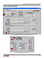
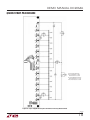
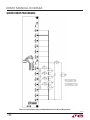
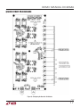
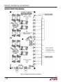
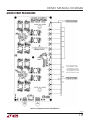
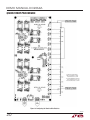
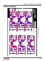
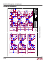
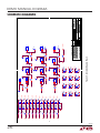
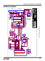
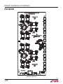
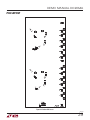
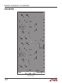
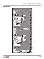
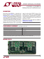
DEMO MANUAL DC2064A LTC3300-1/LTC6803-2 Bidirectional Cell Balancer DESCRIPTION Demonstration Circuit DC2064A is a bidirectional cell balancer using two LTC®3300-1 ICs to achieve active cell balancing of up to 12 Li-Ion batteries. The board uses the LTC6803-2 multi-cell addressable battery stack monitor to measure cell voltages and two LTC3300-1 ICs to provide active cell balancing. The demonstration circuit uses a two window GUI developed for the DC2064A. One window is a modified version of the GUI for the LTC6803‑2 and also contains a tab to control the LTC3300-1 ICs through the DC590B USB Serial controller and the second window PERFORMANCE SUMMARY reports the status of the LTC3300-1 devices. All the functions of the LTC6803-2 GUI are supported except that cell balancing is achieved through the LTC3300-1 ICs by transferring charge from one to six batteries per LTC3300-1 to the stack or from the stack to one to six batteries per LTC3300-1. Design files for this circuit board are available at http://www.linear.com/demo L, LT, LTC, LTM, Linear Technology and the Linear logo are registered trademarks of Linear Technology Corporation. All other trademarks are the property of their respective owners. Specifications are at TA = 25°C Battery Voltage Range 3.2V to 4.5V (2.5V to 4.5V)* Stack Voltage 60V Max Average Battery Balancing Charge Current (12 Cell) 2.6A (Typ) (4A)* Average Battery Balancing Discharge Current (12 Cell) 2.4A (Typ) (3.6A)* Average Battery Balancing Charge Current (6 Cell) 2.2A (Typ) (3.3A)* Average Battery Balancing Discharge Current (6 Cell) 2.4A (Typ) (3.6A)* Balancing Efficiency 92% (Typ) *The battery voltage range may be expanded to 2.5V-4.5V by changing resistor RTONS to 19.1k and resistor RTONP to 29.4k. The demo board’s average balancing current is adjustable up to 4A by scaling and installing new values of RS1A and RS1B through RS12A and RS12B. BOARD PHOTO dc2064af 1 DEMO MANUAL DC2064A DESCRIPTION Power Stage Discharge Efficiency Power Stage Charge Efficiency 100 100 95 95 EFFICIENCY (%) EFFICIENCY (%) 6-CELL 12-CELL 90 85 80 75 6-CELL 12-CELL 90 85 80 2.6 2.8 3.0 3.2 3.4 3.6 CELL VOLTAGE (V) 3.8 4.0 75 2.6 2.8 3.0 3.2 3.4 3.6 CELL VOLTAGE (V) 3.8 4.0 Figure 1. DC2064A Size 5.5" × 12.2" dc2064af 2 DEMO MANUAL DC2064A OPERATING PRINCIPLE Operation of the LTC6803-2 is detailed in the LTC6803-2 data sheet and the operation of the DC2064A GUI is similar to the DC1652A GUI except additional functionality was added to control the LTC3300-1 balancing devices. Refer to the Quick Start Guide for the DC1652B for operation of the LTC6803-2 GUI. The DC2064A has a two window GUI, one window based on the DC1652A GUI to control the LTC6803-2 with a tab to control the LTC3300-1 for battery balancing and the second window to display the status of the LTC3300-1 based on the command and status registers read from the LTC3300-1. The LTC3300-1 active balancer is a power stage control IC. The LTC3300-1 does not have a balancer algorithm built into it. The determination of the balancing times and directions are performed at a system level and conveyed to the LTC3300-1 through its SPI interface. The LTC3300‑1 only accepts battery charge or discharge commands. Charge is transferred to/from a cell (battery) from/to the stack, a series connection of adjacent cells, through a flyback converter that is operating in boundary mode. During discharge of a cell, the current in the primary of a coupled inductor transformer with a turns ratio of 1:2, ramps up to 6.25A at which point the primary switch turns off. The charge in the primary inductor is transferred to the secondary inductor which is connected across the 12-cell pack. This pack current then passes through the series connected cells thus distributing the charge equally across each cell. When charging a cell, the current, in the secondary of the coupled inductor transformer, ramps up to 3.125A at which point the secondary switch turns off. The charge in the secondary inductor is transferred to the primary inductor which is connected across the cell. The secondary current is drawn from the series connected cells thus removing charge equally across each cell. The efficiency through the flyback converter is ≈92%. QUICK START PROCEDURE The demonstration circuit is set up per Figure 27 to evaluate the performance of the DC2064A bidirectional cell balancer using the LTC3300-1. Caution: BOT6_TS and TOP6_TS turrets must not be allowed to float and must be connected to their respective top of stack-battery terminal. Follow the procedure outlined in the DC1835A Quick Start Guide for general use of the modified LTC6803-2 GUI window. The 4-bit board ID code that is set by the A0 through A3 jumpers on the DC2064A must match the board Address box in the LTC6803-2 GUI window shown in Figure 2 for each board in the system. Using short twisted-pair leads for any power connections, refer to Figure 27 for the proper measurement and equipment setup. When installing the batteries start with Cell 1 and progress to Cell 12. Remove batteries in the reverse order. The DC2064A will support a system of 4 to 12 batteries. Figure 2. Board Address Box dc2064af 3 DEMO MANUAL DC2064A QUICK START PROCEDURE The Voltage Comparator box must be turned off and the VREF must remain on during balancing. Set window by using the Up/Down arrows to the right of the box. See Figure 3. Click the START CELL VOLT button followed by the READ CELL VOLT to verify that the batteries are connected and that the LTC6803-2 can read the battery voltages. Figure 3. Voltage Comparator Box The DC2064A GUI periodically checks for OV and UV measured on the cells when balancing. To avoid the program from suspending balancing from an OV or UV measurement during normal operation, the OV and UV values must be entered in the VOV and VUV text boxes on the LTC6803-2 tab shown in Figure 4. Figure 6. Start Cell Voltage Read Box To access the LTC3300-1 screen, click on the LTC3300-1 tab in the upper left of the LTC6803-2 GUI window. Figure 7. LTC3300-1 Screen Select Box Within this window you can manually select which cells are to be discharged by clicking the cell’s DISCHARGE button and which cells are to be charged by clicking the cell’s CHARGE button. Figure 4. VOV and VUV text boxes Once this is done, Click the WRITE CONFIG button and verify that the configuration was set correctly by clicking the READ CONFIG. Figure 8. Balance Mode Select Boxs Figure 5. Write Configuration Box To write this configuration, the WRITE button followed by the SEND button must be clicked. To enable the balancers, the EXECUTE button followed by the SEND button must be clicked. To pause the cell balancers, the SUSPEND button is clicked followed by clicking the SEND button. This will turn off all balancers until the EXECUTE button is clicked followed by clicking the SEND button. This will resume the previous settings of the cell charge/discharge settings. dc2064af 4 DEMO MANUAL DC2064A QUICK START PROCEDURE To do this, select the DISCHARGE or CHARGE button for the desired cell, then enter the time in seconds into the cells “BALANCE TIME” text box. Press the enter key on the key board or select another button in the GUI to load the time. When all the desired balance actions and times have been entered, select the “Balance Cells” START button to start the balancing sequence. Figure 9. Write/Execute Command Box To change any of the settings “on the fly”, a new charge/ discharge setting is entered using the respective CHARGE and DISCHARGE buttons followed by clicking the WRITE button followed by the SEND button and then the EXECUTE button followed by the SEND button. To disable any cell from operating, the cell’s NONE button must be clicked in the balance mode box followed by clicking the WRITE button followed by the SEND button and then the EXECUTE button followed by the SEND button. The LTC3300-1 GUI allows the user to program the balancer to charge or discharge each cell for a specific amount of time. The LTC3300-1 is a power stage control IC. The determination of the balancing times and directions are done at the System level and conveyed to the LTC3300-1 through its SPI communications port. In order to perform a timed balance, the TIMED BALANCE check shown in Figure 10 must be selected to have access to the timed balance controls as shown in Figure 25. Figure 10. TIMED BALANCE Check Box Figure 11. Balance Cells Start Box The START button will display PAUSE. The balancing algorithm will first turn off all cells, then set all cells to be balanced. The cells will run until the first cell(s) have elapsed their balance time. At this time all cell balancing is suspended, the completed cell’s balancing action is set to “None”, the remaining times to balance are recalculated, then the remaining cells continue to balance until the next cell(s) have completed. This sequence continues until all of the balance times have elapsed. Selecting the PAUSE button while the balancer is running, will shut off the active cell and pause the timer. The START button now displays CONTINUE. Selecting the CONTINUE button again will start the active cell balancing and continue the timer. After the last cell has completed balancing, all the cells are turned off. The START button will again display START. Selecting the RESET button will reset all the cell actions and times to the previous entered settings. The LTC3300 STATUS window displays the status of all LTC3300-1 ICs in the system. This GUI is updated every time the LTC3300-1 status or command registers are read. When the balancer timer is running, the command register is read after each execute command is sent. dc2064af 5 DEMO MANUAL DC2064A QUICK START PROCEDURE Cell Balancer Efficiency Measurements: Cells 7-12 Figure 28 shows the proper connections for measuring the efficiency of a cell balancer. The secondary of the cell balancer connects to the top of stack. This connection needs to be to an isolated power source through a current sensing resistor (0.10Ω). Cells 1 through 6 are connected to the BOT6_TS turret with its return path the V– turret while Cells 7 through 12 are connected to the TOP6_TS turret with its return path the C6 turret. The primary side connections of the cell balancers are connected to a string of batteries that simulate the battery stack. Cell 1 is a 2-wire connection that connects the positive node, through a current sensing resistor (0.01Ω), to the C1 turret, and the negative node to the V– turret. Remote sense connections for power sources with remote sensing capabilities should be connected to the C1 and V– respectively. All other connections of the simulated string of batteries connect their positive node, through a current sensing resistor (0.01Ω), to respective turrets. Cell voltage measurements should be made across the C(x) and C(x – 1) turrets of the respective cells. Stack voltage measurements should be made at the BOT6_TS and TOP6_TS turrets and their return path turret. Charge Mode To calculate cell balancer efficiency use the expressions below: Cells 1-6 Charge Mode Efficiency 1 = Vm1 •Vm2 •10 •100% Vm3 •Vm4 Efficiency 11 = Vm5 •Vm6 •10 •100% Vm7 •Vm8 Discharge Mode Efficiency 11 = Vm7 •Vm8 •100% Vm5 •Vm6 •10 Cell Balancer Performance Measurements: Table 2 through Table 5 present the typical operational data for a 12-cell and 6-cell balancer in both Discharge and Charge modes. The cell voltages were 3.6V and measurements of Cell Current, Stack Current, Operating Frequency were taken and transfer Efficiency was calculated from the data. Figure 12 through Figure 15 are actual in circuit waveforms taken on Cell 1 and Cell 7 while operating in both modes. The waveforms present voltage on the primary side and secondary side MOSFET’s drain to source voltage and the primary side and secondary side current sense inputs to the LTC3300-1. Figures 16 through 19 are cell and stack currents taken over a range of cell voltages from 2.6V to 4.0V. The RTONP and RTONS resistors for these graphs were set for 2.6V cell voltage operation. All cells were set to the cell voltage under test. The slight negative slope in current at higher voltages is due to the increased operating frequency and the circuit delays and dead time becoming a higher percent-age of the operating period. Discharge Mode Efficiency 1 = Vm3 •Vm4 •100% Vm1 •Vm2 •10 dc2064af 6 DEMO MANUAL DC2064A QUICK START PROCEDURE 12 Cell Discharge 6 Cell Discharge Table 2. Typical 12 Cell Discharge Data Table 4. Typical 6 Cell Discharge Data Cell I (A) Stack I (A) Frequency (kHz) Efficiency Cell I (A) Stack I (A) Frequency (kHz) Efficiency 2.444 0.188 127.7 92.21% 2.448 0.277 126.1 92.33% Figure 12. 12 Cell Discharge Waveforms Figure 14. 6 Cell Discharge Waveforms 12 Cell Charge 6 Cell Charge Table 3. Typical 12 Cell Charge Data Table 5. Typical 6 Cell Charge Data Cell I (A) Stack I (A) Frequency (kHz) Efficiency Cell I (A) Stack I (A) Frequency (KHz) Efficiency 2.601 0.237 149.1 91.71% 2.219 0.399 133.1 92.72% Figure 13. 12 Cell Charge Waveforms Figure 15. 6 Cell Charge Waveforms dc2064af 7 DEMO MANUAL DC2064A 4.0 4.0 3.5 3.5 CELL CHARGE CURRENT (A) CELL DISCHARGE CURRENT (A) QUICK START PROCEDURE 3.0 12-CELL 2.5 6-CELL 2.0 1.5 1.0 2.6 2.8 3.6 3.0 3.2 3.4 CELL VOLTAGE (V) 3.8 3.0 12-CELL 2.5 6-CELL 2.0 1.5 1.0 2.6 4.0 0.50 0.50 0.45 0.45 0.40 6-CELL 0.35 0.30 0.25 12-CELL 0.20 0.15 0.10 2.6 3.6 3.0 3.2 3.4 CELL VOLTAGE (V) 3.8 4.0 Figure 18. Cell Charge Current STACK CHARGE CURRENT (A) STACK DISCHARGE CURRENT (A) Figure 16. Cell Discharge Current 2.8 6-CELL 0.40 0.35 0.30 12-CELL 0.25 0.20 0.15 2.8 3.2 3.4 3.6 CELL VOLTAGE (V) 3.0 3.8 4.0 Figure 17. Stack Discharge Current 0.10 2.6 2.8 3.2 3.4 3.6 CELL VOLTAGE (V) 3.0 3.8 4.0 Figure 19. Stack Charge Current dc2064af 8 DEMO MANUAL DC2064A QUICK START PROCEDURE Two Board Setup and Operation: As a result of communication latency to the PC, the system only supports two series DC2064A boards When connecting two DC2064A boards together, the interface cables must be connected in sequence as shown in Figure 20 to avoid large inrush currents. The DC590B DC2064A must be connected to the PC USB port and the bottom DC2064A board first and then the top DC2064A board may be connected. The 24 cells should be interconnected to allow balancing between the two 12-cell stacks, as shown in Figure 21. DC2064A Figure 20. Two DC2064A SPI Connection Sequence dc2064af 9 DEMO MANUAL DC2064A QUICK START PROCEDURE Figure 21. 24 Cell Interconnected Stacks dc2064af 10 DEMO MANUAL DC2064A QUICK START PROCEDURE On the LTC6803-2 tab on the DC2064A GUI, the Number of Boards in the System drop down box will need to be changed to 2. Make sure the address for each board in the Hex Address box matches the address set by the A0 to A3 jumpers on the respective DC2064A board. The board selection buttons on the bottom left side of the GUI highlight which board is selected in maroon, as shown and the set hexadecimal address is displayed under each board. To change the hexadecimal address on the GUI, select the board to change by clicking on the appropriate board selection number and then select the correct address in the Hex Address Box. Figure 22. DC2064A GUI Board Selection Controls To set up the charge and discharge actions for each LTC3300, the appropriate board must be selected first and then the commands for each LTC3300-1 can be selected and written to the LTC3300-1 tab. When all the desired actions are selected and written to the four LTC3300-1 ICs, then a single execute command will send an execute command to both boards simultaneously provided the Broadcast Execute/Suspend button is selected as shown in Figure 23. Additional Circuitry Additional circuitry has been added to increase the robustness of the design for fault insertions. Cell 6 Wire Disconnection A 10A 200V Schottky diode has been added for a high current path when the connection between battery cells is broken when a battery stack load is present. The 200V reverse voltage rating of the diode was selected to mini-mize the reverse leakage current at a battery voltage of 4.2V. The 10A current rating was selected for its low forward voltage drop which will minimize the current in the parallel diode within the LTC3300-1 as well as surviving the fusing current of the 7A fuses on the DC2064A. Two overvoltage detection circuits have been added to the design that will sense an overvoltage condition on Cell 6 and Cell 7 when a disconnection of the Cell 6 wire connection between battery Cell 6+ and battery Cell 7– of the battery stack occurs. When Cell 6 is being discharged and other cells controlled by the U1, the lower LTC3300-1, and U2, the upper LTC3300-1 are operational, an overvoltage can occur on Cell 7. The overvoltage on Cell 7 will shut down the operation of Cell 7-Cell 12 but Cell 1-Cell 6 will continue to operate. The overvoltage sensing circuit Q15, D21, D23 and R51 will turn off the operations of Cell 1-Cell 6 through the internal overvoltage protection circuit within the LTC3300-1 of U1. A similar event occurs when Cell 6 is operating in the Charge Mode and the Cell 6 connection from the board to the battery is lost. The overvoltage on Cell 6 will shut down the operation of Cell 1-Cell 6 but Cell 7- Cell 12 will continue to operate. The overvoltage sensing circuit Q16, D22, D24 and R52 will turn off the operations of Cell 7-Cell 12 through the internal overvoltage protection circuit within the LTC3300-1 of U2. Figure 23. Broadcast Execute/Suspend Tab dc2064af 11 DEMO MANUAL DC2064A QUICK START PROCEDURE Cell Bypass Capacitors The DC2064 contains bypass capacitors between the cell connections and the stack connections. These capacitors are intended to smooth the high current triangular wave before they travel down the interconnection wires to the cells within the stack and the secondary stack connections. The RMS current rating of these capacitors is a critical parameter as well as their capacitance with applied voltage and their physical size. The capacitance of MLCC capacitors decreases with applied voltage and this must be taken into account when selecting the capacitance value. The value of the cell bypass capacitor is outline on page 31 of the LTC3300-1 data sheet. Larger size, 1812 and above, MLCC capacitors have a tendency to crack and short due to thermal expansion and physical stress. Each cell must have an equal capacitance between them to prevent an overvoltage condition across the cell when randomly connecting batteries to the LTC3300-1 battery balancer circuit. There are also capacitors across adjacent cells that act a reservoir of charge for the cell’s FET Gate turn on circuit. These capacitors must also be of equal value to maintain the balancing of voltage and a capacitor of ½ the value need to be connected between Cell 1 and V– of the lowest LTC3300-1 and from the top cell to the cell below it to ensure balancing of voltage across all cells when the battery stack is initially connected. Figure 29 through 35 show the proper way to configure the board for between 4 and 11 batteries. Figure 24. DC2064A LTC6803-2 Setup Screen dc2064af 12 DEMO MANUAL DC2064A QUICK START PROCEDURE Figure 25. DC2064A LTC3300-1 Setup Screen with Timed Balance Controls Figure 26. DC2064A LTC3300-1 Status GUI Screen dc2064af 13 DEMO MANUAL DC2064A QUICK START PROCEDURE System Setup Requirements: LFP or Li-Ion Battery ≥ 10AHr Internal Resistance < 30mΩ Recommended Battery Simulator: Power Supply 2V to 5.0 V ±10A Interconnect Resistance < 25mΩ Figure 27. Proper Measurement Equipment Setup for Bidirectional Cell Balancer Note: All connections from equipment should be Kelvin connected directly to the Board Pins which they are connected to on this diagram and any input, or output, leads should be twisted pair, where possible. dc2064af 14 DEMO MANUAL DC2064A QUICK START PROCEDURE System Setup Requirements: LFP or Li-Ion Battery ≥ 10AHr Internal Resistance < 30mΩ Recommended Battery Simulator: Power Supply 2V to 5.0 V ±10A Interconnect Resistance < 25mΩ Figure 28. Proper Equipment Setup for Cell Balancer Efficiency Measurements dc2064af 15 DEMO MANUAL DC2064A QUICK START PROCEDURE System Setup Requirements: LFP or Li-Ion Battery ≥ 10AHr Internal Resistance < 30mΩ Recommended Battery Simulator: Power Supply 2V to 5.0 V ±10A Interconnect Resistance < 25mΩ Figure 29. Proper Equipment Setup for Minimum Number of Cell Efficiency Measurements dc2064af 16 DEMO MANUAL DC2064A QUICK START PROCEDURE System Setup Requirements: LFP or Li-Ion Battery ≥ 10AHr Internal Resistance < 30mΩ Recommended Battery Simulator: Power Supply 2V to 5.0 V ±10A Interconnect Resistance < 25mΩ Figure 30. Configuring the Board for Six Batteries dc2064af 17 DEMO MANUAL DC2064A QUICK START PROCEDURE System Setup Requirements: LFP or Li-Ion Battery ≥ 10AHr Internal Resistance < 30mΩ Recommended Battery Simulator: Power Supply 2V to 5.0 V ±10A Interconnect Resistance < 25mΩ Figure 31. Configuring the Board for Seven Batteries dc2064af 18 DEMO MANUAL DC2064A QUICK START PROCEDURE System Setup Requirements: LFP or Li-Ion Battery ≥ 10AHr Internal Resistance < 30mΩ Recommended Battery Simulator: Power Supply 2V to 5.0 V ±10A Interconnect Resistance < 25mΩ Figure 32. Configuring the Board for Eight Batteries dc2064af 19 DEMO MANUAL DC2064A QUICK START PROCEDURE System Setup Requirements: LFP or Li-Ion Battery ≥ 10AHr Internal Resistance < 30mΩ Recommended Battery Simulator: Power Supply 2V to 5.0 V ±10A Interconnect Resistance < 25mΩ Figure 33. Configuring the Board for Nine Batteries dc2064af 20 DEMO MANUAL DC2064A QUICK START PROCEDURE System Setup Requirements: LFP or Li-Ion Battery ≥ 10AHr Internal Resistance < 30mΩ Recommended Battery Simulator: Power Supply 2V to 5.0 V ±10A Interconnect Resistance < 25mΩ Figure 34. Configuring the Board for Ten Batteries dc2064af 21 DEMO MANUAL DC2064A QUICK START PROCEDURE System Setup Requirements: LFP or Li-Ion Battery ≥ 10AHr Internal Resistance < 30mΩ Recommended Battery Simulator: Power Supply 2V to 5.0 V ±10A Interconnect Resistance < 25mΩ Figure 35. Configuring the Board for Eleven Batteries dc2064af 22 A C1 C2 C1 C1 C2 C2 C3 1210 6.3V 1210 6.3V 1210 6.3V 1210 6.3V I1P C1G 2.2nF OPT D1C G1P C1B 100uF C1A 100uF D1F SBR10U200P5 20 4 3 4 20 R1C 4 5.1 Q1A SiR882DP 20 1206 4 3 T2 4 5 6 7 OPT D3B DFLS1100 9 10 1 2 T1 4 5 6 7 OPT D2B DFLS1100 V- WURTH-750312504 OPT OPT D1A D1B DFLS260 DFLS1100 470pF 100V 0603 C1E RS1A 0.008 20 1206 R1A 4 5 6 7 WURTH-750312504 9 10 1 2 OPT D2A DFLS260 100V 0603 RS2A 0.008 20 1206 R2A C2E 470pF T3 WURTH-750312504 9 10 1 2 OPT D3A DFLS260 100V 0603 C3E 470pF RS3A 0.008 R3A PLACE RC CLOSE TO LTC3300 20 CMOSH-4E R1G 1210 6.3V OPT C1C 100uF 4 3 Q2A SiR882DP CMOSH-4E R2G 5.1 R2C 1210 6.3V OPT C2C 100uF PLACE RC CLOSE TO LTC3300 I2P C2G 2.2nF OPT D2C G2P C2B 100uF C2A 100uF D2F SBR10U200P5 4 Q3A SiR882DP CMOSH-4E R3G 5.1 R3C 1210 6.3V PLACE RC CLOSE TO LTC3300 I3P C3G 2.2nF OPT D3C G3P 1210 6.3V 1210 6.3V D3F SBR10U200P5 C3B 100uF C3A 100uF 1 2 OPT C3C 100uF 1 2 1 2 3 1 2 3 18 1206 OPT R3B BOT6_TS RS3B 0.016 18 1206 OPT R2B BOT6_TS RS2B 0.016 18 1206 RS1B 0.016 I3S C3H 470pF 4 3 4 20 R2H 5.1 1210 100V OPT C2S 2.2uF I2S G2S C2H 470pF 470pF 100V 0603 R2F 1210 100V OPT C2F Q2B SiS892DN OPT C2T 2.2uF 20 R1H 5.1 C1H 470pF I1S G1S V- 1210 100V C2R 2.2uF V- C3R 2.2uF 1210 100V C3 C4 C4 C5 C6 1 2.5V - 4.5V 2.5A C N - C N-1 I6P C6G 2.2nF OPT D6C G6P 1210 6.3V C6B 100uF 1210 6.3V 1210 6.3V 4 C4G 2.2nF 20 THIS CIRCUIT IS PROPRIETARY TO LINEAR TECHNOLOGY AND SUPPLIED FOR USE WITH LINEAR TECHNOLOGY PARTS. LINEAR TECHNOLOGY HAS MADE A BEST EFFORT TO DESIGN A CIRCUIT THAT MEETS CUSTOMER-SUPPLIED SPECIFICATIONS; HOWEVER, IT REMAINS THE CUSTOMER'S RESPONSIBILITY TO VERIFY PROPER AND RELIABLE OPERATION IN THE ACTUAL APPLICATION. COMPONENT SUBSTITUTION AND PRINTED CIRCUIT BOARD LAYOUT MAY SIGNIFICANTLY AFFECT CIRCUIT PERFORMANCE OR RELIABILITY. CONTACT LINEAR TECHNOLOGY APPLICATIONS ENGINEERING FOR ASSISTANCE. 4 5 6 7 T4 4 5 6 7 OPT D5B DFLS1100 SCALE = NONE NC J. DREW PCB DES. APP ENG. APPROVALS 18 1206 OPT R6B OPT C6F RS6B 0.016 18 1206 OPT R5B BOT6_TS 18 1206 OPT R4B RS4B 0.016 DATE: N/A SIZE C6H 470pF I6S G6S I5S C5H 470pF 20 R4H 5.1 C4H 470pF I4S G4S 1210 100V OPT C4S 2.2uF SHEET 1 HIGH EFFICIENCY BIDIRECTIONAL MULTICELL BATTERY BALANCER LTC3300ILXE-1 / LTC6803IG-2 DEMO CIRCUIT 2064A TECHNOLOGY V- C4R 2.2uF 1210 100V V- C5R 2.2uF 1210 100V V- 179313000_SC BOT6_TS BOT6_TS J2 OF 5 1 REV. 1630 McCarthy Blvd. Milpitas, CA 95035 Phone: (408)432-1900 www.linear.com Fax: (408)434-0507 LTC Confidential-For Customer Use Only PLACE RC CLOSE TO LTC3300 4 3 4 1210 100V 470pF 100V 0603 Q4B SiS892DN R4F OPT C4T 2.2uF PLACE RC CLOSE TO LTC3300 20 R5H OPT C4F 4 3 5.1 G5S 1210 100V 1210 100V 470pF 100V 0603 Q5B SiS892DN R5F 4 OPT C5S 2.2uF V- 1 2 DATE 1 - 11 - 13 BOT6_TS E8 F13 7A 1210 J.DREW APPROVED C6R 2.2uF 1210 100V OPT C5T 2.2uF 1 - 11 - 13 IC NO. 20 R6H 5.1 1210 100V OPT C6S 2.2uF OPT C5F BOT6_TS RS5B 0.016 1210 100V OPT C6T 2.2uF PLACE RC CLOSE TO LTC3300 4 3 4 DESCRIPTION REVISION HISTORY PRODUCTION FAB Q6B SiS892DN R6F 470pF 100V 0603 1 REV BOT6_TS - ECO TITLE: SCHEMATIC OPT D4B DFLS1100 WURTH-750312504 9 10 1 2 OPT D4A DFLS260 470pF 100V 0603 C4E RS4A 0.008 20 1206 R4A T5 OPT D6B DFLS1100 WURTH-750312504 9 10 1 2 OPT D5A DFLS260 470pF 100V 0603 C5E RS5A 0.008 20 1206 R5A 4 5 6 7 WURTH-750312504 9 10 1 2 T6 BOT6_TS OPT D6A DFLS260 470pF 100V 0603 C6E RS6A 0.008 20 1206 R6A CUSTOMER NOTICE 4 3 Q4A SiR882DP CMOSH-4E R4G 5.1 4 PLACE RC CLOSE TO LTC3300 I4P OPT D4C R4C 1210 6.3V 1210 6.3V 1210 6.3V G4P OPT C4C 100uF C4B 100uF C4A 100uF D4F SBR10U200P5 20 3 Q5A SiR882DP 4 CMOSH-4E R5G 5.1 R5C 1210 6.3V OPT C5C 100uF 4 PLACE RC CLOSE TO LTC3300 I5P C5G 2.2nF OPT D5C G5P C5B 100uF C5A 100uF D5F SBR10U200P5 20 3 Q6A SiR882DP 4 CMOSH-4E R6G 5.1 R6C 1210 6.3V OPT C6C 100uF PLACE RC CLOSE TO LTC3300 C6A 100uF 1210 6.3V D6F SBR10U200P5 BATTERY CELL VOLTAGES C4 C5 C5 C6 Figure 36. Schematic Diagram Page 1 PLACE RC CLOSE TO LTC3300 4 3 4 R1F 1210 100V 1210 100V 470pF 1210 100V 100V 0603 Q1B SiS892DN C1R 2.2uF OPT C1S 2.2uF OPT C1T 2.2uF OPT C1F PLACE RC CLOSE TO LTC3300 BOT6_TS OPT R1B 20 G3S 100V 1210 OPT C3S 2.2uF PLACE RC CLOSE TO LTC3300 4 3 R3H 5.1 100V 1210 OPT C3T 2.2uF Q3B SiS892DN R3F 4 470pF 100V 0603 OPT C3F 1 2 C3 1 2 1 2 1 2 3 1 2 8 7 6 5 1 2 3 1 2 8 7 6 5 1 2 3 1 2 1 2 1 2 8 7 6 5 1 2 3 1 2 5 6 7 8 3 2 1 1 1 2 3 1 2 3 2 5 6 7 8 3 2 1 1 1 2 1 2 1 2 3 1 2 8 7 6 5 1 2 3 1 2 8 7 6 5 1 2 3 1 1 2 1 2 1 2 1 2 1 2 2 8 7 6 5 1 2 3 1 2 1 2 1 2 5 6 7 8 3 2 1 1 2 5 6 7 8 3 2 1 1 2 5 6 7 8 3 2 1 1 2 2 5 6 7 8 3 2 1 1 2 1 A DEMO MANUAL DC2064A SCHEMATIC DIAGRAMS dc2064af 23 A C7 C8 C7 C7 C8 C8 C9 1210 6.3V 1210 6.3V 4 4 3 20 4 20 4 5.1 Q7A SiR882DP CMOSH-4E R7G 3 R7C 1210 6.3V OPT C7C 100uF 4 CMOSH-4E R8G 3 Q8A 5.1 SiR882DP R8C 1210 6.3V OPT C8C 100uF PLACE RC CLOSE TO LTC3300 I7P C7G 2.2nF OPT D7C G7P C7B 100uF C7A 100uF D7F SBR10U200P5 20 PLACE RC CLOSE TO LTC3300 I8P C8G 2.2nF OPT D8C 1210 6.3V 1210 6.3V G8P C8B 100uF C8A 100uF SBR10U200P5 D8F 4 5.1 Q9A SiR882DP CMOSH-4E R9G R9C 1210 6.3V PLACE RC CLOSE TO LTC3300 I9P C9G 2.2nF OPT D9C G9P 1210 6.3V 1210 6.3V D9F SBR10U200P5 C9B 100uF C9A 100uF OPT C9C 100uF 20 1206 4 5 6 7 OPT D9B DFLS1100 T7 4 5 6 7 OPT D8B DFLS1100 C6 OPT D7B DFLS1100 WURTH-750312504 9 10 1 2 OPT D7A DFLS260 470pF 100V 0603 C7E RS7A 0.008 20 1206 R7A 4 5 6 7 WURTH-750312504 9 10 1 2 T8 OPT D8A DFLS260 100V 0603 RS8A 0.008 20 1206 R8A C8E 470pF T9 WURTH-750312504 9 10 1 2 OPT D9A DFLS260 100V 0603 RS9A 0.008 R9A C9E 470pF 1 2 1 2 3 1 2 3 18 1206 OPT R9B TOP6_TS RS9B 0.016 18 1206 OPT R8B TOP6_TS RS8B 0.016 18 1206 OPT R7B TOP6_TS RS7B 0.016 20 R9H 5.1 1210 100V OPT C9S 2.2uF I9S G9S C9H 470pF 1210 100V OPT C9T 2.2uF 20 R8H 5.1 C8H 470pF I8S G8S 1210 100V OPT C8S 2.2uF 1210 100V OPT C7F 470pF 100V 0603 20 R7H 1210 100V C7R 2.2uF I7S G7S C7H 470pF 1210 100V OPT C7S 2.2uF C6 1210 100V C8R 2.2uF C6 C11 C10 C9 C10 C10 C11 C11 C12 1 2.5V - 4.5V 2.5A C N - C N-1 1210 6.3V 1210 6.3V D10F SBR10U200P5 C10A 100uF 1210 6.3V D11F SBR10U200P5 C11A 100uF 1210 6.3V 4 20 R12G CMOSH-4E 4 3 5.1 Q12A SiR882DP R12C 1210 6.3V OPT C12C 100uF 20 4 3 Q11A SiR882DP CMOSH-4E R11G 5.1 4 4 3 T11 THIS CIRCUIT IS PROPRIETARY TO LINEAR TECHNOLOGY AND SUPPLIED FOR USE WITH LINEAR TECHNOLOGY PARTS. LINEAR TECHNOLOGY HAS MADE A BEST EFFORT TO DESIGN A CIRCUIT THAT MEETS CUSTOMER-SUPPLIED SPECIFICATIONS; HOWEVER, IT REMAINS THE CUSTOMER'S RESPONSIBILITY TO VERIFY PROPER AND RELIABLE OPERATION IN THE ACTUAL APPLICATION. COMPONENT SUBSTITUTION AND PRINTED CIRCUIT BOARD LAYOUT MAY SIGNIFICANTLY AFFECT CIRCUIT PERFORMANCE OR RELIABILITY. CONTACT LINEAR TECHNOLOGY APPLICATIONS ENGINEERING FOR ASSISTANCE. 4 5 6 7 OPT D12B DFLS1100 T10 4 5 6 7 OPT D11B DFLS1100 SCALE = NONE NC J. DREW PCB DES. APP ENG. APPROVALS 18 1206 OPT R12B TOP6_TS RS12B 0.016 18 1206 OPT R11B TOP6_TS RS11B 0.016 18 1206 RS10B 0.016 DATE: N/A SIZE 20 R11H 1210 100V 1210 100V C11H 470pF I11S G11S OPT C11S 2.2uF 20 R10H I10S G10S 1210 100V OPT C10S 2.2uF C6 SHEET LTC3300ILXE-1 / LTC6803IG-2 DEMO CIRCUIT 2064A 2 OF 5 1 REV. 1630 McCarthy Blvd. Milpitas, CA 95035 Phone: (408)432-1900 www.linear.com Fax: (408)434-0507 LTC Confidential-For Customer Use Only C6 C10R 2.2uF 1210 100V C6 C11R 2.2uF 1210 100V TOP6_TS TOP6_TS J3 179313000_SC 1 2 TOP6_TS E15 F14 7A 1210 HIGH EFFICIENCY BIDIRECTIONAL MULTICELL BATTERY BALANCER TECHNOLOGY PLACE RC CLOSE TO LTC3300 4 3 5.1 C10H 470pF 1210 100V 470pF 100V 0603 Q10B SiS892DN R10F OPT C10T 2.2uF 4 C6 C12R 2.2uF 1210 100V OPT C11T 2.2uF OPT C10F 1 - 11 - 13 IC NO. C12H 470pF I12S G12S PLACE RC CLOSE TO LTC3300 4 3 5.1 Q11B SiS892DN R11F 4 470pF 100V 0603 OPT C11F TOP6_TS OPT R10B 20 R12H 5.1 1210 100V OPT C12S 2.2uF PLACE RC CLOSE TO LTC3300 4 3 4 1210 100V 470pF 100V 0603 Q12B SiS892DN R12F OPT C12T 2.2uF OPT C12F TITLE: SCHEMATIC OPT D10B DFLS1100 WURTH-750312504 9 10 1 2 OPT D10A DFLS260 470pF 100V 0603 C10E RS10A 0.008 CUSTOMER NOTICE PLACE RC CLOSE TO LTC3300 20 CMOSH-4E R10G 20 1206 R10A 4 5 6 7 WURTH-750312504 9 10 1 2 OPT D11A DFLS260 470pF 100V 0603 C11E RS11A 0.008 20 1206 R11A T12 WURTH-750312504 9 10 1 2 TOP6_TS OPT D12A DFLS260 470pF 100V 0603 C12E RS12A 0.008 20 1206 R12A Q10A SiR882DP 4 5.1 I10P C10G 2.2nF OPT D10C G10P 1210 6.3V 1210 6.3V R10C OPT C10C 100uF C10B 100uF PLACE RC CLOSE TO LTC3300 C11G 2.2nF I11P OPT D11C R11C 1210 6.3V 1210 6.3V G11P OPT C11C 100uF C11B 100uF PLACE RC CLOSE TO LTC3300 I12P C12G 2.2nF OPT D12C G12P C12B 100uF C12A 100uF D12F SBR10U200P5 BATTERY CELL VOLTAGES C9R 2.2uF 1210 100V C12 Figure 37. Schematic Diagram Page 2 PLACE RC CLOSE TO LTC3300 4 3 5.1 Q7B SiS892DN R7F 4 OPT C7T 2.2uF PLACE RC CLOSE TO LTC3300 4 3 4 R8F 1210 100V 470pF 100V 0603 Q8B SiS892DN OPT C8T 2.2uF OPT C8F PLACE RC CLOSE TO LTC3300 4 3 4 Q9B SiS892DN R9F 470pF 100V 0603 OPT C9F 1 1 2 C9 1 2 1 2 1 2 3 1 2 8 7 6 5 1 2 3 1 2 8 7 6 5 1 2 3 1 1 2 1 2 2 8 7 6 5 1 2 3 1 2 1 2 1 2 1 2 5 6 7 8 3 2 1 1 1 2 3 1 2 3 2 5 6 7 8 3 2 1 1 1 2 1 2 1 2 3 1 2 8 7 6 5 1 2 3 1 2 8 7 6 5 1 2 3 1 1 2 1 2 2 5 6 7 8 3 2 1 1 2 1 2 2 8 7 6 5 1 2 3 1 2 1 2 1 2 5 6 7 8 3 2 1 1 2 5 6 7 8 3 2 1 1 2 5 6 7 8 3 2 1 1 24 2 OPT A DEMO MANUAL DC2064A SCHEMATIC DIAGRAMS dc2064af 16V 0603 C20 A 1.0uF I5S G4S 0 R2 U1 I1S G1S V- 12 11 10 9 8 7 6 5 4 3 2 1 49 V- R7 15.4k LTC3300ILXE-1 I2S 1 VREG1 WDTA G6S I6S G5S G2S I3S G3S I4S C1 4.7uF 16V 1210 WDTA E19 BSS123W Q13 D23 CMOSH-4E CMPT3906E Q15 I1S G1S I2S G2S I3S G3S I4S G4S I5S G5S I6S G6S GND OPT R3 0 1 1 R1 1M 0805 R14 845k D21 CMHZ4689 R8 20.5k 45 2 2 3 2 1 3 2 1 2 SDO SDII 39 I1P V- SCKI CSBI C2 0.1uF 10V 0402 BOT6_TS C6 D25 PDZ5.6B R54 20 0603 44 G1P C5 I2P G2P C2 I3P G3P C3 I4P G4P C4 I5P G5P C1K 1.0uF 16V 0603 25 26 27 28 29 30 31 32 33 34 35 36 I6P G6P C19 0.22uF 10V 0603 I2P G2P I4P 2 C5K 1.0uF 16V 0603 C2K 1.0uF 16V 0603 R45 0 2512 C26 4.7uF 16V 1210 R49 0 2512 C24 4.7uF 16V 1210 R47 0 2512 C22 4.7uF 16V 1210 0 OPT R41 C6K 1.0uF 16V 0603 C4K 1.0uF 16V 0603 C3K G3P 1.0uF 16V I3P 0603 G4P I5P G5P D19 CMMSH2-40 1 C25 4.7uF 16V 1210 R48 0 2512 C23 4.7uF 16V 1210 6.8 R4 D26 PDZ5.6B R55 20 0603 2.0k R52 1 1 1 D22 CMHZ4689 Q16 CMPT3904E 100k R53 3 2 1 C6 G9S I9S I10S G10S 1 R10 20.5k 0805 R13 845k D6 RS07J CUSTOMER NOTICE R11 15.4k I1S G1S I2S G2S I3S G3S I4S G4S I5S G5S I6S G6S GND 48 THIS CIRCUIT IS PROPRIETARY TO LINEAR TECHNOLOGY AND SUPPLIED FOR USE WITH LINEAR TECHNOLOGY PARTS. C4 0.1uF 10V 0402 TOP6_TS LINEAR TECHNOLOGY HAS MADE A BEST EFFORT TO DESIGN A CIRCUIT THAT MEETS CUSTOMER-SUPPLIED SPECIFICATIONS; HOWEVER, IT REMAINS THE CUSTOMER'S RESPONSIBILITY TO VERIFY PROPER AND RELIABLE OPERATION IN THE ACTUAL APPLICATION. COMPONENT SUBSTITUTION AND PRINTED CIRCUIT BOARD LAYOUT MAY SIGNIFICANTLY AFFECT CIRCUIT PERFORMANCE OR RELIABILITY. CONTACT LINEAR TECHNOLOGY APPLICATIONS ENGINEERING FOR ASSISTANCE. C6 12 11 10 9 8 7 6 5 4 3 2 1 49 R9 15.4k R12 0 OPT R5 1M VREG2 WDTC U2 LTC3300ILXE-1 I7S G7S I8S I12S G8S I11S G11S C3 4.7uF 16V 1210 G12S WDTC E20 Q14 BSS123W 3 2 D24 CMOSH-4E C21 1.0uF 16V 0603 Q17 CMPDM8002A 2 Figure 38. Schematic Diagram Page 3 C1 C2 C3 C4 C5 C6 D1 CMMSH2-40 C5 C6 1 2 3 2 1 2 C7 41 45 R51 2.0k 48 VREG 13 RTONS 47 TOS 14 RTONP 46 VMODE CTRL 15 CSBO 43 SCKO CSBI 16 SCKI 17 SDOI 42 BOOST SDO 19 SDI 18 40 BOOST- 21 WDT 20 BOOST+ V- 37 I6P 38 C6 I1P 22 G6P G1P 23 C1 24 1 2 47 VREG 13 RTONS 14 TOS 44 1 2 RTONP 46 VMODE CTRL 15 CSBO 43 SCKO CSBI 17 SCKI 16 1 41 1 39 I7P 2 G7P RS07J OPT D16 NC J. DREW SCALE = NONE APP ENG. PCB DES. APPROVALS D8 RS07J D7 RS07J WDTC 2 SDOI 42 BOOST SDO 19 SDI 18 1 V- C6 2 38 G1P 40 BOOSTWDT 20 BOOST+ V- 21 G6P 37 C5 I2P G2P C2 I3P G3P C3 I4P G4P C4 I5P G5P I6P C1 C6 I1P 22 C6 23 C6 25 26 27 28 29 30 31 32 33 34 35 36 I12P G12P C18 0.22uF 10V 0603 DATE: N/A SIZE D20 2 I8P C7K 1.0uF 16V 0603 C31 4.7uF 16V 1210 R43 0 2512 C28 4.7uF 16V 1210 C7 C8 C9 C10 C11 C12 SHEET LTC3300ILXE-1 / LTC6803IG-2 DEMO CIRCUIT 2064A 3 OF 5 1 REV. 1630 McCarthy Blvd. Milpitas, CA 95035 Phone: (408)432-1900 www.linear.com Fax: (408)434-0507 LTC Confidential-For Customer Use Only C30 4.7uF 16V 1210 R44 0 2512 R6 6.8 D5 CMMSH2-40 HIGH EFFICIENCY BIDIRECTIONAL MULTICELL BATTERY BALANCER TECHNOLOGY G8P C8K 1.0uF 16V 0603 C29 4.7uF 16V 1210 I9P G9P R46 0 2512 C27 4.7uF 16V 1210 C9K 1.0uF 16V 0603 C11K 1.0uF 16V 0603 C12K 1.0uF 16V 0603 0 OPT R42 R50 0 2512 1 - 11 - 13 IC NO. 1 CMMSH2-40 C10K G10P 1.0uF I10P 16V 0603 I11P G11P TITLE: SCHEMATIC 24 1 2 1 A DEMO MANUAL DC2064A SCHEMATIC DIAGRAMS WDTA dc2064af 25 A C1 C2 C3 C4 C5 C6 C7 C8 C9 C10 C11 C1 C2 C3 C4 C5 C6 C7 C8 C9 C10 C11 100 0603 R1K 100 0603 R2K 100 0603 R3K 100 0603 R4K 100 0603 R5K 100 0603 R6K 100 0603 R7K 100 0603 R8K 100 0603 R9K 100 0603 R10K 100 0603 R11K 100 0603 R12K V- V- V- V- V- V- V- V- V- V- V- V- V- V- C12_FILTER C11_FILTER C11L 0.1uF 100V 1206 C10_FILTER C10L 0.1uF 100V 1206 C9_FILTER C9L 0.1uF 100V 1206 C8_FILTER C12L 0.1uF 100V 1206 1 2 1 2 1 2 1 C8L 0.1uF 100V 1206 C7_FILTER 2 1 C7L 0.1uF 100V 1206 C6_FILTER 2 1 C2_FILTER C1L 0.1uF 100V 1206 C2L 0.1uF 100V 1206 C1_FILTER C3L 0.1uF 100V 1206 C4L 0.1uF 100V 1206 C3_FILTER C5L 0.1uF 100V 1206 C4_Filter C6L 0.1uF 100V 1206 C5_FILTER 2 1 2 1 2 1 2 1 2 1 2 1 26 2 C12_CLAMPED C7_FILTER C8_FILTER C9_FILTER C10_FILTER C11_FILTER C5_FILTER C6_FILTER D1E PDZ7.5B GRN GRN GRN C1_FILTER D2E PDZ7.5B C2_FILTER D3E PDZ7.5B C3_FILTER D4E PDZ7.5B C4_Filter D5E PDZ7.5B D6E PDZ7.5B D7E PDZ7.5B D8E PDZ7.5B D9E PDZ7.5B D10E PDZ7.5B D11E PDZ7.5B D12E PDZ7.5B C12_FILTER R1J 2.00k R9J C8 G9P C4 D9D LED-LN 2.00k R5J G5P D5D LED-LN V- C9 G1P D1D LED-LN 2.00k E1 C1 C5 V- 7A F15 1210 1210 GRN GRN GRN 7A G2P C2 C1 G10P C5 2.00k R10J C9 D10D LED-LN 2.00k R6J G6P D6D LED-LN 2.00k R2J D2D LED-LN F9 1210 7A F5 7A 1210 F1 V- C1SC1- J4 1210 E11 C9S+ C9+ C10S- J13 C9 F6 1210 C2 G11P C6 2.00k R11J C10 D11D LED-LN 2.00k R7J G7P D7D LED-LN 2.00k R3J G3P D3D LED-LN 7A F10 1210 7A E7 E18 C6S+ C6+ C7S- J10 C6 C6 C3 179314000_SC C2S+ C2+ C3S- J6 E3 E12 GRN GRN 7A F11 1210 7A C3 1 2.00k R12J G12P C7 C11 D12D LED-LN 2.00k R8J G8P D8D LED-LN 2.00k 1210 F7 1210 7A F3 G4P D4D LED-LN R4J C11 179314000_SC C10S+ C10+ C11S- J14 GRN 1 2 3 C10 C7 179314000_SC 1 2 3 1 2 3 C2 1 C12 C11S+ C11+ C12S- J15 C11 E13 C8 C12 1210 C8 C12S+ C12+ J16 E10 C12_CLAMPED C12 THIS CIRCUIT IS PROPRIETARY TO LINEAR TECHNOLOGY AND SUPPLIED FOR USE WITH LINEAR TECHNOLOGY PARTS. J. DREW SCALE = NONE APP ENG. NC APPROVALS PCB DES. C12_CLAMPED E14 179313000_SC 1 2 C8S+ C8+ C9S- J12 C4 179314000_SC 1 2 3 E5 179314000_SC C4S+ C4+ C5S- J8 CUSTOMER NOTICE 1206 L1 7A F12 1210 7A F8 1210 7A F4 1 2 3 LINEAR TECHNOLOGY HAS MADE A BEST EFFORT TO DESIGN A CIRCUIT THAT MEETS CUSTOMER-SUPPLIED SPECIFICATIONS; HOWEVER, IT REMAINS THE CUSTOMER'S RESPONSIBILITY TO VERIFY PROPER AND RELIABLE OPERATION IN THE ACTUAL APPLICATION. COMPONENT SUBSTITUTION AND PRINTED CIRCUIT BOARD LAYOUT MAY SIGNIFICANTLY AFFECT CIRCUIT PERFORMANCE OR RELIABILITY. CONTACT LINEAR TECHNOLOGY APPLICATIONS ENGINEERING FOR ASSISTANCE. C12 179314000_SC 1 2 3 C7S+ C7+ C8S- J11 E9 C4 179314000_SC 1 2 3 E4 179314000_SC C3S+ C3+ C4S- J7 C7 1 2 3 C3 Figure 39. Schematic Diagram Page 4 GRN GRN GRN C10 179314000_SC 1 2 3 C5S+ C5+ C6S- J9 C5 E6 7A F2 179314000_SC C6 1 2 3 C1S+ C1+ C2S- J5 E2 179314000_SC 1 2 3 C1 179313000_SC 1 2 DATE: N/A SIZE 1 - 11 - 13 IC NO. TITLE: SCHEMATIC SHEET LTC3300ILXE-1 / LTC6803IG-2 DEMO CIRCUIT 2064A 4 OF 5 1 REV. 1630 McCarthy Blvd. Milpitas, CA 95035 Phone: (408)432-1900 www.linear.com Fax: (408)434-0507 LTC Confidential-For Customer Use Only HIGH EFFICIENCY BIDIRECTIONAL MULTICELL BATTERY BALANCER TECHNOLOGY A DEMO MANUAL DC2064A SCHEMATIC DIAGRAMS dc2064af A D12 BAT46W C12_CLAMPED C2_FILTER C3_FILTER C4_FILTER C5_FILTER C6_FILTER C7_FILTER C8_FILTER C9_FILTER C10_FILTER C11_FILTER SDI SCKI A3 A2 A1 S12 C11 S11 C10 S10 GPI01 GPI02 VREF VREG TOS NC WDTB C2 S3 C3 S4 C4 V- V- 44 43 D14 100 R26 23 24 25 26 27 28 29 30 31 32 33 34 35 36 37 38 39 40 41 42 CMHZ5265B S2 C1 S1 V- NC S5 VTEMP1 C5 VTEMP2 S6 C6 S7 C7 S8 C8 S9 A0 SDO C12 C9 CSBI V+ D13 BAT46W 22 21 20 19 18 17 16 15 14 13 12 11 10 9 8 7 6 5 4 3 2 1 U8 LTC6803IG-2 C6 0.1uF 100V 1206 C1_FILTER V- VREG 0 JP2 0 JP1 0 0 C9 OPT 25V 0603 GPIO1 JP3 1 C12 1uF 25V 0603 V- V- JP4 5 3 U4 V- V+ +IN B -IN B OUT B OUT A +IN A -IN A C10 OPT 0603 25V 8 6 7 1 2 GPIO2 E23 LT6004CMS8 R15 1M R16 1M V- 5 4 GPIO1 E22 VREG VTEMP2 C8 TEMP2 PIN 0 V- R20 0 SDII DF3-3P-2DSA 3 2 TEMP1 J1 2 1 0.1uF MM74HC00 6 U5B TEMP1 1 V- 0 R21 0 R19 R18 3 10 9 13 12 1 1 U5A MM74HC00 SCKI VREG MM74HC00 8 U5C MM74HC00 11 U5D SDO CSBI R22 3.3k V- 3Y 2Y 1Y 3A 2A 1A 6 3 1 U6 74LVC3G07 V- K1 L2 L1 L3 L4 L5 K6 L6 K7 L7 K8 L8 V- I1 I2 SDO2 SCK2 SDI2 CS2 AVCC2 VCC2 AV- V- AV+ V+ BATTERY STACK THIS CIRCUIT IS PROPRIETARY TO LINEAR TECHNOLOGY AND SUPPLIED FOR USE WITH LINEAR TECHNOLOGY PARTS. SCALE = NONE NC J. DREW PCB DES. APP ENG. C7 0.1uF 25V 0603 A1 A3 A4 A5 A6 B1 A2 A7 A8 B7 B8 C17 10uf 10V DATE: N/A SIZE 1 - 11 - 13 IC NO. D15 CMSH3-20MA GND_DC590 C15 1uF 0603 25V E17 ISOLATED GND SDA WP A2 Vss 6 5 7 SERIAL EEPROM SCLK A1 A0 U3 5.1k R40 HD2X7 EEVCC EESCLK EESDA EEVSS GND_DC590 GND_DC590 GND_DC590 N/C SDO_590 SCK_590 SDI_590 CS_590 FROM DC 590B OR BOARD BELOW TO DC 590B INPUT ABOVE SHEET 5 OF 5 1 REV. 1630 McCarthy Blvd. Milpitas, CA 95035 Phone: (408)432-1900 www.linear.com Fax: (408)434-0507 LTC Confidential-For Customer Use Only R39 5.1k 10 11 9 12 HD2X7 N/C VCCA J18 EEVCC EESCLK EESDA EEVSS GND_DC590 GND_DC590 GND_DC590 N/C SDO_590 SCK_590 SDI_590 CS_590 N/C VCCA J17 HIGH EFFICIENCY BIDIRECTIONAL MULTICELL BATTERY BALANCER LTC3300ILXE-1 / LTC6803IG-2 DEMO CIRCUIT 2064A TECHNOLOGY 4 3 2 1 5 4 7 6 1 2 10 11 9 12 8 13 3 8 13 3 GND_DC590 5 4 7 6 1 2 14 14 ISOLATED GND PLANE 100 100 R36 R37 100 100 R38 R35 GND_DC590 TITLE: SCHEMATIC 2010 OPT 2010 OPT R34 2010 OPT R33 2010 OPT 470pF 1808 C13 R32 R31 470pF 1808 C5 SDO SCK SDI CS SDOE DO1 DO2 ON VL VCC VCC PC INPUT APPROVALS IF U7 IS NOT INSTALLED: DO NOT INSTALL U6, R22 -R25. INSTALL R31 R34. REPLACE C5 AND C13 WITH ZERO OHM RESISTOR. 2 5 7 V- OPT C16 10uF 10V CUSTOMER NOTICE R25 3.3k C14 0.1uF + U7 LTM2883CY - 5S OPT + E16 ISOLATED +5V ISOLATION BOUNDARY LINEAR TECHNOLOGY HAS MADE A BEST EFFORT TO DESIGN A CIRCUIT THAT MEETS CUSTOMER-SUPPLIED SPECIFICATIONS; HOWEVER, IT REMAINS THE CUSTOMER'S RESPONSIBILITY TO VERIFY PROPER AND RELIABLE OPERATION IN THE ACTUAL APPLICATION. COMPONENT SUBSTITUTION AND PRINTED CIRCUIT BOARD LAYOUT MAY SIGNIFICANTLY AFFECT CIRCUIT PERFORMANCE OR RELIABILITY. CONTACT LINEAR TECHNOLOGY APPLICATIONS ENGINEERING FOR ASSISTANCE. R23 3.3K R24 3.3k Figure 40. Schematic Diagram Page 5 100 R30 C11 1uF 25V 0603 R29 10k 10k R28 100 R27 R17 1M WDTB E21 7 1 14 VREG 14 7 14 7 14 7 1 A0 8 VCC GND 4 1 A1 GND2 GND2 GND2 GND2 K5 K4 K3 K2 1 2 A2 GND 4 GND GND GND GND GND B6 B5 B4 B3 B2 C12_FILTER 1 2 1 2 1 2 8 Vcc A3 A DEMO MANUAL DC2064A SCHEMATIC DIAGRAMS dc2064af 27 DEMO MANUAL DC2064A PCB LAYOUT Figure 41. Top Silk Screen dc2064af 28 DEMO MANUAL DC2064A PCB LAYOUT Figure 42. Bottom Silk Screen dc2064af 29 DEMO MANUAL DC2064A PCB LAYOUT Figure 43. Layer 1 dc2064af 30 DEMO MANUAL DC2064A PCB LAYOUT Figure 44. Layer 2 dc2064af 31 DEMO MANUAL DC2064A PCB LAYOUT Figure 45. Layer 3 dc2064af 32 DEMO MANUAL DC2064A PCB LAYOUT Figure 46. Layer 4 dc2064af 33 DEMO MANUAL DC2064A PARTS LIST ITEM QTY REFERENCE Required Circuit Components 1 24 C1A-C12A, C1B-C12B 2 12 C1G-C12G 3 12 C1H-C12H 4 12 C1R-C12R 5 14 C1K-C12K, C20,C21 6 4 C2, C4, C8, C14 7 1 C7 8 3 C11, C12, C15 9 2 C18, C19 10 2 D23, D24 11 4 D1, D5, D19.D20 12 3 D6, D7, D8 13 12 D1E-D12E 14 2 D12, D13 15 1 D14 16 1 D15 17 2 D21, D22 18 2 D25, D26 19 12 D1F-D12F 20 24 R1C-R12C, R1F-R12F 21 2 R4, R6 22 24 R1G-R12G, R1H-R12H 23 7 R26, R27, R30, R35-R38 24 5 R1, R5, R15-R17 25 2 R13, R14 26 3 R7, R9, R11 27 2 R8, R10 28 2 R51, R52 29 2 R39, R40 30 2 R28, R29 31 1 R53 32 2 R54, R55 33 12 RS1A-RS12A 34 12 RS1B-RS12B 35 12 Q1A-Q12A 36 12 Q1B-Q12B 37 2 Q13,Q14 38 1 Q15 39 1 Q16 40 1 Q17 41 12 T1-T12 42 2 U1,U2 43 1 U3 44 1 U4 45 1 U5 46 1 U8 PART DESCRIPTION MANUFACTURER/PART NUMBER CAP.,X5R, 100µF, 6.3V,10%, 1210 CAP.,X7R, 2200pF, 50V, 10% 0402 CAP.,X7R, 470pF, 50V, 10% 0402 CAP.,X7R, 2.2µF, 100V,10%, 1210 CAP.,X7R, 1.0µF, 16V,10%, 0603 CAP, X7R, 0.1µF, 16V, 10% 0402 CAP.,X7R, 0.1µF, 25V,10%, 0603 CAP.,X5R, 1µF, 25V,10%, 0603 CAP.,X7R, 0.22µF, 10V,10%, 0603 SMD, SCHOTTKY, SOD523 SMD, SCHOTTKY, SOD-123F SMD, SILICON SWITCHING DIODE DIODE, ZENER, 7.5V, 400MW, SOD323 SMD, SCHOTTKY, 200MW, 100V, SOD-12 SMD, SILICON ZENER, 62V SMD, SCHOTTKY DIODE, ZENER, 5.1V,SOD-123 DIODE, ZENER, 5.6V, 400MW, SOD323 DIODE, SUPER BARRIER RECTIFIER, 10A, POWERDI5 RES,CHIP, 5.1Ω, 1/16W, 5%, 0402 RES,CHIP, 6.8Ω, 1/16W, 5%, 0402 RES,CHIP,20Ω,1/16W,5%,0402 RES,CHIP,100Ω,1/16W,5%,0402 RES,CHIP, 1.00M, 1/16W, 5%, 0402 RES, CHIP, 845k, 1/8W, 1%, 0805 RES, CHIP, 15.4k, 1/16W, 1%, 0402 RES, CHIP, 20.5k, 1/16W, 1%, 0402 RES,CHIP,2.0k,1/16W,5%,0402 RES, CHIP, 5.1k, 1/16W, 5%, 0402 RES, CHIP, 10.0k, 1/16W, 5%, 0402 RES, CHIP, 100k, 1/16W, 5%, 0402 RES, CHIP, 20Ω, 1/16W, 5%, 0603 RES, CHIP, 8mΩ, 1W, 1%, 1206 RES, CHIP, 16mΩ, 1W, 1%, 1206 MOSFET, 100V, 0.0087Ω, 60A, POWERPAK-SO8 MOSFET, 100V, 0.058Ω, 25A, POWERPAK-1212-8 MOSFET, 100V, 10Ω, SOT-323 TRANSISTOR,PNP, 60V SOT-23 TRANSISTOR, NPN, 60V SOT-23 MOSFET, P-CHAN, 50V, 4Ω,SOT-23 TRANSFORMER, 1:1, 3.0µH, 10.8A IC, SMT, BIDIRECTIONAL BATTERY BALANCER IC, EEPROM 2KBIT, 400KHZ, 8TSSOP IC, SMT, OP AMP IC, GATE NAND QUAD 2-PIN 14-SO IC, SMT, BATTERY MONITOR MURATA, GRM32ER60J107ME20L MURATA, GRM155R71H222KA01D MURATA, GRM155R71H471KA01D TDK, C3225X7R2A225K MURATA, GRM188R71C105KA12D MURATA, GRM155R71C104KA88D AVX, 06033C104KAT2A TDK, C1608X5R1E105K MURATA, GRM188R71A224KA01 CENTRAL SEMI, CMOSH-4E CENTRAL SEMI, CMMSH2-40 VISHAY, RS07J NXP, PDZ7.5B.115 DIODES INC, BAT46W CENTRAL SEMI, CMHZ5265B CENTRAL SEMI, CMSH3-20MA CENTRAL SEMI, CMHZ4689 NXP, PDZ5.6B.115 DIODES INC, SBR10U200P5 VISHAY, CRCW04025R10JNED VISHAY, CRCW04026R80JNED VISHAY, CRCW040220R0JNED VISHAY, CRCW0402100RJNED VISHAY, CRCW04021M00JNED VISHAY, CRCW0805845KFKEA VISHAY, CRCW040215K4FKED VISHAY, CRCW040220K5FKED VISHAY, CRCW04022K00JNED VISHAY, CRCW04025K10JNED VISHAY, CRCW040210K0JNED VISHAY, CRCW0402100KJNED VISHAY, CRCW060320R0JNED SUSUMU, PRL1632-R008-F-T1 SUSUMU, PRL1632-R016-F-T1 VISHAY, SiR882DP-T1-GE3 VISHAY, SiS892DN-T1-GE3 DIODES INC, BSS123W-7-F CENTRAL SEMI, CMPT3906E CENTRAL SEMI, CMPT3904E CENTRAL SEMI, CMPDM8002A WURTH, 750312504 LINEAR, LTC3300ILXE-1#PBF MICROCHIP TECH. 24LC025-I/ST LINEAR, LT6004IMS8#PBT FAIRCHILD, MM74HC00M LINEAR, LTC6803IG-2#PBF dc2064af 34 DEMO MANUAL DC2064A PARTS LIST ITEM QTY REFERENCE Components and Hardware for Demo Board Only 1 12 C1E-C12E 2 12 C1, C3, C22-C31 3 13 C1L-C12L, C6 4 2 C5, C13 5 12 D1D-D12D 6 15 F1-F15 7 1 L1 8 12 R1A-R12A 9 12 R1K-R12K 10 4 R22-R25 11 8 R43-R50 12 12 R1J-R12J 13 18 E1-E18 14 5 E19-E23 15 2 J17,J18 16 1 J1 17 1 J1 (MATE) 18 3 J1 (MATE CONTACT) 19 4 JP1-JP4 20 4 JP1-JP4 21 1 U6 22 1 U7 23 5 MH1-MH5 Optional Components 1 0 C1C-C12C 2 0 C1F(OPT)-C12F(OPT) 3 0 C1S-C12S, C1T-C12T 4 0 C5, C13 5 0 C9(OPT), C10(OPT) 6 0 C16, C17 7 0 D1A-D12A 8 0 D1B-D12B (OPT) 9 0 D1C-D12C (OPT) 10 0 D16(OPT) 11 0 R1B-R12B (OPT) 12 0 R3, R12, R41, R42 (OPT) 13 0 R31-R34 (OPT) 14 0 J2-J4,J16 (OPT) 15 0 J2(OPT) (MATE) 16 0 J5-J15 (OPT) 17 0 J5-J15 (OPT) PART DESCRIPTION MANUFACTURER/PART NUMBER CAP.,X7R, 470pF, 100V,10%, 0603 CAP.,X7R, 4.7µF, 16V,20%, 1210 CAP., X7R, 0.1µF, 100V, 10%, 1206 CAP., X7R, 470pF, 250VAC, 10%, 1808 LED,GREEN CLEAR 0603 SMD FUSE, 7A, FAST, SMD, 1206 IND, FERRITE CHIP 33Ω, 6A, 1206 RES, CHIP, 20Ω, 1/4W, 5%, 1206 RES, CHIP, 100Ω, 1/16W, 5%, 0603 RES, CHIP, 3.3k, 1/16W, 5%, 0402 RES, CHIP, 0Ω, 2512 RES, CHIP, 2.0k, 1/16W, 5%, 0402 TP, TURRET, 0.094", PBF TURRET, 0.061 DIA CONN, HEADER, 14POS 2mm VERT GOLD CONN, HEADER, 3POS, 2.5mm STR TIN CONN, RECEPT HOUSING, 3POS 2.5mm CONTACT, SOCKET, CRIMP 20-22AWG, TIN HEADER, 3PINS, 2mm SHUNT 2mm IC,SMT, TRIPLE BUFFER IC,SMT,5V, SPI ISOLATER _ODULE STAND-OFF, NYLON, 0.500" TALL (SNAP ON) AVX, 06031C471KAT2A TDK, C3225X7R1C475M AVX, 12061C104KAT2A MURATA, GA342QR7GF471KW01L LITE-ON, LTST-C190KGKT COOPER BUSSMANN, 3216FF7-R MURATA, BLM31PG330SN1L VISHAY, CRCW120620R0JNEA VISHAY, CRCW0603100RJNED VISHAY, CRCW04023K30JNED VISHAY, CRCW25120000Z0EG VISHAY, CRCW04022K00JNED MILL-MAX, 2501-2-00-80-00-00-07-0 MILL-MAX, 2308-2-00-80-00-00-07-0 MOLEX 87831-1420 HIROSE, DF1EC-3P-2.5DSA(05) HIROSE, DF1E-3S-2.5C HIROSE, DF1E-2022SCF SAMTEC, TMM-103-02-L-S SAMTEC, 2SN-BK-G TI, SN74LVC3G07DCTR LINEAR, LTM2883CY-5S#PBF KEYSTONE, 8833 (SNAP ON) CAP., X5R, 100µF, 6.3V,10%, 1210 CAP., X7R, 470pF, 100V,10%, 0603 CAP., X7R, 2.2µF, 100V,10%, 1210 RES, CHIP, 0Ω, 2010 CAP, OPT, 25V, 0603 CAP., TANT, 10µF, 10V, 20%. 1206 SMD, SCHOTTKY BARRIER RECTIFIER 2A, 60V, PWRD123 SMD, SCHOTTKY BARRIER RECTIFIER, 1A, 100V, PWRD123 SMD, SCHOTTKY, SOD-523 SMD, SILICON SWITCHING DIODE RES, CHIP, 18Ω, 1/4W, 5%, 1206 RES, CHIP, 0Ω, 0402 RES, CHIP, 0Ω, 2010 HEADER, 1x2, 2-PIN, 3.81mm, 90 DEG SOCKET, 1x2, 2-PIN, 3.81mm, 180 DEG HEADER, 1x3, 3-PIN, 3.81mm, 90 DEG SOCKET, 1x3, 3-PIN, 3.81mm, 180 DEG MURATA, GRM32ER60J107ME20 AVX, 06031C471KAT2A TDK, C3225X7R2A225K VISHAY, CRCW20100000Z0EF AVX, TAJA106M010RNJ DIODES INC, DFLS260 DIODES INC, DFLS1100-7 CENTRAL SEMI, CMOSH-4E VISHAY, RS07J VISHAY, CRCW120618R0JNEA VISHAY, CRCW04020000Z0ED VISHAY, CRCW20100000Z0EF WEIDMULLER, 1793130000 WEIDMULLER, 1792770000 WEIDMULLER, 1793140000 WEIDMULLER, 1792780000 dc2064af Information furnished by Linear Technology Corporation is believed to be accurate and reliable. However, no responsibility is assumed for its use. Linear Technology Corporation makes no representation that the interconnection of its circuits as described herein will not infringe on existing patent rights. 35 DEMO MANUAL DC2064A DEMONSTRATION BOARD IMPORTANT NOTICE Linear Technology Corporation (LTC) provides the enclosed product(s) under the following AS IS conditions: This demonstration board (DEMO BOARD) kit being sold or provided by Linear Technology is intended for use for ENGINEERING DEVELOPMENT OR EVALUATION PURPOSES ONLY and is not provided by LTC for commercial use. As such, the DEMO BOARD herein may not be complete in terms of required design-, marketing-, and/or manufacturing-related protective considerations, including but not limited to product safety measures typically found in finished commercial goods. As a prototype, this product does not fall within the scope of the European Union directive on electromagnetic compatibility and therefore may or may not meet the technical requirements of the directive, or other regulations. If this evaluation kit does not meet the specifications recited in the DEMO BOARD manual the kit may be returned within 30 days from the date of delivery for a full refund. THE FOREGOING WARRANTY IS THE EXCLUSIVE WARRANTY MADE BY THE SELLER TO BUYER AND IS IN LIEU OF ALL OTHER WARRANTIES, EXPRESSED, IMPLIED, OR STATUTORY, INCLUDING ANY WARRANTY OF MERCHANTABILITY OR FITNESS FOR ANY PARTICULAR PURPOSE. EXCEPT TO THE EXTENT OF THIS INDEMNITY, NEITHER PARTY SHALL BE LIABLE TO THE OTHER FOR ANY INDIRECT, SPECIAL, INCIDENTAL, OR CONSEQUENTIAL DAMAGES. The user assumes all responsibility and liability for proper and safe handling of the goods. Further, the user releases LTC from all claims arising from the handling or use of the goods. Due to the open construction of the product, it is the user’s responsibility to take any and all appropriate precautions with regard to electrostatic discharge. Also be aware that the products herein may not be regulatory compliant or agency certified (FCC, UL, CE, etc.). No License is granted under any patent right or other intellectual property whatsoever. LTC assumes no liability for applications assistance, customer product design, software performance, or infringement of patents or any other intellectual property rights of any kind. LTC currently services a variety of customers for products around the world, and therefore this transaction is not exclusive. Please read the DEMO BOARD manual prior to handling the product. Persons handling this product must have electronics training and observe good laboratory practice standards. Common sense is encouraged. This notice contains important safety information about temperatures and voltages. For further safety concerns, please contact a LTC application engineer. Mailing Address: Linear Technology 1630 McCarthy Blvd. Milpitas, CA 95035 Copyright © 2004, Linear Technology Corporation dc2064af 36 Linear Technology Corporation LT 0613 • PRINTED IN USA 1630 McCarthy Blvd., Milpitas, CA 95035-7417 (408) 432-1900 ● FAX: (408) 434-0507 ● www.linear.com LINEAR TECHNOLOGY CORPORATION 2013