1
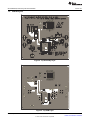
User's Guide
SLUU464 – November 2010
bq24450EVM
This user's guide describes the features and operation of the bq24450EVM Evaluation Module (EVM).
This EVM assists users in evaluating the bq24450 linear battery charger. The manual includes the
bq24450EVM bill of materials, board layout, and schematic.
1
2
3
4
5
6
7
Contents
Introduction ..................................................................................................................
1.1
EVM Features ......................................................................................................
1.2
General Description ................................................................................................
1.3
I/O Description and Jumper Functions ..........................................................................
1.4
Recommended Operating Conditions ...........................................................................
Equipment ....................................................................................................................
2.1
Power Supplies .....................................................................................................
2.2
Loads ................................................................................................................
2.3
Meters ...............................................................................................................
Equipment Setup ............................................................................................................
Procedure ....................................................................................................................
4.1
Pre-charge ..........................................................................................................
4.2
Max Charge .........................................................................................................
4.3
Charge Termination ................................................................................................
4.4
Re-Charge ..........................................................................................................
Functions and Features ....................................................................................................
5.1
Changing Output Voltage and Charge Current ................................................................
5.2
Options for External Transistor ...................................................................................
5.3
Other Options .......................................................................................................
PCB Layout Guideline ......................................................................................................
Bill of Materials, Board Layouts and Schematic ........................................................................
7.1
Bill of Materials .....................................................................................................
7.2
Board Layout .......................................................................................................
7.3
Schematic ...........................................................................................................
2
2
2
2
3
3
3
3
3
3
4
4
4
4
4
5
5
6
6
6
7
7
8
9
List of Figures
1
Original Test Setup for HPA691 (bq24450 EVM) ....................................................................... 3
2
Battery Load Circuit – PR1010-2
3
Calculating the Value of ITAPER ............................................................................................. 5
4
Top Assembly Layer ........................................................................................................ 8
5
Top PCB Layer .............................................................................................................. 8
6
Bottom PCB Layer .......................................................................................................... 9
7
bq24450 EVM Schematic .................................................................................................. 9
1
I/O Description............................................................................................................... 2
2
Recommended Operating Conditions .................................................................................... 3
3
Bill of Materials .............................................................................................................. 7
.........................................................................................
4
List of Tables
SLUU464 – November 2010
Submit Documentation Feedback
bq24450EVM
© 2010, Texas Instruments Incorporated
1
Introduction
www.ti.com
1
Introduction
1.1
EVM Features
•
•
•
•
•
•
1.2
Evaluation module for bq24450 (HPA691)
Charge controller for lead-acid batteries
Constant current and constant voltage modes
Accommodates external transistor in DPAK or TO-220 package
Programmable charge current
Pre-Charge for deeply discharged batteries
General Description
The bq24450 contains all the necessary circuitry to optimally control the charging of lead-acid batteries.
The IC controls the charging current as well as the charging voltage to safely and efficiently charge the
battery, maximizing battery capacity and life. Depending on the application, the IC can be configured as a
simple constant-voltage float charge controller or a dual-voltage float-cum-boost charge controller.
The built-in precision voltage reference is especially temperature-compensated to track the characteristics
of lead-acid cells, and maintains optimum charging voltage over an extended temperature range without
using any external components. The low current consumption of the IC allows for accurate temperature
monitoring by minimizing self-heating effects.
The IC can support a wide range of battery capacities and charging currents, limited only by the selection
of the external pass transistor. The versatile driver for the external pass transistor provides at least 25mA
of base drive.
In addition to the voltage- and current-regulating amplifiers, the IC features comparators that monitor the
charging voltage and current. These comparators feed into an internal state machine that sequences the
charge cycle. Some of these comparator outputs are made available as status signals at external pins of
the IC. These status and control pins can be connected to a processor, or they can be connected up in
flexible ways for standalone applications.
1.3
I/O Description and Jumper Functions
Table 1. I/O Description
Header
Description
J1 – Vin
Power Supply Positive
J2 – GND
Power Supply Negative
J3 – GND
Ground
J4 – Vout
Connected to Battery/System Load
J5 – GND
Ground
spacer
Jumper Description See Functions and Features section for more information.
JP1
Connects ISNSM for current sense for ITAPER. It can connect ISNSM to either side of the sense
resistor, R4.
JP2
Connects IFB for current sense for IMAX. It can connect IFB to either side of the sense resistor, R4.
JP3
Selects the topology for the external transistor. The external transistor can be configured for
either Common-Emitter topology or Quasi-Darlington topology.
2
bq24450EVM
SLUU464 – November 2010
Submit Documentation Feedback
© 2010, Texas Instruments Incorporated
Equipment
www.ti.com
1.4
Recommended Operating Conditions
Table 2. Recommended Operating Conditions
Symbol
Description
Vin, J1
Supply Voltage
Vout, J4
Battery Voltage (3-cell lead-acid battery)
Iin
Supply Current
Iout
Charge Current
2
Equipment
2.1
Power Supplies
Min
Typ
Max Unit
9.5
10.0
10.5
V
4
7.5
V
0
0.5
A
0
0.5
A
Power Supply #1 (PS#1): Adjustable from 0 to ≥ 10 VDC at ≥ 1A; used for input J1.
Power Supply #2 (PS#2): Adjustable from 0 to ≥ 10 VDC at ≥ 1.5A; used for Battery Load Board.
2.2
Loads
Load #1: Battery Load Circuit Board, PR1010-2, as shown in Figure 2.
2.3
Meters
Three Fluke 75 DMMs (equivalent or better).
3
Equipment Setup
The original test setup of HPA691 is shown in Figure 1.
1. Set the PS #1 for 10V, 1A current limit and then turn off supply. Connect PS#1 across J1, J2 (VIN,
GND).
2. Connect a voltage meter (VM #1) across J1, J2 (VIN, GND)
3. Set PS#2 to 5.2V and then turn off supply. Connect to the Battery Load Circuit Board (P/S+, P/S–)
4. Connect Load #1 (BAT+, BAT–) across J4, J5 (VOUT, GND).
5. Connect a voltage meter (VM#2) across J4, J5 (VOUT, GND).
6. Connect a voltage meter (VM#3) across sense resistor on Load #1.
7. Verify the jumpers are placed correctly as per, Figure 1.
Figure 1. Original Test Setup for HPA691 (bq24450 EVM)
SLUU464 – November 2010
Submit Documentation Feedback
bq24450EVM
© 2010, Texas Instruments Incorporated
3
Procedure
www.ti.com
Replacement circuit for a 3-cell lead acid battery. BAT+ to BAT– voltage tracks the power supply input
voltage, minus 1 diode drop
Figure 2. Battery Load Circuit – PR1010-2
4
Procedure
4.1
Pre-charge
Turn on PS #1, preset to 10 VDC. Verify voltage on VM #1.
Turn on PS #2, preset to 5.2 VDC.
Adjust PS #2 such that VM #2 shows 5 VDC.
Using VM #3, measure the voltage across the current sense resistor on Load #1. Multiply this value by a
conversion factor of 10A/V. This is the pre-charge current.
4.2
Max Charge
Adjust PS #2 such that VM #2 shows 6 VDC.
Using VM #3, measure the voltage across the current sense resistor on Load #1. Multiply this value by
a conversion factor of 10A/V. This is the max charge current.
4.3
Charge Termination
Adjust PS #2 such that VM #2 shows 7.5 VDC.
There should be no charge current in this condition.
4.4
Re-Charge
Adjust PS #2 such that VM #2 shows 6 VDC.
Using VM #3, measure the voltage across the current sense resistor on Load #1. Multiply this value
by a conversion factor of 10A/V. This is the max charge current.
4
bq24450EVM
SLUU464 – November 2010
Submit Documentation Feedback
© 2010, Texas Instruments Incorporated
Functions and Features
www.ti.com
5
Functions and Features
5.1
Changing Output Voltage and Charge Current
This EVM is configured to charge a 3-Cell Lead Acid Battery with a maximum charge current of 450 mA.
The EVM can be altered to charge lower or higher voltage batteries and can also be altered to have a
lower or higher maximum charge current.
Power Dissipation
It is important to monitor the power dissipation in the external transistor, Q1.
WARNING
Q1 and the surrounding area of the PCB may become hot.
(Power Dissipation in Q1) = (Vin – Vout – 0.25 – 0.7) × Charge Current
With a large difference between Vin and Vbat, and/or a high charge current, there will be a significant
amount of power dissipation in Q1. This causes both Q1 and the surrounding PCB to get hot. If any
alterations are made to the EVM circuit, it is important to ensure a safe level of power dissipation in the
external FET, Q1.
Changing Output Voltage
The output voltage may be altered by changing some on-board resistors (R7, R8, R9, R11, R12). See the
bq24450 datasheet for information on how to size these resistors. If Vout is changed, Vin must also be
changed. Vin should be high enough to allow for the necessary dropout (across R2, R4, Q1, and D1) and
low enough to maintain a safe level of power dissipation.
Changing the Maximum Charge Current
The maximum charge current is set by sense resistor, R2. (Max Charge Current) = (0.25) / R2. Resistor
R2 may be adjusted to set a different max charge current. However, more current will yield higher power
dissipation in Q1. This may cause the board to become hot.
Changing Pre-Charge Current
Pre-Charge current is set by R10.
Pre-Charge Current = (Vin – 2 – Vout) / R10
Changing the value of Itaper
As populated, ITAPER is 10% of IMax-Chg. This is because VILIM is 250mV and VISNS is 25mV and both are being
sensed across R2. If a different value of ITAPER is desired, R4 can be populated (with a non-zero resistor)
and JP1 and JP2 can be used to connect pins ISNSM and IFB to opposite sides of R4. See figure below.
Figure 3. Calculating the Value of ITAPER
SLUU464 – November 2010
Submit Documentation Feedback
bq24450EVM
© 2010, Texas Instruments Incorporated
5
PCB Layout Guideline
5.2
www.ti.com
Options for External Transistor
Using a Transistor in a TO-220 package
The EVM is populated with a DPAK transistor for Q1. However, if desired, a TO-220 transistor can be
used instead. Three holes have been placed in the PCB in parallel with the DPAK pad. Remove the DPAK
transistor and replace it with a TO-220 transistor. The top hole is the base, the middle hole is the collector,
and the bottom hole is the emitter.
Using a P-channel FET
The EVM is populated with a PNP transistor for Q1. However, if desired, a P-channel MOSFET may be
used instead. In order to use a P-FET, a resistor must be populated on R5. Pin 16 of the BQ24450 will
sink current through R5 and generate a negative gate to source voltage for the P-FET. By varying the sink
current (and subsequently Vgs), the IC can accurately control the charge current. A 1kΩ resistor is
suitable for R5.
Changing the topology
The EVM is configured with the Common-Emitter PNP topology. However, it can also be configured for
the PNP in a Quasi-Darlington as described on page 13 of the datasheet. To make this change, the
following steps should be taken:
1. Place jumper on JP3 such that it connects Pin 15 of the IC to the collector of Q1.
2. Remove R6 and replace with Rp as calculated on page 13 of the data sheet.
5.3
Other Options
Disabling Pre-Charge Mode
The EVM is populated to perform pre-charge on a deeply depleted battery. If pre-charge mode is not
desired, it can be disabled by performing the steps below.
1. Populate R1 = 0 Ω
2. Remove R11 and R12
3. Populate R14 = R11 + R12 (For example: If R11 = 75kΩ and R12 = 16.9kΩ, R14 = 91.9kΩ)
PGOOD
As populated, the EVM uses PGOOD as part of the feedback divider (explained on page 11 of data
sheet). If desired, PGOOD can be used to indicate the supply status on pin 5.
1. Remove R8 and place it on R15 pad.
2. Populate R13 with a pull-up resistor.
6
PCB Layout Guideline
It is important to pay special attention to the printed-circuit board (PCB) layout. The following provides
some guidelines:
1. All low-current GND connections must be kept separate from the high-current charge or discharge
paths from the battery. Use a single-point ground technique incorporating both the small signal ground
path and the power ground path.
2. The high current charge paths into IN pin and from the OUT pin must be sized appropriately for the
maximum charge current in order to avoid voltage drops in these traces.
6
bq24450EVM
SLUU464 – November 2010
Submit Documentation Feedback
© 2010, Texas Instruments Incorporated
Bill of Materials, Board Layouts and Schematic
www.ti.com
7
Bill of Materials, Board Layouts and Schematic
7.1
Bill of Materials
Table 3. Bill of Materials
Reference
Designator
Value
Description
Size
Part Number
MFR
C1, C4
Open
Capacitor, Ceramic
1206
Std
Std
C2, C5
1.0µF
Capacitor, Ceramic, 25V, X5R, 10%
603
Std
Std
C3
0.1µF
Capacitor, Ceramic, 25V, X7R, 10%
603
Std
Std
D1
ES2AA-13-F
Diode
SMA
ES2AA-13-F
Diodes,
Inc.
Q1
MJD32CT4
Transistor, PNP
DPAK
MJD32CT4
ST
R1, R5, R13, R14,
R15
Open
Resistor, Chip, 1/16W, 1%
603
Std
Std
R2
0.56Ω
Resistor, Chip, 1/2W, 1%
2010
STD
STD
R3, R6
0Ω
Resistor, Chip, 1/16W
603
Std
Std
R4
0Ω
Resistor, Chip, 1/2W
2010
CRCW20100000Z0EF
Vishay
R7
475kΩ
Resistor, Chip, 1/16W, 1%
603
Std
Std
R8
46.4kΩ
Resistor, Chip, 1/16W, 1%
603
Std
Std
R9
453Ω
Resistor, Chip, 1/16W, 1%
603
Std
Std
R10
187Ω
Resistor, Chip, 1/10W, 1%
603
Std
Std
R11
75.0kΩ
Resistor, Chip, 1/16W, 1%
603
Std
Std
R12
16.9kΩ
Resistor, Chip, 1/16W, 1%
603
Std
Std
R16
10.0kΩ
Resistor, Chip, 1/16W, 1%
603
Std
Std
U1
BQ24450D
IC, INTEGRATED CHARGE
CONTROLLER
FOR LEAD-ACID BATTERIES
SO-16
BQ24450D
TI
SLUU464 – November 2010
Submit Documentation Feedback
bq24450EVM
© 2010, Texas Instruments Incorporated
7
Bill of Materials, Board Layouts and Schematic
7.2
www.ti.com
Board Layout
Figure 4. Top Assembly Layer
Figure 5. Top PCB Layer
8
bq24450EVM
SLUU464 – November 2010
Submit Documentation Feedback
© 2010, Texas Instruments Incorporated
Bill of Materials, Board Layouts and Schematic
www.ti.com
Figure 6. Bottom PCB Layer
7.3
Schematic
Figure 7. bq24450 EVM Schematic
SLUU464 – November 2010
Submit Documentation Feedback
bq24450EVM
© 2010, Texas Instruments Incorporated
9
Evaluation Board/Kit Important Notice
Texas Instruments (TI) provides the enclosed product(s) under the following conditions:
This evaluation board/kit is intended for use for ENGINEERING DEVELOPMENT, DEMONSTRATION, OR EVALUATION
PURPOSES ONLY and is not considered by TI to be a finished end-product fit for general consumer use. Persons handling the
product(s) must have electronics training and observe good engineering practice standards. As such, the goods being provided are
not intended to be complete in terms of required design-, marketing-, and/or manufacturing-related protective considerations,
including product safety and environmental measures typically found in end products that incorporate such semiconductor
components or circuit boards. This evaluation board/kit does not fall within the scope of the European Union directives regarding
electromagnetic compatibility, restricted substances (RoHS), recycling (WEEE), FCC, CE or UL, and therefore may not meet the
technical requirements of these directives or other related directives.
Should this evaluation board/kit not meet the specifications indicated in the User’s Guide, the board/kit may be returned within 30
days from the date of delivery for a full refund. THE FOREGOING WARRANTY IS THE EXCLUSIVE WARRANTY MADE BY
SELLER TO BUYER AND IS IN LIEU OF ALL OTHER WARRANTIES, EXPRESSED, IMPLIED, OR STATUTORY, INCLUDING
ANY WARRANTY OF MERCHANTABILITY OR FITNESS FOR ANY PARTICULAR PURPOSE.
The user assumes all responsibility and liability for proper and safe handling of the goods. Further, the user indemnifies TI from all
claims arising from the handling or use of the goods. Due to the open construction of the product, it is the user’s responsibility to
take any and all appropriate precautions with regard to electrostatic discharge.
EXCEPT TO THE EXTENT OF THE INDEMNITY SET FORTH ABOVE, NEITHER PARTY SHALL BE LIABLE TO THE OTHER
FOR ANY INDIRECT, SPECIAL, INCIDENTAL, OR CONSEQUENTIAL DAMAGES.
TI currently deals with a variety of customers for products, and therefore our arrangement with the user is not exclusive.
TI assumes no liability for applications assistance, customer product design, software performance, or infringement of
patents or services described herein.
Please read the User’s Guide and, specifically, the Warnings and Restrictions notice in the User’s Guide prior to handling the
product. This notice contains important safety information about temperatures and voltages. For additional information on TI’s
environmental and/or safety programs, please contact the TI application engineer or visit www.ti.com/esh.
No license is granted under any patent right or other intellectual property right of TI covering or relating to any machine, process, or
combination in which such TI products or services might be or are used.
FCC Warning
This evaluation board/kit is intended for use for ENGINEERING DEVELOPMENT, DEMONSTRATION, OR EVALUATION
PURPOSES ONLY and is not considered by TI to be a finished end-product fit for general consumer use. It generates, uses, and
can radiate radio frequency energy and has not been tested for compliance with the limits of computing devices pursuant to part 15
of FCC rules, which are designed to provide reasonable protection against radio frequency interference. Operation of this
equipment in other environments may cause interference with radio communications, in which case the user at his own expense
will be required to take whatever measures may be required to correct this interference.
EVM Warnings and Restrictions
It is important to operate this EVM within the input voltage range of 9.5 V to 10.5 V and the output voltage range of 4 V to 7.5 V .
Exceeding the specified input range may cause unexpected operation and/or irreversible damage to the EVM. If there are
questions concerning the input range, please contact a TI field representative prior to connecting the input power.
Applying loads outside of the specified output range may result in unintended operation and/or possible permanent damage to the
EVM. Please consult the EVM User's Guide prior to connecting any load to the EVM output. If there is uncertainty as to the load
specification, please contact a TI field representative.
During normal operation, some circuit components may have case temperatures greater than 75° C. The EVM is designed to
operate properly with certain components above 75° C as long as the input and output ranges are maintained. These components
include but are not limited to linear regulators, switching transistors, pass transistors, and current sense resistors. These types of
devices can be identified using the EVM schematic located in the EVM User's Guide. When placing measurement probes near
these devices during operation, please be aware that these devices may be very warm to the touch.
Mailing Address: Texas Instruments, Post Office Box 655303, Dallas, Texas 75265
Copyright © 2010, Texas Instruments Incorporated
IMPORTANT NOTICE
Texas Instruments Incorporated and its subsidiaries (TI) reserve the right to make corrections, modifications, enhancements, improvements,
and other changes to its products and services at any time and to discontinue any product or service without notice. Customers should
obtain the latest relevant information before placing orders and should verify that such information is current and complete. All products are
sold subject to TI’s terms and conditions of sale supplied at the time of order acknowledgment.
TI warrants performance of its hardware products to the specifications applicable at the time of sale in accordance with TI’s standard
warranty. Testing and other quality control techniques are used to the extent TI deems necessary to support this warranty. Except where
mandated by government requirements, testing of all parameters of each product is not necessarily performed.
TI assumes no liability for applications assistance or customer product design. Customers are responsible for their products and
applications using TI components. To minimize the risks associated with customer products and applications, customers should provide
adequate design and operating safeguards.
TI does not warrant or represent that any license, either express or implied, is granted under any TI patent right, copyright, mask work right,
or other TI intellectual property right relating to any combination, machine, or process in which TI products or services are used. Information
published by TI regarding third-party products or services does not constitute a license from TI to use such products or services or a
warranty or endorsement thereof. Use of such information may require a license from a third party under the patents or other intellectual
property of the third party, or a license from TI under the patents or other intellectual property of TI.
Reproduction of TI information in TI data books or data sheets is permissible only if reproduction is without alteration and is accompanied
by all associated warranties, conditions, limitations, and notices. Reproduction of this information with alteration is an unfair and deceptive
business practice. TI is not responsible or liable for such altered documentation. Information of third parties may be subject to additional
restrictions.
Resale of TI products or services with statements different from or beyond the parameters stated by TI for that product or service voids all
express and any implied warranties for the associated TI product or service and is an unfair and deceptive business practice. TI is not
responsible or liable for any such statements.
TI products are not authorized for use in safety-critical applications (such as life support) where a failure of the TI product would reasonably
be expected to cause severe personal injury or death, unless officers of the parties have executed an agreement specifically governing
such use. Buyers represent that they have all necessary expertise in the safety and regulatory ramifications of their applications, and
acknowledge and agree that they are solely responsible for all legal, regulatory and safety-related requirements concerning their products
and any use of TI products in such safety-critical applications, notwithstanding any applications-related information or support that may be
provided by TI. Further, Buyers must fully indemnify TI and its representatives against any damages arising out of the use of TI products in
such safety-critical applications.
TI products are neither designed nor intended for use in military/aerospace applications or environments unless the TI products are
specifically designated by TI as military-grade or "enhanced plastic." Only products designated by TI as military-grade meet military
specifications. Buyers acknowledge and agree that any such use of TI products which TI has not designated as military-grade is solely at
the Buyer's risk, and that they are solely responsible for compliance with all legal and regulatory requirements in connection with such use.
TI products are neither designed nor intended for use in automotive applications or environments unless the specific TI products are
designated by TI as compliant with ISO/TS 16949 requirements. Buyers acknowledge and agree that, if they use any non-designated
products in automotive applications, TI will not be responsible for any failure to meet such requirements.
Following are URLs where you can obtain information on other Texas Instruments products and application solutions:
Products
Applications
Amplifiers
amplifier.ti.com
Audio
www.ti.com/audio
Data Converters
dataconverter.ti.com
Automotive
www.ti.com/automotive
DLP® Products
www.dlp.com
Communications and
Telecom
www.ti.com/communications
DSP
dsp.ti.com
Computers and
Peripherals
www.ti.com/computers
Clocks and Timers
www.ti.com/clocks
Consumer Electronics
www.ti.com/consumer-apps
Interface
interface.ti.com
Energy
www.ti.com/energy
Logic
logic.ti.com
Industrial
www.ti.com/industrial
Power Mgmt
power.ti.com
Medical
www.ti.com/medical
Microcontrollers
microcontroller.ti.com
Security
www.ti.com/security
RFID
www.ti-rfid.com
Space, Avionics &
Defense
www.ti.com/space-avionics-defense
RF/IF and ZigBee® Solutions www.ti.com/lprf
Video and Imaging
www.ti.com/video
Wireless
www.ti.com/wireless-apps
Mailing Address: Texas Instruments, Post Office Box 655303, Dallas, Texas 75265
Copyright © 2010, Texas Instruments Incorporated