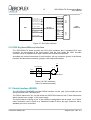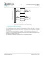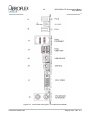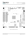
1
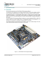
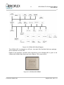
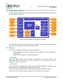
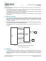
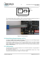
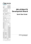
GR-LEON4-ITX
Development Board
User Manual
AEROFLEX GAISLER AB
Rev. 0.3, 2010-08-13
2
GR-LEON4-ITX Development Board
User Manual
Information furnished by Aeroflex Gaisler AB is believed to be accurate and reliable.
However, no responsibility is assumed by Aeroflex Gaisler AB for its use, nor for any infringements
of patents or other rights of third parties which may result from its use.
No license is granted by implication or otherwise under any patent or patent rights of Aeroflex
Gaisler AB.
Aeroflex Gaisler AB
tel +46 31 7758650
Kungsgatan 12
fax +46 31 421407
411 19 Göteborg
[email protected]
Sweden
www.aeroflex.com/gaisler
Copyright © 2010 Aeroflex Gaisler
All information is provided as is. There is no warranty that it is correct or suitable for any purpose,
neither implicit nor explicit.
© Aeroflex Gaisler AB
August 2010, Rev. 0.3
3
GR-LEON4-ITX Development Board
User Manual
TABLE OF CONTENTS
1
INTRODUCTION...........................................................................................................7
1.1
1.2
1.3
1.4
2
Overview...................................................................................................................... 7
References...................................................................................................................9
Handling....................................................................................................................... 9
Abbreviations...............................................................................................................9
ELECTRICAL DESIGN...............................................................................................10
2.1
2.2
2.3
2.4
2.5
2.6
2.7
2.8
2.9
2.10
2.11
2.12
2.13
2.14
2.15
2.16
2.17
2.18
LEON4 ASIC.............................................................................................................. 10
Board Block Diagram.................................................................................................12
Memory...................................................................................................................... 12
DDR2 RAM................................................................................................................ 12
SPI FLASH................................................................................................................. 12
PCI Slots.................................................................................................................... 13
Ethernet Interface......................................................................................................13
USB Host................................................................................................................... 13
USB Device................................................................................................................ 14
USB Debug Communication Link...............................................................................14
Video.......................................................................................................................... 14
PS2 Keyboard/Mouse Interface.................................................................................15
Serial Interface (RS232).............................................................................................15
Serial Debug Support Interface (LVTTL)....................................................................16
CAN Interface............................................................................................................ 16
Configuration of Bus Termination...............................................................................17
Configuration of Slew Rate.........................................................................................17
I2C interface............................................................................................................... 17
SPI interface.............................................................................................................. 18
GPIO.......................................................................................................................... 19
Debug Support Unit Interfaces...................................................................................20
Other Auxiliary Interfaces and Circuits.......................................................................21
Oscillators and Clock Inputs.......................................................................................21
Power Supply and Voltage Regulation......................................................................24
Reset Circuit and Button............................................................................................24
Watchdog................................................................................................................... 24
JTAG interface........................................................................................................... 25
eASIC SPI Configuration Interface.............................................................................25
3
SETTING UP AND USING THE BOARD...................................................................26
4
INTERFACES AND CONFIGURATION.....................................................................27
4.1
4.2
4.3
List of Connectors......................................................................................................27
List of Oscillators, Switches and LED's......................................................................38
List of Jumpers........................................................................................................... 39
© Aeroflex Gaisler AB
August 2010, Rev. 0.3
4
GR-LEON4-ITX Development Board
User Manual
LIST OF TABLES
Table 3-1: Default Status of Jumpers/Switches..............................................................................26
Table 4-1: List of Connectors......................................................................................................... 27
Table 4-2: PCI-J1 PCI Connector Slot 0.........................................................................................30
Table 4-3: PCI-J2 PCI Connector Slot 1.........................................................................................31
Table 4-4: J3A (Top) RJ45 10/100Mbit/s Ethernet Connector 1...................................................32
Table 4-5: J3B (Bottom) RJ45 10/100Mbit/s Ethernet Connector 0..............................................32
Table 4-6: J4A (Top) USB type A connector – USB-Host 0..........................................................32
Table 4-7: J4B (Bottom) USB type A connector – USB-Host 1.....................................................32
Table 4-8: J5 USB type B connector – USB Device......................................................................32
Table 4-9: J6 USB type B connector – USB Debug Communication Link.....................................33
Table 4-10: J7 DVI-I connector – Video........................................................................................33
Table 4-11: J8A (Top) PS2 Connector - Mouse............................................................................34
Table 4-12: J8B (Bottom) PS2 Connector – Keyboard..................................................................34
Table 4-13: J9 - GPIO[15..0] Header connections for PIO signals 0 to 15.....................................34
Table 4-14: J10 - GPIO[43..35] Header connections for PIO signals 35 to 43..............................34
Table 4-15: J11- SPI Header for User SPI interface......................................................................35
Table 4-16: J12 - UART-DSU Header for Serial DSU signals .......................................................35
Table 4-17: J13 – UART-2 Header for Serial UART2 signals.........................................................35
Table 4-18: J14 -UART-1 Header for Serial UART 1 signals.........................................................35
Table 4-19: J15 -CAN-1 Header for CANBUS-1 signals................................................................35
Table 4-20: J16 -CAN-0 Header for CANBUS-0 signals................................................................36
Table 4-21: J17 -I2C Slave Pin connections for User I2C interface................................................36
Table 4-22: J18 -I2C Master1 Pin connections for User I2C interface............................................36
Table 4-23: J19 -Debug Support Unit JTAG signal interface..........................................................36
Table 4-24: J20 -JTAG signal interface..........................................................................................37
Table 4-25: J21 -POWER - ATX Style power input connector.......................................................37
Table 4-26: J22 -POWER +5V DC power input connector.............................................................38
Table 4-27: J23 -ASIC-JTAG JTAG interface.................................................................................38
Table 4-28: J24 -PROM-PROG Config Prom SPI program interface.............................................38
Table 4-29: List and definition of Oscillators..................................................................................38
Table 4-30: List and definition of PCB mounted LED's...................................................................39
Table 4-31: List and definition of Switches.....................................................................................39
Table 4-32: List and definition of PCB Jumpers.............................................................................39
LIST OF FIGURES
Figure 1-1: GR-LEON4-ITX Development Board.............................................................................7
Figure 2-1: LEON4 Core Block Diagram........................................................................................10
Figure 2-2: LEON4 SOC Block Diagram........................................................................................11
Figure 2-3: LEON4-ASIC-DEMO....................................................................................................11
Figure 2-4: Block Diagram of GR-LEON4-ITX board.....................................................................12
Figure 2-5: Block diagram of Ethernet RMII Interface ...................................................................13
Figure 2-6: USB Host Controller PHYsical Interface......................................................................14
Figure 2-7: DVI Video Interface......................................................................................................15
Figure 2-8: PS/2 Interfaces ........................................................................................................... 15
Figure 2-9: Serial interface............................................................................................................. 16
Figure 2-10: Block Diagram of the CAN interface..........................................................................16
Figure 2-11: Transceiver and Termination Configuration ..............................................................17
Figure 2-12: I2C Interface Configuration........................................................................................18
© Aeroflex Gaisler AB
August 2010, Rev. 0.3
5
GR-LEON4-ITX Development Board
User Manual
Figure 2-13: SPI Interface Configuration........................................................................................19
Figure 2-14: PIO interface configuration........................................................................................19
Figure 2-15: Debug Support Unit connections................................................................................20
Figure 2-16: Board level Clock Distribution Scheme......................................................................22
Figure 2-17: Clock and PLL organisation inside LEON4 ASIC.......................................................23
Figure 2-18: Power Regulation Configuration.................................................................................24
Figure 2-19: Watchdog configuration.............................................................................................25
Figure 4-1: Front Panel View (pin 1 of connectors marked)...........................................................28
Figure 4-2: Board Connector View ................................................................................................29
Figure 4-3: PCB Top View.............................................................................................................. 40
Figure 4-4: GR-LEON4-ITX Assembly Photo (Top View)...............................................................41
REVISION HISTORY
Revision
Date
0.1 DRAFT
2010-03-01 All
New document
0.2
2010-03-17
Added reference to Quick Start Guide
0.3
2010-08-13
Added picture showing how to connect ribbon cable with DE-9 connector.
© Aeroflex Gaisler AB
Page
Description
August 2010, Rev. 0.3
6
GR-LEON4-ITX Development Board
User Manual
Intentionally Blank
© Aeroflex Gaisler AB
August 2010, Rev. 0.3
7
1
GR-LEON4-ITX Development Board
User Manual
INTRODUCTION
1.1 Overview
This document describes the GR-LEON4-ITX Development Board.
The purpose of this equipment is to provide developers with a convenient hardware platform
for the evaluation and development of software for the Aeroflex Gaisler LEON4 Processor.
The LEON4 processor is a synthesizable VHDL model of a 32-bit processor compliant to the
SPARC V8 architecture. In this variant, Aeroflex Gaisler has implement a Dual Core LEON4
with a rich set of IP cores and interfaces in a eASIC structured ASIC running at 200 MHz on
this board.
The GR-LEON4-ITX Development Board comprises a custom designed PCB in a Mini-ITX
format, making the board suitable either for stand-alone bench top development, or if
required, to be mounted in a 'standard' commercial Mini-ITX housing.
The principle interfaces and functions are accessible on the front and back edges of the the
board, and secondary interfaces via headers on the board.
Figure 1-1: GR-LEON4-ITX Development Board
© Aeroflex Gaisler AB
August 2010, Rev. 0.3
8
GR-LEON4-ITX Development Board
User Manual
The PCB contains the following main items as detailed in section 2 of this document:
•
LEON4 ASIC with Dual Core Leon4 architecture
•
Memory
• DDR2-400 RAM
256 MByte
• SPI program FLASH 64Mbit
(2x 1Gbit HYB18T1G160BF-5)
(1x M25P64 SPI prom)
•
Power, Reset, Clock and Auxiliary circuits
•
Interface circuits required for the features listed below
The interface connectors on the Front edge of the board provide:
•
Dual PCI (32 bit) mother-board slots
•
Dual RJ45 10/100 Mbit RMII Ethernet interface (DP83848VV with RJ45 jack)
•
Dual USB2.0 (USB-A) Host Interface (ISP1504A)
•
USB2.0 Device (USB-B) Interface (ISP1504A)
•
USB2.0 Debug Comm. Link (USB-B) Interface (ISP1504A)
•
DVI-I (Analog and Digital) Video Interface (Chrontel CH7301C)
•
PS2 Keyboard/Mouse Interface
The interface connectors on the Back edge of the board provide:
• +5V input power connector
• JTAG Debug interface
Additionally, on-board headers and components provide access to the following functions/
features:
• 44 pins General Purpose I/O pins
• 25 on 0.1” pin headers
• 8 on DIP switch
• 3 on Push button switches
• 8 connected to LED indicators
• I2C interface with on-board Real-Time Clock, and user connections on 0.1” header
• SPI interface, with on-board Temperature measurement, and user connections on
0.1” header
• Dual CAN bus interface (SN65HVD230)
• Two Serial UART interface (RS232) with D9 Sub female connectors
• ATX Style power connector
Debug interface support is demonstrated on the board with support for debugging via the
following interfaces:
• Push Buttons for RESET and DSU-BREAK
• LED indicators for POWER, ERRORN, DSU Active
• Assorted jumpers and Test Points for configuration and Test of the board
To enable convenient connection to the interfaces, most connector types and pin-outs are
compatible with the standard connector types for these types of interfaces.
© Aeroflex Gaisler AB
August 2010, Rev. 0.3
9
GR-LEON4-ITX Development Board
User Manual
Debug interface support is demonstrated on the board with support for debugging via the
following interfaces:
•
•
•
•
JTAG
ETH (EDCL)
USB (USB-DCL)
SERIAL (LVTTL i/f)
1.2 References
RD-1
GR-LEON4-ITX_schematic.pdf, Schematic
RD-2
GR-LEON4-ITX_assy_drawing.pdf, Assembly Drawing
RD-3
GR-LEON4-ITX_bom.pdf, Bill of Materials
RD-4
LEON4-ASIC-DEMO Data Sheet and User's Manual
RD-5
GRMON User Manual
RD-6
GR-LEON4-ITX Quick Start Guide
1.3 Handling
ATTENTION : OBSERVE PRECAUTIONS FOR
HANDLING ELECTROSTATIC SENSITIVE DEVICES
This unit contains sensitive electronic components which can be damaged by Electrostatic
Discharges (ESD). When handling or installing the unit observe appropriate precautions and
ESD safe practices.
When not in use, store the unit in an electrostatic protective container or bag.
When configuring the jumpers on the board, or connecting/disconnecting cables, ensure that
the unit is in an un-powered state.
1.4 Abbreviations
ASIC
DIL
DDR
DSU
ESD
GPIO
I/O
IP
MUX
PCB
RMII
SOC
Application Specific Integrated Circuit.
Dual In-Line
Double Data Rate
Debug Support Unit
Electro-Static Discharge
General Purpose Input / Output
Input/Output
Intellectual Property
Multiplexer
Printed Circuit Board
Reduced Media Independent Interface
System On a Chip
© Aeroflex Gaisler AB
August 2010, Rev. 0.3
10
2
GR-LEON4-ITX Development Board
User Manual
ELECTRICAL DESIGN
2.1 LEON4 ASIC
The Aeroflex Gaisler LEON4 processor core is a synthesizable VHDL model of a 32-bit
processor compliant with the SPARC V8 architecture. The core is highly configurable and
particularly suitable for high performance multi-core system-on-a-chip (SOC) designs.
The core is interfaced using the AMBA 2.0 AHB bus and supports the IP core plug&play
method provided in the Aeroflex Gaisler IP library (GRLIB). The processor can be efficiently
implemented on FPGA and ASIC technologies and uses standard synchronous memory
cells for caches and register file. The processor supports the MUL, MAC and DIV
instructions and an optional IEEE-754 floating-point unit (FPU) and Memory Management
Unit (MMU). The LEON4 cache system consists of separate I/D multi-set Level-1 (L1)
caches with up to 4 ways per cache, and an optional Level-2 (L2) cache for increased
performance in data intensive applications. The LEON4 pipeline uses 64-bit internal
load/store data paths, with an AMBA AHB interface of either 64- or 128-bit. Branch
prediction, 1-cycle load latency and a 32x32 multiplier results in a performance of 1.7
DMIPS/MHz, or 2.1 Coremark/MHz.
The wider interfaces provides higher bus and memory bandwidth which is necessary when
designing ASICs with high clock frequencies (800 MHz and above). The LEON4 is fully
software compatible with previous LEON processors. The configurability of LEON4 allows
designers to optimize the processor for performance, power consumption, I/O throughput,
silicon area and cost.
Figure 2-1: LEON4 Core Block Diagram
As a technology demonstrator, Aeroflex Gaisler has implemented a representative LEON4
configuration in a Structured ASIC from eASIC technologies.
This design consists of dual core LEON4 processors and a set of IP cores connected
through AMBA AHB/APB buses as represented in Figure 2-2.
© Aeroflex Gaisler AB
August 2010, Rev. 0.3
11
GR-LEON4-ITX Development Board
User Manual
Figure 2-2: LEON4 SOC Block Diagram
This LEON4 ASIC is packaged in a 672-pin, 1mm pitch Flip Chip Ball Grid Array package ,
and is soldered on to the PCB.
Details of the interfaces, operation and programming of the LEON4 ASIC is given in the
LEON4-ASIC-DEMO Data sheet and User's Manual, RD-4, and in RD-5.
Figure 2-3: LEON4-ASIC-DEMO
© Aeroflex Gaisler AB
August 2010, Rev. 0.3
12
GR-LEON4-ITX Development Board
User Manual
2.2 Board Block Diagram
The GR-LEON4-ITX Board provides the electrical functions and interfaces as represented in
the block diagram, Figure 2-4.
MOUSE/
KEYB I/F
PS/2
I/F
VIDEO I/F
DVI
TRANSCEIVER
USB - DSU
USB 2.0
DSU I/F
USB-B
DEVICE I/F
USB 2.0
DEVICE I/F
USB 2.0
HOSTI/F
DUAL USB-A
HOST I/F
ETHERNET
I/F
DUAL 10/100
ETHERNET
TRANSCEIVER
USER I/O
JTAG
I/F
CONFIGURATION
LEON4
ASIC
SPI
SERIAL
FLASH
2 x CAN
I/F
CAN
I/F
2 x RS232
UART I/F
UART
I/F
SPI
USER SPI
TEMP
I/F
MEASURE
SPI
I/F
I2C
USER I2C
REAL-TIME
I/F
CLOCK
I2C
I/F
PCI I/F
DDR2
RAM
POWER &
REGULATION
5V
PCI I/F
Figure 2-4: Block Diagram of GR-LEON4-ITX board
The Main PCB is a Mini-ITX format board (170 x 170mm) and can be used 'stand-alone' on
the bench-top simply using an external +5V power supply.
2.3 Memory
The memory configuration installed on the board comprises:
•
2 Gbit (256Mbyte) of DDR2-400 RAM memory, organised as 1 bank x 64Mword x
32 bits wide
•
64Mbit of Flash PROM, in serial SPI flash device
DDR2 RAM
Two 16 bit wide DDR2 memory devices are included on the board (Hynix 1Gbit
HYB18T1G160BF-5), providing 32 bit data connection to the processor with a total of
256MByte of volatile RAM memory.
SPI FLASH
A single Serial Flash PROM device (Intel/Numonyx M25P64-VMF6TP) is installed on the
board, connected to the SPIM SPI interface of the processor.
This device provides 64Mbit of Non-Volatile storage, organised as 8Mbyte x 8 bits.
This device can be used for Program storage or as a boot device for the board.
© Aeroflex Gaisler AB
August 2010, Rev. 0.3
13
GR-LEON4-ITX Development Board
User Manual
2.4 PCI Slots
The LEON4 ASIC device incorporates a GRPCI Fast 32-bit PCI bridge core which functions
as the PCI Host Controller on the LEON4-ITX Board.
To allow this board to function as a PCI motherboard, this board includes two 32 bits, 33MHz
PCI motherboard slot connectors, PCI-J1 and PCI-J2.
Note that the PCI slots are intended for cards which are compatible with 3.3V PCI signalling
voltage levels.
2.5 Ethernet Interface
The LEON4 ASIC device incorporates two Ethernet controllers with support for RMII
interface, and the GR-LEON4-ITX Development Board has two National Semiconductor
DP83848 10/100Mbit/s Ethernet PHY transceivers. These are connected to a dual RJ45
connector are on board.
For more information on the registers and functionality of the Ethernet MAC+PHY device
please refer to the data sheet for the DP83848 device.
The RMII Ethernet PHY's are provided with a 50 MHz clock derived from the oscillator X1 on
the board.
2
ETH_RXD[1..0]
2
ETH_TXD[1..0]
RJ45
RJ45
ETH_TXEN
ETH_CRS_DV
ETHERNET
ETHERNET
RMII
RMIIPHY
PHY
ASIC
ASIC
ETH_MDIO
ETH_MDC
ETH_MDINT
RESETN
50MHz
50MHz
ETH_RMIICLK
Figure 2-5: Block diagram of Ethernet RMII Interface
(one of 2 interfaces shown)
2.6 USB Host
The LEON4 ASIC device includes two USB 2.0 Host interfaces, and these are connected to
two on-board ISP1504 USB PHY devices using a standardised 8 bit ULPI interface,
operating at 60MHz.The ULPI interface configuration for the host interfaces is represented in
Figure 2-6.
© Aeroflex Gaisler AB
August 2010, Rev. 0.3
14
GR-LEON4-ITX Development Board
User Manual
The host interfaces include a MIC2025USB power switch component, controlled to provide
5V power output to the Dual USB-A style connector on the board.
Please refer to the device data sheet of the ISP1504A device for further information.
NEXT
DP
STP
DM
DIR
ASIC
ASIC
DATA[7..0]
USB
INTERFACE
USB
USBAA
ISP1504A
ISP1504A
USB
USBPHY
PHY
RESETN_N
ENABLE
POWER
POWER
SWITCH
SWITCH
CLK (60MHz)
XTAL
XTAL
19.2MHz
19.2MHz
Figure 2-6: USB Host Controller PHYsical Interface
2.7 USB Device
The LEON4 ASIC device also includes USB 2.0 Device interface, also connected to an
ISP1504 USB PHY device on the board, with a 8 bit ULPI interface, operating at 60MHz.
The interface configuration is similar to that represented in Figure 2-6, except that a
USB-B device connector is installed on the board, and no power switch is required for this
interface
2.8 USB Debug Communication Link
A second USB Device link is provided on the board (Connector J6), which is dedicated for
the USB Debug Communication link as described in section 2.17 and section 3.
Note that, to enable this interface, it is necessary that the GPIO43 pin is pulled high at power
on of the board.
This can be achieved by inserting a jumper on the pins 17-18 of the header connector J10.
2.9 Video
The GR-LEON4-ITX board incorporates an Chrontel CH7301C display controller device for
DVI interfaces, providing both Analog and Digital display interfaces on a standard DVI-I style
connector.
The LEON4 ASIC incorporates a SVGA controller core with DVI support which interfaces to
the controller device to provide a graphical video interface to the board.
© Aeroflex Gaisler AB
August 2010, Rev. 0.3
15
GR-LEON4-ITX Development Board
User Manual
DVI_CLK_P & N
TFT_LCD_CLK_P
DVI_D1_P & N
TFT_LCD_DATA[11..0]
DIGITAL
VGA
DVI_D0_P & N
TFT_LCD_CLK_N
DVI_D2_P & N
ASIC
ASIC
TFT_LCD_VSYNC
VIDEO
INTERFACE
CH7301C
CH7301C
DVI
DVICONTROLLER
CONTROLLER
RED
GREEN
TFT_LCD_DE
BLUE
HSYNC
TFT_LCD_RESET
ANALOG
VGA
TFT_LCD_HSYNC
VSYNC
DVI-I FEMALE
Figure 2-7: DVI Video Interface
2.10 PS2 Keyboard/Mouse Interface
The GR-LEON4-ITX board provides two PS2 style interfaces with a standard PS/2 style
connector as represented in the figure below, and the logic inside the ASIC provides
controller cores for standard PS2 style a Mouse and Keyboard connections.
According the normal conventions for this interface, the top connector (green) is the Mouse
interface and the bottom connector (purple) is the Keyboard interface.
+5V
3.3V to 5V buffer
5
6
PS2CLK
3
4
PS2DATA
1
2
MINI-DIN 6 pin
DGND
Figure 2-8: PS/2 Interfaces
(one of 2 interfaces shown)
2.11 Serial Interface (RS232)
The GR-LEON4-ITX-BOARD, provides RS232 interface circuits and 10 pin headers for two
Serial interfaces with TXD/RXD pins.
The RS232 transceiver IC's on this board are SN75C3232 devices from Texas Instruments
which operate from a single +3.3V power supply.
The layout and pin ordering of the 10 pin headers is designed so that a simple 1-to-1 ribbon
cable connection can be made to a 'standard' Female D-Sub 9 pin type connector with a
standard pin-out for serial links.
© Aeroflex Gaisler AB
August 2010, Rev. 0.3
16
GR-LEON4-ITX Development Board
User Manual
SUB-D 9 pin
Female
TXD
RS232
DRIVER/
RECEIVERS
ASIC
RS232
INTERFACE
RXD
Figure 2-9: Serial interface
The included ribbon cables providing a DE-9 connector should be connected as shown in
figure 2-10 (the red stripe should be toward the label UART-1/UART-2).
Figure 2-10: Serial interface
2.12 Serial Debug Support Interface (LVTTL)
A 10 pin 0.1” header on the board (J12) provides connections to the serial Debug Support
Unit signals DSURX (receive) and DSUTX (transmit).
Note that these voltage levels are 3.3V LVTTL and not RS232 levels. If you wish to connect
to this interface would be necessary use an adapter circuit to convert the signals to RS232
levels, or alternatively, a converter chip such as the FTDI FT232 could be used to provide a
Serial to USB conversion.
2.13 CAN Interface
The board provides the electrical interfaces for two CAN bus interfaces, as represented in
the block diagram, Figure 2-11.
The CAN bus transceiver IC's on this board are SN65HVD230 devices from Texas
Instruments which operate from a single +3.3V power supply.
© Aeroflex Gaisler AB
August 2010, Rev. 0.3
17
CAN
CAN
TRANSCEIVER
TRANSCEIVER
TXD
RXD
CAN_L
CAN_H
CAN
CAN
TRANSCEIVER
TRANSCEIVER
CAN_L
CAN
interface 1
CONTROLLER LOGIC IN ASIC
RXD
CAN_H
CAN
interface 0
TXD
GR-LEON4-ITX Development Board
User Manual
Figure 2-11: Block Diagram of the CAN interface
Configuration of Bus Termination
The CAN interfaces on the board can be configured for either end node or stub-node
operation by means of the jumpers JP8 and JP7 for interface 0 and 1 respectively, as shown
in Figure 2-12.
For normal end-node termination with a nominal 120 Ohm insert jumpers in position 1-3.
However, if a split termination is desired (if required for improved EMC performance), insert
the jumpers in positions 1-2 and 3-4.
For stub nodes, if termination is not required, do not install any jumpers.
© Aeroflex Gaisler AB
August 2010, Rev. 0.3
18
GR-LEON4-ITX Development Board
User Manual
Figure 2-12: Transceiver and Termination Configuration
(one of 2 interfaces shown)
Configuration of Slew Rate
The SN65HVD230 transceiver device used on the board has the facility to set the device into
STANDBY mode, by connecting an active high external signal to pin 8 of the device. On this
board, this pin is connected to the CAN_ENable contorl pin of the ASIC.
A further feature provided by the SN65HVD230 device is the capability to adjust the
transceiver slew rate. This can be done by modifying the values of resistors connected to pin
8 of the transceivers.
The default value of 0 ohms is compatible with 1Mbps operation.
From the data sheet the following resistor values give the following slew rates:
10kOhm => 15V/us
100kOhm => 2V/us
2.14 I2C interface
The LEON4 ASIC device provides three I2C interfaces, two master interfaces (I2CM0 &
I2CM1) and one slave interface (I2CS), as shown in Figure 2-13.
As a demonstration I2C circuit, an on-board DS1672 Real-Time Clock circuit is connected on
the board to the I2CM0 interface of the ASIC.
The I2CM1 and I2CS interfaces of the ASIC are connected to 4 pin 0.1” headers on the
board, to allow an external circuit to be hooked-up. If required, 10kOhm pull-up resistors on
the SCL and SDA signals can be installed if the appropriate jumpers JP9 and JP10 are
installed.
© Aeroflex Gaisler AB
August 2010, Rev. 0.3
19
GR-LEON4-ITX Development Board
User Manual
C75
DGND
+3V3
+3V3
I2 C
I2 C M 0
SCL
SDA
I2 C M 0 _ S C L
I2 C M 0 _ S D A
U15
VCC
R ST
SCL
SDA
X1
X2
VB
GND
Y1
3 2 .7 6 8 k
1
2
3
4
2
+3V3
TP6
8
7
6
5
1
R23
10k
R24
10k
3
4
100n
+
DGND
DS 1672
I2 C R e a l T im e C lo c k c h ip w ith p o w e r b a c ku p
C76
0 .4 7 F
SUPERCAP
DGND
+3V3
R 25
10k
I n s t a l l j u m p e rs 1 -2 a n d 3 -4 t o p ro v i d e p u l l u p s o n I 2 C s i g n a l s
1
3
R26
10k
JP 10
J18
2
4
I2 C
I2 C M 1
SCL
SDA
I2 C M 1 _ S C L
I2 C M 1 _ S D A
1
3
2
4
+3V3
DGND
HDR2X 2
H e a d e r fo r e x te rn a l I2 C fu n c ti o n s
+3V3
R 27
10k
I n s t a l l j u m p e rs 1 -2 a n d 3 -4 t o p ro v i d e p u l l u p s o n I 2 C s i g n a l s
1
3
R28
10k
I2 C
I2 C S
2
4
JP9
SCL
SDA
I2 C S _ S C L
I2 C S _ S D A
J17
1
3
2
4
+3V3
DGND
HDR2X 2
H e a d e r f o r e x t e rn a l I 2 C f u n c t i o n s
Figure 2-13: I2C Interface Configuration
2.15 SPI interface
In addition to the SPIM memory interface (ref section ), the LEON4 ASIC also provides an
SPI interface for user defined devices.
As shown in Figure 2-14 , the SPI interface pins of the LEON4 ASIC are connected to an 10
pin 0.1” header on the board to allow an external circuit SPI circuits to be hooked-up.
As an example SPI circuit, the GR-LEON4-ITX Board provides an AD7841, Temperature
monitor circuit on the board, which is selected with the SPIC_CS0 output of the ASIC.
© Aeroflex Gaisler AB
August 2010, Rev. 0.3
20
GR-LEON4-ITX Development Board
User Manual
+3V3
M e m o ry
SPI
S P IM _ C L K
S P IM _ M O S I
S P IM _ M IS O
S P IM _ S E L
SPI
S P IC _ C S [1 ..0 ]
S P IC _ M IS O
S P IC _ M O S I
S P IC _ S C K
S P IC _ S E L
S
S
S
S
P
P
P
P
IM _ C L K
IM _ M O S I
IM _ M IS O
IM _ S E L
S
S
S
S
S
P
P
P
P
P
IC
IC
IC
IC
IC
R 43
10k
_ C S [1 ..0 ]
_ M IS O
_MOS I
_S C K
_S E L
U8
1
2
3
4
5
6
7
8
+3V 3
S P IM _ S E L
S P IM _ M IS O
H
V
N
N
N
N
S
D
OLD
CC
C
C
C
C
C
DQ0
NC
NC
NC
NC
VSS
W
Q1
16
15
14
13
12
11
10
9
S P IM _ C L K
S P IM _ M O S I
C81
100n
DGND
R44
10k
M 2 5 P 6 4 -V M F
(o r W 2 5 X 6 4 -V S F )
U s e r C o n n e c to r
+3V3
DGND
+3V3
R45
NF
DGND
+3V3
J11
S P IC _ C S 0
S P IC _ M O S I
S P IC _ S C K
1
3
5
7
9
DGND
+3V3
S P IC _ C S 1
S P IC _ M IS O
S P IC _ S E L
2
4
6
8
10
DGND
+3V3
+3V3
U24
S P IC _ M O S I
S P IC _ M IS O
S P IC _ S C K
R 134
10k
R135
DGND
HDR5X2
+3V3
S P IC _ C S 0
C82
100n
0R
2
6
4
5
D IN
DOUT
SC LK
CS
A D7814A RT
R e m o ve if C S 0 is to b e u s e d o n h e a d e r
VDD
GND
3
C145
100n
1
A D 7 8 1 4 i s T e m p e ra t u re M o n i t o r w i t h S P I i n te rf a c e
DGND
Figure 2-14: SPI Interface Configuration
2.16 GPIO
The LEON4 ASIC provides 44 general Purpose Input Output signals (3.3V LVTTL voltage
levels).
On this board, to provide a range of possible uses, these signals have been connected as
follows:
•
•
•
•
25 signals I/O's on 0.1” pin headers
(with pull-up and series current limiting resistors as shown in Figure 2-15)
8 signal inputs on DIP switch S4 (GPIO[23:16])
(logic '1' input when switch is 'open', else logic '0' when switch is 'closed/on')
3 signal inputs on Push button switches (S1, S2, S3) (GPIO[24:26])
(logic '0' input when pressed, else logic '1')
8 signal outputs connected to LED indicators (D3 to D10) (GPIO[27:34])
('on' when output is logic '1')
PULL-UP
47k
(x67)
LEON4
ASIC
GPIO[43..0]
25
SERIES
470R
(x67)
PCB
Figure 2-15: PIO interface configuration
© Aeroflex Gaisler AB
August 2010, Rev. 0.3
21
GR-LEON4-ITX Development Board
User Manual
2.17 Debug Support Unit Interfaces
Program download and debugging to the processor is performed using the GRMON Debug
Monitor tool from Aeroflex Gaisler (RD-5). The LEON4 ASIC provides a interface for Debug
and control of the processor by means of a host terminal via its DSU interface, as
represented in Figure 2-16.
JTAG
EDCL
USB-DCL
SERIAL
DSUBRE→
DSUACT←
DSU I/F
HOST
TERMINAL/COMPUTER
JTAG I/F
LEON4
ASIC
DSUEN→
Figure 2-16: Debug Support Unit connections
Three control signals and a data connection form the Debug Support Unit interface to the
processor:
DSUEN:
This signal is pulled high on the board to enable Debugging
DSUBRE:
The push-button forces the processor to halt and enter DSU mode.
DSUACT:
When the processor is halted, the LED will illuminate
To communicate with the processor, four possibilities for the data connection to the
processor are provided:
SERIAL DSU Serial Debug Communication Link (connector J12)
JTAG-DCL
JTAG Debug Communication Link (connector J19 or J20)
USB-DCL
USB Debug Communication Link (connector J6)
EDCL
Ethernet Debug Communication Link (connector J3)
GRMON can be used with the above listed interfaces, for more information, please refer to
RD-5 and RD-6.
© Aeroflex Gaisler AB
August 2010, Rev. 0.3
22
GR-LEON4-ITX Development Board
User Manual
2.18 Other Auxiliary Interfaces and Circuits
Oscillators and Clock Inputs
The oscillator and clock scheme for the GR-LEON4-ITX Board is shown in Figure 2-17.
The main oscillator for the GR-LEON4-ITX ASIC is a 50 MHz Crystal oscillator. This
oscillator is an SMD oscillator soldered on to the board and a zero-delay buffer circuit
(CY2305) is used to distribute this 50MHz clock signal.
Addtionally, oscillators are provided as follows:
•
33.3 MHz oscillator with zero delay buffer for PCI interface and slots
•
19.2 MHz, generates 60MHz clock for USB interfaces
•
32.768 kHz crystal for real-time clock chip with battery back-up
Internally to the ASIC, PLL circuits generate the required clock frequencies and phases as
represented in Figure 2-18 for the following:
•
Processor Main frequency
•
DDR2 memory clocks
•
Vide Interface clocks
•
IP core clocks
If a different user defined main operating frequency of the ASIC is required, this can be
achieved by installing a 4 pin DIL8 style oscillator, in socket X2 on the board and moving
jumper JP1.
© Aeroflex Gaisler AB
August 2010, Rev. 0.3
23
ETH-PHY
ETH-PHY
GR-LEON4-ITX Development Board
User Manual
LEON4
ASIC
ETH-PHY
ETH-PHY
50
50MHz
MHz
ZERO
ZERO
DELAY
DELAY
BUFFER
BUFFER
CLK_50MHz
SMD
DDR2CLK
DDR2
SDRAM
RAM
SDRAM
MODULE
MODULE
CLK_MAIN
TBD
TBDMHz
MHz
DIL8 SOCKET
19.2
19.2MHz
MHz
ZERO
ZERO
DELAY
DELAY
BUFFER
BUFFER
SMD
USB-PHY
USB-PHY
USBHC0_CLK
USB-PHY
USB-PHY
USBHC1_CLK
USB-PHY
USB-PHY
USBDC_CLK
USB-PHY
USB-PHY
USBDCL_CLK
PCI_CLK
33.3
33.3MHz
MHz
PCI-SLOT
PCI-SLOT
PCI-SLOT
PCI-SLOT
SMD
Figure 2-17: Board level Clock Distribution Scheme
© Aeroflex Gaisler AB
August 2010, Rev. 0.3
24
GR-LEON4-ITX Development Board
User Manual
Figure 2-18: Clock and PLL organisation inside LEON4 ASIC
© Aeroflex Gaisler AB
August 2010, Rev. 0.3
25
GR-LEON4-ITX Development Board
User Manual
Power Supply and Voltage Regulation
The board operates from a single +5V DC power supply input. On board regulators generate
the following voltages:
•
+3.3V for the GR-LEON4-ITX I/O voltage, interfaces and other peripherals
•
+2.5V for LEON4 configuration voltage
•
+1.8V for DDR2 supply voltage
•
+1.2V for LEON4 Vcore voltage
REGULATOR
+3V3
REGULATOR
+1.2V (Vcore)
+1.8V (Vddr2)
+2.5V (Vconfig)
+5V
PCI SLOTS
+3V3
PCI
EXTERNAL POWER
SUPPLY, REGULATED
+5V, >1A
J22 POWER
2.1mm JACK
+12V
ATX POWER
CONN.
-12V
J21
Figure 2-19: Power Regulation Configuration
As an alternative to the single +5V power supply input, an ATX style power connector is also
provided on the board, which may be more convenent if the board is to be installed in a MiniITX style housing.
If PCI slots are to be used, then the ATX power connector should be used in order that
+3.3V, +5V, +12V and -12V will be correctly provided to the peripheral cards installed in the
slots.
Reset Circuit and Button
A standard Processor Power Supervisory circuit (TPS3705 or equivalent) is provided on the
Board to provide monitoring of the 3.3V power supply rail and to generate a clean reset
signal at power up of the Unit.
To provide a manual reset of the board, a miniature push button switch is provided on the
Main PCB for the control. Additionally connections are provided to an additional off-board
push-button RESET switch if this is required.
Watchdog
The LEON4 ASIC includes a Watchdog timer function which can be used for the purpose of
generating a system reset in the event of a software malfunction or crash.
On this development board the WDOGN signal is connected as shown in the Figure 2-20 to
© Aeroflex Gaisler AB
August 2010, Rev. 0.3
26
GR-LEON4-ITX Development Board
User Manual
the Processor Supervisory circuit.
RESETN
LEON4
LEON4
ASIC
ASIC
WDOGN
RSTIN_N
JUMPER
JUMPER
JP2
JP2
POWER-ON
POWER-ON
RESET
RESET
CIRCUIT
CIRCUIT
Figure 2-20: Watchdog configuration
To utilise the Watchdog feature, it is necessary to appropriately set-up and enable the
Watchdog timer. Please consult the LEON4 ASIC data sheet (RD-4) for the correct register
locations and details.
Also, to allow the WDOGN signal to generate a system reset it is necessary to install the
Jumper JP2 (see Figure 2-20).
For software development it is often convenient or necessary to disable the Watchdog
triggering in order to be able to easily debug without interference from the Watchdog
operation. In this case, the Jumper JP2 should be removed. When the watchdog triggers, a
system reset will not occur.
JTAG interface
Two connectors on the back edge of the PCB provide the possibility to connect to the JTAG
signals and JTAG chain of the LEON4 ASIC.
This interface allows DSU Debug over the JTAG interface to be performed.
Two connectors are provided, J20, a 14 pin 2mm Molex connector for connection with ribbon
cable to a JTAG cable such as the Xilinx Parallel IV or Platform USB cable, and J19, which
is a 6 pin 0.1” header which can be used to connect to Parallel III style cables.
eASIC SPI Configuration Interface
In order to store configuration bit information for the EASIC structured ASIC a dedicated SPI
PROM (U2) is provided on the board with its own 6 pin header for programming (J24).
This configuration information is automatically read out of the PROM by the ASIC when the
board is powered up in order to bring the ASIC into full operation.
When programming the SPI Configuration Prom, the jumpers JP11 must be removed in
order to 'disconnect' the prom form the ASIC. In normal use the jumpers JP11 should be
installed 1-2, 3-4, 5-6, 7-8 so that the correct communication can occur between the ASIC
and PROM.
The configuration prom will normally be pre-programmed during manufacture/test of the
board, and since these parameters are not user accessible, the functioning and
programming of this prom are not further described in this document.
© Aeroflex Gaisler AB
August 2010, Rev. 0.3
27
3
GR-LEON4-ITX Development Board
User Manual
SETTING UP AND USING THE BOARD
The default status of the Jumpers on the boards is as shown in Table 3-1.
For the meaning of the various jumpers, refer to Table 4-3 and RD 1.
Jumper
JP1
Jumper Setting
Installed 1-2
J10
Installed 17-18
JP11
Installed 1-2, 3-4, 5-6, 7-8
Comment
Connects 50MHz Main Oscillator for main CLK
This inserts a pull-up on GPIO43 to enable USB-DCL on
power up.
Table 3-1: Default Status of Jumpers/Switches
To operate the unit stand alone on the bench top, connect the +5V power supply to the
Power Socket J22 at the back of the unit.
The POWER LED should be illuminated indicating that the +3.3V power is active.
Upon power on, the Processor will start executing instructions beginning at the memory
location 0x00000000, which is the start of the PROM. If the PROM is 'empty' or no valid
program is installed, the first executed instruction will be invalid, and the processor will halt
with an ERROR condition, with the ERROR LED illuminated.
To perform program download and software debugging on the hardware it is necessary to
use the Gaisler Research GRMON debugging software, installed on a host PC (as
represented in Figure 2-16). Please refer to the GRMON documentation for the installation
of the software on the host PC (Linux or Windows), and for the installation of the associated
hardware dongle.
To perform software download and debugging on the processor, a link from the Host
computer to the DSU interface of the board is necessary. As described in section 2.17 there
are four possible DSU interfaces available on this board:
SERIAL DSU Serial Debug Communication Link (connector J12)
JTAG-DCL
JTAG Debug Communication Link (connector J19 or J20)
USB-DCL
USB Debug Communication Link (connector J6)
EDCL
Ethernet Debug Communication Link (connector J3)
Program download and debugging can be performed in the usual manner with GRMON.
More information on the usage, commands and debugging features of GRMON, is given in
the GRMON Users Manual and associated documentation. The GR-LEON4-ITX Quick Start
Guide contains more information and examples on using the board.
© Aeroflex Gaisler AB
August 2010, Rev. 0.3
28
4
GR-LEON4-ITX Development Board
User Manual
INTERFACES AND CONFIGURATION
4.1 List of Connectors
Name
Function
Type
Description
PCI-J1
PCI Slot 0
AMP 5145098-1
120 pin (32 bit) PCI motherboard interface – slot 0
PCI-J2
PCI Slot 1
AMP 5145098-1
120 pin (32 bit) PCI motherboard interface – slot 1
J3A
ETHERNET-1
Dual RJ45-Top
10/100Mbit/s Ethernet Connector 1
J3B
ETHERNET-0
Dual RJ45-Bottom
10/100Mbit/s Ethernet Connector 0
J4A
USB-HOST 0
Dual USB-A Top
USB Host Interface - 0
J4B
USB-HOST 1
Dual USB-A Bottom
USB Host Interface - 1
J5
USB-DEVICE
USB-B
USB Device interface
J6
USB-DCL
USB-B
USB Debug link interface
J7
DVI Video
MOLEX 74320-1004
DVI-I (Analog and Digital) Video Interface
J8A
MOUSE
Dual PS2-Top
PS2 Keyboard interface
J8B
KEYBOARD
Dual PS2-Bottom
PS2 Mouse interface
J9
GPIO[15..0]
20 pin 0.1” Header
Pin connections for PIO signals 0 to 15
J10
GPIO[43..35]
20 pin 0.1” Header
Pin connections for PIO signals 35 to 43
J11
SPI
10 pin 0.1” Header
Header for User SPI interface
J12
UART-DSU
10 pin 0.1” Header
Header for Serial DSU signals
J13
UART-2
10 pin 0.1” Header
Header for Serial UART2 signals
J14
UART-1
10 pin 0.1” Header
Header for Serial UART 1 signals
J15
CAN-1
10 pin 0.1” Header
Header for CANBUS-1 signals
J16
CAN-0
10 pin 0.1” Header
Header for CANBUS-0 signals
J17
I2C Slave
4 pin 0.1” Header
Pin connections for User I2C interface
J18
I2C Master1
4 pin 0.1” Header
Pin connections for User I2C interface
J19
JTAG-DSU
6 pin 0.1” Header
JTAG signal interface for DSU
J20
JTAG-DSU
2x7pin 2mm header
JTAG signal interface for DSU
J21
POWER_ATX
MOLEX 39-29-9202
ATX Style power input connector
J22
POWER_5V
2.1mm centre +ve
+5V DC power input connector
J23
JTAG-ASIC
6 pin 0.1” Header
ASIC JTAG interface
J24
PROM-PROG
6 pin 0.1” Header
Config Prom SPI program interface
Table 4-1: List of Connectors
© Aeroflex Gaisler AB
August 2010, Rev. 0.3
29
GR-LEON4-ITX Development Board
User Manual
Figure 4-1: Front Panel View (pin 1 of connectors marked)
© Aeroflex Gaisler AB
August 2010, Rev. 0.3
30
GR-LEON4-ITX Development Board
User Manual
Figure 4-2: Board Connector View
© Aeroflex Gaisler AB
August 2010, Rev. 0.3
31
GR-LEON4-ITX Development Board
User Manual
P C I-J 1
P C I_ T C K
-1 2 V
DGND
P C I_ IN T B
P C I_ IN T D
P C I_ C L K A
P C I_ A R B _ R E Q 0
+5V
+5V
DGND
DGND
P C I_ A D 3 1
P C I_ A D 2 9
P C I_ A D 2 7
P C I_ A D 2 5
P C I_ C B E 3
P C I_ A D 2 3
P C I_ A D 2 1
P C I_ A D 1 9
P C I_ A D 1 7
P C I_ C B E 2
P C I_ IR D Y
P C I_ D E V S E L
P C I_ L O C K
P C I_ P E R R
P C I_ S E R R
P C I_ C B E 1
P C I_ A D 1 4
P C I_ A D 1 2
P C I_ A D 1 0
DGND
+3V3PC I
DGND
+3V3PC I
DGND
+3V3PC I
DGND
+3V3PC I
+3V3PC I
DGND
P C I_ A D 8
P C I_ A D 7
P C I_ A D 5
P C I_ A D 3
P C I_ A D 1
P C I_ A C K 6 4 N
+3V3PC I
DGND
+3V3PC I
+5V
+5V
B1
B2
B3
B4
B5
B6
B7
B8
B9
B10
B11
B
B
B
B
B
B
B
B
B
B
B
B
B
B
B
B
B
B
B
B
B
B
B
B
B
B
B
B
B
B
B
B
B
B
B
B
14
15
16
17
18
19
20
21
22
23
24
25
26
27
28
29
30
31
32
33
34
35
36
37
38
39
40
41
42
43
44
45
46
47
48
49
B
B
B
B
B
B
B
B
B
B
B
52
53
54
55
56
57
58
59
60
61
62
-1 2 V
T C K /N C
GROUND
T D O /N C
+5V
+5V
IN T B #
IN T D #
P R S N T 1 # /N C
R E S ./R E Q 1 #
P R S N T 2 # /N C
T R S T # /N C
+12V
T M S /N C
T D I/ N C
+5V
IN T A #
IN T C #
+5V
R E S ./C L K C
+ V I / O (3 . 3 V )
R ESER V ED
R E S ./G N T 1 #
GROUND
C L K /C L K B
GROUND
R E Q # /R E Q 0 #
+ V I/O (3 .3 V )
A D [3 1 ]
A D [2 9 ]
GROUND
A D [2 7 ]
A D [2 5 ]
+ 3 V 3 /N C
C / B E [3 ] #
A D [2 3 ]
GROUND
A D [2 1 ]
A D [1 9 ]
+ 3 V 3 /N C
A D [1 7 ]
C / B E [2 ] #
GROUND
IR D Y #
+ 3 V 3 /N C
DEV SEL#
GROUND
LOC K #
PER R #
+ 3 V 3 /N C
SER R #
+ 3 V 3 /N C
C / B E [1 ] #
A D [1 4 ]
GROUND
A D [1 2 ]
A D [1 0 ]
M 6 6 E N /G N D
R E S ./C L K A
R ST#
+ V I / O (3 . 3 V )
G N T # /G N T 0 #
GROUND
R E S ./R E Q 2 #
A D [3 0 ]
+ 3 V 3 /N C
A D [2 8 ]
A D [2 6 ]
GROUND
A D [2 4 ]
ID S E L / G N T 2 #
+ 3 V 3 /N C
A D [2 2 ]
A D [2 0 ]
GROUND
A D [1 8 ]
A D [1 6 ]
+ 3 V 3 /N C
FR A M E#
GROUND
TR DY #
GROUND
STO P#
+ 3 V 3 /N C
SDONE
SB O#
GROUND
PAR
A D [1 5 ]
+ 3 V 3 /N C
A D [1 3 ]
A D [1 1 ]
GROUND
A D [0 9 ]
A D [0 8 ]
A D [0 7 ]
+ 3 V 3 /N C
A D [0 5 ]
A D [0 3 ]
GROUND
A D [0 1 ]
+ V I/O (3 .3 V )
ACK64#
+5V
+5V
C / B E [0 ] #
+ 3 V 3 /N C
A D [0 6 ]
A D [0 4 ]
GROUND
A D [0 2 ]
A D [0 0 ]
+ V I / O (3 . 3 V )
R E Q 6 4 # /N C
+5V
+5V
A
A
A
A
A
A
A
A
A
A
A
1
2
3
4
5
6
7
8
9
10
11
A
A
A
A
A
A
A
A
A
A
A
A
A
A
A
A
A
A
A
A
A
A
A
A
A
A
A
A
A
A
A
A
A
A
A
A
14
15
16
17
18
19
20
21
22
23
24
25
26
27
28
29
30
31
32
33
34
35
36
37
38
39
40
41
42
43
44
45
46
47
48
49
A
A
A
A
A
A
A
A
A
A
A
52
53
54
55
56
57
58
59
60
61
62
P C I_ T R S T
+12V
+5V
P C I_ T M S
P C I_ T D I
P C I_ IN T A
P C I_ IN T C
+5V
+3V3PC I
P C I_ R S T
+3V3PC I
P C I_ A R B _ G N T 0
DGND
P C I_ A D 3 0
+3V3PC I
DGND
+3V3PC I
DGND
+3V3PC I
DGND
DGND
P C I_ A D 2 8
P C I_ A D 2 6
P C I_ A D 2 4
P C I_ A D 1 6
P C I_ A D 2 2
P C I_ A D 2 0
P C I_ A D 1 8
P C I_ A D 1 6
P C I_ F R A M E
P C I_ T R D Y
P C I_ S T O P
+3V3PC I
DGND
+3V3PC I
DGND
P C I_ P A R
P C I_ A D 1 5
P C I_ A D 1 3
P C I_ A D 1 1
P C I_ A D 9
P C I_ C B E 0
+3V3PC I
DGND
+3V3PC I
P C I_ A D 6
P C I_ A D 4
P C I_ A D 2
P C I_ A D 0
P C I_ R E Q 6 4 N
+5V
+5V
P C I3 2 -U N IV
Table 4-2: PCI-J1 PCI Connector Slot 0
© Aeroflex Gaisler AB
August 2010, Rev. 0.3
32
GR-LEON4-ITX Development Board
User Manual
P C I-J 2
P C I_ T C K
-1 2 V
DGND
P C I_ IN T C
P C I_ IN T A
P C I_ C L K B
P C I_ A R B _ R E Q 1
P C I_ A D 3 1
P C I_ A D 2 9
P C I_ A D 2 7
P C I_ A D 2 5
P C I_ C B E 3
P C I_ A D 2 3
P C I_ A D 2 1
P C I_ A D 1 9
P C I_ A D 1 7
P C I_ C B E 2
P C I_ IR D Y
P C I_ D E V S E L
P C I_ L O C K
P C I_ P E R R
P C I_ S E R R
P C I_ C B E 1
P C I_ A D 1 4
P C I_ A D 1 2
P C I_ A D 1 0
+5V
+5V
DGND
DGND
+3V3PC I
DGND
+3V3PC I
DGND
+3V3PC I
DGND
+3V3PC I
DGND
+3V3PC I
+3V3PC I
DGND
P C I_ A D 8
P C I_ A D 7
P C I_ A D 5
P C I_ A D 3
P C I_ A D 1
P C I_ A C K 6 4 N
+3V3PC I
DGND
+3V3PC I
+5V
+5V
B1
B2
B3
B4
B5
B6
B7
B8
B9
B10
B11
B
B
B
B
B
B
B
B
B
B
B
B
B
B
B
B
B
B
B
B
B
B
B
B
B
B
B
B
B
B
B
B
B
B
B
B
14
15
16
17
18
19
20
21
22
23
24
25
26
27
28
29
30
31
32
33
34
35
36
37
38
39
40
41
42
43
44
45
46
47
48
49
B
B
B
B
B
B
B
B
B
B
B
52
53
54
55
56
57
58
59
60
61
62
-1 2 V
T C K /N C
GROUND
T D O /N C
+5V
+5V
IN T B #
IN T D #
P R S N T 1 # /N C
R E S ./R E Q 1 #
P R S N T 2 # /N C
T R S T # /N C
+12V
T M S /N C
T D I/ N C
+5V
IN T A #
IN T C #
+5V
R E S ./C L K C
+ V I / O (3 . 3 V )
R ESER V ED
R E S ./G N T 1 #
GROUND
C L K /C L K B
GROUND
R E Q # /R E Q 0 #
+ V I/O (3 .3 V )
A D [3 1 ]
A D [2 9 ]
GROUND
A D [2 7 ]
A D [2 5 ]
+ 3 V 3 /N C
C / B E [3 ] #
A D [2 3 ]
GROUND
A D [2 1 ]
A D [1 9 ]
+ 3 V 3 /N C
A D [1 7 ]
C / B E [2 ] #
GROUND
IR D Y #
+ 3 V 3 /N C
DEV SEL#
GROUND
LOC K #
PER R #
+ 3 V 3 /N C
SER R #
+ 3 V 3 /N C
C / B E [1 ] #
A D [1 4 ]
GROUND
A D [1 2 ]
A D [1 0 ]
M 6 6 E N /G N D
R E S ./C L K A
R ST#
+ V I / O (3 . 3 V )
G N T # /G N T 0 #
GROUND
R E S ./R E Q 2 #
A D [3 0 ]
+ 3 V 3 /N C
A D [2 8 ]
A D [2 6 ]
GROUND
A D [2 4 ]
ID S E L / G N T 2 #
+ 3 V 3 /N C
A D [2 2 ]
A D [2 0 ]
GROUND
A D [1 8 ]
A D [1 6 ]
+ 3 V 3 /N C
FR A M E#
GROUND
TR DY #
GROUND
STO P#
+ 3 V 3 /N C
SDONE
SB O#
GROUND
PAR
A D [1 5 ]
+ 3 V 3 /N C
A D [1 3 ]
A D [1 1 ]
GROUND
A D [0 9 ]
A D [0 8 ]
A D [0 7 ]
+ 3 V 3 /N C
A D [0 5 ]
A D [0 3 ]
GROUND
A D [0 1 ]
+ V I/O (3 .3 V )
ACK64#
+5V
+5V
C / B E [0 ] #
+ 3 V 3 /N C
A D [0 6 ]
A D [0 4 ]
GROUND
A D [0 2 ]
A D [0 0 ]
+ V I / O (3 . 3 V )
R E Q 6 4 # /N C
+5V
+5V
A
A
A
A
A
A
A
A
A
A
A
1
2
3
4
5
6
7
8
9
10
11
A
A
A
A
A
A
A
A
A
A
A
A
A
A
A
A
A
A
A
A
A
A
A
A
A
A
A
A
A
A
A
A
A
A
A
A
14
15
16
17
18
19
20
21
22
23
24
25
26
27
28
29
30
31
32
33
34
35
36
37
38
39
40
41
42
43
44
45
46
47
48
49
A
A
A
A
A
A
A
A
A
A
A
52
53
54
55
56
57
58
59
60
61
62
P C I_ T R S T
+12V
+5V
P C I_ T M S
P C I_ T D I
P C I_ IN T B
P C I_ IN T D
+5V
+3V3PC I
P C I_ R S T
+3V3PC I
P C I_ A R B _ G N T 1
DGND
P C I_ A D 3 0
+3V3PC I
DGND
+3V3PC I
DGND
+3V3PC I
DGND
DGND
P C I_ A D 2 8
P C I_ A D 2 6
P C I_ A D 2 4
P C I_ A D 1 7
P C I_ A D 2 2
P C I_ A D 2 0
P C I_ A D 1 8
P C I_ A D 1 6
P C I_ F R A M E
P C I_ T R D Y
P C I_ S T O P
+3V3PC I
DGND
+3V3PC I
DGND
P C I_ P A R
P C I_ A D 1 5
P C I_ A D 1 3
P C I_ A D 1 1
P C I_ A D 9
P C I_ C B E 0
+3V3PC I
DGND
+3V3PC I
P C I_ A D 6
P C I_ A D 4
P C I_ A D 2
P C I_ A D 0
P C I_ R E Q 6 4 N
+5V
+5V
P C I3 2 -U N IV
Table 4-3: PCI-J2 PCI Connector Slot 1
© Aeroflex Gaisler AB
August 2010, Rev. 0.3
33
Pin
Name
Comment
1
TPFOP
Output +ve
2
TPFON
Output -ve
3
TPFIP
Input +ve
4
TPFOC
Output centre-tap
5
GR-LEON4-ITX Development Board
User Manual
No connect
6
TPFIN
Input -ve
7
TPFIC
Input centre-tap
8
No connect
Table 4-4: J3A (Top) RJ45 10/100Mbit/s Ethernet Connector 1
Pin
Name
Comment
1
TPFOP
Output +ve
2
TPFON
Output -ve
3
TPFIP
Input +ve
4
TPFOC
Output centre-tap
5
No connect
6
TPFIN
Input -ve
7
TPFIC
Input centre-tap
8
No connect
Table 4-5: J3B (Bottom) RJ45 10/100Mbit/s Ethernet Connector 0
Pin
Name
Comment
1
VBUS
+5V (to external device)
2
DM
Data Minus
3
DP
Data Plus
4
DGND
Ground
Table 4-6: J4A (Top) USB type A connector – USB-Host 0
Pin
Name
Comment
1
VBUS
+5V (to external device)
2
DM
Data Minus
3
DP
Data Plus
4
DGND
Ground
Table 4-7: J4B (Bottom) USB type A connector – USB-Host 1
Pin
Name
Comment
1
VBUS
+5V (from external host)
2
DM
Data Minus
3
DP
Data Plus
4
DGND
Ground
Table 4-8: J5 USB type B connector – USB Device
© Aeroflex Gaisler AB
August 2010, Rev. 0.3
34
Pin
Name
Comment
1
VBUS
+5V (from external host)
2
DM
Data Minus
3
DP
Data Plus
4
DGND
Ground
GR-LEON4-ITX Development Board
User Manual
Table 4-9: J6 USB type B connector – USB Debug Communication Link
Pin
Name
Comment
1
Data 2-
Digital red - (Link 1)
2
Data 2+
Digital red + (Link 1)
3
Data 2/4 shield
4
Data 4-
Digital green - (Link 2) - not connected on this board
5
Data 4+
Digital green + (Link 2) - not connected on this board
6
DDC clock
7
DDC data
8
Analog vertical sync
Vsync
9
Data 1-
Digital green - (Link 1)
10
Data 1+
Digital green + (Link 1)
11
Data 1/3 shield
12
Data 3-
Digital blue - (Link 2) - not connected on this board
13
Data 3+
Digital blue + (Link 2) - not connected on this board
14
+5 V
Power for monitor when in standby
15
Ground
Return for pin 14 and analog sync
16
Hot plug detect
17
Data 0-
Digital blue - (Link 1) and digital sync
18
Data 0+
Digital blue + (Link 1) and digital sync
19
Data 0/5 shield
20
Data 5-
Digital red - (Link 2) - not connected on this board
21
Data 5+
Digital red + (Link 2) - not connected on this board
22
Clock shield
23
Clock+
Digital clock + (Links 1 and 2)
24
Clock-
Digital clock - (Links 1 and 2)
C1
Analog red
Red
C2
Analog green
Green
C3
Analog blue
Blue
C4
Analog horizontal sync
Hsync
C5
Analog ground
Return for R, G and B signals
Table 4-10: J7 DVI-I connector – Video
© Aeroflex Gaisler AB
August 2010, Rev. 0.3
35
Pin
Name
ASIC Comment
Pin
1
MOUSE_DATA
E19
2
nc
No connect
3
DGND
Ground
4
V+
+5V
5
MOUSE_CLK
6
nc
D19
GR-LEON4-ITX Development Board
User Manual
Data in
Clock out
No connect
Table 4-11: J8A (Top) PS2 Connector - Mouse
Pin
Name
ASIC Comment
Pin
1
KEYB_DATA
B19
2
nc
No connect
3
DGND
Ground
4
V+
+5V
5
KEYB_CLK
6
nc
A19
Data in
Clock out
No connect
Table 4-12: J8B (Bottom) PS2 Connector – Keyboard
FUNCTION
ASIC pin
CONNECTOR PIN
GPIO0
A13
1
GPIO2
C13
3
GPIO4
E13
5
GPIO6
G13
7
GPIO8
B12
9
GPIO10
E12
11
GPIO12
G12
13
GPIO14
A11
15
+3V3
17
DGND
19
■
□
□
□
□
□
□
□
□
□
□
□
□
□
□
□
□
□
□
□
ASIC pin
FUNCTION
2
B13
GPIO1
4
D13
GPIO3
6
F13
GPIO5
8
A12
GPIO7
10
D12
GPIO9
12
F12
GPIO11
14
H12
GPIO13
16
B11
GPIO15
18
+3V3
20
DGND
Table 4-13: J9 - GPIO[15..0] Header connections for PIO signals 0 to 15
FUNCTION
ASIC pin
CONNECTOR PIN
GPIO35
B8
1
GPIO36
D8
3
GPIO37
F8
5
GPIO38
G8
7
GPIO39
A7
9
GPIO40
B7
11
GPIO41
C7
13
GPIO42
D7
15
GPIO43
E7
17
nc
19
■
□
□
□
□
□
□
□
□
□
□
□
□
□
□
□
□
□
□
□
FUNCTION
2
DGND
4
DGND
6
DGND
8
DGND
10
DGND
12
DGND
14
DGND
16
DGND
18
DGND
20
DGND
Table 4-14: J10 - GPIO[43..35] Header connections for PIO signals 35 to 43
© Aeroflex Gaisler AB
August 2010, Rev. 0.3
36
FUNCTION
ASIC pin
GR-LEON4-ITX Development Board
User Manual
CONNECTOR PIN
SPIC_CS0
A24
1
SPIC_MOSI
B23
2
SPIC_SCK
A22
3
DGND
4
+3V3
5
■
□
□
□
□
□
□
□
□
□
ASIC pin
FUNCTION
6
B24
SPIC_CS0
7
A23
SPIC_MISO
8
C22
SPIC_SEL
9
DGND
10
+3V3
Table 4-15: J11- SPI Header for User SPI interface
FUNCTION
ASIC pin
nc
CONNECTOR PIN
1
DSUTX
A20
2
DSURX
G21
3
nc
4
DGND
5
■
□
□
□
□
□
□
□
□
□
FUNCTION
6
nc
7
nc
8
nc
9
nc
10
CHASSIS
Table 4-16: J12 - UART-DSU Header for Serial DSU signals
FUNCTION
ASIC pin
nc
CONNECTOR PIN
1
TXD-2
E20
2
RXD-2
C20
3
nc
4
DGND
5
■
□
□
□
□
□
□
□
□
□
FUNCTION
6
nc
7
nc
8
nc
9
nc
10
CHASSIS
Table 4-17: J13 – UART-2 Header for Serial UART2 signals
FUNCTION
ASIC pin
nc
CONNECTOR PIN
1
TXD-1
D20
2
RXD-1
B20
3
nc
4
DGND
5
■
□
□
□
□
□
□
□
□
□
FUNCTION
6
nc
7
nc
8
nc
9
nc
10
CHASSIS
Table 4-18: J14 -UART-1 Header for Serial UART 1 signals
FUNCTION
CONNECTOR PIN
nc
1
CAN1_L
2
DGND
3
nc
4
CANSHD
5
■
□
□
□
□
□
□
□
□
□
FUNCTION
6
DGND
7
CAN1_H
8
nc
9
nc
10
CHASSIS
Table 4-19: J15 -CAN-1 Header for CANBUS-1 signals
© Aeroflex Gaisler AB
August 2010, Rev. 0.3
37
FUNCTION
GR-LEON4-ITX Development Board
User Manual
CONNECTOR PIN
nc
1
CAN0_L
2
DGND
3
nc
4
CANSHD
5
■
□
□
□
□
□
□
□
□
□
FUNCTION
6
DGND
7
CAN0_H
8
nc
9
nc
10
CHASSIS
Table 4-20: J16 -CAN-0 Header for CANBUS-0 signals
FUNCTION
ASIC pin
CONNECTOR PIN
FUNCTION
I2CS_SCL
F26
1
I2CS_SDA
F24
3
■ □
□ □
2
+3V3
4
DGND
Table 4-21: J17 -I2C Slave Pin connections for User I2C interface
FUNCTION
ASIC pin
CONNECTOR PIN
FUNCTION
I2CM1_SCL
E24
1
I2CM1_SDA
E23
3
■ □
□ □
2
+3V3
4
DGND
Table 4-22: J18 -I2C Master1 Pin connections for User I2C interface
Pin
Name
Comment
1
V+
3.3V
2
DGND
Ground
3
TCK
DSU-JTAG: TCK
4
TDO
DSU-JTAG: TDO
5
TDI
DSU-JTAG TDI
6
TMS
DSU-JTAG: TMS
Table 4-23: J19 -Debug Support Unit JTAG signal interface
© Aeroflex Gaisler AB
August 2010, Rev. 0.3
38
Pin
Name
Comment
1
DGND
Ground
VREF
3.3V
DGND
Ground
TMS
JTAG: TMS
DGND
Ground
TCK
JTAG: TCK
DGND
Ground
TDO
JTAG: TDO
DGND
Ground
TDI
JTAG: TDI
DGND
Ground
NC
No connect
DGND
Ground
NC
No connect
2
3
4
5
6
7
8
9
10
11
12
13
14
GR-LEON4-ITX Development Board
User Manual
Table 4-24: J20 -JTAG signal interface
Pin
Name
Comment
1
+3V3
Provides 3.3V to PCI slots
2
+3V3
Provides 3.3V to PCI slots
3
DGND
Ground
4
+5V
+5V main supply for board
5
DGND
Ground
6
+5V
+5V main supply for board
7
DGND
Ground
8
POWEROK
Power OK signal from ATX supply (not used)
9
+5VSB
+5V stand-by power (not used)
10
+12V
Provides +12V to PCI slots
11
+3V3
Provides 3.3V to PCI slots
12
-12V
Provides -12V to PCI slots
13
DGND
Ground
14
POWERON
Power on signal to ATX Supply (strapped to DGND on board)
15
DGND
Ground
16
DGND
Ground
17
DGND
Ground
18
-5V
-5V from ATX power supply (not used)
19
+5V
+5V main supply for board
20
+5V
+5V main supply for board
Table 4-25: J21 -POWER - ATX Style power input connector
© Aeroflex Gaisler AB
August 2010, Rev. 0.3
39
Pin
Name
Comment
+VE
+5V
Inner Pin, 5V, typically TBD A
-VE
GND
Outer Pin Return
GR-LEON4-ITX Development Board
User Manual
Table 4-26: J22 -POWER +5V DC power input connector
Pin
Name
Comment
1
V+
3.3V
2
DGND
Ground
3
TCK
JTAG: TCK
4
TDO
JTAG: TDO
5
TDI
JTAG TDI
6
TMS
JTAG: TMS
Table 4-27: J23 -ASIC-JTAG JTAG interface
Pin
Name
Comment
1
V+
3.3V
2
DGND
Ground
3
SCK
SPI: Clock
4
SDO
SPI: Data Out
5
SDI
SPI: Data In
6
SS
SPI: Slave Select
Table 4-28: J24 -PROM-PROG Config Prom SPI program interface
4.2 List of Oscillators, Switches and LED's
Name
Function
Description
X1
OSC_MAIN
Oscillator for main ASIC clock, SMD type, 3.3V, 50MHz
X2
OSC_USER
Alternative User oscillator for main ASIC clock, DIL8 socket, 3.3V
X3
OSC_PCI
Oscillator for PCI interfaces, 3.3V, 33.3MHz
X4
OSC_USB
Oscillator for USB interfaces, 3.3V, 19.2MHz
Y1
XTAL_RTC
32.768kHz crystal for I2C Real Time Clock
Table 4-29: List and definition of Oscillators
© Aeroflex Gaisler AB
August 2010, Rev. 0.3
40
GR-LEON4-ITX Development Board
User Manual
Name
Function
Description
D1
POWER (3.3V)
Power indicator
D2
ERRORN
Leon processor in 'ERROR' mode
D3-D10
GPIO[27..34]
LED indicators for GPIO[27..34]
D11
DSUACT
LED indicator for DSU Active
D12
USB_FAULT1
Current Overload Fault on USB-Host 1
D13
USB_FAULT0
Current Overload Fault on USB-Host 2
D11
PROM_BUSY
Prom Write/Erase in Progress
D4
WDOG
Watchdog indicator
Table 4-30: List and definition of PCB mounted LED's
Name
Function
Description
S1
GPIO24
Push button switch connected to GPIO24 (Default logic '0')
S2
GPIO25
Push button switch connected to GPIO25 (Default logic '0')
S3
GPIO26
Push button switch connected to GPIO26 (Default logic '0')
S4
GPIO[23..16]
8 pole DIP switch connected to GPIO[23..16] (Logic '1' when 'open')
S5
DSU_BREAK
Push button DSU_BREAK switch
S6
RESET
Push button RESET switch
S7
ETH_EDCL_ADDR
4 pole DIP switch to configure ETH EDCL address
Table 4-31: List and definition of Switches
4.3 List of Jumpers
Name
Function
Type
Description
JP1
CLOCK_CFG
1X3 0.1”Header
Connects either X1 to X2 oscillator to Main oscillator i/p
JP2
WDOG_EN
1X2 0.1”Header
Install to allow Watchdog signal to reset board
JP3
RESET
1X2 0.1”Header
Pins for external RESET switch
JP4
DSU-BREAK
1X2 0.1”Header
Pins for external DSU BREAK switch
JP5
+3.3V
1X2 0.1”Header
Test/Power header (Pin 1 = DGND, Pin2 = +3.3V)
JP6
+5V
1X2 0.1”Header
Test/Power header (Pin 1 = DGND, Pin2 = +5V)
JP7
CAN1-Term
2X2 0.1”Header
Configure End Node Termination for CAN-1 I/F
JP8
CAN0-Term
2X2 0.1”Header
Configure End Node Termination for CAN-0 I/F
JP9
I2CS-Pullup
2X2 0.1”Header
Install 1-2 and 3-4 to provide 10k pull-ups on SCL/SDA
JP10
I2CM1-Pullup
2X2 0.1”Header
Install 1-2 and 3-4 to provide 10k pull-ups on SCL/SDA
JP11
ASIC-SPI
2X4 0.1”Header
Install 1-2, 3-4, 5-6, 7-8 except if U2 Prom is being
programmed, when all are removed
Table 4-32: List and definition of PCB Jumpers
(for details refer to schematic, RD 1)
© Aeroflex Gaisler AB
August 2010, Rev. 0.3
41
GR-LEON4-ITX Development Board
User Manual
Figure 4-3: PCB Top View
© Aeroflex Gaisler AB
August 2010, Rev. 0.3
42
GR-LEON4-ITX Development Board
User Manual
Figure 4-4: GR-LEON4-ITX Assembly Photo (Top View)
© Aeroflex Gaisler AB
August 2010, Rev. 0.3