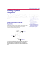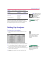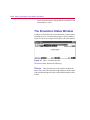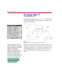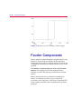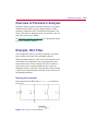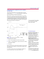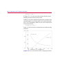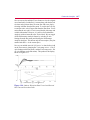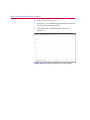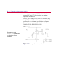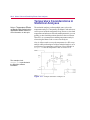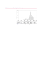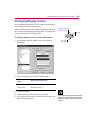
1
MicroSim PSpice A/D & Basics+ Circuit Analysis Software User’s Guide MicroSim Corporation 20 Fairbanks Irvine, California 92618 (714) 770-3022 Version 8.0, June, 1997. Copyright 1997, MicroSim Corporation. All rights reserved. Printed in the United States of America. TradeMarks Referenced herein are the trademarks used by MicroSim Corporation to identify its products. MicroSim Corporation is the exclusive owners of “MicroSim,” “PSpice,” “PLogic,” “PLSyn.” Additional marks of MicroSim include: “StmEd,” “Stimulus Editor,” “Probe,” “Parts,” “Monte Carlo,” “Analog Behavioral Modeling,” “Device Equations,” “Digital Simulation,” “Digital Files,” “Filter Designer,” “Schematics,” “PLogic,” ”PCBoards,” “PSpice Optimizer,” and “PLSyn” and variations theron (collectively the “Trademarks”) are used in connection with computer programs. MicroSim owns various trademark registrations for these marks in the United States and other countries. SPECCTRA is a registered trademark of Cooper & Chyan Technology, Inc. MicroSoft, MS-DOS, Windows, Windows NT and the Windows logo are either registered trademarks or trademarks of Microsoft Corporation. Adobe, the Adobe logo, Acrobat, the Acrobat logo, Exchange and PostScript are trademarks of Adobe Systems Incorporated or its subsidiaries and may be registered in certain jurisdictions. EENET is a trademark of Eckert Enterprises. Mathcad copyright 1991-1997 by Mathsoft, Inc. All other company/product names are trademarks/registered trademarks of their respective holders. Copyright Notice Except as permitted under the United States Copyright Act of 1976, no part of this publication may be reproduced or distributed in any form or by any means, or stored in a data base or retrieval system, without the prior written permission of MicroSim Corporation. As described in the license agreement, you are permitted to run one copy of the MicroSim software on one computer at a time. Unauthorized duplication of the software or documentation is prohibited by law. Corporate Program Licensing and multiple copy discounts are available. Technical Support Internet [email protected] Phone FAX WWW (714) 837-0790 (714) 455-0554 http://www.microsim.com Customer Service Internet Phone [email protected] (714) 770-3022 Contents Before You Begin Welcome to MicroSim . . . . . . . . . . . . . . . . . MicroSim PSpice A/D Overview . . . . . . . . . . . How to Use this Guide . . . . . . . . . . . . . . . . . Typographical Conventions . . . . . . . . . . . . Related Documentation . . . . . . . . . . . . . . . . Online Help . . . . . . . . . . . . . . . . . . . . If You Don’t Have the Standard PSpice A/D Package If You Have PSpice A/D Basics+ . . . . . . . . . If You Have the Evaluation CD-ROM . . . . . . What’s New . . . . . . . . . . . . . . . . . . . . . . . . . . . . . . . . . . . . . . . . . . . . . . . . . . . . . . . . . . . . . . . . . . . . . . . . . . . . . . . . . . . . . . . . . . . . . . . . . . . . . . . . . . . . . . . . . . . . . . . . . . . . . . . . . . . . . . . . . . . . . . . xxv . xxvi xxvii xxvii xxviii . xxix . xxx . xxx xxxiii xxxiv . . . . . . . . . . . . . . . . . . . . . . . . . . . . . . . . . . . . . . . . . . . . . . . . . . . . . . . . . . . . . . . . . . . . . . . . . . . . . . . . . . . . . . . . . . . . . . . . . . . . . . . . . . . . . . . . . . . . . . . . . . . . . . . . . . . . . . . . . . . . . . . . . . . . . . . . . . . . . . . . . . . . . . . . . . . . . . . . . . . . . 1-1 . 1-2 . 1-3 . 1-3 . 1-3 . 1-4 . 1-5 . 1-6 . 1-6 . 1-7 . 1-8 . 1-9 . 1-9 . 1-10 . 1-10 Part One Simulation Primer Chapter 1 Things You Need to Know Chapter Overview . . . . . . . . . . . . . . . . . What is PSpice A/D? . . . . . . . . . . . . . . . Analyses You Can Run with PSpice A/D . . . . . Basic Analyses . . . . . . . . . . . . . . . . DC sweep & other DC calculations . . . . AC sweep and noise . . . . . . . . . . . Transient and Fourier . . . . . . . . . . . Advanced Multi-Run Analyses . . . . . . . . Parametric and temperature . . . . . . . . Monte Carlo and sensitivity/worst-case . Using PSpice A/D with Other MicroSim Programs Using Schematics to Prepare for Simulation . What is the Stimulus Editor? . . . . . . . . . What is the Parts Utility? . . . . . . . . . . . What is Probe? . . . . . . . . . . . . . . . . . . . . . . . . . . . . . . . . . . . . . . . . . . . . . . iv Contents Files Needed for Simulation . . . . . . . . . . . . . . . Files That Schematics Generates . . . . . . . . . . Netlist file . . . . . . . . . . . . . . . . . . . . Circuit file . . . . . . . . . . . . . . . . . . . . Other Files That You Can Configure for Simulation Model library . . . . . . . . . . . . . . . . . . Stimulus file . . . . . . . . . . . . . . . . . . . Include file . . . . . . . . . . . . . . . . . . . . Configuring model library, stimulus, and include files . . . . . . . . . . . . . . . Files That PSpice A/D Generates . . . . . . . . . . . . Probe data file . . . . . . . . . . . . . . . . . . PSpice output file . . . . . . . . . . . . . . . . . . . . . . . . . . . . . . . . . . . . . . . . . . . . . . . . . . . . . . . . . . . . . . . . . . . . . . . . . . . . . . . . . . . . . . . . . . . . . . . . . . . . . . . . 1-11 1-11 1-12 1-12 1-12 1-13 1-14 1-14 . . . . . . . . . . . . . . . . . . . . . . . . . . . . . . . . . . . . . . . . . . . . 1-14 1-15 1-15 1-16 . . . . . . . . . . . . . . . . . . . . . . . . . . . . . . . . . . . . . . . . . . . . . . . . . . . . . . . . . . . . . . . . . . . . . . . . . . . . . . . . . . . . . . . . . . . . . . . . . . . . . . . . . . . . . . . . . . . . . . . . . . . . . . . . . . . . . . . . . . . . . . . . . . . . . . . . . . . . . . . . . . . . . . . . . . . . . . . . . . . . . . . . . . . . . . . . . . . . . . . . . . . . . . . . . . . . . . . . . . . . . . . . . . . . . . . . . . . . . . . . . . . . . . . . . . . . . . . . . . . . . . . . Chapter 2 Simulation Examples Chapter Overview . . . . . . . . . . . . . . . . . . . . Example Circuit Creation . . . . . . . . . . . . . . . . Finding Out More about Setting Up Your Schematic Bias Point Analysis . . . . . . . . . . . . . . . . . . . . Running PSpice A/D . . . . . . . . . . . . . . . . . Using the Bias Information Display . . . . . . . . . Using the Simulation Output File . . . . . . . . . . Finding Out More about Bias Point Calculations . . DC Sweep Analysis . . . . . . . . . . . . . . . . . . . Setting Up and Running a DC Sweep Analysis . . . Displaying DC Analysis Results in Probe . . . . . . Finding Out More about DC Sweep Analysis . . . . Transient Analysis . . . . . . . . . . . . . . . . . . . . Finding Out More about Transient Analysis . . . . . AC Sweep Analysis . . . . . . . . . . . . . . . . . . . Setting Up and Running an AC Sweep Analysis . . AC Sweep Analysis Results . . . . . . . . . . . . . Finding Out More about AC Sweep and Noise Analysis . . . . . . . . . . . . . . . Parametric Analysis . . . . . . . . . . . . . . . . . . . Setting Up and Running the Parametric Analysis . . Analyzing Waveform Families in Probe . . . . . . . Finding Out More about Parametric Analysis . . . . Probe Performance Analysis . . . . . . . . . . . . . . . Finding Out More about Performance Analysis . . . . . . . . . . 2-1 2-2 2-5 2-6 2-6 2-7 2-9 2-10 2-10 2-10 2-11 2-15 2-16 2-19 2-20 2-20 2-22 2-23 2-24 2-25 2-27 2-29 2-30 2-32 Contents v Part Two Design Entry Chapter 3 Preparing a Schematic for Simulation Chapter Overview . . . . . . . . . . . . . . . . . . . . . . . . . . . Checklist for Simulation Setup . . . . . . . . . . . . . . . . . . . . Typical Simulation Setup Steps . . . . . . . . . . . . . . . . . . Advanced Design Entry and Simulation Setup Steps . . . . . . . When Netlisting Fails or the Simulation Does Not Start . . . . . . . . . . . . . . . . . . . . . . Things to check in your schematic . . . . . . . . . . . . . . Things to check in your system configuration . . . . . . . . Using Parts That You Can Simulate . . . . . . . . . . . . . . . . . . Vendor-Supplied Parts . . . . . . . . . . . . . . . . . . . . . . Part naming conventions . . . . . . . . . . . . . . . . . . . Finding the part that you want . . . . . . . . . . . . . . . . Passive Parts . . . . . . . . . . . . . . . . . . . . . . . . . . . . Breakout Parts . . . . . . . . . . . . . . . . . . . . . . . . . . . Behavioral Parts . . . . . . . . . . . . . . . . . . . . . . . . . . Using Global Parameters and Expressions for Values . . . . . . . . Global Parameters . . . . . . . . . . . . . . . . . . . . . . . . . Declaring and using a global parameter . . . . . . . . . . . Expressions . . . . . . . . . . . . . . . . . . . . . . . . . . . . Specifying expressions . . . . . . . . . . . . . . . . . . . . Defining Power Supplies . . . . . . . . . . . . . . . . . . . . . . . For the Analog Portion of Your Circuit . . . . . . . . . . . . . . For A/D Interfaces in Mixed-Signal Circuits . . . . . . . . . . . Default digital power supplies . . . . . . . . . . . . . . . . Custom digital power supplies . . . . . . . . . . . . . . . . Defining Stimuli . . . . . . . . . . . . . . . . . . . . . . . . . . . . Analog Stimuli . . . . . . . . . . . . . . . . . . . . . . . . . . Using VSTIM and ISTIM . . . . . . . . . . . . . . . . . . . If you want to specify multiple stimulus types . . . . . . . . Digital Stimuli . . . . . . . . . . . . . . . . . . . . . . . . . . . Things to Watch For . . . . . . . . . . . . . . . . . . . . . . . . . . Unmodeled Parts . . . . . . . . . . . . . . . . . . . . . . . . . Do this if the part in question is from the MicroSim libraries Check for this if the part in question is custom-built . . . . . Unconfigured Model, Stimulus, or Include Files . . . . . . . . . Check for this . . . . . . . . . . . . . . . . . . . . . . . . . Unmodeled Pins . . . . . . . . . . . . . . . . . . . . . . . . . . Check for this . . . . . . . . . . . . . . . . . . . . . . . . . . . . . . . . . . . . . . . . . . . . . 3-1 3-2 3-2 3-4 . . . . . . . . . . . . . . . . . . . . . . . . . . . . . . . . . . . . . . . . . . . . . . . . . . . . . . . . . . . . . . . . . . . . . . . . . . . . . . . . . . . . . . . . . . . . . . . . . . . . . . . . . . . . . . . . . . . . . . . . . . . . . . . . . . . . . 3-4 . 3-5 . 3-6 . 3-7 . 3-8 . 3-8 . 3-9 . 3-11 . 3-12 . 3-13 . 3-14 . 3-14 . 3-14 . 3-16 . 3-16 . 3-21 . 3-21 . 3-21 . 3-21 . 3-21 . 3-23 . 3-23 . 3-24 . 3-25 . 3-26 . 3-28 . 3-28 . 3-28 . 3-30 . 3-30 . 3-31 . 3-31 . 3-32 vi Contents Missing Ground . . . . . . Check for this . . . . . Missing DC Path to Ground Check for this . . . . . . . . . . . . . . . . . . . . . . . . . . . . . . . . . . . . . . . . . . . . . . . . . . . . . . . . . . . . . . . . . . . . . . . . . . . . . . . . . . . . . . . . . . . . . . . . . . . . . Chapter Overview . . . . . . . . . . . . . . . . . . . . . . . . . . . . . . What Are Models? . . . . . . . . . . . . . . . . . . . . . . . . . . . . . . Models defined as model parameter sets . . . . . . . . . . . . . . Models defined as subcircuit netlists . . . . . . . . . . . . . . . . How Are Models Organized? . . . . . . . . . . . . . . . . . . . . . . . . Model Libraries . . . . . . . . . . . . . . . . . . . . . . . . . . . . . Model Library Configuration . . . . . . . . . . . . . . . . . . . . . . Global vs. Local Models and Libraries . . . . . . . . . . . . . . . . . Nested Model Libraries . . . . . . . . . . . . . . . . . . . . . . . . . MicroSim-Provided Models . . . . . . . . . . . . . . . . . . . . . . . Tools to Create and Edit Models . . . . . . . . . . . . . . . . . . . . . . . Ways to Create and Edit Models . . . . . . . . . . . . . . . . . . . . . . . Using the Parts Utility to Edit Models . . . . . . . . . . . . . . . . . . . . . . . . . . . . . Ways to Use the Parts Utility . . . . . . . . . . . . . . . . . . . . . . Parts-Supported Device Types . . . . . . . . . . . . . . . . . . . . . . Ways To Characterize Models . . . . . . . . . . . . . . . . . . . . . . Creating models from data sheet information . . . . . . . . . . . . Analyzing the effect of model parameters on device characteristics How to Fit Models . . . . . . . . . . . . . . . . . . . . . . . . . . . . Running the Parts Utility Alone . . . . . . . . . . . . . . . . . . . . . Starting the Parts utility . . . . . . . . . . . . . . . . . . . . . . . Enabling and disabling automatic symbol creation . . . . . . . . . Saving global models (and symbols) . . . . . . . . . . . . . . . . Running the Parts Utility from the Symbol Editor . . . . . . . . . . . Starting the Parts utility . . . . . . . . . . . . . . . . . . . . . . . Saving global models . . . . . . . . . . . . . . . . . . . . . . . . Running the Parts Utility from the Schematic Editor . . . . . . . . . . What is an instance model? . . . . . . . . . . . . . . . . . . . . . Starting the Parts utility . . . . . . . . . . . . . . . . . . . . . . . Saving local models . . . . . . . . . . . . . . . . . . . . . . . . . What happens if you don’t save the instance model . . . . . . . . The Parts Utility Tutorial . . . . . . . . . . . . . . . . . . . . . . . . Creating the half-wave rectifier schematic . . . . . . . . . . . . . Starting the Parts utility for the D1 diode . . . . . . . . . . . . . . . . . . . . . . . . . . 3-32 3-32 3-33 3-33 Chapter 4 Creating and Editing Models . . . . . . . . . . . . . . . . . . . . . . . . . . . . . . . . . . 4-1 4-3 4-3 4-3 4-4 4-4 4-5 4-5 4-6 4-6 4-7 4-8 4-10 4-11 4-12 4-13 4-13 4-14 4-14 4-16 4-16 4-16 4-17 4-18 4-18 4-19 4-20 4-20 4-21 4-21 4-22 4-23 4-23 4-24 Contents vii Entering data sheet information . . . . . . . . . . . . . Extracting model parameters . . . . . . . . . . . . . . Adding curves for more than one temperature . . . . . Completing the model definition . . . . . . . . . . . . Using the Model Editor . . . . . . . . . . . . . . . . . . . . . Changing Model Properties . . . . . . . . . . . . . . . . . Editing .MODEL definitions . . . . . . . . . . . . . . Editing .SUBCKT definitions . . . . . . . . . . . . . . Changing the model name . . . . . . . . . . . . . . . Running the Model Editor from the Symbol Editor . . . . . Starting the model editor . . . . . . . . . . . . . . . . Saving global models . . . . . . . . . . . . . . . . . . Running the Model Editor from the Schematic Editor . . . What is an instance model? . . . . . . . . . . . . . . . Starting the model editor . . . . . . . . . . . . . . . . Saving local models . . . . . . . . . . . . . . . . . . . Example: Editing a Q2N2222 Instance Model . . . . . . . Starting the model editor . . . . . . . . . . . . . . . . Editing the Q2N2222-X model instance . . . . . . . . Saving the edits and updating the schematic . . . . . . Using the Create Subcircuit Command . . . . . . . . . . . . . Changing the Model Reference to an Existing Model Definition Reusing Instance Models . . . . . . . . . . . . . . . . . . . . Reusing Instance Models in the Same Schematic . . . . . . Making Instance Models Available To All Schematics . . . Configuring Model Libraries . . . . . . . . . . . . . . . . . . The Library and Include Files dialog box . . . . . . . . . . How PSpice A/D Uses Model Libraries . . . . . . . . . . Search order . . . . . . . . . . . . . . . . . . . . . . . Handling duplicate model names . . . . . . . . . . . . Adding Model Libraries to the Configuration . . . . . . . Changing Local and Global Scope . . . . . . . . . . . . . Changing Model Library Search Order . . . . . . . . . . . Changing the Library Search Path . . . . . . . . . . . . . . . . . . . . . . . . . . . . . . . . . . . . . . . . . . . . . . . . . . . . . . . . . . . . . . . . . . . . . . . . . . . . . . . . . . . . . . . . . . . . . . . . . . . . . . . . . . . . . . . . . . . . . . . . . . . . . . . . . . . . . . . . . . . . . . . . . . . . . . . . . . . . . . . . . . . . . . . . . . . . . . . . . . . . . . . . . . . . . . . . . . . . . . . . . . . . . . . . . . . . . . . . . . . . . . . . . . . . . . . . . . . . . . . . . . . . . . . . . . . . 4-24 . 4-27 . 4-28 . 4-29 . 4-29 . 4-30 . 4-30 . 4-31 . 4-31 . 4-31 . 4-31 . 4-32 . 4-33 . 4-33 . 4-34 . 4-34 . 4-35 . 4-35 . 4-35 . 4-36 . 4-37 . 4-38 . 4-39 . 4-40 . 4-40 . 4-41 . 4-41 . 4-43 . 4-43 . 4-43 . 4-44 . 4-45 . 4-45 . 4-46 Chapter 5 Creating Symbols for Models Chapter Overview . . . . . . . . . . . . . . . . . . . . What’s Different About Symbols Used for Simulation? Ways to Create Symbols for Models . . . . . . . . . . . . . . . . . . . . Preparing Your Models for Symbol Creation . . . . . . . . . . . . . . . . . . 5-1 . . . . . . . . . . . . 5-3 . . . . . . . . . . . . 5-4 . . . . . . . . . . . . 5-5 viii Contents Using the Symbol Wizard . . . . . . . . . . . . . How to Start the Symbol Wizard . . . . . . . How the Symbol Wizard Works . . . . . . . . Creating AKO Symbols . . . . . . . . . . . . . . What Are Base vs. AKO Symbols? . . . . . . Base and AKO Symbols in Symbol Libraries . How to Create AKO Symbols . . . . . . . . . Completing the Configuration of Your Part . . Using the Parts Utility to Create Symbols . . . . . Starting the Parts Utility . . . . . . . . . . . . Setting Up Automatic Symbol Creation . . . . Basing New Symbols On a Custom Set of Symbols Editing Symbol Graphics . . . . . . . . . . . . . . How Schematics Places Symbols . . . . . . . Defining Important Symbol Elements . . . . . Origin . . . . . . . . . . . . . . . . . . . Bounding box . . . . . . . . . . . . . . . Grid spacing for graphics . . . . . . . . . Grid spacing for pins . . . . . . . . . . . Defining Symbol Attributes Needed for Simulation MODEL . . . . . . . . . . . . . . . . . . . . SIMULATION ONLY . . . . . . . . . . . . . TEMPLATE . . . . . . . . . . . . . . . . . . TEMPLATE syntax . . . . . . . . . . . . TEMPLATE examples . . . . . . . . . . IO_LEVEL . . . . . . . . . . . . . . . . . . . MNTYMXDLY . . . . . . . . . . . . . . . . IPIN attributes . . . . . . . . . . . . . . . . . . . . . . . . . . . . . . . . . . . . . . . . . . . . . . . . . . . . . . . . . . . . . . . . . . . . . . . . . . . . . . . . . . . . . . . . . . . . . . . . . . . . . . . . . . . . . . . . . . . . . . . . . . . . . . . . . . . . . . . . . . . . . . . . . . . . . . . . . . . . . . . . . . . . . . . . . . . . . . . . . . . . . . . . . . . . . . . . . . . . . . . . . . . . . . . . . . . . . . . . . . . . . . . . . . . . . . . . . . . . . . . . . . . . . . . . . . . . . . . . . . . . . . . . . . . . . . . . . . . . . . . . . . . . . . . . . . . . . . . . . . . . . . . . . . . . . . . . . . . . . . . . . . . . . . . . . . . . . . . . . . . . . . . . . . . . . . . . . . . . . . . . . . . . . . . . . . . . . . . . . . . . . . . . . . . . . . . . . . . . . . . . . . . . . . . . . . . . . . . . 5-6 5-6 5-7 5-8 5-8 5-8 5-9 5-11 5-11 5-12 5-12 5-13 5-15 5-15 5-16 5-16 5-16 5-17 5-17 5-18 5-19 5-19 5-20 5-20 5-23 5-27 5-28 5-29 Chapter Overview . . . . . . . . . . . . . . . . . . . . Overview of Analog Behavioral Modeling . . . . . . . The abm.slb Symbol Library File . . . . . . . . . . . . Placing and Specifying ABM Parts . . . . . . . . . . . Net Names and Device Names in ABM Expressions Forcing the Use of a Global Definition . . . . . . . ABM Part Templates . . . . . . . . . . . . . . . . . . . Control System Parts . . . . . . . . . . . . . . . . . . . Basic Components . . . . . . . . . . . . . . . . . . Limiters . . . . . . . . . . . . . . . . . . . . . . . Chebyshev Filters . . . . . . . . . . . . . . . . . . . . . . . . . . . . . . . . . . . . . . . . . . . . . . . . . . . . . . . . . . . . . . . . . . . . . . . . . . . . . . . . . . . . . . . . . . . . . . . . . . . . . . . . . . . . . . . . . . . . . . . . . . . . . . . . . . . . . . . . . . . . . . . . . . . . 6-1 6-2 6-3 6-4 6-4 6-5 6-6 6-7 6-9 6-10 6-11 Chapter 6 Analog Behavioral Modeling Contents ix Integrator and Differentiator . . . . . . . . . . . . . . . Table Look-Up Parts . . . . . . . . . . . . . . . . . . . Laplace Transform Part . . . . . . . . . . . . . . . . . . Math Functions . . . . . . . . . . . . . . . . . . . . . . ABM Expression Parts . . . . . . . . . . . . . . . . . . An Instantaneous Device Example: Modeling a Triode . PSpice A/D-Equivalent Parts . . . . . . . . . . . . . . . . . Implementation of PSpice A/D-Equivalent Parts . . . . . Modeling Mathematical or Instantaneous Relationships . EVALUE and GVALUE parts . . . . . . . . . . . . EMULT, GMULT, ESUM, and GSUM . . . . . . . Lookup Tables (ETABLE and GTABLE) . . . . . . . . Frequency-Domain Device Models . . . . . . . . . . . . Laplace Transforms (LAPLACE) . . . . . . . . . . . . . Frequency Response Tables (EFREQ and GFREQ) . . . Cautions and Recommendations for Simulation and Analysis Instantaneous Device Modeling . . . . . . . . . . . . . . Frequency-Domain Parts . . . . . . . . . . . . . . . . . Laplace Transforms . . . . . . . . . . . . . . . . . . . . Non-causality and Laplace transforms . . . . . . . . Chebyshev filters . . . . . . . . . . . . . . . . . . . Frequency tables . . . . . . . . . . . . . . . . . . . Trading Off Computer Resources For Accuracy . . . . . Basic Controlled Sources . . . . . . . . . . . . . . . . . . . Creating Custom ABM Parts . . . . . . . . . . . . . . . . . . . . . . . . . . . . . . . . . . . . . . . . . . . . . . . . . . . . . . . . . . . . . . . . . . . . . . . . . . . . . . . . . . . . . . . . . . . . . . . . . . . . . . . . . . . . . . . . . . . . . . . . . . . . . . . . . . . . . . . . . . . . . . . . . . . . . . . . . . . . . . . . . . . . . . . . . . . . . . . . . . . . . . . . . . . . . . . . . . . . . . . . . . . . . . . . . . . . . . . . 6-14 . 6-14 . 6-18 . 6-21 . 6-21 . 6-25 . 6-28 . 6-29 . 6-30 . 6-30 . 6-32 . 6-33 . 6-35 . 6-35 . 6-37 . 6-40 . 6-40 . 6-41 . 6-41 . 6-42 . 6-43 . 6-44 . 6-45 . 6-46 . 6-46 . . . . . . . . . . . . . . . . . . . . . . . . . . . . . . . . . . . . . . . . . . . . . . . . . . . . . . . . . . . . . . . . . . . . . . . . . . . . . . . . . . . . . . . . . . . . . . . . . . . . . . . . . . . . . . . . . 7-1 . 7-2 . 7-3 . 7-6 . 7-11 . 7-11 . 7-12 . 7-13 . 7-14 . 7-15 . 7-15 . 7-16 . 7-17 . 7-17 Chapter 7 Digital Device Modeling Chapter Overview . . . . . . . . . . . . . . . . . . . Introduction . . . . . . . . . . . . . . . . . . . . . . Functional Behavior . . . . . . . . . . . . . . . . . . Digital primitive syntax . . . . . . . . . . . . Timing Characteristics . . . . . . . . . . . . . . . . . Timing Model . . . . . . . . . . . . . . . . . . . Treatment of unspecified propagation delays . Treatment of unspecified timing constraints . Propagation Delay Calculation . . . . . . . . . . Inertial and Transport Delay . . . . . . . . . . . Inertial delay . . . . . . . . . . . . . . . . . Transport delay . . . . . . . . . . . . . . . . Input/Output Characteristics . . . . . . . . . . . . . . Input/Output Model . . . . . . . . . . . . . . . . . . . . . . . . . . . . . . . . . . . . . . . . . . . . . . . . . . . . . . . . . . . . . . . . . . . . . . . . x Contents Defining Output Strengths . . . . . . . . . . . . . . . . . . . . . . . Configuring the strength scale . . . . . . . . . . . . . . . . . . . Determining the strength of a device output . . . . . . . . . . . Controlling overdrive . . . . . . . . . . . . . . . . . . . . . . . Charge Storage Nets . . . . . . . . . . . . . . . . . . . . . . . . . . Creating Your Own Interface Subcircuits for Additional Technologies . . . . . . . . . . . . . . . . . . . Creating a Digital Model Using the PINDLY and LOGICEXP Primitives Digital Primitives . . . . . . . . . . . . . . . . . . . . . . . . . . . The Logic Expression (LOGICEXP Primitive) . . . . . . . . . . . . Pin-to-Pin Delay (PINDLY Primitive) . . . . . . . . . . . . . . . . BOOLEAN . . . . . . . . . . . . . . . . . . . . . . . . . . . . . . . PINDLY . . . . . . . . . . . . . . . . . . . . . . . . . . . . . . . . Constraint Checker (CONSTRAINT Primitive) . . . . . . . . . . . . Setup_Hold . . . . . . . . . . . . . . . . . . . . . . . . . . . . . . . Width . . . . . . . . . . . . . . . . . . . . . . . . . . . . . . . . . . Freq . . . . . . . . . . . . . . . . . . . . . . . . . . . . . . . . . . The 74160 Example . . . . . . . . . . . . . . . . . . . . . . . . . . . . . . . . . . . . 7-21 7-22 7-22 7-23 7-23 . . . . . . . . . . . . . . . . . . . . . . . . 7-25 7-29 7-30 7-30 7-33 7-33 7-34 7-36 7-36 7-37 7-37 7-37 . . . . . . . . . . . . . . . . . . . . . . . . . . Part Three Setting Up and Running Analyses Chapter 8 Setting Up Analyses and Starting Simulation Chapter Overview . . . . . . . . . . . . . . . . . . . . Analysis Types . . . . . . . . . . . . . . . . . . . . . . Setting Up Analyses . . . . . . . . . . . . . . . . . . . Execution Order for Standard Analyses . . . . . . . Output Variables . . . . . . . . . . . . . . . . . . . Modifiers . . . . . . . . . . . . . . . . . . . . Starting Simulation . . . . . . . . . . . . . . . . . . . . Starting Simulation from Schematics . . . . . . . . Starting Simulation Outside of Schematics . . . . . Setting Up Batch Simulations . . . . . . . . . . . . Multiple simulation setups within one circuit file Running simulations with multiple circuit files . The Simulation Status Window . . . . . . . . . . . . . . . . . . . . . . . . . . . . . . . . . . . . . . . . . . . . . . . . . . . . . . . . . . . . . . . . . . . . . . . . . . . . . . . . . . . . . . . . . . . . . . . . . . . . . . . . . . . . . . . . . . . . . . . . . . . . . . . . . . . . . . 8-1 8-2 8-3 8-4 8-5 8-6 8-11 8-11 8-12 8-12 8-12 8-13 8-14 Chapter 9 DC Analyses Chapter Overview . . . . . . . . . . . . . . . . . . . . . . . . . . . . . . . . 9-1 DC Sweep . . . . . . . . . . . . . . . . . . . . . . . . . . . . . . . . . . . . 9-2 Minimum Requirements to Run a DC Sweep Analysis . . . . . . . . . . . 9-2 Contents xi Overview of DC Sweep . . . . . . . . . . . . . . . . . . . . . . . . . Setting Up a DC Stimulus . . . . . . . . . . . . . . . . . . . . . . . . Nested DC Sweeps . . . . . . . . . . . . . . . . . . . . . . . . . . . Curve Families for DC Sweeps . . . . . . . . . . . . . . . . . . . . . Bias Point Detail . . . . . . . . . . . . . . . . . . . . . . . . . . . . . . . Minimum Requirements to Run a Bias Point Detail Analysis . . . . . Overview of Bias Point Detail . . . . . . . . . . . . . . . . . . . . . Small-Signal DC Transfer . . . . . . . . . . . . . . . . . . . . . . . . . . Minimum Requirements to Run a Small-Signal DC Transfer Analysis Overview of Small-Signal DC Transfer . . . . . . . . . . . . . . . . . DC Sensitivity . . . . . . . . . . . . . . . . . . . . . . . . . . . . . . . . Minimum Requirements to Run a DC Sensitivity Analysis . . . . . . Overview of DC Sensitivity . . . . . . . . . . . . . . . . . . . . . . . . . . . . . . . . . . . . . 9-3 . 9-5 . 9-6 . 9-7 . 9-9 . 9-9 . 9-9 . 9-11 . 9-11 . 9-12 . 9-13 . 9-13 . 9-14 Chapter 10 AC Analyses Chapter Overview . . . . . . . . . . . . . . . . . . . . AC Sweep Analysis . . . . . . . . . . . . . . . . . . . What You Need to Do to Run an AC Sweep . . . . What is AC Sweep? . . . . . . . . . . . . . . . . . Setting Up an AC Stimulus . . . . . . . . . . . . . Setting Up an AC Analysis . . . . . . . . . . . . . AC Sweep Setup in “example.sch” . . . . . . . . . How PSpice A/D Treats Nonlinear Devices . . . . What’s required to linearize a device . . . . . . What PSpice A/D does . . . . . . . . . . . . . Example: Nonlinear behavioral modeling block Noise Analysis . . . . . . . . . . . . . . . . . . . . . . What You Need to Do to Run a Noise Analysis . . What is Noise Analysis? . . . . . . . . . . . . . . How PSpice A/D calculates total output and input noise . . . . . . . . . . . . . Setting Up a Noise Analysis . . . . . . . . . . . . Analyzing Noise in Probe . . . . . . . . . . . . . . About noise units . . . . . . . . . . . . . . . . Example . . . . . . . . . . . . . . . . . . . . . . . . . . . . . . . . . . . . . . . . . . . . . . . . . . . . . . . . . . . . . . . . . . . . . . . . . . . . . . . . . . . . . . . . . . . . . . . . . . . . . . . . . . . . . . . . . . . . . . . . . . . . . . . . . . . . . . . . . . . . . . . . . . . . . . . . . . . . . . . . . . . . . . . . . . . . . . . . 10-1 . 10-2 . 10-2 . 10-2 . 10-3 . 10-5 . 10-6 . 10-7 . 10-7 . 10-7 . 10-7 . 10-9 . 10-9 10-10 . . . . . . . . . . . . . . . . . . . . . . . . . . . . . . . . . . . . . . . . . . . . . . . . . . . . . . . 10-10 10-11 10-12 10-13 10-13 Chapter Overview . . . . . . . . . . . . . . . . . . . . . Overview of Transient Analysis . . . . . . . . . . . . . . Minimum Requirements to Run a Transient Analysis Minimum circuit design requirements . . . . . . . . . . . . . . . . . . . . . . . . . . . . . . . . . . . . . . . . . . . . . . . 11-1 . 11-2 . 11-2 . 11-2 Chapter 11 Transient Analysis xii Contents Minimum program setup requirements . . . . . . . . . Defining a Time-Based Stimulus . . . . . . . . . . . . . . . . Overview of Stimulus Generation . . . . . . . . . . . . . . The Stimulus Editor Utility . . . . . . . . . . . . . . . . . . . Stimulus Files . . . . . . . . . . . . . . . . . . . . . . . . Configuring Stimulus Files . . . . . . . . . . . . . . . . . Starting the Stimulus Editor . . . . . . . . . . . . . . . . . Defining Stimuli . . . . . . . . . . . . . . . . . . . . . . . Example: piecewise linear stimulus . . . . . . . . . . . Example: sine wave sweep . . . . . . . . . . . . . . . Creating New Stimulus Symbols . . . . . . . . . . . . . . Editing a Stimulus . . . . . . . . . . . . . . . . . . . . . . To edit an existing stimulus . . . . . . . . . . . . . . . To edit a PWL stimulus . . . . . . . . . . . . . . . . . To select a time and value scale factor for PWL stimuli Deleting and Removing Traces . . . . . . . . . . . . . . . Manual Stimulus Configuration . . . . . . . . . . . . . . . To manually configure a stimulus . . . . . . . . . . . . Transient (Time) Response . . . . . . . . . . . . . . . . . . . . Internal Time Steps in Transient Analyses . . . . . . . . . . . . Switching Circuits in Transient Analyses . . . . . . . . . . . . Plotting Hysteresis Curves . . . . . . . . . . . . . . . . . . . . Fourier Components . . . . . . . . . . . . . . . . . . . . . . . . . . . . . . . . . . . . . . . . . . . . . . . . . . . . . . . . . . . . . . . . . . . . . . . . . . . . . . . . . . . . . . . . . . . . . . . . . . . . . . . . . . . . . . . . . . . . . . . . . . . . . . . . . . . . . . . . . . . . . . . . . . . . . . . . . . . . . . . . . . . . . . . . . . . . . . . . . . . . . . . . 11-2 11-3 11-3 11-5 11-6 11-6 11-7 11-8 11-8 11-9 11-10 11-12 11-12 11-12 11-12 11-13 11-13 11-13 11-15 11-17 11-18 11-18 11-20 Chapter Overview . . . . . . . . . . . . . . . . . . . . . . . . . . Parametric Analysis . . . . . . . . . . . . . . . . . . . . . . . . . Minimum Requirements to Run a Parametric Analysis . . . . . Overview of Parametric Analysis . . . . . . . . . . . . . . . . Example: RLC Filter . . . . . . . . . . . . . . . . . . . . . . . Entering the schematic . . . . . . . . . . . . . . . . . . . Running the simulation . . . . . . . . . . . . . . . . . . . Using performance analysis to plot overshoot and rise time Example: Frequency Response vs. Arbitrary Parameter . . . . Setting up the circuit . . . . . . . . . . . . . . . . . . . . . Displaying results in Probe . . . . . . . . . . . . . . . . . Temperature Analysis . . . . . . . . . . . . . . . . . . . . . . . . Minimum Requirements to Run a Temperature Analysis . . . . Overview of Temperature Analysis . . . . . . . . . . . . . . . . . . . . . . . . . . . . . . . . . . . . . . . . . . . . . . . . . . . . . . . . . . . . . . . . . . . . . . . . . . . . . . . . . . . . . 12-1 12-2 12-2 12-3 12-3 12-3 12-4 12-5 12-8 12-8 12-9 12-11 12-11 12-11 Chapter 12 Parametric and Temperature Analysis Contents xiii Chapter 13 Monte Carlo and Sensitivity/Worst-Case Analyses Chapter Overview . . . . . . . . . . . . . . . . . . . . . . . . Statistical Analyses . . . . . . . . . . . . . . . . . . . . . . . Overview of Statistical Analyses . . . . . . . . . . . . . . Output Control for Statistical Analyses . . . . . . . . . . . Model Parameter Values Reports . . . . . . . . . . . . . . Waveform Reports . . . . . . . . . . . . . . . . . . . . . Collating Functions . . . . . . . . . . . . . . . . . . . . . Temperature Considerations in Statistical Analyses . . . . Monte Carlo Analysis . . . . . . . . . . . . . . . . . . . . . . Tutorial: Monte Carlo Analysis of a Pressure Sensor . . . . Drawing the schematic . . . . . . . . . . . . . . . . . Defining component values . . . . . . . . . . . . . . . Setting up the parameters . . . . . . . . . . . . . . . . Using resistors with models . . . . . . . . . . . . . . . Saving the schematic . . . . . . . . . . . . . . . . . . Defining tolerances for the resistor models . . . . . . . Setting up the analyses . . . . . . . . . . . . . . . . . Running the analysis and viewing the results . . . . . . Monte Carlo Histograms . . . . . . . . . . . . . . . . . . Chebyshev filter example . . . . . . . . . . . . . . . . Creating models for Monte Carlo analysis . . . . . . . Setting up the analysis . . . . . . . . . . . . . . . . . Creating histograms . . . . . . . . . . . . . . . . . . . Worst-Case Analysis . . . . . . . . . . . . . . . . . . . . . . Overview of Worst-Case Analysis . . . . . . . . . . . . . Inputs . . . . . . . . . . . . . . . . . . . . . . . . . . Procedure . . . . . . . . . . . . . . . . . . . . . . . . Outputs . . . . . . . . . . . . . . . . . . . . . . . . . An important condition for correct worst-case analysis Worst-Case Analysis Example . . . . . . . . . . . . . . . Hints and Other Useful Information . . . . . . . . . . . . VARY BOTH, VARY DEV, and VARY LOT . . . . . Gaussian distributions . . . . . . . . . . . . . . . . . . YMAX collating function . . . . . . . . . . . . . . . . RELTOL . . . . . . . . . . . . . . . . . . . . . . . . Sensitivity analysis . . . . . . . . . . . . . . . . . . . Manual optimization . . . . . . . . . . . . . . . . . . Monte Carlo analysis . . . . . . . . . . . . . . . . . . . . . . . . . . . . . . . . . . . . . . . . . . . . . . . . . . . . . . . . . . . . . . . . . . . . . . . . . . . . . . . . . . . . . . . . . . . . . . . . . . . . . . . . . . . . . . . . . . . . . . . . . . . . . . . . . . . . . . . . . . . . . . . . . . . . . . . . . . . . . . . . . . . . . . . . . . . . . . . . . . . . . . . . . . . . . . . . . . . . . . . . . . . . . . . . . . . . . . . . . . . . . . . . . . . . . . . . . . . . . . . . . . . . . . . . . . . . . . . . . . . . . . . . . . . . . . . . . . . . . . . . . . . . . 13-1 . 13-2 . 13-2 . 13-3 . 13-3 . 13-4 . 13-4 . 13-6 . 13-7 13-10 13-10 13-11 13-12 13-13 13-14 13-14 13-17 13-18 13-19 13-19 13-19 13-20 13-20 13-25 13-25 13-25 13-26 13-26 13-27 13-28 13-32 13-32 13-33 13-33 13-33 13-33 13-34 13-34 xiv Contents Chapter 14 Digital Simulation Chapter Overview . . . . . . . . . . . . . . . . . . . . . What Is Digital Simulation? . . . . . . . . . . . . . . . . Steps for Simulating Digital Circuits . . . . . . . . . . . . Concepts You Need to Understand . . . . . . . . . . . . States . . . . . . . . . . . . . . . . . . . . . . . . . . Strengths . . . . . . . . . . . . . . . . . . . . . . . . Defining a Digital Stimulus . . . . . . . . . . . . . . . . Using Top-Level Interface Ports . . . . . . . . . . . . Ways to start editing stimuli for interface ports . . Using the DIGSTIM Symbol . . . . . . . . . . . . . Defining Input Signals Using the Stimulus Editor . . . Defining clock transitions . . . . . . . . . . . . . Defining signal transitions . . . . . . . . . . . . . Defining bus transitions . . . . . . . . . . . . . . Adding loops . . . . . . . . . . . . . . . . . . . Using the DIGCLOCK Symbol . . . . . . . . . . . . Using STIM1, STIM4, STIM8, and STIM16 Symbols Using the FILESTIM Device . . . . . . . . . . . . . Defining Simulation Time . . . . . . . . . . . . . . . . . Adjusting Simulation Parameters . . . . . . . . . . . . . Selecting Propagation Delays . . . . . . . . . . . . . Circuit-wide propagation delays . . . . . . . . . . Part instance propagation delays . . . . . . . . . Initializing Flip-Flops . . . . . . . . . . . . . . . . . Starting the Simulation . . . . . . . . . . . . . . . . . . . Analyzing Results . . . . . . . . . . . . . . . . . . . . . Adding Digital Signals to a Probe Plot . . . . . . . . Adding Buses to a Probe Plot . . . . . . . . . . . . . Tracking Timing Violations and Hazards . . . . . . . Persistent hazards . . . . . . . . . . . . . . . . . Simulation condition messages . . . . . . . . . . Output control options . . . . . . . . . . . . . . . Severity levels . . . . . . . . . . . . . . . . . . . . . . . . . . . . . . . . . . . . . . . . . . . . . . . . . . . . . . . . . . . . . . . . . . . . . . . . . . . . . . . . . . . . . . . . . . . . . . . . . . . . . . . . . . . . . . . . . . . . . . . . . . . . . . . . . . . . . . . . . . . . . . . . . . . . . . . . . . . . . . . . . . . . . . . . . . . . . . . . . . . . . . . . . . . . . . . . . . . . . . . . . . . . . . . . . . . . . . . . . . . . . . . . . . . . . . . . . . . . . . . . . . . . . . . . . . . . . . . . . . . . . . . . . . . . . . . . . . . . . . . . . . . . . . . . . . . . . . . . . . . . . . . . . . . . . . . . . . . . . . . . . . . . . . . . . . . . . . . . . . . . . . . . . . . . . 14-1 14-2 14-2 14-3 14-3 14-4 14-5 14-6 14-6 14-8 14-8 14-8 14-9 14-11 14-14 14-16 14-16 14-18 14-20 14-20 14-21 14-21 14-21 14-22 14-22 14-23 14-24 14-26 14-28 14-28 14-30 14-33 14-33 . . . . . . . . . . . . . . . . . . . . . . . . . . . . . . . . . . . . . . . . . . . . . . . . . . 15-1 15-1 15-3 15-4 15-5 Chapter 15 Mixed Analog/Digital Simulation Chapter Overview . . . . . . . . . . . . . . Interconnecting Analog and Digital Parts . . Interface Subcircuit Selection by PSpice A/D Level 1 Interface . . . . . . . . . . . . . Level 2 Interface . . . . . . . . . . . . . . . . . . . . . . . . . . . . . . . . . . . . . . . . . . . . . . . . Contents xv Setting the Default A/D Interface . . . . . . . . . . . . . . . . . . . . Specifying Digital Power Supplies . . . . . . . . . . . . . . . . . . . . . Default Power Supply Selection by PSpice A/D . . . . . . . . . . . . Creating Custom Digital Power Supplies . . . . . . . . . . . . . . . . Overriding CD4000 power supply voltage throughout a schematic Creating a secondary CD4000, TTL, or ECL power supply . . . . Interface Generation and Node Names . . . . . . . . . . . . . . . . . . . . . . . . . . . 15-6 . 15-7 . 15-7 . 15-8 15-10 15-11 15-12 Chapter 16 Digital Worst-Case Timing Analysis Chapter Overview . . . . . . . . . . . . . . . . Digital Worst-Case Timing . . . . . . . . . . . Starting Worst-Case Timing Analysis . . . . . . Simulator Representation of Timing Ambiguity Propagation of Timing Ambiguity . . . . . . . . Identification of Timing Hazards . . . . . . . . Convergence Hazard . . . . . . . . . . . . . . . Critical Hazard . . . . . . . . . . . . . . . . . . Cumulative Ambiguity Hazard . . . . . . . . . Reconvergence Hazard . . . . . . . . . . . . . Glitch Suppression Due to Inertial Delay . . . . Methodology . . . . . . . . . . . . . . . . . . . . . . . . . . . . . . . . . . . . . . . . . . . . . . . . . . . . . . . . . . . . . . . . . . . . . . . . . . . . . . . . . . . . . . . . . . . . . . . . . . . . . . . . . . . . . . . . . . . . . . . . . . . . . . . . . . . . . . . . . . . . . . . . . . . . . . . . . . . . . . . . . . . . . . . . . . . . . . . . . . . . . . . . . . . . . . . . . . . . . . . . 16-1 . 16-2 . 16-3 . 16-3 . 16-5 . 16-6 . 16-6 . 16-7 . 16-8 16-10 16-12 16-13 Chapter Overview . . . . . . . . . . . . . . . . . . . . . . Overview of Probe . . . . . . . . . . . . . . . . . . . . . . Elements of a Probe Plot . . . . . . . . . . . . . . . . Elements of a Plot Window . . . . . . . . . . . . . . . Managing Multiple Plot Windows . . . . . . . . . . . Printing multiple windows . . . . . . . . . . . . . Setting Up Probe . . . . . . . . . . . . . . . . . . . . . . . Configuring Probe Colors . . . . . . . . . . . . . . . . Editing display and print colors in the msim.ini file Configuring trace color schemes . . . . . . . . . . Customizing the Probe Command Line . . . . . . . . . Configuring Update Intervals . . . . . . . . . . . . . . Running Probe . . . . . . . . . . . . . . . . . . . . . . . . Starting Probe . . . . . . . . . . . . . . . . . . . . . . . . . . . . . . . . . . . . . . . . . . . . . . . . . . . . . . . . . . . . . . . . . . . . . . . . . . . . . . . . . . . . . . . . . . . . . . . . . . . . . . . . . . . . . . . . . . . . . . . . . . . . . . . . . . . . . . . . . . . . . . . . . . . . . 17-1 . 17-2 . 17-3 . 17-4 . 17-5 . 17-5 . 17-6 . 17-6 . 17-6 . 17-8 . 17-9 . 17-9 17-10 17-10 Part Four Viewing Results Analyzing Waveforms Chapter 17 in Probe xvi Contents Other Ways to Run Probe . . . . . . . . . . . . . . . . . . . . . . . . Starting Probe during a simulation . . . . . . . . . . . . . . . . . Pausing a simulation and then running Probe . . . . . . . . . . . . Interacting with Probe while in monitor mode . . . . . . . . . . . Using Schematic Markers to Add Traces . . . . . . . . . . . . . . . . Limiting Probe Data File Size . . . . . . . . . . . . . . . . . . . . . . Limiting file size using markers . . . . . . . . . . . . . . . . . . . Limiting file size by suppressing the first part of simulation output Using Simulation Data from Multiple Files . . . . . . . . . . . . . . . Setting up Probe for automatic loading of data files . . . . . . . . Appending data files . . . . . . . . . . . . . . . . . . . . . . . . . Adding traces from specific loaded data files . . . . . . . . . . . . Saving Simulation Results in ASCII Format . . . . . . . . . . . . . . Analog Example . . . . . . . . . . . . . . . . . . . . . . . . . . . . . . . Running the Simulation . . . . . . . . . . . . . . . . . . . . . . . Displaying voltages on nets and currents into pins . . . . . . . . . Mixed Analog/Digital Tutorial . . . . . . . . . . . . . . . . . . . . . . . . About Digital States in Probe . . . . . . . . . . . . . . . . . . . . . . About the Oscillator Circuit . . . . . . . . . . . . . . . . . . . . . . . Setting Up the Schematic . . . . . . . . . . . . . . . . . . . . . . . . Running the Simulation . . . . . . . . . . . . . . . . . . . . . . . . . Analyzing Simulation Results . . . . . . . . . . . . . . . . . . . . . . User Interface Features . . . . . . . . . . . . . . . . . . . . . . . . . . . . Zoom Regions . . . . . . . . . . . . . . . . . . . . . . . . . . . . . . Scrolling Traces . . . . . . . . . . . . . . . . . . . . . . . . . . . . . Sizing Digital Plots . . . . . . . . . . . . . . . . . . . . . . . . . . . Modifying Trace Expressions and Labels . . . . . . . . . . . . . . . . Moving and Copying Trace Names and Expressions . . . . . . . . . . Copying and Moving Labels . . . . . . . . . . . . . . . . . . . . . . . Tabulating Trace Data Values . . . . . . . . . . . . . . . . . . . . . . Cursors . . . . . . . . . . . . . . . . . . . . . . . . . . . . . . . . . . Tracking Digital Simulation Messages . . . . . . . . . . . . . . . . . . . . Message Tracking from the Message Summary . . . . . . . . . . . . . The Simulation Message Summary dialog box . . . . . . . . . . . How Probe handles persistent hazards . . . . . . . . . . . . . . . Message Tracking from the Waveform . . . . . . . . . . . . . . . . . Probe Trace Expressions . . . . . . . . . . . . . . . . . . . . . . . . . . . Basic Output Variable Form . . . . . . . . . . . . . . . . . . . . . . . Output Variable Form for Device Terminals . . . . . . . . . . . . . . Analog Trace Expressions . . . . . . . . . . . . . . . . . . . . . . . . Trace expression aliases . . . . . . . . . . . . . . . . . . . . . . . Arithmetic functions . . . . . . . . . . . . . . . . . . . . . . . . . . . . . . . . . . . . . . . . . . . . . . . . . . . . . . . . . . . . . . . . . . . 17-12 17-12 17-12 17-13 17-13 17-15 17-16 17-17 17-18 17-18 17-19 17-20 17-21 17-22 17-22 17-24 17-25 17-25 17-26 17-26 17-27 17-27 17-30 17-30 17-32 17-33 17-34 17-35 17-36 17-36 17-37 17-41 17-41 17-42 17-42 17-43 17-44 17-45 17-46 17-54 17-54 17-54 Contents xvii Rules for numeric values suffixes . . . . . . . . . . . . . . . . . . 17-56 Digital Trace Expressions . . . . . . . . . . . . . . . . . . . . . . . . . 17-57 Viewing Results Chapter 18 on the Schematic Chapter Overview . . . . . . . . . . . . . . . . . . . . . . . . . . . . . . . Viewing Bias Point Voltages and Currents . . . . . . . . . . . . . . . . . . . . . . . . . . . . . . How it works . . . . . . . . . . . . . . . . . . . . . . . . . . . . . If you run more than one analysis type . . . . . . . . . . . . . . . . The Bias Information Toolbar Buttons . . . . . . . . . . . . . . . . . . The Enable Display buttons . . . . . . . . . . . . . . . . . . . . . . The Show/Hide buttons . . . . . . . . . . . . . . . . . . . . . . . . Showing Voltages . . . . . . . . . . . . . . . . . . . . . . . . . . . . . Clearing and adding selected voltage values . . . . . . . . . . . . . Showing Currents . . . . . . . . . . . . . . . . . . . . . . . . . . . . . Clearing and adding selected current values . . . . . . . . . . . . . Changing the Precision of Displayed Data . . . . . . . . . . . . . . . . Moving Voltage and Current Labels . . . . . . . . . . . . . . . . . . . Verifying Label Associations . . . . . . . . . . . . . . . . . . . . . . . Changing Display Colors . . . . . . . . . . . . . . . . . . . . . . . . . If you want obsolete voltage and current labels to change appearance If You Have Hierarchical Symbols or Blocks on Your Schematic . . . . . . . . . . . . . . . . . . . . . . . . Other Ways to View Bias Point Values . . . . . . . . . . . . . . . . . . . . . . . . . . . Using the VIEWPOINT Symbol to Display Voltage . . . . . . . . . . . Using the IPROBE Symbol to Display Current . . . . . . . . . . . . . . . . . . . . . . . . . . . . . . . . . . . . . . . . . . . . . . . . . . . 18-1 . 18-2 . 18-2 . 18-2 . 18-3 . 18-3 . 18-3 . 18-4 . 18-4 . 18-6 . 18-6 . 18-7 . 18-7 . 18-8 . 18-9 18-10 18-10 18-11 18-11 18-11 18-12 Chapter 19 Other Output Options Chapter Overview . . . . . . . . . . . . . . . . . . . Viewing Analog Results in the PSpice Window . . . Writing Additional Results to the PSpice Output File . Generating Plots of Voltage and Current Values . Generating Tables of Voltage and Current Values Generating Tables of Digital State Changes . . . Creating Test Vector Files . . . . . . . . . . . . . . . . . . . . . . . . . . . . . . . . . . . . . . . . . . . . . . . . . . . . . . . . . . . . . . . . . . . . . . . . . . . . . . . . . . . . . . . . . . . . . . . . . . . . 19-1 . 19-2 . 19-3 . 19-3 . 19-4 . 19-5 . 19-6 xviii Contents Appendix ASetting Initial State Appendix Overview . . . Save and Load Bias Point Save Bias Point . . . Load Bias Point . . . Setpoints . . . . . . . . . Setting Initial Conditions . . . . . . . . . . . . . . . . . . . . . . . . . . . . . . . . . . . . . . . . . . . . . . . . . . . . . . . . . . . . . . . . . . . . . . . . . . . . . . . . . . . . . . . . . . . . . . . . . . . . . . . . . . . . . . . . . . . . . . . . . . . . . . . . . . . . . . . . . . . . . . . . . . . . . . . . . . . . . . . . . . . . . . . . . A-1 A-2 A-2 A-3 A-4 A-6 . . . . . . . . . . . . . . . . . . . . . . . . . . . . . . . . . . . . . . . . . . . . . . . . . . . . . . . . . . . . . . . . . . . . . . . . . . . . . . . . . . . . . . . . . . . . . . . . B-1 . B-2 . B-2 . B-3 . B-4 . B-4 . B-5 . B-7 . B-7 . B-8 . B-9 B-10 B-11 B-11 B-12 B-13 B-13 B-14 B-15 Appendix BConvergence and “Time Step Too Small Errors” Appendix Overview . . . . . . . . . . . . . . . Introduction . . . . . . . . . . . . . . . . . . . Newton-Raphson Requirements . . . . . . . Is There a Solution? . . . . . . . . . . . . . Are the Equations Continuous? . . . . . . . Are the derivatives correct? . . . . . . . Is the Initial Approximation Close Enough? . Bias Point and DC Sweep . . . . . . . . . . . . Semiconductors . . . . . . . . . . . . . . . Switches . . . . . . . . . . . . . . . . . . . Behavioral Modeling Expressions . . . . . . Transient Analysis . . . . . . . . . . . . . . . . Skipping the Bias Point . . . . . . . . . . . The Dynamic Range of TIME . . . . . . . . Failure at the First Time Step . . . . . . . . Parasitic Capacitances . . . . . . . . . . . . Inductors and Transformers . . . . . . . . . Bipolar Transistors Substrate Junction . . . Diagnostics . . . . . . . . . . . . . . . . . . . . Index . . . . . . . . . . . . . . . . . . . . . . . . . . . . . . . . . . . . . . . . . . . . . . . . . . . . . . . . . . . . . . . . . . . . . . . . . . . . . . . . . . . . . . . . . . . . . . . . . . . . . . . . . . . . . . . . . . . . . . . . . . . . . . . . . . . . . . . . . . . . . . . . . . . . . . . . . . . . . . . . . . . . . . . . . . . . . . . . . . . . . . . . . . . . . . Figures Figure 1-1 Figure 1-2 Figure 1-3 Figure 1-4 Figure 2-1 Figure 2-2 Figure 2-3 Figure 2-4 Figure 2-5 Figure 2-6 Figure 2-7 Figure 2-8 Figure 2-9 Figure 2-10 Figure 2-11 Figure 2-12 Figure 2-13 Figure 2-14 Figure 2-15 Figure 2-16 Figure 2-17 Figure 2-18 Figure 2-19 Figure 2-20 Figure 2-21 Figure 2-22 Figure 2-23 Figure 2-24 Figure 2-25 Figure 4-1 Figure 4-2 Simulation Design Flow . . . . . . . . . . . . . . . . . . . . Schematics-Generated Data Files That PSpice A/D Reads . . User-Configurable Data Files That PSpice A/D Reads . . . . Data Files That PSpice A/D Creates . . . . . . . . . . . . . . Diode Clipper Circuit . . . . . . . . . . . . . . . . . . . . . Connection Points . . . . . . . . . . . . . . . . . . . . . . . PSpice A/D Simulation Status Window . . . . . . . . . . . . Clipper Circuit with Bias Point Voltages Displayed . . . . . Simulation Output File . . . . . . . . . . . . . . . . . . . . DC Sweep Dialog Box . . . . . . . . . . . . . . . . . . . . . Probe Plot . . . . . . . . . . . . . . . . . . . . . . . . . . . Clipper Circuit with Voltage Marker on Net Out . . . . . . . Voltage at In, Mid, and Out . . . . . . . . . . . . . . . . . . Trace Legend with Cursors Activated . . . . . . . . . . . . . Trace Legend with V(Mid) Symbol Outlined . . . . . . . . . Voltage Difference at V(In) = 4 Volts . . . . . . . . . . . . . Diode Clipper Circuit with a Voltage Stimulus . . . . . . . . Stimulus Editor Window . . . . . . . . . . . . . . . . . . . Transient Analysis Dialog Box . . . . . . . . . . . . . . . . Sinusoidal Input and Clipped Output Waveforms . . . . . . . Clipper Circuit with AC Stimulus . . . . . . . . . . . . . . . AC Sweep and Noise Analysis Dialog Box . . . . . . . . . . dB Magnitude Curves for “Gain” at Mid and Out . . . . . . . Bode Plot of Clipper’s Frequency Response . . . . . . . . . Clipper Circuit with Global Parameter Rval . . . . . . . . . Parametric Dialog Box . . . . . . . . . . . . . . . . . . . . Small Signal Response as R1 is Varied from 100Ω to 10 kΩ . Comparison of Small Signal Frequency Response at 100 and 10 kΩ Input Resistance . . . . . . . . . Performance Analysis Plots of Bandwidth and Gain vs. Rval Relationship of Parts Utility to Schematics and PSpice A/D . Process and Data Flow for the Parts Utility . . . . . . . . . . . . . . . . . . . . . . . . . . . . . . . . . . . . . . . . . . . . . . . . . . . . . . . . . . . . . . . . . . . . . . . . . . . . . . . . . . . . . . . . . . . . . . . . . . . . . . . . . . . . . . . . . . . . . . . . . . . . . . . . . . . . . . . . . . . . . . . . . . . . . . . . . . . . . . . . . . . . . . . . . . . . . . . . . . . . . . . . . . . . . . . . . . . . . . . . . . . . . . . . . . . . . . . . . . . 1-8 . 1-11 . 1-12 . 1-15 . 2-2 . 2-4 . 2-6 . 2-7 . 2-9 . 2-11 . 2-12 . 2-12 . 2-13 . 2-13 . 2-14 . 2-15 . 2-16 . 2-17 . 2-18 . 2-19 . 2-20 . 2-21 . 2-22 . 2-23 . 2-24 . 2-26 . . . . . . . . . 2−27 . . . . . . . . . . . . . . . . . . . . . . . . . . . . . . . . . 2-29 . 2-31 . 4-10 . 4-13 xx Figures Figure 4-3 Figure 4-4 Figure 4-5 Figure 4-6 Figure 4-7 Figure 4-8 Figure 4-9 Figure 5-1 Figure 6-1 Figure 6-2 Figure 6-3 Figure 6-4 Figure 6-5 Figure 6-6 Figure 6-7 Figure 6-8 Figure 6-9 Figure 6-10 Figure 6-11 Figure 6-12 Figure 6-13 Figure 6-14 Figure 6-15 Figure 6-16 Figure 6-17 Figure 6-18 Figure 6-19 Figure 6-20 Figure 7-1 Figure 7-2 Figure 8-1 Figure 9-1 Figure 9-2 Figure 9-3 Figure 9-4 Figure 9-5 Figure 10-1 Figure 10-2 Figure 11-1 Figure 11-2 Parts Utility Window with Data for a Bipolar Transistor . . . . . . . Schematic for a Half-Wave Rectifier . . . . . . . . . . . . . . . . . Diode Model Characteristics and Parameter Values for the Dbreak-X Instance Model. . . . . . . . . . . . . . . . Assorted Device Characteristic Curves for a Diode . . . . . . . . . . Forward Current Device Curve at Two Temperatures . . . . . . . . . AKO Model Definition Before and After Flattening . . . . . . . . . Model Editor Showing Q2N2222 with a DEV Tolerance Set on Rb . Rules for Pin Callout in Subcircuit Templates . . . . . . . . . . . . . LOPASS Filter Example . . . . . . . . . . . . . . . . . . . . . . . . HIPASS Filter Part Example . . . . . . . . . . . . . . . . . . . . . . BANDPASS Filter Part Example . . . . . . . . . . . . . . . . . . . BANDREJ Filter Part Example . . . . . . . . . . . . . . . . . . . . FTABLE Part Example . . . . . . . . . . . . . . . . . . . . . . . . LAPLACE Part Example 1 . . . . . . . . . . . . . . . . . . . . . . . Lossy Integrator Example: Viewing Gain and Phase Characteristics with Probe . . . . . . . . . . . . . . . . . . . . LAPLACE Part Example 2 . . . . . . . . . . . . . . . . . . . . . . . ABM Expression Part Example 1 . . . . . . . . . . . . . . . . . . . ABM Expression Part Example 2 . . . . . . . . . . . . . . . . . . . ABM Expression Part Example 3 . . . . . . . . . . . . . . . . . . . ABM Expression Part Example 4 . . . . . . . . . . . . . . . . . . . Triode Circuit . . . . . . . . . . . . . . . . . . . . . . . . . . . . . Triode Subcircuit Producing a Family of I-V Curves . . . . . . . . . EVALUE Part Example . . . . . . . . . . . . . . . . . . . . . . . . GVALUE Part Example . . . . . . . . . . . . . . . . . . . . . . . . EMULT Part Example . . . . . . . . . . . . . . . . . . . . . . . . . GMULT Part Example . . . . . . . . . . . . . . . . . . . . . . . . . EFREQ Part Example . . . . . . . . . . . . . . . . . . . . . . . . . Voltage Multiplier Circuit (Mixer) . . . . . . . . . . . . . . . . . . . Elements of a Digital Device Definition . . . . . . . . . . . . . . . . Level 1 and 0 Strength Determination . . . . . . . . . . . . . . . . . PSpice A/D Status Window . . . . . . . . . . . . . . . . . . . . . . DC Sweep Setup Example . . . . . . . . . . . . . . . . . . . . . . . Example Schematic example.sch . . . . . . . . . . . . . . . . . . . Curve Family Example Schematic . . . . . . . . . . . . . . . . . . . Device Curve Family . . . . . . . . . . . . . . . . . . . . . . . . . . Operating Point Determination for Each Member of the Curve Family AC Analysis Setup for example.sch . . . . . . . . . . . . . . . . . . Device and Total Noise Traces for “example.sch” . . . . . . . . . . . Relationship of Stimulus Editor with Schematics and PSpice A/D . . Transient Analysis Setup for example.sch . . . . . . . . . . . . . . . . . . . 4-14 . . . . 4-23 . . . . . . . . . . . . . . . . . . . . . . . . . . . . . . . . . . . . . . . . . . . . . . . . .4-24 4-27 4-28 4-30 4-36 5-26 6-11 6-12 6-12 6-13 6-16 6-19 . . . . . . . . . . . . . . . . . . . . . . . . . . . . . . . . . . . . . . . . . . . . . . . . . . . . . . . . . . . . . . . . . . . . . . . . . . . . . . . . . . . . . . . . . . . . . . . . . . . . . . . . .6-19 6-19 6-22 6-23 6-24 6-24 6-25 6-27 6-31 6-31 6-32 6-32 6-38 6-40 . 7-7 7-22 8-14 . 9-2 . 9-3 . 9-7 . 9-8 . 9-8 10-6 10-14 11-5 11-15 Figures Figure 11-3 Figure 11-4 Figure 11-5 Figure 11-6 Figure 12-1 Figure 12-2 Figure 12-3 Figure 12-4 Figure 12-5 Figure 12-6 Figure 12-7 Figure 13-1 Figure 13-2 Figure 13-3 Figure 13-4 Figure 13-5 Figure 13-6 Figure 13-7 Figure 13-8 Figure 13-9 Figure 13-10 Figure 13-11 Figure 13-12 Figure 13-13 Figure 13-14 Figure 13-15 Figure 13-16 Figure 13-17 Figure 13-18 Figure 14-1 Figure 14-2 Figure 14-3 Figure 15-1 Figure 15-2 Figure 16-1 Figure 16-2 Figure 16-3 Figure 16-4 Figure 16-5 Figure 16-6 Figure 16-7 Figure 16-8 xxi Example Schematic example.sch . . . . . . . . . . . . . . . . . . . . . . . 11-16 ECL Compatible Schmitt Trigger . . . . . . . . . . . . . . . . . . . . . . . 11-18 Netlist for Schmitt Trigger Circuit . . . . . . . . . . . . . . . . . . . . . . 11-19 Hysteresis Curve Example: Schmitt Trigger . . . . . . . . . . . . . . . . . 11-20 Passive Filter Schematic . . . . . . . . . . . . . . . . . . . . . . . . . . . . . 12-3 Current of L1 when R1 is 1.5 Ohms . . . . . . . . . . . . . . . . . . . . . . . 12-5 Rise Time and Overshoot vs. Damping Resistance . . . . . . . . . . . . . . . 12-6 Inductor Waveform Data Viewed with Derived Rise Time and Overshoot Data 12-7 RLC Filter Example Circuit . . . . . . . . . . . . . . . . . . . . . . . . . . . 12-8 Probe Plot of Capacitance vs. Bias Voltage . . . . . . . . . . . . . . . . . . 12-10 Example Schematic example.sch . . . . . . . . . . . . . . . . . . . . . . . 12-12 Example Schematic example.sch . . . . . . . . . . . . . . . . . . . . . . . . 13-6 Monte Carlo Analysis Setup for example.sch . . . . . . . . . . . . . . . . . . 13-7 Summary of Monte Carlo Runs for example.sch . . . . . . . . . . . . . . . . 13-8 Parameter Values for Monte Carlo Pass 3 . . . . . . . . . . . . . . . . . . . . 13-9 Pressure Sensor Circuit . . . . . . . . . . . . . . . . . . . . . . . . . . . . 13-10 Model Definition for RMonte1 . . . . . . . . . . . . . . . . . . . . . . . . 13-15 Pressure Sensor Circuit with RMontel and RTherm Model Definitions . . . 13-16 Chebyshev Filter . . . . . . . . . . . . . . . . . . . . . . . . . . . . . . . . 13-20 Monte Carlo Analysis Setup Example . . . . . . . . . . . . . . . . . . . . . 13-20 1 dB Bandwidth Histogram . . . . . . . . . . . . . . . . . . . . . . . . . . 13-22 Center Frequency Histogram . . . . . . . . . . . . . . . . . . . . . . . . . 13-24 Simple Biased BJT Amplifier . . . . . . . . . . . . . . . . . . . . . . . . . 13-28 YatX Goal Function . . . . . . . . . . . . . . . . . . . . . . . . . . . . . . 13-29 Amplifier Netlist and Circuit File . . . . . . . . . . . . . . . . . . . . . . . 13-30 Correct Worst-Case Results . . . . . . . . . . . . . . . . . . . . . . . . . . 13-31 Incorrect Worst-Case Results . . . . . . . . . . . . . . . . . . . . . . . . . 13-31 Schematic Demonstrating Use of VARY BOTH . . . . . . . . . . . . . . . 13-32 Circuit File Demonstrating Use of VARY BOTH . . . . . . . . . . . . . . 13-32 Schematic Fragment with FILESTIM . . . . . . . . . . . . . . . . . . . . . 14-19 Circuit with a Timing Error . . . . . . . . . . . . . . . . . . . . . . . . . . 14-29 Circuit with Timing Ambiguity Hazard . . . . . . . . . . . . . . . . . . . . 14-29 Mixed Analog/Digital Circuit Before and After Interface Generation . . . . 15-13 Simulation Output for Mixed Analog/Digital Circuit . . . . . . . . . . . . . 15-14 Timing Ambiguity Example 1 . . . . . . . . . . . . . . . . . . . . . . . . . . 16-4 Timing Ambiguity Example 2 . . . . . . . . . . . . . . . . . . . . . . . . . . 16-5 Timing Ambiguity Example 3 . . . . . . . . . . . . . . . . . . . . . . . . . . 16-5 Timing Ambiguity Example 4 . . . . . . . . . . . . . . . . . . . . . . . . . . 16-5 Timing Hazard Example . . . . . . . . . . . . . . . . . . . . . . . . . . . . . 16-6 Convergence Hazard Example . . . . . . . . . . . . . . . . . . . . . . . . . 16-6 Critical Hazard Example . . . . . . . . . . . . . . . . . . . . . . . . . . . . . 16-7 Cumulative Ambiguity Hazard Example 1 . . . . . . . . . . . . . . . . . . . 16-8 xxii Figures Figure 16-9 Figure 16-10 Figure 16-11 Figure 16-12 Figure 16-13 Figure 16-14 Figure 16-15 Figure 17-1 Figure 17-2 Figure 17-3 Figure 17-4 Figure 17-5 Figure 17-6 Figure 17-7 Figure 17-8 Figure 17-9 Figure 17-10 Figure 17-11 Figure 17-12 Figure A-1 Cumulative Ambiguity Hazard Example 2 . . . . . . . . . . . . . . Cumulative Ambiguity Hazard Example 3 . . . . . . . . . . . . . . Reconvergence Hazard Example 1 . . . . . . . . . . . . . . . . . . . Reconvergence Hazard Example 2 . . . . . . . . . . . . . . . . . . . Glitch Suppression Example 1 . . . . . . . . . . . . . . . . . . . . . Glitch Suppression Example 2 . . . . . . . . . . . . . . . . . . . . . Glitch Suppression Example 3 . . . . . . . . . . . . . . . . . . . . . Analog and Digital Areas of a Probe Plot . . . . . . . . . . . . . . . Probe Window with Two Plot Windows . . . . . . . . . . . . . . . . Trace Legend Symbols . . . . . . . . . . . . . . . . . . . . . . . . . Section Information Message Box . . . . . . . . . . . . . . . . . . . Example Schematic Example.sch . . . . . . . . . . . . . . . . . . . Probe Main Window with Loaded Example.dat and Open Plot Menu Output from Transient Analysis: Voltage at OUT1 and OUT2 . . . . Mixed Analog/Digital Oscillator Schematic . . . . . . . . . . . . . . Voltage at Net 1 with Y-Axis Added . . . . . . . . . . . . . . . . . Mixed Analog/Digital Oscillator Results . . . . . . . . . . . . . . . Probe Screen with Cursors Positioned on a Trough and Peak of the V(1) Waveform . . . . . . . . . . . . . . . . Waveform Display for a PERSISTENT HAZARD Message . . . . . Setpoints . . . . . . . . . . . . . . . . . . . . . . . . . . . . . . . . . . . . . . . . . . . . . . . . . . . . . . . . . . . . . . . . . . . . . . . . . . . . . . . . . . . . . . . . . . . . . . . . . . . . 16-8 16-9 16-10 16-10 16-12 16-12 16-13 17-3 17-4 17-20 17-21 17-22 17-23 17-24 17-26 17-28 17-29 . . . . 17-39 . . . . 17-43 . . . . . A-4 Tables Table 1-1 Table 1-2 Table 1-3 Table 1-4 Table 1-5 Table 2-1 Table 3-1 Table 3-2 Table 3-3 Table 4-1 Table 4-2 Table 5-1 Table 6-1 Table 6-2 Table 6-3 Table 6-4 Table 6-5 Table 7-1 Table 7-2 Table 8-1 Table 8-2 Table 8-3 Table 8-4 Table 8-5 Table 8-6 Table 8-7 Table 9-1 Table 9-2 Table 11-1 Table 12-1 Table 13-1 Table 14-1 DC Analysis Types . . . . . . . . . . . . . . . . . . . AC Analysis Types . . . . . . . . . . . . . . . . . . . Time-Based Analysis Types . . . . . . . . . . . . . . . Parametric and Temperature Analysis Types . . . . . . Statistical Analysis Types . . . . . . . . . . . . . . . . Association of Probe Cursors with Mouse Buttons . . . Operators in Expressions . . . . . . . . . . . . . . . . Functions in Arithmetic Expressions . . . . . . . . . . System Variables . . . . . . . . . . . . . . . . . . . . Models Supported in the Parts Utility . . . . . . . . . . Sample Diode Data Sheet Values . . . . . . . . . . . . Symbol Names for Custom Symbol Generation . . . . Control System Parts . . . . . . . . . . . . . . . . . . ABM Math Function Parts . . . . . . . . . . . . . . . . ABM Expression Parts . . . . . . . . . . . . . . . . . PSpice A/D-Equivalent Parts . . . . . . . . . . . . . . Basic Controlled Sources in analog.slb . . . . . . . . . Digital Primitives Summary . . . . . . . . . . . . . . . Digital I/O Model Parameters . . . . . . . . . . . . . . Classes of PSpice A/D Analyses . . . . . . . . . . . . Execution Order for Standard Analyses . . . . . . . . . PSpice A/D Output Variable Formats . . . . . . . . . . Element Definitions for 2-Terminal Devices . . . . . . Element Definitions for 3- or 4-Terminal Devices . . . Element Definitions for Transmission Line Devices . . Element Definitions for AC Analysis Specific Elements DC Sweep Circuit Design Requirements . . . . . . . . Curve Family Example Setup . . . . . . . . . . . . . . Stimulus Symbols for Time-Based Input Signals . . . . Parametric Analysis Circuit Design Requirements . . . Collating Functions Used in Statistical Analyses . . . . Digital States . . . . . . . . . . . . . . . . . . . . . . . . . . . . . . . . . . . . . . . . . . . . . . . . . . . . . . . . . . . . . . . . . . . . . . . . . . . . . . . . . . . . . . . . . . . . . . . . . . . . . . . . . . . . . . . . . . . . . . . . . . . . . . . . . . . . . . . . . . . . . . . . . . . . . . . . . . . . . . . . . . . . . . . . . . . . . . . . . . . . . . . . . . . . . . . . . . . . . . . . . . . . . . . . . . . . . . . . . . . . . . . . . . . . . . . . . . . . . . . . . . . . . . . . . . . . . . . . . . . . . . . . . . . . . . . . . . . . . . . . . . . . . . . . . . . . . . . . . . . . . . . . . . . . . . . . . . . . . . . . . . . . . . . . . . . . . . . . . . . . . . . . . . . . . . . . . . . . . . . . . . . . . . . . . . . . . . . . 1-3 . 1-4 . 1-5 . 1-6 . 1-7 . 2-13 . 3-17 . 3-18 . 3-20 . 4-12 . 4-25 . 5-13 . 6-7 . 6-21 . 6-22 . 6-28 . 6-46 . 7-3 . 7-19 . 8-2 . 8-4 . 8-7 . 8-8 . 8-9 . 8-9 . 8-10 . 9-2 . 9-7 . 11-3 . 12-2 . 13-4 . 14-3 xxiv Tables Table 14-2 Table 14-3 Table 14-4 Table 14-5 Table 14-6 Table 15-1 Table 15-2 Table 15-3 Table 15-4 Table 17-1 Table 17-2 Table 17-3 Table 17-4 Table 17-5 Table 17-6 Table 17-7 Table 17-8 Table 17-9 Table 17-10 Table 17-11 Table 17-12 Table 17-13 STIMn Part Attributes . . . . . . . . . . . . . . . . . FILESTIM Part Attributes . . . . . . . . . . . . . . . Simulation Condition Messages—Timing Violations . Simulation Condition Messages—Hazards . . . . . . Simulation Message Output Control Options . . . . . Interface Subcircuit Models . . . . . . . . . . . . . . Default Digital Power/Ground Pin Connections . . . . Digital Power Supply Parts in special.slb . . . . . . . Digital Power Supply Attributes . . . . . . . . . . . . Default Probe Item Colors . . . . . . . . . . . . . . . Mouse Actions for Cursor Control . . . . . . . . . . . Key Combinations for Cursor Control . . . . . . . . . Probe Output Variable Formats . . . . . . . . . . . . Examples of Probe Output Variable Formats . . . . . Output Variable AC Suffixes . . . . . . . . . . . . . Device Names for Two-Terminal Device Types . . . . Terminal IDs by Three & Four-Terminal Device Type Noise Types by Device Type . . . . . . . . . . . . . . Probe Analog Arithmetic Functions . . . . . . . . . . Output Units Recognized by Probe . . . . . . . . . . Digital Logical and Arithmetic Operators . . . . . . . Probe Signal Constants . . . . . . . . . . . . . . . . . . . . . . . . . . . . . . . . . . . . . . . . . . . . . . . . . . . . . . . . . . . . . . . . . . . . . . . . . . . . . . . . . . . . . . . . . . . . . . . . . . . . . . . . . . . . . . . . . . . . . . . . . . . . . . . . . . . . . . . . . . . . . . . . . . . . . . . . . . . . . . . . . . . . . . . . . . . . . . . . . . . . . . . . . . . . . . . . . . . . . . . . . . . . . . . . . . . . . . . . . . . . . . . . . . . . . . . . . . . . . . . . . . . . . . . . . . . . . . . . . . . . . . . . . . . . . . . . . . . . . . . . . 14-17 14-18 14-31 14-32 14-33 15-4 15-8 15-9 15-9 17-7 17-38 17-39 17-47 17-49 17-49 17-50 17-51 17-52 17-54 17-56 17-58 17-59 Before You Begin Welcome to MicroSim Welcome to the MicroSim family of products. Whichever programs you have purchased, we are confident that you will find that they meet your circuit design needs. They provide an easy-to-use, integrated environment for creating, simulating, and analyzing your circuit designs from start to finish. xxvi Before You Begin MicroSim PSpice A/D Overview MicroSim PSpice A/D can simulate analog-only, mixed analog/ digital, and digital-only circuits. PSpice A/D’s analog and digital algorithms are built into the same program so that mixed analog/digital circuits can be simulated with tightly-coupled feedback loops between the analog and digital sections without any performance degradation. Once you prepare a schematic for simulation, MicroSim Schematics generates a circuit file set. The circuit file set, containing the circuit netlist and analysis commands, is read by PSpice A/D for simulation. The results are formulated into meaningful graphical traces in Probe which can be marked for display directly from your schematic. symbols packages MicroSim Schematics MicroSim PCBoards packages footprints padstacks MicroSim PLSyn MicroSim PSpice Optimizer MicroSim PSpice A/D MicroSim Parts MODEL +BF = SPECCTRA® Autorouter models PLD device database MicroSim Probe reports Gerber files drill files How to Use this Guide How to Use this Guide This guide is designed so you can quickly find the information you need to use PSpice A/D. This guide assumes that you are familiar with Microsoft Windows (NT or 95), including how to use icons, menus, and dialog boxes. It also assumes you have a basic understanding about how Windows manages applications and files to perform routine tasks, such as starting applications and opening, and saving your work. If you are new to Windows, please review your MicroSoft Windows User’s Guide. Typographical Conventions Before using PSpice A/D, it is important to understand the terms and typographical conventions used in this documentation. This guide generally follows the conventions used in the MicroSoft Windows User’s Guide. Procedures for performing an operation are generally numbered with the following typographical conventions. Notation Examples Description C+r Press C+r A specific key or key stroke on the keyboard. monospace font Type VAC... Commands/text entered from the keyboard; library and file names. clipper.sch To improve accuracy... Be careful... Tip providing advice or different ways to do things. Important note or cautionary message xxvii xxviii Before You Begin Related Documentation Documentation for MicroSim products is available in both hard copy and online. To access an online manual instantly, you can select it from the Help menu in its respective program (for example, access the Schematics User’s Guide from the Help menu in Schematics). Note The documentation you receive depends on the software configuration you have purchased. The following table provides a brief description of those manuals available in both hard copy and online. This manual... Provides information about how to use... MicroSim Schematics User’s Guide MicroSim Schematics, which is a schematic capture front-end program with a direct interface to other MicroSim programs and options. MicroSim PCBoards User’s Guide MicroSim PCBoards, which is a PCB layout editor that lets you specify printed circuit board structure, as well as the components, metal, and graphics required for fabrication. MicroSim PSpice A/D & Basics+ User’s Guide PSpice A/D, Probe, the Stimulus Editor, and the Parts utility, which are circuit analysis programs that let you create, simulate, and test analog and digital circuit designs. It provides examples on how to specify simulation parameters, analyze simulation results, edit input signals, and create models. MicroSim PSpice & Basics User’s Guide MicroSim PSpice & MicroSim PSpice Basics, which are circuit analysis programs that let you create, simulate, and test analog-only circuit designs. MicroSim PSpice Optimizer User’s Guide MicroSim PSpice Optimizer, which is an analog performance optimization program that lets you fine tune your analog circuit designs. MicroSim PLSyn User’s Guide MicroSim PLSyn, which is a programmable logic synthesis program that lets you synthesize PLDs and CPLDs from a schematic or hardware description language. MicroSim FPGA User’s Guide MicroSim FPGA—the interface between MicroSim Schematics and XACTstep—with MicroSim PSpice A/D to enter designs that include Xilinx field programmable gate array devices. MicroSim Filter Designer User’s Guide MicroSim Filter Designer, which is a filter synthesis program that lets you design electronic frequency selective filters. Related Documentation xxix The following table provides a brief description of those manuals available online only. This online manual... Provides this... MicroSim PSpice A/D Online Reference Manual Reference material for PSpice A/D. Also included: detailed descriptions of the simulation controls and analysis specifications, start-up option definitions, and a list of device types in the analog and digital model libraries. User interface commands are provided to instruct you on each of the screen commands. MicroSim Application Notes Online Manual A variety of articles that show you how a particular task can be accomplished using MicroSim‘s products, and examples that demonstrate a new or different approach to solving an engineering problem. Online Library List A complete list of the analog and digital parts in the model and symbol libraries. MicroSim PCBoards Online Reference Manual Reference information for MicroSim PCBoards, such as: file name extensions, padstack naming conventions and standards, footprint naming conventions, the netlist file format, the layout file format, and library expansion and compression utilities. MicroSim PCBoards Autorouter Online User’s Guide Information on the integrated interface to Cooper & Chyan Technology’s (CCT) SPECCTRA autorouter in MicroSim PCBoards. Online Help Selecting Search for Help On from the Help menu brings up an extensive online help system. The online help from these programs includes: • step-by-step instructions on how to set up PSpice A/D simulations and analyze simulation results • reference information about PSpice A/D • Technical Support information If you are not familiar with Windows (NT or 95) Help System, select How to Use Help from the Help menu. xxx Before You Begin If You Don’t Have the Standard PSpice A/D Package If You Have PSpice A/D Basics+ PSpice A/D Basics+ provides the basic functionality needed for analog and mixed-signal design without the advanced features in the full PSpice A/D package. Because this guide is for both PSpice A/D Basics+ and PSpice A/D users, there are some features described here that are not available to PSpice A/ D Basics+ users. not included in: The Basics+ icon (shown in the sidebar) is used throughout this user guide to mark each section or paragraph which describes a feature not available to PSpice A/D Basics+ users. If an entire section describes a “non-Basics+” feature, the icon is placed next to the section title. If an individual paragraph describes a “non-Basics+” feature, the icon is placed next to the paragraph. The following table identifies which features are included with PSpice A/D and PSpice A/D Basics+. Feature PSpice A/D (Standard) PSpice A/D Basics+ Benefits of integration with MicroSim Schematics graphical design entry (schematic capture) yes yes simulation setup using dialog boxes yes yes cross-probing yes yes multi-window analysis of Probe data sets yes yes marching waveforms in Probe yes yes board layout package interfaces yes yes If You Don’t Have the Standard PSpice A/D Package Feature PSpice A/D (Standard) xxxi PSpice A/D Basics+ Notable PSpice analysis and simulation features DC sweep, AC sweep, transient analysis yes yes noise, Fourier, temperature analysis yes yes parametric analysis yes no Note For expert PSpice A/D users, these are the PSpice circuit file commands that are not available in the Basics+ package: Monte Carlo, sensitivity/worst-case analysis yes no • .STIMULUS analog behavioral modeling (ABM) yes yes propagation delay modeling yes no constraint checking (such as setup and hold timing) yes no digital worst-case timing yes no charge storage on digital nets yes no Stimulus Editor yes no Parts utility yes no performance analysis (goal functions) yes no save/load bias point yes no GaAsFETs: Curtice, Statz, TriQuint, Parker-Skellern all Statz MOSFETs: SPICE3 (1-3) with charge conservation, BSIM1, BSIM3 (version 3) yes yes IGBTs yes no JFETs, BJTs yes yes resistor, capacitor, and inductor .MODEL support yes yes ideal, non-ideal lossy transmission lines all ideal coupled inductors yes yes coupled transmission lines yes no nonlinear magnetics yes no voltage- and current-controlled switches yes yes analog model library 10,200+ 10,200+ * Notable PSpice devices and library models • .STIMLIB • .SAVEBIAS • .LOADBIAS xxxii Before You Begin Feature PSpice A/D (Standard) PSpice A/D Basics+ Notable PSpice devices and library models, continued digital primitives all most** digital model library 1600+ 1600+ MicroSim PCBoards yes yes MicroSim PSpice Optimizer yes no MicroSim PLSyn yes no Device Equations yes no network licensing yes no yes yes Purchase options Miscellaneous specifications unlimited circuit size *. PSpice A/D Basics+ package includes all libraries except IGBTS, SCRs, thyristors, PWMs, magnetic cores, and transmission lines. **. PSpice A/D Basics+ does not include bidirectional transfer gates. If You Don’t Have the Standard PSpice A/D Package If You Have the Evaluation CD-ROM MicroSim’s evaluation CD-ROM has the following limitations: • schematic capture limited to one schematic page (A or A4 size) • maximum of 50 symbols can be placed on a schematic • maximum of 10 symbol libraries can be configured • maximum of 20 symbols in a user-created symbol library • maximum of 70 parts can be netlisted • circuit simulation limited to circuits with up to 64 nodes, 10 transistors, two operational amplifiers, or 65 digital primitive devices, and 10 ideal transmission lines with not more than 4 pairwise coupled lines • device characterization using the Parts utility limited to diodes • stimulus generation limited to sine waves (analog) and clocks (digital) • sample library of approximately 30 analog and 130 digital parts xxxiii xxxiv Before You Begin What’s New To find out more, see Chapter 18,Viewing Results on the Schematic. To find out more, see Using the Symbol Wizard on page 5-6. Bias information display on your schematic After simulating, you can display bias point information on your schematic so you can quickly zero in on problem areas in your design. This means you can selectively display voltages on wire segments and currents on device pins. Automatic symbol creation for existing device models using the symbol wizard The symbol wizard has been expanded to create symbols for entire model libraries. This is a fast way to create symbols for vendor models you have just received, or to supersede existing symbols with a new graphic standard. To find out more, see Using the Parts Utility to Create Symbols on page 5-11. To find out more, see Analyzing Noise in Probe on page 10-12. Automatic symbol creation for new device models using the Parts utility When extracting a simulation model using the Parts utility, you can now have Parts automatically create a symbol for the model. After saving your work, the part is ready for use: just place and connect the symbol in your schematic and you’re ready to simulate. The Parts utility handles all of the library configuration steps for you. Device noise trace display in Probe When you run a noise analysis, PSpice A/D now writes device noise contributions to the Probe data file. This means you can view device noise results as traces in Probe for each frequency in the corresponding AC analysis. (In earlier releases, you could find individual device contributions reported in the PSpice output file; that information is still available and reflects the same data you can now view in Probe.) What’s New BSIM3 version 3 MOSFET model The BSIM3 version 3 model, which was developed at U.C. Berkeley, is a deep submicron MOSFET model with the same physical basis as the BSIM3 version 2 model, but with several major enhancements. These enhancements include: • A single I-V expression to describe current and output conductance in all regions of device operation. • Better modeling of narrow width devices. • A reformulated capacitance model to improve short and narrow geometry models. • A new relaxation time model to improve transient modeling. • Improved model fitting of various W/L ratios using one parameter set. BSIM3 version 3 retains the extensive built-in dependencies of dimensional and processing parameters of BSIM3 version 2. xxxv To find out more, refer to MOSFET devices in the Analog Devices chapter of the online MicroSim PSpice A/D Reference Manual. Part One Simulation Primer Part One provides basic information about circuit simulation including examples of common analyses. Chapter 1,Things You Need to Know, provides an overview of the circuit simulation process including what PSpiceA/D does, descriptions of analysis types, and descriptions of important files. Chapter 2,Simulation Examples, presents examples of common analyses to introduce the methods and tools you’ll need to enter, simulate, and analyze your design. Things You Need to Know 1 Chapter Overview This chapter introduces the purpose and function of the PSpice A/D circuit simulator. What is PSpice A/D? on page 1-2 describes PSpice A/D capabilities. Analyses You Can Run with PSpice A/D on page 1-3 introduces the different kinds of basic and advanced analyses that PSpice A/D supports. Using PSpice A/D with Other MicroSim Programs on page 1-8 presents the high-level simulation design flow. Files Needed for Simulation on page 1-11 describes the files used to pass information between MicroSim programs. This section also introduces the things you can do to customize where and how PSpice A/D finds simulation information. Files That PSpice A/D Generates on page 1-15 describes the files that contain simulation results. 1-2 Things You Need to Know What is PSpice A/D? Because the analog and digital simulation algorithms are built into the same program, PSpice A/D simulates mixed-signal circuits with no performance degradation because of tightly coupled feedback loops between the analog and digital sections. MicroSim PSpice A/D is a simulation program that models the behavior of a circuit containing any mix of analog and digital devices. Used with MicroSim Schematics for design entry, you can think of PSpice A/D as a software-based breadboard of your circuit that you can use to test and refine your design before ever touching a piece of hardware. Run basic and advanced analyses PSpice A/D can perform: The range of models built into PSpice A/D include not only those for resistors, inductors, capacitors, and bipolar transistors, but also these: • transmission line models, including delay, reflection, loss, dispersion, and crosstalk • nonlinear magnetic core models, including saturation and hysteresis • six MOSFET models, including BSIM3 version 3 • five GaAsFET models, including Parker-Skellern and TriQuint’s TOM2 model • IGBTs • digital components with analog I/O models • DC, AC, and transient analyses, so you can test the response of your circuit to different inputs. • Parametric, Monte Carlo, and sensitivity/worst-case analyses, so you can see how your circuit’s behavior varies with changing component values. • Digital worst-case timing analysis to help you find timing problems that occur with only certain combinations of slow and fast signal transmissions. Use parts from MicroSim’s extensive set of libraries The model libraries feature over 10,200 analog and 1,600 digital models of parts made in North America, Japan, and Europe. Vary device characteristics without creating new parts PSpice A/D has numerous built-in models with parameters that you can tweak for a given device. These include independent temperature effects. Model behavior PSpice A/D supports analog and digital behavioral modeling so you can describe functional blocks of circuitry using mathematical expressions and functions. Analyses You Can Run with PSpice A/D Analyses You Can Run with PSpice A/D 1-3 See Chapter 2,Simulation Examples, for introductory examples showing how to run each type of analysis. See Part Three, Setting Up and Running Analyses, for a more Basic Analyses DC sweep & other DC calculations These DC analyses evaluate circuit performance in response to a direct current source. Table 1-1 summarizes what PSpice A/D calculates for each DC analysis type. Table 1-1 DC Analysis Types For this DC analysis... PSpice A/D computes this... DC sweep Steady-state voltages, currents, and digital states when sweeping a source, a model parameter, or temperature over a range of values. Bias point detail Bias point data in addition to what is automatically computed in any simulation. DC sensitivity Sensitivity of a net or part voltage as a function of bias point. Small-signal DC transfer Small-signal DC gain, input resistance, and output resistance as a function of bias point. detailed discussion of each type of analysis and how to set it up. 1-4 Things You Need to Know AC sweep and noise These AC analyses evaluate circuit performance in response to a small-signal alternating current source. Table 1-2 summarizes what PSpice A/D calculates for each AC analysis type. Table 1-2 AC Analysis Types For this AC analysis... PSpice A/D computes this... AC sweep Small-signal response of the circuit (linearized around the bias point) when sweeping one or more sources over a range of frequencies. Outputs include voltages and currents with magnitude and phase; you can use this information to obtain Bode plots. Noise For each frequency specified in the AC analysis: • Propagated noise contributions at an output net from every noise generator in the circuit. • RMS sum of the noise contributions at the output. • Equivalent input noise. Note To run a noise analysis, you must also run an AC sweep analysis. Analyses You Can Run with PSpice A/D Transient and Fourier These time-based analyses evaluate circuit performance in response to time-varying sources. Table 1-3 summarizes what PSpice A/D calculates for each time-based analysis type. Table 1-3 Time-Based Analysis Types For this timebased analysis... Transient PSpice A/D computes this... Voltages, currents, and digital states tracked over time. For digital devices, you can set the propagation delays to minimum, typical, and maximum. If you have enabled digital worst-case timing analysis, then PSpice A/ D considers all possible combinations of propagation delays within the minimum and maximum range. Fourier Note DC and Fourier components of the transient analysis results. To run a Fourier analysis, you must also run a transient analysis. 1-5 1-6 Things You Need to Know Advanced Multi-Run Analyses The multi-run analyses—parametric, temperature, Monte Carlo, and sensitivity/worst-case—result in a series of DC sweep, AC sweep, or transient analyses depending on which basic analyses you enabled. Parametric and temperature For parametric and temperature analyses, PSpice A/D steps a circuit value in a sequence that you specify and runs a simulation for each value. Table 1-4 shows the circuit values that you can step for each kind of analysis. Table 1-4 Parametric and Temperature Analysis Types For this analysis... not included in: You can step one of these... Parametric global parameter model parameter component value DC source operational temperature Temperature operational temperature Analyses You Can Run with PSpice A/D Monte Carlo and sensitivity/worst-case Monte Carlo and sensitivity/worst-case analyses are statistical. PSpice A/D changes device model parameter values with respect to device and lot tolerances that you specify, and runs a simulation for each value. Table 1-5 summarizes how PSpice A/D runs each statistical analysis type. Table 1-5 For this statistical analysis... Statistical Analysis Types PSpice A/D does this... Monte Carlo For each simulation, randomly varies all device model parameters for which you have defined a tolerance. Sensitivity/ worst-case Computes the probable worst-case response of the circuit in two steps: 1 Computes component sensitivity to changes in the device model parameters. This means PSpice A/D nonrandomly varies device model parameters for which you have defined a tolerance, one at a time for each device and runs a simulation with each change. 2 Sets all model parameters for all devices to their worst-case values (assumed to be at one of the tolerance limits) and runs a final simulation. not included in: 1-7 1-8 Things You Need to Know Using PSpice A/D with Other MicroSim Programs Figure 1-1 illustrates the design flow for simulating a circuit and the programs that you use at each step. MicroSim Schematics MicroSim Parts Enter the Design MODEL + BF= MicroSim Schematics MicroSim PSpice A/D MicroSim Probe MicroSim Stimulus Editor Set Up the Simulation Simulate the Circuit Analyze the Results Figure 1-1 Simulation Design Flow Refine the Design Using PSpice A/D with Other MicroSim Programs Using Schematics to Prepare for Simulation Schematics is a design entry program you need to prepare your circuit for simulation. This means: • placing and connecting part symbols, • defining component values and other attributes, • defining input waveforms, • enabling one or more analyses, and • marking the points in the circuit where you want to see results. Schematics is also the control point for running other programs used in the simulation design flow. What is the Stimulus Editor? The Stimulus Editor is a graphical input waveform editor that lets you define the shape of time-based signals used to test your circuit’s response during simulation. Using the Stimulus Editor, you can define: • analog stimuli with sine wave, pulse, piecewise linear, exponential pulse, single-frequency FM shapes, and • digital stimuli that range from simple clocks to complex pulse patterns and bus sequences. The Stimulus Editor lets you draw analog piecewise linear and all digital stimuli by clicking at the points along the timeline that correspond to the input values that you want at transitions. not included in: 1-9 1-10 Things You Need to Know not included in: What is the Parts Utility? The Parts utility is a model extractor that generates model definitions for PSpice A/D to use during simulation. All the Parts utility needs is information about the device found in standard data sheets. As you enter the data sheet information, the Parts utility displays device characteristic curves so you can verify the model-based behavior of the device. When you are finished, the Parts utility automatically creates a symbol for the model so you can use the modeled part in your schematic immediately. What is Probe? Taken together, PSpice A/D simulation and Probe waveform analysis is an iterative process. After analyzing simulation results using Probe, you can refine your schematic and simulation setup parameters and then run a new simulation and Probe analysis. Probe is a graphical results analyzer. When PSpice A/D completes the simulation, Probe plots the waveform results so you can visualize the circuit’s behavior and determine the validity of your design. Perform post-simulation analysis of the results This means you can plot additional information derived from the waveforms. What you can plot depends on the type of analyses you run. Bode plots, phase margin, derivatives for small-signal characteristics, waveform families, and histograms are only a few of the possibilities. You can also plot other waveform characteristics such as rise time versus temperature, or percent overshoot versus component value. Pinpoint design errors in digital circuits When PSpice A/D detects setup and hold violations, race conditions, or timing hazards, Probe displays detailed message text along with corresponding waveforms. Probe also helps you locate the problem in your schematic. Files Needed for Simulation Files Needed for Simulation To simulate your design, PSpice A/D needs to know about: • the parts in your circuit and how they are connected, • what analyses to run, • the simulation models that correspond to the parts in your circuit, and • the stimulus definitions to test with. This information is provided in various data files. Some of these are generated by Schematics, others come from libraries (which can also be generated by other programs like the Stimulus Editor and Parts), and still others are user-defined. Files That Schematics Generates MicroSim Schematics circuit file MicroSim PSpice A/D simulation commands parts & connections netlist file Figure 1-2 Schematics-Generated Data Files That PSpice A/ D Reads When you begin the simulation process, Schematics first generates files describing the parts and connections in your circuit. These files are the netlist file and the circuit file that PSpice A/D reads before doing anything else. 1-11 1-12 Things You Need to Know Netlist file Refer to the online MicroSim PSpice A/D Reference Manual for the syntax of the statements in the netlist file and the circuit file. The netlist file contains a list of device names, values, and how they are connected with other devices. The name that Schematics generates for this file is schematic_name.net. Circuit file The circuit file contains commands describing how to run the simulation. This file also refers to other files that contain netlist, model, stimulus, and any other user-defined information that apply to the simulation. The name that Schematics generates for this file is schematic_name.cir. Other Files That You Can Configure for Simulation MicroSim Stimulus Editor global model libraries MicroSim Parts MODEL + BF = model input definitions waveforms stimulus file simulation primitives local model libraries MicroSim PSpice A/D custom include file Figure 1-3 User-Configurable Data Files That PSpice A/D Reads Files Needed for Simulation Before starting simulation, PSpice A/D needs to read other files that contain simulation information for your circuit. These are model files, and if required, stimulus files and include files. You can create these files using MicroSim programs like the Stimulus Editor and the Parts utility. These programs automate file generation and provide graphical ways to verify the data. Or, you can use any text editor, like the MicroSim Text Editor, to enter the data manually. 1-13 The circuit file (.cir) that Schematics generates contains references to the other userconfigurable files that PSpice A/ D needs to read. not included in: Model library A model library is a file that contains the electrical definition of one or more parts. PSpice A/D uses this information to determine how a part will respond to different electrical inputs. These definitions take the form of either a: • model parameter set, which defines the behavior of a part by fine-tuning the underlying model built into PSpice A/D, or • subcircuit netlist, which describes the structure and function of the part by interconnecting other parts and primitives. The most commonly used models are available in the MicroSim model libraries shipped with your programs. The model library names have a .lib extension. A subcircuit, sometimes called a macromodel, is analogous to a procedure call in a software programming language. If needed, however, you can create your own models and libraries, either: • manually using the model editor in Schematics or some other text editor, or • automatically using the Parts utility. not included in: See What is the Parts Utility? on page 1-10 for a description. 1-14 Things You Need to Know Note Not all stimulus definitions require a stimulus file. In some cases, like DC and AC sources, you must use a schematic symbol and set its attributes. See What is not the Stimulus included Editor? on in: page 1-9 for a Stimulus file description. Include file A stimulus file contains time-based definitions for analog and/ or digital input waveforms. You can create a stimulus file either: • manually using a text editor to create the definition (a typical file extension is .stm), or • automatically using the Stimulus Editor (which generates a .stl file extension). An include file is a user-defined file that contains: Example: An include file that contains definitions, using the PSpice .FUNC command, for functions that you want to use in numeric expressions elsewhere in the circuit. • PSpice commands, or • supplemental text comments that you want to appear in the PSpice output file (see page 1-16). More on libraries... Configuring model library, stimulus, and include files Configuration for model libraries is similar to that for other libraries that Schematics uses. These include symbol and package libraries. To find out more, refer to your MicroSim Schematics User’s Guide. You can create an include file using the MicroSim Text Editor. Typically, include file names have a .inc extension. PSpice A/D searches model libraries, stimulus files, and include files for any information it needs to complete the definition of a part or to run a simulation. The files that PSpice A/D searches depend on how you configure your model libraries and other files. Much of the configuration is set up for you automatically, however, you can do the following yourself: • Add and delete files from the configuration. • Change the scope of a file: that is, whether the file applies to one design only (local) or to any design (global). • Change the search order. Files That PSpice A/D Generates 1-15 Files That PSpice A/D Generates MicroSim Schematics MicroSim PSpice A/D simulation audit output file simulation results Probe data file Probe markers MicroSim Probe Figure 1-4 Data Files That PSpice A/D Creates After first reading the circuit file, netlist file, model libraries, and any other required inputs, PSpice A/D starts the simulation. As simulation progresses, PSpice A/D saves results to two files—the Probe data file and the PSpice output file. Probe data file The Probe data file contains simulation results in a format that Probe can read. Probe reads this file automatically and displays waveforms reflecting circuit response at nets, pins, and parts that you marked in your schematic (cross-probing). You can set up your simulation so Probe displays the results as the simulation progresses or after the simulation completes. Once Probe has read the Probe data file and displays the initial set of results, you are free to add more waveforms and to perform post-simulation analysis of the data. For a description of how to use Probe to display simulation results, see Part Four, Viewing Results. For a description of the waveform analyzer program, see What is Probe? on page 1-10. There are two ways to add waveforms to the Probe display: • From within Probe, by specifying trace expressions. • From within Schematics, by cross-probing. 1-16 Things You Need to Know PSpice output file The PSpice output file is an ASCII text file that contains: • the netlist representation of the circuit, • the PSpice command syntax for simulation commands and options (like the enabled analyses), • simulation results, and • warning and error messages for problems encountered during read-in or simulation. Its content is determined by: Example: Each instance of a VPRINT1 symbol placed in your schematic causes PSpice A/D to generate a table of voltage values for the connecting net, and to write the table to the PSpice output file. • the types of analyses you run, • the options you select for running PSpice A/D, and • the simulation control symbols (like VPRINT1 and VPLOT1) that you place and connect to nets in your schematic. Simulation Examples 2 Chapter Overview The examples in this chapter provide an introduction to the methods and tools for creating circuit designs, running simulations with PSpice A/D, and analyzing simulation results using Probe. All analyses are performed on the same example circuit to clearly illustrate analysis setup, simulation, and result analysis procedures for each analysis type. This chapter includes the following sections: Example Circuit Creation on page 2-2 Bias Point Analysis on page 2-6 DC Sweep Analysis on page 2-10 Transient Analysis on page 2-16 AC Sweep Analysis on page 2-20 Parametric Analysis on page 2-24 Probe Performance Analysis on page 2-30 2-2 Simulation Examples Example Circuit Creation This section describes how to use MicroSim Schematics to create the simple diode clipper circuit shown in Figure 2-1. Figure 2-1 Diode Clipper Circuit To open a new schematic window 1 Start Schematics. If Schematics is already running, be sure you are in the schematic editor.If you are in a blank schematic window (indicated by “Schematicn” in the title bar at the top of the window), you can begin creating the circuit. If you need to open a new schematic window, from the File menu, select New. To place the voltage sources 1 From the Draw menu, select Get New Part to display the Part Browser dialog box. 2 In the Part Name text box, type VDC. 3 Click Place & Close. or press C+g If you have enough room on your screen, click Place to leave the Part Browser dialog box open. Example Circuit Creation 4 Move the pointer to the correct position on the schematic (see Figure 2-1) and click to place the first source. 5 Move the cursor and click again to place the second source. 6 Right-click to cancel placement mode. 2-3 To place the diodes If needed, click to redisplay the Part Browser dialog box. 1 Go to the Part Browser dialog box. 2 In the Part name text box, type D1N39* to display a list of diodes. When placing components: 3 Click D1N3940. • Leave space to connect the components with wires. 4 Click Place (to leave the dialog box open) or Place & Close (to close the dialog box). 5 Press C+r to rotate the diode outline to the correct orientation. 6 Click to place the first diode (D1), then click to place the second diode (D2). 7 Right-click to cancel placement mode. • You will change device names and values that don’t match those shown in Figure 2-1 later in this section. To move the text associated with the diodes (or any other object) 1 Click the text once to select it. 2 Drag the text to a new location. To place the other components Follow similar steps as described for the diodes to place the components listed below. The symbol names you need to type in the Part name text box of the Part Browser dialog box are shown in parentheses: • resistors (R) • capacitor (C) • ground symbols (EGND) • bubble symbols (BUBBLE) To refresh the schematic display, select Redraw from the View menu or press C+l. 2-4 Simulation Examples To connect the components 1 From the Draw menu, select Wire to enter wiring mode. The cursor changes to a pencil. 2 Click the connection point (the very end) of the pin on the bubble at the input of the circuit. 3 Click the nearest connection point of the input resistor R1. 4 Connect the other end of R1 to the output capacitor. 5 Connect the diodes to each other and to the wire between them: or press C+w You can right-click at any time to stop the wiring mode. The cursor changes to the default arrow. If necessary, double-right click or press s to resume wiring mode. The cursor changes back to a pencil. Clicking on any valid connection point terminates a wire. A valid connection point is shown as an x (see Figure 2-2). a Click the connection point of the anode for the lower diode. b Move the cursor straight up and click the wire between the diodes. The wire terminates and the junction of the wire segments is made visible. c Click again on the junction to continue wiring. d Click the end of the upper diode’s cathode pin. Figure 2-2 Connection Points 6 If you make a mistake when placing or connecting components: To assign names (labels) to the nets and bubbles 1 From the Edit menu, select 1 Double-click any segment of the wire that connects R1, R2, R3, the diodes, and the capacitor. 2 In the Label text box, type Mid. 3 Click OK. 4 Double-click each bubble to label it as shown in Figure 2-1 on page 2-2. Undo, or click . Bubbles serve as wireless connections where connectivity is implied by identical labels. Continue connecting components until the circuit is wired as shown in Figure 2-1 on page 2-2. To assign names to devices 1 Double-click the reference designator of the VDC symbol, V2. 2 In the Edit Reference Designator dialog box, type Vin in the Package Reference Designator text box. 3 Click OK. Example Circuit Creation 4 Continue naming devices until all circuit devices are named as in Figure 2-1 on page 2-2. To change the attribute values of devices 1 Double-click the attribute value (0V) of the VDC symbol, V1. 2 In the Set Attribute Value dialog box, type 5V. 3 Click OK. 4 Continue changing the attribute values of the circuit devices until all devices are named as in Figure 2-1 on page 2-2. Your schematic should now have the same symbols, wiring, labels, and attributes as Figure 2-1 on page 2-2. To save your schematic 1 From the File menu, select Save. 2 Type clipper in the File name text box. 3 Click OK to save the file as clipper.sch. Finding Out More about Setting Up Your Schematic About setting up a schematic for simulation For a checklist of all of the things you need to do to set up your schematic for simulation, and how to avoid common problems, see Chapter 3,Preparing a Schematic for Simulation. About tracking versions of your design using Design Journal As you develop and test your design, you can use the Design Journal feature in Schematics to create checkpoint schematics. This allows you to create an electronic record of design development and perform what-if analyses. To find out more, refer to the online Help in Schematics. or press C+s 2-5 2-6 Simulation Examples Bias Point Analysis Running PSpice A/D When you perform a simulation, PSpice A/D generates an output file (for this example, clipper.out). PSpice A/D also generates bias information that Schematics can read and display. While PSpice A/D is running, the progress of the simulation appears and is updated in the PSpice A/D simulation status window (see Figure 2-3). Figure 2-3 PSpice A/D Simulation Status Window To simulate the circuit using PSpice A/D or press ! After the simulation, you may see a Schematics dialog box notifying you that it is backannotating your schematic with simulation data. Do the following: 1 If you do not want to be notified of this after the next simulation, select Don’t Show this Dialog Again. 2 Click OK to continue this example. 1 In Schematics, make the clipper.sch window active. 2 From the Analysis menu, select Simulate. Bias Point Analysis 2-7 Using the Bias Information Display You can display bias information on your schematic, including voltages for all nets and currents into all pins. You can also control which nets and pins have voltage and current measurements displayed at any given time. To display bias voltage information at all nets 1 In Schematics, make the clipper.sch window active. 2 If the Simulation toolbar is not displayed, do the following: 3 a From the View menu, select Toolbars. b Select ( ✓) the Simulation check box, then click Close. If voltages are not displayed, then do the following: On the Simulation toolbar, click the Enable Bias Voltage Display button. DC bias point voltages appear at all nets (Figure 2-4). The bias information display commands are also available from the Analysis menu by pointing to Display Results on Schematic. You can move an individual voltage label as needed by selecting and dragging it. When you select a voltage, the wire with which the voltage is associated is highlighted for clarity. Voltage labels remain wherever you move them unless you delete or move the associated wire. Individual currents have the same properties as voltages except that they are associated with device pins and the association is illustrated by arrows. The voltage at net Mid is in agreement with manual calculation Req V ( Mid ) = ----------------------- × Vcc R2 + Req where Figure 2-4 Clipper Circuit with Bias Point Voltages Displayed Because the diodes are both reverse biased (off), and the input source Vin is 0V (a short circuit to ground), the bias point is dependent only on the values of Vcc, R1, R2, and R3. R1 × R3 Req = -------------------R1 + R3 Correct, expected bias point analysis results provide assurance of proper circuit connectivity. 2-8 Simulation Examples To display bias current through V1, R2, and D1 1 In Schematics, make the clipper.sch window active. 2 On the Simulation toolbar, click the Enable Bias Current Display button. 3 From the Edit menu, select the Select All command. 4 On the Simulation toolbar, click the Show/Hide Currents on Selected Part(s) button. 5 Make sure that no schematic components are selected (by clicking a blank space on the schematic), then shift-click the V1, R2, and D1 symbols. 6 On the Simulation toolbar, click the Show/Hide Currents on Selected Part(s) button. The currents into the pins of V1, R2, and D1 appear. To turn the display of bias information off Your settings for the display of voltages and currents are stored with the schematic. For this reason, if you re-enable the bias display (described later in this chapter), all net voltages and the currents into the pins at V1, R2, and D1 will display, reflecting the latest simulation results. 1 On the Simulation toolbar, click the Enable Bias Voltage Display button. 2 On the Simulation toolbar, click the Enable Bias Current Display button. Voltage and current levels no longer display on the schematic. Bias Point Analysis 2-9 Using the Simulation Output File The simulation output file acts as an audit trail of the simulation. This file optionally echoes the contents of the circuit file as well as the results of the bias point calculation. If there are any syntax errors in the netlist declarations or simulation commands, or anomalies while performing the calculation, PSpice A/D writes error or warning messages to the output file. To view the simulation output file 1 In Schematics, from the Analysis menu, select Examine Output to display the output file in the MicroSim Text Editor window. Figure 2-5 shows the results of the bias point calculation as written in the simulation output file (clipper.out). Figure 2-5 Simulation Output File 2 When finished, close the MicroSim Text Editor window. To view the results of the bias point calculation directly on your schematic, see Using the Bias Information Display on page 2-7. 2-10 Simulation Examples Note that the current through VIN is negative. By convention, PSpice A/D measures the current through a two terminal device into the first terminal and out of the second terminal. For voltage sources, current is measured from the positive terminal to the negative terminal; this is opposite to the positive current flow convention and results in a negative value in the output file. Finding Out More about Bias Point Calculations To find out more about this... See this... Bias point calculations Bias Point Detail on page 9-9 Viewing bias information on your schematic Viewing Bias Point Voltages and Currents on page 18-2 DC Sweep Analysis You can visually verify the DC response of the clipper by performing a DC sweep of the input voltage source and displaying the waveform results in Probe. This example sets up DC sweep analysis parameters to sweep Vin from -10 to 15 volts in 1 volt increments. Setting Up and Running a DC Sweep Analysis To set up and run a DC sweep analysis 1 From the Analysis menu, select Setup. DC Sweep Analysis 2-11 2 In the Analysis Setup dialog box, click the DC Sweep button. 3 Set up the DC Sweep dialog box as shown in Figure 2-6. Note The default settings for the DC Sweep dialog box are Voltage Source as the swept variable type and Linear as the sweep type. To choose a different swept variable type or sweep type, click the appropriate button. 4 Click OK to close the DC Sweep dialog box. 5 Click Close to exit the Analysis Setup dialog box. 6 From the File menu, select Save. 7 From the Analysis menu, select Simulate to run the analysis as specified. Figure 2-6 DC Sweep Dialog or press ! Displaying DC Analysis Results in Probe If Probe is set up to automatically open upon successful completion of a simulation (the default setting), the Probe window appears when the simulation is finished. The Probe window includes one or more plot windows like the one shown in Figure 2-7. To set up Probe to automatically open after simulation, from the Analysis menu, select Probe Setup and select Automatically Run Probe After Simulation. To plot voltages at nets In and Mid 1 If the Probe window is not yet opened, from the Analysis menu, select Run Probe. 2 From the Trace menu, select Add. 3 Click V(In) and V(Mid) in the Add Traces dialog box. 4 Click OK. or press I To display a trace using a marker 1 In Schematics, from the Markers menu, select Mark Voltage/Level. press C+M 2-12 Simulation Examples Figure 2-7 Probe Plot 2 Click to place a marker on net Out (Figure 2-8). Figure 2-8 Clipper Circuit with Voltage Marker on Net Out Schematics saves markers with the schematic files. or press C+s 3 Right-click to cancel marker mode. 4 Activate the Probe window. The V(Out) waveform trace appears as shown in Figure 2-9. 5 From the File menu, select Save. DC Sweep Analysis 2-13 trace legend Figure 2-9 Voltage at In, Mid, and Out To place cursors on V(In) and V(Mid) 1 In Probe, from the Tools menu, point to Cursor, then select Display. Two cursors appear for the first trace defined in the legend below the x-axis—V(In) in this example. The Probe Cursor window also appears. 2 To display the cursor crosshairs: a Position the mouse anywhere inside the plot window. b Click to display the crosshairs for the first cursor. c Right-click to display the crosshairs for the second cursor. This example uses the cursors feature to view the numeric values for two traces and the difference between them by placing a cursor on each trace. Table 2-1 Association of Probe Cursors with Mouse Buttons Cursor 1 left mouse button Cursor 2 right mouse button In the trace legend, the symbol for V(In) is outlined in the crosshair pattern for each cursor, resulting in a dashed line as shown in Figure 2-10. Figure 2-10 Trace Legend 2-14 Simulation Examples 3 Your ability to get as close to 4.0 as possible depends on screen resolution and window size. 4 Place the first cursor on the V(In) waveform: a Click the portion of the V(In) trace in the proximity of 4 volts on the x-axis. The cursor crosshair appears, and the current X and Y values for the first cursor appear in the Probe Cursor window. b To fine-tune the cursor location to 4 volts on the x-axis, drag the crosshairs until the x-axis value of the A1 cursor in the Probe Cursor window is approximately 4.0. You can also press r and l for tighter control. Place the second cursor on the V(Mid) waveform: a Right-click the trace legend symbol (diamond) for V(Mid) to associate the second cursor with the Mid waveform. The crosshair pattern for the second cursor outlines the V(Mid) trace symbol as shown in Figure 2-11. b Right-click the portion on the V(Mid) trace that is in the proximity of 4 volts on the x-axis. The X and Y values for the second cursor appear in the Probe Cursor window along with the difference (dif) between the two cursors’ X and Y values. c To fine-tune the location of the second cursor to 4 volts on the x-axis, drag the crosshairs until the x-axis value of the A2 cursor in the Probe Cursor window is approximately 4.0. You can also press V+r and V+l for tighter control. Figure 2-11 Trace Legend with V(Mid) Symbol Outlined DC Sweep Analysis 2-15 Figure 2-12 shows the Probe window when both cursors are placed. There are also ways to display the difference between two voltages as a trace: • In Probe, add the trace expression V(In)-V(Mid). • In Schematics, from the Markers menu, select Mark Voltage Differential and place the two markers on different pins or wires. Figure 2-12 Voltage Difference at V(In) = 4 Volts To delete all of the traces 1 From the Trace menu, select Delete All. At this point, the schematic has been saved. If needed, you can quit Schematics and Probe and complete the remaining analysis exercises later using the saved schematic. Finding Out More about DC Sweep Analysis To find out more about this... See this... DC sweep analysis DC Sweep on page 9-2 You can also delete an individual trace by selecting its name in the trace legend and then pressing X. Example: To delete the V(In) trace, click the text, V(In), located under the plot’s x-axis, and then press X. 2-16 Simulation Examples Transient Analysis This example shows how to run a transient analysis on the clipper circuit. This requires adding a time-domain voltage stimulus as shown in Figure 2-13. Figure 2-13 Diode Clipper Circuit with a Voltage Stimulus To add a time-domain voltage stimulus not included in: If you do not have the Stimulus Editor: 1 Place a VSIN symbol instead of VSTIM, then double click it. 2 Set values for the VOFF, VAMPL, and FREQ attributes as defined in step 13. Click Save Attr after typing each attribute’s value to accept the changes. When finished, click OK. 1 In Schematics, from the Markers menu, select Clear All. 2 Select the ground symbol beneath the VIN source. 3 From the Edit menu, select Cut. 4 Scroll down or select Out from the View menu. 5 Place a VSTIM symbol as shown in Figure 2-13. Transient Analysis 6 From the Edit menu, select Paste. 7 Place the ground symbol under the VSTIM symbol as shown in Figure 2-13. 8 From the View menu, select Fit. 9 From the File menu, select Save As, and then type clippert.sch as the name of the schematic file you want to save. 10 Double-click the VSTIM symbol. 11 In the Set Attribute Value dialog box, type SINE, then click OK. The New Stimulus dialog box and the Stimulus Editor appear. 12 In the Stimulus Editor, click SIN, then click OK. 13 In the SIN Attributes dialog box, set the first three parameters as follows: Offset Voltage = 0 Amplitude = 10 Frequency = 1kHz 14 Click Apply to view the waveform. The Stimulus Editor window redisplays and looks like Figure 2-14. Figure 2-14 Stimulus Editor Window or press C+v 2-17 2-18 Simulation Examples 15 Click OK. or press V+@ 16 From the File menu, select Save to save the stimulus information. 17 From the File menu, select Exit. To set up and run the transient analysis 1 In Schematics, from the Analysis menu, select Setup. 2 In the Analysis Setup dialog box, click Transient to display the Transient Analysis dialog box. 3 Set up the Transient dialog box as shown in Figure 2-15. 4 Click OK. 5 Clear the DC Sweep check box to disable the DC sweep from the previous example. DC Sweep is disabled here so you can see the results of a transient analysis run by itself. PSpice A/D can run multiple analyses during simulation (for example, both DC sweep and transient analyses). Figure 2-15 Transient Analysis Dialog Box or press a! 6 Click Close to exit the Analysis Setup dialog box. 7 From the File menu, select Save. 8 From the Analysis menu, select Simulate. PSpice A/D uses its own internal time steps for computation. The internal time step is adjusted according to the requirements of the transient analysis as it proceeds. PSpice A/D saves data to the Probe data file for each internal time step. Note The internal time step is different from the Print Step value. Print Step controls how often optional text format data is written to the simulation output file (.OUT). To display the input sine wave and clipped wave at V(Out) 1 In Probe, from the Trace menu, select Add. 2 Select V(In) and V(Out) by clicking them in the trace list. Transient Analysis 3 Click OK to display the traces. 4 Place the symbols shown in the trace legend on the traces themselves as shown in Figure 2-16: a From the Tools menu, select Options to display the Probe Options dialog box. b In the Use Symbols frame, click Always. c Click OK. 2-19 These waveforms illustrate the clipping of the input signal. Figure 2-16 Sinusoidal Input and Clipped Output Waveforms Finding Out More about Transient Analysis To find out more about this... See this... Transient analysis for analog and mixed-signal designs* Chapter 11,Transient Analysis Transient analysis for digital designs* Chapter 14,Digital Simulation *. Includes how to set up time-based stimuli using the Stimulus Editor. 2-20 Simulation Examples AC Sweep Analysis The AC sweep analysis in PSpice A/D is a linear (or small signal) frequency domain analysis that can be used to observe the frequency response of any circuit at its bias point. Setting Up and Running an AC Sweep Analysis In this example, you will set up the clipper circuit for AC analysis by adding an AC voltage source for a stimulus signal (Figure 2-17) and by setting up AC sweep parameters. Figure 2-17 Clipper Circuit with AC Stimulus Time-domain and AC stimuli are independent of one another. For example, the SINE stimulus is ignored (0V) during AC analysis. To change Vin to include the AC stimulus signal 1 In Schematics, open clippert.sch. 2 Click the DC voltage source, Vin, to select it. 3 From the Edit menu, select Replace. AC Sweep Analysis 2-21 4 In the Replace Part dialog box, type VAC. 5 Select ( ✓) the Keep Attribute Values check box. 6 Click OK. The input voltage source changes to an AC voltage source. 7 Double-click the displayed (AC) value of the new Vin. 8 In the Set Attribute Value dialog box, set the value to 1V. The new Vin still has a DC attribute that you can use to include a bias with the AC source. Double-click the AC source to see the DC attribute value. To set up the AC sweep and start simulation 1 From the Analysis menu, select Setup. 2 In the Analysis Setup dialog box, click AC Sweep. 3 Set up the AC Sweep and Noise Analysis dialog box as shown in Figure 2-18. Note PSpice A/D is not case sensitive, so both M and m can be used as “milli,” and MEG, Meg, and meg can all be used for “mega.” However, Probe is case sensitive for M and m, and will read them as mega and milli, respectively. 4 Click OK to close the AC Sweep dialog box. 5 Click Close to exit the Analysis Setup dialog box. 6 From the Markers menu, select Mark Advanced. 7 Double-click Vdb. 8 Place one Vdb marker on the output net, and place another on the Mid net. 9 From the File menu, select Save As, and then type clippera.sch as the name of the schematic file you want to save. 10 From the Analysis menu, select Simulate to start the simulation. Because the transient analysis was still enabled, PSpice A/ D performs both the transient and AC analyses. The Probe window and the Analysis Type dialog box appear. 11 In the Analysis Type dialog box, click AC. Figure 2-18 AC Sweep and Noise Analysis Dialog Box or press ! If Probe is not set to run automatically after simulation, from the Analysis menu, select Run Probe. 2-22 Simulation Examples AC Sweep Analysis Results Probe displays the dB magnitude (20log10) of the voltage at the marked nets, Out and Mid, as shown in Figure 2-19. VDB(Mid) has a lowpass response due to the diode capacitances to ground. The output capacitance and load resistor act as a highpass filter, so the overall response, illustrated by VDB(out), is a bandpass response. Because AC is a linear analysis and the input voltage was set to 1V, the output voltage is the same as the gain (or attenuation) of the circuit. Figure 2-19 dB Magnitude Curves for “Gain” at Mid and Out To display a Bode plot of the output voltage, including phase 1 In Schematics, from the Markers menu, select Mark Advanced. 2 Place a Vphase marker on the output next to the Vdb marker. 3 Delete the Vdb marker on Mid. 4 Activate the Probe window. The gain and phase plots both appear on the same graph with the same scale. 5 Click the trace name VP(Out) to select it. Note Depending upon where the Vphase marker was placed, the trace name may be different, such as VP(Cout:2), VP(R4:1), or VP(R4:2). AC Sweep Analysis 2-23 6 From the Edit menu, select Cut. 7 From the Plot menu, select Add Y Axis. 8 From the Edit menu, select Paste. The Bode plot appears as shown in Figure 2-20. Figure 2-20 Bode Plot of Clipper’s Frequency Response Finding Out More about AC Sweep and Noise Analysis To find out more about this... See this... AC sweep analysis AC Sweep Analysis on page 10-2 Noise analysis based on an AC sweep analysis Noise Analysis on page 10-9 or press C+x or press C+v 2-24 Simulation Examples not included in: Parametric Analysis This example shows the effect of varying input resistance on the bandwidth and gain of the clipper circuit by: • Changing the value of R1 to the expression {Rval}. • Adding a PARAM symbol to declare the parameter Rval. • Specifying a parametric analysis to step the value of R1 using Rval. Figure 2-21 Clipper Circuit with Global Parameter Rval The example results in multiple analysis runs, each with a different value of R1. Once the analysis is complete, you can analyze curve families for the analysis runs in Probe. Parametric Analysis 2-25 Setting Up and Running the Parametric Analysis To change the value of R1 to the expression {Rval} 1 In Schematics, open clippera.sch. 2 Double-click the value label for R1. 3 In the Set Attribute Value dialog box, type {Rval}. 4 Click OK. PSpice A/D interprets text in curly braces as an expression that evaluates to a numerical value. This example uses the simplest form of an expression— a constant. The value of R1 will take on the value of the Rval parameter, whatever it may be. To add a PARAM symbol to declare the parameter Rval 1 From the Draw menu, select Get New Part. 2 In the Part Name text box, type PARAM, then click Place & Close. 3 Place one PARAM symbol on any open space on the schematic. 4 Double-click the PARAM symbol to display the attributes list. 5 Double-click NAME1 and type Rval (no curly braces) in the Value text box. 6 Click Save Attr to accept the change. 7 Double-click VALUE1, type 1k, then click Save Attr. 8 Click OK. Rval 1k appears in the PARAMETERS list on the schematic. or press C+g 2-26 Simulation Examples To set up and run a parametric analysis to step the value of R1 using Rval 1 From the Analysis menu, select Setup. 2 In the Analysis Setup dialog box, click Parametric. 3 Set up the Parametric dialog box as shown below. This setup specifies that the parameter Rval is to be stepped from 100 to 10k logarithmically with a resolution of 10 points per decade. The analysis is run for each value of Rval. Because the value of R1 is defined as {Rval}, the analysis is run for each value of R1 as it logarithmically increases from 100Ω to 10 kΩ in 20 steps, resulting in a total of 21 runs. or press ! Figure 2-22 Parametric Dialog Box 4 Click OK. 5 Clear the Transient check box, and click Close to exit the Analysis Setup dialog box. 6 From the File menu, select Save As, and save the schematic as clipperp.sch. 7 Delete the VP marker. (For this example, we are only interested in the magnitude of the response.) 8 From the Analysis menu, select Simulate to run the analysis as specified. Parametric Analysis 2-27 Analyzing Waveform Families in Probe There are 21 analysis runs, each with a different value of R1. When Probe starts, it displays the Available Sections dialog box that lists all 21 runs and the Rval parameter value for each. You have the option to select one or more runs. If Probe is not set to run automatically after simulation, from the Analysis menu, select Run Probe. To display all 21 traces in Probe 1 In the Available Sections dialog box, click OK to accept the default of all runs. All 21 traces (the entire family of curves) for VDB(Out) appear in Probe as shown in Figure 2-23. To select individual runs, click each one separately. To see more information about the section that produced a specific trace, double-click the corresponding symbol in the legend below the x-axis. Figure 2-23 Small Signal Response as R1 is Varied from 100Ω to 10 kΩ 2 Click the trace name to select it and then press X to remove the traces shown. You can also remove the traces by deleting the VDB marker in Schematics. To compare the last run to the first run 1 From the Trace menu, select Add. 2 In the Trace Expression text box, type the following: Vdb(Out)@1 Vdb(Out)@21 3 Click OK. or press I You can avoid some of the typing for the Trace Expression text box by selecting V(OUT) twice in the trace list and inserting text where appropriate in the resulting Trace Expression. 2-28 Simulation Examples Note 4 or press I The difference in gain is apparent. You can also plot the difference of the waveforms for runs 21 and 1 and then use the search commands feature to find certain characteristics of the difference. Plot the new trace by specifying a waveform expression: a From the Trace menu, select Add. b In the Trace Expression text box, type the following waveform expression: Vdb(Out)@1-Vdb(OUT)@21 c 5 The search command instructs Probe to search for the point on the trace where the x-axis value is 100. Click OK. Use the search commands feature to find the value of the difference trace at its maximum and at a specific frequency: a From the Tools menu, point to Cursor, then select Display. b Right-click then left-click the trace symbol (triangle) for Vdb(Out)@1 - Vdb(Out)@21. Make sure that you left-click last to make cursor 1 the active cursor. c From the Tools menu, point to Cursor, then select Max. d From the Tools menu, point to Cursor, then select Search Commands. e In the Search Command text box, type the following: search forward x value (100) f Choose 2 as the Cursor to Move option. g Click OK. Figure 2-24 shows the Probe window when the cursors are placed. Note that the Y value for cursor 2 in the cursor box is about 17.87. This indicates that when R1 is set to 10 kΩ, the small signal attenuation of the circuit at 100 Hz is 17.87 dB greater than when R1 is 100 Ω. 6 From the Tools menu, point to Cursor, then select Display to deactivate the cursors. 7 Delete the trace. Parametric Analysis Figure 2-24 Comparison of Small Signal Frequency Response at 100 and 10 kΩ Input Resistance Finding Out More about Parametric Analysis To find out more about this... See this... Parametric analysis Parametric Analysis on page 12-2 Using global parameters Using Global Parameters and Expressions for Values on page 3-14 2-29 2-30 Simulation Examples not included in: Probe Performance Analysis Performance analysis is an advanced feature in Probe that you can use to compare the characteristics of a family of waveforms. Performance analysis uses the principle of search commands introduced earlier in this chapter to define functions that detect points on each curve in the family. Once you have defined these functions, you can apply them to a family of waveforms and produce traces that are a function of the variable that changed within the family. This example shows how to use the performance analysis feature of Probe to view the dependence of circuit characteristics on a swept parameter. In this case, the small signal bandwidth and gain of the clipper circuit are plotted against the swept input resistance value. To plot bandwidth vs. Rval using the performance analysis wizard 1 In Schematics, open clipperp.sch and run Probe. 2 In Probe, from the Trace menu, select Performance Analysis. The Performance Analysis dialog box appears with information about the currently loaded data and performance analysis in general. At each step, the wizard provides information and guidelines. Click V(Out). , then double-click 3 Click Wizard. 4 Click Next>. 5 In the Choose a Goal Function list, click Bandwidth, then click Next>. 6 Click in the Name of Trace text box and type V(Out). 7 Click in the db level down for bandwidth calc text box and type 3. 8 Click Next>. The wizard displays the gain trace for the first run (R=100) and shows how the bandwidth is measured. This is done to test the goal function. Probe Performance Analysis 2-31 9 Click Next> or Finish. Probe displays a plot of the 3 dB bandwidth vs. Rval. 10 Change the x-axis to log scale. a From the Plot menu, select X Axis Settings. b In the Scale frame of the X Axis dialog box, choose Log. c Click OK. Double-click the x-axis. To plot gain vs. Rval manually 1 From the Plot menu, select Add Y Axis. 2 From the Trace menu, select Add. 3 In the Functions and Macros frame, change to the Goal Functions list, and then click the Max(1) goal function. 4 In the Simulation Output Variables list, click V(out). 5 In the Trace Expression text box, edit the text to be Max(Vdb(out)), then click OK. Probe displays gain on the second y-axis vs. Rval. Figure 2-25 shows the final performance analysis plot of 3 dB bandwidth and gain in dB vs. the swept input resistance value. Figure 2-25 Performance Analysis Plots of Bandwidth and Gain vs. Rval or press I The Trace list includes goal functions only in performance analysis mode when the x-axis variable is the swept parameter. 2-32 Simulation Examples Finding Out More about Performance Analysis To find out more about this... See this... How to use performance analysis Example: RLC Filter on page 12-3 Tutorial: Monte Carlo Analysis of a Pressure Sensor on page 13-10 How to use search commands and create goal functions Probe online help Part Two Design Entry Part Two provides information about how to enter circuit designs that you want to simulate in MicroSim Schematics. Chapter 3,Preparing a Schematic for Simulation, outlines the things you need to do to successfully simulate your schematic including troubleshooting tips for the most frequently asked questions. Chapter 4,Creating and Editing Models, describes how to use the tools to create and edit model definitions, and how to configure the models for use. Chapter 5,Creating Symbols for Models, explains how to create symbols for existing or new model definitions so you can use the models when simulating from your schematic. Chapter 6,Analog Behavioral Modeling, describes how to model analog behavior mathematically or using table lookups. Chapter 7,Digital Device Modeling, explains the structure of digital subcircuits and how to create your own from primitives. Preparing a Schematic for Simulation 3 Chapter Overview This chapter provides introductory information to help you enter circuit designs that simulate properly. If you want an overview, use the checklist on page 3-2 to guide you to specific topics. Topics include: Checklist for Simulation Setup on page 3-2 Using Parts That You Can Simulate on page 3-7 Using Global Parameters and Expressions for Values on page 3-14 Defining Power Supplies on page 3-21 Defining Stimuli on page 3-23 Things to Watch For on page 3-28 Refer to your MicroSim Schematics User’s Guide for information that is general to schematic entry. 3-2 Preparing a Schematic for Simulation Checklist for Simulation Setup This section is provided so you can quickly step through what you need to do to set up your circuit for simulation. 1 Find the topic that is of interest in the first column of any of these tables. 2 Go to the referenced section. For those sections that provide overviews, you will find references to more detailed discussions. Typical Simulation Setup Steps For more information on this step... See this... To find out this... Using Parts That You Can Simulate on page 3-7 An overview of vendor, passive, breakout, and behavioral parts. Using Global Parameters and Expressions for Values on page 3-14 How to define values using variable parameters, functional calls, and mathematical expressions. ✔ Define power supplies. Defining Power Supplies on page 3-21 An overview of DC power for analog circuits and digital power for mixedsignal circuits. ✔ Define input Defining Stimuli on page 3-23 An overview of DC, AC, and timebased stimulus symbols. Chapter 8,Setting Up Analyses and Starting Simulation Procedures, general to all analysis types, to set up and start the simulation. Chapter 9 through Chapter 14 (see the table of contents) Detailed information about DC, AC, transient, parametric, temperature, Monte Carlo, sensitivity/worst-case, and digital analyses. ✔ Set component values and other attributes. waveforms. ✔ Set up one or more analyses. Checklist for Simulation Setup For more information on this step... ✔ Place markers. See this... To find out this... Using Schematic Markers to Add Traces on page 17-13 How to display results in Probe by picking schematic nets. Limiting Probe Data File Size on page 17-15 How to limit the Probe data file size. 3-3 3-4 Preparing a Schematic for Simulation Advanced Design Entry and Simulation Setup Steps For more information on this step... ✔ Create new models. ✔ Create new symbols. See this... To find out how to... Chapter 4,Creating and Editing Models Define models using the Parts utility, model editor, or Create Subcircuit command. Chapter 6,Analog Behavioral Modeling Define the behavior of a block of analog circuitry as a mathematical function or lookup table. Chapter 7,Digital Device Modeling Define the functional, timing, and I/O characteristics of a digital part. Chapter 5,Creating Symbols for Models Create symbols either automatically for models using the symbol wizard or the Parts utility, or by manually defining AKO symbols; define simulationspecific attributes. In your MicroSim Schematics User’s Guide: Using the Create and edit symbol graphics, pins, and attributes in general. Symbol Editor and Creating and Editing Symbols chapters When Netlisting Fails or the Simulation Does Not Start If you have problems starting the simulation, there may be problems with the schematic or with system resources. If there are problems with the schematic, Schematics or PSpice A/D issues errors and warnings to the Message Viewer. You can use the Message Viewer to get more information quickly about the specific problem. Checklist for Simulation Setup To get online information about an error or warning shown in the Message Viewer 1 Select the error or warning message. 2 Press 1. The following tables list the most commonly encountered problems and where to find out more about what to do. Things to check in your schematic Make sure that... To find out more, see this... ✔ The model libraries, stimulus files, and include Configuring Model Libraries on page 4-41 files are configured. ✔ You are using symbols with models. Unmodeled Parts on page 3-28 and Defining Symbol Attributes Needed for Simulation on page 5-18 ✔ You are not using unmodeled pins. Unmodeled Pins on page 3-31 ✔ You have defined the grounds. Missing Ground on page 3-32 ✔ Every analog net has a DC path to ground. Missing DC Path to Ground on page 3-33 ✔ The symbol template is correct. Defining Symbol Attributes Needed for Simulation on page 5-18 ✔ Hierarchical parts, if used, are properly In your MicroSim Schematics User’s Guide, the Creating and Editing Hierarchical Designs chapter defined. ✔ Ports that connect to the same net have the same name. In your MicroSim Schematics User’s Guide, the Using Ports section in the Creating and Editing Designs chapter 3-5 3-6 Preparing a Schematic for Simulation Things to check in your system configuration Make sure that... To find out more, see this... ✔ Path to the PSpice A/D and Probe programs is In your MicroSim Schematics User’s Guide: the Changing Application Settings section in the Using the Schematic Editor chapter correct. ✔ Directory containing your schematic file has Your operating system manual write permission. ✔ Your system has sufficient free memory and disk space. Your operating system manual Using Parts That You Can Simulate 3-7 Using Parts That You Can Simulate The MicroSim libraries supply numerous parts designed for simulation. These include: • vendor-supplied parts • passive parts • breakout parts • behavioral parts At minimum, a part that you can simulate has these properties: • A simulation model to describe the part’s electrical behavior; the model can be: • explicitly defined in a model library, • built into PSpice A/D, or • built into the symbol (for some kinds of analog behavioral parts). • A symbol with modeled pins to form electrical connections on your schematic. • A translation from schematic symbol to netlist statement so that PSpice A/D can read it in. Note Not all parts in the libraries are set up for simulation. For example, connectors are parts destined for board layout only and do not have these simulation properties. The MicroSim libraries also include special symbols that you can use for simulation only. These include: • stimulus symbols to generate input signals to the circuit (see Defining Stimuli on page 3-23) • ground symbols required by all analog and mixedsignal circuits, which need reference to ground • simulation control symbols to do things like set bias values (see Appendix A, Setting Initial State) • output control symbols to do things like generate tables and line-printer plots to the PSpice output file (see Chapter 19,Other Output Options) 3-8 Preparing a Schematic for Simulation Vendor-Supplied Parts For a listing of vendor-supplied parts contained in the MicroSim libraries, refer to the online Library List. The MicroSim libraries provide an extensive selection of manufacturers’ analog and digital parts. Typically, the library name reflects the kind of parts contained in the library and the vendor that provided the models. To find out more about each model library, read the comments in the .lib file header. Example: motor_rf.slb and motor_rf.lib contain symbols and models, respectively, for Motorola-made RF bipolar transistors. Part naming conventions The part names in the MicroSim libraries usually reflect the manufacturers’ part names. If multiple vendors supply the same part, each part name includes a suffix that indicates the vendor that supplied the model. Example: The MicroSim libraries include several models for the OP-27 opamp as shown by these entries in the online Library List. Using Parts That You Can Simulate 3-9 Notice the following: • There is a generic OP-27 symbol provided by MicroSim, the OP-27/AD from Analog Devices, Inc., and the OP-27/LT from Linear Technology Corporation. • The Model column for all of these parts contains an asterisk. This indicates that this part is modeled and that you can simulate it. Finding the part that you want If you are having trouble finding a part, you can search the libraries for parts with similar names by using either: • the parts browser in Schematics and restricting the parts list to those names that match a specified wildcard text string, or • the online Library List and searching for the generic part name using capabilities of the Adobe Acrobat Reader. To find parts using the parts browser 1 In Schematics, from the Draw menu, select Get New Part. 2 In the Part Name text box, type a text string with wildcards that approximates the part name that you want to find. Use this syntax: <wildcard><part_name_fragment><wildcard> where <wildcard> is one of the following: * to match zero or more characters ? to match exactly one character The parts browser displays only the matching part names. Note This method finds any part contained in the current symbol libraries configuration, including symbols for userdefined parts. If you want to find out more about a part supplied in the MicroSim libraries, such as manufacturer or whether you can simulate it, then search the online Library List (see page 3-10). 3-10 Preparing a Schematic for Simulation Note This method finds only parts that MicroSim supplies. To find parts using the online Library List 1 From the Help menu in Schematics, PSpice A/D, or the Parts utility, select Library List. 2 From the Library List Help topic, click the button for the analog, digital, or mixed-signal device types that you want to search. 3 From the Tools menu, select Find. 4 In the Find What text box, type the generic part name. Instead of the generic part name, you can enter other kinds of search information such as device type or manufacturer. 5 Enter any other search criteria, and then click Find. press C+G 6 If you want to include userdefined parts in the search, use the parts browser in Schematics (see page 3-9). or press C+F The Acrobat Reader displays the first page where it finds a match. Each page maps the generic part name to the symbols (and corresponding vendor and symbol library name) in the MicroSim libraries. If you want to repeat the search, from the Tools menu, select Find Again. Note If you are unsure of the device type, you can scan all of the device type lists using the Acrobat search capability. The first time you do this, you need to set up the across-list index. To find out more, refer to the online Library List help topics and the online Adobe Acrobat manuals. Using Parts That You Can Simulate 3-11 Passive Parts The MicroSim libraries supply several basic parts based on the passive device models built-in to PSpice A/D. These are summarized in the following table. These symbols are available... For this part type... Which is this PSpice device letter... C C_VAR capacitor C L inductor L R R_VAR resistor R XFRM_LINEAR K_LINEAR transformer K and L T ideal transmission line T TLOSSY* Lossy transmission line T TnCOUPLED** TnCOUPLEDX** KCOUPLEn** coupled transmission line T and K *. TLOSSY is not available in Basics+ packages. **. For these device types, the MicroSim libraries supply several parts. Refer to the online MicroSim PSpice A/D Reference Manual for the available symbols. To find out more about how to use these symbols and define their attributes, look up the corresponding PSpice device letter in the Analog Devices chapter in the online MicroSim PSpice A/D Reference Manual, and then look in the Schematic Symbols section. 3-12 Preparing a Schematic for Simulation Breakout Parts To find out more about models, see What Are Models? on page 4-3. To find out more about Monte Carlo and sensitivity/worst-case analyses, see Chapter The MicroSim libraries supply passive and semiconductor parts with default model definitions that define a basic set of model parameters. This way, you can easily: • assign device and lot tolerances to model parameters for Monte Carlo and sensitivity/worst-case analyses, • define temperature coefficients, and 13,Monte Carlo and Sensitivity/ Worst-Case Analyses. • define device-specific operating temperatures. To find out more about setting temperature parameters, see the Analog Devices chapter in the online MicroSim PSpice A/D Reference Manual and find the device type that you are interested in. These are called breakout parts and are summarized in the following table. To find out more about how to use these symbols and define their attributes, look up the corresponding PSpice device letter in the Analog Devices chapter in the online MicroSim PSpice A/D Reference Manual, and then look in the Schematics Symbols section. Which is this PSpice device letter... Use this breakout part... For this part type... BBREAK GaAsFET B CBREAK capacitor C DBREAKx* diode D JBREAKx* JFET J KBREAK inductor coupling K LBREAK inductor L MBREAKx* MOSFET M QBREAKx* bipolar transistor Q RBREAK resistor R SBREAK voltage-controlled switch S TBREAK transmission line T WBREAK current-controlled switch W XFRM_NONLINEAR transformer K and L ZBREAKN IGBT Z *. For this device type, the MicroSim libraries supply several breakout parts. Refer to the online MicroSim PSpice A/D Reference Manual for the available symbols. Using Parts That You Can Simulate 3-13 Behavioral Parts Behavioral parts allow you to define how a block of circuitry should work without having to define each discrete component. Analog behavioral parts These parts use analog behavioral modeling (ABM) to define each part’s behavior as a mathematical expression or lookup table. The MicroSim libraries provide ABM parts that operate as math functions, limiters, Chebyshev filters, integrators, differentiators, and others that you can customize for specific expressions and lookup tables. You can also create your own ABM parts. For more information, see Digital behavioral parts These parts use special behavioral primitives to define each part’s functional and timing behavior. These primitives are: For more information, see: LOGICEXP to define logic expressions PINDLY to define pin-to-pin delays CONSTRAINT to define constraint checks Many of the digital parts provided in the MicroSim libraries are modeled using these primitives. You can also create your own digital behavioral parts using these primitives. Chapter 6,Analog Behavioral Modeling. • Chapter 7,Digital Device Modeling • the Digital Devices chapter in the online MicroSim PSpice A/D Reference Manual 3-14 Preparing a Schematic for Simulation Using Global Parameters and Expressions for Values In addition to literal values, you can use global parameters and expressions to represent numeric values in your circuit design. Global Parameters When multiple parts are set to the same value, global parameters provide a convenient way to change all of their values for “what-if” analyses. Example: If two independent sources have a value defined by the parameter VSUPPLY, then you can change both sources to 10 volts by assigning the value once to VSUPPLY. A global parameter is like a programming variable that represents a numeric value by name. Once you have defined a parameter (declared its name and given it a value), you can use it to represent circuit values anywhere in the schematic; this applies to any hierarchical level. Some ways that you can use parameters are as follows: • Apply the same value to multiple part instances. • Set up an analysis that sweeps a variable through a range of values (for example, DC sweep or parametric analysis). Declaring and using a global parameter To use a global parameter in your schematic, you need to: • define the parameter using a PARAM symbol, and • use the parameter in place of a literal value somewhere in your design. Using Global Parameters and Expressions for Values 3-15 To declare a global parameter 1 Place a PARAM symbol in your schematic. 2 Double-click the PARAM symbol instance. 3 In the Attributes dialog box, declare up to three global parameters. For each global parameter: a Click the NAMEn attribute, type the parameter name in the Value text box, and then click Save Attr. b Click the corresponding VALUEn attribute, type a default value for the parameter in the Value text box, and then click Save Attr. Note Example: To declare the global parameter VSUPPLY that will set the value of an independent voltage source to 14 volts, place the PARAM symbol, and then set its NAME1 attribute to VSUPPLY and the VALUE1 attribute to 14v. The system variables in Table 3-3 on page 3-20 have reserved parameter names. Do not use these parameter names when defining your own parameters. To use the global parameter in your circuit 1 Find the numeric value that you want to replace: a component value, model parameter value, or other attribute value. 2 Replace the value with the name of the global parameter using the following syntax: { global_parameter_name } The curly braces tell PSpice A/D to evaluate the parameter and use its value. Example: To set the independent voltage source, VCC, to the value of the VSUPPLY parameter, set its DC attribute to {VSUPPLY}. 3-16 Preparing a Schematic for Simulation Expressions An expression is a mathematical relationship that you can use to define a numeric or boolean (TRUE/FALSE) value. PSpice A/D evaluates the expression to a single value every time: Example: A parameter that changes with each step of a DC sweep or parametric analysis. • it reads in a new circuit, and • a parameter value used within an expression changes during an analysis. Specifying expressions To use an expression in your circuit Example: Suppose you have declared a parameter named FACTOR (with a value of 1.2) and want to scale a -10 V independent voltage source, VEE, by the value of FACTOR. To do this, set the DC attribute of VEE to: {-10*FACTOR} 1 Find the numeric or boolean value you want to replace: a component value, model parameter value, other attribute value, or logic in an IF function test (see page 3-19 for a description of the IF function). 2 Replace the value with an expression using the following syntax: { expression } where expression can contain any of the following: PSpice A/D evaluates this expression to: • standard operators listed in Table 3-1 (-10 * 1.2) or -12 volts • built-in functions listed in Table 3-2 For more information on userdefined functions, see the .FUNC command in the Commands chapter in the online MicroSim PSpice A/D Reference Manual. • user-defined functions • system variables listed in Table 3-3 • user-defined global parameters • literal operands For more information on userdefined parameters, see Using The curly braces tell PSpice A/D to evaluate the expression and use its value. Global Parameters and Expressions for Values on page 3-14. Using Global Parameters and Expressions for Values Note Though PSpice A/D accepts expressions of any length, Schematics does not. Value assignments to symbol attributes are limited to 1,024 characters. If your expression exceeds this limit, create a user-defined function (saved in an include file) and use the function in the expression. Remember to configure the include file. Table 3-1 Operators in Expressions This operator class... Includes this operator.. . arithmetic + addition or string concatenation - subtraction * multiplication / division ** exponentiation ~ unary NOT | boolean OR ^ boolean XOR & boolean AND == equality test != non-equality test > greater than test >= greater than or equal to test < less than test <= less than or equal to test logical* relational* Which means... *. Logical and relational operators are used within the IF() function; for digital parts, logical operators are used in Boolean expressions. 3-17 3-18 Preparing a Schematic for Simulation Table 3-2 Functions in Arithmetic Expressions Note In Probe, this function is D(x). This function... Means this... ABS(x) |x| SQRT(x) x1/2 EXP(x) ex LOG(x) ln(x) which is log base e LOG10(x) log(x) which is log base 10 PWR(x,y) |x| y PWRS(x,y) +|x|y (if x > 0) -|x|y (if x < 0) SIN(x) sin(x) where x is in radians ASIN(x) sin-1 (x) where the result is in radians SINH(x) sinh(x) where x is in radians COS(x) cos(x) where x is in radians ACOS(x) cos-1 (x) where the result is in radians COSH(x) cosh(x) where x is in radians TAN(x) tan(x) where x is in radians ATAN(x) ARCTAN(x) tan-1 (x) where the result is in radians ATAN2(y,x) tan-1 (y/x) where the result is in radians TANH(x) tanh(x) where x is in radians x* M(x) magnitude of P(x) phase of x* R(x) real part of x* IMG(x) imaginary part of x* which is applicable to AC analysis only DDT(x) time derivative of x which is applicable to transient analysis only which is the same as ABS(x) in degrees; returns 0.0 for real numbers Using Global Parameters and Expressions for Values Table 3-2 3-19 Functions in Arithmetic Expressions (continued) This function... Means this... SDT(x) time integral of x which is applicable to transient analysis only TABLE(x,x1,y1,...) y value as a function of x where xn,yn point pairs are plotted and connected by straight lines MIN(x,y) minimum of x and y MAX(x,y) maximum of x and y LIMIT(x,min,max) min if x < min max if x > max else x SGN(x) +1 if x > 0 0 if x = 0 -1 if x < 0 STP(x) 1 if x > 0 0 otherwise which is used to suppress a value until a given amount of time has passed IF(t,x,y) x if t is true y otherwise where t is a relational expression using the relational operators shown in Table 3-1 *. M(x), P(x), R(x), and IMG(x) apply to Laplace expressions only. Note In Probe, this function is S(x). Example: {v(1)*STP(TIME10ns)} gives a value of 0.0 until 10 nsec has elapsed, then gives v(1). 3-20 Preparing a Schematic for Simulation Table 3-3 System Variables This variable... Note If a passive or semiconductor device has an independent temperature assignment, then TEMP does not represent that device’s temperature. To find out more about customizing temperatures for passive or semiconductor devices, refer to the .MODEL command in the Commands chapter in the online MicroSim PSpice A/D Reference Manual. TEMP Evaluates to this... Temperature values resulting from a temperature, parametric temperature, or DC temperature sweep analysis. The default temperature, TNOM, is set in the Options dialog box (from the Analysis menu, select Setup and click Options). TNOM defaults to 27°C. Note TEMP can only be used in expressions pertaining to analog behavioral modeling and the propagation delay of digital devices. TIME Time values resulting from a transient analysis. If no transient analysis is run, this variable is undefined. Note TIME can only be used in analog behavioral modeling expressions. Defining Power Supplies 3-21 Defining Power Supplies For the Analog Portion of Your Circuit If the analog portion of your circuit requires DC power, then you need to include a DC source in your design. To specify a DC source, use one of the following symbols. For this source type... Use this symbol... To find out how to use these symbols and specify their attributes, see the following: voltage VDC or VSRC • Setting Up a DC Stimulus on current IDC or ISRC page 9-5 • Using VSRC or ISRC symbols on page 3-26 For A/D Interfaces in MixedSignal Circuits Default digital power supplies Every digital part supplied in the MicroSim libraries has a default digital power supply defined for its A-to-D or D-to-A interface subcircuit. This means that if you are designing a mixed-signal circuit, then you have a default 5 volt digital power supply built-in to the circuit at every interface. Custom digital power supplies If needed, you can customize the power supply for different logic families. For this logic family... Use this symbol... CD4000 CD4000_PWR To find out how to use these symbols and specify their digital power and ground pins, see Specifying Digital Power Supplies on page 15-7. 3-22 Preparing a Schematic for Simulation For this logic family... Use this symbol... TTL DIGIFPWR ECL 10K ECL_10K_PWR ECL 100K ECL_100K_PWR Defining Stimuli 3-23 Defining Stimuli To simulate your circuit, you need to connect one or more source symbols that describe the input signal that the circuit must respond to. The MicroSim libraries supply several source symbols that are described in the tables that follow. These symbols depend on: • the kind of analysis you are running, • whether you are connecting to the analog or digital portion of your circuit, and • how you want to define the stimulus: using the Stimulus Editor, using a file specification, or by defining symbol attribute values. Analog Stimuli Analog stimuli include both voltage and current sources. The following table shows the symbol names for voltage sources. If you want this kind of input... Use this symbol for voltage... For DC analyses DC bias VDC or VSRC For AC analyses AC magnitude and phase VAC or VSRC For transient analyses VSTIM* exponential VEXP or periodic pulse VPULSE or VSTIM* piecewise-linear VPWL or VSTIM* piecewise-linear that repeats forever VPWL_RE_FOREVER or VPWL_F_RE_FOREVER** See Setting Up a DC Stimulus on page 9-5 for more details. See Setting Up an AC Stimulus on page 10-3 for more details. See Defining a Time-Based Stimulus on page 11-3 for more details. 3-24 Preparing a Schematic for Simulation If you want this kind of input... Use this symbol for voltage... piecewise-linear that repeats n times VPWL_N_TIMES or VPWL_F_N_TIMES** frequency-modulated sine wave VSFFM or VSTIM* sine wave VSIN or VSTIM* *. VSTIM and ISTIM symbols require the Stimulus Editor to define the input signal; these symbols are not available in Basics+. **. VPWL_F_RE_FOREVER and VPWL_F_N_TIMES are file-based symbols; the stimulus specification resides in a file and adheres to PSpice netlist syntax. Example: The current source equivalent to VDC is IDC, to VAC is IAC, to VEXP is IEXP, and so on. not included in: To determine the symbol name for an equivalent current source 1 In the table of voltage source symbols, replace the first V in the symbol name with I. Using VSTIM and ISTIM You can use VSTIM and ISTIM symbols to define any kind of time-based input signal. To specify the input signal itself, you need to use the Stimulus Editor. To start the Stimulus Editor for a VSTIM or ISTIM symbol 1 Double-click the symbol instance on your schematic. You are now ready to specify the input signal’s behavior. To find out how, see The Stimulus Editor Utility on page 11-5. Defining Stimuli 3-25 If you want to specify multiple stimulus types If you want to run more than one analysis type, including a transient analysis, then you need to use either of the following: • time-based stimulus symbols with AC and DC attributes • VSRC or ISRC symbols Using time-based stimulus symbols with AC and DC attributes The time-based stimulus symbols that you can use to define a transient, DC, and/or AC input signal are listed below. VEXP VPULSE VPWL VPWL_F_RE_FOREVER VPWL_F_N_TIMES VPWL_RE_FOREVER VPWL_RE_N_TIMES VSFFM VSIN IEXP IPULSE IPWL IPWL_F_RE_FOREVER IPWL_F_N_TIMES IPWL_RE_FOREVER IPWL_RE_N_TIMES ISFFM ISIN In addition to the transient attributes, each of these symbols also has a DC and AC attribute. When you use one of these symbols, you must define all of the transient- attributes. However, it’s common to leave DC and/or AC undefined (blank). When you give them a value, the syntax you need to use is as follows. This attribute... Has this syntax... DC DC_value[units] AC magnitude_value[units] [phase_value] For the meaning of transient source attributes, refer to the I/V (independent current and voltage source) device type syntax in the Analog Devices chapter in the online MicroSim PSpice A/D Reference Manual. 3-26 Preparing a Schematic for Simulation Using VSRC or ISRC symbols The VSRC and ISRC symbols have one attribute for each analysis type: DC, AC, and TRAN. You can set any or all of them using PSpice netlist syntax. When you give them a value, the syntax you need to use is as follows. For the syntax and meaning of transient source specifications, refer to the I/V (independent current and voltage source) device type in the Analog Devices chapter in the online This attribute... Has this syntax... DC DC_value[units] AC magnitude_value[units] [phase_value] TRAN time-based_type (parameters) where time-based_type is EXP, PULSE, PWL, SFFM, or SIN, and the parameters depend on the time-based_type. Note MicroSim PSpice A/D Reference Manual. MicroSim recommends that if you are running only a transient analysis, use a VSTIM or ISTIM symbol if you have the standard package, or one of the other time-based source symbols that has attributes specific for a waveform shape. Digital Stimuli You can use the DIGSTIM, IF_IN, and INTERFACE symbols to define both 1-bit signal or bus (any width) input signals using the Stimulus Editor; double-click the symbol instance to start the Stimulus Editor. If you want this kind of input... Use this symbol.... For transient analyses signal or bus (any width) DIGSTIM* signal or bus (any width) at interface ports IF_IN* INTERFACE* See Defining a Digital Stimulus on page 14-5 to find out more about: clock signal DIGCLOCK 1-bit signal STIM1 • all of these source symbols, and 4-bit bus STIM4 8-bit bus STIM8 • how to use the Stimulus Editor to specify DIGSTIM, IF_IN, and INTERFACE symbols. 16-bit bus STIM16 file-based signal or bus (any width) FILESTIM Defining Stimuli *. The DIGSTIM, IF_IN and INTERFACE symbols require the Stimulus Editor to define the input signal; these symbols are not available in Basics+. 3-27 3-28 Preparing a Schematic for Simulation Things to Watch For For a roadmap to other commonly encountered problems and solutions, see When Netlisting Fails or the Simulation Does Not Start on page 3-4. This section includes troubleshooting tips for some of the most common reasons why your circuit might fail to netlist or simulate. Unmodeled Parts If you see messages like this in the Message Viewer, Warning: Part part_name has no simulation model. then you may have done one of the following things: • Placed a part from the MicroSim libraries that is not available for simulation (used only for board layout). • Placed a custom part that has been incompletely defined for simulation. Do this if the part in question is from the MicroSim libraries The libraries listed in the tables that follow all contain parts that you can simulate. Some files also contain parts that you can only use for board layout. That’s why you need to check the TEMPLATE attribute if you are unsure or still getting warnings when you try to simulate your circuit. • Replace the part with an equivalent part from one of the libraries listed in the tables that follow. • Make sure that you can simulate the part by checking the following: • That it has a TEMPLATE attribute and that its value is non-blank. • That it has a MODEL attribute and that its value is nonblank. Things to Watch For 3-29 Analog Libraries with Modeled Parts 1_SHOT EPWRBJT MOTOR_RF ABM FILTSUB NAT_SEMI ADV_LIN FWBELL OPAMP AMP HARRIS OPTO ANALOG IGBT* PHIL_BJT ANA_SWIT JBIPOLAR PHIL_FET ANLG_DEV JDIODE PHIL_RF ANL_MISC JFET POLYFET APEX JJFET PWRBJT BIPOLAR JOPAMP PWRMOS BREAKOUT JPWRBJT SIEMENS BUFFER JPWRMOS SWIT_RAV BURR_BRN LIN_TECH SWIT_REG CD4000 MAGNETIC* TEX_INST COMLINR MAXIM THYRISTR* DIODE MIX_MISC** TLINE* EBIPOLAR MOTORAMP XTAL EDIODE MOTORMOS ZETEX ELANTEC MOTORSEN * Not included in Basics+. ** Contains mixed-signal parts. Digital Libraries with Modeled Parts 7400 74H DIG_ECL 74AC 74HC DIG_GAL 74ACT 74HCT DIG_MISC 74ALS 74L DIG_PAL 74AS 74LS DIG_PRIM 74F 74S To find out more about a particular library, refer to the online Library List or read the header of the model library file itself. 3-30 Preparing a Schematic for Simulation Check for this if the part in question is custombuilt Are there blank (or inappropriate) values for the symbol’s MODEL and TEMPLATE attributes? If so, load this symbol into the symbol editor and set these attributes appropriately. One way to approach this is to edit the symbol that appears on your schematic. To find out more about setting the simulation attributes for symbols, see Defining Symbol To edit the attributes for the symbol in question 1 In the schematic editor, select the symbol. Attributes Needed for Simulation on page 5-18. 2 From the Edit menu, select Symbol. The symbol editor window appears with the symbol already loaded. To find out more about using the symbol editor, refer to your MicroSim Schematics User’s Guide. 3 From the Part menu, select Attributes and proceed to change the attributes values. Unconfigured Model, Stimulus, or Include Files If you see messages like these in the Message Viewer, (schematic_name) Floating pin: refdes pin pin_name Floating pin: pin_id File not found Can’t open stimulus file or messages like these in the PSpice output file, Model model_name used by device_name is undefined. Subcircuit subckt_name used by device_name is undefined. Can’t find .STIMULUS “refdes” definition then you may be missing a model library, stimulus file, or include file from the configuration list, or the configured file is not on the library path. Things to Watch For 3-31 Check for this • Does the relevant model library, stimulus file, or include file appear in the configuration list? • If the file is configured, does the default library search path include the directory path where the file resides, or explicitly define the directory path in the configuration list? If the file is not configured, add it to the list and make sure that it appears before any other library or file that has an identicallynamed definition. To find out more about how to configure these files and about search order, see Configuring Model Libraries on page 4-41. To view the configuration list To find out more about the default configuration, see How 1 In the schematic editor, from the Analysis menu, select Library and Include Files. Are Models Organized? on page 4-4. If the directory path is not specified, update the default library search path or change the file entry in the configuration list to include the full path specification. To view the default library search path 1 In the schematic editor, from the Options menu, select Editor Configuration. Unmodeled Pins If you see messages like these in the Message Viewer, Warning: Part part_name pin pin_name is unmodeled. Warning: Less than 2 connections at node node_name. or messages like this in the PSpice output file, Floating/unmodeled pin fixups then you may have drawn a wire to an unmodeled pin. To find out more about the library search path, see Changing the Library Search Path on page 4-46. 3-32 Preparing a Schematic for Simulation unmodeled pins The MicroSim libraries include parts that are suitable for both simulation and board layout. These parts may have a mix of modeled pins (solid line) and unmodeled pins (broken line). The unmodeled pins map into packages but have no electrical significance; PSpice A/D ignores unmodeled pins during simulation. Check for this Are there connections to unmodeled pins? If so, do one of the following: To find out more about searching for parts, see Finding the part that you want on page 3-9. This applies to analog-only and mixed-signal circuits. • Remove wires connected to unmodeled pins. • If you expect the connection to affect simulation results, find an equivalent part that models the pins in question and draw the connections. Missing Ground If for every net in your circuit you see this message in the PSpice output file, ERROR -- Node node_name is floating. then your circuit may not be tied to ground. Check for this Are there AGND or EGND symbols connected appropriately on your schematic? If not, place and connect one (or more, as needed) on your schematic. AGND EGND Things to Watch For 3-33 Missing DC Path to Ground This applies to analog-only and mixed-signal circuits. If for selected nets in your circuit you see this message in the PSpice output file, ERROR -- Node node_name is floating. then you may be missing a DC path to ground. Check for this Are there any nets that are isolated from ground by either open circuits or capacitors? If so, then add a very large (for example, 1 Gohm) resistor either: • in parallel with the capacitor or open circuit, or • from the isolated net to ground. Example: The circuit shown below connects capacitors (DC open circuits) such that both ends of inductor L2 are isolated from ground. When simulated, PSpice A/D flags nets 2 and 3 as floating. The following topology solves this problem. Note When calculating the bias point solution, PSpice A/ D treats capacitors as open circuits and inductors as short circuits. Creating and Editing Models 4 Chapter Overview This chapter provides information about creating and editing models for parts that you want to simulate. Topics are grouped into four areas introduced later in this overview. If you want to find out quickly which tools to use to complete a given task and how to start, then: 1 Go to the roadmap in Ways to Create and Edit Models on page 4-8. 2 Find the task you want to complete. 3 Go to the sections referenced for that task for more information about how to proceed. 4-2 Creating and Editing Models Background information These topics present model library concepts and an overview of the tools that you can use to create and edit models. Topics include: • What Are Models? on page 4-3 • How Are Models Organized? on page 4-4 • Tools to Create and Edit Models on page 4-7 Task roadmap This topic helps you find the sections in this chapter that are relevant to the model editing task that you want to complete. This topic is: • Ways to Create and Edit Models on page 4-8 How to use the tools These topics explain how to use different tools to create and edit models on their own and when editing schematics or symbols. Topics include: • Using the Parts Utility to Edit Models on page 4-10 • Using the Model Editor on page 4-29 • Using the Create Subcircuit Command on page 4-37 Other useful information These topics explain how to configure and reuse models after you have created or edited them. Topics include: • Changing the Model Reference to an Existing Model Definition on page 4-38 • Reusing Instance Models on page 4-39 • Configuring Model Libraries on page 4-41 What Are Models? 4-3 What Are Models? A model defines the electrical behavior of a part. On your schematic, this correspondence is defined by a symbol’s MODEL attribute, which is assigned the model name. A model is defined as either a: • model parameter set, or • subcircuit netlist, For a description of the MODEL attribute, see MODEL on page 5-19. depending on the device type that it describes. Both ways of defining a model are text-based with specific rules of syntax. Models defined as model parameter sets PSpice A/D has built-in algorithms or models that describe the behavior of many device types. The behavior of these built-in models is described by a set of model parameters. The behavior for a part that is based on a built-in model is defined by setting all or any of the corresponding model parameters to new values using the PSpice .MODEL syntax. Example: .MODEL MLOAD NMOS + (LEVEL=1 VTO=0.7 CJ=0.02pF) In addition to the analog models built in to PSpice A/D, the .MODEL syntax applies to the timing and I/O characteristics of digital parts. Models defined as subcircuit netlists For some parts, there are no PSpice A/D built-in models that can describe their behavior fully. These kinds of parts are defined using the PSpice .SUBCKT/.ENDS or subcircuit syntax instead. Subcircuit syntax includes: • Netlists to describe the structure and function of the part. • Variable input parameters to fine tune the model. To find out more about PSpice A/D command and netlist syntax, refer to the online MicroSim PSpice A/D Reference Manual. 4-4 Creating and Editing Models Example: * FIRST ORDER RC STAGE .SUBCKT LIN/STG IN OUT AGND + PARAMS: C1VAL=1 C2VAL=1 R1VAL=1 R2VAL=1 + GAIN=10000 C1 IN N1 {C1VAL} C2 N1 OUT {C2VAL} R1 IN N1 {R1VAL} R2 N1 OUT {R2VAL} EAMP1 OUT AGND VALUE={V(AGND,N1)*GAIN} .ENDS How Are Models Organized? The key concepts behind model organization are as follows: • Model definitions are saved in files called libraries. • Model libraries must be configured so PSpice A/D searches them for definitions. • Depending on the configuration, model libraries are available either to a specific design or to all designs. Model Libraries You can use the MicroSim Text Editor, or any other standard text editor, to view model definitions in the libraries. Example: motor_rf.lib contains models for Motorolamade RF bipolar transistors. Device model and subcircuit definitions are organized into model libraries. Model libraries are text files that contain one or more model definitions. Typically, model library names have a .lib extension. Most model libraries contain parts of similar type. For vendorsupplied parts, libraries are also partitioned by manufacturer. To find out more about the parts contained in a library, read the comments in the file header. How Are Models Organized? 4-5 Model Library Configuration PSpice A/D searches model libraries for the model names specified by the MODEL attribute value on symbols in your schematic. These are the model definitions that PSpice A/D uses to simulate your circuit. For PSpice A/D to know where to look for these model definitions, you must configure the libraries. This means: • Specifying the directory path or paths to the model libraries. • Naming each model library that PSpice A/D should search and listing them in the needed search order. • Assigning global or local scope to the model library. Global vs. Local Models and Libraries Model libraries and the models they contain have either local or global application to your designs. To optimize the search, PSpice A/D uses indexes. To find out more about this and how to add, delete, and rearrange configured libraries, see Configuring Model Libraries on page 4-41. To find out how to change the local and global configuration of model libraries, see Changing Local and Global Scope on page 4-45. Local models Local models apply to one design. The schematic editor automatically creates a local model whenever you modify the model definition for a part instance on your schematic. You can also create models externally and then manually configure the new libraries for a specific design. Example usage: To set up device and lot tolerances on the model parameters for a particular part instance when running a Monte Carlo or sensitivity/worst-case analysis. Global models Global models are available to all designs PSpice A/D searches local libraries before global libraries. To find out more, see Changing you might create. The symbol editor automatically creates a global model whenever you create a symbol with a new model definition. The Parts utility also creates global models. You can also create models externally and then manually configure the new libraries for use in all designs. Model Library Search Order on page 4-45. 4-6 Creating and Editing Models Nested Model Libraries Besides device model and subcircuit definitions, model libraries can also contain references to other model libraries using the PSpice .LIB syntax. When searching model libraries for matches, PSpice A/D also scans these referenced libraries. Example: Suppose you have two custom model libraries, mydiodes.lib and myopamps.lib, that you want PSpice A/ D to search any time you simulate a design. Then you can create a third model library, mymodels.lib, that contains these two statements: .LIB mydiodes.lib .LIB myopamps.lib and configure mymodels.lib for global use. Because mydiodes.lib and myopamps.lib are referenced from mymodels.lib, they are automatically configured for global use as well. For a listing of parts provided by MicroSim, refer to the online Library List. MicroSim-Provided Models The model libraries that you initially install with your MicroSim programs are listed in nom.lib. This file demonstrates how you can nest references to other libraries and models. If you select Library and Include Files from the Analysis menu in Schematics immediately after installation, you will see the nom.lib* entry in the Library Files list. The asterisk means that this model library, and any of the model libraries it references, contain global model definitions. Tools to Create and Edit Models 4-7 Tools to Create and Edit Models There are three tools that you can use to create and edit model definitions. Use the: • • • Parts utility when you want to: • derive models from data sheet curves provided by manufacturers, or • modify the behavior of a Parts-supported model. Model editor when: • model parameters are already defined (such as for models from a vendor), or • the model is not supported by the Parts utility, or • you want to edit the PSpice command syntax (text) for .MODEL and .SUBCKT definitions. Create Subcircuit command when you have a hierarchical level in your schematic that you want to set up as an equivalent symbol with behavior described as a subcircuit netlist (.SUBCKT syntax). Note If you created a subcircuit definition using the Create Subcircuit command and want to alter it, use the model editor to edit the definition, or modify the original hierarchical schematic and run Create Subcircuit again to replace the definition. Note The Parts utility is not included in PSpice A/D Basics+. For a description of models supported by the Parts utility, see Parts-Supported Device Types on page 4-12. The Create Subcircuit command will not help you create a hierarchical design. You need to do this yourself before using the Create Subcircuit command. For information on hierarchical schematics and how to create them, refer to your MicroSim Schematics User’s Guide. 4-8 Creating and Editing Models Ways to Create and Edit Models This section is a roadmap to other information in this chapter. Find the task that you want to complete, then go to the referenced sections for more information. If you want to... Then do this... To find out more, see this... ➥ Create or edit the model Create or load the symbol first in the symbol editor, then edit the model using either the: Running the Parts Utility from the Symbol Editor on page 4-18. Running the Model Editor from the Symbol Editor on page 4-31. for an existing symbol and have it affect all schematics that use that symbol. ➥ Create a model from scratch and automatically create a symbol for it to use in any schematic. • Parts utility*, or • model editor. Start the Parts* utility and enable/ disable automatic symbol creation as needed; then create or view the model. Running the Parts Utility Alone on page 4-16. Select the part instance on your schematic then edit the model using the model editor. Running the Model Editor from the Schematic Editor on page 4-33. Select the part instance on your schematic then edit the model using either the: Running the Parts Utility from the Schematic Editor on page 4-20 Running the Model Editor from the Schematic Editor on page 4-33. ➥ Create a model from scratch without a symbol and have the model definition available to any design. ➥ View model characteristics for a part. ➥ Define tolerances on model parameters for statistical analyses. ➥ Test behavior variations on a part. ➥ Refine a model before making it available to all schematics. ➥ Derive subcircuit definitions from a hierarchical schematic. • Parts utility*, or • model editor. Use the Create Subcircuit command in the schematic editor. Using the Create Subcircuit Command on page 4-37. Ways to Create and Edit Models * For a list of device types that the Parts utility supports, see Parts-Supported Device Types on page 4-12. If the Parts utility does not support the device type for the model definition that you want to create, then you can use a standard text editor to create a model definition using the PSpice .MODEL and .SUBCKT command syntax. Remember to configure the new model library. 4-9 4-10 Creating and Editing Models not included in: Using the Parts Utility to Edit Models The Parts utility converts information that you enter from the part manufacturer’s data sheet into either: The Parts utility does not support the following subcircuit constructs: • optional nodes construct, OPTIONAL: • variable parameters construct, PARAMS: • local .PARAM command • model parameter sets using PSpice .MODEL syntax, or • subcircuit netlists using PSpice .SUBCKT syntax, and saves these definitions to model libraries that PSpice A/D can search when looking for simulation models. model libraries MicroSim Schematics MicroSim Parts MicroSim PSpice A/D MODEL +B F = • local .FUNC command model definitions exported model file To refine the subcircuit definition for these constructs, use the model editor described in Using the Model Editor on page 4-29. Figure 4-1 Relationship of Parts Utility to Schematics and PSpice A/D Note By default, the Parts utility creates or updates model libraries. To create an exported model file, use the Export command from the Part menu and configure it as an include file. For more information, see How PSpice A/D Uses Model Libraries and the companion sidebar on page 4-43. Using the Parts Utility to Edit Models 4-11 Ways to Use the Parts Utility You can use the Parts utility five ways: • • • • • To define a new model, and then automatically create a symbol. Any new models and symbols are automatically available to any schematic. To find out more, see Running To define a new model only (no symbol). You can optionally turn off the symbol creation feature for new models. The model definition is available to any design, for example, by changing a model reference on a part instance. To find out more, see Running To edit the model definition linked to symbol definition in the symbol library. This means you need to start Parts from the symbol editor after having loaded or created a symbol. Schematics automatically links the new model definition (that the Parts utility creates) to the symbol definition. To find out more, see Running To edit a model definition for a part instance on your schematic. This means you need to start the Parts utility from the schematic editor after having selected a part instance on your schematic. The schematic editor automatically links the new model definition (that the Parts utility creates) to the selected part instance. To find out more, see Running To examine or verify the electrical characteristics of a model without running PSpice A/D. This means you can run the Parts utility alone to: To find out more, see Running • check characteristics of a model quickly, given a set of model parameter values, or • compare characteristic curves to data sheet information or measured data. the Parts Utility Alone on page 4-16. the Parts Utility Alone on page 4-16. the Parts Utility from the Symbol Editor on page 4-18. the Parts Utility from the Schematic Editor on page 4-20. the Parts Utility Alone on page 4-16. 4-12 Creating and Editing Models Parts-Supported Device Types Part types that the Parts utility models using the .MODEL statement are based on the models built into PSpice A/D. Note The model parameter defaults used by the Parts utility are different from those used by the models built into PSpice A/D. Table 4-1 summarizes the device types supported in the Parts utility. Table 4-1 Models Supported in the Parts Utility Uses this definition form... And this name prefix*... diode .MODEL D bipolar transistor .MODEL Q IGBT .MODEL Z JFET .MODEL J power MOSFET .MODEL M operational amplifier** .SUBCKT X voltage comparator** .SUBCKT X nonlinear magnetic core .MODEL K voltage regulator** .SUBCKT X voltage reference** .SUBCKT X This part type... *. This is the standard PSpice A/D device letter notation. Refer to the online MicroSim PSpice A/D Reference Manual. **. The Parts utility only supports .SUBCKT models that were generated by the Parts utility. This means that you cannot load a .SUBCKT model created manually or by another tool into the Parts utility for editing. When you try to load a .SUBCKT model that the Parts utility did not create, Parts displays the “model not supported” message. Using the Parts Utility to Edit Models 4-13 Ways To Characterize Models Figure 4-2 shows two ways to characterize models using the Parts utility. Each curve in the Parts utility is defined only by the parameters being adjusted. For the diode, the forward current curve only shows the part of the current equation which is associated with the forward characteristic parameters (such as IS, N, Rs). part data from data sheets parts estimation model parameters Testing and verifying models created with Parts PSpice A/D simplified equation evaluation graph of device characteristic user data-entry However, PSpice A/D uses the full equation for the diode model, which includes a term involving the reverse characteristic parameters (such as ISR, NR). These parameters could have a significant effect at low current. This means that the curve displayed in the Parts utility does not exactly match what is displayed in Probe after a simulation. Be sure to test and verify models using PSpice A/D. If needed, fine-tune the models. “what-if” model data Figure 4-2 Process and Data Flow for the Parts Utility Creating models from data sheet information The most common way to characterize models is to enter data sheet information for each device characteristic. After you are satisfied with the behavior of each characteristic, you can have the Parts utility estimate (or extract) the corresponding model parameters and generate a graph showing the behavior of the characteristic. This is called the fitting process. You can repeat this process and when you are satisfied with the results, save them; the Parts utility creates model libraries containing appropriate device model and subcircuit definitions. Note When specifying operating characteristics for a part, you can use typical values found on data sheets effectively for most simulations. To verify your design, you may also want to use best- and worst-case values to create separate models, and then swap them into the circuit. 4-14 Creating and Editing Models Analyzing the effect of model parameters on device characteristics You can also edit model parameters directly and investigate how changing their values affects a device characteristic. As you change model parameters, the Parts utility recalculates the behavior of the part characteristics and displays a new curve for each of the affected ones. How to Fit Models For more information about the properties of devices supported by the Parts utility, refer to the online MicroSim PSpice A/D Reference Manual. For a given model, the Parts utility displays a window with a list of the device characteristics and a list of all model parameters. You can also view performance curves (see Figure 4-3). Figure 4-3 Parts Utility Window with Data for a Bipolar Transistor Using the Parts Utility to Edit Models 4-15 To fit the model 1 2 For each device characteristic that you want to set up: a In the Model Spec list, select the device characteristic. b From the Edit menu, select Spec. c In the Edit Model Spec dialog box, type in the device information from the data sheet. d Click Add. e Click OK. From the Extract menu, select Parameters to extract all relevant model parameters for the current specification. An asterisk (*) appears next to each extracted model parameter. 3 Repeat steps 1-2 until the model meets target behaviors. To view performance curves 1 From the Model Spec list, select a device characteristic. 2 From the Plot menu, select Display. Note If you view performance curves before fitting, then your data points and the curve for the current model specification may not match. Or, instead of steps a and b, double-click the device characteristic in the Model Spec list. 4-16 Creating and Editing Models After you have selected the part that you want to model, you can proceed with entering data sheet information and model fitting as described in How to Fit Models on page 4-14. Running the Parts Utility Alone If you want to: • model a new part and use the part in any schematic (and automatically create a symbol), • create a model and have the model definition available to any design (do not create a symbol), or • examine or verify the characteristics of a given model without using PSpice A/D, then run the Parts utility alone. This means that the model you are creating or examining is not currently tied to a part instance on your schematic or to a symbol editing session. Note You can only edit models for device types that the Parts utility supports. See Parts-Supported Device Types on page 4-12 for details. Starting the Parts utility If you have already started the Parts utility from Schematics and want to continue working on new models, then: To start the Parts utility alone 1 From the MicroSim program folder, select Parts. 2 From the File menu, select Open/Create, and enter an existing or new model library name. 3 From the Part menu, select New, Copy, or Import to load a device model. 1 Save the opened model library. 2 Open or create a different model library. 3 Get a model, or create a new one. Instead of using the MicroSim default symbol set for new models, you can have the Parts utility use your own set of standard symbols. To find out more, see Basing New Symbols On a Custom Set of Symbols on page 5-13. Enabling and disabling automatic symbol creation Symbol creation in the Parts utility is optional. By default, automatic symbol creation is enabled. However, if you previously disabled symbol creation, you will need to enable it before creating a new model and symbol. To automatically create symbols for new models 1 From the Options menu, select Symbol Creation Setup. Using the Parts Utility to Edit Models 2 If not already checked, select Always Create Symbol to enable automatic symbol creation. 3 In the Save Symbol To frame, define the name of the symbol library for the new symbol. Choose either: • Symbol Library Path Same As Model Library to create or open the .slb file that has the same name prefix as the currently open model library (.lib). • User-Defined Symbol Library, and then enter a file name into the Symbol Library Name text box. Note If you select a user-defined symbol library, the Parts utility saves all new symbols to the specified file until you change it. Saving global models (and symbols) When you save your edits, the Parts utility does the following for you: • Saves the model definition to the model library that you originally opened. • If you had the automatic symbol creation option enabled, saves the symbol definition to model_library_name.slb. • If the libraries are new, configures them for global use. To save the new model (and symbol) 1 From the File menu, select Save Library to update model_library_name.lib (and, if you enabled symbol creation, model_library_name.slb), and save them to disk. 4-17 Example: If the model library is myparts.lib, then the Parts utility creates the symbol library myparts.slb. If you want to save the open model library to a new library, then 1 From the File menu, select SaveAs. 2 Enter the name of the new model library. The Parts utility still automatically configures the model library as global. If the Parts utility created symbols, Parts saves the symbol library to new_model_ library_name.slb, which is also global. If you want to save only the model definition that you are currently editing to a different library, then 1 From the Part menu, select Export. 2 Enter the name of the new file. 3 If you want PSpice A/D to search this file automatically, configure it in Schematics (using the Library and Include Files command from the Analysis menu). 4-18 Creating and Editing Models After you have started the Parts utility, you can proceed with entering data sheet information and model fitting as described in How to Fit Models on page 4-14. Running the Parts Utility from the Symbol Editor If you want to: • base a new part on an existing symbol, or • edit the model for an existing symbol and have it affect all schematics that use the symbol, then run the Parts utility from the symbol editor in Schematics. Note You can only edit models for device types that the Parts utility supports. See Parts-Supported Device Types on page 4-12 for details. Starting the Parts utility To start the Parts utility from the Schematics symbol editor For general information about creating symbols, see Chapter 5,Creating Symbols for Models. Start the symbol editor. 1 From the File menu in the schematic editor, select Edit Library. Start the Parts utility. 2 In the symbol editor, get, copy, or import a symbol definition. 3 From the Edit menu, click Attribute. a Make sure that the MODEL attribute is assigned a a new or existing model name. If the model name exists, make sure that the Parts utility supports the device type. b If you are creating a new model, change the PART attribute value as needed to match the new model name. c Click OK. 4 From the Edit menu, click Model. 5 Click Edit Model (Parts). Using the Parts Utility to Edit Models The symbol editor searches the model libraries for the model. • If found, the symbol editor opens the model library containing the original model and initializes Parts with the model information. • If not found, the symbol editor assumes that it is a new model; at startup, the Parts utility displays the Create New Part dialog box. 4-19 To find out how Schematics searches the library, see Changing Model Library Search Order on page 4-45. Saving global models When you save your edits, the following is done for you to make sure that the symbol saved to the symbol library and new model definition are linked and available to all schematics: • The Parts utility saves the model definition to symbol_library_name.lib. • If the library is new, the Parts utility configures it for global use. To save models created from the symbol editor 1 From the File menu, select Save to update symbol_library_name.lib and write it to disk. If you want to save the open model library to a new library, then 1 From the File menu, select SaveAs. 2 Enter the name of the new model library. The Parts utility automatically configures the model library as global. 4-20 Creating and Editing Models Once you have started the Parts utility, you can proceed with entering data sheet information and model fitting as described in How to Fit Models on page 4-14. Running the Parts Utility from the Schematic Editor If you want to: • test behavior variations on a part, or • refine a model before making it available to all schematics, then run the Parts utility from the schematic editor in Schematics. This means editing models for part instances on your schematic. When you select a part instance and edit its model, the schematic editor automatically creates an instance model that you can then change. Note For more information on instance models, see Reusing Instance Models on page 4-39. You can only edit models for device types that the Parts utility supports. See Parts-Supported Device Types on page 4-12 for details. What is an instance model? An instance model is a copy of the symbol’s original model. The copied model is local to the design. You can customize the instance model without impacting any other schematic that uses the original symbol from the library. When the schematic editor creates the copy, it assigns a unique name that is by default: original_model_name-Xn where n is <blank 1 | 2 | ... > depending on the number of different instance models derived from the original model for the current schematic. Using the Parts Utility to Edit Models 4-21 Starting the Parts utility To start editing an instance model 1 In the schematic editor, select one symbol on your schematic. 2 From the Edit menu, select Model. 3 Click Edit Instance Model (Parts). The schematic editor searches the model libraries for the instance model. To find out how Schematics searches the library, see • If found, the schematic editor initializes the Parts utility with the name of the model library that contains the instance model; the Parts utility opens the model library and reads in the instance model. Changing Model Library Search Order on page 4-45. • If not found, the schematic editor assumes that this is a new instance model and does the following: makes a copy of the original model definition, names it original_model_nameXn, and initializes the Parts utility with the new model. Saving local models When you save your edits, the Parts utility writes the model definition to schematic_name.lib, which is already configured for local use (see What happens if you don’t save the instance model on page 4-22). To save instance models 1 From the File menu, select Save to update schematic_name.lib and write it to disk. Actions that automatically configure the instance model file for global use instead Instance model libraries are normally configured for local use. However, if you perform any of the following actions, the Parts utility configures this library for global use instead: • Save the model to a different library using SaveAs from the File menu. • After saving the instance model, you decide to create additional models and save them to the same instance model library schematic_name.lib. 4-22 Creating and Editing Models What happens if you don’t save the instance model Before the schematic editor starts the Parts utility, it does these things: • Makes a copy of the original model and saves it as an instance model in schematic_name.lib. • Configures schematic_name.lib for local use, if not already done. • Assigns the new instance model name to the MODEL attribute for the selected part instance. This means that if you: • cancel the Parts utility session, or • return to Schematics to simulate the design without first saving the model you are editing, the part instance on your schematic still refers to the instance model. In this case, the instance model is identical to the original model. If you decide to edit this model later, be sure to do one of the following: To find out how to change model references, see Changing the Model Reference to an Existing Model Definition on page 4-38. • If you want the changes to remain local, edit the instance model in the local library, using the model editor. • If you want the change to be global, change the model reference for the part instance on your schematic back to the original model name in the global library, and then edit the original model in the symbol editor. Using the Parts Utility to Edit Models The Parts Utility Tutorial In this tutorial, you will model a simple diode device as follows: • Create the schematic for a simple half-wave rectifier. • Run the Parts utility from the schematic editor to create an instance model for the diode in your schematic. Creating the half-wave rectifier schematic To draw the schematic 1 Start Schematics. 2 From the Draw menu in the schematic editor, select Get New Part. 3 Place one each of the following symbols (reference designator shown in parentheses) as shown in Figure 4-4: • Dbreak (D1 diode) • C (C1 capacitor) • R (R1 resistor) • VSIN (V1 sine wave source) • AGND (0 analog ground). 4 From the Draw menu, select Wire, and draw the connections between symbols as shown in Figure 4-4. 5 From the File menu, select Save As. 6 Type rectfr and click OK to save the schematic to rectfr.sch. Note If you were to simulate this design using a transient analysis, you would also need to set up a transient specification for V1; most likely, this would mean defining the VOFF (offset voltage), VAMPL (amplitude), and FREQ (frequency) attributes for V1. For this tutorial, however, you will not run a simulation, so you can skip this step. Figure 4-4 Schematic for a Half-Wave Rectifier or press C+W 4-23 4-24 Creating and Editing Models Starting the Parts utility for the D1 diode To start the Parts utility 1 Click the D1 symbol to select it. 2 From the Edit menu, select Model. 3 Click Edit Instance Model (Parts). The schematic editor searches the configured set of model libraries for an instance model corresponding to this symbol. 4 Click OK. Three things happen: • Schematics automatically creates rectfr.lib and configures it into the set of local model libraries. • The Parts window displays. • The D1 instance in the schematic references a unique instance model name, Dbreak-X. Entering data sheet information As shown in Figure 4-5, the Parts window initially displays: Figure 4-5 Diode Model Characteristics and Parameter Values for the Dbreak-X • diode model characteristics listed in the Model Spec box, and • Dbreak-X model parameter values listed in the Parameters box. Using the Parts Utility to Edit Models You can modify each model characteristic listed in the Model Spec list with new values from the data sheets. The Part utility takes the new information and fits new model parameter values. When updating the entered data, the Parts utility expects either: • device curve data (point pairs), or • single-valued data, depending on the device characteristic. For the diode, Forward Current, Junction Capacitance, and Reverse Leakage require device curve data. Reverse Breakdown and Reverse Recovery require single-valued data. Table 4-2 lists the data sheet information for the Dbreak-X model. Table 4-2 Sample Diode Data Sheet Values For this model characteristic... Enter this... forward current (1.3, 0.2) junction capacitance (1m, 120p) (1, 73p) (3.75, 45p) reverse leakage (6, 20n) reverse breakdown (Vz=7.5, Iz=20m, Zz=5) reverse recovery no changes 4-25 4-26 Creating and Editing Models To change the Forward Current characteristic 1 In the Model Spec list, double-click Forward Current. The Edit Model Spec-Forward Current dialog box appears. This dialog box requires curve data. 2 In the Vfwd text box, type 1.3. 3 Press F to move to the Ifwd text box, and then type 0.2. 4 Click Add. The new values appear in the Vfwd-Ifwd table. 5 Click OK. To change the values for Junction Capacitance and Reverse Leakage 1 Follow the same steps as for Forward Current, entering the data sheet information listed in Table 4-2 that corresponds to the current device characteristic. To change the Reverse Breakdown characteristic 1 In the Model Spec list, double-click Reverse Breakdown. The Edit Model Spec-Reverse Breakdown dialog box appears. This dialog box accepts single-valued data. 2 In the Vz text box, type 7.5. 3 Press F to move to the Iz text box, and then type 20m. Note that the Parts utility accepts the same scale factors normally accepted by PSpice A/D. 4 Press F to move to the Zz text box, and then type 5. 5 Click OK. Using the Parts Utility to Edit Models 4-27 Extracting model parameters To generate new model parameter values 1 From the Extract menu, select Parameter. The new values appear in the Parameters box with an asterisk appearing to the right of the ones that have changed. To display the curves for the five diode characteristics 1 Click Forward Current and drag the mouse down to the end of the list to select all of the entries in the Model Spec box. 2 From the Plot menu, select Display. 3 From the Window menu, select Tile. A few of the plots are shown in Figure 4-6. You can also do the following with an active plot window: • Drag the plot to a new position. • Pan and zoom within the plot using options in the View menu. • Rescale axes using options in the Plot menu. Figure 4-6 Assorted Device Characteristic Curves for a Diode 4-28 Creating and Editing Models Adding curves for more than one temperature By default, the Parts utility computes device curves at 27°C. For any characteristic, you can add curves to the plot at other temperatures. To add curves for Forward Current at a different temperature press Z 1 Click the Forward Current plot window to bring it to the foreground. 2 From the Trace menu, select Add. 3 Type 100 (in °C). 4 Click OK. The Forward Current plot should appear as shown in Figure 4-7. Figure 4-7 Forward Current Device Curve at Two Using the Model Editor 4-29 Completing the model definition You can refine the model definition by: • modifying the entered data as described before, or • editing model parameters directly. Example: If you double-click BV in the Parameters list, the Edit Parameter BV dialog box displays. You can update individual model parameters by double-clicking the entry in the Parameters list of the main parts window, and then updating the parameter values in the dialog box. When you exit from the dialog box, the Parts utility automatically updates the device curves. For now, you will leave the model parameters at their current settings. To save the model definition with the current parameter values and to make the model available to your schematic 1 From the File menu, select Save to update rectfr.lib and write the library to disk. Your schematic is now ready to simulate with the model definition you just created. Using the Model Editor The model editor displays the PSpice syntax for model definitions: • .MODEL syntax for models defined as parameter sets • .SUBCKT syntax for models defined as netlist subcircuits You can use the model editor to: • change definitions, and • create new definitions by typing in PSpice commands and netlist entries. When you are finished, Schematics automatically configures the model definitions into the model libraries. This dialog box lets you define a valid range for the model parameter and specify whether it should be excluded from the extraction process. 4-30 Creating and Editing Models Changing Model Properties To find out more about PSpice A/ D command and netlist syntax, refer to the online MicroSim PSpice A/D Reference Manual. The model editor window contains an edit area that displays the PSpice commands and netlist entries for the model definition. You can freely edit the definition just as you would in any standard text editor. Editing .MODEL definitions For definitions implemented as model parameter sets using PSpice .MODEL syntax, the model editor lists one parameter per line. This makes it easier to add DEV/LOT tolerances to model parameters for Monte Carlo or sensitivity/worst-case analysis. AKO (A Kind Of) models are based on another model, and inherit the parameter values of the base model. Any parameters defined for the AKO model supersede those inherited from the base model. See Figure 4-8. If the model is an AKO (see sidebar) and you want to view all of the parameters that are available, you can have the model editor flatten the AKO hierarchy into one model definition. To convert an AKO model into a non-AKO model (showing all parameters) 1 Click Expand AKO(s). Figure 4-8 AKO Model Definition Before and After Flattening Using the Model Editor 4-31 Editing .SUBCKT definitions For definitions implemented as subcircuit netlists using PSpice .SUBCKT syntax, the model editor displays the subcircuit syntax exactly as it appears in the model library. The model editor also includes all of the comments immediately before or after the subcircuit definition. Changing the model name You can change the model name directly in the PSpice .MODEL or .SUBCKT syntax, but should double-check that the new name does not conflict with models already contained in the libraries. Note If you do create a model with the same name as another model and want PSpice A/D to always use your model, make sure the configured model libraries are ordered so your definition precedes any other definitions. To find out more about instance model naming conventions, see What is an instance model? on page 4-33. To find out more about search order in the model library, see Changing Model Library Search Order on page 4-45. Running the Model Editor from the Symbol Editor If you want to: • base a new part on an existing symbol, or • edit the model for an existing symbol and have it affect all schematics that use the symbol, then run the model editor from the symbol editor in Schematics. Starting the model editor To start the model editor from the Schematics symbol editor Start the symbol editor. 1 From the File menu in the schematic editor, select Edit Library. For general information about creating symbols, see Chapter 5,Creating Symbols for Models. 4-32 Creating and Editing Models Once you have started the model editor, you can proceed to change the text as described in Start the model editor. 2 Create or load a symbol definition. Changing Model Properties on page 4-30. 3 From the Edit menu, click Attribute. a Make sure that your symbol has a MODEL attribute and an assigned value. b Change the PART attribute value as needed to match the model name. c Click OK. 4 From the Edit menu, select Model. 5 Click Edit Model (Text). To find out how Schematics searches the library, see The model editor searches the configured model libraries for the model. Changing Model Library Search Order on page 4-45. • If found, the model editor opens the library containing the original model and displays the definition in the edit area. • If not found, the model editor assumes that this is a new model and displays an empty edit area. Saving global models When you save your edits, the following is done for you to make sure the symbol saved to the symbol library and new model definition are linked and available to any schematic: If you want to save the model to a different library, then • The model editor saves the model definition to symbol_library_name.lib. • If the library is new, the model editor configures it for global use. • The symbol editor assigns the new model name to the MODEL attribute for the symbol in the library. 1 In the Library text box in the Save To frame, type a different name. The model editor still automatically configures the model library as global. To save models created in the symbol editor 1 In the model editor window, click OK when you have finished editing the model. Using the Model Editor 4-33 Running the Model Editor from the Schematic Editor If you want to: • define tolerances on model parameters for statistical analyses, • test behavior variations on a part, or • refine a model before making it available to all schematics, You can also use the model editor to view the syntax for a model definition. When you are finished, be sure to click Cancel so the schematic editor does not create an instance model. then run the model editor from the schematic editor in Schematics. This means editing models for part instances on your schematic. When you select a part instance and edit its model, the schematic editor automatically creates an instance model that you can then change. What is an instance model? An instance model is a copy of the symbol’s original model. The copied model is local to the design. You can customize the instance model without impacting any other schematic that uses the original symbol from the library. When the schematic editor creates the copy, it assigns a unique name that is by default: original_model_name-Xn where n is <blank 1 | 2 | ... > depending on the number of different instance models derived from the original model for the current schematic. For more information on instance models, see Reusing Instance Models on page 4-39. 4-34 Creating and Editing Models Starting the model editor Once you have started the model editor, you can proceed to change the text as described in To start editing an instance model Changing Model Properties on page 4-30. 1 In the schematic editor, select the symbol on your schematic. 2 From the Edit menu, select Model. 3 Click Edit Instance Model (Text). To find out how Schematics searches the library, see The model editor searches the configured libraries for the instance model: Changing Model Library Search Order on page 4-45. • If found, the model editor opens the library containing the instance model and displays the instance model definition in the edit area. • If not found, the model editor assumes that this is a new instance model and does the following: makes a copy of the original model definition, names it original_model_nameXn, and displays the new model definition. Actions that automatically configure the instance model library for global use instead Saving local models When you save your edits, the following is done for you to make sure the instance model is linked to the selected part instances on your schematic: Instance model libraries are normally • configured for local use. However, if you perform the following action, the model editor configures the library for global • use instead: • Save the model to a different library • by typing a new file name in the Library text box in the Save To frame. The model editor saves the model definition to schematic_name.lib. If the library is new, the model editor configures schematic_name.lib for local use. The schematic editor assigns the new model name to the MODEL attribute for each of the selected part instances. To save instance models created in the model editor 1 In the model editor window, click OK when you have finished editing the model. Using the Model Editor Example: Editing a Q2N2222 Instance Model Suppose you have a schematic named my.sch that contains several instances of a Q2N2222 bipolar transistor. Suppose also, that you are interested in the effect of base resistance variation on one specific device—Q6. To do this you need to do the following: • Define a tolerance (in this example, 5%) on the Rb model parameter. • Set up and run a Monte Carlo analysis. The following example demonstrates how to set up the instance model for Q6. Starting the model editor To start the model editor, you need to: 1 Select Q6 on your schematic. 2 From the Edit menu, select Model. 3 Click Edit Instance Model (Text). The model editor automatically creates a copy of the Q2N2222 base model definition and changes the name to Q2N2222-X. The model editor also displays the PSpice syntax for the copied model in the edit area. Editing the Q2N2222-X model instance Text edits appropriate to this example are as follows: • Add the DEV 5% clause to the Rb statement (required). • Change the model name to Q2N2222-MC (optional, for descriptive purposes only). 4-35 4-36 Creating and Editing Models Figure 4-9 shows how the model definition looks after having made these changes. Figure 4-9 Model Editor Showing Q2N2222 with a DEV Tolerance Set on Rb Saving the edits and updating the schematic If you were to verify the model library configuration (from the Analysis menu in the schematic editor, select Library and Include Files), you would see entries for nom.lib* (global as denoted by the asterisk) and my.lib (local, no asterisk) in the model library list. If you wanted, you could change the model reference for this part back to the original Q2N2222 by following the procedure To change model references for part instances on your schematic on page 4-38. When you click OK, two things happen: • The model editor writes the model definition to the library showing in the Library text box, and closes the editing window. • The schematic editor updates the MODEL attribute value to Q2N2222-MC for the Q6 part instance. In this example, the library defaults to my.lib (see Figure 4-9). If my.lib does not already exist, the model editor creates and saves it in the current working directory. The schematic editor then automatically configures it as a local model library for use with the current schematic only. Now you are ready to set up and run the Monte Carlo analysis. Using the Create Subcircuit Command Using the Create Subcircuit Command The Create Subcircuit command in the schematic editor creates a subcircuit netlist definition for the displayed level of hierarchy and all lower levels in your schematic. The schematic editor does the following things for you: • Maps any named interface ports at the active level of hierarchy to terminal nodes in the PSpice .SUBCKT statement. • Writes the subcircuit definition to a file named schematic_name.sub. Before you can use the subcircuit definition in your schematic, you need to: • Create a symbol for the subcircuit. • Configure the schematic_name.sub file so PSpice A/D knows where to find it. To create a subcircuit definition for a portion of your schematic 1 Move to the level of hierarchy for which you want to create a subcircuit (.SUBCKT) definition. 2 From the Draw menu, select Get New Part. 3 Place interface ports for your subcircuit: • IF_IN for input ports • IF_OUT for output ports 4 From the File menu, select Save. 5 From the Tools menu, select Create Subcircuit to generate the subcircuit definition and save it to schematic_name.sub. 6 In the schematic editor, from the Analysis menu, select Library and Include Files, and then configure 4-37 The Create Subcircuit command will not help you create a hierarchical design. You need to do this yourself before using the Create Subcircuit command. For information on hierarchical schematics and how to create them, refer to your MicroSim Schematics User’s Guide. 4-38 Creating and Editing Models schematic_name.sub as either a model library or include file (see Configuring Model Libraries on page 4-41). Refinements can include extending the subcircuit definition using the optional nodes construct, OPTIONAL:, the variable parameters construct, PARAMS:, and the .FUNC and local .PARAM commands. 7 If necessary, refine the subcircuit definition for the new symbol or for a part instance on your schematic using the model editor (see Using the Model Editor on page 4-29). 8 From the File menu, select Edit Library to start the symbol editor. 9 Define a new symbol for the subcircuit definition. One way to do this is to use the symbol wizard. See Chapter 5,Creating Symbols for Models for a complete discussion. Changing the Model Reference to an Existing Model Definition Symbols are linked to models by the model name assigned to the symbols’ MODEL attribute. You can change this assignment by replacing the MODEL attribute value with the name of a different model that already exists in the library. You can do this for: • A part instance in your schematic. • A symbol in the symbol library. To change model references for part instances on your schematic 1 Find the name of the model that you want to use. 2 In the schematic editor, select one or more symbols on your schematic. 3 From the Edit menu, select Model. 4 Click Change Model Reference. Reusing Instance Models 5 In the Model Name text box, type the name of the existing model that you want to use. 6 Click OK. 4-39 To change the model reference for a symbol in the symbol library 1 Find the name of the model that you want to use. 2 In the schematic editor, from the File menu, select Edit Library to start the symbol editor. Or you can replace steps 2-4 as follows: 3 From the File menu, select Open, and then select the symbol library that contains the symbol that you want to change. 1 In the schematic editor, select 4 From the Part menu, select Get, and then select the symbol that you want to change. 2 From the Edit menu, select 5 From the Part menu, select Attributes. 6 Click MODEL, and then change its value to the name of the existing model that you want to use. 7 Click PART, and then change its value to reflect the new symbol name. the symbol that you want to change. Symbol to start the symbol editor. Now you can continue with step 5 in the main procedure. In general, the symbol name should match the MODEL name. Reusing Instance Models If you created instance models in your schematic and want to reuse them, there are two things you can do: For information on how to create instance models, see: • Assign the instance model to other part instances in the same schematic. • Running the Parts Utility • Change the instance model to a global model and create a symbol that corresponds to it. from the Schematic Editor on page 4-20 • Running the Model Editor from the Schematic Editor on page 4-33 4-40 Creating and Editing Models Reusing Instance Models in the Same Schematic There are two ways to use the instance model elsewhere in the same schematic. To use the instance model elsewhere on your schematic 1 See Changing the Model Reference to an Existing Model Definition on page 4-38. Do one of the following: • Change the model reference for other part instances to the name of the new model instance. • From the Edit menu, use Copy and Paste to place more part instances. Making Instance Models Available To All Schematics If you are refining model behavior locally in your schematic, and are ready to make it available to any schematic, then you need to link the model definition to a symbol and configure it for global use. To make your instance model available to any schematic See Chapter 5,Creating Symbols for Models for more information. See Configuring Model Libraries on page 4-41 for more information. 1 Create a symbol and assign the instance model name to the MODEL attribute. 2 If needed, move the instance model definition to an appropriate model library, and make sure the library is configured for global use. Note If you use the symbol wizard to create the symbol automatically from the model definition, then this step is handled for you. Configuring Model Libraries 4-41 Configuring Model Libraries Though model libraries are usually configured for you, there are things that you sometimes must do manually. These are: • add new model libraries that were created outside of Schematics or the Parts utility • change the global or local scope of a model library • change the library search order • change or add directory search paths The Library and Include Files dialog box The Library and Include Files dialog box is where you can add, change, and delete model libraries from the configuration, or resequence the search order. Note Deletion in this context means you are removing the model library from the configured list. The library still exists on disk and you can add it back to the configuration later. To display the Library and Include Files dialog box 1 From the Analysis menu in the schematic editor, select Library and Include Files. The Library Files box lists the model libraries that PSpice A/D searches for definitions matching the parts in your design. Files showing an asterisk ( * ) after their name have global scope; files with names left unmarked have local scope. The buttons for adding model libraries to the configuration follow the same local/global syntax convention. Use: • Add Library for local models. A second list box contains include files. You can manually add local and global include files to your configuration using the Add Include and Add Include* buttons, respectively. A third list box contains stimulus files. See Configuring Stimulus Files on page 11-6 for more information. 4-42 Creating and Editing Models • Add Library* for global models. Configuring Model Libraries 4-43 How PSpice A/D Uses Model Libraries PSpice A/D searches libraries for any information it needs to complete the definition of a part or to run a simulation. If an upto-date index does not already exist, PSpice A/D automatically generates an index file and uses the index to access only the model definitions relevant to the simulation. This means: When you use include files instead PSpice A/D treats model library and include files differently as follows: • For model library files, PSpice A/D reads in only the definitions it needs to run the current simulation. • Memory is not used up with definitions that your design does not use. • For include files, PSpice A/D reads in the file in its entirety. • There is no memory penalty for having large model libraries. • Read-in time is kept to a minimum. This means if you configure a model library (.lib extension) as an include file using the Add Include or Add Include* button, PSpice A/D reads in every model definition contained in that file. Search order When searching for model definitions, PSpice A/D scans the model libraries using these criteria: If the model library is large, you may overload the memory capacity of your system. However, when developing models, you can do the following: • local model libraries before global model libraries 1 Initially configure the model library • model library sequence as listed in the Library Files list box in the Analysis and Include Files dialog box • local directory (where the current schematic resides) first, then the list of directories specified in the library search path in the order given (see Changing the Library Search Path on page 4-46) Handling duplicate model names If your model libraries contain duplicate model names, PSpice A/D always uses the first model it finds. This means you might need to resequence the search order to make sure PSpice A/D uses the model that you want. See Changing Model Library Search Order on page 4-45. Note Keep in mind that PSpice A/D searches local libraries before global libraries, if the new model you want to use is local and the duplicate definition is global, you do not need to make any changes. as an include file; this avoids rebuilding the index files every time the model library changes. 2 When your models are stable, reconfigure the include file containing the model definitions as a library file. To reconfigure an include file as a library file: 1 From the Analysis menu, select Library and Include Files. 2 Select the include file that you want to change. 3 Click Add Library* or Add Library. 4 Click Delete to remove the include file entry. 4-44 Creating and Editing Models Adding Model Libraries to the Configuration Schematics always adds new libraries above the selected library name in the Library Files list box. To add model libraries to the configuration 1 From the Analysis menu, select Library and Include Files. 2 Click the library name positioned one entry below where you want to add the new library. 3 In the File Name text box, either: 4 5 • type the name of the model library, or • use Browse to locate and select the library. Do one of the following: • If the model definitions are for local use in the current schematic, click Add Library. • If the model definitions are for global use in any schematic, click Add Library* instead. Click OK. Note If the model libraries reside in a directory that is not on the library search path, and you use the Browse button in step 3 to select the libraries you want to add, then the schematic editor automatically updates the library search path. Otherwise, you need to add the directory path yourself. See Changing the Library Search Path on page 4-46. Configuring Model Libraries 4-45 Changing Local and Global Scope There are times when you might need to change the scope of a model library from local to global, or vice versa. To change the scope of a local model to global 1 From the Analysis menu, select Library and Include Files. 2 Select the model library that you want to change. 3 Click Add Library* to add a global entry. 4 Click Delete to remove the local entry. Example: If you have an instance model that you now want to make available to any design, then you need to change the local model library that contains it to have global scope. For more information, see Global vs. Local Models and Libraries on page 4-5. If you have a global model that you want to make local, use the Add Library button instead in step 3. Changing Model Library Search Order Two reasons why you might need to modify the search order are to: • reduce the search time • avoid using the wrong model when there are model names duplicated across libraries; PSpice A/D always uses the first instance See Handling duplicate model names on page 4-43 for more information. To change the order of libraries 1 In the Library and Include Files dialog box: a In the Library Files list, delete the library that you want to move. b Add back the same library in the location where you want it. (Remember that Schematics adds a new library above the selected entry in the list.) See Adding Model Libraries to the Configuration on page 4-44 for more information. 4-46 Creating and Editing Models 2 Do not edit nom.lib. If you do, PSpice A/D will recreate the indexes for every model library referenced in nom.lib. This can take some time. If you have listed multiple .lib commands within a single library (like nom.lib), then edit the library using a text editor to change the order. Example: The model libraries diodes.lib and ediodes.lib (European manufactured diodes) shipped with your MicroSim programs have identically named device definitions. If your schematic uses a device out of one of these libraries, you need to position the model library containing the definition of choice earlier in the list. If your system is configured as originally shipped, this means you need to add the specific library to the list before nom.lib. Changing the Library Search Path For model libraries that are configured without explicit path names, PSpice A/D first searches the directory where the working schematic resides, then steps down the list of directories specified in the Library Path text box in the Editor Configuration dialog box. Configuring Model Libraries 4-47 To change the library search path 1 In the schematic editor, from the Options menu, select Editor Configuration. 2 In the Library Path text box, position the pointer after the directory path that PSpice A/D should search before the new path. 3 Type in the new path name following these rules: • Use a semi-colon character ( ; ) to separate two path names. • Do not follow the last path name with a semi-colon. Example: To search first C:\MSIM\LIB then C:\MYLIBS for model libraries, type "C:\MSIM\LIB";"C:\MYLIBS" in the Library Path text box. Creating Symbols for Models 5 Chapter Overview This chapter provides information about creating symbols for model definitions so you can simulate the part from your schematic. Topics are grouped into four areas introduced later in this overview. If you want to find out quickly which tools to use to complete a given task and how to start, then: 1 Go to the roadmap in Ways to Create Symbols for Models on page 5-4. 2 Find the task you want to complete. 3 Go to the sections referenced for that task for more information about how to proceed. For general information about creating symbols, including from scratch or from existing symbols, refer to your MicroSim Schematics User’s Guide. 5-2 Creating Symbols for Models Background information These topics provide background on the things you need to know and do to prepare for creating symbols. • What’s Different About Symbols Used for Simulation? on page 5-3 • Preparing Your Models for Symbol Creation on page 5-5 Task roadmap This topic helps you find the sections in this chapter that are relevant to the symbol creation task that you want to complete. This topic is: • Ways to Create Symbols for Models on page 5-4 How to use the tools These topics explain how to use different tools to create symbols for model definitions. Topics include: • Using the Symbol Wizard on page 5-6 • Using the Parts Utility to Create Symbols on page 5-11 • Creating AKO Symbols on page 5-8 • Basing New Symbols On a Custom Set of Symbols on page 5-13 Other useful information These topics explain how to refine symbol graphics and attributes. Topics include: • Editing Symbol Graphics on page 5-15 • Defining Symbol Attributes Needed for Simulation on page 5-18 What’s Different About Symbols Used for Simulation? 5-3 What’s Different About Symbols Used for Simulation? A symbol used for simulation has these special properties: • a link to a simulation model • a netlist translation • modeled pins • other simulation properties specific to the part, which can include hidden pin connections or propagation delay level (for digital parts) For information on adding simulation models to a model library, see Chapter 4,Creating and Editing Models. Note To use the symbol for board layout, you must link a package definition. For information on creating and linking package definitions, refer to your MicroSim Schematics User’s Guide. 5-4 Creating Symbols for Models Ways to Create Symbols for Models If you want to... Then do this... To find out more, see this... ➥ Automatically create Run the symbol wizard to create symbols from a model library. Using the Symbol Wizard on page 5-6 Basing New Symbols On a Custom Set of Symbols on page 5-13 Create AKO symbols using the symbol editor. Creating AKO Symbols on page 5-8 Run the Parts utility* and enable automatic creation of symbols. Using the Parts Utility to Create Symbols on page 5-11 Using the Parts Utility to Edit Models on page 4-10 Basing New Symbols On a Custom Set of Symbols on page 5-13 symbols for a set of vendor or user-defined models saved in a model library. ➥ Change the graphic standard for an existing model library. ➥ Produce a compact symbol library for a set of vendor or user-defined models. ➥ Automatically create one symbol each time you extract a new model. *. For a list of device types that the Parts utility supports, see Parts-Supported Device Types on page 4-12. Preparing Your Models for Symbol Creation 5-5 Preparing Your Models for Symbol Creation If you already have model definitions and want to create symbols for them, you should organize the definitions into libraries containing similar device types. To set up a model library for symbol creation 1 2 If all of your models are in one file and you wish to keep them that way, rename the file to: • reflect the kinds of models contained in the file, and • have the .lib extension. If each model is in its own file, and you want to concatenate them into one file, use the DOS copy command. Example: You can append a set of files with .mod extensions into a single .lib file using the DOS command: Model libraries typically have a .lib extension. However, you can use a different file extension as long as the file format conforms to the standard model library file format. copy *.mod mylib.lib 3 Make sure the model names in your new library do not conflict with model names in any other model library. For information on managing model libraries, including the search order PSpice A/D uses, see Configuring Model Libraries on page 4-41. 5-6 Creating Symbols for Models Using the Symbol Wizard If: • you want to automatically create symbols for a set of similar model definitions that are saved in a model library, and • you do not need to minimize the size of the new symbol library to save disk space, then use the symbol wizard. How to Start the Symbol Wizard To start the symbol wizard for a set of model definitions in a library Start the symbol editor 1 In the schematic editor, from the File menu, select Edit Library. Start the symbol wizard 2 From the Part menu, select Symbol Wizard. 3 In the first wizard screen, choose From a Model Library. 4 Click Next. 5 Continue to follow the instructions. Using the Symbol Wizard 5-7 How the Symbol Wizard Works The symbol wizard operates in four phases: setup, automatic symbol creation, refinement, and global configuration. Phase 1: Setup To begin, the symbol wizard asks you for: • the name of the model library that contains the model definitions, and • the name of the symbol library to save the new symbol definitions to. Phase 2: Automatic symbol creation Instead of using the MicroSim default symbol set, you can use your own set of standard symbols. To find out more, see Basing New Symbols On a Custom Set of Symbols on page 5-13. The symbol wizard automatically creates symbols for: • all of the models defined as model parameter sets (.MODEL syntax), and • as many of the models defined as subcircuits (.SUBCKT syntax) as it recognizes. When phase 2 completes, the wizard displays two lists showing: • subcircuits that it could not create symbols for, and • subcircuits with symbols. Phase 3: Refinement The wizard arranges the subcircuits into groups that have the same terminal node names (pins) in the same order. If you want to replace a symbol that the wizard created or want to create a symbol for a group (or subset) of subcircuits that don’t have a symbol, then you can do so by choosing to base the new symbol on either: • an existing symbol, or • a generic rectangle, and then continue to follow the instructions. You can repeat this process until you are satisfied with the symbol assignments. If needed, you can refine the graphics after finishing the wizard. See Editing Symbol Graphics on page 5-15. 5-8 Creating Symbols for Models Phase 4, Global library configuration When you click Finish, the wizard saves the symbols to the symbol library you named in the setup phase and does the following: • Configures the symbol library for global use. • If the model library is not yet configured, configures it for global use. Creating AKO Symbols If you want to create a compact symbol library for a set of similar models, then create AKO symbols. AKO symbols are a convenient way to define new symbols that are only slightly different from another symbol. Example: The symbol library, bipolar.slb, contains two base symbols named qnpn and qpnp. Every other symbol in this library is derived from one of these base symbols. For example, DH3467CD is an AKO of the qpnp base symbol, with changes to the PART and MODEL attributes to reflect individual part behaviors. This means that DH3467CD inherits all of the graphics and attribute values of qpnp, except that the specific PART and MODEL attribute values for DH3467CD supersede the corresponding attribute values for qpnp. What Are Base vs. AKO Symbols? Base symbols A base symbol defines the graphical properties of the symbol and the minimum set of attributes needed to make the symbol functional in any schematic. AKO (A Kind Of) symbols An AKO symbol inherits all of the graphics and attributes of the base symbol that it references, and it can alter or add to the base symbol’s attributes. Base and AKO Symbols in Symbol Libraries A symbol library contains definitions for both base symbols and AKO symbols. In any symbol library provided by MicroSim, the base symbols appear at the end of the file. Creating AKO Symbols Note An AKO symbol can only reference base symbols contained in its own library. How to Create AKO Symbols AKO symbol creation is a two step process as follows: 1 Create the base symbol. 2 Add one or more AKO symbols. The following procedure explains how to create a new library with the base and AKO symbols. To create a new library with a base symbol and AKO symbols Start the symbol editor 1 From the File menu in the schematic editor, select Edit Library. Add the base symbol 2 5-9 Create the base symbol using either of these methods: • Copy (and modify) an existing base part. • Create the base part from scratch. Refer to your MicroSim Schematics User’s Guide for instructions. Note When you are creating new symbols, MicroSim recommends that you save the symbols to a library other than those provided by MicroSim. This way, you’ll avoid losing custom symbols when you next install a MicroSim program update. Here are a few things to keep in mind: • If you need to create new symbols with different graphics, you can add more than one base symbol to the same custom symbol library. • If you need to add symbols over the course of several editing sessions, you can open your custom symbol library using Open from the File menu and proceed to add new base and AKO symbols as described in this procedure. • AKO symbols must reside in the same symbol library as the base symbols they reference. 5-10 Creating Symbols for Models 3 Save the base symbol to a new library: a From the File menu, select Save As. b Type the name of the new library without the .slb extension. Make sure the new library name: c 4 • matches the name of the model library with the corresponding definitions, and • does not duplicate an existing library name. Click OK. Click YES when you are prompted to add this library to the list of Schematics' configured libraries. Schematics automatically configures the symbol library for global use, which makes the symbols available to any schematic. Add one or more AKO symbols 5 From the Part menu, select New. 6 In the Description text box, type a description for the part. 7 In the Part Name text box, type the name of the part. This should match the name of the corresponding model definition. 8 In the AKO Name text box, type the name of the base part. 9 Click OK. The status bar at the top of the screen lists the AKO symbol name. 10 From the Part menu, select Attributes. In general, you will not need to edit the TEMPLATE attribute. 11 Change the MODEL attribute and any other attributes as needed. 12 Click OK. 13 From the File menu, select Save. 14 For each AKO symbol that you want to create, repeat steps 5 through 13. Using the Parts Utility to Create Symbols 5-11 Completing the Configuration of Your Part The only thing left to do is to make sure PSpice A/D knows where to find the model library that contains the model definitions corresponding to the symbols you just created. To configure the model library 1 Click in the schematic editor window. 1 From the Analysis menu, select Library and Include Files. 2 In the File Name text box, type the name of the library including the file extension. 3 Click Add Library* (with an asterisk) to configure the model library for global use. 4 Click OK. Using the Parts Utility to Create Symbols If you want to run the Parts utility and enable automatic creation of symbols for any model that you create or change, then run the Parts utility alone. This means any models you create are not currently tied to a part instance on your schematic or to a symbol editing session. Note If you open an existing model library, the Parts utility creates symbols for only the models that you change or add to it. If you want to create symbols for all model definitions in a library, or for model definitions that the Parts utility does not support, then use the symbol wizard (see Using the Symbol Wizard on page 5-6). not included in: To find out how to use Parts to create models, see Using the Parts Utility to Edit Models on page 4-10. To find out which device types the Parts utility supports, see Parts-Supported Device Types on page 4-12. 5-12 Creating Symbols for Models Starting the Parts Utility If you have already started the Parts utility from Schematics, and want to continue working on new models and symbols, then: To start the Parts utility alone 1 From the MicroSim program folder, select Parts. 2 From the File menu, select Open/Create, and enter an existing or new model library name. 3 From the Part menu, select New, Copy, or Import to load a device model. 1 Close the opened model library. 2 Open a new model library. 3 Load a device model or create a new one. Setting Up Automatic Symbol Creation Symbol creation from the Parts utility is optional. By default, automatic symbol creation is enabled. However, if you previously disabled symbol creation, you will need to enable it before creating a new model and symbol. Instead of using the MicroSim default symbol set, you can use your own set of standard symbols. To find out more, see Basing New Symbols On a Custom Set of Symbols on page 5-13. Example: If the model library is named myparts.lib, then the Parts utility creates the symbol library named myparts.slb. To automatically create symbols for new models 1 From the Options menu, select Symbol Creation Setup. 2 If not already checked, select Always Create Symbol to enable automatic symbol creation. 3 In the Save Symbols To frame, define the name of the symbol library for the new symbol. Choose one of the following: • Symbol Library Path Same As Model Library to create or open the .slb file that has the same name prefix as the currently open model library (.lib). • User-Defined Symbol Library, and then enter a library name into the Symbol Library Name text box. Basing New Symbols On a Custom Set of Symbols 5-13 Basing New Symbols On a Custom Set of Symbols If you are using the symbol wizard or the Parts utility to automatically generate symbols for model definitions, and you want to base the new symbols on a custom graphic standard (rather than the MicroSim default symbols), then you can change which underlying symbols either utility uses by setting up your own set of symbols. To create a custom set of symbols for automatic symbol generation 1 Create a symbol library with the custom symbols. Be sure to name these symbols by their device type as shown in Table 5-1; this is how the symbol wizard and the Parts utility determine which symbol to use for a model definition. Table 5-1 Note If you use a custom symbol set, the symbol wizard and the Parts utility always check the custom symbol library first for a symbol that matches the model definition. If none can be found, they use the MicroSim default symbol instead. For information on creating symbols from scratch or from an existing symbol, refer to your MicroSim Schematics User’s Guide. Symbol Names for Custom Symbol Generation For this device type... Use this symbol name... For this device type... Use this symbol name... Bipolar transistor: LPNP LPNP MOSFET: N-channel NMOS Bipolar transistor: NPN NPN MOSFET: P-channel PMOS Bipolar transistor: PNP PNP OPAMP: 5-pin OPAMP5 Capacitor* CAP OPAMP: 7-pin OPAMP7 Diode DIODE Resistor* RES GaAsFET* GASFET Switch: voltage-controlled* VSWITCH IGBT: N-channel NIGBT Transmission line* TRN Inductor* IND Voltage comparator VCOMP JFET: N-channel NJF Voltage comparator: 6 pin VCOMP6 JFET: P-channel PJF Voltage reference VREF Magnetic core CORE Voltage regulator VREG 5-14 Creating Symbols for Models *. Does not apply to the Parts utility. 2 For each custom symbol, set its MODEL attribute to `M where ` is a back-single quote or grave symbol. This tells the Parts utility or symbol wizard to substitute the correct model name. To base new symbols on custom symbols using the Parts utility 1 From the Options menu in the Parts utility, select Symbol Creation Setup, and enable automatic symbol creation as described in the procedure, To automatically create symbols for new models on page 5-12. 2 Click Advanced Options. 3 In the Base Symbols On frame, choose Symbols in Existing Symbol Library, and then enter the name of the symbol library that contains your custom symbols. 4 Click OK. To base new symbols on custom symbols using the symbol wizard 1 In the symbol wizard screen that asks, “Which symbol library do you want to save your symbols to?”, click Advanced Options. 2 Choose “Symbols in an existing symbol library...”, and then enter the name of the symbol library that contains your custom symbols. Editing Symbol Graphics 5-15 Editing Symbol Graphics If you created symbols using the symbol wizard or the Parts utility, and you want to make further changes, the following sections explain a few key things to remember when you edit the symbols. Here are the things to check when changing symbol graphics: ✔ Is the origin at the connecting point of the upper leftmost pin of the symbol? ✔ Are all visible pins How Schematics Places Symbols contained within the bounding box? ✔ Is the bounding box no When placing symbols in your schematic, the schematic editor uses the symbol’s origin and bounding box as points of reference for different editing activities. grid point origin bounding box You will need to adjust these when you change your symbol in the symbol editor. The symbol editor helps you position the origin, bounding box, and also pins by using an adjustable snap grid. larger than necessary? ✔ Are all pins on grid? 5-16 Creating Symbols for Models Defining Important Symbol Elements Origin The point of connection of a wire or pin is known as the hot-spot. The origin, denoted by a small box with a dashed outline, is the center point that the schematic editor uses when rotating a part instance. By convention, the origin of each symbol in the symbol library is placed at the point of connection to the upper far left pin on the device. To define the symbol origin 1 From the Graphics menu in the symbol editor, select Origin. 2 Double-click the connecting point of the pin that you want to use as the origin (usually the upper far-left pin). Bounding box You can position the following symbol properties outside of the bounding box: • Hidden pins, like those found on digital parts. • Attributes which are visible on the schematic. The bounding box, denoted by a large rectangle with a dashed outline, defines the selection area for a part instance on the schematic. By convention, the bounding box encompasses the symbol graphics and pins. To make proper connections, the bounding box must contain all visible pins. If you try to save a symbol that has pins outside the bounding box, the symbol editor issues a warning message. Note To make selection of closely-spaced part instances on a schematic as easy as possible, avoid defining symbol bounding boxes that are larger than necessary. To define the symbol bounding box 1 From the Graphics menu in the symbol editor, select Bbox. 2 Click to establish one corner, and then move the mouse to adjust the size of the bounding box. 3 Click again to quit. Editing Symbol Graphics 5-17 Grid spacing for graphics The grid, denoted by evenly spaced grid points, regulates the sizing and positioning of graphic objects and the positioning of pins. The default grid spacing is set at 0.1", and the minimum grid spacing is 0.01". You can change the grid spacing when you need to draw graphics in a tighter space. To change the grid spacing 1 From the Options menu in the symbol editor, select Display Options. 2 In the Grid Spacing text box, type in a new value in inches. 3 Click OK. Note Before placing pins, be sure to set the grid spacing back to the default. Grid spacing for pins Pins must be placed on the grid at integer multiples of the grid spacing. Because the default grid spacing in the schematic editor is set at 0.1", MicroSim recommends setting pin spacing in the symbol editor at 0.1" intervals from the origin of the symbol and at least 0.1" from any adjacent pins. The symbol editor considers pins that are not placed at integer multiples of the grid spacing from the origin as off-grid, and displays a warning when you try to save the symbol. Here are two rules of thumb: • Make sure Stay on Grid is enabled when editing symbol pins and editing schematics so you can easily make connections. • Make sure the grid spacing used to edit the symbol pins matches the grid spacing in the schematic editor. Pin changes that alter the symbol template If you either: • change pin names, or • delete pins then you must adjust the value of the symbol’s TEMPLATE attribute to reflect these changes. To find out how, see Pin callout in subcircuit templates on page 5-25. 5-18 Creating Symbols for Models Here are the things to check when editing symbol attributes: ✔ Does the value of the MODEL attribute match the PSpice A/D .MODEL or .SUBCKT name? ✔ Does the TEMPLATE specify the correct number of pins/nodes? ✔ Are the pins/nodes in the TEMPLATE specified in the proper order? ✔ Do the pin/node names in the TEMPLATE match the pin names on the symbol? Defining Symbol Attributes Needed for Simulation If you created your symbols using any of the methods discussed in this chapter, then your symbol will have these attributes already defined for it: • MODEL and TEMPLATE for simulation, and • PART and REFDES for identification. You can also add other simulation-specific attributes: SIMULATION ONLY, and for digital parts, IO_LEVEL, MNTYMXDLY, and IPIN(xxx). Example: If you create a symbol that has electrical behavior described by the subcircuit definition that starts with: .SUBCKT 7400 A B Y + optional: DPWR=$G_DPWR DGND=$G_DGND + params: MNTYMXDLY=0 IO_LEVEL=0 To edit an attribute needed for simulation: 1 In the symbol editor, from the Part menu, select Attributes. 2 Click the attribute in the list that you want to change (for example, MODEL), or type an attribute name into the Name text box (for example SIMULATION ONLY). 3 If needed, type a value into the Value text box. 4 Click Save Attr. 5 Click OK. then the appropriate symbol attributes are: MODEL = 7400 ipin(PWR) = $G_DPWR ipin(GND) = $G_DGND MNTYMXDLY = 0 IO_LEVEL = 0 TEMPLATE = X^@REFDES %A %B %Y %PWR %GND @MODEL PARAMS:IO_LEVEL=@IO_LEVEL MNTYMXDLY=@MNTYMXDLY Note For clarity, the TEMPLATE attribute value is shown here in multiple lines; in a symbol definition, it is specified in one line (no line breaks). Defining Symbol Attributes Needed for Simulation To find out more about this attribute... See this... MODEL page 5-19 SIMULATION ONLY page 5-19 TEMPLATE page 5-20 IO_LEVEL page 5-27 MNTYMXDLY page 5-28 IPIN(xxx) page 5-29 MODEL The MODEL attribute defines the name of the model that PSpice A/D must use for simulation. When defining this attribute, this rule applies: • The MODEL name should match the name of the .MODEL or .SUBCKT definition of the simulation model as it appears in the model library (.lib). Example: If your design includes a 2N2222 bipolar transistor with a .MODEL name of Q2N2222, then the MODEL attribute for that part’s symbol should be Q2N2222. Note Make sure that the model library containing the definition for the assigned model is configured into the model library. See Configuring Model Libraries on page 4-41 for more information. SIMULATION ONLY The SIMULATION ONLY attribute indicates that the part or special symbol applies only to simulation with PSpice A/D. Parts like voltage sources, current sources, breakout parts (like RBREAK found in breakout.slb), and simulation control symbols (like VIEWPOINT found in special.slb) have the SIMULATION ONLY attribute. This attribute does not require a value. 5-19 When in the schematic editor, you cannot edit the MODEL attribute directly through the Attributes dialog box. Instead, you must change the MODEL assignment using the Model command from the Edit menu and then either: • change the model reference to an existing model definition, or • create a new instance model. The schematic editor automatically assigns the resulting model name to the MODEL attribute. You can also edit the underlying model for a symbol from within the symbol editor, using the Model command from the Edit menu. For more information on model editing in general, see Chapter 4,Creating and Editing Models. For specific information on changing model references, see Changing the Model Reference to an Existing Model Definition on page 4-38. 5-20 Creating Symbols for Models When in the schematic editor, you cannot edit the TEMPLATE attribute. You must run the symbol editor to change this attribute. Creating symbols not destined for simulation TEMPLATE The TEMPLATE attribute defines the PSpice A/D syntax for the symbol’s netlist entry. When netlisting, the schematic editor substitutes actual values from the circuit into the appropriate places in the TEMPLATE syntax, then writes the translated statement to the netlist file. Any symbol that you want to simulate must have a defined TEMPLATE attribute. These rules apply: Some symbol libraries contain parts designed only for board layout; PSpice A/D cannot simulate these parts. This means they do not have TEMPLATE attributes or that the TEMPLATE attribute value is blank. • The pin names specified in the TEMPLATE attribute must match the pin names on the symbol. • The number and order of the pins listed in the TEMPLATE attribute must match those for the associated .MODEL or .SUBCKT definition referenced for simulation. If you create a symbol that you don’t want used for simulation, be sure to delete the TEMPLATE attribute that the symbol editor provides automatically. • The first character in a TEMPLATE must be a PSpice A/D device letter appropriate for the symbol (such as Q for a bipolar transistor). Example: Connectors are used for board layout, but don’t take part in simulation except to provide one or more pins where you can place Probe markers. Connectors have a PKGREF attribute but no TEMPLATE attribute. TEMPLATE syntax The TEMPLATE contains: • regular characters that the schematic editor interprets verbatim, and • attribute names and control characters that the schematic editor translates. Regular characters in templates Regular characters include the following: • alphanumerics • any keyboard symbol except the special syntactical symbols used with attributes (@ & ? ~ #). • white space An identifier is a collection of regular characters of the form: alphabetic character [any other regular character]*. Defining Symbol Attributes Needed for Simulation 5-21 Attribute names in templates Attribute names are preceded by a special character as follows: [ @ | ? | ~ | # | & ]<identifier> The schematic editor processes the attribute according to the special character as shown in the following table. This syntax...* Is replaced with this... @<id> Value of <id>. Error if no <id> attribute or if no value assigned. &<id> Value of <id> if <id> is defined. ?<id>s...s Text between s...s separators if <id> is defined. ?<id>s...ss...s Text between the first s...s separators if <id> is defined, else the second s...s clause. ~<id>s...s Text between s...s separators if <id> is undefined. ~<id> s...ss...s Text between the first s...s separators if <id> is undefined, else the second s...s clause. #<id>s...s Text between s...s separators if <id> is defined, but delete rest of template if <id> is undefined. *. s is a separator character Separator characters include commas (,), periods (.), semicolons (;), forward slashes (/), and vertical bars ( | ). You must always use the same character to specify an opening-closing pair of separators. Note You can use different separator characters to nest conditional attribute clauses. Example: The template fragment ?G|G=@G||G=1000| uses the vertical bar as the separator between the if-then-else parts of this conditional clause. If G has a value, then this fragment translates to G=<G attribute value>. Otherwise, this fragment translates to G=1000. 5-22 Creating Symbols for Models Recommended scheme for netlist templates Templates for devices in the symbol library start with a PSpice A/D device letter, followed by the hierarchical path, and then the reference designator (REFDES) attribute. The ^ character in templates The schematic editor replaces the ^ character with the complete hierarchical path to the device being netlisted. The \n character sequence in templates The symbol editor replaces the character sequence \n with a new MicroSim recommends that you adopt this line. Using \n, you can specify a multi-line netlist entry from a one-line template. scheme when defining your own netlist templates. Example: R^@REFDES ... for a resistor The % character and pin names in templates Pin names are denoted as follows: %<pin name> where pin name is one or more regular characters. The schematic editor replaces the %<pin name> clause in the template with the name of the net connected to that pin. The end of the pin name is marked with a separator (see Attribute names in templates on page 5-21). To avoid name conflicts in Probe, the schematic editor translates the following characters contained in pin names. This pin name character... Is replaced with this... < l (L) > g = e \XXX\ XXXbar Note To include a literal % character into the netlist output, enter %% in the template. Defining Symbol Attributes Needed for Simulation TEMPLATE examples Simple resistor (R) template The R symbol has: • two pins: 1 and 2 • two required attributes: REFDES and VALUE Template R^@REFDES %1 %2 @VALUE Sample translation R_R23 abc def 1k where REFDES equals R23, VALUE equals 1k, and R is connected to nets abc and def. Voltage source with optional AC and DC specifications (VAC) template The VAC symbol has: • two attributes: AC and DC • two pins: + and - Template V^@REFDES %+ %- ?DC|DC=@DC| ?AC|AC=@AC| Sample translation V_V6 vp vm DC=5v where REFDES equals V6, VSRC is connected to nodes vp and vm, DC is set to 5v, and AC is undefined. Sample translation V_V6 vp vm DC=5v AC=1v where, in addition to the settings for the previous translation, AC is set to 1v. 5-23 5-24 Creating Symbols for Models Parameterized subcircuit call (X) template Suppose you have a subcircuit Z that has: • two pins: a and b • a subcircuit parameter: G, where G defaults to 1000 when no value is supplied To allow the parameter to be changed on the schematic, treat G as an attribute in the template. Note For clarity, the TEMPLATE attribute value is shown here in multiple lines; in a symbol definition, it is specified in one line (no line breaks). Template X^@REFDES %a %b Z PARAMS: ?G|G=@G| ~G|G=1000| Equivalent template (using the if...else form) X^@REFDES %a %b Z PARAMS: ?G|G=@G||G=1000| Sample translation X_U33 101 102 Z PARAMS: G=1024 where REFDES equals U33, G is set to 1024, and the subcircuit connects to nets 101 and 102.Sample translation: X_U33 101 102 Z PARAMS: G=1000 where the settings of the previous translation apply except that G is undefined. Defining Symbol Attributes Needed for Simulation 5-25 Digital stimulus symbols with variable width pins template For a digital stimulus device template (such as that for a DIGSTIM symbol), a pin name can be preceded by a * character. This signifies the pin can be connected to a bus and the width of the pin is set equal to the width of the bus. Note For clarity, the TEMPLATE attribute value is shown here in multiple lines; in a symbol definition, it is specified in one line (no line breaks). Template: U^@REFDES STIM(%#PIN, 0) %*PIN \n+ STIMULUS=@STIMULUS where #PIN refers to a variable width pin. Sample translation: U_U1 STIM(4,0) 5PIN1 %PIN2 %PIN3 %PIN4 + STIMULUS=mystim where the stimulus is connected to a four-input bus, a[03]. Pin callout in subcircuit templates The number and sequence of pins named in a template for a subcircuit must agree with the definition of the subcircuit itself—that is, the node names listed in the .SUBCKT statement, which heads the definition of a subcircuit. These are the pinouts of the subcircuit. Example: Consider the following first line of a (hypothetical) subcircuit definition: .SUBCKT SAMPLE 10 3 27 2 The four numbers following the name SAMPLE—10, 3, 27, and 2—are the node names for this subcircuit’s pinouts. Now suppose that the symbol definition shows four pins: IN+ OUT+ IN- OUT- The number of pins on the symbol equals the number of nodes in the subcircuit definition. To find out how to define subcircuits, refer to the .SUBCKT command in the online MicroSim PSpice A/D Reference Manual. 5-26 Creating Symbols for Models If the correspondence between pin names and nodes is as follows: This node name... Corresponds to this pin name... 10 IN+ 3 IN- 27 OUT+ 2 OUT- then the template would look like this: X^@REFDES %IN+ %IN- %OUT+ %OUT- @MODEL The rules of agreement are outlined in Figure 5-1. Number of nodes in first line of subcircuit definition Sequence of nodes in first line of subcircuit definition Number of modeled* pins Number of pins called out must equal in template must equal shown in symbol Sequence of pins called out must match in template Names of modeled* pins Names of pins called out in template must match shown in symbol * Unmodeled pins may appear on a symbol (like the two voltage offset pins on a 741 opamp symbol). These pins are not netlisted, and do not appear on the template. Figure 5-1 Rules for Pin Callout in Subcircuit Templates Defining Symbol Attributes Needed for Simulation 5-27 IO_LEVEL The IO_LEVEL attribute defines what level of interface subcircuit model PSpice A/D must use for a digital part that is connected to an analog part. All digital symbols provided in the MicroSim libraries have an IO_LEVEL attribute. If you are creating a digital part, you need to To find out more about interface subcircuits, see Interface 1 Subcircuit Selection by PSpice A/D on page 15-3. 2 Add the IO_LEVEL attribute to the symbol and assign a value shown in the table. Assign this value... To use this interface subcircuit (level)... 0 circuit-wide default 1 AtoD1 and DtoA1 2 AtoD2 and DtoA2 3 AtoD3 and DtoA3 4 AtoD4 and DtoA4 Use this attribute in the TEMPLATE attribute definition (IO_LEVEL is also a subcircuit parameter used in calls for digital subcircuits). Example: TEMPLATE=X^@REFDES %A %B %C %D %PWR %GND @MODEL PARAMS:\n+ IO_LEVEL=@IO_LEVEL MNTYMXDLY=@MNTYMXDLY Note For clarity, the TEMPLATE attribute value is shown here in multiple lines; in a symbol definition, it is specified in one line (no line breaks). 5-28 Creating Symbols for Models MNTYMXDLY All digital symbols provided in the MicroSim libraries have a MNTYMXDLY attribute. The MNTYMXDLY attribute defines the digital propagation delay level that PSpice A/D must use for a digital part. To find out more about propagation delays, see Timing Characteristics on page 7-11 and If you are creating a digital part, you need to do the following Selecting Propagation Delays on page 14-21. 1 2 Add the MNTYMXDLY attribute to the symbol and assign a value shown in the table. Assign this value... To use this propagation delay... 0 circuit-wide default 1 minimum 2 typical 3 maximum 4 worst-case (min/max) Use this attribute in the TEMPLATE attribute definition (MNTYMXDLY is also a subcircuit parameter used in calls for digital subcircuits). Example: Note For clarity, the TEMPLATE attribute value is shown here in multiple lines; in a symbol definition, it is specified in one line (no line breaks). TEMPLATE=X^@REFDES %A %B %C %D %PWR %GND @MODEL PARAMS:\n+ IO_LEVEL=@IO_LEVEL MNTYMXDLY=@MNTYMXDLY Defining Symbol Attributes Needed for Simulation 5-29 IPIN attributes IPIN attributes define the net name to which a hidden (invisible) pin is connected. Whenever you define a hidden pin for a symbol, the symbol editor automatically creates an IPIN attribute. Hidden pins are typically used for power and ground on digital parts. The naming convention for IPIN attributes is IPIN(xxx) where xxx is the name of the pin. If you are creating a digital part, you need to do the following 1 For each IPIN attribute, assign the name of the digital net to which the pin is connected. Example: If power (PWR) and ground (GND) pins of a digital part connect to the digital nets $G_DPWR and $G_DGND, respectively, then the IPIN attributes for this symbol are: IPIN(PWR)=$G_DPWR IPIN(GND)=$G_DGND 2 Use the appropriate hidden pin name in the TEMPLATE attribute definition. Example: If the name of the hidden power pin is PWR and the name of the hidden ground pin is GND, then the template might look like this: TEMPLATE=X^@REFDES %A %B %C %D %PWR %GND @MODEL PARAMS:\n+ IO_LEVEL=@IO_LEVEL MNTYMXDLY=@MNTYMXDLY Note For clarity, the TEMPLATE attribute value is shown here in multiple lines; in a symbol definition, it is specified in one line (no line breaks). Analog Behavioral Modeling 6 Chapter Overview This chapter describes how to use Analog Behavioral Modeling (ABM) feature provided in PSpice A/D. This chapter includes the following sections: Overview of Analog Behavioral Modeling on page 6-2 The abm.slb Symbol Library File on page 6-3 Placing and Specifying ABM Parts on page 6-4 ABM Part Templates on page 6-6 Control System Parts on page 6-7 PSpice A/D-Equivalent Parts on page 6-28 Cautions and Recommendations for Simulation and Analysis on page 6-40 Basic Controlled Sources on page 6-46 6-2 Analog Behavioral Modeling Overview of Analog Behavioral Modeling The Analog Behavioral Modeling (ABM) feature provided in PSpice A/D allows for flexible descriptions of electronic components in terms of a transfer function or lookup table. In other words, a mathematical relationship is used to model a circuit segment so the segment need not be designed component by component. The symbol library contains several ABM parts that can be classified as either control system parts or as PSpice A/Dequivalent parts. See Basic Controlled Sources on page 6-46 for an introduction to these parts, how to use them, and the distinction between those with general-purpose application and those with special purpose application. Control system parts are defined with the reference voltage preset to ground so that each controlling input and output are represented by a single pin in the symbol. These are described in Control System Parts on page 6-7. PSpice A/D-equivalent parts reflect the structure of the PSpice A/D “E” and “G” device types which respond to a differential input and have double-ended output. These are described in PSpice A/D-Equivalent Parts on page 6-28. The Device Equations option (described in the online MicroSim PSpice A/D Reference Manual) can also be used for modeling of this type, but we recommend using the ABM feature wherever possible. With Device Equations, the PSpice A/D source code is actually modified. While this is more flexible and the result executes faster, it is much more difficult to use and prone to error. In addition, any changes made to source code must be reapplied whenever a PSpice A/D update is installed. Parts built using ABM can be used for most cases of interest, are much easier to use, and are unaffected by PSpice A/D updates. The abm.slb Symbol Library File 6-3 The abm.slb Symbol Library File The symbol file abm.slb contains the ABM components. This file can logically be thought of as consisting of two sections. The first section contains symbols that can be quickly connected to form “control system” types of circuits. These components have names like SUM, GAIN, LAPLACE, and HIPASS. The second section contains symbols that are useful for more traditional “controlled source” forms of schematic parts. These PSpice A/D-equivalent symbols have names like EVALUE and GFREQ and are based on extensions to traditional PSpice A/D “E” and “G” device types. ABM components are implemented using PSpice A/D primitives; there is no corresponding abm.lib file. A small number of components generate multi-line netlist entries, but the majority are implemented as single PSpice A/D “E” or “G” device declarations. See ABM Part Templates on page 6-6 for a discussion of TEMPLATE attributes and their role in generating netlist declarations. See Implementation of PSpice A/DEquivalent Parts on page 6-29 for more on PSpice A/D “E” and “G” syntax. 6-4 Analog Behavioral Modeling Placing and Specifying ABM Parts ABM parts are placed and connected in the same way as other part symbols. Once an ABM symbol is placed, the instance attributes can be edited, effectively customizing the operational behavior of the part. This is equivalent to defining an ABM expression describing how inputs are transformed into outputs. The following sections discuss some of the rules for specifying ABM expressions. Net Names and Device Names in ABM Expressions In ABM expressions, it is natural to refer to signals by name. This is also considerably more convenient than having to connect a wire from a pin on an ABM component to a point carrying the voltage of interest. The name of an interface port does not extend to any connected nets. To refer to a signal originating at an interface port, connect the port to an offpage connector of the desired name. If you used an expression such as V(2), then the referenced net (2 in this case) is interpreted as the name of a local or global net. A local net is a labeled wire or bus segment in a hierarchical schematic, or a labeled offpage connector. A global net is a labeled wire or bus segment at the top level, or a global connector. MicroSim Schematics recognizes these constructs in ABM expressions: V(<net name>) V(<net name>,<net name>) I(<vdevice>) When one of these is recognized, Schematics searches for <net name> or <vdevice> in the net name space or the device name space, respectively. Names are searched for first at the hierarchical level of the part being netlisted. If not found there, then the set of global names is searched. If the fragment is not found, then a warning is issued but Schematics still outputs the Placing and Specifying ABM Parts resulting netlist. When a match is found, the original fragment is replaced by the fully qualified name of the net or device. For example, suppose we have a hierarchical part U1. Inside the schematic representing U1 we have an ABM expression including the term V(Reference). If “Reference” is the name of a local net, then the fragment written to the netlist will be translated to V(U1_Reference). If “Reference” is the name of a global net, the corresponding netlist fragment will be V(Reference). Names of voltage sources are treated similarly. For example, an expression including the term I(Vsense) will be output as I(V_U1_Vsense) if the voltage source exists locally, and as I(V_Vsense) if the voltage source exists at the top level. Forcing the Use of a Global Definition If a net name exists both at the local hierarchical level and at the top level, the search mechanism used by Schematics will find the local definition. You can override this, and force Schematics to use the global definition, by prefixing the name with a single quote (') character. For example, suppose there is a net called Reference both inside hierarchical part U1 and at the top level. Then, the ABM fragment V(Reference) will result in V(U1_Reference) in the netlist, while the fragment V('Reference) will produce V(Reference). 6-5 6-6 Analog Behavioral Modeling ABM Part Templates For most ABM symbols, a single PSpice A/D “E” or “G” device declaration is output to the netlist per symbol instance. The TEMPLATE attribute in these cases is straightforward. For example the LOG symbol defines an expression variant of the E device with its output being the natural logarithm of the voltage between the input pin and ground: E^@REFDES %out 0 VALUE { LOG(V(%in)) } The fragment E^@REFDES is standard. The “E” specifies a PSpice A/D controlled voltage source (E device); %in and %out are the input and output pins, respectively; VALUE is the keyword specifying the type of ABM device; and the expression inside the curly braces defines the logarithm of the input voltage. Several ABM symbols produce more than one primitive PSpice A/D device per symbol instance. In this case, the TEMPLATE attribute may be quite complicated. An example is the DIFFER (differentiator) symbol. This is implemented as a capacitor in series with a current sensor together with an E device which outputs a voltage proportional to the current through the capacitor. The template has several unusual features: it gives rise to three primitives in the PSpice A/D netlist, and it creates a local node for the connection of the capacitor and its current-sensing V device. For clarity, the template is shown on three lines although the actual template is a single line. C^@REFDES %in $$U^@REFDES 1\n V^@REFDES $$U^@REFDES 0 0v\n E^@REFDES %out 0 VALUE {@GAIN * I(V^@REFDES)} The fragments C^@REFDES, V^@REFDES, and E^@REFDES create a uniquely named capacitor, current sensing V device, and E device, respectively. The fragment $$U^@REFDES creates a name suitable for use as a local node. The E device generates an output proportional to the current through the local V device. Control System Parts Control System Parts Control system parts have single-pin inputs and outputs. The reference for input and output voltages is analog ground (0). An enhancement to PSpice A/D means these components can be connected together with no need for dummy load or input resistors. Table 6-1 lists the control system parts, grouped by function. Also listed are characteristic attributes that may be set. In the sections that follow, each part and its attributes are described in more detail. Table 6-1 Control System Parts Category Symbol Description Attributes Basic Components CONST constant VALUE SUM adder MULT multiplier GAIN gain block DIFF subtracter LIMIT hard limiter LO, HI GLIMIT limiter with gain LO, HI, GAIN SOFTLIM soft (tanh) limiter LO, HI, GAIN LOPASS lowpass filter FP, FS, RIPPLE, STOP HIPASS highpass filter FP, FS, RIPPLE, STOP BANDPASS bandpass filter F0, F1, F2, F3, RIPPLE, STOP BANDREJ band reject (notch) filter F0, F1, F2, F3, RIPPLE, STOP Integrator and Differentiator INTEG integrator GAIN, IC DIFFER differentiator GAIN Table Look-Ups TABLE lookup table ROW1...ROW5 FTABLE frequency lookup table ROW1...ROW5 Limiters Chebyshev Filters GAIN 6-7 6-8 Analog Behavioral Modeling Table 6-1 Control System Parts (continued) Category Symbol Description Laplace Transform LAPLACE Laplace expression NUM, DENOM Math Functions (where ‘x’ is the input) ABS |x| SQRT x1/2 PWR |x|EXP EXP PWRS xEXP EXP LOG ln(x) LOG10 log(x) EXP ex SIN sin(x) COS cos(x) TAN tan(x) ATAN tan-1 (x) ARCTAN tan-1 (x) ABM no inputs, V out EXP1...EXP4 ABM1 1 input, V out EXP1...EXP4 ABM2 2 inputs, V out EXP1...EXP4 ABM3 3 inputs, V out EXP1...EXP4 ABM/I no input, I out EXP1...EXP4 ABM1/I 1 input, I out EXP1...EXP4 ABM2/I 2 inputs, I out EXP1...EXP4 ABM3/I 3 inputs, I out EXP1...EXP4 Expression Functions Attributes Control System Parts Basic Components The basic components provide fundamental functions and in many cases, do not require specifying attribute values. These parts are described below. CONST VALUE constant value The CONST part outputs the voltage specified by the VALUE attribute. This part provides no inputs and one output. SUM The SUM part evaluates the voltages of the two input sources, adds the two inputs together, then outputs the sum. This part provides two inputs and one output. MULT The MULT part evaluates the voltages of the two input sources, multiplies the two together, then outputs the product. This part provides two inputs and one output. GAIN GAIN constant gain value The GAIN part multiplies the input by the constant specified by the GAIN attribute, then outputs the result. This part provides one input and one output. DIFF The DIFF part evaluates the voltage difference between two inputs, then outputs the result. This part provides two inputs and one output. 6-9 6-10 Analog Behavioral Modeling Limiters The Limiters can be used to restrict an output to values between a set of specified ranges. These parts are described below. LIMIT HI upper limit value LO lower limit value The LIMIT part constrains the output voltage to a value between an upper limit (set with the HI attribute) and a lower limit (set with the LO attribute). This part takes one input and provides one output. GLIMIT HI upper limit value LO lower limit value GAIN constant gain value The GLIMIT part functions as a one-line opamp. The gain is applied to the input voltage, then the output is constrained to the limits set by the LO and HI attributes. This part takes one input and provides one output. SOFTLIMIT HI upper limit value LO lower limit value GAIN constant gain value A, B, V, TANH internal variables used to define the limiting function The SOFTLIMIT part provides a limiting function much like the LIMIT device, except that it uses a continuous curve limiting function, rather than a discontinuous limiting function. This part takes one input and provides one output. Control System Parts 6-11 Chebyshev Filters The Chebyshev filters allow filtering of the signal based on a set of frequency characteristics. The output of a Chebyshev filter depends upon the analysis being done. For DC and bias point, the output is simply the DC response of the filter. For AC analysis, the output for each frequency is the filter response at that frequency. For transient analysis, the output is then the convolution of the past values of the input with the impulse response of the filter. These rules follow the standard method of using Fourier transforms. Note Note PSpice A/D computes the impulse response of each Chebyshev filter used in a transient analysis during circuit read-in. This may require considerable computing time. A message is displayed on your screen indicating that the computation is in progress. To obtain a listing of the filter Laplace coefficients for each stage, select Setup from the Analysis menu, click on Options, and enable LIST in the Options dialog box. Each of the Chebyshev filter parts is described in the following pages. LOPASS MicroSim recommends looking at one or more of the references cited in Frequency-Domain Device Models on page 6-35, as well as some of the following references on analog filter design: 1 Ghavsi, M.S. & Laker, K.R., Modern Filter Design, Prentice-Hall, 1981. 2 Gregorian, R. & Temes, G., Analog MOS Integrated Circuits, Wiley-Interscience, 1986. 3 Johnson, David E., Introduction to Filter Theory, Prentice-Hall, 1976. 4 Lindquist, Claude S., Active Network Design with Signal Filtering Applications, Steward & Sons, 1977. 5 Stephenson, F.W. (ed), RC Active Filter Design Handbook, Wiley, 1985. 6 Van Valkenburg, M.E., FS stop band frequency FP pass band frequency RIPPLE pass band ripple in dB STOP stop band attenuation in dB Analog Filter Design, Holt, Rinehart & Winston, 1982. The LOPASS part is characterized by two cutoff frequencies that delineate the boundaries of the filter pass band and stop band. The attenuation values, RIPPLE and STOP, define the maximum allowable attenuation in the pass band, and the minimum required attenuation in the stop band, respectively. The LOPASS part provides one input and one output. Figure 6-1 shows an example of a LOPASS filter device. The filter provides a pass band cutoff of 800 Hz and a stop band cutoff of 1.2 kHz. The pass band ripple is 0.1 dB and the Figure 6-1 LOPASS Filter Example 6-12 Analog Behavioral Modeling minimum stop band attenuation is 50 dB. Assuming that the input to the filter is the voltage at net 10 and output is a voltage between nets 5 and 0, this will produce a PSpice A/D netlist declaration like this: ELOWPASS 5 0 CHEBYSHEV {V(10)} = LP 800 1.2K .1dB 50dB HIPASS FS stop band frequency FP pass band frequency RIPPLE pass band ripple in dB STOP stop band attenuation in dB The HIPASS part is characterized by two cutoff frequencies that delineate the boundaries of the filter pass band and stop band. The attenuation values, RIPPLE and STOP, define the maximum allowable attenuation in the pass band, and the minimum required attenuation in the stop band, respectively. The HIPASS part provides one input and one output. Figure 6-2 HIPASS Filter Part Example Figure 6-2 shows an example of a HIPASS filter device. This is a high pass filter with the pass band above 1.2 kHz and the stop band below 800 Hz. Again, the pass band ripple is 0.1 dB and the minimum stop band attenuation is 50 dB. This will produce a PSpice A/D netlist declaration like this: EHIGHPASS 5 0 CHEBYSHEV {V(10)} = HP 1.2K 800 .1dB 50dB BANDPASS RIPPLE pass band ripple in dB STOP stop band attenuation in dB F0, F1, F2, F3 cutoff frequencies The BANDPASS part is characterized by four cutoff frequencies. The attenuation values, RIPPLE and STOP, define the maximum allowable attenuation in the pass band, and the minimum required attenuation in the stop band, respectively. The BANDPASS part provides one input and one output. Figure 6-3 BANDPASS Filter Part Example Figure 6-3 shows an example of a BANDPASS filter device. This is a band pass filter with the pass band between 1.2 kHz and 2 kHz, and stop bands below 800 Hz and above 3 kHz. The pass Control System Parts 6-13 band ripple is 0.1 dB and the minimum stop band attenuation is 50 dB. This will produce a PSpice A/D netlist declaration like this: EBANDPASS 5 0 CHEBYSHEV + {V(10)} = BP 800 1.2K 2K 3K .1dB 50dB BANDREJ RIPPLE is the pass band ripple in dB STOP is the stop band attenuation in dB F0, F1, F2, F3 are the cutoff frequencies The BANDREJ part is characterized by four cutoff frequencies. The attenuation values, RIPPLE and STOP, define the maximum allowable attenuation in the pass band, and the minimum required attenuation in the stop band, respectively. The BANDREJ part provides one input and one output. Figure 6-4 shows an example of a BANDREJ filter device. This is a band reject (or “notch”) filter with the stop band between 1.2 kHz and 2 kHz, and pass bands below 800 Hz and above 3 kHz. The pass band ripple is 0.1 dB and the minimum stop band attenuation is 50 dB. This will produce a PSpice A/D netlist declaration like this: ENOTCH 5 0 CHEBYSHEV {V(10)} = BR 1.2K 800 3K 2K .1dB 50dB Figure 6-4 BANDREJ Filter Part Example 6-14 Analog Behavioral Modeling Integrator and Differentiator The integrator and differentiator parts are described below. INTEG IC initial condition of the integrator output GAIN gain value The INTEG part implements a simple integrator. A current source/capacitor implementation is used to provide support for setting the initial condition. DIFFER GAIN gain value The DIFFER part implements a simple differentiator. A voltage source/capacitor implementation is used. The DIFFER part provides one input and one output. Table Look-Up Parts TABLE and FTABLE parts provide a lookup table that is used to correlate an input and an output based on a set of data points. These parts are described below and on the following pages. TABLE If more than five values are required, the symbol can be customized through the symbol editor. Insert additional row variables into the template using the same form as the first five, and add ROWn attributes as needed to the list of attributes. ROWn is an (input, output) pair; by default, up to five triplets are allowed where n=1, 2, 3, 4, or 5 The TABLE part allows the response to be defined by a table of one to five values. Each row contains an input and a corresponding output value. Linear interpolation is performed between entries. For values outside the table’s range, the device’s output is a constant with a value equal to the entry with the smallest (or largest) input. This characteristic can be used to impose an upper and lower limit on the output. The TABLE part provides one input and one output. Control System Parts 6-15 FTABLE ROWn either an (input frequency, magnitude, phase) triplet, or an (input frequency, real part, imaginary part) triplet describing a complex value; by default, up to five triplets are allowed where n=1, 2, 3, 4, or 5 DELAY group delay increment; defaults to 0 if left blank R_I table type; if left blank, the frequency table is interpreted in the (input frequency, magnitude, phase) format; if defined with any value (such as YES), the table is interpreted in the (input frequency, real part, imaginary part) format MAGUNITS units for magnitude where the value can be DB (decibels) or MAG (raw magnitude); defaults to DB if left blank PHASEUNITS units for phase where the value can be DEG (degrees) or RAD (radians); defaults to DEG if left blank The FTABLE part is described by a table of frequency responses in either the magnitude/phase domain (R_I= ) or complex number domain (R_I=YES). The entire table is read in and converted to magnitude in dB and phase in degrees. Interpolation is performed between entries. Magnitude is interpolated logarithmically; phase is interpolated linearly. For frequencies outside the table’s range, 0 (zero) magnitude is used. This characteristic can be used to impose an upper and lower limit on the output. The DELAY attribute increases the group delay of the frequency table by the specified amount. The delay term is particularly useful when a frequency table device generates a non-causality warning message during a transient analysis. The warning message issues a delay value that can be assigned to the symbol’s DELAY attribute for subsequent runs, without otherwise altering the table. The output of the part depends on the analysis being done. For DC and bias point, the output is the zero frequency magnitude times the input voltage. For AC analysis, the input voltage is linearized around the bias point (similar to EVALUE and If more than five values are required, the symbol can be customized through the symbol editor. Insert additional row variables into the template using the same form as the first five, and add ROWn attributes as needed to the list of attributes. 6-16 Analog Behavioral Modeling GVALUE parts, Modeling Mathematical or Instantaneous Relationships on page 6-30). The output for each frequency is then the input times the gain, times the value of the table at that frequency. For transient analysis, the voltage is evaluated at each time point. The output is then the convolution of the past values with the impulse response of the frequency response. These rules follow the standard method of using Fourier transforms. We recommend looking at one or more of the references cited in Frequency-Domain Device Models on page 6-35 for more information. Note The table’s frequencies must be in order from lowest to highest. The TABLE part provides one input and one output. Example Figure 6-5 FTABLE Part Example A device, ELOFILT, is used as a frequency filter. The input to the frequency response is the voltage at net 10. The output is a voltage across nets 5 and 0. The table describes a low pass filter with a response of 1 (0 dB) for frequencies below 5 kilohertz and a response of 0.001 (-60 dB) for frequencies above 6 kilohertz. The phase lags linearly with frequency. This is the same as a constant time delay. The delay is necessary so that the impulse response is causal. That is, so that the impulse response does not have any significant components before time zero. The FTABLE part in Figure 6-5 could be used. Control System Parts This part is characterized by the following attributes: ROW1 = 0Hz ROW2 = 5kHz ROW3 = 6kHz DELAY = R_I = MAGUNITS = PHASEUNITS = 0 0 -60 0 -5760 -6912 Since R_I, MAGUNITS, and PHASEUNITS are undefined, each table entry is interpreted as containing frequency, magnitude value in dB, and phase values in degrees. Delay defaults to 0. This produces a PSpice A/D netlist declaration like this: ELOFILT 5 0 FREQ {V(10)} = (0,0,0) (5kHz,0,-5760) + (6kHz,-60,-6912) Since constant group delay is calculated from the values for a given table entry as: group delay = phase / 360 / frequency An equivalent FTABLE instance could be defined using the DELAY attribute. For this example, the group delay is 3.2 msec (6912 / 360 / 6k = 5760 / 360 / 6k = 3.2m). Equivalent attribute assignments are: ROW1 = 0Hz ROW2 = 5kHz ROW3 = 6kHz DELAY = 3.2ms R_I = MAGUNITS = PHASEUNITS = 0 0 -60 0 0 0 This produces a PSpice A/D netlist declaration like this: ELOFILT 5 0 FREQ {V(10)} = (0,0,0) (5kHz,0,0) (6kHz,-60,0) + DELAY=3.2ms 6-17 6-18 Analog Behavioral Modeling Laplace Transform Part The LAPLACE part specifies a Laplace transform which is used to determine an output for each input value. LAPLACE NUM numerator of the Laplace expression DENOM denominator of the Laplace expression The LAPLACE part uses a Laplace transform description. The input to the transform is a voltage. The numerator and denominator of the Laplace transform function are specified as attributes for the symbol. Note Voltages, currents, and TIME may not appear in a Laplace transform specification. The output of the part depends on the type of analysis being done. For DC and bias point, the output is the zero frequency gain times the value of the input. The zero frequency gain is the value of the Laplace transform with s=0. For AC analysis, the output is then the input times the gain times the value of the Laplace transform. The value of the Laplace transform at a frequency is calculated by substituting j·ω for s, where ω is 2π·frequency. For transient analysis, the output is the convolution of the input waveform with the impulse response of the transform. These rules follow the standard method of using Laplace transforms. Example 1 The input to the Laplace transform is the voltage at net 10. The output is a voltage and is applied between nets 5 and 0. For DC, the output is simply equal to the input, since the gain at s = 0 is 1. The transform, 1/(1+.001·s), describes a simple, lossy integrator with a time constant of 1 millisecond. This can be implemented with an RC pair that has a time constant of 1 millisecond. For AC analysis, the gain is found by substituting j·ω for s. This gives a flat response out to a corner frequency of 1000/(2π) = 159 hertz and a roll-off of 6 dB per octave after 159 Hz. There is also a phase shift centered around 159 Hz. In other words, the Control System Parts 6-19 gain has both a real and an imaginary component. For transient analysis, the output is the convolution of the input waveform with the impulse response of 1/(1+.001·s). The impulse response is a decaying exponential with a time constant of 1 millisecond. This means that the output is the “lossy integral” of the input, where the loss has a time constant of 1 millisecond. The LAPLACE part shown in Figure 6-6 could be used for this purpose. The transfer function is the Laplace transform (1/[1+.001*s]). This LAPLACE part is characterized by the following attributes: Figure 6-6 LAPLACE Part Example 1 NUM = 1 DENOM = 1 + .001*s The gain and phase characteristics are shown in Figure 6-7. Figure 6-7 Lossy Integrator Example: Viewing Gain and Phase Characteristics with Probe This produces a PSpice A/D netlist declaration like this: ERC 5 0 LAPLACE {V(10)} = {1/(1+.001*s)} Example 2 The input is V(10). The output is a current applied between nets 5 and 0. The Laplace transform describes a lossy transmission line. R, L, and C are the resistance, inductance, and capacitance of the line per unit length. Figure 6-8 LAPLACE Part Example 2 6-20 Analog Behavioral Modeling If R is small, the characteristic impedance of such a line is Z = ((R + j·ω·L)/(j·ω·C))1/2, the delay per unit length is (L C)1/ 2, and the loss in dB per unit length is 23·R/Z. This could be represented by the device in Figure 6-8. The parameters R, L, and C can be defined in a .PARAM statement contained in a model file. (Refer to the online MicroSim PSpice A/D Reference Manual for more information about using .PARAM statements.) More useful, however, is for R, L, and C to be arguments passed into a subcircuit. This part has the following characteristics: NUM = EXP(-SQRT(C*s*(R+L*s))) DENOM = 1 This produces a PSpice A/D netlist declaration like this: GLOSSY 5 0 LAPLACE {V(10)} = {exp(-sqrt(C*s*(R + L*s)))} The Laplace transform parts are, however, an inefficient way, in both computer time and memory, to implement a delay. For ideal delays we recommend using the transmission line part instead. Control System Parts Math Functions The ABM math function parts are shown in Table 6-2. For each device, the corresponding template is shown, indicating the order in which the inputs are processed, if applicable. Table 6-2 ABM Math Function Parts For this device... Output is the... ABS absolute value of the input SQRT square root of the input PWR result of raising the absolute value of the input to the power specified by EXP PWRS result of raising the (signed) input value to the power specified by EXP LOG LOG of the input LOG10 LOG10 of the input EXP result of e raised to the power specified by the input value (ex where x is the input) SIN sin of the input (where the input is in radians) COS cos of the input (where the input is in radians) TAN tan of the input (where the input is in radians) ATAN, ARCTAN tan-1 of the input (where the output is in radians) Math function parts are based on the PSpice A/D “E” device type. Each provides one or more inputs, and a mathematical function which is applied to the input. The result is output on the output net. ABM Expression Parts The expression parts are shown in Table 6-3. These parts can be customized to perform a variety of functions depending on your 6-21 6-22 Analog Behavioral Modeling requirements. Each of these parts has a set of four expression building block attributes of the form: EXPn where n = 1, 2, 3, or 4. During netlist generation, the complete expression is formed by concatenating the building block expressions in numeric order, thus defining the transfer function. Hence, the first expression fragment should be assigned to the EXP1 attribute, the second fragment to EXP2, and so on. Expression attributes can be defined using a combination of arithmetic operators and input designators. You may use any of the standard PSpice A/D arithmetic operators (see Table 3-1 on page 3-17) within an expression statement. You may also use the EXPn attributes as variables to represent nets or constants. Table 6-3 ABM Expression Parts Device Inputs Output ABM none V ABM1 1 V ABM2 2 V ABM3 3 V ABM/I none I ABM1/I 1 I ABM2/I 2 I ABM3/I 3 I The following examples illustrate a variety of ABM expression part applications. Example 1 Figure 6-9 ABM Expression Part Example 1 Suppose you want to set an output voltage on net 4 to 5 volts times the square root of the voltage between nets 3 and 2. You could use an ABM2 part (which takes two inputs and provides a voltage output) to define a part like the one shown in Figure 6-9. Control System Parts 6-23 In this example of an ABM device, the output voltage is set to 5 volts times the square root of the voltage between net 3 and net 2. The attribute settings for this part are as follows: EXP1 = 5V * EXP2 = SQRT(V(%IN2,%IN1)) This will produce a PSpice A/D netlist declaration like this: ESQROOT 4 0 VALUE = {5V*SQRT(V(3,2))} Example 2 GPSK is an oscillator for a PSK (Phase Shift Keyed) modulator. Current is pumped from net 11 through the source to net 6. Its value is a sine wave with an amplitude of 15 mA and a frequency of 10 kHz. The voltage at net 3 can shift the phase of GPSK by 1 radian/volt. Note the use of the TIME parameter in the EXP2 expression. This is the PSpice A/D internal sweep variable used in transient analyses. For any analysis other than transient, TIME = 0. This could be represented with an ABM1/I part (single input, current output) like the one shown in Figure 6-10. This part is characterized by the following attributes: EXP1 = 15ma * SIN( EXP2 = 6.28*10kHz*TIME EXP3 = + V(%IN)) This produces a PSpice A/D netlist declaration like this: GPSK 11 6 VALUE = {15MA*SIN(6.28*10kHz*TIME+V(3))} Figure 6-10 ABM Expression Part Example 2 6-24 Analog Behavioral Modeling Example 3 Figure 6-11 ABM Expression Part Example 3 A device, EPWR, computes the instantaneous power by multiplying the voltage across nets 5 and 4 by the current through VSENSE. Sources are controlled by expressions which may contain voltages or currents or both. The ABM2 part (two inputs, current output) in Figure 6-11 could represent this. This part is characterized by the following attributes: EXP1 = V(%IN2,%IN1) * EXP2 = I(VSENSE) This produces a PSpice A/D netlist declaration like this: EPWR 3 0 VALUE = {V(5,4)*I(VSENSE)} Example 4 The output of a component, GRATIO, is a current whose value (in amps) is equal to the ratio of the voltages at nets 13 and 2. If V(2) = 0, the output depends upon V(13) as follows: if V(13) = 0, output = 0 if V(13) > 0, output = MAXREAL if V(13) < 0, output = -MAXREAL Figure 6-12 ABM Expression Part Example 4 where MAXREAL is a PSpice A/D internal constant representing a very large number (on the order of 1e30). In general, the result of evaluating an expression is limited to MAXREAL. This is modeled with an ABM2/I (two input, current output) part like this one in Figure 6-12. This part is characterized by the following attributes: EXP1 = V(%IN2)/V(%IN1) Note that output of GRATIO can be used as part of the controlling function. This produces a PSpice A/D netlist declaration like this: GRATIO 2 3 VALUE = {V(13)/V(2)} Note Letting a current approach ±1e30 will almost certainly cause convergence problems. To avoid this, use the limit function on the ratio to keep the current within reasonable limits. Control System Parts An Instantaneous Device Example: Modeling a Triode This section provides an example of using various ABM parts to model a triode vacuum tube. The schematic of the triode subcircuit is shown in Figure 6-13. Figure 6-13 Triode Circuit Assumptions: In its main operating region, the triode’s current is proportional to the 3/2 power of a linear combination of the grid and anode voltages: ianode = k0*(vg + k1*va)1.5 For a typical triode, k0 = 200e-6 and k1 = 0.12. Looking at the upper left-hand portion of the schematic, notice the a general-purpose ABM part used to take the input voltages from anode, grid, and cathode. Assume the following associations: • V(anode) is associated with V(%IN1) • V(grid) is associated with V(%IN2) • V(cathode) is associated with V(%IN3) The expression attribute EXP1 then represents V(grid, cathode) and the expression attribute EXP2 represents 0.12[V(anode, cathode)]. When the template substitution is performed, the resulting VALUE is equivalent to the following: V = V(grid, cathode) + 0.12*V(anode, cathode) The part would be defined with the following characteristics: 6-25 6-26 Analog Behavioral Modeling EXP1 = V(%IN2,%IN3)+ EXP2 = 0.12*V(%IN1,%IN3) This works for the main operating region but does not model the case in which the current stays 0 when combined grid and anode voltages go negative. We can accommodate that situation as follows by adding the LIMIT part with the following characteristics: HI = 1E3 LO = 0 This part instance, LIMIT1, converts all negative values of vg+.12*va to 0 and leaves all positive values (up to 1 kV) alone. For a more realistic model, we could have used TABLE to correctly model how the tube turns off at 0 or at small negative grid voltages. We also need to make sure that the current becomes zero when the anode alone goes negative. To do this, we can use a DIFF device, (immediately below the ABM3 device) to monitor the difference between V(anode) and V(cathode), and output the difference to the TABLE part. The table translates all values at or below zero to zero, and all values greater than or equal to 30 to one. All values between 0 and 30 are linearly interpolated. The attributes for the TABLE part are as follows: ROW1 = 00 ROW2 = 301 The TABLE part is a simple one, and ensures that only a zero value is output to the multiplier for negative anode voltages. The output from the TABLE part and the LIMIT part are combined at the MULT multiplier part. The output of the MULT part is the product of the two input voltages. This value is then raised to the 3/2 or 1.5 power using the PWR part. The exponential attribute of the PWR part is defined as follows: EXP = 1.5 The last major component is an ABM expression component to take an input voltage and convert it into a current. The relevant ABM1/I part attribute looks like this: EXP1 = 200E-6 * V(%IN) A final step in the model is to add device parasitics. For example, a resistor can be used to give a finite output Control System Parts impedance. Capacitances between the grid, cathode, and anode are also needed. The lower part of the schematic in Figure 6-13 shows a possible method for incorporating these effects. To complete the example, one could add a circuit which produces the family of I-V curves (shown in Figure 6-14). Figure 6-14 Triode Subcircuit Producing a Family of I-V Curves 6-27 6-28 Analog Behavioral Modeling PSpice A/D-Equivalent Parts PSpice A/D-equivalent parts respond to a differential input and have double-ended output. These parts reflect the structure of PSpice A/D “E” and “G” devices, thus having two pins for each controlling input and the output in the symbol. Table 6-4 summarizes the PSpice A/D-equivalent parts available in the symbol library. Table 6-4 PSpice A/D-Equivalent Parts Category Symbol Description Attribut es Mathematical Expression EVALUE general purpose EXPR special purpose (none) general purpose EXPR GVALUE ESUM GSUM EMULT GMULT Table Look-Up ETABLE GTABLE There are no equivalent “F” or “H” part types in the symbol library since PSpice A/D “F” and “H” devices do not support the ABM extensions. Frequency Table Look-Up EFREQ Laplace Transform ELAPLACE TABLE general purpose GFREQ GLAPLACE EXPR TABLE general purpose EXPR XFORM PSpice A/D-equivalent ABM parts can be classified as either “E” part types or “G” part types. The E part type provides a voltage output, and the G part type provides a current output. The part’s transfer function can contain any mixture of voltages and currents as inputs. Hence, there is no longer a division between voltage-controlled and current-controlled parts. Rather the part type is dictated only by the output requirements. If a PSpice A/D-Equivalent Parts voltage output is required, use an E part type. If a current output is necessary, use a G part type. Each E or G part type in the abm.slb symbol file is defined by a template that provides the specifics of the transfer function. Other attributes in the model definition can be edited to customize the transfer function. By default, the template cannot be modified directly using Attributes on the Edit menu in Schematics. Rather, the values for other attributes (such as the expressions used in the template) are usually edited, then these values are substituted into the template. However, the symbol editor can be used to modify the template or designate the template as modifiable from within Schematics. This way, custom symbols can be created for special-purpose application. Implementation of PSpice A/DEquivalent Parts Although you generally use Schematics to place and specify PSpice A/D-equivalent ABM parts, it is useful to know the PSpice A/D command syntax for “E” and “G” devices. This is especially true when creating custom ABM symbols since symbol templates must adhere to PSpice A/D syntax. The general forms for PSpice A/D “E” and “G” extensions are: E <name> <connecting nodes> <ABM keyword> <ABM function> G <name> <connecting nodes> <ABM keyword> <ABM function> where <name> is the device name appended to the E or G device type character <connecting nodes> specifies the <(+ node name, - node name)> pair between which the device is connected 6-29 6-30 Analog Behavioral Modeling <ABM keyword> specifies the form of the transfer function to be used, as one of: VALUE TABLE LAPLACE FREQ CHEBYSHEV <ABM function> arithmetic expression lookup table Laplace transform frequency response table Chebyshev filter characteristics specifies the transfer function as a formula or lookup table as required by the specified <ABM keyword> Refer to the online MicroSim PSpice A/D Reference Manual for detailed information. Modeling Mathematical or Instantaneous Relationships The instantaneous models (using VALUE and TABLE extensions to PSpice A/D “E” and “G” devices in the symbol templates) enforce a direct response to the input at each moment in time. For example, the output might be equal to the square root of the input at every point in time. Such a device has no memory, or, a flat frequency response. These techniques can be used to model both linear and nonlinear responses. Note For AC analysis, a nonlinear device is first linearized around the bias point, and then the linear equivalent is used. EVALUE and GVALUE parts The EVALUE and GVALUE parts allow an instantaneous transfer function to be written as a mathematical expression in standard notation. These parts take the input signal, perform the function specified by the EXPR attribute on the signal, and output the result on the output pins. In controlled sources, EXPR may contain constants and parameters as well as voltages, currents, or time. Voltages may PSpice A/D-Equivalent Parts 6-31 be either the voltage at a net, such as V(5), or the voltage across two nets, such as V(4,5). Currents must be the current through a voltage source (V device), for example, I(VSENSE). Voltage sources with a value of 0 are handy for sensing current for use in these expressions. Functions may be used in expressions, along with arithmetic operators (+, -, *, and /) and parentheses. Available built-in functions are summarized in Table 3-2 on page 3-18. The EVALUE and GVALUE symbols are defined, in part, by the following attributes (default values are shown): EVALUE EXPR V(%IN+, %IN-) GVALUE EXPR V(%IN+, %IN-) Sources are controlled by expressions which may contain voltages, currents, or both. The following examples illustrate customized EVALUE and GVALUE parts. Example 1 In the example of an EVALUE device shown in Figure 6-15, the output voltage is set to 5 volts times the square root of the voltage between pins %IN+ and %IN-. The attribute settings for this device are as follows: EXPR = 5v * SQRT(V(%IN+,%IN-)) Figure 6-15 EVALUE Part Example Example 2 Consider the device in Figure 6-16. This device could be used as an oscillator for a PSK (Phase Shift Keyed) modulator. A current through a source is a sine wave with an amplitude of 15 mA and a frequency of 10 kHz. The voltage at the input pin can shift the phase by 1 radian/volt. Note the use of the TIME parameter in this expression. This is the PSpice A/D internal sweep variable used in transient analyses. For any analysis other than transient, TIME = 0. The relevant attribute settings for this device are shown below: EXPR = 15ma*SIN(6.28*10kHz*TIME+V(%IN+,%IN-)) Figure 6-16 GVALUE Part Example 6-32 Analog Behavioral Modeling EMULT, GMULT, ESUM, and GSUM The EMULT and GMULT parts provide output which is based on the product of two input sources. The ESUM and GSUM parts provide output which is based on the sum of two input sources. The complete transfer function may also include other mathematical expressions. Example 1 Consider the device in Figure 6-17. This device computes the instantaneous power by multiplying the voltage across pins %IN+ and %IN- by the current through VSENSE. This device’s behavior is built-in to the TEMPLATE attribute as follows (appears on one line): Figure 6-17 EMULT Part Example TEMPLATE=E^@REFDES %OUT+ %OUT- VALUE {V(%IN1+,%IN1-) *V(%IN2+,%IN2-)} You can use the symbol editor to change the characteristics of the template to accommodate additional mathematical functions, or to change the nature of the transfer function itself. For example, you may want to create a voltage divider, rather than a multiplier. This is illustrated in the following example. Example 2 Consider the device in Figure 6-18. Figure 6-18 GMULT Part Example With this device, the output is a current is equal to the ratio of the voltages at input pins 1 and input pins 2. If V(%IN2+, %IN2) = 0, the output depends upon V(%IN1+, %IN1-) as follows: if V(%IN1+, %IN1-) = 0, output = 0 if V(%IN1+, %IN1-) > 0, output = MAXREAL if V(%IN1+, %IN1-) < 0, output = -MAXREAL PSpice A/D-Equivalent Parts where MAXREAL is a PSpice A/D internal constant representing a very large number (on the order of 1e30). In general, the result of evaluating an expression is limited to MAXREAL. Note that the output of the symbol can also be used as part of the controlling function. To create this device, you would first make a new symbol, GDIV, based on the GMULT part. Edit the GDIV template to divide the two input values rather than multiply them. Lookup Tables (ETABLE and GTABLE) The ETABLE and GTABLE parts use a transfer function described by a table. These device models are well suited for use with measured data. The ETABLE and GTABLE symbols are defined in part by the following attributes (default values are shown): ETABLE TABLE EXPR (-15, -15), (15,15) V(%IN+, %IN-) GTABLE TABLE EXPR (-15, -15), (15,15) V(%IN+, %IN-) First, EXPR is evaluated, and that value is used to look up an entry in the table. EXPR is a function of the input (current or voltage) and follows the same rules as for VALUE expressions. The table consists of pairs of values, the first of which is an input, and the second of which is the corresponding output. Linear interpolation is performed between entries. For values of EXPR outside the table’s range, the device’s output is a constant with a value equal to the entry with the smallest (or largest) input. This characteristic can be used to impose an upper and lower limit on the output. An example of a table declaration (using the TABLE attribute) would be the following: 6-33 6-34 Analog Behavioral Modeling TABLE = + (0, 0) (.02, 2.690E-03) (.04, 4.102E-03) (.06, 4.621E-03) + (.08, 4.460E-03) (.10, 3.860E-03) (.12, 3.079E-03) (.14, + 2.327E-03) + (.16, 1.726E-03) (.18, 1.308E-03) (.20, 1.042E-03) (.22, + 8.734E-04) + (.24, 7.544E-04) (.26, 6.566E-04) (.28, 5.718E-04) (.30, + 5.013E-04) + (.32, 4.464E-04) (.34, 4.053E-04) (.36, 3.781E-04) (.38, + 3.744E-04) + (.40, 4.127E-04) (.42, 5.053E-04) (.44, 6.380E-04) (.46, + 7.935E-04) + (.48, 1.139E-03) (.50, 2.605E-03) (.52, 8.259E-03) (.54, + 2.609E-02) + (.56, 7.418E-02) (.58, 1.895E-01) (.60, 4.426E-01) PSpice A/D-Equivalent Parts 6-35 Frequency-Domain Device Models Frequency-domain models (ELAPLACE, GLAPLACE, EFREQ, and GFREQ) are characterized by output that depends on the current input as well as the input history. The relationship is therefore non-instantaneous. For example, the output may be equal to the integral of the input over time. In other words, the response depends upon frequency. During AC analysis, the frequency response determines the complex gain at each frequency. During DC analysis and bias point calculation, the gain is the zero-frequency response. During transient analysis, the output of the device is the convolution of the input and the impulse response of the device. Laplace Transforms (LAPLACE) The ELAPLACE and GLAPLACE parts allow a transfer function to be described by a Laplace transform function. The ELAPLACE and GLAPLACE symbols are defined, in part, by the following attributes (default values are shown): ELAPLACE EXPR XFORM 1 R. Bracewell, The Fourier Transform and Its Applications, McGraw-Hill, Revised Second Edition (1986) We also recommend familiarity with the use of transforms in analyzing linear systems. Some references on this subject: 2 W. H. Chen, The Analysis of Linear Systems, McGraw-Hill (1962) 3 J. A. Aseltine, Transform V(%IN+, %IN-) 1/s Method in Linear System Analysis, McGraw-Hill (1958) 4 G. R. Cooper and C. D. GLAPLACE EXPR XFORM Moving back and forth between the time and frequency-domains can cause surprising results. Often the results are quite different than what one would intuitively expect. For this reason, we strongly recommend familiarity with a reference on Fourier and Laplace transforms. A good one is: V(%IN+, %IN-) 1/s The LAPLACE parts use a Laplace transform description. The input to the transform is the value of EXPR, where EXPR follows the same rules as for VALUE expressions (see EVALUE and GVALUE parts on page 6-30). XFORM is an expression in the Laplace variable, s. It follows the rules for standard expressions as described for VALUE expressions with the addition of the s variable. The output of the device depends on the type of analysis being done. For DC and bias point, the output is simply the zero McGillen, Methods of Signal Voltages, currents, and TIME cannot appear in a Laplace transform. 6-36 Analog Behavioral Modeling frequency gain times the value of EXPR. The zero frequency gain is the value of XFORM with s = 0. For AC analysis, EXPR is linearized around the bias point (similar to the VALUE parts). The output is then the input times the gain of EXPR times the value of XFORM. The value of XFORM at a frequency is calculated by substituting j·w for s, where w is 2p·frequency. For transient analysis, the value of EXPR is evaluated at each time point. The output is then the convolution of the past values of EXPR with the impulse response of XFORM. These rules follow the standard method of using Laplace transforms. We recommend looking at one or more of the references cited in Frequency-Domain Device Models on page 6-35 for more information. Example The input to the Laplace transform is the voltage across the input pins, or V(%IN+, %IN-). The EXPR attribute may be edited to include constants or functions, as with other parts. The transform, 1/(1+.001·s), describes a simple, lossy integrator with a time constant of 1 millisecond. This can be implemented with an RC pair that has a time constant of 1 millisecond. Using the symbol editor, you would define the XFORM and EXPR attributes as follows: XFORM = 1/(1+.001*s) EXPR = V(%IN+, %IN-) The default template remains (appears on one line): TEMPLATE= E^@REFDES %OUT+ %OUT- LAPLACE {@EXPR}= (@XFORM) After netlist substitution of the template, the resulting transfer function would become: V(%OUT+, %OUT-) = LAPLACE {V(%IN+, %IN-)}= (1/1+.001*s)) The output is a voltage and is applied between pins %OUT+ and %OUT-. For DC, the output is simply equal to the input, since the gain at s = 0 is 1. For AC analysis, the gain is found by substituting j·ω for s. This gives a flat response out to a corner frequency of 1000/(2π) = 159 Hz and a roll-off of 6 dB per octave after 159 Hz. There is also a phase shift centered around 159 Hz. In other words, the PSpice A/D-Equivalent Parts gain has both a real and an imaginary component. The gain and phase characteristic is the same as that shown for the equivalent control system part example using the LAPLACE part (see Figure 6-7 on page 6-19). For transient analysis, the output is the convolution of the input waveform with the impulse response of 1/(1+.001·s). The impulse response is a decaying exponential with a time constant of 1 millisecond. This means that the output is the “lossy integral” of the input, where the loss has a time constant of 1 millisecond. This will produce a PSpice A/D netlist declaration similar to: ERC 5 0 LAPLACE {V(10)} = {1/(1+.001*s)} Frequency Response Tables (EFREQ and GFREQ) The EFREQ and GFREQ parts are described by a table of frequency responses in either the magnitude/phase domain or complex number domain. The entire table is read in and converted to magnitude in dB and phase in degrees. Interpolation is performed between entries. Phase is interpolated linearly; magnitude is interpolated logarithmically. For frequencies outside the table’s range, 0 (zero) magnitude is used. EFREQ and GFREQ attributes are defined as follows: EXPR value used for table lookup; defaults to V(%IN+, %IN-) if left blank. TABLE series of either (input frequency, magnitude, phase) triplets, or (input frequency, real part, imaginary part) triplets describing a complex value; defaults to (0,0,0) (1Meg,-10,90) if left blank. DELAY group delay increment; defaults to 0 if left blank. 6-37 6-38 Analog Behavioral Modeling R_I table type; if left blank, the frequency table is interpreted in the (input frequency, magnitude, phase) format; if defined with any value (such as YES), the table is interpreted in the (input frequency, real part, imaginary part) format. MAGUNITS units for magnitude where the value can be DB (decibels) or MAG (raw magnitude); defaults to DB if left blank. PHASEUNITS units for phase where the value can be DEG (degrees) or RAD (radians); defaults to DEG if left blank. The DELAY attribute increases the group delay of the frequency table by the specified amount. The delay term is particularly useful when an EFREQ or GFREQ device generates a non-causality warning message during a transient analysis. The warning message issues a delay value that can be assigned to the symbol’s DELAY attribute for subsequent runs, without otherwise altering the table. The output of the device depends on the analysis being done. For DC and bias point, the output is simply the zero frequency magnitude times the value of EXPR. For AC analysis, EXPR is linearized around the bias point (similar to EVALUE and GVALUE parts). The output for each frequency is then the input times the gain of EXPR times the value of the table at that frequency. For transient analysis, the value of EXPR is evaluated at each time point. The output is then the convolution of the past values of EXPR with the impulse response of the frequency response. These rules follow the standard method of using Fourier transforms. We recommend looking at one or more of the references cited in Frequency-Domain Device Models on page 6-35 for more information. Note Figure 6-19 EFREQ Part Example The table’s frequencies must be in order from lowest to highest. Figure 6-19 shows an EFREQ device used as a low pass filter. The input to the frequency response is the voltage across the input pins. The table describes a low pass filter with a response of 1 (0 dB) for frequencies below 5 kilohertz and a response of PSpice A/D-Equivalent Parts .001 (-60 dB) for frequencies above 6 kilohertz. The output is a voltage across the output pins. This part is defined by the following attributes: TABLE = (0, 0, 0) (5kHz, 0, -5760) (6kHz, -60, -6912) DELAY = R_I = MAGUNITS = PHASEUNITS = Since R_I, MAGUNITS, and PHASEUNITS are undefined, each table entry is interpreted as containing frequency, magnitude value in dB, and phase values in degrees. Delay defaults to 0. The phase lags linearly with frequency meaning that this table exhibits a constant time (group) delay. The delay is necessary so that the impulse response is causal. That is, so that the impulse response does not have any significant components before time zero. The constant group delay is calculated from the values for a given table entry as follows: group delay = phase / 360 / frequency For this example, the group delay is 3.2 msec (6912 / 360 / 6k = 5760 / 360 / 6k = 3.2m). An alternative specification for this table could be: TABLE = (0, 0, 0) (5kHz, 0, 0) (6kHz, -60, 0) DELAY = 3.2ms R_I = MAGUNITS = PHASEUNITS = This produces a PSpice A/D netlist declaration like this: ELOWPASS 5 0 FREQ {V(10)} = (0,0,0) (5kHz,0,0) (6kHz-60,0) + DELAY = 3.2ms 6-39 6-40 Analog Behavioral Modeling Cautions and Recommendations for Simulation and Analysis Instantaneous Device Modeling During AC analysis, nonlinear transfer functions are handled the same way as other nonlinear parts: each function is linearized around the bias point and the resulting small-signal equivalent is used. Consider the voltage multiplier (mixer) shown in Figure 6-20. This circuit has the following characteristics: Vin1: Vin2: DC=0v AC=1v DC=0v AC=1v where the output on net 3 is V(1)*V(2). Figure 6-20 Voltage Multiplier Circuit (Mixer) During AC analysis, V(3) = 0 due to the 0 volts bias point voltage on nets 1, 2, and 3. The small-signal equivalent therefore has 0 gain (the derivative of V(1)*V(2) with respect to both V(1) and V(2) is 0 when V(1)=V(2)=0). So, the output of the mixer during AC analysis will be 0 regardless of the AC values of V(1) and V(2). Another way of looking at this is that a mixer is a nonlinear device and AC analysis is a linear analysis. The output of the mixer has 0 amplitude at the fundamental. (Output is nonzero at DC and twice the input frequency, but these are not included in a linear analysis.) If you need to analyze nonlinear functions, such as a mixer, use transient analysis. Transient analysis solves the full, nonlinear circuit equations. It also allows you to use input waveforms with different frequencies (for example, VIN1 could be 90 MHz and VIN2 could be 89.8 MHz). AC analysis does not have this flexibility, but in return it uses much less computer time. Cautions and Recommendations for Simulation and Analysis Frequency-Domain Parts Some caution is in order when moving between frequency and time domains. This section discusses several points that are involved in the implementation of frequency-domain parts. These discussions all involve the transient analysis, since both the DC and AC analyses are straightforward. The first point is that there are limits on the maximum values and on the resolution of both time and frequency. These are related: the frequency resolution is the inverse of the maximum time and vice versa. The maximum time is the length of the transient analysis, TSTOP. Therefore, the frequency resolution is 1/TSTOP. Laplace Transforms For Laplace transforms, PSpice A/D starts off with initial bounds on the frequency resolution and the maximum frequency determined by the transient analysis parameters as follows. The frequency resolution is initially set below the theoretical limit to (.25/TSTOP) and is then made as large as possible without inducing sampling errors. The maximum frequency has an initial upper bound of (1/(RELTOL*TMAX)), where TMAX is the transient analysis Step Ceiling value, and RELTOL is the relative accuracy of all calculated voltages and currents. If a Step Ceiling value is not specified, PSpice A/D uses the Transient Analysis Print Step, TSTEP, instead. Note TSTOP, TMAX, and TSTEP values are configured using Transient on the Setup menu. The RELTOL attribute is set using Options on the Setup menu. PSpice A/D then attempts to reduce the maximum frequency by searching for the frequency at which the response has fallen to RELTOL times the maximum response. For instance, for the transform: 1/(1+s) the maximum response, 1.0, is at s = j·ω = 0 (DC). The cutoff frequency used when RELTOL=.001, is approximately 1000/ 6-41 6-42 Analog Behavioral Modeling (2π) = 159 Hz. At 159 Hz, the response is down to .001 (down by 60 db). Since some transforms do not have such a limit, there is also a limit of 10/RELTOL times the frequency resolution, or 10/(RELTOL·TSTOP). For example, consider the transform: e-0.001·s This is an ideal delay of 1 millisecond and has no frequency cutoff. If TSTOP = 10 milliseconds and RELTOL=.001, then PSpice A/D imposes a frequency cutoff of 10 MHz. Since the time resolution is the inverse of the maximum frequency, this is equivalent to saying that the delay cannot resolve changes in the input at a rate faster than .1 microseconds. In general, the time resolution will be limited to RELTOL·TSTOP/10. A final computational consideration for Laplace parts is that the impulse response is determined by means of an FFT on the Laplace expression. The FFT is limited to 8192 points to keep it tractable, and this places an additional limit on the maximum frequency, which may not be greater than 8192 times the frequency resolution. If your circuit contains many Laplace parts which can be combined into a more complex single device, it is generally preferable to do this. This saves computation and memory since there are fewer impulse responses. It also reduces the number of opportunities for numerical artifacts that might reduce the accuracy of your transient analyses. Laplace transforms can contain poles in the left half-plane. Such poles will cause an impulse response that increases with time instead of decaying. Since the transient analysis is always for a finite time span, PSpice A/D does not have a problem calculating the transient (or DC) response. However, you need to be aware that such poles will make the actual device oscillate. Non-causality and Laplace transforms PSpice A/D applies an inverse FFT to the Laplace expression to obtain an impulse response, and then convolves the impulse response with the dependent source input to obtain the output. Some common impulse responses are inherently non-causal. This means that the convolution must be applied to both past and future samples of the input in order to properly represent the inverse of the Laplace expression. Cautions and Recommendations for Simulation and Analysis A good example of this is the expression {S}, which corresponds to differentiation in the time domain. The impulse response for {S} is an impulse pair separated by an infinitesimal distance in time. The impulses have opposite signs, and are situated one in the infinitesimal past, the other in the infinitesimal future. In other words, convolution with this corresponds to applying a finite-divided difference in the time domain. The problem with this for PSpice A/D is that the simulator only has the present and past values of the simulated input, so it can only apply half of the impulse pair during convolution. This will obviously not result in time-domain differentiation. PSpice A/D can detect, but not fix this condition, and issues a non-causality warning message when it occurs. The message tells what percentage of the impulse response is non-causal, and how much delay would need to be added to slide the non-causal part into a causal region. {S} is theoretically 50% non-causal. Noncausality on the order of 1% or less is usually not critical to the simulation results. One more point about {S}. You can delay it to keep it causal, but keep in mind that the separation between the impulses is infinitesimal. This means that a very small time step is needed. For this reason, it is usually better to use a macromodel to implement differentiation. Here are some useful guidelines: • In the case of a Laplace device (ELAPLACE), multiply the Laplace expression by e to the (-s ∗ <the suggested delay>). • In the case of a frequency table (EFREQ or GFREQ), do either of the following: • Specify the table with DELAY=<the suggested delay>. • Compute the delay by adding a phase shift. Chebyshev filters All of the considerations given above for Laplace parts also apply to Chebyshev filter parts. However, PSpice A/D also attempts to deal directly with inaccuracies due to sampling by applying Nyquist criteria based on the highest filter cutoff frequency. This is done by checking the value of TMAX. If 6-43 6-44 Analog Behavioral Modeling TMAX is not specified it is assigned a value, or if it is specified, it may be reduced. For low pass and band pass filters, TMAX is set to (0.5/FS), where FS is the stop band cutoff in the case of a low pass filter, or the upper stop band cutoff in the case of a band pass filter. For high pass and band reject filters, there is no clear way to apply the Nyquist criterion directly, so an additional factor of two is thrown in as a safety margin. Thus, TMAX is set to (0.25/ FP), where FP is the pass band cutoff for the high pass case or the upper pass band cutoff for the band reject case. It may be necessary to set TMAX to something smaller if the filter input has significant frequency content above these limits. Frequency tables For frequency response tables, the maximum frequency is twice the highest value. It will be reduced to 10/(RELTOL⋅TSTOP) or 8192 times the frequency resolution if either value is smaller. The frequency resolution for frequency response tables is taken to be either the smallest frequency increment in the table or the fastest rate of phase change, whichever is least. PSpice A/D then checks to see if it can be loosened without inducing sampling errors. Cautions and Recommendations for Simulation and Analysis Trading Off Computer Resources For Accuracy It should be clear from the foregoing discussion that there is a significant trade-off between accuracy and computation time for parts modeled in the frequency domain. The amount of computer time and memory scale approximately inversely to RELTOL. Therefore, if you can use RELTOL=.01 instead of the default .001, you will be ahead. However, you should first assure yourself based on the relevant criteria described above that this will not adversely affect the impulse response. You may also wish to vary TMAX and TSTOP, since these also come into play. Since the trade-off issues are fairly complex, it is advisable to first simulate a small test circuit containing only the frequencydomain device, and then after proper validation, proceed to incorporate it in your larger design. The PSpice A/D defaults will be appropriate most of the time if accuracy is your main concern, but it is still worth checking. Note Do not set RELTOL to a value above 0.01. This can seriously compromise the accuracy of your simulation. 6-45 6-46 Analog Behavioral Modeling Basic Controlled Sources As with basic SPICE, PSpice A/D has basic controlled sources derived from the standard SPICE E, F, G, and H devices. Table 6-5 summarizes the linear controlled source types provided in the standard symbol library. Table 6-5 Basic Controlled Sources in analog.slb Part Type Symbol Name Controlled Voltage Source (PSpice A/D “E” device) E Current-Controlled Current Source (PSpice A/D “F” device) F Controlled Current Source (PSpice A/D “G” device) G Current-Controlled Voltage Source (PSpice A/D “H” device) H Creating Custom ABM Parts Refer to your MicroSim Schematics User’s Guide for a description of how to create a custom symbol. Refer to the online MicroSim PSpice A/D Reference Manual for more information about E and G devices. When you require a controlled source that is not provided within the special purpose set, or that exhibits more elaborate behavior than is provided with the general purpose parts (with multiple controlling inputs, for example), we recommend building the functionality into a custom symbol similar to the special purpose parts introduced above. The transfer function can be built into the symbol either of the following ways: • directly in the TEMPLATE definition • by defining the part’s EXPR and related attributes (if any) Familiarity with the PSpice A/D syntax for declaring E and G devices will help you form a suitable TEMPLATE definition. Digital Device Modeling 7 Chapter Overview This chapter provides information about digital modeling, and includes the following sections: Introduction on page 7-2 Functional Behavior on page 7-3 Timing Characteristics on page 7-11 Input/Output Characteristics on page 7-17 7-2 Digital Device Modeling Introduction The standard symbol libraries contain a comprehensive set of digital parts in many different technologies. Each digital part is described electrically by a digital device model in the form of a subcircuit definition stored in a model library. The corresponding subcircuit name is defined by the part’s MODEL attribute value. Other attributes—MNTYMXDLY, IO_LEVEL, and the IPIN(<pin name>) set—are passed to the subcircuit, thus providing a high-level means for influencing the behavior of the digital device model. Generally, the digital parts provided in the symbol libraries are satisfactory for most circuit designs. However, if your design requires digital parts that are not already provided in the standard Symbol and model libraries, you will need to define digital device models corresponding to the new digital part symbols. A complete digital device model has three main characteristics: • Functional behavior: described by the gate-level and behavioral digital primitives comprising the subcircuit. • I/O behavior: described by the I/O Model, interface subcircuits, and power supplies related to a logic family. • Timing behavior: described by one or more Timing Models, pin-to-pin delay primitives, or constraint checker primitives. These characteristics are described in this chapter with a running example demonstrating the use of gate-level primitives. Functional Behavior Functional Behavior A digital device model’s functional behavior is defined by one or more interconnected digital primitives. Typically, a logic diagram in a data book can be implemented directly using the primitives provided by PSpice A/D. Table 7-1 provides a summary of the digital primitives. Table 7-1 Digital Primitives Summary Type Description Standard Gates BUF buffer INV inverter AND AND gate NAND NAND gate OR OR gate NOR NOR gate XOR exclusive OR gate NXOR exclusive NOR gate BUFA buffer array INVA inverter array ANDA AND gate array NANDA NAND gate array ORA OR gate array NORA NOR gate array XORA exclusive OR gate array NXORA exclusive NOR gate array AO AND-OR compound gate OA OR-AND compound gate AOI AND-NOR compound gate OA OR-NAND compound gate 7-3 7-4 Digital Device Modeling Table 7-1 Digital Primitives Summary (continued) Type Description Tristate Gates BUF3 buffer INV3 inverter AND3 AND gate NAND3 NAND gate OR3 OR gate NOR3 NOR gate XOR3 exclusive OR gate NXOR3 exclusive NOR gate BUF3A buffer array INV3A inverter array AND3A AND gate array NAND3A NAND gate array OR3A OR gate array NOR3A NOR gate array XOR3A exclusive OR gate array NXOR3A exclusive NOR gate array Bidirectional Transfer Gates NBTG N-channel transfer gate PBTG P-channel transfer gate Flip-Flops and Latches JKFF J-K, negative-edge triggered DFF D-type, positive-edge triggered SRFF S-R gated latch DLTCH D gated latch Pullup/Pulldown Resistors PULLUP pullup resistor array PULLDN pulldown resistor array Delay Lines DLYLINE delay line Functional Behavior Table 7-1 Digital Primitives Summary (continued) Type Description Programmable Logic Arrays PLAND AND array PLOR OR array PLXOR exclusive OR array PLNAND NAND array PLNOR NOR array PLNXOR exclusive NOR array PLANDC AND array, true and complement PLORC OR array, true and complement PLXORC exclusive OR array, true and complement PLNANDC NAND array, true and complement PLNORC NOR array, true and complement PLNXORC exclusive NOR array, true and complement Memory ROM read-only memory RAM random access read-write memory Multi-Bit A/D & D/A Converters ADC multi-bit A/D converter DAC multi-bit D/A converter Behavioral LOGICEXP logic expression PINDLY pin-to-pin delay CONSTRAINT constraint checking 7-5 7-6 Digital Device Modeling The format for digital primitives is similar to that for analog devices. One difference is that most digital primitives require two models instead of one: • The Timing Model, which specifies propagation delays and timing constraints such as setup and hold times. • The I/O Model, which specifies information specific to the device’s input/output characteristics. The reason for having two models is that, while timing information is specific to a device, the input/output characteristics are specific to a whole logic family. Thus, many devices in the same family reference the same I/O Model, but each device has its own Timing Model. Figure 7-1 presents an overview of a digital device definition in terms of its primitives and underlying model attributes. These models are discussed further on Timing Model on page 7-11 and Input/Output Model on page 7-17. For specific information on each primitive type see the online MicroSim PSpice A/D Reference Manual. Note that some digital primitives, such as pullups, do not have Timing Models. See Timing Model on page 7-11 for more information. Digital primitive syntax The general digital primitive format is shown below. U<name> <primitive type> [( <parameter value>* )] + <digital power node> <digital ground node> + <node>* + <Timing Model name> <I/O Model name> + [MNTYMXDLY=<delay select value>] + [IO_LEVEL=<interface subckt select value>] where <primitive type> [( <parameter value>* )] is the type of digital device, such as NAND, JKFF, or INV. It is followed by zero or more parameters specific to the primitive type, such as number of inputs. The number and meaning of the parameters depends on the primitive type. Functional Behavior Digital Device .subckt 7400 A B Y + params: MNTYMXDLY=0 IO_LEVEL=0 + optional: DPWR=$G_DPWR DGND=$G_DGND U1 NAND(2) DPWR DGND A B Y IO_STD + D_7400 + MNTYMXDLY={MNTYMXDLY} IO_LEVEL={IO_LEVEL} Timing Model I/O Model .model IO_STD uio ( + drvh=96.4 drvl=104 + AtoD1="AtoD_STD" AtoD2="AtoD_STD_NX" + AtoD3="AtoD_STD" AtoD4="AtoD_STD_NX" + DtoA1="DtoA_STD" DtoA2="DtoA_STD" + DtoA3="DtoA_STD" DtoA4="DtoA_STD" + tswhl1=1.373ns tswlh1=3.382ns ... + DIGPOWER="DIGIFPWR" ) .model D_7400 ugate ( + tplhty=11ns tplhmx=22ns + tphlty=7ns tphlmx=15ns ) AtoD Interface Subcircuit .subckt AtoD_STD A D DPWR DGND + .params: CAPACITANCE=0 O0 A DGND DO74 DGTLNET=D IO_STD C1 A DGND {CAPACITANCE+0.1pF} .ends Digital Output (AtoD) Model .model DO74 doutput( + s0name="X" s0vlo=0.8 + s1name="0" s1vlo=0.0 + s2name="R" s2vlo=0.8 + s3name="R" s3vlo=1.3 + s4name="X" s4vlo=0.8 + s5name="1" s5vlo=2.0 + s6name="F" s6vlo=1.3 + s7name="F" s7vlo=0.8 +) s0vhi=2.0 s1vhi=0.8 s2vhi=1.4 s3vhi=2.0 s4vhi=2.0 s5vhi=7.0 s6vhi=2.0 s7vhi=1.4 DtoA Interface Subcircuit .subckt DotA_STD D A DPWR DGND + params: DRVL=0 DRVH=0 CAPACITANCE=0 N1 A DGND DPWR DIN74 DGTLNET=D IO_STD C1 A DGND {CAPACITANCE+0.1pF} .ends Digital Input (DtoA) Model .model DIN74 dinput( + s0name="0" s0tsw=3.5ns + s1name="1" s1tsw=5.5ns + s2name="X" s2tsw=3.5ns + s3name="R" s3tsw=3.5ns + s4name="F" s4tsw=3.5ns + s5name="Z" s5tsw=3.5ns +) Figure 7-1 Elements of a Digital Device Definition s0rlo=7.13 s1rlo=467 s2rlo=42.9 s3rlo=42.9 s4rlo=42.9 s5rlo=200K s0rhi=389 s1rhi=200 s2rhi=116 s3rhi=116 s4rhi=116 s5rhi=200K 7-7 7-8 Digital Device Modeling <digital power node> <digital ground node> are the nodes used by the interface subcircuits which connect analog nodes to digital nodes or vice versa. <node>* is one or more input and output nodes. The number of nodes depends on the primitive type and its parameters. Analog devices, digital devices, or both may be connected to a node. If a node has both analog and digital connections, then PSpice A/D automatically inserts an interface subcircuit to translate between digital output states and voltages. This type of Timing Model and its parameters are specific to each primitive type and are discussed in the online MicroSim PSpice A/ D Reference Manual. <Timing Model name> See Input/Output Model on page 7-17 for more information. <I/O Model name> is the name of a Timing Model, which describes the device’s timing characteristics, such as propagation delay and setup and hold times. Each timing parameter has a minimum, typical, and maximum value which may be selected during analysis setup. is the name of an I/O Model, which describes the device’s loading and driving characteristics. I/O Models also contain the names of up to four DtoA and AtoD interface subcircuits, which are automatically called by PSpice A/D to handle analog/digital interface nodes. MNTYMXDLY is an optional device parameter which selects either the minimum, typical, or maximum delay values from the device’s Timing Model. If not specified, MNTYMXDLY defaults to 0. Valid values are: 0 = the current value of the circuit-wide DIGMNTYMX option (default=2) 1 = minimum 2 = typical 3 = maximum 4 = worst-case timing (min-max) Functional Behavior IO_LEVEL is an optional device parameter which selects one of the four AtoD or DtoA interface subcircuits from the device’s I/O Model. PSpice A/D calls the selected subcircuit automatically in the event a node connecting to the primitive also connects to an analog device. If not specified, IO_LEVEL defaults to 0. Valid values are: 0 = the current value of the circuit-wide DIGIOLVL option (default=1) 1 = AtoD1/DtoA1 2 = AtoD2/DtoA2 3 = AtoD3/DtoA3 4 = AtoD4/DtoA4 Following are some simple examples of “U” device declarations: U1 NAND(2) $G_DPWR $G_DGND 1 2 10 D0_GATE IO_DFT U2 JKFF(1) $G_DPWR $G_DGND 3 5 200 3 3 10 2 D_293ASTD + IO_STD U3 INV $G_DPWR $G_DGND IN OUT D_INV IO_INV MNTYMXDLY=3 + IO_LEVEL=2 For example, the 74393 part could be defined as a subcircuit composed of “U” devices as shown below. .subckt 74393 A CLR QA QB QC QD + optional: DPWR=$G_DPWR DGND=$G_DGND + params: MNTYMXDLY=0 IO_LEVEL=0 UINV inv DPWR DGND + CLR CLRBAR D0_GATE IO_STD + IO_LEVEL={IO_LEVEL} U1 jkff(1) DPWR DGND + $D_HI CLRBAR A $D_HI $D_HI + QA_BUF $D_NC D_393_1 IO_STD + MNTYMXDLY={MNTYMXDLY} + IO_LEVEL={IO_LEVEL} U2 jkff(1) DPWR DGND + $D_HI CLRBAR QA_BUF $D_HI $D_HI + QB_BUF $D_NC D_393_2 IO_STD Refer to the “Analog/Digital Interfaces” chapter for more information. 7-9 7-10 Digital Device Modeling + MNTYMXDLY={MNTYMXDLY} U3 jkff(1) DPWR DGND + $D_HI CLRBAR QB_BUF $D_HI $D_HI + QC_BUF $D_NC D_393_2 IO_STD + MNTYMXDLY={MNTYMXDLY} U4 jkff(1) DPWR DGND + $D_HI CLRBAR QC_BUF $D_HI $D_HI + QD_BUF $D_NC D_393_3 IO_STD + MNTYMXDLY={MNTYMXDLY} UBUFF bufa(4) DPWR DGND + QA_BUF QB_BUF QC_BUF QD_BUF + QA QB QC QD D_393_4 IO_STD + MNTYMXDLY={MNTYMXDLY} + IO_LEVEL={IO_LEVEL} .ends When adding digital parts to the symbol libraries, you must create corresponding digital device models by connecting U devices in a subcircuit definition similar to the one shown above. MicroSim recommends you save these in your own custom model library, which you can then configure for use with a given schematic. Timing Characteristics 7-11 Timing Characteristics A digital device model’s timing behavior can be defined in one of two ways: • Most primitives have an associated Timing Model, in which propagation delays and timing constraints (such as setup/ hold times) are specified. This method is used when it is easy to partition delays among individual primitives; typically when the number of primitives is small. • Use the PINDLY and CONSTRAINT primitives, which can directly model pin-to-pin delays and timing constraints for the whole device model. With this method, all other functional primitives operate in zero delay. In addition to explicit propagation delays, other factors, such as output loads, can affect the total propagation delay through a device. Timing Model With the exception of the PULLUP, PULLDN, and PINDLY devices, all digital primitives have a Timing Model which provides timing parameters to the simulator. The Timing Model for each primitive type is unique. That is, the model name and the parameters that can be defined for that model vary with the primitive type. Within a Timing Model, there may be one or more types of parameters: • Propagation delays (TP) • Setup times (TSU) • Hold times (TH) • Pulse widths (TW) • Switching times (TSW) Each parameter is further divided into three values: minimum (MN), typical (TY), and maximum (MX). For example, the Refer to the online MicroSim PSpice A/D Reference Manual for a detailed discussion on these two primitives. 7-12 Digital Device Modeling typical low-to-high propagation delay on a gate is specified as the parameter TPLHTY. The minimum data-to-clock setup time on a flip-flop is specified as the parameter TSUDCLKMN. Several timing models are used by digital device 74393 from the model libraries. One of them, D_393_1, is shown below for an edge-triggered flip-flop. .model D_393_1 ueff ( + tppcqhlty=18ns tppcqhlmx=33ns + tpclkqlhty=6ns tpclkqlhmx=14ns + tpclkqhlty=7ns tpclkqhlmx=14ns + twclkhmn=20ns twclklmn=20ns + twpclmn=20ns tsudclkmn=25ns + ) For a description of Timing Model parameters, see the specific primitive type under U devices in the online MicroSim PSpice A/D Reference Manual. When creating your own digital device models, you can create Timing Models like these for the primitives you are using. MicroSim recommends that you save these in your own custom model library, which you can then configure for use with a given schematic. One or more parameters may be missing from the Timing Model definition. Data books do not always provide all three (minimum, typical, and maximum) timing specifications. The way the simulator handles missing parameters depends on the type of parameter. Note This discussion applies only to propagation delay parameters (TP). All other timing parameters, such as setup/hold times and pulse widths are handled differently, and are discussed in the following section. These options are provided under the Setup Command in the Analysis menu in Schematics. Treatment of unspecified propagation delays Often, only the typical and maximum delays are specified in data books. If, in this case, the simulator were to assume that the unspecified minimum delay defaults to zero, the logic in certain circuits could break down. For this reason, the simulator provides two configurable options, DIGMNTYSCALE and DIGTYMXSCALE, which are used to extrapolate unspecified propagation delays in the Timing Models. Timing Characteristics DIGMNTYSCALE This option computes the minimum delay when a typical delay is known, using the formula: TPxxMN = DIGMNTYSCALE ⋅ TPxxTY DIGMNTYSCALE defaults to the value 0.4, or 40% of the typical delay. Its value must be between 0.0 and 1.0. DIGTYMXSCALE This option computes the maximum delay from a typical delay, using the formula TPxxMX = DIGTYMXSCALE ⋅ TPxxTY DIGTYMXSCALE defaults to the value 1.6. Its value must be greater than 1.0. When a typical delay is unspecified, its value is derived from the minimum and/or maximum delays, in one of the following ways. If both the minimum and maximum delays are known, the typical delay is the average of these two values. If only the minimum delay is known, the typical delay is derived using the value of the DIGMNTYSCALE option. Likewise, if only the maximum delay is specified, the typical delay is derived using DIGTYMXSCALE. Obviously, if no values are specified, all three delays will default to zero. Treatment of unspecified timing constraints The remaining timing constraint parameters are handled differently than the propagation delays. Often, data books state pulse widths, setup times, and hold times as a minimum value. These parameters do not lend themselves to the extrapolation method used for propagation delays. 7-13 7-14 Digital Device Modeling Instead, when one or more timing constraints are omitted, the simulator uses the following steps to fill in the missing values: • If the minimum value is omitted, it defaults to zero. • If the maximum value is omitted, it takes on the typical value if one was specified, otherwise it takes on the minimum value. • If the typical value is omitted, it is computed as the average of the minimum and maximum values. Propagation Delay Calculation The timing characteristics of digital primitives are determined by both the Timing Models and the I/O Models. Timing Models specify propagation delays and timing constraints such as setup and hold times. I/O Models specify input and output loading, driving resistances, and switching times. When a device’s output connects to another digital device, the total propagation delay through a device is determined by adding the loading delay (on the output terminal) to the delay specified in the device’s Timing Model. Loading delay is calculated from the total load on the output and the device’s driving resistances. The total load on an output is found by summing the output and input loads (OUTLD and INLD in the I/O Model) of all devices connected to that output. This total load, combined with the device’s driving resistances (DRVL and DRVH in the I/O Model), allows the loading delay to be calculated: Loading delay = RDRIVE·CTOTAL·ln(2) The loading delay is calculated for each output terminal of every device before the simulation begins. The total propagation delay is easily calculated during the simulation by adding the precalculated loading delay to the device’s timing delay. However, for any individual timing delay specification (e.g., TPLH) having a value of 0, the loading delay is not used. Timing Characteristics When outputs connect to analog devices, the propagation delay is reduced by the switching times specified in the I/O Model. 7-15 See Input/Output Characteristics on page 7-17 for more information. Inertial and Transport Delay The simulator uses two different types of internal delay functions when simulating the digital portion of the circuit: inertial delay and transport delay. The application of these concepts is embodied within the implementation of the digital primitives within the simulator. Therefore, they are not userselectable. Inertial delay The simulation of a device may be described as the application of some stimulus (S) to a function (F) and predicting the response (R). If this device is electrical in nature, application of the stimulus implies that energy will be imparted to the device to cause it to change state. The amount of such energy is a function of the signal’s amplitude and duration. If the stimulus is applied to the device for a length of time that is too short, the device will not switch. The minimum duration required for an input change to have an effect on a device’s output state is called the inertial delay of the device. For digital simulation, all delay parameters specified in Timing Models are considered inertial, with the exception of the delay line primitive, DLYLINE. To model the noise immunity behavior of digital devices correctly, the TPWRT (Pulse Width Rejection Threshold) parameter can be set in the digital device’s I/O Model. When pulse width ≥ TPWRT and pulse width < propagation delay, then the device generates either a 0-R-0, 1-F-1, or an X pulse. This example shows normal operation in which a pulse of 20 nsec width is applied to a BUF primitive having propagation delays of 10 nsec. TPWRT is not set. S F R 7-16 Digital Device Modeling 20 40 30 50 TPLHTY=10 TPHLTY=10 (TPWRT not set) The same device with a short pulse applied produces no output change. 20 22 TPLHTY=10 TPHLTY=10 (TPWRT not set) However, if TPWRT is assigned a numerical value (1 or 2 for this example), then the device outputs a glitch. 20 22 30 32 TPLHTY=10 TPHLTY=10 TPWRT=1 Transport delay See the DLYLINE digital primitive in the online MicroSim The delay line primitive is the only simulator model that can propagate any width pulse applied to its input. Its function is to skew the applied stimulus by some constant time value. For example: PSpice A/D Reference Manual. T 0 2 6 8 12 14 DLYTY=4 4 6 10 12 16 18 Input/Output Characteristics Input/Output Characteristics A digital device model’s input/output characteristics are defined by the I/O Model that it references. Some characteristics, such as output drive resistance and loading capacitances, apply to digital simulation. Others, such as the interface subcircuits and the power supplies, apply only to mixed analog/digital simulation. This section describes in detail: • the I/O Model • the relationship between drive resistances and output strengths • charge storage on digital nets • the format of the interface subcircuits Input/Output Model I/O Models are common to entire logic families. For example, in the model libraries, there are only four I/O Models for the entire 74LS family: IO_LS, for standard inputs and outputs; IO_LS_OC, for standard inputs and open-collector outputs; IO_LS_ST, for Schmitt trigger inputs and standard outputs; and IO_LS_OC_ST, for Schmitt trigger inputs and open-collector outputs. In contrast, Timing Models are unique to each device. I/O Models are specified as .MODEL <I/O model name> UIO [model parameters]* where valid model parameters are described in Table 7-2. 7-17 7-18 Digital Device Modeling INLD and OUTLD These are used in the calculation of loading capacitance, which factors into the propagation delay discussed under Timing Models on Timing Model on page 7-11. Note that INLD does not apply to stimulus generators because they have no input nodes. DRVH and DRVL These are used to determine the strength of the output. Strengths are discussed on Defining Output Strengths on page 7-21. DRVZ, INR, and TSTOREMN These are used to determine which nets should be simulated as charge storage nets. These are discussed on Charge Storage Nets on page 7-23. TPWRT This is used to specify the pulse width above which the noise immunity behavior of a device is to be considered. See Inertial delay on page 7-15 on inertial delay for detail. The following UIO model parameters are needed only when creating models for use in mixed-signal simulations, and therefore only apply to PSpice A/D simulations. AtoD1 through AtoD4, and DtoA1 through DtoA4 These are used to hold the names of interface subcircuits. Note that AtoD1 through AtoD4 do not apply to stimulus generators because digital stimuli have no input nodes. DIGPOWER This is used to specify the name of the digital power supply PSpice A/D should call if one of the AtoD or DtoA interface subcircuits is called. Input/Output Characteristics 7-19 TSWLHn and TSWHLn These switching times are subtracted from a device’s propagation delay on the outputs which connect to interface nodes. This compensates for the time it takes the DtoA device to change its output voltage from its current level to that of the switching threshold. By subtracting the switching time from the propagation delay, the analog signal reaches the switching threshold at the correct time (that is, at the exact time of the digital transition). The values for these model parameters should be obtained by measuring the time it takes the analog output of the DtoA (with a nominal analog load attached) to change to the switching threshold after its digital input changes. If the switching time is larger than the propagation delay for an output, no warning is issued, and a delay of zero is used. When creating your own digital device models, you can create I/O Models like these for the primitives you are using. MicroSim recommends that you save these in your own custom model library, which you can then configure for use with a given schematic. Note The switching time parameters are not used when the output drives a digital node. Table 7-2 Digital I/O Model Parameters UIO Model Parameters Description INLD input load capacitance OUTLD output load capacitance DRVH output high level resistance DRVL output low level resistance DRVZ output Z-state leakage resistance INR input leakage resistance TSTOREMN minimum storage time for net to be simulated as a charge TPWRT pulse width rejection threshold See the online MicroSim PSpice A/D Reference Manual for more on units and defaults for these parameters. 7-20 Digital Device Modeling Table 7-2 Digital I/O Model Parameters (continued) UIO Model Parameters Description AtoD1 (Level 1) name of AtoD interface subcircuit DtoA1 (Level 1) name of DtoA interface subcircuit AtoD2 (Level 2) name of AtoD interface subcircuit DtoA2 (Level 2) name of DtoA interface subcircuit AtoD3 (Level 3) name of AtoD interface subcircuit DtoA3 (Level 3) name of DtoA interface subcircuit AtoD4 (Level 4) name of AtoD interface subcircuit DtoA4 (Level 4) name of DtoA interface subcircuit DIGPOWER name of power supply subcircuit TSWLH1 switching time low to high for DtoA1 TSWLH2 switching time low to high for DtoA2 TSWLH3 switching time low to high for DtoA3 TSWLH4 switching time low to high for DtoA4 TSWHL1 switching time high to low for DtoA1 TSWHL2 switching time high to low for DtoA2 TSWHL3 switching time high to low for DtoA3 TSWHL4 switching time high to low for DtoA4 Input/Output Characteristics 7-21 The digital primitives comprising the 74393 part, reference the IO_STD I/O Model in the model libraries as shown: .model IO_STD uio ( + drvh=96.4 drvl=104 + AtoD1="AtoD_STD" AtoD2="AtoD_STD_NX" + AtoD3="AtoD_STD" AtoD4="AtoD_STD_NX" + DtoA1="DtoA_STD" DtoA2="DtoA_STD" + DtoA3="DtoA_STD" DtoA4="DtoA_STD" + tswhl1=1.373ns tswlh1=3.382ns + tswhl2=1.346ns tswlh2=3.424ns + tswhl3=1.511ns tswlh3=3.517ns + tswhl4=1.487ns tswlh4=3.564ns + ) Defining Output Strengths The goal of running simulations is to calculate values for each node in the circuit. For analog nodes, the values are voltages. For digital nodes, these values are states. The state of a digital node is calculated from the output strengths of the devices driving the node, and the logic level of the node. The purpose of strengths is to allow the simulator to find the value of a node when more than one output is driving it. A common example is a bus line which is driven by more than one tristate driver. Under normal circumstances, all drivers except one are driving at the Z (high impedance) strength. Thus, the bus line will take on the value of the one gate that is driving at a higher strength (lower impedance). Another example is a bus line connected to several open collector output devices and a digital pullup resistor. The pullup resistor outputs a 1 level at a weak (but non-Z) strength. If all of the open-collector devices are outputting at Z strength, then the node will have a 1 level because of the pullup resistor. If any of the open collectors output a 0, at a higher strength than the pullup resistor, then the 0 will overpower the weak 1 from the pullup, and the node will be a 0 level. Node strength calculations are described in Chapter 14,Digital Simulation. 7-22 Digital Device Modeling Configuring the strength scale You can set these options by selecting Setup from the Analysis menu in Schematics. The 64 strengths are determined by two configurable options: DIGDRVZ and DIGDRVF. DIGDRVZ defines the impedance of the Z strength, and DIGDRVF defines the impedance of the forcing strength. These two values define a logarithmic scale consisting of 64 ranges of impedance values. By default, DIGDRVZ is 20 kohms and DIGDRVF is 2 ohms. The larger the range between DIGDRVZ and DIGDRVF, the larger the range of impedance values in each of the 64 strengths. Determining the strength of a device output See Input/Output Model on page 7-17 for more information. The simulator uses the value of the DRVH (high-level driving resistance) or DRVL (low-level driving resistance) parameters from the device’s I/O Model. If the level of the output is a 1, the simulator obtains the strength by finding the bin which contains the value of the DRVH parameter. Likewise, if the level is a 0, the simulator uses the value of the DRVL parameter to obtain the strength. Output Drive Output Strength Output Drive Output Strength DIGDRVF 63 DIGDRVF 63 . . . . . . Higher Strength (DRVH) Level 1 Strength Level 0 Higher Strength Impedance . . . . . . DIGDRVZ (DRVL) 0 DIGDRVZ 0 Figure 7-2 Level 1 and 0 Strength Determination Note that if the values of DRVH and DRVL in the I/O Model are different, it is possible for the 1 and 0 levels to have different strengths. This is useful for open-collector devices, where the 0 Input/Output Characteristics 7-23 level is at a higher strength than the 1 level (which drives at the Z strength). Drive impedances which are higher than the value of DIGDRVZ are assigned the Z strength (0). Likewise, drive impedances lower than the value of DIGDRVF are assigned the forcing strength (63). Controlling overdrive During a simulation, the simulator uses only the strength range number (0-63) to compare the driving strength of outputs. The simulator allows you to control how much stronger an output must be before it overdrives the other outputs driving the same node. This is controlled with the configurable DIGOVRDRV option. By default, DIGOVRDRV is 3, meaning that the strength value assigned to an output must be at least 3 greater than all other drivers before it determines the level of the node. The accuracy of the DIGOVRDRV strength comparison is limited by the size of the strength range, DIGDRVZ through DIGDRVF. The default drive range of 2 ohms to 20,000 ohms gives strength ranges of 7.5%. The accuracy of the strength comparison is 15%. In other words, depending on the particular values of DRVH and DRVL, it might take as much as a factor of 3.45 to overdrive a signal, or as little as a factor of 2.55. The accuracy of the comparison increases as the ratio between DIGDRVF and DIGDRVZ decreases. Charge Storage Nets The ability to model charge storage on digital nets is useful for engineers who are designing dynamic MOS integrated circuits. In such circuits, it is common for the designer to temporarily store a one or zero on a net by driving the net to the appropriate voltage and then turning off the drive. The charge which is trapped on the net causes the net’s voltage to remain unchanged for some time after the net is no longer driven. The technique is not normally used on PCB nets because sub-nanoampere input You can set these options by selecting Setup from the Analysis menu in Schematics. 7-24 Digital Device Modeling and output leakage currents would be required, as well as low coupling from adjacent signals. The simulator models the stored charge nets using a simplified switch-level simulation technique. A normalized (with respect to power supply) charge or discharge current is calculated for each output or transfer gate attached to the net. This current, divided by the net’s total capacitance, is integrated and recalculated at intervals which are appropriate for the particular net. The net’s digital level is determined by the normalized voltage on the net. Only the digital level (1, 0, R, F, X) on the net is used by device inputs attached to the net. This technique allows accurate simulation of networks of transfer gates and capacitive loads. The sharing of charge among several nets which are connected by transfer gates is handled properly because the simulation method calculates the charge transferred between the nets, and maintains a floating-point value for the charge on the net (not just a one or zero). Because of the increased computation, it takes the simulator longer to simulate charge storage nets than normal digital nets. However, charge storage nets are simulated much faster than analog nets. The I/O Model parameters INR, DRVZ, and TSTOREMN (see Table 7-2 on page 7-19) are used by the simulator to determine which nets should be simulated as charge storage nets. The simulator will simulate charge storage only for a net which has some devices attached to it which can be high impedance (Z), and which has a storage time greater than or equal to the smallest TSTOREMN of all inputs attached to the net. The storage time is calculated as the total capacitance (sum of all INLD and OUTLD values for attached inputs and outputs) multiplied by the total leakage resistance for the net (the parallel combination of all INR and DRVZ values for attached inputs and outputs). Note The default values provided by the UIO model will not allow the use of charge-storage simulation techniques—even with circuits using nonMicroSim libraries of digital devices. This is appropriate, since these libraries are usually for PCB-based designs. Input/Output Characteristics Creating Your Own Interface Subcircuits for Additional Technologies If you are creating custom digital parts for a technology which is not in the model libraries, you may also need to create AtoD and DtoA subcircuits. The new subcircuits need to be referenced by the I/O Models for that technology. The AtoD and DtoA interfaces have specific formats, such as node order and parameters, which are expected by PSpice A/D for mixed-signal simulations. If you are creating parts in one of the logic families already in the model libraries, you should reference the existing I/O Models appropriate to that family. The I/O Models, in turn, automatically reference the correct interface subcircuits for that family. These, too, are already contained in the model libraries. The AtoD interface subcircuit format is shown here: .SUBCKT ATOD <name suffix> + <analog input node> + <digital output node> + <digital power supply node> + <digital ground node> + PARAMS: CAPACITANCE=<input load value> + {O device, loading capacitor, and other + declarations} .ENDS It has four nodes as described. The AtoD subcircuit has one parameter, CAPACITANCE, which corresponds to the input load. PSpice A/D passes the value of the I/O Model parameter INLD to this parameter when the interface subcircuit is called. 7-25 7-26 Digital Device Modeling The DtoA interface subcircuit format is shown here: .SUBCKT DTOA <name suffix> + <digital input node> <analog output node> + <digital power supply node> <digital + ground node> + PARAMS: DRVL=<0 level driving resistance> + DRVH=<1 level driving resistance> + CAPACITANCE=<output load value> + {N device, loading capacitor, and other + declarations} .ENDS It also has four nodes. Unlike the AtoD subcircuit, the DtoA subcircuit has three parameters. PSpice A/D will pass the values of the I/O Model parameters DRVL, DRVH, and OUTLD to the interface subcircuit’s DRVL, DRVH, and CAPACITANCE parameters when it is called. The library file dig_io.lib contains the I/O Models and interface subcircuits for all logic families supported in the model libraries. You should refer to this file for examples of the I/O Models, interface subcircuits, and the proper use of N and O devices. Shown below are the I/O Model and AtoD interface subcircuit definition used by the primitives describing the 74393 part. .model IO_STD uio ( + drvh=96.4 drvl=104 + AtoD1="AtoD_STD" AtoD2="AtoD_STD_NX" + AtoD3="AtoD_STD" AtoD4="AtoD_STD_NX" + DtoA1="DtoA_STD" DtoA2="DtoA_STD" + DtoA3="DtoA_STD" DtoA4="DtoA_STD" + tswhl1=1.373ns tswlh1=3.382ns + tswhl2=1.346ns tswlh2=3.424ns + tswhl3=1.511ns tswlh3=3.517ns + tswhl4=1.487ns tswlh4=3.564ns + ) .subckt AtoD_STD A D DPWR DGND + params: CAPACITANCE=0 * O0 A DGND DO74 DGTLNET=D IO_STD C1 A 0 {CAPACITANCE+0.1pF} .ends Input/Output Characteristics 7-27 If an instance of the 74393 part is connected to an analog part via node AD_NODE, PSpice A/D generates an interface block using the I/O Model specified by the digital primitive actually at the interface. Suppose that U1 is the primitive connected at AD_NODE (see the 74393 subcircuit definition on page 9), and that the IO_LEVEL is set to 1. PSpice A/D determines that IO_STD is the I/O Model used by U1. Notice how IO_STD identifies the interface subcircuit names AtoD_STD and DtoA_STD to be used for level 1 subcircuit selection. If the connection with U1 is an input (e.g., a clock line), PSpice A/D creates an instance of the subcircuit AtoD_STD: X$AD_NODE_AtoD1 AD_NODE AD_NODE$AtoD $G_DPWR $G_DGND + AtoD_STD + PARAMS: CAPACITANCE=0 The AtoD_STD interface subcircuit references the DO74 model in its PSpice A/D O device declaration. This model, stated elsewhere in the model libraries, describes how to translate an analog signal on the analog side of an interface node, to a digital state on the digital side of an interface node. .model DO74 doutput + s0name="X" s0vlo=0.8 + s1name="0" s1vlo=-1.5 + s2name="R" s2vlo=0.8 + s3name="R" s3vlo=1.3 + s4name="X" s4vlo=0.8 + s5name="1" s5vlo=2.0 + s6name="F" s6vlo=1.3 + s7name="F" s7vlo=0.8 + s0vhi=2.0 s1vhi=0.8 s2vhi=1.4 s3vhi=2.0 s4vhi=2.0 s5vhi=7.0 s6vhi=2.0 s7vhi=1.4 Supposing the output of the 74393 is connected to an analog part via the digital primitive UBUFF. At IO_LEVEL set to 1, PSpice A/D determines that the DtoA_STD interface subcircuit identified in the IO_STD model, should be used. The DOUTPUT model parameters are described under O devices in the online MicroSim PSpice A/D Reference Manual. 7-28 Digital Device Modeling .subckt DtoA_STD D A DPWR DGND + params: DRVL=0 DRVH=0 CAPACITANCE=0 * N1 A DGND DPWR DIN74 DGTLNET=D IO_STD C1 A DGND {CAPACITANCE+0.1pF} .ends For this subcircuit, the DRVH and DRVL parameters values specified in the IO_STD model would be passed to it. (The interface subcircuits in the model libraries do not currently use these values.) The DtoA_STD interface subcircuit references the DIN74 model in its PSpice A/D N device declaration. This model, stated elsewhere in the libraries, describes how to translate a digital state into a voltage and impedance. The DINPUT model parameters are described under PSpice A/D N devices in the online MicroSim PSpice A/D Reference Manual. .model DIN74 dinput ( + s0name="0" s0tsw=3.5ns s0rlo=7.13 + s0rhi=389 ; 7ohm, 0.09v + s1name="1" s1tsw=5.5ns s1rlo=467 + s1rhi=200 ; 140ohm, 3.5v + s2name="X" s2tsw=3.5ns s2rlo=42.9 + s2rhi=116 ; 31.3ohm, 1.35v + s3name="R" s3tsw=3.5ns s3rlo=42.9 + s3rhi=116 ; 31.3ohm, 1.35v + s4name="F" s4tsw=3.5ns s4rlo=42.9 + s4rhi=116 ; 31.3ohm, 1.35v + s5name="Z" s5tsw=3.5ns s5rlo=200K + s5rhi=200K +) Each state is turned into a pullup and pulldown resistor pair to provide the correct voltage and impedance. The Z state is accounted for as well as the 0, 1, and X logic levels. You can create your own interface subcircuits, DINPUT models, DOUTPUT models, and I/O Models like these for technologies not currently supported in the model libraries. MicroSim recommends that you save these in your own custom model library, which you can then configure for use with a given schematic. Creating a Digital Model Using the PINDLY and LOGICEXP Primitives Creating a Digital Model Using the PINDLY and LOGICEXP Primitives Unlike the majority of analog device types, the bulk of digital devices are not primitives that are compiled into the simulator. Instead, most digital models are macro models or subcircuits that are built from a few primitive devices. These subcircuits reference interface and timing models to handle the D-to-A and A-to-D interfaces and the overall timing parameters of the physical device. For most families of digital components, the interface models are already defined and available in the dig_io.lib library, which is supplied with all digital and mixed-signal packages. If you are unsure of the exact name of the interface model you need to use, use a text editor to look in dig_io.lib. For instance, if you are trying to model a 74LS component that is not already in a library, open dig_io.lib with your text editor and search for 74LS to get the interface models for the 74LS family. You can also read the information at the beginning of the file which explains many of the terms and uses for the I/O models. In the past, the timing model has presented the greatest challenge when trying to model a digital component. This was due to the delays of a component being distributed among the various gates. Recently, the ability to model digital components using logic expressions (LOGICEXP) and pin-to-pin delays (PINDLY) has been added to the simulator. Using the LOGICEXP and PINDLY digital primitives, you can describe the logic of the device with zero delay and then enter the timing parameters for the pin-to-pin delays directly from the manufacturer’s data sheet. Digital primitives still must reference a standard timing model, but when the PINDLY device is used, the timing models are simply zero-delay models that are supplied in dig_io.lib. The default timing models can be found in the same manner as the standard I/O models. The PINDLY primitive also incorporates constraint checking which allows you to enter device data such as pulse width and setup/ not included in: 7-29 7-30 Digital Device Modeling hold timing from the data sheet. Then the simulator can verify that these conditions are met during the simulation. Digital Primitives Primitives in the simulator are devices or functions which are compiled directly into the code. The primitives serve as fundamental building blocks for more complex macro models. There are two types of primitives in the simulator: gate level and behavioral. A gate level primitive normally refers to an actual physical device (such as buffers, AND gates, inverters). A behavioral primitive is not an actual physical device, but rather helps to define parameters of a higher level model. Just like gate level primitives, behavioral primitives are intrinsic functions in the simulator and are treated in much the same manner. They are included in the gate count for circuit size and cannot be described by any lower level model. In our 74160 example (see The TTL Data Book from Texas Instruments for schematic and description), the four J-K flipflops are the four digital gate level primitives. While flip-flops are physically more complex than gates in terms of modeling, they are defined on the same level as a gate (for example, flipflops are a basic device in the simulator). Since all four share a common Reset, Clear, and Clock signal, they can be combined into one statement as an array of flip-flops. They could just as easily have been written separately, but the array method is more compact. See the Digital Devices chapter in the online MicroSim PSpice A/D Reference Manual for more information. The Logic Expression (LOGICEXP Primitive) Looking at the listing in The 74160 Example on page 7-37 and at the schematic representation of the 74160 subcircuit, you can see that there are three main parts to the subcircuit. Following the usual header information, .SUBCKT keyword, subcircuit Creating a Digital Model Using the PINDLY and LOGICEXP Primitives name, interface pin list, and parameter list is the LOGICEXP primitive. It contains everything in the component that can be expressed in terms of simple combinational logic. The logic expression device also serves to buffer other input signals that will go to the PINDLY primitive. In this case, LOGICEXP buffers the ENP_I, ENT_I, CLK_I, CLRBAR_I, LOADBAR_I, and four data signals. See the Digital Devices chapter in the online MicroSim PSpice A/D Reference Manual for more information. For our 74160 example, the logic expression (LOGICEXP) has fourteen inputs and twenty outputs. The inputs are the nine interface input pins in the subcircuit plus five feedback signals that come from the flip-flops (QA, QB, QC, QD, and QDBAR). The flip-flops are primitive devices themselves and are not part of the logic expression. The outputs are the eight J-K data inputs to the flip-flops, RCO, the four data lines used internal to the logic expression (A, B, C, D), and the seven control lines: CLK, CLKBAR, EN, ENT, ENP, CLRBAR, and LOADBAR. The schematic representation of the device shows buffers on every input signal of the model, while the logic diagram of the device in the data book shows buffers or inverters on only the CLRBAR_I, CLK_I, and LOADBAR_I signals. We have added buffers to the inputs to minimize the insertion of A-to-D interfaces when the device is driven by analog circuitry. The best example is the CLK signal. With the buffer in place, if the CLK signal is analog, one A-to-D interface device will be inserted into the circuit by the simulator. If the buffer was not present, then an interface device would be inserted at the CLK pin of each of the flip-flops. The buffers have no delay associated with them, but by minimizing the number of A-to-D interfaces, we speed up the mixed-signal simulation by reducing the number of necessary calculations. For situations where the device is only connected to other digital nodes, the buffers have no effect on the simulation. The D0_GATE, shown in the listing, is a zero-delay primitive gate timing model. For most TTL modeling applications, this only serves as a place holder and is not an active part of the model. Its function has been replaced by the PINDLY primitive. The D0_GATE model can be found in the library file dig_io.lib. For a more detailed description of digital 7-31 7-32 Digital Device Modeling primitives, see the Digital Devices chapter in the online MicroSim PSpice A/D Reference Manual. IO_STD, shown in the listing, is the standard I/O model. This determines the A-to-D and D-to-A interface characteristics for the subcircuit. The device contains family-specific information, but the models have been created for nearly all of the stock families. The various I/O models can be found in the library file dig_io.lib. The logic expressions themselves are straightforward. The first nine are buffering the input signals from outside the subcircuit. The rest describe the logic of the actual device up to the flipflops. By tracing the various paths in the schematic, you can derive each of the logic equations. The D0_EFF timing model, shown in the listing, is a zero-delay default model already defined in dig_io.lib for use with flipflops. All of the delays for the device are defined in the PINDLY section. The I/O model is IO_STD as identified previously. We have not specified a MNTYMXDLY or IO_LEVEL parameter, so the default values are used. For a more detailed description of the general digital primitives MNTYMXDLY and IO_LEVEL, see the Digital Devices chapter in the online MicroSim PSpice A/D Reference Manual. The primitive MNTYMXDLY specifies whether to use the minimum, typical, maximum, or digital worst-case timing values from the device’s timing model (in this case the PINDLY device). For the 74160, MNTYMXDLY is set to 0. This means that it takes on the current value of the DIGMNTYMX parameter. DIGMNTYMX defaults to 2 (typical timing) unless specifically changed using the .OPTIONS command. The primitive IO_LEVEL selects one of four possible A-to-D and D-to-A interface subcircuits from the device’s I/O model. In the header of this subcircuit, IO_LEVEL is set to 0. This means that it takes on the value of the DIGIOLVL parameter. DIGIOLVL defaults to 1 unless specifically changed using the .OPTIONS command. Creating a Digital Model Using the PINDLY and LOGICEXP Primitives Pin-to-Pin Delay (PINDLY Primitive) The delay and constraint specifications for the model are specified using the PINDLY primitive. The PINDLY primitive is evaluated every time any of its inputs or outputs change. See the Digital Devices chapter in the online MicroSim PSpice A/D Reference Manual for more information. For the 74160, we have five delay paths, the four flip-flop outputs to subcircuit outputs QA...QD to QA_O...QD_O, and RCO to RCO_O. The five paths are seen in the Delay & Constraint section of the schematic. For delay paths, the number of inputs must equal the number of outputs. Since the 74160 does not have TRI-STATE outputs, there are no enable signals for this example, but there are ten reference nodes. The first four (CLK, LOADBAR, ENT, and CLRBAR) are used for both the pin-to-pin delay specification and the constraint checking. The last six (ENP, A, B, C, D, and EN) are used only for the constraint checking. The PINDLY primitive also allows constraint checking of the model. It can verify the setup, hold times, pulse width, and frequency. It also has a general mechanism to allow for userdefined conditions to be reported. The constraint checking only reports timing violations; it does not affect the propagation delay or the logic state of the device. Since the timing parameters are generally specified at the pin level of the actual device, the checking is normally done at the interface pins of the subcircuit after the appropriate buffering has been done. BOOLEAN The keyword BOOLEAN begins the boolean assignments which define temporary variables that can be used later in the PINDLY primitive. The form is: boolean variable = {boolean expression} The curly braces are required. 7-33 7-34 Digital Device Modeling In the 74160 model, the boolean expressions are actually reference functions. There are three reference functions available: CHANGED, CHANGED_LH, and CHANGED_HL. The format is: function name (node, delta time) For our example, we define the variable CLOCK as a logical TRUE if there has been a LO-to-HI transition of the CLK signal at simulation time. We define CNTENT as TRUE if there has been any transition of the ENT signal at the simulation time. Boolean operators take the following boolean values as operands: • reference functions • transition functions • previously assigned boolean variables • boolean constants TRUE and FALSE Transition functions have the general form of: TRN_pn For a complete list of reference functions and transition functions, see the Digital Devices chapter in the online MicroSim PSpice A/D Reference Manual. PINDLY PINDLY contains the actual delay and constraint expressions for each of the outputs. The CASE function defines a more complex, rule-based <delay expression> and works as a rule section mechanism for establishing path delays. Each boolean expression in the CASE function is evaluated in order until one is encountered that produces a TRUE result. Once a TRUE expression is found, the delay expression portion of the rule is associated with the output node being evaluated, and the remainder of the CASE function is ignored. If none of the expressions evaluate to TRUE, then the DEFAULT delay is used. Since it is possible for none of the expressions to yield a TRUE result, you must include a default Creating a Digital Model Using the PINDLY and LOGICEXP Primitives delay in every CASE function. Also note that the expressions must be separated by a comma. In the PINDLY section of the PINDLY primitive in the model listing, the four output nodes (QA_O through QD_O) all use the same delay rules. The CASE function is evaluated independently for each of the outputs in turn. The first delay expression is: CLOCK & LOADBAR=='1 & TRN_LH, DELAY(-1,13NS,20NS) This means that if CLOCK is TRUE, and LOADBAR is equal to 1, and QA_O is transitioning from 0 to 1, then the values of 1, 13ns, and 20ns are used for the MINIMUM, TYPICAL, and MAXIMUM propagation delay for the CLK-to-QA data output of the chip. In this case, the manufacturer did not supply a minimum prop delay, so we used the value -1 to tell the simulator to derive a value from what was given. If this statement is TRUE, then the simulator assigns the values and move on to the CASE function for QB_O and eventually RCO_O. For instances where one or more propagation delay parameters are not supplied by the data sheet, the simulator derives a value from what is known and the values specified for the .OPTION DIGMNTYSCALE and DIGTYMXSCALE. When the typical value for a delay parameter is known but the minimum is not, the simulator uses the formula: TPxxMN = DIGMNTYSCALE X TPxxTY where the value of DIGMNTYSCALE is between 0.1 and 1.0 with the default value being 0.4. If the typical is known and the maximum is not, then the simulator uses the formula: TPxxMX = DIGTYMXSCALE X TPxxTY where the value of DIGTYMXSCALE is greater than 1.0 with the default being 1.6. If the typical value is not known, and both the minimum and maximum are, then the typical value used by the simulator will be the average of the minimum and maximum propagation delays. If only one of min or max is known, then the typical delay is calculated using the appropriate formula as listed above. If all three are unknown, then they all default to a value of 0. 7-35 7-36 Digital Device Modeling Constraint Checker (CONSTRAINT Primitive) The CONSTRAINT primitive provides a general constraint checking mechanism to the digital device modeler. It performs setup and hold time checks, pulse width checks, frequency checks, and includes a general mechanism to allow user-defined conditions to be reported. See the Digital Devices chapter in the online MicroSim PSpice A/D Reference Manual for more information. Setup_Hold The expressions in the SETUP_HOLD specification may be listed in any order. CLOCK defines the node that is to be used as the reference for the setup/hold/release specification. The assertion edge must be LH or HL (for example, a transition from logic state 0 to 1 or from 1 to 0.) DATA specifies which node(s) is to have its setup/hold time measured. SETUPTIME defines the minimum time that all DATA nodes must be stable prior to the assertion edge of the clock. The time value must be a nonnegative constant or expression and is measured in seconds. If the device has different setup/hold times depending on whether the data is HI or LOW at the clock change, you can use either or both of the following forms: SETUPTIME_LO = <time value> SETUPTIME_HI = <time value> If either of the time values is 0, then no check is done for that case. HOLDTIME is used in the same way as SETUPTIME and also has the alternate _LH and _HL formats and 0 value condition. RELEASETIME causes the simulator to perform a specialpurpose setup check. Release time (also referred to as recovery time in some data sheets) refers to the minimum time that a Creating a Digital Model Using the PINDLY and LOGICEXP Primitives signal can go inactive before the active clock edge. Again, the _LH and _HL forms are available. The difference between RELEASETIME and SETUPTIME checking is that simultaneous CLOCK/DATA transitions are never allowed (this assumes a nonzero hold time). RELEASETIME is usually not used in conjunction with SETUPTIME or HOLDTIME. Width WIDTH does the minimum pulse-width checking. MIN_HI/ MIN_LO is the minimum time that the node can remain HI/ LOW. The value must be a nonnegative constant, or expression. A value of 0 means that any pulse width is allowed. At least one of MIN_HI or MIN_LO must be used within a WIDTH section. Freq FREQ checks the frequency. MINFREQ/MAXFREQ is the minimum/maximum frequency that is allowed on the node in question. The value must be a nonnegative floating point constant or expression measured in hertz. At least one of MINFREQ or MAXFREQ must be used within a FREQ section. AFFECTS clauses (not used in this example) can be included in constraints to describe how the simulator should associate the failure of a constraint check with the outputs (paths through the device) of the PINDLY. This information does not affect the logic state of the outputs but provides causality detail used by the error tracking mechanism in Probe. The 74160 Example In the 74160 example, we are checking that the maximum clock frequency (CLK) is not more than 25 MHz and the pulse width is 25 ns. We are also checking that the CLRBAR signal has a minimum LO pulse width of 20 ns, and that the 4 data inputs (A, 7-37 7-38 Digital Device Modeling B, C, D) have a setup/hold time of 20 ns in reference to the CLK signal. We are also checking that ENP and ENT have a setup/ hold time of 20 ns with respect to the 0 to 1 transition of the CLK signal, but only when the conditions in the WHEN statement are met. All of the delay and constraint checking values were taken directly from the actual data sheet. This makes the delay modeling both easy and accurate. All of the above primitives and modeling methods, as well as a few special cases that are not covered here, can be found in the Digital Devices chapter of the online MicroSim PSpice A/D Reference Manual. * 74160 Synchronous 4-bit Decade Counters with asynchronous clear * Modeled using LOGICEXP, PINDLY, & CONSTRAINT devices .SUBCKT 74160 CLK_I ENP_I ENT_I CLRBAR_I LOADBAR_I A_I B_I C_I D_I + QA_O QB_O QC_O QD_O RCO_O + OPTIONAL: DPWR=$G_DPWR DGND=$G_DGND + PARAMS: MNTYMXDLY=0 IO_LEVEL=0 * U160LOG LOGICEXP(14,20) DPWR DGND + CLK_I ENP_I ENT_I CLRBAR_I LOADBAR_I A_I B_I C_I D_I + QDBAR QA QB QC QD + CLK ENP ENT CLRBAR LOADBAR A B C D + CLKBAR RCO JA JB JC JD KA KB KC KD EN + D0_GATE IO_STD IO_LEVEL={IO_LEVEL} + LOGIC: + CLK = { CLK_I } ;Buffering + ENP = { ENP_I } + ENT = { ENT_I } + CLRBAR = { CLRBAR_I } + LOADBAR = { LOADBAR_I } + A = { A_I } + B = { B_I } + C = { C_I } + D = { D_I } + CLKBAR = { ~CLK } ;Logic expressions + LOAD = { ~LOADBAR } + EN = { ENP & ENT } + I1A = { LOAD | EN } + I2A = { ~(LOAD & A) } + JA = { I1A & ~(LOAD & I2A) } + KA = { I1A & I2A } + I1B = { (QA & EN & QDBAR) | LOAD } + I2B = { ~(LOAD & B) } + JB = { I1B & ~(LOAD & I2B) } + KB = { I1B & I2B } Creating a Digital Model Using the PINDLY and LOGICEXP Primitives + I1C = { (QA & EN & QB) | LOAD } + I2C = { ~(LOAD & C) } + JC = { I1C & ~(LOAD & I2C) } + KC = { I1C & I2C } + I1D = { ((QC & QB & QA & EN) | (EN & QA & QD)) | LOAD } + I2D = { ~(LOAD & D) } + JD = { I1D & ~(LOAD & I2D) } + KD = { I1D & I2D } + RCO = { QD & QA & ENT } * UJKFF JKFF(4) DPWR DGND $D_HI CLRBAR CLKBAR JA JB JC JD KA KB KC KD + QA QB QC QD QABAR QBBAR QCBAR QDBAR D0_EFF IO_STD U160DLY PINDLY (5,0,10) DPWR DGND + RCO QA QB QC QD + CLK LOADBAR ENT CLRBAR ENP A B C D EN + RCO_O QA_O QB_O QC_O QD_O + IO_STD MNTYMXDLY={MNTYMXDLY} IO_LEVEL={IO_LEVEL} + BOOLEAN: + CLOCK = { CHANGED_LH(CLK,0) } + CNTENT = { CHANGED(ENT,0) } + PINDLY: + QA_O QB_O QC_O QD_O = { + CASE( + CLOCK & LOADBAR=='1 & TRN_LH, DELAY(-1,13NS,20NS), + CLOCK & LOADBAR=='1 & TRN_HL, DELAY(-1,15NS,23NS), + CLOCK & LOADBAR=='0 & TRN_LH, DELAY(-1,17NS,25NS), + CLOCK & LOADBAR=='0 & TRN_HL, DELAY(-1,19NS,29NS), + CHANGED_HL(CLRBAR,0), DELAY(-1,26NS,38NS), + DELAY(-1,26NS,38NS) + ) + } + RCO_O = { + CASE( + CNTENT, DELAY(-1,11NS,16NS), + CLOCK, DELAY(-1,23NS,35NS), + DELAY(-1,23NS,35NS) + ) + } + FREQ: + NODE = CLK + MAXFREQ = 25MEG + WIDTH: + NODE = CLK + MIN_LO = 25NS + MIN_HI = 25NS + WIDTH: + NODE = CLRBAR + MIN_LO = 20NS + SETUP_HOLD: + DATA(4) = A B C D + CLOCK LH = CLK + SETUPTIME = 20NS + WHEN = { (LOADBAR!='1 ^ CHANGED(LOADBAR,0)) & + CLRBAR!='0 } 7-39 7-40 Digital Device Modeling + SETUP_HOLD: + DATA(2) = ENP ENT + CLOCK LH = CLK + SETUPTIME = 20NS + WHEN = { CLRBAR!='0 & (LOADBAR!='0 ^ + CHANGED(LOADBAR,0)) + & CHANGED(EN,20NS) } + SETUP_HOLD: + DATA(1) = LOADBAR + CLOCK LH = CLK + SETUPTIME = 25NS + WHEN = { CLRBAR!='0 } + SETUP_HOLD: + DATA(1) = CLRBAR + CLOCK LH = CLK + RELEASETIME_LH = 20NS .ENDS Part Three Setting Up and Running Analyses Part Three describes how to set up and run analyses and provides setup information specific to each analysis type. Chapter 8,Setting Up Analyses and Starting Simulation, explains the procedures general to all analysis types to set up and start the simulation. Chapter 9,DC Analyses, describes how to set up DC analyses, including DC sweep, bias point detail, small-signal DC transfer, and DC sensitivity. Chapter 10,AC Analyses, describes how to set up AC sweep and noise analyses. Chapter 11,Transient Analysis, describes how to set up transient analysis and optionally Fourier components. This chapter also explains how to use the Stimulus Editor to create time-based input. Chapter 12,Parametric and Temperature Analysis, describes how to set up parametric and temperature analyses, and how to run post-simulation performance analysis in Probe on the results of these analyses. Chapter 13,Monte Carlo and Sensitivity/Worst-Case Analyses, describes how to set up Monte Carlo and sensitivity/worst-case analyses for statistical interpretation of your circuit’s behavior. Chapter 14,Digital Simulation, describes how to set up a digital simulation analysis on either a digital-only or mixed-signal circuit. Chapter 15,Mixed Analog/Digital Simulation, explains how PSpice A/D processes the analog and digital interfaces in mixed-signal circuits. Chapter 16,Digital Worst-Case Timing Analysis, describes how PSpice A/D performs digital worst-case timing analysis and the kinds of hazards that this analysis can help you detect. Setting Up Analyses and Starting Simulation 8 Chapter Overview This chapter provides an overview of setting up analyses and starting simulation which applies to any analysis type. The other chapters in Part Three, Setting Up and Running Analyses provide specific analysis setup information for each analysis type. This chapter includes the following sections: Analysis Types on page 8-2 Setting Up Analyses on page 8-3 Starting Simulation on page 8-11 8-2 Setting Up Analyses and Starting Simulation Analysis Types PSpice A/D supports analyses that can simulate analog-only, mixed-signal, and digital-only circuits. PSpice A/D fully supports digital analysis by simulating the timing behavior of digital devices within a standard transient analysis, including worst-case (min/max) timing. For mixed analog/digital circuits, all of the above-mentioned analyses can be run. If the circuit is digital-only, only the transient analysis can be run. Table 8-1 provides a summary of the available PSpice A/D analyses and the corresponding dialog box (accessed using Setup on the Analysis menu) where the analysis parameters are specified. Table 8-1 Classes of PSpice A/D Analyses Analysis Analysis Setup Dialog Box Swept Variable DC sweep source Standard analyses DC sweep parameter temperature Note Parametric analysis is not supported in PSpice A/D Basics+. bias point bias point detail small-signal DC transfer transfer function DC sensitivity sensitivity frequency response AC sweep frequency noise (requires a frequency response analysis) AC sweep frequency transient response transient time Fourier (requires transient response analysis) transient time Simple multi-run analyses parametric parametric temperature temperature Setting Up Analyses Table 8-1 8-3 Classes of PSpice A/D Analyses (continued) Analysis Analysis Setup Dialog Box Swept Variable Statistical analyses Monte Carlo Monte Carlo/ worst-case Sensitivity/worst-case Monte Carlo/ worst-case The Probe waveform analyzer is used to display and graphically analyze the results of PSpice A/D simulations for swept analyses. Supplementary analysis information is generated to the simulation output file in the form of lists and tables. Note Monte Carlo and sensitivity/worst-case analyses are not supported by PSpice A/D Basics+. See Part Four, Viewing Results, for information about using Probe. Setting Up Analyses To set up one or more analyses 1 In the schematic editor, from the Analysis menu, select Setup. Specific information for setting up each type of analysis is discussed in the following chapters. 2 In the Analysis Setup dialog box, click an analysis button. 3 If a setup options dialog box is displayed for the selected analysis type, complete the specification appropriately. 4 If needed, select ( ✓) the check box next to the analysis-type button to enable the analysis. 5 Set up any other analyses you want to perform for the circuit. See Output Variables on page 8-5 for a description of the output variables that can be entered in the setup options dialog box displayed for an analysis type. 8-4 Setting Up Analyses and Starting Simulation Execution Order for Standard Analyses During simulation, any analyses that are enabled are performed in the order shown in Table 8-2. Each type of analysis is conducted at most once per run. Several of the analyses (small-signal transfer, DC sensitivity, and frequency response) depend upon the bias point calculation. Since so many analyses use the bias point, PSpice A/D calculates it automatically. PSpice A/D’s bias point calculation computes initial states of digital components as well as the analog components. .Table 8-2 Execution Order for Standard Analyses 1. DC sweep 5. DC sensitivity 2. Bias point 6. Small-signal DC transfer 3. Frequency response 7. Transient response 4. Noise 8. Fourier components Setting Up Analyses Output Variables Certain analyses (such as noise, Monte Carlo, sensitivity/worstcase, DC sensitivity, Fourier, and small-signal DC transfer function) require you to specify output variables for voltages and currents at specific points on the schematic. Depending upon the analysis type, you may need to specify the following: • voltage on a net, a pin, or at a terminal of a semiconductor device • current through a part or into a terminal of a semiconductor device • a device name If output variables or other information are required, a dialog box is displayed when you click on the button for the analysis type in the Analysis Setup dialog box. Voltage Specify voltage in the following format: v[modifiers](<out id>[,<out id>]) (1) where <out id > is: <net id> or <pin id> (2) <net id> is a fully qualified net name (3) <pin id> is <fully qualified device name>:<pin name> (4) A fully qualified net name (as referred to in line 3 above) is formed by prefixing the visible net name (from a label applied to one of the segments of a wire or bus, or an offpage port connected to the net) with the full hierarchical path, separated by periods. At the top level of hierarchy, this is just the visible name. A fully qualified device name (from line 4 above) is distinguished by specifying the full hierarchical path followed by the device’s reference designator, separated by period characters. For example, a resistor with reference designator R34 inside part Y1 placed on a top-level page is referred to as Y1.R34 when used in an output variable. 8-5 8-6 Setting Up Analyses and Starting Simulation A <pin id> (from line 4) is uniquely distinguished by specifying the full part name (as described above) followed by a colon, and the pin name. For example, the pins on a capacitor with reference designator C31 placed on a top-level page and pin names 1 and 2 would be identified as C31:1 and C31:2, respectively. Current Specify current in the following format: i[modifiers](<out device>[:modifiers]) where <out device> is a fully qualified device name. Modifiers The basic syntax for output variables can be modified to indicate terminals of semiconductors and/or AC specifications. The modifiers come before <out id> or <out device>. Or, when specifying terminals (such as source or drain), the modifier is the pin name contained in <out id>, or is appended to <out device> separated by a colon. Modifiers can be specified as follows: • For voltage: v[AC suffix](<out id>[, out id]) v[terminal]*(<out device>) • For current: i[AC suffix](<out device>[:terminal]) i[terminal][AC suffix](<out device>]) where terminal specifies one or two terminals for devices with more than two terminals, such as D (drain), G (gate), S (source) AC suffix specifies the quantity to be reported for an AC analysis, such as M (magnitude), P (phase), G (group delay) out id specifies either the <net id> or <pin id> (<fully qualified device name>:<pin name>) Setting Up Analyses out device specifies the <fully qualified device name> These building blocks can be used for specifying output variables as shown in Table 8-3 (which summarizes the accepted output variable formats) and Tables 8-4 through 8-7 (which list valid elements for two-terminal, three or fourterminal, transmission line devices, and AC specifications). Table 8-3 PSpice A/D Output Variable Formats Format Meaning V[ac](< + out id >) voltage at out id V[ac](< +out id >,< - out id >) voltage across + and - out id’s V[ac](< 2-terminal device out id >) voltage at a 2-terminal device out id V[ac](< 3 or 4-terminal device out id >) or voltage at non-grounded terminal x of a 3 or 4terminal device V<x>[ac](< 3 or 4-terminal out device >) V<x><y>[ac](< 3 or 4-terminal out device >) voltage across terminals x and y of a 3 or 4-terminal device V[ac](< transmission line out id >) or voltage at one end z of a transmission line device V<z>[ac](< transmission line out device >) I[ac](< 3 or 4-terminal out device >:<x>) or I<x>[ac](< 3 or 4-terminal out device >) I[ac](< transmission line out device >:<z>) or I<z>[ac](< 3 or 4-terminal out device >) < DC sweep variable > current through nongrounded terminal x of a 3 or 4-terminal out device current through one end z of a transmission line out device voltage or current source name 8-7 8-8 Setting Up Analyses and Starting Simulation Table 8-4 Element Definitions for 2-Terminal Devices Device Type < out id > or < out device > Device Indicator capacitor C Output Variable Examples V(CAP:1) I(CAP) diode D V(D23:1) I(D23) voltage-controlled voltage source E current-controlled current source F voltage-controlled current source G current-controlled voltage source H independent current source I inductor L V(E14:1) I(E14) V(F1:1) I(F1) V(G2:1) I(G2) V(HSOURCE:1) I(HSOURCE) V(IDRIV:+) I(IDRIV) V(L1:1) I(L1) resistor R V(RC1:1) I(RC1) voltage-controlled switch S independent voltage source V current-controlled switch W V(SWITCH:+) I(SWITCH) V(VSRC:+) I(VSRC) V(W22:-) I(W22) Setting Up Analyses Table 8-5 8-9 Element Definitions for 3- or 4-Terminal Devices < out id > or < out device > Device Type <pin id > Output Variable Examples D (Drain terminal) V(B11:D) G (Gate terminal) ID(B11) Device Indicato r GaAs MESFET B S (Source terminal) Junction FET J D (Drain terminal) VG(JFET) G (Gate terminal) I(JFET:G) S (Source terminal) MOSFET M B (Bulk, substrate terminal) VDG(M1) ID(M1) D (Drain terminal) G (Gate terminal) S (Source terminal) bipolar transistor Q B (Base terminal) V(Q1:B) C (Collector terminal) I(Q1:C) E (Emitter terminal) S (Source terminal) IGBT Z C (Collector terminal) V(Z1:C) E (Emitter terminal) I(Z1:C) G (Gate terminal) Table 8-6 Devices Element Definitions for Transmission Line Device Type transmission line < out id > or < out device > Device Indicator <z> Output Variable Examples T A (Port A) V(T32:A+) B (Port B) I(T32:B-) Note The IGBT device type is not supported by PSpice A/D Basics+. 8-10 Setting Up Analyses and Starting Simulation Table 8-7 Element Definitions for AC Analysis Specific Elements <ac suffix> Device Symbol Meaning Output Variable Examples (none) magnitude (default) V(V1) I(V1) M magnitude VM(CAP1:1) IM(CAP1:1) DB magnitude in decibels VDB(R1) P phase IP(R1) R real part VR(R1) I imaginary part VI(R1) The INOISE, ONOISE, DB(INOISE), and DB(ONOISE) output variables are predefined for use with noise (AC sweep) analysis. Starting Simulation Starting Simulation Once you have used MicroSim Schematics to enter your circuit design and to set up the analyses to be performed, you can start simulation by selecting Simulate from the Analysis menu. When you enter and set up your circuit this way, the files needed for simulation are automatically created by Schematics and the simulator is started from Schematics. There may be situations, however, when you want to run PSpice A/D outside of Schematics. You may want to simulate a circuit that wasn’t created in Schematics, for example, or you may want to run simulations of multiple circuits in batch mode. This section includes the following: Starting Simulation from Schematics, below Starting Simulation Outside of Schematics on page 8-12 Setting Up Batch Simulations on page 8-12 The Simulation Status Window on page 8-14 Starting Simulation from Schematics Once you have set up the analyses for the circuit, you can start simulation from Schematics any of the following ways: • select Simulate from the Analysis menu • press ! • click on the Simulate icon 8-11 8-12 Setting Up Analyses and Starting Simulation Starting Simulation Outside of Schematics To start PSpice A/D outside of Schematics 1 Double-click on the PSpice A/D icon in the MicroSim Program Group. 2 Select Open from the File menu. 3 Do one of the following: • Double-click on the circuit file name in the list box. • Enter the name of the circuit file to be simulated in the File Name text box. Setting Up Batch Simulations Multiple simulations can be run in batch mode when starting PSpice A/D directly with circuit file input. You can use batch mode, for example, to run a number of simulations overnight without user intervention. There are two ways to do this as described below. Multiple simulation setups within one circuit file Multiple circuit/simulation descriptions can be concatenated into a single circuit file and simulated once with PSpice A/D. Each circuit/simulation description in the file must begin with a title line and end with a .END statement. The simulator reads all the circuits in the circuit file and then processes each one in sequence. The Probe data file and simulation output file contain the outputs from each circuit in the same order as they appeared in the circuit file. The effect is the same as if you had run each circuit separately and then concatenated all of the outputs. Starting Simulation Running simulations with multiple circuit files You can direct PSpice A/D to simulate multiple circuit files using one of the following methods. Method 1 1 Click on the PSpice A/D icon in the MicroSim program group. 2 Select Properties from the File menu. 3 Include the following switch in the command line: /wNO_NOTIFY This disables the message that pops up each time a simulation is completed. 4 Select Open from the File menu from the PSpice A/D status window. 5 Do one of the following: • Type each file name in the File Name text box separated by a space. • Use the combination keystrokes and mouse clicks in the list box as follows: C+click to select file names one at a time, and V+click to select groups of files. Method 2 1 Click on the PSpice A/D icon in the MicroSim program group. 2 Select Properties from the File menu. 3 Include the following switch in the command line: /wNO_NOTIFY This disables the message that pops up each time a simulation is completed. 4 Update the command line in one of the following ways: • Include a list of circuit file names separated by spaces. • Read a file of run time properties (using the @<file name> syntax) which contains a list of circuit file names. 8-13 8-14 Setting Up Analyses and Starting Simulation Circuit file names may be fully qualified or contain the wild card characters * and ?. The Simulation Status Window As PSpice A/D performs the circuit simulation, a status window is displayed so you can monitor the progress of the simulation. Figure 8-1 shows an example of the PSpice A/D status window. Figure 8-1 PSpice A/D Status Window The status window includes the following: Title bar This area at the top of the window identifies the name of the circuit file currently being simulated, and the name of the simulation output file where audit trail information will be written. Starting Simulation Menus The menus accessed from the menu bar include items to control the simulator and customize the window display characteristics. These are especially useful when invoking PSpice A/D directly. Simulation progress display The lower portion of the window displays the progress of each simulation as it proceeds. 8-15 DC Analyses 9 Chapter Overview This chapter describes how to set up DC analyses and includes the following sections: DC Sweep on page 9-2 Bias Point Detail on page 9-9 Small-Signal DC Transfer on page 9-11 DC Sensitivity on page 9-13 9-2 DC Analyses DC Sweep Minimum Requirements to Run a DC Sweep Analysis Minimum circuit design requirements Table 9-1 DC Sweep Circuit Design Requirements Swept Variable Type See Setting Up Analyses on page 8-3 for a description of the Analysis Setup dialog box. voltage source voltage source with a DC specification (VDC, for example) temperature none current source current source with a DC specification (IDC, for example) model parameter PSpice A/D model (.MODEL) global parameter global parameter defined with a parameter block (.PARAM) Minimum program setup requirements • In the Analysis Setup dialog box, click the DC Sweep button. Complete the DC Sweep dialog box as needed. • If needed, select ( ✓) the DC Sweep check box to enable it. • Start the simulation as described in Starting Simulation on page 8-11. Note Figure 9-1 DC Sweep Setup Example Requirement Do not specify a DC sweep and a parametric analysis for the same variable. DC Sweep 9-3 Overview of DC Sweep The DC sweep analysis causes a DC sweep to be performed on the circuit. DC sweep allows you to sweep a source (voltage or current), a global parameter, a model parameter, or the temperature through a range of values. The bias point of the circuit is calculated for each value of the sweep. This is useful for finding the transfer function of an amplifier, the high and low thresholds of a logic gate, and so on. For the DC sweep analysis specified in Figure 9-1, the voltage source V1 is swept from -0.125 volts to 0.125 volts by steps of 0.005. This means that the output has (0.125 + 0.125)/0.005 +1 = 51 lines. A source with a DC specification (such as VDC or IDC) must be used if the swept variable is to be a voltage type or current source. To set the DC attribute, select Attributes from the Edit menu. Click symbol. or double-click the The default DC value of V1 is overridden during the DC sweep analysis and is made to be the swept value. All of the other sources retain their values. After running the analysis, the simulation output file (example.out for the example.sch circuit in Figure 9-2) contains a table of voltages relating V1, node OUT1, and node OUT2. The example circuit example.sch is provided with the MicroSim program installation. Figure 9-2 Example Schematic example.sch 9-4 DC Analyses To calculate the DC response of an analog circuit, PSpice A/D removes time from the circuit. This is done by treating all capacitors as open circuits, all inductors as shorts, and using only the DC values of voltage and current sources. A similar approach is used for digital devices: all propagation delays are set to zero, and all stimulus generators are set to their time-zero values. In order to solve the circuit equations, PSpice A/D uses an iterative algorithm. For analog devices, the equations are continuous, and for digital devices, the equations are Boolean. If PSpice A/D cannot get a self-consistent result after a certain number of iterations, the analog/digital devices are forced to the X value, and more iterations are done. Since X as input to a digital component gives X as output, the Boolean equations can always be solved this way. If a digital node cannot be driven by known values during the DC iterations (for instance, the output of a flip-flop with the clock line held low), then its DC state will be X. Depending on the circuit, some, none, or all of the digital nodes may have the state X when the bias point is calculated. DC Sweep 9-5 Setting Up a DC Stimulus To run a DC sweep or small-signal DC transfer analysis, you need to place and connect one or more independent sources and then set the DC voltage or current level for each source. To set up a DC stimulus 1 Place and connect one of these symbols in your schematic: For voltage input Use this... VDC VSRC When you are running... A DC sweep and/or transfer function analysis only. Multiple analysis types including DC sweep and/or transfer function. When you are running... IDC A DC sweep and/or transfer function analysis only. ISRC Multiple analysis types including DC sweep and/or transfer function. 2 Double-click the symbol instance. A dialog box appears listing the attribute settings for the symbol instance. 3 Define the DC specification as follows: Set this attribute... DC • Using time-based stimulus symbols with AC and DC attributes on page 3-25 for other source symbols that you can use. • Using VSRC or ISRC For current input Use this... If you are planning to run an AC or transient analysis in addition to a DC analysis, see the following: To this value... DC_level where DC_level is in volts or amps (units are optional). symbols on page 3-26 to find out how to specify the TRAN attribute for a time-based input signal when using VSRC or ISRC symbols. 9-6 DC Analyses Nested DC Sweeps A second sweep variable can be selected once a primary sweep value has been specified in the DC Sweep dialog box. When you specify a secondary sweep variable, it forms the outer loop for the analysis. That is, for every increment of the second sweep variable, the first sweep variable is stepped through its entire range of values. To set up a nested sweep 1 Click the Nested Sweep button in the DC Sweep dialog box. 2 Specify a secondary DC sweep in the DC Nested Sweep dialog box. 3 Select ( ✓) the Enable Nested Sweep check box. 4 Click Main Sweep to return to the DC Sweep dialog box, or click OK to return to the Analysis Setup dialog box. DC Sweep 9-7 Curve Families for DC Sweeps Whenever a nested DC sweep is performed, the entire curve family is displayed. That is, the nested DC sweep is treated as a single Probe data section (or you can think of it as a single PSpice A/D run). For the circuit shown in Figure 9-3, you could set up a DC sweep analysis with an outer sweep of the voltage source VD and an inner sweep of the voltage source VG as listed in Table 9-2. Table 9-2 Curve Family Example Setup Outer Sweep Nested Sweep Swept Var Type Voltage Source Voltage Source Sweep Type Linear Linear Name VD VG Start Value 0 0 End Value 5 2 Increment 0.1 0.5 When the DC sweep analysis is run, add a current marker at the drain pin of M1 and display the simulation result in Probe. The result will look like Figure 9-4. To add a load line for a resistor, add a trace that computes the load line from the sweep voltage. Assume that the X axis variable is the sweep voltage V_VD, which runs from 0 to 5 volts. The expression which will add a trace that is the load line for a 50 kohm resistor is: (5V-V_VD)/50K This can be useful for determining the bias point for each member of a curve family as shown in Figure 9-5. Figure 9-3 Curve Family Example Schematic Use Mark Current Into Pin in MicroSim Schematics on the Markers menu to add a current marker. V_VD is the hierarchical name for VD created by netlisting the schematic. This is the name used by Probe. 9-8 DC Analyses Figure 9-4 Device Curve Family Figure 9-5 Operating Point Determination for Each Member of the Curve Family Bias Point Detail 9-9 Bias Point Detail Minimum Requirements to Run a Bias Point Detail Analysis Minimum circuit design requirements None. Minimum program setup requirements • In the Analysis Setup dialog box, select ( ✓) the Bias Point Detail check box to enable it. • Start the simulation as described in Starting Simulation on page 8-11. See Setting Up Analyses on page 8-3 for a description of the Analysis Setup dialog box. Overview of Bias Point Detail The bias point is calculated for any analysis whether or not the Bias Point Detail analysis is enabled in the Analysis Setup dialog box. However, additional information is reported when the Bias Point Detail analysis is enabled. When Bias Point Detail analysis is not enabled, only analog node voltages and digital node states are reported to the output file. Also see Save and Load Bias Point on page A-2. 9-10 DC Analyses When the Bias Point Detail analysis is enabled, the following information is reported to the output file: • a list of all analog node voltages • a list of all digital node states • the currents of all voltage sources and their total power • a list of the small-signal parameters for all devices If Bias Point Detail is enabled, you can suppress the reporting of the bias point analog and digital node values: 1 Select Setup from the Analysis menu. 2 In the Analysis Setup dialog box, click Options. 3 In the Yes/No options for the Options dialog box, set NOBIAS to Y (for yes). Small-Signal DC Transfer 9-11 Small-Signal DC Transfer Minimum Requirements to Run a Small-Signal DC Transfer Analysis Minimum circuit design requirements • The circuit should contain an input source, such as VSRC. Minimum program setup requirements • In the Analysis Setup dialog box, click the Transfer Function button. In the Transfer Function dialog box, specify the name of the input source desired. See Output Variables on page 8-5 for a description of output variable formats. • If needed, in the Analysis Setup dialog box, select ( ✓) the Transfer Function check box to enable it. • Start the simulation as described in Starting Simulation on page 8-11. See Setting Up Analyses on page 8-3 for a description of the Analysis Setup dialog box. 9-12 DC Analyses Overview of Small-Signal DC Transfer The small-signal DC transfer analysis causes the small-signal transfer function to be calculated by linearizing the circuit around the bias point. The small-signal gain, input resistance, and output resistance are calculated and reported. The digital devices themselves are not included in the smallsignal analysis. A gate, for instance, does not have a frequency response. Instead, all the digital devices hold the states that were calculated when solving for the bias point. However, for N and O devices in the analog/digital interface subcircuits, the analog side has a well-defined linearized equivalent. To calculate the small-signal gain, input resistance, and output resistance, you need to specify an output voltage or current through a voltage source in the Transfer Function dialog box. For example, entering V(a,b) as the output variable specifies that the output variable is the output voltage between two nets, a and b. Entering I(VDRIV) as the output variable specifies that the output variable is the current through a voltage source VDRIV. You also need to specify the input source name in the Transfer Function dialog box. The gain from the input source to the output variable is output along with the input and output resistances. For example, if you enter V(OUT2) as the output variable and V1 as the input source, the input resistance for V1 is calculated, the output resistance for V(OUT2) is calculated, and the gain from V1 to V(OUT2) is calculated. All calculations are reported to the simulation output file. DC Sensitivity 9-13 DC Sensitivity Minimum Requirements to Run a DC Sensitivity Analysis Minimum circuit design requirements None. Minimum program setup requirements • In the Analysis Setup dialog box, click the Sensitivity button. In the Sensitivity Analysis dialog box, enter the output variable desired. See Setting Up Analyses on page 8-3 for a description of the Analysis Setup dialog box. • If needed, in the Analysis Setup dialog box, select ( ✓) the Sensitivity check box to enable it. See Output Variables on page 8-5 for a description of • Start the simulation as described in Starting Simulation on page 8-11. output variables. 9-14 DC Analyses Overview of DC Sensitivity DC sensitivity analysis calculates and reports the sensitivity of one node voltage to each device parameter for the following device types: • resistors • independent voltage and current sources • voltage and current-controlled switches • diodes • bipolar transistors The sensitivity is calculated by linearizing all devices around the bias point. Purely digital devices hold the states calculated when solving for the bias point as discussed in Small-Signal DC Transfer on page 9-11. AC Analyses 10 Chapter Overview This chapter describes how to set up AC sweep and noise analyses. AC Sweep Analysis on page 10-2 describes how to set up an analysis to calculate the frequency response of your circuit. This section also discusses how to define an AC stimulus and how PSpice A/D treats nonlinear devices in an AC sweep. Noise Analysis on page 10-9 describes how to set up an analysis to calculate device noise contributions and total input and output noise. 10-2 AC Analyses AC Sweep Analysis What You Need to Do to Run an AC Sweep The following procedure describes the minimum set of things that you need to do to run an AC sweep analysis. For more detail on any step, go to the page referenced in the sidebar next to the step. To set up and run an AC sweep To find out how, see Setting Up an AC Stimulus on page 10-3. 1 Place and connect a voltage or current source with an AC input signal. 2 Set up the AC sweep simulation specification and enable the analysis by doing one of the following: To find out how, see Setting Up an AC Analysis on page 10-5. To find out how, see Starting Simulation on page 8-11. 3 • If you have not yet specified the simulation parameters, complete the AC Sweep and Noise Analysis dialog box as needed. • If you disabled the AC sweep analysis after having set up the simulation parameters, then in the Analysis Setup dialog box, select (✓) the AC Sweep check box to enable it. Start the simulation. What is AC Sweep? AC sweep is a frequency response analysis. PSpice A/D calculates the small-signal response of the circuit, linearized around the bias point, to a combination of inputs. Here are a few things to note: To find out more, see How PSpice A/D Treats Nonlinear Devices on page 10-7. • Nonlinear devices, such as voltage- or current-controlled switches, are linearized about their bias point value before PSpice A/D runs the linear (small-signal) analysis. AC Sweep Analysis • Digital devices hold the states that PSpice A/D calculated when solving for the bias point. • Because AC sweep analysis is a linear analysis, it only considers the gain and phase response of the circuit; it does not limit voltages or currents. 10-3 The best way to use AC sweep analysis is to set the source magnitude to one. This way, the measured output equals the gain, relative to the input source, at that output. Setting Up an AC Stimulus To run an AC sweep analysis, you need to place and connect one or more independent sources and then set the AC magnitude and phase for each source. To set up an AC stimulus 1 Place and connect one of these symbols in your schematic: For voltage input Use this... When you are running... VAC An AC sweep analysis only. VSRC Multiple analysis types including AC sweep. For current input Use this... When you are running... IAC An AC sweep analysis only. ISRC Multiple analysis types including AC sweep. Note Unlike DC sweep, the AC sweep analysis setup dialog box does not include an input source option. Instead, each independent source in your circuit contains its own AC specification for magnitude and phase. If you are planning to run a DC or transient analysis in addition to an AC analysis, see If you want to specify multiple stimulus types on page 3-25 for additional information and source symbols that you can use. 10-4 AC Analyses 2 Double-click the symbol instance. A dialog box appears listing the attribute settings for the symbol instance. 3 Depending on the source symbol that you placed, define the AC specification as follows: For VAC or IAC Set this attribute... To this value... ACMAG AC magnitude in volts (for VAC) or amps (for IAC); units are optional. ACPHASE Optional AC phase in degrees. For VSRC or ISRC Set this attribute... If you are also planning to run a transient analysis, see Using VSRC or ISRC symbols on page 3-26 to find out how to specify the TRAN attribute. AC To this value... Magnitude_value [phase_value] where magnitude_value is in volts or amps (units are optional) and the optional phase_value is in degrees. AC Sweep Analysis 10-5 Setting Up an AC Analysis To set up the AC analysis 1 From the Analysis menu, select Setup. 2 Click AC Sweep. 3 In the AC Sweep dialog box, choose the AC Sweep Type and set the number of sweep points as follows: To sweep frequency... Do this... linearly Choose Linear and set Total Pts to the total number of points in the sweep. logarithmically by octaves Choose Octave and set Pts/Octave to the total number of points per octave. logarithmically by decades Choose Decades and set Pts/Decade to the total number of points per decade. 4 In the Start Freq and End Freq text boxes, enter the starting and ending frequencies, respectively, for the sweep. 5 Click OK. If you also want to run a noise analysis, then before clicking OK, complete the Noise Analysis frame in this dialog box as described in Setting Up a Noise Analysis on page 10-11. 10-6 AC Analyses AC Sweep Setup in “example.sch” If you look at the example circuit, example.sch, provided with your MicroSim programs, you’ll find that its AC analysis is set up as shown in Figure 10-1. Figure 10-1 AC Analysis Setup for example.sch Note The source, V1, is a VSIN source that is normally used for setting up sine wave signals for a transient analysis. It also has an AC attribute so that you can also use it for an AC analysis. To find out more about VSIN and other source symbols that you can use for AC analysis, see Using time-based stimulus symbols with AC and DC attributes on page 3-25. Frequency is swept from 100 kHz to 10 GHz by decades, with 10 points per decade. The V1 independent voltage source is the only input to an amplifier, so it is the only AC stimulus to this circuit. Magnitude equals 1 V and relative phase is left at zero degrees (the default). All other voltage sources have zero AC value. AC Sweep Analysis 10-7 How PSpice A/D Treats Nonlinear Devices An AC Sweep analysis is a linear or small-signal analysis. This means that nonlinear devices must be linearized to run the analysis. What’s required to linearize a device If you were to manually linearize a device such as a transistor amplifier, you would need to do the following: 1 Compute the DC bias point for the circuit. 2 Compute the complex impedance and/or transconductance values for each device at this bias point. 3 Perform the linear circuit analysis at the frequencies of interest by using simplifying approximations. What PSpice A/D does PSpice A/D automates this process for you. PSpice A/D computes the partial derivatives for nonlinear devices at the bias point and uses these to perform small-signal analysis. Example: Nonlinear behavioral modeling block Suppose you have an analog behavioral modeling block that multiplies V(1) by V(2). Multiplication is a nonlinear operation. To run an AC sweep analysis on this block, the block needs to be replaced with its linear equivalent. To determine the linear equivalent block, PSpice A/D needs a known bias point. Example: Replace a bipolar transistor in common-emitter mode with a constant transconductance (collector current proportional to baseemitter voltage) and a number of constant impedances. 10-8 AC Analyses Using a DC source Consider the circuit shown here. At the DC bias point, PSpice A/D calculates the partial derivatives which determine the linear response of the multiplier as follows: ∂V ( Out ) ∂V ( Out ) V ( Out ) = V ( In1 ) ⋅ --------------------- + V ( In2 ) ⋅ --------------------∂V ( In1 ) ∂V ( In2 ) = V ( In1 ) ⋅ V ( In2 ) + V ( In2 ) ⋅ V ( In1 ) where the terms in bold are calculated at the DC bias point. For this circuit, this equation reduces to: V ( Out ) = V ( In1 ) ⋅ 2 + V ( In2 ) ⋅ 0 This means that the multiplier acts as an amplifier of the AC input with a gain that is set by the DC input. Caution: Multiplying AC sources This is exactly how a doublebalanced mixer behaves, which is in practice, a simple multiplier. Note A double-balanced mixer with inputs at the same frequency would produce outputs at DC and at twice the input frequency, but these terms cannot be seen with a linear, small-signal analysis. Suppose that you replace the 2 volt DC source in the above example with an AC source with amplitude 1 and no DC value (DC=0). When PSpice A/D computes the bias point, there are no DC sources in the circuit, so all nodes are at 0 volts at the bias point. Now the linear equivalent of the multiplier block is a block with gain 0, which means that there is no output voltage at the fundamental frequency. Noise Analysis 10-9 Noise Analysis What You Need to Do to Run a Noise Analysis The following procedure describes the minimum set of things that you need to do to run a noise analysis. For more detail on any step, go to the page referenced in the sidebar next to the step. To set up and run an AC sweep 1 Place and connect a voltage or current source with an AC input signal. To find out how, see Setting Up an AC Stimulus on page 10-3. 2 Set up the AC sweep simulation specification. 3 Set up the noise simulation specification and enable the analysis by doing one of the following. To find out how, see Setting Up an AC Analysis on page 10-5. 4 • If you have not yet specified the simulation parameters, complete the noise analysis parameters in the AC Sweep and Noise Analysis dialog box. • If you disabled the AC sweep analysis after having set up the AC and noise simulation parameters, then in the Analysis Setup dialog box, select (✓) the AC Sweep check box to enable it. Start the simulation. To find out how, see Setting Up a Noise Analysis on page 10-11. To find out how, see Starting Simulation on page 8-11. 10-10 AC Analyses What is Noise Analysis? When running a noise analysis, PSpice A/D calculates and reports the following for each frequency specified for the AC sweep analysis: • device noise, which is the noise contribution propagated to the specified output net from every resistor and semiconductor device in the circuit; for semiconductor devices, the device noise is also broken down into constituent noise contributions where applicable • total output and equivalent input noise Example: Diodes have separate noise contributions from thermal, shot, and flicker noise. This value... Means this... Output noise RMS sum of all the device contributions propagated to a specified output net Input noise equivalent noise that would be needed at the input source to generate the calculated output noise in an ideal (noiseless) circuit How PSpice A/D calculates total output and input noise To calculate total noise at an output net, PSpice A/D computes the RMS sum of the noise propagated to the net by all noisegenerating devices in the circuit. To calculate the equivalent input noise, PSpice A/D then divides total output noise by the gain from the input source to the output net. This results in the amount of noise which, if injected at the input source into a noiseless circuit, would produce the total noise originally calculated for the output net. Noise Analysis 10-11 Setting Up a Noise Analysis To set up the noise analysis 1 From the Analysis menu, select Setup. 2 Click AC Sweep. 3 In the AC Sweep dialog box, set up an AC sweep analysis as described on page 10-5. 4 In the AC Sweep dialog box, select (✓) the Noise Enabled check box. 5 Enter the noise analysis parameters as follows: In this text box... Output Voltage Type this... A voltage output variable of the form V(node, [node]) where you want the total output noise calculated. I/V Source The name of an independent current or voltage source where you want the equivalent input noise calculated. Note If the source is in a lower level of a hierarchical schematic, separate the names of the hierarchical devices with periods (.). Interval 6 Click OK. To find out more about valid syntax, see Output Variables on page 8-5. An integer n designating that at every nth frequency, you want to see a table printed in the PSpice output file (.out) showing the individual contributions of all of the circuit’s noise generators to the total noise. Example: U1.V2 Note In Probe, you can view the device noise contributions at every frequency specified in the AC sweep. The Interval parameter has no effect on what PSpice A/D writes to the Probe data file. 10-12 AC Analyses Analyzing Noise in Probe For a break down of noise output variables by supported device type, see Table 17-9 on page 17-52. Probe supports these output variable formats, which you can use to view traces for device noise contributions and total input or output noise at every frequency in the analysis. To view this... Flicker noise for a device Shot noise for a device Use this output variable... Which is represented by this equation*... NFID(device_name) NFIB(device_name) noise ∝ k f ⋅ ----b- NSID(device_name) NSIB(device_name) NSIC(device_name) For diodes and BJTs: I af f noise ∝ 2qI For GaAsFETs, JFETs, and MOSFETs: dI 2 - ⋅ --noise ∝ 4kT ⋅ ----dV 3 Thermal noise for the RB, RC, RD, RE, RG, or RS constituent of a device, respectively NRB(device_name) NRC(device_name) NRD(device_name) NRE(device_name) NRG(device_name) NRS(device_name) noise ∝ --------- Thermal noise generated by equivalent resistances in the output of a digital device NRLO(device_name) NRHI(device_name) noise ∝ --------- Total noise for a device NTOT(device_name) Sum of all contributors in device_name Total output noise for the circuit NTOT(ONOISE) 4kT R 4kT R ∑ NTOT ( device ) device RMS-summed output noise for the circuit V(ONOISE) Equivalent input noise for the circuit V(INOISE) RMS sum of all contributors ( NTOT ( ONOISE ) ) V ( ONOISE ) -------------------------------gain *. To find out more about the equations that describe noise behavior, refer to the appropriate device type in the Analog Devices chapter in the online MicroSim PSpice A/D Reference Manual. Noise Analysis 10-13 About noise units This type of noise output variable... Device contribution of the form Nxxx Total input or output noise of the form V(ONOISE) or V(INOISE) Is reported in these units... 2 ( volts ) ⁄ ( Hz ) ( volts ) ⁄ ( Hz ) Example You can run a noise analysis on the circuit shown in Figure 10-1 on page 10-6. To run a noise analysis on the example: 1 In Schematics, open the example.sch circuit provided with your MicroSim programs in the Examples\Schemat\Example subdirectory. 2 From the Analysis menu, select Setup. 3 Clear the check boxes for the Transient and Temperature analyses. 4 Click AC Sweep. 5 Select (✓) the Noise Enabled check box. These are the existing settings for the noise analysis parameters: Output Voltage V(OUT2) I/V Source V1 Interval 30 These settings mean that PSpice A/D will calculate noise contributions and total output noise at net OUT2 and equivalent input noise from V1. For a discussion of the Interval parameter, see page 10-11. 10-14 AC Analyses To find out more about Probe macros, refer to Probe online help. Figure 10-2 shows Probe traces for Q1’s constituent noise sources as well as total nose for the circuit after simulating. Notice that the trace for RMSSUM (at the top of the plot), which is a macro for the trace expression SQRT(NTOT(Q1) + NTOT(Q2) + NTOT(Q3) + ... ), exactly matches the total output noise, V(ONOISE), calculated by PSpice A/D. Figure 10-2 Device and Total Noise Traces for “example.sch” Transient Analysis 11 Chapter Overview This chapter describes how to set up a transient analysis and includes the following sections: Overview of Transient Analysis on page 11-2 Defining a Time-Based Stimulus on page 11-3 Transient (Time) Response on page 11-15 Internal Time Steps in Transient Analyses on page 11-17 Switching Circuits in Transient Analyses on page 11-18 Plotting Hysteresis Curves on page 11-18 Fourier Components on page 11-20 11-2 Transient Analysis Overview of Transient Analysis Minimum Requirements to Run a Transient Analysis Minimum circuit design requirements Circuit should contain one of the following: • an independent source with a transient specification (see Table 11-1) • an initial condition on a reactive element • a controlled source that is a function of time Minimum program setup requirements See Setting Up Analyses on page 8-3 for a description of the Analysis Setup dialog box. • In the Analysis Setup dialog box, click the Transient button. Complete the Transient dialog box as needed. • If needed, in the Analysis Setup dialog box, select ( ✓) the Transient check box to enable it. • Start the simulation as described in Starting Simulation on page 8-11. Defining a Time-Based Stimulus 11-3 Defining a Time-Based Stimulus Overview of Stimulus Generation Symbols that generate input signals for your circuit can be divided into two categories: • those whose transient behavior is characterized graphically using the Stimulus Editor • those whose transient behavior is characterized by manually defining their attributes within Schematics Note PSpice A/ D Basics+ does not include the Stimulus Editor. Their symbols are summarized in Table 11-1. Table 11-1 Stimulus Symbols for Time-Based Input Signals Specified by... Symbol Name Description Using the Stimulus Editor VSTIM voltage source ISTIM current source IF_IN INTERFACE interface ports (digital stimuli) DIGSTIM digital stimulus VSRC VEXP VPULSE VPWL VPWL_RE_FOREVER VPWL_F_RE_FOREVER VPWL_N_TIMES VPWL_F_N_TIMES VSFFM VSIN voltage sources Defining symbol attribute not included in: 11-4 Transient Analysis Table 11-1 Stimulus Symbols for Time-Based Input Signals Specified by... Symbol Name Description ISRC IEXP IPULSE IPWL IPWL_RE_FOREVER IPWL_F_RE_FOREVER IPWL_N_TIMES IPWL_F_N_TIMES ISFFM ISIN current sources DIGCLOCK digital clock signal STIM1 STIM4 STIM8 STIM16 digital stimuli FSTIM digital file stimulus To use any of these source types, you must place the symbol in your schematic and then define its transient behavior. For information on digital stimuli characterized by attribute, see Chapter 14,Digital Simulation. Each attribute-characterized stimulus has a distinct set of attributes depending upon the kind of transient behavior it represents. For VPWL_F_xxx, IPWL_F_xxx, and FSTIM, a separate file contains the stimulus specification. As an alternative, the Stimulus Editor utility automates the process of defining the transient behavior of stimulus devices. The Stimulus Editor allows you to create analog stimuli which generate sine wave, repeating pulse, exponential pulse, singlefrequency FM, and piecewise linear waveforms. It also facilitates creating digital stimuli with complex timing relations. This applies to both stimulus symbols placed in your schematic as well as new ones that you might create. The Stimulus Editor Utility 11-5 MicroSim Schematics MicroSim PSpice A/D MicroSim Stimulus Editor input waveforms stimulus files Figure 11-1 Relationship of Stimulus Editor with Schematics and PSpice A/D The stimulus specification created using the Stimulus Editor is saved to a file, automatically configured into the schematic, and associated with the corresponding VSTIM, ISTIM, or DIGSTIM part instance or symbol definition. The Stimulus Editor Utility not included in: The Stimulus Editor is a utility that allows you to quickly set up and verify the input waveforms for a transient analysis. You can create and edit voltage sources, current sources, and digital stimuli for your circuit. Menu prompts guide you to provide the necessary parameters, such as the rise time, fall time, and period of an analog repeating pulse, or the complex timing relations with repeating segments of a digital stimulus. Graphical feedback allows you quickly verify the waveform. MicroSim program versions without the Stimulus Editor must use the characterized-byattribute sources listed in Table 11-1 on page 11-3. 11-6 Transient Analysis Stimulus Files The Stimulus Editor produces a file containing the stimuli with their transient specification. These stimuli are defined as simulator device declarations using the V (voltage source), I (current source), and U STIM (digital stimulus generator) forms. Since the Stimulus Editor produces these statements automatically, you will never have to be concerned with their syntax. However, if you are interested in a detailed description of their syntax, see the descriptions of V and I devices in the Analog Devices chapter and stimulus generator in the Digital Devices chapter of the the online MicroSim PSpice A/D Reference Manual. Configuring Stimulus Files In the schematic editor, Library and Include Files on the Analysis menu allows you to view the list of stimulus files pertaining to your current schematic, or to manually add, delete, or change the stimulus file configuration. The Stimulus Library Files list box displays all of the currently configured stimulus files. One file is specified per line. Files can be configured as either global to the Schematics environment or local to the current schematic. Global files are marked with an asterisk (*) after the file name. When starting the Stimulus Editor from Schematics, stimulus files are automatically configured (added to the list) as local to the current schematic. Otherwise, new stimulus files can be added to the list by entering the file name in the File Name text box and then clicking on the Add Stimulus (local configuration) or Add Stimulus* (global configuration) button. All other commands work as described for model and include files in Configuring Model Libraries on page 4-41. The Stimulus Editor Utility 11-7 Starting the Stimulus Editor The Stimulus Editor is fully integrated with Schematics and can be run from either the schematic editor or symbol editor. You can start the Stimulus Editor by the following methods: • Double-click a stimulus instance • Select one or more stimulus instances in the schematic and select Stimulus from the Edit menu. • Select Edit Stimulus from the Analysis menu. When you first start the Stimulus Editor, you may need to adjust the scale settings to fit the trace you are going to add. You can use Axis Settings on the Plot menu or the corresponding toolbar button to change the displayed data, the extent of the scrolling region, and the minimum resolution for each of the axes. Displayed Data Range parameters determine what portion of the stimulus data set will be presented on the screen. Extent of Scrolling Region parameters set the absolute limits on the viewable range. Minimum Resolution parameters determine the smallest usable increment (example: if it is set to 1 msec, then you cannot add a data point at 1.5 msec). 11-8 Transient Analysis See Chapter 14,Digital Simulation, for detailed information about creating digital stimuli. Defining Stimuli 1 Place stimulus part instances from the symbol set: VSTIM, ISTIM, interface ports (IF_IN and INTERFACE), and DIGSTIM. 2 Double-click the source instance to start the Stimulus Editor. When you are asked whether you want to edit the named stimulus, click OK. 3 Fill in the transient specification according to the dialogs and prompts. Piecewise linear and digital stimuli can be specified by direct manipulation of the input waveform display. 4 Save the edits by selecting Save from the File menu. Example: piecewise linear stimulus 1 Open an existing schematic or start a new one. 2 Select Get New Part from the Draw menu and either browse the source.slb Symbol Library file for VSTIM (and select it), or type VSTIM in the Part text box. 3 Place the symbol. It looks like a regular voltage source with a STIMULUS attribute displayed. 4 Double-click the STIMULUS label and type Vfirst. This names the stimulus that you are going to create. 5 If you are working in a new schematic, use Save As from the File menu to save it. This is necessary since the schematic name is used to create the default stimulus file name. 6 Double-click the VSTIM symbol. This starts the Stimulus Editor and displays the New Stimulus dialog box. You can see that the stimulus already has the name of Vfirst. 7 Select PWL in the dialog box and click OK. The cursor looks like a pencil. The message in the status bar at the bottom of the screen lets you know that you are in the process of adding new data points to the stimulus. The left end of the bottom status bar displays the current coordinates of the cursor. The Stimulus Editor Utility 11-9 8 Move the cursor to (200ns, 1) and click the left mouse button. This adds the point. Notice that there is automatically a point at (0,0). Ignore it for now and continue to add a couple more points to the right of the current one. 9 Click-right to stop adding points. 10 Select Save from the File menu. If you make a mistake or want to make any changes, reshape the trace by dragging any of the handles to a new location. The dragged handle cannot pass any other defined data point. To delete a point, click its handle and press X. To add additional points, either select Add Point from the Edit menu, press A+A, or click the Add Point toolbar button. At this point you can return to Schematics, edit the current stimulus, or go on to create another. Example: sine wave sweep 1 Open an existing schematic or start a new one. 2 Place a VSTIM symbol on your schematic. 3 To name the stimulus, double-click the STIMULUS attribute and type Vsin. 4 Double-click the VSTIM symbol to start the Stimulus Editor. 5 Define the stimulus parameter for amplitude: 6 a Select Cancel while in the New Stimulus dialog. b Select Parameters from the Tools menu. c Enter AMP=1 in the Definition text box, and click OK. d Select New from the Stimulus menu or click the New Stimulus button in the toolbar. e Give the stimulus the name of Vsin. f Select SIN as the type of stimulus to be created, and click OK. Define the other stimulus properties: a Enter 0 for Offset Value. This example creates a 10 K sin wave with the amplitude parameterized so that it can be swept during a simulation. 11-10 Transient Analysis 7 8 9 b Enter {AMP} for Amplitude. The curly braces are required. They indicate that the expression needs to be evaluated at simulation time. c Enter 10k for Frequency and click OK. d Select Save from the File menu. Within Schematics, place and define the PARAM symbol: a Select Get New Part from the Draw menu. b Either browse special.slb for the PARAM symbol or type in the name. c Place the symbol on your schematic and double-click it to edit the attributes. d Set the value of the NAME1 attribute to AMP (no curly braces). e Set the value of the VALUE1 attribute to 1. Set up the parametric sweep and other analyses: a Select Setup from the Analysis menu, and click the Parametric button. b Select Global Parameter in the Swept Var. Type frame. c Select Linear in the Sweep type frame. Enter AMP in the Name text box. 10 Specify values for the Start Value, End Value, and Increment text boxes. You can now set up your usual Transient, AC, or DC analysis and run the simulation. Creating New Stimulus Symbols 1 Use the symbol editor to edit or create a symbol with the following attributes: The Stimulus Editor Utility STIMTYPE type of stimulus; valid values are ANALOG or DIGITAL; if this attribute is nonexistent, the stimulus is assumed to be ANALOG STIMULUS name of the stimulus model 2 Select Stimulus from the Edit menu. Schematics searches the configured list of global stimulus files. If you are creating a new stimulus symbol and the stimulus is not found, you are prompted for the name of the stimulus file in which the new definition should be saved. 3 From within the Stimulus Editor, edit the transient specification as indicated by the dialogs and prompts, or by direct manipulation of the input waveform display for analog piecewise linear and digital stimuli. 4 Select Save from the File menu. 11-11 11-12 Transient Analysis Editing a Stimulus To edit an existing stimulus PWL stimuli are a little different since they are a series of time/ value pairs. This provides a fast way to scale a PWL stimulus. 1 Start the Stimulus Editor and select Get from the Stimulus menu. 2 Double-click the trace name (at the bottom of the X axis for analog and to the left of the Y axis for digital traces.) This opens the Stimulus Attributes dialog box where you can modify the attributes of the stimulus directly and immediately see the effect of the changes. To edit a PWL stimulus 1 Double click the trace name. This displays the handles for each defined data point. 2 Click any handle to select it. To reshape the trace, drag it to a new location. To delete the data point, press X. 3 To add additional data points, either select Add from the Edit menu or click the Add Point button. 4 Right-click to end adding new points. To select a time and value scale factor for PWL stimuli 1 Select the PWL trace by clicking on its name. 2 Select Attributes from the Edit menu or click the corresponding toolbar button. The Stimulus Editor Utility Deleting and Removing Traces To delete a trace from the displayed screen, select the trace name by clicking on its name, then press X. This will only erase the display of the trace, not delete it from your file. The trace is still available by selecting Get from the Stimulus menu. To remove a trace from a file, select Remove from the Stimulus menu. Note Once a trace is removed, it is no longer retrievable. Delete traces with caution. Manual Stimulus Configuration Stimuli can be characterized by manually starting the Stimulus Editor and saving their specifications to a file. These stimulus specifications can then be associated to stimulus instances in your schematic or to stimulus symbols in the symbol library. To manually configure a stimulus 1 Start the Stimulus Editor by double-clicking on the Stimulus Editor icon in the MicroSim program group. 2 Open a stimulus file by selecting Open from the File menu. If the file is not found in your current library search path, you are prompted for a new file name. 3 Create one or more stimuli to be used in your schematic. For each stimulus: a Name it whatever you want. This name will be used to associate the stimulus specification to the stimulus instance in your schematic, or to the symbol in the symbol library. b Provide the transient specification. c Select Save from the File menu. 11-13 11-14 Transient Analysis 4 In the schematic editor, configure the Stimulus Editor’s output file into your schematic: a Select Library and Include Files from the Analysis menu. b Enter the file name specified in step 2. c If the stimulus specifications are for local use in the current schematic, click the Add Stimulus (or Add Include) button. For global use by a symbol in the Symbol Library or by any schematic, use Add Stimulus* (or Add Include*) instead. d Click OK. 5 Modify either the stimulus instances in the schematic or symbols in the symbol library to reference the new stimulus specification. 6 Associate the transient stimulus specification to a stimulus instance: a Place a stimulus part in your schematic from the symbol set: VSTIM, ISTIM, and DIGSTIM. b Click the VSTIM, ISTIM, or DIGSTIM instance. c Select Attributes from the Edit menu. d Click the STIMULUS= attribute, type in the name of the stimulus, and click Save Attr. e Complete specification of any VSTIM or ISTIM instances by selecting Attributes from the Edit menu and editing their DC and AC attributes. Click the DC= attribute, type its value in the Value text box, and then click Save Attr. Click the AC= attribute, type its value in the Value text box, and then click Save Attr. f Click OK to return to the schematic. Transient (Time) Response 7 11-15 To change stimulus references globally for a symbol: a Select Edit Library from the File menu to start the symbol editor. b Create or change a symbol definition, making sure to define the following attributes: PART symbol name (it is good practice to have the symbol name match the STIMULUS name) STIMULUS stimulus name as defined in the Stimulus Editor Transient (Time) Response See Chapter 5,Creating Symbols for Models, for a description of how to create and edit symbols. not included in: The Transient response analysis causes the response of the circuit to be calculated from TIME = 0 to a specified time. A transient analysis specification is shown for the circuit example.sch in Figure 11-2. (Example.sch is shown in Figure 11-3.) The analysis is to span the time interval from 0 to 1000 nanoseconds and values should be reported to the simulation output file every 20 nanoseconds. During a transient analysis, any or all of the independent sources may have time-varying values. In example.sch, the only source which has a time-varying value is V1 (VSIN part) with attributes: VOFF = 0v VAMPL = 0.1v FREQ = 5Meg V1’s value varies as a 5 MHz sine wave with an offset voltage of 0 volts and a peak amplitude of 0.1 volts. In general, more than one source has time-varying values; for instance, two or more clocks in a digital circuit. Figure 11-2 Transient Analysis Setup for example.sch 11-16 Transient Analysis The example circuit example.sch is provided with the MicroSim program installation. Figure 11-3 Example Schematic example.sch The transient analysis does its own calculation of a bias point to start with, using the same technique as described for DC sweep. This is necessary because the initial values of the sources can be different from their DC values. If you want to report the smallsignal parameters for the transient bias point, you should use the Transient command and enable Detailed Bias Point. Otherwise, if all you want is the result of the transient run itself, you should only enable the Transient command. In the simulation output file example.out, the bias-point report for the transient bias point is labeled INITIAL TRANSIENT SOLUTION. Internal Time Steps in Transient Analyses 11-17 Internal Time Steps in Transient Analyses During analog analysis, PSpice A/D maintains an internal time step which is continuously adjusted to maintain accuracy while not performing unnecessary steps. During periods of inactivity, the internal time step is increased. During active regions, it is decreased. The maximum internal step size can be controlled by specifying so in the Step Ceiling text box in the Transient dialog. PSpice A/D will never exceed either the step ceiling value or two percent of the total transient run time, whichever is less. The internal time steps used may not correspond to the time steps at which information has been requested to be reported. The values at the print time steps are obtained by 2nd-order polynomial interpolation from values at the internal steps. When simulating mixed analog/digital circuits, there are actually two time steps: one analog and one digital. This is necessary for efficiency. Since the analog and digital circuitry usually have very different time constants, any attempt to lock them together would greatly slow down the simulation. The time step shown on the PSpice A/D display during a transient analysis is that of the analog section. See Chapter 14,Digital Simulation, for more information on the digital timing analysis of PSpice A/D. 11-18 Transient Analysis Switching Circuits in Transient Analyses Running transient analysis on switching circuits can lead to long run times. PSpice A/D must keep the internal time step short compared to the switching period, but the circuit’s response extends over many switching cycles. This technique is described in: V. Bello, “Computer Program Adds SPICE to SwitchingRegulator Analysis,” Electronic Design, March 5, 1981. One method of avoiding this problem is to transform the switching circuit into an equivalent circuit without switching. The equivalent circuit represents a sort of quasi steady-state of the actual circuit and can correctly model the actual circuit’s response as long as the inputs do not change too fast. Plotting Hysteresis Curves Transient analysis can be used to look at a circuit’s hysteresis. Consider, for instance, the circuit shown in Figure 11-4 (netlist in Figure 11-5). Figure 11-4 ECL Compatible Schmitt Trigger Plotting Hysteresis Curves * Schematics Netlist R_RIN 1 2 50 R_RC1 0 3 50 R_R1 3 5 185 R_R2 5 8 760 R_RC2 0 6 100 R_RE 4 8 260 R_RTH2 7 0 85 C_CLOAD 0 7 5PF V_VEE 8 0 dc -5 V_VIN 1 0 +PWL 0 -8 1MS -1.0V 2MS -1.8V R_RTH1 8 7 125 Q_Q1 3 2 4 QSTD Q_Q2 6 5 4 QSTD Q_Q3 0 6 7 QSTD Q_Q4 0 6 7 QSTD Figure 11-5 Netlist for Schmitt Trigger Circuit The QSTD model is defined as: .MODEL QSTD NPN( is=1e-16 bf=50 br=0.1 rb=50 rc=10 tf=.12ns tr=5ns + cje=.4pF pe=.8 me=.4 cjc=.5pF pc=.8 mc=.333 ccs=1pF va=50) Instead of using the DC sweep to look at the hysteresis, we use the transient analysis, (Print Step = .01ms and Final Time = 2ms) sweeping VIN from -1.8 volts to -1.0 volts and back down to -1.8 volts, very slowly. This has two advantages: • it avoids convergence problems • it covers both the upward and downward transitions in one analysis After the simulation, when we are in Probe, the X axis variable is initially set to be Time. By selecting X Axis Settings from the Plot menu and clicking on the Axis Variable button, we can set the X axis variable to be V(1). Then we can use Add on the Trace menu to display V(7), and change the X axis to a user defined data range from -1.8V to -1.0V (X Axis Settings on the Plot menu). This plots the output of the Schmitt trigger against its input, which is what we want. The result looks similar to Figure 11-6. 11-19 11-20 Transient Analysis Figure 11-6 Hysteresis Curve Example: Schmitt Trigger Fourier Components Fourier analysis is enabled through the transient analysis setup dialog box. Fourier analysis calculates the DC and Fourier components of the result of a transient analysis. By default, the 1st through 9th components are computed, however, more can be specified. You must do a transient analysis in order to do a Fourier analysis. The sampling interval used during the Fourier transform is equal to the print step specified for the transient analysis. When selecting Fourier to run a harmonic decomposition analysis on a transient waveform, only a portion of the waveform is used. Using Probe, a Fast Fourier Transform (FFT) of the complete waveform can be calculated and its spectrum displayed. Fourier Components In the example Fourier analysis specification shown in Figure 11-2 on page 11-15, the voltage waveform at node OUT2 from the transient analysis is to be used and the fundamental frequency is to be 1 megahertz for the harmonic decomposition. The period of fundamental frequency is 1 microsecond (inverse of the fundamental frequency). Only the last 1 microsecond of the transient analysis is used, and that portion is assumed to repeat indefinitely. Since V1’s sine wave does indeed repeat every 1 microsecond, this is sufficient. In general, however, you must make sure that the fundamental Fourier period fits the waveform in the transient analysis. 11-21 Parametric and Temperature Analysis 12 Chapter Overview This chapter describes how to set up parametric and temperature analyses. Parametric and temperature are both simple multi-run analysis types. This chapter includes the following sections: Parametric Analysis on page 12-2 Temperature Analysis on page 12-11 12-2 Parametric and Temperature Analysis not included in: Parametric Analysis Minimum Requirements to Run a Parametric Analysis Minimum circuit design requirements • Set up the circuit according to the swept variable type as listed in Table 12-1. • Set up a DC sweep, AC sweep, or transient analysis. Table 12-1 Parametric Analysis Circuit Design Requirements Swept Variable Type See Setting Up Analyses on page 8-3 for a description of the Analysis Setup dialog box. Requirement voltage source voltage source with a DC specification (VDC, for example) temperature none current source current source with a DC specification (IDC, for example) model parameter PSpice A/D model global parameter global parameter defined with a parameter block (PARAM) Minimum program setup requirements • In the Analysis Setup dialog box, click the Parametric button. Complete the Parametric dialog box as needed. • If needed, in the Analysis Setup dialog box, select ( ✓) the Parametric check box to enable it. • Start the simulation as described in Starting Simulation on page 8-11. Note Do not specify a DC sweep and a parametric analysis for the same variable. Parametric Analysis Overview of Parametric Analysis Parametric analysis performs multiple iterations of a specified standard analysis while varying a global parameter, model parameter, component value, or operational temperature. The effect is the same as running the circuit several times, once for each value of the swept variable. See Parametric Analysis on page 2-24 for a description of how to set up a parametric analysis. Example: RLC Filter This example shows how to perform a parametric sweep and how to analyze the results with performance analysis. With performance analysis, values can be derived from a series of simulator runs and plotted versus a parameter that varies between those runs. For this example, the derived values we wish to plot are the overshoot and the rise time versus the damping resistance of the filter. Deriving these values by hand is quite involved and letting the simulator do the work for us is an appealing alternative. Entering the schematic The schematic for the RLC filter (rlcfilt.sch) is shown in Figure 12-1. Figure 12-1 Passive Filter Schematic 12-3 12-4 Parametric and Temperature Analysis This series of PSpice A/D runs varies the value of resistor R1 from 0.5 to 1.5 ohms in 0.1 ohm steps. Since the time-constant of the circuit is about one second, we perform a transient analysis of approximately 20 seconds. Create the circuit in MicroSim Schematics by placing a piecewise linear independent current source (IPWL from source.slb). Set the current source attributes as follows: AC T1 I1 T2 I2 T3 I3 = = = = = = = 1a 0s 0a 10ms 0a 10.1ms 1a Place an instance of a resistor and set its VALUE attribute to the expression, {R}. To define R as a global parameter, place a PARAM pseudocomponent defining its NAME1 attribute to R and VALUE1 attribute to 0.5. Place an inductor and set its value to 1H, place a capacitor and set its value to 1, and place an analog ground symbol (AGND from port.slb). Wire the schematic symbols together as shown in Figure 12-1. Running the simulation Run PSpice A/D with the following analyses enabled: or press ! transient print step: final time: parametric swept var. type: sweep type: name: start value: end value: increment: 100ms 20s global parameter linear R 0.5 1.5 0.1 After setting up the analyses, start the simulation by selecting Simulate from the Analysis menu. Parametric Analysis 12-5 Using performance analysis to plot overshoot and rise time After performing the PSpice A/D simulation that creates the data file called rlcfilt.dat, you can run Probe to compute the specified performance analysis goal functions. When Probe is started, you are presented with a list of all the sections or runs in the Probe data file produced by PSpice A/D. To use the data from every run, select All and click OK in the Available Selections dialog box. In the case of Figure 12-2, the trace I(L1) from the ninth section was added by specifying the following in the Add Traces dialog box: I(L1)@9 To access the Add Traces dialog box, in Probe, from the Add menu, select Traces. Troubleshooting tip Figure 12-2 Current of L1 when R1 is 1.5 Ohms To run performance analysis: 1 Select X Axis Setting from the Plot menu in Probe. 2 Select ( ✓) the Performance Analysis check box to enable performance analysis 3 Click OK. Probe resets the X axis variable for the graph to be the parameter that changed between PSpice A/D runs. In the example, this is the R parameter. To see the rise time for the current through the inductor L1, select the Add from the Trace menu and then enter: More than one PSpice A/D run or data section is required for performance analysis because one data value is derived for each waveform in a related set of waveforms. A trace of the derived values cannot be displayed if there is only one run or data section because at least two data points are required to produce a trace. However, you can use Eval Goal Functions on the Trace menu in Probe to evaluate a goal function on a single waveform, thus producing a single data point result. The genrise and overshoot goal functions are contained in the file msim.prb in the MSIM directory. 12-6 Parametric and Temperature Analysis genrise( I(L1) ) In Figure 12-3, we can see how the rise time decreases as the damping resistance increases for the filter. Another Y axis can be added to the plot for the overshoot of the current through L1 by selecting Add Y Axis from the Plot menu. The Y axis is immediately added. We now select Add from the Trace menu and enter: overshoot( I(L1) ) Figure 12-3 shows how the overshoot increases with increasing resistance. Figure 12-3 Rise Time and Overshoot vs. Damping Resistance Parametric Analysis Now we can use the multiple X axes feature to view the original waveform family for inductor L1 current along with the derived rise time and overshoot data. We must first add a new plot by selecting Add Plot from the Plot menu. To set this plot’s X axis to a unique scale, select Unsync Plot from the Plot menu. You’ll notice that the new plot’s X axis is now labeled with range and variable information. However, it is still set for Performance Analysis (with resistance R as the X axis label). We can toggle off the Performance Analysis feature by selecting X Axis Settings from the Plot menu and clearing the Performance Analysis check box. This affects only the current plot. (The plot marked with SEL>> is the current plot.) Now we can add the trace for I(L1) as we’ve done before (Add on the Trace menu), changing the Y axis range to 0A - 1.5A (Y Axis Settings on the Plot menu), and the X axis range to 0s - 20s (X Axis Settings on the Plot menu). This produces the display shown in Figure 12-4. Figure 12-4 Inductor Waveform Data Viewed with Derived Rise Time and Overshoot Data 12-7 12-8 Parametric and Temperature Analysis Example: Frequency Response vs. Arbitrary Parameter A common request is to view a plot of the linear response of a circuit at a specific frequency as one of the circuit parameters varies (such as the output of a band pass filter at its center frequency vs. an inductor value). In this example, the value of a nonlinear capacitance is measured using a 10 kHz AC signal and plotted vs. its bias voltage. The capacitance is in parallel with a resistor, so a Probe expression is used to calculate the capacitance from the complex admittance of the R-C pair. This technique for measuring branch capacitances works well in both simple and complex circuits. Setting up the circuit Enter the circuit in Schematics as shown in Figure 12-5 To create the capacitor model in the schematic editor: Figure 12-5 RLC Filter Example Circuit 1 Place a Cbreak symbol. 2 Select it so that it is highlighted. 3 Select Model from the Edit menu. 4 Select Edit Instance Model Text. Enter the following: .model Cnln CAP(C=1 VC1=-0.01 VC2=0.05) Set up the circuit for a parametric AC analysis (sweep Vbias), and run PSpice A/D. Include only the frequency of interest in the AC sweep. Parametric Analysis Displaying results in Probe Use Probe to display the capacitance calculated at the frequency of interest vs. the stepped parameter. After analyzing the circuit with PSpice A/D: 1 Run Probe. 2 Load all AC analysis sections. 3 Select Add from the Trace menu. 4 Add the following trace expression: IMG(-I(Vin)/V(1,0))/(2*3.1416*Frequency) Or add the expression: CvF(-I(Vin)/V(1,0)) Where CvF is a macro which measures the effective capacitance in a complex conductance. Macros are defined using Macro on the Trace menu. The CvF macro should be defined as: CvF(G)= IMG(G)/(2*3.1416*Frequency) Note that -I(Vin)/V(1) is the complex admittance of the R-C branch; the minus sign is required for correct polarity. To use performance analysis to plot capacitance vs. bias voltage 1 In Probe, select Performance Analysis from the Trace menu. 2 Click Wizard. 3 Click Next>. 4 Click YatX in the Choose a Goal Function list, and then click Next>. 5 In the Name of Trace text box, type the following: CvF(-I(Vin)/V(1)) 12-9 12-10 Parametric and Temperature Analysis 6 In the X value text box, type 10K. 7 Click Next>. The wizard displays the gain trace for the first run to text the goal function (YatX). 8 Click Finish. The resultant Probe plot is shown in Figure 12-6. Figure 12-6 Probe Plot of Capacitance vs. Bias Voltage Temperature Analysis 12-11 Temperature Analysis Minimum Requirements to Run a Temperature Analysis Minimum circuit design requirements None. Minimum program setup requirements • In the Analysis Setup dialog box, click the Temperature button. Specify the temperature or list of temperatures in the Temperature Analysis dialog box. • If needed, in the Analysis Setup dialog box, select ( ✓) the Temperature check box to enable it. • Start the simulation as described in Starting Simulation on page 8-11. See Setting Up Analyses on page 8-3 for a description of the Analysis Setup dialog box. Overview of Temperature Analysis When a temperature analysis is run, PSpice A/D reruns standard analyses enabled in the Analysis Setup dialog box at different temperatures. Temperature analysis allows zero or more temperatures to be specified. If no temperature is specified, the circuit is run at 27°C. If more than one temperature is listed, the effect is the same as running the simulation several times, once for each temperature in the list. Setting the temperature to a value other than the default results in recalculating the values of temperature-dependent devices. In example.sch (see Figure 12-7), the temperature for all of the analyses is set to 35°C. The values for resistors RC1 and RC2 Running multiple analyses for different temperatures can also be achieved using parametric analysis (see Parametric Analysis on page 12-2). With parametric analysis, the temperatures can be specified either by list, or by range and increments within the range. 12-12 Parametric and Temperature Analysis are recomputed based upon the CRES model which has parameters TC1 and TC2 reflecting linear and quadratic temperature dependencies. Likewise, the Q3 and Q4 device values are recomputed using the Q2N2222 model which also has temperature-dependent parameters. In the simulation output file, these recomputed device values are reported in the section labeled TEMPERATURE ADJUSTED VALUES. The example circuit example.sch is provided with the MicroSim program installation. Figure 12-7 Example Schematic example.sch Monte Carlo and Sensitivity/ Worst-Case Analyses 13 Chapter Overview This chapter describes how to set up Monte Carlo and sensitivity/worst-case analyses and includes the following sections: Statistical Analyses on page 13-2 Monte Carlo Analysis on page 13-7 Worst-Case Analysis on page 13-25 This entire chapter describes features that are not included in PSpice A/D Basics+. 13-2 Monte Carlo and Sensitivity/Worst-Case Analyses not included in: Statistical Analyses Monte Carlo and sensitivity/worst-case are statistical analyses. This section describes information common to both types of analyses. See Monte Carlo Analysis on page 13-7 for information specific to Monte Carlo analyses, and see Worst-Case Analysis on page 13-25 for information specific to sensitivity/worst-case analyses. Overview of Statistical Analyses Generating statistical results for Probe As the number of Monte Carlo or worst-case runs increase, simulation takes longer and the Probe data file gets larger. Large Probe data files may be slow to open and slow to draw traces. One way to avoid this problem is to set up an overnight batch job to run the simulation and execute Probe commands. You can even set up the batch job to produce a series of plots on paper which are ready for you in the morning. The Monte Carlo and worst-case analyses vary the lot or device tolerances of devices between multiple runs of an analysis (DC, AC, or transient). Before running the analysis, you must set up the model and/or lot tolerances of the model parameter to be investigated. A Monte Carlo analysis causes a Monte Carlo (statistical) analysis of the circuit to be performed. A worst-case analysis causes a sensitivity and worst-case analysis of the circuit to be performed. Sensitivity/worst-case analyses are different from Monte Carlo analysis in that they compute the parameters using the sensitivity data rather than random numbers. You can run either a Monte Carlo or a worst-case analysis, but you cannot run both at the same time. Multiple runs of the selected analysis are done while parameters are varied. You can select only one analysis type (AC, DC, or transient) per run. The analysis selected is repeated in subsequent passes of the analysis. Statistical Analyses Output Control for Statistical Analyses Monte Carlo and sensitivity/worst-case analyses can generate the following types of reports: • model parameter values used for each run (that is, the values with tolerances applied) • waveforms from each run, as a function of specifying data collection, or by specifying output variables in the analysis set up • summary of all the runs using a collating function Output is saved to the Probe data file for use by the Probe graphical waveform analyzer. For Monte Carlo analyses, Probe offers a special facility through the performance analysis feature to produce histograms of derived data. For information about performance analysis, see Example: RLC Filter on page 12-3. For information about histograms, see Creating histograms on page 13-20. Model Parameter Values Reports The List option in the MC Options section of the Monte Carlo or Worst Case dialog box produces a list of the model parameters actually used for each run. This list is written to the simulation output file at the beginning of the run and contains the parameters for each device, as opposed to the parameters for each .MODEL statement. This is because devices can have different parameter values when using a model statement containing a DEV tolerance. Note that for medium and large circuits, the List option can produce a large output file. 13-3 13-4 Monte Carlo and Sensitivity/Worst-Case Analyses Waveform Reports For Monte Carlo analyses, there are four variations of the output which can be specified in the Output section of the Monte Carlo or Worst Case dialog. These options are: In excess of about 10 runs, the Probe display tends to become more of a band than a set of individual waveforms. This can be useful for seeing the typical spread for a particular output variable. As the number of runs becomes larger, the spread more closely approximates the actual worst-case limits for the circuit. All forces all output to be generated (including nominal run) First* generates output only during the first n runs Every* generates output for every nth run Runs* does specified analysis and generates outputs only for the listed runs (up to 25 values can be specified in the list) The * indicates that you can specify runs in the Value text box. Values for the output variables specified in the selected analyses are saved to the simulation output file and Probe data file. Note that even a modest number of runs can produce large output files. Collating Functions You may want to compress the results of Monte Carlo and worst-case analyses further. Using the collating function specified in the Function section of the Monte Carlo or Worst Case dialog box, each run can be represented by a single number. A table of deviations per run is reported in the simulation output file. Collating functions are listed in Table 13-1. Table 13-1 Collating Functions Used in Statistical Analyses Function Description YMAX find the greatest difference in each waveform from the nominal MAX find the maximum value of each waveform Statistical Analyses Table 13-1 Collating Functions Used in Statistical Analyses Function Description MIN find the minimum value of each waveform RISE_EDGE find the first occurrence of the waveform crossing above a specified threshold value FALL_EDGE find the first occurrence of the waveform crossing below a specified threshold value 13-5 13-6 Monte Carlo and Sensitivity/Worst-Case Analyses Temperature Considerations in Statistical Analyses Refer to Temperature Effects on Monte Carlo Analysis in the Application Notes manual for more information on this topic. The statistical analyses perform multiple runs, as does the temperature analysis. Conceptually, the Monte Carlo and worstcase loops are inside the temperature loop. However, since both temperature and tolerances affect the model parameters, you can quickly get into detailed questions about how the two interact. Therefore, we recommend not enabling temperature analysis when using the Monte Carlo or worst-case analyses. Also, it will not work to sweep the temperature in a DC sweep analysis while performing one of these statistical analyses, or to put tolerances on temperature coefficients. You will notice in example.sch how the temperature value is fixed at 35 °C. The example circuit example.sch is provided with the MicroSim software installation. Figure 13-1 Example Schematic example.sch Monte Carlo Analysis Monte Carlo Analysis The Monte Carlo analysis computes the circuit response to changes in component values by randomly varying all of the device model parameters for which a tolerance is specified. This provides statistical data on the impact of a device parameter’s variance. 13-7 not included in: With Monte Carlo analysis model parameters are given tolerances, and multiple analyses (DC, AC, or transient) are run using these tolerances. A typical application of Monte Carlo analysis is predicting yields on production runs of a circuit. For example.sch in Figure 13-1 on page 13-6, effects due to variances in resistors RC1 and RC2 values can be analyzed by assigning a model description to these resistors that includes a 5% device tolerance on the multiplier parameter R. Then, you can run a Monte Carlo analysis that runs a DC analysis first with the nominal R multiplier value for RC1 and RC2, then the specified number of additional runs with the R multiplier varied independently for RC1 and RC2 within 5% tolerance. To modify example.sch and set up simulation 1 Replace RC1 and RC2 with RBREAK symbols, setting attribute values to match the resistors that are being replaced (VALUE=10k) and reference designators to match previous names. 2 Select Model from the Edit menu, then select Edit Instance Model. Create the model CRES as follows: .MODEL CRES RES( R=1 DEV=5% TC1=0.02 TC2=0.0045 ) By default, MicroSim Schematics saves the definition to the model file example.lib and automatically configures the file for local use with the current schematic. 3 Click on the resistor instance. Select Model from the Edit menu, then select Change Model Reference to change the model reference to CRES. 4 Set up a new Monte Carlo analysis as shown in Figure 13-2. The analysis specification instructs PSpice A/D to do one nominal run and four Monte Carlo runs, saving the DC analysis output from those five runs. TC1 is the linear temperature coefficient. TC2 is the quadratic temperature coefficient. Figure 13-2 Monte Carlo Analysis Setup for example.sch 13-8 Monte Carlo and Sensitivity/Worst-Case Analyses PSpice A/D starts as usual by running all of the analyses enabled in the Analysis Setup dialog with all parameters set to their nominal values. However, with Monte Carlo enabled, the DC sweep analysis results are saved for later reference and comparison. After the nominal analyses are finished, more of the specified analysis runs are performed (DC sweep in this example). Subsequent runs use the same analysis specification as the nominal with one major exception. Instead of using the nominal parameter values, the tolerances are applied to set new parameter values and thus, new component values. The summary report generated in this example specifies that the waveform generated from V(OUT1, OUT2) should be the subject of the collating function YMAX. In each of the last four runs, the new V(OUT1, OUT2) waveform is compared to the nominal V(OUT1, OUT2) waveform for the first run, calculating the maximum deviation in the Y direction (YMAX collating function). The deviations are printed in order of size along with their run number (see Figure 13-3). Figure 13-3 Summary of Monte Carlo Runs for example.sch With the List option enabled, a report is also generated showing the parameter value used for each device in each run. In this case (see Figure 13-4), run 3 exhibits the highest deviation. Monte Carlo Analysis 13-9 Figure 13-4 Parameter Values for Monte Carlo Pass 3 There is a trade-off in choosing the number of Monte Carlo runs. More runs provide better statistics, but take proportionally more computer time. The amount of computer time scales directly with the number of runs: 20 transient analyses take 20 times as long as one transient analysis. During Monte Carlo runs, the PSpice A/D status display includes a line showing the run number and the total number of runs to be done. This gives an idea of how far the program has progressed. Probe offers a facility to generate histograms of data derived from Monte Carlo waveform families through the performance analysis feature. For information about performance analysis, see Example: RLC Filter on page 12-3. For information about histograms, see Creating histograms on page 13-20. 13-10 Monte Carlo and Sensitivity/Worst-Case Analyses Tutorial: Monte Carlo Analysis of a Pressure Sensor In this tutorial, you will see how the performance of a pressure sensor circuit with a pressure-dependent resistor bridge is affected by manufacturing tolerances. You will use Monte Carlo analysis features provided in Schematics and PSpice A/D to explore these effects. Drawing the schematic To begin, construct the bridge as shown in the schematic in Figure 13-5. Figure 13-5 Pressure Sensor Circuit Here are a few things you should know when placing and connecting the symbols: or press C+G • To get the symbol you want to place, select Get New Part from the Draw menu, and enter the symbol name. • To rotate a symbol before placing it, press C+R. • For V1 and Meter, place a generic voltage source using the VSRC symbol. When you place the source for the meter, change its name by double-clicking the symbol’s reference designator and typing Meter in the Edit Reference Designator dialog box. • For R1-R7, place a resistor using the R symbol. Monte Carlo Analysis • Place the analog ground using the AGND symbol. • To connect the symbols, use Wire from the Draw menu. • To move values and/or reference designators, click the value or reference designator to select it, then drag it to the new location. 13-11 or press C+W Defining component values Define the component values as shown in Figure 13-5. For the pressure sensor, you need to do the following: • Change the resistor values for R3, R5, R6, and R7 from their 1K default. • Set the DC value for the V1 voltage source. To change resistor values 1 Double-click the value label for a resistor symbol. 2 Type the new value. Depending on the resistor you are changing, set its value to one of the following (refer to Figure 13-5). If you are changing this resistor... 3 Note Because the Meter source is used to measure current, it has no DC value and can be left unchanged. Type this... R3 {1k*(1+P*Pcoeff/Pnom)} R5 2k R6 470 R7 25 Repeat steps 1-2 for each resistor symbol in your schematic. To set the DC value for the V1 source and make it visible 1 Double-click the V1 source symbol. 2 In the Edit Attributes dialog box, double-click DC=. 3 In the Value text box, type 1.35v. Note The value for R3— {1k*(1+P*Pcoeff/Pnom)}—is an expression that represents linear dependence of resistance on pressure. To complete the definition for R3, you will create and define global parameters for Pcoeff, P, and Pnom later on in this tutorial. 13-12 Monte Carlo and Sensitivity/Worst-Case Analyses press J 4 Click Save Attr to accept the changes. 5 Click Change Display. 6 In the What to Display frame, choose the Value Only option to make the DC value (1.35v) visible on the schematic. 7 Click OK to accept the change, then click OK again to exit the attributes dialog box. Setting up the parameters To complete the value specification for R3, define the global parameters: Pcoeff, P, and Pnom. To define and initialize Pcoeff, P, and Pnom 1 Place a PARAM symbol on the schematic. 2 Double-click the PARAM symbol. 3 For each parameter: a b press J 4 Double-click the NAMEn or VALUEn attribute to specify the parameter name and corresponding value as follows. For this attribute... Type this... NAME1 Pcoeff VALUE1 -0.06 NAME2 P VALUE2 0 NAME3 Pnom VALUE3 1.0 Click Save Attr. Click OK. Monte Carlo Analysis 13-13 Using resistors with models To explore the effects of manufacturing tolerances on the behavior of this circuit, you will set device (DEV) and (LOT) tolerances on the model parameters for resistors R1, R2, R3, and R4 in a later step (see page 13-14). This means you need to use resistor symbols that have model associations. Because R symbols do not have an associated model (and therefore no model parameters), change the resistor symbols to Rbreak symbols which do have a a model. To replace R1, R2, R3, and R4 with the RBREAK symbol 1 Click R1 to select it. 2 S+click R2, R3, and R4 to add them to the selection set. 3 From the Edit menu, select Replace. 4 In the Replacement text box, type Rbreak. 5 Choose the Selected Parts Only option. 6 Click OK. Notice that the reference designator changes to the next consecutive set of identifiers. 7 To change each resistor’s reference designator back to its original identifier, do the following for each resistor that you just replaced: a Double-click the resistor’s reference designator label. b Type in its original identifier as shown in Figure 13-5 on page 13-10. c Click OK. When PSpice A/D runs a Monte Carlo analysis, it uses tolerance values to determine how to vary model parameters during the simulation. 13-14 Monte Carlo and Sensitivity/Worst-Case Analyses Saving the schematic Before editing the models for the Rbreak resistors, save the schematic. To save the schematic 1 From the File menu, select Save As. 2 In the File Name text box, type psensor.sch. 3 Click OK. Defining tolerances for the resistor models The model editor lets you change the .MODEL or .SUBCKT syntax for a model definition. To find out more about the model editor, see Using the Model Editor on page 4-29. Assign device (DEV) and lot (LOT) tolerances to the model parameters for resistors R1, R2, R3, and R4 using the model editor. To assign 2% device and 10% lot tolerances to the resistance multiplier for R1 1 Select R1. 2 From the Edit menu, select Model. The Edit Model dialog box appears with these choices: 3 • Change Model Reference, which lets you change the model association for the symbol instance; if you had a model named MyModel, you could change R1 to reference MyModel. • Edit Instance Model (Text), which starts the model editor and loads a copy of the model definition; for this tutorial, this means the PSpice command syntax for the .MODEL Rbreak definition. • Edit Instance Model (Parts), which starts the Parts utility and loads the device information for the corresponding model; this selection lets you change the behavioral properties of the device, but not device and lot tolerances. Click Edit Instance Model (Text). Schematics searches the libraries for the Rbreak model definition, makes a copy to create an instance model, and Monte Carlo Analysis 13-15 names it <old model name>-X, which in this tutorial, is Rbreak-X. In the model editor, you can change this name to whatever you want. 4 5 To change the instance model name from Rbreak-X to Rmonte1, do the following: a In the model editor window, double-click Rbreak-X in the .model Rbreak-X RES line. b Type RMonte1. To add a 2% device tolerance and a 10% lot tolerance to the resistance multiplier, do the following: a Change the R=1 line following the .MODEL statement to: R=1 DEV=2% LOT=10% The model editing window should look something like Figure 13-6. Figure 13-6 Model Definition for RMonte1 6 Click OK to accept the changes. By default, Schematics saves the RMonte1 .MODEL definition to the schematic_name.lib library, which is psensor.lib. Schematics also automatically configures the library for local use. To find out more about adding model libraries to the configuration, see Configuring Model Libraries on page 4-41. 13-16 Monte Carlo and Sensitivity/Worst-Case Analyses To have resistors R2 and R4 use the same tolerances as R1 1 Select R2. 2 From the Edit menu, select Model. 3 Click Change Model Reference. 4 Type RMonte1. 5 Repeat steps 1-4 for R4. To assign 5% device tolerance to the resistance multiplier for R3 1 Select R3. 2 From the Edit menu, select Model. 3 Click Edit Instance Model (Text). 4 Change the instance model name in the .MODEL statement to RTherm. 5 Change the R=1 line following the .MODEL statement to: R=1 DEV=5% 6 Click OK to accept the changes. Your schematic should look like Figure 13-7. Figure 13-7 Pressure Sensor Circuit with RMontel and RTherm Model Definitions Monte Carlo Analysis Setting up the analyses Define and enable a DC analysis that sweeps the pressure value, and a Monte Carlo analysis that runs the DC sweep with each change to the resistance multipliers. To set up the DC sweep 1 From the Analysis menu, select Setup. 2 Click DC Sweep. 3 In the Swept Var. Type frame, select Global Parameter. 4 Type values in the relevant text boxes as follows. 5 In this text box... Type this... Name P Start Value 0 End Value 5.0 Increment 0.1 Click OK. To set up the Monte Carlo analysis 1 In the Analysis Setup dialog box, click Monte Carlo/Worst Case. 2 In the Analysis frame, do the following: 3 a Choose the Monte Carlo option. b In the MC Runs text box, type 10. In the Analysis Type frame, do the following: a Choose the DC option. b In the Output Var text box, type I(Meter). 4 In the MC Options frame, choose the All option. 5 Click OK. or press ! 13-17 13-18 Monte Carlo and Sensitivity/Worst-Case Analyses To verify that the DC sweep and Monte Carlo analyses are enabled 1 In the Analysis Setup dialog box, make sure that the check box next to the DC Sweep and to the Monte Carlo/Worst Case buttons are selected ( ✓). If not, click them to enable the analyses. 2 Click OK. Running the analysis and viewing the results Run the simulation and analyze the results in Probe. To complete setup, simulate, and view results 1 In Schematics, from the Analysis menu, select Probe setup. a or press ! 2 On the Probe Startup tab, make sure the Automatically Run Probe after Simulation option and the Show All Markers options are chosen. From the Analysis menu, select Simulate. When complete, Probe automatically starts. Because PSpice A/D ran a Monte Carlo analysis, PSpice A/D saved multiple runs or sections of data. These are listed in the Available Sections dialog box. Another way to view the family of curves without using schematic markers is as follows: 1 In Probe, from the Trace menu, select Add. 2 In the Simulation Output Variables list, double-click I(Meter). 3 In Probe, in the Available Sections dialog box, click All, and then OK. 4 To display current through the Meter voltage source, do the following: 5 a In Schematics, from the Markers menu, select Mark Current into Pin. b Place a current marker on the left-hand pin of the Meter source. Return to the Probe window to see the family of curves for I(Meter) as a function of P. Note For more on analyzing Monte Carlo results in Probe, see the next section on Monte Carlo histograms. Monte Carlo Analysis Monte Carlo Histograms A typical application of Monte Carlo analysis is predicting yields on production runs of a circuit. Probe can be used to display data derived from Monte Carlo waveform families as histograms, part of Probe’s performance analysis feature. To illustrate this feature, we will simulate a fourth order Chebyshev active filter, running a series of 100 AC analyses while randomly varying resistor and capacitor values for each run. Then, having defined performance analysis goal functions for bandwidth and center frequency, we will observe the statistical distribution of these quantities for the 100 runs. Chebyshev filter example The Chebyshev filter is designed to have a 10 kHz center frequency and a 1.5 kHz bandwidth. The schematic for the filter is shown in Figure 13-8. The stimulus specifications for V1, V2, and V3 are: V1: DC=-15 V2: DC=+15 V3: AC=1 The components were rounded to the nearest available 1% resistor and 5% capacitor value. In our analysis, we are concerned with how the bandwidth and the center frequency vary when 1% resistors and 5% capacitors are used in the circuit. Creating models for Monte Carlo analysis Since we are interested in varying the resistors and capacitors in the filter circuit, we will need to create models for these components on which we can set some device tolerances for Monte Carlo analysis. The breakout.slb Symbol Library file contains generic devices for this purpose. The resistors and capacitors in this schematic are the Rbreak and Cbreak symbols from breakout.slb. Using the model editor, we must modify the models for these components as follows: .model RMOD RES(R=1 DEV=1%) .model CMOD CAP(C=1 DEV=5%) For information about performance analysis, see Example: RLC Filter on page 12-3. 13-19 13-20 Monte Carlo and Sensitivity/Worst-Case Analyses Figure 13-8 Chebyshev Filter Setting up the analysis To analyze our filter, we will set up both an AC analysis and a Monte Carlo analysis. The AC analysis sweeps 50 points per decade from 100 Hz to 1 MHz. The Monte Carlo analysis is set to take 100 runs (see Figure 13-9). The analysis type is AC and the output variable that we are interested in is V(OUT). We will select All in the MC Options box. Creating histograms Figure 13-9 Monte Carlo Analysis Setup Example Because the data file can become quite large when running a Monte Carlo analysis and because we are only interested in the output of the filter, we will place a voltage marker at the output of the filter. To collect data for the marked node only 1 From the Analysis menu, select Probe Setup. 2 On the Probe Startup tab, choose the Automatically Run Probe after Simulation option. 3 On the Data Collection tab, choose the At Markers Only option. 4 Click OK. Monte Carlo Analysis 13-21 To run the simulation and load Probe with data 1 From the Analysis menu, select Simulate. or press ! When complete, Probe automatically starts. Because PSpice A/D ran a Monte Carlo analysis, PSpice A/D saved multiple runs or sections of data. These are listed in the Available Sections dialog box. 2 In Probe, in the Available Sections dialog box, click All, and then OK. To display a histogram for the 1 dB bandwidth 1 In Probe, from the Plot menu, select X Axis Settings. 2 In the Processing Options frame, select ( ✓) the Performance Analysis check box. The display changes to the histogram display where the Y axis is the percent of samples. 1 From the Trace menu, select Add. 2 In the Goal Functions list, select: Bandwidth(1, db_level). 3 In the Simulation Output Variables list, select V(OUT). 4 In the Trace Command text box, position the cursor after the V in Bandwidth(V(OUT) , ) and type DB. The text box should now read like this: Bandwidth(VDB(OUT) , ) 5 In the Trace Command text box, position the cursor after the comma and type 1 for the 1 dB level. The text box should now read like this: Bandwidth(VDB(OUT) , 1) 6 Click OK to view the histogram. To change the number of histogram divisions 1 From the Tools menu, select Options. 2 In the Number of Histogram Divisions text box, replace 10 with 20. For information about performance analysis, see Example: RLC Filter on page 12-3. You can also display this histogram by using the performance analysis wizard to display Bandwidth (VDB(OUT) , 1). 13-22 Monte Carlo and Sensitivity/Worst-Case Analyses 3 Click Save and then OK. The histogram for 1 dB bandwidth is shown in Figure 13-10. Figure 13-10 1 dB Bandwidth Histogram Monte Carlo Analysis The statistics for the histogram are displayed along the bottom of the display. The statistics show the number of Monte Carlo runs, the number of divisions or vertical bars that make up the histogram, mean, sigma, minimum, maximum, 10th percentile, median, and 90th percentile. Ten percent of the goa1 function values are less than or equal to the 10th percentile number, and 90% of the goal function values are greater than or equal to that number. If there is more than one goal function value that satisfies this criteria, then the 10th percentile is the midpoint of the interval between the goal function values that satisfy the criteria. Similarly, the median and 90th percentile numbers represent goal function values such that 50% and 90% (respectively) of the goal function values are less than or equal to those numbers. Sigma is the standard deviation of the goal function values. We can also show the distribution of the center frequency of our filter. To display the center frequency 1 From the Trace menu, select Add. 2 In the Goal Functions list, select: CenterFreq(1, db_level). 3 In the Simulation Output Variables list, select V(OUT). 4 In the Trace Command text box, position the cursor after the V in CenterFreq(V(OUT) , ) and type DB. The text box should now read like this: CenterFreq(VDB(OUT) , ) 5 In the Trace Command text box, position the cursor after the comma and type 1 for the 1 dB level. The text box should now read like this: CenterFreq(VDB(OUT) , 1) 6 Click OK to view the histogram. The new histogram replaces the previous histogram. To display both histograms at once, use Add Plot on the Plot menu before selecting Add from the Trace menu. The histogram of the center frequency is as shown in Figure 13-11. 13-23 If needed, you can turn off the statistical data display as follows: 1 From the Tools menu, select Options. 2 Clear the Display Statistics check box. 3 Click Save, and then OK. 13-24 Monte Carlo and Sensitivity/Worst-Case Analyses Figure 13-11 Center Frequency Histogram Worst-Case Analysis Worst-Case Analysis This section discusses the analog worst-case analysis feature of PSpice A/D. The information provided in this section will help you to apply it properly and with realistic expectations. Overview of Worst-Case Analysis Worst-case analysis is used to find the worst probable output of a circuit or system given the restricted variance of its parameters. For instance, if the values of R1, R2, and R3 can vary by +10%, then the worst-case analysis attempts to find the combination of possible resistor values which result in the worst simulated output. As with any other analysis, there are three important parts: inputs, procedure, and outputs. Inputs Besides the circuit description, two forms of information are required from the user: • parameter tolerances • a definition of what worst means PSpice A/D allows tolerances to be set on any number of the parameters that characterize a model. Models can be defined for nearly all primitive analog circuit components, such as resistors, capacitors, inductors, and semiconductor devices. PSpice A/D reads the standard model parameter tolerance syntax specified in the .MODEL statement. For each model parameter, PSpice A/D uses the nominal, minimum, and maximum probable values, and the DEV and/or LOT specifiers; the probability distribution type (such as UNIFORM or GAUSS) is ignored. The criterion for determining the worst values for the relevant model parameters is defined in the .WC statement as a function of any standard output variable in a specified range of the sweep. In a given range, the measurement must be reduced to a single value by one of these five collating functions: not included in: 13-25 13-26 Monte Carlo and Sensitivity/Worst-Case Analyses Analog behavioral models can be used to measure waveform characteristics other than those detected by the available collating functions, such as rise time or slope. Analog behavioral models can also be used to incorporate several voltages and currents into one output variable to which a collating function may be applied. See Chapter 6,Analog Behavioral Modeling, for more information. MAX maximum output variable value MIN minimum output variable value YMAX output variable value at the point where it differs the most with the nominal run RISE_EDGE (value) sweep value where the output variable value crosses above a given threshold value FALL_EDGE (value) sweep value where the output variable value crosses below a given threshold value Worst is user-defined as the highest (HI) or lowest (LO) possible collating function relative to the nominal run. Procedure To establish the initial value of the collating function, worstcase analysis begins with a nominal run with all model parameters at their nominal values. Next, multiple sensitivity analyses determine the individual effect of each model parameter on the collating function. This is accomplished by varying model parameters, one at a time, in consecutive simulations. The direction (better or worse) in which the collating function changes with a small increase in each model parameter is recorded. Finally, for the worst-case run, each parameter value is taken as far from its nominal as allowed by its tolerance, in the direction which should cause the collating function to be its worst (given by the HI or LO specification). This procedure saves time by performing the minimum number of simulations required to make an educated guess at the parameter values which produce the worst results. It also has some limitations, which will be discussed in the following sections. Outputs A summary of the sensitivity analysis is printed in the PSpice A/ D output file (.out). This summary shows the percent change in the collating function corresponding to a small change in each Worst-Case Analysis model parameter. If a .PROBE statement is included in the circuit file, then the results of the nominal and worst-case runs are saved for viewing with Probe. An important condition for correct worst-case analysis Worst-case analysis is not an optimization process; it does not search for the set of parameter values which result in the worst result. It assumes that the worst case occurs when each parameter has been either pushed to one of its limits or left at its nominal value as indicated by the sensitivity analysis. It shows the true worst-case results when the collating function is monotonic within all tolerance combinations. Otherwise, there is no guarantee. Usually you cannot be certain if this condition is true, but insight into the operation of the circuit may alert you to possible anomalies. 13-27 13-28 Monte Carlo and Sensitivity/Worst-Case Analyses Worst-Case Analysis Example The schematic shown in Figure 13-12 is for an amplifier circuit which is a biased BJT. This circuit is used to demonstrate how a simple worst-case analysis works. It also shows how nonmonotonic dependence of the output on a single parameter can adversely affect the worst-case analysis. Since an AC (smallsignal) analysis is being performed, setting the input to unity means that the output, Vm([OUT]), is the magnitude of the gain of the amplifier. The only variable declared in this circuit is the resistance of Rb2. Since the value of Rb2 determines the bias on the BJT, it also affects the amplifier’s gain. Figure 13-12 Simple Biased BJT Amplifier Figure 13-14 is the circuit file used to run either a parametric analysis (.STEP, shown enabled in the circuit file) that sets the value of resistor Rb2 by stepping model parameter R through values spanning the specified DEV tolerance range, or a worstcase analysis (shown disabled in the circuit file) that allows PSpice A/D to determine the worst-case value for parameter R based upon a sensitivity analysis. PSpice A/D allows only one of these analyses to be run in any given simulation. Note that the AC and worst-case analysis specifications (.AC and .WC statements) are written so that the worst-case analysis tries to minimize Vm([OUT]) at 100 kHz. The netlist and circuit file in Figure 13-14 is set up to run either a parametric (.STEP) or worst-case (.WC) analysis of the specified AC analysis. These simulations demonstrate the Worst-Case Analysis 13-29 conditions under which worst-case analysis works well and those that can produce misleading results when output is not monotonic with a variable parameter (see Figure 13-15 and Figure 13-16). For demonstration, the parametric analysis is run first, generating the curve shown in Figure 13-15 and Figure 13-16. This curve, derived using the YatX goal function shown in Figure 13-13, illustrates the non-monotonic dependence of gain on Rb2. To do this yourself, place the goal function definition in a probe.gf file in the circuit directory. Then run Probe, load all of the AC sweeps, set up the X axis for performance analysis, and add the following trace: YatX(Vm([OUT]),100k) Next, the parametric analysis is commented out and the worstcase analysis is enabled. Two runs are made using the two versions of the Rbmod .MODEL statement shown in the circuit file. The model parameter, R, is a multiplier which is used to scale the nominal value of any resistor referencing the Rbmod model (Rb2 in this case). The first .MODEL statement leaves the nominal value of Rb2 at 720 ohms. The sensitivity analysis increments R by a small amount and checks its effect on Vm([OUT]). This slight increase in R causes an increase in the base bias voltage of the BJT, and increases the amplifier’s gain, Vm([OUT]). The worstcase analysis correctly sets R to its minimum value for the lowest possible Vm([OUT]) (see Figure 13-15). The second .MODEL statement scales the nominal value of Rb2 by 1.1 to approximately 800 ohms. The gain still increases with a small increase in R, but a larger increase in R increases the base voltage so much that it drives the BJT into saturation and nearly eliminates the gain. The worst-case analysis is fooled by the sensitivity analysis into assuming that Rb2 must be minimized to degrade the gain, but maximizing Rb2 is much worse (see Figure 13-16). Note that even an optimizer, which checks the local gradients to determine how the parameters should be varied, is fooled by this circuit. Consider a slightly different scenario: Rb2 is set to 720 ohms so that maximizing it is not enough to saturate the BJT, but Rb1 is variable also. The true worst case occurs when Rb2 is YatX(1, X_value)=y1 { 1|sfxv(X_value)!1; } Figure 13-13 YatX Goal Note The YatX goal function is used on the simulation results for the parametric sweep (.STEP) defined in Figure 13-14. The resulting curves are shown in Figure 13-15 and Figure 13-16. 13-30 Monte Carlo and Sensitivity/Worst-Case Analyses * Worst-case analysis comparing monotonic and non-monotonic * output with a variable parameter .lib ***** Input signal and blocking capacitor ***** Vin In 0 ac 1 Cin In B 1u ***** "Amplifier" ***** * gain increases with small increase in Rb2, but * device saturates if Rb2 is maximized. Vcc Vcc 0 10 Rc Vcc C 1k Q1 C B 0 Q2N2222 Rb1 Vcc B 10k Rb2 B 0 Rbmod 720 .model Rbmod res(R=1 dev 5%) ; WC analysis results ; are correct * .model Rbmod res(R=1.1 dev 5%) ; WC analysis misled ; by sensitivity ***** Load and blocking capacitor ***** CoutC Out 1u Rl Out 0 1k * Run with either the .STEP or the .WC, but not both. * This circuit file is currently set up to run the .STEP * (.WC is commented out) **** Parametric Sweep—providing plot of Vm([OUT]) vs. Rb2 **** .STEP Res Rbmod(R) 0.8 1.2 10m ***** Worst-case analysis ***** * run once for each of the .model definitions stated above) * WC AC Vm([Out]) min range 99k 101k list output all .AC Lin .probe .end 3 90k 110k Figure 13-14 Amplifier Netlist and Circuit File maximized and Rb1 is minimized. Checking their individual effects is not sufficient, even if the circuit were simulated four times with each resistor in turn set to its extreme values. Worst-Case Analysis 13-31 Output is monotonic within the tolerance range. Sensitivity analysis correctly points to the minimum value. Figure 13-15 Correct Worst-Case Results Output is non-monotonic within the tolerance range, thus producing incorrect worst-case results. Figure 13-16 Incorrect Worst-Case Results 13-32 Monte Carlo and Sensitivity/Worst-Case Analyses Hints and Other Useful Information VARY BOTH, VARY DEV, and VARY LOT Figure 13-17 Schematic Demonstrating Use of VARY BOTH When VARY BOTH is specified in the .WC statement and a model parameter is specified with both DEV and LOT tolerances defined, the worst-case analysis may produce unexpected results. The sensitivity of the collating function is only tested with respect to LOT variations of such a parameter; for example, during the sensitivity analysis, the parameter is varied once affecting all devices referring to it and its effect on the collating function is recorded. For the worst-case analysis, the parameter is changed for all devices by LOT + DEV in the determined direction. Consider the example schematic in Figure 13-17 and circuit file in Figure 13-18. WCASE VARY BOTH Test Vin 1 0 10V Rs 1 2 1K Rwc12 3 Rmod 100 Rwc23 0 Rmod 100 .MODEL Rmod RES(R=1 LOT 10% DEV 5%) .DC Vin LIST 10 .WC DC V(3) MAX VARY BOTH .ENDS LIST OUTPUT ALL Figure 13-18 Circuit File Demonstrating Use of VARY BOTH In this case, V(3) is maximized if: • Rwc1 and Rwc2 are both increased by 10% per the LOT tolerance specification, and • Rwc1 is decreased by 5% and Rwc2 is increased by 5% per the DEV tolerance specification. The final values for Rwc1 and Rwc2 should be 105 and 115, respectively. However, because Rwc1 and Rwc2 are varied together during the sensitivity analysis, it is assumed that both must be increased to their maximum for a maximum V(3). Therefore, both are increased by 15%. Here again, the purpose of the technique is to reduce the number of simulations. For a more accurate worst-case analysis, you should first perform a worst-case analysis with VARY LOT, Worst-Case Analysis manually adjust the nominal model parameter values according to the results, then perform another analysis with VARY DEV specified. Gaussian distributions Parameters using Gaussian distributions are changed by 3σ (three times sigma) for the worst-case analysis. YMAX collating function The purpose of the YMAX collating function is often misunderstood. This function does not try to maximize the deviation of the output variable value from nominal. Depending on whether HI or LO is specified, it tries to maximize or minimize the output variable value itself at the point where maximum deviation occurred during sensitivity analysis. This may result in maximizing or minimizing the output variable value over the entire range of the sweep. This collating function is usually useful when you know the direction in which the maximum deviation occurs. RELTOL During the sensitivity analysis, each parameter is varied (multiplied) by 1+RELTOL where RELTOL is specified in a .OPTIONS statement, or defaults to 0.001. Sensitivity analysis The sensitivity analysis results are printed in the output file (.out). For each varied parameter, the percent change in the collating function and the sweep variable value at which the collating function was measured are given. The parameters are listed in worst output order; for example, the collating function was its worst when the first parameter printed in the list was varied. When the YMAX collating function is used, the output file also lists mean deviation and sigma values. These are based on the changes in the output variable from nominal at every sweep point in every sensitivity run. 13-33 13-34 Monte Carlo and Sensitivity/Worst-Case Analyses Manual optimization Worst-case analysis can be used to perform manual optimization with PSpice A/D. The monotonicity condition is usually met if the parameters have a very limited range. Performing worst-case analysis with tight tolerances on the parameters yields sensitivity and worst-case results (in the output file) which can be used to decide how the parameters should be varied to achieve the desired response. You can then make adjustments to the nominal values in the circuit file, and perform the worst-case analysis again for a new set of gradients. Parametric sweeps (.STEP), like the one performed in the circuit file shown in Figure 13-14, can be used to augment this procedure. Monte Carlo analysis Monte Carlo (.MC) analysis may be helpful when worst-case analysis cannot be used. Monte Carlo analysis can often be used to verify or improve on worst-case analysis results. Monte Carlo analysis randomly selects possible parameter values, which can be thought of as randomly selecting points in the parameter space. The worst-case analysis assumes that the worst results occur somewhere on the surface of this space, where parameters (to which the output is sensitive) are at one of their extreme values. If this is not true, the Monte Carlo analysis may find a point at which the results are worse. To try this, simply replace .WC in the circuit file with .MC <#runs>, where <#runs> is the number of simulations you are willing to perform. More runs provide higher confidence results. To save disk space, do not specify any OUTPUT options. The Monte Carlo summary in the output file lists the runs in decreasing order of collating function value. Now add the following option to the .MC statement, and simulate again. OUTPUT LIST RUNS <worst_run#> This performs only two simulations: the nominal and the worst Monte Carlo run. The parameter values used during the worst run are written to the output file, and the results of both simulations are saved. Worst-Case Analysis Using Monte Carlo analysis with YMAX is a good way to obtain a conservative guess at the maximum possible deviation from nominal, since worst-case analysis usually cannot provide this information. 13-35 Digital Simulation 14 Chapter Overview This chapter describes how to set up a digital simulation analysis and includes the following sections: What Is Digital Simulation? on page 14-2 Steps for Simulating Digital Circuits on page 14-2 Concepts You Need to Understand on page 14-3 Defining a Digital Stimulus on page 14-5 Defining Simulation Time on page 14-20 Adjusting Simulation Parameters on page 14-20 Starting the Simulation on page 14-22 Analyzing Results on page 14-23 14-2 Digital Simulation What Is Digital Simulation? Digital simulation is the analysis of logic and timing behavior of digital devices over time. PSpice A/D simulates this behavior during transient analysis. When computing the bias point, PSpice A/D considers the digital devices in addition to any analog devices in the circuit. See Tracking Timing Violations and Hazards on page 14-28 for information about persistent hazards, and for descriptions of the messages. PSpice A/D conducts detailed timing analysis subject to the constraints specified for the devices. For example, flip-flops perform setup checks on the incoming clock and data signals. PSpice A/D reports any timing violations or hazards as messages written to the simulation output file and the Probe data file. Steps for Simulating Digital Circuits There are six steps in the development and simulation of digital circuits: For more information on drawing schematics see the MicroSim Schematics User’s Guide. Steps 2 through 6 are covered in this chapter. 1 Draw schematic. 2 Define stimuli. 3 Set simulation time. 4 Adjust simulation parameters. 5 Start simulation. 6 Analyze results. Concepts You Need to Understand 14-3 Concepts You Need to Understand States When the circuit is in operation, digital nodes take on values or output states shown in Table 14-1. Each digital state has a strength component as well. Table 14-1 Stat e Digital States Meaning 0 Low, false, no, off 1 High, true, yes, on R Rising (changes from 0 to 1 sometime during the R interval) F Falling (changes from 1 to 0 sometime during the F interval) X Unknown: may be high, low, intermediate, or unstable Z High impedance: may be high, low, intermediate, or unstable Note that states do not necessarily correspond to a specific, or even stable, voltage. A logical 1 level means only that the voltage is somewhere within the high range for the particular device family. The rising and falling levels only indicate that the voltage crosses the 0–1 threshold at some time during the R or F interval, not that the voltage change follows a particular slope. Strengths are described in the next section. 14-4 Digital Simulation Strengths For additional information on this topic see Defining Output Strengths on page 7-21of Chapter 7,Digital Device Modeling. When a digital node is driven by more than one device, PSpice A/D must determine the correct level of the node. Each output has a strength value, and PSpice A/D compares the strengths of the outputs driving the node. The strongest driver determines the resulting level of the node. If outputs of the same strength but different levels drive a node, the node’s level becomes X. PSpice A/D supports 64 strengths. The lowest (weakest) strength is called Z. The highest (strongest) strength is called the forcing strength. The Z strength (called high impedance) is typically output by disabled tristate gates or open-collector output devices. The program reports any nodes of Z strength (at any level) as Z, and reports all other nodes by the designations shown in Table 14-1. Defining a Digital Stimulus Defining a Digital Stimulus A digital stimulus defines input to the digital portions of your circuit, playing a similar role to that played by the independent voltage and current sources for the analog portion of your circuit. The following table summarizes the digital stimulus devices provided in the symbol libraries. If you want to specify the input signal by... Then use this symbol... For this type of digital input... Using the Stimulus Editor IF_IN or INTERFACE signal or bus stimulus from an interface port DIGSTIM signal or bus stimulus DIGCLOCK clock signal STIM1 one-bit stimulus STIM4 four-bit stimulus STIM8 eight-bit stimulus STIM16 sixteen-bit stimulus FILESTIM file-based stimulus Defining symbol attributes not included in: 14-5 14-6 Digital Simulation not included in: Using Top-Level Interface Ports Interface ports have two uses. You can use them to define: • connections only • stimuli and connections To enable using interface ports for stimuli 1 In Schematics, from the Options menu, select Restricted Operations. 2 In the Stimulus Options frame, select (✓) both check boxes. 3 Click OK. You are now ready to define digital stimuli. The stimuli you define for a particular schematic are stored in a stimulus file (.stl). Note Clearing the upper check box under Stimulus Options disables the automatic generation of digital stimuli for interface ports. It does not “erase” or otherwise make unavailable any stimuli that have been saved in a stimulus file. Ways to start editing stimuli for interface ports There are two ways to start the Stimulus Editor when using interface ports. These methods have the following effects. • Method 1: Loads the Stimulus Editor with default stimuli for all top-level input and bidirectional ports. • Method 2: Loads the Stimulus Editor with a default stimulus for one interface port. Defining a Digital Stimulus To start the Stimulus Editor with default stimuli for ALL top-level interface ports 1 In Schematics, place interface ports (INTERFACE or IF_IN) to define the inputs at the top level of the design. 2 From the Analysis menu, select Edit Stimuli. This creates entries (if they don’t already exist) in the design’s stimulus library for each interface port, and then starts the Stimulus Editor. 3 Define stimulus transitions for each port; see Defining Input Signals Using the Stimulus Editor on page 14-8. To start the Stimulus Editor with a default stimulus for ONE top-level interface port 1 In Schematics, place an interface port (INTERFACE or IF_IN). 2 From the Edit menu, select Stimulus. 3 Define stimulus transitions for the port you are currently working on; see Defining Input Signals Using the Stimulus Editor on page 14-8. 14-7 14-8 Digital Simulation not included in: Using the DIGSTIM Symbol The DIGSTIM stimulus symbol allows you to define a stimulus for a net or bus using the Stimulus Editor. To use the DIGSTIM symbol 1 Place and connect the DIGSTIM stimulus symbol to a wire or bus on your schematic. 2 Double-click the stimulus instance. This starts the Stimulus Editor. A dialog box appears asking you whether you want to edit the named stimulus. not included in: 3 Click OK. 4 Define stimulus transitions; see Defining Input Signals Using the Stimulus Editor on page 14-8. Defining Input Signals Using the Stimulus Editor Defining clock transitions If you have the Basics+ package, you can define clock signals using DIGCLOCK. To find out more, see Using the To create a clock stimulus 1 In the Stimulus Editor, select the stimulus that you want as a clock. DIGCLOCK Symbol on page 14-16. 2 From the Stimulus menu, select Change Type. 3 In the Type frame, choose Clock. 4 Click OK. Defining a Digital Stimulus 5 6 Enter values for the clock signal properties as described below. Enter this... Frequency clock rate Duty Cycle percent of high versus low in decimal or integer units Frequency = 20Meg Initial Value starting value: 0 or 1 Duty Cycle = 0.50 (or 50) Time Delay time after simulation begins when the clock stimulus takes effect Initial Value = 1 To change clock properties 1 Example: To create a clock signal with a clock rate of 20 MHz, 50% duty cycle, a starting value of 1, and time delay of 5 nsec, set the signal properties as follows: For this property... From the File menu, select Save. In the Stimulus Editor, do one of the following: • Double-click the clock name to the left of the axis. • Click the clock name, and then, from the Edit menu, select Attributes. 2 Modify the clock properties as needed. 3 Click OK. Defining signal transitions You can do any of the following when defining digital signal transitions: • add a transition • move a transition • edit a transition • delete a transition Note These operations cannot be applied to a stimulus defined as a clock signal. 14-9 Time Delay = 5ns 14-10 Digital Simulation To add a transition When you have selected a transition to edit, a red handle appears. 1 In the Stimulus Editor, from the Edit menu, select Add. 2 Click the digital stimulus you want to edit. 3 Drag the new transition to its proper location on the waveform. 4 If you want to add more transitions, repeat steps 2 and 3. 5 When you are finished, right-click to exit the edit mode. To move a transition 1 Click the transition you want to move. 2 If needed, use V+click to select additional transitions on the same signal or different signals. 3 Reposition the transition (or transitions) by dragging. Note If you press V while dragging, then all selected transitions move by the same amount. To edit a transition 1 Do one of the following: • Click the transition you want to edit, and then, from the Edit menu, select Attributes. • Double-click the transition you want to edit. 2 When the Stimulus Attributes box appears, edit the timing and value of the transition. 3 Click OK. Defining a Digital Stimulus 14-11 To delete a transition 1 Click the transition you want to delete. 2 If needed, press V+click to select additional transitions on the same signal or different signals. 3 From the Edit menu, select Delete. Defining bus transitions The steps to create a bus are: 1 Create the digital bus stimulus. 2 Introduce transitions. 3 Optionally define the radix for bus values. These steps are described in detail in the following procedures. To create a digital bus stimulus 1 From the Stimulus menu, select New. 1 In the Digital frame, choose Bus. 2 If needed, change the bus width from its default value of 8 bits: In the Width text box, type a different integer number. 3 Click OK. During any interval, the bits on the bus lines represent a value from zero through (2n - 1), where n is the number of bus lines. To set bus values, introduce transitions using either of the two methods described below. press D 14-12 Digital Simulation To introduce transitions (method 1) 1 In the Stimulus Editor, from the Edit menu, select Add. 2 In the digital value field on the toolbar (just right of the Add button), type a bus value in any of the following ways: To get this effect... Type this... Example: 12 A literal value <unsigned_number>[;radix] Example: +12;H An increment +<unsigned_number>[;radix] Example: -12;O A decrement -<unsigned_number>[;radix] To find out about valid radix values, see page 14-26. If you do not enter a radix value, the Stimulus Editor appends the default bus radix. 3 Click the waveform where you want the transition added. 4 Repeat steps 2 and 3 as needed. 5 When you are finished, right-click to exit the editing mode. To introduce transitions (method 2) 1 In the Stimulus Editor, from the Edit menu, select Add. 2 Place the tip of the pencil-shaped pointer on the waveform, and click to create transitions as shown here: • Delete a transition by clicking it and then, from the Edit menu, selecting Delete (or by pressing D). 3 When you have finished creating transitions, right-click. 4 • Select more than one transition by holding down V while clicking. Click the transition at the start (far left) of the interval. A small diamond appears over the transition. 5 From the Edit menu, select Attributes. Here are some other things that you can do: • Move a transition left or right by clicking and dragging. 6 In the Transition Type frame, choose Set Value, Increment, or Decrement. 7 Do one of the following to specify the bus value: • In the Value text box, type a value. • Select one of these defaults from the list: 0, All bits 1, X (Unknown), or Z (High impedance). Defining a Digital Stimulus 14-13 8 Click OK. 9 Repeat steps 4 through 8 for each transition. To set the default bus radix 1 From the Tools menu, select Options. 2 In the Bus Display Defaults frame, in the Radix list, select the radix you want as default. 3 Select this radix... To show values in this notation... Binary base 2 Octal base 8 Decimal base 10 Hexadecimal base 16 Click OK. 14-14 Digital Simulation Adding loops Suppose you have a stimulus that looks like this: A B and you want to create a stimulus that consists of three consecutive occurrences of the sequence that starts at A and ends at B: You can do this by using the MicroSim Text Editor to edit a stimulus library file. Within this file is a sequence of transitions that produces the original waveform. With the Text Editor you can modify the stimulus definition so it repeats itself. To add a loop 1 In the Stimulus editor, save and close the stimulus file. 2 Start the MicroSim Text Editor: In Schematics, from the Analysis menu, select Examine Netlist (or Examine Output). Disregard the document that appears in the Text Editor window. Example: C:\<path>\mydesign.STL 3 In the Text Editor window, from the File menu, select Open. 4 Enter the path for the stimulus file. 5 Click OK. Defining a Digital Stimulus 14-15 6 In the document that appears, find the set of consecutive lines comprising the sequence that you want to repeat. Each relevant line begins with the time of the transition and ends with a value or change in value. 7 Ahead of these lines, insert a line that uses this syntax: + Repeat for n_times where n_times is one of the following: 8 • A positive integer representing the number of repetitions. • The keyword FOREVER, which means repeat this sequence for an unlimited number of times (like a clock signal). Following all of these lines, insert a line that uses this syntax: + 9 To find out more about the syntax of the stimulus commands used in the stimulus file, refer to the online MicroSim PSpice A/D Reference Manual. Endrepeat From the File menu, select Save. 10 From the File menu, select Exit. Example: Given the example shown on page 14-14, if you wanted to repeat three times the sequence shown from point A to point B, then you would need to modify the stimulus file as shown here (added lines are in bold): + + + + + + + Repeat for 3 +0s 000000000 250us INCR BY 000000001 500us 000000010 750us INCR BY 000000001 1ms 000000000 Endrepeat 14-16 Digital Simulation Using the DIGCLOCK Symbol To find out how to define a clock signal using the Stimulus Editor with interface ports or the DIGSTIM symbol, see Defining clock transitions on page 14-8. The DIGCLOCK symbol is way to define a clock signal by defining the symbol’s attributes. To define a clock signal using DIGCLOCK 1 Place and connect a DIGCLOCK symbol. 2 Double-click the symbol instance. 3 Define the attributes as described here: For this attribute... Specify this... DELAY time before the first transition of the clock ONTIME time in high state for each period OFFTIME time in low state for each period STARTVAL low state of clock (default:0) OPPVAL high state of clock (default: 1) Using STIM1, STIM4, STIM8, and STIM16 Symbols The STIMn parts have a single pin for connection. STIM1 is used for driving a single net. STIM4, STIM8, and STIM16 drive buses that are 4, 8, and 16 bits wide, respectively. The attributes for all of these parts are the same as those shown in Table 14-2. Defining a Digital Stimulus 14-17 Table 14-2 STIMn Part Attributes Attribute Description WIDTH Number of output signals (nodes). FORMAT Sequence of digits defining the number of signals corresponding to a digit in any <value> term appearing in a COMMANDn attribute definition. Each digit must be either 1, 3, or 4 (binary, octal, hexadecimal, respectively); the sum of all digits in FORMAT must equal WIDTH. IO_MODEL I/O model describing the stimulus’ driving characteristics. IO_LEVEL Interface subcircuit selection from one of the four analog/digital subcircuits provided with the part’s I/O model. DIG_PWR Digital power pin used by the interface subcircuit. DIG_GND Digital ground pin used by the interface subcircuit. TIMESTEP Number of seconds per clock cycle or step. COMMAND1COMMAND16 Stimulus transition specification statements including time/value pairs, labels, and conditional constructs. When placed, each symbol must be connected to the wire or bus of the corresponding radix. Generally, only the FORMAT, TIMESTEP, and COMMANDn attributes need to be modified. Typically, each COMMANDn attribute only contains one command line. It is possible to enter more than one command line per attribute by placing \n+ between command lines in a given definition. (The n must be lower case and no spaces between characters; spaces may precede or follow the entire key sequence. Refer to the online MicroSim PSpice A/D Reference Manual for information about command line syntax. 14-18 Digital Simulation Refer to the online MicroSim PSpice A/D Reference Manual Using the FILESTIM Device for more information about creating digital stimulus specifications and files. FILESTIM has a single pin for connection to the rest of the circuit. The digital stimulus specification must be defined in an external file. Using this technique, stimulus definitions can be created from scratch or extracted with little modification from another simulation’s output file. Table 14-3 lists the attributes of the FILESTIM part. The IO_MODEL, IO_LEVEL, and IPIN attributes describing this part’s I/O characteristics are provided with default values that rarely need modification. However, the FILENAME attribute must be defined with the name of the external file containing the digital stimulus specification. The SIGNAME attribute specifies the name of the signal inside the stimulus file which is to be output by the FILESTIM part. If left undefined, the name of the connected net (generally a labeled wire) determines which signal is used. Table 14-3 FILESTIM Part Attributes Attribute Description FILENAME name of file containing the stimulus specification SIGNAME name of output signal IO_MODEL I/O model describing the stimulus’ driving characteristics IO_LEVEL interface subcircuit selection from one of the four AtoD or DtoA subcircuits provided with the part’s I/ O model IPIN(<power pin name>) hidden digital power pin used by the interface subcircuit IPIN(<ground pin name>) hidden digital ground pin used by the interface subcircuit For example, a FILESTIM part can be used to reset a counter which could appear as shown in Figure 14-1. In this case, the FILESTIM part instance, U2, generates a reset signal to the CLR pin of the 74393 counter. Defining a Digital Stimulus 14-19 Figure 14-1 Schematic Fragment with FILESTIM The following steps set up the U2 stimulus so that the 74393 counter is cleared after 40 nsec have elapsed in a transient analysis: 1 Create a stimulus file named, for instance, reset.stm: Reset 0ns 1 40ns 0 The header line contains the names of all signals described in the file. In this case, there is only one: Reset. The remaining lines are the state transitions output for the signals named in the header. In this case, the Reset signal remains at state 1 until 40 nsec have elapsed, at which time it drops to state 0. 2 Associate this file with the digital stimulus instance, U2, by setting U2’s FILENAME attribute to reset.stm. 3 Define the signal named Reset in reset.stm as the output of U2 by setting U2’s SIGNAME attribute to Reset. Since the labeled wire connecting U2 with the 74393 counter is also named Reset, it is also acceptable to leave SIGNAME undefined. 4 Select Library and Include Files from the Analysis menu, and configure reset.stm as an include file. A blank line is required between the signal name list and the first transition. 14-20 Digital Simulation Defining Simulation Time To set up the transient analysis 1 In Schematics, from the Analysis menu, select Setup. 2 Click Transient. 3 In the Final Time text box, type the duration of the transient analysis. 4 Click OK. 5 Before exiting the Analysis Setup dialog box, make sure that the Transient check box is selected (✓). 6 Click Close. Adjusting Simulation Parameters The Digital Setup dialog box enables you to adjust the simulation behavior of your circuit’s digital devices. To access the Digital Setup dialog box For additional options, see Output control options on page 14-33. 1 From the Analysis menu, select Setup. 2 Click Digital Setup. Each of the dialog box settings is described in the following sections. Adjusting Simulation Parameters Selecting Propagation Delays All of PSpice A/D’s digital devices, including the primitives and library models, perform simulations using either minimum, typical, maximum, or worst-case (min/max) timing characteristics. You can select the delay circuit-wide or on individual device instances. Circuit-wide propagation delays These can be set to minimum, typical, maximum, or variable within the min/max range for digital worst-case timing simulation in the digital setup dialog box. To specify the delay level circuit-wide 1 From the Analysis menu, select Setup. 2 Click Digital Setup. 3 Choose the appropriate Timing Mode. Part instance propagation delays You can set the propagation delay mode on an individual device, thereby overriding the circuit-wide delay mode. To override the circuit-wide default on an individual part 1 Set its MNTYMXDLY attribute from 1 to 4 where 1 = minimum 2 = typical 3 = maximum 4 = worst-case (min/max) By default, MNTYMXDLY is set to 0, thereby instructing PSpice A/D to use the circuit-wide value defined in the Digital Setup dialog. not included in: 14-21 14-22 Digital Simulation Refer to the online MicroSim PSpice A/D Reference Manual Initializing Flip-Flops for more information about flipflops and latches. To initialize all flip-flops and latches 1 Note that the X initialization is the safest setting, since many devices do not power up to a known state. However, the 0 and 1 settings are useful in situations where the initial state of the flipflop is unimportant to the function of the circuit, such as a toggle flip-flop in a frequency divider. Select one of the three Flip-flop Initialization choices in the Digital Setup dialog box. • If set to X, all flip-flops and latches produce an X (unknown state) until explicitly set or cleared, or until a known state is clocked in. • If set to 0, all such devices are cleared. • If set to 1, all such devices are preset. Starting the Simulation To start the simulation 1 From the Analysis menu, select Simulate to initiate PSpice A/D. If PSpice A/D successfully completes the simulation, then (by default) Probe automatically starts. Analyzing Results 14-23 Analyzing Results MicroSim Probe is the waveform analyzer for PSpice A/D simulations. Probe allows you to observe and manipulate interactively the waveform data produced by circuit simulation. For mixed analog/digital simulations, Probe can display analog and digital waveforms simultaneously with a common time base. PSpice A/D generates two forms of output: the simulation output file and the Probe data file. The calculations and results reported in the simulation output file act as an audit trail of the simulation. However, the graphical analysis of information stored in the Probe data file using the Probe program is the most informative and flexible method for evaluating simulation results. To display waveforms in Probe 1 In Probe, from the Trace menu, select Add. 2 Select traces for display: • In the Simulation Output Variables list, click any waveforms you want to display. Each appears in the Trace Expressions box at the bottom. • Construct expressions by selecting operators, functions and/or macros from the Functions or Macros list, and output variables in the Simulation Output Variables list. In effect, Probe is a software oscilloscope. Running PSpice A/ D corresponds to building or changing a breadboard, and running Probe corresponds to looking at the breadboard with an oscilloscope. For a full discussion of how Probe is used to analyze results, see Chapter 17,Analyzing Waveforms in Probe. For detailed information on how to add digital traces, see Digital Trace Expressions on page 17-57. 14-24 Digital Simulation • Use spaces or commas to separate the output variables you place in the Trace Expressions list. You can also type trace expression directly into the Trace Expression text box. A typical set of entries might be: IN1 IN2 Q1 Q2 3 Click OK. Waveforms for the selected output variables appear on the screen. Adding Digital Signals to a Probe Plot When defining digital trace expressions, you can include any combination of digital signals, buses, signal constants, bus constants, digital operators, macros, and the Time sweep variable. The following rules apply: • An arithmetic or logical operation between two bus operands results in a bus value that is wide enough to contain the result. • An arithmetic or logical operation between a bus operand and a signal operand results in a bus value. The syntax for expressing a digital output variable or expression is: digital_output_variable[;display_name] or digital_expression[;display_name] Analyzing Results This placeholder... Means this... digital_output_ variable output variable from the Simulation Output Variable list (Digital check box selected) digital_expression expression using digital output variables and operators understood by Probe display_name (optional) text string (name) that you want Probe to use to label the signal on the plot instead of using the default output variable notation 14-25 To add a digital trace expression 1 In the Add Trace dialog box, make sure that the Digital check box is selected (✓). 2 Do one of the following: 3 • In the Simulation Output Variables list, click the signal you want to display. • In the Trace Expression text box, create a digital expression by either typing the expression, or by selecting digital output variables from the Simulation Output Variables list and digital operators from the Digital Operators and Functions list. If you want to label a signal with a name that is different from the output variable: a Click in the Trace Expression text box after the last character in the signal name. b Type ;display_name where display_name is the name of the label. Example: U2:Y;OUT1 where U2:Y is the output variable. On the Probe plot, the signal is labeled OUT1. 14-26 Digital Simulation Adding Buses to a Probe Plot A set of up to 32 signals can be evaluated and displayed as a bus even if the selected signals were not originally a bus. This is done by following the same procedure already given for adding digital signals to the plot. However, when adding a bus, be sure to enclose the list of signals in braces: { }. { Q3 Q2 Q1 Q2 } The complete syntax is as follows: {signal_list}[;[display_name][;radix]] or {bus_prefix[msb:lsb]}[;[display_name][;radix]] To change the radix without changing the display name, be sure to include two consecutive semicolons. Example: This placeholder... Means this... signal_list comma- or space-separated list of up to 32 digital node names in sequence from high order to low order bus_prefix[msb:lsb] alternate way to express up to 32 signals in the bus display_name (optional) text string (name) that you want Probe to use to label the bus on the plot instead of using the default output variable notation radix (optional) numbering system that you want to display bus values in {A3,A2,A1,A0};;radix Valid entries for radix are shown in the following table. For this numbering system... Use this notation... Binary (base 2) B Decimal (base 10) D Hexadecimal (base 16) H or X Octal (base 8) O (the letter) Analyzing Results 14-27 To add a bus expression Examples: 1 In the Add Trace dialog box, in the Functions and Macros list, select Digital Operators and Functions. 2 Click the { } entry. 3 In the Simulation Output Variables list, click the signals in high-order to low-order sequence. {Q2,Q1,Q0};A;O specifies a 3bit bus whose most significant bit is Q2. Probe labels the plot A, and values appear in octal notation. 4 5 If you want to label the bus with a name that is different from the default: a Click in the Trace Expression text box after the last character in the bus name. b Type ;display_name where display_name is the name of the label. If you want to set the radix to something different from the default: a Click in the Trace Expression text box after the last character in the expression. b Type one of the following where radix is a value from the table on page 14-26: • If you specified a display_name, then type ;radix. • If you did not specify a display_name, then type ;;radix (two semicolons preceding the radix value). {a3,a2,a1,a0};;d specifies a 4-bit bus. On the Probe plot, values appear in decimal notation. Since no display name is specified, Probe uses the signal list as a label. {a[3:0]} is equivalent to {a3,a2,a1,a0} 14-28 Digital Simulation Tracking Timing Violations and Hazards not included in: The messaging feature is discussed further in Tracking Digital Simulation Messages on page 17-41 of Chapter 17,Analyzing Waveforms in Probe. When there are problems with your design, such as setup/hold violations, pulse-width violations, or worst-case timing hazards, PSpice A/D logs messages to the simulation output file and/or Probe data file. When using Probe, messages can be selected causing associated waveforms and detailed message text to be automatically displayed. PSpice A/D can also detect persistent hazards which may have a potential effect on a primary circuit output or on the internal state of the design. Persistent hazards In the digital domain, the types of problems identified by PSpice A/D are generally classified as either timing violations or timing hazards. Timing violations include SETUP, HOLD, and minimum pulse WIDTH violations of component specifications. The occurrence of such a violation may result in a change in the state behavior of the design, and potentially the answer. However, the effects of many of these errors are shortlived and don’t influence the final circuit results. For example, consider an asynchronous data change on the input to flip-flop FF1 in Figure 14-2. The data change is too close to the clock edge e1, resulting in a SETUP violation. In a hardware implementation, the output of FF1 may or may not change. However, some designs won’t be sensitive to this individual missed data because the next clock edge (e2 in this example) latches the data. The significance of timing errors such as this one must ultimately be judged by the designer, accounting for the overall behavior of the design. Timing hazards are most easily identified by simulating a design in worst-case timing mode, usually close to its critical timing limits. Under such conditions, PSpice A/D reports conditions such as AMBIGUITY CONVERGENCE hazards. Again, these may or may not pose a problem to the operation of the design. However, there are identifiable cases that cause major problems. An example of one such case is shown below. Due to the simultaneous arrival of two timing ambiguities (having Analyzing Results O1 D S Q D ... Q FF1 FF2 C ~Q C ~Q O2 ... O3 e1 e2 Figure 14-2 Circuit with a Timing Error unrelated origins, therefore nothing in common) at the inputs to gate G1, PSpice A/D reports the occurrence as an AMBIGUITY CONVERGENCE hazard. This means that the output of G1 may glitch. Note that the output fans out to two devices, G2 and L1. The effects of a glitch on G1 in this case do not reach the circuit output P1, because that path is not sensitized (the other input to G2 being held LO blocks the symptom). But, because G1’s output is also used to clock latch L1, the effects of a glitch could result in visibly incorrect behavior on output P2. This is an example of a persistent hazard. 0 Figure 14-3 Circuit with Timing Ambiguity Hazard A persistent hazard is a timing violation or hazard that has a potential effect on a primary (external) circuit output or on the internal state (stored state or memory elements) of the design. For the design to be considered reliable, such timing hazards must be corrected. PSpice A/D fully distinguishes between state uncertainty and time uncertainty. When a hazard occurs, PSpice A/D propagates 14-29 14-30 Digital Simulation hazard origin information along with the machine state through all digital devices. When a hazard propagates to a state-storage device primitive (JKFF, DFF, SRFF, DLTCH, RAM), PSpice A/D reports a PERSISTENT HAZARD. Simulation condition messages PSpice A/D produces warning messages in various situations, such as those that originate from the digital CONSTRAINT devices monitoring timing relationships of digital nodes. These messages are directed to the simulation output file and/or to the Probe data file for use by Probe. Options are available for controlling where and how many of these messages are generated, as summarized later in this section. Table 14-4 summarizes the simulation message types, with a brief description of their meaning. Currently, the messages supported are specific to digital device timing violations and hazards. Analyzing Results Table 14-4 14-31 Simulation Condition Messages—Timing Violations Message Type Severity Level SETUP WARNING Minimum time required for a data signal to be stable prior to the assertion of a clock was not met. HOLD WARNING Minimum time required for a data signal to be stable after the assertion of a clock was not met. RELEASE WARNING Minimum time required for a signal that has gone inactive (usually a control such as CLEAR) to remain inactive before the asserting clock edge was not met. WIDTH WARNING Minimum pulse width specification for a signal was not satisfied; that is, a pulse that was too narrow was observed on the node. FREQUENCY WARNING Minimum or maximum frequency specification for a signal was not satisfied. Minimum frequency violations indicate that the period of the measured signal is too long, while maximum frequency violations describe signals changing too rapidly. GENERAL INFO Boolean expression described within the GENERAL constraint checker was evaluated and produced a true result. Meaning 14-32 Digital Simulation Table 14-5 Simulation Condition Messages—Hazards Message Type Severity Level Meaning AMBIGUITY CONVERGENCE WARNING Convergence of conflicting rising and falling states (timing ambiguities) arrived at the inputs of a primitive and produced a pulse (glitch) on the output. See Chapter 16,Digital Worst-Case Timing Analysis for more information. CUMULATIVE AMBIGUITY WARNING Signal ambiguities are additive, increased by propagation through each level of logic in the circuit. The ambiguities associated with both edges of a pulse increased to the point where they overlapped, which PSpice A/D reports as a cumulative ambiguity hazard. See Chapter 16,Digital Worst-Case Timing Analysis for more information. SUPPRESSED GLITCH WARNING Pulse applied to the input of a primitive that is shorter than the active propagation delay was ignored by PSpice A/D; significance depends on the nature of the circuit. There might be a problem either with the stimulus, or with the path delay configuration of the circuit. See Chapter 16,Digital Worst-Case Timing Analysis for more information. NET-STATE CONFLICT WARNING Two or more outputs attempted to drive a net to different states, which PSpice A/D reports as an X (unknown) state. This usually results from improper selection of a bus driver’s enable inputs. ZERO-DELAYOSCILLATION FATAL Output of a primitive changed more than 50 times within a single digital time step. PSpice A/D aborted the run. DIGITAL INPUT VOLTAGE SERIOUS Voltage on a digital pin was out of range, which means PSpice A/D used the state with a voltage range closest to the input voltage and continued the simulation. PERSISTENT HAZARD SERIOUS Effects of any of the aforementioned logic hazards were able to propagate to either an external port or to any storage device in the circuit. See Persistent hazards on page 14-28 for more information. Analyzing Results 14-33 Output control options Several control options in the Analysis Setup Options dialog box are available for managing the generation of simulation condition messages. These are described in Table 14-6. Table 14-6 Simulation Message Output Control Options Option Meaning NOOUTMSG Suppresses the recording of simulation condition messages in the simulation output file. NOPRBMSG Suppresses the recording of simulation condition messages in the Probe data file. DIGERRDEFAULT=<n> Establishes a default limit, n, to the number of condition messages that may be generated by any digital device that has a constraint checker primitive without a local default. If global or local defaults are unspecified, there is no limit. DIGERRLIMIT=<n> Establishes an upper limit, n, for the total number of condition messages that may be generated by any digital device. If this limit is exceeded, PSpice A/D aborts the run. By default, the total number of messages is 20. Severity levels Messages are assigned one of four severity levels: • FATAL • SERIOUS • WARNING • INFO (informational) FATAL conditions cause PSpice A/D to abort. Under all other severity levels, PSpice A/D continues to run. The severity levels are used to filter the classes of messages which are displayed when loading a Probe data file. To access the Analysis Setup Options dialog box in Schematics, select Setup from the Analysis menu, and click the Options button. Mixed Analog/Digital Simulation 15 Chapter Overview This chapter describes how PSpice A/D runs mixed analog/ digital simulations and includes the following sections: Interconnecting Analog and Digital Parts on page 15-1 Interface Subcircuit Selection by PSpice A/D on page 15-3 Specifying Digital Power Supplies on page 15-7 Interface Generation and Node Names on page 15-12 Interconnecting Analog and Digital Parts Prior to simulation, the part instances and nets defined in your schematic are translated into devices connected by nodes in the 15-2 Mixed Analog/Digital Simulation netlist. The netlist presents a flat view of the circuit (no hierarchy). Furthermore, PSpice A/D extracts the definitions for all parts modeled as subcircuits, thus viewing parts as a collection of primitive devices and node connections. The digital primitives comprising a given digital part determine the manner in which PSpice A/D processes an analog/digital interface to that part. Specifically, the I/O model for each digital primitive connected at the interface provides PSpice A/D with the necessary information. PSpice A/D recognizes three types of nodes: analog nodes, digital nodes, and interface nodes. The node type is determined by the types of devices connected to it. If all of the devices connected to a node are analog, then it is an analog node. If all of the devices are digital, then it is a digital node. If there is a combination of analog and digital devices, then it is an interface node. PSpice A/D automatically breaks interface nodes into one purely analog and one or more digital nodes by inserting one or more analog/digital interface subcircuits. PSpice A/D also automatically connects a power supply to the interface subcircuit to complete the generation of the interface. To view simulation results in Probe at an analog/digital interface in your schematic: To find out more, see Interface Generation and Node Names on page 15-12. • Place a marker on the appropriate interface net. The additional nodes created by PSpice A/D remain transparent. • View results by selecting traces from Probe’s output variable list (select Trace from the Add menu). If you use this approach, you must be aware of the names PSpice A/D generates for the new nodes. Interface Subcircuit Selection by PSpice A/D 15-3 Interface Subcircuit Selection by PSpice A/D AtoD and DtoA interface subcircuits handle the translation between analog voltages/impedances and digital states, or viceversa. The main component of an interface subcircuit is either a PSpice A/D N device (digital input: digital-to-analog) or a PSpice A/D O device (digital output: analog-to-digital). PSpice A/D “N” and “O” devices are neatly packaged into interface subcircuits in the model library . The standard model library shipped with your MicroSim software installation includes interface subcircuits for each of the supported logic families: TTL, CD4000 series CMOS and high-speed CMOS (HC/HCT), ECL 10K, and ECL 100K. This frees you from ever having to define them yourself when using parts in the standard library. Every digital primitive comprising the subcircuit description of a digital part has an I/O model describing its loading and driving characteristics. The name of the interface subcircuit actually inserted by PSpice A/D is specified by the I/O model of the digital primitive at the interface. The I/O model has parameters for up to four analog-to-digital (AtoD) and four digital-toanalog (DtoA) subcircuit names. The reason for having four possible levels of interfaces is that in some instances you may need more accurate simulations of the input/output stages of a digital part. In other instances, a simple, smaller model will suffice. Therefore, the four interface levels allow you to choose among different models depending on the accuracy required from the simulation. Currently, digital parts provided in the standard libraries only use interface levels 1 and 2. With the exception of the HC/HCT series (described below), levels 3 and 4 reference the same subcircuits as levels 1 and 2, though future releases may make use of these. Table 15-1 summarizes the four interface levels. The difference between levels 1 and 2 only occurs in the AtoD interfaces, described below. In all cases, the level 1 DtoA interface is the same as the level 2 DtoA interface. That’s the letter O, not the numeral zero. If you are creating custom digital parts in technologies other than those provided in the standard model library, you may have to create your own interface subcircuits. 15-4 Mixed Analog/Digital Simulation Table 15-1 Interface Subcircuit Models Lev el Subcircuits Definition 1 AtoD1/DtoA1 AtoD generates intermediate R, F, and X levels 2 AtoD2/DtoA2 AtoD does not generate intermediate R, F, and X levels 3 AtoD3/DtoA3 (same as level 1) 4 AtoD4/DtoA4 (same as level 2) In the HC/HCT series, we provide two different DtoA models: the simple model and the elaborate model. The simple model is accessed by specifying level 1 or 2, and the elaborate model by specifying level 3 or 4. The HC/HCT level 1 and 2 DtoA models provide accurate I-V curves given a fixed power supply of 5.0 volts and a temperature of 25°C. The level 3 and 4 DtoA models model I-V curves accurately over the acceptable range of power supply voltages (2-6 volts), and include temperature derating. The elaborate model is noticeably slower than the simple model, so you should only use it if you are using a power supply level other than 5.0 volts. Level 1 Interface The level 1 AtoD interface generates intermediate logic levels (R, F, X) between the voltage ranges VILMAX and VIHMIN (specific voltages depend on the technology you are using). A steadily rising voltage on the input of the AtoD will transition from 0 to R at VILMAX and from R to 1 at VIHMIN. The F level is output for steadily falling voltages in a similar manner. The X level is produced if the input voltage starts in the threshold region or doubles back into a previously crossed threshold. Level 1 (the default) is very strict in its mapping of logic levels onto the changing input voltage. That is, the exact switching voltage is assumed to be anywhere between VILMAX and VIHMIN due to temperature or power supply variations. Thus, Interface Subcircuit Selection by PSpice A/D it provides a more accurate, less optimistic answer. However, this behavior may not be appropriate when the input rise and fall times are long, or when the input voltage never leaves the threshold region. If this is the case, you may want to use the level 2 interface. Level 2 Interface The level 2 AtoD interface transitions directly from 0 to 1 and 1 to 0 without passing through intermediate R, F, or X levels. That is, an exact switching voltage is assumed (again, the specific voltage depends on the technology you are using). It provides a more optimistic, and therefore less accurate, response than level 1. Level 2’s behavior is appropriate when the input voltage oscillates around the threshold voltage. Simulations can therefore avoid getting bogged down with the greater detail of R, F, and X states around these oscillations. Thus, you may want to specify level 2 on only those devices for which this behavior is critical to a successful simulation. This mechanism is described below. 15-5 15-6 Mixed Analog/Digital Simulation Setting the Default A/D Interface For mixed-signal simulation, you can select the AtoD and DtoA interface level circuit-wide and on individual device instances. • To select the default interface level circuit-wide, select one of the four Default A/D interfaces in the Digital Setup dialog. Part instances whose IO_LEVEL attribute is set to 0 will use this value. • You can override the circuit-wide default on an individual part by specifying an IO_LEVEL attribute from 1 to 4, where: 1: AtoD1 and DtoA1 (default) 2: AtoD2 and DtoA2 3: AtoD3 and DtoA3 4: AtoD4 and DtoA4 For example, the simulator can be informed to use the level 2 interface subcircuits for a 7400 instance by setting its IO_LEVEL attribute to 2. All other part instances continue to use the circuit-wide setting. By default, IO_LEVEL is set to 0, thus instructing the simulator to use the circuit-wide level defined in the Digital Setup dialog box. Specifying Digital Power Supplies 15-7 Specifying Digital Power Supplies Digital power supplies are used to power interface subcircuits that are automatically created by PSpice A/D when simulating analog/digital interfaces. They are specified as follows: • PSpice A/D can instantiate them automatically. • You can create your own digital power supplies and place them in the schematic. When using parts from the standard libraries in your schematic, you can normally let PSpice A/D automatically create the necessary digital power supply. Because digital power supplies are used only by analog/digital interface subcircuits, digital power supplies are not needed for digital-only schematics. It is recommended to avoid placing a power supply to a digital-only schematic because it may increase simulation time and memory usage. Default Power Supply Selection by PSpice A/D When PSpice A/D encounters an analog/digital interface, it creates the appropriate interface subcircuit and power supply according to the I/O model referenced by the digital part. The I/ O model is specific to the digital part’s logic family. The power supply provides reference or drive voltage for the analog side of the interface. By default, PSpice A/D inserts one power supply subcircuit for every logic family in which a digital primitive is involved with an analog/digital interface. These power supply subcircuits create the digital power and ground nodes which are the defaults for all devices in that family. If multiple digital primitives from the same logic family are involved with analog/digital interfaces, one instance of the power supply subcircuit is created If you use custom digital parts created in technologies other than those provided in the standard Model Library, you may need to create your own digital power supplies. 15-8 Mixed Analog/Digital Simulation with all primitives appropriately connected to the power supply nodes. Table 15-2 summarizes the default node names and values. For instance, TTL family parts default to 5 volt power supplies at analog/digital interfaces. The default I/O models and power supply subcircuits are found in dig_io.lib. The four default power supplies provided in the model library are DIGIFPWR (TTL), CD4000_PWR (CD4000 series CMOS), ECL_10K_PWR (ECL 10K), and ECL_100K_PWR (ECL 100K). Table 15-2 Default Digital Power/Ground Pin Connections Logic Family Digital Power/ Ground Pin Attributes TTL IPIN(PWR) IPIN(GND) CD4000 IPIN(VDD) IPIN(VSS) ECL 10K IPIN(VEE) IPIN(VCC1) IPIN(VCC2) ECL 100K IPIN(VEE) IPIN(VCC1) IPIN(VCC2) Default Digital Power/Ground Nodes $G_DPWR (5.0 volts) $G_DGND (0 volts) $G_CD4000_VDD (5 volts) $G_CD4000_VSS (0 volts) $G_ECL_10K_VEE (-5.2 volts) $G_ECL_10K_VCC1 (0 volts) $G_ECL_10K_VCC2 (0 volts) $G_ECL_100K_VEE (-4.5 volts) $G_ECL_100K_VCC1 (0 volts) $G_ECL_100K_VCC2 (0 volts) The IPIN attributes default to the same digital power and ground nodes created by the default power supply. These node assignments are passed from the part instance to the digital primitives describing its behavior, thus connecting any digital primitive affected by an analog connection to the correct power supply. Creating Custom Digital Power Supplies When creating custom power supplies, you can refer to the power supply definitions in dig_io.lib for examples of power supply subcircuit definitions. Each digital device model has optional digital power and ground nodes which provide the means for specifying custom power supplies. You can define your own power supplies with voltages different from the defaults by placing one of the digital power supplies Specifying Digital Power Supplies 15-9 listed in Table 15-3 in your schematic and redefining the digital power supply nodes. Table 15-3 Digital Power Supply Parts in special.slb Part Type (PSpice A/D “X” Device) Symbol Name CD4000 power supply CD4000_PWR TTL power supply DIGIFPWR ECL 10K power supply ECL_10K_PWR ECL 100K power supply ECL_100K_PWR The attributes relevant to creating custom power supplies are shown in Table 15-4. Table 15-4 Digital Power Supply Attributes Symbol Name Attribute Description CD4000_PWR VOLTAGE CD4000 series CMOS power supply voltage IPIN(VDD) IPIN(VSS) CD4000 series CMOS hidden power supply pins VOLTAGE TTL power supply voltage IPIN(PWR) IPIN(GND) TTL hidden power and ground pins VEE VCC1 VCC2 ECL power supply voltages IPIN(VEE) IPIN(VCC1) IPIN(VCC2) ECL hidden power supply pins DIGIFPWR ECL_10K_PWR ECL_100K_PWR To create a custom digital power supply 1 Place the appropriate power supply part listed in Table 15-3 in your schematic (by logic family). 2 Rename the power supply power and ground nodes (IPIN attributes). Note This procedure applies to all logic families. 15-10 Mixed Analog/Digital Simulation 3 Reset the power supply power and ground voltages as required. 4 For any digital part instance that use the power supply must, set its IPIN attributes to the power and ground node names created by the secondary power supply. Overriding CD4000 power supply voltage throughout a schematic Circuits using CD4000 parts often require power supply voltages other than the default 5.0 volts supplied by the standard CD4000_PWR power supply part. If needed, you can override the power supply voltage for all CD4000 parts in a schematic. The default power supply nodes used by CD4000 parts are named $G_CD4000_VDD and $G_CD4000_VSS as created by the power supply subcircuit CD4000_PWR. This supply defaults to 5.0 volts. You can override the voltage across these two nodes by defining values for the parameters named CD4000_VDD and CD4000_VSS that are referenced by the CD4000_PWR subcircuit definition. For example, to change the CD4000_PWR power supply to 12 volts, referenced to ground, you would perform these steps: 1 Place an instance of the PARAM pseudocomponent from special.slb. 2 Modify the PARAM attributes as follows: NAME1 = CD4000_VDD VALUE1 = 12.0V DC4000_VSS is left at its default of 0 volts. If the reference voltage also needs to be reset, the same method can be used to define the CD4000_VSS parameter by setting the NAME2 and VALUE2 attributes of the same PARAM instance. For example, if you want the supplies to go between -5 volts and +5 volts (a difference of 10 volts), you should set CD4000_VSS to -5V and CD4000_VDD to +10V; as a result, CD4000_VDD is 10 volts above CD4000_VSS, or +5 volts. Specifying Digital Power Supplies Creating a secondary CD4000, TTL, or ECL power supply Circuits using CD4000, TTL, or ECL parts may require power supply voltages in addition to the default 5.0 volts supplied by the standard CD4000_PWR power supply part. To create a secondary power supply for any one of the CD4000, TTL, or ECL technologies, you must place the appropriate power supply part and create user-defined nodes with a new voltage value. For example, to create and use a secondary CD4000 power supply with nodes MY_VDD and MY_VSS and a voltage of 3.5 volts, you would perform these steps: 1 Place the CD4000_PWR power supply and modify its attributes as follows: VOLTAGE = 3.5V IPIN(VDD) = MY_VDD IPIN(VSS) = MY_VSS 2 Select a CD4000 part in the schematic to which the new power supply should apply and change its attributes as follows: IPIN(VDD) = MY_VDD IPIN(VSS) = MY_VSS 15-11 Designs with TTL and ECL parts rarely require secondary power supplies. If needed, however, you can use this procedure to add a secondary power supply for TTL and ECL parts. 15-12 Mixed Analog/Digital Simulation Interface Generation and Node Names The majority of the interface generation process involves PSpice A/D determining whether analog and digital primitives are connected, and if so, inserting an interface subcircuit for each digital connection. This turns the interface node into a purely analog node, which now connects to the analog terminal of the interface subcircuit. To complete the original connection, PSpice A/D creates a new digital node between the digital terminal of the interface subcircuit and the digital primitive. Because PSpice A/D must create new digital nodes, it must give them unique names. These node names are used in Probe output variables appearing in the list of viewable traces when you select Trace from the Add menu. Name creation follows these rules: • The analog node retains the name of the original interface node—either the labeled wire name in the schematic, or the node name automatically generated for an unlabeled wire. • Each new digital node name consists of the labeled wire name in the schematic or the node name automatically generated for an unlabeled wire, suffixed with $AtoD or $DtoA. If the node is attached to more than one digital device, the second digital node is appended with $AtoD2 or $DtoA2, and so on. Figure 15-1 shows a fragment of a mixed analog/digital circuit before and after the interface subcircuits have been added. The wires labeled 1 and 2 in the schematic representation are the interface nets connecting analog and digital devices. These translate to interface nodes which are processed by PSpice A/D to effectively create the circuit fragment shown in the PSpice A/ D representation. After interface generation, node 1 is a purely analog node, connecting the resistor, transistor, and the analog inputs of both AtoD subcircuits. Node 2 is also a purely analog node, connecting the resistor and the analog output of the DtoA interface. You can see that PSpice A/D inserted two new digital nodes, 1$AtoD and 1$AtoD2, which connect the outputs of the AtoD interfaces to the inverter inputs. It also created one digital Interface Generation and Node Names schematic representation PSpice A/D representation Figure 15-1 Mixed Analog/Digital Circuit Before and After Interface Generation node, 2$DtoA, to connect the output of U1 to the digital input of the DtoA interface. The interface subcircuits PSpice A/D automatically generates are listed in the simulation output file under the section named Generated AtoD and DtoA Interfaces. For the example in Figure 15-1, this section would appear in the simulation output file as shown in Figure 15-2. The lines which begin with “Moving ... from analog node” indicate the new digital node names being generated. Below each of these are the actual interface subcircuit calls inserted by PSpice A/D. In this example, the subcircuits named AtoD_STD and DtoA_STD, are obtained from the I/O Model which is referenced by the inverter primitive inside the subcircuit describing the 7404 part. The CAPACITANCE, DRVL (lowlevel driving resistance), and DRVH (high-level driving 15-13 15-14 Mixed Analog/Digital Simulation **** Generated AtoD and DtoA Interfaces **** * * Analog/Digital interface for node 1 * * Moving X1.U1:.A from analog node 1 to new digital node * 1$AtoD X$1_AtoD1 1 1$AtoD $G_DPWR $G_DGND AtoD_STD + PARAMS: CAPACITANCE= 0 * Moving X2.U1:.A from analog node 1 to new digital node * 1$AtoD2 X$1_AtoD2 1 1$AtoD $G_DPWR $G_DGND AtoD_STD + PARAMS: CAPACITANCE= 0 * * Analog/Digital interface for node 2 * ** Moving X1.U1.Y from analog node 2 to new digital node * 2$DtoA X$2_DtoA1 2$DtoA 2 $G_DPWR $G_DGND DtoA_STD + PARAMS: DRVL=0 DRVH=0 CAPACITANCE=0 * * Analog/Digital interface power supply subcircuit * X$DIGIFPWR 0 DIGIFPWR .END ;(end of AtoD and DtoA interfaces) Figure 15-2 Simulation Output for Mixed Analog/Digital Circuit resistance) subcircuit parameter values are also obtained from the same I/O model. After the interface subcircuit calls, PSpice A/D inserts one or more interface power supply subcircuits. The subcircuit name is specified in the I/O model for the digital primitive at the interface. In the above example, PSpice A/D inserted DIGIFPWR, which is the power supply subcircuit used by all TTL device models in the model library. DIGIFPWR creates the global nodes $G_DPWR and $G_DGND, which are the default nodes used by each TTL device. Digital Worst-Case Timing Analysis 16 Chapter Overview This chapter deals with worst-case timing analysis and includes the following sections: Digital Worst-Case Timing on page 16-2 Starting Worst-Case Timing Analysis on page 16-3 Simulator Representation of Timing Ambiguity on page 16-3 Propagation of Timing Ambiguity on page 16-5 Identification of Timing Hazards on page 16-6 Convergence Hazard on page 16-6 Critical Hazard on page 16-7 Cumulative Ambiguity Hazard on page 16-8 Reconvergence Hazard on page 16-10 Glitch Suppression Due to Inertial Delay on page 16-12 Methodology on page 16-13 16-2 Digital Worst-Case Timing Analysis not included in: Compared to Analog Worst-Case Analysis Digital worst-case timing simulation is different from analog worst-case analysis in several ways. Analog worst-case analysis is implemented as a sensitivity analysis for each parameter which has a tolerance, followed by a projected worst-case simulation with each parameter set to its minimum or maximum value. This type of analysis is general since any type of variation caused by any type of parameter tolerance can be studied. But it is time consuming since a separate simulation is required for each parameter. This does not always produce true worst-case results, since the algorithm assumes that the sensitivity is monotonic over the tolerance range. The techniques used for digital worstcase timing simulation are not compatible with analog worst-case analysis. It is therefore not possible to do combined analog/digital worstcase analysis and simulation and get the correct results. PSpice A/D allows digital worst-case simulation of mixedsignal and all-digital circuits; any analog sections are simulated with nominal values. Systems containing embedded analog-within-digital sections do not give accurate worst-case results; they may be optimistic or pessimistic. This is because analog simulation can not model a signal that will change voltage at an unknown point within some time interval. Digital Worst-Case Timing Manufacturers of electronic components generally specify component parameters (such as propagation delays in the case of logic devices) as having tolerances. These are expressed as either an operating range, or as a spread around a typical operating point. The designer then has some indication of how much deviation from typical one might expect for any of these . particular component delay values. Realizing that any two (or more) instances of a particular type of component may have propagation delay values anywhere within the published range, designers are faced with the problem of ensuring that their products are fully functional when they are built with combinations of components having delay specifications that fall (perhaps randomly) anywhere within this range. Historically, this has been done by making simulation runs using minimum (MIN), typical (TYP), and maximum (MAX) delays, and verifying that the product design is functional at these extremes. But, while this is useful to some extent, it does not uncover circuit design problems that occur only with certain combinations of slow and fast parts. True worst-case simulation, as provided by PSpice A/D, does just that. Other tools called timing verifiers are sometimes used in the design process to identify problems that are indigenous to circuit definition. They yield analyses that are inherently patternindependent and often pessimistic in that they tend to find more problems than will truly exist. In fact, they do not consider the actual usage of the circuit under an applied stimulus. PSpice A/D does not provide this type of static timing verification. Worst-case timing simulation, as provided by PSpice A/D, is a pattern-dependent mechanism that allows a designer to locate timing problems subject to the constraints of a specific applied stimulus. Starting Worst-Case Timing Analysis 16-3 Starting Worst-Case Timing Analysis 1 In the Analysis Setup dialog box, click on the Digital Setup button. Set Timing to Worst-Case (Min/Max, and complete the rest of the Digital Setup dialog box as needed. Click on OK when finished. 2 If needed, in the Analysis Setup dialog box, select ( ✓) the Digital Setup check box to enable it. 3 Start the simulation as described in Starting Simulation on page 8-11. Simulator Representation of Timing Ambiguity PSpice A/D relies on the use of the five-valued state representation {0,1,R,F,X}, where R and F represent rising and falling transitions, respectively. Any R or F transitions can be thought of as ambiguity regions. Although the starting and final states are known (example: R is a 0 → 1 transition), the exact time of the transition is not known except to say that it occurs somewhere within the ambiguity region. In other words, the time interval between the earliest and the latest time that a transition could occur is the ambiguity region. Timing ambiguities propagate through digital devices via whatever paths are sensitized to the specific transitions involved. This is normal logic behavior. The delay values (MIN, TYP, or MAX) skew the propagation of such signals by whatever amount of propagation delay is associated with each primitive instance. When worst-case (MIN/MAX) timing operation is selected, both the MIN and the MAX delay values are used to compute See Setting Up Analyses on page 8-3 for a description of the Analysis Setup dialog box. 16-4 Digital Worst-Case Timing Analysis the duration of the timing ambiguity result that represents a primitive’s output change. For example, consider the model of a BUF device in the following figure. U5 BUF $G_DPWR $G_DGND IN1 OUT1 ; BUFFER model + T_BUF IO_STD .MODEL T_BUF UGATE ( ; BUF timing model + TPLHMN=15ns TPLHTY=25ns TPLHMX=40ns + TPHLMN=12ns TPHLTY=20ns TPHLMX=35ns) 5 20 45 Figure 16-1 Timing Ambiguity Example 1 The application of the instantaneous 0-1 transition at 5 nsec in this example produces a corresponding output result. Given the delay specifications in the timing model, the output edge occurs at a MIN of 15 nsec later and a MAX of 40 nsec later. The region of ambiguity for the output response is from 20 to 45 nsec (from TPLHMN and TPLHMX values). Similar calculations apply to a 1-0 transition at the input, using TPHLMN and TPHLMX values. Propagation of Timing Ambiguity Propagation of Timing Ambiguity As signals propagate through the circuit, ambiguity is contributed by each primitive having a nonzero MIN/MAX delay spread. Consider the following example that uses the delay values of the previous BUF model. 35 5 20 85 45 Figure 16-2 Timing Ambiguity Example 2 This accumulation of ambiguity may have adverse effects on proper circuit operation. In the following example, consider ambiguity on the data input to a flip-flop. D Q C Figure 16-3 Timing Ambiguity Example 3 The simulator must predict an X output, because it is not known with any certainty when the data input actually made the 0-1 transition. If the cumulative ambiguity present in the data signal had been less, the 1 state would be latched-up correctly. Figure 16-4 illustrates the case of unambiguous data change (settled before the clock could transition) being latched-up by a clock signal with some ambiguity. Note that the Q output will change, but the time of its transition is a function of both the clock’s ambiguity and that contributed by the flip-flop MIN/ MAX delays. D Q C Figure 16-4 Timing Ambiguity Example 4 16-5 16-6 Digital Worst-Case Timing Analysis Identification of Timing Hazards Timing hazard is the term applied to situations in which the response of a device cannot be properly predicted due to uncertainty in the arrival times of signals applied to its inputs. Consider the following signal transitions (0-1, 1-0) being applied to the AND gate. Figure 16-5 Timing Hazard Example It is clear that the state of the output does not (and should not) change, since at no time do both input states qualify the gate, and the arrival times of the transitions are known. Convergence Hazard Consider the situation where there are ambiguities associated with the signal transitions 0-R-1 and 1-F-0, which have a certain amount of overlap; it is no longer certain which of the transitions happens first. The output could pulse (0-1-0) at some point because the input states may qualify the gate. On the other hand, the output could remain stable at the 0-state. This is called a convergence hazard, so named because the reason for the glitch occurrence is the convergence of the conflicting ambiguities at two primitive inputs. Gate primitives (including LOGICEXP primitives) which are presented with simultaneous opposing R and F levels may produce a pulse of the form 0-R-0, or 1-F-1. For example, a two-input AND gate with the inputs shown below, produces the output shown. Figure 16-6 Convergence Hazard Example Critical Hazard This output (0-R-0) should be interpreted as a possible single pulse, no longer than the duration of the R level. The actual device’s output may or may not change, depending on the transition times of the inputs. Note that other types of primitives, such as flip-flops, may produce an X instead of an R-0 or F-1 in response to a convergence hazard. Critical Hazard It is important to note that the glitch so predicted could propagate through the circuit and may cause incorrect operation. If the glitch from a timing hazard becomes latched-up in an internal state (such as flip-flop or ram), or if it causes an incorrect state to be latched-up, it is called a critical hazard since it definitely causes incorrect operation. Otherwise, the hazard may pose no problem. Figure 16-7 shows the same case as above, driving the data input to a latch. D Q C Figure 16-7 Critical Hazard Example As long as the glitch always occurs well before the leading edge of the clock input, it will not cause a problem. 16-7 16-8 Digital Worst-Case Timing Analysis Cumulative Ambiguity Hazard In worst-case mode, simple signal propagation through the network will result in a buildup of ambiguity along the paths between synchronization points (see Glitch Suppression Due to Inertial Delay on page 16-12). The cumulative ambiguity is illustrated in Figure 16-8. 1 2 8 9 2 5 9 12 TPxxMN=1 TPxxMX=3 Figure 16-8 Cumulative Ambiguity Hazard Example 1 The rising and falling transitions applied to the input of the buffer have a 1 nsec ambiguity. The delay specifications of the buffer indicate that an additional 2 nsec of ambiguity is added to each edge as they propagate through the device. Notice that the duration of the stable state 1 has diminished due to the accumulation of ambiguity. Now, consider the effects of additional cumulative ambiguity shown in Figure 16-9. 2 5 9 12 3 TPxxMN=1 TPxxMX=7 10 19 12 Figure 16-9 Cumulative Ambiguity Hazard Example 2 The X result is predicted here because the ambiguity of the rising edge propagating through the device has increased to the point where it will overlap the later falling edge ambiguity. Specifically, the rising edge should occur between 3 nsec and 12 nsec; but, the subsequent falling edge applied to the input predicts the output starts to fall at 10 nsec. This situation is called a cumulative ambiguity hazard. Cumulative Ambiguity Hazard Another cause of cumulative ambiguity hazard involves circuits with asynchronous feedback. The simulation of such circuits under worst-case timing constraints yields an overly pessimistic result due to the unbounded accumulation of ambiguity in the feedback path. A simple example of this effect is shown in Figure 16-10. OSC OSC Figure 16-10 Cumulative Ambiguity Hazard Example 3 Due to the accumulation of ambiguity in the loop, the output signal will eventually become X, because the ambiguities of the rising and falling edges overlap. However, in the hardware realization of this circuit, a continuous phase shift with respect to absolute time is what will actually occur (assuming normal deviations of the rise and fall delays from the nominal values). If this signal were used to clock another circuit, it becomes the reference and the effects of the phase shift may be ignored. This can be accomplished in the simulation by setting the NAND gate’s model parameter, MNTYMXDLY=2 to utilize typical delay values for that one gate only (all other devices continue to operate in worst-case mode). 16-9 16-10 Digital Worst-Case Timing Analysis Reconvergence Hazard The simulator recognizes situations where signals having a common origin reconverge on the inputs of a single device (see Figure 16-11). 25 TPLHMN=10 TPLHMX=30 60 U2 D t=0 15 30 U1 Q U4 C U3 TPLHMN=15 TPLHMX=30 TPLHMN=40 TPLHMX=60 55 90 Figure 16-11 Reconvergence Hazard Example 1 The relative timing relationship between the two paths (U2, U3) is the important aspect of this example. Given the delay values shown, it is impossible for the clock to change before the data input, since the MAX delay of the U2 path is smaller than the MIN delay of the U3 path. In other words, the overlap of the two ambiguity regions could not actually occur. The simulator recognizes this type of situation and does not produce the overly pessimistic result of latching an X state into the Q-output of U4. Conceptually, this is accomplished by factoring out the 15 nsec of common ambiguity attributed to U1, from the U2 and U3 signals (see Figure 16-12). U2 25 45 U3 55 75 Figure 16-12 Reconvergence Hazard Example 2 The result in Figure 16-12 does not represent what is actually propagated at U2 and U3, but is a computation to determine that U2 must be stable at the earliest time U3 might change. It is for this reason that an X level should not be latched. Reconvergence Hazard 16-11 In the event that discounting the common ambiguity does not preclude the X being latched (or, in the case of simple gates, a glitch being predicted), the situation is called a reconvergence hazard. This is nothing more than a convergence hazard with the conflicting signal ambiguities having a common origin. To get the greatest benefit from digital worst-case simulation, consider the areas of the circuit where signal timing is most critical and make use of constraint checkers (see the online MicroSim PSpice A/D Reference Manual for more information about digital primitives) where appropriate. These devices identify specific timing violations, taking into account the actual signal ambiguities (resulting from the elements’ MIN/MAX delay characteristics). The most common areas of concern are often: • data/clock signal relationships • clock pulse-widths • bus arbitration timing Signal ambiguities that converge (or reconverge) on wired nets or buses having multiple drivers may also produce hazards in a manner similar to the behavior of logic gates. In such cases, the simulator will factor out any common ambiguity that may exist before reporting the existence of a hazard condition. The use of constraint checkers to validate signal behavior and interaction in these areas of your design allows timing problems to be identified at the earliest possible time. Otherwise, a timingrelated failure is only identifiable by realizing that the circuit is not producing the desired (expected) results at some point during the simulation. Of course, it could be very difficult to pinpoint the cause of the problem. See Methodology on page 16-13 for discussion of digital worst-case timing simulation methodology. 16-12 Digital Worst-Case Timing Analysis Glitch Suppression Due to Inertial Delay Signal propagation through digital primitives is performed by the simulator subject to constraints such as the primitive’s function, delay parameter values, and the frequency of the applied stimulus. These constraints are applied both in the context of a normal, well-behaved stimulus, and a stimulus that represents timing hazards. There are certain situations in which timing hazards may not result in the prediction of an X or glitch output from a primitive. These are due to the delay characteristics of the primitive, which the simulator models using the concept of inertial delay. A device presented with a combination of rising and falling input transitions (assuming no other dominant inputs) produces a glitch due to the uncertainty of the arrival times of the transitions (see Figure 16-13). n n ≥ TPLHMX-TPLHMN Figure 16-13 Glitch Suppression Example 1 However, when the duration of the conflicting input stimulus is less than the inertial delay of the device, the X result is automatically suppressed by the simulator because it would be overly pessimistic (see Figure 16-14). n n < TPLHMX-TPLHMN Figure 16-14 Glitch Suppression Example 2 In the analysis of reconvergent fanout cases (where common ambiguity is recognized), it is possible that conflicting signal ambiguities may still overlap at the inputs to a primitive, even after factoring out the commonality. In such cases, where the Methodology 16-13 amount of overlap is less than the inertial delay of the device, the prediction of a glitch is also suppressed by the simulator (see Figure 16-15). TPLHMN=40 TPLHMX=60 55 15 90 30 TPLHMN=4 TPLHMX=10 TPLHMN=10 TPLHMX=45 25 75 Figure 16-15 Glitch Suppression Example 3 In this case, the factoring out of the 15 nsec common ambiguity still results in a 5 nsec overlap of conflicting states. The glitch is suppressed, however, because 5 nsec is less than TPLHMXTPLHMN (the computed inertial delay value of the AND gate, 6 nsec). Note Glitch suppression can be overridden by setting the pulse-width rejection threshold parameter (TPWRT) in the device’s I/O Model. Methodology The combination of component tolerances and the functional response of a circuit design to a specific stimulus presents a major challenge to the designer: to be certain that all copies of the circuit that are built operate properly. Well-designed systems have a high degree of immunity from the effects of varying combinations of individual component tolerances. The usefulness of digital worst-case timing simulation as an aid to identifying design problems is dependent upon the nature of the stimulus applied to the design. It is the simulation of signal propagation through the network that enables you to observe the timing relationships among various devices, and make adjustments to the design as necessary. This is not intended to be a comprehensive discussion of the application of digital worst-case timing simulation in the design process. Rather, it is a suggested starting point for understanding the results of your simulation. 16-14 Digital Worst-Case Timing Analysis Digital worst-case timing simulation does not yield such results without an applied stimulus; it is not a static timing analysis tool. The level of confidence that you establish for your design’s timing-dependent characteristics is directly a function of the applied stimulus. Generally, the most productive approach to stimulus definition is to use functional testing: a stimulus designed to operate the design in a normal manner, exercising all of the important features in combination with a practical set of data. For example, if you are designing a digital ADDER circuit, you will likely want to ensure that no timing race conditions exist in the carry logic. To be effective, any timing simulation methodology should include the following key steps: • Accurate specification of device delay characteristics • Functional specification of circuit behavior, including all don’t care states or conditions • A set of stimuli designed to verify the operation of all functions of the design One common design verification strategy is stepwise identification of the sections of the design that are to be exercised by particular subsets of the stimulus, followed by verification of the response against the functional specification. This phase would be done using normal (not worst-case) simulation, with typical delays selected for the elements. The key metric here is the state response of the design. Note that (with rare exception) this response consists of defined states and does not include X’s. The second phase of design verification is to use digital worstcase simulation, reapplying the functionally correct stimulus, and comparing the resulting state response to that obtained during normal simulation. Differences at primary observation points (such as circuit outputs and internal state variables), particularly those due to X states (such as critical hazards), must be investigated to determine their cause. Starting at those points, use Probe in conjunction with the circuit schematic to trace back through the network. Continue until the reason for the hazard is located. Methodology For example, in the case of a convergence or reconvergence hazard, look for conflicting rise/fall inputs. In the case of cumulative ambiguity, look for the merging of successive ambiguity regions within two edges forming a pulse. Once the appropriate paths are identified, the relative timing of the paths can be understood, and one of the following courses of action may be taken: • Modifying the stimulus (in the case of a simple convergence hazard) to rearrange the relative timing of the signals involved. • Changing one or both of the path delays to accomplish the same thing, by adding or removing logic, or by substitution of component types with ones having different delay characteristics. Note that the first option is not generally effective in the case of the reconvergent hazard since the difficulty lies between the source of the reconvergent fanout and the location of the hazard. The simulator has already determined that discounting the common ambiguity did not preclude the hazard. In the case of the cumulative ambiguity hazard, the most likely solution will involve shortening the (one) path involved. This may be done by: • Adding a synchronization point to the logic, such as a flipflop, or perhaps simply gating the questionable signal with a clock (having well-controlled ambiguity) before its ambiguity can grow to unmanageable duration. • Substituting faster components in the path, so that the buildup of ambiguity happens less quickly. 16-15 Part Four Viewing Results Part Four describes the ways to view simulation results. Chapter 17,Analyzing Waveforms in Probe, describes how to perform graphical waveform analysis of simulation results. Chapter 18,Viewing Results on the Schematic, explains how to view bias point voltages, currents, and digital states directly on your schematic to help you quickly debug your circuit. Chapter 19,Other Output Options, describes the special symbols you can place on your schematic to generate additional information to the PSpice output file, PSpice window, and to digital test vector files. Analyzing Waveforms in Probe 17 Chapter Overview This chapter describes how to use Probe to perform graphical waveform analysis of simulation results. This chapter includes the following: Overview of Probe on page 17-2 Setting Up Probe on page 17-6 Running Probe on page 17-10 Analog Example on page 17-22 Mixed Analog/Digital Tutorial on page 17-25 User Interface Features on page 17-30 Tracking Digital Simulation Messages on page 17-41 Probe Trace Expressions on page 17-44 17-2 Analyzing Waveforms in Probe Overview of Probe MicroSim Probe is the waveform analyzer for PSpice A/D simulations. In Probe, you can visually analyze and interactively manipulate the waveform data produced by circuit simulation. Probe uses high-resolution graphics so you can view the results of a simulation both on the screen and in hard copy. In effect, Probe is a software oscilloscope. Running PSpice A/D corresponds to building or changing a breadboard, and running Probe corresponds to looking at the breadboard with an oscilloscope. With Probe you can: • view simulation results in multiple plot windows • compare simulation results from multiple circuit designs, including checkpoint schematics, in a single plot window • display simple voltages, currents, and noise data • display complex arithmetic expressions that use the basic measurements • display Fourier transforms of voltages and currents, or of arithmetic expressions involving voltages and currents • for mixed analog/digital simulations, display analog and digital waveforms simultaneously with a common time base • add text labels and other annotation symbols for clarification PSpice A/D generates two forms of output: the simulation output file and the Probe data file. The calculations and results reported in the simulation output file act as an audit trail of the simulation. However, the graphical analysis of information in the Probe data file is the most informative and flexible method for evaluating simulation results. Overview of Probe Elements of a Probe Plot A single Probe plot consists of the analog (lower) area and the digital (upper) area. digital area analog area Figure 17-1 Analog and Digital Areas of a Probe Plot You can display multiple plots on the screen. If you display only analog waveforms, the entire plot will be an analog area. Likewise, if you display only digital waveforms, the entire plot will be a digital area. 17-3 17-4 Analyzing Waveforms in Probe Elements of a Plot Window A plot window is a separately managed waveform display area. A plot window can include multiple analog and digital plots. Figure 17-2 shows the Probe window with two plot windows displayed (toolbars disabled). From the View menu, select Toolbar to display orhide the toolbar. Because a plot window is a window object, you can minimize and maximize the window or move and scale the window within the Probe window area. A toolbar can be displayed in the Probe window and applies to the active plot window. window A window B (active) Figure 17-2 Probe Window with Two Plot Windows You can have one or more Probe data files open in one plot window. Do one of the following: You can use the Design Journal feature in Schematics to create checkpoint schematics, allowing you to create an electronic record of design development and to perform what-if analyses on your original schematic. See the online Help in Schematics for more information. • Using the Design Journal feature in Schematics, set up Probe to automatically load open working schematics and checkpoint files. • After the first file is loaded, load other files into the same plot window by manually appending them in Probe. Overview of Probe Managing Multiple Plot Windows Any number of plot windows can be opened. Each plot window is an independent window. The same Probe data file can be displayed in more than one plot window. Only one plot window is active at any given time, identified by a highlighted title bar. Menu, keyboard, and cursor operations affect only the active plot window. Another plot window can be made active by clicking anywhere in the window. Printing multiple windows You can print all or selected plot windows, with up to nine windows on a single page. When you select Print from the File menu, a list of all open plot windows is displayed. Each plot window is identified by the unique identifier in parentheses in its title bar. The arrangement of plot windows on the page can be customized using the Page Setup dialog box. You can print in either portrait (vertical) or landscape (horizontal) orientation. You can also use Print Preview to view all of the plot windows as they will appear when printed. 17-5 17-6 Analyzing Waveforms in Probe Setting Up Probe Configuring Probe Colors You can over-ride the color configuration you set here for traces by assigning colors to markers in Schematics. For more information, see Using Schematic Markers to Add Traces on page 17-13. For information on how to use the available colors and color order in a Probe plot window, see Configuring trace color schemes on page 17-8. Colors for all items are specified as <item name>=<color>. The item names and what they represent are listed in Table 17-1. Here are the color names you can specify: You can configure Probe display and print colors in: • the configuration file, msim.ini, and • the Probe Options dialog box. Editing display and print colors in the msim.ini file In the msim.ini file, you can control the following print and display color settings: • the colors that Probe uses to display traces • the colors that Probe uses for the plot window foreground and background • the order that Probe uses colors to display traces • the number of colors that Probe uses to display traces To edit display and print colors in the msim.ini file Note After editing the msim.ini file, you must restart Probe before your changes will take effect. 1 Using MicroSim Text Editor (or any other text editor), open the msim.ini file. 2 Scroll to the [PROBE DISPLAY COLORS] or [PROBE PRINTER COLORS] section of the file. 3 Add or modify a color entry. See Table 17-1 on page 17-7 for a description of color entries and their default values. Valid item names include: black blue brightblue brightcyan brightgreen brightmagenta brightred brightwhite brightyellow brown cyan darkblue darkcyan darkgray darkgreen • BACKGROUND darkmagenta darkpink darkred • FOREGROUND green lightblue lightgray lightgreen magenta mustard • TRACE_1 through TRACE_12 orange pink purple Setting Up Probe 4 If you added or deleted trace number entries, set NUMTRACECOLORS=n to the new number of traces (1≤n≤12). This item represents the number of trace colors displayed on the screen or printed before the color order repeats. 5 Save the file. Table 17-1 17-7 Default Probe Item Colors Item Name Description Default BACKGROUND specifies the color of window background BLACK FOREGROUND specifies the default color for items not explicitly specified WHITE TRACE_1 specifies the first color used for trace display BRIGHTGREEN TRACE_2 specifies the second color used for trace display BRIGHTRED TRACE_3 specifies the third color used for trace display BRIGHTBLUE TRACE_4 specifies the fourth color used for trace display BRIGHTYELLOW TRACE_5 specifies the fifth color used for trace display BRIGHTMAGENTA TRACE_6 specifies the sixth color used for trace display BRIGHTCYAN When you want to copy Probe plots to the clipboard and then paste them into a black and white document, try these color settings: BACKGROUND = BRIGHTWHITE FOREGROUND = BLACK 17-8 Analyzing Waveforms in Probe Configuring trace color schemes For information on what the default available colors and color order are and how to change them, see Editing display and print colors in the msim.ini file on page 17-6. Use this option, in conjunction with the Design Journal feature, to see the differences between a working schematic and its checkpoints. See Schematics online Help for more information. Probe saves the selected color scheme for future Probe sessions. In the Probe Options dialog box, you can set options for how the available colors and the color order specified in the msim.ini file are used to display the traces in a Probe plot window. You can use: • a different color for each trace • the same color for all the traces that belong to the same yaxis • the available colors in sequence for each y-axis • the same color for all the traces that belong to the same data file, including data files for checkpoint schematics To configure trace color schemes in the Probe Options dialog box 1 From the Tools menu, select Options to display the Probe Options dialog box. 2 In the Trace Color Scheme frame, choose one of the following options: Choose this option... To do this... Normal Use a different color for each trace (for up to 12 traces, depending on the number of colors set in the msim.ini file). Match Axis Use the same color for all the traces that belong to the same y-axis. The title of the axis (by default, 1, 2, etc.) is the same color as its traces. Sequential Per Axis Use the available colors in sequence for each y-axis. Unique by File Use the same color for all the traces in one plot window that belong to the same data file. 3 Click OK. Setting Up Probe 17-9 Customizing the Probe Command Line Command files, .prb files, and options can be specified in the Probe command line. Probe recognizes these options when you start it automatically after simulation or when you start it from Schematics by selecting Run Probe from the Analysis menu. To edit the Probe command line 1 In Schematics, from the Option menu, select Editor Configuration. 2 In the Editor Configuration dialog box, select App Settings. 3 In the Simulate Command frame, edit the Command text box. This command line is saved to msim.ini. Configuring Update Intervals You can define the frequency at which Probe updates the waveform display as follows: • At fixed time intervals (every n sec) • According to the percentage of simulation completed (every n %), where n is user-defined The default setting (Auto) allows Probe to update traces each time it gets new data from a simulation. To change the update interval 1 From the Tools menu, select Options. 2 In the Auto-Update Interval frame, choose the interval type (sec or %), then type the interval in the text box. A .prb file is an ASCII text file that contains display configurations, goal functions, and macros. A command file is an ASCII text file that contains a list of commands. For more information about .prb and command files, see the online Help in Probe. For a listing and description of command line options, refer to the online MicroSim PSpice A/D Reference Manual. 17-10 Analyzing Waveforms in Probe Running Probe You do not need to quit Probe if you are finished examining the simulation results for one circuit and want to begin a new simulation. However, when you set up Probe to run automatically after simulation, Probe unloads the old data file for a circuit each time that you run a new simulation of the circuit. After the simulation is complete, the new or updated Probe data file is loaded for viewing. Starting Probe If you are using Schematics, you can automatically start Probe after a simulation is run, or you can start Probe separately from Windows 95 or NT. When you start Probe, you can use the default .prb file or you can use a custom .prb file. To automatically start Probe after simulation 1 In Schematics, from the Analysis menu, select Probe Setup. 2 In the Probe Setup Options dialog box, select the Probe Startup tab. 3 In the Auto-Run Option frame, select Automatically Run Probe After Simulation. 4 Select any other options that you want to use. 5 Click OK. To start Probe and monitor results during a simulation If you open a new Probe window (from the Window menu, select New Window) while monitoring the data, the new window also starts in monitor mode because it is associated with the same Probe data file. 1 In Schematics, from the Analysis menu, select Probe Setup. 2 In the Probe Setup Options dialog box, select the Probe Startup tab. 3 In the Auto-Run Option frame, select Monitor Waveforms (Auto-Update). If this option is unavailable, do the following: 4 a Select the Data Collection tab. b Clear the Text Data File Format (CSDF) check box. The Monitor Waveforms (Auto-Update) option should now be available from the Probe Startup tab. Click OK. Running Probe 5 6 From the Analysis menu, select Simulate to start the simulation. Probe starts automatically and displays one window in monitor mode. Do one of the following to select the waveforms to be monitored: • In Probe, from the Trace menu, select Add, and enter one or more trace expressions. • In Schematics, from the Markers menu, select and place one or more markers (and marker color, as needed). 17-11 or press ! During a multi-run simulation (such as Monte Carlo, parametric, or temperature), Probe displays only the data for the current run in the plot window. or press I For more information, see Using To start Probe from Schematics Schematic Markers to Add Traces on page 17-13. 1 press @ From the Analysis menu, select Run Probe. To start Probe in Windows 95 1 From the Windows Start menu, select the MicroSim program folder and then the Probe shortcut. To start Probe manually using the Windows Run command 1 From the Windows Start menu, select Run. 2 Type the path to the Probe command file and command line options or a data file (.dat). The command for starting Probe using the Windows Run command is: probe options* data_file This option... Means this... options one or more command line options for running Probe with a command file (C option), log file (L option), and so on, where options are preceded with / or - data_file name of the Probe data file generated by PSpice A/D See the online MicroSim PSpice A/D Reference Manual for a complete list of Probe command line options. 17-12 Analyzing Waveforms in Probe Other Ways to Run Probe Starting Probe during a simulation Once a simulation is in progress, you can monitor the results for the data section currently being written by PSpice A/D. This function is only available when Monitor Waveforms (AutoUpdate) is not enabled in Schematics in the Probe Setup Options dialog box. To start Probe during a simulation 1 Start the simulation as described in Starting Simulation on page 8-11. 2 In Schematics, from the Analysis menu, select Run Probe. Probe automatically opens the data file and the data section that PSpice is currently writing. When started during a simulation, the Probe window monitors the waveforms for as long as the current data section is being written. After the data section is finished, the window reverts to manual mode. Pausing a simulation and then running Probe You can pause a simulation to analyze waveforms before the simulation is finished. Once you pause the simulation, you can either resume the simulation or terminate it. To pause a simulation and then run Probe 1 In the PSpice A/D simulation status window, from the File menu, select Pause Simulation. 2 From the File menu, select Run Probe and verify that the analysis is proceeding correctly. 3 Do one of the following: • In the PSpice A/D simulation status window, from the File menu, select Pause Simulation to clear the check mark. • In the PSpice A/D simulation status window, from the File menu, select Terminate Simulation. Running Probe 17-13 Interacting with Probe while in monitor mode All of the Probe functionality is available when in monitor mode. However, functions that change the x-axis domain (set a new x-axis variable) pause monitoring and place the window in manual mode until the x-axis is reverted to its original domain. The following table describes how to enable the functions that change the x-axis domain: Enable this function... By doing this... Fast Fourier transforms 1 From the Plot menu, select X Axis Settings. 2 In the Processing Options frame, choose the Fourier option. Performance analysis 1 From the Plot menu, select X Axis Settings. 2 In the Processing Options frame, choose the Performance Analysis option. New x-axis variable 1 From the Plot menu, select X Axis Settings, and click Axis Variable. 2 In the X Axis Variable dialog box, specify a new x-axis variable. Goal function evaluation 1 From the Trace menu, select Eval Goal Function. 2 In the Evaluate Goal Function(s) dialog box, specify a goal function. Load a completed data section 1 From the File menu, select Append. 2 Specify a .dat file to append. Using Schematic Markers to Add Traces You can place markers on a schematic to identify the points where you want to see the waveform results displayed in Probe. Markers can be placed: • Before simulation to limit results written to the Probe data file and automatically display those traces in Probe. See Probe Trace Expressions on page 17-44 for ways to add traces within Probe. 17-14 Analyzing Waveforms in Probe • During or after simulation, with Probe running, to automatically display traces in the active plot window. You can also control the color of each marker you place. The color you choose for a marker will also be the color of its trace in Probe. The Markers menu provides additional selections for controlling display of marked results in Probe, after initial marker placement, and during or after simulation. To place markers on a schematic 1 marker color list The color you choose for a marker (and its trace) over-rides the Probe trace color configuration described in In Schematics, from the Markers menu, select the marker type you want to place. Waveform Markers menu selection Symbol selection voltage Mark Voltage/Level not required voltage differential Mark Voltage Differential not required current Mark Current into Pin not required digital signal Mark Voltage/Level not required dB* Mark Advanced VDB (voltage) IDB (current) phase* Mark Advanced VPHASE (voltage) IPHASE (current) group delay* Mark Advanced VGROUPDELAY (voltage) IGROUPDELAY (current) real* Mark Advanced VREAL (voltage) IREAL (current) imaginary* Mark Advanced VIMAGINARY (voltage) IIMAGINARY (current) Configuring Probe Colors on page 17-6. *. You can use these markers instead of the built-in Probe functions provided in output variable expressions (see Table 17-10 on page 17-54). Note that these markers are only useful during or after AC analyses. The colors available in the marker color list are the same as the colors available for trace display in Probe. This color set is configured in the msim.ini file as described in Editing display and 2 If you want to select a color for the marker and its Probe trace, choose one of the colors from the list in the Simulation toolbar. print colors in the msim.ini file on page 17-6. 3 Point to wires or pins and click to place markers. Running Probe 4 Right-click to quit placing markers. 5 If you have not simulated the circuit yet, from the Analysis menu, select Simulate. To control the display of marked results in Probe 1 In Schematics, from the Markers menu, select one of the following: Choose this option... To do this... Show All Display traces for all markers placed on any page or level of the schematic in Probe. Show Selected Display traces only for selected markers (highlight markers of interest and select Show Selected). Clear All Remove all markers from the schematic and all corresponding traces from the Probe display. Limiting Probe Data File Size When PSpice A/D runs, it creates a Probe data file. The size of this file for transient analyses is roughly equal to: (# transistors)·(# simulation time points)·24 bytes The size for other analyses is about 2.5 times smaller. For long runs, especially transient runs, this can generate Probe data files that are several megabytes in size. Even if this does not cause a problem with disk space, large Probe data files take longer to read in and longer to display traces on the screen. You can limit Probe data file size by: • placing markers on your schematic before simulation and having PSpice A/D restrict the saved data to these markers only • excluding data for internal subcircuits • suppressing simulation output 17-15 17-16 Analyzing Waveforms in Probe Limiting file size using markers One reason that Probe data files are large is that, by default, PSpice A/D stores all net voltages and device currents for each step (for example, time or frequency points). However, if you have placed markers on your schematic prior to simulation, PSpice A/D saves only the results for the marked wires and pins. To limit file size using markers 1 In Schematics, from the Analysis menu, select Probe Setup. 2 In the Probe Setup Options dialog box, select the Data Collection tab. 3 In the Data Collection frame, select At Markers Only and click OK. 4 In Schematics, from the Markers menu, select the marker type you want to place. 5 If desired, on the Simulation toolbar, from the marker color list, select a color for one or more of the markers (and its Probe trace). 6 Click wires or pins to place markers. 7 Right-click to quit placing markers. 8 From the Analysis menu, select Simulate. marker color list or press ! Running Probe 17-17 Limiting file size by excluding internal subcircuit data By default, PSpice A/D writes data to the Probe file for all internal nodes and devices in subcircuit models on a schematic. You can choose to exclude data for internal subcircuit nodes and devices. To limit file size by excluding data for internal subcircuits 1 In Schematics, from the Analysis menu, select Probe Setup. 2 In the Probe Setup Options dialog box, select the Data Collection tab. 3 In the Data Collection frame, select All Except Internal Subcircuit Data and click OK. 4 From the Analysis menu, select Simulate. Limiting file size by suppressing the first part of simulation output Long transient simulations create large Probe data files because PSpice A/D stores many data points. You can suppress a part of the data from a transient run by setting the simulation analysis to start the output at a time later than 0. This does not affect the transient calculations themselves—these always start at time 0. This delay only suppresses the output for the first part of the simulation. Suppressing part of the data run also limits the size of the PSpice A/D output file. To limit file size by suppressing the first part of transient simulation output 1 In Schematics, from the Analysis menu, select Setup. 2 In the Analysis Setup dialog box, click the Transient button. 3 In the No-Print Delay text box, type a delay time and click OK. 4 From the Analysis menu, select Simulate. No data will be stored until the delay has elapsed. or press ! 17-18 Analyzing Waveforms in Probe Using Simulation Data from Multiple Files You can load simulation data from multiple files into the same Probe plot in two ways: You can use the Design Journal feature in Schematics to create checkpoint schematics, which are copies of your working (or current development) schematic at any point of development up to the present. Checkpoint schematics allow you to create an electronic record of design development and to perform what-if analyses on your original schematic. See the online Help in Schematics for more information. • By setting up Probe for automatic loading of checkpoint and working schematic data files. • By appending data files. When more than one data file is loaded, you can add traces using all loaded data, data from only one file, or individual data sections from one or more files. Setting up Probe for automatic loading of data files In Schematics, you can set up Probe so data from open checkpoint and working schematics simulations is automatically loaded. To set up Probe for automatic loading of data files 1 In Schematics, from the Analysis menu, select Probe Setup. 2 In the Probe Setup Options dialog box, select the Checkpoint tab. 3 Select the following option: Automatically load data for open checkpoints. Running Probe 4 In the Show Results In frame, choose one of the following options: Choose this option... To do this... Same window for all schematics (working and checkpoint) Load the data sets for all open working and checkpoint schematics in one plot window. Separate windows for each working schematic including its checkpoints Load the data sets for each open working schematic and its checkpoints in one plot window. A separate window for each schematic (working or checkpoint) Load all data sets in separate plot windows. 5 Click OK. Appending data files You can manually load data sets one at time into a plot window using the Append command. To append a data file 1 In Probe, from the File menu, select Append. 2 Select a .dat file to append, and click OK. 3 If the file has multiple sections of data for the selected analysis type, the Available Sections dialog box appears. Do one of the following: 4 • Click the sections you want to use. • Click the All button to use all sections. Click OK. 17-19 17-20 Analyzing Waveforms in Probe Adding traces from specific loaded data files If two or more data files have identical simulation output variables, trace expressions that include those variables will plot traces for each file. However, you can specify which data file to use in the trace expression. You can also determine which data file was used to generate a specific trace. To add a trace from a specific loaded data file 1 or press UI In Probe, from the Trace menu, select Add to display the Add Traces dialog box. The Simulation Output Variables list in 2 the Add Traces dialog box contains the output variables for all loaded data files. In the Trace Expression text box, type an expression using the following syntax: Example: To plot the V(1) output for data section 1 from the second data file loaded, type the following trace expression: where n is the numerical order (from left to right) of the data file as it appears in the Probe title bar, or trace_expression@s@fn V(1)@1@f2 You can alternately use the name of lthe oaded data file to specify it. For example, to plot the V(1) output for all data sections of a loaded data file, MyFile.dat, type the following trace expression: V(1)@"MyFile.dat" trace symbols Figure 17-3 Trace Legend Symbols trace_expression@fn where s is a specific data section of a specific data file. 3 Click OK. To identify the source file for an individual trace 1 In the trace legend, double-click the symbol for the trace you want to identify (Figure 17-3). The Section Information dialog box appears, containing the trace name and, if there is more than one data file loaded in the plot, the full path for the file from which the trace was generated. Also listed is information about the simulation that generated the data file and the number of data points used. If the trace is from a checkpoint data file, the dialog box includes the checkpoint description (Figure 17-4). Running Probe 17-21 Figure 17-4 Section Information Message Box Saving Simulation Results in ASCII Format The default Probe data file format is binary. However, you can save the Probe data file in the Common Simulation Data Format (CSDF) instead. To save simulation results in ASCII format 1 In Schematics, from the Analysis menu, select Probe Setup. 2 In the Probe Setup Options dialog box, select the Data Collection tab. 3 Select Text Data File Format (CSDF). 4 Click OK. PSpice A/D will write simulation results to the Probe data file in ASCII format (as .csd instead of .dat) following the CSDF convention. Warning: Data files saved in the CSDF format are two or more times the size of binary files. When you first open a CSDF data file, Probe converts it back to the Probe .dat format. This conversion takes two or more times as long as opening a .dat Probe file. Probe saves the new .dat file for future use. 17-22 Analyzing Waveforms in Probe Analog Example The example circuit Example.sch is provided with your MicroSim programs. When shipped, Example.sch is set up with multiple analyses. For this example, the AC sweep, DC sweep, Monte Carlo/worstcase, and small-signal transfer function analyses have been disabled. The specification for each of these disabled analyses remains intact. You can run them in the future by selecting Setup from the Analysis menu in Schematics and selecting ( ✓) the check boxes next to the analyses. In this section, basic techniques for operating Probe are demonstrated using the analog circuit Example.sch. Figure 17-5 Example Schematic Example.sch Running the Simulation The simulation is run with the Bias Point Detail, Temperature, and Transient analyses enabled. The temperature analysis is set to 35 degrees. The transient analysis is setup as follows: When you run a Fourier Note or press ! PSpice A/D as analysis By default,using Probe is set to specified in this example, automatically run. However, if PSpice A/Dnot writes the results Probe does run automatically to the PSpice output file (.out). after a simulation is complete, then the Analysis menu, You from can also use Probe to select displayRun theProbe. Fourier transform ofProbe any trace by for If is setexpression to show traces using Probe’s FFT capability all markers on startup, you will see the V(OUT1) and V(OUT2) traces when the Probe window displays. To clear these traces from the plot, do the following: from the Trace menu, select Delete All. Print Step Final Time Enable Fourier Center Frequency Output Vars 20ns 1000ns selected 1Meg V(OUT2) To start the simulation 1 Start Schematics. If Schematics is already running, be sure you are in the schematic editor. 2 Open the following file from the directory where you installed your MicroSim programs: Examples\Schemat\Example\Example.sch 3 From the Analysis menu, select Simulate to start the simulation. Analog Example 17-23 PSpice A/D generates a binary Probe data file containing the results of the simulation. The Probe screen displays with the data file, Example.dat, already loaded (Figure 17-6). Figure 17-6 Probe Main Window with Loaded Example.dat and Open Plot Menu The name of the data file, Example.dat, is shown in the title bar. All Probe commands are available through the menu items. Notice that the Transient command on the Plot menu is selected, indicating that the data currently loaded are the transient analysis results. Dimmed menu commands cannot be selected. The availability of commands depends on what activities are currently valid. For example, the Digital Size command is not displayed because no digital data is currently loaded (and is not available in Example.dat). 17-24 Analyzing Waveforms in Probe Displaying voltages on nets and currents into pins Having selected an analysis, voltages on nets and currents into device pins can be displayed in the Probe plot using either the schematic marker method or by explicitly specifying Probe output variables (as will be demonstrated in this example). To display the voltages at the OUT1 and OUT2 nets using output variables 1 From the Trace menu, select Add. Probe displays a list of valid output variables in the Simulation Output Variables frame. 2 Click V(OUT1) and V(OUT2), then click OK. The plot window should look similar to Figure 17-7. or press UI Figure 17-7 Output from Transient Analysis: Voltage at OUT1 and OUT2 Mixed Analog/Digital Tutorial Mixed Analog/Digital Tutorial In this tutorial, you will use PSpice A/D to simulate a simple, mixed analog/digital circuit. You will then use Probe to analyze the output by: • simultaneously displaying analog and digital traces along a common time axis, and • displaying digital data values and features unique to mixed analog/digital circuit analysis, such as identification of digital nets inserted by PSpice A/D. About Digital States in Probe All digital states are supported in Probe. Logic levels appear as shown below. displays and prints red displays and prints yellow 0 1 R F X Nets with the Z strength (at any level) are displayed as a triple line as shown below. Z displays and prints blue 17-25 17-26 Analyzing Waveforms in Probe About the Oscillator Circuit The circuit you will simulate and analyze is a mixed analog/ digital oscillator using Schmitt trigger inverters, an opencollector output inverter, a standard inverter, a JK flip-flop, a resistor, and a capacitor. The schematic is shown in Figure 17-8. Figure 17-8 Mixed Analog/Digital Oscillator Schematic The circuit uses a one-bit digital stimulus device, DSTIM1. The device is connected to the rest of the circuit by a single pin and creates a reset pulse, which resets the flip-flop. Setting Up the Schematic You must set up and simulate the oscillator circuit using Schematics. To open the schematic file 1 Start Schematics. If Schematics is already running, be sure you are in the schematic editor. 2 From the File menu, select Open and open the following file in your MicroSim program installation directory: Examples\Mixsim\Osc\Osc.sch To clear markers 1 From the Markers menu, select Clear All. Mixed Analog/Digital Tutorial 17-27 Running the Simulation To run the simulation 1 From the Analysis menu, select Simulate. Because the oscillator circuit used here has been run with only a transient analysis, Probe automatically selects the transient analysis data section from the Probe data file. This means that the Available Selection dialog box is skipped and control is placed immediately into the main Probe window. or press ! Analyzing Simulation Results To view the clock input to the inverter (voltage at net 1) 1 From the Trace menu, select Add to display the Add Traces dialog box. 2 In the Simulation Output Variables list, click V(1) to plot the voltage at net 1. To add a second y-axis to avoid analog trace overlap 1 From the Plot menu, select Y Axis Settings. 2 In the Data Range frame, select User Defined and set the range from -5 to 5. This will change the range for the current y-axis. 3 From the Plot menu, select Add Y Axis. 4 From the Plot menu, select Y Axis Settings. 5 In the Data Range frame, select User Defined and set the range from 0 to 10. 6 In the Scale frame, select Linear then click OK. (See Figure 17-9.) or press I You can also use aliases to refer to nets. For example, V(U2:A) refers to the same net as V(1). In the plot window, double-click the y-axis. press C+Y Note that the V(1) label at the bottom of the plot is preceded by a boxed 1. This indicates that the far-left y-axis applies to the V(1) waveform. In the Y Axis Settings dialog box, you can change to the settings for another y-axis by selecting it from the Y axis Number box. 17-28 Analyzing Waveforms in Probe Figure 17-9 Voltage at Net 1 with Y-Axis Added To view traces for V(3), RESET, and OUT You can add up to 75 digital traces to the digital portion of the plot. If you add more traces than can be displayed, Probe scrolls the traces upwards so you can see the last trace added. A + character in front of the highest or lowest trace name indicates that there are more traces above or below the marked traces. 1 From the Trace menu, select Add. 2 In the Simulation Output Variables list, click V(3), RESET, and OUT. The trace names appear in the Trace Expression text box. 3 Click OK to plot the traces. The plot now displays a digital area above the analog area as shown in Figure 17-10. Mixed Analog/Digital Tutorial Figure 17-10 Mixed Analog/Digital Oscillator Results 17-29 17-30 Analyzing Waveforms in Probe User Interface Features Probe offers a number of direct manipulation techniques and shortcuts to analyze the waveform data. These techniques are described in this section. Shortcut keys Many of the menu functions in Probe have matching keystrokes. For instance, having placed a selection rectangle in the analog portion of the plot, you can type C+A instead of selecting Area from the View menu. For a list of shortcut keys, from the Help menu, select Keyboard Shortcuts. Zoom Regions Probe provides a direct manipulation method for marking the zoom region in either the digital or the analog area of the plot. To zoom in or out 1 or Do one of the following on the toolbar: • Click View In to zoom in by a factor of 2 around the point you specify. • Click View Out buttons to zoom out by a factor of 2 around the point you specify. To zoom in the digital area using the mouse Click the mouse anywhere on the plot to remove the vertical bars without zooming. 1 In the digital area, drag the mouse left or right to produce two vertical bars. zoom bars (digital) 2 From the View menu, select Area. Probe changes the plot display to the area in between the selection bars. If the plot includes an analog area, it is zoomed in as well. User Interface Features 17-31 To zoom in the analog area using the mouse 1 Drag the mouse to make a selection rectangle as shown below. selection rectangle (analog) 2 From the View menu, select Area. Probe changes the plot to display the region within the selection rectangle. The digital portion of the display, if present, is also zoomed. Click anywhere on the plot to remove the selection rectangle without zooming. 17-32 Analyzing Waveforms in Probe Scrolling Traces By default, when a plot is zoomed or when a digital plot contains more traces than can be displayed in the visible area, standard scroll bars appear to the right or at the bottom of the plot area as necessary. These can be used to pan through the data. You can configure scroll bars so they are always present or are never displayed. To configure scroll bars 1 In Probe, from the Tools menu, select Options. 2 In the Use Scroll Bars frame, choose the appropriate scroll bars option. Choose this option... To do this... Auto Have scroll bars appear when a plot is zoomed or additional traces are displayed in the plot but are not visible (default). Never Never display scroll bars. This mode provides maximum plot size and is useful on VGA and other low resolution displays. Always Display scroll bars at all times. However, they are disabled if the corresponding axis is full scale. User Interface Features Sizing Digital Plots Sizing bars can be used to change the digital plot size instead of using Digital Size from the Plot menu. The digital trace name sizing bar is at the left vertical boundary of the digital plot. If an analog plot area is displayed simultaneously with the digital plot, there is an additional plot sizing bar at the bottom horizontal boundary of the digital plot. To set the digital plot size using the mouse 1 Display at least one digital trace and one analog trace in the plot window for which you want to set the digital size. 2 To change the bottom position of the digital plot window, do the following: 3 a Place the cursor between the analog and digital parts of the plot. b Click the plot separator. c Drag the plot separator until you have the digital size you want. To change the left side of the digital plot window, do the following: a Place the cursor at the left edge of the digital plot window you want to resize. b Click the left edge. c Drag the left edge of the digital plot window to adjust the space available for displaying digital trace names. 17-33 17-34 Analyzing Waveforms in Probe To set the digital plot size using menu options 1 Display at least one digital trace in the plot for which you want to set the digital size. 2 From the Plot menu, select Digital Size. 3 In the Digital Size dialog box, set the following: 4 For information about adding labels (including text, line, polyline, arrow, box, circle, ellipse, and mark), see the online Help in Probe. • Percentage of Plot to be Digital • Length of Digital Trace Name Click OK. Modifying Trace Expressions and Labels You can modify trace expressions, text labels, and ellipse labels that are currently displayed within the plot window, thus eliminating the need to delete and recreate any of these objects. To modify trace expressions You can also double-click the trace name to modify the trace expression. 1 Click the trace name to select it (selection is indicated by a color change). 2 From the Edit menu, select Modify Object. 3 In the Modify Trace dialog box, edit the trace expression just as you would when adding a trace. To modify text and ellipse labels You can also double-click a text or ellipse label to modify it. 1 Click the text or ellipse to select it (selection is indicated by a color change). 2 From the Edit menu, select Modify Object. 3 Edit the label by doing one of the following: • In the Ellipse Label dialog box, change the inclination angle. • In the Text Label dialog box, change the text label. User Interface Features Moving and Copying Trace Names and Expressions Trace names and expressions can be selected and moved or copied, either within the same plot window or to another plot window. To copy or move trace names and expressions 1 Click one or more (V+click) trace names. Selected trace names are highlighted. 2 From the Edit menu, select Copy or Cut to save the trace names and expressions to the clipboard. Cut removes trace names and traces from the plot window. 3 In the plot window where traces are to be added, do one of the following: • • To add trace names to the end of the currently displayed set, select Paste from the Edit menu. To add traces before a currently displayed trace name, select the trace name and then select Paste from the Edit menu. Here are some considerations when copying or moving trace names and expressions into a different plot window: • If the new plot window is reading the same Probe data file, the copied or moved trace names and expressions display traces that are identical to the original selection set. • If the new plot window is reading a different Probe data file, the copied or moved names and expressions display different traces generated from the new data. For example, suppose two data files, mysim.dat and yoursim.dat each contain a V(2) waveform. Suppose also that two plot windows are currently displayed where window A is loaded with mysim.dat, and window B is loaded with yoursim.dat. When V(2) is copied from window A to window B, the trace looks different because it is determined by data from yoursim.dat instead of mysim.dat. 17-35 When adding a trace to a plot window you can make the trace display name different from the trace expression: 1 From the trace menu, select Add. 2 In the Trace Expression text box, enter a trace expression using the syntax: trace_expression[;display_name] 3 Click OK. or or press C+v 17-36 Analyzing Waveforms in Probe For information about adding labels (including text, line, polyline, arrow, box, circle, ellipse, and mark), see the online Help in Probe. Copying and Moving Labels Labels can be selected and moved or copied, either within the same plot window or to another plot window. To copy labels or 1 Select one or more (V+click) labels, or select multiple labels by drawing a selection rectangle. Selected labels are highlighted. 2 From the Edit menu, select Copy or Cut to save the labels to the clipboard. Cut will remove labels from the plot window. 3 From the plot window where labels are to be added, select Paste from the Edit menu. 4 Click on the new location to place the labels. or press C+v To move labels 1 Select one or more (V+click) labels, or select multiple labels by drawing a selection rectangle. Selected labels are highlighted. 2 Move the labels by dragging them to a new location. Tabulating Trace Data Values You can generate a table of data points reflecting one or more traces in the plot window and use this information in a document or spreadsheet. To view the trace data values table or 1 Select one or more (V+click) traces. Selected traces are highlighted. 2 From the Edit menu, select Copy or Cut to save the trace data point values to the Clipboard. Cut will remove traces from the plot window. 3 From within Clipboard Viewer, select either Text or OEM Text from the Display menu. User Interface Features To export the data points to other Windows 95 or NT programs 1 Select one or more (V+click) traces. Selected traces are highlighted. 2 From the Edit menu, select Copy or Cut to save the trace data point values to the Clipboard. Cut will remove traces from the plot window. 3 Paste the data from the Clipboard into the MicroSim Text Editor (or any other text editor), a spreadsheet program, or a technical computing program (such as Mathcad). 4 Save the file. 17-37 Saving the data directly to a file from Clipboard Viewer can create superfluous data at the beginning of the file. or Cursors When one or more traces are displayed, Probe provides cursors that can be used to display the exact coordinates of two points on the same trace, or points on two different traces. In addition, differences are shown between the corresponding coordinate values for the two cursors. To display both cursors 1 From the Tools menu, point to Cursor, then select Display. The Probe Cursor box appears on the screen, showing the current position of the cursor on the x-axis and y-axis. As you move the cursors, the values in the cursor box change. In the analog area of the plot (if any), both cursors are initially placed on the trace listed first in the trace legend. The corresponding trace symbol is outlined with a dashed line. In the digital area of the plot (if any), both cursors are initially placed on the trace named first along the y-axis. The corresponding trace name is outlined with a dashed line. or press C+S+C You can move the cursor box any where over the plot window by dragging the box to another location. 17-38 Analyzing Waveforms in Probe To move cursors along a trace using menu commands For information about cursors commands, see the online Help in Probe. 1 For a family of curves (such as from a nested DC sweep), you can use the mouse or the arrow keys to move the cursor to one of the other curves in the family. You can also click the desired curve. To move cursors along a trace using the mouse 1 From the Tools menu, point to Cursor, then select Peak, Trough, Slope, Min, Max, Point, or Search. Use the right and left mouse buttons as described in Table 17-2. Table 17-2 Mouse Actions for Cursor Control Category Action Function cursor assignment Left-click the analog trace symbol or digital trace name. Associates the first cursor with the selected trace. Right-click the analog trace symbol or digital trace name. Associates the second cursor with the selected trace. Left-click in the display area. Moves the first cursor to the closest trace segment at the X position. Right-click in the display area. Moves the second cursor to the closest trace segment at the X position. cursor movement User Interface Features To move cursors along a trace using the keyboard 1 Use key combinations as described in Table 17-3. Table 17-3 Key Combinations for Cursor Control Key Combination Function C+l and C+r Changes the trace associated with the first cursor. V+C+l and V+C+r Changes the trace associated with the second cursor. l and r Moves the first cursor along the trace. V+l and V+r Moves the second cursor along the trace. h Moves the first cursor to the beginning of the trace. V+h Moves the second cursor to the beginning of the trace. e Moves the first cursor to the end of the trace. V+e Moves the second cursor to the end of the trace. Example: Using cursors Figure 17-11 shows both cursors positioned on the Out signal in the digital area of a plot, and both cursors on the V(1) waveform in the analog area of the plot. digital signal w/cursors cursor 1 results cursor 2 results analog waveform w/cursors Figure 17-11 Probe Screen with Cursors Positioned on a Trough and Peak of the V(1) Waveform 17-39 17-40 Analyzing Waveforms in Probe To position a cursor on the next trough of a waveform, from the Tools menu, point to Cursor, then select Trough. To position a cursor on the next peak of a waveform, from the Tools menu, point to Cursor, then select Peak. For more information about cursors, see the online Help in Probe. Cursor 1 is positioned on the first trough (dip) of the V(1) waveform. Cursor 2 is positioned on the second peak of the same waveform. In the Probe Cursor box, cursor 1 and cursor 2 coordinates are displayed (A1 and A2, respectively) with their difference shown in the bottom line (dif). The logic state of the Out signal is also displayed to the right of the cursor coordinates. The mouse buttons are also used to associate each cursor with a different trace by clicking appropriately on either the analog trace symbol in the legend or on the digital trace name (see Table 17-2 on page 17-38). These are outlined in the pattern corresponding to the associated cursor’s crosshair pattern. Given the example in Figure 17-11, right-clicking the V(2) symbol will associate cursor 2 with the V(2) waveform. The analog legend now appears as shown below. cursor 1 cursor 2 The Probe Cursor box also updates the A2 coordinates to reflect the X and Y values corresponding to the V(2) waveform. Tracking Digital Simulation Messages 17-41 Tracking Digital Simulation Messages Probe provides an interactive message facility that automatically associates errors that occurred during a digital simulation with their corresponding waveforms. You can initiate message analysis from: • the Simulation Message Summary dialog box, or • the waveform display. Message Tracking from the Message Summary A message summary is available for simulations where diagnostics have been logged to the Probe data file. You can display the message summary in the following situations: • When loading a Probe data file (click OK when the Simulation Errors dialog box appears). • Any time during a Probe session (from the Tools menu, select Simulation Messages). See Simulation condition messages on page 14-30 for information on the message types that can be issued by PSpice A/D. 17-42 Analyzing Waveforms in Probe The Simulation Message Summary dialog box The Simulation Message Summary dialog box lists message header information. You can filter the messages displayed in the list by selecting a severity level from the Minimum Severity Level drop-down menu. Messages are categorized (in decreasing order of severity) as FATAL, SERIOUS, WARNING, or INFO (informational). Example: If you select WARNING as the minimum severity level, the Simulation Message Summary dialog box will display WARNING, SERIOUS, and FATAL messages. When you select a severity level, the Message Summary displays only those messages with the chosen severity or higher. By default, the minimum severity level displayed is SERIOUS. To display waveforms associated with messages 1 In the Simulation Message Summary dialog box, doubleclick a message. For most message conditions, a Probe window appears that contains the waveforms associated with the simulation condition, along with detailed message text. How Probe handles persistent hazards If a PERSISTENT HAZARD message occurs, two plots display (see Figure 17-12) containing the following: • the waveforms initially causing the timing violation or hazard (lower plot) • the primary outputs or internal state devices to which the condition has propagated (upper plot) Tracking Digital Simulation Messages Figure 17-12 Waveform Display for a PERSISTENT HAZARD Message Message Tracking from the Waveform Trace segments with associated diagnostics are displayed in the foreground color specified in your msim.ini file. This color is different from those used for standard state transitions. To display explanatory message text 1 Double-click within the tagged region of a trace. 17-43 17-44 Analyzing Waveforms in Probe Probe Trace Expressions Traces are referred to by Probe output variable names. Probe output variables are similar to the PSpice A/D output variables specified in the Schematics Analysis Setup dialog boxes for noise, Monte Carlo, worst-case, transfer function, and Fourier analyses. However, there are additional alias forms that are valid within Probe. Both forms are discussed here. To add traces using Probe output variables 1 From the Trace menu, select Add to display the Add Traces dialog box. 2 Construct a trace expression using any combination of these controls: You can display a subset of the available simulation output variables by clearing or selecting the variable type check boxes in the Simulation Output Variables frame. Variable types not generated by the circuit simulation are dimmed. For more information about trace expressions, see Analog Trace Expressions on page 17-54 and Digital Trace Expressions on page 17-57. 3 • In the Simulation Output Variables frame, click output variables. • In the Functions or Macros frame, select operators, functions, constants, or macros. • In the Trace Expression text box, type in or edit output variables, operators, functions, constants, or macros. If you want to change the name of the trace expression as it displays in the plot window, use the following syntax: trace expression;display name 4 Click OK. Probe Trace Expressions 17-45 Basic Output Variable Form This form is representative of those used for specifying some PSpice A/D analyses. <output>[AC suffix](<name>[,name]) This placeholder... Means this... <output> type of output quantity: V for voltage or I for current (digital values do not require a prefix) [AC suffix]* quantity to be reported for an AC analysis. For a list of valid AC suffixes, see Table 17-6 on page 17-49 <name>[,name] specifies either the net or (+ net, - net) pair for which the voltage is to be reported, or the device for which a current is reported, where: • net specifies either the net or pin id (<fully qualified device name>:<pin name>) • device name specifies the fully qualified device name; for a list of device types, see Table 17-7 on page 17-50 and Table 17-8 on page 17-51 A fully qualified device name consists of the full hierarchical path followed by the device’s reference designator. For information about syntax, see the voltage output variable naming rules on page 8-5. 17-46 Analyzing Waveforms in Probe Output Variable Form for Device Terminals This form can only be specified in Probe. The primary difference between this and the basic form is that the terminal symbol appears before the net or device name specification (whereas the basic form treats this as the pin name within the pin id). <output>[terminal]*[AC suffix](<name>[,name]) This placeholder... Means this... <output> type of output quantity: V for voltage, I for current, or N for noise (digital values do not require a prefix) [terminal]* one or more terminals for devices with more than two terminals; for a list of terminal IDs, see Table 17-8 on page 17-51 [AC suffix]* quantity to be reported for an AC analysis; for a list of valid AC suffixes, see Table 17-6 on page 17-49 <name>[,<name>]) net, net pair, or fully qualified device name; for a list of device types, see Table 17-7 on page 17-50 and Table 17-8 on page 17-51 Table 17-4 on page 17-47 summarizes the allowed Probe output formats. Table 17-5 on page 17-49 provides examples of equivalent output variables. Note that some of the output variable formats are unique to Probe. Probe Trace Expressions Table 17-4 Probe Output Variable Formats Format Meaning Voltage Variables V[ac](< +analog net > [,< -analog net >]) Voltage between + and - analog net ids V<pin name>[ac](< device >) Voltage at pin name of a device V< x >[ac](< 3 or 4-terminal device >) Voltage at nongrounded terminal x of a 3 or 4-terminal device V< z >[ac](< transmission line device >) Voltage at end z of a transmission line device (z is either A or B) Current Variables I[ac](< device >) Current into a device I< x >[ac](< 3 or 4-terminal device >) Current into terminal x of a 3 or 4-terminal device I< z >[ac](< transmission line device >) Current into end z of a transmission line device (z is either A or B) Digital Signal and Bus Variables < digital net >[;< display name >] Digital state at digital net labeled as display name {< digital net >*}[;< display name >] [;< radix >] Digital bus labeled as display name and of specified radix 17-47 17-48 Analyzing Waveforms in Probe Table 17-4 Probe Output Variable Formats (continued) Format Meaning Sweep Variables < DC sweep variable > name of any variable used in the DC sweep analysis FREQUENCY AC analysis sweep variable TIME transient analysis sweep variable Noise Variables V[db](ONOISE) total RMS-summed noise at output net V[db](INOISE) total equivalent noise at input source NTOT(ONOISE) sum of all noise contributors in the circuit N< noise type >(< device name >) contribution from noise type of device name to the total output noise* *. See Table 17-9 on page 17-52 for a complete list of noise types by device type. For information about noise output variable equations, the units used to represent noise quantities in Probe, and a noise analysis example, see Analyzing Noise in Probe on page 10-12. Probe Trace Expressions Table 17-5 Examples of Probe Output Variable Formats A Basic Form An alias equivalent V(NET3,NET2) (same) voltage between analog nets labeled NET3 and NET2 V(C1:1) V1(C1) voltage at pin1 of capacitor C1 VP(Q2:B) VBP(Q2) phase of voltage at base of bipolar transistor Q2 V(T32:A) VA(T32) voltage at port A of transmission line T32 I(M1:D) ID(M1) current through drain of MOSFET device M1 QA (same) digital state at net QA Meaning {IN1, IN2, IN3}; (same) MYBUS;X digital bus made of 3 digital nets (IN1, IN2, IN3) named MYBUS displayed in hexadecimal VIN (same) voltage source named VIN FREQUENCY (same) AC analysis sweep variable NFID(M1) (same) flicker noise from MOSFET M1 Table 17-6 Output Variable AC Suffixes Suffix Meaning of Output Variables none magnitude DB magnitude in decibels G group delay (-dPHASE/dFREQUENCY) I imaginary part M magnitude P phase in degrees R real part 17-49 17-50 Analyzing Waveforms in Probe Table 17-7 Device Names for Two-Terminal Device Types Two-Terminal Device Type* Device Type Letter capacitor C diode D voltage-controlled voltage source** E current-controlled current source** F voltage-controlled current source** G current-controlled voltage source** H independent current source I inductor L resistor R voltage-controlled switch** S independent voltage source V current-controlled switch** W *. The pin name for two-terminal devices is either 1 or 2. **. The controlling inputs for these devices are not considered terminals. Probe Trace Expressions Table 17-8 Terminal IDs by Three & Four-Terminal Device Type Three & Four-Terminal Device Type Device Type Letter GaAs MESFET B Terminal IDs D (drain) G (gate) S (source) Junction FET J D (drain) G (gate) S (source) MOSFET M D (drain) G (gate) S (source) B (bulk, substrate) Bipolar transistor Q C (collector) B (base) E (emitter) S (substrate) transmission line T A (near side) B (far side) IGBT Z C (collector) G (gate) E (emitter) 17-51 17-52 Analyzing Waveforms in Probe Table 17-9 Noise Types by Device Type Noise Types* Meaning B (GaAsFET) FID RD RG RS SID TOT flicker noise thermal noise associated with RD thermal noise associated with RG thermal noise associated with RS shot noise total noise D (diode) FID RS SID TOT flicker noise thermal noise associated with RS shot noise total noise Digital Input RHI RLO TOT thermal noise associated with RHI thermal noise associated with RLO total noise Digital Output TOT total noise J (JFET) FID RD RG RS SID TOT flicker noise thermal noise associated with RD thermal noise associated with RG thermal noise associated with RS shot noise total noise M (MOSFET) FID RB RD RG RS SID TOT flicker noise thermal noise associated with RB thermal noise associated with RD thermal noise associated with RG thermal noise associated with RS shot noise total noise Device Type Probe Trace Expressions Table 17-9 Noise Types by Device Type (continued) Noise Types* Meaning Q (BJT) FIB RB RC RE SIB SIC TOT flicker noise thermal noise associated with RB thermal noise associated with RC thermal noise associated with RE shot noise associated with base current shot noise associated with collector current total noise R (resistor) TOT total noise Iswitch TOT total noise Vswitch TOT total noise Device Type 17-53 *. These variables report the contribution of the specified device’s noise to the total output noise in units of V2/Hz. This means that the sum of all device noise contributions is equal to the total output noise in V2/Hz, NTOT(ONOISE). 17-54 Analyzing Waveforms in Probe Analog Trace Expressions Trace expression aliases Analog trace expressions in Probe vary from the output variables used in PSpice A/D analyses because analog net values can be specified by: <output variable>[;display name] as opposed to the <output variable> format used by PSpice A/ D. With this format, the analog trace expression can be displayed in the analog legend with an optional alias. Arithmetic functions Arithmetic expressions of analog output variables use the same operators as those used in PSpice A/D (by means of symbol attribute definitions in Schematics). You can also include intrinsic functions in expressions. The intrinsic functions available in Probe are similar to those available for PSpice A/D math expressions, but with some differences, as shown in Table 17-10. A complete list of PSpice A/D arithmetic functions can be found in Table 3-2 on page 3-18. Table 17-10 Probe Analog Arithmetic Functions Probe Function Description Available in PSpice A/ D? ABS(x) |x| YES SGN(x) +1 (if x>0), 0 (if x=0), -1 (if x<0) YES SQRT(x) x1/2 YES EXP(x) ex YES LOG(x) ln(x) YES LOG10(x) log(x) YES M(x) magnitude of x YES P(x) phase of x (degrees) YES R(x) real part of x YES IMG(x) imaginary part of x YES Probe Trace Expressions Table 17-10 Probe Analog Arithmetic Functions (continued) Probe Function Description Available in PSpice A/ D? G(x) group delay of x (seconds) NO PWR(x,y) |x|y YES SIN(x) sin(x) YES COS(x) cos(x) YES TAN(x) tan(x) YES -1 (x) ATAN(x) ARCTAN(x) tan YES d(x) derivative of x with respect to the x-axis variable YES* s(x) integral of x over the range of the x-axis variable YES** AVG(x) running average of x over the range of the x-axis variable NO AVGX(x,d) running average of x from X_axis_value(x)-d to X_axis_value(x) NO RMS(x) running RMS average of x over the range of the x-axis variable NO DB(x) magnitude in decibels of x NO MIN(x) minimum of the real part of x NO MAX(x) maximum of the real part of x NO *. In PSpice A/D, this function is called DDT(x). **. In PSpice A/D, this function is called SDT(x). Note For AC analysis, Probe uses complex arithmetic to evaluate expressions. If the result of the expression is complex, then its magnitude is displayed. 17-55 17-56 Analyzing Waveforms in Probe Rules for numeric values suffixes Explicit numeric values are entered in the same form as PSpice A/D (by means of symbol attributes in Schematics), with the following exceptions: • Suffixes M and MEG are replaced with m (milli, 1E-3) and M (mega, 1E+6), respectively. • MIL and mil are not supported. Example: V(5) and v(5) are equivalent in Probe. • With the exception of the m and M scale suffixes, Probe is not case sensitive, therefore upper and lower case characters are equivalent. Example: The quantities 2e-3, 2mV, and .002v all have the same numerical value. For axis labeling purposes, Probe recognizes that the second and third forms are in volts, whereas the first is dimensionless. Unit suffixes are only used to label the axis; they never affect the numerical results. Therefore, it is always safe to leave off a unit suffix. Probe also knows that W=V·A, V=W/A, and A=W/V. So, if you add this trace: V(5)*ID(M13) the axis values will be labeled with W. For a demonstration of analog trace presentation, see Analog Example on page 17-22. The units that Probe recognizes are shown in Table 17-11. Table 17-11 Output Units Recognized by Probe Symbol Unit V volt A amps W watt d degree (of phase) s second Hz hertz Probe Trace Expressions 17-57 Digital Trace Expressions Digital output variables in Probe vary from those used in PSpice A/D analyses as follows: For a procedural discussion of digital trace expressions, see • Analyzing Results on page 14-23 in the Digital Simulation chapter. Digital net values are specified by: <digital net>[;display name] as opposed to the <digital net> format used by PSpice A/D. With this format, the digital signal can be displayed on the digital plot with an optional alias. • The output from several digital nets can be collected into a single output of higher radix known as a bus. A bus is formed by enclosing a list of digital net names (separated by blanks or commas) within braces according to the format: Example: You can request that four bus lines be displayed together as one hexadecimal digit. You can combine up to 32 digital signals into a bus. {<high-order net> [mid-order net]* <low-order net>} The elements of the bus definition, taken left to right, specify the output values of the bus from high order to low order. By definition, a digital signal is any digital net value or a logical expression involving digital nets. For the digital output variable formats described earlier, you can use a digital signal expression everywhere a net name is expected. You can also form buses into expressions using both logical and arithmetic operators. Example: { Q2, Q1, Q0 } specifies a 3-bit bus whose highorder bit is the digital value at net Q2. As a result, the generalized form for defining a digital trace is: <digital trace expression> [;display name [;radix]] This placeholder... Means this... digital trace expression expression of digital buses or digital signals. display name name that will be displayed on the screen; if no display name is specified, the actual trace expression is used; if a display name is given, it is available for use in subsequent trace definitions. Exception: You can display your radix designation option with the digital trace expression by leaving the display name blank and using the following syntax: digital trace expression;;radix 17-58 Analyzing Waveforms in Probe This placeholder... Means this... radix applies only to bus expressions and denotes the radix in which the bus value is to be displayed; the radix is specified as: H or X D O B hexadecimal (default) decimal octal binary Table 17-12 presents the operators available for digital signal and bus expressions listed in order of precedence (high to low). Table 17-12 Digital Logical and Arithmetic Operators Operato r Meaning () grouping ~ logical complement * multiplication (bus values only) / division (bus values only) + addition (bus values only) - subtraction (bus values only) & and ^ exclusive or | or An arithmetic or logical operation between two bus operands results in a bus value that is as wide as is necessary to contain the result. Prior to the operation, if necessary, the shorter operand is extended to the width of the longer operand by zerofilling on the high-order end. An arithmetic or logical operation between a bus operand and a signal operand results in a bus value. Prior to the operation, the signal is converted to a bus of width one, then extended if necessary. Probe Trace Expressions 17-59 You can use signal constants in signal expressions. Specify them as shown in Table 17-13. Table 17-13 Probe Signal Constants Signal Constant Meaning ’0 low ’1 high ’F falling ’R rising ’X unknown ’Z high impedance You can use bus constants in bus expressions. Specify them as strings of the form: r'ddd This placeholder... Example notations for bus constants: Means this... r case-insensitive radix specifier (x, h, d, o, or b) ddd string of digits appropriate to the specified radix For a discussion and demonstration of digital trace presentation, complete the Mixed Analog/Digital Tutorial on page 17-25. This notation... Has this radix... x'3FFFF hexadecimal h'5a hexadecimal d'79 decimal o'177400 octal Viewing Results on the Schematic 18 Chapter Overview This chapter describes how to view bias point information directly on your schematic after running a simulation. Viewing Bias Point Voltages and Currents on page 18-2 explains how to use the interactive bias information display feature from the Analysis menu to dynamically show and hide voltages on wire segments and currents on device pins without having to run extra simulations. Other Ways to View Bias Point Values on page 18-11 explains the old way of using VIEWPOINT and IPROBE symbols to view bias information. Note These symbols are superseded by the interactive method described in Viewing Bias Point Voltages and Currents on page 18-2. 18-2 Viewing Results on the Schematic If you used IPROBE and VIEWPOINT symbols in earlier designs... ...you don’t need to anymore. The bias information is always available and saves you steps. Viewing Bias Point Voltages and Currents When using symbols like IPROBE and VIEWPOINT, you typically have to: After simulating, you can display bias point information on your schematic so you can find problem areas in your design. 1 Place IPROBE symbols to detect How it works the currents that you are interested in. Each IPROBE symbol introduces a new net into the circuit. 2 Run one simulation and use VIEWPOINT symbols to look at bias point voltages. 3 Connect IPROBE symbols to any new device pins where you think there may be problems. 4 Then run another simulation to actually view the bias point currents on problem devices. Because you no longer need to place these symbols to view bias information, you can minimize the number of simulations and symbols that you need to debug your circuit. If you are using hierarchical symbols or blocks... Schematics automatically displays pin currents for symbols representing PSpice (.SUBCKT and .MODEL) models, but not for hierarchical symbols and blocks. If you want to see currents on the pins of hierarchical symbols, then you need to use IPROBE symbols. To find out more, see If You Have Hierarchical Symbols or Blocks on Your Schematic on page 18-10. When simulating, PSpice A/D calculates and saves the bias point voltages and currents. By default, Schematics reads all of this information and displays voltages for every net in your schematic; currents on pins are not visible, but are available for display. After this is done, it is up to you to decide where you want to show currents and voltages. Schematics handles each separately so that you can: • show or hide voltages on selected wire segments • show or hide currents on selected device pins • turn off all of the displayed voltages, and then redisplay the same voltages later • turn off all of the displayed currents, and then redisplay the same currents later If you run more than one analysis type If you have set up more than one analysis, here are a few things you should know about: • Schematics always shows bias information for the analysis that you last ran. PSpice A/D runs analyses in this order: DC, AC, transient. This means if you perform a multi-run analysis like parametric, Monte Carlo, sensitivity/worst-case, or temperature, you will see bias values for the last run only. Viewing Bias Point Voltages and Currents • A given voltage or current source can have a different DC value and initial transient value at TIME=0. This means the initial transient bias calculation can be different from the DC (small-signal) bias point. 18-3 Note For a transient analysis, only the initial transient bias values are available for display. The Bias Information Toolbar Buttons The easiest way to control bias information display is to use the buttons on the simulation toolbar. In the following diagram, the description of each toolbar button corresponds to a command in the Display Results on Schematic submenu that you can access from the Analysis menu. Enable Current Display Show/Hide Selected Currents Display Results on Schematic submenu Enable Voltage Display Show/Hide Selected Voltages The Enable Display buttons The Enable Voltage Display and Enable Current Display buttons are push buttons that let you toggle the display functions. When you enable display by clicking the buttons, they appear pushed in as shown above. The corresponding submenu commands are checked. The Show/Hide buttons The Show/Hide Selected Voltages and Show/Hide Selected Currents buttons let you toggle the voltage and current display for selected wires and device pins. The buttons are unavailable unless you enable the corresponding display and make appropriate selections on your schematic. The corresponding submenu commands are dimmed. 18-4 Viewing Results on the Schematic Showing Voltages You can also display the voltage more than once for a net by using the Show/Hide Selected Voltages command on different wire segments. By default, voltage display is initially enabled for all nets in your schematic. This means bias voltage values appear once for each net on each schematic page or level of hierarchy, either under the user-defined label for the net or next to the middle of the longest wire segment. Note For digital parts, digital states are displayed instead of voltages. To enable/disable voltage display On the Toolbar 1 this means enabled From the Analysis menu, point to Display Results on Schematic, and then select Enable Voltage Display. A ✓ means that voltage display is enabled; no check means the voltage display is disabled and the dependent command, Show/Hide Selected Voltages, is dimmed on the submenu and on the toolbar. this means disabled Clearing and adding selected voltage values To clear selected voltages from the existing display select a wire 1 select a voltage label 2 Do one of the following to select one or more voltage values: • Select wire segments that have a voltage value next to them. • Select voltage value text (labels). From the Analysis menu, point to Display Results on Schematic, and then select Show/Hide Selected Voltages to clear voltages for the selected wire segments. Note If your selection includes a mix of cleared and displayed voltage values, selecting Show/Hide Selected Voltages the first time will clear the display for the selected wire segments. To display them, select Show/Hide Selected Voltages again. Viewing Bias Point Voltages and Currents To view a subset of the voltages that are already displayed 1 From the Edit menu, select Select All. 2 From the Analysis menu, point to Display Results on Schematic, and then select Show/Hide Selected Voltages to hide all of the voltage values. 3 Click to deselect everything. 4 Click one or more (shift-click) wire segments or select an area where you want to see voltages on several nets. 5 From the Analysis menu, point to Display Results on Schematic, and then select Show/Hide Selected Voltages to display voltages for the selected wire segments. To add selected voltages to the existing display 1 Select one or more wire segments that do not have a voltage value appearing next to them. 2 From the Analysis menu, point to Display Results on Schematic, and then select Show/Hide Selected Voltages to display voltages for the selected wire segments. 18-5 18-6 Viewing Results on the Schematic Showing Currents By default, current display is initially disabled for all device pins in your schematic. When you enable current display, the values you see are the currents flowing into the pins. Note For digital parts, current information is not available. To enable/disable current display On the Toolbar 1 this means enabled From the Analysis menu, point to Display Results on Schematic, and then select Enable Current Display. A ✓ means that current display is enabled; no check means that current display is disabled and the dependent command, Show/Hide Selected Currents, is dimmed on the submenu and on the toolbar. this means disabled Clearing and adding selected current values select a device symbol... ...to toggle currents at pins You can add and clear current values using procedures similar to those for voltage values. Keep in mind these differences: • Current values correspond to pins on part symbols. • To show or hide current values, select a part symbol that has pins you are interested in. • Use the Show/Hide Selected Currents command to toggle current display for the selected device’s pins. Note If your selection includes a mix of devices with cleared and displayed current values, selecting Show/Hide Selected Currents the first time will clear the display for the selected devices’ pins. To display them, select Show/Hide Selected Currents again. Viewing Bias Point Voltages and Currents 18-7 Changing the Precision of Displayed Data By default, Schematics displays voltage and current values with four significant digits. This means up to a total of four digits on the left and right of the decimal point. If you want to see more or fewer significant digits, you can change the display setting. Schematics immediately updates the existing display, and uses the new precision value for any voltages and currents that you subsequently display on the same schematic. Note An additional simulation is not required. To change the precision 1 From the Analysis menu, point to Display Results on Schematic, and then select Display Options. 2 In the Significant Digits frame, select the number that you want to view. 3 If you want to save this as the default for future sessions, select ( ✓) the Save As Default check box. 4 Click OK. Moving Voltage and Current Labels To improve readability, you can relocate voltage and current labels for the active editing session. If you later move sections of the schematic, the labels maintain their relative position to the wire (for voltage labels) or pin (for current labels). To move a voltage or current label to a new location 1 Click the voltage or current label to select it. A box appears around the label. 2 Drag it to the new location. Note If you flip or rotate a portion of a schematic, Schematics positions the voltage and current labels at their default position near the relevant wire segment or pin, whether or not you had previously repositioned the label yourself. 18-8 Viewing Results on the Schematic Note Schematics remembers the position of voltage labels, but not current labels. This means if you close (after having saved changes) and then reopen your schematic, the voltage labels appear where you last positioned them; however, Schematics places each current label at its default location near the corresponding pin. Verifying Label Associations Schematics provides visual cues to help you see what piece of the schematic a voltage or current label describes. To see which wire segment a voltage value belongs to 1 Click the voltage label. Schematics highlights the wire segment that the voltage label describes and draws a dotted line from the label to the wire segment. To see which pin a current value belongs to 1 Click the current label. Schematics displays two things: • an arrow positioned on the corresponding device pin; the arrow points in the direction of the current • a dotted line from the current label to the device pin that it describes Viewing Bias Point Voltages and Currents 18-9 Changing Display Colors You can change the appearance of the voltage and current labels using Display Preferences in Schematics. Labels are constructed of a frame and text. The frame defines the label’s outline and fill (background) properties. Text defines the color and font of the label’s numeric data. frame outline: color, width, and style frame fill: color To change display colors for bias information 1 In Schematics, from the Options menu, select Display Preferences. 2 Select the Display Layer that you want to change. To change these... Select this display layer... Voltage labels Simulation Voltages Current labels Simulation Currents 3 Click the Text tab. 4 Change the frame and text properties as needed. 5 Click Apply if you want to leave the dialog box displayed or OK to exit the dialog box. text: color and font If you want a transparent frame (which means you see only the text portion of the label), set the frame color and fill to None. 18-10 Viewing Results on the Schematic If you want obsolete voltage and current labels to change appearance You can also check the title bar in the Schematics window for the word Stale. When you change your schematic, the voltage and current values displayed from a previous simulation may no longer be valid. As a reminder, you can have Schematics change the color of the “stale” voltage and current labels. The procedure to change the label color is the same as that described for active voltage and current labels on page 18-9, except that you need to set the colors for a different display layer as follows. To set display color for this... Select this display layer... Stale voltage values Obsolete Sim. Voltages Stale current values Obsolete Sim. Currents If You Have Hierarchical Symbols or Blocks on Your Schematic Note If you push to the lowest level subschematic of a hierarchical symbol, then you can use the automatic bias information display feature described earlier in this chapter. Automatic bias information display for pin currents works only with part instances that are defined by PSpice A/D models (built-in or provided in the libraries). Because a hierarchical symbol is defined by a subschematic—not a PSpice A/D model—you need to use an IPROBE symbol connected in series with the symbol’s pin to view current on that pin. See Using the IPROBE Symbol to Display Current on page 18-11. Other Ways to View Bias Point Values Other Ways to View Bias Point Values For the analog portion of your circuit, Schematics provides two special symbols to display bias point information: VIEWPOINT and IPROBE. Using the VIEWPOINT Symbol to Display Voltage The VIEWPOINT symbol displays the bias point voltage on a net in your schematic. 18-11 There’s an easier way to view bias information The IPROBE and VIEWPOINT symbols have been superseded with the bias information display feature that is available from the Analysis menu. To find out more, see Viewing Bias Point Voltages and Currents on page 18-2. Note In the case of hierarchical symbols and blocks, you still need to use the IPROBE symbol to view currents. To use a VIEWPOINT 1 Place the VIEWPOINT symbol and connect it to the net that you are interested in. 2 If you haven’t yet simulated, run the simulation. When the simulation completes, Schematics displays the bias point value for the net that the VIEWPOINT connects to. After simulating, you can add VIEWPOINT symbols to display bias point values on other nets. VIEWPOINT symbol Using the IPROBE Symbol to Display Current The IPROBE symbol displays the bias point current into a pin. Using an IPROBE symbol is like placing a zero-valued voltage source on your schematic. To use an IPROBE 1 Before simulating, connect the IPROBE symbol in series to the pin you are interested in. IPROBE symbol 18-12 Viewing Results on the Schematic 2 Run the simulation. When the simulation completes, Schematics displays the bias point current next to the IPROBE symbol. Other Output Options 19 Chapter Overview This chapter describes how to output results in addition to those normally written to the Probe data file or PSpice output file. Viewing Analog Results in the PSpice Window on page 19-2 explains how to monitor the numerical values for voltages or currents on up to three nets in your circuit as the simulation proceeds. Writing Additional Results to the PSpice Output File on page 19-3 explains how to generate additional line plots and tables of voltage and current values to the PSpice output file. Creating Test Vector Files on page 19-6 explains how to save digital output states to a file that you can use later as input to another circuit. 19-2 Other Output Options Viewing Analog Results in the PSpice Window Schematics provides a special WATCH1 symbol that lets you monitor voltage values for up to three nets in your schematic as a DC sweep, AC sweep or transient analysis proceeds. Results display in the PSpice window. To display voltage values in the PSpice window If the results move outside of the specified bounds, PSpice A/D pauses the simulation so that you can investigate the behavior. 1 Place and connect a WATCH1 symbol on an analog net. 2 Double-click the WATCH1 symbol instance. 3 Set the ANALYSIS attribute to DC, AC, or TRAN(transient) for the type of analysis results you want to see. 4 Set the LO and HI attributes to define the lower and upper bounds, respectively, on the values you expect to see on this net. 5 Repeat steps 1 through 4 for up to two more WATCH1 instances. 6 Start the simulation. Example: In the schematic fragment shown below at left, WATCH1 symbols are connected to the Mid and Vcc nets. After starting the simulation, PSpice A/D displays voltages on the Mid and Vcc nets in the PSpice window. voltage on Mid voltage on Vcc Writing Additional Results to the PSpice Output File 19-3 Writing Additional Results to the PSpice Output File Schematics provides special symbols that let you save additional simulation results to the PSpice output file as either line-printer plots or tables. To view the PSpice output file after having run a simulation: 1 From the Analysis menu, select Examine Output. Generating Plots of Voltage and Current Values You can generate voltage and current line-printer plots for any DC sweep, AC sweep, or transient analysis. To generate plots of voltage or current to the output file 1 Place and connect any of the following symbols. Use this symbol... To plot this... VPLOT1 Voltage on the net that the symbol terminal is connected to. VPLOT2 Voltage differential between the two nets that the symbol terminals are connected to. IPLOT Current through a net. (Insert this symbol in series, like a current meter.) 2 Double-click the symbol instance. 3 Click the attribute name for the analysis type that you want plotted: DC, AC, or TRAN. 4 In the Value text box, type any non-blank value such as Y, YES, or 1. 19-4 Other Output Options If you do not enable a format, PSpice A/D defaults to MAG. 5 6 If you selected the AC analysis type, enable an output format: a Click the attribute name for one of the following output formats: MAG (magnitude), PHASE, REAL, IMAG (imaginary), or DB. b In the Value text box, type any non-blank value. c Repeat the previous steps (a) and (b) for as many AC output formats as you want to see plotted. Repeat steps 2 through 5 for any additional analysis types you want plotted. Note If you do not enable an analysis type, PSpice A/D reports the transient results. Generating Tables of Voltage and Current Values You can generate tables of voltage and current values on nets for any DC sweep, AC sweep, or transient analysis. To generate tables of voltage or current to the output file 1 Place and connect any of the following symbols. Use this symbol... To tabulate this... VPRINT1 Voltage on the net that the symbol terminal is connected to. VPRINT2 Voltage differential between the two nets that the symbol terminals are connected to. IPRINT Current through a cut in the net. (Insert this symbol in series, like a current meter.) 2 Double-click the symbol instance. 3 Click the attribute name for the analysis type that you want tabulated: DC, AC, or TRAN. Writing Additional Results to the PSpice Output File 4 In the Value text box, type any non-blank value such as Y, YES, or 1. 5 If you selected the AC analysis type, enable an output format. 6 a Click the attribute name for one of the following output formats: MAG (magnitude), PHASE, REAL, IMAG (imaginary), or DB. b In the Value text box, type any non-blank value. c Repeat the previous steps (a) and (b) for as many AC output formats as you want to see tabulated. Repeat steps 2 through 5 for any additional analysis types you want plotted. Note If you do not enable an analysis type, PSpice A/D reports the transient results. Generating Tables of Digital State Changes You can generate a table of digital state changes during a transient analysis for any net. To generate a table of digital state changes to the output file 1 Place a PRINTDGTLCHG symbol and connect it to the net that you are interested in. 19-5 If you do not enable a format, PSpice A/D defaults to MAG. 19-6 Other Output Options Creating Test Vector Files To find out about vector file syntax, refer to the online MicroSim PSpice A/D Reference Manual. To find out about setting up digital stimuli, see Defining a Schematics provides a special VECTOR symbol that lets you save digital simulation results to a vector file. Whenever any net with an attached VECTOR symbol changes state, PSpice A/D writes a line of time-value data to the vector file using the same format as the file stimulus device. This means that you can use the vector file to drive inputs for another simulation. Digital Stimulus on page 14-5. To generate a test vector file from your circuit double-click here to edit the POS attribute 1 Place a VECTOR symbol and connect it to a wire or bus at the output of a digital part instance. 2 Double-click the VECTOR symbol instance. 3 Set the symbol attributes as described below. double-click here to edit all attributes Note You can group separate signal values to form a hex or octal value by specifying the same POS attribute and defining RADIX as Hex or Octal. Define the bit position within the value using the BIT attribute. For this attribute... Define this... POS Column position in the file. Valid values range from 1 to 255. FILE Name of the vector file. If left blank, PSpice A/D creates a file named schematic_name.vec. RADIX If the VECTOR symbol is attached to a bus, the numerical notation for a bus. Valid values are B[inary], O[ctal], and H[ex]. BIT If the VECTOR symbol is attached to a wire, the bit position within a single hex or octal digit. SIGNAMES Names of the signals that appear in the header of the file. If left blank, PSpice A/D defaults to the following: • For a wire, the label (name) on the wire. • For a bus, a name derived from the position of each signal in the bus (from MSB to LSB). 4 Repeat steps 1 through 3 for as many test vectors as you want to create. Setting Initial State A Appendix Overview This appendix includes the following sections: Save and Load Bias Point on page A-2 Setpoints on page A-4 Setting Initial Conditions on page A-6 A- 2 Setting Initial State not included in: If the circuit uses high gain components, or if the circuit’s behavior is nonlinear around the bias point, this feature is not useful. Save and Load Bias Point Save Bias Point and Load Bias Point are used to save and restore bias point calculations in successive PSpice A/D simulations. Saving and restoring bias point calculations can decrease simulation times when large circuits are run multiple times and can aid convergence. Save/Load Bias Point affect the following types of analyses: • transient • DC • AC Save Bias Point Save bias point is a simulation control function that allows you to save the bias point data from one simulation for use as initial conditions in subsequent simulations. Once bias point data is saved to a file, you can use the load bias point function to use the data for another simulation. To use save bias point See Setting Up Analyses on page 8-3 for a description of the Analysis Setup dialog box. 1 In the Analysis Setup dialog box, click Load Bias Point. 2 Complete the Save Bias Point dialog box as described in the Schematics User’s Guide. Click OK when finished. 3 Make sure the check box next to Save Bias Point is selected ( ✓). Save and Load Bias Point A-3 Load Bias Point Load bias point is a simulation control function that allows you to set the bias point as an initial condition. A common reason for giving PSpice A/D initial conditions is to select one out of two or more stable operating points (set or reset for a flip-flop, for example). To use load bias point 1 Run a simulation using Save Bias Point for the Analysis Setup dialog box. 2 Prior to running another simulation, click Load Bias Point. 3 Specify a bias point file to load. Include the path if the file is not located in your working directory. Click OK when finished. 4 Make sure the check box next to Load Bias Point is selected ( ✓). See Setting Up Analyses on page 8-3 for a description of the Analysis Setup dialog box. A- 4 Setting Initial State Setpoints Pseudocomponents that specify initial conditions are called setpoints. These apply to the analog portion of your circuit. Figure A-1 Setpoints The example is Figure A-1 includes the following: IC1 a one-pin symbol that allows you to set the initial condition on a net for both smallsignal and transient bias points IC2 a two-pin symbol that allows you to set initial condition between two nets Using IC symbols sets the initial conditions for the bias point only. It does not affect the DC sweep. If the circuit contains both an IC symbol and a NODESET symbol for the same net, the NODESET symbol is ignored. To specify the initial condition, edit the value of the VALUE attribute to the desired initial condition. PSpice A/D attaches a voltage source with a 0.0002 ohm series resistance to each net to which an IC symbol is connected. The voltages are clamped this way for the entire bias point calculation. NODESET1 is a one-pin symbol which helps calculate the bias point by providing a initial guess for some net. NODESET2 is a two-pin symbol which helps calculate the bias point between two nets. Some or all of the circuit’s nets may be given an initial guess. NODESET symbols are effective for the bias point (both small-signal and transient bias points) and for the first step of the DC sweep. It has no effect during the rest of the DC sweep or during the transient analysis itself. Setpoints Unlike the IC pseudocomponents, NODESET provides only an initial guess for some net voltages. It does not clamp those nodes to the specified voltages. However, by providing an initial guess, NODESET symbols may be used to break the tie (in a flip-flop, for instance) and make it come up in a desired state. To guess at the bias point, enter the initial guess in the Value text box for the VALUE attribute. PSpice A/D attaches a voltage source with a 0.0002 ohm series resistance to each net to which an IC symbol is connected. These pseudocomponents are netlisted as PSpice A/D .IC and .NODESET commands. Refer to these commands in the online MicroSim PSpice A/D Reference Manual for more information. Setpoints can be created for inductor currents and capacitor voltages using the IC attribute described in Setting Initial Conditions on page A-6. A-5 A- 6 Setting Initial State Setting Initial Conditions The IC attribute allows initial conditions to be set on capacitors and inductors. These conditions are applied during all bias point calculations. However, if you select ( ✓) the Skip Initial Transient Solution check box in the Transient Analysis Setup dialog box, the bias point calculation is skipped and the simulation proceeds directly with transient analysis at TIME=0. Devices with the IC attribute defined start with the specified voltage or current value; however, all other such devices have an initial voltage or current of 0. Note See Setpoints on page A-4 for more information about IC1 and IC2. Skipping the bias point calculation can make the transient analysis subject to convergence problems. Applying an IC attribute for a capacitor has the same effect as applying one of the pseudocomponents IC1 or IC2 across its nodes. PSpice A/D attaches a voltage source with a 0.002 ohm series resistance in parallel with the capacitor. The IC attribute allows the user to associate the initial condition with a device, while the IC1 and IC2 pseudocomponents allow the association to be with a node or node pair. In the case of initial currents through inductors, the association is only with a device, and so there are no corresponding pseudocomponents. The internal implementation is analogous to the capacitor. PSpice A/D attaches a current source with a 1 Gohm parallel resistance in series with the inductor. If you want IC attributes to be ignored when Skip Initial Transient Solution is not enabled in the Transient Analysis Setup dialog box: See Setting Up Analyses on page 8-3 for a description of the Analysis Setup dialog box. 1 Click Options in the Setup Analysis dialog box. 2 Set NOICTRANSLATE to Y. Convergence and “Time Step Too Small Errors” B Appendix Overview This appendix discusses common errors and convergence problems in PSpice. Introduction on page B-2 Bias Point and DC Sweep on page B-7 Transient Analysis on page B-10 Diagnostics on page B-15 B- 2 Convergence and “Time Step Too Small Errors” Introduction In order to calculate the bias point, DC sweep and transient analysis for analog devices PSpice must solve a set of nonlinear equations which describe the circuit's behavior. This is accomplished by using an iterative technique - the NewtonRaphson algorithm - which starts by having an initial approximation to the solution and iteratively improves it until successive voltages and currents converge to the same result. In a few cases PSpice cannot find a solution to the nonlinear circuit equations. This is generally called a “convergence problem” because the symptom is that the Newton-Raphson repeating series cannot converge onto a consistent set of voltages and currents. The following discussion gives some background on the algorithms in PSpice and some guidelines for avoiding convergence problems. The transient analysis has the additional possibility of being unable to continue because the time step required becomes too small from something in the circuit moving too fast. This is also discussed below. The AC and noise analyses are linear and do not use an iterative algorithm. The following discussion does not apply to them. Digital devices are evaluated using boolean algebra and this discussion does not apply to them either. Newton-Raphson Requirements The Newton-Raphson algorithm has the very nice property that it is guaranteed to converge to a solution. However, this nice property has some serious strings attached: 1 The nonlinear equations must have a solution. 2 The equations must be continuous. 3 The algorithm needs the equations' derivatives. 4 The initial approximation must be close enough to the solution. Introduction B-3 Each of these can be taken in order. One must keep in mind that PSpice’s algorithms are used in computer hardware that has finite precision and finite dynamic range which produce these limits: • voltages and currents in PSpice are limited to +/-1e10 volts and amps, • derivatives in PSpice are limited to 1e14, and • the arithmetic used in PSpice is double precision and has 15 digits of accuracy. Is There a Solution? The answer is yes for any physically realistic circuit. However, it is not difficult to set up a circuit which does not have a solution within the limits of PSpice’s numerics. Consider, for example, a voltage source of one megavolt connected to a resistor of one micro-ohm. This circuit does not have a solution within the dynamic range of currents (+/- 1e10 amps). Here is a sneakier example: V1 1, D1 1, .MODEL 0 5v 0 DMOD DMOD(IS=1e-16) The problem here is that the diode model has no series resistance. It can be shown that the current through a diode is: I = IS*eV/(N*k*T) N defaults to one and k*T at room temperature is about .025 volts. So, in this example the current through the diode would be: I = 1e-16*e200 = 7.22e70 amps This circuit also does not have solution within the limits of the dynamic range of PSpice. In general, you should be careful of components without limits built into them. Extra care is needed when using the expressions for controlled sources (i.e., behavioral modeling). It is easy to write expressions whose values can be very large. To find out more about the diode equations, refer to the Analog Devices chapter in the the online MicroSim PSpice A/D Reference Manual. B- 4 Convergence and “Time Step Too Small Errors” Are the Equations Continuous? The device equations built into PSpice are continuous. The functions available for behavioral modeling are also continuous (there are several functions, such as int(x), which cannot be added because of this). So, for physically realistic circuits the equations can also be continuous. Exceptions that come are usually from exceeding the limits of the numerics in PSpice. Consider the following attempt to approximate an ideal switch using the diode model: .MODEL DMOD(IS=1e-16 N=1e-6) The current through this diode is: I = 1e-16*eV/(N*.025) = 1e-16*eV/25e-9 Because the denominator in the exponential is so small, the current I is essentially zero for V < 0 and almost infinite for V > 0. Even if there are external components that limit the current the “knee” of the diode's I-V curve is so sharp that it is almost a discontinuity. The caution again is to avoid unrealistic model parameters. Behavioral modeling expressions need extra care. Are the derivatives correct? The device equations built into PSpice include the derivatives and these are correct. Depending on the device, the physical meaning of the derivatives is small-signal conductance, transconductance or gain. Unrealistic model parameters can exceed the limit of 1e14, but it requires some effort. The main thing to look at is the behavioral modeling expressions, especially those having denominators. Introduction Is the Initial Approximation Close Enough? It seems like a Catch-22: Newton-Raphson is guaranteed to converge only if the analysis is started close to the answer. Worse yet, there is no measurement that can tell how close is close enough. PSpice gets around this by making heavy use of continuity. Each analysis starts from a known solution and uses a variable step size to find the next solution. If the next solution does not converge PSpice reduces the step size, falls back and tries again. Bias point The hardest part of the whole process is getting started. That is, finding the bias point. PSpice first tries with the power supplies set to 100%. A solution is not guaranteed, but most of the time the PSpice algorithm finds one. If not, then the power supplies are cut back to almost zero. They are cut to a level small enough that all nonlinearities are turned off. When the circuit is linear a solution can be found (very near zero, of course). Then, PSpice works its way back up to 100% power supplies using a variable step size. Once a bias point is found the transient analysis can be run. It starts from a known solution (the bias point) and steps forward in time. The step size is variable and is reduced as needed to find further solutions. DC sweep The DC sweep uses a hybrid approach. It uses the bias point algorithm (varying the power supplies) to get started. For subsequent steps it uses the previous solution as the initial approximation. The sweep step is not variable, however. If a solution cannot be found at a step then the bias point algorithm is used for that step. The whole process relies heavily on continuity. It also requires that the circuit be linear when the supplies are turned off. B-5 B- 6 Convergence and “Time Step Too Small Errors” STEPGMIN An alterative algorithm is GMIN stepping. This is not obtained by default, and is enabled by specifying the circuit analysis option STEPGMIN (either using .OPTION STEPGMIN in the netlist, or by making the appropriate choice from the Analysis/ Setup/Options menu). When enabled, the GMIN stepping algorithm is applied after the circuit fails to converge with the power supplies at 100 percent, and if GMIN stepping also fails, the supplies are then cut back to almost zero. GMIN stepping attempts to find a solution by starting the repeating cycle with a large value of GMIN, initially 1.0e10 times the nominal value. If a solution is found at this setting it then reduces GMIN by a factor of 10, and tries again. This continues until either GMIN is back to the nominal value, or a repeating cycle fails to converge. In the latter case, GMIN is restored to the nominal value and the power supplies are stepped. Bias Point and DC Sweep B-7 Bias Point and DC Sweep Power supply stepping As previously discussed, PSpice uses a proprietary algorithm which finds a continuous path from zero power supplies levels to 100%. It starts at almost zero (.001%) power supplies levels and works its way back up to the 100% levels. The minimum step size is 1e-6 (.0001%). The first repeating series of the first step starts at zero for all voltages. Semiconductors Model parameters The first consideration for semiconductors is to avoid physically unrealistic model parameters. Remember that as PSpice steps the power supplies up it has to step carefully through the turn on transition for each device. In the diode example above, for the setting N=1e-6, the knee of the I-V curve would be too sharp for PSpice to maintain its continuity within the power supply step size limit of 1e-6. Unguarded p-n junctions A second consideration is to avoid “unguarded” p-n junctions (no series resistance). The above diode example also applies to the p-n junctions inside bipolar transistors, MOSFETs (drainbulk and source-bulk), JFETs and GaAsFETs. B- 8 Convergence and “Time Step Too Small Errors” No leakage resistance A third consideration is to avoid situations which could have an ideal current source pushing current into a reverse-biased p-n junction without a shunt resistance. Since p-n junctions in PSpice have (almost) no leakage resistance and would cause the junction's voltage to go beyond 1e10 volts. The model libraries which are part of PSpice follow these guidelines. Typos can cause unrealistic device parameters. The following MOSFET: M1 3, 2, 1, 0 MMOD L=5 W=3 has a length of five meters and a width of three meters instead of micrometers. It should have been: M1 3, 2, 1, 0 MMOD L=5u W=3u PSpice flags an error for L too large, but cannot for W because power MOSFETs are so interdigitated (a zipper-like trace) that their effective W can be very high. The LIST option can show this kind of problem. When the devices are listed in the output file their values are shown in scientific notation making it easy to spot unusual values. Switches PSpice switches have gain in their transition region. If several are cascaded then the cumulative gain can easily exceed the derivative limit of 1e14. This can happen when modeling simple logic gates using totem-pole switches and there are several gates in cascaded in series. Usually a cascade of two switches works but three or more can cause trouble. Bias Point and DC Sweep B-9 Behavioral Modeling Expressions Range limits Voltages and currents in PSpice are limited to the range +/1e10. Care must be taken that the output of expressions fall within this range. This is especially important when one is building an electrical analog of a mechanical, hydraulic or other type of system. Source limits Another consideration is that the controlled sources must turn off when the supplies are almost 0 (.001%). There is special code in PSpice which “squelches” the controlled sources in a continuous way near 0 supplies. However, care should still be taken using expressions that have denominators. Take, for example, a constant power load: GLOAD 3, 5 VALUE = {2Watts/V(3,5)} The first repeating series starts with V(3,5) = 0 and the current through GLOAD would be infinite (actually, the code in PSpice which does the division clips the result to a finite value). The “squelching” code is required to be a smooth and well-behaved function. Note The “squelching” code cannot be “strong” enough to suppress dividing by 0. The result is that GLOAD does not turn off near 0 power supplies. A better way is described in the application note Modeling Constant Power Loads. The “squelching” code is sufficient for turning off all expressions except those having denominators. In general, though, it is good practice to constrain expressions having the LIMIT function to keep results within physically realistic bounds. B-10 Convergence and “Time Step Too Small Errors” Example: A first approximation to an opamp that has an open loop gain of 100,000 is: VOPAMP 3, 5 VALUE = {V(in+,in-)*1e5} This has the undesirable property that there is no limit on the output. A better expression is: VOPAMP 3, 5 VALUE = + {LIMIT(V(in+,in-)*1e5,15v,-15v} where the output is limited to +/- 15 volts. Transient Analysis The transient analysis starts using a known solution - the bias point. It then uses the most recent solution as the first guess for each new time point. If necessary, the time step is cut back to keep the new time point close enough that the first guess allows the Newton-Raphson repeating series to converge. The time step is also adjusted to keep the integration of charges and fluxes accurate enough. In theory the same considerations which were noted for the bias point calculation apply to the transient analysis. However, in practice they show up during the bias point calculation first and, hence, are corrected before a transient analysis is run. The transient analysis can fail to complete if the time step gets too small. This can have two different effects: 1 The Newton-Raphson iterations would not converge even for the smallest time step size, or 2 Something in the circuit is moving faster than can be accommodated by the minimum step size. The message PSpice puts into the output file specifies which condition occurred. Transient Analysis Skipping the Bias Point The SKIPBP option for the transient analysis skips the bias point calculation. In this case the transient analysis has no known solution to start from and, therefore, is not assured of converging at the first time point. Because of this, its use is not recommended. It inclusion in PSpice is to maintain compatibility with UC Berkeley SPICE. SKIPBP has the same meaning as UIC in Berkeley SPICE. UIC is not needed in order to specify initial conditions. The Dynamic Range of TIME TIME, the simulation time during transient analysis, is a double precision variable which gives it about 15 digits of accuracy. The dynamic range is set to be 15 digits minus the number of digits of accuracy required by RELTOL. For a default value of RELTOL = .001 (.1% or 3 digits) this gives 15-3 = 12 digits. This means that the minimum time step is the overall run time (TSTOP) divided by 1e12. The dynamic range is large but finite. It is possible to exceed this dynamic range in some circuits. Consider, for example, a timer circuit which charges up a 100uF capacitor to provide a delay of 100 seconds. At a certain threshold a comparator turns on a power MOSFET. The overall simulation time is 100 seconds. For default RELTOL this gives us a minimum time step of 100 picoseconds. If the comparator and other circuitry has portions that switch in a nanosecond then PSpice needs steps of less than 100 picoseconds to calculate the transition accurately. B-11 B-12 Convergence and “Time Step Too Small Errors” Failure at the First Time Step If the transient analysis fails at the first time point then usually there is an unreasonably large capacitor or inductor. Usually this is due to a typographical error. Consider the following capacitor: C 1 3, 0 1Ouf “1O” (has the letter O) should have been “10.” This capacitor has a value of one farad, not 10 microfarads. An easy way to catch these is to use the LIST option (on the .OPTIONS command). LIST The LIST option can echo back all the devices into the output file that have their values in scientific notation. That makes it easy to spot any unusual values. This kind of problem does not show up during the bias point calculation because capacitors and inductors do not participate in the bias point. Similar comments apply to the parasitic capacitance parameters in transistor (and diode) models. These are normally echoed to the output file (the NOMOD option suppresses the echo but the default is to echo). As in the LIST output, the model parameters are echoed in scientific notation making it easy to spot unusual values. A further diagnostic is to ask for the detailed operating bias point (.TRAN/OP) information. .TRAN/OP This lists the small-signal parameters for each semiconductor device including the calculated parasitic capacitances. Transient Analysis Parasitic Capacitances It is important that switching times be nonzero. This is assured if devices have parasitic capacitances. The semiconductor model libraries in PSpice have such capacitances. If switches and/or controlled sources are used, then care should be taken to assure that no sections of circuitry can try to switch in zero time. In practice this means that if any positive feedback loops exist (such as a Schmidt trigger built out of switches) then such loops should include capacitances. Another way of saying all this is that during transient analysis the circuit equations must be continuous over time (just as during the bias point calculation the equations must be continuous with the power supply level). Inductors and Transformers While the impedance of capacitors gets lower at high frequencies (and small time steps) the impedance of inductors gets higher. Note The inductors in PSpice have an infinite bandwidth. Real inductors have a finite bandwidth due to eddy current losses and/or skin effect. At high frequencies the effective inductance drops. Another way to say this is that physical inductors have a frequency at which their Q begins to roll off. The inductors in PSpice have no such limit. This can lead to very fast spikes as transistors (and diodes) connected to inductors turn on and off. The fast spikes, in turn, can force PSpice to take unrealistically small time steps. Note MicroSim recommends that all inductors have a parallel resistor (series resistance is good for modeling DC effects but does not limit the inductor's bandwidth). B-13 B-14 Convergence and “Time Step Too Small Errors” The parallel resistor gives a good model for eddy current loss and limits the bandwidth of the inductor. The size of resistor should be set to be equal to the inductor's impedance at the frequency at which its Q begins to roll off. Example: A common one millihenry iron core inductor begins to roll off at no less than 100KHz. A good resistor value to use in parallel is then R = 2*π*100e3*.001 = 628 ohms. Below the roll-off frequency the inductor dominates; above it the resistor does. This keeps the width of spikes from becoming unreasonably narrow. Bipolar Transistors Substrate Junction The UC Berkeley SPICE contains an unfortunate convention for the substrate node of bipolar transistors. The collector-substrate p-n junction has no DC component. If the capacitance model parameters are specified (e.g., CJS) then the junction has (voltage-dependent) capacitance but no DC current. This can lead to a sneaky problem: if the junction is inadvertently forward-biased it can create a very large capacitance. The capacitance goes as a power of the junction voltage. Normal junctions cannot sustain much forward voltage because a large current flows. The collector-substrate junction is an exception because it has no DC current. If this happens it usually shows up at the first time step. It can be spotted turning on the detailed operating point information (.TRAN/OP) and looking at the calculated value of CJS for bipolar transistors. The whole problem can be prevented by using the PSpice model parameter ISS. This parameter “turns on” DC current for the substrate junction. Diagnostics B-15 Diagnostics If PSpice encounters a convergence problem it inserts into the output file a message that looks like the following. ERROR -- Convergence problem in transient analysis at Time = Time step = 47.69E-15, minimum allowable step size = 7.920E-03 300.0E-15 These voltages failed to converge: V(x2.23) V(x2.25) = = 1230.23 / -68.4137 -1211.94 / 86.6888 These supply currents failed to converge: I(X2.L1) I(X2.L2) = = -36.6259 / 2.25682 -36.5838 / 2.29898 These devices failed to converge: X2.DCR3 X2.DCR4 x2.ktr X2.Q1 X2.Q2 Last node voltages tried were: NODE VOLTAGE NODE VOLTAGE NODE 25.2000 ( 3) 4.0000 ( (x2.23) 1230.2000 (X2.24) 9.1441 (X2.28) -206.6100 (X2.29) (X3.34) 1.771E-06 (X3.35) ( 1) VOLTAGE NODE 0.0000 ( (x2.25) -1211.9000 (X2.26) 256.9700 75.4870 (X2.30) -25.0780 (X2.31) 26.2810 1.0881 (X3.36) .4279 (X2.XU1.6) 1.2636 4) The message always includes the banner (ERROR -convergence problem ...) and the trailer (Last node voltages tried were ...). It cannot include all three of the middle blocks. VOLTAGE 6) 25.2030 B-16 Convergence and “Time Step Too Small Errors” The Last node voltages tried... trailer shows the voltages tried at the last Newton-Raphson iteration. If any of the nodes have unreasonable large values this is a clue that these nodes are related to the problem. “These voltages failed to converge” lists the specific nodes which did not settle onto consistent values. It also shows their values for the last two iterations. “These supply currents failed converge” does the same for currents through voltage sources and inductors. If any of the listed numbers are +/- 1e10 then that is an indication that the value is being clipped from an unreasonable value. Finally, “These devices failed to converge” shows devices whose terminal currents or core fluxes did not settle onto consistent values. The message gives a clue as to the part of the circuit which is causing the problem. Looking at those devices and/or nodes for the problems discussed above is recommended. Index A ABM ABM part templates, 6-6 abm.slb, 6-3 basic controlled sources, 6-46 cautions and recommendations for simulation, 6-40 control system parts, 6-7 custom parts, 6-46 frequency domain device models, 6-35 frequency domain parts, 6-35, 6-41 instantaneous models, 6-30, 6-40 overview, 6-2 placing and specifying ABM parts, 6-4 PSpice A/D-equivalent parts, 6-28, 6-29 signal names, 6-1 simulation accuracy, 6-45 syntax, 6-29 triode modeling example, 6-25 AC stimulus attribute, 10-4 AC sweep analysis, 8-2, 10-1, 10-2 about, 10-2 displaying results in Probe, 2-22 example, 2-20, 10-6 introduction, 1-4 noise analysis, 8-2, 10-9 setup, 2-20, 10-2, 10-5 stimulus, 10-3 treatment of nonlinear devices, 10-7 ACMAG stimulus attribute, 10-4 ACPHASE stimulus attribute, 10-4 adding a stimulus, 2-16 AGND ground symbol, 3-32 AKO (A Kind Of) model, 4-30 symbol, 5-8 ambiguity cumulative hazard, 14-32 analog behavioral modeling, see ABM analog parts basic components (ABM), 6-7, 6-9 basic controlled sources (ABM), 6-46 behavioral, 3-13 bipolar transistor, 17-51, 17-53 bipolar transistors, 4-12, 8-9 breakout, 3-12 capacitors, 8-8 Chebyshev filters, 6-7, 6-11, 6-43, 13-19 diodes, 4-12, 8-8, 17-52 expression parts (ABM), 6-8, 6-21 frequency table parts (ABM), 6-28, 6-37, 6-44 GaAsFET, 8-9, 17-51, 17-52 Index-2 IGBT, 4-12, 8-9, 17-51 inductors, 8-8 integrators and differentiators (ABM), 6-7, 6-14 JFET, 4-12, 8-9, 17-51, 17-52 Laplace transform (ABM), 6-8, 6-18, 6-28, 6- 35, 6-41 limiters (ABM), 6-7, 6-10 math functions (ABM), 6-8, 6-21 mathematical expressions (ABM), 6-28 MOSFET, 4-12, 8-9, 17-51, 17-52 nonlinear magnetic core, 4-12 opamp, 4-12 passive, 3-11 PSpice A/D-equivalent parts (ABM), 6-28 resistors, 8-8, 17-53 switch, 17-53 table look-up (ABM), 6-7, 6-14, 6-28, 6-33 transmission lines, 8-9, 17-51 vendor-supplied, 3-8 voltage comparator, 4-12 voltage reference, 4-12 voltage regulator, 4-12 analyses AC sweep, 2-20, 8-2, 10-1, 10-2 bias point detail, 2-6, 8-2, 9-9 DC sensitivity, 8-2, 9-13 DC sweep, 2-10, 8-2, 9-2 execution order, 8-4 Fourier, 8-2 frequency response, 8-2 Monte Carlo, 8-3, 13-7 noise, 8-2, 10-9 overview, 1-3 parametric, 2-24, 8-2, 12-2 performance analysis, 2-30 sensitivity/worst-case, 8-3, 13-25 setup, 8-3 small-signal DC transfer, 8-2, 9-11 temperature, 8-2, 12-11 transient, 2-16, 8-2 types, 8-2 approximation, problems, B-5 AtoD interface, see mixed analog/digital circuits attributes (symbol) for simulation, 5-18 B basic components (ABM), 6-7, 6-9 basic controlled sources (ABM), 6-46 behavioral modeling expressions, B-9 behavorial parts, 3-13 bias information display (schematic) changing display colors, 18-9 changing precision, 18-7 example, 2-7 how it works, 18-2 moving labels, 18-7 replacing VIEWPOINTand IPROBE symbols, 18-2 showing/hiding selected currents, 18-6 showing/hiding selected voltages, 18-4 toolbar, 18-3 verifying label associations, 18-8 bias point convergence analysis, B-11 display on schematic, 18-2 save/restore, A-2 skipping, B-11 bias point detail analysis, 8-2, 9-9 example, 2-6 introduction, 1-3 bipolar transistor, 17-51, 17-53 bipolar transistors, 4-12, 8-9 problems, B-14 Bode plot, 1-4, 2-22 bounding box, symbol, 5-16 C CAPACITANCE (I/O model parameter), 15-13 capacitors, 8-8 CD4000_PWR digital power symbol, 3-21 CD4000_PWR symbol (power supply), 15-9 charge storage nets, 7-18 charge storagenets, 7-23 Chebyshev filters, 6-7, 6-11, 6-43, 13-19 circuit file (.cir), 1-11 simulating multiple circuits, 8-12 COMMANDn stimulus attribute (digital), 14-17 comparator, 4-12 CONSTRAINT primitive, 3-13, 7-36 continuous equations problems, B-4 control system parts (ABM), 6-7 controlled sources, 6-28, 6-46 convergence analysis bias point, B-11 convergence hazard, 14-32 convergence problems, B-1 Index-3 approximations, B-5 behavioral modeling expressions, B-9 bias point, B-7 bipolar transistors, B-14 continuous equations, B-4 DC sweep, B-7 derivatives, B-4 diagnostics, B-15 dynamic range of time, B-11 inductors and transformers, B-13 Newton-Raphson requirements, B-2 parasitic capacitances, B-13 semiconductors, B-7 switches, B-8 transient analysis, B-10 Create Subcircuit command, 4-7, 4-37 current source, controlled, 6-28, 6-46 cursors, Probe, 17-37 custom symbol creation for models, 5-13 using the Parts utility, 4-16, 5-11 using the symbol wizard, 5-6 D DC analyses displaying results in Probe, 2-11 see also DC sweep analysis, bias point detail analysis, small-signal DC transfer analysis, DC sensitivity analysis DC sensitivity analysis, 8-2, 9-13 introduction, 1-3 DC stimulus attribute, 9-5 DC sweep analysis, 8-2, 9-2 about, 9-3 curve families, 9-7 example, 2-10 introduction, 1-3 nested, 9-6 setting up, 2-10 stimulus, 9-5 DELAY stimulus attribute (digital), 14-16 derivative problems, B-4 device noise, 10-10, 10-12 total, 10-12 diagnostic problems, B-15 differentiators (ABM), 6-7, 6-14 DIG_GND stimulus attribute (digital), 14-17 DIG_PWR stimulus attribute (digital), 14-17 DIGCLOCK digital stimulus symbol, 3-26, 14-5, 14- 16 DIGDRVF (strengths), 7-23 DIGDRVZ (strengths), 7-23 DIGERRDEFAULT (simulation option), 14-33 DIGERRLIMIT (simulation option), 14-33 DIGIFPWR digital power symbol, 3-22 DIGIOLVL (simulation option), 7-9 digital models, 7-29 digital parts $G_DGND (reserved global net), 15-14 $G_DPWR (reserved global net), 15-14 CONSTRAINT primitive, 3-13 DIGIFPWR (power supply), 15-14 logic propagation delay selection, 14-21 LOGICEXP primitive, 3-13 PINDLY primitive, 3-13 vendor-supplied, 3-8 digital primitives, 7-3, 7-30 input (N device), 7-25 output (O device), 7-25 propagation delays, see timing model syntax, 7-6 timing model, see timing model digital simulation charge storage nets, 7-18, 7-23 messages, 14-30 Probe waveform display, 17-25, 17-54, 17-57 propagation delays, see timing model states, 7-21, 14-3 strengths, 7-21 timing model, see timing model vector file, 19-6 worst-case timing, 16-2 digital values, 14-3 digital worst-case timing, 16-2 compared to analog worst-case, 16-2 convergence hazard, 14-32 cumulative ambiguity hazard, 14-32 glitch suppression, 14-32 DIGMNTYMX (simulation option), 16-3 DIGMNTYSCALE (simulation option), 7-12 DIGOVRDRV (simulation option), 7-23 DIGPOWER (I/O model), 7-18 DIGSTIM digital stimulus symbol, 3-26, 14-5, 14-8 DIGTYMXSCALE (simulation option), 7-12 diode, 17-52 diodes, 4-12, 8-8 DRVH (I/O model parameter), 15-13 DRVH (I/O model), 7-18, 7-22 Index-4 DRVL (I/O model parameter), 15-13 DRVL (I/O model), 7-18, 7-22 DRVZ (I/O model), 7-18 DtoA interface, see mixed analog/digital circuits dynamic range of time, B-11 E ECL_100K_PWR digital power symbol, 3-22 ECL_10K_PWR digital power symbol, 3-22 EGND ground symbol, 3-32 examples and tutorials AC sweep, 10-6 AC sweep analysis, 2-20 bias point detail analysis, 2-6 creating a digital model, 7-37 DC sweep analysis, 2-10 example circuit creation, 2-2 frequency response vs. arbitrary parameter, 12-8 modeling a triode (ABM), 6-25 Monte Carlo analysis, 13-10 parametric analysis, 2-24 performance analysis, 2-30, 12-3 transient analysis, 2-16 using Probe (analog waveform analysis), 17-21 using Probe (mixed analog/digital waveform analysis), 17-25 using the model editor, 4-35 using the Parts utility, 4-23 worst-case analysis, 13-28 expression parts (ABM), 6-8, 6-21 expressions, 3-16, 3-17 see also parameters ABM, 6-28 functions, 3-18 Probe, 17-54 specifying, 3-16 system variables, 3-20 F files generated by Schematics, 1-11 user-configurable, 1-12 with simulation results, 1-15 FILESTIM digital stimulus symbol, 3-26, 14-5, 14-18 flicker noise, 10-12 FORMAT stimulus attribute (digital), 14-17 Fourier analysis, 8-2 introduction, 1-5 FREQUENCY output variable, 17-48 frequency response vs. arbitrary parameter, 12-8 frequency table parts (ABM), 6-28, 6-37, 6-44 functions Probe, 17-54 PSpice A/D, 3-18 G GaAsFET, 8-9, 17-51, 17-52 glitch suppression, 14-32 goal functions, 12-5 in performance analysis, 12-5 single data point, 12-5 grid spacing symbol graphics, 5-17 symbol pins, 5-17 ground missing, 3-32 missing DC path to, 3-33 symbols, 3-7 group delay, 17-49 H histograms, 13-19 hysteresis curves, 11-18 I I/O model, 7-6, 7-8, 7-17, 15-3 and switching times (TSW), 7-19 charge storage nets, 7-23 DIGPOWER, 7-18 DRVH, 7-18 DRVL, 7-18 DRVZ, 7-18 INLD, 7-18 INR, 7-18 OUTLD, 7-18 parameter summary, 7-19 TPWRT, 7-15, 7-18 TSTOREMN, 7-18 IAC stimulus symbol, 10-3 IC (attribute), A-6 ICn initial conditions symbol, A-4 IDC stimulus symbol, 3-21, 9-5 Index-5 IF_IN interface port symbol, 3-26, 14-5, 14-6 IGBT, 4-12, 8-9, 17-51 imaginary part, 17-49 include files, 1-12 configuring, 1-14, 4-41 with model definitions, 4-43 inductors, 8-8 problems, B-13 inertial delay, 7-15 initial conditions, A-2, A-6 INLD (I/O model), 7-18 input noise, total, 10-12 INR (I/O model), 7-18 instance models changing model references, 4-38 editing, 4-22 model editor, 4-33 Parts utility, 4-20 reusing, 4-39 saving for global use instead using the model editor, 4-34 using the Parts utility, 4-21 integrators (ABM), 6-7, 6-14 INTERFACE interface port symbol, 3-26, 14-5, 14-6 interface ports as stimuli, 3-26, 14-6 interface subcircuits, 7-25, 15-1, 15-14 and I/O models, 7-8, 15-3 and power supplies, 15-2 CAPACITANCE, 7-25 customized, 7-25 DRVH, 7-25 DRVL, 7-25 IO_LEVEL, 7-6 N device (digital input), 7-25 O device (digital output), 7-25 syntax, 7-25 IO_LEVEL interface subcircuit parameter, 7-6 stimulus attribute (digital), 14-17 symbol attribute, 5-27 IO_LEVEL attribute, 5-27 IO_MODEL stimulus attribute (digital), 14-17 IPIN attributes, 5-29 IPLOT (write current plot symbol), 19-3 IPRINT (write current table symbol), 19-4 IPROBE view bias point current symbol, 18-11 ISRC stimulus symbol, 3-21, 9-5, 10-3 how to use, 3-26 ISTIM stimulus symbol, 3-24 J JFET, 4-12, 8-9, 17-51, 17-52 L Laplace transform parts (ABM), 6-8, 6-18, 6-28, 6- 35, 6-41, 6-42 libraries configuring, 4-41 footprint, 1-14 model, 4-4 package, 1-14 searching for models, 4-43 symbol, 1-14 see also model libraries Library List, using, 3-10 limiters (ABM), 6-7, 6-10 loading delay, 7-14 LOGICEXP primitive, 3-13, 7-29 M magnetic core, nonlinear, 4-12 magnitude, 17-49 markers, 2-11, 17-15 for limiting Probe data file size, 17-15 for Probe trace display, 17-13 math function parts (ABM), 6-8, 6-21 mathematical expressions (ABM), 6-28 messages, simulation, 14-30 mixed analog/digital circuits, 7-29, 8-2 I/O models, 15-3 interface subcircuits, 15-1 power supplies, 15-2, 15-14 Probe waveform display, 17-25, 17-54, 17-57 MNTYMXDLY symbol attribute, 5-28 timing model parameter, 7-6 MODEL attribute, 4-3, 5-19 model editor about, 4-29 changing .MODEL definitions, 4-30 .SUBCKT definitions, 4-31 model names, 4-31 compared to the Parts utility, 4-7 example, 4-35 running from the Index-6 schematic editor, 4-33 symbol editor, 4-31 model libraries, 1-12, 4-4 adding to the configuration, 4-44 analog list of, 3-29 and duplicate model names, 4-43 configuration, 4-5 configured as include files, 4-43 configuring, 1-14, 3-30, 4-41 digital list of, 3-29 directory search path, 4-46 global vs. local, 4-5, 4-45 how PSpice searches them, 4-43 MicroSim-provided, 4-6 nested, 4-6 preparing for symbol creation, 5-5 search order, 4-43, 4-45 models built-in, 1-2 changing associations to symbols, 4-38 converting AKOs to non-AKOs, 4-30 creating symbols for, 5-6 custom, 5-13 using the Parts utility, 4-16, 5-11 creating with the using the model editor, 4-29 using the Parts utility, 4-10 defined as parameter sets, 4-3 subcircuits, 4-3, 4-37 digital models, 7-29 global vs. local, 4-5 instance, 4-20, 4-33, 4-38, 4-39 organization, 4-4 preparing for symbol creation, 5-5 saving as global using the model editor, 4-31 using the Parts utility, 4-18 saving as local using the model editor, 4-33 using the Parts utility, 4-20 testing/verifying (Parts-created), 4-13 tools to create, 4-7 ways to create/edit, 4-8 Monte Carlo analysis, 8-3, 13-7 collating functions, 13-4 histograms, 13-19 introduction, 1-7 model parameter values reports, 13-3 output control, 13-3 tutorial, 13-10 using the model editor, 4-35 waveform reports, 13-4 with temperature analysis, 13-6 MOSFET, 4-12, 8-9, 17-51, 17-52 msim.ini file, editing, 17-6 multiple Y axes, Probe, 12-6, 17-27 N netlist failure to netlist, 3-4 file (.net), 1-11 Newton-Raphson requirements, B-2 nodes, interface, 15-1 NODESETn initial conditions symbol, A-4 NOICTRANSLATE (simulation option), A-6 noise analysis, 8-2, 10-9 about, 1-4, 10-10 device noise, 10-10 flicker noise, 10-12 noise equations, 10-12 Probe output variables, 10-12, 17-52 setup, 10-9, 10-11 shot noise, 10-12 thermal noise, 10-12 total output and input noise, 10-10 units of measure, 10-13 viewing results in Probe, 10-12, 17-52 noise units, 10-13 non-causality, 6-42 nonlinear magnetic core, 4-12 nonlinear devices in AC sweep analysis, 10-7 NOOUTMSG (simulation option), 14-33 NOPRBMSG (simulation option), 14-33 O OFFTIME stimulus attribute (digital), 14-16 ONTIME stimulus attribute (digital), 14-16 opamp, 4-12 operators in expressions, 3-17 OPPVAL stimulus attribute (digital), 14-16 options DIGERRDEFAULT, 14-33 DIGERRLIMIT, 14-33 DIGIOLVL, 7-9 Index-7 DIGMNTYMX, 16-3 DIGMNTYSCALE, 7-12 DIGOVRDRV, 7-23 DIGTYMXSCALE, 7-12 NOOUTMSG, 14-33 NOPRBMSG, 14-33 RELTOL, 6-45 origin, symbol, 5-16 OUTLD (I/O model), 7-18 output control symbols, 3-7, 19-3 output file (.out), 2-9 control symbols, 19-3 messages, 14-30 tables and plots, 19-3 output noise, total, 10-12 output variables digital signals and buses, 17-57 noise (Probe), 10-12, 17-52 Probe, 17-44, 17-57 Probe arithmetic expressions, 17-54 Probe digital trace expression, 17-57 Probe functions, 17-54 Probe logic/arithmetic operators, 17-58 PSpice A/D, 8-5 P PARAM global parameter symbol, 2-25, 3-14 parameters, 3-14 parametric analysis, 8-2, 12-2 analyzing waveform families in Probe, 2-27 example, 2-24 frequency response vs. arbitrary parameter, 12-8 introduction, 1-6 performance analysis, 12-3 setting up, 2-25 temperature analysis, 8-2, 12-11 parasitic capacitance, B-13 parts behavioral, 3-13 breakout, 3-12 finding, 3-9 passive, 3-11 unmodeled, 3-28 vendor-supplied, 3-8 Parts utility about, 1-10, 4-10 analyzing model parameter effects, 4-14 compared to the model editor, 4-7 creating symbols for models, 4-16, 5-11 custom, 5-13 fitting models, 4-14 running from the schematic editor, 4-20 from the symbol editor, 4-18 stand-alone, 4-16 supported devices, 4-12 testing and verifying models, 4-13 tutorial, 4-23 using data sheet information, 4-13 viewing performance curves, 4-15 ways to use, 4-11 performance analysis, 12-3 example, 2-30 goal functions, 12-5 phase, 17-49 PINDLY primitive, 3-13, 7-29 PLogic simulation status window, 8-14 starting, 8-11 power supplies, 15-14 $G_DGND, 15-14 $G_DPWR, 15-14 A/D interfaces, 3-21 analog, 3-21 default digital power supply selection by PSpice A/ D, 15-7 DIGIFPWR, 15-14 digital, custom CD4000, TTL, or ECL, 15-8, 15- 11 primitives, digital, 7-30 PRNTDGTLCHG (write digital state changes symbol), 19-5 Probe, 17-2 about, 1-10 adding traces, 2-11 arithmetic expressions, 17-54 color configuration, 17-6 cursors, 17-37 data file (.dat), 1-15, 17-21 digital display name, 17-57 digital signals and buses, 17-57 displaying results, 2-11, 2-22 expressions, 17-54 functions, 17-54 hysteresis curves, 11-18 limiting data file size, 17-15 logic/arithmetic operators, 17-58 messages, 14-30 Index-8 multiple Y axes, 12-6, 17-27 output variables, 17-44, 17-57 for noise, 10-12, 17-52 performance analysis, 2-30, 12-3 placing a cursor on a trace, 2-13 plot, 17-3 plot update methods, 17-34 plot windows, 17-4 printing plot windows, 17-5 scrolling, 17-32 shortcut keys, 17-30 sizing plots, 17-33 startup, 17-10 trace data tables, 17-36 traces, 17-15 traces, displaying, 2-11, 17-30 traces, using output variables, 17-44 using markers, 17-13 waveform families, 2-27, 9-7 zoom regions, 17-30 propagation delay, see timing model PSpice A/D about, 1-2 default power supply selection, 15-7 expressions, 3-16 functions, 3-18 output file (.out), 1-15, 2-9, 19-3 output variables, 8-5 PSpice A/D-equivalent parts, 6-28, 6-29 simulation status window, 8-14, 19-2 starting, 8-11 using with other programs, 1-8 viewing in-progress output values, 19-2 R real part, 17-49 regulator, 4-12 RELTOL (simulation option), 6-45 resistor, 17-53 resistors, 8-8 S schematic preparing for simulation, 1-9, 3-2 viewing bias point voltages and currents, 2-7, 18-2 schematic editor starting other tools from model editor, 4-34 Parts utility, 4-20, 4-33 scrolling, Probe, 17-32 semiconductor problems, B-7 shot noise, 10-12 simulation about, 1-2 analysis execution order, 8-4 setup, 8-3 types, 8-2 batch jobs, 8-12 bias point, A-2 failure to start, 3-4 initial conditions, A-2, A-6 messages, 14-30 output file (.out), 2-9 setup checklist, 3-2 starting, 8-11 status window, 8-14 troubleshooting checklist, 3-4 simulation control symbols, 3-7 ICn, A-4 NODESETn (initial conditions), A-4 PARAM, 2-25, 3-14 SIMULATION ONLY attribute, 5-19 small-signal DC transfer analysis, 8-2, 9-11 introduction, 1-3 STARTVAL stimulus attribute (digital), 14-16 states, digital, 7-21, 14-3 STIMn digital stimulus symbols, 3-26, 14-5, 14-16 Stimulus Editor, 2-17, 11-5 about, 1-9 creating new stimulus symbols, 11-10 defining analog stimuli, 3-24 defining digital inputs, 3-26, 14-6, 14-8 defining stimuli, 11-8 editing a stimulus, 11-12 manual stimulus configuration, 11-13 starting, 11-7 stimulus files, 11-6 stimulus files, 1-12 configuring, 1-14, 4-41 stimulus generation, 11-3 manually configuring, 11-13 stimulus, adding, 2-16 AC sweep, 10-3 bus transitions (digital), 14-11 clock transitions (digital), 14-8 Index-9 DC sweep, 9-5 for multiple analysis types, 3-25 loops (digital), 14-14 signal transitions (digital), 14-9 transient (analog/mixed-signal), 11-3 transient (digital), 14-5 subcircuits, 4-3 analog/digital interface, 15-1 creating .SUBCKT definitions from schematics, 4- 7, 4-37 tools to create, 4-7 ways to create/edit, 4-8 see also models switch, 17-53 problems, B-8 symbol editor starting other tools from model editor, 4-31 Parts utility, 4-18 starting the symbol wizard, 5-6 symbol wizard, 5-6 using custom symbols, 5-13 symbols attributes for simulation, 5-18 base vs. AKO, 5-8 bounding box, 5-16 creating for models using the Parts utility, 4-16, 5-11 using the symbol wizard, 5-6 creating new stimulus symbols, 11-10 editing graphics, 5-15 grid spacing graphics, 5-17 pins, 5-17 ground, 3-7 non-simulation, 5-20 origin, 5-16 output control, 3-7 pins, 3-31, 5-17 preparing model libraries for symbol creation, 5-5 saving as global using the Parts utility, 4-16, 5-11 using the symbol wizard, 5-6 simulation control, 3-7 simulation properties, 5-3 stimulus, 3-7 ways to create for models, 5-4 AGND (ground), 3-32 BBREAK (GaAsFET), 3-12 C (capacitor), 3-11 CBREAK (capacitor), 3-12 CD4000_PWR (digital power), 3-21 creating for models custom symbols, 5-13 using the Parts utility, 5-11 CVAR (capacitor), 3-11 D (diode), 3-11 DBREAK (diode), 3-12 DIGCLOCK (digital stimulus), 3-26 DIGIFPWR (digital power), 3-22 DIGSTIM (digital stimulus), 3-26 ECL_100K_PWR (digital power), 3-22 ECL_10K_PWR (digital power), 3-22 EGND (ground), 3-32 FILESTIM (digital stimulus), 3-26 IAC (AC stimulus), 10-3 ICn (initial conditions), A-4 IDC (DC stimulus), 3-21, 9-5 IO_LEVEL attribute, 5-27 IPIN attributes, 5-29 IPROBE (bias point current display), 18-11 ISRC (analog stimulus), 3-21, 3-26, 9-5, 10-3 ISTIM (transient stimulus), 3-24 JBREAK (JFET), 3-12 K_LINEAR (transformer), 3-11 KBREAK (inductor coupling), 3-12 KCOUPLEn (coupled transmission line), 3-11 LBREAK (inductor), 3-12 MBREAK (MOSFET), 3-12 MNTYMXDLY attribute, 5-28 MODEL attribute, 5-19 NODESETn, A-4 PARAM (global parameter), 2-25, 3-14 QBREAK (bipolar transistor), 3-12 R (resistor), 3-11 RBREAK (resistor), 3-12 RVAR (resistor), 3-11 SBREAK (voltage-controlled switch), 3-12 SIMULATION ONLY attribute, 5-19 STIMn (digital stimulus), 3-26 T (ideal transmission line), 3-11 TBREAK (transmission line), 3-12 TEMPLATE attribute, 5-20 TLOSSY (Lossy transmission line), 3-11 TnCOUPLEDx (coupled transmission line), 3-11 VAC (AC stimulus), 3-23, 10-3 VDC (DC stimulus), 3-21, 3-23 VDC (DC stimulus)l, 9-5 VEXP (transient stimulus), 3-23 Index-10 VIEWPOINT (bias point voltage display), 18-11 VPULSE (transient stimulus), 3-23 VPWL (transient stimulus), 3-23 VPWL_F_N_TIMES (transient stimulus), 3-24 VPWL_F_RE_FOREVER (transient stimulus), 3- 23 VPWL_N_TIMES (transient stimulus), 3-24 VPWL_RE_FOREVER (transient stimulus), 3-23 VSFFM (transient stimulus), 3-24 VSIN (transient stimulus), 3-24 VSRC (analog stimulus), 3-21, 3-23, 3-26, 9-5, 10-3 VSTIM (analog stimulus), 3-23 VSTIM (transient stimulus), 3-24 WBREAK (current-controlled switch), 3-12 XFRM_LINEAR (transformer), 3-11 XFRM_NONLINEAR (transformer), 3-12 ZBREAK (IGBT), 3-12 ABMn and ABMn/I (ABM), 6-8, 6-22 ABS (ABM), 6-8, 6-21 ARCTAN (ABM), 6-8, 6-21 ATAN (ABM), 6-8, 6-21 BANDPASS (ABM), 6-7, 6-12 BANDREJ (ABM), 6-7, 6-13 CONST (ABM), 6-7, 6-9 COS (ABM), 6-8, 6-21 DIFF (ABM), 6-7, 6-9 DIFFER (ABM), 6-7, 6-14 DIGIFPWR (power supply), 15-9 E (ABM controlled analog source), 6-46 ECL_100K_PWR (power supply), 15-9 ECL_10K_PWR (power supply), 15-9 EFREQ (ABM), 6-28, 6-37 ELAPLACE (ABM), 6-28, 6-35 EMULT (ABM), 6-28, 6-32 ESUM (ABM), 6-28, 6-32 ETABLE (ABM), 6-28, 6-33 EVALUE (ABM), 6-28, 6-30, 6-31 EXP (ABM), 6-8, 6-21 F (ABM controlled analog source), 6-46 FTABLE (ABM), 6-7, 6-15 G (ABM controlled analog source), 6-46 GAIN (ABM), 6-7, 6-9 GFREQ (ABM), 6-28, 6-37 GLAPLACE (ABM), 6-28, 6-35 GLIMIT (ABM), 6-7, 6-10 GMULT (ABM), 6-28, 6-32 GSUM (ABM), 6-28, 6-32 GTABLE (ABM), 6-28, 6-33 GVALUE (ABM), 6-28, 6-30, 6-31 H (ABM controlled analog source), 6-46 HIPASS (ABM), 6-7, 6-12 ICn (initial condition), A-4 INTEG (ABM), 6-7, 6-14 LAPLACE (ABM), 6-8, 6-18 LIMIT (ABM), 6-7, 6-10 LOG (ABM), 6-8, 6-21 LOG10 (ABM), 6-8, 6-21 LOPASS (ABM), 6-7, 6-11 MULT (ABM), 6-7, 6-9 NODESETn (initial bias point), A-4 PWR (ABM), 6-8, 6-21 PWRS (ABM), 6-8, 6-21 SIN (ABM), 6-8, 6-21 SOFTLIM (ABM), 6-7, 6-10 SQRT (ABM), 6-8, 6-21 SUM (ABM), 6-7, 6-9 TABLE (ABM), 6-7, 6-14 TAN (ABM), 6-8, 6-21 system variables in expressions, 3-20 T table look-up parts (ABM), 6-7, 6-14, 6-28, 6-33 temperature analysis, 8-2, 12-11 introduction, 1-6 with statistical analyses, 13-6 TEMPLATE attribute, 5-20 and non-simulation symbols, 5-20 examples, 5-23 naming conventions, 5-21 regular characters, 5-20 special characters, 5-22 test vector file, 19-6 thermal noise, 10-12 TIME (Probe output variable), 17-48 TIMESTEP stimulus attribute (digital), 14-17 timing model, 7-6, 7-8, 7-11 hold times (TH), 7-11 inertial delay, 7-15 loading delay, 7-14 propagation delays, 7-11, 14-21 calculation, 7-14 DIGMNTYSCALE, 7-12 DIGTYMXSCALE, 7-12 MNTYMXDLY, 7-6 unspecified, 7-12 pulse widths (TW), 7-11 setup times (TSU), 7-11 Index-11 switching times (TSW), 7-11 transport delay, 7-16 unspecified timing constraints, 7-13 timing violations and hazards convergence, 14-32 cumulative ambiguity, 14-32 persistent hazards, 14-28 total noise, 10-10 circuit, 10-12 per device, 10-12 TPWRT (I/O model), 7-15, 7-18 traces adding, 2-11 direct manipulation, 17-30 displaying, 2-11, 2-18 markers, 17-15 output variables, 17-44 placing a cursor on, 2-13 transformer problems, B-13 transient analysis, 8-2 example, 2-16 Fourier analysis, 8-2 hysteresis curves, 11-18 internal time steps, 11-17 introduction, 1-5 overview, 11-2 problems, B-10 setting up, 2-18 Stimulus Editor, 11-5 stimulus generation, 11-3 switching circuits, 11-18 transient response, 11-15 transmission lines, 17-51 transport delay, 7-16 triode, 6-25 troubleshooting checklist, 3-4 missing DC path to ground, 3-33 missing ground, 3-32 unconfigured libraries and files, 3-30 unmodeled parts, 3-28 unmodeled pins, 3-31 TSTOREMN (I/O model), 7-18 TTL, 15-14 tutorials, see examples and tutorials U unmodeled parts, 3-28 pins, 3-31 V VAC stimulus symbol, 3-23, 10-3 variables in expressions, 3-20 VDC stimulus symbo, 9-5 VDC stimulus symbol, 3-21, 3-23 VECTOR (write digital vector file symbol), 19-6 vector file, 19-6 vendor-supplied parts, 3-8 VEXP stimulus symbol, 3-23 VIEWPOINT view bias point voltage symbol, 18-11 voltage comparator, 4-12 voltage reference, 4-12 voltage regulator, 4-12 voltage source, controlled, 6-28, 6-46 VPLOTn (write voltage plot symbol), 19-3 VPRINTn (write voltage table symbol), 19-4 VPULSE stimulus symbol, 3-23 VPWL stimulus symbol, 3-23 VPWL_F_N_TIMES stimulus symbol, 3-24 VPWL_F_RE_FOREVER stimulus symbol, 3-23 VPWL_N_TIMES stimulus symbol, 3-24 VPWL_RE_FOREVER stimulus symbol, 3-23 VSFFM stimulus symbol, 3-24 VSIN stimulus symbol, 3-24 VSRC stimulus symbol, 3-21, 3-23, 9-5, 10-3 how to use, 3-26 VSTIM stimulus symbol, 2-16, 3-23, 3-24 W WATCH1 (view output variable symbol), 19-2 waveform analysis, see Probe waveform families, displaying in Probe, 2-27 WIDTH stimulus attribute (digital), 14-17 worst-case analysis, 8-3, 13-25 collating functions, 13-4 example, 13-28 hints, 13-32 introduction, 1-7 model parameter values reports, 13-3 output control, 13-3 overview, 13-25 Index-12 waveform reports, 13-4 with temperature analysis, 13-6 Z zoom regions, Probe, 17-30