1
PCIS-DASK
Data Acquisition Software Development Kit
For NuDAQ PCI-bus Cards, Windows NT/98/2000
User’s Guide
@Copyright 1997-2002 ADLink Technology Inc.
All Rights Reserved.
Manual Rev. 3.25: Sep. 07, 2002
The information in this document is subject to change without prior notice in
order to improve reliability, design and function and does not represent a
commitment on the part of the manufacturer.
In no event will the manufacturer be liable for direct, indirect, special, incidental,
or consequential damages arising out of the use or inability to use the product
or documentation, even if advised of the possibility of such damages.
This document contains proprietary information protected by copyright. All
rights are reserved. No part of this manual may be reproduced by any
mechanical, electronic, or other means in any form without prior written
permission of the manufacturer.
Trademarks
NuDAQ, NuIPC, PCIS-DASK and PCI series products names are registered
trademarks of ADLink Technology Inc. Other product names mentioned herein
are used for identification purposes only and may be trademarks and/or
registered trademarks of their respective companies.
CONTENTS
INTRODUCTION TO PCIS-DASK..........................................................................1
1.1 ABOUT THE PCIS-DASK SOFTWARE ...............................................................1
1.2 PCIS-DASK HARDWARE SUPPORT ..................................................................2
1.3 PCIS-DASK LANGUAGE SUPPORT ..................................................................3
THE FUNDAMENTALS OF BUILDING WINDOWSNT/98/2000
APPLICATIONS WITH PCIS-DASK......................................................................4
2.1 CREATING A WINDOWS NT/98/2000 PCIS-DASK APPLICATIONS U SING
M ICROSOFT VISUAL C/C++.........................................................................................4
2.2 CREATING A WINDOWS NT/98/2000 PCIS-DASK APPLICATIONS U SING
M ICROSOFT VISUAL BASIC..........................................................................................5
PCIS-DASK UTILITIES ..............................................................................................8
3.1 NUDAQ REGISTRY/CONFIGURATION UTILITY (PCI UTIL).............................8
3.2 PCIS-DASK DATA FILE CONVERTER UTILITY (DAQCVT )........................14
3.3 PCIS-DASK SAMPLE PROGRAMS BROWSER (EXAMPLES.EXE).................16
PCIS-DASK OVERVIEW..........................................................................................17
4.1 GENERAL CONFIGURATION FUNCTION GROUP .............................................18
4.2 ACTUAL SAMPLING RATE FUNCTION GROUP ................................................18
4.3 ANALOG INPUT FUNCTION GROUP ..................................................................18
4.3.1
Analog Input Configuration Functions................................................18
4.3.2
One-Shot Analog Input Functions........................................................20
4.3.3
Continuous Analog Input Functions....................................................20
Contents • i
4.3.4
Asynchronous Analog Input Monitoring Functions..........................22
4.4 ANALOG OUTPUT FUNCTION GROUP ..............................................................22
4.4.1
Analog output Configuration Functions..............................................23
4.4.2
One-Shot Analog Output Functions.....................................................24
4.5 DIGITAL INPUT FUNCTION GROUP ..................................................................24
4.5.1
Digital Input Configuration Functions................................................24
4.5.2
One-Shot Digital Input Functions........................................................25
4.5.3
Continuous Digital Input Functions....................................................25
4.5.4
Asynchronous Digital Input Monitoring Functions..........................26
4.6 DIGITAL OUTPUT FUNCTION GROUP ..............................................................26
4.6.1
Digital Output Configuration Functions.............................................27
4.6.2
One-Shot Digital Output Functions.....................................................27
4.6.3
Continuous Digital Output Functions.................................................28
4.6.4
Asynchronous Digital Output Monitoring Functions.......................28
4.7 TIMER/COUNTER FUNCTION GROUP ...............................................................29
4.7.1
Timer/Counter Functions.......................................................................29
4.7.2
The General-Purpose Timer/Counter Functions...............................29
4.8 DIO FUNCTION GROUP .....................................................................................30
4.8.1
Digital Input/Output Configuration Functions..................................30
4.8.2
Dual-Interrupt System Setting Functions............................................30
4.8.3
Local Interrupt Setting Functions........................................................31
PCIS-DASK APPLICATION HINTS.....................................................................32
5.1 ANALOG INPUT PROGRAMMING HINTS..........................................................33
5.1.1
One-Shot Analog input programming Scheme ...................................34
5.1.2
Synchronous Continuous Analog input programming Scheme .......35
ii • Contents
5.1.3
Non-Trigger Non-double-buffered Asynchronous Continuous
Analog input programming Scheme ..................................................................36
5.1.4
Non-Trigger Double-buffered Asynchronous Continuous Analog
input programming Scheme ................................................................................37
5.1.5
Trigger Mode Non-double-buffered Asynchronous Continuous
Analog input programming Scheme ..................................................................39
5.1.6
Trigger Mode Double-buffered Asynchronous Continuous Analog
input programming Scheme ................................................................................41
5.2 ANALOG OUTPUT PROGRAMMING HINTS.......................................................44
5.3 DIGITAL INPUT PROGRAMMING HINTS...........................................................45
5.3.1
One-Shot Digital input programming Scheme ...................................46
5.3.2
Synchronous Continuous Digital input programming Scheme .......47
5.3.3
Non-double-buffered Asynchronous Continuous Digital input
programming Scheme ..........................................................................................48
5.3.4
Double-buffered Asynchronous Continuous Digital input
programming Scheme ..........................................................................................49
5.3.5
Multiple-buffered Asynchronous Continuous Digital input
programming Scheme ..........................................................................................51
5.4 DIGITAL OUTPUT PROGRAMMING HINTS.......................................................53
5.4.1
One-Shot Digital output programming Scheme .................................55
5.4.2
Synchronous Continuous Digital output programming Scheme .....56
5.4.3
Asynchronous Continuous Digital output programming Scheme ...57
5.4.4
Pattern Generation Digital output programming Scheme ...............58
5.4.5
Multiple-buffered Asynchronous Continuous Digital output
programming Scheme ..........................................................................................59
5.5 INTERRUPT EVENT M ESSAGE PROGRAMMING HINTS...................................62
Contents • iii
CONTINUOUS DATA TRANSFER IN PCIS-DASK........................................64
6.1 CONTINUOUS DATA TRANSFER MECHANISM ................................................64
6.2 DOUBLE-BUFFERED AI/DI OPERATION .........................................................65
6.2.1
Double Buffer Mode Principle..............................................................65
6.2.2
Single-Buffered Versus Double-Buffered Data Transfer..................66
6.3 TRIGGER M ODE DATA ACQUISITION FOR ANALOG INPUT ..........................67
SAMPLE PROGRAMS ..............................................................................................68
7.1 SAMPLE PROGRAMS DEVELOPMENT ENVIRONMENT ...................................84
7.1.1
Visual Basic Sample Programs.............................................................84
7.1.2
Microsoft C/C++ Sample Programs....................................................84
7.2 EXECUTE SAMPLE PROGRAMS .........................................................................85
7.3 THE DETAILED DESCRIPTIONS OF THESE SAMPLE PROGRAMS ...................85
7.3.1
A/D conversion, D/A conversion, D/I, and D/O.................................85
7.3.2
Data I/O through DMA Data Transfer or Interrupt operation.......87
7.3.3
Double buffer mode data I/O through DMA transfer or Interrupt
operation
7.3.4
89
Trigger Mode Data I/O through DMA Data Transfer or Interrupt
operation
90
DISTRIBUTION OF APPLICATIONS .................................................................91
8.1 FILES 91
8.2 AUTOMATIC INSTALLERS..................................................................................92
8.3 M ANUAL INSTALLATION ...................................................................................94
iv • Contents
How to Use This Manual
This manual is to help you use the PCIS-DASK software driver for NuDAQ
PCI-bus data acquisition cards. The manual describes how to install and use
the software library to meet your requirements and help you program your own
software applications. It is organized as follows:
l Chapter 1, "Introduction to PCIS-DASK" describes the hardware and
language support of PCIS-DASK.
l Chapter 2, "The Fundamentals of Building Windows NT/98 Applications with
PCIS-DASK" describes the fundamentals of creating PCIS-DASK
applications in Windows NT and Windows 98.
l Chapter 3, "PCIS-DASK Utilities" describes the utilities PCIS-DASK provides.
l Chapter 4, "PCIS-DASK Overview" describes the classes of functions in
PCIS-DASK and briefly describes each function.
l Chapter 5, "PCIS-DASK Application Hints" provides the programming
schemes showing the function flow of that PCIS-DASK performs analog I/O
and digital I/O.
l Chapter 6, "Continuous Data Transfer in PCIS-DASK" describes the
mechanism and techniques that PCIS-DASK uses for continuous data
transfer.
l Chapter 7, "Sample Programs" describes some sample programs in the
software package.
1
Introduction to PCIS-DASK
1.1
About the PCIS-DASK Software
PCIS-DASK is a software development kit for NuDAQ PCI-bus data acquisition
cards. It contains a high performance data acquisition driver for developing
custom applications under Windows NT, Windows 98 and Windows 2000
environments.
The memory and data buffer management capabilities free developers from
dealing with there complex issues. That is, PCIS-DASK is constructed to
provide a simple programming interface in communication with the NuDAQ
PCI-bus data acquisition cards. The easy-to-use functions provided by PCISDASK allow a programmer to use the features of the card in a high level way.
Using PCIS-DASK also makes you take advantage of the power and features
of Microsoft Win32 System for your data acquisition applications, including
running multiple applications and using extended memory. Also, using PCISDASK under Visual Basic environment makes it easy to create custom user
interfaces and graphics.
In addition to the software drivers, some sample programs are provided for
your reference to save a lot of programming time and get some other benefits
as well.
Introduction to PCIS-DASK • 1
1.2
PCIS-DASK Hardware Support
ADLink will periodically upgrade PCIS-DASK for new NuDAQ PCI-bus data
acquisition cards and NuIPC CompactPCI cards. Please refer to Release
Notes for the cards that the current PCIS-DASK actually supports. The
following cards are those which PCIS-DASK supports currently or will support
in the near future:
l PCI-6208A : 8-channel 16-bit current output card
l PCI-6208V/16V : 8/16-channel 16-bit voltage output card
l PCI-6308A : Isolated 8-channel voltage and current output card
l PCI-6308V : Isolated 8-channel voltage output card
l PCI-7200/cPCI-7200 : high-speed 32-bit digital I/O card with bus mastering
DMA transfer capability
l PCI-7230/cPCI-7230 : 32-channel isolated digital I/O card
l PCI-7233/PCI-7233H : Isolated 32 channels DI card with COS detection
l PCI-7234 : 32-channel isolated digital output card
l PCI-7248/cPCI-7248 : 48-bit digital I/O card
l cPCI-7249R : 3U CompactPCI 48 parallel digital I/O card
l PCI-7250 : 8 relay output and 8 isolated input card
l cPCI-7252 : 8 relay output and 16 isolated input card
l PCI-7256 : 16 latching relay actuators and 16 isolated input card
l PCI-7258 : 32 PhotoMos relay actuators and 2 isolated input card
l PCI-7296 : 96-bit digital I/O card
l PCI-7300A/cPCI-7300A : 40 Mbytes/sec Ultra-high speed 32 channels
digital I/O card with bus mastering DMA transfer
supporting scatter gather technology •PCI-7396 :
High driving capability 96 channels DIO card
l PCI-7432/cPCI-7432 : 32 isolated channels DI & 32 isolated channels DO
card
l PCI-7433/cPCI-7433 : 64 isolated channels DI card
l PCI-7434/cPCI-7434 : 64 isolated channels DO card
l cPCI-7432R : Isolation 32 Digital Inputs & 32 Digital Outputs with Rear I/O
2 • Introduction to PCIS-DASK
l cPCI-7433R : Isolation 64 Digital Inputs Module with Rear I/O
l cPCI-7434R : Isolation 64 Digital Outputs Module with Rear I/O
l PCI-8554 : 16-CH Timer/Counter & DIO card
l PCI-9111 : advanced multi-function card
l PCI-9112/cPCI-9112: advanced multi-function card with bus mastering DMA
transfer capability
l PCI-9113 : 32 isolated channels A/D card
l PCI-9114 : 32-channel high gain multi-function card
l cPCI-9116: 64-channel advanced multi-function card with bus mastering
DMA transfer capability
l PCI-9118 : 333KHz high speed multi-function card with bus mastering DMA
transfer capability
l PCI-9812/10 : 20MHz Ultra-high speed A/D card with bus mastering DMA
transfer capability
1.3
PCIS-DASK Language Support
PCIS-DASK is DLL (Dynamic-Link Library) version for using under Windows
NT, Window 98 and Windows 2000. It can work with any Windows
programming language that allows calls to a DLL, such as Microsoft Visual
C/C++ (4.0 or above), Borland C++ (5.0 or above), or Microsoft Visual Basic
(4.0 or above), etc.
PCIS-DASK also provides a PCIS-DASK function prototype file, Dask.pas for
use with Borland Delphi 2.x (32-bit) or above.
Introduction to PCIS-DASK • 3
2
The Fundamentals of
Building WindowsNT/98/2000
Applications with PCIS-DASK
2.1
Creating a Windows NT/98/2000 PCIS-DASK
Applications Using Microsoft Visual C/C++
To create a data acquisition application using PCIS-DASK and Microsoft Visual
C/C++, follow these steps after entering Visual C/C++:
step 1. Open the project in which you want to use PCIS-DASK.
This can be a new or existing project
step 2. Include header file DASK.H in the C/C++ source files that
call PCIS-DASK functions. DASK.H contains all the
function declarations and constants that you can use to
develop your data acquisition application. Incorporate
the following statement in your code to include the
header file.
#include “DASK.H”
step 3. Build your application.
Setting the appropriate compile and link options, then
build your application by selecting the Build command
from Build menu (Visual C/C++ 4.0). Remember to link
PCIS-DASK’s import library, PCI-DASK.LIB.
4 • The Fundamental of Building Windows NT/98/2000 Applications with PCIS-DASK
2.2
Creating a Windows NT/98/2000 PCIS-DASK
Applications Using Microsoft Visual Basic
To create a data acquisition application using PCIS-DASK and Visual Basic,
follow these steps after entering Visual Basic:
step 1. Open the project in which you want to use PCIS-DASK.
This can be a new or existing project
Open a new project by selecting the New Project
command from the File menu. If it is an existing project,
open it by selecting the Open Project command from the
File menu. Then the Open Project dialog box appears.
Changed directory to the place the project file located.
Double-click the project file name in the File Name list to
load the project.
step 2. Add file DASK.BAS into the project if this file is not
included in the project. This file contains all the
procedure declarations and constants that you can use
to develop your data acquisition application.
From the File menu, select the Add File command. The Add File window
appears, displaying a list of files in the current directory.
The Fundamental of Building Windows NT/98/2000 Applications with PCIS-DASK • 5
Select DASK.BAS from the Files list by double clicking on it. If you can't find
this file in the list, make sure the list is displaying files from the correct directory.
By default, DASK.BAS is installed in C:\ADLink\PCI-DASK\INCLUDE.
step 3. Design the interface for the application.
To design the interface, you place the desired elements, such as command
button, list box, text box, etc., on the Visual Basic form. These are standard
controls from the Visual Basic Toolbox. To place a control on a form, you just
move pointer to Toolbox, select the desired control and draw it on the form. Or
you can double-click the control icon in the Toolbox to place it on the form.
step 4. Set properties for the controls.
To view the property list, click the desired control and then choose the
Properties command from the View menu or press F4, or you can also click the
Properties button
on the toolbar.
step 5. Write the event code.
The event code defines the action you want to perform when an event occurs.
To write the event code, double-click the desired control or form to view the
code module and then add code you want. You can call the functions that
declared in the file DASK.BAS to perform data acquisition operations.
6 • The Fundamental of Building Windows NT/98/2000 Applications with PCIS-DASK
step 6. Run your application.
To run the application, choose Start from the Run menu, or
click the Start icon
on the toolbar (you can also press F5).
step 7. Distribute your application.
Once you have finished a project, you can save the application as an
executable (.EXE) file by using the Make EXE File command on the File menu.
And once you have saved your application as an executable file, you've ready
to distribute it. When you distribute your application, remember also to include
the PCIS-DASK’s DLL and driver files. These files should be copied to their
appropriate directory as section 1.4.1 described.
The Fundamental of Building Windows NT/98/2000 Applications with PCIS-DASK • 7
3
PCIS-DASK Utilities
This chapter introduces the tools that accompanied with the PCIS-DASK
package.
3.1
NuDAQ Registry/Configuration utility (PciUtil)
PciUtil is used for the users to register PCIS-DASK drivers (Windows NT4
only), remove installed drivers (Windows NT4 only), and set/modify the
allocated buffer sizes of AI, AO, DI and DO. The default location of this utility is
<InstallDir>\Util directory.
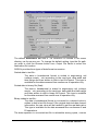
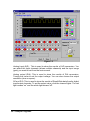
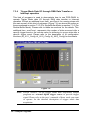
[PciUtil in Windows NT]
The PciUtil main window is shown as the following window. If any PCISDASK/NT driver has been registered, it will be shown on the Registered Driver
list.
8 • PCIS-DASK Utilities
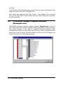
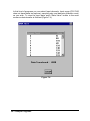
To register one of PCIS-DASK drivers, click “New …” button and a Driver
Configuration window appears.
In this window, users can select the driver you want to register and input the
parameters in the box corresponding to AI, AO, DI, or DO for the requirement
of your applications. The “Buffer Allocated” of AI, AO, DI, DO represent the
sizes of contiguous Initially Allocated memory for continuous analog input,
analog output, digital input, digital output respectively. Its unit is KB, i.e. 1024
bytes. Device driver will try to allocate these sizes of memory at system startup
time. The size of initially allocated memory is the maximum memory size that
PCIS-DASK Utilities • 9
DMA or Interrupt transfer can be performed. It will induce an unexpected result
in that DMA or Interrupt transfer performed exceeds the initially allocated size.
After the device configurations of the driver you select is finished, click “OK” to
register the driver and return to the PciUtil main window. The driver you just
registered will be shown on the registered driver list as the following figure:
10 • PCIS-DASK Utilities
Using PciUtil to change the buffer allocated settings of one of the PCISDASK drivers, select the driver from the Registered Driver list and click
“Modify …” button and then a “Driver Configuration” window is shown as below.
Inside the allocated buffer size fields of AI, AO, DI and DO are the originally set
values. Type the value in the box corresponding to AI, AO, DI, or DO according
to the requirement of your applications, and then click “OK” button.
To remove a registered driver, select the driver from the Registered Driver list
in The PciUtil main window and click “Remove” button. The selected driver will
be deleted from the registry table.
PCIS-DASK Utilities • 11
[PciUtil in Windows 98]
This utility is used to set/modify the allocated buffer sizes of AI, AO, DI and
DO. The allocated buffer sizes of AI, AO, DI, DO represent the sizes of
contiguous Initially Allocated memory for continuous analog input, analog
output, digital input, digital output respectively. Its unit is page KB, i.e. 1024
bytes. Device driver will try to allocate these sizes of memory at system startup
time. The size of initially allocated memory is the maximum memory size that
DMA or Interrupt transfer can be performed. It will induce an unexpected result
in that DMA or Interrupt transfer performed exceeds the initially allocated size.
The “Driver Configuration” window is shown as below.
Using PciUtil to change the buffer allocated settings of one of the PCISDASK drivers, select the driver from the Card Type combo box.
Inside the allocated buffer size fields of AI, AO, DI and DO are the originally set
values. Type the value in the box corresponding to AI, AO, DI, or DO according
to the requirement of your applications, and then click “Apply” button.
12 • PCIS-DASK Utilities
[PciUtil in Windows 2000]
This utility is used to set/modify the allocated buffer sizes of AI, AO, DI and DO.
The allocated buffer sizes of AI, AO, DI, DO represent the sizes of contiguous
Initially Allocated memory for continuous analog input, analog output, digital
input, digital output respectively. Its unit is page KB, i.e. 1024 bytes. Device
driver will try to allocate these sizes of memory at system startup time. The
size of initially allocated memory is the maximum memory size that DMA or
Interrupt transfer can be performed. It will induce an unexpected result in that
DMA or Interrupt transfer performed exceeds the initially allocated size.
The “Driver Configuration” window is shown as below.
Using PciUtil to change the buffer allocated settings of one of the PCIS-DASK
drivers, select the driver from the Card Type combo box.
Inside the allocated buffer size fields of AI, AO, DI and DO are the originally set
values. Type the value in the box corresponding to AI, AO, DI, or DO according
to the requirement of your applications, and then click “Apply” button.
PCIS-DASK Utilities • 13
3.2
PCIS-DASK Data File Converter utility (DAQCvt)
The data files, generated by the PCIS-DASK functions performing continuous
data acquisition followed by storing the data to disk, is written in binary format.
Since a binary file can’t be read by the normal text editor and can’t be used to
analyze the accessed data by Excel, PCIS-DASK provides a convenient tool
DAQCvt to convert the binary file to the file format read easily. The default
location of this utility is <InstallDir>\Util directory. The DAQCvt main window is
as the following figure:
The DAQCvt main window includes two frames. The upper frame, Input File
frame is used for the source data file and the lower frame is used for the
destination file.
To load the source binary data file, type the binary data file name in File
Path field or click Browser button to select the source file from Input File frame,
and then click Load button. As the file is loaded, the information related to the
data file, e.g. data type, data width, AD Range, …etc., are shown in the
corresponding fields in “Input File” frame, and the default converted data file
path and format are also listed as the figure below.
14 • PCIS-DASK Utilities
The default destination file with a .cvt extension is located in the same
directory as the source one. To change the default setting, type the file path
you wish or click the Browser button from Output File frame to select the
destination file location.
DAQCvt provides three types of data format conversion.
Scaled data to text file :
The data in hexadecimal format is scaled to engineering unit
(voltage, ample, …etc) according to the card type, data width and
data range and then written to disk in text file format. This type is
available for the data accessed from continuous AI operation only.
Scaled data to binary file (float) :
The data in hexadecimal is scaled to engineering unit (voltage,
ample, …etc) according to the card type, data width and data range
and then written to disk in binary file format. This type is available
for the data accessed from continuous AI operation only.
Binary codes to text file :
The data in hexadecimal format or converted to a decimal value is
written to disk in text file format. If the original data includes channel
information, the raw value will be handled to get the real data value.
This type is available for the data accessed form continuous AI and
DI operations.
The data separator in converted text file is selectable among space, comma
PCIS-DASK Utilities • 15
and Tab .
If you want to add title/head which includes the card type information at the
beginning of file, check the “Title/Head” box.
After setting the properties (File Path, Format, …etc) related to the converted
file, you can push Start Convert button from the Output File frame to perform
the file conversion.
3.3
PCIS-DASK Sample Programs Browser
(Examples.exe)
PCIS-DASK provides a sample program browser, Examples.exe, for you to
view and execute the sample programs that PCIS-DASK package includes.
The default location of this utility is <InstallDir>\Samples directory. After
Examples.exe utility is running, select the device you wish to operate from the
device list in the left frame, and then double click the icon of the sample you
wish to execute to run this sample program.
16 • PCIS-DASK Utilities
4
PCIS-DASK Overview
This chapter describes the classes of functions in PCIS-DASK and briefly
describes each function.
PCIS-DASK functions are grouped to the following classes:
l General Configuration Function Group
l Actual Sampling Rate Function Group
l Analog Input Function Group
-
Analog Input Configuration functions
One-Shot Analog Input functions
Continuous Analog Input functions
Asynchronous Analog Input Monitoring functions
l Analog Output Function Group
l Digital Input Function Group
-
Digital Input Configuration functions
One-Shot Digital Input functions
Continuous Digital Input functions
Asynchronous Digital Input Monitoring functions
l Digital Output Function Group
- Digital Output Configuration functions
- One-Shot Digital Output functions
- Continuous Digital Output functions
- Asynchronous Digital Output Monitoring functions
l Timer/Counter Function Group
l DIO Function Group
- Digital Input/Output Configuration function
PCIS-DASK Overview • 17
- Dual-Interrupt System Setting function
4.1
General Configuration Function Group
Use these functions to initializes and configures data acquisition card.
4.2
Register_Card
Initializes the hardware and software
states of an NuDAQ PCI-bus data
acquisition card. Register_Card must be
called before any other DASK library
functions can be called for that card.
Release_Card
Tells DASK library that this registered card
is not used currently and can be released.
This would make room for new card to
register.
Actual Sampling Rate Function Group
GetActualRate
4.3
4.3.1
Returns the actual sampling rate the
device will perform for the defined
sampling rate value.
Analog Input Function Group
Analog Input Configuration Functions
AI_9111_Config
Informs PCIS-DASK library of the
trigger source and trigger mode
selected for the analog input operation
of PCI9111. You must call this function
before calling function to perform
continuous analog input operation of
PCI9111.
AI_9112_Config
Informs PCIS-DASK library of the
trigger source selected for the analog
input operation of PCI9112. You must
call this function before calling function
18 • PCIS-DASK Overview
to perform continuous analog input
operation of PCI9112.
AI_9113_Config
Informs PCIS-DASK library of the
trigger source selected for the analog
input operation of PCI9113. You must
call this function before calling function
to perform continuous analog input
operation of PCI9113.
AI_9114_Config
Informs PCIS-DASK library of the
trigger source selected for the analog
input operation of PCI9114. You must
call this function before calling function
to perform continuous analog input
operation of PCI9114.
AI_9116_Config
Informs PCIS-DASK library of the
trigger source, trigger mode, input
mode, and conversion mode selected
for the analog input operation of
PCI9116. You must call this function
before calling function to perform
continuous analog input operation of
PCI9116.
AI_9118_Config
Informs PCIS-DASK library of the
trigger source, trigger mode, input
mode, and conversion mode selected
for the analog input operation of
PCI9118. You must call this function
before calling function to perform
continuous analog input operation of
PCI9118.
AI_9812_Config
Informs PCIS-DASK library of the
trigger source, trigger mode, and
trigger properties selected for the
analog input operation of PCI9812.
You must call this function before
PCIS-DASK Overview • 19
calling function to perform continuous
analog input operation of PCI9812.
AI_9116_CounterInterval
Informs PCIS-DASK library of the scan
interval value and sample interval
value selected for the analog input
operation of PCI9116. You must call
this function before calling function to
perform continuous analog input
operation of PCI9116.
AI_InitialMemoryAllocated
Gets the actual size of analog input
memory that is available in the device
driver.
4.3.2
One-Shot Analog Input Functions
AI_ReadChannel
4.3.3
Performs a software triggered A/D
conversion (analog input) on an analog
input channel and returns the value
converted (unscaled).
AI_VReadChannel
Performs a software triggered
A/D conversion (analog input)
on an analog input channel and
returns the value scaled to a
voltage in units of volts.
AI_VoltScale
Converts the result from an
AI_ReadChannel call to the
actual input voltage.
Continuous Analog Input Functions
AI_ContReadChannel
20 • PCIS-DASK Overview
Performs continuous A/D
conversions on the specified
analog input channel at a rate
as close to the rate you
specified.
AI_ContScanChannels
Performs continuous A/D
conversions on the specified
continuous analog input
channels at a rate as close to
the rate you specified. This
function is only available for
those cards that support autoscan functionality.
AI_ContReadMultiChannels
Performs continuous A/D
conversions on the specified
analog input channels at a rate
as close to the rate you
specified. This function is only
available for those cards that
support auto-scan functionality.
AI_ContReadChannelToFile Performs continuous A/D
conversions on the specified
analog input channel at a rate
as close to the rate you
specified and saves the
acquired data in a disk file.
AI_ContScanChannelsToFile Performs continuous A/D
conversions on the specified
continuous analog input
channels at a rate as close to
the rate you specified and
saves the acquired data in a
disk file. This function is only
available for those cards that
support auto-scan functionality.
AI_ContReadMultiChannelsToFile
Performs continuous A/D
conversions on the specified
analog input channels at a rate
as close to the rate you
specified and saves the
acquired data in a disk file.
PCIS-DASK Overview • 21
This function is only available
for those cards that support
auto-scan functionality.
4.3.4
AI_ContVScale
Converts the values of an array
of acquired data from an
continuous A/D conversion call
to the actual input voltages.
AI_ContStatus
Checks the current status of
the continuous analog input
operation.
Asynchronous Analog Input Monitoring Functions
AI_AsyncCheck
Checks the current status of
the asynchronous analog
input operation.
AI_AsyncClear
Stops the asynchronous
analog input operation.
AI_AsyncDblBufferMode
Enables or Disables double
buffer data acquisition mode.
AI_AsyncDblBufferHalfReady Checks whether the next half
buffer of data in circular buffer
is ready for transfer during an
asynchronous doublebuffered analog input
operation.
AI_AsyncDblBufferTransfer
4.4
Copies half of the data of
circular buffer to user buffer.
You can execute this function
repeatedly to return
sequential half buffers of the
data.
Analog Output Function Group
22 • PCIS-DASK Overview
4.4.1
Analog output Configuration Functions
AO_6208A_Config
Informs PCIS-DASK library of the
current range selected for the analog
output operation of PCI6208A. You
must call this function before calling
function to perform current output
operation.
AO_6308A_Config
Informs PCIS-DASK library of the
current range selected for the analog
output operation of PCI6308A. You
must call this function before calling
function to perform current output
operation.
AO_6308V_Config
Informs PCIS-DASK library of the
polarity (unipolar or bipolar) that the
output channel is configured for the
analog output and the reference
voltage value selected for the analog
output channel(s) of PCI6308V. You
must call this function before calling
function to perform current output
operation.
AO_9111_Config
Informs PCIS-DASK library of the
polarity (unipolar or bipolar) that the
output channel is configured for the
analog output of PCI9111. You must
call this function before calling function
to perform voltage output operation.
AO_9112_Config
Informs PCIS-DASK library of the
reference voltage value selected for
the analog output channel(s) of
PCI9112. You must call this function
before calling function to perform
voltage output operation.
PCIS-DASK Overview • 23
4.4.2
One-Shot Analog Output Functions
AO_WriteChannel
Writes a binary value to the specified
analog output channel.
AO_VWriteChannel
Accepts a voltage value, scales it to
the proper binary value and writes a
binary value to the specified analog
output channel.
AO_VoltScale
Scales a voltage to a binary value.
AO_SimuWriteChannel
Writes binary values to the specified
analog output channels simultaneously.
AO_SimuVWriteChannel
Accepts voltage values, scales them to
the proper binary values and writes
binary values to the specified analog
output channels simultaneously.
4.5
4.5.1
Digital Input Function Group
Digital Input Configuration Functions
DI_7200_Config
Informs PCIS-DASK library of the
trigger source and trigger properties
selected for the digital input operation
of PCI7200. You must call this
function before calling function to
perform continuous digital input
operation of PCI7200.
DI_7300A_Config/ DI_7300B_Config
Informs PCIS-DASK library of the
trigger source and trigger properties
selected for the digital input operation
of PCI7300A Rev.A or PCI7300A
24 • PCIS-DASK Overview
Rev.B. You must call this function
before calling function to perform
continuous digital input operation of
PCI7300A Rev.A or PCI7300A Rev.B.
DI_InitialMemoryAllocated
Gets the actual size of digital input
DMA memory that is available in the
device driver.
4.5.2
4.5.3
One-Shot Digital Input Functions
DI_ReadLine
Reads the digital logic state of the
specified digital line in the specified
port.
DI_ReadPort
Reads digital data from the specified
digital input port.
Continuous Digital Input Functions
DI_ContReadPort
Performs continuous digital
input on the specified digital
input port at a rate as close to
the rate you specified.
DI_ContReadPortToFile
Performs continuous digital
input on the specified digital
input port at a rate as close to
the rate you specified and
saves the acquired data in a
disk file.
DI_ContStatus
Checks the current status of
the continuous digital input
operation.
DI_ContMultiBufferSetup
Set up the buffer for multibuffered continuous digital
input.
PCIS-DASK Overview • 25
DI_ContMultiBufferStart
4.5.4
Starts
the
multi-buffered
continuous digital input on the
specified digital input port at a
rate as close to the rate you
specified.
Asynchronous Digital Input Monitoring Functions
DI_AsyncCheck
Checks the current status of
the asynchronous digital input
operation.
DI_AsyncClear
Stops the asynchronous
digital input operation.
DI_AsyncDblBufferMode
Enables or Disables double
buffer data acquisition mode.
DI_AsyncDblBufferHalfReady Checks whether the next half
buffer of data in circular buffer
is ready for transfer during an
asynchronous doublebuffered digital input
operation.
DI_AsyncDblBufferTransfer
Copies half of the data of
circular buffer to user buffer.
You can execute this function
repeatedly to return
sequential half buffers of the
data.
DI_AsyncMultiBufferNextReady
Checks whether the next
buffer of data in circular buffer
is ready for transfer during an
asynchronous multi-buffered
digital input operation.
4.6
Digital Output Function Group
26 • PCIS-DASK Overview
4.6.1
Digital Output Configuration Functions
DO_7200_Config
Informs PCIS-DASK library of the
trigger source and trigger properties
selected for the digital input operation
of PCI7200. You must call this
function before calling function to
perform continuous digital output
operation of PCI7200.
DO_7300A_Config/ DO_7300B_Config
Informs PCIS-DASK library of the
trigger source and trigger properties
selected for the digital input operation
of PCI7300A Rev.A or PCI7300A
Rev.B. You must call this function
before calling function to perform
continuous digital output operation of
PCI7300A Rev.A or PCI7300A Rev.B.
EDO_9111_Config
Informs PCIS-DASK library of the
mode of EDO channels of PCI9111.
DO_InitialMemoryAllocated
Gets the actual size of digital output
DMA memory that is available in the
device driver.
4.6.2
One-Shot Digital Output Functions
DO_WriteLine
Sets the specified digital output line in the
specified digital output port to the specified
state. This function is only available for
those cards that support digital output
read-back functionality.
DO_WritePort
Writes digital data to the specified digital
output port.
PCIS-DASK Overview • 27
DO_ReadLine
Reads the specified digital output line in
the specified digital output port.
DO_ReadPort
Reads digital data from the specified
digital output port.
DO_Write ExtTrigLine
Sets the digital output trigger line to the
specified state. This function is only
available for PCI-7200.
4.6.3
Continuous Digital Output Functions
DO_ContWritePort
Performs continuous digital output on the
specified digital output port at a rate as
close to the rate you specified.
DO_ContStatus
Checks the current status of the
continuous digital output operation.
DO_PGStart
Performs pattern generation operation.
DO_PGStop
Stops pattern generation operation.
DO_ContMultiBufferSetup
Set up the buffer for multi-buffered
continuous digital output.
DO_ContMultiBufferStart
Starts the multi-buffered continuous
digital output on the specified digital
output port at a rate as close to the rate
you specified.
4.6.4
Asynchronous Digital Output Monitoring Functions
DO_AsyncCheck
28 • PCIS-DASK Overview
Checks the current status of the
asynchronous digital output operation.
DO_AsyncClear
Stops the asynchronous digital output
operation.
DO_AsyncMultiBufferNextReady
Checks whether the next buffer is ready
for new data during an asynchronous
multi-buffered digital output operation.
4.7
4.7.1
Timer/Counter Function Group
Timer/Counter Functions
CTR_Setup
Configures the selected
counter to operate in the
specified mode.
CTR_Read
Reads the current contents of
the selected counter.
CTR_Clear
Sets the output of the selected
counter to the specified state.
CTR_8554_ClkSrc_Config
Sets the counter clock source.
CTR_8554_CK1_Config
Sets the source of CK1.
CTR_8554_Debounce_Config Sets the debounce clock.
4.7.2
The General-Purpose Timer/Counter Functions
GCTR_Setup
Controls the general-purpose
counter to operate in the
specified mode.
GCTR_Read
Reads the current counter
value of the general-purpose
counter.
PCIS-DASK Overview • 29
GCTR_Clear
4.8
4.8.1
DIO Function Group
Digital Input/Output Configuration Functions
DIO_PortConfig
4.8.2
Clears the general-purpose
timer/counter control register
and counter register.
This function is only used by the
Digital I/O cards whose I/O port can
be set as input port or output port.
This function informs PCIS-DASK
library of the port direction selected
for the digital input/output operation.
You must call this function before
calling functions to perform digital
input/output operation.
Dual-Interrupt System Setting Functions
DIO_SetDualInterrupt
Controls two interrupt sources of Dual
Interrupt system.
DIO_SetCOSInterrupt
Sets the ports used for COS interrupt
detection.
DIO_GetCOSLatchData
Get the DI data that latched in the
the COS Latch register while the
Change-of-State(COS) interrupt
occurred.
DIO_INT1_EventMessage
Controls the interrupt sources of
INT1 of Dual Interrupt system
and notifies the user’s application
when an interrupt event occurs.
The notification is performed
through a user-specified callback
function or the Windows
PostMessage API.
DIO_INT2_EventMessage
Controls the interrupt sources of
INT2 of Dual Interrupt system
30 • PCIS-DASK Overview
and notifies the user’s application
when an interrupt event occurs.
The notification is performed
through a user-specified callback
function or the Windows
PostMessage API.
4.8.3
Local Interrupt Setting Functions
DIO_7300SetInterrupt
Controls the interrupt sources (AUXDI
and Timer2) of local Interrupt system
of PCI7300A/cPCI7300A.
DIO_AUXDI_EventMessage Controls AUXDI Interrupt and
notifies the user’s application
when an interrupt event occurs.
The notification is performed
through a user-specified callback
function or the Windows
PostMessage API.
DIO_T2_EventMessage
Controls Timer2 Interrupt and
notifies the user’s application
when an interrupt event occurs.
The notification is performed
through a user-specified callback
function or the Windows
PostMessage API.
PCIS-DASK Overview • 31
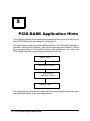
5
PCIS-DASK Application Hints
This chapter provides the programming schemes showing the function flow of
that PCIS-DASK performs analog I/O and digital I/O.
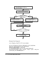
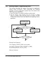
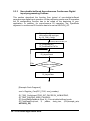
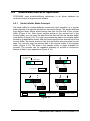
The figure below shows the basic building blocks of a PCIS-DASK application.
However, except using Register_Card at the beginning and Release_Card at
the end, depending on the specific devices and applications you have, the
PCIS-DASK functions comprising each building block vary.
Regiser_Card
Configuration Function
AI/AO/DI//DO
Operation Function
Release_Card
The programming schemes for analog input/output and digital input/output are
described individually in the following sections.
32 • PCIS-DASK Application Hints
5.1
Analog Input Programming Hints
PCIS-DASK provides two kinds of analog input operation nonbuffered
single-point analog input readings and buffered continuous analog input
operation.
The non-buffered single-point AI uses software polling method to read data
from the device. The programming scheme for this kind of AI operation is
described in section 5.1.1.
The buffered continuous analog input uses interrupt transfer or DMA
transfer method to transfer data from device to user’s buffer. The maximum
number of count in one transfer depends on the size of initially allocated
memory for analog input in the driver. The driver allocates the memory at
system boot time (in Window NT) or Windows startup time (in Window 98). We
recommend the applications use AI_InitialMemoryAllocated function to get the
size of initially allocated memory before performing continuous AI operation.
The buffered continuous analog input includes:
- synchronous continuous AI
- non-triggered non-double-buffered asynchronous continuous AI
- non-triggered double-buffered asynchronous continuous AI
- triggered non-double-buffered asynchronous continuous AI
- triggered double-buffered asynchronous continuous AI
They are described in section 5.1.2 to 5.1.6 section respectively. About the
special consideration and performance issues for the buffered continuous
analog input, please refer to the Continuous Data Transfer in PCIS-DASK
chapter for the details.
PCIS-DASK Application Hints • 33
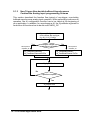
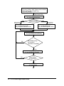
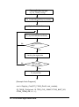
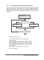
5.1.1
One-Shot Analog input programming Scheme
This section described the function flow typical of non-buffered single-point
analog input readings. While performing one-shot AI operation, most of the
cards (except PCI-9118 series cards) don’t need to include AI configuration
step at the beginning of your application.
AI_9118_Config
(only needed by PCI9118 series cards)
No
Voltage reading ?
AI_ReadChannel
Yes
Yes
AI_VReadChannel
Another reading ?
No
[Example Code Fragment]
card = Register_Card(PCI_9118, card_number);
…
AI_9118_Config(card,Input_Signal|Input_Mode,0,0,0);
AI_ReadChannel(card, channelNo, range, &analog_input[i]);
…
Release_Card(card);
34 • PCIS-DASK Application Hints
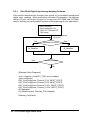
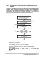
5.1.2
Synchronous Continuous Analog input programming
Scheme
This section described the function flow typical of synchronous analog input
operation. While performing continuous AI operation, the AI configuration
function has to be called at the beginning of your application. In addition, for
synchronous AI, the SyncMode argument in continuous AI functions has to be
set as SYNCH_OP.
AI_xxxx_Config
(xxxx means the card
type, e.g.
AI_9112_Config)
With SyncMode
=SYNCH_OP
Yes
Sample multiple
continuous chans?
AI_ContScanChannels/
AI_ContScanChannelsToFile
No
With SyncMode
=SYNCH_OP
AI_ContReadChannel/
AI_ContReadChannelToFile
Scale to voltage?
No
Yes
AI_ContVScale
[Example Code Fragment]
card = Register_Card(PCI_9112, card_number);
…
AI_9112_Config(card,TRIG_INT_PACER);
AI_ContScanChannels (card, channel, range, ai_buf, data_size,
(F64)sample_rate, SYNCH_OP); or
AI_ContReadChannel(card, channel, range, ai_buf, data_size,
(F64)sample_rate, SYNCH_OP)
… Release_Card(card);
PCIS-DASK Application Hints • 35
5.1.3
Non-Trigger Non-double-buffered Asynchronous
Continuous Analog input programming Scheme
This section described the function flow typical of non-trigger, non-doublebuffered asynchronous analog input operation. While performing continuous AI
operation, the AI configuration function has to be called at the beginning of
your application. In addition, for asynchronous AI, the SyncMode argument in
continuous AI functions has to be set as ASYNCH_OP.
AI_xxxx_Config
(xxxx means the card type,
e.g. AI_9112_Config)
Sample multiple
continuous chans?
Yes
With SyncMode
=ASYNCH_OP
AI_ContScanChannels/
AI_ContScanChannelsToFile
With SyncMode
=ASYNCH_OP
AI_ContReadChannel /
AI_ContReadChannel ToFile
AI_AsyncCheck
No
Operation complete?
Yes
AI_AsyncClear
36 • PCIS-DASK Application Hints
No
[Example Code Fragment]
card = Register_Card(PCI_9112, card_number);
…
AI_9112_Config(card,TRIG_INT_PACER);
AI_AsyncDblBufferMode (card, 0); //non-double-buffered AI
AI_ContScanChannels (card, channel, range, ai_buf, data_size,
(F64)sample_rate, ASYNCH_OP); or
AI_ContReadChannel(card, channel, range, ai_buf, data_size,
(F64)sample_rate, ASYNCH_OP)
do {
AI_AsyncCheck(card, &bStopped, &count);
} while (!bStopped);
AI_AsyncClear(card, &count);
…
Release_Card(card);
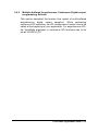
5.1.4
Non-Trigger Double-buffered Asynchronous Continuous
Analog input programming Scheme
This section described the function flow typical of non-trigger, double-buffered
asynchronous analog input operation. While performing continuous AI
operation, the AI configuration function has to be called at the beginning of
your application. For asynchronous AI, The SyncMode argument in continuous
AI functions has to be set as ASYNCH_OP. In addition, double-buffered AI
operation is enabled by setting Enable argument of AI_AsyncDblBufferMode
function to 1. To learn more about double buffer mode, please refer to section
5.2 Double-Buffered AI/DI Operation for the details.
PCIS-DASK Application Hints • 37
AI_xxxx_Config
(xxxx means the card type,
e.g. AI_9112_Config)
With Enable=TRUE
AI_AsyncDblBufferMode
Yes
With SyncMode
=ASYNCH_OP
Sample multiple
continuous chans?
AI_ContScanChannels/
AI_ContScanChannelsToFile
Next half buffer
ready for transfer?
Yes
AI_AsyncDblBufferTransfer
No
Want to stop
the operation?
Yes
AI_AsyncClear
38 • PCIS-DASK Application Hints
With SyncMode
=ASYNCH_OP
AI_ContReadChannel /
AI_ContReadChannel ToFile
AI_AsyncDblBufferHalfReady
No
No
[Example Code Fragment]
card = Register_Card(PCI_9112, card_number);
…
AI_9112_Config(card,TRIG_INT_PACER);
AI_AsyncDblBufferMode (card, 1); // Double-buffered AI
AI_ContScanChannels (card, channel, range, ai_buf, data_size,
(F64)sample_rate, ASYNCH_OP); or
AI_ContReadChannel(card, channel, range, ai_buf, data_size,
(F64)sample_rate, ASYNCH_OP)
do {
do {
AI_AsyncDblBufferHalfReady(card, &HalfReady, &fstop);
} while (!HalfReady);
AI_AsyncDblBufferTransfer(card, ai_buf);
…
} while (!clear_op);
AI_AsyncClear(card, &count);
…
Release_Card(card);
5.1.5
Trigger Mode Non-double-buffered Asynchronous
Continuous Analog input programming Scheme
This section described the function flow typical of trigger mode double-buffered
asynchronous analog input operation. A trigger is an event that occurs based
on a specified set of conditions. An interrupt mode or DMA-mode Analog input
operation can use a trigger to determinate when acquisition stop. The trigger
mode data acquisition programming is almost the same as the non-trigger
mode asynchronous analog input programming. Using PCIS-DASK to perform
trigger mode data acquisition, the SyncMode of continuous AI should be set as
ASYNCH_OP.
PCIS-DASK Application Hints • 39
AI_xxxx_Config / With Trigger mode enebled
(xxxx means the card type, e.g.
AI_9118_Config)
With Enable=TRUE
AI_AsyncDblBufferMode
Yes
Sample multiple
continuous
chans?
With SyncMode
=ASYNCH_OP
AI_ContScanChannels/
AI_ContScanChannelsToFile
No
With SyncMode
=ASYNCH_OP
AI_ContReadChannel /
AI_ContReadChannel ToFile
AI_AsyncCheck
No
Operation complete?
Yes
AI_AsyncClear
[Example Code Fragment]
card = Register_Card(PCI_9118, card_number);
…
AI_9118_Config(card, P9118_AI_BiPolar|P9118_AI_SingEnded,
P9118_AI_DtrgPositive|P9118_AI_EtrgPositive|
P9118_AI_AboutTrgEn, 0, postCount)
AI_AsyncDblBufferMode (card, 0); //non-double-buffered AI
AI_ContScanChannels (card, channel, range, ai_buf, data_size,
(F64)sample_rate, ASYNCH_OP); or
40 • PCIS-DASK Application Hints
AI_ContReadChannel(card, channel, range,
(F64)sample_rate, ASYNCH_OP)
do {
AI_AsyncCheck(card, &bStopped, &count);
} while (!bStopped);
ai_buf,
data_size,
AI_AsyncClear(card, &count);
…
Release_Card(card);
5.1.6
Trigger Mode Double-buffered Asynchronous Continuous
Analog input programming Scheme
This section described the function flow typical of trigger mode double-buffered
asynchronous analog input operation. A trigger is an event that occurs based
on a specified set of conditions. An interrupt mode or DMA-mode Analog input
operation can use a trigger to determinate when acquisition stop. The trigger
mode data acquisition programming is almost the same as the non-trigger
mode asynchronous analog input programming. Using PCIS-DASK to perform
trigger mode data acquisition, the SyncMode of continuous AI should be set as
ASYNCH_OP. In addition, double-buffered AI operation is enabled by setting
Enable argument of AI_AsyncDblBufferMode function to 1. To learn more
about double buffer mode, please refer to section 5.2 Double-Buffered AI/DI
Operation for the details.
PCIS-DASK Application Hints • 41
AI_xxxx_Config / With Trigger mode enebled
(xxxx means the card type, e.g.
AI_9118_Config)
With Enable=TRUE
AI_AsyncDblBufferMode
Yes
With SyncMode
=ASYNCH_OP
Sample multiple
continuous chans?
AI_ContScanChannels/
AI_ContScanChannelsToFile
Next Buffer ready
for transfer? /
Operation Complete?
Yes
AI_AsyncDblBufferTransfer
No
Want to stop
the operation ?
Yes
AI_AsyncClear
42 • PCIS-DASK Application Hints
With SyncMode
=ASYNCH_OP
AI_ContReadChannel /
AI_ContReadChannel ToFile
AI_AsyncDblBufferHalfReady
No
No
[Example Code Fragment]
card = Register_Card(PCI_9118, card_number);
…
AI_9118_Config(card,P9118_AI_BiPolar|P9118_AI_SingEnded,
P9118_AI_DtrgPositive|P9118_AI_EtrgPositive|
P9118_AI_AboutTrgEn,0,postCount)
AI_AsyncDblBufferMode (card, 1); Double-buffered AI
AI_ContScanChannels (card, channel, range, ai_buf, data_size,
(F64)sample_rate, ASYNCH_OP); or
AI_ContReadChannel(card, channel, range, ai_buf, data_size,
(F64)sample_rate, ASYNCH_OP)
do {
do {
AI_AsyncDblBufferHalfReady(card, &HalfReady, &fstop);
} while (!HalfReady && !fstop);
AI_AsyncDblBufferTransfer(card, ai_buf);
…
} while (!clear_op && !fstop);
AI_AsyncClear(card, &count);
AI_AsyncDblBufferTransfer(card, ai_buf);
…
Release_Card(card);
PCIS-DASK Application Hints • 43
5.2
Analog Output Programming Hints
This section described the function flow typical of single-point
analog output conversion. While performing the following
operation, the AO configuration function has to be called at the
beginning of your application:
a. Use PCI-6208A, PCI-6308A to perform current output
b. Use the analog output function that can convert a voltage
value to a binary value and then write it to device, the AO
configuration function has to be called at the beginning of your
application.
AO_6208A_Config /
AO_9112_Config
No
Output voltage?
AO_WriteChannel
Yes
Yes
AO_VWriteChannel
Another outputting?
No
[Example Code Fragment]
card = Register_Card(PCI_6208A, card_number);
…
AO_6208A_Config(card, P6208_CURRENT_4_20MA);
AO_WriteChannel(card, chan, out_value);
…
Release_Card(card);
44 • PCIS-DASK Application Hints
5.3
Digital Input Programming Hints
PCIS-DASK provides two kinds of digital input operation non-buffered
single-point digital input operation and buffered continuous digital input
operation.
The non-buffered single-point DI uses software polling method to read data
from the device. The programming scheme for this kind of DI operation is
described in section 5.3.1.
The buffered continuous DI uses DMA transfer method to transfer data from
device to user’s buffer. The maximum number of count in one transfer depends
on the size of initially allocated memory for digital input in the driver. The driver
allocates the memory at system boot time (in Window NT) or Windows startup
time (in Window 98). We recommend the applications use
DI_InitialMemoryAllocated function to get the size of initially allocated memory
before performing continuous DI operation.
The buffered continuous analog input includes synchronous continuous DI,
non-double-buffered asynchronous continuous DI and double-buffered
asynchronous continuous DI. They are described in section 5.3.2 to 5.3.5
section respectively. About the special consideration and performance issues
for the buffered continuous digital input, please refer to the Continuous Data
Transfer in PCIS-DASK chapter for the details.
PCIS-DASK Application Hints • 45
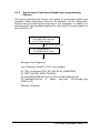
5.3.1
One-Shot Digital input programming Scheme
This section described the function flow typical of non-buffered single-point
digital input readings. While performing one-shot DI operation, the devices
whose I/O port can be set as input or out put port (PCI-7248 and PCI7296)
need to include port configuration function at the beginning of your application.
DIO_PortConfig
(Only needed by PCI7248, PCI-7249 and PCI7296 cards)
Port configured as
input port
No
Input data form Line?
DI_ReadPort
Yes
Yes
DI_ReadLine
Another reading ?
No
[Example Code Fragment]
card = Register_Card(PCI_7248, card_number);
//port configured
DIO_PortConfig(card ,Channel_P1A, INPUT_PORT);
DIO_PortConfig(card, Channel_P1B, INPUT_PORT);
DIO_PortConfig(card, Channel_P1CL, INPUT_PORT);
DIO_PortConfig(card, Channel_P1CH, INPUT_PORT);
//DI operation
DI_ReadPort(card, Channel_P1A, &inputA);
…
Release_Card(card);
46 • PCIS-DASK Application Hints
5.3.2
Synchronous Continuous Digital input programming
Scheme
This section described the function flow typical of synchronous digital input
operation. While performing continuous DI operation, the DI configuration
function has to be called at the beginning of your application. In addition, for
synchronous DI, the SyncMode argument in continuous DI functions has to be
set as SYNCH_OP.
DI_xxxx_Config
(xxxx means the card type,
e.g. DI_7200_Config)
With SyncMode=SYNCH_OP
DI_ContReadPort /
DI_ContReadPort ToFile
[Example Code Fragment]
card = Register_Card(PCI_7200, card_number);
…
DI_7200_Config(card,TRIG_INT_PACER, DI_NOWAITING,
DI_TRIG_FALLING, IREQ_FALLING);
DI_AsyncDblBufferMode (card, 0); //non-double-buffered mode
DI_ContReadPort(card, 0, pMem, data_size, (F64)sample_rate,
SYNCH_OP)
…
Release_Card(card);
PCIS-DASK Application Hints • 47
5.3.3
Non-double-buffered Asynchronous Continuous Digital
input programming Scheme
This section described the function flow typical of non-double-buffered
asynchronous digital input operation. While performing continuous DI operation,
the DI configuration function has to be called at the beginning of your
application. In addition, for asynchronous DI operation, the SyncMode
argument in continuous DI functions has to be set as ASYNCH_OP.
DI_xxxx_Config
(xxxx means the card type,
e.g. DI_7200_Config)
With SyncMode=ASYNCH_OP
DI_ContReadPort /
DI_ContReadPort ToFile
DI_AsyncCheck
No
Operation complete?
Yes
DI_AsyncClear
[Example Code Fragment]
card = Register_Card(PCI_7200, card_number);
…
DI_7200_Config(card,TRIG_INT_PACER, DI_NOWAITING,
DI_TRIG_FALLING, IREQ_FALLING);
DI_AsyncDblBufferMode (card, 0); // non-double-buffered mode
DI_ContReadPort(card, 0, pMem, data_size, (F64)sample_rate,
ASYNCH_OP)
48 • PCIS-DASK Application Hints
do {
DI_AsyncCheck(card, &bStopped, &count);
} while (!bStopped);
DI_AsyncClear(card, &count);
…
Release_Card(card);
5.3.4
Double-buffered Asynchronous Continuous Digital input
programming Scheme
This section described the function flow typical of double-buffered
asynchronous digital input operation. While performing
continuous DI operation, the DI configuration function has to be
called at the beginning of your application. For asynchronous DI,
the SyncMode argument in continuous DI functions has to be set
as ASYNCH_OP. In addition, double-buffered DI operation is
enabled by setting Enable argument of DI_AsyncDblBufferMode
function to 1. To learn more about double buffer mode, please
refer to the Double-Buffered AI/DI operation section for the
details.
PCIS-DASK Application Hints • 49
DI_xxxx_Config
(xxxx means the card type,
e.g. DI_7200_Config)
With Enable=TRUE
DIAsyncDblBufferMode
With SyncMode=ASYNCH_OP
DI_ContReadPort/
DI_ContReadPortToFile
DI_AsyncDblBufferHalfReady
No
Next half buffer
ready for transfer?
Yes
DI_AsyncDblBufferTransfer
No
Want to stop
the operation?
Yes
DI_AsyncClear
[Example Code Fragment]
card = Register_Card(PCI_7200, card_number);
…
DI_7200_Config(card,TRIG_INT_PACER, DI_NOWAITING,
50 • PCIS-DASK Application Hints
DI_TRIG_FALLING, IREQ_FALLING);
DI_AsyncDblBufferMode (card, 1); // Double-buffered mode
DI_ContReadPort(card, 0, pMem, data_size, (F64)sample_rate,
ASYNCH_OP)
do {
do {
DI_AsyncDblBufferHalfReady(card, &HalfReady);
} while (!HalfReady);
DI_AsyncDblBufferTransfer(card, pMem);
} while (!clear_op);
DI_AsyncClear(card, &count);
…
Release_Card(card);
5.3.5
Multiple-buffered Asynchronous Continuous Digital input
programming Scheme
This section described the function flow typical of multi-buffered
asynchronous digital input operation. While performing
continuous DI operation, the DI configuration function has to be
called at the beginning of your application. For asynchronous DI,
the SyncMode argument in continuous DI functions has to be set
as ASYNCH_OP.
PCIS-DASK Application Hints • 51
DI_xxxx_Config
(xxxx means the card type,
e.g. DI_7300B_Config)
DI_ContMultiBufferSetup repeatedly…
DI_ContMultiBufferStart
DI_AsyncMultiBufferNextReady
No
Next half buffer
ready?
Yes
Handling the ready data
No
Want to stop
the operation?
Yes
DI_AsyncClear
[Example Code Fragment]
card = Register_Card(PCI_7300A_RevB, card_number);
…
DI_7300B_Config(card, 16, TRIG_CLK_10MHZ, P7300_WAIT_NO,
P7300_TERM_ON, 0, 1, 1);
52 • PCIS-DASK Application Hints
//setting the DMA buffers repeatedly
DI_ContMultiBufferSetup (card, in_buf, data_size, &BufferId);
DI_ContMultiBufferSetup (card, in_buf, data_size, &BufferId);
…
// start multi-buffered DI
DI_ContMultiBufferStart (card, 0, 1);
do {
do {
DI_AsyncDblBufferHalfReady(card, &HalfReady);
} while (!HalfReady);
//Handling the ready data
} while (!clear_op);
DI_AsyncClear(card, &count);
…
Release_Card(card);
5.4
Digital Output Programming Hints
PCIS-DASK provides three kinds of digital output operation non-buffered
single-point digital output operation, buffered continuous digital output
operation and pattern generation.
The non-buffered single-point DO uses software polling method to write data
to the device. The programming scheme for this kind of DO operation is
described in section 5.4.1.
The buffered continuous DO uses DMA transfer method to transfer data from
user’s buffer to device. The maximum number of count in one transfer depends
on the size of initially allocated memory for digital output in the driver. The
driver allocates the memory at system boot time (in Window NT) or Windows
startup time (in Window 98). We recommend the applications use
DO_InitialMemoryAllocated function to get the size of initially allocated memory
before start performing continuous DO operation.
The buffered continuous digital output includes synchronous continuous DO
and asynchronous continuous DO. They are described in section 5.4.2 and
5.4.3 section individually. About the special consideration and performance
issues for the buffered continuous digital output, please refer to the Continuous
Data Transfer in PCIS-DASK chapter for the details.
The Pattern Generation DO outputs digital data pattern repeatedly at a
PCIS-DASK Application Hints • 53
predetermined rate. The programming scheme for this kind of DO operation is
described in section 5.4.4.
54 • PCIS-DASK Application Hints
5.4.1
One-Shot Digital output programming Scheme
This section described the function flow typical of non-buffered single-point
digital output operation. While performing one-shot DO operation, the cards
whose I/O port can be set as input or out put port (PCI-7248, PCI7249 and
PCI-7296) need to include port configuration function at the beginning of your
application.
DIO_PortConfig
(only needed by PCI-7248,
PCI-7249 and PCI-7296
Port configured as
output port
No
Output data to Line?
DO_WritePort
Yes
Yes
DO_WriteLine
Another outputting ?
No
[Example Code Fragment]
card = Register_Card(PCI_7248, card_number);
//port configured
DIO_PortConfig(card ,Channel_P1A, OUTPUT_PORT);
DIO_PortConfig(card, Channel_P1B, OUTPUT_PORT);
DIO_PortConfig(card, Channel_P1CL, OUTPUT_PORT);
DIO_PortConfig(card, Channel_P1CH, OUTPUT_PORT);
//DO operation
DO_WritePort(card, Channel_P1A, outA_value);
…
Release_Card(card);
PCIS-DASK Application Hints • 55
5.4.2
Synchronous Continuous Digital output programming
Scheme
This section described the function flow typical of synchronous digital output
operation. While performing continuous DO operation, the DO configuration
function has to be called at the beginning of your application. In addition, for
synchronous DO operation, the SyncMode argument in continuous DO
functions for synchronous mode has to be set as SYNCH_OP.
DO_xxxx_Config
(xxxx means the card type,
e.g. DO_7200_Config)
With SyncMode=SYNCH_OP
DO_Cont WritePort
[Example Code Fragment]
card = Register_Card(PCI_7200, card_number);
…
DO_7200_Config(card, TRIG_INT_PACER, OREQ_DISABLE,
OTRIG_LOW);
DO_AsyncDblBufferMode (card, 0); //non-double-buffered mode
DO_ContWritePort(card, 0, DoBuf, count, 1, (F64)sample_rate,
SYNCH_OP);
…
Release_Card(ca rd);
56 • PCIS-DASK Application Hints
5.4.3
Asynchronous Continuous Digital output programming
Scheme
This section described the function flow typical of asynchronous digital output
operation. While performing continuous DO operation, the DO configuration
function has to be called at the beginning of your application. In addition, for
asynchronous DO operation, the SyncMode argument in continuous DO
functions for asynchronous mode has to be set as ASYNCH_OP.
DO_xxxx_Config
(xxxx means the card type,
e.g. DO_7200_Config)
With SyncMode=ASYNCH_OP
DO_ContWritePort
DO_AsyncCheck
No
Operation complete?
Yes
DO_AsyncClear
[Example Code Fragment]
card = Register_Card(PCI_7200, card_number);
…
DO_7200_Config(card, TRIG_INT_PACER, OREQ_DISABLE,
OTRIG_LOW);
DO_ContWritePort(card, 0, DoBuf, count, 1, (F64)sample_rate,
ASYNCH_OP);
do {
PCIS-DASK Application Hints • 57
DO_AsyncCheck(card, &bStopped, &count);
} while (!bStopped);
DO_AsyncClear(card, &count);
…
Release_Card(card);
5.4.4
Pattern Generation Digital output programming Scheme
This section described the function flow typical of pattern generation for digital
output. While performing pattern generation of DO, the DO configuration
function has to be called at the beginning of your application.
DO_xxxx_Config
(xxxx means the card type,
e.g. DO_7300B_Config)
DO_PGStart
Complete pattern
generation
DO_PGStop
[Example Code Fragment]
card = Register_Card(PCI_7300A_RevB, card_number);
…
DO_7300B_Config (card, 16, TRIG_INT_PACER, P7300_WAIT_NO,
P7300_TERM_ON, 0, 0x40004000);
//start pattern generation
DO_PGStart (card, out_buf, 10000, 5000000);
…
//stop pattern generation
DO_PGStop (card);
Release_Card(card);
58 • PCIS-DASK Application Hints
5.4.5
Multiple-buffered Asynchronous Continuous Digital output
programming Scheme
This section described the function flow typical of multi-buffered
asynchronous digital output operation. While performing
continuous DO operation, the DO configuration function has to be
called at the beginning of your application. For asynchronous DO,
the SyncMode argument in continuous DO functions has to be
set as ASYNCH_OP.
PCIS-DASK Application Hints • 59
DI_xxxx_Config
(xxxx means the card type,
e.g. DO_7300B_Config)
DO_ContMultiBufferSetup repeatedly…
DO_ContMultiBufferStart
DO_AsyncMultiBufferNextRead
y
No
Next half buffer
ready?
Yes
Copy prepared data to the ready
buffer
No
Want to stop
the operation?
Yes
DO_AsyncClear
[Example Code Fragment]
card = Register_Card(PCI_7300A_RevB, card_number);
…
DO_7300B_Config (card, 16, TRIG_CLK_10MHZ, P7300_WAIT_NO,
P7300_TERM_ON, 0, 0x00040004);
60 • PCIS-DASK Application Hints
//setting the DMA buffers repeatedly
DO_ContMultiBufferSetup (card, out_buf, data_size, &BufferId);
DO_ContMultiBufferSetup (card, out_buf, data_size, &BufferId);
…
// start multi-buffered DO
DO_ContMultiBufferStart (card, 0, 1);
do {
do {
DO_AsyncDblBufferHalfReady(card, &HalfReady);
} while (!HalfReady);
// Copy prepared data to the ready buffer
} while (!clear_op);
DO_AsyncClear(card, &count);
…
Release_Card(card);
PCIS-DASK Application Hints • 61
5.5
Interrupt Event Message Programming Hints
PCIS-DASK provides two methods to perform interrupt occurrence notification
for NuDAQ DIO cards that have dual interrupt system.
The Event Message method handles event notification through user-defined
callbacks and/or the Windows Message queue (for VB5, through user-defined
callbacks only). When a user-specified interrupt event occurs, PCIS-DASK
calls the user-defined callback (if defined) and/or puts a message into the
Windows Message queue, if you specified a window handle. After receiving the
message, the user’s application can carry out the appropriate task.
The event message mechanism is easy and safe in Windows 98 and NT
systems; however, the time delay between the event and notification is highly
variable and depends largely on how loaded your system is. In addition, if a
callback function is called, succeeding events will not be handled until your
callback has returned. If the time interval between interrupt events is smaller
than the time taken for callback function processing, the succeeding interrupt
events will not be handled. Therefore this mechanism is not suitable for the
frequent interrupt occurrence condition.
The Event Status checking and waiting method handles interrupt event
status checking through Win32 wait functions, such as WaitForSingleObject or
WaitForMultipleObjects. This method is useful for the situation that the
interrupt event occurs very often, and the applications written in the language
that doesn’t support function pointers (e.g. VB4).
1. Through user-defined callbacks and the Windows Message queue
[Example Code Fragment]
card = Register_Card(PCI_7230, card_number);
//INT1 event notification is through window message
DIO_INT1_EventMessage (card, INT1_EXT_SIGNAL, hWnd,
WM_INT, NULL);
//INT2 event notification is through a callback function
DIO_INT2_EventMessage (card, INT2_EXT_SIGNAL, hWnd, NULL,
(void *) cbfn);
….
//window message handling function
long PASCAL MainWndProc(hWnd, message, wParam,
lParam)
{
switch(message) {
….
62 • PCIS-DASK Application Hints
case WM_INT: //interrupt event occurring message
….
break;
….
case WM_DESTROY:
//Disable interrupts
DIO_INT1_EventMessage (card, INT1_DISABLE, hMainWnd,
NULL, NULL);
DIO_INT2_EventMessage (card, INT2_DISABLE, hMainWnd,
NULL, NULL);
//Release card
if (card >= 0) Release_Card(card);
PostQuitMessage(0);
break;
….
}
}
….
//call back function
LRESULT CALLBACK cbfn()
{
….
}
2. Through a Win32 wait function
[Example Code Fragment]
card = Register_Card(PCI_7230, card_number);
DIO_SetDualInterrupt(card, INT1_EXT_SIGNAL, INT2_EXT_SIGNAL,
hEvent);
….
//wait for INT1 event
if (WaitForSingleObject(hEvent[0], INFINITE) == WAIT_OBJECT_0) {
ResetEvent(hEvent[0]);
……
}
… ..
//wait for INT2 event
if (WaitForSingleObject(hEvent[1], INFINITE) == WAIT_OBJECT_0)
{
ResetEvent(hEvent[1]);
……
}
… ..
if (card >= 0) Release_Card(card);
PCIS-DASK Application Hints • 63
6
Continuous Data Transfer in
PCIS-DASK
The continuous data transfer functions in PCIS-DASK input or output blocks of
data to or from a plug-in NuDAQ PCI device. For input operations, PCIS-DASK
must transfer the incoming data to a buffer in the computer memory. For output
operations, PCIS-DASK must transfer outgoing data from a buffer in the
computer memory to the NuDAQ PCI device. This chapter describes the
mechanism and techniques that PCIS-DASK uses for continuous data transfer
and the considerations for selecting the continuous data transfer mode (sync.
or async., double buffered or not, triggered or non-triggered mode).
6.1
Continuous Data Transfer Mechanism
PCIS-DASK uses two mechanisms to perform the continuous data transfer.
The first one, interrupt transfer, transfers data through the interrupt mechanism.
The second one is to use the DMA controller chip to perform a hardware
transfer of the data. Whether PCIS-DASK uses interrupt or DMA depends on
the device. If the device support both of these two mechanisms, PCIS-DASK
decides on the data transfer method that typically takes maximum advantage
of available resources. For example, PCI-9112 supports interrupt and DMA for
data transfers. The DMA data transfer is typically faster, so PCIS-DASK takes
advantage of it. PCI-9111 supports FIFO Half-Full and EOC interrupt transfer
modes. PCIS-DASK takes FIFO Half-Full interrupt transfer mode, because the
CPU is interrupted do data transfer only when the FIFO becomes half-full.
64 • Continuous Data Transfer in PCIS-DASK
6.2
Double-Buffered AI/DI Operation
PCIS-DASK uses double-buffering techniques in its driver software for
continuous input of large amounts of data.
6.2.1
Double Buffer Mode Principle
The data buffer for double-buffered continuous input operation is a circular
buffer logically. It is logically divided into two equal halves. The double-buffered
input begins when device starts writing data into the first half of the circular
buffer (Figure 6-1a). After device begins writing to the second half of the
circular buffer, you can copy the data from the first half into the transfer buffer
(user buffer) (Figure 6-1b). You now can process the data in the transfer buffer
according to application needs. After the board has filled the second half of the
circular buffer, the board returns to the first half buffer and overwrites the old
data. You now can copy the second half of the circular buffer to the transfer
buffer (Figure 6-1c). The data in the transfer buffer is again available for
process. The process can be repeated endlessly to provide a continuous
stream of data to your application (Figure 6-1d).
a
Incoming DMA
input data
b
> > >
Circular Buffer
Transfer Buffer
c
d
> >
> >
Empty Buffer
> > >
Untransferred Data
Transferred Data
Figure 7-1
Continuous Data Transfer in PCIS-DASK • 65
The PCIS-DASK double buffer mode functions were designed according to the
principle described above. If you use
AI_AsyncDblBufferMode/DI_AsyncDblBufferMode to enable double
buffer mode, the following continuous AI/DI function will perform doublebuffered continuous AI/DI. You can call
AI_AsyncDblBufferHalfReady/DI_AsyncDblBufferHalfReady to
check if data in the circular buffer is half full and ready for copying to the
transfer buffer. Then you can call
AI_AsyncDblBufferTransfer/DI_AsyncDblBufferTransfer to copy
data from the ready half buffer to the transfer buffer.
6.2.2
Single-Buffered Versus Double-Buffered Data Transfer
Single-buffered data transfer is the most common method for continuous data
transfer. In single-buffered input operations, a fixed number of samples are
acquired at a specified rate and transferred into user’s buffer. After the user’s
buffer stores the data, the application can analyze, display, or store the data to
the hard disk for later processing. Single-buffered operations are relatively
simple to implement and can usually take advantage of the full hardware
speed of the device. However, the major disadvantage of single-buffered
operation is that the maximum amount of data that can be input at any one
time is limited to the amount of initially allocated memory allocated in driver
and the amount of free memory available in the computer.
In double-buffered operations, as mentioned above, the data buffer is
configured as a circular buffer. Therefore, unlike single-buffered operations,
double-buffered operations reuse the same buffer and are able to input or
output an infinite number of data points without requiring an infinite amount of
memory. However, there exits the undesired result of data overwritten for
double-buffered data transfer. The device might overwrite data before PCISDASK has copied it to the transfer buffer. Another data overwritten problem
occurs when an input device overwrites data that PCIS-DASK is
simultaneously copying to the transfer buffer. Therefore, the data must be
processed by the application at least as fast as the rate at which the device is
reading data. For most of the applications, this requirement depends on the
speed and efficiency of the computer system and programming language.
Hence, double buffering might not be practical for high-speed input
applications.
66 • Continuous Data Transfer in PCIS-DASK
6.3
Trigger Mode Data Acquisition for Analog Input
A trigger is an event that occurs based on a specified set of conditions. An
interrupt mode or DMA-mode analog input operation can use a trigger to
determinate when acquisition stops or starts.
PCIS-DASK also provides two buffering methods for trigger mode AI – doublebuffering and single-buffering. However, the single buffer in trigger mode AI is
different from that in non-trigger mode AI. It is a circular buffer just like that in
double buffer mode but the data stored in the buffer can be processed only
when the continuous data reading is completed. The buffer will be reused until
the data acquisition operation is completed. Therefore, to protect the data you
want to get from being overwritten, the size of the single buffer should be the
same as or larger than the amount of data you wish to access. For example, if
you want to perform single-buffered middle-trigger AI with PCI-9812, and the
amount of data you want to collect before and after the trigger event are 1000
and 3000 respectively, the size of single buffer is at least 4000 in order to get
all the data you want to collect. Since the data are handled after the input
operation is completed, the desired data loss problem hardly occurs.
Since PCIS-DASK uses asynchronous AI to perform trigger mode data
acquisition, the SyncMode of continuous AI should be set as ASYNCH_OP.
Continuous Data Transfer in PCIS-DASK • 67
7
Sample Programs
There are several sample programs provided in this software diskette. They
could help you to program your own applications by using PCIS-DASK easily.
The brief descriptions of these programs are specified as follows:
Card Type Sample Name
PCI-6208
SDK6208V
Description
D/A conversion of PCI-6208V/16V
Visual C/C++ Program
SDK6208A
D/A conversion of PCI-6208A
Visual C/C++ Program
VB6208
D/A conversion of PCI-6208A
Visual Basic Program
VB6216
D/A conversion of PCI-6208V/16V
Visual Basic Program
PCI-6308
SDK6308V
D/A conversion of PCI-6308V
Visual C/C++ Program
SDK6308A
D/A conversion of PCI-6308A
Visual C/C++ Program
VB6308A
D/A conversion of PCI-6308A
Visual Basic Program
VB6308V
D/A conversion of PCI-6308V
Visual Basic Program
68 • Sample Programs
PCI-7200
C7200File
1. Digital input of PCI-7200/cPCI-7200 through
DMA transfer
2. Storing the data to disk
Visual C/C++ console Program
C7200DbfFile
1. Double buffer mode digital input of PCI7200/cPCI-7200 through DMA transfer
2. 2. Storing the data to disk
Visual C/C++ console Program
SDK7200Wave
Digital input of PCI-7200/cPCI-7200 through
DMA transfer
Visual C/C++ Program
SDK7200DbfWav
Double buffer mode digital input of PCI7200/cPCI-7200 through DMA transfer
Visual C/C++ Program
SDK7200HdSk
HandShanking mode digital input of PCI7200/cPCI-7200 through DMA transfer
Visual C/C++ program
SDKETrigLine
ExtTrig Line setting of PCI-7200/cPCI-7200
Visual C/C++ Program
VB7200Dma
Digital input of PCI-7200/cPCI-7200 through
DMA transfer
Visual Basic Program
PCI-7230
SDK7230
D/I, and D/O of PCI-7230/cPCI-7230
Visual C/C++ Program
SDK7230Int
D/I, and D/O of PCI-7230/cPCI-7230 by
Interrupt Event Status checking and waiting
method
Visual C/C++ Program
SDK7230DbEvt
D/I, and D/O of PCI-7230/cPCI-7230 by
Interrupt Event Status checking and waiting
method (Dual Interrupt Events)
Visual C/C++ Program
SDK7230IntMsg
D/I, and D/O of PCI-7230/cPCI-7230 by
Interrupt Event Message method
Visual C/C++ Program
Sample Programs • 69
SDK7230DbEvtMsg
D/I, and D/O of PCI-7230/cPCI-7230 by
Interrupt Event Message method (Dual
Interrupt Events)
Visual C/C++ Program
VB7230
D/I, and D/O of PCI-7230/cPCI-7230
Visual Basic Program
PCI-7233
SDK7233
D/I of PCI-7233
Visual C/C++ Program
SDK7233Int
D/I of PCI-7233 by Interrupt Event Status
checking and waiting method
Visual C/C++ Program
SDK7233DbEvt
D/I of PCI-7233 by Interrupt Event Status
checking and waiting method (Dual Interrupt
Events)
Visual C/C++ Program
VB7233
D/I of PCI-7233
Visual Basic Program
PCI-7234
SDK7234
D/O of PCI-7234
Visual C/C++ Program
VB7234
D/O of PCI-7234
Visual Basic Program
PCI-7248
SDK7248
D/I, and D/O of PCI-7248/cPCI-7248
Visual C/C++ Program
SDK7248Int
D/I, and D/O of PCI-7248/cPCI-7248 by
Interrupt Event Status checking and waiting
method
Visual C/C++ Program
SDK7248DbEvt
D/I, and D/O of PCI-7248/cPCI-7248 by
Interrupt Event Status checking and waiting
method (Dual Interrupt Events)
Visual C/C++ Program
SDK7248IntMsg
D/I, and D/O of PCI-7248/cPCI-7248 by
Interrupt Event Message method
Visual C/C++ Program
70 • Sample Programs
SDK7248DbEvtMsg
D/I, and D/O of PCI-7248/cPCI-7248 by
Interrupt Event Message method (Dual
Interrupt Events)
Visual C/C++ Program
VB7248
D/I, and D/O of PCI-7248/cPCI-7248
Visual Basic Program
PCI-7249
SDK7249
D/I, and D/O of cPCI-7249
Visual C/C++ Program
SDK7249Int
D/I, and D/O of cPCI-7249 by Interrupt Event
Status checking and waiting method
Visual C/C++ Program
SDK7249DbEvt
D/I, and D/O of cPCI-7249 by Interrupt Event
Status checking and waiting method (Dual
Interrupt Events)
Visual C/C++ Program
VB7249
D/I, and D/O of cPCI-7249
Visual Basic Program
PCI-7250
SDK7250
D/I, and D/O of PCI-7250/51
Visual C/C++ Program
VB7250
D/I, and D/O of PCI-7250/51
Visual Basic Program
PCI-7252
SDK7252
D/I, and D/O of cPCI-7252
Visual C/C++ Program
VB7252
D/I, and D/O of cPCI-7252
Visual Basic Program
PCI-7256
SDK7256
D/I, and D/O of PCI-7256
Visual C/C++ Program
SDK7256Int
D/I, and D/O of PCI-7256 by Interrupt Event
Status checking and waiting method
Visual C/C++ Program
SDK7256DbEvt
D/I, and D/O of PCI-7256 by Interrupt Event
Status checking and waiting method (Dual
Interrupt Events)
Visual C/C++ Program
Sample Programs • 71
VB7256
D/I, and D/O of PCI-7256
Visual Basic Program
PCI-7296
SDK7296
D/I, and D/O of PCI-7296
Visual C/C++ sample program
SDK7296Int
D/I, and D/O of PCI-7296 by Interrupt Event
Status checking and waiting method
Visual C/C++ Program
SDK7296DbEvt
D/I, and D/O of PCI-7296 by Interrupt Event
Status checking and waiting method (Dual
Interrupt Events)
Visual C/C++ Program
SDK7248IntMsg
D/I, and D/O of PCI-7296 by Interrupt Event
Message method
Visual C/C++ Program
SDK7248DbEvtMsg
D/I, and D/O of PCI-7296 by Interrupt Event
Message method (Dual Interrupt Events)
Visual C/C++ Program
VB7296
D/I, and D/O of PCI-7296
Visual Basic Program
PCI-7300
Rev.A
SDK7300Wave
Digital input of PCI-7300A_Rev.A/cPCI7300A_Rev.A through DMA transfer
Visual C/C++ Program
S7300PGwav
Pattern generation of PCI-7300A_Rev.A/cPCI7300A_Rev.A
Visual C/C++ program
SDK7300aMBufWav
Multiple buffer mode digital input of PCI7300A_Rev.A/cPCI-7300A_Rev.A
through
DMA transfer
Visual C/C++ Program
SDK7300Int
Interrupt operation of PCI-7300A_Rev.A/cPCI7300A_Rev.A by Event Status checking and
waiting method
Visual C/C++ program
SDK7300DbEvt
Interrupt operation of PCI-7300A_Rev.A/cPCI7300A_Rev.A by Interrupt Event Status
checking and waiting method (Dual Interrupt
Events)
Visual C/C++ Program
72 • Sample Programs
C7300File
1. Digital input of PCI-7300A_Rev.A/cPCI7300A_Rev.A through DMA transfer
2. Storing the data to disk
Visual C/C++ console program
PCI-7300
Rev.B
SDK7300Wave
Digital input of PCI-7300A_Rev.B/cPCI7300A_Rev.B through DMA transfer
Visual C/C++ Program
S7300PGwav
Pattern generation of PCI-7300A_Rev.B/cPCI7300A_Rev.B
Visual C/C++ program
SDK7300aMBufWav
Multiple buffer mode digital input of PCI7300A_Rev.B/cPCI-7300A_Rev.B
through
DMA transfer
Visual C/C++ Program
SDK7300Int
Interrupt operation of PCI-7300A_Rev.B/cPCI7300A_Rev.B by Event Status checking and
waiting method
Visual C/C++ program
SDK7300DbEvt
Interrupt operation of PCI-7300A_Rev.B/cPCI7300A_Rev.B by Interrupt Event Status
checking and waiting method (Dual Interrupt
Events)
Visual C/C++ Program
C7300bDbfDO
Double buffer mode digital output of PCI7300A_Rev.B/cPCI-7300A_Rev.B
through
DMA transfer
Visual C/C++ console Program
C7300File
1. Digital input of PCI-7300A_Rev.B/cPCI7300A_Rev.B through DMA transfer
2. Storing the data to disk
Visual C/C++ console program
PCI-7348/
PCI-7396
SDK7348
D/I, and D/O of PCI-7348
Visual C/C++ sample program
SDK7348Int
D/I, and D/O of PCI-7348 by Interrupt Event
Status checking and waiting method
Visual C/C++ Program
Sample Programs • 73
SDK7348DbEvt
D/I, and D/O of PCI-7348 by Interrupt Event
Status checking and waiting method (Dual
Interrupt Events)
Visual C/C++ Program
SDK7348COSi
COS of Interrup operation of D/I, and D/O of
PCI-7348 by Interrupt Event Status checking
and waiting method
Visual C/C++ Program
SDK7348IntMsg
D/I, and D/O of PCI-7348 by Interrupt Event
Message method
Visual C/C++ Program
SDK7348DbEvtMsg
D/I, and D/O of PCI- PCI-7348 by Interrupt
Event Message method (Dual Interrupt
Events)
Visual C/C++ Program
VB7348
D/I, and D/O of PCI-7348
Visual Basic Program
SDK7396
D/I, and D/O of PCI-7396
Visual C/C++ sample program
SDK7396Int
D/I, and D/O of PCI-7396 by Interrupt Event
Status checking and waiting method
Visual C/C++ Program
SDK7396DbEvt
D/I, and D/O of PCI-7396 by Interrupt Event
Status checking and waiting method (Dual
Interrupt Events)
Visual C/C++ Program
SDK7396COSi
COS of Interrup operation of D/I, and D/O of
PCI-7396 by Interrupt Event Status checking
and waiting method
Visual C/C++ Program
SDK7396IntMsg
D/I, and D/O of PCI-7396 by Interrupt Event
Message method
Visual C/C++ Program
SDK7396DbEvtMsg
D/I, and D/O of PCI- PCI-7396 by Interrupt
Event Message method (Dual Interrupt
Events)
Visual C/C++ Program
VB7396
D/I, and D/O of PCI-7396
Visual Basic Program
74 • Sample Programs
PCI-7432
SDK7432
D/I, and D/O of PCI-7432/cPCI-7432
Visual C/C++ sample program
SDK7432Int
D/I, and D/O of PCI-7432/cPCI-7432 by
Interrupt Event Status checking and waiting
method
Visual C/C++ Program
SDK7432DbEvt
D/I, and D/O of PCI-7432/cPCI-7432 by
Interrupt Event Status checking and waiting
method (Dual Interrupt Events)
Visual C/C++ Program
SDK7432IntMsg
D/I, and D/O of PCI-7432/cPCI-7432 by
Interrupt Event Message method
Visual C/C++ Program
SDK7432DbEvtMsg
D/I, and D/O of PCI-7432/cPCI-7432 by
Interrupt Event Message method (Dual
Interrupt Events)
Visual C/C++ Program
VB7432
D/I, and D/O of PCI-7432/cPCI-7433
Visual Basic Program
PCI-7433
SDK7433
D/I of PCI-7433/cPCI-7433
Visual C/C++ sample program
SDK7433R
D/I of cPCI-7433R
Visual C/C++ sample program
SDK7433Int
D/I of PCI-7433/cPCI-7433 through Interrupt
operation
Visual C/C++ Program
SDK7433DbEvt
D/I of PCI-7433/cPCI-7433 through Interrupt
operation (Dual Interrupt Events)
Visual C/C++ Program
SDK7433IntMsg
D/I of PCI-7433/cPCI-7433 by Interrupt Event
Message method
Visual C/C++ Program
SDK7433DbEvtMsg
D/I of PCI-7433/cPCI-7433 by Interrupt Event
Message method (Dual Interrupt Events)
Visual C/C++ Program
VB7433
D/I of PCI-7433/cPCI-7433
Visual Basic Program
Sample Programs • 75
PCI-7434
SDK7434
D/O of PCI-7434/cPCI-7434
Visual C/C++ sample program
SDK7434R
D/O of cPCI-7434R
Visual C/C++ sample program
VB7434
D/O of PCI-7434/cPCI-7434
Visual Basic Program
PCI-8554
SDK8554
Timer/counter of PCI-8554
Visual C/C++ sample program
SDKEventCnt
Event counter of PCI-8554
Visual C/C++ sample program
VB8554
Timer/counter of PCI-8554
Visual Basic Program
PCI-9111
SDK9111
A/D conversion, D/A conversion, D/I, and D/O
of PCI9111
Visual C/C++ Program
SDK9111Int
Analog input of PCI-9111 through Interrupt
operation
Visual C/C++ Program
SDK9111DbfPreTrg
Pre-trigger with Double buffer mode analog
input of PCI-9111 through Interrupt operation
Visual C/C++ Program
SDK9111SpreTrg
Pre-trigger with Double buffer mode analog
input of PCI-9111 through Interrupt operation
Visual C/C++ Program
C9111File
1. Analog input of PCI-9111 through Interrupt
operation
2. Storing the data to disk
Visual C/C++ console Program
C9111DbfFile
1. Double buffer mode analog input of PCI9111 through Interrupt operation
2. Storing the data to disk
Visual C/C++ console Program
VB9111
A/D conversion, D/A conversion, D/I, and D/O
of PCI9111
Visual Basic Program
76 • Sample Programs
VB9111Int
Analog input of PCI-9111 through Interrupt
operation
Visual Basic Program
VB9111PreTrg
Pre-trigger with Double buffer mode analog
input of PCI-9111 through Interrupt operation
Visual Basic Program
VB9111Scan
Autoscan Analog input of PCI-9111
Visual Basic Program
PCI-9112
SDK9112
A/D conversion, D/A conversion, D/I, and D/O
of PCI9112/cPCI-9112
Visual C/C++ program
SDK9112DMA
Analog input of PCI-9112/cPCI-9112 through
DMA data transfer
Visual C/C++ Program
SDK9112DbfDma
Double buffer mode analog input of PCI9112/cPCI-9112 through DMA data transfer
Visual C/C++ sample program
C9112File
3. Analog input of PCI-9112 through DMA
data transfer
4. Storing the data to disk
Visual C/C++ console Program
C9112DbfFile
3. Double buffer mode analog input of PCI9112 through DMA data transfer
4. Storing the data to disk
Visual C/C++ console Program
VB9112
A/D conversion, D/A conversion, D/I, and D/O
of PCI9112/cPCI-9112
Visual Basic Program
VB9112DbfDma
Double buffer mode analog input of PCI9112/cPCI-9112 through DMA data transfer
Visual Basic Program
PCI-9113
SDK9113
A/D conversion, D/A conversion, D/I, and D/O
of PCI9113
Visual C/C++ Program
SDK9113Int
Analog input of PCI-9113 through Interrupt
operation
Visual C/C++ Program
Sample Programs • 77
SDK9113DbfInt
Double buffer mode analog input of PCI-9113
through Interrupt operation
Visual C/C++ sample program
C9113File
5. Analog input of PCI-9113 through Interrupt
operation
6. Storing the data to disk
Visual C/C++ console Program
C9113DbfFile
5. Double buffer mode analog input of PCI9113 through Interrupt operation
6. Storing the data to disk
Visual C/C++ console Program
VB9113
A/D conversion, D/A conversion, D/I, and D/O
of PCI9113
Visual Basic Program
VB9113Int
Analog input of PCI-9113 through Interrupt
operation
Visual Basic Program
VB9113Scan
Autoscan Analog input of PCI-9113
Visual Basic Program
PCI-9114
SDK9114
A/D conversion, D/A conversion, D/I, and D/O
of PCI9114
Visual C/C++ Program
SDK9114Int
Analog input of PCI-9114 through Interrupt
operation
Visual C/C++ Program
SDK9114DbfInt
Double buffer mode analog input of PCI-9114
through Interrupt operation
Visual C/C++ sample program
C9114File
7. Analog input of PCI-9114 through Interrupt
operation
8. Storing the data to disk
Visual C/C++ console Program
C9114DbfFile
7. Double buffer mode analog input of PCI9114 through Interrupt operation
8. Storing the data to disk
Visual C/C++ console Program
78 • Sample Programs
VB9114
A/D conversion, D/A conversion, D/I, and D/O
of PCI9114
Visual Basic Program
VB9114Int
Analog input of PCI-9114 through Interrupt
operation
Visual Basic Program
VB9114Scan
Autoscan Analog input of PCI-9114
Visual Basic Program
cPCI-9116
SDK9116
A/D conversion of CPCI-9116
Visual C/C++ Program
SDK9116ScanDma
Software trigger with Single buffer mode
analog input of CPCI-9116 through DMA data
transfer
Visual C/C++ Program
SDK9116PostTrg
Post trigger with Single buffer mode analog
input of CPCI-9116 through DMA data transfer
Visual C/C++ Program
SDK9116MidTrg
Middle trigger with Single buffer mode analog
input of CPCI-9116 through DMA data transfer
Visual C/C++ Program
SDK9116DlyTrg
Delay trigger with Single buffer mode analog
input of CPCI-9116 through DMA data transfer
Visual C/C++ Program
SDK9116DbfDma
Double buffer mode analog input of
9116 through DMA data transfer
cPCI-
Visual C/C++ Program
SDK9116DbfAboutTrg Middle trigger with Double buffer mode analog
input of CPCI-9116 through DMA data transfer
Visual C/C++ Program
SDK9116DbfPostTrg
Post trigger with Double buffer mode analog
input of CPCI-9116 through DMA data transfer
Visual C/C++ Program
SDK9116DbfDlyTrg
Delay trigger with Double buffer mode analog
input of CPCI-9116 through DMA data transfer
Visual C/C++ Program
Sample Programs • 79
C9116File
9. Analog input of cPCI-9116 through DMA
data transfer
10. Storing the data to disk
Visual C/C++ console Program
C9116DbfFile
9. Double buffer mode analog input of cPCI9116 through DMA data transfer
10. Storing the data to disk
Visual C/C++ console Program
VB9116
Analog input of CPCI-9116 through DMA data
transfer
Visual Basic Program
PCI-9118
SDK9118
A/D conversion, D/A conversion, D/I, and D/O
of PCI9118
Visual C/C++ Program
SDK9118DbfAboutTrg About trigger with Double buffer mode analog
input of PCI-9118 through DMA data transfer
Visual C/C++ Program
SDK9118BurstDma
Analog input of PCI-9118 through Burst Mode
DMA data transfer
Visual C/C++ Program
SDK9118DbfDma
Double buffer mode analog input of PCI-9118
through DMA data transfer
Visual C/C++ Program
SDK9118HRDbfDma Double buffer mode analog input of
9118HR through DMA data transfer
PCI-
Visual C/C++ Program
SDK9118ScanDma
Autoscan Analog input of PCI-9118 through
DMA data transfer
Visual C/C++ Program
SDK9118HRScanDma Autoscan Analog input of PCI-9118HR through
DMA data transfer
Visual C/C++ Program
SDK9118DbfPreTrg
Pre-trigger with Double buffer mode analog
input of PCI-9118 through DMA data transfer
Visual C/C++ Program
SDK9118DbfPostTrg
Post trigger with Double buffer mode analog
input of PCI-9118 through DMA data transfer
Visual C/C++ sample program
80 • Sample Programs
SDK9118AboutTrg
About trigger with Single buffer mode analog
input of PCI-9118 through DMA data transfer
Visual C/C++ Program
SDK9118HRAboutTrg About trigger with Single buffer mode analog
input of PCI-9118HR through DMA data
transfer
Visual C/C++ Program
SDK9118PostTrg
Post trigger with Single buffer mode analog
input of PCI-9118 through DMA data transfer
Visual C/C++ Program
C9118File
11. Analog input of PCI-9118 through DMA
data transfer
12. Storing the data to disk
Visual C/C++ console Program
C9118DbfFile
11. Double buffer mode analog input of PCI9118 through DMA data transfer
12. Storing the data to disk
Visual C/C++ console Program
VB9118DgHr
A/D conversion, D/A conversion, D/I, and D/O
of PCI9118DG/HR
Visual Basic Program
VB9118Hg
A/D conversion, D/A conversion, D/I, and D/O
of PCI9118HG
Visual Basic Program
VB9118AboutTrg
About trigger with Single buffer mode analog
input of PCI-9118 through DMA data transfer
Visual Basic Program
VB9118PostTrg
Post trigger with Single buffer mode analog
input of PCI-9118 through DMA data transfer
Visual Basic sample program
VB9118Dma
Analog input of PCI-9118 through DMA data
transfer
Visual Basic Program
VB9118HRDma
Analog input of PCI-9118HR through DMA
data transfer
Visual Basic Program
Sample Programs • 81
PCI-9812
SDK9812SoftTrg
Software trigger with Single buffer mode
analog input of PCI-9812/cPCI-9812 through
DMA data transfer
Visual C/C++ Program
SDK9812PreTrg
Pre-trigger with Single buffer mode analog
input of PCI-9812/cPCI-9812 through DMA
data transfer
Visual C/C++ Program
SDK9812PostTrg
Post trigger with Single buffer mode analog
input of PCI-9812/cPCI-9812 through DMA
data transfer
Visual C/C++ Program
SDK9812MidTrg
Middle trigger with Single buffer mode analog
input of PCI-9812/cPCI-9812 through DMA
data transfer
Visual C/C++ Program
SDK9812DelayTrg
Delay trigger with Single buffer mode analog
input of PCI-9812/cPCI-9812 through DMA
data transfer
Visual C/C++ Program
SDK9812DbfMidTrg
Middle trigger with Double buffer mode analog
input of PCI-9812/cPCI-9812 through DMA
data transfer
Visual C/C++ Program
SDK9812DbfPreTrg
Pre-trigger with Double buffer mode analog
input of PCI-9812/cPCI-9812 through DMA
data transfer
Visual C/C++ Program
SDK9812DbfPostTrg
Post trigger with Double buffer mode analog
input of PCI-9812/cPCI-9812 through DMA
data transfer
Visual C/C++ Program
SDK9812DbfDelayTrg Delay trigger with Double buffer mode analog
input of PCI-9812/cPCI-9812 through DMA
data transfer
Visual C/C++ Program
C9812File
13. Analog input of PCI-9812/10 through DMA
data transfer
14. Storing the data to disk
Visual C/C++ console Program
82 • Sample Programs
C9812DbfFile
13. Double buffer mode analog input of PCI9812/10 through DMA data transfer
14. Storing the data to disk
Visual C/C++ console Program
VB9812
Analog input of PCI-9812/cPCI-9812 through
DMA data transfer
Visual Basic 4.0 Program
9812 VB5
Analog input of PCI-9812/cPCI-9812 through
DMA data transfer
Visual Basic 5.0 Program
Note 1: ADLink will periodically upgrades PCIS-DASK to add support for
new NuDAQ PCI-bus data acquisition cards and NuIPC
CompactPCI cards and the additional sample programs for the
new devices will be included. Please refer to Release Notes for
the card types that the current release of PCIS-DASK actually
supports.
Note 2: PCIS-DASK provides a sample program browser, Examples.exe,
for you to view and execute the sample programs that PCISDASK package includes. The default location of this utility is
<InstallDir>\Samples directory. After Examples.exe utility is
running, you can double click the icon of the sample you wish to
execute to execute this sample program.
Sample Programs • 83
7.1
7.1.1
Sample Programs Development Environment
Visual Basic Sample Programs
There are several Visual Basic sample programs provided for each card in this
software package. The following files are included in each sample program
(Using VB9112DMA as an example):
l VB project file --- VB9112D.VBP
l VB form files --- VB9112D.FRM
l Executable file --- VB9112D.EXE
You must have 32-bit Microsoft Visual Basic 4.0 Professional Edition or above
to deal with these sample programs. Please refer to Visual Basic Manual or
related reference books to get the information about how to use Visual Basic
4.0.
If you don’t install 32-bit Microsoft Visual Basic 4.0, but want to execute the VB
sample programs, please install “VB4 Runtime” package first. The VB4
Runtime package includes the required library and DLL files to run the VB
sample programs. You can find this package in the root directory of “ADLink
All-In-One Compact Disc” CD or from the setup main window of this CD. After
the installation of VB4 Runtime package, the VB4 samples can be executed on
the system with no VB4 installed.
PCIS-DASK includes another kind of samples, Microsoft C/C++ sample
programs, which will be described in the next section. The C/C++ samples
provide the similar functions as those provided by VB samples. Preferably,
they can be run directly and don’t need to install any additional package. So, if
you just want to test the PCIS-DASK package, please use Microsoft C/C++
sample programs.
7.1.2
Microsoft C/C++ Sample Programs
We provide several Microsoft C/C++ sample programs for each card in this
package. The following files are included in each sample program (Using
SDK7200WAV as an example):
l C source file --- 7200WAV.C
l Workspace file --- 7200WAV.MDP
l Resource script file --- 7200WAV.RC, RESOURCE.H
l Make file --- 7200WAV.MAK
l Executable file --- 7200WAV.EXE
84 • Sample Programs
You can use any editor or Microsoft Visual C++ 4.0 to view or modify these
source files. However, to build the executable 7200WAV.EXE, you must have
Microsoft Visual C++ 4.0 or above. Please refer to Visual C++ Manual or
related reference books to get the information about how to use Visual C++.
7.2
Execute Sample Programs
To run the sample programs, please follow these steps:
step 1. Open the sample program
You can use Microsoft Visual C++ 4.0 or Visual Basic 4.0 to open and
execute the sample programs. Or you can run the executable files
directly.
step 2. Option Setting
According to your requirements, select the testing functions, e.g. A/D,
D/A, etc., testing channels, sampling rate and transfer count, etc.
step 3. Push “start” button to run the program.
7.3
The Detailed Descriptions of these Sample
Programs
There are four kinds of sample programs provided in this software package.
The descriptions of these three types are the following (Using the screens of
VB 9112, SDK 9112DMA, SDK 9112CDMA and SDK 9118 DbfPreTrg as the
figure examples ) :
7.3.1
A/D conversion, D/A conversion, D/I, and D/O
This kind of samples is used to demonstrate how to use PCIS-DASK to
operate software trigger with program polling data mode and Read/Write data
from digital input/output channels on PCI-9112. The main screen of this kind of
programs is shown below (Figure 7.2):
Sample Programs • 85
Figure 7.2
Analog Input (A/D) : This is used to show the results of A/D conversion. You
can select the Input channels (allows multiple channels) and the input range
(gain) you want to test from the main screen.
Analog output (D/A): This is used to show the results of D/A conversion.
Turning the turner to set the output voltage. You can also choose the output
waveform (sine or square).
D/I and D/O: This is used to show the results of Read/Write data from/to digital
input/output channels. To set the output value, click the channel lights. The red
light means “on” and the white light means “off”.
86 • Sample Programs
7.3.2
Data I/O through DMA Data Transfer or Interrupt operation
This kind of programs is used to demonstrate how to use PCIS-DASK to
operate data I/O through DMA data transfer or Interrupt operation. The main
screen of this kind of programs is shown below (Figure 7.3):
Figure 7.3
Sample Programs • 87
In this kind of programs you can select Input channels, Input range (PCI-7200
does not have these two options), sampling rate, and data size (transfer count)
as you wish. To view the input data, push “Data Value” button in the main
screen as data transfer is finished (Figure 7.4).
Figure 7.4
88 • Sample Programs
7.3.3
Double buffer mode data I/O through DMA transfer or
Interrupt operation
This kind of programs is used to demonstrate how to use PCIS-DASK to
operate double-buffered data I/O through DMA transfer or Interrupt operation.
The screen of this kind of programs is shown below (Figure 7.5) :
Figure 7.5
In this kind of programs you can select Input channel, input range (PCI-7200
does not have this two options), sampling rate, and data size (transfer count)
as you wish. To view the input data, push “Data Value” button in the main
screen after you stop the double-buffered operation.
Sample Programs • 89
7.3.4
Trigger Mode Data I/O through DMA Data Transfer or
Interrupt operation
This kind of programs is used to demonstrate how to use PCIS-DASK to
operate Trigger Mode data I/O through DMA data transfer or Interrupt
operation. Except an additional input item, postCount, the running steps and
the main screen of this kind of programs (Figure 7.6) are almost the same as
those mentioned in section 7.3.2 (For Single-Buffer Mode) or section 7.3.3 (For
Double-Buffer Mode). Please refer to these two sections for the details. This
additional item, postCount , represents the number of data accessed after a
specific trigger event or the counter value for deferring to access data after a
specific trigger event. Please refer to the description of AI configuration
functions (AI_9111_Config, AI_9118_Config, AI_9812_Config) for the details.
Figure 7.6
Note: Except VB9812, all the trigger mode data acquisition sample
programs use external digital trigger source to provide trigger
signal. Please refer to the user’s manuals of these cards you want
to operate for the detailed description of trigger mode data
acquisition.
90 • Sample Programs
8
Distribution of Applications
8.1
Files
To install an application using PCIS-DASK on another computer, you also
must install the necessary driver files and supporting libraries on the target
machine. You can create an automatic installer to install your program and all
of the files needed to run that program or you can manually install the program
and program files. Whichever installation method you choose, you must install
the following files:
l Required support DLLs:
– Pci-dask.dll
l Driver files
Windows 98
– The corresponding driver files in \Software\Pcis-dask\W98NT2K
\redist\W98\drivers, e.g. pci7200.sys for PCI-7200. These files should
be copied to Windows\system32\drivers directory.
– The corresponding INF files in \Software\Pcis-dask\W98NT2K
\redist\W98\Inf, e.g. p7200.inf for PCI-7200. These files should be
copied to Windows\inf directory.
– Device
configuration
utility
in
\Software\Pcisdask\W98NT2K\redist\W98\Util.
Windows NT 4.0
– adldask.sys in \Software\Pcis-dask\W98NT2K\redist\Wnt\drivers. This
file should be copied to Winnt\system32\drivers directory.
– The corresponding driver files in \Software\Pcis-dask\W98NT2K
\redist\Wnt\drivers, e.g. pci7200.sys for PCI-7200. These files should
be copied to Winnt\system32\drivers directory.
Distribution of Applications • 91
– Device configuration utility in \Software\Pcisdask\W98NT2K/redist\Wnt\Util.
Windows 2000
– The corresponding driver file in \Software\Pcis-dask\W98NT2K
\redist\W2000\drivers, e.g. pci7200.sys for PCI-7200. These files
should be copied to Winnt\system32\drivers directory.
– The corresponding INF file in \Software\Pcis-dask\W98NT2K
\redist\W2000\Inf, e.g. p7200.inf for PCI-7200. These files should be
copied to Winnt\inf directory.
– Device configuration utility in \Software\Pcis-dask\W98NT2K
\redist\W2000\Util.
l Utility file (option)
– Data Conversion utility DAQCvt.exe in \Software\Pcis-dask\
W98NT2K\redist\W98\Util,
\Software\Pcisdask\W98NT2K\redist\Wnt\Util
or
\Software\Pcisdask\W98NT2K\redist\W2000\Util to convert the binary data file
to the file format read easily.
8.2
Automatic Installers
Many programming environments include some form of setup or distribution kit
tool. This tool automatically creates an installation program for your program
so that you can easily install it on another computer. To function successfully,
this tool must recognize which control files and supporting libraries are
required by your program and include these in the installation program it
creates.
Some of these tools, such as the Visual Basic 5 Setup Wizard, use
dependency files to determine which libraries are required by an VB
application.
Some setup tools might not automatically recognize which files are required by
a program but provide an option to add additional files to the installation
program. In this case, verify that all the necessary files described in the
previous section are included. You also should verify that the resulting
installation program does not copy older versions of a file over a newer version
on the target computer.
If your programming environment does not provide a tool or wizard for building
an installation program, you can use third-party tools such as InstallShield.
Some programming environments provide simplified or trial versions of thirdparty installer creation tools on their installation CDs.
92 • Distribution of Applications
The installation program not only copies all the required files into the
appropriated location, but executes Device configuration utility to configure the
devices.
Distribution of Applications • 93
8.3
Manual Installation
If your programming environment does not include a setup or distribution kit
tool, you can perform the installation task manually. To install your program on
another computer, follow these steps:
1. Copy the program executable to the target computer.
2. Copy all required PCIS-DASK files described in the section
8.1.1 to the appropriate directory on the target computer.
3. Use NuDAQ Device Configuration utility to configure the device.
Note: Do not replace any files on the target computer if the file on the
target computer has a newer version than the file you are installing.
94 • Distribution of Applications