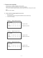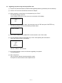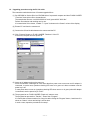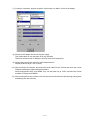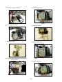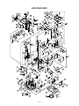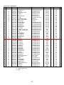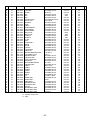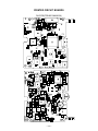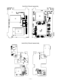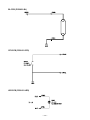
1
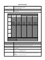
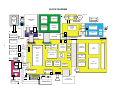
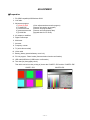
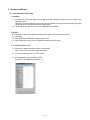
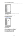
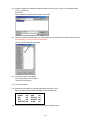
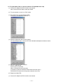
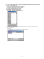
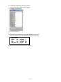
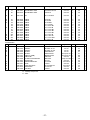
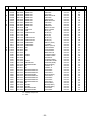
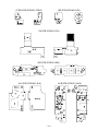
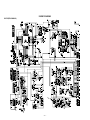
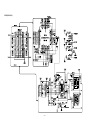
(without price)
QV-4000
(KX-821D)
SEP. 2001
INDEX
R
Ver. 2
NOV. / 2002
Ver. 1
FEB. / 2002
CONTENTS
SPECIFICATIONS ....................................................................................................................................... 1
BLOCK DIAGRAM ...................................................................................................................................... 3
ADJUSTMENT ............................................................................................................................................ 4
1. Program version upgrading .............................................................................................................. 5
1-1. How to confirm the program (graphic menu) version ............................................................. 5
1-2. Upgrading procedure using the CompactFlash card .............................................................. 6
1-3. Upgrading procedure using the PC link cable ......................................................................... 7
2. Test mode ........................................................................................................................................... 9
2-1. Booting ........................................................................................................................................ 9
2-2. Item for testing ............................................................................................................................ 9
3. Product conditions .......................................................................................................................... 11
3-1. Color adjustment data writing ................................................................................................. 18
3-2. Flash adjustment ...................................................................................................................... 18
3-3. Flash operation and recharge operation ................................................................................ 19
3-4. Current consumption ............................................................................................................... 20
3-5. VCOM DC adjustment ............................................................................................................... 21
3-6. Assist light adjustment. ........................................................................................................... 22
3-7. Operation check ........................................................................................................................ 23
4. MAIN PCB Assy ............................................................................................................................... 24
4-1. RGB AMP and Sub-Brightness voltage setting adjustment ................................................. 24
4-2. Contrast and Brightness voltage setting adjustment ........................................................... 25
4-3. TINT setting adjustment ........................................................................................................... 26
4-4. EVCC3, VCC1.8, VCC3, VCC5, BLVCC Voltage check .......................................................... 27
4-5. VCC2, VCC7, VCC15, VEE7 Voltage check ............................................................................. 27
DISASSEMBLE ......................................................................................................................................... 28
EXPLODED VIEW ..................................................................................................................................... 34
PARTS LIST .............................................................................................................................................. 35
PRINTED CIRCUIT BOARDS ................................................................................................................... 40
SCHEMATIC DIAGRAMS ......................................................................................................................... 44
SPECIFICATIONS
File Format
Still images (including panoramas): JPEG (Exif. Ver. 2.1)/TIFF, DCF standard (Design rule for
Camera File system), DPOF compatible
Movies: AVI (Motion JPEG)
Recording Medium
CompactFlash card (Type I/II), IBM Microdrive
Recorded Image Size
2240 x 1680 pixels, 2256 x 1504 (3 : 2) pixels, 1600 x 1200 pixels, 1280 x 960 pixels,
640 x 480 pixels
Standard Memory Capacity, Number of Image Files, Computer Output Image Size (JPEG images only)
Still
Image size
Quality
(pixels)
2240
X
FINE
NORMAL
1680
ECONOMY
2256
TIFF
FINE
X
1504
(3:2)
8MB
Number of images
64MB
340MB
memory card
memory card
memory card
1.8 MB
1.2 MB
7 images
10 images
30 images
43 images
513 images
730 images
File size
0.72 MB
15 images
60 images
1026 images
11.025 MB
1.6 MB
1 image
8 images
5 images
33 images
87 images
566 images
NORMAL
1.1 MB
12 images
50 images
842 images
ECONOMY
TIFF
0.66 MB
9.99 MB
19 images
1 image
77 images
5 images
1314 images
97 images
1600
FINE
0.85 MB
15 images
60 images
1026 images
X
1200
NORMAL
ECONOMY
0.6 MB
0.35 MB
19 images
30 images
77 images
124 images
1314 images
2053 images
TIFF
5.625 MB
2 images
10 images
171 images
1280
X
FINE
NORMAL
0.5 MB
0.35 MB
22 images
30 images
88 images
124 images
1493 images
2053 images
960
ECONOMY
0.2 MB
51 images
207 images
3285 images
640
TIFF
FINE
3.6 MB
0.15 MB
3 images
77 images
15 images
311 images
269 images
4693 images
X
NORMAL
0.09 MB
101 images
415 images
6571 images
480
ECONOMY
TIFF
0.06 MB
0.9 MB
154 images
15 images
622 images
62 images
8213 images
1026 images
Storage Capacity
Movie (320 x 240 pixels)
Approximately 300 KB/second
Recording Time
30 seconds per movie
• The above figures are approximations only.
Image Deletion
Single image; all images in a folder; all images in memory (with image protection)
Imaging Element
1/1.8-inch CCD (Total Pixels: 4.13 million, Effective Pixels; 3.98 million)
Lens
F2 (W) to 2.5 (T); f = 7 (W) to 21 mm (T)
(equivalent to approximately 34 (W) to 102 mm (T) for 35 mm film)
Zoom
3X optical zoom; 3.2X digital zoom (9.6X in combination with optical zoom)
Focusing
Contrast-type Multi-area Auto Focus (Spot Auto Focus Mode, Macro Mode, Infinity Mode); manual
focus; focus lock
Approximate Focus Range
Normal:
Macro:
Manual Focus:
Exposure Control
Light Metering: Multi-pattern, center-weighted, spot by CCD
Exposure:
Full Auto, Program AE, Shutter priority AE, Aperture priority AE, Manual
Exposure
Compensation: –2EV to +2EV (1/3EV units)
30 cm to ∞
6 cm (W)/20 cm (T) to 50 cm
6 cm (W)/20 cm (T) to ∞
—1—
Shutter
CCD electronic shutter; mechanical shutter, BULB, 60 to 1/1000 second
Aperture
F2.0/2.3/2.8/4.0/5.6/8.0, auto switching or manual switching
White Balance
Automatic, fixed (4 modes), manual switching
Self-timer
10 seconds, 2 seconds
Built-in Flash
Flash Modes: AUTO, ON, OFF, Red eye reduction
Flash Range: Approximately 0.5 to 3.5 meters
Recording Functions
One-shot, continuous, movie, panorama, AEB, self-timer, macro, Best Shot
Monitor
1.8" TFT, low-glare color HAST LCD (122,100 pixels, 555 x 220)
Viewfinder
LCD Monitor or optical viewfinder
Clock
Built-in quartz digital timepiece for time and date recording and storage with image data; auto
calendar up to 2049
Input/Output Terminals
Remote shutter release terminal; AC adaptor terminal; USB port (MINI-B); VIDEO OUT (NTSC/
PAL)
Power Supply
Four AA-size alkaline or lithium batteries
Four AA-size nickel-metal hydride rechargeable batteries (NP-H3)
AC adaptor (AD-C620)
AC adaptor charger (BC-3HA)
Battery Life
The values noted below indicate the number of hours before battery failure under normal operating
temperature (25 °C). These values are for reference only, and do not guarantee that any particular
set of batteries actually will provide the service life indicated. Low temperatures shorten battery
life.
Type of Operation
Continuous Playback
AA-size Alkaline
170 minutes
Batteries LR6
AA-size Lithium
Batteries FR6
320 minutes
AA-size Ni-MH Batteries
180 minutes
NP-H3
Continuous Recording
90 minutes
(540 shots)
180 minutes
(1,130 shots)
100 minutes
(600 shots)
• The above figures are approximations only.
• The above guidelines are based on the following battery types:
Alkaline: MX1500 (AA) DURACELL ULTRA
Lithium: Energizer
• Battery life varies with brand.
Continuous recording values show the number of shots without using the flash. The number of
shots depends on use of the flash and whether flash is turned on or off.
Power Consumption
Approximately 6.8 W
Dimensions
118(W) x 74.5(H) x 64.5(D) mm
Weight
Approximately 355 g (excluding batteries)
• This camera does not have a separate battery to power its clock. Clock settings are cleared whenever power to the camera is cut
off (by batteries going dead while the camera is not connected to an AC power outlet with the AC adaptor) for about 24 hours. After
power is resumed, either by loading fresh batteries or connecting to an AC power outlet, you will have to set the correct time and
date again.
• The liquid crystal panel built into this camera is the product of precision engineering, with a pixel yield of 99.99%. This also means,
however that 0.01% of the pixels can be expected to fail to light or to remain lit at all times.
—2—
BLOCK DIAGRAM
C
LED
Driver
Lever
AF
LED
Mode
Dial
CCD
ICX406AQ
Lens Unit
4pin CtoF
POWER
SW
ØH-DRIVER
TC7MH368FK
X2
JOG
Dial
SHUTTER
MAIN(SUB)
LV-040A
VCC300
16pin
6pin
6pin
CDS/AGC
AD9843A
ØV-DRIVER
CXD3400N
VLED
Charging
Booster
Circuit
SGND
+
Strobe Unit
FLASH
JK
CN
Serial JACK
40pin
BtoB
VCC1-ST
40pin BtoB
VCC5
A/V-JACK
CF
Connector
—3—
DB+
DCIN
USB-JACK
JKGND
DC-JACK
DB+
+1.8V
+3.3V
+5.0V
+5.4V
+15V
+7.5V
-7.5V
18pin
BtoB
AE
LOCK
AELOCK
RTC
RTC-4574
Power Supply
Block
DB-
KEY
VCOMAMP
NJM3414
TELE
Chroma
Interface
IR3Y29AM
Cross
Controller
AF/ZOOM
DRIVER
LB1937T
Shutter/AE
DRIVER
LB1837M
BL Circuit
BLA
CF
SW
Flahing Controller
Photo Sensor
CAS-1.8
+
-
Battery BOX
CF-BUFFER
TC7MH367FK
X2
Incline
Sensor
BLB
CASE
FLASH-ROM
16M
MBM29LV160
DISP
FOCUS
EXST
75C
HG75C
PREV
HD404889
26pin
Photometric
Method
SDRAM
128MX16bit
WIDE
4bit Microcomputer
20pin
BtoB
WB
External
Storobe
TIMER
MAIN(DB)
MAIN(DA)
SGND
20pin BtoB
SUB-LCD
TFL-LCD
COD18T1035FN
SH3
HD6417709A
ADJUSTMENT
■ Preparation
1. PC (IBM Compatible)/OS:Windows 95/98
2. Link cable.
3. Adjustment program
1) ADJ821A.EXE
2) FLOAD.EXE
3) romxxxxxxxx.bin
4) gmenuxxxxxxxx.bin
5) qv-4000.bin
(Color adjustment data transfer program)
(Camera unit version up program)
(Camera unit program data)
(Camera unit menu display data)
(Upgrade data for CF cards)
4. AC adaptor or stabilizer
5. Digital oscilloscope
6. Multimeter
7. Ammeter
8. Frequency counter
9. TV (with video terminal)
10. Video cable
11. Battery (battery operation/battery cover lock)
12. PC link program : Photo Loader (Communication function confirmation)
13. USB cable/USB driver (USB function confirmation)
14. Test chart (for photography check)
That which carried out color printing of picture data "CHART1.JPG" and the "CHART2.JPG".
CHART1.JPG
CHART2.JPG
—4—
1. Program version upgrading
In the camera unit, program and graphic menu are stored.
Please check the version and update it if the version is not updated.
There are two method of program updating; using CompactFlash card or utilizing PC link cable.
Note:
Be sure to use AC adaptor.
1-1. How to confirm the program (graphic menu) version
1.
2.
Boot the test mode.
Turn the power on while pressing DISP and MENU buttons simultaneously.
Check the LCD display.
(Example)
English/ Japanese/ Spanish
TEST MODE
PROG
01.
09.
21.
13.
01
씯 Program version
GMENU
01.
07.
23.
10.
24
씯 Graphic menu version
····
(Example)
English/ German/ French
TEST MODE
PROG
01.
09.
21.
13.
01
씯 Program version
GMENU
01.
07.
23.
10.
32
씯 Graphic menu version
····
(Example)
English/ Spanish/ Italian
TEST MODE
PROG
01.
09.
21.
13.
01
씯 Program version
GMENU
01.
07.
23.
10.
34
씯 Graphic menu version
····
—5—
1-2. Upgrading procedure using the CompactFlash card
(1) Prepare a CF card that contain QV-4000 firmware upgrading software (qv-4000.bin) in the root directory.
(2) Insert the CF card in the QV-4000 and connect AC adaptor.
(3) While pressing the control button, turn the power key on to "PLAY".
The following display comes out.
Version display (VER1.00 etc.) may come out on the bottom of the display.
PROGRAM UPDATE
YES
NO
(4) Moving the contol button up or down, move the white cursor at "YES" then push "SHUTTER" key.
The following display comes out and rewriting firmware starts.
NOW LOADING
(5) After a while, display shows “COMPLETE!” and the camera is set in PLAY mode.
(6) Turn the camera off then turn the power key to “PLAY” while pressing the control button.
Check the version number on the display.
PROGRAM UPDATE
YES
NO
VER1.01
This time “VER1.01” will be shown.
(7) If the version number is correct, the firmware upgrading is completed.
Turn the camera off.
(8) Take a test picture.
Take one picture and play it back and check the result.
If the picture is normal, delete it and complete the test.
—6—
1-3. Upgrading procedure using the PC link cable
The restoration method at the time of firmware upgrade failure
(1) Set CD-ROM for Service Disc into CD-ROM drive of a personal computer and boot FLASH LOADER
“Fload.exe” then select a file to be transferred.
The transmission files are “romXXXX XXXX.bin” and “gmenuXXXX XXXX.bin”.
Perform file selection and rewriting one by one.
If a transmission file is chosen, “loaded ***** bytes” is shown on the “Status” column of the display.
(2) Extract CF card from the camera unit.
(3) Connect the QV serial cable between the camera and the PC.
(4) Click “Progress” button on FLASH LOADER “Fload.exe” of the PC.
At this time, keep the camera’s power off.
(5) Insert an AC adaptor and turn the power on.
Since the software is damaged in most cases therefore power turns on as soon as AC adaptor is
connected. In such a case, operation checking LED turns on in green so it does not matter even the
power key is off.
In case power does not turn on (operation checking LED does not turn on in green) when AC adaptor
is connected, turn the power key to “PLAY”.
(6) The progress bar on FLASH LOADER “Fload.exe” starts to move.
The progress bar proceeds to “Transfer”, “Erase” then “Program”.
If a camera has not been turned on for a long time after clicking the “Progress” button, “read timeout” is
shown on “Status” column and writing is not be done.
In such a case, repeat the procedures from step 1.
—7—
(7) If writing is completed, “program complete” will be shown on “Status” column of the display.
(8) Disconnect AC adapter and shut off a power supply.
This method does not turn the power off by key operation.
Therefore, disconnect the AC adaptor to shut the camera off compulsorily.
(9) Continuously choose and rewrite the other transmission file.
Repeat the above steps 1 to 8 to rewrite.
(10) When both files are rewritten, disconnect QV serial cable from the camera and check the version
indication following the undermentioned procedure.
While pushing down “DISP” and “MENU” keys, turn the power key to “PLAY” and check the version
numbers of Program and GMENU.
(11) After checking the version numbers, take one test picture and make sure that shooting, playing back,
and deleting are done normally.
—8—
2. Test mode
Note: Do not perform the menu item unless explained here. (It may damage the internal data and
camera becomes unusable.)
2-1. Booting
To boot the test mode;
Turn the camera on while pressing MENU and DISP buttons.
To boot MENU1
Press DISP ➜ DISP ➜ MENU keys in order rapidly.
To boot MENU2
Press FLASH ➜ FLASH ➜ MENU keys in order rapidly.
To boot MENU3
Press SELF ➜ SELF ➜ MENU keys in order rapidly.
* To execute
Move up or down the control key to select a test item then press shutter button to execute it.
2-2. Item for testing
1 TEST MODE
TEST MODE
EN PAL
PROG
01. 09. 21. 13. 01
GMENU
01. 07. 23. 10. 24
LOADER VERSION
1.10
POWER
OX3F
G-MENU
EJS
1.00
ADJUSTMENT
ZOOM
OK
WB
OK
IRIS
OK
SHUTTER OK
KIZU
ZTRACK
STROBE
VCOM
2 MENU1
MENU 1
1. INIT , NTSC JAPANESE
2. LED+SUBLCD ON
3. INIT , NTSC ENGLISH
4. CROSS HATCH
5. ANGLE DETECT CHECK
6. INIT , PAL ENGLISH
7. COLOR BAR
8. INIT , PAL GERMAN
—9—
OK
OK
OK
OK
3 MENU2
MENU2
1. NOP
2. ZOOM
3. WB
4. IRIS
5. SHUTTER
6. KIZU
7. ZTRACK
8. STROBE
9. VCOM
ADJUST
ADJUST
ADJUST
ADJUST
ADJUST
ADJUST
ADJUST
4 MENU3
MENU3
1. HARDWARE COLORBAR
2. REC INFO
3. BATT , TEST
4. PROG+GMENU UPDATE
5. PROG UP DATE
6. GMENU UPDATE
7. CHECK SUM
8. OSD DATA CHECK
9. ERROR MESSAGE TEST
10. SDRAM CHECK
MENU3
11. KEY CHECK
12. LED CHECK
13. CF CHECK
14. SUBLCD ALL ON
15. CF SPEED TEST
16. AF INFO
17. SUBLCO CHECK
18. LASTMEM CLEAR
19. NOISE CAPTURE
20. BAYER CAPTURE
MENU3
21. SHUTTER CLOSE REC
22. CLEAR ADJUSTMENT
23. GRAY SCALE(10STEP)
24. WHITE
25. BLACK
26. 50PERCENT GRAY
— 10 —
3. Product conditions
3-1. Color adjustment data writing
1. Summary
(1) QV-4000 is a high quality digital camera and makeshift adjustments cannot cover the quality of the
camera's picture.
Therefore, we have prepared set of lens ass'y that is adjusted precisely in the factory and a floppy disc
containing the lens'es adjustment data as spare parts.
(2) These adjustment data are stored in the FlashROM on Main PCB.
2. Repairs
It is necessary to write color adjustment data for the replacements of the following units.
(1) Lens ass'y
(2) Main PCB (when FlashROM contents can be read)
(3) Main PCB and lens ass'y (when FlashROM contents cannot be read)
3. To replace the lens ass'y
(1) Connect AC adaptor and PC link cable to the camera.
Note: Connect the link cable to serial port COM1.
(2) Turn the camera on to set it on PLAY mode.
(3) Boot adjustment program ADJ821A.EXE.
At this time, each adjustment data are "-1".
— 11 —
(4) Read the adjustment data of before repairs.
Click the Receipt button. “receive OK” will be indicated and adjustment data are shown.
Reference: At this time you can save the adjustment data in your PC.
File (F) ➜ Save as (A)
Select the drive and name the file then save it.
(Note: Do not forget to put extension code ".ADJ".)
(5) Write down the following numbers.
strobe-pwm
(6) Replace the lens ass'y.
(Adjusted in the factory and comes with adjustment data)
(7) Connect AC adaptor and PC link cable to the camera.
(8) Turn the camera on and set it on PLAY mode.
(9) Boot the adjustment program (ADJ821A.EXE).
— 12 —
(10) Insert the floppy disc containing adjustment data of the lens ass'y in your PC and read the data.
File (F) ➜ Open (O)
Select FDD
Select adjustment data file with extension code .ADJ.
(11) Return the data of the Strobe-pwn you have written on step 5 (data before replacing the lens unit).
Set strobeFlag "0" and click the calc sum button.
Caution: Never change the other data.
(12) Transfer the data to the camera.
Click Trans button on ADJ window.
“send OK” will be shown.
(13) Turn the camera off.
(14) Booting the test mode, be sure that each adjustment item is YES.
Power on while pressing DISP and MENU keys simultaneously.
ADJUSTMENT
ZOOM
OK
WB
OK
IRIS
OK
SHUTTER OK
KIZU
ZTRACK
STROBE
VCOM
OK
OK
OK
OK
(15) Check the camera operation by shooting a picture and play it back.
— 13 —
1-4. To replace Main PCB (in case the contents of FlashROM can be read)
(1) Connect AC adaptor and PC link cable to the camera.
Note: Connect the link cable to serial port COM1.
(2) Turn the camera on to set it on PLAY mode.
(3) Boot adjustment program ADJ821A.EXE.
At this time, each adjustment data are "-1".
(4) Read the adjustment data of before repairs.
Click the Receipt button. "receive OK" will be indicated and adjustment data are shown.
(5) Save the adjustment data in the PC.
File (F) ➜ Save as (A)
Select a drive to save data.
Name a file name then save the data.
(It is better to name the camera's serial number as the file name.)
XXXXXXXX.ADJ (Note: do not forget the extension code .ADJ.)
(6) Replace the Main PCB
(7) Connect AC adaptor and PC link cable to the camera.
— 14 —
(8) Turn the camera on and set it on PLAY mode.
(9) Boot the adjustment program (ADJ821A.EXE).
(10) Load the saved data of the lens unit.
(11) Transfer the data to the camera.
Click Trans button on ADJ window.
“send OK” will be shown.
(12) Turn the camera off.
(13) Booting the test mode, be sure that each adjustment item is YES.
Power on while pressing DISP and MENU keys simultaneously.
ADJUSTMENT
ZOOM
OK
WB
OK
IRIS
OK
SHUTTER OK
KIZU
ZTRACK
STROBE
VCOM
OK
OK
OK
OK
(14) Check the camera operation by shooting a picture and play it back.
— 15 —
1-5. In case of replacing Main PCB and lens ass'y (FlashROM on Main PCB contents cannot be read)
(1) Replace PCB D and lens ass'y.
(2) Connect AC adaptor and PC link cable to the camera.
Note: Connect the link cable to serial port COM1.
(3) Turn the camera on to set it on PLAY mode.
(4) Boot adjustment program ADJ821A.EXE.
At this point, adjustment data of each item is "-1".
(5) Insert the floppy disc containing adjustment data of the lens ass'y in your PC and read the data.
File (F) ➜ Open (O)
Select FDD
Select adjustment data file with extension code .ADJ.and load it.
— 16 —
(6) Transfer the adjustment data to the camera.
Clock Trans button on ADJ program window.
Send OK. Will be shown.
(7) Turn the camera off.
(8) Booting the test mode, be sure that each adjustment item is YES.
Power on while pressing DISP and MENU keys simultaneously.
ADJUSTMENT
ZOOM
OK
WB
OK
IRIS
OK
SHUTTER OK
KIZU OK
ZTRACK
STROBE
VCOM
OK
OK
OK
(9) Perform the function check (Record/Playback).
— 17 —
3-2. Flash adjustment
1. General
When you exchange a flash unit, please perform this adjustment.
2. Necessary equipment
(1) Dark room
(2) AC adaptor
(3) Gray paper (Superior's oxford gray No. 22)
The following sizes are available from us (also available from camra shop).
Parts code
1904 5411
1904 5412
Parts name
Superior photographing background paper
Sperior photographing background paper
Specifications
No. 22 (1.75 x 2.7m)
No. 22 (2.72 x 11m)
3. Condition
(1) Perform in a dark room.
(2) Distance between flash lens and gray paper should be 70 ± 5 cm.
(3) Use lighter color of the gray paper.
Paper should be larger enough to fit in a picture taken from 70 cm distance.
(Reference; more than 1.5m x 2.0m)
4. Adjustment
(1) Connect an AC adaptor to the camera.
(2) Set the camera in REC mode.
(3) Boot MENU 2 in the test mode by the following operations;
Turn the power on while pushing DISP and MENU keys.
Push FLASH, FLASH, and MENU keys rapidly in order.
(4) Move control button up and down, select STROBE ADJUST and push the shutter release button.
(5) Adjustment is completed after emitting flash 4 times.
1st flashing; Checking amount of light in normal shooting
(Emitting 4 times maximum changing PWM value.)
nd
2 flashing; Confirming amount of light of the 1st flashing.
3rd flashing; Checking brightness after changing PWM value.
4th flashing; Checking the circuit for changing aperture (F2.0 -> F5.6).
5. Block diagram
Back ground paper.
70 cm
QV-4000
— 18 —
3-3. Flash operation and recharge operation
1. General
When you exchange a flash unit, please perform this adjustment.
2. Necessary equipment
(1) Dark room
(2) AC adaptor
(3) Gray paper (Superior's oxford gray No. 22)
The following sizes are available from us (also available from camra shop).
Parts code
1904 5411
1904 5412
Parts name
Superior photographing background paper
Sperior photographing background paper
Specifications
No. 22 (1.75 x 2.7m)
No. 22 (2.72 x 11m)
3. Condition
(1) Perform in a dark room.
(2) Distance between flash lens and gray paper should be 70 ± 5 cm.
(3) Use lighter color of the gray paper.
Paper should be larger enough to fit in a picture taken from 70 cm distance.
(Reference; more than 1.5m x 2.0m)
4. Adjustment
(1)
(2)
(3)
(4)
Connect an AC adaptor to the camera.
Set the camera in red-eye reduction mode.
Shoot a back ground paper (confirm pre-flashing and actual flashing.)
Connect the camera and TV’s video terminal with a video cable and check the picture.
Should not be too white, too dark, or colored.
(5) Flash charging current should not exceed 1.3 A.
(6) Shoot in non-flash mode and confirm flash does not emit light.
5. Block diagram
Video cable
QV-4000
TV monitor
(with a video input terminal)
70 cm
Back ground paper
— 19 —
3-4. Current consumption
1. General
When consumption of a battery is early, check.
2. Conditions
• Set QV-4000UX to “PLAY” mode.
3. Preparation
(1) Voltage regulator.
(2) Ammeter.
4. Adjustment procedure
(1) Current consumption (DC in = 6.0 ± 0.1 [V])
• Make sure that current consumption is less than 495 mA in PLAY mode.
• Make sure that current consumption is less than 680 mA in REC mode.
(Flash charge current is not included)
(2) Lower the voltage from 6 V as shown below then make sure the battery warning indicator changes.
DC in = 5.0 ± 0.05 [V] (one indicator is off )
DC in = 4.65 ± 0.05 [V] (two indicators are off)
— 20 —
3-5. VCOM DC adjustment
1. General
Perform these adjustments when you replace LCD module or MAIN-PCB.
2. Preparation
(1) AC adaptor or stabilizer.
(2) Photo sensor / Photo sensor amp (C2719)
(3) Digital oscilloscope.
3. Adjustment and checking
(1) Turn the power on while pressing DISP and MENU keys simultaneously. (TEST MODE)
(2) Push FLASH ➜ FLASH ➜ MENU keys in order rapidly. (TEST MODE 2)
(3) Select VCOM ADJUST and press the shutter release button about half way.
VCOM DC ADJ
0X00000840
(4) Monitoring the Photo Sensor Amp output via B.P.F., move the control button up or down so that the
ripple component is minimum.
AC meter
Photo diode
S1153
B.P.F
Photo Sensor Amp
C2719
Minimize the
ripple components
LCD
QV-4000
— 21 —
3-6. Assist light adjustment.
1. General
Perform this adjustment when you replace the assist light(LED).
2. Necessary equipment
(1) Dark room.
(2) AC adaptor.
(3) TV (With video terminal).
(4) Video cable.
3. Condition
(1) Perform the adjustment in a dark room.
(2) Distance between Lens and object is 2.0 ± 0.1m.
(3) The camera's upper case is removed.
4. Adjustment.
(1) Connect AC adaptor and video cable to the camera.
(2) Turn on the camera and enter REC mode.
(3) Set the drive mode dial in AEB mode.
(4) Move the control button UP, UP, DOWN, DOWN.
(5) Assist light (LED) comes on.
(6) To move the assist light reflected on the screen to the correct position,
turn the screw A and B as shown below.
*Make adjustment while looking at the TV monitor.
LED plate
Figure
5. Screw A and B.
(1) To move the assist light to the right and left,
turn the screw A.
Screw A
(2) To move the assist light up and down,
turn the screw B.
Screw B
6. Adjustment process.
<Before adjustment>
<After adjustment>
Focus range
reflected on the screen.
Assist light
reflected on the screen.
— 22 —
Both are matched.
3-7. Operation check
1. General
After repairs, please check if needed.
2. Preparation
(1) Batteries.
(2) AC adaptor.
(3) PC (IBM compatible)/OS:Windows 95/98.
(4) Link cable.
(5) Photo loader (program).
(6) TV (with video teminal).
(7) Video cable.
(8) USB cable/USB driver
(9) Test chart (for photography check)
(That which carried out color printing of picture data "CHART1.JPG" and the "CHART2.JPG".)
3. Check matter
(1) Shock and flash check (essential)
1 Shoot the test chart without flashing.
2 Shoot the test chart with flashing.
3 Confirm the result (compare with properly functioning camera) for;
• Color
• Focus and resolution
(2) Unti-shock, Battery operations, AC Adaptor check
(3) Power jack, switch, buttons operations
(4) CompactFlash insersion/eject operation, Cover open/close operation, battery cover open/close operation.
Lens block rotation
(5) Image reversing, Normal/Macro switching, ZOOM operation, AE operation , AF operation, Self-timer
count down display, exposure adjustment function, flash display function, self-timer function.
(6) Video output, serial communication, USB function.
(7) Appearance check (Dust on the lens, scratch, dirt, damage, etc.)
4. Note
(1) Make sure Video out setting are appropriate to your country.
(i.e. Japan=NTSC, England = PAL)
5. Test chart picture
CHART1.JPG
CHART2.JPG
— 23 —
4.
MAIN PCB Assy
4-1. RGB AMP and Sub-Brightness voltage setting adjustment
1. General
Perform the following adjustments in order.
4-1. RGB AMP and Sub-Brightness voltage setting adjustment
4-2. Contrast and Brightness voltage setting adjustment
4-3. TINT setting adjustment
2. Preparation
• AC adaptor or voltage regulator
• Digital oscilloscope
3. Adjustment procedure
(1) Start up Test mode Menu3.
1. Turn POWER on while pressing DISP key and MENU button simultaneously
2. Quickly press keys in the order of TIMER key, TIMER key and MENU key.
(2) Select / Execute GRAY SCALE (10 step).
(3) Impress the killer terminal (CP342) with VCC2 (CP172) voltage through a 22 kΩ resistance.
(4) Trigger VG waveform (CP344) by FRP (CP346) signal to adjust as noted below.
(5) Adjust RGB-AMP VR (VR340) so that pedestal-pedestal voltage of VG(CP344) signal is 3.80 ± 0.05
Vp-p.
(6) Adjust SUB R BRIGHT VR (VR343) so that potential between VR (CP343) signal’s pedestal and pedestal
is 3.70 ± 0.05 Vp-p.
(7) Adjust SUB B BRIGHT VR (VR342) so that potential between VB (CP345) signal’s pedestal and pedestal
is 3.60 ± 0.05 Vp-p.
3. Notes
• Consecutively, execute 5-4. Contrast and Brightness voltage setting adjustment.
• Make sure that waveforms are not distorted.
4. Connection diagram
VCC2
QV-4000
Power
Supply
(CP-102)
22KΩ
Killer terminal
(CP342)
VR(CP343)
VG(CP344)
VB(CP345)
— 24 —
Digital oscilloscope
pedestal – pedestal
MAIN-PCB
4-2. Contrast and Brightness voltage setting adjustment
1. Preparation
• AC adaptor or voltage regulator
• Digital oscilloscope
2. Adjustment procedure
(1) Start up Test mode Menu3.
1. Turn POWER on while pressing DISP key and MENU button simultaneously
2. Quickly press keys in the order of TIMER key, TIMER key and MENU key.
(2) Select / Execute GRAY SCALE (10 step).
(3) Trigger VG waveform (CP344) by FRP (CP346) signal to adjust as noted below.
(4) Adjust CONTRAST VR (VR344) so that contrast terminal voltage(CP341) signal is 1.50 ± 0.05 Vp-p.
(5) Adjust BRIGHT VR (VR341) so that potential between signal’s pedestal and 4 step is 2.16 ± 0.05 Vpp.
(6) Adjust CONTRAST VR (VR344) so that potential between signal’s pedestal and 10 step is 2.00 ± 0.05
Vp-p.
(7) Remove the resistance set between the killer terminal (CP342) and the VCC5 (CP172).
3. Notes
• Consecutively, execute 5-5. TINT setting adjustment.
• Make sure that waveforms are not distorted.
4. Connection diagram
VCC2
QV-4000
22KΩ
Vcc1-1
Power
Supply
(CP-102)
Bright adjustment
Contrast adjustment
MAIN-PCB
Killer terminal
(CP342)
VG(CP344)
— 25 —
Digital oscilloscope
4-3. TINT setting adjustment
1. Preparation
• AC adaptor or voltage regulator
• Digital oscilloscope
2. Adjustment procedure
(1) Start up Test mode Menu1.
1. Turn POWER on while pressing DISP key and MENU button simultaneously
2. Quickly press keys in the order of DISP key, DISP key and MENU key.
(2) Select / Execute COLOR BAR.
(3) Trigger FRP (CP346) signal to adjust as noted below.
(4) Adjust the VR345 in order to set the potential difference of the fourth pulse height B (between a pedestal
and the peak) and the second pulse height A (between a pedestal and the peak) of the four pulses of
the VB wave form (CP345) to be less than 0.1 [Vp-p].
3. Notes
• Perform the adjustment consecutively after RGB AMP, Sub brightness, Brightness adjustments.
4. Connection diagram
QV-4000
MAIN-PCB
Vcc1-1
Power
Supply
1 2 3 4
(CP-102)
A
VB(CP345)
— 26 —
B
Digital oscilloscope
4-4. EVCC3, VCC1.8, VCC3, VCC5, BLVCC Voltage check
1. Preparation
• AC adaptor or voltage regulator
• Multimeter
2. Adjustment procedure
Confirm the following voltages.
EVCC3 (CP140) = 3.30 ± 0.10 [V]
VCC1.8 (CP116) = 1.80 ± 0.08 [V]
VCC3 (CP112) = 3.30 ± 0.10 [V]
VCC5 (CP120) = 5.00 ± 0.10 [V]
BLVCC (CP180) = 5.40 ± 0.20 [V]
4-5. VCC2, VCC7, VCC15, VEE7 Voltage check
1. Preparation
• AC adaptor or voltage regulator
• Multimeter
2. Adjustment procedure
VCC2 (CP172) = 5.00 ± 0.30 [V]
VCC7 (CP171) = 7.50 ± 0.50 [V]
VCC15 (CP170) = 15.0 ± 0.10 [V]
VEE7 (CP173) = -7.5 ± 0.60 [V]
— 27 —
DISASSEMBLE
1. Remove five screws.
a)
2. After opening CF cover, open uppercase.
Screw.
b)
c)
3. Remove the connector.
Screw.
5. Battery cover and Shaft are removed.
Two screws.
d)
4. Open the Upperr case wide.
Screw.
Shaft
— 28 —
Battery cover
6. Remove one screw.
Screw.
10. Remove one screw.
Screw.
11. Remove the connector (CN485)
7. Unsolder the lead wire.
12. Remove one screw.
8. Upper case is completely separated.
13.Separate unit from the case.
9. Remove the connector (CN103).
*Separate the unit from JK-PCB side,
while widening the case.
— 29 —
14. Separated in two blocks.
18. Remove screw and connector.
Screw.
15. Unsolder the lead wire.
19. Separate Key PCB.
20. After removing Tape, pull the wires.
16. Remove three screws and connector CN390.
Tape.
Screw.
21. Remove one screw on Strobe unit.
17. separate LCD unit.
Screw.
— 30 —
22. Open the Strobe unit.
26. Remove five screws.
Screw.
23. Discharge Fash capacitor using tool.
27. Remove screw and connector.
(CN102)
24. Remove two screws.
Screw.
Screw.
28. Remove two connectors.
CN260
*Peel off the adhesive tape attached
on the back side of the PCB.
25. Remove one screw at the side.
29. Remove one screw.
Screw.
— 31 —
CN707
30. Remove connector (CN601).
33. Remove two screws.
Screw.
31. Open Main PCB assy.
a)
b) Main PCB is open.
34. Separate chassis.
35. Remove one screw.
Screw.
32. Remove three screws and two connectors
CN705, CN706.
36. Remove JK-PCB
Screw.
— 32 —
37. Remove two screws.
39. Remove Lens unit.
Screw.
38. Remove one screw.
Screw.
40. Lens unit is separated.
■ Tool
Soldering iron / solder / desoldering wire
Precision screwdrivers / Tweezers
Discharge tool (Resistor 1.5 kΩ 5 W) / Pliers
— 33 —
EXPLODED VIEW
21
S2
75
S3
15
Silver
2-1
17
Black
S8
2-3
75
S9
22
14
S9
2-2
24
23
2-4
S9
4
25
27
S4
S1
N1
75
13
S9
S6
26 16
53
2-5
S9
2-6
S1
2-9
18
S9
5
19
2
66
20
2-8
2-7
62
S6
S9
2-9
9
S9
58
10
6
S9
65
11
54
1
(+3.5 FD)
S9
72
59
S9
56
S10
71
S10
67
3
69
63
68
73
S9
61
S9
55
70
57
74
7
45
80
S1
S6
64
S9
S9
39
S4
77
S9
28
S2
52
51
50
49
33
36
79
S4
S6
S4
34
46
8
31
29
48
S4
37
32
47
60
78
42
78
S4
35
S3
S2
12
38
S4
76
40
S4
44
41
43
30
— 34 —
S5
Black × 2
S7
Silver × 2
MAIN BODY COMPONENT
N
Item
Code No.
N
N
N
N
N
N
N
N
N
N
N
N
N
N
N
N
N
N
N
N
N
N
N
N
N
N
N
N
N
N
N
N
N
N
N
N
N
N
N
N
N
N
N
N
N
N
1
2
2-1
2-2
2-3
2-4
2-5
2-6
2-7
2-8
2-9
3
4
5
6
7
8
9
9
10
11
11
12
12
13
13
14
15
15
16
16
17
18
18
19
20
21
22
22
23
24
25
26
26
27
28
29
30
30
1006 1972
1006 1976
1006 0534
1006 0535
10056850
1002 8706
1006 0533
1006 1979
1001 9241
3851 2113
6613 5260
1006 1982
1006 1975
1006 1977
1006 1981
1006 1983
1006 1980
1006 1974
1006 1973
1006 0567
1005 6840
1006 0570
1006 0568
1006 4434
1006 0467
1006 0478
1006 0466
1005 6844
1006 0476
1005 6843
1006 0475
1005 6842
1005 6837
1006 0474
1006 0465
1005 6841
1005 6838
1005 6816
1006 0477
1006 0464
1006 0470
1006 0471
1005 6817
1006 0473
1006 0469
1005 6828
1005 6832
1006 0491
1006 0496
Notes: N
Q
R
Parts Name
CL UNIT
ASSY/DISPLAY
PANEL/DP
TAPE/DOUBLE SIDE
FLAME/DP
LCD
SHEET/SPACER
ASSY/BL
TAPE/DOUBLE SIDE
LAMP/FLUORESCENT
CAP/SILICON
PCB ASSY/MAIN
PCB ASSY/KEY
PCB ASSY/JK
PCB ASSY/LED
PCB ASSY/CN
ASSY/CFSW
BATTERY COVER ASSY
BATTERY COVER ASSY
SHAFT
KEY/CURSOR A
KEY/CURSOR B
PLATE/RATING
PLATE/RATING
LABEL/CF
LABEL/CF
SPRING/CS
BUTTON/CS
BUTTON/CS
BUTTON/LCD
BUTTON/LCD
COVER/LCD
KNOB/ZOOM
KNOB/ZOOM
SPRING/ZOOM
HOLDER/ZOOM
EYEPIECE
CASE/UPPER
CASE/UPPER
TERMINAL/SYNCHRO
SWITCH UNIT
BRIDGE
BUTTON/MENU
BUTTON/MENU
TERMINAL/LUG
COVER/CONNECTOR
COVER/AF
RING/CAM
RING/CAM
: New registration parts
: Quantity used per unit
: Rank
Specification
RJK502360*001V01TK
RJK502023*001V01TK
RJK502026-001V01
RJK502147-001V01
RJK502087-001V01
COD18T1029FN
RJK502025-001V01
RJK502024*001V01TK
K441932-4
CAS-1.8JS1.8-1
K441448-1
RJK501949*001V01TK
RJK501923*005V01TK
RJK501950*001V01TK
RJK502345*001V01TK
RJK501923*004V01TK
RJK502369*001V01TK
RJK502016*001V01TK
RJK502016*002V01TK
RJK502019-001V01
RJK502058-001V01
RJK502058-002V01
RJK502260-001V01
RJK502260-002V01
RJK502259-001V01
RJK502259-002V01
RJK502094-001V01
RJK502063-001V01
RJK502063-002V01
RJK502062-001V01
RJK502062-002V01
RJK502061-001V01
RJK502054-001V01
RJK502054-002V01
RJK502093-001V01
RJK502060-001V01
RJK502056-001V01
RJK502008-001V01
RJK502008-002V01
CO-821-SYNC-1
IB-DC-Y0535
RJK501998-001V01
RJK502052-001V01
RJK502052-002V01
CO-821-SYNC-3
RJK502075-001V01
RJK502080-001V01
RJK502088-001V01
RJK502088-002V01
- 35 -
Applicable
Q
Price Code
R
Common
Common
Common
Common
Common
Common
Common
Common
Common
Common
Common
Common
Common
Common
Common
Common
Common
Black
Silver
Common
Black
Silver
Black
Silver
Common
Silver
Common
Black
Silver
Black
Silver
Common
Black
Silver
Common
Common
Common
Black
Silver
Common
Common
Common
Black
Silver
Common
Common
Common
Black
Silver
1
1
1
1
1
1
1
1
1
1
2
1
1
1
1
1
1
1
1
1
1
1
1
1
1
1
1
4
4
1
1
2
1
1
1
1
1
1
1
1
1
1
1
1
1
1
1
1
1
EL
DM
AJ
AA
AC
DE
AA
BU
AA
AW
AB
EG
BX
CH
BK
BR
BO
BJ
BJ
AA
AC
AC
AA
AA
AA
A
A
C
X
X
A
X
A
X
A
X
A
B
A
B
B
B
A
A
A
B
B
X
X
X
X
X
C
C
C
C
C
C
C
X
X
X
X
X
C
B
X
C
C
X
C
X
X
X
AC
AF
AF
AC
AC
AB
AP
AP
AA
AC
AP
BT
BT
AL
BJ
AD
AP
AP
AD
AF
AC
BO
BO
N
Item
Code No.
N
N
N
N
N
N
N
N
N
N
N
N
N
N
N
N
N
N
N
N
N
N
N
N
N
N
N
N
N
N
N
N
N
N
N
N
N
N
N
N
N
N
N
N
N
N
N
31
32
33
34
34
35
36
37
38
39
40
41
42
43
44
44
45
45
46
47
48
49
50
51
52
53
54
55
56
57
58
59
60
61
62
63
64
65
66
67
68
69
70
71
72
73
74
75
76
77
1005 6839
1005 6845
1006 0481
1005 6826
1006 0494
1005 6827
1006 1978
1006 0482
1006 4431
1006 0484
1006 9272
1005 6831
1005 6815
1005 6829
1006 0490
1006 0495
1005 6818
1006 0518
1005 6820
1006 0512
1005 6830
1006 0513
1006 0515
1005 6819
1006 0557
1006 0564
3012 1624
6601 1700
1006 0500
1006 0509
1006 0501
1006 0508
1000 8862
1006 0503
1006 0561
1005 6833
1005 6847
1005 6848
1005 6846
1006 0542
1006 2827
1006 0543
1005 5233
1006 0539
1006 0537
1006 0538
1006 0540
1006 0468
1006 0492
1001 9241
Notes: N
Q
R
Parts Name
BUTTON/MODE
PLATE/SDP
LENS/ST
GRIP
GRIP
GRIP
ASSY/SHUTTER
SWITCH UNIT
PIN/STRAP
STRAP
CUSHIN
COVER/SENSOR
CASE/CENTER
COVER/FINDER
PANEL/LEAR
PANEL/LEAR
COVER/CF
COVER/CF
CF UNIT
SHAFT
COVER/SHAFT
SPRING
SPRING
LEVER/CF
LEVER/PIN/CF
CABLE/FLAT
TRANSFORMER/INVERTER
PLATE/INSULATION
SPRING/BATTERY
LABEL/BATTERY
CLAMP PLATE/LED
SPRING/LED
UNIT/STROBE SENSOR
SCREW/STAND
BUZZER
FLAME/A
FLAME/B
FLAME/C
FLAME/D
CASE/S
LCD
CONNECTOR
STROBE UNIT
HARNESS/BT
SPRING/BATTERY
SPRING/BATTERY
CHASSIS
TAPE/DOUBLE SIDE
TAPE/DOUBLE SIDE
TAPE/DOUBLE SIDE
: New registration parts
: Quantity used per unit
: Rank
Specification
RJK502057-001V01
RJK502082-001V01
CO-821STL
RJK502073-001V01
RJK502073-002V01
RJK502074-001V01
RJK502069*001V01TK
IB-DC-Y0536
RJK502474-001V01
RJK502004-001V01
RJK502378-001V01
RJK502079-001V01
RJK502006-001V01
RJK502077-001V01
RJK502076-001V01
RJK502076-002V01
RJK502064-001V01
RJK502064-002V01
RJK502066-001V01
RJK501999-001V01
RJK502078-001V01
RJK502002-001V01
RJK502096-001V01
RJK502065-001V01
RJK502278-001V01
RJK502041-001V01
BLT1.8K713
K4117-3
RJK502031-001V01
RJK502306-001V01
RJK502032-001V01
RJK502100-001V01
CO-716SU
RJK502034-001V01
7BB-15-6A38
RJK502081-001V01
RJK502084-001V01
RJK502085-001V01
RJK502083-001V01
RJK502038-001V01
WK-TZB271-RG-B
RJK502338-001V01
CO-821
RJK502042-001V01
RJK502029-001V01
RJK502030-001V01
RJK502036-001V01
RJK502368-001V01
RJK502144-001V01
K441932-4
- 36 -
Applicable
Q
Price Code
R
Common
Common
Common
Black
Silver
Common
Common
Common
Common
Common
Common
Common
Common
Common
Black
Silver
Black
Silver
Common
Common
Common
Common
Common
Common
Common
Common
Common
Common
Common
Common
Common
Common
Common
Common
Common
Common
Common
Common
Common
Common
Common
Common
Common
Common
Common
Common
Common
Common
Common
Common
1
1
1
1
1
1
1
1
1
1
1
1
1
1
1
1
1
1
1
1
1
1
1
1
2
1
1
3
1
1
1
1
1
1
1
1
1
1
1
1
1
1
1
1
1
1
1
3
2
2
AR
AG
AF
AR
AR
AP
BD
CA
AK
AF
AA
AC
BX
AK
BV
BV
AX
AX
AE
AI
AE
AA
AA
AP
AB
AD
AR
AA
AC
AA
AD
AB
AX
AF
AG
AN
AD
AD
AC
AB
AI
AA
CE
AB
AB
AB
AH
AA
AA
AA
C
X
X
X
X
X
X
B
B
B
X
X
X
X
X
X
X
X
X
X
X
X
X
X
X
X
X
X
X
X
X
X
B
X
X
X
X
X
X
X
C
X
A
X
X
X
X
X
X
X
N
Item
Applicable
Q
Price Code
R
N
N
-
78
79
80
1006 0489 TAPE/DOUBLE SIDE
1006 0487 TAPE/DOUBLE SIDE
10019198 TAPE/DOUBLE SIDE
RJK502148-001V01
RJK502145-001V01
K441932-8
Common
Common
Common
2
1
1
AA
AA
AA
X
X
X
N
N1
1003 7904 NUT
CO-717-SYNC-2
Common
1
AC
X
N
N
N
N
N
N
N
N
S1
S2
S3
S4
S5
S6
S7
S8
S9
S10
S11
S12
S13
1006 0505
1006 0480
1006 0566
1002 5765
1004 8636
1006 0463
1002 8704
1001 2551
5861 3690
1006 0506
5861 3691
1006 0565
1006 0460
M1.4X4 NI
M1.7X4.0NI
M1.7X4.0BK
BT3 1.7X4 BK
BT3 1.4X3.5 BK
BT3 1.7X3.0 NI
BT3 1.7X3.0 BK
BT3 1.7X3.5 BK
BT3 1.7X4.0 BK
BT3 1.7X5.0 NI
PS3 1.7X2.5 NI
ST3 1.7X4.0 ZNC
ST1 2.0X2.2 NI
Common
Common
Common
Common
Common
Common
Common
Common
Common
Common
Common
Common
Common
4
5
2
11
2
6
4
2
26
6
5
3
1
AA
AA
AA
AA
AA
AA
AA
AA
AA
AA
AA
AA
AA
X
X
X
X
X
X
X
X
X
X
X
X
X
Applicable
Q
Price Code
R
For EU except UK
For US
For UK
For US
Except for US
Except for US
Common
Except for EU/US
Common
For EU/US
Common
For EU/US
Common
Common
1
1
1
1
1
1
1
2
1
1
1
4
1
1
AW
AT
BM
AJ
AJ
DO
AU
AG
AF
CS
AV
AV
AL
AG
X
X
X
X
X
C
C
X
X
X
X
X
X
C
Code No.
Parts Name
SCREW
SCREW
SCREW
SCREW
SCREW
SCREW
SCREW
SCREW
SCREW
SCREW
SCREW
SCREW
SCREW
Specification
ACCESSORY
N
N
N
N
N
N
N
N
N
N
Item
Code No.
1006 4225
1006 4224
1006 4226
1006 5589
1006 4233
1015 1507
1006 4229
3816 0266
1001 2567
1006 4223
1006 4227
1000 6297
1014 8773
1006 4218
Notes: N
Q
R
Parts Name
CODE/AC
CODE/AC
CODE/AC
CD-ROM
CD-ROM
CARD/CF (16MB)
CABLE/USB
BATTERY/ALKALINE/LR6
HOLDER/CAP
CHARGER/BATTERY
STRAP
NICKEL BATTERY
CODE/VIDEO
CAP/LENS
: New registration parts
: Quantity used per unit
: Rank
Specification
CBL-K821-AC-EU
CBL-K821-AC-JU
CBL-K821-AC-UK
CK821DBA01R
CK821DCA01R
HB289016C4XA
59204-9401
LR6PA/2ST
CH-K716
BC-2H-WW
ST-K821
NP-H3-1600E-SA
VC-K723-FC
LC-K821
- 37 -
N
N
N
N
N
N
N
N
-
Item
MAIN PCB
C804
CN390
CN480
CN485
CN490
CN600
CN601
CN610
CN701
CN702
D100
D113
D160
D161
D162
D163
D390
D490
D491
D602
D611
D612
FU102
FU103
FU104
IC140
IC405
IC457
IC490
IC491
IC612
IC620
Q100
Q110
Q115
Q152
Q161
Q424
Q425
Q426
Q450
Q481
Q490
Q491
Q492
Q622
Q720
Q721
Code No.
7740 6979
3501 9226
1002 3278
1006 0435
3502 1410
7930 0479
3502 2585
1001 5291
1005 6835
1005 6814
2390 2506
2390 1876
7101 1194
2390 1379
7101 1194
7101 1194
2390 1379
2390 1379
2390 1379
2390 3100
2390 3102
2390 3101
1005 6873
1005 6872
1005 6874
2105 6479
2105 6244
2105 3521
2105 6490
2105 5712
2105 6394
2105 4158
2253 0133
2254 0571
2254 0571
2259 2715
2259 2715
2259 2731
2253 0133
2259 2731
2259 2715
2259 2715
2259 2731
7911 3830
2795 8150
2795 8150
7101 5791
7101 5791
Notes: N
Q
R
Parts Name
CAPACITOR
CONNECTOR
CONNECTOR
CONNECTOR
CONNECTOR
CONNECTOR
CONNECTOR
CONNECTOR
CONNECTOR
CONNECTOR
DIODE
DIODE/CHIP
DIODE
DIODE/SHOTTKY
DIODE
DIODE
DIODE/SHOTTKY
DIODE/SHOTTKY
DIODE/SHOTTKY
DIODE/ZENER
DIODE/ZENER
DIODE/ZENER
FUSE
FUSE
FUSE
IC
IC/CMOS
IC/CMOS
IC
IC
IC/CMOS
COMPARATOR
TRANSISTOR/CHIP
FET
FET
TRANSISTOR/DIGITAL
TRANSISTOR/DIGITAL
TRANSISTOR/DIGITAL
TRANSISTOR/CHIP
TRANSISTOR/DIGITAL
TRANSISTOR/DIGITAL
TRANSISTOR/DIGITAL
TRANSISTOR/DIGITAL
FET
FET/CHIP
FET/CHIP
TRANSISTOR/CHIP
TRANSISTOR/CHIP
: New registration parts
: Quantity used per unit
: Rank
Specification
PAS614L-VL3
52559-2692
55575-5026
SM02B-SSR-H-TB
52745-2090
AXK6S40545P
BM02B-SRSS-TB
52745-0490
54037-0207
AXK640345J
RB060L-40-TE25
RB161L-40TE25
MA111(TX)
MA729-(TX)
MA111(TX)
MA111(TX)
MA729-(TX)
MA729-(TX)
MA729-(TX)
02DZ13-Y(TPH3)
F1C2300TP
02DZ8.2-Y(TPH3)
FCC16132ABTP
FCC16102ABTP
FCC16202ABTP
RN5RL33AA-TR
TC7S32FU(TE85L)
TC7S08FU-TE85L
TK15405MTL
TC7S04FU(TE85L)
TC7SET08FU-TE85L
TA75S393F(TE85L)
2SD1819A-R(TX)
SI3443DV-T1
SI3443DV-T1
DTC144EETL
DTC144EETL
DTA114EE-TL
2SD1819A-R(TX)
DTA114EE-TL
DTC144EETL
DTC144EETL
DTA114EE-TL
2SJ347(TE85L)
2SK2035(TE85L)
2SK2035(TE85L)
DTA144EETL
DTA144EETL
- 38 -
Applicable
Q
Price Code
R
Common
Common
Common
Common
Common
Common
Common
Common
Common
Common
Common
Common
Common
Common
Common
Common
Common
Common
Common
Common
Common
Common
Common
Common
Common
Common
Common
Common
Common
Common
Common
Common
Common
Common
Common
Common
Common
Common
Common
Common
Common
Common
Common
Common
Common
Common
Common
Common
1
1
1
1
1
1
1
1
1
1
1
1
1
1
1
1
1
1
1
1
1
1
1
1
1
1
1
1
1
1
1
1
1
1
1
1
1
1
1
1
1
1
1
1
1
1
1
1
AK
AE
BR
AB
AC
AI
AB
AA
AF
AJ
AD
AB
AA
AB
AA
AA
AB
AB
AB
AA
AD
AA
AA
AA
AA
AC
AC
AB
AH
AB
AB
AC
AA
AE
AE
AA
AA
AA
AA
AA
AA
AA
AA
AA
AA
AA
AA
AA
X
X
X
X
X
X
X
X
X
X
X
X
X
X
X
X
X
X
X
X
X
X
A
A
A
X
X
X
X
X
X
X
X
X
X
X
X
X
X
X
X
X
X
X
X
X
X
X
Applicable
Q
Price Code
R
DTC143EETL
DTC144EETL
DTC143EETL
DTC144EETL
DTA143EETL
IMX17T110
SPSE22
ESE24MH1T
TSW-3D-T50
EVQWHE50K
EVQPLHA15
EVQPLHA15
EVQPLHA15
EVQPUM02K
EVQPLHA15
CLQ52-02
CLQ122-01
POZ2AN-1-203N-T00
POZ2AN-1-103N-T00
POZ2AN-1-203N-T00
POZ2AN-1-203N-T00
POZ2AN-1-503N-T00
POZ2AN-1-203N-T00
RJK502048-001V01
55364-0011
Common
Common
Common
Common
Common
Common
Common
Common
Common
Common
Common
Common
Common
Common
Common
Common
Common
Common
Common
Common
Common
Common
Common
Common
Common
1
1
1
1
1
1
1
1
1
1
1
1
1
1
1
1
1
1
1
1
1
1
1
1
1
AA
AA
AA
AA
AA
AA
AH
AD
AC
AN
AB
AB
AB
AC
AB
AE
AP
AA
AA
AA
AA
AA
AA
AB
AY
X
X
X
X
X
X
C
C
C
C
C
C
C
C
C
X
X
X
X
X
X
X
X
X
X
1005 6856 SWITCH/DETECTOR
1006 0571 HARNESS/CF SWITCH
ESE18RJ02
RJK502317-001V01
Common
Common
1
1
AD
AE
C
X
1005 6811 CONNECTOR
1005 6812 CONNECTOR
10056834 CONNECTOR
06FLH-RSM1-TB
16FLH-RSM1-TB
53794-0208
Common
Common
Common
1
1
1
AB
AC
AI
X
X
X
3502 2211
3501 8183
3502 2466
3502 2557
3502 2585
1001 5273
1005 6836
3501 8197
CONNECTOR
CONNECTOR
CONNECTOR
CONNECTOR
CONNECTOR
JACK
JACK
JACK/MINI
53309-1890
S2B-PH-SM3-TB
S3B-PH-SM3-TB
52559-0692
BM02B-SRSS-TB
HEC3604-010120
54819-0578
HSJ1169-019010
Common
Common
Common
Common
Common
Common
Common
Common
1
1
1
1
1
1
1
1
AF
AB
AB
AB
AB
AD
AD
AF
X
X
X
X
X
B
B
B
3502 2508
3502 1438
1005 6858
1005 6858
1005 6858
1005 6858
CONNECTOR
CONNECTOR
SWITCH
SWITCH
SWITCH
SWITCH
52746-2090
52465-1891
EVQP1K05M
EVQP1K05M
EVQP1K05M
EVQP1K05M
Common
Common
Common
Common
Common
Common
1
1
1
1
1
1
AD
AF
AC
AC
AC
AC
X
X
C
C
C
C
1006 0558
Notes: N
Q
R
HARNESS/LED
: New registration parts
: Quantity used per unit
: Rank
RJK502044-001V01
Common
1
AB
X
N
Item
Code No.
N
N
N
N
N
N
N
N
N
N
Q805
Q810
Q881
Q882
Q991
Q992
SW380
SW810
SW830
SW890
SW891
SW892
SW893
SW894
SW895
T155
T600
VR340
VR341
VR342
VR343
VR344
VR345
CFSW PCB
SW400
CN PCB
CN705
CN706
CN707
JK PCB
CN100
CN101
CN102
CN103
CN104
JK190
JK192
JK194
KEY PCB
CN860
CN861
SW860
SW861
SW862
SW863
LED PCB
-
2259 2745
2259 2715
2259 2745
2259 2715
2259 2744
2259 2789
1004 8661
1005 6857
1001 4578
1006 0433
1005 6859
1005 6859
1005 6859
1005 6860
1005 6859
1005 6866
1001 9089
2775 3464
7911 4200
2775 3464
2775 3464
2775 3465
2775 3464
1006 0456
1001 5294
N
N
N
N
N
N
N
N
N
N
N
N
N
N
N
Parts Name
TRANSISTOR/DIGITAL
TRANSISTOR/DIGITAL
TRANSISTOR/DIGITAL
TRANSISTOR/DIGITAL
TRANSISTOR/DIGITAL
TRANSISTOR/ARRAY
SWITCH
SWITCH/DETECTOR
SWITCH/DETECTOR
SWITCH
SWITCH
SWITCH
SWITCH
SWITCH
SWITCH
CONVERTER/DC-DC
CONVERTER/DC-DC
RESISTOR/SEMIFIXED/CHIP
VOLUME
RESISTOR/SEMIFIXED/CHIP
RESISTOR/SEMIFIXED/CHIP
RESISTOR/SEMIFIXED/CHIP
RESISTOR/SEMIFIXED/CHIP
HARNESS/PW
UNIT/EJECT/CF
Specification
- 39 -
PRINTED CIRCUIT BOARDS
DA-PCB (PCB-821-MAIN-DA)
— 40 —
DB-PCB (PCB-821-MAIN-DB)
SUB-PCB (PCB-821-MAIN-SUB)
— 41 —
C-PCB (PCB-821-C)
BLA-PCB (PCB-821-BLA)
BLB-PCB (PCB-821-BLB)
— 42 —
CFSW-PCB (PCB-821-CFSW)
LED-PCB (PCB-821-LED)
CN-PCB (PCB-821-CN)
KEY-PCB (PCB-821-KEY)
JK-A-PCB (PCB-821-JK-A)
JK-B-PCB (PCB-821-JK-B)
— 43 —
SCHEMATIC DIAGRAMS
DA-PCB (PCB-821-MAIN-DA)
— 44 —
DB-PCB (PCB-821-MAIN-DB)
— 45 —
SUB-PCB (PCB-821-MAIN-SUB)
— 46 —
C-PCB (PCB-821-C)
— 47 —
JK-PCB (PCB-821-JK)
— 48 —
BL-PCB (PCB-821-BL)
CFS-PCB (PCB-821-CFS)
LED-PCB (PCB-821-LED)
— 49 —
CN-PCB (PCB-821-CN)
— 50 —
KEY-PCB (PCB-821-KEY)
— 51 —
Ver. 1 :
Correction of page 34.
Ver. 2 :
Correction of page 4, 11 - 17.
CASIO TECHNO CO.,LTD.
Overseas Service Division
Nishi-Shinjuku Kimuraya Bldg. 1F
5-25, Nishi-Shinjuku 7-Chome
Shinjuku-ku, Tokyo 160-0023, Japan