1
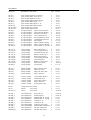
Operators & Service Manual XL3 EVI PRO AUDIO GROUP Klark Teknik Building, Walter Nash Road, Kidderminster Worcestershire DY11 7HJ, England Tel: (01562) 741515 Fax: (01562) 745371 1 2 DECLARATION OF CONFORMITY Thee Directive Covered by this Declaration 89/336/EEC Electromagnetic Compatibility Directive, amended by 92/31/EEC & 93/68/EEC Equipment Type Product Name Audio Mixing Console XL3 The Basis on which Conformity is being Declared The Products named above comply with the requirements of the above EU directives by meeting the following standards: EN 55013: 1990 EN 50082: 1992 Signed: ..................... Alex Cooper Authority: Project Leader Date: 28th November, 1995 Attention! The attention of the specifier, purchaser, installer or user is drawn to special limitations of use which must be observed when these products are taken into service to maintain compliance with the above directives. Details of these special measures and limitations to use are available on request and are also contained in products manuals. 3 ATTENTION! CABLES This product should only be used with high quality, screened twisted pair audio cables, terminated with metal bodied 3-pin XLR connectors. The cable shield should be connected to pin 1. Any other cable type or configuration for the audio signals may result in degraded performance due to electromagnetic interference. ELECTRIC FIELDS Should this product be used in an electromagnetic field that is amplitude modulated by an audio frequency signal (20Hz to 20kHz), the signla to noise ratio may be degraded. Degradation of up to 60dB at a frequency corresponding to the modulation signal may be experienced under extreme conditions (3V/m,90% modulation). No permanent damage or degradation of performance will be caused by these conditions. 4 CONTENTS INTRODUCTION 5 INPUT MODULE 7 INPUT MODULE OPTIONS 10 GROUP MODULE 11 MASTER MODULE 14 COMMUNICATIONS MODULE 16 VCA CONTROL 18 POWER SUPPLY 20 SCHEMATIC DIAGRAMS LIST 22 SCHEMATIC DIAGRAMS 5 Introduction The Midas XL3 series of consoles has been designed not only to provide the highest possible quality sound processing facilities, but also the greatest possible degree of reliability. However, no unit of such complexity can be expected never to need service, and to help anyone undertaking such work circuit descriptions will be found below. The less experienced technician or operator may find the following notes useful in emergency fault finding when more experienced help may not be available. The priority in console fault finding is to adopt a logical approach, as this is the quickest way to identify the precise source of a problem. For instance, if an input module appears to have failed, it will be helpful to establish with greater accuracy where the failure is. Does the signal return if the equaliser is switched out? [Failure in equaliser section]. Is it present at PFL? Does it route to all mixes but not to the masters? [Fault in pan buffers or pan pot]. Are mix sends affected both pre- and post-fader? In this way a particular circuit block can be identified as faulty, and a careful inspection will often reveal a disconnected wire, a damaged component, or a suspect IC can be changed. Furthermore, if help is sought over the telephone, it will be helpful to have the greatest possible amount of detail for the technician to work with. When performing tests on the console, it is tempting to take modules in or out of the console frame without switching off the power supply. THIS MUST NEVER BE DONE, AS IT NOT ONLY DESTROYS SOME COMPONENTS AT ONCE, BUT LEADS TO THE EARLY FAILURE OF MANY THAT APPEAR TO HAVE SURVIVED. The power supply is designed to bring the console to full power gradually, which protects sensitive components from damage caused by voltage spikes created by sudden powering up. Two extender card sets can be supplied which allow active tests to be performed on modules while they are out of the frame but powered up. Care must be taken that the bottom of the p.c.b. is not allowed to rest on anything metal which could short-circuit the tracks. 6 INPUT MODULE Diagram XL301_1.DGM The input signal enters via the relevant XLR connector on the console back panel at pins 7 and 8 on connector 'A' (ST1), where pin 7 is hot [pole 3 of the XLR in standard format], and pin 8 is cold [pole 2 of the XLR in standard format]. Input ground [pole 1 of the XLR] is on pin 9 on module connector 'A', which, on the single input version, is grounded only through to the EARTH LIFT switch SW2. [See later section for details of the dual input version]. SW1 supplies +48V phantom power for condenser microphones etc. via current limiting and decoupling components R10, R11, R12, and C7 to pins 2 and 3 of the XLR connector with reference to pin 1. When SW1 is depressed, pin 1 of the xlr connector is grounded regardless of the position of SW2 ( ground lift) The MIC/LINE switch SW3 offers a balanced attenuator and impedance changing network before the signal arrives at the balanced input stage. In standard format, this is of an electronically balanced design, where RF decoupling is achieved by C10, C11 and C12, input gain is adjusted by RV1, and a typical Common Mode Rejection Ratio of 85dB at 100Hz is set by VR1. DC blocking for the input amplifiers Q1 and Q2 is provided by C8, C9, C19 and C20, and the diode bridge network D4, D5, D6 and D7 blunts any spikes in excess of rail voltages. IC1 debalances the input signal and feeds it to the phase reverse switch and high pass filter via C24. If input balancing is by transformers, these will be fitted to a bracket which runs the length of the console beneath the motherboards. They are wired via pins on connector 'A': 19 [hot, primary], 20 [cold, primary], 21 [cold, secondary], and 22 [hot, secondary]. The transformer secondary is RF decoupled by C15, C16 and C17. It is then fed into the same input stage as the electronic balanced input stage built around IC1. When the module is equipped for electronic balanced input, splash links are used in the four E locations on the pcb. When a transformer balanced input is used, these links are in the four T locations to select the alternative route and also adjust the gain of the input stage to match the transformer. 7 Diagram XL301_2.DGM The PHASE REVERSE switch SW4 controls the inversion mode of IC2a,and passes the signal to the 12dB/octave high pass filter around IC2b and IC3a controlled by SW5 and RV2a/RV2b. From the wiper of SW5 the signal is fed to three different points:[a] The INSERT switch SW6 to provide the insert return by-pass. [b] The insert send balancing network. This is built around IC4 as a unity-gain, phasecontrasting amplifier whose common mode re-jection ratio is set by VR3 [typically 85dB at 100Hz]. Diodes D9, D10, D11 and D12 are provided to protect the insert send circuitry from damage by excess voltage. [c] The input channel meter via connector ST3 pin 1. The insert return appears at connector A pins 15 [hot] and 16 [cold]; it is protected from R.F. contamination by R48/C41 and R53/C44, and from over-voltage by diode bridge D13-16. IC5 is a differential amplifier whose common mode rejection is factory set by VR3 to maximum at 100Hz, typically 85dB. The insert return is fed via C47 to SW6 (INSERT) and from here to the EQ in/out switch SW7. After returning from the equaliser section, a signal is fed to the meter via ST3, the SOLO switch SW8 via buffer IC6b and the VCA section via either Jumper ST4/pre or IC19a. VCA and Mute The mute control is detailed later. Two mutes are associated with the vca stage, pre-fade and post-fade. These can be selected as required by jumpers in ST4 and ST5. The options are shown on diagram XL301_LK.DGM. The vca is based around IC6a, IC7 and IC8a in the audio path and IC8b in the control path. The control voltage from either the internal module level control RV3 (if fitted) and the fader tray level control are summed with an offset voltage by IC8b. This offset voltage adjusted by VR6 is used to define the available vca control range. It has been preset in the factory and should not require adjusting unless the vca has been replaced. The output voltage of IC8b, and therefore the control range of the vca, is further clamped by D58 and D59 to prevent overshoot. The VCA output is routed either pre or post mute (dependent upon ST5) to the pan control RV14a/RV14b which offers 3dB of attenuation at pan centre [Diagram XL301_4.DGM]. The pan control is buffered by IC16a and IC16b and then fed to the left and right master busses via the fet switches Q27-30 activated by SW5 (MASTER ON) [Diagram. XL301_M.DGM]. The outputs from IC16a and IC16b are also fed to the SOLO switch SW8 for routing to the solo busses. The feeds for the mixes are derived from the VCA input (Pin 1 of IC6) and the muted vca output. These are buffered by IC17a & b for Mix 1 to 8 [Diagram XL301_5.DGM] and IC18a & b for Mix 9 to 16 [Diagram XL301_6.DGM]. Each Mix can be selected pre or post fade (vca). The mixes are turned on and off by a combination of mechanically breaking the feed to the level control and effectively isolating the level controls output from the mix buss with the fets (Q11 to 26). The fets control voltage is arranged to ramp up or down to provide a click free transition. 8 Mute control [Diagram.XL301_4.DGM]. The channel mute circuit can be activated from either the channels own MUTE switch SW13 or any of the 8 automute circuits. The eight automute lines enter the module via connector 'B' (ST2) pins 29 to 36. They are isolated by diodes and fed to the eight automute selection switches. SW9 to SW12 for automute 1 to 4 and SW1 to SW4 on pcb no. B2715 [Diagram XL301_M.DGM], linked via ST8, for automutes 5 to 8. The common output from these nine switches is the main mute line. A second mute line is also required for operation of the mute control circuit. This is derived from the collector of Q9 whose purpose is to invert the mute signal and also to provide a current sink for D35 the mute indicator. The two signals mute and mute-inv are fed to the quad analogue switch IC19 [XL301-2.DGM]. IC19 is used to selectively (see earlier) mute the vca input and/or output. Under normal (unmuted) operation, mute will be low (0V) and mute-inv will be high (+VC). IC19a and IC19c will therefore be closed with IC19b and IC19d open. When the mute circuit is operational mute will be high and mute-inv will be low, IC19a and IC19c will be open and IC19b and IC19d will be closed, holding the vca input and the muted output (post-sig) from the vca at 0V. Equaliser [Diagram XL301_3.DGM]. The Treble and Bass controls each provide 15dB of boost and/or cut by varying the feedback parameters at selected frequencies between the output and the inverting input of IC9a and IC10b respectively. The frequency can be swept over a 10:1 range by RV5a/R94 and RV5b/R95 in conjunction with C77, C78 and IC11 for Bass and RV13a/R122 and RV13b/R123 in conjunction with C98, C99 and IC15 for Treble. These sections operate at a fixed selectivity of 12dB per octave. The two mid controls are configured to provide continuously variable boost and/or cut of 15dB with sweepable frequencies and adjustable selectivity. Taking the low mid as the example, the boost and cut are provided at IC9b by the same mixing of output and inverting input signals as was used on the Treble and Bass controls: the frequency setting is determined by RV8a/R103 and RV8b/R105 working in conjunction with C82 and C83. The bandwidth is adjustable by RV7 in conjunction with IC12a between 0.1 and 2 octaves. Channel level meter [Diagram XL3_M10.DGM]. The pre insert and the post insert/post eq signals are both fed via ST3 to their own full wave rectifiers on pcb B2706. The rectifier outputs (IC1a for pre insert and IC1b for post eq) are summed by IC1c and fed to the main led drive IC2 as well as the -25dB signal present circuit IC1d via level trim preset RV1. Transistor Q2 and its associated components form a constant current source for the LED chain D2 to D10. Transistor Q1 is used to provide a stabilised voltage for the LM3915. The calibration preset for the meter RV1 should be adjusted with a signal of 0dB [monitored at the insert] so that D5 (0dB) is just activate. IC1d is used as a comparitor to activate D1 when the level equals or exceeded -25dB. 9 Switch LED Powering [All diagrams]. The status LEDs are powered by three constant current sources based round Q3, Q4 and Q5 [Diagram XL301_1.DGM]. The order for the first chain starting from Q3 is: PHANTOM, INSERT, EQ, FILTER, mix 1 thro 6 ON. The order for the second chain starting from Q4 is: mix 7 thro 16 ON. The order for the third chain starting from Q5 is: AUTOMUTE 1 thro 4, SOLO, AUTOMUTE 5 thro8, MASTERS ON. All three chains finish at the negative rail (-V). INPUT MODULE OPTIONS. Direct output buffer. When fitted,this buffer can be assigned pre or post fade by inserting the appropriate link in ST6. It is built around IC20 as a unity-gain, phase-contrasting amplifier whose common mode rejection ratio is set by VR5 [typically 85dB at 100Hz]. Diodes D53, D54, D55 and D56 are provided to protect the direct output circuitry from damage by excess voltage. The output is routed via connector A17 to the channel direct out socket on the mixer rear panel. Dual inputs. If the dual (A and B) input option is fitted, relay RL1 is used to select the currently active input. This selection can be made by either the Earth lift switch or the mic/line switch depending upon the settings of option links SL1, SL2 and SL3. Refer to drawing no. XL301_LK.DGM for details. A dual concentric gain control option is also available when dual inputs are used. When fitted, a relay RL2 is used to select the section of the gain control active on the alternate inputs. On standard single input versions this relay is replaced by a link R25 and the gain control is wired as RV1b only. 10 GROUP MODULE This is a double module for use as either two independent output groups or one stereo output group. It is constructed on two interlinked pcbs. Only one of the groups is described except where operations affect both groups simultaneously. Direct Input [Diagram XL310_A1.DGM]. The signal appears at connector 'A' (ST1) pin 19 [hot] and pin 20 [cold] from the XLR socket on the console back panel. First order R.F. filtering is provided by R14/C16 and R19/C17, and over-voltage protection by D2/D3 and D4/D5. IC2 operates as a differential amplifier whose common mode rejection is set by VR1 at the factory for maximum rejection [typically 85dB] at 100Hz. The signal then passes through C21 to the direct input PFL/solo switch S1 and via C20 and the level potentiometer RV1 to the inverting buffer IC3b. A feed is taken from this point to the solo routing system ( detailed later) as well as via the direct in mute circuit Q3 and Q4 to IC1b where it is summed with the mix buss signal. The direct in mute circuit is controlled by S2 which is used to switch the fets gates between 0V and Vref. The voltage ramps up or down at a rate controlled by R32/C44 and R31/C24 to provide a clickless transition. Group Mix input [Diagram XL310_A1.DGM]. The group mix buss signal arrives via connector 'B' (ST2) pin 24 at the virtual earth summing stage IC1a, and is reinverted and summed with the direct input signal by IC1b. It is fed via the insert stage to non inverting buffer IC6a and then to the vca stage as well as the pfl switch S4 [Diagram XL310 - A2.DGM]. The insert or by-pass is selected by S3. The insert consists of IC4 as the balancing network for the insert send which appears at connector 'A' pins 8 [hot] and 9 [cold], it is protected from excess voltage by the diode bridge D7-10, and set for maximum common mode rejection at 100Hz by VR2 [typically 85dB]. The insert return appears at connector 'A' pins 6 [hot] and 7 [cold]. It is protected from R.F. contamination by R36/C35 and R41/C36 and from over-voltage by diode bridge D11-14. IC5 is a differential amplifier whose common mode rejection is factory set by VR3 to maximum at 100Hz, typically 85d. VCA and Outputs [Diagram XL310_A2.DGM]. The vca is based around IC6b, IC7 and IC8a in the audio path and IC8b in the control path. The control voltage from the internal module level control RVX and the fader tray level control via connector 'B' pin 9 is summed with an offset voltage by IC8b. This offset voltage adjusted by VR7 is used to define the available vca control range. It has been preset in the factory and should not require adjusting unless the vca has been replaced. The output voltage of IC8b, and therefore the control range of the vca, is further clamped by D55 and D56 to prevent overshoot. The vca output is routed to ST6 and ST7 for master and matrix, post fade pre mute output options as well as the main group mute circuit consisting of analogue switch IC9a and IC9b. It also appears at the modules internal meter connector (ST5 pin 1) as well as on connector 'A' pin 18s for connection to the optional meter bridge. An alternative link point for pre-mute solo send is also fitted. Note: if this is used, it is out of phase with any direct input. 11 The mute output from the vca is summed with any talkback signals from the communications module by IC12a and then fed to the solo switching circuit (see later) as well as the group output stage. This is built around IC13 as a unity-gain, phase-contrasting amplifier whose common mode rejection ratio at 100Hz is set by VR6 [typically 85dB at 100Hz]. Diodes D16-19 are provided to protect the circuitry from damage by excess voltage. The group output appears on connector 'A' pins 10 [Hot] and 11 [Cold], from where it connects to the rear panel xlr group output connector. Two talkback lines are available from the comms. module on connector B21. Talk_All on the solder side of the connector and Talk_Select on the component side of the connector. Talk_All is always summed into IC12a, Talk_Select only if S11 the talk switch is on. Master and Matrix [Diagram XL310_A2.DGM]. The master buss signal level is controlled by RV2 and selected to be either pre or post vca by S5. If the signal is pre-vca, the option to mute or not with the main group mute is determined by the link in ST3. If post-vca, the location of the link in ST6 will determine if the signal is pre or post mute (see diagram XL310_LK.DGM for link locations). The signal is routed via the noninverting buffer IC212b to the pan control RV3a/RV3b which offers 3dB of attenuation at pan centre. The pan control is buffered by IC14a and IC14b and then fed to the master busses left and right via the master on circuit Q5/Q19 and Q6/Q20 activated by S6 (Master on). The matrix buss signal levels are controlled by RV4 and RV5 and selected to be either pre or post vca by S7 and S9. If the signals are pre-vca, the option to mute or not with the main group mute is determined by the link in ST4. If post-vca, the location of the link in ST7 will determine if the signals are pre or post mute (see diagram XL310_LK.DGM for link locations). The signals are routed via R103 and R105 to the two matrix mix busses. The feeds can be muted with S8 and S10. Mute control [Diagram XL310_A2.DGM & XL310_A3.DGM]. The groups mute circuit can be activated from either the groups own mute switch S12 or any of the 8 automute circuits. The eight automute lines enter the module via connector B pins 29 to 36. They are isolated by diodes and fed to the eight automute selection switches. S14 to S21 for module group A and via ST8 to module group B. The common output from the eight automutes are connected to S12 and the main mute line via the Mute Safe switch S13. A second mute line is also required for operation of the mute control circuit. This is derived from the collector of transistor Q7 whose purpose is to invert the mute signal and also to provide a current sink for D40 the mute indicator. The two signals mute and mute-inv are fed to the quad analogue switch IC9. IC9 is used to selectively (see earlier) mute the pre and post vca signals. Under normal (unmuted) operation, mute will be low (0V) and mute-inv will be high (+VC). IC9b, IC9c and IC9d will therefore be closed with IC9a open. When the mute circuit is operational mute will be high and mute-inv will be low, IC9b, IC9c and IC9d will be open and I9a will be closed, breaking the signal feed to the master and matrix pre/post switches (depending upon the links in ST3 and 4) and holding the output from the vca at 0V. 12 Output Meter [Diagram XL20M.DGM]. IC3a and b receive, rectify, and calibrate the signal fed from the group module connector ST5. The signal, now a varying positive voltage, is fed to IC3c and d; IC3c has 30dB of gain, which enables D1-D10 to turn on 30dB ahead of D11-D20. Transistor Q1 provides a regulated power source for the LM3915s and transistors Q2 and Q3 are constant current sources for the LED chains. To calibrate the meter, a signal of -30dB is applied at pin 1 of ST1 [the level can be externally verified at whichever output is driving the meter, selected by the meter change-over switch S34], and the cathode of D23 is monitored by an oscilloscope. When a symmetrical trace is obtained by adjusting VR1, the level is increased to 0dB and VR2 is adjusted so that D13 [the 0dB yellow LED] just illuminates. Then the signal is reduced to -30dB, when the LED chain should have only the first three LEDs [D1-D3] illuminated. If the calibration appears to be wrong, the symmetry should be rechecked. Solo Routing [Diagram XL310_A3.DGM (both groups)]. Each of the four pfl switches, two per group (mix PFL and direct in PFL), provide a gate signal to select the appropriate fet switches for the source. These four gate signals are summed by diodes D51 to D54 and are used to turn on fet Q14 routing the pfl signal to the pfl buss via connector 'B' pin 10. They are also used to route the left and right solo buss feeds from IC15 via fets Q10 and Q13 to connector 'B' pins 11 (left) and 12 (right). In addition to this the signal is inverted by transistor Q15 in order to drive transistor Q16. Q16 is used to activate the Solo_Gate line via connector 'B' pin 13. In the case of channel A, the two group solos are switched by Q8 and Q9 into the summing input of IC15a via R111 and R112 to give unity gain. Likewise for channel B with Q11 & Q12 with R123 and R124 into IC15b. Under normal (two separate groups) operation, the SOLO STEREO SPLIT switch is in the off position. This allows Q17 and Q18 to turn on whichever solo is selected to ensure that channel A and channel B solo outputs are crosscoupled to each other for monitoring through both left and right solo monitor channels. If the SOLO STEREO SPLIT switch is on, this crosscoupling does not occur and so the group solo monitoring is as a stereo pair. Switch LED Powering [All diagrams]. The status LEDs are powered by three constant current sources based round Q1, Q2 and Q201 [Diagrams XL310_A1.DGM & XL310_B1.DGM]. The order for the first chain starting from Q1 is: Direct in A PFL, Direct in A MUTE, Direct in B PFL, Direct in B MUTE, A Matrix 1 MUTE, A matrix 2 MUTE, B Matrix 1 MUTE, B Matrix 2 MUTE, A Level to Masters ON, A Automute Safe ON. The order for the second chain starting from Q2 is: A Automutes 1 thro 8, A TALK, A INST, A PFL, SOLO Stereo Split. The third chain from Q201 is: B Level to Masters ON, B Automute Safe ON, B Automutes 1 thro 8, B TALK, B INST, B PFL. All three chains finish at the negative rail. 13 Remote Volume Options [Diagrams XL310_A4.DGM & XL310_B4.DGM]. The remote volume control is based around IC10a, IC11 and IC12b in the audio path and IC10b in the control path. The control voltage from the external level control enters the module via connector B pin 5 (pin 6 on ch B). No internal clamping or range adjustments are provided. MASTER MODULE This module is constructed from two identical printed circuit boards, each of which contains the circuitry for one master output, one matrix output, one auxiliary to masters summing stage, and one half of the solo-to-masters facility [both halves are controlled by S10, however]. The following description applies equally to each half of the module, except where specific exception is made. Each function of the module will be considered separately. Master Output [Diagram XL320_1.DGM]. Master signals arrive via connector 'B' pins 8 and 9 [signal] and 7 [ground] at the virtual earth summing stage IC2b, and are reinverted by IC2a before arriving at the master/solo changeover relay RLY1, which is activated by the solo-to-masters switch S10 [which operates only if there is a voltage on the solo gate derived from any solo/PFL switch being switched on]; this transposes the signals from the solo and master summing stages. IC4 is the balancing network for the insert send which appears at connector 'A' (STA) pins 19 [hot] and 20 [cold], it is protected from excess voltage by the diode bridge D1-4, and set for maximum common mode rejection at 100Hz by VR1 [typically 85dB]. The insert return appears at connector 'A' pins 21 [hot] and 22 [cold]; it is protected from R.F. contamination by R21/C18 and R26/C21, and from over-voltage by diode bridge D5-8. IC5 is a differential amplifier whose common mode rejection is factory set by VR2 to maximum at 100Hz, typically 85dB. Block b of the insert switch S2 selects pre-insert signal from RLY1 or post-insert signal from C24 and feeds it to block b of the master output PFL switch S3 [change to diagram XL320_3.DGM], and via JPA to the master output fader RV1. The non-inverting buffer IC12a feeds both the meter [via the meter changeover switch S8] and the mute switch S4. The inverting input of IC12a is fed via connector 'B' pin 12s [solder side only] with talk signals from the communications module. The mute switch [S4] wiper feeds the output stage IC6, which is protected from excess voltage by the diode bridge D9-12, and set for maximum common mode rejection at 100Hz by VR3 [typically 85dB]. Matrix Output [Diagram XL320_2.DGM]. Matrix signals arrive via connector 'B' pins 10 and 11 [signal] and 7 [ground] at the virtual earth summing stage IC7b, and are reinverted by IC7a. IC8 is the balancing network for the insert send which appears at connector 'A' pins 6 [hot] and 7 [cold], it is protected from excess voltage by the diode bridge D13-16, and set for maximum common mode rejection at 100Hz by VR4 [typically 85dB]. The insert return appears at connector 'A' pins 8 [hot] and 9 [cold]; it is protected from R.F. contamination by R50/C47 and R55/C50, and from over-voltage by diode bridge D17-20. IC9 is a differential amplifier whose common mode rejection is factory set by VR5 to maximum at 100Hz, typically 85dB. Block b of the insert switch S5 selects pre-insert signal from C37 or post-insert signal from C53 and feeds it to block b of the matrix output PFL switch S6 14 [Diagram XL320_3.DGM], and via JPC to the matrix output fader RV2. The non-inverting buffer IC13a feeds both the meter [via the meter changeover switch S8] and the mute switch S7. The inverting input of IC13a is fed via connector B pin 12 [component side only] with talk signals from the communications module. The mute switch [S7] wiper feeds the output stage IC10, which is protected from excess voltage by the diode bridge D21-24, and set for maximum common mode rejection at 100Hz by VR6 [typically 85dB]. Record Output [Diagram XL320_2.DGM]. The record outputs share one level control and one level check switch [which overrides whichever input has been selected by the meter changeover switch S8 on diagram XL320_3.DGM]. The controls are linked by the ribbon connector between ST2a on the lower (left) PBC and ST2b on the upper (right) PCB, but in all other respects each output is entirely separate. Signal is derived from the wiper of the master mute switch S4 [diagram XL320_3.DGM] and fed to the top of the level control RV3a (left) or b (right), from the wiper of which it passes through a non-inverting buffer IC14b. From here the signal is fed both to the check level switch S9a or b via C66, and to the output stage IC11a, which is protected from excess voltage by the diode bridge D25-28, and set for maximum common mode rejection at 100Hz by VR7 [typically 85dB]. Output Meter [Diagram XL20M.DGM]. IC3a and b receive, rectify, and calibrate the signal fed from the master module via connector ST1. The signal, now a varying positive voltage, is fed to IC3c and d; IC3c has 30dB of gain, which enables D1-D10 to turn on 30dB ahead of D11-D20. Transistor Q1 provides a regulated power source for the LM3915s and transistors Q2 and Q3 are constant current sources for the LED chains. To calibrate the meter, a signal of -30dB is applied at pin 1 of ST1 and the cathode of D23 is monitored by an oscilloscope. When a symmetrical trace is obtained by adjusting VR1, the level is increased to 0dB and VR2 is adjusted so that D13 [the 0dB yellow LED] just illuminates. Then the signal is reduced to -30dB, when the LED chain should have only the first three LEDs [D1-D3] illuminated. If the calibration appears to be wrong, the symmetry should be rechecked. LED Powering [All diagrams]. The status LEDs are powered by a constant current source based round Q2 [Diagram XL320_1.DGM]. The order for the chain starting from Q2 is meter changeover, matrix insert, master insert, matrix PFL, master PFL, matrix mute, and master mute. The chain finishes at the negative rail. 15 COMMUNICATIONS MODULE Centred in this module are the controls for the intercom, talk and pink noise generator functions, the automute system, and the signal monitoring facilities, as well as the headphone amplifier. Intercom [Diagram XL330_1.DGM]. The intercom shares much of its circuitry with the monitoring and talkback facilities; the intercom switch [S3] selects the routing and function of the microphone amplifier and headphone signal. In intercom mode, microphone signals arrive through either the headset or microphone connectors [both mounted on the modules front panel], pass through the a.g.c. amplifier IC5 and IC6a and to the remote station via the isolating transformer T1 via block d of the intercom switch S3. VR3 adjusts the amount of microphone signal fed to the headphones by varying the common mode rejection ratio of the microphone input to IC6b without varying the gain structure for signals arriving from the remote station via T1. Overall intercom level is adjusted by RV3 before it passes through blocks a and e of the intercom switch, the headphone level controls RV1 and the headphone mute switch to the headphone amplifier [see diagram XL330_5.DGM] and the headphone jack socket on the module front panel. IC7 and IC8 are isolating networks which ensure that ground loops are avoided when the intercom is used with an actively powered station. When the intercom is switched on, a negative voltage is applied via block f of the intercom switch S3 to the anode of the LED in IC7, causing a positive voltage to be applied to pin 14 of connector 'A' (ST1) via D18 and R52; when a call is received, the positive voltage on pin 14 energises the photo-transistor within IC8 and turns on Q1, which illuminates the intercom call light [LP1]. In the event that the console is to be used as the slave station, the intercom can be decoupled completely from the consoles power supply by applying the master stations power rail via the unused pin on the intercom XLR connector and edge connector A pin 15 to RLY1, which disconnects the intercom ground completely from the console. Talk Facility [Diagram XL330_1.DGM]. Microphone and headset signals arrive at block d of the intercom switch S3 as previously described for the intercom: however, with the switch in its normal [non-intercom] position, talk signals pass through block c to block b of the pink noise generator switch S6 [change to diagram XL330_2.DGM]. From the wiper of this switch the signal passes both via buffer IC10b to connector 'A' pin 12 [and thus to the talk external XLR connector on the console back panel] and to the talk master switch S13. When this switch is on, signal is fed to the three talk level pots [RV4-6]; a further 10dB of gain is provided by IC10a, IC12a, or IC12b before the individual talk switches [S7-S12] enable signals to pass to their respective busses. The LED indicators for these switches are wired in parallel between +VA and ground via limiting resistors R58-R63, with +VA appearing on each wiper of the LED switching blocks; all the normally open contacts are joined and fed to the second block of the talk master switch S13. This means that whenever a talk route is open [i.e. the talk master switch and any individual talk switch both on] a gate voltage is fed from the talk master switch to Q2 and Q3, which dims the local outputs to avoid the feedback which would otherwise result if the talkback microphone and a loudspeaker driven from a local output are close together. 16 Pink Noise Generator [Diagram XL330_3.DGM]. IC9 is the noise source; R92/C62, R93/C63, and R94/C64 provide the necessary colouration and IC11a corrects the gain structure and provides a buffer stage before the pink noise is fed to its switch S6 [Diagram XL330_2.DGM], from which point it follows the same path as the talk signals. Automute Master Controls [Diagram XL330_3.DGM]. The eight illuminated MUTE GROUP switches [S14-21] feed positive rail voltage current-limited by R111 and decoupled by C69-768 and R103-110 to DC buffers IC13 to IC16. The outputs of these feed the automute busses on connector 'B' (ST2) [pins 15-22]. Signal Monitoring [Diagram XL330_1.DGM]. PFL signals arrive at connector B pin 1 where they are summed by the virtual earth stage IC1b and reinverted by IC1a. The solo listen switch S2 blocks c and d select either PFL signals from C3 or solo signals from the master module via connector B pins 13 and 14 and feed them through the intercom switch S3 blocks a and e to the headphone level control RV1 and headphone mute switch S4, and thus to the headphone amplifier [see diagram XL330_5.DGM]. In addition to driving the headphone level control, the wipers of S3 blocks a and e feed the local output level control RV2 [change to diagram XL330_2.DGM]: signals pass through the local output mute switch S5 and buffers IC2a and b to the balanced local output stages IC3 and IC4, which are protected from excess voltage by the diode bridges D6-9 and 10-13, and set for maximum common mode rejection at 100Hz by VR1 and VR2 [typically 85dB]. Headphone Amplifier [Diagram XL330_5.DGM]. R19/C17 and R20/C18 are the power supply decoupling networks; RF protection is afforded by R2/C1 and R4/C2. Connections to the module are hard-wired. Signal Metering [Diagram XL330_1.DGM]. The two meters are controlled by changeover switch S1. In solo mode [switch on], blocks c and d are fed with solo left and right signals respectively from connector B pins 13 and 14 and pass them to the meters via ST3 and ST4. In PFL mode [switch S1 off], block c is fed with PFL signals from C3 and passes them to the left meter via ST3; block d is fed with left local output post-fader signals from the junction of R17 and C6 [diagram XL330_2.DGM] and passes them to the right meter via ST4. LED Powering [All diagrams]. The status LEDs [with the exception of all the talk switches] are powered by a constant current source based round Q4 [Diagram XL330_3.DGM]. The order for the chain starting from Q4 is meter changeover, intercom, pink noise, mute group masters 1-8, solo listen, local output mute, and headphone mute. The chain finishes at the negative rail. 17 VCA CONTROL The internal mixes vca control voltages are derived either on the individual modules or more commonly from the fader tray circuitry. Grand Master VCA Control [Diagram XL321.DGM]. DC power for the fader tray pcbs are linked to the Grand Master 2 board via connector ST4. From here it is distributed to all other master and channel control cards via the VCA Control Buss ribbon cable linked to ST1. A stable vca reference voltage is also derived on this board from D2 via IC2b. It is adjusted with VR2 to give the required control range and distributed via the VCA Control Buss. This reference voltage is buffered and inverted by IC1a and fed to the Grand Master fader RV1. Dependent upon the status of SW1 (VCA MUTE), either the attenuated voltage from RV1 or the inverted reference voltage is summed with an offset voltage derived from the reference voltage via VR1. Provided SW2 (VCA ON) is in the on state, this summated voltage will have the output voltage from IC3a (see later) summed with it before buffering by IC1b ready for distribution to the group and channel control cards. A set of splash links allow this output control voltage to be assigned as one of four grand master or one of eight group control lines. Links will be inserted in Grand Master 1 and 2 (GDM-CTL1 & GDM-CTL-2 on the diagram) respectively for the two Grand Master boards. Master/Slave buffering. Facilities are fitted to allow this console to act as either a master or slave console to another for vca control. When used as a master, the modules control voltage, as well as being distributed to the fader tray boards, is buffered by IC3b and, with the appropriate splash link made, connected to the DC CONTROL OUT connector on the mixer rear panel via ST2. For situations where then console is to be used as a slave, the DC control voltage from the master console is connected to the DC CONTROL IN connector on the mixer rear panel. From here it connects into the board(s) via ST2 and via the appropriate splash link to IC3a. IC3a is connected as a ground compensated differential buffer and provides a dc voltage which is summed into IC1b with the internally derived control voltages. Group (Master) VCA Control [Diagram XL311.DGM]. The VCA Group control boards combine two internal desk control functions as well as interfacing to external master/slave desks. The two associated group channels (A & B), can each have there vcas controlled not only by the internal channel fader but also a combination of one or both the Grand Master controls. Considering channel A, The two Grand Master inputs from ST1 pins 11 and 12 are selected by switches SW3 and SW4 for Grand Masters 1 and 2 respectively. The signals are summed and inverted by IC2a and connected to the group module via ST2. Channel B is similar using SW5, SW6 and IC2b. 18 The second function of the module is the control for one of the eight VCA Groups. The reference voltage from the Grand Master 2 board is sauced via the VCA control buss connector ST1 pin 9. It is buffered and inverted by IC1a and fed to the Master fader RV1. Dependent upon the status of SW1 (VCA MUTE), either the attenuated voltage from RV1 or the inverted reference voltage is summed with an offset voltage derived from the reference voltage via VR1. Provided SW2 (VCA ON) is in the on state, this summated voltage will have the output voltage from IC3a (see previous details on master/slave linking) summed with it before buffering by IC1b ready for distribution to the channel control cards. A set of splash links allow this output control voltage to be assigned as one of the eight VCA Group control lines. Links will be inserted in the appropriate location (VCA-CTL-1 to VCACTL-8 on the diagram) on the eight VCA Group boards. Channel VCA control [Diagram XL302_VC.DGM]. All eight Group VCA control lines are available on the channel control module. These enter via the VCA Control Buss connector ST1 pins 1 to 8 and are selected by switches SW1 thro SW8 for groups 1 to 8 respectively. The reference voltage on ST1 pin 9 is buffered and inverted by IC1b and fed to the channel vca level control RV1. The wiper of this level control is summed with the combined group level control voltage (as selected by SW1 thro SW8) by IC1a. The Group control voltage is only effective when the VCA ON switch (SW9) is in the on position. The output of IC1a is fed to the channel module vca input via ST2. LED Powering [All diagrams]. The status leds are powered by constant current sources, one on each vca control board. These are based round transistor Q1. The order for the chain starting from Q1 can be clearly seen on the appropriate diagram. Each chain ends at the -v rail. 19 POWER SUPPLY The Midas XL3 has an external 19" rack mounting power supply to provide the three voltage rails to power the console, +18V and -18V DC at 12 amps per rail and +48V phantom power at 500mA for capacitor microphones and direct injection boxes. It is fitted with two fully protected outputs through polarised 19 pin multipin connectors, one female for connection to the console and one male for connection to an additional power supply if used for fail-safe operation. The two connectors are parallel wired and the three power modules incorporate blocking diodes, so that the power supplies can share the load but never feed power into each other in the event of one unit failing. Each 18 volt block incorporates an over-temperature sensor which switches off the affected unit. If this occurs while two power supplies are connected, there will be no effect on the operation of the console since load sharing and switchover is automatic; however, the relevant monitoring LED on the front panel will be extinguished. The relevant block will reset automatically on cooling and the LED will come back on when this happens. Connection of the power supply to the console is via a 5 meter multiconductor cable fitted with polarised 19 pin connectors, one male and one female. PLEASE NOTE THAT THE POWER SUPPLY CONTAINS CIRCUITRY WHICH GENERATES LETHAL VOLTAGES. NOT ONLY IS IT POWERED BY HIGH VOLTAGE, BUT THE SWITCH MODE BLOCKS FOR THE 18v RAILS CREATE VOLTAGES FAR IN EXCESS OF THE MAINS INPUT. ALL SERVICING OF THESE UNITS MUST BE REFERRED ONLY TO AUTHORISED SERVICE AGENTS OF KLARK TEKNIK. ON NO ACCOUNT MUST SERVICE WORK BE ATTEMPTED BY ANYONE ELSE. IF IT IS, THE WARRANTY WHICH COVERS THE EQUIPMENT BECOMES INVALID, AND KLARK TEKNIK ACCEPT NO LIABILITY FOR CONSEQUENT DAMAGE TO THE CONSOLE OR ANCILLARY EQUIPMENT. QUALIFIED SERVICE PERSONNEL ONLY MAY UNDERTAKE THE SERVICE WORK DETAILED BELOW. Voltage Change-over. There are five steps involved in this operation. It is most important that all five are carried out together, and that power is not applied to the unit when change-over procedures are incomplete, and that the power is disconnected by unplugging the mains lead before work is commenced. 1. Change the fuse. The fuse holder is located on the back of the unit below the mains input plug. The correct fuse ratings are as follows:220/240 volt operation: 5A. 100/110 volt operation: 10A. The fuse is 20mm, HRC type. 20 2. Rejumper the +18 volt block. The lid of the power supply must be removed by taking out all the relevant screws: four from the front panel, four from each side at the bottom of the unit, and three from the back panel. The voltage change-over jumper may now be moved to the appropriate position. [see diagram] 3. Rejumper the -18 volt block. This procedure is identical to the +18 volt block. 4. Selector, Phantom power module. The voltage change over switch is located on the phantom power pcb, its setting is clearly marked on the pcb. 5. Replace lid before reconnecting the mains supply. Indicator Module. [Diagram XL293_2.DGM] The pcb for this module (BRD:2690) is mounted behind the front panel and houses led indicators for each of the P.S.U. output voltages. Also mounted on this pcb is the ground lift switch S1. This disconnects earth from the 0V rails. Earth remains connected to all the console metalwork. Regulator Assembly. [Diagram XL293_1.DGM] This contains the linear regulators for both 18V supplies. Both negative and positive regulators are identical utilising a series power fet (Q3 & Q6 respectively). Output voltages are factory set at 18V with VR1 and VR4 respectively. D3 and D7 allow fail safe linking. Phantom power supply. [Diagram XL293_2.DGM] The 48V phantom supply is derived from transformer TX1, The primary supply voltage is selected by SW1. The secondary voltage is rectified by D1 to D4 and requlated by IC1. The output voltage being set by R1 and R2. D6 allows fail safe linking. The power supplys cooling fans are also powered from the phantom power module. Two alternatives types are catered for, 110V AC and 24V DC. When equipped for 110V AC fans, connector ST2 is fitted. If 24V DC fans are used, the additional requlator IC2 with its associated components and connector ST4 are fitted. Both types are not normally available simultaneously on the same module. In the unlikely event of a replacement fan being required, the correct type should be ascertained by checking on the pcb for ST2 (110V) or ST4 (24V). 21 DRAWINGS DWG No. REFERS TO SECTION ISS DATE XL301_1 XL301_2 XL301_3 XL301_4 XL301_5 XL301_6 XL301_M XL301_M10 XL301_LK XL304_1 XL304_2 XL304_3 XL304_4 XL304_5 XL304_6 XL304_7 XL304_8 XL304_9 XL304_VC Input module Inputs & Connectors Input module Filter, Insert & Vca Input module Equaliser section Input module Mutes, Master & Dir. Input module Mix outputs 1 - 8 Input module Mix outputs 9 - 16 Input module Mute add-on board Input module 10 Led meter Input module Option links St. Input module Inputs, Phase & Filters St. Input module M-S Control & Hi-Pass St. Input module Solo Select & Inserts St. Input module VCA's & Stereo Pan St. Input module CH A Equaliser Section St. Input module CH B Equaliser Section St. Input module Mix Outputs St. Input module Mutes & Direct Outputs St. Input module Edge Connectors & PSU St. Input module XL302 Input VCA Contr. 5 5 5 5 5 5 4 3 3 2 2 2 2 2 2 2 2 2 6 4.9.91 4.9.91 4.9.91 4.9.91 4.9.91 4.9.91 4.9.91 26.10.90 4.9.91 17.9.93 17.9.93 17.9.93 17.9.93 17.9.93 17.9.93 17.9.93 17.9.93 17.9.93 6.9.93 XL310_A1 XL310_A2 XL310_A3 XL310_A4 XL310_B1 XL310_B2 XL310_B3 XL310_B4 XL310_LK XL20M_3 Group module Group module Group module Group module Group module Group module Group module Group module Group module Group module Buss & dir inputs A Vca, Routing & O/P A Automutes & Solo Sel Remote volume opt A Buss & dir inputs B Vca, Routing & O/P B Ch B Automutes Remote volume opt B Mute link options 20 Led meter 8 8 8 8 8 8 8 8 1 2 4.9.91 4.9.91 4.9.91 4.9.91 4.9.91 4.9.91 4.9.91 4.9.91 29.10.90 11.1.91 XL320_1 XL320_2 XL320_3 XL320_4 Master module Master module Master module Master module Sum & master insert Matrix & record Master & matrix O/P Edge connectors 2 2 2 2 6.9.91 6.9.91 6.9.91 6.9.91 XL330_1 XL330_2 XL330_3 XL330_4 XL330_5 Comms module Comms module Comms module Comms module Comms module Comm, Pfl & Phones Talkback & local Noise, Mutes & Psu Edge connectors Stereo phones amp 2 2 2 2 2 6.9.91 5.9.91 6.9.91 6.9.91 6.9.91 XL321 XL311 XL302_VC Grand master Vca control Master Vca control Input Vca control 6 6 3 6.9.91 6.9.91 29.10.90 XL3FR_1 XL3FR_2 XL3FR_3 XL3FR_4 XL3FR_5 XL3FR_6 XL3FR_7 XL3FR_8 XL3FR_9 XLBUSS_A XL3 Mainframe XL3 Mainframe XL3 Mainframe XL3 Mainframe XL3 Mainframe XL3 Mainframe XL3 Meterbridge XL3 Meterbridge XL3 Mainframe XL3 Mainframe 1 1 2 2 2 2 2 2 1 2 30.10.90 30.10.90 9.9.91 9.9.91 7.9.91 7.9.91 7.9.91 7.9.91 9.9.91 24.9.91 Power I/P pcb Jackfield layout Motherboard B wiring Motherboard A wiring Connectors A Connectors B Connector pin assign. Motherboard connections DC link connections DC Buss link board 22 XL390_1 XL390_2 XL390_3 XL390_4 XL390_5 XL390_6 XL390_7 Power supply Twin linear regulator Power supply 48V & Fans PSU & status Power supply Block diagram Power supply Connector pin assignment Power supply Power supply linking Power supply Linking two consoles Power supply Switch mode block 23 2 2 2 2 2 2 2 24.9.91 24.9.91 24.9.91 24.9.91 24.9.91 24.9.91 24.9.91