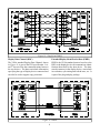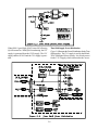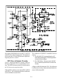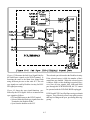
1
T
2003
ECHNICAL
RAINING
Projection Television
Technical Training &
Troubleshooting Manual
V23
V23
WS-48513
WS-55513
WS-65513
WS-73513
V23+
V23++
V23+++
WS-48613 WS-65713 WS-55813
WS-55613 WS-73713 WS-65813
WS-65613
MITSUBISHI ELECTRIC
MITSUBISHI DIGITAL ELECTRONICS AMERICA, INC.
T
2003
ECHNICAL
RAINING
V23 Chassis
Projection Television
Technical Training &
Troubleshooting Manual
Copyright © 2003, Mitsubishi Digital Electronics America, Inc.
All Rights Reserved
V23 CHASSIS
TECHNICAL TRAINING AND TROUBLESHOOTING MANUAL
TABLE of CONTENTS
Introduction ... New Technologies
Models ............................................................................................................... 1
Features ............................................................................................................... 2
NetCommand™ 3.0 ............................................................................................. 3
Five Format Memory Card Reader ....................................................................... 4
PerfectColor™ ...................................................................................................... 5
MonitorLink™ ....................................................................................................... 6
Service Code Chart ............................................................................................ 12
Chapter1 ... Disassembly and Service
Disassembly Procedures ................................................................................... 1-1
DM Replacement .............................................................................................. 1-2
PCB & Main Component Locations ................................................................... 1-4
Convergence Output IC Replacement .............................................................. 1-5
Composite Cabinet ............................................................................................ 1-6
Chapter 2 ... Alignment Procedures
Initial Setup ....................................................................................................... 2-1
Circuit Adjustment Mode ................................................................................... 2-3
ConvergenceAdjustment Mode ......................................................................... 2-5
Alignment Data Storage Locations .................................................................... 2-6
Chapter 3 ... Power Supply
Low Energy Power Supply ................................................................................ 3-1
Standard Standby Power Supply ....................................................................... 3-4
Time Shift Recording Power Supply .................................................................. 3-2
Switched Supplies ............................................................................................. 3-7
Troubleshooting................................................................................................. 3-8
Chapter 4 ... Control Circuitry
Basic uPC Requirements .................................................................................. 4-1
Reset Circuitry ................................................................................................... 4-2
Input Command Circuitry ................................................................................... 4-3
Serial Data Lines ............................................................................................... 4-4
Parallel Input Lines ............................................................................................ 4-5
Parallel Outputs ................................................................................................. 4-7
I
Chapter 5 ... Video/Color Circuitry
Overall Block Diagram ....................................................................................... 5-1
PCB-Terminal .................................................................................................... 5-2
PCB-Signal ........................................................................................................ 5-3
RGB CRT Drive & Protect Circuitry ................................................................... 5-4
Digital Signal Path ............................................................................................. 5-5
Monitor Out ....................................................................................................... 5-6
Chapter 6 ... Sync, Deflection and High Voltage
Overall Block Diagram ....................................................................................... 6-1
Sync Signal Path ............................................................................................... 6-2
Vertical Deflection ............................................................................................. 6-5
Horizontal Deflection ......................................................................................... 6-5
Deflection Loss Detection.................................................................................. 6-7
High Voltage & HV Regulation .......................................................................... 6-8
X-Ray Protect .................................................................................................... 6-9
Chapter 7... Convergence Circuitry
Overall Block Diagram ....................................................................................... 7-1
Waveform Generator and D/A Converter .......................................................... 7-2
LPF and Summing Amplifiers ............................................................................ 7-3
Convergence Output Circuitry ........................................................................... 7-4
Chapter 8 ... Sound Circuitry
Overall Block Diagram ....................................................................................... 8-1
Signal Path ........................................................................................................ 8-2
Chapter 9 ...Troubleshooting Tips
Using the Front Panel LED ................................................................................ 9-1
II
Introduction
Series
Chassis
48" W
Screen 55" W
Size
65" W
73" W
Gold
Gold Plus Platinum Diamond
V23
V23+
V23++
V23+++
WS-48513 WS-48613
WS-55513 WS-55613
WS-55813
WS-65513 WS-65613 WS-65713 WS-65813
WS-73513
WS-73713
Table 1: V23 Models
The V23 Chassis is carried in the Gold, Gold Plus,
Platinum and Diamond series models for 2003 and
2004. This full featured, integrated HDTV chassis
represents the latest technologies in CRT based projection television. A breakdown of V23 models is
shown in Table 1.
Improved Features
• 3rd Generation HDTV Receiver
• NetCommand 3.0 with IR Learning
• PerfectColor - All Inputs and Signal Types
• AMVP™ Improved Performance
• 9" CRTs now available in a 65" Model
• Coaxial and 2-way speaker systems
• Contemporary cabinet in a 55" Model
Features
Table 2 shows some of the major features by model
category. Some of the features are carried over from
previous years, some have been improved upon and
some are totally new. In addition to all the user features, the V23 chassis includes many serviceability
features.
New Features
• 5 Format Memory Card Reader
• MonitorLink™ Input
• Low Energy Mode
Serviceability Features
• Modular design with "Light Box"
• Self Diagnostics
• Serviceable to Component or PCB level.
• ATSC Tuner/Decoder circuitry separated
from DM assembly.
• Reduction in number of stand-up PCBs.
• Service Adjustment Mode Data Reset.
Carry Over Features
• IEEE1394, FireWire
• DTV Link
• VGA Input
• QuadField Focus
• TruFocus Lenses
• Gold Plated Jacks
• 2 Piece Cabinets (65" & 73")
• Fine Pitch Lenticular Screen
• Anti-glare DiamondShield
This section will provide further explanation on the
following features that are either new or may have
the most impact on service:
1) NetCommand 3.0
2) 5 Format Memory Card Reader
3) PerfectColor
4) MonitorLink
1
V23 Features
Feature
3rd Generation HDTV Receiver
Explaination
ATSC and Unscrambled QAM Reception
Greater Sensitivity
NetCommand™ 3.0
Home Theater Control by Firewire or IR
Five-Format Memory Card Reader For viewing JPEG digital photos and listening to
MP3 or WMA audio recordings.
AMVP (Advanced Multimedia Video 8 Screen Formats, Improved Line Doubling and
Processor)
Noise Reduction
FireWire/IEEE1394
Digital Home Networking Interface.
DTV-LINK
Standard for future FireWire interfaces.
PerfectColor™
Individual Control of 6 Colors
Low Energy Mode
Reduced Power Consumption in Standby
MonitorLink™ Input
Digital Video Input
VGA Input
640x480 - 60HZ
Two-way Coaxial Speakers
V23+ Features
(Additional Features)
Magnetic Focus Assembly on CRT Neck.
Results in smaller electron beam.
WS-55613 & WS-65613. Improved Audio.
Tru-Focus™ Lenses
Two-way Speaker System
Gold Plated Jacks
V23++ Features
(Additional Features)
Improved and more uniform focus.
6" Woofer & 1.5" Tweeter for improved audio.
Gives high quality connections.
QuadField Focus™
Contemporary Cabinet
Fine-Pitch Lenticular Screen
Anti-glare DiamondShield™
9" CRT (WS-65813)
V23+++ Features
(Additional Features)
High Gloss Black.
Composite Back has Reduced Weight
Best Horizontal Resolution
Reduction in Reflections
Improved Brightness and Resolution
Other Features
9" CRTs in all 73" Models
Improved Brightness and Resolution
2 Piece Cabinet (65" & 73" Models) Simplifies Delivery
Table 2: Features
2
NetCommand 3.0
NetCommand allows most common
home theater products to be connected
and controlled by way of the TV's remote control by simply selecting onscreen icons. See Figure 1.
Figure 1: NetCommand Icons
The control interface can be by one of
two means.
• IEEE1394/Firewire
• Infrared (IR Blaster)
The 3rd generation of NetCommand offers additional
functionality and a simplier user interface.
When using the Firewire, NetCommand is "plugand-play." For the end user, it makes all digital video,
audio and control connections with one cable (Figure 2).
All other configuration is automatic. For control, the
industry standard sofware supported includes:
• AV/C - Includes common functions such as
Stop, Play, FF, RWD, etc.
• HAVi - Includes AV/C but also allows a
higher level of sofware communication for a
more interactive interface.
Figure 2: FireWire Connection
When using IR, an IR blaster must be connected to
the TV and placed in front of the device to be controlled. The TV must then be configured so the
proper IR codes will be used.
Like previous versions of NetCommand,
an "IR Library" is loaded in the TV's software so that most common devices can
be selected for immediate use. New for
NetCommand 3.0 is the "Learning" feature. For devices that are not included in
the IR Library, NetCommand can memorize the IR code from that devices remote.
A series of menus walks the customer
through the learning process. Once
loaded, the TV can then control the device using the IR blaster. This makes
NetCommand almost 100% compatable
with all other IR controlled devices.
Figure 3: IR Learning Menu
3
5 Format Memory Card Reader
Digital music and photography can now be enjoyed
in the home theater environment thanks to the
memory card reader featured in the V23 chassis.
When the user inserts a memory card into any one
of the four card reader slots on the front of the set,
NetCommand will take control, allowing a slide
show or giving a music play list.
The memory card formats supported are:
• Memory Stick™
• MultiMedia Card™
• SD (Secure Digital)
• SmartMedia™
• CompactFlash®
Figure 5: JPEG Thumbnails
When a memory card is inserted into the correct slot,
an LED next to the slot will light up. Then, after the
slot is selected using the DEVICE button on the remote, the Memory Card Screen, Figure 4, will be
automatically displayed.
Figure 6: Audio Playlist
For Slideshow, press PLAY.
For Thumbnails, press GUIDE.
To redisplay this menu or to
setup, press DEVICE MENU.
For Playlist, press AUDIO
Figure 4: Memory Card Screen
An overview of remote push buttons and their functions is given in Table 3. Other remote functions are
explained within the menus. Full instructions are
included in the Owner's Guide.
BUTTON
VIDEO
AUDIO
DEVICE
MENU
PLAY
GUIDE
PAUSE
FF
REW
STOP
FORMAT
Figure 7: Media Setup
FUNCTION
Switch from Audio Play List to JPEG Thumbnails (Figure 5)
Switch from JPEG Thumbnails to Audio Playlist (Figure 6)
Display the Media Setup Menu (Figure 7 )
Start the Slideshow or play audio
Return to the Thumbnail menu or the Audio Playlist while in Play
Pauses or resumes playback
Skips to the next slide or song
Returns to the previous slide or song
Stops slide show or play and returns to Memory Card Screen
Rotates slide 90° each time it is pressed
Table 3: Remote Functions
4
PerfectColor™
Compatibility
Users having difficulties with the memory card reader
should be aware of the following requirements:
For JPEG Pictures up to 128mb:
1. Still images recorded using the Exchangable
Image File Format (EXIF) for digital still cameras and Design Rules for Camera File Systems (DCF).
2. Standard digital images with a maximum size
of 5-megapixels (2560x1920).
3. File name maximum of 50 characters ending
with a .jpg extension.
With conventional tint controls providing only a
tradeoff between red and green, PerfectColor was
developed to provide precise control over the 6 individual primary and secondary colors.
Introduced in the V20 Chassis, PerfectColor was
initially limited to 480i composite video sources only.
For the V22 and V23 chassis, PerfectColor can be
setup individually for each and every Input and is
compatible with all video source formats. (480i,
480p, 1080i)
For MP3 or WMA7 Audio files:
1. Files recorded with sampling rates of 32 KHz,
44.1 KHz or 48KHz.
2. Files recorded with fixed bit rates.
3. File names with .jpg or .wma extensions.
A colorbar chart with slider controls is provided in
the menu for easy reference. See Figure 8.
PerfectColor can also provide automatic color correction. Compared to conventional “Auto Color”
systems, it can better sense and correct for color differences when changing channels. It is specifically
designed for the customer that watches a wide range
of channels where no one setting can be used.
NOTES:
Images opened and resaved on a computer may
not playback or may not be able to display a
picture in the thumbnail list. This is because
the computer may change the file to an incompatible format.
NOTE: Improperly set, PerfectColor can exhibit a wide variety of color symptoms. These
symptoms will not affect the on-screen menus
or a black and white picture. In such instances,
be sure to check the PerfectColor settings prior
to troubleshooting.
For audio playback, the audio output from the
TV to the A/V receiver is analog. Digital audio output is not available.
Y
E
L
L
O
W
Magenta (31):
Red (31):
Yellow (31):
Green (31):
Cyan (31):
Blue (31):
C
Y
A
N
G
R
E
E
N
Figure 8: PerfectColor On-Screen Display
5
M
A
G
E
N
T
A
R
E
D
B
L
U
E
MonitorLink™
MonitorLink is a new digital interface introduced in
Mitsubishi's 2003-2004 model line, including the
V23 chassis.
MonitorLink provides a proprietary connection for
Mitsubishi's HD-5000, Monitor/Receiver, allowing
Mitsubishi's upgradeability promise to be fulfilled
using a digital, rather than analog, interface.
While MonitorLink is a proprietary connection, it
uses industry standard technologies that may provide even more versatility.
• RS-232C - Provides device communication
and control.
• Audio - Standard analog stereo connections.
• DVI - (Digital Visual Interface) Provides a
digital video connection.
Figure 9: MonitorLink Input
Digital Visual Interface (DVI)
RS-232C… The RS-232C connection interfaces
communications and control between the receiver/
controller and display. Commands such as Power
On, Input, Mute, etc., make the system operate as
one via the customer's remote control.
DVI was originally designed by the Digital Display
Working Group (DDWG) to provide a universally
accepted digital connection between a PC and a display device.
At first glance, another digital interface would seem
unnecessary with the presence of IEEE1394,
Firewire. However, differences between IEEE1394
and DVI make them each suitable for different applications. A comparison of the two interfaces, as
applied to home theater, is provided in Table 4.
Audio… Analog Left and Right Audio connectors
are provided for the set's internal audio/speaker system. The V23 chassis has digital audio outputs and
IEEE1394 for more advanced connections with an
external A/V receiver.
Simply stated, 1394's bi-directional, compressed
data, and AV control capabilities make it suited for
recording and networking between various devices.
DVI's high speed, full bandwidth capabilities make
it most suitable to connect a display device.
DVI… Technicians experienced with computer
monitors may already be familiar with DVI and its
features. However, because it is new to home theater, it will be covered here further.
IEEE1394
DVI
Bi-directional interface (Record and Playback) One direction interface (One way to a display)
Networkable between multiple devices
Single point-to-point.
Distributes Compressed Data (MPEG2)
Uncompressed Data (High bit rate HDTV)
Supports A/V Commands (AV/C & HAVi)
No AV Control capability
Copy Protection (5C)
Copy Protection (HDCP)
Table 4
6
DDC
DDWG
DMPM
DVI-A
DVI-D
DVI-I
EDID
HDCP
TMDS
VESA
Acronyms
Display Data Channel
Digital Display Working Group
Digital Monitor Power Management
Digital Visual Interface - Analog
Digital Visual Interface - Digital
Digital Visual Interface - Integrated (Digital or Analog)
Extended Display Identification Data
High-bandwidth Digital Content Protection
Transistion Minimized Differential Signaling
Video Electronics Standards Association
Table 5
Used with its optional copy protection scheme, DVI
makes it possible to view full resolution signals without exposing the signal to copyright infringement.
It is the digital equivalent of component DTV connections (Y,Pr,Pb) that can be configured for use in
a copy protected environment.
Transition Minimized Differential Signaling
(TMDS)
TMDS is a method used to transmit digital data that
reduces the number of bit transitions (high to low or
low to high) occurring in the serial bit stream. To
reduce the transitions, it uses an advanced formula
(algorithm) that converts 8 bit data into 10 bit data.
Differential circuitry is then used to output complimentary signals. The results are…
• Reduced Electromagnetic Interference
(EMI).
• Faster transfer rates with reduced errors.
• Ability to use twisted pair wire vs. coax.
The DVI standard supports the following…
• Analog only interface (DVI-A)
• Digital only interface (DVI-D)
• Analog or Digital interface (DVI-I)
• Transition Minimized Differential Signaling
(TMDS)
• Display Data Channel (DDC)
• Extended Display Identification Data
(EDID)
• High-bandwidth Digital Content Protection
(HDCP)
• Hot Plug Detect (HPD)
• Digital Monitor Power Management
(DMPM)
A TMDS link consists of a TMDS Transmitter that
encodes and sends a data stream to a TMDS Receiver,
see Figure 10. Three sets of twisted pair wires carry
the Red, Green and Blue data. An additional twisted
pair carries the timing clock signal.
Because the bandwidth over copper wire is limited
to about 165 MHz, DVI can use up to two TMDS
links, or 6 channels sharing the same clock. DVI
with a dual-link TMDS has a bandwidth that is
doubled.
A glossary of acronyms is provided in Table 5.
DVI-A, DVI-D, DVI-I
DVI can provide an analog link, DVI-A, or a digital
link, DVI-D. The integrated link, DVI-I, was designed to support either. Each link has its own type
connector, covered later in this article. MonitorLink
uses digital only DVI, so the focus of the remainder
of this discussion will concentrate on the digital link.
1080i HDTV, with a pixel rate of 1920 X 1080 at
30Hz can be supported by a DVI interface operating
in the single-link mode.
7
Figure 10: Single-Link TMDS
Display Data Channel (DDC)
The VESA standard Display Data Channel, shown
in Figure 10, is part of the DVI specification. It is
an I2C bus used for data communications between
the two devices. The data can include information
specifying the type of display device connected and
can also be used to support copy protection.
Extended Display Identification Data (EDID)
EDID is the VESA standard protocol used over the
DDC so the display device can communicate identification about itself to the host device. The data,
stored in memory in the display device, can include
its resolution, sync timing and refresh rates, etc. It
is part of the plug and play package.
Figure 11: HDCP
8
the host know it is plugged in. When the host device detects a High condition greater than 2.4 VDC
(typically 5.0 VDC), it will read the EDID and start
operation. If the potential falls below 2.0 VDC the
TMDS transmitter is stopped.
High-bandwidth Digital Content Protection
(HDCP)
HDCP is a system designed to protect the outputs of
a DVI device from being copied. The protection can
be applied in various ways.
• Unrestricted copies
• Limited number of copies
• Limited use of copies
• No copies
Digital Monitor Power Management (DMPM)
DMPM allows several different levels of power management by detecting the presence of EDID and/or
TMDS activity. One pin on the DVI connector is
provided so the host can supply a 5 V source. The
display has the option to use this supply to keep the
DDC capable while the monitor is off.
Since this is a optional element of DVI, both the host
device and the receiving device must be properly
equipped to function and provide the protected link
between them. There are three parts within the content protection scheme.
• Authentication… The host and receiver
exchange data to confirm the receiver is
authorized to receive the protected data.
• Encryption/Decryption… After the host
has verified the receiver, "keys" are provided
that will allow the receiver to decrypt the
data sent.
• Renewability… Each receiver is given both
a secret code and a non-secret identification
number. If the host determines the secret
keys have been tampered with, the receiver
is denied authentication.
DVI Connectors
There two types of DVI receptacles shown in Figure 12, DVI-D and DVI-I. Pin assignments are detailed in Table 6. It should be noted, the additional
pins, C1-C5, arranged in the + shape on the DVI-I
receptacle, are provided for analog signals. No DVIA connector is shown because DVI-A is generally
associated with adapting VGA connectors to DVI-I.
The authentication process occurs over the DDC I2C
bus shown in Figure 11. After authentication, the
encrypted video data is applied to the TMDS encoder.
The encrypted data sent over the DVI interface is
then immune to "eavesdropping." Only the authorized display device can reverse the encryption afterwards.
Hot Plug Detect (HPD)
Another part of the plug and play package is the
VESA standard Hot Plug Detect. A dedicated pin
on the DVI connector is used by the display to let
Figure 12: DVI Receptacles
9
PIN
1
2
3
4
5
6
7
8
9
10
11
12
13
14
15
SIGNAL
PIN
SIGNAL
TMDS Data 216 Hot Plug Detect
TMDS Data 2+
17 TMDS Data 0TMDS 2&4 Shield
18 TMDS Data 0+
TMDS Data 4- (NA)
19 TMDS 0&5 Shield
TMDS Data 4+ (NA)
20 TMDS Data 5- (NA)
DDC Clock
21 TMDS Data 5+ (NA)
DDC Data
22 TMDS Clock Shield
Analog Vertical Sync (NA) 23 TMDS Clock+
TMDS Data 124 TMDS ClockTMDS Data 1+
C1 Analog Red (NA)
TMDS 1&3 Shield
C2 Analog Green (NA)
TMDS Data 3- (NA)
C3 Analog Blue (NA)
TMDS Data 3+ (NA)
C4 Analog Horizontal Sync (NA)
+5.0 VDC
C5 Analog Ground (NA)
Ground
(NA) Not used by MonitorLink
Table 6
DVI Input Block Diagram
Figure 13 is a block diagram of the DVI input circuitry used on the V23 Chassis. The circuitry will
be similar in other models.
MonitorLink DVI Connector
Some manufacturers use DVI-I connectors for DVID only. This is the arrangement used by
MonitorLink. This configuration will not support
analog connections. Therefore, any attempt to interface analog signals, no matter what form of DVIA or DVI-I cables or adaptors used, will not be successful. Looking at the pin assignments in Table 6,
it should become obvious, the DVI-I connector used
by MonitorLink is a digital only, single-link TMDS
interface.
Single-link TMDS Data and Clock signals are applied directly to IC2D00. Vcc for the EEPROM,
IC7AAA, is supplied by the host device via the DVI
connector, pin 14. At the same time, this potential is
fed back to pin 16 for Hot Plug Detection. The host
device communicates over the DDC bus directly with
the EEPROM to retrieve the EDID. IC2D02 is used
to convert the 5V I2C to 3.3V logic for compatibility
with IC2D00 where HDCP data is exchanged.
NOTE: V23 models are compliant with HDCP
and EIA861 standards for standard, extended
and high definition (480i, 480p, 1080i) video.
The DVI input is not intended for use with
personal computers or devices outputing video
signals with computer resolution.
IC2D00 decodes and outputs analog RGB/H/V signals for selection by the TV input select circuitry.
Firewire is a trademark of Apple Computer, Inc.
DVI is a trademark of the Digital Display Working Group.
VESA, DDC and EDID are trademarks of the Video Electronics Standard
Association.
TMDS is a trademark of Silicone Image, Inc.
HDCP is a trademark of Digital Content Protection, LLC.
10
Figure 13: V23 Chassis DVI Input Block Diagram
11
Chassis
Option Menu Adjustment Mode
VZ5/VZ6/V15
1-3-7-0
2-3-5-7
VZ7/VZ8/V16
1-2-7-0
1-2-5-7
V17
8-2-7-0
8-2-5-7
VZ9/V18/V19
0-1-7-0
0-1-5-7
V20/VK20
2-2-7-0
2-2-5-7
V21
2-1-7-0
2-1-5-7
K20/V22/V23
0-3-7-0
0-3-5-7
Convergence Mode
2-3-5-9 <6><5><4>
1-2-5-9 <6><5><4>
8-2-5-9 <6><5><4>
0-1-5-9 <6><5><4>
2-2-5-9 <6><5><4>
2-1-5-9 <6><5><4>
0-3-5-9 <6><5><4>
Service Menu Access Codes
12
OSD Position
Adjust Mode
Adjust Mode
Adjust Mode
Adj. Mode/0-1-8-8
Adjust Mode
2-1-8-8
Adj. Mode/0-3-8-8
Chapter 1
Disassembly and Service
Figure 1-1: Lightbox Removal - 48” Models
With 11 different models, mechanical features and
disassembly procedures vary in the V23. Since all
features and disassembly procedures are in the Service Manual, this chapter will only provide a general discussion.
The V23 has the following mechanical features:
• Removable Lightbox
• Two piece cabinet (65” & 73” models)
• Customer Removable DiamondShield™
• Composite Cabinet Back (V23+++)
1-1
Lightbox
Like previous Mitsubishi projection TV chassis, the
V23 is based on a modular design that allows the
“lightbox” to be removed for service. Even without
the front control panel, card reader or front inputs, it
is still fully functional by use of the remote control.
This allows easier access to test points, etc. And,
when “shop service” becomes necessary, this design
has several more benefits.
• No lifting of heavy, bulky cabinets
• No cabinet or screen damage.
• Less customer inconvenience.
The lightbox removal procedure for 48” V23 models is shown in Figure 1-1.
1. Remove the Back Board by removing 7
screws (a), 2 screws (b) and 8 screws (c).
2. Remove the Back Cover by removing 8
screws (d).
3 Remove 4 screws (e) to remove the Board
Slide.
4. Remove 8 screws (f) to remove the Board
Shelves.
5. Remove screw (g) holding the chassis.
6. Remove 4 screws (h) securing the Light Box
Assembly.
7. Be certain that all cables and connectors
between the Light Box Assembly and external items are disconnected (e.g. speaker
plugs, etc.), including the USB and IEE1394
connectors from the Card Reader to the DM.
8. Slide the Light Box Assembly from the
cabinet.
The procedure is similar for all models. The 48” versions do not require the removal of the black plastic
Back Cover. Refer to the Service Manual for specific disassembly instructions on all models.
NOTE: When V19, V21 and V23 models are
first plugged in, the front panel LED will flash
for about 1 minute indicating the “boot time”
required before the Power On command will
be recognized. In addition, V23 models have
a “Energy Mode,” If set to Low, the 1 minute
boot time does not start until after the Power
on command is given. If the lightbox is being
serviced without the front panel, no indication
of these requirements will be present.
Although not required, for the reasons noted, it is
usually better to have the front panel connected when
servicing the lightbox. If this is not possible, the
following power up sequence should be used:
1-2
1)
2)
3)
4)
5)
Apply AC power.
Press the remote Power button once.
Wait 90 seconds.
If no response, press the Power button again.
Wait 90 seconds.
Main Chassis Removal
Refer to Figure 1-2 to remove the Main Chassis.
1. Undo the cable wire ties to the Front Panel,
Speakers, CRTs, etc.
2. Unplug the Card Reader USB and 1394
cables from the DM module.
2. Remove screw (a) securing the Main Chassis
[and screws (b) in models WS-55813 and
WS-65813] .
3. Release the Chassis Locks on each side of
the chassis.
4. Slide the Chassis out the rear of the unit.
5. Tilt upward to access the bottom of the main
chassis.
DM Replacement
Refer to Figure 1-3 to replace the DM assembly.
1. Unplug the Card Reader USB and 1394
cables from the DM module, and refer to the
Chassis Removal Procedure to slide the
chassis towards the rear of the set.
2. Remove screws (a), to remove the DM Rear
Panel, Step 1.
3. Remove screws (a) and (b) to remove the
DM Module Cover, Step 2.
3. Remove the E2P module from the original
DM and plug it into the replacement DM.
5. Plug the DM module securely into the PCBDTV-TUNER.
6. Check operation before installing the DM
Cover, Step 3.
• Insert insulation (cardboard) between the
Demodulator Ground Spring and the
DM.
• Plug the set in and check the operation.
• If O.K., unplug the set and install the
DM Cover.
Figure 1-2: Main Chassis Removal
REAR VIEW
Step 1
TOP VIEW
Step 2
Figure 1-3: DM Replacement
1-3
TOP VIEW
Step 3
Figure 1-4: PCB Locations
Figure 1-5: Main Component Locations
1-4
PCB-DTV Tuner
IR Learning
DM Interface
DTV Tuner
& Demodulator
Interface
DM
PCB-MLINK
NetCommand
DVI Decoder
IEEE1394
RS-232C Interface
Card Viewer
OSD-Menus
Digital uPC Control
PCB-Doubler
PIP-POP
Picture Format
3:2 Pull Down
Line Double
480i to 480p
PCB-SVM
Scan Velocity
Modulation
(Picture Edge
Enhancement)
PCB-Terminal
A/V Inputs
A/V Selection
3D-Y/C
NTSC Video
Decoders
PCB-Signal
Control uPC
Tuning
VCJ
Convergence
Generator
PCB-Power
PCB-Main
PCB-DBF
Power Supplies
Horizontal Defl. Dynamic
Audio Amp.
Vertical Defl.
Beam
Convergence Amps. High Voltage
Forming
(Corner Focus)
Table 1-1: PCB Functions
PCB & Major Component Locations
PCB and major component locations are shown in
Figures 1-4 and 1-5. The major circuit functions
performed on each PCB is listed in Table 1-1.
Convergence IC Replacement
To maximize cooling efficiency, the Convergence
Amplifier ICs, IC8C01 & IC8C02, are mounted as
close to the back cover vents as possible. With the
heat sink fins over the top of the IC, access for replacement is restricted. To simplify replacement use
the following procedure to remove the heat sink.
1) Release the 2 spring clips from the rear
(towards the front of the set) of the heat sink.
2) Remove the 3 mounting screws shown in
Figure 1-6.
3) Remove the heat sink by gently prying the
IC’s loose.
When reinstalling, please note:
• Overtightening the screws can strip the
plastic threads in the chassis.
• Mounting clips should be firmly seated for
proper heat transfer.
Figure 1-6: Convergence IC Removal
1-5
V23+++ Composite Cabinet Back
The WS-55813 and WS-65813 feature a unique cabinet similar to last year’s WS-65712. It has a composite cabinet back that offers several advantages.
• Rounded edges in the back have a modern
appearance.
• Unit construction gives it high strength.
• Low Weight - The 55” version is about 50
lbs lighter and the 65” version is about 100
lbs lighter than comparable models!
The disassembly procedure for the cabinet front differs from conventional cabinets. Note how the Cosmetic Front Panel is removed. Refer to Figure 1-7.
1. Remove the Speaker Grille by pulling
forward.
2. Remove 2 screws (a) securing the Cosmetic
Front Panel.
3. Slide the Cosmetic Front Panel 1 inch to the
right, then lift away from the TV.
4. Remove 6 screws (b) to remove the Board
Front.
5. Unplug the LF connector.
6. Remove the 4 screws (c) securing the Screen
Assembly.
7. Lift the Screen Assembly up and away from
the cabinet.
Figure 1-7: V23+++ Cabinet Front Disassembly
1-6
Chapter 2
Alignment Procedures
With the exception of the Service Menu access codes,
the general alignment procedures for the V23 chassis remains the same as previous HD chassis. A chart
showing all recent Service Menu Access Codes is
provided on page 12 of the Introduction. This chapter will give an overview of the following alignment
procedures.
• Initial Setup - Option Menu
• Circuit Adjustment Mode
• Convergence Adjustment Mode
• Alignment Data Storage Locations
For specific alignments, refer to the Service Manual.
Follow the steps below for the initial set-up:
1) Select the "MENU" display by pressing the
"MENU" button once.
2) Press the number buttons "0", "3", "7", "0"
in sequence to select the "OPTION MENU"
display. See Figure 2-1.
3) Press the "ADJUST" button to select "INITIAL."
4) Press "ENTER."
NOTE: At this time, all Main Menu and A/
V settings will be set to the factory default
settings and channel 3 will be automatically
selected.
(MENU-0-3-7-0)
Initial Setup
Option Menu - Initial Setup
Prior to alignment, the procedures for initial setup
should be followed so that all customer Main Menu
and A/V settings are set to the factory defaults listed
in Table 2-1 and Table 2-2.
2-1
OPTION MENU
Initial
Power restore
DTV Port
:OFF
:Auto
Figure 2-1: Option Menu
MAIN MENU DEFAULT SETTINGS
SETUP
Edit Setup
Review
(v) Enabled
Antenna A
(v) Enabled
Antenna B
(v) Enabled
Input DTV
(v) Enabled
Input 1
(v) Enabled
Input 2
(v) Enabled
Input 3
(v) Enabled
Component 1
(v) Enabled
Component 2
(v) Enabled
Antenna DTV
(v) Enabled
VGA
(v) Enabled
MonLink
(v) Enabled
Card 1
(v) Enabled
Card 2
(v) Enabled
Card 3
(v) Enabled
Card 4
Icon Position
As above
Ant-A, Ant-B, Ant-DTV, ComFlash
MemStick, SmartMed, MMC& SD
Input-1, Input-2, Input-3, Comp-1,
Comp-2, Input DTV, VGA,
MonLink, Cards 1…4
Transport Menu
On
Energy Mode
Standard
Language
English
ANTENNA
Antenna
ANT A
Memorize Channels
Air
Channel
Ch-3
Memory
Deleted
TIME
Clock Setting
Manual
Time
12:00 AM
Day
Monday
CAPTIONS
Analog Captions
With Mute
Background
Gray
Digital Captions
With Mute
Digital Settings
Appearance
Default
Digital Channel Guide
Off
V-CHIP LOCK
V-CHIP
Off
TV Rating
TV-PG
FV-Fantasy Violence (v) Enabled
(v) Enabled
D-Sexual Dialog
(v) Enabled
L-Adult Language
(v) Enabled
S-Sexual Situation
(v) Enabled
V-Violence
(v) Enabled
Program not Rated
Movie Rating
PG
V-Chip Time
Start Time
12:00 AM
Stop Time
12:00 AM
Lock By Time
Lock by Time
Off
Lock Time
NA
Unlock Time
NA
Front Button Lock
Off
AUDIO/VIDEO SETTINGS
A/V Memory Reset
Ant-A
Audio
Volume
30%
Bass
50%
Treble
50%
Balance
50%
Surround
Off
Listen to
Stereo
Level Sound
Off
TV Speakers
On
Audio 2 Out
Main
Video
Contrast
100%
Brightness
50%
Sharpness
50%
Color
50%
Tint
50%
Color Temp.
High
Video Noise
Standard
Image Type
Video
VSM Sharpness
On
Video Mute
On
Black Enhancement
On
Advanced
Color Balance
Manual
PerfectColor™
Centered
PIP/POP
Source
Ant A Ch 3
PIP Position
Lower Right
POP Position
Right Half
PIP/POP Format
2 Window
Format
Stretched
Table 2-1: Main Menu Factory Defaults
A/V Memory
Contrast
Brightness
Sharpness
Color
Tint
Color Temp.
Video Noise
Image Type
VSM Sharpness
Bass
Treble
Balance
Surround
Listen To
Level Sound
A/V RESET DEFAULT SETTINGS (By Input)
INPUTS Compon.
Ant A/B Ant DTV Inp-DTV
VGA
1/2/3
1/2
Max.
Max.
Max.
Max.
Max.
Max.
Center
Center
Center
Center
Center
Center
Center
Center
Center
Center
Center
N/A
Center
Center
Center
Center
Center
Center
Center
Center
Center
Center
Center
Center
High
High
High
High
High
High
Standard
N/A
Standard Standard Standard
N/A
Video
N/A
Video
Video
Video
N/A
On
On
On
On
On
On
Center
Center
Center
Center
Center
Center
Center
Center
Center
Center
Center
Center
Center
Center
Center
Center
Center
Center
OFF
OFF
OFF
OFF
OFF
OFF
Stereo
English
N/A
N/A
N/A
N/A
OFF
OFF
OFF
OFF
OFF
OFF
Table 2-2: A/V Default Settings
2-2
1394
MonLink
1/2/3
Max.
Max.
Center
Center
Center
Center
Center
Center
Center
Center
High
High
N/A
Standard
N/A
Video
On
On
Center
Center
Center
Center
Center
Center
OFF
OFF
N/A
N/A
OFF
OFF
Card
1~4
Max.
Center
Center
Center
Center
High
N/A
N/A
On
Center
Center
Center
OFF
N/A
OFF
Circuit Adjustment Mode
Most of the adjustments can only be performed using the remote hand unit. See Figure 2-2. Many of
the adjustments must be performed in both the 480i
and 1080i modes. Video/Color adjustments must
be performed in the 480i and 1080i modes, and data
must be preset in the 480P (DVD) and VGA modes.
Note: Set the Remote Operational Mode to
“NetCommand”. (Hold the “Power” button
and press “9-3-5” in sequence.) This slows
the remote’s response and makes adjustments
easier. When adjustments are complete, set
the Remote to its’ original Operational
Mode. (Hold the “Power” button and press
“0-0-0” in sequence)
Activating the Circuit Adjustment Mode
The current signal source determines if the activated
Adjustment Mode is 480i or 1080i.
1. Select the signal source (480i or 1080i).
2. Press the "MENU" button on the remote
control so the Main Menu is displayed.
3. Press the number buttons "0", "3", "5", "7"
in sequence. The screen will change to the
Circuit Adjustment Mode. See Figure 2-3.
Note: Repeat steps 2 and 3 if the circuit adjustment mode does not appear on screen.
Figure 2-2: Remote Control
CHASSIS
FUNCTION
ADJ ITEM
V23
DECODER 1
22 SCNT 16 480i
ABBREV.
DATA
Figure 2-3: Circuit Adjustment Mode
2-3
SIGNAL
Selection of adjustment Functions and
Adjustment Items
To select an adjustment item in the circuit
adjustment mode, first select the adjustment
function that includes the specific adjustment item to be selected. Then select the
adjustment item. Refer to the following
pages for the listing of adjustment functions
and adjustment items.
CRT-VC
CRT-JNGL
Adjustment Functions
DECODER 2
DECODER 1
DOUBLER
Figure 2-4: Adjustment Functions
1) Press the "AUDIO" button on the remote
hand unit to select an adjustment function.
Each time the button is pressed, the Function changes in the sequence shown in
Figure 2-4.
2) Press the “VIDEO” button to select a specific Adjustment Item. The Item number
increases each time the “VIDEO” button is
pressed.
Terminating the Circuit Adjustment Mode
Press the “MENU” button on the remote hand unit
twice to terminate the adjustment mode.
Note: The circuit adjustment mode can also
be terminated by turning the power OFF.
Changing Data
After selecting an adjustment Item, use the “ADJUST UP/DOWN” buttons to change data.
• Press “ADJUST DOWN” to decrease the
data value.
• Press “ADJUST UP” to increase the data
value.
Saving Adjustment Data
Press “ENTER” to save adjustment data in memory.
The character display turns red for approximately
one second in this step.
Toggle Between Reception Modes
Pressing “3” when in the Adjustment Mode, CRTVC Function toggles between 480i, 480p, 1080i and
VGA. However, data changes are not automatically
saved. Press “ENTER” to save data before pressing “3”.
NEW FEATURE… Service Mode Reset
To reset items in the Service Mode to their original
factory adjusted values:
1) Press MENU-0-3-5-7 to enter the Service
Mode.
2) Press “0-1-2-3,” in sequence to Reset to the
Factory settings.
On Screen Display Position Adjustment Mode
Activation
1) Select 480i or 1080i source.
2) Press MENU-0-3-8-8
Note: If the circuit adjustment mode is terminated without pressing “ENTER”, changes
in adjustment data are not saved.
2-4
Convergence Adjustment Mode
The Convergence mode is used to perform raster geometry correction and convergence adjustments.
These adjustments must be made in both the SD
(NTSC 480i) and HD (1080i) modes.
Note: Before activating the Convergence
mode, turn “Video Mute” Off. The internal
crosshatch pattern will not be displayed with
“Video Mute” On, only a blue background is
displayed.
Convergence Mode Functions
In the Convergence Mode there are three main Functions (Categories).
• Pressing “6” activates CONV MISC
• Pressing “5” activates COARSE CONV
• Pressing “4” activates FINE CONV
Convergence Mode Activation
1. Press MENU-0-3-5-9
2. When the Convergence Mode is activated,
this display appears on a Green Crosshatch.
See Figure 2-5.
MODE
SD or HD
FUNCTION
CONV MISC (Press 6)
This mode is used to preset data values controlling
the Convergence Generator, and to perform the HV
Regulation adjustment.
1) Use the VIDEO button to select an item.
2) Use the ADJUST buttons to change data.
SUB-FUNCTION
SD COARSE GREEN
0
ITEM
NO.
HSTA
ABREV
3. Activating the HD mode when no HD
signal is available
• Press the “DEVICE” button.
• Use the “UP-DOWN-RIGHT-LEFT”
direction buttons to select ANT-DTV,
then press “ENTER”.
• Press “MENU-0-3-9-5” in sequence to
activate the Coarse Green HD Convergence mode.
00
NOTE: When Item “1 HVOL” is selected the
screen goes black except for the data display.
This occurs since a black screen is required
when making the HV Regulation adjustment.
DATA
Figure 2-5: Convergence Mode
COARSE CONV (Press 5)
There are four Sub Functions in the Coarse mode,
COARSE GREEN, COARSE RED, COARSE
BLUE and DF.
• COARSE GREEN .... used to make Coarse
Raster Geometry Adjustments.
• COARSE RED ... used to make Coarse Red
Convergence Adjustments.
• COARSE BLUE ... used to make Coarse
Blue Convergence Adjustments.
• DF ... used to preset data values controlling
the Dynamic Beam Focus circuit drive
signal.
Selecting the HD or SD Mode
1. Select the Signal Source before entering the
Convergence Mode, either an NTSC or HD
source.
2. Enter the Convergence Mode
• If the signal source is NTSC, the SD mode
is activated.
• If the signal source is HD, the HD mode is
activated.
2-5
1) Use AUDIO button to select a Sub
Function
2) Use the VIDEO button to select an
Adjustment Item.
3) Use the ADJUST buttons to change
data.
FINE CONV (Press 4)
This mode is used to perform Fine Raster
Correction, and Fine Red and Blue Convergence Adjustments. There are three Sub
Adjustment Functions, selected with the
AUDIO button:
• FINE GREEN .... a Green Crosshatch is
displayed, to make Fine Raster Corrections.
• FINE RED .... a White Crosshatch is displayed, to make Fine Red Convergence
Adjustments.
• FINE BLUE .... a White Crosshatch is
displayed, to make Fine Blue Convergence
Adjustments.
Figure 2-6: Fine Convergence Mode
V23
CONV FINE
V13
In the Fine mode a Cursor is added to the Crosshatch. See Figure 2-6. The ENTER button toggles
the Cursor between two modes:
• MOVE (blinking Cursor) .... use the ADJUST buttons to select any of 64 points on
the Crosshatch.
• ADJUST (Non blinking Cursor) .... the
ADJUST buttons adjust the active color at
the current Cursor position, horizontally or
vertically.
The on-screen display changes in the Fine mode, as
shown in Figure 2-7. The display shows the vertical and horizontal data for the current Cursor Position, and the horizontal and vertical coordinates for
that position.
Saving Data and Exiting the Convergence Mode
Press MENU twice to exit the Convergence mode.
Data is automatically saved at this time.
2-6
VERTICAL
DATA
GREEN
H-4
SD
HORIZ.
DATA
Figure 2-7: Fine Convergence
Alignment Data Storage Locations
Data accessed in the Convergence Adjustment Mode
is stored in IC8D01 located on the PCB-Signal. Replacement PCB’s are supplied pre-aligned so that
only fine adjustments should be necessary after replacement. All other service alignment data is stored
on the PCB-E2P located on the DM assembly. When
replacing the DM assembly, retaining the original
PCB-E2P will minimize the need for any realignment.
Chapter 3
Power Supply
From the above diagram, it is apparent that the V23
Chassis has four Power Supply Operational Modes.
1) Low Energy Mode
2) Standard Standby Supply Mode.
3) Time Shift Recording Mode.
4) Conventional PTV On Mode.
In the Low Energy Mode the set is booted up each time
the TV is switched On. When switched On, the LED
will flash for approximately one minute before the TV
powers On.
Low Energy Mode Activation
The Low Energy Mode is activated from the user's Onscreen Menus. To activate the Low Energy Mode:
1) Press "MENU".
2) Select the Setup Menu (Shown in Figure 3-1).
3) Use the Remote Direction Keys to activate, or
deactivate the Low Energy Mode.
Low Energy Mode
When the Low Energy Mode is activated the TV uses
less than 3 Watts while the set is Off. The Low Power
Standby Supply generates a 9VS supply. Three additional supplies are derived from the 9VS supply, 5VS,
3.3V-ES and 3.3VS-1.
Low Energy Standby Regulator
These supplies furnish power for the PTV Control Circuitry. This is the only circuitry active in the Low Energy Mode when the PTV is Off.
Figure 3-2 illustrates the Low Energy Mode Regulator
Circuitry. IC9A10 is the same is the same type of regulator used in the V20.
3-1
Figure 3-1: User Setup Menu
A 132 kHz internal Oscillator drives an internal Output
For regulation a sample of the 9VS supply is fed back
FET. The signal from the FET at pin 5 of IC9A10,
to pin 4 of IC9A10, via D9A14 and PC9A20.
drives transformer T9A10. Signal from pin 10 of T9A10
is rectified, generating the 9VS supply.
Regulation
IC9A10 does not regulate by controlling the PWM of
The signal from pin 2 of the transformer is rectified and
the oscillator signal. Under normal load, some of the
takes two paths:
132 kHz cycles are removed and not applied to the
1) To pin 1 of IC9A10, adding to an internally
FET. Under light loads, more of the cycles are removed,
generated 6.3V supply.
and during heavy loads few, if any cycles are removed.
2) Through R9A18 to the Standard Standby
This is illustrated in Figure 3-3.
Regulator circuit, serving as a start-up voltage
source.
3-2
The 3.3V-ES supplies power to the PTV Control circuit E2PROM, now located on the PCB-TERMINAL.
Low Energy Power Distribution
Figure 3-4 shows the Low Energy Mode Power Distribution. As stated earlier, the Low Energy 9VS is the
source for the 5VS, 3.3V-ES and 3.3VS-1. The 5VS
and 3.3VS-1 supplies power to the IC7A00 the PTV
Control µPC.
The 9VS supply also provides power for the Antenna
Relay in the RF Switch.
3-3
The Standard Standby Regulator circuit is shown in Figure 3-5.
• When oscillation starts, the signal from pin 2 of
T9A20 is rectified by D9A22 and added to the
start-up voltage to maintain oscillation.
Start-up
The Start-up Voltage Supply is from R9A18 in the Low
Energy Mode circuit, refer to Figure 3-2. The SUBPOWER command from the Control Circuitry activates
the Standby Supply.
Regulation
The secondary 12VS supply is monitored for regulation. A sample of the 12VS is compared to a reference
in IC9A21. A correction voltage from IC9A21 controls a second Optical Coupler in PC9A20.
When SUB-POWER goes High:
• Q9A09 conducts, activating a Photo Coupler in
PC9A20.
• The Photo Coupler turns Q9A12 On, supplying
start-up voltage to pin 4 of IC9A20.
The output of the Optical Coupler is applied to pin 5 of
IC9A20, controlling the PWM of the oscillator's signal.
Standard Standby Supply
3-4
Standard Standby Supplies
Two Standby supplies are generated directly from
T9A20, 12VS and 6VS. Both of these supplies are
directed to the DM module, and are denoted as 12VDM and 6V-DM.
In addition to being the 6V-DM source, the 6VS supply supplies power for CRT Protect circuitry, and is the
source for the 3.3V-1 and 5V-2 supplies.
Time Shift Recording Power
Supplies.
A 30VS supply is derived from the 12VS source using
voltage doubler circuitry, comprised of D9A31, D9A32,
C9A32 and C9A27. The resulting 30VS is the source
for a 28V-DM supply.
The Time Shift Record Supplies are switched supplies
derived from the Standby 12VS supply. They are activated during Time Shift Recording and when the PTV is
switched On. The Time Shift Power Supply circuit is
shown if Figure 3-7.
Standby Power Distribution
Figure 3-6 illustrates the Standby Power Distribution.
As mentioned earlier, the 12VS is source for 12VDM,and through the Voltage Doubler circuitry is the
source for 30VS and 28-DM supplies. The 12VS is
also directed to Horizontal Drive Circuitry and is the
Start-up voltage source for the Switched Supply Regulator.
The supply is activated by the PON-1 command from
the Control Circuitry. When Off, the PON-1 line is
low, holding Q921 On, which holds Q9A20 Off by pulling its Gate low.
3-5
When PON-1 goes High, Q9A21 turns Off, allowing
Q9A20 to turn On. With Q9A20 conducting, the 12V
supply is generated from the 12VS supply. The 12V
supply enables IC9A22 and the 5V-1 supply is generated.
Time Shift Supply Power Distribution
Figure 3-8 illustrates the Power Distribution for the Time
Shift supplies. The 5V-1 supply is used by the MLink,
3DYC and Signal Select circuitry. It is also the source
for the 3.3V-2 supply, which is directed to the Conver-
3-6
gence Generator, 3DYC and Signal Select circuitry, and
to IC2E65. IC2E65 generates 2.5 Volts for 3DYC.
1) Closing relay K9A50, shorting out current
limiting resistor R9A02, refer to Figure 3-2.
2) Activating a Photo Coupler in PC9A50.
The 12V supply provides power for Tuners and CRT
Protect circuitry. It also is the source of four additional
DC Supplies:
• 9V-1 for the Signal Select circuitry
• 5V-DECOD for the NTSC Decoders.
• 9V-2 for CRT Drive, MCS, Signal Select and
Doubler circuitry.
• 5V-DAC for the Convergence DAC circuits.
The Photo Coupler turns Q9A56 On, and start up voltage from the Standby Regulator is applied to pin 4 of
IC9A50.
Signal from pin 3 of T9A50 is rectified by D9A44 and
added to the start up voltage to maintain oscillation.
Regulation
Regulation is achieved by monitoring the 110V secondary supply, and through IC9A51 and PC9A50 a correction voltage is fed back to pin 1 of IC9A50. The
voltage at pin 1 determines the PWM (duty cycle) of
Switched Supplies Regulator
Figure 3-9 shows the Switched Supplies Regulator.
When the TV is switched On, both the PON-1 and
PON-2 lines go High. When PON-2 goes High Q9A51
conducts:
3-7
Troubleshooting
the oscillator drive to the FET. The PWM is automatically changed to maintain a constant 110V source.
The most common symptom due to Power Supply problems is "The TV Will Not Turn On". The Flow Chart in
Figure 3-11 may be of some help in isolating the cause
of a "Won't Turn On Problem".
Five supplies are directly generated by signal from
T9A50, 210V, 110V, 17V, +24V and -24V.
If the LED flashes:
• For 1 minute before the TV turns On:
This is normal, it takes about 1 minute for the
circuitry to Boot Up. Boot Up occurs the first
time the TV is plugged, and if in the Low
Energy mode when the Power button is
pressed.
Power Distributions
Figure 3-10 shows the Switched Supplies Power Distribution. The 110V supplies power to DBF, Horizontal Drive, HV and SVM circuitry.
The +24 source supplies power to the Vertical Output,
X-Protect and Convergence circuitry. It also generates
the 12V-MAIN supply that is dedicated to HV Drive
and Deflection Loss circuitry.
• Flashes Continuously
It indicates the TV µPC is not functioning.
The -24V supply is used in the Convergence circuitry,
and is the source for the -20V supply used in the CRT
Drive circuitry. The 210V supply is also used in the
CRT Drive circuits.
• Flashes-Stops-Flashes-Stops-etc.
It indicates a loss of communication between
the TV µPC and the DM µPC.
3-8
If the LED does not flash:
• Check that the DM board is seated properly.
• Check that there is Standby 9VS (Fig. 3-2).
• Check that the SUB-POWER command line
does not go High (Fig. 3-5).
• Chirping sound - check the Standby Regulator,
IC9A20 (Fig.3-5).
• If it Turns On then Off
-Check the ±24V fuses
-Check Horizontal Deflection Circuitry.
3-9
3-10
Chapter 4
Control Circuitry
Even though circuitry is becoming more complex, the
same basic requirements must be met for a µPC to operate.
As in the two earlier integrated HDTV chassis, V19
and V21, the V23 uses two Microprocessors in the
Control circuitry.
1) TV µPC … controlling the analog circuitry.
2) DM µPC … controlling the digital circuitry.
Basic µPC Requirements
Figure 4-1 illustrates the four basic requirements for
the TV µPC operation in the V23.
1) DC Supply … 3.3V-ES and 5VS.
2) Ground Returns … pins 8, 9 and 14.
3) Timing Signal … 15 mHz Clock Oscillator
4) Reset circuitry … sets the µPC to its nominal
starting point
The two µPCs constantly communicate with each other.
User commands are input to the TV µPC. Digital commands are forwarded from the TV µPC to the DM µPC.
The TV µPC generates Control commands from two
sources.:
1) User commands from the front panel or remote
control
2) Commands from the DM µPC.
There is similar circuitry for the DM µPC. Since the
DM Module is considered a replaceable component
4-1
IC7C70 is the Reset IC. A Low from pin 1 resets the
TV µPC. IC7C70 is a Watch Dog type of Reset IC
that monitors the µPC’s operation. It has an internal
counter that is continually reset by pulses from the µPC,
input at pin 4 of the IC. If the µPC locks up, no pulses
are generated. The counter reaches its maximum count
and a reset pulse is output at pin 1 to reset the µPC.
we are not showing the details of the DM circuitry. Figure 4-1 shows only the DC supplies and Reset signal
going to the DM module.
Reset Circuitry
Figure 4-2 illustrates the Reset circuitry in more detail.
The normal and Reset logic are shown in the diagram.
4-2
Input Command Circuitry
Both the µPCs have the ability to reset each other if
communication is lost. IC7C30 serves as a Reset interface between the two µPCs and the front panel Reset
button. If the TV µPC gets no response from the DM,
it outputs a High at pin 73 of IC7A00. The High is
routed through IC7C30 and drives the DM-RESET input at pin 15 of the TC connector High.
Figure 4-3 illustrates the Command Input circuit. It is
basically the same as that in the V19 and V21 so an in
depth description is only necessary on those parts that
are different.
The front panel Buttons are in a conventional resistive
ladder configuration. Pressing a button changes the
voltage at the KSC0 or KSC1 input of the µPC. The
command is identified by the change in voltage at the
KSC input.
Conversely, if the DM µPC gets no response from
IC7A00, the DM outputs a Low at pin 18 of the VC
connector. The Low, through IC7C30 activates a TV
Reset pulse from IC7C70.
There are differences in the Remote input circuitry due
to the Remote Learning feature of the V23. As in previous models there are two Remote Preamps:
1) A conventional Mitsubishi Preamp.
2) A wideband Preamp amplifying the IR signals of
most manufacturers.
When the front panel recessed Reset button is pressed,
both µPCs are reset through IC7C30.
IC7A00 also outputs reset pulses for the Convergence
Generator, Audio Control, 3DYC and MLink circuitry.
4-3
back to the TV µPC over the DM-RXD line. If the
commands are for a System 5 component they are directed to the SYS-5 IR Blaster Outputs.
IR signals from a Mitsubishi Remote are directed to the
RMC input of IC7A00. The signals are filtered, processed and directed over the IR-IN-BUSY line to the
SYS-5 µPC on PCB-DTV TUNER. If the SYS-5 circuitry is busy, it holds the IR-IN-BUSY line Low until it
is clear to receive data.
Other manufacturers IR signals are amplified by the Wide
Band Preamp, directed through IC7C50 to the Repeater
IR Blaster Outputs. If IR signals are being output at
that time the IR-OUT-EN line disables IC7C50 until
the current IR output has ended.
If it is a Mitsubishi command the SYS-5 µPC directs it
to the DM Module. The signal is processed and routed
4-4
Figure 4-4 also shows that the DM Module receives
and processes the signals from the Card Reader.
Note that the output of the Wide Band Preamp (IR-IN)
is also directed to the SYS-5 µPC. This connection
was not used in the V19 and V21. It enables the Learning feature. The signals from the units Remote are memorized by the SYS-5 circuitry.
µPC Parallel Inputs
The parallel inputs to the µPC are status inputs or signals inputs required for control purposes.
Serial Data Lines
AC-OFF Input
Informs the µPC if AC Power is lost. The monitoring
circuit is shown in Figure 4-5. Samples of the input AC
are applied to the base of Q9A10. D9A16 removes
the negative half of the sine waves. The remaining positive half cycles keep Q9A10 conducting. With Q9A10
conducting PC9A10 conducts, turning Q7A20 On. The
conduction of Q7A20 holds the AC-OFF input to
IC7A00 Low.
Figure 4-4 shows the Serial Data lines and indicates
what circuits they control. ICs IC7B00~IC7B03 are
level shift ICs, changing the 3.3V data and clock lines
from IC7A00 to 5V lines.
In previous sets the TV Control circuitry used two
E2PROM Memory ICs, one on the PCB-SIGNAL and
one on the PCB-TERMINAL. Due to the changes in
design only one E2PROM is required, and for factory
alignment purposes it is located on PCB-TERMINAL.
If AC power is lost, Q9A10, PC9A10 and Q7A20 all
quit conducting, allowing pin 20 of IC7A00 to go High.
This informs the Control circuitry power has been lost.
The µPC responds by rapidly storing all user programming and service adjustments to memory. It also outputs a High on the Power Good line, informing the DM
of the power loss.
In the V23 the DTV Tuner and Modulator are separate
from the DM Module. The DTV Tuner is controlled by
the TDAT and TCLK lines from the DM Module. The
DM Module also controls the MLink (DVI) circuitry,
through the DVI-RXD and DVI-TXD lines.
4-5
SHORT Detect
The short Detect circuitry is shown in Figure 4-6 and is
the same as in the V19 and V21 chassis. If a short
occurs in the + or – 24V supplies, pin 46 on IC7A00
goes Low indicating a short and the TV shuts Off. With
-24V shorted, the 12VS supply turns Q9A53 On, pulling the SHORT line Low. If +24V is shorted D9A54 is
forward biased and the short line goes Low.
X-RAY Protect
Refer to Figure 4-7, the X-Ray input is at pin 47 of
IC7A00, and is normally High. The X-Ray Protect
circuit monitors:
• Excessive HV
• Excess CRT Beam Current
• Excess HV circuit Current
The monitoring circuits for X-ray Protect are described
in the detail in the Deflection and HV Section. Other
parallel inputs to the µPC, are listed in Table 4-1.
If any of the preceeding occurs, the X-Ray line goes
Low, and the TV shuts Off.
IC7A00 Additional Inputs
Pin #
6
7
62
64
92
93
94
97
100
Name
SD-SUB
SD-MAIN
H-SYNC-IN
V-SYNC-IN
AFT1
AFT2
VBLK
CV-IN-SUB
CV-IN-MAIN
Source
Sub Tuner Sync Detector
Main Tuner Sync Detector
ASIC Horizontal Sync
ASIC Vertical Sync
Main Tuner AFT voltage.
Sub Tuner AFT voltage
Deflection Loss Detect circuit
Sub Video (CCD, V-chip,etc)
Main Video (CCD, V-chip,etc)
Table 4-1: µPC Inputs
4-6
Additional IC7A00 Outputs
Pin #
42
49
50
51
52
56
57
71
76
80
82
86
87
Name
BLNK-CRT
PON-2
PON-1
BWC
F
F31K
DEFL-MUTE
BLK-EN
MUTE SUB
MUTE SPKR
POWERGOOD
MUTE MON
SUB POWER
Purpose
Blanks CRTs during Input &Channel changes.
Power ON: (Defl, Conv, HV, etc. circuitry)
Power ON: Signal Processing circuitry)
Band Width Control for Doubler Output
Sets the Free Run Horizontal Frequency
Decreases H-Defl DC supply for 31.5 kHz.
Decreases H-Defl DC supply during freq. change.
Enables OSD Insertion
Mutes Sub Picture Audio Output
Mutes the TV's Speakers
Informs the DM that the DC Power is ok
Mutes Monitor Out Audio
Activates/Deactivates the Economy Mode
Table 4-2: µPC Outputs
Parallel Outputs
directs the signal to the VCJ, and IC2V03 directs the
signal to the Doubler circuit. The path of the DM-BLK
signal is determined by BLK-EN from the TV µPC.
Most of the parallel outputs are listed in Table 4-2. Most
of them have been used before and need no explanation. However, the function of two items should be described.
BLK-EN is applied directly to the OE (Output Enable)
input of IC2V03, and is inverted by Q2X04 and applied to the OE input of IC2V02. IC2V02 and IC2V03
are enabled when their OE input GOES Low.
BWC (Band Width Control)
This line is directed to the Doubler circuitry, and automatically becomes active when the signal source is
NTSC. The Doubler circuit is designed to produce the
best possible picture for an HDTV signal. Due to this
design, artifacts may appear in the picture when the signal source is NTSC.
When EN-BLK is High, IC2V02 is enabled and the
DM-BLK is directed to the VCJ. When EN-BLK is
Low, DM-BLK is directed to the Doubler. DM-BLK
is needed in Doubler, even though the OSD insertion
for a DM signal occurs in the DM Module.
With an NTSC source, the BWC line automatically goes High. The High reduces some
of the high frequency output from the Doubler, removing the unwanted artifacts.
BLK-EN
Figure 4-8 illustrates the BLK-EN circuitry.
The BLK-EN selects the path for the OSD
insertion timing signal (DM-BLK). The OSD
signals and the DM-BLK timing signal are
generated in the DM Module.
If the source signal is not from the DTV Tuner
or a 1394 input, the OSD signal is inserted
in the main signal in the VCJ IC2V01. The
Timing Signal (DM-BLK) is applied to the
inputs of IC2V02 and ICSVO3. IC2V02
4-7
The PerfectColor feature is performed in the Doubler
circuit, therefore all signal sources must pass through
the Doubler. With DM signal sources, any OSD is already inserted in the signal before it goes to the Doubler. The PerfectColor circuitry can cause incorrect color
in the OSD. The DM-BLK signal is directed to the
Doubler when the source is Digital, momentarily disabling the PerfectColor during the OSD.
ered a status sensor. It prevents a momentary flash on
the screen:
• When the TV is switched Off (PON-1 goes
Low)
• If AC power is lost. (AC-OFF goes High)
• If the +24V supply is lost (Q7C11 conducts)
If any of the above occurs, drive to the HV circuit is
removed to prevent any flash on the screen. The Flash
line goes High, turns On Q2V41, which removes HV
Drive.
Flash Circuit
Figure 4-9 shows the Flash Circuit in the V23. This
circuit is not controlled by the µPCs, but can be consid-
4-8
Chapter 5
Video/Color Circuitry
The above block diagram illustrates the Video/Color
circuitry in the V23 chassis. Although initially it looks
the same as in the V21, there are differences. The A/V
Switch circuitry still selects main and sub picture signals
from NTSC signal sources. Although it’s not apparent
from the Block Diagram, the NTSC Decoders, Component Switch ICs, and the Doubler circuitry are different.
Doubler circuitry when a display other than Standard
format was selected, or when PIP/POP was activated.
The new improved Color Management (ColorPerfectTM)
circuitry is in the Doubler circuitry and it now processes
all signal sources. Therefore all signals must pass through
the Doubler. Two additional signal sources are shown in
the Block Diagram, MLink (DVI) Input, and a Memory
Card Reader located in the front of the TV.
Note that all main picture sources, including the DTV
Tuner, are processed by the Doubler circuitry. In the
V21, 480p and DM signals only were processed by the
Also the diagram indicates that the Sub Picture source
can only be from a NTSC source, an External Component Input or the DTV input.
5-1
PCB-TERMINAL Video Path
The Component Switch ICs are also new, generic #
MM1519XQ. There are two Component Switch ICs
on PCB-TERMINAL, and a third one on PCB-SIGNAL, not shown in Figure 5-1.
Figure 5-1 illustrates the Video Signal Path on the PCBTERMINAL. The AV-Switch circuitry has not changed,
IC2L00 and IC2K00 are the same ICs used in the V21
chassis.
IC2A00 selects the Main and Sub picture sources from:
• Main Decoder output
• External Comp-1 Input
• External Comp-2 input
IC2B00 selects the Main and Sub picture sources from:
• The outputs of IC2A00
• The External DTV Inputs
• The VGA Input
The 3DYC Motion Adaptive Come Filter provides a
clean separation of luminance (Y) and chroma (C) signals.
The Main and Sub Decoders are new, generic
#TA12440AF. Their functions include:
• Converting NTSC to YPbPr.
• Sync Separation
• Detecting signal format (480i, 480p, etc.)
• Converting RGB to YPbPr.
The VGA Input cannot be selected as the Sub picture
source.
5-2
The Sub picture signals from IC2B00 are directed to
IC2G00, the Sub Decoder. Switch circuitry in IC2G00
selects Sub picture signals from IC2B00 or the AVSW(2), IC2K00.
or the MLINK signal from the MLINK Decoder, or
the RGB signal from the DM Module. The output of
IC2H01 is applied to the Main Picture inputs to the
Doubler circuit.
As in previous chassis, the main and sub selected YPbPr
signal are direct to the PCB-SIGNAL.
Note that the OSD RGB signals from the DM Module
are also directed the VCJ, IC2V01.
PCB-SIGNAL Video Path
Figure 5-2 shows the PCB-SIGNAL Video Signal Path.
Sub picture signals from PCB-TERMINAL are routed
directly to the Sub YPbPr inputs of PCB-DOUBLER.
On-Screen Display (OSD) signals are generated in the
DM Module, and when the signal source is not the DM,
OSD is inserted in the main picture in the VCJ. If the
source is from the DM, the DTV Tuner or 1394 inputs,
OSD insertion occurs in the DM module.
The main picture signals from PCB-TERMINAL are
routed to COMP SW-3, IC2H01. IC2H01 selects the
main signal from the PCB-TERMINAL main outputs,
The diagram also shows that Convergence OSD signals are applied to the VCJ and inserted in the VCJ.
5-3
The outputs of the Doubler circuit, ASIC-Y, ASIC-Pb
and ASIC-Pr are directed to the VCJ. The signals are
processed in the VCJ and CRT RGB drive signals are
output at pins 64, 63, and 62.
The conduction of Q2W03 is controlled from two
sources:
1) The BLANK-CRT command from the µPC,
momentarily blanking the CRTs during channel
or input selection changes.
2) The VBLNK line. The logic on the VBLNK
line is controlled by Deflection Loss Detection
circuitry.
CRT Drive & Protect Circuitry
Figure 5-3 shows the CRT Drive circuitry. Since it is
the same as that in the V21, no explanation is necessary. The CRT Protection circuitry is also the same as
the V21, but a review may be in order.
A High on VBLNK blanks the CRTs. The Deflection
Loss Detection circuitry is discussed in detail in the Section on Deflection and HV.
When Q2W03 conducts, it turn On Q2W05, Q2W08
and Q2W11. The conduction of the three transistors
removes RGB drive to the CRTS.
5-4
Digital Signal Path
put of the Demodulator is the Transport data stream
used to modulate the carrier at the station.
The basic Digital Signal path was shown in Figure 5-2.
Figure 5-4 shows the Digital Path in more detail. Digital signal sources are the DTV/AQM Tuner, 1394 Inputs and the front panel Card Reader. There are two
1394 inputs at the rear of the DM module. A third 1394
input is on the front of the Card Reader. The Card Reader
serves as a feed through for the 1394 signals and does
not process these signals at all.
The Transport Data Stream (TODATA) is directed to
the Digital Module. The signal is processed by the circuitry in the DM, and results in analog RGB signals output at pins 8, 4, and 6 of the VA connector.
Signals from the 1394 inputs are processed in the DM
Digital Signal Processing circuitry and are output as analog RGB signals at VA connector.
The I.F. signal from the DTV/QAM Tuner is directed to
PCB-DEMODULATOR. The I.F. signal passes
through two SAW filters, and two I.F. amp ICs,
SF5200, IC5252, SF5201 and IC5253, in that order.
Signals from the Card Reader are send to the DM over
a USB cable. The DM also processes these signals
and outputs the resulting analog RGB signals.
The (+) and (-) I.F. signals from IC5253 are directed to
pin 69 and 68 of the Demodulator, IC52A0. The out-
5-5
Monitor Out Circuit
the signal from IC2L00 or the DM signal input at pins
24 and 26 of IC2K00.
Figure 5-5 shows that the Monitor Output signal source
is limited to an NTSC source, or the DM Module. The
NTSC Y and C signals from the 3DYC Comb Filter,
are directed back to IC2L00. IC2L00 directs the signals to the monitor Inputs of IC2K00. IC2K00 selects
If the signal source is from a Component Input, the DTV
Input, VGA Input or MLINK Input, no signal is available at the Monitor Outputs.
5-6
Chapter 6
Sync, Deflection & High Voltage
The Overall Sync, Deflection and Hign Voltage circuitry in the V23 is shown in the Block Diagram at
the top of the page. The V23 can display either of
two scanning formats, 480p or 1080i. The horizontal scanning frequency for 480p is 31.5 kHz, and
1080i is 33.75 kHz.
Sync Select circuitry selects the Main picture sync
source. The selected output is used to synchronize
the Horizontal and Vertical Deflection Generators.
If the source signal is 480i, horizontal sync is
doubled, before synchronizing the Horizontal Drive
Generator.
Conventional 480i TV signals have a scanning rate
of 15.75 kHz. For these signals, line doubling circuitry changes the signal format from 480i to 480p.
Horizontal deflection drive is amplified by the Horizontal Output circuitry and directed to the horizontal windings in the Deflection Yokes. The signal
from the Horizontal Output is also directed to HV
Drive circuitry. HV Drive is amplified at directed to
the Flyback transformer.
In NTSC and Component format signals, horizontal
and vertical sync must be extracted from the Y signal by the NTSC Decoder. For the DTV Input, the
signal can be either Y,Pr,Pb or RGB/HV, sometimes
referred to as “5-wire.” (Sync on green is no longer
an option.) Obviously all 5-wire inputs have separate horizontal and vertical sync.
6-1
Vertical sync synchronizes the Vertical Deflection
Generator. Output from the Vertical Generator is
amplified in the Vertical Output circuitry and directed
to the vertical windings in the Deflection Yokes.
Sync Signal Path
Figure 6-1 illustrates the Sync Signal Path for the
Main Picture signals on the PCB-Terminal. IC2K00,
IC2A00, IC2B00 and IC2A95 comprise the Main
Picture Sync Select Circuitry. Sync must be extracted
from NTSC, Composite and Component Format Y
Signals. NTSC and Composite signals are 480i scanning format. Component signals can be 480i, 480p
or 1080i.
IC2F00, the Main NTSC Decoder, extracts horizontal and vertical sync when the source signal is composite or component video.
6-2
IC2A95 selects the already seperate vertical and horizontal sync from the 5-wire sources.
• DTV (when the source is 5-wire)
• VGA
• DVI (decoded from the digital signal)
• DM (also decoded from a digital signal)
The selected sync is directed to the PCB-Signal via
connector JA, pins 32 and 33, and then to the Doubler circuitry.
Figure 6-2 illustrates the Sub Sync Signal Path for
the Sub-Picture signals on the PCB-Terminal. It
functions the same as the Main Sync Signal Path
using different pin sets on the same ICs. The sub
sync signals are used by Doubler circuitry for POP/
PIP signal processing.
Figure 6-3 shows the sync signal functions performed by the PCN-Signal. It serves to interface the
sync signals as follows:
• DVI and DM inputs to the PCB-Terminal
• Selected Main and Sub sync signals from the
Terminal to the Doubler PCBs.
• Sync from the doubler to the VCJ
6-3
The selected sync is directed to the Doubler circuitry.
If the selected source is 480i, the number of horizontal lines are doubled. When the selected source
is 480p or 1080i, no line doubling is required. However, since all sync signals, 480i, 480p and 1080i
pass through the PCB-DOUBLER, the TV cannot
be operated with the PCB-DOUBLER unplugged.
IC2X10 and IC2X11 are flip-flops serving as schmitt
triggers. They effectively remove any spikes or noise
that may be riding on the sync, preventing false triggering.
From the flip-flops, sync pulses are directed to the
VCJ, IC2V01. Both Horizontal and Vertical Drive
Generators are in the VCJ. Horizontal drive is out-
6-4
put at pin 40, and vertical drive is output at pins 52
and 53. The signals are directed to their respective
output circuitry on the PCB-MAIN.
Vertical Deflection
Figure 6-4 shows the Vertical Deflection circuitry.
The Vertical Deflection Generator in the VCJ outputs push-pull type of vertical deflection drive signal. +VDR at pin 53 and –VDR atz pin 52. Both
signals are applied to the Vertical Output IC, IC4B01.
The amplified output from IC4B01 is directed to the
vertical coils in the Deflection Yokes.
D4B01 and C4B04 make up the pump-up circuitry.
Feedback from the Deflection Yokes ground return
at pin 4 of DY, to pin 1 of IC4B01, provide linearity
and S correction.
6-5
Horizontal Deflection
Figure 6-4 illustrates the Horizontal Deflection Drive
and Output circuitry. Horizontal drive signal from
the VCJ is amplified by Horizontal Drive circuitry
including transistors Q2V40, Q5A40, Q5A33,
Q5A39 and Q5A32.
The output from Q5A32 is directed to Q5A31, the
Horizontal Output transistor. The output from
Q5A31 takes three paths:
1) To the horizontal windings in the Deflection
Yokes
2) Through C5A34 and Q5A37 to the HV
Drive circuitry.
3) Through T5A31, providing the source for
the CRT filament supply.
Horizontal Deflection DC Supply Circuitry
The DC supplies for Q5A32 and Q5A31 are derived
from Horizontal Deflection DC Supply circuitry. The
31K line from the Control µPC controls the DC voltage for Q5A31. Q5A31 supply voltage is approximately 10 volts higher for the 33.75 kHz scan format (1080i), than that for the 31.5 kHz scan (480p),
The H-Deflection DC Supply circuitry is also used
to:
• Add side pincushion correction, controlled
by the EWDRV signal from the VCJ.
• Reduce the Deflection DC supply during
scanning frequency changes.
6-6
Figure 6-6 shows the Horizontal Deflection DC Supply circuitry. The conduction of Q5A01 determines
the value of the DC Supply for the Horizontal Output Transistor, Q5A31.
The conduction of Q5A01 is controlled by Q5A06,
Q5A05, Q5A03 and Q5A02. EWDRV signal is applied to the base of Q5A06 for Side Pincushion Correction.
When the base voltage of Q5A06 decreases, Q5A01
conducts less, lowering the Horizontal Output DC
supply. When is the 31.5 kHz scan mode, the 31K
line from the µPC goes High. The High drives
Q5A07 into conduction, reducing the base voltage
of Q5A06, which reduces the DC supply to the Horizontal Output.
The DEFL-MUTE line from the µPC and Q5A08
reduce the DC supply during scan frequency change
by the same method.
The DC supply for the Horizontal Drive transistor,
Q5A32, is derived from the Horizontal Output DC
supply through R5A36, R5A37 and Q5A34. In the
31.5 kHz mode, the DC supply for Q5A32 would
drop, since the supply for Q5A31 decreases.
To prevent this the 31K control line also connects to
the base of Q5A35. When Q5A35 is driven into
conduction, the conduction of Q5A34 is increased
to maintain the DC supply for Q5A32.
6-7
Deflection Loss Detection
To prevent damage to the CRTs, the TV must shut
Off if deflection is lost. The Deflection Loss Detection circuit is similar to previous models, as shown
in Figure 6-7.
Q4B01 monitors vertical deflection, and Q5A38
monitors horizontal deflection. The conduction of
both transistors holds their respective collector voltage below the forward bias point of the diode in their
collector circuit's (D4B04 or D5A12).
If either Q4B01 or Q5A38 stop conducting, indicating a loss of deflection, the increase in that
transistor’s collector voltage drives the V-Blank line
High. The V-Blank line goes to the CRT Protect
circuitry and immediately removing all drive to the
CRTs.
HV & HV Regulation
Figure 6-8 illustrates the HV and HV Regulation circuitry. Drive from the Horizontal Deflection Output circuitry is applied the HD-IN input of IC5A00.
IC5A00 amplifies the signal which is output at pin
1, and through Q5A07 and Q5A09, is applied to the
gate of Q5A51.
The output of Q5A51 is the drive signal for the Flyback transformer, T5A51. In the Flyback, the signals are stepped up and rectified to generate the HV
and Focus voltages for the three CRTs.
6-8
The amount of HV generated depends of the conduction time of Q5A51, the longer the conduction
time the more energy supplied to the Flyback, and
HV increases. HV is regulated by controlling the
duty cycle of the drive signal to Q5A31.
A sample of the HV, HV-DC-FB, is derived from an
internal resistive divider in the Flyback and is output at pin 13. The HV sample is applied to the noninverting input of an OP-Amp in IC5A01. The HV
ADJ voltage in applied to the inverting input of a
second OP-Amp in IC5A01. The outputs of both
OP-Amps are combined and directed to pin 4 of
IC5A00.
DO NOT measure the HV-DC-FB voltage at pin 13
of the T5A51. The meter may load down the internal resistive divider, resulting in excessive HV.
X-Ray Protect
X-Ray Protect circuitry is the basically the same as
in previous models, as shown in Figure 5. The XRay Protect circuit in the V20 monitors three items:
1) Q5A51 (HV Output) current, by monitoring
Q5A51 source voltage.
2) Excessive HV, by monitoring the rectified
voltage from D5A57.
3) Excessive CRT Beam current, by monitoring
the voltage at pin 8 for T5A51.
6-9
Each of the monitored sources is applied to an input
of an OP-Amp in IC5A02. The second input of each
OP-Amp is connected to a specific reference. The
outputs of all three Op-Amps are tied together at the
X-Ray line.
The X-Ray line is normally High. If any of the monitored sources exceeds its’ specific reference the XRay line is pulled Low, shutting Off the TV.
The connection from the source of Q5A51 to pin 5
of IC5A00 provides further protection. If the source
voltage becomes excessive (excess current), IC5A00
immediately removes all drive to Q5A51.
Q5A20 and its associated circuitry comprise an Arc
Protect circuit. If a CRT Arcs this circuitry immediately removes HV Drive.
6-10
If X-Ray Protect shuts the TV Off, pressing the Power
button will turn the TV back On (it may shut Off
again if the problem still exists). If Arc Protect is
activated, the TV must be switched Off before it can
be switched back On.
Chapter 7
Convergence Circuitry
Figure 7-1: Convergence Circuitry - Overall Block Diagram
The Overall Block Diagram in Figure 7-1 shows the
the V23 Convergence Circuitry.. A Waveform Generator generates the convergence correction signals
timed from horizontal and vertical sync pulses. The
correction signals from the Waveform Generator are
in a serial digital format.
The following Digital/Analog Converter changes the
digital signals to analog signals. The analog signals
from the D/A Converter are directed LPF (Low Pass
Filter) and Summing Amplifiers. Any remaining
high frequency digital signals are removed and the
analog correction signals are amplified. Green correction signals are added to the red and blue signals
in the Amplifiers, hence the name Summing Amplifiers.
7-1
The correction signals are amplified by Output Amplifiers and are directed to the sub coils in their respective Deflection Yokes.
This is the same basic circuitry used in the last few
chassis types. There are only two major differences
in V23 Convergence circuitry compared to that in
the V21.
1) In the V23, the Waveform Generator is on the
PCB-SIGNAL, not on a separate plug-in PCB.
2) Two Convergence Output ICs are used in the
V23, only one was used in the V19.
Figure 7-2: Convergence Waveform Generator & D/A Converter
Waveform Generator & D/A
Converter
Figure 7-2 illustrates the Convergence Waveform
Generator and Digital/Analog Converter circuitry.
Horizontal Sync from the doubler circuitry is applied
to pin 34 of IC8D00. Vertical Sync is applied to pin
27. From these two signals, IC8D00 generates six
Convergence Correction signals, consisting of horizontal and vertical correction signals for each CRT.
off, and when exiting the convergence mode
(when data is stored in memory).
• C-BUSY … Allows IC8D00 to notify the
µPC if it is busy.
• C-ACK … Acknowledgment line, allows
notification to the µPC that a command was
received.
• C—RST … Convergence Reset
Correction signals from IC8D00 are converted to
analog signals in IC8E03 and are then directed to
LPF and Summing Amplifiers.
IC8D00 also generates the signals for the internal
crosshatch pattern. These are the C-OSDR, C-OSDG
and C-OSDB signals that are directed to the VCJ.
The C-BLK signal from IC8D00 times the crosshatch pattern insertion in the picture.
Convergence Control signals are also shown in Figure 7-2. These include:
• C-SCL … Serial Clock
• C-SDA … I2C Data line
• C-MUTE … disables the Convergence
circuitry when the set is first powered on,
Two additional signals from IC8D00 are HV-ADJ
and DF. HV-ADJ is set by the service HV adjustment and is directed to the HV Regulation circuitry.
DF (Dynamic Focus) is a parabolic signal used by
the DBF (Dynamic Beam Focus Circuitry).
7-2
Figure 7-3: Low Pass Filter and Summing Amplifiers
LPF & Summing Amps
Figure 7-3 illustrates the LPF and Summing Amplifiers. The circuitry consists of three ICs, IC8E00,
IC8E01 and IC8E02. Each correction signal from
IC8D00 goes through two stages of amplification:
1) The first stage is part of the LPF.
2) The second stage is the Summing Amplifier.
7-3
Green horizontal and vertical correction signals are
added to the Red and Blue Summing Amplifier inputs.
Figure 7-4: Convergence Output Circuitry
Convergence Output Circuitry
Figure 7-4 shows the Convergence Output circuitry
located on the PCB-Power. The correction signals
7-4
are amplified and directed to the Sub Vertical and
Sub Horizontal coils located within their respective
red, green and blue Deflection Yokes.
Chapter 8
Sound Circuitry
Figure 8-1: Sound Circuitry - Overall Block Diagram
The V23 Sound Circuitry is shown above in the Overall Block Diagram, Figure 8-1.
The Sound Source Select circuitry selects the sound
source for both the main and sub pictures. The
sources correspond to the Video Inputs:
• Main Tuner
• Sub Tuner (monaural only)
• Three External NTSC Inputs
• Two Component Inputs (DVD)
• DTV
• DVI
• VGA
• DM (Analog Audio from a digital source)
The sound signal from the DM Module is initially
received in a digital format, from the ATSC/QAM
Tuner or the IEEE 1394 inputs.
8-1
The remainder of the circuitry is conventional:
• MCS Decoder circuitry decodes the Main
Tuner sound signal, generating mono, stereo,
or SAP signals when broadcast.
• Main picture sound from the Select circuitry
takes two paths:
1) To Audio Control circuitry
2) To the Monitor Outputs
• The Audio Control circuitry performs adjustments to the Volume, Treble, Bass, etc. The
outputs from Audio Control circuit are
directed to the Audio Amplifier, and then to
the set’s speakers.
• Sub picture (PIP) sound, from the Source
Select circuit is directed to the PIP Sound
Output Jacks.
Figure 8-2: Overall Sound Circuitry Block Diagram
8-2
Overall Sound Signal Path
Digital Audio Output
Figure 8-2 illustrates the Overall Sound Circuitry
Block Diagram. The AV/SW ICs, IC2L00 and
IC2K00, used to select Main and Sub Picture Video/
Color are also used to the select the Sound sources.
There is one additional audio output signal in the
V23 chassis, External Digital Audio Output on the
rear of the DM. This is an AC-3 digital data stream
(when available from a digital source). It allows connection to an external A/V Receiver with an AC-3
Decoder. If the signal has been fully encoded, the
AC-3 Decoder is capable of producing 5.1 surround
sound, 5 full audio channels (20 kHz) and one low
frequency enhancement channel (120 Hz).
IC2L00 selects Main and Sub sound sources from
the Main Tuner (decoded by MCS circuitry in
IC3A01), Sub Tuner, External NTSC Inputs 1-3 and
from Component Inputs 1 and 2. The selected signals are directed to IC2K00.
IC2K00 selects the signals from either IC2L00, DVI,
DTV, VGA Inputs or the DM Module.
The Sub (PIP) sound signal is routed from IC2K00
to the PIP Sound Output Jacks. The selected main
Sound signal is directed to Audio Control circuitry,
also in IC3A01. The sound signal from IC3A01 is
amplified in IC3E01 and directed to the speakers.
The input signals to IC3A01 are also directed to the
Monitor Output Jacks. Only fixed level sound is
available at the Monitor Output Jacks.
8-3
8-4
Chapter 9
Troubleshooting Tips
LED Indications
Off
Fast Blink for 70 sec.
Fast Blink for 70 sec.
Fast Blink (Doesn't stop)
Slow Blink
Conditions
Probable Cause
After AC is applied
No Standby Power or TV µPC not running
After AC is applied
Normal - DM µPC is booting up.
Each time TV is switched On
Power Save Mode is activated
After AC is applied
TV µPC is running, but DM failed to boot up
Set is Off
Normal - Timer is set for Auto Turn On
Table 9-1: Power LED Indications
Use the following tips when troubleshooting the source
of a problem in the V23 chassis.
Using The Front Panel LED
The Front Panel LED helps isolate the cause of the
following problems.
• The TV will not turn On.
• The TV turns On, and then Shuts Off.
If the TV will not turn On, the LED response indicates the possible cause of the problem. Table 9-1 lists
the possible LED response when this problem occurs.
When the TV turns On and then shuts Off, the LED
Diagnostic Error codes help isolate the problem. This
is the same LED Diagnostic featured on some previous model TVs.
Reading the Error Codes
The Error Codes are two digit numbers. The LED:
• Flashes the value of the most significant digit
(MSD).
• Then there is a pause.
• Flashes the value of the least significant digit
(LSD).
• The Error Code is repeated 5 times.
Figure 9-1 shows the LED Error Code Activation Procedure, an is describe in the following:
1) With the TV Off
2) Press and hold the front panel "MENU" and
"DEVICE" buttons for 5 seconds.
3) The LED will flash the Error Code indicating
what caused the TV to shut Off.
4) The Error Code will be repeated 5 times.
5) When the LED stops flashing the mode is
automatically terminated.
As an example, Figure 9-2 illustrates the LED drive
for Error Code "23". Table 9-2 lists the Error Codes
and their possible cause.
9-1
Error Code Probable Cause
12
No error detected
21
X-Ray Protect
22
Short Protect
23
Loss of Deflection
Table 9-2: Error Codes
trol may not be in the NetCommand Operational Mode.
To put the Remote in the NetCommand Mode:
1) Set the Remote to the TV Layer.
2) Point the Remote away from the TV.
3) Press and Hold the "POWER" button and
enter "9-3-5" in sequence.
DM Module Check
CRT Phosphor Protection
When the TV turns On, but a problem exists that may
be caused by the DM Module, perform the following
two checks:
1) Select the DTV Antenna as the source an
select and HD Channel.
2) Select an analog 480i signal as the source
and note if an On Screen Display (OSD) is
present.
Troubleshooting problems in the CRT Protect, Deflection Loss Detection and the Deflection circuits,
sometimes involves disabling the CRT Protect circuitry and then Powering up the TV.
However, first disable the CRTs to prevent any
possible phosphor damage.
1) Unplug the SP connector at the PCBCRT(R). This removes the filament voltage
to all three CRTs.
2) Remove zener diode D5A13 on PCB-MAIN.
This disables the CRT Protect circuit.
The ability to display Menus and receive an HD channel
indicates the DM Assembly is functioning properly.
Except for the convergence crosshatch, all OSD signals
are generated in the DM Module. When there is no
OSD using a 480i source, the DM assembly may be the
cause of the problem. However, before condemning
the DM, make certain it is properly seated onto the
PCB-DTV TUNER and that all connections between
the PCB-DTV TUNER and PCB-SIGNAL are secure.
The set then can be switched on for troubleshooting
without damaging CRT phosphors.
NetCommandTM Control Problems
If devices in a Home Theater System cannot be controlled properly with NetCommand, the Remote Con-
9-2
Copyright © 2003 Mitsubishi Digital Electronics America, Inc.
9351 Jeronimo Road • Irvine, CA 92618-1904
T/M V23