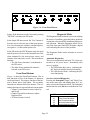
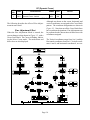
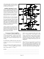
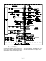
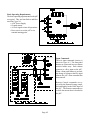
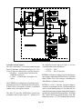
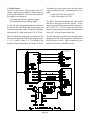
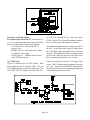
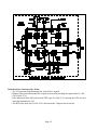
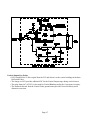
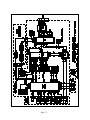
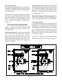
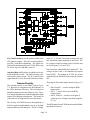
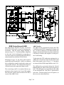
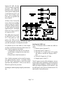
1
MITSUBISHI ELECTRIC MITSUBISHI DIGITAL ELECTRONICS AMERICA, INC. Projection Television Technical Training T 2000 VZ7 Chassis ♦ ♦ ♦ ♦ ♦ Features Alignment Procedures Circuit Descriptions Block Diagrams Troubleshooting Techniques Models: VS-45605 • VS-50605 • VS-50705 VS-55705 • VS-60705 • VS-70705 www.mitsubishi-tv.com ECHNICAL RAINING VZ7 Chassis Technical Training Table of Contents Section 1 -- Introduction ....................................................................................................................... 1-1 Latest Technologies .......................................................................................................................... 1-1 User Menus ....................................................................................................................................... 1-2 User Adjustments .............................................................................................................................. 1-3 Remote Control ................................................................................................................................ 1-4 Front Panel Buttons .......................................................................................................................... 1-5 Diagnostic Mode ............................................................................................................................... 1-5 Main Chassis PCB Location ............................................................................................................. 1-6 CR Block Connectors ....................................................................................................................... 1-7 Section 2 -- Option Menu and Service Adjustment Mode ................................................................. 2-1 Option Menu ..................................................................................................................................... 2-1 Service Adjustment Mode ................................................................................................................. 2-2 Section 3 -- Convergence Adjustments ................................................................................................ 3-1 Static Convergence ........................................................................................................................... 3-1 Convergence Mode Description ....................................................................................................... 3-1 CONV-MISC Function ..................................................................................................................... 3-1 Coarse Adjustment Mode ................................................................................................................. 3-2 Fine Adjustment Mode ...................................................................................................................... 3-3 Fine Convergence Adjustment Description ....................................................................................... 3-4 General Adjustment Procedure ......................................................................................................... 3-8 Section 4 -- Convergence Circuitry ...................................................................................................... 4-1 Overall Convergence Circuit ............................................................................................................. 4-1 DAC & LPF Circuitry ....................................................................................................................... 4-3 Amplifier/Summing Circuitry ............................................................................................................ 4-4 Convergence Output Amplifiers ....................................................................................................... 4-4 Convergence Control Circuitry ......................................................................................................... 4-7 Section 5 -- Power Supply ..................................................................................................................... 5-1 Standby Supplies ............................................................................................................................... 5-1 Switch Mode Regulator .................................................................................................................... 5-2 ON/OFF Circuitry ............................................................................................................................. 5-3 Deflection/HV Generated Supplies ................................................................................................... 5-4 Switched Supplies Power Distribution .............................................................................................. 5-5 Troubleshooting ................................................................................................................................ 5-6 Section 6 -- Control Circuitry ............................................................................................................... 6-1 Basic Microprocessor Requirements ................................................................................................ 6-2 Input Commands ............................................................................................................................... 6-2 Overall Control Circuitry .................................................................................................................. 6-3 Copyright © 1999 Mitsubishi Digital Electronics America, Inc. All Rights Reserved V-Chip Circuitry ............................................................................................................................... 6-4 AC OFF............................................................................................................................................. 6-5 SHORT Circuit ................................................................................................................................. 6-6 X-RAY Protect ................................................................................................................................. 6-6 Single Function Inputs/Outputs ........................................................................................................ 6-8 Section 7 -- Video/Color Circuitry ....................................................................................................... 7-1 PIP/POP Feature ............................................................................................................................... 7-1 Overall Signal Path............................................................................................................................ 7-2 Main/Sub NTSC Decoders ............................................................................................................... 7-4 PIP/POP Circuitry ............................................................................................................................. 7-4 VCJ Video/Color Internal Path ......................................................................................................... 7-6 Gamma Circuitry ............................................................................................................................... 7-8 Blanking Insertion & CRT Protect .................................................................................................... 7-9 RGB Output Amplifiers & AKB ..................................................................................................... 7-10 On-Screen-Display Signal Path ....................................................................................................... 7-12 Section 8 -- Deflection Circuitry ........................................................................................................... 8-1 Deflection Drive Generator ............................................................................................................... 8-2 Horizontal & HV Output Circuitry ................................................................................................... 8-3 HV Regulation .................................................................................................................................. 8-4 Scan Velocity Modulation ................................................................................................................. 8-5 Dynamic Beam Formation ................................................................................................................ 8-6 Vertical Output Circuitry................................................................................................................... 8-7 Section 9 -- Audio Circuitry .................................................................................................................. 8-1 Audio Signal Path ............................................................................................................................. 8-1 Section 1 Introduction VZ7 Chassis Model/Features FEATURES VS-45605 VS-50605 VS-50705 VS-55705 VS-60705 VS-70705 Chassis Screen Size TM DiamondShield Advanced PIP/POP Digital Convergence Digital Comb Filter INPUTS Rear A/V & S-Video Front A/V & S-Video Component Inputs (Y,CR&CB) OUTPUTS Video Monitor Fixed/Variable Audio R/L VZ7 45" Optional PIP X 3DYC VZ7 50" Optional PIP X 3DYC VZ7+ 50" Included PIP/POP X 3DYC VZ7+ 55" Included PIP/POP X 3DYC VZ7+ 60" Included PIP/POP X 3DYC VZ7+ 70" Included PIP/POP X 3DYC 2 1 1 2 1 1 2 1 1 2 1 1 2 1 1 2 1 1 1 1 1 1 Table 1-1 1 1 1 1 1 1 1 1 A total of six Projection TV Models use one of two versions of the VZ7 Chassis. Two models use the VZ7 Chassis and four models use the VZ7+ Chassis. Table 1-1 lists the models and some of the main features. The VZ7 Chassis uses some of the latest technologies available, including those listed in Figure 1-1. Convergence & Raster Correction • Digital Circuitry Luminance/Chrominance Separation • 3-D Y/C PIP • Picture out of Picture (Vz7+) Component Inputs • DVD Component Input Circuitry Figure 1-1: VZ7 Chassis Circuitry The VZ7 chassis has Digital Convergence and Raster Correction circuitry. This not only affects the circuitry, but also the Convergence and Raster Correction Adjustments. Adjustments are covered in Section 3, and the convergence circuitry is described in Section 4. Luminance/Chrominance separation is acheived through the 3D-Y/C process, a method that digitally processes an entire video frame. This method produces results far superior than those that only process two or three lines at a time such as Digital Dynamic or 2D-Y/C processing. The PIP circuitry features the Picture out of Picture feature in VZ7+ Models. The PIP circuitry description is in Section 7. Component Video Inputs are featured in all VZ7 models. They are labeled DVD Inputs, and consist of three video Input jacks, plus Right and Left Audio Jacks. The video jacks are denoted as Y, Cr and Cb. This method allows the baseband Luminance and Color Difference Signals to be coupled directly from a DVD player, avoiding any signal degredation that can be caused by chroma modulation and demodulation. Basically the signals are Y (Luminance), R-Y, and B-Y. In the NTSC format the three signals have the following amplitude relationship: • Y = 0.7 Vp-p (plus sync) • R-Y = 1.0 Vp-p • B-Y = 1.3 Vp-p Page 1-1 The designations Cr and Cb denote that the R-Y and B-Y are reduced in amplitude, R-Y by a factor of 0.71, and B-Y by 0.56. This results in the following signal amplitudes: • Y = 0.7 Vp-p (plus sync = 1.0 Vp-p) • Cr = 0.7 Vp-p • Cb = 0.7 Vp-p User Menus Figure 1-2 shows the Main Menu, listing four Sub Menu Categories. Most of the Menu Items are clear. Others warrant further explanation. The V-Chip Parental Lock enables the user to lock out specific types of TV programming. Program rating information is transmitted on the 21st horizontal line during the vertical blanking interval. The V-Chip lock out can be active at all times, set for a specific time period every day, or turned off completely. If the program on a selected channel is locked, the screen goes blue and an on-screen display indicates that the program is locked. If the PIP source program is locked, a black insert picture appears when PIP is activated. One sub-menu item under Advanced Features is the user's Advanced Convergence Feature. It displays complete Crosshatch pattern allowing the user to adjust 64 intersections in the pattern. If the convergence gets too far off, the user still has the option of selecting Reset to Factory Settings, in the initial Convergence menu. MAIN MENU • V-Chip Parental Lock • Channel Edit • Advanced Features • Audio Video Settings The AV Memory, under Audio Video Settings has five AV Memory selections: • Standard -- for typical viewing • Daylight -- for daylight viewing • Evening -- for evening viewing • Home Theater • DVD -- for DVD viewing In each category, the video and audio controls are set for optimum picture. The default control settings for each of the AV Memory categories are shown in Table 1-3. User Adjustments Most user adjustments will be made using the VIDEO and AUDIO buttons on the remote control. Pressing the AUDIO button cycles through six audio adjustments, or options: 1) Bass 2) Treble 3) Balance 4) Surround 5) Listen To 6) Level Sound Pressing the VIDEO button sequences through eight video adjustments/options. 1) IRIS (On or Off) 2) Contrast 3) Brightness 4) Auto Picture (On or Off) 5) Sharpness 6) Tint 7) Color 8) Color Temperature (High, Medium or Low) The Auto Picture feature, when activated, detects the strength of the RF signal. Sharpness and Color are automatically set to produce the optimum picture for that signal level. This option is only effective when using the TV's tuner. Figure 1-2: Main Menu Page 1-2 The AGC voltage is used to determine signal strength. One of three signal levels can be detected: • Weak signal -- less than 65 db • Medium signal -- between 65 and 70 db • Strong signal -- more than 70 db On a strong signal, Sharpness and Color settings remain at their reset values. As signal strength de- creases, both Sharpness and Color adjustments are reduced. When Auto Picture is ON, the normal adjustment slide is not displayed for Sharpness and Color adjustments. It is replaced by the text "AUTO PICTURE". During this display, pressing the right or left Adjust button will cancel the Auto Picture mode, and the adjustment slide will be displayed. AV MEMORY ADJUSTMENT Tint Color Contrast Brightness Sharpness Color Temp. Bass Treble Balance Surround Level Sound CATEGORY Standard Daylight Evening Home Theater 31 31 31 31 31 31 31 27 63 63 63 45 31 40 25 31 31 31 31 35 HIGH HIGH HIGH LOW 31 35 35 31 31 35 35 31 31 31 31 31 OFF OFF OFF OFF OFF OFF OFF OFF Table 1-3 Page 1-3 DVD 31 31 63 31 35 LOW 31 31 31 OFF OFF Remote Control The Remote Control for VZ7 models is illustrated in Figure 1-3. Its functions are straightforward. The numerical buttons 0 through 9, are used to enter numerical values for Time Setting, Alarm setting, V-Chip Lock Code, etc. The buttons are also used to directly access a channel. The numerical buttons channel change is a three digit system. Channels with less than three digits may be accessed in one of three ways. 1) Add zeros prior to entering the channel number, making it a three digit entry. Press 002 for channel 2. 2) Enter the channel number then press ENTER. 3) Enter just the channel number. There will be a four second delay before the channel change occurs. PIP/POP PIP INPUT PIP CH PIP SIZE EXCH When the QV (Quick View) button is pressed, the TV changes to the previous channel selection. If pressed again it returns to the original channel. Repeated pressing will toggle the TV back and forth between the two channels. Figure 1-3: Remote Control When viewing a normal TV picture with no Menu displayed, pressing Info activates the Detail Status Display. This display includes: • Channel Number • Channel Name (if any) • SAP, STEREO, CC, and SQV • V-Chip rating (if any) • Time display 1) Side by Side …the main and sub pictures are displayed side by side. Both pictures are compressed horizontally to fit on the 4:3 aspect screen. 2) Three Picture Channel Scan … the set scans through channels, displaying the content of three channels at a time in small insert pictures. The insert for the current channel in the scanning process is live, the other two inserts are still pictures. 3) Single Insert Picture … ¼ normal size insert picture in the lower right corner. Pressing Info in the user's Advanced Convergence Mode, displays the functions of the buttons required to set convergence. Repeatedly pressing the "PIP/POP" button selects the desired PIP mode. The following describes each PIP feature and their sequence of activation. The single PIP can be moved with the Up/Down and Right/Left buttons on the Remote. When selecting a specific PIP feature, the "PIP/POP" button must be pressed within 10 seconds to select the next Page 1-4 Figure 1-4: Front Panel Buttons feature. If the duration exceeds 10 seconds, pressing "PIP/POP" terminates the PIP mode. In the Single PIP Insert mode, the "Size" button allows the user to select the size of the insert picture. Five size selections are available, with the largest insert equal to ¼ of the normal picture size. In the PIP mode, the EXCH button swaps the main and sub pictures. However this button has no effect when Antenna B is the main picture source, and Antenna A the sub picture source. Due to hardware limitions: • The Sub Tuner (Antenna A) is dedicated as the PIP source. • The Main Tuner (Antenna B) cannot be selected as the PIP source. Front Panel Buttons Figure 1-4 shows the Front Panel buttons. Due to dual functions of five of the buttons, 14 functions can be performed. The primary function of the buttons is shown above each button. The secondary functions are indicated below the buttons. The secondary functions are activated when in a menu mode. • Volume Up and Down becomes Adjust Up and Down • Channel Up and Down becomes Adjust Right and Left. • AV Reset becomes Cancel Diagnostic Mode The Diagnostic Mode assists the servicer in isolating the source of a problem, particularly those problems causing the set to switch OFF (shutdown) during normal operation. When the Diagnostic Mode is activated, the front panel On/Off LED flashes a digital code indicating the source of the problem. The Diagnostic Mode can be automatic or servicer activated. Automatic Diagnostics This occurs automatically when the TV is first connected to an AC power source. Immediately after power is applied: • The LED flashes three times... indicating the µPC has been initialized and is functioning. • The LED does not flash... indicating the µPC is not functioning. Servicer Activated Diagnostics Pressing the front panel "Input" and "Menu" buttons at the same time, and holding them for 5 seconds, activates the Diagnostic Mode. The front panel buttons must be used, not those on the Remote Control. CODE 12 21 22 23 24 INDICATES No error has occured X-Ray Protect Shutdown Short Protect Shutdown Horizontal Deflection failure Vertical Deflection failure Table 1-4: Error Codes Page 1-5 When the mode is activated, the front panel LED starts flashing a two digit code: 1) The initial number of flashes denotes the value of the tens digit (MSD) of the code. 2) Flashing pauses for ½ second. 3) The LED flashes the value of the ones digit (LSD) of the code. 4) The code is repeated 5 times, then normal operation resumes. The two digit codes indicate what malfunction has occurred, or that no malfunction has occurred. Table 1-4 lists the two digit codes and their meanings. Main Chassis PCB Location Figure 1-5 shows the location of the PCBs, and major components on the main chassis assembly. Two major PCBs comprise the main chassis: • PCB-MAIN • PCB-SIGNAL Circuitry on the PCB-MAIN includes: 1) Power Supply 2) Horizontal and Vertical Deflection 3) HV circuitry 4) X-Ray Protect Figure 1-5: PCB Locations Page 1-6 Signal processing circuits are located on the PCBSIGNAL. These include: • Both Tuners • Video Processing • Color Processing • Convergence Circuitry • Audio Circuitry The Control Microprocessor is also located on the PCB-SIGNAL. To minimize component clutter, this PCB is double sided. PCB-APERTURE plugs into the PCB-SIGNAL. PCB-SVM, Scan Velocity Modulation and PCBDBF, Dynamic Beam Formation (or Focus), plug into the PCB-MAIN. Note the Flyback Transformer and the HV Capacitance/Resistance Divider are separate components. The Flyback is mounted on the PCB-MAIN, and CR Block is mounted on the Main Chassis Frame. CR Block Connectors Care must be taken when connecting the HV leads to the CR Block. Figure 1-6 illustrates the type of connector used on the CR Block. To disconnect a lead: 1) Rotate the connector cap approximately 90o counter clockwise. 2) The cap and the lead can then be pulled from the CR Block. To connect a HV lead, reverse the procedure. When inserting the lead in the CR Block, insure that the lead wire is not bent over. If the lead is bent internal arcing occurs and the CR Block can be damaged. If any audible noise is heard from the CR Block, arcing, sizzling, buzz, etc., check all HV Lead connections. This type of arcing can also be seen in the picture in the form of dotted interference. Page 1-7 Page 1-8 Section 2 Option Menu and Service Adjustment Mode Option Menu and Service Adjustment items must be set to either a specific setting, data value or set according to a prescribed adjustment procedure. For specific adjustment instructions, refer to the Service Manual. For training purposes, the Option Menu setup and Service Adjustment procedures are reprinted from the Service Manual. 1. Option Menu Option Menu items should be set as shown in the figure below. The Initial function is also accessed from the Option Menu. Performing an Initial setup will set all customer controls to the factory default condition. This can be useful in determining if a symptom is caused by an improperly set customer control. Follow the steps below for the Initial set-up: 1. Select the "MENU" display by pressing the "MENU" button once. 2. Press the number buttons "1", "2", "7", "0" in sequence to select the "OPTION MENU" display. 3. Press the "ADJUST" button to select "INITIAL." 4. Press "ENTER." NOTE: At this time channel 3 is automatically selected. CAUTION: On these models E2 RESET activation has been changed. To activate, the "QV" button must be pressed while "E2 RESET" is selected on the menu screen. The “QV” button may be denoted as “RCL” on some models. This feature is for factory use only. DO NOT ACTIVATE E2 RESET AS THIS WILL RESET ALL ALIGNMENT DATA. Doing so will require a full item by item alignment of all data values listed in the "adjustment items" section of this manual. OPTION MENU INITIAL E2 RESET POWER RESTORE: WHEN MUTE: DIRECT KEY MODE VS-70705 V-CHIP OFF ON OFF *NO ON SERIES SETTING: XXXXXXXX SERIES SETTING: XXXXXXXX *This option should be "YES" for model VS-70705 Page 2-1 After Initalization, customer controls are set according to the following tables. INITIAL SETTINGS Item 1 2 3 4 5 6 7 8 9 10 11 Description Input Receiving Channel TV/CATV RCL Channel Memory V-CHIP LOCK Lock by Time Lock Time UnlocK Time Lock Channels LOCK CODE VOLUME AUDIO FUNCTIONS TV Listen to TV Bass TV Treble TV Balance TV Surround TV Level sound VIDEO FUNCTIONS TV Tint TV Color temp Initial Setting TV 003 CH CATV Recalls previous ch. All CH (0,0) OFF 12:00 AM 12:00 AM OFF ---30% STEREO 50% 50% 50% OFF OFF 50% High Item Description 11 TV IRIS TV Contrast TV Brightness TV Sharpness TV Color 12 Speaker 13 Background 14 Closed Caption 15 PIP SOURCE 16 PIP POSITION 17 VIDEO MUTE 18 INPUT, NAME 19 TIMER 20 SQV 21 A/V NETWORK 22 LANGUAGE 23 NAME THE CHANNELS 24 Locked to Input 25 External Audio System 26 Vol. change by AV Rec. 27 Clock Time 28 Set Day Initial Setting OFF 100% 50% 50% 50% ON Gray On if Mute TV Lower Right OFF OFF All input name OFF OFF All CH CLEAR (deleted) OFF English ALL LABELS CLEARED No No N/A - -:- Sunday AV MEMORY AV MEMORY TINT COLOR CONTRAST BRIGHTNESS SHARPNESS COLOR TEMP BASS TREBLE BALANCE SURRONG LEVEL SOUND Standard 31 31 63 31 31 HIGH 31 31 31 OFF OFF Daylight 31 31 63 40 31 HIGH 35 35 31 OFF OFF Evening 31 31 63 25 31 HIGH 35 35 31 OFF OFF Page 2-2 Home Theater Component 31 31 27 31 45 63 31 31 35 35 LOW LOW 31 31 31 31 31 31 OFF OFF OFF OFF 2. Circuit Adjustment Mode Except for the following, all adjustment items must be performed using the remote hand unit. • Lens Focus • Electrostatic Focus A. Activating the Circuit Adjustment Mode 1. Press the "MENU" button on a remote hand unit. 2. Press the number buttons "1", "2", "5", "7" in sequence. The screen will change to the Adjustment Mode. Note: Repeat steps 1 and 2 if the circuit adjustment mode does not appear on screen B. Selection of adjustment Functions and Adjustment Items To select an adjustment item in the circuit adjustment mode, first select the adjustment function that includes the specific adjustment item to be selected. Then, select the adjustment item. CABLE/DBS Refer to the following pages for the listing of adjustment functions and adjustment items. VCR DVD AUDIO TV 1. Press the "AUDIO" button on a remote hand unit to select an adjustment function. Each time the button is pressed, the Function changes in the following sequence: 1 2 3 6 4 5 7 8 9 SQV 0 QV POWER SLEEP VIDEO INPUT CHANNEL VOLUME AUDIO VIDEO AUDIO MUTE ENTER ENTER GUIDE CANCEL MENU HOME PIP/POP PIP SIZE 2. Press the “VIDEO” button to select a specific Adjustment Item. The Item number increases each time the “VIDEO” button is pressed. REC REW/REV C. Changing Data After selecting an adjustment Item, use the “ADJUST UP/DOWN” button to change data. • Press “ADJUST DOWN” to decrease the data value. • Press “ADJUST UP” to increase the data value. Page 2-3 PIP INPUT PIP CH EXCH STOP PLAY INFO PAUSE FF/FWD ADJUST UP/DN MENU D. Saving Adjustment Data Press “ENTER” to save adjustment data in memory. The character display turns red for approximately one second in this step. Note: If the circuit adjustment mode is terminated without pressing “ENTER”, changes in adjustment data are not saved. E. Terminating the Circuit Adjustment Mode Press the “MENU” button on the remote hand unit twice to terminate the adjustment mode. Note: The circuit adjustment mode can also be terminated by turning power OFF. F. Direct Key Mode This feature is for Factory Use Only. It enables access to the Service Adjustment Modes by using the VCR buttons on the remote control. 1. 2. 3. 4. Activate the Factory Option Menu (MENU-1-2-7-0) Change the option for “DIRECT KEY MODE” from OFF to ON. Exit the Option Menu (Press “MENU” twice). Service Adjustment Modes can now be activated using the following VCR buttons on the remote: • “REWIND”... activates the Circuit Adjustment Mode • “PLAY”........ activates the Coarse Convergence Mode • “STOP”....... activates the Fine Convergence Mode • “PAUSE”..... activates the Factory Option Menu 5. After performing adjustments, set the “DIRECT KEY MODE” option back to OFF. IMPORTANT If the “DIRECT KEY MODE” is not turned OFF: • The VCR buttons will not control a VCR • The user has access to the Adjustment Modes Page 2-4 Section 3 Convergence Adjustments Convergence Adjustments in the VZ7 chassis are divided into two major categories, Static and Dynamic. The Static Convergence Adjustment has not changed. However, the Dynamic Convergence Adjustment has changed, due to using Advanced Digital Convergence circuitry. Dynamic Convergence is performed in the Convergence Adjustment Mode. Coarse Dynamic Adjustments are performed first, followed by Fine Adjustments. The digital circuitry, and Adjustment Procedure provides a higher degree of raster geometry and convergence correction over the entire picture, than was possible in the past. In addition to Dynamic Convergence, the Convergence Mode is used to adjust HV Regulation and: 1) Set Initial Data Values for the: • Convergence Waveform Generator • Green Raster Coarse Geometry Adjustments • Red Dynamic Coarse Convergence Adjustments • Blue Dynamic Coarse Convergence Adjustments • Dynamic Focus Settings 2) Perform most Raster Geometry Adjustments • Width and Horizontal Linearity • Pincushion Correction • Skew (X axis tilt), and Tilt (Y axis tilt) • Vertical Keystone Note that Data Values and Adjustments for Raster Geometry in the Circuit adjustment mode must be set prior to performing Raster Geometry adjustments in the Convergence adjustment mode. These procedures are described in the Service Manual. Convergence Mode Description To activate the Convergence Mode, press MENU1-2-5-9, in sequence. The screen changes to an internally generated Cross Hatch pattern. The Cross Hatch is super imposed on the current selected signal source. To display the Cross Hatch with a black background, prior to entering the Convergence Mode, select an External Input with no signal applied as the source. Once in the Convergence Mode, several Functions, Modes or displays can be selected: 1) Pressing (1) (2) or (3) respectively activates a Red Green or Blue display 2) Pressing (6) activates the CONV-MISC function 3) Pressing (5) activates the Coarse Adjustment Mode 4) Pressing (4) activates the Fine Adjustment Mode The CONV-MISC Function is used to perform the HV Regulation Adjustment, and to preset the data values controlling the Convergence Waveform Generator. Table 3-1 lists the items and preset values under CONV-MISC. Some of the data values are model specific. Check the Service Manual for a specific model to verify the correct preset values. As in the Service Adjustment Mode, the VIDEO button selects the Adjustment Item, and the ADJUST buttons set the Data Value. In the Convergence Mode it is not necessary to press ENTER to save data changes. Changes are automatically saved when the mode is terminated. Page 3-1 CONV MISC ADJ NO. 0 1 2 3 4 5 6 7 8 9 10 11 12 13 14 ABBR. HVOL VINT HINT COUT HPLL VSTR VCNT STLN FPHS CPHS DPHS TPHS HDLY PLWD PWM2 DESCRIPTION HV DC Control Voltage Interpolation Value (0=NTSC, 1=line db) Horiz. Interpolation Value (0 Req'd) Conv. IC Output Mode (0=Analog, 1=Digital) 1= HPLL Divider Value (256=NTSC) Vertical Offset Value Vertical Count Value Sets the Vertical Position of the Crosshatch Fine Phase of Correction Wrt. Hor. Blk. Phase Coarse Adjustment Phase of Dynamic Focus Wrt. Hor. Blk. Sets the Horizontal Position of the Crosshatch Phase of Hblk (out) Wrt. Hor. Blk. Pulse Width of Hblk. (out) Pulse Width of PWM-2 Output for 2H DATA NOTES 140 0 0 1 1 0 56 31 233 20 40 48 0 8 6 HV Regulation Preset " " " " " " " " " " " " " Table 3-1 When HV Regulation, Item (0), is selected the cross Table 3-2, set the Vertical Height and Linearity Adhatch is replaced with a black raster. A black raster justments under the VCJ Function in the Service Adis required to perform this adjustment. justment Mode. In the Coarse Adjustment Mode, the AUDIO button selects the following sub functions: • CONV-GREEN --- Green Cross Hatch • CONV-RED --- White Cross Hatch • CONV-BLUE --- White Cross Hatch • DF --- White Cross Hatch The adjustments under CONV-GREEN include Width, Pincushion, X and Y axis Tilt, and Vertical Keystone. In all the Coarse Adjustment Sub Functions, the VIDEO button selects the Adjustment Item, and the ADJUST, Up and Down buttons set the data. CONV-RED and CONV-BLUE are used to perform Red and Blue Coarse Dynamic Convergence Adjustments. In both the Red and Blue modes, a white Crosshatch is displayed. However, only Red is adjustable in the Red Mode, and only Blue in the Blue Mode. CONV-GREEN is used to set Coarse Raster Geometry Correction. The Adjustment Items are listed in Table 3-2. Before performing the adjustments in The Adjustment Items under CONV-RED, and CONV-BLUE, are shown in Tables 3-3 and 3-4, respectively. These adjustments include: CONV GREEN ADJ NO. 0 1 2 3 4 5 6 7 ABBR. HSTA SPCC HWID SKEW VSTA VKEY TBPC TILT DESCRIPTION RANGE DATA Horiz. Position Side PCC Width x Axis Tilt Vertical Position Vertical Keystone Top/Bottom PCC Y Axis Tilt ±511 ±511 ±511 ±511 ±511 ±511 ±511 ±511 Table 3-2 Page 3-2 +6 -182 -66 +1 +88 -14 -270 -7 NOTES Coarse Raster Correction " " " " " " " • Horizontal Width, Linearity and Bow. • Vertical Keystone • X and Y Axis Tilt Set the coarse adjustments so that the red (or blue) converges on the green crosshatch, at the center of the top, bottom, and sides of the screen. If Static Convergence shifts during coarse alignment, use HSTA and VSTA, items 0 and 5, to correct the shift. DF (Dynamic Focus) is used to preset the data values controlling the Dynamic Focus circuitry. There are only two items under the DF Sub Function, as shown in Table 3-5. Set the Items to the data values given in the Service Manual for that specific model. The Fine Adjustment Mode is activated by pressing (4), when in the Convergence Mode. In this mode the On-screen Data Display changes, and a blinking Cursor appears on the Cross Hatch. There are two sub modes of Cursor operation: 1) Cursor Move (blinking cursor) 2) Adjust Data (non-blinking cursor) The ENTER button toggles the mode between Cursor Move, and Adjust. In the Move Mode the ADJUST buttons move the Cursor. In the Adjust Mode, the ADJUST buttons set the horizontal and vertical position, of Red, Green or Blue, at the current Cursor position. The AUDIO button toggles the Adjust Mode Color, Green, Red, and Blue. For a quick reference, the Convergence Mode General Procedure is illustrated graphically in Figure 3-1. CONV RED ADJ NO. 0 1 2 3 4 5 6 7 ABBR. HSTA HLIN SKEW HWID HSBW VSTA VKEY TILT DESCRIPTION RANGE DATA Horiz. Position Horiz. Linearity x Axis Tilt Width Horiz. Bow Vertical Position Vertical Keystone Y Axis Tilt ±511 ±511 ±511 ±511 ±511 ±511 ±511 ±511 +71 -231 +15 +21 +60 +30 -250 -7 NOTES Coarse Red Convergence " " " " " " " Table 3-3 CONV BLUE ADJ NO. 0 1 2 3 4 5 6 7 ABBR. HSTA HLIN SKEW HWID HSBW VSTA VKEY TILT DESCRIPTION RANGE DATA Horiz. Position Horiz. Linearity x Axis Tilt Width Horiz. Bow Vertical Position Vertical Keystone Y Axis Tilt ±511 ±511 ±511 ±511 ±511 ±511 ±511 ±511 Table 3-4 Page 3-3 +50 +263 +7 +9 -125 +39 +153 -7 NOTES Coarse Blue Convergence " " " " " " " DF (Dynamic Focus) ADJ NO. 0 1 ABBR. DFH DFV DESCRIPTION RANGE DATA Dynamic Focus - Horiz. Dynamic Focus - Vertical ±511 ±511 -300 -159 NOTES Preset " Table 3-5 The following describes the effect of Fine Adjustments in more detail. Fine Adjustment Effect When the Fine Adjustment Mode is entered, the screen changes to that shown in Figure 3-2, with a Green Cross Hatch. The Cursor is flashing, indicating the Move Cursor mode. The mode name and data values are also displayed. Although not shown on the screen, horizontal and vertical coordinates are assigned to the Cross Hatch pattern. The coordinate designations are shown in Figure 3-3. Note that not all the Cross Hatch lines have coordinate designations. Fine Adjustments can be performed at the intersections of those lines with coordinates assigned. The Vertical coordinates range from 0 to 9, and the Horizontal coordinates from 0 to 8. Vertical coordinates 0 and 9, and horizontal coordinate 8, are out- Page 3-4 side the picture area (off the screen). If the Cursor is located at these coordinates it will not be visible, and must be moved to the visible area of the screen, using the ADJUST buttons. tal cross hatch lines at the sides of the screen. The same is true for vertical coordinate 8. Adjusting horizontal position effects the vertical crosshatch lines at the extreme bottom of the picture. Horizontal coordinates 0 and 7 are also off the screen. However, they are close enough to the edge of the screen so part of the cursor is visible. Adjusting the vertical position at these points effects the horizon- The shaded circles in Figure 3-3 indicate the crosshatch intersections that can be adjusted. There are a total of sixty four cursor positions to make fine adjustments on the crosshatch. NOTES: ___________________________________________________________________________ __________________________________________________________________________________ __________________________________________________________________________________ __________________________________________________________________________________ __________________________________________________________________________________ Page 3-5 Moving the Cursor The Cursor is moved using the ADJUST buttons. The Cursor only stops at intersections that are assigned horizontal and vertical coordinates. • ADJUST UP --- moves the Cursor to the next upper active intersection • ADJUST DN --- moves the Cursor to the next lower active intersection • ADJUST RGT --- moves to the next active intersection on the right • ADJUST LFT --- moves to the next active intersection on the left Adjusting Data Pressing ENTER toggles the Cursor from the Move to the Adjust Mode, the Cursor stops flashing. The intersection at the Cursor, can be adjusted vertically using the ADJUST UP & DN buttons, or horizontally using the ADJUST LFT & RGT buttons. The effect of Green Adjustments is illustrated in Figure 3-4A. In the Green mode, only Green is displayed, and moves when adjusted. Green is used to correct raster distortion. Page 3-6 Pressing the AUDIO button toggles the color from GREEN to RED to BLUE, and back to GREEN. In the RED and BLUE modes all three colors are displayed. However, only Red can be adjusted in the RED mode, and only Blue in the BLUE mode. This is illustrated in Figure 4B. The RED and BLUE modes are used for Fine Convergence Adjustment. Some interaction between the current cursor position, and adjacent cursor positions does occur. Therefore, a back and forth type of adjustment procedure may be required. Data Display Fine Adjustment Mode Data Display designations are shown in Figure 3-5. The Y digits, to the left of the V, denote the vertical data value for the current Cursor Position. The X digits, to the right of the H, denote the horizontal data value for the Cursor position. Both vertical and horizontal data may be either positive or negative, ranging from -511 to +511. The digit to the right of the V indicates the Cursor’s current vertical coordinate position, and digit to the left of the H indicates the NOTES: ___________________________________________________________________________ __________________________________________________________________________________ __________________________________________________________________________________ __________________________________________________________________________________ __________________________________________________________________________________ Page 3-7 current horizontal coordinate position. In Figure 35, vertical coordinate 3 and horizontal coordinate 6 are shown. Horizontal coordinates range from 0 to 8, and the vertical ranges from 0 to 9. General Adjustment Procedure When servicing Projection TV, usually only touch up Raster and Convergence Correction adjustments are required. If mis-convergence appears in one or more areas of the screen, it may only require a Fine Convergence Adjustment touch up. However, it must be remembered that it may also be due to: 1) Incorrect preset data value in the CONVMISC mode. Incorrect data values can distort the generated correction signals. 2) Incorrect Raster Correction adjustments. 3) Coarse Convergence Adjustments are not set to optimum. If not set to optimum, correction may be out of the Fine Adjustment mode range. NOTES: ___________________________________________________________________________ __________________________________________________________________________________ __________________________________________________________________________________ __________________________________________________________________________________ __________________________________________________________________________________ Page 3-8 The following General Procedure sequence serves as a reference. It is not meant to be performed each time the set is serviced. However, if a quick touch up does not solve the problem, we suggest checking the adjustments in the following sequence. General Procedure 1) Preset CONV-MISC data. Check the data against the values given in the Service Manual for that specific model. 2) Raster Correction Adjustments • Perform Vertical Height and Linearity Adjustments in the Service Adjustment Mode, VCJ Function, Items 24 and 28. • Perform Coarse Raster Correction Adjustments, CONV-GREEN mode. • Perform Fine Raster Correction Adjustments, FINE CONV GREEN mode. 3) Static Convergence -- if too far off, correction may be out of the range of the Convergence circuitry. 4) Coarse Dynamic Convergence Adjustment • CONV RED mode -- converge red on the green at the center of the top, bottom and sides of the picture. • CONV BLUE mode -- converge blue on the green at the center of the top, bottom and sides of the picture. 5) Fine Convergence Adjustment • Adjust the cursor positions where misconvergence appears. • Adjust cursor positions in the sequence shown in Figure 3-6. Page 3-9 Page 3-10 Section 4 Convergence Circuitry The Convergence Correction Circuitry in the VZ7 chassis is digital. Figure 4-1 illustrates a Basic Block Diagram of the circuit. Horizontal and vertical pulses are applied to a Convergence Correction Generator. The Correction Generator produces Horizontal and Vertical Correction signals for each CRT, Red, Green and Blue. The Correction Signals are not analog waveforms, but are Serial Digital Signals. The signals are applied to Digital to Analog Converters to produce the analog waveforms required to drive the Sub Coils in the Deflection Yokes. The signals are then amplified and applied to their respective Yoke Sub Coils. Overall Convergence Circuitry Figure 4-2 shows a simplified diagram of the Overall Convergence Circuitry. IC800 is the Convergence Correction Waveform Generator. Horizontal pulses are derived from the Horizontal Output stage circuitry, and vertical pulses from the V-Pump terminal on the Vertical Output IC, IC451. The horizontal and vertical pulses are buffered by IC803, on the PCB-CONV, and then directed to IC800. IC803 is comprised of two D-type Flip Flops providing clean precisely timed output pulses. The internal circuitry in IC800, uses the pulses from IC803 to generate the Convergence Correction signals, in a Serial Digital format. Page 4-1 Page 4-2 The signals from IC800 are directed to Digital to Analog Converters in IC8E01, IC8E02 and IC8E03. Each of the ICs is comprised of two separate Digital to Analog Converters. The analog outputs of the D/ A Converters are directed to Low Pass Filter (LPF) circuitry in IC802, IC803, and IC804. The outputs from the LPF circuitry are applied to amplifiers in the second stage of IC802, IC803, and IC804. The Green signal is also directed to the Red and Blue Amplifier inputs. The raster correction adjustments are performed on the Green raster, but also effect the Red and Blue rasters. The six amplified signals are directed to their respective Convergence Output IC. The Convergence Output ICs, IC8C01 and IC8C02, contain three separate amplifiers. IC8C01 amplifies the horizontal correction signals, and IC8C02 the vertical correction signals. An oscilloscope can be used to trace the signal through the circuitry to isolate a problem area. Not much can be told from the serial digital signals, except that the signals are present. DAC & LPF Circuitry Figure 4-3 illustrates the circuitry of one Digital/Analog Converter IC, and its associated LPF circuitry. All three DAC and LPF circuits are the same, except for component nomenclature. The component nomenclature that is given in Figure 4-3, is common to all three circuits. As stated earlier, each DAC IC has two internal Digital to Analog Converters. Serial data is input to D/A #1 at pin 15, and data for D/A #2 is input at pin 14. The timing signals for the internal converters, are common to all three DAC ICs, • CLK -- input to the IC at pin 16. • WDCLK -- input at pin 13 The charges on the capacitors at pins 9 and 10, are the reference voltages for the internal converters. The D/A #1 analog signal is output at pin 11, and D/A #2 signal is output at pin 6. The two signals are directed to LPF circuitry in the Low Pass Filter IC. The LPF circuitry receives DC power from the plus and minus 9 Volt supplies. The IC, and its external circuitry, removes the high frequency components Page 4-3 of the analog signals, and directs them to Amplifier/Summing circuits located in the second stage of the same ICs. Amplifier/Summing Circuitry Figure 4-4 illustrates the Horizontal Correction Amplifier/Summing circuitry. The Vertical Correction circuitry is the same except for component notation. The Amplifier/Summing circuitry is within the second stage of the ICs used in the LPF. Referring to Figure 4-4, there is an amplifier for each color, red, green and blue. The Green Horizontal Correction signal is applied to all three amplifiers. Resistor R867 directs Green signal to the Red Amplifier Input, at pin 2 of IC806, and R872 supplies Green signal to the Blue Amplifier input, at pin 2 of IC807. All three amplifiers are stabilized by feedback to their non-inverting input. The amplified correction signals are directed to their respective Convergence Output Amplifiers on the PCB-CONV. Convergence Output Amplifiers Figure 4-5 shows the circuitry for the Horizontal Correction Output Amplifiers. All three of the amplifiers are in IC8C01. The amplified outputs are directed to their respective horizontal sub yoke coil winding. For stabilization, feedback from the return end of each sub coil, is direct to the inverting input of its' amplifier. The plus, and minus 24 Volts supplies furnish power for IC8C01. +24 Volts is applied to pins 5 and 10, and -24 Volts to pins 4, 8, 12, and 17. Q8C01, at pin 3, momentarily disables the IC when the TV is switched ON. As the negative 24 Volt supply is generated, the voltage at the base of Q8C01 is delayed while C8C12 charges through R8C06. During the charging period, Q8C01 conducts, applying negative voltage the Mute input at pin 3, disabling the IC. When C8C12 has charged, Q8C01 turns OFF and the IC is enabled. Both 24 Volt supplies are scan derived from the Horizontal Output Circuitry. The momentary disabling of the Convergence Output ICs, reduces the load on the Horizontal Output stage. NOTES: __________________________________________________________________________ _________________________________________________________________________________ _________________________________________________________________________________ Page 4-4 The circuitry related to Q5A01 thru Q5A06 is a Dynamic Regulator. It compensates for width changes due to changes in the HV circuit load. The capacitive divider in the CR Block provides a sample of the HV. The sample is combined with horizontal sync pulses in the Dynamic Regulator circuit. The output of the Dynamic Regulator is routed through resistive networks to the (+) input of Horizontal Correction Output Amplifier. The Dynamic Regulator is only used for the Horizontal Correction Output Amplifiers. It is not connected to Vertical Correction Output Amplifiers. Page 4-5 Page 4-6 Convergence Control Circuitry Figure 4-6 illustrates the Convergence Control Circuitry. The Main Control Microprocessor, IC700, controls the Convergence circuit over the CSDA serial data line. Transfer of data is timed by CSCL clock signal from IC700. The ACK line informs the Microprocessor (uPC) that IC800 has received a response from the E2PROM. If an expected response is not received, IC800 pulls the ACK LOW, telling the uPC that the response is missing. When this occurs, the uPC will repeat the initial command. The C_BUSY line informs the uPC if IC800 is busy, performing a command, or communicating with the E2PROM. When IC800 is busy, it pulls the C_BUSY line LOW. If the line remains LOW for an extended period of time, the uPC assumes the Convergence circuitry is locked up and initiates a Reset command. A LOW on the NOT E2RESET line, from pin 20 of IC700, will set all convergence data to its nominal point. Convergence data is stored, and read in IC801, an E2PROM. Data is written, and read from memory over the SDAM line, and timed by the SCLK line. PLL circuitry in IC809 generates timing signals for the operation of IC800, and the generation of the internal Crosshatch pattern. The PLL is phase locked to horizontal sync, input to IC809 at pin 4. IC800 also outputs two clock signals, BCLK at pin 28, and WCLK at pin 27. The two are timing signals for the three Digital to Analog Converter ICs. The BCLK signal is applied to pin 16 of each D/A Converter, and the WCLK signal to pin 13. The WCLK signal is also used as the Clock signal for the two D-type FFs in IC803, the Sync Buffer. The WCLK signal is applied the CLK1 and CLK2 inputs of IC803. The PWM1 output at pin 16 of IC800, is the HV Adjustment output and is directed to the HV Regulation circuitry on the PCB-MAIN. This adjustment is performed in the Convergence Adjustment, under the CONV-MISC function. The DAOUT at pin 38 of IC800 are the combined horizontal and vertical parabolic signals for the Dynamic Beam Formation (DBF) circuitry. The signals are amplified in IC805 and directed to the DBF circuitry. NOTES: __________________________________________________________________________ _________________________________________________________________________________ _________________________________________________________________________________ _________________________________________________________________________________ _________________________________________________________________________________ _________________________________________________________________________________ _________________________________________________________________________________ _________________________________________________________________________________ _________________________________________________________________________________ Page 4-7 Page 4-8 Section 5 Power Supply The above illustration shows the Overall Power Supply Block Diagram for the VZ7 chassis. A single Switch Mode Regulator generates both Standby and Switched supplies. Since it generates Standby supplies, it is active as long as the set is plugged into an AC source. The Switch Mode Regulator directly generates three Standby Supplies, and through the On/Off Relay, two Switched Supplies: STBY 32 Volts STBY 12 Volts STBY 4 Volts SW 18 Volts SW 130 Volts The STBY 12V supply is the source for two additional Standby supplies: STBY 9 Volts STBY 5 Volts The STBY 12 V supply is also the source for three Switched Supplies: SW 12 Volts SW 9 Volts SW 5 Volts The STBY 4 Volts supply is the source for the SW 3.2 Volts supply Page 5-1 Switch Mode Regulator Self Generated DC Supply To maintain oscillation, rectification of the signal from the secondary winding at pin 3 of T951 adds to the voltage at pin 4 of the IC. Pin 4 is also the Over Voltage Protect input. If the voltage exceeds 22 volts the internal circuitry shuts down the oscillator. Start Up Voltage The Start Up voltage is supplied by Bridge Rectifier D951, through R964 to pin 4 of the IC951. It takes approximately 16 volts at pin 4 to start the oscillator in the IC. Once the IC starts conducting, the voltage at pin 4 drops. If it drops below 11.5 volts the oscillator shuts OFF. Therefore, an added DC source is required to keep the oscillator running. Regulation Feedback Stabilization and rough regulation are provided by feedback from pin 3 of T951 to pin 1 of the IC. Fine regulation feedback is from a secondary supply, through the Photo Coupler, PC951, to pin 1 of IC951. Figure 5-1 illustrates the Switch Mode Regulator circuitry. Its requirements are: Start Up voltage Self generated oscillator DC Supply Feedback for regulation. When the set is OFF, the STBY 12V supply is monitored, through Q972 and PC951. When the set is ON, the SW 130V supply is monitored. The 130 volts is compared to a reference in IC952 and a correction voltage is directed to PC951. Page 5-2 Over Current Protection Pin 1 of IC951 is also the Over Current Protect input. The internal FETs ground return is at pin 2 of the IC. The voltage drop across R955 and R956 indicates the FETs current, and is coupled through R953 to pin 1 of the IC. The Over Current Protect circuit is activated if the voltage at pin 1 of the IC exceeds 1.35 volts. When Q973 is OFF, it allows Q972 to conduct. A sample of the STBY 12V supply is applied to the base and compared to zener diode D976 in the emitter circuit. The collector voltage is the regulation correction voltage applied to PC951. If the STBY 12V supply is high, Q972 conducts more decreasing the correction voltage. If the supply is low, the correction voltage increases. ON/OFF Circuitry Set ON Operation When the P-ON line goes HIGH, Q971 conducts closing the ON/OFF Relay. Q978 and Q973 are driven into conduction. The conduction of Q978 turns Q977 OFF, which allows Q976 to conduct, generating the SW 12V Supply. Figure 5-2 shows the ON/OFF circuitry in the VZ7 chassis. The P-ON line from the Control µPC is the ON command. When the set is OFF, the line is LOW, holding Q971, Q973 and Q978 OFF. Set OFF Operation With Q971 OFF, the Off/On Relay is open and the 130V and 18V supplies are not generated. The 18V Relay contacts are not shown in Figure 2. When Q978 is OFF, it holds Q976 OFF through the conduction of Q977. With Q976 OFF, the SW 12V supply is not generated. The conduction of Q973 turns Q972 OFF. The regulation correction voltage is now derived from the 130V supply through the Error Amplifier in IC952. Page 5-3 Deflection/HV Generated Switched Supplies Figure 5-3 shows the DC supplies generated by rectification of signals from the Flyback Transformer (T551), and the Horizontal Output Transformer (T519). Besides High Voltage, Focus and Screen Voltage, the Flyback transformer generates a 230 Volt and a 34 Volt supply. The 230 Volt supply is for the RGB amplifiers located on the CRT circuit boards. The 34 volt supply sources the Vertical Output circuit. The Horizontal Output Transformer is the source for the plus and minus 24 Volt supplies, used for the Convergence Circuit. An additional secondary winding is the source for the CRTs' filaments. Page 5-4 Power Distribution If the cause of a problem is due to a missing, or incorrect supply voltage, considerable time may be spent tracing the circuitry back to the supplys source. The Power Distribution Diagram in Figure 5-4 reduces the time needed to trace a supplys source. Page 5-5 Troubleshooting Since the Power Supply in the VZ7 chassis is similar to other switched mode designs, troubleshooting should not present a problem. The Bridge Rectifier is connected directly to the AC line. Therefore, the primary circuit of the regulator is referenced to a HOT ground. When servicing this circuit, an Isolation Transformer must be used to protect both the technician and test equipment. A more detailed diagram of the Power Supply's primary circuit is shown in Figure 5-5. Some key points to remember when troubleshooting are: 1) It requires 16 VDC at pin 4 of the IC to start the oscillator. 2) Q975 provides Soft Start Protection, applying some positive voltage to pin 1 during initial start up. 4) If pin 4's voltage drops below 11.5 volts the oscillator shuts Off. 5) If the voltage at pin 4 increases above 22 VDC, the internal Over Voltage Protect circuit shut the oscillator Off. 6) If the voltage at pin 1 reaches 1.35 VDC, the Over Current Protect circuit disables the oscillator. 7) A clicking sound indicates the IC is probably defective. 8) A chirping sound usually is caused by an excessive load on the Power Supply. Before replacing the IC try resetting it. 1) Unplug the AC cord. 2) Connect a 100 Ohm resistor (R) between pins 4 and 5 of the IC. This discharges C960 that may still be charged if the Over Voltage Protect circuit was activated. 3) Remove the 100 Ohm resistor and apply power to the set. If the problem still exists, the IC is probably defective. Excessive load on the Power Supply is usually caused by a high current component in the TV, such as the: HV Output transistor Horizontal Output transistor Audio Output IC Convergence Output ICs. Page 5-6 Section 6 Control Circuitry Control Circuity Even with many advanced features such as Digital Convergence Circuitry, PIP/POP, V-Chip Program Blocking and the Diagnostic Mode, the Control circuitry is not overly complex. An overview of the circuit is shown above. A 100 pin surface mount µPC is the heart of the Control circuitry. Primary inputs come from either the front keyboard or the remote. Most output commands are communicated by way of four I2C Buses. Besides receiving and generating commands, the internal circuitry in the µPC: • Processes Closed Caption signals. • Generates signals for On Screen Displays. • Performs V-Chip Program Blocking. Page 6-1 Basic Operating Requirements The basic operating requirements for the µPC are typical. They are listed below and illustrated in Figure 6-1. • A DC Power Supply • Ground returns • A Clock signal to time all operations. • Reset circuit to set the µPC to its nominal starting point. Input Commands The user input command circuitry is shown in Figure 6-2. The front panel buttons are connected in a two column resistive ladder array. Each column connects to a Key input on the µPC. When a front panel button is pressed, the change in voltage at the Key input informs the µPC what command has been entered. Remote Control commands are received by the Remote Preamp, amplified and applied to the RMC input of the µPC. The Remote commands are a serial data stream that is decoded in the µPC. Page 6-2 Overall Control Circuitry The µPC controls the TV’s circuitry mainly through three I2C data lines, as illustrated in Figure 6-3. Two of the I2C lines are dedicated to a specific function: • EE SDA … transfers data to and from the E2PROM memory IC. • C-SDA … Controls the Convergence Circuitry The E2PROM serves the purpose of storing user programming and service adjustment data in memory. Control of the Convergence circuitry is explained further in the Convergence Section. The third I2C data line, MAIN-SDA, controls the remainder of the circuitry in the TV. All but two of the controlled circuits shown in Figure 3 are conventional and need no explanation: • IC2Y02 … DAC • IC7V01 … Line 21 Decoder IC2Y02 is a Digital to Analog Converter that generates voltages controlling PIP Sub Picture Color, POP Main Picture Color, and voltages controlling the White Balance (Gamma) circuitry. IC7V01 is a Line 21 Decoder. Program rating information is transmitted on the 21st horizontal line in the vertical blanking interval. The Main µPC decodes the main picture program rating and if required, performs the program blocking operation. The Main µPC cannot decode the program rating of the PIP sub picture source. IC7V01 performs this function. Page 6-3 V-Chip Circuitry Figure 6-4 shows the V-Chip circuitry in the VZ7 chassis. Main picture Composite Video is input to pin 100 of the Main µPC. The internal circuitry uses the signal for two purposes: 1) Decoding the Closed Captioning signal 2) Decoding the Program Rating signal. To monitor the sub picture source, the sub picture signal is buffered by Q6C31 and directed over two paths: • To the NTSC Decoder in IC6C02 • To the Video Input of IC7V01. If a specific type of programming has been blocked by the user, the µPC blanks the main picture, and mutes the main picture sound. The picture is blanked, and replaced by a blue raster in the VCJ, IC2V00. The NTSC Decoder demodulates the video signal and directs the signal to the PIP circuitry. It also outputs sub picture horizontal sync that is applied to pin 5 of IC7V01. IC7V01 decodes the sub picture program rating signal and transfers the information to the µPC over the Program Block line. The µPC blanks the main picture and generates the blue raster through the OSD insertion inputs at pins 13, 14, 15 and 16 of the VCJ. The sound for the blocked channel is muted in the AV Switch, IC2KO1. The µPC determines whether or not the sub picture should be blocked. If the sub picture is blocked, the PIP/POP insert is black. This is controlled by the Main SDA data line to the PIP circuitry. Page 6-4 Protection and Status Inputs The inputs at pin 20, 46 and 47, as shown in Figure 6-5, are protection and status inputs, informing the uPC of any abnormal operating conditions. • AC OFF (pin 20) -- informs the uPC if power is lost. • SHORT (pin 46) -- informs the uPC if there is a short on a DC supply. • X-RAY (pin 47) -- monitors for Excess HV and CRT Beam Current. ter of Q7A20, through R7A11, and zener diode D7A20. Since Q7A20 is an NPN transistor, and the base is tied to ground, the transistor conducts. AC OFF Circuit Figure 6-6 illustrates the AC OFF circuitry. With power applied to the TV, both the STBY -12V, and +5V Holdup supplies are present, whether the TV is ON or OFF. The -12V supply is directed to the emit- If power is removed, or lost, the -12V supply drops to zero. The 5V Holdup supply temporarily remains at 5 volts. This drives pin 4 HIGH, informing the uPC that power has been lost, and programmed data is automatically stored in memory. The conduction applies negative voltage to pin 20 of the uPC. At the same time, positive voltage from the 5V Standby supply, through R7A08, is directed to pin 20. The combination of the two voltages holds pin 20 LOW. The logic at the AC OFF input of the uPC is automatically checked every 16 msec. Page 6-5 X-RAY Protect Figure 6-8 illustrates the XRAY Protect circuitry. The logic at pin 47 of the uPC is controlled by two protect circuits, monitoring for excess HV and Beam Current. SHORT Circuit Figure 6-7 shows the SHORT circuitry. The input at pin 46 of IC700, connects to the 5V Standby Supply through R7B19. Three Switched Supplies are monitored through discrete diodes. Under normal conditions, all the diodes are reversed biased and pin 46 is HIGH from the 5V supply. If a short is present on any of the monitored supplies, that specific diode is forward biased pulling pin 46 LOW. The uPC responds by automatically shutting the set OFF. The SHORT line also monitors the Horizontal Output transistor, and the Horizontal Yokes' current. R566 is the ground return for both Q5A00 and the Horizontal Yokes. If current through R566 becomes excessive, the increased voltage turns Q533 ON. The conduction of Q533 pulls the SHORT line LOW, shutting the TV OFF. The three main causes resulting in excessive voltage across R566 are: 1) Shorted or leaky Horizontal Output Transistor. 2) Shorted Horizontal Deflection Yoke. 3) Excessive current drain on the Convergence + 24 Volt DC Supplies, generated from T519 in the collector circuit of Q5A00. To monitor HV, a sample of the HV is derived from the resistive divider in the CR Block, and is directed to pin 5 of IC501. The sample is amplified in IC501 and directed to the inverting input of an OP Amplifier at pin 6 of IC502. A stable reference voltage, from IC503, is applied to the non-inverting input of the OP Amplifier, pin 5. If HV becomes excessive, the sample at pin 6 of IC502, exceeds the reference voltage at pin 5, and the output at pin 7 goes LOW. The uPC responds to the LOW on the X-RAY line by switching the set OFF. To check if the excess HV Protect is working, short pins 1 and 2 of the DN connector. If the TV does not shut off, a circuit problem exists. Beam Current Protect Beam Current is detected by monitoring the voltage at the Flyback HV Winding ground return, pin 8 of T551. The voltage at pin 8 drops as beam current increases. If the drop in voltage is excessive, D543 is forward biased, dropping the voltage at pin 3 of IC502. If the voltage at pin 3 drops below the reference at pin 2, the output at pin 1 goes LOW, pulling the X-RAY line LOW. To check the Beam Current Protect circuit, short pins 1 and 3 of the DQ connector. The TV must shut off. Failure to shut off indicates a circuit problem. Page 6-6 Arc Protect The Arc Protect circuit is also shown in Figure 6-8. It does not control the logic at the X-RAY input to the uPC, but if activated, the symptom is similar to X-RAY Protect operation, the set switches OFF. However, if the Arc Protect circuit shuts the set OFF, the set cannot be switched back ON unless AC power is removed, and then reapplied to the set. base of Q523 LOW. When Q523 conducts it turns the set OFF by pulling the P-ON command to the power supply LOW. If an arc occurs, there is a momentary sudden decrease in the voltage at pin 8 of the Flyback. The sudden drop in voltage turns Q523 ON. The conduction of Q523 turns Q524 ON, which holds the To check the Arc Protect circuit, momentarily short TP1 to ground. The set must automatically switch OFF. The TV should not switch ON unless AC power is removed then reapplied. Since the circuit latches ON when activated, the set cannot be switched back ON. AC Power must be removed, allowing C593 to discharge, before the set can be turned back ON. Page 6-7 Single Function µPC Inputs/Outputs There are, of course, µPC inputs and outputs that serve specific purposes. The inputs are basically Status Inputs, informing the µPC of the TV’s current operating status. Table 6-1 lists these inputs and their purpose. PIN # 95 5 6 7 20 46 47 51 67 68 75 89 92 93 97 100 ABBREV VSYNC1 VSYNC2 TU2-SD TU1-SD AC OFF SHORT XRAY BLANK IN C ACK C BUSY VCHIP-PB IRIS AFT1 AFT2 H SYNC CVIN The outputs used to perform specific functions, such as TV On/Off, Sound Mute, Antenna Input selection, etc., are listed in Table 6-2. DESCRIPTION V pulse from V Pump output V pulse from V Pump output Sub Tuner Sync Detector Main Tuner Sync Detector Informs when power is lost Senses Power Supply short Excess HV/Beam Current input High if deflection is lost Acknowledgement from the Convergence circuit Busy signal from the Convergence circuit Indicates the sub picture program rating From Auto Iris circuit Main Tuner AFT voltage Sub Tuner AFT voltage H Pulse from the Horizontal Output Video input for Closed Caption, V-Chip, Etc. Table 6-1: µPC Specific Function Inputs PIN 3 3 4 21 22 32 33 34 44 45 49 50 52 58 69 70 72 73 ABBREV AB2 AB3 OSD-BLNK HALFTONE R G B SUB CONT BLANK2 YUV-SW POW ER FREE RUN LED C RST C MUTE C-E2RST PIP SW DESCRIPTION Color Temperature Select Color Temperature Select OSD Timing Signal Produces transparent gray background R OSD signal G OSD signal B OSD signal High during Sub Contrast Adjustment Blanks the picture Selects the YUV Signal Source Turns the TV ON Removes sync from VCJ during video mute Controls ON/OFF LED Resets the Convergence circuit Momentarily removes Convergence correction Unlocks the Convergence E2PROM Selects POP signals 74 VCHIP RST Resets Line 21 Decoder 79 3D RST 80 81 85 86 88 MUTE3 ANT B YUV DLY MUTE 2 SYST 1A Resets 3DYC Comb Filter Mutes sound from Audio Output IC Selects the Antenna B Input Sets the delay for the YUV signals Mutes sound from the AV Switch IC Enables the Active AV Network mode Table 6-2: µPC Specific Function Outputs Page 6-8 Section 8 Deflection Circuitry From the above block diagram it is apparent that the Deflection circuitry in the VZ7 is similar to many other designs. Naturally, there are pin numbers, component nomenclature and connector designation differences. Due to this similarity, no detailed description is necessary. Therefore, this section is comprised of only simplified diagrams of the various sections of the deflection circuity. Each diagram is accompanied by a list of key points for that circuit. The simplified diagrams are listed below: • Figure 8-1: Deflect Drive Generator • Figure 8-2: Horizontal Deflection & HV Output Circuitry • Figure 8-3: HV Regulation • Figure 8-4: Scan Velocity Modulation • Figure 8-5: Dynamic Beam Forming • Figure 8-6: Vertical Output Circuitry Page 8-1 Deflection Drive Generator Key Points • The VCJ generates both Horizontal and Vertical Drive signals. • Both the Vertical and Horizontal Drive signal are derived by dividing the output of the 32 x FH (503.4 kHz) VCO. • If the Horizontal Pulse fed back from the FBT to pin 43 of the VCJ is missing, the CRTs are automatically blanked by the VCJ. • The BGP pulse from pin 55 of the VCJ is directed to the Y-Improvement circuitry. Page 8-2 Horizontal Deflection and HV Key Points • The Horizontal Drive from the VCJ drives both the Horizontal and HV Outputs. • The saturable reactor transform, T501, is controlled by the HV Regulation circuit. • The FBT generates the HV, Focus, 230V, 34V, and CRT filament supplies. • A sample of the HV is derived from the CR Block for the HV Regulation and X-Protect circuits. • The capacitive divider in the CR Block provides the drive signal for the PCB-D-REG. • The voltage from pin 8 of the FBT is used by the ACL and Beam Current Protect circuits. • T519 is the source for the Convergence ±24 volt supplies. • The pulse from Q5AD0 is the Horizontal Yokes drive, and is used by the Horizontal Blanking and CRT Protect circuitry. • The voltage at the emitter of Q5AD0 is monitored by the SHORT line, through Q533. Page 8-3 HV Regulation Key Points • The sample of the HV from the CR Block is amplified and applied to the inverting input of the OP Amp at pin 9 of IC501. • The HV Adjustment voltage from the Convergence circuity is amplified and applied to the non inverting input of the OP Amplifier, at pin 10 of IC501. • The output of the OP Amplifier controls the conduction of Q501, determining the primary current of T501. • The primary current controls the amplitude of the drive signal applied to the FBT. Page 8-4 Scan Velocity Modulation Key Points • The input signal is a differentiated video signal from the VCJ. • The signal is amplified and applied to the three SVM coils. • The signal either aids the horizontal deflection signal (increasing horizontal scanning velocity), or bucks the deflection signal (decreasing scanning velocity). • The SVM effects scanning velocity at sudden video transition from black to white, or white to black • The scanning velocity is increased in the black area at a transition, and decreased in the white area at a transition. Page 8-5 Dynamic Beam Formation Key Points • The DBF circuitry improves edge focus. • A parabolic waveform from the Convergence Waveform Generator is amplified and added to the focus voltage in the Focus VR Block. • The DC Supply for the DBF Output stage, Q5K00, is derived by rectifying the large pulses from the Horizontal Output transistor. Page 8-6 Vertical Output Key Points • IC451 amplifies the V-Drive signal from the VCJ and directs it to the vertical windings in the three Deflection Yokes. • The charge on C451 provides additional DC for the Vertical Output stage during vertical retrace. • The pulse from pin 7 of IC451 is also used for Vertical Blanking and by the Convergence circuitry. • The feedback network from the Vertical Yokes ground return provides Vertical Linearity and S distortion correction. Page 8-7 Page 8-8 Section 7 Video/Color & PIP/POP Circuitry VZ7 VS-45605 VS-50605 VZ7+ VS-50705 VS-60705 VS-55705 VS-70705 Increased PIP functions in the VZ7+ chassis models makes a more complex Video/Color signal path. The above illustration shows the PIP (Picture In Picture) and added POP (Picture Outside of Picture) features. Pressing the “PIP/POP” remote button activates the Side by Side mode, available in VZ7+ models. The main and sub pictures are compressed horizontally and displayed Side by Side. Pressing the “PIP/POP” button a second time activates the Channel Scan mode. The sub picture source scans through channels and displays the channels in three inserts. The current channel is live and the two previous channels are still pictures. Pressing “PIP/POP” a third time activates the conventional PIP mode, a single sub picture insert, available in all VZ7 models. The insert may be moved using the “Adjust" direction buttons. The “PIP Size” button allows the user to select any of five sizes for the single insert picture. In all of the PIP/POP modes, pressing the “PIP/ POP” button after 10 seconds terminates the PIP mode. Familiarity with the Video/Color signal path in the various PIP/POP modes helps isolate problems to a specific section of the circuitry. The following lists key points that are valuable when isolating a problem. • In a PIP insert mode, the main picture signal does not pass through the PIP/POP circuitry. • In the POP mode, both the main and sub picture signals are processed in the PIP/POP circuitry (VZ7+ models only). • In a PIP insert mode, the sub picture signals are input to the VCJ at pins 7, 10 and 8. • In the Side by Side mode, the main Y signal is input to the VCJ at pin 63, and the UV color signals are input at pins 10 and 8. Page 7-1 Page 7-2 Overall Video/Color Signal Path The simplified diagram in Figure 7-1 shows the main ICs in the signal path. Discrete component buffers, amplifiers, etc. are not shown in the diagram. Main/Sub Signal Selection IC2K01 selects the source for both the main and sub pictures. The choices include: • the Tuners • any of the External Video/S-YC inputs. The DVD Inputs can only be selected as the main picture source. When selected, IC2K01 selects the DVD Y signal for the Main-Y signal. The DVD UV color signals are routed through IC2Y01 to the VCJ. Main Signal Path--Normal Viewing When the main picture source is composite video, from the Tuner or one of the External Video inputs, it is directed to IC2001, a 3DYC Comb Filter. The signal is separated into its’ Y and C components. The Y and C signals are directed back to IC2K01 and output at the Main-Y (M-Y) and Main-C (M-C) outputs of the IC. The Main-C signal is routed through delay circuitry on the PCB-APERTURE and then applied to the Main-C input on the VCJ (IC2V00). The Main-Y signal is directed through IC60Y1, processed by the Aperture Improvement circuitry and then applied to the Main-Y input on the VCJ. The VCJ processes both signals and combines them to generate RGB video signals. The RGB signals are directed through the White Balance circuitry and then to the PCB-CRTs. Signal Path--Side by Side Mode (VZ7+ Models) The Main Y and C signals are applied to an NTSC Decoder in IC6C01. In the IC, the signals are processed to form Y, U, and V signals. The main picture YUV signals are directed to the PIP/POP circuitry in IC6P01. The sub picture video signal from IC2K01 is applied to an NTSC Decoder in IC6C02. The sub picture YUV output signals are also applied to IC6P01. In IC6P01, the main and sub picture signals are processed and combined to form the Y, U and V signals for the Side by Side picture. The Y signal is directed through IC60Y1 and Aperture circuit to the Main-Y input of the VCJ. The U and V signals are routed through IC2Y01 to pins 10 and 8 of the VCJ, respectively. In the VCJ, the YUV signals are processed to form RGB video. The RGB signals follow the conventional signal path to the CRTs. Signal Path--PIP Insert Modes In the PIP insert modes, the main picture signal path is the same as during normal viewing. The sub picture signal path is the same as in the Side by Side mode, only with one exception, the Sub-Y signal path. Pin 7 of the VCJ serves as the sub signal Y input. The sub picture U and V signals are applied to pins 10 and 8 of the VCJ. In the VCJ the sub YUV signals are inserted in the main YUV signals. Then the combined signals are converted to RGB signals and output from the IC. Signal Path--DVD Component Inputs When the DVD Component inputs are the selected main picture source, they are applied to the same inputs on the VCJ that are used in the Side by Side mode. The DVD Y signal is output from IC2K01 and directed to the Main-Y input of the VCJ (pin 63). The DVD U and V signals are selected by IC2Y01 and applied to pins 10 and 8 of the VCJ. On Screen Display The On Screen Display (OSD) signals, from the Control and Convergence circuitry are applied to the VCJ at pins 14, 15 and 16. In the VCJ, the OSD RGB signals are inserted in the main picture RGB signals. Page 7-3 Main/Sub NTSC Decoders Figure 7-2 shows a more detailed diagram of the NTSC Decoder circuits. In the Main NTSC Decoder, IC6C01, (VZ7+ only) the internal switches select the path of the Main Y and C signals. The Main-Y signal passes through Delay circuitry, is amplified and then output from the IC. The Main-C signal is applied to the NTSC Decoder where it is demodulated, and the following Matrix outputs U and V signals. The signals then pass through color amplifiers and are output from the IC. The Side by Side main picture Color and Tint adjustments take place in IC6C01. The MAINSDA line from the Control circuitry controls the adjustments through the Digital to Analog Converter in IC2Y02. The analog voltage from pin 14 of IC2Y02 sets the tint of the Side by Side main picture, and the voltage from pin 13 sets the color level. Both these adjustments are performed to match color of the Side by Side main picture to that of the sub picture. IC6C02 is the Sub Picture NTSC Decoder. Since the sub picture signal is composite video, the internal input signal path in the IC differs from that of the main picture Decoder. The sub picture Video is input to the IC at pin 13 and then takes two paths: 1) Through a Chroma Trap, removing chroma signal, and then to the Y Delay circuitry. 2) Through a Bandpass Filter, removing the luminance (Y) signal, and then to the NTSC Decoder. The sub picture Color and Tint are also set through IC2Y02. Pin 12 of IC2Y02 sets the sub picture tint, and pin 11 the sub picture color level. The adjustments are performed in the Single Insert mode, and must be performed before the Side by Side picture color adjustments. PIP/POP Circuitry Figure 7-3 illustrates a simplified functional diagram of the PIP/POP circuitry in IC6P01. PIP insert mode The sub picture YUV input signals are converted to digital and are written into memory. The memory is then read at a rate to produce the insert picture(s). Page 7-4 The signals are then converted back to analog and output at the YUV outputs of the IC. The PIP-Y signal is applied directly to pin 7 of the VCJ. The PIP UV signals are selected by IC2Y01 and are directed to pins 10 and 8 of the VCJ. The YUV-SW signal from the Control circuitry is LOW selecting the PIP UV signals. The FBL (Fast Blank Switch) signal from pin 68 of IC6P01 is applied to the YUV-SW input of the VCJ. This signal times the insertion of the PIP signals into the main signals. Side by Side Mode (VZ7+ only) The internal circuitry in IC6P01 converts both the main and sub picture YUV signals to digital, and writes them into memory. The memory is then read in the sequence required to produce the signal for the Side by Side pictures. The signals are converted back to analog and directed out the YUV outputs of the IC. IC6Y01 directs the POP-Y signal to pin 63 of the VCJ. The signal selection of IC6Y01 is controlled by the PIP-SW line from the Control circuitry. A HIGH selects the POP-Y signal. The PIP-SW line also drives the YUV-SW input of the VCJ HIGH, selecting pins 10 and 8 as the U and V inputs. DVD Component as the Main Picture Source The YUV-SW line goes HIGH selecting the DVD UV signals and via R6P81 drives pin 5 of the VCJ HIGH, enabling the UV input at pins 10 and 8. The PIP-SW line is held LOW, so the logic at pin 2 of IC6Y01 does not go HIGH from the YUV-SW line. Page 7-5 Control and Timing The operation of the PIP/POP circuitry in IC6P01 is controlled by the MAIN-SDA line from the Control µPC, IC700. The MAIN-SCL line controls the timing of data transfer. To synchronize writing and reading data, to and from the memory, requires horizontal and vertical sync pulses from both the sub and main signals. Main picture sync signals are input to IC6P01 at pins 70 and 94. Sub picture sync signals are applied to pins 87 and 72. VCJ Video/Color Internal Path Figure 7-4A shows VCJ Video/Color paths in the PIP Insert mode path, and Figure 7-4B in the POP and DVD modes. In a PIP Insert mode, the main picture signal paths are the same as in conventional viewing. Y signal is input at pin 63, and C signal input at pin 64. The sub picture YUV inputs are at pins 7, 10 and 8. The FBL (Fast Blank) signal input at pin 5 of the VCJ, controls the insertion of the sub YUV signals into the main YUV signal. In the POP mode (VZ7+ only), the combined main and sub picture Y signals are input to the VCJ at pin 63. The POP UV signals are input to pins 10 and 8 of the VCJ. The logic at pin 5 goes HIGH from the PIP-SW line, selecting pins 63, 8 and 10 as the active inputs to the VCJ. When DVD Component is the selected source, the YUV-SW line drives pin 5 of the VCJ HIGH, selecting the same inputs to the VCJ as in the POP mode. YUV Switch Control It is apparent that the function of the internal YUV Switch in the VCJ differs between the PIP, POP and DVD modes. The function of the YUV Switch is controlled by the Main SDA line from the Control µPC. In a PIP Insert mode a HIGH at pin 5 selects pins 7, 8 and 10 as the active inputs. In the POP or DVD modes, a HIGH at pin 5 selects pins 63, 8 and 10 as the active inputs. Next, the YUV Signals are processed in the Matrix and RGB section of the VCJ as shown in Figure 7-5. Page 7-6 Matrix and RGB Circuitry The R-Y and B-Y signals from the YUV Switch pass through Axis circuitry. The circuit sets the axis of the R-Y and B-Y signals and generates the G-Y signal. The three color difference signals, along with Y signal from the YUV Switch, are input to the Matrix circuitry. In the Matrix, Y signal is added to each of the color difference signals, resulting in Red, Green and Blue Video signals. The RGB signals are directed to the RGB circuitry in the VCJ. The RGB signals from the Matrix circuit pass through YM Attenuation, YS Switch and Picture Control circuitry. YM Attenuation decreases the RGB signal's amplitude by 6db. Activated by a HIGH at the Half Tone input, pin 12 of the IC, it is used to produce the transparent gray background for certain on-screen displays. The amplitude of the RGB video signals is reduced by 1/2 in the background area of the OSD. This dims the video in the background. The YS Switch, inserts On Screen Display (OSD) information into the Main Signals. OSD signals are applied to pins 14, 15 and 16. The YS signal at pin 13 times the insertion of the OSD. The signal path for the OSD sources is provided at the end of this section. The Picture Control circuitry amplifies the RGB signals. The amount of gain is determined by the user's Contrast adjustment setting. The signals then pass through the Dynamic Color stage of the circuitry. In the following circuity: • Gamma -- increases the detail in white areas of the picture. • Clamping -- sets the pedestal level of the three signals. • Brightness -- sets the DC level of the signals In the Drive circuitry, the amplitude of the Blue and Green signals are adjustable. These adjustments are used when performing White Balance adjustments. Page 7-7 The Cutoff circuitry sets the point at which each CRT starts to conduct. These are set when performing CRT Cutoff Bias adjustments. The signals are then buffered and output from IC2V00, Red at pin 20, Green at pin 24, and Blue at pin 26. Auto kine Bias (AKB) pulses are added to each signal in the Buffer circuits. The AKB circuitry is described later in this section. The R, G and B Video signal from the VCJ are directed to Gamma circuitry. at pin 1, 2, 3, 4, 6 and 7 determine at what point, and how much blue signal amplitude is increased. The DC voltages are derived from resistive dividers and are fixed at pins 3 (a3) and 7 (b3). Pins 2 and 6 are controlled by the Control uPC. The voltages at pins 1 and 4 are controlled by outputs from IC2Y01. The outputs of IC2Y01 are in turn controlled by the Main SDA line from the Control uPC. The Gamma circuitry is in IC2H00, refer to Figure 7-6. Basically it compensates for the difference in the CRTs phosphor efficiency. The red and green phosphor characteristics are relatively close. However, at high brightness levels the blue phosphor light output is less than the red and green. This results in yellowish cast in bright white areas of the picture. The purpose of the other inputs shown in Figure 7-6 are: • Pins 14 and 15 -- used to clamp the RGB input signals. • Pin 17 -- sets the DC level of the RGB output signals. • Pins 8, 9 and 10 -- sets the overall gain of each respective Voltage Controlled Amplifier (VCA). The circuitry in IC2H00 increases the amplitude of the blue signal at high brightness levels, so its light output matches the red and green. The DC voltages The RGB signals from IC2H00 are directed to Blanking Insertion circuitry. Gamma Circuitry Page 7-8 This circuitry is also used for CRT Protection, against loss of deflection, and by the Spot Killer circuit. Horizontal pulses are applied to the base of Q522, and a Vertical Sawtooth from the Vertical Yokes ground return circuit is applied to base of Q401. The conduction of the two transistors holds their collector voltages below the zener point of D456. If either transistor stops conducting, its collector voltage exceeds the zener point and Q2W62 is driven into conduction, blanking all three CRTs. Blanking Insertion & CRT Protect Video retrace blanking is inserted in the RGB signals before they are applied to the CRTs. The Blanking Insertion circuitry is shown in Figure 7-7. The RGB outputs from the Gamma IC are applied to the base of their respective Color Amplifiers, Q2W82, Q2W81 and Q2W80. The base of each amplifier is connected through a discrete diode to the collector of Q2W62. When Q2W62 conducts, all three bases are pulled LOW, shutting of all three RGB amplifiers, which blanks the CRTs. Horizontal pulses, from the Horizontal Output Circuitry, and Vertical pulses from pin 7 of the V-OUT IC, are directed to the base of Q2W62. The pulses drive Q2W62 into conduction during horizontal and vertical retrace, blanking the CRT screens. Spot Killer circuitry momentarily turns ON Q2W62 when the TV is switched OFF, eliminating the momentary spot. When the TV is ON, C2W61, at the emitter of Q2W61, charges to 9 volts. The base is also at 9 volts from R2W75. When the TV is switched OFF, the SW 9V supply is turned OFF, and the base voltage of Q2W61 drops to zero. However, the emitter is still positive, due to the charge on C2W61. Q2W61 conducts until the capacitor discharges. During this period, Q2W62 conducts, blanking the CRT screens. The BLK2 output from the Main uPC also connects to the base of Q2W62, blanking the screens during channel, and input selection. The RGB outputs from Q2W82, Q2W81 and Q2W80, are directed to the RGB Output Amplifiers on the PCB-CRTs. Page 7-9 RGB Output Amps & AKB The RGB Output Amplifier circuitry on all three PCB-CRTs is the same, except for component nomenclature. Only the Green Output Amplifier is shown in Figure 7-8. The Red and Blue Amplifiers are the same circuit configuration, except they receive their respective signal from the PCB-CRT(G), rather than directly from the PCB-SIGNAL. Referring to Figure 7-8, the Green video signal is amplified by Q6G0 and Q6G2. Q6G0 is a common base configuration, signal is input at the emitter and output at the collector. This configuration improves isolation between the input and output circuits. The second stage, Q6G2, is an emitter follower, applying the Green signal to the Green CRT cathode. The rest of the circuitry shown on the PCB-CRT(G) is part of the AKB Circuit. AKB Circuitry The AKB circuitry automatically adjusts the CRTs Cutoff Bias point if CRT characteristics change with age. To detect a change in CRT characteristics, the circuitry automatically checks the point at which each CRT starts to conduct, and compares it to the previous Cutoff setting. To determine the CRT conduction starting point, an AKB pulse is inserted in each of the Red, Green and Blue video signals, refer to Figure 7-9. The pulses are inserted in the RGB Output Buffers in the VCJ. The AKB pulses are inserted during the Vertical Blanking Interval (VBI) of each signal, one pulse per field. The AKB pulses are approximately the width of one horizontal line. One pulse is generated for each color. The three pulses occur in sequence, on three successive horizontal lines. Page 7-10 During the VBI, all three CRTs are cutoff by the blanking pulse. The AKB pulse drives the CRT to conduction. At the point of conduction the Current Detector, Q6G1, conducts. The resulting pulse from Q6G1 is applied to the base of Q6G3. All three of the Current Detectors, Red, Green and Blue, connect to the base of Q6G3. During the AKB period there are three pulses in sequence applied to Q6G3. Each pulse denotes the turn on point of its' respective CRT. The AKB pulses from Q6G3 are fed back to pin 27 of the VCJ. The pulses are compared to the CRTs previous Cutoff point, and the circuitry automatically readjusts the cutoff point if a change has occurred. If a problem occurs in the AKB, or Color Output circuitry it is difficult to determine which circuit is at fault. Typical symptoms can include: • A bright white raster that can exceed beam current limits, causing the set to shut down. • No raster • Delayed raster when first turned on. Note: Similar symptoms can be caused by improperly adjusted Screen Controls. Accurately setting the CRT Cutoff Adjustments is critical for proper operation and performance. Refer to the Service Manual to perform the procedure. Disabling the AKB loop helps simplify troubleshooting. Opening the AKB Loop Figure 7-9 illustrates how to disable the AKB circuitry. 1) Remove power from the TV 2) Disconnect pin 27 of the VCJ 3) Short pins 19, 21 and 25 of the VCJ together and connect a Variable DC Supply to these pins. 4) Set the DC Supply for 4.2 Volts. 5) Reapply power to the TV The DC supply inversely effects brightness, increasing the supply reduces brightness, and decreasing the supply increases brightness. With the set in this condition, the Output Amplifiers can be checked. Also the AKB pulses can be checked, both from the VCJ, and from the Current Detectors. Page 7-11 On-Screen-Display Signal Path On-Screen Displays inserted into the main picture by the VCJ, IC2V00, can be sourced from two different circuits as shown in Figure 7-10. • IC800, Convergence Generator--Generates the Convergence Crosshatch used in the Customer's Advanced Convergence Adjustment and the servicer accessed Convergence Adjustment Mode. • IC700, Control Microprocessor--Generates all other OSD graphics including all Menus, Closed Captioning and other informational displays. The Red, Green and Blue signals output from the two sources are combined within the OR gates internal to IC703 to form the RGB signals applied to the VCJ. Blanking signals, used to time OSD insertion, are combined separately before being sent to the VCJ. The Half Tone signal, discussed earlier in this section, is generated by the Control uPC, IC700. Page 7-12 Section 9 Audio Circuitry Overall Audio Signal Path The Audio Signal Path in the VZ7 chassis is shown in Figure 9-1. The same IC used to select the Video source is used to select the Audio source, IC2K01. TV Tuner Audio is demodulated and the Stereo/SAP signals are decoded by IC3A01. External Audio Inputs 1, 2 and 3, are on the rear of the set. The External 4 inputs are on the front of the TV. Audio Outputs are also located on rear of the set. The selected sound source is output from pins 52, and 54, of IC2K01 to IC3A01, the same IC used for audio demodulation and Stereo/SAP decoding. User sound adjustments such as Volume, Treble and Bass are performed in the this IC, controlled by the Main SDA line from the uPC Control Circuitry. The outputs at pin 6, and pin 47 of IC3A01, are directed over two paths: 1) To the Power Amplifiers in IC301, and then to the Speakers, and 2) back to IC2K01 at pins 29 and 31. The sound signals applied to the Audio Output Jacks (Monitor Outputs), are output at pins 43 and 45 of IC2K01. The user has the option of selecting fixed or variable (adjustable) level signals for the Monitor Outputs. If fixed level is selected, the signals from pins 43 and 45 are the same as those output at pins 52 and 54. If variable level is selected, the signals from pins 29 and 31, are output at pins 43 and 45. Page 9-1 Page 9-2