1
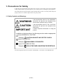
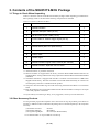
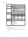
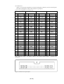
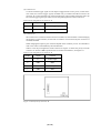
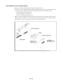
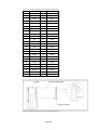
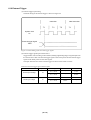
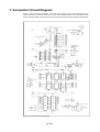
M34551T2-MCU
MCU Board for PC4504 Emulator System
User's Manual
Rev.1.00
September 1, 2003
REJ10J0276-0100Z
MS-DOS is a registered trademark of Microsoft Corporation of the U.S.
IBM and AT are registered trademarks of International Business Machines Corporation of the U.S.
Keep safety first in your circuit designs!
• Renesas Technology Corporation and Renesas Solutions Corporation put the maximum effort into making semiconductor products better
and more reliable, but there is always the possibility that trouble may occur with them. Trouble with semiconductors may lead to personal
injury, fire or property damage. Remember to give due consideration to safety when making your circuit designs, with appropriate
measures such as (i) placement of substitutive, auxiliary circuits, (ii) use of nonflammable material or (iii) prevention against any
malfunction or mishap.
Notes regarding these materials
• These materials are intended as a reference to assist our customers in the selection of the Renesas Technology product best suited to
the customer's application; they do not convey any license under any intellectual property rights, or any other rights, belonging to Renesas
Technology Corporation, Renesas Solutions Corporation or a third party.
• Renesas Technology Corporation and Renesas Solutions Corporation assume no responsibility for any damage, or infringement of any
third-party's rights, originating in the use of any product data, diagrams, charts, programs, algorithms, or circuit application examples
contained in these materials.
• All information contained in these materials, including product data, diagrams, charts, programs and algorithms represents information
on products at the time of publication of these materials, and are subject to change by Renesas Technology Corporation and Renesas
Solutions Corporation without notice due to product improvements or other reasons. It is therefore recommended that customers contact
Renesas Technology Corporation, Renesas Solutions Corporation or an authorized Renesas Technology product distributor for the latest
product information before purchasing a product listed herein. The information described here may contain technical inaccuracies or
typographical errors. Renesas Technology Corporation and Renesas Solutions Corporation assume no responsibility for any damage,
liability, or other loss rising from these inaccuracies or errors. Please also pay attention to information published by Renesas Technology
Corporation and Renesas Solutions Corporation by various means, including the Renesas home page (http://www.renesas.com).
• When using any or all of the information contained in these materials, including product data, diagrams, charts, programs, and algorithms,
please be sure to evaluate all information as a total system before making a final decision on the applicability of the information and
products. Renesas Technology Corporation and Renesas Solutions Corporation assume no responsibility for any damage, liability or
other loss resulting from the information contained herein.
• Renesas Technology semiconductors are not designed or manufactured for use in a device or system that is used under circumstances
in which human life is potentially at stake. Please contact Renesas Technology Corporation, Renesas Solutions Corporation or an
authorized Renesas Technology product distributor when considering the use of a product contained herein for any specific purposes,
such as apparatus or systems for transportation, vehicular, medical, aerospace, nuclear, or undersea repeater use.
• The prior written approval of Renesas Technology Corporation and Renesas Solutions Corporation is necessary to reprint or reproduce
in whole or in part these materials.
• If these products or technologies are subject to the Japanese export control restrictions, they must be exported under a license from the
Japanese government and cannot be imported into a country other than the approved destination. Any diversion or reexport contrary to
the export control laws and regulations of Japan and/or the country of destination is prohibited.
• Please contact Renesas Technology Corporation or Renesas Solutions Corporation for further details on these materials or the products
contained therein.
Precautions to be taken when using this product
• This product is a development supporting unit for use in your program development and evaluation stages. In mass-producing your
program you have finished developing, be sure to make a judgment on your own risk that it can be put to practical use by performing
integration test, evaluation, or some experiment else.
• In no event shall Renesas Solutions Corporation be liable for any consequence arising from the use of this product.
• Renesas Solutions Corporation strives to renovate or provide a workaround for product malfunction at some charge or without charge.
However, this does not necessarily mean that Renesas Solutions Corporation guarantees the renovation or the provision under any
circumstances.
• This product has been developed by assuming its use for program development and evaluation in laboratories. Therefore, it does not fall
under the application of Electrical Appliance and Material Safety Law and protection against electromagnetic interference when used in
Japan.
For inquiries about the contents of this document or product, fill in the text file the installer of the emulator debugger generates in the
following directory and email to your local distributor.
\SUPPORT\Product-name\SUPPORT.TXT
Renesas Tools Homepage http://www.renesas.com/en/tools
( 2 / 40 )
Contents
Preface ....................................................................................................................................4
1. Precautions for Safety ......................................................................................................... 5
1.1 Safety Symbols and Meanings ..............................................................................5
2. Handling Precautions .......................................................................................................... 9
3. Contents of the M34551T2-MCU Package ...................................................................... 11
3.1 Things to Check When Unpacking ..................................................................... 11
3.2 Other Necessary Products ................................................................................... 11
4. M34551T2-MCU .............................................................................................................. 13
4.1 Outline ................................................................................................................. 13
4.2 Specifications ...................................................................................................... 14
4.3 Description of Switches ...................................................................................... 15
4.4 Description of Connectors ................................................................................... 17
4.5 Connection to the Target System ........................................................................ 21
4.6 LED ..................................................................................................................... 23
5. Using as an Evaluation Board .......................................................................................... 25
5.1 System Configuration .......................................................................................... 25
5.2 Mounting the EPROM ........................................................................................ 25
5.3 Mounting the Rubber Legs .................................................................................. 26
5.4 Switch Settings .................................................................................................... 27
5.5 Connection to the Target System ........................................................................ 27
5.6 Connection to the External Power Source .......................................................... 27
5.7 Turning the Power On ......................................................................................... 27
6. Precautions to Be Taken When Debugging ...................................................................... 29
6.1 Reset .................................................................................................................... 29
6.2 System Clock ...................................................................................................... 29
6.3 Real-time Capability of Timer ............................................................................ 29
6.4 Watchdog Timer .................................................................................................. 30
6.5 Pullup Transistors ................................................................................................ 30
6.6 Port I/O Timing ................................................................................................... 30
6.7 Characteristics of I/O Ports ................................................................................. 31
6.8 Power-down Mode .............................................................................................. 32
6.9 Program Execution (G, GB) ................................................................................ 33
6.10 External Trigger ................................................................................................ 35
7. Connection Circuit Diagram ............................................................................................. 37
Appendix A .......................................................................................................................... 38
( 3 / 40 )
Preface
This user's manual describes the specifications of the M34551T2-MCU emulator board for Renesas
4551 and 4555 groups of 4-bit single-chip microcomputers.
The M34551T2-MCU is the MCU board for the PC4504 emulator.
For the PC4504 emulator main unit and the M3T-PD45 emulator debugger, refer to their user's
manuals.
To use the product properly
Precautions for Safety
• In both this User's Manual and on the product itself, several icons are used to insure
proper handling of this product and also to prevent injuries to you or other persons,
or damage to your properties.
• The icons' graphic images and meanings are given in "Chapter 1. Precautions for
Safety". Be sure to read this chapter before using the product.
( 4 / 40 )
1. Precautions for Safety
In both the user's manual and on the product itself, several icons are used to insure proper handling
of this product and also to prevent injuries to you or other persons, or damage to your properties.
This chapter describes the precautions which should be taken in order to use this product safely and
properly. Be sure to read this chapter before using this product.
1.1 Safety Symbols and Meanings
WARNING
If the requirements shown in the "WARNING"
sentences are ignored, the equipment may
cause serious personal injury or death.
CAUTION
If the requirements shown in the "CAUTION"
sentences are ignored, the equipment may
malfunction.
IMPORTANT
It means important information on using this
product.
In addition to the three above, the following are also used as appropriate.
means WARNING or CAUTION.
Example:
CAUTION AGAINST AN ELECTRIC SHOCK
means PROHIBITION.
Example:
DISASSEMBLY PROHIBITED
means A FORCIBLE ACTION.
Example:
UNPLUG THE POWER CABLE FROM THE RECEPTACLE.
The following pages describe the symbols "WARNING", "CAUTION", and "IMPORTANT".
( 5 / 40 )
WARNING
Warning for Installation:
• Do not set this product in water or areas of high humidity. Make sure that the main unit does not
get wet. Spilling water or some other liquid into the main unit can cause an unrepairable damage.
Warning for Use Environment:
• This equipment is to be used in an environment with a maximum ambient temperature of 35 °C.
Care should be taken that this temperature is not exceeded.
CAUTION
Cautions to be Taken for This Product:
• Do not disassemble or modify this product. Disassembling or modifying this product can cause
damage. Disassembling and modifying the product will void your warranty.
• Use caution when handling the main unit. Be careful not to apply a mechanical shock.
• Do not pull the emulator probe (100-pin half-pitch cable or 50-pin normal-pitch cable) to
disconnect from the emulator main unit.
• Do not use inch-size screws for this equipment. The screws used in this equipment are all ISO
(meter-size) type screws. When replacing screws, use same type screws as equipped before.
( 6 / 40 )
IMPORTANT
Notes on Differences between Actual MCU and Emulator:
• Emulator operation differs from emulation of a mask MCU, as listed below. For details refer to
"Chapter 6. Precautions to be Taken When Debugging".
(1) Reset condition
(2) Initial values of internal resource data at power-on
(3) Internal RAM and ROM capacities, etc.
(4) Electrical characteristics
(5) Operation in the power-down mode
(6) Operation of the watchdog timer function
• Therefore, always be sure to evaluate your system with an evaluation MCU (onetime version).
Also, be sure to perform board-mounted evaluation with ES (Engineering Sample) version MCU
to make final confirmation of device operation before starting mask production.
Note on the Target System:
• The operating voltage of the M34551T2-MCU is +3.0 V or +5.0 V. Therefore the target's supply
voltage should be in the range of +3.0 V ±10 % or 5.0 V ±10 %.
Notes on Connecting the Target System:
• When connecting the emulator probe, be careful to the wrong connection.
• When connecting the emulator probe, be careful to the warp of the cable. The warp may cause
breaking the wire.
( 7 / 40 )
MEMO
( 8 / 40 )
2. Handling Precautions
When using the M34551T2-MCU board, pay attention to the following:
(1) About the emulator
To use the M34551T2-MCU board, you always need to install it on the PC4504 emulator main
unit.
(2) About the MCU board installation
Before installing (and removing) the MCU board, always be sure to power off the PC4504
emulator main unit and unplug its power cord from the outlet. For details on how to install and
remove the MCU board, see "Chapter 2. Set-up" in the PC4504 System User’s Manual.
(3) Emulator debugger
When using the M34551T2-MCU board to debug your program, you need to have the M3T-PD45
emulator debugger (sold separately). You need also the data file for 4551/4555 Group included
with M3T-PD45.
(4) Registers that can be operated from M3T-PD45
Table 2.1 lists the registers that can be operated from the M3T-PD45. The "O" in the table means
that the register can be operated; the "X" means that the register cannot be operated.
Table 2.1 Registers that can be operated from M3T-PD45
Register
Reference
Modification
Register
Reference
Modification
PC
O
O
W1
O
O
CY
O
O
W2
O
O
A
O
O
W3
O
O
B
O
O
C1
O
O
X
O
O
C2
X
O
Y
O
O
CR
O
O
Z
O
O
PU0
O
O
D
O
O
RLC
O
O
E
O
O
MR
O
O
SP
O
X
R1
X
O
V1
O
O
L1
X
O
V2
O
O
L2
X
O
I1
O
O
(5) About the system clock frequency
When setting both bit 3 and bit 0 in the MR clock control register to "0" (high-speed mode, system
clock = f(XIN)), the system clock frequency should be in the following ranges.
• VDD = 3.0 V: XIN ≤ 1.0 MHz
• VDD = 5.0 V: XIN ≤ 2.0 MHz
( 9 / 40 )
MEMO
( 10 / 40 )
3. Contents of the M34551T2-MCU Package
3.1 Things to Check When Unpacking
Table 3.1 shows the contents of the M34551T2-MCU package. When unpacking your M34551T2MCU package, check to see that all the following components are included.
Table 3.1 Contents of M34551T2-MCU
Item
Product name
Quantity
1
M34551T2-MCU*1
1
2
100-wire half-pitch cable (40 cm)
1
3
50-wire normal-pitch cable (10 cm)
1
4
2-wire cable for external trigger signal (50 cm)
1
5
PCA4029 pitch converter board
1
6
M34551E8FP (MCU for replacement)*2
1
7
OSC-2 oscillator circuit board (J1 connector mounted)*3
1
8
Power code*4
1
9
Rubber legs*4
4
10
M34551T2-MCU English user's manual (this manual)
1
11
M34551T2-MCU Japanese user's manual
1
*1 "M34551T-MCU" is printed on the board.
*2 M34551T2-MCU is shipped from the factory with the M34555M4-002FP mounted as an
evaluation MCU. If using with the 4551 Group, replace the evaluation MCU with the M34551E8FP
(included).
*3 The M34551T2-MCU is equipped with the OSC-2 oscillator circuit board for 4.0 MHz when
shipped from the factory. The OSC-2 oscillator circuit board mounted with only J1 connector for
clock frequency alteration is included with the product.
*4 The power cable and rubber legs are used when using the M34551T2-MCU as an evaluation
board.
*5 Keep the packaging carton and cushion material of the M34551T2-MCU to transport it for repair
or for other purposes in the future.
*6 If you find any item missing or faulty, or any suggestion, contact your local distributor.
3.2 Other Necessary Products
To bring forward program development on the 4551/4555 Group, the products given below are
necessary in addition to those contained in the package above. Get them separately to be ready when
necessary.
(1) Emulator main unit:
(2) Emulator debugger:
(3) Programming adapter:
PC4504
M3T-PD45
PCA7414 (for M34551E8FP)
* An evaluation MCU is not provided for 4555 Group.
( 11 / 40 )
MEMO
( 12 / 40 )
4. M34551T2-MCU
4.1 Outline
By using with the PC4504 emulator main unit, the M34551T2-MCU can make up an emulator system
which can be operated by a personal computer.
Figure 4.1 shows the development support system configuration.
Figure 4.1 Development support system configuration
( 13 / 40 )
4.2 Specifications
Table 4.1 lists specifications of the M34551T2-MCU.
Table 4.1 M34551T2-MCU Specifications
Applicable MCUs
M34551MX-XXXFP
M34555MX-XXXFP
Evaluation MCUs
M34551E8FP (included)
M34555M4-002FP (mounted)
Maximum operating
clock frequency
3V
Medium-speed mode*1: 4.0 MHz
High-speed mode: 1.0 MHz
5V
Medium-speed mode*1: 8.0 MHz
High-speed mode: 2.0 MHz
3V/5V
XC clock: 32 kHz (using the crystal oscillator on the board)
Target system voltage
3 V or 5 V
Power supply
Supplied by the PC4504's internal power supply (+5 V, +12 V)
Port emulation
Port
Output type
Direction
Devices used
P20, P21 *2
-
Input
Input: 74HC4066
N-channel
open drain
Input/output
Input: 74HC541
Output: 74LS06
P10 - P13
P00 - P03
D0 - D5
Board dimensions
233 (L) x 135 (W) x 26 (H) mm
Operating temperature 5 to 35 °C (non-condensing)
Product configuration
M34551T2-MCU *3
100-wire half-pitch cable
50-wire normal-pitch cable
External trigger cable
PCA4029
M34551E8FP (for replacement)
OSC-2 (for changing frequencies) *4
Power code
Rubber legs (4 pieces)
*1 Operates in the medium-speed mode (instruction clock: f (XIN)/12) immediately after reset
termination.
*2 Ports P20 and P21 are used with both SEG16 and SEG17, and function as output ports when the
segment output is selected.
*3 "M34551T-MCU" is printed on the board.
*4 The M34551T2-MCU has an oscillator circuit board OSC-2 (for 4.0 MHz) when shipped from
the factory. In addition, it comes with an oscillator circuit board OSC-2, with only a connector
J1 mounted.
( 14 / 40 )
4.3 Description of Switches
The M34551T2-MCU board has nine switches. Figure 4.2 shows the positions of these switches.
Tables 4.2 and 4.3 list the functions of the switches and the preset switch positions that are set before
the MCU board is shipped from the factory.
Figure 4.2 Positions of switches
Table 4.2 Functions of switches (1/2)
Label
Description
Switch position
OFF
ON
OFF
Does not connect the VDD of the M34551T2MCU to the VDD of the target system.
ON
ON
OFF
Connects the VDD of the M34551T2-MCU to
the VDD of the target system.
Factory-setting
SW1
OFF
Sets the MCU’s ROM size.
SW2
ROMSIZE
• M4, set SW2 to "4".
• E8, set SW2 to "8".
4
5V
3V
5V
Operates the target MCU at +5 V.
3V
3V
5V
Operates the target MCU at +3 V.
SW3
5V
( 15 / 40 )
Table 4.3 Functions of the switches (2/2)
Label
Switch position
Description
OFF
Does not connect the pullup resistor 68 kΩ to
the port P10.
ON
Connects the pullup resistor 68 kΩ to the port
P10.
Factory-setting
SW4
OFF
Does not connect the pullup resistor 68 kΩ to
the port P11.
ON
Connects the pullup resistor 68 kΩ to the port
P11.
OFF
SW5
OFF
Does not connect the pullup resistor 68 kΩ to
the port P12.
ON
Connects the pullup resistor 68 kΩ to the port
P12.
OFF
SW6
OFF
Does not connect the pullup resistor 68 kΩ to
the port P13.
ON
Connects the pullup resistor 68 kΩ to the port
P13.
OFF
SW7
PORT
PORT
XC
Uses the ports D6 and D7.
XC
PORT
XC
Uses the sub-clock oscillator circuit.
551
555
551
Operates the M34551T2-MCU for 4551 group.
555
555
551
Operates the M34551T2-MCU for 4555 group.
OFF
SW8
PORT
SW9
( 16 / 40 )
555
4.4 Description of Connectors
The M34551T2-MCU board has eight connectors. Table 4.4 lists the functions of these connectors.
Figure 4.3 shows the positions of connectors on the MCU board.
Table 4.4 Connectors
Function
Connector
J1
Connects the evaluation MCU bus.
J2
Connects the monitor CPU bus.
J3
Connects the target system. (100-pin)
J4
Connects the external trigger signal. (2-pin)
J5
Connects the evaluation board.
J6
Connects the oscillator circuit board. (4-pin)
J7, J8
Connects PCA7745.
Figure 4.3 Positions of connectors
( 17 / 40 )
(1) Connector J3
Table 4.5 lists the pin assignments of 100-wire half-pitch connector (J3) for connecting the
PCA4029. And Figure 4.4 shows the connector J3 pin layout.
Table 4.5 Pin assignments of connector J3
Line A
Line B
I/O Pin No.
Line D
Line C
Pin No.
Signal
I/O Pin No.
1
GND
1
GND
1
EP22/SEG18 I/O
2
GND
2
GND
2
EP23/SEG19 I/O
3
GND
3
GND
3
EP00
4
GND
4
GND
4
5
GND
5
GND
6
GND
6
7
GND
8
Signal
I/O
1
EP21/SEG17
I/O
2
EP20/SEG16
I/O
I/O
3
SEG15
O
EP01
I/O
4
SEG14
O
5
EP02
I/O
5
SEG13
O
GND
6
EP03
I/O
6
VSS
7
GND
7
EP10
I/O
7
SEG12
O
GND
8
GND
8
EP11
I/O
8
SEG11
O
9
GND
9
GND
9
EP12
I/O
9
SEG10
O
10
GND
10
GND
10
EP13
I/O 10
SEG9
O
11
GND
11
GND
11
ED0
O
11
SEG8
O
12
GND
12
GND
12
ED1
O
12
SEG7
O
13
GND
13
GND
13
ED2
O
13
SEG6
O
14
GND
14
GND
14
ED3
O
14
SEG5
O
15
GND
15
GND
15
ED4
O
15
SEG4
O
16
GND
16
GND
16
ED5/INT
I/O 16
SEG3
O
17
GND
17
GND
17
CARR
O
17
SEG2
O
18
GND
18
GND
18
VDD
18
SEG1
O
19
GND
19
GND
19
VSS
19
SEG0
O
20
GND
20
GND
20
XIN
-
20
COM3
O
21
GND
21
GND
21
XOUT
-
21
COM2
O
22
GND
22
GND
22
CNVSS
-
22
COM1
O
23
GND
23
GND
23
ED6/XCIN
I/O 23
COM0
O
24
GND
24
GND
24
ED7/XCOUT
O
24
ERESET*
I
25
GND
25
GND
25
NC
-
25
NC
-
Signal
Signal
I/O Pin No.
Note: "I" denotes "Input"; "O" denotes "Output"; "I/O" denotes "Input/output"; "-" denotes "Not
connected".
Figure 4.4 Connector J3 pin layout
( 18 / 40 )
(2) Connector J4
To use the external trigger signal as event input of trigger breaks or trace points, connect the 2wire cable (for external trigger signal) included with your M34551T2-MCU board to the
connector J4. Connect the black clip of the external trigger cable to GND, and use the white clip
for external trigger signal input. Table 4.6 lists the pin assignments of the connector J4.
Table 4.6 Pin assignments of connector J4
Pin No.
Signal
Function
1
TRIG
External trigger signal input
2
GND
GND input
(3) Connector J6
The connector J6 is a connector used to connect an oscillator circuit board OSC-2. When changing
the frequency of the oscillator, use the OSC-2 oscillator circuit board (only the connector J1
mounted) included.
When changing the frequency, the constants depend on the oscillator you use. It's advisable to
refer to the values recommended by the manufacturers.
Table 4.7 lists the pin assignments of the connector J6. Figure 4.5 shows the pin layout of the
connector J6. For the 4 MHz operation with an oscillator board OSC-2, see Figure 4.6.
Table 4.7 Pin assignments of connector J6
Pin No.
Signal
Function
1
VCC
Power supply
2
GND
GND
3
CLK
Clock input
4
GND
GND
Figure 4.5 Pin layout of connector J6
( 19 / 40 )
Figure 4.6 Schematic circuit diagram of OSC-2 (4.0 MHz)
( 20 / 40 )
4.5 Connection to the Target System
When connecting the M34551T2-MCU board to the target system:
Connect the 50-wire normal-pitch cable included with the MCU board to the 50-pin dual-in-line pins
on the target system. Following products are required for connection to the target system.
(1) 100-wire half-pitch cable (40 cm)
(2) PCA4029 pitch converter board
(3) 50-wire normal-pitch cable (10 cm)
Figure 4.7 depicts the M34551T2-MCU board connected to the target system using the 50-wire
normal-pitch cable. Table 4.8 lists the connector signal assignments of the 50-wire normal-pitch
cable. Figure 4.8 shows the pin layout of the 50-wire normal-pitch cable.
Figure 4.7 Connecting the MCU board to the target system using dual-in-line pins
( 21 / 40 )
Table 4.8 50-wire normal-pitch cable pin assignments
Pin No.
Signal
Pin No.
Signal
1
EP22/SEG18
50
EP21/SEG17
2
EP23/SEG19
49
EP20/SEG16
3
EP00
48
SEG15
4
EP01
47
SEG14
5
EP02
46
SEG13
6
EP03
45
VSS
7
EP10
44
SEG12
8
EP11
43
SEG11
9
EP12
42
SEG10
10
EP13
41
SEG9
11
ED0
40
SEG8
12
ED1
39
SEG7
13
ED2
38
SEG6
14
ED3
37
SEG5
15
ED4
36
SEG4
16
ED5/INT
35
SEG3
17
CARR
34
SEG2
18
VDD
33
SEG1
19
VSS
32
SEG0
20
NC
31
COM3
21
NC
30
COM2
22
NC
29
COM1
23
ED6/NC
28
COM0
24
ED7/NC
27
ERESET*
25
NC
26
NC
Figure 4.8 Pin layout of the 50-wire normal-pitch cable
( 22 / 40 )
Some signals connected to the target system are emulated on the M34551T2-MCU board. For details,
see "Chapter 7. Connection Circuit Diagram".
• Pins connected directly to the target system (6 types, 24 lines)
(1) SEG0 - SEG15
(2) COM0 - COM3
(3) CARR
(4) D6*
(5) D7*
(6) VSS
• Pins connected to the target system via emulation circuits, etc. (6 types, 20 lines)
(1) P00 - P03
(2) P10 - P13
(3) P20 - P23
(4) D0 - D5
(5) RESET *
(6) VDD
• Pins not connected to the target system (5 types, 5 lines)
(1) XIN
(2) XOUT
(3) CNVSS
(4) XCIN *
(5) XCOUT *
* Not connected to the target system when the sub-clock is selected (switch SW8: "XC"). The
external clock signal (32.768 kHz) is input to the XCIN pin from the oscillator of the M34551T2MCU board. And the XCOUT pin is not connected.
4.6 LED
Figure 4.9 shows the LED layout of the M34551T2-MCU. The LED lights in green when the power
is supplied to the MCU board.
Figure 4.9 Layout of the LED
( 23 / 40 )
MEMO
( 24 / 40 )
5. Using as an Evaluation Board
Mounting the EPROM containing the program and supplying power enables the M34551T2-MCU
to be used as an evaluation board. Use to evaluate the functions that cannot be evaluated with the
evaluation MCU of the 4551 Group. Use an evaluation MCU (OTP version) for 4551 Group
evaluation.
5.1 System Configuration
System configuration when using the M34551T2-MCU as an evaluation board is as shown in Figure
5.1.
Figure 5.1 System configuration for using as evaluation board
5.2 Mounting the EPROM
Load HEX file data generated by ASM45 into the EPROM and mount in the IC socket on the
PCA7745. Prepare two EPROM loaded with the same data, and mount them in the IC sockets on the
PCA7745 while checking the position of pin No. 1 (High and Low side sequence differs for EPROM).
Figure 5.2 shows the EPROM mounting position on the PCA7745.
Figure 5.2 EPROM mounting position on the PCA7745
( 25 / 40 )
5.3 Mounting the Rubber Legs
Mount the rubber legs (included) in the four corners of the board if using the M34551T2-MCU board
as an evaluation board. Figure 5.3 shows the positions of the mounting holes and method of mounting
the rubber legs. When mounting them, securely fasten the screws with a screwdriver, etc. Using the
board without the rubber legs could result in damage of the M34551T2-MCU board and target system
due to a short, etc.
Figure 5.3 Positions of the mounting holes and method of mounting the rubber legs
( 26 / 40 )
5.4 Switch Settings
The PCA7745 board is equipped with switch SW1 for setting the ROM type. Set switch SW1
according to the type of EPROM to be used as shown in Table 5.1.
Table 5.1 Setting switch SW1 on PCA7745
Setting
Device
256
M5M27C2566AK
512
M5M27C512ALK
5.5 Connection to the Target System
For method of connecting the MCU board to the target system when using this product as an
evaluation board, refer to "4.5 Connecting the MCU board to the Target System".
5.6 Connection to the External Power Source
If using the M34551T2-MCU board as an evaluation board, you must supply power from an external
source. Use a power source capable of delivering +5 V or +12 V. Table 5.2 gives the pin positions
for the external power source input cable.
Table 5.2 Pin positions for the external power source input cable
Pin No.
Color
Function
1
Red
Input (+5 V)
2
Black
GND
3
White
Input (+12 V)
4
-
Not used
5.7 Turning the Power On
After checking connection of the target system and external power source for the evaluation board,
turn the target system and external power supply on. And turn on the power to each equipment
following the procedure below successively.
(1) Turn on the target system.
(2) Turn on the external power source for the evaluation board.
Also, follow steps (1) and (2) when powering off.
(1) Turn off the target system.
(2) Turn off the external power source for the evaluation board.
( 27 / 40 )
MEMO
( 28 / 40 )
6. Precautions to Be Taken When Debugging
6.1 Reset
The M34551T2-MCU uses 74AC14 for the reset signal input buffer, and electrical characteristics
therefore differ from those of an actual chip.
Table 6.1 lists the RESET signal input characteristics on the M34551T2-MCU.
Table 6.1 RESET signal input characteristics
Item
Symbol
H-level threshold voltage
VP
L-level threshold voltage
VN
Hysteresis voltage
VH
Voltage
Min.
Max.
VCC=3.0 V
-
2.2 V
VCC=4.5 V
-
3.2 V
VCC=5.5 V
-
3.9 V
VCC=3.0 V
0.5 V
-
VCC=4.5 V
0.9 V
-
VCC=5.5 V
1.1 V
-
VCC=3.0 V
0.3 V
1.2 V
VCC=4.5 V
0.4 V
1.4 V
VCC=5.5 V
0.5 V
1.6 V
6.2 System Clock
Use the product within the range of MCU specifications and within the frequency range given in
Table 6.2 in accordance with power source voltage and operation mode.
Table 6.2 Maximum operating frequencies of the M34551T2-MCU
Voltage
Mode
Maximum operating frequency
Medium-speed mode
Up to 4.0 MHz
High-speed mode
Up to 1.0 MHz
Medium-speed mode
Up to 8.0 MHz
High-speed mode
Up to 2.0 MHz
3V
5V
Use components required for the OSC-2 oscillator circuit board (included) if changing frequency in
accordance with the target system.
For details about the oscillation circuit constants, consult the manufacturer of your oscillator.
6.3 Real-time Capability of Timer
Since the clock on the MCU board is active even during emulation, its timer values are modified.
Examples:
(1) When single-stepping instructions
(2) When referencing or modifying registers or the internal RAM
( 29 / 40 )
6.4 Watchdog Timer
The watchdog timer does not operate on the M34551T2-MCU board. Use an evaluation MCU (OTP
version) to verify the watchdog timer-related operations.
6.5 Pullup Transistors
Since the P1 port of the M34551T2-MCU contains emulation circuits, you cannot control the pullup
transistors using the pullup control register PU0. When you want to use the internal pullup transistors,
turn on switches SW4 to SW7 to activate the pullup resistors of the M34551T2-MCU. The port P1's
resistance value of the pullup resistor is 68 kΩ by the settings (SW4 to SW7).
And the port P0's (M34551T2-MCU) resistance value of the pullup register is 68 kΩ.
6.6 Port I/O Timing
(1) Port input timing
Port input timings are the same as with the actual MCUs.
(2) Port output timing
When using the M34551T2-MCU, output timings are different from those of the actual MCUs
for the following ports that are configured with port emulation circuits:
• Ports P00 to P03
• Ports P10 to P13
• Ports D0 to D5
With the actual MCUs, changes occur at the beginning of the T3 state of an output instruction.
With the M34551T2-MCU, changes occur at the beginning of the T2 state of the next output
instruction. Figure 6.1 shows the port output timings of the M34551T2-MCU.
For the other ports, the output timings are the same as with the actual MCUs.
Output instruction
System clock XIN
P0, P1, and D port
output timings on
actual MCUs
P0, P1, and D port
output timings on
M34551T2-MCU
Figure 6.1 P0, P1 and D port output timings
( 30 / 40 )
Next output instruction
6.7 Characteristics of I/O Ports
Characteristics of Ports P0, P1, P2, D0 to D7 of the M34551T2-MCU differ from those of actual MCU,
because the M34551T2-MCU have emulation circuit. Table 6.3 shows characteristics of the
emulation ports.
Table 6.3 Characteristics of emulation ports
Port
I/O
Device
Item
VIH
Input
74HC541
VIL
P0, P1
Voltage
Min.
Max.
Vcc=2.0 V
1.5 V
-
Vcc=4.5 V
3.15 V
-
Vcc=2.0 V
-
0.5 V
Vcc=4.5 V
-
1.35 V
-
250 µA
-
40 mA
-
0.4 V
IOL=16 mA
-
0.7 V
IOL=MAX
160 Ω
-
70 Ω
130 Ω
96 Ω
200 Ω
VI/O=Vcc or GND
II/O≤1 mA
Vcc=4.5 V
10 Ω
-
VI/O=Vcc to GND
II/O≤1 mA
Vcc=2.0 V
1.5 V
-
Vcc=4.5 V
3.15 V
-
Vcc=2.0 V
-
0.5 V
Vcc=4.5 V
-
1.35 V
-
250 µA
-
40 mA
-
0.4 V
IOL=16 mA
-
0.7 V
IOL=MAX
IOH
Output
74LS06
IOL
Vcc=4.75 V
VOL
Vcc=2.0 V
RON
P2
Input/
Output
74HC4066
RON
VIH
D5
Input
74HC541
VIL
Vcc=4.5 V
IOH
D5 - D0
Output
74LS06
IOL
VOL
( 31 / 40 )
Vcc=4.75 V
Remarks
VOH=MAX
VI/O=Vcc to GND
II/O≤1 mA
VOH=MAX
6.8 Power-down Mode
The power-down mode of the M34551T2-MCU operates differently from that of the actual MCUs.
(1) Power-down operation of the M34551T2-MCU
While with the actual MCUs the power-down mode works by the "EPOF" and "POF" instructions,
with the M34551T2-MCU the power-down mode works only by the "POF" instruction.
With the M34551T2-MCU, the "EPOF" instruction is invalid.
Example program 6.1
RC
INY
EPOF
POF
•
•
Actual MCU
The power-down mode works.
M34551T2-MCU
The power-down mode works.
Example program 6.2
RC
INY
POF
•
•
•
Actual MCU
The power-down mode does NOT work.
M34551T2-MCU
The power-down mode works.
( 32 / 40 )
6.9 Program Execution (G, GB)
The PC4504 and the M34551T2-MCU’s hardware is subject to the following restrictions with respect
to the operation of the program execution commands (G and GB).
(1) Continuous description of instructions
Hardware breakpoints set in a continuous description of instructions following one after another
do not cause a break to occur in the continuous description of instructions. A break occurs only
after fetching the address where the continuous description of instructions is discontinued. (See
Program example 6.3.)
However, a break does occur even in a continuous description of instructions when an external
trigger break or forced break is encountered. For execution to be resumed in this case, you need
to make sure that the execution start address is next to the continuous description of instructions.
(See Program example 6.4.)
Program example 6.3
POINT:
POINT+2:
LA
0
LA
1
LA
2
XAM
3
; Continuous description of instructions
If a break is set at POINT, execution is halted immediately before the XAM institution at
address POINT+2.
Program example 6.4
LA
0
POINT:
LA
1
POINT+1:
LA
2
POINT+2:
XAM
3
; Continuous description of instructions
If a forced or external trigger break is applied at POINT, execution is halted at POINT+1.
When resuming program execution after the break, make sure that the start address is at
POINT+2, an address immediately after the continuous description of instructions is
discontinued.
( 33 / 40 )
(2) Skip instructions (e.g. SNZP, INY, DEY, SZB, SEAM, SZC and RTS)
In cases when a skip instruction skips the next instruction, a breakpoint set in the skipped
instruction does not cause execution to halt. (See Program examples 6.5 and 6.6)
Program example 6.5
RC
RC
SZC
SZC
POINT:
TABP
POINTA:
TAM
0
POINT:
TABP
POINTA:
TAM
•
•
0
•
•
A breakpoint set at address POINT causes execution to halt immediately before address POINTA
in only the case of the instruction shown on the right side.
Program example 6.6
RC
; Skip instruction
INY
POINT:
TABP
TAM
0
•
•
If a break with pass count is set at address POINT, the count is taken and execution is halted only
when the instruction at address POINT is executed.
( 34 / 40 )
6.10 External Trigger
(1) External trigger input timing
The latch timing of the external trigger is shown in Figure 6.2.
Instruction
Next instruction
System clock
XIN
External trigger signal
TRIG
Figure 6.2 Latch timing of the external trigger signal
(2) External trigger signal input characteristics
Trigger breaks work according to the condition (leading edge/trailing edge) of signals input from
the external trace cable. The external trigger signals of the trace points and the external trigger
signals of the break points use the same signals.
The input characteristics of the external trigger are shown in the Table 6.4 below.
Table 6.4 External trigger input characteristics
Item
H-level input Voltage
L-level input voltage
Symbol
Voltage
Max.
Min.
Vcc = 2.0 V
-
1.5 V
Vcc = 4.5 V
-
3.15 V
Vcc = 2.0 V
0.5 V
-
Vcc = 4.5 V
1.35 V
-
VIH
VIL
( 35 / 40 )
MEMO
( 36 / 40 )
7. Connection Circuit Diagram
Figure 7.1 shows the M34551T2-MCU connection circuit diagram. This circuit diagram depicts the
M34551T2-MCU connection centering on circuits connected to the target system. Emulator control
blocks and other similar circuits that are not connected to the target system are omitted in this diagram.
: Connected to IC23-8.
: Control signal
Figure 7.1 Connection circuit diagram
( 37 / 40 )
Appendix A. How to Request for Repair
If your product is found faulty, follow the procedure below to send your product for repair.
Customer
Fill in the Repair Request Sheet included with this product, then send it
along with this product for repair to your local distributor. Make sure
that information in the Repair Request Sheet is written in as much detail
as possible to facilitate repair.
Distributor
After checking the contents of fault, the distributor should please send
the faulty product along with the Repair Request Sheet to Renesas
Solutions Corp.
Renesas Solutions
When the faulty product is repaired, it will be returned to the customer
at the earliest convenience.
CAUTION
Note on Transporting the Product:
• When sending your product for repair, use the packing box and cushion material supplied with this
product when delivered to you and specify handling caution for it to be handled as precision
equipment. If packing of your product is not complete, it may be damaged during transportation.
When you pack your product in a bag, make sure to use conductive polyvinyl supplied with this
product (usually a blue bag). When you use other bags, they may cause a trouble on your product
because of static electricity.
( 38 / 40 )
M34551T2-MCU User's Manual
Rev.1.00
September 1, 2003
REJ10J0276-0100Z
COPYRIGHT ©2003 RENESAS TECHNOLOGY CORPORATION
AND RENESAS SOLUTIONS CORPORATION ALL RIGHTS RESERVED